Embed Size (px)
Citation preview

2012-2013 Microchip Technology Inc. DS50002063B
MCP16301High-Performance Low-Noise
5V Output Buck ConverterEvaluation Board
User’s Guide

DS50002063B-page 2 2012-2013 Microchip Technology Inc.
Information contained in this publication regarding deviceapplications and the like is provided only for your convenienceand may be superseded by updates. It is your responsibility toensure that your application meets with your specifications.MICROCHIP MAKES NO REPRESENTATIONS ORWARRANTIES OF ANY KIND WHETHER EXPRESS ORIMPLIED, WRITTEN OR ORAL, STATUTORY OROTHERWISE, RELATED TO THE INFORMATION,INCLUDING BUT NOT LIMITED TO ITS CONDITION,QUALITY, PERFORMANCE, MERCHANTABILITY ORFITNESS FOR PURPOSE. Microchip disclaims all liabilityarising from this information and its use. Use of Microchipdevices in life support and/or safety applications is entirely atthe buyer’s risk, and the buyer agrees to defend, indemnify andhold harmless Microchip from any and all damages, claims,suits, or expenses resulting from such use. No licenses areconveyed, implicitly or otherwise, under any Microchipintellectual property rights.
Note the following details of the code protection feature on Microchip devices:
• Microchip products meet the specification contained in their particular Microchip Data Sheet.
• Microchip believes that its family of products is one of the most secure families of its kind on the market today, when used in the intended manner and under normal conditions.
• There are dishonest and possibly illegal methods used to breach the code protection feature. All of these methods, to our knowledge, require using the Microchip products in a manner outside the operating specifications contained in Microchip’s Data Sheets. Most likely, the person doing so is engaged in theft of intellectual property.
• Microchip is willing to work with the customer who is concerned about the integrity of their code.
• Neither Microchip nor any other semiconductor manufacturer can guarantee the security of their code. Code protection does not mean that we are guaranteeing the product as “unbreakable.”
Code protection is constantly evolving. We at Microchip are committed to continuously improving the code protection features of ourproducts. Attempts to break Microchip’s code protection feature may be a violation of the Digital Millennium Copyright Act. If such actsallow unauthorized access to your software or other copyrighted work, you may have a right to sue for relief under that Act.
Microchip received ISO/TS-16949:2009 certification for its worldwide headquarters, design and wafer fabrication facilities in Chandler and Tempe, Arizona; Gresham, Oregon and design centers in California and India. The Company’s quality system processes and procedures are for its PIC® MCUs and dsPIC® DSCs, KEELOQ® code hopping devices, Serial EEPROMs, microperipherals, nonvolatile memory and analog products. In addition, Microchip’s quality system for the design and manufacture of development systems is ISO 9001:2000 certified.
QUALITY MANAGEMENT SYSTEM CERTIFIED BY DNV
== ISO/TS 16949 ==
Trademarks
The Microchip name and logo, the Microchip logo, dsPIC, FlashFlex, KEELOQ, KEELOQ logo, MPLAB, PIC, PICmicro, PICSTART, PIC32 logo, rfPIC, SST, SST Logo, SuperFlash and UNI/O are registered trademarks of Microchip Technology Incorporated in the U.S.A. and other countries.
FilterLab, Hampshire, HI-TECH C, Linear Active Thermistor, MTP, SEEVAL and The Embedded Control Solutions Company are registered trademarks of Microchip Technology Incorporated in the U.S.A.
Silicon Storage Technology is a registered trademark of Microchip Technology Inc. in other countries.
Analog-for-the-Digital Age, Application Maestro, BodyCom, chipKIT, chipKIT logo, CodeGuard, dsPICDEM, dsPICDEM.net, dsPICworks, dsSPEAK, ECAN, ECONOMONITOR, FanSense, HI-TIDE, In-Circuit Serial Programming, ICSP, Mindi, MiWi, MPASM, MPF, MPLAB Certified logo, MPLIB, MPLINK, mTouch, Omniscient Code Generation, PICC, PICC-18, PICDEM, PICDEM.net, PICkit, PICtail, REAL ICE, rfLAB, Select Mode, SQI, Serial Quad I/O, Total Endurance, TSHARC, UniWinDriver, WiperLock, ZENA and Z-Scale are trademarks of Microchip Technology Incorporated in the U.S.A. and other countries.
SQTP is a service mark of Microchip Technology Incorporated in the U.S.A.
GestIC and ULPP are registered trademarks of Microchip Technology Germany II GmbH & Co. KG, a subsidiary of Microchip Technology Inc., in other countries.
All other trademarks mentioned herein are property of their respective companies.
© 2012-2013, Microchip Technology Incorporated, Printed in the U.S.A., All Rights Reserved.
Printed on recycled paper.
ISBN: 978-1-62077-420-5

2012-2013 Microchip Technology Inc. DS50002063B-page 3
Object of Declaration: MCP16301 High-Performance Low-Noise 5V Output Buck Converter Evaluation Board User’s Guide

MCP16301 HIGH-PERFORMANCELOW-NOISE 5V BUCK CONVERTER
EVALUATION BOARD USER’S GUIDE
Table of Contents
Preface ........................................................................................................................... 5Introduction............................................................................................................ 5
Document Layout .................................................................................................. 5
Conventions Used in this Guide ............................................................................ 6
Recommended Reading........................................................................................ 7
The Microchip Web Site ........................................................................................ 7
Customer Support ................................................................................................. 7
Document Revision History ................................................................................... 7
Chapter 1. Product Overview1.1 Introduction ..................................................................................................... 91.2 MCP16301 Short Overview ............................................................................ 91.3 What Is the MCP16301 High Performance Low Noise 5V Buck Converter
Evaluation Board? .................................................................................. 11
1.4 MCP16301 High Performance Low Noise 5V Buck Converter Evaluation Board Kit Contents ................................................................ 11
Chapter 2. Installation and Operation2.1 Introduction ................................................................................................... 132.2 Getting Started ............................................................................................. 14
Appendix A. Schematic and LayoutsA.1 Introduction .................................................................................................. 21A.2 Board – Schematic ....................................................................................... 22A.3 Board – Top Silk And Copper ...................................................................... 23A.4 Board – Mid Inner Layer 1 ........................................................................... 24A.5 Board – Mid Inner Layer 2 ........................................................................... 25A.6 Board – Bottom Copper and Pads ............................................................... 26
Appendix B. Bill of Materials (BOM).......................................................................... 27
Worldwide Sales and Service .................................................................................... 28
2012-2013 Microchip Technology Inc. DS50002063B-page 4

MCP16301 HIGH-PERFORMANCELOW-NOISE 5V BUCK CONVERTER
EVALUATION BOARD USER’S GUIDE
Preface
INTRODUCTION
This chapter contains general information that will be useful to know before using the MCP16301 High-Performance Low-Noise 5V Buck Converter Evaluation Board. Items discussed in this chapter include:
• Document Layout
• Conventions Used in this Guide
• Recommended Reading
• The Microchip Web Site
• Customer Support
• Document Revision History
DOCUMENT LAYOUT
This document describes how to use the MCP16301 High-Performance Low-Noise 5V Buck Converter Evaluation Board as a development tool to emulate and debug firm-ware on a target board. The manual layout is as follows:
• Chapter 1. “Product Overview” – Important information about the MCP16301 High-Performance Low-Noise 5V Buck Converter Evaluation Board
• Chapter 2. “Installation and Operation” – Includes instructions on how to get started with the MCP16301 High-Performance Low-Noise 5V Buck Converter Evaluation Board and a description of the user’s guide
• Appendix A. “Schematic and Layouts” – Shows the schematic and layout diagrams for the MCP16301 High-Performance Low-Noise 5V Buck Converter Evaluation Board
• Appendix B. “Bill of Materials (BOM)” – Lists the parts used to build the MCP16301 High-Performance Low-Noise 5V Buck Converter Evaluation Board
NOTICE TO CUSTOMERS
All documentation becomes dated, and this manual is no exception. Microchip tools and documentation are constantly evolving to meet customer needs, so some actual dialogs and/or tool descriptions may differ from those in this document. Please refer to our web site (www.microchip.com) to obtain the latest documentation available.
Documents are identified with a “DS” number. This number is located on the bottom of each page, in front of the page number. The numbering convention for the DS number is “DSXXXXXA”, where “XXXXX” is the document number and “A” is the revision level of the document.
For the most up-to-date information on development tools, see the MPLAB® IDE online help. Select the Help menu, and then Topics to open a list of available online help files.
2012-2013 Microchip Technology Inc. DS50002063B-page 5

MCP16301 High-Performance Low-Noise 5V Buck Converter Evaluation Board User’s Guide
CONVENTIONS USED IN THIS GUIDE
This manual uses the following documentation conventions:
DOCUMENTATION CONVENTIONS
Description Represents Examples
Arial font:
Italic characters Referenced books MPLAB® IDE User’s Guide
Emphasized text ...is the only compiler...
Initial caps A window the Output window
A dialog the Settings dialog
A menu selection select Enable Programmer
Quotes A field name in a window or dialog
“Save project before build”
Underlined, italic text with right angle bracket
A menu path File>Save
Bold characters A dialog button Click OK
A tab Click the Power tab
N‘Rnnnn A number in verilog format, where N is the total number of digits, R is the radix and n is a digit.
4‘b0010, 2‘hF1
Text in angle brackets < > A key on the keyboard Press <Enter>, <F1>
Courier New font:
Plain Courier New Sample source code #define START
Filenames autoexec.bat
File paths c:\mcc18\h
Keywords _asm, _endasm, static
Command-line options -Opa+, -Opa-
Bit values 0, 1
Constants 0xFF, ‘A’
Italic Courier New A variable argument file.o, where file can be any valid filename
Square brackets [ ] Optional arguments mcc18 [options] file [options]
Curly brackets and pipe character: { | }
Choice of mutually exclusive arguments; an OR selection
errorlevel {0|1}
Ellipses... Replaces repeated text var_name [, var_name...]
Represents code supplied by user
void main (void){ ...}
DS50002063B-page 6 2012-2013 Microchip Technology Inc.

Preface
RECOMMENDED READING
This user's guide describes how to use the MCP16301 High-Performance Low-Noise 5V Buck Converter Evaluation Board. Other useful documents are listed below. The following Microchip documents are available and recommended as supplemental reference resources.
• MCP16301 Data Sheet – “High-Voltage Input Integrated Switch Step-Down Regulator” (DS25004)
• MCP16301 High-Voltage Buck-Boost Demo Board User’s Guide (DS52020)
• MCP16301 High-Voltage Buck Converter 600 mA Demo Board User’s Guide (DS51978)
THE MICROCHIP WEB SITE
Microchip provides online support via our web site at www.microchip.com. This web site is used as a means to make files and information easily available to customers. Accessible by using your favorite Internet browser, the web site contains the following information:
• Product Support – Data sheets and errata, application notes and sample programs, design resources, user’s guides and hardware support documents, latest software releases and archived software
• General Technical Support – Frequently Asked Questions (FAQs), technical support requests, online discussion groups, Microchip consultant program member listing
• Business of Microchip – Product selector and ordering guides, latest Microchip press releases, listing of seminars and events, listings of Microchip sales offices, distributors and factory representatives
CUSTOMER SUPPORT
Users of Microchip products can receive assistance through several channels:
• Distributor or Representative
• Local Sales Office
• Field Application Engineer (FAE)
• Technical Support
Customers should contact their distributor, representative or field application engineer (FAE) for support. Local sales offices are also available to help customers. A listing of sales offices and locations is included in the back of this document.
Technical support is available through the web site at: http://www.microchip.com/support.
DOCUMENT REVISION HISTORY
Revision B (August 2013)
• Updated the board layout in Figure 2-2.
• Updated the A.3 “Board – Top Silk And Copper” and A.6 “Board – Bottom Copper and Pads” layouts in Appendix A. “Schematic and Layouts”.
• Updated Appendix B. “Bill of Materials (BOM)”.
Revision A (June 2012)
• Initial Release of this Document.
2012-2013 Microchip Technology Inc. DS50002063B-page 7

MCP16301 High-Performance Low-Noise 5V Buck Converter Evaluation Board User’s Guide
NOTES:
DS50002063B-page 8 2012-2013 Microchip Technology Inc.

MCP16301 HIGH-PERFORMANCELOW-NOISE 5V BUCK CONVERTER
EVALUATION BOARD USER’S GUIDE
Chapter 1. Product Overview
1.1 INTRODUCTION
This chapter provides an overview of the MCP16301 High-Performance Low-Noise 5V Buck Converter Evaluation Board and covers the following topics:
• MCP16301 Short Overview
• What Is the MCP16301 High-Performance Low-Noise 5V Buck Converter Evaluation Board?
• MCP16301 High-Performance Low-Noise 5V Buck Converter Evaluation Board Kit Contents
1.2 MCP16301 SHORT OVERVIEW
The MCP16301 device is a highly integrated, high-efficiency, fixed frequency, step-down DC-DC converter in a popular 6-pin SOT-23 package, that operates from input voltage sources up to 30V. Integrated features include a high-side switch, fixed frequency peak current mode control, internal compensation, peak current limit and overtemperature protection.
All control system components necessary for stable operation over the entire device operating range are integrated.
High-converter efficiency is achieved by integrating the current-limited, low-resistance, high-speed N-Channel MOSFET and associated drive circuitry. High-switching fre-quency minimizes the size of the external filtering components, resulting in a small solution size.
The MCP16301 is a high-input voltage step-down regulator, capable of supplying a maximum of 600 mA to a regulated output voltage from 2.0V to 15V. An integrated pre-cise 0.8V reference combined with an external resistor divider sets the desired con-verter output voltage. The internal reference voltage rate of rise is controlled during startup, minimizing the output voltage overshoot and the inrush current.
The internally trimmed 500 kHz oscillator provides a fixed frequency, while the peak current mode control architecture varies the duty cycle for output voltage regulation. An internal floating driver is used to turn the high side integrated N-Channel MOSFET on and off. The power for this driver is derived from an external boost capacitor whose energy is supplied from a fixed voltage ranging between 3.0V and 5.5V, typically the output voltage of the converter. For applications with 5.5V < VOUT < 15V and VIN < 30V, an alternative boost supply must be used (from input derived, output derived or an auxiliary system voltage). For more information and examples, see the MCP16301 data sheet.
The EN input is used to enable and disable the device. If disabled, the MCP16301 device consumes 7 µA (typical) from the input. An integrated Under Voltage Lockout (UVLO) prevents the converter from starting until the input voltage is high enough for normal operation. The converter will typically start at 3.5V and operate down to 3.0V.
An overtemperature protection limits the silicon die temperature to +150°C by turning the converter off. The normal switching resumes at +120°C.
2012-2013 Microchip Technology Inc. DS50002063B-page 9

MCP16301 High-Performance Low-Noise 5V Buck Converter Evaluation Board User’s Guide
FIGURE 1-1: Typical MCP16301 3.3V OUT Application.
1.2.1 MCP16301 Features
• Up to 96% Typical Efficiency
• Input Voltage Range: 4.0V to 30V
• Output Voltage Range: 2.0V to 15V
• 2% Output Voltage Accuracy
• 600 mA Output Current
• Quiescent Current (Switching Mode, No Load): 2 mA Typical
• Quiescent Current (Shutdown, EN = 0): 7 µA Typical
• 500 kHz Fixed Frequency
• Peak Current Mode Control
• Internal Compensation
• Internal Soft-Start
• Cycle-by-Cycle Peak Current Limit
• Undervoltage Lockout (UVLO): 3.5V to Start, 3.0V to Stop
• Overtemperature Protection
• Package type: SOT-23-6
VIN
GND
VFB
SW
VIN 4.5V To 30V
VOUT
3.3V @ 600 mA
COUT22 µFCIN
22 µF
L115 µH
BOOST
31.2 K
10 K
EN
1N4448
40VSchottkyDiode
CBOOST100 nF
DS50002063B-page 10 2012-2013 Microchip Technology Inc.

Product Overview
1.3 WHAT IS THE MCP16301 HIGH-PERFORMANCE LOW-NOISE 5V BUCK CONVERTER EVALUATION BOARD?
The MCP16301 High-Performance Low-Noise 5V Buck Converter Evaluation Board is designed to operate from a 6V to 30V input and regulate the output to 5V, while deliv-ering a maximum 600 mA of load current.
The evaluation board is optimized for a high-efficiency and low-output noise and ripple, especially at 12V Input and 100 mA load current. Because the MCP16301 is switching fast to achieve high efficiency, high-frequency noise is generated and may affect some RF systems. This evaluation board demonstrates a low-noise, high-performance design.
FIGURE 1-2: MCP16301 High-Performance Low-Noise 5V Buck Converter Evaluation Board Block Diagram.
1.4 MCP16301 HIGH-PERFORMANCE LOW-NOISE 5V BUCK CONVERTER EVALUATION BOARD KIT CONTENTS
The MCP16301 High-Performance Low-Noise 5V Buck Converter Evaluation Board kit includes:
• MCP16301 High-Performance Low-Noise 5V Buck Converter Evaluation Board
• Important Information Sheet
VIN = 12V Input
VIN
EN
SWL
RBOOST
RT
VOUT = 5V
FB
CIN
COUT
RB
BOOST
CBOOST
RSnubber
CSnubber
BOOST Diode
GND
120 pF
4R7 52k3
10k
82R100 nF
22 µF
22 µH
MC
P16
301
22 µF
2012-2013 Microchip Technology Inc. DS50002063B-page 11

MCP16301 High-Performance Low-Noise 5V Buck Converter Evaluation Board User’s Guide
NOTES:
DS50002063B-page 12 2012-2013 Microchip Technology Inc.

MCP16301 HIGH-PERFORMANCELOW-NOISE 5V BUCK CONVERTER
EVALUATION BOARD USER’S GUIDE
Chapter 2. Installation and Operation
2.1 INTRODUCTION
The MCP16301 High-Performance Low-Noise 5V Buck Converter Evaluation Board is used to demonstrate a high-voltage input DC-DC converter design, that can deliver high efficiency, while minimizing high-frequency switching noise. The board steps down high-input voltages, up to 30V, to a low-output voltage, having more than 90% efficiency and a minimum of 30 mV output ripple.
High-frequency input/output noise generated by the switching converters can reach high-noise levels that interfere with other devices powered from the same source. The high amplitude of high-frequency noise can disturb some RF systems.
High efficiency is achieved with the MCP16301 buck converter by switching the inte-grated N-Channel MOSFET at a high speed. This high speed can cause disturbances to other system components if the high-speed switching edges of the converter are not minimized. The designer must be concerned with:
• good PCB layout practice
• choosing high-quality shielded inductors and low Equivalent Series Resistance (ESR) capacitors
• choosing an RC snubber or a RBOOST resistor to properly limit the speed of the internal N-Channel MOSFET switch (see Figure 1-2).
The evaluation board is optimized for 12V Input and 100 mA load.
2.1.1 MCP16301 High-Performance Low-Noise 5V Buck Converter Evaluation Board Features
The MCP16301 High-Performance Low-Noise 5V Buck Converter Evaluation Board has the following key features:
• Input Voltage: 6 to 30V
• Output Voltage: 5V
• Output Capability: 600 mA Load Current
• Output Ripple Plus Noise: 30 mVp-p @ 12V Input and 100 mA Load
• Low-Radiated Noise
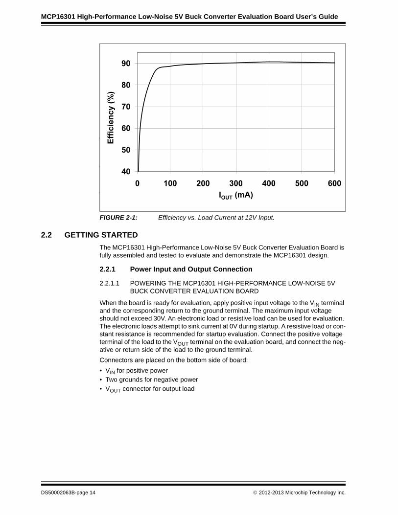
• Efficiency: Up to 91% @ 12V Input (see Figure 2-1)
2012-2013 Microchip Technology Inc. DS50002063B-page 13
MCP16301 High-Performance Low-Noise 5V Buck Converter Evaluation Board User’s Guide
FIGURE 2-1: Efficiency vs. Load Current at 12V Input.
2.2 GETTING STARTED
The MCP16301 High-Performance Low-Noise 5V Buck Converter Evaluation Board is fully assembled and tested to evaluate and demonstrate the MCP16301 design.
2.2.1 Power Input and Output Connection
2.2.1.1 POWERING THE MCP16301 HIGH-PERFORMANCE LOW-NOISE 5V BUCK CONVERTER EVALUATION BOARD
When the board is ready for evaluation, apply positive input voltage to the VIN terminal and the corresponding return to the ground terminal. The maximum input voltage should not exceed 30V. An electronic load or resistive load can be used for evaluation. The electronic loads attempt to sink current at 0V during startup. A resistive load or con-stant resistance is recommended for startup evaluation. Connect the positive voltage terminal of the load to the VOUT terminal on the evaluation board, and connect the neg-ative or return side of the load to the ground terminal.
Connectors are placed on the bottom side of board:
• VIN for positive power
• Two grounds for negative power
• VOUT connector for output load
40
50
60
70
80
90
0 100 200 300 400 500 600
Effic
ienc
y (%
)
IOUT (mA)
DS50002063B-page 14 2012-2013 Microchip Technology Inc.
Installation and Operation
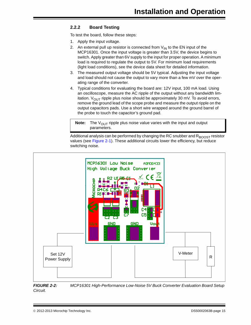
2.2.2 Board Testing
To test the board, follow these steps:
1. Apply the input voltage.
2. An external pull up resistor is connected from VIN to the EN input of the MCP16301. Once the input voltage is greater than 3.5V, the device begins to switch. Apply greater than 6V supply to the input for proper operation. A minimum load is required to regulate the output to 5V. For minimum load requirements (light load conditions), see the device data sheet for detailed information.
3. The measured output voltage should be 5V typical. Adjusting the input voltage and load should not cause the output to vary more than a few mV over the oper-ating range of the converter.
4. Typical conditions for evaluating the board are: 12V input, 100 mA load. Using an oscilloscope, measure the AC ripple of the output without any bandwidth lim-itation. VOUT ripple plus noise should be approximately 30 mV. To avoid errors, remove the ground lead of the scope probe and measure the output ripple on the output capacitors pads. Use a short wire wrapped around the ground barrel of the probe to touch the capacitor’s ground pad.
Additional analysis can be performed by changing the RC snubber and RBOOST resistor values (see Figure 2-1). These additional circuits lower the efficiency, but reduce switching noise.
FIGURE 2-2: MCP16301 High-Performance Low-Noise 5V Buck Converter Evaluation Board Setup Circuit.
Note: The VOUT ripple plus noise value varies with the input and output parameters.
Set 12V Power Supply
V-MeterR
2012-2013 Microchip Technology Inc. DS50002063B-page 15

MCP16301 High-Performance Low-Noise 5V Buck Converter Evaluation Board User’s Guide
2.2.3 How Does the MCP16301 High-Performance Low-Noise 5V Buck Converter Evaluation Board Work?
The MCP16301 integrates a low resistance N-Channel MOSFET (typically 460 m). A high-side or floating supply is needed to drive the gate of the N-Channel MOSFET above the input voltage (to turn it on). The evaluation board uses the 5V output voltage to charge the boost capacitor (CBOOST), while the inductor current flows, clamping the SW node to a diode drop below ground. Prior to start up, there is no inductor current, so an internal precharge circuit charges the boost cap up to a minimum threshold. Once CBOOST is charged, the N-Channel MOSFET can be turned on, ramping current into the inductor. The BOOST diode is used to provide a charging path for the CBOOST capacitor, while current is flowing through the inductor.
The two sense resistors (RT and RB in Figure 2-1) set the output (VOUT) at 5.0V accord-ing to the following equation:
EQUATION 2-1:
where VFB = 0.8V is the reference voltage of the FB pin. The transconductance error amplifier gain is controlled by its internal impedance. The external divider resistors have no effect on system gain, so a wide range of values can be used. A 10 k resistor is recommended as a good trade-off for quiescent current and noise immunity.
The MCP16301 device features integrated slope compensation to prevent the bimodal operation of the pulse-width modulation (PWM) duty cycle. Internally, approximately half of the inductor current down slope is summed with the internal current sense signal. For the proper amount of slope compensation, it is recommended to keep the inductor down-slope current constant by varying the inductance with VOUT. For 5.0V output, a 22 µH inductor is recommended.
The input capacitor must filter the high input ripple current, as a result of pulsing or chopping the input voltage. The MCP16301 input voltage pin is used to supply voltage for the power train and as a source for internal bias. A low Equivalent Series Resistance (ESR), preferably a ceramic capacitor, is recommended. The necessary capacitance is dependent upon the maximum load current and source impedance. Minimum capacitance at light load is 2.2 µF.
The output capacitor helps in providing a stable output voltage during sudden load transients, and reduces the output voltage ripple. The minimum value of the output capacitance is limited to 20 µF, due to the integrated compensation of the MCP16301.
The freewheeling diode creates a path for inductor current flow after the internal switch is turned off. The efficiency of the converter is a function of the forward drop voltage value and speed of the freewheeling Schottky diode.
For detailed information, see the MCP16301 Data Sheet (DS25004).
RTOP RBOT
VOUT
VFB------------- 1– =
DS50002063B-page 16 2012-2013 Microchip Technology Inc.

Installation and Operation
2.2.4 Reduction of the High Frequency Switching Noise
Because the MCP16301’s internal MOSFET is switching at 500 kHz, high-frequency noise may appear. This can affect the circuitry in close proximity. Parasitic elements generate ringing. There are two main noise sources. The first source occurs at the fundamental switching frequency and is called “Output Ripple”. The second source, associated with high-frequency ringing, occurs during the ON-OFF transition of the integrated N-Channel MOSFET switch. This results in a high-frequency noise that can be in the range of 100s of MHz and up to 500 mV peak-to-peak voltage ripple. Both noise components require separate filtering. Figure 2-3 shows an example of the two noise components.
FIGURE 2-3: VOUT Ripple and Noise for an MCP16301 Buck Converter Without Any Noise Reduction Components.
The low-frequency output ripple of the MCP16301 is generally less than 20 mV peak-to-peak, and it depends on the output capacitor value and capacitor dielectric type. Low ESR and Equivalent Series Inductance (ESL) ceramic capacitors signifi-cantly decrease the output voltage low-frequency ripple.
Additional output capacitance does not remove the high-frequency noise. Ceramic capacitors have high-impedance in the frequency band in which this noise occurs. The ringing frequency is very high, and the output capacitor alone or an extra low-value capacitor in parallel with it are ineffective in attenuating this noise. First, the noise can be attenuated by good PCB design practices. A four-layer board is recommended in this case. The solution is to place the SW node of the MCP16301 pin into the inner layer (Mid-Layer 2) as an individual plane between two ground planes (Mid-Layer 1 and Layer 4 - Bottom plane).
High-quality shielded inductors reduce the spreading of electromagnetic fields, a desirable characteristic of any power supply. An example of a high-quality shielded inductor is the CoilCraft Inc. XAL6060.
2012-2013 Microchip Technology Inc. DS50002063B-page 17

MCP16301 High-Performance Low-Noise 5V Buck Converter Evaluation Board User’s Guide
The third and most effective method to reduce switching noise is to slow down the turn-on of the integrated N-Channel MOSFET switch, addressing the noise at its source. This method lowers the efficiency of the converter insignificantly (see Figure 2-6), but the noise in the system is significantly reduced. A RBOOST resistance value between 47 and 100 Ohms was typical for this analysis.
Placing an RC snubber in parallel with the external Schottky diode is another method that can be used to reduce high-frequency noise. Some basic equations are used to calculate the RC snubber values.
For example, the Schottky rectifier diode MBRA140T (1A/40V) has a parasitic Lp = 2 nH and Cp = 38 pF (see the MBRA140T data sheet for details). When measuring the MCP16301 High-Performance Low-Noise 5V Buck Converter Evaluation Board cir-cuit without an RC snubber (for 12V Input and 100 mA load), the ringing frequency is approximately 250 MHz. Considering the parasitic inductance equal to LP, calculate the parasitic impedance, using the following equation:
EQUATION 2-2:
For this example, Z is approximately 3. Choose a snubber resistor to be similar or greater than this value (4.7 standard value).
EQUATION 2-3:
With the value of RSnubber established, the snubber’s capacitor value results from the following equation:
EQUATION 2-4:
Z 2fLp=
RSnubber ZWhere:
RSnubber = 4.7
CSnubber1
2fRSnubber-----------------------------=
Where:
CSnubber = 120 pF
DS50002063B-page 18 2012-2013 Microchip Technology Inc.

Installation and Operation
Figures 2-4 – 2-6 show the results for the MCP16301 High-Performance Low-Noise 5V Buck Converter Evaluation Board:
• AC output ripple for board with RC snubber only (Figure 2-4)
• AC output ripple for RC snubber and RBOOST on board (Figure 2-5)
• Efficiency comparison with RC snubber and RBOOST (Figure 2-6)
FIGURE 2-4: VOUT Ripple of the Evaluation Board is less than 80 mVp-p using RC Snubber only (12V Input, 100 mA Load). Compare to Figure 2-3.
FIGURE 2-5: VOUT Ripple of the Evaluation Board is less than 30 mVp-p using RC Snubber and RBOOST (12V Input, 100 mA Load). Compare to Figures 2-3 and 2-4.
2012-2013 Microchip Technology Inc. DS50002063B-page 19

MCP16301 High-Performance Low-Noise 5V Buck Converter Evaluation Board User’s Guide
FIGURE 2-6: Efficiency Comparison for the MCP16301 High-Performance Low-Noise 5V Buck Converter Evaluation Board (12V and 24V Input).
40
50
60
70
80
90
0 100 200 300 400 500 600
Effic
ienc
y (%
)
IOUT (mA)
Vin = 12V, no RC Snubber, no RBoostVin = 24V no RC Snubber, no RBoostVin = 12V, RC Snubber, no RBoostVin = 24V, RC Snubber, no RBoostVin = 12V, Snubber, RBoostVin = 24V, Snubber, RBoost
DS50002063B-page 20 2012-2013 Microchip Technology Inc.

MCP16301 HIGH-PERFORMANCELOW-NOISE 5V BUCK CONVERTER
EVALUATION BOARD USER’S GUIDE
Appendix A. Schematic and Layouts
A.1 INTRODUCTION
This appendix contains the following schematics and layouts for the MCP16301 High-Performance Low-Noise 5V Buck Converter Evaluation Board:
• Board – Schematic
• Board – Top Silk And Copper
• Board – Mid-Inner Layer 1
• Board – Mid-Inner Layer 2
• Board – Bottom Copper and Pads
2012-2013 Microchip Technology Inc. DS50002063B-page 21

MC
P1
630
1 H
igh
-Perfo
rman
ce L
ow
-No
ise 5
V B
uc
k Co
nve
rter E
valu
ation
Bo
ard U
se
r’s G
uid
e
DS
50
00
20
63
B-p
ag
e 2
2
20
12
-20
13
Micro
chip
Te
chn
olo
gy In
c.
10uFC4
10uFC5
GND GND
1
J4
GND
1
J2
VOUT
GND
VOUT = 5V
C6
A.2 BOARD – SCHEMATIC
BOOST
1GND
2
VFB3EN
4
SW6
VIN5
BOOST
GND
VFBEN
SWVIN
MCP16301U1
1MR1
GNDGND
1
J1
VIN
1
J3
GND
10uFC3
10uFC2
GND
0.1uF
C1
MBRA140T3G
D2
GND
10kR4
GND
1N4148WS
D1
22uH/5A
L1
GND
VIN = 12V
4.71%
0603
R3
52.3K
1%
R2
120p0603
C7
82
0603
R5
1%

Schematic and Layouts
A.3 BOARD – TOP SILK AND COPPER
2012-2013 Microchip Technology Inc. DS50002063B-page 23
MCP16301 High-Performance Low-Noise 5V Buck Converter Evaluation Board User’s Guide
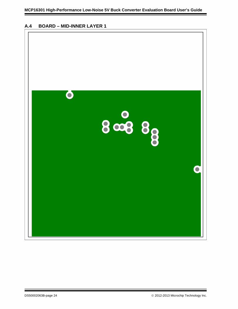
A.4 BOARD – MID-INNER LAYER 1
DS50002063B-page 24 2012-2013 Microchip Technology Inc.

Schematic and Layouts
A.5 BOARD – MID-INNER LAYER 2
2012-2013 Microchip Technology Inc. DS50002063B-page 25

MCP16301 High-Performance Low-Noise 5V Buck Converter Evaluation Board User’s Guide
A.6 BOARD – BOTTOM COPPER AND PADS
DS50002063B-page 26 2012-2013 Microchip Technology Inc.
MCP16301 HIGH-PERFORMANCELOW-NOISE 5V BUCK CONVERTER
EVALUATION BOARD USER’S GUIDE
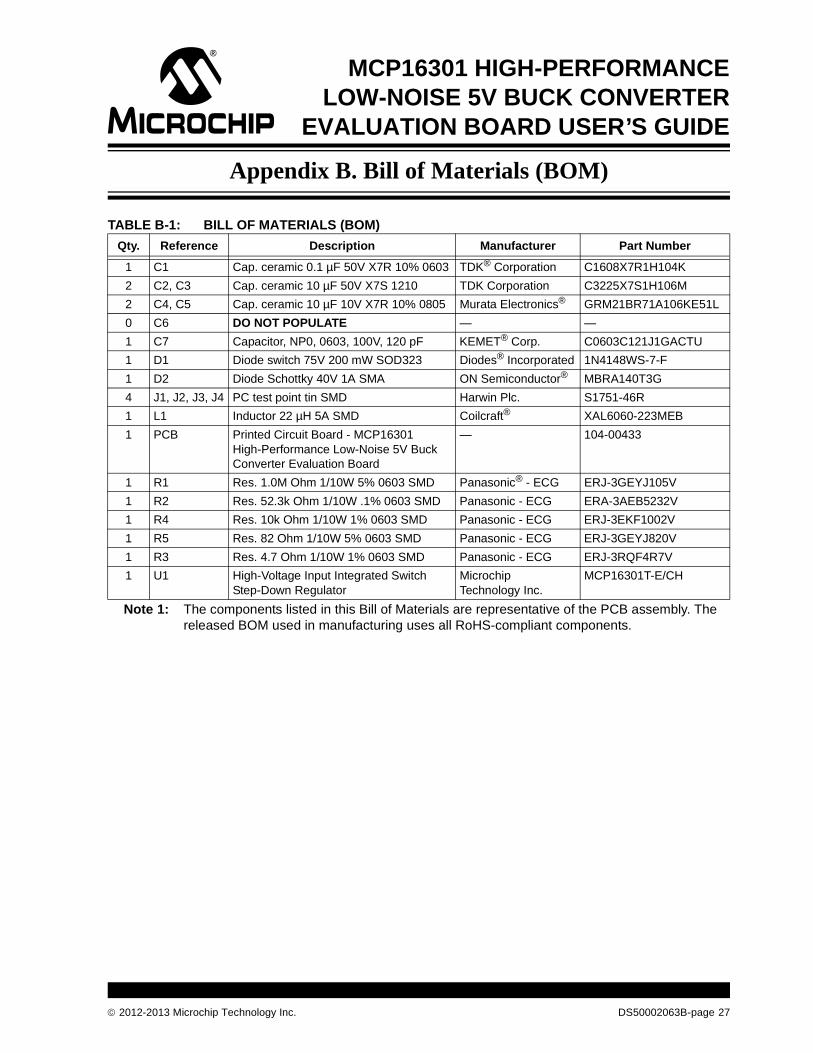
Appendix B. Bill of Materials (BOM)
TABLE B-1: BILL OF MATERIALS (BOM)
Qty. Reference Description Manufacturer Part Number
1 C1 Cap. ceramic 0.1 µF 50V X7R 10% 0603 TDK® Corporation C1608X7R1H104K
2 C2, C3 Cap. ceramic 10 µF 50V X7S 1210 TDK Corporation C3225X7S1H106M
2 C4, C5 Cap. ceramic 10 µF 10V X7R 10% 0805 Murata Electronics® GRM21BR71A106KE51L
0 C6 DO NOT POPULATE — —
1 C7 Capacitor, NP0, 0603, 100V, 120 pF KEMET® Corp. C0603C121J1GACTU
1 D1 Diode switch 75V 200 mW SOD323 Diodes® Incorporated 1N4148WS-7-F
1 D2 Diode Schottky 40V 1A SMA ON Semiconductor® MBRA140T3G
4 J1, J2, J3, J4 PC test point tin SMD Harwin Plc. S1751-46R
1 L1 Inductor 22 µH 5A SMD Coilcraft® XAL6060-223MEB
1 PCB Printed Circuit Board - MCP16301 High-Performance Low-Noise 5V Buck Converter Evaluation Board
— 104-00433
1 R1 Res. 1.0M Ohm 1/10W 5% 0603 SMD Panasonic® - ECG ERJ-3GEYJ105V
1 R2 Res. 52.3k Ohm 1/10W .1% 0603 SMD Panasonic - ECG ERA-3AEB5232V
1 R4 Res. 10k Ohm 1/10W 1% 0603 SMD Panasonic - ECG ERJ-3EKF1002V
1 R5 Res. 82 Ohm 1/10W 5% 0603 SMD Panasonic - ECG ERJ-3GEYJ820V
1 R3 Res. 4.7 Ohm 1/10W 1% 0603 SMD Panasonic - ECG ERJ-3RQF4R7V
1 U1 High-Voltage Input Integrated Switch Step-Down Regulator
Microchip Technology Inc.
MCP16301T-E/CH
Note 1: The components listed in this Bill of Materials are representative of the PCB assembly. The released BOM used in manufacturing uses all RoHS-compliant components.
2012-2013 Microchip Technology Inc. DS50002063B-page 27

DS50002063B-page 28 2012-2013 Microchip Technology Inc.
AMERICASCorporate Office2355 West Chandler Blvd.Chandler, AZ 85224-6199Tel: 480-792-7200 Fax: 480-792-7277Technical Support: http://www.microchip.com/supportWeb Address: www.microchip.com
AtlantaDuluth, GA Tel: 678-957-9614 Fax: 678-957-1455
BostonWestborough, MA Tel: 774-760-0087 Fax: 774-760-0088
ChicagoItasca, IL Tel: 630-285-0071 Fax: 630-285-0075
ClevelandIndependence, OH Tel: 216-447-0464 Fax: 216-447-0643
DallasAddison, TX Tel: 972-818-7423 Fax: 972-818-2924
DetroitFarmington Hills, MI Tel: 248-538-2250Fax: 248-538-2260
IndianapolisNoblesville, IN Tel: 317-773-8323Fax: 317-773-5453
Los AngelesMission Viejo, CA Tel: 949-462-9523 Fax: 949-462-9608
Santa ClaraSanta Clara, CA Tel: 408-961-6444Fax: 408-961-6445
TorontoMississauga, Ontario, CanadaTel: 905-673-0699 Fax: 905-673-6509
ASIA/PACIFICAsia Pacific OfficeSuites 3707-14, 37th FloorTower 6, The GatewayHarbour City, KowloonHong KongTel: 852-2401-1200Fax: 852-2401-3431
Australia - SydneyTel: 61-2-9868-6733Fax: 61-2-9868-6755
China - BeijingTel: 86-10-8569-7000 Fax: 86-10-8528-2104
China - ChengduTel: 86-28-8665-5511Fax: 86-28-8665-7889
China - ChongqingTel: 86-23-8980-9588Fax: 86-23-8980-9500
China - HangzhouTel: 86-571-2819-3187 Fax: 86-571-2819-3189
China - Hong Kong SARTel: 852-2943-5100 Fax: 852-2401-3431
China - NanjingTel: 86-25-8473-2460Fax: 86-25-8473-2470
China - QingdaoTel: 86-532-8502-7355Fax: 86-532-8502-7205
China - ShanghaiTel: 86-21-5407-5533 Fax: 86-21-5407-5066
China - ShenyangTel: 86-24-2334-2829Fax: 86-24-2334-2393
China - ShenzhenTel: 86-755-8864-2200 Fax: 86-755-8203-1760
China - WuhanTel: 86-27-5980-5300Fax: 86-27-5980-5118
China - XianTel: 86-29-8833-7252Fax: 86-29-8833-7256
China - XiamenTel: 86-592-2388138 Fax: 86-592-2388130
China - ZhuhaiTel: 86-756-3210040 Fax: 86-756-3210049
ASIA/PACIFICIndia - BangaloreTel: 91-80-3090-4444 Fax: 91-80-3090-4123
India - New DelhiTel: 91-11-4160-8631Fax: 91-11-4160-8632
India - PuneTel: 91-20-2566-1512Fax: 91-20-2566-1513
Japan - OsakaTel: 81-6-6152-7160 Fax: 81-6-6152-9310
Japan - TokyoTel: 81-3-6880- 3770 Fax: 81-3-6880-3771
Korea - DaeguTel: 82-53-744-4301Fax: 82-53-744-4302
Korea - SeoulTel: 82-2-554-7200Fax: 82-2-558-5932 or 82-2-558-5934
Malaysia - Kuala LumpurTel: 60-3-6201-9857Fax: 60-3-6201-9859
Malaysia - PenangTel: 60-4-227-8870Fax: 60-4-227-4068
Philippines - ManilaTel: 63-2-634-9065Fax: 63-2-634-9069
SingaporeTel: 65-6334-8870Fax: 65-6334-8850
Taiwan - Hsin ChuTel: 886-3-5778-366Fax: 886-3-5770-955
Taiwan - KaohsiungTel: 886-7-213-7828Fax: 886-7-330-9305
Taiwan - TaipeiTel: 886-2-2508-8600 Fax: 886-2-2508-0102
Thailand - BangkokTel: 66-2-694-1351Fax: 66-2-694-1350
EUROPEAustria - WelsTel: 43-7242-2244-39Fax: 43-7242-2244-393Denmark - CopenhagenTel: 45-4450-2828 Fax: 45-4485-2829
France - ParisTel: 33-1-69-53-63-20 Fax: 33-1-69-30-90-79
Germany - MunichTel: 49-89-627-144-0 Fax: 49-89-627-144-44
Italy - Milan Tel: 39-0331-742611 Fax: 39-0331-466781
Netherlands - DrunenTel: 31-416-690399 Fax: 31-416-690340
Spain - MadridTel: 34-91-708-08-90Fax: 34-91-708-08-91
UK - WokinghamTel: 44-118-921-5869Fax: 44-118-921-5820
Worldwide Sales and Service
11/29/12