Embed Size (px)
Citation preview

ATLAS Week, MCC-I FDRR. Beccherle - INFN / Genova CERN, 10 Oct 2002
MCC-I1 Design Specifications
Roberto Beccherle / INFN Roberto Beccherle / INFN -- GenovaGenovaEE--mail: mail: [email protected]@ge.infn.it
MCCMCC--DSM TeamDSM Team:: R.Beccherle, G.Comes, G.Darbo, P.Denes, R.Beccherle, G.Comes, G.Darbo, P.Denes, P.FisherP.Fisher, , G.Gagliardi, K.Kostas, P.Morettini, G.Gagliardi, K.Kostas, P.Morettini, P.MusicoP.Musico, I.Peric, C.Schiavi, I.Peric, C.Schiavi
Copy of This Talk:Copy of This Talk:http://www.ge.infn.it/ATLAShttp://www.ge.infn.it/ATLAS

MCC-I1 Design SpecificationsR. Beccherle - INFN / Genova CERN, 10 Oct 2002 2
System ArchitectureSystem Architecture11
FE chips
FE chips
2880
1
11
1
Sensor 16 chips MCC
1
4 fast + 4 slow
2DORIC
VDC
Op
to P
acka
ge
PIN
VCSEL
VCSEL
3 fibres/module
Op
to C
ard
RO
D
RO
B
TIM
CTRL
2880
~30
Power supplies
module control room
1 Sensor16Front End chips (FE)1 Module Controller Chip (MCC)2 VCSEL Driver Chips (VDC)1 PIN diode receiver(DORIC)
Optical ReceiversReadout Drivers (ROD)Readout Buffers (ROB)Timing Control (TIM)Slow Control, Supplies

MCC-I1 Design SpecificationsR. Beccherle - INFN / Genova CERN, 10 Oct 2002 3
System ArchitectureSystem Architecture11
FE chips
FE chips
2880
1
11
1
Sensor 16 chips MCC
1
4 fast + 4 slow
2DORIC
VDC
Op
to P
acka
ge
PIN
VCSEL
VCSEL
3 fibres/module
Op
to C
ard
RO
D
RO
B
TIM
CTRL
2880
~30
Power supplies
module control room
Data push architecture: All FE chips are connected to the MCC with a star topology (point to point data links). 1 link between each FE and the MCC.All module operation is controlled via the MCC with a serial protocol.All data links active during data taking mode are LVDS.

MCC-I1 Design SpecificationsR. Beccherle - INFN / Genova CERN, 10 Oct 2002 4
MCC: ArchitectureMCC: ArchitectureSerial data coming from FE chips are stored in 16 full-custom 27x128 bit deep FIFO’s until event building occurs.Trigger, Timing & Control circuitryCommand Decoder:5-bit Trigger command is recognized correctly, without any loss of synchronization even with a single bit-flip in the command.It is not possible to mix up configuration and data taking commands in case of bit-flips in the commands.Event Builder.Register Bank:Holds configuration information and stores eventual error flags.Output Port:Formats data on two output pins allowing data speeds from 40 to 160 Mbit/s.

MCC-I1 Design SpecificationsR. Beccherle - INFN / Genova CERN, 10 Oct 2002 5
MCC–I1: Main Characteristics MCC–I1: Main Characteristics System startup and initialization.Decode data/command signals (from the ROD):A simple serial protocol is used for all communication between the ROD and the MCC and also between the MCC and the FE chips (Slow, Fast and Trigger commands).Trigger, Timing and Control: the MCC has to provide Triggers to all FE chips and keep event synchronization.The MCC receives serial data from 16 FE chips, accumulates data in local FIFO's. Event building: complete module events are reconstructed with some data compression. Scoreboard mechanism allows to start event building as soon as all enabled FE chips finish sending the data of one complete event.Send event to DAQ (via VDC)Error handling: (FIFO overflows, misalignment of data from FE chips with BCID information, disable defective or noisy FE chips, ...)
IBM 0.25 µm rad-tolerant designDie size is 6.38 x 3.98 µm2
16 FIFO’s (128 21bit words)1 analog delay line650.000 transistors

MCC-I1 Design SpecificationsR. Beccherle - INFN / Genova CERN, 10 Oct 2002 6
System Initialization and ConfigurationSystem Initialization and ConfigurationAt power up the whole system has to be correctly initialized.FE chips and the MCC are connected by means of a star topology in which each FE has dedicated parallel connections with the MCC.Each FE has one 40 MHz LVDS data and clock line and 3 slower (5 MHz) common configuration lines.FE chips can be addressed by the MCC either in “broadcast” mode or one by one using their geographical address.In order to reduce the number of electrical connections to the module our system does not provide a pin reset signal.The MCC Command Decoder is designed so that at power up, after a finite amount of time, it returns to the idle state in order to be able to accept a Global Reset command that puts the chip in it’s default state. At this point global configuration data (number of enabled FE chips, desired output mode, …) can be stored in the MCC register bank. The next phase implies a Global reset to all FE chips of the module.Once the whole system is initialized configuration of the single FE chips can begin.

MCC-I1 Design SpecificationsR. Beccherle - INFN / Genova CERN, 10 Oct 2002 7
MCC–I1: System FunctionsMCC–I1: System FunctionsSystem Configuration:
Individual FE addressing to R/W configuration data before a run starts.MCC configuration and ability to test FE chips during module assembly.
Event Building:As soon as a FE receives a hit the information is sent to the MCC.Data storage in 16 full custom FIFO’s until all FE’s terminate transmitting hits belonging to the same event.Data are formatted with some event compression and are sent to the ROD.Ability to provide error detection during Event Building.
Trigger Timing and Control:Trigger distribution to all FE chips keeping the synchronization.Error detection in case of buffer overflows and truncated / lost events.
Testability:Ability to disable one or more FE chips without stopping the whole module. Capability of testing internal structures in case of errors.Transmission error detection.

MCC-I1 Design SpecificationsR. Beccherle - INFN / Genova CERN, 10 Oct 2002 8
MCC-I1: ConfigurationMCC-I1: ConfigurationThe MCC Command Decoder allows 3 type of serial commands;
Slow Commands, used during module (FE and MCC) configuration;Fast Commands (data syncronization) that can be issued without exiting data taking mode;Trigger commands.
There are 8 16-bit wide configuration registers inside the MCC that allow to configure the chip for all its features, like:
Enabling a certain number of FE chips on the module;Output data mode: 40 Mbit/s, 80 Mbit/s and 160 Mbit/s on one or two output lines are supported;Selecting the level of error checking/reporting;
There is the ability to self test most of the chip circuitry. One can,for example, send data that simulate data coming from certain FE chips and perform real event building on these data.Calibration of all FE pixels is possible using an analog delay line that provides a signal sent to a chopper circuit inside the FE chip that allows charge to be injected in each single pixel cell (2 different charge ranges may be selected). FE configuration data is sent on a dedicated line and validated by a load signal.

MCC-I1 Design SpecificationsR. Beccherle - INFN / Genova CERN, 10 Oct 2002 9
MCC-I1: Data-TakingMCC-I1: Data-TakingData Taking phase can occur immediately after system initialization.The system has to be set in Run Mode and after that only Trigger and Fastcommands are allowed, any Slow command will return to Configuration Mode.The architecture of the module is Data Push, i.e. as soon as the MCC receives a Trigger command it is immediately sent to the FE chips for data collecting.Up to 16 pending Triggers are allowed in the system.Trigger commands are 5-bit commands that allow automatic correction for eventual bit flips inside the command preserving correct timing information.A Pending Event FIFO keeps track of how many Events have still to be processed.In case more than 16 Triggers are received before an event is fully reconstructed they are simply dropped and the information will be propagated to the ROD inserting a Warning word in the corresponding Event.This mechanism allows the ROD to insert empty events to maintainsynchronization with the data flow.Event Counter Reset and BCID Reset commands (Fast commands) can be issued to keep correct event synchronization.

MCC-I1 Design SpecificationsR. Beccherle - INFN / Genova CERN, 10 Oct 2002 10
MCC-I1: Data-TakingMCC-I1: Data-TakingOnly enabled FE chips participate to Event building.16 parallel data streams are received and stored in 16 independent FIFO’s.Each Event is identified by an EoE word.EoE information is stored in the Scoreboard.As soon as all 16 EoE words of an Event are collected event building is performed.8 bit BCID and 4 bit Lev1 information is stored with each incoming Trigger.Event building collects data from all 16 FIFO’s and formats the output data stream according to the selected output mode.Up to two output lines (each sampling data on both clock edges) can be used in order to provide a data throughput up to 160 Mbit/s.Data consistency checking between hits from the same FE chip and between EoE words from different FE’s is performed.FIFO data overflow, which produces loss of hits, may occur and is signaled in the data flow.

MCC-I1 Design SpecificationsR. Beccherle - INFN / Genova CERN, 10 Oct 2002 11
MCC-I1: Command DecoderMCC-I1: Command DecoderDesignedDesigned for single bit flip tolerance in command stream.
No mismatch between Trigger, Fast and Slow commands in case of bit flip.A wrong Fast command is never interpreted as a different Fast or a Slowcommand in case of a single bit flip.A wrong Slow command can never be interpreted as a Fast or a Trigger command.
5-bit Trigger command (11101) with one bit flip allowed.4 Fast Commands: (BCR, ECR, CAL, SyncFE).
BCR [10110.0001]: Bunch Counter Reset.ECR [10110.0010]: Event Counter Reset.CAL [10110.0100]: Calibration signal for the FE chips.SyncFE [10110.1000]: One CK pulse lasting reset signal to the FE chips.
10 Slow Commands (WrRegister, RdRegister, WrFifo, RdFifo, WrFrontEnd, RdFrontEnd, WrReceiver, EnDataTake, GlobalResetMCC, GlobalResetFE ).The Header of the Slow commands is 10110.10114 different state machines which do not need, by construction, a reset to start in idle mode.

MCC-I1 Design SpecificationsR. Beccherle - INFN / Genova CERN, 10 Oct 2002 12
Trigger and Fast commandsTrigger and Fast commandsTrigger and Fast commands are executed only if the MCC is in RunMode(must execute an EnDataTake command).LV1: Triggers the acquisition of a new event
A LV1 is issued to the FE chips, L1ID and BCID values are stored in the PendingLv1Fifo, the L1ID counter is incremented.
BCR: Bunch Counter ResetThe BCR counter inside the MCC is set to 0.
ECR: Event Counter Reset (data-path reset)Reset of the ReceiverFifo‘s and the PendingLv1Fifo pointers are cleared, the L1ID counter is cleared. If there are events pending they are cleared.
ROD must take care that no data is coming from the FE’s after a CAL command has been issued!
CAL: Calibration pulse generationLength and Delay (~0.5 ns steps) are set in the CAL register.

MCC-I1 Design SpecificationsR. Beccherle - INFN / Genova CERN, 10 Oct 2002 13
Slow commandsSlow commandsThe Header (10110.1011) is followed by 2 (or 3) more fields
Name Field3 Field4 Field4 Data bitsWrRegister 0000 Address Data 16 bitsRdRegister 0001 Address ---- 16 bitsWrFifo 0010 ---- Data 21 bitsRdFifo 0011 Address ---- 21 bitsWrFrontEnd 0100 ---- Data CNT<15:3> *8+CNT<2:0> *64RdFrontEnd 0101 ---- Data CNT<15:3> *8+CNT<2:0> *64WrReceiver 0110 ---- Data CNT<12:0> *8EnDataTake 1000 ---- 0GlobalResetMCC 1001 ---- 0GlobalResetFE 1010 ---- SyncW 4 bits

MCC-I1 Design SpecificationsR. Beccherle - INFN / Genova CERN, 10 Oct 2002 14
Slow command descriptionSlow command descriptionWrRegister: Writes data to the addressed register
Does not produce any output data!
RdRegister: Reads addressed registerProduces hex:0000 if wrong address is selected!
WrFifo: Writes data into selected (FEEN register) FIFO’sWrite Pointer is incremented
RdFifo: Reads data from addressed FIFO’sRead Pointer is incremented
WrFrontEnd:Write configuration data to all FE chipsCNT<15:3> + CNT<2:0> * 8 bits are writtenCCK, which is 8 times slower, and not CK is used to transmit data
RdFrontEnd: Read conf. data from enabled FIFOThe FIFO is enabled setting the FEEN registerOnly one FIFO has to be selected!
1 of 21 of 2

MCC-I1 Design SpecificationsR. Beccherle - INFN / Genova CERN, 10 Oct 2002 15
Slow command descriptionSlow command descriptionWrReceiver: Writes data into the selected Receiver.
Receivers are selected by the FEEN register.This command is designed to exercise the EventBuilder and the Receiver blocks with simulated events. FE inputs must be disabled.
EnDataTake: Enable RUN mode in the MCC.Fast and Trigger commands are executed only in RunMode.A Solw command sets the MCC in Configuration mode!
GlobalResetMCC:Internal registers and status flags are reset, FIFO pointers arecleared and state machines are put to their idle state.Only the Command Decoder is unaffected!
GlobalResetFE: Sends a reset signal to all FE chips.The width of the signal is read from the SyncW field.Different reset widths act differently on the FE chips.The width can range from 1 to 31 CK units.
2 of 22 of 2

MCC-I1 Design SpecificationsR. Beccherle - INFN / Genova CERN, 10 Oct 2002 16
Required timing & Command robustnessRequired timing & Command robustnessTrigger commands can be issued without any gap (125 ns).After a Trigger command both Fast and Slow commands can be issued without any gap.After a Fast command a Trigger can be issued without any gap.After a Fast command 2 CK cycles should be left before issuing a new Fast or Slow command.The command decoder was optimized for being able to detect a Trigger command even in presence of a single bit flip.
Correct timing information is restored in this case.
A Fast command is never recognized as a different Fast or as a Slow command in case of a single bit flip.A Slow command header is never interpreted as a Fastcommand in case of a single bit flip.

MCC-I1 Design SpecificationsR. Beccherle - INFN / Genova CERN, 10 Oct 2002 17
Command robustness: Trigger commandCommand robustness: Trigger command
Received Pattern Recognized Pattern Recognized command0000 11101 00 0000 11101 00 LV10000 11101 10 0000 11101 10 LV10000 11100 00 0000 11100 00 LV1 (with bit flip)0000 11111 00 0000 11111 00 LV1 (with bit flip)0000 11001 00 0000 11001 00 LV1 (with bit flip)0000 10101 00 0000 10101 00 LV1 (with bit flip)0000 01101 00 0000 01101 00 LV1 (with bit flip)0001 11101 00 0001 11101 00 LV10010 11101 00 0010 11101 00 LV10100 11101 00 0100 11101 00 LV1
Recognized patterns are: 11101, 11100, 11111, 11001, 10101, 01101In this case correct timing information is restored!

MCC-I1 Design SpecificationsR. Beccherle - INFN / Genova CERN, 10 Oct 2002 18
State Machines: Lv1FastState Machines: Lv1Fast
S0
S1cmd_shift_reg<4:0> = x1011 &
zero = 1zero = 0
cmd_shift_reg<4:0> != 11101 |01101 | 10101 | 11001 | 11111 | 11101 | 10011
cmd_shift_reg<4:0> = 10011
S2
S3
cmd_shift_reg<3:0> != 1011 &zero = 1
zero = 0cmd_shift_reg<3:0> = 0,1,2,3,4,5,6,9
& zero = 1
cmd_shift_reg<3:0> = 7,8,A,B,C,D,E,F& zero = 1
slow_enc<2:0> = 000 & stop_slow = 0| stop_slow = 1
slow_enc<2:0> != 000 & stop_slow = 0

MCC-I1 Design SpecificationsR. Beccherle - INFN / Genova CERN, 10 Oct 2002 19
State Machines: SlowState Machines: Slow
S0
S1
Start=1
Start=0
S2 S3 S4 S5
S6
S7
slowenc<2:0> = 0 & zero = 1
zero = 0
slowenc<2:0> = 7 & zero = 1
slowenc<2:0> = 5,6 & CCNT<6:0> != 0& zero = 1
slowenc<2:0> = 5,6 & CCNT<6:0> = 0 & zero = 1
zero = 0
zero = 1
zero = 1
zero = 0
zero = 0
zero = 1
zero = 0
zero = 1
slowenc<2:0> != 6
slowenc<2:0> = 6
slowenc<2:0> = 1,2,3,4 & zero = 1

MCC-I1 Design SpecificationsR. Beccherle - INFN / Genova CERN, 10 Oct 2002 20
State Machines: CalState Machines: Cal
S0
S1
start=1
zero=1
zero=0
start=0

MCC-I1 Design SpecificationsR. Beccherle - INFN / Genova CERN, 10 Oct 2002 21
State Machines: CCKState Machines: CCK
S0
S1
Start=1
Start=0
S2
S3
S4
S5
S6
S7

MCC-I1 Design SpecificationsR. Beccherle - INFN / Genova CERN, 10 Oct 2002 22
Register BankRegister Bank
RegisterRegister AddressAddress ContentContent DescriptionDescriptionCSR 0000 ---S,SSSS,-CCC,CCCC Control Status RegisterLV1 0001 ----,CCCC,LLLL,LLLL Trigger RegisterFEEN 0010 dddd,dddd,dddd,dddd Front End EnableWFE 0011 dddd,dddd,dddd,dddd Warning from FE chipsWMCC 0100 dddd,dddd,dddd,dddd Warning from MCC ReceiverCNT 0101 cccd,dddd,dddd,dccc Control & Data countersCAL 0110 ----,-pRR,RRDD,DDDD Calibration RegisterPEF 0111 SSSS,LLLL,BBBB,BBBB Pending Event FIFONote:
B,c,d,D,l,n,p,R,s,S,w: used data bit-: Non existing bit. It is always read back a ‘0’
A WrRegister command does not produce any output data.
MCC-I1 Design SpecificationsR. Beccherle - INFN / Genova CERN, 10 Oct 2002 23
Control & Status RegisterControl & Status RegisterCSR<6:0> Control part.
<0,1> OM: Output mode selection. From 40 Mb/s single link to 160 Mb/s.double link. In case of single link same data transmitted on both links.
<2> EREP: Enables error report in the event data for the LV1 check(s).<3> ECHK: Enables the LV1 check amongst FE chips done in the EventBuilder.<4> TOT: Enables Time over Threshold option in the MCC.<5> OPAT: Generates a 010101... pattern on the MCC-DTO-0/1 outputs.<6> PLBK: Test mode used to be able to playback events after having written
simulated FE data in the Receivers. This disables data coming fromthe FE chips. LV1 command is needed to read out data.
CSR<12:8> Status part.<8> WLV1: There has been a bit flip in a Trigger command.<9> WFST: There has been a bit flip in a Fast command.<10> WSLW: There has been a bit flip in a Slow command.<11> ERR0: Error on a LV1 check inside a single FE data stream.<12> ERR1: Error on a LV1 check amongst data of different FE chips.

MCC-I1 Design SpecificationsR. Beccherle - INFN / Genova CERN, 10 Oct 2002 24
Register descriptionRegister descriptionLV1: Level 1 Trigger
LV1<7:0>, Level1 ID counter:Mapped to the Lv1Counter. Not affected by a WrRegister command!LV1<11:8>, Contiguous Level1:1 to 16 LV1’s. Triggers have the same L1ID, consecutive BCID numbers.
FEEN: Front End Enable.WFE: Warning from a FE chip.
If a warning is written by a FE in the EoE word the corresponding bit is set.WMCC:Warning from MCC Receivers.
Set if there is an overflow in the corresponding ReceiverFIFO.CNT: FE Configuration Counters.
CNT<15:3>, Data bits: [LD is high during data phase].Number of data bits in the command going to the FE chips in CCK units. CNT<2:0>, Command bits: [LD is low during command phase]Number of bits in a FE command in CCK * 8 units (multiples of 8 required).CNT<15:0>, Width of the STRO pulse in CK units generated in response to a CAL command.
1 of 21 of 2
MCC-I1 Design SpecificationsR. Beccherle - INFN / Genova CERN, 10 Oct 2002 25
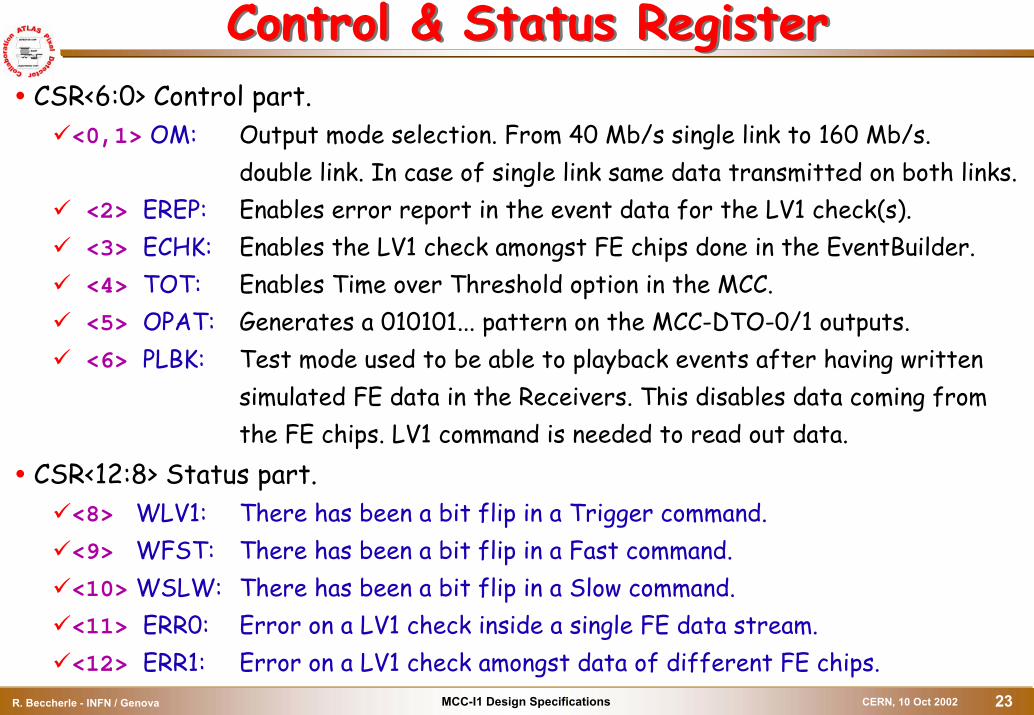
Register descriptionRegister descriptionCAL: Calibration register, calibration pulses for the FE chips
CAL<5:0>: Calibration delay. Delay of the strobe pulse in ~0.5 ns steps (at max. resolution).Determines the width of the strobe pulse (From 1 to 512 CK units).CAL<9:6>: Calibration range. Allow to select the coarse tuning of the minimum delay step of the strobe pulse, generated in response to a CAL command.CAL<10>: Turns on (‘1’) or off (‘0’) the whole Delay Line.
PEF: Pending Event FIFO (GlobalResetMCC clears pointers, not contents)PEF<7:0>: BCIDMapped to the PendingEventFifo<7:0> which contain the BCID information.PEF<11:8>: L1IDMapped to the PendingEventFifo<11:8> which contain the L1ID information.Only the 4 LSB of the LV1Counter are copied into the FIFO and are always added to the 4 LSB of the L1ID field of the MCC output data stream.PEF<15:12>:Skipped eventsMapped to the PendingEventFifo<15:12> interpreted by the EventBuilder as the number of skipped events. If different from ‘0’ it is interpreted by the ROD to know the number of missing events in the data stream due to a PendingLv1Fifo overflow. A number of 15 means that the counter has overflown. This field is always added to the 4 MSB of the L1ID field of the MCC output data stream.
2 of 22 of 2

MCC-I1 Design SpecificationsR. Beccherle - INFN / Genova CERN, 10 Oct 2002 26
MCC-I1: Trigger Timing & ControlMCC-I1: Trigger Timing & ControlBCID Counter (8 bit): Incremented each clock cycle.LV1ID Counter (8 bit): Incremented each time a LV1 has been received (even if
it has been dropped). Contiguous LV1’s are counted once.PendingLV1Counter (5 bit): Has Full (16), Almost Full (15) and Empty flags.The counter is incremented if a LV1 has been issued and the counter is not full. It is decremented each time a LV1 has been read and the counter is not empty.SkippedLV1 counter (4 bit): Incremented each time a LV1 is received and rejected.Contiguous LV1 counter (4 bit): Each time a LV1 is received the counter is loaded with the contiguous LV1 value and is then decremented at each clock cycle.A state machine accepts or rejects the incoming LV1’s depending on the counters.BCID, LV1ID and SkippedLV1 values are to be written into the PendingLV1FIFO. BCID and LV1ID values are updated each time there is an accepted LV1.SkippedLV1 is updated if the PendingLV1FIFO is full and a ReadPendingLV1FIFO command has been issued (by the Event Builder). A WritePendingLV1FIFO command is generated each time a LV1 is accepted and the PendingLV1 counter is not Almost Full. If this counter is Almost Full and a new LV1 is received we wait until the next ReadPendingLV1FIFO command before generating the command. This ensures that the correct value of SkippedLV1 is written to the PendingLV1FIFO.

MCC-I1 Design SpecificationsR. Beccherle - INFN / Genova CERN, 10 Oct 2002 27
MCC-I1: ReceiverMCC-I1: Receiver25 bit shift register:Collects data stream coming from a FE chip (only if in Run Mode). As soon as a complete Hit/EoE word has been read data, if possible, is copied to the SRAM. We can distinguish between Hits, EoE words with and without warnings.SRAM (27 x 128 bit):Dual Port Static RAM (done by K. Kostas, CERN) used as FIFO.Read Address: Incremented each time a word is written to the FIFO.Write Address: Incremented each time a word is read from the FIFO.Hit Counter (8 bit): Has Full (112) and Empty flags. Incremented each time a Hit has been detected and the counter is not Full. Decremented if a Hit has been read and the counter is not empty. If more than 112 Hits are seen they are simply dropped!EoE Counter (5 bit): Has Full (16) and Empty flags. Incremented each time an EoE has been detected and the counter is not Full. Decremented if an EoE has been read and the counter is not empty. It will always be possible to write all 16 EoE words!LV1Id check: The LV1ID of the first Hit is copied and checked against following ones.EoE words written to the FIFO (21 bit) have the following data format:{111X,FE_Flag[3:0],00,LV1IDCheckFail,EoE Overflow,EoE Overflow,0000,LV1ID[3:0]}where:
X = LV1IDCheckFail | EoE Overflow | Hit Overflow

MCC-I1 Design SpecificationsR. Beccherle - INFN / Genova CERN, 10 Oct 2002 28
Output data formatOutput data format1 of 21 of <Event>
::= <Header> L1ID <S> BCID <MccFlag>? <FrontEnd>* <Trailer><Header>
::= 11101<S>
::= 1<MccFlag>
::= <Sync> MCC-FLAG<Sync>
::= <S>||= < <S> NULL >+
<FrontEnd>::= <Sync> MCC-FE# <Hit>+ <FeFlag>?||= <Sync> MCC-FE# <Hit>* <FeFlag>?
<Hit>::= <Sync> ROW# COL# (TOT, if ToT is selected)
<FeFlag>::= <Sync> FE-FLAG
<Trailer>::= <S> 00 0000 0000 0000 ( 0000 0000, if ToT is selected)
2
<Name> Syntax construct defined by othersyntax construct or bit field.
NAME Bit field. Definitions are presentedin the table on next page.
<Name>? Is an optional field, 0 or 1 itemsoccurrence.
<Name>* Is 0, 1 or more items.<Name>+ Is 1 or more items
::= Gives a syntax definition||= Gives an alternate definition
MCC-I1 Design SpecificationsR. Beccherle - INFN / Genova CERN, 10 Oct 2002 29
Output data formatOutput data format2 of 22 of 2
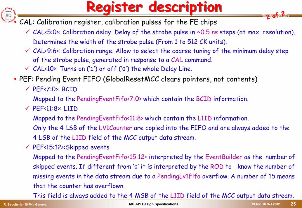
Keyword min value max value DescriptionBCID 0000 0000 1111 1111 Bunch crossing ID (0÷255)COL# 0 0000 1 1111 Column numberFE-FLAG 1 1110 FFFF MMMM Err/Wng F = FE, M = MCCL1ID 0000 1111 Level 1 Trigger ID (0÷15)MCC-FE# 1110 0000 1101 1111 FE number in module (0÷255)MCC-FLAG 0000 0000 1101 1111 Err/Wng message from MCCNULL 1111 1111 Null dataROW# 0000 0000 1101 1111 Row number (0÷224)TOT 0000 0000 1111 1111 Time over Threshold

MCC-I1 Design SpecificationsR. Beccherle - INFN / Genova CERN, 10 Oct 2002 30
MCC-I1: Event BuilderMCC-I1: Event BuilderPriority Encoder: Generates the Enable signal for the next FE to be read out.Din Mux: Selects which FE data are to be read out based on the Enable signal.
The FE is selected if there is a Hit or an EoE word with warning.Scoreboard: Keeps track of received EoE words. Generates the Build signal.FE Flag Generator: If there is a warning inside an EoE word.
If ECHK is enabled and there is a LV1ID mismatch between different EoE words.The FE Flag word is the logical or of all possible Warnings.4 bits come from the FE’s, 3 from the Receiver and one from EVB.
EVB Control:Data is generated only if (DATA_TAKE | PLBK) is true. State machine that performs event building and prepares the output data.
Data preparation: The Event Builder output is a 26 bit register. EVB Control writes the correct word, together with it’s length, to this register following the data grammar.
Possible output words are: {Header, LV1ID, Sync, BCID} 22 bit{Sync, 0111, FE#} 9 bit{Sync, Hit Data, ToT} 22 (14) bit{Sync, Trailer} 23 (15) bit{Header, Rd_FE_FIFO} 26 bit

MCC-I1 Design SpecificationsR. Beccherle - INFN / Genova CERN, 10 Oct 2002 31
MCC-I1: Output PortMCC-I1: Output PortShift Register (32 bit): Loaded with data coming from the Event Builder as soon as a
Header is ready to be transmitted. Shifts 1, 2 or 4 locations according to selected output mode.
Counter (5 bit): Loaded with data length of data loaded in the Shift Register. Decremented by 1, 2 or 4 at each clock cycle.Each time the counter gets below a certain threshold new data isloaded in the Shift Register and the counter is updated accordingly.If no data is available the Shift Register is updated each clock cycle.
DOUT (4 bit): Filled with data coming from the 4 less significant bits of the Shift Register. The register is updated each clock cycle.
The multiplexer selects data according to the selected output mode:
(40X1) DOUT[3:0] = {ShReg[0], ShReg[0], ShReg[0], ShReg[0]};(80X1) DOUT[3:0] = {ShReg[1], ShReg[1], ShReg[0], ShReg[0]},(40X2) DOUT[3:0] = {ShReg[1], ShReg[0], ShReg[1], ShReg[0]};(80X2) DOUT[3:0] = {ShReg[3], ShReg[2], ShReg[1], ShReg[0]};

MCC-I1 Design SpecificationsR. Beccherle - INFN / Genova CERN, 10 Oct 2002 32
MCC-I1: FE Port, Module PortMCC-I1: FE Port, Module PortFE Port: Synchronizes data between MCC and FE’s with the system clock.
SYNC = Sync command | GLB_FE_RST;LV1 = LV1_TTC & ~PLBK;This ensures that no Trigger commands are sent to the FE’s while in Playback mode. This feature is used during MCC self testing.DTI signals are synchronized with the system clock.
Module Port: Synchronizes data between MCC and ROD with system clock.DCI is synchronized wit the system clock.DTO: Data is selected between different possible signal sources:
RdRegister, EVB, Opat, RdFrontEnd.RdFrontEnd output pattern is the logical or of all enabled FIFO’s.In 80x1 and 80x2 output modes data is transmitted on both edges of the clock.Output Pattern (0101010101…) is generated if this mode is selected taking into account the selected output mode.All output data uses the 11101 header.

MCC-I1 Design SpecificationsR. Beccherle - INFN / Genova CERN, 10 Oct 2002 33
MCC_top schematicMCC_top schematic
Return Clock
Input Clock
System Clock
DCI
DTI<15:0>
AMS/DSM
RSIb
DTO<1:0>Latch Latch
LatchDFF
DFF
mux
mux
MCC_CORE
mux

MCC-I1 Design SpecificationsR. Beccherle - INFN / Genova CERN, 10 Oct 2002 34
MCC -> FE: Configuration data formatMCC -> FE: Configuration data formatConfiguration data between the MCC and the FE chips uses the values stored in CNT<15:3> and CNT<2:0> in order to determine when to rise the LD signal needed by the FE chips to distinguish between Data an Commandbits in the data stream.LD is low for the first CNT<2:0> * 8 CCK pulses, is risen on the CCK trailing edge staying high for CNT<15:3> CCK pulses.If the number of control bits is not a multiple of 8, one has to add zeroes to the MSB part of the control bits to create an n bit word and n/8 must be loaded in the CNT<2:0>.

MCC-I1 Design SpecificationsR. Beccherle - INFN / Genova CERN, 10 Oct 2002 35
MCC -> ROD: Link operationMCC -> ROD: Link operationDifferent output modes are selected by setting CSR<1:0>
00: 40 x 1 @ 40 Mb/s01: 40 x 2 @ 80 Mb/s10: 80 x 1 @ 80 Mb/s11: 80 x 2 @ 160 Mb/s
In 40 x 1 and 80 x 1modes the same data istransmitted on bothlinks
Configuration data isalways sent @ 40 Mb/s

MCC-I1 Design SpecificationsR. Beccherle - INFN / Genova CERN, 10 Oct 2002 36
MCC-I1: Next StepsMCC-I1: Next StepsSingle event upset studies have been performed at CERN’s PS.This is a very important issue for the final reliability of the entire project and many different approaches are possible in order to address the problem.
SEU free FF’s: We really need to understand the results of these flip flops that were developed by the Pixel FE community. Such FF’s would be the best approach for most parts of the chip.Hamming Code Correction: This would probably solve the problem of data integrity inside the 16 MCC FIFO’s. Data size of actual FIFO’s is 27 bit (instead of the required 21) and 6 additional bits are exactly what is needed for doing Hamming Correction. One would calculate the Hamming Code of data to be written to the FIFO and correct eventual bit flips before processing data in the Event Builder.Triple Logic with majority voting: This technique helps on bigger designs where speed is crucial and where Hamming correction is not feasible (i.e. State Machines).
There is no unique and/or secure solution to the problem. Probably a combination of these methods would help but we will never be able to address all possible situations.
System solutions: Add some intelligence in the ROD and allow for fast reaction.

MCC-I1 Design SpecificationsR. Beccherle - INFN / Genova CERN, 10 Oct 2002 37
Conclusions & OutlookConclusions & OutlookThis talk highlighted the design aspects involved in the design, synthesis and functional verification of the MCC-I1.
Verilog was used for the design description.Synopsys was used for the synthesys of the whole chip, with the exception of the topmost cells.Particular attention was put in the testability of the design and an ad-hoc simulation framework was set-up and used throughout the whole design phases and system tests performed on real chips.The described approach has proven to be effective and produced high quality results, but there are still improvements to be performed.
Some minor design errors went through the simulation process…SEU studies in the design would give more insight on the criticality of the effect on global system performances:
It is a rather difficult and time consuming task.
A SEU-proof DFF would be a big improvement for such types of designs!


![MCC - Catálago MCC 17030 3D - nowak.com.br238].pdf · Title: MCC - Catálago MCC 17030_3D Author: SQD Soluções Corporativas Ltda Subject: Catálago MCC 17030 Created Date: 8/12/2008](https://img.dokumen.tips/doc/110x75/60290bee18d70330981d7547/mcc-catlago-mcc-17030-3d-nowakcombr-238pdf-title-mcc-catlago-mcc.jpg)