Embed Size (px)
Citation preview

MCA4HighPROTEC
Feeder Protection
Device Manual DOK-HB-MCA4E

MCA4 Functional Overview
Page 2 EN MCA4 05/11
3
1
3(4)
MCA4
*
* = Via Adaptive Parameters
74TC
50BF 50P 51P46
81R81U/O78V60
FL5927 50N 51N 51V
67P
67N
51C*
SOTF CLPU
Fault recorder
Event recorder
Disturbance recorder
Current and Volt. : unbalance, %THD
and THD, Fund. and RMS min./max./avg
,phasors and angles
Power :Fund. and RMS, S,
P, Q, PF
Metering, Statistics and Demand
Inrush
79
Q(U)
CTS
47
Standard
55
LOP
32
25
1(0)
59N
59A
27A
Programmable LogicIRIG-B00X Trend recorder
Option
51Ns
67Ns
50Ns
SNTP Switchgear WearControl
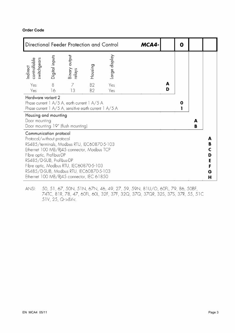
Order Code
EN MCA4 05/11 Page 3
Comments on the Manual...............................................................................................................8Information Concerning Liability and Warranty ................................................................................................8
IMPORTANT DEFINITIONS..............................................................................................................9Scope of Delivery ..........................................................................................................................................13Storage..........................................................................................................................................................13Important Information ....................................................................................................................................13Symbols.........................................................................................................................................................14General Conventions.....................................................................................................................................19Load Reference Arrow System......................................................................................................................20
Device.............................................................................................................................................21Device Planning.............................................................................................................................................21Device Planning Parameters of the Device....................................................................................................22
Installation and Connection ........................................................................................................23Three-Side-View - 19”....................................................................................................................................23Three-Side-View - 7-Pushbutton Version.......................................................................................................24Three-Side-View - 8-Pushbutton Version.......................................................................................................25Installation Diagram 7-Pushbutton Version....................................................................................................26Installation Diagram 8-Pushbutton Version....................................................................................................27Assembly Groups...........................................................................................................................................28Grounding......................................................................................................................................................28Slot X1: Power Supply Card with Digital Inputs..............................................................................................29Slot X2: Relay Output Card............................................................................................................................32Slot X3: Current Transformer Measuring Inputs.............................................................................................35Slot X4: Voltage Transformer Measuring Inputs.............................................................................................45Slot X5: Relay Output Card............................................................................................................................55Slot X6: Digital Inputs.....................................................................................................................................56Digital Inputs..................................................................................................................................................57Slot X100: Ethernet Interface.........................................................................................................................59Slot X103: Data Communication....................................................................................................................61Slot X104: IRIG-B00X and Supervision Contact............................................................................................70
Input, Output and LED Settings...................................................................................................74Configuration of the Digital Inputs..................................................................................................................74DI-8P X..........................................................................................................................................................74DI-8 X.............................................................................................................................................................78Output Relays Settings..................................................................................................................................82LED configuration........................................................................................................................................107
Navigation - Operation ...............................................................................................................127Basic Menu Control .....................................................................................................................................133Smart view Keyboard Commands................................................................................................................134
Smart View...................................................................................................................................135Installation of Smart View.............................................................................................................................135Deinstalling Smart view................................................................................................................................135Switching the Language of the Graphical User Interface.............................................................................135Setting up the Connection PC - Device........................................................................................................136Loading of Device Data when using Smart view .........................................................................................147Restoring of Device Data when using Smart view........................................................................................148Backup and Documentation when using Smart view...................................................................................148Offline Device Planning via Smart view........................................................................................................150
Measuring Values........................................................................................................................151Read out Measured Values..........................................................................................................................151Current - Measured Values..........................................................................................................................151Voltage - Measured Values..........................................................................................................................155Power - Measured Values............................................................................................................................159
Energy Counter...........................................................................................................................161Global Parameters of the Energy Counter Module.......................................................................................161Direct Commands of the Energy Counter Module .......................................................................................161Signals of the Energy Counter Module (States of the Outputs)....................................................................162
Statistics......................................................................................................................................163Read out Statistics.......................................................................................................................................163Statistics (Configuration)..............................................................................................................................164Direct Commands........................................................................................................................................165
Page 4 EN MCA4 05/11
Global Protection Parameters of the Statistics Module................................................................................166States of the Inputs of the Statistics Module................................................................................................169Signals of the Statistics Module...................................................................................................................169Counters of the Module Statistics.................................................................................................................170
System Alarms.............................................................................................................................180Demand Management.................................................................................................................................180Peak Values.................................................................................................................................................182Min. and Max. Values...................................................................................................................................182THD Protection............................................................................................................................................183Device Planning Parameters of the Demand Management.........................................................................183Signals of the Demand Management (States of the Outputs)......................................................................183Global Protection Parameter of the Demand Management..........................................................................184States of the Inputs of the Demand Management........................................................................................186
Acknowledgments.......................................................................................................................187Manual Acknowledgment.............................................................................................................................189Manual Acknowledgment via Smart view.....................................................................................................189External Acknowledgments..........................................................................................................................190External Acknowledge via Smart view..........................................................................................................190Manual Resets ............................................................................................................................................191Manual Resets via Smart view.....................................................................................................................191Reset to Factory Defaults.............................................................................................................................191
Status Display .............................................................................................................................192Status Display via Smart View.....................................................................................................................193
Operating Panel (HMI).................................................................................................................194Special Parameters of the Panel..................................................................................................................194Direct Commands of the Panel....................................................................................................................194Global Protection Parameters of the Panel..................................................................................................194
Recorders....................................................................................................................................195Disturbance Recorder .................................................................................................................................195Fault Recorder ............................................................................................................................................205Trend Recorder............................................................................................................................................209Event Recorder ...........................................................................................................................................214
Communication Protocols..........................................................................................................217SCADA Interface..........................................................................................................................................217Modbus®.....................................................................................................................................................218Profibus........................................................................................................................................................225IEC60870-5-103...........................................................................................................................................239IEC61850.....................................................................................................................................................244
Time Synchronisation.................................................................................................................254SNTP...........................................................................................................................................................255IRIG-B00X...................................................................................................................................................265
Parameters...................................................................................................................................271Parameter Definitions..................................................................................................................................271Operational Modes (access authorization)...................................................................................................288Password.....................................................................................................................................................289Changing of Parameters - Example.............................................................................................................290Changing of Parameters when using the Smart View - Example.................................................................291Protection Parameters ................................................................................................................................294Setting Groups.............................................................................................................................................294Comparing Parameter Files via Smart view.................................................................................................297Converting Parameter Files via Smart view.................................................................................................297
Device Parameters......................................................................................................................298Date and Time.............................................................................................................................................298Synchronize Date and Time via Smart View................................................................................................298Version.........................................................................................................................................................298Version via Smart view.................................................................................................................................298TCP/IP Settings...........................................................................................................................................299Direct Commands of the System Module.....................................................................................................300Global Protection Parameters of the System...............................................................................................301System Module Input States........................................................................................................................303System Module Signals................................................................................................................................304
EN MCA4 05/11 Page 5

Special Values of the System Module..........................................................................................................305Field Parameters ........................................................................................................................306
General Field Parameters............................................................................................................................306Field Parameters – Current Related.............................................................................................................307Field Parameters – Voltage Related.............................................................................................................309
Blockings.....................................................................................................................................312Permanent Blocking.....................................................................................................................................312Temporary Blocking.....................................................................................................................................312To Activate or Deactivate the Tripping Command of a Protection Module....................................................314Activate, Deactivate Respectively Block Temporarily Protection Functions..................................................315
Module: Protection (Prot)...........................................................................................................320Direct Commands of the Protection Module.................................................................................................327Global Protection Parameters of the Protection Module ..............................................................................327Protection Module Input States....................................................................................................................328Protection Module Signals (Output States)..................................................................................................328Protection Module Values.............................................................................................................................329
Switchgear/Breaker – Manager..................................................................................................330Single Line Diagram.....................................................................................................................................331Transfer of the Single Line Diagram into the device.....................................................................................331Switchgear Configuration.............................................................................................................................333Switchgear Wear.........................................................................................................................................344Control - Example: Switching of a Circuit Breaker........................................................................................351Control Parameters......................................................................................................................................355Controlled Circuit Breaker............................................................................................................................366Monitored Circuit Breaker............................................................................................................................378Controlled Disconnector...............................................................................................................................387Monitored Disconnector...............................................................................................................................391
Protective Elements....................................................................................................................394I - Overcurrent Protection [50, 51,51Q, 51V, 67]..........................................................................................394I2> - Negative-Sequence Overcurrent [51Q]................................................................................................424Directional Features for Measured Ground Fault Elements 50N/51N..........................................................427Directional Features for Calculated (IG calc) Ground Fault 50N/51N...........................................................429IG - Ground Fault [50N/G, 51N/G, 67N/G]...................................................................................................432Commissioning: Undervoltage Protection [27].............................................................................................457ThR-Protection Module: Thermal Replica [49].............................................................................................458%I2/I1> - Unbalanced Load [46]...................................................................................................................467SOTF - Switch Onto Fault............................................................................................................................475CLPU - Cold Load Pickup............................................................................................................................481IH2 - Inrush..................................................................................................................................................490V - Voltage Protection [27/59].......................................................................................................................495VG, VX - Voltage Supervision [59N].............................................................................................................506Sync - Synchrocheck [25]............................................................................................................................515V 012 – Voltage Asymmetry [47]..................................................................................................................538PQS - Power [32, 37]...................................................................................................................................545PF - Power Factor [55].................................................................................................................................564Q->&V< Reactive-Power/Undervoltage Protection.......................................................................................572f - Frequency [81O/U, 78, 81R]....................................................................................................................589AR - Automatic Reclosure [79].....................................................................................................................613ExP - External Protection.............................................................................................................................656CBF- Circuit Breaker Failure [50BF].............................................................................................................662
Supervision..................................................................................................................................681TCS - Trip Circuit Supervision [74TC]..........................................................................................................681CTS - Current Transformer Supervision [60L]..............................................................................................688LOP - Loss of Potential................................................................................................................................694
Programmable Logic...................................................................................................................704General Description.....................................................................................................................................704Programmable Logic at the Panel................................................................................................................708Programmable Logic via Smart view............................................................................................................709
Commissioning ..........................................................................................................................714Commissioning/Protection Test ...................................................................................................................715Putting out of Operation – Plug out the Relay..............................................................................................716Service and Commissioning Support...........................................................................................................717
Page 6 EN MCA4 05/11
Forcing the Relay Output Contacts..............................................................................................................718Failure Simulator (Sequencer)*....................................................................................................................721Self Supervision...........................................................................................................................................736
Technical Data ............................................................................................................................738Climatic Environmental Conditions...............................................................................................................738Degree of Protection EN 60529...................................................................................................................738Routine Test.................................................................................................................................................738Housing........................................................................................................................................................739Current and Earth Current Measurement.....................................................................................................740Voltage and Residual Voltage Measurement................................................................................................742Frequency Measurement ............................................................................................................................742Voltage Supply.............................................................................................................................................742Power Consumption.....................................................................................................................................742Display.........................................................................................................................................................742Front Interface RS232..................................................................................................................................742Real Time Clock...........................................................................................................................................743Digital Inputs................................................................................................................................................743Binary Output Relays...................................................................................................................................743Supervision Contact (SC).............................................................................................................................744Time Synchronization IRIG..........................................................................................................................744RS485*........................................................................................................................................................744Fibre Optic*..................................................................................................................................................744URTD-Interface*..........................................................................................................................................744Boot phase...................................................................................................................................................744
Standards.....................................................................................................................................745Approvals.....................................................................................................................................................745Design Standards........................................................................................................................................745High Voltage Tests (IEC 60255-6) ...............................................................................................................745EMC Immunity Tests....................................................................................................................................746EMC Emission Tests....................................................................................................................................746Environmental Tests.....................................................................................................................................747Mechanical Tests.........................................................................................................................................748
Tolerances....................................................................................................................................749Real Time Clock Tolerances........................................................................................................................749Time Synchronisation Tolerances................................................................................................................749Measured Values Tolerances.......................................................................................................................749Protection Stages Tolerances......................................................................................................................751
Assignment List .........................................................................................................................762List of the Digital Inputs................................................................................................................................823Signals of the Digital Inputs and Logic.........................................................................................................824
ad5058c30a609c40bbdb8f6e61dd47728d0688130aa325073b4a2aaf3754c95dRMS Handoff: 0File: C:\p4_data\deliverMCA4\generated\MCA4_user_manual_uk.odt
This manual applies to devices (version):
Version 2.0.27, 2.0.g
Build: 13713, 14404
EN MCA4 05/11 Page 7

Comments on the Manual
Comments on the ManualThis manual explains in general the tasks of device planning, parameter setting, installation, commissioning, operation and maintenance of the HighPROTEC devices.
The manual serves as working basis for:
• Engineers in the protection field, • commissioning engineers, • people dealing with setting, testing and maintenance of protection and control devices, • as well as trained personnel for electrical installations and power stations.
All functions concerning the type code will be defined. Should there be a description of any functions, parameters or inputs/outputs which do not apply to the device in use, please ignore that information.
All details and references are explained to the best of our knowledge and are based on our experience and observations. This manual describes the (optionally) full featured versions of the devices.
All technical information and data included in this manual reflect their state at the time this document was issued. We reserve the right to carry out technical modifications in line with further development without changing this manual and without previous notice. Hence no claim can be brought based on the information and descriptions this manual includes.
Text, graphic and formulae do not always apply to the actual delivery scope. The drawings and graphics are not true to scale. We do not accept any liability for damage and operational failures caused by operating errors or disregarding the directions of this manual.
No part of this manual is allowed to be reproduced or passed on to others in any form, unless Woodward Kempen GmbH have approved in writing.
This user manual is part of the delivery scope when purchasing the device. In case the device is passed on (sold) to a third party, the manual has to be handed over as well.
Any repair work carried out on the device requires skilled and competent personnel who need to be well aware especially of the local safety regulations and have the necessary experience for working on electronic protection devices and power installations (provided by evidence).
Information Concerning Liability and Warranty Woodward does not accept any liability for damage resulting from conversions or changes carried out on the device or planning (projecting) work, parameter setting or adjustment changes done by the customer.
The warranty expires after a device has been opened by others than Woodward specialists.
Warranty and liability conditions stated in Woodward General Terms and Conditions are not supplemented by the above mentioned explanations.
Page 8 EN MCA4 05/11

IMPORTANT DEFINITIONS
IMPORTANT DEFINITIONSThe signal definitions shown below serve the safety of life and limb as well as for the appropriate operating life of the device.
DANGER indicates a hazardous situation which, if not avoided, will result in death or serious injury.
WARNING indicates a hazardous situation which, if not avoided, could result in death or serious injury.
CAUTION, used with the safety alert symbol, indicates a hazardous situation which, if not avoided, could result in minor or moderate injury.
NOTICE is used to address practices not related to personal injury.
CAUTION, without the safety alert symbol, is used to address practices not related to personal injury.
EN MCA4 05/11 Page 9

IMPORTANT DEFINITIONS
FOLLOW INSTRUCTIONS
Read this entire manual and all other publications pertaining to the work to be performed before installing, operating, or servicing this equipment. Practice all plant and safety instructions and precautions. Failure to follow instructions can cause personal injury and/or property damage.
PROPER USE
Any unauthorized modifications to or use of this equipment outside its specified mechanical, electrical, or other operating limits may cause personal injury and/or property damage, including damage to the equipment. Any such unauthorized modifications: (1) constitute "misuse" and/or "negligence" within the meaning of the product warranty thereby excluding warranty coverage for any resulting damage, and (2) invalidate product certifications or listings.
The programmable devices subject to this manual are designed for protection and also control of power installations and operational devices that are fed by voltage sources with a fixed frequency, i.e. fixed at 50 or 60 Hertz. They are not intended for use with Variable Frequency Drives. The devices are further designed for installation in low-voltage (LV) compartments of medium voltage (MV) switchgear panels or in de-centralized protection panels. The programming and parameterization has to meet all requirements of the protection concept (of the equipment that is to be protected). You must ensure that the device will properly recognize and manage (e.g. switch off the circuit breaker) on the basis of your programming and parameterization all operational conditions (failures). The proper use requires a backup protection by an additional protective device. Before starting any operation and after any modification of the programming (parameterization) test make a documentary proof that your programming and parameterization meets the requirements of your protection concept.
Typical applications for this product family/device line are for instance:
• Feeder protection
• Mains protection
• Machine protection
• Transformer Differential Protection
Any usage beyond these applications the devices are not designed for. This applies also to the use as a partly completed machinery. The manufacturer cannot be held liable for any resulting damage, the user alone bears the risk for this. As to the appropriate use of the device: The technical data and tolerances specified by Woodward have to be met.
Page 10 EN MCA4 05/11

IMPORTANT DEFINITIONS
OUT-OF-DATE PUBLICATION
This publication may have been revised or updated since this copy was produced. To verify that you have the latest revision, please visit the download section of our website:
www.woodward.com
If your publication is not there, please contact your customer service representative to get the latest copy.
EN MCA4 05/11 Page 11

IMPORTANT DEFINITIONS
Electrostatic Discharge Awareness
All electronic equipment is electro static-sensitive, some components more than others. To protect these components from electro static damage, you must take special precautions to minimize or eliminate electrostatic discharges.
Follow these precautions when working with or near the control.
1. Before doing maintenance on the electronic control, discharge the static electricity on your body to ground by touching and holding a grounded metal object (pipes, cabinets, equipment, etc.).
2. Avoid the build-up of static electricity on your body by not wearing clothing made of synthetic materials. Wear cotton or cotton-blend materials as much as possible because these do not store static electric charges as much as synthetics.
3. Keep plastic, vinyl, and Styrofoam materials (such as plastic or Styrofoam cups, cup holders, cigarette packages, cellophane wrappers, vinyl books or folders, plastic bottles, and plastic ash trays) away from the control, the modules, and the work area as much as possible.
4. Do not remove any printed circuit board (PCB) from the control cabinet unless absolutely necessary. If you must remove the PCB from the control cabinet, follow these precautions:
• Verify the safe isolation from supply. All connectors have to be unplugged.
• Do not touch any part of the PCB except the edges.
• Do not touch the electrical conductors, the connectors, or the components with conductive devices or with your hands.
• When replacing a PCB, keep the new PCB in the plastic antistatic protective bag it comes in until you are ready to install it. Immediately after removing the old PCB from the control cabinet, place it in the antistatic protective bag.
To prevent damage to electronic components caused by improper handling, read and observe the precautions in Woodward manual 82715, Guide for Handling and Protection of Electronic Controls, Printed Circuit Boards, and Modules.
Woodward reserves the right to update any portion of this publication at any time. Information provided by Woodward is believed to be correct and reliable. However, no responsibility is assumed by Woodward unless otherwise expressly undertaken.
© Woodward 2010 All Rights Reserved
Page 12 EN MCA4 05/11

IMPORTANT DEFINITIONS
Scope of Delivery The delivery scope does not include the fastening material, but includes all connection terminals, except communication connectors. Please check the consignment for completeness on arrival (delivery note).
Please ascertain whether the type plate, connection diagram, type code and description of the device tally.If you have any doubts please contact our Service Department (contact address to be found on the reverse of the manual).
StorageThe devices must not be stored outdoors. The storing facilities have to be sufficiently ventilated and must be dry (see Technical Data).
Important Information
In line with the customer’s requirement the devices are combined in a modular way (in compliance with the order code). The terminal assignment of the device can be found on the top of the device (wiring diagram).
EN MCA4 05/11 Page 13
IMPORTANT DEFINITIONS
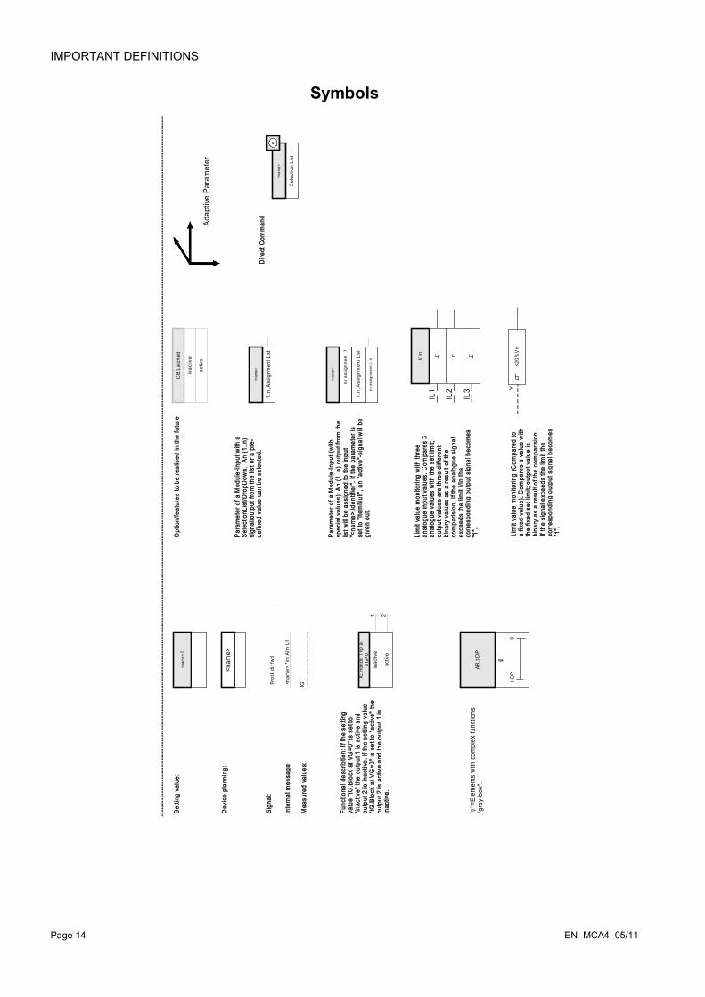
Symbols
Page 14 EN MCA4 05/11
inac
tive
activ
e
IG.n
ondi
r Trip
at
VG=0
1 2
Setti
ng v
alue
:<n
ame>
.I
Dev
ice
plan
ning
:<n
ame>
Sign
al:
IGM
easu
red
valu
es:
<nam
e>.*i
nt A
lm L
1in
tern
al m
essa
ge
Func
tiona
l des
crip
tion:
If th
e se
tting
va
lue
"IG.B
lock
at V
G=0
" is
set t
o "in
activ
e" th
e ou
tput
1 is
act
ive
and
outp
ut 2
is in
activ
e. If
the
setti
ng v
alue
"IG
.Blo
ck a
t VG
=0" i
s se
t to
"act
ive"
the
outp
ut 2
is a
ctiv
e an
d th
e ou
tput
1 is
in
activ
e.
Prot
.I di
r fw
d
AR.t-
DP
0t-D
P
φ
"φ"=
Elem
ents
with
com
plex
func
tions
"g
ray-
box"
.
inac
tive
activ
e
CB.
Latc
hed
Opt
ion/
feat
ures
to b
e re
alis
ed in
the
futu
re
Para
met
er o
f a M
odul
e-In
put w
ith a
Se
lect
ionL
ist/D
ropD
own.
An
(1..n
) si
gnal
/out
put f
rom
the
list o
r a p
re-
defin
ed v
alue
can
be
sele
cted
.1.
.n, A
ssig
nmen
t Lis
t
<nam
e>
1..n
, VeE
nabl
e
no a
ssig
nmen
t,1..n
no a
ssig
nmen
t 1
<nam
e>
1..n
, Ass
ignm
ent L
ist
Para
met
er o
f a M
odul
e-In
put (
with
sp
ecia
l val
ues)
: An
(1..n
) out
put f
rom
the
list w
ill be
ass
igne
d to
the
inpu
t "<
nam
e>.id
entif
ier".
If th
e pa
ram
eter
is
set t
o "It
emN
ull",
an
"act
ive"
-sig
nal w
ill be
gi
ven
out.
Lim
it va
lue
mon
itorin
g w
ith th
ree
anal
ogue
inpu
t val
ues.
Com
pare
s 3
anal
ogue
val
ues
with
the
set l
imit;
ou
tput
val
ues
are
thre
e di
ffere
nt
bina
ry v
alue
s as
a re
sult
of th
e co
mpa
risio
n. If
the
anal
ogue
sig
nal
exce
eds
the
limit
I/In
the
corre
spon
ding
out
put s
igna
l bec
omes
"1
".
I/ In
IL1
IL2
IL3
<20%
VnV
Lim
it va
lue
mon
itorin
g (C
ompa
red
to
a fix
ed v
alue
). C
ompa
res
a va
lue
with
th
e fix
ed s
et li
mit;
out
put v
alue
is
bina
ry a
s a
resu
lt of
the
com
paris
ion.
If
the
sign
al e
xcee
ds th
e lim
it th
e co
rresp
ondi
ng o
utpu
t sig
nal b
ecom
es
"1".
Ada
ptiv
e Pa
ram
eter
Sele
ctio
n Li
st
<nam
e>
Dire
ct C
omm
and
IMPORTANT DEFINITIONS
EN MCA4 05/11 Page 15
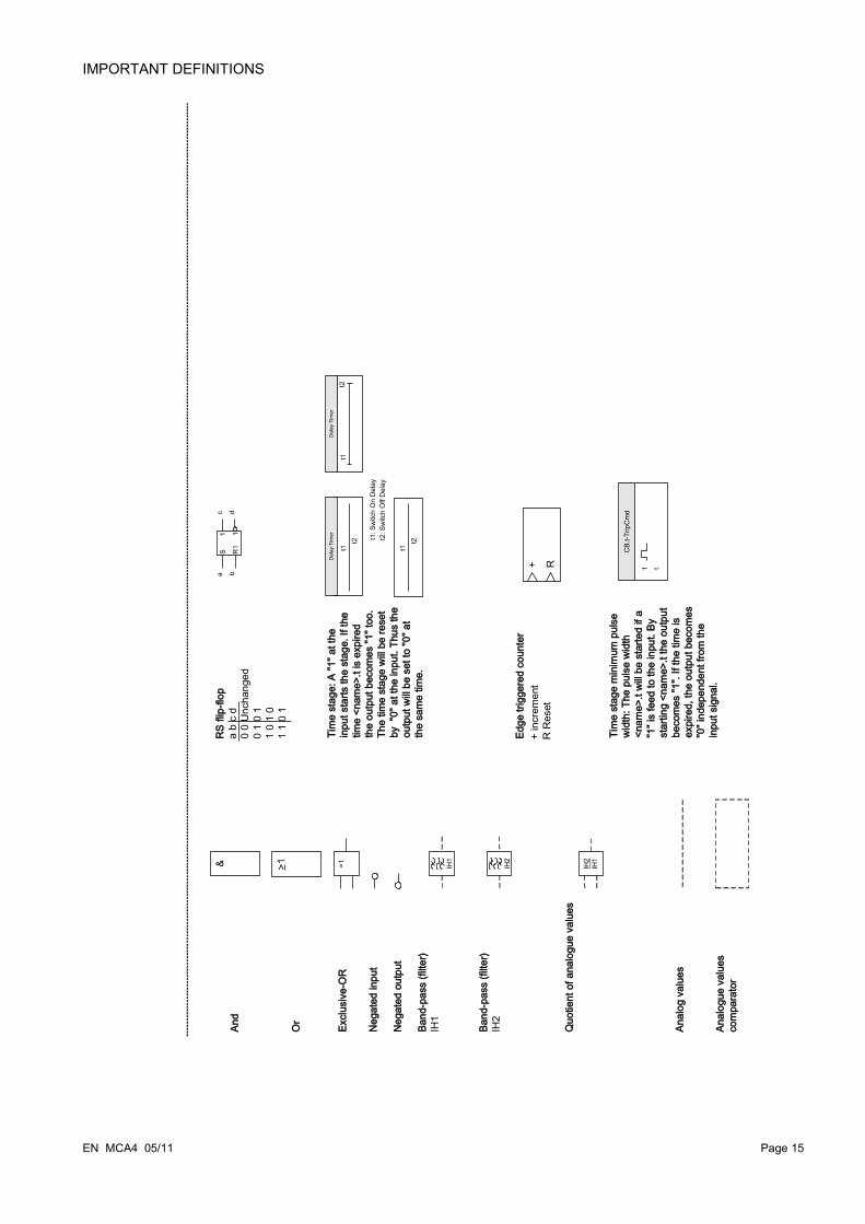
And
Or
Neg
ated
inpu
t
Neg
ated
out
put
Band
-pas
s (fi
lter)
IH1
Band
-pas
s (fi
lter)
IH2
Quo
tient
of a
nalo
gue
valu
es
1
CB.
t-Trip
Cm
d
t
Anal
og v
alue
s
S
1
R1
1
a bc d
RS
flip-
flop
a b
c d
0 0
Unc
hang
ed0
1 0
11
0 1
01
1 0
1
Tim
e st
age:
A "1
" at t
he
inpu
t sta
rts th
e st
age.
If th
e tim
e <n
ame>
.t is
exp
ired
th
e ou
tput
bec
omes
"1" t
oo.
The
time
stag
e w
ill be
rese
t by
"0"
at t
he in
put.
Thus
the
outp
ut w
ill be
set
to "0
" at
the
sam
e tim
e.
Tim
e st
age
min
imum
pul
se
wid
th: T
he p
ulse
wid
th
<nam
e>.t
will
be s
tarte
d if
a "1
" is
feed
to th
e in
put.
By
star
ting
<nam
e>.t
the
outp
ut
beco
mes
"1".
If th
e tim
e is
ex
pire
d, th
e ou
tput
bec
omes
"0
" ind
epen
dent
from
the
inpu
t sig
nal.
IH1
IH2
IH2
IH1
=1Ex
clus
ive-
OR
Anal
ogue
val
ues
com
para
tor
+ R+
incr
emen
tR
Res
et
Edge
trig
gere
d co
unte
r
t1
Del
ay T
imer
t2
t1: S
witc
h O
n D
elay
t2: S
witc
h O
ff D
elay
Del
ay T
imer
t1t2
t1t2
>1&
IMPORTANT DEFINITIONS
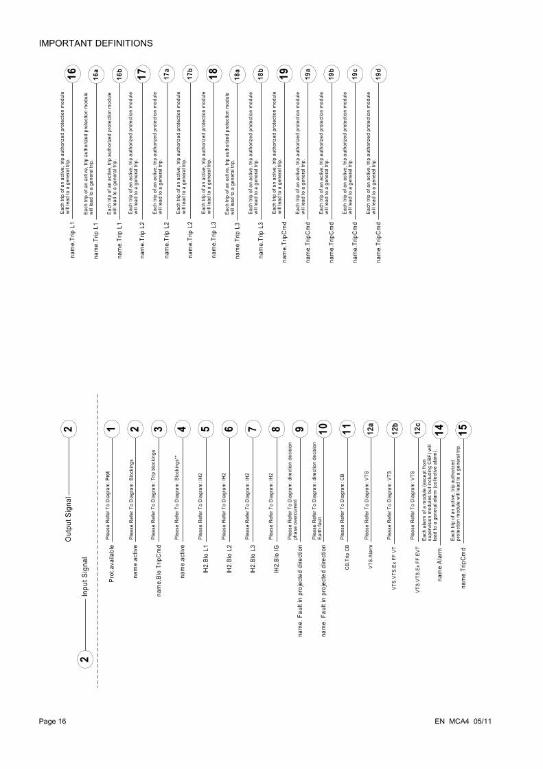
Page 16 EN MCA4 05/11
22
Inpu
t Sig
nal
Out
put S
igna
l
2na
me.
activ
e
3na
me.
Blo
Trip
Cm
d
4na
me.
activ
e
5IH
2.Bl
o L1
6IH
2.Bl
o L2
7IH
2.Bl
o L3
8IH
2.Bl
o IG
9na
me.
Fau
lt in
pro
ject
ed d
irect
ion
10na
me.
Fau
lt in
pro
ject
ed d
irect
ion
11C
B.Tr
ip C
B
12a
VTS.
Alar
m
12b
12c
VTS.
VTS.
Ex F
F EV
T
1Pr
ot.a
vaila
ble
Plea
se R
efer
To
Dia
gram
: Blo
ckin
gs
Plea
se R
efer
To
Dia
gram
: Blo
ckin
gs**
Plea
se R
efer
To
Dia
gram
: Pro
t
Plea
se R
efer
To
Dia
gram
: Trip
blo
ckin
gs
Plea
se R
efer
To
Dia
gram
: IH
2
Plea
se R
efer
To
Dia
gram
: IH
2
Plea
se R
efer
To
Dia
gram
: IH
2
Plea
se R
efer
To
Dia
gram
: IH
2
Plea
se R
efer
To
Dia
gram
: dire
ctio
n de
cisi
on
phas
e ov
ercu
rren
t
Plea
se R
efer
To
Dia
gram
: VTS
Plea
se R
efer
To
Dia
gram
: CB
Plea
se R
efer
To
Dia
gram
: dire
ctio
n de
cisi
on
Earth
faul
t
VTS.
VTS.
Ex F
F VT
Plea
se R
efer
To
Dia
gram
: VTS
Plea
se R
efer
To
Dia
gram
: VTS
17b
nam
e.Tr
ip L
2
18na
me.
Trip
L3
19na
me.
Trip
Cm
d
16na
me.
Trip
L1
Each
trip
of a
n ac
tive,
trip
aut
horiz
ed p
rote
ctio
n m
odul
e w
ill le
ad to
a g
ener
al tr
ip.
Each
trip
of a
n ac
tive,
trip
aut
horiz
ed p
rote
ctio
n m
odul
e w
ill le
ad to
a g
ener
al tr
ip.
Each
trip
of a
n ac
tive,
trip
aut
horiz
ed p
rote
ctio
n m
odul
e w
ill le
ad to
a g
ener
al tr
ip.
Each
trip
of a
n ac
tive,
trip
aut
horiz
ed p
rote
ctio
n m
odul
e w
ill le
ad to
a g
ener
al tr
ip.
16a
nam
e.Tr
ip L
1E
ach
trip
of a
n ac
tive,
trip
aut
horiz
ed p
rote
ctio
n m
odul
e w
ill le
ad to
a g
ener
al tr
ip.
16b
nam
e.Tr
ip L
1E
ach
trip
of a
n ac
tive,
trip
aut
horiz
ed p
rote
ctio
n m
odul
e w
ill le
ad to
a g
ener
al tr
ip.
17na
me.
Trip
L2
Each
trip
of a
n ac
tive,
trip
aut
horiz
ed p
rote
ctio
n m
odul
e w
ill le
ad to
a g
ener
al tr
ip.
17a
nam
e.Tr
ip L
2
Each
trip
of a
n ac
tive,
trip
aut
horiz
ed p
rote
ctio
n m
odul
e w
ill le
ad to
a g
ener
al tr
ip.
19a
nam
e.Tr
ipC
md
Each
trip
of a
n ac
tive,
trip
aut
horiz
ed p
rote
ctio
n m
odul
e w
ill le
ad to
a g
ener
al tr
ip.
19b
nam
e.Tr
ipC
md
Each
trip
of a
n ac
tive,
trip
aut
horiz
ed p
rote
ctio
n m
odul
e w
ill le
ad to
a g
ener
al tr
ip.
19c
nam
e.Tr
ipC
md
Each
trip
of a
n ac
tive,
trip
aut
horiz
ed p
rote
ctio
n m
odul
e w
ill le
ad to
a g
ener
al tr
ip.
19d
nam
e.Tr
ipC
md
Each
trip
of a
n ac
tive,
trip
aut
horiz
ed p
rote
ctio
n m
odul
e w
ill le
ad to
a g
ener
al tr
ip.
18a
nam
e.Tr
ip L
3E
ach
trip
of a
n ac
tive,
trip
aut
horiz
ed p
rote
ctio
n m
odul
e w
ill le
ad to
a g
ener
al tr
ip.
18b
nam
e.Tr
ip L
3Ea
ch tr
ip o
f an
activ
e, tr
ip a
utho
rized
pro
tect
ion
mod
ule
will
lead
to a
gen
eral
trip
.
14 15na
me.
Trip
Cm
d
nam
e.Al
arm
Each
ala
rm o
f a m
odul
e (e
xcep
t fro
m
supe
rvis
ion
mod
ules
but
incl
udin
g C
BF) w
ill le
ad to
a g
ener
al a
larm
(col
lect
ive
alar
m).
Each
trip
of a
n ac
tive,
trip
aut
horiz
ed
prot
ectio
n m
odul
e w
ill le
ad to
a g
ener
al tr
ip.
IMPORTANT DEFINITIONS
EN MCA4 05/11 Page 17
34C
B.Po
s O
N
35C
B.Po
s O
FF
33C
B.Po
s
Plea
se R
efer
To
Dia
gram
: CB.
CB
Man
ager
Plea
se R
efer
To
Dia
gram
: CB.
CB
Man
ager
Plea
se R
efer
To
Dia
gram
: CB.
CB
Man
ager
36C
B.Po
s In
dete
rm
37C
B.Po
s D
istu
rb
Plea
se R
efer
To
Dia
gram
: CB
.CB
Man
ager
Plea
se R
efer
To
Dia
gram
: CB
.CB
Man
ager
20na
me.
Trip
L1
21na
me.
Trip
L2
Each
trip
of a
n ac
tive,
trip
aut
horiz
ed p
rote
ctio
n m
odul
e w
ill le
ad to
a g
ener
al tr
ip.
Each
trip
of a
n ac
tive,
trip
aut
horiz
ed p
rote
ctio
n m
odul
e w
ill le
ad to
a g
ener
al tr
ip.
22na
me.
Trip
L3
23na
me.
Trip
Each
trip
of a
n ac
tive,
trip
aut
horiz
ed p
rote
ctio
n m
odul
e w
ill le
ad to
a g
ener
al tr
ip.
Each
trip
of a
n ac
tive,
trip
aut
horiz
ed p
rote
ctio
n m
odul
e w
ill le
ad to
a g
ener
al tr
ip.
25na
me.
Alar
m L
2
26b
nam
e.Al
arm
L3
27na
me.
Alar
m
28na
me.
Alar
m L
1
29na
me.
Alar
m L
2
24na
me.
Alar
m L
1
Each
pha
se s
elec
tive
alar
m o
f a m
odul
e (I,
IG, V
, VX
depe
ndin
g on
the
devi
ce ty
pe) w
ill le
ad to
a p
hase
se
lect
ive
gene
ral a
larm
(col
lect
ive
alar
m).
Each
pha
se s
elec
tive
alar
m o
f a m
odul
e (I,
IG, V
, VX
depe
ndin
g on
the
devi
ce ty
pe) w
ill le
ad to
a p
hase
se
lect
ive
gene
ral a
larm
(col
lect
ive
alar
m).
Each
pha
se s
elec
tive
alar
m o
f a m
odul
e (I,
IG, V
, VX
depe
ndin
g on
the
devi
ce ty
pe) w
ill le
ad to
a p
hase
se
lect
ive
gene
ral a
larm
(col
lect
ive
alar
m).
Each
pha
se s
elec
tive
alar
m o
f a m
odul
e (I,
IG, V
, VX
depe
ndin
g on
the
devi
ce ty
pe) w
ill le
ad to
a p
hase
se
lect
ive
gene
ral a
larm
(col
lect
ive
alar
m).
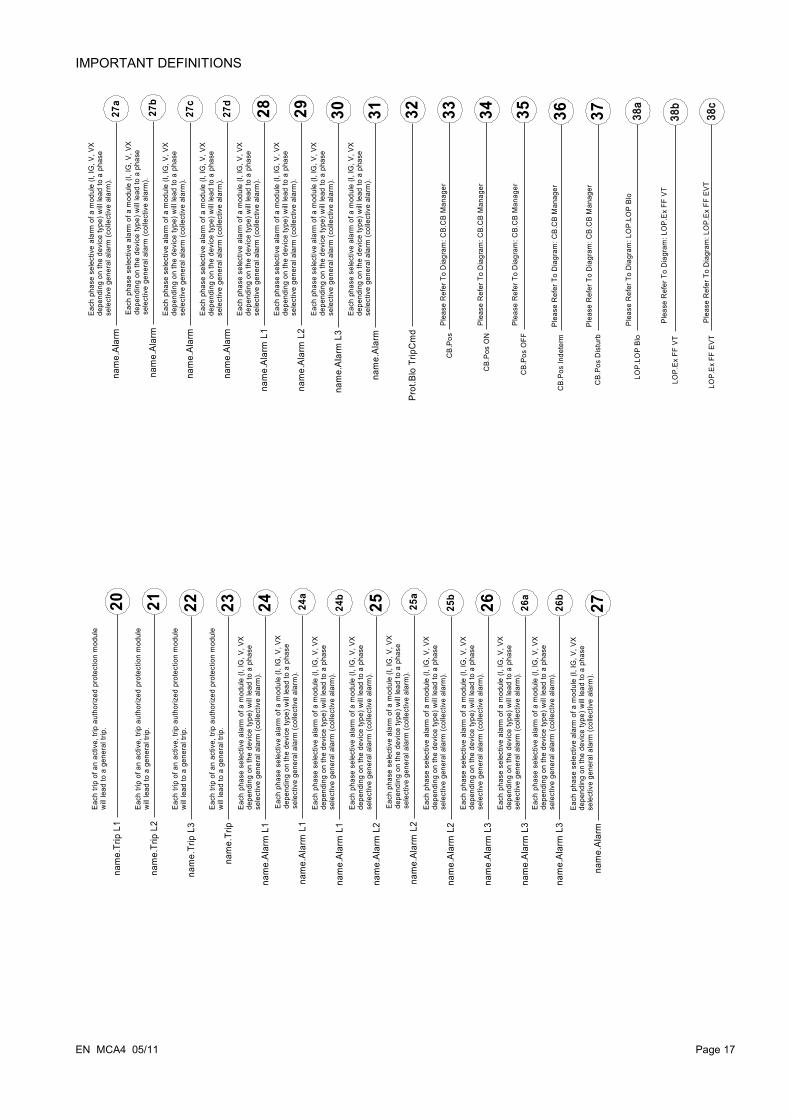
Eac
h ph
ase
sele
ctiv
e al
arm
of a
mod
ule
(I, IG
, V, V
X de
pend
ing
on th
e de
vice
type
) will
lead
to a
pha
se
sele
ctiv
e ge
nera
l ala
rm (c
olle
ctiv
e al
arm
).
Eac
h ph
ase
sele
ctiv
e al
arm
of a
mod
ule
(I, IG
, V, V
X de
pend
ing
on th
e de
vice
type
) will
lead
to a
pha
se
sele
ctiv
e ge
nera
l ala
rm (c
olle
ctiv
e al
arm
).
30na
me.
Alar
m L
3
31na
me.
Alar
m
Eac
h ph
ase
sele
ctiv
e al
arm
of a
mod
ule
(I, IG
, V, V
X de
pend
ing
on th
e de
vice
type
) will
lead
to a
pha
se
sele
ctiv
e ge
nera
l ala
rm (c
olle
ctiv
e al
arm
).
Eac
h ph
ase
sele
ctiv
e al
arm
of a
mod
ule
(I, IG
, V, V
X de
pend
ing
on th
e de
vice
type
) will
lead
to a
pha
se
sele
ctiv
e ge
nera
l ala
rm (c
olle
ctiv
e al
arm
).
32Pr
ot.B
lo T
ripC
md
24a
nam
e.Al
arm
L1
Each
pha
se s
elec
tive
alar
m o
f a m
odul
e (I,
IG, V
, VX
de
pend
ing
on th
e de
vice
type
) will
lead
to a
pha
se
sele
ctiv
e ge
nera
l ala
rm (c
olle
ctiv
e al
arm
).
24b
nam
e.Al
arm
L1
Each
pha
se s
elec
tive
alar
m o
f a m
odul
e (I,
IG, V
, VX
depe
ndin
g on
the
devi
ce ty
pe) w
ill le
ad to
a p
hase
se
lect
ive
gene
ral a
larm
(col
lect
ive
alar
m).
25a
nam
e.Al
arm
L2
Each
pha
se s
elec
tive
alar
m o
f a m
odul
e (I,
IG, V
, VX
de
pend
ing
on th
e de
vice
type
) will
lead
to a
pha
se
sele
ctiv
e ge
nera
l ala
rm (c
olle
ctiv
e al
arm
).
25b
nam
e.Al
arm
L2
Each
pha
se s
elec
tive
alar
m o
f a m
odul
e (I,
IG, V
, VX
depe
ndin
g on
the
devi
ce ty
pe) w
ill le
ad to
a p
hase
se
lect
ive
gene
ral a
larm
(col
lect
ive
alar
m).
26na
me.
Alar
m L
3
Each
pha
se s
elec
tive
alar
m o
f a m
odul
e (I,
IG, V
, VX
depe
ndin
g on
the
devi
ce ty
pe) w
ill le
ad to
a p
hase
se
lect
ive
gene
ral a
larm
(col
lect
ive
alar
m).
26a
nam
e.Al
arm
L3
Each
pha
se s
elec
tive
alar
m o
f a m
odul
e (I,
IG, V
, VX
depe
ndin
g on
the
devi
ce ty
pe) w
ill le
ad to
a p
hase
se
lect
ive
gene
ral a
larm
(col
lect
ive
alar
m).
27a
nam
e.Al
arm
Each
pha
se s
elec
tive
alar
m o
f a m
odul
e (I,
IG, V
, VX
depe
ndin
g on
the
devi
ce ty
pe) w
ill le
ad to
a p
hase
se
lect
ive
gene
ral a
larm
(col
lect
ive
alar
m).
27b
nam
e.Al
arm
Each
pha
se s
elec
tive
alar
m o
f a m
odul
e (I,
IG, V
, VX
depe
ndin
g on
the
devi
ce ty
pe) w
ill le
ad to
a p
hase
se
lect
ive
gene
ral a
larm
(col
lect
ive
alar
m).
27c
nam
e.Al
arm
Each
pha
se s
elec
tive
alar
m o
f a m
odul
e (I,
IG, V
, VX
depe
ndin
g on
the
devi
ce ty
pe) w
ill le
ad to
a p
hase
se
lect
ive
gene
ral a
larm
(col
lect
ive
alar
m).
27d
nam
e.Al
arm
Each
pha
se s
elec
tive
alar
m o
f a m
odul
e (I,
IG, V
, VX
depe
ndin
g on
the
devi
ce ty
pe) w
ill le
ad to
a p
hase
se
lect
ive
gene
ral a
larm
(col
lect
ive
alar
m).
38a
Ple
ase
Ref
er T
o D
iagr
am: L
OP.
LOP
Blo
LOP.
LOP
Blo
38b
Plea
se R
efer
To
Dia
gram
: LO
P.E
x FF
VT
LOP.
Ex F
F VT
38c
Ple
ase
Ref
er T
o D
iagr
am: L
OP.
Ex
FF E
VTLO
P.Ex
FF
EVT
IMPORTANT DEFINITIONS
Page 18 EN MCA4 05/11
41
SG.P
rot O
N
42SG
.ON
Cm
d
SG
.Pro
t ON
SG
.ON
Cm
d
39P
leas
e R
efer
To
Dia
gram
: Q->
&V<.
Dec
oupl
ing
Ener
gy R
esou
rce
Q->
&V<.
Dec
oupl
ing
Ener
gy R
esou
rce
40P
leas
e R
efer
To
Dia
gram
: CTS
.Ala
rmC
TS.A
larm

IMPORTANT DEFINITIONS
General Conventions
EN MCA4 05/11 Page 19
»Parameters are indicated by right and left double arrow heads and written in italic.«
»SIGNALS are indicated by right and left double arrow heads and small caps.«
[Paths are indicated by brackets.]
Software and Device names are written in italic.
Module and Instance (Element) names are displayed italic and underlined.
»Pushbuttons, Modes and Menu entries are indicated by right and left double arrow heads.«
1 2 3 Image References (Squares)

IMPORTANT DEFINITIONS
Load Reference Arrow SystemIn general, the “Load Reference Arrow System” is used for loads (consumed energy) and the “Generator Reference System” is used for generators (generated energy).
Within the HighPROTEC the “Load Reference Arrow System” is used exclusively.
This applies to directions and phase angles. The phase angle is definded as the angle from the current phasor to the voltage phasor. Current and voltage arrows are to be counted positive in the direction of the arrow. The advantage of determining the load reference arrow system as the standard is that it is not necessary to change the direction of the current arrow if there is a transition from motor to generator.
Page 20 EN MCA4 05/11

Device
Device MCA4
Device PlanningPlanning of a device means to reduce the functional range to a degree that suits the protection task to be fulfilled, i.e. the device shows only those functions you really need. If you, for example, deactivate the voltage protection function, all parameter branches related to this function do not appear in the parameter tree any more. All corresponding events, signals etc. will be deactivated too. By this the parameter trees become very transparent. Planning also involves adjustment of all basic system data (frequency etc.).
But it has to be taken into account that by deactivating, for instance, protective functions, you also change the functionality of the device. If you cancel the directional feature of the overcurrent protections then the device no longer trips in a directional way but merely in a non-directional way.
The manufacturer does not accept liability for any personal or material damage as a result of wrong planning.
A planning service is also offered by Woodward Kempen GmbH.
Beware of inadvertent deactivating protective functions/modules
If you are deactivating modules within the device planning all parameters of those modules will be set on default.If you are activating one of these modules again all parameters of those reactivated modules will be set on default.
EN MCA4 05/11 Page 21
Device
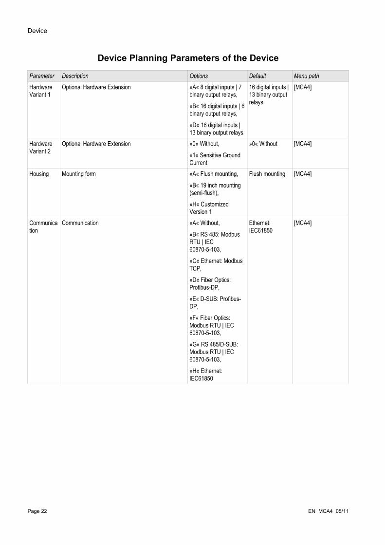
Device Planning Parameters of the Device
Parameter Description Options Default Menu path
Hardware Variant 1
Optional Hardware Extension »A« 8 digital inputs | 7 binary output relays,
»B« 16 digital inputs | 6 binary output relays,
»D« 16 digital inputs | 13 binary output relays
16 digital inputs | 13 binary output relays
[MCA4]
Hardware Variant 2
Optional Hardware Extension »0« Without,
»1« Sensitive Ground Current
»0« Without [MCA4]
Housing Mounting form »A« Flush mounting,
»B« 19 inch mounting (semi-flush),
»H« Customized Version 1
Flush mounting [MCA4]
Communication
Communication »A« Without,
»B« RS 485: Modbus RTU | IEC 60870-5-103,
»C« Ethernet: Modbus TCP,
»D« Fiber Optics: Profibus-DP,
»E« D-SUB: Profibus-DP,
»F« Fiber Optics: Modbus RTU | IEC 60870-5-103,
»G« RS 485/D-SUB: Modbus RTU | IEC 60870-5-103,
»H« Ethernet: IEC61850
Ethernet: IEC61850
[MCA4]
Page 22 EN MCA4 05/11
Installation and Connection
Installation and Connection
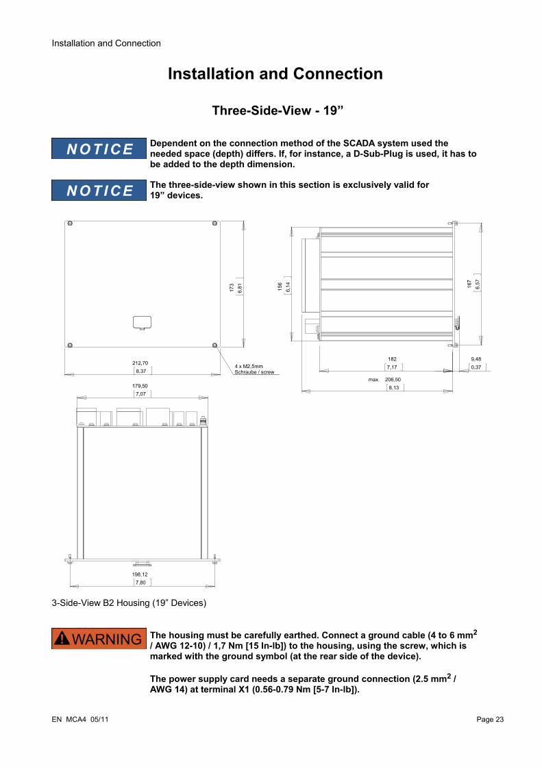
Three-Side-View - 19”
Dependent on the connection method of the SCADA system used the needed space (depth) differs. If, for instance, a D-Sub-Plug is used, it has to be added to the depth dimension.
The three-side-view shown in this section is exclusively valid for 19” devices.
3-Side-View B2 Housing (19” Devices)
The housing must be carefully earthed. Connect a ground cable (4 to 6 mm2
/ AWG 12-10) / 1,7 Nm [15 In-lb]) to the housing, using the screw, which is marked with the ground symbol (at the rear side of the device).
The power supply card needs a separate ground connection (2.5 mm2 / AWG 14) at terminal X1 (0.56-0.79 Nm [5-7 In-lb]).
EN MCA4 05/11 Page 23
Installation and Connection
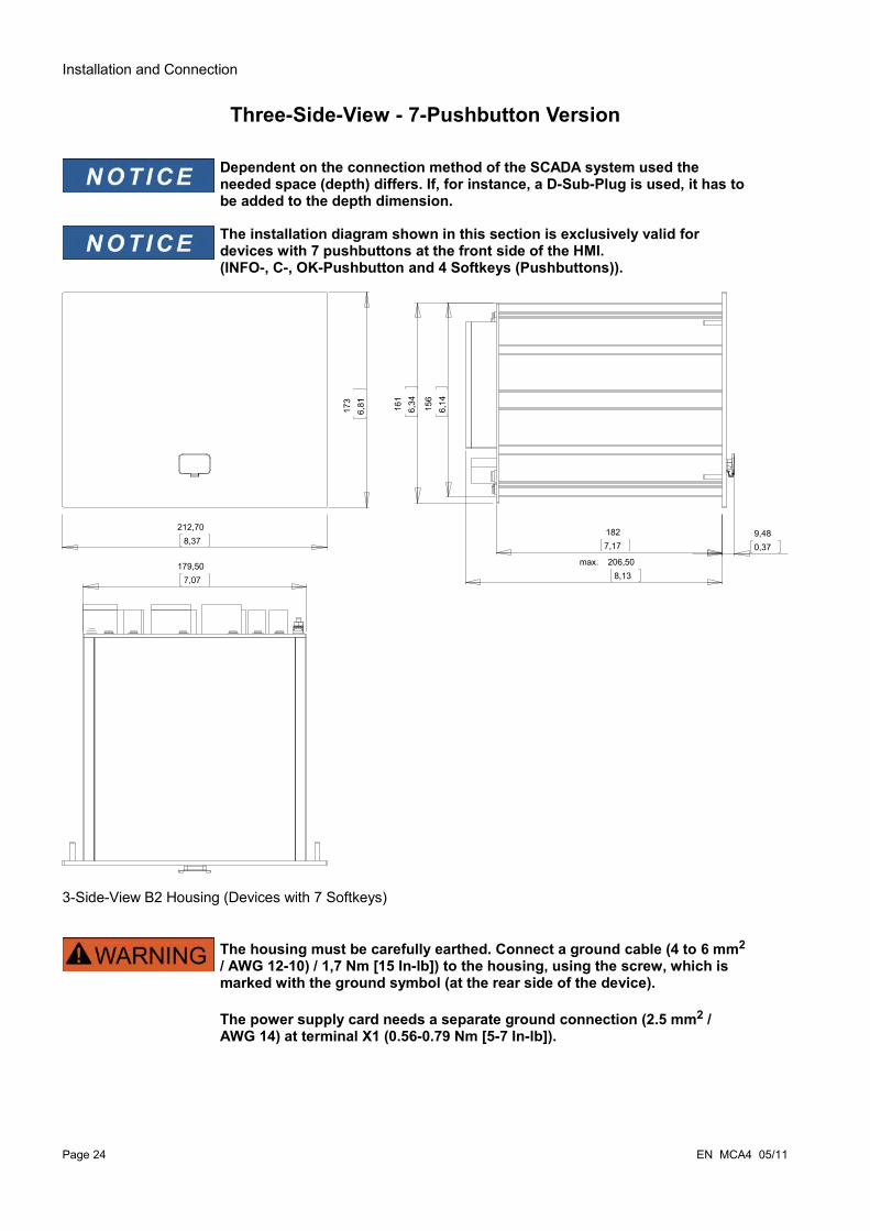
Three-Side-View - 7-Pushbutton Version
Dependent on the connection method of the SCADA system used the needed space (depth) differs. If, for instance, a D-Sub-Plug is used, it has to be added to the depth dimension.
The installation diagram shown in this section is exclusively valid for devices with 7 pushbuttons at the front side of the HMI. (INFO-, C-, OK-Pushbutton and 4 Softkeys (Pushbuttons)).
3-Side-View B2 Housing (Devices with 7 Softkeys)
The housing must be carefully earthed. Connect a ground cable (4 to 6 mm2
/ AWG 12-10) / 1,7 Nm [15 In-lb]) to the housing, using the screw, which is marked with the ground symbol (at the rear side of the device).
The power supply card needs a separate ground connection (2.5 mm2 / AWG 14) at terminal X1 (0.56-0.79 Nm [5-7 In-lb]).
Page 24 EN MCA4 05/11

Installation and Connection
Three-Side-View - 8-Pushbutton Version
Dependent on the connection method of the SCADA system used the needed space (depth) differs. If, for instance, a D-Sub-Plug is used, it has to be added to the depth dimension.
The installation diagram shown in this section is exclusively valid for devices with 8 pushbuttons at the front side of the HMI. (INFO-, C-, OK-, CTRL-Pushbutton and 4 Softkeys (Pushbuttons)).
3-Side-View B2 Housing (Devices with 8 Softkeys)
The housing must be carefully earthed. Connect a ground cable (4 to 6 mm2
/ AWG 12-10) / 1,7 Nm [15 In-lb]) to the housing, using the screw, which is marked with the ground symbol (at the rear side of the device).
The power supply card needs a separate ground connection (2.5 mm2 / AWG 14) at terminal X1 (0.56-0.79 Nm [5-7 In-lb]).
EN MCA4 05/11 Page 25

Installation and Connection
Installation Diagram 7-Pushbutton Version
Even when the auxiliary voltage is switched-off, unsafe voltages might remain at the device connections.
The installation diagram shown in this section is exclusively valid for devices with 7 pushbuttons at the front side of the HMI. (INFO-, C-, OK-Pushbutton and 4 Softkeys (Pushbuttons)).
B2 Housing Door Cut-out (7-Pushbutton Version)
The housing must be carefully earthed. Connect a ground cable (4 to 6 mm2
/ AWG 12-10) / 1,7 Nm [15 In-lb]) to the housing, using the screw, which is marked with the ground symbol (at the rear side of the device).
The power supply card needs a separate ground connection (2.5 mm2 / AWG 14) at terminal X1 (0.56-0.79 Nm [5-7 In-lb]).
Be careful. Do not overtighten the mountings nuts of the relay (M4 metric 4 mm). Check the torque by means of a torque wrench (1,7 Nm [15 In-lb]). Overtightening the mounting nuts could due to personal injury or damage the relay.
Page 26 EN MCA4 05/11

Installation and Connection
Installation Diagram 8-Pushbutton Version
Even when the auxiliary voltage is switched-off, unsafe voltages might remain at the device connections.
The installation diagram shown in this section is exclusively valid for devices with 8 pushbuttons at the front side of the HMI. (INFO-, C-, OK-, CTRL-Pushbutton and 4 Softkeys (Pushbuttons)).
B2 Housing Door Cut-out (8-Pushbutton Version)
The housing must be carefully earthed. Connect a ground cable (4 to 6 mm2
/ AWG 12-10) / 1,7 Nm [15 In-lb]) to the housing, using the screw, which is marked with the ground symbol (at the rear side of the device).
The power supply card needs a separate ground connection (2.5 mm2 / AWG 14) at terminal X1 (0.56-0.79 Nm [5-7 In-lb]).
Be careful. Do not overtighten the mountings nuts of the relay (M4 metric 4 mm). Check the torque by means of a torque wrench (1,7 Nm [15 In-lb]). Overtightening the mounting nuts could due to personal injury or damage the relay.
EN MCA4 05/11 Page 27
Installation and Connection
Assembly Groups
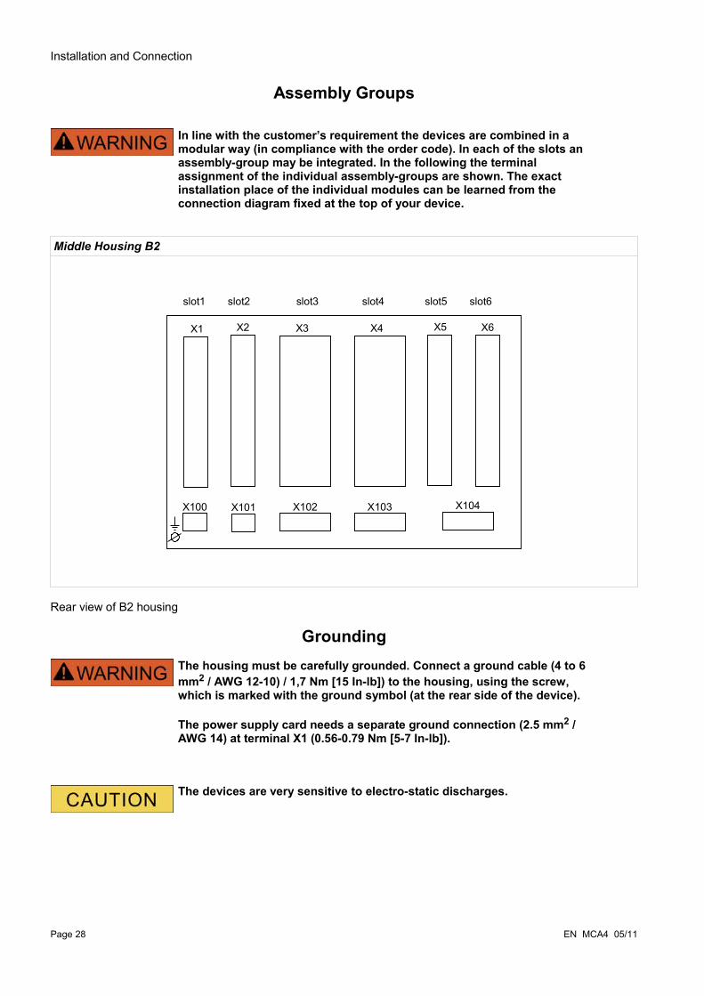
In line with the customer’s requirement the devices are combined in a modular way (in compliance with the order code). In each of the slots an assembly-group may be integrated. In the following the terminal assignment of the individual assembly-groups are shown. The exact installation place of the individual modules can be learned from the connection diagram fixed at the top of your device.
Middle Housing B2
Rear view of B2 housing
GroundingThe housing must be carefully grounded. Connect a ground cable (4 to 6 mm2 / AWG 12-10) / 1,7 Nm [15 In-lb]) to the housing, using the screw, which is marked with the ground symbol (at the rear side of the device).
The power supply card needs a separate ground connection (2.5 mm2 / AWG 14) at terminal X1 (0.56-0.79 Nm [5-7 In-lb]).
The devices are very sensitive to electro-static discharges.
Page 28 EN MCA4 05/11
X1 X2 X3
X100 X102
X5 X6
X104
X4
X103
slot3 slot4 slot5 slot6slot1 slot2
X101

Installation and Connection
Slot X1: Power Supply Card with Digital Inputs
Rear side of the device (Slots)
The type of power supply card and the number of digital inputs on it used in this slot is dependent on the ordered device type. The different variants have a different scope of functions.
Available assembly groups in this slot:
• (DI8-X1): This assembly group comprises a wide-range power supply unit; and two non-grouped digital inputs and six (6) digital inputs (grouped).
The available combinations can be gathered from the ordering code.
EN MCA4 05/11 Page 29
X1 X2 X3
X100 X102
X5 X6
X104
X4
X103
Slot3 Slot4 Slot5 Slot6Slot1 Slot2
X101

Installation and Connection
DI8-X Power Supply and Digital Inputs
Make sure, that the tightening torque is 0.56-0.79 Nm [5-7 In-lb].
This assembly group comprises:
• a wide-range power supply unit • 6 digital inputs, grouped• 2 digital inputs, non-grouped• 24V DC (for options with Woodward Devices only)
Auxiliary voltage supply
• The aux. voltage inputs (wide-range power supply unit) are non-polarized. The device could be provided with AC or DC voltage.
Digital inputs
For each digital input group the related voltage input range has to be parameterized. Wrong switching thresholds can result in malfunctions/wrong signal transfer times.
The digital inputs are provided with different switching thresholds (can be parameterized) (two AC and five DC input ranges). For the six grouped (connected to common potential) inputs and the two non-grouped inputs the following switching levels can be defined:
• 24V DC• 48V DC / 60V DC • 110 V AC/DC • 230 V AC/DC
If a voltage >80% of the set switching threshold is applied at the digital input, the state change is recognized (physically “1”). If the voltage is below 40% of the set switching threshold, the device detects physically “0”.
The ground terminal has to be connected to the »-pole« when using DC supply.
Use of the 24 V DC Output is prohibited. This output is exclusively for factory testing and commissioning.
Page 30 EN MCA4 05/11
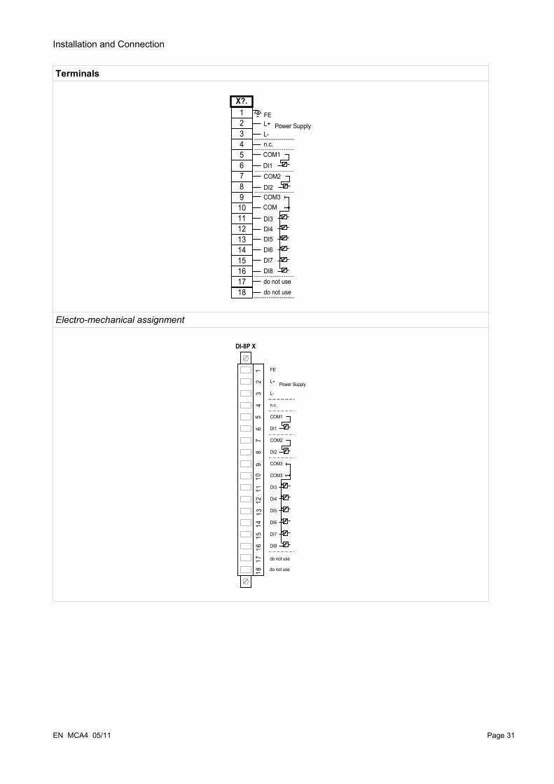
Installation and Connection
Terminals
Electro-mechanical assignment
EN MCA4 05/11 Page 31
L+
L-
FE
COM1
DI1
COM2
DI2
DI3
DI4
DI5
DI6
DI7
DI8
COM3
do not use
DI-8P X
COM3
n.c.
do not use
13
24
56
78
910
1112
1314
1516
1718
Power Supply
12345678
FE
9101112
COM1
131415161718
L+ Power Supply
DI1COM2DI2COM3
DI3DI4DI5DI6DI7DI8
COM
do not usedo not use
L-
X?.
n.c.

Installation and Connection
Slot X2: Relay Output Card
Rear side of the device (Slots)
The type of card in this slot is dependent on the ordered device type. The different variants have a different scope of functions.
Available assembly groups in this slot:
• (RO-6 X2): Assembly Group with 6 Relay Outputs.
The available combinations can be gathered from the ordering code.
Page 32 EN MCA4 05/11
X1 X2 X3
X100 X102
X5 X6
X104
X4
X103
Slot3 Slot4 Slot5 Slot6Slot1 Slot2
X101

Installation and Connection
Binary Output Relays
The number of the binary output relay contacts is related to the type of the device or type code. The binary output relays are potential-free change-over contacts. In chapter [Assignment/binary outputs] the assignment of the binary output relays is specified. The changeable signals are listed in the »assignment list« which can be found in the appendix.
Make sure that the tightening torque is 0.56-0.79 Nm [5-7 In-lb].
Please duly consider the current carrying capacity of the binary output relays. Please refer to the Technical Data.
EN MCA4 05/11 Page 33

Installation and Connection
Terminals
Electro-mechanical assignment
Page 34 EN MCA4 05/11
BO1 C
BO1 n.o.
BO1 n.c.
BO2 C
BO2 n.o.
BO2 n.c.
BO3 C
BO3 n.o.
BO3 n.c.
BO4 C
BO4 n.o.
BO4 n.c.
BO5 C
BO5 n.o.
BO5 n.c.
BO6 C
BO6 n.o.
BO6 n.c.
13
24
56
78
910
1112
1314
1516
1718
BO-6 X
123456789
101112131415161718
BO3
BO1
BO2
BO4
BO5
BO6
X?.
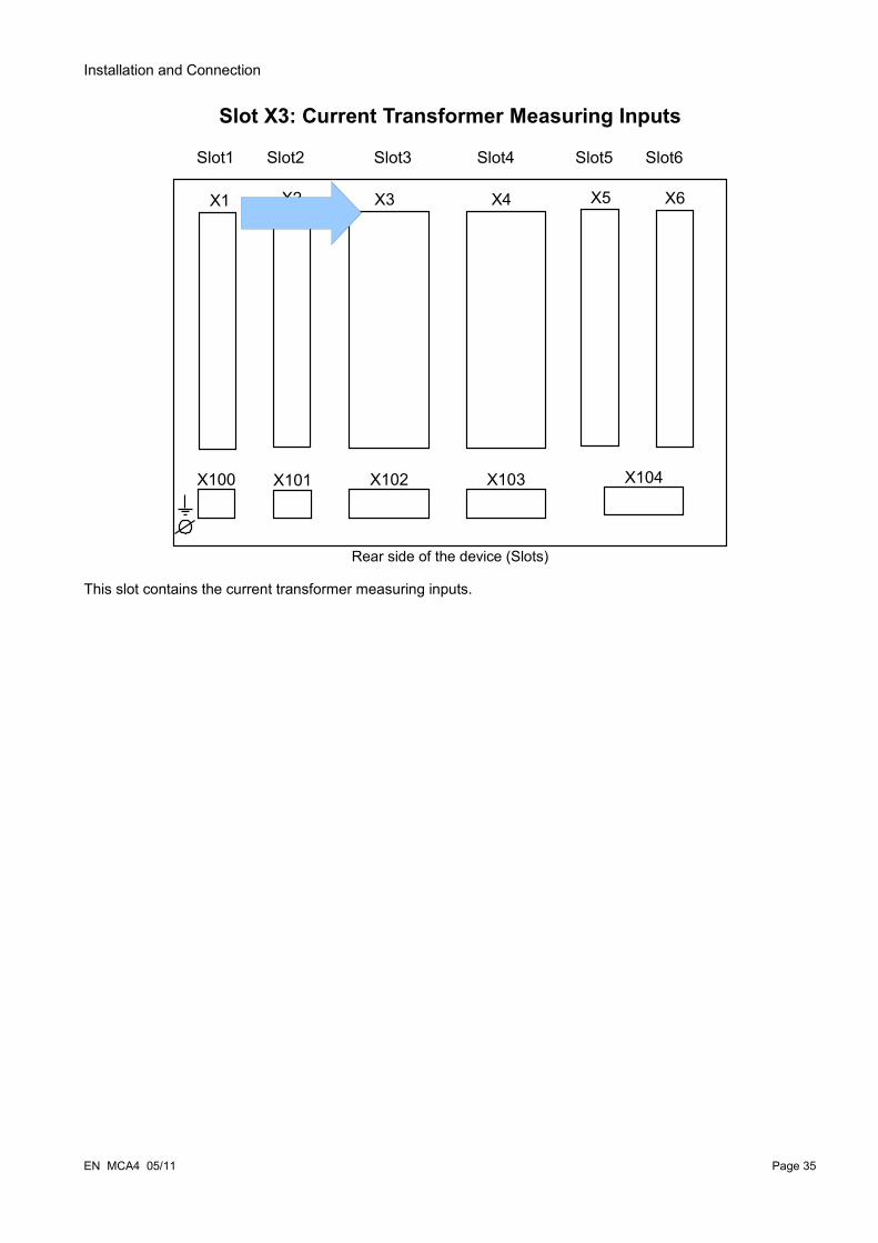
Installation and Connection
Slot X3: Current Transformer Measuring Inputs
Rear side of the device (Slots)
This slot contains the current transformer measuring inputs.
EN MCA4 05/11 Page 35
X1 X2 X3
X100 X102
X5 X6
X104
X4
X103
Slot3 Slot4 Slot5 Slot6Slot1 Slot2
X101

Installation and Connection
Current Measuring Inputs and Ground Current Measuring Input
The device is provided with 4 current measuring inputs: three for measuring the phase currents and one for measuring of the earth current. Each of the current measuring inputs has a measuring input for 1 A and 5 A.
The input for earth current measuring either can be connected to a cable-type current transformer or alternatively it is possible to connect the summation current path of the phase current transformer to this input (Holmgreen connection).
Current transformers have to be earthed on their secondary side.
Interrupting the secondary circuits of current transformers causes hazardous voltages.
The secondary side of the current transformers have to be short circuited before the current circuit to the device is opened.
The current measuring inputs may exclusively be connected to current measuring transformers (with galvanic separation).
• Do not interchange the inputs (1 A/5 A)
• Make sure the transformation ratios and the power of the CTs are correctly rated. If the rating of the CTs is not right (overrated), then the normal operational conditions may not be recognized. The pickup value of the measuring unit amounts approx. 3% of the rated current of the device. Also the CTs need a current greater than approx 3% of the rated current to ensure sufficient accuracy. Example: For a 600 A CT (primary current) any currents below 18 A cannot be detected any more.
• Overloading can result in destruction of the measuring inputs or faulty signals. Overloading means that in case of a short-circuit the current-carrying capacity of the measuring inputs could be exceeded.
Make sure, that the tightening torque is 2 Nm [17.7 In-lb].
Page 36 EN MCA4 05/11

Installation and Connection
Terminals
Electro-mechanical assignment
EN MCA4 05/11 Page 37
IL1-1A
IL1-N
IL1-5A
IL2-1A
IL2-N
IL3-1A
IL3-N
IL3-5A
IG-1A
IG-N
IG-5A
IL2-5A
1
2
3
4
5
6
7
8
10
11
9
12
123456789
101112
IL1
1A
5A
N
IL2
1A
5A
N
IL3
1A
5A
N
IG
1A
5A
N
X?.
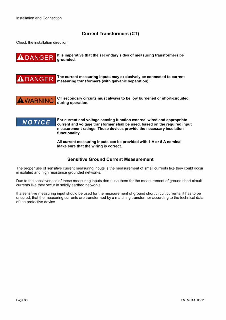
Installation and Connection
Current Transformers (CT)
Check the installation direction.
It is imperative that the secondary sides of measuring transformers be grounded.
The current measuring inputs may exclusively be connected to current measuring transformers (with galvanic separation).
CT secondary circuits must always to be low burdened or short-circuited during operation.
For current and voltage sensing function external wired and appropriate current and voltage transformer shall be used, based on the required input measurement ratings. Those devices provide the necessary insulation functionality.
All current measuring inputs can be provided with 1 A or 5 A nominal. Make sure that the wiring is correct.
Sensitive Ground Current Measurement
The proper use of sensitive current measuring inputs is the measurement of small currents like they could occur in isolated and high resistance grounded networks.
Due to the sensitiveness of these measuring inputs don´t use them for the measurement of ground short circuit currents like they occur in solidly earthed networks.
If a sensitive measuring input should be used for the measurement of ground short circuit currents, it has to be ensured, that the measuring currents are transformed by a matching transformer according to the technical data of the protective device.
Page 38 EN MCA4 05/11
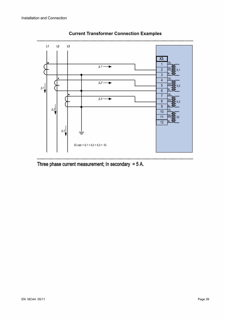
Installation and Connection
Current Transformer Connection Examples
EN MCA4 05/11 Page 39
L1 L2 L3
IL1
IL2
IL3
1X3.
23456789101112
Three phase current measurement; In secondary = 5 A.
IL1
1A
5A
N
IL2
1A
5A
N
IL3
1A
5A
N
IG
1A
5A
N
IL2'
IL3'
IL1'
IG calc = IL1 + IL2 + IL3 = IG

Installation and Connection
Page 40 EN MCA4 05/11
L1 L2 L3
IL2'IL1
IL3'
IL2
IL3
IL1' 1X3.
23456789101112
Three phase current measurement; In secondary = 1 A.Earth-current measuring via cable-type current transformer ; IGnom secondary = 1 A.
IG'
IL1
1A
5A
N
IL2
1A
5A
N
IL3
1A
5A
N
IG
1A
5A
N
Warning!The shielding at the dismantled end of the line has to be put through the cable-type current transformer and has to be grounded at the cable side.
Ring Core Type Current Transformer: Measures the ground current. (Sum of the three phase currents). Can be used for measuring the earth current in isolated and compensated networks. The shield is to be returned through the ring core current transformer.
IG meas = IG
IG calc = IL1 + IL2 + IL3
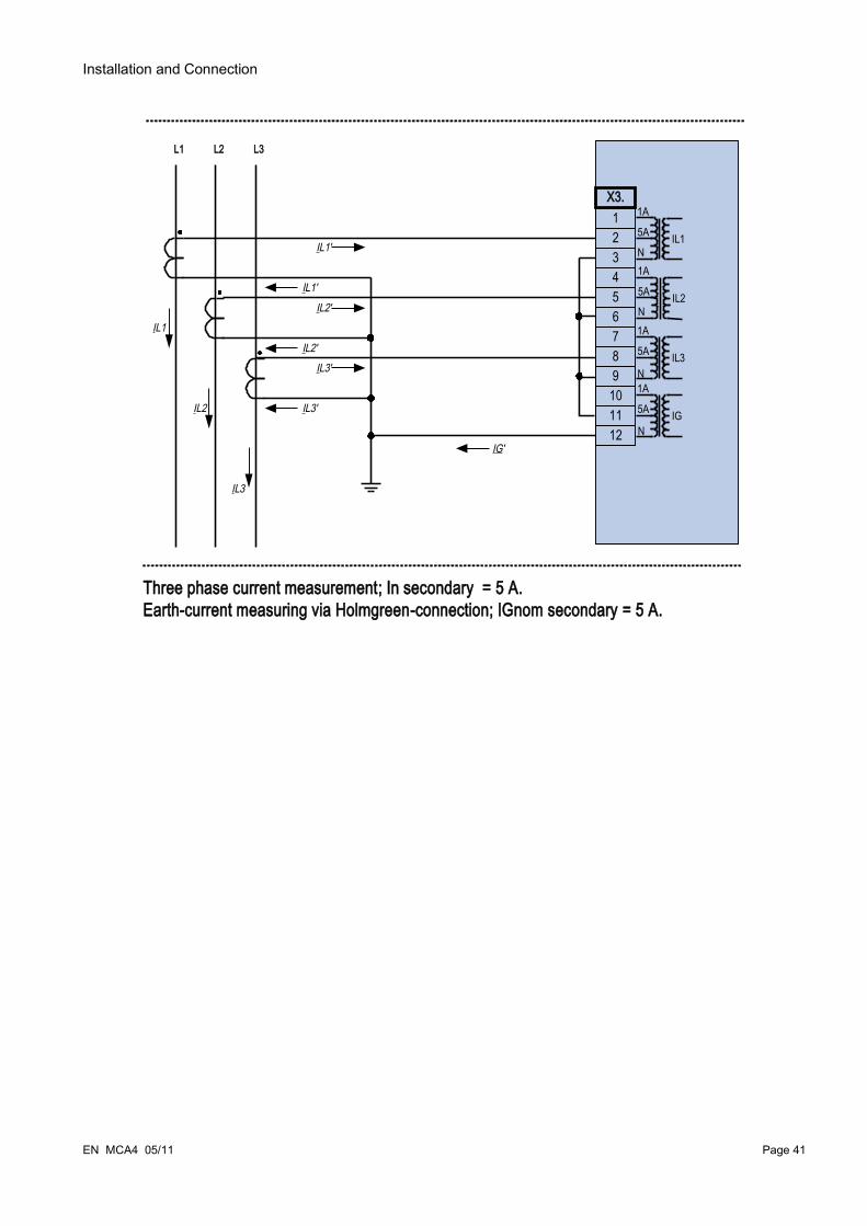
Installation and Connection
EN MCA4 05/11 Page 41
L1 L2 L3
IL2'IL1
IL3'IL2
IL3
IL1'
1X3.
23456789
101112
IG'
Three phase current measurement; In secondary = 5 A.Earth-current measuring via Holmgreen-connection; IGnom secondary = 5 A.
IL1
1A
5A
N
IL2
1A
5A
N
IL3
1A
5A
N
IG
1A
5A
N
IL2'
IL3'
IL1'
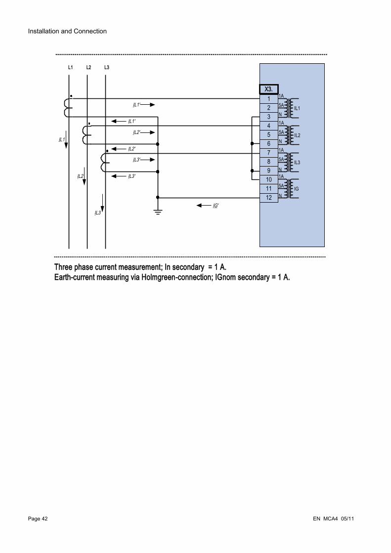
Installation and Connection
Page 42 EN MCA4 05/11
L1 L2 L3
IL1
IL2
IL3
1X3.
23456789
101112
IG'
Three phase current measurement; In secondary = 1 A.Earth-current measuring via Holmgreen-connection; IGnom secondary = 1 A.
IL1
1A
5A
N
IL2
1A
5A
N
IL3
1A
5A
N
IG
1A
5A
N
IL2'
IL3'
IL1'
IL2'
IL3'
IL1'

Installation and Connection
EN MCA4 05/11 Page 43
L1 L2 L3
IL1
IL3'
IL2
IL3
IL1'1
X3.
23456789101112
IL2'
IL1'
Two phase current measurement (Open Delta); In secondary = 5 A.Earth-current measuring via cable-type current transformer ; IGnom secondary = 5 A.
IL3'
IG'
IL1
1A
5A
N
IL2
1A
5A
N
IL3
1A
5A
N
IG
1A
5A
N
Warning!The shielding at the dismantled end of the line has to be put through the cable-type current transformer and has to be grounded at the cable side.
Ring Core Type Current Transformer: Measures the ground current. (Sum of the three phase currents). Can be used for measuring the earth current in isolated and compensated networks. The shield is to be returned through the ring core current transformer.
IG meas = IG
IG calc = IL1 + IL2 + IL3

Installation and Connection
Page 44 EN MCA4 05/11
L1 L3 L2
IL1
IL3
IL2
1X3.
23456789
101112
IG'
Three phase current measurement; In secondary = 1 A.Earth-current measuring via Holmgreen-connection; IGnom secondary = 1 A.
IL1
1A
5A
N
IL3
1A
5A
N
IL2
1A
5A
N
IG
1A
5A
N
IL3'
IL2'
IL1'IL3'
IL2'
IL1'
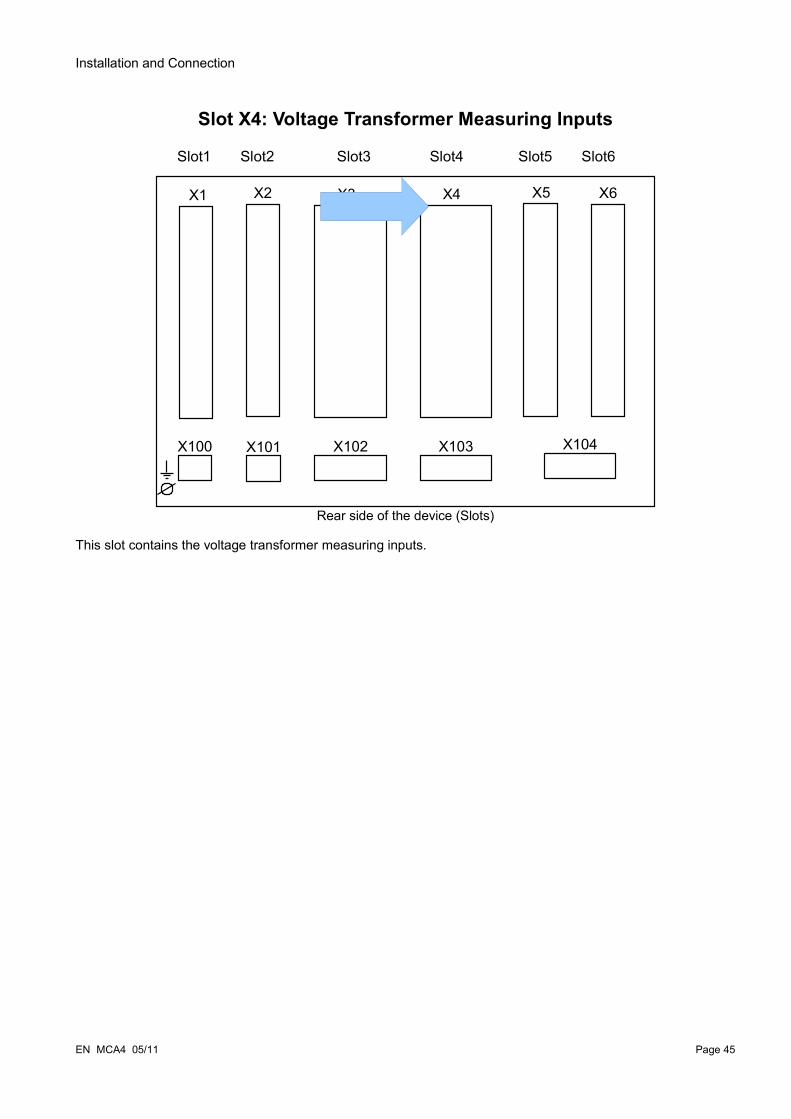
Installation and Connection
Slot X4: Voltage Transformer Measuring Inputs
Rear side of the device (Slots)
This slot contains the voltage transformer measuring inputs.
EN MCA4 05/11 Page 45
X1 X2 X3
X100 X102
X5 X6
X104
X4
X103
Slot3 Slot4 Slot5 Slot6Slot1 Slot2
X101

Installation and Connection
Voltage Measuring Inputs
The device is provided with 4 voltage measuring inputs: three for measuring the phase-to-phase voltages (»V12«, »V23« , »V31«) or phase-to-neutral voltages (»VL1«, »VL2«, »VL3«) and one for the measuring of the residual voltage »VE«. With the field parameters the correct connection of the voltage measuring inputs has to be set:
• phase-to-neutral (star)• phase-to-phase (Open Delta respectively V-Connection)
Make sure that the tightening torque is 1.2-1-6 Nm [11-15 In-lb].
The rotating field of your power supply system has to be taken in to account. Make sure that the transformer is wired correctly.
For the V-connection the parameter »VT con« has to be set to »phase-to-phase«.
Please refer to the Technical Data.
Page 46 EN MCA4 05/11
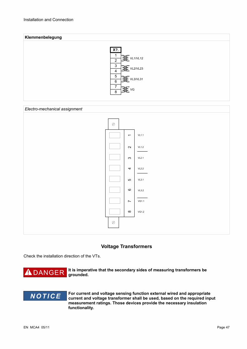
Installation and Connection
Klemmenbelegung
Electro-mechanical assignment
Voltage Transformers
Check the installation direction of the VTs.
It is imperative that the secondary sides of measuring transformers be grounded.
For current and voltage sensing function external wired and appropriate current and voltage transformer shall be used, based on the required input measurement ratings. Those devices provide the necessary insulation functionality.
EN MCA4 05/11 Page 47
VL1.112
63
78
54
VL1.2
VL2.1
VL2.2
VL3.1
VL3.2
VG1.1
VG1.2
12345678
VG
VL3/VL31
VL2/VL23
VL1/VL12
X?.

Installation and Connection
Check of the Voltage Measuring Values
Connect a three-phase measuring voltage equal to the rated voltage to the relay.
Take connection of the measuring transformers (star connection/open delta connection) duly into account.
Now adjust voltage values in the nominal voltage range with the corresponding nominal frequency which are not likely to cause overvoltage- or undervoltage trips.
Compare the values shown in the device display with the readings of the measuring instruments. The deviation must be according to the technical data.
When r.m.s. value measuring instruments are used, higher deviations can arise if the fed voltage has a very high harmonic content. Since the device is provided with a filter for the harmonics, only the fundamental oscillation is evaluated (exception: thermal protection functions). If, however, a r.m.s. value forming measuring instrument is used, the harmonics are also measured.
Page 48 EN MCA4 05/11
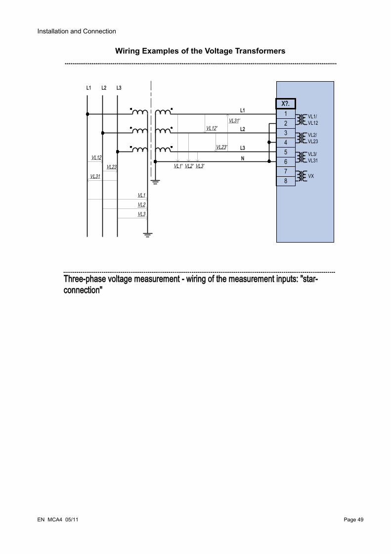
Installation and Connection
Wiring Examples of the Voltage Transformers
EN MCA4 05/11 Page 49
L1 L2 L3
VL12VL23
VL31
VL1VL2VL3
VL1'
L1
L3
L2
NVL2' VL3'
VL12'
VL23'
VL31'1
X?.
2345678
Three-phase voltage measurement - wiring of the measurement inputs: "star-connection"
VX
VL3/VL31
VL2/VL23
VL1/VL12

Installation and Connection
Page 50 EN MCA4 05/11
1X?.
2345678
L1 L2 L3
VL12VL23
VL31
VL1VL2VL3
L1
L3
L2
NVL2' VL3'
VL12'
VL23'
VL31'
VL1'
nVX'
Three-phase voltage measurement - wiring of the measurement inputs: "star-connection"Measurement of the residual voltage VG via auxilliary windings (e-n) "broken delta"
e VX
VL3/VL31
VL2/VL23
VL1/VL12

Installation and Connection
EN MCA4 05/11 Page 51
L1 L2 L3
VL12VL23
VL31
VL1VL2VL3
L1
L3
L2VL12'
VL23'
VL31'1
X?.
2345678
Three-phase voltage measurement - wiring of the measurement inputs: "open delta"
VX
VL3/VL31
VL2/VL23
VL1/VL12
Notice!Calculation of the residual voltage VG is not possible

Installation and Connection
Page 52 EN MCA4 05/11
L1 L2 L3
VL12VL23
VL31
VL1VL2VL3
VL1'
L1
L3
L2
NVL2' VL3'
VL12'
VL23'
VL31'1
X?.
2345678
Three-phase voltage measurement - wiring of the measurement inputs: "star-connection". Fourth measuring input for measuring a synchronisation voltage.
VX
VL3/VL31
VL2/VL23
VL1/VL12
V Sync

Installation and Connection
EN MCA4 05/11 Page 53
1X?.
2345678
L1 L2 L3
VL12VL23
VL31
VL1VL2VL3
L1
L3
L2VL12'
VL23'
VL31'
nVX'
e
Three-phase voltage measurement - wiring of the measurement inputs: "open delta"Measurement of the residual voltage VG via auxilliary windings (e-n) "broken delta"
VX
VL3/VL31
VL2/VL23
VL1/VL12

Installation and Connection
Page 54 EN MCA4 05/11
L1 L2 L3
VL12VL23
VL31
L1
L3
L2VL12'
VL23'
VL31'1
X?.
2345678
Two-phase voltage measurement - wiring of the measuring inputs: "Open Delta"
VX
VL3/VL31
VL2/VL23
VL1/VL12

Installation and Connection
Slot X5: Relay Output Card
Rear side of the device (Slots)
The type of card in this slot is dependent on the ordered device type. The different variants have a different scope of functions.
Available assembly groups in this slot:
• (RO-6 X5): Assembly Group with 6 Relay Outputs. The Relay Output Card is identical with the one on Slot X2.
The available combinations can be gathered from the ordering code.
EN MCA4 05/11 Page 55
X1 X2 X3
X100 X102
X5 X6
X104
X4
X103
Slot3 Slot4 Slot5 Slot6Slot1 Slot2
X101

Installation and Connection
Slot X6: Digital Inputs
Rear side of the device (Slots)
The type of card in this slot is dependent on the ordered device type. The different variants have a different scope of functions.
Available assembly groups in this slot:
• (DI-8 X5): Assembly Group with 8 Digital Inputs.
The available combinations can be gathered from the ordering code.
Page 56 EN MCA4 05/11
X1 X2 X3
X100 X102
X5 X6
X104
X4
X103
Slot3 Slot4 Slot5 Slot6Slot1 Slot2
X101

Installation and Connection
Digital InputsThis module is provided with 8 grouped digital inputs. In chapter [Device parameter/Digital Inputs] the assignment of the digital inputs is specified.
Make sure that the tightening torque is 0.56-0.79 Nm [5-7 In-lb].
The ground terminal has to be connected to the »-pole« when using DC supply.
For each digital input group the related voltage input range has to be parameterized. Wrong switching thresholds can result in malfunctions/wrong signal transfer times.
Via the »assignment list« the states of the digital inputs are assigned to the module inputs (e.g. I[1]).
The digital inputs are provided with different switching thresholds (can be parameterized) (two AC and five DC input ranges). For each group the following switching thresholds can be defined:
• 24V DC• 48V DC / 60V DC• 110 V AC/DC • 230 V AC/DC
If a voltage >80% of the set switching threshold is applied at the digital input, the state change is recognized (physically “1”). If the voltage is below 40% of the set switching threshold, the device detects physically “0”.
EN MCA4 05/11 Page 57
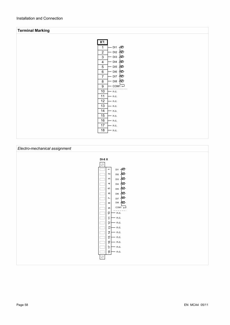
Installation and Connection
Terminal Marking
Electro-mechanical assignment
Page 58 EN MCA4 05/11
DI2
DI3
DI1
DI5
DI6
DI4
DI8
COM1
DI7
DI-8 X
13
24
56
78
910
1112
1314
1516
1718
n.c.
n.c.
n.c.
n.c.
n.c.
n.c.
n.c.
n.c.
n.c.
1X?.
23456789101112131415161718
n.c.
n.c.
n.c.
n.c.
n.c.
n.c.
n.c.
n.c.
n.c.
COM1
DI1
DI2
DI3
DI4
DI5
DI6
DI7
DI8

Installation and Connection
Slot X100: Ethernet Interface
Rear side of the device (Slots)
An Ethernet interface may be available depending on the device type ordered.
The available combinations can be gathered from the ordering code.
EN MCA4 05/11 Page 59
X1 X2 X3
X100 X102
X5 X6
X104
X4
X103
Slot3 Slot4 Slot5 Slot6Slot1 Slot2
X101

Installation and Connection
Ethernet - RJ45
Terminals
Page 60 EN MCA4 05/11
1 8
TxD
+
TxD
–
RxD
+
n.c.
n.c.
RxD
–
n.c.
n.c.

Installation and Connection
Slot X103: Data Communication
Rear side of the device (Slots)
The data communication interface in the X103 slot is dependent on the ordered device type. The scope of functions is dependent on the type of data communication interface.
Available assembly groups in this slot:
• RS485 Terminals for Modbus and IEC• LWL Interface for Modbus, IEC and Profibus• D-SUB Interface for Modbus and IEC• D-SUB Interface for Profibus
The available combinations can be gathered from the ordering code.
EN MCA4 05/11 Page 61
X1 X2 X3
X100 X102
X5 X6
X104
X4
X103
Slot3 Slot4 Slot5 Slot6Slot1 Slot2
X101

Installation and Connection
Modbus® RTU / IEC 60870-5-103 via RS485
There are two different versions of the RS485 interface. By means of the wiring diagram on the top of your device, you have to find out which version is built in your device (Type1 or Type2).
Make sure that the tightening torque is 0.22-0.45 Nm [2-4 In-lb].
RS485 – Type 1 (see wiring diagram)
Electro-mechanical assignment Type 1 (see wiring diagram)
The Modbus® / IEC 60870-5-103 connection cable must be shielded. The shielding has to be fixed at the screw which is marked with the ground symbol at the rear side of the device.
The communication is Halfduplex.
Page 62 EN MCA4 05/11
64 5321
R1R2
R1
+5V GNDR1 = 560 ΩR2 = 120 Ω
P N P* N*
Protective Relay
1X
103
2 3 4 5 6
P N P*
N*
+5V GND560 Ω 560Ω
120Ω
Protective Relay

Installation and Connection
Type 1 Wiring example, Device in the Middle of the BUS
Type 1 Wiring example, Device at the End of the BUS (using the integrated Terminal Resistor)
EN MCA4 05/11 Page 63
64 5321
R1R2
R1
+5V GNDR1 = 560 ΩR2 = 120 Ω
Protective Relay
P
N
64 5321
R1R2
R1
+5V GNDR1 = 560 ΩR2 = 120 Ω
Protective Relay
P P*
N N*
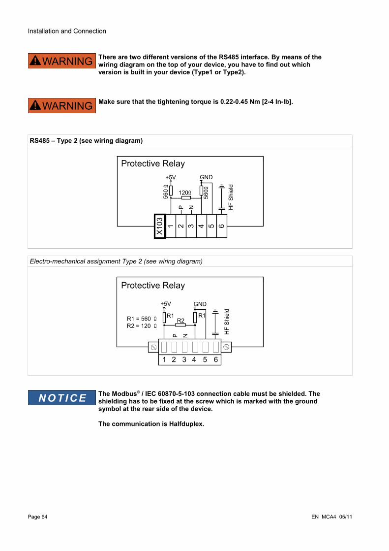
Installation and Connection
There are two different versions of the RS485 interface. By means of the wiring diagram on the top of your device, you have to find out which version is built in your device (Type1 or Type2).
Make sure that the tightening torque is 0.22-0.45 Nm [2-4 In-lb].
RS485 – Type 2 (see wiring diagram)
Electro-mechanical assignment Type 2 (see wiring diagram)
The Modbus® / IEC 60870-5-103 connection cable must be shielded. The shielding has to be fixed at the screw which is marked with the ground symbol at the rear side of the device.
The communication is Halfduplex.
Page 64 EN MCA4 05/11
64 5321
R1R2
R1
+5V GND
R1 = 560 ΩR2 = 120 Ω
P N
Protective Relay
HF
Shi
eld
1X
103
2 3 4 5 6
P N
+5V GND
560
Ω
560Ω120Ω
Protective Relay
HF
Shi
eld
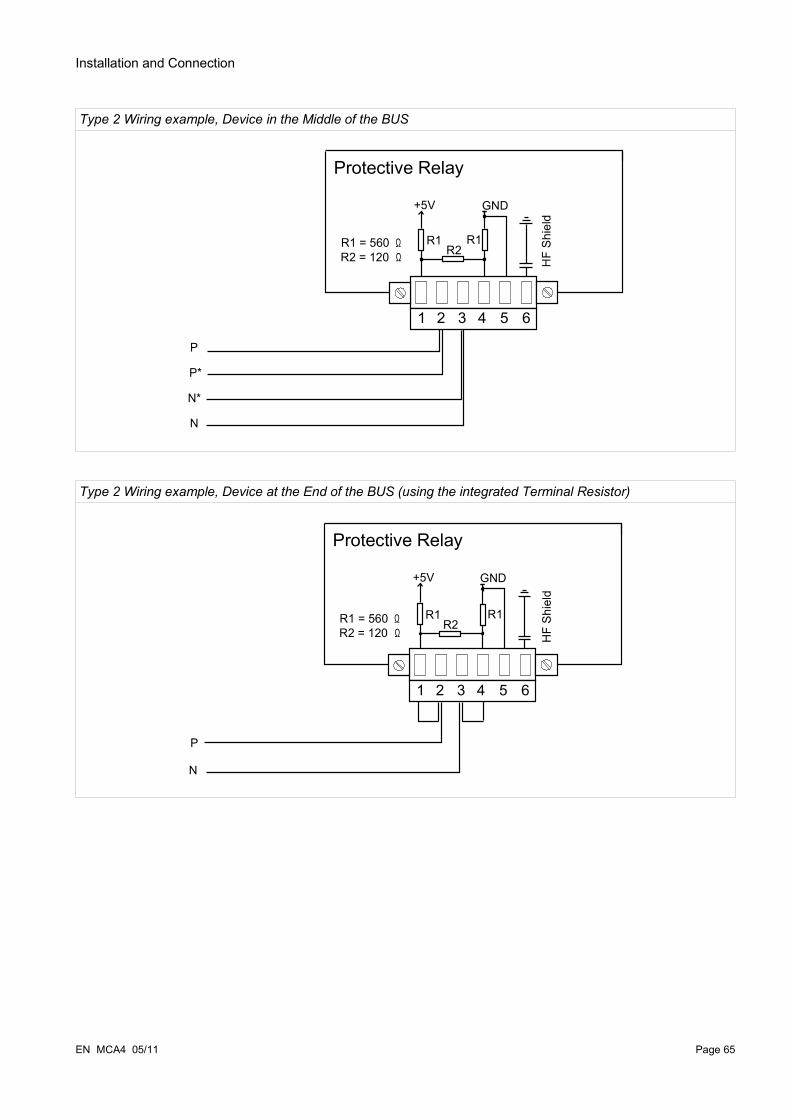
Installation and Connection
Type 2 Wiring example, Device in the Middle of the BUS
Type 2 Wiring example, Device at the End of the BUS (using the integrated Terminal Resistor)
EN MCA4 05/11 Page 65
64 5321
+5V GND
R1 = 560 ΩR2 = 120 Ω
Protective Relay
P
N
R1R2
R1
HF
Shi
eld
64 5321
+5V GND
R1 = 560 ΩR2 = 120 Ω
Protective Relay
P
P*
N
N*
R1R2
R1
HF
Shi
eld

Installation and Connection
Type 2 Shielding Options (2-wire + Shield)
Type 2 Shielding Options (3-wire + Shield)
Page 66 EN MCA4 05/11
1 32 4 5 6
TR-P
2.2nF(internal)
1 32 4 5 6
TR-P
2.2nF(internal)
1 32 4 5 6
TR-P
2.2nF(internal)
1 32 4 5 6
TR-P
2.2nF(internal)
Shield at bus master side connected to earth termination
resistors used
Shield at bus device side connected to earth termination
resistors used
Shield at bus master side connected to earth termination
resistors not used
Shield at bus device side connected to earth termination
resistors not used
P N P N P N P NTR-N
TR-N
TR-N
TR-N
Com
mon
Com
mon
Com
mon
Com
mon
HF
Shi
eld
HF
Shi
eld
HF
Shi
eld
HF
Shi
eld
Shield at bus master side connected to earth termination
resistors used
Shield at bus device side connected to earth termination
resistors used
Shield at bus master side connected to earth termination
resistors not used
Shield at bus device side connected to earth termination
resistors not used
1 32 4 5 6
TR-P
2.2nF(internal)
1 32 4 5 6
TR-P
2.2nF(internal)
1 32 4 5 6
TR-P
2.2nF(internal)
1 32 4 5 6
TR-P
2.2nF(internal)
P N P N P N P NTR-N
TR-N
TR-N
TR-N
Com
mon
Com
mon
Com
mon
Com
mon
HF
Shi
eld
HF
Shie
ld
HF
Shi
eld
HF
Shi
eld

Installation and Connection
Profibus DP/ Modbus® RTU / IEC 60870-5-103 via fibre optic
Fibre Optic
EN MCA4 05/11 Page 67

Installation and Connection
Modbus® RTU / IEC 60870-5-103 via D-SUB
D-SUB
Electro-mechanical assignment
The connection cable must be shielded. The shielding has to be fixed at the screw which is marked with the ground symbol at the back side of the device.
Page 68 EN MCA4 05/11
D-SUB assignment - bushing
1 Earthing/shielding
3 RxD TxD - P: High-Level
4 RTS-signal
5 DGND: Ground, neg. Potential of aux voltage supply
6 VP: pos. Potential of the aux voltage supply
8 RxD TxD - N: Low-Level
51
96

Installation and Connection
Profibus DP via D-SUB
D-SUB
Electro-mechanical assignment
The connection cable must be shielded. The shielding has to be fixed at the screw which is marked with the ground symbol at the back side of the device.
EN MCA4 05/11 Page 69
D-SUB assignment - bushing
1 Earthing/shielding
3 RxD TxD - P: High-Level
4 RTS-signal
5 DGND: Ground, neg. Potential of aux voltage supply
6 VP: pos. Potential of the aux voltage supply
8 RxD TxD - N: Low-Level
51
96
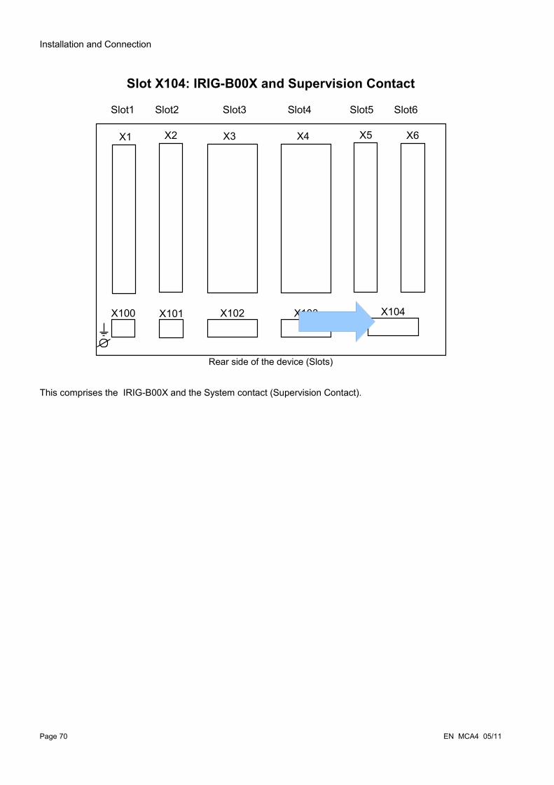
Installation and Connection
Slot X104: IRIG-B00X and Supervision Contact
Rear side of the device (Slots)
This comprises the IRIG-B00X and the System contact (Supervision Contact).
Page 70 EN MCA4 05/11
X1 X2 X3
X100 X102
X5 X6
X104
X4
X103
Slot3 Slot4 Slot5 Slot6Slot1 Slot2
X101

Installation and Connection
System Contact and IRIG-B00X
Make sure that the tightening torque is 0.56-0.79 Nm [5-7 In-lb].
Terminal
Electro-mechanical assignment
The System-OK contact (SC relay) cannot be configured. The system contact is a changeover contact that picks up when the device is free from internal faults. While the device is booting up, the System OK relay (SC) remains dropped-off (unenergized). As soon as the system is properly started (and protection is active), the System Contact picks up and the assigned LED is activated accordingly (please refer to the Self Supervision chapter).
EN MCA4 05/11 Page 71
X1041 32 4 5
SC
n.c
.
SC n
.o.
SC C
IRIG
-B+
IRIG
-B-
1X1
04 2 3 4 5SC
IRIG
-B+
IRIG
-B-

Installation and Connection
PC Interface - X120
9-pole D-Sub at all device fronts
Electro-mechanical assignment for all device types
Page 72 EN MCA4 05/11
1 DCD
2 RxD
3 TxD
4 DTR
5 GND
6 DSR
7 RTS
8 CTS
housing shielded
9 RI
51
6 9
B1, B2 und B3 Housing
RS232 PC-Interface for Parameter Setting
and Evaluation Software - X120
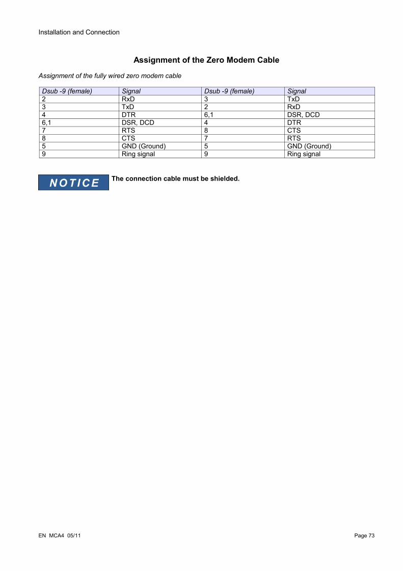
Installation and Connection
Assignment of the Zero Modem Cable
Assignment of the fully wired zero modem cable
Dsub -9 (female) Signal Dsub -9 (female) Signal2 RxD 3 TxD3 TxD 2 RxD4 DTR 6,1 DSR, DCD6,1 DSR, DCD 4 DTR7 RTS 8 CTS8 CTS 7 RTS5 GND (Ground) 5 GND (Ground)9 Ring signal 9 Ring signal
The connection cable must be shielded.
EN MCA4 05/11 Page 73

Input, Output and LED Settings
Input, Output and LED Settings
Configuration of the Digital Inputs
Based on the »assignment list«, the states of digital inputs are allocated to the module inputs.
Set the following parameters for each of the digital inputs:
• »Nominal voltage«
• »Debouncing time«: A state change will only be adopted by the digital input after the debouncing time has expired.
• »Inverting« (where necessary)
The debouncing time will be started each time the state of the input signal alternates.
In addition to the debouncing time that can be set via software, there is always a hardware debouncing time (approx 12 ms) that cannot be turned of.
DI-8P X DI Slot X1
Device Parameters of the Digital Inputs on DI-8P X
Page 74 EN MCA4 05/11
=1
State of the digital input
Inverting
Input Signal
Nom voltage
0t
Debouncing time
DI Slot X.DI x

Input, Output and LED Settings
Parameter Description Setting range Default Menu path
Nom voltage Nominal voltage of the digital inputs 24 V DC,
48 V DC,
60 V DC,
110 V DC,
230 V DC,
110 V AC,
230 V AC
24 V DC [Device Para
/Digital Inputs
/DI Slot X1
/Group 1]
Inverting 1 Inverting the input signals. inactive,
active
inactive [Device Para
/Digital Inputs
/DI Slot X1
/Group 1]Debouncing time 1
A change of the state of a digital input will only be recognized after the debouncing time has expired (become effective). Thus, transient signals will not be misinterpreted.
no debouncing time,
20 ms,
50 ms,
100 ms
no debouncing time
[Device Para
/Digital Inputs
/DI Slot X1
/Group 1]
Nom voltage Nominal voltage of the digital inputs 24 V DC,
48 V DC,
60 V DC,
110 V DC,
230 V DC,
110 V AC,
230 V AC
24 V DC [Device Para
/Digital Inputs
/DI Slot X1
/Group 2]
Inverting 2 Inverting the input signals. inactive,
active
inactive [Device Para
/Digital Inputs
/DI Slot X1
/Group 2]Debouncing time 2
A change of the state of a digital input will only be recognized after the debouncing time has expired (become effective). Thus, transient signals will not be misinterpreted.
no debouncing time,
20 ms,
50 ms,
100 ms
no debouncing time
[Device Para
/Digital Inputs
/DI Slot X1
/Group 2]
Nom voltage Nominal voltage of the digital inputs 24 V DC,
48 V DC,
60 V DC,
110 V DC,
230 V DC,
110 V AC,
230 V AC
24 V DC [Device Para
/Digital Inputs
/DI Slot X1
/Group 3]
EN MCA4 05/11 Page 75
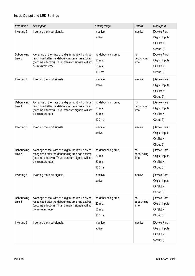
Input, Output and LED Settings
Parameter Description Setting range Default Menu path
Inverting 3 Inverting the input signals. inactive,
active
inactive [Device Para
/Digital Inputs
/DI Slot X1
/Group 3]Debouncing time 3
A change of the state of a digital input will only be recognized after the debouncing time has expired (become effective). Thus, transient signals will not be misinterpreted.
no debouncing time,
20 ms,
50 ms,
100 ms
no debouncing time
[Device Para
/Digital Inputs
/DI Slot X1
/Group 3]
Inverting 4 Inverting the input signals. inactive,
active
inactive [Device Para
/Digital Inputs
/DI Slot X1
/Group 3]Debouncing time 4
A change of the state of a digital input will only be recognized after the debouncing time has expired (become effective). Thus, transient signals will not be misinterpreted.
no debouncing time,
20 ms,
50 ms,
100 ms
no debouncing time
[Device Para
/Digital Inputs
/DI Slot X1
/Group 3]
Inverting 5 Inverting the input signals. inactive,
active
inactive [Device Para
/Digital Inputs
/DI Slot X1
/Group 3]Debouncing time 5
A change of the state of a digital input will only be recognized after the debouncing time has expired (become effective). Thus, transient signals will not be misinterpreted.
no debouncing time,
20 ms,
50 ms,
100 ms
no debouncing time
[Device Para
/Digital Inputs
/DI Slot X1
/Group 3]
Inverting 6 Inverting the input signals. inactive,
active
inactive [Device Para
/Digital Inputs
/DI Slot X1
/Group 3]Debouncing time 6
A change of the state of a digital input will only be recognized after the debouncing time has expired (become effective). Thus, transient signals will not be misinterpreted.
no debouncing time,
20 ms,
50 ms,
100 ms
no debouncing time
[Device Para
/Digital Inputs
/DI Slot X1
/Group 3]
Inverting 7 Inverting the input signals. inactive,
active
inactive [Device Para
/Digital Inputs
/DI Slot X1
/Group 3]
Page 76 EN MCA4 05/11
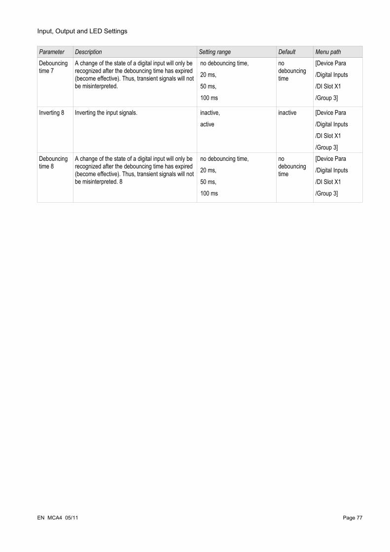
Input, Output and LED Settings
Parameter Description Setting range Default Menu path
Debouncing time 7
A change of the state of a digital input will only be recognized after the debouncing time has expired (become effective). Thus, transient signals will not be misinterpreted.
no debouncing time,
20 ms,
50 ms,
100 ms
no debouncing time
[Device Para
/Digital Inputs
/DI Slot X1
/Group 3]
Inverting 8 Inverting the input signals. inactive,
active
inactive [Device Para
/Digital Inputs
/DI Slot X1
/Group 3]Debouncing time 8
A change of the state of a digital input will only be recognized after the debouncing time has expired (become effective). Thus, transient signals will not be misinterpreted. 8
no debouncing time,
20 ms,
50 ms,
100 ms
no debouncing time
[Device Para
/Digital Inputs
/DI Slot X1
/Group 3]
EN MCA4 05/11 Page 77

Input, Output and LED Settings
Signals of the Digital Inputs on DI-8P X
Name Description
DI 1 Signal: Digital InputDI 2 Signal: Digital InputDI 3 Signal: Digital InputDI 4 Signal: Digital InputDI 5 Signal: Digital InputDI 6 Signal: Digital InputDI 7 Signal: Digital InputDI 8 Signal: Digital Input
DI-8 X DI Slot X6
Device Parameters of the Digital Inputs on DI-8 X
Parameter Description Setting range Default Menu path
Nom voltage Nominal voltage of the digital inputs 24 V DC,
48 V DC,
60 V DC,
110 V DC,
230 V DC,
110 V AC,
230 V AC
24 V DC [Device Para
/Digital Inputs
/DI Slot X6
/Group 1]
Inverting 1 Inverting the input signals. inactive,
active
inactive [Device Para
/Digital Inputs
/DI Slot X6
/Group 1]Debouncing time 1
A change of the state of a digital input will only be recognized after the debouncing time has expired (become effective). Thus, transient signals will not be misinterpreted.
no debouncing time,
20 ms,
50 ms,
100 ms
no debouncing time
[Device Para
/Digital Inputs
/DI Slot X6
/Group 1]
Inverting 2 Inverting the input signals. inactive,
active
inactive [Device Para
/Digital Inputs
/DI Slot X6
/Group 1]
Page 78 EN MCA4 05/11

Input, Output and LED Settings
Parameter Description Setting range Default Menu path
Debouncing time 2
A change of the state of a digital input will only be recognized after the debouncing time has expired (become effective). Thus, transient signals will not be misinterpreted.
no debouncing time,
20 ms,
50 ms,
100 ms
no debouncing time
[Device Para
/Digital Inputs
/DI Slot X6
/Group 1]
Inverting 3 Inverting the input signals. inactive,
active
inactive [Device Para
/Digital Inputs
/DI Slot X6
/Group 1]Debouncing time 3
A change of the state of a digital input will only be recognized after the debouncing time has expired (become effective). Thus, transient signals will not be misinterpreted.
no debouncing time,
20 ms,
50 ms,
100 ms
no debouncing time
[Device Para
/Digital Inputs
/DI Slot X6
/Group 1]
Inverting 4 Inverting the input signals. inactive,
active
inactive [Device Para
/Digital Inputs
/DI Slot X6
/Group 1]Debouncing time 4
A change of the state of a digital input will only be recognized after the debouncing time has expired (become effective). Thus, transient signals will not be misinterpreted.
no debouncing time,
20 ms,
50 ms,
100 ms
no debouncing time
[Device Para
/Digital Inputs
/DI Slot X6
/Group 1]
Inverting 5 Inverting the input signals. inactive,
active
inactive [Device Para
/Digital Inputs
/DI Slot X6
/Group 1]Debouncing time 5
A change of the state of a digital input will only be recognized after the debouncing time has expired (become effective). Thus, transient signals will not be misinterpreted.
no debouncing time,
20 ms,
50 ms,
100 ms
no debouncing time
[Device Para
/Digital Inputs
/DI Slot X6
/Group 1]
Inverting 6 Inverting the input signals. inactive,
active
inactive [Device Para
/Digital Inputs
/DI Slot X6
/Group 1]Debouncing time 6
A change of the state of a digital input will only be recognized after the debouncing time has expired (become effective). Thus, transient signals will not be misinterpreted.
no debouncing time,
20 ms,
50 ms,
100 ms
no debouncing time
[Device Para
/Digital Inputs
/DI Slot X6
/Group 1]
EN MCA4 05/11 Page 79
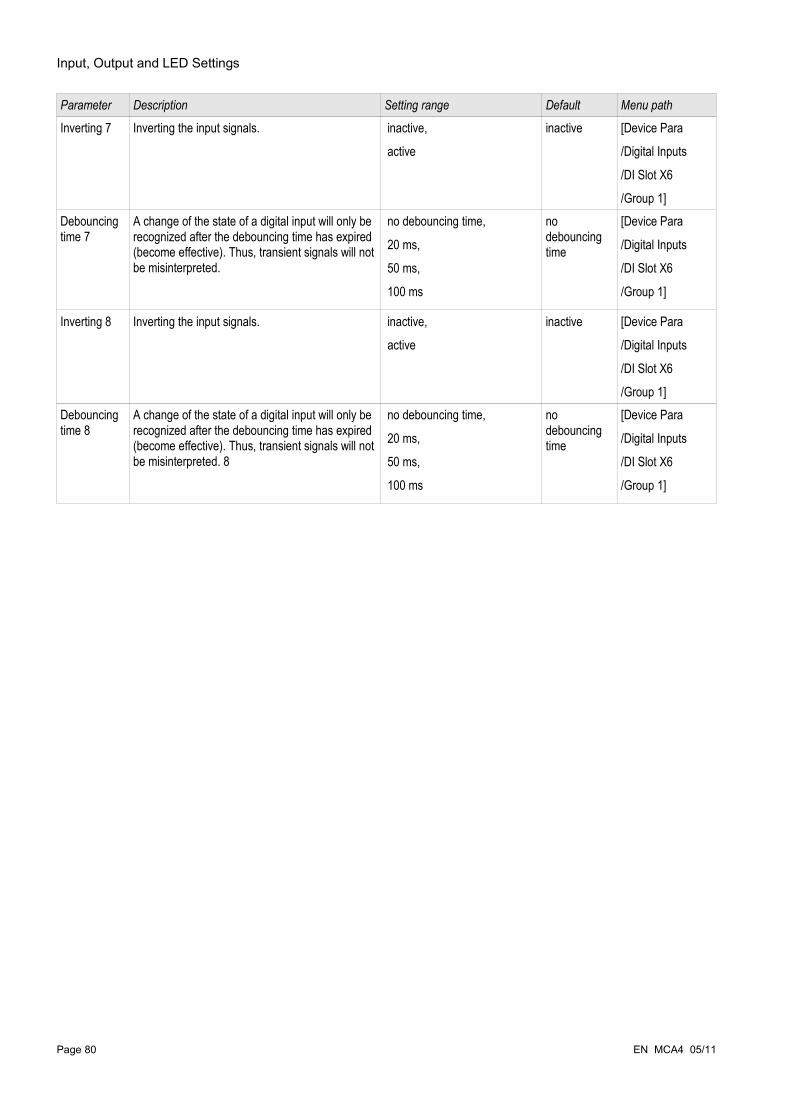
Input, Output and LED Settings
Parameter Description Setting range Default Menu path
Inverting 7 Inverting the input signals. inactive,
active
inactive [Device Para
/Digital Inputs
/DI Slot X6
/Group 1]Debouncing time 7
A change of the state of a digital input will only be recognized after the debouncing time has expired (become effective). Thus, transient signals will not be misinterpreted.
no debouncing time,
20 ms,
50 ms,
100 ms
no debouncing time
[Device Para
/Digital Inputs
/DI Slot X6
/Group 1]
Inverting 8 Inverting the input signals. inactive,
active
inactive [Device Para
/Digital Inputs
/DI Slot X6
/Group 1]Debouncing time 8
A change of the state of a digital input will only be recognized after the debouncing time has expired (become effective). Thus, transient signals will not be misinterpreted. 8
no debouncing time,
20 ms,
50 ms,
100 ms
no debouncing time
[Device Para
/Digital Inputs
/DI Slot X6
/Group 1]
Page 80 EN MCA4 05/11

Input, Output and LED Settings
Signals of the Digital Inputs on DI-8 X
Name Description
DI 1 Signal: Digital InputDI 2 Signal: Digital InputDI 3 Signal: Digital InputDI 4 Signal: Digital InputDI 5 Signal: Digital InputDI 6 Signal: Digital InputDI 7 Signal: Digital InputDI 8 Signal: Digital Input
EN MCA4 05/11 Page 81

Input, Output and LED Settings
Output Relays Settings
BO Slot X2 ,BO Slot X5
The conditions of module outputs and signals/protective functions (such as reverse interlocking) can be passed by means of alarm relays. The alarm relays are potential-free contacts (which can be used as opening or closing contact). Each alarm relay can be assigned up to 7 functions out of the »assignment list«.
Set the following parameters for each of the binary output relays:
• Up to 7 signals from the »assignment list« (OR-connected)
• Each of the assigned signals can be inverted.
• The (collective) state of the binary output relay can be inverted (open or closed circuit current principle)
• »Latched« active or inactive
• »Latched = inactive«:If the latching function is »inactive«, the alarm relay respectively the alarm contact will adopt the state of those alarms that were assigned.
• »Latched = active«If the »latching function« is »active«, the state of the alarm relay respectively alarm contact that was set by the alarms will be stored.
The alarm relay can only be acknowledged after reset of those signals that hadinitiated setting of the relay and after expiry of the minimum retention time.
• »Hold time«: At signal changes, the minimal latching time ensures that the relay will be maintained picked-up or released for at least this period.
If binary outputs are parameterized »Latched=active«, they will keep (return into) their position even if there is a break within the power supply.
If binary output relays are parameterized »Latched=active«, The binary output will also retain, if the binary output is reprogrammed in another way. This applies also if »Latched is set to inactive«. Resetting a binary output that has latched a signal will always require an acknowledgement.
The »System OK Relay« (watchdog) cannot be configured.
Acknowledgment options
Binary output relays can be acknowledged:
• Via the push-button »C« at the operating panel.
• Each binary output relay can be acknowledged by a signal of the »assignment list« (If »Latched is active«).
• Via the module »Ex Acknowledge« all binary output relays can be acknowledged at once, if the signal for external acknowledgement that was selected from the »assignment list« becomes true. (e.g the state of a digital input).
• Via SCADA, all output relays can be acknowledged at once.
Page 82 EN MCA4 05/11

Input, Output and LED Settings
Relay output contacts can be set by force or disarmed (for commisioning support, please refer to the „Service/Disarming the Output Relay Contacts“ and „Service/Forcing the Output Relay Contacts“ sections).
EN MCA4 05/11 Page 83
=1A
ssig
nmen
t 1
Inve
rting
1
=1A
ssig
nmen
t 2
Inve
rting
2
=1A
ssig
nmen
t 3
Inve
rting
3
=1A
ssig
nmen
t 4
Inve
rting
4
=1A
ssig
nmen
t 5
Inve
rting
5
>1
inact
ive
active
Latc
hed
=1A
ssig
nmen
t 6
Inve
rting
6
=1A
ssig
nmen
t 7
Inve
rting
7
=1In
verti
ng
>1
1
hold
tim
e
t-hol
d>1
>1
S1
1
R
1
&
Sta
te o
f the
bin
ary
outp
ut re
lay
Ackn
owle
dge
-HM
I
Ackn
owle
dge-
1..n
, Ass
ignm
ent L
ist
Ackn
owle
dge-
Scad
a
0
Switc
h O
ff D
elay
t-Off
Del
ay

Input, Output and LED Settings
System Contact
The System OK alarm relay (SC) is the devices »LIFE CONTACT«. Its installation location depends on the housing type. Please refer to the wiring diagram of the device (WDC-contact).
The System-OK relay (SC) cannot be parameterized. The system contact is an operating current contact that picks-up, when the device is free from internal faults. While the device is booting up, the System OK relay (SC) remains dropped-off. As soon as the system was duly started up, the relay picks up and the assigned LED is activated accordingly (please refer to chapter Self Supervision).
Page 84 EN MCA4 05/11
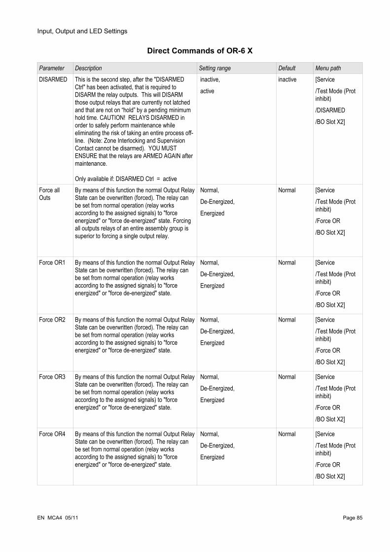
Input, Output and LED Settings
Direct Commands of OR-6 X
Parameter Description Setting range Default Menu path
DISARMED This is the second step, after the "DISARMED Ctrl" has been activated, that is required to DISARM the relay outputs. This will DISARM those output relays that are currently not latched and that are not on “hold” by a pending minimum hold time. CAUTION! RELAYS DISARMED in order to safely perform maintenance while eliminating the risk of taking an entire process off-line. (Note: Zone Interlocking and Supervision Contact cannot be disarmed). YOU MUST ENSURE that the relays are ARMED AGAIN after maintenance.
Only available if: DISARMED Ctrl = active
inactive,
active
inactive [Service
/Test Mode (Prot inhibit)
/DISARMED
/BO Slot X2]
Force all Outs
By means of this function the normal Output Relay State can be overwritten (forced). The relay can be set from normal operation (relay works according to the assigned signals) to "force energized" or "force de-energized" state. Forcing all outputs relays of an entire assembly group is superior to forcing a single output relay.
Normal,
De-Energized,
Energized
Normal [Service
/Test Mode (Prot inhibit)
/Force OR
/BO Slot X2]
Force OR1 By means of this function the normal Output Relay State can be overwritten (forced). The relay can be set from normal operation (relay works according to the assigned signals) to "force energized" or "force de-energized" state.
Normal,
De-Energized,
Energized
Normal [Service
/Test Mode (Prot inhibit)
/Force OR
/BO Slot X2]
Force OR2 By means of this function the normal Output Relay State can be overwritten (forced). The relay can be set from normal operation (relay works according to the assigned signals) to "force energized" or "force de-energized" state.
Normal,
De-Energized,
Energized
Normal [Service
/Test Mode (Prot inhibit)
/Force OR
/BO Slot X2]
Force OR3 By means of this function the normal Output Relay State can be overwritten (forced). The relay can be set from normal operation (relay works according to the assigned signals) to "force energized" or "force de-energized" state.
Normal,
De-Energized,
Energized
Normal [Service
/Test Mode (Prot inhibit)
/Force OR
/BO Slot X2]
Force OR4 By means of this function the normal Output Relay State can be overwritten (forced). The relay can be set from normal operation (relay works according to the assigned signals) to "force energized" or "force de-energized" state.
Normal,
De-Energized,
Energized
Normal [Service
/Test Mode (Prot inhibit)
/Force OR
/BO Slot X2]
EN MCA4 05/11 Page 85

Input, Output and LED Settings
Parameter Description Setting range Default Menu path
Force OR5 By means of this function the normal Output Relay State can be overwritten (forced). The relay can be set from normal operation (relay works according to the assigned signals) to "force energized" or "force de-energized" state.
Normal,
De-Energized,
Energized
Normal [Service
/Test Mode (Prot inhibit)
/Force OR
/BO Slot X2]
Force OR6 By means of this function the normal Output Relay State can be overwritten (forced). The relay can be set from normal operation (relay works according to the assigned signals) to "force energized" or "force de-energized" state.
Normal,
De-Energized,
Energized
Normal [Service
/Test Mode (Prot inhibit)
/Force OR
/BO Slot X2]
Device Parameters of the Binary Output Relays on OR-6 X
Parameter Description Setting range Default Menu path
t-hold To clearly identify the state transition of a binary output relay, the "new state" is being hold, at least for the duration of the hold time.
0.00 - 300.00s 0.00s [Device Para
/Binary Outputs
/BO Slot X2
/BO 1]t-Off Delay Switch Off Delay 0.00 - 300.00s 0.00s [Device Para
/Binary Outputs
/BO Slot X2
/BO 1]Latched Defines whether the Relay Output will be latched
when it picks up. inactive,
active
BO Slot X2: active
BO Slot X5: inactive
[Device Para
/Binary Outputs
/BO Slot X2
/BO 1]Acknowledgement
Acknowledgement Signal - An acknowledgement signal (that acknowledges the corresponding binary output relay) can be assigned to each output relay. The acknowledgement-signal is only effective if the parameter "Latched" is set to active.
Only available if: Latched = active
1..n, Assignment List -.- [Device Para
/Binary Outputs
/BO Slot X2
/BO 1]
Inverting Inverting of the Binary Output Relay. inactive,
active
inactive [Device Para
/Binary Outputs
/BO Slot X2
/BO 1]
Page 86 EN MCA4 05/11

Input, Output and LED Settings
Parameter Description Setting range Default Menu path
Assignment 1
Assignment 1..n, Assignment List BO Slot X2: SG[1].TripCmd
BO Slot X5: -.-
[Device Para
/Binary Outputs
/BO Slot X2
/BO 1]Inverting 1 Inverting of the state of the assigned signal. inactive,
active
inactive [Device Para
/Binary Outputs
/BO Slot X2
/BO 1]Assignment 2
Assignment 1..n, Assignment List -.- [Device Para
/Binary Outputs
/BO Slot X2
/BO 1]Inverting 2 Inverting of the state of the assigned signal. inactive,
active
inactive [Device Para
/Binary Outputs
/BO Slot X2
/BO 1]Assignment 3
Assignment 1..n, Assignment List -.- [Device Para
/Binary Outputs
/BO Slot X2
/BO 1]Inverting 3 Inverting of the state of the assigned signal. inactive,
active
inactive [Device Para
/Binary Outputs
/BO Slot X2
/BO 1]Assignment 4
Assignment 1..n, Assignment List -.- [Device Para
/Binary Outputs
/BO Slot X2
/BO 1]Inverting 4 Inverting of the state of the assigned signal. inactive,
active
inactive [Device Para
/Binary Outputs
/BO Slot X2
/BO 1]Assignment 5
Assignment 1..n, Assignment List -.- [Device Para
/Binary Outputs
/BO Slot X2
/BO 1]
EN MCA4 05/11 Page 87

Input, Output and LED Settings
Parameter Description Setting range Default Menu path
Inverting 5 Inverting of the state of the assigned signal. inactive,
active
inactive [Device Para
/Binary Outputs
/BO Slot X2
/BO 1]Assignment 6
Assignment 1..n, Assignment List -.- [Device Para
/Binary Outputs
/BO Slot X2
/BO 1]Inverting 6 Inverting of the state of the assigned signal. inactive,
active
inactive [Device Para
/Binary Outputs
/BO Slot X2
/BO 1]Assignment 7
Assignment 1..n, Assignment List -.- [Device Para
/Binary Outputs
/BO Slot X2
/BO 1]Inverting 7 Inverting of the state of the assigned signal. inactive,
active
inactive [Device Para
/Binary Outputs
/BO Slot X2
/BO 1]t-hold To clearly identify the state transition of a binary
output relay, the "new state" is being hold, at least for the duration of the hold time.
0.00 - 300.00s 0.00s [Device Para
/Binary Outputs
/BO Slot X2
/BO 2]t-Off Delay Switch Off Delay 0.00 - 300.00s 0.00s [Device Para
/Binary Outputs
/BO Slot X2
/BO 2]Latched Defines whether the Relay Output will be latched
when it picks up. inactive,
active
inactive [Device Para
/Binary Outputs
/BO Slot X2
/BO 2]Acknowledgement
Acknowledgement Signal - An acknowledgement signal (that acknowledges the corresponding binary output relay) can be assigned to each output relay. The acknowledgement-signal is only effective if the parameter "Latched" is set to active.
Only available if: Latched = active
1..n, Assignment List -.- [Device Para
/Binary Outputs
/BO Slot X2
/BO 2]
Page 88 EN MCA4 05/11

Input, Output and LED Settings
Parameter Description Setting range Default Menu path
Inverting Inverting of the Binary Output Relay. inactive,
active
inactive [Device Para
/Binary Outputs
/BO Slot X2
/BO 2]Assignment 1
Assignment 1..n, Assignment List BO Slot X2: Prot.Alarm
BO Slot X5: -.-
[Device Para
/Binary Outputs
/BO Slot X2
/BO 2]Inverting 1 Inverting of the state of the assigned signal. inactive,
active
inactive [Device Para
/Binary Outputs
/BO Slot X2
/BO 2]Assignment 2
Assignment 1..n, Assignment List -.- [Device Para
/Binary Outputs
/BO Slot X2
/BO 2]Inverting 2 Inverting of the state of the assigned signal. inactive,
active
inactive [Device Para
/Binary Outputs
/BO Slot X2
/BO 2]Assignment 3
Assignment 1..n, Assignment List -.- [Device Para
/Binary Outputs
/BO Slot X2
/BO 2]Inverting 3 Inverting of the state of the assigned signal. inactive,
active
inactive [Device Para
/Binary Outputs
/BO Slot X2
/BO 2]Assignment 4
Assignment 1..n, Assignment List -.- [Device Para
/Binary Outputs
/BO Slot X2
/BO 2]Inverting 4 Inverting of the state of the assigned signal. inactive,
active
inactive [Device Para
/Binary Outputs
/BO Slot X2
/BO 2]
EN MCA4 05/11 Page 89
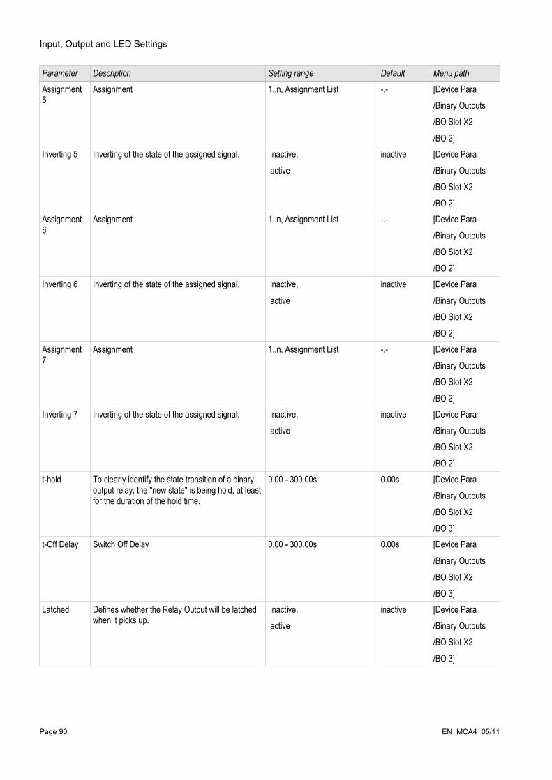
Input, Output and LED Settings
Parameter Description Setting range Default Menu path
Assignment 5
Assignment 1..n, Assignment List -.- [Device Para
/Binary Outputs
/BO Slot X2
/BO 2]Inverting 5 Inverting of the state of the assigned signal. inactive,
active
inactive [Device Para
/Binary Outputs
/BO Slot X2
/BO 2]Assignment 6
Assignment 1..n, Assignment List -.- [Device Para
/Binary Outputs
/BO Slot X2
/BO 2]Inverting 6 Inverting of the state of the assigned signal. inactive,
active
inactive [Device Para
/Binary Outputs
/BO Slot X2
/BO 2]Assignment 7
Assignment 1..n, Assignment List -.- [Device Para
/Binary Outputs
/BO Slot X2
/BO 2]Inverting 7 Inverting of the state of the assigned signal. inactive,
active
inactive [Device Para
/Binary Outputs
/BO Slot X2
/BO 2]t-hold To clearly identify the state transition of a binary
output relay, the "new state" is being hold, at least for the duration of the hold time.
0.00 - 300.00s 0.00s [Device Para
/Binary Outputs
/BO Slot X2
/BO 3]t-Off Delay Switch Off Delay 0.00 - 300.00s 0.00s [Device Para
/Binary Outputs
/BO Slot X2
/BO 3]Latched Defines whether the Relay Output will be latched
when it picks up. inactive,
active
inactive [Device Para
/Binary Outputs
/BO Slot X2
/BO 3]
Page 90 EN MCA4 05/11

Input, Output and LED Settings
Parameter Description Setting range Default Menu path
Acknowledgement
Acknowledgement Signal - An acknowledgement signal (that acknowledges the corresponding binary output relay) can be assigned to each output relay. The acknowledgement-signal is only effective if the parameter "Latched" is set to active.
Only available if: Latched = active
1..n, Assignment List -.- [Device Para
/Binary Outputs
/BO Slot X2
/BO 3]
Inverting Inverting of the Binary Output Relay. inactive,
active
inactive [Device Para
/Binary Outputs
/BO Slot X2
/BO 3]Assignment 1
Assignment 1..n, Assignment List BO Slot X2: SG[1].ON Cmd
BO Slot X5: -.-
[Device Para
/Binary Outputs
/BO Slot X2
/BO 3]Inverting 1 Inverting of the state of the assigned signal. inactive,
active
inactive [Device Para
/Binary Outputs
/BO Slot X2
/BO 3]Assignment 2
Assignment 1..n, Assignment List -.- [Device Para
/Binary Outputs
/BO Slot X2
/BO 3]Inverting 2 Inverting of the state of the assigned signal. inactive,
active
inactive [Device Para
/Binary Outputs
/BO Slot X2
/BO 3]Assignment 3
Assignment 1..n, Assignment List -.- [Device Para
/Binary Outputs
/BO Slot X2
/BO 3]Inverting 3 Inverting of the state of the assigned signal. inactive,
active
inactive [Device Para
/Binary Outputs
/BO Slot X2
/BO 3]Assignment 4
Assignment 1..n, Assignment List -.- [Device Para
/Binary Outputs
/BO Slot X2
/BO 3]
EN MCA4 05/11 Page 91
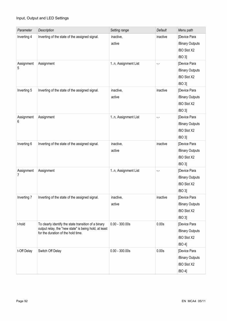
Input, Output and LED Settings
Parameter Description Setting range Default Menu path
Inverting 4 Inverting of the state of the assigned signal. inactive,
active
inactive [Device Para
/Binary Outputs
/BO Slot X2
/BO 3]Assignment 5
Assignment 1..n, Assignment List -.- [Device Para
/Binary Outputs
/BO Slot X2
/BO 3]Inverting 5 Inverting of the state of the assigned signal. inactive,
active
inactive [Device Para
/Binary Outputs
/BO Slot X2
/BO 3]Assignment 6
Assignment 1..n, Assignment List -.- [Device Para
/Binary Outputs
/BO Slot X2
/BO 3]Inverting 6 Inverting of the state of the assigned signal. inactive,
active
inactive [Device Para
/Binary Outputs
/BO Slot X2
/BO 3]Assignment 7
Assignment 1..n, Assignment List -.- [Device Para
/Binary Outputs
/BO Slot X2
/BO 3]Inverting 7 Inverting of the state of the assigned signal. inactive,
active
inactive [Device Para
/Binary Outputs
/BO Slot X2
/BO 3]t-hold To clearly identify the state transition of a binary
output relay, the "new state" is being hold, at least for the duration of the hold time.
0.00 - 300.00s 0.00s [Device Para
/Binary Outputs
/BO Slot X2
/BO 4]t-Off Delay Switch Off Delay 0.00 - 300.00s 0.00s [Device Para
/Binary Outputs
/BO Slot X2
/BO 4]
Page 92 EN MCA4 05/11

Input, Output and LED Settings
Parameter Description Setting range Default Menu path
Latched Defines whether the Relay Output will be latched when it picks up.
inactive,
active
inactive [Device Para
/Binary Outputs
/BO Slot X2
/BO 4]Acknowledgement
Acknowledgement Signal - An acknowledgement signal (that acknowledges the corresponding binary output relay) can be assigned to each output relay. The acknowledgement-signal is only effective if the parameter "Latched" is set to active.
Only available if: Latched = active
1..n, Assignment List -.- [Device Para
/Binary Outputs
/BO Slot X2
/BO 4]
Inverting Inverting of the Binary Output Relay. inactive,
active
inactive [Device Para
/Binary Outputs
/BO Slot X2
/BO 4]Assignment 1
Assignment 1..n, Assignment List BO Slot X2: SG[1].OFF Cmd
BO Slot X5: -.-
[Device Para
/Binary Outputs
/BO Slot X2
/BO 4]Inverting 1 Inverting of the state of the assigned signal. inactive,
active
inactive [Device Para
/Binary Outputs
/BO Slot X2
/BO 4]Assignment 2
Assignment 1..n, Assignment List -.- [Device Para
/Binary Outputs
/BO Slot X2
/BO 4]Inverting 2 Inverting of the state of the assigned signal. inactive,
active
inactive [Device Para
/Binary Outputs
/BO Slot X2
/BO 4]Assignment 3
Assignment 1..n, Assignment List -.- [Device Para
/Binary Outputs
/BO Slot X2
/BO 4]Inverting 3 Inverting of the state of the assigned signal. inactive,
active
inactive [Device Para
/Binary Outputs
/BO Slot X2
/BO 4]
EN MCA4 05/11 Page 93

Input, Output and LED Settings
Parameter Description Setting range Default Menu path
Assignment 4
Assignment 1..n, Assignment List -.- [Device Para
/Binary Outputs
/BO Slot X2
/BO 4]Inverting 4 Inverting of the state of the assigned signal. inactive,
active
inactive [Device Para
/Binary Outputs
/BO Slot X2
/BO 4]Assignment 5
Assignment 1..n, Assignment List -.- [Device Para
/Binary Outputs
/BO Slot X2
/BO 4]Inverting 5 Inverting of the state of the assigned signal. inactive,
active
inactive [Device Para
/Binary Outputs
/BO Slot X2
/BO 4]Assignment 6
Assignment 1..n, Assignment List -.- [Device Para
/Binary Outputs
/BO Slot X2
/BO 4]Inverting 6 Inverting of the state of the assigned signal. inactive,
active
inactive [Device Para
/Binary Outputs
/BO Slot X2
/BO 4]Assignment 7
Assignment 1..n, Assignment List -.- [Device Para
/Binary Outputs
/BO Slot X2
/BO 4]Inverting 7 Inverting of the state of the assigned signal. inactive,
active
inactive [Device Para
/Binary Outputs
/BO Slot X2
/BO 4]t-hold To clearly identify the state transition of a binary
output relay, the "new state" is being hold, at least for the duration of the hold time.
0.00 - 300.00s 0.00s [Device Para
/Binary Outputs
/BO Slot X2
/BO 5]
Page 94 EN MCA4 05/11
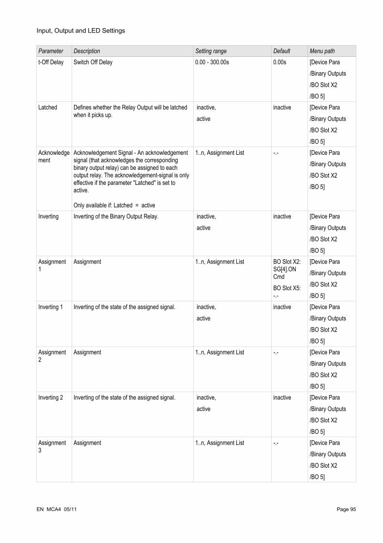
Input, Output and LED Settings
Parameter Description Setting range Default Menu path
t-Off Delay Switch Off Delay 0.00 - 300.00s 0.00s [Device Para
/Binary Outputs
/BO Slot X2
/BO 5]Latched Defines whether the Relay Output will be latched
when it picks up. inactive,
active
inactive [Device Para
/Binary Outputs
/BO Slot X2
/BO 5]Acknowledgement
Acknowledgement Signal - An acknowledgement signal (that acknowledges the corresponding binary output relay) can be assigned to each output relay. The acknowledgement-signal is only effective if the parameter "Latched" is set to active.
Only available if: Latched = active
1..n, Assignment List -.- [Device Para
/Binary Outputs
/BO Slot X2
/BO 5]
Inverting Inverting of the Binary Output Relay. inactive,
active
inactive [Device Para
/Binary Outputs
/BO Slot X2
/BO 5]Assignment 1
Assignment 1..n, Assignment List BO Slot X2: SG[4].ON Cmd
BO Slot X5: -.-
[Device Para
/Binary Outputs
/BO Slot X2
/BO 5]Inverting 1 Inverting of the state of the assigned signal. inactive,
active
inactive [Device Para
/Binary Outputs
/BO Slot X2
/BO 5]Assignment 2
Assignment 1..n, Assignment List -.- [Device Para
/Binary Outputs
/BO Slot X2
/BO 5]Inverting 2 Inverting of the state of the assigned signal. inactive,
active
inactive [Device Para
/Binary Outputs
/BO Slot X2
/BO 5]Assignment 3
Assignment 1..n, Assignment List -.- [Device Para
/Binary Outputs
/BO Slot X2
/BO 5]
EN MCA4 05/11 Page 95
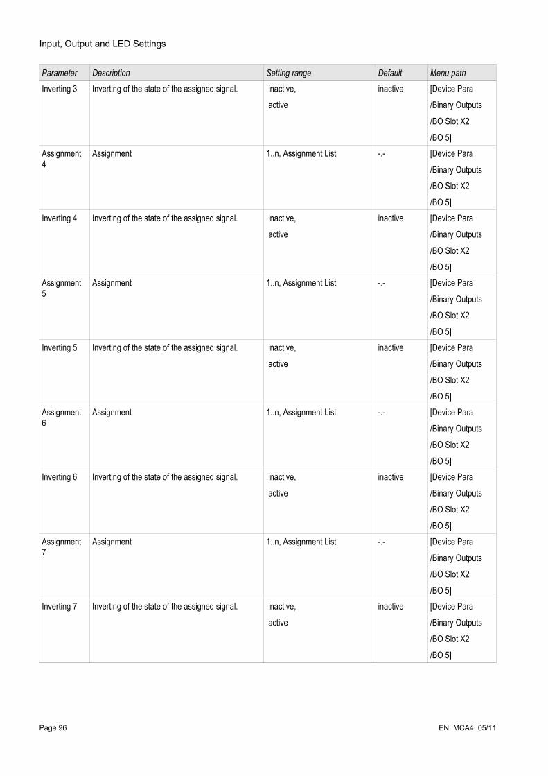
Input, Output and LED Settings
Parameter Description Setting range Default Menu path
Inverting 3 Inverting of the state of the assigned signal. inactive,
active
inactive [Device Para
/Binary Outputs
/BO Slot X2
/BO 5]Assignment 4
Assignment 1..n, Assignment List -.- [Device Para
/Binary Outputs
/BO Slot X2
/BO 5]Inverting 4 Inverting of the state of the assigned signal. inactive,
active
inactive [Device Para
/Binary Outputs
/BO Slot X2
/BO 5]Assignment 5
Assignment 1..n, Assignment List -.- [Device Para
/Binary Outputs
/BO Slot X2
/BO 5]Inverting 5 Inverting of the state of the assigned signal. inactive,
active
inactive [Device Para
/Binary Outputs
/BO Slot X2
/BO 5]Assignment 6
Assignment 1..n, Assignment List -.- [Device Para
/Binary Outputs
/BO Slot X2
/BO 5]Inverting 6 Inverting of the state of the assigned signal. inactive,
active
inactive [Device Para
/Binary Outputs
/BO Slot X2
/BO 5]Assignment 7
Assignment 1..n, Assignment List -.- [Device Para
/Binary Outputs
/BO Slot X2
/BO 5]Inverting 7 Inverting of the state of the assigned signal. inactive,
active
inactive [Device Para
/Binary Outputs
/BO Slot X2
/BO 5]
Page 96 EN MCA4 05/11

Input, Output and LED Settings
Parameter Description Setting range Default Menu path
t-hold To clearly identify the state transition of a binary output relay, the "new state" is being hold, at least for the duration of the hold time.
0.00 - 300.00s 0.00s [Device Para
/Binary Outputs
/BO Slot X2
/BO 6]t-Off Delay Switch Off Delay 0.00 - 300.00s 0.00s [Device Para
/Binary Outputs
/BO Slot X2
/BO 6]Latched Defines whether the Relay Output will be latched
when it picks up. inactive,
active
inactive [Device Para
/Binary Outputs
/BO Slot X2
/BO 6]Acknowledgement
Acknowledgement Signal - An acknowledgement signal (that acknowledges the corresponding binary output relay) can be assigned to each output relay. The acknowledgement-signal is only effective if the parameter "Latched" is set to active.
Only available if: Latched = active
1..n, Assignment List -.- [Device Para
/Binary Outputs
/BO Slot X2
/BO 6]
Inverting Inverting of the Binary Output Relay. inactive,
active
inactive [Device Para
/Binary Outputs
/BO Slot X2
/BO 6]Assignment 1
Assignment 1..n, Assignment List BO Slot X2: SG[4].OFF Cmd
BO Slot X5: -.-
[Device Para
/Binary Outputs
/BO Slot X2
/BO 6]Inverting 1 Inverting of the state of the assigned signal. inactive,
active
inactive [Device Para
/Binary Outputs
/BO Slot X2
/BO 6]Assignment 2
Assignment 1..n, Assignment List -.- [Device Para
/Binary Outputs
/BO Slot X2
/BO 6]Inverting 2 Inverting of the state of the assigned signal. inactive,
active
inactive [Device Para
/Binary Outputs
/BO Slot X2
/BO 6]
EN MCA4 05/11 Page 97
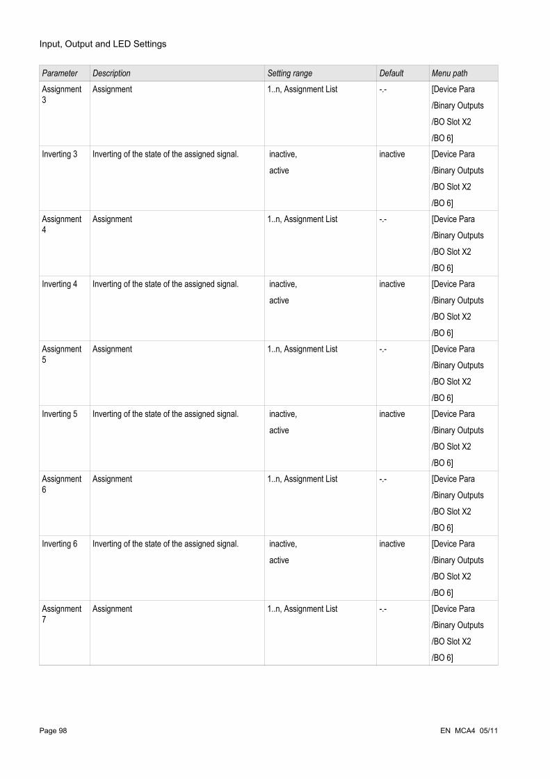
Input, Output and LED Settings
Parameter Description Setting range Default Menu path
Assignment 3
Assignment 1..n, Assignment List -.- [Device Para
/Binary Outputs
/BO Slot X2
/BO 6]Inverting 3 Inverting of the state of the assigned signal. inactive,
active
inactive [Device Para
/Binary Outputs
/BO Slot X2
/BO 6]Assignment 4
Assignment 1..n, Assignment List -.- [Device Para
/Binary Outputs
/BO Slot X2
/BO 6]Inverting 4 Inverting of the state of the assigned signal. inactive,
active
inactive [Device Para
/Binary Outputs
/BO Slot X2
/BO 6]Assignment 5
Assignment 1..n, Assignment List -.- [Device Para
/Binary Outputs
/BO Slot X2
/BO 6]Inverting 5 Inverting of the state of the assigned signal. inactive,
active
inactive [Device Para
/Binary Outputs
/BO Slot X2
/BO 6]Assignment 6
Assignment 1..n, Assignment List -.- [Device Para
/Binary Outputs
/BO Slot X2
/BO 6]Inverting 6 Inverting of the state of the assigned signal. inactive,
active
inactive [Device Para
/Binary Outputs
/BO Slot X2
/BO 6]Assignment 7
Assignment 1..n, Assignment List -.- [Device Para
/Binary Outputs
/BO Slot X2
/BO 6]
Page 98 EN MCA4 05/11

Input, Output and LED Settings
Parameter Description Setting range Default Menu path
Inverting 7 Inverting of the state of the assigned signal. inactive,
active
inactive [Device Para
/Binary Outputs
/BO Slot X2
/BO 6]DISARMED Ctrl
Enables and disables the disarming of the relay outputs. This is the first step of a two step process, to inhibit the operation or the relay outputs. Please refer to "DISARMED" for the second step.
inactive,
active
inactive [Service
/Test Mode (Prot inhibit)
/DISARMED
/BO Slot X2]
Disarm Mode CAUTION!RELAYS DISARMED in order to safely perform maintenance while eliminating the risk of taking an entire process off-line. (Note: The Supervision Contact cannot be disarmed). YOU MUST ENSURE that the relays are ARMED AGAIN after maintenance.
permanent,
Timeout
permanent [Service
/Test Mode (Prot inhibit)
/DISARMED
/BO Slot X2]
t-Timeout DISARM
The relays will be armed again after expiring of this time.
Only available if: Mode = Timeout DISARM
0.00 - 300.00s 0.03s [Service
/Test Mode (Prot inhibit)
/DISARMED
/BO Slot X2]Force Mode By means of this function the normal Output Relay
States can be overwritten (forced) in case that the Relay is not in a disarmed state. The relays can be set from normal operation (relay works according to the assigned signals) to "force energized" or "force de-energized" state.
permanent,
Timeout
permanent [Service
/Test Mode (Prot inhibit)
/Force OR
/BO Slot X2]
t-Timeout Force
The Output State will be set by force for the duration of this time. That means for the duration of this time the Output Relay does not show the state of the signals that are assigned on it.
Only available if: Mode = Timeout DISARM
0.00 - 300.00s 0.03s [Service
/Test Mode (Prot inhibit)
/Force OR
/BO Slot X2]
EN MCA4 05/11 Page 99

Input, Output and LED Settings
Input States of the Binary Output Relays on OR-6 X
Name Description Assignment via
BO1.1 Module input state: Assignment [Device Para
/Binary Outputs
/BO Slot X2
/BO 1]BO1.2 Module input state: Assignment [Device Para
/Binary Outputs
/BO Slot X2
/BO 1]BO1.3 Module input state: Assignment [Device Para
/Binary Outputs
/BO Slot X2
/BO 1]BO1.4 Module input state: Assignment [Device Para
/Binary Outputs
/BO Slot X2
/BO 1]BO1.5 Module input state: Assignment [Device Para
/Binary Outputs
/BO Slot X2
/BO 1]BO1.6 Module input state: Assignment [Device Para
/Binary Outputs
/BO Slot X2
/BO 1]BO1.7 Module input state: Assignment [Device Para
/Binary Outputs
/BO Slot X2
/BO 1]Ack signal BO 1 Module input state: Acknowledgement
signal for the binary output relay. If latching is set to active, the binary output relay can only be acknowledged if those signals that initiated the setting are fallen back and the hold time is expired.
[Device Para
/Binary Outputs
/BO Slot X2
/BO 1]
BO2.1 Module input state: Assignment [Device Para
/Binary Outputs
/BO Slot X2
/BO 2]
Page 100 EN MCA4 05/11

Input, Output and LED Settings
Name Description Assignment via
BO2.2 Module input state: Assignment [Device Para
/Binary Outputs
/BO Slot X2
/BO 2]BO2.3 Module input state: Assignment [Device Para
/Binary Outputs
/BO Slot X2
/BO 2]BO2.4 Module input state: Assignment [Device Para
/Binary Outputs
/BO Slot X2
/BO 2]BO2.5 Module input state: Assignment [Device Para
/Binary Outputs
/BO Slot X2
/BO 2]BO2.6 Module input state: Assignment [Device Para
/Binary Outputs
/BO Slot X2
/BO 2]BO2.7 Module input state: Assignment [Device Para
/Binary Outputs
/BO Slot X2
/BO 2]Ack signal BO 2 Module input state: Acknowledgement
signal for the binary output relay. If latching is set to active, the binary output relay can only be acknowledged if those signals that initiated the setting are fallen back and the hold time is expired.
[Device Para
/Binary Outputs
/BO Slot X2
/BO 2]
BO3.1 Module input state: Assignment [Device Para
/Binary Outputs
/BO Slot X2
/BO 3]BO3.2 Module input state: Assignment [Device Para
/Binary Outputs
/BO Slot X2
/BO 3]
EN MCA4 05/11 Page 101

Input, Output and LED Settings
Name Description Assignment via
BO3.3 Module input state: Assignment [Device Para
/Binary Outputs
/BO Slot X2
/BO 3]BO3.4 Module input state: Assignment [Device Para
/Binary Outputs
/BO Slot X2
/BO 3]BO3.5 Module input state: Assignment [Device Para
/Binary Outputs
/BO Slot X2
/BO 3]BO3.6 Module input state: Assignment [Device Para
/Binary Outputs
/BO Slot X2
/BO 3]BO3.7 Module input state: Assignment [Device Para
/Binary Outputs
/BO Slot X2
/BO 3]Ack signal BO 3 Module input state: Acknowledgement
signal for the binary output relay. If latching is set to active, the binary output relay can only be acknowledged if those signals that initiated the setting are fallen back and the hold time is expired.
[Device Para
/Binary Outputs
/BO Slot X2
/BO 3]
BO4.1 Module input state: Assignment [Device Para
/Binary Outputs
/BO Slot X2
/BO 4]BO4.2 Module input state: Assignment [Device Para
/Binary Outputs
/BO Slot X2
/BO 4]BO4.3 Module input state: Assignment [Device Para
/Binary Outputs
/BO Slot X2
/BO 4]
Page 102 EN MCA4 05/11

Input, Output and LED Settings
Name Description Assignment via
BO4.4 Module input state: Assignment [Device Para
/Binary Outputs
/BO Slot X2
/BO 4]BO4.5 Module input state: Assignment [Device Para
/Binary Outputs
/BO Slot X2
/BO 4]BO4.6 Module input state: Assignment [Device Para
/Binary Outputs
/BO Slot X2
/BO 4]BO4.7 Module input state: Assignment [Device Para
/Binary Outputs
/BO Slot X2
/BO 4]Ack signal BO 4 Module input state: Acknowledgement
signal for the binary output relay. If latching is set to active, the binary output relay can only be acknowledged if those signals that initiated the setting are fallen back and the hold time is expired.
[Device Para
/Binary Outputs
/BO Slot X2
/BO 4]
BO5.1 Module input state: Assignment [Device Para
/Binary Outputs
/BO Slot X2
/BO 5]BO5.2 Module input state: Assignment [Device Para
/Binary Outputs
/BO Slot X2
/BO 5]BO5.3 Module input state: Assignment [Device Para
/Binary Outputs
/BO Slot X2
/BO 5]BO5.4 Module input state: Assignment [Device Para
/Binary Outputs
/BO Slot X2
/BO 5]
EN MCA4 05/11 Page 103
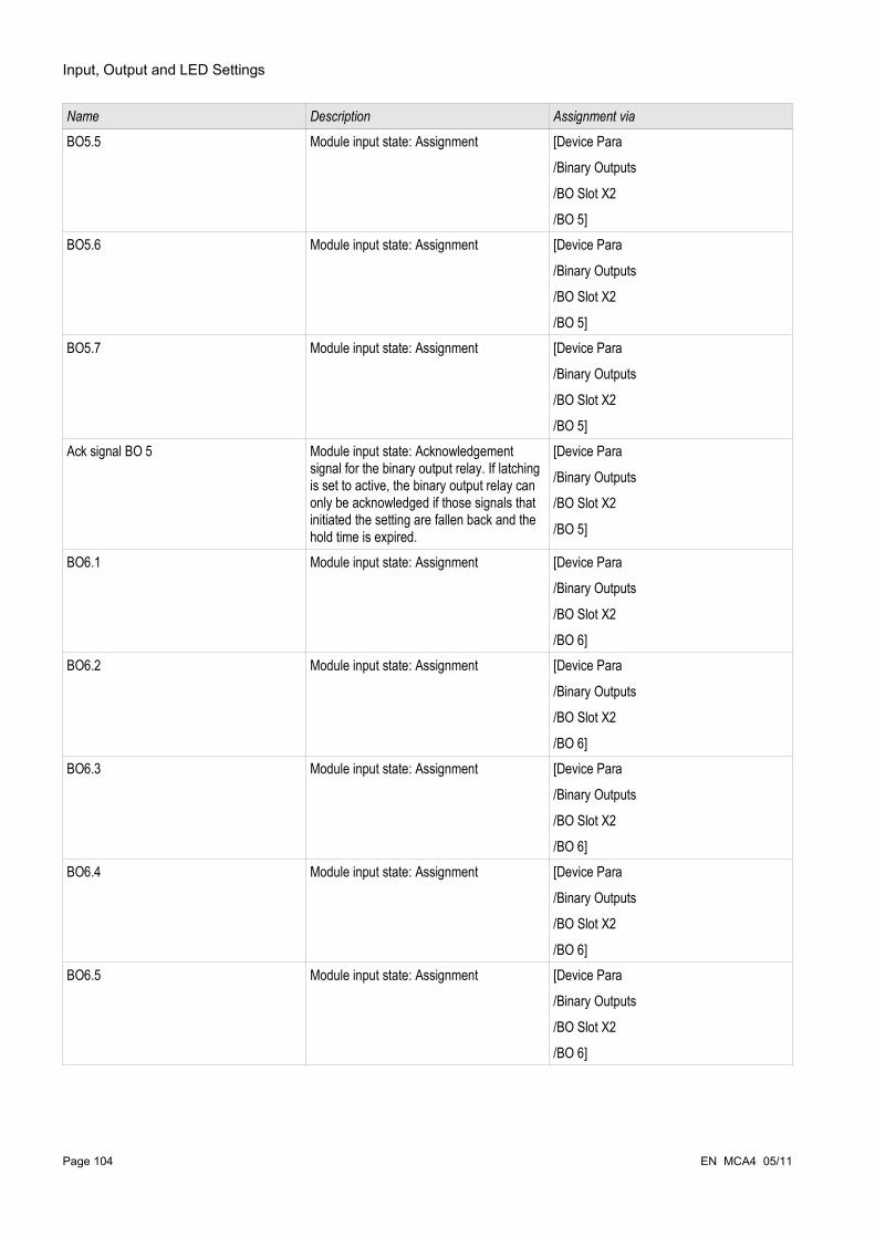
Input, Output and LED Settings
Name Description Assignment via
BO5.5 Module input state: Assignment [Device Para
/Binary Outputs
/BO Slot X2
/BO 5]BO5.6 Module input state: Assignment [Device Para
/Binary Outputs
/BO Slot X2
/BO 5]BO5.7 Module input state: Assignment [Device Para
/Binary Outputs
/BO Slot X2
/BO 5]Ack signal BO 5 Module input state: Acknowledgement
signal for the binary output relay. If latching is set to active, the binary output relay can only be acknowledged if those signals that initiated the setting are fallen back and the hold time is expired.
[Device Para
/Binary Outputs
/BO Slot X2
/BO 5]
BO6.1 Module input state: Assignment [Device Para
/Binary Outputs
/BO Slot X2
/BO 6]BO6.2 Module input state: Assignment [Device Para
/Binary Outputs
/BO Slot X2
/BO 6]BO6.3 Module input state: Assignment [Device Para
/Binary Outputs
/BO Slot X2
/BO 6]BO6.4 Module input state: Assignment [Device Para
/Binary Outputs
/BO Slot X2
/BO 6]BO6.5 Module input state: Assignment [Device Para
/Binary Outputs
/BO Slot X2
/BO 6]
Page 104 EN MCA4 05/11
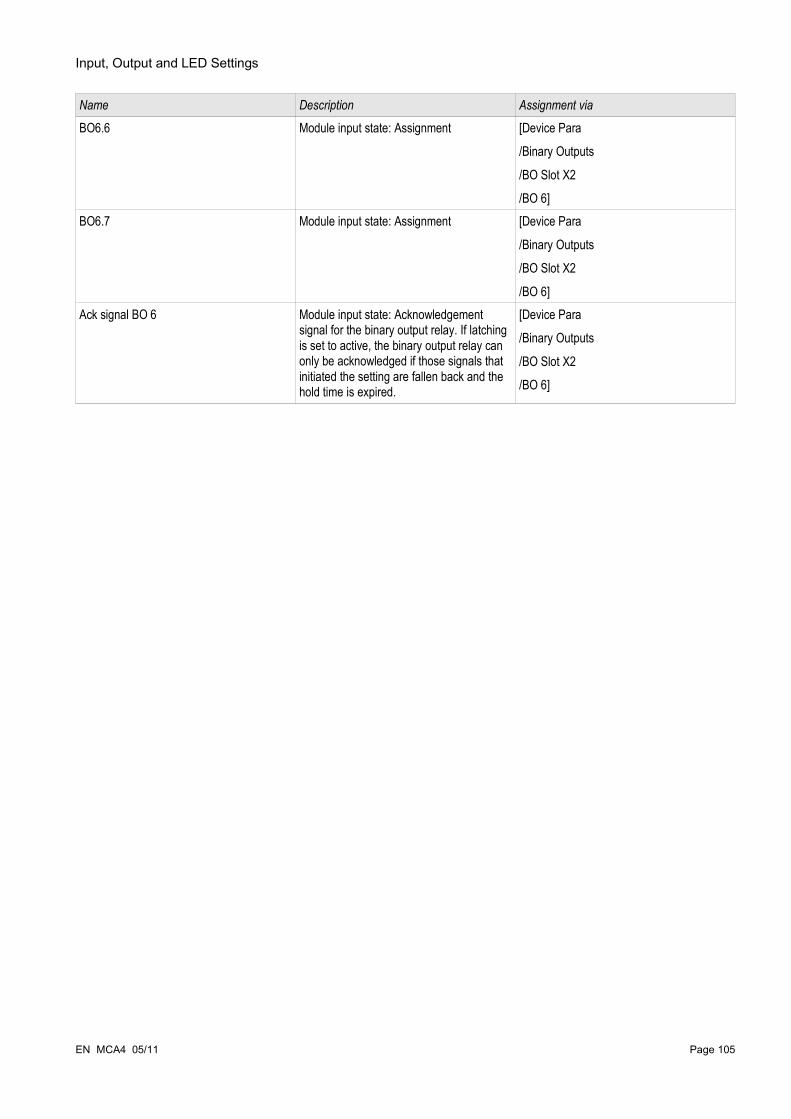
Input, Output and LED Settings
Name Description Assignment via
BO6.6 Module input state: Assignment [Device Para
/Binary Outputs
/BO Slot X2
/BO 6]BO6.7 Module input state: Assignment [Device Para
/Binary Outputs
/BO Slot X2
/BO 6]Ack signal BO 6 Module input state: Acknowledgement
signal for the binary output relay. If latching is set to active, the binary output relay can only be acknowledged if those signals that initiated the setting are fallen back and the hold time is expired.
[Device Para
/Binary Outputs
/BO Slot X2
/BO 6]
EN MCA4 05/11 Page 105
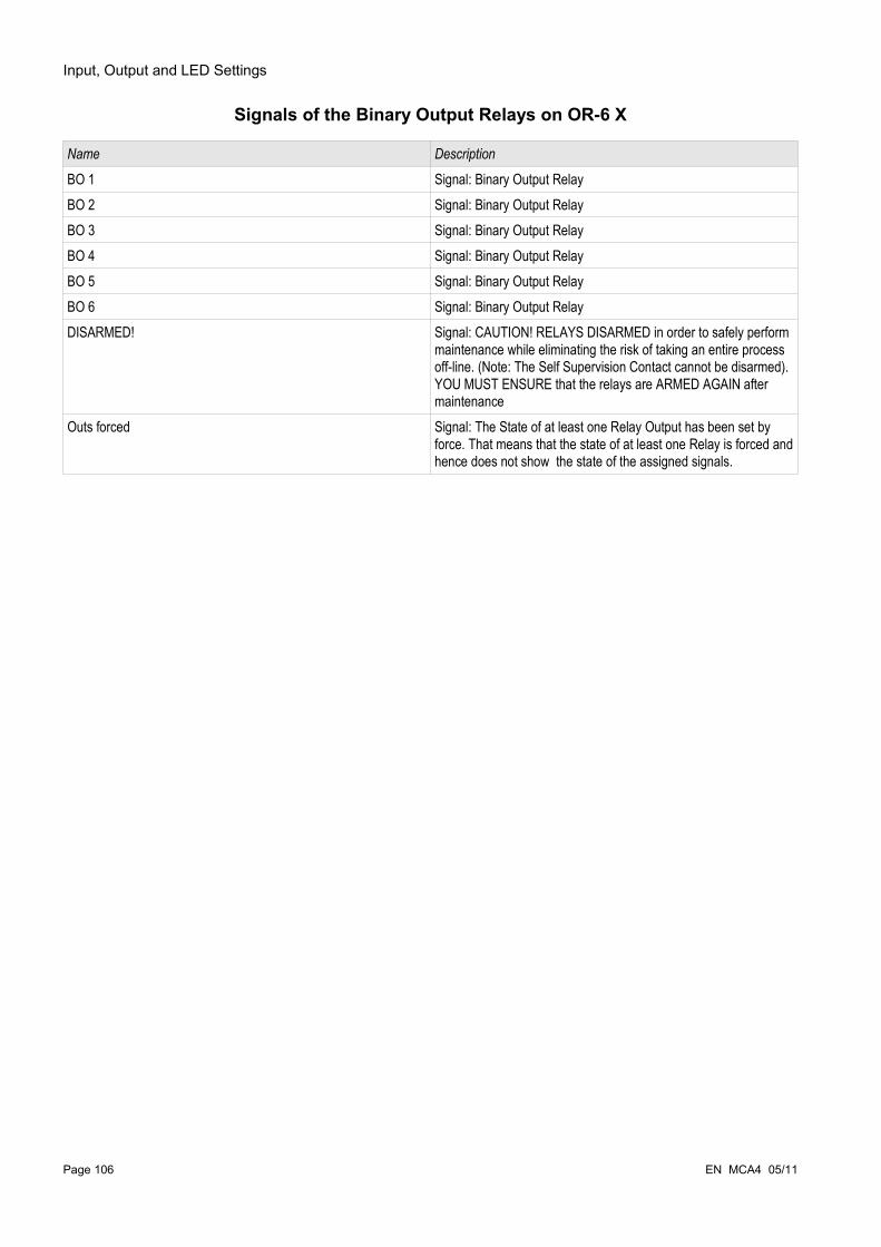
Input, Output and LED Settings
Signals of the Binary Output Relays on OR-6 X
Name Description
BO 1 Signal: Binary Output RelayBO 2 Signal: Binary Output RelayBO 3 Signal: Binary Output RelayBO 4 Signal: Binary Output RelayBO 5 Signal: Binary Output RelayBO 6 Signal: Binary Output RelayDISARMED! Signal: CAUTION! RELAYS DISARMED in order to safely perform
maintenance while eliminating the risk of taking an entire process off-line. (Note: The Self Supervision Contact cannot be disarmed). YOU MUST ENSURE that the relays are ARMED AGAIN after maintenance
Outs forced Signal: The State of at least one Relay Output has been set by force. That means that the state of at least one Relay is forced and hence does not show the state of the assigned signals.
Page 106 EN MCA4 05/11
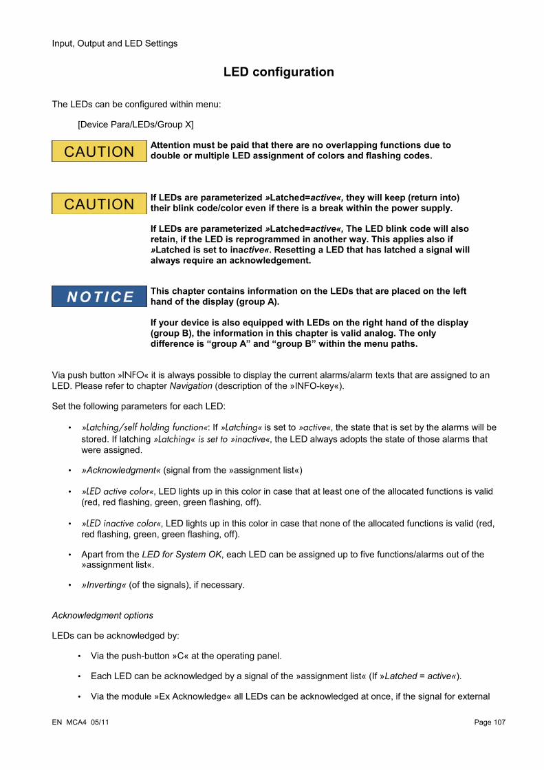
Input, Output and LED Settings
LED configuration
The LEDs can be configured within menu:
[Device Para/LEDs/Group X]
Attention must be paid that there are no overlapping functions due to double or multiple LED assignment of colors and flashing codes.
If LEDs are parameterized »Latched=active«, they will keep (return into) their blink code/color even if there is a break within the power supply.
If LEDs are parameterized »Latched=active«, The LED blink code will also retain, if the LED is reprogrammed in another way. This applies also if »Latched is set to inactive«. Resetting a LED that has latched a signal will always require an acknowledgement.
This chapter contains information on the LEDs that are placed on the left hand of the display (group A).
If your device is also equipped with LEDs on the right hand of the display (group B), the information in this chapter is valid analog. The only difference is “group A” and “group B” within the menu paths.
Via push button »INFO« it is always possible to display the current alarms/alarm texts that are assigned to an LED. Please refer to chapter Navigation (description of the »INFO-key«).
Set the following parameters for each LED:
• »Latching/self holding function«: If »Latching« is set to »active«, the state that is set by the alarms will be stored. If latching »Latching« is set to »inactive«, the LED always adopts the state of those alarms that were assigned.
• »Acknowledgment« (signal from the »assignment list«)
• »LED active color«, LED lights up in this color in case that at least one of the allocated functions is valid (red, red flashing, green, green flashing, off).
• »LED inactive color«, LED lights up in this color in case that none of the allocated functions is valid (red, red flashing, green, green flashing, off).
• Apart from the LED for System OK, each LED can be assigned up to five functions/alarms out of the »assignment list«.
• »Inverting« (of the signals), if necessary.
Acknowledgment options
LEDs can be acknowledged by:
• Via the push-button »C« at the operating panel.
• Each LED can be acknowledged by a signal of the »assignment list« (If »Latched = active«).
• Via the module »Ex Acknowledge« all LEDs can be acknowledged at once, if the signal for external
EN MCA4 05/11 Page 107

Input, Output and LED Settings
acknowledgment that was selected from the »assignment list« becomes true (e.g. the state of a digital input).
• Via SCADA, all LEDs can be acknowledged at once.
The Product-CD that is delivered with the device contains a PDF-Template in order to create and print out self adhesive films for LED assignment texts (front foil) by means of a laser printer. Recommendation: (AVERY Zweckform Art.Nr.3482)
Page 108 EN MCA4 05/11

Input, Output and LED Settings
EN MCA4 05/11 Page 109
inac
tive
act
ive
Latc
hed
=1As
sign
men
t 1
Inve
rting
1
=1As
sign
men
t 2
Inve
rting
2
=1As
sign
men
t 3
Inve
rting
3
=1As
sign
men
t 4
Inve
rting
4
=1As
sign
men
t 5
Inve
rting
5
>1
1
LED
act
ive
colo
r
LED
inac
tive
colo
r
>1
>1
S1
1
R
1
&
Ackn
owle
dge
-HM
IAc
know
ledg
e-1.
.n, A
ssig
nmen
t Lis
tAc
know
ledg
e-Sc
ada

Input, Output and LED Settings
The »System OK« LED
This LED flashes green while the device is booting. After completed booting, the LED for System OK lights up in green thus signalizing that the protection (function) is »activated«. If, however, in spite of successful booting, or after the third unsuccessful reboot caused by the module self supervision the System OK – LED flashes in red or is red illuminated, please contact the Woodward Kempen GmbH – Service Dept (See also chapter Self Supervision).
LED System OK cannot be parameterized.
Page 110 EN MCA4 05/11

Input, Output and LED Settings
Global Protection Parameters of the LED Module
LEDs group A ,LEDs group B
Parameter Description Setting range Default Menu path
Latched Defines whether the LED will be latched when it picks up.
inactive,
active
inactive [Device Para
/LEDs
/LEDs group A
/LED 1]Ack signal Acknowledgement signal for the LED. If latching is
set to active the LED can only be acknowledged if those signals that initiated the setting are no longer present.
Dependency Only available if: Latched = active
1..n, Assignment List -.- [Device Para
/LEDs
/LEDs group A
/LED 1]
LED active color
The LED lights up in this color if the state of the OR-assignment of the signals is true.
green,
red,
red flash,
green flash,
-
LEDs group A: green
LEDs group B: red
[Device Para
/LEDs
/LEDs group A
/LED 1]
LED inactive color
The LED lights up in this color if the state of the OR-assignment of the signals is untrue.
green,
red,
red flash,
green flash,
-
- [Device Para
/LEDs
/LEDs group A
/LED 1]
Assignment 1
Assignment 1..n, Assignment List LEDs group A: Prot.active
LEDs group B: -.-
[Device Para
/LEDs
/LEDs group A
/LED 1]Inverting 1 Inverting of the state of the assigned signal. inactive,
active
inactive [Device Para
/LEDs
/LEDs group A
/LED 1]Assignment 2
Assignment 1..n, Assignment List -.- [Device Para
/LEDs
/LEDs group A
/LED 1]Inverting 2 Inverting of the state of the assigned signal. inactive,
active
inactive [Device Para
/LEDs
/LEDs group A
/LED 1]
EN MCA4 05/11 Page 111
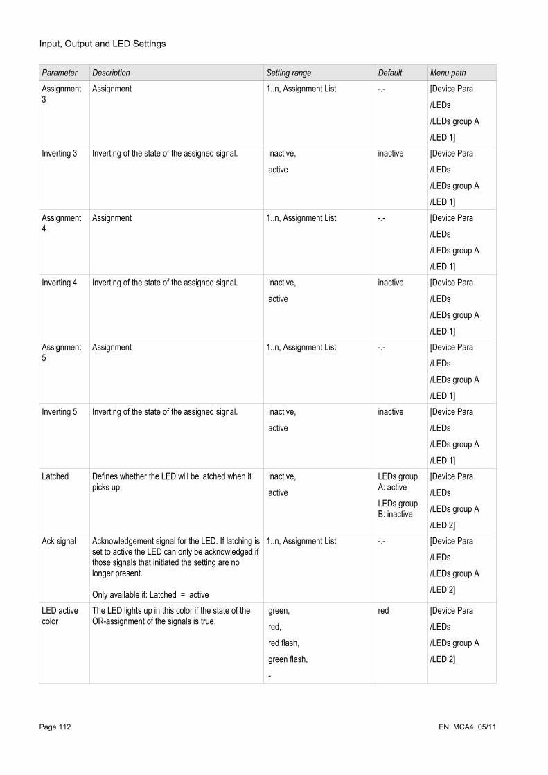
Input, Output and LED Settings
Parameter Description Setting range Default Menu path
Assignment 3
Assignment 1..n, Assignment List -.- [Device Para
/LEDs
/LEDs group A
/LED 1]Inverting 3 Inverting of the state of the assigned signal. inactive,
active
inactive [Device Para
/LEDs
/LEDs group A
/LED 1]Assignment 4
Assignment 1..n, Assignment List -.- [Device Para
/LEDs
/LEDs group A
/LED 1]Inverting 4 Inverting of the state of the assigned signal. inactive,
active
inactive [Device Para
/LEDs
/LEDs group A
/LED 1]Assignment 5
Assignment 1..n, Assignment List -.- [Device Para
/LEDs
/LEDs group A
/LED 1]Inverting 5 Inverting of the state of the assigned signal. inactive,
active
inactive [Device Para
/LEDs
/LEDs group A
/LED 1]Latched Defines whether the LED will be latched when it
picks up. inactive,
active
LEDs group A: active
LEDs group B: inactive
[Device Para
/LEDs
/LEDs group A
/LED 2]Ack signal Acknowledgement signal for the LED. If latching is
set to active the LED can only be acknowledged if those signals that initiated the setting are no longer present.
Only available if: Latched = active
1..n, Assignment List -.- [Device Para
/LEDs
/LEDs group A
/LED 2]
LED active color
The LED lights up in this color if the state of the OR-assignment of the signals is true.
green,
red,
red flash,
green flash,
-
red [Device Para
/LEDs
/LEDs group A
/LED 2]
Page 112 EN MCA4 05/11

Input, Output and LED Settings
Parameter Description Setting range Default Menu path
LED inactive color
The LED lights up in this color if the state of the OR-assignment of the signals is untrue.
green,
red,
red flash,
green flash,
-
- [Device Para
/LEDs
/LEDs group A
/LED 2]
Assignment 1
Assignment 1..n, Assignment List LEDs group A: SG[1].TripCmd
LEDs group B: -.-
[Device Para
/LEDs
/LEDs group A
/LED 2]
Inverting 1 Inverting of the state of the assigned signal. inactive,
active
inactive [Device Para
/LEDs
/LEDs group A
/LED 2]Assignment 2
Assignment 1..n, Assignment List -.- [Device Para
/LEDs
/LEDs group A
/LED 2]Inverting 2 Inverting of the state of the assigned signal. inactive,
active
inactive [Device Para
/LEDs
/LEDs group A
/LED 2]Assignment 3
Assignment 1..n, Assignment List -.- [Device Para
/LEDs
/LEDs group A
/LED 2]Inverting 3 Inverting of the state of the assigned signal. inactive,
active
inactive [Device Para
/LEDs
/LEDs group A
/LED 2]Assignment 4
Assignment 1..n, Assignment List -.- [Device Para
/LEDs
/LEDs group A
/LED 2]Inverting 4 Inverting of the state of the assigned signal. inactive,
active
inactive [Device Para
/LEDs
/LEDs group A
/LED 2]
EN MCA4 05/11 Page 113

Input, Output and LED Settings
Parameter Description Setting range Default Menu path
Assignment 5
Assignment 1..n, Assignment List -.- [Device Para
/LEDs
/LEDs group A
/LED 2]Inverting 5 Inverting of the state of the assigned signal. inactive,
active
inactive [Device Para
/LEDs
/LEDs group A
/LED 2]Latched Defines whether the LED will be latched when it
picks up. inactive,
active
inactive [Device Para
/LEDs
/LEDs group A
/LED 3]Ack signal Acknowledgement signal for the LED. If latching is
set to active the LED can only be acknowledged if those signals that initiated the setting are no longer present.
Only available if: Latched = active
1..n, Assignment List -.- [Device Para
/LEDs
/LEDs group A
/LED 3]
LED active color
The LED lights up in this color if the state of the OR-assignment of the signals is true.
green,
red,
red flash,
green flash,
-
LEDs group A: red flash
LEDs group B: red
[Device Para
/LEDs
/LEDs group A
/LED 3]
LED inactive color
The LED lights up in this color if the state of the OR-assignment of the signals is untrue.
green,
red,
red flash,
green flash,
-
- [Device Para
/LEDs
/LEDs group A
/LED 3]
Assignment 1
Assignment 1..n, Assignment List LEDs group A: Prot.Alarm
LEDs group B: -.-
[Device Para
/LEDs
/LEDs group A
/LED 3]Inverting 1 Inverting of the state of the assigned signal. inactive,
active
inactive [Device Para
/LEDs
/LEDs group A
/LED 3]Assignment 2
Assignment 1..n, Assignment List -.- [Device Para
/LEDs
/LEDs group A
/LED 3]
Page 114 EN MCA4 05/11
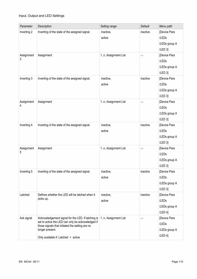
Input, Output and LED Settings
Parameter Description Setting range Default Menu path
Inverting 2 Inverting of the state of the assigned signal. inactive,
active
inactive [Device Para
/LEDs
/LEDs group A
/LED 3]Assignment 3
Assignment 1..n, Assignment List -.- [Device Para
/LEDs
/LEDs group A
/LED 3]Inverting 3 Inverting of the state of the assigned signal. inactive,
active
inactive [Device Para
/LEDs
/LEDs group A
/LED 3]Assignment 4
Assignment 1..n, Assignment List -.- [Device Para
/LEDs
/LEDs group A
/LED 3]Inverting 4 Inverting of the state of the assigned signal. inactive,
active
inactive [Device Para
/LEDs
/LEDs group A
/LED 3]Assignment 5
Assignment 1..n, Assignment List -.- [Device Para
/LEDs
/LEDs group A
/LED 3]Inverting 5 Inverting of the state of the assigned signal. inactive,
active
inactive [Device Para
/LEDs
/LEDs group A
/LED 3]Latched Defines whether the LED will be latched when it
picks up. inactive,
active
inactive [Device Para
/LEDs
/LEDs group A
/LED 4]Ack signal Acknowledgement signal for the LED. If latching is
set to active the LED can only be acknowledged if those signals that initiated the setting are no longer present.
Only available if: Latched = active
1..n, Assignment List -.- [Device Para
/LEDs
/LEDs group A
/LED 4]
EN MCA4 05/11 Page 115
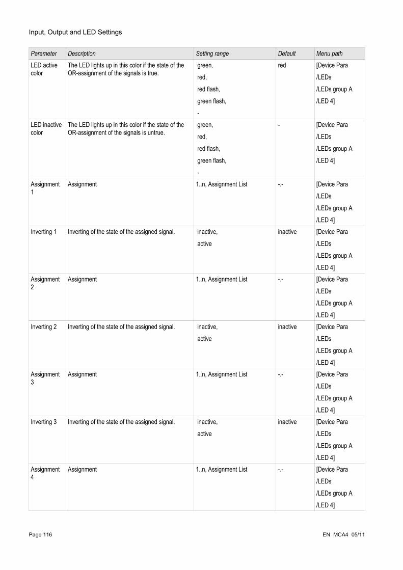
Input, Output and LED Settings
Parameter Description Setting range Default Menu path
LED active color
The LED lights up in this color if the state of the OR-assignment of the signals is true.
green,
red,
red flash,
green flash,
-
red [Device Para
/LEDs
/LEDs group A
/LED 4]
LED inactive color
The LED lights up in this color if the state of the OR-assignment of the signals is untrue.
green,
red,
red flash,
green flash,
-
- [Device Para
/LEDs
/LEDs group A
/LED 4]
Assignment 1
Assignment 1..n, Assignment List -.- [Device Para
/LEDs
/LEDs group A
/LED 4]Inverting 1 Inverting of the state of the assigned signal. inactive,
active
inactive [Device Para
/LEDs
/LEDs group A
/LED 4]Assignment 2
Assignment 1..n, Assignment List -.- [Device Para
/LEDs
/LEDs group A
/LED 4]Inverting 2 Inverting of the state of the assigned signal. inactive,
active
inactive [Device Para
/LEDs
/LEDs group A
/LED 4]Assignment 3
Assignment 1..n, Assignment List -.- [Device Para
/LEDs
/LEDs group A
/LED 4]Inverting 3 Inverting of the state of the assigned signal. inactive,
active
inactive [Device Para
/LEDs
/LEDs group A
/LED 4]Assignment 4
Assignment 1..n, Assignment List -.- [Device Para
/LEDs
/LEDs group A
/LED 4]
Page 116 EN MCA4 05/11
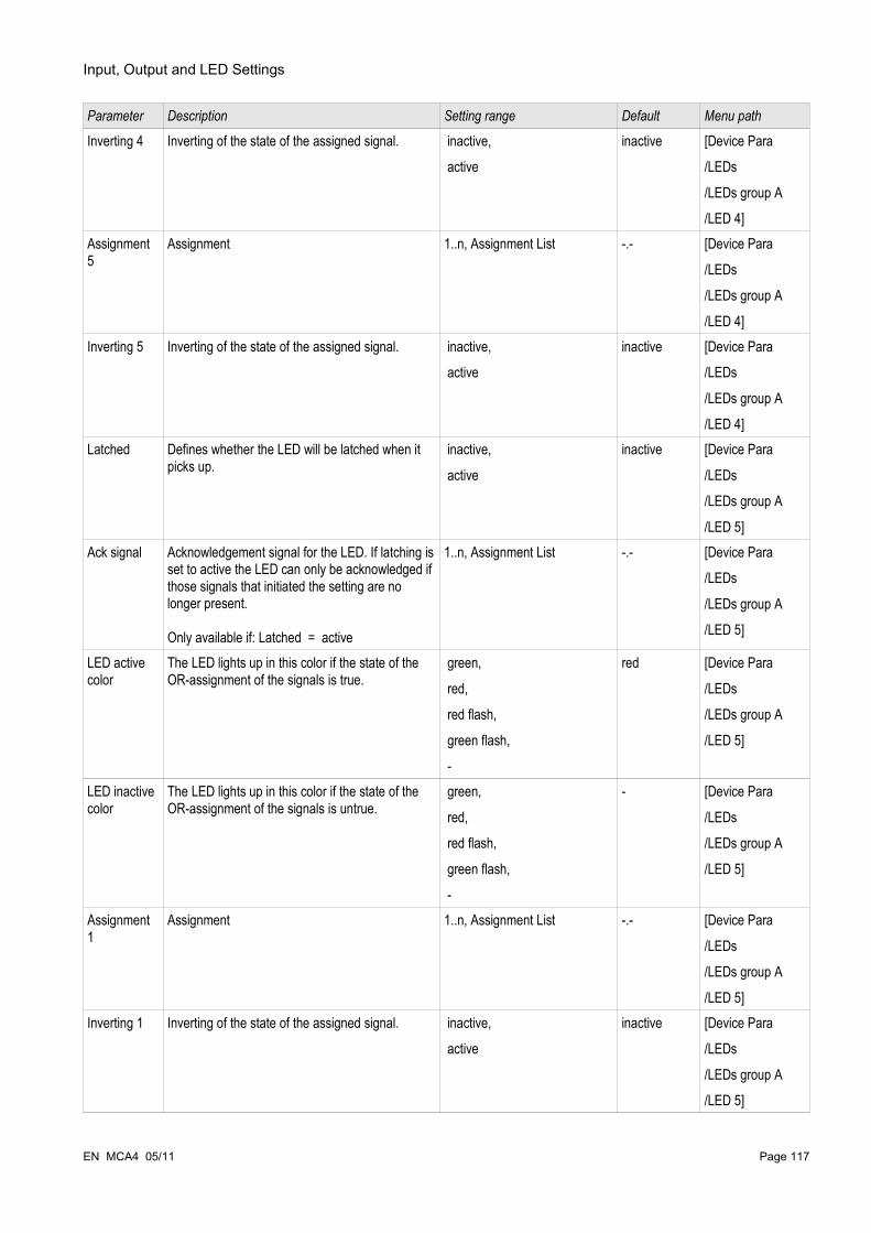
Input, Output and LED Settings
Parameter Description Setting range Default Menu path
Inverting 4 Inverting of the state of the assigned signal. inactive,
active
inactive [Device Para
/LEDs
/LEDs group A
/LED 4]Assignment 5
Assignment 1..n, Assignment List -.- [Device Para
/LEDs
/LEDs group A
/LED 4]Inverting 5 Inverting of the state of the assigned signal. inactive,
active
inactive [Device Para
/LEDs
/LEDs group A
/LED 4]Latched Defines whether the LED will be latched when it
picks up. inactive,
active
inactive [Device Para
/LEDs
/LEDs group A
/LED 5]Ack signal Acknowledgement signal for the LED. If latching is
set to active the LED can only be acknowledged if those signals that initiated the setting are no longer present.
Only available if: Latched = active
1..n, Assignment List -.- [Device Para
/LEDs
/LEDs group A
/LED 5]
LED active color
The LED lights up in this color if the state of the OR-assignment of the signals is true.
green,
red,
red flash,
green flash,
-
red [Device Para
/LEDs
/LEDs group A
/LED 5]
LED inactive color
The LED lights up in this color if the state of the OR-assignment of the signals is untrue.
green,
red,
red flash,
green flash,
-
- [Device Para
/LEDs
/LEDs group A
/LED 5]
Assignment 1
Assignment 1..n, Assignment List -.- [Device Para
/LEDs
/LEDs group A
/LED 5]Inverting 1 Inverting of the state of the assigned signal. inactive,
active
inactive [Device Para
/LEDs
/LEDs group A
/LED 5]
EN MCA4 05/11 Page 117
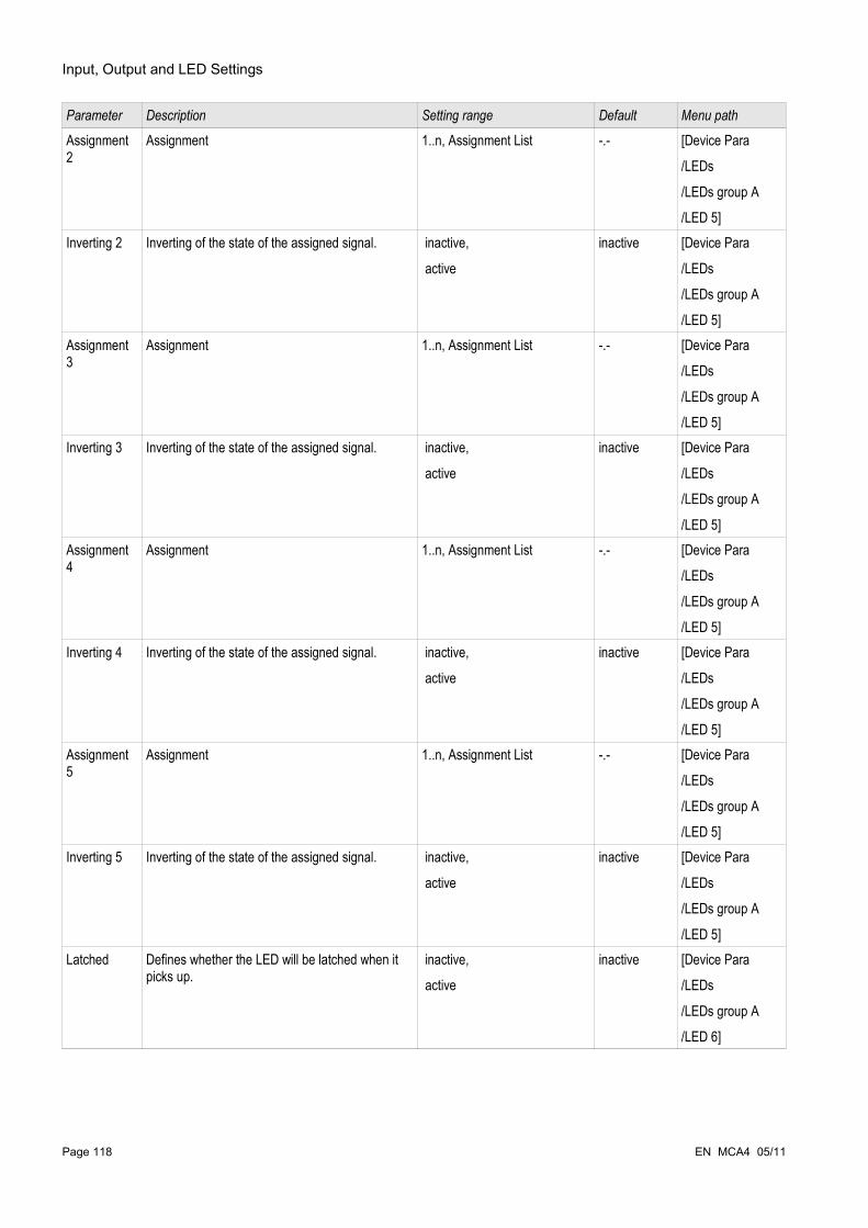
Input, Output and LED Settings
Parameter Description Setting range Default Menu path
Assignment 2
Assignment 1..n, Assignment List -.- [Device Para
/LEDs
/LEDs group A
/LED 5]Inverting 2 Inverting of the state of the assigned signal. inactive,
active
inactive [Device Para
/LEDs
/LEDs group A
/LED 5]Assignment 3
Assignment 1..n, Assignment List -.- [Device Para
/LEDs
/LEDs group A
/LED 5]Inverting 3 Inverting of the state of the assigned signal. inactive,
active
inactive [Device Para
/LEDs
/LEDs group A
/LED 5]Assignment 4
Assignment 1..n, Assignment List -.- [Device Para
/LEDs
/LEDs group A
/LED 5]Inverting 4 Inverting of the state of the assigned signal. inactive,
active
inactive [Device Para
/LEDs
/LEDs group A
/LED 5]Assignment 5
Assignment 1..n, Assignment List -.- [Device Para
/LEDs
/LEDs group A
/LED 5]Inverting 5 Inverting of the state of the assigned signal. inactive,
active
inactive [Device Para
/LEDs
/LEDs group A
/LED 5]Latched Defines whether the LED will be latched when it
picks up. inactive,
active
inactive [Device Para
/LEDs
/LEDs group A
/LED 6]
Page 118 EN MCA4 05/11

Input, Output and LED Settings
Parameter Description Setting range Default Menu path
Ack signal Acknowledgement signal for the LED. If latching is set to active the LED can only be acknowledged if those signals that initiated the setting are no longer present.
Only available if: Latched = active
1..n, Assignment List -.- [Device Para
/LEDs
/LEDs group A
/LED 6]
LED active color
The LED lights up in this color if the state of the OR-assignment of the signals is true.
green,
red,
red flash,
green flash,
-
red [Device Para
/LEDs
/LEDs group A
/LED 6]
LED inactive color
The LED lights up in this color if the state of the OR-assignment of the signals is untrue.
green,
red,
red flash,
green flash,
-
- [Device Para
/LEDs
/LEDs group A
/LED 6]
Assignment 1
Assignment 1..n, Assignment List -.- [Device Para
/LEDs
/LEDs group A
/LED 6]Inverting 1 Inverting of the state of the assigned signal. inactive,
active
inactive [Device Para
/LEDs
/LEDs group A
/LED 6]Assignment 2
Assignment 1..n, Assignment List -.- [Device Para
/LEDs
/LEDs group A
/LED 6]Inverting 2 Inverting of the state of the assigned signal. inactive,
active
inactive [Device Para
/LEDs
/LEDs group A
/LED 6]Assignment 3
Assignment 1..n, Assignment List -.- [Device Para
/LEDs
/LEDs group A
/LED 6]Inverting 3 Inverting of the state of the assigned signal. inactive,
active
inactive [Device Para
/LEDs
/LEDs group A
/LED 6]
EN MCA4 05/11 Page 119
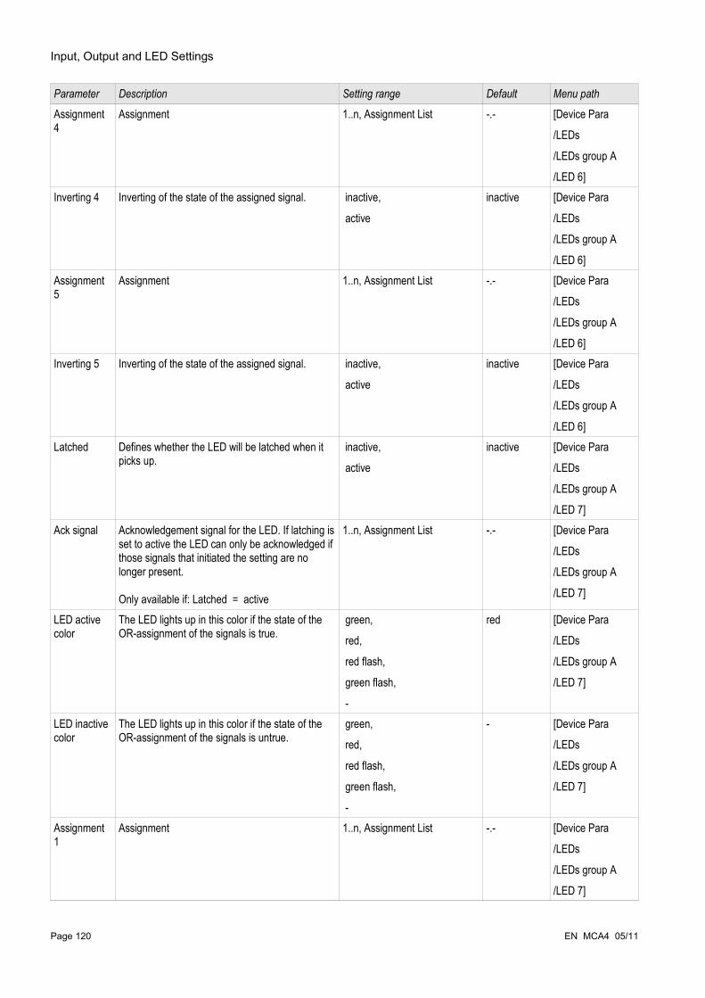
Input, Output and LED Settings
Parameter Description Setting range Default Menu path
Assignment 4
Assignment 1..n, Assignment List -.- [Device Para
/LEDs
/LEDs group A
/LED 6]Inverting 4 Inverting of the state of the assigned signal. inactive,
active
inactive [Device Para
/LEDs
/LEDs group A
/LED 6]Assignment 5
Assignment 1..n, Assignment List -.- [Device Para
/LEDs
/LEDs group A
/LED 6]Inverting 5 Inverting of the state of the assigned signal. inactive,
active
inactive [Device Para
/LEDs
/LEDs group A
/LED 6]Latched Defines whether the LED will be latched when it
picks up. inactive,
active
inactive [Device Para
/LEDs
/LEDs group A
/LED 7]Ack signal Acknowledgement signal for the LED. If latching is
set to active the LED can only be acknowledged if those signals that initiated the setting are no longer present.
Only available if: Latched = active
1..n, Assignment List -.- [Device Para
/LEDs
/LEDs group A
/LED 7]
LED active color
The LED lights up in this color if the state of the OR-assignment of the signals is true.
green,
red,
red flash,
green flash,
-
red [Device Para
/LEDs
/LEDs group A
/LED 7]
LED inactive color
The LED lights up in this color if the state of the OR-assignment of the signals is untrue.
green,
red,
red flash,
green flash,
-
- [Device Para
/LEDs
/LEDs group A
/LED 7]
Assignment 1
Assignment 1..n, Assignment List -.- [Device Para
/LEDs
/LEDs group A
/LED 7]
Page 120 EN MCA4 05/11

Input, Output and LED Settings
Parameter Description Setting range Default Menu path
Inverting 1 Inverting of the state of the assigned signal. inactive,
active
inactive [Device Para
/LEDs
/LEDs group A
/LED 7]Assignment 2
Assignment 1..n, Assignment List -.- [Device Para
/LEDs
/LEDs group A
/LED 7]Inverting 2 Inverting of the state of the assigned signal. inactive,
active
inactive [Device Para
/LEDs
/LEDs group A
/LED 7]Assignment 3
Assignment 1..n, Assignment List -.- [Device Para
/LEDs
/LEDs group A
/LED 7]Inverting 3 Inverting of the state of the assigned signal. inactive,
active
inactive [Device Para
/LEDs
/LEDs group A
/LED 7]Assignment 4
Assignment 1..n, Assignment List -.- [Device Para
/LEDs
/LEDs group A
/LED 7]Inverting 4 Inverting of the state of the assigned signal. inactive,
active
inactive [Device Para
/LEDs
/LEDs group A
/LED 7]Assignment 5
Assignment 1..n, Assignment List -.- [Device Para
/LEDs
/LEDs group A
/LED 7]Inverting 5 Inverting of the state of the assigned signal. inactive,
active
inactive [Device Para
/LEDs
/LEDs group A
/LED 7]
EN MCA4 05/11 Page 121

Input, Output and LED Settings
LED Module Input States
Name Description Assignment via
LED1.1 Module input state: LED [Device Para
/LEDs
/LEDs group A
/LED 1]LED1.2 Module input state: LED [Device Para
/LEDs
/LEDs group A
/LED 1]LED1.3 Module input state: LED [Device Para
/LEDs
/LEDs group A
/LED 1]LED1.4 Module input state: LED [Device Para
/LEDs
/LEDs group A
/LED 1]LED1.5 Module input state: LED [Device Para
/LEDs
/LEDs group A
/LED 1]Acknow Sig 1 Module input state: Acknowledgement
Signal (only for automatic acknowledgement)
[Device Para
/LEDs
/LEDs group A
/LED 1]LED2.1 Module input state: LED [Device Para
/LEDs
/LEDs group A
/LED 2]LED2.2 Module input state: LED [Device Para
/LEDs
/LEDs group A
/LED 2]LED2.3 Module input state: LED [Device Para
/LEDs
/LEDs group A
/LED 2]
Page 122 EN MCA4 05/11

Input, Output and LED Settings
Name Description Assignment via
LED2.4 Module input state: LED [Device Para
/LEDs
/LEDs group A
/LED 2]LED2.5 Module input state: LED [Device Para
/LEDs
/LEDs group A
/LED 2]Acknow Sig 2 Module input state: Acknowledgement
Signal (only for automatic acknowledgement)
[Device Para
/LEDs
/LEDs group A
/LED 2]LED3.1 Module input state: LED [Device Para
/LEDs
/LEDs group A
/LED 3]LED3.2 Module input state: LED [Device Para
/LEDs
/LEDs group A
/LED 3]LED3.3 Module input state: LED [Device Para
/LEDs
/LEDs group A
/LED 3]LED3.4 Module input state: LED [Device Para
/LEDs
/LEDs group A
/LED 3]LED3.5 Module input state: LED [Device Para
/LEDs
/LEDs group A
/LED 3]Acknow Sig 3 Module input state: Acknowledgement
Signal (only for automatic acknowledgement)
[Device Para
/LEDs
/LEDs group A
/LED 3]
EN MCA4 05/11 Page 123

Input, Output and LED Settings
Name Description Assignment via
LED4.1 Module input state: LED [Device Para
/LEDs
/LEDs group A
/LED 4]LED4.2 Module input state: LED [Device Para
/LEDs
/LEDs group A
/LED 4]LED4.3 Module input state: LED [Device Para
/LEDs
/LEDs group A
/LED 4]LED4.4 Module input state: LED [Device Para
/LEDs
/LEDs group A
/LED 4]LED4.5 Module input state: LED [Device Para
/LEDs
/LEDs group A
/LED 4]Acknow Sig 4 Module input state: Acknowledgement
Signal (only for automatic acknowledgement)
[Device Para
/LEDs
/LEDs group A
/LED 4]LED5.1 Module input state: LED [Device Para
/LEDs
/LEDs group A
/LED 5]LED5.2 Module input state: LED [Device Para
/LEDs
/LEDs group A
/LED 5]LED5.3 Module input state: LED [Device Para
/LEDs
/LEDs group A
/LED 5]
Page 124 EN MCA4 05/11

Input, Output and LED Settings
Name Description Assignment via
LED5.4 Module input state: LED [Device Para
/LEDs
/LEDs group A
/LED 5]LED5.5 Module input state: LED [Device Para
/LEDs
/LEDs group A
/LED 5]Acknow Sig 5 Module input state: Acknowledgement
Signal (only for automatic acknowledgement)
[Device Para
/LEDs
/LEDs group A
/LED 5]LED6.1 Module input state: LED [Device Para
/LEDs
/LEDs group A
/LED 6]LED6.2 Module input state: LED [Device Para
/LEDs
/LEDs group A
/LED 6]LED6.3 Module input state: LED [Device Para
/LEDs
/LEDs group A
/LED 6]LED6.4 Module input state: LED [Device Para
/LEDs
/LEDs group A
/LED 6]LED6.5 Module input state: LED [Device Para
/LEDs
/LEDs group A
/LED 6]Acknow Sig 6 Module input state: Acknowledgement
Signal (only for automatic acknowledgement)
[Device Para
/LEDs
/LEDs group A
/LED 6]
EN MCA4 05/11 Page 125

Input, Output and LED Settings
Name Description Assignment via
LED7.1 Module input state: LED [Device Para
/LEDs
/LEDs group A
/LED 7]LED7.2 Module input state: LED [Device Para
/LEDs
/LEDs group A
/LED 7]LED7.3 Module input state: LED [Device Para
/LEDs
/LEDs group A
/LED 7]LED7.4 Module input state: LED [Device Para
/LEDs
/LEDs group A
/LED 7]LED7.5 Module input state: LED [Device Para
/LEDs
/LEDs group A
/LED 7]Acknow Sig 7 Module input state: Acknowledgement
Signal (only for automatic acknowledgement)
[Device Para
/LEDs
/LEDs group A
/LED 7]
Page 126 EN MCA4 05/11
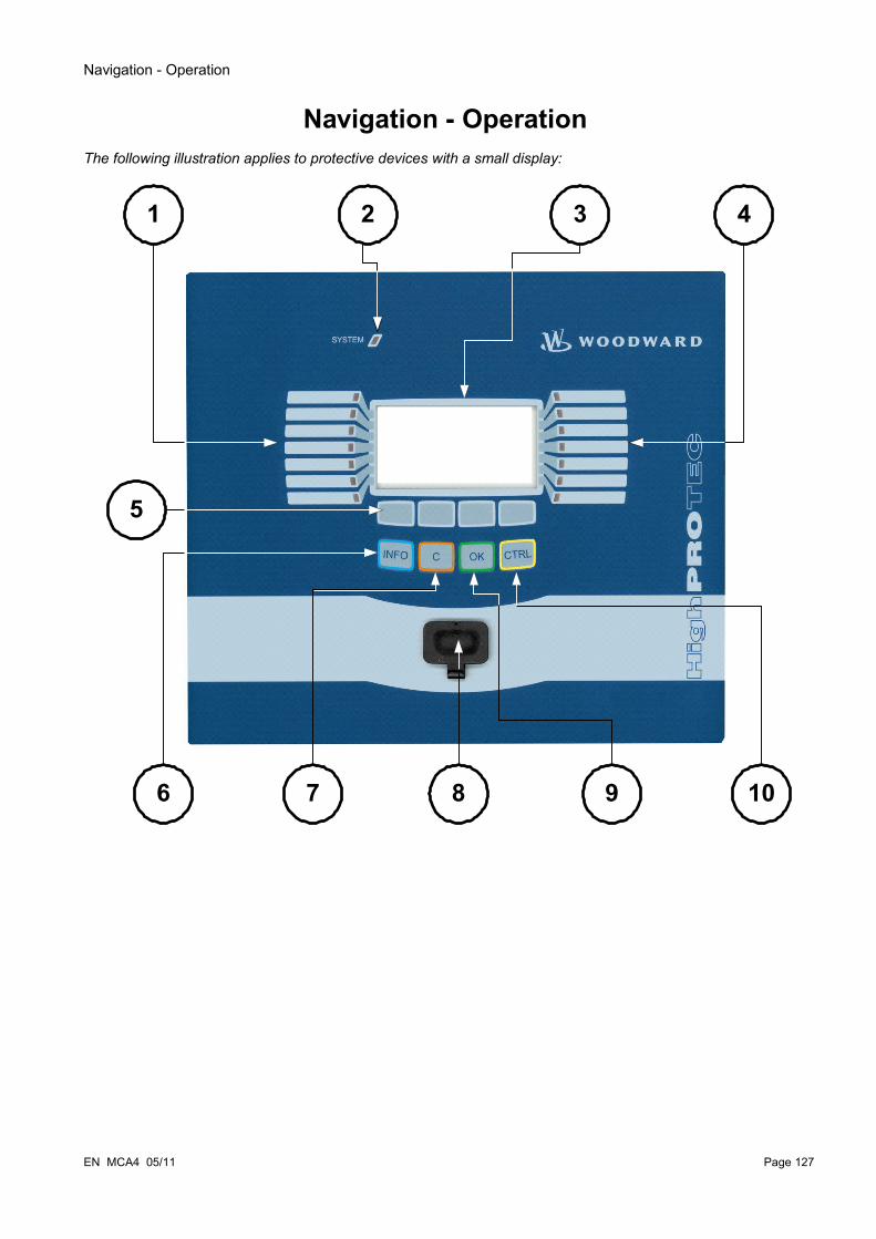
Navigation - Operation
Navigation - Operation The following illustration applies to protective devices with a small display:
EN MCA4 05/11 Page 127
1 2 3
5
76 8 109
4
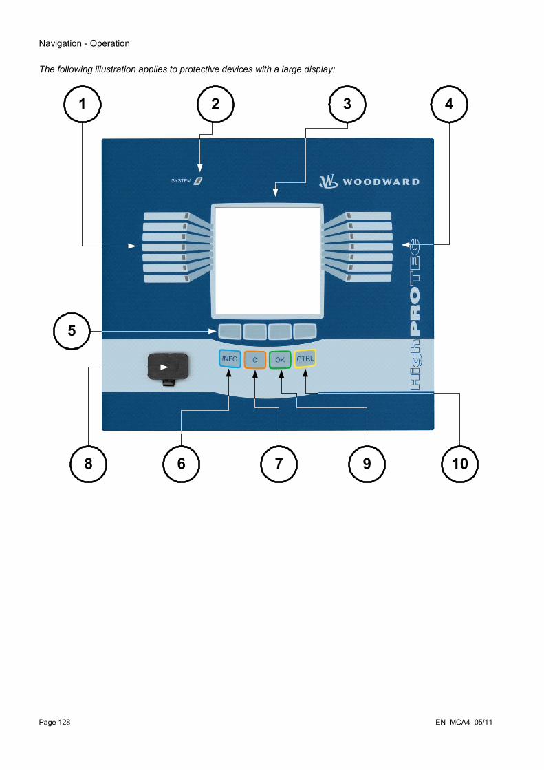
Navigation - Operation
The following illustration applies to protective devices with a large display:
Page 128 EN MCA4 05/11
1 2 3
5
68 7 109
4
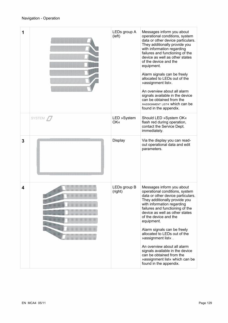
Navigation - Operation
1 LEDs group A (left)
Messages inform you about operational conditions, system data or other device particulars. They additionally provide you with information regarding failures and functioning of the device as well as other states of the device and the equipment.
Alarm signals can be freely allocated to LEDs out of the »assignment list«.
An overview about all alarm signals available in the device can be obtained from the»ASSIGNMENT LIST« which can be found in the appendix.
LED »System OK«
Should LED »System OK« flash red during operation, contact the Service Dept. immediately.
3 Display Via the display you can read-out operational data and edit parameters.
4 LEDs group B (right)
Messages inform you about operational conditions, system data or other device particulars. They additionally provide you with information regarding failures and functioning of the device as well as other states of the device and the equipment.
Alarm signals can be freely allocated to LEDs out of the »assignment list« .
An overview about all alarm signals available in the device can be obtained from the »assignment list« which can be found in the appendix.
EN MCA4 05/11 Page 129

Navigation - Operation
5 Softkeys The function of the »SOFTKEYS« are contextual. On the bottom line of the display the present function is displayed/symbolized.
Possible functions are:
• Navigation
• Parameter decrement/increment.
• Scrolling up/down a menu page
• Moving to a digit
• Change into the parameter setting mode »wrench symbol«.
Page 130 EN MCA4 05/11

Navigation - Operation
6 INFO Key (Signals/Messages)
Looking through the present LED assignment. The direct select key can be actuated at any time.
If the INFO key is actuated once, the »LEFT LED SIGNALS« are inserted, if the INFO key is actuated again, the »RIGHT LED SIGNALS« are inserted. If the INFO key is actuated again you will leave the LED menu.
Here only the first assignments of the LEDs will be shown. Every three seconds the »SOFTKEYs« will be shown (flashing).
Displaying the multiple Assignments
If the INFO-Button is pressed only the first assignments of any LED is shown. Every three seconds the »SOFTKEYs« will be shown (flashing).
If there is more than one signal assigned to a LED (indicated by three dots) you can check the state of the multiple assignments if you proceed as follows.
In order to show all (multiple) assignments select a LED by means of the »SOFTKEYs« »up« and »down«
Via the »Softkey« »right« call up a Submenu of this LED that gives you detailed information on the state of all signals assigned to this LED. An arrow symbol points to the LED whose assignments are currently displayed.
Via the »SOFTKEYs« »up« and »down« you can call up the next / previous LED.
In order to leave the LED menu press the »SOFTKEY« »left« multiple times.
EN MCA4 05/11 Page 131

Navigation - Operation
7 »C Key« To abort changes and to ac-knowledge messages.
In order to reset please press the Softkey »wrench« and enter the password.
The reset menu can be left by pressing the Softkey »Arrow-left«
8 RS232 Interface (Smart view Connection)
Connection to software Smart view is done via the RS232 interface.
9 »OK Key« When using the »OK« key parameter changes are temporarily stored. If the »OK« key is pressed again, those changes are stored definitely.
10 »CTRL Key«* For future applications
*=Not for all devices available.
Page 132 EN MCA4 05/11

Navigation - Operation
Basic Menu Control The graphic user interface is equivalent to a hierarchical structured menu tree. For access to the individual submenus the »SOFTKEYS«/Navigation Keys are used. The function of the »SOFTKEYS« can be found as symbol in the footer of the display.
Softkey Description• Via »SOFTKEY« »up« you will come to the prior menu point/one parameter up by scrolling
upwards. • Via »SOFTKEY« »left« you will go one step back.
• Via »SOFTKEY« »down« you will change to the next menu point/one parameter down by scrolling downwards.
• Via »SOFTKEY« »right« you will come to a submenu.
• Via »SOFTKEY« »Top of list« you will jump directly to the top of a list.
• Via »SOFTKEY« »Bottom of list« you will jump directly to the end of a list.
• Via »SOFTKEY« »+«the related digit will be incremented. (Continuous pressure -> fast).
• Via »SOFTKEY« »-«the related digit will be decremented. (Continuous pressure -> fast)
• Via »SOFTKEY« »left« you will go one digit to the left.
• Via »SOFTKEY« »right« you will go one digit to the right.
• Via »SOFTKEY« »Parameter setting« you will call up the parameter setting mode.
• Via »SOFTKEY« »delete« data will be deleted.
In order to return to the main menu, just keep pressing the Softkey »Arrow-Left« until you arrive at the »main menu».
EN MCA4 05/11 Page 133

Navigation - Operation
Smart view Keyboard CommandsYou can control Smart view alternatively by means of keyboard commands (instead of the mouse)
Key Description
á Moving up within the navigation tree or parameter list.
â
Moving down within the navigation tree or parameter list.
ß
Collapse the tree item or select a folder on a higher level.
à Expands the tree item or selects a subfolder.
Numpad + Expands the tree item.
Numpad - Collapses the tree item.
Home Moves to the top of the active window.
End Moves to the bottom of the active window.
Ctrl+O Opens the file opening dialog. Browsing through the file system for an existing device file.
Ctrl+N Creates a new parameter file file by means of a template.
Ctrl+S Saves actual loaded parameter file.
F1 Displays the online help information.
F2 Load Device Data
F5 Reloads the displayed data of a device.
Ctrl+F5 Enables automatic refresh.
Ctrl+Shift+T Back to the navigation window.
Ctrl+F6 Walks through the tabular forms (detail windows).
Page á Previous value (parameter setting).
Page â Next value (parameter setting).
Page 134 EN MCA4 05/11
Smart View
Smart ViewSmart view is a parameter setting and evaluation software.
• Menu-controlled parameter setting incl. validity checks• Offline configuration of all relay types• Reading and evaluating of statistical data and measuring values• Setting into operation assistance• Display of the device status• Fault analysis via event- and fault recorder
Smart view 3.0 or higher supports reading parameter files generated by older versions of Smart view. Parameter files generated by Smart view 3.0 and higher cannot be read by older versions of Smart view.
Installation of Smart ViewPort 52152 must not be blocked by a Firewall
If the Windows Vista User Access Control pops up while installing Smart view, please “Allow” all installation requirements concerning Smart view.
System requirements: Windows 2000 or compatible (e.g. Windows XP, Windows Vista or Windows 7)
• Double-click on the installation file with the left mouse button.
• Select a language for the installation procedure.
• Confirm by pressing the »Continue« button in the INFO frame.
• Select an installation path or confirm the standard installation path by mouse click on the »Continue« button.
• Confirm the entry for the suggested installation folder by mouse click on the »Continue« button.
• By mouse click on the »Install« button, the installation routine is started.
• Close the installation procedure by mouse click on the »Complete« button.
Now you can call up the program via [Start>Programs>Woodward>HighPROTEC>Smart view].
Deinstalling Smart viewVia the menu [Start>System Control >Software] the Smart view can be removed from your computer.
Switching the Language of the Graphical User InterfaceWithin the menu Settings/Language, you can change the language of the graphical user interface.
EN MCA4 05/11 Page 135

Smart View
Setting up the Connection PC - Device
Set-up a Connection via Ethernet - TCP/IP
Establishing a connection via TCP/IP to the device is only possible if your device is equipped with an Ethernet Interface (RJ45).
Contact your IT administrator in order to establish the network connection.
Part 1: Set the TCP/IP Parameters at the panel (Device)
Call up the menu »Device parameter/TCP/IP« at the HMI (panel) and set the following parameters:
• TCP/IP address
• Subnetmask
• Gateway
Part 2: Setting the IP address within Smart view
• Call up the menu Settings/Device Connection within Smart view.
• Set radio button Network Connection.
• Enter the IP-Address of the device that should be connected.
Page 136 EN MCA4 05/11
Smart View
Set-up a Connection via Serial Interface under Windows 2000
After installation of the software, the »Connection PC/Notebook to the Device« has to be configured once, so that you are able to read device data or re-write them into the device by means of the software Smart view.
For connection of your PCs/notebooks with the device you need a special zero-modem cable (no serial cable!/please refer to chapter »Zero Modem Cable«).
If your PC/notebook does not have a serial interface, you need a special USB-to-serial-adapter. Only if the USB-to-serial-adapter is correctly installed - aided by the provided CD – the communication with the device can be established. (see next chapter).
The connection Notebook/PC to the device must not be protected/encrypted via a smartcard.
If the network connection wizard asks you, to encrypt the connection via a smartcard or not, please choose »Do not use the smartcard«.
Setting up/Configuring the connection
• Connect your PC/notebook with the device via a zero-modem cable.
• Start the software Smart view.
• Select the menu point »Device Connection« in menu »Settings«.
• Click on »Serial Connection«.
• Click button »Settings«.
• When initially setting up the connection, a dialogue window appears with the information that, so far, a direct connection with your protection device has not been established. Click on »Yes«.
• If, so far, a location has not been set up on your PC, your location information has to be put in. Confirm the pop-up window »Telephone and Modem Options« with »OK«.
• The Windows network connection assistant appears after the location information is set up. Select the connection type »Establish direct connection to another computer«.
• Select the serial interface (COM-Port) where the device shall be connected to.
• Select »To be used for all users« in window »Availability of the connection«.
• Do not change the connection name appearing in window »Name of the connection« and click the button »Complete«.
• Finally you arrive again in window »Device Installation« from where you started establishing the connection. Confirm the adjustments by clicking the »OK« button.
Due to an bug in Windows 2000 it is possible that the automatically made communication settings are not correctly adopted. In order to overcome this problem, proceed as follows after setting up the serial connection:
EN MCA4 05/11 Page 137
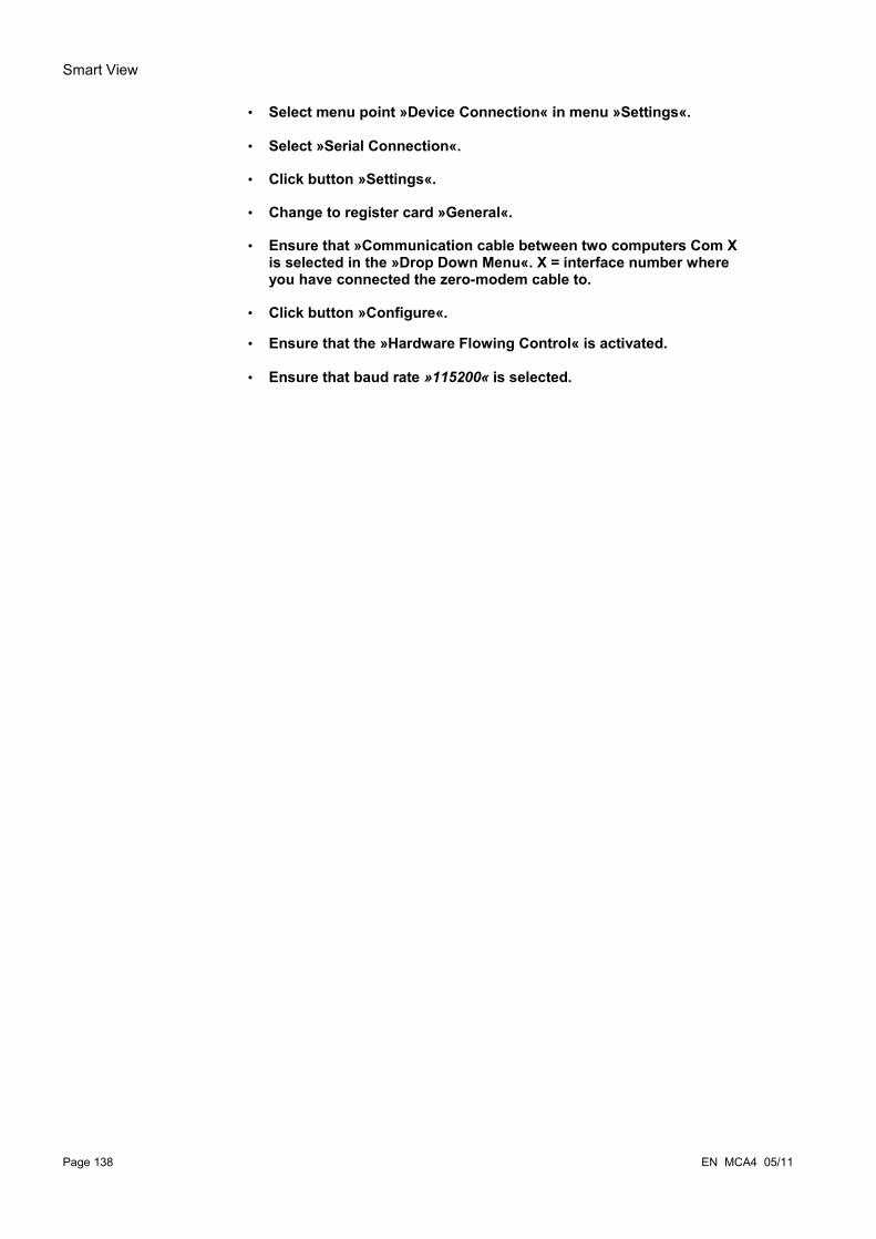
Smart View
• Select menu point »Device Connection« in menu »Settings«.
• Select »Serial Connection«.
• Click button »Settings«.
• Change to register card »General«.
• Ensure that »Communication cable between two computers Com X is selected in the »Drop Down Menu«. X = interface number where you have connected the zero-modem cable to.
• Click button »Configure«.
• Ensure that the »Hardware Flowing Control« is activated.
• Ensure that baud rate »115200« is selected.
Page 138 EN MCA4 05/11

Smart View
Set up a Connection via Serial Interface under Windows XP
After installation of the software, the »Connection PC/Notebook to the Device« has to be configured once so that you are able to read device data or re-write them into the device by means of the software Smart view.
For connection of your PCs/notebooks with the device, you need a zero-modem cable (no serial cable!/please refer to chapter »Zero Modem Cable«).
If your PC/notebook does not have a serial interface, you need a special »USB-to-serial-adapter«. Only if the »USB-to-serial-adapter« is correctly installed - aided by the provided CD – the communication with the device can be established. (see next chapter).
Setting up/Configuring the connection
• Connect your PC/notebook with the device via a zero-modem cable.
• Start the software Smart view.
• Select the menu point »Device Connection« in menu »Settings«.
• Click on »Serial Connection«.
• Click button »Settings«.
• When initially setting up the connection, a dialogue window appears with the information that, so far, a direct connection with your protection device has not been established. Click on »Yes«.
• If, so far, a location has not been set up on your PC, your location information has to be put in. Confirm the following pop-up window »Telephone and Modem Options« with »OK«.
• The Windows network connection assistant appears after the location information is set up. Select the connection type »Establish direct connection to another computer«.
• Select the serial interface (COM-Port) where the device shall be connected to.
• Select »To be used for all users« in window »Availability of the connection«.
• Do not change the connection name appearing in window »Name of the connection« and click the button »Complete«.
• Finally you arrive again in window »Device Installation« from where you started establishing the connection. Confirm the adjustments by clicking the »OK« button.
EN MCA4 05/11 Page 139

Smart View
Set up a Connection via Serial Interface under Windows Vista or Windows 7
Establishing the connection between Smart view and the device is a three step procedure.
1. Installing Smart view (the application itself)
2. Installing a (virtual) modem (that is a precondition for TCP/IP communication via a zero-modem cable)/ ((to be done within the Windows Phone and Modem dialog).
3. Establishing a network connection between Smart view and the device (to be done within Smart view).
1. Installation of Smart view (the application itself).Please see above.
2. Installation of the (virtual) modem
• Open the Windows Start menu and type “Phone and Modem” and RETURN. This opens the “Phone and Modem” Dialog
• Go to Tab »Modem«
• Click on the »Add« button
• The Hardware Wizard window Install New Modem pops up
• Set the check box Don´t detect my modem; I will select it from a list
• Click on the »Next« button
• Select Communications cable between two computers
• Click on the »Next« button
• Choose the correct COM-Port
• Click on the »Next« button
• Click on the »Finish« button
• Select the new added modem and click on the »Properties« button
• Go to Tab »General«
• Click on the »Change settings« button
• Go to Tab »Modem«
• Set within the Drop-Down Menu the correct baud rate = 115200
• Close this dialog with the »OK« button
• Close the Phone and Modem dialog with the »OK« button
• You have to reboot your computer now!
Page 140 EN MCA4 05/11
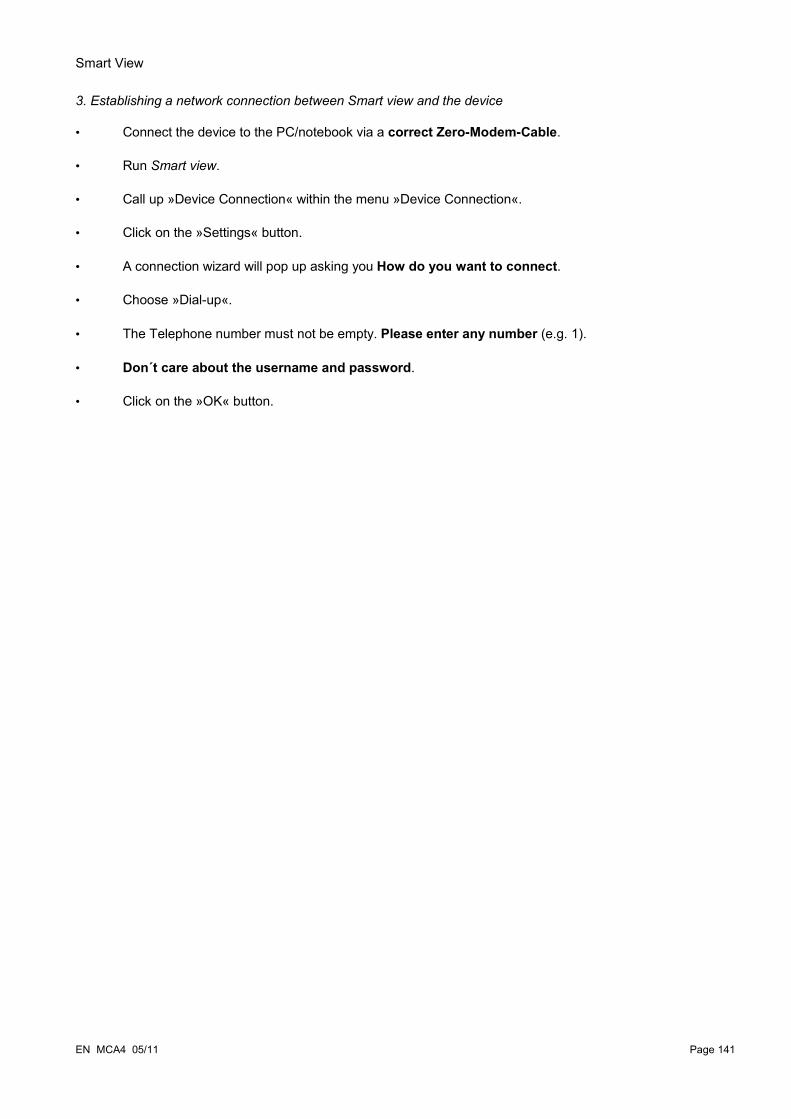
Smart View
3. Establishing a network connection between Smart view and the device
• Connect the device to the PC/notebook via a correct Zero-Modem-Cable.
• Run Smart view.
• Call up »Device Connection« within the menu »Device Connection«.
• Click on the »Settings« button.
• A connection wizard will pop up asking you How do you want to connect.
• Choose »Dial-up«.
• The Telephone number must not be empty. Please enter any number (e.g. 1).
• Don´t care about the username and password.
• Click on the »OK« button.
EN MCA4 05/11 Page 141

Smart View
Connected to the Device and Calling up Websites at the same Time
In principle, it is possible to call up websites while there is an active connection to the device.
If your computer has no direct connection to the internet, that means, that it is placed behind a proxy server, the device connection has to be modified in certain circumstances. The device connection has to be provided with the proxy settings.
Internet ExplorerFor each connection the proxy settings have to be set manually. Please proceed as follows:
• Start your Internet Explorer.
• Call up the »Tools« menu.
• Call up the menu »Internet options«.
• Call up the tab »Connections«.
• Click with the left hand mouse key on the button »Settings« on the right of the »HighPROTEC-Device-Connection«.
• Set the check box »Use Proxy Server for this connection.
• Enter the proxy settings that are available by your network administrator.
• Confirm the settings by pressing »OK«.
FirefoxThe proxy settings are centrally managed, so there is no need to modify any settings.
Establishing the Connection via a USB-/RS232-Adapter
If your PC/notebook is not provided with a serial interface, this can be compensated by a special USB-/RS232-Adapter+Zero Modem-Cable.
Only an adapter accepted by Woodward Kempen GmbH may be used. First install the adapter (with the related driver that you can find on the CD) and then establish the connection (Smart view => Device). The adapters must support very high speed.
Page 142 EN MCA4 05/11

Smart View
Set-up a Connection via Ethernet - TCP/IP
Warning: Mixing up IP-Addresses (In case that there is more than one protective device within the TCP/IP network). Establishing an unintentional wrong connection to a protective device based on a wrong entered IP-Address. Transferring parameters into a wrong protective device might lead to death, personal injury or damage of electrical equipment.
In order to prevent faulty connections the user has to document and maintain a list with the IP addresses of any switchboard/protective device.
The user has to doublecheck the IP addresses of the connection that is to be established. That means, the user must first read out the IP address at the HMI of the device (within menu [Device para/TCP IP] then compare the IP address with the list. If the addresses are identical, establish the connection. If not, DO not connect.
Establishing a connection via TCP/IP to the device is only possible if your device is equipped with an Ethernet Interface (RJ45).
Contact your IT administrator in order to establish the network connection.
Part 1: Set the TCP/IP Parameters at the panel (Device)
Call up the menu »Device parameter/TCP/IP« at the HMI (panel) and set the following parameters:
•TCP/IP address
•Subnet mask
•Gateway
Part 2: Setting the IP address within Smart view
• Call up the menu Settings/Device Connection within Smart view.
• Set radio button Network Connection.
• Enter the IP-Address of the device that should be connected.
EN MCA4 05/11 Page 143

Smart View
Smart view Troubleshooting (XP and Windows 2000)
• Make sure whether the Windows service Telephony is started. In [Start>System Control >Administration >Services] the service »Telephony« must be visible and must have also been started. If not, the service has to be started.
• For establishing the connection, you need to have sufficient rights (administration rights).
• If a firewall is installed on your computer, TCP/IP port 52152 must have been released.
• If your computer is not provided with a serial interface, you need a USB-to-serial-adapter, accepted by Woodward Kempen GmbH. This adapter has to be properly installed.
• Ensure that a zero-modem cable is used (a standard serial cable without control wires does not enable communication).
If »WINDOWS 2000 is running on your computer and a serial interface for direct connection to another computer has not been established so far, the following problem can arise:
If you have selected a serial interface in the connection assistant, it may happen that this is not entered correctly in the dial-up network due to an bug in the Windows operating system. Your attention is drawn to this problem by the operational software and the error message »Warning, invalid connection setting« will be shown.
To solve this problem, you need administration rights.
Please proceed as follows:
• Select menu point »Device Connection« in menu »Settings«.
• Select »Serial Connection«.
• Click button »Settings«.
• Change to register card »General«.
• Ensure that »Communication cable between two computers (Com X)“ is selected in the »Drop Down Menu«. »X« = interface number where you have connected the zero-modem cable to.
Page 144 EN MCA4 05/11

Smart View
If the message »Warning, invalid connection settings« appears during establishing the connection, this indicates that the connection adjustments you have chosen are not correct.
On this warning you can react as follows:
»Yes«: (to set up the connection completely new).By this, all adjustments are cancelled and the connection assistant is opened again for renewed adjustment of the connection to the device.
This procedure is advisable in case basic adjustments cannot be modified via the characteristics dialogue (e.g. if a new additional serial interface has been installed on the system).
»No«: (to modify the existing dial-up network entry).Opens the dialogue for characteristics of the connection settings. During the dialogue it is possible to correct invalid settings (e.g. the recommended baud rate).
»Cancel«:The warning is ignored and the connection adjustments remain as they are. This procedure is accepted for a limited time, but in such a case, the user is obliged to establish a correct connection later on.
EN MCA4 05/11 Page 145

Smart View
Smart view persistent connection problems
In case of persistent connection problems you should remove all connection settings and establish them again afterwards. In order to remove all connection settings please proceed as follows:
1. Remove the settings for the Dial-up Network
• Close Smart view
• Call up the »Control Panel«
• Choose »Network & Internet«
• On the left side click on »Manage Network Connections«•• Click on HighPROTEC Direct Connection with the right hand mouse key•• Choose Delete from the shortcut menu
• Click on the OK button
2. Remove the virtual modem
• Call up the »Control Panel«
• Choose »Hardware & Sound«
• Choose »Phone & Modem Options«
• Go to Tab Modem
• Click on the correct (in case there is more than one) entry Connection cable between two computers
• Click on the Remove button
Page 146 EN MCA4 05/11

Smart View
Loading of Device Data when using Smart view • Starting of the Smart view.
• Make sure the connection has been established properly.
• Connect your PC with the device via a zero-modem cable.
• Select »Receiving Data From The Device« in menu »Device«.
EN MCA4 05/11 Page 147
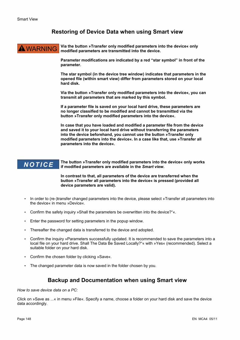
Smart View
Restoring of Device Data when using Smart view
Via the button »Transfer only modified parameters into the device« only modified parameters are transmitted into the device.
Parameter modifications are indicated by a red “star symbol” in front of the parameter.
The star symbol (in the device tree window) indicates that parameters in the opened file (within smart view) differ from parameters stored on your local hard disk.
Via the button »Transfer only modified parameters into the device«, you can transmit all parameters that are marked by this symbol.
If a parameter file is saved on your local hard drive, these parameters are no longer classified to be modified and cannot be transmitted via the button »Transfer only modified parameters into the device«.
In case that you have loaded and modified a parameter file from the device and saved it to your local hard drive without transferring the parameters into the device beforehand, you cannot use the button »Transfer only modified parameters into the device«. In a case like that, use »Transfer all parameters into the device«.
The button »Transfer only modified parameters into the device« only works if modified parameters are available in the Smart view.
In contrast to that, all parameters of the device are transferred when the button »Transfer all parameters into the device« is pressed (provided all device parameters are valid).
• In order to (re-)transfer changed parameters into the device, please select »Transfer all parameters into the device« in menu »Device«.
• Confirm the safety inquiry »Shall the parameters be overwritten into the device?“«.
• Enter the password for setting parameters in the popup window.
• Thereafter the changed data is transferred to the device and adopted.
• Confirm the inquiry »Parameters successfully updated. It is recommended to save the parameters into a local file on your hard drive. Shall The Data Be Saved Locally?“« with »Yes« (recommended). Select a suitable folder on your hard disk.
• Confirm the chosen folder by clicking »Save«.
• The changed parameter data is now saved in the folder chosen by you.
Backup and Documentation when using Smart viewHow to save device data on a PC:
Click on »Save as ...« in menu »File«. Specify a name, choose a folder on your hard disk and save the device data accordingly.
Page 148 EN MCA4 05/11
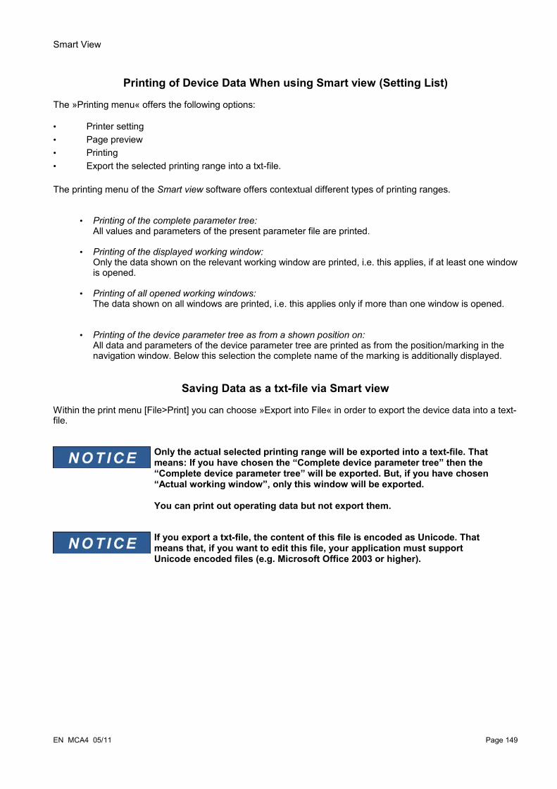
Smart View
Printing of Device Data When using Smart view (Setting List)
The »Printing menu« offers the following options:
• Printer setting• Page preview• Printing • Export the selected printing range into a txt-file.
The printing menu of the Smart view software offers contextual different types of printing ranges.
• Printing of the complete parameter tree:All values and parameters of the present parameter file are printed.
• Printing of the displayed working window: Only the data shown on the relevant working window are printed, i.e. this applies, if at least one window is opened.
• Printing of all opened working windows: The data shown on all windows are printed, i.e. this applies only if more than one window is opened.
• Printing of the device parameter tree as from a shown position on:All data and parameters of the device parameter tree are printed as from the position/marking in the navigation window. Below this selection the complete name of the marking is additionally displayed.
Saving Data as a txt-file via Smart view
Within the print menu [File>Print] you can choose »Export into File« in order to export the device data into a text-file.
Only the actual selected printing range will be exported into a text-file. That means: If you have chosen the “Complete device parameter tree” then the “Complete device parameter tree” will be exported. But, if you have chosen “Actual working window”, only this window will be exported.
You can print out operating data but not export them.
If you export a txt-file, the content of this file is encoded as Unicode. That means that, if you want to edit this file, your application must support Unicode encoded files (e.g. Microsoft Office 2003 or higher).
EN MCA4 05/11 Page 149
Smart View
Offline Device Planning via Smart viewIn order to be able to transmit a parameter file (e.g. offline created) into the device the following issues must comply:
• Type Code (written on the top of the device/type label) and
• Version of the device model (can be found in menu [Device Parameters\Version].
The Smart view software enables also to parameterize offline. The advantage is: By using device models you can do planning jobs for a device and set parameters in advance.
You can also read the parameter file out of the device, further process it offline (e.g. from your office) and finally re-transfer it to the device.
You can either:
• load an existing parameter file from a device (please refer to chapter [Loading device data when using Smart view]).
• create a new parameter file (see below),• open a locally saved parameter file (backup).
In order to create a new device/parameter file by way of a device template offline:
• In order to create a new offline parameter file please choose within the »file-menu« »create new parameter file«.
• A working window pops up. Please make sure, that you select the right device type with the correct version and configuration.
• Finally click on »Apply«
• In order to save the device configuration select »Save« out of the »File-Menu«.
• Within the menu »Modify Device Configuration (Typecode)« you can modify the device configuration or simply find out the type code of your current selection.
If you want to transfer the parameter file into a device, please refer to chapter “Restoring of device data when using Smart view”.
Page 150 EN MCA4 05/11

Measuring Values
Measuring Values
Read out Measured ValuesIn menu »Operation/Measured Values« both measured and calculated values can be viewed. The measured values are ordered by »Standard values« and »special values« (depending on the type of device).
Read out of Measured Values via Smart view
• In case Smart view is not running – please start it.
• If the device data were not yet loaded – select »Receive Data From The Device« from menu »Device«.
• Double click on icon »Operation« in the navigation tree.
• Double click on icon »Measured Values« within the navigation tree »Operation«.
• Double click the »Standard Values« or special values within the »Measured values«.
• The measured and calculated values are shown now in tabular form on the window.
To have the measuring data read in a cyclic manner, select »Auto refresh« in menu »View«. The measured values are read out about every two seconds.
Measurement Display
Menu [Device Para\Measurem Display] offers options to change the display of measured values within the HMI and Smart view.
Scaling of Measured values
By means of the parameter »Scaling« the user can determine how measured values are to be displayed within the HMI and Smart view:
• Primary quantities• Secondary quantities• Per Unit quantities
Cutoff level
In order to suppress noise within measured values that are close to zero the user has the option to set cutoff levels. By means of the cutoff levels, measuring quantities that are close to zero will be displayed as zero. These parameters have no impact on recorded values.
Current - Measured Values Current
If the device is not equipped with an voltage measuring card the first measuring input on the first current measuring card (slot with the lowest number) will be used as the reference angle (»IL1«).
EN MCA4 05/11 Page 151

Measuring Values
Value Description Menu path
IL1 Measured value: Phase current (fundamental)
[Operation
/Measured values
/Current ]
IL2 Measured value: Phase current (fundamental)
[Operation
/Measured values
/Current ]
IL3 Measured value: Phase current (fundamental)
[Operation
/Measured values
/Current ]
IG meas Measured value (measured): IG (fundamental)
[Operation
/Measured values
/Current ]
IG calc Measured value (calculated): IG (fundamental)
[Operation
/Measured values
/Current ]
I0 Measured value (calculated): Zero current (fundamental)
[Operation
/Measured values
/Current ]
I1 Measured value (calculated): Positive phase sequence current (fundamental)
[Operation
/Measured values
/Current ]
I2 Measured value (calculated): Unbalanced load current (fundamental)
[Operation
/Measured values
/Current ]
IL1 H2 Measured value: 2nd harmonic/1st harmonic of IL1
[Operation
/Measured values
/Current ]
IL2 H2 Measured value: 2nd harmonic/1st harmonic of IL2
[Operation
/Measured values
/Current ]
IL3 H2 Measured value: 2nd harmonic/1st harmonic of IL3
[Operation
/Measured values
/Current ]
Page 152 EN MCA4 05/11

Measuring Values
IG H2 meas Measured value: 2nd harmonic/1st harmonic of IG (measured)
[Operation
/Measured values
/Current ]
IG H2 calc Measured value (calculated): 2nd harmonic/1st harmonic of IG (calculated)
[Operation
/Measured values
/Current ]
phi IL1 Measured value (calculated): Angle of Phasor IL1
[Operation
/Measured values
/Current ]
phi IL2 Measured value (calculated): Angle of Phasor IL2
[Operation
/Measured values
/Current ]
phi IL3 Measured value (calculated): Angle of Phasor IL3
[Operation
/Measured values
/Current ]
phi IG meas Measured value: Angle of Phasor IG meas [Operation
/Measured values
/Current ]phi IG calc Measured value (calculated): Angle of
Phasor IG calc[Operation
/Measured values
/Current ]
phi I0 Measured value (calculated): Angle Zero Sequence System
[Operation
/Measured values
/Current ]
phi I1 Measured value (calculated): Angle of Positive Sequence System
[Operation
/Measured values
/Current ]
phi I2 Measured Value (calculated): Angle of Negative Sequence System
[Operation
/Measured values
/Current ]
IL1 RMS Measured value: Phase current (RMS) [Operation
/Measured values
/Current RMS]IL2 RMS Measured value: Phase current (RMS) [Operation
/Measured values
/Current RMS]
EN MCA4 05/11 Page 153
Measuring Values
IL3 RMS Measured value: Phase current (RMS) [Operation
/Measured values
/Current RMS]IG meas RMS Measured value (measured): IG (RMS) [Operation
/Measured values
/Current RMS]IG calc RMS Measured value (calculated): IG (RMS) [Operation
/Measured values
/Current RMS]%IL1 THD Measured value (calculated): IL1 Total
Harmonic Distortion[Operation
/Measured values
/Current RMS]
%IL2 THD Measured value (calculated): IL2 Total Harmonic Distortion
[Operation
/Measured values
/Current RMS]
%IL3 THD Measured value (calculated): IL3 Total Harmonic Distortion
[Operation
/Measured values
/Current RMS]
IL1 THD Measured value (calculated): IL1 Total Harmonic Current
[Operation
/Measured values
/Current RMS]
IL2 THD Measured value (calculated): IL2 Total Harmonic Current
[Operation
/Measured values
/Current RMS]
IL3 THD Measured value (calculated): IL3 Total Harmonic Current
[Operation
/Measured values
/Current RMS]
%(I2/I1) Measured value (calculated): I2/I1 if ABC, I1/I2 if CBA
[Operation
/Measured values
/Current ]
Page 154 EN MCA4 05/11

Measuring Values
Voltage - Measured Values Voltage
The first measuring input on the first measuring card (slot with the lowest number) is used as the reference angle.E.g. »VL1« respectively »VL12«.
Value Description Menu path
f Measured value: Frequency [Operation
/Measured values
/Voltage ]VL12 Measured value: Phase-to-phase voltage
(fundamental)[Operation
/Measured values
/Voltage ]
VL23 Measured value: Phase-to-phase voltage (fundamental)
[Operation
/Measured values
/Voltage ]
VL31 Measured value: Phase-to-phase voltage (fundamental)
[Operation
/Measured values
/Voltage ]
VL1 Measured value: Phase-to-neutral voltage (fundamental)
[Operation
/Measured values
/Voltage ]
VL2 Measured value: Phase-to-neutral voltage (fundamental)
[Operation
/Measured values
/Voltage ]
VL3 Measured value: Phase-to-neutral voltage (fundamental)
[Operation
/Measured values
/Voltage ]
VX meas Measured value (measured): VG measured (fundamental)
[Operation
/Measured values
/Voltage ]
VG calc Measured value (calculated): VG (fundamental)
[Operation
/Measured values
/Voltage ]
V0 Measured value (calculated): Symmetrical components Zero voltage(fundamental)
[Operation
/Measured values
/Voltage ]
EN MCA4 05/11 Page 155

Measuring Values
V1 Measured value (calculated): Symmetrical components positive phase sequence voltage(fundamental)
[Operation
/Measured values
/Voltage ]
V2 Measured value (calculated): Symmetrical components negative phase sequence voltage(fundamental)
[Operation
/Measured values
/Voltage ]
VL12 RMS Measured value: Phase-to-phase voltage (RMS)
[Operation
/Measured values
/Voltage RMS]
VL23 RMS Measured value: Phase-to-phase voltage (RMS)
[Operation
/Measured values
/Voltage RMS]
VL31 RMS Measured value: Phase-to-phase voltage (RMS)
[Operation
/Measured values
/Voltage RMS]
VL1 RMS Measured value: Phase-to-neutral voltage (RMS)
[Operation
/Measured values
/Voltage RMS]
VL2 RMS Measured value: Phase-to-neutral voltage (RMS)
[Operation
/Measured values
/Voltage RMS]
VL3 RMS Measured value: Phase-to-neutral voltage (RMS)
[Operation
/Measured values
/Voltage RMS]
VX meas RMS Measured value (measured): VG measured (RMS)
[Operation
/Measured values
/Voltage RMS]
VG calc RMS Measured value (calculated): VG (RMS) [Operation
/Measured values
/Voltage RMS]phi VL12 Measured value (calculated): Angle of
Phasor VL12[Operation
/Measured values
/Voltage ]
Page 156 EN MCA4 05/11

Measuring Values
phi VL23 Measured value (calculated): Angle of Phasor VL23
[Operation
/Measured values
/Voltage ]
phi VL31 Measured value (calculated): Angle of Phasor VL31
[Operation
/Measured values
/Voltage ]
phi VL1 Measured value (calculated): Angle of Phasor VL1
[Operation
/Measured values
/Voltage ]
phi VL2 Measured value (calculated): Angle of Phasor VL2
[Operation
/Measured values
/Voltage ]
phi VL3 Measured value (calculated): Angle of Phasor VL3
[Operation
/Measured values
/Voltage ]
phi VX meas Measured value: Angle of Phasor VX meas [Operation
/Measured values
/Voltage ]phi VG calc Measured value (calculated): Angle of
Phasor VG calc[Operation
/Measured values
/Voltage ]
phi V0 Measured value (calculated): Angle Zero Sequence System
[Operation
/Measured values
/Voltage ]
phi V1 Measured value (calculated): Angle of Positive Sequence System
[Operation
/Measured values
/Voltage ]
phi V2 Measured Value (calculated): Angle of Negative Sequence System
[Operation
/Measured values
/Voltage ]
%(V2/V1) Measured value (calculated): %V2/V1 if ABC, %V1/V2 if CBA
[Operation
/Measured values
/Voltage ]
% VL12 THD Measured value (calculated): V12 Total Harmonic Distortion / Ground wave
[Operation
/Measured values
/Voltage RMS]
EN MCA4 05/11 Page 157

Measuring Values
% VL23 THD Measured value (calculated): V23 Total Harmonic Distortion / Ground wave
[Operation
/Measured values
/Voltage RMS]
% VL31 THD Measured value (calculated): V31 Total Harmonic Distortion / Ground wave
[Operation
/Measured values
/Voltage RMS]
% VL1 THD Measured value (calculated): VL1 Total Harmonic Distortion / Ground wave
[Operation
/Measured values
/Voltage RMS]
% VL2 THD Measured value (calculated): VL2 Total Harmonic Distortion / Ground wave
[Operation
/Measured values
/Voltage RMS]
% VL3 THD Measured value (calculated): VL3 Total Harmonic Distortion / Ground wave
[Operation
/Measured values
/Voltage RMS]
VL12 THD Measured value (calculated): V12 Total Harmonic Distortion
[Operation
/Measured values
/Voltage RMS]
VL23 THD Measured value (calculated): V23 Total Harmonic Distortion
[Operation
/Measured values
/Voltage RMS]
VL31 THD Measured value (calculated): V31 Total Harmonic Distortion
[Operation
/Measured values
/Voltage RMS]
VL1 THD Measured value (calculated): VL1 Total Harmonic Distortion
[Operation
/Measured values
/Voltage RMS]
VL2 THD VL2 THD [Operation
/Measured values
/Voltage RMS]VL3 THD VL3 THD [Operation
/Measured values
/Voltage RMS]
Page 158 EN MCA4 05/11

Measuring Values
Power - Measured Values
Value Description Menu path
S Measured Value (Calculated): Apparent power (fundamental)
[Operation
/Measured values
/Power]
P Measured value (calculated): Active power (P- = Fed Active Power, P+ = Consumpted Active Power) (fundamental)
[Operation
/Measured values
/Power]
Q Measured value (calculated): Reactive power (Q- = Fed Reactive Power, Q+ = Consumpted Reactive Power) (fundamental)
[Operation
/Measured values
/Power]
cos phi Measured value (calculated): Power factor [Operation
/Measured values
/Power]Wp+ Positive Active Power is consumed active
energy [Operation
/Measured values
/Energy]
Wp- Negative Active Power (Fed Energy) [Operation
/Measured values
/Energy]Wq+ Positive Reactive Power is consumed
Reactive Energy[Operation
/Measured values
/Energy]
Wq- Negative Reactive Power (Fed Energy) [Operation
/Measured values
/Energy]Ws Net Absolute Apparent Power Hours [Operation
/Measured values
/Energy]Wp Net Absolute Active Power Hours [Operation
/Measured values
/Energy]Wq Net Absolute Reactive Power Hours [Operation
/Measured values
/Energy]
EN MCA4 05/11 Page 159

Measuring Values
Start Date/Time Energy counters run since... (Date and time of last reset)
[Operation
/Measured values
/Energy]
S RMS Measured Value (Calculated): Apparent power (RMS)
[Operation
/Measured values
/Power RMS]
P RMS Measured value (calculated): Active power (P- = Fed Active Power, P+ = Consumpted Active Power) (RMS)
[Operation
/Measured values
/Power RMS]
Q RMS Measured value (calculated): Reactive power (Q- = Fed Reactive Power, Q+ = Consumpted Reactive Power) (RMS)
[Operation
/Measured values
/Power RMS]
cos phi RMS Measured value (calculated): Power factor [Operation
/Measured values
/Power RMS]P 1 Measured value (calculated): Active power
in positive sequence system (P- = Fed Active Power, P+ = Consumpted Active Power)
[Operation
/Measured values
/Power]
Q 1 Measured value (calculated): Reactive power in positive sequence system (Q- = Fed Reactive Power, Q+ = Consumpted Reactive Power)
[Operation
/Measured values
/Power]
Page 160 EN MCA4 05/11
Energy Counter
Energy Counter
PQSCr
Global Parameters of the Energy Counter Module
Parameter Description Setting range Default Menu path
S, P, Q Cutoff Level
The Active/Reactive/Apparent Power shown in the Display or within the PC Software will be displayed as zero, if the absolute value of the corresponding Power falls below this Cutoff Level. This parameter has no impact on recorders.
0.0 - 0.100Sn 0.005Sn [Device Para
/Measurem Display]
Direct Commands of the Energy Counter Module
Parameter Description Setting range Default Menu path
Res all Energy Cr
Reset of all Energy Counters inactive,
active
inactive [Operation
/Reset]
EN MCA4 05/11 Page 161
Energy Counter
Signals of the Energy Counter Module (States of the Outputs)
Name Description
Cr OflwW Ws Net Signal: Counter Overflow Ws NetCr OflwW Wp Net Signal: Counter Overflow Wp NetCr OflwW Wp+ Signal: Counter Overflow Wp+Cr OflwW Wp- Signal: Counter Overflow Wp-Cr OflwW Wq Net Signal: Counter Overflow Wq NetCr OflwW Wq+ Signal: Counter Overflow Wq+Cr OflwW Wq- Signal: Counter Overflow Wq-Ws Net Res Cr Signal: Ws Net Reset CounterWp Net Res Cr Signal: Wp Net Reset CounterWp+ Res Cr Signal: Wp+ Reset CounterWp- Res Cr Signal: Wp- Reset CounterWq Net Res Cr Signal: Wq Net Reset CounterWq+ Res Cr Signal: Wq+ Reset CounterWq- Res Cr Signal: Wq- Reset CounterRes all Energy Cr Signal: Reset of all Energy CountersCr OflwW Ws Net Signal: Counter Ws Net will overflow soonCr OflwW Wp Net Signal: Counter Wp Net will overflow soonCr OflwW Wp+ Signal: Counter Wp+ will overflow soonCr OflwW Wp- Signal: Counter Wp- will overflow soonCr OflwW Wq Net Signal: Counter Wq Net will overflow soonCr OflwW Wq+ Signal: Counter Wq+ will overflow soonCr OflwW Wq- Signal: Counter Wq- will overflow soon
Page 162 EN MCA4 05/11
Statistics
Statistics Statistics
In menu »Operation/Statistics« the min., max. and mean values of the measured and calculated measured quantities can be found. The statistics are ordered by »Standard values« and »special values« (depending on the type of device and the device planning).
In menu »Device Parameter/Statistics« you can either set a fixed synchronization time and a calculation interval or start and stop the statistics via a function (e.g. digital input).
Read out Statistics• Call up the main menu.
• Call up the submenu »Operation/Statistics«.
• Call up the »Standard values« or »Special values«
Statistics to be Read-Out via Smart view
• In case Smart view is not running – please start it.
• If device data have not yet been loaded – click »Receive Data From The Device« in menu »Device«.
• Double click on icon »Operation« in the navigation tree
• Double click on icon »Statistics« within the navigation tree »Operation«
• Double click on icon »Standard values« or »Special values«
• In the window the statistical data is shown in tabular form
The values can be read out cyclically. For this purpose, please select »Auto Refresh« out of the menu »View«.
EN MCA4 05/11 Page 163

Statistics
Statistics (Configuration)The Statistic-module can be configured within the menu »Device Parameter/Statistics«.
The time interval, that is taken into account for the calculation of the statistics can either be limited by a fixed duration or it can be limited by a start function (freely assignable signal from the »assignment list«).
Fixed duration:
If the statistic module is set to a fixed duration/time interval, the minimum, maximum and average values will be calculated and displayed continuously on the basis of this duration/time interval.
Start function (flexible duration):
If the statistic module is to be started by a start function the statistics will be updated not until the start function becomes true (rising edge). At the same time a new time interval will be started.
Statistics (Configuration) via Smart view
In case Smart view is not running – please start it
• If device data has not been loaded yet – click »Receive Data From The Device« in menu »Device«
• Double click on icon »Device Parameter« in the navigation tree
• Double click on icon »Statistics« within the navigation tree »Device Parameter«
• Configure the Statistics-module
Page 164 EN MCA4 05/11

Statistics
Direct Commands
Parameter Description Setting range Default Menu path
ResFc all Resetting of all Statistic values (Current Demand, Power Demand, Min, Max)
inactive,
active
inactive [Operation
/Reset]
ResFc I Demand
Resetting of Statistics - Current Demand (avg, peak avg)
inactive,
active
inactive [Operation
/Reset]
ResFc P Demand
Resetting of Statistics - Power Demand (avg, peak avg)
inactive,
active
inactive [Operation
/Reset]
ResFc Min Resetting of all Minimum values inactive,
active
inactive [Operation
/Reset]
ResFc Max Resetting of all Maximum values inactive,
active
inactive [Operation
/Reset]
EN MCA4 05/11 Page 165
Statistics
Global Protection Parameters of the Statistics Module
Parameter Description Setting range Default Menu path
ResFc Max Resetting of all Maximum values 1..n, Assignment List -.- [Device Para
/Statistics
/Min / Max]ResFc Min Resetting of all Minimum values 1..n, Assignment List -.- [Device Para
/Statistics
/Min / Max]Min Max Definition
Definition of the time base that is used for calculating the minimum and maximum values.
Sliding window,
Peak values
Sliding window
[Device Para
/Statistics
/Min / Max]
Start I Demand via:
Start Current demand by: Duration,
StartFct
Duration [Device Para
/Statistics
/Demand
/Current Demand]Start I Demand Fc
Start of the calculation, if the assigned signal becomes true.
Only available if: Start I Demand via: = StartFct
1..n, Assignment List -.- [Device Para
/Statistics
/Demand
/Current Demand]ResFc I Demand
Resetting of Statistics - Current Demand (avg, peak avg)
1..n, Assignment List -.- [Device Para
/Statistics
/Demand
/Current Demand]
Page 166 EN MCA4 05/11
Statistics
Parameter Description Setting range Default Menu path
Duration I Demand
Recording time
Only available if: Start I Demand via: = Duration
2 s,
5 s,
10 s,
15 s,
30 s,
1 min,
5 min,
10 min,
15 min,
30 min,
1 h,
2 h,
6 h,
12 h,
1 d,
2 d,
5 d,
7 d,
10 d,
30 d
15 s [Device Para
/Statistics
/Demand
/Current Demand]
Window I Demand
Window configuration sliding,
fixed
sliding [Device Para
/Statistics
/Demand
/Current Demand]Start P Demand via:
Start Active Power demand by: Duration,
StartFct
Duration [Device Para
/Statistics
/Demand
/Power Demand]Start P Demand Fc
Start of the calculation, if the assigned signal becomes true.
Only available if: Start P Demand via: = StartFct
1..n, Assignment List -.- [Device Para
/Statistics
/Demand
/Power Demand]ResFc P Demand
Resetting of Statistics - Power Demand (avg, peak avg)
1..n, Assignment List -.- [Device Para
/Statistics
/Demand
/Power Demand]
EN MCA4 05/11 Page 167

Statistics
Parameter Description Setting range Default Menu path
Duration P Demand
Recording time
Only available if: Start P Demand via: = Duration
2 s,
5 s,
10 s,
15 s,
30 s,
1 min,
5 min,
10 min,
15 min,
30 min,
1 h,
2 h,
6 h,
12 h,
1 d,
2 d,
5 d,
7 d,
10 d,
30 d
15 s [Device Para
/Statistics
/Demand
/Power Demand]
Window P Demand
Window configuration sliding,
fixed
sliding [Device Para
/Statistics
/Demand
/Power Demand]
Page 168 EN MCA4 05/11

Statistics
States of the Inputs of the Statistics Module
Name Description Assignment via
StartFc 1-I State of the module input: Start of Statistics 1
[Device Para
/Statistics
/Demand
/Current Demand]StartFc 2-I State of the module input: Start of Statistics
2[Device Para
/Statistics
/Demand
/Power Demand]ResFc I Demand-I State of the module input: Resetting of
Statistics - Current Demand (avg, peak avg)
[Device Para
/Statistics
/Demand
/Current Demand]ResFc P Demand-I State of the module input: Resetting of
Statistics - Power Demand (avg, peak avg)[Device Para
/Statistics
/Demand
/Power Demand]ResFc Max-I State of the module input: Resetting of all
Maximum values [Device Para
/Statistics
/Min / Max]ResFc Min-I State of the module input: Resetting of all
Minimum values [Device Para
/Statistics
/Min / Max]
Signals of the Statistics Module
Name Description
ResFc all Signal: Resetting of all Statistic values (Current Demand, Power Demand, Min, Max)
ResFc I Demand Signal: Resetting of Statistics - Current Demand (avg, peak avg)ResFc P Demand Signal: Resetting of Statistics - Power Demand (avg, peak avg)ResFc Max Signal: Resetting of all Maximum values ResFc Min Signal: Resetting of all Minimum values
EN MCA4 05/11 Page 169
Statistics
Counters of the Module Statistics
Value Description Menu path
MeasPointNo Each measuring point that is taken over by the statistics increments this counter. By means of this counter, the User can check whether the statistics are alive and if data are being acquired.
[Operation
/Count and RevData
/Statistics]
Res Cr I Demand Number of resets since last booting. The timestamp shows date and time of the last reset.
[Operation
/Statistics
/Demand
/Current Demand]Res Cr P Demand Number of resets since last booting. The
timestamp shows date and time of the last reset.
[Operation
/Statistics
/Demand
/Power Demand]Res Cr Min values Number of resets since last booting. The
timestamp shows date and time of the last reset.
[Operation
/Statistics
/Min
/ThR]Res Cr Max values Number of resets since last booting. The
timestamp shows date and time of the last reset.
[Operation
/Statistics
/Max
/ThR]
Page 170 EN MCA4 05/11
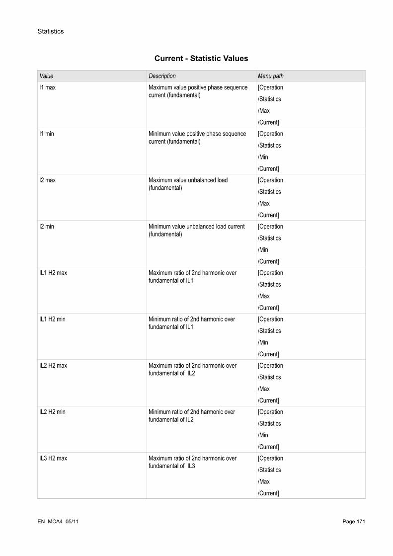
Statistics
Current - Statistic Values
Value Description Menu path
I1 max Maximum value positive phase sequence current (fundamental)
[Operation
/Statistics
/Max
/Current]I1 min Minimum value positive phase sequence
current (fundamental)[Operation
/Statistics
/Min
/Current]I2 max Maximum value unbalanced load
(fundamental)[Operation
/Statistics
/Max
/Current]I2 min Minimum value unbalanced load current
(fundamental)[Operation
/Statistics
/Min
/Current]IL1 H2 max Maximum ratio of 2nd harmonic over
fundamental of IL1[Operation
/Statistics
/Max
/Current]IL1 H2 min Minimum ratio of 2nd harmonic over
fundamental of IL1[Operation
/Statistics
/Min
/Current]IL2 H2 max Maximum ratio of 2nd harmonic over
fundamental of IL2[Operation
/Statistics
/Max
/Current]IL2 H2 min Minimum ratio of 2nd harmonic over
fundamental of IL2[Operation
/Statistics
/Min
/Current]IL3 H2 max Maximum ratio of 2nd harmonic over
fundamental of IL3[Operation
/Statistics
/Max
/Current]
EN MCA4 05/11 Page 171
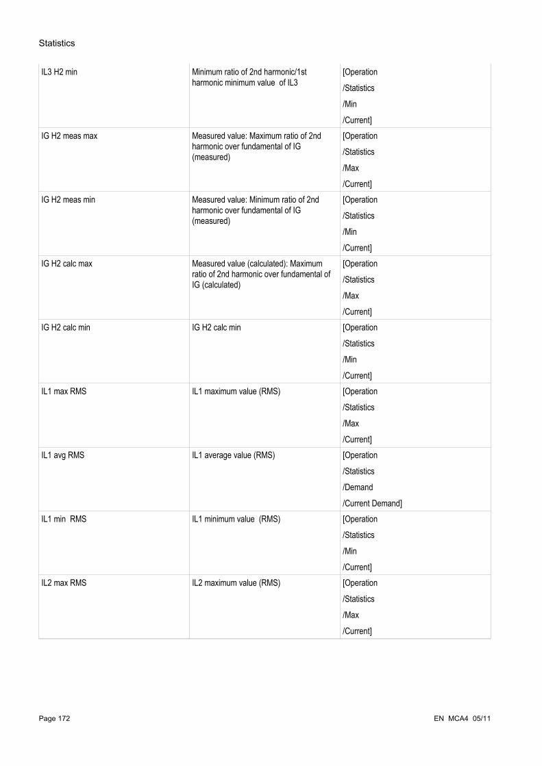
Statistics
IL3 H2 min Minimum ratio of 2nd harmonic/1st harmonic minimum value of IL3
[Operation
/Statistics
/Min
/Current]IG H2 meas max Measured value: Maximum ratio of 2nd
harmonic over fundamental of IG (measured)
[Operation
/Statistics
/Max
/Current]IG H2 meas min Measured value: Minimum ratio of 2nd
harmonic over fundamental of IG (measured)
[Operation
/Statistics
/Min
/Current]IG H2 calc max Measured value (calculated): Maximum
ratio of 2nd harmonic over fundamental of IG (calculated)
[Operation
/Statistics
/Max
/Current]IG H2 calc min IG H2 calc min [Operation
/Statistics
/Min
/Current]IL1 max RMS IL1 maximum value (RMS) [Operation
/Statistics
/Max
/Current]IL1 avg RMS IL1 average value (RMS) [Operation
/Statistics
/Demand
/Current Demand]IL1 min RMS IL1 minimum value (RMS) [Operation
/Statistics
/Min
/Current]IL2 max RMS IL2 maximum value (RMS) [Operation
/Statistics
/Max
/Current]
Page 172 EN MCA4 05/11
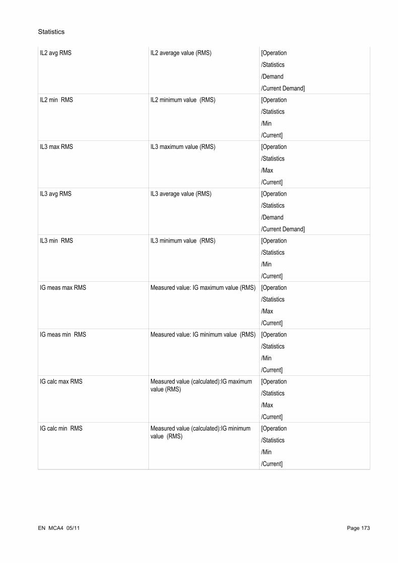
Statistics
IL2 avg RMS IL2 average value (RMS) [Operation
/Statistics
/Demand
/Current Demand]IL2 min RMS IL2 minimum value (RMS) [Operation
/Statistics
/Min
/Current]IL3 max RMS IL3 maximum value (RMS) [Operation
/Statistics
/Max
/Current]IL3 avg RMS IL3 average value (RMS) [Operation
/Statistics
/Demand
/Current Demand]IL3 min RMS IL3 minimum value (RMS) [Operation
/Statistics
/Min
/Current]IG meas max RMS Measured value: IG maximum value (RMS) [Operation
/Statistics
/Max
/Current]IG meas min RMS Measured value: IG minimum value (RMS) [Operation
/Statistics
/Min
/Current]IG calc max RMS Measured value (calculated):IG maximum
value (RMS)[Operation
/Statistics
/Max
/Current]IG calc min RMS Measured value (calculated):IG minimum
value (RMS)[Operation
/Statistics
/Min
/Current]
EN MCA4 05/11 Page 173
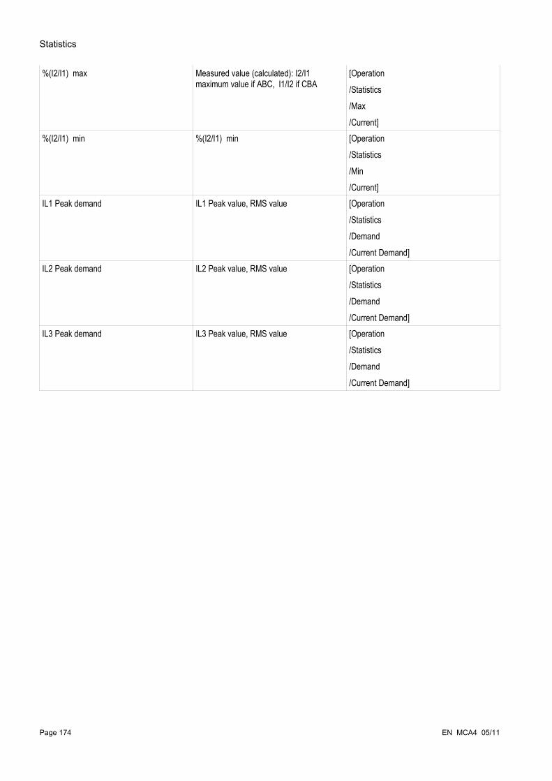
Statistics
%(I2/I1) max Measured value (calculated): I2/I1 maximum value if ABC, I1/I2 if CBA
[Operation
/Statistics
/Max
/Current]%(I2/I1) min %(I2/I1) min [Operation
/Statistics
/Min
/Current]IL1 Peak demand IL1 Peak value, RMS value [Operation
/Statistics
/Demand
/Current Demand]IL2 Peak demand IL2 Peak value, RMS value [Operation
/Statistics
/Demand
/Current Demand]IL3 Peak demand IL3 Peak value, RMS value [Operation
/Statistics
/Demand
/Current Demand]
Page 174 EN MCA4 05/11
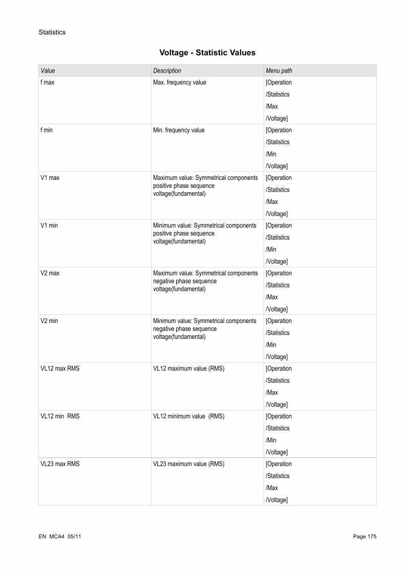
Statistics
Voltage - Statistic Values
Value Description Menu path
f max Max. frequency value [Operation
/Statistics
/Max
/Voltage]f min Min. frequency value [Operation
/Statistics
/Min
/Voltage]V1 max Maximum value: Symmetrical components
positive phase sequence voltage(fundamental)
[Operation
/Statistics
/Max
/Voltage]V1 min Minimum value: Symmetrical components
positive phase sequence voltage(fundamental)
[Operation
/Statistics
/Min
/Voltage]V2 max Maximum value: Symmetrical components
negative phase sequence voltage(fundamental)
[Operation
/Statistics
/Max
/Voltage]V2 min Minimum value: Symmetrical components
negative phase sequence voltage(fundamental)
[Operation
/Statistics
/Min
/Voltage]VL12 max RMS VL12 maximum value (RMS) [Operation
/Statistics
/Max
/Voltage]VL12 min RMS VL12 minimum value (RMS) [Operation
/Statistics
/Min
/Voltage]VL23 max RMS VL23 maximum value (RMS) [Operation
/Statistics
/Max
/Voltage]
EN MCA4 05/11 Page 175

Statistics
VL23 min RMS VL23 minimum value (RMS) [Operation
/Statistics
/Min
/Voltage]VL31 max RMS VL31 maximum value (RMS) [Operation
/Statistics
/Max
/Voltage]VL31 min RMS VL31 minimum value (RMS) [Operation
/Statistics
/Min
/Voltage]VL1 max RMS VL1 maximum value (RMS) [Operation
/Statistics
/Max
/Voltage]VL1 min RMS VL1 minimum value (RMS) [Operation
/Statistics
/Min
/Voltage]VL2 max RMS VL2 maximum value (RMS) [Operation
/Statistics
/Max
/Voltage]VL2 min RMS VL2 minimum value (RMS) [Operation
/Statistics
/Min
/Voltage]VL3 max RMS VL3 maximum value (RMS) [Operation
/Statistics
/Max
/Voltage]VL3 min RMS VL3 minimum value (RMS) [Operation
/Statistics
/Min
/Voltage]
Page 176 EN MCA4 05/11
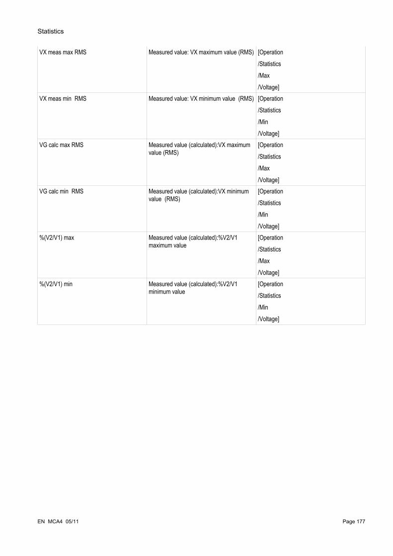
Statistics
VX meas max RMS Measured value: VX maximum value (RMS) [Operation
/Statistics
/Max
/Voltage]VX meas min RMS Measured value: VX minimum value (RMS) [Operation
/Statistics
/Min
/Voltage]VG calc max RMS Measured value (calculated):VX maximum
value (RMS)[Operation
/Statistics
/Max
/Voltage]VG calc min RMS Measured value (calculated):VX minimum
value (RMS)[Operation
/Statistics
/Min
/Voltage]%(V2/V1) max Measured value (calculated):%V2/V1
maximum value[Operation
/Statistics
/Max
/Voltage]%(V2/V1) min Measured value (calculated):%V2/V1
minimum value [Operation
/Statistics
/Min
/Voltage]
EN MCA4 05/11 Page 177

Statistics
Power - Statistic Values
Value Description Menu path
cos phi max Maximum value of the power factor [Operation
/Statistics
/Max
/Power]cos phi min Minimum value of the power factor [Operation
/Statistics
/Min
/Power]S max Maximum value of the apparent power [Operation
/Statistics
/Max
/Power]S avg Average of the apparent power [Operation
/Statistics
/Demand
/Power Demand]S min Minimum value of the apparent power [Operation
/Statistics
/Min
/Power]P max Maximum value of the active power [Operation
/Statistics
/Max
/Power]P avg Average of the active power [Operation
/Statistics
/Demand
/Power Demand]P min Minimum value of the active power [Operation
/Statistics
/Min
/Power]Q max Maximum value of the reactive power [Operation
/Statistics
/Max
/Power]
Page 178 EN MCA4 05/11

Statistics
Q avg Average of the reactive power [Operation
/Statistics
/Demand
/Power Demand]Q min Minimum value of the reactive power [Operation
/Statistics
/Min
/Power]cos phi max RMS Maximum value of the power factor [Operation
/Statistics
/Max
/Power]cos phi min RMS Minimum value of the power factor [Operation
/Statistics
/Min
/Power]VA Peak demand VA Peak value, RMS value [Operation
/Statistics
/Demand
/Power Demand]Watt Peak demand WATTS Peak value, RMS value [Operation
/Statistics
/Demand
/Power Demand]VAr Peak demand VARs Peak value, RMS value [Operation
/Statistics
/Demand
/Power Demand]
EN MCA4 05/11 Page 179

System Alarms
System AlarmsAvailable Elements: SysA
Within the System Alarms menu [SysA] the User can configure:
• General Settings (activate/inactivate the Demand Management, optional assign a signal, that will block the Demand Management);
• Power Protection (Peak values);
• Demand Management (Power and Current); and
• THD Protection.
Please note, that all thresholds are to be set as primary values.
Demand ManagementDemand is the average of system current or power over a time interval (window). Demand management supports the User to keep energy demand below target values bound by contract (with the energy supplier). If the contractual target values are exceeded, extra charges are to be paid to the energy supplier.
Therefore, demand management helps the User detect and avoid averaged peak loads that are taken into account for the billing. In order to reduce the demand charge respective to demand rate, peak loads, if possible, should be diversified. That means, if possible, avoiding large loads at the same time. In order to assist the User in analyzing the demand, demand management might inform the User by an alarm. The User might also use demand alarms and assign them on relays in order to perform load shedding (where applicable).
Demand management comprises:
• Power Demand• Watt Demand (Active Power);• VAr Demand (Reactive Power);• VA Demand (Apparent Power); and
• Current Demand.
Configuring the Demand
Configuring the demand is a two step procedure. Proceed as follows.Step1: Configure the general settings within the [Device Para/Statistics/Demand] menu:
• Set the trigger source to »Duration«.• Select a time base for the »window«.• Determine if the window is »fixed« or »sliding«.• If applicable assign a reset signal.
The interval time (window) can be set to fixed or sliding.
Example for a fixed window: If the range is set for 15 minutes, the protective device calculates the average current or power over the past 15 minutes and updates the value every 15 minutes.
Example for a sliding window: If the sliding window is selected and the interval is set to 15 minutes, the protective device calculates and updates the average current or power continuously, for the past 15 minutes (the newest measuring value replaces the oldest measuring value continuously).
Page 180 EN MCA4 05/11
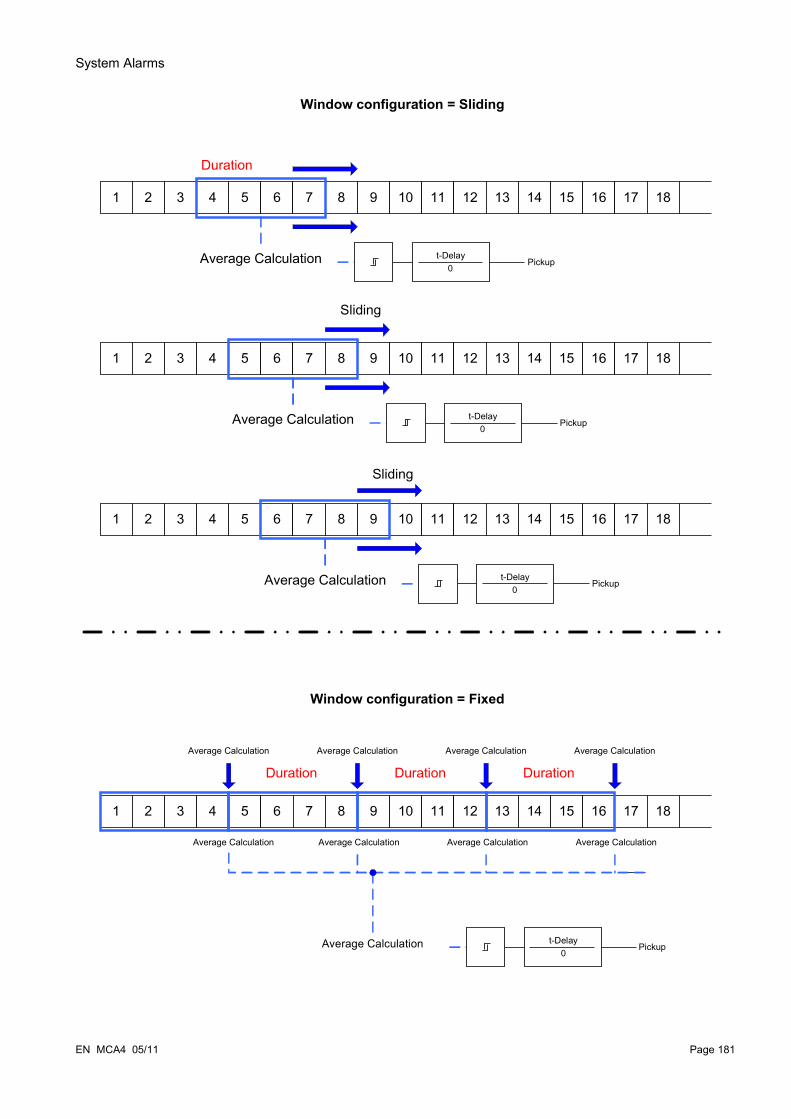
System Alarms
EN MCA4 05/11 Page 181
5 6 7 8 9 10 11 12 13 14 15 16 17 181 2 3 4
5 6 7 8 9 10 11 12 13 14 15 16 17 181 2 3 4
5 6 7 8 9 10 11 12 13 14 15 16 17 181 2 3 4
5 6 7 8 9 10 11 12 13 14 15 16 17 181 2 3 4
Window configuration = Sliding
Window configuration = Fixed
Sliding
Sliding
t-Delay0
Duration
Average Calculation Pickup
t-Delay0
Average Calculation Pickup
t-Delay0
Average Calculation Pickup
t-Delay0
Average Calculation Pickup
Average Calculation Average Calculation Average Calculation Average Calculation
Average Calculation Average Calculation Average Calculation Average Calculation
Duration Duration Duration

System Alarms
Step 2:
• In addition, the Demand specific settings have to be configured in the [SysA/Demand] menu.• Determine if the demand should generate an alarm or if it should run in the silent mode.
(Alarm active/inactive).• Set the threshold.• Where applicable, set a delay time for the alarm.
Peak ValuesThe protective device also saves the peak demand values for current and power. The quantities represent the largest demand value since the demand values were last reset. Peak demands for current and system power are date and time stamped.
Within the [Operation/Statistics] menu, the current Demand and Peak demand values can be seen.
Configuring the Peak Value Supervision
The supervision for the peak values can be configurated within menu [SysA/Power] in order to monitor:
• Active Power (Watt),• Reactive Power (VAr) • Apparent Powr (VA)
The specific settings are to be set within menu [SysA/Power].
• Determine if the peak value supervision should generate an alarm or if it should run in the silent mode. (Alarm active/inactive).
• Set the threshold.• Where applicable, set a delay time for the alarm.
Min. and Max. Values.Within [Operation/Statistics] menu the minimum (min.) and maximum (max.) values can be seen.
Minimum values since last reset: The minimum values are continuously compared to the last minimum value for that measuring value. If the new value is less than the last minimum, the value is updated. Within the [Device Para/Statistics/"Min / Max"] menu, a reset signal can be assigned.
Maximum values since last reset: The maximum values are continuously compared to the last maximum value for that measuring value. If the new value is greater than the last maximum, the value is updated. Within the [Device Para/Statistics/"Min / Max"] menu, a reset signal can be assigned.
Page 182 EN MCA4 05/11

System Alarms
THD ProtectionIn order to supervise power quality, the protective device can monitor the voltage (phase-to-phase) and current THDs.
Within the [SysA/THD] menu:
• Determine if an alarm is to be issued or not (Alarm active/inactive);• Set the threshold; and• Where applicable, set a delay time for the alarm.
Device Planning Parameters of the Demand Management
Parameter Description Options Default Menu path
Mode Mode do not use,
use
do not use [Device planning]
Signals of the Demand Management (States of the Outputs)
Name Description
active Signal: activeExBlo Signal: External BlockingAlarm Watt Power Signal: Alarm permitted Active Power exceededAlarm VAr Power Signal: Alarm permitted Reactive Power exceededAlarm VA Power Signal: Alarm permitted Apparent Power exceededAlarm Watt Demand Signal: Alarm averaged Active Power exceededAlarm VAr Demand Signal: Alarm averaged Reactive Power exceededAlarm VA Demand Signal: Alarm averaged Apparent Power exceededAlm Current Demd Signal: Alarm averaged demand current Alarm I THD Signal: Alarm Total Harmonic Distortion CurrentAlarm V THD Signal: Alarm Total Harmonic Distortion VoltageTrip Watt Power Signal: Trip permitted Active Power exceededTrip VAr Power Signal: Trip permitted Reactive Power exceededTrip VA Power Signal: Trip permitted Apparent Power exceededTrip Watt Demand Signal: Trip averaged Active Power exceededTrip VAr Demand Signal: Trip averaged Reactive Power exceededTrip VA Demand Signal: Trip averaged Apparent Power exceededTrip Current Demand Signal: Trip averaged demand current Trip I THD Signal: Trip Total Harmonic Distortion CurrentTrip V THD Signal: Trip Total Harmonic Distortion Voltage
EN MCA4 05/11 Page 183

System Alarms
Global Protection Parameter of the Demand Management
Parameter Description Setting range Default Menu path
Function Permanent activation or deactivation of module/stage.
inactive,
active
inactive [SysA
/General settings]
ExBlo Fc Activate (allow) or inactivate (disallow) blocking of the module/stage. This parameter is only effective if a signal is assigned to the corresponding global protection parameter. If the signal becomes true, those modules/stages are blocked that are parameterized "ExBlo Fc=active".
1..n, Assignment List -.- [SysA
/General settings]
Alarm Alarm inactive,
active
inactive [SysA
/Power
/Watt]Threshold Threshold (to be entered as primary value) 1 - 40000000kW 10000kW [SysA
/Power
/Watt]t-Delay Tripping Delay 0 - 60min 0min [SysA
/Power
/Watt]Alarm Alarm inactive,
active
inactive [SysA
/Power
/VAr]Threshold Threshold (to be entered as primary value) 1 - 40000000kVAr 10000kVAr [SysA
/Power
/VAr]t-Delay Tripping Delay 0 - 60min 0min [SysA
/Power
/VAr]Alarm Alarm inactive,
active
inactive [SysA
/Power
/VA]Threshold Threshold (to be entered as primary value) 1 - 40000000kVA 10000kVA [SysA
/Power
/VA]t-Delay Tripping Delay 0 - 60min 0min [SysA
/Power
/VA]
Page 184 EN MCA4 05/11

System Alarms
Parameter Description Setting range Default Menu path
Alarm Alarm inactive,
active
inactive [SysA
/Demand
/Power Demand
/Watt Demand]Threshold Threshold (to be entered as primary value) 1 - 40000000kW 10000kW [SysA
/Demand
/Power Demand
/Watt Demand]t-Delay Tripping Delay 0 - 60min 0min [SysA
/Demand
/Power Demand
/Watt Demand]Alarm Alarm inactive,
active
inactive [SysA
/Demand
/Power Demand
/VAr Demand]Threshold Threshold (to be entered as primary value) 1 - 40000000kVAr 20000kVAr [SysA
/Demand
/Power Demand
/VAr Demand]t-Delay Tripping Delay 0 - 60min 0min [SysA
/Demand
/Power Demand
/VAr Demand]Alarm Alarm inactive,
active
inactive [SysA
/Demand
/Power Demand
/VA Demand]Threshold Threshold (to be entered as primary value) 1 - 40000000kVA 20000kVA [SysA
/Demand
/Power Demand
/VA Demand]t-Delay Tripping Delay 0 - 60min 0min [SysA
/Demand
/Power Demand
/VA Demand]
EN MCA4 05/11 Page 185

System Alarms
Parameter Description Setting range Default Menu path
Alarm Alarm inactive,
active
inactive [SysA
/Demand
/Current Demand]Threshold Threshold (to be entered as primary value) 10 - 500000A 500A [SysA
/Demand
/Current Demand]t-Delay Tripping Delay 0 - 60min 0min [SysA
/Demand
/Current Demand]Alarm Alarm inactive,
active
inactive [SysA
/THD
/I THD]Threshold Threshold (to be entered as primary value) 1 - 500000A 500A [SysA
/THD
/I THD]t-Delay Tripping Delay 0 - 3600s 0s [SysA
/THD
/I THD]Alarm Alarm inactive,
active
inactive [SysA
/THD
/U THD]Threshold Threshold (to be entered as primary value) 1 - 500000V 10000V [SysA
/THD
/U THD]t-Delay Tripping Delay 0 - 3600s 0s [SysA
/THD
/U THD]
States of the Inputs of the Demand Management
Name Description Assignment via
ExBlo-I Module input state: External blocking [SysA
/General settings]
Page 186 EN MCA4 05/11

Acknowledgments
AcknowledgmentsCollective Acknowledgments for latched signals:
Collective Acknowledgments
LEDs Binary Output Relays
SCADA Pending Trip Command
LEDs+
Binary Output Relays+
SCADA+
Pending Trip Command
Via Smart view or at the panel all...can be acknowledged.
At the panel, the menu
[Operation\Acknowledge] can directly be
accessed via the »C« key
All LEDs at once:
Where? [Operation\
Acknowledge]
All Binary Output Relays at once:
Where? [Operation\
Acknowledge]
All SCADA signals at once:
Where? [Operation\
Acknowledge]
All pending trip commands at
once:
Where? [Operation\
Acknowledge]
All at once:
Where? [Operation\
Acknowledge]
External Acknowledgment: Via a signal from the assignment list (e.g. a digital Input) all... can be acknowledged.
All LEDs at once:
Where? Within the menu
Ex Acknowledge
All Binary Output Relays at once:
Where? Within the menu
Ex Acknowledge
All SCADA signals at once:
Where? Within the menu
Ex Acknowledge
All pending trip commands at
once:
Where? Within the menu
Ex Acknowledge
EN MCA4 05/11 Page 187

Acknowledgments
Options for individual acknowledgments for latched signals:
Individual Acknowledgment
LEDs Binary Output Relays Pending Trip Command
Via a signal from the assignment list (e.g.:a digital Input) a single... can be acknowledged.
Single LED:
Where? Within the configuration menu of this single LED.
Binary Output Relay:
Where? Within the configuration
menu of this single Binary Output Relay.
Pending Trip Command.
Where?Within the module
TripControl
As long as you are within the parameter setting mode, you cannot acknowledge.
In case of a fault during parameter setting via the operating panel, you must first leave the parameter mode by pressing either push-button »C« or »OK« before you may access to menu »Acknowledgments« via push-button.
Page 188 EN MCA4 05/11

Acknowledgments
Manual Acknowledgment• Press the C-Button at the panel.• Select the item to be acknowledged via the Softkeys:
• Binary output relays,• LEDs, • SCADA,• a pending trip command or• all (above) mentioned items at once.
• Press the Softkey with the »Wrench-Symbol«.• Enter your password.
Manual Acknowledgment via Smart view
• In case Smart view is not running – please start it
• If the device data were not yet loaded – select »Receive Data From The Device« from menu »Device«
• Double click on icon »Operation« in the navigation tree.
• Double click on icon »Acknowledgment« within the operation menu.
• Double click the entry within the popup that is to be acknowledged.
• Press the button »Execute immediately«.
• Enter your password.
EN MCA4 05/11 Page 189

Acknowledgments
External AcknowledgmentsWithin the menu [Ex Acknowledge] you can assign a signal (e.g. the state of a digital input) from the assignment list that:
• acknowledges all (acknowledgeable) LEDs at once;• acknowledges all (acknowledgeable) binary outputs at once:• acknowledges all (acknowledgeable) SCADA-signals at once.
Within the menu [Protection Para\Global Prot Para\TripControl] you can assign a signal that:
• acknowledges a pending trip command.
For details, please refer to chapter »TripControl«.
External Acknowledge via Smart viewIn case Smart view is not running – please start it.
• If the device data were not yet loaded – select »Receive Data From The Device« from menu »Device«
• Double click on icon »Device Parameter« in the navigation tree
• Double click on icon »Ex Acknowledge« within the operation menu
• In the working window you can assign now each one signal that resets all acknowledgeable LEDs, a signal that resets all binary outputs, a signal that resets the SCADA-signals respectively a signal that acknowledges a pending trip command.
Page 190 EN MCA4 05/11
1..n, Assignment List
Ack LED
1..n, Assignment List
Ack BO
1..n, Assignment List
Ack Scada
Ex Acknowledge.Ack LED
Ex Acknowledge.Ack BO
Ex Acknowledge.Ack Scada
Acknowledgments
Manual Resets In menu »Operation/Reset« you can:
• reset counters,• delete records (e.g. disturbance records) and • reset special things (like statistics, thermal replica...).
The description of the reset commands can be found within the corresponding modules.
Manual Resets via Smart view
• In case Smart view is not running – please start it
• If device data has not been loaded yet – click »Receive Data From The Device« in menu »Device«
• Double click the »Operation« icon in the navigation tree
• Double click the »Reset icon« within the operation menu
• Double click the entry within the popup that is to be reset or deleted.
The description of the reset commands can be found within the corresponding modules.
Reset to Factory Defaults
This Function will reset the device to the factory defaults.All records will be deleted and and the measured values and counters will be reset. The operation hours counter will be kept.
This Function is available at the HMI only.
• Press the »C-key« during a cold start, in order to access the »Reset« menu.
• Select »Reset to factory default«.
• Confirm »Reset device to factory defaults and reboot« with »Yes« in order to execute the reset to factory defaults.«
EN MCA4 05/11 Page 191

Status Display
Status Display In the status display within the »Operation« menu, the present state of all signals can be viewed. This means the User is able to see if the individual signals are active or inactive at that moment. The User can see all signals sorted by protective elements/modules.
Page 192 EN MCA4 05/11

Status Display
State of the module Input/Signal is... Is shown at the panel as...
false / »0«
true / »1«
Status Display via Smart View• In case Smart view is not running – please start it.
• If the device data were not yet loaded – select »Receive Data From The Device« from menu »Device«.
• Double click on icon »Operation« in the navigation tree
• Double click on the »Status Display« icon within the operational data.
• Double click on a subfolder (e.g. Prot) in order to see e.g. the states of the general alarms.
To have the status display updated in a cyclic manner select »Automatic Up-Date« in menu »VIEW«.
State of the module Input/Signal is... Is shown in Smart view as...
false / »0« 0true / »1« 1
No connection to the device ?
EN MCA4 05/11 Page 193

Operating Panel (HMI)
Operating Panel (HMI) HMI
Special Parameters of the PanelThis menu »Device Parameter/HMI« is used to define the contrast of the display, the maximum admissible edit time and the menu language (after expiry of which, all unsaved parameter changes will be rejected).
Direct Commands of the Panel
Parameter Description Setting range Default Menu path
Contrast Contrast 30 - 60 50 [Device Para
/HMI]
Global Protection Parameters of the Panel
Parameter Description Setting range Default Menu path
t-max Edit If no other key(s) is pressed at the panel, after expiration of this time, all cached (changed) parameters are canceled.
20 - 3600s 180s [Device Para
/HMI]
Menu language
Selection of the language English,
German,
Russian
English [Device Para
/HMI]
Page 194 EN MCA4 05/11

Recorders
Recorders
Disturbance Recorder Available elements: Disturb rec
The disturbance recorder works with 32 samples per cycle. The disturbance recorder can be started by one of eight start events (selection from the »assignment list«/OR-Logic).The disturbance record contains the measuring values inclusively pre-trigger-time. By means of Smart view/Datavisualizer (option) the oscillographic curves of the analogue (current, voltage) and digital channels/traces can be shown and evaluated in a graphical form. The disturbance recorder has a storage capacity of 120s. The disturbance recorder is able to record up to 10 s (adjustable) per record. The amount of records depends on the file size of each record.
The disturbance recorder can be parameterized in the menu »Device Parameter/Recorder/Disturb rec«.
Determine the max. recording time to register a disturbance event. The max. total length of a recording is 10s (inclusive pre-trigger and post-trigger time).
To trigger the disturbance recorder, up to 8 signals can be selected from the »assignment list«. The trigger events are OR-linked. If a disturbance record is written, a new disturbance record cannot be triggered until all trigger signals, which have triggered the previous disturbance record, are gone. Recording is only done for the time the assigned event exists (event controlled), plus the time for the pre- and post-trigger, but not longer than 10s. The time for forward run and tracking of the disturbance recorder is shown in percent of the total recording length.
The post-trigger time will be up to "Post-trigger time" depending on the duration of the trigger signal. The post-trigger will be the remaining time of the "Max file size" but at maximum "Post-trigger time"
EN MCA4 05/11 Page 195

Recorders
ExampleThe disturbance recorder is started by the general activation facility. After the fault has been cancelled (+ follow-up time), the recording process is stopped (but after 10s at the latest).
The parameter »Auto Delete« defines how the device shall react if there is no saving place available. In case »Auto Delete« is »active«, the first recorded disturbance will be overwritten according to the FIFO principle. If the parameter is set to »inactive«, recording of the disturbance events will be stopped until the storage location is released manually.
Page 196 EN MCA4 05/11
Start: 1Trigger
>1
Start: 2Trigger
Start: 3Trigger
Start: 4Trigger
Start: 5Trigger
Start: 6Trigger
Start: 7Trigger
Start: 8Trigger
Man Trigger
Recording>1

Recorders
Example Disturbance Recorder Timing Chart I
EN MCA4 05/11 Page 197
Start 1
t
t
0
1
0
1
300 ms
200 ms
Pre-trigger time
t
0
1500 ms
Post-trigger time
t
0
11000 ms
t-rec
t-rec < Max file size
t
0
12000 ms
Max file size
Start 1 = Prot.Trip
Start 2 = -.-
Start 3 = -.-
Start 4 = -.-
Start 5 = -.-
Start 6 = -.-
Start 7 = -.-
Start 8 = -.-
Post-trigger time = 25%
Pre-trigger time = 15%
Max file size = 2s
Auto overwriting = active
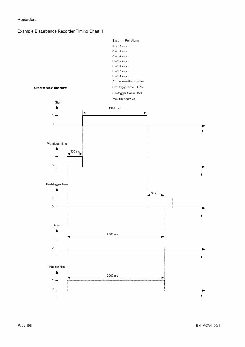
Recorders
Example Disturbance Recorder Timing Chart II
Page 198 EN MCA4 05/11
Start 1
t
t
0
1
0
1
300 ms
1335 ms
Pre-trigger time
t
0
1365 ms
Post-trigger time
t
0
12000 ms
t-rec
t
0
12000 ms
Max file size
Start 1 = Prot.Alarm
Start 2 = -.-
Start 3 = -.-
Start 4 = -.-
Start 5 = -.-
Start 6 = -.-
Start 7 = -.-
Start 8 = -.-
Post-trigger time = 25%
Pre-trigger time = 15%
Max file size = 2s
Auto overwriting = active
t-rec = Max file size

Recorders
Read Out Disturbance Records
Within the Menu Operation/Disturb rec you can
• Detect accumulated Disturbance Records.
Within the Menu »Operation/Recorders/Man Trigger« you can trigger the disturbance recorder manually.
Disturbance Recorder to be Read Out by Smart view
• In case Smart view is not running – please start it.
• If device data has not been loaded yet – click »Receive Data From The Device« in menu »Device«.
• Double click the »Operation« icon in the navigation tree.
• Double click the »Recorders« icon in the navigation tree.
• Double click the »Disturb rec-Icon«.
• In the window the disturbance records are shown in tabular form.
• A popup will be appear by a double click onto a disturbance record. Choose a folder where the disturbance record is to be saved to.
• You can analyze the disturbance records by means of the optionally available Data Visualizer by clicking on Yes when you are asked “Shall the received disturbance record be opened by the Data Visualizer?"
EN MCA4 05/11 Page 199

Recorders
Deleting Disturbance Records
Within the Menu Operation/Disturb rec you can
• Delete Disturbance Records.
• Choose via »SOFTKEY« »up« and »SOFTKEY« »down« the disturbance record that is to be deleted.
• Call up the detailed view of the disturbance record via »SOFTKEY« »right«.
• Confirm by pressing »SOFTKEY« »delete«
• Enter your password followed by pressing the key »OK«
• Choose whether only the current of whether all disturbance records should be deleted.
• Confirm by pressing »SOFTKEY« »OK«
Deleting Disturbance Records via Smart view
• In case Smart view is not running – please start it.
• If device data has not been loaded yet – click »Receive Data From The Device« in menu »Device«.
• Double click the »Operation« icon in the navigation tree.
• Double click the »Recorders« icon in the navigation tree.
• Double click the »Disturb rec-Icon«.
• In the window the disturbance records are shown in tabular form.
• In order to delete a disturbance record double click on:
(the red x) in front of the disturbance record and confirm.
Page 200 EN MCA4 05/11

Recorders
Direct Commands of the Disturbance Recorder
Parameter Description Setting range Default Menu path
Man Trigger Manual Trigger False,
True
False [Operation
/Recorders
/Man Trigger]Res all rec Reset all records inactive,
active
inactive [Operation
/Reset]
Global Protection Parameters of the Disturbance Recorder
Parameter Description Setting range Default Menu path
Start: 1 Start recording if the assigned signal is true. 1..n, Assignment List Prot.Alarm [Device Para
/Recorders
/Disturb rec]Start: 2 Start recording if the assigned signal is true. 1..n, Assignment List -.- [Device Para
/Recorders
/Disturb rec]Start: 3 Start recording if the assigned signal is true. 1..n, Assignment List -.- [Device Para
/Recorders
/Disturb rec]Start: 4 Start recording if the assigned signal is true. 1..n, Assignment List -.- [Device Para
/Recorders
/Disturb rec]Start: 5 Start recording if the assigned signal is true. 1..n, Assignment List -.- [Device Para
/Recorders
/Disturb rec]Start: 6 Start recording if the assigned signal is true. 1..n, Assignment List -.- [Device Para
/Recorders
/Disturb rec]Start: 7 Start recording if the assigned signal is true. 1..n, Assignment List -.- [Device Para
/Recorders
/Disturb rec]Start: 8 Start recording if the assigned signal is true. 1..n, Assignment List -.- [Device Para
/Recorders
/Disturb rec]
EN MCA4 05/11 Page 201
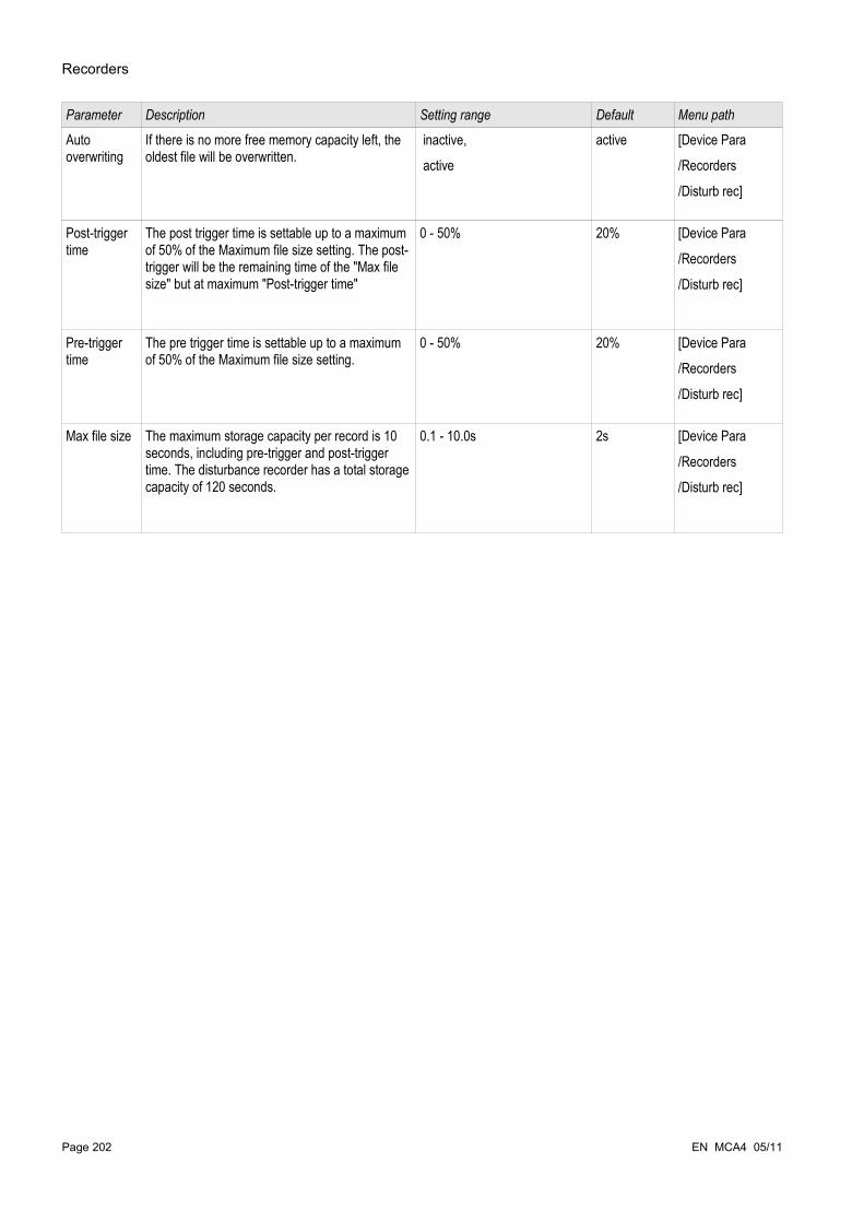
Recorders
Parameter Description Setting range Default Menu path
Auto overwriting
If there is no more free memory capacity left, the oldest file will be overwritten.
inactive,
active
active [Device Para
/Recorders
/Disturb rec]
Post-trigger time
The post trigger time is settable up to a maximum of 50% of the Maximum file size setting. The post-trigger will be the remaining time of the "Max file size" but at maximum "Post-trigger time"
0 - 50% 20% [Device Para
/Recorders
/Disturb rec]
Pre-trigger time
The pre trigger time is settable up to a maximum of 50% of the Maximum file size setting.
0 - 50% 20% [Device Para
/Recorders
/Disturb rec]
Max file size The maximum storage capacity per record is 10 seconds, including pre-trigger and post-trigger time. The disturbance recorder has a total storage capacity of 120 seconds.
0.1 - 10.0s 2s [Device Para
/Recorders
/Disturb rec]
Page 202 EN MCA4 05/11
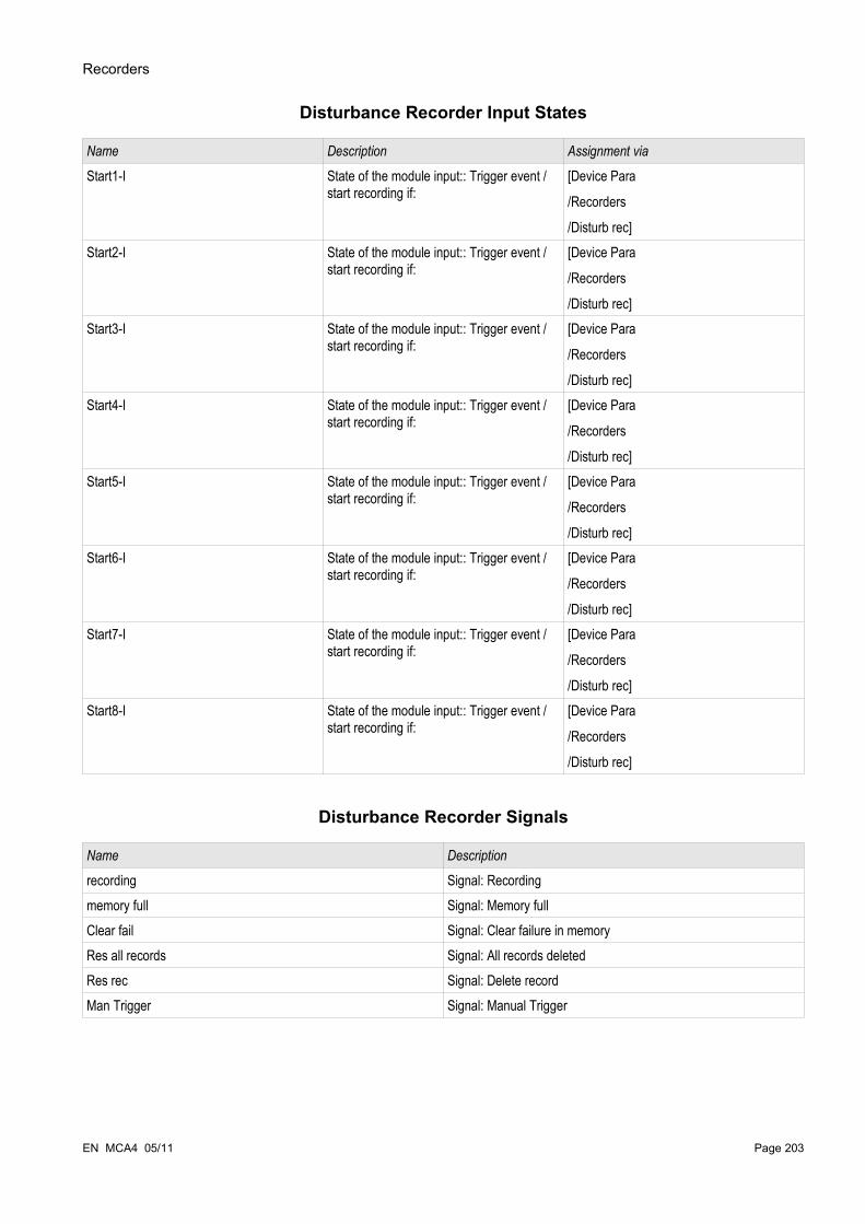
Recorders
Disturbance Recorder Input States
Name Description Assignment via
Start1-I State of the module input:: Trigger event / start recording if:
[Device Para
/Recorders
/Disturb rec]Start2-I State of the module input:: Trigger event /
start recording if:[Device Para
/Recorders
/Disturb rec]Start3-I State of the module input:: Trigger event /
start recording if:[Device Para
/Recorders
/Disturb rec]Start4-I State of the module input:: Trigger event /
start recording if:[Device Para
/Recorders
/Disturb rec]Start5-I State of the module input:: Trigger event /
start recording if:[Device Para
/Recorders
/Disturb rec]Start6-I State of the module input:: Trigger event /
start recording if:[Device Para
/Recorders
/Disturb rec]Start7-I State of the module input:: Trigger event /
start recording if:[Device Para
/Recorders
/Disturb rec]Start8-I State of the module input:: Trigger event /
start recording if:[Device Para
/Recorders
/Disturb rec]
Disturbance Recorder Signals
Name Description
recording Signal: Recordingmemory full Signal: Memory fullClear fail Signal: Clear failure in memoryRes all records Signal: All records deletedRes rec Signal: Delete record Man Trigger Signal: Manual Trigger
EN MCA4 05/11 Page 203
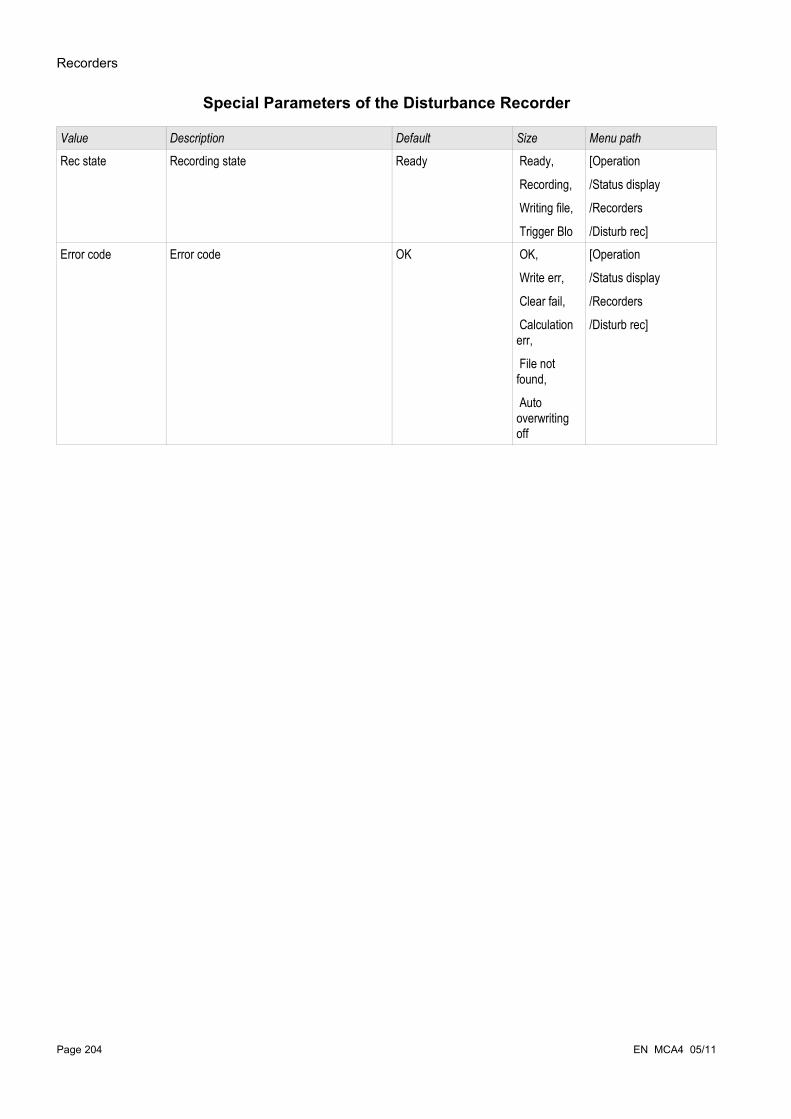
Recorders
Special Parameters of the Disturbance Recorder
Value Description Default Size Menu path
Rec state Recording state Ready Ready,
Recording,
Writing file,
Trigger Blo
[Operation
/Status display
/Recorders
/Disturb rec]Error code Error code OK OK,
Write err,
Clear fail,
Calculation err,
File not found,
Auto overwriting off
[Operation
/Status display
/Recorders
/Disturb rec]
Page 204 EN MCA4 05/11

Recorders
Fault Recorder
Fault rec
The fault recorder can be started by one of eight start events (selection from the »assignment list«/OR-Logic). The fault recorder can register up to 20 faults. The last of the recorded faults is stored in a fail-safe manner.
If one of the assigned trigger events becomes true, the fault recorder will be started. Each fault is saved inclusive module and name, fault number, mains fault number and record number at that time one of the trigger events becomes true. To each of the faults the measuring values (at the time when the trigger event became true) can be viewed.
Up to 8 signals to trigger the fault recorder can be selected from following list. The trigger events are OR-linked.
The parameter »Auto Delete« defines how the device shall react if there is no saving place available. In case »Auto Delete« is »active«, the first recorded fault will be overwritten according to the FIFO principle. If the parameter is set to »inactive«, recording of the fault events will be stopped until the storage location is released manually.
EN MCA4 05/11 Page 205
Start: 1Trigger
>1
Start: 2Trigger
Start: 3Trigger
Start: 4Trigger
Start: 5Trigger
Start: 6Trigger
Start: 7Trigger
Start: 8Trigger
Man Trigger
Recording>1

Recorders
Read Out the Fault Recorder
The measured values at the time of tripping are saved (failure safe) within the fault recorder. If there is no more memory free, the oldest record will be overwritten (FIFO).
In order to read out a failure record:
• call up the main menu,
• call up the submenu Operation/Recorders/Fault rec.,
• select a fault record,
• analyze the corresponding measured values.
Read Out the Fault Recorder via Smart View
• In case Smart view is not running – please start it.
• If device data has not been loaded yet – click »Receive Data From The Device« in menu »Device«.
• Double click the »Operation« icon in the navigation tree.
• Double click the »Fault Rec« icon within the tree »Operation/Recorders«.
• In the window the fault recordings are shown in tabular form.
• In order to receive more detailed information on a fault, click the »Plus Sign« in front of the fault number.
Via the print menu you can export the data into a file. Please proceed as follows:
• Call up the data as described above.
• Call up the menu [File/Print].
• Choose »Print Actual Working Window« within the popup.
• Press the »Print« button.
• Press the »Export to File« button.
• Enter a file name.
• Choose a location where to save the file.
• Confirm the »Save« button.
Page 206 EN MCA4 05/11

Recorders
Direct Commands of the Fault Recorder
Parameter Description Setting range Default Menu path
Res all rec Reset all records inactive,
active
inactive [Operation
/Reset]
Man Trigger Manual Trigger False,
True
False [Operation
/Recorders
/Man Trigger]
Global Protection Parameters of the Fault Recorder
Parameter Description Setting range Default Menu path
Start: 1 Start recording if the assigned signal is true. 1..n, Assignment List Prot.Trip [Device Para
/Recorders
/Fault rec]Start: 2 Start recording if the assigned signal is true. 1..n, Assignment List -.- [Device Para
/Recorders
/Fault rec]Start: 3 Start recording if the assigned signal is true. 1..n, Assignment List -.- [Device Para
/Recorders
/Fault rec]Start: 4 Start recording if the assigned signal is true. 1..n, Assignment List -.- [Device Para
/Recorders
/Fault rec]Start: 5 Start recording if the assigned signal is true. 1..n, Assignment List -.- [Device Para
/Recorders
/Fault rec]Start: 6 Start recording if the assigned signal is true. 1..n, Assignment List -.- [Device Para
/Recorders
/Fault rec]Start: 7 Start recording if the assigned signal is true. 1..n, Assignment List -.- [Device Para
/Recorders
/Fault rec]Start: 8 Start recording if the assigned signal is true. 1..n, Assignment List -.- [Device Para
/Recorders
/Fault rec]Auto overwriting
If there is no more free memory capacity left, the oldest file will be overwritten.
inactive,
active
active [Device Para
/Recorders
/Fault rec]
EN MCA4 05/11 Page 207

Recorders
Fault Recorder Input States
Name Description Assignment via
Start1-I State of the module input:: Trigger event / start recording if:
[Device Para
/Recorders
/Fault rec]Start2-I State of the module input:: Trigger event /
start recording if:[Device Para
/Recorders
/Fault rec]Start3-I State of the module input:: Trigger event /
start recording if:[Device Para
/Recorders
/Fault rec]Start4-I State of the module input:: Trigger event /
start recording if:[Device Para
/Recorders
/Fault rec]Start5-I State of the module input:: Trigger event /
start recording if:[Device Para
/Recorders
/Fault rec]Start6-I State of the module input:: Trigger event /
start recording if:[Device Para
/Recorders
/Fault rec]Start7-I State of the module input:: Trigger event /
start recording if:[Device Para
/Recorders
/Fault rec]Start8-I State of the module input:: Trigger event /
start recording if:[Device Para
/Recorders
/Fault rec]
Fault Recorder Signals
Name Description
Res rec Signal: Delete record Man Trigger Signal: Manual Trigger
Page 208 EN MCA4 05/11
Recorders
Trend RecorderAvailable Elements: Trend rec
Functional Description
The Trend Data are data points stored by the Trend Recorder on the relay device over fixed intervals of time, and can be downloaded from the device using Smart view. A Trend Record is viewable using the Data Visualizer software by selecting files saved by Smart view with a file extension of “.ErTr”. The list of available trend recorder data is viewable by selecting [Operation/ Recorders/Trend Recorder].
When viewed within the Data Visualizer, the trend record will show the observed values (up to 10) that the User has specified. The values available in the Trend Recorder depend on the type of the connected device and the configuration of the Trend Recorder.
Managing Trend Records
To download information from the Trend Recorder, select [Operation/Recorder/Trend Rec] from the menu tree. The User will find three options within the Trend Recorder window that will allow the User to:
• Receive Trend Records,• Refresh the Trend Recorder, and • Delete Trend Records.
Selecting the »Receive Trend Record« button will download data from the relay to the User's PC. By selecting the »Refresh Trend Recorder«”, Smart view updates the list of the Trend Recorder. The »Delete Trend Records« function will clear all trend data from the relay. Trend Recorder data previously stored on the User's PC remains untouched.
After having received trend data from the device, the User can view the data in the Data Visualizer by double-clicking on the received “.ErTr” file stored on the PC. Once the “.ErTr” file is open, the User will see the “Analog Channels” that are monitored by the Trend Recorder. By clicking on the “Analog Channels”, all monitored parameters are listed. To view a channel, the User must click on the left mouse key, then drag and drop the channel onto the right side of the Data Visualizer screen. The channel is then listed under the »Displayed Channels«.
To remove a channel from view, the User must select the Trend Data to be removed in the »Displayed Channels« menu tree, then click on the right mouse button to bring up the menu options. Here, the User will find the »Remove« menu option that, when selected, will remove the trend data.
Configuring the Trend Recorder
The Trend Recorder is to be configured within [Device Para/Recorders/Trend Recorder] menu.
The User has to set the time interval. This defines the distance between two measuring points.
The User can select up to ten values that will be recorded.
EN MCA4 05/11 Page 209

Recorders
Page 210 EN MCA4 05/11
Tren
d re
c
10 m
in
Res
olut
ion
60 m
in
15 m
in
5 m
in
30 m
in
Tren
d1
1..n
, Ass
ignm
ent L
ist
Tren
d2
1..n
, Ass
ignm
ent L
ist
Tren
d10
1..n
, Ass
ignm
ent L
ist
. . .
Tren
d re
c

Recorders
Global Protection Parameters of the Trend Recorder
Parameter Description Setting range Default Menu path
Resolution Resolution (recording frequency) 60 min,
30 min,
15 min,
10 min,
5 min
15 min [Device Para
/Recorders
/Trend rec]
Trend1 Observed Value1 1..n, TrendRecList IL1 RMS [Device Para
/Recorders
/Trend rec]Trend2 Observed Value2 1..n, TrendRecList IL2 RMS [Device Para
/Recorders
/Trend rec]Trend3 Observed Value3 1..n, TrendRecList IL3 RMS [Device Para
/Recorders
/Trend rec]Trend4 Observed Value4 1..n, TrendRecList IG meas
RMS[Device Para
/Recorders
/Trend rec]Trend5 Observed Value5 1..n, TrendRecList VL1 RMS [Device Para
/Recorders
/Trend rec]Trend6 Observed Value6 1..n, TrendRecList VL2 RMS [Device Para
/Recorders
/Trend rec]Trend7 Observed Value7 1..n, TrendRecList VL3 RMS [Device Para
/Recorders
/Trend rec]Trend8 Observed Value8 1..n, TrendRecList VX meas
RMS[Device Para
/Recorders
/Trend rec]Trend9 Observed Value9 1..n, TrendRecList - [Device Para
/Recorders
/Trend rec]Trend10 Observed Value10 1..n, TrendRecList - [Device Para
/Recorders
/Trend rec]
EN MCA4 05/11 Page 211

Recorders
Trend Recorder Signals (Output States)
Name Description
Hand Reset Hand Reset
Direct Commands of the Trend Recorder
Parameter Description Setting range Default Menu path
Reset Delete all entries inactive,
active
inactive [Operation
/Reset]
Assignable Values of the Trend Recorder
Name Description
- No assignmentIL1 Measured value: Phase current (fundamental)IL2 Measured value: Phase current (fundamental)IL3 Measured value: Phase current (fundamental)IG meas Measured value (measured): IG (fundamental)IG calc Measured value (calculated): IG (fundamental)IL1 RMS Measured value: Phase current (RMS)IL2 RMS Measured value: Phase current (RMS)IL3 RMS Measured value: Phase current (RMS)IG meas RMS Measured value (measured): IG (RMS)IG calc RMS Measured value (calculated): IG (RMS)I0 Measured value (calculated): Zero current (fundamental)I1 Measured value (calculated): Positive phase sequence current
(fundamental)I2 Measured value (calculated): Unbalanced load current
(fundamental)VL1 Measured value: Phase-to-neutral voltage (fundamental)VL2 Measured value: Phase-to-neutral voltage (fundamental)VL3 Measured value: Phase-to-neutral voltage (fundamental)VX meas Measured value (measured): VG measured (fundamental)VG calc Measured value (calculated): VG (fundamental)VL12 Measured value: Phase-to-phase voltage (fundamental)VL23 Measured value: Phase-to-phase voltage (fundamental)VL31 Measured value: Phase-to-phase voltage (fundamental)VL1 RMS Measured value: Phase-to-neutral voltage (RMS)VL2 RMS Measured value: Phase-to-neutral voltage (RMS)VL3 RMS Measured value: Phase-to-neutral voltage (RMS)
Page 212 EN MCA4 05/11

Recorders
Name Description
VX meas RMS Measured value (measured): VG measured (RMS)VG calc RMS Measured value (calculated): VG (RMS)VL12 RMS Measured value: Phase-to-phase voltage (RMS)VL23 RMS Measured value: Phase-to-phase voltage (RMS)VL31 RMS Measured value: Phase-to-phase voltage (RMS)V0 Measured value (calculated): Symmetrical components Zero
voltage(fundamental)V1 Measured value (calculated): Symmetrical components positive
phase sequence voltage(fundamental)V2 Measured value (calculated): Symmetrical components negative
phase sequence voltage(fundamental)f Measured value: Frequencycos phi Measured value (calculated): Power factorcos phi RMS Measured value (calculated): Power factorIL1 THD Measured value (calculated): IL1 Total Harmonic Current IL2 THD Measured value (calculated): IL2 Total Harmonic Current IL3 THD Measured value (calculated): IL3 Total Harmonic Current VL1 THD Measured value (calculated): VL1 Total Harmonic Distortion VL2 THD VL2 THDVL3 THD VL3 THDVL12 THD Measured value (calculated): V12 Total Harmonic Distortion VL23 THD Measured value (calculated): V23 Total Harmonic Distortion VL31 THD Measured value (calculated): V31 Total Harmonic Distortion
EN MCA4 05/11 Page 213

Recorders
Event Recorder Event rec
The event recorder can register up to 300 events and the last (minimum) 50 saved events are recorded fail-safe. The following information is provided for any of the events:
Events are logged as follows:
Record No. Fault No. No of grid faults Date of Record Module.Name State
Sequential Number
Number of the ongoing fault
This counter will be incremented by each General Alarm (Prot.Alarm).
A grid fault No. can have several Fault No.
This counter will be incremented by each General Alarm.
(Exception AR: this applies only to devices that offer auto reclosing).
Time stamp What has changed?
Changed Value
There are three different classes of events:
• Alternation of binary states are shown as:• 0->1 if the signal changes physically from »0« to »1«.• 1->0 if the signal changes physically from »1« to »0«.
• Counters increment is shown as:• Old Counter state -> New Counter state (e.g. 3->4)
• Alternation of multiple states are shown as:• Old state -> New state (e.g. 0->2)
Page 214 EN MCA4 05/11
Recorders
Read Out the Event Recorder
• Call up the »main menu«.
• Call up the submenu »Operation/Recorders/Event rec«.
• Select an event.
Read Out the Event Recorder via Smart View
• In case Smart view is not running – please start it.
• If device data has not been loaded yet – click »Receive Data From The Device« in menu »Device.
• Double click the »Operation« icon in the navigation tree.
• Double click the »Event Rec« icon within the »OPERATION/RECORDERS« menu.
• In the window the events are shown in tabular form.
To have the event recorder up-dated in a cyclic manner, select »Automatic Up-Date« in menu View.
Smart view is able to record more events than the device itself, if the window of the event recorder is opened and »Automatic Up-Date« is set to active.
Via the print menu you can export the data into a file. Please proceed as follows:
• Call up the data as described above.
• Call up the menu [File/Print].
• Choose »Print Actual Working Window« within the popup.
• Press the »Print« button.
• Press the »Export to File« button.
• Enter a file name.
• Choose a location where to save the file.
• Confirm the »Save« button.
EN MCA4 05/11 Page 215

Recorders
Direct Commands of the Event Recorder
Parameter Description Setting range Default Menu path
Res all rec Reset all records inactive,
active
inactive [Operation
/Reset]
Event Recorder Signals
Name Description
Res all records Signal: All records deleted
Page 216 EN MCA4 05/11
Communication Protocols
Communication ProtocolsSCADA Interface
X103
Device Planning Parameters of the Serial Scada Interface
Parameter Description Options Default Menu path
Protocol Caution! Changing the protocol will cause a restart of the device
-,
Modbus,
IEC60870-5-103,
Profibus
Modbus [Device planning]
Global Protection Parameters of the Serial Scada Interface
Parameter Description Setting range Default Menu path
Optical rest position
Optical rest position Light off,
Light on
Light on [Device Para
/X103]
EN MCA4 05/11 Page 217

Communication Protocols
Modbus®
Modbus
Modbus® Protocol Configuration
The time-controlled Modbus® protocol is based on the Master-Slave working principle. This means that the substation control and protection system sends an enquiry or instruction to a certain device (slave address) which will then be answered or carried out accordingly. If the enquiry/instruction cannot be answered/carried out (e.g. because of an invalid slave address), a failure message is returned to the master.
The Master (substation control and protection system) can query information from the device, such as:
• Type of unit version• Measuring values/Statistical measured values• Switch operating position (in preparation)• State of device• Time and date• State of the device’s digital inputs• Protection-/State alarms
The Master (control system) can give commands/instructions to the device, such as:
• Control of switchgear (where applicable, i.e. each acc. to the applied device version)• Change-over of parameter set• Reset and acknowledgement of alarms/signals• Adjustment of date and time• Control of alarm relays
For detailed information on data point lists and error handling, please refer to the Modbus® documentation.
To allow configuration of the devices for Modbus® connection, some default values of the control system must be available.
Page 218 EN MCA4 05/11
Communication Protocols
Modbus RTU
Part 1: Configuration of the Devices
Call up »Device parameter/Modbus« and set the following communication parameters there:
• Slave-address, to allow clear identification of the device.
• Baud-Rate
Also, select below indicated RS485 interface-related parameters from there, such as:
• Number of data bits
• One of the following supported communication variants: Number of data bits, even, odd, parity or no parity, number of stop bits.
• »t-timeout«: communication errors are only identified after expiry of a supervision time »t-timeout«.
• Response time (defining the period within which an enquiry from the master has to be answered).
Part 2: Hardware Connection
• For hardware connection to the control system, there is an RS485 interface at the rear side of the device (RS485, fiber optic or terminals).
• Connect bus and device (wiring).
Error Handling - Hardware Errors
Information on physical communication errors, such as:
• Baudrate Error• Parity Error ...
can be obtained from the event recorder.
Error Handling – Errors on protocol level
If, for example, an invalid memory address is enquired, error codes will be returned by the device that need to be interpreted.
EN MCA4 05/11 Page 219

Communication Protocols
Modbus TCP
Establishing a connection via TCP/IP to the device is only possible if your device is equipped with an Ethernet Interface (RJ45).
Contact your IT administrator in order to establish the network connection.
Part 1: Setting the TCP/IP Parameters
Call up »Device parameter/TCP/IP« at the HMI (panel) and set the following parameters:
• TCP/IP address
• Subnetmask
• Gateway
Part 2: Configuration of the Devices
Call up »Device parameter/Modbus« and set the following communication parameters:
• Setting a Unit Identifier is only necessary if a TCP network should be coupled to a RTU network.
• If a different port than the default port 502 should be used please proceed as follows:
• Choose “Private” within the TCP-Port-Configuration.
• Set the port-number.
• Set the maximum accepted time of “no communication”. If this time has expired – without any comunication, the device concludes a failure within the master system.
• Allow or disallow the blocking of SCADA commands.
Part 3: Hardware Connection
• There is a RJ45 interface at the rear side of the device for the hardware connection to the control system.
• Establish the connection to the device by means of a proper Ethernet cable.
Page 220 EN MCA4 05/11

Communication Protocols
Direct Commands of the Modbus®
Parameter Description Setting range Default Menu path
Res Diagn Cr All Modbus Diagnosis Counters will be reset. inactive,
active
inactive [Operation
/Reset]
Global Protection Parameters of the Modbus®
Parameter Description Setting range Default Menu path
Slave ID Device address (Slave ID) within the bus system. Each device address has to be unique within a bus system.
Only available if:Device planning = RTU
1 - 247 1 [Device Para
/Modbus]
Unit ID The Unit Identifier is used for routing. This parameter is to be set, if a Modbus RTU and a Modbus TCP network should be coupled.
Only available if:Device planning = TCP
1 - 255 255 [Device Para
/Modbus]
TCP Port Config
TCP Port Configuration. This parameter is to be set only if the default Modubs TCP Port should not be used.
Only available if:Device planning = TCP
Default,
Private
Default [Device Para
/Modbus]
Port Port number
Only available if:Device planning = TCP And Only available if: TCP Port Config = Private
502 - 65535 502 [Device Para
/Modbus]
t-timeout Within this time the answer has to be received by the SCADA system, otherwise the request will be disregarded. In that case the Scada system detects a communication failure and the Scada System has to send a new request.
Only available if:Device planning = RTU
0.01 - 10.00s 1s [Device Para
/Modbus]
Baud rate Baud rate
Only available if:Device planning = RTU
1200,
2400,
4800,
9600,
19200,
38400
19200 [Device Para
/Modbus]
EN MCA4 05/11 Page 221

Communication Protocols
Parameter Description Setting range Default Menu path
Physical Settings
Digit 1: Number of bits. Digit 2: E=even parity, O=odd parity, N=no parity. Digit 3: Number of stop bits. More information on the parity: It is possible that the last data bit is followed by a parity bit which is used for recognition of communication errors. The parity bit ensures that with even parity ("EVEN") always an even number of bits with valence "1" or with odd parity ("ODD") an odd number of "1" valence bits are transmitted. But it is also possible to transmit no parity bits (here the setting is "Parity = None"). More information on the stop-bits: The end of a data byte is terminated by the stop-bits.
Only available if:Device planning = RTU
8E1,
8O1,
8N1,
8N2
8E1 [Device Para
/Modbus]
t-call If there is no request telegram sent from Scada to the device after expiry of this time - the device concludes a communication failure within the Scada system.
1 - 3600s 10s [Device Para
/Modbus]
Scada CmdBlo
Activating (allowing)/ Deactivating (disallowing) the blocking of the Scada Commands
inactive,
active
inactive [Device Para
/Modbus]
Disable Latching
Disable Latching: If this parameter is active (true), none of the Modbus states will be latched. That means that trip signals wont be latched by Modbus.
inactive,
active
inactive [Device Para
/Modbus]
AllowGap If this parameter is active (True), the user can request a set of modbus register without getting an exception, because of invalid address in the requested array. The invalid addresses have a special value 0xFAFA, but the user is responsible for ignoring invalid addresses. Attention: This special value can be valid, if address is valid.
inactive,
active
inactive [Device Para
/Modbus]
Page 222 EN MCA4 05/11

Communication Protocols
Modbus® Signals (Output States)
Some signals (that are for a short time active only) have to be acknowledged separately (e.g. Trip signals) by the Communication System.
Name Description
Transmission Signal: SCADA activeScada Cmd 1 Scada CommandScada Cmd 2 Scada CommandScada Cmd 3 Scada CommandScada Cmd 4 Scada CommandScada Cmd 5 Scada CommandScada Cmd 6 Scada CommandScada Cmd 7 Scada CommandScada Cmd 8 Scada CommandScada Cmd 9 Scada CommandScada Cmd 10 Scada CommandScada Cmd 11 Scada CommandScada Cmd 12 Scada CommandScada Cmd 13 Scada CommandScada Cmd 14 Scada CommandScada Cmd 15 Scada CommandScada Cmd 16 Scada Command
EN MCA4 05/11 Page 223
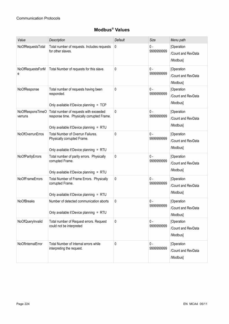
Communication Protocols
Modbus® Values
Value Description Default Size Menu path
NoOfRequestsTotal Total number of requests. Includes requests for other slaves.
0 0 - 9999999999
[Operation
/Count and RevData
/Modbus]
NoOfRequestsForMe
Total Number of requests for this slave. 0 0 - 9999999999
[Operation
/Count and RevData
/Modbus]NoOfResponse Total number of requests having been
responded.
Only available if:Device planning = TCP
0 0 - 9999999999
[Operation
/Count and RevData
/Modbus]
NoOfResponsTimeOverruns
Total number of requests with exceeded response time. Physically corrupted Frame.
Only available if:Device planning = RTU
0 0 - 9999999999
[Operation
/Count and RevData
/Modbus]
NoOfOverrunErros Total Number of Overrun Failures. Physically corrupted Frame.
Only available if:Device planning = RTU
0 0 - 9999999999
[Operation
/Count and RevData
/Modbus]
NoOfParityErrors Total number of parity errors. Physically corrupted Frame.
Only available if:Device planning = RTU
0 0 - 9999999999
[Operation
/Count and RevData
/Modbus]
NoOfFrameErrors Total Number of Frame Errors. Physically corrupted Frame.
Only available if:Device planning = RTU
0 0 - 9999999999
[Operation
/Count and RevData
/Modbus]
NoOfBreaks Number of detected communication aborts
Only available if:Device planning = RTU
0 0 - 9999999999
[Operation
/Count and RevData
/Modbus]NoOfQueryInvalid Total number of Request errors. Request
could not be interpreted0 0 -
9999999999[Operation
/Count and RevData
/Modbus]
NoOfInternalError Total Number of Internal errors while interpreting the request.
0 0 - 9999999999
[Operation
/Count and RevData
/Modbus]
Page 224 EN MCA4 05/11
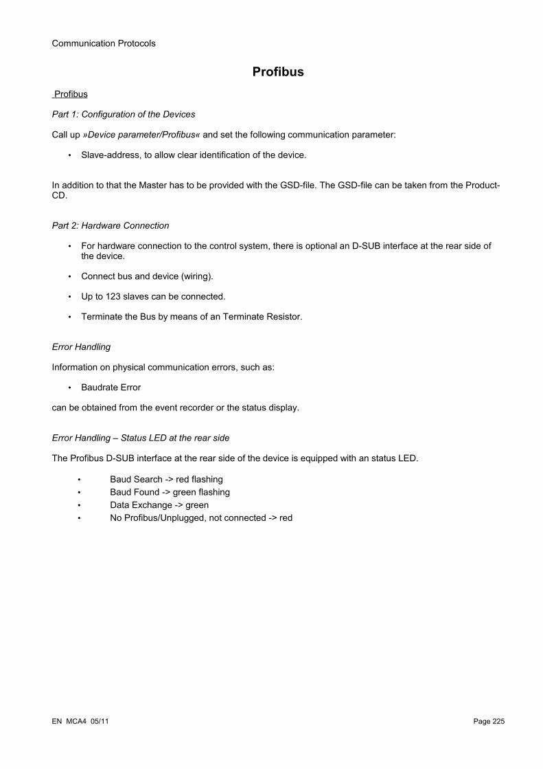
Communication Protocols
Profibus Profibus
Part 1: Configuration of the Devices
Call up »Device parameter/Profibus« and set the following communication parameter:
• Slave-address, to allow clear identification of the device.
In addition to that the Master has to be provided with the GSD-file. The GSD-file can be taken from the Product-CD.
Part 2: Hardware Connection
• For hardware connection to the control system, there is optional an D-SUB interface at the rear side of the device.
• Connect bus and device (wiring).
• Up to 123 slaves can be connected.
• Terminate the Bus by means of an Terminate Resistor.
Error Handling
Information on physical communication errors, such as:
• Baudrate Error
can be obtained from the event recorder or the status display.
Error Handling – Status LED at the rear side
The Profibus D-SUB interface at the rear side of the device is equipped with an status LED.
• Baud Search -> red flashing• Baud Found -> green flashing• Data Exchange -> green• No Profibus/Unplugged, not connected -> red
EN MCA4 05/11 Page 225

Communication Protocols
Direct Commands of the Profibus
Parameter Description Setting range Default Menu path
Reset Comds
All Profibus Commands will be reset. inactive,
active
inactive [Operation
/Reset]
Global Protection Parameters of the Profibus
Parameter Description Setting range Default Menu path
Assignment 1
Assignment 1..n, Assignment List -.- [Device Para
/Profibus
/Assignment 1-16]
Latched 1 Defines whether the Input is latched.
Only available if: Latched = active
inactive,
active
inactive [Device Para
/Profibus
/Assignment 1-16]Assignment 2
Assignment 1..n, Assignment List -.- [Device Para
/Profibus
/Assignment 1-16]
Latched 2 Defines whether the Input is latched.
Only available if: Latched = active
inactive,
active
inactive [Device Para
/Profibus
/Assignment 1-16]Assignment 3
Assignment 1..n, Assignment List -.- [Device Para
/Profibus
/Assignment 1-16]
Latched 3 Defines whether the Input is latched.
Only available if: Latched = active
inactive,
active
inactive [Device Para
/Profibus
/Assignment 1-16]Assignment 4
Assignment 1..n, Assignment List -.- [Device Para
/Profibus
/Assignment 1-16]
Latched 4 Defines whether the Input is latched.
Only available if: Latched = active
inactive,
active
inactive [Device Para
/Profibus
/Assignment 1-16]
Page 226 EN MCA4 05/11

Communication Protocols
Parameter Description Setting range Default Menu path
Assignment 5
Assignment 1..n, Assignment List -.- [Device Para
/Profibus
/Assignment 1-16]
Latched 5 Defines whether the Input is latched.
Only available if: Latched = active
inactive,
active
inactive [Device Para
/Profibus
/Assignment 1-16]Assignment 6
Assignment 1..n, Assignment List -.- [Device Para
/Profibus
/Assignment 1-16]
Latched 6 Defines whether the Input is latched.
Only available if: Latched = active
inactive,
active
inactive [Device Para
/Profibus
/Assignment 1-16]Assignment 7
Assignment 1..n, Assignment List -.- [Device Para
/Profibus
/Assignment 1-16]
Latched 7 Defines whether the Input is latched.
Only available if: Latched = active
inactive,
active
inactive [Device Para
/Profibus
/Assignment 1-16]Assignment 8
Assignment 1..n, Assignment List -.- [Device Para
/Profibus
/Assignment 1-16]
Latched 8 Defines whether the Input is latched.
Only available if: Latched = active
inactive,
active
inactive [Device Para
/Profibus
/Assignment 1-16]Assignment 9
Assignment 1..n, Assignment List -.- [Device Para
/Profibus
/Assignment 1-16]
Latched 9 Defines whether the Input is latched.
Only available if: Latched = active
inactive,
active
inactive [Device Para
/Profibus
/Assignment 1-16]Assignment 10
Assignment 1..n, Assignment List -.- [Device Para
/Profibus
/Assignment 1-16]
EN MCA4 05/11 Page 227

Communication Protocols
Parameter Description Setting range Default Menu path
Latched 10 Defines whether the Input is latched.
Only available if: Latched = active
inactive,
active
inactive [Device Para
/Profibus
/Assignment 1-16]Assignment 11
Assignment 1..n, Assignment List -.- [Device Para
/Profibus
/Assignment 1-16]
Latched 11 Defines whether the Input is latched.
Only available if: Latched = active
inactive,
active
inactive [Device Para
/Profibus
/Assignment 1-16]Assignment 12
Assignment 1..n, Assignment List -.- [Device Para
/Profibus
/Assignment 1-16]
Latched 12 Defines whether the Input is latched.
Only available if: Latched = active
inactive,
active
inactive [Device Para
/Profibus
/Assignment 1-16]Assignment 13
Assignment 1..n, Assignment List -.- [Device Para
/Profibus
/Assignment 1-16]
Latched 13 Defines whether the Input is latched.
Only available if: Latched = active
inactive,
active
inactive [Device Para
/Profibus
/Assignment 1-16]Assignment 14
Assignment 1..n, Assignment List -.- [Device Para
/Profibus
/Assignment 1-16]
Latched 14 Defines whether the Input is latched.
Only available if: Latched = active
inactive,
active
inactive [Device Para
/Profibus
/Assignment 1-16]Assignment 15
Assignment 1..n, Assignment List -.- [Device Para
/Profibus
/Assignment 1-16]
Latched 15 Defines whether the Input is latched.
Only available if: Latched = active
inactive,
active
inactive [Device Para
/Profibus
/Assignment 1-16]
Page 228 EN MCA4 05/11

Communication Protocols
Parameter Description Setting range Default Menu path
Assignment 16
Assignment 1..n, Assignment List -.- [Device Para
/Profibus
/Assignment 1-16]
Latched 16 Defines whether the Input is latched.
Only available if: Latched = active
inactive,
active
inactive [Device Para
/Profibus
/Assignment 1-16]Assignment 17
Assignment 1..n, Assignment List -.- [Device Para
/Profibus
/Assignment 17-32]
Latched 17 Defines whether the Input is latched.
Only available if: Latched = active
inactive,
active
inactive [Device Para
/Profibus
/Assignment 17-32]
Assignment 18
Assignment 1..n, Assignment List -.- [Device Para
/Profibus
/Assignment 17-32]
Latched 18 Defines whether the Input is latched.
Only available if: Latched = active
inactive,
active
inactive [Device Para
/Profibus
/Assignment 17-32]
Assignment 19
Assignment 1..n, Assignment List -.- [Device Para
/Profibus
/Assignment 17-32]
Latched 19 Defines whether the Input is latched.
Only available if: Latched = active
inactive,
active
inactive [Device Para
/Profibus
/Assignment 17-32]
Assignment 20
Assignment 1..n, Assignment List -.- [Device Para
/Profibus
/Assignment 17-32]
Latched 20 Defines whether the Input is latched.
Only available if: Latched = active
inactive,
active
inactive [Device Para
/Profibus
/Assignment 17-32]
EN MCA4 05/11 Page 229

Communication Protocols
Parameter Description Setting range Default Menu path
Assignment 21
Assignment 1..n, Assignment List -.- [Device Para
/Profibus
/Assignment 17-32]
Latched 21 Defines whether the Input is latched.
Only available if: Latched = active
inactive,
active
inactive [Device Para
/Profibus
/Assignment 17-32]
Assignment 22
Assignment 1..n, Assignment List -.- [Device Para
/Profibus
/Assignment 17-32]
Latched 22 Defines whether the Input is latched.
Only available if: Latched = active
inactive,
active
inactive [Device Para
/Profibus
/Assignment 17-32]
Assignment 23
Assignment 1..n, Assignment List -.- [Device Para
/Profibus
/Assignment 17-32]
Latched 23 Defines whether the Input is latched.
Only available if: Latched = active
inactive,
active
inactive [Device Para
/Profibus
/Assignment 17-32]
Assignment 24
Assignment 1..n, Assignment List -.- [Device Para
/Profibus
/Assignment 17-32]
Latched 24 Defines whether the Input is latched.
Only available if: Latched = active
inactive,
active
inactive [Device Para
/Profibus
/Assignment 17-32]
Assignment 25
Assignment 1..n, Assignment List -.- [Device Para
/Profibus
/Assignment 17-32]
Latched 25 Defines whether the Input is latched.
Only available if: Latched = active
inactive,
active
inactive [Device Para
/Profibus
/Assignment 17-32]
Page 230 EN MCA4 05/11

Communication Protocols
Parameter Description Setting range Default Menu path
Assignment 26
Assignment 1..n, Assignment List -.- [Device Para
/Profibus
/Assignment 17-32]
Latched 26 Defines whether the Input is latched.
Only available if: Latched = active
inactive,
active
inactive [Device Para
/Profibus
/Assignment 17-32]
Assignment 27
Assignment 1..n, Assignment List -.- [Device Para
/Profibus
/Assignment 17-32]
Latched 27 Defines whether the Input is latched.
Only available if: Latched = active
inactive,
active
inactive [Device Para
/Profibus
/Assignment 17-32]
Assignment 28
Assignment 1..n, Assignment List -.- [Device Para
/Profibus
/Assignment 17-32]
Latched 28 Defines whether the Input is latched.
Only available if: Latched = active
inactive,
active
inactive [Device Para
/Profibus
/Assignment 17-32]
Assignment 29
Assignment 1..n, Assignment List -.- [Device Para
/Profibus
/Assignment 17-32]
Latched 29 Defines whether the Input is latched.
Only available if: Latched = active
inactive,
active
inactive [Device Para
/Profibus
/Assignment 17-32]
Assignment 30
Assignment 1..n, Assignment List -.- [Device Para
/Profibus
/Assignment 17-32]
Latched 30 Defines whether the Input is latched.
Only available if: Latched = active
inactive,
active
inactive [Device Para
/Profibus
/Assignment 17-32]
EN MCA4 05/11 Page 231
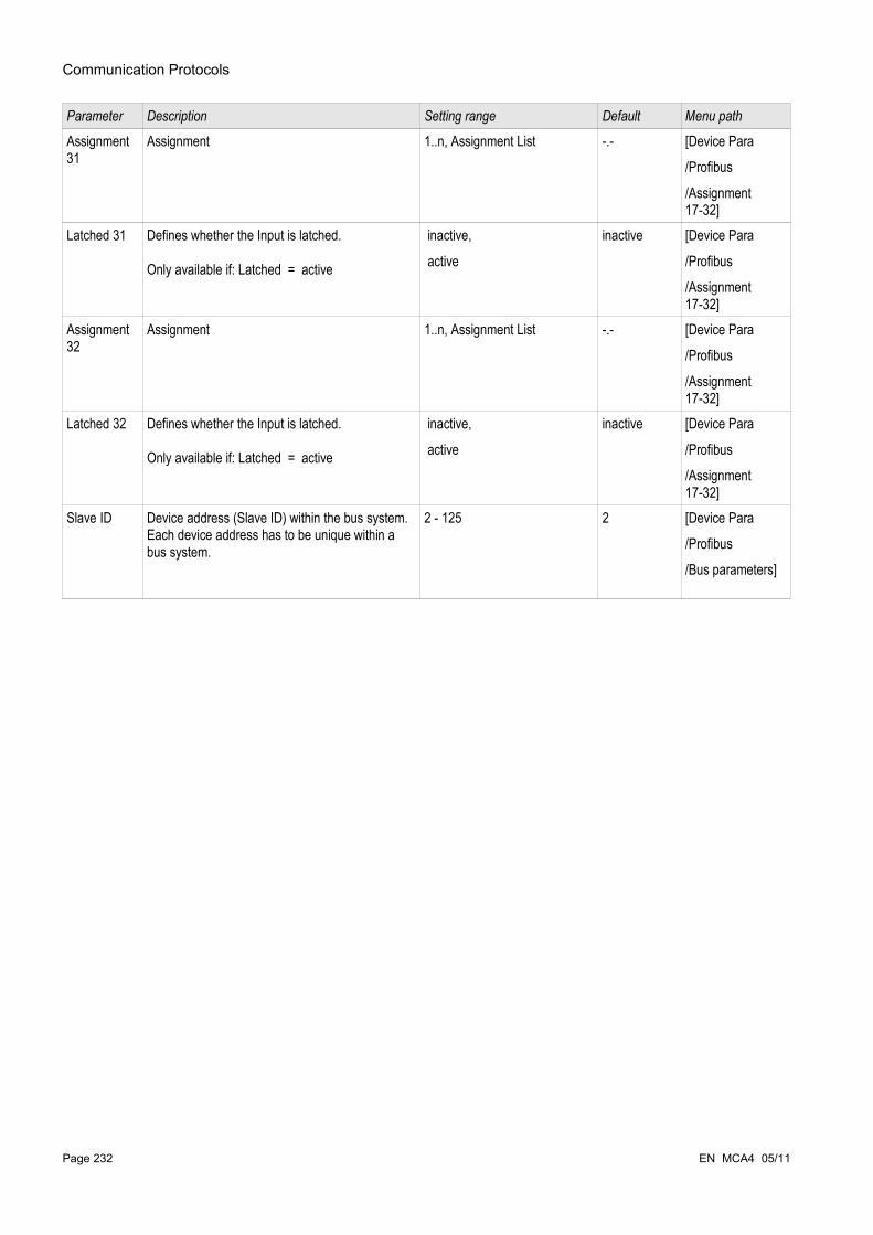
Communication Protocols
Parameter Description Setting range Default Menu path
Assignment 31
Assignment 1..n, Assignment List -.- [Device Para
/Profibus
/Assignment 17-32]
Latched 31 Defines whether the Input is latched.
Only available if: Latched = active
inactive,
active
inactive [Device Para
/Profibus
/Assignment 17-32]
Assignment 32
Assignment 1..n, Assignment List -.- [Device Para
/Profibus
/Assignment 17-32]
Latched 32 Defines whether the Input is latched.
Only available if: Latched = active
inactive,
active
inactive [Device Para
/Profibus
/Assignment 17-32]
Slave ID Device address (Slave ID) within the bus system. Each device address has to be unique within a bus system.
2 - 125 2 [Device Para
/Profibus
/Bus parameters]
Page 232 EN MCA4 05/11

Communication Protocols
Inputs of the Profibus
Name Description Assignment via
Assignment 1-I Module input state: Scada Assignment [Device Para
/Profibus
/Assignment 1-16]Assignment 2-I Module input state: Scada Assignment [Device Para
/Profibus
/Assignment 1-16]Assignment 3-I Module input state: Scada Assignment [Device Para
/Profibus
/Assignment 1-16]Assignment 4-I Module input state: Scada Assignment [Device Para
/Profibus
/Assignment 1-16]Assignment 5-I Module input state: Scada Assignment [Device Para
/Profibus
/Assignment 1-16]Assignment 6-I Module input state: Scada Assignment [Device Para
/Profibus
/Assignment 1-16]Assignment 7-I Module input state: Scada Assignment [Device Para
/Profibus
/Assignment 1-16]Assignment 8-I Module input state: Scada Assignment [Device Para
/Profibus
/Assignment 1-16]Assignment 9-I Module input state: Scada Assignment [Device Para
/Profibus
/Assignment 1-16]Assignment 10-I Module input state: Scada Assignment [Device Para
/Profibus
/Assignment 1-16]Assignment 11-I Module input state: Scada Assignment [Device Para
/Profibus
/Assignment 1-16]Assignment 12-I Module input state: Scada Assignment [Device Para
/Profibus
/Assignment 1-16]
EN MCA4 05/11 Page 233
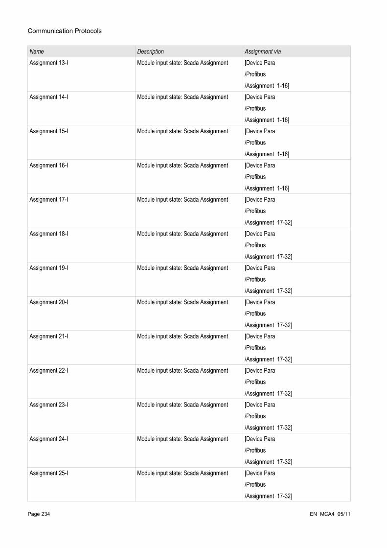
Communication Protocols
Name Description Assignment via
Assignment 13-I Module input state: Scada Assignment [Device Para
/Profibus
/Assignment 1-16]Assignment 14-I Module input state: Scada Assignment [Device Para
/Profibus
/Assignment 1-16]Assignment 15-I Module input state: Scada Assignment [Device Para
/Profibus
/Assignment 1-16]Assignment 16-I Module input state: Scada Assignment [Device Para
/Profibus
/Assignment 1-16]Assignment 17-I Module input state: Scada Assignment [Device Para
/Profibus
/Assignment 17-32]Assignment 18-I Module input state: Scada Assignment [Device Para
/Profibus
/Assignment 17-32]Assignment 19-I Module input state: Scada Assignment [Device Para
/Profibus
/Assignment 17-32]Assignment 20-I Module input state: Scada Assignment [Device Para
/Profibus
/Assignment 17-32]Assignment 21-I Module input state: Scada Assignment [Device Para
/Profibus
/Assignment 17-32]Assignment 22-I Module input state: Scada Assignment [Device Para
/Profibus
/Assignment 17-32]Assignment 23-I Module input state: Scada Assignment [Device Para
/Profibus
/Assignment 17-32]Assignment 24-I Module input state: Scada Assignment [Device Para
/Profibus
/Assignment 17-32]Assignment 25-I Module input state: Scada Assignment [Device Para
/Profibus
/Assignment 17-32]
Page 234 EN MCA4 05/11

Communication Protocols
Name Description Assignment via
Assignment 26-I Module input state: Scada Assignment [Device Para
/Profibus
/Assignment 17-32]Assignment 27-I Module input state: Scada Assignment [Device Para
/Profibus
/Assignment 17-32]Assignment 28-I Module input state: Scada Assignment [Device Para
/Profibus
/Assignment 17-32]Assignment 29-I Module input state: Scada Assignment [Device Para
/Profibus
/Assignment 17-32]Assignment 30-I Module input state: Scada Assignment [Device Para
/Profibus
/Assignment 17-32]Assignment 31-I Module input state: Scada Assignment [Device Para
/Profibus
/Assignment 17-32]Assignment 32-I Module input state: Scada Assignment [Device Para
/Profibus
/Assignment 17-32]
EN MCA4 05/11 Page 235
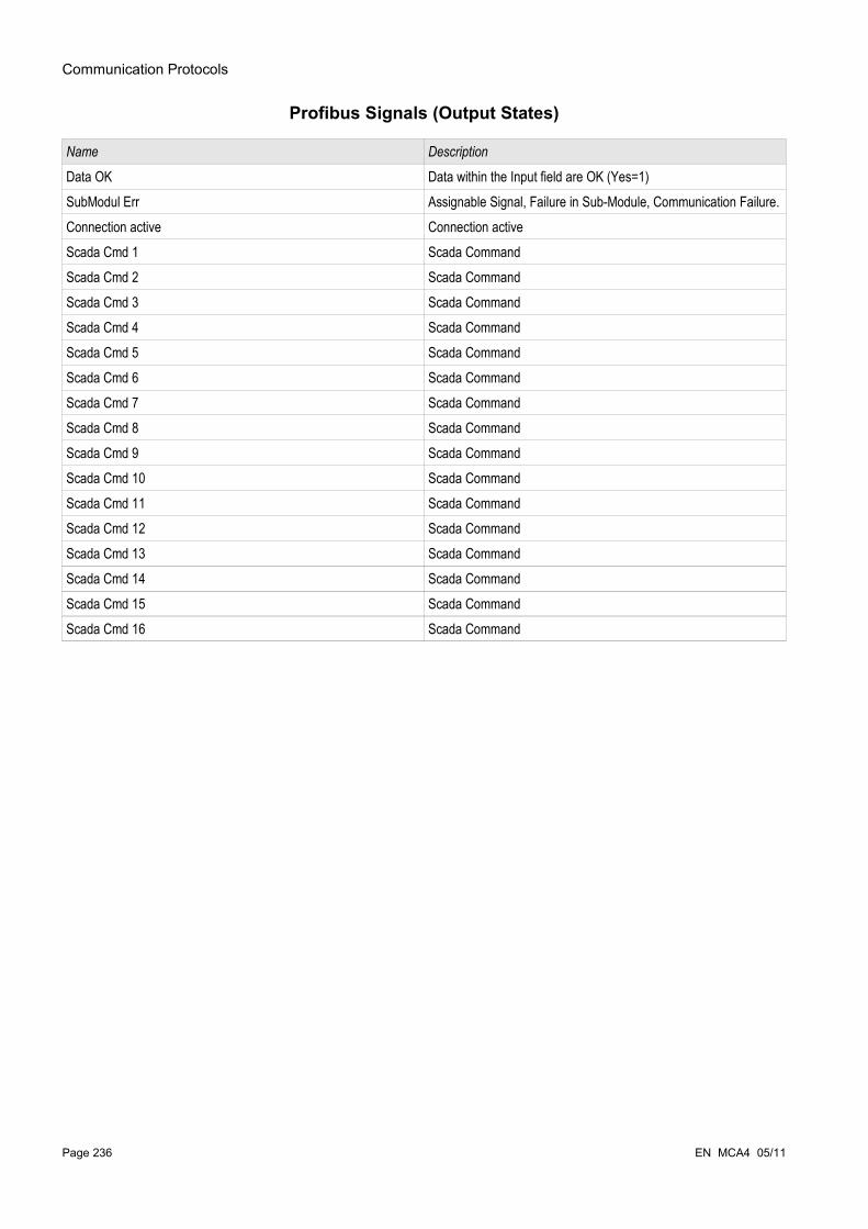
Communication Protocols
Profibus Signals (Output States)
Name Description
Data OK Data within the Input field are OK (Yes=1)SubModul Err Assignable Signal, Failure in Sub-Module, Communication Failure.Connection active Connection activeScada Cmd 1 Scada CommandScada Cmd 2 Scada CommandScada Cmd 3 Scada CommandScada Cmd 4 Scada CommandScada Cmd 5 Scada CommandScada Cmd 6 Scada CommandScada Cmd 7 Scada CommandScada Cmd 8 Scada CommandScada Cmd 9 Scada CommandScada Cmd 10 Scada CommandScada Cmd 11 Scada CommandScada Cmd 12 Scada CommandScada Cmd 13 Scada CommandScada Cmd 14 Scada CommandScada Cmd 15 Scada CommandScada Cmd 16 Scada Command
Page 236 EN MCA4 05/11

Communication Protocols
Profibus Values
Value Description Default Size Menu path
Fr Sync Err Frames, that were sent from the Master to the Slave are faulty.
1 1 - 99999999 [Operation
/Count and RevData
/Profibus]
crcErrors Number of CRC errors that the ss manager has recognized in received response frames from ss (each error caused a subsystem reset)
1 1 - 99999999 [Operation
/Count and RevData
/Profibus]
frLossErrors Number of frame loss errors that the ss manager recognized in received response frames from ss (each error caused a subsystem reset)
1 1 - 99999999 [Operation
/Count and RevData
/Profibus]
ssCrcErrors Number of CRC errors that the subsystem has recognized in received trigger frames from host
1 1 - 99999999 [Operation
/Count and RevData
/Profibus]
ssResets Number of subsystem resets/restarts from ss manager
1 1 - 99999999 [Operation
/Count and RevData
/Profibus]
Master ID Device address (Master ID) within the bus system. Each device address has to be unique within a bus system.
1 1 - 125 [Operation
/Status display
/Profibus
/State]HO Id PSub Handoff Id of PbSub 0 0 -
9999999999[Operation
/Status display
/Profibus
/State]t-WatchDog The Profibus Chip detects a communication
issue if this timer is expired without any communication (Parameterising telegram).
0 0 - 9999999999
[Operation
/Status display
/Profibus
/State]
EN MCA4 05/11 Page 237
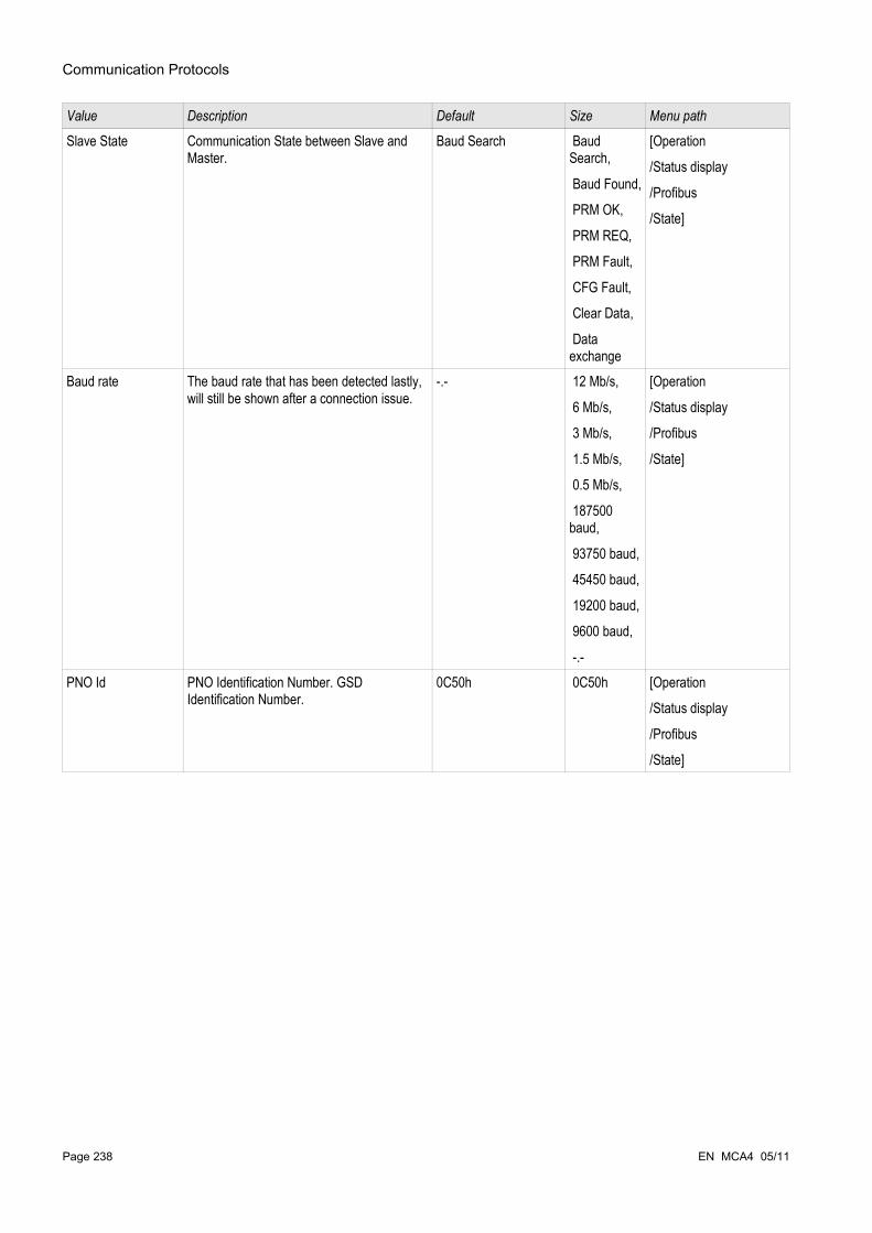
Communication Protocols
Value Description Default Size Menu path
Slave State Communication State between Slave and Master.
Baud Search Baud Search,
Baud Found,
PRM OK,
PRM REQ,
PRM Fault,
CFG Fault,
Clear Data,
Data exchange
[Operation
/Status display
/Profibus
/State]
Baud rate The baud rate that has been detected lastly, will still be shown after a connection issue.
-.- 12 Mb/s,
6 Mb/s,
3 Mb/s,
1.5 Mb/s,
0.5 Mb/s,
187500 baud,
93750 baud,
45450 baud,
19200 baud,
9600 baud,
-.-
[Operation
/Status display
/Profibus
/State]
PNO Id PNO Identification Number. GSD Identification Number.
0C50h 0C50h [Operation
/Status display
/Profibus
/State]
Page 238 EN MCA4 05/11

Communication Protocols
IEC60870-5-103 IEC 103
IEC60870-5-103 Protocol Configuration
In order to use the IEC60870-5-103 protocol it has to be assigned to the X103 Interface within the Device Planning. The device will reboot after setting this parameter.
The parameter X103 is only available if the device is at the rear side equipped with an interface like RS485 or Fiber Optic.
If the device is equipped with an Fiber Optic Interface, the Optical Rest Position has to be set within the Device Parameters .
The time-controlled IEC60870-5-103 protocol is based on the Master-Slave working principle. This means that the substation control and protection system sends an enquiry or instruction to a certain device (slave address) which will then be answered or carried out accordingly.The device meets the compatibility mode 2. Compatibility mode 3 is not supported.
The following IEC60870-5-103-functions will be supported:
• Initialization (Reset)• Time Synchronization• Reading out of time stamped, instantaneous signals • General Queries• Cyclic Signals• General Commands• Transmission of Disturbance Data
InitializationThe communication has to be reset by a Reset Command each time that the device is turned on or that communication parameters have been changed. The “Reset CU” Command resets. The relay acts on both Reset Commands (Reset CU or Reset FCB).
The relay acts on the reset command by an identification signal ASDU 5 (Application Service Data Unit), as a reason (Cause Of Transmission, COT) for the transmission of the answer either a “Reset CU” or a “Reset FCB” will be sent depending on the type of the reset command. This information can be part of the data section of the ASDU-signal.
Name of the ManufacturerThe section for the identification of the software contains three digits of the device code for the identification of the device type. Beside the upper mentioned identification number the device generates a communication start event.
Time SynchronizationTime and date of the relay can be set by means of the time synchronization function of the IEC60870-5-103 protocol. If the time synchronization signal is send out with a confirmation request, the device will answer with a confirmation signal.
EN MCA4 05/11 Page 239
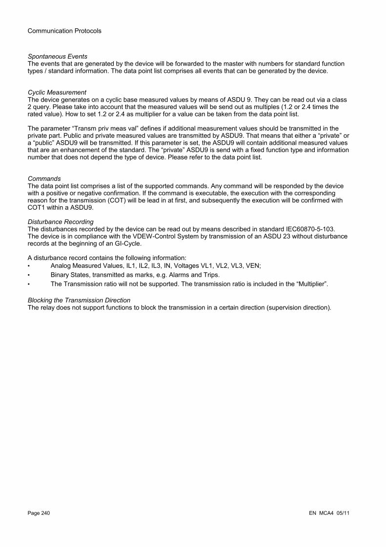
Communication Protocols
Spontaneous EventsThe events that are generated by the device will be forwarded to the master with numbers for standard function types / standard information. The data point list comprises all events that can be generated by the device.
Cyclic MeasurementThe device generates on a cyclic base measured values by means of ASDU 9. They can be read out via a class 2 query. Please take into account that the measured values will be send out as multiples (1.2 or 2.4 times the rated value). How to set 1.2 or 2.4 as multiplier for a value can be taken from the data point list.
The parameter “Transm priv meas val” defines if additional measurement values should be transmitted in the private part. Public and private measured values are transmitted by ASDU9. That means that either a “private” or a “public” ASDU9 will be transmitted. If this parameter is set, the ASDU9 will contain additional measured values that are an enhancement of the standard. The “private” ASDU9 is send with a fixed function type and information number that does not depend the type of device. Please refer to the data point list.
CommandsThe data point list comprises a list of the supported commands. Any command will be responded by the device with a positive or negative confirmation. If the command is executable, the execution with the corresponding reason for the transmission (COT) will be lead in at first, and subsequently the execution will be confirmed with COT1 within a ASDU9.
Disturbance RecordingThe disturbances recorded by the device can be read out by means described in standard IEC60870-5-103. The device is in compliance with the VDEW-Control System by transmission of an ASDU 23 without disturbance records at the beginning of an GI-Cycle.
A disturbance record contains the following information: • Analog Measured Values, IL1, IL2, IL3, IN, Voltages VL1, VL2, VL3, VEN;• Binary States, transmitted as marks, e.g. Alarms and Trips. • The Transmission ratio will not be supported. The transmission ratio is included in the “Multiplier”.
Blocking the Transmission DirectionThe relay does not support functions to block the transmission in a certain direction (supervision direction).
Page 240 EN MCA4 05/11

Communication Protocols
Global Protection Parameters of the IEC60870-5-103
Parameter Description Setting range Default Menu path
Slave ID Device address (Slave ID) within the bus system. Each device address has to be unique within a bus system.
1 - 247 1 [Device Para
/IEC 103]
t-call If there is no request telegram sent from Scada to the device after expiry of this time - the device concludes a communication failure within the Scada system.
1 - 3600s 60s [Device Para
/IEC 103]
Transm priv meas val
Transmit additional (private) measuring values inactive,
active
inactive [Device Para
/IEC 103]
Baud rate Baud rate 1200,
2400,
4800,
9600,
19200,
38400,
57600
19200 [Device Para
/IEC 103]
Physical Settings
Digit 1: Number of bits. Digit 2: E=even parity, O=odd parity, N=no parity. Digit 3: Number of stop bits. More information on the parity: It is possible that the last data bit is followed by a parity bit which is used for recognition of communication errors. The parity bit ensures that with even parity ("EVEN") always an even number of bits with valence "1" or with odd parity ("ODD") an odd number of "1" valence bits are transmitted. But it is also possible to transmit no parity bits (here the setting is "Parity = None"). More information on the stop-bits: The end of a data byte is terminated by the stop-bits.
8E1,
8O1,
8N1,
8N2
8E1 [Device Para
/IEC 103]
EN MCA4 05/11 Page 241
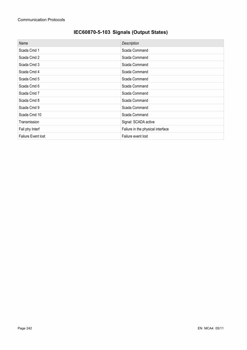
Communication Protocols
IEC60870-5-103 Signals (Output States)
Name Description
Scada Cmd 1 Scada CommandScada Cmd 2 Scada CommandScada Cmd 3 Scada CommandScada Cmd 4 Scada CommandScada Cmd 5 Scada CommandScada Cmd 6 Scada CommandScada Cmd 7 Scada CommandScada Cmd 8 Scada CommandScada Cmd 9 Scada CommandScada Cmd 10 Scada CommandTransmission Signal: SCADA activeFail phy Interf Failure in the physical interfaceFailure Event lost Failure event lost
Page 242 EN MCA4 05/11
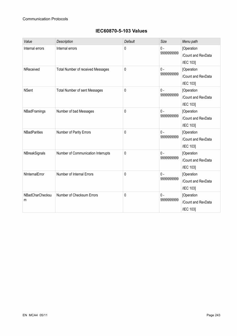
Communication Protocols
IEC60870-5-103 Values
Value Description Default Size Menu path
Internal errors Internal errors 0 0 - 9999999999
[Operation
/Count and RevData
/IEC 103]NReceived Total Number of received Messages 0 0 -
9999999999[Operation
/Count and RevData
/IEC 103]NSent Total Number of sent Messages 0 0 -
9999999999[Operation
/Count and RevData
/IEC 103]NBadFramings Number of bad Messages 0 0 -
9999999999[Operation
/Count and RevData
/IEC 103]NBadParities Number of Parity Errors 0 0 -
9999999999[Operation
/Count and RevData
/IEC 103]NBreakSignals Number of Communication Interrupts 0 0 -
9999999999[Operation
/Count and RevData
/IEC 103]NInternalError Number of Internal Errors 0 0 -
9999999999[Operation
/Count and RevData
/IEC 103]NBadCharChecksum
Number of Checksum Errors 0 0 - 9999999999
[Operation
/Count and RevData
/IEC 103]
EN MCA4 05/11 Page 243
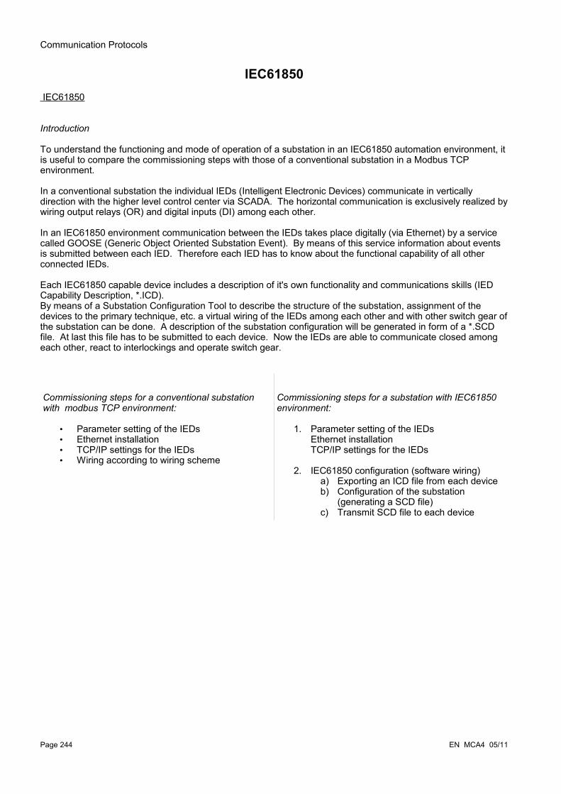
Communication Protocols
IEC61850 IEC61850
Introduction
To understand the functioning and mode of operation of a substation in an IEC61850 automation environment, it is useful to compare the commissioning steps with those of a conventional substation in a Modbus TCP environment.
In a conventional substation the individual IEDs (Intelligent Electronic Devices) communicate in vertically direction with the higher level control center via SCADA. The horizontal communication is exclusively realized by wiring output relays (OR) and digital inputs (DI) among each other.
In an IEC61850 environment communication between the IEDs takes place digitally (via Ethernet) by a service called GOOSE (Generic Object Oriented Substation Event). By means of this service information about events is submitted between each IED. Therefore each IED has to know about the functional capability of all other connected IEDs.
Each IEC61850 capable device includes a description of it's own functionality and communications skills (IED Capability Description, *.ICD).By means of a Substation Configuration Tool to describe the structure of the substation, assignment of the devices to the primary technique, etc. a virtual wiring of the IEDs among each other and with other switch gear of the substation can be done. A description of the substation configuration will be generated in form of a *.SCD file. At last this file has to be submitted to each device. Now the IEDs are able to communicate closed among each other, react to interlockings and operate switch gear.
Commissioning steps for a conventional substation with modbus TCP environment:
• Parameter setting of the IEDs• Ethernet installation• TCP/IP settings for the IEDs• Wiring according to wiring scheme
Commissioning steps for a substation with IEC61850 environment:
1. Parameter setting of the IEDsEthernet installationTCP/IP settings for the IEDs
2. IEC61850 configuration (software wiring)a) Exporting an ICD file from each deviceb) Configuration of the substation
(generating a SCD file)c) Transmit SCD file to each device
Page 244 EN MCA4 05/11

Communication Protocols
Generation/Export of a device specific ICD file
Each device of the HighPROTEC line includes a description of it's own functionality and communications skills in form of an *.ICD file (IED Capability Description). This file can be exported as follows and be used for the configuration of the substation.
• A change of the devices parameters has an influence on the content of the ICD file.
1. Connect the device with your PC/Notebook.2. Start Smart view.3. Click on »Receive data from Device« in the menu »Device«.4. Click on »IEC61850« in the menu »Device Para«.5. Click on the ICD icon in the IEC61850 window.6. Select a drive and file name for the ICD file and click "save".7. Repeat the steps 1 to 6 for all connected devices in this IEC61850 environment.
Substation configuration,Generation of .SCD file (Station Configuration Description)
The substation configuration, i. e. connection of all logical nodes of protection and control devices, as well as switch gear usually is done with a „Substation Configuration Tool“. Therefore the ICD files of all connected IEDs in the IEC61850 environment have to be available. The result of the station wide “software wiring” can be exported in the form of a SCD file (Station Configuration Description).
Suitable Substation Configuration Tools (SCT) are available by the following Companies:
H&S, Hard- & Software Technologie GmbH & Co. KG, Dortmund (Germany) (www.hstech.de).Applied Systems Engineering Inc. (www.ase-systems.com)Kalki Communication Technologies Limited (www.kalkitech.com)
EN MCA4 05/11 Page 245

Communication Protocols
Import of the .SCD file into the device
When the substation configuration is completed, the .SCD file has to be transmitted to all connected devices. This is has to be done as follows:
1. Connect the device with your PC/Notebook.2. Start Smart view.3. Click on »Receive data from Device« in the menu »Device«.4. Click on »IEC61850« in the menu »Device Para«.5. Switch the parameter »IEC61850 Communication« to »OFF« and submit the changed parameter set
into the device.6. Click on the SCD icon in the IEC61850 window.7. Select the folder, where the .SCD file is stored. Select the .SCD file and click "open".8. Now a password is requested. Enter the same password, which you use for parameter setting of the
device (4 digits).9. Acc. to step 5 switch on again the IEC Communication and submit the changed parameter set into the
device.10. Repeat the steps 1 to 9 for all devices connected to this IEC61850 environment.11. If no error message occurs, the configuration has been completed successfully.
• When changing the substation configuration, usually a new .SCD file has to be generated. This .SCD file has to be mandatory transmitted to all devices by means of Smart view. For the case, that this step will be forgotten, IEC61850 malfunctions will be the result
• Provided that parameters of the devices are changed after the substation configuration completion, changes in the corresponding .ICD file may result – this in turn may make an update of the .SCD file necessary.
IEC 61850 Virtual Outputs
Additionally to the standardized logical node status information up to 16 free configurable status information can be assigned to 16 Virtual Outputs. This can be done in the menu [Device Para/IEC61850].
Page 246 EN MCA4 05/11

Communication Protocols
Device Planning Parameters of the IEC 61850
Parameter Description Options Default Menu path
Mode Mode do not use,
use
use [Device planning]
Direct Commands of the IEC 61850
Parameter Description Setting range Default Menu path
ResetStatistic
Reset of all IEC61850 diagnostic counters inactive,
active
inactive [Operation
/Reset]
EN MCA4 05/11 Page 247

Communication Protocols
Global Protection Parameters of the IEC 61850
Parameter Description Setting range Default Menu path
Function Permanent activation or deactivation of module/stage.
active,
inactive
inactive [Device Para
/IEC61850]
VirtualOutput1
Virtual Output. This signal can be assigned or visualized via the SCD file to other devices within the IEC61850 substation.
1..n, Assignment List -.- [Device Para
/IEC61850]
VirtualOutput2
Virtual Output. This signal can be assigned or visualized via the SCD file to other devices within the IEC61850 substation.
1..n, Assignment List -.- [Device Para
/IEC61850]
VirtualOutput3
Virtual Output. This signal can be assigned or visualized via the SCD file to other devices within the IEC61850 substation.
1..n, Assignment List -.- [Device Para
/IEC61850]
VirtualOutput4
Virtual Output. This signal can be assigned or visualized via the SCD file to other devices within the IEC61850 substation.
1..n, Assignment List -.- [Device Para
/IEC61850]
VirtualOutput5
Virtual Output. This signal can be assigned or visualized via the SCD file to other devices within the IEC61850 substation.
1..n, Assignment List -.- [Device Para
/IEC61850]
VirtualOutput6
Virtual Output. This signal can be assigned or visualized via the SCD file to other devices within the IEC61850 substation.
1..n, Assignment List -.- [Device Para
/IEC61850]
VirtualOutput7
Virtual Output. This signal can be assigned or visualized via the SCD file to other devices within the IEC61850 substation.
1..n, Assignment List -.- [Device Para
/IEC61850]
VirtualOutput8
Virtual Output. This signal can be assigned or visualized via the SCD file to other devices within the IEC61850 substation.
1..n, Assignment List -.- [Device Para
/IEC61850]
VirtualOutput9
Virtual Output. This signal can be assigned or visualized via the SCD file to other devices within the IEC61850 substation.
1..n, Assignment List -.- [Device Para
/IEC61850]
Page 248 EN MCA4 05/11
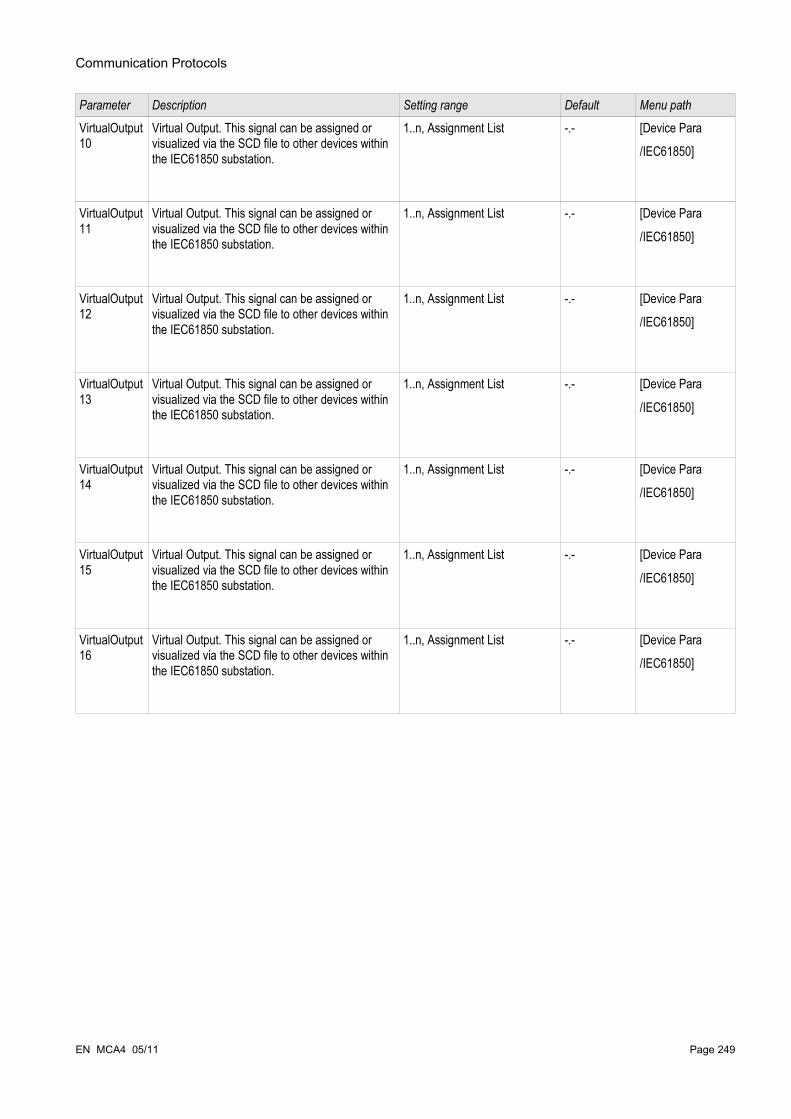
Communication Protocols
Parameter Description Setting range Default Menu path
VirtualOutput10
Virtual Output. This signal can be assigned or visualized via the SCD file to other devices within the IEC61850 substation.
1..n, Assignment List -.- [Device Para
/IEC61850]
VirtualOutput11
Virtual Output. This signal can be assigned or visualized via the SCD file to other devices within the IEC61850 substation.
1..n, Assignment List -.- [Device Para
/IEC61850]
VirtualOutput12
Virtual Output. This signal can be assigned or visualized via the SCD file to other devices within the IEC61850 substation.
1..n, Assignment List -.- [Device Para
/IEC61850]
VirtualOutput13
Virtual Output. This signal can be assigned or visualized via the SCD file to other devices within the IEC61850 substation.
1..n, Assignment List -.- [Device Para
/IEC61850]
VirtualOutput14
Virtual Output. This signal can be assigned or visualized via the SCD file to other devices within the IEC61850 substation.
1..n, Assignment List -.- [Device Para
/IEC61850]
VirtualOutput15
Virtual Output. This signal can be assigned or visualized via the SCD file to other devices within the IEC61850 substation.
1..n, Assignment List -.- [Device Para
/IEC61850]
VirtualOutput16
Virtual Output. This signal can be assigned or visualized via the SCD file to other devices within the IEC61850 substation.
1..n, Assignment List -.- [Device Para
/IEC61850]
EN MCA4 05/11 Page 249
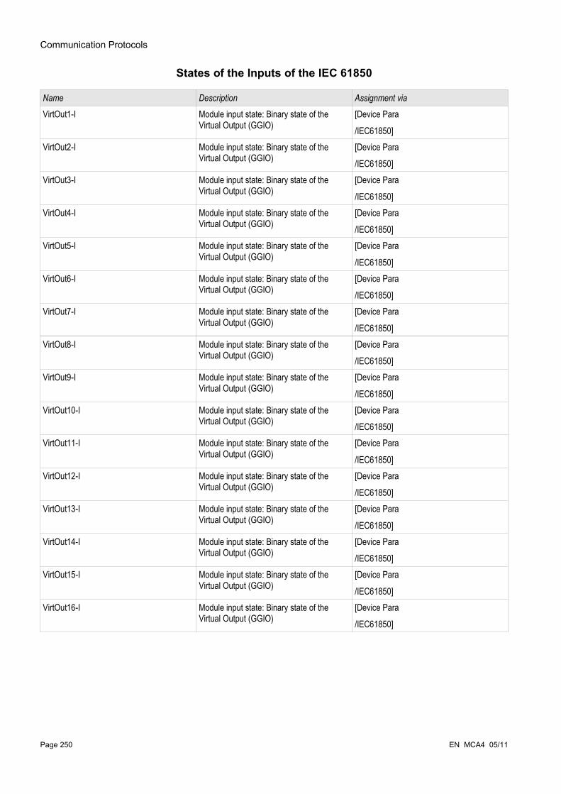
Communication Protocols
States of the Inputs of the IEC 61850
Name Description Assignment via
VirtOut1-I Module input state: Binary state of the Virtual Output (GGIO)
[Device Para
/IEC61850]VirtOut2-I Module input state: Binary state of the
Virtual Output (GGIO)[Device Para
/IEC61850]VirtOut3-I Module input state: Binary state of the
Virtual Output (GGIO)[Device Para
/IEC61850]VirtOut4-I Module input state: Binary state of the
Virtual Output (GGIO)[Device Para
/IEC61850]VirtOut5-I Module input state: Binary state of the
Virtual Output (GGIO)[Device Para
/IEC61850]VirtOut6-I Module input state: Binary state of the
Virtual Output (GGIO)[Device Para
/IEC61850]VirtOut7-I Module input state: Binary state of the
Virtual Output (GGIO)[Device Para
/IEC61850]VirtOut8-I Module input state: Binary state of the
Virtual Output (GGIO)[Device Para
/IEC61850]VirtOut9-I Module input state: Binary state of the
Virtual Output (GGIO)[Device Para
/IEC61850]VirtOut10-I Module input state: Binary state of the
Virtual Output (GGIO)[Device Para
/IEC61850]VirtOut11-I Module input state: Binary state of the
Virtual Output (GGIO)[Device Para
/IEC61850]VirtOut12-I Module input state: Binary state of the
Virtual Output (GGIO)[Device Para
/IEC61850]VirtOut13-I Module input state: Binary state of the
Virtual Output (GGIO)[Device Para
/IEC61850]VirtOut14-I Module input state: Binary state of the
Virtual Output (GGIO)[Device Para
/IEC61850]VirtOut15-I Module input state: Binary state of the
Virtual Output (GGIO)[Device Para
/IEC61850]VirtOut16-I Module input state: Binary state of the
Virtual Output (GGIO)[Device Para
/IEC61850]
Page 250 EN MCA4 05/11
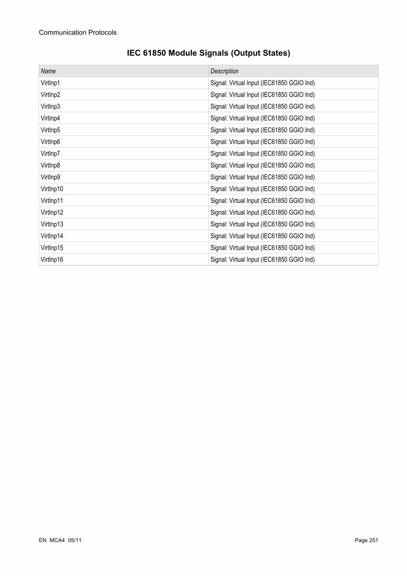
Communication Protocols
IEC 61850 Module Signals (Output States)
Name Description
VirtInp1 Signal: Virtual Input (IEC61850 GGIO Ind)VirtInp2 Signal: Virtual Input (IEC61850 GGIO Ind)VirtInp3 Signal: Virtual Input (IEC61850 GGIO Ind)VirtInp4 Signal: Virtual Input (IEC61850 GGIO Ind)VirtInp5 Signal: Virtual Input (IEC61850 GGIO Ind)VirtInp6 Signal: Virtual Input (IEC61850 GGIO Ind)VirtInp7 Signal: Virtual Input (IEC61850 GGIO Ind)VirtInp8 Signal: Virtual Input (IEC61850 GGIO Ind)VirtInp9 Signal: Virtual Input (IEC61850 GGIO Ind)VirtInp10 Signal: Virtual Input (IEC61850 GGIO Ind)VirtInp11 Signal: Virtual Input (IEC61850 GGIO Ind)VirtInp12 Signal: Virtual Input (IEC61850 GGIO Ind)VirtInp13 Signal: Virtual Input (IEC61850 GGIO Ind)VirtInp14 Signal: Virtual Input (IEC61850 GGIO Ind)VirtInp15 Signal: Virtual Input (IEC61850 GGIO Ind)VirtInp16 Signal: Virtual Input (IEC61850 GGIO Ind)
EN MCA4 05/11 Page 251
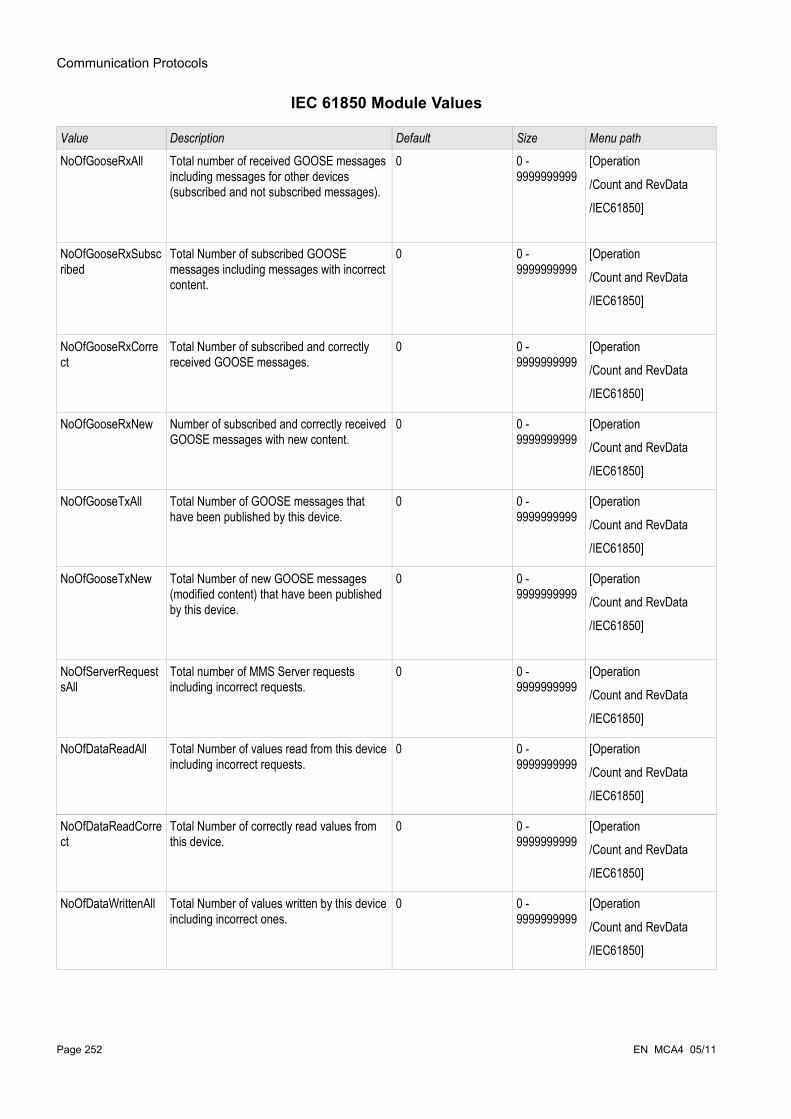
Communication Protocols
IEC 61850 Module Values
Value Description Default Size Menu path
NoOfGooseRxAll Total number of received GOOSE messages including messages for other devices (subscribed and not subscribed messages).
0 0 - 9999999999
[Operation
/Count and RevData
/IEC61850]
NoOfGooseRxSubscribed
Total Number of subscribed GOOSE messages including messages with incorrect content.
0 0 - 9999999999
[Operation
/Count and RevData
/IEC61850]
NoOfGooseRxCorrect
Total Number of subscribed and correctly received GOOSE messages.
0 0 - 9999999999
[Operation
/Count and RevData
/IEC61850]
NoOfGooseRxNew Number of subscribed and correctly received GOOSE messages with new content.
0 0 - 9999999999
[Operation
/Count and RevData
/IEC61850]
NoOfGooseTxAll Total Number of GOOSE messages that have been published by this device.
0 0 - 9999999999
[Operation
/Count and RevData
/IEC61850]
NoOfGooseTxNew Total Number of new GOOSE messages (modified content) that have been published by this device.
0 0 - 9999999999
[Operation
/Count and RevData
/IEC61850]
NoOfServerRequestsAll
Total number of MMS Server requests including incorrect requests.
0 0 - 9999999999
[Operation
/Count and RevData
/IEC61850]
NoOfDataReadAll Total Number of values read from this device including incorrect requests.
0 0 - 9999999999
[Operation
/Count and RevData
/IEC61850]
NoOfDataReadCorrect
Total Number of correctly read values from this device.
0 0 - 9999999999
[Operation
/Count and RevData
/IEC61850]
NoOfDataWrittenAll Total Number of values written by this device including incorrect ones.
0 0 - 9999999999
[Operation
/Count and RevData
/IEC61850]
Page 252 EN MCA4 05/11

Communication Protocols
Value Description Default Size Menu path
NoOfDataWrittenCorrect
Total Number of correctly written values by this device.
0 0 - 9999999999
[Operation
/Count and RevData
/IEC61850]
NoOfDataChangeNotification
Number of detected changes within the datasets that are published with GOOSE messages.
0 0 - 9999999999
[Operation
/Count and RevData
/IEC61850]
Values of the IEC 61850
Value Description Default Size Menu path
GoosePublisherState
State of the GOOSE Publisher (on or off) Off Off,
On,
Error
[Operation
/Status display
/IEC61850]GooseSubscriberState
State of the GOOSE Subscriber (on or off) Off Off,
On,
Error
[Operation
/Status display
/IEC61850]MmsServerState State of MMS Server (on or off) Off Off,
On,
Error
[Operation
/Status display
/IEC61850]
EN MCA4 05/11 Page 253
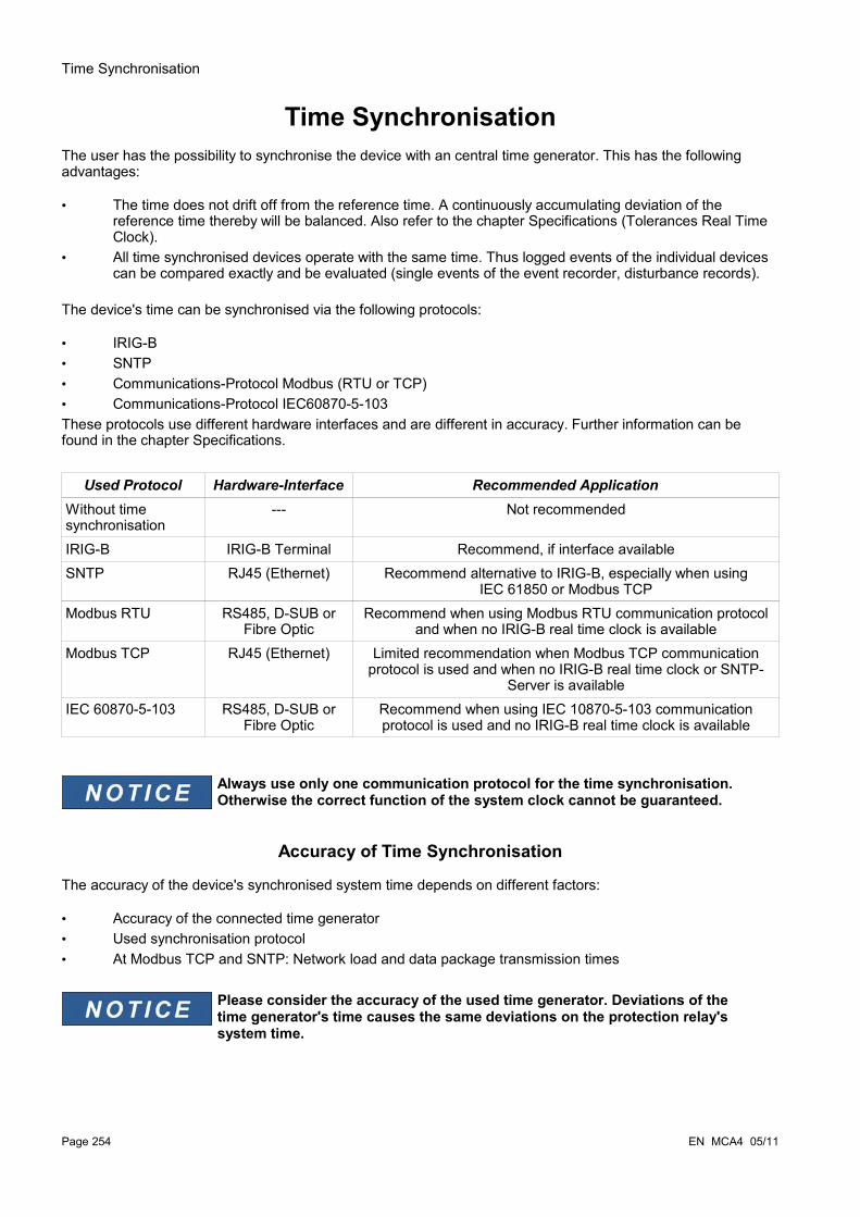
Time Synchronisation
Time SynchronisationThe user has the possibility to synchronise the device with an central time generator. This has the following advantages:
• The time does not drift off from the reference time. A continuously accumulating deviation of the reference time thereby will be balanced. Also refer to the chapter Specifications (Tolerances Real Time Clock).
• All time synchronised devices operate with the same time. Thus logged events of the individual devices can be compared exactly and be evaluated (single events of the event recorder, disturbance records).
The device's time can be synchronised via the following protocols:
• IRIG-B• SNTP• Communications-Protocol Modbus (RTU or TCP)• Communications-Protocol IEC60870-5-103These protocols use different hardware interfaces and are different in accuracy. Further information can be found in the chapter Specifications.
Used Protocol Hardware-Interface Recommended ApplicationWithout time synchronisation
--- Not recommended
IRIG-B IRIG-B Terminal Recommend, if interface availableSNTP RJ45 (Ethernet) Recommend alternative to IRIG-B, especially when using
IEC 61850 or Modbus TCPModbus RTU RS485, D-SUB or
Fibre OpticRecommend when using Modbus RTU communication protocol
and when no IRIG-B real time clock is availableModbus TCP RJ45 (Ethernet) Limited recommendation when Modbus TCP communication
protocol is used and when no IRIG-B real time clock or SNTP-Server is available
IEC 60870-5-103 RS485, D-SUB or Fibre Optic
Recommend when using IEC 10870-5-103 communication protocol is used and no IRIG-B real time clock is available
Always use only one communication protocol for the time synchronisation. Otherwise the correct function of the system clock cannot be guaranteed.
Accuracy of Time Synchronisation
The accuracy of the device's synchronised system time depends on different factors:
• Accuracy of the connected time generator• Used synchronisation protocol• At Modbus TCP and SNTP: Network load and data package transmission times
Please consider the accuracy of the used time generator. Deviations of the time generator's time causes the same deviations on the protection relay's system time.
Page 254 EN MCA4 05/11
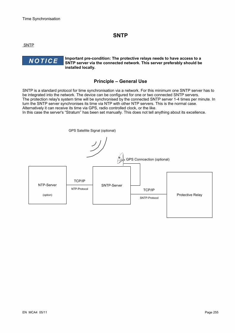
Time Synchronisation
SNTP SNTP
Important pre-condition: The protective relays needs to have access to a SNTP server via the connected network. This server preferably should be installed locally.
Principle – General Use
SNTP is a standard protocol for time synchronisation via a network. For this minimum one SNTP server has to be integrated into the network. The device can be configured for one or two connected SNTP servers.The protection relay's system time will be synchronised by the connected SNTP server 1-4 times per minute. In turn the SNTP server synchronises its time via NTP with other NTP servers. This is the normal case. Alternatively it can receive its time via GPS, radio controlled clock, or the like.In this case the server's “Stratum” has been set manually. This does not tell anything about its excellence.
EN MCA4 05/11 Page 255
SNTP-Server
Protective Relay
GPS Satellite Signal (optional)
GPS Conncection (optional)
TCP/IPNTP-Server
SNTP-Protocol
NTP-Protocol
TCP/IP
(option)

Time Synchronisation
Accuracy
The accuracy of the used SNTP server and the excellence of its reference clock influences the accuracy of the protection relay's clock.
With each transmitted time information, the SNTP server sends information about its accuracy:• Stratum: The stratum gives information, how close the SNTP server within the cluster is to other NTP
servers that are connected to an atomic clock.• Precision: This is the accuracy, the SNTP server provides the system time.
Also the performance (traffic and data package transmission time) of the connected network has an influence on the accuracy of the time synchronisation. Recommended is a locally installed SNTP server with an accuracy of ≤200 µsec. If this cannot be realised, the connected server's excellence can be checked in the menu [Operation/Status Display/Time Sync.]:
• The server quality gives information about the accuracy of the used server. The quality should be GOOD or MEDIUM. A server with POOR quality should not be used, because this could cause fluctuations of the time synchronisation.
• The network quality gives information about the network's load and data package transmission time. The quality should be GOOD or MEDIUM. A network with POOR quality should not be used, because this could cause fluctuations during time synchronisation.
Using two SNTP Servers
When configuring two SNTP servers, the device selects the server with the lower stratum value, because this provides a more precise time synchronisation. If the servers have the same stratum value, the device selects the server with the better accuracy (precision). It dos not matter, which of the servers is configured as server 1 or server 2. When the last used server fails, the device automatically switches to the other server. When the server recovers, the device switches back to the previous one with the better quality.
Page 256 EN MCA4 05/11

Time Synchronisation
SNTP CommissioningActivate the SNTP time synchronisation by means of the menu [Device Para/Time Sync./Sntp]:
• Set the server IP address.• Set the IP address of the second server, if available.• Set all configures servers to “active”.• Select a time zone.
When the connected SNTP server sends a UTC signal, select your local time zone (one of 36 UTC time zones). This is normally the case. If the server sends a local time signal, select the time zone „UTC+0 London“.
• “Summer time” can be activated or deactivated.When the connected SNTP server sends a UTC signal, activate the “Summer time” according to your needs. This is normally the case. If the server sends a local time signal, deactivate the “Summer time”
The selection of summer or winter time has to be done manually. The relays does not do this automatically.
Fault Analysis
If there is no SNTP signal for more than 120 sec. The SNTP status changes from “active” to “inactive” and an entry in the Event Recorder will be set.
The SNTP functionality can be checked in the menu [Operation/Status Display/Time Sync./Sntp]:If the SNTP status is not “active”, please proceed as follows:
• Check if wiring is correct (Ethernet-cable connected).• Check if a valid IP address is set in the device (Device Para/TCP/IP).• Check if the Ethernet connection is active (Device Para/TCP/IP/Link = Up?).• Check if the SNTP server as well as the protection device answers to a Ping.• Check if the SNTP server is up and works.
EN MCA4 05/11 Page 257

Time Synchronisation
Device Planning Parameters of the SNTP
Parameter Description Options Default Menu path
Mode Mode do not use,
use
do not use [Device planning]
Direct Commands of the SNTP
Parameter Description Setting range Default Menu path
Res Counter Reset all Counters. inactive,
active
inactive [Operation
/Reset]
Global Protection Parameters of the SNTP
Parameter Description Setting range Default Menu path
Server1 Server 1 inactive,
active
inactive [Device Para
/TimeSync
/SNTP
/IP Server1]IP Byte1 IP1.IP2.IP3.IP4 0 - 255 0 [Device Para
/TimeSync
/SNTP
/IP Server1]IP Byte2 IP1.IP2.IP3.IP4 0 - 255 0 [Device Para
/TimeSync
/SNTP
/IP Server1]IP Byte3 IP1.IP2.IP3.IP4 0 - 255 0 [Device Para
/TimeSync
/SNTP
/IP Server1]IP Byte4 IP1.IP2.IP3.IP4 0 - 255 0 [Device Para
/TimeSync
/SNTP
/IP Server1]Server2 Server 2 inactive,
active
inactive [Device Para
/TimeSync
/SNTP
/IP Server2]
Page 258 EN MCA4 05/11
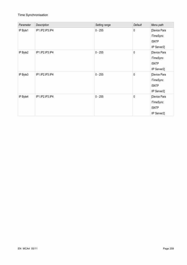
Time Synchronisation
Parameter Description Setting range Default Menu path
IP Byte1 IP1.IP2.IP3.IP4 0 - 255 0 [Device Para
/TimeSync
/SNTP
/IP Server2]IP Byte2 IP1.IP2.IP3.IP4 0 - 255 0 [Device Para
/TimeSync
/SNTP
/IP Server2]IP Byte3 IP1.IP2.IP3.IP4 0 - 255 0 [Device Para
/TimeSync
/SNTP
/IP Server2]IP Byte4 IP1.IP2.IP3.IP4 0 - 255 0 [Device Para
/TimeSync
/SNTP
/IP Server2]
EN MCA4 05/11 Page 259
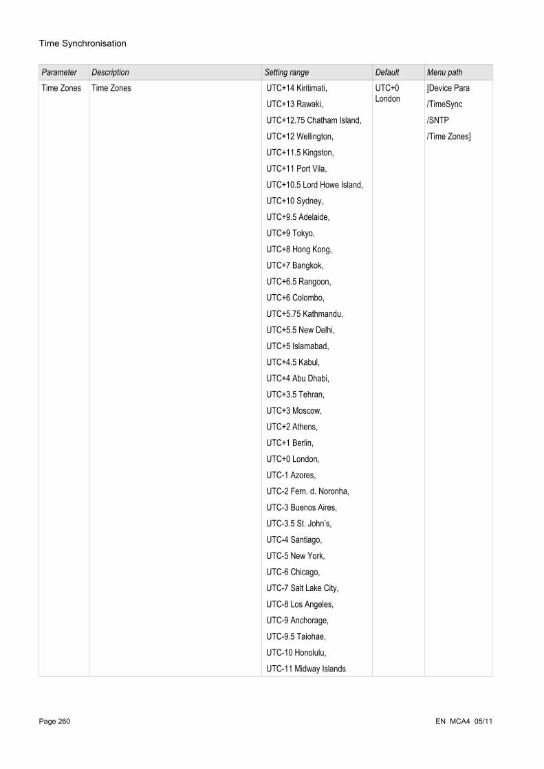
Time Synchronisation
Parameter Description Setting range Default Menu path
Time Zones Time Zones UTC+14 Kiritimati,
UTC+13 Rawaki,
UTC+12.75 Chatham Island,
UTC+12 Wellington,
UTC+11.5 Kingston,
UTC+11 Port Vila,
UTC+10.5 Lord Howe Island,
UTC+10 Sydney,
UTC+9.5 Adelaide,
UTC+9 Tokyo,
UTC+8 Hong Kong,
UTC+7 Bangkok,
UTC+6.5 Rangoon,
UTC+6 Colombo,
UTC+5.75 Kathmandu,
UTC+5.5 New Delhi,
UTC+5 Islamabad,
UTC+4.5 Kabul,
UTC+4 Abu Dhabi,
UTC+3.5 Tehran,
UTC+3 Moscow,
UTC+2 Athens,
UTC+1 Berlin,
UTC+0 London,
UTC-1 Azores,
UTC-2 Fern. d. Noronha,
UTC-3 Buenos Aires,
UTC-3.5 St. John’s,
UTC-4 Santiago,
UTC-5 New York,
UTC-6 Chicago,
UTC-7 Salt Lake City,
UTC-8 Los Angeles,
UTC-9 Anchorage,
UTC-9.5 Taiohae,
UTC-10 Honolulu,
UTC-11 Midway Islands
UTC+0 London
[Device Para
/TimeSync
/SNTP
/Time Zones]
Page 260 EN MCA4 05/11

Time Synchronisation
Parameter Description Setting range Default Menu path
Summer Time
Summer Time inactive,
active
inactive [Device Para
/TimeSync
/SNTP
/Time Zones]
EN MCA4 05/11 Page 261

Time Synchronisation
Signals of the SNTP
Name Description
SNTP active Signal: If there is no valid SNTP signal for 120 sec, SNTP is regarded as inactive.
SNTP Counters
Value Description Default Size Menu path
NoOfSyncs Total Number of Synchronizations. 0 0 - 9999999999
[Operation
/Count and RevData
/TimeSync
/SNTP]NoOfConnectLost Total Number of lost SNTP Connections (no
sync for 120 sec).0 0 -
9999999999[Operation
/Count and RevData
/TimeSync
/SNTP]NoOfSmallSyncs Service counter: Total Number of very small
Time Corrections.0 0 -
9999999999[Operation
/Count and RevData
/TimeSync
/SNTP]NoOfNormSyncs Service counter: Total Number of normal
Time Corrections0 0 -
9999999999[Operation
/Count and RevData
/TimeSync
/SNTP]NoOfBigSyncs Service counter: Total Number of big Time
Corrections0 0 -
9999999999[Operation
/Count and RevData
/TimeSync
/SNTP]NoOfFiltSyncs Service counter: Total Number of filtered
Time Corrections0 0 -
9999999999[Operation
/Count and RevData
/TimeSync
/SNTP]NoOfSlowTrans Service counter: Total Number of slow
Transfers.0 0 -
9999999999[Operation
/Count and RevData
/TimeSync
/SNTP]
Page 262 EN MCA4 05/11

Time Synchronisation
Value Description Default Size Menu path
NoOfHighOffs Service counter: Total Number of high Offsets.
0 0 - 9999999999
[Operation
/Count and RevData
/TimeSync
/SNTP]NoOfIntTimeouts Service counter: Total Number of internal
timeouts.0 0 -
9999999999[Operation
/Count and RevData
/TimeSync
/SNTP]StratumServer1 Stratum of Server 1 0 0 -
9999999999[Operation
/Status display
/TimeSync
/SNTP]StratumServer2 Stratum of Server 2 0 0 -
9999999999[Operation
/Status display
/TimeSync
/SNTP]
EN MCA4 05/11 Page 263
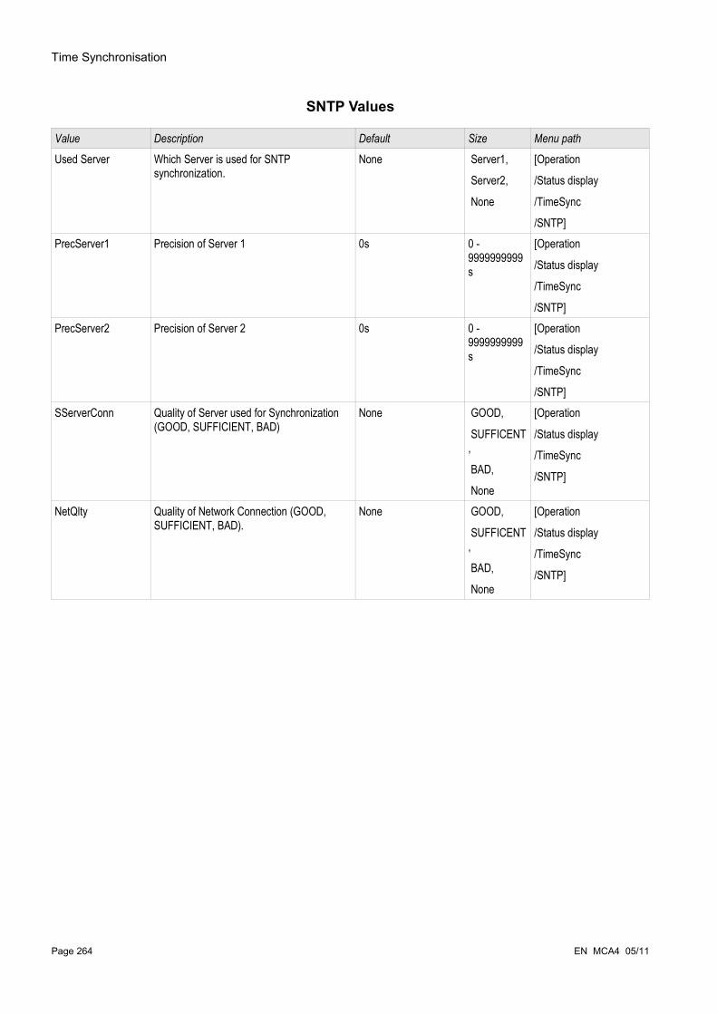
Time Synchronisation
SNTP Values
Value Description Default Size Menu path
Used Server Which Server is used for SNTP synchronization.
None Server1,
Server2,
None
[Operation
/Status display
/TimeSync
/SNTP]PrecServer1 Precision of Server 1 0s 0 -
9999999999s
[Operation
/Status display
/TimeSync
/SNTP]PrecServer2 Precision of Server 2 0s 0 -
9999999999s
[Operation
/Status display
/TimeSync
/SNTP]SServerConn Quality of Server used for Synchronization
(GOOD, SUFFICIENT, BAD)None GOOD,
SUFFICENT,
BAD,
None
[Operation
/Status display
/TimeSync
/SNTP]
NetQlty Quality of Network Connection (GOOD, SUFFICIENT, BAD).
None GOOD,
SUFFICENT,
BAD,
None
[Operation
/Status display
/TimeSync
/SNTP]
Page 264 EN MCA4 05/11

Time Synchronisation
IRIG-B00X IRIG-B
Requirement: An IRIG-B00X time code generator is needed. IRIG-B004 and higher will support/transmit the “year information”.
If you are using an IRIG time code that does not support the “year information” (IRIG-B000, IRIG-B001, IRIG-B002, IRIG-B003), you have to set the “year” manually within the device. In these cases the correct year information is a precondition for a properly working IRIG-B.
Principle - General Use
The IRIG-B standard is the most used standard to synchronize the time of protection devices in medium voltage applications.
The protection device supports IRIG-B according to the IRIG STANDARD 200-04.This means that all time synchronization formats IRIG-B00X (IRIG-B000 / B001 / B002 / B003 / B004 / B005 / B006 / B007) are supported. It is recommended to use IRIG-B004 and higher which also transmits the “year information”.
The system time of the protection device is being synchronized with the connected IRIG-B code generator once a second. The accuracy of the used IRIG-B code generator can be increased by connecting a GPS-receiver to it.
The location of the IRIG-B interface depends to the device type. Please refer to the wiring diagram supplied with the protective device.
EN MCA4 05/11 Page 265
IRIG-BTime Code Generator
Protective Relay
GPS Satellite Signal (optional)
GPS Conncection (optional)
+
Twisted Pair Cable
To Other Devices
-
Time Synchronisation
IRIG-B Commissioning
Activate the IRIG-B synchronization within menu [Device Para/ TimeSync/ IRIG-B]:
• Set the time synchronization via IRIG-B to »Active«.• Set the IRIG-B type (choose B000 through B007).• Set the time zone parameter.
If the connected IRIG-B code generator sends basic UTC time, please select your local time zone (one of 36 UTC time zones). This is the normal case. Should the IRIG-B code generator already be sending local time, leave the time zone at default (»UTC+0 London«).
• Activate or deactivate the »Daylight Saving Time«.If the connected IRIG-B code generator sends basic UTC time, please select daylight saving time as necessary. This is the normal case. Should the IRIG-B code generator already be sending local time, leave the daylight saving time deactivated.
The parameter for Daylight Saving Time (summer-winter time) has to be set manually. The device does not switch automatically.
Fault Analysis
If the device does not receive any IRIG-B time code for more than 60 s, the IRIG-B status switches from »active« to »inactive« and there is created an entry within the Event Recorder.
Check the IRIG-B functionality through the menu [Operation/ Status display/ TimeSync/ IRIG-B]:Should the IRIG-B status not be reported as being »active«, please proceed as follows:
• To begin with check the IRIG-B wiring.• Check, if the correct IRIG-B00X type is configured.
IRIG-B Control Commands
In addition to the date and time information, the IRIG-B code offers the option to transmit up to 18 control commands that can be processed by the protective device. They have to be set and issued by the IRIG-B code generator.
The protective device offers up to 18 IRIG-B assignment options for those control commands in order to carry out the assigned action. If there is a control command assigned to an action, this action is being triggered as soon as the control command is transmitted as being true. As an example there can be triggered the start of statistics or the street lighting can be switched on through a relay.
Page 266 EN MCA4 05/11

Time Synchronisation
Device Planning Parameters of the IRIG-B00X
Parameter Description Options Default Menu path
Mode Mode do not use,
use
do not use [Device planning]
Direct Commands of the IRIG-B00X
Parameter Description Setting range Default Menu path
Res IRIG-B Cr
Resetting of the Diagnosis Counters: IRIG-B inactive,
active
inactive [Operation
/Reset]
Global Protection Parameters of the IRIG-B00X
Parameter Description Setting range Default Menu path
Function Permanent activation or deactivation of module/stage.
inactive,
active
inactive [Device Para
/TimeSync
/IRIG-B]IRIG-B00X Determination of the Type: IRIG-B00X. IRIG-B
types differ in types of included “Coded Expressions” (year, control-functions, straight-binary-seconds).
IRIGB-000,
IRIGB-001,
IRIGB-002,
IRIGB-003,
IRIGB-004,
IRIGB-005,
IRIGB-006,
IRIGB-007
IRIGB-000 [Device Para
/TimeSync
/IRIG-B]
EN MCA4 05/11 Page 267
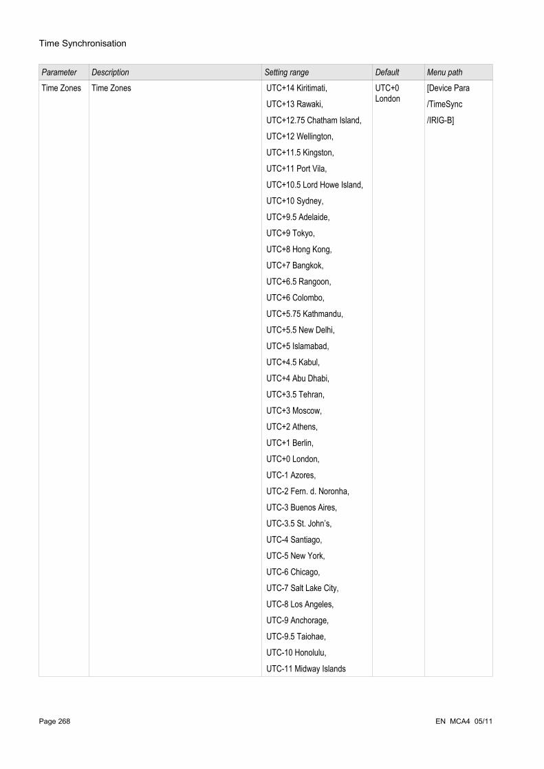
Time Synchronisation
Parameter Description Setting range Default Menu path
Time Zones Time Zones UTC+14 Kiritimati,
UTC+13 Rawaki,
UTC+12.75 Chatham Island,
UTC+12 Wellington,
UTC+11.5 Kingston,
UTC+11 Port Vila,
UTC+10.5 Lord Howe Island,
UTC+10 Sydney,
UTC+9.5 Adelaide,
UTC+9 Tokyo,
UTC+8 Hong Kong,
UTC+7 Bangkok,
UTC+6.5 Rangoon,
UTC+6 Colombo,
UTC+5.75 Kathmandu,
UTC+5.5 New Delhi,
UTC+5 Islamabad,
UTC+4.5 Kabul,
UTC+4 Abu Dhabi,
UTC+3.5 Tehran,
UTC+3 Moscow,
UTC+2 Athens,
UTC+1 Berlin,
UTC+0 London,
UTC-1 Azores,
UTC-2 Fern. d. Noronha,
UTC-3 Buenos Aires,
UTC-3.5 St. John’s,
UTC-4 Santiago,
UTC-5 New York,
UTC-6 Chicago,
UTC-7 Salt Lake City,
UTC-8 Los Angeles,
UTC-9 Anchorage,
UTC-9.5 Taiohae,
UTC-10 Honolulu,
UTC-11 Midway Islands
UTC+0 London
[Device Para
/TimeSync
/IRIG-B]
Page 268 EN MCA4 05/11

Time Synchronisation
Parameter Description Setting range Default Menu path
Summer Time
Summer Time inactive,
active
inactive [Device Para
/TimeSync
/IRIG-B]
EN MCA4 05/11 Page 269

Time Synchronisation
Signals of the IRIG-B00X (Output States)
Name Description
active Signal: activeinverted Signal: IRIG-B invertedControl Signal1 Signal: IRIG-B Control SignalControl Signal2 Signal: IRIG-B Control SignalControl Signal4 Signal: IRIG-B Control SignalControl Signal5 Signal: IRIG-B Control SignalControl Signal6 Signal: IRIG-B Control SignalControl Signal7 Signal: IRIG-B Control SignalControl Signal8 Signal: IRIG-B Control SignalControl Signal9 Signal: IRIG-B Control SignalControl Signal10 Signal: IRIG-B Control SignalControl Signal11 Signal: IRIG-B Control SignalControl Signal12 Signal: IRIG-B Control SignalControl Signal13 Signal: IRIG-B Control SignalControl Signal14 Signal: IRIG-B Control SignalControl Signal15 Signal: IRIG-B Control SignalControl Signal16 Signal: IRIG-B Control SignalControl Signal17 Signal: IRIG-B Control SignalControl Signal18 Signal: IRIG-B Control Signal
IRIG-B00X Values
Value Description Default Size Menu path
NoOfFramesOK Total Number valid Frames. 0 0 - 65535 [Operation
/Count and RevData
/TimeSync
/IRIG-B]NoOfFrameErrors Total Number of Frame Errors. Physically
corrupted Frame.0 0 - 65535 [Operation
/Count and RevData
/TimeSync
/IRIG-B]Edges Edges 0 0 - 65535 [Operation
/Count and RevData
/TimeSync
/IRIG-B]
Page 270 EN MCA4 05/11

Parameters
ParametersParameter setting and planning can be done:
• directly at the device or
• by way of the Smart view software.
Parameter Definitions
Device Parameters
Device Parameters are part of the Device Parameter Tree. By means of them you can (depending on the type of device):
• Set cutoff levels,• Configure Digital Inputs,• Configure Output Relays,• Assign LEDs,• Assign Acknowledgment Signals,• Configure Statistics,• Configure Protocol Parameters,• Adapt HMI Settings,• Configure Recorders (reports),• Set Date and Time,• Change Passwords,• Check the version (build) of the device.
Field Parameters
Field Parameters are part of the Device Parameter Tree. Field Parameters comprise the essential, basic settings of your switchboard such as rated frequency, transformer ratios.
Protection Parameters
Protection Parameters are part of the Device Parameter Tree. This tree comprises:
• Global Protection Parameters are part of the Protection Parameters: All settings and assignments that are done within the Global Parameter Tree are valid independent of the Setting Groups. They have to be set once only. In addition to that they comprise the CB Management.
• The Parameter Setting Switch is part of the Protection Parameters: You can either direct switch onto a certain parameter setting group or you can determine the conditions for switching onto another parameter setting group.
• Setting Group Parameters are part of the Protection Parameters: By means of the Parameter Setting Group Parameters you can individually adapt you protective device to the current conditions or grid conditions. They can be individually set in each Setting group.
EN MCA4 05/11 Page 271
Parameters
Device Planning Parameters
Device Planning Parameters are part of the Device Parameter Tree.
• Improving the Usability (clearness): All protection modules that are currently not needed can be • de-protected (switched to invisible) by means of Device Planning. In Menu Device Planning you can
adapt the scope of functionality of the protective device exactly to your needs. You can improve the usability by de-projecting all modules that are currently not needed.
• Adapting the device to your application: For those modules that you need, determine how they should work (e.g. directional, non-directional, <, >...).
Direct Commands
Direct Commands are part of the Device Parameter Tree but they are NOT part of the parameter file. They will be executed directly (e.g. Resetting of a Counter).
State of the Module Inputs
Module Inputs are part of the Device Parameter Tree. The State of the Module Input is context-dependent.
By means of the Module Inputs influence can be taken on the Modules. You can assign Signals onto Module Inputs. The state of the signals that are assigned to an input can be taken from the Status Display. Module Inputs can be identified by an „-I“ at the end of the name.
Signals
Signals are part of the Device Parameter Tree. The state of the signal is context-dependent.
• Signals represent the state of your installation/equipment (e.g. Position Indicators of the Circuit Breaker).
• Signals are assessments of the state of the grid and the equipment (System OK, Transformer failure detected...).
• Signals represent decisions that are taken by the device (e.g. Trip command) based on your parameter settings.
Page 272 EN MCA4 05/11

Parameters
Adaptive Parameter Sets
EN MCA4 05/11 Page 273
PSet-SwitchAdap
tSet
Prot
ectio
n P
ara
Para
met
er S
et 4
activ
e/in
activ
eac
tive/
inac
tive
activ
e/in
activ
eac
tive/
inac
tive
activ
e/in
activ
e
Para
met
er S
et 3
activ
e/in
activ
eac
tive/
inac
tive
activ
e/in
activ
eac
tive/
inac
tive
activ
e/in
activ
e
Para
met
er S
et 2
activ
e/in
activ
eac
tive/
inac
tive
activ
e/in
activ
eac
tive/
inac
tive
activ
e/in
activ
e
Para
met
er S
et 1
activ
e/in
activ
eac
tive/
inac
tive
activ
e/in
activ
eac
tive/
inac
tive
activ
e/in
activ
e
PS1
PS2
PS3
PS4
PSS
via
Inp
fct
PSS
via
Scad
a
PSet
-Sw
itch.
Mod
e
Func
tion
ExB
lo F
cE
x re
v In
terl
FcB
lo T
ripC
md
ExB
lo T
ripC
md
FcAda
ptS
et 4
[0…
*In]
[1...
n][0
…s]
[0.0
5...n
][1
...n]
[0…
s]ac
tive/
inac
tive
activ
e/in
activ
e
[0…
*In]
[1...
n][0
…s]
[0.0
5...n
][1
...n]
[0…
s]ac
tive/
inac
tive
activ
e/in
activ
e
[0…
*In]
[1...
n][0
…s]
[0.0
5...n
][1
...n]
[0…
s]ac
tive/
inac
tive
activ
e/in
activ
e
[0…
*In]
[1...
n][0
…s]
[0.0
5...n
][1
...n]
[0…
s]ac
tive/
inac
tive
activ
e/in
activ
e
[0…
*In]
[1...
n][0
…s]
[0.0
5...n
][1
...n]
[0…
s]ac
tive/
inac
tive
activ
e/in
activ
e
Ada
ptSe
t 3
[0…
*In]
[1...
n][0
…s]
[0.0
5...n
][1
...n]
[0…
s]ac
tive/
inac
tive
activ
e/in
activ
e
Adap
tSet
2
[0…
*In]
[1...
n][0
…s]
[0.0
5...n
][1
...n]
[0…
s]ac
tive/
inac
tive
activ
e/in
activ
e[0
…*I
n][1
...n]
[0…
s][0
.05.
..n]
[1...
n][0
…s]
activ
e/in
activ
eac
tive/
inac
tive
Sta
ndar
d
I>
Sta
ndar
d
Cha
r
Sta
ndar
d
t
Sta
ndar
d
t-cha
r
Sta
ndar
d
Res
et M
ode
Sta
ndar
d
t-res
et
Sta
ndar
d
IH2
Blo
Stan
dard
nond
ir Tr
ip a
t V=0
Prot
ectio
n P
ara/
Glo
bal P
rot P
ara
/ I-P
rot /
I[1]
...[n
] / A
dapt
Set
...
&
&
&
1..n
, Ass
ignm
ent L
ist
Adap
tSet
4
1..n
, Ass
ignm
ent L
ist
Adap
tSet
3
1..n
, Ass
ignm
ent L
ist
Adap
tSet
2
1..n
, Ass
ignm
ent L
ist
Adap
tSet
1
Ada
ptSe
t 1
&
Sta
ndar
d

Parameters
Adaptive Parameter Sets are part of the Device Parameter Tree. By means of Adaptive Parameter Sets you can temporarily modify single parameters within the parameter setting groups.
Adaptive Parameters fall back automatically, if the acknowledged signal, that has activated them, has fallen back. Please take into account that Adaptive Set 1 is dominant to Adaptive Set 2. Adaptive Set 2 is dominant to Adaptive Set 3. Adaptive Set 3 is dominant to Adaptive Set 4.
In order to increase the usability (clearness) Adaptive Parameter Sets become visible if an corresponding activation signals has been assigned (Smart view 2.0 and higher).
Example: In order to use Adaptive Parameters within Protective Element I[1] please proceed as follows:
• Assign within the Global Parameter tree within Protective Element I[1] an activation signal for AdaptiveParameterSet 1.
• AdaptiveParameterSet 1 becomes now visible within the Protection Parameter Sets for element I[1].
By means of additional activation signals further Adaptive Parameter Sets can be used.
The functionality of the IED (relay) can be enhanced / adapted by means of Adaptive Parameters in order to meet the requirements of modified states of the grid or the power supply system respectively to manage unpredictable events.
Moreover, the adaptive parameter can also be used to realize various special protective functions or to expand the existing function modules in a simple way without to redesign the existing hardware or software platform costly.
The Adaptive Parameter feature allows, besides a standard parameter set, one of the four parameter sets labeled from 1 to 4, to be used for example in a time overcurrent element under the control of the configurable Set Control Logics. The dynamical switch-over of the adaptive parameter set is only active for a particular element when its adaptive set control logic is configured and only as long as the activation signal is true.
For some protection elements such as time overcurrent and instantaneous overcurrent ( 50P, 51P, 50G, 51G…), besides the “default” setting there exist another 4 “alternative” settings for pickup value, curve type, time dial, reset mode set values which can dynamically be switched-over by means of the configurable adaptive setting control logics in the single set parameter.
If the Adaptive Parameter feature is not used, the adaptive set control logics will not be selected (assigned). The protective elements work in this case just like a normal protection using the “Default” settings. If one of the Adaptive Set Control logics” is assigned to a logic function, the protective element will be “switched-over” to the corresponding adaptive settings if the assigned logic function is asserted and will fall back to the “Default” Setting if the assigned signal that has activated the Adaptive Set has fallen back.
Page 274 EN MCA4 05/11

Parameters
Application Example
During a Switch-OnTo-Fault condition, it is usually requested to make the embedded protective function tripping the faulted line faster, instantaneously or sometimes non-directionally.Such a Switch-OnTo-Fault application can easily be realized using the Adaptive Parameter features above mentioned: The standard time overcurrent protection element (e.g. 51P) normally works with an inverse curve type (e.g. ANSI Type A), while in case of SOTF condition, it should trip instantaneously. If the SOTF logic function »SOTF ENABLED« is detecting a manual circuit breaker close condition the relay switches to AdaptiveSet1 if the signal »SOTF.ENABLED« is assigned to AdaptiveSet1. The corresponding AdaptiveSet1 will become active and that means e.g. »curve type = DEFT« and »t = 0« sec.
EN MCA4 05/11 Page 275

Parameters
The screenshot above shows the adaptive setting configurations following applications based on only one simple overcurrent protection element:
1. Standard Set: Default settings2. Adaptive Set 1: SOTF application (Switch-Onto-Fault)3. Adaptive Set 2: CLPU application (Cold Load Pickup)4. Adaptive Set 3: Voltage-Controlled time overcurrent protection (ANSI 51V)5. Adaptive Set 4: Negative- Phase- Sequence- Voltage-Controlled time overcurrent protection
Page 276 EN MCA4 05/11
Parameters
Application Examples
• The output signal of the Switch Onto Fault module can be used to activate an Adaptive Parameter Set that sensibilizes the overcurrent protection.
• The output signal of the Cold Load Pickup module can be used to activate an Adaptive Parameter Set that desensitizes the overcurrent protection.
• By means of Adaptive Parameter Sets an Adaptive Auto Reclosure can be realized. After a reclosure attempt the tripping thresholds or tripping curves of the overcurrent protection can be adapted.
• Depending on undervoltage the overcurrent protection can be modified (Voltage Controlled).
• The earth overcurrent protection can be modified by the residual voltage.
• Matching the ground current protective settings dynamically and automatically according to the single-phase load diversity (Adaptive relay Setting – Normal Setting/Alternative Setting)
Adaptive Parameter Sets are only available for devices with current protection modules.
EN MCA4 05/11 Page 277
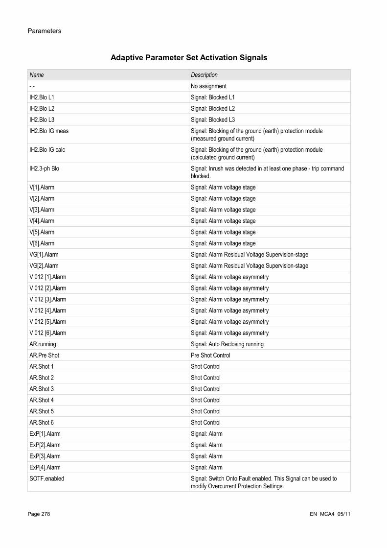
Parameters
Adaptive Parameter Set Activation Signals
Name Description
-.- No assignmentIH2.Blo L1 Signal: Blocked L1IH2.Blo L2 Signal: Blocked L2IH2.Blo L3 Signal: Blocked L3IH2.Blo IG meas Signal: Blocking of the ground (earth) protection module
(measured ground current)IH2.Blo IG calc Signal: Blocking of the ground (earth) protection module
(calculated ground current)IH2.3-ph Blo Signal: Inrush was detected in at least one phase - trip command
blocked.V[1].Alarm Signal: Alarm voltage stageV[2].Alarm Signal: Alarm voltage stageV[3].Alarm Signal: Alarm voltage stageV[4].Alarm Signal: Alarm voltage stageV[5].Alarm Signal: Alarm voltage stageV[6].Alarm Signal: Alarm voltage stageVG[1].Alarm Signal: Alarm Residual Voltage Supervision-stageVG[2].Alarm Signal: Alarm Residual Voltage Supervision-stageV 012 [1].Alarm Signal: Alarm voltage asymmetryV 012 [2].Alarm Signal: Alarm voltage asymmetryV 012 [3].Alarm Signal: Alarm voltage asymmetryV 012 [4].Alarm Signal: Alarm voltage asymmetryV 012 [5].Alarm Signal: Alarm voltage asymmetryV 012 [6].Alarm Signal: Alarm voltage asymmetryAR.running Signal: Auto Reclosing runningAR.Pre Shot Pre Shot ControlAR.Shot 1 Shot ControlAR.Shot 2 Shot ControlAR.Shot 3 Shot ControlAR.Shot 4 Shot ControlAR.Shot 5 Shot ControlAR.Shot 6 Shot ControlExP[1].Alarm Signal: AlarmExP[2].Alarm Signal: AlarmExP[3].Alarm Signal: AlarmExP[4].Alarm Signal: AlarmSOTF.enabled Signal: Switch Onto Fault enabled. This Signal can be used to
modify Overcurrent Protection Settings.
Page 278 EN MCA4 05/11

Parameters
Name Description
CLPU.enabled Signal: Cold Load enabledDI Slot X1.DI 1 Signal: Digital InputDI Slot X1.DI 2 Signal: Digital InputDI Slot X1.DI 3 Signal: Digital InputDI Slot X1.DI 4 Signal: Digital InputDI Slot X1.DI 5 Signal: Digital InputDI Slot X1.DI 6 Signal: Digital InputDI Slot X1.DI 7 Signal: Digital InputDI Slot X1.DI 8 Signal: Digital InputDI Slot X6.DI 1 Signal: Digital InputDI Slot X6.DI 2 Signal: Digital InputDI Slot X6.DI 3 Signal: Digital InputDI Slot X6.DI 4 Signal: Digital InputDI Slot X6.DI 5 Signal: Digital InputDI Slot X6.DI 6 Signal: Digital InputDI Slot X6.DI 7 Signal: Digital InputDI Slot X6.DI 8 Signal: Digital InputLogics.LE1.Gate Out Signal: Output of the logic gateLogics.LE1.Timer Out Signal: Timer OutputLogics.LE1.Out Signal: Latched Output (Q)Logics.LE1.Out inverted Signal: Negated Latched Output (Q NOT)Logics.LE2.Gate Out Signal: Output of the logic gateLogics.LE2.Timer Out Signal: Timer OutputLogics.LE2.Out Signal: Latched Output (Q)Logics.LE2.Out inverted Signal: Negated Latched Output (Q NOT)Logics.LE3.Gate Out Signal: Output of the logic gateLogics.LE3.Timer Out Signal: Timer OutputLogics.LE3.Out Signal: Latched Output (Q)Logics.LE3.Out inverted Signal: Negated Latched Output (Q NOT)Logics.LE4.Gate Out Signal: Output of the logic gateLogics.LE4.Timer Out Signal: Timer OutputLogics.LE4.Out Signal: Latched Output (Q)Logics.LE4.Out inverted Signal: Negated Latched Output (Q NOT)Logics.LE5.Gate Out Signal: Output of the logic gateLogics.LE5.Timer Out Signal: Timer OutputLogics.LE5.Out Signal: Latched Output (Q)Logics.LE5.Out inverted Signal: Negated Latched Output (Q NOT)Logics.LE6.Gate Out Signal: Output of the logic gateLogics.LE6.Timer Out Signal: Timer Output
EN MCA4 05/11 Page 279
Parameters
Name Description
Logics.LE6.Out Signal: Latched Output (Q)Logics.LE6.Out inverted Signal: Negated Latched Output (Q NOT)Logics.LE7.Gate Out Signal: Output of the logic gateLogics.LE7.Timer Out Signal: Timer OutputLogics.LE7.Out Signal: Latched Output (Q)Logics.LE7.Out inverted Signal: Negated Latched Output (Q NOT)Logics.LE8.Gate Out Signal: Output of the logic gateLogics.LE8.Timer Out Signal: Timer OutputLogics.LE8.Out Signal: Latched Output (Q)Logics.LE8.Out inverted Signal: Negated Latched Output (Q NOT)Logics.LE9.Gate Out Signal: Output of the logic gateLogics.LE9.Timer Out Signal: Timer OutputLogics.LE9.Out Signal: Latched Output (Q)Logics.LE9.Out inverted Signal: Negated Latched Output (Q NOT)Logics.LE10.Gate Out Signal: Output of the logic gateLogics.LE10.Timer Out Signal: Timer OutputLogics.LE10.Out Signal: Latched Output (Q)Logics.LE10.Out inverted Signal: Negated Latched Output (Q NOT)Logics.LE11.Gate Out Signal: Output of the logic gateLogics.LE11.Timer Out Signal: Timer OutputLogics.LE11.Out Signal: Latched Output (Q)Logics.LE11.Out inverted Signal: Negated Latched Output (Q NOT)Logics.LE12.Gate Out Signal: Output of the logic gateLogics.LE12.Timer Out Signal: Timer OutputLogics.LE12.Out Signal: Latched Output (Q)Logics.LE12.Out inverted Signal: Negated Latched Output (Q NOT)Logics.LE13.Gate Out Signal: Output of the logic gateLogics.LE13.Timer Out Signal: Timer OutputLogics.LE13.Out Signal: Latched Output (Q)Logics.LE13.Out inverted Signal: Negated Latched Output (Q NOT)Logics.LE14.Gate Out Signal: Output of the logic gateLogics.LE14.Timer Out Signal: Timer OutputLogics.LE14.Out Signal: Latched Output (Q)Logics.LE14.Out inverted Signal: Negated Latched Output (Q NOT)Logics.LE15.Gate Out Signal: Output of the logic gateLogics.LE15.Timer Out Signal: Timer OutputLogics.LE15.Out Signal: Latched Output (Q)Logics.LE15.Out inverted Signal: Negated Latched Output (Q NOT)Logics.LE16.Gate Out Signal: Output of the logic gate
Page 280 EN MCA4 05/11

Parameters
Name Description
Logics.LE16.Timer Out Signal: Timer OutputLogics.LE16.Out Signal: Latched Output (Q)Logics.LE16.Out inverted Signal: Negated Latched Output (Q NOT)Logics.LE17.Gate Out Signal: Output of the logic gateLogics.LE17.Timer Out Signal: Timer OutputLogics.LE17.Out Signal: Latched Output (Q)Logics.LE17.Out inverted Signal: Negated Latched Output (Q NOT)Logics.LE18.Gate Out Signal: Output of the logic gateLogics.LE18.Timer Out Signal: Timer OutputLogics.LE18.Out Signal: Latched Output (Q)Logics.LE18.Out inverted Signal: Negated Latched Output (Q NOT)Logics.LE19.Gate Out Signal: Output of the logic gateLogics.LE19.Timer Out Signal: Timer OutputLogics.LE19.Out Signal: Latched Output (Q)Logics.LE19.Out inverted Signal: Negated Latched Output (Q NOT)Logics.LE20.Gate Out Signal: Output of the logic gateLogics.LE20.Timer Out Signal: Timer OutputLogics.LE20.Out Signal: Latched Output (Q)Logics.LE20.Out inverted Signal: Negated Latched Output (Q NOT)Logics.LE21.Gate Out Signal: Output of the logic gateLogics.LE21.Timer Out Signal: Timer OutputLogics.LE21.Out Signal: Latched Output (Q)Logics.LE21.Out inverted Signal: Negated Latched Output (Q NOT)Logics.LE22.Gate Out Signal: Output of the logic gateLogics.LE22.Timer Out Signal: Timer OutputLogics.LE22.Out Signal: Latched Output (Q)Logics.LE22.Out inverted Signal: Negated Latched Output (Q NOT)Logics.LE23.Gate Out Signal: Output of the logic gateLogics.LE23.Timer Out Signal: Timer OutputLogics.LE23.Out Signal: Latched Output (Q)Logics.LE23.Out inverted Signal: Negated Latched Output (Q NOT)Logics.LE24.Gate Out Signal: Output of the logic gateLogics.LE24.Timer Out Signal: Timer OutputLogics.LE24.Out Signal: Latched Output (Q)Logics.LE24.Out inverted Signal: Negated Latched Output (Q NOT)Logics.LE25.Gate Out Signal: Output of the logic gateLogics.LE25.Timer Out Signal: Timer OutputLogics.LE25.Out Signal: Latched Output (Q)Logics.LE25.Out inverted Signal: Negated Latched Output (Q NOT)
EN MCA4 05/11 Page 281

Parameters
Name Description
Logics.LE26.Gate Out Signal: Output of the logic gateLogics.LE26.Timer Out Signal: Timer OutputLogics.LE26.Out Signal: Latched Output (Q)Logics.LE26.Out inverted Signal: Negated Latched Output (Q NOT)Logics.LE27.Gate Out Signal: Output of the logic gateLogics.LE27.Timer Out Signal: Timer OutputLogics.LE27.Out Signal: Latched Output (Q)Logics.LE27.Out inverted Signal: Negated Latched Output (Q NOT)Logics.LE28.Gate Out Signal: Output of the logic gateLogics.LE28.Timer Out Signal: Timer OutputLogics.LE28.Out Signal: Latched Output (Q)Logics.LE28.Out inverted Signal: Negated Latched Output (Q NOT)Logics.LE29.Gate Out Signal: Output of the logic gateLogics.LE29.Timer Out Signal: Timer OutputLogics.LE29.Out Signal: Latched Output (Q)Logics.LE29.Out inverted Signal: Negated Latched Output (Q NOT)Logics.LE30.Gate Out Signal: Output of the logic gateLogics.LE30.Timer Out Signal: Timer OutputLogics.LE30.Out Signal: Latched Output (Q)Logics.LE30.Out inverted Signal: Negated Latched Output (Q NOT)Logics.LE31.Gate Out Signal: Output of the logic gateLogics.LE31.Timer Out Signal: Timer OutputLogics.LE31.Out Signal: Latched Output (Q)Logics.LE31.Out inverted Signal: Negated Latched Output (Q NOT)Logics.LE32.Gate Out Signal: Output of the logic gateLogics.LE32.Timer Out Signal: Timer OutputLogics.LE32.Out Signal: Latched Output (Q)Logics.LE32.Out inverted Signal: Negated Latched Output (Q NOT)Logics.LE33.Gate Out Signal: Output of the logic gateLogics.LE33.Timer Out Signal: Timer OutputLogics.LE33.Out Signal: Latched Output (Q)Logics.LE33.Out inverted Signal: Negated Latched Output (Q NOT)Logics.LE34.Gate Out Signal: Output of the logic gateLogics.LE34.Timer Out Signal: Timer OutputLogics.LE34.Out Signal: Latched Output (Q)Logics.LE34.Out inverted Signal: Negated Latched Output (Q NOT)Logics.LE35.Gate Out Signal: Output of the logic gateLogics.LE35.Timer Out Signal: Timer OutputLogics.LE35.Out Signal: Latched Output (Q)
Page 282 EN MCA4 05/11
Parameters
Name Description
Logics.LE35.Out inverted Signal: Negated Latched Output (Q NOT)Logics.LE36.Gate Out Signal: Output of the logic gateLogics.LE36.Timer Out Signal: Timer OutputLogics.LE36.Out Signal: Latched Output (Q)Logics.LE36.Out inverted Signal: Negated Latched Output (Q NOT)Logics.LE37.Gate Out Signal: Output of the logic gateLogics.LE37.Timer Out Signal: Timer OutputLogics.LE37.Out Signal: Latched Output (Q)Logics.LE37.Out inverted Signal: Negated Latched Output (Q NOT)Logics.LE38.Gate Out Signal: Output of the logic gateLogics.LE38.Timer Out Signal: Timer OutputLogics.LE38.Out Signal: Latched Output (Q)Logics.LE38.Out inverted Signal: Negated Latched Output (Q NOT)Logics.LE39.Gate Out Signal: Output of the logic gateLogics.LE39.Timer Out Signal: Timer OutputLogics.LE39.Out Signal: Latched Output (Q)Logics.LE39.Out inverted Signal: Negated Latched Output (Q NOT)Logics.LE40.Gate Out Signal: Output of the logic gateLogics.LE40.Timer Out Signal: Timer OutputLogics.LE40.Out Signal: Latched Output (Q)Logics.LE40.Out inverted Signal: Negated Latched Output (Q NOT)Logics.LE41.Gate Out Signal: Output of the logic gateLogics.LE41.Timer Out Signal: Timer OutputLogics.LE41.Out Signal: Latched Output (Q)Logics.LE41.Out inverted Signal: Negated Latched Output (Q NOT)Logics.LE42.Gate Out Signal: Output of the logic gateLogics.LE42.Timer Out Signal: Timer OutputLogics.LE42.Out Signal: Latched Output (Q)Logics.LE42.Out inverted Signal: Negated Latched Output (Q NOT)Logics.LE43.Gate Out Signal: Output of the logic gateLogics.LE43.Timer Out Signal: Timer OutputLogics.LE43.Out Signal: Latched Output (Q)Logics.LE43.Out inverted Signal: Negated Latched Output (Q NOT)Logics.LE44.Gate Out Signal: Output of the logic gateLogics.LE44.Timer Out Signal: Timer OutputLogics.LE44.Out Signal: Latched Output (Q)Logics.LE44.Out inverted Signal: Negated Latched Output (Q NOT)Logics.LE45.Gate Out Signal: Output of the logic gateLogics.LE45.Timer Out Signal: Timer Output
EN MCA4 05/11 Page 283

Parameters
Name Description
Logics.LE45.Out Signal: Latched Output (Q)Logics.LE45.Out inverted Signal: Negated Latched Output (Q NOT)Logics.LE46.Gate Out Signal: Output of the logic gateLogics.LE46.Timer Out Signal: Timer OutputLogics.LE46.Out Signal: Latched Output (Q)Logics.LE46.Out inverted Signal: Negated Latched Output (Q NOT)Logics.LE47.Gate Out Signal: Output of the logic gateLogics.LE47.Timer Out Signal: Timer OutputLogics.LE47.Out Signal: Latched Output (Q)Logics.LE47.Out inverted Signal: Negated Latched Output (Q NOT)Logics.LE48.Gate Out Signal: Output of the logic gateLogics.LE48.Timer Out Signal: Timer OutputLogics.LE48.Out Signal: Latched Output (Q)Logics.LE48.Out inverted Signal: Negated Latched Output (Q NOT)Logics.LE49.Gate Out Signal: Output of the logic gateLogics.LE49.Timer Out Signal: Timer OutputLogics.LE49.Out Signal: Latched Output (Q)Logics.LE49.Out inverted Signal: Negated Latched Output (Q NOT)Logics.LE50.Gate Out Signal: Output of the logic gateLogics.LE50.Timer Out Signal: Timer OutputLogics.LE50.Out Signal: Latched Output (Q)Logics.LE50.Out inverted Signal: Negated Latched Output (Q NOT)Logics.LE51.Gate Out Signal: Output of the logic gateLogics.LE51.Timer Out Signal: Timer OutputLogics.LE51.Out Signal: Latched Output (Q)Logics.LE51.Out inverted Signal: Negated Latched Output (Q NOT)Logics.LE52.Gate Out Signal: Output of the logic gateLogics.LE52.Timer Out Signal: Timer OutputLogics.LE52.Out Signal: Latched Output (Q)Logics.LE52.Out inverted Signal: Negated Latched Output (Q NOT)Logics.LE53.Gate Out Signal: Output of the logic gateLogics.LE53.Timer Out Signal: Timer OutputLogics.LE53.Out Signal: Latched Output (Q)Logics.LE53.Out inverted Signal: Negated Latched Output (Q NOT)Logics.LE54.Gate Out Signal: Output of the logic gateLogics.LE54.Timer Out Signal: Timer OutputLogics.LE54.Out Signal: Latched Output (Q)Logics.LE54.Out inverted Signal: Negated Latched Output (Q NOT)Logics.LE55.Gate Out Signal: Output of the logic gate
Page 284 EN MCA4 05/11

Parameters
Name Description
Logics.LE55.Timer Out Signal: Timer OutputLogics.LE55.Out Signal: Latched Output (Q)Logics.LE55.Out inverted Signal: Negated Latched Output (Q NOT)Logics.LE56.Gate Out Signal: Output of the logic gateLogics.LE56.Timer Out Signal: Timer OutputLogics.LE56.Out Signal: Latched Output (Q)Logics.LE56.Out inverted Signal: Negated Latched Output (Q NOT)Logics.LE57.Gate Out Signal: Output of the logic gateLogics.LE57.Timer Out Signal: Timer OutputLogics.LE57.Out Signal: Latched Output (Q)Logics.LE57.Out inverted Signal: Negated Latched Output (Q NOT)Logics.LE58.Gate Out Signal: Output of the logic gateLogics.LE58.Timer Out Signal: Timer OutputLogics.LE58.Out Signal: Latched Output (Q)Logics.LE58.Out inverted Signal: Negated Latched Output (Q NOT)Logics.LE59.Gate Out Signal: Output of the logic gateLogics.LE59.Timer Out Signal: Timer OutputLogics.LE59.Out Signal: Latched Output (Q)Logics.LE59.Out inverted Signal: Negated Latched Output (Q NOT)Logics.LE60.Gate Out Signal: Output of the logic gateLogics.LE60.Timer Out Signal: Timer OutputLogics.LE60.Out Signal: Latched Output (Q)Logics.LE60.Out inverted Signal: Negated Latched Output (Q NOT)Logics.LE61.Gate Out Signal: Output of the logic gateLogics.LE61.Timer Out Signal: Timer OutputLogics.LE61.Out Signal: Latched Output (Q)Logics.LE61.Out inverted Signal: Negated Latched Output (Q NOT)Logics.LE62.Gate Out Signal: Output of the logic gateLogics.LE62.Timer Out Signal: Timer OutputLogics.LE62.Out Signal: Latched Output (Q)Logics.LE62.Out inverted Signal: Negated Latched Output (Q NOT)Logics.LE63.Gate Out Signal: Output of the logic gateLogics.LE63.Timer Out Signal: Timer OutputLogics.LE63.Out Signal: Latched Output (Q)Logics.LE63.Out inverted Signal: Negated Latched Output (Q NOT)Logics.LE64.Gate Out Signal: Output of the logic gateLogics.LE64.Timer Out Signal: Timer OutputLogics.LE64.Out Signal: Latched Output (Q)Logics.LE64.Out inverted Signal: Negated Latched Output (Q NOT)
EN MCA4 05/11 Page 285

Parameters
Name Description
Logics.LE65.Gate Out Signal: Output of the logic gateLogics.LE65.Timer Out Signal: Timer OutputLogics.LE65.Out Signal: Latched Output (Q)Logics.LE65.Out inverted Signal: Negated Latched Output (Q NOT)Logics.LE66.Gate Out Signal: Output of the logic gateLogics.LE66.Timer Out Signal: Timer OutputLogics.LE66.Out Signal: Latched Output (Q)Logics.LE66.Out inverted Signal: Negated Latched Output (Q NOT)Logics.LE67.Gate Out Signal: Output of the logic gateLogics.LE67.Timer Out Signal: Timer OutputLogics.LE67.Out Signal: Latched Output (Q)Logics.LE67.Out inverted Signal: Negated Latched Output (Q NOT)Logics.LE68.Gate Out Signal: Output of the logic gateLogics.LE68.Timer Out Signal: Timer OutputLogics.LE68.Out Signal: Latched Output (Q)Logics.LE68.Out inverted Signal: Negated Latched Output (Q NOT)Logics.LE69.Gate Out Signal: Output of the logic gateLogics.LE69.Timer Out Signal: Timer OutputLogics.LE69.Out Signal: Latched Output (Q)Logics.LE69.Out inverted Signal: Negated Latched Output (Q NOT)Logics.LE70.Gate Out Signal: Output of the logic gateLogics.LE70.Timer Out Signal: Timer OutputLogics.LE70.Out Signal: Latched Output (Q)Logics.LE70.Out inverted Signal: Negated Latched Output (Q NOT)Logics.LE71.Gate Out Signal: Output of the logic gateLogics.LE71.Timer Out Signal: Timer OutputLogics.LE71.Out Signal: Latched Output (Q)Logics.LE71.Out inverted Signal: Negated Latched Output (Q NOT)Logics.LE72.Gate Out Signal: Output of the logic gateLogics.LE72.Timer Out Signal: Timer OutputLogics.LE72.Out Signal: Latched Output (Q)Logics.LE72.Out inverted Signal: Negated Latched Output (Q NOT)Logics.LE73.Gate Out Signal: Output of the logic gateLogics.LE73.Timer Out Signal: Timer OutputLogics.LE73.Out Signal: Latched Output (Q)Logics.LE73.Out inverted Signal: Negated Latched Output (Q NOT)Logics.LE74.Gate Out Signal: Output of the logic gateLogics.LE74.Timer Out Signal: Timer OutputLogics.LE74.Out Signal: Latched Output (Q)
Page 286 EN MCA4 05/11

Parameters
Name Description
Logics.LE74.Out inverted Signal: Negated Latched Output (Q NOT)Logics.LE75.Gate Out Signal: Output of the logic gateLogics.LE75.Timer Out Signal: Timer OutputLogics.LE75.Out Signal: Latched Output (Q)Logics.LE75.Out inverted Signal: Negated Latched Output (Q NOT)Logics.LE76.Gate Out Signal: Output of the logic gateLogics.LE76.Timer Out Signal: Timer OutputLogics.LE76.Out Signal: Latched Output (Q)Logics.LE76.Out inverted Signal: Negated Latched Output (Q NOT)Logics.LE77.Gate Out Signal: Output of the logic gateLogics.LE77.Timer Out Signal: Timer OutputLogics.LE77.Out Signal: Latched Output (Q)Logics.LE77.Out inverted Signal: Negated Latched Output (Q NOT)Logics.LE78.Gate Out Signal: Output of the logic gateLogics.LE78.Timer Out Signal: Timer OutputLogics.LE78.Out Signal: Latched Output (Q)Logics.LE78.Out inverted Signal: Negated Latched Output (Q NOT)Logics.LE79.Gate Out Signal: Output of the logic gateLogics.LE79.Timer Out Signal: Timer OutputLogics.LE79.Out Signal: Latched Output (Q)Logics.LE79.Out inverted Signal: Negated Latched Output (Q NOT)Logics.LE80.Gate Out Signal: Output of the logic gateLogics.LE80.Timer Out Signal: Timer OutputLogics.LE80.Out Signal: Latched Output (Q)Logics.LE80.Out inverted Signal: Negated Latched Output (Q NOT)
EN MCA4 05/11 Page 287

Parameters
Operational Modes (access authorization)
Operational Mode – »Display Only«
• The protection is activated.
• All data, measuring values, records and counters/meters can be viewed.
Operation Mode – »Parameter Setting and Planning«
In this mode you are able to:
• edit and set parameters.
• change device planning details and
• parameterize and reset operational data (event recorder/fault recorder/power meter/switching cycles).
If the device was not active within the parameter setting mode for a longer time (can be set between 20 – 3600 seconds) it changes automatically into »Display Only« mode. (Please refer to the appendix Module Panel).
As long as you are within the parameter setting mode you cannot acknowledge.
In order to change into operation mode »Parameter Setting« please proceed as follows:
1. Mark in the device display the parameter you want to change.
2. Press the softkey »Wrench« to change temporarily into the parameter setting mode.
3. Enter the parameter password.
4. Change the parameter.
5. Change perhaps additional parameters.
As long as you are within the parameter setting mode a wrench icon will be shown in the upper right corner of the display.
6. For saving the altered parameter:• press the »OK« key,• confirm by pressing the softkey »Yes«.
1. Then the device changes into mode »Display Only«.
Page 288 EN MCA4 05/11

Parameters
Password
Password Entry at the Panel
Passwords can be entered by way of the softkeys.
1 2 3 4
Example: For password (3244) press successively:
• Softkey 3• Softkey 2• Softkey 4• Softkey 4
Password Changes
Passwords can be changed at the device in menu »Device Para/Password« or by means of the Smart view software.
A password must be a user-defined combination of the numerics 1, 2, 3 and 4. All other characters and keys won´t be accepted.
The password of operation mode »Parameter setting and planning« enables you to transfer parameters from the Smart view software into the device.
When you want to change a password, the existing one has to be entered firstly. The new password (up to 8 digits) is then to be confirmed twice. Please proceed as follows:
• In order to change the password please enter your old password followed by pressing the »OK«-key. • Afterwards enter the new password and press the »OK«-key. • Finally confirm your new password and press the »OK-key«.
Password Forgotten
By pressing the »C« key during cold booting a reset menu will be called up. By selecting »Reset All Passwords?« and confirming with »Yes« all passwords will be reset to the defaults »1234«.
EN MCA4 05/11 Page 289

Parameters
Changing of Parameters - Example
• Move to the parameter you want to change by using the softkeys .
• Press the softkey »Wrench«.
• Enter the password for parameter setting.
• Edit/change the parameter.
Now you can:
• save the change you made and have them adopted by the system or:
• change additional parameters and save finally all the altered parameters and have them adopted by the system.
To save parameter changes immediately,
• press the »OK« key for saving changed parameters directly and to have them adopted by the device. Confirm the parameter changes by pressing the »Yes« softkey or dismiss by pressing »No«.
To change additional parameters and save afterwards,
• move to other parameters and change them
A star symbol in front of the changed parameters indicates that the modifications have only temporarily been saved, they are not yet finally stored and adopted by the device. In order to make things easier to follow, especially where complex parameter changes are involved, on every superior/higher-ranking menu level the intended change of the parameter is indicated by the star symbol (star trace). This makes it possible to control or follow from the main menu level at any time where parameter changes have been made and have not finally been saved. In addition to the star trace to the temporarily saved parameter changes, a general parameter changing symbol is faded-in at the left corner of the display, and so it is possible from each point of the menu tree to see that there are parameter changes still not adopted by the device.
Press the »OK« key to initiate the final storage of all parameter changes. Confirm the parameter changes by pressing the »Yes« softkey or dismiss by pressing Softkey »No«.
Page 290 EN MCA4 05/11
Parameters
Plausibility check: In order to prevent obvious wrong settings the device monitors constantly all temporarily saved parameter changes. If the device detects an implausibility, this is indicated by a question mark in front of the respective parameter. In order to make things easier to follow, especially where complex parameter changes are involved, on every superior/higher-ranking menu level, above the temporarily saved parameters an invalidity is indicated by the question mark (plausibility trace). This makes it possible to control or follow from the main menu level at any time where implausibilities are intended to be saved.
In addition to the question mark trace to the temporarily saved implausible parameter changes a general implausibility symbol/question mark is faded-in at the left corner of the display, and so it is possible to see from each point of the menu tree that implausibilities have been detected by the device.
A star/parameter change indication is always overwritten by the question mark/implausibility symbol.
If a device detects an implausibility, it rejects saving and adopting of the parameters.
Changing of Parameters when using the Smart View - ExampleExample: Changing of a protective parameter (to alter the characteristic for the overcurrent protection function I[1] in parameter set 1).
• In case Smart view is not in operation – start this software.
• In case the device data has not been loaded – select »Data To Be Received From The Device« in menu »Device«.
• Double-click the »Protection Para Icon« in the navigation tree.
• Double-click the »Protection Para Set Icon« in the navigation tree.
• Double-click the »Set 1 Icon« in the navigation tree.
• Double-click the »protection stage I[1]« in the navigation tree.
• In the working window a tabulated overview appears, showing the parameters assigned to this protective function.
• In this table double-click the value/parameter you want to change (here: »Char«).
• Another window (popup) is opened where you can select the required characteristic.
• Close this window by clicking the »OK« key.
A star symbol in front of the changed parameters indicates that the alterations have only temporarily been saved. They are not yet finally stored and adopted by the software/device.In order to make things easier to follow, especially where complex
EN MCA4 05/11 Page 291

Parameters
parameter changes are involved, on every superior/higher menu level, the intended change of the parameter is indicated by the star symbol (star trace). This makes it possible to control or follow from the main menu level at any time where parameter changes have been made and have not finally been saved.
Plausibility check: In order to prevent obvious wrong settings the software monitors constantly all temporarily saved parameter changes. If it detects an implausibility, this is indicated by a question mark in front of the respective parameter. In order to make things easier to follow, especially where complex parameter changes are involved, on every superior/higher menu level above of the temporarily saved parameters, an implausibility is indicated by a question mark (plausibility trace). This makes it possible to control or follow from the main menu level at any time where implausibilities exist.
So it is possible to see from each point of the menu tree that implausibilities have been detected by the software.
A star/parameter change indication is always overwritten by the question mark/implausibility symbol.
If the software detects an implausibility it rejects saving and adopting of the parameters.
• Additional parameters can be changed if required.
• In order to transfer changed parameters into the device, please select »Transfer all parameters into the device« in menu »Device«.
• Confirm the safety inquiry »Shall The Parameters Be Overwritten?«.
• Enter the password for setting parameters in the popup window.
• Confirm the inquiry »Shall The Data Be Saved Locally?« with »Yes« (recommended). Select a suitable storing location on your hard disk.
• Confirm the chosen storing location by clicking »Save«.
• The changed parameter data is now saved in the data file chosen by you. Thereafter the changed data is transferred to the device and adopted. .
Once you have entered the parameter setting password, Smart view wont ask you again for the password for at least 10 minutes. This time interval will start again, each time parameters are transmitted into the device. If for more than 10 minutes no parameters are transmitted into the device, Smart
Page 292 EN MCA4 05/11

Parameters
view will ask you again for the password, when you are trying to transmit parameters into the device.
EN MCA4 05/11 Page 293

Parameters
Protection Parameters
It has to be taken into account that by deactivating, for instance, protective functions, you also change the functionality of the device.
The manufacturer does not accept liability for any personal or material damage as a result of wrong planning.
A planning/parameter setting service is also offered by Woodward Kempen GmbH.
The protection parameters include the following protection parameter trees:
• Global Protection Parameters: »Global Prot Para«: Here you can find all protection parameters that are universally valid, that means that they are valid independent of the protection parameter sets.
• Setting Group Parameters: »Set1..4«: The protection parameters that you set within a parameter set are only valid, if the parameter set where you set them is switched to active.
Setting Groups
Setting Group Switch
Within the menu »Protection Para/P-Set Switch« you have the following possibilities:
• To set one of the four setting groups active manually.• To assign a signal to each setting group that sets this group to active.• Scada switches the setting groups.
Setting Group Switch
Manual Selection Via Input Function (e.g. Digital Input)
Via Scada
Switching Options Switch over, if another setting group is chosen
manually within the menu »Protection Para/P-Set
Switch«
Switch over not until the request is clear.
That means, if there is more or less than one
request signal active, no switch over will be
executed.
Switch over if there is a clear Scada request.
Otherwise no switch over will be executed.
The description of the parameters can be found within chapter System Parameters.
Page 294 EN MCA4 05/11

Parameters
Setting Group Switch via Smart View
• In case Smart view is not running – please start it.
• If device data has not been loaded yet – click »Receive Data From The Device« in menu »Device«.
• Double click the »Protection Para« icon in the navigation tree.
• Double click the »P-Set Switch« within the protection parameters.
• Configure the Setting Group Switch respectively choose an active set manually.
The description of the parameters can be found within chapter System Parameters.
EN MCA4 05/11 Page 295

Parameters
Copying Setting Groups (Parameter Sets) via Smart View
Setting groups can only be copied if there are no implausibilities (no red question mark).
It is not necessary to set up two setting groups that only differ in few parameters.
With the help of „Smart view“ you can simply copy an existing setting group to another (not yet configured) one. You only need to change those parameters where the two setting groups are different.
To efficiently establish a second parameter set where only few parameters are different, proceed as follows:
• In case Smart view is not running – please start it.
• Open an (offline) parameter file of a device or load data of a connected device.
• By way of precaution, save (the relevant) device parameters [File\Save as].
• Select »Copy Parameter Sets« out of the menu “Edit”.
• Then define both, source and destination of the parameter sets to be copied (source = copy from; destination: copy to ).
• Mouse click on »OK« to start copy procedure.
• The copied parameter set is now cached (not yet saved!).
• Then, modify the copied parameter set(s), if applicable.
• Assign a new file name to the revised device parameter file and save it on your hard disk (backup copy).
• To transfer the modified parameters back to the device, click on menu item »Device« and select »Transfer All Parameters into the Device«.
Comparing Setting Groups via Smart View
• In case Smart view is not running – please start it.
• Click on menu item »Edit« and select »Compare Parameter Sets«.
• Select the two parameter sets from the (two) drop down menus you would like to have compared with each other.
• Press the pushbutton »compare«.
• The values that are different from the set parameters will be listed in tabular form.
Page 296 EN MCA4 05/11

Parameters
Comparing Parameter Files via Smart viewWith the help of „Smart view“ you can simply compare/diff the currently open parameter/device file against a file on your hard disk. The precondition is that the versions and type of devices match. Please proceed as follows:
• Click on »Compare with a Parameter File« within the menu »Device«.
• Click on the Folder icon in order to select a file on your hard disk.
• The differences will be shown in tabular form.
Converting Parameter Files via Smart viewParameter files of the same type can be up- or downgraded (converted). As many parameters as possible will be taken over.
• Parameters, that are newly added, will be set to default.
• Parameters, that are not included in the target file version, will be deleted.
In order to convert a parameter file please proceed as follows:
• In case Smart view is not in operation – start this software.
• Open a parameter file or load the parameters from a device that should be converted.
• Make a backup of this file at a fail safe place.
• Choose »Save as« from menu »File«
• Enter a new file name (in order to prevent overwriting the original file)
• Choose the new file type from drop down menu »File Type«.
• Confirm the security check by clicking on »yes« if and only you are sure that the file conversion should be executed.
• In tabular form the modifications will be shown as follows.
Added parameter:
Deleted parameter:
EN MCA4 05/11 Page 297

Device Parameters
Device Parameters Sys
Date and TimeIn menu »Device parameters/Date/Time« you can set date and time.
Synchronize Date and Time via Smart View• In case Smart view is not running – please start it.
• If device data has not been loaded yet – click »Receive Data From The Device« in menu »Device«
• Double click the »Device parameters« icon in the navigation tree.
• Double click the »Date/time-icon« within the operational data.
• Out of the working window you can now synchronize date and time of the device with your PC i.e. That means, that the device takes over date and time from your PC.
VersionWithin this menu »Device parameters/Version« you can obtain information on the soft- and hardware version.
Version via Smart viewWithin this menu »File/Properties« you can obtain detailed information on the currently opened file like e.g. soft- and hardware version....
In order to be able to transmit a parameter file (e.g. offline created) into the device the following issues must comply:
• Type Code (written on the top of the device/type label) and
• Version of the device model (can be found in menu [Device Parameters\Version].
Page 298 EN MCA4 05/11

Device Parameters
TCP/IP SettingsWithin menu »Device Para / TCP/IP« the TCP/IP settings have to be set.
The first-time setting of the TCP/IP Parameters can be done at the panel (HMI) only.
Establishing a connection via TCP/IP to the device is only possible if your device is equipped with an Ethernet Interface (RJ45).
Contact your IT administrator in order to establish the network connection.
Set the TCP/IP Parameters
Call up »Device parameter/TCP/IP« at the HMI (panel) and set the following parameters:
• TCP/IP address
• Subnetmask
• Gateway
EN MCA4 05/11 Page 299

Device Parameters
Direct Commands of the System Module
Parameter Description Setting range Default Menu path
Ack LED All acknowledgeable LEDs will be acknowledged. inactive,
active
inactive [Operation
/Acknowledge]
Ack BO All acknowledgeable binary output relays will be acknowledged.
inactive,
active
inactive [Operation
/Acknowledge]
Ack Scada SCADA will be acknowledged. inactive,
active
inactive [Operation
/Acknowledge]
Ack BO LED Scd TCmd
Reset the binary output relays, LEDs, SCADA and the Trip Command.
inactive,
active
inactive [Operation
/Acknowledge]
Reboot Rebooting the device. no,
yes
no [Service
/General]
CAUTION, rebooting the device manually will release the Supervision Contact.
Page 300 EN MCA4 05/11

Device Parameters
Global Protection Parameters of the System
Parameter Description Setting range Default Menu path
PSet-Switch Switching Parameter Set PS1,
PS2,
PS3,
PS4,
PSS via Inp fct,
PSS via Scada
PS1 [Protection Para
/PSet-Switch]
PS1: activated by
This Setting Group will be the active one if: The Parameter Setting Group Switch is set to "Switch via Input" and the other three input functions are inactive at the same time. In case that there is more than one input function active, no Parameter Setting Group Switch will be executed. In case all input functions are inactive, the device will keep working with the Setting Group that was activated lastly.
Only available if: PSet-Switch = PSS via Inp fct
1..n, DI-LogicList -.- [Protection Para
/PSet-Switch]
PS2: activated by
This Setting Group will be the active one if: The Parameter Setting Group Switch is set to "Switch via Input" and the other three input functions are inactive at the same time. In case that there is more than one input function active, no Parameter Setting Group Switch will be executed. In case all input functions are inactive, the device will keep working with the Setting Group that was activated lastly.
Only available if: PSet-Switch = PSS via Inp fct
1..n, DI-LogicList -.- [Protection Para
/PSet-Switch]
PS3: activated by
This Setting Group will be the active one if: The Parameter Setting Group Switch is set to "Switch via Input" and the other three input functions are inactive at the same time. In case that there is more than one input function active, no Parameter Setting Group Switch will be executed. In case all input functions are inactive, the device will keep working with the Setting Group that was activated lastly.
Only available if: PSet-Switch = PSS via Inp fct
1..n, DI-LogicList -.- [Protection Para
/PSet-Switch]
PS4: activated by
This Setting Group will be the active one if: The Parameter Setting Group Switch is set to "Switch via Input" and the other three input functions are inactive at the same time. In case that there is more than one input function active, no Parameter Setting Group Switch will be executed. In case all input functions are inactive, the device will keep working with the Setting Group that was activated lastly.
Only available if: PSet-Switch = PSS via Inp fct
1..n, DI-LogicList -.- [Protection Para
/PSet-Switch]
EN MCA4 05/11 Page 301
Device Parameters
Parameter Description Setting range Default Menu path
Ack LED All acknowledgeable LEDs will be acknowledged if the state of the assigned signal becomes true.
1..n, Assignment List -.- [Device Para
/Ex Acknowledge]
Ack BO All acknowledgeable binary output relays will be acknowledged if the state of the assigned signal becomes true.
1..n, Assignment List -.- [Device Para
/Ex Acknowledge]
Ack Scada SCADA will be acknowledged if the state of the assigned signal becomes true.
1..n, Assignment List -.- [Device Para
/Ex Acknowledge]
Scaling Display of the measured values as primary, secondary or per unit values
Per unit values,
Primary values,
Secondary values
Per unit values
[Device Para
/Measurem Display]
Page 302 EN MCA4 05/11
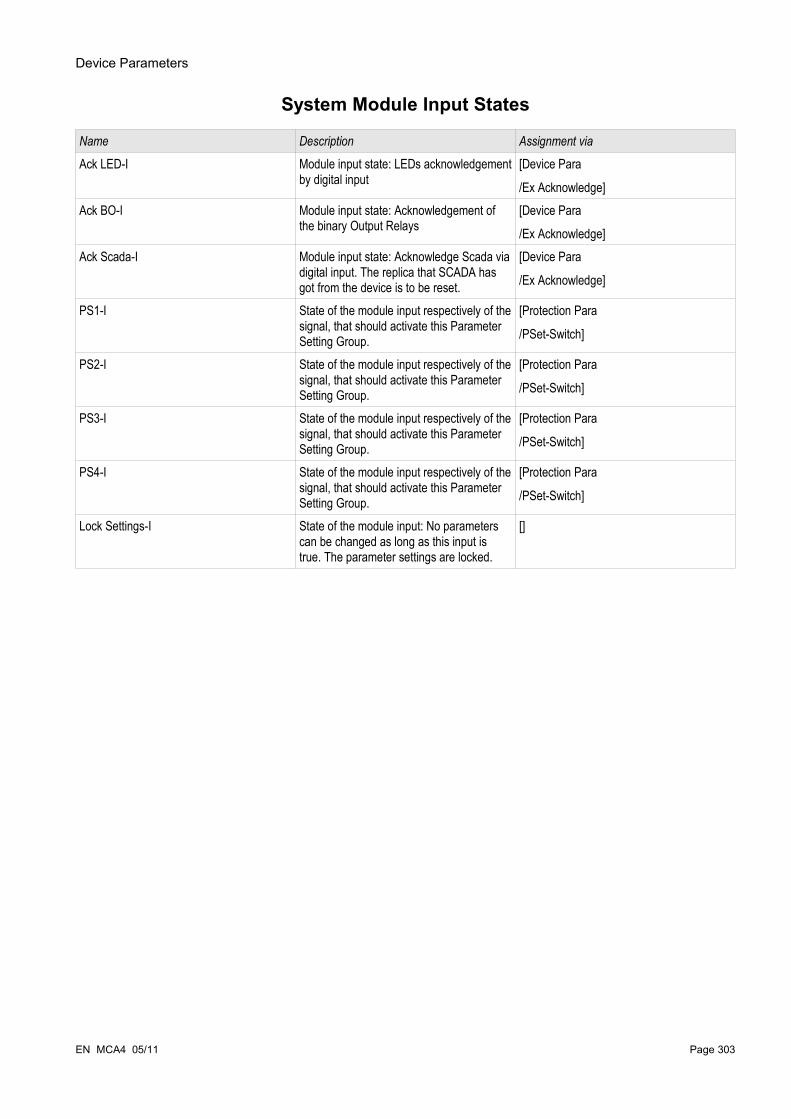
Device Parameters
System Module Input States
Name Description Assignment via
Ack LED-I Module input state: LEDs acknowledgement by digital input
[Device Para
/Ex Acknowledge]Ack BO-I Module input state: Acknowledgement of
the binary Output Relays[Device Para
/Ex Acknowledge]Ack Scada-I Module input state: Acknowledge Scada via
digital input. The replica that SCADA has got from the device is to be reset.
[Device Para
/Ex Acknowledge]
PS1-I State of the module input respectively of the signal, that should activate this Parameter Setting Group.
[Protection Para
/PSet-Switch]
PS2-I State of the module input respectively of the signal, that should activate this Parameter Setting Group.
[Protection Para
/PSet-Switch]
PS3-I State of the module input respectively of the signal, that should activate this Parameter Setting Group.
[Protection Para
/PSet-Switch]
PS4-I State of the module input respectively of the signal, that should activate this Parameter Setting Group.
[Protection Para
/PSet-Switch]
Lock Settings-I State of the module input: No parameters can be changed as long as this input is true. The parameter settings are locked.
[]
EN MCA4 05/11 Page 303

Device Parameters
System Module Signals
Name Description
Reboot Signal: Rebooting the device: 1=Restart initiated by power supply; 2=Restart initiated by the user; 3=Set on defaults (Super Reset); 4=Restart by the debugger; 5=Restart because of configuration change; 6=General failure; 7=Restart initiated by System Abort (host side); 8=Restart initiated by watchdog timeout (host side); 9=Restart initiated by System Abort (dspside); 10=Restart initiated by watchdog timeout (dspside); 11=Power supply failure (short term interruption) or power supply voltage to low; 12=illegal memory access.
Act Set Signal: Active Parameter SetPS 1 Signal: Parameter Set 1PS 2 Signal: Parameter Set 2PS 3 Signal: Parameter Set 3PS 4 Signal: Parameter Set 4PSS manual Signal: Manual Switch over of a Parameter SetPSS via Scada Signal: Parameter Set Switch via ScadaPSS via Inp fct Signal: Parameter Set Switch via input functionmin 1 param changed Signal: At least one parameter has been changedParam to be saved Number of parameters to be saved. 0 means that all parameter
changes are overtaken.Ack LED Signal: LEDs acknowledgementAck BO Signal: Acknowledgement of the Binary OutputsAck Counter Signal: Reset of all CountersAck Scada Signal: Acknowledge ScadaAck TripCmd Signal: Reset Trip CommandAck LED-HMI Signal: LEDs acknowledgement :HMIAck BO-HMI Signal: Acknowledgement of the Binary Outputs :HMIAck Counter-HMI Signal: Reset of all Counters :HMIAck Scada-HMI Signal: Acknowledge Scada :HMIAck TripCmd-HMI Signal: Reset Trip Command :HMIAck LED-Sca Signal: LEDs acknowledgement :SCADAAck BO-Sca Signal: Acknowledgement of the Binary Outputs :SCADAAck Counter-Sca Signal: Reset of all Counters :SCADAAck Scada-Sca Signal: Acknowledge Scada :SCADAAck TripCmd-Sca Signal: Reset Trip Command :SCADARes OperationsCr Signal:: Res OperationsCrRes AlarmCr Signal:: Res AlarmCrRes TripCr Signal:: Res TripCrRes TotalCr Signal:: Res TotalCr
Page 304 EN MCA4 05/11

Device Parameters
Special Values of the System Module
Value Description Menu path
Build Build [Device Para
/Version]
Version Version [Device Para
/Version]
Operating hours Cr Operating hours counter of the protective device
[Operation
/Count and RevData
/Sys]
EN MCA4 05/11 Page 305

Field Parameters
Field Parameters Field Para
Within the field parameters you can set all parameters, that are relevant for the primary side and the mains operational method like frequency, primary and secondary values and the star point treatment.
General Field Parameters
Parameter Description Setting range Default Menu path
Phase Sequence
Phase Sequence direction ABC,
ACB
ABC [Field Para
/General settings]
f Nominal frequency 50Hz,
60Hz
50Hz [Field Para
/General settings]
Page 306 EN MCA4 05/11

Field Parameters
Field Parameters – Current Related
Parameter Description Setting range Default Menu path
CT pri Nominal current of the primary side of the current transformers.
1 - 50000A 1000A [Field Para
/Current transf]
CT sec Nominal current of the secondary side of the current transformers.
1A,
5A
1A [Field Para
/Current transf]
CT dir Protection functions with directional feature can only work properly if the connection of the current transformers is free of wiring errors. If all current transformers are connected to the device with an incorrect polarity, the wiring error can be compensated by this parameter. This parameter turns the current vectors by 180 degrees.
0°,
180°
0° [Field Para
/Current transf]
ECT pri This parameter defines the primary nominal current of the connected earth current transformer. If the earth current is measured via the Holmgreen connection, the primary value of the phase current transformer must be entered here.
1 - 50000A 1000A [Field Para
/Current transf]
ECT sec This parameter defines the secondary nominal current of the connected earth current transformer. If the earth current is done via the Holmgreen connection, the primary value of the phase current transformer must be entered here.
1A,
5A
1A [Field Para
/Current transf]
ECT dir Earth fault protection with directional feature depends also on the correct wiring of the earth current transformer. An incorrect polarity/wiring can be corrected by means of the settings "0°" or "180°". The operator has the possibility of turning the current vector by 180 degrees (change of sign) without modification of the wiring. This means, that – in terms of figures - the determined current indicator was turned by 180° by the device.
0°,
180°
0° [Field Para
/Current transf]
IL1, IL2, IL3 Cutoff Level
The Current shown in the Display or within the PC Software will be displayed as zero, if the Current falls below this Cutoff Level. This parameter has no impact on recorders.
0.0 - 0.100In 0.005In [Device Para
/Measurem Display]
EN MCA4 05/11 Page 307
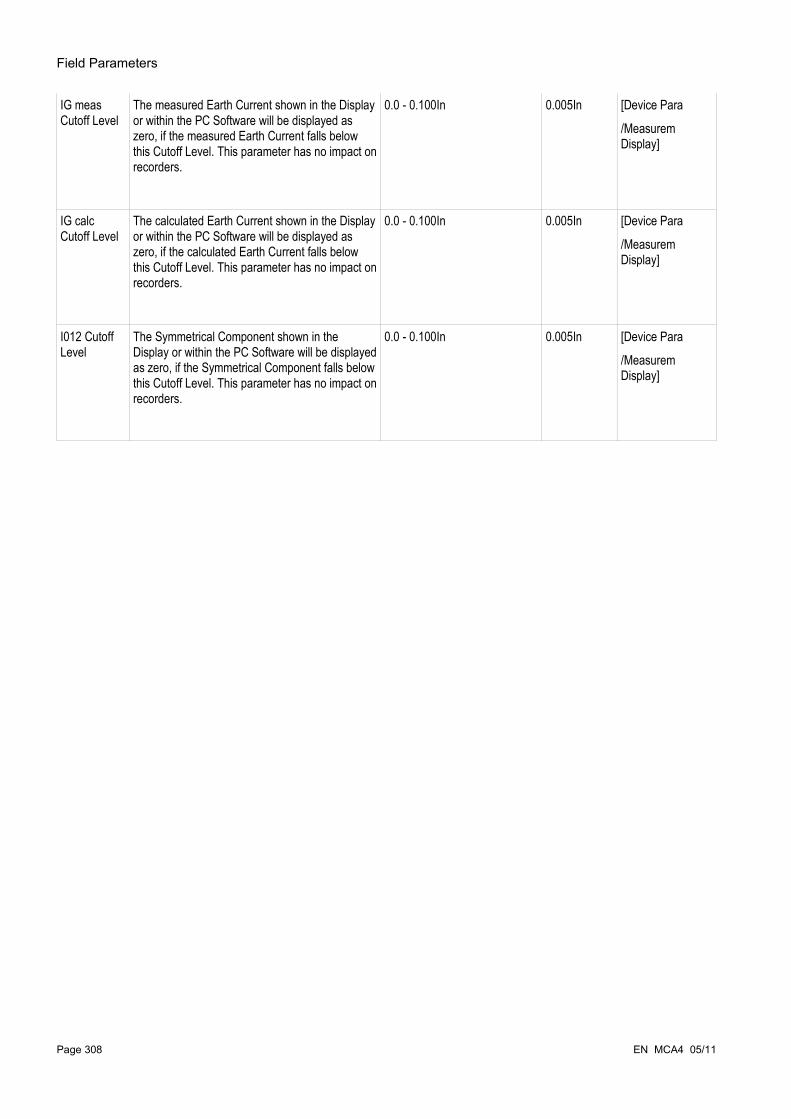
Field Parameters
IG meas Cutoff Level
The measured Earth Current shown in the Display or within the PC Software will be displayed as zero, if the measured Earth Current falls below this Cutoff Level. This parameter has no impact on recorders.
0.0 - 0.100In 0.005In [Device Para
/Measurem Display]
IG calc Cutoff Level
The calculated Earth Current shown in the Display or within the PC Software will be displayed as zero, if the calculated Earth Current falls below this Cutoff Level. This parameter has no impact on recorders.
0.0 - 0.100In 0.005In [Device Para
/Measurem Display]
I012 Cutoff Level
The Symmetrical Component shown in the Display or within the PC Software will be displayed as zero, if the Symmetrical Component falls below this Cutoff Level. This parameter has no impact on recorders.
0.0 - 0.100In 0.005In [Device Para
/Measurem Display]
Page 308 EN MCA4 05/11

Field Parameters
Field Parameters – Voltage Related
Parameter Description Setting range Default Menu path
VT pri Nominal voltage of the Voltage Transformers at the primary side. The phase to phase voltage is to be entered even if the load is in delta connection.
60 - 500000V 10000V [Field Para
/Voltage transf]
VT sec Nominal voltage of the Voltage Transformers at the secondary side. The phase to phase voltage is to be entered even if the load is in delta connection.
60.00 - 520V 100V [Field Para
/Voltage transf]
VT con This parameter has to be set in order to ensure the correct assignment of the voltage measurement channels in the device.
Phase to Phase,
Phase to Ground
Phase to Ground
[Field Para
/Voltage transf]
EVT pri Primary nominal voltage of the e-n winding of the voltage transformers, which is only taken into account in the direct measurement of the residual voltage (GVT con=measured/broken delta).
60 - 500000V 10000V [Field Para
/Voltage transf]
EVT sec Secondary nominal voltage of the e-n winding of the voltage transformers, which is only taken into account in the direct measurement of the residual voltage.
35.00 - 520V 100V [Field Para
/Voltage transf]
V Block f Threshold for the release of the frequency stages 0.15 - 1.00Vn 0.5Vn [Field Para
/General settings]
V Sync The fourth measuring input of the voltage measuring card measures the voltage that is to be synchronized.
L1,
L2,
L3,
L12,
L23,
L31
L12 [Field Para
/Voltage transf]
Phase MTA Maximum Torque Angle: Angle between phase current and reference voltage in case of a short circuit. This angle is needed to determine the fault direction in case of short circuits.
0 - 360° 45° [Field Para
/Direction]
EN MCA4 05/11 Page 309
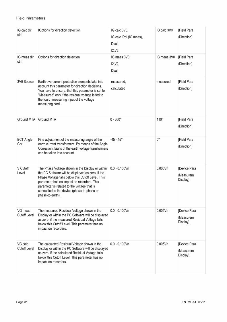
Field Parameters
IG calc dir ctrl
IOptions for direction detection IG calc 3V0,
IG calc IPol (IG meas),
Dual,
I2,V2
IG calc 3V0 [Field Para
/Direction]
IG meas dir ctrl
Options for direction detection IG meas 3V0,
I2,V2,
Dual
IG meas 3V0 [Field Para
/Direction]
3V0 Source Earth overcurrent protection elements take into account this parameter for direction decisions. You have to ensure, that this parameter is set to "Measured" only if the residual voltage is fed to the fourth measuring input of the voltage measuring card.
measured,
calculated
measured [Field Para
/Direction]
Ground MTA Ground MTA 0 - 360° 110° [Field Para
/Direction]
ECT Angle Cor
Fine adjustment of the measuring angle of the earth current transformers. By means of the Angle Correction, faults of the earth voltage transformers can be taken into account.
-45 - 45° 0° [Field Para
/Direction]
V Cutoff Level
The Phase Voltage shown in the Display or within the PC Software will be displayed as zero, if the Phase Voltage falls below this Cutoff Level. This parameter has no impact on recorders. This parameter is related to the voltage that is connected to the device (phase-to-phase or phase-to-earth).
0.0 - 0.100Vn 0.005Vn [Device Para
/Measurem Display]
VG meas Cutoff Level
The measured Residual Voltage shown in the Display or within the PC Software will be displayed as zero, if the measured Residual Voltage falls below this Cutoff Level. This parameter has no impact on recorders.
0.0 - 0.100Vn 0.005Vn [Device Para
/Measurem Display]
VG calc Cutoff Level
The calculated Residual Voltage shown in the Display or within the PC Software will be displayed as zero, if the calculated Residual Voltage falls below this Cutoff Level. This parameter has no impact on recorders.
0.0 - 0.100Vn 0.005Vn [Device Para
/Measurem Display]
Page 310 EN MCA4 05/11

Field Parameters
V012 Comp Cutoff Level
The Symmetrical Component shown in the Display or within the PC Software will be displayed as zero, if the Symmetrical Component falls below this Cutoff Level. This parameter has no impact on recorders.
0.0 - 0.100Vn 0.005Vn [Device Para
/Measurem Display]
EN MCA4 05/11 Page 311

Blockings
BlockingsThe device provides a function for temporary and permanent blocking of the complete protection functionality or of single protection stages.
Make absolutely sure that no illogical or even life-threatening blockings are allocated.
Make sure that you do not carelessly deactivate protection functions which have to be available according to the protection concept.
Permanent BlockingSwitching ON or OFF the complete protection functionality In module »Protection« the complete protection of the device can be switched on or off. Set the parameter Function to »active« or »inactive« in module »Prot«.
Only if in module »Prot« the parameter »Function« is = »active«, the protection is activated; i.e. with »Function« = »inactive«, no protection function is operating. Then the device cannot protect any components.
Switching modules ON or OFF Each of the modules can be switched on or off (permanently). This is achieved when the parameter »Function« is set to »active« or »inactive« in the respective module.
Activating or deactivating the tripping command of a protection stage permanentlyIn each of the protection stages the tripping command to the CB can be permanently blocked. For this purpose the parameter »TripCmd Blo« has to be set to »active«.
Temporary BlockingTo block the complete protection of the device temporarily by a signal In module »Prot« the complete protection of the device can be blocked temporarily by a signal. On condition that a module-external blocking is permitted »ExBlo Fc=active«. In addition to this, a related blocking signal from the »assignment list« must have been assigned. For the time the allocated blocking signal is active, the module is blocked.
If the module »Prot« is blocked, the complete protection function does not work. As long as the blocking signal is active, the device cannot protect any components.
To block a complete protection module temporarily by an active assignment
• In order to establish a temporary blockage of a protection module, the parameter »ExBlo Fc« of the module has to be set to »active«. This gives the permission: »This module can be blocked«.
• Within the general protection parameters a signal has to be additionally chosen from the »ASSIGNMENT LIST«. The blocking only becomes active when the assigned signal is active.
Page 312 EN MCA4 05/11

Blockings
To block the tripping command of a protection stage temporarily by an active assignment.The tripping command of any of the protection modules can be blocked from external. In this case, external does not only mean from outside the device, but also from outside the module. Not only real external signals are permitted to be used as blocking signals, as for example, the state of a digital input, but you can also choose any other signal from the »assignment list«.
• In order to establish a temporary blockage of a protection stage, the parameter »ExBlo TripCmd Fc« of the module has to be set to »active«. This gives the permission: »The tripping command of this stage can be blocked«.
• Within the general protection parameters, a signal has to be chosen additionally and assigned to the parameter »ExBlo« from the »assignment list«. If the selected signal is activated, the temporary blockage becomes effective.
EN MCA4 05/11 Page 313

Blockings
To Activate or Deactivate the Tripping Command of a Protection Module
Page 314 EN MCA4 05/11
inac
tive
activ
e
&
nam
e.Bl
o Tr
ipC
md
inac
tive
activ
e
nam
e.Ex
Blo
Trip
Cm
d Fc
1..n
, Ass
ignm
ent L
ist
nam
e.Ex
Blo
Trip
Cm
d
nam
e.Ex
Blo
Trip
Cm
d
Trip
blo
ckin
gs
>1
nam
e =
all m
odul
es th
at a
re b
lock
able
nam
e.Ex
Blo
Trip
Cm
d-I
nam
e.Bl
o Tr
ipC
md
3
inac
tive
activ
e
Prot
.Blo
Trip
Cm
d
&
inac
tive
activ
e
Prot
.ExB
lo T
ripC
md
Fc
1..n
, Ass
ignm
ent L
ist
Prot
.ExB
lo T
ripC
md
Prot
.Blo
Trip
Cm
d>1
Prot
.ExB
lo T
ripC
md
Prot
.ExB
lo T
ripC
md-
I
32

Blockings
Activate, Deactivate Respectively Block Temporarily Protection FunctionsThe following diagram applies to all protective elements except: Phase current, Earth current and Q->&V< protection elements.
EN MCA4 05/11 Page 315
&
inac
tive
activ
e
nam
e.Fu
nctio
n
inac
tive
activ
e
nam
e.Ex
Blo
Fc
nam
e.ac
tive
Prot
. act
ive
&
1..n
, Ass
ignm
ent L
ist
nam
e.Ex
Blo
1
nam
e.Ex
Blo
Bloc
king
s (The
Gen
eral
Pro
tect
ion
mod
ule
is n
ot d
eact
ivate
d or
blo
cked
)
nam
e.Ex
Blo1
-I
1..n
, Ass
ignm
ent L
ist
nam
e.Ex
Blo
2na
me.
ExBl
o2-I
>1
nam
e =a
ll m
odul
es th
at a
re b
lock
able
1
2
Plea
se R
efer
To
Dia
gram
: Pro
t

Blockings
The following diagram is applies to the Q->&V< Protection:
Page 316 EN MCA4 05/11
&
inac
tive
activ
e
Prot
.Fun
ctio
n
inac
tive
activ
e
Prot
.ExB
lo F
c
Prot
.act
ive
1..n
, Ass
ignm
ent L
ist
Prot
.ExB
lo 1
Prot
.ExB
lo
Prot
-ac
tive
>1
1..n
, Ass
ignm
ent L
ist
Prot
.ExB
lo 2
Prot
.ExB
lo1-
I
Prot
.ExB
lo2-
I
&
&
Prot
.ava
ilabl
e M
easu
red
valu
es: O
K
At th
e m
omen
t no
para
met
er is
bei
ng c
hang
ed (e
xcep
t par
amet
er s
et
para
met
ers)
1
12a
12b
38a
38b
inac
tive
nam
e.M
eas
Circ
uit
Supe
rv
activ
e
&>1
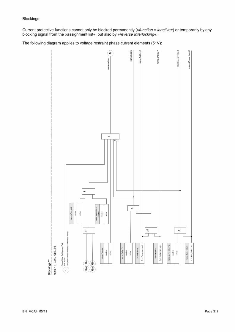
Blockings
Current protective functions cannot only be blocked permanently (»function = inactive«) or temporarily by any blocking signal from the »assignment list«, but also by »reverse Interlocking«.
The following diagram applies to voltage restraint phase current elements (51V):
EN MCA4 05/11 Page 317
&
inac
tive
activ
e
nam
e.Ex
rev
Inte
rl Fc
&
inac
tive
activ
e
nam
e.Fu
nctio
n
nam
e.ac
tive
Prot
. act
ive
&
nam
e.Ex
Blo
nam
e.Ex
rev
Inte
rl
Bloc
king
s **
(The
Gen
eral
Pro
tect
ion
mod
ule
is n
ot d
eact
ivat
ed o
r blo
cked
)
nam
e =
I[1]..
.[n],
IG[1
]...[n
]
nam
e.Ex
Blo1
-I
nam
e.Ex
rev
Inte
rl-I
1..n
, Ass
ignm
ent L
ist
nam
e.Ex
Blo
2
>1
nam
e.Ex
Blo2
-I
1
4
Ple
ase
Ref
er T
o D
iagr
am: P
rot
12a
12b
38a
38b
>1
inac
tive
nam
e.VR
estra
int
activ
e
1..n
, Ass
ignm
ent L
ist
nam
e.Ex
rev
Inte
rl
1..n
, Ass
ignm
ent L
ist
nam
e.Ex
Blo
1
inac
tive
activ
e
nam
e.Ex
Blo
Fc
inac
tive
nam
e.M
eas
Circ
uit
Supe
rv
activ
e
&
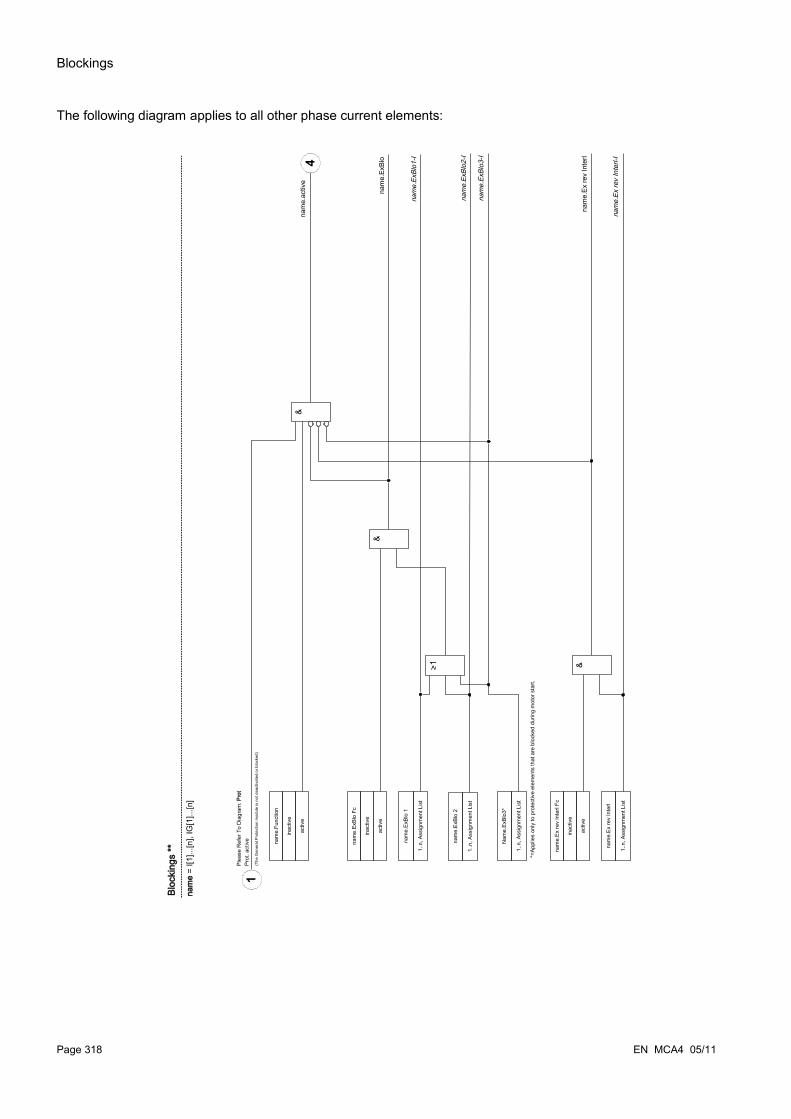
Blockings
The following diagram applies to all other phase current elements:
Page 318 EN MCA4 05/11
inac
tive
activ
e
nam
e.Ex
rev
Inte
rl Fc
inac
tive
activ
e
nam
e.Fu
nctio
n
nam
e.ac
tive
Prot
. act
ive
nam
e.Ex
Blo
nam
e.Ex
rev
Inte
rl
Bloc
king
s **
(The
Gen
eral
Pro
tect
ion
mod
ule
is n
ot d
eact
ivat
ed o
r blo
cked
)
nam
e =
I[1]..
.[n],
IG[1
]...[n
]
nam
e.Ex
Blo1
-I
nam
e.Ex
rev
Inte
rl-I
1..n
, Ass
ignm
ent L
ist
nam
e.Ex
Blo
2na
me.
ExBl
o2-I
1
4
Ple
ase
Ref
er T
o D
iagr
am: P
rot
nam
e.Ex
Blo3
-I
&
&in
activ
e
activ
e
nam
e.Ex
Blo
Fc
>11.
.n, A
ssig
nmen
t Lis
t
nam
e.Ex
Blo
1
1..n
, Ass
ignm
ent L
ist
nam
e.Ex
rev
Inte
rl
1..n
, Ass
ignm
ent L
ist
Nam
e.Ex
Blo3
*
&
*=Ap
plie
s on
ly to
pro
tect
ive
elem
ents
that
are
blo
cked
dur
ing
mot
or s
tart.
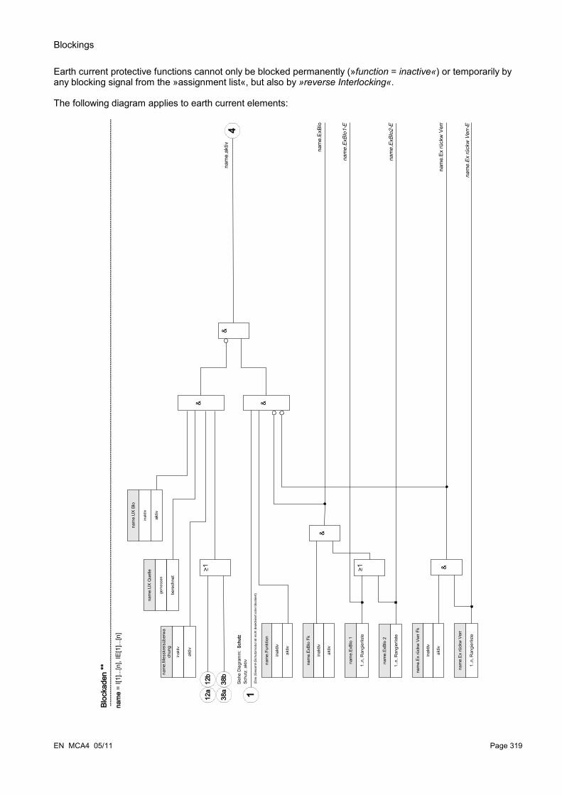
Blockings
Earth current protective functions cannot only be blocked permanently (»function = inactive«) or temporarily by any blocking signal from the »assignment list«, but also by »reverse Interlocking«.
The following diagram applies to earth current elements:
EN MCA4 05/11 Page 319
&
inak
tiv
aktiv
nam
e.Ex
rück
w V
err F
k
&
inak
tiv
aktiv
nam
e.Fu
nktio
n
inak
tiv
aktiv
nam
e.Ex
Blo
Fk
nam
e.ak
tiv
Schu
tz. a
ktiv
&
1..n
, Ran
gier
liste
nam
e.Ex
Blo
1
1..n
, Ran
gier
liste
nam
e.Ex
rück
w V
err
nam
e.Ex
Blo
nam
e.Ex
rück
w V
err
Bloc
kade
n **
(Das
(Ges
amt-)
Schu
tzm
odul
ist n
icht
dea
ktiv
iert
oder
blo
ckie
rt)
nam
e =
I[1]..
.[n],
IE[1
]...[n
]
nam
e.Ex
Blo1
-E
nam
e.Ex
rück
w V
err-E
1..n
, Ran
gier
liste
nam
e.Ex
Blo
2
>1
nam
e.Ex
Blo2
-E
1
4S
iehe
Dia
gram
m:
Schu
tz
12a
12b
38a
38b
>1
inak
tiv
nam
e.M
essk
reis
über
wa
chun
g
aktiv
gem
esse
n
nam
e.U
X Q
uelle
bere
chne
t
inak
tiv
nam
e.U
X Bl
o
aktiv
&
&

Module: Protection (Prot)
Module: Protection (Prot) Prot
The module »Protection« serves as outer frame for all other protection modules, i.e. they are all enclosed by the module »Protection«. All alarms and tripping commands are combined in module »Protection« by an OR-logic.
If in module »Protection« the parameter »Function« is set on »inactive« or in case the module is blocked, then the complete protective function of the device does not work anymore.
Protection inactiveIf the master module »Protection« was permanently deactivated or if a temporary blockage of this module has occurred and the allocated blocking signal is still active, then the complete functionality (protection) of the device is zero. In such a case the protective function is »inactive«.
Protection activeIf the master module »Protection« was activated and a blockade for this module was not activated respectively the assigned blocking signal is inactive at that moment, then the »Protection« is »active«.
Page 320 EN MCA4 05/11
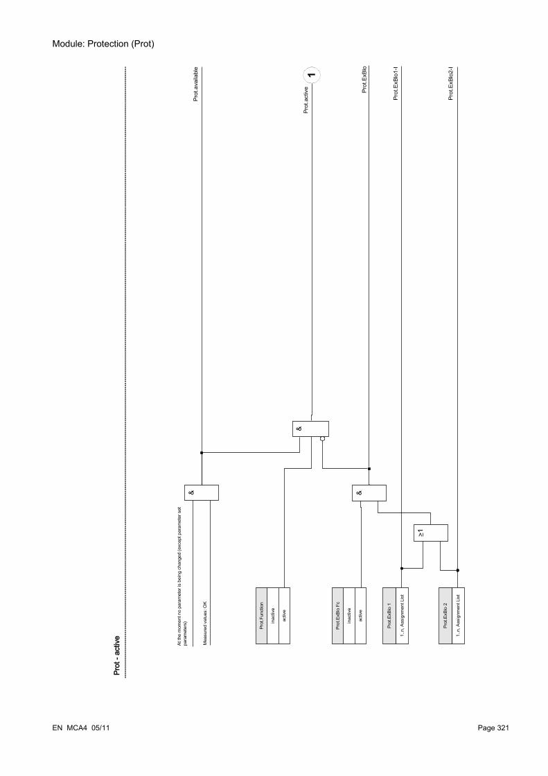
Module: Protection (Prot)
EN MCA4 05/11 Page 321
&
inac
tive
activ
e
Prot
.Fun
ctio
n
inac
tive
activ
e
Prot
.ExB
lo F
c
Prot
.act
ive
1..n
, Ass
ignm
ent L
ist
Prot
.ExB
lo 1
Prot
.ExB
lo
Prot
-ac
tive
>1
1..n
, Ass
ignm
ent L
ist
Prot
.ExB
lo 2
Prot
.ExB
lo1-
I
Prot
.ExB
lo2-
I
&
&
Prot
.ava
ilabl
e M
easu
red
valu
es: O
K
At th
e m
omen
t no
para
met
er is
bei
ng c
hang
ed (e
xcep
t par
amet
er s
et
para
met
ers)
1

Module: Protection (Prot)
Each protection stage can decide automatically about a trip. The trip decision is passed on to module »Prot« and The tripping commands of all protection stages are combined in module »Prot« by an OR logic (Collective signals, direction decisions, information about phases). The tripping commands are executed by the module »TripControl«.
The tripping commands are executed by the module »TripControl«
If a protection module is activated respectively issues a trip command to the CB two alarm signals will be created:
1. The module or the protection stage issues an alarm e.g. »I[1].ALARM« or »I[1].TRIP«.
2. The master module »Prot« collects/summarizes the signals and issues an alarm or a trip signal »PROT.ALARM« »PROT.TRIP«.
Page 322 EN MCA4 05/11
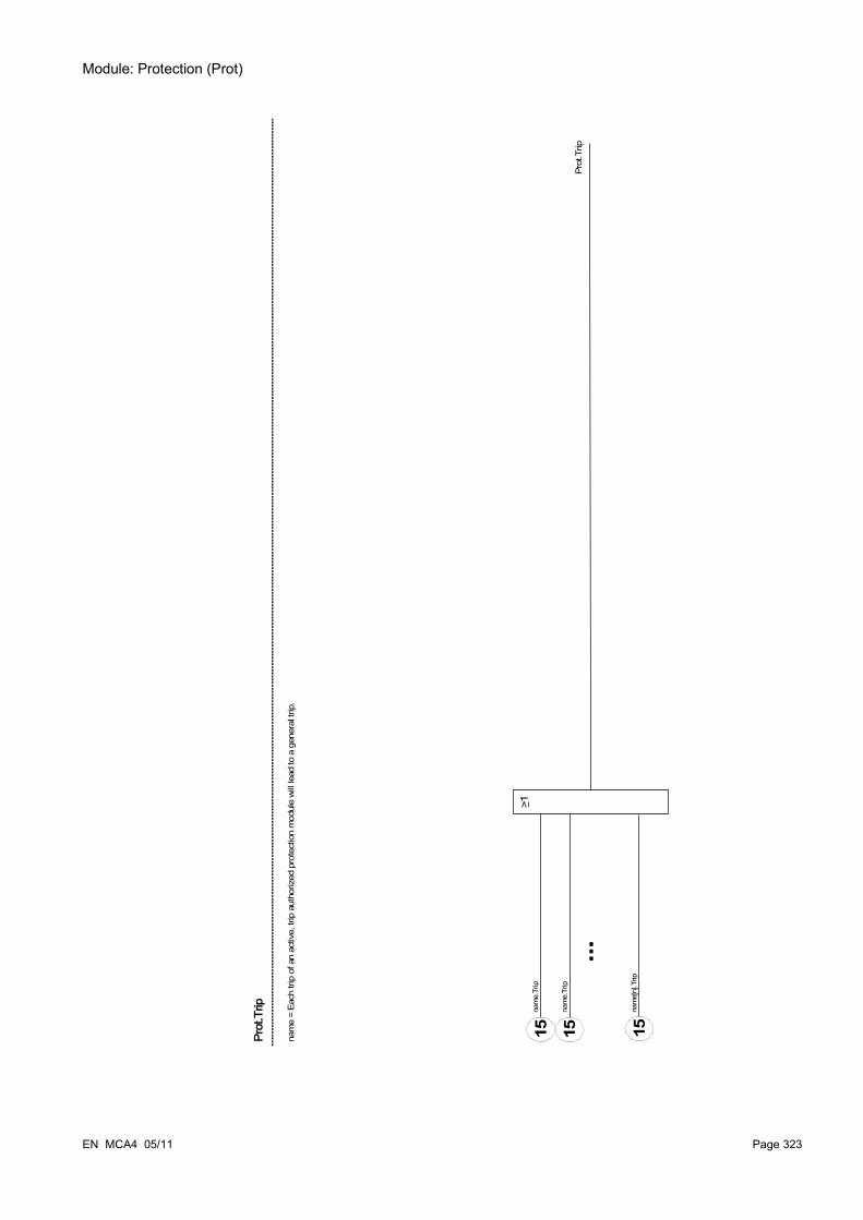
Module: Protection (Prot)
EN MCA4 05/11 Page 323
>1
Prot
.Trip
nam
e.Tr
ip
nam
e =
Each
trip
of a
n ac
tive,
trip
aut
horiz
ed p
rote
ctio
n m
odul
e w
ill le
ad to
a g
ener
al tr
ip.
nam
e.Tr
ip
Prot
.Trip na
me[
n].T
rip
...
15 15 15
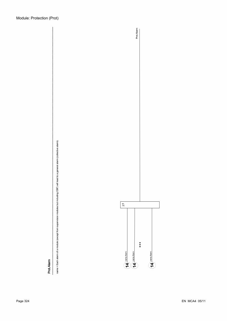
Module: Protection (Prot)
Page 324 EN MCA4 05/11
Prot
.Ala
rm
Prot
.Ala
rm
>1na
me.
Alar
m
nam
e.Al
arm
nam
e.Al
arm
nam
e =
Each
ala
rm o
f a m
odul
e (e
xcep
t fro
m s
uper
visi
on m
odul
es b
ut in
clud
ing
CBF
) will
lead
to a
gen
eral
ala
rm (c
olle
ctiv
e al
arm
).
...14 1414
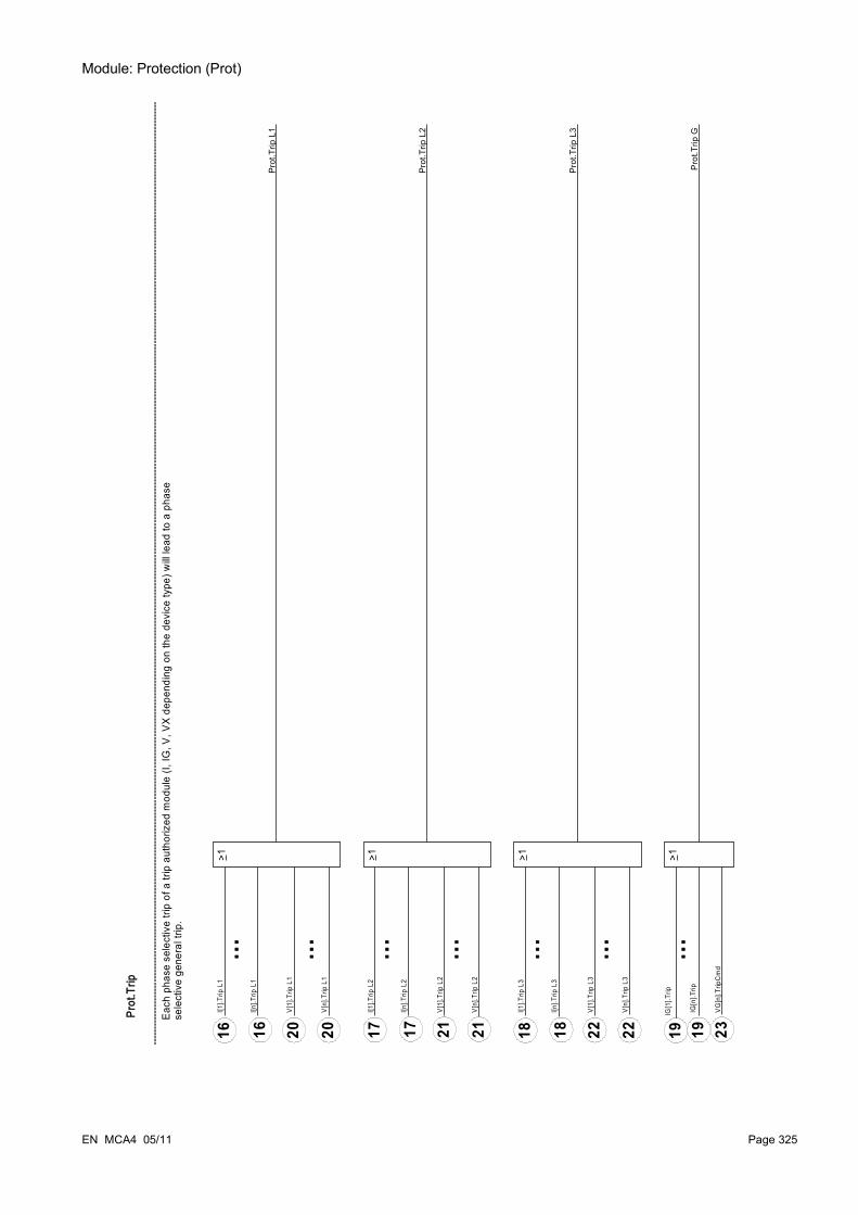
Module: Protection (Prot)
EN MCA4 05/11 Page 325
Prot
.Trip
L1
I[1].T
rip L
1
I[n].T
rip L
1
V[1]
.Trip
L1
V[n]
.Trip
L1
Prot
.Trip
L2
I[1].T
rip L
2
I[n].T
rip L
2
V[1]
.Trip
L2
V[n]
.Trip
L2
Prot
.Trip
L3
I[1].T
rip L
3
I[n].T
rip L
3
V[1]
.Trip
L3
V[n]
.Trip
L3
IG[1
].Trip
VG[n
].Trip
Cm
d
Prot
.Trip
GIG
[n].T
rip
>1 >1 >1 >1
Prot
.Trip
Each
pha
se s
elec
tive
trip
of a
trip
aut
horiz
ed m
odul
e (I,
IG, V
, VX
depe
ndin
g on
the
devi
ce ty
pe) w
ill le
ad to
a p
hase
se
lect
ive
gene
ral t
rip.
... ... ... ... ... ... ...
16 16 20 20 17 17 21 21 18 18 22 22 19 19 23
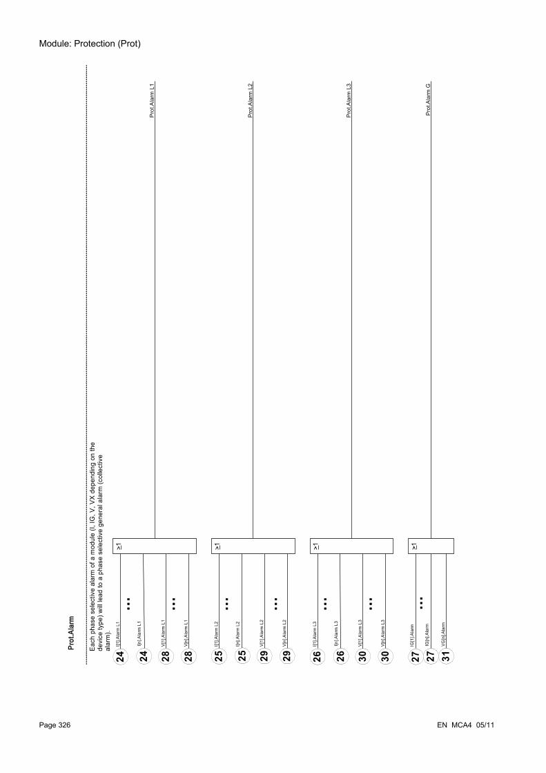
Module: Protection (Prot)
Page 326 EN MCA4 05/11
Prot
.Ala
rm L
1
I[1].A
larm
L1
I[n].A
larm
L1
V[1]
.Ala
rm L
1
V[n]
.Ala
rm L
1
Prot
.Ala
rm L
2
I[1].A
larm
L2
I[n].A
larm
L2
V[1]
.Ala
rm L
2
V[n]
.Ala
rm L
2
Prot
.Ala
rm L
3
I[1].A
larm
L3
I[n].A
larm
L3
V[1]
.Ala
rm L
3
V[n]
.Ala
rm L
3
IG[1
].Ala
rm
VG[n
].Ala
rm
Prot
.Ala
rm G
IG[n
].Ala
rm
>1 >1 >1 >1
Prot
.Ala
rm
Eac
h ph
ase
sele
ctiv
e al
arm
of a
mod
ule
(I, IG
, V, V
X de
pend
ing
on th
e de
vice
type
) will
lead
to a
pha
se s
elec
tive
gene
ral a
larm
(col
lect
ive
alar
m).
... ... ... ... ... ... ...
24 24 28 28 25 25 29 29 26 26 30 30 27 27 31
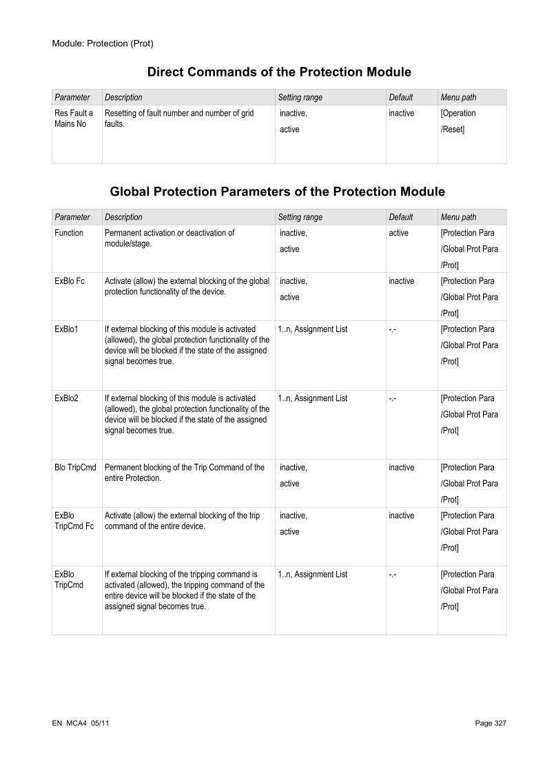
Module: Protection (Prot)
Direct Commands of the Protection Module
Parameter Description Setting range Default Menu path
Res Fault a Mains No
Resetting of fault number and number of grid faults.
inactive,
active
inactive [Operation
/Reset]
Global Protection Parameters of the Protection Module
Parameter Description Setting range Default Menu path
Function Permanent activation or deactivation of module/stage.
inactive,
active
active [Protection Para
/Global Prot Para
/Prot]ExBlo Fc Activate (allow) the external blocking of the global
protection functionality of the device. inactive,
active
inactive [Protection Para
/Global Prot Para
/Prot]ExBlo1 If external blocking of this module is activated
(allowed), the global protection functionality of the device will be blocked if the state of the assigned signal becomes true.
1..n, Assignment List -.- [Protection Para
/Global Prot Para
/Prot]
ExBlo2 If external blocking of this module is activated (allowed), the global protection functionality of the device will be blocked if the state of the assigned signal becomes true.
1..n, Assignment List -.- [Protection Para
/Global Prot Para
/Prot]
Blo TripCmd Permanent blocking of the Trip Command of the entire Protection.
inactive,
active
inactive [Protection Para
/Global Prot Para
/Prot]ExBlo TripCmd Fc
Activate (allow) the external blocking of the trip command of the entire device.
inactive,
active
inactive [Protection Para
/Global Prot Para
/Prot]
ExBlo TripCmd
If external blocking of the tripping command is activated (allowed), the tripping command of the entire device will be blocked if the state of the assigned signal becomes true.
1..n, Assignment List -.- [Protection Para
/Global Prot Para
/Prot]
EN MCA4 05/11 Page 327
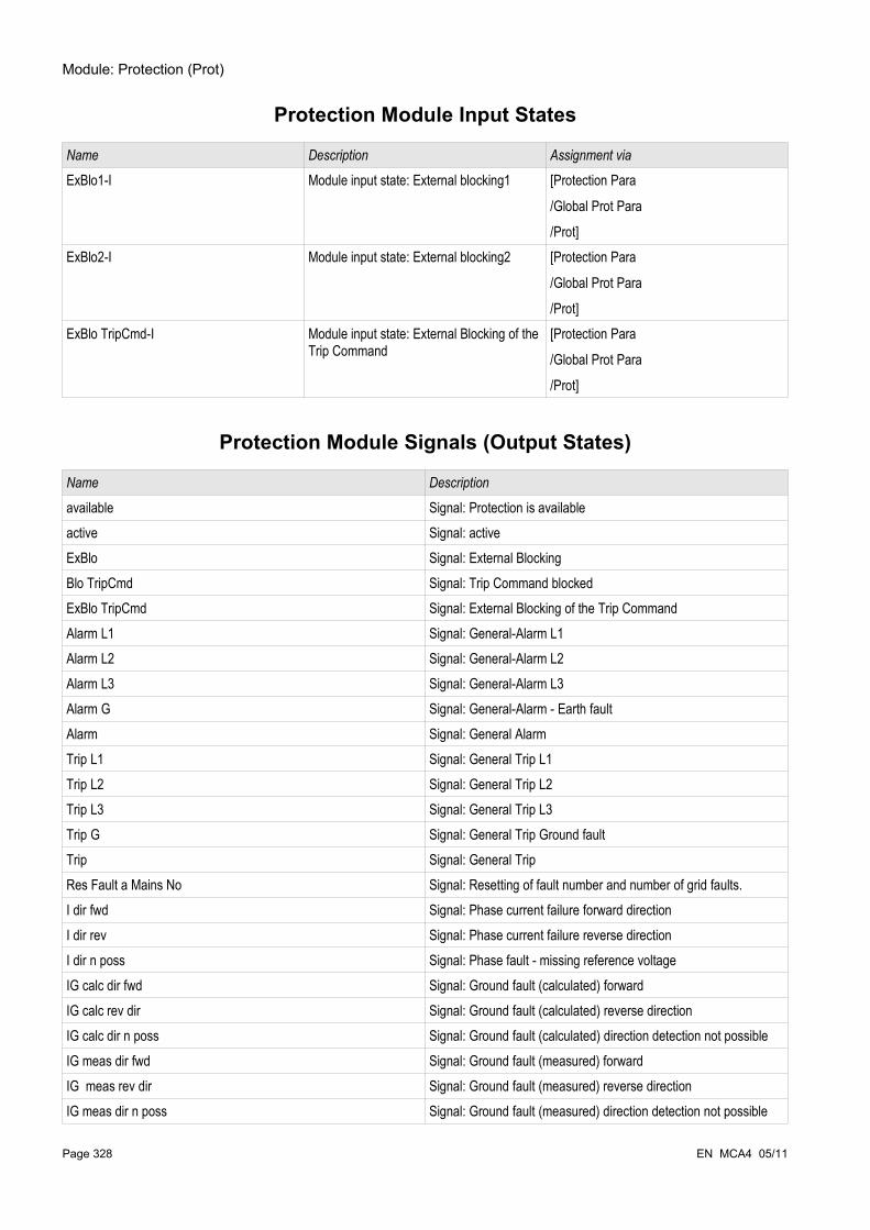
Module: Protection (Prot)
Protection Module Input States
Name Description Assignment via
ExBlo1-I Module input state: External blocking1 [Protection Para
/Global Prot Para
/Prot]ExBlo2-I Module input state: External blocking2 [Protection Para
/Global Prot Para
/Prot]ExBlo TripCmd-I Module input state: External Blocking of the
Trip Command[Protection Para
/Global Prot Para
/Prot]
Protection Module Signals (Output States)
Name Description
available Signal: Protection is availableactive Signal: activeExBlo Signal: External BlockingBlo TripCmd Signal: Trip Command blockedExBlo TripCmd Signal: External Blocking of the Trip CommandAlarm L1 Signal: General-Alarm L1Alarm L2 Signal: General-Alarm L2Alarm L3 Signal: General-Alarm L3Alarm G Signal: General-Alarm - Earth faultAlarm Signal: General AlarmTrip L1 Signal: General Trip L1Trip L2 Signal: General Trip L2Trip L3 Signal: General Trip L3Trip G Signal: General Trip Ground faultTrip Signal: General TripRes Fault a Mains No Signal: Resetting of fault number and number of grid faults.I dir fwd Signal: Phase current failure forward directionI dir rev Signal: Phase current failure reverse directionI dir n poss Signal: Phase fault - missing reference voltageIG calc dir fwd Signal: Ground fault (calculated) forwardIG calc rev dir Signal: Ground fault (calculated) reverse directionIG calc dir n poss Signal: Ground fault (calculated) direction detection not possibleIG meas dir fwd Signal: Ground fault (measured) forwardIG meas rev dir Signal: Ground fault (measured) reverse directionIG meas dir n poss Signal: Ground fault (measured) direction detection not possible
Page 328 EN MCA4 05/11

Module: Protection (Prot)
Protection Module Values
Name Description Assignment via
FaultNo Disturbance No []No of grid faults Number of grid faults: A grid fault, e.g. a
short circuit, might cause several faults with trip and autoreclosing, each fault being identified by an increased fault number. In this case, the grid fault number remains the same.
[]
EN MCA4 05/11 Page 329

Switchgear/Breaker – Manager
Switchgear/Breaker – Manager
WARNING Misconfiguration of switchgears could result in death or serious injury. This e. g. is the case when opening a disconnector under load or when switching a ground connector to live parts of a system.
The user has to follow and document the step by step procedure (use the Breaker Configuration Documentation).
Beside protection functions, protective relays more and more will take care about controlling switchgears, like circuit breakers, load break switches, disconnectors and ground connectors.
A correct configuration of all switchgears is an indispensable precondition for the proper functioning of the protective device. This also is the case, when the switchgears are not controlled, but supervised only.
Page 330 EN MCA4 05/11

Switchgear/Breaker – Manager
Single Line DiagramFor construction of a single line diagram, please address to our technical support.
The single line diagram includes the graphically description of the switchgears and their designations (names) as well as their features (short circuit proof or not ...). For displaying in the devices software, the switchgears' designations (e. g. QA1, QA2, instead of SG[x]) will be taken from the single line diagram.
Beside parameters a configuration file also includes a single line diagram. Parameter setting and single line diagram are coupled via the the configuration file.
Whenever a configuration file is loaded into a protection device, a single line diagram will be always loaded at the same time.
Transfer of the Single Line Diagram into the deviceIf in the Smart view menu »Device« »Transfer All Parameters into the Device« has been selected, beside all parameters also the single line diagram will be transferred into the device.
EN MCA4 05/11 Page 331

Switchgear/Breaker – Manager
After the single line diagram has been loaded, each individual switchgear has to be configured. The following table shows the required configurations dependent on the type of switchgear.
To be configured at: Type of switchgear
[Control\SG\Designation of switchgear]
Circ
uit B
reak
er
(con
trol
led)
Circ
uit B
reak
er
(sup
ervi
sed)
Switc
h D
isco
nnec
tor
(con
trol
led)
Switc
h D
isco
nnec
tor
(sup
ervi
sed)
Gro
und
Con
nect
or(c
ontr
olle
d)
Gro
und
Con
nect
or(s
uper
vise
d)
Dis
conn
ecto
r(c
ontr
olle
d)
Dis
conn
ecto
r(s
uper
vise
d)
Switc
h(c
ontr
olle
d)
Switc
h(s
uper
vise
d)
Assignment of position indications(Digital inputs)
x x x x x x x x
Assignment of commands(Output relays) x - x - x - x -
Setting of supervision timers x x x x x x x x
Interlockings x - x - x - x -Trip Manager(Assignment of trip commands) x x - - - - - -
Optional: Synchronous switching x x - - - - - -
Optional: Ex ON/OFF Cmd x - x - x - x -Optional: SGW x x x x x x x x
Page 332 EN MCA4 05/11
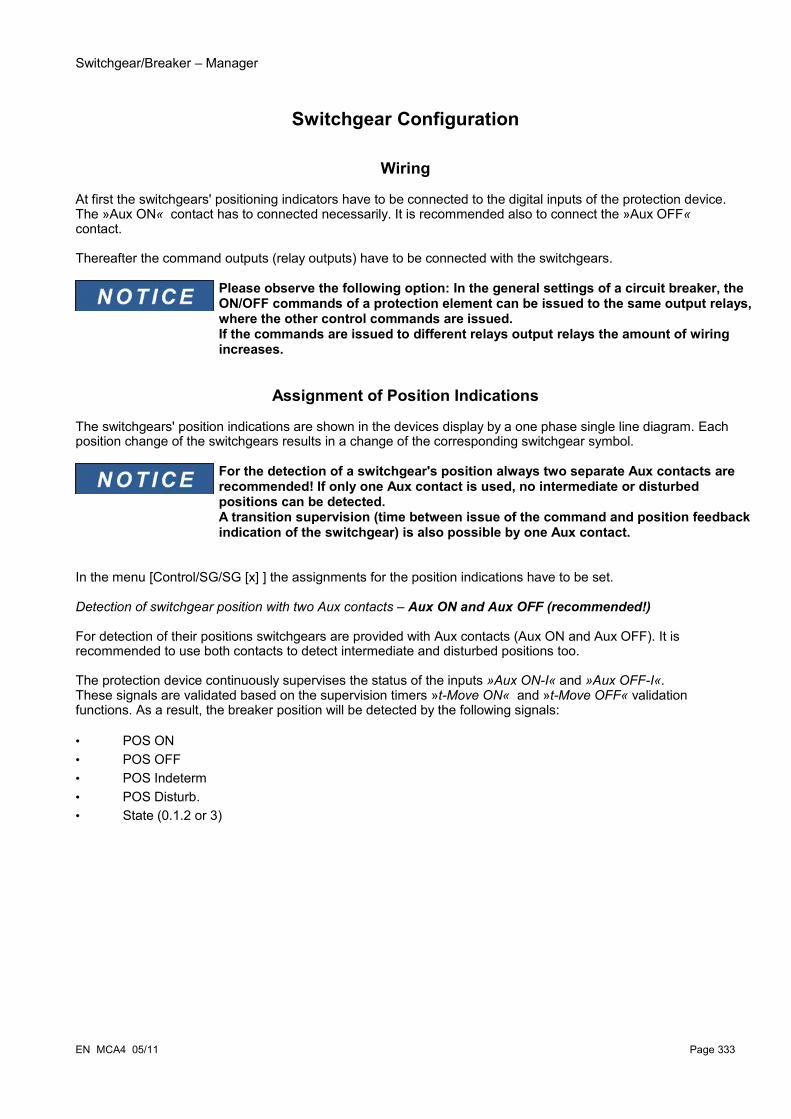
Switchgear/Breaker – Manager
Switchgear Configuration
Wiring
At first the switchgears' positioning indicators have to be connected to the digital inputs of the protection device.The »Aux ON« contact has to connected necessarily. It is recommended also to connect the »Aux OFF« contact.
Thereafter the command outputs (relay outputs) have to be connected with the switchgears.
Please observe the following option: In the general settings of a circuit breaker, the ON/OFF commands of a protection element can be issued to the same output relays, where the other control commands are issued.If the commands are issued to different relays output relays the amount of wiring increases.
Assignment of Position Indications
The switchgears' position indications are shown in the devices display by a one phase single line diagram. Each position change of the switchgears results in a change of the corresponding switchgear symbol.
For the detection of a switchgear's position always two separate Aux contacts are recommended! If only one Aux contact is used, no intermediate or disturbed positions can be detected.A transition supervision (time between issue of the command and position feedback indication of the switchgear) is also possible by one Aux contact.
In the menu [Control/SG/SG [x] ] the assignments for the position indications have to be set.
Detection of switchgear position with two Aux contacts – Aux ON and Aux OFF (recommended!)
For detection of their positions switchgears are provided with Aux contacts (Aux ON and Aux OFF). It is recommended to use both contacts to detect intermediate and disturbed positions too.
The protection device continuously supervises the status of the inputs »Aux ON-I« and »Aux OFF-I«.These signals are validated based on the supervision timers »t-Move ON« and »t-Move OFF« validation functions. As a result, the breaker position will be detected by the following signals:
• POS ON • POS OFF• POS Indeterm• POS Disturb.• State (0.1.2 or 3)
EN MCA4 05/11 Page 333

Switchgear/Breaker – Manager
Supervision of the ON commandWhen an ON command is initiated, the »t-Move ON« timer will be started. While the timer is running, the »POS INDETERM« State will become true. If the command is executed and properly fed back before the timer has run down, »POS ON« will become true. Otherwise, if the timer has expired »POS DISTURB« will become true.
Supervision of the OFF commandWhen an OFF command is initiated, the »t-Move OFF« timer will be started. While the timer is running, the »POS INDETERM« State will become true. If the command is executed and properly fed back before the timer has run down, »POS OFF« will become true. Otherwise, if the timer has expired »POS DISTURB« will become true.
The following table shows how breaker positions are validated:
States of the Digital Inputs Validated Breaker PositionsAux ON-I Aux OFF-I POS ON POS OFF POS
IndetermPOS Disturb POS
State
0 0 0 0 1(while a Moving timer is running)
0(while a Moving timer is running)
0Intermediate
1 1 0 0 1(while a Moving timer is running)
0(while a Moving timer is running)
0Intermediate
0 1 0 1 0 0 1OFF
1 0 1 0 0 0 2ON
0 0 0 0 0(Moving timer
elapsed)
1(Moving timer
elapsed)
3Disturbed
1 1 0 0 0(Moving timer
elapsed)
1(Moving timer
elapsed)
3Disturbed
Page 334 EN MCA4 05/11

Switchgear/Breaker – Manager
Single Position Indication Aux ON or Aux OFF
If the single pole indication is used, the »SI SINGLECONTACTIND« will become true.
The moving time supervision works only in one direction. If the Aux OFF signal is connected to the device, only the “OFF command” can be supervised and if the Aux ON signal is connected to the device, only the “ON command” can be supervised.
Single Position Indication – Aux ON only
If only the Aux ON signal is used for the Status Indication of an “ON command”, the switch command will also start the moving time, the position indication indicates an INTERMEDIATE position during this time interval. When the switchgear reaches the end position indicated by the signals Pos ON and CES succesf before the moving time has elapsed the signal Pos Indeterm disappears.
If the moving time elapsed before the switchgear has reached the end position, the switching operation was not successful and the Position Indication will change to POS Disturb and the signal Pos Indeterm disappears. After the moving time has elapsed, the Dwell time will be started (if set). During this time interval the Position Indication will also indicate an INTERMEDIATE state. When the Dwell time elapses the Position Indication will change to Pos ON.
The following table shows how breaker positions are validated based on Aux ON only:
States of the Digital Input Validated Breaker PositionsAux ON-I Aux OFF-I POS ON POS OFF POS
IndetermPOS Disturb POS
State
0 Not wired 0 0 1(while t-Move ON is running)
0(while t-Move ON is running)
0Intermediate
0 Not wired 0 1 0 0 1OFF
1 Not wired 1 0 0 0 2ON
1 Not wired 0 0 0(after t-Move ON
is elapsed)
1(after t-Move ON
is elapsed)
3Disturbed
If there is no digital input assigned to the »Aux On« contact, the position indication will have the value 3 (disturbed).
EN MCA4 05/11 Page 335

Switchgear/Breaker – Manager
Single Position Indication – Aux OFF only
If only the Aux OFF signal is used for the monitoring of the “OFF command”, the switch command will start the moving timer. The Position Indication will indicate an INTERMEDIATE position. When the the switchgear reaches its end position before the moving timer elapses, and »CES succesf« will be indicated. At the same time the signal »Pos Indeterm« disappears.If the moving time elapsed before the switchgear has reached the OFF position, the switching operation was not successful and the Position Indication will change to »Pos Disturb« and the signal »Pos Indeterm« disappears.When the moving timer has elapsed, the dwell timer will be started (if configured). During this timer elapses »Pos Disturb« will be indicated. When the dwell time has elapsed, the OFF position of the switchgear will be indicated by the »Pos OFF« signal.
The following table shows how breaker positions are validated based on Aux OFF only:
States of the Digital Input Validated Breaker PositionsAux ON-I Aux OFF-I POS ON POS OFF POS
IndetermPOS Disturb POS
State
Not wired 0 0 0 1(while t-Move
OFF is running)
0(while t-Move
OFF is running)
0Intermediate
Not wired 0 0 1 0 0 1OFF
Not wired 1 1 0 0 0 2ON
Not wired 1 0 0 0(after t-Move
OFF is elapsed)
1(after t-Move
OFF is elapsed)
3Disturbed
Setting of Supervision Times
In the menu [Control/SG/SG[x]/General Settings] the supervision times of the individual switchgear have to be set. Dependent on the type of switchgear it can be necessary to set further parameters, like dwell time.
Interlockings
To avoid faulty operations, interlockings have to be provided. This can be realised mechanically or electrically.
Controllable switchgears up to three interlockings can be assigned to both switching directions (ON/OFF). These interlockings prevent switching in the corresponding direction.
The protection OFF command and the reclosing command of the AR module are always executed without interlockings. For the case, that a protection OFF command must not be issued, this must be blocked separately.
Further interlockings can be realised by means of the Logic module.
Page 336 EN MCA4 05/11

Switchgear/Breaker – Manager
EN MCA4 05/11 Page 337
Switc
h co
mm
and
requ
est
via
Dig
ital I
nput
:(M
anua
l Sw
itch
Com
man
d)
Com
mun
icat
ion
issu
es th
e fo
llow
ing
com
man
ds:
(Man
ual S
witc
h C
omm
and)
HM
I iss
ues
the
follo
win
g co
mm
ands
:(M
anua
l Sw
itch
Com
man
d)
Auto
recl
osur
e is
sues
the
follo
win
g co
mm
ands
:(A
utom
atic
Sw
itch
Com
man
d)
Rel
ease
by
sync
hron
izin
g un
it
50P
Trip
s of
Pro
tect
ive
Elem
ents
Interlockings
Trip Manager (t-Min Hold Time, Latched)
Trip
Cm
d
Prot
ON
ON
Cm
d
OFF
Cm
d
& &
&
& &
>1 >1
>1
41 42
CB
ON
Cm
d
ON
Cm
d m
anua
l
ON
Cm
d m
anua
l
ON
Cm
d m
anua
l
OFF
Cm
d m
anua
l
OFF
Cm
d m
anua
l
OFF
Cm
d m
anua
lC
B O
FF C
md
CB
ON
Cm
d
inac
tive
nam
e.M
eas
Circ
uit
Supe
rv
activ
e
inac
tive
#(O
nInc
lude
sPro
tOn_
k
activ
e
>1
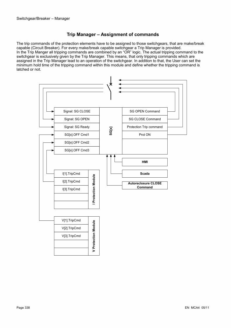
Switchgear/Breaker – Manager
Trip Manager – Assignment of commands
The trip commands of the protection elements have to be assigned to those switchgears, that are make/break capable (Circuit Breaker). For every make/break capable switchgear a Trip Manager is provided.In the Trip Manger all tripping commands are combined by an “OR” logic. The actual tripping command to the switchgear is exclusively given by the Trip Manager. This means, that only tripping commands which are assigned in the Trip Manager lead to an operation of the switchgear. In addition to that, the User can set the minimum hold time of the tripping command within this module and define whether the tripping command is latched or not.
Page 338 EN MCA4 05/11
Signal: SG CLOSE
Signal: SG OPEN
Signal: SG Ready
SG[x].OFF Cmd1
SG[x].OFF Cmd2
SG[x].OFF Cmd3
SG[x
]SG OPEN Command
SG CLOSE Command
Protection Trip command
Prot ON
I[1].TripCmd
I[2].TripCmd
I[3].TripCmd
I Pro
tect
ion
Mod
ule
V[1].TripCmd
V[2].TripCmd
V[3].TripCmd
V Pr
otec
tion
Mod
ule
HMI
Autoreclosure CLOSE Command
Scada

Switchgear/Breaker – Manager
EN MCA4 05/11 Page 339
SG[x
].Trip
CB
SG.T
rip C
B
>1na
me.
Trip
Cmd
1
SG.t-
Trip
Cm
d
t>1
. . . .
activ
e
inac
tive
Trip
com
man
d.La
tche
d
&
>1
S1
1
R
1
>1
+ R
Num
ber o
f Ope
ratio
nsSG
.Res
Trip
Cm
d C
r
nam
e.Tr
ipCm
d
nam
e.Tr
ipCm
d
nam
e.Tr
ipCm
d
nam
e.Tr
ipCm
d
Ackn
owle
dge
-HM
I
Ackn
owle
dge-
1..n
, Ass
ignm
ent L
ist
Ackn
owle
dge-
Scad
a
nam
e =G
ener
al T
rip s
igna
l of t
he a
ssig
ned
sign
als.
11
15 15 15 15 15
>1(M
anua
l Sw
itch
Com
man
d)
The
exac
t nam
e of
the
Switc
hgea
r is
defin
ed in
the
Sing
le L
ine
file.

Switchgear/Breaker – Manager
Ex ON/OFF
If the breaker should be opened or closed by an external signal, the User can assign one signal that will trigger the ON and one signal that will trigger the OFF command (e.g. digital inputs or output signals of the Logics). An OFF command has priority. ON commands are slope oriented, OFF commands are level oriented
Synchronised Switching
Before a switchgear may connect two mains sections, synchronism of these sections must be assured.In the menu [Synchronous Switching] the parameter »Synchronism« defines which signal indicates synchronism.
If the synchronism condition shall be evaluated by the internal Synch-Check module the signal »Sync. Ready to Close« (release by synch-check module) has to be assigned. Alternatively a digital input or a logic output can be assigned.
In the synchronisation mode “Generator-to-System” additionally the synchronism request has to be assigned in the menu [Protection Para\Global Prot Para\Sync].
If a synchronism signal is assigned, the switching command will only be executed, when the synchronism signal will become true within the maximum supervision time »t-MaxSyncSuperv«. This supervision time will be started with the issued ON command. The real control command will only be issued, when the synchronism feedback signal is present within this supervision time. If no synchronism signal has been assigned, the synchronism release is permanently.
Page 340 EN MCA4 05/11
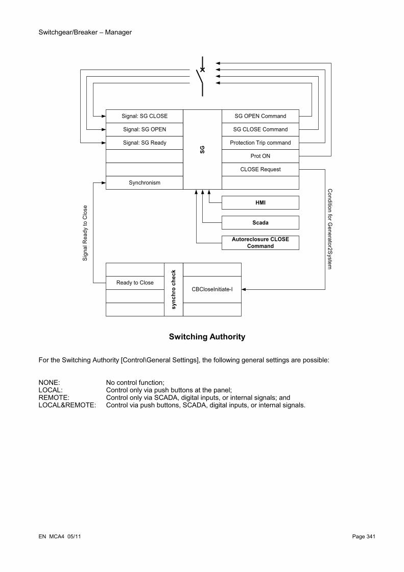
Switchgear/Breaker – Manager
Switching Authority
For the Switching Authority [Control\General Settings], the following general settings are possible:
NONE: No control function;LOCAL: Control only via push buttons at the panel;REMOTE: Control only via SCADA, digital inputs, or internal signals; andLOCAL&REMOTE: Control via push buttons, SCADA, digital inputs, or internal signals.
EN MCA4 05/11 Page 341
Signal: SG CLOSE
Signal: SG OPEN
Signal: SG Ready
Synchronism
SG
SG OPEN Command
SG CLOSE Command
Protection Trip command
Prot ON
HMI
Autoreclosure CLOSE Command
Scada
Ready to Close
sync
hro
chec
k
CBCloseInitiate-I
Condition for G
enerator2System
Sign
al R
eady
to C
lose
CLOSE Request

Switchgear/Breaker – Manager
Non interlocked Switching
For test purposes, during commissioning and temporarily operations, interlockings can be disabled.
WARNING: Non interlocked Switching can lead to serious injuries or death!
For non interlocked switching the menü [Control\General Settings] provides the following options:
• Non interlocked switching for one single command• Permanent• Non interlocked switching for a certain time• Non interlocked switching, activated by an assigned signal
The set time for non interlocked switching applies also for the „single Operation“ mode.
Manual Manipulation of the Switchgear Position
In case of faulty position indication contacts (Aux contacts) or broken wires, the position indication resulted from the assigned signals can be manipulated (overwritten) manually, to keep the ability to switch the affected switchgear. A manipulated switchgearposition will be indicated on the display by an exclamation mark “!” beside the switchgear symbol.
WARNING: Manipulation of the Switchgear Position can lead to serious injuries or death!
Double Operation Locking
All control commands to any switchgear in a bay have to be processed sequentially. During a running control command no other command will be handled.
Switch Direction Control
Switching command are validated before execution. When the switchgear is already in the desired position, the switch command will not be issued again. An opened circuit breaker cannot be opened again. This also applies for switching command at the HMI or via SCADA.
Anti PumpingBy pressing the ON command softkey only a single switching ON impulse will be issued independent, how low the softkey is actuated.
Page 342 EN MCA4 05/11
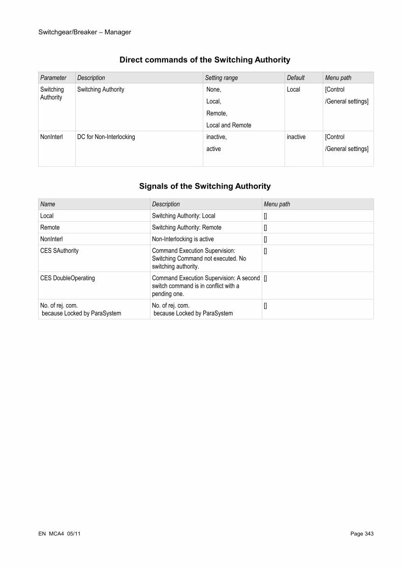
Switchgear/Breaker – Manager
Direct commands of the Switching Authority
Parameter Description Setting range Default Menu path
Switching Authority
Switching Authority None,
Local,
Remote,
Local and Remote
Local [Control
/General settings]
NonInterl DC for Non-Interlocking inactive,
active
inactive [Control
/General settings]
Signals of the Switching Authority
Name Description Menu path
Local Switching Authority: Local []Remote Switching Authority: Remote []NonInterl Non-Interlocking is active []CES SAuthority Command Execution Supervision:
Switching Command not executed. No switching authority.
[]
CES DoubleOperating Command Execution Supervision: A second switch command is in conflict with a pending one.
[]
No. of rej. com. because Locked by ParaSystem
No. of rej. com. because Locked by ParaSystem
[]
EN MCA4 05/11 Page 343

Switchgear/Breaker – Manager
Switchgear Wear
Switchgear Wear Features
The sum of the accumulated interrupted currents.
A »SGwear Slow Switchgear« might indicate malfunction at an early stage.
The protective relay will calculate the »SG OPEN Capacity« continuously. 100% means, that switchgear maintenance is mandatory now.
The protective relay will make a alarm decision based on the curve that the user provides.
The relay will monitor the frequency of ON/OFF cycles. The User can set thresholds for the maximum allowed sum of interrupt currents and the maximum allowed sum of interrupt currents per hour. By means of this alarm, excessive switchgear operations can be detected at an early stage.
Slow Switchgear Alarm
An increase of the close or opening time of the switchgear is an indication for the maintenance need. If the measured time exceeds the time »t-Move OFF« or »t-Move ON«, the signal »SGwear Slow Switchgear« will be activated.
Page 344 EN MCA4 05/11

Switchgear/Breaker – Manager
Switchgear Wear Curve
In order to keep the switchgear in good working condition, the switchgear needs to be monitored. The switchgear health (operation life) depends above all on:
• The number of CLOSE/OPEN cycles. • The amplitudes of the interrupting currents.• The frequency that the switchgear operates (Operations per hour).
The User has to maintain the switchgear accordingly to the maintenance schedule that is to be provided by the manufacturer (switchgear operation statistics). By means of up to ten points that the user can replicate the switchgear wear curve within menu [Control/SG/SG[x]/SGW] . Each point has two settings: the interrupt current in kilo amperes and the allowed operation counts. No matter how many points are used, the operation counts the last point as zero. The protective relay will interpolate the allowed operations based on the switchgear wear curve. When the interrupted current is greater than the interrupt current at the last point, the protective relay will assume zero operation counts.
EN MCA4 05/11 Page 345
0.1 1 10 1001
10
100
1 103×
1 104×0.0
100001.2
10000
8.0150
20.012
20.00
Breaker Maintenance Curve for a typical 25kV Breaker
Num
ber o
f Ope
ratio
ns
Interrupted Current in kA per operation

Switchgear/Breaker – Manager
Global Protection Parameters of the Breaker Wear Module
Parameter Description Setting range Default Menu path
Operations Alarm
Service Alarm, too many Operations 1 - 100000 9999 [Control
/SG
/SG[1]
/SGW]Isum Intr Alarm
Alarm, the Sum (Limit) of interrupting currents has been exceeded.
0.00 - 2000.00kA 100.00kA [Control
/SG
/SG[1]
/SGW]Isum Intr ph Alm
Alarm, the per hour Sum (Limit) of interrupting currents has been exceeded.
0.00 - 2000.00kA 100.00kA [Control
/SG
/SG[1]
/SGW]SGwear Curve Fc
The Circuit Breaker (load-break switch) Wear Curve defines the maximum allowed CLOSE/OPEN cycles depending on the brake currents. If the circuit breaker maintenance curve is exceeded, an alarm will be issued. The breaker maintenance curve is to be taken from the technical data sheet of the breaker manufactor. By means of the available points this curve is to be replicated.
inactive,
active
inactive [Control
/SG
/SG[1]
/SGW]
WearLevel Alarm
Threshold for the Alarm Level in %
Only available if:SGwear Curve Fc = active
0.00 - 100.00% 80.00% [Control
/SG
/SG[1]
/SGW]WearLevel Lockout
Threshold for the Lockout Level in %
Only available if:SGwear Curve Fc = active
0.00 - 100.00% 95.00% [Control
/SG
/SG[1]
/SGW]Current1 Interrupted Current Level #1
Only available if:SGwear Curve Fc = active
0.00 - 2000.00kA 0.00kA [Control
/SG
/SG[1]
/SGW]Count1 Open Counts Allowed #1
Only available if:SGwear Curve Fc = active
1 - 32000 10000 [Control
/SG
/SG[1]
/SGW]
Page 346 EN MCA4 05/11
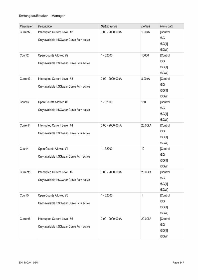
Switchgear/Breaker – Manager
Parameter Description Setting range Default Menu path
Current2 Interrupted Current Level #2
Only available if:SGwear Curve Fc = active
0.00 - 2000.00kA 1.20kA [Control
/SG
/SG[1]
/SGW]Count2 Open Counts Allowed #2
Only available if:SGwear Curve Fc = active
1 - 32000 10000 [Control
/SG
/SG[1]
/SGW]Current3 Interrupted Current Level #3
Only available if:SGwear Curve Fc = active
0.00 - 2000.00kA 8.00kA [Control
/SG
/SG[1]
/SGW]Count3 Open Counts Allowed #3
Only available if:SGwear Curve Fc = active
1 - 32000 150 [Control
/SG
/SG[1]
/SGW]Current4 Interrupted Current Level #4
Only available if:SGwear Curve Fc = active
0.00 - 2000.00kA 20.00kA [Control
/SG
/SG[1]
/SGW]Count4 Open Counts Allowed #4
Only available if:SGwear Curve Fc = active
1 - 32000 12 [Control
/SG
/SG[1]
/SGW]Current5 Interrupted Current Level #5
Only available if:SGwear Curve Fc = active
0.00 - 2000.00kA 20.00kA [Control
/SG
/SG[1]
/SGW]Count5 Open Counts Allowed #5
Only available if:SGwear Curve Fc = active
1 - 32000 1 [Control
/SG
/SG[1]
/SGW]Current6 Interrupted Current Level #6
Only available if:SGwear Curve Fc = active
0.00 - 2000.00kA 20.00kA [Control
/SG
/SG[1]
/SGW]
EN MCA4 05/11 Page 347
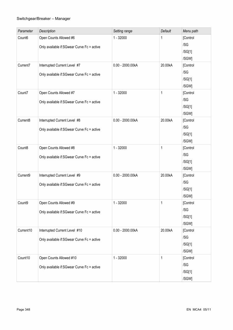
Switchgear/Breaker – Manager
Parameter Description Setting range Default Menu path
Count6 Open Counts Allowed #6
Only available if:SGwear Curve Fc = active
1 - 32000 1 [Control
/SG
/SG[1]
/SGW]Current7 Interrupted Current Level #7
Only available if:SGwear Curve Fc = active
0.00 - 2000.00kA 20.00kA [Control
/SG
/SG[1]
/SGW]Count7 Open Counts Allowed #7
Only available if:SGwear Curve Fc = active
1 - 32000 1 [Control
/SG
/SG[1]
/SGW]Current8 Interrupted Current Level #8
Only available if:SGwear Curve Fc = active
0.00 - 2000.00kA 20.00kA [Control
/SG
/SG[1]
/SGW]Count8 Open Counts Allowed #8
Only available if:SGwear Curve Fc = active
1 - 32000 1 [Control
/SG
/SG[1]
/SGW]Current9 Interrupted Current Level #9
Only available if:SGwear Curve Fc = active
0.00 - 2000.00kA 20.00kA [Control
/SG
/SG[1]
/SGW]Count9 Open Counts Allowed #9
Only available if:SGwear Curve Fc = active
1 - 32000 1 [Control
/SG
/SG[1]
/SGW]Current10 Interrupted Current Level #10
Only available if:SGwear Curve Fc = active
0.00 - 2000.00kA 20.00kA [Control
/SG
/SG[1]
/SGW]Count10 Open Counts Allowed #10
Only available if:SGwear Curve Fc = active
1 - 32000 1 [Control
/SG
/SG[1]
/SGW]
Page 348 EN MCA4 05/11

Switchgear/Breaker – Manager
Breaker Wear Signals (Output States)
Name Description
Operations Alarm Signal: Service Alarm, too many OperationsIsum Intr trip: IL1 Signal: Maximum permissible Summation of the interrupting
(tripping) currents exceeded: IL1Isum Intr trip: IL2 Signal: Maximum permissible Summation of the interrupting
(tripping) currents exceeded: IL2Isum Intr trip: IL3 Signal: Maximum permissible Summation of the interrupting
(tripping) currents exceeded: IL3Isum Intr trip Signal: Maximum permissible Summation of the interrupting
(tripping) currents exceeded in at least one phase.Res TripCmd Cr Signal: Resetting of the Counter: total number of trip commandsRes Sum trip Signal: Reset summation of the tripping currentsWearLevel Alarm Signal: Threshold for the Alarm Level in %WearLevel Lockout Signal: Threshold for the Lockout Level in %Res SGwear Curve Signal: Res SGwear CurveIsum Intr ph Alm Signal: Isum Intr ph AlmRes Isum Intr ph Alm Signal: Res Isum Intr ph Alm
Breaker Wear Counter Values
Value Description Menu path
TripCmd Cr Counter: Total number of trips of the switchgear (circuit breaker, load break switch…). Resettable with Total or All.
[Operation
/Count and RevData
/Ctrl
/SG[1]]
Breaker Wear Values
Value Description Default Size Menu path
Sum trip IL1 Summation of the tripping currents phase 0.00A 0.00 - 1000.00A
[Operation
/Count and RevData
/Ctrl
/SG[1]]Sum trip IL2 Summation of the tripping currents phase 0.00A 0.00 -
1000.00A[Operation
/Count and RevData
/Ctrl
/SG[1]]
EN MCA4 05/11 Page 349
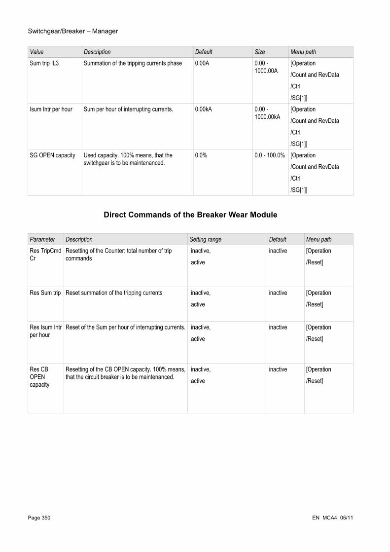
Switchgear/Breaker – Manager
Value Description Default Size Menu path
Sum trip IL3 Summation of the tripping currents phase 0.00A 0.00 - 1000.00A
[Operation
/Count and RevData
/Ctrl
/SG[1]]Isum Intr per hour Sum per hour of interrupting currents. 0.00kA 0.00 -
1000.00kA[Operation
/Count and RevData
/Ctrl
/SG[1]]SG OPEN capacity Used capacity. 100% means, that the
switchgear is to be maintenanced.0.0% 0.0 - 100.0% [Operation
/Count and RevData
/Ctrl
/SG[1]]
Direct Commands of the Breaker Wear Module
Parameter Description Setting range Default Menu path
Res TripCmd Cr
Resetting of the Counter: total number of trip commands
inactive,
active
inactive [Operation
/Reset]
Res Sum trip Reset summation of the tripping currents inactive,
active
inactive [Operation
/Reset]
Res Isum Intr per hour
Reset of the Sum per hour of interrupting currents. inactive,
active
inactive [Operation
/Reset]
Res CB OPEN capacity
Resetting of the CB OPEN capacity. 100% means, that the circuit breaker is to be maintenanced.
inactive,
active
inactive [Operation
/Reset]
Page 350 EN MCA4 05/11
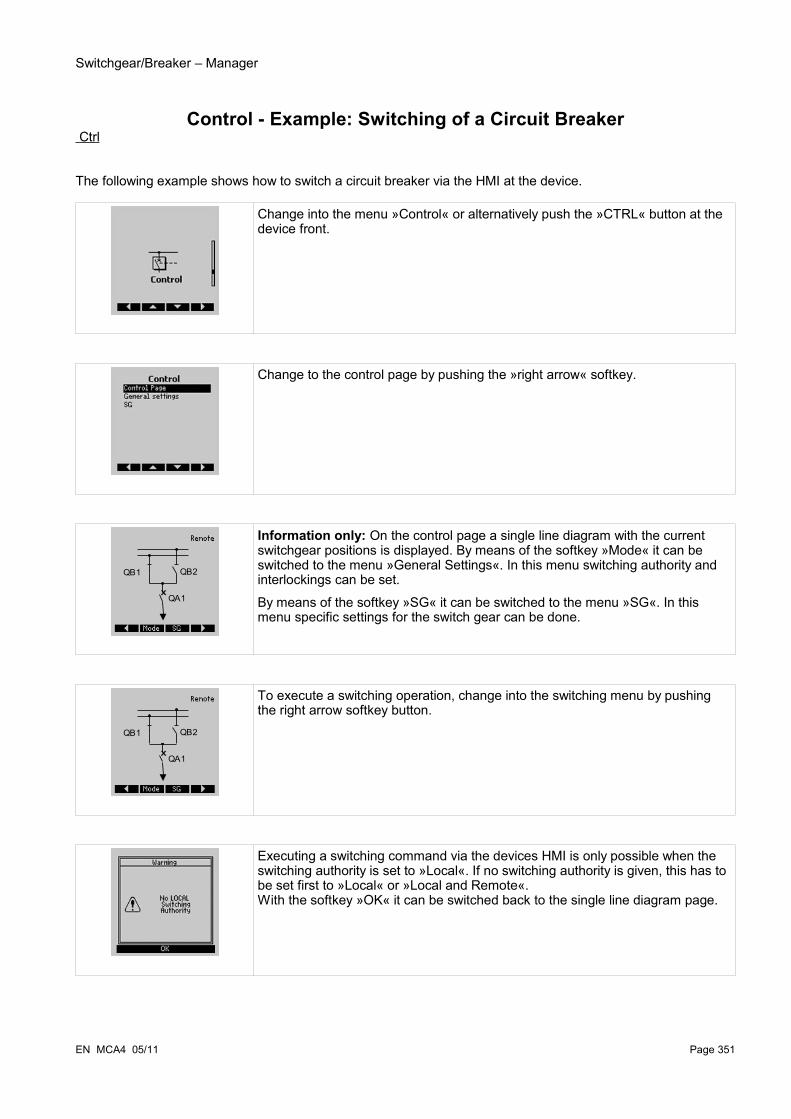
Switchgear/Breaker – Manager
Control - Example: Switching of a Circuit Breaker Ctrl
The following example shows how to switch a circuit breaker via the HMI at the device.
Change into the menu »Control« or alternatively push the »CTRL« button at the device front.
Change to the control page by pushing the »right arrow« softkey.
Information only: On the control page a single line diagram with the current switchgear positions is displayed. By means of the softkey »Mode« it can be switched to the menu »General Settings«. In this menu switching authority and interlockings can be set.
By means of the softkey »SG« it can be switched to the menu »SG«. In this menu specific settings for the switch gear can be done.
To execute a switching operation, change into the switching menu by pushing the right arrow softkey button.
Executing a switching command via the devices HMI is only possible when the switching authority is set to »Local«. If no switching authority is given, this has to be set first to »Local« or »Local and Remote«.With the softkey »OK« it can be switched back to the single line diagram page.
EN MCA4 05/11 Page 351
xQA1
QB1 QB2
xQA1
QB1 QB2

Switchgear/Breaker – Manager
Pushing the softkey »Mode« leads to the menu »General Settings«.
In this menu the switching authority can be changed.
Select between »Local« or »Local and Remote«.
Now it is possible to execute switching commands at the HMI.
Push the »right arrow« softkey to get to the control page.
Page 352 EN MCA4 05/11
xQA1
QB1 QB2
xQA1
QB1 QB2
xQA1
QB1 QB2
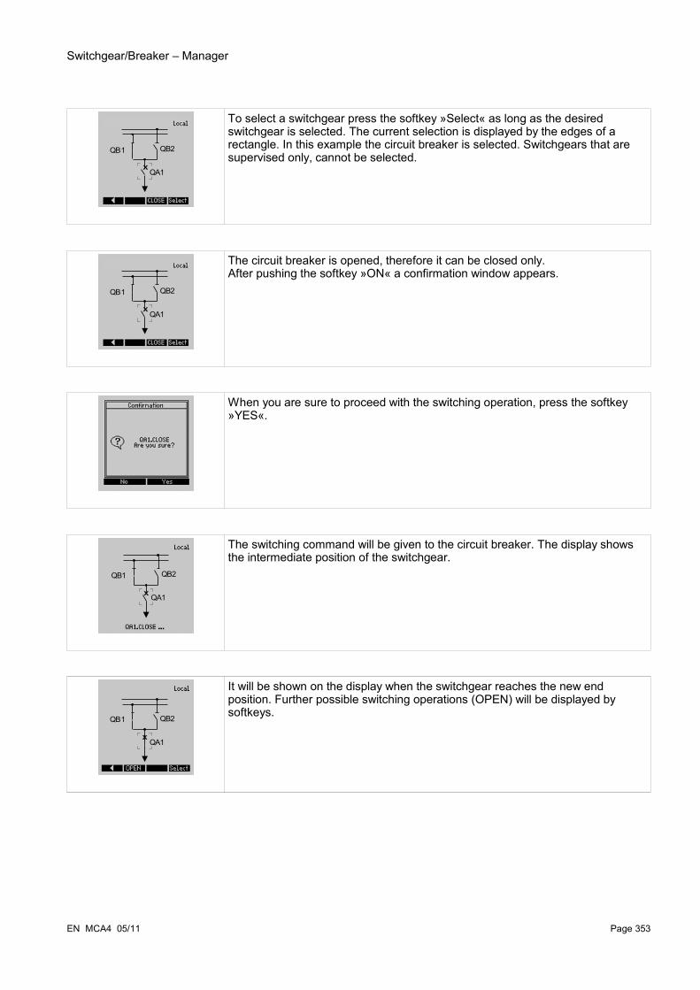
Switchgear/Breaker – Manager
To select a switchgear press the softkey »Select« as long as the desired switchgear is selected. The current selection is displayed by the edges of a rectangle. In this example the circuit breaker is selected. Switchgears that are supervised only, cannot be selected.
The circuit breaker is opened, therefore it can be closed only.After pushing the softkey »ON« a confirmation window appears.
When you are sure to proceed with the switching operation, press the softkey »YES«.
The switching command will be given to the circuit breaker. The display shows the intermediate position of the switchgear.
It will be shown on the display when the switchgear reaches the new end position. Further possible switching operations (OPEN) will be displayed by softkeys.
EN MCA4 05/11 Page 353
xQA1
QB1 QB2
x QA1
QB1 QB2
xQA1
QB1 QB2
xQA1
QB1 QB2

Switchgear/Breaker – Manager
Notice: For the case, the switchgear does not reach the new end position within the set supervision time the following Warning appears on the display.
Page 354 EN MCA4 05/11
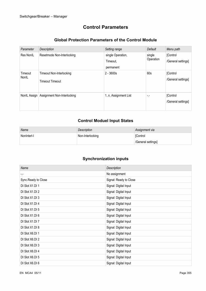
Switchgear/Breaker – Manager
Control Parameters
Global Protection Parameters of the Control Module
Parameter Description Setting range Default Menu path
Res NonIL Resetmode Non-Interlocking single Operation,
Timeout,
permanent
single Operation
[Control
/General settings]
Timeout NonIL
Timeout Non-Interlocking
Timeout Timeout
2 - 3600s 60s [Control
/General settings]
NonIL Assign Assignment Non-Interlocking 1..n, Assignment List -.- [Control
/General settings]
Control Moduel Input States
Name Description Assignment via
NonInterl-I Non-Interlocking [Control
/General settings]
Synchronization inputs
Name Description
-.- No assignmentSync.Ready to Close Signal: Ready to CloseDI Slot X1.DI 1 Signal: Digital InputDI Slot X1.DI 2 Signal: Digital InputDI Slot X1.DI 3 Signal: Digital InputDI Slot X1.DI 4 Signal: Digital InputDI Slot X1.DI 5 Signal: Digital InputDI Slot X1.DI 6 Signal: Digital InputDI Slot X1.DI 7 Signal: Digital InputDI Slot X1.DI 8 Signal: Digital InputDI Slot X6.DI 1 Signal: Digital InputDI Slot X6.DI 2 Signal: Digital InputDI Slot X6.DI 3 Signal: Digital InputDI Slot X6.DI 4 Signal: Digital InputDI Slot X6.DI 5 Signal: Digital InputDI Slot X6.DI 6 Signal: Digital Input
EN MCA4 05/11 Page 355

Switchgear/Breaker – Manager
Name Description
DI Slot X6.DI 7 Signal: Digital InputDI Slot X6.DI 8 Signal: Digital InputLogics.LE1.Gate Out Signal: Output of the logic gateLogics.LE1.Timer Out Signal: Timer OutputLogics.LE1.Out Signal: Latched Output (Q)Logics.LE1.Out inverted Signal: Negated Latched Output (Q NOT)Logics.LE2.Gate Out Signal: Output of the logic gateLogics.LE2.Timer Out Signal: Timer OutputLogics.LE2.Out Signal: Latched Output (Q)Logics.LE2.Out inverted Signal: Negated Latched Output (Q NOT)Logics.LE3.Gate Out Signal: Output of the logic gateLogics.LE3.Timer Out Signal: Timer OutputLogics.LE3.Out Signal: Latched Output (Q)Logics.LE3.Out inverted Signal: Negated Latched Output (Q NOT)Logics.LE4.Gate Out Signal: Output of the logic gateLogics.LE4.Timer Out Signal: Timer OutputLogics.LE4.Out Signal: Latched Output (Q)Logics.LE4.Out inverted Signal: Negated Latched Output (Q NOT)Logics.LE5.Gate Out Signal: Output of the logic gateLogics.LE5.Timer Out Signal: Timer OutputLogics.LE5.Out Signal: Latched Output (Q)Logics.LE5.Out inverted Signal: Negated Latched Output (Q NOT)Logics.LE6.Gate Out Signal: Output of the logic gateLogics.LE6.Timer Out Signal: Timer OutputLogics.LE6.Out Signal: Latched Output (Q)Logics.LE6.Out inverted Signal: Negated Latched Output (Q NOT)Logics.LE7.Gate Out Signal: Output of the logic gateLogics.LE7.Timer Out Signal: Timer OutputLogics.LE7.Out Signal: Latched Output (Q)Logics.LE7.Out inverted Signal: Negated Latched Output (Q NOT)Logics.LE8.Gate Out Signal: Output of the logic gateLogics.LE8.Timer Out Signal: Timer OutputLogics.LE8.Out Signal: Latched Output (Q)Logics.LE8.Out inverted Signal: Negated Latched Output (Q NOT)Logics.LE9.Gate Out Signal: Output of the logic gateLogics.LE9.Timer Out Signal: Timer OutputLogics.LE9.Out Signal: Latched Output (Q)Logics.LE9.Out inverted Signal: Negated Latched Output (Q NOT)Logics.LE10.Gate Out Signal: Output of the logic gate
Page 356 EN MCA4 05/11

Switchgear/Breaker – Manager
Name Description
Logics.LE10.Timer Out Signal: Timer OutputLogics.LE10.Out Signal: Latched Output (Q)Logics.LE10.Out inverted Signal: Negated Latched Output (Q NOT)Logics.LE11.Gate Out Signal: Output of the logic gateLogics.LE11.Timer Out Signal: Timer OutputLogics.LE11.Out Signal: Latched Output (Q)Logics.LE11.Out inverted Signal: Negated Latched Output (Q NOT)Logics.LE12.Gate Out Signal: Output of the logic gateLogics.LE12.Timer Out Signal: Timer OutputLogics.LE12.Out Signal: Latched Output (Q)Logics.LE12.Out inverted Signal: Negated Latched Output (Q NOT)Logics.LE13.Gate Out Signal: Output of the logic gateLogics.LE13.Timer Out Signal: Timer OutputLogics.LE13.Out Signal: Latched Output (Q)Logics.LE13.Out inverted Signal: Negated Latched Output (Q NOT)Logics.LE14.Gate Out Signal: Output of the logic gateLogics.LE14.Timer Out Signal: Timer OutputLogics.LE14.Out Signal: Latched Output (Q)Logics.LE14.Out inverted Signal: Negated Latched Output (Q NOT)Logics.LE15.Gate Out Signal: Output of the logic gateLogics.LE15.Timer Out Signal: Timer OutputLogics.LE15.Out Signal: Latched Output (Q)Logics.LE15.Out inverted Signal: Negated Latched Output (Q NOT)Logics.LE16.Gate Out Signal: Output of the logic gateLogics.LE16.Timer Out Signal: Timer OutputLogics.LE16.Out Signal: Latched Output (Q)Logics.LE16.Out inverted Signal: Negated Latched Output (Q NOT)Logics.LE17.Gate Out Signal: Output of the logic gateLogics.LE17.Timer Out Signal: Timer OutputLogics.LE17.Out Signal: Latched Output (Q)Logics.LE17.Out inverted Signal: Negated Latched Output (Q NOT)Logics.LE18.Gate Out Signal: Output of the logic gateLogics.LE18.Timer Out Signal: Timer OutputLogics.LE18.Out Signal: Latched Output (Q)Logics.LE18.Out inverted Signal: Negated Latched Output (Q NOT)Logics.LE19.Gate Out Signal: Output of the logic gateLogics.LE19.Timer Out Signal: Timer OutputLogics.LE19.Out Signal: Latched Output (Q)Logics.LE19.Out inverted Signal: Negated Latched Output (Q NOT)
EN MCA4 05/11 Page 357

Switchgear/Breaker – Manager
Name Description
Logics.LE20.Gate Out Signal: Output of the logic gateLogics.LE20.Timer Out Signal: Timer OutputLogics.LE20.Out Signal: Latched Output (Q)Logics.LE20.Out inverted Signal: Negated Latched Output (Q NOT)Logics.LE21.Gate Out Signal: Output of the logic gateLogics.LE21.Timer Out Signal: Timer OutputLogics.LE21.Out Signal: Latched Output (Q)Logics.LE21.Out inverted Signal: Negated Latched Output (Q NOT)Logics.LE22.Gate Out Signal: Output of the logic gateLogics.LE22.Timer Out Signal: Timer OutputLogics.LE22.Out Signal: Latched Output (Q)Logics.LE22.Out inverted Signal: Negated Latched Output (Q NOT)Logics.LE23.Gate Out Signal: Output of the logic gateLogics.LE23.Timer Out Signal: Timer OutputLogics.LE23.Out Signal: Latched Output (Q)Logics.LE23.Out inverted Signal: Negated Latched Output (Q NOT)Logics.LE24.Gate Out Signal: Output of the logic gateLogics.LE24.Timer Out Signal: Timer OutputLogics.LE24.Out Signal: Latched Output (Q)Logics.LE24.Out inverted Signal: Negated Latched Output (Q NOT)Logics.LE25.Gate Out Signal: Output of the logic gateLogics.LE25.Timer Out Signal: Timer OutputLogics.LE25.Out Signal: Latched Output (Q)Logics.LE25.Out inverted Signal: Negated Latched Output (Q NOT)Logics.LE26.Gate Out Signal: Output of the logic gateLogics.LE26.Timer Out Signal: Timer OutputLogics.LE26.Out Signal: Latched Output (Q)Logics.LE26.Out inverted Signal: Negated Latched Output (Q NOT)Logics.LE27.Gate Out Signal: Output of the logic gateLogics.LE27.Timer Out Signal: Timer OutputLogics.LE27.Out Signal: Latched Output (Q)Logics.LE27.Out inverted Signal: Negated Latched Output (Q NOT)Logics.LE28.Gate Out Signal: Output of the logic gateLogics.LE28.Timer Out Signal: Timer OutputLogics.LE28.Out Signal: Latched Output (Q)Logics.LE28.Out inverted Signal: Negated Latched Output (Q NOT)Logics.LE29.Gate Out Signal: Output of the logic gateLogics.LE29.Timer Out Signal: Timer OutputLogics.LE29.Out Signal: Latched Output (Q)
Page 358 EN MCA4 05/11

Switchgear/Breaker – Manager
Name Description
Logics.LE29.Out inverted Signal: Negated Latched Output (Q NOT)Logics.LE30.Gate Out Signal: Output of the logic gateLogics.LE30.Timer Out Signal: Timer OutputLogics.LE30.Out Signal: Latched Output (Q)Logics.LE30.Out inverted Signal: Negated Latched Output (Q NOT)Logics.LE31.Gate Out Signal: Output of the logic gateLogics.LE31.Timer Out Signal: Timer OutputLogics.LE31.Out Signal: Latched Output (Q)Logics.LE31.Out inverted Signal: Negated Latched Output (Q NOT)Logics.LE32.Gate Out Signal: Output of the logic gateLogics.LE32.Timer Out Signal: Timer OutputLogics.LE32.Out Signal: Latched Output (Q)Logics.LE32.Out inverted Signal: Negated Latched Output (Q NOT)Logics.LE33.Gate Out Signal: Output of the logic gateLogics.LE33.Timer Out Signal: Timer OutputLogics.LE33.Out Signal: Latched Output (Q)Logics.LE33.Out inverted Signal: Negated Latched Output (Q NOT)Logics.LE34.Gate Out Signal: Output of the logic gateLogics.LE34.Timer Out Signal: Timer OutputLogics.LE34.Out Signal: Latched Output (Q)Logics.LE34.Out inverted Signal: Negated Latched Output (Q NOT)Logics.LE35.Gate Out Signal: Output of the logic gateLogics.LE35.Timer Out Signal: Timer OutputLogics.LE35.Out Signal: Latched Output (Q)Logics.LE35.Out inverted Signal: Negated Latched Output (Q NOT)Logics.LE36.Gate Out Signal: Output of the logic gateLogics.LE36.Timer Out Signal: Timer OutputLogics.LE36.Out Signal: Latched Output (Q)Logics.LE36.Out inverted Signal: Negated Latched Output (Q NOT)Logics.LE37.Gate Out Signal: Output of the logic gateLogics.LE37.Timer Out Signal: Timer OutputLogics.LE37.Out Signal: Latched Output (Q)Logics.LE37.Out inverted Signal: Negated Latched Output (Q NOT)Logics.LE38.Gate Out Signal: Output of the logic gateLogics.LE38.Timer Out Signal: Timer OutputLogics.LE38.Out Signal: Latched Output (Q)Logics.LE38.Out inverted Signal: Negated Latched Output (Q NOT)Logics.LE39.Gate Out Signal: Output of the logic gateLogics.LE39.Timer Out Signal: Timer Output
EN MCA4 05/11 Page 359

Switchgear/Breaker – Manager
Name Description
Logics.LE39.Out Signal: Latched Output (Q)Logics.LE39.Out inverted Signal: Negated Latched Output (Q NOT)Logics.LE40.Gate Out Signal: Output of the logic gateLogics.LE40.Timer Out Signal: Timer OutputLogics.LE40.Out Signal: Latched Output (Q)Logics.LE40.Out inverted Signal: Negated Latched Output (Q NOT)Logics.LE41.Gate Out Signal: Output of the logic gateLogics.LE41.Timer Out Signal: Timer OutputLogics.LE41.Out Signal: Latched Output (Q)Logics.LE41.Out inverted Signal: Negated Latched Output (Q NOT)Logics.LE42.Gate Out Signal: Output of the logic gateLogics.LE42.Timer Out Signal: Timer OutputLogics.LE42.Out Signal: Latched Output (Q)Logics.LE42.Out inverted Signal: Negated Latched Output (Q NOT)Logics.LE43.Gate Out Signal: Output of the logic gateLogics.LE43.Timer Out Signal: Timer OutputLogics.LE43.Out Signal: Latched Output (Q)Logics.LE43.Out inverted Signal: Negated Latched Output (Q NOT)Logics.LE44.Gate Out Signal: Output of the logic gateLogics.LE44.Timer Out Signal: Timer OutputLogics.LE44.Out Signal: Latched Output (Q)Logics.LE44.Out inverted Signal: Negated Latched Output (Q NOT)Logics.LE45.Gate Out Signal: Output of the logic gateLogics.LE45.Timer Out Signal: Timer OutputLogics.LE45.Out Signal: Latched Output (Q)Logics.LE45.Out inverted Signal: Negated Latched Output (Q NOT)Logics.LE46.Gate Out Signal: Output of the logic gateLogics.LE46.Timer Out Signal: Timer OutputLogics.LE46.Out Signal: Latched Output (Q)Logics.LE46.Out inverted Signal: Negated Latched Output (Q NOT)Logics.LE47.Gate Out Signal: Output of the logic gateLogics.LE47.Timer Out Signal: Timer OutputLogics.LE47.Out Signal: Latched Output (Q)Logics.LE47.Out inverted Signal: Negated Latched Output (Q NOT)Logics.LE48.Gate Out Signal: Output of the logic gateLogics.LE48.Timer Out Signal: Timer OutputLogics.LE48.Out Signal: Latched Output (Q)Logics.LE48.Out inverted Signal: Negated Latched Output (Q NOT)Logics.LE49.Gate Out Signal: Output of the logic gate
Page 360 EN MCA4 05/11
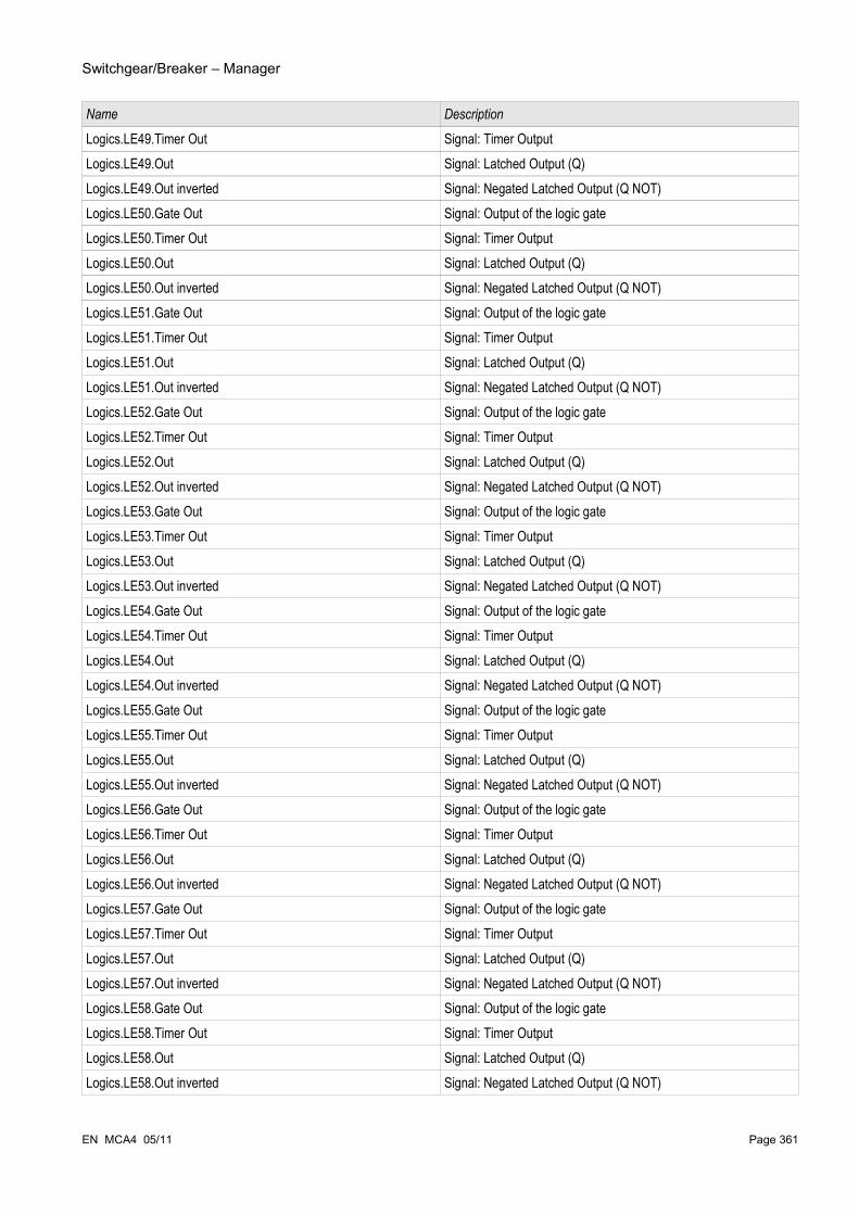
Switchgear/Breaker – Manager
Name Description
Logics.LE49.Timer Out Signal: Timer OutputLogics.LE49.Out Signal: Latched Output (Q)Logics.LE49.Out inverted Signal: Negated Latched Output (Q NOT)Logics.LE50.Gate Out Signal: Output of the logic gateLogics.LE50.Timer Out Signal: Timer OutputLogics.LE50.Out Signal: Latched Output (Q)Logics.LE50.Out inverted Signal: Negated Latched Output (Q NOT)Logics.LE51.Gate Out Signal: Output of the logic gateLogics.LE51.Timer Out Signal: Timer OutputLogics.LE51.Out Signal: Latched Output (Q)Logics.LE51.Out inverted Signal: Negated Latched Output (Q NOT)Logics.LE52.Gate Out Signal: Output of the logic gateLogics.LE52.Timer Out Signal: Timer OutputLogics.LE52.Out Signal: Latched Output (Q)Logics.LE52.Out inverted Signal: Negated Latched Output (Q NOT)Logics.LE53.Gate Out Signal: Output of the logic gateLogics.LE53.Timer Out Signal: Timer OutputLogics.LE53.Out Signal: Latched Output (Q)Logics.LE53.Out inverted Signal: Negated Latched Output (Q NOT)Logics.LE54.Gate Out Signal: Output of the logic gateLogics.LE54.Timer Out Signal: Timer OutputLogics.LE54.Out Signal: Latched Output (Q)Logics.LE54.Out inverted Signal: Negated Latched Output (Q NOT)Logics.LE55.Gate Out Signal: Output of the logic gateLogics.LE55.Timer Out Signal: Timer OutputLogics.LE55.Out Signal: Latched Output (Q)Logics.LE55.Out inverted Signal: Negated Latched Output (Q NOT)Logics.LE56.Gate Out Signal: Output of the logic gateLogics.LE56.Timer Out Signal: Timer OutputLogics.LE56.Out Signal: Latched Output (Q)Logics.LE56.Out inverted Signal: Negated Latched Output (Q NOT)Logics.LE57.Gate Out Signal: Output of the logic gateLogics.LE57.Timer Out Signal: Timer OutputLogics.LE57.Out Signal: Latched Output (Q)Logics.LE57.Out inverted Signal: Negated Latched Output (Q NOT)Logics.LE58.Gate Out Signal: Output of the logic gateLogics.LE58.Timer Out Signal: Timer OutputLogics.LE58.Out Signal: Latched Output (Q)Logics.LE58.Out inverted Signal: Negated Latched Output (Q NOT)
EN MCA4 05/11 Page 361

Switchgear/Breaker – Manager
Name Description
Logics.LE59.Gate Out Signal: Output of the logic gateLogics.LE59.Timer Out Signal: Timer OutputLogics.LE59.Out Signal: Latched Output (Q)Logics.LE59.Out inverted Signal: Negated Latched Output (Q NOT)Logics.LE60.Gate Out Signal: Output of the logic gateLogics.LE60.Timer Out Signal: Timer OutputLogics.LE60.Out Signal: Latched Output (Q)Logics.LE60.Out inverted Signal: Negated Latched Output (Q NOT)Logics.LE61.Gate Out Signal: Output of the logic gateLogics.LE61.Timer Out Signal: Timer OutputLogics.LE61.Out Signal: Latched Output (Q)Logics.LE61.Out inverted Signal: Negated Latched Output (Q NOT)Logics.LE62.Gate Out Signal: Output of the logic gateLogics.LE62.Timer Out Signal: Timer OutputLogics.LE62.Out Signal: Latched Output (Q)Logics.LE62.Out inverted Signal: Negated Latched Output (Q NOT)Logics.LE63.Gate Out Signal: Output of the logic gateLogics.LE63.Timer Out Signal: Timer OutputLogics.LE63.Out Signal: Latched Output (Q)Logics.LE63.Out inverted Signal: Negated Latched Output (Q NOT)Logics.LE64.Gate Out Signal: Output of the logic gateLogics.LE64.Timer Out Signal: Timer OutputLogics.LE64.Out Signal: Latched Output (Q)Logics.LE64.Out inverted Signal: Negated Latched Output (Q NOT)Logics.LE65.Gate Out Signal: Output of the logic gateLogics.LE65.Timer Out Signal: Timer OutputLogics.LE65.Out Signal: Latched Output (Q)Logics.LE65.Out inverted Signal: Negated Latched Output (Q NOT)Logics.LE66.Gate Out Signal: Output of the logic gateLogics.LE66.Timer Out Signal: Timer OutputLogics.LE66.Out Signal: Latched Output (Q)Logics.LE66.Out inverted Signal: Negated Latched Output (Q NOT)Logics.LE67.Gate Out Signal: Output of the logic gateLogics.LE67.Timer Out Signal: Timer OutputLogics.LE67.Out Signal: Latched Output (Q)Logics.LE67.Out inverted Signal: Negated Latched Output (Q NOT)Logics.LE68.Gate Out Signal: Output of the logic gateLogics.LE68.Timer Out Signal: Timer OutputLogics.LE68.Out Signal: Latched Output (Q)
Page 362 EN MCA4 05/11

Switchgear/Breaker – Manager
Name Description
Logics.LE68.Out inverted Signal: Negated Latched Output (Q NOT)Logics.LE69.Gate Out Signal: Output of the logic gateLogics.LE69.Timer Out Signal: Timer OutputLogics.LE69.Out Signal: Latched Output (Q)Logics.LE69.Out inverted Signal: Negated Latched Output (Q NOT)Logics.LE70.Gate Out Signal: Output of the logic gateLogics.LE70.Timer Out Signal: Timer OutputLogics.LE70.Out Signal: Latched Output (Q)Logics.LE70.Out inverted Signal: Negated Latched Output (Q NOT)Logics.LE71.Gate Out Signal: Output of the logic gateLogics.LE71.Timer Out Signal: Timer OutputLogics.LE71.Out Signal: Latched Output (Q)Logics.LE71.Out inverted Signal: Negated Latched Output (Q NOT)Logics.LE72.Gate Out Signal: Output of the logic gateLogics.LE72.Timer Out Signal: Timer OutputLogics.LE72.Out Signal: Latched Output (Q)Logics.LE72.Out inverted Signal: Negated Latched Output (Q NOT)Logics.LE73.Gate Out Signal: Output of the logic gateLogics.LE73.Timer Out Signal: Timer OutputLogics.LE73.Out Signal: Latched Output (Q)Logics.LE73.Out inverted Signal: Negated Latched Output (Q NOT)Logics.LE74.Gate Out Signal: Output of the logic gateLogics.LE74.Timer Out Signal: Timer OutputLogics.LE74.Out Signal: Latched Output (Q)Logics.LE74.Out inverted Signal: Negated Latched Output (Q NOT)Logics.LE75.Gate Out Signal: Output of the logic gateLogics.LE75.Timer Out Signal: Timer OutputLogics.LE75.Out Signal: Latched Output (Q)Logics.LE75.Out inverted Signal: Negated Latched Output (Q NOT)Logics.LE76.Gate Out Signal: Output of the logic gateLogics.LE76.Timer Out Signal: Timer OutputLogics.LE76.Out Signal: Latched Output (Q)Logics.LE76.Out inverted Signal: Negated Latched Output (Q NOT)Logics.LE77.Gate Out Signal: Output of the logic gateLogics.LE77.Timer Out Signal: Timer OutputLogics.LE77.Out Signal: Latched Output (Q)Logics.LE77.Out inverted Signal: Negated Latched Output (Q NOT)Logics.LE78.Gate Out Signal: Output of the logic gateLogics.LE78.Timer Out Signal: Timer Output
EN MCA4 05/11 Page 363

Switchgear/Breaker – Manager
Name Description
Logics.LE78.Out Signal: Latched Output (Q)Logics.LE78.Out inverted Signal: Negated Latched Output (Q NOT)Logics.LE79.Gate Out Signal: Output of the logic gateLogics.LE79.Timer Out Signal: Timer OutputLogics.LE79.Out Signal: Latched Output (Q)Logics.LE79.Out inverted Signal: Negated Latched Output (Q NOT)Logics.LE80.Gate Out Signal: Output of the logic gateLogics.LE80.Timer Out Signal: Timer OutputLogics.LE80.Out Signal: Latched Output (Q)Logics.LE80.Out inverted Signal: Negated Latched Output (Q NOT)
Assignable Trip Commands (Trip Manager)
Name Description
-.- No assignmentI[1].TripCmd Signal: Trip CommandI[2].TripCmd Signal: Trip CommandI[3].TripCmd Signal: Trip CommandI[4].TripCmd Signal: Trip CommandI[5].TripCmd Signal: Trip CommandI[6].TripCmd Signal: Trip CommandIG[1].TripCmd Signal: Trip CommandIG[2].TripCmd Signal: Trip CommandIG[3].TripCmd Signal: Trip CommandIG[4].TripCmd Signal: Trip CommandThR.TripCmd Signal: Trip CommandI2>[1].TripCmd Signal: Trip CommandI2>[2].TripCmd Signal: Trip CommandV[1].TripCmd Signal: Trip CommandV[2].TripCmd Signal: Trip CommandV[3].TripCmd Signal: Trip CommandV[4].TripCmd Signal: Trip CommandV[5].TripCmd Signal: Trip CommandV[6].TripCmd Signal: Trip CommandVG[1].TripCmd Signal: Trip CommandVG[2].TripCmd Signal: Trip CommandV 012 [1].TripCmd Signal: Trip CommandV 012 [2].TripCmd Signal: Trip CommandV 012 [3].TripCmd Signal: Trip Command
Page 364 EN MCA4 05/11
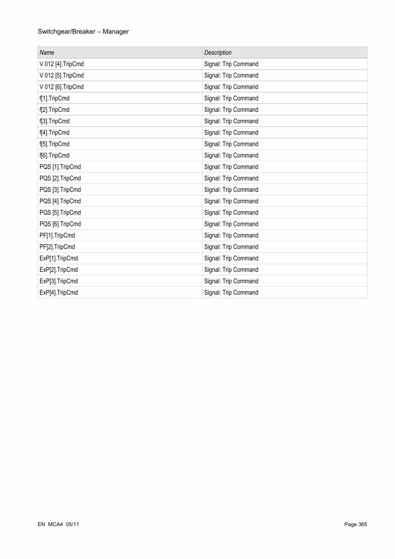
Switchgear/Breaker – Manager
Name Description
V 012 [4].TripCmd Signal: Trip CommandV 012 [5].TripCmd Signal: Trip CommandV 012 [6].TripCmd Signal: Trip Commandf[1].TripCmd Signal: Trip Commandf[2].TripCmd Signal: Trip Commandf[3].TripCmd Signal: Trip Commandf[4].TripCmd Signal: Trip Commandf[5].TripCmd Signal: Trip Commandf[6].TripCmd Signal: Trip CommandPQS [1].TripCmd Signal: Trip CommandPQS [2].TripCmd Signal: Trip CommandPQS [3].TripCmd Signal: Trip CommandPQS [4].TripCmd Signal: Trip CommandPQS [5].TripCmd Signal: Trip CommandPQS [6].TripCmd Signal: Trip CommandPF[1].TripCmd Signal: Trip CommandPF[2].TripCmd Signal: Trip CommandExP[1].TripCmd Signal: Trip CommandExP[2].TripCmd Signal: Trip CommandExP[3].TripCmd Signal: Trip CommandExP[4].TripCmd Signal: Trip Command
EN MCA4 05/11 Page 365

Switchgear/Breaker – Manager
Controlled Circuit Breaker SG[1]
Direct Commands of a Controlled Circuit Breaker
Parameter Description Setting range Default Menu path
Manipulate Position
WARNING! Fake Position - Manual Position Manipulation
inactive,
Pos OFF,
Pos ON
inactive [Control
/SG
/SG[1]
/General settings]Res SGwear Sl SG
Resetting the slow Switchgear Alarm inactive,
active
inactive [Operation
/Reset]
Ack TripCmd Acknowledge Trip Command inactive,
active
inactive [Operation
/Acknowledge]
Global Protection Parameters of a Controlled Circuit Breaker
Parameter Description Setting range Default Menu path
Aux ON The CB is in ON-position if the state of the assigned signal is true (52a).
1..n, DI-LogicList DI Slot X1.DI 1
[Control
/SG
/SG[1]
/Pos Indicators wiring]
Aux OFF The CB is in OFF-position if the state of the assigned signal is true (52b).
1..n, DI-LogicList DI Slot X1.DI 2
[Control
/SG
/SG[1]
/Pos Indicators wiring]
Ready Circuit breaker is ready for operation if the state of the assigned signal is true. This digital input can be used by some protective elements (if they are available within the device) like Auto Reclosure (AR), e.g. as a trigger signal.
1..n, DI-LogicList -.- [Control
/SG
/SG[1]
/Pos Indicators wiring]
Interl ON1 Interlocking of the ON command 1..n, Assignment List -.- [Control
/SG
/SG[1]
/Interlockings]
Page 366 EN MCA4 05/11
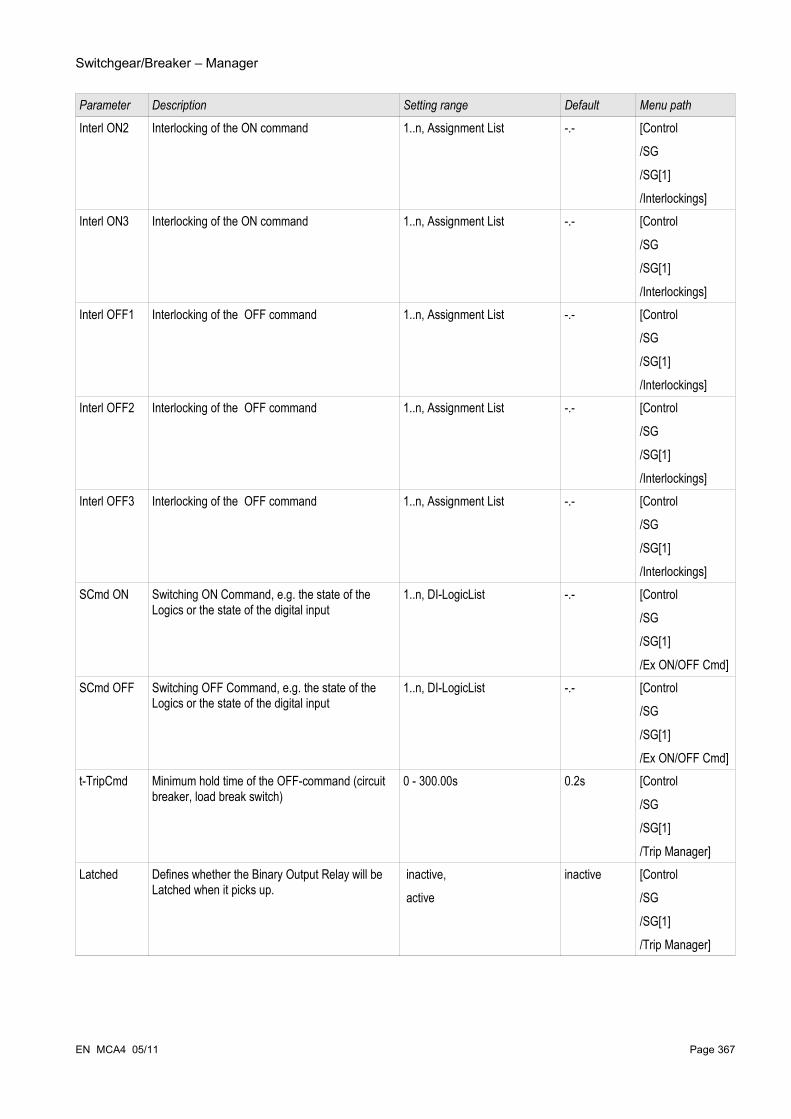
Switchgear/Breaker – Manager
Parameter Description Setting range Default Menu path
Interl ON2 Interlocking of the ON command 1..n, Assignment List -.- [Control
/SG
/SG[1]
/Interlockings]Interl ON3 Interlocking of the ON command 1..n, Assignment List -.- [Control
/SG
/SG[1]
/Interlockings]Interl OFF1 Interlocking of the OFF command 1..n, Assignment List -.- [Control
/SG
/SG[1]
/Interlockings]Interl OFF2 Interlocking of the OFF command 1..n, Assignment List -.- [Control
/SG
/SG[1]
/Interlockings]Interl OFF3 Interlocking of the OFF command 1..n, Assignment List -.- [Control
/SG
/SG[1]
/Interlockings]SCmd ON Switching ON Command, e.g. the state of the
Logics or the state of the digital input1..n, DI-LogicList -.- [Control
/SG
/SG[1]
/Ex ON/OFF Cmd]SCmd OFF Switching OFF Command, e.g. the state of the
Logics or the state of the digital input1..n, DI-LogicList -.- [Control
/SG
/SG[1]
/Ex ON/OFF Cmd]t-TripCmd Minimum hold time of the OFF-command (circuit
breaker, load break switch)0 - 300.00s 0.2s [Control
/SG
/SG[1]
/Trip Manager]Latched Defines whether the Binary Output Relay will be
Latched when it picks up. inactive,
active
inactive [Control
/SG
/SG[1]
/Trip Manager]
EN MCA4 05/11 Page 367

Switchgear/Breaker – Manager
Parameter Description Setting range Default Menu path
Ack TripCmd Ack TripCmd 1..n, Assignment List -.- [Control
/SG
/SG[1]
/Trip Manager]Off Cmd1 Off Command to the Circuit Breaker if the state of
the assigned signal becomes true.1..n, Trip Cmds I[1].TripCmd [Control
/SG
/SG[1]
/Trip Manager]Off Cmd2 Off Command to the Circuit Breaker if the state of
the assigned signal becomes true.1..n, Trip Cmds V[1].TripCmd [Control
/SG
/SG[1]
/Trip Manager]Off Cmd3 Off Command to the Circuit Breaker if the state of
the assigned signal becomes true.1..n, Trip Cmds V[2].TripCmd [Control
/SG
/SG[1]
/Trip Manager]Off Cmd4 Off Command to the Circuit Breaker if the state of
the assigned signal becomes true.1..n, Trip Cmds f[1].TripCmd [Control
/SG
/SG[1]
/Trip Manager]Off Cmd5 Off Command to the Circuit Breaker if the state of
the assigned signal becomes true.1..n, Trip Cmds f[2].TripCmd [Control
/SG
/SG[1]
/Trip Manager]Off Cmd6 Off Command to the Circuit Breaker if the state of
the assigned signal becomes true.1..n, Trip Cmds PQS
[1].TripCmd[Control
/SG
/SG[1]
/Trip Manager]Off Cmd7 Off Command to the Circuit Breaker if the state of
the assigned signal becomes true.1..n, Trip Cmds -.- [Control
/SG
/SG[1]
/Trip Manager]Off Cmd8 Off Command to the Circuit Breaker if the state of
the assigned signal becomes true.1..n, Trip Cmds -.- [Control
/SG
/SG[1]
/Trip Manager]
Page 368 EN MCA4 05/11

Switchgear/Breaker – Manager
Parameter Description Setting range Default Menu path
Off Cmd9 Off Command to the Circuit Breaker if the state of the assigned signal becomes true.
1..n, Trip Cmds -.- [Control
/SG
/SG[1]
/Trip Manager]Off Cmd10 Off Command to the Circuit Breaker if the state of
the assigned signal becomes true.1..n, Trip Cmds -.- [Control
/SG
/SG[1]
/Trip Manager]Off Cmd11 Off Command to the Circuit Breaker if the state of
the assigned signal becomes true.1..n, Trip Cmds -.- [Control
/SG
/SG[1]
/Trip Manager]Off Cmd12 Off Command to the Circuit Breaker if the state of
the assigned signal becomes true.1..n, Trip Cmds -.- [Control
/SG
/SG[1]
/Trip Manager]Off Cmd13 Off Command to the Circuit Breaker if the state of
the assigned signal becomes true.1..n, Trip Cmds -.- [Control
/SG
/SG[1]
/Trip Manager]Off Cmd14 Off Command to the Circuit Breaker if the state of
the assigned signal becomes true.1..n, Trip Cmds -.- [Control
/SG
/SG[1]
/Trip Manager]Off Cmd15 Off Command to the Circuit Breaker if the state of
the assigned signal becomes true.1..n, Trip Cmds -.- [Control
/SG
/SG[1]
/Trip Manager]Off Cmd16 Off Command to the Circuit Breaker if the state of
the assigned signal becomes true.1..n, Trip Cmds -.- [Control
/SG
/SG[1]
/Trip Manager]Off Cmd17 Off Command to the Circuit Breaker if the state of
the assigned signal becomes true.1..n, Trip Cmds -.- [Control
/SG
/SG[1]
/Trip Manager]
EN MCA4 05/11 Page 369

Switchgear/Breaker – Manager
Parameter Description Setting range Default Menu path
Off Cmd18 Off Command to the Circuit Breaker if the state of the assigned signal becomes true.
1..n, Trip Cmds -.- [Control
/SG
/SG[1]
/Trip Manager]Off Cmd19 Off Command to the Circuit Breaker if the state of
the assigned signal becomes true.1..n, Trip Cmds -.- [Control
/SG
/SG[1]
/Trip Manager]Off Cmd20 Off Command to the Circuit Breaker if the state of
the assigned signal becomes true.1..n, Trip Cmds -.- [Control
/SG
/SG[1]
/Trip Manager]Off Cmd21 Off Command to the Circuit Breaker if the state of
the assigned signal becomes true.1..n, Trip Cmds -.- [Control
/SG
/SG[1]
/Trip Manager]Off Cmd22 Off Command to the Circuit Breaker if the state of
the assigned signal becomes true.1..n, Trip Cmds -.- [Control
/SG
/SG[1]
/Trip Manager]Off Cmd23 Off Command to the Circuit Breaker if the state of
the assigned signal becomes true.1..n, Trip Cmds -.- [Control
/SG
/SG[1]
/Trip Manager]Off Cmd24 Off Command to the Circuit Breaker if the state of
the assigned signal becomes true.1..n, Trip Cmds -.- [Control
/SG
/SG[1]
/Trip Manager]Off Cmd25 Off Command to the Circuit Breaker if the state of
the assigned signal becomes true.1..n, Trip Cmds -.- [Control
/SG
/SG[1]
/Trip Manager]Off Cmd26 Off Command to the Circuit Breaker if the state of
the assigned signal becomes true.1..n, Trip Cmds -.- [Control
/SG
/SG[1]
/Trip Manager]
Page 370 EN MCA4 05/11
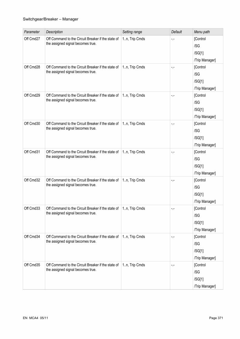
Switchgear/Breaker – Manager
Parameter Description Setting range Default Menu path
Off Cmd27 Off Command to the Circuit Breaker if the state of the assigned signal becomes true.
1..n, Trip Cmds -.- [Control
/SG
/SG[1]
/Trip Manager]Off Cmd28 Off Command to the Circuit Breaker if the state of
the assigned signal becomes true.1..n, Trip Cmds -.- [Control
/SG
/SG[1]
/Trip Manager]Off Cmd29 Off Command to the Circuit Breaker if the state of
the assigned signal becomes true.1..n, Trip Cmds -.- [Control
/SG
/SG[1]
/Trip Manager]Off Cmd30 Off Command to the Circuit Breaker if the state of
the assigned signal becomes true.1..n, Trip Cmds -.- [Control
/SG
/SG[1]
/Trip Manager]Off Cmd31 Off Command to the Circuit Breaker if the state of
the assigned signal becomes true.1..n, Trip Cmds -.- [Control
/SG
/SG[1]
/Trip Manager]Off Cmd32 Off Command to the Circuit Breaker if the state of
the assigned signal becomes true.1..n, Trip Cmds -.- [Control
/SG
/SG[1]
/Trip Manager]Off Cmd33 Off Command to the Circuit Breaker if the state of
the assigned signal becomes true.1..n, Trip Cmds -.- [Control
/SG
/SG[1]
/Trip Manager]Off Cmd34 Off Command to the Circuit Breaker if the state of
the assigned signal becomes true.1..n, Trip Cmds -.- [Control
/SG
/SG[1]
/Trip Manager]Off Cmd35 Off Command to the Circuit Breaker if the state of
the assigned signal becomes true.1..n, Trip Cmds -.- [Control
/SG
/SG[1]
/Trip Manager]
EN MCA4 05/11 Page 371

Switchgear/Breaker – Manager
Parameter Description Setting range Default Menu path
Off Cmd36 Off Command to the Circuit Breaker if the state of the assigned signal becomes true.
1..n, Trip Cmds -.- [Control
/SG
/SG[1]
/Trip Manager]Off Cmd37 Off Command to the Circuit Breaker if the state of
the assigned signal becomes true.1..n, Trip Cmds -.- [Control
/SG
/SG[1]
/Trip Manager]Off Cmd38 Off Command to the Circuit Breaker if the state of
the assigned signal becomes true.1..n, Trip Cmds -.- [Control
/SG
/SG[1]
/Trip Manager]Off Cmd39 Off Command to the Circuit Breaker if the state of
the assigned signal becomes true.1..n, Trip Cmds -.- [Control
/SG
/SG[1]
/Trip Manager]Off Cmd40 Off Command to the Circuit Breaker if the state of
the assigned signal becomes true.1..n, Trip Cmds -.- [Control
/SG
/SG[1]
/Trip Manager]Off Cmd41 Off Command to the Circuit Breaker if the state of
the assigned signal becomes true.1..n, Trip Cmds -.- [Control
/SG
/SG[1]
/Trip Manager]Off Cmd42 Off Command to the Circuit Breaker if the state of
the assigned signal becomes true.1..n, Trip Cmds -.- [Control
/SG
/SG[1]
/Trip Manager]Off Cmd43 Off Command to the Circuit Breaker if the state of
the assigned signal becomes true.1..n, Trip Cmds -.- [Control
/SG
/SG[1]
/Trip Manager]Off Cmd44 Off Command to the Circuit Breaker if the state of
the assigned signal becomes true.1..n, Trip Cmds -.- [Control
/SG
/SG[1]
/Trip Manager]
Page 372 EN MCA4 05/11
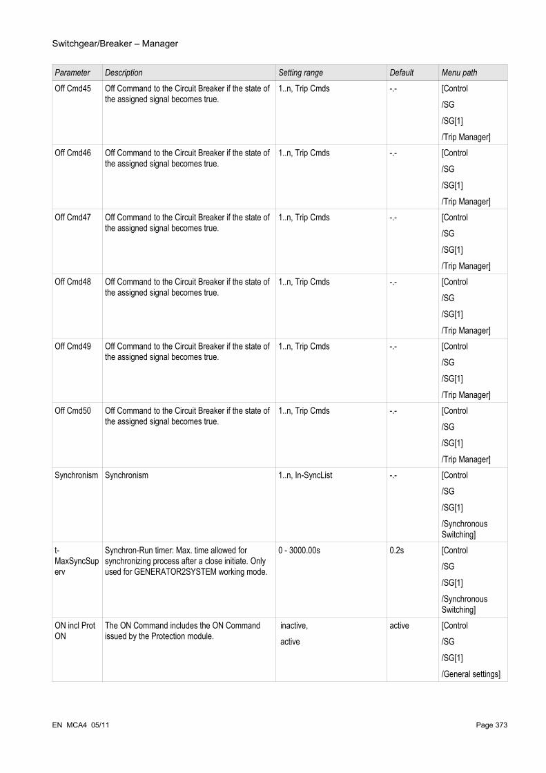
Switchgear/Breaker – Manager
Parameter Description Setting range Default Menu path
Off Cmd45 Off Command to the Circuit Breaker if the state of the assigned signal becomes true.
1..n, Trip Cmds -.- [Control
/SG
/SG[1]
/Trip Manager]Off Cmd46 Off Command to the Circuit Breaker if the state of
the assigned signal becomes true.1..n, Trip Cmds -.- [Control
/SG
/SG[1]
/Trip Manager]Off Cmd47 Off Command to the Circuit Breaker if the state of
the assigned signal becomes true.1..n, Trip Cmds -.- [Control
/SG
/SG[1]
/Trip Manager]Off Cmd48 Off Command to the Circuit Breaker if the state of
the assigned signal becomes true.1..n, Trip Cmds -.- [Control
/SG
/SG[1]
/Trip Manager]Off Cmd49 Off Command to the Circuit Breaker if the state of
the assigned signal becomes true.1..n, Trip Cmds -.- [Control
/SG
/SG[1]
/Trip Manager]Off Cmd50 Off Command to the Circuit Breaker if the state of
the assigned signal becomes true.1..n, Trip Cmds -.- [Control
/SG
/SG[1]
/Trip Manager]Synchronism Synchronism 1..n, In-SyncList -.- [Control
/SG
/SG[1]
/Synchronous Switching]
t-MaxSyncSuperv
Synchron-Run timer: Max. time allowed for synchronizing process after a close initiate. Only used for GENERATOR2SYSTEM working mode.
0 - 3000.00s 0.2s [Control
/SG
/SG[1]
/Synchronous Switching]
ON incl Prot ON
The ON Command includes the ON Command issued by the Protection module.
inactive,
active
active [Control
/SG
/SG[1]
/General settings]
EN MCA4 05/11 Page 373

Switchgear/Breaker – Manager
Parameter Description Setting range Default Menu path
OFF incl TripCmd
The OFF Command includes the OFF Command issued by the Protection module.
inactive,
active
active [Control
/SG
/SG[1]
/General settings]t-Move ON Time to move to the ON Position 0.01 - 100.00s 0.1s [Control
/SG
/SG[1]
/General settings]t-Move OFF Time to move to the OFF Position 0.01 - 100.00s 0.1s [Control
/SG
/SG[1]
/General settings]
Controlled Circuit Breaker Input States
Name Description Assignment via
Aux ON-I Position indicator/check-back signal of the CB (52a)
[Control
/SG
/SG[1]
/Pos Indicators wiring]Aux OFF-I Module input state: Position
indicator/check-back signal of the CB (52b)[Control
/SG
/SG[1]
/Pos Indicators wiring]Ready-I Module input state: CB ready [Control
/SG
/SG[1]
/Pos Indicators wiring]Sys-in-Sync-I State of the module input: This signals has
to become true within the synchronization time. If not, switching is unsuccessful.
[Control
/SG
/SG[1]
/Synchronous Switching]Ack TripCmd-I State of the module input:
Acknowledgement Signal (only for automatic acknowledgement) Module input signal
[Control
/SG
/SG[1]
/Trip Manager]
Page 374 EN MCA4 05/11

Switchgear/Breaker – Manager
Name Description Assignment via
Interl ON1-I State of the module input: Interlocking of the ON command
[Control
/SG
/SG[1]
/Interlockings]Interl ON2-I State of the module input: Interlocking of
the ON command[Control
/SG
/SG[1]
/Interlockings]Interl ON3-I State of the module input: Interlocking of
the ON command[Control
/SG
/SG[1]
/Interlockings]Interl OFF1-I State of the module input: Interlocking of
the OFF command[Control
/SG
/SG[1]
/Interlockings]Interl OFF2-I State of the module input: Interlocking of
the OFF command[Control
/SG
/SG[1]
/Interlockings]Interl OFF3-I State of the module input: Interlocking of
the OFF command[Control
/SG
/SG[1]
/Interlockings]SCmd ON-I State of the module input: Switching ON
Command, e.g. the state of the Logics or the state of the digital input
[Control
/SG
/SG[1]
/Ex ON/OFF Cmd]SCmd OFF-I State of the module input: Switching OFF
Command, e.g. the state of the Logics or the state of the digital input
[Control
/SG
/SG[1]
/Ex ON/OFF Cmd]
EN MCA4 05/11 Page 375

Switchgear/Breaker – Manager
Signals of a Controlled Circuit Breaker
Name Description
SI SingleContactInd Signal: The Position of the Switchgear is detected by one auxiliary contact (pole) only. Thus indeterminate and disturbed Positions cannot be detected.
Pos not ON Signal: Pos not ONPos ON Signal: Circuit Breaker is in ON-PositionPos OFF Signal: Circuit Breaker is in OFF-PositionPos Indeterm Signal: Circuit Breaker is in Indeterminate PositionPos Disturb Signal: Circuit Breaker Disturbed - Undefined Breaker Position.
The Position Indicators contradict themselves. After expiring of a supervision timer this signal becomes true.
Pos Signal: Circuit Breaker Position (0 = Indeterminate, 1 = OFF, 2 = ON, 3 = Disturbed)
Ready Signal: Circuit breaker is ready for operation.Interl ON Signal: One or more IL_On inputs are active.Interl OFF Signal: One or more IL_Off inputs are active.CES succesf Command Execution Supervision: Switching command executed
successfully.CES Disturbed Command Execution Supervision: Switching Command
unsuccessful. Switchgear in disturbed position.CES Fail TripCmd Command Excecution Supervision: Trip command not executed.CES SwitchgDir Command Execution Supervision respectively Switching Direction
Control: This signal becomes true, if a switch command is issued even though the switchgear is already in the requested position. Example: A switchgear that is already OFF should be switched OFF again (doubly). The same applies to CLOSE commands.
CES ON d OFF Command Execution Supervision: On Command during a pending OFF Command.
CES SG not ready Command Execution Supervision: Switchgear not readyCES Fiel Interl Command Execution Supervision: Switching Command not
executed because of field interlocking.CES SyncTimeout Command Execution Supervision: Switching Command not
excecuted. No Synchronization signal while t-sync was running.Prot ON Signal: ON Command issued by the Prot moduleTripCmd Signal: Trip CommandAck TripCmd Signal: Acknowledge Trip CommandON incl Prot ON Signal: The ON Command includes the ON Command issued by
the Protection module.OFF incl TripCmd Signal: The OFF Command includes the OFF Command issued by
the Protection module.Position Ind manipul Signal: Position Ind manipulSGwear Slow SG Signal: Alarm, the circuit breaker (load-break switch) becomes
slowerRes SGwear Sl SG Signal: Resetting the slow Switchgear Alarm
Page 376 EN MCA4 05/11

Switchgear/Breaker – Manager
Name Description
ON Cmd Signal: ON Command issued to the switchgear. Depending on the setting the signal may include the ON command of the Prot module.
OFF Cmd Signal: OFF Command issued to the switchgear. Depending on the setting the signal may include the OFF command of the Prot module.
ON Cmd manual Signal: ON Cmd manualOFF Cmd manual Signal: OFF Cmd manualSync ON request Signal: Synchronous ON request
EN MCA4 05/11 Page 377

Switchgear/Breaker – Manager
Monitored Circuit Breaker
SG[3]
Direct Commands of a Monitored Circuit Breaker
Parameter Description Setting range Default Menu path
Manipulate Position
WARNING! Fake Position - Manual Position Manipulation
inactive,
Pos OFF,
Pos ON
inactive [Control
/SG
/SG[3]
/General settings]Res SGwear Sl SG
Resetting the slow Switchgear Alarm inactive,
active
inactive [Operation
/Reset]
Ack TripCmd Acknowledge Trip Command inactive,
active
inactive [Operation
/Acknowledge]
Global Protection Parameters of a Monitored Circuit Breaker
Parameter Description Setting range Default Menu path
Aux ON The CB is in ON-position if the state of the assigned signal is true (52a).
1..n, DI-LogicList DI Slot X1.DI 3
[Control
/SG
/SG[3]
/Pos Indicators wiring]
Aux OFF The CB is in OFF-position if the state of the assigned signal is true (52b).
1..n, DI-LogicList DI Slot X1.DI 4
[Control
/SG
/SG[3]
/Pos Indicators wiring]
Ready Circuit breaker is ready for operation if the state of the assigned signal is true. This digital input can be used by some protective elements (if they are available within the device) like Auto Reclosure (AR), e.g. as a trigger signal.
1..n, DI-LogicList -.- [Control
/SG
/SG[3]
/Pos Indicators wiring]
t-TripCmd Minimum hold time of the OFF-command (circuit breaker, load break switch)
0 - 300.00s 0.2s [Control
/SG
/SG[3]
/Trip Manager]
Page 378 EN MCA4 05/11

Switchgear/Breaker – Manager
Parameter Description Setting range Default Menu path
Latched Defines whether the Binary Output Relay will be Latched when it picks up.
inactive,
active
inactive [Control
/SG
/SG[3]
/Trip Manager]Ack TripCmd Ack TripCmd 1..n, Assignment List -.- [Control
/SG
/SG[3]
/Trip Manager]Off Cmd1 Off Command to the Circuit Breaker if the state of
the assigned signal becomes true.1..n, Trip Cmds -.- [Control
/SG
/SG[3]
/Trip Manager]Off Cmd2 Off Command to the Circuit Breaker if the state of
the assigned signal becomes true.1..n, Trip Cmds -.- [Control
/SG
/SG[3]
/Trip Manager]Off Cmd3 Off Command to the Circuit Breaker if the state of
the assigned signal becomes true.1..n, Trip Cmds -.- [Control
/SG
/SG[3]
/Trip Manager]Off Cmd4 Off Command to the Circuit Breaker if the state of
the assigned signal becomes true.1..n, Trip Cmds -.- [Control
/SG
/SG[3]
/Trip Manager]Off Cmd5 Off Command to the Circuit Breaker if the state of
the assigned signal becomes true.1..n, Trip Cmds -.- [Control
/SG
/SG[3]
/Trip Manager]Off Cmd6 Off Command to the Circuit Breaker if the state of
the assigned signal becomes true.1..n, Trip Cmds -.- [Control
/SG
/SG[3]
/Trip Manager]Off Cmd7 Off Command to the Circuit Breaker if the state of
the assigned signal becomes true.1..n, Trip Cmds -.- [Control
/SG
/SG[3]
/Trip Manager]
EN MCA4 05/11 Page 379

Switchgear/Breaker – Manager
Parameter Description Setting range Default Menu path
Off Cmd8 Off Command to the Circuit Breaker if the state of the assigned signal becomes true.
1..n, Trip Cmds -.- [Control
/SG
/SG[3]
/Trip Manager]Off Cmd9 Off Command to the Circuit Breaker if the state of
the assigned signal becomes true.1..n, Trip Cmds -.- [Control
/SG
/SG[3]
/Trip Manager]Off Cmd10 Off Command to the Circuit Breaker if the state of
the assigned signal becomes true.1..n, Trip Cmds -.- [Control
/SG
/SG[3]
/Trip Manager]Off Cmd11 Off Command to the Circuit Breaker if the state of
the assigned signal becomes true.1..n, Trip Cmds -.- [Control
/SG
/SG[3]
/Trip Manager]Off Cmd12 Off Command to the Circuit Breaker if the state of
the assigned signal becomes true.1..n, Trip Cmds -.- [Control
/SG
/SG[3]
/Trip Manager]Off Cmd13 Off Command to the Circuit Breaker if the state of
the assigned signal becomes true.1..n, Trip Cmds -.- [Control
/SG
/SG[3]
/Trip Manager]Off Cmd14 Off Command to the Circuit Breaker if the state of
the assigned signal becomes true.1..n, Trip Cmds -.- [Control
/SG
/SG[3]
/Trip Manager]Off Cmd15 Off Command to the Circuit Breaker if the state of
the assigned signal becomes true.1..n, Trip Cmds -.- [Control
/SG
/SG[3]
/Trip Manager]Off Cmd16 Off Command to the Circuit Breaker if the state of
the assigned signal becomes true.1..n, Trip Cmds -.- [Control
/SG
/SG[3]
/Trip Manager]
Page 380 EN MCA4 05/11

Switchgear/Breaker – Manager
Parameter Description Setting range Default Menu path
Off Cmd17 Off Command to the Circuit Breaker if the state of the assigned signal becomes true.
1..n, Trip Cmds -.- [Control
/SG
/SG[3]
/Trip Manager]Off Cmd18 Off Command to the Circuit Breaker if the state of
the assigned signal becomes true.1..n, Trip Cmds -.- [Control
/SG
/SG[3]
/Trip Manager]Off Cmd19 Off Command to the Circuit Breaker if the state of
the assigned signal becomes true.1..n, Trip Cmds -.- [Control
/SG
/SG[3]
/Trip Manager]Off Cmd20 Off Command to the Circuit Breaker if the state of
the assigned signal becomes true.1..n, Trip Cmds -.- [Control
/SG
/SG[3]
/Trip Manager]Off Cmd21 Off Command to the Circuit Breaker if the state of
the assigned signal becomes true.1..n, Trip Cmds -.- [Control
/SG
/SG[3]
/Trip Manager]Off Cmd22 Off Command to the Circuit Breaker if the state of
the assigned signal becomes true.1..n, Trip Cmds -.- [Control
/SG
/SG[3]
/Trip Manager]Off Cmd23 Off Command to the Circuit Breaker if the state of
the assigned signal becomes true.1..n, Trip Cmds -.- [Control
/SG
/SG[3]
/Trip Manager]Off Cmd24 Off Command to the Circuit Breaker if the state of
the assigned signal becomes true.1..n, Trip Cmds -.- [Control
/SG
/SG[3]
/Trip Manager]Off Cmd25 Off Command to the Circuit Breaker if the state of
the assigned signal becomes true.1..n, Trip Cmds -.- [Control
/SG
/SG[3]
/Trip Manager]
EN MCA4 05/11 Page 381

Switchgear/Breaker – Manager
Parameter Description Setting range Default Menu path
Off Cmd26 Off Command to the Circuit Breaker if the state of the assigned signal becomes true.
1..n, Trip Cmds -.- [Control
/SG
/SG[3]
/Trip Manager]Off Cmd27 Off Command to the Circuit Breaker if the state of
the assigned signal becomes true.1..n, Trip Cmds -.- [Control
/SG
/SG[3]
/Trip Manager]Off Cmd28 Off Command to the Circuit Breaker if the state of
the assigned signal becomes true.1..n, Trip Cmds -.- [Control
/SG
/SG[3]
/Trip Manager]Off Cmd29 Off Command to the Circuit Breaker if the state of
the assigned signal becomes true.1..n, Trip Cmds -.- [Control
/SG
/SG[3]
/Trip Manager]Off Cmd30 Off Command to the Circuit Breaker if the state of
the assigned signal becomes true.1..n, Trip Cmds -.- [Control
/SG
/SG[3]
/Trip Manager]Off Cmd31 Off Command to the Circuit Breaker if the state of
the assigned signal becomes true.1..n, Trip Cmds -.- [Control
/SG
/SG[3]
/Trip Manager]Off Cmd32 Off Command to the Circuit Breaker if the state of
the assigned signal becomes true.1..n, Trip Cmds -.- [Control
/SG
/SG[3]
/Trip Manager]Off Cmd33 Off Command to the Circuit Breaker if the state of
the assigned signal becomes true.1..n, Trip Cmds -.- [Control
/SG
/SG[3]
/Trip Manager]Off Cmd34 Off Command to the Circuit Breaker if the state of
the assigned signal becomes true.1..n, Trip Cmds -.- [Control
/SG
/SG[3]
/Trip Manager]
Page 382 EN MCA4 05/11

Switchgear/Breaker – Manager
Parameter Description Setting range Default Menu path
Off Cmd35 Off Command to the Circuit Breaker if the state of the assigned signal becomes true.
1..n, Trip Cmds -.- [Control
/SG
/SG[3]
/Trip Manager]Off Cmd36 Off Command to the Circuit Breaker if the state of
the assigned signal becomes true.1..n, Trip Cmds -.- [Control
/SG
/SG[3]
/Trip Manager]Off Cmd37 Off Command to the Circuit Breaker if the state of
the assigned signal becomes true.1..n, Trip Cmds -.- [Control
/SG
/SG[3]
/Trip Manager]Off Cmd38 Off Command to the Circuit Breaker if the state of
the assigned signal becomes true.1..n, Trip Cmds -.- [Control
/SG
/SG[3]
/Trip Manager]Off Cmd39 Off Command to the Circuit Breaker if the state of
the assigned signal becomes true.1..n, Trip Cmds -.- [Control
/SG
/SG[3]
/Trip Manager]Off Cmd40 Off Command to the Circuit Breaker if the state of
the assigned signal becomes true.1..n, Trip Cmds -.- [Control
/SG
/SG[3]
/Trip Manager]Off Cmd41 Off Command to the Circuit Breaker if the state of
the assigned signal becomes true.1..n, Trip Cmds -.- [Control
/SG
/SG[3]
/Trip Manager]Off Cmd42 Off Command to the Circuit Breaker if the state of
the assigned signal becomes true.1..n, Trip Cmds -.- [Control
/SG
/SG[3]
/Trip Manager]Off Cmd43 Off Command to the Circuit Breaker if the state of
the assigned signal becomes true.1..n, Trip Cmds -.- [Control
/SG
/SG[3]
/Trip Manager]
EN MCA4 05/11 Page 383

Switchgear/Breaker – Manager
Parameter Description Setting range Default Menu path
Off Cmd44 Off Command to the Circuit Breaker if the state of the assigned signal becomes true.
1..n, Trip Cmds -.- [Control
/SG
/SG[3]
/Trip Manager]Off Cmd45 Off Command to the Circuit Breaker if the state of
the assigned signal becomes true.1..n, Trip Cmds -.- [Control
/SG
/SG[3]
/Trip Manager]Off Cmd46 Off Command to the Circuit Breaker if the state of
the assigned signal becomes true.1..n, Trip Cmds -.- [Control
/SG
/SG[3]
/Trip Manager]Off Cmd47 Off Command to the Circuit Breaker if the state of
the assigned signal becomes true.1..n, Trip Cmds -.- [Control
/SG
/SG[3]
/Trip Manager]Off Cmd48 Off Command to the Circuit Breaker if the state of
the assigned signal becomes true.1..n, Trip Cmds -.- [Control
/SG
/SG[3]
/Trip Manager]Off Cmd49 Off Command to the Circuit Breaker if the state of
the assigned signal becomes true.1..n, Trip Cmds -.- [Control
/SG
/SG[3]
/Trip Manager]Off Cmd50 Off Command to the Circuit Breaker if the state of
the assigned signal becomes true.1..n, Trip Cmds -.- [Control
/SG
/SG[3]
/Trip Manager]t-Move ON Time to move to the ON Position 0.01 - 100.00s 0.1s [Control
/SG
/SG[3]
/General settings]t-Move OFF Time to move to the OFF Position 0.01 - 100.00s 0.1s [Control
/SG
/SG[3]
/General settings]
Page 384 EN MCA4 05/11

Switchgear/Breaker – Manager
Monitored Circuit Breaker Input States
Name Description Assignment via
Aux ON-I Position indicator/check-back signal of the CB (52a)
[Control
/SG
/SG[3]
/Pos Indicators wiring]Aux OFF-I Module input state: Position
indicator/check-back signal of the CB (52b)[Control
/SG
/SG[3]
/Pos Indicators wiring]Ready-I Module input state: CB ready [Control
/SG
/SG[3]
/Pos Indicators wiring]Ack TripCmd-I State of the module input:
Acknowledgement Signal (only for automatic acknowledgement) Module input signal
[Control
/SG
/SG[3]
/Trip Manager]
EN MCA4 05/11 Page 385
Switchgear/Breaker – Manager
Signals of a Monitored Circuit Breaker
Name Description
SI SingleContactInd Signal: The Position of the Switchgear is detected by one auxiliary contact (pole) only. Thus indeterminate and disturbed Positions cannot be detected.
Pos not ON Signal: Pos not ONPos ON Signal: Circuit Breaker is in ON-PositionPos OFF Signal: Circuit Breaker is in OFF-PositionPos Indeterm Signal: Circuit Breaker is in Indeterminate PositionPos Disturb Signal: Circuit Breaker Disturbed - Undefined Breaker Position.
The Position Indicators contradict themselves. After expiring of a supervision timer this signal becomes true.
Pos Signal: Circuit Breaker Position (0 = Indeterminate, 1 = OFF, 2 = ON, 3 = Disturbed)
Ready Signal: Circuit breaker is ready for operation.Position Ind manipul Signal: Position Ind manipulSGwear Slow SG Signal: Alarm, the circuit breaker (load-break switch) becomes
slowerRes SGwear Sl SG Signal: Resetting the slow Switchgear Alarm
Page 386 EN MCA4 05/11

Switchgear/Breaker – Manager
Controlled Disconnector SG[4]
Direct Commands of a Controlled Disconnector
Parameter Description Setting range Default Menu path
Manipulate Position
WARNING! Fake Position - Manual Position Manipulation
inactive,
Pos OFF,
Pos ON
inactive [Control
/SG
/SG[4]
/General settings]Res SGwear Sl SG
Resetting the slow Switchgear Alarm inactive,
active
inactive [Operation
/Reset]
Global Protection Parameters of a Controlled Disconnector
Parameter Description Setting range Default Menu path
Aux ON The CB is in ON-position if the state of the assigned signal is true (52a).
1..n, DI-LogicList DI Slot X1.DI 5
[Control
/SG
/SG[4]
/Pos Indicators wiring]
Aux OFF The CB is in OFF-position if the state of the assigned signal is true (52b).
1..n, DI-LogicList DI Slot X1.DI 6
[Control
/SG
/SG[4]
/Pos Indicators wiring]
Interl ON1 Interlocking of the ON command 1..n, Assignment List SG[1].Pos ON
[Control
/SG
/SG[4]
/Interlockings]Interl ON2 Interlocking of the ON command 1..n, Assignment List SG[6].Pos
ON[Control
/SG
/SG[4]
/Interlockings]Interl ON3 Interlocking of the ON command 1..n, Assignment List -.- [Control
/SG
/SG[4]
/Interlockings]
EN MCA4 05/11 Page 387

Switchgear/Breaker – Manager
Parameter Description Setting range Default Menu path
Interl OFF1 Interlocking of the OFF command 1..n, Assignment List SG[1].Pos ON
[Control
/SG
/SG[4]
/Interlockings]Interl OFF2 Interlocking of the OFF command 1..n, Assignment List -.- [Control
/SG
/SG[4]
/Interlockings]Interl OFF3 Interlocking of the OFF command 1..n, Assignment List -.- [Control
/SG
/SG[4]
/Interlockings]SCmd ON Switching ON Command, e.g. the state of the
Logics or the state of the digital input1..n, DI-LogicList -.- [Control
/SG
/SG[4]
/Ex ON/OFF Cmd]SCmd OFF Switching OFF Command, e.g. the state of the
Logics or the state of the digital input1..n, DI-LogicList -.- [Control
/SG
/SG[4]
/Ex ON/OFF Cmd]t-Move ON Time to move to the ON Position 0.01 - 100.00s 0.1s [Control
/SG
/SG[4]
/General settings]t-Move OFF Time to move to the OFF Position 0.01 - 100.00s 0.1s [Control
/SG
/SG[4]
/General settings]t-Dwell Dwell time 0 - 100.00s 0s [Control
/SG
/SG[4]
/General settings]
Page 388 EN MCA4 05/11
Switchgear/Breaker – Manager
Controlled Disconnector Input States
Name Description Assignment via
Aux ON-I Position indicator/check-back signal of the CB (52a)
[Control
/SG
/SG[4]
/Pos Indicators wiring]Aux OFF-I Module input state: Position
indicator/check-back signal of the CB (52b)[Control
/SG
/SG[4]
/Pos Indicators wiring]SCmd ON-I State of the module input: Switching ON
Command, e.g. the state of the Logics or the state of the digital input
[Control
/SG
/SG[4]
/Ex ON/OFF Cmd]SCmd OFF-I State of the module input: Switching OFF
Command, e.g. the state of the Logics or the state of the digital input
[Control
/SG
/SG[4]
/Ex ON/OFF Cmd]
EN MCA4 05/11 Page 389
Switchgear/Breaker – Manager
Signals of a Controlled Disconnector
Name Description
SI SingleContactInd Signal: The Position of the Switchgear is detected by one auxiliary contact (pole) only. Thus indeterminate and disturbed Positions cannot be detected.
Pos not ON Signal: Pos not ONPos ON Signal: Circuit Breaker is in ON-PositionPos OFF Signal: Circuit Breaker is in OFF-PositionPos Indeterm Signal: Circuit Breaker is in Indeterminate PositionPos Disturb Signal: Circuit Breaker Disturbed - Undefined Breaker Position.
The Position Indicators contradict themselves. After expiring of a supervision timer this signal becomes true.
Pos Signal: Circuit Breaker Position (0 = Indeterminate, 1 = OFF, 2 = ON, 3 = Disturbed)
t-Dwell Signal: Dwell timeInterl ON Signal: One or more IL_On inputs are active.Interl OFF Signal: One or more IL_Off inputs are active.CES succesf Command Execution Supervision: Switching command executed
successfully.CES Disturbed Command Execution Supervision: Switching Command
unsuccessful. Switchgear in disturbed position.CES SwitchgDir Command Execution Supervision respectively Switching Direction
Control: This signal becomes true, if a switch command is issued even though the switchgear is already in the requested position. Example: A switchgear that is already OFF should be switched OFF again (doubly). The same applies to CLOSE commands.
CES ON d OFF Command Execution Supervision: On Command during a pending OFF Command.
CES Fiel Interl Command Execution Supervision: Switching Command not executed because of field interlocking.
Position Ind manipul Signal: Position Ind manipulSGwear Slow SG Signal: Alarm, the circuit breaker (load-break switch) becomes
slowerRes SGwear Sl SG Signal: Resetting the slow Switchgear AlarmON Cmd Signal: ON Command issued to the switchgear. Depending on the
setting the signal may include the ON command of the Prot module.
OFF Cmd Signal: OFF Command issued to the switchgear. Depending on the setting the signal may include the OFF command of the Prot module.
Page 390 EN MCA4 05/11
Switchgear/Breaker – Manager
Monitored Disconnector SG[2] ,SG[5] ,SG[6]
Direct Commands of a Monitored Disconnector
Parameter Description Setting range Default Menu path
Manipulate Position
WARNING! Fake Position - Manual Position Manipulation
inactive,
Pos OFF,
Pos ON
inactive [Control
/SG
/SG[2]
/General settings]Res SGwear Sl SG
Resetting the slow Switchgear Alarm inactive,
active
inactive [Operation
/Reset]
Global Protection Parameters of a Monitored Disconnector
Parameter Description Setting range Default Menu path
Aux ON The CB is in ON-position if the state of the assigned signal is true (52a).
1..n, DI-LogicList SG[2]: -.-
SG[5]: -.-
SG[6]: DI Slot X1.DI 7
[Control
/SG
/SG[2]
/Pos Indicators wiring]
Aux OFF The CB is in OFF-position if the state of the assigned signal is true (52b).
1..n, DI-LogicList SG[2]: -.-
SG[5]: -.-
SG[6]: DI Slot X1.DI 8
[Control
/SG
/SG[2]
/Pos Indicators wiring]
t-Move ON Time to move to the ON Position 0.01 - 100.00s 0.1s [Control
/SG
/SG[2]
/General settings]t-Move OFF Time to move to the OFF Position 0.01 - 100.00s 0.1s [Control
/SG
/SG[2]
/General settings]t-Dwell Dwell time 0 - 100.00s 0s [Control
/SG
/SG[2]
/General settings]
EN MCA4 05/11 Page 391

Switchgear/Breaker – Manager
Monitored Disconnector Input States
Name Description Assignment via
Aux ON-I Position indicator/check-back signal of the CB (52a)
[Control
/SG
/SG[2]
/Pos Indicators wiring]Aux OFF-I Module input state: Position
indicator/check-back signal of the CB (52b)[Control
/SG
/SG[2]
/Pos Indicators wiring]
Page 392 EN MCA4 05/11
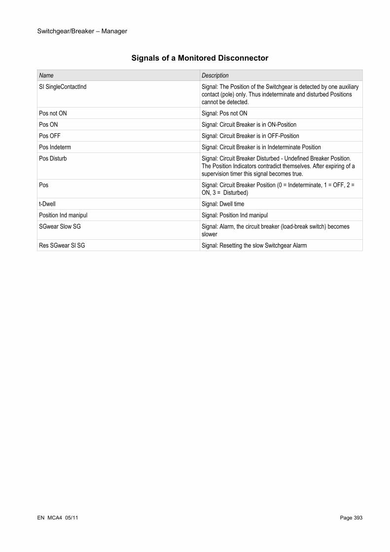
Switchgear/Breaker – Manager
Signals of a Monitored Disconnector
Name Description
SI SingleContactInd Signal: The Position of the Switchgear is detected by one auxiliary contact (pole) only. Thus indeterminate and disturbed Positions cannot be detected.
Pos not ON Signal: Pos not ONPos ON Signal: Circuit Breaker is in ON-PositionPos OFF Signal: Circuit Breaker is in OFF-PositionPos Indeterm Signal: Circuit Breaker is in Indeterminate PositionPos Disturb Signal: Circuit Breaker Disturbed - Undefined Breaker Position.
The Position Indicators contradict themselves. After expiring of a supervision timer this signal becomes true.
Pos Signal: Circuit Breaker Position (0 = Indeterminate, 1 = OFF, 2 = ON, 3 = Disturbed)
t-Dwell Signal: Dwell timePosition Ind manipul Signal: Position Ind manipulSGwear Slow SG Signal: Alarm, the circuit breaker (load-break switch) becomes
slowerRes SGwear Sl SG Signal: Resetting the slow Switchgear Alarm
EN MCA4 05/11 Page 393

Protective Elements
Protective ElementsI - Overcurrent Protection [50, 51,51Q, 51V, 67]
Available stages: I[1] ,I[2] ,I[3] ,I[4] ,I[5] ,I[6]
If you are using inrush blockings the tripping delay of the current protection functions must be at least 30ms or more in order to prevent faulty trippings.
In order to ensure correct functioning of the directional detection after single-phase short-circuits, the following reference voltage is used: For phase current I1 it is the line-to-line voltage U23, for phase current I2 the line-to-line voltage U31 and for phase current I3 the line-to-line voltage U12.
In case the fault happens to be near the measuring location and there is no reference voltage for directional recognition available any more (neither measured or from history (voltage memory)), then the module will - depending on the parameter setting - either trip non-directional or it will be blocked.
All overcurrent protective elements are identically structured.
This module offers Adaptive Parameter Sets.Parameters can be modified within parameter sets dynamically by means of Adaptive Parameter Sets. Please refer to chapter Parameter / Adaptive Parameter Sets.
Page 394 EN MCA4 05/11

Protective Elements
The following table shows the application options of the Overcurrent Protection element
Applications of the I-Protection Module Setting in Option
ANSI 50 – Overcurrent protection, non-directional
Device Planning menu Measuring Mode: Fundamental/TrueRMS/negative phase sequence current (I2)
ANSI 51 – Short circuit protection, non-directional
Device Planning menu Measuring Mode: Fundamental/TrueRMS/negative phase sequence current (I2)
ANSI 67 – Overcurrent/ Short circuit protection, directional
Device Planning menu Measuring Mode: Fundamental/TrueRMS/negative phase sequence current (I2)
ANSI 51V – Voltage restraint overcurrent protection
Parameter Set:VRestraint = active
Measuring Mode: Fundamental/TrueRMS/negative phase sequence current (I2)
Measuring Channel:Phase to Phase/Phase to Neutral
ANSI 51Q Negative Phase Sequence Overcurrent Protection
Parameter Set: Measuring Method =I2 (Negative Sequence Current)
51R Voltage controlled overcurrent protection
(Please refer to the chapter Parameter/Adaptive Parameter)
Adaptive Parameters Measuring Mode: Fundamental/TrueRMS/negative phase sequence current (I2)
Measuring Channel:(in voltage protection module)Phase to Phase/Phase to Neutral
EN MCA4 05/11 Page 395
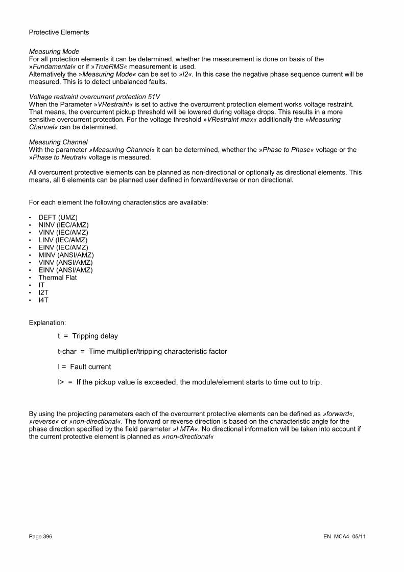
Protective Elements
Measuring ModeFor all protection elements it can be determined, whether the measurement is done on basis of the »Fundamental« or if »TrueRMS« measurement is used.Alternatively the »Measuring Mode« can be set to »I2«. In this case the negative phase sequence current will be measured. This is to detect unbalanced faults.
Voltage restraint overcurrent protection 51VWhen the Parameter »VRestraint« is set to active the overcurrent protection element works voltage restraint. That means, the overcurrent pickup threshold will be lowered during voltage drops. This results in a more sensitive overcurrent protection. For the voltage threshold »VRestraint max« additionally the »Measuring Channel« can be determined.
Measuring ChannelWith the parameter »Measuring Channel« it can be determined, whether the »Phase to Phase« voltage or the »Phase to Neutral« voltage is measured.
All overcurrent protective elements can be planned as non-directional or optionally as directional elements. This means, all 6 elements can be planned user defined in forward/reverse or non directional.
For each element the following characteristics are available:
• DEFT (UMZ)• NINV (IEC/AMZ)• VINV (IEC/AMZ)• LINV (IEC/AMZ)• EINV (IEC/AMZ)• MINV (ANSI/AMZ)• VINV (ANSI/AMZ)• EINV (ANSI/AMZ)• Thermal Flat• IT• I2T• I4T
Explanation:
By using the projecting parameters each of the overcurrent protective elements can be defined as »forward«, »reverse« or »non-directional«. The forward or reverse direction is based on the characteristic angle for the phase direction specified by the field parameter »I MTA«. No directional information will be taken into account if the current protective element is planned as »non-directional«
Page 396 EN MCA4 05/11
t = Tripping delay
t-char = Time multiplier/tripping characteristic factor
I = Fault current
I> = If the pickup value is exceeded, the module/element starts to time out to trip.
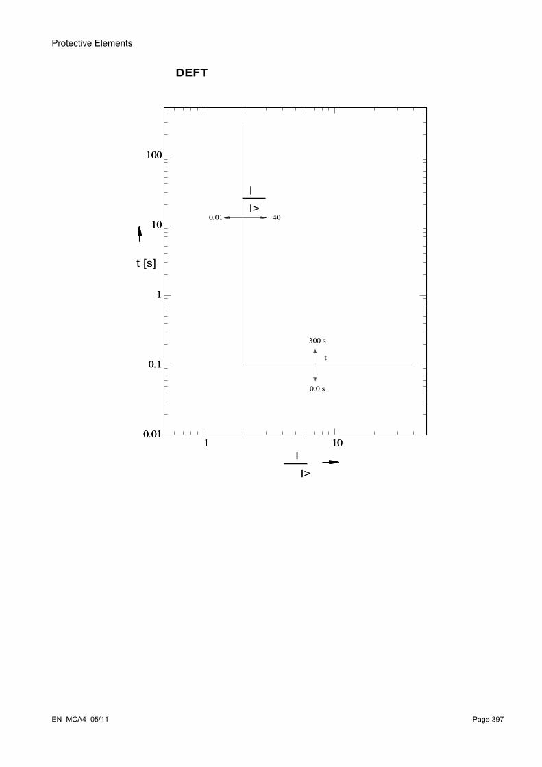
Protective Elements
EN MCA4 05/11 Page 397
t [s]
I>I
1 100.01
0.1
1
10
100
1 100.01
0.1
1
10
100
tt
4040
300 s300 s
0.0 s0.0 s
0.010.01I>I
DEFT
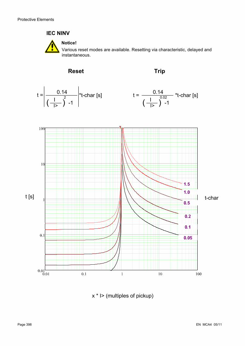
Protective Elements
Page 398 EN MCA4 05/11
t-char
x * I> (multiples of pickup)
TripReset
t = 0.14 *t-char [s]
I> -1I( )2 t = 0.14 *t-char [s]
I> -1I( )0.02
t [s]
Notice!Various reset modes are available. Resetting via characteristic, delayed and instantaneous.
IEC NINV

Protective Elements
EN MCA4 05/11 Page 399
t [s]t-char
t = 13.5 *t-char [s]
I> -1I( )t = 13.5 *t-char [s]
I> -1I( )2
TripReset
x * I> (multiples of pickup)
Notice!Various reset modes are available. Resetting via characteristic, delayed and instantaneous.
IEC VINV

Protective Elements
Page 400 EN MCA4 05/11
t [s] t-char
t = 120 *t-char [s]
I> -1I( )2
t = 120 *t-char [s]
I> -1I( )
TripReset
x * I> (multiples of pickup)
Notice!Various reset modes are available. Resetting via characteristic, delayed and instantaneous.
IEC LINV
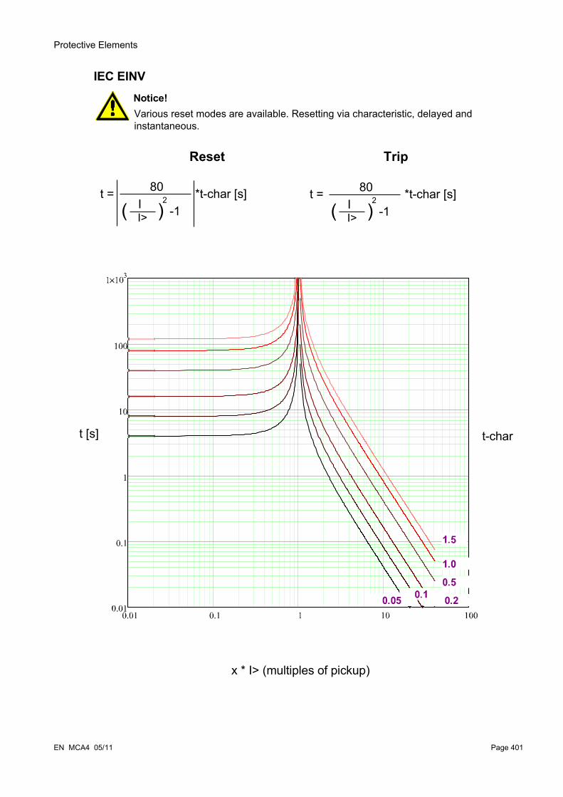
Protective Elements
EN MCA4 05/11 Page 401
t [s] t-char
t = 80 *t-char [s]
I> -1I( )2t = 80 *t-char [s]
I> -1I( )2
TripReset
x * I> (multiples of pickup)
Notice!Various reset modes are available. Resetting via characteristic, delayed and instantaneous.
IEC EINV

Protective Elements
Page 402 EN MCA4 05/11
t [s] t-char
t = 4.85 *t-char [s]
I> -1I( )2 t = 0.0515 *t-char [s]
I> -1I( )0.02 + 0.1140( )
TripReset
x * I> (multiples of pickup)
Notice!Various reset modes are available. Resetting via characteristic, delayed and instantaneous.
ANSI MINV
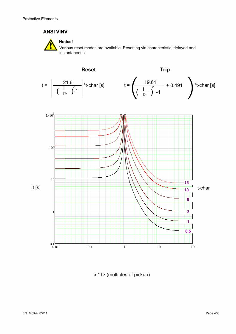
Protective Elements
EN MCA4 05/11 Page 403
t [s] t-char
TripReset
x * I> (multiples of pickup)
t = 19.61 *t-char [s]
I> -1I( )2 + 0.491( )t = 21.6 *t-char [s]
I> -1I( )2
Notice!Various reset modes are available. Resetting via characteristic, delayed and instantaneous.
ANSI VINV

Protective Elements
Page 404 EN MCA4 05/11
t [s] t-char
t = 29.1 *t-char [s]
I> -1I( )2
TripReset
x * I> (multiples of pickup)
t = 28.2 *t-char [s]
I> -1I( )2 + 0.1217( )
Notice!Various reset modes are available. Resetting via characteristic, delayed and instantaneous.
ANSI EINV
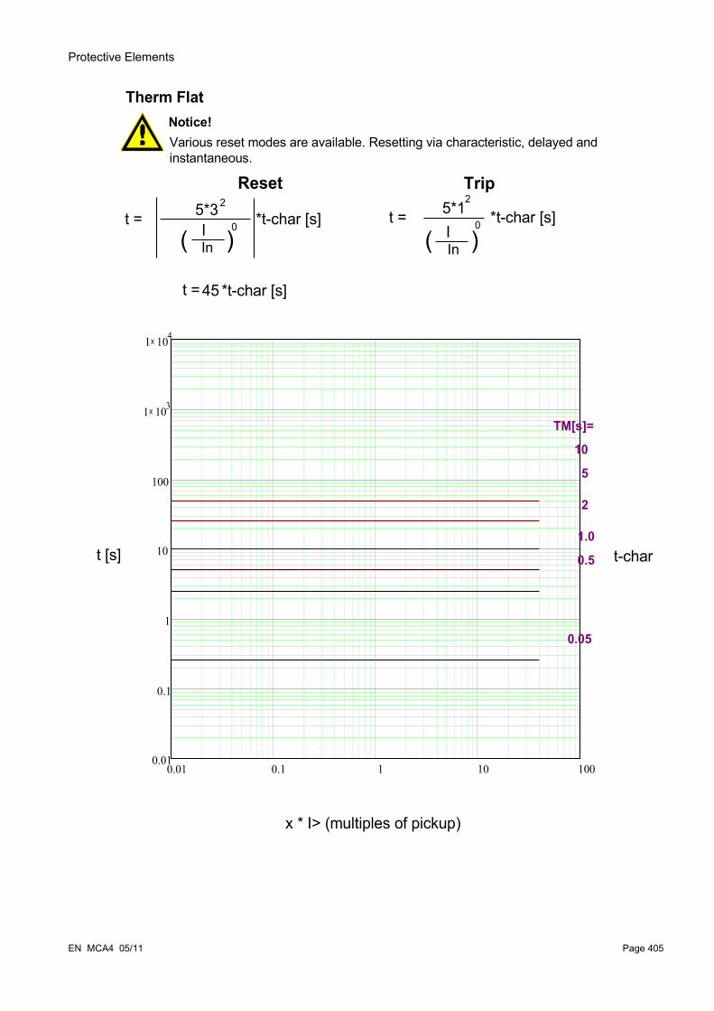
Protective Elements
EN MCA4 05/11 Page 405
t [s] t-char
x * I> (multiples of pickup)
TripReset
t = 5*3 *t-char [s]2
InI( )
0t = 5*1 *t-char [s]
InI( )
0
2
Notice!Various reset modes are available. Resetting via characteristic, delayed and instantaneous.
Therm Flat
t = 45 *t-char [s]
0.01 0.1 1 10 1000.01
0.1
1
10
100
1 103×
1 104×
TM[s]=
10
5
2
1.0
0.5
0.05
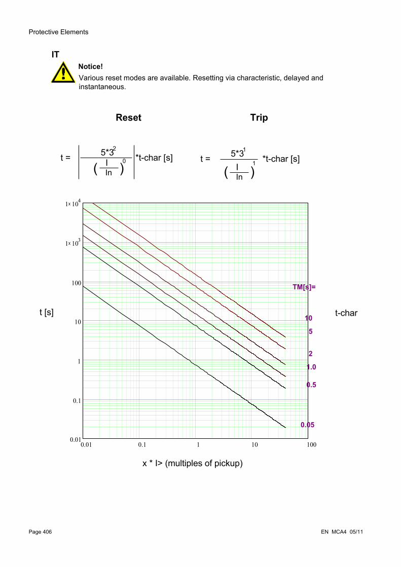
Protective Elements
Page 406 EN MCA4 05/11
t [s] t-char
x * I> (multiples of pickup)
TripReset
t = 5*3 *t-char [s]2
InI( )
0
Notice!Various reset modes are available. Resetting via characteristic, delayed and instantaneous.
IT
t = 5*3 *t-char [s]1
InI( )
1
0.01 0.1 1 10 1000.01
0.1
1
10
100
1 103×
1 104×
TM[s]=
10
5
2
1.0
0.5
0.05

Protective Elements
EN MCA4 05/11 Page 407
0.01 0.1 1 10 1000.01
0.1
1
10
100
1 103×
1 104×
TM[s]=
10
5
2
1.0
0.50.05
t [s] t-char
x * I> (multiples of pickup)
TripReset
t = 5*3 *t-char [s]2
InI( )
0
Notice!Various reset modes are available. Resetting via characteristic, delayed and instantaneous.
I2T
t = 5*3 *t-char [s]
InI( )
2
2

Protective Elements
Page 408 EN MCA4 05/11
t [s] t-char
x * I> (multiples of pickup)
TripReset
t = 5*3 *t-char [s]2
InI( )
0
Notice!Various reset modes are available. Resetting via characteristic, delayed and instantaneous.
I4T
t = 5*3 *t-char [s]
InI( )
4
4
0.01 0.1 1 10 1000.01
0.1
1
10
100
1 103×
1 104×
TM[s]=
10
52
1.00.5
0.05

Protective Elements
EN MCA4 05/11 Page 409
Prot
.I di
r n p
oss
Prot
.I di
r rev
Prot
.I di
r fwd
VL1
IL1
IL2
IL3
VL3
VL2
Prot
.I Ph
ase
MTA
φ VL12
VL1
VL23
VL2
VL31
VL3
VL23
I1
Phas
e M
TA
reve
rse
forw
ard
Volta
ge m
emor
y
(forw
ard)
(reve
rse)
(not
pos
sibl
e)
Prot
-ph
ase
failu
re d
irect
ion
dete
ctio
n
& & &Pr
ot.P
hase
Seq
uenc
e
Prot
.Ala
rm
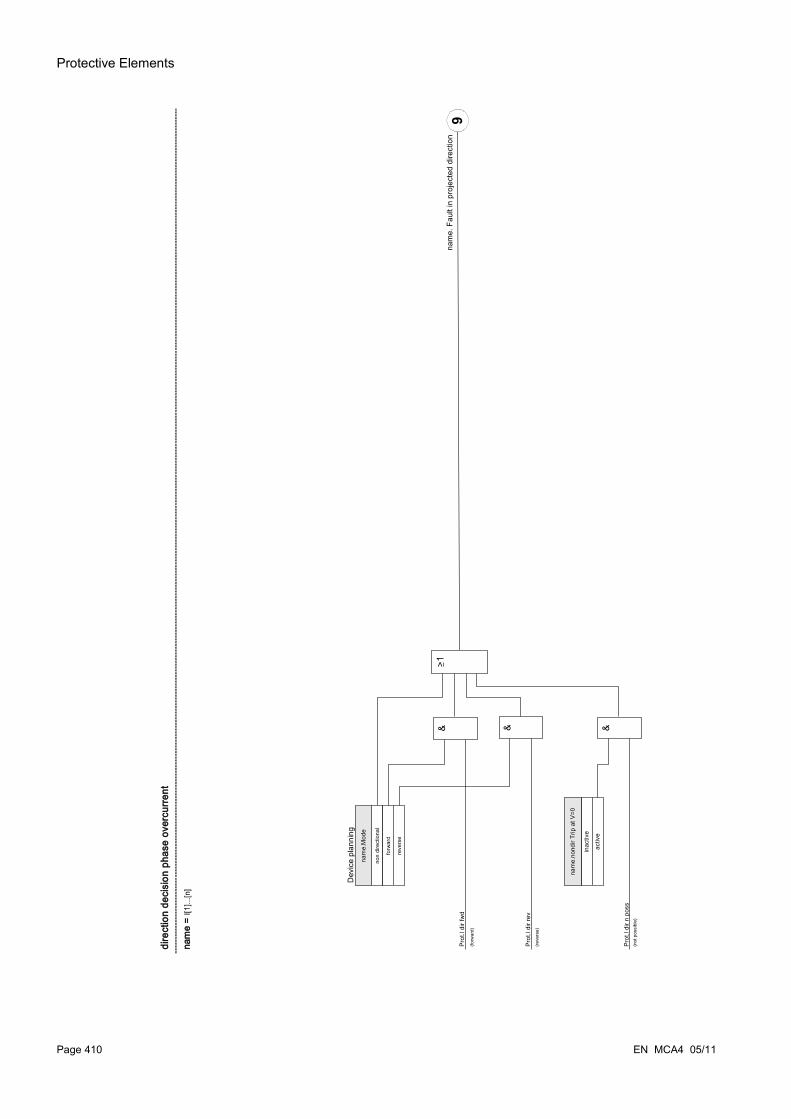
Protective Elements
Page 410 EN MCA4 05/11
non
dire
ctio
nal
reve
rse
forw
ard
nam
e.M
ode
& &
Prot
.I di
r fw
d
Prot
.I di
r rev
nam
e. F
ault
in p
roje
cted
dire
ctio
n
(forw
ard)
(reve
rse)
dire
ctio
n de
cisi
on p
hase
ove
rcur
rent
&
Prot
.I di
r n p
oss
(not
pos
sibl
e)
inac
tive
activ
e
nam
e.no
ndir
Trip
at V
=0
>1
nam
e =
I[1]..
.[n]
Dev
ice
plan
ning
9

Protective Elements
EN MCA4 05/11 Page 411
name.TripCmd
name.Alarm L1
name.Alarm L2
name.Alarm L3
name.Trip
IH2.Blo L1
IH2.Blo L2
IH2.Blo L3
Please Refer To Diagram: Blockings**
51V Pickup = %Pickup * 51P
I>
IL1
IL2
IL3
name.Trip L1
name.Trip L2
name.Alarm
Please Refer To Diagram: Trip blockings
inactive
active
name.IH2 Blo
(Stage is not deactivated and no active blocking signals)
name.IH2 Blo*
ILx max
(Tripping command not deactivated or blocked . )
5
6
7
4
3
Please Refer To Diagram: IH2*
Please Refer To Diagram: IH2*
Please Refer To Diagram: IH2*
15
16b
17b
18b
24b
25b
26b
14
φINV
ILx max
name.t-reset
name.t-char
name.Char
name.Reset Mode
Based on above parameters, tripping times and reset modes will be calculated by the device.
I[1]...[n]
name = 51V[1]...[n]
*=Applies only to devices that offer Inrush P
rotection
name.Trip L3
VL1
VL2
VL3
φ
Pickup%
25%
100%
V
25%
VRestraint max
%Pickup
&
&
&
&
&
&
&
&
&
&
&
>1>1
Fundamental
True RMS
name.Measuring method
φ
Phase to Ground
name.Measuring Mode
Phase to Phase
38b 38c38a
inactive
name.Meas Circuit Superv
active &

Protective Elements
Device Planning Parameters of the I Module
Parameter Description Options Default Menu path
Mode Mode do not use,
non directional,
forward,
reverse
I[1]: non directional
I[2]: do not use
I[3]: do not use
I[4]: do not use
I[5]: do not use
I[6]: do not use
[Device planning]
Global Protection Parameters of the I Module
Parameter Description Setting range Default Menu path
ExBlo1 External blocking of the module, if blocking is activated (allowed) within a parameter set and if the state of the assigned signal is true.
1..n, Assignment List -.- [Protection Para
/Global Prot Para
/I-Prot
/I[1]]ExBlo2 External blocking of the module, if blocking is
activated (allowed) within a parameter set and if the state of the assigned signal is true.
1..n, Assignment List -.- [Protection Para
/Global Prot Para
/I-Prot
/I[1]]ExBlo TripCmd
External blocking of the Trip Command of the module/the stage, if blocking is activated (allowed) within a parameter set and if the state of the assigned signal is true.
1..n, Assignment List -.- [Protection Para
/Global Prot Para
/I-Prot
/I[1]]
Ex rev Interl External blocking of the module by external reverse interlocking, if blocking is activated (allowed) within a parameter set and if the state of the assigned signal is true.
1..n, Assignment List -.- [Protection Para
/Global Prot Para
/I-Prot
/I[1]]
AdaptSet 1 Assignment Adaptive Parameter 1 AdaptSet -.- [Protection Para
/Global Prot Para
/I-Prot
/I[1]]AdaptSet 2 Assignment Adaptive Parameter 2 AdaptSet -.- [Protection Para
/Global Prot Para
/I-Prot
/I[1]]
Page 412 EN MCA4 05/11

Protective Elements
Parameter Description Setting range Default Menu path
AdaptSet 3 Assignment Adaptive Parameter 3 AdaptSet -.- [Protection Para
/Global Prot Para
/I-Prot
/I[1]]AdaptSet 4 Assignment Adaptive Parameter 4 AdaptSet -.- [Protection Para
/Global Prot Para
/I-Prot
/I[1]]
EN MCA4 05/11 Page 413

Protective Elements
Setting Group Parameters of the I Module
Parameter Description Setting range Default Menu path
Function Permanent activation or deactivation of module/stage.
inactive,
active
I[1]: active
I[2]: inactive
I[3]: inactive
I[4]: inactive
I[5]: inactive
I[6]: inactive
[Protection Para
/<n>
/I-Prot
/I[1]]
ExBlo Fc Activate (allow) or inactivate (disallow) blocking of the module/stage. This parameter is only effective if a signal is assigned to the corresponding global protection parameter. If the signal becomes true, those modules/stages are blocked that are parameterized "ExBlo Fc=active".
inactive,
active
inactive [Protection Para
/<n>
/I-Prot
/I[1]]
Ex rev Interl Fc
Activate (allow) or inactivate (disallow) blocking of the module/stage. This parameter is only effective if a signal is assigned to the corresponding global protection parameter. If the signal becomes true, those modules/stages are blocked that are parameterized "Ex rev Interl Fc = active".
inactive,
active
inactive [Protection Para
/<n>
/I-Prot
/I[1]]
Blo TripCmd Permanent blocking of the Trip Command of the module/stage.
inactive,
active
inactive [Protection Para
/<n>
/I-Prot
/I[1]]ExBlo TripCmd Fc
Activate (allow) or inactivate (disallow) blocking of the module/stage. This parameter is only effective if a signal is assigned to the corresponding global protection parameter. If the signal becomes true, those modules/stages are blocked that are parameterized "ExBlo TripCmd Fc=active".
inactive,
active
inactive [Protection Para
/<n>
/I-Prot
/I[1]]
Measuring method
Measuring method: fundamental or rms Fundamental,
True RMS,
I2
Fundamental [Protection Para
/<n>
/I-Prot
/I[1]]I>
~adapt~
If the pickup value is exceeded, the module/element starts to time out to trip.
Only available if: Characteristic = DEFT Or Characteristic = INV Minimum of the setting range If: VRestraint = active Minimum of the setting range If: VRestraint = inactive
0.02 - 40.00In 1.00In [Protection Para
/<n>
/I-Prot
/I[1]]
Page 414 EN MCA4 05/11

Protective Elements
Parameter Description Setting range Default Menu path
Char
~adapt~
Characteristic DEFT,
IEC NINV,
IEC VINV,
IEC EINV,
IEC LINV,
ANSI MINV,
ANSI VINV,
ANSI EINV,
Therm Flat,
IT,
I2T,
I4T
DEFT [Protection Para
/<n>
/I-Prot
/I[1]]
t
~adapt~
Tripping delay
Only available if: Characteristic = DEFT
0.00 - 300.00s 1.00s [Protection Para
/<n>
/I-Prot
/I[1]]t-char
~adapt~
Time multiplier/tripping characteristic factor. The setting range depends on the selected tripping curve.
Only available if: Characteristic = INV Or Characteristic = Therm Flat Or Characteristic = IT Or Characteristic = I2T Or Characteristic = I4T
0.02 - 20.00 1 [Protection Para
/<n>
/I-Prot
/I[1]]
Reset Mode
~adapt~
Reset Mode
Only available if: Characteristic = INV Or Characteristic = Therm Flat Or Characteristic = IT Or Characteristic = I2T Or Characteristic = I4T
instantaneous,
t-delay,
calculated
instantaneous [Protection Para
/<n>
/I-Prot
/I[1]]t-reset
~adapt~
Reset time for intermittent phase failures (INV characteristics only)
Available if:Reset Mode = t-delay
0.00 - 60.00s 0s [Protection Para
/<n>
/I-Prot
/I[1]]IH2 Blo
~adapt~
Blocking the trip command, if an inrush is detected.
inactive,
active
inactive [Protection Para
/<n>
/I-Prot
/I[1]]
EN MCA4 05/11 Page 415

Protective Elements
Parameter Description Setting range Default Menu path
nondir Trip at V=0
~adapt~
Only relevant for current protection modules/stages with directional feature! The device will trip non directional if this parameter is set to active and no direction could be determined because no reference voltage (V=0) could be measured any more (e.g. if there is a three-phase short circuit close to the device). If this parameter is set to inactive, the protection stage will be blocked in case of V=0.
Only available if: Device planning: I.Mode = directional
inactive,
active
inactive [Protection Para
/<n>
/I-Prot
/I[1]]
VRestraint
~adapt~
Voltage Restraint Protection inactive,
active
inactive [Protection Para
/<n>
/I-Prot
/I[1]]Measuring Mode
~adapt~
Measuring Mode
Only available if: VRestraint = active
Phase to Neutral,
Phase to Phase
Phase to Neutral
[Protection Para
/<n>
/I-Prot
/I[1]]VRestraint max
~adapt~
Maximum voltage restraint level. Definition of Vn: Vn is dependent on the System Parameter setting of "VT con". When the System Parameters "VT con" is set to "phase-to-phase" , "Vn = VT sec ". When the System Parameters "VT con" is set to "phase-to-ground", "Vn = VT sec/SQRT(3)".
Only available if: VRestraint = active
0.04 - 1.50Vn 1.00Vn [Protection Para
/<n>
/I-Prot
/I[1]]
Meas Circuit Superv
~adapt~
Measuring Circuit Supervision
Only available if: VRestraint = active
inactive,
active
inactive [Protection Para
/<n>
/I-Prot
/I[1]]
Page 416 EN MCA4 05/11

Protective Elements
I Module Input States
Name Description Assignment via
ExBlo1-I Module input state: External blocking1 [Protection Para
/Global Prot Para
/I-Prot
/I[1]]ExBlo2-I Module input state: External blocking2 [Protection Para
/Global Prot Para
/I-Prot
/I[1]]ExBlo TripCmd-I Module input state: External Blocking of the
Trip Command[Protection Para
/Global Prot Para
/I-Prot
/I[1]]Ex rev Interl-I Module input state: External reverse
interlocking[Protection Para
/Global Prot Para
/I-Prot
/I[1]]AdaptSet1-I Module input state: Adaptive Parameter1 [Protection Para
/Global Prot Para
/I-Prot
/I[1]]AdaptSet2-I Module input state: Adaptive Parameter2 [Protection Para
/Global Prot Para
/I-Prot
/I[1]]AdaptSet3-I Module input state: Adaptive Parameter3 [Protection Para
/Global Prot Para
/I-Prot
/I[1]]AdaptSet4-I Module input state: Adaptive Parameter4 [Protection Para
/Global Prot Para
/I-Prot
/I[1]]
EN MCA4 05/11 Page 417

Protective Elements
I Module Signals (Output States)
Name Description
active Signal: activeExBlo Signal: External BlockingEx rev Interl Signal: External reverse InterlockingBlo TripCmd Signal: Trip Command blockedExBlo TripCmd Signal: External Blocking of the Trip CommandIH2 Blo Signal: Blocking the trip command by an inrushAlarm L1 Signal: Alarm L1Alarm L2 Signal: Alarm L2Alarm L3 Signal: Alarm L3Alarm Signal: AlarmTrip L1 Signal: General Trip Phase L1Trip L2 Signal: General Trip Phase L2Trip L3 Signal: General Trip Phase L3Trip Signal: TripTripCmd Signal: Trip CommandActive AdaptSet Active Adaptive ParameterDefaultSet Signal: Default Parameter SetAdaptSet 1 Signal: Adaptive Parameter 1AdaptSet 2 Signal: Adaptive Parameter 2AdaptSet 3 Signal: Adaptive Parameter 3AdaptSet 4 Signal: Adaptive Parameter 4
Page 418 EN MCA4 05/11

Protective Elements
Commissioning: Overcurrent Protection, non-directional [50, 51]
Object to be tested
• Signals to be measured for each current protection element, the threshold values, total tripping time (recommended), or alternatively tripping delays and the fallback ratios; each time 3 x single-phase and 1 x three-phase.
Especially in Holmgreen connections, wiring errors can easily happen, and these are then detected safely. Measuring the total tripping time can ensure that the secondary wiring is o.k. (from the terminal on, up to the trip coil of the CB).
It is recommended to measure the total tripping time instead of the tripping delay. The tripping delay should be specified by the customer. The total tripping time is measured at the position signalling contact of the CB (not at the relay output!).
Total tripping time = tripping delay (please refer to the tolerances of the protection stages) + CB operating time (about 50 ms)
Please take the CB operating times from the technical data specified in the relevant documentation provided by the CB manufacturer.
Necessary means • Current source• May be: ampere meters• Timer
Procedure
Testing the threshold values (3 x single-phase and 1 x three-phase)Each time feed a current which is about 3-5% above the threshold value for activation/tripping. Then check the threshold values.
Testing the total tripping delay (recommendation)Measure the total tripping times at the auxiliary contacts of the CB (CB tripping).
Testing the tripping delay (measuring at the relay output)Measure the tripping times at the relay output.
Testing the fallback ratioReduce the current to 97% below the trip value and check the fallback ratio.
Successful test result The measured total tripping delays or individual tripping delays, threshold values and fallback ratios correspond with those values, specified in the adjustment list. Permissible deviations/tolerances can be found under Technical Data.
EN MCA4 05/11 Page 419

Protective Elements
Commissioning: Overcurrent Protection, directional [67]
Object to be tested
For each directional overcurrent element is to be measured: the total tripping time (recommendation) or alternatively tripping delays and the fallback ratios; each time 3 x single-phase and 1 x three-phase.
Especially in Holmgreen connections, wiring errors can happen easily and these are then detected safely. By measuring the total tripping time, it can be ensured that the secondary wiring is o.k. (from the terminal on, up to the trip coil of the CB ).
It is recommended to measure the total tripping time instead of the tripping time. The tripping delay should be specified by the customer. The total tripping time is measured at the position signaling contacts of the CBs (not at the relay output!).
Total tripping time: = tripping delay (please refer to the tolerances of the protection stages) + CB operating time (about 50 ms)
Please take the CB switching times from the technical data, specified in the relevant documentation, provided by the CB manufacturer.
Necessary means• Synchronizable current and voltage sources• May be: ampere meters • Timer
Procedure
Synchronize the 3-phase current and voltage sources with each other. Then simulate the tripping directions to be tested by the angle between current and voltage.
Testing the threshold values (3 x single-phase and 1 x three-phase)Each time feed a current which is about 3-5% above the threshold value for activation/tripping. Check then the threshold values.
Testing the total tripping delay (recommendation)Measure the total tripping times at the auxiliary contacts of the CB (CB tripping).
Testing the trip delay (measured at the relay output)Measure the tripping times at the relay output.
Testing the fallback ratioReduce the current to 97% below the trip value and check the fallback ratio.
Successful test resultThe measured total tripping delays or individual tripping delays, threshold values and fallback ratios correspond with those values, specified in the adjustment list. Permissible deviations/tolerances can be found under Technical Data.
Page 420 EN MCA4 05/11

Protective Elements
51V - Voltage Restraint Overcurrent
For activating this function, the parameter »VRestraint« has to be set to active in the parameter set of the corresponding overcurrent element I[x].
The 51V protection function restrains operation which reduces pickup levels. This allows the User to lower the pickup value of the 51V protection function with the corresponding phase input voltage (phase-to-phase or phase-to-ground, depending on the setting of »Measuring Channel« within the current protection module). When the minimum fault phase current is close to the load current, it may make the phase time overcurrent protection coordination difficult. In this case, an undervoltage function may be used to alleviate this situation. When the voltage is low, the phase time overcurrent pickup threshold may be set low accordingly, so that the phase time overcurrent protection may achieve adequate sensitivity and better coordination. The device uses a simple linear model to determine the effective pickup by characterizing the relationship between the voltage and the phase time overcurrent pickup threshold.
Once the voltage restraint protection function is activated, the effective phase time overcurrent pickup threshold will be the calculated Pickup% times the phase time overcurrent pickup setting. The effective pickup threshold must be within the setting range allowed and, if it is less, the minimum pickup value will be used.
That means:Vmin = 0.25*Vmax;•Pickup%min = 25%;•Pickup% = 25%, if V <= Vmin;•Pickup% = 1/Vmax*(V - Vmin) + 25%, if Vmin < V < Vmax;•Pickup% = 100%, if V >= Vmax;
The tripping curves (characteristic) will not be influenced by the voltage restraint function.If the voltage transformer supervision is activated, the voltage restraint overcurrent protection element is blocked in case of m.c.b. trip to avoid false trippings.
EN MCA4 05/11 Page 421
Pickup%
VRestraint max25% VRestraint max
25%
100%
V

Protective Elements
Definition of Vn: Vn is dependent on the »Measuring Channel« setting in the current protection modules.
In case that this parameter is set to "Phase to Phase":
Vn=MainVT sec
In case that this parameter is set to "Phase to Neutral":
Vn=MainVT sec3
If the parameter »VT con« within the field parameters is set to »Phase to Phase« the setting »Phase to Neutral« in the current modules is effectless.
Page 422 EN MCA4 05/11
Protective Elements
Commissioning: Overcurrent Protection, Non-directional [ANSI 51V]
Object to be tested:
Signals to be measured for Voltage Restraint function: the threshold values, total tripping time (recommended), or alternatively tripping delays and the dropout ratios; each time 3 x single-phase and 1 x three-phase.
It is recommended to measure the total tripping time instead of the tripping time. The tripping delay should be specified by the customer. The total tripping time is measured at the position signaling contacts of the CBs (not at the relay output!).
Total tripping time: = tripping delay (please refer to the tolerances of the protection stages) + CB operating time (about 50 ms)
Please take the CB switching times from the technical data, specified in the relevant documentation, provided by the CB manufacturer.
Necessary means:
• Current source;• Voltage Source;• Current and Voltage meters; and• Timer.
Procedure:
Testing the threshold values (3 x single-phase and 1 x three-phase)Feed %Pickup voltage. For each test performed, feed a current that is about 3-5% above the threshold value for activation/tripping. Then check if the pickup values are %Pickup of the value according to the standard overcurrent protection.
Testing the total tripping delay (recommendation)Measure the total tripping times at the auxiliary contacts of the breakers (breaker tripping).
Testing the tripping delay (measuring at the relay output contact)Measure the tripping times at the relay output contact.
Testing the dropout ratioReduce the current to 97% below the trip value and check the dropout ratio.
Successful test resultThe measured total tripping delays or individual tripping delays, threshold values, and dropout ratios correspond with those values specified in the adjustment list. Permissible deviations/tolerances can be found under Technical Data.
EN MCA4 05/11 Page 423

Protective Elements
I2> - Negative-Sequence Overcurrent [51Q]
For activating this function, the parameter »Measuring Mode« has to be set to »I2« in the parameter set of the corresponding overcurrent element I[x].
The negative-sequence overcurrent protection function (I2>) is to be seen as an equivalent to the phase overcurrent protection with the exception that it uses negative-sequence current (I2>) as measured quantities instead of the three phase currents used by phase overcurrent protection function. The negative-sequence current used by I2> is derived from the following well-known symmetrical component transformation:
I 2=13 I L1a
2 I L2a I L3
The pickup set value of a I2> protection function should be set in accordance of the negative-sequence current occurrence in the protected object.
Besides that, the negative-sequence overcurrent protection function (I2>) uses the same setting parameters as the phase overcurrent protection function, like trip and reset characteristics from both IEC/ANSI standards, time multiplier, etc. The negative-sequence overcurrent protection function (I2>) can be used for line, generator, transformer and motor protection to protect the system from unbalanced faults. Because the I2> protection function operates on the negative-sequence current component which is normally absent during load conditions, the I2> can, therefore, be set more sensitive than the phase overcurrent protection functions. On the other hand, coordination of negative-sequence overcurrent protection function in a radial system does not mean automatically very long fault clearing time for the furthest upstream protection devices, because the tripping time of concerned negative-sequence overcurrent protection function needs only be coordinate with the next downstream device with the negative-sequence overcurrent protection function. This makes the I2> in many cases as an advantageous protection concept in addition to the phase overcurrent protection function.
If you are using inrush blockings, the tripping delay of the current protection functions must be at least 30 ms or more in order to prevent faulty trippings.
At the moment of breaker closure, negative-sequence current might be the result of transients.
Page 424 EN MCA4 05/11
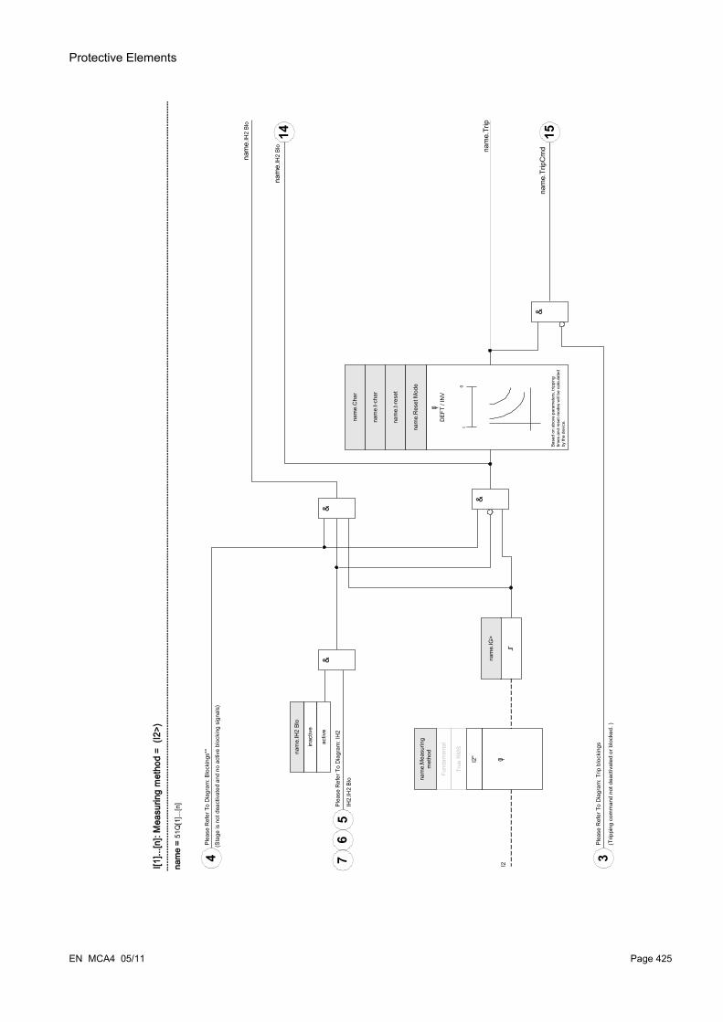
Protective Elements
EN MCA4 05/11 Page 425
nam
e.Tr
ipC
mdna
me.
Trip
Plea
se R
efer
To
Dia
gram
: Blo
ckin
gs**
nam
e.IH
2 Bl
o
Plea
se R
efer
To
Dia
gram
: Trip
blo
ckin
gs
(Sta
ge is
not
dea
ctiv
ated
and
no
activ
e bl
ocki
ng s
igna
ls)
(Trip
ping
com
man
d no
t dea
ctiv
ated
or b
lock
ed. )
IH2.
IH2
Blo
inac
tive
activ
e
nam
e.IH
2 Bl
o
nam
e.IG
>
nam
e.IH
2 Bl
o
5
4 3
Ple
ase
Ref
er T
o D
iagr
am: I
H2
1514
I2I[1]..
.[n]:
Mea
surin
g m
etho
d =
(I2>
)
nam
e =
51Q
[1]..
.[n]
φD
EFT
/ IN
V
nam
e.t-r
eset
nam
e.t-c
har
nam
e.C
har
nam
e.R
eset
Mod
e
Base
d on
abo
ve p
aram
eter
s, tr
ippi
ng
times
and
rese
t mod
es w
ill be
cal
cula
ted
by th
e de
vice
.
67
&&
&
&
t0
φ
Fund
amen
tal
True
RM
S
nam
e.M
easu
ring
met
hod
I2"
Protective Elements
Commissioning: Negative Sequence Overcurrent]
Object to be tested
Signals to be measured for each current protection function: the threshold values, total tripping time (recommended), or alternatively tripping delays and the dropout ratios.
It is recommended to measure the total tripping time instead of the tripping time. The tripping delay should be specified by the customer. The total tripping time is measured at the position signaling contacts of the CBs (not at the relay output!).
Total tripping time: = tripping delay (please refer to the tolerances of the protection stages) + CB operating time (about 50 ms)
Please take the CB switching times from the technical data, specified in the relevant documentation, provided by the CB manufacturer.
Necessary means:• Current source• Current meters• Timer
Procedure:
Testing the threshold values
In order to get a negative-sequence current, please change the phase sequence at the terminals of the current source (in case of ABC sequence to ACB – in case of a ACB sequence to ABC).
For each test performed, feed a current that is about 3-5% above the threshold value for activation/tripping. Then check the threshold values.
Testing the total tripping delay (recommendation)Measure the total tripping times at the auxiliary contacts of the breakers (breaker tripping).
Testing the tripping delay (measuring at the relay output contact)Measure the tripping times at the relay output contact.
Testing the dropout ratioReduce the current to 97% below the trip value and check the dropout ratio.
Successful test resultThe measured total tripping delays or individual tripping delays, threshold values, and dropout ratios correspond with those values specified in the adjustment list. Permissible deviations/tolerances can be found under Technical Data.
Page 426 EN MCA4 05/11

Protective Elements
Directional Features for Measured Ground Fault Elements 50N/51NAll ground fault elements can be selected as »non-directional/forward/reverse« operated. This has to be done in the »Device Planning« menu.
Important Definitions
Polarizing Quantity: This is the quantity that is used as a reference value. The polarizing quantity can be selected by the parameter »IG meas dir ctrl« in the [Field Para/Direction] menu as follows:
• »IG meas 3V0«: The neutral voltage selected by the parameter »3V0 Source« will be used as the polarizing quantity. The traditional way to polarize a ground fault element is to use neutral voltage (3V0). The neutral voltage can, however, be either »measured« or »calculated«. This can be selected by the parameter »3V0 Source« in the[Field Para/Direction] menu.
• »I2,V2«: With this selection, the negative phase sequence voltage and current (Polarizing: V2/Operating: I2) will be used to detect direction. The monitored current is still the measured residual current IG meas.
• »Dual«: For this method, the negative phase sequence voltage »V2« will be used as polarizing quantity if »V2« and »I2« are available, otherwise 3V0 will be used. The operating quantity is either I2 if »V2« and »I2« are available, else IG meas.
The following table gives the User a quick overview of all possible directional settings.50N/51N Direction Decision
by Angle Between: [Field Para/ Direction]
The Following Angle Has to Be Set:
[Field Para/Direction]:
IG meas dir ctrl =
[Field Para/Direction]:
3V0 Source =
Measured ground current and neutral voltage:IG meas, 3V0 (measured)
Ground MTA IG meas 3V0 measured
Measured ground current and neutral voltage:IG meas, 3V0 (calculated)
Ground MTA IG meas 3V0 calculated
Negative sequence voltage and currentI2, V2
90° + Phase MTA I2,V2 not used
Negative phase sequence current and voltage (preferred), measured ground current and neutral voltage (alternatively):I2, V2 (if available)or else:IG meas, 3V0 (measured)
If V2 and I2 are available: 90° + Phase MTA
else:
Ground MTA
Dual measured
Negative phase sequence current and voltage (preferred), measured ground current and neutral voltage (alternatively):I2, V2 (if available)or else:IG meas, 3V0 (calculated)
If V2 and I2 are available: 90° + Phase MTA
else:
Ground MTA
Dual calculated
EN MCA4 05/11 Page 427

Protective Elements
Page 428 EN MCA4 05/11
50G
/51G
-di
rect
ion
dete
ctio
n
Prot
.IG m
eas
dir n
pos
s
Prot
.IG m
eas
rev
dir
Prot
.IG m
eas
dir f
wd
(forw
ard)
(reve
rse)
(not
pos
sibl
e)
10b
10b
Prot
-50
G/5
1G -
dire
ctio
n de
tect
ion
10b
mea
sure
d
3V0
Sour
ce
Fiel
d Pa
ra calc
ulat
ed
VG
cal
c
VX
mea
s
IG m
eas
3V0
I2,V
2
IG m
eas
dir c
trl
Dua
l
3V0
3V0
If V
2 an
d I2
are
ava
ilabl
e, I2
is th
e op
erat
ing
quan
tity,
els
e IG
mea
s is
the
oper
atin
g qu
antit
y
V2
IG =
IG m
eas 90°
+ P
hase
MTA
Gro
und
MTA
Fiel
d Pa
ra
Fiel
d Pa
ra
If V2
and
I2 a
re a
vaila
ble,
MTA
= 9
0° +
Ph
ase
MTA
, oth
erw
ise
MTA
= G
roun
d M
TA
reve
rse
forw
ard
pola
rizin
g
MTA
pola
rizin
gop
erat
ing
oper
atin
g
V2*
I2
*=P
riorit
y if
avai
labl
e.
Protective Elements
Directional Features for Calculated (IG calc) Ground Fault 50N/51NAll ground fault elements can be selected as »non-directional/forward/reverse« operated. This has to be done in the »Device Planning« menu.
Important Definitions
Polarizing Quantity: This is the quantity that is used as a reference value. The polarizing quantity can be selected by the parameter »IG calc dir ctrl« in the [Field Para/Direction] menu as follows:
• »IG calc 3V0«: The neutral voltage selected by the parameter »3V0 Source« will be used as the polarizing quantity. The traditional way to polarize a ground fault element is to use neutral voltage (3V0). The neutral voltage can, however, be either »measured« or »calculated«. This can be selected by the parameter »3V0 Source« in the [Field Para/Direction] menu.
• »IG calc Ipol (IG meas)«: The measured neutral current (usually = IG meas) will be used as polarizing quantity.
• »Dual«: For this method, the measured neutral current Ipol=IG meas will be used as polarizing quantity, if available, otherwise 3V0 will be used.
• »I2,V2«: With this selection, the negative phase sequence voltage and current will be used to detect the direction. The monitored current is still the calculated residual current IG calc.
Operating Quantity: For the directional IG calc elements, the operating quantity is in general the calculated neutral current IG calc (except from »I2,V2« mode, where »I2« is the operating quantity).
The ground maximum torque angles (MTA) can be adjusted from 0° to 360°, except, if »IG calc Ipol (IG meas)« is selected. In this case it is set to 0° (fixed).
The MTA will also be set internally to 0° in case that Ipol=IG meas is available within the Dual-Mode
EN MCA4 05/11 Page 429

Protective Elements
The following table gives the User a quick overview of all possible directional settings.50N/51N Direction Decision
by Angle Between: [Field Para/ Direction]
The Following Angle Has to Be Set:
[Field Para/Direction]:
IG calc dir ctrl =
[Field Para/Direction]:
3V0 Source =
Residual current and neutral voltage:IG calc, 3V0 (measured)
Ground MTA IG calc 3V0 measured
Residual current and neutral voltage:IG calc, 3V0 (calculated)
Ground MTA IG calc 3V0 calculated
Residual current and neutral/ground currentIG calc, IG meas
0° (fixed) IG calc Ipol (IG meas) not used
Residual current and neutral/ground current (preferred), residual current and neutral voltage (alternatively):IG calc, IG meas (if available)or else:IG calc, 3V0 (measured)
If Ipol (=IG meas) is available, MTA = 0° (fixed); else MTA=Ground MTA
Dual measured
Residual current and neutral/ground current (preferred), residual current and neutral voltage (alternatively):IG calc, IG meas (if available)or else:IG calc, 3V0 (calculated)
If Ipol (=IG meas) is available, MTA = 0° (fixed); else MTA=Ground MTA
Dual calculated
Negative sequence voltage and currentI2, V2
90° + Phase MTA I2,V2 not used
Page 430 EN MCA4 05/11
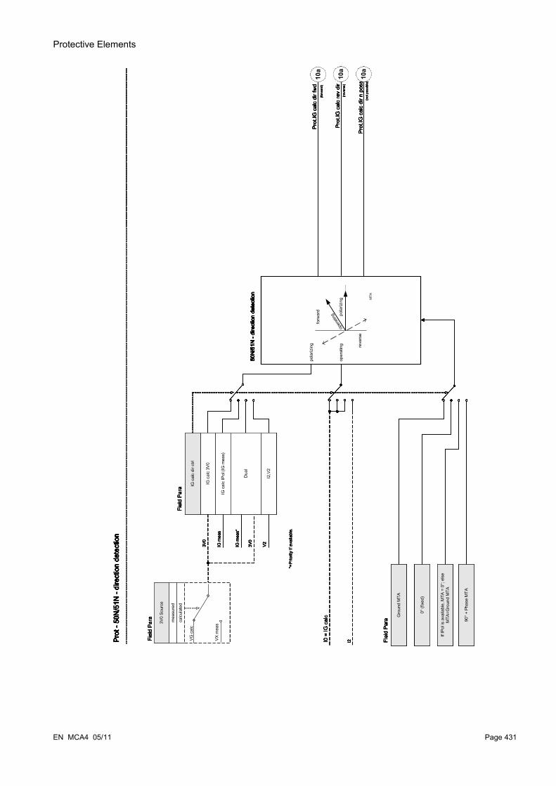
Protective Elements
EN MCA4 05/11 Page 431
reve
rse
forw
ard
pola
rizin
g
50N
/51N
-di
rect
ion
dete
ctio
n
MTA
mea
sure
d
3V0
Sour
ce
Fiel
d Pa
ra calc
ulat
ed
VG
cal
c
VX
mea
s
IG c
alc
3V0
IG c
alc
IPol
(IG
mea
s)
IG c
alc
dir c
trl
Dua
l
I2,V
2
3V0
3V0
IG m
eas
IG m
eas*
I2
V2
I0 =
IG c
alc
Prot
.IG c
alc
dir n
pos
s
Prot
.IG c
alc
rev
dir
Prot
.IG c
alc
dir f
wd
(forw
ard)
(reve
rse)
(not
pos
sibl
e)
10a
10a
pola
rizin
gop
erat
ing
Prot
-50
N/5
1N -
dire
ctio
n de
tect
ion
oper
ating
0° (f
ixed
)
Gro
und
MTA
Fiel
d Pa
ra
Fiel
d Pa
ra
10a
Prot
.IG N
eg c
alc
dir n
pos
s
Prot
.IG N
eg c
alc
rev
dir
Prot
.IG m
eas
Neg
cal
c di
r fw
d(fo
rwar
d)
(reve
rse)
(not
pos
sibl
e)
10a
10a
10a
If IP
ol is
ava
ilabl
e, M
TA =
0°;
els
e M
TA=G
roun
d M
TA
90°
+ Ph
ase
MTA
*=P
riorit
y if
avai
labl
e.

Protective Elements
IG - Ground Fault [50N/G, 51N/G, 67N/G]Available elements: IG[1] ,IG[2] ,IG[3] ,IG[4]
If you are using inrush blockings the tripping delay of the earth current protection functions must be at least 30ms or more in order to prevent faulty trippings.
All earth current elements are identically structured.
This module offers Adaptive Parameter Sets.Parameters can be modified within parameter sets dynamically by means of Adaptive Parameter Sets. Please refer to chapter Parameter / Adaptive Parameter Sets.
The following table shows the application options of the earth overcurrent protection element
Applications of the IE-Protection Module Setting in OptionANSI 50N/G – Earth overcurrent protection, non directional
Device Planning menuSetting: non directional
Measuring Mode: Fundamental/TrueRMS
ANSI 51N/G – Earth short circuit protection, non directional
Device Planning menuSetting: non directional
Measuring Mode: Fundamental/TrueRMS
ANSI 67N/G – Earth overcurrent/Earth short circuit protection, directional
Device Planning menuSetting: directional
Field parameter menu3V0 Source: measured/calculated
3I0 Source: measured/calculated
Measuring Mode: Fundamental/TrueRMS
IG Source: measured/calculated
VG Source: measured/calculated
Measuring ModeFor all protection elements it can be determined, whether the measurement is done on basis of the »Fundamental« or if »TrueRMS« measurement is used.
IG Source/VG SourceWithin the parameter menu, this parameter determines, whether the earth current and the residual voltage is »measured« or »calculated«.
Direction detection (3V0 Source und 3I0 Source)In the field parameter menu it can be determined, if the earth current directional detection should be based on measured or calculated values of currents and voltages. This setting takes effect on all earth current elements.
• Calculation of the residual voltage is only possible, when phase to neutral voltage is applied to the voltage inputs.
At setting »measured« the quantities to be measured, i. e. Residual voltage and the measured earth current have to be applied to the corresponding 4th measuring input.
Page 432 EN MCA4 05/11
Protective Elements
All earth current protective elements can be planned user defined as non-directional or as directional stages. This means, for instance, all 4 elements can be projected in forward/reverse direction. For each element the following characteristics are available:
• DEFT (UMZ)• NINV (AMZ)• VINV (AMZ)• LINV (AMZ)• EINV (AMZ)• MINV (AMZ)• VINV (AMZ)• EINV (AMZ)• Thermal Flat• IT• I2T• I4T
Explanation:
The earth current can be measured either directly via a cable-type transformer or detected by a Holmgreen connection. The earth current can alternatively be calculated from the phase currents; but this is only possible if the phase currents are not ascertained by a V-connection.
The device can optionally be procured with a sensitive earth current measuring input.
EN MCA4 05/11 Page 433
t = Tripping delay
t-char = Time multiplier/tripping characteristic factor
IG = Fault current
IG> = If the pickup value is exceeded, the module/element starts to time out to trip.

Protective Elements
Page 434 EN MCA4 05/11
t [s]
1 100.01
0.1
1
10
100
1 100.01
0.1
1
10
100
I/I>
tt
4020
300 s300 s
0.0 s0.0 s
0.010.01
IG>IG
IG>IG
DEFT

Protective Elements
EN MCA4 05/11 Page 435
t-char
t = 0.14 *t-char [s]
IG> -1IG( )0.02
TripReset
t = 0.14 *t-char [s]
IG> -1IG( )2
x * IG> (multiples of pickup)
t [s]
Notice!Various reset modes are available. Resetting via characteristic, delayed and instantaneous.
IEC NINV

Protective Elements
Page 436 EN MCA4 05/11
t [s]t-char
TripReset
x * IG> (multiples of pickup)
t = 13.5 *t-char [s]
IG> -1IG( )2
t = 13.5 *t-char [s]
IG> -1IG( )
Notice!Various reset modes are available. Resetting via characteristic, delayed and instantaneous.
IEC VINV
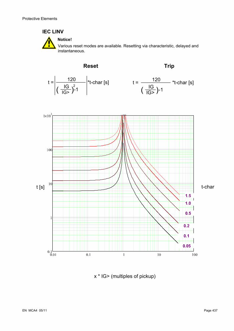
Protective Elements
EN MCA4 05/11 Page 437
t [s] t-char
x * IG> (multiples of pickup)
TripReset
t = 120 *t-char [s]
IG> -1IG( )t = 120 *t-char [s]
-1IG( )2
IG>
Notice!Various reset modes are available. Resetting via characteristic, delayed and instantaneous.
IEC LINV

Protective Elements
Page 438 EN MCA4 05/11
t [s] t-char
x * IG> (multiples of pickup)
TripReset
t = 80 *t-char [s]
IG> -1IG( )2 t = 80 *t-char [s]
IG> -1IG( )2
Notice!Various reset modes are available. Resetting via characteristic, delayed and instantaneous.
IEC EINV
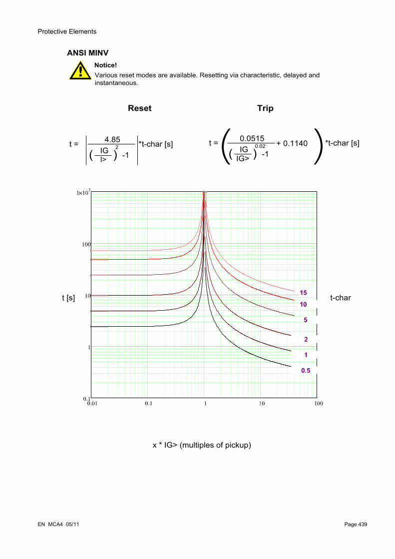
Protective Elements
EN MCA4 05/11 Page 439
t [s] t-char
x * IG> (multiples of pickup)
t = 0.0515 *t-char [s]
IG> -1IG( )0.02 + 0.1140( )t = 4.85 *t-char [s]
-1IG( )2
I>
TripReset
Notice!Various reset modes are available. Resetting via characteristic, delayed and instantaneous.
ANSI MINV
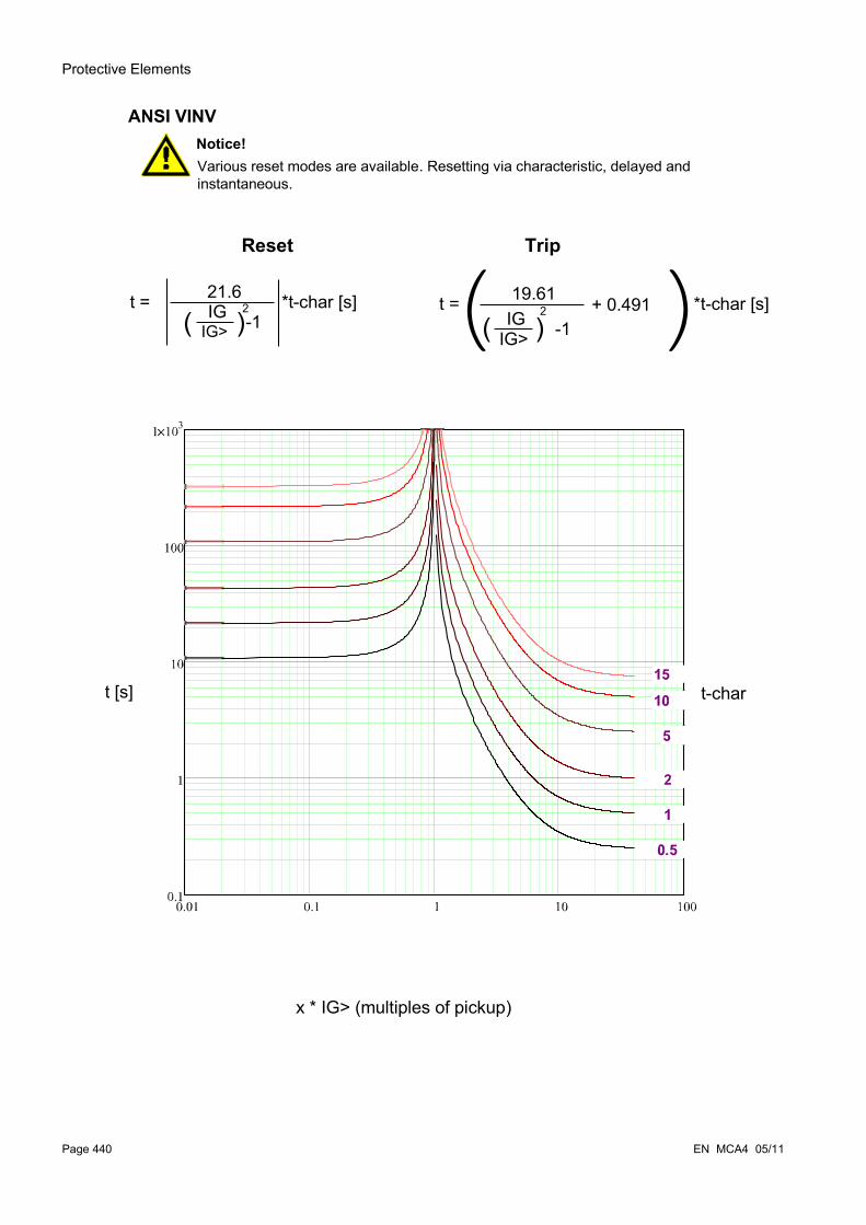
Protective Elements
Page 440 EN MCA4 05/11
t [s] t-char
x * IG> (multiples of pickup)
TripReset
t = 21.6 *t-char [s]-1IG( )
2
IG>
t = 19.61 *t-char [s]
IG> -1IG( )2 + 0.491( )
Notice!Various reset modes are available. Resetting via characteristic, delayed and instantaneous.
ANSI VINV
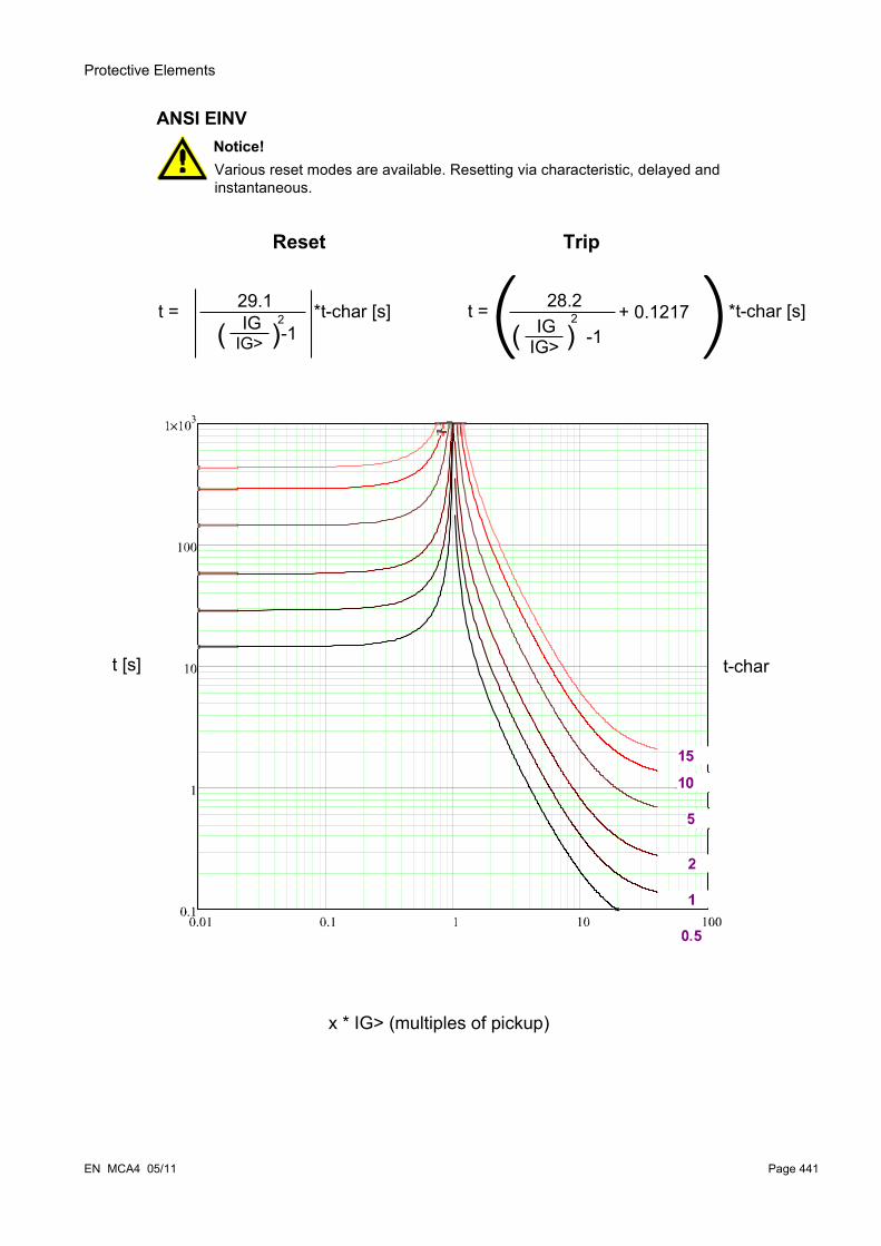
Protective Elements
EN MCA4 05/11 Page 441
t [s] t-char
x * IG> (multiples of pickup)
TripReset
t = 28.2 *t-char [s]
IG> -1IG( )2 + 0.1217( )t = 29.1 *t-char [s]
-1IG( )2
IG>
Notice!Various reset modes are available. Resetting via characteristic, delayed and instantaneous.
ANSI EINV
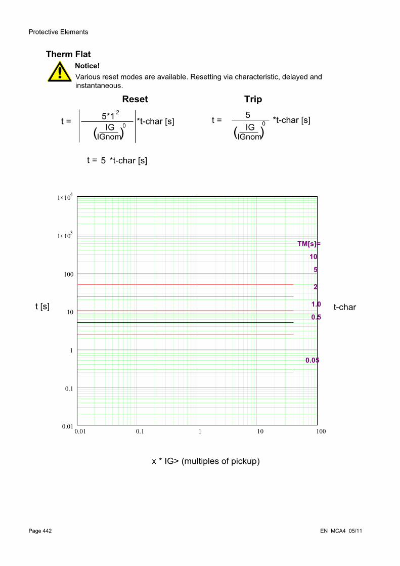
Protective Elements
Page 442 EN MCA4 05/11
t [s] t-char
TripReset
t = 5*1 *t-char [s]2
IG( )0
IGnom
x * IG> (multiples of pickup)
Notice!Various reset modes are available. Resetting via characteristic, delayed and instantaneous.
Therm Flat
t = 5 *t-char [s]
IGnomIG( )
0
t = 5 *t-char [s]
0.01 0.1 1 10 1000.01
0.1
1
10
100
1 103×
1 104×
TM[s]=
10
5
2
1.0
0.5
0.05
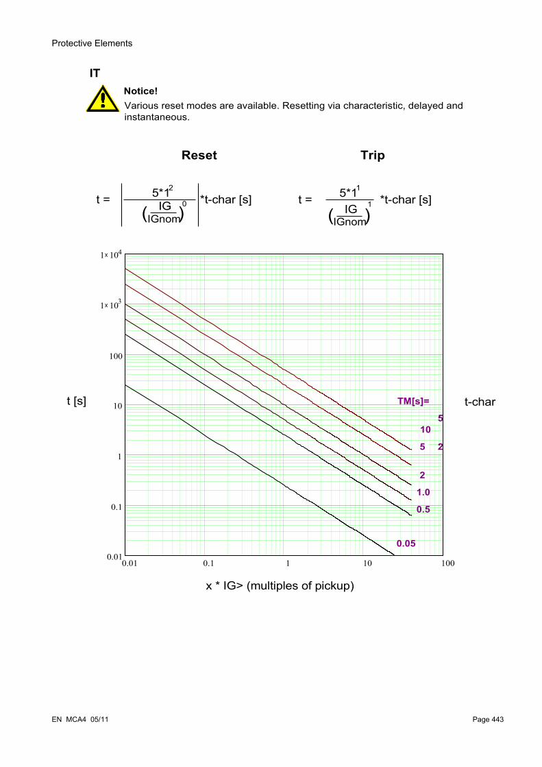
Protective Elements
EN MCA4 05/11 Page 443
t [s] t-char
TripReset
x * IG> (multiples of pickup)
t = 5*1 *t-char [s]2
IG( )0
IGnom
Notice!Various reset modes are available. Resetting via characteristic, delayed and instantaneous.
IT
t = 5*1 *t-char [s]
IGnomIG( )
1
1
0.01 0.1 1 10 1000.01
0.1
1
10
100
1 103×
1 10×
TM[s]=
510
5 2
2
1.0
0.5
0.05
4

Protective Elements
Page 444 EN MCA4 05/11
t [s] t-char
TripReset
x * IG> (multiples of pickup)
t = 5*1 *t-char [s]2
IG( )0
IGnom
Notice!Various reset modes are available. Resetting via characteristic, delayed and instantaneous.
I2T
t = 5*1 *t-char [s]
IGnomIG( )
2
2
0.01 0.1 1 10 1000.01
0.1
1
10
100
1 103×
1 104×
TM[s]=
10
5
2
1.00.50.05
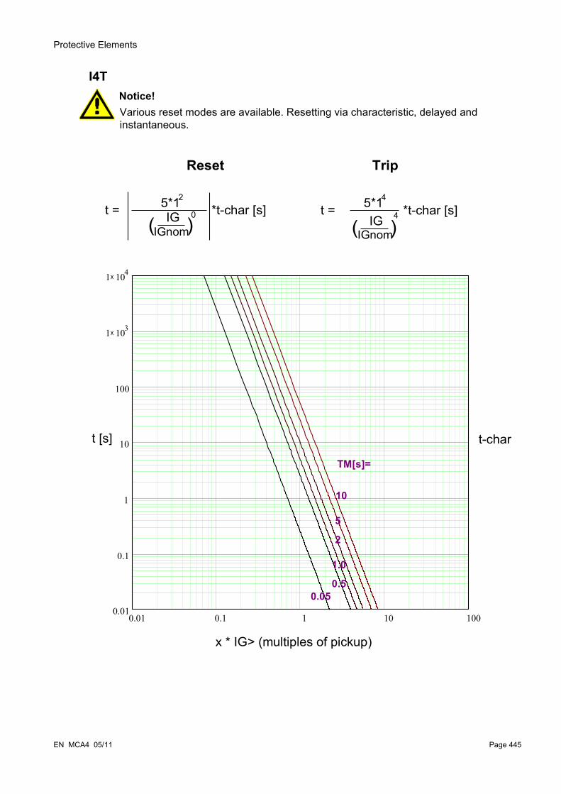
Protective Elements
EN MCA4 05/11 Page 445
t [s] t-char
TripReset
x * IG> (multiples of pickup)
t =
Notice!Various reset modes are available. Resetting via characteristic, delayed and instantaneous.
I4T
t = 5*1 *t-char [s]
IGnomIG( )
4
45*1 *t-char [s]2
IGnomIG( )
0
0.01 0.1 1 10 1000.01
0.1
1
10
100
1 103×
1 104×
TM[s]=
10
5
2
1.0
0.50.05

Protective Elements
Page 446 EN MCA4 05/11
VX
Prot
-Ea
rth fa
ult -
dire
ctio
n de
tect
ion
sin
(-90°
)?
VX
IGI C
reve
rse
forw
ard
cos
(180
°)VX
IG
I W
forw
ard
reve
rse
reve
rse
VX
IG
SOLI
-RES
I
IG M
TA
forw
ard
Prot
.IG M
TA +
Pro
t.EC
T An
gle
Cor
φ
Prot
.IG d
ir n
poss
Prot
.IG re
v di
r
Prot
.IG d
ir fw
d(fo
rwar
d)
(reve
rse)
(not
pos
sibl
e)
& & &
Prot
.Ala
rm
IG
mea
sure
d
calc
ulat
ed
Fiel
d Pa
ra.3
V0 S
ourc
e
mea
sure
d
calc
ulat
ed
Fiel
d Pa
ra.3
I0 S
ourc
e
Fiel
d Pa
ra φ φ
Fiel
d Pa
ra

Protective Elements
EN MCA4 05/11 Page 447
non
dire
ctio
nal
nam
e.M
ode
reve
rse
forw
ard
& &
Prot
.IG d
ir fw
d
Prot
.IG re
v di
r
nam
e. F
ault
in p
roje
cted
dire
ctio
n
dire
ctio
n de
cisi
on E
arth
faul
t
&
Prot
.IG d
ir n
poss
(not
pos
sibl
e)
inac
tive
activ
e
nam
e.no
ndir
Trip
at
VG
=0
>1
nam
e =
IG[1
]...[n
]
Dev
ice
plan
ning
10
mea
sure
d
calc
ulat
ed
Fiel
d Pa
ra.3
V0 S
ourc
e
mea
sure
d
calc
ulat
ed
Fiel
d Pa
ra.3
I0 S
ourc
e
Fiel
d Pa
ra
IG VXφ
φ
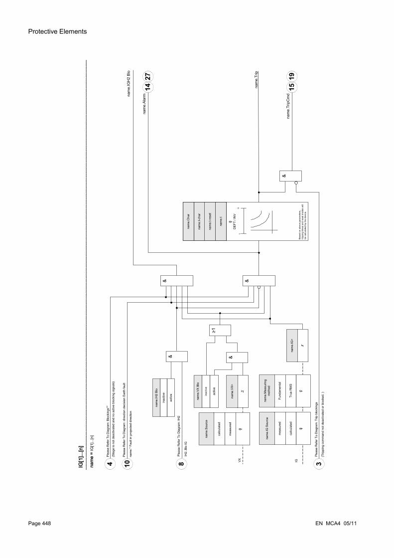
Protective Elements
Page 448 EN MCA4 05/11
φD
EFT
/ IN
V
nam
e.t
nam
e.t-r
eset
nam
e.t-c
har
nam
e.C
har
t0
nam
e.Tr
ipC
md
nam
e.Tr
ip
Plea
se R
efer
To
Dia
gram
: Blo
ckin
gs**
nam
e.* F
ault
in p
roje
cted
dire
ctio
n
nam
e.Al
arm
&
IG
inac
tive
nam
e.VX
Blo
activ
e
Plea
se R
efer
To
Dia
gram
: Trip
blo
ckin
gs
IG[1
]...[n
]
(Sta
ge is
not
dea
ctiv
ated
and
no
activ
e bl
ocki
ng s
igna
ls)
(Trip
ping
com
man
d no
t dea
ctiv
ated
or b
lock
ed. )
IH2.
.Blo
IG
inac
tive
activ
e
nam
e.IH
2 Bl
o
&
&
nam
e.VX
>
VX
&
nam
e.IG
>
>1
nam
e =
IG[1
]...[n
]
nam
e.IG
H2
Blo
&
8104 3
Ple
ase
Ref
er T
o D
iagr
am: d
irect
ion
deci
sion
Ear
th fa
ult
Ple
ase
Ref
er T
o D
iagr
am: I
H2
151427 19
Bas
ed o
n ab
ove
para
met
ers,
tri
ppin
g tim
es a
nd re
set m
odes
will
be
cal
cula
ted
by th
e de
vice
.
Fund
amen
tal
True
RM
S
nam
e.M
easu
ring
met
hod
φ
mea
sure
d
calc
ulat
ed
nam
e.IG
Sou
rce
φ
calc
ulat
ed
mea
sure
d
nam
e.So
urce
φ

Protective Elements
Device Planning Parameters of the Ground Fault Protection
Parameter Description Options Default Menu path
Mode Mode do not use,
non directional,
forward,
reverse
do not use [Device planning]
EN MCA4 05/11 Page 449

Protective Elements
Global Protection Parameters of the Ground Fault Protection
Parameter Description Setting range Default Menu path
ExBlo1 External blocking of the module, if blocking is activated (allowed) within a parameter set and if the state of the assigned signal is true.
1..n, Assignment List -.- [Protection Para
/Global Prot Para
/I-Prot
/IG[1]]ExBlo2 External blocking of the module, if blocking is
activated (allowed) within a parameter set and if the state of the assigned signal is true.
1..n, Assignment List -.- [Protection Para
/Global Prot Para
/I-Prot
/IG[1]]ExBlo TripCmd
External blocking of the Trip Command of the module/the stage, if blocking is activated (allowed) within a parameter set and if the state of the assigned signal is true.
1..n, Assignment List -.- [Protection Para
/Global Prot Para
/I-Prot
/IG[1]]
Ex rev Interl External blocking of the module by external reverse interlocking, if blocking is activated (allowed) within a parameter set and if the state of the assigned signal is true.
1..n, Assignment List -.- [Protection Para
/Global Prot Para
/I-Prot
/IG[1]]
AdaptSet 1 Assignment Adaptive Parameter 1 AdaptSet -.- [Protection Para
/Global Prot Para
/I-Prot
/IG[1]]AdaptSet 2 Assignment Adaptive Parameter 2 AdaptSet -.- [Protection Para
/Global Prot Para
/I-Prot
/IG[1]]AdaptSet 3 Assignment Adaptive Parameter 3 AdaptSet -.- [Protection Para
/Global Prot Para
/I-Prot
/IG[1]]AdaptSet 4 Assignment Adaptive Parameter 4 AdaptSet -.- [Protection Para
/Global Prot Para
/I-Prot
/IG[1]]
Page 450 EN MCA4 05/11

Protective Elements
Setting Group Parameters of the Ground Fault Protection
Parameter Description Setting range Default Menu path
Function Permanent activation or deactivation of module/stage.
inactive,
active
inactive [Protection Para
/<n>
/I-Prot
/IG[1]]ExBlo Fc Activate (allow) or inactivate (disallow) blocking of
the module/stage. This parameter is only effective if a signal is assigned to the corresponding global protection parameter. If the signal becomes true, those modules/stages are blocked that are parameterized "ExBlo Fc=active".
inactive,
active
inactive [Protection Para
/<n>
/I-Prot
/IG[1]]
Ex rev Interl Fc
Activate (allow) or inactivate (disallow) blocking of the module/stage. This parameter is only effective if a signal is assigned to the corresponding global protection parameter. If the signal becomes true, those modules/stages are blocked that are parameterized "Ex rev Interl Fc = active".
inactive,
active
inactive [Protection Para
/<n>
/I-Prot
/IG[1]]
Blo TripCmd Permanent blocking of the Trip Command of the module/stage.
inactive,
active
inactive [Protection Para
/<n>
/I-Prot
/IG[1]]ExBlo TripCmd Fc
Activate (allow) or inactivate (disallow) blocking of the module/stage. This parameter is only effective if a signal is assigned to the corresponding global protection parameter. If the signal becomes true, those modules/stages are blocked that are parameterized "ExBlo TripCmd Fc=active".
inactive,
active
inactive [Protection Para
/<n>
/I-Prot
/IG[1]]
IG Source Selection if measured or calculated ground current should be used.
calculated,
measured
calculated [Protection Para
/<n>
/I-Prot
/IG[1]]Measuring method
Measuring method: fundamental or rms Fundamental,
True RMS
Fundamental [Protection Para
/<n>
/I-Prot
/IG[1]]VX Source Selection if VG is measured or calculated (neutral
voltage or residual voltage) measured,
calculated
measured [Protection Para
/<n>
/I-Prot
/IG[1]]
EN MCA4 05/11 Page 451
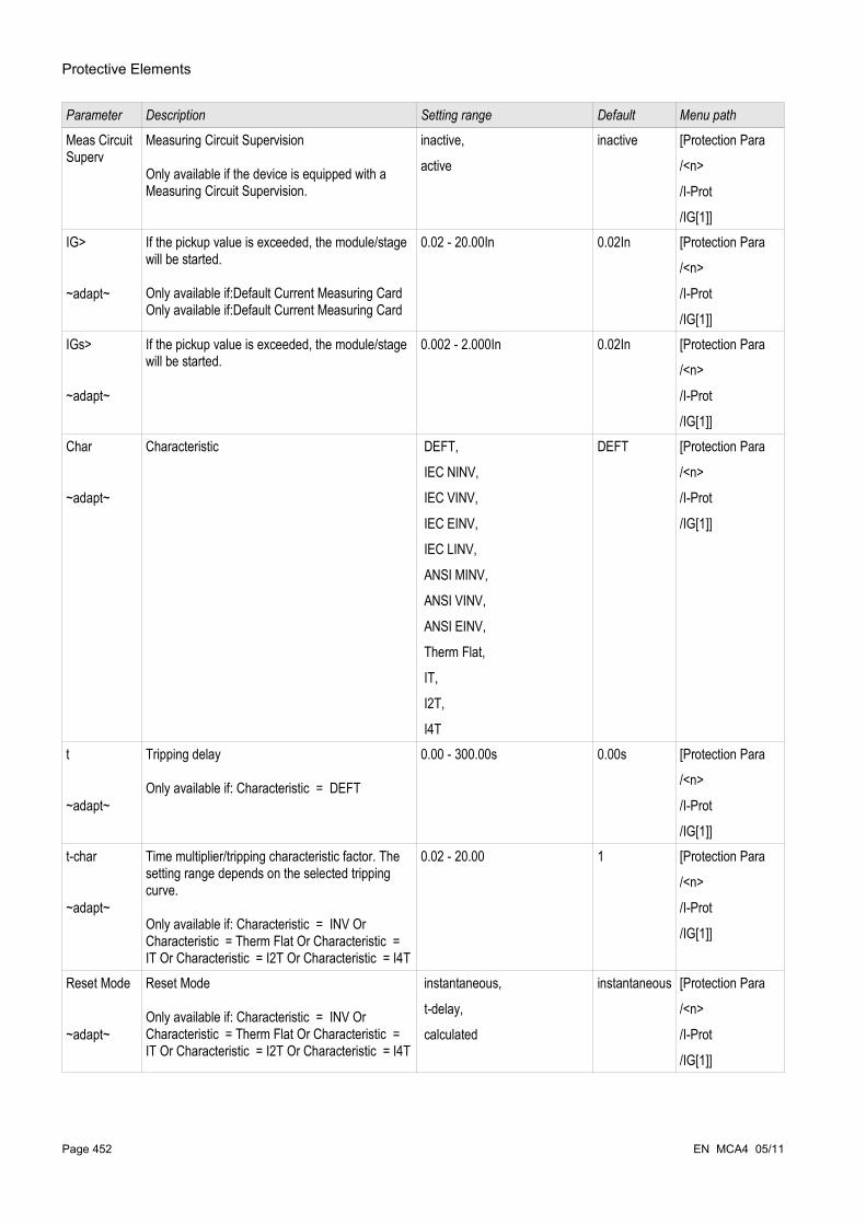
Protective Elements
Parameter Description Setting range Default Menu path
Meas Circuit Superv
Measuring Circuit Supervision
Only available if the device is equipped with a Measuring Circuit Supervision.
inactive,
active
inactive [Protection Para
/<n>
/I-Prot
/IG[1]]IG>
~adapt~
If the pickup value is exceeded, the module/stage will be started.
Only available if:Default Current Measuring Card Only available if:Default Current Measuring Card
0.02 - 20.00In 0.02In [Protection Para
/<n>
/I-Prot
/IG[1]]IGs>
~adapt~
If the pickup value is exceeded, the module/stage will be started.
0.002 - 2.000In 0.02In [Protection Para
/<n>
/I-Prot
/IG[1]]Char
~adapt~
Characteristic DEFT,
IEC NINV,
IEC VINV,
IEC EINV,
IEC LINV,
ANSI MINV,
ANSI VINV,
ANSI EINV,
Therm Flat,
IT,
I2T,
I4T
DEFT [Protection Para
/<n>
/I-Prot
/IG[1]]
t
~adapt~
Tripping delay
Only available if: Characteristic = DEFT
0.00 - 300.00s 0.00s [Protection Para
/<n>
/I-Prot
/IG[1]]t-char
~adapt~
Time multiplier/tripping characteristic factor. The setting range depends on the selected tripping curve.
Only available if: Characteristic = INV Or Characteristic = Therm Flat Or Characteristic = IT Or Characteristic = I2T Or Characteristic = I4T
0.02 - 20.00 1 [Protection Para
/<n>
/I-Prot
/IG[1]]
Reset Mode
~adapt~
Reset Mode
Only available if: Characteristic = INV Or Characteristic = Therm Flat Or Characteristic = IT Or Characteristic = I2T Or Characteristic = I4T
instantaneous,
t-delay,
calculated
instantaneous [Protection Para
/<n>
/I-Prot
/IG[1]]
Page 452 EN MCA4 05/11

Protective Elements
Parameter Description Setting range Default Menu path
t-reset
~adapt~
Reset time for intermittent phase failures (INV characteristics only)
Only available if: Characteristic = INV Or Characteristic = Therm Flat Or Characteristic = IT Or Characteristic = I2T Or Characteristic = I4T Only available if:Reset Mode = t-delay
0.00 - 60.00s 0.00s [Protection Para
/<n>
/I-Prot
/IG[1]]
IH2 Blo
~adapt~
Blocking the trip command, if an inrush is detected.
inactive,
active
inactive [Protection Para
/<n>
/I-Prot
/IG[1]]nondir Trip at VG=0
~adapt~
Only relevant for current protection modules/stages with directional feature! The device will trip non directional if this parameter is set to active and no direction could be determined because no reference voltage (V=0) could be measured any more (e.g. if there is a three-phase short circuit close to the device). If this parameter is set to inactive, the protection stage will be blocked in case of V=0.
Only available if: Device planning: Earth current protection - Stage.Mode = directional
inactive,
active
inactive [Protection Para
/<n>
/I-Prot
/IG[1]]
VX Blo
~adapt~
VX Blo = active means that the IG-stage will only excite if a residual voltage higher than the pickup value is measured at the same time. VX Blo = inactive means that the excitation of the IG stage does not depend on any residual voltage stage.
inactive,
active
inactive [Protection Para
/<n>
/I-Prot
/IG[1]]
VX>
~adapt~
If the pickup value is exceeded, the module/stage will be started.
Only available if: VX Blo = active
0.01 - 1.50Vn 1.00Vn [Protection Para
/<n>
/I-Prot
/IG[1]]
EN MCA4 05/11 Page 453
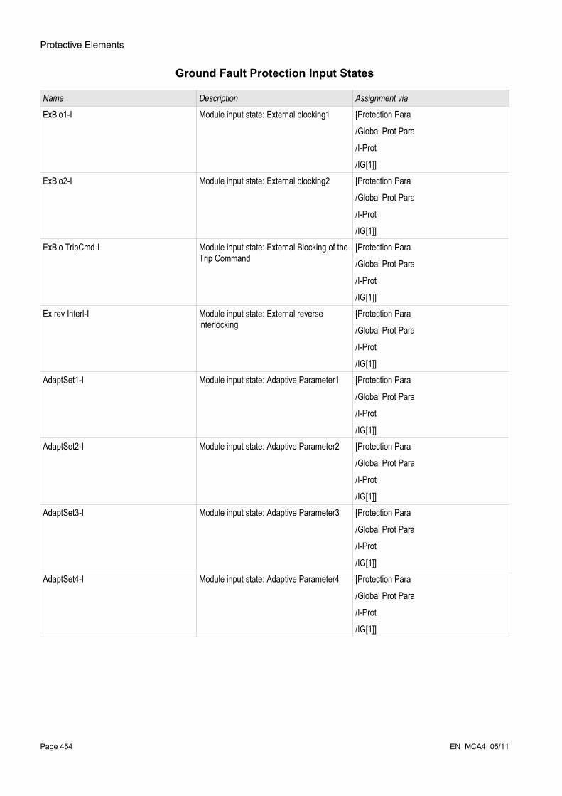
Protective Elements
Ground Fault Protection Input States
Name Description Assignment via
ExBlo1-I Module input state: External blocking1 [Protection Para
/Global Prot Para
/I-Prot
/IG[1]]ExBlo2-I Module input state: External blocking2 [Protection Para
/Global Prot Para
/I-Prot
/IG[1]]ExBlo TripCmd-I Module input state: External Blocking of the
Trip Command[Protection Para
/Global Prot Para
/I-Prot
/IG[1]]Ex rev Interl-I Module input state: External reverse
interlocking[Protection Para
/Global Prot Para
/I-Prot
/IG[1]]AdaptSet1-I Module input state: Adaptive Parameter1 [Protection Para
/Global Prot Para
/I-Prot
/IG[1]]AdaptSet2-I Module input state: Adaptive Parameter2 [Protection Para
/Global Prot Para
/I-Prot
/IG[1]]AdaptSet3-I Module input state: Adaptive Parameter3 [Protection Para
/Global Prot Para
/I-Prot
/IG[1]]AdaptSet4-I Module input state: Adaptive Parameter4 [Protection Para
/Global Prot Para
/I-Prot
/IG[1]]
Page 454 EN MCA4 05/11

Protective Elements
Ground Fault Protection Signals (Output States)
Name Description
active Signal: activeExBlo Signal: External BlockingEx rev Interl Signal: External reverse InterlockingBlo TripCmd Signal: Trip Command blockedExBlo TripCmd Signal: External Blocking of the Trip CommandAlarm Signal: Alarm IGTrip Signal: TripTripCmd Signal: Trip CommandIGH2 Blo Signal: blocked by an inrushActive AdaptSet Active Adaptive ParameterDefaultSet Signal: Default Parameter SetAdaptSet 1 Signal: Adaptive Parameter 1AdaptSet 2 Signal: Adaptive Parameter 2AdaptSet 3 Signal: Adaptive Parameter 3AdaptSet 4 Signal: Adaptive Parameter 4
EN MCA4 05/11 Page 455

Protective Elements
Commissioning: Ground Fault Protection – non-directional [50N/G, 51N/G]
Please test the non-directional earth overcurrent analog to the non-directional phase overcurrent protection.
Commissioning: Ground Fault Protection – directional [50N/G, 51N/G, 67N/G]
Please test the directional earth overcurrent analog to the directional phase overcurrent protection.
Page 456 EN MCA4 05/11

Protective Elements
Commissioning: Undervoltage Protection [27]This test can be carried out similar to the test for overvoltage protection (by using the related undervoltage values).
Please consider the following deviations:
• For testing the threshold values the test voltage has to be decreased until the relay is activated.
• For detection of the fallback value, the measuring quantity has to be increased so to achieve more than 103% of the trip value. At 103% of the trip value the relay is to fall back at the earliest.
EN MCA4 05/11 Page 457

Protective Elements
ThR-Protection Module: Thermal Replica [49] ThR
The maximal permissible thermal loading capacity, and consequently the tripping delay of a component, depends on the amount of the flowing current at a specific time, the »previously existing load (current)« as well as on a constant specified by the component.
The thermal overload protection is in compliance with IEC255-8 (VDE 435 T301). A complete thermal replica function is implemented in the device as Homogeneous-Body Replica of the equipment to be protected and by taking the previously existing load into account. The protection function is of one step design, provided with a warning limit.
For this the device calculates the thermal load of the equipment by using the existing measured values and the parameter settings. When knowing the thermal constants, the temperature of the equipment can be established (simulated).
The general tripping times of the overload protection can be gathered from the following equation according to IEC 255-8:
Legend:
Page 458 EN MCA4 05/11
( )t = t -warm ln I2 - Ip2
I2 - (K*Ib)2
t = Tripping delay
t -cool = Cooling time constant
K =
I = measured current (x In)
Ip = Preload Current
Ib = Base current: Maximum permissible thermal continuous current.
Overload Factor: The maximum thermal limit is defined as k*IB, the product of the overload factor and the basic current.
t -warm = Warming-up time constant

Protective Elements
EN MCA4 05/11 Page 459
ThR
&
ThR
.Trip
Plea
se R
efer
To
Dia
gram
: Blo
ckin
gs
IL1
RM
S
&
IL1
ThR
.Ala
rm
Ple
ase
Ref
er T
o D
iagr
am: T
rip b
lock
ings
(Sta
ge is
not
dea
ctiv
ated
and
no
activ
e bl
ocki
ng s
igna
ls)
(Trip
ping
com
man
d no
t dea
ctiv
ated
or b
lock
ed. )
Alar
m T
heta
IL2
RM
SIL
2
IL3
RM
SIL
3
MAX
ILxR
MS
100%
t-war
mt-
cool
k*Ib
&
nam
e =
ThR
2 3
ThR
.Trip
Cm
d1514

Protective Elements
Direct Commands of the Thermal Overload Module
Parameter Description Setting range Default Menu path
Reset Reset the Thermal Replica inactive,
active
inactive [Operation
/Reset]
Device Planning Parameters of the Thermal Overload Module
Parameter Description Options Default Menu path
Mode Mode do not use,
use
do not use [Device planning]
Page 460 EN MCA4 05/11
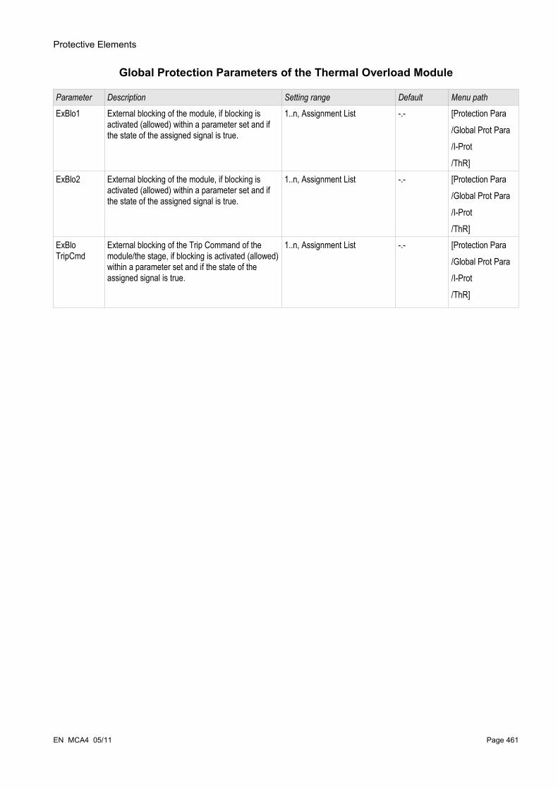
Protective Elements
Global Protection Parameters of the Thermal Overload Module
Parameter Description Setting range Default Menu path
ExBlo1 External blocking of the module, if blocking is activated (allowed) within a parameter set and if the state of the assigned signal is true.
1..n, Assignment List -.- [Protection Para
/Global Prot Para
/I-Prot
/ThR]ExBlo2 External blocking of the module, if blocking is
activated (allowed) within a parameter set and if the state of the assigned signal is true.
1..n, Assignment List -.- [Protection Para
/Global Prot Para
/I-Prot
/ThR]ExBlo TripCmd
External blocking of the Trip Command of the module/the stage, if blocking is activated (allowed) within a parameter set and if the state of the assigned signal is true.
1..n, Assignment List -.- [Protection Para
/Global Prot Para
/I-Prot
/ThR]
EN MCA4 05/11 Page 461

Protective Elements
Setting Group Parameters of the Thermal Overload Module
Parameter Description Setting range Default Menu path
Function Permanent activation or deactivation of module/stage.
inactive,
active
inactive [Protection Para
/<n>
/I-Prot
/ThR]ExBlo Fc Activate (allow) or inactivate (disallow) blocking of
the module/stage. This parameter is only effective if a signal is assigned to the corresponding global protection parameter. If the signal becomes true, those modules/stages are blocked that are parameterized "ExBlo Fc=active".
inactive,
active
inactive [Protection Para
/<n>
/I-Prot
/ThR]
Blo TripCmd Permanent blocking of the Trip Command of the module/stage.
inactive,
active
inactive [Protection Para
/<n>
/I-Prot
/ThR]ExBlo TripCmd Fc
Activate (allow) or inactivate (disallow) blocking of the module/stage. This parameter is only effective if a signal is assigned to the corresponding global protection parameter. If the signal becomes true, those modules/stages are blocked that are parameterized "ExBlo TripCmd Fc=active".
inactive,
active
inactive [Protection Para
/<n>
/I-Prot
/ThR]
Ib Base current: Maximum permissible thermal continuous current.
0.01 - 4.00In 1.00In [Protection Para
/<n>
/I-Prot
/ThR]K Overload Factor: The maximum thermal limit is
defined as k*IB, the product of the overload factor and the basic current.
0.80 - 1.20 1.00 [Protection Para
/<n>
/I-Prot
/ThR]Alarm Theta Pickup value 50 - 100% 80% [Protection Para
/<n>
/I-Prot
/ThR]τ-warm Warming-up time constant 1 - 60000s 10s [Protection Para
/<n>
/I-Prot
/ThR]
Page 462 EN MCA4 05/11

Protective Elements
Parameter Description Setting range Default Menu path
τ-cool Cooling time constant 1 - 60000s 10s [Protection Para
/<n>
/I-Prot
/ThR]
EN MCA4 05/11 Page 463

Protective Elements
Thermal Overload Module Input States
Name Description Assignment via
ExBlo1-I Module input state: External blocking1 [Protection Para
/Global Prot Para
/I-Prot
/ThR]ExBlo2-I Module input state: External blocking2 [Protection Para
/Global Prot Para
/I-Prot
/ThR]ExBlo TripCmd-I Module input state: External Blocking of the
Trip Command[Protection Para
/Global Prot Para
/I-Prot
/ThR]
Signals of the Thermal Overload Signals (Output States)
Name Description
active Signal: activeExBlo Signal: External BlockingBlo TripCmd Signal: Trip Command blockedExBlo TripCmd Signal: External Blocking of the Trip CommandAlarm Signal: Alarm Thermal OverloadTrip Signal: TripTripCmd Signal: Trip CommandRes Thermal Cap Signal: Resetting Thermal Replica
Page 464 EN MCA4 05/11

Protective Elements
Thermal Overload Module Values
Value Description Menu path
Thermal Cap Used Measured value: Thermal Capacity Used [Operation
/Measured values
/ThR]Time To Trip Measured value (calculated/measured):
Remaining time until the thermal overload module will trip
[Operation
/Measured values
/ThR]
Thermal Overload Module Statistics
Value Description Menu path
Thermal Cap max Thermal Capacity maximum value [Operation
/Statistics
/Max
/ThR]Thermal Cap min Thermal Capacity minimum value [Operation
/Statistics
/Min
/ThR]
EN MCA4 05/11 Page 465

Protective Elements
Commissioning: Thermal Replica
Object to be testedProtective function ThR
Necessary means• Three-phase current source• Timer
ProcedureCalculate the tripping time for the current to be constantly impressed by using the formula for the thermal image.
The parameter of the temperature rise of the component »τw« has to be known to guarantee an optimal protection.
Legend:
Testing the threshold valuesApply the current you have based your mathematical calculation on.
Testing the trip delay
The thermal capacity should be zero before the test is started. See »Measuring Values«.
For testing the trip delay, a timer is to be connected to the contact of the associated trip relay. Apply the current you have based your mathematical calculation on. The timer is started as soon as the current is applied and it is stopped when the relay trips.
Successful test resultThe calculated tripping time and the fallback ratio comply with the measured values. For permissible deviations/tolerances, please see Technical Data.
Page 466 EN MCA4 05/11
( )t = t -warm ln I2 - Ip2
I2 - (K*Ib)2
t = Tripping delay
t -cool = Cooling time constant
K =
I = measured current (x In)
Ip = Preload Current
Ib = Base current: Maximum permissible thermal continuous current.
Overload Factor: The maximum thermal limit is defined as k*IB, the product of the overload factor and the basic current.
t -warm = Warming-up time constant

Protective Elements
%I2/I1> - Unbalanced Load [46]Elements: I2>[1] ,I2>[2]
The I2> Current Unbalance element works similar to the V 012 Voltage Unbalance element. The positive and negative sequence currents are calculated from the 3-phase currents. The Threshold setting defines a minimum operating current magnitude of I2 for the 46 function to operate, which insures that the relay has a solid basis for initiating a current unbalance trip. The »%(I2/I1)« setting is the unbalance trip pickup setting. It is defined by the ratio of negative sequence current to positive sequence current »%(I2/I1)«.
This function requires positive or negative sequence current magnitude above the threshold setting and the percentage current unbalance above the »%(I2/I1)« setting before allowing a current unbalance trip. Therefore, both the threshold and percent settings must be met for the specified Delay time setting before the relay initiates a trip for current unbalance.
All elements are identically structured.
EN MCA4 05/11 Page 467
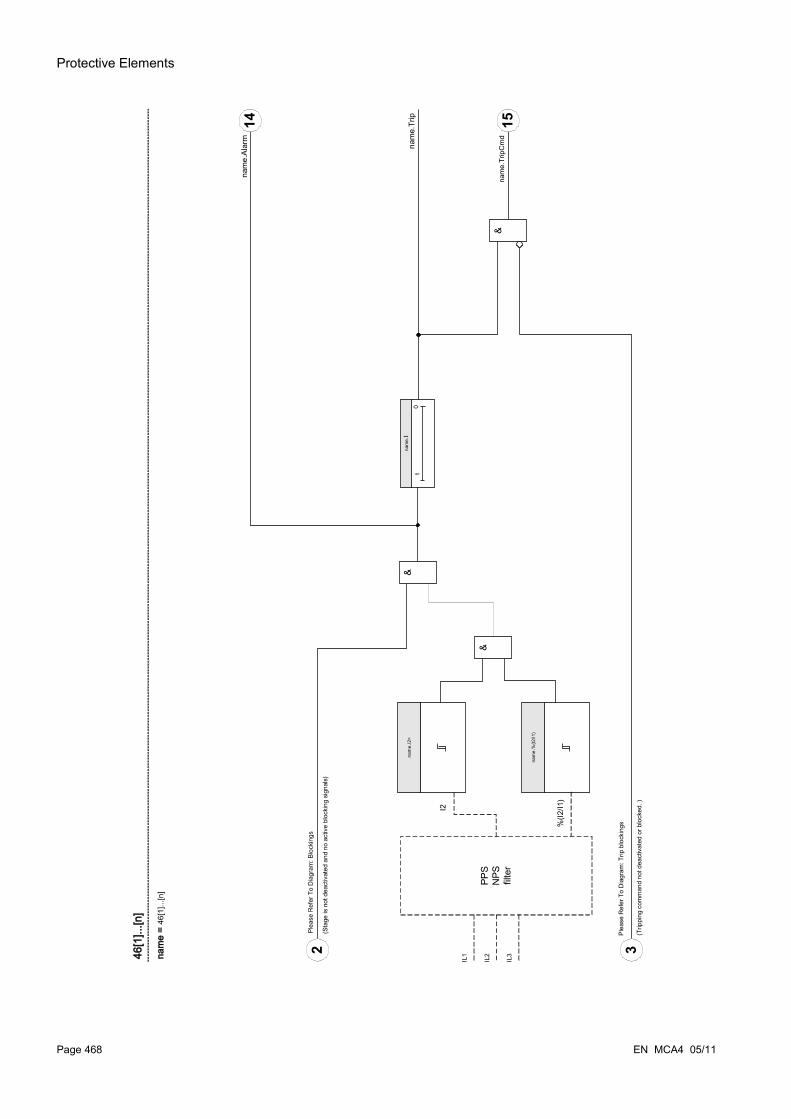
Protective Elements
Page 468 EN MCA4 05/11
nam
e.Tr
ipC
md
nam
e.Tr
ip
Ple
ase
Ref
er T
o D
iagr
am: B
lock
ings
IL1
nam
e.Al
arm
Ple
ase
Ref
er T
o D
iagr
am: T
rip b
lock
ings
46[1
]...[n
]
(Sta
ge is
not
dea
ctiv
ated
and
no
activ
e bl
ocki
ng s
igna
ls)
(Trip
ping
com
man
d no
t dea
ctiv
ated
or b
lock
ed. )
IL3
IL2na
me
= 46
[1]..
.[n]
2 3
1514
PPS
NPS filte
r
nam
e.%(I2
/I1)
nam
e.I2>
I2
%(I2
/I1)
&
&
&
tna
me.
t0

Protective Elements
Device Planning Parameters of the Current Unbalance Module
Parameter Description Options Default Menu path
Mode Mode do not use,
use
do not use [Device planning]
Global Protection Parameters of the Current Unbalance Module
Parameter Description Setting range Default Menu path
ExBlo1 External blocking of the module, if blocking is activated (allowed) within a parameter set and if the state of the assigned signal is true.
1..n, Assignment List -.- [Protection Para
/Global Prot Para
/I-Prot
/I2>[1]]ExBlo2 External blocking of the module, if blocking is
activated (allowed) within a parameter set and if the state of the assigned signal is true.
1..n, Assignment List -.- [Protection Para
/Global Prot Para
/I-Prot
/I2>[1]]ExBlo TripCmd
External blocking of the Trip Command of the module/the stage, if blocking is activated (allowed) within a parameter set and if the state of the assigned signal is true.
1..n, Assignment List -.- [Protection Para
/Global Prot Para
/I-Prot
/I2>[1]]
EN MCA4 05/11 Page 469
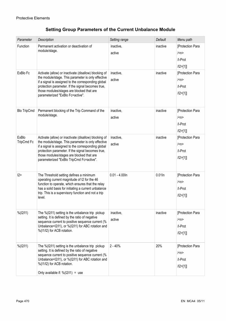
Protective Elements
Setting Group Parameters of the Current Unbalance Module
Parameter Description Setting range Default Menu path
Function Permanent activation or deactivation of module/stage.
inactive,
active
inactive [Protection Para
/<n>
/I-Prot
/I2>[1]]ExBlo Fc Activate (allow) or inactivate (disallow) blocking of
the module/stage. This parameter is only effective if a signal is assigned to the corresponding global protection parameter. If the signal becomes true, those modules/stages are blocked that are parameterized "ExBlo Fc=active".
inactive,
active
inactive [Protection Para
/<n>
/I-Prot
/I2>[1]]
Blo TripCmd Permanent blocking of the Trip Command of the module/stage.
inactive,
active
inactive [Protection Para
/<n>
/I-Prot
/I2>[1]]ExBlo TripCmd Fc
Activate (allow) or inactivate (disallow) blocking of the module/stage. This parameter is only effective if a signal is assigned to the corresponding global protection parameter. If the signal becomes true, those modules/stages are blocked that are parameterized "ExBlo TripCmd Fc=active".
inactive,
active
inactive [Protection Para
/<n>
/I-Prot
/I2>[1]]
I2> The Threshold setting defines a minimum operating current magnitude of I2 for the 46 function to operate, which ensures that the relay has a solid basis for initiating a current unbalance trip. This is a supervisory function and not a trip level.
0.01 - 4.00In 0.01In [Protection Para
/<n>
/I-Prot
/I2>[1]]
%(I2/I1) The %(I2/I1) setting is the unbalance trip pickup setting. It is defined by the ratio of negative sequence current to positive sequence current (% Unbalance=I2/I1), or %(I2/I1) for ABC rotation and %(I1/I2) for ACB rotation.
inactive,
active
inactive [Protection Para
/<n>
/I-Prot
/I2>[1]]
%(I2/I1) The %(I2/I1) setting is the unbalance trip pickup setting. It is defined by the ratio of negative sequence current to positive sequence current (% Unbalance=I2/I1), or %(I2/I1) for ABC rotation and %(I1/I2) for ACB rotation.
Only available if: %(I2/I1) = use
2 - 40% 20% [Protection Para
/<n>
/I-Prot
/I2>[1]]
Page 470 EN MCA4 05/11

Protective Elements
Parameter Description Setting range Default Menu path
Char Characteristic DEFT,
INV
DEFT [Protection Para
/<n>
/I-Prot
/I2>[1]]t Tripping delay
Only available if: Characteristic = DEFT
0.00 - 300.00s 0.00s [Protection Para
/<n>
/I-Prot
/I2>[1]]K Indicates the thermal load capability of the engine
while running with 100% unbalanced load current.
Only available if: Characteristic = INV
1.0 - 200.0 10.0 [Protection Para
/<n>
/I-Prot
/I2>[1]]τ-cool If the unbalanced load current falls below the
pickup value, the cooling-off time is taken into account. If the unbalanced load exceeds the pickup value again, than the saved heat within the electrical equipment will lead to an accelerated trip.
Only available if: Characteristic = INV
0.0 - 60000.0 0.0 [Protection Para
/<n>
/I-Prot
/I2>[1]]
EN MCA4 05/11 Page 471
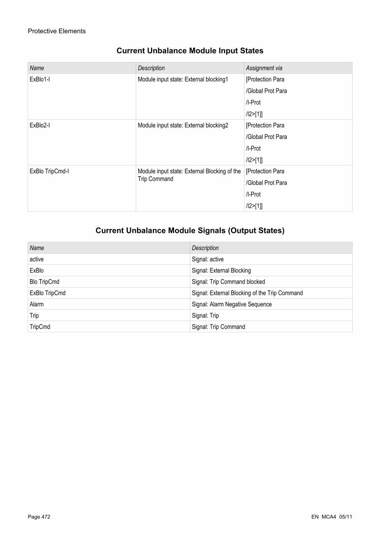
Protective Elements
Current Unbalance Module Input States
Name Description Assignment via
ExBlo1-I Module input state: External blocking1 [Protection Para
/Global Prot Para
/I-Prot
/I2>[1]]ExBlo2-I Module input state: External blocking2 [Protection Para
/Global Prot Para
/I-Prot
/I2>[1]]ExBlo TripCmd-I Module input state: External Blocking of the
Trip Command[Protection Para
/Global Prot Para
/I-Prot
/I2>[1]]
Current Unbalance Module Signals (Output States)
Name Description
active Signal: activeExBlo Signal: External BlockingBlo TripCmd Signal: Trip Command blockedExBlo TripCmd Signal: External Blocking of the Trip CommandAlarm Signal: Alarm Negative SequenceTrip Signal: TripTripCmd Signal: Trip Command
Page 472 EN MCA4 05/11
Protective Elements
Commissioning: Current Unbalance Module
Object to be tested:Test of the unbalanced load protection function.
Necessary means:• Three-phase current source with adjustable current unbalance; and• Timer.
Procedure:
Check the phase sequence:
• Ensure that the phase sequence is the same as that set in the field parameters.
• Feed-in a three-phase nominal current.
• Change to the »Measuring Values« menu.
• Check the measuring value for the unbalanced current »I2«. The measuring value displayed for »I2« should be zero (within the physical measuring accuracy).
If the displayed magnitude for I2 is the same as that for the symmetrical nominal currents fed to the relay, it implies that the phase sequence of the currents seen by the relay is reversed.
• Now turn-off phase L1.
• Again check the measuring value of the unbalanced current »I2« in the »Measuring Values« menu.The measuring value of the asymmetrical current »I2« should now be 33%.
• Turn-on phase L1, but turn-off phase L2.
• Once again check the measuring value of the asymmetrical current I2 in the »Measuring Values« menu.The measuring value of the asymmetrical current »I2« should be again 33%.
• Turn-on phase L2, but turn-off phase L3.
• Again check the measuring value of asymmetrical current »I2« in the »Measuring Values« menu.The measuring value of the asymmetrical current »I2« should still be 33%.
Testing the trip delay:
• Apply a symmetrical three-phase current system (nominal currents).
• Switch off IL1 (the threshold value »Threshold« for »I2« must be below 33%).
• Measure the tripping time.
The present current unbalance »I2« corresponds with 1/3 of the existing phase current displayed.
EN MCA4 05/11 Page 473
Protective Elements
Testing the threshold values
• Configure minimum »%I2/I1« setting (2%) and an arbitrary threshold value »Threshold« (I2).
• For testing the threshold value, a current has to be fed to phase A which is lower than three times the adjusted threshold value »Threshold« (I2).
• Feeding only phase A results in »%I2/I1 = 100%«, so the first condition »%I2/I1 >= 2%« is always fulfilled.
• Now increase the phase L1 current until the relay is activated.
Testing the dropout ratio of the threshold values
Having tripped the relay in the previous test, now decrease the phase A current. The dropout ratio must not be higher than 0.97 times the threshold value.
Testing %I2/I1
• Configure minimum threshold value »Threshold« (I2) (0.01 x In) and set »%I2/I1« greater or equal to 10%.
• Apply a symmetrical three-phase current system (nominal currents). The measuring value of »%I2/I1« should be 0%.
• Now increase the phase L1 current. With this configuration, the threshold value »Threshold« (I2) should be reached before the value »%I2/I1« reaches the set »%I2/I1« ratio threshold.
• Continue increasing the phase 1 current until the relay is activated.
Testing the dropout ratio of %I2/I1
Having tripped the relay in the previous test, now decrease the phase L1 current. The dropout of »%I2/I1« has to be 1% below the »%I2/I1«setting.
Successful test result:
The measured trip delays, threshold values, and dropout ratios are within the permitted deviations/tolerances, specified under Technical Data.
Page 474 EN MCA4 05/11

Protective Elements
SOTF - Switch Onto Fault SOTF
In case a faulty line is energized (e.g.: when an earthing switch is in the ON-Position), an instantaneous trip is required. The SOTF module is provided to generate a permissive signal for other protection functions such as overcurrents to accelerate their trips (via adaptive parameters). The SOTF condition is recognized according to the User’s operation mode that can be based on:
• The breaker state (CB Pos);• No current flowing (I<);• Breaker state and no current flowing( CB Pos and I<);• Breaker switched on manually (CB manually On); and/or• An external trigger (Ex SOTF).
This protection module can initiate a high speed trip of the overcurrent protection modules.
This module issues a signal only (the module is not armed and does not issue a trip command).
In order to influence the trip settings of the overcurrent protection in case of switching onto a fault, the User has to assign the signal “SOTF.ENABLED“ onto an Adaptive Parameter Set. Please refer to Parameter / Adaptive Parameter Sets sections. Within the Adaptive Parameter Set, the User has to modify the trip characteristic of the overcurrent protection according to the User's needs.
EN MCA4 05/11 Page 475

Protective Elements
Page 476 EN MCA4 05/11
Ple
ase
Ref
er T
o D
iagr
am: B
lock
ings
(Sta
ge is
not
dea
ctiv
ated
and
no
activ
e bl
ocki
ng s
igna
ls)
nam
e =
SOTF
2
SOTF
.ena
bled
SOTF
.I<IL
1IL
2IL
3SOTF
.CB[
x].P
os O
FF**
SOTF
.I<
SOTF
.AR
Blo
*AR
.runn
ing*
SO
TF.
t-en
able
tT
SOTF
.Ext
SO
TF
SOTF
I<C
B Po
s An
d I<
SOTF
.Mod
e
CB
Pos
CB
man
ual O
NEx
t SO
TF
*App
lies
only
for d
evic
es w
ith A
uto
Rec
losu
re
SOTF
.CB[
x].M
anua
l ON
**
0
>1>1
&
&&
**Th
is s
igna
l is
the
outp
ut o
f the
sw
itchg
ear t
hat i
s as
sign
ed to
this
pro
tect
ive
elem
ent.
This
app
lies
to p
rote
ctiv
e de
vice
s th
at o
ffer c
ontro
l fun
ctio
nalit
y.

Protective Elements
Device Planning Parameters of the Switch Onto Fault Module
Parameter Description Options Default Menu path
Mode Mode do not use,
use
do not use [Device planning]
Global Protection Parameters of the Switch Onto Fault Module
Parameter Description Setting range Default Menu path
Mode Mode CB Pos,
I<,
CB Pos And I<,
CB manual ON,
Ext SOTF
CB Pos [Protection Para
/Global Prot Para
/SOTF]
ExBlo1 External blocking of the module, if blocking is activated (allowed) within a parameter set and if the state of the assigned signal is true.
1..n, Assignment List -.- [Protection Para
/Global Prot Para
/SOTF]
ExBlo2 External blocking of the module, if blocking is activated (allowed) within a parameter set and if the state of the assigned signal is true.
1..n, Assignment List -.- [Protection Para
/Global Prot Para
/SOTF]
Ex rev Interl External blocking of the module by external reverse interlocking, if blocking is activated (allowed) within a parameter set and if the state of the assigned signal is true.
1..n, Assignment List -.- [Protection Para
/Global Prot Para
/SOTF]
Assigned SG Assigned Switchgear
Only available if: Mode = CB Pos Or CB Pos And I<
-,
SG[1],
SG[2],
SG[3],
SG[4],
SG[5],
SG[6]
SG[1] [Protection Para
/Global Prot Para
/SOTF]
Ext SOTF External Switch Onto Fault
Only available if: Mode = Ext SOTF
1..n, DI-LogicList -.- [Protection Para
/Global Prot Para
/SOTF]
EN MCA4 05/11 Page 477

Protective Elements
Setting Group Parameters of the Switch Onto Fault Module
Parameter Description Setting range Default Menu path
Function Permanent activation or deactivation of module/stage.
inactive,
active
inactive [Protection Para
/<n>
/SOTF]ExBlo Fc Activate (allow) or inactivate (disallow) blocking of
the module/stage. This parameter is only effective if a signal is assigned to the corresponding global protection parameter. If the signal becomes true, those modules/stages are blocked that are parameterized "ExBlo Fc=active".
inactive,
active
inactive [Protection Para
/<n>
/SOTF]
Ex rev Interl Fc
Activate (allow) or inactivate (disallow) blocking of the module/stage. This parameter is only effective if a signal is assigned to the corresponding global protection parameter. If the signal becomes true, those modules/stages are blocked that are parameterized "Ex rev Interl Fc = active".
inactive,
active
inactive [Protection Para
/<n>
/SOTF]
I< The CB is in the OFF Position, if the measured current is less than this parameter.
0.01 - 1.00In 0.01In [Protection Para
/<n>
/SOTF]t-enable While this timer is running, and while the module
is not blocked, the Switch Onto Fault Module is effective (SOTF is armed).
0.10 - 10.00s 2s [Protection Para
/<n>
/SOTF]
Page 478 EN MCA4 05/11

Protective Elements
Switch Onto Fault Module Input States
Name Description Assignment via
ExBlo1-I Module input state: External blocking [Protection Para
/Global Prot Para
/SOTF]ExBlo2-I Module input state: External blocking [Protection Para
/Global Prot Para
/SOTF]Ex rev Interl-I Module input state: External reverse
interlocking[Protection Para
/Global Prot Para
/SOTF]Ext SOTF-I Module input state: External Switch Onto
Fault Alarm[Protection Para
/Global Prot Para
/SOTF]
Signals of the Switch Onto Fault Module (Output States)
Name Description
active Signal: activeExBlo Signal: External BlockingEx rev Interl Signal: External reverse Interlockingenabled Signal: Switch Onto Fault enabled. This Signal can be used to
modify Overcurrent Protection Settings.AR Blo Signal: Blocked by ARI< Signal: No Load Current.
EN MCA4 05/11 Page 479

Protective Elements
Commissioning: Switch Onto Fault
Object to be tested
Testing the module Switch Onto Fault according to the parameterized operating mode:
• The breaker state (CB Pos);• No current flowing (I<);• Breaker state and no current flowing( CB Pos and I<);• Breaker switched on manually (CB manually On); and/or• An external trigger (Ex SOTF).
Necessary means:
• Three-phase current source (If the Enable-Mode depends on current);
• Ampere meters (May be needed if the Enable-Mode depends on current); and
• Timer.
Test Example for Mode CB manual ON
Mode I<: In order to test the effectiveness: Initially do not feed any current. Start the timer and feed with an abrupt change current that is distinctly greater than the I<-threshold to the measuring inputs of the relay.
Mode I< and Bkr state: Simultaneous switch on the breaker manually and feed with an abrupt change current that is distinctly greater than the I<-threshold.
Mode Bkr state: The breaker has to be in the OFF Position. The signal „SOTF.ENABLED“=0 is untrue. If the breaker is switched on, the signal „SOTF.ENABLED“=1 becomes true as long as the timer t-enabled is running.
• The Circuit Breaker has to be in the OFF Position. There must be no load current.
• The Status Display of the device shows the signal „SOTF.ENABLED“=1.
Testing
• Switch the Circuit Breaker manually ON and start the timer at the same time.
• After the hold time t-enable is expired the state of the signal has to change to „SOTF.ENABLED“=0.
• Write down the measured time.
Successful test result The measured total tripping delays or individual tripping delays, threshold values and fallback ratios correspond with those values, specified in the adjustment list. Permissible deviations/tolerances can be found under Tech-nical Data.
Page 480 EN MCA4 05/11

Protective Elements
CLPU - Cold Load PickupAvailable Elements: CLPU
When the electric load is freshly started or restarted after a prolonged outage, the load current tends to have a temporary surge that could be several times the normal load current in magnitude due to motor starting. This phenomena is called cold load inrush. If the overcurrent pickup threshold is set according to the maximum possible load inrush, the overcurrent protection may be insensitive to some faults, thus making whole protection systems coordination difficult or even impossible. On the other hand, the overcurrent protection could trip on load inrush if it is set based on the fault current studies. The CLPU module is provided to generate a temporary blocking/desensitizing signal to prevent overcurrent protections from unwanted tripping. The cold load pickup function detects a warm-to-cold load transition according to the four selectable cold load detection modes:
• CB POS (Breaker state);• I< (Undercurrent);• CB POS AND I< (Breaker state and undercurrent); and• CB POS OR I< (Breaker state OR undercurrent).
After a warm-to-cold load transition has been detected, a specified load-off timer will be started. This User-settable load-off timer is used in some cases to make sure that the load is really “cold” enough. After the load-off timer times out, the CLPU function issues an “enable” signal »CLPU.ENABLED« that can be used to block some sensitive protection elements like instantaneous overcurrent elements, current unbalance, or power protection elements at User´s choice. Using this enable signal, some time inverse overcurrent elements may also be desensitized at the User's choice by means of activating adaptive settings of the corresponding overcurrent elements.
When a cold load condition is finished (a cold-to-warm load condition is detected) due to, for example, breaker closing or load current injection, a load inrush detector will be initiated that supervises the coming and going of the load inrush current process. A load inrush is detected if the coming load current exceeds a User-specified inrush current threshold. This load inrush is considered as finished if the load current is decreased to 90% of the inrush current threshold. After the inrush current is diminished, a settle timer starts. The cold load pickup enable signal can only be reset after the settle timer times out. Another max-Block timer, which is started parallel with the load inrush detector after a cold load condition is finished, may also terminate the CLPU enable signal if a load inrush condition is prolonged abnormally.
The cold load pickup function can be blocked manually by external or internal signal at the User´s choice. For the devices with Auto-Reclosing function, the CLPU function will be blocked automatically if auto-reclosure is initiated (AR is running).
EN MCA4 05/11 Page 481
Protective Elements
This module issues a signal only (it is not armed).
In order to influence the tripping settings of the overcurrent protection, the User has to assign the signal “CLPU.ENABLED“ to an adaptive parameter set. Please refer to the Parameter / Adaptive Parameter Sets section. Within the adaptive parameter set, the User has to modify the tripping characteristic of the overcurrent protection according to the needs.
Please be aware of the meaning of the two delay timers.
t load Off (Pickup Delay): After this time expires, the load is no longer diversified.
t Max Block (Release Delay): After the starting condition is fulfilled (e.g.: breaker switched on manually), the “CLPU.enabled” signal will be issued for this time. That means for the duration of this time, the tripping thresholds of the overcurrent protection can be desensitized by means of adaptive parameters (please refer to the Parameters section). This timer will be stopped if the current falls below 0.9 times of the threshold of the load inrush detector and remains below 0.9 times of the threshold for the duration of the settle time.
This Notice applies to protective devices that offer control functionality only! This protective element requires, that a switchgear (circuit breaker is assigned to it. It is allowed only to assign switchgears (circuit breaker) to this protective element, whose measuring transformers provide measuring data to the protective device.
Page 482 EN MCA4 05/11

Protective Elements
EN MCA4 05/11 Page 483
Ple
ase
Ref
er T
o D
iagr
am: B
lock
ings
(Sta
ge is
not
dea
ctiv
ated
and
no
activ
e bl
ocki
ng s
igna
ls)
nam
e =
CLP
U
2
CLP
U.e
nabl
ed
CLP
U.I<
IL1
IL2
IL3
CLP
U.I<
AR.ru
nnin
g*
CLP
U
I<C
B Po
s An
d I<
CLP
U.M
ode
CB
Pos
CB
Pos
Or I
<
CB[
x].P
os O
FF**
*App
lies
only
for d
evic
es w
ith A
uto
Rec
losu
reC
LPU
.Loa
d In
rush
CLP
U.S
ettle
Tim
e
ILx
max
1.0
* Thr
esho
ld
0.9
* Thr
esho
ld
S
Q
R
CLP
U.d
etec
ted
1.0
* Thr
esho
ld
0.9
* Thr
esho
ld
Load
Inru
sh D
etec
tor
&
&&
&
>1
>1
>1
Settl
e Ti
me
Del
ay T
imer
0
t-Loa
d O
ff
Del
ay T
imer
0
0
Del
ay T
imer
t-Max
Blo
ck
0
Del
ay T
imer S
ettle
Tim
e+e
**Th
is s
igna
l is
the
outp
ut o
f the
sw
itchg
ear t
hat i
s as
sign
ed to
this
pro
tect
ive
elem
ent.
This
app
lies
to p
rote
ctiv
e de
vice
s th
at o
ffer c
ontro
l fun
ctio
nalit
y.
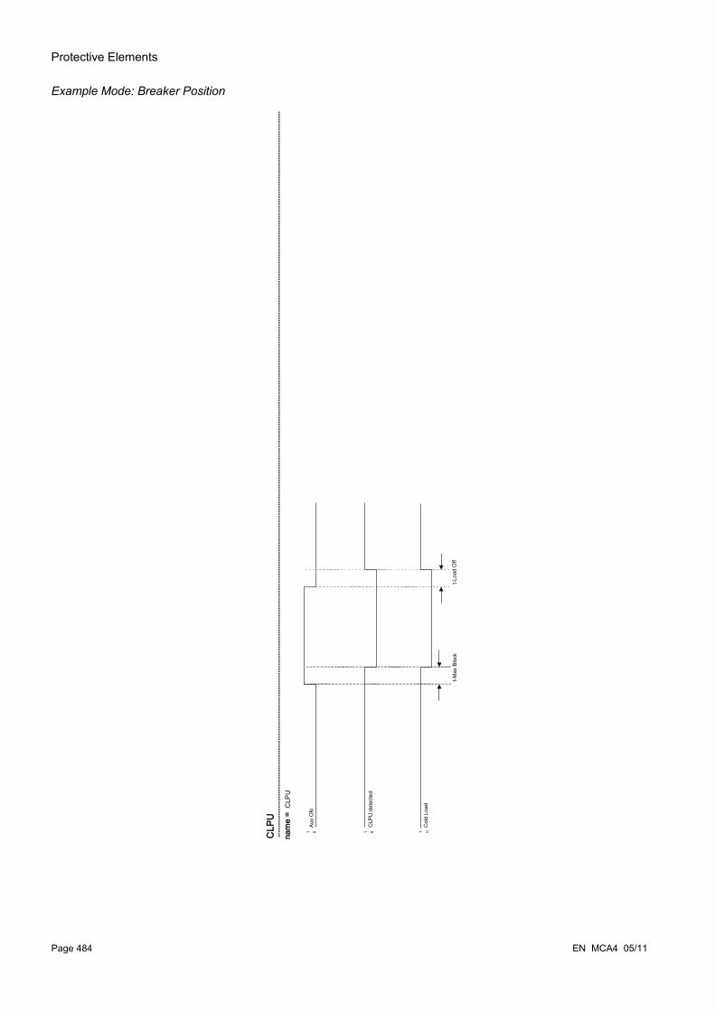
Protective Elements
Example Mode: Breaker Position
Page 484 EN MCA4 05/11
nam
e =
CLP
U
CLP
U
Aux
ON
0101
CLP
U.d
etec
ted
t-Loa
d O
fft-M
ax B
lock
Col
d Lo
ad01
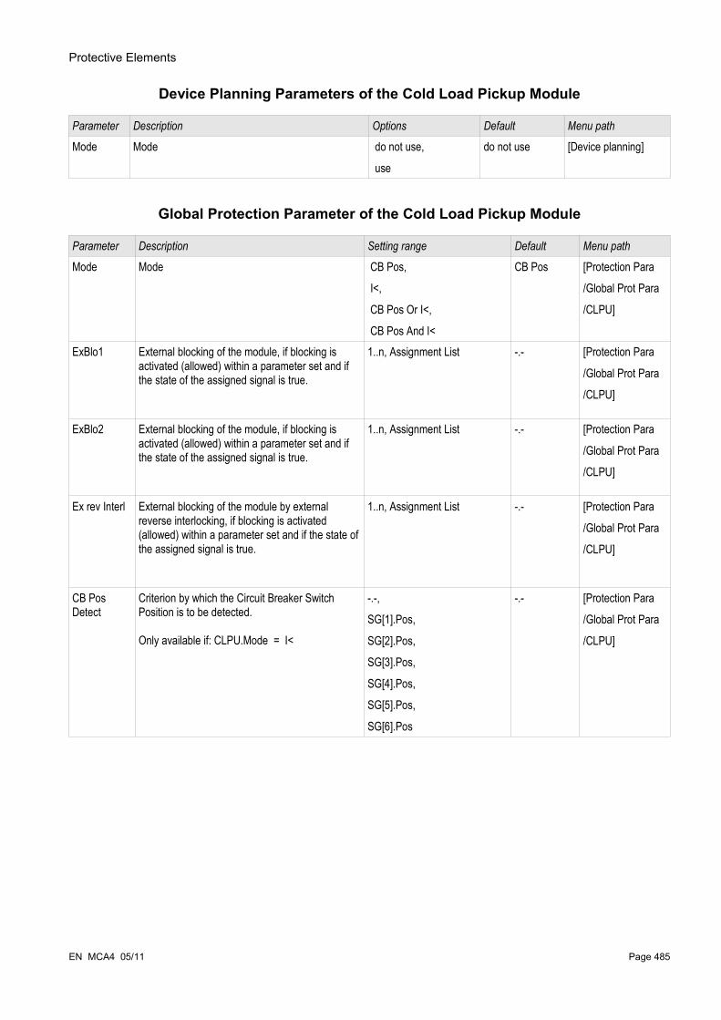
Protective Elements
Device Planning Parameters of the Cold Load Pickup Module
Parameter Description Options Default Menu path
Mode Mode do not use,
use
do not use [Device planning]
Global Protection Parameter of the Cold Load Pickup Module
Parameter Description Setting range Default Menu path
Mode Mode CB Pos,
I<,
CB Pos Or I<,
CB Pos And I<
CB Pos [Protection Para
/Global Prot Para
/CLPU]
ExBlo1 External blocking of the module, if blocking is activated (allowed) within a parameter set and if the state of the assigned signal is true.
1..n, Assignment List -.- [Protection Para
/Global Prot Para
/CLPU]
ExBlo2 External blocking of the module, if blocking is activated (allowed) within a parameter set and if the state of the assigned signal is true.
1..n, Assignment List -.- [Protection Para
/Global Prot Para
/CLPU]
Ex rev Interl External blocking of the module by external reverse interlocking, if blocking is activated (allowed) within a parameter set and if the state of the assigned signal is true.
1..n, Assignment List -.- [Protection Para
/Global Prot Para
/CLPU]
CB Pos Detect
Criterion by which the Circuit Breaker Switch Position is to be detected.
Only available if: CLPU.Mode = I<
-.-,
SG[1].Pos,
SG[2].Pos,
SG[3].Pos,
SG[4].Pos,
SG[5].Pos,
SG[6].Pos
-.- [Protection Para
/Global Prot Para
/CLPU]
EN MCA4 05/11 Page 485

Protective Elements
Set Parameters of the Cold Load Pickup Module
Parameter Description Setting range Default Menu path
Function Permanent activation or deactivation of module/stage.
inactive,
active
inactive [Protection Para
/<n>
/CLPU]ExBlo Fc Activate (allow) or inactivate (disallow) blocking of
the module/stage. This parameter is only effective if a signal is assigned to the corresponding global protection parameter. If the signal becomes true, those modules/stages are blocked that are parameterized "ExBlo Fc=active".
inactive,
active
inactive [Protection Para
/<n>
/CLPU]
Ex rev Interl Fc
Activate (allow) or inactivate (disallow) blocking of the module/stage. This parameter is only effective if a signal is assigned to the corresponding global protection parameter. If the signal becomes true, those modules/stages are blocked that are parameterized "Ex rev Interl Fc = active".
inactive,
active
inactive [Protection Para
/<n>
/CLPU]
t-Load Off Select the outage time required for a load to be considered cold. If the Pickup Timer (Delay) has run out, a Cold Load Signal will be issued.
0.00 - 7200.00s 1.00s [Protection Para
/<n>
/CLPU]
t-Max Block Select the amount of time for the cold load inrush. If the Release Time (Delay) has run out, a Warm Load Signal will be issued.
0.00 - 300.00s 1.00s [Protection Para
/<n>
/CLPU]
I< The CB is in the OFF Position, if the measured current is less than this parameter.
0.01 - 1.00In 0.01In [Protection Para
/<n>
/CLPU]Threshold Set the load current inrush threshold. 0.10 - 4.00In 1.2In [Protection Para
/<n>
/CLPU]Settle Time Select the time for the cold load inrush 0.00 - 300.00s 1.00s [Protection Para
/<n>
/CLPU]
Page 486 EN MCA4 05/11

Protective Elements
States of the Inputs of the Cold Load Pickup Module
Name Description Assignment via
ExBlo1-I Module input state: External blocking [Protection Para
/Global Prot Para
/CLPU]ExBlo2-I Module input state: External blocking [Protection Para
/Global Prot Para
/CLPU]Ex rev Interl-I Module input state: External reverse
interlocking[Protection Para
/Global Prot Para
/CLPU]CB Pos-I Module input state: Circuit Breaker Position
by now (switching position).[Protection Para
/Global Prot Para
/CLPU]
Signals of the Cold Load Pickup Module (States of the Outputs)
Name Description
active Signal: activeExBlo Signal: External BlockingEx rev Interl Signal: External reverse Interlockingenabled Signal: Cold Load enableddetected Signal: Cold Load detectedAR Blo Module input state: AR BloI< Signal: No Load Current.Load Inrush Signal: Load InrushSettle Time Signal: Settle Time
EN MCA4 05/11 Page 487

Protective Elements
Commissioning of the Cold Load Pickup Module
Object to be tested:
Testing the Cold Load Pickup module according to the configured operating mode:
•I< (No current);•Bkr state (Breaker position);•I< (No Current) and Bkr state (Breaker position); and•I< (No Current) or Bkr state (Breaker position).
Necessary means:
•Three-phase current source (if the Enable Mode depends on current);•Ampere meters (may be needed if the Enable Mode depends on current); and•Timer.
Test Example for Mode Bkr State (Breaker Position)
Mode I<: In order to test the tripping delay, start the timer and feed with an abrupt change current that is distinctly less than the I<-threshold. Measure the tripping delay. In order to measure the drop-out ratio, feed a current with an abrupt change that is distinctly above the I<-threshold.
Mode I< and Bkr state: Combine the abrupt change (switching the current ON and OFF) with the manual switching ON and OFF of the breaker.
Mode I< or Bkr state: Initially carry out the test with an abrupt changing current that is switched ON and OFF (above and below the I<-threshold). Measure the tripping times. Finally, carry out the test by manually switching the breaker ON and OFF.
•The breaker has to be in the OFF position. There must not be any load current.
•The Status Display of the device shows the signal "CLPU.ENABLED“=1.
•The Status Display of the device shows the signal ”CLPU.I<“=1.•
•Testing the tripping delay and the resetting ratio:
•Switch the breaker manually ON and simultaneously start the timer.
•After the the »t Max Block (Release Delay)« timer has expired, the signal "CPLU.Enabled “=0 has to become untrue.
•Write down the measured time.
•Manually switch the breaker OFF and simultaneously start the timer.
•After the »t load Off« timer has expired, the signal ”CPLU.ENABLED “=1 has to become true.
•Write down the measured time.
Page 488 EN MCA4 05/11

Protective Elements
Successful test result:
The measured total tripping delays or individual tripping delays, threshold values, and drop-out ratios correspond with those values specified in the adjustment list. Permissible deviations/tolerances can be found in the Tech-nical Data section.
EN MCA4 05/11 Page 489

Protective Elements
IH2 - InrushAvailable elements: IH2
The inrush module can prevent false trips caused by switching actions of saturated inductive loads. The ratio of the 2nd harmonic to the 1st harmonic is taken into account.
Page 490 EN MCA4 05/11
&
1-ph
Blo
Inru
sh.b
lock
mod
e
3-ph
Blo
Inru
sh. I
H2
/ IH
1
IL1 IL2
IL3
& & &
Inru
sh.a
ctiv
e
IH2.
Blo
L2
IH2.
Blo
L3
IH2.
Blo
L1
IH2
IH1
IH2
IH1
IH2
IH1
IH2
IH1
IH2
IH1
IH2
IH2
IH1
IGIG
H1
IGH
2IG
H1
IGH
2
&IH
2.Bl
o IG
IH2.
3-ph
Blo
4
5 6 7 8
Ple
ase
Ref
er T
o D
iagr
am: B
lock
ings
>1
>1 >1 >1
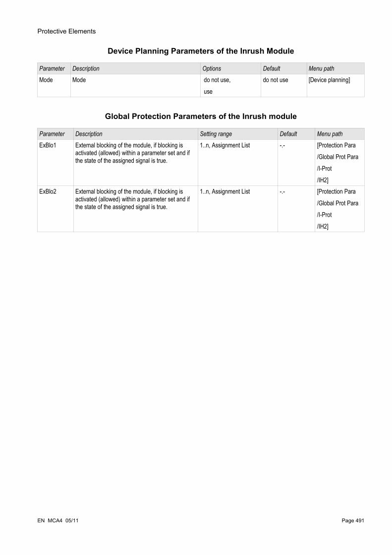
Protective Elements
Device Planning Parameters of the Inrush Module
Parameter Description Options Default Menu path
Mode Mode do not use,
use
do not use [Device planning]
Global Protection Parameters of the Inrush module
Parameter Description Setting range Default Menu path
ExBlo1 External blocking of the module, if blocking is activated (allowed) within a parameter set and if the state of the assigned signal is true.
1..n, Assignment List -.- [Protection Para
/Global Prot Para
/I-Prot
/IH2]ExBlo2 External blocking of the module, if blocking is
activated (allowed) within a parameter set and if the state of the assigned signal is true.
1..n, Assignment List -.- [Protection Para
/Global Prot Para
/I-Prot
/IH2]
EN MCA4 05/11 Page 491

Protective Elements
Setting Group Parameters of the Inrush Module
Parameter Description Setting range Default Menu path
Function Permanent activation or deactivation of module/stage.
inactive,
active
inactive [Protection Para
/<n>
/I-Prot
/IH2]ExBlo Fc Activate (allow) or inactivate (disallow) blocking of
the module/stage. This parameter is only effective if a signal is assigned to the corresponding global protection parameter. If the signal becomes true, those modules/stages are blocked that are parameterized "ExBlo Fc=active".
inactive,
active
inactive [Protection Para
/<n>
/I-Prot
/IH2]
IH2 / IH1 Maximum permissible percentage of the 2nd harmonic of the 1st harmonic.
10 - 40% 15% [Protection Para
/<n>
/I-Prot
/IH2]block mode 1-ph Blo: If an inrush is detected in one phase, the
corresponding phase of those modules will be blocked, where inrush blocking is set to active./3-ph Blo: If an inrush is detected in at least one phase, all three phases of those modules where inrush blocking is set to active will be blocked (cross blocking).
1-ph Blo,
3-ph Blo
1-ph Blo [Protection Para
/<n>
/I-Prot
/IH2]
Inrush Module Input States
Name Description Assignment via
ExBlo1-I Module input state: External blocking1 [Protection Para
/Global Prot Para
/I-Prot
/IH2]ExBlo2-I Module input state: External blocking2 [Protection Para
/Global Prot Para
/I-Prot
/IH2]
Page 492 EN MCA4 05/11

Protective Elements
Inrush Module Signals (Output States)
Name Description
active Signal: activeExBlo Signal: External BlockingBlo L1 Signal: Blocked L1Blo L2 Signal: Blocked L2Blo L3 Signal: Blocked L3Blo IG meas Signal: Blocking of the ground (earth) protection module
(measured ground current)Blo IG calc Signal: Blocking of the ground (earth) protection module
(calculated ground current)3-ph Blo Signal: Inrush was detected in at least one phase - trip command
blocked.
EN MCA4 05/11 Page 493

Protective Elements
Commissioning: Inrush
Dependent on the parameterized inrush-blocking-mode (»1-ph Blo or 3-ph Blo«), the test procedure is different.
For mode »1-ph-Blo« the test has to be carried out first for each individual phase and then for all three phases together.
For mode »3-ph-Blo« the test is a three-phase one.
Object to be testedTest of inrush blocking.
Necessary means• three-phase current source with adjustable frequency• three-phase current source (for the first harmonic)
Procedure (dependent on the parameterized blocking mode)
• Feed the current to the secondary side with nominal frequency.• Feed abruptly current to the secondary side with double nominal frequency. The amplitude must exceed
the preset ratio/threshold »IH2/IN«. • Ascertain that the signal »INRUSH ALARM« is generated now.
Successful test resultsThe signal »INRUSH ALARM« is generated and the event recorder indicates the blocking of the current protection stage.
Page 494 EN MCA4 05/11
Protective Elements
V - Voltage Protection [27/59]Available stages: V[1] ,V[2] ,V[3] ,V[4] ,V[5] ,V[6]
If the VT measurement location is not at the bus bar side but at the output side, the following has to be taken into account:
When disconnecting the line is it has to be ensured that by an »External Blocking« undervoltage tripping of the U<-elements cannot happen. This is realized through detecting of the CB position (via digital inputs).
When the aux. voltage is switched on and the measuring voltage has not yet been applied, undervoltage tripping has to be prevented by an »External Blocking«
In case of an fuse failure, it is important to block the »U<-stages« so that an undesired operation can be prevented.
All voltage elements are identically structured and can optionally be projected as over-, undervoltage or time dependent (polygon) element.
If phase voltages are applied to the measuring inputs of the device and field parameter »VT con« is set to »Phase-to-neutral«, the messages issued by the voltage protection module in case of actuation or trip should be interpreted as follows:
»V[1].ALARM L1« or »V[1].TRIP L1« => alarm or trip caused by phase voltage »VL1«.»V[1].ALARM L2« or »V[1].TRIP L2« => alarm or trip caused by phase voltage »VL2«.»V[1].ALARM L3« or »V[1].TRIP L3« => alarm or trip caused by phase voltage »VL3«.
If, however, line-to-line voltages are applied to the measuring inputs and field parameter »VT con« is set to »Phase to Phase«, then the messages should be interpreted as follows:
»V[1].ALARM L1« or »V[1].TRIP L1« => alarm or trip caused by line-to-line voltage »V12«.»V[1].ALARM L2« or »V[1].TRIP L2« => alarm or trip caused by line-to-line voltage »V23«.»V[1].ALARM L3« or »V[1].TRIP L3« => alarm or trip caused by line-to-line voltage »V31«
EN MCA4 05/11 Page 495
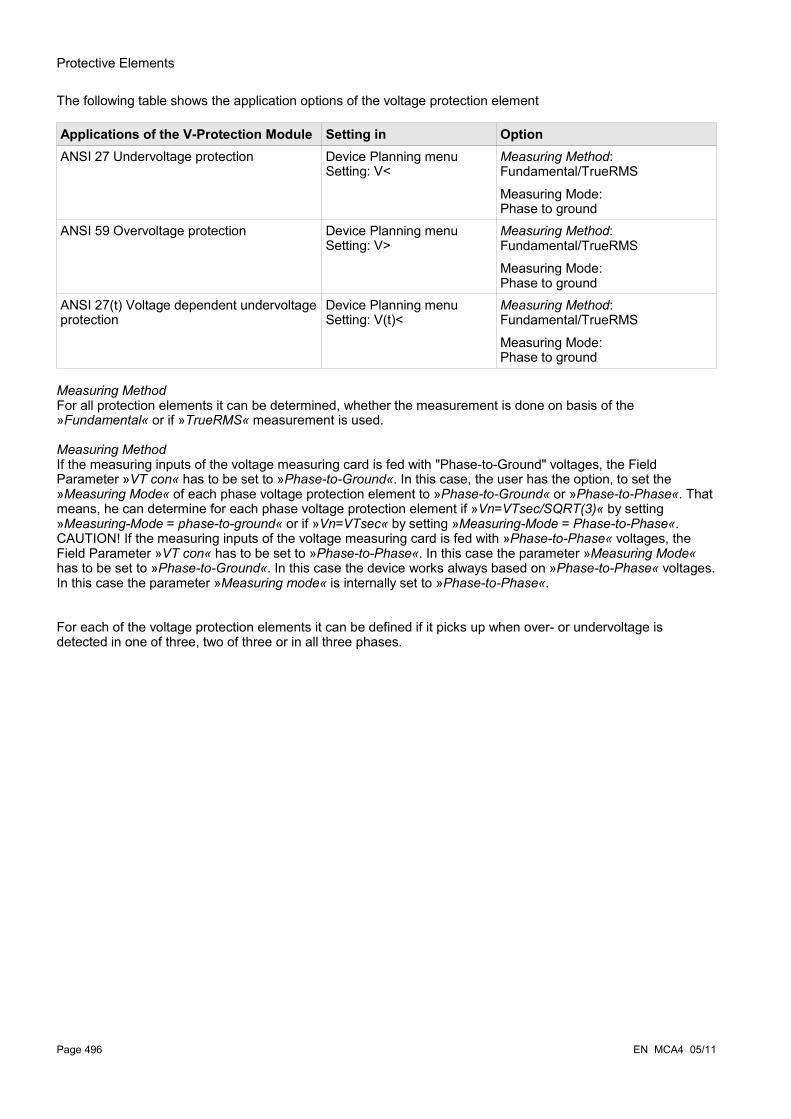
Protective Elements
The following table shows the application options of the voltage protection element
Applications of the V-Protection Module Setting in OptionANSI 27 Undervoltage protection Device Planning menu
Setting: V<Measuring Method:Fundamental/TrueRMS
Measuring Mode:Phase to ground
ANSI 59 Overvoltage protection Device Planning menuSetting: V>
Measuring Method:Fundamental/TrueRMS
Measuring Mode:Phase to ground
ANSI 27(t) Voltage dependent undervoltage protection
Device Planning menuSetting: V(t)<
Measuring Method:Fundamental/TrueRMS
Measuring Mode:Phase to ground
Measuring MethodFor all protection elements it can be determined, whether the measurement is done on basis of the »Fundamental« or if »TrueRMS« measurement is used.
Measuring MethodIf the measuring inputs of the voltage measuring card is fed with "Phase-to-Ground" voltages, the Field Parameter »VT con« has to be set to »Phase-to-Ground«. In this case, the user has the option, to set the »Measuring Mode« of each phase voltage protection element to »Phase-to-Ground« or »Phase-to-Phase«. That means, he can determine for each phase voltage protection element if »Vn=VTsec/SQRT(3)« by setting »Measuring-Mode = phase-to-ground« or if »Vn=VTsec« by setting »Measuring-Mode = Phase-to-Phase«. CAUTION! If the measuring inputs of the voltage measuring card is fed with »Phase-to-Phase« voltages, the Field Parameter »VT con« has to be set to »Phase-to-Phase«. In this case the parameter »Measuring Mode« has to be set to »Phase-to-Ground«. In this case the device works always based on »Phase-to-Phase« voltages. In this case the parameter »Measuring mode« is internally set to »Phase-to-Phase«.
For each of the voltage protection elements it can be defined if it picks up when over- or undervoltage is detected in one of three, two of three or in all three phases.
Page 496 EN MCA4 05/11

Protective Elements
EN MCA4 05/11 Page 497
nam
e.Al
arm
L3
&na
me.
Trip
Cm
d
nam
e.Tr
ip
nam
e.Al
arm
nam
e.Al
arm
L1
nam
e.Al
arm
L2
Ple
ase
Ref
er T
o D
iagr
am: B
lock
ings
& & &
nam
e.Tr
ip L
1
nam
e.Tr
ip L
2
nam
e.Tr
ip L
3
Ple
ase
Ref
er T
o D
iagr
am: T
rip b
lock
ings
(Sta
ge is
not
dea
ctiv
ated
and
no
activ
e bl
ocki
ng s
igna
ls)
V[1]
...[n
]
V>
nam
e.M
ode
V<
&
inac
tive
nam
e.M
eas
Circ
uit
Supe
rv
activ
e
nam
e =
V[1]
...[n
]
Dev
ice
plan
ning
(Trip
ping
com
man
d no
t dea
ctiv
ated
or b
lock
ed. )
2 3
1514 20 21 2228 29 30
V(t)<
nam
e.t
0t
V>V< V(t)<
t1
t2t3
t4t..
.n
VL1
VL2
VL3
nam
e.V
(V<|
V>)
Fund
amen
tal
True
RM
S
nam
e.M
easu
ring
met
hod
φ
Phas
e to
Gro
und
nam
e.M
easu
ring
Mod
e
Phas
e to
Pha
se
>1
38a
12a
12b
38b
>1
>1 & & &
any
one
nam
e.M
ode
any
two
all
& &&
>1>1
& &&
&

Protective Elements
Device Planning Parameters of the Voltage Protection Module
Parameter Description Options Default Menu path
Mode Mode do not use,
V>,
V<,
V(t)<
V[1]: V>
V[2]: V<
V[3]: do not use
V[4]: do not use
V[5]: do not use
V[6]: do not use
[Device planning]
Global Protection Parameters of the Voltage Protection Module
Parameter Description Setting range Default Menu path
ExBlo1 External blocking of the module, if blocking is activated (allowed) within a parameter set and if the state of the assigned signal is true.
1..n, Assignment List -.- [Protection Para
/Global Prot Para
/V-Prot
/V[1]]ExBlo2 External blocking of the module, if blocking is
activated (allowed) within a parameter set and if the state of the assigned signal is true.
1..n, Assignment List -.- [Protection Para
/Global Prot Para
/V-Prot
/V[1]]ExBlo TripCmd
External blocking of the Trip Command of the module/the stage, if blocking is activated (allowed) within a parameter set and if the state of the assigned signal is true.
1..n, Assignment List -.- [Protection Para
/Global Prot Para
/V-Prot
/V[1]]
Page 498 EN MCA4 05/11
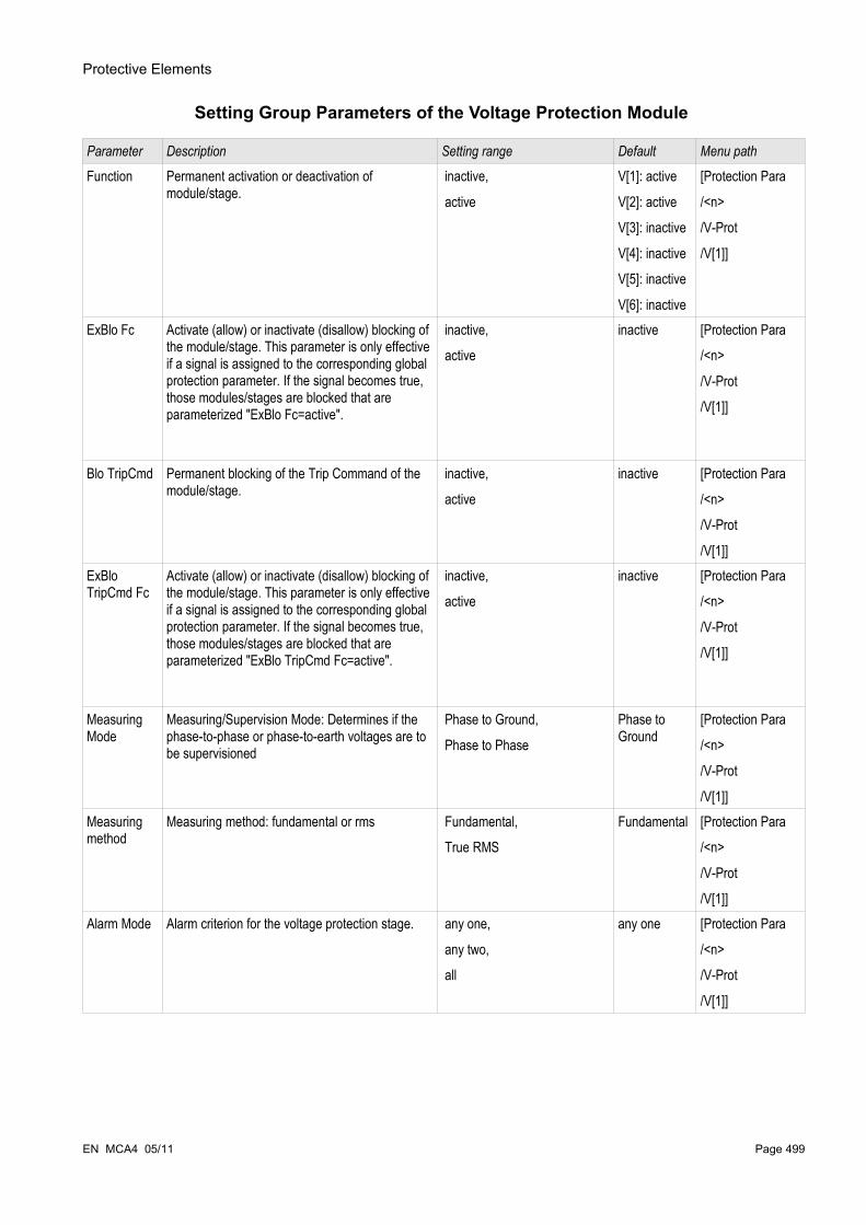
Protective Elements
Setting Group Parameters of the Voltage Protection Module
Parameter Description Setting range Default Menu path
Function Permanent activation or deactivation of module/stage.
inactive,
active
V[1]: active
V[2]: active
V[3]: inactive
V[4]: inactive
V[5]: inactive
V[6]: inactive
[Protection Para
/<n>
/V-Prot
/V[1]]
ExBlo Fc Activate (allow) or inactivate (disallow) blocking of the module/stage. This parameter is only effective if a signal is assigned to the corresponding global protection parameter. If the signal becomes true, those modules/stages are blocked that are parameterized "ExBlo Fc=active".
inactive,
active
inactive [Protection Para
/<n>
/V-Prot
/V[1]]
Blo TripCmd Permanent blocking of the Trip Command of the module/stage.
inactive,
active
inactive [Protection Para
/<n>
/V-Prot
/V[1]]ExBlo TripCmd Fc
Activate (allow) or inactivate (disallow) blocking of the module/stage. This parameter is only effective if a signal is assigned to the corresponding global protection parameter. If the signal becomes true, those modules/stages are blocked that are parameterized "ExBlo TripCmd Fc=active".
inactive,
active
inactive [Protection Para
/<n>
/V-Prot
/V[1]]
Measuring Mode
Measuring/Supervision Mode: Determines if the phase-to-phase or phase-to-earth voltages are to be supervisioned
Phase to Ground,
Phase to Phase
Phase to Ground
[Protection Para
/<n>
/V-Prot
/V[1]]Measuring method
Measuring method: fundamental or rms Fundamental,
True RMS
Fundamental [Protection Para
/<n>
/V-Prot
/V[1]]Alarm Mode Alarm criterion for the voltage protection stage. any one,
any two,
all
any one [Protection Para
/<n>
/V-Prot
/V[1]]
EN MCA4 05/11 Page 499

Protective Elements
Parameter Description Setting range Default Menu path
V> If the pickup value is exceeded, the module/element will be started. Definition of Vn: If the measuring inputs of the voltage measuring card is fed with "Phase-to-Ground" voltages, the Field Parameter "VT con" has to be set to "Phase-to-Ground". In this case, the user has the option, to set the "Measuring Mode" of each phase voltage protection element to "Phase-to-Ground" or "Phase-to-Phase". That means, he can determine for each phase voltage protection element if "Vn=VTsec/SQRT(3)" by setting "Measuring-Mode = phase-to-ground" or if "Vn=VTsec" by setting "Measuring-Mode = Phase-to-Phase". CAUTION! If the measuring inputs of the voltage measuring card is fed with "Phase-to-Phase" voltages, the Field Parameter "VT con" has to be set to "Phase-to-Phase". In this case the parameter "Measuring Mode" has to be set to "Phase-to-Ground". In this case the device works always based on "Phase-to-Phase" Voltages. In this case the parameter "Measuring mode" is internally set to "Phase-to-Phase".
Only available if: Device planning: V.Mode = V>
0.01 - 1.50Vn V[1]: 1.1Vn
V[2]: 1.20Vn
V[3]: 1.20Vn
V[4]: 1.20Vn
V[5]: 1.20Vn
V[6]: 1.20Vn
[Protection Para
/<n>
/V-Prot
/V[1]]
V< If the pickup value is exceeded, the module/element will be started. Definition of Vn: If the measuring inputs of the voltage measuring card is fed with "Phase-to-Ground" voltages, the Field Parameter "VT con" has to be set to "Phase-to-Ground". In this case, the user has the option, to set the "Measuring Mode" of each phase voltage protection element to "Phase-to-Ground" or "Phase-to-Phase". That means, he can determine for each phase voltage protection element if "Vn=VTsec/SQRT(3)" by setting "Measuring-Mode = phase-to-ground" or if "Vn=VTsec" by setting "Measuring-Mode = Phase-to-Phase". CAUTION! If the measuring inputs of the voltage measuring card is fed with "Phase-to-Phase" voltages, the Field Parameter "VT con" has to be set to "Phase-to-Phase". In this case the parameter "Measuring Mode" has to be set to "Phase-to-Ground". In this case the device works always based on "Phase-to-Phase" Voltages. In this case the parameter "Measuring mode" is internally set to "Phase-to-Phase".
Only available if: Device planning: V.Mode = V< Only available if: Device planning: V.Mode = V(t)<
0.01 - 1.50Vn V[1]: 0.80Vn
V[2]: 0.9Vn
V[3]: 0.80Vn
V[4]: 0.80Vn
V[5]: 0.80Vn
V[6]: 0.80Vn
[Protection Para
/<n>
/V-Prot
/V[1]]
Page 500 EN MCA4 05/11

Protective Elements
Parameter Description Setting range Default Menu path
t Tripping delay
Only available if: Device planning: V.Mode = V> Or V<
0.00 - 300.00s V[1]: 1s
V[2]: 1s
V[3]: 0.00s
V[4]: 0.00s
V[5]: 0.00s
V[6]: 0.00s
[Protection Para
/<n>
/V-Prot
/V[1]]
Meas Circuit Superv
Measuring Circuit Supervision
Only available if: Device planning: V.Mode = V(t)<
inactive,
active
inactive [Protection Para
/<n>
/V-Prot
/V[1]]Vstart< If the voltage falls below this Voltage, the Time
Depending Voltage Protection will be started.
Only available if: Device planning: V.Mode = Vstart< Only available if: Device planning: V.Mode = Vstart<
0.01 - 1.50Vn 0.90Vn [Protection Para
/<n>
/V-Prot
/V[1]]
V(t)<1 Pickup value
Only available if: Device planning: V.Mode = V(t)<
0.01 - 1.50Vn 0.01Vn [Protection Para
/<n>
/V-Prot
/V[1]]t1 Tripping delay
Only available if: Device planning: V.Mode = V(t)<
0.00 - 10.00s 0.00s [Protection Para
/<n>
/V-Prot
/V[1]]V(t)<2 Pickup value
Only available if: Device planning: V.Mode = V(t)<
0.01 - 1.50Vn 0.01Vn [Protection Para
/<n>
/V-Prot
/V[1]]t2 Tripping delay
Only available if: Device planning: V.Mode = V(t)<
0.00 - 10.00s 0.15s [Protection Para
/<n>
/V-Prot
/V[1]]V(t)<3 Pickup value
Only available if: Device planning: V.Mode = V(t)<
0.01 - 1.50Vn V[1]: 0.70Vn
V[2]: 0.70Vn
V[3]: 0.70Vn
V[4]: 0.30Vn
V[5]: 0.30Vn
V[6]: 0.30Vn
[Protection Para
/<n>
/V-Prot
/V[1]]
EN MCA4 05/11 Page 501
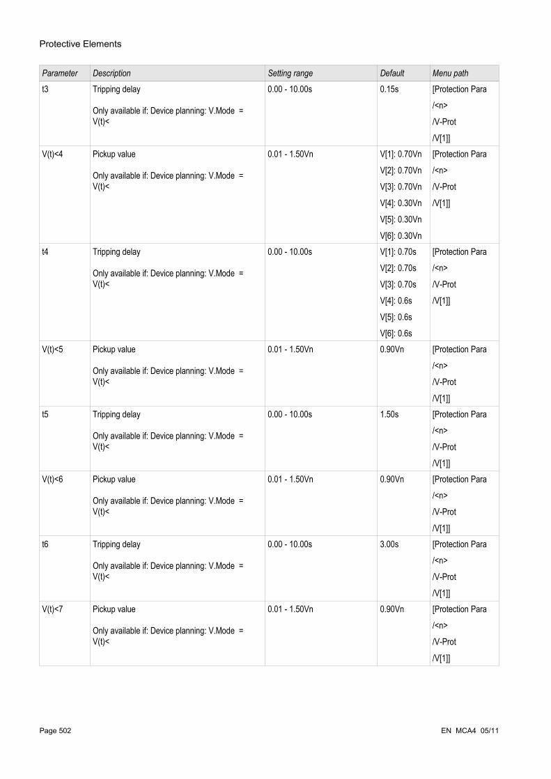
Protective Elements
Parameter Description Setting range Default Menu path
t3 Tripping delay
Only available if: Device planning: V.Mode = V(t)<
0.00 - 10.00s 0.15s [Protection Para
/<n>
/V-Prot
/V[1]]V(t)<4 Pickup value
Only available if: Device planning: V.Mode = V(t)<
0.01 - 1.50Vn V[1]: 0.70Vn
V[2]: 0.70Vn
V[3]: 0.70Vn
V[4]: 0.30Vn
V[5]: 0.30Vn
V[6]: 0.30Vn
[Protection Para
/<n>
/V-Prot
/V[1]]
t4 Tripping delay
Only available if: Device planning: V.Mode = V(t)<
0.00 - 10.00s V[1]: 0.70s
V[2]: 0.70s
V[3]: 0.70s
V[4]: 0.6s
V[5]: 0.6s
V[6]: 0.6s
[Protection Para
/<n>
/V-Prot
/V[1]]
V(t)<5 Pickup value
Only available if: Device planning: V.Mode = V(t)<
0.01 - 1.50Vn 0.90Vn [Protection Para
/<n>
/V-Prot
/V[1]]t5 Tripping delay
Only available if: Device planning: V.Mode = V(t)<
0.00 - 10.00s 1.50s [Protection Para
/<n>
/V-Prot
/V[1]]V(t)<6 Pickup value
Only available if: Device planning: V.Mode = V(t)<
0.01 - 1.50Vn 0.90Vn [Protection Para
/<n>
/V-Prot
/V[1]]t6 Tripping delay
Only available if: Device planning: V.Mode = V(t)<
0.00 - 10.00s 3.00s [Protection Para
/<n>
/V-Prot
/V[1]]V(t)<7 Pickup value
Only available if: Device planning: V.Mode = V(t)<
0.01 - 1.50Vn 0.90Vn [Protection Para
/<n>
/V-Prot
/V[1]]
Page 502 EN MCA4 05/11

Protective Elements
Parameter Description Setting range Default Menu path
t7 Tripping delay
Only available if: Device planning: V.Mode = V(t)<
0.00 - 10.00s 3.00s [Protection Para
/<n>
/V-Prot
/V[1]]V(t)<8 Pickup value
Only available if: Device planning: V.Mode = V(t)<
0.01 - 1.50Vn 0.90Vn [Protection Para
/<n>
/V-Prot
/V[1]]t8 Tripping delay
Only available if: Device planning: V.Mode = V(t)<
0.00 - 10.00s 3.00s [Protection Para
/<n>
/V-Prot
/V[1]]V(t)<9 Pickup value
Only available if: Device planning: V.Mode = V(t)<
0.01 - 1.50Vn 0.90Vn [Protection Para
/<n>
/V-Prot
/V[1]]t9 Tripping delay
Only available if: Device planning: V.Mode = V(t)<
0.00 - 10.00s 3.00s [Protection Para
/<n>
/V-Prot
/V[1]]V(t)<10 Pickup value
Only available if: Device planning: V.Mode = V(t)<
0.01 - 1.50Vn 0.90Vn [Protection Para
/<n>
/V-Prot
/V[1]]t10 Tripping delay
Only available if: Device planning: V.Mode = V(t)<
0.00 - 10.00s 3.00s [Protection Para
/<n>
/V-Prot
/V[1]]
EN MCA4 05/11 Page 503

Protective Elements
Voltage Protection Module Input States
Name Description Assignment via
ExBlo1-I Module input state: External blocking1 [Protection Para
/Global Prot Para
/V-Prot
/V[1]]ExBlo2-I Module input state: External blocking2 [Protection Para
/Global Prot Para
/V-Prot
/V[1]]ExBlo TripCmd-I Module input state: External Blocking of the
Trip Command[Protection Para
/Global Prot Para
/V-Prot
/V[1]]
Voltage Protection Module Signals (Output States)
Name Description
active Signal: activeExBlo Signal: External BlockingBlo TripCmd Signal: Trip Command blockedExBlo TripCmd Signal: External Blocking of the Trip CommandAlarm L1 Signal: Alarm L1Alarm L2 Signal: Alarm L2Alarm L3 Signal: Alarm L3Alarm Signal: Alarm voltage stageTrip L1 Signal: General Trip Phase L1Trip L2 Signal: General Trip Phase L2Trip L3 Signal: General Trip Phase L3Trip Signal: TripTripCmd Signal: Trip Command
Page 504 EN MCA4 05/11
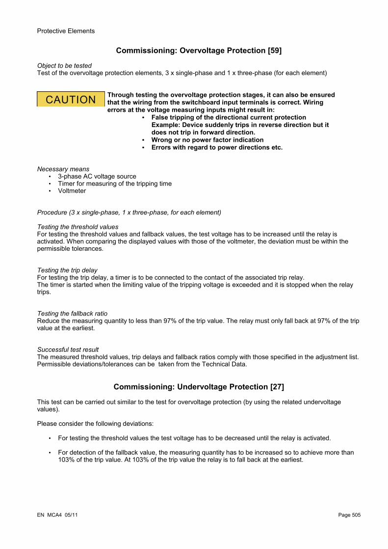
Protective Elements
Commissioning: Overvoltage Protection [59]
Object to be testedTest of the overvoltage protection elements, 3 x single-phase and 1 x three-phase (for each element)
Through testing the overvoltage protection stages, it can also be ensured that the wiring from the switchboard input terminals is correct. Wiring errors at the voltage measuring inputs might result in:
• False tripping of the directional current protection Example: Device suddenly trips in reverse direction but it does not trip in forward direction.
• Wrong or no power factor indication• Errors with regard to power directions etc.
Necessary means• 3-phase AC voltage source • Timer for measuring of the tripping time• Voltmeter
Procedure (3 x single-phase, 1 x three-phase, for each element)
Testing the threshold values For testing the threshold values and fallback values, the test voltage has to be increased until the relay is activated. When comparing the displayed values with those of the voltmeter, the deviation must be within the permissible tolerances.
Testing the trip delay For testing the trip delay, a timer is to be connected to the contact of the associated trip relay. The timer is started when the limiting value of the tripping voltage is exceeded and it is stopped when the relay trips.
Testing the fallback ratioReduce the measuring quantity to less than 97% of the trip value. The relay must only fall back at 97% of the trip value at the earliest.
Successful test result The measured threshold values, trip delays and fallback ratios comply with those specified in the adjustment list. Permissible deviations/tolerances can be taken from the Technical Data.
Commissioning: Undervoltage Protection [27]
This test can be carried out similar to the test for overvoltage protection (by using the related undervoltage values).
Please consider the following deviations:
• For testing the threshold values the test voltage has to be decreased until the relay is activated.
• For detection of the fallback value, the measuring quantity has to be increased so to achieve more than 103% of the trip value. At 103% of the trip value the relay is to fall back at the earliest.
EN MCA4 05/11 Page 505

Protective Elements
VG, VX - Voltage Supervision [59N]Available elements: VG[1] ,VG[2]
All elements of the voltage supervision of the fourth measuring input are identically structured.
This protective element can be used to (depending on device planning and setting)
• Supervison of the calculated or measured residual voltage. The residual voltage can be calculated only if the phase voltages (star connection) are connected to the measuring inputs of the device.
• Supervision of another (auxiliary) voltage against overvoltage or undervoltage.
The following table shows the application options of the voltage protection element
Applications of the VG/VX-Protection Module
Setting in Option
ANSI 59N/G Residual voltage protection(measured or calculated)
Device Planning menuSetting: V>
Criterion:Fundamental/TrueRMS
VG Source:measured/calculated
ANSI 59A Supervision of an Auxiliary (additional) Voltage in relation to Overvoltage.
Device Planning menuSetting: V>
Within the corresponding Parameter-Set:
VG Source:measured
Criterion:Fundamental/TrueRMS
ANSI 27A Supervision of an Auxiliary (additional) Voltage in relation to Undervoltage.
Device Planning menuSetting: V<
Within the corresponding Parameter-Set:
VG Source:measured
Criterion:Fundamental/TrueRMS
Measuring ModeFor all protection elements it can be determined, whether the measurement is done on basis of the »Fundamental« or if »TrueRMS« measurement is used.
Page 506 EN MCA4 05/11
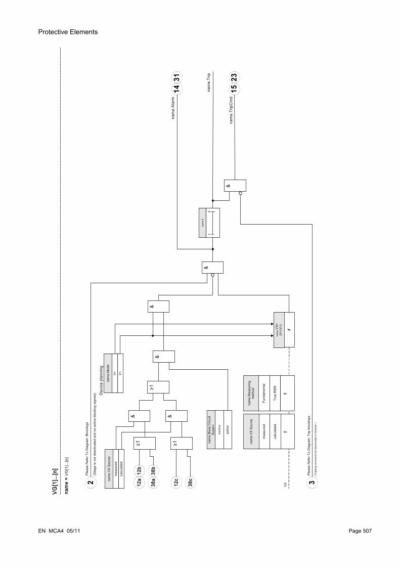
Protective Elements
EN MCA4 05/11 Page 507
0t
nam
e.t
&
Ple
ase
Ref
er T
o D
iagr
am: B
lock
ings
nam
e.Al
arm
nam
e.Tr
ip
nam
e.Tr
ipC
md
VX
Ple
ase
Ref
er T
o D
iagr
am: T
rip b
lock
ings
(Sta
ge is
not
dea
ctiv
ated
and
no
activ
e bl
ocki
ng s
igna
ls)
VG[1
]...[n
]
nam
e =
VG[1
]...[n
]
(Trip
ping
com
man
d no
t dea
ctiv
ated
or b
lock
ed. )
2 3
151431 23
V>
nam
e.M
ode
V<
Dev
ice
plan
ning
mea
sure
d
calc
ulat
ed
nam
e.VX
Sou
rce
φ
Fund
amen
tal
True
RM
S
nam
e.M
easu
ring
met
hod
φ
mea
sure
d
nam
e.VX
Sou
rce
calc
ulat
ed
inac
tive
nam
e.M
eas
Circ
uit
Supe
rv
activ
e
nam
e.VX>
(V<|
V>)
&
38a
12a
12b
38b
38c
12c
>1 >1
& &
>1&
&

Protective Elements
Device Planning Parameters of the Residual Voltage Supervision Module
Parameter Description Options Default Menu path
Mode Mode do not use,
V>,
V<
do not use [Device planning]
Global Protection Parameters of the Residual Voltage Supervision Module
Parameter Description Setting range Default Menu path
ExBlo1 External blocking of the module, if blocking is activated (allowed) within a parameter set and if the state of the assigned signal is true.
1..n, Assignment List -.- [Protection Para
/Global Prot Para
/V-Prot
/VG[1]]ExBlo2 External blocking of the module, if blocking is
activated (allowed) within a parameter set and if the state of the assigned signal is true.
1..n, Assignment List -.- [Protection Para
/Global Prot Para
/V-Prot
/VG[1]]ExBlo TripCmd
External blocking of the Trip Command of the module/the stage, if blocking is activated (allowed) within a parameter set and if the state of the assigned signal is true.
1..n, Assignment List -.- [Protection Para
/Global Prot Para
/V-Prot
/VG[1]]
Page 508 EN MCA4 05/11
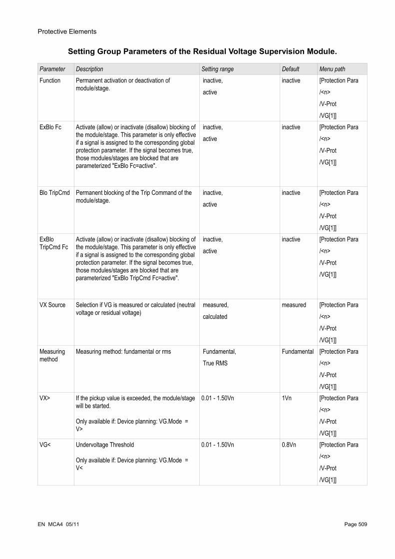
Protective Elements
Setting Group Parameters of the Residual Voltage Supervision Module.
Parameter Description Setting range Default Menu path
Function Permanent activation or deactivation of module/stage.
inactive,
active
inactive [Protection Para
/<n>
/V-Prot
/VG[1]]ExBlo Fc Activate (allow) or inactivate (disallow) blocking of
the module/stage. This parameter is only effective if a signal is assigned to the corresponding global protection parameter. If the signal becomes true, those modules/stages are blocked that are parameterized "ExBlo Fc=active".
inactive,
active
inactive [Protection Para
/<n>
/V-Prot
/VG[1]]
Blo TripCmd Permanent blocking of the Trip Command of the module/stage.
inactive,
active
inactive [Protection Para
/<n>
/V-Prot
/VG[1]]ExBlo TripCmd Fc
Activate (allow) or inactivate (disallow) blocking of the module/stage. This parameter is only effective if a signal is assigned to the corresponding global protection parameter. If the signal becomes true, those modules/stages are blocked that are parameterized "ExBlo TripCmd Fc=active".
inactive,
active
inactive [Protection Para
/<n>
/V-Prot
/VG[1]]
VX Source Selection if VG is measured or calculated (neutral voltage or residual voltage)
measured,
calculated
measured [Protection Para
/<n>
/V-Prot
/VG[1]]Measuring method
Measuring method: fundamental or rms Fundamental,
True RMS
Fundamental [Protection Para
/<n>
/V-Prot
/VG[1]]VX> If the pickup value is exceeded, the module/stage
will be started.
Only available if: Device planning: VG.Mode = V>
0.01 - 1.50Vn 1Vn [Protection Para
/<n>
/V-Prot
/VG[1]]VG< Undervoltage Threshold
Only available if: Device planning: VG.Mode = V<
0.01 - 1.50Vn 0.8Vn [Protection Para
/<n>
/V-Prot
/VG[1]]
EN MCA4 05/11 Page 509

Protective Elements
Parameter Description Setting range Default Menu path
t Tripping delay 0.00 - 300.00s 0.00s [Protection Para
/<n>
/V-Prot
/VG[1]]Meas Circuit Superv
Measuring Circuit Supervision inactive,
active
inactive [Protection Para
/<n>
/V-Prot
/VG[1]]
Page 510 EN MCA4 05/11

Protective Elements
Residual Voltage Supervision Module Input States
Name Description Assignment via
ExBlo1-I Module input state: External blocking1 [Protection Para
/Global Prot Para
/V-Prot
/VG[1]]ExBlo2-I Module input state: External blocking2 [Protection Para
/Global Prot Para
/V-Prot
/VG[1]]ExBlo TripCmd-I Module input state: External Blocking of the
Trip Command[Protection Para
/Global Prot Para
/V-Prot
/VG[1]]
EN MCA4 05/11 Page 511

Protective Elements
Residual Voltage Supervision Module Signals (Output States)
Name Description
active Signal: activeExBlo Signal: External BlockingBlo TripCmd Signal: Trip Command blockedExBlo TripCmd Signal: External Blocking of the Trip CommandAlarm Signal: Alarm Residual Voltage Supervision-stageTrip Signal: TripTripCmd Signal: Trip Command
Page 512 EN MCA4 05/11

Protective Elements
Commissioning: Residual Voltage Protection - Measured [59N]
Object to be testedResidual voltage protection stages.
Necessary components• 1-phase AC voltage source • Timer for measuring of the tripping time• Voltmeter
Procedure (for each element)
Testing the threshold values For testing the threshold and fallback values, the test voltage at the measuring input for the residual voltage has to be increased until the relay is activated. When comparing the displayed values with those of the voltmeter, the deviation must be within the permissible tolerances.
Testing the trip delayFor testing the trip delay a timer is to be connected to the contact of the associated trip relay. The timer is started when the limiting value of the tripping voltage is exceeded and it is stopped when the relay trips.
Testing the fallback ratio Reduce the measuring quantity to less than 97% of the trip value. The relay must only fall back at 97% of the trip value at the latestly.
Successful test result The measured threshold values, trip delays and fallback ratios comply with those specified in the adjustment list. Permissible deviations/tolerances can be taken from the Technical Data.
EN MCA4 05/11 Page 513

Protective Elements
Commissioning: Residual Voltage Protection - Calculated [59N]
Object to be testedTest of the residual voltage protection elements
Necessary means• 3-phase voltage source
Calculation of the residual voltage is only possible if phase voltages (star) were applied to the voltage measuring inputs and if »VX Source=calculated« is set within the corresponding parameter set.
Procedure• Feed a three-phase, symmetrical voltage system (Vn) into the voltage measuring inputs of the relay.• Set the limiting value of VX[x] to 90% Vn. • Disconnect the phase voltage at two measuring inputs (symmetrical feeding at the secondary side has to
be maintained). • Now the »VX calc« measuring value has to be about 100% of the value Vn. • Ascertain that the signal »VX.ALARM« or »VX.TRIP« is generated now.
Successful test resultThe signal »VX.ALARM« or »VX.TRIP« is generated.
Page 514 EN MCA4 05/11
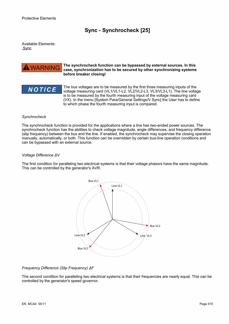
Protective Elements
Sync - Synchrocheck [25]
Available Elements: Sync
The synchrocheck function can be bypassed by external sources. In this case, synchronization has to be secured by other synchronizing systems before breaker closing!
The bus voltages are to be measured by the first three measuring inputs of the voltage measuring card (VL1/VL1-L2, VL2/VL2-L3, VL3/VL3-L1). The line voltage is to be measured by the fourth measuring input of the voltage measuring card (VX). In the menu [System Para/General Settings/V Sync] the User has to define to which phase the fourth measuring input is compared.
Synchrocheck
The synchrocheck function is provided for the applications where a line has two-ended power sources. The synchrocheck function has the abilities to check voltage magnitude, angle differences, and frequency difference (slip frequency) between the bus and the line. If enabled, the synchrocheck may supervise the closing operation manually, automatically, or both. This function can be overridden by certain bus-line operation conditions and can be bypassed with an external source.
Voltage Difference ΔV
The first condition for paralleling two electrical systems is that their voltage phasors have the same magnitude. This can be controlled by the generator's AVR.
Frequency Difference (Slip Frequency) ΔF
The second condition for paralleling two electrical systems is that their frequencies are nearly equal. This can be controlled by the generator's speed governor.
EN MCA4 05/11 Page 515
Line VL1
Bus VL2
Line VL3Line VL2
Bus VL1
Bus VL3

Protective Elements
If the generator frequency fBus is not equal to the mains frequency fLine, it results in a slip frequency ΔF = |fBus -fLine| between the two system frequencies.
Voltage Curve with Enlarged Resolution.
Page 516 EN MCA4 05/11
Line VL1
Bus VL2
Line VL3Line VL2
Bus VL1
Bus VL3
Bus f
Line f
t
∆ v(t)
t
v(t)
v(t)Linev(t)Line
v(t)Busbarv(t)Busbar
∆ v(t)∆ v(t)

Protective Elements
Angular or Phase Difference.
Even if the frequency of both systems is exactly identical, usually an angular difference of the voltage phasors is the case.
At the instant of synchronization, the angular difference of the two systems should be nearly zero because, otherwise, unwanted load inrushes occur. Theoretically, the angular difference can be regulated to zero by giving short pulses to the speed governors. When paralleling generators with the grid, in practice, synchronization is requested as quick as possible and so usually a slight frequency difference is accepted. In such cases, the angular difference is not constant but changes with the slip frequency ΔF.
By taking the breaker closing time into consideration, a lead of the closing release impulse can be calculated in a way that breaker closing takes place at exactly the time when both systems are in angular conformity.
Basically the following applies:
Where large rotating masses are concerned, the frequency difference (slip frequency) of the two systems should possibly be nearly zero, because of the very high load inrushes at the instant of breaker closing. For smaller rotating masses, the frequency difference of the systems can be higher.
EN MCA4 05/11 Page 517
Line VL1
Bus VL2
Line VL3Line VL2
Bus VL1
Bus VL3
Angle Diff
Bus f = Line f

Protective Elements
Synchronization Modes
The synchrocheck module is able to check the synchronization of two electrical systems (system-to-system) or between a generator and an electrical system (generator-to-system). For paralleling two electrical systems, the station frequency, voltage and phase angle should be exactly the same as the utility grid. Whereas the synchronization of a generator to a system can be done with a certain slip-frequency, depending on the size of the generator used. Therefore the maximum breaker closing time has to be taken into consideration. With the set breaker closing time, the synchrocheck module is able to calculate the moment of synchronization and gives the paralleling release.
When paralleling two systems, it has to be verified that the system-to-system mode is selected. Paralleling two systems in generator-to-system mode can cause severe damage!
Working Principle Synchrocheck (Generator-to-System)
(Please refer to the block diagram on next page.)
The synchrocheck element measures the three phase-to-neutral voltages »VL1«, »VL2«, and »VL3« or the three phase-to-phase voltages »VL1-L2«, »VL2-L3«, and »VL3-L1« of the generator busbar. The line voltage Vx is measured by the fourth voltage input. If all synchronous conditions are fulfilled (i. e.: ΔV [VoltageDiff], ΔF [SlipFrequency], and Δφ [AngleDiff]) are within the limits, a signal will be issued that both systems are synchronous. An advanced Close Angle Evaluator function takes the breaker closing time into consideration.
Page 518 EN MCA4 05/11
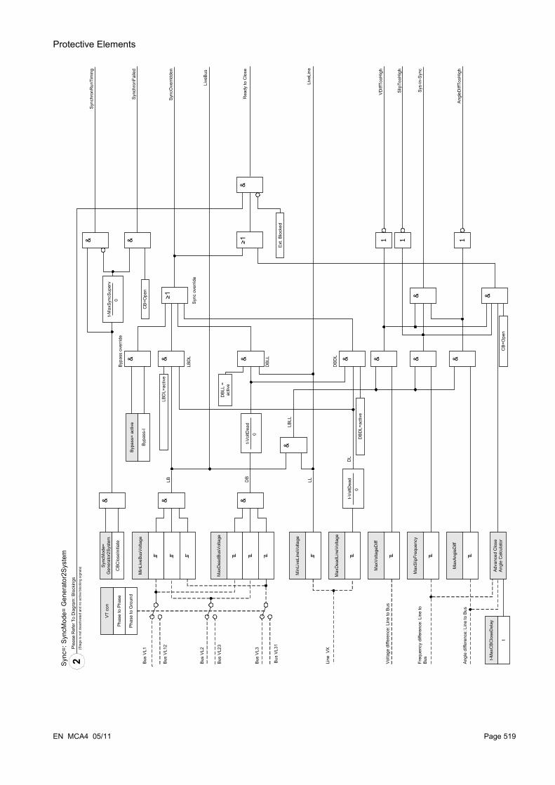
Protective Elements
EN MCA4 05/11 Page 519
t-Vol
tDea
d0
Min
Live
BusV
olta
ge
Max
Dea
dBus
Volta
ge
Min
Live
Line
Volta
ge
Max
Dea
dLin
eVol
tage
Max
Volta
geD
iff
Max
Slip
Freq
uenc
y
Max
Angl
eDiff
Bus
VL1
Bus
VL12
Bus
VL3
Bus
VL31
Bus
VL2
Bus
VL23
CBC
lose
Initi
ate
Sync
Mod
e=
Gen
erat
or2S
yste
m
t-Vol
tDea
d0
Bypa
ss-I
Bypa
ss=
activ
e
t-Max
Sync
Supe
rv0
Line
VX
Adva
nced
Clo
se
Angl
e C
alcu
lato
rC
B=O
pen
LBD
L=ac
tive
DBL
L =
activ
e
VT c
on
Ext.
Bloc
ked
DBD
L=ac
tive
CB=
Ope
n
LBD
L
DBL
L
DBD
L
Bypa
ss o
verri
de
Sync
ove
rride
LB DB
LBLL
LL
DL
Sync
hron
Run
Tim
ing
Sync
hron
Faile
d
Sync
Ove
rridd
en
VDiff
TooH
igh
Rea
dy to
Clo
se
Slip
TooH
igh
Sys-
in-S
ync
Angl
eDiff
TooH
igh
Ple
ase
Ref
er T
o D
iagr
am: B
lock
ings
(Sta
ge is
not
dea
ctiv
ated
and
no
activ
e bl
ocki
ng s
igna
ls)2
Phas
e to
Pha
se
Phas
e to
Gro
und
Vol
tage
diff
eren
ce: L
ine
to B
us
Freq
uenc
y di
ffere
nce:
Lin
e to
B
us
Ang
le d
iffer
ence
: Lin
e to
Bus
t-Max
CBC
lose
Del
ay
t
>1
& & &
&
& & & & & & &
& &
111>1&
&
Syn
c=: S
yncM
ode=
Gen
erat
or2S
yste
m
Live
Line
Live
Bus
&

Protective Elements
Working Principle Synchrocheck (System-to-System)
(Please refer to the block diagram on next page.)
The synchrocheck function for two systems is very similar to the synchrocheck function for generator-to-system except there is no need to take the breaker closing time into account. The synchrocheck element measures the three phase-to-neutral voltages »VL1«, »VL2«, and »VL3« or the three phase-to-phase voltages »VL1-L2«, »VL2-L3«, and »VL3-L1« of the station voltage bus bar. The line voltage Vx is measured by the fourth voltage input. If all synchronous conditions are fulfilled (i. e.: ΔV [VoltageDiff], ΔF [SlipFrequency], and Δφ [AngleDiff]) are within the limits, a signal will be issued that both systems are synchronous.
Page 520 EN MCA4 05/11

Protective Elements
EN MCA4 05/11 Page 521
t-Vol
tDea
d0
Min
Live
BusV
olta
ge
Max
Dea
dBus
Volta
ge
Min
Live
Line
Volta
ge
Max
Dea
dLin
eVol
tage
Max
Volta
geD
iff
Max
Slip
Freq
uenc
y
Max
Angl
eDiff
Bus
VL1
Bus
VL12
Bus
VL3
Bus
VL31
Bus
VL2
Bus
VL23
t-Vol
tDea
d0
Bypa
ss-I
Bypa
ss=
activ
e
Line
VX
LBD
L=ac
tive
DBL
L =
activ
e
VT c
on
Ext.
Bloc
ked
DBD
L=ac
tive
LBD
L
DBL
L
DBD
L
Bypa
ss o
verri
de
Sync
ove
rride
LB DB
LBLL
LL
DL
Sync
Ove
rridd
en
VDiff
TooH
igh
Rea
dy to
Clo
se
Slip
TooH
igh
Sys-
in-S
ync
Angl
eDiff
TooH
igh
Phas
e to
Pha
se
Phas
e to
Gro
und
Vol
tage
diff
eren
ce: L
ine
to B
us
Freq
uenc
y di
ffere
nce:
Lin
e to
B
us
Ang
le d
iffer
ence
: Lin
e to
Bus
Plea
se R
efer
To
Dia
gram
: Blo
ckin
gs(S
tage
is n
ot d
eact
ivat
ed a
nd n
o ac
tive
bloc
king
sig
nals
)2
& &
&
& & & & & & &
&>1
>1&
111
Syn
c=: S
yncM
ode=
Sys
tem
2Sys
tem
Live
Bus
Live
Line

Protective Elements
Synchrocheck Override Conditions
If enabled the following conditions can override the synchrocheck function:
•LBDL = Live Bus – Dead Line•DBLL = Dead Bus – Live Line•DBDL = Dead Bus – Dead Line
Also the synchrocheck function can be bypassed by an external source.
When the synchrocheck function is overridden or bypassed, synchronization has to be secured by other synchronizing systems before breaker closing!
Page 522 EN MCA4 05/11

Protective Elements
Device Planning Parameters of the Synchrocheck Module
Parameter Description Options Default Menu path
Mode Mode do not use,
use
do not use [Device planning]
EN MCA4 05/11 Page 523
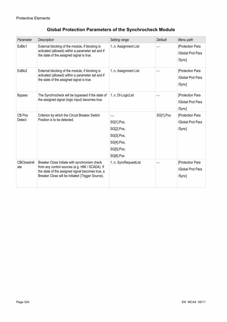
Protective Elements
Global Protection Parameters of the Synchrocheck Module
Parameter Description Setting range Default Menu path
ExBlo1 External blocking of the module, if blocking is activated (allowed) within a parameter set and if the state of the assigned signal is true.
1..n, Assignment List -.- [Protection Para
/Global Prot Para
/Sync]
ExBlo2 External blocking of the module, if blocking is activated (allowed) within a parameter set and if the state of the assigned signal is true.
1..n, Assignment List -.- [Protection Para
/Global Prot Para
/Sync]
Bypass The Synchrocheck will be bypassed if the state of the assigned signal (logic input) becomes true.
1..n, DI-LogicList -.- [Protection Para
/Global Prot Para
/Sync]CB Pos Detect
Criterion by which the Circuit Breaker Switch Position is to be detected.
-.-,
SG[1].Pos,
SG[2].Pos,
SG[3].Pos,
SG[4].Pos,
SG[5].Pos,
SG[6].Pos
SG[1].Pos [Protection Para
/Global Prot Para
/Sync]
CBCloseInitiate
Breaker Close Initiate with synchronism check from any control sources (e.g. HMI / SCADA). If the state of the assigned signal becomes true, a Breaker Close will be initiated (Trigger Source).
1..n, SyncRequestList -.- [Protection Para
/Global Prot Para
/Sync]
Page 524 EN MCA4 05/11
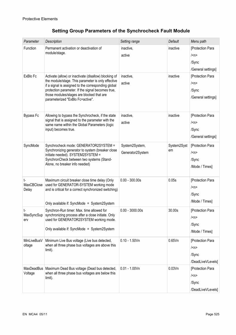
Protective Elements
Setting Group Parameters of the Synchrocheck Fault Module
Parameter Description Setting range Default Menu path
Function Permanent activation or deactivation of module/stage.
inactive,
active
inactive [Protection Para
/<n>
/Sync
/General settings]ExBlo Fc Activate (allow) or inactivate (disallow) blocking of
the module/stage. This parameter is only effective if a signal is assigned to the corresponding global protection parameter. If the signal becomes true, those modules/stages are blocked that are parameterized "ExBlo Fc=active".
inactive,
active
inactive [Protection Para
/<n>
/Sync
/General settings]
Bypass Fc Allowing to bypass the Synchrocheck, if the state signal that is assigned to the parameter with the same name within the Global Parameters (logic input) becomes true.
inactive,
active
inactive [Protection Para
/<n>
/Sync
/General settings]
SyncMode Synchrocheck mode: GENERATOR2SYSTEM = Synchronizing generator to system (breaker close initiate needed). SYSTEM2SYSTEM = SynchronCheck between two systems (Stand-Alone, no breaker info needed)
System2System,
Generator2System
System2System
[Protection Para
/<n>
/Sync
/Mode / Times]
t-MaxCBCloseDelay
Maximum circuit breaker close time delay (Only used for GENERATOR-SYSTEM working mode and is critical for a correct synchronized switching)
Only available if: SyncMode = System2System
0.00 - 300.00s 0.05s [Protection Para
/<n>
/Sync
/Mode / Times]
t-MaxSyncSuperv
Synchron-Run timer: Max. time allowed for synchronizing process after a close initiate. Only used for GENERATOR2SYSTEM working mode.
Only available if: SyncMode = System2System
0.00 - 3000.00s 30.00s [Protection Para
/<n>
/Sync
/Mode / Times]
MinLiveBusVoltage
Minimum Live Bus voltage (Live bus detected, when all three phase bus voltages are above this limit).
0.10 - 1.50Vn 0.65Vn [Protection Para
/<n>
/Sync
/DeadLiveVLevels]MaxDeadBusVoltage
Maximum Dead Bus voltage (Dead bus detected, when all three phase bus voltages are below this limit).
0.01 - 1.00Vn 0.03Vn [Protection Para
/<n>
/Sync
/DeadLiveVLevels]
EN MCA4 05/11 Page 525
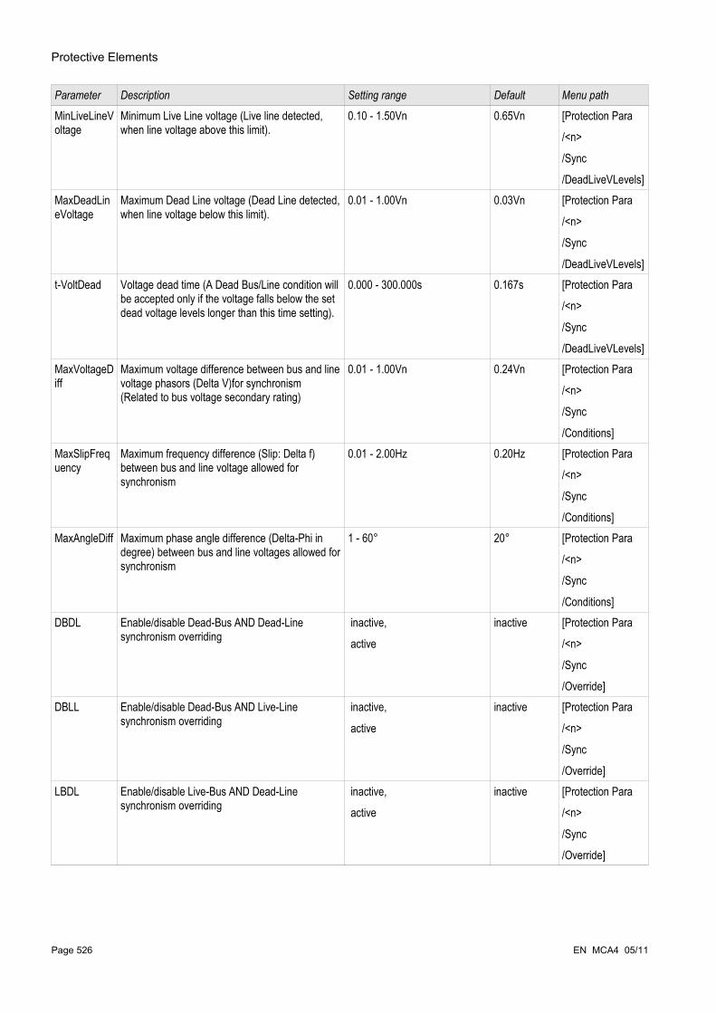
Protective Elements
Parameter Description Setting range Default Menu path
MinLiveLineVoltage
Minimum Live Line voltage (Live line detected, when line voltage above this limit).
0.10 - 1.50Vn 0.65Vn [Protection Para
/<n>
/Sync
/DeadLiveVLevels]MaxDeadLineVoltage
Maximum Dead Line voltage (Dead Line detected, when line voltage below this limit).
0.01 - 1.00Vn 0.03Vn [Protection Para
/<n>
/Sync
/DeadLiveVLevels]t-VoltDead Voltage dead time (A Dead Bus/Line condition will
be accepted only if the voltage falls below the set dead voltage levels longer than this time setting).
0.000 - 300.000s 0.167s [Protection Para
/<n>
/Sync
/DeadLiveVLevels]MaxVoltageDiff
Maximum voltage difference between bus and line voltage phasors (Delta V)for synchronism (Related to bus voltage secondary rating)
0.01 - 1.00Vn 0.24Vn [Protection Para
/<n>
/Sync
/Conditions]MaxSlipFrequency
Maximum frequency difference (Slip: Delta f) between bus and line voltage allowed for synchronism
0.01 - 2.00Hz 0.20Hz [Protection Para
/<n>
/Sync
/Conditions]MaxAngleDiff Maximum phase angle difference (Delta-Phi in
degree) between bus and line voltages allowed for synchronism
1 - 60° 20° [Protection Para
/<n>
/Sync
/Conditions]DBDL Enable/disable Dead-Bus AND Dead-Line
synchronism overriding inactive,
active
inactive [Protection Para
/<n>
/Sync
/Override]DBLL Enable/disable Dead-Bus AND Live-Line
synchronism overriding inactive,
active
inactive [Protection Para
/<n>
/Sync
/Override]LBDL Enable/disable Live-Bus AND Dead-Line
synchronism overriding inactive,
active
inactive [Protection Para
/<n>
/Sync
/Override]
Page 526 EN MCA4 05/11

Protective Elements
Synchrocheck Module Input States
Name Description Assignment via
ExBlo1-I Module input state: External blocking1 [Protection Para
/Global Prot Para
/Sync]ExBlo2-I Module input state: External blocking2 [Protection Para
/Global Prot Para
/Sync]Bypass-I State of the module input: Bypass [Protection Para
/Global Prot Para
/Sync]CBCloseInitiate-I State of the module input: Breaker Close
Initiate with synchronism check from any control sources (e.g. HMI / SCADA). If the state of the assigned signal becomes true, a Breaker Close will be initiated (Trigger Source).
[Protection Para
/Global Prot Para
/Sync]
Signals of the Synchrocheck Module (Output States)
Name Description
active Signal: activeExBlo Signal: External BlockingLiveBus Signal: Live-Bus flag: 1=Live-Bus, 0=Voltage is below the LiveBus
thresholdLiveLine Signal: Live Line flag: 1=Live-Line, 0=Voltage is below the
LiveLine thresholdSynchronRunTiming Signal: SynchronRunTimingSynchronFailed Signal: This signal indicates a failed synchronization. It is set for 5s
when the circuit breaker is still open after the Synchron-Run-timer has timed out.
SyncOverridden Signal:Synchronism Check is overridden because one of the Synchronism overriding conditions (DB/DL or ExtBypass) is met.
VDiffTooHigh Signal: Voltage difference between bus and line too high.SlipTooHigh Signal: Frequency difference (slip frequency) between bus and line
voltages too high.AngleDiffTooHigh Signal: Phase Angle difference between bus and line voltages too
high.Sys-in-Sync Signal: Bus and line voltages are in synchronism according to the
system synchronism criteria.Ready to Close Signal: Ready to Close
EN MCA4 05/11 Page 527
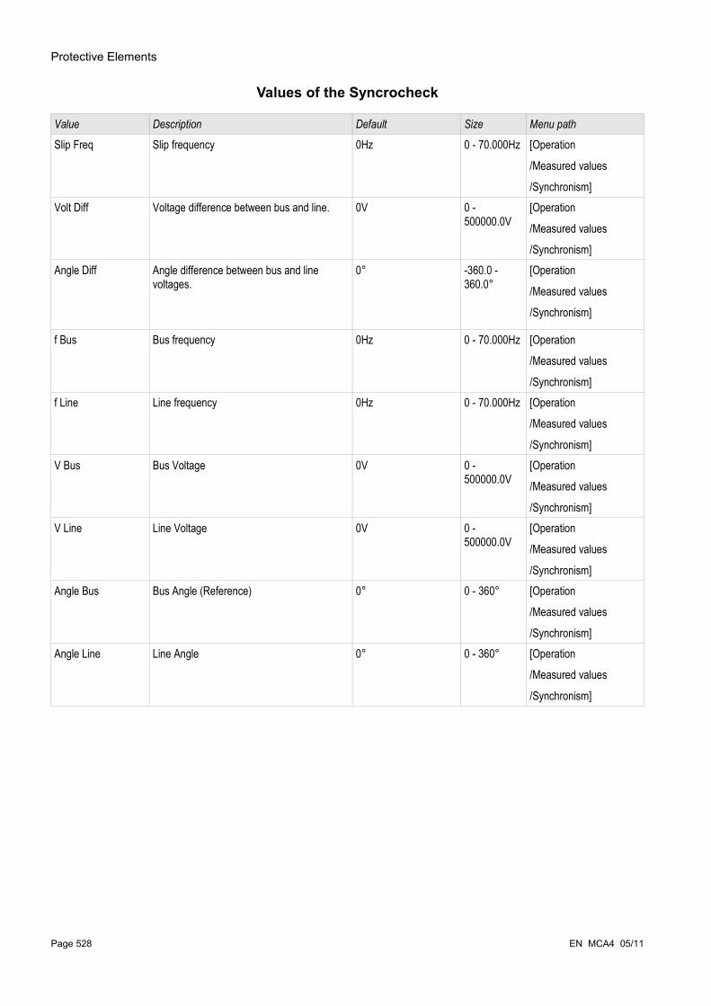
Protective Elements
Values of the Syncrocheck
Value Description Default Size Menu path
Slip Freq Slip frequency 0Hz 0 - 70.000Hz [Operation
/Measured values
/Synchronism]Volt Diff Voltage difference between bus and line. 0V 0 -
500000.0V[Operation
/Measured values
/Synchronism]Angle Diff Angle difference between bus and line
voltages.0° -360.0 -
360.0°[Operation
/Measured values
/Synchronism]
f Bus Bus frequency 0Hz 0 - 70.000Hz [Operation
/Measured values
/Synchronism]f Line Line frequency 0Hz 0 - 70.000Hz [Operation
/Measured values
/Synchronism]V Bus Bus Voltage 0V 0 -
500000.0V[Operation
/Measured values
/Synchronism]V Line Line Voltage 0V 0 -
500000.0V[Operation
/Measured values
/Synchronism]Angle Bus Bus Angle (Reference) 0° 0 - 360° [Operation
/Measured values
/Synchronism]Angle Line Line Angle 0° 0 - 360° [Operation
/Measured values
/Synchronism]
Page 528 EN MCA4 05/11

Protective Elements
Signals that Trigger a Synchrocheck
Name Description
-.- No assignmentSG[1].Sync ON request Signal: Synchronous ON requestSG[2].Sync ON request Signal: Synchronous ON requestSG[3].Sync ON request Signal: Synchronous ON requestSG[4].Sync ON request Signal: Synchronous ON requestSG[5].Sync ON request Signal: Synchronous ON requestSG[6].Sync ON request Signal: Synchronous ON requestDI Slot X1.DI 1 Signal: Digital InputDI Slot X1.DI 2 Signal: Digital InputDI Slot X1.DI 3 Signal: Digital InputDI Slot X1.DI 4 Signal: Digital InputDI Slot X1.DI 5 Signal: Digital InputDI Slot X1.DI 6 Signal: Digital InputDI Slot X1.DI 7 Signal: Digital InputDI Slot X1.DI 8 Signal: Digital InputDI Slot X6.DI 1 Signal: Digital InputDI Slot X6.DI 2 Signal: Digital InputDI Slot X6.DI 3 Signal: Digital InputDI Slot X6.DI 4 Signal: Digital InputDI Slot X6.DI 5 Signal: Digital InputDI Slot X6.DI 6 Signal: Digital InputDI Slot X6.DI 7 Signal: Digital InputDI Slot X6.DI 8 Signal: Digital InputLogics.LE1.Gate Out Signal: Output of the logic gateLogics.LE1.Timer Out Signal: Timer OutputLogics.LE1.Out Signal: Latched Output (Q)Logics.LE1.Out inverted Signal: Negated Latched Output (Q NOT)Logics.LE2.Gate Out Signal: Output of the logic gateLogics.LE2.Timer Out Signal: Timer OutputLogics.LE2.Out Signal: Latched Output (Q)Logics.LE2.Out inverted Signal: Negated Latched Output (Q NOT)Logics.LE3.Gate Out Signal: Output of the logic gateLogics.LE3.Timer Out Signal: Timer OutputLogics.LE3.Out Signal: Latched Output (Q)Logics.LE3.Out inverted Signal: Negated Latched Output (Q NOT)Logics.LE4.Gate Out Signal: Output of the logic gateLogics.LE4.Timer Out Signal: Timer Output
EN MCA4 05/11 Page 529

Protective Elements
Name Description
Logics.LE4.Out Signal: Latched Output (Q)Logics.LE4.Out inverted Signal: Negated Latched Output (Q NOT)Logics.LE5.Gate Out Signal: Output of the logic gateLogics.LE5.Timer Out Signal: Timer OutputLogics.LE5.Out Signal: Latched Output (Q)Logics.LE5.Out inverted Signal: Negated Latched Output (Q NOT)Logics.LE6.Gate Out Signal: Output of the logic gateLogics.LE6.Timer Out Signal: Timer OutputLogics.LE6.Out Signal: Latched Output (Q)Logics.LE6.Out inverted Signal: Negated Latched Output (Q NOT)Logics.LE7.Gate Out Signal: Output of the logic gateLogics.LE7.Timer Out Signal: Timer OutputLogics.LE7.Out Signal: Latched Output (Q)Logics.LE7.Out inverted Signal: Negated Latched Output (Q NOT)Logics.LE8.Gate Out Signal: Output of the logic gateLogics.LE8.Timer Out Signal: Timer OutputLogics.LE8.Out Signal: Latched Output (Q)Logics.LE8.Out inverted Signal: Negated Latched Output (Q NOT)Logics.LE9.Gate Out Signal: Output of the logic gateLogics.LE9.Timer Out Signal: Timer OutputLogics.LE9.Out Signal: Latched Output (Q)Logics.LE9.Out inverted Signal: Negated Latched Output (Q NOT)Logics.LE10.Gate Out Signal: Output of the logic gateLogics.LE10.Timer Out Signal: Timer OutputLogics.LE10.Out Signal: Latched Output (Q)Logics.LE10.Out inverted Signal: Negated Latched Output (Q NOT)Logics.LE11.Gate Out Signal: Output of the logic gateLogics.LE11.Timer Out Signal: Timer OutputLogics.LE11.Out Signal: Latched Output (Q)Logics.LE11.Out inverted Signal: Negated Latched Output (Q NOT)Logics.LE12.Gate Out Signal: Output of the logic gateLogics.LE12.Timer Out Signal: Timer OutputLogics.LE12.Out Signal: Latched Output (Q)Logics.LE12.Out inverted Signal: Negated Latched Output (Q NOT)Logics.LE13.Gate Out Signal: Output of the logic gateLogics.LE13.Timer Out Signal: Timer OutputLogics.LE13.Out Signal: Latched Output (Q)Logics.LE13.Out inverted Signal: Negated Latched Output (Q NOT)Logics.LE14.Gate Out Signal: Output of the logic gate
Page 530 EN MCA4 05/11

Protective Elements
Name Description
Logics.LE14.Timer Out Signal: Timer OutputLogics.LE14.Out Signal: Latched Output (Q)Logics.LE14.Out inverted Signal: Negated Latched Output (Q NOT)Logics.LE15.Gate Out Signal: Output of the logic gateLogics.LE15.Timer Out Signal: Timer OutputLogics.LE15.Out Signal: Latched Output (Q)Logics.LE15.Out inverted Signal: Negated Latched Output (Q NOT)Logics.LE16.Gate Out Signal: Output of the logic gateLogics.LE16.Timer Out Signal: Timer OutputLogics.LE16.Out Signal: Latched Output (Q)Logics.LE16.Out inverted Signal: Negated Latched Output (Q NOT)Logics.LE17.Gate Out Signal: Output of the logic gateLogics.LE17.Timer Out Signal: Timer OutputLogics.LE17.Out Signal: Latched Output (Q)Logics.LE17.Out inverted Signal: Negated Latched Output (Q NOT)Logics.LE18.Gate Out Signal: Output of the logic gateLogics.LE18.Timer Out Signal: Timer OutputLogics.LE18.Out Signal: Latched Output (Q)Logics.LE18.Out inverted Signal: Negated Latched Output (Q NOT)Logics.LE19.Gate Out Signal: Output of the logic gateLogics.LE19.Timer Out Signal: Timer OutputLogics.LE19.Out Signal: Latched Output (Q)Logics.LE19.Out inverted Signal: Negated Latched Output (Q NOT)Logics.LE20.Gate Out Signal: Output of the logic gateLogics.LE20.Timer Out Signal: Timer OutputLogics.LE20.Out Signal: Latched Output (Q)Logics.LE20.Out inverted Signal: Negated Latched Output (Q NOT)Logics.LE21.Gate Out Signal: Output of the logic gateLogics.LE21.Timer Out Signal: Timer OutputLogics.LE21.Out Signal: Latched Output (Q)Logics.LE21.Out inverted Signal: Negated Latched Output (Q NOT)Logics.LE22.Gate Out Signal: Output of the logic gateLogics.LE22.Timer Out Signal: Timer OutputLogics.LE22.Out Signal: Latched Output (Q)Logics.LE22.Out inverted Signal: Negated Latched Output (Q NOT)Logics.LE23.Gate Out Signal: Output of the logic gateLogics.LE23.Timer Out Signal: Timer OutputLogics.LE23.Out Signal: Latched Output (Q)Logics.LE23.Out inverted Signal: Negated Latched Output (Q NOT)
EN MCA4 05/11 Page 531

Protective Elements
Name Description
Logics.LE24.Gate Out Signal: Output of the logic gateLogics.LE24.Timer Out Signal: Timer OutputLogics.LE24.Out Signal: Latched Output (Q)Logics.LE24.Out inverted Signal: Negated Latched Output (Q NOT)Logics.LE25.Gate Out Signal: Output of the logic gateLogics.LE25.Timer Out Signal: Timer OutputLogics.LE25.Out Signal: Latched Output (Q)Logics.LE25.Out inverted Signal: Negated Latched Output (Q NOT)Logics.LE26.Gate Out Signal: Output of the logic gateLogics.LE26.Timer Out Signal: Timer OutputLogics.LE26.Out Signal: Latched Output (Q)Logics.LE26.Out inverted Signal: Negated Latched Output (Q NOT)Logics.LE27.Gate Out Signal: Output of the logic gateLogics.LE27.Timer Out Signal: Timer OutputLogics.LE27.Out Signal: Latched Output (Q)Logics.LE27.Out inverted Signal: Negated Latched Output (Q NOT)Logics.LE28.Gate Out Signal: Output of the logic gateLogics.LE28.Timer Out Signal: Timer OutputLogics.LE28.Out Signal: Latched Output (Q)Logics.LE28.Out inverted Signal: Negated Latched Output (Q NOT)Logics.LE29.Gate Out Signal: Output of the logic gateLogics.LE29.Timer Out Signal: Timer OutputLogics.LE29.Out Signal: Latched Output (Q)Logics.LE29.Out inverted Signal: Negated Latched Output (Q NOT)Logics.LE30.Gate Out Signal: Output of the logic gateLogics.LE30.Timer Out Signal: Timer OutputLogics.LE30.Out Signal: Latched Output (Q)Logics.LE30.Out inverted Signal: Negated Latched Output (Q NOT)Logics.LE31.Gate Out Signal: Output of the logic gateLogics.LE31.Timer Out Signal: Timer OutputLogics.LE31.Out Signal: Latched Output (Q)Logics.LE31.Out inverted Signal: Negated Latched Output (Q NOT)Logics.LE32.Gate Out Signal: Output of the logic gateLogics.LE32.Timer Out Signal: Timer OutputLogics.LE32.Out Signal: Latched Output (Q)Logics.LE32.Out inverted Signal: Negated Latched Output (Q NOT)Logics.LE33.Gate Out Signal: Output of the logic gateLogics.LE33.Timer Out Signal: Timer OutputLogics.LE33.Out Signal: Latched Output (Q)
Page 532 EN MCA4 05/11

Protective Elements
Name Description
Logics.LE33.Out inverted Signal: Negated Latched Output (Q NOT)Logics.LE34.Gate Out Signal: Output of the logic gateLogics.LE34.Timer Out Signal: Timer OutputLogics.LE34.Out Signal: Latched Output (Q)Logics.LE34.Out inverted Signal: Negated Latched Output (Q NOT)Logics.LE35.Gate Out Signal: Output of the logic gateLogics.LE35.Timer Out Signal: Timer OutputLogics.LE35.Out Signal: Latched Output (Q)Logics.LE35.Out inverted Signal: Negated Latched Output (Q NOT)Logics.LE36.Gate Out Signal: Output of the logic gateLogics.LE36.Timer Out Signal: Timer OutputLogics.LE36.Out Signal: Latched Output (Q)Logics.LE36.Out inverted Signal: Negated Latched Output (Q NOT)Logics.LE37.Gate Out Signal: Output of the logic gateLogics.LE37.Timer Out Signal: Timer OutputLogics.LE37.Out Signal: Latched Output (Q)Logics.LE37.Out inverted Signal: Negated Latched Output (Q NOT)Logics.LE38.Gate Out Signal: Output of the logic gateLogics.LE38.Timer Out Signal: Timer OutputLogics.LE38.Out Signal: Latched Output (Q)Logics.LE38.Out inverted Signal: Negated Latched Output (Q NOT)Logics.LE39.Gate Out Signal: Output of the logic gateLogics.LE39.Timer Out Signal: Timer OutputLogics.LE39.Out Signal: Latched Output (Q)Logics.LE39.Out inverted Signal: Negated Latched Output (Q NOT)Logics.LE40.Gate Out Signal: Output of the logic gateLogics.LE40.Timer Out Signal: Timer OutputLogics.LE40.Out Signal: Latched Output (Q)Logics.LE40.Out inverted Signal: Negated Latched Output (Q NOT)Logics.LE41.Gate Out Signal: Output of the logic gateLogics.LE41.Timer Out Signal: Timer OutputLogics.LE41.Out Signal: Latched Output (Q)Logics.LE41.Out inverted Signal: Negated Latched Output (Q NOT)Logics.LE42.Gate Out Signal: Output of the logic gateLogics.LE42.Timer Out Signal: Timer OutputLogics.LE42.Out Signal: Latched Output (Q)Logics.LE42.Out inverted Signal: Negated Latched Output (Q NOT)Logics.LE43.Gate Out Signal: Output of the logic gateLogics.LE43.Timer Out Signal: Timer Output
EN MCA4 05/11 Page 533

Protective Elements
Name Description
Logics.LE43.Out Signal: Latched Output (Q)Logics.LE43.Out inverted Signal: Negated Latched Output (Q NOT)Logics.LE44.Gate Out Signal: Output of the logic gateLogics.LE44.Timer Out Signal: Timer OutputLogics.LE44.Out Signal: Latched Output (Q)Logics.LE44.Out inverted Signal: Negated Latched Output (Q NOT)Logics.LE45.Gate Out Signal: Output of the logic gateLogics.LE45.Timer Out Signal: Timer OutputLogics.LE45.Out Signal: Latched Output (Q)Logics.LE45.Out inverted Signal: Negated Latched Output (Q NOT)Logics.LE46.Gate Out Signal: Output of the logic gateLogics.LE46.Timer Out Signal: Timer OutputLogics.LE46.Out Signal: Latched Output (Q)Logics.LE46.Out inverted Signal: Negated Latched Output (Q NOT)Logics.LE47.Gate Out Signal: Output of the logic gateLogics.LE47.Timer Out Signal: Timer OutputLogics.LE47.Out Signal: Latched Output (Q)Logics.LE47.Out inverted Signal: Negated Latched Output (Q NOT)Logics.LE48.Gate Out Signal: Output of the logic gateLogics.LE48.Timer Out Signal: Timer OutputLogics.LE48.Out Signal: Latched Output (Q)Logics.LE48.Out inverted Signal: Negated Latched Output (Q NOT)Logics.LE49.Gate Out Signal: Output of the logic gateLogics.LE49.Timer Out Signal: Timer OutputLogics.LE49.Out Signal: Latched Output (Q)Logics.LE49.Out inverted Signal: Negated Latched Output (Q NOT)Logics.LE50.Gate Out Signal: Output of the logic gateLogics.LE50.Timer Out Signal: Timer OutputLogics.LE50.Out Signal: Latched Output (Q)Logics.LE50.Out inverted Signal: Negated Latched Output (Q NOT)Logics.LE51.Gate Out Signal: Output of the logic gateLogics.LE51.Timer Out Signal: Timer OutputLogics.LE51.Out Signal: Latched Output (Q)Logics.LE51.Out inverted Signal: Negated Latched Output (Q NOT)Logics.LE52.Gate Out Signal: Output of the logic gateLogics.LE52.Timer Out Signal: Timer OutputLogics.LE52.Out Signal: Latched Output (Q)Logics.LE52.Out inverted Signal: Negated Latched Output (Q NOT)Logics.LE53.Gate Out Signal: Output of the logic gate
Page 534 EN MCA4 05/11

Protective Elements
Name Description
Logics.LE53.Timer Out Signal: Timer OutputLogics.LE53.Out Signal: Latched Output (Q)Logics.LE53.Out inverted Signal: Negated Latched Output (Q NOT)Logics.LE54.Gate Out Signal: Output of the logic gateLogics.LE54.Timer Out Signal: Timer OutputLogics.LE54.Out Signal: Latched Output (Q)Logics.LE54.Out inverted Signal: Negated Latched Output (Q NOT)Logics.LE55.Gate Out Signal: Output of the logic gateLogics.LE55.Timer Out Signal: Timer OutputLogics.LE55.Out Signal: Latched Output (Q)Logics.LE55.Out inverted Signal: Negated Latched Output (Q NOT)Logics.LE56.Gate Out Signal: Output of the logic gateLogics.LE56.Timer Out Signal: Timer OutputLogics.LE56.Out Signal: Latched Output (Q)Logics.LE56.Out inverted Signal: Negated Latched Output (Q NOT)Logics.LE57.Gate Out Signal: Output of the logic gateLogics.LE57.Timer Out Signal: Timer OutputLogics.LE57.Out Signal: Latched Output (Q)Logics.LE57.Out inverted Signal: Negated Latched Output (Q NOT)Logics.LE58.Gate Out Signal: Output of the logic gateLogics.LE58.Timer Out Signal: Timer OutputLogics.LE58.Out Signal: Latched Output (Q)Logics.LE58.Out inverted Signal: Negated Latched Output (Q NOT)Logics.LE59.Gate Out Signal: Output of the logic gateLogics.LE59.Timer Out Signal: Timer OutputLogics.LE59.Out Signal: Latched Output (Q)Logics.LE59.Out inverted Signal: Negated Latched Output (Q NOT)Logics.LE60.Gate Out Signal: Output of the logic gateLogics.LE60.Timer Out Signal: Timer OutputLogics.LE60.Out Signal: Latched Output (Q)Logics.LE60.Out inverted Signal: Negated Latched Output (Q NOT)Logics.LE61.Gate Out Signal: Output of the logic gateLogics.LE61.Timer Out Signal: Timer OutputLogics.LE61.Out Signal: Latched Output (Q)Logics.LE61.Out inverted Signal: Negated Latched Output (Q NOT)Logics.LE62.Gate Out Signal: Output of the logic gateLogics.LE62.Timer Out Signal: Timer OutputLogics.LE62.Out Signal: Latched Output (Q)Logics.LE62.Out inverted Signal: Negated Latched Output (Q NOT)
EN MCA4 05/11 Page 535
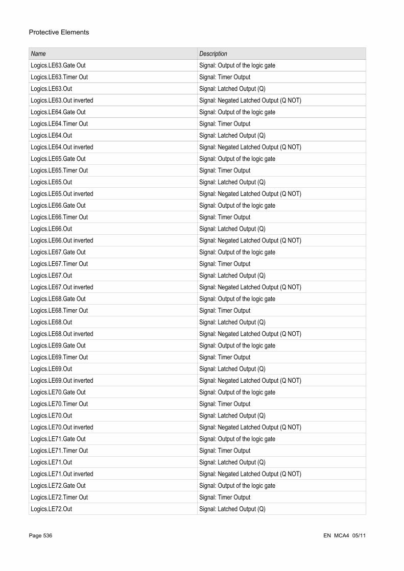
Protective Elements
Name Description
Logics.LE63.Gate Out Signal: Output of the logic gateLogics.LE63.Timer Out Signal: Timer OutputLogics.LE63.Out Signal: Latched Output (Q)Logics.LE63.Out inverted Signal: Negated Latched Output (Q NOT)Logics.LE64.Gate Out Signal: Output of the logic gateLogics.LE64.Timer Out Signal: Timer OutputLogics.LE64.Out Signal: Latched Output (Q)Logics.LE64.Out inverted Signal: Negated Latched Output (Q NOT)Logics.LE65.Gate Out Signal: Output of the logic gateLogics.LE65.Timer Out Signal: Timer OutputLogics.LE65.Out Signal: Latched Output (Q)Logics.LE65.Out inverted Signal: Negated Latched Output (Q NOT)Logics.LE66.Gate Out Signal: Output of the logic gateLogics.LE66.Timer Out Signal: Timer OutputLogics.LE66.Out Signal: Latched Output (Q)Logics.LE66.Out inverted Signal: Negated Latched Output (Q NOT)Logics.LE67.Gate Out Signal: Output of the logic gateLogics.LE67.Timer Out Signal: Timer OutputLogics.LE67.Out Signal: Latched Output (Q)Logics.LE67.Out inverted Signal: Negated Latched Output (Q NOT)Logics.LE68.Gate Out Signal: Output of the logic gateLogics.LE68.Timer Out Signal: Timer OutputLogics.LE68.Out Signal: Latched Output (Q)Logics.LE68.Out inverted Signal: Negated Latched Output (Q NOT)Logics.LE69.Gate Out Signal: Output of the logic gateLogics.LE69.Timer Out Signal: Timer OutputLogics.LE69.Out Signal: Latched Output (Q)Logics.LE69.Out inverted Signal: Negated Latched Output (Q NOT)Logics.LE70.Gate Out Signal: Output of the logic gateLogics.LE70.Timer Out Signal: Timer OutputLogics.LE70.Out Signal: Latched Output (Q)Logics.LE70.Out inverted Signal: Negated Latched Output (Q NOT)Logics.LE71.Gate Out Signal: Output of the logic gateLogics.LE71.Timer Out Signal: Timer OutputLogics.LE71.Out Signal: Latched Output (Q)Logics.LE71.Out inverted Signal: Negated Latched Output (Q NOT)Logics.LE72.Gate Out Signal: Output of the logic gateLogics.LE72.Timer Out Signal: Timer OutputLogics.LE72.Out Signal: Latched Output (Q)
Page 536 EN MCA4 05/11

Protective Elements
Name Description
Logics.LE72.Out inverted Signal: Negated Latched Output (Q NOT)Logics.LE73.Gate Out Signal: Output of the logic gateLogics.LE73.Timer Out Signal: Timer OutputLogics.LE73.Out Signal: Latched Output (Q)Logics.LE73.Out inverted Signal: Negated Latched Output (Q NOT)Logics.LE74.Gate Out Signal: Output of the logic gateLogics.LE74.Timer Out Signal: Timer OutputLogics.LE74.Out Signal: Latched Output (Q)Logics.LE74.Out inverted Signal: Negated Latched Output (Q NOT)Logics.LE75.Gate Out Signal: Output of the logic gateLogics.LE75.Timer Out Signal: Timer OutputLogics.LE75.Out Signal: Latched Output (Q)Logics.LE75.Out inverted Signal: Negated Latched Output (Q NOT)Logics.LE76.Gate Out Signal: Output of the logic gateLogics.LE76.Timer Out Signal: Timer OutputLogics.LE76.Out Signal: Latched Output (Q)Logics.LE76.Out inverted Signal: Negated Latched Output (Q NOT)Logics.LE77.Gate Out Signal: Output of the logic gateLogics.LE77.Timer Out Signal: Timer OutputLogics.LE77.Out Signal: Latched Output (Q)Logics.LE77.Out inverted Signal: Negated Latched Output (Q NOT)Logics.LE78.Gate Out Signal: Output of the logic gateLogics.LE78.Timer Out Signal: Timer OutputLogics.LE78.Out Signal: Latched Output (Q)Logics.LE78.Out inverted Signal: Negated Latched Output (Q NOT)Logics.LE79.Gate Out Signal: Output of the logic gateLogics.LE79.Timer Out Signal: Timer OutputLogics.LE79.Out Signal: Latched Output (Q)Logics.LE79.Out inverted Signal: Negated Latched Output (Q NOT)Logics.LE80.Gate Out Signal: Output of the logic gateLogics.LE80.Timer Out Signal: Timer OutputLogics.LE80.Out Signal: Latched Output (Q)Logics.LE80.Out inverted Signal: Negated Latched Output (Q NOT)
EN MCA4 05/11 Page 537
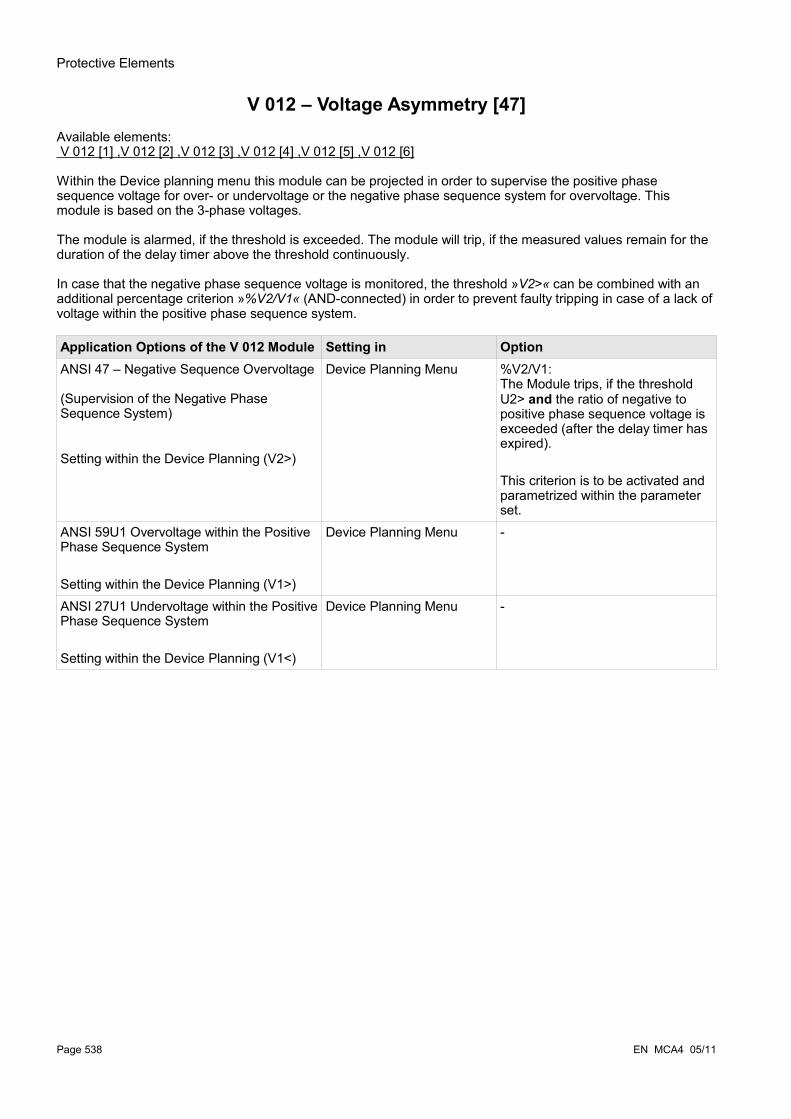
Protective Elements
V 012 – Voltage Asymmetry [47]Available elements: V 012 [1] ,V 012 [2] ,V 012 [3] ,V 012 [4] ,V 012 [5] ,V 012 [6]
Within the Device planning menu this module can be projected in order to supervise the positive phase sequence voltage for over- or undervoltage or the negative phase sequence system for overvoltage. This module is based on the 3-phase voltages.
The module is alarmed, if the threshold is exceeded. The module will trip, if the measured values remain for the duration of the delay timer above the threshold continuously.
In case that the negative phase sequence voltage is monitored, the threshold »V2>« can be combined with an additional percentage criterion »%V2/V1« (AND-connected) in order to prevent faulty tripping in case of a lack of voltage within the positive phase sequence system.
Application Options of the V 012 Module Setting in OptionANSI 47 – Negative Sequence Overvoltage
(Supervision of the Negative Phase Sequence System)
Setting within the Device Planning (V2>)
Device Planning Menu %V2/V1: The Module trips, if the threshold U2> and the ratio of negative to positive phase sequence voltage is exceeded (after the delay timer has expired).
This criterion is to be activated and parametrized within the parameter set.
ANSI 59U1 Overvoltage within the Positive Phase Sequence System
Setting within the Device Planning (V1>)
Device Planning Menu -
ANSI 27U1 Undervoltage within the Positive Phase Sequence System
Setting within the Device Planning (V1<)
Device Planning Menu -
Page 538 EN MCA4 05/11

Protective Elements
EN MCA4 05/11 Page 539
&
nam
e.Tr
ip
Ple
ase
Ref
er T
o D
iagr
am: B
lock
ings
NPS filte
r
VL1
nam
e.Al
arm
Ple
ase
Ref
er T
o D
iagr
am: T
rip b
lock
ings
V 01
2[1]
...[n
]
(Sta
ge is
not
dea
ctiv
ated
and
no
activ
e bl
ocki
ng s
igna
ls)
(Trip
ping
com
man
d no
t dea
ctiv
ated
or b
lock
ed. )
VL3
VL2
PPS
filte
r
V1>
0t
nam
e.t
nam
e =
V 01
2[1]
...[n
]
2 3
nam
e.Tr
ipC
md
1514
V2
nam
e.V2
>V1
nam
e.%(V
2/V1
)
&
activ
e
inac
tive
%(V
2/V1
)
>1&
V1 V2
V1<
| V1>
V2>
Devi
ce p
lann
ing
nam
e.M
ode
inac
tive
nam
e.M
eas
Circ
uit
Supe
rv
activ
e
38a
12a
12b
38b
>1
nam
e.M
ode
V1<
V2>
Dev
ice
plan
ning
&
&
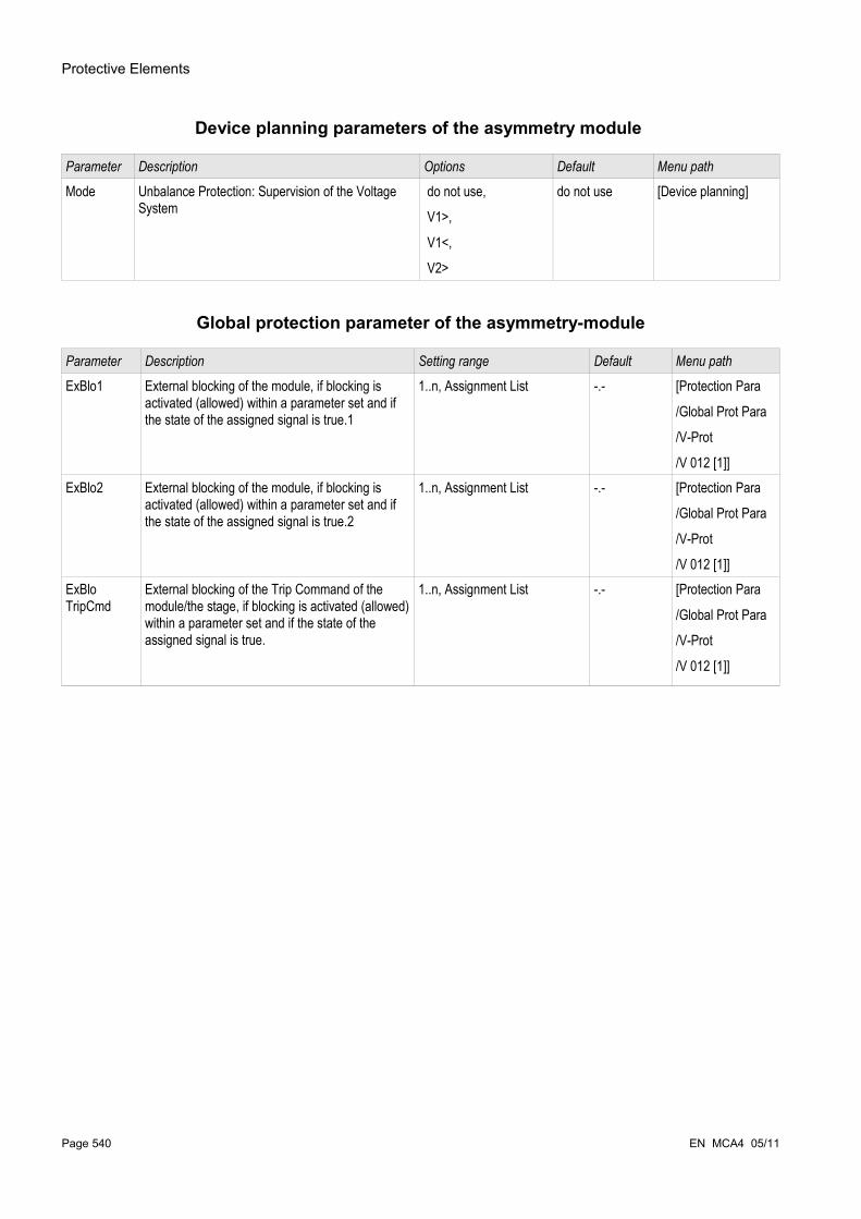
Protective Elements
Device planning parameters of the asymmetry module
Parameter Description Options Default Menu path
Mode Unbalance Protection: Supervision of the Voltage System
do not use,
V1>,
V1<,
V2>
do not use [Device planning]
Global protection parameter of the asymmetry-module
Parameter Description Setting range Default Menu path
ExBlo1 External blocking of the module, if blocking is activated (allowed) within a parameter set and if the state of the assigned signal is true.1
1..n, Assignment List -.- [Protection Para
/Global Prot Para
/V-Prot
/V 012 [1]]ExBlo2 External blocking of the module, if blocking is
activated (allowed) within a parameter set and if the state of the assigned signal is true.2
1..n, Assignment List -.- [Protection Para
/Global Prot Para
/V-Prot
/V 012 [1]]ExBlo TripCmd
External blocking of the Trip Command of the module/the stage, if blocking is activated (allowed) within a parameter set and if the state of the assigned signal is true.
1..n, Assignment List -.- [Protection Para
/Global Prot Para
/V-Prot
/V 012 [1]]
Page 540 EN MCA4 05/11
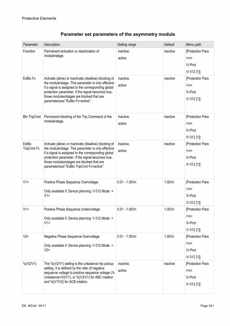
Protective Elements
Parameter set parameters of the asymmetry module
Parameter Description Setting range Default Menu path
Function Permanent activation or deactivation of module/stage.
inactive,
active
inactive [Protection Para
/<n>
/V-Prot
/V 012 [1]]ExBlo Fc Activate (allow) or inactivate (disallow) blocking of
the module/stage. This parameter is only effective if a signal is assigned to the corresponding global protection parameter. If the signal becomes true, those modules/stages are blocked that are parameterized "ExBlo Fc=active".
inactive,
active
inactive [Protection Para
/<n>
/V-Prot
/V 012 [1]]
Blo TripCmd Permanent blocking of the Trip Command of the module/stage.
inactive,
active
inactive [Protection Para
/<n>
/V-Prot
/V 012 [1]]ExBlo TripCmd Fc
Activate (allow) or inactivate (disallow) blocking of the module/stage. This parameter is only effective if a signal is assigned to the corresponding global protection parameter. If the signal becomes true, those modules/stages are blocked that are parameterized "ExBlo TripCmd Fc=active".
inactive,
active
inactive [Protection Para
/<n>
/V-Prot
/V 012 [1]]
V1> Positive Phase Sequence Overvoltage
Only available if: Device planning: V 012.Mode = V1>
0.01 - 1.50Vn 1.00Vn [Protection Para
/<n>
/V-Prot
/V 012 [1]]V1< Positive Phase Sequence Undervoltage
Only available if: Device planning: V 012.Mode = V1<
0.01 - 1.50Vn 1.00Vn [Protection Para
/<n>
/V-Prot
/V 012 [1]]V2> Negative Phase Sequence Overvoltage
Only available if: Device planning: V 012.Mode = V2>
0.01 - 1.50Vn 1.00Vn [Protection Para
/<n>
/V-Prot
/V 012 [1]]%(V2/V1) The %(V2/V1) setting is the unbalance trip pickup
setting. It is defined by the ratio of negative sequence voltage to positive sequence voltage (% Unbalance=V2/V1), or %(V2/V1) for ABC rotation and %(V1/V2) for ACB rotation.
inactive,
active
inactive [Protection Para
/<n>
/V-Prot
/V 012 [1]]
EN MCA4 05/11 Page 541

Protective Elements
Parameter Description Setting range Default Menu path
%(V2/V1) The %(V2/V1) setting is the unbalance trip pickup setting. It is defined by the ratio of negative sequence voltage to positive sequence voltage (% Unbalance=V2/V1), or %(V2/V1) for ABC rotation and %(V1/V2) for ACB rotation.
Only available if: %(V2/V1) = use
2 - 40% 20% [Protection Para
/<n>
/V-Prot
/V 012 [1]]
t Tripping delay 0.00 - 300.00s 0.00s [Protection Para
/<n>
/V-Prot
/V 012 [1]]Meas Circuit Superv
Measuring Circuit Supervision
Only available if: Device planning: V 012.Mode = V2>
inactive,
active
inactive [Protection Para
/<n>
/V-Prot
/V 012 [1]]
States of the inputs of the asymmetry module
Name Description Assignment via
ExBlo1-I Module input state: External blocking1 [Protection Para
/Global Prot Para
/V-Prot
/V 012 [1]]ExBlo2-I Module input state: External blocking2 [Protection Para
/Global Prot Para
/V-Prot
/V 012 [1]]ExBlo TripCmd-I Module input state: External Blocking of the
Trip Command[Protection Para
/Global Prot Para
/V-Prot
/V 012 [1]]
Page 542 EN MCA4 05/11

Protective Elements
Signals of the asymmetry module (states of the outputs)
Name Description
active Signal: activeExBlo Signal: External BlockingBlo TripCmd Signal: Trip Command blockedExBlo TripCmd Signal: External Blocking of the Trip CommandAlarm Signal: Alarm voltage asymmetryTrip Signal: TripTripCmd Signal: Trip Command
EN MCA4 05/11 Page 543

Protective Elements
Commissioning: Asymmetry Protection
Object to be testedTest of the asymmetry protection elements.
Necessary means• 3-phase AC voltage source • Timer for measuring of the tripping time• Voltmeter
Testing the tripping values (Example)
Set the pickup value for the voltage in the negative phase sequence to 0.5 Vn. Set the tripping delay to 1 s.
In order to generate a negative phase sequence voltage interchange the wiring of two phases (VL2 and VL3).
Testing the trip delay Start the timer and abrupt change (switch) to 1.5 times of the set tripping value. Measure the trip delay.
Successful test result The measured threshold values and trip delays comply with those specified in the adjustment list. Permissible deviations/tolerances can be taken from the Technical Data.
Page 544 EN MCA4 05/11

Protective Elements
PQS - Power [32, 37]Available stages: PQS [1] ,PQS [2] ,PQS [3] ,PQS [4] ,PQS [5] ,PQS [6]
Each of the elements can be used as P<, P>, Pr>, Q<, Q>, Qr>, S< or S> within the device planning.
P< and P> are settable and effective in positive active power range, Q< and Q> in positive reactive power range. These modes are used for protecting against underload or overload in positive power direction.
The apparent power makes S< or S> effective like a circle in all power quadrants. Protection is against underload and overload.
In reverse mode, Pr> is effective in negative active power range and Qr> in negative reactive power range. Both modes protect against power direction reversing from positive into negative direction.
The following graphics show the areas that are protected by the corresponding modes.
EN MCA4 05/11 Page 545
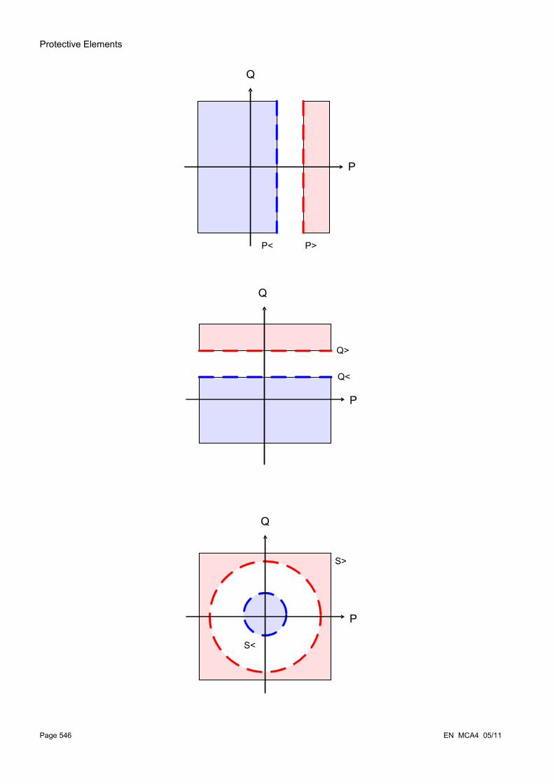
Protective Elements
Page 546 EN MCA4 05/11
P>P<
Q
P
Q
P
Q>
Q<
Q
P
S>
S<

Protective Elements
EN MCA4 05/11 Page 547
Pr>
Q
P
Q
PQr>

Protective Elements
Page 548 EN MCA4 05/11
&
Ple
ase
Ref
er T
o D
iagr
am: B
lock
ings
Ple
ase
Ref
er T
o D
iagr
am: T
rip b
lock
ings
(Sta
ge is
not
dea
ctiv
ated
and
no
activ
e bl
ocki
ng s
igna
ls)
(Trip
ping
com
man
d no
t dea
ctiva
ted
or b
lock
ed. )
0t
nam
e.t
nam
e =
PQS[
1]...
[n]
&
nam
e.Al
arm na
me.
Trip
2 3
nam
e.Tr
ipC
md 1514
P> P<
Dev
ice
plan
ning
Pr>
Q>
Q<
Qr> S> S<
P Q S
nam
e.M
ode
P>,
P<,
Pr>
, Q>,
Q<,
Qr>
, S>,
S<
PQS.
Mod
e
PQS[
1]...
[n]
38a
38b
40
>1
inac
tive
nam
e.M
easC
ircSv
Cur
r
activ
e
&
inac
tive
nam
e.M
easC
ircSv
Vol
t
activ
e>1
& &

Protective Elements
Device planning parameters of the Power Protection module
Parameter Description Options Default Menu path
Mode Mode do not use,
P>,
P<,
Pr>,
Q>,
Q<,
Qr>,
S>,
S<
PQS [1]: P>
PQS [2]: do not use
PQS [3]: do not use
PQS [4]: do not use
PQS [5]: do not use
PQS [6]: do not use
[Device planning]
Global protection parameter of the Power Protection-module
Parameter Description Setting range Default Menu path
ExBlo1 External blocking of the module, if blocking is activated (allowed) within a parameter set and if the state of the assigned signal is true.
1..n, Assignment List -.- [Protection Para
/Global Prot Para
/P-Prot
/PQS [1]]ExBlo2 External blocking of the module, if blocking is
activated (allowed) within a parameter set and if the state of the assigned signal is true.
1..n, Assignment List -.- [Protection Para
/Global Prot Para
/P-Prot
/PQS [1]]ExBlo TripCmd
External blocking of the Trip Command of the module/the stage, if blocking is activated (allowed) within a parameter set and if the state of the assigned signal is true.
1..n, Assignment List -.- [Protection Para
/Global Prot Para
/P-Prot
/PQS [1]]
EN MCA4 05/11 Page 549

Protective Elements
Parameter set parameters of the Power Protection module
Parameter Description Setting range Default Menu path
Function Permanent activation or deactivation of module/stage.
inactive,
active
PQS [1]: active
PQS [2]: inactive
PQS [3]: inactive
PQS [4]: inactive
PQS [5]: inactive
PQS [6]: inactive
[Protection Para
/<n>
/P-Prot
/PQS [1]]
ExBlo Fc Activate (allow) or inactivate (disallow) blocking of the module/stage. This parameter is only effective if a signal is assigned to the corresponding global protection parameter. If the signal becomes true, those modules/stages are blocked that are parameterized "ExBlo Fc=active".
inactive,
active
inactive [Protection Para
/<n>
/P-Prot
/PQS [1]]
Blo TripCmd Permanent blocking of the Trip Command of the module/stage.
inactive,
active
inactive [Protection Para
/<n>
/P-Prot
/PQS [1]]ExBlo TripCmd Fc
Activate (allow) or inactivate (disallow) blocking of the module/stage. This parameter is only effective if a signal is assigned to the corresponding global protection parameter. If the signal becomes true, those modules/stages are blocked that are parameterized "ExBlo TripCmd Fc=active".
inactive,
active
inactive [Protection Para
/<n>
/P-Prot
/PQS [1]]
MeasCircSv Volt
Measuring circuit supervision voltage
Only available if: Device planning: PQS.Mode = P< Only available if: Device planning: PQS.Mode = Q< Only available if: Device planning: PQS.Mode = S<
inactive,
active
active [Protection Para
/<n>
/P-Prot
/PQS [1]]
MeasCircSv Curr
Measuring circuit supervision current
Only available if: Device planning: PQS.Mode = P< Only available if: Device planning: PQS.Mode = Q< Only available if: Device planning: PQS.Mode = S<
inactive,
active
active [Protection Para
/<n>
/P-Prot
/PQS [1]]
Page 550 EN MCA4 05/11
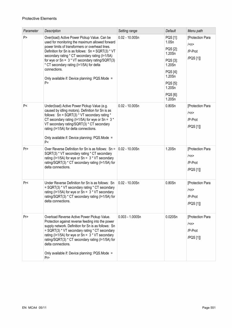
Protective Elements
Parameter Description Setting range Default Menu path
P> Over(load) Active Power Pickup Value. Can be used for monitoring the maximum allowed forward power limits of transformers or overhead lines. Definition for Sn is as follows: Sn = SQRT(3) * VT secondary rating * CT secondary rating (I=1/5A) for wye or Sn = 3 * VT secondary rating/SQRT(3) * CT secondary rating (I=1/5A) for delta connections.
Only available if: Device planning: PQS.Mode = P>
0.02 - 10.00Sn PQS [1]: 1.0Sn
PQS [2]: 1.20Sn
PQS [3]: 1.20Sn
PQS [4]: 1.20Sn
PQS [5]: 1.20Sn
PQS [6]: 1.20Sn
[Protection Para
/<n>
/P-Prot
/PQS [1]]
P< Under(load) Active Power Pickup Value (e.g. caused by idling motors). Definition for Sn is as follows: Sn = SQRT(3) * VT secondary rating * CT secondary rating (I=1/5A) for wye or Sn = 3 * VT secondary rating/SQRT(3) * CT secondary rating (I=1/5A) for delta connections.
Only available if: Device planning: PQS.Mode = P<
0.02 - 10.00Sn 0.80Sn [Protection Para
/<n>
/P-Prot
/PQS [1]]
Pr> Over Reverse Definition for Sn is as follows: Sn = SQRT(3) * VT secondary rating * CT secondary rating (I=1/5A) for wye or Sn = 3 * VT secondary rating/SQRT(3) * CT secondary rating (I=1/5A) for delta connections.
0.02 - 10.00Sn 1.20Sn [Protection Para
/<n>
/P-Prot
/PQS [1]]
Pr< Under Reverse Definition for Sn is as follows: Sn = SQRT(3) * VT secondary rating * CT secondary rating (I=1/5A) for wye or Sn = 3 * VT secondary rating/SQRT(3) * CT secondary rating (I=1/5A) for delta connections.
0.02 - 10.00Sn 0.80Sn [Protection Para
/<n>
/P-Prot
/PQS [1]]
Pr> Overload Reverse Active Power Pickup Value. Protection against reverse feeding into the power supply network. Definition for Sn is as follows: Sn = SQRT(3) * VT secondary rating * CT secondary rating (I=1/5A) for wye or Sn = 3 * VT secondary rating/SQRT(3) * CT secondary rating (I=1/5A) for delta connections.
Only available if: Device planning: PQS.Mode = Pr>
0.003 - 1.000Sn 0.020Sn [Protection Para
/<n>
/P-Prot
/PQS [1]]
EN MCA4 05/11 Page 551

Protective Elements
Parameter Description Setting range Default Menu path
Q> Over(load) Reactive Power Pickup Value. Monitoring the maximum allowed reactive power of the electrical equipment like transformers or overhead lines). If the maximum value is exceeded a condensator bank could be switched off. Definition for Sn is as follows: Sn = SQRT(3) * VT secondary rating * CT secondary rating (I=1/5A) for wye or Sn = 3 * VT secondary rating/SQRT(3) * CT secondary rating (I=1/5A) for delta connections.
Only available if: Device planning: PQS.Mode = Q>
0.02 - 10.00Sn 1.20Sn [Protection Para
/<n>
/P-Prot
/PQS [1]]
Q< Under(load) Reactive Power Pickup Value. Monitoring the minimum value of the reactive power. If it falls below the set value a condensator bank could be switched on. Definition for Sn is as follows: Sn = SQRT(3) * VT secondary rating * CT secondary rating (I=1/5A) for wye or Sn = 3 * VT secondary rating/SQRT(3) * CT secondary rating (I=1/5A) for delta connections.
Only available if: Device planning: PQS.Mode = Q<
0.02 - 10.00Sn 0.80Sn [Protection Para
/<n>
/P-Prot
/PQS [1]]
Qr> Over Reverse Definition for Sn is as follows: Sn = SQRT(3) * VT secondary rating * CT secondary rating (I=1/5A) for wye or Sn = 3 * VT secondary rating/SQRT(3) * CT secondary rating (I=1/5A) for delta connections.
0.02 - 10.00Sn 1.20Sn [Protection Para
/<n>
/P-Prot
/PQS [1]]
Qr< Under Reverse Definition for Sn is as follows: Sn = SQRT(3) * VT secondary rating * CT secondary rating (I=1/5A) for wye or Sn = 3 * VT secondary rating/SQRT(3) * CT secondary rating (I=1/5A) for delta connections.
0.02 - 10.00Sn 0.80Sn [Protection Para
/<n>
/P-Prot
/PQS [1]]
Qr> Overload Reverse Reactive Power Pickup Value Definition for Sn is as follows: Sn = SQRT(3) * VT secondary rating * CT secondary rating (I=1/5A) for wye or Sn = 3 * VT secondary rating/SQRT(3) * CT secondary rating (I=1/5A) for delta connections.
Only available if: Device planning: PQS.Mode = Qr>
0.003 - 1.000Sn 0.020Sn [Protection Para
/<n>
/P-Prot
/PQS [1]]
Page 552 EN MCA4 05/11

Protective Elements
Parameter Description Setting range Default Menu path
S> Over(load) Apparent Power Pickup Value Definition for Sn is as follows: Sn = SQRT(3) * VT secondary rating * CT secondary rating (I=1/5A) for wye or Sn = 3 * VT secondary rating/SQRT(3) * CT secondary rating (I=1/5A) for delta connections.
Only available if: Device planning: PQS.Mode = S>
0.02 - 10.00Sn 1.20Sn [Protection Para
/<n>
/P-Prot
/PQS [1]]
S< Under(load) Apparent Power Pickup Value Definition for Sn is as follows: Sn = SQRT(3) * VT secondary rating * CT secondary rating (I=1/5A) for wye or Sn = 3 * VT secondary rating/SQRT(3) * CT secondary rating (I=1/5A) for delta connections.
Only available if: Device planning: PQS.Mode = S<
0.02 - 10.00Sn 0.80Sn [Protection Para
/<n>
/P-Prot
/PQS [1]]
t Tripping delay 0.00 - 1100.00s PQS [1]: 1.00s
PQS [2]: 0.01s
PQS [3]: 0.01s
PQS [4]: 0.01s
PQS [5]: 0.01s
PQS [6]: 0.01s
[Protection Para
/<n>
/P-Prot
/PQS [1]]
States of the inputs of the Power Protection module
Name Description Assignment via
ExBlo1-I Module input state: External blocking [Protection Para
/Global Prot Para
/P-Prot
/PQS [1]]ExBlo2-I Module input state: External blocking [Protection Para
/Global Prot Para
/P-Prot
/PQS [1]]ExBlo TripCmd-I Module input state: External Blocking of the
Trip Command[Protection Para
/Global Prot Para
/P-Prot
/PQS [1]]
EN MCA4 05/11 Page 553

Protective Elements
Signals of the Power Protection module (states of the outputs)
Name Description
active Signal: activeExBlo Signal: External BlockingBlo TripCmd Signal: Trip Command blockedExBlo TripCmd Signal: External Blocking of the Trip CommandAlarm Signal: Alarm Power ProtectionTrip Signal: Trip Power ProtectionTripCmd Signal: Trip Command
Page 554 EN MCA4 05/11
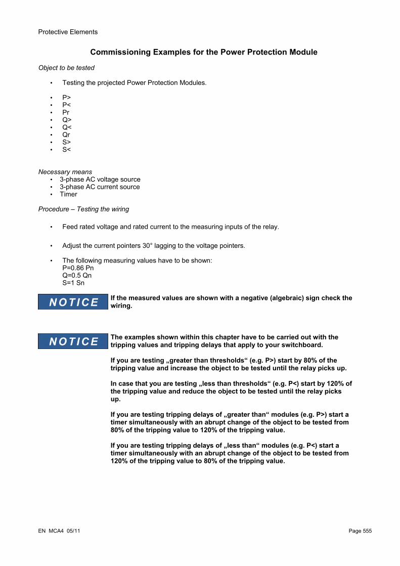
Protective Elements
Commissioning Examples for the Power Protection Module
Object to be tested
• Testing the projected Power Protection Modules.
• P>• P<• Pr• Q>• Q<• Qr• S>• S<
Necessary means• 3-phase AC voltage source • 3-phase AC current source • Timer
Procedure – Testing the wiring
• Feed rated voltage and rated current to the measuring inputs of the relay.
• Adjust the current pointers 30° lagging to the voltage pointers.
• The following measuring values have to be shown:P=0.86 PnQ=0.5 QnS=1 Sn
If the measured values are shown with a negative (algebraic) sign check the wiring.
The examples shown within this chapter have to be carried out with the tripping values and tripping delays that apply to your switchboard.
If you are testing „greater than thresholds“ (e.g. P>) start by 80% of the tripping value and increase the object to be tested until the relay picks up.
In case that you are testing „less than thresholds“ (e.g. P<) start by 120% of the tripping value and reduce the object to be tested until the relay picks up.
If you are testing tripping delays of „greater than“ modules (e.g. P>) start a timer simultaneously with an abrupt change of the object to be tested from 80% of the tripping value to 120% of the tripping value.
If you are testing tripping delays of „less than“ modules (e.g. P<) start a timer simultaneously with an abrupt change of the object to be tested from 120% of the tripping value to 80% of the tripping value.
EN MCA4 05/11 Page 555

Protective Elements
P>Testing the threshold values (Example, Threshold 1.1 Pn)
• Feed rated voltage and 0.9 times rated current in phase to the measuring inputs of the relay (PF=1).
• The measured values for the active power „P“ must show a positive algebraic sign.
• Set the tripping threshold (e.g. 1.1 Pn).
• In order to test the tripping thresholds feed 0.9 times rated current to the measuring inputs of the relay. Increase the current slowly until the relay picks up. Ensure that the angle between current and voltage remains constant. Compare the tripping value to the parameterized.
Testing the tripping delay (Example, Threshold 1.1 Pn)
• Feed rated voltage and rated current in phase to the measuring inputs of the relay (PF=1).
• The measured values for the active power „P“ must show a positive algebraic sign.
• Set the tripping threshold (e.g. 1.1 Pn).
• In order to test the tripping delay feed 0.9 times rated current to the measuring inputs of the relay. Increase the current with an abrupt change to 1.2 In. Ensure that the angle between current and voltage remains constant. Measure the tripping delay at the output of the relay.
Successful test resultThe measured total tripping delays or individual tripping delays, threshold values and fallback ratios correspond with those values, specified in the adjustment list. Permissible deviations/tolerances can be found under Technical Data.
Page 556 EN MCA4 05/11
Protective Elements
Q>Testing the threshold values (Example, Threshold 1,1 Qn)
• Feed rated voltage and 0.9 times rated current (90° phase shift) to the measuring inputs of the relay (PF=0).
• The measured values for the active power „Q“ must show a positive algebraic sign.
• Set the tripping threshold (e.g. 1.1 Qn).
• In order to test the tripping thresholds feed 0.9 times rated current to the measuring inputs of the relay. Increase the current slowly until the relay picks up. Ensure that the angle between current and voltage remains constant. Compare the tripping value to the parameterized.
Testing the tripping delay (Example, Threshold 1.1 Qn)
• Feed rated voltage and rated current (90° phase shift) to the measuring inputs of the relay (PF=0).
• The measured values for the active power „Q“ must show a positive algebraic sign.
• Set the tripping threshold (e.g. 1.1 Qn).
• In order to test the tripping delay feed 0.9 times rated current to the measuring inputs of the relay. Increase the current with an abrupt change to 1.2 In. Ensure that the angle between current and voltage remains constant. Measure the tripping delay at the output of the relay.
Successful test resultThe measured total tripping delays or individual tripping delays, threshold values and fallback ratios correspond with those values, specified in the adjustment list. Permissible deviations/tolerances can be found under Technical Data.
EN MCA4 05/11 Page 557

Protective Elements
P<Testing the threshold values (Example, Threshold 0.3 Pn)
• Feed rated voltage and rated current in phase to the measuring inputs of the relay (PF=1).
• The measured values for the active power „P“ must show a positive algebraic sign.
• Set the tripping threshold (e.g. 0.3 Pn).
• In order to test the tripping thresholds feed 0.5 times rated current to the measuring inputs of the relay. Reduce the current slowly until the relay picks up. Ensure that the angle between current and voltage remains constant. Compare the tripping value to the parameterized.
Testing the tripping delay (Example, Threshold 0.3 Pn)
• Feed rated voltage and rated current in phase to the measuring inputs of the relay (PF=1).
• The measured values for the active power „P“ must show a positive algebraic sign.
• Set the tripping threshold (e.g. 0.3 Pn).
• In order to test the tripping delay feed 0.5 times rated current to the measuring inputs of the relay. Increase the current with an abrupt change to 0.2 In. Ensure that the angle between current and voltage remains constant. Measure the tripping delay at the output of the relay.
Successful test resultThe measured total tripping delays or individual tripping delays, threshold values and fallback ratios correspond with those values, specified in the adjustment list. Permissible deviations/tolerances can be found under Technical Data.
Page 558 EN MCA4 05/11

Protective Elements
Q<Testing the threshold values (Example, Threshold 0.3 Qn)
• Feed rated voltage and 0.9 times rated current (90° phase shift) to the measuring inputs of the relay (PF=0).
• The measured values for the active power „Q“ must show a positive algebraic sign.
• Set the tripping threshold (e.g. 0.3 Qn).
• In order to test the tripping thresholds feed 0.5 times rated current to the measuring inputs of the relay. Reduce the current slowly until the relay picks up. Ensure that the angle between current and voltage remains constant. Compare the tripping value to the parameterized.
Testing the tripping delay (Example, Threshold 0.3 Qn)
• Feed rated voltage and 0.9 times rated current (90° phase shift) to the measuring inputs of the relay (PF=0).
• The measured values for the active power „Q“ must show a positive algebraic sign.
• Set the tripping threshold (e.g. 0.3 Qn).
• In order to test the tripping delay feed 0.5 times rated current to the measuring inputs of the relay. Increase the current with an abrupt change to 0.2 In. Ensure that the angle between current and voltage remains constant. Measure the tripping delay at the output of the relay.
Successful test resultThe measured total tripping delays or individual tripping delays, threshold values and fallback ratios correspond with those values, specified in the adjustment list. Permissible deviations/tolerances can be found under Technical Data.
EN MCA4 05/11 Page 559

Protective Elements
Pr
Testing the threshold values (Example, Threshold 0.2 Pn)
• Feed rated voltage and rated current with 180 degree phase shift between voltage and current pointers to the measuring inputs of the relay.
• The measured values for the active power „P“ must show a negative algebraic sign.
• Set the tripping threshold (e. g. 0.2 Pn).
• In order to test the tripping thresholds feed 0.1 times rated current to the measuring inputs of the relay. Increase the current slowly until the relay picks up. Ensure that the angle between current and voltage remains constant. Compare the tripping value to the parameterized.
Testing the tripping delay (Example, Threshold 0.2 Pn)
• Feed rated voltage and rated current with 180 degree phase shift between voltage and current pointers to the measuring inputs of the relay.
• The measured values for the active power „P“ must show a negative algebraic sign.
• Set the tripping threshold (e.g. 0.2 Pn).
• In order to test the tripping delay feed 0.1 times rated current to the measuring inputs of the relay. Increase the current with an abrupt change to 0.3 In. Ensure that the angle between current and voltage remains constant. Measure the tripping delay at the output of the relay.
Successful test resultThe measured total tripping delays or individual tripping delays, threshold values and fallback ratios correspond with those values, specified in the adjustment list. Permissible deviations/tolerances can be found under Technical Data.
Page 560 EN MCA4 05/11

Protective Elements
Qr
Testing the threshold values (Example, Threshold 0.2 Qn)
• Feed rated voltage and rated current with -90 degree phase shift between voltage and current pointers to the measuring inputs of the relay.
• The measured values for the active power „Q“ must show a negative algebraic sign.
• Set the tripping threshold (e. g. 0.2 Qn).
• In order to test the tripping delay feed 0.1 times rated current to the measuring inputs of the relay. Increase the current slowly until the relay picks up. Ensure that the angle between current and voltage remains constant. Measure the tripping delay at the output of the relay.
Testing the tripping delay (Example, Threshold 0.2 Qn)
• Feed rated voltage and rated current with -90 degree phase shift between voltage and current pointers to the measuring inputs of the relay.
• The measured values for the active power „Q“ must show a negative algebraic sign.
• Set the tripping threshold (e. g. 0.2 Qn).
• In order to test the tripping thresholds feed 0.1 times rated current to the measuring inputs of the relay. Increase the current with an abrupt change to 0.3 In. Ensure that the angle between current and voltage remains constant. Compare the tripping value to the parameterized.
Successful test resultThe measured total tripping delays or individual tripping delays, threshold values and fallback ratios correspond with those values, specified in the adjustment list. Permissible deviations/tolerances can be found under Technical Data.
EN MCA4 05/11 Page 561

Protective Elements
S>
Testing the threshold values
• Feed 80% of the S> threshold to the measuring inputs of the relay.
• Increase the fed power slowly until the relay picks up. Compare the measured value at the time of tripping to the parameterized setting.
Testing the tripping delay
• Feed 80% of the S> threshold to the measuring inputs of the relay.
• Increase the fed power with an abrupt change to 120% of the S> threshold. Measure the tripping delay at the output of the relay.
Successful test resultThe measured total tripping delays or individual tripping delays, threshold values and fallback ratios correspond with those values, specified in the adjustment list. Permissible deviations/tolerances can be found under Technical Data.
Page 562 EN MCA4 05/11
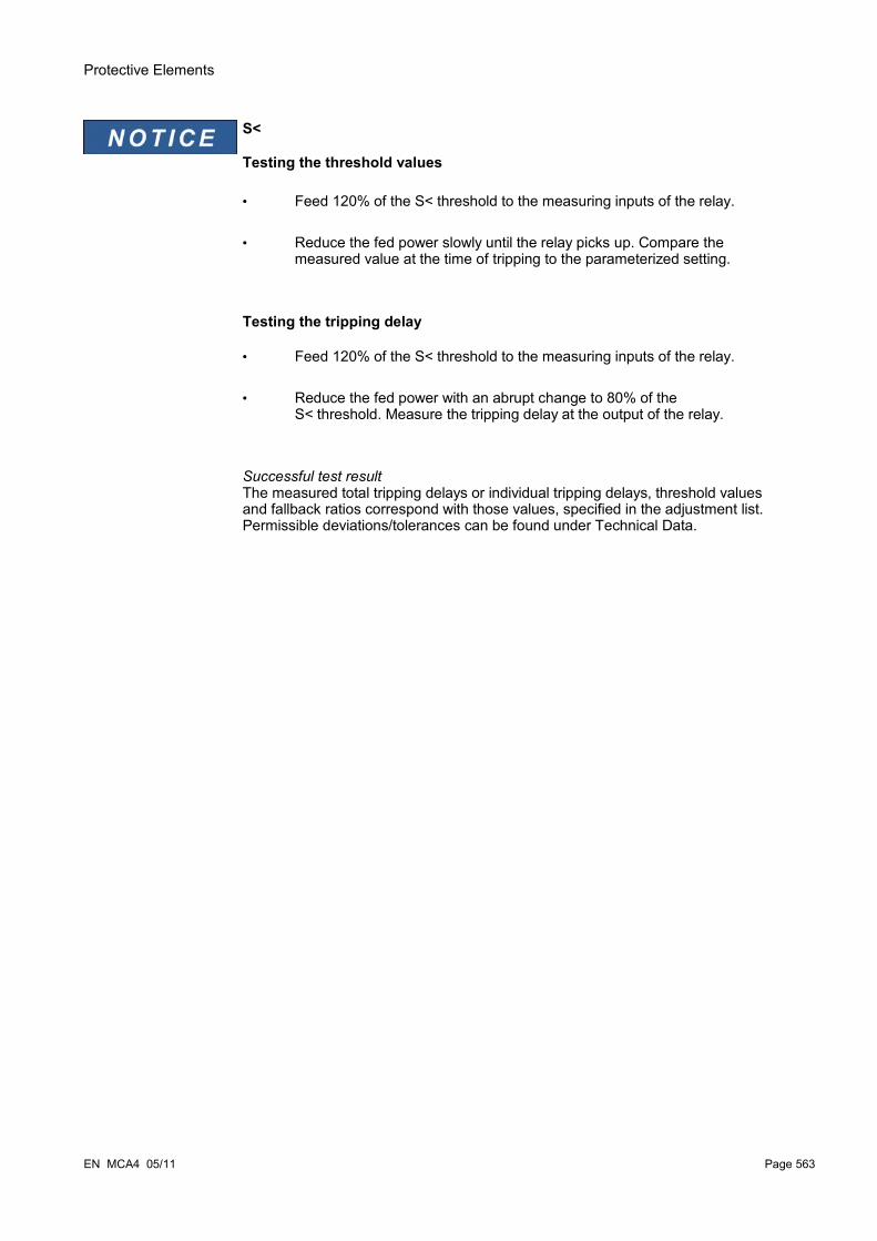
Protective Elements
S<
Testing the threshold values
• Feed 120% of the S< threshold to the measuring inputs of the relay.
• Reduce the fed power slowly until the relay picks up. Compare the measured value at the time of tripping to the parameterized setting.
Testing the tripping delay
• Feed 120% of the S< threshold to the measuring inputs of the relay.
• Reduce the fed power with an abrupt change to 80% of the S< threshold. Measure the tripping delay at the output of the relay.
Successful test resultThe measured total tripping delays or individual tripping delays, threshold values and fallback ratios correspond with those values, specified in the adjustment list. Permissible deviations/tolerances can be found under Technical Data.
EN MCA4 05/11 Page 563

Protective Elements
PF - Power Factor [55]Available stages: PF[1] ,PF[2]
These Element supervises the Power Factor within a defined area (limits).
The area is defined by four parameters.
• The Trigger quadrant (lead or lag).
• The Threshold (Power Factor value)
• The Reset quadrant (lead or lag).
• The Reset Value (Power Factor value)
Page 564 EN MCA4 05/11
Q
P
leading
leading
lagging
lagging
PF>0
PF>0 PF<0
PF<0
0°<phi<90°
270°<phi<360°
90°<phi<180°
180°<phi<270°
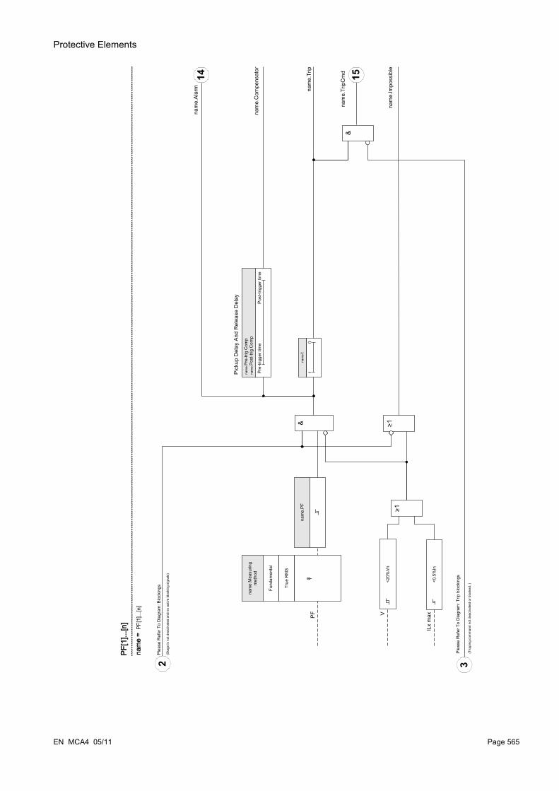
Protective Elements
EN MCA4 05/11 Page 565
nam
e.Tr
ip
Plea
se R
efer
To
Dia
gram
: Blo
ckin
gs
Plea
se R
efer
To
Dia
gram
: Trip
blo
ckin
gs
(Sta
ge is
not
dea
ctiv
ated
and
no
activ
e bl
ocki
ng s
igna
ls)
(Trip
ping
com
man
d no
t dea
ctiv
ated
or b
lock
ed. )
nam
e =
PF[1
]...[n
]
&
nam
e.Al
arm
2 3
nam
e.Tr
ipC
md 1514
0t
nam
e.t
<20%
Vn
<0.5
%In
ILx
maxV
>1
Post
-trig
ger t
ime
Pre-
trigg
er ti
me
nam
e.Pr
e-tri
g Co
mp
nam
e.Po
st-tr
ig C
omp
nam
e.PF
PF
&
nam
e.Im
poss
ible
nam
e.C
ompe
nsat
or
Pick
up D
elay
And
Rel
ease
Del
ay
PF[1
]...[n
]
>1
Fund
amen
tal
True
RM
S
nam
e.M
easu
ring
met
hod
φ

Protective Elements
Device planning parameters of the Power Factor module
Parameter Description Options Default Menu path
Mode Mode do not use,
use
do not use [Device planning]
Global protection parameter of the Power Factor-module
Parameter Description Setting range Default Menu path
ExBlo1 External blocking of the module, if blocking is activated (allowed) within a parameter set and if the state of the assigned signal is true.
1..n, Assignment List -.- [Protection Para
/Global Prot Para
/PF-Prot
/PF[1]]ExBlo2 External blocking of the module, if blocking is
activated (allowed) within a parameter set and if the state of the assigned signal is true.
1..n, Assignment List -.- [Protection Para
/Global Prot Para
/PF-Prot
/PF[1]]ExBlo TripCmd
External blocking of the Trip Command of the module/the stage, if blocking is activated (allowed) within a parameter set and if the state of the assigned signal is true.
1..n, Assignment List -.- [Protection Para
/Global Prot Para
/PF-Prot
/PF[1]]
Page 566 EN MCA4 05/11
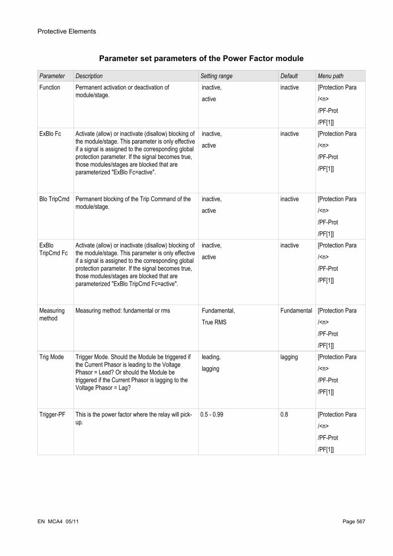
Protective Elements
Parameter set parameters of the Power Factor module
Parameter Description Setting range Default Menu path
Function Permanent activation or deactivation of module/stage.
inactive,
active
inactive [Protection Para
/<n>
/PF-Prot
/PF[1]]ExBlo Fc Activate (allow) or inactivate (disallow) blocking of
the module/stage. This parameter is only effective if a signal is assigned to the corresponding global protection parameter. If the signal becomes true, those modules/stages are blocked that are parameterized "ExBlo Fc=active".
inactive,
active
inactive [Protection Para
/<n>
/PF-Prot
/PF[1]]
Blo TripCmd Permanent blocking of the Trip Command of the module/stage.
inactive,
active
inactive [Protection Para
/<n>
/PF-Prot
/PF[1]]ExBlo TripCmd Fc
Activate (allow) or inactivate (disallow) blocking of the module/stage. This parameter is only effective if a signal is assigned to the corresponding global protection parameter. If the signal becomes true, those modules/stages are blocked that are parameterized "ExBlo TripCmd Fc=active".
inactive,
active
inactive [Protection Para
/<n>
/PF-Prot
/PF[1]]
Measuring method
Measuring method: fundamental or rms Fundamental,
True RMS
Fundamental [Protection Para
/<n>
/PF-Prot
/PF[1]]Trig Mode Trigger Mode. Should the Module be triggered if
the Current Phasor is leading to the Voltage Phasor = Lead? Or should the Module be triggered if the Current Phasor is lagging to the Voltage Phasor = Lag?
leading,
lagging
lagging [Protection Para
/<n>
/PF-Prot
/PF[1]]
Trigger-PF This is the power factor where the relay will pick-up.
0.5 - 0.99 0.8 [Protection Para
/<n>
/PF-Prot
/PF[1]]
EN MCA4 05/11 Page 567

Protective Elements
Parameter Description Setting range Default Menu path
Res Mode Trigger Mode. Should the Module be triggered if the Current Phasor is leading to the Voltage Phasor = Lead? Or should the Module be triggered if the Current Phasor is lagging to the Voltage Phasor = Lag?
leading,
lagging
leading [Protection Para
/<n>
/PF-Prot
/PF[1]]
Reset-PF This setting is the power factor, at which the relay will reset the power factor trip. It is like setting a hysteresis for the Trigger setting.
0.5 - 0.99 0.99 [Protection Para
/<n>
/PF-Prot
/PF[1]]t Tripping delay 0.00 - 300.00s 0.00s [Protection Para
/<n>
/PF-Prot
/PF[1]]Pre-trig Comp
Pickup (Pre-trigger) time for the Compensation Signal. When this timer is elapsed the compensation signal will be activated.
0.00 - 300.00s 5.00s [Protection Para
/<n>
/PF-Prot
/PF[1]]Post-trig Comp
Post-trigger time of the Compensation Signal. When this timer is elapsed the compensation signal will be deactivated.
0.00 - 300.00s 5.00s [Protection Para
/<n>
/PF-Prot
/PF[1]]
States of the inputs of the Power Factor module
Name Description Assignment via
ExBlo1-I Module input state: External blocking [Protection Para
/Global Prot Para
/PF-Prot
/PF[1]]ExBlo2-I Module input state: External blocking [Protection Para
/Global Prot Para
/PF-Prot
/PF[1]]ExBlo TripCmd-I Module input state: External Blocking of the
Trip Command[Protection Para
/Global Prot Para
/PF-Prot
/PF[1]]
Page 568 EN MCA4 05/11

Protective Elements
Signals of the Power Factor module (states of the outputs)
Name Description
active Signal: activeExBlo Signal: External BlockingBlo TripCmd Signal: Trip Command blockedExBlo TripCmd Signal: External Blocking of the Trip CommandAlarm Signal: Alarm Power FactorTrip Signal: Trip Power FactorTripCmd Signal: Trip CommandCompensator Signal: Compensation SignalImpossible Signal: Alarm Power Factor Impossible
EN MCA4 05/11 Page 569

Protective Elements
Commissioning: Power Factor [55]
Object to be tested
• Testing the projected Power Factor Modules
Necessary means• 3-phase AC voltage source • 3-phase AC current source • Timer
Procedure – Testing the wiring
• Feed rated voltage and rated current to the measuring inputs of the relay.
• Adjust the current pointers 30° lagging to the voltage pointers.
• The following measuring values have to be shown:P=0.86 PnQ=0.5 QnS=1 Sn
If the measured values are shown with a negative (algebraic) sign check the wiring.
In this example PF-Trigger is set to 0.86 = 30° (lagging) and PF-Reset is set to 0.86 = 30° leading.
Carry out the test with the settings (trigger and reset) that fit to your switchboard.
Testing the threshold values (Trigger) (PF Trigger: Example = 0.86 lagging)
• Feed rated voltage and rated current in phase to the measuring inputs of the relay (PF=1).
• Adjust the angle between voltage and current (current pointer lagging) until the relay picks up.
• Write down the pickup value.
Testing the Reset (PF Reset: Example = 0.86 leading)
• Reduce the angle between voltage and current beyond PF = 1 (current pointer leading) until the alarm drops off.
• Write down the reset value.
Page 570 EN MCA4 05/11

Protective Elements
Testing the trip delay (PF Trigger: Example = 0.86 lagging)
• Feed rated voltage and rated current in phase to the measuring inputs of the relay (PF=1).
• Adjust the angle between voltage and current (current pointer lagging) with an abrupt change to PF = 0.707 (45°) lagging.
• Measure the tripping delay at the output of the relay. Compare the measured tripping time to the parameterized.
Successful test resultThe measured total tripping delays, threshold and reset values correspond with those values, specified in the ad-justment list. Permissible deviations/tolerances can be found under Technical Data.
EN MCA4 05/11 Page 571

Protective Elements
Q->&V< Reactive-Power/Undervoltage ProtectionAvailable Elements: Q->&V<
The number of distributed energy resources (DER) raises continuously. At the same time the controllable power reserve through large-scale power plants decreases.
Therefore various grid codes requirements and regulations stipulate that mains parallel distributed power plants consisting of one or more power generation units feeding power into the MV grid, have to support the mains voltage in case of failures.
In case of failure the voltage close to the short circuit location drops to nearly zero. Around the fault location a potential gradient area is built whose expansion can be restricted by feeding reactive-power into the grid. At mains failures (voltage drop) the Q->V< protection prevents the expansion of the potential gradient area for the case that any further reactive-power is taken from the mains.
The function of this protection module is not the protection of the power generation system itself, but more the decoupling of the power generation system when it takes reactive current from the mains in case the voltage drops below a certain value. This protection is an upstream system protection.
The Q->&V< protection module with decoupling and auto reclosing function is implemented as an autonomous protection element acc. to the German regulations 1 and 2 mentioned below.
The comprehensive setting and configuration possibilities of this protection element allow the adaptation of connected energy resources to various grid conditions.
For the correct function of this protection module you have to
• Configure the »General Settings«,
• Select and set the decoupling method.
• Configure the reconnection of the power generation units.
General Settings
For each parameterset [Protection Para\Set [x]\Q->&U<] the general settings »General Settings« can be configured.
Here the entire function of this protection element can be activated or de-activated.
By activating the voltage transformer supervision a malfunction of this protection module can be prevented.
1 TransmissionCode 2007, Netz- und Systemregeln der deutschen Übertragungsnetzbetreiber, Version 1.1, August 2007, Verband der Netzbetreiber –VDN – e.V. beim VDEW siehe Kap. 3.3.13.5 (6)
2 Technische Richtlinie „Erzeugungsanlagen am Mittelspannungsnetz“, Richtlinie für Anschluss und Parallelbetrieb von Erzeugungsanlagen am Mittelspannungsnetz, Ausgabe Juni 2008, BDEW Bundesverband der Energie- und Wasserwirtschaft e.V., siehe Kap. 3.2.3.2 – Blindleistungs-Unterspannungsschutz Q->&U<
Page 572 EN MCA4 05/11

Protective Elements
Parameter Setting of Decoupling
To support the decreasing voltage (voltage drop) during faults the electric utilities require the following behaviour by the connected energy resources:
“During voltage dips under 85% of rated voltage (380/220/110 kV, e. g. 110 kV x 0.85 = 93.5 kV) and simultaneous reactive-power demand at the PCC = point of common coupling (underexcited operation), the connected energy resource has to be decoupled after 0.5 s.The voltage value refers to the highest value of the three phase to phase voltages. The decoupling has to be done at the generator circuit breaker.“
The reactive-power of the positive phase sequence system (Q1) is evaluated.
The voltage supervision only monitors the phase to phase voltages.This prevents any influence on the measurement through neutral point displacement in resonant earthed systems.
In the menu [Protection Para\Set[x]\Q->&U<] the »Decoupling« parameters can be set.
The reactive-power demand from the grid can be detected by two different methods. Therefor the decoupling method »QV-Method« has to be selected first.
• Power Angle Supervision (method 1)
• Pure Reactive Power Supervision (method 2)
Method 1: Power Angle Supervision
EN MCA4 05/11 Page 573
0.5
Phi-Power
GridP
GridP
0.5
Q 1S
P 1S
Phi-Power
I1 min QV.

Protective Elements
Method 2: Pure Reactive Power Supervision
A minimum current supervision (I1) in the positive phase sequence system prevents a hyperfunction of the reactive-power supervision at lower power levels.
For the power angle supervision, the minimum current supervision is always active. For the pure reactive-power supervision the minimum current supervision is optional.
When using the power angle supervision (method 1):
• Set the power factor »Phi-Power« (Default setting 3°).
• Select a suitable minimum current »I min QV« (Default setting 0.1 In) which prevents false trippings.
When using the pure reactive power supervision (method 2):
• Set the reactive-power threshold »Q min QV«(Default setting 0.05 Sn).
• Optionally select a suitable minimum current »I min QV« (Default setting 0.1 In) to prevent false trippings.
Two timer elements are available »t1-QV« und »t2-QV«. Both timer elements will be started at pick-up of theQ->U< module.
First timer element (Decoupling of the power generation unit)When several mains parallel power generation units feed one PCC, the first timer element can give a trip command to the generator circuit breaker of the power generation unit (Default setting 0.5 s)
Second timer element (Decoupling at the PCC)For the case, that tripping of the first timer element (decoupling of a certain power generation unit) does not have the expected effect the second timer element can give a trip command to the circuit breaker at the PCC (Default setting 1.5 s). This decouples the entire DER from the grid.
Page 574 EN MCA4 05/11
0.5
Grid
PGrid
P
0.5
Q 1S
P 1S
Q min QV: Trigger for the Reactive Power (Positive Phase Sequence System)
.
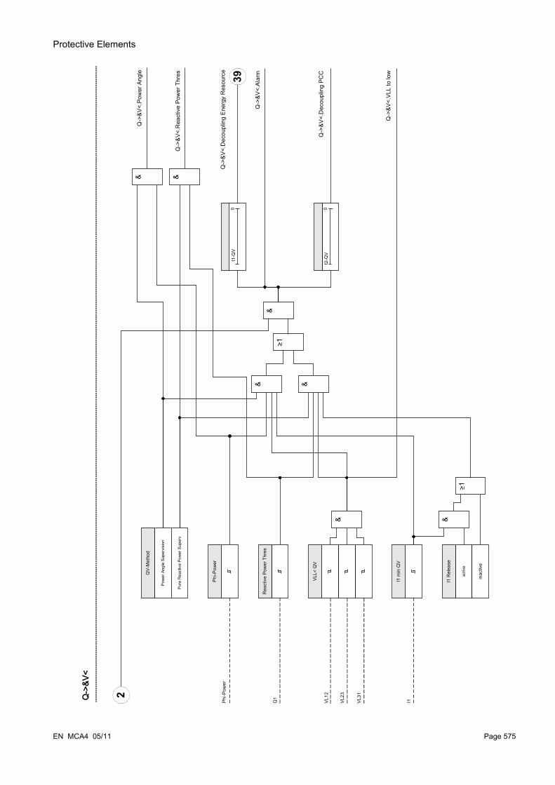
Protective Elements
EN MCA4 05/11 Page 575
>1
& &
&
VLL<
QV
&
Rea
ctiv
e Po
wer
Thr
es
Phi-P
ower
I1 m
in Q
V
activ
e
inac
tive
I1 R
elea
se
>1
&
Pow
er A
ngle
Sup
ervi
sion
Pure
Rea
ctiv
e Po
wer
Sup
erv
QV-
Met
hod
t2-Q
V0
t1-Q
V0
2
VL12
VL23
VL31Q->
&V<
Q->
&V<.
Dec
oupl
ing
Ener
gy R
esou
rce
Q->
&V<.
Dec
oupl
ing
PCC
Q->
&V<.
Alar
m
Q->
&V<.
Rea
ctiv
e Po
wer
Thr
es
Q->
&V<.
Pow
er A
ngle
& &
I1Q1
Phi-P
ower
39
Q->
&V<.
VLL
to lo
w

Protective Elements
Reclosing
The reclosing function after a mains decoupling is based on the requirements of the Transmission-Code (TC2007)[1] and the German directive „Erzeugungsanlagen am MS-Netz“ [2].
To monitor the reclosing conditions after a mains decoupling, a reclosing function has been implemented additionally to the decoupling function.
The main criteria for reclosing are mains voltage (phase to phase) and frequency. Always the mains side voltage at the generator circuit breaker has to be evaluated.
The reclosing function is only one of the system functions for mains decoupling and return synchronizing.Triggering of the reclosing function is only possible after a trip of the first timer element (decoupling of a power generation unit). After a trip of the circuit breaker at the PCC by the decoupling function, reclosing has to be done manually.
Danger of asynchronously reclosing:The reclosing function does not substitute a synchronizing device.Before connecting different electrical networks, synchronism has to be secured.
After decoupling by the Q->&V< module or other decoupling functions, like V</V<<, V>/>>, f</> the reclosing release signal for reclosing the circuit breaker of the power generating unit will be blocked for a preset time interval (default setting 10 min.).
This is to wait until all switching operations are completed. The reclosing release only will be issued, when after elapse of the mains recovery time the thresholds for mains voltage and frequency are met.
Release logic for the PCC circuit breakerIf the PCC circuit breaker has tripped reclosing has to be done manually. A special blocking logic is not necessary.
If a power generating unit should be reconnected by the generator circuit breaker the voltage transformers have to be installed at the mains side of the circuit breaker.
Page 576 EN MCA4 05/11

Protective Elements
Release logic for the PCC circuit breaker.
EN MCA4 05/11 Page 577
VLL>
Rel
ease
inac
tive
activ
e
V Ex
t Rel
ease
PC
C
&
f< (5
0,05
Hz)
f> (4
7,5
Hz)
V In
tern
al R
elea
se
V Ex
t Rel
ease
PC
C
Rec
losu
re R
elea
se C
ond
& &
&&
>1&
Dec
oupl
ing1
Dec
oupl
ing3
Dec
oupl
ing2
Rec
losu
reTr
igge
r
Dec
oupl
ing4
Dec
oupl
ing5
Dec
oupl
ing6
>1
&
Q->
&V<.
Rel
ease
Ene
rgy
Res
ourc
e
f
Q->
&V<.
PCC
V R
elea
se
2
V Ex
t Rel
ease
PCC
39 Q->
&V<.
Alar
m
VL12
VL23
VL31
digi
tal i
nput
0D
elay
Tim
er
t1-R
elea
se B
lo
inac
tive
activ
e
PCC
Fus
e Fa
il VT
&
PCC
Fus
e Fa
il VT
digi
tal i
nput
Protective Elements
Voltage release via remote control connection from the PCC
This method has to be used, if the PCC is on the HV side.
This method can be used, if the PCC is on the MV side.
If reclosing should be done via remote control signal from the PCC:
In the menu [Protection Para\Set[x]\Q->&U<\General settings] the parameter »PCC-Release Fc« has to be set to »active«. With this setting the voltage release signal from the PCC is used (e. g. signal via digital input)
Additionally the parameter »Reclosure Release Cond« in the menu [Protection Para\Set[x]\Q->&U<\Reclosure\Reclosure Trigger] has to be set to »PCC (Extrernal Release)«
Also the remote control release signal has to be assigned to the parameter »PCC-Release« in the menu [Protection Para\Global Prot Para\Q->&V<]
Voltage release by measured voltage values
This method can be used, if the PCC is on the MV side.
If the PCC is on the MV side, the device can measure the phase to phase voltages on the mains side and decide if the mains voltage has stabilized sufficiently for reclosing.
For this method the parameter »V Ext Release PCC Fk« in the menu [Protection Para\Set[x]\Q->&V<\General settings] has to be set to »inactive«.
Additionally the parameter »»Reclosure Release Cond«« in the menu[Protection Para\Set[x]\Q->&V<\Reclosure\Reclosure Release] has to be set to »Internal Release«
Page 578 EN MCA4 05/11

Protective Elements
PCC in HV systems
According to the TranmissionCode 2007 [1] the following condition has to be observed:After decoupling of a DER caused by overfrequency, underfrequency, undervoltage, overvoltage or after isolated operation, automatic synchronizing of the generators to the grid is only allowed under the following conditions:
• The voltage in a 110 kV system is higher than 105 kV• The voltage in a 220 kV system is higher than 210 kV• The voltage in a 380 kV system is higher than 370 kV
The voltage values refer to the lowest voltage of the three phase to phase voltages.
It is required that the PCC and also the DER are equipped with a decoupling devices.
It is required that the decoupling device of the PCC controls the PCC's circuit breaker.
It is required that the decoupling device of the power generation unit controls the generator circuit breaker.
Reclosing Conditions:
Before reclosing a power generation unit, it has to be secured, that mains voltage has stabilized sufficiently. For this a corresponding remote signal has to be available.
Set the parameter »Reclosure Release Cond« in the menu [Protection Para\Set[x]\Q->&V<\Reclosure\Reclosure Release] to »V Ext Release PCC«. The required parameter settings are described in the chapter »General Settings«.
Set the blocking signals in the menu[Protection Para\Set[x]\Q->&V<\Reclosure\Reclosure Trigger] which start the mains recovery time(OR logic).
Select a sufficiently long recovery time »t1-Release Blo« in the menu[Protection Para\Set[x]\Q->&V<\Reclosure\Reclosure Release Cond]. Reclosing is only possible after this time has elapsed.
In the menu [Protection Para\Set[x]\Q->&V<\Reclosure\Reclosure Release Cond] the frequency range to be met for reclosing can be set.
EN MCA4 05/11 Page 579
Protective Elements
PCC in MV systems
It is required that the PCC and also the DER are equipped with a decoupling devices.
It is required that the decoupling device of the PCC controls the PCC's circuit breaker.
It is required that the decoupling device of the power generation unit controls the generator circuit breaker.
The German regulation „Erzeugungsanlagen am MS-Netz“ (BDEW, Issue June 2008 [2]) recommends to have a time delay (some minutes) between mains voltage recovery and reclosure after a trip of a decoupling system as a result of a mains failure. This is to wait until all switching operations are completed. Usually this is the case af-ter 10 minutes. A reclosing of the DER is only permitted, when the mains voltage is >95% of Vn and the frequen-cy is in the range of 47.5 Hz to 50.05 Hz.
Set the blocking signals in the menu[Protection Para\Set[x]\Q->&V<\Reclosure\Reclosure Trigger] which start the mains recovery time(OR logic).
Select a sufficiently long recovery time »t1-Release Blo« in the menu[Protection Para\Set[x]\Q->&V<\Reclosure\Reclosure Release Cond]. Reclosing is only possible after this time has elapsed.
In the menu [Protection Para\Set[x]\Q->&V<\Reclosure\Reclosure Release Cond] the frequency range to be met for reclosing can be set.
For the case, that the reclosure release should be realized via internal measurement values, the mains voltage threshold »VLL>« can be set in the [Protection Para\Set[x]\Q->&V<\Reclosure\Reclosure Release Cond] menu (default 0.95 Vn). For reclosing all phase to phase voltages have to be above this threshold. The required parameter settings are described in the chapter »General Settings«.
Page 580 EN MCA4 05/11

Protective Elements
Device Planning Parameters of the Q->&V< Module
Parameter Description Options Default Menu path
Mode Mode do not use,
use
do not use [Device planning]
Global Protection Parameters of the Q->&V< Module
Parameter Description Setting range Default Menu path
ExBlo1 External blocking of the module, if blocking is activated (allowed) within a parameter set and if the state of the assigned signal is true.
1..n, Assignment List -.- [Protection Para
/Global Prot Para
/Q->&V<]
ExBlo2 External blocking of the module, if blocking is activated (allowed) within a parameter set and if the state of the assigned signal is true.
1..n, Assignment List -.- [Protection Para
/Global Prot Para
/Q->&V<]
V Ext Release PCC
Release Signal by the Point of Common Coupling. The line-to-line voltage is greater than 95% of VN.
1..n, Assignment List -.- [Protection Para
/Global Prot Para
/Q->&V<]
PCC Fuse Fail VT
Blocking if the fuse of a voltage transformer has tripped at the PCC.
1..n, Dig Inputs -.- [Protection Para
/Global Prot Para
/Q->&V<]
EN MCA4 05/11 Page 581
Protective Elements
Decoupling Functions of the Q->&V< Module
Name Description
-.- No assignmentV[1].TripCmd Signal: Trip CommandV[2].TripCmd Signal: Trip CommandV[3].TripCmd Signal: Trip CommandV[4].TripCmd Signal: Trip CommandV[5].TripCmd Signal: Trip CommandV[6].TripCmd Signal: Trip CommandVG[1].TripCmd Signal: Trip CommandVG[2].TripCmd Signal: Trip Commandf[1].TripCmd Signal: Trip Commandf[2].TripCmd Signal: Trip Commandf[3].TripCmd Signal: Trip Commandf[4].TripCmd Signal: Trip Commandf[5].TripCmd Signal: Trip Commandf[6].TripCmd Signal: Trip CommandPF[1].TripCmd Signal: Trip CommandPF[2].TripCmd Signal: Trip Command
Page 582 EN MCA4 05/11

Protective Elements
Setting Group Parameters of the Q->&V< Module
Parameter Description Setting range Default Menu path
Function Permanent activation or deactivation of module/stage.
inactive,
active
inactive [Protection Para
/<n>
/Q->&V<
/General settings]ExBlo Fc Activate (allow) or inactivate (disallow) blocking of
the module/stage. This parameter is only effective if a signal is assigned to the corresponding global protection parameter. If the signal becomes true, those modules/stages are blocked that are parameterized "ExBlo Fc=active".
inactive,
active
inactive [Protection Para
/<n>
/Q->&V<
/General settings]
Meas circuit superv
Measuring circuit supervision inactive,
active
active [Protection Para
/<n>
/Q->&V<
/General settings]V Ext Release PCC Fc
Activate the release signal of the Point of Common Coupling. The line-to-line voltage is greater than 95% of VN.
inactive,
active
inactive [Protection Para
/<n>
/Q->&V<
/General settings]
QV-Method Selection of the Q(V)-Method: Power Angle or Reactive Power Threshold
Power Angle Supervision,
Pure Reactive Power Superv
Power Angle Supervision
[Protection Para
/<n>
/Q->&V<
/Decoupling]I1 Release Activation of the "I1 Minimum Current"-Criterion.
Only available if: QV-Method = Power Angle Supervision
inactive,
active
active [Protection Para
/<n>
/Q->&V<
/Decoupling]I1 min QV Activation of an "I1 Minimum Current" of the rated
current of the (distributed) energy resource can prevent faulty tripping.
Only available if:Activation of the "I1 Minimum Current"-Criterion. = active
0.01 - 0.20In 0.10In [Protection Para
/<n>
/Q->&V<
/Decoupling]
VLL< QV Undervoltage threshold (line-to-line voltage!) 0.70 - 1.00Vn 0.85Vn [Protection Para
/<n>
/Q->&V<
/Decoupling]
EN MCA4 05/11 Page 583
Protective Elements
Parameter Description Setting range Default Menu path
Phi-Power Trigger Phi-Power (Positive Phase Sequence System)
Only available if: QV-Method = Power Angle Supervision
0 - 10° 3° [Protection Para
/<n>
/Q->&V<
/Decoupling]Q min QV Trigger for the Reactive Power (Positive Phase
Sequence System)
Only available if: QV-Method = Pure Reactive Power Superv
0.01 - 0.20Sn 0.05Sn [Protection Para
/<n>
/Q->&V<
/Decoupling]t1-QV First timer. If this timer has elapsed, a trip signal
will be issued to the (local) energy resource.0.00 - 2.00s 0.5s [Protection Para
/<n>
/Q->&V<
/Decoupling]t2-QV Second timer. If this timer is elapsed, the an trip
signal will be issued to the PCC (Point of Common Coupling)
0.00 - 4.00s 1.5s [Protection Para
/<n>
/Q->&V<
/Decoupling]$$(UFreigabeAuswahl _k)
$$(UFreigabeAuswahl _h) V Internal Release,
V Ext Release PCC
V Internal Release
[Protection Para
/<n>
/Q->&V<
/Reclosure
/Reclosure Release Cond]
PCC Fuse Fail VT Fk
Blocking if the fuse of a voltage transformer has tripped at the PCC.
Only available if: $$(UFreigabeAuswahl _k)
inactive,
active
inactive [Protection Para
/<n>
/Q->&V<
/Reclosure
/Reclosure Release Cond]
Decoupling1 Decoupling function, that blocks the reclosure. ReclosureTrigger -.- [Protection Para
/<n>
/Q->&V<
/Reclosure
/ReclosureTrigger]Decoupling2 Decoupling function, that blocks the reclosure. ReclosureTrigger -.- [Protection Para
/<n>
/Q->&V<
/Reclosure
/ReclosureTrigger]
Page 584 EN MCA4 05/11

Protective Elements
Parameter Description Setting range Default Menu path
Decoupling3 Decoupling function, that blocks the reclosure. ReclosureTrigger -.- [Protection Para
/<n>
/Q->&V<
/Reclosure
/ReclosureTrigger]Decoupling4 Decoupling function, that blocks the reclosure. ReclosureTrigger -.- [Protection Para
/<n>
/Q->&V<
/Reclosure
/ReclosureTrigger]Decoupling5 Decoupling function, that blocks the reclosure. ReclosureTrigger -.- [Protection Para
/<n>
/Q->&V<
/Reclosure
/ReclosureTrigger]Decoupling6 Decoupling function, that blocks the reclosure. ReclosureTrigger -.- [Protection Para
/<n>
/Q->&V<
/Reclosure
/ReclosureTrigger]VLL> Release
Minimum voltage (line-to-line) for reclosure (Restoration Voltage)
Only available if: $$(UFreigabeAuswahl _k)
0.70 - 1.00Vn 0.95Vn [Protection Para
/<n>
/Q->&V<
/Reclosure
/Reclosure Release Cond]
f< Lower voltage (line-to-line) limit for the reclosure (Restoration Voltage)
40.00 - 69.90Hz 47.5Hz [Protection Para
/<n>
/Q->&V<
/Reclosure
/Reclosure Release Cond]
f> Upper frequency limit for the reclosure 40.00 - 69.90Hz 50.05Hz [Protection Para
/<n>
/Q->&V<
/Reclosure
/Reclosure Release Cond]
EN MCA4 05/11 Page 585

Protective Elements
Parameter Description Setting range Default Menu path
t1-Release Blo
Time stage (delay) for the reclosure of the energy resources
0.00 - 3600.00s 600s [Protection Para
/<n>
/Q->&V<
/Reclosure
/Reclosure Release Cond]
Page 586 EN MCA4 05/11

Protective Elements
Input States of the Q->&V< ModuleName Description Assignment via
ExBlo1-I Module input state: External blocking1 [Protection Para
/Global Prot Para
/Q->&V<]ExBlo2-I Module input state: External blocking2 [Protection Para
/Global Prot Para
/Q->&V<]V Ext Release PCC-I Module input state: Release signal is being
generated by the PCC (External Release)[Protection Para
/Global Prot Para
/Q->&V<]PCC Fuse Fail VT-I State of the module input: Blocking if the
fuse of a voltage transformer has tripped at the PCC.
[Protection Para
/Global Prot Para
/Q->&V<]
EN MCA4 05/11 Page 587
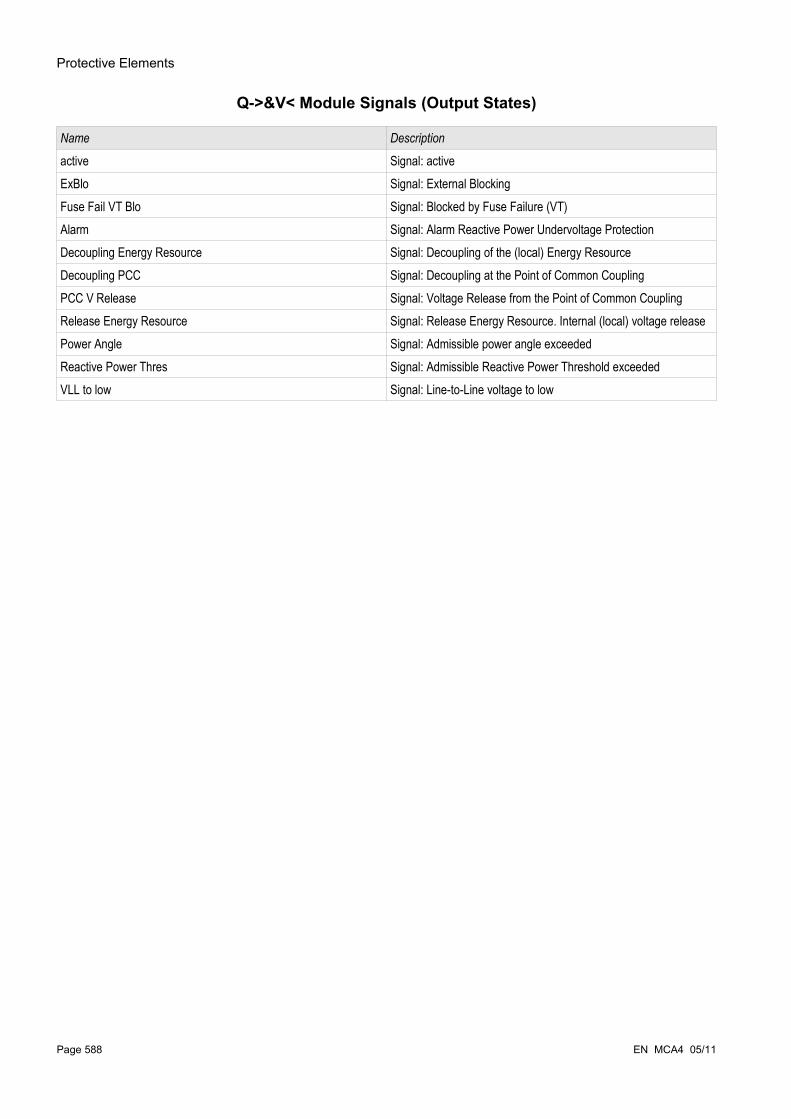
Protective Elements
Q->&V< Module Signals (Output States)
Name Description
active Signal: activeExBlo Signal: External BlockingFuse Fail VT Blo Signal: Blocked by Fuse Failure (VT)Alarm Signal: Alarm Reactive Power Undervoltage ProtectionDecoupling Energy Resource Signal: Decoupling of the (local) Energy ResourceDecoupling PCC Signal: Decoupling at the Point of Common CouplingPCC V Release Signal: Voltage Release from the Point of Common CouplingRelease Energy Resource Signal: Release Energy Resource. Internal (local) voltage releasePower Angle Signal: Admissible power angle exceededReactive Power Thres Signal: Admissible Reactive Power Threshold exceededVLL to low Signal: Line-to-Line voltage to low
Page 588 EN MCA4 05/11
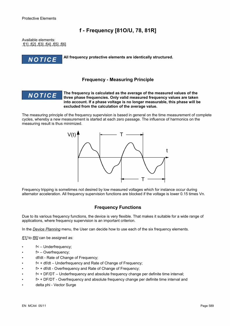
Protective Elements
f - Frequency [81O/U, 78, 81R]Available elements: f[1] ,f[2] ,f[3] ,f[4] ,f[5] ,f[6]
All frequency protective elements are identically structured.
Frequency - Measuring Principle
The frequency is calculated as the average of the measured values of the three phase frequencies. Only valid measured frequency values are taken into account. If a phase voltage is no longer measurable, this phase will be excluded from the calculation of the average value.
The measuring principle of the frequency supervision is based in general on the time measurement of complete cycles, whereby a new measurement is started at each zero passage. The influence of harmonics on the measuring result is thus minimized.
Frequency tripping is sometimes not desired by low measured voltages which for instance occur during alternator acceleration. All frequency supervision functions are blocked if the voltage is lower 0.15 times Vn.
Frequency Functions
Due to its various frequency functions, the device is very flexible. That makes it suitable for a wide range of applications, where frequency supervision is an important criterion.
In the Device Planning menu, the User can decide how to use each of the six frequency elements.
f[1] to f[6] can be assigned as:
• f< – Underfrequency;• f> – Overfrequency;• df/dt - Rate of Change of Frequency;• f< + df/dt – Underfrequency and Rate of Change of Frequency;• f> + df/dt - Overfrequency and Rate of Change of Frequency;• f< + DF/DT – Underfrequency and absolute frequency change per definite time interval;• f> + DF/DT - Overfrequency and absolute frequency change per definite time interval and• delta phi - Vector Surge
EN MCA4 05/11 Page 589
V(t)
t
T
T

Protective Elements
f< – Underfrequency
This protection element provides a pickup threshold and a tripping delay. If the frequency falls below the set pickup threshold, an alarm will be issued instantaneously. If the frequency remains under the set pickup threshold until the tripping delay has elapsed, a tripping command will be issued.
With this setting, the frequency element protects electrical generators, consumers, or electrical operating equipment in general against underfrequency.
f> – Overfrequency
This protection element provides a pickup threshold and a tripping delay. If the frequency exceeds the set pickup threshold, an alarm will be issued instantaneously. If the frequency remains above the set tripping pickup until the tripping delay has elapsed, a tripping command will be issued.
With this setting the frequency element protects electrical generators, consumers, or electrical operating equipment in general against overfrequency.
Working Principle f< and f>
(Please refer to the block diagram on next page.)
The frequency element supervises the three phase voltages »VL1«, »VL2« and »VL3«. If any of the three phase voltages is below 15% Vn, the frequency calculation is blocked. According to the frequency supervision mode set in the Device Planning (f< or f>), the phase voltages are compared to the set pickup threshold for over- or under-frequency. If in any of the phases, the frequency exceeds or falls below the set pickup threshold and if there are no blocking commands for the frequency element, an alarm is issued instantaneously and the tripping delay timer is started. When the frequency still exceeds or is below the set pickup threshold after the tripping delay timer has elapsed, a tripping command will be issued.
Page 590 EN MCA4 05/11

Protective Elements
EN MCA4 05/11 Page 591
&na
me.
Trip
Cm
d
nam
e.Tr
ip f
Ple
ase
Ref
er T
o D
iagr
am: B
lock
ings
VL1
nam
e.Al
arm
f
Ple
ase
Ref
er T
o D
iagr
am: T
rip b
lock
ings
f[1]..
.[n]
(Sta
ge is
not
dea
ctiv
ated
and
no
activ
e bl
ocki
ng s
igna
ls)
(Trip
ping
com
man
d no
t dea
ctiv
ated
or b
lock
ed. )
VL3
VL2
0t
nam
e.t
nam
e =
f[1]..
.[n]
nam
e.Bl
o by
V<
V Bl
ock
f
&
nam
e.f
(f>|f<
)
f>
nam
e.M
ode
f<
Dev
ice
plan
ning
&Fr
eque
ncy
calc
ulat
ion
fna
me.
Trip
nam
e.Al
arm
2 3
1514
Fiel
d Pa
ra

Protective Elements
df/dt - Rate of Change of Frequency
Electrical generators running in parallel with the mains, (e. g. industrial internal power supply plants), should be separated from the mains when failure in the intra-system occurs for the following reasons:
• Damage to electrical generators must be prevented when mains voltage is recoveringasynchronously, (e. g. after a short interruption).
• The industrial internal power supply must be maintained.
A reliable criterion of detecting mains failure is the measurement of the rate of change of frequency (df/dt). The precondition for this is a load flow via the mains coupling point. At mains failure the load flow change spontaneously leads to an increasing or decreasing frequency. At active power deficit of the internal power station, a linear drop of the frequency occurs and a linear increase occurs at power excess. Typical frequency gradients during application of "mains decoupling" are in the range of 0.5 Hz/s up to over 2 Hz/s.
The protective device detects the instantaneous frequency gradient (df/dt) of each mains voltage period. Through multiple evaluations of the frequency gradient in sequence the continuity of the directional change (sign of the frequency gradient) is determined. Because of this special measuring procedure a high safety in tripping and thus a high stability against transient processes, (e. g. switching procedure) are achieved.
The frequency gradient (rate of change of frequency [df/dt]) may have a negative or positive sign, depending on frequency increase (positive sign) or decrease (negative sign).
In the frequency parameter sets, the User can define the kind of df/dt mode:
• Positive df/dt = the frequency element detects an increase in frequency• Negative df/dt = the frequency element detects a decrease in frequency and• Absolute df/dt (positive and negative) = the frequency element detects both, increase and decrease in
frequency
This protection element provides a tripping threshold and a tripping delay. If the frequency gradient df/dt exceeds or falls below the set tripping threshold, an alarm will be issued instantaneously. If the frequency gradient remains still above/below the set tripping threshold until the tripping delay has elapsed, a tripping command will be issued.
Working Principle df/dt
(Please refer to the block diagram on next page)
The frequency element supervises the three phase voltages »VL1«, »VL2« and »VL3«. If any of the three phase voltages is below 15% Vn, the frequency calculation is blocked. According to the frequency supervision mode set in the Device Planning (df/dt), the phase voltages are compared to the set frequency gradient (df/dt) threshold. If in any of the phases, the frequency gradient exceeds or falls below the set pickup threshold (acc. to the set df/dt mode) and if there are no blocking commands for the frequency element, an alarm is issued instantaneously and the tripping delay timer is started. When the frequency gradient still exceeds or is below the set pickup threshold after the tripping delay timer has elapsed, a tripping command will be issued.
Page 592 EN MCA4 05/11
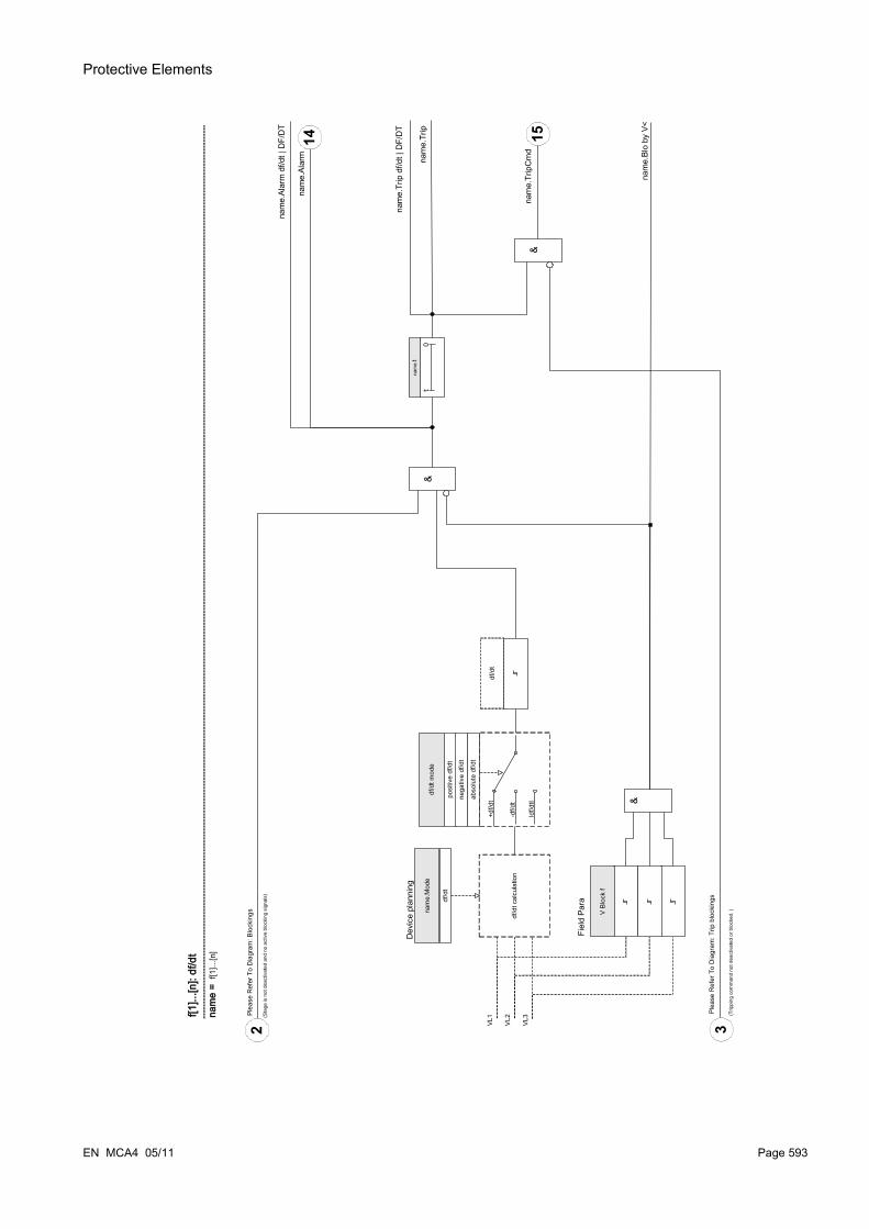
Protective Elements
EN MCA4 05/11 Page 593
&
VL1
VL3
VL2
df/d
t cal
cula
tion
&
df/d
t
df/d
t mod
e
+df/d
t
Idf/d
tI
-df/d
t
0t
nam
e.t
f[1]..
.[n]:
df/d
t
nam
e =
f[1]..
.[n]
Ple
ase
Ref
er T
o D
iagr
am: B
lock
ings
Ple
ase
Ref
er T
o D
iagr
am: T
rip b
lock
ings
(Sta
ge is
not
dea
ctiv
ated
and
no
activ
e bl
ocki
ng s
igna
ls)
(Trip
ping
com
man
d no
t dea
ctiv
ated
or b
lock
ed. )V
Bloc
k f
Fiel
d Pa
ra
&posi
tive
df/d
tne
gativ
e df
/dt
abso
lute
df/d
t
nam
e.Al
arm
df/d
t | D
F/D
T
df/d
t
Dev
ice
plan
ning
nam
e.M
ode
nam
e.Bl
o by
V<
nam
e.Al
arm nam
e.Tr
ip
nam
e.Tr
ip d
f/dt |
DF/
DT
2 3
nam
e.Tr
ipCm
d1514

Protective Elements
f< and df/dt – Underfrequency and Rate of Change of Frequency
With this setting the frequency element supervises if the frequency falls below a set pickup threshold and if the frequency gradient exceeds a set threshold at the same time.
In the selected frequency parameter set f[X], an underfrequency pickup threshold f<, a frequency gradient df/dt and a tripping delay can be set.
Whereby:• Positive df/dt = the frequency element detects an increase in frequency• Negative df/dt = the frequency element detects a decrease in frequency and• Absolute df/dt (positive and negative) = the frequency element detects both, increase and decrease in
frequency
f> and df/dt – Overfrequency and Rate of Change of Frequency
With this setting the frequency element supervises if the frequency exceeds a set pickup threshold and if the frequency gradient exceeds a set threshold at the same time.
In the selected frequency parameter set f[X], an overfrequency pickup threshold f>, a frequency gradient df/dt and a tripping delay can be set.
Whereby:• Positive df/dt = the frequency element detects an increase in frequency• Negative df/dt = the frequency element detects a decrease in frequency and• Absolute df/dt (positive and negative) = the frequency element detects both, increase and decrease in
frequency
Working Principle f< and df/dt | f> and df/dt
(Please refer to the block diagram on next page)
The frequency element supervises the three phase voltages »VL1«, »VL2« and »VL3«. If any of the three phase voltages is below 15% Vn, the frequency calculation is blocked. According to the frequency supervision mode set in the Device Planning (f< and df/dt or f> and dt/dt), the phase voltages are compared to the set frequency pickup threshold and the set frequency gradient (df/dt) threshold. If in any of the phases, both - the frequency and the frequency gradient exceed or fall below the set thresholds and if there are no blocking commands for the frequency element, an alarm is issued instantaneously and the tripping delay timer is started. When the frequency and the frequency gradient still exceed or are below the set threshold after the tripping delay timer has elapsed, a tripping command will be issued.
Page 594 EN MCA4 05/11
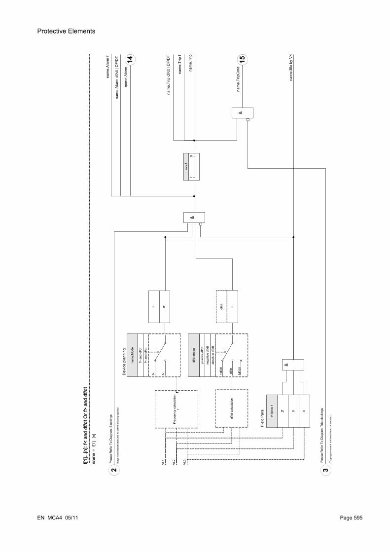
Protective Elements
EN MCA4 05/11 Page 595
&
Freq
uenc
y ca
lcul
atio
nf
VL1
VL3
VL2
f
df/d
t cal
cula
tion
&
nam
e.Al
arm
f
df/d
t
df/d
t mod
e
+df/d
t
Idf/d
tI
-df/d
t
0t
nam
e.t
f[1]..
.[n]:
f< a
nd d
f/dt O
r f>
and
df/d
tna
me
= f[1
]...[n
]
Ple
ase
Ref
er T
o D
iagr
am: B
lock
ings
Ple
ase
Ref
er T
o D
iagr
am: T
rip b
lock
ings
(Sta
ge is
not
dea
ctiv
ated
and
no
activ
e bl
ocki
ng s
igna
ls)
(Trip
ping
com
man
d no
t dea
ctiv
ated
or b
lock
ed. )
f
V Bl
ock
f
Fiel
d Pa
ra
&posi
tive
df/d
t
nega
tive
df/d
t
abso
lute
df/d
t
nam
e.Al
arm
nam
e.Tr
ip f
nam
e.Bl
o by
V<
nam
e.Tr
ip
nam
e.Tr
ip d
f/dt |
DF/
DT
nam
e.Al
arm
df/d
t | D
F/D
T2 3
nam
e.Tr
ipC
md
1514f>
and
df/d
t
nam
e.M
ode
Dev
ice
plan
ning
f< a
nd d
f/dt
f> f<

Protective Elements
f< and DF/DT – Underfrequency and DF/DT
With this setting the frequency element supervises the frequency and the absolute frequency difference during a definite time interval.
In the selected frequency parameter set f[X], an underfrequency pickup threshold f<, a threshold for the absolute frequency difference (frequency decrease) DF and supervision interval DT can be set.
f> and DF/DT – Overfrequency and DF/DT
With this setting the frequency element supervises the frequency and the absolute frequency difference during a definite time interval.
In the selected frequency parameter set f[X], an overfrequency pickup threshold f>, a threshold for the absolute frequency difference (frequency increase) DF and supervision interval DT can be set.
Working principle f< and DF/DT | f> and DF/DT
(please refer to block diagram on next page)
The frequency element supervises the three phase voltages »VL1«, »VL2« and »VL3«. If any of the three phase voltages is below 15% Vn, the frequency calculation is blocked. According to the frequency supervision mode set in the Device Planning (f< and DF/DT or f> and DF/DT), the phase voltages are compared to the set frequency pickup threshold and the set frequency decrease or increase threshold DF.If in any of the phases, the frequency exceeds or falls below the set pickup threshold and if there are no blocking commands for the frequency element, an alarm is issued instantaneously. At the same time the timer for the supervision interval DT is started. When, during the supervision interval DT, the frequency still exceeds or is below the set pickup threshold and the frequency decrease/increase reaches the set threshold DF, a tripping command will be issued.
Working Principle of DF/DT Function
(Please refer to f(t) diagram after the block diagram)
Case 1:When the frequency falls below a set f< threshold at t1, the DF/DT element energizes. If the frequency difference (decrease) does not reach the set value DF before the time interval DT has expired, no trip will occur. The frequency element remains blocked until the frequency falls below the underfrequency threshold f< again.
Case 2:When the frequency falls below a set f< threshold at t4, the DF/DT element energizes. If the frequency difference (decrease) reaches the set value DF before the time interval DT has expired (t5), a trip command is issued.
Page 596 EN MCA4 05/11

Protective Elements
EN MCA4 05/11 Page 597
&
&1
DT
t <nam
e>
.f+
DF
&
Freq
uenc
y ca
lcul
atio
nf
V Bl
ock
f
Fiel
d Pa
ra
&
f> a
nd D
F/D
T
Dev
ice
plan
ning
f< a
nd D
F/D
T
f> f<
Ple
ase
Ref
er T
o D
iagr
am: T
rip b
lock
ings
(Trip
ping
com
man
d no
t dea
ctiv
ated
or b
lock
ed. )
Ple
ase
Ref
er T
o D
iagr
am: B
lock
ings
(Sta
ge is
not
dea
ctiv
ated
and
no
activ
e bl
ocki
ng s
igna
ls)
f[1]..
.[n]:
f< a
nd D
F/D
T O
r f>
and
DF/
DT
nam
e =
f[1]..
.[n]
nam
e.Bl
o by
V<
VL1
VL3
VL2
f
nam
e.M
ode
nam
e.Al
arm
f
nam
e.Al
arm
nam
e.Al
arm
df/d
t | D
F/D
T
nam
e.Tr
ip f
nam
e.Tr
ip
nam
e.Tr
ip d
f/dt |
DF/
DT
2 4
nam
e.Tr
ipC
md
1514

Protective Elements
Page 598 EN MCA4 05/11
fNf f<
DT
DT
Res
et
DF
DF
DF
tem
pora
rily
bloc
king
t
t1t2
t3t4
t6
Trip
f[1]..
.[n]:
f< a
nd D
F/D
T na
me
= f[1
]...[n
]
t5

Protective Elements
Delta phi - Vector Surge
The vector surge supervision protects synchronous generators in mains parallel operation due to very fast decoupling in case of mains failure. Very dangerous are mains auto reclosings for synchronous generators. The mains voltage returning typically after 300 ms can hit the generator in asynchronous position. A very fast decoupling is also necessary in case of long time mains failures.
Generally there are two different applications:
Only mains parallel operation - no single operation:In this application the vector surge supervision protects the generator by tripping the generator circuit breaker in case of mains failure.
Mains parallel operation and single operation:For this application the vector surge supervision trips the mains circuit breaker. Here it is insured that the gen.-set is not blocked when it is required as an emergency set.
A very fast decoupling in case of mains failures for synchronous generators is very difficult. Voltage supervision units cannot be used because the synchronous alternator as well as the consumer impedance support the decreasing voltage.
In this situation the mains voltage drops only after some 100 ms below the pickup threshold of the voltage supervision and therefore a safe detection of mains auto reclosings is not possible with voltage supervision only.
Frequency supervision is partially unsuitable because only a highly loaded generator decreases its speed within 100 ms. Current relays detect a fault only when short-circuit type currents exist, but cannot avoid their development. Power relays are able to pickup within 200 ms, but they also cannot prevent the power rising to short-circuit values. Since power changes are also caused by sudden loaded alternators, the use of power relays can be problematic.
Whereas the vector surge supervision of the device detects mains failures within 60 ms without the restrictions described above because it is specially designed for applications where very fast decoupling from the mains is required. Adding the typical operating time of a circuit breaker or contactor, the total disconnection time remains below 150 ms.
Basic requirement for tripping of the generator/mains monitor is a change in load of more than 15 - 20% of the rated load. Slow changes of the system frequency, for instance at regulating processes (adjustment of speed regulator) do not cause the relay to trip.
Trippings can also be caused by short-circuits within the grid, because a voltage vector surge higher than the preset value can occur. The magnitude of the voltage vector surge depends on the distance between the short-circuit and the generator. This function is also of advantage to the Power Utility Company because the mains short-circuit capacity and, consequently, the energy feeding the short-circuit is limited.
To prevent a possible false tripping, the vector surge measuring is blocked at a low input voltage <15% Vn. The undervoltage lockout acts faster then the vector surge measurement.
Vector surge tripping is blocked by a phase loss so that a VT fault (e. g.: faulty VTs fuse) does not cause false tripping.
EN MCA4 05/11 Page 599

Protective Elements
Measuring Principle of Vector Surge Supervision
Equivalent circuit at synchronous generator in parallel with the mains.
Voltage vectors at mains parallel operation.
The rotor displacement angle between stator and rotor is dependent on the mechanical moving torque of the generator. The mechanical shaft power is balanced with the electrical fed mains power and, therefore the synchronous speed keeps constant.
Page 600 EN MCA4 05/11
Grid/Load
Generator
VPV1
V = I1* j Xd
Grid
V = I1* j Xd
VP V1
I1 I2
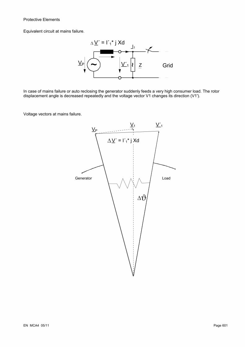
Protective Elements
Equivalent circuit at mains failure.
In case of mains failure or auto reclosing the generator suddenly feeds a very high consumer load. The rotor displacement angle is decreased repeatedly and the voltage vector V1 changes its direction (V1').
Voltage vectors at mains failure.
EN MCA4 05/11 Page 601
Grid
V´ = I´1* j Xd
VP V´1
I1
Generator Load
VPV1 V´1
V´ = I´1* j Xd

Protective Elements
Voltage vector surge.
As shown in the voltage/time diagram the instantaneous value of the voltage jumps to another value and the phase position changes. This is called phase or vector surge.
The relay measures the cycle duration. A new measuring is started at each zero passage. The measured cycle duration is internally compared with a reference time and from this the deviation of the cycle duration of the voltage signal is ascertained. In case of a vector surge as shown in the above graphic, the zero passage occurs either earlier or later. The established deviation of the cycle duration is in compliance with the vector surge angle.If the vector surge angle exceeds the set value, the relay trips immediately.
Tripping of the vector surge is blocked in case of loss of one or more phases of the measuringvoltage.
Working Principle delta phi
(Please refer to the block diagram on next page)
The vector surge element supervises the three phase voltages »VL1«, »VL2« and »VL3«. If any of the three phase voltages is below 15% Vn, the vector surge calculation is blocked. According to the frequency supervision mode set in the Device Planning (delta phi), the phase voltages are compared to the set vector surge threshold. If in any of the phases, the vector surge exceeds the set threshold and if there are no blocking commands for the frequency element, an alarm and a trip command is issued instantaneously.
Page 602 EN MCA4 05/11
V(t) V(t) V(t)`
Trip
tt=0
delta phi
Voltage Vector Surge
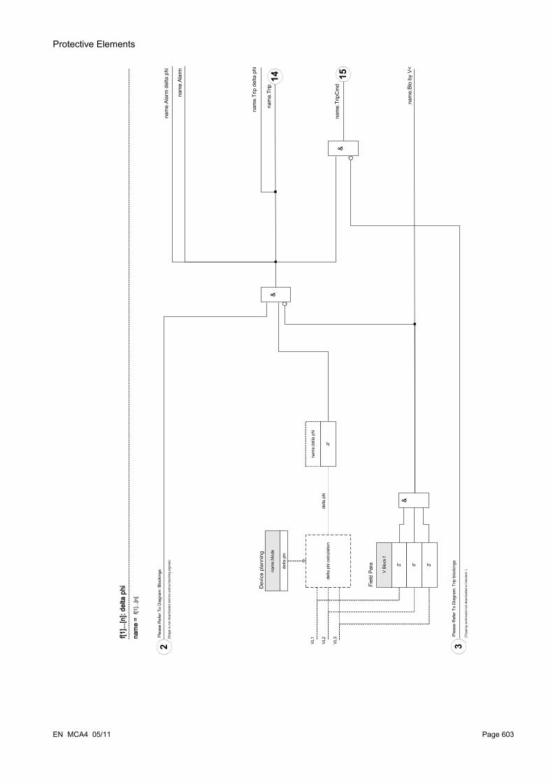
Protective Elements
EN MCA4 05/11 Page 603
&
VL1
VL3
VL2
delta
phi
cal
cula
tion
&
nam
e.de
lta p
hi
f[1]..
.[n]:
delta
phi
nam
e =
f[1]..
.[n]
Plea
se R
efer
To
Dia
gram
: Blo
ckin
gs
Ple
ase
Ref
er T
o D
iagr
am: T
rip b
lock
ings
(Sta
ge is
not
dea
ctiv
ated
and
no
activ
e bl
ocki
ng s
igna
ls)
(Trip
ping
com
man
d no
t dea
ctiv
ated
or b
lock
ed. )V
Bloc
k f
Fiel
d Pa
ra
&
nam
e.Al
arm
nam
e.Tr
ip
delta
phi
Dev
ice
plan
ning
nam
e.M
ode
delta
phi
nam
e.Bl
o by
V<
nam
e.Tr
ip d
elta
phi
nam
e.Al
arm
del
ta p
hi2 3
nam
e.Tr
ipC
md
1514

Protective Elements
Device Planning Parameters of the Frequency Protection Module
Parameter Description Options Default Menu path
Mode Mode do not use,
f<,
f>,
f< and df/dt,
f> and df/dt,
f< and DF/DT,
f> and DF/DT,
df/dt,
delta phi
f[1]: f<
f[2]: f>
f[3]: do not use
f[4]: do not use
f[5]: do not use
f[6]: do not use
[Device planning]
Global Protection Parameters of the Frequency Protection Module
Parameter Description Setting range Default Menu path
ExBlo1 External blocking of the module, if blocking is activated (allowed) within a parameter set and if the state of the assigned signal is true.
1..n, Assignment List -.- [Protection Para
/Global Prot Para
/f-Prot
/f[1]]ExBlo2 External blocking of the module, if blocking is
activated (allowed) within a parameter set and if the state of the assigned signal is true.
1..n, Assignment List -.- [Protection Para
/Global Prot Para
/f-Prot
/f[1]]ExBlo TripCmd
External blocking of the Trip Command of the module/the stage, if blocking is activated (allowed) within a parameter set and if the state of the assigned signal is true.
1..n, Assignment List -.- [Protection Para
/Global Prot Para
/f-Prot
/f[1]]
Page 604 EN MCA4 05/11

Protective Elements
Setting Group Parameters of the Frequency Protection Module
Parameter Description Setting range Default Menu path
Function Permanent activation or deactivation of module/stage.
inactive,
active
f[1]: active
f[2]: active
f[3]: inactive
f[4]: inactive
f[5]: inactive
f[6]: inactive
[Protection Para
/<n>
/f-Prot
/f[1]]
ExBlo Fc Activate (allow) or inactivate (disallow) blocking of the module/stage. This parameter is only effective if a signal is assigned to the corresponding global protection parameter. If the signal becomes true, those modules/stages are blocked that are parameterized "ExBlo Fc=active".
inactive,
active
inactive [Protection Para
/<n>
/f-Prot
/f[1]]
Blo TripCmd Permanent blocking of the Trip Command of the module/stage.
inactive,
active
inactive [Protection Para
/<n>
/f-Prot
/f[1]]ExBlo TripCmd Fc
Activate (allow) or inactivate (disallow) blocking of the module/stage. This parameter is only effective if a signal is assigned to the corresponding global protection parameter. If the signal becomes true, those modules/stages are blocked that are parameterized "ExBlo TripCmd Fc=active".
inactive,
active
inactive [Protection Para
/<n>
/f-Prot
/f[1]]
f> Pickup value for overfrequency.
Only available if: Device planning: f.Mode = f> Or f> and df/dt Or f> and DF/DT
40.00 - 69.95Hz 51.00Hz [Protection Para
/<n>
/f-Prot
/f[1]]f< Pickup value for underfrequency.
Only available if: Device planning: f.Mode = f< Or f< and df/dt Or f< and DF/DT
40.00 - 69.95Hz 49.00Hz [Protection Para
/<n>
/f-Prot
/f[1]]t Tripping delay
Only available if: Device planning: f.Mode = f< Or f>Or f> and df/dt Or f< and df/dt
0.00 - 3600.00s 1.00s [Protection Para
/<n>
/f-Prot
/f[1]]df/dt Measured value (calculated): Rate-of-frequency-
change.
Only available if: Device planning: f.Mode = df/dt Or f< and df/dt Or f> and df/dt
0.1 - 10.0Hz/s 1.0Hz/s [Protection Para
/<n>
/f-Prot
/f[1]]
EN MCA4 05/11 Page 605
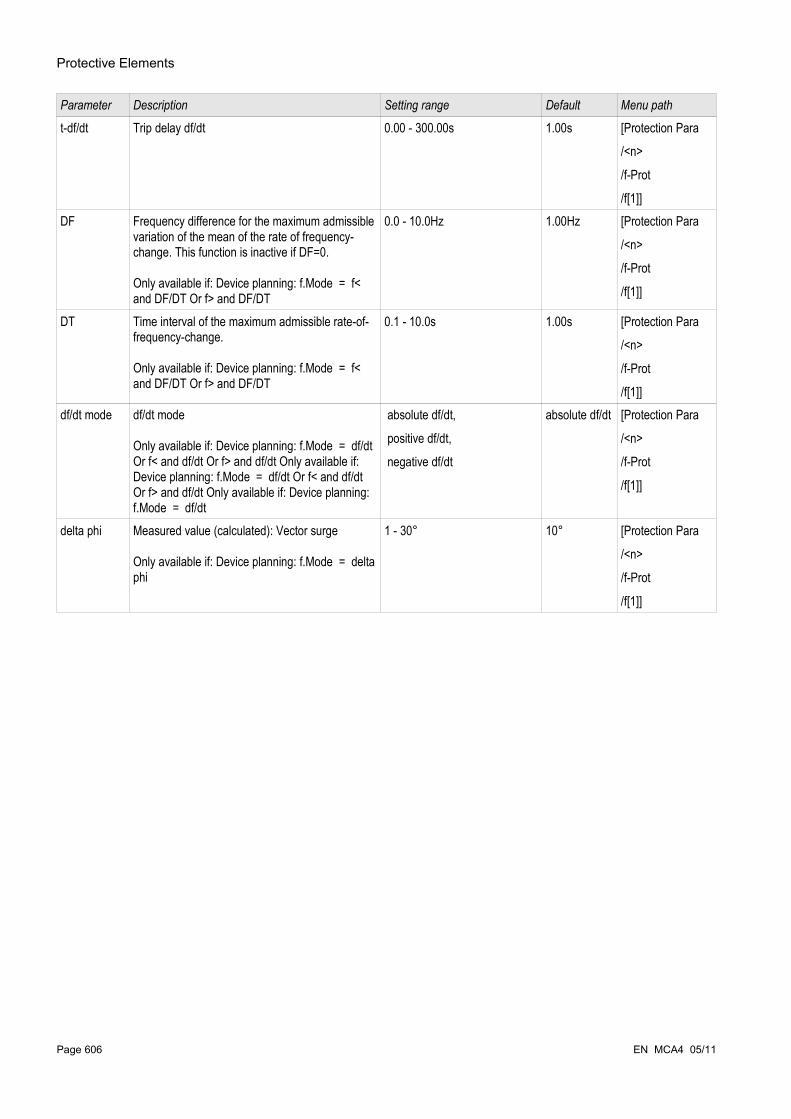
Protective Elements
Parameter Description Setting range Default Menu path
t-df/dt Trip delay df/dt 0.00 - 300.00s 1.00s [Protection Para
/<n>
/f-Prot
/f[1]]DF Frequency difference for the maximum admissible
variation of the mean of the rate of frequency-change. This function is inactive if DF=0.
Only available if: Device planning: f.Mode = f< and DF/DT Or f> and DF/DT
0.0 - 10.0Hz 1.00Hz [Protection Para
/<n>
/f-Prot
/f[1]]
DT Time interval of the maximum admissible rate-of-frequency-change.
Only available if: Device planning: f.Mode = f< and DF/DT Or f> and DF/DT
0.1 - 10.0s 1.00s [Protection Para
/<n>
/f-Prot
/f[1]]df/dt mode df/dt mode
Only available if: Device planning: f.Mode = df/dt Or f< and df/dt Or f> and df/dt Only available if: Device planning: f.Mode = df/dt Or f< and df/dt Or f> and df/dt Only available if: Device planning: f.Mode = df/dt
absolute df/dt,
positive df/dt,
negative df/dt
absolute df/dt [Protection Para
/<n>
/f-Prot
/f[1]]
delta phi Measured value (calculated): Vector surge
Only available if: Device planning: f.Mode = delta phi
1 - 30° 10° [Protection Para
/<n>
/f-Prot
/f[1]]
Page 606 EN MCA4 05/11
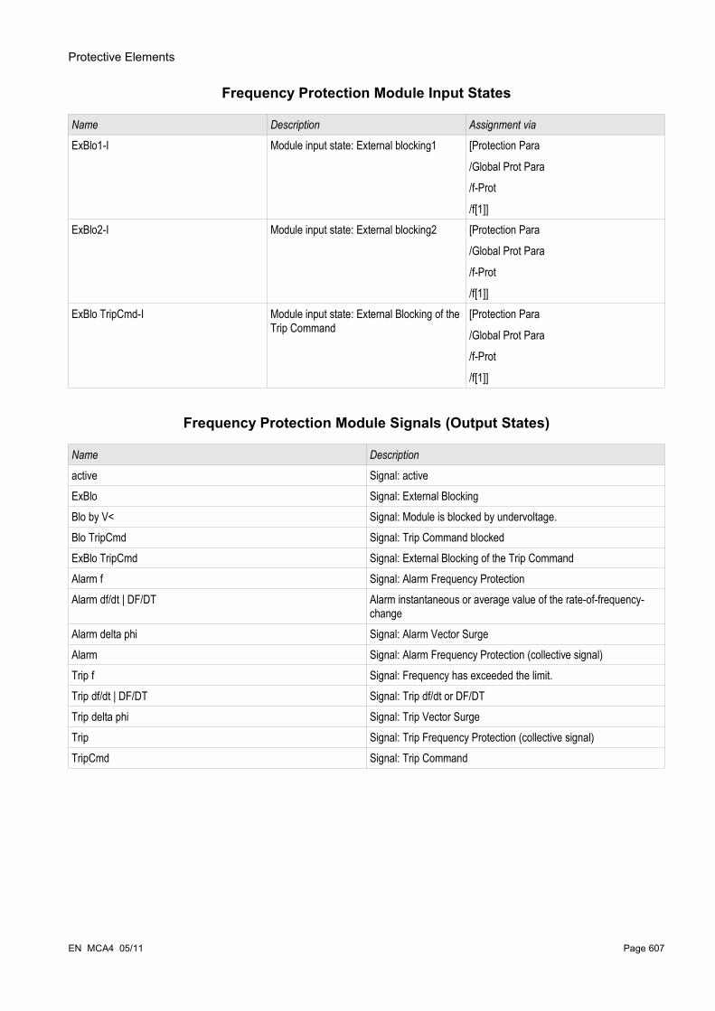
Protective Elements
Frequency Protection Module Input States
Name Description Assignment via
ExBlo1-I Module input state: External blocking1 [Protection Para
/Global Prot Para
/f-Prot
/f[1]]ExBlo2-I Module input state: External blocking2 [Protection Para
/Global Prot Para
/f-Prot
/f[1]]ExBlo TripCmd-I Module input state: External Blocking of the
Trip Command[Protection Para
/Global Prot Para
/f-Prot
/f[1]]
Frequency Protection Module Signals (Output States)
Name Description
active Signal: activeExBlo Signal: External BlockingBlo by V< Signal: Module is blocked by undervoltage.Blo TripCmd Signal: Trip Command blockedExBlo TripCmd Signal: External Blocking of the Trip CommandAlarm f Signal: Alarm Frequency ProtectionAlarm df/dt | DF/DT Alarm instantaneous or average value of the rate-of-frequency-
change Alarm delta phi Signal: Alarm Vector SurgeAlarm Signal: Alarm Frequency Protection (collective signal)Trip f Signal: Frequency has exceeded the limit.Trip df/dt | DF/DT Signal: Trip df/dt or DF/DTTrip delta phi Signal: Trip Vector SurgeTrip Signal: Trip Frequency Protection (collective signal)TripCmd Signal: Trip Command
EN MCA4 05/11 Page 607

Protective Elements
Commissioning: Overfrequency [f>]
Object to be testedAll configured overfrequency protection stages.
Necessary means• Three-phase voltage source with variable frequency and• Timer
Procedure
Testing the threshold values• Keep on increasing the frequency until the respective frequency element is activated;• Note the frequency value and• Disconnect the test voltage.
Testing the trip delay• Set the test voltage to nominal frequency and• Now connect a frequency jump (activation value) and then start a timer. Measure the tripping time at the
relay output.
Testing the fallback ratioReduce the measuring quantity to less than 99.95% of the trip value (or 0.05% fn). The relay must only fall back at 99.95% of the trip value at the earliest (or 0.05% fn).
Successful test resultPermissible deviations/tolerances can be taken from the Technical Data.
Commissioning: Underfrequency [f<]
For all configured underfrequency elements, this test can be carried out similar to the test for overfrequency protection (by using the related underfrequency values).
Please consider the following deviations:
• For testing the threshold values, the frequency has to be decreased until the protection element is activated.
• For detection of the fallback ratio, the measuring quantity has to be increased to more than 100.05% of the trip value (or 0.05% fn). At 100.05% of the trip value the relay is to fall back at the earliest (or 0.05% fn).
Page 608 EN MCA4 05/11

Protective Elements
Commissioning: df/dt - Rate of Change of Frequency
Object to be testedAll frequency protection stages that are projected as df/dt.
Necessary means• Three-phase voltage source and• Frequency generator that can generate and measure a linear, defined rate of change of frequency.
Procedure
Testing the threshold values • Keep on increasing the rate of change of frequency until the respective element is activated.• Note the value.
Testing the trip delay • Set the test voltage to nominal frequency.• Now apply a step change (sudden change) that is 1.5 times the setting value (example: apply 3 Hz per
second if the setting value is 2 Hz per second) and• Measure the tripping time at the relay output. Compare the measured tripping time to the configured
tripping time.
Successful test result:Permissible deviations/tolerances and dropout ratios can be taken from the Technical Data.
EN MCA4 05/11 Page 609

Protective Elements
Commissioning: f< and -df/dt – underfrequencyand Rate of Change of Frequency
Object to be tested:All frequency protection stages that are projected as f< and -df/dt.
Necessary means:• Three-phase voltage source and• Frequency generator that can generate and measure a linear, defined rate of change of frequency.
Procedure:
Testing the threshold values• Feed nominal voltage and nominal frequency to the device• Decrease the frequency below the f< threshold and• Apply a rate of change of frequency (step change) that is below the setting value (example apply -1 Hz
per second if the setting value is -0.8 Hz per second). After the tripping delay is expired the relay has to trip.
Successful test resultPermissible deviations/tolerances and dropout ratios can be taken from the Technical Data.
Commissioning: f> and df/dt – overfrequencyand Rate of Change of Frequency
Object to be testedAll frequency protection stages that are projected as f> and df/dt.
Necessary means• Three-phase voltage source and.• Frequency generator that can generate and measure a linear, defined rate of change of frequency.
Procedure
Testing the threshold values • Feed nominal voltage and nominal frequency to the device.• Increase the frequency above the f> threshold and.• Apply a rate of change of frequency (step change) that is above the setting value (example apply 1 Hz
per second if the setting value is 0.8 Hz per second). After the tripping delay is expired the relay has to trip.
Successful test result:Permissible deviations/tolerances and dropout ratios can be taken from the Technical Data.
Page 610 EN MCA4 05/11
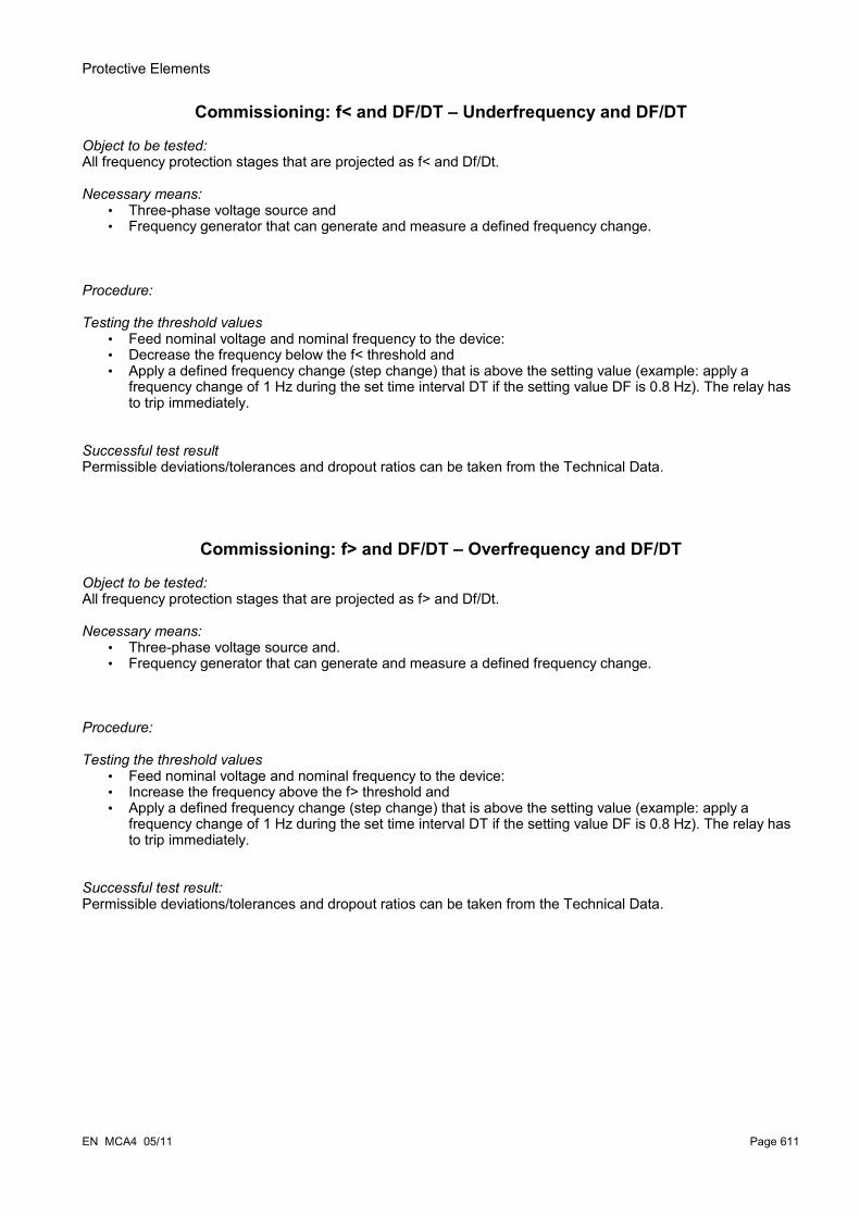
Protective Elements
Commissioning: f< and DF/DT – Underfrequency and DF/DT
Object to be tested:All frequency protection stages that are projected as f< and Df/Dt.
Necessary means:• Three-phase voltage source and• Frequency generator that can generate and measure a defined frequency change.
Procedure:
Testing the threshold values • Feed nominal voltage and nominal frequency to the device:• Decrease the frequency below the f< threshold and• Apply a defined frequency change (step change) that is above the setting value (example: apply a
frequency change of 1 Hz during the set time interval DT if the setting value DF is 0.8 Hz). The relay has to trip immediately.
Successful test resultPermissible deviations/tolerances and dropout ratios can be taken from the Technical Data.
Commissioning: f> and DF/DT – Overfrequency and DF/DT
Object to be tested:All frequency protection stages that are projected as f> and Df/Dt.
Necessary means:• Three-phase voltage source and.• Frequency generator that can generate and measure a defined frequency change.
Procedure:
Testing the threshold values • Feed nominal voltage and nominal frequency to the device:• Increase the frequency above the f> threshold and• Apply a defined frequency change (step change) that is above the setting value (example: apply a
frequency change of 1 Hz during the set time interval DT if the setting value DF is 0.8 Hz). The relay has to trip immediately.
Successful test result:Permissible deviations/tolerances and dropout ratios can be taken from the Technical Data.
EN MCA4 05/11 Page 611

Protective Elements
Commissioning: delta phi - Vector Surge
Object to be tested:All frequency protection stages that are projected as delta phi (vector surge).
Necessary means:• Three-phase voltage source that can generate a definite step (sudden change) of the voltage pointers
(phase shift).
Procedure:
Testing the threshold values• Apply a vector surge (sudden change) that is 1.5 times the setting value (example: if the setting value is
10° apply 15°).
Successful test result:Permissible deviations/tolerances and dropout ratio can be taken from the Technical Data.
Page 612 EN MCA4 05/11

Protective Elements
AR - Automatic Reclosure [79] AR
The autoreclosure is used to minimize outages on overhead lines. The majority1 (>60% in medium voltage and >85% in high voltage) of faults (arc flash over) on overhead lines are temporary and can be cleared by means of the autoreclosure element.
Deproject the autoreclosure element within the device planning if the protective device is used in order to protect cables, generators or transformers.
Features
The autoreclose function is designed with diverse very comprehensive yet flexible features which meet all requirements of different utility concepts and technical applications.
The available features of the autoreclose function can be summarized as follows:
• Flexible assignment of initiate functions for individual shots.
• Maximum six autoreclose shots.
• Dynamic adjustment of protection setting values (e.g. pickup, time delay tripping curve etc.) during autoreclose process via adaptive set concept.
• Reclose shots per hour limit.
• Autorecloser wear monitor with maintenance alarm.
• Programmable reclosing blocking feature.
• Auto zone coordination with downstream reclosers.
• Automatic manual-breaker-close blocking feature.
• Manual/Auto reset lockout (panel, contact input, communications, etc)
• Autoreclose with Synchron-Check (only in conjunction with internal Sync-Check and Control modules).
• External AR shot counter increment is possible.
• Automatic autoreclose result evaluation (successful/unsuccessful).
• Separate counters to register total, successful/unsuccessful reclosing numbers.
1: VDE-Verlag: Schutztechnik in elektrischen Netzen 1, Page179, ISBN 3-8007-1753-0
EN MCA4 05/11 Page 613

Protective Elements
The following table gives a folder (structure) overview:
AR Menu Folder Purpose
Page 614 EN MCA4 05/11

Protective Elements
AR
Path:[Protection Para\Global Prot Para\AR]
Within this menu, external blockings, external lockings, external shot increments and external resets can be assigned. Those external events can only become effective, if they have been activated (allowed) within the General Settings. Please see table row below.
General Settings
Path: [Protection Para\Set[x]\AR\General Settings]
Within this menu several general settings can be activated: The function itself, external blocking, zone coordination, external locking and external shot increment can be set to active. The corresponding trigger events (e.g. digital inputs) have to be assigned within the corresponding global protection parameters. Please see table row above.
Furthermore, this menu contains some timers, the number of permitted reclosure attempts, the alarm mode (trip/alarm) and the reset mode can be set
Shot Manager
Path: [Protection Para\Set[x]\AR\Shot Manager]
In Shot-manager setting menu the control logics between individual shots and protective functions will be specified. For each shot (inclusive the pre shot) the trigger (start) events can be assigned.
For each shot, maximum 4 initiate functions (protective functions which are dedicated to start this shot) can be selected from an available protective function list.
When the autoreclosure process is running in the shot X stage, the corresponding protection and control settings will be used to control the operation during this stage.
In addition to that the dead times have to be set. For each shot, its dead time will be set individually, except for the shot 0, for which no dead timer setting is necessary. The shot 0 is just a virtual state to define the time before the first shot is to issue. Each dead timer specifies the time duration which has to be expired before the reclosure command for this shot can be issued.
Wear Monitor
Path: [Protection Para\Set[x]\AR\Wear Monitor]
This setting group contains all parameters which monitor the wear and maintenance conditions related to the autoreclosure operations. The corresponding information and control can be useful for an optimal autoreclosure application.
Blo Fc
Path: [Protection Para\Set[x]\AR\Blo Fc]
This group of settings specifies the protection functions by which the autoreclosure function must be blocked even if the autoreclosure function is already initiated.
Note the difference between the protection function which can be blocked by auto-recloser and the function(s) here to block the auto-recloser.
EN MCA4 05/11 Page 615
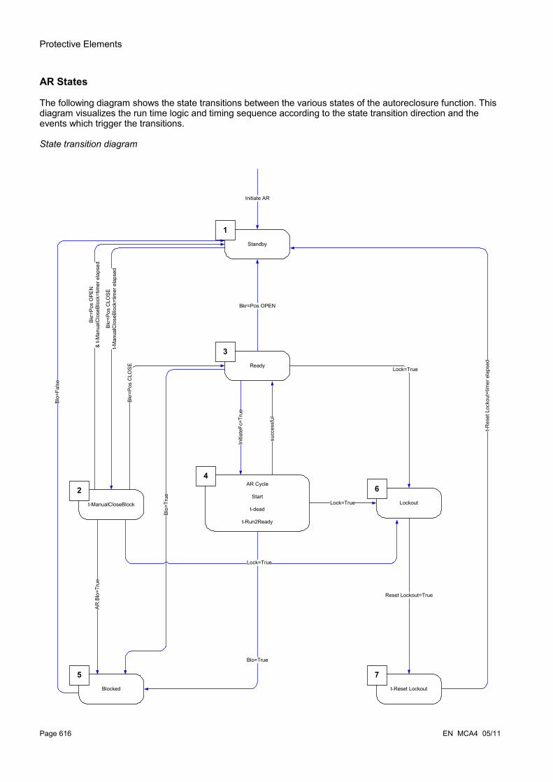
Protective Elements
AR States
The following diagram shows the state transitions between the various states of the autoreclosure function. This diagram visualizes the run time logic and timing sequence according to the state transition direction and the events which trigger the transitions.
State transition diagram
Page 616 EN MCA4 05/11
Standby
1
Ready
3
Lockout
6
t-ManualCloseBlock
2
t-Reset Lockout
7Blocked
5
AR Cycle
Start
t-dead
t-Run2Ready
4
Lock=True
Initiate AR
Initia
teFc
=Tru
e
succ
essf
ul
Bkr=
Pos
CLO
SE Lock=True
Bkr=
Pos
CLO
SEt-M
anua
lClo
seBl
ock=
timer
ela
psed
Reset Lockout=True
t-Res
et L
ocko
ut=t
imer
ela
psed
Blo=
Fals
e
Bkr=
Pos
OPE
N&
t-Man
ualC
lose
Bloc
k=tim
er e
laps
ed
Blo=
True
Blo=True
AR.B
lo=T
rue
Lock=True
Bkr=Pos OPEN

Protective Elements
In general, the autoreclosure function is only active (will be initiated) when all of the following conditions are met:
• Autoreclosure function is enabled (In AR General Setting: Function =active)
• The breaker (CB) is configured within the “AR/General Settings“.
• Autoreclosure is not blocked by the blocking inputs (ExBlo1/2).
1 Standby
The autoreclosure is in this state when the following conditions are met:
• The breaker is in the open position.• The autoreclose function is not initiated from any initiate (start) functions.• No external or internal AR blocking signals are present.
No autoreclose shot operation is possible if the autoreclose function is within Standby state.
2 t-manual close block
Suppose that the breaker is open and the AR state is in Standby state. Then the breaker is closed manually. The event “CB Pos On” starts a Manual-Close-Blocking timer and results in a state transition from »STANDBY« to a transit state - »T-BLO AFTER CB MAN ON«. The autoreclosure function changes into the »READY« state only as the Manual-Close-Blocking timer elapses and the breaker is closed. By means of the manual close blocking timer a faulty starting of the autoreclose function in case of a Switch-OnTo-Fault condition is prevented.
3 Ready
An activated autoreclose function is considered to be in »READY« state when all of the following conditions are true:
• The breaker is in closed position.
• The Manual-Close-Block-timer elapses after a breaker manual/remote close operation.
• The autoreclose function is not initiated from any initiate (start) functions.
• No external or internal AR blocking signals are present.
An autoreclose start is only possible if the autoreclose function is in Ready state.
EN MCA4 05/11 Page 617
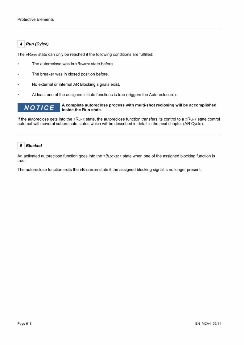
Protective Elements
4 Run (Cylce)
The »RUN« state can only be reached if the following conditions are fulfilled:
• The autoreclose was in »READY« state before.
• The breaker was in closed position before.
• No external or internal AR Blocking signals exist.
• At least one of the assigned initiate functions is true (triggers the Autoreclosure).
A complete autoreclose process with multi-shot reclosing will be accomplished inside the Run state.
If the autoreclose gets into the »RUN« state, the autoreclose function transfers its control to a »RUN« state control automat with several subordinate states which will be described in detail in the next chapter (AR Cycle).
5 Blocked
An activated autoreclose function goes into the »BLOCKED« state when one of the assigned blocking function is true.
The autoreclose function exits the »BLOCKED« state if the assigned blocking signal is no longer present.
Page 618 EN MCA4 05/11

Protective Elements
6 Lockout
An activated autoreclose function goes into the »LOCKOUT« state when one of the following conditions is true:
• An unsuccessful autoreclose is detected after all programmed autoreclose shots. The fault is of permanent nature.
• Reclose failure (incomplete sequence)
• Autoreclose rate per hour exceeds the limit
• Fault timer elapses (tripping time too long)
• Breaker failure during AR starting
• Manual breaker close operation during autoreclose process
• At least one protective function is still tripping before reclose command is issued
The autoreclose function exits the »LOCKOUT« state if the programmed lockout reset signal asserts and programmed Lockout Reset timer elapses.
A Service Alarm (Service Alarm 1 or Service Alarm 2) will not lead to a lockout of the AR function.
EN MCA4 05/11 Page 619
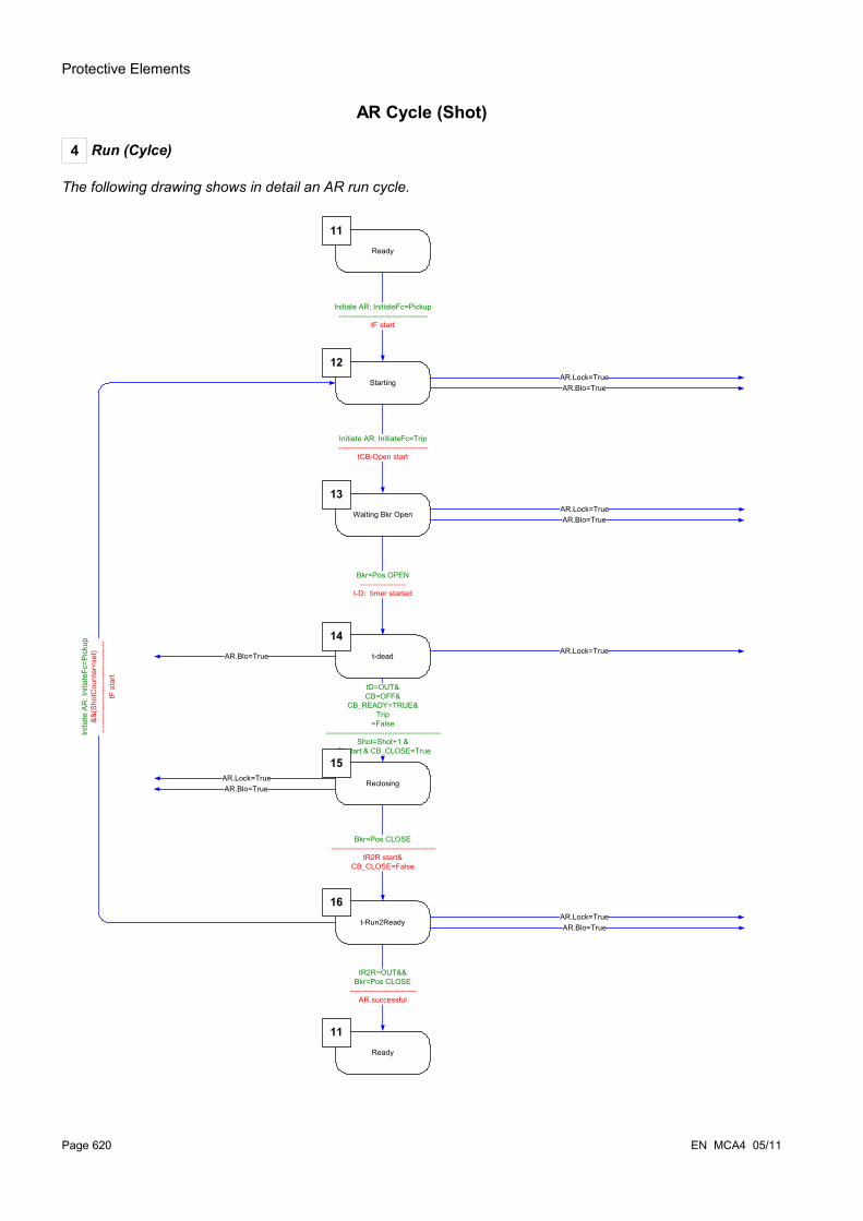
Protective Elements
AR Cycle (Shot)
4 Run (Cylce)
The following drawing shows in detail an AR run cycle.
Page 620 EN MCA4 05/11
tR2R=OUT&&Bkr=Pos CLOSE
--------------------------AR.successful
tD=OUT&CB=OFF&
CB_READY=TRUE&Trip
=False---------------------------------------------
Shot=Shot+1 & tCI start & CB_CLOSE=True
t-Run2Ready
16
t-dead
14
Waiting Bkr Open
13
Starting
12
Ready
11
Ready
11
AR.Blo=TrueAR.Lock=True
AR.Lock=TrueAR.Blo=True
AR.Lock=True
AR.Lock=TrueAR.Blo=True
AR.Blo=True
AR.Blo=TrueAR.Lock=True
Initi
ate
AR: I
nitia
teFc
=Pic
kup
&&(S
hotC
ount
er<s
et)
------
------
------
------
------
------
tF s
tart
Bkr=Pos OPEN------------------
t-D: timer started
Initiate AR: InitiateFc=Trip-----------------------------------
tCB-Open start
Bkr=Pos CLOSE-----------------------------------------
tR2R start&CB_CLOSE=False
Initiate AR: InitiateFc=Pickup-----------------------------------
tF start
Reclosing
15

Protective Elements
11 Ready
An activated autoreclose function is considered to be in »READY« state when all of the following conditions are true:
• The breaker is in closed position.
• The Manual-Close-Block-timer elapses after a breaker manual/remote close operation.
• The autoreclose function is not initiated from any initiate (start) functions.
• No external or internal AR blocking signals are present.
12 Run
This is the first subordinate state after the autoreclosure process goes from »READY« into »RUN« state triggered from the first AR initiate event. During the »RUNNING« state, the auto reclosure element supervises the trip signal of the initiate function while a preset fault timer is timing. The autoreclosure element transfers to the »WAITING BKR OPEN« state by receiving the trip signal if the fault timer does NOT time out and there are no other blocking and lockout conditions.
13 Waiting Bkr Open
While in the »WAITING BKR OPEN« state, the autoreclosure supervises if the breaker is really tripped (open) after receiving the trip flag of the initiate protection function within a preset breaker supervision time (200ms). If this is the case, the autoreclosure starts the programmed dead timer and goes to the dead timing state »t-dead«.
14 t-dead
While in the dead timing state »t-dead«, the preset dead timer for current AR shot is timing and cannot be interrupted unless there are any blocking or lockout conditions coming.After dead timer elapses, the autoreclosure issues the breaker reclosing command and goes into the next state: »RECLOSING«, only if the following conditions are met:
• The breaker is in open position,• The breaker is ready for next reclosing operation (if the CB Ready logic input is used)• No pickup from current (assigned) AR initiate function(s)• No trip from current (assigned) AR initiate function(s)• No general tipping command
Before issuing the breaker reclosing command, the current shot counter will be incremented. This is very important for the shot-controlled initiate and blocking functions. Before entering into the »RECLOSING« state, the preset breaker reclosing supervision timer (»t-Brk-ON-cmd«) will be started, too.
EN MCA4 05/11 Page 621

Protective Elements
15 Reclosing
If there is no other blocking or lockout conditions and the breaker is closed while the breaker reclosing supervision timer is timing, the autoreclosure starts the »t-Run2Ready« timer and goes into the state: »T-RUN2READY«.
16 t-Run2Ready
Successful Autoreclosure:While in »T-RUN2READY« state, if there is no other blocking or lockout conditions and no more faults detected within the »t-Run2Ready« timer, the autoreclosure logic will leave the »RUN« state and goes back to the »READY« state. The flag “successful” is set.
Unsuccessful Autoreclose:If a fault is detected again (the shot-controlled initiate function is triggering) while »t-Run2Ready« timer is still timing, the autoreclosure control transfers to the »RUNNING« state again. For a permanent fault, the process described before will be repeated until all programmed shots were operated and the autoreclose process changes into the »LOCKOUT« state. The flag “failed” is set.
Page 622 EN MCA4 05/11

Protective Elements
Timing Diagrams
Auto Reclosing timing diagram for unsuccessful 2-shot auto reclosing scheme with acceleration at pre-shot
EN MCA4 05/11 Page 623
Pre Shot
Shot
AR.running
Shot 1 Shot 2
AR - Module statest
0
1
Ready running Lockout
Reclosing
t
0
1
CB Pos
t0
1
Protection
t
0
1
Protection
t
0
1
Fault
t
0
1
t-DP1 t-DP2 t-Run2Ready
Pos OFF
Pos ON
Reset
Trip
Reset
Alarm
Clearance
Inception
50P[1].Fasttrip 50P[1].Trip 51P[1].Trip
51P[1] 50P[1]. AdaptSet1 50P[1].DefaultSet
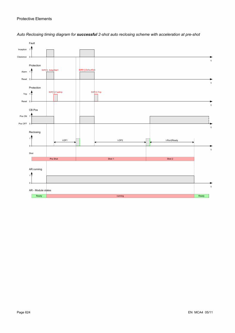
Protective Elements
Auto Reclosing timing diagram for successful 2-shot auto reclosing scheme with acceleration at pre-shot
Page 624 EN MCA4 05/11
Pre Shot
Shot
AR.running
Shot 1 Shot 2
AR - Module statest
0
1
Ready running Ready
Reclosing
t0
1
CB Pos
t0
1
Protection
t0
1
Protection
t0
1
Fault
t0
1
t-DP1 t-DP2 t-Run2Ready
Pos OFF
Pos ON
Reset
Trip
Reset
Alarm
50P[1].Fasttrip 50P[1].Trip
50P[1]. AdaptSet1 50P[1].DefaultSet
Clearance
Inception

Protective Elements
Auto Reclosing States during manual breaker closing
Protection Trip while Manual Close Blocking time is Timing
What happens if while the timer manual close block time is timing down the protective device gets a trip signal?
While the timer manual close block time is timing, any trip during this time period trips the breaker. The manual close block timer doesn´t care about that and timing further until it times out.
After it times out, the AR-module looks at the breaker status again, and sees that the breaker is open. The AR goes to the »STANDBY« state, no autoreclose is possible (Note: The AR doesn´t go to »LOCKOUT« state!)
EN MCA4 05/11 Page 625
Protection Trip
AR - Module statest
0
1
t-Blo after CB man ON
Circuit Breaker Manual Close
t0
1
CB Pos
t0
1
t-Blo after CB man ON
Standby
Pos OFF
Pos ON
Standby
Circuit Breaker Manual Close
AR - Module statest
0
1
t-Blo after CB man ON
t0
1
t-Blo after CB man ON
Pos OFF
Pos ON
Standby Ready
CB Pos

Protective Elements
AR Lockout Reset Logic in case lockout Reset coming before manual breaker closed
AR Lockout Reset Logic in case lockout Reset coming after manual breaker closed
Page 626 EN MCA4 05/11
Lockout Reset
AR - Module statest
0
1
Lockout t-Blo after CB man ON Ready
Circuit Breaker Manual Close
t0
1
t0
1
t-Lock2Ready t-Blo after CB man ON
t-Reset Lockout
CB Pos
Pos OFF
Pos ON
Lockout Reset
AR - Module statest
0
1
Lockout t-Blo after CB man ON Ready
Circuit Breaker Manual Close
t0
1
t0
1
Lockout Reset Time
t-Blo after CB man ON
t-Reset Lockout Standby
CB Pos
Pos OFF
Pos ON
Protective Elements
Zone Coordination
General Description
What does Zone Coordination mean?Zone Coordination means, that the upstream protection device is doing a virtual autoreclosure while the downstream protective device is doing a “real” autoreclosure. By means of the zone coordination selectivity can be kept, even if a downstream protective device changes its tripping characteristic after a reclosure cycle. The virtual autoreclosure of the upstream device follows the downstream autoreclosure.
What application can be realized by means of Zone Coordination?A radial distribution system is protected by an upstream protective device (with a circuit breaker) and a downstream protective device with a reclosure and fuse. By means of the zone coordination a “fuse saving scheme” might be realised. In order to “save fuses” the downstream protective device might trip for the first reclosure attempt at low tripping values (undergrade the fuse, trying to avoid a damaging of the fuse). If the reclosure attempt fails the tripping values might be risen (overgrade the fuse) for the second reclosure attempt (using higher tripping values/characteristics).
What is essential?The triggering thresholds of the upstream and the downstream devices have to be the same but the tripping times have to be selectively.
How is Zone Coordination activated?The zone coordination function is part of the autoreclosure element and it can be enabled by setting the parameter »Zone coordination« as »active« within the menu [Protection Para/AR/General Settings] for an upstream feeder protection device.
How does the Zone Coordination work (within the upstream protection device)?When the zone coordination function is enabled, it works similar to a normal autoreclose function with the same setting parameters: maximum reclosure attempts, dead timer for each shot, initiate functions for each shot and other timers for autoreclose process, but with the following zone coordination features to coordinate with the downstream reclosers:
• The corresponding dead timer for each shot will be started even the breaker of the upstream feeder relay is NOT tripped from the assigned initiate protective functions.
• The dead timer begins timing once the autoreclose senses a drawback of the assigned overcurrent protection pickup signal. This exhibits that the fault current was tripped by the downstream recloser opening.
• The shot counter of an enabled zone coordination will be incremented after the dead timer elapses, even there is no breaker reclosing command issued and meanwhile the »T-RUN2READY« timer is started.
• If a permanent fault exists after the downstream recloser is reclosed, the fault current makes the upstream overcurrent protection picks up again, but with the pickup thresholds or operating curves controlled by the incremented shot number. In this way, the upstream feeder will “follow” the protective settings of downstream recloser shot by shot.
• For a transient fault the autoreclose with zone coordination will not be initiated again because of absence of the fault current and will be reset normally after the expiration of the reset timer »t-Run2Ready«.
EN MCA4 05/11 Page 627

Protective Elements
Page 628 EN MCA4 05/11
HighPROTEC
Recloser
Shot 1(triggered by: I [1])
Fuse Characteristic
Shot 2 (triggered by: I [2])
Shot 1(triggered by: I [1])
Shot 2(triggered by: I [2])
I
t
I
t
I
t

Protective Elements
Direct Commands of the Automatic Reclosure Module
Parameter Description Setting range Default Menu path
Res TotNo suc unsuc
Reset all statistic AR counters: Total number of AR, successful and unsuccessful no of AR.
inactive,
active
inactive [Operation
/Reset]
Res Service Cr
Reset the Service Counters inactive,
active
inactive [Operation
/Reset]
Reset Lock via HMI
Reset the AR Lockout via the panel. inactive,
active
inactive [Operation
/Reset]
Res Max Shots / h Cr
Resetting the Counter for the maximum allowed shots per hour.
inactive,
active
inactive [Operation
/Reset]
Device Planning Parameters of the Module Automatic Reclosure
Parameter Description Options Default Menu path
Mode Mode do not use,
use
do not use [Device planning]
EN MCA4 05/11 Page 629

Protective Elements
Global Protection Parameters of the Module Automatic Reclosure
Parameter Description Setting range Default Menu path
CB Circuit Breaker Module -.-,
SG[1].,
SG[2].,
SG[3].,
SG[4].,
SG[5].,
SG[6].
SG[1]. [Protection Para
/Global Prot Para
/AR]
ExBlo1 External blocking of the module, if blocking is activated (allowed) within a parameter set and if the state of the assigned signal is true.
1..n, Assignment List -.- [Protection Para
/Global Prot Para
/AR]
ExBlo2 External blocking of the module, if blocking is activated (allowed) within a parameter set and if the state of the assigned signal is true.
1..n, Assignment List -.- [Protection Para
/Global Prot Para
/AR]
Ex Shot Inc The AR Shot counter will be incremented by this external Signal. This can be used for Zone Coordination (of upstream Auto Reclosure devices).
1..n, DI-LogicList -.- [Protection Para
/Global Prot Para
/AR]
Ex Lock The auto reclosure will locked out by this external Signal (set into the lockout state).
1..n, DI-LogicList -.- [Protection Para
/Global Prot Para
/AR]DI Reset Ex Lock
The Lockout State of the AR can be resetted by a digital input.
1..n, DI-LogicList -.- [Protection Para
/Global Prot Para
/AR]
Scada Reset Ex Lock
The Lockout State of the AR can be resetted by Scada.
Communication Commands -.- [Protection Para
/Global Prot Para
/AR]
Page 630 EN MCA4 05/11

Protective Elements
Setting Group Parameters of the Module Automatic Reclosure
Parameter Description Setting range Default Menu path
Function Permanent activation or deactivation of module/stage.
inactive,
active
inactive [Protection Para
/<n>
/AR
/General settings]ExBlo Fc Activate (allow) or inactivate (disallow) blocking of
the module/stage. This parameter is only effective if a signal is assigned to the corresponding global protection parameter. If the signal becomes true, those modules/stages are blocked that are parameterized "ExBlo Fc=active".
inactive,
active
inactive [Protection Para
/<n>
/AR
/General settings]
Zone coordination
Zone coordination: Sequence coordination is to keep upstream reclosers in step with the downstream ones for fast and delay curve operation, thus avoiding overtripping.
inactive,
active
inactive [Protection Para
/<n>
/AR
/General settings]
Ex Shot Inc Fc
The AR Shot counter will be incremented by this external Signal. This can be used for Zone Coordination (of upstream Auto Reclosure devices). Note: This parameter enables the functionality only. The assignment has to be set within the global parameters.
inactive,
active
inactive [Protection Para
/<n>
/AR
/General settings]
Ex Lock Fc The auto reclosure will locked out by this external Signal. Note: This parameter enables the functionality only. The assignment has to be set within the global parameters.
inactive,
active
inactive [Protection Para
/<n>
/AR
/General settings]
Reset Mode Reset Mode auto,
HMI,
DI,
Scada,
HMI And Scada,
HMI And DI,
Scada And DI,
HMI And DI
auto [Protection Para
/<n>
/AR
/General settings]
Attempts Maximum number of permitted reclosure attempts. 1 - 6 1 [Protection Para
/<n>
/AR
/General settings]
EN MCA4 05/11 Page 631
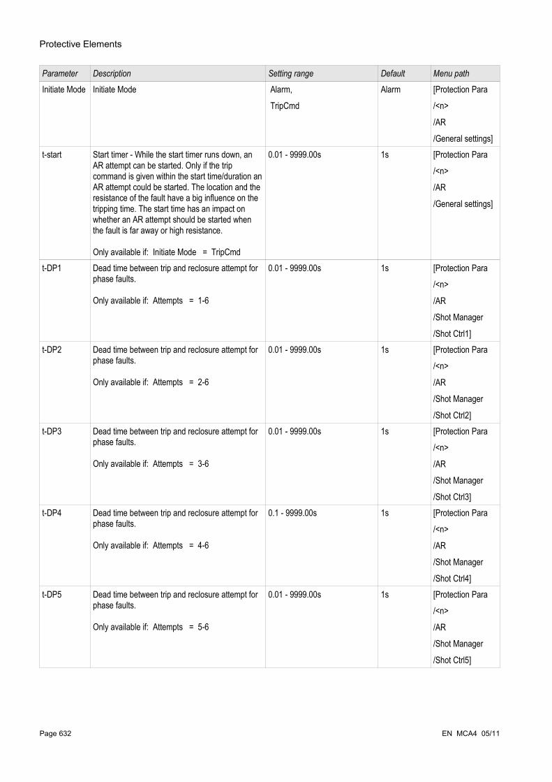
Protective Elements
Parameter Description Setting range Default Menu path
Initiate Mode Initiate Mode Alarm,
TripCmd
Alarm [Protection Para
/<n>
/AR
/General settings]t-start Start timer - While the start timer runs down, an
AR attempt can be started. Only if the trip command is given within the start time/duration an AR attempt could be started. The location and the resistance of the fault have a big influence on the tripping time. The start time has an impact on whether an AR attempt should be started when the fault is far away or high resistance.
Only available if: Initiate Mode = TripCmd
0.01 - 9999.00s 1s [Protection Para
/<n>
/AR
/General settings]
t-DP1 Dead time between trip and reclosure attempt for phase faults.
Only available if: Attempts = 1-6
0.01 - 9999.00s 1s [Protection Para
/<n>
/AR
/Shot Manager
/Shot Ctrl1]t-DP2 Dead time between trip and reclosure attempt for
phase faults.
Only available if: Attempts = 2-6
0.01 - 9999.00s 1s [Protection Para
/<n>
/AR
/Shot Manager
/Shot Ctrl2]t-DP3 Dead time between trip and reclosure attempt for
phase faults.
Only available if: Attempts = 3-6
0.01 - 9999.00s 1s [Protection Para
/<n>
/AR
/Shot Manager
/Shot Ctrl3]t-DP4 Dead time between trip and reclosure attempt for
phase faults.
Only available if: Attempts = 4-6
0.1 - 9999.00s 1s [Protection Para
/<n>
/AR
/Shot Manager
/Shot Ctrl4]t-DP5 Dead time between trip and reclosure attempt for
phase faults.
Only available if: Attempts = 5-6
0.01 - 9999.00s 1s [Protection Para
/<n>
/AR
/Shot Manager
/Shot Ctrl5]
Page 632 EN MCA4 05/11
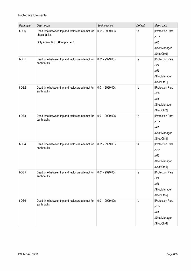
Protective Elements
Parameter Description Setting range Default Menu path
t-DP6 Dead time between trip and reclosure attempt for phase faults.
Only available if: Attempts = 6
0.01 - 9999.00s 1s [Protection Para
/<n>
/AR
/Shot Manager
/Shot Ctrl6]t-DE1 Dead time between trip and reclosure attempt for
earth faults0.01 - 9999.00s 1s [Protection Para
/<n>
/AR
/Shot Manager
/Shot Ctrl1]t-DE2 Dead time between trip and reclosure attempt for
earth faults0.01 - 9999.00s 1s [Protection Para
/<n>
/AR
/Shot Manager
/Shot Ctrl2]t-DE3 Dead time between trip and reclosure attempt for
earth faults0.01 - 9999.00s 1s [Protection Para
/<n>
/AR
/Shot Manager
/Shot Ctrl3]t-DE4 Dead time between trip and reclosure attempt for
earth faults0.01 - 9999.00s 1s [Protection Para
/<n>
/AR
/Shot Manager
/Shot Ctrl4]t-DE5 Dead time between trip and reclosure attempt for
earth faults0.01 - 9999.00s 1s [Protection Para
/<n>
/AR
/Shot Manager
/Shot Ctrl5]t-DE6 Dead time between trip and reclosure attempt for
earth faults0.01 - 9999.00s 1s [Protection Para
/<n>
/AR
/Shot Manager
/Shot Ctrl6]
EN MCA4 05/11 Page 633

Protective Elements
Parameter Description Setting range Default Menu path
t-Blo after CB man ON
This timer will be started if the circuit breaker was switched on manually. While this timer is running, AR cannot be started.
0.01 - 9999.00s 10.0s [Protection Para
/<n>
/AR
/General settings]t-Lock2Ready
This timer is started by the lockout reset signal, and before the timer expire the AR cannot go to any other state.
0.01 - 9999.00s 10.0s [Protection Para
/<n>
/AR
/General settings]t-Run2Ready Examination Time: If the Circuit Breaker remains
after an reclosure attempt for the duration of this timer in the Closed position, the AR has been successful and the AR module returns into the ready state.
0.01 - 9999.00s 10.0s [Protection Para
/<n>
/AR
/General settings]
t-Blo2Ready The release (de-blocking) of the AR will be delayed for this time, if there is no blocking signal anymore.
0.01 - 9999.00s 10.0s [Protection Para
/<n>
/AR
/General settings]t-AR Supervision
AR Overall supervision time (> sum of all the timers used by AR)
1.00 - 9999.00s 100.0s [Protection Para
/<n>
/AR
/General settings]Service Alarm 1
As soon as the AR-Counter exceeds this number of reclosure attempts an alarm will be given out (overhauling of the CB)
1 - 65535 1000 [Protection Para
/<n>
/AR
/Wear Monitor]Service Alarm 2
Too many auto reclosure attempts. If the parameterized number of AR cycles is reached, an alarm will be given out.
1 - 65535 65535 [Protection Para
/<n>
/AR
/Wear Monitor]Max AR/h Maximum Number of permitted Auto Reclosure
Cycles per hour.1 - 20 10 [Protection Para
/<n>
/AR
/Wear Monitor]Initiate AR: InitiateFc1
Initiate Auto Reclosure : Initiate Function Start fct - [Protection Para
/<n>
/AR
/Shot Manager
/Pre Shot Ctrl]
Page 634 EN MCA4 05/11

Protective Elements
Parameter Description Setting range Default Menu path
Initiate AR: InitiateFc2
Initiate Auto Reclosure : Initiate Function Start fct - [Protection Para
/<n>
/AR
/Shot Manager
/Pre Shot Ctrl]Initiate AR: InitiateFc3
Initiate Auto Reclosure : Initiate Function Start fct - [Protection Para
/<n>
/AR
/Shot Manager
/Pre Shot Ctrl]Initiate AR: InitiateFc4
Initiate Auto Reclosure : Initiate Function Start fct - [Protection Para
/<n>
/AR
/Shot Manager
/Pre Shot Ctrl]Shot 1: InitiateFc1
Automatic Reclosure Attempt : Initiate Function
Only available if: Attempts = 1-6
Start fct - [Protection Para
/<n>
/AR
/Shot Manager
/Shot Ctrl1]Shot 1: InitiateFc2
Automatic Reclosure Attempt : Initiate Function
Only available if: Attempts = 1-6
Start fct - [Protection Para
/<n>
/AR
/Shot Manager
/Shot Ctrl1]Shot 1: InitiateFc3
Automatic Reclosure Attempt : Initiate Function
Only available if: Attempts = 1-6
Start fct - [Protection Para
/<n>
/AR
/Shot Manager
/Shot Ctrl1]Shot 1: InitiateFc4
Automatic Reclosure Attempt : Initiate Function
Only available if: Attempts = 1-6
Start fct - [Protection Para
/<n>
/AR
/Shot Manager
/Shot Ctrl1]
EN MCA4 05/11 Page 635
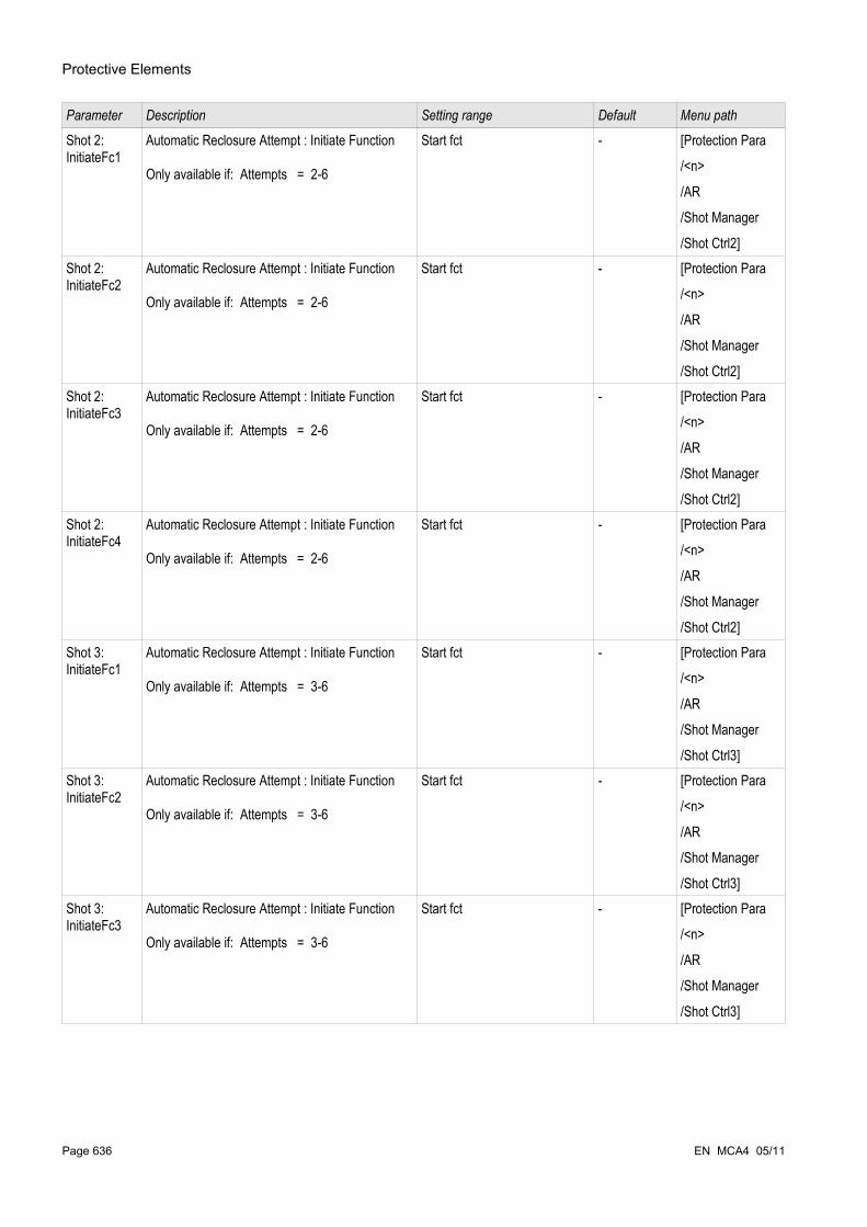
Protective Elements
Parameter Description Setting range Default Menu path
Shot 2: InitiateFc1
Automatic Reclosure Attempt : Initiate Function
Only available if: Attempts = 2-6
Start fct - [Protection Para
/<n>
/AR
/Shot Manager
/Shot Ctrl2]Shot 2: InitiateFc2
Automatic Reclosure Attempt : Initiate Function
Only available if: Attempts = 2-6
Start fct - [Protection Para
/<n>
/AR
/Shot Manager
/Shot Ctrl2]Shot 2: InitiateFc3
Automatic Reclosure Attempt : Initiate Function
Only available if: Attempts = 2-6
Start fct - [Protection Para
/<n>
/AR
/Shot Manager
/Shot Ctrl2]Shot 2: InitiateFc4
Automatic Reclosure Attempt : Initiate Function
Only available if: Attempts = 2-6
Start fct - [Protection Para
/<n>
/AR
/Shot Manager
/Shot Ctrl2]Shot 3: InitiateFc1
Automatic Reclosure Attempt : Initiate Function
Only available if: Attempts = 3-6
Start fct - [Protection Para
/<n>
/AR
/Shot Manager
/Shot Ctrl3]Shot 3: InitiateFc2
Automatic Reclosure Attempt : Initiate Function
Only available if: Attempts = 3-6
Start fct - [Protection Para
/<n>
/AR
/Shot Manager
/Shot Ctrl3]Shot 3: InitiateFc3
Automatic Reclosure Attempt : Initiate Function
Only available if: Attempts = 3-6
Start fct - [Protection Para
/<n>
/AR
/Shot Manager
/Shot Ctrl3]
Page 636 EN MCA4 05/11
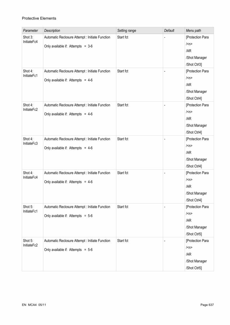
Protective Elements
Parameter Description Setting range Default Menu path
Shot 3: InitiateFc4
Automatic Reclosure Attempt : Initiate Function
Only available if: Attempts = 3-6
Start fct - [Protection Para
/<n>
/AR
/Shot Manager
/Shot Ctrl3]Shot 4: InitiateFc1
Automatic Reclosure Attempt : Initiate Function
Only available if: Attempts = 4-6
Start fct - [Protection Para
/<n>
/AR
/Shot Manager
/Shot Ctrl4]Shot 4: InitiateFc2
Automatic Reclosure Attempt : Initiate Function
Only available if: Attempts = 4-6
Start fct - [Protection Para
/<n>
/AR
/Shot Manager
/Shot Ctrl4]Shot 4: InitiateFc3
Automatic Reclosure Attempt : Initiate Function
Only available if: Attempts = 4-6
Start fct - [Protection Para
/<n>
/AR
/Shot Manager
/Shot Ctrl4]Shot 4: InitiateFc4
Automatic Reclosure Attempt : Initiate Function
Only available if: Attempts = 4-6
Start fct - [Protection Para
/<n>
/AR
/Shot Manager
/Shot Ctrl4]Shot 5: InitiateFc1
Automatic Reclosure Attempt : Initiate Function
Only available if: Attempts = 5-6
Start fct - [Protection Para
/<n>
/AR
/Shot Manager
/Shot Ctrl5]Shot 5: InitiateFc2
Automatic Reclosure Attempt : Initiate Function
Only available if: Attempts = 5-6
Start fct - [Protection Para
/<n>
/AR
/Shot Manager
/Shot Ctrl5]
EN MCA4 05/11 Page 637

Protective Elements
Parameter Description Setting range Default Menu path
Shot 5: InitiateFc3
Automatic Reclosure Attempt : Initiate Function
Only available if: Attempts = 5-6
Start fct - [Protection Para
/<n>
/AR
/Shot Manager
/Shot Ctrl5]Shot 5: InitiateFc4
Automatic Reclosure Attempt : Initiate Function
Only available if: Attempts = 5-6
Start fct - [Protection Para
/<n>
/AR
/Shot Manager
/Shot Ctrl5]Shot 6: InitiateFc1
Automatic Reclosure Attempt : Initiate Function
Only available if: Attempts = 6
Start fct - [Protection Para
/<n>
/AR
/Shot Manager
/Shot Ctrl6]Shot 6: InitiateFc2
Automatic Reclosure Attempt : Initiate Function
Only available if: Attempts = 6
Start fct - [Protection Para
/<n>
/AR
/Shot Manager
/Shot Ctrl6]Shot 6: InitiateFc3
Automatic Reclosure Attempt : Initiate Function
Only available if: Attempts = 6
Start fct - [Protection Para
/<n>
/AR
/Shot Manager
/Shot Ctrl6]Shot 6: InitiateFc4
Automatic Reclosure Attempt : Initiate Function
Only available if: Attempts = 6
Start fct - [Protection Para
/<n>
/AR
/Shot Manager
/Shot Ctrl6]
Page 638 EN MCA4 05/11

Protective Elements
Module Automatic Reclosure Input States
Name Description Assignment via
ExBlo1-I Module input state: External blocking1 [Protection Para
/Global Prot Para
/AR]ExBlo2-I Module input state: External blocking2 [Protection Para
/Global Prot Para
/AR]Ex Shot Inc-I Module input state: The AR Shot counter
will be incremented by this external Signal. This can be used for Zone Coordination (of upstream Auto Reclosure devices). Note: This parameter enables the functionality only. The assignment has to be set within the global parameters.
[Protection Para
/Global Prot Para
/AR]
Ex Lock-I Module input state: External AR lockout. [Protection Para
/Global Prot Para
/AR]DI Reset Ex Lock-I Module input state: Resetting the lockout
state of the AR (if the resetting via digital inputs has been selected).
[Protection Para
/Global Prot Para
/AR]Scada Reset Ex Lock-I Module input state: Resetting the Lockout
State of the AR by Communication.[Protection Para
/Global Prot Para
/AR]
EN MCA4 05/11 Page 639

Protective Elements
Module Automatic Reclosure Signals (Output States)
Name Description
active Signal: activeExBlo Signal: External BlockingStandby Signal: Standbyt-Blo after CB man ON Signal: AR blocked after circuit breaker was switched on manually.
This timer will be started if the circuit breaker was switched on manually. While this timer is running, AR cannot be started.
Ready Signal: Ready to shootrunning Signal: Auto Reclosing runningt-dead Signal: Dead time between trip and reclosure attemptCB ON Cmd Signal: CB switch ON Commandt-Run2Ready Signal: Examination Time: If the Circuit Breaker remains after a
reclosure attempt for the duration of this timer in the Closed position, the AR has been successful and the AR module returns into the ready state.
Lock Signal: Auto Reclosure is locked outt-Reset Lockout Signal: Delay Timer for resetting the AR lockout. The reset of the
AR lockout state will be delayed for this time, after the reset signal (e.g digital input or Scada) has been detected .
Blo Signal: Auto Reclosure is blockedt-Blo Reset Signal: Delay Timer for resetting the AR blocking. The release (de-
blocking) of the AR will be delayed for this time, if there is no blocking signal anymore.
successful Signal: Auto Reclosing successfulfailed Signal: Auto Reclosing failuret-AR Supervision Signal: AR SupervisionPre Shot Pre Shot ControlShot 1 Shot ControlShot 2 Shot ControlShot 3 Shot ControlShot 4 Shot ControlShot 5 Shot ControlShot 6 Shot ControlService Alarm 1 Signal: AR - Service Alarm 1, too many switching operationsService Alarm 2 Signal: AR - Service Alarm 2 - too many switching operationsMax Shots / h exceeded Signal: The maximum allowed number of shots per hour has been
exceeded.Res Statistics Cr Signal: Reset all statistic AR counters: Total number of AR,
successful and unsuccessful no of AR. Res Service Cr Signal: Reset the Service Counters for Alarm and BlockingReset Lockout Signal: The AR Lockout has been resetted via the panel.Res Max Shots / h Signal: The Counter for the maximum allowed shots per hour has
been resetted.
Page 640 EN MCA4 05/11

Protective Elements
Name Description
ARRecCState Signal: AutoReclosing states defined by IEC61850:1=Ready/2=In Progress/3=Successful
EN MCA4 05/11 Page 641
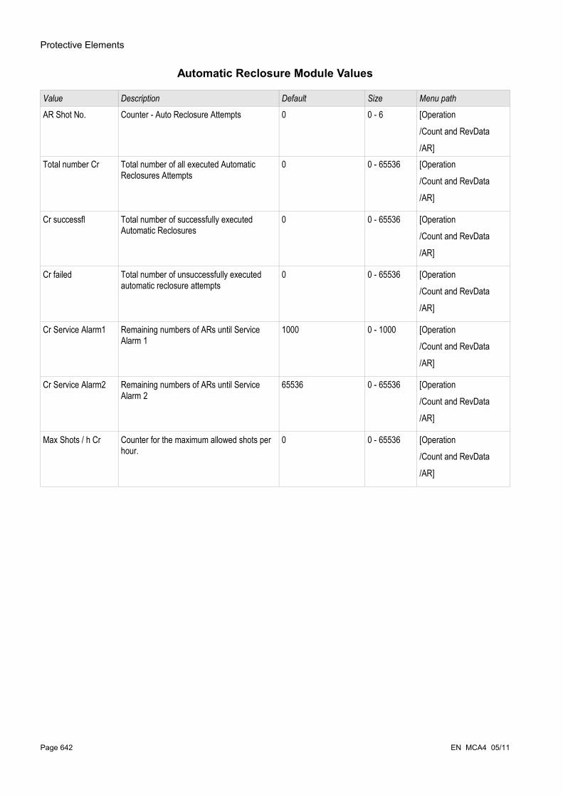
Protective Elements
Automatic Reclosure Module Values
Value Description Default Size Menu path
AR Shot No. Counter - Auto Reclosure Attempts 0 0 - 6 [Operation
/Count and RevData
/AR]Total number Cr Total number of all executed Automatic
Reclosures Attempts0 0 - 65536 [Operation
/Count and RevData
/AR]
Cr successfl Total number of successfully executed Automatic Reclosures
0 0 - 65536 [Operation
/Count and RevData
/AR]
Cr failed Total number of unsuccessfully executed automatic reclosure attempts
0 0 - 65536 [Operation
/Count and RevData
/AR]
Cr Service Alarm1 Remaining numbers of ARs until Service Alarm 1
1000 0 - 1000 [Operation
/Count and RevData
/AR]
Cr Service Alarm2 Remaining numbers of ARs until Service Alarm 2
65536 0 - 65536 [Operation
/Count and RevData
/AR]
Max Shots / h Cr Counter for the maximum allowed shots per hour.
0 0 - 65536 [Operation
/Count and RevData
/AR]
Page 642 EN MCA4 05/11

Protective Elements
Setting Group Parameters of the AR Abort Functions
Parameter Description Setting range Default Menu path
abort: 1 Abort the AR-cycle, if the state of the assigned signal is true. If the state of this function is true the AR will be aborted.
Block Fc -.- [Protection Para
/<n>
/AR
/Block Fc]abort: 2 Abort the AR-cycle, if the state of the assigned
signal is true. If the state of this function is true the AR will be aborted.
Block Fc -.- [Protection Para
/<n>
/AR
/Block Fc]abort: 3 Abort the AR-cycle, if the state of the assigned
signal is true. If the state of this function is true the AR will be aborted.
Block Fc -.- [Protection Para
/<n>
/AR
/Block Fc]abort: 4 Abort the AR-cycle, if the state of the assigned
signal is true. If the state of this function is true the AR will be aborted.
Block Fc -.- [Protection Para
/<n>
/AR
/Block Fc]abort: 5 Abort the AR-cycle, if the state of the assigned
signal is true. If the state of this function is true the AR will be aborted.
Block Fc -.- [Protection Para
/<n>
/AR
/Block Fc]abort: 6 Abort the AR-cycle, if the state of the assigned
signal is true. If the state of this function is true the AR will be aborted.
Block Fc -.- [Protection Para
/<n>
/AR
/Block Fc]
EN MCA4 05/11 Page 643
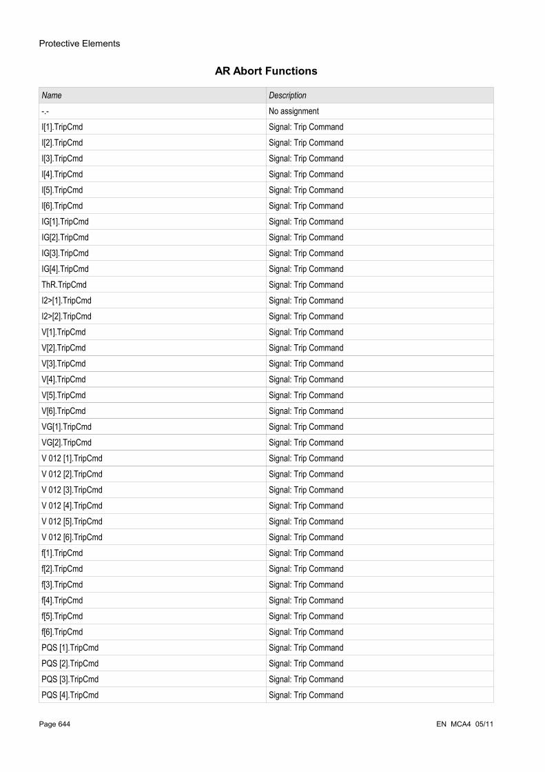
Protective Elements
AR Abort Functions
Name Description
-.- No assignmentI[1].TripCmd Signal: Trip CommandI[2].TripCmd Signal: Trip CommandI[3].TripCmd Signal: Trip CommandI[4].TripCmd Signal: Trip CommandI[5].TripCmd Signal: Trip CommandI[6].TripCmd Signal: Trip CommandIG[1].TripCmd Signal: Trip CommandIG[2].TripCmd Signal: Trip CommandIG[3].TripCmd Signal: Trip CommandIG[4].TripCmd Signal: Trip CommandThR.TripCmd Signal: Trip CommandI2>[1].TripCmd Signal: Trip CommandI2>[2].TripCmd Signal: Trip CommandV[1].TripCmd Signal: Trip CommandV[2].TripCmd Signal: Trip CommandV[3].TripCmd Signal: Trip CommandV[4].TripCmd Signal: Trip CommandV[5].TripCmd Signal: Trip CommandV[6].TripCmd Signal: Trip CommandVG[1].TripCmd Signal: Trip CommandVG[2].TripCmd Signal: Trip CommandV 012 [1].TripCmd Signal: Trip CommandV 012 [2].TripCmd Signal: Trip CommandV 012 [3].TripCmd Signal: Trip CommandV 012 [4].TripCmd Signal: Trip CommandV 012 [5].TripCmd Signal: Trip CommandV 012 [6].TripCmd Signal: Trip Commandf[1].TripCmd Signal: Trip Commandf[2].TripCmd Signal: Trip Commandf[3].TripCmd Signal: Trip Commandf[4].TripCmd Signal: Trip Commandf[5].TripCmd Signal: Trip Commandf[6].TripCmd Signal: Trip CommandPQS [1].TripCmd Signal: Trip CommandPQS [2].TripCmd Signal: Trip CommandPQS [3].TripCmd Signal: Trip CommandPQS [4].TripCmd Signal: Trip Command
Page 644 EN MCA4 05/11

Protective Elements
Name Description
PF[1].TripCmd Signal: Trip CommandPF[2].TripCmd Signal: Trip CommandExP[1].TripCmd Signal: Trip CommandExP[2].TripCmd Signal: Trip CommandExP[3].TripCmd Signal: Trip CommandExP[4].TripCmd Signal: Trip CommandSOTF.enabled Signal: Switch Onto Fault enabled. This Signal can be used to
modify Overcurrent Protection Settings.CLPU.enabled Signal: Cold Load enabledCBF.Alarm Signal: Circuit Breaker FailureTCS.Alarm Signal: Alarm Trip Circuit SupervisionLogics.LE1.Gate Out Signal: Output of the logic gateLogics.LE1.Timer Out Signal: Timer OutputLogics.LE1.Out Signal: Latched Output (Q)Logics.LE1.Out inverted Signal: Negated Latched Output (Q NOT)Logics.LE2.Gate Out Signal: Output of the logic gateLogics.LE2.Timer Out Signal: Timer OutputLogics.LE2.Out Signal: Latched Output (Q)Logics.LE2.Out inverted Signal: Negated Latched Output (Q NOT)Logics.LE3.Gate Out Signal: Output of the logic gateLogics.LE3.Timer Out Signal: Timer OutputLogics.LE3.Out Signal: Latched Output (Q)Logics.LE3.Out inverted Signal: Negated Latched Output (Q NOT)Logics.LE4.Gate Out Signal: Output of the logic gateLogics.LE4.Timer Out Signal: Timer OutputLogics.LE4.Out Signal: Latched Output (Q)Logics.LE4.Out inverted Signal: Negated Latched Output (Q NOT)Logics.LE5.Gate Out Signal: Output of the logic gateLogics.LE5.Timer Out Signal: Timer OutputLogics.LE5.Out Signal: Latched Output (Q)Logics.LE5.Out inverted Signal: Negated Latched Output (Q NOT)Logics.LE6.Gate Out Signal: Output of the logic gateLogics.LE6.Timer Out Signal: Timer OutputLogics.LE6.Out Signal: Latched Output (Q)Logics.LE6.Out inverted Signal: Negated Latched Output (Q NOT)Logics.LE7.Gate Out Signal: Output of the logic gateLogics.LE7.Timer Out Signal: Timer OutputLogics.LE7.Out Signal: Latched Output (Q)Logics.LE7.Out inverted Signal: Negated Latched Output (Q NOT)Logics.LE8.Gate Out Signal: Output of the logic gate
EN MCA4 05/11 Page 645

Protective Elements
Name Description
Logics.LE8.Timer Out Signal: Timer OutputLogics.LE8.Out Signal: Latched Output (Q)Logics.LE8.Out inverted Signal: Negated Latched Output (Q NOT)Logics.LE9.Gate Out Signal: Output of the logic gateLogics.LE9.Timer Out Signal: Timer OutputLogics.LE9.Out Signal: Latched Output (Q)Logics.LE9.Out inverted Signal: Negated Latched Output (Q NOT)Logics.LE10.Gate Out Signal: Output of the logic gateLogics.LE10.Timer Out Signal: Timer OutputLogics.LE10.Out Signal: Latched Output (Q)Logics.LE10.Out inverted Signal: Negated Latched Output (Q NOT)Logics.LE11.Gate Out Signal: Output of the logic gateLogics.LE11.Timer Out Signal: Timer OutputLogics.LE11.Out Signal: Latched Output (Q)Logics.LE11.Out inverted Signal: Negated Latched Output (Q NOT)Logics.LE12.Gate Out Signal: Output of the logic gateLogics.LE12.Timer Out Signal: Timer OutputLogics.LE12.Out Signal: Latched Output (Q)Logics.LE12.Out inverted Signal: Negated Latched Output (Q NOT)Logics.LE13.Gate Out Signal: Output of the logic gateLogics.LE13.Timer Out Signal: Timer OutputLogics.LE13.Out Signal: Latched Output (Q)Logics.LE13.Out inverted Signal: Negated Latched Output (Q NOT)Logics.LE14.Gate Out Signal: Output of the logic gateLogics.LE14.Timer Out Signal: Timer OutputLogics.LE14.Out Signal: Latched Output (Q)Logics.LE14.Out inverted Signal: Negated Latched Output (Q NOT)Logics.LE15.Gate Out Signal: Output of the logic gateLogics.LE15.Timer Out Signal: Timer OutputLogics.LE15.Out Signal: Latched Output (Q)Logics.LE15.Out inverted Signal: Negated Latched Output (Q NOT)Logics.LE16.Gate Out Signal: Output of the logic gateLogics.LE16.Timer Out Signal: Timer OutputLogics.LE16.Out Signal: Latched Output (Q)Logics.LE16.Out inverted Signal: Negated Latched Output (Q NOT)Logics.LE17.Gate Out Signal: Output of the logic gateLogics.LE17.Timer Out Signal: Timer OutputLogics.LE17.Out Signal: Latched Output (Q)Logics.LE17.Out inverted Signal: Negated Latched Output (Q NOT)
Page 646 EN MCA4 05/11

Protective Elements
Name Description
Logics.LE18.Gate Out Signal: Output of the logic gateLogics.LE18.Timer Out Signal: Timer OutputLogics.LE18.Out Signal: Latched Output (Q)Logics.LE18.Out inverted Signal: Negated Latched Output (Q NOT)Logics.LE19.Gate Out Signal: Output of the logic gateLogics.LE19.Timer Out Signal: Timer OutputLogics.LE19.Out Signal: Latched Output (Q)Logics.LE19.Out inverted Signal: Negated Latched Output (Q NOT)Logics.LE20.Gate Out Signal: Output of the logic gateLogics.LE20.Timer Out Signal: Timer OutputLogics.LE20.Out Signal: Latched Output (Q)Logics.LE20.Out inverted Signal: Negated Latched Output (Q NOT)Logics.LE21.Gate Out Signal: Output of the logic gateLogics.LE21.Timer Out Signal: Timer OutputLogics.LE21.Out Signal: Latched Output (Q)Logics.LE21.Out inverted Signal: Negated Latched Output (Q NOT)Logics.LE22.Gate Out Signal: Output of the logic gateLogics.LE22.Timer Out Signal: Timer OutputLogics.LE22.Out Signal: Latched Output (Q)Logics.LE22.Out inverted Signal: Negated Latched Output (Q NOT)Logics.LE23.Gate Out Signal: Output of the logic gateLogics.LE23.Timer Out Signal: Timer OutputLogics.LE23.Out Signal: Latched Output (Q)Logics.LE23.Out inverted Signal: Negated Latched Output (Q NOT)Logics.LE24.Gate Out Signal: Output of the logic gateLogics.LE24.Timer Out Signal: Timer OutputLogics.LE24.Out Signal: Latched Output (Q)Logics.LE24.Out inverted Signal: Negated Latched Output (Q NOT)Logics.LE25.Gate Out Signal: Output of the logic gateLogics.LE25.Timer Out Signal: Timer OutputLogics.LE25.Out Signal: Latched Output (Q)Logics.LE25.Out inverted Signal: Negated Latched Output (Q NOT)Logics.LE26.Gate Out Signal: Output of the logic gateLogics.LE26.Timer Out Signal: Timer OutputLogics.LE26.Out Signal: Latched Output (Q)Logics.LE26.Out inverted Signal: Negated Latched Output (Q NOT)Logics.LE27.Gate Out Signal: Output of the logic gateLogics.LE27.Timer Out Signal: Timer OutputLogics.LE27.Out Signal: Latched Output (Q)
EN MCA4 05/11 Page 647

Protective Elements
Name Description
Logics.LE27.Out inverted Signal: Negated Latched Output (Q NOT)Logics.LE28.Gate Out Signal: Output of the logic gateLogics.LE28.Timer Out Signal: Timer OutputLogics.LE28.Out Signal: Latched Output (Q)Logics.LE28.Out inverted Signal: Negated Latched Output (Q NOT)Logics.LE29.Gate Out Signal: Output of the logic gateLogics.LE29.Timer Out Signal: Timer OutputLogics.LE29.Out Signal: Latched Output (Q)Logics.LE29.Out inverted Signal: Negated Latched Output (Q NOT)Logics.LE30.Gate Out Signal: Output of the logic gateLogics.LE30.Timer Out Signal: Timer OutputLogics.LE30.Out Signal: Latched Output (Q)Logics.LE30.Out inverted Signal: Negated Latched Output (Q NOT)Logics.LE31.Gate Out Signal: Output of the logic gateLogics.LE31.Timer Out Signal: Timer OutputLogics.LE31.Out Signal: Latched Output (Q)Logics.LE31.Out inverted Signal: Negated Latched Output (Q NOT)Logics.LE32.Gate Out Signal: Output of the logic gateLogics.LE32.Timer Out Signal: Timer OutputLogics.LE32.Out Signal: Latched Output (Q)Logics.LE32.Out inverted Signal: Negated Latched Output (Q NOT)Logics.LE33.Gate Out Signal: Output of the logic gateLogics.LE33.Timer Out Signal: Timer OutputLogics.LE33.Out Signal: Latched Output (Q)Logics.LE33.Out inverted Signal: Negated Latched Output (Q NOT)Logics.LE34.Gate Out Signal: Output of the logic gateLogics.LE34.Timer Out Signal: Timer OutputLogics.LE34.Out Signal: Latched Output (Q)Logics.LE34.Out inverted Signal: Negated Latched Output (Q NOT)Logics.LE35.Gate Out Signal: Output of the logic gateLogics.LE35.Timer Out Signal: Timer OutputLogics.LE35.Out Signal: Latched Output (Q)Logics.LE35.Out inverted Signal: Negated Latched Output (Q NOT)Logics.LE36.Gate Out Signal: Output of the logic gateLogics.LE36.Timer Out Signal: Timer OutputLogics.LE36.Out Signal: Latched Output (Q)Logics.LE36.Out inverted Signal: Negated Latched Output (Q NOT)Logics.LE37.Gate Out Signal: Output of the logic gateLogics.LE37.Timer Out Signal: Timer Output
Page 648 EN MCA4 05/11

Protective Elements
Name Description
Logics.LE37.Out Signal: Latched Output (Q)Logics.LE37.Out inverted Signal: Negated Latched Output (Q NOT)Logics.LE38.Gate Out Signal: Output of the logic gateLogics.LE38.Timer Out Signal: Timer OutputLogics.LE38.Out Signal: Latched Output (Q)Logics.LE38.Out inverted Signal: Negated Latched Output (Q NOT)Logics.LE39.Gate Out Signal: Output of the logic gateLogics.LE39.Timer Out Signal: Timer OutputLogics.LE39.Out Signal: Latched Output (Q)Logics.LE39.Out inverted Signal: Negated Latched Output (Q NOT)Logics.LE40.Gate Out Signal: Output of the logic gateLogics.LE40.Timer Out Signal: Timer OutputLogics.LE40.Out Signal: Latched Output (Q)Logics.LE40.Out inverted Signal: Negated Latched Output (Q NOT)Logics.LE41.Gate Out Signal: Output of the logic gateLogics.LE41.Timer Out Signal: Timer OutputLogics.LE41.Out Signal: Latched Output (Q)Logics.LE41.Out inverted Signal: Negated Latched Output (Q NOT)Logics.LE42.Gate Out Signal: Output of the logic gateLogics.LE42.Timer Out Signal: Timer OutputLogics.LE42.Out Signal: Latched Output (Q)Logics.LE42.Out inverted Signal: Negated Latched Output (Q NOT)Logics.LE43.Gate Out Signal: Output of the logic gateLogics.LE43.Timer Out Signal: Timer OutputLogics.LE43.Out Signal: Latched Output (Q)Logics.LE43.Out inverted Signal: Negated Latched Output (Q NOT)Logics.LE44.Gate Out Signal: Output of the logic gateLogics.LE44.Timer Out Signal: Timer OutputLogics.LE44.Out Signal: Latched Output (Q)Logics.LE44.Out inverted Signal: Negated Latched Output (Q NOT)Logics.LE45.Gate Out Signal: Output of the logic gateLogics.LE45.Timer Out Signal: Timer OutputLogics.LE45.Out Signal: Latched Output (Q)Logics.LE45.Out inverted Signal: Negated Latched Output (Q NOT)Logics.LE46.Gate Out Signal: Output of the logic gateLogics.LE46.Timer Out Signal: Timer OutputLogics.LE46.Out Signal: Latched Output (Q)Logics.LE46.Out inverted Signal: Negated Latched Output (Q NOT)Logics.LE47.Gate Out Signal: Output of the logic gate
EN MCA4 05/11 Page 649

Protective Elements
Name Description
Logics.LE47.Timer Out Signal: Timer OutputLogics.LE47.Out Signal: Latched Output (Q)Logics.LE47.Out inverted Signal: Negated Latched Output (Q NOT)Logics.LE48.Gate Out Signal: Output of the logic gateLogics.LE48.Timer Out Signal: Timer OutputLogics.LE48.Out Signal: Latched Output (Q)Logics.LE48.Out inverted Signal: Negated Latched Output (Q NOT)Logics.LE49.Gate Out Signal: Output of the logic gateLogics.LE49.Timer Out Signal: Timer OutputLogics.LE49.Out Signal: Latched Output (Q)Logics.LE49.Out inverted Signal: Negated Latched Output (Q NOT)Logics.LE50.Gate Out Signal: Output of the logic gateLogics.LE50.Timer Out Signal: Timer OutputLogics.LE50.Out Signal: Latched Output (Q)Logics.LE50.Out inverted Signal: Negated Latched Output (Q NOT)Logics.LE51.Gate Out Signal: Output of the logic gateLogics.LE51.Timer Out Signal: Timer OutputLogics.LE51.Out Signal: Latched Output (Q)Logics.LE51.Out inverted Signal: Negated Latched Output (Q NOT)Logics.LE52.Gate Out Signal: Output of the logic gateLogics.LE52.Timer Out Signal: Timer OutputLogics.LE52.Out Signal: Latched Output (Q)Logics.LE52.Out inverted Signal: Negated Latched Output (Q NOT)Logics.LE53.Gate Out Signal: Output of the logic gateLogics.LE53.Timer Out Signal: Timer OutputLogics.LE53.Out Signal: Latched Output (Q)Logics.LE53.Out inverted Signal: Negated Latched Output (Q NOT)Logics.LE54.Gate Out Signal: Output of the logic gateLogics.LE54.Timer Out Signal: Timer OutputLogics.LE54.Out Signal: Latched Output (Q)Logics.LE54.Out inverted Signal: Negated Latched Output (Q NOT)Logics.LE55.Gate Out Signal: Output of the logic gateLogics.LE55.Timer Out Signal: Timer OutputLogics.LE55.Out Signal: Latched Output (Q)Logics.LE55.Out inverted Signal: Negated Latched Output (Q NOT)Logics.LE56.Gate Out Signal: Output of the logic gateLogics.LE56.Timer Out Signal: Timer OutputLogics.LE56.Out Signal: Latched Output (Q)Logics.LE56.Out inverted Signal: Negated Latched Output (Q NOT)
Page 650 EN MCA4 05/11
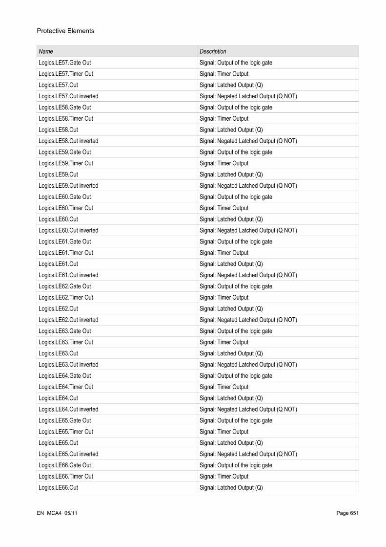
Protective Elements
Name Description
Logics.LE57.Gate Out Signal: Output of the logic gateLogics.LE57.Timer Out Signal: Timer OutputLogics.LE57.Out Signal: Latched Output (Q)Logics.LE57.Out inverted Signal: Negated Latched Output (Q NOT)Logics.LE58.Gate Out Signal: Output of the logic gateLogics.LE58.Timer Out Signal: Timer OutputLogics.LE58.Out Signal: Latched Output (Q)Logics.LE58.Out inverted Signal: Negated Latched Output (Q NOT)Logics.LE59.Gate Out Signal: Output of the logic gateLogics.LE59.Timer Out Signal: Timer OutputLogics.LE59.Out Signal: Latched Output (Q)Logics.LE59.Out inverted Signal: Negated Latched Output (Q NOT)Logics.LE60.Gate Out Signal: Output of the logic gateLogics.LE60.Timer Out Signal: Timer OutputLogics.LE60.Out Signal: Latched Output (Q)Logics.LE60.Out inverted Signal: Negated Latched Output (Q NOT)Logics.LE61.Gate Out Signal: Output of the logic gateLogics.LE61.Timer Out Signal: Timer OutputLogics.LE61.Out Signal: Latched Output (Q)Logics.LE61.Out inverted Signal: Negated Latched Output (Q NOT)Logics.LE62.Gate Out Signal: Output of the logic gateLogics.LE62.Timer Out Signal: Timer OutputLogics.LE62.Out Signal: Latched Output (Q)Logics.LE62.Out inverted Signal: Negated Latched Output (Q NOT)Logics.LE63.Gate Out Signal: Output of the logic gateLogics.LE63.Timer Out Signal: Timer OutputLogics.LE63.Out Signal: Latched Output (Q)Logics.LE63.Out inverted Signal: Negated Latched Output (Q NOT)Logics.LE64.Gate Out Signal: Output of the logic gateLogics.LE64.Timer Out Signal: Timer OutputLogics.LE64.Out Signal: Latched Output (Q)Logics.LE64.Out inverted Signal: Negated Latched Output (Q NOT)Logics.LE65.Gate Out Signal: Output of the logic gateLogics.LE65.Timer Out Signal: Timer OutputLogics.LE65.Out Signal: Latched Output (Q)Logics.LE65.Out inverted Signal: Negated Latched Output (Q NOT)Logics.LE66.Gate Out Signal: Output of the logic gateLogics.LE66.Timer Out Signal: Timer OutputLogics.LE66.Out Signal: Latched Output (Q)
EN MCA4 05/11 Page 651
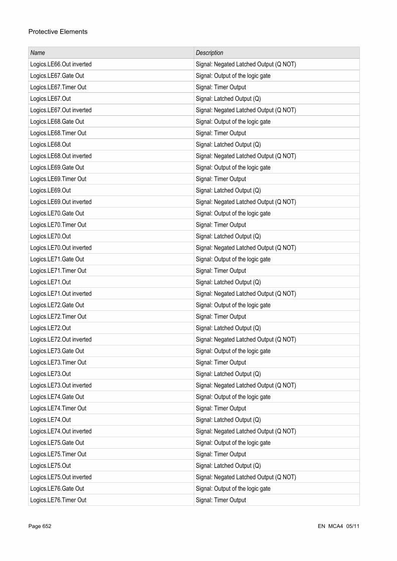
Protective Elements
Name Description
Logics.LE66.Out inverted Signal: Negated Latched Output (Q NOT)Logics.LE67.Gate Out Signal: Output of the logic gateLogics.LE67.Timer Out Signal: Timer OutputLogics.LE67.Out Signal: Latched Output (Q)Logics.LE67.Out inverted Signal: Negated Latched Output (Q NOT)Logics.LE68.Gate Out Signal: Output of the logic gateLogics.LE68.Timer Out Signal: Timer OutputLogics.LE68.Out Signal: Latched Output (Q)Logics.LE68.Out inverted Signal: Negated Latched Output (Q NOT)Logics.LE69.Gate Out Signal: Output of the logic gateLogics.LE69.Timer Out Signal: Timer OutputLogics.LE69.Out Signal: Latched Output (Q)Logics.LE69.Out inverted Signal: Negated Latched Output (Q NOT)Logics.LE70.Gate Out Signal: Output of the logic gateLogics.LE70.Timer Out Signal: Timer OutputLogics.LE70.Out Signal: Latched Output (Q)Logics.LE70.Out inverted Signal: Negated Latched Output (Q NOT)Logics.LE71.Gate Out Signal: Output of the logic gateLogics.LE71.Timer Out Signal: Timer OutputLogics.LE71.Out Signal: Latched Output (Q)Logics.LE71.Out inverted Signal: Negated Latched Output (Q NOT)Logics.LE72.Gate Out Signal: Output of the logic gateLogics.LE72.Timer Out Signal: Timer OutputLogics.LE72.Out Signal: Latched Output (Q)Logics.LE72.Out inverted Signal: Negated Latched Output (Q NOT)Logics.LE73.Gate Out Signal: Output of the logic gateLogics.LE73.Timer Out Signal: Timer OutputLogics.LE73.Out Signal: Latched Output (Q)Logics.LE73.Out inverted Signal: Negated Latched Output (Q NOT)Logics.LE74.Gate Out Signal: Output of the logic gateLogics.LE74.Timer Out Signal: Timer OutputLogics.LE74.Out Signal: Latched Output (Q)Logics.LE74.Out inverted Signal: Negated Latched Output (Q NOT)Logics.LE75.Gate Out Signal: Output of the logic gateLogics.LE75.Timer Out Signal: Timer OutputLogics.LE75.Out Signal: Latched Output (Q)Logics.LE75.Out inverted Signal: Negated Latched Output (Q NOT)Logics.LE76.Gate Out Signal: Output of the logic gateLogics.LE76.Timer Out Signal: Timer Output
Page 652 EN MCA4 05/11
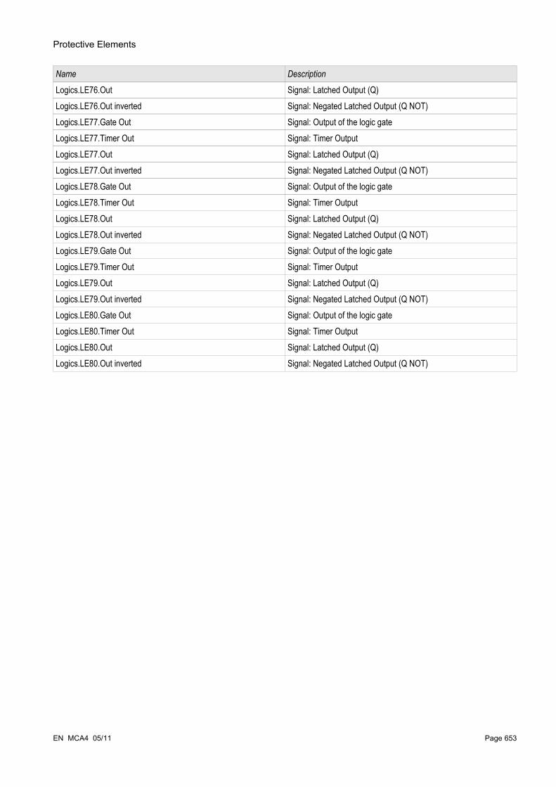
Protective Elements
Name Description
Logics.LE76.Out Signal: Latched Output (Q)Logics.LE76.Out inverted Signal: Negated Latched Output (Q NOT)Logics.LE77.Gate Out Signal: Output of the logic gateLogics.LE77.Timer Out Signal: Timer OutputLogics.LE77.Out Signal: Latched Output (Q)Logics.LE77.Out inverted Signal: Negated Latched Output (Q NOT)Logics.LE78.Gate Out Signal: Output of the logic gateLogics.LE78.Timer Out Signal: Timer OutputLogics.LE78.Out Signal: Latched Output (Q)Logics.LE78.Out inverted Signal: Negated Latched Output (Q NOT)Logics.LE79.Gate Out Signal: Output of the logic gateLogics.LE79.Timer Out Signal: Timer OutputLogics.LE79.Out Signal: Latched Output (Q)Logics.LE79.Out inverted Signal: Negated Latched Output (Q NOT)Logics.LE80.Gate Out Signal: Output of the logic gateLogics.LE80.Timer Out Signal: Timer OutputLogics.LE80.Out Signal: Latched Output (Q)Logics.LE80.Out inverted Signal: Negated Latched Output (Q NOT)
EN MCA4 05/11 Page 653

Protective Elements
AR Start Functions
Name Description
- No assignmentI[1] Phase Overcurrent StageI[2] Phase Overcurrent StageI[3] Phase Overcurrent StageI[4] Phase Overcurrent StageI[5] Phase Overcurrent StageI[6] Phase Overcurrent StageIG[1] Earth current protection - StageIG[2] Earth current protection - StageIG[3] Earth current protection - StageIG[4] Earth current protection - StageI2>[1] Unbalanced Load-StageI2>[2] Unbalanced Load-StageExP[1] External Protection - ModuleExP[2] External Protection - ModuleExP[3] External Protection - ModuleExP[4] External Protection - Module
Scada Commands of the Auto Reclosure
Name Description
-.- No assignmentModbus.Scada Cmd 1 Scada CommandModbus.Scada Cmd 2 Scada CommandModbus.Scada Cmd 3 Scada CommandModbus.Scada Cmd 4 Scada CommandModbus.Scada Cmd 5 Scada CommandModbus.Scada Cmd 6 Scada CommandModbus.Scada Cmd 7 Scada CommandModbus.Scada Cmd 8 Scada CommandModbus.Scada Cmd 9 Scada CommandModbus.Scada Cmd 10 Scada CommandModbus.Scada Cmd 11 Scada CommandModbus.Scada Cmd 12 Scada CommandModbus.Scada Cmd 13 Scada CommandModbus.Scada Cmd 14 Scada CommandModbus.Scada Cmd 15 Scada CommandModbus.Scada Cmd 16 Scada Command
Page 654 EN MCA4 05/11
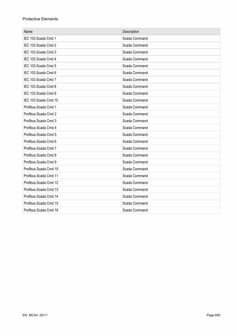
Protective Elements
Name Description
IEC 103.Scada Cmd 1 Scada CommandIEC 103.Scada Cmd 2 Scada CommandIEC 103.Scada Cmd 3 Scada CommandIEC 103.Scada Cmd 4 Scada CommandIEC 103.Scada Cmd 5 Scada CommandIEC 103.Scada Cmd 6 Scada CommandIEC 103.Scada Cmd 7 Scada CommandIEC 103.Scada Cmd 8 Scada CommandIEC 103.Scada Cmd 9 Scada CommandIEC 103.Scada Cmd 10 Scada CommandProfibus.Scada Cmd 1 Scada CommandProfibus.Scada Cmd 2 Scada CommandProfibus.Scada Cmd 3 Scada CommandProfibus.Scada Cmd 4 Scada CommandProfibus.Scada Cmd 5 Scada CommandProfibus.Scada Cmd 6 Scada CommandProfibus.Scada Cmd 7 Scada CommandProfibus.Scada Cmd 8 Scada CommandProfibus.Scada Cmd 9 Scada CommandProfibus.Scada Cmd 10 Scada CommandProfibus.Scada Cmd 11 Scada CommandProfibus.Scada Cmd 12 Scada CommandProfibus.Scada Cmd 13 Scada CommandProfibus.Scada Cmd 14 Scada CommandProfibus.Scada Cmd 15 Scada CommandProfibus.Scada Cmd 16 Scada Command
EN MCA4 05/11 Page 655

Protective Elements
ExP - External ProtectionAvailable stages: ExP[1] ,ExP[2] ,ExP[3] ,ExP[4]
All 4 stages of the external protection ExP[1]...[4] are identically structured.
By using the module External Protection the following can be incorporated into the device function: trip commands, alarms and blockades of external protection facilities. Devices which are not provided with a communication interface can be connected to the control system as well.
Page 656 EN MCA4 05/11
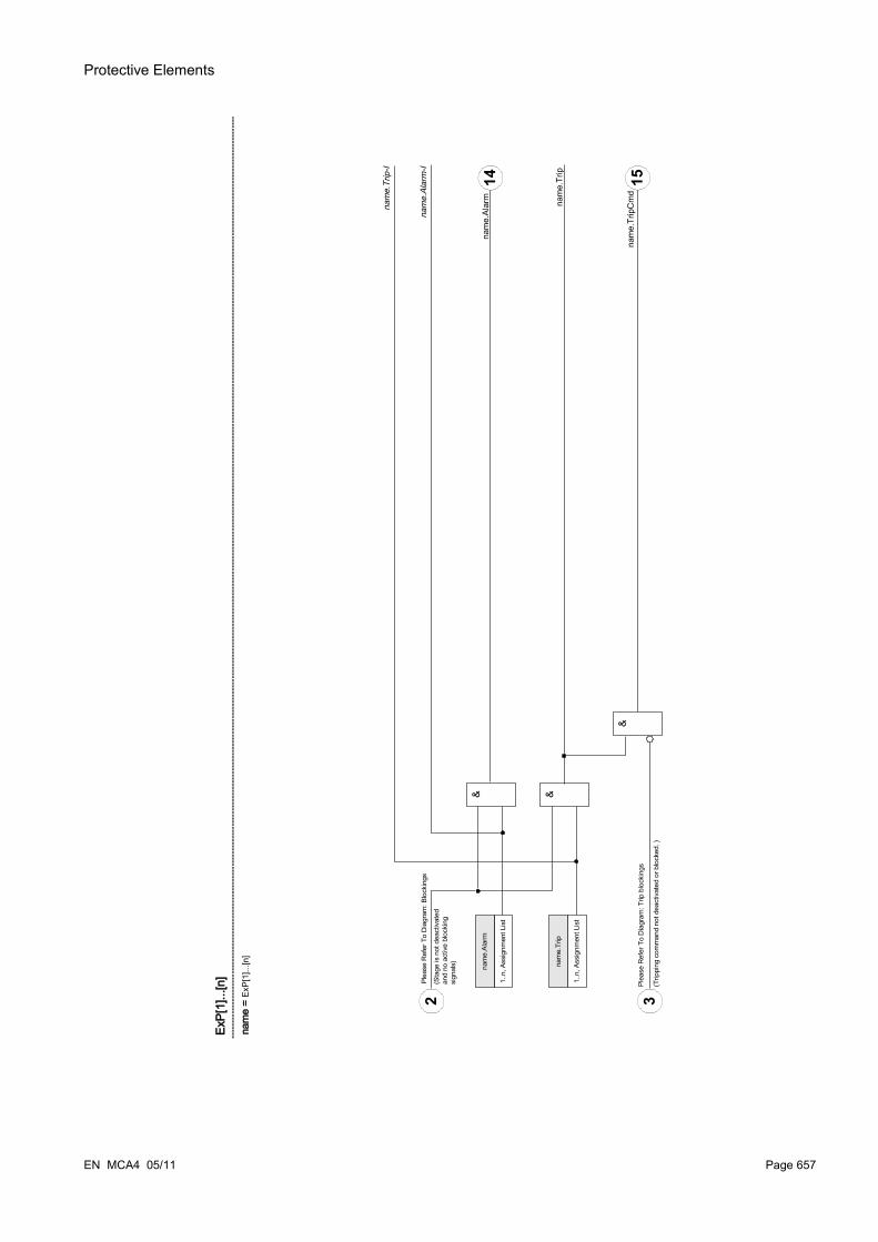
Protective Elements
EN MCA4 05/11 Page 657
1..n
, Ass
ignm
ent L
ist
nam
e.Al
arm
nam
e.Tr
ipC
md
&
1..n
, Ass
ignm
ent L
ist
nam
e.Tr
ip
& &na
me.
Trip
nam
e.Al
arm
Ple
ase
Ref
er T
o D
iagr
am: B
lock
ings
Ple
ase
Ref
er T
o D
iagr
am: T
rip b
lock
ings
(Sta
ge is
not
dea
ctiv
ated
an
d no
act
ive
bloc
king
si
gnal
s)
(Trip
ping
com
man
d no
t dea
ctiv
ated
or b
lock
ed. )
ExP[
1]...
[n]
nam
e =
ExP[
1]...
[n]
nam
e.Tr
ip-I
nam
e.Al
arm
-I2 3
14 15
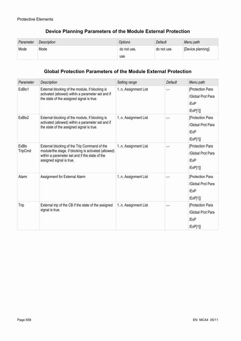
Protective Elements
Device Planning Parameters of the Module External Protection
Parameter Description Options Default Menu path
Mode Mode do not use,
use
do not use [Device planning]
Global Protection Parameters of the Module External Protection
Parameter Description Setting range Default Menu path
ExBlo1 External blocking of the module, if blocking is activated (allowed) within a parameter set and if the state of the assigned signal is true.
1..n, Assignment List -.- [Protection Para
/Global Prot Para
/ExP
/ExP[1]]ExBlo2 External blocking of the module, if blocking is
activated (allowed) within a parameter set and if the state of the assigned signal is true.
1..n, Assignment List -.- [Protection Para
/Global Prot Para
/ExP
/ExP[1]]ExBlo TripCmd
External blocking of the Trip Command of the module/the stage, if blocking is activated (allowed) within a parameter set and if the state of the assigned signal is true.
1..n, Assignment List -.- [Protection Para
/Global Prot Para
/ExP
/ExP[1]]
Alarm Assignment for External Alarm 1..n, Assignment List -.- [Protection Para
/Global Prot Para
/ExP
/ExP[1]]Trip External trip of the CB if the state of the assigned
signal is true.1..n, Assignment List -.- [Protection Para
/Global Prot Para
/ExP
/ExP[1]]
Page 658 EN MCA4 05/11
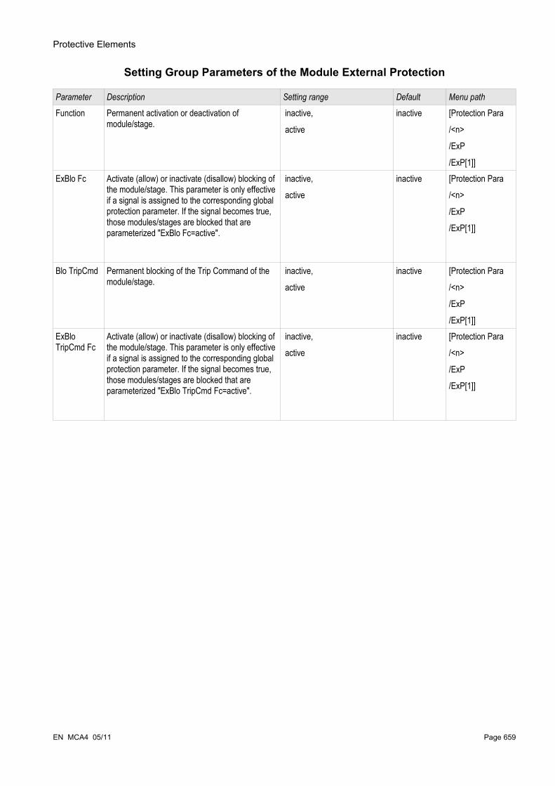
Protective Elements
Setting Group Parameters of the Module External Protection
Parameter Description Setting range Default Menu path
Function Permanent activation or deactivation of module/stage.
inactive,
active
inactive [Protection Para
/<n>
/ExP
/ExP[1]]ExBlo Fc Activate (allow) or inactivate (disallow) blocking of
the module/stage. This parameter is only effective if a signal is assigned to the corresponding global protection parameter. If the signal becomes true, those modules/stages are blocked that are parameterized "ExBlo Fc=active".
inactive,
active
inactive [Protection Para
/<n>
/ExP
/ExP[1]]
Blo TripCmd Permanent blocking of the Trip Command of the module/stage.
inactive,
active
inactive [Protection Para
/<n>
/ExP
/ExP[1]]ExBlo TripCmd Fc
Activate (allow) or inactivate (disallow) blocking of the module/stage. This parameter is only effective if a signal is assigned to the corresponding global protection parameter. If the signal becomes true, those modules/stages are blocked that are parameterized "ExBlo TripCmd Fc=active".
inactive,
active
inactive [Protection Para
/<n>
/ExP
/ExP[1]]
EN MCA4 05/11 Page 659

Protective Elements
Module External Protection Input States
Name Description Assignment via
ExBlo1-I Module input state: External blocking1 [Protection Para
/Global Prot Para
/ExP
/ExP[1]]ExBlo2-I Module input state: External blocking2 [Protection Para
/Global Prot Para
/ExP
/ExP[1]]ExBlo TripCmd-I Module input state: External Blocking of the
Trip Command[Protection Para
/Global Prot Para
/ExP
/ExP[1]]Alarm-I Module input state: Alarm [Protection Para
/Global Prot Para
/ExP
/ExP[1]]Trip-I Module input state: Trip [Protection Para
/Global Prot Para
/ExP
/ExP[1]]
Module External Protection Signals (Output States)
Name Description
active Signal: activeExBlo Signal: External BlockingBlo TripCmd Signal: Trip Command blockedExBlo TripCmd Signal: External Blocking of the Trip CommandAlarm Signal: AlarmTrip Signal: TripTripCmd Signal: Trip Command
Page 660 EN MCA4 05/11

Protective Elements
Commissioning: External Protection
Object to be testedTest of the module External Protection
Necessary means• Depending on the application
ProcedureSimulate the functionality of the External Protection (Alarm, Trip, Blockings...) by (de-)energizing of the digital inputs.
Successful test resultAll external alarms, external trips and external blockings are correctly recognized and processed by the device.
EN MCA4 05/11 Page 661

Protective Elements
CBF- Circuit Breaker Failure [50BF]Available elements: CBF
Principle – General Use
The breaker failure (BF) protection is used to provide backup protection in the event that a breaker fails to oper-ate properly during fault clearing. A breaker failure condition is recognized if current is still flowing through the breaker after tripping or opening breaker commands have been issued for a specified time. The User can select different trigger modes. In addition, up to three additional trigger events can be assigned from all the protection modules.
Trigger Modes
There are three trigger modes for the breaker failure available. In addition, there are three assignable trigger inputs available.
•All Trips: All trip signals that are assigned to this breaker (within the breaker manager) will start the BF module.
•Current Trips: All current trips that are assigned to this breaker (within the breaker manager) will start the BF module.
•External Trips: All external trips that are assigned to this breaker (within the breaker manager) will start the BF module.
•In addition, the User can also select none (e.g.: if the User intends to use one of the three additional assignable trigger inputs).
Those trips can exclusively start the breaker failures that are assigned within the breaker manager to the breaker that is to be supervised.
Select the winding side from which the measured currents should be taken in case this protective device is a transformer differential protection.
This Notice applies to protective devices that offer control functionality only! This protective element requires, that a switchgear (circuit breaker is assigned to it. It is allowed only to assign switchgears (circuit breaker) to this protective element, whose measuring transformers provide measuring data to the protective device.
Breaker Failure Lockout
The signal of the Circuit Breaker Failure is latched. This signal can be used within the interlockings of the circuit breaker.
Page 662 EN MCA4 05/11

Protective Elements
EN MCA4 05/11 Page 663
Cur
rent
Trip
s
Det
erm
inin
g th
e tri
gger
mod
e fo
r th
e Br
eake
r Fai
lure
.
All T
rips
Exte
rnal
Trip
s
nam
e.I-C
BF >
IL1
IL2
IL3
S
1
R1
1
Plea
se R
efer
To
Dia
gram
: Blo
ckin
gs
CBF
.Ala
rm
CBF
.runn
ing
CBF
(Sta
ge is
not
dea
ctiv
ated
and
no
activ
e bl
ocki
ng
sign
als)
nam
e =
CBF
2
14
All T
rips
Exte
rnal
Trip
s
Cur
rent
Trip
s
1515 15
15
15 15
CBF
.Trig
ger1
CBF.
Trig
ger2
CBF.
Trig
ger3
CBF.
Trig
ger1
-I
CBF.
Trig
ger2
-I
CBF.
Trig
ger3
-I
none
&
>1 &
t-CBF
nam
e.t-C
BF0
S
1
R1
1
CBF
.Loc
kout
Res
Loc
kout
*
*Thi
s si
gnal
is th
e ou
tput
of t
he s
witc
hgea
r tha
t is
assi
gned
to th
is
prot
ectiv
e el
emen
t. Th
is a
pplie
s to
pro
tect
ive
devi
ces
that
offe
r co
ntro
l fun
ctio
nalit
y.

Protective Elements
Device Planning Parameters of the CBF
Parameter Description Options Default Menu path
Mode Mode do not use,
use
do not use [Device planning]
Global Protection Parameters of the CBF
Parameter Description Setting range Default Menu path
CB Selection of the Circuit Breaker to be monitored. -.-,
SG[1].,
SG[2].,
SG[3].,
SG[4].,
SG[5].,
SG[6].
SG[1]. [Protection Para
/Global Prot Para
/Supervision
/CBF]
ExBlo1 External blocking of the module, if blocking is activated (allowed) within a parameter set and if the state of the assigned signal is true.
1..n, Assignment List -.- [Protection Para
/Global Prot Para
/Supervision
/CBF]ExBlo2 External blocking of the module, if blocking is
activated (allowed) within a parameter set and if the state of the assigned signal is true.
1..n, Assignment List -.- [Protection Para
/Global Prot Para
/Supervision
/CBF]Trigger Determining the trigger mode for the Breaker
Failure. - . -,
All Trips,
Current Trips,
External Trips
- . - [Protection Para
/Global Prot Para
/Supervision
/CBF]Trigger1 Trigger that will start the CBF Trigger -.- [Protection Para
/Global Prot Para
/Supervision
/CBF]Trigger2 Trigger that will start the CBF Trigger -.- [Protection Para
/Global Prot Para
/Supervision
/CBF]Trigger3 Trigger that will start the CBF Trigger -.- [Protection Para
/Global Prot Para
/Supervision
/CBF]
Page 664 EN MCA4 05/11

Protective Elements
Direct Commands of the CBF
Parameter Description Setting range Default Menu path
Res Lockout Reset Lockout inactive,
active
inactive [Operation
/Reset]
EN MCA4 05/11 Page 665
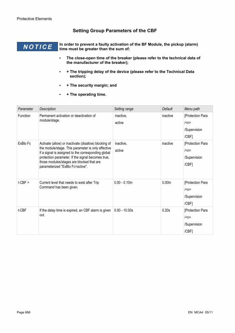
Protective Elements
Setting Group Parameters of the CBF
In order to prevent a faulty activation of the BF Module, the pickup (alarm) time must be greater than the sum of:
• The close-open time of the breaker (please refer to the technical data of the manufacturer of the breaker);
• + The tripping delay of the device (please refer to the Technical Data section);
• + The security margin; and
• + The operating time.
Parameter Description Setting range Default Menu path
Function Permanent activation or deactivation of module/stage.
inactive,
active
inactive [Protection Para
/<n>
/Supervision
/CBF]ExBlo Fc Activate (allow) or inactivate (disallow) blocking of
the module/stage. This parameter is only effective if a signal is assigned to the corresponding global protection parameter. If the signal becomes true, those modules/stages are blocked that are parameterized "ExBlo Fc=active".
inactive,
active
inactive [Protection Para
/<n>
/Supervision
/CBF]
I-CBF > Current level that needs to exist after Trip Command has been given.
0.00 - 0.10In 0.00In [Protection Para
/<n>
/Supervision
/CBF]t-CBF If the delay time is expired, an CBF alarm is given
out.0.00 - 10.00s 0.20s [Protection Para
/<n>
/Supervision
/CBF]
Page 666 EN MCA4 05/11

Protective Elements
CBF Input States
Name Description Assignment via
ExBlo1-I Module input state: External blocking1 [Protection Para
/Global Prot Para
/Supervision
/CBF]ExBlo2-I Module input state: External blocking2 [Protection Para
/Global Prot Para
/Supervision
/CBF]Trigger1 Module Input: Trigger that will start the CBF [Protection Para
/Global Prot Para
/Supervision
/CBF]Trigger2 Module Input: Trigger that will start the CBF [Protection Para
/Global Prot Para
/Supervision
/CBF]Trigger3 Module Input: Trigger that will start the CBF [Protection Para
/Global Prot Para
/Supervision
/CBF]
CBF Signals (Output States)
Name Description
active Signal: activeExBlo Signal: External Blockingrunning Signal: CBF-Module startedAlarm Signal: Circuit Breaker FailureLockout Signal: LockoutRes Lockout Signal: Reset Lockout
EN MCA4 05/11 Page 667

Protective Elements
CBF Trigger (Current Trips) Functions
These trips will start the BF module if all trips have been selected as the trigger event.
Name Description
-.- No assignmentI[1].TripCmd Signal: Trip CommandI[2].TripCmd Signal: Trip CommandI[3].TripCmd Signal: Trip CommandI[4].TripCmd Signal: Trip CommandI[5].TripCmd Signal: Trip CommandI[6].TripCmd Signal: Trip CommandIG[1].TripCmd Signal: Trip CommandIG[2].TripCmd Signal: Trip CommandIG[3].TripCmd Signal: Trip CommandIG[4].TripCmd Signal: Trip CommandThR.TripCmd Signal: Trip CommandI2>[1].TripCmd Signal: Trip CommandI2>[2].TripCmd Signal: Trip CommandV[1].TripCmd Signal: Trip CommandV[2].TripCmd Signal: Trip CommandV[3].TripCmd Signal: Trip CommandV[4].TripCmd Signal: Trip CommandV[5].TripCmd Signal: Trip CommandV[6].TripCmd Signal: Trip CommandVG[1].TripCmd Signal: Trip CommandVG[2].TripCmd Signal: Trip CommandV 012 [1].TripCmd Signal: Trip CommandV 012 [2].TripCmd Signal: Trip CommandV 012 [3].TripCmd Signal: Trip CommandV 012 [4].TripCmd Signal: Trip CommandV 012 [5].TripCmd Signal: Trip CommandV 012 [6].TripCmd Signal: Trip Commandf[1].TripCmd Signal: Trip Commandf[2].TripCmd Signal: Trip Commandf[3].TripCmd Signal: Trip Commandf[4].TripCmd Signal: Trip Commandf[5].TripCmd Signal: Trip Commandf[6].TripCmd Signal: Trip CommandPQS [1].TripCmd Signal: Trip CommandPQS [2].TripCmd Signal: Trip Command
Page 668 EN MCA4 05/11

Protective Elements
Name Description
PQS [3].TripCmd Signal: Trip CommandPQS [4].TripCmd Signal: Trip CommandPQS [5].TripCmd Signal: Trip CommandPQS [6].TripCmd Signal: Trip CommandPF[1].TripCmd Signal: Trip CommandPF[2].TripCmd Signal: Trip CommandExP[1].TripCmd Signal: Trip CommandExP[2].TripCmd Signal: Trip CommandExP[3].TripCmd Signal: Trip CommandExP[4].TripCmd Signal: Trip CommandDI Slot X1.DI 1 Signal: Digital InputDI Slot X1.DI 2 Signal: Digital InputDI Slot X1.DI 3 Signal: Digital InputDI Slot X1.DI 4 Signal: Digital InputDI Slot X1.DI 5 Signal: Digital InputDI Slot X1.DI 6 Signal: Digital InputDI Slot X1.DI 7 Signal: Digital InputDI Slot X1.DI 8 Signal: Digital InputDI Slot X6.DI 1 Signal: Digital InputDI Slot X6.DI 2 Signal: Digital InputDI Slot X6.DI 3 Signal: Digital InputDI Slot X6.DI 4 Signal: Digital InputDI Slot X6.DI 5 Signal: Digital InputDI Slot X6.DI 6 Signal: Digital InputDI Slot X6.DI 7 Signal: Digital InputDI Slot X6.DI 8 Signal: Digital InputLogics.LE1.Gate Out Signal: Output of the logic gateLogics.LE1.Timer Out Signal: Timer OutputLogics.LE1.Out Signal: Latched Output (Q)Logics.LE1.Out inverted Signal: Negated Latched Output (Q NOT)Logics.LE2.Gate Out Signal: Output of the logic gateLogics.LE2.Timer Out Signal: Timer OutputLogics.LE2.Out Signal: Latched Output (Q)Logics.LE2.Out inverted Signal: Negated Latched Output (Q NOT)Logics.LE3.Gate Out Signal: Output of the logic gateLogics.LE3.Timer Out Signal: Timer OutputLogics.LE3.Out Signal: Latched Output (Q)Logics.LE3.Out inverted Signal: Negated Latched Output (Q NOT)Logics.LE4.Gate Out Signal: Output of the logic gate
EN MCA4 05/11 Page 669

Protective Elements
Name Description
Logics.LE4.Timer Out Signal: Timer OutputLogics.LE4.Out Signal: Latched Output (Q)Logics.LE4.Out inverted Signal: Negated Latched Output (Q NOT)Logics.LE5.Gate Out Signal: Output of the logic gateLogics.LE5.Timer Out Signal: Timer OutputLogics.LE5.Out Signal: Latched Output (Q)Logics.LE5.Out inverted Signal: Negated Latched Output (Q NOT)Logics.LE6.Gate Out Signal: Output of the logic gateLogics.LE6.Timer Out Signal: Timer OutputLogics.LE6.Out Signal: Latched Output (Q)Logics.LE6.Out inverted Signal: Negated Latched Output (Q NOT)Logics.LE7.Gate Out Signal: Output of the logic gateLogics.LE7.Timer Out Signal: Timer OutputLogics.LE7.Out Signal: Latched Output (Q)Logics.LE7.Out inverted Signal: Negated Latched Output (Q NOT)Logics.LE8.Gate Out Signal: Output of the logic gateLogics.LE8.Timer Out Signal: Timer OutputLogics.LE8.Out Signal: Latched Output (Q)Logics.LE8.Out inverted Signal: Negated Latched Output (Q NOT)Logics.LE9.Gate Out Signal: Output of the logic gateLogics.LE9.Timer Out Signal: Timer OutputLogics.LE9.Out Signal: Latched Output (Q)Logics.LE9.Out inverted Signal: Negated Latched Output (Q NOT)Logics.LE10.Gate Out Signal: Output of the logic gateLogics.LE10.Timer Out Signal: Timer OutputLogics.LE10.Out Signal: Latched Output (Q)Logics.LE10.Out inverted Signal: Negated Latched Output (Q NOT)Logics.LE11.Gate Out Signal: Output of the logic gateLogics.LE11.Timer Out Signal: Timer OutputLogics.LE11.Out Signal: Latched Output (Q)Logics.LE11.Out inverted Signal: Negated Latched Output (Q NOT)Logics.LE12.Gate Out Signal: Output of the logic gateLogics.LE12.Timer Out Signal: Timer OutputLogics.LE12.Out Signal: Latched Output (Q)Logics.LE12.Out inverted Signal: Negated Latched Output (Q NOT)Logics.LE13.Gate Out Signal: Output of the logic gateLogics.LE13.Timer Out Signal: Timer OutputLogics.LE13.Out Signal: Latched Output (Q)Logics.LE13.Out inverted Signal: Negated Latched Output (Q NOT)
Page 670 EN MCA4 05/11

Protective Elements
Name Description
Logics.LE14.Gate Out Signal: Output of the logic gateLogics.LE14.Timer Out Signal: Timer OutputLogics.LE14.Out Signal: Latched Output (Q)Logics.LE14.Out inverted Signal: Negated Latched Output (Q NOT)Logics.LE15.Gate Out Signal: Output of the logic gateLogics.LE15.Timer Out Signal: Timer OutputLogics.LE15.Out Signal: Latched Output (Q)Logics.LE15.Out inverted Signal: Negated Latched Output (Q NOT)Logics.LE16.Gate Out Signal: Output of the logic gateLogics.LE16.Timer Out Signal: Timer OutputLogics.LE16.Out Signal: Latched Output (Q)Logics.LE16.Out inverted Signal: Negated Latched Output (Q NOT)Logics.LE17.Gate Out Signal: Output of the logic gateLogics.LE17.Timer Out Signal: Timer OutputLogics.LE17.Out Signal: Latched Output (Q)Logics.LE17.Out inverted Signal: Negated Latched Output (Q NOT)Logics.LE18.Gate Out Signal: Output of the logic gateLogics.LE18.Timer Out Signal: Timer OutputLogics.LE18.Out Signal: Latched Output (Q)Logics.LE18.Out inverted Signal: Negated Latched Output (Q NOT)Logics.LE19.Gate Out Signal: Output of the logic gateLogics.LE19.Timer Out Signal: Timer OutputLogics.LE19.Out Signal: Latched Output (Q)Logics.LE19.Out inverted Signal: Negated Latched Output (Q NOT)Logics.LE20.Gate Out Signal: Output of the logic gateLogics.LE20.Timer Out Signal: Timer OutputLogics.LE20.Out Signal: Latched Output (Q)Logics.LE20.Out inverted Signal: Negated Latched Output (Q NOT)Logics.LE21.Gate Out Signal: Output of the logic gateLogics.LE21.Timer Out Signal: Timer OutputLogics.LE21.Out Signal: Latched Output (Q)Logics.LE21.Out inverted Signal: Negated Latched Output (Q NOT)Logics.LE22.Gate Out Signal: Output of the logic gateLogics.LE22.Timer Out Signal: Timer OutputLogics.LE22.Out Signal: Latched Output (Q)Logics.LE22.Out inverted Signal: Negated Latched Output (Q NOT)Logics.LE23.Gate Out Signal: Output of the logic gateLogics.LE23.Timer Out Signal: Timer OutputLogics.LE23.Out Signal: Latched Output (Q)
EN MCA4 05/11 Page 671

Protective Elements
Name Description
Logics.LE23.Out inverted Signal: Negated Latched Output (Q NOT)Logics.LE24.Gate Out Signal: Output of the logic gateLogics.LE24.Timer Out Signal: Timer OutputLogics.LE24.Out Signal: Latched Output (Q)Logics.LE24.Out inverted Signal: Negated Latched Output (Q NOT)Logics.LE25.Gate Out Signal: Output of the logic gateLogics.LE25.Timer Out Signal: Timer OutputLogics.LE25.Out Signal: Latched Output (Q)Logics.LE25.Out inverted Signal: Negated Latched Output (Q NOT)Logics.LE26.Gate Out Signal: Output of the logic gateLogics.LE26.Timer Out Signal: Timer OutputLogics.LE26.Out Signal: Latched Output (Q)Logics.LE26.Out inverted Signal: Negated Latched Output (Q NOT)Logics.LE27.Gate Out Signal: Output of the logic gateLogics.LE27.Timer Out Signal: Timer OutputLogics.LE27.Out Signal: Latched Output (Q)Logics.LE27.Out inverted Signal: Negated Latched Output (Q NOT)Logics.LE28.Gate Out Signal: Output of the logic gateLogics.LE28.Timer Out Signal: Timer OutputLogics.LE28.Out Signal: Latched Output (Q)Logics.LE28.Out inverted Signal: Negated Latched Output (Q NOT)Logics.LE29.Gate Out Signal: Output of the logic gateLogics.LE29.Timer Out Signal: Timer OutputLogics.LE29.Out Signal: Latched Output (Q)Logics.LE29.Out inverted Signal: Negated Latched Output (Q NOT)Logics.LE30.Gate Out Signal: Output of the logic gateLogics.LE30.Timer Out Signal: Timer OutputLogics.LE30.Out Signal: Latched Output (Q)Logics.LE30.Out inverted Signal: Negated Latched Output (Q NOT)Logics.LE31.Gate Out Signal: Output of the logic gateLogics.LE31.Timer Out Signal: Timer OutputLogics.LE31.Out Signal: Latched Output (Q)Logics.LE31.Out inverted Signal: Negated Latched Output (Q NOT)Logics.LE32.Gate Out Signal: Output of the logic gateLogics.LE32.Timer Out Signal: Timer OutputLogics.LE32.Out Signal: Latched Output (Q)Logics.LE32.Out inverted Signal: Negated Latched Output (Q NOT)Logics.LE33.Gate Out Signal: Output of the logic gateLogics.LE33.Timer Out Signal: Timer Output
Page 672 EN MCA4 05/11
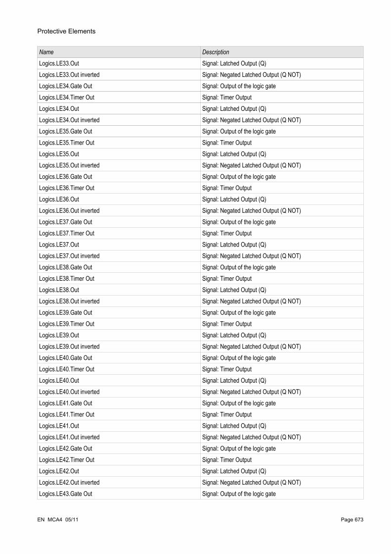
Protective Elements
Name Description
Logics.LE33.Out Signal: Latched Output (Q)Logics.LE33.Out inverted Signal: Negated Latched Output (Q NOT)Logics.LE34.Gate Out Signal: Output of the logic gateLogics.LE34.Timer Out Signal: Timer OutputLogics.LE34.Out Signal: Latched Output (Q)Logics.LE34.Out inverted Signal: Negated Latched Output (Q NOT)Logics.LE35.Gate Out Signal: Output of the logic gateLogics.LE35.Timer Out Signal: Timer OutputLogics.LE35.Out Signal: Latched Output (Q)Logics.LE35.Out inverted Signal: Negated Latched Output (Q NOT)Logics.LE36.Gate Out Signal: Output of the logic gateLogics.LE36.Timer Out Signal: Timer OutputLogics.LE36.Out Signal: Latched Output (Q)Logics.LE36.Out inverted Signal: Negated Latched Output (Q NOT)Logics.LE37.Gate Out Signal: Output of the logic gateLogics.LE37.Timer Out Signal: Timer OutputLogics.LE37.Out Signal: Latched Output (Q)Logics.LE37.Out inverted Signal: Negated Latched Output (Q NOT)Logics.LE38.Gate Out Signal: Output of the logic gateLogics.LE38.Timer Out Signal: Timer OutputLogics.LE38.Out Signal: Latched Output (Q)Logics.LE38.Out inverted Signal: Negated Latched Output (Q NOT)Logics.LE39.Gate Out Signal: Output of the logic gateLogics.LE39.Timer Out Signal: Timer OutputLogics.LE39.Out Signal: Latched Output (Q)Logics.LE39.Out inverted Signal: Negated Latched Output (Q NOT)Logics.LE40.Gate Out Signal: Output of the logic gateLogics.LE40.Timer Out Signal: Timer OutputLogics.LE40.Out Signal: Latched Output (Q)Logics.LE40.Out inverted Signal: Negated Latched Output (Q NOT)Logics.LE41.Gate Out Signal: Output of the logic gateLogics.LE41.Timer Out Signal: Timer OutputLogics.LE41.Out Signal: Latched Output (Q)Logics.LE41.Out inverted Signal: Negated Latched Output (Q NOT)Logics.LE42.Gate Out Signal: Output of the logic gateLogics.LE42.Timer Out Signal: Timer OutputLogics.LE42.Out Signal: Latched Output (Q)Logics.LE42.Out inverted Signal: Negated Latched Output (Q NOT)Logics.LE43.Gate Out Signal: Output of the logic gate
EN MCA4 05/11 Page 673

Protective Elements
Name Description
Logics.LE43.Timer Out Signal: Timer OutputLogics.LE43.Out Signal: Latched Output (Q)Logics.LE43.Out inverted Signal: Negated Latched Output (Q NOT)Logics.LE44.Gate Out Signal: Output of the logic gateLogics.LE44.Timer Out Signal: Timer OutputLogics.LE44.Out Signal: Latched Output (Q)Logics.LE44.Out inverted Signal: Negated Latched Output (Q NOT)Logics.LE45.Gate Out Signal: Output of the logic gateLogics.LE45.Timer Out Signal: Timer OutputLogics.LE45.Out Signal: Latched Output (Q)Logics.LE45.Out inverted Signal: Negated Latched Output (Q NOT)Logics.LE46.Gate Out Signal: Output of the logic gateLogics.LE46.Timer Out Signal: Timer OutputLogics.LE46.Out Signal: Latched Output (Q)Logics.LE46.Out inverted Signal: Negated Latched Output (Q NOT)Logics.LE47.Gate Out Signal: Output of the logic gateLogics.LE47.Timer Out Signal: Timer OutputLogics.LE47.Out Signal: Latched Output (Q)Logics.LE47.Out inverted Signal: Negated Latched Output (Q NOT)Logics.LE48.Gate Out Signal: Output of the logic gateLogics.LE48.Timer Out Signal: Timer OutputLogics.LE48.Out Signal: Latched Output (Q)Logics.LE48.Out inverted Signal: Negated Latched Output (Q NOT)Logics.LE49.Gate Out Signal: Output of the logic gateLogics.LE49.Timer Out Signal: Timer OutputLogics.LE49.Out Signal: Latched Output (Q)Logics.LE49.Out inverted Signal: Negated Latched Output (Q NOT)Logics.LE50.Gate Out Signal: Output of the logic gateLogics.LE50.Timer Out Signal: Timer OutputLogics.LE50.Out Signal: Latched Output (Q)Logics.LE50.Out inverted Signal: Negated Latched Output (Q NOT)Logics.LE51.Gate Out Signal: Output of the logic gateLogics.LE51.Timer Out Signal: Timer OutputLogics.LE51.Out Signal: Latched Output (Q)Logics.LE51.Out inverted Signal: Negated Latched Output (Q NOT)Logics.LE52.Gate Out Signal: Output of the logic gateLogics.LE52.Timer Out Signal: Timer OutputLogics.LE52.Out Signal: Latched Output (Q)Logics.LE52.Out inverted Signal: Negated Latched Output (Q NOT)
Page 674 EN MCA4 05/11

Protective Elements
Name Description
Logics.LE53.Gate Out Signal: Output of the logic gateLogics.LE53.Timer Out Signal: Timer OutputLogics.LE53.Out Signal: Latched Output (Q)Logics.LE53.Out inverted Signal: Negated Latched Output (Q NOT)Logics.LE54.Gate Out Signal: Output of the logic gateLogics.LE54.Timer Out Signal: Timer OutputLogics.LE54.Out Signal: Latched Output (Q)Logics.LE54.Out inverted Signal: Negated Latched Output (Q NOT)Logics.LE55.Gate Out Signal: Output of the logic gateLogics.LE55.Timer Out Signal: Timer OutputLogics.LE55.Out Signal: Latched Output (Q)Logics.LE55.Out inverted Signal: Negated Latched Output (Q NOT)Logics.LE56.Gate Out Signal: Output of the logic gateLogics.LE56.Timer Out Signal: Timer OutputLogics.LE56.Out Signal: Latched Output (Q)Logics.LE56.Out inverted Signal: Negated Latched Output (Q NOT)Logics.LE57.Gate Out Signal: Output of the logic gateLogics.LE57.Timer Out Signal: Timer OutputLogics.LE57.Out Signal: Latched Output (Q)Logics.LE57.Out inverted Signal: Negated Latched Output (Q NOT)Logics.LE58.Gate Out Signal: Output of the logic gateLogics.LE58.Timer Out Signal: Timer OutputLogics.LE58.Out Signal: Latched Output (Q)Logics.LE58.Out inverted Signal: Negated Latched Output (Q NOT)Logics.LE59.Gate Out Signal: Output of the logic gateLogics.LE59.Timer Out Signal: Timer OutputLogics.LE59.Out Signal: Latched Output (Q)Logics.LE59.Out inverted Signal: Negated Latched Output (Q NOT)Logics.LE60.Gate Out Signal: Output of the logic gateLogics.LE60.Timer Out Signal: Timer OutputLogics.LE60.Out Signal: Latched Output (Q)Logics.LE60.Out inverted Signal: Negated Latched Output (Q NOT)Logics.LE61.Gate Out Signal: Output of the logic gateLogics.LE61.Timer Out Signal: Timer OutputLogics.LE61.Out Signal: Latched Output (Q)Logics.LE61.Out inverted Signal: Negated Latched Output (Q NOT)Logics.LE62.Gate Out Signal: Output of the logic gateLogics.LE62.Timer Out Signal: Timer OutputLogics.LE62.Out Signal: Latched Output (Q)
EN MCA4 05/11 Page 675

Protective Elements
Name Description
Logics.LE62.Out inverted Signal: Negated Latched Output (Q NOT)Logics.LE63.Gate Out Signal: Output of the logic gateLogics.LE63.Timer Out Signal: Timer OutputLogics.LE63.Out Signal: Latched Output (Q)Logics.LE63.Out inverted Signal: Negated Latched Output (Q NOT)Logics.LE64.Gate Out Signal: Output of the logic gateLogics.LE64.Timer Out Signal: Timer OutputLogics.LE64.Out Signal: Latched Output (Q)Logics.LE64.Out inverted Signal: Negated Latched Output (Q NOT)Logics.LE65.Gate Out Signal: Output of the logic gateLogics.LE65.Timer Out Signal: Timer OutputLogics.LE65.Out Signal: Latched Output (Q)Logics.LE65.Out inverted Signal: Negated Latched Output (Q NOT)Logics.LE66.Gate Out Signal: Output of the logic gateLogics.LE66.Timer Out Signal: Timer OutputLogics.LE66.Out Signal: Latched Output (Q)Logics.LE66.Out inverted Signal: Negated Latched Output (Q NOT)Logics.LE67.Gate Out Signal: Output of the logic gateLogics.LE67.Timer Out Signal: Timer OutputLogics.LE67.Out Signal: Latched Output (Q)Logics.LE67.Out inverted Signal: Negated Latched Output (Q NOT)Logics.LE68.Gate Out Signal: Output of the logic gateLogics.LE68.Timer Out Signal: Timer OutputLogics.LE68.Out Signal: Latched Output (Q)Logics.LE68.Out inverted Signal: Negated Latched Output (Q NOT)Logics.LE69.Gate Out Signal: Output of the logic gateLogics.LE69.Timer Out Signal: Timer OutputLogics.LE69.Out Signal: Latched Output (Q)Logics.LE69.Out inverted Signal: Negated Latched Output (Q NOT)Logics.LE70.Gate Out Signal: Output of the logic gateLogics.LE70.Timer Out Signal: Timer OutputLogics.LE70.Out Signal: Latched Output (Q)Logics.LE70.Out inverted Signal: Negated Latched Output (Q NOT)Logics.LE71.Gate Out Signal: Output of the logic gateLogics.LE71.Timer Out Signal: Timer OutputLogics.LE71.Out Signal: Latched Output (Q)Logics.LE71.Out inverted Signal: Negated Latched Output (Q NOT)Logics.LE72.Gate Out Signal: Output of the logic gateLogics.LE72.Timer Out Signal: Timer Output
Page 676 EN MCA4 05/11

Protective Elements
Name Description
Logics.LE72.Out Signal: Latched Output (Q)Logics.LE72.Out inverted Signal: Negated Latched Output (Q NOT)Logics.LE73.Gate Out Signal: Output of the logic gateLogics.LE73.Timer Out Signal: Timer OutputLogics.LE73.Out Signal: Latched Output (Q)Logics.LE73.Out inverted Signal: Negated Latched Output (Q NOT)Logics.LE74.Gate Out Signal: Output of the logic gateLogics.LE74.Timer Out Signal: Timer OutputLogics.LE74.Out Signal: Latched Output (Q)Logics.LE74.Out inverted Signal: Negated Latched Output (Q NOT)Logics.LE75.Gate Out Signal: Output of the logic gateLogics.LE75.Timer Out Signal: Timer OutputLogics.LE75.Out Signal: Latched Output (Q)Logics.LE75.Out inverted Signal: Negated Latched Output (Q NOT)Logics.LE76.Gate Out Signal: Output of the logic gateLogics.LE76.Timer Out Signal: Timer OutputLogics.LE76.Out Signal: Latched Output (Q)Logics.LE76.Out inverted Signal: Negated Latched Output (Q NOT)Logics.LE77.Gate Out Signal: Output of the logic gateLogics.LE77.Timer Out Signal: Timer OutputLogics.LE77.Out Signal: Latched Output (Q)Logics.LE77.Out inverted Signal: Negated Latched Output (Q NOT)Logics.LE78.Gate Out Signal: Output of the logic gateLogics.LE78.Timer Out Signal: Timer OutputLogics.LE78.Out Signal: Latched Output (Q)Logics.LE78.Out inverted Signal: Negated Latched Output (Q NOT)Logics.LE79.Gate Out Signal: Output of the logic gateLogics.LE79.Timer Out Signal: Timer OutputLogics.LE79.Out Signal: Latched Output (Q)Logics.LE79.Out inverted Signal: Negated Latched Output (Q NOT)Logics.LE80.Gate Out Signal: Output of the logic gateLogics.LE80.Timer Out Signal: Timer OutputLogics.LE80.Out Signal: Latched Output (Q)Logics.LE80.Out inverted Signal: Negated Latched Output (Q NOT)
EN MCA4 05/11 Page 677
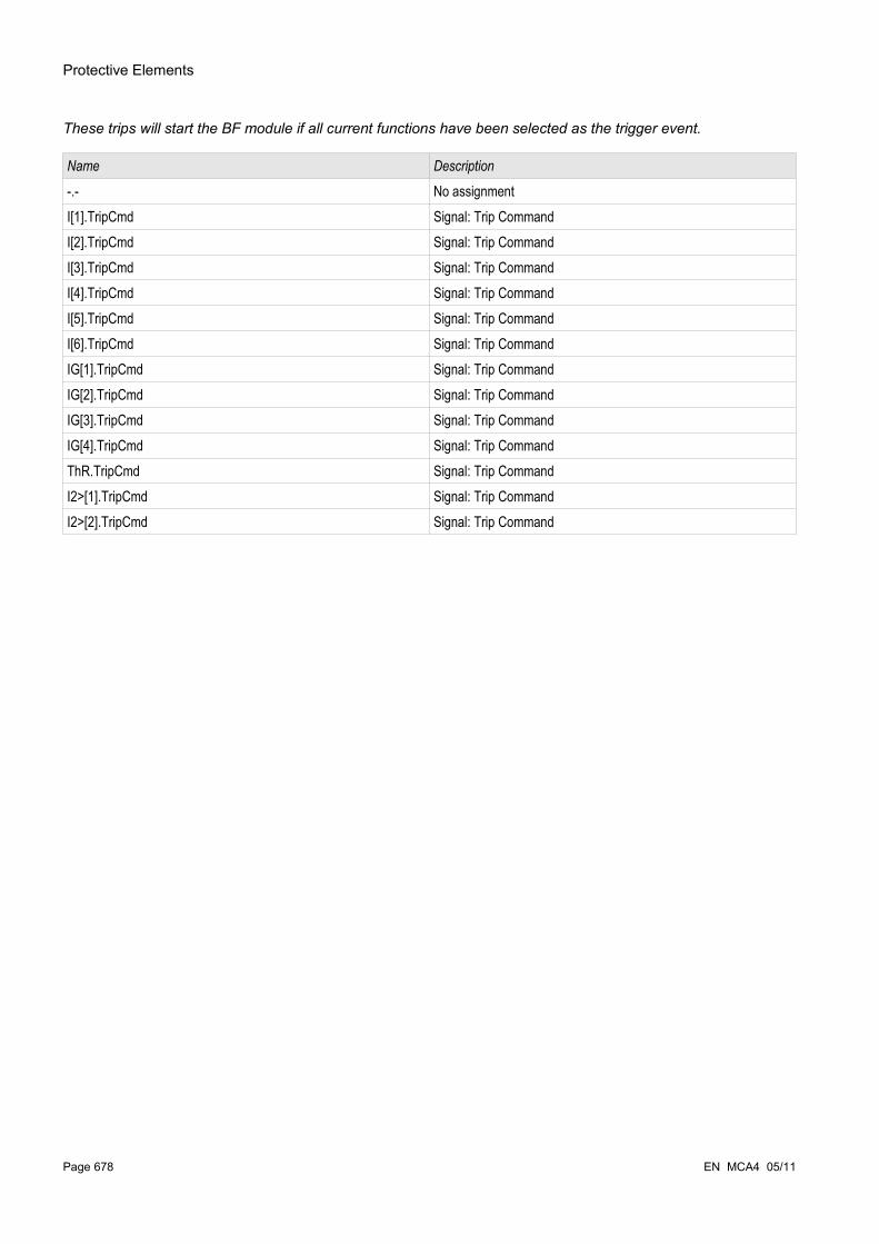
Protective Elements
These trips will start the BF module if all current functions have been selected as the trigger event.
Name Description
-.- No assignmentI[1].TripCmd Signal: Trip CommandI[2].TripCmd Signal: Trip CommandI[3].TripCmd Signal: Trip CommandI[4].TripCmd Signal: Trip CommandI[5].TripCmd Signal: Trip CommandI[6].TripCmd Signal: Trip CommandIG[1].TripCmd Signal: Trip CommandIG[2].TripCmd Signal: Trip CommandIG[3].TripCmd Signal: Trip CommandIG[4].TripCmd Signal: Trip CommandThR.TripCmd Signal: Trip CommandI2>[1].TripCmd Signal: Trip CommandI2>[2].TripCmd Signal: Trip Command
Page 678 EN MCA4 05/11

Protective Elements
These trips will start the BF module if external trips have been selected as the trigger event.
Name Description
-.- No assignmentExP[1].TripCmd Signal: Trip CommandExP[2].TripCmd Signal: Trip CommandExP[3].TripCmd Signal: Trip CommandExP[4].TripCmd Signal: Trip Command
EN MCA4 05/11 Page 679

Protective Elements
Commissioning: Circuit Breaker Failure Protection
The time that is configured for the BF MUST NOT be below the breaker control time, otherwise an unwanted operation of the BF is caused by any protective trip.
Object to Be Tested:
Test of the breaker failure protection.
Necessary Means:
• Current source;• Ammeter; and• Timer.
When testing, the applied test current must always be higher than the tripping threshold »I-CBF«. If the test current falls below the threshold while the breaker is in the “Off” position, no pickup will be generated.
Procedure (Single-Phase):
For testing the tripping time of the CBF protection, a test current has to be higher than the threshold value of one of the current protection modules that are assigned to trigger the CBF protection. The CBF trip delay can be measured from the time when one of the triggering inputs becomes active to the time when the CBF protection trip is asserted.
To avoid wiring errors, checked to make sure the breaker in the upstream system switches off.
The time, measured by the timer, should be in line with the specified tolerances.
Re-connect the control cable to the breaker!
Successful Test Result:
The actual times measured comply with the setpoint times. The breaker in the higher-level section switches off.
Page 680 EN MCA4 05/11

Supervision
SupervisionTCS - Trip Circuit Supervision [74TC]
Available elements: TCS
The trip circuit monitoring is used for monitoring if the trip circuit is ready for operations. The monitoring can be fulfilled in two ways. The first assumes only »Aux On (52a)« is used in the trip circuit. The second assumes that, in addition to »Aux On (52a), »Aux Off(52b)« is also used for the circuit monitoring.
With »Aux On (52a), only in the trip circuit, the monitoring is only effective when the breaker is closed while if both »Aux On (52a), and »Aux Off(52b)« are used, the trip circuit will be monitored all time as long as the control power is on.
Note that the digital inputs used for this purpose must be configured properly based on the trip circuit control voltage. If the trip circuit is detected broken, an alarm will be issued with a specified delay, which must be longer than the time when a trip contact is closed to the time when the breaker status is clearly recognized by the relay.
In Slot 1 has 2 digital inputs, each of which has a separate root (contact separation) for the trip circuit supervision.
This Notice applies to protective devices that offer control functionality only! This protective element requires, that a switchgear (circuit breaker is assigned to it.
In this case, the trip circuit supply voltage serves also as supply voltage for the digital inputs and so the supply voltage failure of a trip circuit can be detected directly.
In order to identify a conductor failure in the trip circuit on the supply line or in the trip coil, the off-coil has to be looped-in to the supervision circuit.
The time delay is to be set in a way that switching actions cannot cause false trips in this module.
EN MCA4 05/11 Page 681
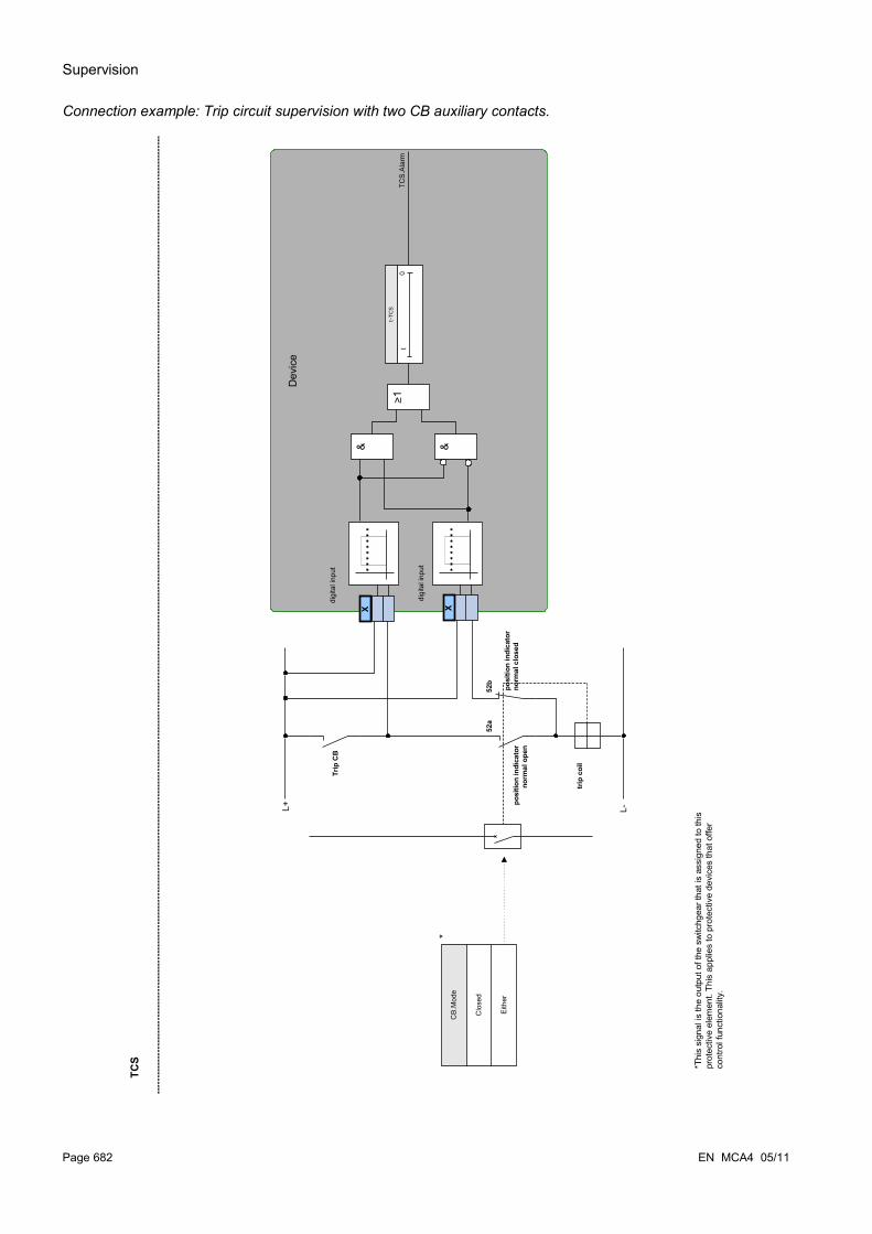
Supervision
Connection example: Trip circuit supervision with two CB auxiliary contacts.
Page 682 EN MCA4 05/11
L+ L-
LS
Trip
CB
posi
tion
indi
cato
r no
rmal
ope
n
posi
tion
indi
cato
r no
rmal
clo
sed
TCS
trip
coi
l
52a
52b
TCS
.Ala
rm
digi
tal i
nput
Dev
ice
X
t
t-TCS
0
digi
tal i
nput
X
& &
>1
Eith
er
CB.
Mod
e
Clo
sed
*Thi
s si
gnal
is th
e ou
tput
of t
he s
witc
hgea
r tha
t is
assi
gned
to th
is
prot
ectiv
e el
emen
t. Th
is a
pplie
s to
pro
tect
ive
devi
ces
that
offe
r co
ntro
l fun
ctio
nalit
y.
*

Supervision
Connection example: Trip circuit supervision with one CB auxiliary contact (Aux On (52a)) only.
EN MCA4 05/11 Page 683
L+ L-
LS
Trip
CB
posi
tion
indi
cato
r nor
mal
op
en
TCS
trip
coi
l
TCS.
Alar
m
digi
tal i
nput
CB.
Pos
ON
52a
Dev
ice
CB
Eith
er
CB.
Mod
e
Clo
sed
X
&
X
t
t-TC
S
0
digi
tal i
nput
*Thi
s si
gnal
is th
e ou
tput
of t
he s
witc
hgea
r tha
t is
assi
gned
to th
is
prot
ectiv
e el
emen
t. Th
is a
pplie
s to
pro
tect
ive
devi
ces
that
offe
r co
ntro
l fun
ctio
nalit
y.
*
*

Supervision
Device Planning Parameters of the Trip Circuit Supervision
Parameter Description Options Default Menu path
Mode Mode do not use,
use
do not use [Device planning]
Global Protection Parameters of the Trip Circuit Supervision
Parameter Description Setting range Default Menu path
CB Pos Detect
Criterion by which the Circuit Breaker Switch Position is to be detected.
-.-,
SG[1].Pos,
SG[2].Pos,
SG[3].Pos,
SG[4].Pos,
SG[5].Pos,
SG[6].Pos
-.- [Protection Para
/Global Prot Para
/Supervision
/TCS]
Mode Select if trip circuit is going to be monitored when the breaker is closed or when the breaker is either open or close.
Closed,
Either
Closed [Protection Para
/Global Prot Para
/Supervision
/TCS]Input 1 Select the input configured to monitor the trip coil
when the breaker is closed.1..n, Dig Inputs -.- [Protection Para
/Global Prot Para
/Supervision
/TCS]Input 2 Select the input configured to monitor the trip coil
when the breaker is open. Only available if Mode set to “Either”.
Only available if: Mode = Either
1..n, Dig Inputs -.- [Protection Para
/Global Prot Para
/Supervision
/TCS]ExBlo1 External blocking of the module, if blocking is
activated (allowed) within a parameter set and if the state of the assigned signal is true.
1..n, Assignment List -.- [Protection Para
/Global Prot Para
/Supervision
/TCS]ExBlo2 External blocking of the module, if blocking is
activated (allowed) within a parameter set and if the state of the assigned signal is true.
1..n, Assignment List -.- [Protection Para
/Global Prot Para
/Supervision
/TCS]
Page 684 EN MCA4 05/11
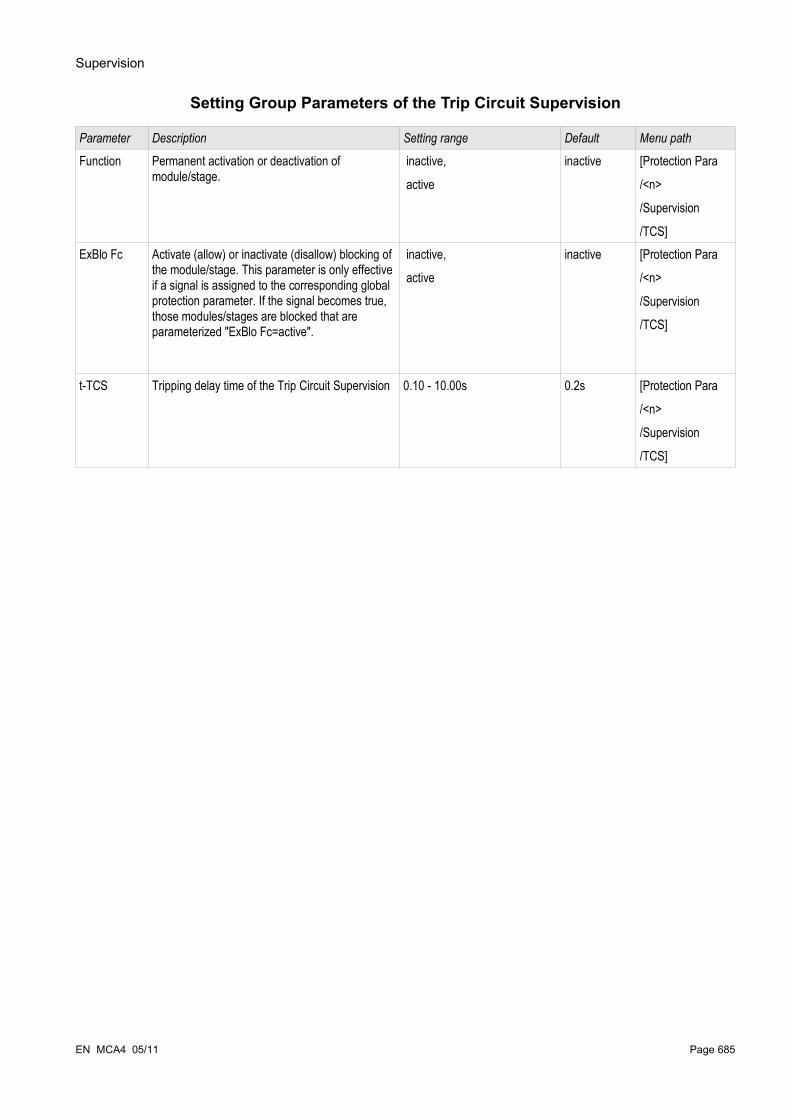
Supervision
Setting Group Parameters of the Trip Circuit Supervision
Parameter Description Setting range Default Menu path
Function Permanent activation or deactivation of module/stage.
inactive,
active
inactive [Protection Para
/<n>
/Supervision
/TCS]ExBlo Fc Activate (allow) or inactivate (disallow) blocking of
the module/stage. This parameter is only effective if a signal is assigned to the corresponding global protection parameter. If the signal becomes true, those modules/stages are blocked that are parameterized "ExBlo Fc=active".
inactive,
active
inactive [Protection Para
/<n>
/Supervision
/TCS]
t-TCS Tripping delay time of the Trip Circuit Supervision 0.10 - 10.00s 0.2s [Protection Para
/<n>
/Supervision
/TCS]
EN MCA4 05/11 Page 685

Supervision
Trip Circuit Supervision Input States
Name Description Assignment via
Aux ON-I Position indicator/check-back signal of the CB (52a)
[Protection Para
/Global Prot Para
/Supervision
/TCS]Aux OFF-I Module input state: Position
indicator/check-back signal of the CB (52b)[Protection Para
/Global Prot Para
/Supervision
/TCS]ExBlo1-I Module input state: External blocking1 [Protection Para
/Global Prot Para
/Supervision
/TCS]ExBlo2-I Module input state: External blocking2 [Protection Para
/Global Prot Para
/Supervision
/TCS]CB Pos Detect-I Module input state: Criterion by which the
Circuit Breaker Switch Position is to be detected.
[Protection Para
/Global Prot Para
/Supervision
/TCS]
Trip Circuit Supervision Signals (Output States)
Name Description
active Signal: activeExBlo Signal: External BlockingAlarm Signal: Alarm Trip Circuit SupervisionNot Possible Not possible because no state indicator assigned to the breaker.
Page 686 EN MCA4 05/11

Supervision
Commissioning: Trip Circuit Supervision [74TC]
For CBs that trip by means of little energy (e.g. via an optocoupler), it has to be ensured that the current applied by the digital inputs will not cause false tripping of the CB.
Object to be testedTest of the trip circuit supervision.
Procedure, part 1Simulate failure of the control voltage in the power circuits.
Successful test result, part 1After expiry of »t-TCS« the trip circuit supervision TCS of the device should signal an alarm.
Procedure, part 2Simulate a broken cable in the CB control circuit.
Successful test result, part 2After expiry of »t-TCS« the trip circuit supervision TCS of the device should signal an alarm.
EN MCA4 05/11 Page 687

Supervision
CTS - Current Transformer Supervision [60L]Available elements: CTS
Wire breaks and failures within measuring circuits cause current transformer failures.The module »CTS« can detect a failure of the CT if the calculated earth current does not match the measured one. If an adjustable threshold value (Difference of measured and calculated earth current) is exceeded, a CT failure can be assumed. This is signaled through a message/alarm. The precondition is that the conductor currents are measured by the device and the earth current, for instance, by a ring core type current transformer.
The measuring principles of the circuit supervision are based on comparing the measured and the calculated residual currents: In an ideal case these are:
IL1 IL2 IL3KI∗ IG=3∗I 0KI∗ IG=0
KI represents a correction factor which takes the different transformation ratio of the phase- and earth current transformers into account. The device automatically calculates this factor from the rated field parameters, i.e. the relation between the rated primary and secondary current values of the phase- and earth current transformers.
For compensating the current proportional ratio error of the measuring circuits, the dynamic correction factor Kd can be used. As a function of the measured max. current this factor is considering the linear rising measuring error. The limiting value of the CT supervision is calculated as follows:
∆I = deviation I (rated value)Kd = correction factor Imax = current maximum Limiting value = ∆I + Kd x Imax
Precondition for identifying an error
3∗I 0KI∗ IGDelta IKd∗Imax
The evaluation method of the circuit supervision by using factor Kd can be graphically represented as follows:
If the current is measured in two phases only (for instant only IL1/IL3) or if there is no separate earth current measuring (e.g. normally via a cable-type CT), the supervision function should be deactivated.
Page 688 EN MCA4 05/11
limit value
Imax
I
Kd*Imax
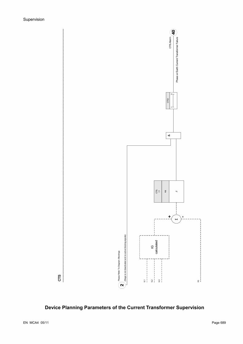
Supervision
Device Planning Parameters of the Current Transformer Supervision
EN MCA4 05/11 Page 689
Plea
se R
efer
To
Dia
gram
: Blo
ckin
gs
IG
calc
ulat
ed
IL1
CTS
.Ala
rm
CTS
(Sta
ge is
not
dea
ctiv
ated
and
no
activ
e bl
ocki
ng s
igna
ls)
IL3
IL2
IG
Σ+ -
KdCTS
.ξI
&
2
400
t
CTS
.t
Phas
e or
Ear
th C
urre
nt T
rans
form
er F
ailu
re
Supervision
Parameter Description Options Default Menu path
Mode Mode do not use,
use
do not use [Device planning]
Global Protection Parameter of the Current Transformer Supervision
Parameter Description Setting range Default Menu path
ExBlo1 External blocking of the module, if blocking is activated (allowed) within a parameter set and if the state of the assigned signal is true.
1..n, Assignment List -.- [Protection Para
/Global Prot Para
/Supervision
/CTS]ExBlo2 External blocking of the module, if blocking is
activated (allowed) within a parameter set and if the state of the assigned signal is true.
1..n, Assignment List -.- [Protection Para
/Global Prot Para
/Supervision
/CTS]
Page 690 EN MCA4 05/11

Supervision
Setting Group Parameters of the Current Transformer Supervision
Parameter Description Setting range Default Menu path
Function Permanent activation or deactivation of module/stage.
inactive,
active
inactive [Protection Para
/<n>
/Supervision
/CTS]ExBlo Fc Activate (allow) or inactivate (disallow) blocking of
the module/stage. This parameter is only effective if a signal is assigned to the corresponding global protection parameter. If the signal becomes true, those modules/stages are blocked that are parameterized "ExBlo Fc=active".
inactive,
active
inactive [Protection Para
/<n>
/Supervision
/CTS]
ΔI In order to prevent faulty tripping of phase selective protection functions that use the current as tripping criterion. If the difference of the measured earth current and the calculated value I0 is higher than the pick up value ΔI, an alarm event is generated after expiring of the excitation time. In such a case, a fuse failure, a broken wire or a faulty measuring circuit can be assumed.
0.10 - 1.00In 0.50In [Protection Para
/<n>
/Supervision
/CTS]
Alarm delay Alarm delay 0.1 - 9999.0s 1.0s [Protection Para
/<n>
/Supervision
/CTS]Kd Dynamic correction factor for the evaluation of the
difference between calculated and measured earth current. This correction factor allows transformer faults, caused by higher currents, to be compensated.
0.00 - 0.99 0.00 [Protection Para
/<n>
/Supervision
/CTS]
EN MCA4 05/11 Page 691
Supervision
Current Transformer Supervision Input States
Name Description Assignment via
ExBlo1-I Module input state: External blocking1 [Protection Para
/Global Prot Para
/Supervision
/CTS]ExBlo2-I Module input state: External blocking2 [Protection Para
/Global Prot Para
/Supervision
/CTS]
Current Transformer Supervision Signals (Outputs States)
Name Description
active Signal: activeExBlo Signal: External BlockingAlarm Signal: Alarm Current Transformer Measuring Circuit Supervision
Page 692 EN MCA4 05/11
Supervision
Commissioning: Current Transformer Failure Supervision
Precondition:1. Measurement of all three phase currents (are applied to the measuring inputs of the device).2. The earth current is detected via a cable-type transformer (not in Holmgreen connection).
Object to be testedCheck of the CT supervision (by comparing the calculated with the measured earth current).
Necessary means• Three-phase current source
Procedure, part 1• Set the limiting value of the CTS to »delta I=0.1*In«.• Feed a three-phase, symmetrical current system (approx. nominal current) to the secondary side.• Disconnect the current of one phase from one of the measuring inputs (the symmetrical feeding at
secondary side has to be maintained).• Make sure that the signal »CTS.ALARM« is generated now.
Successful test result, part 1• The signal »CTS.ALARM« is generated.
Procedure, part 2• Feed a three-phase, symmetrical current system (approx. nominal current) to the secondary side.• Feed a current that is higher than the threshold value for the measuring circuit supervision to the earth
current measuring input. • Ascertain that the signal »CTS.ALARM« is generated now.
Successful test result, part 2The signal »CTS.ALARM« is generated.
EN MCA4 05/11 Page 693
Supervision
LOP - Loss of PotentialAvailable elements: LOP
Loss of Potential - Evaluating Measured Quantities
Precondition:1. The residual voltage is measured via the residual voltage measuring input.2. Phase voltages are applied to the voltage measuring inputs (no line-to-line voltages)
Calculation of the residual voltage is only possible, if phase voltages (star) were applied to the voltage measuring inputs and »VT con = phase-to-neutral« and »EVT con=calculated« were set in the field parameters.
This Notice applies to protective devices that offer control functionality only! This protective element requires, that a switchgear (circuit breaker is assigned to it. It is allowed only to assign switchgears (circuit breaker) to this protective element, whose measuring transformers provide measuring data to the protective device.
The LOP function detects the loss of voltage in any of the voltage input measuring circuits. Faulty tripping of protective elements that take undervoltage into account can be prevented by means of this supervision element. The following measured values and information to detect an Phase VT Failure condition:
• Three-phase voltages;
• Ratio of negative-to-positive sequence voltages;
• Zero sequence voltage;
• Three-phase currents;
• Residual current (I0);
• Pickup flags from all overcurrent elements; and
• Breaker status
After a set time delay time an Alarm »LOP.LOP BLO« will be issued.
How to set up the Loss of Potential (Evaluating Measured Quantities)
• Set the Alarm Time Delay »t-Alarm«.
• To prevent a malfunction of the VT supervision assign those Alarms of instantaneous overcurrent elements that should block the Loss of Potential element.
• It is necessary to set the parameter »LOP.LOPB Enable« to »active«. Otherwise the Measuring circuit supervision cannot block undervoltage depending elements in case of a loss of potential.
Page 694 EN MCA4 05/11

Supervision
How to make the Loss of Potential (Evaluating Measured Quantities) effective
The Loss of Potential respectively measuring circuit supervision can be used to block protective elements like undervoltage protection in order to prevent faulty tripping.
• Set the parameter »Measuring Circuit Supervision=active« within those protective elements that should be blocked by the Loss of Potential supervision.
Loss of Potential - Fuse Failure
VT Supervision via digital inputs (Fuse Failure)The module »LOP« is capable of detecting a fuse failure at the secondary side of the VTs as long as the automatic circuit breakers of the VTs are connected with the device via a digital input and if this input is assigned to the module »LOP«.
Setting the Parameters for detecting a fuse failure (FF) of a phase voltage transformer
In order to detect a fuse failure of a phase voltage transformer via digital input, please proceed as follows:
• Assign a digital input onto the parameter »LOP.Ex FF VT« that represents the state of the automatic circuit breaker of the phase voltage transformer.
• Set the parameter »Measuring Crcuit Supervison=active« within all those protective elements, that should be blocked by a fuse failure.
Setting the Parameters for detecting a fuse failure (FF) of a earth phase voltage transformer
In order to detect a fuse failure of a phase voltage transformer via digital input, please proceed as follows:
• Assign a digital input onto the parameter »LOP.Ex FF EVT« that represents the state of the automatic circuit breaker of the phase voltage transformer.
• Set the parameter »Measuring Crcuit Supervison=active« within all those protective elements, that should be blocked by a fuse failure.
EN MCA4 05/11 Page 695
Supervision
Page 696 EN MCA4 05/11
inac
tive
LOPB
Ena
ble
activ
eVL
1/VL
12
VL2/
VL23
VL3/
VL31
%(V
2/V1
)
V0 IL1
IL2
IL3
3*I0
Pos
ON
* = c
lose
d
V <
1.0
V
%(V
2/V1
) > 4
0%
V0 <
1.0
V
I < 2
x In
3*I0
< 0
.1 x
In
LOP.
Alar
m
LOP
nam
e =
LOP
38a
Ple
ase
Ref
er T
o D
iagr
am: B
lock
ings
(Sta
ge is
not
dea
ctiv
ated
and
no
activ
e bl
ocki
ng s
igna
ls)
2
Phas
e Vo
ltage
Tra
nsfo
rmer
Fai
lure
LOP.
Ex F
F VT
LOP.
Ex F
F EV
T
1..n
, Ass
ignm
ent L
ist
LOP.
Ex F
F EV
T
1..n
, Ass
ignm
ent L
ist
LOP.
Ex F
F VT
38b
38c
>1 >1 &
&&
& &
1..n
, I [x
]
Blo
Trig
ger
1..n
, I [x
]
Blo
Trig
ger
>1
…..
t-Ala
rm0.0
999
9s
0
50 m
s
1t-M
in H
old
Tim
e0
100
ms
t-Res
etD
elay
LOP.
LOP
Blo
*Thi
s si
gnal
is th
e ou
tput
of t
he s
witc
hgea
r tha
t is
assi
gned
to th
is
prot
ectiv
e el
emen
t. Th
is a
pplie
s to
pro
tect
ive
devi
ces
that
offe
r co
ntro
l fun
ctio
nalit
y.

Supervision
Device Planning Parameters of the LOP Module
Parameter Description Options Default Menu path
Mode Mode do not use,
use
do not use [Device planning]
Global Protection Parameters of the LOP Module
Parameter Description Setting range Default Menu path
CB_Status Criterion 2: Breaker(52a/b) is closed (hidden) -.-,
SG[1].Pos,
SG[2].Pos,
SG[3].Pos,
SG[4].Pos,
SG[5].Pos,
SG[6].Pos
SG[1].Pos [Protection Para
/Global Prot Para
/Supervision
/LOP]
ExBlo1 External blocking of the module, if blocking is activated (allowed) within a parameter set and if the state of the assigned signal is true.
1..n, Assignment List -.- [Protection Para
/Global Prot Para
/Supervision
/LOP]ExBlo2 External blocking of the module, if blocking is
activated (allowed) within a parameter set and if the state of the assigned signal is true.
1..n, Assignment List -.- [Protection Para
/Global Prot Para
/Supervision
/LOP]Blo Trigger1 An Alarm of this protective element will block the
Loss of Potential Detection.Blo Trigger -.- [Protection Para
/Global Prot Para
/Supervision
/LOP]Blo Trigger2 An Alarm of this protective element will block the
Loss of Potential Detection.Blo Trigger -.- [Protection Para
/Global Prot Para
/Supervision
/LOP]Blo Trigger3 An Alarm of this protective element will block the
Loss of Potential Detection.Blo Trigger -.- [Protection Para
/Global Prot Para
/Supervision
/LOP]Blo Trigger4 An Alarm of this protective element will block the
Loss of Potential Detection.Blo Trigger -.- [Protection Para
/Global Prot Para
/Supervision
/LOP]
EN MCA4 05/11 Page 697
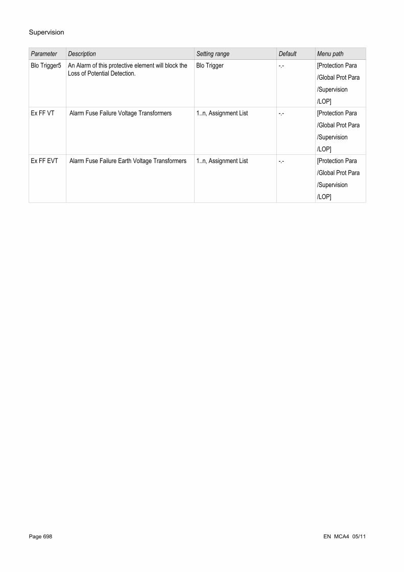
Supervision
Parameter Description Setting range Default Menu path
Blo Trigger5 An Alarm of this protective element will block the Loss of Potential Detection.
Blo Trigger -.- [Protection Para
/Global Prot Para
/Supervision
/LOP]Ex FF VT Alarm Fuse Failure Voltage Transformers 1..n, Assignment List -.- [Protection Para
/Global Prot Para
/Supervision
/LOP]Ex FF EVT Alarm Fuse Failure Earth Voltage Transformers 1..n, Assignment List -.- [Protection Para
/Global Prot Para
/Supervision
/LOP]
Page 698 EN MCA4 05/11
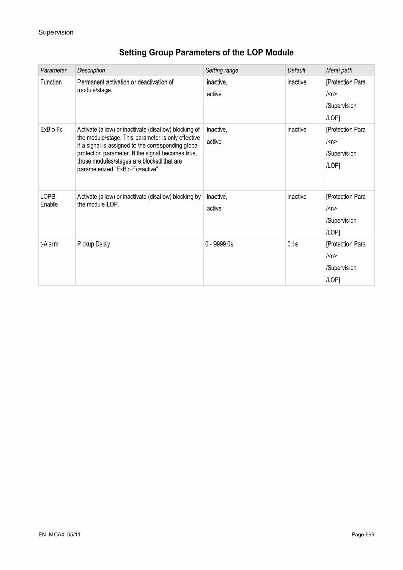
Supervision
Setting Group Parameters of the LOP Module
Parameter Description Setting range Default Menu path
Function Permanent activation or deactivation of module/stage.
inactive,
active
inactive [Protection Para
/<n>
/Supervision
/LOP]ExBlo Fc Activate (allow) or inactivate (disallow) blocking of
the module/stage. This parameter is only effective if a signal is assigned to the corresponding global protection parameter. If the signal becomes true, those modules/stages are blocked that are parameterized "ExBlo Fc=active".
inactive,
active
inactive [Protection Para
/<n>
/Supervision
/LOP]
LOPB Enable
Activate (allow) or inactivate (disallow) blocking by the module LOP.
inactive,
active
inactive [Protection Para
/<n>
/Supervision
/LOP]t-Alarm Pickup Delay 0 - 9999.0s 0.1s [Protection Para
/<n>
/Supervision
/LOP]
EN MCA4 05/11 Page 699
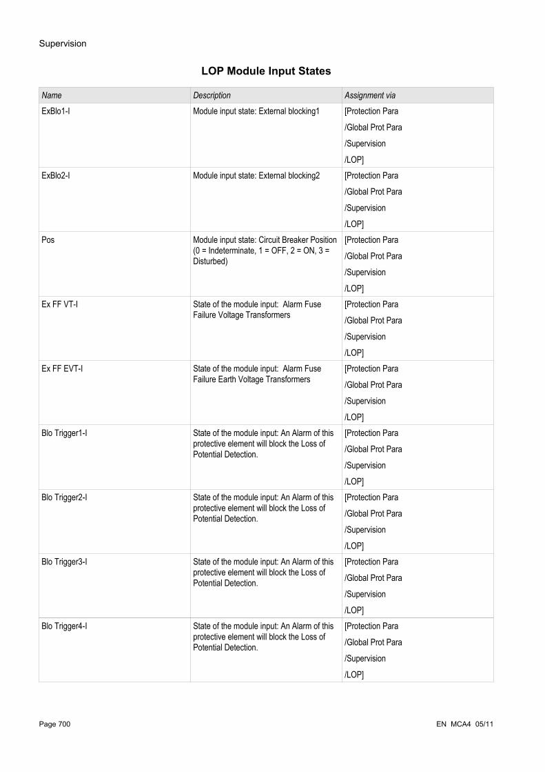
Supervision
LOP Module Input States
Name Description Assignment via
ExBlo1-I Module input state: External blocking1 [Protection Para
/Global Prot Para
/Supervision
/LOP]ExBlo2-I Module input state: External blocking2 [Protection Para
/Global Prot Para
/Supervision
/LOP]Pos Module input state: Circuit Breaker Position
(0 = Indeterminate, 1 = OFF, 2 = ON, 3 = Disturbed)
[Protection Para
/Global Prot Para
/Supervision
/LOP]Ex FF VT-I State of the module input: Alarm Fuse
Failure Voltage Transformers[Protection Para
/Global Prot Para
/Supervision
/LOP]Ex FF EVT-I State of the module input: Alarm Fuse
Failure Earth Voltage Transformers[Protection Para
/Global Prot Para
/Supervision
/LOP]Blo Trigger1-I State of the module input: An Alarm of this
protective element will block the Loss of Potential Detection.
[Protection Para
/Global Prot Para
/Supervision
/LOP]Blo Trigger2-I State of the module input: An Alarm of this
protective element will block the Loss of Potential Detection.
[Protection Para
/Global Prot Para
/Supervision
/LOP]Blo Trigger3-I State of the module input: An Alarm of this
protective element will block the Loss of Potential Detection.
[Protection Para
/Global Prot Para
/Supervision
/LOP]Blo Trigger4-I State of the module input: An Alarm of this
protective element will block the Loss of Potential Detection.
[Protection Para
/Global Prot Para
/Supervision
/LOP]
Page 700 EN MCA4 05/11
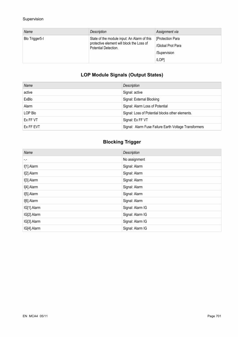
Supervision
Name Description Assignment via
Blo Trigger5-I State of the module input: An Alarm of this protective element will block the Loss of Potential Detection.
[Protection Para
/Global Prot Para
/Supervision
/LOP]
LOP Module Signals (Output States)
Name Description
active Signal: activeExBlo Signal: External BlockingAlarm Signal: Alarm Loss of PotentialLOP Blo Signal: Loss of Potential blocks other elements.Ex FF VT Signal: Ex FF VTEx FF EVT Signal: Alarm Fuse Failure Earth Voltage Transformers
Blocking Trigger
Name Description
-.- No assignmentI[1].Alarm Signal: AlarmI[2].Alarm Signal: AlarmI[3].Alarm Signal: AlarmI[4].Alarm Signal: AlarmI[5].Alarm Signal: AlarmI[6].Alarm Signal: AlarmIG[1].Alarm Signal: Alarm IGIG[2].Alarm Signal: Alarm IGIG[3].Alarm Signal: Alarm IGIG[4].Alarm Signal: Alarm IG
EN MCA4 05/11 Page 701
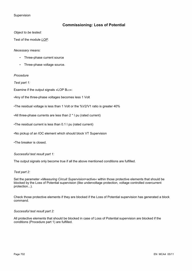
Supervision
Commissioning: Loss of Potential
Object to be tested:
Test of the module LOP.
Necessary means:
• Three-phase current source
• Three-phase voltage source.
Procedure
Test part 1:
Examine if the output signals »LOP BLO«:
•Any of the three-phase voltages becomes less 1 Volt
•The residual voltage is less than 1 Volt or the %V2/V1 ratio is greater 40%
•All three-phase currents are less than 2 * I pu (rated current)
•The residual current is less than 0.1 I pu (rated current)
•No pickup of an IOC element which should block VT Supervision
•The breaker is closed.
Successful test result part 1:
The output signals only become true if all the above mentioned conditions are fulfilled.
Test part 2:
Set the parameter »Measuring Circuit Supervision=active« within those protective elements that should be blocked by the Loss of Potential supervision (like undervoltage protection, voltage controlled overcurrent protection...).
Check those protective elements if they are blocked if the Loss of Potential supervision has generated a block command.
Successful test result part 2:
All protective elements that should be blocked in case of Loss of Potential supervision are blocked if the conditions (Procedure part 1) are fulfilled.
Page 702 EN MCA4 05/11

Supervision
Commissioning: Loss of Potential (FF via DI)
Object to be tested:Check if the auto fuse failure is correctly identified by the device.
Procedure
• Disconnect the automatic circuit breaker of the VTs (all poles to be dead)
Successful test result
• The state of the respective digital input changes.
• All protective elements are blocked which should not have an unwanted operation caused by a fuse fai-lure »Measuring Circuit Supervision=active«.
EN MCA4 05/11 Page 703

Programmable Logic
Programmable LogicAvailable Elements (Equations): Logics
General DescriptionThe Protective Relay includes programmable Logic Equations for programming output relays, blocking of protective functions and custom logic functions in the relay.
The logic provides control of the output relays based on the state of the inputs that can be choosen from the assignment list (protective function pickups, protective function states, breaker states, system alarms, and module inputs). The user can use the outputs signals of a Logic Equation as inputs in higher equations (e.g. the output signal of Logic Equation 10 might be used as an input of Logic Equation 11).
Principle Overview
Page 704 EN MCA4 05/11
Input1
Input2
Input3
Input4
Reset Latched
Inverting settable
Inverting settable
Inverting settable
Inverting settable
AND
OR
NAND
NOR
Inverting settable
Inverting settable
Gate Out
Timer Out
Out
Out inverted
Set
Reset
Type of logic gate selectable
S
R1
Q
Q
t-On Delay
Delay Timer
t-Off Delay

Programmable Logic
Detailed Overview – Overall Logic diagram
EN MCA4 05/11 Page 705
φ
AN
DO
RN
AN
DN
OR
Gat
e O
ut
Tim
er O
ut Out
Out
inve
rted
1..n
, Ass
ignm
ent L
ist
LE[x
].Inp
ut1
activ
e
inac
tive
Inve
rting
1
1..n
, Ass
ignm
ent L
ist
LE[x
].Inp
ut2
activ
e
inac
tive
Inve
rting
2
1..n
, Ass
ignm
ent L
ist
LE[x
].Inp
ut3
activ
e
inac
tive
Inve
rting
3
1..n
, Ass
ignm
ent L
ist
LE[x
].Inp
ut4
activ
e
inac
tive
Inve
rting
4
1..n
, Ass
ignm
ent L
ist
LE[x
].Res
et L
atch
ed
activ
e
inac
tive
Inve
rting
Res
et
Gat
e
AND
OR
NA
ND
NO
R
activ
e
inac
tive
Inve
rting
Set
S
Q
R1
Q
LE[1
]...[n
]
=1 =1 =1 =1 =1
=1t-O
n D
elay
Del
ay T
imer t-O
ff D
elay
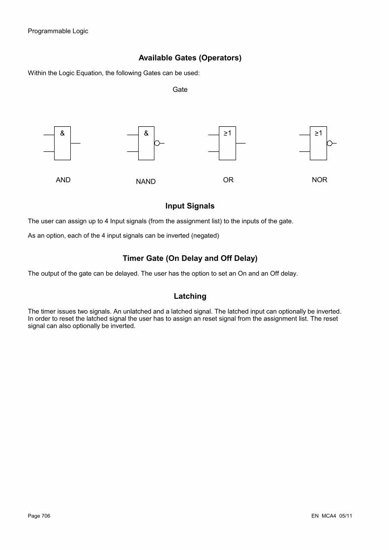
Programmable Logic
Available Gates (Operators)
Within the Logic Equation, the following Gates can be used:
Input Signals
The user can assign up to 4 Input signals (from the assignment list) to the inputs of the gate.
As an option, each of the 4 input signals can be inverted (negated)
Timer Gate (On Delay and Off Delay)
The output of the gate can be delayed. The user has the option to set an On and an Off delay.
Latching
The timer issues two signals. An unlatched and a latched signal. The latched input can optionally be inverted.In order to reset the latched signal the user has to assign an reset signal from the assignment list. The reset signal can also optionally be inverted.
Page 706 EN MCA4 05/11
&
AND NAND OR NOR
Gate
& >1 >1
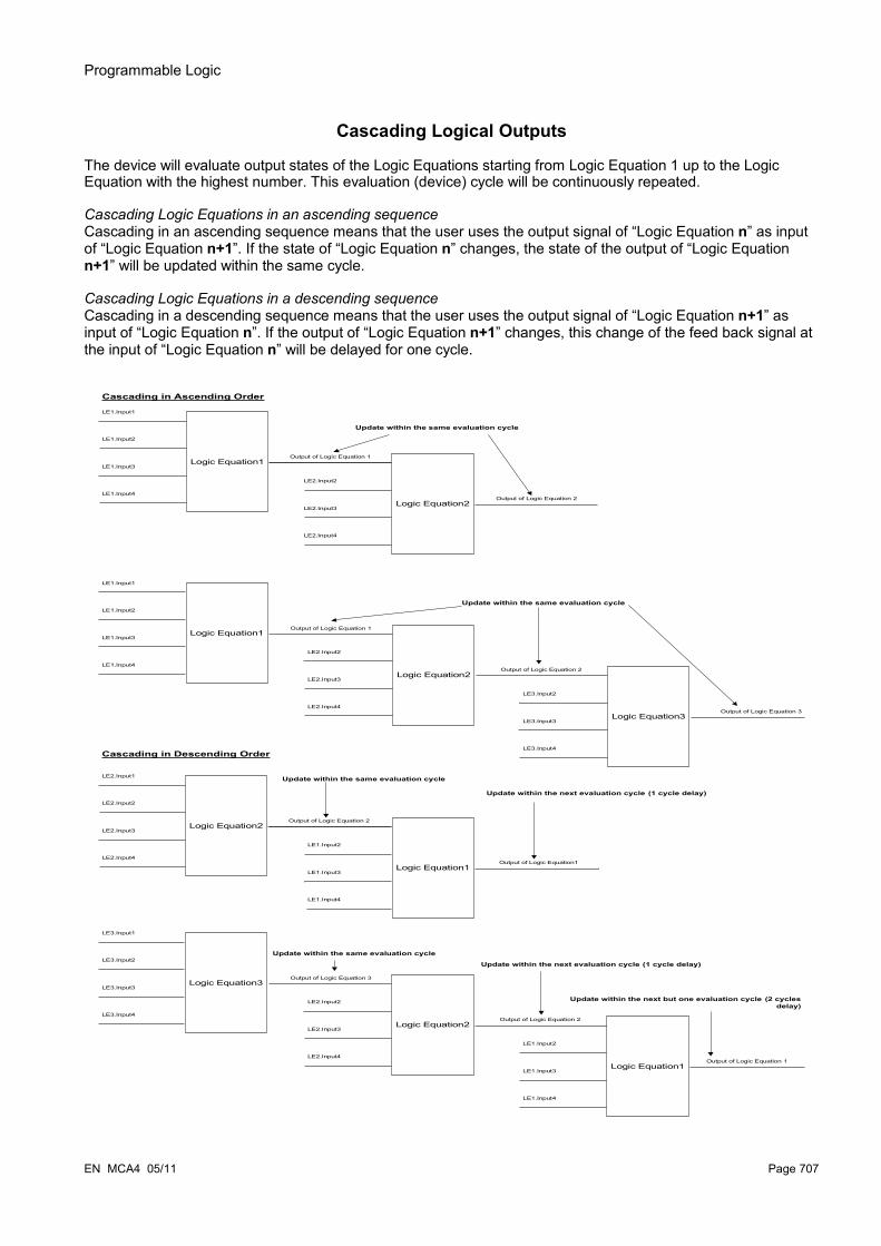
Programmable Logic
Cascading Logical Outputs
The device will evaluate output states of the Logic Equations starting from Logic Equation 1 up to the Logic Equation with the highest number. This evaluation (device) cycle will be continuously repeated.
Cascading Logic Equations in an ascending sequenceCascading in an ascending sequence means that the user uses the output signal of “Logic Equation n” as input of “Logic Equation n+1”. If the state of “Logic Equation n” changes, the state of the output of “Logic Equation n+1” will be updated within the same cycle.
Cascading Logic Equations in a descending sequenceCascading in a descending sequence means that the user uses the output signal of “Logic Equation n+1” as input of “Logic Equation n”. If the output of “Logic Equation n+1” changes, this change of the feed back signal at the input of “Logic Equation n” will be delayed for one cycle.
EN MCA4 05/11 Page 707
Logic Equation1
LE1.Input1
LE1.Input2
LE1.Input3
LE1.Input4
Output of Logic Equation 1
Logic Equation2
LE2.Input2
LE2.Input3
LE2.Input4
Output of Logic Equation 2
Update within the same evaluation cycle
Update within the next evaluation cycle (1 cycle delay)
Logic Equation2
LE2.Input1
LE2.Input2
LE2.Input3
LE2.Input4
Output of Logic Equation 2
Logic Equation1
LE1.Input2
LE1.Input3
LE1.Input4
Output of Logic Equation1
Update within the next evaluation cycle (1 cycle delay)
Logic Equation2
LE2.Input2
LE2.Input3
LE2.Input4
Output of Logic Equation 2
Logic Equation1
LE1.Input2
LE1.Input3
LE1.Input4
Output of Logic Equation 1
Logic Equation3
LE3.Input1
LE3.Input2
LE3.Input3
LE3.Input4
Logic Equation2
Output of Logic Equation 1
LE2.Input2
LE2.Input3
LE2.Input4
Output of Logic Equation 2
Logic Equation3
LE3.Input2
LE3.Input3
LE3.Input4
Output of Logic Equation 3
Logic Equation1
LE1.Input1
LE1.Input2
LE1.Input3
LE1.Input4
Update within the same evaluation cycle
Update within the same evaluation cycle
Update within the next but one evaluation cycle (2 cycles delay)
Update within the same evaluation cycle
Output of Logic Equation 3
Cascading in Ascending Order
Cascading in Descending Order

Programmable Logic
Programmable Logic at the Panel
WARNING improper use of Logic Equations might result in personal injury or damage the electrical equipment.
Don´t use Logic Equations unless that you can ensure the safe functionality.
How to configure a Logic Equation?• Call up menu [Logics/LE [x]]:
• Set the Input Signals (where necessary, invert them).
• If required, configure the timer (»On delay« and »Off delay«).
• If the latched output signal is used assign a reset signal to the reset input.
• Within the »status display«, the user can check the status of the logical inputs and outputs of the Logic Equation.
In case that Logic Equations should be cascaded the user has to be aware of timing delays (cycles) in case of descending sequences (Please refer to section: Cascading Logical Outputs).
By means the Status Display [Operation/Status Display] the logical states can be verified.]
Page 708 EN MCA4 05/11
Programmable Logic
Programmable Logic via Smart view
WARNING improper use of Logic Equations might result in personal injury or damage the electrical equipment.
Don´t use Logic Equations unless that you can ensure the safe functionality.
It is recommended to configure the logic via Smart view.
How to configure a Logic Equation?• Call up menu [Logics/LE [x]:
• Call up the Logic Editor
• Set the Input Signals (where necessary, invert them).
• If required, configure the timer (»On delay« and »Off delay«).
• If the latched output signal is used assign a reset signal to the reset input.
• Within the »status display«, the user can check the status of the logical inputs and outputs of the Logic Equation.
In case that Logic Equations should be cascaded the user has to be aware of timing delays (cycles) in case of descending sequences (Please refer to section: Cascading Logical Outputs).
By means the Status Display [Operation/Status Display] the logical states can be verified.]
Device Planning Parameters of the Programmable Logic
Parameter Description Options Default Menu path
No of Equations:
Number of required Logic Equations: 0,
5,
10,
20,
40,
80
20 [Device planning]
EN MCA4 05/11 Page 709

Programmable Logic
Global Protection Parameter of the Programmable Logic
Parameter Description Setting range Default Menu path
LE1.Gate Logic gate AND,
OR,
NAND,
NOR
AND [Logics
/LE 1]
LE1.Input1 Assignment of the Input Signal 1..n, Assignment List -.- [Logics
/LE 1]
LE1.Inverting1
Inverting the input signals.
Only available if an input signal has been assigned.
inactive,
active
inactive [Logics
/LE 1]
LE1.Input2 Assignment of the Input Signal 1..n, Assignment List -.- [Logics
/LE 1]
LE1.Inverting2
Inverting the input signals.
Only available if an input signal has been assigned.
inactive,
active
inactive [Logics
/LE 1]
LE1.Input3 Assignment of the Input Signal 1..n, Assignment List -.- [Logics
/LE 1]
LE1.Inverting3
Inverting the input signals.
Only available if an input signal has been assigned.
inactive,
active
inactive [Logics
/LE 1]
LE1.Input4 Assignment of the Input Signal 1..n, Assignment List -.- [Logics
/LE 1]
LE1.Inverting4
Inverting the input signals.
Only available if an input signal has been assigned.
inactive,
active
inactive [Logics
/LE 1]
LE1.t-On Delay
Switch On Delay 0.00 - 36000.00s 0.00s [Logics
/LE 1]
Page 710 EN MCA4 05/11
Programmable Logic
Parameter Description Setting range Default Menu path
LE1.t-Off Delay
Switch Off Delay 0.00 - 36000.00s 0.00s [Logics
/LE 1]
LE1.Reset Latched
Reset Signal for the Latching 1..n, Assignment List -.- [Logics
/LE 1]
LE1.Inverting Reset
Inverting Reset Signal for the Latching inactive,
active
inactive [Logics
/LE 1]
LE1.Inverting Set
Inverting the Setting Signal for the Latching inactive,
active
inactive [Logics
/LE 1]
EN MCA4 05/11 Page 711

Programmable Logic
Programmable Logic Inputs
Name Description Assignment via
LE1.Gate In1-I State of the module input: Assignment of the Input Signal
[Logics
/LE 1]LE1.Gate In2-I State of the module input: Assignment of
the Input Signal[Logics
/LE 1]LE1.Gate In3-I State of the module input: Assignment of
the Input Signal[Logics
/LE 1]LE1.Gate In4-I State of the module input: Assignment of
the Input Signal[Logics
/LE 1]LE1.Reset Latch-I State of the module input: Reset Signal for
the Latching[Logics
/LE 1]
Page 712 EN MCA4 05/11

Programmable Logic
Programmable Logic Outputs
Name Description
LE1.Gate Out Signal: Output of the logic gateLE1.Timer Out Signal: Timer OutputLE1.Out Signal: Latched Output (Q)LE1.Out inverted Signal: Negated Latched Output (Q NOT)
EN MCA4 05/11 Page 713

Commissioning
Commissioning Before starting work on an opened switchboard it is imperative that the complete switchboard is dead and the following 5 safety regulations are always met: ,
Safety precautions: • Disconnect from the power supply• Secure against reconnection• Verify if the equipment is dead• Connect to ground and short-circuit all phases• Cover or safeguard all live adjacent parts
The secondary circuit of a current transformer must never be opened during operation. The prevailing high voltages are dangerous to life.
Even when the auxiliary voltage is switched off, it is likely that there are still hazardous voltages at the component connections. All locally applicable national and international installation and safety regulations for working at electrical power installations must always to be followed (e.g. VDE, EN, DIN, IEC).
Prior to the initial voltage connection, the following must be guaranteed:
• Correct grounding of the device• That all signal circuits are tested• That all control circuits are tested• Transformer wiring is checked• Correct rating of the CTs • Correct burden of the CTs• That the operational conditions are in line with the Technical Data• Correct rating of the transformer protection • Function of the transformer fuses• Correct wiring of all digital inputs • Polarity and capacity of the supply voltage• Correct wiring of the analogue inputs and outputs
The permissible deviations of measuring values and device adjustment are dependent on the technical data/tolerances.
Page 714 EN MCA4 05/11

Commissioning
Commissioning/Protection Test
Putting into operation/Protection test must be carried out by authorized and qualified personnel. Before the device is put into operation the related documentation has to be read and understood.
With any test of the protection functions the following has to be checked:
• Is activation/tripping saved in the event recorder?• Is tripping saved in the fault recorder?• Is tripping saved in the disturbance recorder?• Are all signals/messages correctly generated? • Do all general parameterized blocking functions work properly?• Do all temporary parameterized (via DI) blocking functions work
properly?• To enable checks on all LEDs and relay functions, these have to
be provided with the relevant alarm and tripping functions of the respective protection functions/elements. This has to be tested in practical operation.
Check of all temporary blockings (via digital inputs):
• In order to avoid malfunctions, all blockings related to tripping/non-tripping of protection function have to be tested. The test can be very complex and should therefore be performed by the same people who set up the protection concept.
Check of all general trip blockings:
• All general trip blockings have to be tested.
Prior to the initial operation of the protection device all tripping times and values shown in the adjustment list have to be confirmed by a secondary test
Any description of functions, parameters, inputs or outputs that does not match the device in hand, can be ignored.
EN MCA4 05/11 Page 715

Commissioning
Putting out of Operation – Plug out the Relay
Warning! Dismounting the relay will lead to a loss of the protection functionality. Ensure that there is a back-up protection. If you are not aware of the consequences of dismounting the device – stop! Don´t start.
Inform SCADA before you start.
Switch-off the power supply.
Ensure, that the cabinet is dead and that there are no voltages that could lead to personal injury.
Plug-out the terminals at the rear-side of the device. Do not pull any cable – pull on the plugs! If it is stuck use for example a screw driver.
Fasten the cables and terminals in the cabinet by means of cable clips to ensure that no accidental electrical connections are caused.
Hold the device at the front-side while opening the mounting nuts.
Remove the device carefully out of the cabinet.
In case no other device is to be mounted or replaced cover/close the cut-out in the front-door.
Close the cabinet.
Page 716 EN MCA4 05/11

Commissioning
Service and Commissioning SupportWithin the service menu various functions support maintenance and commissioning of the device.
General
Within the menu [Service/General], the user can initiate a reboot of the device.
EN MCA4 05/11 Page 717
Commissioning
Forcing the Relay Output ContactsThe parameters, their defaults, and setting ranges have to be taken from Relay Output Contacts section.
Principle – General Use
The User MUST ENSURE that the relay output contacts operate normally after maintenance is completed. If the relay output contacts do not operate normally, the protective device WILL NOT provide protection.
For commissioning purposes or for maintenance, relay output contacts can be set by force.
Within this mode [Service/Test Mode/Force OR/BO Slot X(2/5)], relay output contacts can be set by force:
• Permanent; or• Via timeout.
If they are set with a timeout, they will keep their “Force Position” only as long as this timer runs. If the timer expires, the relay will operate normally. If they are set as Permanent, they will keep the “Force Position” continuously.
There are two options available:
• Forcing a single relay »Force ORx«; and• Forcing an entire group of relay output contacts »Force all Outs«.
Forcing an entire group takes precedence over forcing a single relay output contact!
A relay output contact will NOT follow a force command as long as it is disarmed at the same time.
A relay output contact will follow a force command:
• If it is not disarmed; and • If the Direct Command is applied to the relay(s).
Keep in mind, that the forcing of all relay output contacts (of the same assembly group) takes precedence over the force command of a single relay output contact.
Page 718 EN MCA4 05/11

Commissioning
Disarming the Relay Output Contacts
The parameters, their defaults, and setting ranges have to be taken from the Relay Output Contacts section.
Principle – General Use
Within this mode [Service/Test Mode/DISARMED], entire groups of relay output contacts can be disabled. By means of this test mode, contact outputs switching actions of the relay output contacts are prevented. If the relay output contacts are disarmed, maintenance actions can be carried out without the risk of taking entire processes off-line.
The User MUST ENSURE that the relay output contacts are ARMED AGAIN after maintenance is complete. If they are not armed, the protective device WILL NOT provide protection.
Zone Interlocking Output and the Supervision Contact cannot be disarmed.
Within this mode [Service/Test Mode/DISARMED] entire groups of relay output contacts can be disarmed:
• Permanent; or• Via timeout.
If they are set with a timeout, they will keep their “Disarm Position” only as long as this timer runs. If the timer expires, the relay output contacts will operate normally. If they are set Permanent, they will keep the “Disarm State” continuously.
A relay output contact will NOT be disarmed as long as:
• It´s latched (and not yet reset).
• As long as a running t-OFF-delay timer is not yet expired (hold time of a relay output contact).
• The Disarm Control is not set to active.
• The Direct Command is not applied.
A relay output contact will be disarmed if it´s not latched and
• There is no running t-OFF-delay timer (hold time of a relay output contact) and
EN MCA4 05/11 Page 719

Commissioning
• The DISARM Control is set to active and
• The Direct Command Disarm is applied.
Page 720 EN MCA4 05/11

Commissioning
Failure Simulator (Sequencer)*Available Elements: Sgen
* = Availability depends on ordered device.
For commissioning support and in order to analyze failures, the protective device offers the option to simulate measuring quantities. The simulation menu can be found within the [Service/Test Mode/Sgen] menu. The simulation cycle consists of three states:
• Pre-failure;• Failure; and• Post-failure State (Phase).
Within the [Service/Test Mode/Sgen/Configuration/Times] sub-menu, the duration of each phase can be set. In addition; the measuring quantities to be simulated can be determined (e.g.: voltages, currents, and the corresponding angles) for each phase (and ground).
Setting the device into the simulation mode means taking the protective device out of operation for the duration of the simulation. Do not use this feature during operation of the device if the User cannot guarantee that there is a running and properly working backup protection.
The energy counters will be stopped while the failure simulator is running.
The simulation voltages are always phase to neutral voltages, irrespectively of the mains voltage transformers' connection method (Phase-to-phase / Wey / Open Delta).
EN MCA4 05/11 Page 721
pre postFailure Simulation
t-PreFault t-FaultSimulation t-PostFault
Sgen
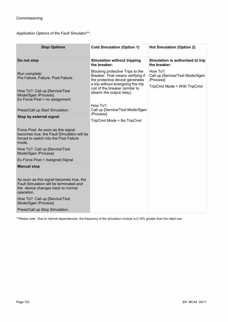
Commissioning
Application Options of the Fault Simulator**:
Stop Options Cold Simulation (Option 1) Hot Simulation (Option 2)
Do not stop
Run complete: Pre Failure, Failure, Post Failure.
How To?: Call up [Service/Test Mode/Sgen /Process] Ex Force Post = no assignment
Press/Call up Start Simulation.
Simulation without tripping the breaker:Blocking protective Trips to the Breaker. That means verifying if the protective device generates a trip without energizing the trip coil of the breaker (similar to disarm the output relay).
How To?: Call up [Service/Test Mode/Sgen /Process]
TripCmd Mode = No TripCmd
Simulation is authorized to trip the breaker:How To?: Call up [Service/Test Mode/Sgen /Process]
TripCmd Mode = With TripCmd
Stop by external signal
Force Post: As soon as this signal becomes true, the Fault Simulation will be forced to switch into the Post Failure mode.
How To?: Call up [Service/Test Mode/Sgen /Process]
Ex Force Post = Assigned Signal
Manual stop
As soon as this signal becomes true, the Fault Simulation will be terminated and the device changes back to normal operation.
How To?: Call up [Service/Test Mode/Sgen /Process]
Press/Call up Stop Simulation.
**Please note: Due to internal dependencies, the frequency of the simulation module is 0.16% greater than the rated one.
Page 722 EN MCA4 05/11

Commissioning
Device Planning Parameters of the Failure Simulator
Parameter Description Options Default Menu path
Mode Mode do not use,
use
use [Device planning]
Global Protection Parameter of the Failure Simulator
Parameter Description Setting range Default Menu path
t-PreFault Pre Fault Duration 0.00 - 300.00s 0.0s [Service
/Test Mode (Prot inhibit)
/Sgen
/Configuration
/Times]t-FaultSimulation
Duration of Fault Simulation 0.00 - 10800.00s 0.0s [Service
/Test Mode (Prot inhibit)
/Sgen
/Configuration
/Times]t-PostFault t-PostFault 0.00 - 300.00s 0.0s [Service
/Test Mode (Prot inhibit)
/Sgen
/Configuration
/Times]TripCmd Mode
Trip Command Mode No TripCmd,
With TripCmd
No TripCmd [Service
/Test Mode (Prot inhibit)
/Sgen
/Process]ExBlo External blocking of the module, if blocking is
activated (allowed) within a parameter set and if the state of the assigned signal is true.
1..n, Assignment List SG[1].Pos ON
[Service
/Test Mode (Prot inhibit)
/Sgen
/Process]
EN MCA4 05/11 Page 723

Commissioning
Parameter Description Setting range Default Menu path
Ex ForcePost Force Post state. Abort simulation. 1..n, Assignment List -.- [Service
/Test Mode (Prot inhibit)
/Sgen
/Process]
Voltage Parameter of the Failure Simulator
Parameter Description Setting range Default Menu path
VL1 Voltage Fundamental Magnitude in Pre State: phase L1
0.00 - 2.00Vn 1.0Vn [Service
/Test Mode (Prot inhibit)
/Sgen
/Configuration
/t-PreFault
/Voltage]VL2 Voltage Fundamental Magnitude in Pre State:
phase L20.00 - 2.00Vn 1.0Vn [Service
/Test Mode (Prot inhibit)
/Sgen
/Configuration
/t-PreFault
/Voltage]VL3 Voltage Fundamental Magnitude in Pre State:
phase L30.00 - 2.00Vn 1.0Vn [Service
/Test Mode (Prot inhibit)
/Sgen
/Configuration
/t-PreFault
/Voltage]VX Voltage Fundamental Magnitude in Pre State: VX 0.00 - 2.00Vn 0.0Vn [Service
/Test Mode (Prot inhibit)
/Sgen
/Configuration
/t-PreFault
/Voltage]
Page 724 EN MCA4 05/11
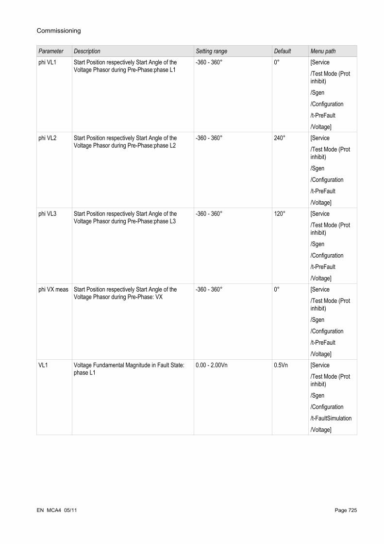
Commissioning
Parameter Description Setting range Default Menu path
phi VL1 Start Position respectively Start Angle of the Voltage Phasor during Pre-Phase:phase L1
-360 - 360° 0° [Service
/Test Mode (Prot inhibit)
/Sgen
/Configuration
/t-PreFault
/Voltage]phi VL2 Start Position respectively Start Angle of the
Voltage Phasor during Pre-Phase:phase L2-360 - 360° 240° [Service
/Test Mode (Prot inhibit)
/Sgen
/Configuration
/t-PreFault
/Voltage]phi VL3 Start Position respectively Start Angle of the
Voltage Phasor during Pre-Phase:phase L3-360 - 360° 120° [Service
/Test Mode (Prot inhibit)
/Sgen
/Configuration
/t-PreFault
/Voltage]phi VX meas Start Position respectively Start Angle of the
Voltage Phasor during Pre-Phase: VX-360 - 360° 0° [Service
/Test Mode (Prot inhibit)
/Sgen
/Configuration
/t-PreFault
/Voltage]VL1 Voltage Fundamental Magnitude in Fault State:
phase L10.00 - 2.00Vn 0.5Vn [Service
/Test Mode (Prot inhibit)
/Sgen
/Configuration
/t-FaultSimulation
/Voltage]
EN MCA4 05/11 Page 725

Commissioning
Parameter Description Setting range Default Menu path
VL2 Voltage Fundamental Magnitude in Fault State: phase L2
0.00 - 2.00Vn 0.5Vn [Service
/Test Mode (Prot inhibit)
/Sgen
/Configuration
/t-FaultSimulation
/Voltage]VL3 Voltage Fundamental Magnitude in Fault State:
phase L30.00 - 2.00Vn 0.5Vn [Service
/Test Mode (Prot inhibit)
/Sgen
/Configuration
/t-FaultSimulation
/Voltage]VX Voltage Fundamental Magnitude in Fault State:
phase VX0.00 - 2.00Vn 0.5Vn [Service
/Test Mode (Prot inhibit)
/Sgen
/Configuration
/t-FaultSimulation
/Voltage]phi VL1 Start Position respectively Start Angle of the
Voltage Phasor during Fault-Phase:phase L1-360 - 360° 0° [Service
/Test Mode (Prot inhibit)
/Sgen
/Configuration
/t-FaultSimulation
/Voltage]phi VL2 Start Position respectively Start Angle of the
Voltage Phasor during Fault-Phase:phase L2-360 - 360° 240° [Service
/Test Mode (Prot inhibit)
/Sgen
/Configuration
/t-FaultSimulation
/Voltage]
Page 726 EN MCA4 05/11

Commissioning
Parameter Description Setting range Default Menu path
phi VL3 Start Position respectively Start Angle of the Voltage Phasor during Fault-Phase:phase L3
-360 - 360° 120° [Service
/Test Mode (Prot inhibit)
/Sgen
/Configuration
/t-FaultSimulation
/Voltage]phi VX meas Start Position respectively Start Angle of the
Voltage Phasor during Fault-Phase: VX-360 - 360° 0° [Service
/Test Mode (Prot inhibit)
/Sgen
/Configuration
/t-FaultSimulation
/Voltage]VL1 Voltage Fundamental Magnitude during Post
phase: phase L10.00 - 2.00Vn 1.0Vn [Service
/Test Mode (Prot inhibit)
/Sgen
/Configuration
/t-PostFault
/Voltage]VL2 Voltage Fundamental Magnitude during Post
phase: phase L20.00 - 2.00Vn 1.0Vn [Service
/Test Mode (Prot inhibit)
/Sgen
/Configuration
/t-PostFault
/Voltage]VL3 Voltage Fundamental Magnitude during Post
phase: phase L30.00 - 2.00Vn 1.0Vn [Service
/Test Mode (Prot inhibit)
/Sgen
/Configuration
/t-PostFault
/Voltage]
EN MCA4 05/11 Page 727

Commissioning
Parameter Description Setting range Default Menu path
VX Voltage Fundamental Magnitude during Post phase: phase VX
0.00 - 2.00Vn 0.0Vn [Service
/Test Mode (Prot inhibit)
/Sgen
/Configuration
/t-PostFault
/Voltage]phi VL1 Start Position respectively Start Angle of the
Voltage Phasor during Post phase: phase L1-360 - 360° 0° [Service
/Test Mode (Prot inhibit)
/Sgen
/Configuration
/t-PostFault
/Voltage]phi VL2 Start Position respectively Start Angle of the
Voltage Phasor during Post phase: phase L2-360 - 360° 240° [Service
/Test Mode (Prot inhibit)
/Sgen
/Configuration
/t-PostFault
/Voltage]phi VL3 Start Position respectively Start Angle of the
Voltage Phasor during Post phase: phase L3-360 - 360° 120° [Service
/Test Mode (Prot inhibit)
/Sgen
/Configuration
/t-PostFault
/Voltage]phi VX meas Start Position respectively Start Angle of the
Voltage Phasor during Post phase: phase VX-360 - 360° 0° [Service
/Test Mode (Prot inhibit)
/Sgen
/Configuration
/t-PostFault
/Voltage]
Page 728 EN MCA4 05/11
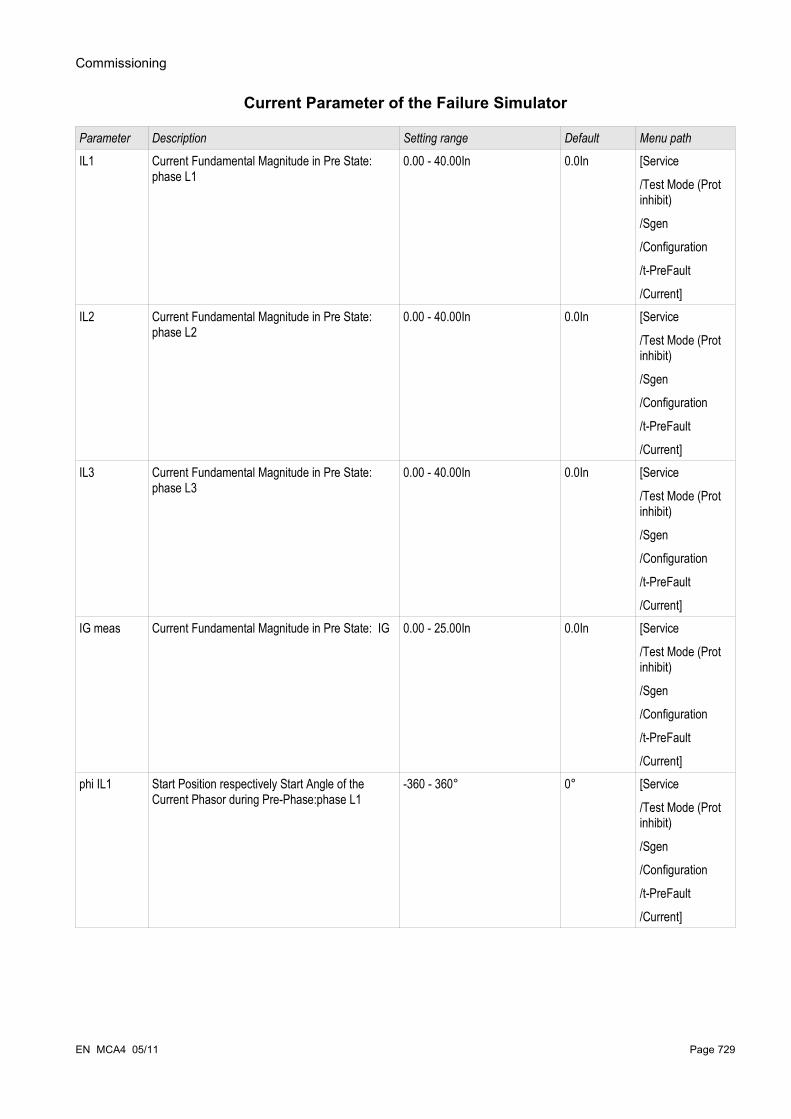
Commissioning
Current Parameter of the Failure Simulator
Parameter Description Setting range Default Menu path
IL1 Current Fundamental Magnitude in Pre State: phase L1
0.00 - 40.00In 0.0In [Service
/Test Mode (Prot inhibit)
/Sgen
/Configuration
/t-PreFault
/Current]IL2 Current Fundamental Magnitude in Pre State:
phase L20.00 - 40.00In 0.0In [Service
/Test Mode (Prot inhibit)
/Sgen
/Configuration
/t-PreFault
/Current]IL3 Current Fundamental Magnitude in Pre State:
phase L30.00 - 40.00In 0.0In [Service
/Test Mode (Prot inhibit)
/Sgen
/Configuration
/t-PreFault
/Current]IG meas Current Fundamental Magnitude in Pre State: IG 0.00 - 25.00In 0.0In [Service
/Test Mode (Prot inhibit)
/Sgen
/Configuration
/t-PreFault
/Current]phi IL1 Start Position respectively Start Angle of the
Current Phasor during Pre-Phase:phase L1-360 - 360° 0° [Service
/Test Mode (Prot inhibit)
/Sgen
/Configuration
/t-PreFault
/Current]
EN MCA4 05/11 Page 729

Commissioning
Parameter Description Setting range Default Menu path
phi IL2 Start Position respectively Start Angle of the Current Phasor during Pre-Phase:phase L2
-360 - 360° 240° [Service
/Test Mode (Prot inhibit)
/Sgen
/Configuration
/t-PreFault
/Current]phi IL3 Start Position respectively Start Angle of the
Current Phasor during Pre-Phase:phase L3-360 - 360° 120° [Service
/Test Mode (Prot inhibit)
/Sgen
/Configuration
/t-PreFault
/Current]phi IG meas Start Position respectively Start Angle of the
Current Phasor during Pre-Phase: IG-360 - 360° 0° [Service
/Test Mode (Prot inhibit)
/Sgen
/Configuration
/t-PreFault
/Current]IL1 Current Fundamental Magnitude in Fault State:
phase L10.00 - 40.00In 0.0In [Service
/Test Mode (Prot inhibit)
/Sgen
/Configuration
/t-FaultSimulation
/Current]IL2 Current Fundamental Magnitude in Fault State:
phase L20.00 - 40.00In 0.0In [Service
/Test Mode (Prot inhibit)
/Sgen
/Configuration
/t-FaultSimulation
/Current]
Page 730 EN MCA4 05/11
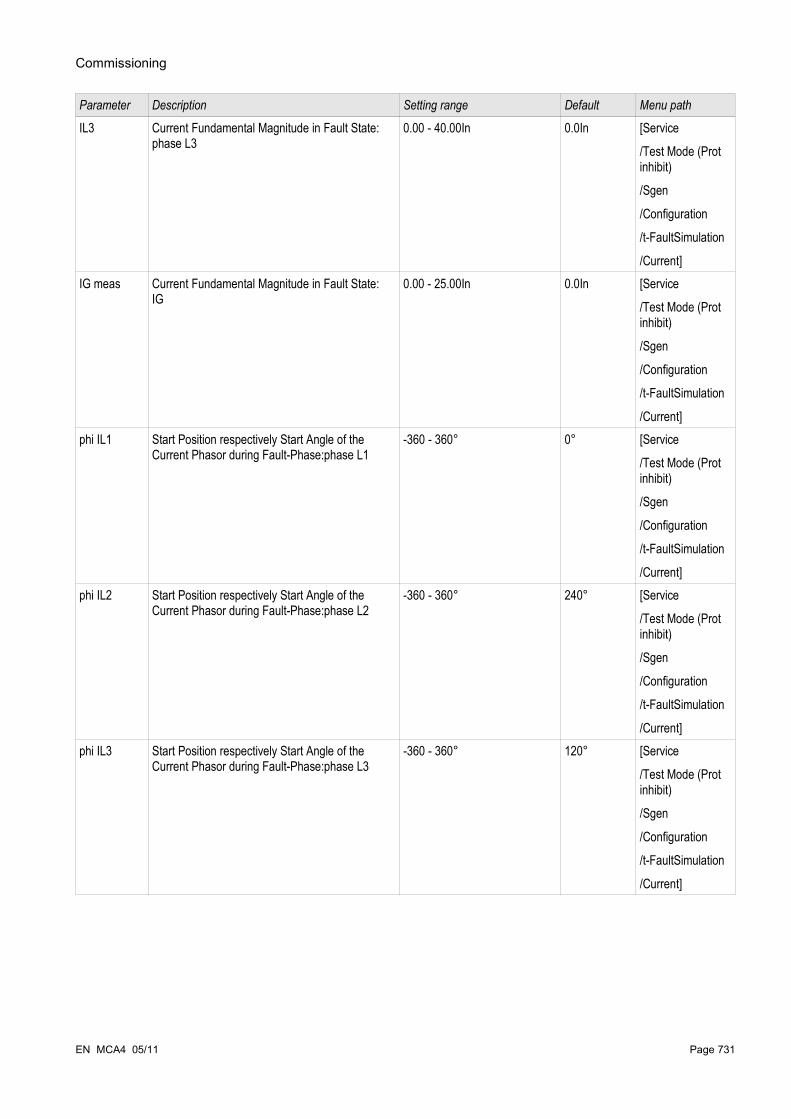
Commissioning
Parameter Description Setting range Default Menu path
IL3 Current Fundamental Magnitude in Fault State: phase L3
0.00 - 40.00In 0.0In [Service
/Test Mode (Prot inhibit)
/Sgen
/Configuration
/t-FaultSimulation
/Current]IG meas Current Fundamental Magnitude in Fault State:
IG0.00 - 25.00In 0.0In [Service
/Test Mode (Prot inhibit)
/Sgen
/Configuration
/t-FaultSimulation
/Current]phi IL1 Start Position respectively Start Angle of the
Current Phasor during Fault-Phase:phase L1-360 - 360° 0° [Service
/Test Mode (Prot inhibit)
/Sgen
/Configuration
/t-FaultSimulation
/Current]phi IL2 Start Position respectively Start Angle of the
Current Phasor during Fault-Phase:phase L2-360 - 360° 240° [Service
/Test Mode (Prot inhibit)
/Sgen
/Configuration
/t-FaultSimulation
/Current]phi IL3 Start Position respectively Start Angle of the
Current Phasor during Fault-Phase:phase L3-360 - 360° 120° [Service
/Test Mode (Prot inhibit)
/Sgen
/Configuration
/t-FaultSimulation
/Current]
EN MCA4 05/11 Page 731

Commissioning
Parameter Description Setting range Default Menu path
phi IG meas Start Position respectively Start Angle of the Current Phasor during Fault-Phase: IG
-360 - 360° 0° [Service
/Test Mode (Prot inhibit)
/Sgen
/Configuration
/t-FaultSimulation
/Current]IL1 Current Fundamental Magnitude during Post
phase: phase L10.00 - 40.00In 0.0In [Service
/Test Mode (Prot inhibit)
/Sgen
/Configuration
/t-PostFault
/Current]IL2 Current Fundamental Magnitude during Post
phase: phase L20.00 - 40.00In 0.0In [Service
/Test Mode (Prot inhibit)
/Sgen
/Configuration
/t-PostFault
/Current]IL3 Current Fundamental Magnitude during Post
phase: phase L30.00 - 40.00In 0.0In [Service
/Test Mode (Prot inhibit)
/Sgen
/Configuration
/t-PostFault
/Current]IG meas Current Fundamental Magnitude during Post
phase: IG0.00 - 25.00In 0.0In [Service
/Test Mode (Prot inhibit)
/Sgen
/Configuration
/t-PostFault
/Current]
Page 732 EN MCA4 05/11
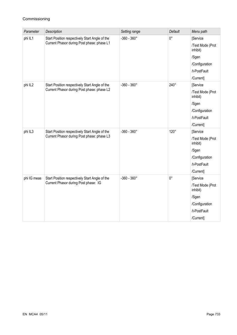
Commissioning
Parameter Description Setting range Default Menu path
phi IL1 Start Position respectively Start Angle of the Current Phasor during Post phase: phase L1
-360 - 360° 0° [Service
/Test Mode (Prot inhibit)
/Sgen
/Configuration
/t-PostFault
/Current]phi IL2 Start Position respectively Start Angle of the
Current Phasor during Post phase: phase L2-360 - 360° 240° [Service
/Test Mode (Prot inhibit)
/Sgen
/Configuration
/t-PostFault
/Current]phi IL3 Start Position respectively Start Angle of the
Current Phasor during Post phase: phase L3-360 - 360° 120° [Service
/Test Mode (Prot inhibit)
/Sgen
/Configuration
/t-PostFault
/Current]phi IG meas Start Position respectively Start Angle of the
Current Phasor during Post phase: IG-360 - 360° 0° [Service
/Test Mode (Prot inhibit)
/Sgen
/Configuration
/t-PostFault
/Current]
EN MCA4 05/11 Page 733
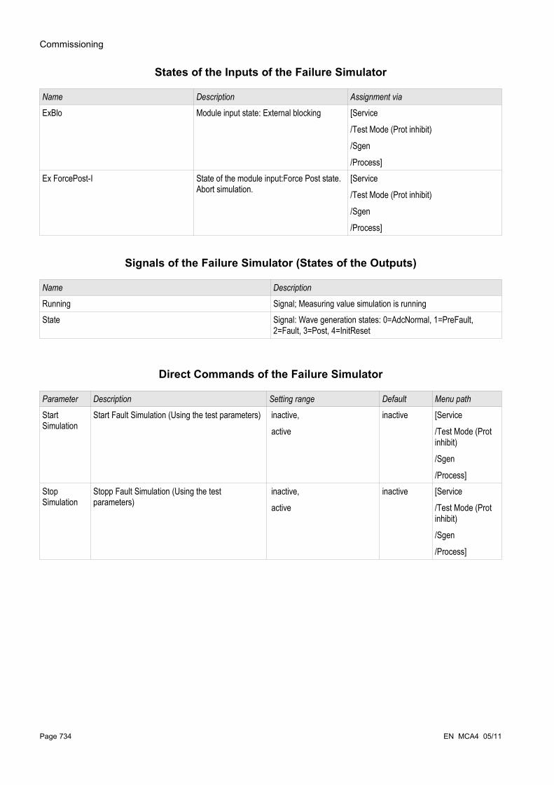
Commissioning
States of the Inputs of the Failure Simulator
Name Description Assignment via
ExBlo Module input state: External blocking [Service
/Test Mode (Prot inhibit)
/Sgen
/Process]Ex ForcePost-I State of the module input:Force Post state.
Abort simulation.[Service
/Test Mode (Prot inhibit)
/Sgen
/Process]
Signals of the Failure Simulator (States of the Outputs)
Name Description
Running Signal; Measuring value simulation is runningState Signal: Wave generation states: 0=AdcNormal, 1=PreFault,
2=Fault, 3=Post, 4=InitReset
Direct Commands of the Failure Simulator
Parameter Description Setting range Default Menu path
Start Simulation
Start Fault Simulation (Using the test parameters) inactive,
active
inactive [Service
/Test Mode (Prot inhibit)
/Sgen
/Process]Stop Simulation
Stopp Fault Simulation (Using the test parameters)
inactive,
active
inactive [Service
/Test Mode (Prot inhibit)
/Sgen
/Process]
Page 734 EN MCA4 05/11

Commissioning
Failure Simulator Values
Value Description Default Size Menu path
State Wave generation states: 0=AdcNormal, 1=PreFault, 2=Fault, 3=Post, 4=InitReset
L1 L2 L3 Normal L1 L2 L3 Normal,
t-PreFault,
t-FaultSimulation,
t-PostFault,
Init Res
[Service
/Test Mode (Prot inhibit)
/Sgen
/State]
EN MCA4 05/11 Page 735

Commissioning
Self SupervisionHighPROTEC devices are continuously monitored and supervised through different methods during normal operation as well as during start-up phase.
Results of this supervision may be:
• messages appearing within event-recorder (from release 1.2 or later),• indications within the display or Smart view,• corrective measures,• disabling of protection functions,• restart of the device•
or any combination out of these.
In case of failures that cannot be corrected immediately three restarts within 20 minutes are accepted before the device will be deactivated. The device should be removed in for service in such case. Contact data and address can be found at the end of this manual.In case of any failures the recorders of the device should be left untouched to ensure an easy diagnosis and proper repair at the factory. Besides the records and visible indications to the customer there exists internal information about failures. These allow service personnel to make a detailed analysis of files with failure reports, at least at factory site.
Self supervision is applied by different functions at different cyclic or noncyclic timings to the following parts and functions of the device:
• faultless cyclic execution of software,• functional capability of memory boards,• consistency of data,• functional capability of hardware sub-assemblies and• faultless operation of the measuring unit.
Faultless cyclic operation of software is supervised by timing analysis and checking results of different functions. Errors of the software function (watchdog function) lead to restarting the device and switching off the self-supervision relay (life-contact). Also the System-OK LED will blink red, after three unsuccessful attempts to restart the device within a time-period of 20 minutes.
The main processor cyclically monitors the operation of the signal processor and initiates corrective actions or restart of the device in case of faulty operation.
Data and files are generally secured against unintended overwriting or faulty changes by checksums.
The measuring unit continuously checks the measured data by comparing received data with data from a second channel sampled in parallel.
The auxiliary voltage is monitored continuously. If the voltage of one of the different supply circuits falls below a certain threshold, a restart of the device is initiated. If the voltage staggers around the threshold, the device also starts again after several seconds. Additionally the level of all internal supply voltage groups are continuously monitored.
Independent of these separate monitoring functions, the intermediate voltage circuit is buffered until all important and relevant operational and fault-data have been saved and the device initiates a restart.
Page 736 EN MCA4 05/11

Commissioning
Error messages / -codes
After a reboot of the device the reason for rebooting will be displayed under [Operation/Status Display/Sys/Reset].For more information about the reboot reason please follow this chapter.
The reboot will also be logged within the event recorder. Rebooting causes an event named: Sys.reboot.
Numerical reboot codes:
Error messages / -codes
1. Reboot after clean switching off of the device normal reboot after clean shut down of the device.2. Reboot by user command user-initiated reboot through panel-command.3. Super reset: reset to factory settings4. Restart by debugger; internally for system-analysis purpose.5. Restart because of configuration changes.6. General failure: reboot.7. Reboot by SW-system abort (HOST-side); summary of several reboot reasons detected by
software, i.e. wrong pointer, corrupted files etc.8. Reboot by watchdog timeout (HOST-side) - Signaling if the protection-class-task hangs.9. Reboot by system abort (DSP-side); summary of several reboot reasons detected by software,
i.e. wrong pointer, DSP-side.10. Reboot by watchdog timeout (DSP-side) - Appears when DSP sequence needs too long for one
cycle.11. Loss of auxiliary voltage or low voltage reboot after loss of auxiliary voltage or voltage dropping
below reboot-level but not becoming zero.12. Faulty memory access: message of MMU (memory mapping unit) that prohibited memory access
has occurred.
EN MCA4 05/11 Page 737
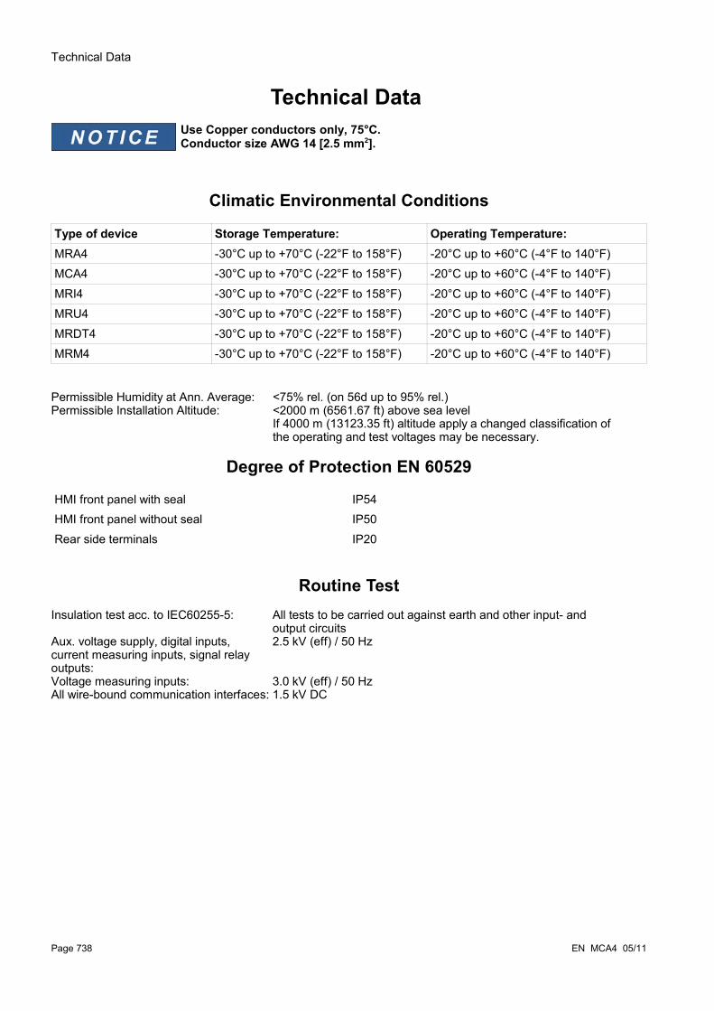
Technical Data
Technical Data Use Copper conductors only, 75°C.Conductor size AWG 14 [2.5 mm2].
Climatic Environmental Conditions
Type of device Storage Temperature: Operating Temperature: MRA4 -30°C up to +70°C (-22°F to 158°F) -20°C up to +60°C (-4°F to 140°F)MCA4 -30°C up to +70°C (-22°F to 158°F) -20°C up to +60°C (-4°F to 140°F)
MRI4 -30°C up to +70°C (-22°F to 158°F) -20°C up to +60°C (-4°F to 140°F)MRU4 -30°C up to +70°C (-22°F to 158°F) -20°C up to +60°C (-4°F to 140°F)
MRDT4 -30°C up to +70°C (-22°F to 158°F) -20°C up to +60°C (-4°F to 140°F)MRM4 -30°C up to +70°C (-22°F to 158°F) -20°C up to +60°C (-4°F to 140°F)
Permissible Humidity at Ann. Average: <75% rel. (on 56d up to 95% rel.)Permissible Installation Altitude: <2000 m (6561.67 ft) above sea level
If 4000 m (13123.35 ft) altitude apply a changed classification of the operating and test voltages may be necessary.
Degree of Protection EN 60529
HMI front panel with seal IP54HMI front panel without seal IP50Rear side terminals IP20
Routine TestInsulation test acc. to IEC60255-5: All tests to be carried out against earth and other input- and
output circuitsAux. voltage supply, digital inputs, current measuring inputs, signal relay outputs:
2.5 kV (eff) / 50 Hz
Voltage measuring inputs: 3.0 kV (eff) / 50 HzAll wire-bound communication interfaces: 1.5 kV DC
Page 738 EN MCA4 05/11
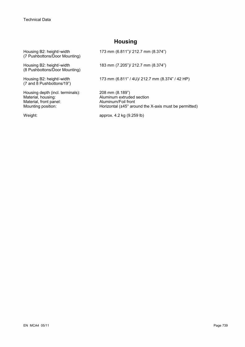
Technical Data
HousingHousing B2: height/-width(7 Pushbottons/Door Mounting)
Housing B2: height/-width(8 Pushbottons/Door Mounting)
Housing B2: height/-width(7 and 8 Pushbottons/19”)
173 mm (6.811”)/ 212.7 mm (8.374”)
183 mm (7.205”)/ 212.7 mm (8.374”)
173 mm (6.811” / 4U)/ 212.7 mm (8.374” / 42 HP)
Housing depth (incl. terminals): 208 mm (8.189”)Material, housing: Aluminum extruded section Material, front panel: Aluminum/Foil frontMounting position: Horizontal (±45° around the X-axis must be permitted)
Weight: approx. 4.2 kg (9.259 lb)
EN MCA4 05/11 Page 739

Technical Data
Current and Earth Current Measurement
Plug-in Connectors with Integrated Short-Circuiter (Conventional Current Inputs)
Nominal currents: 1 A / 5 AMax. measuring range: up to 40 x In (phase currents)
up to 25 x In (earth current standard)up to 2.5 x In (earth current sensitive)
Continuous loading capacity: Phase current/Earth current4 x In/continuously
Earth current sensitive2 x In/continuously
Overcurrent proof: Phase current/Earth current30 x In/10 s100 x In/1 s250 x In/10 ms (1 half-wave)
Earth current sensitive10 x In/10 s25 x In/1 s100 x In/10 ms (1 half-wave)
Power consumption: Phase current inputs: at In = 1A S = 0.15 mVAat In = 5A S = 0.15 mVA
Earth current input:at In = 1A S = 0.35 mVA at In = 5A S = 0.35 mVA
Sensitive earth current input:at In = 1A S = 0.35 mVA at In = 5A S = 0.35 mVA
Frequency range: 50 Hz / 60 Hz ±10%
Terminals:
Screws:
Screw-type terminals with integrated short-circuiters (contacts)
M4, captive type acc. to VDEW
Page 740 EN MCA4 05/11

Technical Data
Nominal currents: 1 A / 5 AConnection Cross Sections: 1 x or 2 x 2.5 mm² (2 x AWG 14) with wire end ferrule
1 x or 2 x 4.0 mm² (2 x AWG 12) with ring cable sleeve or cable sleeve1 x or 2 x 6 mm² (2 x AWG 10) with ring cable sleeve or cable sleeve
The current measuring board´s terminal blocks may be used as with 2 (double) conductors AWG 10,12,14 otherwise with single conductors only.
EN MCA4 05/11 Page 741
Technical Data
Voltage and Residual Voltage MeasurementNominal voltages: 100 V/110 V/230 V/400 V (can be parameterized)Max. measuring range: 2 x nominal voltageContinuous loading capacity: 2 x nominal voltage (800V AC) Power consumption: at Vn = 100 V S = 0.1 mVA
at Vn = 110 V S = 0.1 mVAat Vn = 230 V S = 0.4 mVAat Vn = 400 V S = 1.0 mVA
Frequency range: 50 Hz or 60 Hz ±10%Terminals: Screw-type terminals
Frequency Measurement Nominal frequencies: 50 Hz / 60 Hz
Voltage SupplyAux. Voltage: 24V - 270 V DC/48 - 230 V AC (-20/+10%)
Buffer time in case of supply failure: >= 50 ms at minimal aux. voltage communication is permitted to be interrupted
Max. permissible making current: 18 A peak value for <0.25 ms12 A peak value for <1 ms
The voltage supply must be protected by a fuse of:• 2,5 A time-lag miniature fuse 5x20 mm (approx. 1/5” x 0.8”) according to IEC 60127• 3,5 A time-lag miniature fuse 6,3x32 mm (approx. 1/4” x 1 1/4”) according to UL 248-14
Power ConsumptionPower supply range: Power consumption
in idle modeMax. power consumption
24-270 V DC: 7 W 13 W48-230 V AC (for frequencies of 50-60 Hz):
7 VA 13 VA
DisplayDisplay type: LCD with LED background illuminationResolution graphics display: 128 x 128 pixel
LED-Type: Two colored: red/greenNumber of LEDs, Housing B2: 15
Front Interface RS232Baud rates: 115200 BaudHandshake: RTS and CTSConnection: 9-pole D-Sub plug
Page 742 EN MCA4 05/11
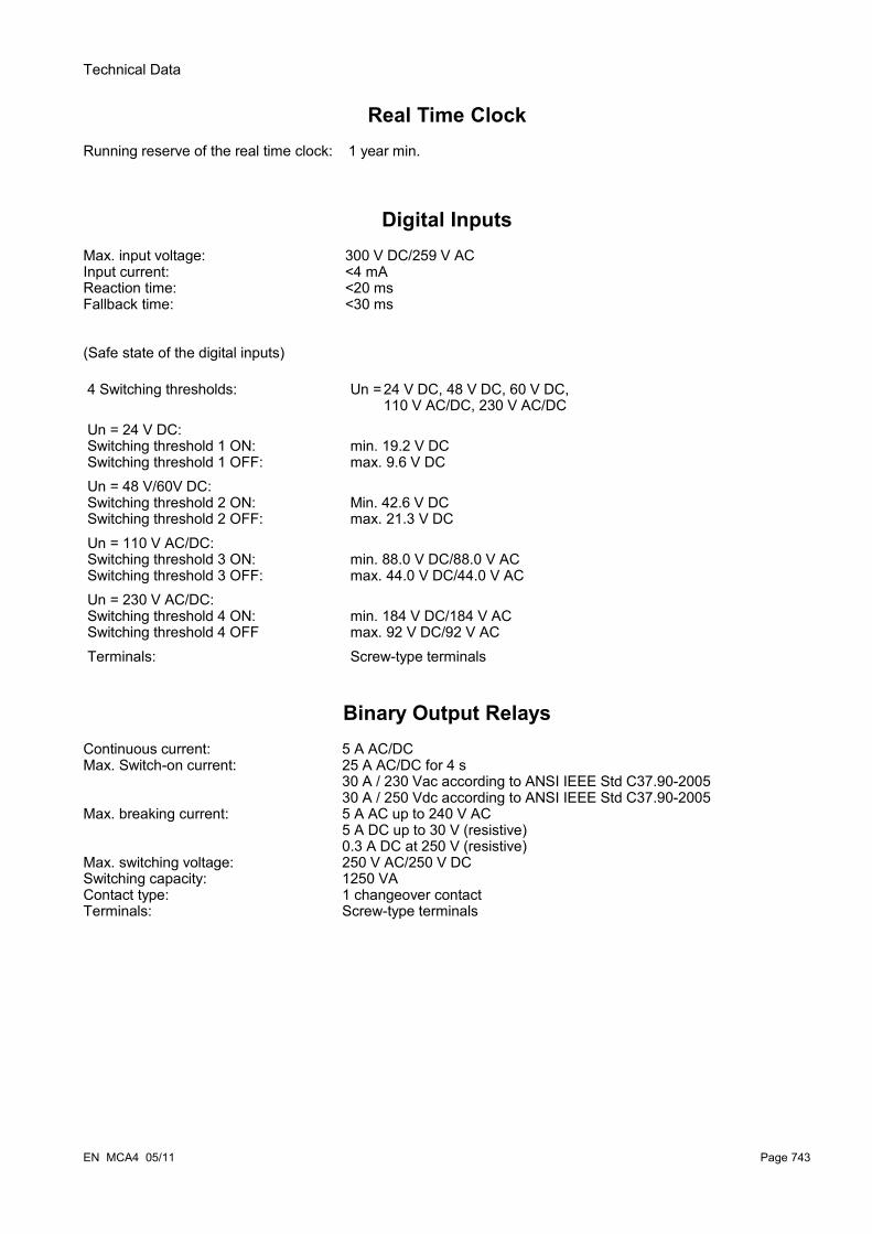
Technical Data
Real Time ClockRunning reserve of the real time clock: 1 year min.
Digital InputsMax. input voltage: 300 V DC/259 V ACInput current: <4 mAReaction time: <20 msFallback time: <30 ms
(Safe state of the digital inputs)
4 Switching thresholds: Un =24 V DC, 48 V DC, 60 V DC, 110 V AC/DC, 230 V AC/DC
Un = 24 V DC:Switching threshold 1 ON:Switching threshold 1 OFF:
min. 19.2 V DCmax. 9.6 V DC
Un = 48 V/60V DC:Switching threshold 2 ON:Switching threshold 2 OFF:
Min. 42.6 V DCmax. 21.3 V DC
Un = 110 V AC/DC:Switching threshold 3 ON:Switching threshold 3 OFF:
min. 88.0 V DC/88.0 V ACmax. 44.0 V DC/44.0 V AC
Un = 230 V AC/DC:Switching threshold 4 ON:Switching threshold 4 OFF
min. 184 V DC/184 V ACmax. 92 V DC/92 V AC
Terminals: Screw-type terminals
Binary Output RelaysContinuous current: 5 A AC/DCMax. Switch-on current: 25 A AC/DC for 4 s
30 A / 230 Vac according to ANSI IEEE Std C37.90-200530 A / 250 Vdc according to ANSI IEEE Std C37.90-2005
Max. breaking current: 5 A AC up to 240 V AC5 A DC up to 30 V (resistive)0.3 A DC at 250 V (resistive)
Max. switching voltage: 250 V AC/250 V DCSwitching capacity: 1250 VAContact type: 1 changeover contactTerminals: Screw-type terminals
EN MCA4 05/11 Page 743

Technical Data
Supervision Contact (SC)
Continuous current:: 5 A AC/DCMax. Switch-on current: 15 A AC/DC for 4 sMax. breaking current: 5 A AC up to 250 V AC
5 A DC up to 30 V (resistive)0.25 A DC at 250 V (resistive)
Max. switching voltage: 250 V AC/250 V DCSwitching capacity: 1250 VAContact type: 1 changeover contactTerminals: Screw-type terminals
Time Synchronization IRIGNominal input voltage: 5 VConnection: Screw-type terminals (twisted pair)
RS485*Master/Slave: SlaveConnection: 9-pole D-Sub socket
(external terminating resistors/in D-Sub)or 6 screw-clamping terminals RM 3.5 mm (138 MIL)(terminating resistors internal)
In case that the RS485 interface is realized via terminals, the communication cable has to be shielded. The shielding has to be fixed at the screw that is marked with the ground symbol (rear side of the device).
Fibre Optic*Master/Slave: SlaveConnection: ST-Plug
URTD-Interface*Connection: Versatile Link
*availability depends on device
Boot phaseAfter switching on the power supply the protection will be available in approximately 22 seconds. After approximately 161-204 (depending on the configuration) seconds the boot phase is completed (HMI and Communication initialized).
Page 744 EN MCA4 05/11

Standards
StandardsApprovals
• GOST-R• UL-listed file: e217753
Design StandardsGeneric standard EN 61000-6-2
EN 61000-6-3 Product standard IEC 60255-6
EN 50178 UL 508 (Industrial Control Equipment)CSA C22.2 No. 14-95 (Industrial Control Equipment)ANSI C37.90
High Voltage Tests (IEC 60255-6) High frequency interference testIEC 60255-22-1 class 3
Within one circuit
Circuit to earth
Circuit to circuit
1 kV/2 s
2.5 kV/2 s
2.5 kV/2 s
Insulation voltage testIEC 60255-5 EN 50178
All circuits to other circuits and exposed conductive parts
Except interfaces
and Voltage measuring input
2.5 kV (eff.)/50Hz, 1 min.
1,5 kV DC, 1 min.
3 kV (eff.)/50 Hz, 1 min.
Impulse voltage testIEC 60255-5 5 kV/0.5J, 1.2/50 µs
EN MCA4 05/11 Page 745

Standards
EMC Immunity Tests
Fast transient disturbance immunity test (Burst)IEC 60255-22-4 IEC 61000-4-4 class 4
Power supply, mains inputs
Other in- and outputs
±4 kV, 2.5 kHz
±2 kV, 5 kHz
Surge immunity testIEC 61000-4-5 class 4
Within one circuit
Circuit to earth
2 kV
4 kV
Class 3 Communication cables to earth 2 kV
Electrical discharge immunity testIEC 60255-22-2 IEC 61000-4-2 class 3
Air discharge
Contact discharge
8 kV
6 kV
Radiated radio-frequency electromagnetic field immunity testIEC 61000-4-3Class XANSI C37.90.2
26 MHz – 80 MHz80 MHz – 1 GHz1 GHz – 3 GHz
10 V/m35 V/m10 V/m
Immunity to conducted disturbances induced by radio frequency fieldsIEC 61000-4-6 class 3
10 V
Power frequency magnetic field immunity testIEC 61000-4-8 class 4
continues
3 sec
30 A/m
300 A/m
EMC Emission Tests
Radio interference suppression testIEC/CISPR11 Limit value class B
Radio interference radiation testIEC/CISPR11 Limit value class B
Page 746 EN MCA4 05/11

Standards
Environmental Tests
Classification:IEC 60068-1 Climatic
classification
20/060/56
IEC 60721-3-1 Classification of ambient conditions (Storage)
1K5/1B1/1C1L/1S1/1M2but min. -30°C
IEC 60721-3-2 Classification of ambient conditions (Transportation)
2K4/2B1/2C1/2S1/2M2but min. -30°C
IEC 60721-3-3 Classification of ambient conditions (Stationary use at weather protected locations)
3K6/3B1/3C1/3S1/3M2 but min. -20°C/max +60°C
Test Ad: ColdIEC 60068-2-1 Temperature
test duration-20°C16 h
Test Bd: Dry HeatIEC 60068-2-2 Temperature
Relative humiditytest duration
60°C<50%72 h
Test Cab: Damp Heat (steady state)IEC 60068-2-78 Temperature
Relative humiditytest duration
40°C93%12 h
Test Db: Damp Heat (cyclic)IEC 60068-2-30 Temperature
Relative humidityCycles (12 + 12-hour)
60°C95%2
EN MCA4 05/11 Page 747

Standards
Mechanical TestsTest Fc: Vibration response testIEC 60068-2-6IEC 60255-21-1class 1
(10 Hz – 59 Hz)Displacement
(59Hz – 150Hz)Acceleration
Number of cycles in each axis
0.035 mm
0.5 gn
1
Test Fc: Vibration endurance testIEC 60068-2-6IEC 60255-21-1class 1
(10 Hz – 150 Hz)Acceleration
Number of cycles in each axis
1.0 gn
20
Test Ea: Shock testsIEC 60068-2-27IEC 60255-21-2 class 1
Shock response test 5 gn, 11 ms, 3 impulses in each direction
Shock resistance test 15 gn, 11 ms, 3 impulses in each direction
Test Eb: Shockendurance testIEC 60068-2-29IEC 60255-21-2 class 1
Shock endurance test 10 gn, 16 ms, 1000 impulses in each direction
Test Fe: Earthquake testIEC 60068-3-3KTA 3503IEC 60255-21-3
Single axis earthquake vibration test 3 – 7 Hz: Horizontal 10 mm, 1 cycle each axis
class 2 7 – 35 Hz Horizontal: 2 gn, 1 cycle each axis
Page 748 EN MCA4 05/11
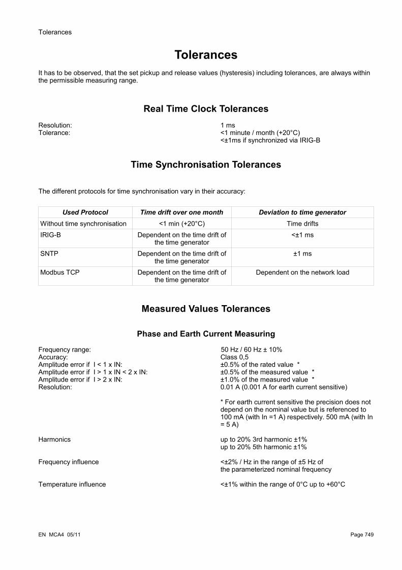
Tolerances
TolerancesIt has to be observed, that the set pickup and release values (hysteresis) including tolerances, are always within the permissible measuring range.
Real Time Clock TolerancesResolution: 1 msTolerance: <1 minute / month (+20°C)
<±1ms if synchronized via IRIG-B
Time Synchronisation Tolerances
The different protocols for time synchronisation vary in their accuracy:
Used Protocol Time drift over one month Deviation to time generatorWithout time synchronisation <1 min (+20°C) Time driftsIRIG-B Dependent on the time drift of
the time generator<±1 ms
SNTP Dependent on the time drift of the time generator
±1 ms
Modbus TCP Dependent on the time drift of the time generator
Dependent on the network load
Measured Values Tolerances
Phase and Earth Current Measuring
Frequency range: 50 Hz / 60 Hz ± 10%Accuracy: Class 0,5Amplitude error if I < 1 x IN: ±0.5% of the rated value *Amplitude error if I > 1 x IN < 2 x IN: ±0.5% of the measured value *Amplitude error if I > 2 x IN: ±1.0% of the measured value *Resolution: 0.01 A (0.001 A for earth current sensitive)
* For earth current sensitive the precision does not depend on the nominal value but is referenced to 100 mA (with In =1 A) respectively. 500 mA (with In = 5 A)
Harmonics up to 20% 3rd harmonic ±1%up to 20% 5th harmonic ±1%
Frequency influence <±2% / Hz in the range of ±5 Hz ofthe parameterized nominal frequency
Temperature influence <±1% within the range of 0°C up to +60°C
EN MCA4 05/11 Page 749

Tolerances
Phase-to-earth and Residual Voltage Measurement
Nominal voltage (Vn): 60 - 520 V(parameterizable)Max measuring range: 800 VFrequency range: 50 Hz or 60 Hz ±10%Precision: Class 0,5Amplitude error for V<Vn (measured): ±0.5% (of the rated value)Amplitude error for V<Vn (calculated): ±1.0% (of the rated value)Amplitude error for V>Vn (measured): ±0.5% (of the measured value)Amplitude error for V>Vn (calculated): ±1.0% (of the calculated value)Resolution: 0.1 V
Harmonics up to 20% 3rd harmonic ±1%up to 20% 5th harmonic ±1%
Frequency influence <±2% / Hz in the range of ±5 Hz ofthe parameterized nominal frequency
Temperature influence <±1% within the range of 0°C up to +60°C
Frequency measurement
Nominal frequency: 50 Hz / 60 HzPrecision: ±0.05% of fn within the range of 40-70 Hz,
at voltages >50 VVoltage dependency frequency acquisition of 5 V – 800 V
Page 750 EN MCA4 05/11

Tolerances
Protection Stages TolerancesNote: The tripping delay relates to the time between alarm and trip. The tolerance of the operating time relates to the time between the measured value has exceeded the threshold until the protection stage is alarmed.
Overcurrent protection: I[x] Tolerance
I MTA ±3° at I >20% In
I> ±1.5% of the setting value resp. ±1% In
Resetting ratio 97% or 0.5% x In
t DEFT±1% resp.. ±10 ms
Operating timeStarting from I higher than 1.1 x I>
non-directional <35msdirectional <40ms
Release time directional and non-directional <45ms
t-char ±5% IEC NINV, IEC VINV, IEC LINV, IEC EINV, ANSI MINV, ANSI ANSI VINV, ANSI EINV, Therm Flat, IT, I2T, I4T
t-resetOnly available if: Characteristic = INV
±1% resp. ±10 ms
Voltage restraint: I[x]VRestraint = active
Tolerance
I> ±1.5% of the setting value resp. ±1% In
Resetting ratio 97% or 0.5% x In
Operating TimeStarting from I higher than 1.1 x I>
<35 ms
Release time <45 ms
t-char ±5% IEC NINV, IEC VINV, IEC LINV, IEC EINV, ANSI MINV, ANSI ANSI VINV, ANSI EINV, Therm Flat, IT, I2T, I4T
t-resetOnly available if: Characteristic = INV
±1% resp. ±10 ms forIEC NINV, IEC VINV, IEC LINV, IEC EINV
±5% for ANSI MINV, ANSI ANSI VINV, ANSI EINV, Therm Flat, IT, I2T, I4T
EN MCA4 05/11 Page 751

Tolerances
Negative phase sequence current: I[x]Measuring method = I2
Tolerance
I> ±2% of the setting value resp. ±1% In
Resetting ratio 97% or 0.5% x In
tTripping delay time (DEFT)
DEFT±1% resp. ±10 ms
Operating timeStarting from I> higher than 1.1 x I>
<60ms
Release time <45ms
Page 752 EN MCA4 05/11

Tolerances
Earth current: IG[x] Tolerance
IG MTA ±3° at IG >20% In
IG> ±1.5% of the setting value resp. ±1% In
resetting ratio 97% or 0.5% x In
VE> ±1.5% of the setting value resp. ±1% In
Resetting ratio 97% or 0.5% x In
t DEFT±1% resp. ±10 ms
Operating timeStarting from IG higher than 1.1 x IG>
non-directional <35 msdirectional <40 ms
Release time directional and non-directional <45ms
t-char ±5% IEC NINV, IEC VINV, IEC LINV, IEC EINV, ANSI MINV, ANSI ANSI VINV, ANSI EINV, Therm Flat, IT, I2T, I4T
t-resetOnly available if: Characteristic = INV
±1% resp. ±10 ms
Directional Sensitivity (calculated ground current) Value:3V0 (calculated)3V0 (measured)I2IRIXIX (sensitive)V2
Release Level:1 V1 V10 mA18 mA10 mA1 mA0.35 V
Blocking Level:0.8 V0.8 V5 mA11 mA5 mA0.5 mA0.25 V
Directional Sensitivity (measured ground current) Value:3V0 (calculated)3V0 (measured)I2IXIX (sensitive)V2
Release Level:0.35 V0.35 V10 mA10 mA1 mA0.35 V
Blocking Level:0.25 V0.25 V5 mA5 mA0.5 mA0.25 V
EN MCA4 05/11 Page 753
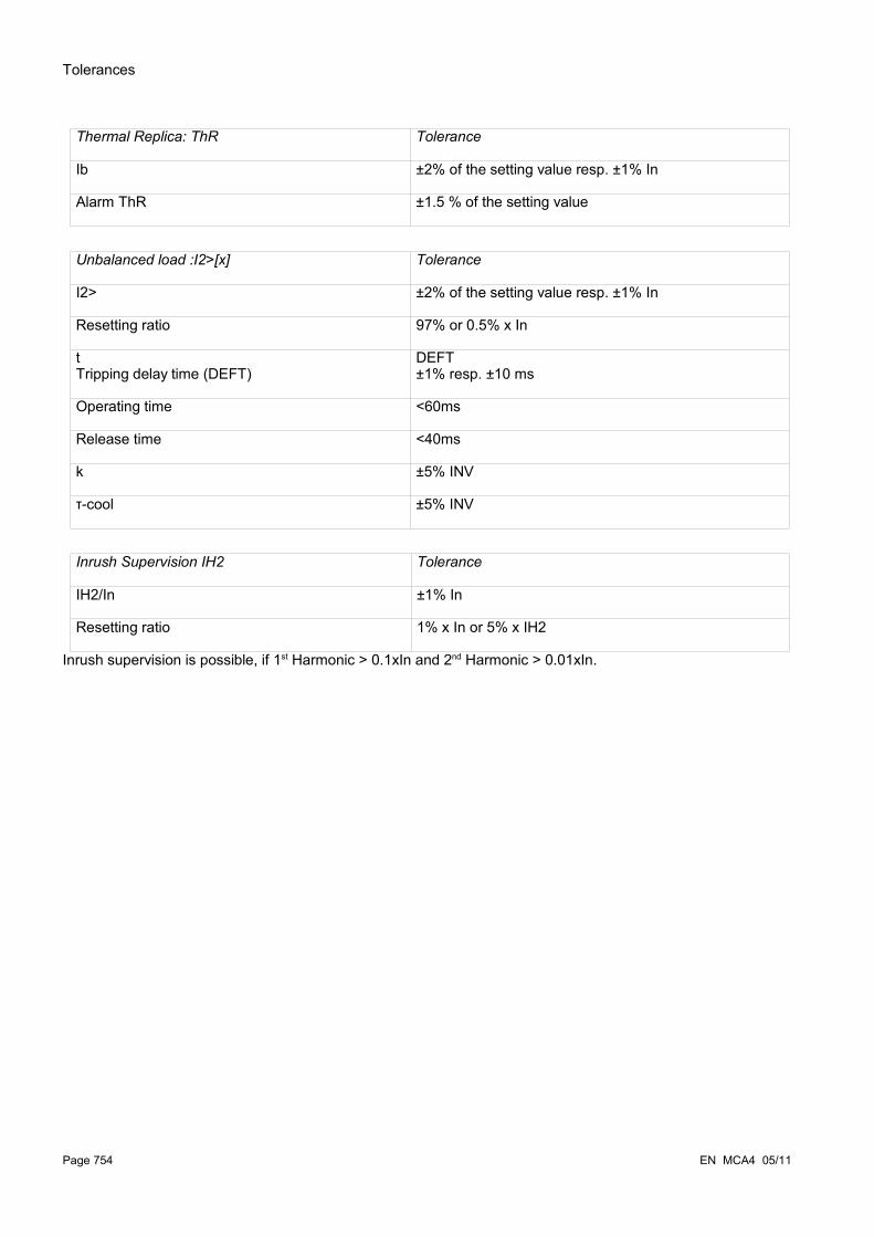
Tolerances
Thermal Replica: ThR Tolerance
Ib ±2% of the setting value resp. ±1% In
Alarm ThR ±1.5 % of the setting value
Unbalanced load :I2>[x] Tolerance
I2> ±2% of the setting value resp. ±1% In
Resetting ratio 97% or 0.5% x In
tTripping delay time (DEFT)
DEFT±1% resp. ±10 ms
Operating time <60ms
Release time <40ms
k ±5% INV
τ-cool ±5% INV
Inrush Supervision IH2 Tolerance
IH2/In ±1% In
Resetting ratio 1% x In or 5% x IH2
Inrush supervision is possible, if 1st Harmonic > 0.1xIn and 2nd Harmonic > 0.01xIn.
Page 754 EN MCA4 05/11

Tolerances
Voltage Protection V>[x] Tolerance
V> ±1.5% of the setting value resp. ±1% Vn
Resetting ratio 97% or 0.5% x Vn
t ±1% resp. ±10 ms
Operating timeStarting from U higher than 1.3 x U>
<40ms
Release time <40ms
Voltage Protection V<[x] Tolerance
V< ±1.5% of the setting value resp. ±1% Vn
Resetting ratio 103% or 0.5% x Vn
t ±1% resp. ±10 ms
Operating timeStarting from V lower than 0.7 x V<
<40ms
Release time <40ms
Voltage Protection V(t)<[x] Tolerance
V(t)< ±1.5% of the setting value resp. ±1% Vn
Resetting ratio 103% or 0.5% x Vn
t ±1% resp. ±10 ms
Operating timeStarting from V lower than 0.7 x V<
<40ms
Release time <40ms
Residual Voltage Protection VG[x] Tolerance
VG> ±1.5% of the setting value resp. ±1% Vn
Resetting ratio 97% or 0.5% x Vn
t ±1% resp. ±10 ms
Operating timeStarting from VE higher than 1.3 x VG>
<40ms
Release time <40ms
EN MCA4 05/11 Page 755
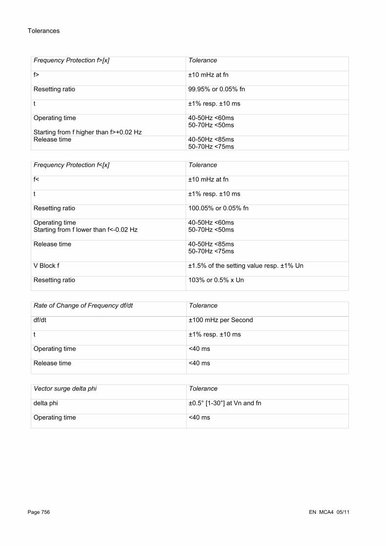
Tolerances
Frequency Protection f>[x] Tolerance
f> ±10 mHz at fn
Resetting ratio 99.95% or 0.05% fn
t ±1% resp. ±10 ms
Operating time
Starting from f higher than f>+0.02 Hz
40-50Hz <60ms50-70Hz <50ms
Release time 40-50Hz <85ms 50-70Hz <75ms
Frequency Protection f<[x] Tolerance
f< ±10 mHz at fn
t ±1% resp. ±10 ms
Resetting ratio 100.05% or 0.05% fn
Operating timeStarting from f lower than f<-0.02 Hz
40-50Hz <60ms50-70Hz <50ms
Release time 40-50Hz <85ms 50-70Hz <75ms
V Block f ±1.5% of the setting value resp. ±1% Un
Resetting ratio 103% or 0.5% x Un
Rate of Change of Frequency df/dt Tolerance
df/dt ±100 mHz per Second
t ±1% resp. ±10 ms
Operating time <40 ms
Release time <40 ms
Vector surge delta phi Tolerance
delta phi ±0.5° [1-30°] at Vn and fn
Operating time <40 ms
Page 756 EN MCA4 05/11

Tolerances
Circuit Breaker Failure Protection CBF Tolerance
I-CBF> ±1.5% of the setting value resp. ±1% In
Resetting ratio 0.5% x In
t-CBF ±1% resp. ±10 ms
Operating timeStarting from I higher than 1.3 x I-CBF>
<40 ms
Release time <40 ms
Trip Circuit Supervision TCS Tolerance
t-TCS ±1% resp. ±10 ms
Current Transformer Supervision CTS Tolerance
ΔI ±2% of the setting value resp. ±1.5% In
Resetting ratio 94%
t ±1% resp. ± 10 ms
Asymmetry V012[x] Tolerance
V1> ±2% of the setting value resp. ±1.5% Vn
resetting ratio 97% or 0.5% x Vn
V1< ±2% of the setting value resp. ±1.5% Vn
resetting ratio 103% or 0.5% x Vn
V2> ±2% of the setting value resp. ±1.5% Vn
Resetting ratio 97% or 0.5% x Vn
t ±1% resp. ±10 ms
%V2/V1 (≥ 0.1 x Vn) ±1%
Resetting ratio 97% or 0.5% x Vn
t DEFT±1% resp. ±10 ms
Operating time <60ms
Release time <40ms
EN MCA4 05/11 Page 757
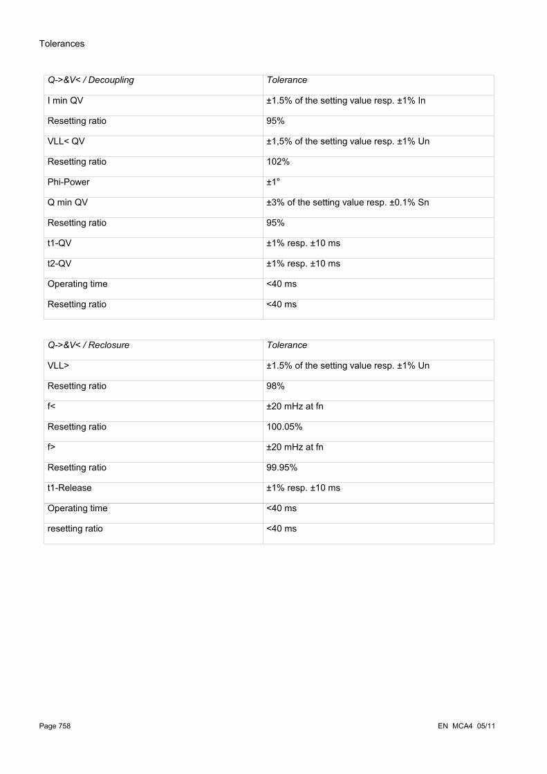
Tolerances
Q->&V< / Decoupling Tolerance
I min QV ±1.5% of the setting value resp. ±1% In
Resetting ratio 95%
VLL< QV ±1,5% of the setting value resp. ±1% Un
Resetting ratio 102%
Phi-Power ±1°
Q min QV ±3% of the setting value resp. ±0.1% Sn
Resetting ratio 95%
t1-QV ±1% resp. ±10 ms
t2-QV ±1% resp. ±10 ms
Operating time <40 ms
Resetting ratio <40 ms
Q->&V< / Reclosure Tolerance
VLL> ±1.5% of the setting value resp. ±1% Un
Resetting ratio 98%
f< ±20 mHz at fn
Resetting ratio 100.05%
f> ±20 mHz at fn
Resetting ratio 99.95%
t1-Release ±1% resp. ±10 ms
Operating time <40 ms
resetting ratio <40 ms
Page 758 EN MCA4 05/11

Tolerances
Automatic Reclosing AR Tolerance
t-start ±1% resp. ±20 ms
t-DP1 .... t-DP6 ±1% resp. ±20 ms
t-DE1 .… t-DE6 ±1% resp. ±20 ms
t-Superv ±1% resp. ±20 ms
1.n SA ... 6.t-SA ±1% resp. ±20 ms
Sync - Sync-Check Tolerance
t-MaxSyncSuperv ±1% resp. ±10 ms
MinLiveBusVoltage ±1.5% of the setting value Resp. 1% x Vn
MaxDeadBusVoltage ±1.5% of the setting value Resp. 1% x Vn
MinLiveLineVoltage ±1.5% of the setting value Resp. 1% x Vn
MaxDeadLineVoltage ±1.5% of the setting value Resp. 1% x Vn
t-VoltDead ±1% resp. ±10 ms
MaxVoltageDiff ±1.5% of the setting value Resp. 1% x Vn, may be exceeded when open delta is configured
MaxSlipFrequency ±20 mHz at fn
Angle measurement ±2°
Angle Difference Measurement ±2°
Angle Compensation Measurement ±4°
SOTF – Switch onto fault Tolerance
Operating time <35 ms
I< ±1.5% of the setting value resp.1% x In
t-enable ±1% resp. ±10 ms
CLPU – Cold load pickup Tolerance
Operating time <35 ms
t-Load OFF ±1% resp. ±10 ms
t-Max Block ±1% resp. ±10 ms
I< ±1.5% of the setting value resp.1% x In
EN MCA4 05/11 Page 759

Tolerances
LOP - loss of potential Tolerance
t-Alarm ±1% resp. ±10 ms
PQS Tolerance at 0.8 Vn (Vn =100 V) symmetrically feeded
P>, Q> |PF|>0,5 ±3% of the setting value resp. ±0.1% of Sn
Resetting ratio 97% of setting values or 0.2 W
t ±1% of the setting value resp. ±10 ms
Operating time <75 ms
Resetting time <75 ms
PQS Tolerance at 0.8 Vn (Vn =100 V) symmetrically feeded
P<, Q< |PF|>0,5 ±3% of the setting value resp. ±0.1% of Sn
Resetting ratio 103% of setting values or 0.2 W
t ±1% of the setting value resp. ±10 ms
Operating time <75 ms
Resetting time <75 ms
PQS Tolerance at 0.8 Vn (Vn =100 V) symmetrically feeded
S> ±3% of the setting value resp. ±0.1% of Sn
Resetting ratio 97% of setting values or 0.2 W
t ±1% of the setting value resp. ±10 ms
Operating time <75 ms
Resetting time <75 ms
PQS Tolerance at 0.8 Vn (Vn =100 V) symmetrically feeded
S< ±3% of the setting value resp. ±0.1% of Sn
Resetting ratio 103% of setting values or 0.2 W
t ±1% of the setting value resp. ±10 ms
Operating time <75 ms
Resetting time <75 ms
Page 760 EN MCA4 05/11
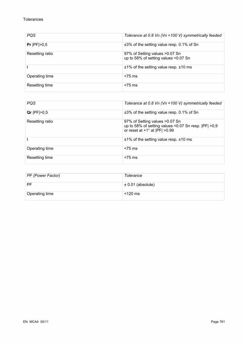
Tolerances
PQS Tolerance at 0.8 Vn (Vn =100 V) symmetrically feeded
Pr |PF|>0,5 ±3% of the setting value resp. 0.1% of Sn
Resetting ratio 97% of Setting values >0.07 Snup to 58% of setting values <0.07 Sn
t ±1% of the setting value resp. ±10 ms
Operating time <75 ms
Resetting time <75 ms
PQS Tolerance at 0.8 Vn (Vn =100 V) symmetrically feeded
Qr |PF|>0,5 ±3% of the setting value resp. 0.1% of Sn
Resetting ratio 97% of Setting values >0.07 Snup to 58% of setting values <0.07 Sn resp. |PF| >0,9 or reset at +1° at |PF| >0.99
t ±1% of the setting value resp. ±10 ms
Operating time <75 ms
Resetting time <75 ms
PF (Power Factor) Tolerance
PF ± 0.01 (absolute)
Operating time <120 ms
EN MCA4 05/11 Page 761

Assignment List
Assignment List The »ASSIGNMENT LIST« below summarizes all module outputs (signals) and inputs (e.g. states of the assignments).
Name Description
-.- No assignmentProt.available Signal: Protection is availableProt.active Signal: activeProt.ExBlo Signal: External BlockingProt.Blo TripCmd Signal: Trip Command blockedProt.ExBlo TripCmd Signal: External Blocking of the Trip CommandProt.Alarm L1 Signal: General-Alarm L1Prot.Alarm L2 Signal: General-Alarm L2Prot.Alarm L3 Signal: General-Alarm L3Prot.Alarm G Signal: General-Alarm - Earth faultProt.Alarm Signal: General AlarmProt.Trip L1 Signal: General Trip L1Prot.Trip L2 Signal: General Trip L2Prot.Trip L3 Signal: General Trip L3Prot.Trip G Signal: General Trip Ground faultProt.Trip Signal: General TripProt.Res Fault a Mains No Signal: Resetting of fault number and number of grid faults.Prot.I dir fwd Signal: Phase current failure forward directionProt.I dir rev Signal: Phase current failure reverse directionProt.I dir n poss Signal: Phase fault - missing reference voltageProt.IG calc dir fwd Signal: Ground fault (calculated) forwardProt.IG calc rev dir Signal: Ground fault (calculated) reverse directionProt.IG calc dir n poss Signal: Ground fault (calculated) direction detection not possibleProt.IG meas dir fwd Signal: Ground fault (measured) forwardProt.IG meas rev dir Signal: Ground fault (measured) reverse directionProt.IG meas dir n poss Signal: Ground fault (measured) direction detection not possibleProt.ExBlo1-I Module input state: External blocking1Prot.ExBlo2-I Module input state: External blocking2Prot.ExBlo TripCmd-I Module input state: External Blocking of the Trip CommandCtrl.Local Switching Authority: LocalCtrl.Remote Switching Authority: RemoteCtrl.NonInterl Non-Interlocking is activeCtrl.NonInterl-I Non-InterlockingSG[1].SI SingleContactInd Signal: The Position of the Switchgear is detected by one auxiliary
contact (pole) only. Thus indeterminate and disturbed Positions cannot be detected.
Page 762 EN MCA4 05/11

Assignment List
Name Description
SG[1].Pos not ON Signal: Pos not ONSG[1].Pos ON Signal: Circuit Breaker is in ON-PositionSG[1].Pos OFF Signal: Circuit Breaker is in OFF-PositionSG[1].Pos Indeterm Signal: Circuit Breaker is in Indeterminate PositionSG[1].Pos Disturb Signal: Circuit Breaker Disturbed - Undefined Breaker Position.
The Position Indicators contradict themselves. After expiring of a supervision timer this signal becomes true.
SG[1].Ready Signal: Circuit breaker is ready for operation.SG[1].t-Dwell Signal: Dwell timeSG[1].Interl ON Signal: One or more IL_On inputs are active.SG[1].Interl OFF Signal: One or more IL_Off inputs are active.SG[1].CES succesf Command Execution Supervision: Switching command executed
successfully.SG[1].CES Disturbed Command Execution Supervision: Switching Command
unsuccessful. Switchgear in disturbed position.SG[1].CES Fail TripCmd Command Excecution Supervision: Trip command not executed.SG[1].CES SwitchgDir Command Execution Supervision respectively Switching Direction
Control: This signal becomes true, if a switch command is issued even though the switchgear is already in the requested position. Example: A switchgear that is already OFF should be switched OFF again (doubly). The same applies to CLOSE commands.
SG[1].CES ON d OFF Command Execution Supervision: On Command during a pending OFF Command.
SG[1].CES SG not ready Command Execution Supervision: Switchgear not readySG[1].CES Fiel Interl Command Execution Supervision: Switching Command not
executed because of field interlocking.SG[1].CES SyncTimeout Command Execution Supervision: Switching Command not
excecuted. No Synchronization signal while t-sync was running.SG[1].Prot ON Signal: ON Command issued by the Prot moduleSG[1].TripCmd Signal: Trip CommandSG[1].Ack TripCmd Signal: Acknowledge Trip CommandSG[1].ON incl Prot ON Signal: The ON Command includes the ON Command issued by
the Protection module.SG[1].OFF incl TripCmd Signal: The OFF Command includes the OFF Command issued by
the Protection module.SG[1].Position Ind manipul Signal: Position Ind manipulSG[1].SGwear Slow SG Signal: Alarm, the circuit breaker (load-break switch) becomes
slowerSG[1].Res SGwear Sl SG Signal: Resetting the slow Switchgear AlarmSG[1].ON Cmd Signal: ON Command issued to the switchgear. Depending on the
setting the signal may include the ON command of the Prot module.
SG[1].OFF Cmd Signal: OFF Command issued to the switchgear. Depending on the setting the signal may include the OFF command of the Prot module.
EN MCA4 05/11 Page 763

Assignment List
Name Description
SG[1].ON Cmd manual Signal: ON Cmd manualSG[1].OFF Cmd manual Signal: OFF Cmd manualSG[1].Sync ON request Signal: Synchronous ON requestSG[1].Aux ON-I Position indicator/check-back signal of the CB (52a)SG[1].Aux OFF-I Module input state: Position indicator/check-back signal of the CB
(52b)SG[1].Ready-I Module input state: CB readySG[1].Sys-in-Sync-I State of the module input: This signals has to become true within
the synchronization time. If not, switching is unsuccessful.SG[1].Ack TripCmd-I State of the module input: Acknowledgement Signal (only for
automatic acknowledgement) Module input signalSG[1].Interl ON1-I State of the module input: Interlocking of the ON commandSG[1].Interl ON2-I State of the module input: Interlocking of the ON commandSG[1].Interl ON3-I State of the module input: Interlocking of the ON commandSG[1].Interl OFF1-I State of the module input: Interlocking of the OFF commandSG[1].Interl OFF2-I State of the module input: Interlocking of the OFF commandSG[1].Interl OFF3-I State of the module input: Interlocking of the OFF commandSG[1].Ack UnsucSwitchCmd-I State of the module input: Acknowledge an error signal the
signalizes an unsuccessful switching attemptSG[1].SCmd ON-I State of the module input: Switching ON Command, e.g. the state
of the Logics or the state of the digital inputSG[1].SCmd OFF-I State of the module input: Switching OFF Command, e.g. the state
of the Logics or the state of the digital inputSG[1].Operations Alarm Signal: Service Alarm, too many OperationsSG[1].Isum Intr trip: IL1 Signal: Maximum permissible Summation of the interrupting
(tripping) currents exceeded: IL1SG[1].Isum Intr trip: IL2 Signal: Maximum permissible Summation of the interrupting
(tripping) currents exceeded: IL2SG[1].Isum Intr trip: IL3 Signal: Maximum permissible Summation of the interrupting
(tripping) currents exceeded: IL3SG[1].Isum Intr trip Signal: Maximum permissible Summation of the interrupting
(tripping) currents exceeded in at least one phase.SG[1].Res TripCmd Cr Signal: Resetting of the Counter: total number of trip commandsSG[1].Res Sum trip Signal: Reset summation of the tripping currentsSG[1].WearLevel Alarm Signal: Threshold for the Alarm Level in %SG[1].WearLevel Lockout Signal: Threshold for the Lockout Level in %SG[1].Res SGwear Curve Signal: Res SGwear CurveSG[1].Isum Intr ph Alm Signal: Isum Intr ph AlmSG[1].Res Isum Intr ph Alm Signal: Res Isum Intr ph AlmSG[2].SI SingleContactInd Signal: The Position of the Switchgear is detected by one auxiliary
contact (pole) only. Thus indeterminate and disturbed Positions cannot be detected.
SG[2].Pos not ON Signal: Pos not ON
Page 764 EN MCA4 05/11

Assignment List
Name Description
SG[2].Pos ON Signal: Circuit Breaker is in ON-PositionSG[2].Pos OFF Signal: Circuit Breaker is in OFF-PositionSG[2].Pos Indeterm Signal: Circuit Breaker is in Indeterminate PositionSG[2].Pos Disturb Signal: Circuit Breaker Disturbed - Undefined Breaker Position.
The Position Indicators contradict themselves. After expiring of a supervision timer this signal becomes true.
SG[2].Ready Signal: Circuit breaker is ready for operation.SG[2].t-Dwell Signal: Dwell timeSG[2].Interl ON Signal: One or more IL_On inputs are active.SG[2].Interl OFF Signal: One or more IL_Off inputs are active.SG[2].CES succesf Command Execution Supervision: Switching command executed
successfully.SG[2].CES Disturbed Command Execution Supervision: Switching Command
unsuccessful. Switchgear in disturbed position.SG[2].CES Fail TripCmd Command Excecution Supervision: Trip command not executed.SG[2].CES SwitchgDir Command Execution Supervision respectively Switching Direction
Control: This signal becomes true, if a switch command is issued even though the switchgear is already in the requested position. Example: A switchgear that is already OFF should be switched OFF again (doubly). The same applies to CLOSE commands.
SG[2].CES ON d OFF Command Execution Supervision: On Command during a pending OFF Command.
SG[2].CES SG not ready Command Execution Supervision: Switchgear not readySG[2].CES Fiel Interl Command Execution Supervision: Switching Command not
executed because of field interlocking.SG[2].CES SyncTimeout Command Execution Supervision: Switching Command not
excecuted. No Synchronization signal while t-sync was running.SG[2].Prot ON Signal: ON Command issued by the Prot moduleSG[2].TripCmd Signal: Trip CommandSG[2].Ack TripCmd Signal: Acknowledge Trip CommandSG[2].ON incl Prot ON Signal: The ON Command includes the ON Command issued by
the Protection module.SG[2].OFF incl TripCmd Signal: The OFF Command includes the OFF Command issued by
the Protection module.SG[2].Position Ind manipul Signal: Position Ind manipulSG[2].SGwear Slow SG Signal: Alarm, the circuit breaker (load-break switch) becomes
slowerSG[2].Res SGwear Sl SG Signal: Resetting the slow Switchgear AlarmSG[2].ON Cmd Signal: ON Command issued to the switchgear. Depending on the
setting the signal may include the ON command of the Prot module.
SG[2].OFF Cmd Signal: OFF Command issued to the switchgear. Depending on the setting the signal may include the OFF command of the Prot module.
SG[2].ON Cmd manual Signal: ON Cmd manual
EN MCA4 05/11 Page 765

Assignment List
Name Description
SG[2].OFF Cmd manual Signal: OFF Cmd manualSG[2].Sync ON request Signal: Synchronous ON requestSG[2].Aux ON-I Position indicator/check-back signal of the CB (52a)SG[2].Aux OFF-I Module input state: Position indicator/check-back signal of the CB
(52b)SG[2].Ready-I Module input state: CB readySG[2].Sys-in-Sync-I State of the module input: This signals has to become true within
the synchronization time. If not, switching is unsuccessful.SG[2].Ack TripCmd-I State of the module input: Acknowledgement Signal (only for
automatic acknowledgement) Module input signalSG[2].Interl ON1-I State of the module input: Interlocking of the ON commandSG[2].Interl ON2-I State of the module input: Interlocking of the ON commandSG[2].Interl ON3-I State of the module input: Interlocking of the ON commandSG[2].Interl OFF1-I State of the module input: Interlocking of the OFF commandSG[2].Interl OFF2-I State of the module input: Interlocking of the OFF commandSG[2].Interl OFF3-I State of the module input: Interlocking of the OFF commandSG[2].Ack UnsucSwitchCmd-I State of the module input: Acknowledge an error signal the
signalizes an unsuccessful switching attemptSG[2].SCmd ON-I State of the module input: Switching ON Command, e.g. the state
of the Logics or the state of the digital inputSG[2].SCmd OFF-I State of the module input: Switching OFF Command, e.g. the state
of the Logics or the state of the digital inputSG[2].Operations Alarm Signal: Service Alarm, too many OperationsSG[2].Isum Intr trip: IL1 Signal: Maximum permissible Summation of the interrupting
(tripping) currents exceeded: IL1SG[2].Isum Intr trip: IL2 Signal: Maximum permissible Summation of the interrupting
(tripping) currents exceeded: IL2SG[2].Isum Intr trip: IL3 Signal: Maximum permissible Summation of the interrupting
(tripping) currents exceeded: IL3SG[2].Isum Intr trip Signal: Maximum permissible Summation of the interrupting
(tripping) currents exceeded in at least one phase.SG[2].Res TripCmd Cr Signal: Resetting of the Counter: total number of trip commandsSG[2].Res Sum trip Signal: Reset summation of the tripping currentsSG[2].WearLevel Alarm Signal: Threshold for the Alarm Level in %SG[2].WearLevel Lockout Signal: Threshold for the Lockout Level in %SG[2].Res SGwear Curve Signal: Res SGwear CurveSG[2].Isum Intr ph Alm Signal: Isum Intr ph AlmSG[2].Res Isum Intr ph Alm Signal: Res Isum Intr ph AlmSG[3].SI SingleContactInd Signal: The Position of the Switchgear is detected by one auxiliary
contact (pole) only. Thus indeterminate and disturbed Positions cannot be detected.
SG[3].Pos not ON Signal: Pos not ONSG[3].Pos ON Signal: Circuit Breaker is in ON-Position
Page 766 EN MCA4 05/11
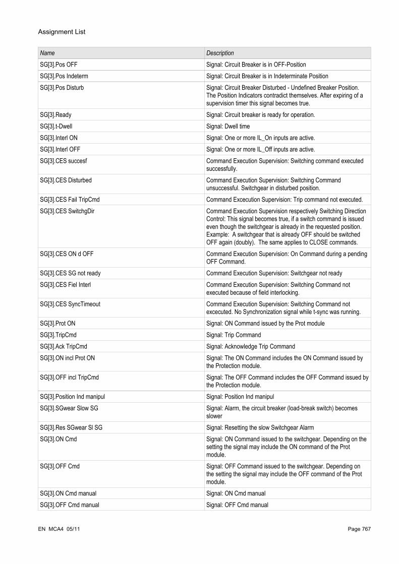
Assignment List
Name Description
SG[3].Pos OFF Signal: Circuit Breaker is in OFF-PositionSG[3].Pos Indeterm Signal: Circuit Breaker is in Indeterminate PositionSG[3].Pos Disturb Signal: Circuit Breaker Disturbed - Undefined Breaker Position.
The Position Indicators contradict themselves. After expiring of a supervision timer this signal becomes true.
SG[3].Ready Signal: Circuit breaker is ready for operation.SG[3].t-Dwell Signal: Dwell timeSG[3].Interl ON Signal: One or more IL_On inputs are active.SG[3].Interl OFF Signal: One or more IL_Off inputs are active.SG[3].CES succesf Command Execution Supervision: Switching command executed
successfully.SG[3].CES Disturbed Command Execution Supervision: Switching Command
unsuccessful. Switchgear in disturbed position.SG[3].CES Fail TripCmd Command Excecution Supervision: Trip command not executed.SG[3].CES SwitchgDir Command Execution Supervision respectively Switching Direction
Control: This signal becomes true, if a switch command is issued even though the switchgear is already in the requested position. Example: A switchgear that is already OFF should be switched OFF again (doubly). The same applies to CLOSE commands.
SG[3].CES ON d OFF Command Execution Supervision: On Command during a pending OFF Command.
SG[3].CES SG not ready Command Execution Supervision: Switchgear not readySG[3].CES Fiel Interl Command Execution Supervision: Switching Command not
executed because of field interlocking.SG[3].CES SyncTimeout Command Execution Supervision: Switching Command not
excecuted. No Synchronization signal while t-sync was running.SG[3].Prot ON Signal: ON Command issued by the Prot moduleSG[3].TripCmd Signal: Trip CommandSG[3].Ack TripCmd Signal: Acknowledge Trip CommandSG[3].ON incl Prot ON Signal: The ON Command includes the ON Command issued by
the Protection module.SG[3].OFF incl TripCmd Signal: The OFF Command includes the OFF Command issued by
the Protection module.SG[3].Position Ind manipul Signal: Position Ind manipulSG[3].SGwear Slow SG Signal: Alarm, the circuit breaker (load-break switch) becomes
slowerSG[3].Res SGwear Sl SG Signal: Resetting the slow Switchgear AlarmSG[3].ON Cmd Signal: ON Command issued to the switchgear. Depending on the
setting the signal may include the ON command of the Prot module.
SG[3].OFF Cmd Signal: OFF Command issued to the switchgear. Depending on the setting the signal may include the OFF command of the Prot module.
SG[3].ON Cmd manual Signal: ON Cmd manualSG[3].OFF Cmd manual Signal: OFF Cmd manual
EN MCA4 05/11 Page 767
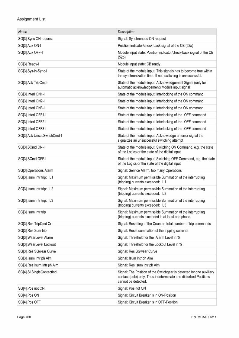
Assignment List
Name Description
SG[3].Sync ON request Signal: Synchronous ON requestSG[3].Aux ON-I Position indicator/check-back signal of the CB (52a)SG[3].Aux OFF-I Module input state: Position indicator/check-back signal of the CB
(52b)SG[3].Ready-I Module input state: CB readySG[3].Sys-in-Sync-I State of the module input: This signals has to become true within
the synchronization time. If not, switching is unsuccessful.SG[3].Ack TripCmd-I State of the module input: Acknowledgement Signal (only for
automatic acknowledgement) Module input signalSG[3].Interl ON1-I State of the module input: Interlocking of the ON commandSG[3].Interl ON2-I State of the module input: Interlocking of the ON commandSG[3].Interl ON3-I State of the module input: Interlocking of the ON commandSG[3].Interl OFF1-I State of the module input: Interlocking of the OFF commandSG[3].Interl OFF2-I State of the module input: Interlocking of the OFF commandSG[3].Interl OFF3-I State of the module input: Interlocking of the OFF commandSG[3].Ack UnsucSwitchCmd-I State of the module input: Acknowledge an error signal the
signalizes an unsuccessful switching attemptSG[3].SCmd ON-I State of the module input: Switching ON Command, e.g. the state
of the Logics or the state of the digital inputSG[3].SCmd OFF-I State of the module input: Switching OFF Command, e.g. the state
of the Logics or the state of the digital inputSG[3].Operations Alarm Signal: Service Alarm, too many OperationsSG[3].Isum Intr trip: IL1 Signal: Maximum permissible Summation of the interrupting
(tripping) currents exceeded: IL1SG[3].Isum Intr trip: IL2 Signal: Maximum permissible Summation of the interrupting
(tripping) currents exceeded: IL2SG[3].Isum Intr trip: IL3 Signal: Maximum permissible Summation of the interrupting
(tripping) currents exceeded: IL3SG[3].Isum Intr trip Signal: Maximum permissible Summation of the interrupting
(tripping) currents exceeded in at least one phase.SG[3].Res TripCmd Cr Signal: Resetting of the Counter: total number of trip commandsSG[3].Res Sum trip Signal: Reset summation of the tripping currentsSG[3].WearLevel Alarm Signal: Threshold for the Alarm Level in %SG[3].WearLevel Lockout Signal: Threshold for the Lockout Level in %SG[3].Res SGwear Curve Signal: Res SGwear CurveSG[3].Isum Intr ph Alm Signal: Isum Intr ph AlmSG[3].Res Isum Intr ph Alm Signal: Res Isum Intr ph AlmSG[4].SI SingleContactInd Signal: The Position of the Switchgear is detected by one auxiliary
contact (pole) only. Thus indeterminate and disturbed Positions cannot be detected.
SG[4].Pos not ON Signal: Pos not ONSG[4].Pos ON Signal: Circuit Breaker is in ON-PositionSG[4].Pos OFF Signal: Circuit Breaker is in OFF-Position
Page 768 EN MCA4 05/11
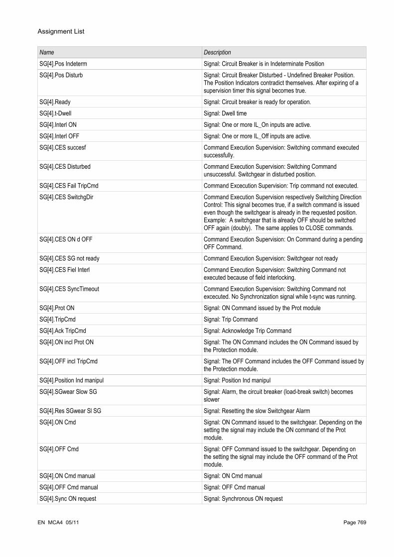
Assignment List
Name Description
SG[4].Pos Indeterm Signal: Circuit Breaker is in Indeterminate PositionSG[4].Pos Disturb Signal: Circuit Breaker Disturbed - Undefined Breaker Position.
The Position Indicators contradict themselves. After expiring of a supervision timer this signal becomes true.
SG[4].Ready Signal: Circuit breaker is ready for operation.SG[4].t-Dwell Signal: Dwell timeSG[4].Interl ON Signal: One or more IL_On inputs are active.SG[4].Interl OFF Signal: One or more IL_Off inputs are active.SG[4].CES succesf Command Execution Supervision: Switching command executed
successfully.SG[4].CES Disturbed Command Execution Supervision: Switching Command
unsuccessful. Switchgear in disturbed position.SG[4].CES Fail TripCmd Command Excecution Supervision: Trip command not executed.SG[4].CES SwitchgDir Command Execution Supervision respectively Switching Direction
Control: This signal becomes true, if a switch command is issued even though the switchgear is already in the requested position. Example: A switchgear that is already OFF should be switched OFF again (doubly). The same applies to CLOSE commands.
SG[4].CES ON d OFF Command Execution Supervision: On Command during a pending OFF Command.
SG[4].CES SG not ready Command Execution Supervision: Switchgear not readySG[4].CES Fiel Interl Command Execution Supervision: Switching Command not
executed because of field interlocking.SG[4].CES SyncTimeout Command Execution Supervision: Switching Command not
excecuted. No Synchronization signal while t-sync was running.SG[4].Prot ON Signal: ON Command issued by the Prot moduleSG[4].TripCmd Signal: Trip CommandSG[4].Ack TripCmd Signal: Acknowledge Trip CommandSG[4].ON incl Prot ON Signal: The ON Command includes the ON Command issued by
the Protection module.SG[4].OFF incl TripCmd Signal: The OFF Command includes the OFF Command issued by
the Protection module.SG[4].Position Ind manipul Signal: Position Ind manipulSG[4].SGwear Slow SG Signal: Alarm, the circuit breaker (load-break switch) becomes
slowerSG[4].Res SGwear Sl SG Signal: Resetting the slow Switchgear AlarmSG[4].ON Cmd Signal: ON Command issued to the switchgear. Depending on the
setting the signal may include the ON command of the Prot module.
SG[4].OFF Cmd Signal: OFF Command issued to the switchgear. Depending on the setting the signal may include the OFF command of the Prot module.
SG[4].ON Cmd manual Signal: ON Cmd manualSG[4].OFF Cmd manual Signal: OFF Cmd manualSG[4].Sync ON request Signal: Synchronous ON request
EN MCA4 05/11 Page 769
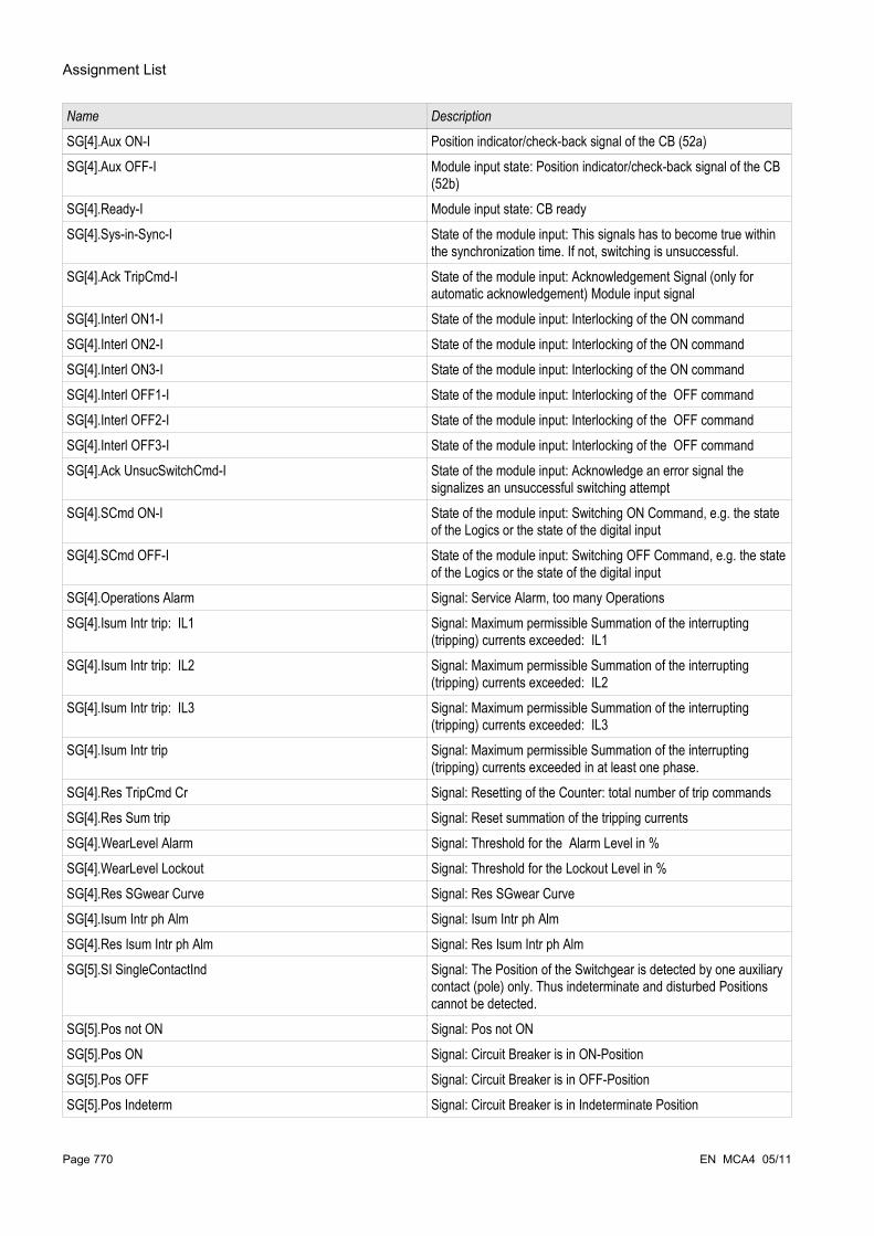
Assignment List
Name Description
SG[4].Aux ON-I Position indicator/check-back signal of the CB (52a)SG[4].Aux OFF-I Module input state: Position indicator/check-back signal of the CB
(52b)SG[4].Ready-I Module input state: CB readySG[4].Sys-in-Sync-I State of the module input: This signals has to become true within
the synchronization time. If not, switching is unsuccessful.SG[4].Ack TripCmd-I State of the module input: Acknowledgement Signal (only for
automatic acknowledgement) Module input signalSG[4].Interl ON1-I State of the module input: Interlocking of the ON commandSG[4].Interl ON2-I State of the module input: Interlocking of the ON commandSG[4].Interl ON3-I State of the module input: Interlocking of the ON commandSG[4].Interl OFF1-I State of the module input: Interlocking of the OFF commandSG[4].Interl OFF2-I State of the module input: Interlocking of the OFF commandSG[4].Interl OFF3-I State of the module input: Interlocking of the OFF commandSG[4].Ack UnsucSwitchCmd-I State of the module input: Acknowledge an error signal the
signalizes an unsuccessful switching attemptSG[4].SCmd ON-I State of the module input: Switching ON Command, e.g. the state
of the Logics or the state of the digital inputSG[4].SCmd OFF-I State of the module input: Switching OFF Command, e.g. the state
of the Logics or the state of the digital inputSG[4].Operations Alarm Signal: Service Alarm, too many OperationsSG[4].Isum Intr trip: IL1 Signal: Maximum permissible Summation of the interrupting
(tripping) currents exceeded: IL1SG[4].Isum Intr trip: IL2 Signal: Maximum permissible Summation of the interrupting
(tripping) currents exceeded: IL2SG[4].Isum Intr trip: IL3 Signal: Maximum permissible Summation of the interrupting
(tripping) currents exceeded: IL3SG[4].Isum Intr trip Signal: Maximum permissible Summation of the interrupting
(tripping) currents exceeded in at least one phase.SG[4].Res TripCmd Cr Signal: Resetting of the Counter: total number of trip commandsSG[4].Res Sum trip Signal: Reset summation of the tripping currentsSG[4].WearLevel Alarm Signal: Threshold for the Alarm Level in %SG[4].WearLevel Lockout Signal: Threshold for the Lockout Level in %SG[4].Res SGwear Curve Signal: Res SGwear CurveSG[4].Isum Intr ph Alm Signal: Isum Intr ph AlmSG[4].Res Isum Intr ph Alm Signal: Res Isum Intr ph AlmSG[5].SI SingleContactInd Signal: The Position of the Switchgear is detected by one auxiliary
contact (pole) only. Thus indeterminate and disturbed Positions cannot be detected.
SG[5].Pos not ON Signal: Pos not ONSG[5].Pos ON Signal: Circuit Breaker is in ON-PositionSG[5].Pos OFF Signal: Circuit Breaker is in OFF-PositionSG[5].Pos Indeterm Signal: Circuit Breaker is in Indeterminate Position
Page 770 EN MCA4 05/11

Assignment List
Name Description
SG[5].Pos Disturb Signal: Circuit Breaker Disturbed - Undefined Breaker Position. The Position Indicators contradict themselves. After expiring of a supervision timer this signal becomes true.
SG[5].Ready Signal: Circuit breaker is ready for operation.SG[5].t-Dwell Signal: Dwell timeSG[5].Interl ON Signal: One or more IL_On inputs are active.SG[5].Interl OFF Signal: One or more IL_Off inputs are active.SG[5].CES succesf Command Execution Supervision: Switching command executed
successfully.SG[5].CES Disturbed Command Execution Supervision: Switching Command
unsuccessful. Switchgear in disturbed position.SG[5].CES Fail TripCmd Command Excecution Supervision: Trip command not executed.SG[5].CES SwitchgDir Command Execution Supervision respectively Switching Direction
Control: This signal becomes true, if a switch command is issued even though the switchgear is already in the requested position. Example: A switchgear that is already OFF should be switched OFF again (doubly). The same applies to CLOSE commands.
SG[5].CES ON d OFF Command Execution Supervision: On Command during a pending OFF Command.
SG[5].CES SG not ready Command Execution Supervision: Switchgear not readySG[5].CES Fiel Interl Command Execution Supervision: Switching Command not
executed because of field interlocking.SG[5].CES SyncTimeout Command Execution Supervision: Switching Command not
excecuted. No Synchronization signal while t-sync was running.SG[5].Prot ON Signal: ON Command issued by the Prot moduleSG[5].TripCmd Signal: Trip CommandSG[5].Ack TripCmd Signal: Acknowledge Trip CommandSG[5].ON incl Prot ON Signal: The ON Command includes the ON Command issued by
the Protection module.SG[5].OFF incl TripCmd Signal: The OFF Command includes the OFF Command issued by
the Protection module.SG[5].Position Ind manipul Signal: Position Ind manipulSG[5].SGwear Slow SG Signal: Alarm, the circuit breaker (load-break switch) becomes
slowerSG[5].Res SGwear Sl SG Signal: Resetting the slow Switchgear AlarmSG[5].ON Cmd Signal: ON Command issued to the switchgear. Depending on the
setting the signal may include the ON command of the Prot module.
SG[5].OFF Cmd Signal: OFF Command issued to the switchgear. Depending on the setting the signal may include the OFF command of the Prot module.
SG[5].ON Cmd manual Signal: ON Cmd manualSG[5].OFF Cmd manual Signal: OFF Cmd manualSG[5].Sync ON request Signal: Synchronous ON requestSG[5].Aux ON-I Position indicator/check-back signal of the CB (52a)
EN MCA4 05/11 Page 771

Assignment List
Name Description
SG[5].Aux OFF-I Module input state: Position indicator/check-back signal of the CB (52b)
SG[5].Ready-I Module input state: CB readySG[5].Sys-in-Sync-I State of the module input: This signals has to become true within
the synchronization time. If not, switching is unsuccessful.SG[5].Ack TripCmd-I State of the module input: Acknowledgement Signal (only for
automatic acknowledgement) Module input signalSG[5].Interl ON1-I State of the module input: Interlocking of the ON commandSG[5].Interl ON2-I State of the module input: Interlocking of the ON commandSG[5].Interl ON3-I State of the module input: Interlocking of the ON commandSG[5].Interl OFF1-I State of the module input: Interlocking of the OFF commandSG[5].Interl OFF2-I State of the module input: Interlocking of the OFF commandSG[5].Interl OFF3-I State of the module input: Interlocking of the OFF commandSG[5].Ack UnsucSwitchCmd-I State of the module input: Acknowledge an error signal the
signalizes an unsuccessful switching attemptSG[5].SCmd ON-I State of the module input: Switching ON Command, e.g. the state
of the Logics or the state of the digital inputSG[5].SCmd OFF-I State of the module input: Switching OFF Command, e.g. the state
of the Logics or the state of the digital inputSG[5].Operations Alarm Signal: Service Alarm, too many OperationsSG[5].Isum Intr trip: IL1 Signal: Maximum permissible Summation of the interrupting
(tripping) currents exceeded: IL1SG[5].Isum Intr trip: IL2 Signal: Maximum permissible Summation of the interrupting
(tripping) currents exceeded: IL2SG[5].Isum Intr trip: IL3 Signal: Maximum permissible Summation of the interrupting
(tripping) currents exceeded: IL3SG[5].Isum Intr trip Signal: Maximum permissible Summation of the interrupting
(tripping) currents exceeded in at least one phase.SG[5].Res TripCmd Cr Signal: Resetting of the Counter: total number of trip commandsSG[5].Res Sum trip Signal: Reset summation of the tripping currentsSG[5].WearLevel Alarm Signal: Threshold for the Alarm Level in %SG[5].WearLevel Lockout Signal: Threshold for the Lockout Level in %SG[5].Res SGwear Curve Signal: Res SGwear CurveSG[5].Isum Intr ph Alm Signal: Isum Intr ph AlmSG[5].Res Isum Intr ph Alm Signal: Res Isum Intr ph AlmSG[6].SI SingleContactInd Signal: The Position of the Switchgear is detected by one auxiliary
contact (pole) only. Thus indeterminate and disturbed Positions cannot be detected.
SG[6].Pos not ON Signal: Pos not ONSG[6].Pos ON Signal: Circuit Breaker is in ON-PositionSG[6].Pos OFF Signal: Circuit Breaker is in OFF-PositionSG[6].Pos Indeterm Signal: Circuit Breaker is in Indeterminate Position
Page 772 EN MCA4 05/11
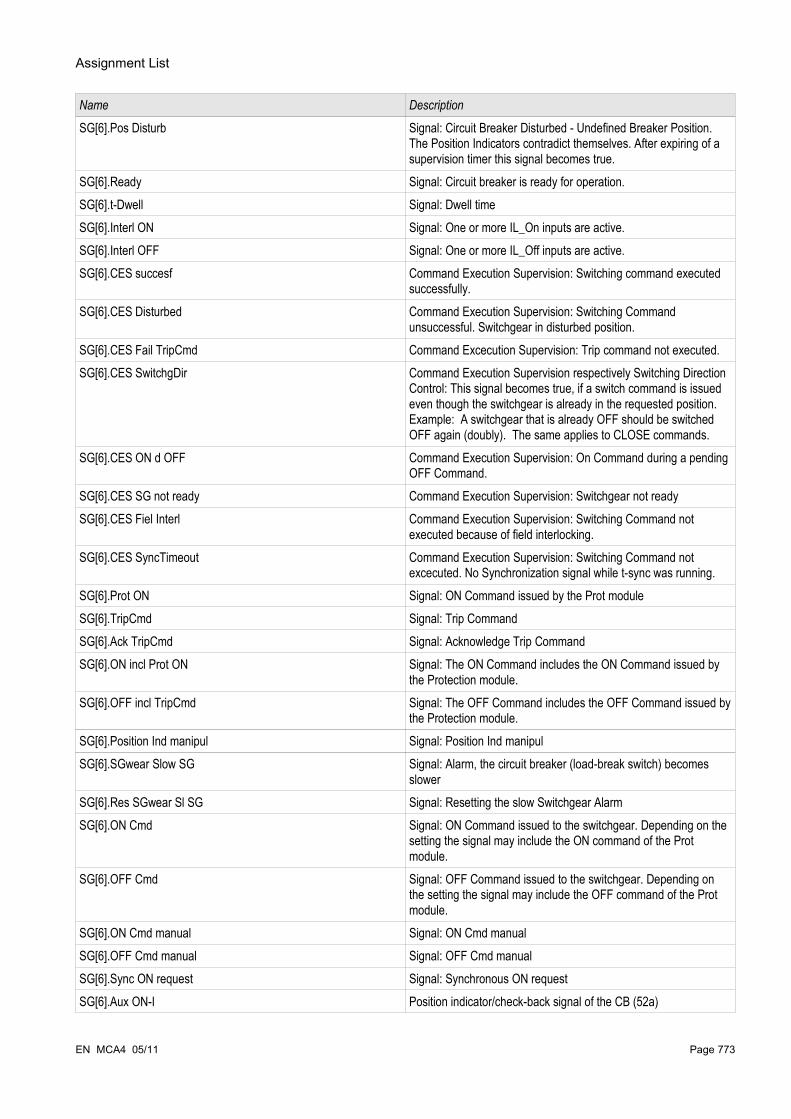
Assignment List
Name Description
SG[6].Pos Disturb Signal: Circuit Breaker Disturbed - Undefined Breaker Position. The Position Indicators contradict themselves. After expiring of a supervision timer this signal becomes true.
SG[6].Ready Signal: Circuit breaker is ready for operation.SG[6].t-Dwell Signal: Dwell timeSG[6].Interl ON Signal: One or more IL_On inputs are active.SG[6].Interl OFF Signal: One or more IL_Off inputs are active.SG[6].CES succesf Command Execution Supervision: Switching command executed
successfully.SG[6].CES Disturbed Command Execution Supervision: Switching Command
unsuccessful. Switchgear in disturbed position.SG[6].CES Fail TripCmd Command Excecution Supervision: Trip command not executed.SG[6].CES SwitchgDir Command Execution Supervision respectively Switching Direction
Control: This signal becomes true, if a switch command is issued even though the switchgear is already in the requested position. Example: A switchgear that is already OFF should be switched OFF again (doubly). The same applies to CLOSE commands.
SG[6].CES ON d OFF Command Execution Supervision: On Command during a pending OFF Command.
SG[6].CES SG not ready Command Execution Supervision: Switchgear not readySG[6].CES Fiel Interl Command Execution Supervision: Switching Command not
executed because of field interlocking.SG[6].CES SyncTimeout Command Execution Supervision: Switching Command not
excecuted. No Synchronization signal while t-sync was running.SG[6].Prot ON Signal: ON Command issued by the Prot moduleSG[6].TripCmd Signal: Trip CommandSG[6].Ack TripCmd Signal: Acknowledge Trip CommandSG[6].ON incl Prot ON Signal: The ON Command includes the ON Command issued by
the Protection module.SG[6].OFF incl TripCmd Signal: The OFF Command includes the OFF Command issued by
the Protection module.SG[6].Position Ind manipul Signal: Position Ind manipulSG[6].SGwear Slow SG Signal: Alarm, the circuit breaker (load-break switch) becomes
slowerSG[6].Res SGwear Sl SG Signal: Resetting the slow Switchgear AlarmSG[6].ON Cmd Signal: ON Command issued to the switchgear. Depending on the
setting the signal may include the ON command of the Prot module.
SG[6].OFF Cmd Signal: OFF Command issued to the switchgear. Depending on the setting the signal may include the OFF command of the Prot module.
SG[6].ON Cmd manual Signal: ON Cmd manualSG[6].OFF Cmd manual Signal: OFF Cmd manualSG[6].Sync ON request Signal: Synchronous ON requestSG[6].Aux ON-I Position indicator/check-back signal of the CB (52a)
EN MCA4 05/11 Page 773

Assignment List
Name Description
SG[6].Aux OFF-I Module input state: Position indicator/check-back signal of the CB (52b)
SG[6].Ready-I Module input state: CB readySG[6].Sys-in-Sync-I State of the module input: This signals has to become true within
the synchronization time. If not, switching is unsuccessful.SG[6].Ack TripCmd-I State of the module input: Acknowledgement Signal (only for
automatic acknowledgement) Module input signalSG[6].Interl ON1-I State of the module input: Interlocking of the ON commandSG[6].Interl ON2-I State of the module input: Interlocking of the ON commandSG[6].Interl ON3-I State of the module input: Interlocking of the ON commandSG[6].Interl OFF1-I State of the module input: Interlocking of the OFF commandSG[6].Interl OFF2-I State of the module input: Interlocking of the OFF commandSG[6].Interl OFF3-I State of the module input: Interlocking of the OFF commandSG[6].Ack UnsucSwitchCmd-I State of the module input: Acknowledge an error signal the
signalizes an unsuccessful switching attemptSG[6].SCmd ON-I State of the module input: Switching ON Command, e.g. the state
of the Logics or the state of the digital inputSG[6].SCmd OFF-I State of the module input: Switching OFF Command, e.g. the state
of the Logics or the state of the digital inputSG[6].Operations Alarm Signal: Service Alarm, too many OperationsSG[6].Isum Intr trip: IL1 Signal: Maximum permissible Summation of the interrupting
(tripping) currents exceeded: IL1SG[6].Isum Intr trip: IL2 Signal: Maximum permissible Summation of the interrupting
(tripping) currents exceeded: IL2SG[6].Isum Intr trip: IL3 Signal: Maximum permissible Summation of the interrupting
(tripping) currents exceeded: IL3SG[6].Isum Intr trip Signal: Maximum permissible Summation of the interrupting
(tripping) currents exceeded in at least one phase.SG[6].Res TripCmd Cr Signal: Resetting of the Counter: total number of trip commandsSG[6].Res Sum trip Signal: Reset summation of the tripping currentsSG[6].WearLevel Alarm Signal: Threshold for the Alarm Level in %SG[6].WearLevel Lockout Signal: Threshold for the Lockout Level in %SG[6].Res SGwear Curve Signal: Res SGwear CurveSG[6].Isum Intr ph Alm Signal: Isum Intr ph AlmSG[6].Res Isum Intr ph Alm Signal: Res Isum Intr ph AlmI[1].active Signal: activeI[1].ExBlo Signal: External BlockingI[1].Ex rev Interl Signal: External reverse InterlockingI[1].Blo TripCmd Signal: Trip Command blockedI[1].ExBlo TripCmd Signal: External Blocking of the Trip CommandI[1].IH2 Blo Signal: Blocking the trip command by an inrushI[1].Alarm L1 Signal: Alarm L1
Page 774 EN MCA4 05/11
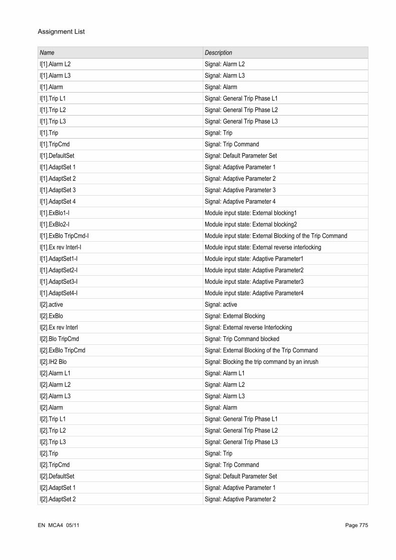
Assignment List
Name Description
I[1].Alarm L2 Signal: Alarm L2I[1].Alarm L3 Signal: Alarm L3I[1].Alarm Signal: AlarmI[1].Trip L1 Signal: General Trip Phase L1I[1].Trip L2 Signal: General Trip Phase L2I[1].Trip L3 Signal: General Trip Phase L3I[1].Trip Signal: TripI[1].TripCmd Signal: Trip CommandI[1].DefaultSet Signal: Default Parameter SetI[1].AdaptSet 1 Signal: Adaptive Parameter 1I[1].AdaptSet 2 Signal: Adaptive Parameter 2I[1].AdaptSet 3 Signal: Adaptive Parameter 3I[1].AdaptSet 4 Signal: Adaptive Parameter 4I[1].ExBlo1-I Module input state: External blocking1I[1].ExBlo2-I Module input state: External blocking2I[1].ExBlo TripCmd-I Module input state: External Blocking of the Trip CommandI[1].Ex rev Interl-I Module input state: External reverse interlockingI[1].AdaptSet1-I Module input state: Adaptive Parameter1I[1].AdaptSet2-I Module input state: Adaptive Parameter2I[1].AdaptSet3-I Module input state: Adaptive Parameter3I[1].AdaptSet4-I Module input state: Adaptive Parameter4I[2].active Signal: activeI[2].ExBlo Signal: External BlockingI[2].Ex rev Interl Signal: External reverse InterlockingI[2].Blo TripCmd Signal: Trip Command blockedI[2].ExBlo TripCmd Signal: External Blocking of the Trip CommandI[2].IH2 Blo Signal: Blocking the trip command by an inrushI[2].Alarm L1 Signal: Alarm L1I[2].Alarm L2 Signal: Alarm L2I[2].Alarm L3 Signal: Alarm L3I[2].Alarm Signal: AlarmI[2].Trip L1 Signal: General Trip Phase L1I[2].Trip L2 Signal: General Trip Phase L2I[2].Trip L3 Signal: General Trip Phase L3I[2].Trip Signal: TripI[2].TripCmd Signal: Trip CommandI[2].DefaultSet Signal: Default Parameter SetI[2].AdaptSet 1 Signal: Adaptive Parameter 1I[2].AdaptSet 2 Signal: Adaptive Parameter 2
EN MCA4 05/11 Page 775

Assignment List
Name Description
I[2].AdaptSet 3 Signal: Adaptive Parameter 3I[2].AdaptSet 4 Signal: Adaptive Parameter 4I[2].ExBlo1-I Module input state: External blocking1I[2].ExBlo2-I Module input state: External blocking2I[2].ExBlo TripCmd-I Module input state: External Blocking of the Trip CommandI[2].Ex rev Interl-I Module input state: External reverse interlockingI[2].AdaptSet1-I Module input state: Adaptive Parameter1I[2].AdaptSet2-I Module input state: Adaptive Parameter2I[2].AdaptSet3-I Module input state: Adaptive Parameter3I[2].AdaptSet4-I Module input state: Adaptive Parameter4I[3].active Signal: activeI[3].ExBlo Signal: External BlockingI[3].Ex rev Interl Signal: External reverse InterlockingI[3].Blo TripCmd Signal: Trip Command blockedI[3].ExBlo TripCmd Signal: External Blocking of the Trip CommandI[3].IH2 Blo Signal: Blocking the trip command by an inrushI[3].Alarm L1 Signal: Alarm L1I[3].Alarm L2 Signal: Alarm L2I[3].Alarm L3 Signal: Alarm L3I[3].Alarm Signal: AlarmI[3].Trip L1 Signal: General Trip Phase L1I[3].Trip L2 Signal: General Trip Phase L2I[3].Trip L3 Signal: General Trip Phase L3I[3].Trip Signal: TripI[3].TripCmd Signal: Trip CommandI[3].DefaultSet Signal: Default Parameter SetI[3].AdaptSet 1 Signal: Adaptive Parameter 1I[3].AdaptSet 2 Signal: Adaptive Parameter 2I[3].AdaptSet 3 Signal: Adaptive Parameter 3I[3].AdaptSet 4 Signal: Adaptive Parameter 4I[3].ExBlo1-I Module input state: External blocking1I[3].ExBlo2-I Module input state: External blocking2I[3].ExBlo TripCmd-I Module input state: External Blocking of the Trip CommandI[3].Ex rev Interl-I Module input state: External reverse interlockingI[3].AdaptSet1-I Module input state: Adaptive Parameter1I[3].AdaptSet2-I Module input state: Adaptive Parameter2I[3].AdaptSet3-I Module input state: Adaptive Parameter3I[3].AdaptSet4-I Module input state: Adaptive Parameter4I[4].active Signal: active
Page 776 EN MCA4 05/11
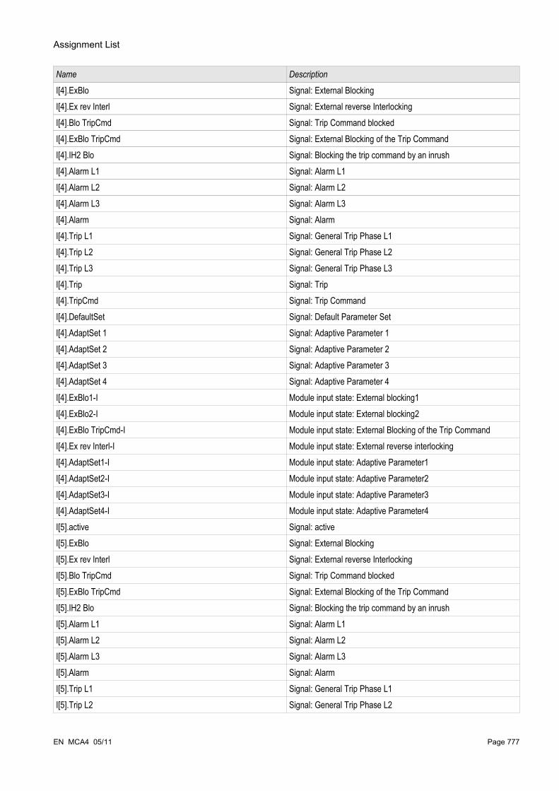
Assignment List
Name Description
I[4].ExBlo Signal: External BlockingI[4].Ex rev Interl Signal: External reverse InterlockingI[4].Blo TripCmd Signal: Trip Command blockedI[4].ExBlo TripCmd Signal: External Blocking of the Trip CommandI[4].IH2 Blo Signal: Blocking the trip command by an inrushI[4].Alarm L1 Signal: Alarm L1I[4].Alarm L2 Signal: Alarm L2I[4].Alarm L3 Signal: Alarm L3I[4].Alarm Signal: AlarmI[4].Trip L1 Signal: General Trip Phase L1I[4].Trip L2 Signal: General Trip Phase L2I[4].Trip L3 Signal: General Trip Phase L3I[4].Trip Signal: TripI[4].TripCmd Signal: Trip CommandI[4].DefaultSet Signal: Default Parameter SetI[4].AdaptSet 1 Signal: Adaptive Parameter 1I[4].AdaptSet 2 Signal: Adaptive Parameter 2I[4].AdaptSet 3 Signal: Adaptive Parameter 3I[4].AdaptSet 4 Signal: Adaptive Parameter 4I[4].ExBlo1-I Module input state: External blocking1I[4].ExBlo2-I Module input state: External blocking2I[4].ExBlo TripCmd-I Module input state: External Blocking of the Trip CommandI[4].Ex rev Interl-I Module input state: External reverse interlockingI[4].AdaptSet1-I Module input state: Adaptive Parameter1I[4].AdaptSet2-I Module input state: Adaptive Parameter2I[4].AdaptSet3-I Module input state: Adaptive Parameter3I[4].AdaptSet4-I Module input state: Adaptive Parameter4I[5].active Signal: activeI[5].ExBlo Signal: External BlockingI[5].Ex rev Interl Signal: External reverse InterlockingI[5].Blo TripCmd Signal: Trip Command blockedI[5].ExBlo TripCmd Signal: External Blocking of the Trip CommandI[5].IH2 Blo Signal: Blocking the trip command by an inrushI[5].Alarm L1 Signal: Alarm L1I[5].Alarm L2 Signal: Alarm L2I[5].Alarm L3 Signal: Alarm L3I[5].Alarm Signal: AlarmI[5].Trip L1 Signal: General Trip Phase L1I[5].Trip L2 Signal: General Trip Phase L2
EN MCA4 05/11 Page 777
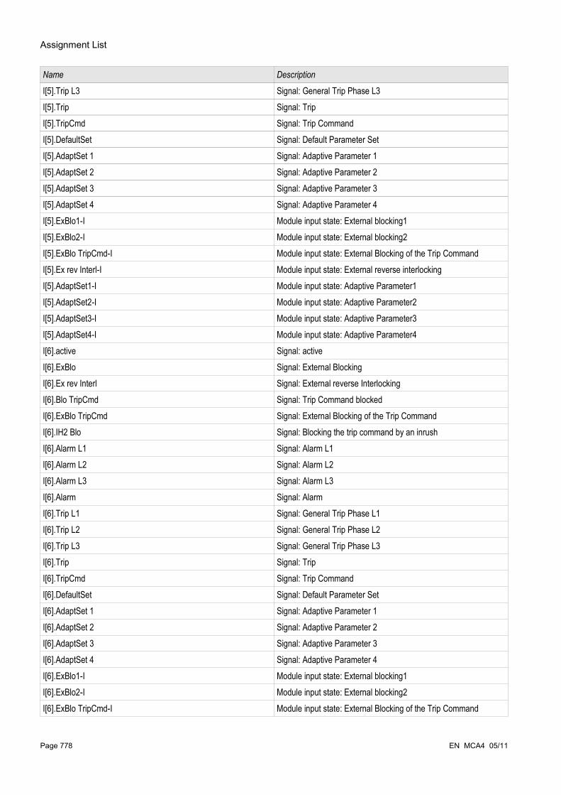
Assignment List
Name Description
I[5].Trip L3 Signal: General Trip Phase L3I[5].Trip Signal: TripI[5].TripCmd Signal: Trip CommandI[5].DefaultSet Signal: Default Parameter SetI[5].AdaptSet 1 Signal: Adaptive Parameter 1I[5].AdaptSet 2 Signal: Adaptive Parameter 2I[5].AdaptSet 3 Signal: Adaptive Parameter 3I[5].AdaptSet 4 Signal: Adaptive Parameter 4I[5].ExBlo1-I Module input state: External blocking1I[5].ExBlo2-I Module input state: External blocking2I[5].ExBlo TripCmd-I Module input state: External Blocking of the Trip CommandI[5].Ex rev Interl-I Module input state: External reverse interlockingI[5].AdaptSet1-I Module input state: Adaptive Parameter1I[5].AdaptSet2-I Module input state: Adaptive Parameter2I[5].AdaptSet3-I Module input state: Adaptive Parameter3I[5].AdaptSet4-I Module input state: Adaptive Parameter4I[6].active Signal: activeI[6].ExBlo Signal: External BlockingI[6].Ex rev Interl Signal: External reverse InterlockingI[6].Blo TripCmd Signal: Trip Command blockedI[6].ExBlo TripCmd Signal: External Blocking of the Trip CommandI[6].IH2 Blo Signal: Blocking the trip command by an inrushI[6].Alarm L1 Signal: Alarm L1I[6].Alarm L2 Signal: Alarm L2I[6].Alarm L3 Signal: Alarm L3I[6].Alarm Signal: AlarmI[6].Trip L1 Signal: General Trip Phase L1I[6].Trip L2 Signal: General Trip Phase L2I[6].Trip L3 Signal: General Trip Phase L3I[6].Trip Signal: TripI[6].TripCmd Signal: Trip CommandI[6].DefaultSet Signal: Default Parameter SetI[6].AdaptSet 1 Signal: Adaptive Parameter 1I[6].AdaptSet 2 Signal: Adaptive Parameter 2I[6].AdaptSet 3 Signal: Adaptive Parameter 3I[6].AdaptSet 4 Signal: Adaptive Parameter 4I[6].ExBlo1-I Module input state: External blocking1I[6].ExBlo2-I Module input state: External blocking2I[6].ExBlo TripCmd-I Module input state: External Blocking of the Trip Command
Page 778 EN MCA4 05/11

Assignment List
Name Description
I[6].Ex rev Interl-I Module input state: External reverse interlockingI[6].AdaptSet1-I Module input state: Adaptive Parameter1I[6].AdaptSet2-I Module input state: Adaptive Parameter2I[6].AdaptSet3-I Module input state: Adaptive Parameter3I[6].AdaptSet4-I Module input state: Adaptive Parameter4IG[1].active Signal: activeIG[1].ExBlo Signal: External BlockingIG[1].Ex rev Interl Signal: External reverse InterlockingIG[1].Blo TripCmd Signal: Trip Command blockedIG[1].ExBlo TripCmd Signal: External Blocking of the Trip CommandIG[1].Alarm Signal: Alarm IGIG[1].Trip Signal: TripIG[1].TripCmd Signal: Trip CommandIG[1].IGH2 Blo Signal: blocked by an inrushIG[1].DefaultSet Signal: Default Parameter SetIG[1].AdaptSet 1 Signal: Adaptive Parameter 1IG[1].AdaptSet 2 Signal: Adaptive Parameter 2IG[1].AdaptSet 3 Signal: Adaptive Parameter 3IG[1].AdaptSet 4 Signal: Adaptive Parameter 4IG[1].ExBlo1-I Module input state: External blocking1IG[1].ExBlo2-I Module input state: External blocking2IG[1].ExBlo TripCmd-I Module input state: External Blocking of the Trip CommandIG[1].Ex rev Interl-I Module input state: External reverse interlockingIG[1].AdaptSet1-I Module input state: Adaptive Parameter1IG[1].AdaptSet2-I Module input state: Adaptive Parameter2IG[1].AdaptSet3-I Module input state: Adaptive Parameter3IG[1].AdaptSet4-I Module input state: Adaptive Parameter4IG[2].active Signal: activeIG[2].ExBlo Signal: External BlockingIG[2].Ex rev Interl Signal: External reverse InterlockingIG[2].Blo TripCmd Signal: Trip Command blockedIG[2].ExBlo TripCmd Signal: External Blocking of the Trip CommandIG[2].Alarm Signal: Alarm IGIG[2].Trip Signal: TripIG[2].TripCmd Signal: Trip CommandIG[2].IGH2 Blo Signal: blocked by an inrushIG[2].DefaultSet Signal: Default Parameter SetIG[2].AdaptSet 1 Signal: Adaptive Parameter 1IG[2].AdaptSet 2 Signal: Adaptive Parameter 2
EN MCA4 05/11 Page 779

Assignment List
Name Description
IG[2].AdaptSet 3 Signal: Adaptive Parameter 3IG[2].AdaptSet 4 Signal: Adaptive Parameter 4IG[2].ExBlo1-I Module input state: External blocking1IG[2].ExBlo2-I Module input state: External blocking2IG[2].ExBlo TripCmd-I Module input state: External Blocking of the Trip CommandIG[2].Ex rev Interl-I Module input state: External reverse interlockingIG[2].AdaptSet1-I Module input state: Adaptive Parameter1IG[2].AdaptSet2-I Module input state: Adaptive Parameter2IG[2].AdaptSet3-I Module input state: Adaptive Parameter3IG[2].AdaptSet4-I Module input state: Adaptive Parameter4IG[3].active Signal: activeIG[3].ExBlo Signal: External BlockingIG[3].Ex rev Interl Signal: External reverse InterlockingIG[3].Blo TripCmd Signal: Trip Command blockedIG[3].ExBlo TripCmd Signal: External Blocking of the Trip CommandIG[3].Alarm Signal: Alarm IGIG[3].Trip Signal: TripIG[3].TripCmd Signal: Trip CommandIG[3].IGH2 Blo Signal: blocked by an inrushIG[3].DefaultSet Signal: Default Parameter SetIG[3].AdaptSet 1 Signal: Adaptive Parameter 1IG[3].AdaptSet 2 Signal: Adaptive Parameter 2IG[3].AdaptSet 3 Signal: Adaptive Parameter 3IG[3].AdaptSet 4 Signal: Adaptive Parameter 4IG[3].ExBlo1-I Module input state: External blocking1IG[3].ExBlo2-I Module input state: External blocking2IG[3].ExBlo TripCmd-I Module input state: External Blocking of the Trip CommandIG[3].Ex rev Interl-I Module input state: External reverse interlockingIG[3].AdaptSet1-I Module input state: Adaptive Parameter1IG[3].AdaptSet2-I Module input state: Adaptive Parameter2IG[3].AdaptSet3-I Module input state: Adaptive Parameter3IG[3].AdaptSet4-I Module input state: Adaptive Parameter4IG[4].active Signal: activeIG[4].ExBlo Signal: External BlockingIG[4].Ex rev Interl Signal: External reverse InterlockingIG[4].Blo TripCmd Signal: Trip Command blockedIG[4].ExBlo TripCmd Signal: External Blocking of the Trip CommandIG[4].Alarm Signal: Alarm IGIG[4].Trip Signal: Trip
Page 780 EN MCA4 05/11

Assignment List
Name Description
IG[4].TripCmd Signal: Trip CommandIG[4].IGH2 Blo Signal: blocked by an inrushIG[4].DefaultSet Signal: Default Parameter SetIG[4].AdaptSet 1 Signal: Adaptive Parameter 1IG[4].AdaptSet 2 Signal: Adaptive Parameter 2IG[4].AdaptSet 3 Signal: Adaptive Parameter 3IG[4].AdaptSet 4 Signal: Adaptive Parameter 4IG[4].ExBlo1-I Module input state: External blocking1IG[4].ExBlo2-I Module input state: External blocking2IG[4].ExBlo TripCmd-I Module input state: External Blocking of the Trip CommandIG[4].Ex rev Interl-I Module input state: External reverse interlockingIG[4].AdaptSet1-I Module input state: Adaptive Parameter1IG[4].AdaptSet2-I Module input state: Adaptive Parameter2IG[4].AdaptSet3-I Module input state: Adaptive Parameter3IG[4].AdaptSet4-I Module input state: Adaptive Parameter4ThR.active Signal: activeThR.ExBlo Signal: External BlockingThR.Blo TripCmd Signal: Trip Command blockedThR.ExBlo TripCmd Signal: External Blocking of the Trip CommandThR.Alarm Signal: Alarm Thermal OverloadThR.Trip Signal: TripThR.TripCmd Signal: Trip CommandThR.Res Thermal Cap Signal: Resetting Thermal ReplicaThR.ExBlo1-I Module input state: External blocking1ThR.ExBlo2-I Module input state: External blocking2ThR.ExBlo TripCmd-I Module input state: External Blocking of the Trip CommandI2>[1].active Signal: activeI2>[1].ExBlo Signal: External BlockingI2>[1].Blo TripCmd Signal: Trip Command blockedI2>[1].ExBlo TripCmd Signal: External Blocking of the Trip CommandI2>[1].Alarm Signal: Alarm Negative SequenceI2>[1].Trip Signal: TripI2>[1].TripCmd Signal: Trip CommandI2>[1].ExBlo1-I Module input state: External blocking1I2>[1].ExBlo2-I Module input state: External blocking2I2>[1].ExBlo TripCmd-I Module input state: External Blocking of the Trip CommandI2>[2].active Signal: activeI2>[2].ExBlo Signal: External BlockingI2>[2].Blo TripCmd Signal: Trip Command blocked
EN MCA4 05/11 Page 781
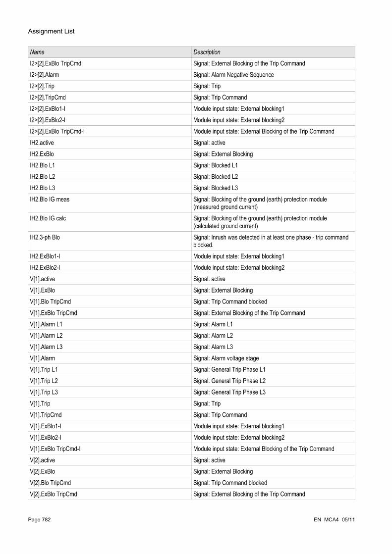
Assignment List
Name Description
I2>[2].ExBlo TripCmd Signal: External Blocking of the Trip CommandI2>[2].Alarm Signal: Alarm Negative SequenceI2>[2].Trip Signal: TripI2>[2].TripCmd Signal: Trip CommandI2>[2].ExBlo1-I Module input state: External blocking1I2>[2].ExBlo2-I Module input state: External blocking2I2>[2].ExBlo TripCmd-I Module input state: External Blocking of the Trip CommandIH2.active Signal: activeIH2.ExBlo Signal: External BlockingIH2.Blo L1 Signal: Blocked L1IH2.Blo L2 Signal: Blocked L2IH2.Blo L3 Signal: Blocked L3IH2.Blo IG meas Signal: Blocking of the ground (earth) protection module
(measured ground current)IH2.Blo IG calc Signal: Blocking of the ground (earth) protection module
(calculated ground current)IH2.3-ph Blo Signal: Inrush was detected in at least one phase - trip command
blocked.IH2.ExBlo1-I Module input state: External blocking1IH2.ExBlo2-I Module input state: External blocking2V[1].active Signal: activeV[1].ExBlo Signal: External BlockingV[1].Blo TripCmd Signal: Trip Command blockedV[1].ExBlo TripCmd Signal: External Blocking of the Trip CommandV[1].Alarm L1 Signal: Alarm L1V[1].Alarm L2 Signal: Alarm L2V[1].Alarm L3 Signal: Alarm L3V[1].Alarm Signal: Alarm voltage stageV[1].Trip L1 Signal: General Trip Phase L1V[1].Trip L2 Signal: General Trip Phase L2V[1].Trip L3 Signal: General Trip Phase L3V[1].Trip Signal: TripV[1].TripCmd Signal: Trip CommandV[1].ExBlo1-I Module input state: External blocking1V[1].ExBlo2-I Module input state: External blocking2V[1].ExBlo TripCmd-I Module input state: External Blocking of the Trip CommandV[2].active Signal: activeV[2].ExBlo Signal: External BlockingV[2].Blo TripCmd Signal: Trip Command blockedV[2].ExBlo TripCmd Signal: External Blocking of the Trip Command
Page 782 EN MCA4 05/11
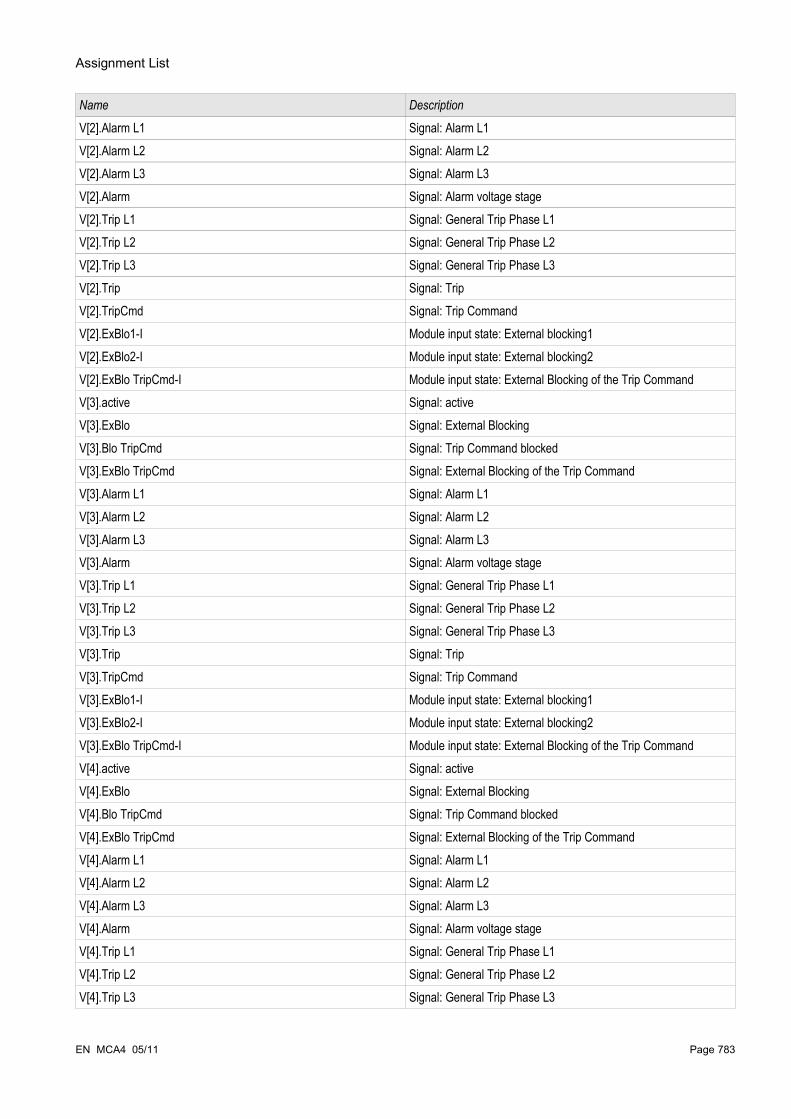
Assignment List
Name Description
V[2].Alarm L1 Signal: Alarm L1V[2].Alarm L2 Signal: Alarm L2V[2].Alarm L3 Signal: Alarm L3V[2].Alarm Signal: Alarm voltage stageV[2].Trip L1 Signal: General Trip Phase L1V[2].Trip L2 Signal: General Trip Phase L2V[2].Trip L3 Signal: General Trip Phase L3V[2].Trip Signal: TripV[2].TripCmd Signal: Trip CommandV[2].ExBlo1-I Module input state: External blocking1V[2].ExBlo2-I Module input state: External blocking2V[2].ExBlo TripCmd-I Module input state: External Blocking of the Trip CommandV[3].active Signal: activeV[3].ExBlo Signal: External BlockingV[3].Blo TripCmd Signal: Trip Command blockedV[3].ExBlo TripCmd Signal: External Blocking of the Trip CommandV[3].Alarm L1 Signal: Alarm L1V[3].Alarm L2 Signal: Alarm L2V[3].Alarm L3 Signal: Alarm L3V[3].Alarm Signal: Alarm voltage stageV[3].Trip L1 Signal: General Trip Phase L1V[3].Trip L2 Signal: General Trip Phase L2V[3].Trip L3 Signal: General Trip Phase L3V[3].Trip Signal: TripV[3].TripCmd Signal: Trip CommandV[3].ExBlo1-I Module input state: External blocking1V[3].ExBlo2-I Module input state: External blocking2V[3].ExBlo TripCmd-I Module input state: External Blocking of the Trip CommandV[4].active Signal: activeV[4].ExBlo Signal: External BlockingV[4].Blo TripCmd Signal: Trip Command blockedV[4].ExBlo TripCmd Signal: External Blocking of the Trip CommandV[4].Alarm L1 Signal: Alarm L1V[4].Alarm L2 Signal: Alarm L2V[4].Alarm L3 Signal: Alarm L3V[4].Alarm Signal: Alarm voltage stageV[4].Trip L1 Signal: General Trip Phase L1V[4].Trip L2 Signal: General Trip Phase L2V[4].Trip L3 Signal: General Trip Phase L3
EN MCA4 05/11 Page 783
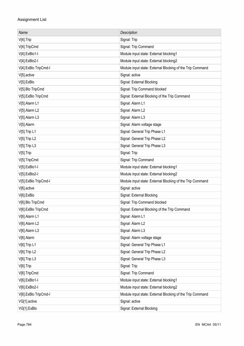
Assignment List
Name Description
V[4].Trip Signal: TripV[4].TripCmd Signal: Trip CommandV[4].ExBlo1-I Module input state: External blocking1V[4].ExBlo2-I Module input state: External blocking2V[4].ExBlo TripCmd-I Module input state: External Blocking of the Trip CommandV[5].active Signal: activeV[5].ExBlo Signal: External BlockingV[5].Blo TripCmd Signal: Trip Command blockedV[5].ExBlo TripCmd Signal: External Blocking of the Trip CommandV[5].Alarm L1 Signal: Alarm L1V[5].Alarm L2 Signal: Alarm L2V[5].Alarm L3 Signal: Alarm L3V[5].Alarm Signal: Alarm voltage stageV[5].Trip L1 Signal: General Trip Phase L1V[5].Trip L2 Signal: General Trip Phase L2V[5].Trip L3 Signal: General Trip Phase L3V[5].Trip Signal: TripV[5].TripCmd Signal: Trip CommandV[5].ExBlo1-I Module input state: External blocking1V[5].ExBlo2-I Module input state: External blocking2V[5].ExBlo TripCmd-I Module input state: External Blocking of the Trip CommandV[6].active Signal: activeV[6].ExBlo Signal: External BlockingV[6].Blo TripCmd Signal: Trip Command blockedV[6].ExBlo TripCmd Signal: External Blocking of the Trip CommandV[6].Alarm L1 Signal: Alarm L1V[6].Alarm L2 Signal: Alarm L2V[6].Alarm L3 Signal: Alarm L3V[6].Alarm Signal: Alarm voltage stageV[6].Trip L1 Signal: General Trip Phase L1V[6].Trip L2 Signal: General Trip Phase L2V[6].Trip L3 Signal: General Trip Phase L3V[6].Trip Signal: TripV[6].TripCmd Signal: Trip CommandV[6].ExBlo1-I Module input state: External blocking1V[6].ExBlo2-I Module input state: External blocking2V[6].ExBlo TripCmd-I Module input state: External Blocking of the Trip CommandVG[1].active Signal: activeVG[1].ExBlo Signal: External Blocking
Page 784 EN MCA4 05/11

Assignment List
Name Description
VG[1].Blo TripCmd Signal: Trip Command blockedVG[1].ExBlo TripCmd Signal: External Blocking of the Trip CommandVG[1].Alarm Signal: Alarm Residual Voltage Supervision-stageVG[1].Trip Signal: TripVG[1].TripCmd Signal: Trip CommandVG[1].ExBlo1-I Module input state: External blocking1VG[1].ExBlo2-I Module input state: External blocking2VG[1].ExBlo TripCmd-I Module input state: External Blocking of the Trip CommandVG[2].active Signal: activeVG[2].ExBlo Signal: External BlockingVG[2].Blo TripCmd Signal: Trip Command blockedVG[2].ExBlo TripCmd Signal: External Blocking of the Trip CommandVG[2].Alarm Signal: Alarm Residual Voltage Supervision-stageVG[2].Trip Signal: TripVG[2].TripCmd Signal: Trip CommandVG[2].ExBlo1-I Module input state: External blocking1VG[2].ExBlo2-I Module input state: External blocking2VG[2].ExBlo TripCmd-I Module input state: External Blocking of the Trip CommandV 012 [1].active Signal: activeV 012 [1].ExBlo Signal: External BlockingV 012 [1].Blo TripCmd Signal: Trip Command blockedV 012 [1].ExBlo TripCmd Signal: External Blocking of the Trip CommandV 012 [1].Alarm Signal: Alarm voltage asymmetryV 012 [1].Trip Signal: TripV 012 [1].TripCmd Signal: Trip CommandV 012 [1].ExBlo1-I Module input state: External blocking1V 012 [1].ExBlo2-I Module input state: External blocking2V 012 [1].ExBlo TripCmd-I Module input state: External Blocking of the Trip CommandV 012 [2].active Signal: activeV 012 [2].ExBlo Signal: External BlockingV 012 [2].Blo TripCmd Signal: Trip Command blockedV 012 [2].ExBlo TripCmd Signal: External Blocking of the Trip CommandV 012 [2].Alarm Signal: Alarm voltage asymmetryV 012 [2].Trip Signal: TripV 012 [2].TripCmd Signal: Trip CommandV 012 [2].ExBlo1-I Module input state: External blocking1V 012 [2].ExBlo2-I Module input state: External blocking2V 012 [2].ExBlo TripCmd-I Module input state: External Blocking of the Trip CommandV 012 [3].active Signal: active
EN MCA4 05/11 Page 785

Assignment List
Name Description
V 012 [3].ExBlo Signal: External BlockingV 012 [3].Blo TripCmd Signal: Trip Command blockedV 012 [3].ExBlo TripCmd Signal: External Blocking of the Trip CommandV 012 [3].Alarm Signal: Alarm voltage asymmetryV 012 [3].Trip Signal: TripV 012 [3].TripCmd Signal: Trip CommandV 012 [3].ExBlo1-I Module input state: External blocking1V 012 [3].ExBlo2-I Module input state: External blocking2V 012 [3].ExBlo TripCmd-I Module input state: External Blocking of the Trip CommandV 012 [4].active Signal: activeV 012 [4].ExBlo Signal: External BlockingV 012 [4].Blo TripCmd Signal: Trip Command blockedV 012 [4].ExBlo TripCmd Signal: External Blocking of the Trip CommandV 012 [4].Alarm Signal: Alarm voltage asymmetryV 012 [4].Trip Signal: TripV 012 [4].TripCmd Signal: Trip CommandV 012 [4].ExBlo1-I Module input state: External blocking1V 012 [4].ExBlo2-I Module input state: External blocking2V 012 [4].ExBlo TripCmd-I Module input state: External Blocking of the Trip CommandV 012 [5].active Signal: activeV 012 [5].ExBlo Signal: External BlockingV 012 [5].Blo TripCmd Signal: Trip Command blockedV 012 [5].ExBlo TripCmd Signal: External Blocking of the Trip CommandV 012 [5].Alarm Signal: Alarm voltage asymmetryV 012 [5].Trip Signal: TripV 012 [5].TripCmd Signal: Trip CommandV 012 [5].ExBlo1-I Module input state: External blocking1V 012 [5].ExBlo2-I Module input state: External blocking2V 012 [5].ExBlo TripCmd-I Module input state: External Blocking of the Trip CommandV 012 [6].active Signal: activeV 012 [6].ExBlo Signal: External BlockingV 012 [6].Blo TripCmd Signal: Trip Command blockedV 012 [6].ExBlo TripCmd Signal: External Blocking of the Trip CommandV 012 [6].Alarm Signal: Alarm voltage asymmetryV 012 [6].Trip Signal: TripV 012 [6].TripCmd Signal: Trip CommandV 012 [6].ExBlo1-I Module input state: External blocking1V 012 [6].ExBlo2-I Module input state: External blocking2V 012 [6].ExBlo TripCmd-I Module input state: External Blocking of the Trip Command
Page 786 EN MCA4 05/11

Assignment List
Name Description
f[1].active Signal: activef[1].ExBlo Signal: External Blockingf[1].Blo by V< Signal: Module is blocked by undervoltage.f[1].Blo TripCmd Signal: Trip Command blockedf[1].ExBlo TripCmd Signal: External Blocking of the Trip Commandf[1].Alarm f Signal: Alarm Frequency Protectionf[1].Alarm df/dt | DF/DT Alarm instantaneous or average value of the rate-of-frequency-
change f[1].Alarm delta phi Signal: Alarm Vector Surgef[1].Alarm Signal: Alarm Frequency Protection (collective signal)f[1].Trip f Signal: Frequency has exceeded the limit.f[1].Trip df/dt | DF/DT Signal: Trip df/dt or DF/DTf[1].Trip delta phi Signal: Trip Vector Surgef[1].Trip Signal: Trip Frequency Protection (collective signal)f[1].TripCmd Signal: Trip Commandf[1].ExBlo1-I Module input state: External blocking1f[1].ExBlo2-I Module input state: External blocking2f[1].ExBlo TripCmd-I Module input state: External Blocking of the Trip Commandf[2].active Signal: activef[2].ExBlo Signal: External Blockingf[2].Blo by V< Signal: Module is blocked by undervoltage.f[2].Blo TripCmd Signal: Trip Command blockedf[2].ExBlo TripCmd Signal: External Blocking of the Trip Commandf[2].Alarm f Signal: Alarm Frequency Protectionf[2].Alarm df/dt | DF/DT Alarm instantaneous or average value of the rate-of-frequency-
change f[2].Alarm delta phi Signal: Alarm Vector Surgef[2].Alarm Signal: Alarm Frequency Protection (collective signal)f[2].Trip f Signal: Frequency has exceeded the limit.f[2].Trip df/dt | DF/DT Signal: Trip df/dt or DF/DTf[2].Trip delta phi Signal: Trip Vector Surgef[2].Trip Signal: Trip Frequency Protection (collective signal)f[2].TripCmd Signal: Trip Commandf[2].ExBlo1-I Module input state: External blocking1f[2].ExBlo2-I Module input state: External blocking2f[2].ExBlo TripCmd-I Module input state: External Blocking of the Trip Commandf[3].active Signal: activef[3].ExBlo Signal: External Blockingf[3].Blo by V< Signal: Module is blocked by undervoltage.f[3].Blo TripCmd Signal: Trip Command blocked
EN MCA4 05/11 Page 787

Assignment List
Name Description
f[3].ExBlo TripCmd Signal: External Blocking of the Trip Commandf[3].Alarm f Signal: Alarm Frequency Protectionf[3].Alarm df/dt | DF/DT Alarm instantaneous or average value of the rate-of-frequency-
change f[3].Alarm delta phi Signal: Alarm Vector Surgef[3].Alarm Signal: Alarm Frequency Protection (collective signal)f[3].Trip f Signal: Frequency has exceeded the limit.f[3].Trip df/dt | DF/DT Signal: Trip df/dt or DF/DTf[3].Trip delta phi Signal: Trip Vector Surgef[3].Trip Signal: Trip Frequency Protection (collective signal)f[3].TripCmd Signal: Trip Commandf[3].ExBlo1-I Module input state: External blocking1f[3].ExBlo2-I Module input state: External blocking2f[3].ExBlo TripCmd-I Module input state: External Blocking of the Trip Commandf[4].active Signal: activef[4].ExBlo Signal: External Blockingf[4].Blo by V< Signal: Module is blocked by undervoltage.f[4].Blo TripCmd Signal: Trip Command blockedf[4].ExBlo TripCmd Signal: External Blocking of the Trip Commandf[4].Alarm f Signal: Alarm Frequency Protectionf[4].Alarm df/dt | DF/DT Alarm instantaneous or average value of the rate-of-frequency-
change f[4].Alarm delta phi Signal: Alarm Vector Surgef[4].Alarm Signal: Alarm Frequency Protection (collective signal)f[4].Trip f Signal: Frequency has exceeded the limit.f[4].Trip df/dt | DF/DT Signal: Trip df/dt or DF/DTf[4].Trip delta phi Signal: Trip Vector Surgef[4].Trip Signal: Trip Frequency Protection (collective signal)f[4].TripCmd Signal: Trip Commandf[4].ExBlo1-I Module input state: External blocking1f[4].ExBlo2-I Module input state: External blocking2f[4].ExBlo TripCmd-I Module input state: External Blocking of the Trip Commandf[5].active Signal: activef[5].ExBlo Signal: External Blockingf[5].Blo by V< Signal: Module is blocked by undervoltage.f[5].Blo TripCmd Signal: Trip Command blockedf[5].ExBlo TripCmd Signal: External Blocking of the Trip Commandf[5].Alarm f Signal: Alarm Frequency Protectionf[5].Alarm df/dt | DF/DT Alarm instantaneous or average value of the rate-of-frequency-
change
Page 788 EN MCA4 05/11

Assignment List
Name Description
f[5].Alarm delta phi Signal: Alarm Vector Surgef[5].Alarm Signal: Alarm Frequency Protection (collective signal)f[5].Trip f Signal: Frequency has exceeded the limit.f[5].Trip df/dt | DF/DT Signal: Trip df/dt or DF/DTf[5].Trip delta phi Signal: Trip Vector Surgef[5].Trip Signal: Trip Frequency Protection (collective signal)f[5].TripCmd Signal: Trip Commandf[5].ExBlo1-I Module input state: External blocking1f[5].ExBlo2-I Module input state: External blocking2f[5].ExBlo TripCmd-I Module input state: External Blocking of the Trip Commandf[6].active Signal: activef[6].ExBlo Signal: External Blockingf[6].Blo by V< Signal: Module is blocked by undervoltage.f[6].Blo TripCmd Signal: Trip Command blockedf[6].ExBlo TripCmd Signal: External Blocking of the Trip Commandf[6].Alarm f Signal: Alarm Frequency Protectionf[6].Alarm df/dt | DF/DT Alarm instantaneous or average value of the rate-of-frequency-
change f[6].Alarm delta phi Signal: Alarm Vector Surgef[6].Alarm Signal: Alarm Frequency Protection (collective signal)f[6].Trip f Signal: Frequency has exceeded the limit.f[6].Trip df/dt | DF/DT Signal: Trip df/dt or DF/DTf[6].Trip delta phi Signal: Trip Vector Surgef[6].Trip Signal: Trip Frequency Protection (collective signal)f[6].TripCmd Signal: Trip Commandf[6].ExBlo1-I Module input state: External blocking1f[6].ExBlo2-I Module input state: External blocking2f[6].ExBlo TripCmd-I Module input state: External Blocking of the Trip CommandPQS [1].active Signal: activePQS [1].ExBlo Signal: External BlockingPQS [1].Blo TripCmd Signal: Trip Command blockedPQS [1].ExBlo TripCmd Signal: External Blocking of the Trip CommandPQS [1].Alarm Signal: Alarm Power ProtectionPQS [1].Trip Signal: Trip Power ProtectionPQS [1].TripCmd Signal: Trip CommandPQS [1].ExBlo1-I Module input state: External blockingPQS [1].ExBlo2-I Module input state: External blockingPQS [1].ExBlo TripCmd-I Module input state: External Blocking of the Trip CommandPQS [2].active Signal: activePQS [2].ExBlo Signal: External Blocking
EN MCA4 05/11 Page 789
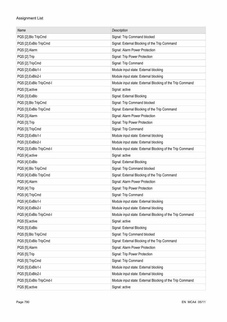
Assignment List
Name Description
PQS [2].Blo TripCmd Signal: Trip Command blockedPQS [2].ExBlo TripCmd Signal: External Blocking of the Trip CommandPQS [2].Alarm Signal: Alarm Power ProtectionPQS [2].Trip Signal: Trip Power ProtectionPQS [2].TripCmd Signal: Trip CommandPQS [2].ExBlo1-I Module input state: External blockingPQS [2].ExBlo2-I Module input state: External blockingPQS [2].ExBlo TripCmd-I Module input state: External Blocking of the Trip CommandPQS [3].active Signal: activePQS [3].ExBlo Signal: External BlockingPQS [3].Blo TripCmd Signal: Trip Command blockedPQS [3].ExBlo TripCmd Signal: External Blocking of the Trip CommandPQS [3].Alarm Signal: Alarm Power ProtectionPQS [3].Trip Signal: Trip Power ProtectionPQS [3].TripCmd Signal: Trip CommandPQS [3].ExBlo1-I Module input state: External blockingPQS [3].ExBlo2-I Module input state: External blockingPQS [3].ExBlo TripCmd-I Module input state: External Blocking of the Trip CommandPQS [4].active Signal: activePQS [4].ExBlo Signal: External BlockingPQS [4].Blo TripCmd Signal: Trip Command blockedPQS [4].ExBlo TripCmd Signal: External Blocking of the Trip CommandPQS [4].Alarm Signal: Alarm Power ProtectionPQS [4].Trip Signal: Trip Power ProtectionPQS [4].TripCmd Signal: Trip CommandPQS [4].ExBlo1-I Module input state: External blockingPQS [4].ExBlo2-I Module input state: External blockingPQS [4].ExBlo TripCmd-I Module input state: External Blocking of the Trip CommandPQS [5].active Signal: activePQS [5].ExBlo Signal: External BlockingPQS [5].Blo TripCmd Signal: Trip Command blockedPQS [5].ExBlo TripCmd Signal: External Blocking of the Trip CommandPQS [5].Alarm Signal: Alarm Power ProtectionPQS [5].Trip Signal: Trip Power ProtectionPQS [5].TripCmd Signal: Trip CommandPQS [5].ExBlo1-I Module input state: External blockingPQS [5].ExBlo2-I Module input state: External blockingPQS [5].ExBlo TripCmd-I Module input state: External Blocking of the Trip CommandPQS [6].active Signal: active
Page 790 EN MCA4 05/11

Assignment List
Name Description
PQS [6].ExBlo Signal: External BlockingPQS [6].Blo TripCmd Signal: Trip Command blockedPQS [6].ExBlo TripCmd Signal: External Blocking of the Trip CommandPQS [6].Alarm Signal: Alarm Power ProtectionPQS [6].Trip Signal: Trip Power ProtectionPQS [6].TripCmd Signal: Trip CommandPQS [6].ExBlo1-I Module input state: External blockingPQS [6].ExBlo2-I Module input state: External blockingPQS [6].ExBlo TripCmd-I Module input state: External Blocking of the Trip CommandPF[1].active Signal: activePF[1].ExBlo Signal: External BlockingPF[1].Blo TripCmd Signal: Trip Command blockedPF[1].ExBlo TripCmd Signal: External Blocking of the Trip CommandPF[1].Alarm Signal: Alarm Power FactorPF[1].Trip Signal: Trip Power FactorPF[1].TripCmd Signal: Trip CommandPF[1].Compensator Signal: Compensation SignalPF[1].Impossible Signal: Alarm Power Factor ImpossiblePF[1].ExBlo1-I Module input state: External blockingPF[1].ExBlo2-I Module input state: External blockingPF[1].ExBlo TripCmd-I Module input state: External Blocking of the Trip CommandPF[2].active Signal: activePF[2].ExBlo Signal: External BlockingPF[2].Blo TripCmd Signal: Trip Command blockedPF[2].ExBlo TripCmd Signal: External Blocking of the Trip CommandPF[2].Alarm Signal: Alarm Power FactorPF[2].Trip Signal: Trip Power FactorPF[2].TripCmd Signal: Trip CommandPF[2].Compensator Signal: Compensation SignalPF[2].Impossible Signal: Alarm Power Factor ImpossiblePF[2].ExBlo1-I Module input state: External blockingPF[2].ExBlo2-I Module input state: External blockingPF[2].ExBlo TripCmd-I Module input state: External Blocking of the Trip CommandQ->&V<.active Signal: activeQ->&V<.ExBlo Signal: External BlockingQ->&V<.Fuse Fail VT Blo Signal: Blocked by Fuse Failure (VT)Q->&V<.Alarm Signal: Alarm Reactive Power Undervoltage ProtectionQ->&V<.Decoupling Energy Resource Signal: Decoupling of the (local) Energy ResourceQ->&V<.Decoupling PCC Signal: Decoupling at the Point of Common Coupling
EN MCA4 05/11 Page 791
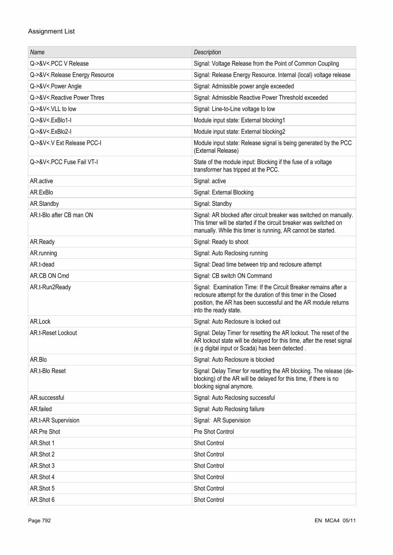
Assignment List
Name Description
Q->&V<.PCC V Release Signal: Voltage Release from the Point of Common CouplingQ->&V<.Release Energy Resource Signal: Release Energy Resource. Internal (local) voltage releaseQ->&V<.Power Angle Signal: Admissible power angle exceededQ->&V<.Reactive Power Thres Signal: Admissible Reactive Power Threshold exceededQ->&V<.VLL to low Signal: Line-to-Line voltage to lowQ->&V<.ExBlo1-I Module input state: External blocking1Q->&V<.ExBlo2-I Module input state: External blocking2Q->&V<.V Ext Release PCC-I Module input state: Release signal is being generated by the PCC
(External Release)Q->&V<.PCC Fuse Fail VT-I State of the module input: Blocking if the fuse of a voltage
transformer has tripped at the PCC.AR.active Signal: activeAR.ExBlo Signal: External BlockingAR.Standby Signal: StandbyAR.t-Blo after CB man ON Signal: AR blocked after circuit breaker was switched on manually.
This timer will be started if the circuit breaker was switched on manually. While this timer is running, AR cannot be started.
AR.Ready Signal: Ready to shootAR.running Signal: Auto Reclosing runningAR.t-dead Signal: Dead time between trip and reclosure attemptAR.CB ON Cmd Signal: CB switch ON CommandAR.t-Run2Ready Signal: Examination Time: If the Circuit Breaker remains after a
reclosure attempt for the duration of this timer in the Closed position, the AR has been successful and the AR module returns into the ready state.
AR.Lock Signal: Auto Reclosure is locked outAR.t-Reset Lockout Signal: Delay Timer for resetting the AR lockout. The reset of the
AR lockout state will be delayed for this time, after the reset signal (e.g digital input or Scada) has been detected .
AR.Blo Signal: Auto Reclosure is blockedAR.t-Blo Reset Signal: Delay Timer for resetting the AR blocking. The release (de-
blocking) of the AR will be delayed for this time, if there is no blocking signal anymore.
AR.successful Signal: Auto Reclosing successfulAR.failed Signal: Auto Reclosing failureAR.t-AR Supervision Signal: AR SupervisionAR.Pre Shot Pre Shot ControlAR.Shot 1 Shot ControlAR.Shot 2 Shot ControlAR.Shot 3 Shot ControlAR.Shot 4 Shot ControlAR.Shot 5 Shot ControlAR.Shot 6 Shot Control
Page 792 EN MCA4 05/11

Assignment List
Name Description
AR.Service Alarm 1 Signal: AR - Service Alarm 1, too many switching operationsAR.Service Alarm 2 Signal: AR - Service Alarm 2 - too many switching operationsAR.Max Shots / h exceeded Signal: The maximum allowed number of shots per hour has been
exceeded.AR.Res Statistics Cr Signal: Reset all statistic AR counters: Total number of AR,
successful and unsuccessful no of AR. AR.Res Service Cr Signal: Reset the Service Counters for Alarm and BlockingAR.Reset Lockout Signal: The AR Lockout has been resetted via the panel.AR.Res Max Shots / h Signal: The Counter for the maximum allowed shots per hour has
been resetted.AR.ExBlo1-I Module input state: External blocking1AR.ExBlo2-I Module input state: External blocking2AR.Ex Shot Inc-I Module input state: The AR Shot counter will be incremented by
this external Signal. This can be used for Zone Coordination (of upstream Auto Reclosure devices). Note: This parameter enables the functionality only. The assignment has to be set within the global parameters.
AR.Ex Lock-I Module input state: External AR lockout.AR.DI Reset Ex Lock-I Module input state: Resetting the lockout state of the AR (if the
resetting via digital inputs has been selected).AR.Scada Reset Ex Lock-I Module input state: Resetting the Lockout State of the AR by
Communication.Sync.active Signal: activeSync.ExBlo Signal: External BlockingSync.LiveBus Signal: Live-Bus flag: 1=Live-Bus, 0=Voltage is below the LiveBus
thresholdSync.LiveLine Signal: Live Line flag: 1=Live-Line, 0=Voltage is below the
LiveLine thresholdSync.SynchronRunTiming Signal: SynchronRunTimingSync.SynchronFailed Signal: This signal indicates a failed synchronization. It is set for 5s
when the circuit breaker is still open after the Synchron-Run-timer has timed out.
Sync.SyncOverridden Signal:Synchronism Check is overridden because one of the Synchronism overriding conditions (DB/DL or ExtBypass) is met.
Sync.VDiffTooHigh Signal: Voltage difference between bus and line too high.Sync.SlipTooHigh Signal: Frequency difference (slip frequency) between bus and line
voltages too high.Sync.AngleDiffTooHigh Signal: Phase Angle difference between bus and line voltages too
high.Sync.Sys-in-Sync Signal: Bus and line voltages are in synchronism according to the
system synchronism criteria.Sync.Ready to Close Signal: Ready to CloseSync.ExBlo1-I Module input state: External blocking1Sync.ExBlo2-I Module input state: External blocking2Sync.Bypass-I State of the module input: Bypass
EN MCA4 05/11 Page 793

Assignment List
Name Description
Sync.CBCloseInitiate-I State of the module input: Breaker Close Initiate with synchronism check from any control sources (e.g. HMI / SCADA). If the state of the assigned signal becomes true, a Breaker Close will be initiated (Trigger Source).
ExP[1].active Signal: activeExP[1].ExBlo Signal: External BlockingExP[1].Blo TripCmd Signal: Trip Command blockedExP[1].ExBlo TripCmd Signal: External Blocking of the Trip CommandExP[1].Alarm Signal: AlarmExP[1].Trip Signal: TripExP[1].TripCmd Signal: Trip CommandExP[1].ExBlo1-I Module input state: External blocking1ExP[1].ExBlo2-I Module input state: External blocking2ExP[1].ExBlo TripCmd-I Module input state: External Blocking of the Trip CommandExP[1].Alarm-I Module input state: AlarmExP[1].Trip-I Module input state: TripExP[2].active Signal: activeExP[2].ExBlo Signal: External BlockingExP[2].Blo TripCmd Signal: Trip Command blockedExP[2].ExBlo TripCmd Signal: External Blocking of the Trip CommandExP[2].Alarm Signal: AlarmExP[2].Trip Signal: TripExP[2].TripCmd Signal: Trip CommandExP[2].ExBlo1-I Module input state: External blocking1ExP[2].ExBlo2-I Module input state: External blocking2ExP[2].ExBlo TripCmd-I Module input state: External Blocking of the Trip CommandExP[2].Alarm-I Module input state: AlarmExP[2].Trip-I Module input state: TripExP[3].active Signal: activeExP[3].ExBlo Signal: External BlockingExP[3].Blo TripCmd Signal: Trip Command blockedExP[3].ExBlo TripCmd Signal: External Blocking of the Trip CommandExP[3].Alarm Signal: AlarmExP[3].Trip Signal: TripExP[3].TripCmd Signal: Trip CommandExP[3].ExBlo1-I Module input state: External blocking1ExP[3].ExBlo2-I Module input state: External blocking2ExP[3].ExBlo TripCmd-I Module input state: External Blocking of the Trip CommandExP[3].Alarm-I Module input state: AlarmExP[3].Trip-I Module input state: Trip
Page 794 EN MCA4 05/11
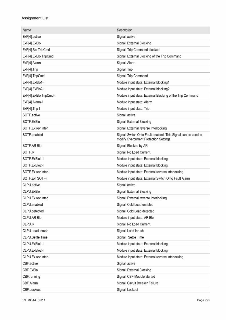
Assignment List
Name Description
ExP[4].active Signal: activeExP[4].ExBlo Signal: External BlockingExP[4].Blo TripCmd Signal: Trip Command blockedExP[4].ExBlo TripCmd Signal: External Blocking of the Trip CommandExP[4].Alarm Signal: AlarmExP[4].Trip Signal: TripExP[4].TripCmd Signal: Trip CommandExP[4].ExBlo1-I Module input state: External blocking1ExP[4].ExBlo2-I Module input state: External blocking2ExP[4].ExBlo TripCmd-I Module input state: External Blocking of the Trip CommandExP[4].Alarm-I Module input state: AlarmExP[4].Trip-I Module input state: TripSOTF.active Signal: activeSOTF.ExBlo Signal: External BlockingSOTF.Ex rev Interl Signal: External reverse InterlockingSOTF.enabled Signal: Switch Onto Fault enabled. This Signal can be used to
modify Overcurrent Protection Settings.SOTF.AR Blo Signal: Blocked by ARSOTF.I< Signal: No Load Current.SOTF.ExBlo1-I Module input state: External blockingSOTF.ExBlo2-I Module input state: External blockingSOTF.Ex rev Interl-I Module input state: External reverse interlockingSOTF.Ext SOTF-I Module input state: External Switch Onto Fault AlarmCLPU.active Signal: activeCLPU.ExBlo Signal: External BlockingCLPU.Ex rev Interl Signal: External reverse InterlockingCLPU.enabled Signal: Cold Load enabledCLPU.detected Signal: Cold Load detectedCLPU.AR Blo Module input state: AR BloCLPU.I< Signal: No Load Current.CLPU.Load Inrush Signal: Load InrushCLPU.Settle Time Signal: Settle TimeCLPU.ExBlo1-I Module input state: External blockingCLPU.ExBlo2-I Module input state: External blockingCLPU.Ex rev Interl-I Module input state: External reverse interlockingCBF.active Signal: activeCBF.ExBlo Signal: External BlockingCBF.running Signal: CBF-Module startedCBF.Alarm Signal: Circuit Breaker FailureCBF.Lockout Signal: Lockout
EN MCA4 05/11 Page 795
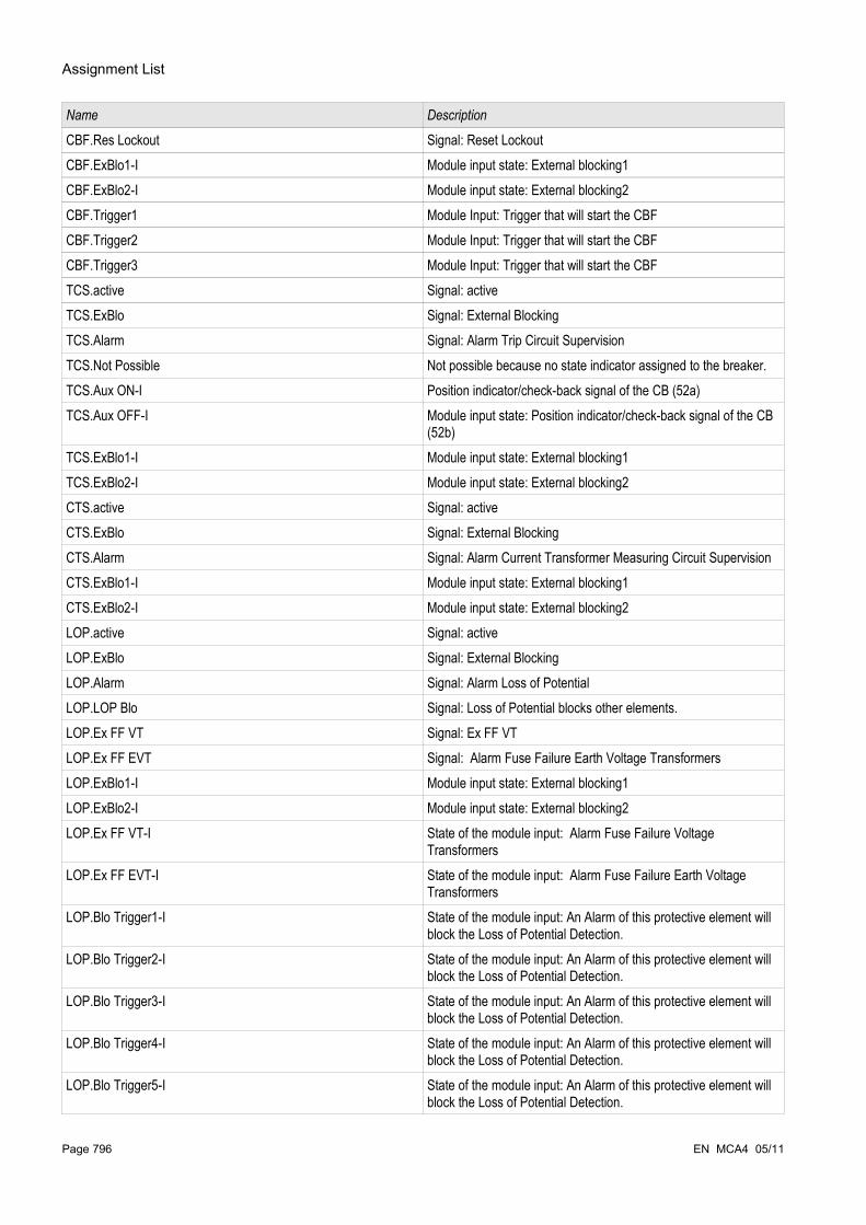
Assignment List
Name Description
CBF.Res Lockout Signal: Reset LockoutCBF.ExBlo1-I Module input state: External blocking1CBF.ExBlo2-I Module input state: External blocking2CBF.Trigger1 Module Input: Trigger that will start the CBFCBF.Trigger2 Module Input: Trigger that will start the CBFCBF.Trigger3 Module Input: Trigger that will start the CBFTCS.active Signal: activeTCS.ExBlo Signal: External BlockingTCS.Alarm Signal: Alarm Trip Circuit SupervisionTCS.Not Possible Not possible because no state indicator assigned to the breaker.TCS.Aux ON-I Position indicator/check-back signal of the CB (52a)TCS.Aux OFF-I Module input state: Position indicator/check-back signal of the CB
(52b)TCS.ExBlo1-I Module input state: External blocking1TCS.ExBlo2-I Module input state: External blocking2CTS.active Signal: activeCTS.ExBlo Signal: External BlockingCTS.Alarm Signal: Alarm Current Transformer Measuring Circuit SupervisionCTS.ExBlo1-I Module input state: External blocking1CTS.ExBlo2-I Module input state: External blocking2LOP.active Signal: activeLOP.ExBlo Signal: External BlockingLOP.Alarm Signal: Alarm Loss of PotentialLOP.LOP Blo Signal: Loss of Potential blocks other elements.LOP.Ex FF VT Signal: Ex FF VTLOP.Ex FF EVT Signal: Alarm Fuse Failure Earth Voltage TransformersLOP.ExBlo1-I Module input state: External blocking1LOP.ExBlo2-I Module input state: External blocking2LOP.Ex FF VT-I State of the module input: Alarm Fuse Failure Voltage
TransformersLOP.Ex FF EVT-I State of the module input: Alarm Fuse Failure Earth Voltage
TransformersLOP.Blo Trigger1-I State of the module input: An Alarm of this protective element will
block the Loss of Potential Detection.LOP.Blo Trigger2-I State of the module input: An Alarm of this protective element will
block the Loss of Potential Detection.LOP.Blo Trigger3-I State of the module input: An Alarm of this protective element will
block the Loss of Potential Detection.LOP.Blo Trigger4-I State of the module input: An Alarm of this protective element will
block the Loss of Potential Detection.LOP.Blo Trigger5-I State of the module input: An Alarm of this protective element will
block the Loss of Potential Detection.
Page 796 EN MCA4 05/11

Assignment List
Name Description
DI Slot X1.DI 1 Signal: Digital InputDI Slot X1.DI 2 Signal: Digital InputDI Slot X1.DI 3 Signal: Digital InputDI Slot X1.DI 4 Signal: Digital InputDI Slot X1.DI 5 Signal: Digital InputDI Slot X1.DI 6 Signal: Digital InputDI Slot X1.DI 7 Signal: Digital InputDI Slot X1.DI 8 Signal: Digital InputDI Slot X6.DI 1 Signal: Digital InputDI Slot X6.DI 2 Signal: Digital InputDI Slot X6.DI 3 Signal: Digital InputDI Slot X6.DI 4 Signal: Digital InputDI Slot X6.DI 5 Signal: Digital InputDI Slot X6.DI 6 Signal: Digital InputDI Slot X6.DI 7 Signal: Digital InputDI Slot X6.DI 8 Signal: Digital InputBO Slot X2.BO 1 Signal: Binary Output RelayBO Slot X2.BO 2 Signal: Binary Output RelayBO Slot X2.BO 3 Signal: Binary Output RelayBO Slot X2.BO 4 Signal: Binary Output RelayBO Slot X2.BO 5 Signal: Binary Output RelayBO Slot X2.BO 6 Signal: Binary Output RelayBO Slot X2.DISARMED! Signal: CAUTION! RELAYS DISARMED in order to safely perform
maintenance while eliminating the risk of taking an entire process off-line. (Note: The Self Supervision Contact cannot be disarmed). YOU MUST ENSURE that the relays are ARMED AGAIN after maintenance
BO Slot X2.Outs forced Signal: The State of at least one Relay Output has been set by force. That means that the state of at least one Relay is forced and hence does not show the state of the assigned signals.
BO Slot X5.BO 1 Signal: Binary Output RelayBO Slot X5.BO 2 Signal: Binary Output RelayBO Slot X5.BO 3 Signal: Binary Output RelayBO Slot X5.BO 4 Signal: Binary Output RelayBO Slot X5.BO 5 Signal: Binary Output RelayBO Slot X5.BO 6 Signal: Binary Output RelayBO Slot X5.DISARMED! Signal: CAUTION! RELAYS DISARMED in order to safely perform
maintenance while eliminating the risk of taking an entire process off-line. (Note: The Self Supervision Contact cannot be disarmed). YOU MUST ENSURE that the relays are ARMED AGAIN after maintenance
EN MCA4 05/11 Page 797

Assignment List
Name Description
BO Slot X5.Outs forced Signal: The State of at least one Relay Output has been set by force. That means that the state of at least one Relay is forced and hence does not show the state of the assigned signals.
Event rec.Res all records Signal: All records deletedDisturb rec.recording Signal: RecordingDisturb rec.memory full Signal: Memory fullDisturb rec.Clear fail Signal: Clear failure in memoryDisturb rec.Res all records Signal: All records deletedDisturb rec.Res rec Signal: Delete record Disturb rec.Man Trigger Signal: Manual TriggerDisturb rec.Start1-I State of the module input:: Trigger event / start recording if:Disturb rec.Start2-I State of the module input:: Trigger event / start recording if:Disturb rec.Start3-I State of the module input:: Trigger event / start recording if:Disturb rec.Start4-I State of the module input:: Trigger event / start recording if:Disturb rec.Start5-I State of the module input:: Trigger event / start recording if:Disturb rec.Start6-I State of the module input:: Trigger event / start recording if:Disturb rec.Start7-I State of the module input:: Trigger event / start recording if:Disturb rec.Start8-I State of the module input:: Trigger event / start recording if:Fault rec.Res rec Signal: Delete record Fault rec.Man Trigger Signal: Manual TriggerFault rec.Start1-I State of the module input:: Trigger event / start recording if:Fault rec.Start2-I State of the module input:: Trigger event / start recording if:Fault rec.Start3-I State of the module input:: Trigger event / start recording if:Fault rec.Start4-I State of the module input:: Trigger event / start recording if:Fault rec.Start5-I State of the module input:: Trigger event / start recording if:Fault rec.Start6-I State of the module input:: Trigger event / start recording if:Fault rec.Start7-I State of the module input:: Trigger event / start recording if:Fault rec.Start8-I State of the module input:: Trigger event / start recording if:Trend rec.Hand Reset Hand ResetPQSCr.Cr OflwW Ws Net Signal: Counter Overflow Ws NetPQSCr.Cr OflwW Wp Net Signal: Counter Overflow Wp NetPQSCr.Cr OflwW Wp+ Signal: Counter Overflow Wp+PQSCr.Cr OflwW Wp- Signal: Counter Overflow Wp-PQSCr.Cr OflwW Wq Net Signal: Counter Overflow Wq NetPQSCr.Cr OflwW Wq+ Signal: Counter Overflow Wq+PQSCr.Cr OflwW Wq- Signal: Counter Overflow Wq-PQSCr.Ws Net Res Cr Signal: Ws Net Reset CounterPQSCr.Wp Net Res Cr Signal: Wp Net Reset CounterPQSCr.Wp+ Res Cr Signal: Wp+ Reset CounterPQSCr.Wp- Res Cr Signal: Wp- Reset Counter
Page 798 EN MCA4 05/11
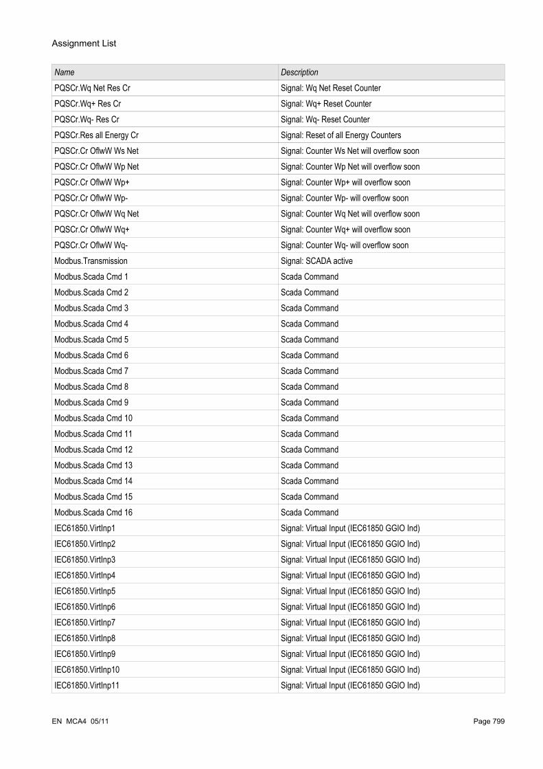
Assignment List
Name Description
PQSCr.Wq Net Res Cr Signal: Wq Net Reset CounterPQSCr.Wq+ Res Cr Signal: Wq+ Reset CounterPQSCr.Wq- Res Cr Signal: Wq- Reset CounterPQSCr.Res all Energy Cr Signal: Reset of all Energy CountersPQSCr.Cr OflwW Ws Net Signal: Counter Ws Net will overflow soonPQSCr.Cr OflwW Wp Net Signal: Counter Wp Net will overflow soonPQSCr.Cr OflwW Wp+ Signal: Counter Wp+ will overflow soonPQSCr.Cr OflwW Wp- Signal: Counter Wp- will overflow soonPQSCr.Cr OflwW Wq Net Signal: Counter Wq Net will overflow soonPQSCr.Cr OflwW Wq+ Signal: Counter Wq+ will overflow soonPQSCr.Cr OflwW Wq- Signal: Counter Wq- will overflow soonModbus.Transmission Signal: SCADA activeModbus.Scada Cmd 1 Scada CommandModbus.Scada Cmd 2 Scada CommandModbus.Scada Cmd 3 Scada CommandModbus.Scada Cmd 4 Scada CommandModbus.Scada Cmd 5 Scada CommandModbus.Scada Cmd 6 Scada CommandModbus.Scada Cmd 7 Scada CommandModbus.Scada Cmd 8 Scada CommandModbus.Scada Cmd 9 Scada CommandModbus.Scada Cmd 10 Scada CommandModbus.Scada Cmd 11 Scada CommandModbus.Scada Cmd 12 Scada CommandModbus.Scada Cmd 13 Scada CommandModbus.Scada Cmd 14 Scada CommandModbus.Scada Cmd 15 Scada CommandModbus.Scada Cmd 16 Scada CommandIEC61850.VirtInp1 Signal: Virtual Input (IEC61850 GGIO Ind)IEC61850.VirtInp2 Signal: Virtual Input (IEC61850 GGIO Ind)IEC61850.VirtInp3 Signal: Virtual Input (IEC61850 GGIO Ind)IEC61850.VirtInp4 Signal: Virtual Input (IEC61850 GGIO Ind)IEC61850.VirtInp5 Signal: Virtual Input (IEC61850 GGIO Ind)IEC61850.VirtInp6 Signal: Virtual Input (IEC61850 GGIO Ind)IEC61850.VirtInp7 Signal: Virtual Input (IEC61850 GGIO Ind)IEC61850.VirtInp8 Signal: Virtual Input (IEC61850 GGIO Ind)IEC61850.VirtInp9 Signal: Virtual Input (IEC61850 GGIO Ind)IEC61850.VirtInp10 Signal: Virtual Input (IEC61850 GGIO Ind)IEC61850.VirtInp11 Signal: Virtual Input (IEC61850 GGIO Ind)
EN MCA4 05/11 Page 799

Assignment List
Name Description
IEC61850.VirtInp12 Signal: Virtual Input (IEC61850 GGIO Ind)IEC61850.VirtInp13 Signal: Virtual Input (IEC61850 GGIO Ind)IEC61850.VirtInp14 Signal: Virtual Input (IEC61850 GGIO Ind)IEC61850.VirtInp15 Signal: Virtual Input (IEC61850 GGIO Ind)IEC61850.VirtInp16 Signal: Virtual Input (IEC61850 GGIO Ind)IEC61850.VirtOut1-I Module input state: Binary state of the Virtual Output (GGIO)IEC61850.VirtOut2-I Module input state: Binary state of the Virtual Output (GGIO)IEC61850.VirtOut3-I Module input state: Binary state of the Virtual Output (GGIO)IEC61850.VirtOut4-I Module input state: Binary state of the Virtual Output (GGIO)IEC61850.VirtOut5-I Module input state: Binary state of the Virtual Output (GGIO)IEC61850.VirtOut6-I Module input state: Binary state of the Virtual Output (GGIO)IEC61850.VirtOut7-I Module input state: Binary state of the Virtual Output (GGIO)IEC61850.VirtOut8-I Module input state: Binary state of the Virtual Output (GGIO)IEC61850.VirtOut9-I Module input state: Binary state of the Virtual Output (GGIO)IEC61850.VirtOut10-I Module input state: Binary state of the Virtual Output (GGIO)IEC61850.VirtOut11-I Module input state: Binary state of the Virtual Output (GGIO)IEC61850.VirtOut12-I Module input state: Binary state of the Virtual Output (GGIO)IEC61850.VirtOut13-I Module input state: Binary state of the Virtual Output (GGIO)IEC61850.VirtOut14-I Module input state: Binary state of the Virtual Output (GGIO)IEC61850.VirtOut15-I Module input state: Binary state of the Virtual Output (GGIO)IEC61850.VirtOut16-I Module input state: Binary state of the Virtual Output (GGIO)IEC 103.Scada Cmd 1 Scada CommandIEC 103.Scada Cmd 2 Scada CommandIEC 103.Scada Cmd 3 Scada CommandIEC 103.Scada Cmd 4 Scada CommandIEC 103.Scada Cmd 5 Scada CommandIEC 103.Scada Cmd 6 Scada CommandIEC 103.Scada Cmd 7 Scada CommandIEC 103.Scada Cmd 8 Scada CommandIEC 103.Scada Cmd 9 Scada CommandIEC 103.Scada Cmd 10 Scada CommandIEC 103.Transmission Signal: SCADA activeIEC 103.Fail phy Interf Failure in the physical interfaceIEC 103.Failure Event lost Failure event lostProfibus.Data OK Data within the Input field are OK (Yes=1)Profibus.SubModul Err Assignable Signal, Failure in Sub-Module, Communication Failure.Profibus.Connection active Connection activeProfibus.Scada Cmd 1 Scada CommandProfibus.Scada Cmd 2 Scada Command
Page 800 EN MCA4 05/11
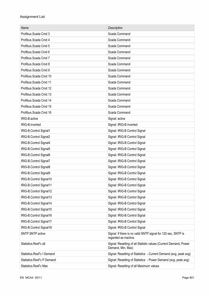
Assignment List
Name Description
Profibus.Scada Cmd 3 Scada CommandProfibus.Scada Cmd 4 Scada CommandProfibus.Scada Cmd 5 Scada CommandProfibus.Scada Cmd 6 Scada CommandProfibus.Scada Cmd 7 Scada CommandProfibus.Scada Cmd 8 Scada CommandProfibus.Scada Cmd 9 Scada CommandProfibus.Scada Cmd 10 Scada CommandProfibus.Scada Cmd 11 Scada CommandProfibus.Scada Cmd 12 Scada CommandProfibus.Scada Cmd 13 Scada CommandProfibus.Scada Cmd 14 Scada CommandProfibus.Scada Cmd 15 Scada CommandProfibus.Scada Cmd 16 Scada CommandIRIG-B.active Signal: activeIRIG-B.inverted Signal: IRIG-B invertedIRIG-B.Control Signal1 Signal: IRIG-B Control SignalIRIG-B.Control Signal2 Signal: IRIG-B Control SignalIRIG-B.Control Signal4 Signal: IRIG-B Control SignalIRIG-B.Control Signal5 Signal: IRIG-B Control SignalIRIG-B.Control Signal6 Signal: IRIG-B Control SignalIRIG-B.Control Signal7 Signal: IRIG-B Control SignalIRIG-B.Control Signal8 Signal: IRIG-B Control SignalIRIG-B.Control Signal9 Signal: IRIG-B Control SignalIRIG-B.Control Signal10 Signal: IRIG-B Control SignalIRIG-B.Control Signal11 Signal: IRIG-B Control SignalIRIG-B.Control Signal12 Signal: IRIG-B Control SignalIRIG-B.Control Signal13 Signal: IRIG-B Control SignalIRIG-B.Control Signal14 Signal: IRIG-B Control SignalIRIG-B.Control Signal15 Signal: IRIG-B Control SignalIRIG-B.Control Signal16 Signal: IRIG-B Control SignalIRIG-B.Control Signal17 Signal: IRIG-B Control SignalIRIG-B.Control Signal18 Signal: IRIG-B Control SignalSNTP.SNTP active Signal: If there is no valid SNTP signal for 120 sec, SNTP is
regarded as inactive.Statistics.ResFc all Signal: Resetting of all Statistic values (Current Demand, Power
Demand, Min, Max)Statistics.ResFc I Demand Signal: Resetting of Statistics - Current Demand (avg, peak avg)Statistics.ResFc P Demand Signal: Resetting of Statistics - Power Demand (avg, peak avg)Statistics.ResFc Max Signal: Resetting of all Maximum values
EN MCA4 05/11 Page 801

Assignment List
Name Description
Statistics.ResFc Min Signal: Resetting of all Minimum values Statistics.StartFc 1-I State of the module input: Start of Statistics 1Statistics.StartFc 2-I State of the module input: Start of Statistics 2SysA.active Signal: activeSysA.ExBlo Signal: External BlockingSysA.Alarm Watt Power Signal: Alarm permitted Active Power exceededSysA.Alarm VAr Power Signal: Alarm permitted Reactive Power exceededSysA.Alarm VA Power Signal: Alarm permitted Apparent Power exceededSysA.Alarm Watt Demand Signal: Alarm averaged Active Power exceededSysA.Alarm VAr Demand Signal: Alarm averaged Reactive Power exceededSysA.Alarm VA Demand Signal: Alarm averaged Apparent Power exceededSysA.Alm Current Demd Signal: Alarm averaged demand current SysA.Alarm I THD Signal: Alarm Total Harmonic Distortion CurrentSysA.Alarm V THD Signal: Alarm Total Harmonic Distortion VoltageSysA.Trip Watt Power Signal: Trip permitted Active Power exceededSysA.Trip VAr Power Signal: Trip permitted Reactive Power exceededSysA.Trip VA Power Signal: Trip permitted Apparent Power exceededSysA.Trip Watt Demand Signal: Trip averaged Active Power exceededSysA.Trip VAr Demand Signal: Trip averaged Reactive Power exceededSysA.Trip VA Demand Signal: Trip averaged Apparent Power exceededSysA.Trip Current Demand Signal: Trip averaged demand current SysA.Trip I THD Signal: Trip Total Harmonic Distortion CurrentSysA.Trip V THD Signal: Trip Total Harmonic Distortion VoltageSysA.ExBlo-I Module input state: External blockingLogics.LE1.Gate Out Signal: Output of the logic gateLogics.LE1.Timer Out Signal: Timer OutputLogics.LE1.Out Signal: Latched Output (Q)Logics.LE1.Out inverted Signal: Negated Latched Output (Q NOT)Logics.LE1.Gate In1-I State of the module input: Assignment of the Input SignalLogics.LE1.Gate In2-I State of the module input: Assignment of the Input SignalLogics.LE1.Gate In3-I State of the module input: Assignment of the Input SignalLogics.LE1.Gate In4-I State of the module input: Assignment of the Input SignalLogics.LE1.Reset Latch-I State of the module input: Reset Signal for the LatchingLogics.LE2.Gate Out Signal: Output of the logic gateLogics.LE2.Timer Out Signal: Timer OutputLogics.LE2.Out Signal: Latched Output (Q)Logics.LE2.Out inverted Signal: Negated Latched Output (Q NOT)Logics.LE2.Gate In1-I State of the module input: Assignment of the Input SignalLogics.LE2.Gate In2-I State of the module input: Assignment of the Input Signal
Page 802 EN MCA4 05/11
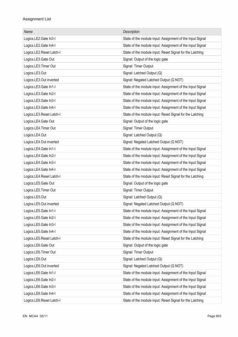
Assignment List
Name Description
Logics.LE2.Gate In3-I State of the module input: Assignment of the Input SignalLogics.LE2.Gate In4-I State of the module input: Assignment of the Input SignalLogics.LE2.Reset Latch-I State of the module input: Reset Signal for the LatchingLogics.LE3.Gate Out Signal: Output of the logic gateLogics.LE3.Timer Out Signal: Timer OutputLogics.LE3.Out Signal: Latched Output (Q)Logics.LE3.Out inverted Signal: Negated Latched Output (Q NOT)Logics.LE3.Gate In1-I State of the module input: Assignment of the Input SignalLogics.LE3.Gate In2-I State of the module input: Assignment of the Input SignalLogics.LE3.Gate In3-I State of the module input: Assignment of the Input SignalLogics.LE3.Gate In4-I State of the module input: Assignment of the Input SignalLogics.LE3.Reset Latch-I State of the module input: Reset Signal for the LatchingLogics.LE4.Gate Out Signal: Output of the logic gateLogics.LE4.Timer Out Signal: Timer OutputLogics.LE4.Out Signal: Latched Output (Q)Logics.LE4.Out inverted Signal: Negated Latched Output (Q NOT)Logics.LE4.Gate In1-I State of the module input: Assignment of the Input SignalLogics.LE4.Gate In2-I State of the module input: Assignment of the Input SignalLogics.LE4.Gate In3-I State of the module input: Assignment of the Input SignalLogics.LE4.Gate In4-I State of the module input: Assignment of the Input SignalLogics.LE4.Reset Latch-I State of the module input: Reset Signal for the LatchingLogics.LE5.Gate Out Signal: Output of the logic gateLogics.LE5.Timer Out Signal: Timer OutputLogics.LE5.Out Signal: Latched Output (Q)Logics.LE5.Out inverted Signal: Negated Latched Output (Q NOT)Logics.LE5.Gate In1-I State of the module input: Assignment of the Input SignalLogics.LE5.Gate In2-I State of the module input: Assignment of the Input SignalLogics.LE5.Gate In3-I State of the module input: Assignment of the Input SignalLogics.LE5.Gate In4-I State of the module input: Assignment of the Input SignalLogics.LE5.Reset Latch-I State of the module input: Reset Signal for the LatchingLogics.LE6.Gate Out Signal: Output of the logic gateLogics.LE6.Timer Out Signal: Timer OutputLogics.LE6.Out Signal: Latched Output (Q)Logics.LE6.Out inverted Signal: Negated Latched Output (Q NOT)Logics.LE6.Gate In1-I State of the module input: Assignment of the Input SignalLogics.LE6.Gate In2-I State of the module input: Assignment of the Input SignalLogics.LE6.Gate In3-I State of the module input: Assignment of the Input SignalLogics.LE6.Gate In4-I State of the module input: Assignment of the Input SignalLogics.LE6.Reset Latch-I State of the module input: Reset Signal for the Latching
EN MCA4 05/11 Page 803

Assignment List
Name Description
Logics.LE7.Gate Out Signal: Output of the logic gateLogics.LE7.Timer Out Signal: Timer OutputLogics.LE7.Out Signal: Latched Output (Q)Logics.LE7.Out inverted Signal: Negated Latched Output (Q NOT)Logics.LE7.Gate In1-I State of the module input: Assignment of the Input SignalLogics.LE7.Gate In2-I State of the module input: Assignment of the Input SignalLogics.LE7.Gate In3-I State of the module input: Assignment of the Input SignalLogics.LE7.Gate In4-I State of the module input: Assignment of the Input SignalLogics.LE7.Reset Latch-I State of the module input: Reset Signal for the LatchingLogics.LE8.Gate Out Signal: Output of the logic gateLogics.LE8.Timer Out Signal: Timer OutputLogics.LE8.Out Signal: Latched Output (Q)Logics.LE8.Out inverted Signal: Negated Latched Output (Q NOT)Logics.LE8.Gate In1-I State of the module input: Assignment of the Input SignalLogics.LE8.Gate In2-I State of the module input: Assignment of the Input SignalLogics.LE8.Gate In3-I State of the module input: Assignment of the Input SignalLogics.LE8.Gate In4-I State of the module input: Assignment of the Input SignalLogics.LE8.Reset Latch-I State of the module input: Reset Signal for the LatchingLogics.LE9.Gate Out Signal: Output of the logic gateLogics.LE9.Timer Out Signal: Timer OutputLogics.LE9.Out Signal: Latched Output (Q)Logics.LE9.Out inverted Signal: Negated Latched Output (Q NOT)Logics.LE9.Gate In1-I State of the module input: Assignment of the Input SignalLogics.LE9.Gate In2-I State of the module input: Assignment of the Input SignalLogics.LE9.Gate In3-I State of the module input: Assignment of the Input SignalLogics.LE9.Gate In4-I State of the module input: Assignment of the Input SignalLogics.LE9.Reset Latch-I State of the module input: Reset Signal for the LatchingLogics.LE10.Gate Out Signal: Output of the logic gateLogics.LE10.Timer Out Signal: Timer OutputLogics.LE10.Out Signal: Latched Output (Q)Logics.LE10.Out inverted Signal: Negated Latched Output (Q NOT)Logics.LE10.Gate In1-I State of the module input: Assignment of the Input SignalLogics.LE10.Gate In2-I State of the module input: Assignment of the Input SignalLogics.LE10.Gate In3-I State of the module input: Assignment of the Input SignalLogics.LE10.Gate In4-I State of the module input: Assignment of the Input SignalLogics.LE10.Reset Latch-I State of the module input: Reset Signal for the LatchingLogics.LE11.Gate Out Signal: Output of the logic gateLogics.LE11.Timer Out Signal: Timer OutputLogics.LE11.Out Signal: Latched Output (Q)
Page 804 EN MCA4 05/11
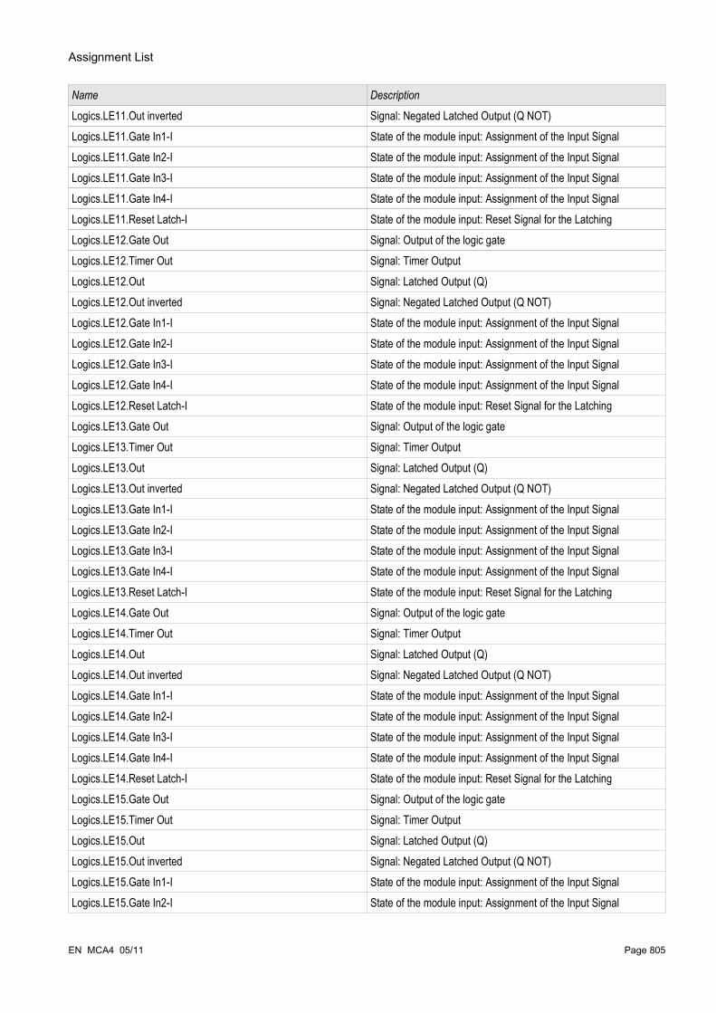
Assignment List
Name Description
Logics.LE11.Out inverted Signal: Negated Latched Output (Q NOT)Logics.LE11.Gate In1-I State of the module input: Assignment of the Input SignalLogics.LE11.Gate In2-I State of the module input: Assignment of the Input SignalLogics.LE11.Gate In3-I State of the module input: Assignment of the Input SignalLogics.LE11.Gate In4-I State of the module input: Assignment of the Input SignalLogics.LE11.Reset Latch-I State of the module input: Reset Signal for the LatchingLogics.LE12.Gate Out Signal: Output of the logic gateLogics.LE12.Timer Out Signal: Timer OutputLogics.LE12.Out Signal: Latched Output (Q)Logics.LE12.Out inverted Signal: Negated Latched Output (Q NOT)Logics.LE12.Gate In1-I State of the module input: Assignment of the Input SignalLogics.LE12.Gate In2-I State of the module input: Assignment of the Input SignalLogics.LE12.Gate In3-I State of the module input: Assignment of the Input SignalLogics.LE12.Gate In4-I State of the module input: Assignment of the Input SignalLogics.LE12.Reset Latch-I State of the module input: Reset Signal for the LatchingLogics.LE13.Gate Out Signal: Output of the logic gateLogics.LE13.Timer Out Signal: Timer OutputLogics.LE13.Out Signal: Latched Output (Q)Logics.LE13.Out inverted Signal: Negated Latched Output (Q NOT)Logics.LE13.Gate In1-I State of the module input: Assignment of the Input SignalLogics.LE13.Gate In2-I State of the module input: Assignment of the Input SignalLogics.LE13.Gate In3-I State of the module input: Assignment of the Input SignalLogics.LE13.Gate In4-I State of the module input: Assignment of the Input SignalLogics.LE13.Reset Latch-I State of the module input: Reset Signal for the LatchingLogics.LE14.Gate Out Signal: Output of the logic gateLogics.LE14.Timer Out Signal: Timer OutputLogics.LE14.Out Signal: Latched Output (Q)Logics.LE14.Out inverted Signal: Negated Latched Output (Q NOT)Logics.LE14.Gate In1-I State of the module input: Assignment of the Input SignalLogics.LE14.Gate In2-I State of the module input: Assignment of the Input SignalLogics.LE14.Gate In3-I State of the module input: Assignment of the Input SignalLogics.LE14.Gate In4-I State of the module input: Assignment of the Input SignalLogics.LE14.Reset Latch-I State of the module input: Reset Signal for the LatchingLogics.LE15.Gate Out Signal: Output of the logic gateLogics.LE15.Timer Out Signal: Timer OutputLogics.LE15.Out Signal: Latched Output (Q)Logics.LE15.Out inverted Signal: Negated Latched Output (Q NOT)Logics.LE15.Gate In1-I State of the module input: Assignment of the Input SignalLogics.LE15.Gate In2-I State of the module input: Assignment of the Input Signal
EN MCA4 05/11 Page 805

Assignment List
Name Description
Logics.LE15.Gate In3-I State of the module input: Assignment of the Input SignalLogics.LE15.Gate In4-I State of the module input: Assignment of the Input SignalLogics.LE15.Reset Latch-I State of the module input: Reset Signal for the LatchingLogics.LE16.Gate Out Signal: Output of the logic gateLogics.LE16.Timer Out Signal: Timer OutputLogics.LE16.Out Signal: Latched Output (Q)Logics.LE16.Out inverted Signal: Negated Latched Output (Q NOT)Logics.LE16.Gate In1-I State of the module input: Assignment of the Input SignalLogics.LE16.Gate In2-I State of the module input: Assignment of the Input SignalLogics.LE16.Gate In3-I State of the module input: Assignment of the Input SignalLogics.LE16.Gate In4-I State of the module input: Assignment of the Input SignalLogics.LE16.Reset Latch-I State of the module input: Reset Signal for the LatchingLogics.LE17.Gate Out Signal: Output of the logic gateLogics.LE17.Timer Out Signal: Timer OutputLogics.LE17.Out Signal: Latched Output (Q)Logics.LE17.Out inverted Signal: Negated Latched Output (Q NOT)Logics.LE17.Gate In1-I State of the module input: Assignment of the Input SignalLogics.LE17.Gate In2-I State of the module input: Assignment of the Input SignalLogics.LE17.Gate In3-I State of the module input: Assignment of the Input SignalLogics.LE17.Gate In4-I State of the module input: Assignment of the Input SignalLogics.LE17.Reset Latch-I State of the module input: Reset Signal for the LatchingLogics.LE18.Gate Out Signal: Output of the logic gateLogics.LE18.Timer Out Signal: Timer OutputLogics.LE18.Out Signal: Latched Output (Q)Logics.LE18.Out inverted Signal: Negated Latched Output (Q NOT)Logics.LE18.Gate In1-I State of the module input: Assignment of the Input SignalLogics.LE18.Gate In2-I State of the module input: Assignment of the Input SignalLogics.LE18.Gate In3-I State of the module input: Assignment of the Input SignalLogics.LE18.Gate In4-I State of the module input: Assignment of the Input SignalLogics.LE18.Reset Latch-I State of the module input: Reset Signal for the LatchingLogics.LE19.Gate Out Signal: Output of the logic gateLogics.LE19.Timer Out Signal: Timer OutputLogics.LE19.Out Signal: Latched Output (Q)Logics.LE19.Out inverted Signal: Negated Latched Output (Q NOT)Logics.LE19.Gate In1-I State of the module input: Assignment of the Input SignalLogics.LE19.Gate In2-I State of the module input: Assignment of the Input SignalLogics.LE19.Gate In3-I State of the module input: Assignment of the Input SignalLogics.LE19.Gate In4-I State of the module input: Assignment of the Input SignalLogics.LE19.Reset Latch-I State of the module input: Reset Signal for the Latching
Page 806 EN MCA4 05/11
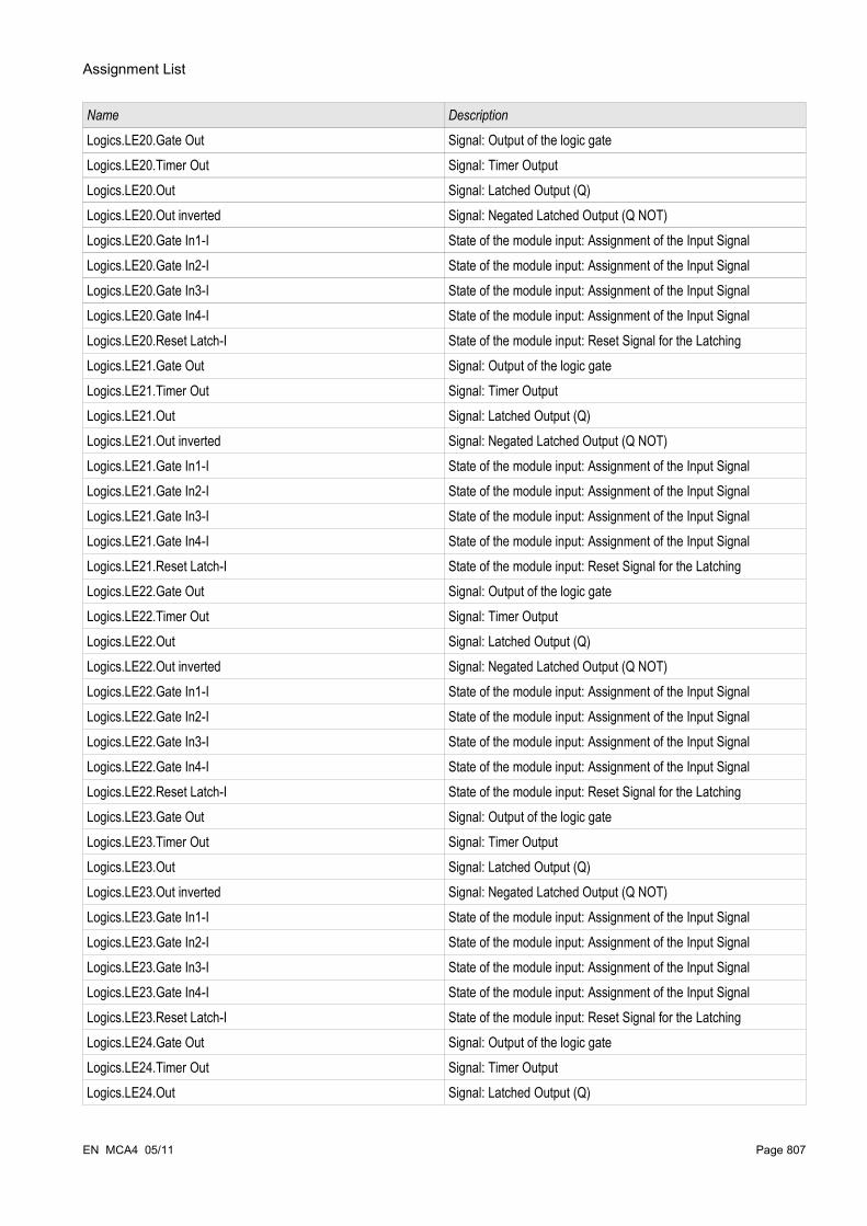
Assignment List
Name Description
Logics.LE20.Gate Out Signal: Output of the logic gateLogics.LE20.Timer Out Signal: Timer OutputLogics.LE20.Out Signal: Latched Output (Q)Logics.LE20.Out inverted Signal: Negated Latched Output (Q NOT)Logics.LE20.Gate In1-I State of the module input: Assignment of the Input SignalLogics.LE20.Gate In2-I State of the module input: Assignment of the Input SignalLogics.LE20.Gate In3-I State of the module input: Assignment of the Input SignalLogics.LE20.Gate In4-I State of the module input: Assignment of the Input SignalLogics.LE20.Reset Latch-I State of the module input: Reset Signal for the LatchingLogics.LE21.Gate Out Signal: Output of the logic gateLogics.LE21.Timer Out Signal: Timer OutputLogics.LE21.Out Signal: Latched Output (Q)Logics.LE21.Out inverted Signal: Negated Latched Output (Q NOT)Logics.LE21.Gate In1-I State of the module input: Assignment of the Input SignalLogics.LE21.Gate In2-I State of the module input: Assignment of the Input SignalLogics.LE21.Gate In3-I State of the module input: Assignment of the Input SignalLogics.LE21.Gate In4-I State of the module input: Assignment of the Input SignalLogics.LE21.Reset Latch-I State of the module input: Reset Signal for the LatchingLogics.LE22.Gate Out Signal: Output of the logic gateLogics.LE22.Timer Out Signal: Timer OutputLogics.LE22.Out Signal: Latched Output (Q)Logics.LE22.Out inverted Signal: Negated Latched Output (Q NOT)Logics.LE22.Gate In1-I State of the module input: Assignment of the Input SignalLogics.LE22.Gate In2-I State of the module input: Assignment of the Input SignalLogics.LE22.Gate In3-I State of the module input: Assignment of the Input SignalLogics.LE22.Gate In4-I State of the module input: Assignment of the Input SignalLogics.LE22.Reset Latch-I State of the module input: Reset Signal for the LatchingLogics.LE23.Gate Out Signal: Output of the logic gateLogics.LE23.Timer Out Signal: Timer OutputLogics.LE23.Out Signal: Latched Output (Q)Logics.LE23.Out inverted Signal: Negated Latched Output (Q NOT)Logics.LE23.Gate In1-I State of the module input: Assignment of the Input SignalLogics.LE23.Gate In2-I State of the module input: Assignment of the Input SignalLogics.LE23.Gate In3-I State of the module input: Assignment of the Input SignalLogics.LE23.Gate In4-I State of the module input: Assignment of the Input SignalLogics.LE23.Reset Latch-I State of the module input: Reset Signal for the LatchingLogics.LE24.Gate Out Signal: Output of the logic gateLogics.LE24.Timer Out Signal: Timer OutputLogics.LE24.Out Signal: Latched Output (Q)
EN MCA4 05/11 Page 807

Assignment List
Name Description
Logics.LE24.Out inverted Signal: Negated Latched Output (Q NOT)Logics.LE24.Gate In1-I State of the module input: Assignment of the Input SignalLogics.LE24.Gate In2-I State of the module input: Assignment of the Input SignalLogics.LE24.Gate In3-I State of the module input: Assignment of the Input SignalLogics.LE24.Gate In4-I State of the module input: Assignment of the Input SignalLogics.LE24.Reset Latch-I State of the module input: Reset Signal for the LatchingLogics.LE25.Gate Out Signal: Output of the logic gateLogics.LE25.Timer Out Signal: Timer OutputLogics.LE25.Out Signal: Latched Output (Q)Logics.LE25.Out inverted Signal: Negated Latched Output (Q NOT)Logics.LE25.Gate In1-I State of the module input: Assignment of the Input SignalLogics.LE25.Gate In2-I State of the module input: Assignment of the Input SignalLogics.LE25.Gate In3-I State of the module input: Assignment of the Input SignalLogics.LE25.Gate In4-I State of the module input: Assignment of the Input SignalLogics.LE25.Reset Latch-I State of the module input: Reset Signal for the LatchingLogics.LE26.Gate Out Signal: Output of the logic gateLogics.LE26.Timer Out Signal: Timer OutputLogics.LE26.Out Signal: Latched Output (Q)Logics.LE26.Out inverted Signal: Negated Latched Output (Q NOT)Logics.LE26.Gate In1-I State of the module input: Assignment of the Input SignalLogics.LE26.Gate In2-I State of the module input: Assignment of the Input SignalLogics.LE26.Gate In3-I State of the module input: Assignment of the Input SignalLogics.LE26.Gate In4-I State of the module input: Assignment of the Input SignalLogics.LE26.Reset Latch-I State of the module input: Reset Signal for the LatchingLogics.LE27.Gate Out Signal: Output of the logic gateLogics.LE27.Timer Out Signal: Timer OutputLogics.LE27.Out Signal: Latched Output (Q)Logics.LE27.Out inverted Signal: Negated Latched Output (Q NOT)Logics.LE27.Gate In1-I State of the module input: Assignment of the Input SignalLogics.LE27.Gate In2-I State of the module input: Assignment of the Input SignalLogics.LE27.Gate In3-I State of the module input: Assignment of the Input SignalLogics.LE27.Gate In4-I State of the module input: Assignment of the Input SignalLogics.LE27.Reset Latch-I State of the module input: Reset Signal for the LatchingLogics.LE28.Gate Out Signal: Output of the logic gateLogics.LE28.Timer Out Signal: Timer OutputLogics.LE28.Out Signal: Latched Output (Q)Logics.LE28.Out inverted Signal: Negated Latched Output (Q NOT)Logics.LE28.Gate In1-I State of the module input: Assignment of the Input SignalLogics.LE28.Gate In2-I State of the module input: Assignment of the Input Signal
Page 808 EN MCA4 05/11
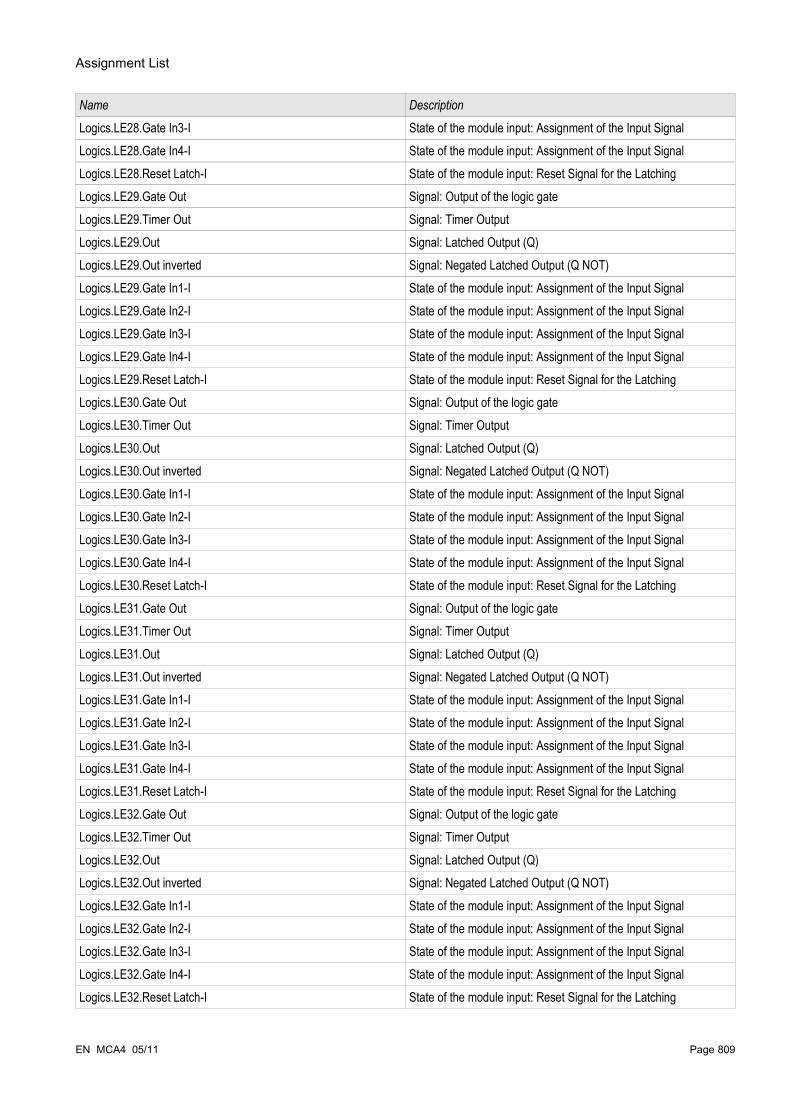
Assignment List
Name Description
Logics.LE28.Gate In3-I State of the module input: Assignment of the Input SignalLogics.LE28.Gate In4-I State of the module input: Assignment of the Input SignalLogics.LE28.Reset Latch-I State of the module input: Reset Signal for the LatchingLogics.LE29.Gate Out Signal: Output of the logic gateLogics.LE29.Timer Out Signal: Timer OutputLogics.LE29.Out Signal: Latched Output (Q)Logics.LE29.Out inverted Signal: Negated Latched Output (Q NOT)Logics.LE29.Gate In1-I State of the module input: Assignment of the Input SignalLogics.LE29.Gate In2-I State of the module input: Assignment of the Input SignalLogics.LE29.Gate In3-I State of the module input: Assignment of the Input SignalLogics.LE29.Gate In4-I State of the module input: Assignment of the Input SignalLogics.LE29.Reset Latch-I State of the module input: Reset Signal for the LatchingLogics.LE30.Gate Out Signal: Output of the logic gateLogics.LE30.Timer Out Signal: Timer OutputLogics.LE30.Out Signal: Latched Output (Q)Logics.LE30.Out inverted Signal: Negated Latched Output (Q NOT)Logics.LE30.Gate In1-I State of the module input: Assignment of the Input SignalLogics.LE30.Gate In2-I State of the module input: Assignment of the Input SignalLogics.LE30.Gate In3-I State of the module input: Assignment of the Input SignalLogics.LE30.Gate In4-I State of the module input: Assignment of the Input SignalLogics.LE30.Reset Latch-I State of the module input: Reset Signal for the LatchingLogics.LE31.Gate Out Signal: Output of the logic gateLogics.LE31.Timer Out Signal: Timer OutputLogics.LE31.Out Signal: Latched Output (Q)Logics.LE31.Out inverted Signal: Negated Latched Output (Q NOT)Logics.LE31.Gate In1-I State of the module input: Assignment of the Input SignalLogics.LE31.Gate In2-I State of the module input: Assignment of the Input SignalLogics.LE31.Gate In3-I State of the module input: Assignment of the Input SignalLogics.LE31.Gate In4-I State of the module input: Assignment of the Input SignalLogics.LE31.Reset Latch-I State of the module input: Reset Signal for the LatchingLogics.LE32.Gate Out Signal: Output of the logic gateLogics.LE32.Timer Out Signal: Timer OutputLogics.LE32.Out Signal: Latched Output (Q)Logics.LE32.Out inverted Signal: Negated Latched Output (Q NOT)Logics.LE32.Gate In1-I State of the module input: Assignment of the Input SignalLogics.LE32.Gate In2-I State of the module input: Assignment of the Input SignalLogics.LE32.Gate In3-I State of the module input: Assignment of the Input SignalLogics.LE32.Gate In4-I State of the module input: Assignment of the Input SignalLogics.LE32.Reset Latch-I State of the module input: Reset Signal for the Latching
EN MCA4 05/11 Page 809
Assignment List
Name Description
Logics.LE33.Gate Out Signal: Output of the logic gateLogics.LE33.Timer Out Signal: Timer OutputLogics.LE33.Out Signal: Latched Output (Q)Logics.LE33.Out inverted Signal: Negated Latched Output (Q NOT)Logics.LE33.Gate In1-I State of the module input: Assignment of the Input SignalLogics.LE33.Gate In2-I State of the module input: Assignment of the Input SignalLogics.LE33.Gate In3-I State of the module input: Assignment of the Input SignalLogics.LE33.Gate In4-I State of the module input: Assignment of the Input SignalLogics.LE33.Reset Latch-I State of the module input: Reset Signal for the LatchingLogics.LE34.Gate Out Signal: Output of the logic gateLogics.LE34.Timer Out Signal: Timer OutputLogics.LE34.Out Signal: Latched Output (Q)Logics.LE34.Out inverted Signal: Negated Latched Output (Q NOT)Logics.LE34.Gate In1-I State of the module input: Assignment of the Input SignalLogics.LE34.Gate In2-I State of the module input: Assignment of the Input SignalLogics.LE34.Gate In3-I State of the module input: Assignment of the Input SignalLogics.LE34.Gate In4-I State of the module input: Assignment of the Input SignalLogics.LE34.Reset Latch-I State of the module input: Reset Signal for the LatchingLogics.LE35.Gate Out Signal: Output of the logic gateLogics.LE35.Timer Out Signal: Timer OutputLogics.LE35.Out Signal: Latched Output (Q)Logics.LE35.Out inverted Signal: Negated Latched Output (Q NOT)Logics.LE35.Gate In1-I State of the module input: Assignment of the Input SignalLogics.LE35.Gate In2-I State of the module input: Assignment of the Input SignalLogics.LE35.Gate In3-I State of the module input: Assignment of the Input SignalLogics.LE35.Gate In4-I State of the module input: Assignment of the Input SignalLogics.LE35.Reset Latch-I State of the module input: Reset Signal for the LatchingLogics.LE36.Gate Out Signal: Output of the logic gateLogics.LE36.Timer Out Signal: Timer OutputLogics.LE36.Out Signal: Latched Output (Q)Logics.LE36.Out inverted Signal: Negated Latched Output (Q NOT)Logics.LE36.Gate In1-I State of the module input: Assignment of the Input SignalLogics.LE36.Gate In2-I State of the module input: Assignment of the Input SignalLogics.LE36.Gate In3-I State of the module input: Assignment of the Input SignalLogics.LE36.Gate In4-I State of the module input: Assignment of the Input SignalLogics.LE36.Reset Latch-I State of the module input: Reset Signal for the LatchingLogics.LE37.Gate Out Signal: Output of the logic gateLogics.LE37.Timer Out Signal: Timer OutputLogics.LE37.Out Signal: Latched Output (Q)
Page 810 EN MCA4 05/11

Assignment List
Name Description
Logics.LE37.Out inverted Signal: Negated Latched Output (Q NOT)Logics.LE37.Gate In1-I State of the module input: Assignment of the Input SignalLogics.LE37.Gate In2-I State of the module input: Assignment of the Input SignalLogics.LE37.Gate In3-I State of the module input: Assignment of the Input SignalLogics.LE37.Gate In4-I State of the module input: Assignment of the Input SignalLogics.LE37.Reset Latch-I State of the module input: Reset Signal for the LatchingLogics.LE38.Gate Out Signal: Output of the logic gateLogics.LE38.Timer Out Signal: Timer OutputLogics.LE38.Out Signal: Latched Output (Q)Logics.LE38.Out inverted Signal: Negated Latched Output (Q NOT)Logics.LE38.Gate In1-I State of the module input: Assignment of the Input SignalLogics.LE38.Gate In2-I State of the module input: Assignment of the Input SignalLogics.LE38.Gate In3-I State of the module input: Assignment of the Input SignalLogics.LE38.Gate In4-I State of the module input: Assignment of the Input SignalLogics.LE38.Reset Latch-I State of the module input: Reset Signal for the LatchingLogics.LE39.Gate Out Signal: Output of the logic gateLogics.LE39.Timer Out Signal: Timer OutputLogics.LE39.Out Signal: Latched Output (Q)Logics.LE39.Out inverted Signal: Negated Latched Output (Q NOT)Logics.LE39.Gate In1-I State of the module input: Assignment of the Input SignalLogics.LE39.Gate In2-I State of the module input: Assignment of the Input SignalLogics.LE39.Gate In3-I State of the module input: Assignment of the Input SignalLogics.LE39.Gate In4-I State of the module input: Assignment of the Input SignalLogics.LE39.Reset Latch-I State of the module input: Reset Signal for the LatchingLogics.LE40.Gate Out Signal: Output of the logic gateLogics.LE40.Timer Out Signal: Timer OutputLogics.LE40.Out Signal: Latched Output (Q)Logics.LE40.Out inverted Signal: Negated Latched Output (Q NOT)Logics.LE40.Gate In1-I State of the module input: Assignment of the Input SignalLogics.LE40.Gate In2-I State of the module input: Assignment of the Input SignalLogics.LE40.Gate In3-I State of the module input: Assignment of the Input SignalLogics.LE40.Gate In4-I State of the module input: Assignment of the Input SignalLogics.LE40.Reset Latch-I State of the module input: Reset Signal for the LatchingLogics.LE41.Gate Out Signal: Output of the logic gateLogics.LE41.Timer Out Signal: Timer OutputLogics.LE41.Out Signal: Latched Output (Q)Logics.LE41.Out inverted Signal: Negated Latched Output (Q NOT)Logics.LE41.Gate In1-I State of the module input: Assignment of the Input SignalLogics.LE41.Gate In2-I State of the module input: Assignment of the Input Signal
EN MCA4 05/11 Page 811

Assignment List
Name Description
Logics.LE41.Gate In3-I State of the module input: Assignment of the Input SignalLogics.LE41.Gate In4-I State of the module input: Assignment of the Input SignalLogics.LE41.Reset Latch-I State of the module input: Reset Signal for the LatchingLogics.LE42.Gate Out Signal: Output of the logic gateLogics.LE42.Timer Out Signal: Timer OutputLogics.LE42.Out Signal: Latched Output (Q)Logics.LE42.Out inverted Signal: Negated Latched Output (Q NOT)Logics.LE42.Gate In1-I State of the module input: Assignment of the Input SignalLogics.LE42.Gate In2-I State of the module input: Assignment of the Input SignalLogics.LE42.Gate In3-I State of the module input: Assignment of the Input SignalLogics.LE42.Gate In4-I State of the module input: Assignment of the Input SignalLogics.LE42.Reset Latch-I State of the module input: Reset Signal for the LatchingLogics.LE43.Gate Out Signal: Output of the logic gateLogics.LE43.Timer Out Signal: Timer OutputLogics.LE43.Out Signal: Latched Output (Q)Logics.LE43.Out inverted Signal: Negated Latched Output (Q NOT)Logics.LE43.Gate In1-I State of the module input: Assignment of the Input SignalLogics.LE43.Gate In2-I State of the module input: Assignment of the Input SignalLogics.LE43.Gate In3-I State of the module input: Assignment of the Input SignalLogics.LE43.Gate In4-I State of the module input: Assignment of the Input SignalLogics.LE43.Reset Latch-I State of the module input: Reset Signal for the LatchingLogics.LE44.Gate Out Signal: Output of the logic gateLogics.LE44.Timer Out Signal: Timer OutputLogics.LE44.Out Signal: Latched Output (Q)Logics.LE44.Out inverted Signal: Negated Latched Output (Q NOT)Logics.LE44.Gate In1-I State of the module input: Assignment of the Input SignalLogics.LE44.Gate In2-I State of the module input: Assignment of the Input SignalLogics.LE44.Gate In3-I State of the module input: Assignment of the Input SignalLogics.LE44.Gate In4-I State of the module input: Assignment of the Input SignalLogics.LE44.Reset Latch-I State of the module input: Reset Signal for the LatchingLogics.LE45.Gate Out Signal: Output of the logic gateLogics.LE45.Timer Out Signal: Timer OutputLogics.LE45.Out Signal: Latched Output (Q)Logics.LE45.Out inverted Signal: Negated Latched Output (Q NOT)Logics.LE45.Gate In1-I State of the module input: Assignment of the Input SignalLogics.LE45.Gate In2-I State of the module input: Assignment of the Input SignalLogics.LE45.Gate In3-I State of the module input: Assignment of the Input SignalLogics.LE45.Gate In4-I State of the module input: Assignment of the Input SignalLogics.LE45.Reset Latch-I State of the module input: Reset Signal for the Latching
Page 812 EN MCA4 05/11

Assignment List
Name Description
Logics.LE46.Gate Out Signal: Output of the logic gateLogics.LE46.Timer Out Signal: Timer OutputLogics.LE46.Out Signal: Latched Output (Q)Logics.LE46.Out inverted Signal: Negated Latched Output (Q NOT)Logics.LE46.Gate In1-I State of the module input: Assignment of the Input SignalLogics.LE46.Gate In2-I State of the module input: Assignment of the Input SignalLogics.LE46.Gate In3-I State of the module input: Assignment of the Input SignalLogics.LE46.Gate In4-I State of the module input: Assignment of the Input SignalLogics.LE46.Reset Latch-I State of the module input: Reset Signal for the LatchingLogics.LE47.Gate Out Signal: Output of the logic gateLogics.LE47.Timer Out Signal: Timer OutputLogics.LE47.Out Signal: Latched Output (Q)Logics.LE47.Out inverted Signal: Negated Latched Output (Q NOT)Logics.LE47.Gate In1-I State of the module input: Assignment of the Input SignalLogics.LE47.Gate In2-I State of the module input: Assignment of the Input SignalLogics.LE47.Gate In3-I State of the module input: Assignment of the Input SignalLogics.LE47.Gate In4-I State of the module input: Assignment of the Input SignalLogics.LE47.Reset Latch-I State of the module input: Reset Signal for the LatchingLogics.LE48.Gate Out Signal: Output of the logic gateLogics.LE48.Timer Out Signal: Timer OutputLogics.LE48.Out Signal: Latched Output (Q)Logics.LE48.Out inverted Signal: Negated Latched Output (Q NOT)Logics.LE48.Gate In1-I State of the module input: Assignment of the Input SignalLogics.LE48.Gate In2-I State of the module input: Assignment of the Input SignalLogics.LE48.Gate In3-I State of the module input: Assignment of the Input SignalLogics.LE48.Gate In4-I State of the module input: Assignment of the Input SignalLogics.LE48.Reset Latch-I State of the module input: Reset Signal for the LatchingLogics.LE49.Gate Out Signal: Output of the logic gateLogics.LE49.Timer Out Signal: Timer OutputLogics.LE49.Out Signal: Latched Output (Q)Logics.LE49.Out inverted Signal: Negated Latched Output (Q NOT)Logics.LE49.Gate In1-I State of the module input: Assignment of the Input SignalLogics.LE49.Gate In2-I State of the module input: Assignment of the Input SignalLogics.LE49.Gate In3-I State of the module input: Assignment of the Input SignalLogics.LE49.Gate In4-I State of the module input: Assignment of the Input SignalLogics.LE49.Reset Latch-I State of the module input: Reset Signal for the LatchingLogics.LE50.Gate Out Signal: Output of the logic gateLogics.LE50.Timer Out Signal: Timer OutputLogics.LE50.Out Signal: Latched Output (Q)
EN MCA4 05/11 Page 813

Assignment List
Name Description
Logics.LE50.Out inverted Signal: Negated Latched Output (Q NOT)Logics.LE50.Gate In1-I State of the module input: Assignment of the Input SignalLogics.LE50.Gate In2-I State of the module input: Assignment of the Input SignalLogics.LE50.Gate In3-I State of the module input: Assignment of the Input SignalLogics.LE50.Gate In4-I State of the module input: Assignment of the Input SignalLogics.LE50.Reset Latch-I State of the module input: Reset Signal for the LatchingLogics.LE51.Gate Out Signal: Output of the logic gateLogics.LE51.Timer Out Signal: Timer OutputLogics.LE51.Out Signal: Latched Output (Q)Logics.LE51.Out inverted Signal: Negated Latched Output (Q NOT)Logics.LE51.Gate In1-I State of the module input: Assignment of the Input SignalLogics.LE51.Gate In2-I State of the module input: Assignment of the Input SignalLogics.LE51.Gate In3-I State of the module input: Assignment of the Input SignalLogics.LE51.Gate In4-I State of the module input: Assignment of the Input SignalLogics.LE51.Reset Latch-I State of the module input: Reset Signal for the LatchingLogics.LE52.Gate Out Signal: Output of the logic gateLogics.LE52.Timer Out Signal: Timer OutputLogics.LE52.Out Signal: Latched Output (Q)Logics.LE52.Out inverted Signal: Negated Latched Output (Q NOT)Logics.LE52.Gate In1-I State of the module input: Assignment of the Input SignalLogics.LE52.Gate In2-I State of the module input: Assignment of the Input SignalLogics.LE52.Gate In3-I State of the module input: Assignment of the Input SignalLogics.LE52.Gate In4-I State of the module input: Assignment of the Input SignalLogics.LE52.Reset Latch-I State of the module input: Reset Signal for the LatchingLogics.LE53.Gate Out Signal: Output of the logic gateLogics.LE53.Timer Out Signal: Timer OutputLogics.LE53.Out Signal: Latched Output (Q)Logics.LE53.Out inverted Signal: Negated Latched Output (Q NOT)Logics.LE53.Gate In1-I State of the module input: Assignment of the Input SignalLogics.LE53.Gate In2-I State of the module input: Assignment of the Input SignalLogics.LE53.Gate In3-I State of the module input: Assignment of the Input SignalLogics.LE53.Gate In4-I State of the module input: Assignment of the Input SignalLogics.LE53.Reset Latch-I State of the module input: Reset Signal for the LatchingLogics.LE54.Gate Out Signal: Output of the logic gateLogics.LE54.Timer Out Signal: Timer OutputLogics.LE54.Out Signal: Latched Output (Q)Logics.LE54.Out inverted Signal: Negated Latched Output (Q NOT)Logics.LE54.Gate In1-I State of the module input: Assignment of the Input SignalLogics.LE54.Gate In2-I State of the module input: Assignment of the Input Signal
Page 814 EN MCA4 05/11

Assignment List
Name Description
Logics.LE54.Gate In3-I State of the module input: Assignment of the Input SignalLogics.LE54.Gate In4-I State of the module input: Assignment of the Input SignalLogics.LE54.Reset Latch-I State of the module input: Reset Signal for the LatchingLogics.LE55.Gate Out Signal: Output of the logic gateLogics.LE55.Timer Out Signal: Timer OutputLogics.LE55.Out Signal: Latched Output (Q)Logics.LE55.Out inverted Signal: Negated Latched Output (Q NOT)Logics.LE55.Gate In1-I State of the module input: Assignment of the Input SignalLogics.LE55.Gate In2-I State of the module input: Assignment of the Input SignalLogics.LE55.Gate In3-I State of the module input: Assignment of the Input SignalLogics.LE55.Gate In4-I State of the module input: Assignment of the Input SignalLogics.LE55.Reset Latch-I State of the module input: Reset Signal for the LatchingLogics.LE56.Gate Out Signal: Output of the logic gateLogics.LE56.Timer Out Signal: Timer OutputLogics.LE56.Out Signal: Latched Output (Q)Logics.LE56.Out inverted Signal: Negated Latched Output (Q NOT)Logics.LE56.Gate In1-I State of the module input: Assignment of the Input SignalLogics.LE56.Gate In2-I State of the module input: Assignment of the Input SignalLogics.LE56.Gate In3-I State of the module input: Assignment of the Input SignalLogics.LE56.Gate In4-I State of the module input: Assignment of the Input SignalLogics.LE56.Reset Latch-I State of the module input: Reset Signal for the LatchingLogics.LE57.Gate Out Signal: Output of the logic gateLogics.LE57.Timer Out Signal: Timer OutputLogics.LE57.Out Signal: Latched Output (Q)Logics.LE57.Out inverted Signal: Negated Latched Output (Q NOT)Logics.LE57.Gate In1-I State of the module input: Assignment of the Input SignalLogics.LE57.Gate In2-I State of the module input: Assignment of the Input SignalLogics.LE57.Gate In3-I State of the module input: Assignment of the Input SignalLogics.LE57.Gate In4-I State of the module input: Assignment of the Input SignalLogics.LE57.Reset Latch-I State of the module input: Reset Signal for the LatchingLogics.LE58.Gate Out Signal: Output of the logic gateLogics.LE58.Timer Out Signal: Timer OutputLogics.LE58.Out Signal: Latched Output (Q)Logics.LE58.Out inverted Signal: Negated Latched Output (Q NOT)Logics.LE58.Gate In1-I State of the module input: Assignment of the Input SignalLogics.LE58.Gate In2-I State of the module input: Assignment of the Input SignalLogics.LE58.Gate In3-I State of the module input: Assignment of the Input SignalLogics.LE58.Gate In4-I State of the module input: Assignment of the Input SignalLogics.LE58.Reset Latch-I State of the module input: Reset Signal for the Latching
EN MCA4 05/11 Page 815

Assignment List
Name Description
Logics.LE59.Gate Out Signal: Output of the logic gateLogics.LE59.Timer Out Signal: Timer OutputLogics.LE59.Out Signal: Latched Output (Q)Logics.LE59.Out inverted Signal: Negated Latched Output (Q NOT)Logics.LE59.Gate In1-I State of the module input: Assignment of the Input SignalLogics.LE59.Gate In2-I State of the module input: Assignment of the Input SignalLogics.LE59.Gate In3-I State of the module input: Assignment of the Input SignalLogics.LE59.Gate In4-I State of the module input: Assignment of the Input SignalLogics.LE59.Reset Latch-I State of the module input: Reset Signal for the LatchingLogics.LE60.Gate Out Signal: Output of the logic gateLogics.LE60.Timer Out Signal: Timer OutputLogics.LE60.Out Signal: Latched Output (Q)Logics.LE60.Out inverted Signal: Negated Latched Output (Q NOT)Logics.LE60.Gate In1-I State of the module input: Assignment of the Input SignalLogics.LE60.Gate In2-I State of the module input: Assignment of the Input SignalLogics.LE60.Gate In3-I State of the module input: Assignment of the Input SignalLogics.LE60.Gate In4-I State of the module input: Assignment of the Input SignalLogics.LE60.Reset Latch-I State of the module input: Reset Signal for the LatchingLogics.LE61.Gate Out Signal: Output of the logic gateLogics.LE61.Timer Out Signal: Timer OutputLogics.LE61.Out Signal: Latched Output (Q)Logics.LE61.Out inverted Signal: Negated Latched Output (Q NOT)Logics.LE61.Gate In1-I State of the module input: Assignment of the Input SignalLogics.LE61.Gate In2-I State of the module input: Assignment of the Input SignalLogics.LE61.Gate In3-I State of the module input: Assignment of the Input SignalLogics.LE61.Gate In4-I State of the module input: Assignment of the Input SignalLogics.LE61.Reset Latch-I State of the module input: Reset Signal for the LatchingLogics.LE62.Gate Out Signal: Output of the logic gateLogics.LE62.Timer Out Signal: Timer OutputLogics.LE62.Out Signal: Latched Output (Q)Logics.LE62.Out inverted Signal: Negated Latched Output (Q NOT)Logics.LE62.Gate In1-I State of the module input: Assignment of the Input SignalLogics.LE62.Gate In2-I State of the module input: Assignment of the Input SignalLogics.LE62.Gate In3-I State of the module input: Assignment of the Input SignalLogics.LE62.Gate In4-I State of the module input: Assignment of the Input SignalLogics.LE62.Reset Latch-I State of the module input: Reset Signal for the LatchingLogics.LE63.Gate Out Signal: Output of the logic gateLogics.LE63.Timer Out Signal: Timer OutputLogics.LE63.Out Signal: Latched Output (Q)
Page 816 EN MCA4 05/11

Assignment List
Name Description
Logics.LE63.Out inverted Signal: Negated Latched Output (Q NOT)Logics.LE63.Gate In1-I State of the module input: Assignment of the Input SignalLogics.LE63.Gate In2-I State of the module input: Assignment of the Input SignalLogics.LE63.Gate In3-I State of the module input: Assignment of the Input SignalLogics.LE63.Gate In4-I State of the module input: Assignment of the Input SignalLogics.LE63.Reset Latch-I State of the module input: Reset Signal for the LatchingLogics.LE64.Gate Out Signal: Output of the logic gateLogics.LE64.Timer Out Signal: Timer OutputLogics.LE64.Out Signal: Latched Output (Q)Logics.LE64.Out inverted Signal: Negated Latched Output (Q NOT)Logics.LE64.Gate In1-I State of the module input: Assignment of the Input SignalLogics.LE64.Gate In2-I State of the module input: Assignment of the Input SignalLogics.LE64.Gate In3-I State of the module input: Assignment of the Input SignalLogics.LE64.Gate In4-I State of the module input: Assignment of the Input SignalLogics.LE64.Reset Latch-I State of the module input: Reset Signal for the LatchingLogics.LE65.Gate Out Signal: Output of the logic gateLogics.LE65.Timer Out Signal: Timer OutputLogics.LE65.Out Signal: Latched Output (Q)Logics.LE65.Out inverted Signal: Negated Latched Output (Q NOT)Logics.LE65.Gate In1-I State of the module input: Assignment of the Input SignalLogics.LE65.Gate In2-I State of the module input: Assignment of the Input SignalLogics.LE65.Gate In3-I State of the module input: Assignment of the Input SignalLogics.LE65.Gate In4-I State of the module input: Assignment of the Input SignalLogics.LE65.Reset Latch-I State of the module input: Reset Signal for the LatchingLogics.LE66.Gate Out Signal: Output of the logic gateLogics.LE66.Timer Out Signal: Timer OutputLogics.LE66.Out Signal: Latched Output (Q)Logics.LE66.Out inverted Signal: Negated Latched Output (Q NOT)Logics.LE66.Gate In1-I State of the module input: Assignment of the Input SignalLogics.LE66.Gate In2-I State of the module input: Assignment of the Input SignalLogics.LE66.Gate In3-I State of the module input: Assignment of the Input SignalLogics.LE66.Gate In4-I State of the module input: Assignment of the Input SignalLogics.LE66.Reset Latch-I State of the module input: Reset Signal for the LatchingLogics.LE67.Gate Out Signal: Output of the logic gateLogics.LE67.Timer Out Signal: Timer OutputLogics.LE67.Out Signal: Latched Output (Q)Logics.LE67.Out inverted Signal: Negated Latched Output (Q NOT)Logics.LE67.Gate In1-I State of the module input: Assignment of the Input SignalLogics.LE67.Gate In2-I State of the module input: Assignment of the Input Signal
EN MCA4 05/11 Page 817

Assignment List
Name Description
Logics.LE67.Gate In3-I State of the module input: Assignment of the Input SignalLogics.LE67.Gate In4-I State of the module input: Assignment of the Input SignalLogics.LE67.Reset Latch-I State of the module input: Reset Signal for the LatchingLogics.LE68.Gate Out Signal: Output of the logic gateLogics.LE68.Timer Out Signal: Timer OutputLogics.LE68.Out Signal: Latched Output (Q)Logics.LE68.Out inverted Signal: Negated Latched Output (Q NOT)Logics.LE68.Gate In1-I State of the module input: Assignment of the Input SignalLogics.LE68.Gate In2-I State of the module input: Assignment of the Input SignalLogics.LE68.Gate In3-I State of the module input: Assignment of the Input SignalLogics.LE68.Gate In4-I State of the module input: Assignment of the Input SignalLogics.LE68.Reset Latch-I State of the module input: Reset Signal for the LatchingLogics.LE69.Gate Out Signal: Output of the logic gateLogics.LE69.Timer Out Signal: Timer OutputLogics.LE69.Out Signal: Latched Output (Q)Logics.LE69.Out inverted Signal: Negated Latched Output (Q NOT)Logics.LE69.Gate In1-I State of the module input: Assignment of the Input SignalLogics.LE69.Gate In2-I State of the module input: Assignment of the Input SignalLogics.LE69.Gate In3-I State of the module input: Assignment of the Input SignalLogics.LE69.Gate In4-I State of the module input: Assignment of the Input SignalLogics.LE69.Reset Latch-I State of the module input: Reset Signal for the LatchingLogics.LE70.Gate Out Signal: Output of the logic gateLogics.LE70.Timer Out Signal: Timer OutputLogics.LE70.Out Signal: Latched Output (Q)Logics.LE70.Out inverted Signal: Negated Latched Output (Q NOT)Logics.LE70.Gate In1-I State of the module input: Assignment of the Input SignalLogics.LE70.Gate In2-I State of the module input: Assignment of the Input SignalLogics.LE70.Gate In3-I State of the module input: Assignment of the Input SignalLogics.LE70.Gate In4-I State of the module input: Assignment of the Input SignalLogics.LE70.Reset Latch-I State of the module input: Reset Signal for the LatchingLogics.LE71.Gate Out Signal: Output of the logic gateLogics.LE71.Timer Out Signal: Timer OutputLogics.LE71.Out Signal: Latched Output (Q)Logics.LE71.Out inverted Signal: Negated Latched Output (Q NOT)Logics.LE71.Gate In1-I State of the module input: Assignment of the Input SignalLogics.LE71.Gate In2-I State of the module input: Assignment of the Input SignalLogics.LE71.Gate In3-I State of the module input: Assignment of the Input SignalLogics.LE71.Gate In4-I State of the module input: Assignment of the Input SignalLogics.LE71.Reset Latch-I State of the module input: Reset Signal for the Latching
Page 818 EN MCA4 05/11

Assignment List
Name Description
Logics.LE72.Gate Out Signal: Output of the logic gateLogics.LE72.Timer Out Signal: Timer OutputLogics.LE72.Out Signal: Latched Output (Q)Logics.LE72.Out inverted Signal: Negated Latched Output (Q NOT)Logics.LE72.Gate In1-I State of the module input: Assignment of the Input SignalLogics.LE72.Gate In2-I State of the module input: Assignment of the Input SignalLogics.LE72.Gate In3-I State of the module input: Assignment of the Input SignalLogics.LE72.Gate In4-I State of the module input: Assignment of the Input SignalLogics.LE72.Reset Latch-I State of the module input: Reset Signal for the LatchingLogics.LE73.Gate Out Signal: Output of the logic gateLogics.LE73.Timer Out Signal: Timer OutputLogics.LE73.Out Signal: Latched Output (Q)Logics.LE73.Out inverted Signal: Negated Latched Output (Q NOT)Logics.LE73.Gate In1-I State of the module input: Assignment of the Input SignalLogics.LE73.Gate In2-I State of the module input: Assignment of the Input SignalLogics.LE73.Gate In3-I State of the module input: Assignment of the Input SignalLogics.LE73.Gate In4-I State of the module input: Assignment of the Input SignalLogics.LE73.Reset Latch-I State of the module input: Reset Signal for the LatchingLogics.LE74.Gate Out Signal: Output of the logic gateLogics.LE74.Timer Out Signal: Timer OutputLogics.LE74.Out Signal: Latched Output (Q)Logics.LE74.Out inverted Signal: Negated Latched Output (Q NOT)Logics.LE74.Gate In1-I State of the module input: Assignment of the Input SignalLogics.LE74.Gate In2-I State of the module input: Assignment of the Input SignalLogics.LE74.Gate In3-I State of the module input: Assignment of the Input SignalLogics.LE74.Gate In4-I State of the module input: Assignment of the Input SignalLogics.LE74.Reset Latch-I State of the module input: Reset Signal for the LatchingLogics.LE75.Gate Out Signal: Output of the logic gateLogics.LE75.Timer Out Signal: Timer OutputLogics.LE75.Out Signal: Latched Output (Q)Logics.LE75.Out inverted Signal: Negated Latched Output (Q NOT)Logics.LE75.Gate In1-I State of the module input: Assignment of the Input SignalLogics.LE75.Gate In2-I State of the module input: Assignment of the Input SignalLogics.LE75.Gate In3-I State of the module input: Assignment of the Input SignalLogics.LE75.Gate In4-I State of the module input: Assignment of the Input SignalLogics.LE75.Reset Latch-I State of the module input: Reset Signal for the LatchingLogics.LE76.Gate Out Signal: Output of the logic gateLogics.LE76.Timer Out Signal: Timer OutputLogics.LE76.Out Signal: Latched Output (Q)
EN MCA4 05/11 Page 819

Assignment List
Name Description
Logics.LE76.Out inverted Signal: Negated Latched Output (Q NOT)Logics.LE76.Gate In1-I State of the module input: Assignment of the Input SignalLogics.LE76.Gate In2-I State of the module input: Assignment of the Input SignalLogics.LE76.Gate In3-I State of the module input: Assignment of the Input SignalLogics.LE76.Gate In4-I State of the module input: Assignment of the Input SignalLogics.LE76.Reset Latch-I State of the module input: Reset Signal for the LatchingLogics.LE77.Gate Out Signal: Output of the logic gateLogics.LE77.Timer Out Signal: Timer OutputLogics.LE77.Out Signal: Latched Output (Q)Logics.LE77.Out inverted Signal: Negated Latched Output (Q NOT)Logics.LE77.Gate In1-I State of the module input: Assignment of the Input SignalLogics.LE77.Gate In2-I State of the module input: Assignment of the Input SignalLogics.LE77.Gate In3-I State of the module input: Assignment of the Input SignalLogics.LE77.Gate In4-I State of the module input: Assignment of the Input SignalLogics.LE77.Reset Latch-I State of the module input: Reset Signal for the LatchingLogics.LE78.Gate Out Signal: Output of the logic gateLogics.LE78.Timer Out Signal: Timer OutputLogics.LE78.Out Signal: Latched Output (Q)Logics.LE78.Out inverted Signal: Negated Latched Output (Q NOT)Logics.LE78.Gate In1-I State of the module input: Assignment of the Input SignalLogics.LE78.Gate In2-I State of the module input: Assignment of the Input SignalLogics.LE78.Gate In3-I State of the module input: Assignment of the Input SignalLogics.LE78.Gate In4-I State of the module input: Assignment of the Input SignalLogics.LE78.Reset Latch-I State of the module input: Reset Signal for the LatchingLogics.LE79.Gate Out Signal: Output of the logic gateLogics.LE79.Timer Out Signal: Timer OutputLogics.LE79.Out Signal: Latched Output (Q)Logics.LE79.Out inverted Signal: Negated Latched Output (Q NOT)Logics.LE79.Gate In1-I State of the module input: Assignment of the Input SignalLogics.LE79.Gate In2-I State of the module input: Assignment of the Input SignalLogics.LE79.Gate In3-I State of the module input: Assignment of the Input SignalLogics.LE79.Gate In4-I State of the module input: Assignment of the Input SignalLogics.LE79.Reset Latch-I State of the module input: Reset Signal for the LatchingLogics.LE80.Gate Out Signal: Output of the logic gateLogics.LE80.Timer Out Signal: Timer OutputLogics.LE80.Out Signal: Latched Output (Q)Logics.LE80.Out inverted Signal: Negated Latched Output (Q NOT)Logics.LE80.Gate In1-I State of the module input: Assignment of the Input SignalLogics.LE80.Gate In2-I State of the module input: Assignment of the Input Signal
Page 820 EN MCA4 05/11

Assignment List
Name Description
Logics.LE80.Gate In3-I State of the module input: Assignment of the Input SignalLogics.LE80.Gate In4-I State of the module input: Assignment of the Input SignalLogics.LE80.Reset Latch-I State of the module input: Reset Signal for the LatchingSgen.Running Signal; Measuring value simulation is runningSgen.ExBlo Module input state: External blockingSgen.Ex ForcePost-I State of the module input:Force Post state. Abort simulation.Sys.PS 1 Signal: Parameter Set 1Sys.PS 2 Signal: Parameter Set 2Sys.PS 3 Signal: Parameter Set 3Sys.PS 4 Signal: Parameter Set 4Sys.PSS manual Signal: Manual Switch over of a Parameter SetSys.PSS via Scada Signal: Parameter Set Switch via ScadaSys.PSS via Inp fct Signal: Parameter Set Switch via input functionSys.min 1 param changed Signal: At least one parameter has been changedSys.Ack LED Signal: LEDs acknowledgementSys.Ack BO Signal: Acknowledgement of the Binary OutputsSys.Ack Scada Signal: Acknowledge ScadaSys.Ack TripCmd Signal: Reset Trip CommandSys.Ack LED-HMI Signal: LEDs acknowledgement :HMISys.Ack BO-HMI Signal: Acknowledgement of the Binary Outputs :HMISys.Ack Scada-HMI Signal: Acknowledge Scada :HMISys.Ack TripCmd-HMI Signal: Reset Trip Command :HMISys.Ack LED-Sca Signal: LEDs acknowledgement :SCADASys.Ack BO-Sca Signal: Acknowledgement of the Binary Outputs :SCADASys.Ack Counter-Sca Signal: Reset of all Counters :SCADASys.Ack Scada-Sca Signal: Acknowledge Scada :SCADASys.Ack TripCmd-Sca Signal: Reset Trip Command :SCADASys.Res OperationsCr Signal:: Res OperationsCrSys.Res AlarmCr Signal:: Res AlarmCrSys.Res TripCr Signal:: Res TripCrSys.Res TotalCr Signal:: Res TotalCrSys.Ack LED-I Module input state: LEDs acknowledgement by digital inputSys.Ack BO-I Module input state: Acknowledgement of the binary Output RelaysSys.Ack Scada-I Module input state: Acknowledge Scada via digital input. The
replica that SCADA has got from the device is to be reset.Sys.PS1-I State of the module input respectively of the signal, that should
activate this Parameter Setting Group.Sys.PS2-I State of the module input respectively of the signal, that should
activate this Parameter Setting Group.Sys.PS3-I State of the module input respectively of the signal, that should
activate this Parameter Setting Group.
EN MCA4 05/11 Page 821

Assignment List
Name Description
Sys.PS4-I State of the module input respectively of the signal, that should activate this Parameter Setting Group.
Sys.Lock Settings-I State of the module input: No parameters can be changed as long as this input is true. The parameter settings are locked.
Page 822 EN MCA4 05/11

Assignment List
List of the Digital Inputs
The following list comprises all Digital Inputs. This list is used in various Protective Elements (e.g. TCS, Q->&V<...). The availability and the number of entries depends on the type of device.
Name Description
-.- No assignmentDI Slot X1.DI 1 Signal: Digital InputDI Slot X1.DI 2 Signal: Digital InputDI Slot X1.DI 3 Signal: Digital InputDI Slot X1.DI 4 Signal: Digital InputDI Slot X1.DI 5 Signal: Digital InputDI Slot X1.DI 6 Signal: Digital InputDI Slot X1.DI 7 Signal: Digital InputDI Slot X1.DI 8 Signal: Digital InputDI Slot X6.DI 1 Signal: Digital InputDI Slot X6.DI 2 Signal: Digital InputDI Slot X6.DI 3 Signal: Digital InputDI Slot X6.DI 4 Signal: Digital InputDI Slot X6.DI 5 Signal: Digital InputDI Slot X6.DI 6 Signal: Digital InputDI Slot X6.DI 7 Signal: Digital InputDI Slot X6.DI 8 Signal: Digital Input
EN MCA4 05/11 Page 823

Assignment List
Signals of the Digital Inputs and Logic
The following list comprises the signals of the Digital Inputs and the Logic. This list is used in various protective elements.
Name Description
-.- No assignmentDI Slot X1.DI 1 Signal: Digital InputDI Slot X1.DI 2 Signal: Digital InputDI Slot X1.DI 3 Signal: Digital InputDI Slot X1.DI 4 Signal: Digital InputDI Slot X1.DI 5 Signal: Digital InputDI Slot X1.DI 6 Signal: Digital InputDI Slot X1.DI 7 Signal: Digital InputDI Slot X1.DI 8 Signal: Digital InputDI Slot X6.DI 1 Signal: Digital InputDI Slot X6.DI 2 Signal: Digital InputDI Slot X6.DI 3 Signal: Digital InputDI Slot X6.DI 4 Signal: Digital InputDI Slot X6.DI 5 Signal: Digital InputDI Slot X6.DI 6 Signal: Digital InputDI Slot X6.DI 7 Signal: Digital InputDI Slot X6.DI 8 Signal: Digital InputLogics.LE1.Gate Out Signal: Output of the logic gateLogics.LE1.Timer Out Signal: Timer OutputLogics.LE1.Out Signal: Latched Output (Q)Logics.LE1.Out inverted Signal: Negated Latched Output (Q NOT)Logics.LE2.Gate Out Signal: Output of the logic gateLogics.LE2.Timer Out Signal: Timer OutputLogics.LE2.Out Signal: Latched Output (Q)Logics.LE2.Out inverted Signal: Negated Latched Output (Q NOT)Logics.LE3.Gate Out Signal: Output of the logic gateLogics.LE3.Timer Out Signal: Timer OutputLogics.LE3.Out Signal: Latched Output (Q)Logics.LE3.Out inverted Signal: Negated Latched Output (Q NOT)Logics.LE4.Gate Out Signal: Output of the logic gateLogics.LE4.Timer Out Signal: Timer OutputLogics.LE4.Out Signal: Latched Output (Q)Logics.LE4.Out inverted Signal: Negated Latched Output (Q NOT)Logics.LE5.Gate Out Signal: Output of the logic gateLogics.LE5.Timer Out Signal: Timer OutputLogics.LE5.Out Signal: Latched Output (Q)
Page 824 EN MCA4 05/11

Assignment List
Name Description
Logics.LE5.Out inverted Signal: Negated Latched Output (Q NOT)Logics.LE6.Gate Out Signal: Output of the logic gateLogics.LE6.Timer Out Signal: Timer OutputLogics.LE6.Out Signal: Latched Output (Q)Logics.LE6.Out inverted Signal: Negated Latched Output (Q NOT)Logics.LE7.Gate Out Signal: Output of the logic gateLogics.LE7.Timer Out Signal: Timer OutputLogics.LE7.Out Signal: Latched Output (Q)Logics.LE7.Out inverted Signal: Negated Latched Output (Q NOT)Logics.LE8.Gate Out Signal: Output of the logic gateLogics.LE8.Timer Out Signal: Timer OutputLogics.LE8.Out Signal: Latched Output (Q)Logics.LE8.Out inverted Signal: Negated Latched Output (Q NOT)Logics.LE9.Gate Out Signal: Output of the logic gateLogics.LE9.Timer Out Signal: Timer OutputLogics.LE9.Out Signal: Latched Output (Q)Logics.LE9.Out inverted Signal: Negated Latched Output (Q NOT)Logics.LE10.Gate Out Signal: Output of the logic gateLogics.LE10.Timer Out Signal: Timer OutputLogics.LE10.Out Signal: Latched Output (Q)Logics.LE10.Out inverted Signal: Negated Latched Output (Q NOT)Logics.LE11.Gate Out Signal: Output of the logic gateLogics.LE11.Timer Out Signal: Timer OutputLogics.LE11.Out Signal: Latched Output (Q)Logics.LE11.Out inverted Signal: Negated Latched Output (Q NOT)Logics.LE12.Gate Out Signal: Output of the logic gateLogics.LE12.Timer Out Signal: Timer OutputLogics.LE12.Out Signal: Latched Output (Q)Logics.LE12.Out inverted Signal: Negated Latched Output (Q NOT)Logics.LE13.Gate Out Signal: Output of the logic gateLogics.LE13.Timer Out Signal: Timer OutputLogics.LE13.Out Signal: Latched Output (Q)Logics.LE13.Out inverted Signal: Negated Latched Output (Q NOT)Logics.LE14.Gate Out Signal: Output of the logic gateLogics.LE14.Timer Out Signal: Timer OutputLogics.LE14.Out Signal: Latched Output (Q)Logics.LE14.Out inverted Signal: Negated Latched Output (Q NOT)Logics.LE15.Gate Out Signal: Output of the logic gateLogics.LE15.Timer Out Signal: Timer Output
EN MCA4 05/11 Page 825
Assignment List
Name Description
Logics.LE15.Out Signal: Latched Output (Q)Logics.LE15.Out inverted Signal: Negated Latched Output (Q NOT)Logics.LE16.Gate Out Signal: Output of the logic gateLogics.LE16.Timer Out Signal: Timer OutputLogics.LE16.Out Signal: Latched Output (Q)Logics.LE16.Out inverted Signal: Negated Latched Output (Q NOT)Logics.LE17.Gate Out Signal: Output of the logic gateLogics.LE17.Timer Out Signal: Timer OutputLogics.LE17.Out Signal: Latched Output (Q)Logics.LE17.Out inverted Signal: Negated Latched Output (Q NOT)Logics.LE18.Gate Out Signal: Output of the logic gateLogics.LE18.Timer Out Signal: Timer OutputLogics.LE18.Out Signal: Latched Output (Q)Logics.LE18.Out inverted Signal: Negated Latched Output (Q NOT)Logics.LE19.Gate Out Signal: Output of the logic gateLogics.LE19.Timer Out Signal: Timer OutputLogics.LE19.Out Signal: Latched Output (Q)Logics.LE19.Out inverted Signal: Negated Latched Output (Q NOT)Logics.LE20.Gate Out Signal: Output of the logic gateLogics.LE20.Timer Out Signal: Timer OutputLogics.LE20.Out Signal: Latched Output (Q)Logics.LE20.Out inverted Signal: Negated Latched Output (Q NOT)Logics.LE21.Gate Out Signal: Output of the logic gateLogics.LE21.Timer Out Signal: Timer OutputLogics.LE21.Out Signal: Latched Output (Q)Logics.LE21.Out inverted Signal: Negated Latched Output (Q NOT)Logics.LE22.Gate Out Signal: Output of the logic gateLogics.LE22.Timer Out Signal: Timer OutputLogics.LE22.Out Signal: Latched Output (Q)Logics.LE22.Out inverted Signal: Negated Latched Output (Q NOT)Logics.LE23.Gate Out Signal: Output of the logic gateLogics.LE23.Timer Out Signal: Timer OutputLogics.LE23.Out Signal: Latched Output (Q)Logics.LE23.Out inverted Signal: Negated Latched Output (Q NOT)Logics.LE24.Gate Out Signal: Output of the logic gateLogics.LE24.Timer Out Signal: Timer OutputLogics.LE24.Out Signal: Latched Output (Q)Logics.LE24.Out inverted Signal: Negated Latched Output (Q NOT)Logics.LE25.Gate Out Signal: Output of the logic gate
Page 826 EN MCA4 05/11

Assignment List
Name Description
Logics.LE25.Timer Out Signal: Timer OutputLogics.LE25.Out Signal: Latched Output (Q)Logics.LE25.Out inverted Signal: Negated Latched Output (Q NOT)Logics.LE26.Gate Out Signal: Output of the logic gateLogics.LE26.Timer Out Signal: Timer OutputLogics.LE26.Out Signal: Latched Output (Q)Logics.LE26.Out inverted Signal: Negated Latched Output (Q NOT)Logics.LE27.Gate Out Signal: Output of the logic gateLogics.LE27.Timer Out Signal: Timer OutputLogics.LE27.Out Signal: Latched Output (Q)Logics.LE27.Out inverted Signal: Negated Latched Output (Q NOT)Logics.LE28.Gate Out Signal: Output of the logic gateLogics.LE28.Timer Out Signal: Timer OutputLogics.LE28.Out Signal: Latched Output (Q)Logics.LE28.Out inverted Signal: Negated Latched Output (Q NOT)Logics.LE29.Gate Out Signal: Output of the logic gateLogics.LE29.Timer Out Signal: Timer OutputLogics.LE29.Out Signal: Latched Output (Q)Logics.LE29.Out inverted Signal: Negated Latched Output (Q NOT)Logics.LE30.Gate Out Signal: Output of the logic gateLogics.LE30.Timer Out Signal: Timer OutputLogics.LE30.Out Signal: Latched Output (Q)Logics.LE30.Out inverted Signal: Negated Latched Output (Q NOT)Logics.LE31.Gate Out Signal: Output of the logic gateLogics.LE31.Timer Out Signal: Timer OutputLogics.LE31.Out Signal: Latched Output (Q)Logics.LE31.Out inverted Signal: Negated Latched Output (Q NOT)Logics.LE32.Gate Out Signal: Output of the logic gateLogics.LE32.Timer Out Signal: Timer OutputLogics.LE32.Out Signal: Latched Output (Q)Logics.LE32.Out inverted Signal: Negated Latched Output (Q NOT)Logics.LE33.Gate Out Signal: Output of the logic gateLogics.LE33.Timer Out Signal: Timer OutputLogics.LE33.Out Signal: Latched Output (Q)Logics.LE33.Out inverted Signal: Negated Latched Output (Q NOT)Logics.LE34.Gate Out Signal: Output of the logic gateLogics.LE34.Timer Out Signal: Timer OutputLogics.LE34.Out Signal: Latched Output (Q)Logics.LE34.Out inverted Signal: Negated Latched Output (Q NOT)
EN MCA4 05/11 Page 827

Assignment List
Name Description
Logics.LE35.Gate Out Signal: Output of the logic gateLogics.LE35.Timer Out Signal: Timer OutputLogics.LE35.Out Signal: Latched Output (Q)Logics.LE35.Out inverted Signal: Negated Latched Output (Q NOT)Logics.LE36.Gate Out Signal: Output of the logic gateLogics.LE36.Timer Out Signal: Timer OutputLogics.LE36.Out Signal: Latched Output (Q)Logics.LE36.Out inverted Signal: Negated Latched Output (Q NOT)Logics.LE37.Gate Out Signal: Output of the logic gateLogics.LE37.Timer Out Signal: Timer OutputLogics.LE37.Out Signal: Latched Output (Q)Logics.LE37.Out inverted Signal: Negated Latched Output (Q NOT)Logics.LE38.Gate Out Signal: Output of the logic gateLogics.LE38.Timer Out Signal: Timer OutputLogics.LE38.Out Signal: Latched Output (Q)Logics.LE38.Out inverted Signal: Negated Latched Output (Q NOT)Logics.LE39.Gate Out Signal: Output of the logic gateLogics.LE39.Timer Out Signal: Timer OutputLogics.LE39.Out Signal: Latched Output (Q)Logics.LE39.Out inverted Signal: Negated Latched Output (Q NOT)Logics.LE40.Gate Out Signal: Output of the logic gateLogics.LE40.Timer Out Signal: Timer OutputLogics.LE40.Out Signal: Latched Output (Q)Logics.LE40.Out inverted Signal: Negated Latched Output (Q NOT)Logics.LE41.Gate Out Signal: Output of the logic gateLogics.LE41.Timer Out Signal: Timer OutputLogics.LE41.Out Signal: Latched Output (Q)Logics.LE41.Out inverted Signal: Negated Latched Output (Q NOT)Logics.LE42.Gate Out Signal: Output of the logic gateLogics.LE42.Timer Out Signal: Timer OutputLogics.LE42.Out Signal: Latched Output (Q)Logics.LE42.Out inverted Signal: Negated Latched Output (Q NOT)Logics.LE43.Gate Out Signal: Output of the logic gateLogics.LE43.Timer Out Signal: Timer OutputLogics.LE43.Out Signal: Latched Output (Q)Logics.LE43.Out inverted Signal: Negated Latched Output (Q NOT)Logics.LE44.Gate Out Signal: Output of the logic gateLogics.LE44.Timer Out Signal: Timer OutputLogics.LE44.Out Signal: Latched Output (Q)
Page 828 EN MCA4 05/11

Assignment List
Name Description
Logics.LE44.Out inverted Signal: Negated Latched Output (Q NOT)Logics.LE45.Gate Out Signal: Output of the logic gateLogics.LE45.Timer Out Signal: Timer OutputLogics.LE45.Out Signal: Latched Output (Q)Logics.LE45.Out inverted Signal: Negated Latched Output (Q NOT)Logics.LE46.Gate Out Signal: Output of the logic gateLogics.LE46.Timer Out Signal: Timer OutputLogics.LE46.Out Signal: Latched Output (Q)Logics.LE46.Out inverted Signal: Negated Latched Output (Q NOT)Logics.LE47.Gate Out Signal: Output of the logic gateLogics.LE47.Timer Out Signal: Timer OutputLogics.LE47.Out Signal: Latched Output (Q)Logics.LE47.Out inverted Signal: Negated Latched Output (Q NOT)Logics.LE48.Gate Out Signal: Output of the logic gateLogics.LE48.Timer Out Signal: Timer OutputLogics.LE48.Out Signal: Latched Output (Q)Logics.LE48.Out inverted Signal: Negated Latched Output (Q NOT)Logics.LE49.Gate Out Signal: Output of the logic gateLogics.LE49.Timer Out Signal: Timer OutputLogics.LE49.Out Signal: Latched Output (Q)Logics.LE49.Out inverted Signal: Negated Latched Output (Q NOT)Logics.LE50.Gate Out Signal: Output of the logic gateLogics.LE50.Timer Out Signal: Timer OutputLogics.LE50.Out Signal: Latched Output (Q)Logics.LE50.Out inverted Signal: Negated Latched Output (Q NOT)Logics.LE51.Gate Out Signal: Output of the logic gateLogics.LE51.Timer Out Signal: Timer OutputLogics.LE51.Out Signal: Latched Output (Q)Logics.LE51.Out inverted Signal: Negated Latched Output (Q NOT)Logics.LE52.Gate Out Signal: Output of the logic gateLogics.LE52.Timer Out Signal: Timer OutputLogics.LE52.Out Signal: Latched Output (Q)Logics.LE52.Out inverted Signal: Negated Latched Output (Q NOT)Logics.LE53.Gate Out Signal: Output of the logic gateLogics.LE53.Timer Out Signal: Timer OutputLogics.LE53.Out Signal: Latched Output (Q)Logics.LE53.Out inverted Signal: Negated Latched Output (Q NOT)Logics.LE54.Gate Out Signal: Output of the logic gateLogics.LE54.Timer Out Signal: Timer Output
EN MCA4 05/11 Page 829

Assignment List
Name Description
Logics.LE54.Out Signal: Latched Output (Q)Logics.LE54.Out inverted Signal: Negated Latched Output (Q NOT)Logics.LE55.Gate Out Signal: Output of the logic gateLogics.LE55.Timer Out Signal: Timer OutputLogics.LE55.Out Signal: Latched Output (Q)Logics.LE55.Out inverted Signal: Negated Latched Output (Q NOT)Logics.LE56.Gate Out Signal: Output of the logic gateLogics.LE56.Timer Out Signal: Timer OutputLogics.LE56.Out Signal: Latched Output (Q)Logics.LE56.Out inverted Signal: Negated Latched Output (Q NOT)Logics.LE57.Gate Out Signal: Output of the logic gateLogics.LE57.Timer Out Signal: Timer OutputLogics.LE57.Out Signal: Latched Output (Q)Logics.LE57.Out inverted Signal: Negated Latched Output (Q NOT)Logics.LE58.Gate Out Signal: Output of the logic gateLogics.LE58.Timer Out Signal: Timer OutputLogics.LE58.Out Signal: Latched Output (Q)Logics.LE58.Out inverted Signal: Negated Latched Output (Q NOT)Logics.LE59.Gate Out Signal: Output of the logic gateLogics.LE59.Timer Out Signal: Timer OutputLogics.LE59.Out Signal: Latched Output (Q)Logics.LE59.Out inverted Signal: Negated Latched Output (Q NOT)Logics.LE60.Gate Out Signal: Output of the logic gateLogics.LE60.Timer Out Signal: Timer OutputLogics.LE60.Out Signal: Latched Output (Q)Logics.LE60.Out inverted Signal: Negated Latched Output (Q NOT)Logics.LE61.Gate Out Signal: Output of the logic gateLogics.LE61.Timer Out Signal: Timer OutputLogics.LE61.Out Signal: Latched Output (Q)Logics.LE61.Out inverted Signal: Negated Latched Output (Q NOT)Logics.LE62.Gate Out Signal: Output of the logic gateLogics.LE62.Timer Out Signal: Timer OutputLogics.LE62.Out Signal: Latched Output (Q)Logics.LE62.Out inverted Signal: Negated Latched Output (Q NOT)Logics.LE63.Gate Out Signal: Output of the logic gateLogics.LE63.Timer Out Signal: Timer OutputLogics.LE63.Out Signal: Latched Output (Q)Logics.LE63.Out inverted Signal: Negated Latched Output (Q NOT)Logics.LE64.Gate Out Signal: Output of the logic gate
Page 830 EN MCA4 05/11

Assignment List
Name Description
Logics.LE64.Timer Out Signal: Timer OutputLogics.LE64.Out Signal: Latched Output (Q)Logics.LE64.Out inverted Signal: Negated Latched Output (Q NOT)Logics.LE65.Gate Out Signal: Output of the logic gateLogics.LE65.Timer Out Signal: Timer OutputLogics.LE65.Out Signal: Latched Output (Q)Logics.LE65.Out inverted Signal: Negated Latched Output (Q NOT)Logics.LE66.Gate Out Signal: Output of the logic gateLogics.LE66.Timer Out Signal: Timer OutputLogics.LE66.Out Signal: Latched Output (Q)Logics.LE66.Out inverted Signal: Negated Latched Output (Q NOT)Logics.LE67.Gate Out Signal: Output of the logic gateLogics.LE67.Timer Out Signal: Timer OutputLogics.LE67.Out Signal: Latched Output (Q)Logics.LE67.Out inverted Signal: Negated Latched Output (Q NOT)Logics.LE68.Gate Out Signal: Output of the logic gateLogics.LE68.Timer Out Signal: Timer OutputLogics.LE68.Out Signal: Latched Output (Q)Logics.LE68.Out inverted Signal: Negated Latched Output (Q NOT)Logics.LE69.Gate Out Signal: Output of the logic gateLogics.LE69.Timer Out Signal: Timer OutputLogics.LE69.Out Signal: Latched Output (Q)Logics.LE69.Out inverted Signal: Negated Latched Output (Q NOT)Logics.LE70.Gate Out Signal: Output of the logic gateLogics.LE70.Timer Out Signal: Timer OutputLogics.LE70.Out Signal: Latched Output (Q)Logics.LE70.Out inverted Signal: Negated Latched Output (Q NOT)Logics.LE71.Gate Out Signal: Output of the logic gateLogics.LE71.Timer Out Signal: Timer OutputLogics.LE71.Out Signal: Latched Output (Q)Logics.LE71.Out inverted Signal: Negated Latched Output (Q NOT)Logics.LE72.Gate Out Signal: Output of the logic gateLogics.LE72.Timer Out Signal: Timer OutputLogics.LE72.Out Signal: Latched Output (Q)Logics.LE72.Out inverted Signal: Negated Latched Output (Q NOT)Logics.LE73.Gate Out Signal: Output of the logic gateLogics.LE73.Timer Out Signal: Timer OutputLogics.LE73.Out Signal: Latched Output (Q)Logics.LE73.Out inverted Signal: Negated Latched Output (Q NOT)
EN MCA4 05/11 Page 831

Assignment List
Name Description
Logics.LE74.Gate Out Signal: Output of the logic gateLogics.LE74.Timer Out Signal: Timer OutputLogics.LE74.Out Signal: Latched Output (Q)Logics.LE74.Out inverted Signal: Negated Latched Output (Q NOT)Logics.LE75.Gate Out Signal: Output of the logic gateLogics.LE75.Timer Out Signal: Timer OutputLogics.LE75.Out Signal: Latched Output (Q)Logics.LE75.Out inverted Signal: Negated Latched Output (Q NOT)Logics.LE76.Gate Out Signal: Output of the logic gateLogics.LE76.Timer Out Signal: Timer OutputLogics.LE76.Out Signal: Latched Output (Q)Logics.LE76.Out inverted Signal: Negated Latched Output (Q NOT)Logics.LE77.Gate Out Signal: Output of the logic gateLogics.LE77.Timer Out Signal: Timer OutputLogics.LE77.Out Signal: Latched Output (Q)Logics.LE77.Out inverted Signal: Negated Latched Output (Q NOT)Logics.LE78.Gate Out Signal: Output of the logic gateLogics.LE78.Timer Out Signal: Timer OutputLogics.LE78.Out Signal: Latched Output (Q)Logics.LE78.Out inverted Signal: Negated Latched Output (Q NOT)Logics.LE79.Gate Out Signal: Output of the logic gateLogics.LE79.Timer Out Signal: Timer OutputLogics.LE79.Out Signal: Latched Output (Q)Logics.LE79.Out inverted Signal: Negated Latched Output (Q NOT)Logics.LE80.Gate Out Signal: Output of the logic gateLogics.LE80.Timer Out Signal: Timer OutputLogics.LE80.Out Signal: Latched Output (Q)Logics.LE80.Out inverted Signal: Negated Latched Output (Q NOT)
Page 832 EN MCA4 05/11