Embed Size (px)
Citation preview
M68HC08Microcontrollers
freescale.com
MC68HC908AP64AMC68HC908AP32AMC68HC908AP16AMC68HC908AP8A
Data Sheet
MC68HC908AP64ARev. 201/2007


MC68HC908AP A-Family Data Sheet, Rev. 2
Freescale Semiconductor 3
Freescale™ and the Freescale logo are trademarks of Freescale Semiconductor, Inc.This product incorporates SuperFlash® technology licensed from SST.
© Freescale Semiconductor, Inc., 2005, 2007. All rights reserved.
MC68HC908AP64AMC68HC908AP32AMC68HC908AP16AMC68HC908AP8AData Sheet
To provide the most up-to-date information, the revision of our documents on the World Wide Web will bethe most current. Your printed copy may be an earlier revision. To verify you have the latest informationavailable, refer to:
http://www.freescale.com
The following revision history table summarizes changes contained in this document. For yourconvenience, the page number designators have been linked to the appropriate location.

MC68HC908AP A-Family Data Sheet, Rev. 2
4 Freescale Semiconductor
Revision History
DateRevision
LevelDescription
PageNumber(s)
January 2007 215.7.2 ADC Clock Control Register — Changed “The ADC clock shouldbe set to between 500kHz and 2MHz” to “The ADC clock should be setto between 500kHz and 1MHz”
250
Mar 2005 1 First general release. —

MC68HC908AP A-Family Data Sheet, Rev. 2
Freescale Semiconductor 5
List of Chapters
Chapter 1 General Description. . . . . . . . . . . . . . . . . . . . . . . . . . . . . . . . . . . . . . . . . . . . . . . .19
Chapter 2 Memory. . . . . . . . . . . . . . . . . . . . . . . . . . . . . . . . . . . . . . . . . . . . . . . . . . . . . . . . . .29
Chapter 3 Configuration & Mask Option Registers (CONFIG & MOR) . . . . . . . . . . . . . . . .49
Chapter 4 Central Processor Unit (CPU). . . . . . . . . . . . . . . . . . . . . . . . . . . . . . . . . . . . . . . .55
Chapter 5 Oscillator (OSC) . . . . . . . . . . . . . . . . . . . . . . . . . . . . . . . . . . . . . . . . . . . . . . . . . . .71
Chapter 6 Clock Generator Module (CGM) . . . . . . . . . . . . . . . . . . . . . . . . . . . . . . . . . . . . . .79
Chapter 7 System Integration Module (SIM) . . . . . . . . . . . . . . . . . . . . . . . . . . . . . . . . . . . . .97
Chapter 8 Monitor ROM (MON) . . . . . . . . . . . . . . . . . . . . . . . . . . . . . . . . . . . . . . . . . . . . . .115
Chapter 9 Timer Interface Module (TIM) . . . . . . . . . . . . . . . . . . . . . . . . . . . . . . . . . . . . . . .131
Chapter 10 Timebase Module (TBM) . . . . . . . . . . . . . . . . . . . . . . . . . . . . . . . . . . . . . . . . . .147
Chapter 11 Serial Communications Interface Module (SCI) . . . . . . . . . . . . . . . . . . . . . . .151
Chapter 12 Infrared Serial Communications Interface Module (IRSCI) . . . . . . . . . . . . . .177
Chapter 13 Serial Peripheral Interface Module (SPI) . . . . . . . . . . . . . . . . . . . . . . . . . . . . .205
Chapter 14 Multi-Master IIC Interface (MMIIC) . . . . . . . . . . . . . . . . . . . . . . . . . . . . . . . . . .225
Chapter 15 Analog-to-Digital Converter (ADC). . . . . . . . . . . . . . . . . . . . . . . . . . . . . . . . . .243
Chapter 16 Input/Output (I/O) Ports. . . . . . . . . . . . . . . . . . . . . . . . . . . . . . . . . . . . . . . . . . .255
Chapter 17 External Interrupt (IRQ) . . . . . . . . . . . . . . . . . . . . . . . . . . . . . . . . . . . . . . . . . . .267
Chapter 18 Keyboard Interrupt Module (KBI) . . . . . . . . . . . . . . . . . . . . . . . . . . . . . . . . . . .273
Chapter 19 Computer Operating Properly (COP) . . . . . . . . . . . . . . . . . . . . . . . . . . . . . . . .279
Chapter 20 Low-Voltage Inhibit (LVI). . . . . . . . . . . . . . . . . . . . . . . . . . . . . . . . . . . . . . . . . .283
Chapter 21 Break Module (BRK) . . . . . . . . . . . . . . . . . . . . . . . . . . . . . . . . . . . . . . . . . . . . .287
Chapter 22 Electrical Specifications . . . . . . . . . . . . . . . . . . . . . . . . . . . . . . . . . . . . . . . . . .293
Chapter 23 Mechanical Specifications . . . . . . . . . . . . . . . . . . . . . . . . . . . . . . . . . . . . . . . .307
Chapter 24 Ordering Information. . . . . . . . . . . . . . . . . . . . . . . . . . . . . . . . . . . . . . . . . . . . .311

List of Chapters
MC68HC908AP A-Family Data Sheet, Rev. 2
6 Freescale Semiconductor
MC68HC908AP A-Family Data Sheet, Rev. 2
Freescale Semiconductor 7
Table of Contents
Chapter 1General Description
1.1 Introduction . . . . . . . . . . . . . . . . . . . . . . . . . . . . . . . . . . . . . . . . . . . . . . . . . . . . . . . . . . . . . . . . 191.2 Features. . . . . . . . . . . . . . . . . . . . . . . . . . . . . . . . . . . . . . . . . . . . . . . . . . . . . . . . . . . . . . . . . . . 191.3 MCU Block Diagram . . . . . . . . . . . . . . . . . . . . . . . . . . . . . . . . . . . . . . . . . . . . . . . . . . . . . . . . . 201.4 Pin Assignment . . . . . . . . . . . . . . . . . . . . . . . . . . . . . . . . . . . . . . . . . . . . . . . . . . . . . . . . . . . . . 221.5 Pin Functions . . . . . . . . . . . . . . . . . . . . . . . . . . . . . . . . . . . . . . . . . . . . . . . . . . . . . . . . . . . . . . . 251.6 Power Supply Bypassing (VDD, VDDA, VSS, VSSA) . . . . . . . . . . . . . . . . . . . . . . . . . . . . . . . . 261.7 Regulator Power Supply Configuration (VREG) . . . . . . . . . . . . . . . . . . . . . . . . . . . . . . . . . . . . 27
Chapter 2Memory
2.1 Introduction . . . . . . . . . . . . . . . . . . . . . . . . . . . . . . . . . . . . . . . . . . . . . . . . . . . . . . . . . . . . . . . . 292.2 Input/Output (I/O) Section . . . . . . . . . . . . . . . . . . . . . . . . . . . . . . . . . . . . . . . . . . . . . . . . . . . . . 292.3 Monitor ROM . . . . . . . . . . . . . . . . . . . . . . . . . . . . . . . . . . . . . . . . . . . . . . . . . . . . . . . . . . . . . . . 292.4 Random-Access Memory (RAM) . . . . . . . . . . . . . . . . . . . . . . . . . . . . . . . . . . . . . . . . . . . . . . . . 412.5 FLASH Memory . . . . . . . . . . . . . . . . . . . . . . . . . . . . . . . . . . . . . . . . . . . . . . . . . . . . . . . . . . . . . 422.5.1 Functional Description . . . . . . . . . . . . . . . . . . . . . . . . . . . . . . . . . . . . . . . . . . . . . . . . . . . . . 422.5.2 FLASH Control Register. . . . . . . . . . . . . . . . . . . . . . . . . . . . . . . . . . . . . . . . . . . . . . . . . . . . 432.5.3 FLASH Page Erase Operation . . . . . . . . . . . . . . . . . . . . . . . . . . . . . . . . . . . . . . . . . . . . . . . 432.5.4 FLASH Mass Erase Operation. . . . . . . . . . . . . . . . . . . . . . . . . . . . . . . . . . . . . . . . . . . . . . . 442.5.5 FLASH Program Operation . . . . . . . . . . . . . . . . . . . . . . . . . . . . . . . . . . . . . . . . . . . . . . . . . 442.5.6 FLASH Protection . . . . . . . . . . . . . . . . . . . . . . . . . . . . . . . . . . . . . . . . . . . . . . . . . . . . . . . . 452.5.7 FLASH Block Protect Register . . . . . . . . . . . . . . . . . . . . . . . . . . . . . . . . . . . . . . . . . . . . . . . 47
Chapter 3Configuration & Mask Option Registers (CONFIG & MOR)
3.1 Introduction . . . . . . . . . . . . . . . . . . . . . . . . . . . . . . . . . . . . . . . . . . . . . . . . . . . . . . . . . . . . . . . . 493.2 Functional Description . . . . . . . . . . . . . . . . . . . . . . . . . . . . . . . . . . . . . . . . . . . . . . . . . . . . . . . . 503.3 Configuration Register 1 (CONFIG1) . . . . . . . . . . . . . . . . . . . . . . . . . . . . . . . . . . . . . . . . . . . . . 503.4 Configuration Register 2 (CONFIG2) . . . . . . . . . . . . . . . . . . . . . . . . . . . . . . . . . . . . . . . . . . . . . 523.5 Mask Option Register (MOR). . . . . . . . . . . . . . . . . . . . . . . . . . . . . . . . . . . . . . . . . . . . . . . . . . . 53
Chapter 4Central Processor Unit (CPU)
4.1 Introduction . . . . . . . . . . . . . . . . . . . . . . . . . . . . . . . . . . . . . . . . . . . . . . . . . . . . . . . . . . . . . . . . 554.2 Features. . . . . . . . . . . . . . . . . . . . . . . . . . . . . . . . . . . . . . . . . . . . . . . . . . . . . . . . . . . . . . . . . . . 554.3 CPU Registers . . . . . . . . . . . . . . . . . . . . . . . . . . . . . . . . . . . . . . . . . . . . . . . . . . . . . . . . . . . . . . 564.3.1 Accumulator . . . . . . . . . . . . . . . . . . . . . . . . . . . . . . . . . . . . . . . . . . . . . . . . . . . . . . . . . . . . . 56

Table of Contents
MC68HC908AP A-Family Data Sheet, Rev. 2
8 Freescale Semiconductor
4.3.2 Index Register . . . . . . . . . . . . . . . . . . . . . . . . . . . . . . . . . . . . . . . . . . . . . . . . . . . . . . . . . . . 564.3.3 Stack Pointer . . . . . . . . . . . . . . . . . . . . . . . . . . . . . . . . . . . . . . . . . . . . . . . . . . . . . . . . . . . . 574.3.4 Program Counter . . . . . . . . . . . . . . . . . . . . . . . . . . . . . . . . . . . . . . . . . . . . . . . . . . . . . . . . . 574.3.5 Condition Code Register . . . . . . . . . . . . . . . . . . . . . . . . . . . . . . . . . . . . . . . . . . . . . . . . . . . 584.4 Arithmetic/Logic Unit (ALU) . . . . . . . . . . . . . . . . . . . . . . . . . . . . . . . . . . . . . . . . . . . . . . . . . . . . 594.5 Low-Power Modes . . . . . . . . . . . . . . . . . . . . . . . . . . . . . . . . . . . . . . . . . . . . . . . . . . . . . . . . . . . 594.5.1 Wait Mode . . . . . . . . . . . . . . . . . . . . . . . . . . . . . . . . . . . . . . . . . . . . . . . . . . . . . . . . . . . . . . 594.5.2 Stop Mode . . . . . . . . . . . . . . . . . . . . . . . . . . . . . . . . . . . . . . . . . . . . . . . . . . . . . . . . . . . . . . 594.6 CPU During Break Interrupts . . . . . . . . . . . . . . . . . . . . . . . . . . . . . . . . . . . . . . . . . . . . . . . . . . . 604.7 Instruction Set Summary . . . . . . . . . . . . . . . . . . . . . . . . . . . . . . . . . . . . . . . . . . . . . . . . . . . . . . 604.8 Opcode Map . . . . . . . . . . . . . . . . . . . . . . . . . . . . . . . . . . . . . . . . . . . . . . . . . . . . . . . . . . . . . . . 60
Chapter 5Oscillator (OSC)
5.1 Introduction . . . . . . . . . . . . . . . . . . . . . . . . . . . . . . . . . . . . . . . . . . . . . . . . . . . . . . . . . . . . . . . . 715.2 Clock Selection . . . . . . . . . . . . . . . . . . . . . . . . . . . . . . . . . . . . . . . . . . . . . . . . . . . . . . . . . . . . . 715.2.1 CGM Reference Clock Selection . . . . . . . . . . . . . . . . . . . . . . . . . . . . . . . . . . . . . . . . . . . . . 725.2.2 TBM Reference Clock Selection . . . . . . . . . . . . . . . . . . . . . . . . . . . . . . . . . . . . . . . . . . . . . 735.3 Internal Oscillator . . . . . . . . . . . . . . . . . . . . . . . . . . . . . . . . . . . . . . . . . . . . . . . . . . . . . . . . . . . . 745.4 RC Oscillator . . . . . . . . . . . . . . . . . . . . . . . . . . . . . . . . . . . . . . . . . . . . . . . . . . . . . . . . . . . . . . . 755.5 X-tal Oscillator . . . . . . . . . . . . . . . . . . . . . . . . . . . . . . . . . . . . . . . . . . . . . . . . . . . . . . . . . . . . . . 755.6 I/O Signals . . . . . . . . . . . . . . . . . . . . . . . . . . . . . . . . . . . . . . . . . . . . . . . . . . . . . . . . . . . . . . . . . 765.6.1 Crystal Amplifier Input Pin (OSC1). . . . . . . . . . . . . . . . . . . . . . . . . . . . . . . . . . . . . . . . . . . . 765.6.2 Crystal Amplifier Output Pin (OSC2) . . . . . . . . . . . . . . . . . . . . . . . . . . . . . . . . . . . . . . . . . . 765.6.3 Oscillator Enable Signal (SIMOSCEN) . . . . . . . . . . . . . . . . . . . . . . . . . . . . . . . . . . . . . . . . 765.6.4 CGM Oscillator Clock (CGMXCLK) . . . . . . . . . . . . . . . . . . . . . . . . . . . . . . . . . . . . . . . . . . . 775.6.5 CGM Reference Clock (CGMRCLK) . . . . . . . . . . . . . . . . . . . . . . . . . . . . . . . . . . . . . . . . . . 775.6.6 Oscillator Clock to Time Base Module (OSCCLK) . . . . . . . . . . . . . . . . . . . . . . . . . . . . . . . . 775.7 Low Power Modes . . . . . . . . . . . . . . . . . . . . . . . . . . . . . . . . . . . . . . . . . . . . . . . . . . . . . . . . . . . 775.7.1 Wait Mode . . . . . . . . . . . . . . . . . . . . . . . . . . . . . . . . . . . . . . . . . . . . . . . . . . . . . . . . . . . . . . 775.7.2 Stop Mode . . . . . . . . . . . . . . . . . . . . . . . . . . . . . . . . . . . . . . . . . . . . . . . . . . . . . . . . . . . . . . 775.8 Oscillator During Break Mode . . . . . . . . . . . . . . . . . . . . . . . . . . . . . . . . . . . . . . . . . . . . . . . . . . 77
Chapter 6Clock Generator Module (CGM)
6.1 Introduction . . . . . . . . . . . . . . . . . . . . . . . . . . . . . . . . . . . . . . . . . . . . . . . . . . . . . . . . . . . . . . . . 796.2 Features. . . . . . . . . . . . . . . . . . . . . . . . . . . . . . . . . . . . . . . . . . . . . . . . . . . . . . . . . . . . . . . . . . . 796.3 Functional Description . . . . . . . . . . . . . . . . . . . . . . . . . . . . . . . . . . . . . . . . . . . . . . . . . . . . . . . . 796.3.1 Oscillator Module . . . . . . . . . . . . . . . . . . . . . . . . . . . . . . . . . . . . . . . . . . . . . . . . . . . . . . . . . 816.3.2 Phase-Locked Loop Circuit (PLL) . . . . . . . . . . . . . . . . . . . . . . . . . . . . . . . . . . . . . . . . . . . . 816.3.3 PLL Circuits . . . . . . . . . . . . . . . . . . . . . . . . . . . . . . . . . . . . . . . . . . . . . . . . . . . . . . . . . . . . . 816.3.4 Acquisition and Tracking Modes . . . . . . . . . . . . . . . . . . . . . . . . . . . . . . . . . . . . . . . . . . . . . 826.3.5 Manual and Automatic PLL Bandwidth Modes . . . . . . . . . . . . . . . . . . . . . . . . . . . . . . . . . . 836.3.6 Programming the PLL . . . . . . . . . . . . . . . . . . . . . . . . . . . . . . . . . . . . . . . . . . . . . . . . . . . . . 836.3.7 Special Programming Exceptions . . . . . . . . . . . . . . . . . . . . . . . . . . . . . . . . . . . . . . . . . . . . 866.3.8 Base Clock Selector Circuit . . . . . . . . . . . . . . . . . . . . . . . . . . . . . . . . . . . . . . . . . . . . . . . . . 86

MC68HC908AP A-Family Data Sheet, Rev. 2
Freescale Semiconductor 9
6.3.9 CGM External Connections . . . . . . . . . . . . . . . . . . . . . . . . . . . . . . . . . . . . . . . . . . . . . . . . . 866.4 I/O Signals . . . . . . . . . . . . . . . . . . . . . . . . . . . . . . . . . . . . . . . . . . . . . . . . . . . . . . . . . . . . . . . . . 876.4.1 External Filter Capacitor Pin (CGMXFC) . . . . . . . . . . . . . . . . . . . . . . . . . . . . . . . . . . . . . . . 876.4.2 PLL Analog Power Pin (VDDA) . . . . . . . . . . . . . . . . . . . . . . . . . . . . . . . . . . . . . . . . . . . . . . . 876.4.3 PLL Analog Ground Pin (VSSA) . . . . . . . . . . . . . . . . . . . . . . . . . . . . . . . . . . . . . . . . . . . . . . 876.4.4 Oscillator Output Frequency Signal (CGMXCLK) . . . . . . . . . . . . . . . . . . . . . . . . . . . . . . . . 886.4.5 CGM Reference Clock (CGMRCLK) . . . . . . . . . . . . . . . . . . . . . . . . . . . . . . . . . . . . . . . . . . 886.4.6 CGM VCO Clock Output (CGMVCLK) . . . . . . . . . . . . . . . . . . . . . . . . . . . . . . . . . . . . . . . . . 886.4.7 CGM Base Clock Output (CGMOUT) . . . . . . . . . . . . . . . . . . . . . . . . . . . . . . . . . . . . . . . . . 886.4.8 CGM CPU Interrupt (CGMINT) . . . . . . . . . . . . . . . . . . . . . . . . . . . . . . . . . . . . . . . . . . . . . . 886.5 CGM Registers . . . . . . . . . . . . . . . . . . . . . . . . . . . . . . . . . . . . . . . . . . . . . . . . . . . . . . . . . . . . . 886.5.1 PLL Control Register . . . . . . . . . . . . . . . . . . . . . . . . . . . . . . . . . . . . . . . . . . . . . . . . . . . . . . 896.5.2 PLL Bandwidth Control Register . . . . . . . . . . . . . . . . . . . . . . . . . . . . . . . . . . . . . . . . . . . . . 916.5.3 PLL Multiplier Select Registers . . . . . . . . . . . . . . . . . . . . . . . . . . . . . . . . . . . . . . . . . . . . . . 926.5.4 PLL VCO Range Select Register . . . . . . . . . . . . . . . . . . . . . . . . . . . . . . . . . . . . . . . . . . . . . 926.5.5 PLL Reference Divider Select Register . . . . . . . . . . . . . . . . . . . . . . . . . . . . . . . . . . . . . . . . 936.6 Interrupts . . . . . . . . . . . . . . . . . . . . . . . . . . . . . . . . . . . . . . . . . . . . . . . . . . . . . . . . . . . . . . . . . . 936.7 Special Modes . . . . . . . . . . . . . . . . . . . . . . . . . . . . . . . . . . . . . . . . . . . . . . . . . . . . . . . . . . . . . . 946.7.1 Wait Mode . . . . . . . . . . . . . . . . . . . . . . . . . . . . . . . . . . . . . . . . . . . . . . . . . . . . . . . . . . . . . . 946.7.2 Stop Mode . . . . . . . . . . . . . . . . . . . . . . . . . . . . . . . . . . . . . . . . . . . . . . . . . . . . . . . . . . . . . . 946.7.3 CGM During Break Interrupts. . . . . . . . . . . . . . . . . . . . . . . . . . . . . . . . . . . . . . . . . . . . . . . . 946.8 Acquisition/Lock Time Specifications. . . . . . . . . . . . . . . . . . . . . . . . . . . . . . . . . . . . . . . . . . . . . 956.8.1 Acquisition/Lock Time Definitions . . . . . . . . . . . . . . . . . . . . . . . . . . . . . . . . . . . . . . . . . . . . 956.8.2 Parametric Influences on Reaction Time . . . . . . . . . . . . . . . . . . . . . . . . . . . . . . . . . . . . . . . 956.8.3 Choosing a Filter . . . . . . . . . . . . . . . . . . . . . . . . . . . . . . . . . . . . . . . . . . . . . . . . . . . . . . . . . 96
Chapter 7System Integration Module (SIM)
7.1 Introduction . . . . . . . . . . . . . . . . . . . . . . . . . . . . . . . . . . . . . . . . . . . . . . . . . . . . . . . . . . . . . . . . 977.2 SIM Bus Clock Control and Generation . . . . . . . . . . . . . . . . . . . . . . . . . . . . . . . . . . . . . . . . . . . 997.2.1 Bus Timing . . . . . . . . . . . . . . . . . . . . . . . . . . . . . . . . . . . . . . . . . . . . . . . . . . . . . . . . . . . . . . 997.2.2 Clock Start-up from POR or LVI Reset . . . . . . . . . . . . . . . . . . . . . . . . . . . . . . . . . . . . . . . 1007.2.3 Clocks in Stop Mode and Wait Mode . . . . . . . . . . . . . . . . . . . . . . . . . . . . . . . . . . . . . . . . . 1007.3 Reset and System Initialization . . . . . . . . . . . . . . . . . . . . . . . . . . . . . . . . . . . . . . . . . . . . . . . . 1007.3.1 External Pin Reset . . . . . . . . . . . . . . . . . . . . . . . . . . . . . . . . . . . . . . . . . . . . . . . . . . . . . . . 1007.3.2 Active Resets from Internal Sources . . . . . . . . . . . . . . . . . . . . . . . . . . . . . . . . . . . . . . . . . 1017.3.2.1 Power-On Reset . . . . . . . . . . . . . . . . . . . . . . . . . . . . . . . . . . . . . . . . . . . . . . . . . . . . . . . 1017.3.2.2 Computer Operating Properly (COP) Reset . . . . . . . . . . . . . . . . . . . . . . . . . . . . . . . . . . 1027.3.2.3 Illegal Opcode Reset . . . . . . . . . . . . . . . . . . . . . . . . . . . . . . . . . . . . . . . . . . . . . . . . . . . 1027.3.2.4 Illegal Address Reset . . . . . . . . . . . . . . . . . . . . . . . . . . . . . . . . . . . . . . . . . . . . . . . . . . . 1037.3.2.5 Low-Voltage Inhibit (LVI) Reset . . . . . . . . . . . . . . . . . . . . . . . . . . . . . . . . . . . . . . . . . . . 1037.3.2.6 Monitor Mode Entry Module Reset . . . . . . . . . . . . . . . . . . . . . . . . . . . . . . . . . . . . . . . . . 1037.4 SIM Counter . . . . . . . . . . . . . . . . . . . . . . . . . . . . . . . . . . . . . . . . . . . . . . . . . . . . . . . . . . . . . . . 1037.4.1 SIM Counter During Power-On Reset . . . . . . . . . . . . . . . . . . . . . . . . . . . . . . . . . . . . . . . . 1037.4.2 SIM Counter During Stop Mode Recovery. . . . . . . . . . . . . . . . . . . . . . . . . . . . . . . . . . . . . 1037.4.3 SIM Counter and Reset States . . . . . . . . . . . . . . . . . . . . . . . . . . . . . . . . . . . . . . . . . . . . . 1047.5 Exception Control. . . . . . . . . . . . . . . . . . . . . . . . . . . . . . . . . . . . . . . . . . . . . . . . . . . . . . . . . . . 104

Table of Contents
MC68HC908AP A-Family Data Sheet, Rev. 2
10 Freescale Semiconductor
7.5.1 Interrupts . . . . . . . . . . . . . . . . . . . . . . . . . . . . . . . . . . . . . . . . . . . . . . . . . . . . . . . . . . . . . . 1047.5.1.1 Hardware Interrupts . . . . . . . . . . . . . . . . . . . . . . . . . . . . . . . . . . . . . . . . . . . . . . . . . . . . 1057.5.1.2 SWI Instruction . . . . . . . . . . . . . . . . . . . . . . . . . . . . . . . . . . . . . . . . . . . . . . . . . . . . . . . . 1067.5.2 Interrupt Status Registers . . . . . . . . . . . . . . . . . . . . . . . . . . . . . . . . . . . . . . . . . . . . . . . . . 1067.5.2.1 Interrupt Status Register 1 . . . . . . . . . . . . . . . . . . . . . . . . . . . . . . . . . . . . . . . . . . . . . . . 1077.5.2.2 Interrupt Status Register 2 . . . . . . . . . . . . . . . . . . . . . . . . . . . . . . . . . . . . . . . . . . . . . . . 1077.5.2.3 Interrupt Status Register 3 . . . . . . . . . . . . . . . . . . . . . . . . . . . . . . . . . . . . . . . . . . . . . . . 1077.5.3 Reset . . . . . . . . . . . . . . . . . . . . . . . . . . . . . . . . . . . . . . . . . . . . . . . . . . . . . . . . . . . . . . . . . 1097.5.4 Break Interrupts . . . . . . . . . . . . . . . . . . . . . . . . . . . . . . . . . . . . . . . . . . . . . . . . . . . . . . . . . 1097.5.5 Status Flag Protection in Break Mode . . . . . . . . . . . . . . . . . . . . . . . . . . . . . . . . . . . . . . . . 1097.6 Low-Power Modes . . . . . . . . . . . . . . . . . . . . . . . . . . . . . . . . . . . . . . . . . . . . . . . . . . . . . . . . . . 1097.6.1 Wait Mode . . . . . . . . . . . . . . . . . . . . . . . . . . . . . . . . . . . . . . . . . . . . . . . . . . . . . . . . . . . . . 1097.6.2 Stop Mode . . . . . . . . . . . . . . . . . . . . . . . . . . . . . . . . . . . . . . . . . . . . . . . . . . . . . . . . . . . . . 1107.7 SIM Registers . . . . . . . . . . . . . . . . . . . . . . . . . . . . . . . . . . . . . . . . . . . . . . . . . . . . . . . . . . . . . 1117.7.1 SIM Break Status Register. . . . . . . . . . . . . . . . . . . . . . . . . . . . . . . . . . . . . . . . . . . . . . . . . 1127.7.2 SIM Reset Status Register . . . . . . . . . . . . . . . . . . . . . . . . . . . . . . . . . . . . . . . . . . . . . . . . 1137.7.3 SIM Break Flag Control Register . . . . . . . . . . . . . . . . . . . . . . . . . . . . . . . . . . . . . . . . . . . 114
Chapter 8Monitor ROM (MON)
8.1 Introduction . . . . . . . . . . . . . . . . . . . . . . . . . . . . . . . . . . . . . . . . . . . . . . . . . . . . . . . . . . . . . . . 1158.2 Features. . . . . . . . . . . . . . . . . . . . . . . . . . . . . . . . . . . . . . . . . . . . . . . . . . . . . . . . . . . . . . . . . . 1158.3 Functional Description . . . . . . . . . . . . . . . . . . . . . . . . . . . . . . . . . . . . . . . . . . . . . . . . . . . . . . . 1158.3.1 Entering Monitor Mode. . . . . . . . . . . . . . . . . . . . . . . . . . . . . . . . . . . . . . . . . . . . . . . . . . . . 1178.3.2 Data Format . . . . . . . . . . . . . . . . . . . . . . . . . . . . . . . . . . . . . . . . . . . . . . . . . . . . . . . . . . . . 1198.3.3 Break Signal. . . . . . . . . . . . . . . . . . . . . . . . . . . . . . . . . . . . . . . . . . . . . . . . . . . . . . . . . . . . 1208.3.4 Baud Rate . . . . . . . . . . . . . . . . . . . . . . . . . . . . . . . . . . . . . . . . . . . . . . . . . . . . . . . . . . . . . 1208.3.5 Commands. . . . . . . . . . . . . . . . . . . . . . . . . . . . . . . . . . . . . . . . . . . . . . . . . . . . . . . . . . . . . 1208.4 Security . . . . . . . . . . . . . . . . . . . . . . . . . . . . . . . . . . . . . . . . . . . . . . . . . . . . . . . . . . . . . . . . . . 1248.5 ROM-Resident Routines . . . . . . . . . . . . . . . . . . . . . . . . . . . . . . . . . . . . . . . . . . . . . . . . . . . . . 1268.5.1 PRGRNGE. . . . . . . . . . . . . . . . . . . . . . . . . . . . . . . . . . . . . . . . . . . . . . . . . . . . . . . . . . . . . 1278.5.2 ERARNGE . . . . . . . . . . . . . . . . . . . . . . . . . . . . . . . . . . . . . . . . . . . . . . . . . . . . . . . . . . . . . 1288.5.3 LDRNGE . . . . . . . . . . . . . . . . . . . . . . . . . . . . . . . . . . . . . . . . . . . . . . . . . . . . . . . . . . . . . . 1298.5.4 MON_PRGRNGE. . . . . . . . . . . . . . . . . . . . . . . . . . . . . . . . . . . . . . . . . . . . . . . . . . . . . . . . 1308.5.5 MON_ERARNGE . . . . . . . . . . . . . . . . . . . . . . . . . . . . . . . . . . . . . . . . . . . . . . . . . . . . . . . . 130
Chapter 9Timer Interface Module (TIM)
9.1 Introduction . . . . . . . . . . . . . . . . . . . . . . . . . . . . . . . . . . . . . . . . . . . . . . . . . . . . . . . . . . . . . . . 1319.2 Features. . . . . . . . . . . . . . . . . . . . . . . . . . . . . . . . . . . . . . . . . . . . . . . . . . . . . . . . . . . . . . . . . . 1319.3 Pin Name Conventions . . . . . . . . . . . . . . . . . . . . . . . . . . . . . . . . . . . . . . . . . . . . . . . . . . . . . . 1319.4 Functional Description . . . . . . . . . . . . . . . . . . . . . . . . . . . . . . . . . . . . . . . . . . . . . . . . . . . . . . . 1329.4.1 TIM Counter Prescaler . . . . . . . . . . . . . . . . . . . . . . . . . . . . . . . . . . . . . . . . . . . . . . . . . . . . 1349.4.2 Input Capture . . . . . . . . . . . . . . . . . . . . . . . . . . . . . . . . . . . . . . . . . . . . . . . . . . . . . . . . . . . 1349.4.3 Output Compare. . . . . . . . . . . . . . . . . . . . . . . . . . . . . . . . . . . . . . . . . . . . . . . . . . . . . . . . . 1349.4.3.1 Unbuffered Output Compare . . . . . . . . . . . . . . . . . . . . . . . . . . . . . . . . . . . . . . . . . . . . . 1349.4.3.2 Buffered Output Compare . . . . . . . . . . . . . . . . . . . . . . . . . . . . . . . . . . . . . . . . . . . . . . . 135

MC68HC908AP A-Family Data Sheet, Rev. 2
Freescale Semiconductor 11
9.4.4 Pulse Width Modulation (PWM) . . . . . . . . . . . . . . . . . . . . . . . . . . . . . . . . . . . . . . . . . . . . . 1359.4.4.1 Unbuffered PWM Signal Generation . . . . . . . . . . . . . . . . . . . . . . . . . . . . . . . . . . . . . . . 1369.4.4.2 Buffered PWM Signal Generation . . . . . . . . . . . . . . . . . . . . . . . . . . . . . . . . . . . . . . . . . 1379.4.4.3 PWM Initialization . . . . . . . . . . . . . . . . . . . . . . . . . . . . . . . . . . . . . . . . . . . . . . . . . . . . . . 1379.5 Interrupts . . . . . . . . . . . . . . . . . . . . . . . . . . . . . . . . . . . . . . . . . . . . . . . . . . . . . . . . . . . . . . . . . 1389.6 Low-Power Modes . . . . . . . . . . . . . . . . . . . . . . . . . . . . . . . . . . . . . . . . . . . . . . . . . . . . . . . . . . 1389.6.1 Wait Mode . . . . . . . . . . . . . . . . . . . . . . . . . . . . . . . . . . . . . . . . . . . . . . . . . . . . . . . . . . . . . 1389.6.2 Stop Mode . . . . . . . . . . . . . . . . . . . . . . . . . . . . . . . . . . . . . . . . . . . . . . . . . . . . . . . . . . . . . 1389.7 TIM During Break Interrupts. . . . . . . . . . . . . . . . . . . . . . . . . . . . . . . . . . . . . . . . . . . . . . . . . . . 1389.8 I/O Signals . . . . . . . . . . . . . . . . . . . . . . . . . . . . . . . . . . . . . . . . . . . . . . . . . . . . . . . . . . . . . . . . 1399.9 I/O Registers . . . . . . . . . . . . . . . . . . . . . . . . . . . . . . . . . . . . . . . . . . . . . . . . . . . . . . . . . . . . . . 1399.9.1 TIM Status and Control Register . . . . . . . . . . . . . . . . . . . . . . . . . . . . . . . . . . . . . . . . . . . . 1399.9.2 TIM Counter Registers . . . . . . . . . . . . . . . . . . . . . . . . . . . . . . . . . . . . . . . . . . . . . . . . . . . . 1419.9.3 TIM Counter Modulo Registers . . . . . . . . . . . . . . . . . . . . . . . . . . . . . . . . . . . . . . . . . . . . . 1419.9.4 TIM Channel Status and Control Registers . . . . . . . . . . . . . . . . . . . . . . . . . . . . . . . . . . . . 1429.9.5 TIM Channel Registers . . . . . . . . . . . . . . . . . . . . . . . . . . . . . . . . . . . . . . . . . . . . . . . . . . . 144
Chapter 10Timebase Module (TBM)
10.1 Introduction . . . . . . . . . . . . . . . . . . . . . . . . . . . . . . . . . . . . . . . . . . . . . . . . . . . . . . . . . . . . . . . 14710.2 Features. . . . . . . . . . . . . . . . . . . . . . . . . . . . . . . . . . . . . . . . . . . . . . . . . . . . . . . . . . . . . . . . . . 14710.3 Functional Description . . . . . . . . . . . . . . . . . . . . . . . . . . . . . . . . . . . . . . . . . . . . . . . . . . . . . . . 14710.4 Timebase Register Description . . . . . . . . . . . . . . . . . . . . . . . . . . . . . . . . . . . . . . . . . . . . . . . . 14810.5 Interrupts . . . . . . . . . . . . . . . . . . . . . . . . . . . . . . . . . . . . . . . . . . . . . . . . . . . . . . . . . . . . . . . . . 15010.6 Low-Power Modes . . . . . . . . . . . . . . . . . . . . . . . . . . . . . . . . . . . . . . . . . . . . . . . . . . . . . . . . . . 15010.6.1 Wait Mode . . . . . . . . . . . . . . . . . . . . . . . . . . . . . . . . . . . . . . . . . . . . . . . . . . . . . . . . . . . . . 15010.6.2 Stop Mode . . . . . . . . . . . . . . . . . . . . . . . . . . . . . . . . . . . . . . . . . . . . . . . . . . . . . . . . . . . . . 150
Chapter 11Serial Communications Interface Module (SCI)
11.1 Introduction . . . . . . . . . . . . . . . . . . . . . . . . . . . . . . . . . . . . . . . . . . . . . . . . . . . . . . . . . . . . . . . 15111.2 Features. . . . . . . . . . . . . . . . . . . . . . . . . . . . . . . . . . . . . . . . . . . . . . . . . . . . . . . . . . . . . . . . . . 15111.3 Pin Name Conventions . . . . . . . . . . . . . . . . . . . . . . . . . . . . . . . . . . . . . . . . . . . . . . . . . . . . . . 15211.4 Functional Description . . . . . . . . . . . . . . . . . . . . . . . . . . . . . . . . . . . . . . . . . . . . . . . . . . . . . . . 15311.4.1 Data Format . . . . . . . . . . . . . . . . . . . . . . . . . . . . . . . . . . . . . . . . . . . . . . . . . . . . . . . . . . . . 15411.4.2 Transmitter . . . . . . . . . . . . . . . . . . . . . . . . . . . . . . . . . . . . . . . . . . . . . . . . . . . . . . . . . . . . . 15411.4.2.1 Character Length . . . . . . . . . . . . . . . . . . . . . . . . . . . . . . . . . . . . . . . . . . . . . . . . . . . . . . 15511.4.2.2 Character Transmission . . . . . . . . . . . . . . . . . . . . . . . . . . . . . . . . . . . . . . . . . . . . . . . . . 15511.4.2.3 Break Characters . . . . . . . . . . . . . . . . . . . . . . . . . . . . . . . . . . . . . . . . . . . . . . . . . . . . . . 15511.4.2.4 Idle Characters . . . . . . . . . . . . . . . . . . . . . . . . . . . . . . . . . . . . . . . . . . . . . . . . . . . . . . . . 15611.4.2.5 Inversion of Transmitted Output . . . . . . . . . . . . . . . . . . . . . . . . . . . . . . . . . . . . . . . . . . . 15611.4.2.6 Transmitter Interrupts . . . . . . . . . . . . . . . . . . . . . . . . . . . . . . . . . . . . . . . . . . . . . . . . . . . 15611.4.3 Receiver . . . . . . . . . . . . . . . . . . . . . . . . . . . . . . . . . . . . . . . . . . . . . . . . . . . . . . . . . . . . . . . 15611.4.3.1 Character Length . . . . . . . . . . . . . . . . . . . . . . . . . . . . . . . . . . . . . . . . . . . . . . . . . . . . . . 15611.4.3.2 Character Reception. . . . . . . . . . . . . . . . . . . . . . . . . . . . . . . . . . . . . . . . . . . . . . . . . . . . 15611.4.3.3 Data Sampling . . . . . . . . . . . . . . . . . . . . . . . . . . . . . . . . . . . . . . . . . . . . . . . . . . . . . . . . 158

Table of Contents
MC68HC908AP A-Family Data Sheet, Rev. 2
12 Freescale Semiconductor
11.4.3.4 Framing Errors . . . . . . . . . . . . . . . . . . . . . . . . . . . . . . . . . . . . . . . . . . . . . . . . . . . . . . . . 16011.4.3.5 Baud Rate Tolerance . . . . . . . . . . . . . . . . . . . . . . . . . . . . . . . . . . . . . . . . . . . . . . . . . . . 16011.4.3.6 Receiver Wakeup . . . . . . . . . . . . . . . . . . . . . . . . . . . . . . . . . . . . . . . . . . . . . . . . . . . . . . 16111.4.3.7 Receiver Interrupts . . . . . . . . . . . . . . . . . . . . . . . . . . . . . . . . . . . . . . . . . . . . . . . . . . . . . 16211.4.3.8 Error Interrupts . . . . . . . . . . . . . . . . . . . . . . . . . . . . . . . . . . . . . . . . . . . . . . . . . . . . . . . . 16211.5 Low-Power Modes . . . . . . . . . . . . . . . . . . . . . . . . . . . . . . . . . . . . . . . . . . . . . . . . . . . . . . . . . . 16311.5.1 Wait Mode . . . . . . . . . . . . . . . . . . . . . . . . . . . . . . . . . . . . . . . . . . . . . . . . . . . . . . . . . . . . . 16311.5.2 Stop Mode . . . . . . . . . . . . . . . . . . . . . . . . . . . . . . . . . . . . . . . . . . . . . . . . . . . . . . . . . . . . . 16311.6 SCI During Break Module Interrupts . . . . . . . . . . . . . . . . . . . . . . . . . . . . . . . . . . . . . . . . . . . . 16311.7 I/O Signals . . . . . . . . . . . . . . . . . . . . . . . . . . . . . . . . . . . . . . . . . . . . . . . . . . . . . . . . . . . . . . . . 16311.7.1 TxD (Transmit Data). . . . . . . . . . . . . . . . . . . . . . . . . . . . . . . . . . . . . . . . . . . . . . . . . . . . . . 16311.7.2 RxD (Receive Data) . . . . . . . . . . . . . . . . . . . . . . . . . . . . . . . . . . . . . . . . . . . . . . . . . . . . . . 16411.8 I/O Registers . . . . . . . . . . . . . . . . . . . . . . . . . . . . . . . . . . . . . . . . . . . . . . . . . . . . . . . . . . . . . . 16411.8.1 SCI Control Register 1 . . . . . . . . . . . . . . . . . . . . . . . . . . . . . . . . . . . . . . . . . . . . . . . . . . . . 16511.8.2 SCI Control Register 2 . . . . . . . . . . . . . . . . . . . . . . . . . . . . . . . . . . . . . . . . . . . . . . . . . . . . 16711.8.3 SCI Control Register 3 . . . . . . . . . . . . . . . . . . . . . . . . . . . . . . . . . . . . . . . . . . . . . . . . . . . 16911.8.4 SCI Status Register 1. . . . . . . . . . . . . . . . . . . . . . . . . . . . . . . . . . . . . . . . . . . . . . . . . . . . . 17011.8.5 SCI Status Register 2. . . . . . . . . . . . . . . . . . . . . . . . . . . . . . . . . . . . . . . . . . . . . . . . . . . . . 17311.8.6 SCI Data Register . . . . . . . . . . . . . . . . . . . . . . . . . . . . . . . . . . . . . . . . . . . . . . . . . . . . . . . 17311.8.7 SCI Baud Rate Register. . . . . . . . . . . . . . . . . . . . . . . . . . . . . . . . . . . . . . . . . . . . . . . . . . . 174
Chapter 12Infrared Serial Communications Interface Module (IRSCI)
12.1 Introduction . . . . . . . . . . . . . . . . . . . . . . . . . . . . . . . . . . . . . . . . . . . . . . . . . . . . . . . . . . . . . . . 17712.2 Pin Name Conventions . . . . . . . . . . . . . . . . . . . . . . . . . . . . . . . . . . . . . . . . . . . . . . . . . . . . . . 17812.3 IRSCI Module Overview. . . . . . . . . . . . . . . . . . . . . . . . . . . . . . . . . . . . . . . . . . . . . . . . . . . . . . 17912.4 Infrared Functional Description . . . . . . . . . . . . . . . . . . . . . . . . . . . . . . . . . . . . . . . . . . . . . . . . 17912.4.1 Infrared Transmit Encoder . . . . . . . . . . . . . . . . . . . . . . . . . . . . . . . . . . . . . . . . . . . . . . . . . 18012.4.2 Infrared Receive Decoder . . . . . . . . . . . . . . . . . . . . . . . . . . . . . . . . . . . . . . . . . . . . . . . . . 18012.5 SCI Functional Description . . . . . . . . . . . . . . . . . . . . . . . . . . . . . . . . . . . . . . . . . . . . . . . . . . . 18112.5.1 Data Format . . . . . . . . . . . . . . . . . . . . . . . . . . . . . . . . . . . . . . . . . . . . . . . . . . . . . . . . . . . . 18212.5.2 Transmitter . . . . . . . . . . . . . . . . . . . . . . . . . . . . . . . . . . . . . . . . . . . . . . . . . . . . . . . . . . . . . 18212.5.2.1 Character Length . . . . . . . . . . . . . . . . . . . . . . . . . . . . . . . . . . . . . . . . . . . . . . . . . . . . . . 18212.5.2.2 Character Transmission . . . . . . . . . . . . . . . . . . . . . . . . . . . . . . . . . . . . . . . . . . . . . . . . . 18312.5.2.3 Break Characters . . . . . . . . . . . . . . . . . . . . . . . . . . . . . . . . . . . . . . . . . . . . . . . . . . . . . . 18412.5.2.4 Idle Characters . . . . . . . . . . . . . . . . . . . . . . . . . . . . . . . . . . . . . . . . . . . . . . . . . . . . . . . . 18412.5.2.5 Transmitter Interrupts . . . . . . . . . . . . . . . . . . . . . . . . . . . . . . . . . . . . . . . . . . . . . . . . . . . 18412.5.3 Receiver . . . . . . . . . . . . . . . . . . . . . . . . . . . . . . . . . . . . . . . . . . . . . . . . . . . . . . . . . . . . . . . 18512.5.3.1 Character Length . . . . . . . . . . . . . . . . . . . . . . . . . . . . . . . . . . . . . . . . . . . . . . . . . . . . . . 18612.5.3.2 Character Reception. . . . . . . . . . . . . . . . . . . . . . . . . . . . . . . . . . . . . . . . . . . . . . . . . . . . 18612.5.3.3 Data Sampling . . . . . . . . . . . . . . . . . . . . . . . . . . . . . . . . . . . . . . . . . . . . . . . . . . . . . . . . 18612.5.3.4 Framing Errors . . . . . . . . . . . . . . . . . . . . . . . . . . . . . . . . . . . . . . . . . . . . . . . . . . . . . . . . 18812.5.3.5 Baud Rate Tolerance . . . . . . . . . . . . . . . . . . . . . . . . . . . . . . . . . . . . . . . . . . . . . . . . . . . 18812.5.3.6 Receiver Wakeup . . . . . . . . . . . . . . . . . . . . . . . . . . . . . . . . . . . . . . . . . . . . . . . . . . . . . . 19012.5.3.7 Receiver Interrupts . . . . . . . . . . . . . . . . . . . . . . . . . . . . . . . . . . . . . . . . . . . . . . . . . . . . . 19012.5.3.8 Error Interrupts . . . . . . . . . . . . . . . . . . . . . . . . . . . . . . . . . . . . . . . . . . . . . . . . . . . . . . . . 19012.6 Low-Power Modes . . . . . . . . . . . . . . . . . . . . . . . . . . . . . . . . . . . . . . . . . . . . . . . . . . . . . . . . . . 191

MC68HC908AP A-Family Data Sheet, Rev. 2
Freescale Semiconductor 13
12.6.1 Wait Mode . . . . . . . . . . . . . . . . . . . . . . . . . . . . . . . . . . . . . . . . . . . . . . . . . . . . . . . . . . . . . 19112.6.2 Stop Mode . . . . . . . . . . . . . . . . . . . . . . . . . . . . . . . . . . . . . . . . . . . . . . . . . . . . . . . . . . . . . 19112.7 SCI During Break Module Interrupts . . . . . . . . . . . . . . . . . . . . . . . . . . . . . . . . . . . . . . . . . . . . 19112.8 I/O Signals . . . . . . . . . . . . . . . . . . . . . . . . . . . . . . . . . . . . . . . . . . . . . . . . . . . . . . . . . . . . . . . . 19212.8.1 PTC6/SCTxD (Transmit Data) . . . . . . . . . . . . . . . . . . . . . . . . . . . . . . . . . . . . . . . . . . . . . . 19212.8.2 PTC7/SCRxD (Receive Data) . . . . . . . . . . . . . . . . . . . . . . . . . . . . . . . . . . . . . . . . . . . . . . 19212.9 I/O Registers . . . . . . . . . . . . . . . . . . . . . . . . . . . . . . . . . . . . . . . . . . . . . . . . . . . . . . . . . . . . . . 19312.9.1 IRSCI Control Register 1 . . . . . . . . . . . . . . . . . . . . . . . . . . . . . . . . . . . . . . . . . . . . . . . . . . 19312.9.2 IRSCI Control Register 2 . . . . . . . . . . . . . . . . . . . . . . . . . . . . . . . . . . . . . . . . . . . . . . . . . . 19512.9.3 IRSCI Control Register 3 . . . . . . . . . . . . . . . . . . . . . . . . . . . . . . . . . . . . . . . . . . . . . . . . . . 19612.9.4 IRSCI Status Register 1 . . . . . . . . . . . . . . . . . . . . . . . . . . . . . . . . . . . . . . . . . . . . . . . . . . . 19812.9.5 IRSCI Status Register 2 . . . . . . . . . . . . . . . . . . . . . . . . . . . . . . . . . . . . . . . . . . . . . . . . . . . 20012.9.6 IRSCI Data Register. . . . . . . . . . . . . . . . . . . . . . . . . . . . . . . . . . . . . . . . . . . . . . . . . . . . . . 20112.9.7 IRSCI Baud Rate Register . . . . . . . . . . . . . . . . . . . . . . . . . . . . . . . . . . . . . . . . . . . . . . . . . 20112.9.8 IRSCI Infrared Control Register . . . . . . . . . . . . . . . . . . . . . . . . . . . . . . . . . . . . . . . . . . . . . 204
Chapter 13Serial Peripheral Interface Module (SPI)
13.1 Introduction . . . . . . . . . . . . . . . . . . . . . . . . . . . . . . . . . . . . . . . . . . . . . . . . . . . . . . . . . . . . . . . 20513.2 Features. . . . . . . . . . . . . . . . . . . . . . . . . . . . . . . . . . . . . . . . . . . . . . . . . . . . . . . . . . . . . . . . . . 20513.3 Pin Name Conventions and I/O Register Addresses . . . . . . . . . . . . . . . . . . . . . . . . . . . . . . . . 20513.4 Functional Description . . . . . . . . . . . . . . . . . . . . . . . . . . . . . . . . . . . . . . . . . . . . . . . . . . . . . . . 20613.4.1 Master Mode . . . . . . . . . . . . . . . . . . . . . . . . . . . . . . . . . . . . . . . . . . . . . . . . . . . . . . . . . . . 20613.4.2 Slave Mode . . . . . . . . . . . . . . . . . . . . . . . . . . . . . . . . . . . . . . . . . . . . . . . . . . . . . . . . . . . . 20813.5 Transmission Formats . . . . . . . . . . . . . . . . . . . . . . . . . . . . . . . . . . . . . . . . . . . . . . . . . . . . . . . 20813.5.1 Clock Phase and Polarity Controls. . . . . . . . . . . . . . . . . . . . . . . . . . . . . . . . . . . . . . . . . . . 20813.5.2 Transmission Format When CPHA = 0 . . . . . . . . . . . . . . . . . . . . . . . . . . . . . . . . . . . . . . . 20913.5.3 Transmission Format When CPHA = 1 . . . . . . . . . . . . . . . . . . . . . . . . . . . . . . . . . . . . . . . 21013.5.4 Transmission Initiation Latency . . . . . . . . . . . . . . . . . . . . . . . . . . . . . . . . . . . . . . . . . . . . . 21013.6 Queuing Transmission Data . . . . . . . . . . . . . . . . . . . . . . . . . . . . . . . . . . . . . . . . . . . . . . . . . . 21113.7 Error Conditions . . . . . . . . . . . . . . . . . . . . . . . . . . . . . . . . . . . . . . . . . . . . . . . . . . . . . . . . . . . . 21213.7.1 Overflow Error . . . . . . . . . . . . . . . . . . . . . . . . . . . . . . . . . . . . . . . . . . . . . . . . . . . . . . . . . . 21313.7.2 Mode Fault Error . . . . . . . . . . . . . . . . . . . . . . . . . . . . . . . . . . . . . . . . . . . . . . . . . . . . . . . . 21413.8 Interrupts . . . . . . . . . . . . . . . . . . . . . . . . . . . . . . . . . . . . . . . . . . . . . . . . . . . . . . . . . . . . . . . . . 21513.9 Resetting the SPI . . . . . . . . . . . . . . . . . . . . . . . . . . . . . . . . . . . . . . . . . . . . . . . . . . . . . . . . . . . 21613.10 Low-Power Modes . . . . . . . . . . . . . . . . . . . . . . . . . . . . . . . . . . . . . . . . . . . . . . . . . . . . . . . . . . 21713.10.1 Wait Mode . . . . . . . . . . . . . . . . . . . . . . . . . . . . . . . . . . . . . . . . . . . . . . . . . . . . . . . . . . . . . 21713.10.2 Stop Mode . . . . . . . . . . . . . . . . . . . . . . . . . . . . . . . . . . . . . . . . . . . . . . . . . . . . . . . . . . . . . 21713.11 SPI During Break Interrupts . . . . . . . . . . . . . . . . . . . . . . . . . . . . . . . . . . . . . . . . . . . . . . . . . . . 21713.12 I/O Signals . . . . . . . . . . . . . . . . . . . . . . . . . . . . . . . . . . . . . . . . . . . . . . . . . . . . . . . . . . . . . . . . 21813.12.1 MISO (Master In/Slave Out). . . . . . . . . . . . . . . . . . . . . . . . . . . . . . . . . . . . . . . . . . . . . . . . 21813.12.2 MOSI (Master Out/Slave In). . . . . . . . . . . . . . . . . . . . . . . . . . . . . . . . . . . . . . . . . . . . . . . . 21813.12.3 SPSCK (Serial Clock) . . . . . . . . . . . . . . . . . . . . . . . . . . . . . . . . . . . . . . . . . . . . . . . . . . . . 21813.12.4 SS (Slave Select) . . . . . . . . . . . . . . . . . . . . . . . . . . . . . . . . . . . . . . . . . . . . . . . . . . . . . . . . 21913.12.5 CGND (Clock Ground) . . . . . . . . . . . . . . . . . . . . . . . . . . . . . . . . . . . . . . . . . . . . . . . . . . . . 22013.13 I/O Registers . . . . . . . . . . . . . . . . . . . . . . . . . . . . . . . . . . . . . . . . . . . . . . . . . . . . . . . . . . . . . . 220

Table of Contents
MC68HC908AP A-Family Data Sheet, Rev. 2
14 Freescale Semiconductor
13.13.1 SPI Control Register . . . . . . . . . . . . . . . . . . . . . . . . . . . . . . . . . . . . . . . . . . . . . . . . . . . . . 22013.13.2 SPI Status and Control Register . . . . . . . . . . . . . . . . . . . . . . . . . . . . . . . . . . . . . . . . . . . . 22213.13.3 SPI Data Register . . . . . . . . . . . . . . . . . . . . . . . . . . . . . . . . . . . . . . . . . . . . . . . . . . . . . . . 224
Chapter 14Multi-Master IIC Interface (MMIIC)
14.1 Introduction . . . . . . . . . . . . . . . . . . . . . . . . . . . . . . . . . . . . . . . . . . . . . . . . . . . . . . . . . . . . . . . 22514.2 Features. . . . . . . . . . . . . . . . . . . . . . . . . . . . . . . . . . . . . . . . . . . . . . . . . . . . . . . . . . . . . . . . . . 22514.3 I/O Pins . . . . . . . . . . . . . . . . . . . . . . . . . . . . . . . . . . . . . . . . . . . . . . . . . . . . . . . . . . . . . . . . . . 22614.4 Multi-Master IIC System Configuration . . . . . . . . . . . . . . . . . . . . . . . . . . . . . . . . . . . . . . . . . . 22614.5 Multi-Master IIC Bus Protocol . . . . . . . . . . . . . . . . . . . . . . . . . . . . . . . . . . . . . . . . . . . . . . . . . 22714.5.1 START Signal . . . . . . . . . . . . . . . . . . . . . . . . . . . . . . . . . . . . . . . . . . . . . . . . . . . . . . . . . . 22714.5.2 Slave Address Transmission . . . . . . . . . . . . . . . . . . . . . . . . . . . . . . . . . . . . . . . . . . . . . . . 22714.5.3 Data Transfer . . . . . . . . . . . . . . . . . . . . . . . . . . . . . . . . . . . . . . . . . . . . . . . . . . . . . . . . . . . 22814.5.4 Repeated START Signal . . . . . . . . . . . . . . . . . . . . . . . . . . . . . . . . . . . . . . . . . . . . . . . . . . 22814.5.5 STOP Signal . . . . . . . . . . . . . . . . . . . . . . . . . . . . . . . . . . . . . . . . . . . . . . . . . . . . . . . . . . . 22814.5.6 Arbitration Procedure . . . . . . . . . . . . . . . . . . . . . . . . . . . . . . . . . . . . . . . . . . . . . . . . . . . . . 22814.5.7 Clock Synchronization . . . . . . . . . . . . . . . . . . . . . . . . . . . . . . . . . . . . . . . . . . . . . . . . . . . . 22814.5.8 Handshaking . . . . . . . . . . . . . . . . . . . . . . . . . . . . . . . . . . . . . . . . . . . . . . . . . . . . . . . . . . . 22914.5.9 Packet Error Code . . . . . . . . . . . . . . . . . . . . . . . . . . . . . . . . . . . . . . . . . . . . . . . . . . . . . . . 22914.6 MMIIC I/O Registers . . . . . . . . . . . . . . . . . . . . . . . . . . . . . . . . . . . . . . . . . . . . . . . . . . . . . . . . 22914.6.1 MMIIC Address Register (MMADR) . . . . . . . . . . . . . . . . . . . . . . . . . . . . . . . . . . . . . . . . . . 23014.6.2 MMIIC Control Register 1 (MMCR1) . . . . . . . . . . . . . . . . . . . . . . . . . . . . . . . . . . . . . . . . . 23114.6.3 MMIIC Control Register 2 (MMCR2) . . . . . . . . . . . . . . . . . . . . . . . . . . . . . . . . . . . . . . . . . 23214.6.4 MMIIC Status Register (MMSR). . . . . . . . . . . . . . . . . . . . . . . . . . . . . . . . . . . . . . . . . . . . . 23314.6.5 MMIIC Data Transmit Register (MMDTR) . . . . . . . . . . . . . . . . . . . . . . . . . . . . . . . . . . . . . 23414.6.6 MMIIC Data Receive Register (MMDRR) . . . . . . . . . . . . . . . . . . . . . . . . . . . . . . . . . . . . . 23514.6.7 MMIIC CRC Data Register (MMCRCDR) . . . . . . . . . . . . . . . . . . . . . . . . . . . . . . . . . . . . . 23614.6.8 MMIIC Frequency Divider Register (MMFDR) . . . . . . . . . . . . . . . . . . . . . . . . . . . . . . . . . . 23614.7 Program Algorithm . . . . . . . . . . . . . . . . . . . . . . . . . . . . . . . . . . . . . . . . . . . . . . . . . . . . . . . . . 23714.7.1 Data Sequence . . . . . . . . . . . . . . . . . . . . . . . . . . . . . . . . . . . . . . . . . . . . . . . . . . . . . . . . . 23814.8 SMBus Protocols with PEC and without PEC . . . . . . . . . . . . . . . . . . . . . . . . . . . . . . . . . . . . . 23914.8.1 Quick Command . . . . . . . . . . . . . . . . . . . . . . . . . . . . . . . . . . . . . . . . . . . . . . . . . . . . . . . . 23914.8.2 Send Byte. . . . . . . . . . . . . . . . . . . . . . . . . . . . . . . . . . . . . . . . . . . . . . . . . . . . . . . . . . . . . . 23914.8.3 Receive Byte . . . . . . . . . . . . . . . . . . . . . . . . . . . . . . . . . . . . . . . . . . . . . . . . . . . . . . . . . . . 23914.8.4 Write Byte/Word . . . . . . . . . . . . . . . . . . . . . . . . . . . . . . . . . . . . . . . . . . . . . . . . . . . . . . . . . 24014.8.5 Read Byte/Word. . . . . . . . . . . . . . . . . . . . . . . . . . . . . . . . . . . . . . . . . . . . . . . . . . . . . . . . . 24014.8.6 Process Call . . . . . . . . . . . . . . . . . . . . . . . . . . . . . . . . . . . . . . . . . . . . . . . . . . . . . . . . . . . . 24114.8.7 Block Read/Write . . . . . . . . . . . . . . . . . . . . . . . . . . . . . . . . . . . . . . . . . . . . . . . . . . . . . . . . 24114.9 SMBus Protocol Implementation . . . . . . . . . . . . . . . . . . . . . . . . . . . . . . . . . . . . . . . . . . . . . . . 242
Chapter 15Analog-to-Digital Converter (ADC)
15.1 Introduction . . . . . . . . . . . . . . . . . . . . . . . . . . . . . . . . . . . . . . . . . . . . . . . . . . . . . . . . . . . . . . . 24315.2 Features. . . . . . . . . . . . . . . . . . . . . . . . . . . . . . . . . . . . . . . . . . . . . . . . . . . . . . . . . . . . . . . . . . 24315.3 Functional Description . . . . . . . . . . . . . . . . . . . . . . . . . . . . . . . . . . . . . . . . . . . . . . . . . . . . . . . 24415.3.1 ADC Port I/O Pins . . . . . . . . . . . . . . . . . . . . . . . . . . . . . . . . . . . . . . . . . . . . . . . . . . . . . . . 244

MC68HC908AP A-Family Data Sheet, Rev. 2
Freescale Semiconductor 15
15.3.2 Voltage Conversion . . . . . . . . . . . . . . . . . . . . . . . . . . . . . . . . . . . . . . . . . . . . . . . . . . . . . . 24415.3.3 Conversion Time . . . . . . . . . . . . . . . . . . . . . . . . . . . . . . . . . . . . . . . . . . . . . . . . . . . . . . . . 24515.3.4 Continuous Conversion . . . . . . . . . . . . . . . . . . . . . . . . . . . . . . . . . . . . . . . . . . . . . . . . . . . 24615.3.5 Auto-Scan Mode . . . . . . . . . . . . . . . . . . . . . . . . . . . . . . . . . . . . . . . . . . . . . . . . . . . . . . . . 24615.3.6 Result Justification . . . . . . . . . . . . . . . . . . . . . . . . . . . . . . . . . . . . . . . . . . . . . . . . . . . . . . . 24715.3.7 Data Register Interlocking . . . . . . . . . . . . . . . . . . . . . . . . . . . . . . . . . . . . . . . . . . . . . . . . . 24715.3.8 Monotonicity . . . . . . . . . . . . . . . . . . . . . . . . . . . . . . . . . . . . . . . . . . . . . . . . . . . . . . . . . . . . 24715.4 Interrupts . . . . . . . . . . . . . . . . . . . . . . . . . . . . . . . . . . . . . . . . . . . . . . . . . . . . . . . . . . . . . . . . . 24715.5 Low-Power Modes . . . . . . . . . . . . . . . . . . . . . . . . . . . . . . . . . . . . . . . . . . . . . . . . . . . . . . . . . . 24715.5.1 Wait Mode . . . . . . . . . . . . . . . . . . . . . . . . . . . . . . . . . . . . . . . . . . . . . . . . . . . . . . . . . . . . . 24815.5.2 Stop Mode . . . . . . . . . . . . . . . . . . . . . . . . . . . . . . . . . . . . . . . . . . . . . . . . . . . . . . . . . . . . . 24815.6 I/O Signals . . . . . . . . . . . . . . . . . . . . . . . . . . . . . . . . . . . . . . . . . . . . . . . . . . . . . . . . . . . . . . . . 24815.6.1 ADC Voltage In (VADIN) . . . . . . . . . . . . . . . . . . . . . . . . . . . . . . . . . . . . . . . . . . . . . . . . . . . 24815.6.2 ADC Analog Power Pin (VDDA) . . . . . . . . . . . . . . . . . . . . . . . . . . . . . . . . . . . . . . . . . . . . . 24815.6.3 ADC Analog Ground Pin (VSSA). . . . . . . . . . . . . . . . . . . . . . . . . . . . . . . . . . . . . . . . . . . . . 24815.6.4 ADC Voltage Reference High Pin (VREFH). . . . . . . . . . . . . . . . . . . . . . . . . . . . . . . . . . . . . 24815.6.5 ADC Voltage Reference Low Pin (VREFL) . . . . . . . . . . . . . . . . . . . . . . . . . . . . . . . . . . . . . 24815.7 I/O Registers . . . . . . . . . . . . . . . . . . . . . . . . . . . . . . . . . . . . . . . . . . . . . . . . . . . . . . . . . . . . . . 24915.7.1 ADC Status and Control Register . . . . . . . . . . . . . . . . . . . . . . . . . . . . . . . . . . . . . . . . . . . 24915.7.2 ADC Clock Control Register. . . . . . . . . . . . . . . . . . . . . . . . . . . . . . . . . . . . . . . . . . . . . . . . 25015.7.3 ADC Data Register 0 (ADRH0 and ADRL0) . . . . . . . . . . . . . . . . . . . . . . . . . . . . . . . . . . . 25115.7.4 ADC Auto-Scan Mode Data Registers (ADRL1–ADRL3) . . . . . . . . . . . . . . . . . . . . . . . . . 25315.7.5 ADC Auto-Scan Control Register (ADASCR) . . . . . . . . . . . . . . . . . . . . . . . . . . . . . . . . . . 253
Chapter 16Input/Output (I/O) Ports
16.1 Introduction . . . . . . . . . . . . . . . . . . . . . . . . . . . . . . . . . . . . . . . . . . . . . . . . . . . . . . . . . . . . . . . 25516.2 Port A . . . . . . . . . . . . . . . . . . . . . . . . . . . . . . . . . . . . . . . . . . . . . . . . . . . . . . . . . . . . . . . . . . . . 25716.2.1 Port A Data Register (PTA) . . . . . . . . . . . . . . . . . . . . . . . . . . . . . . . . . . . . . . . . . . . . . . . . 25716.2.2 Data Direction Register (DDRA) . . . . . . . . . . . . . . . . . . . . . . . . . . . . . . . . . . . . . . . . . . . . 25716.2.3 Port-A LED Control Register (LEDA) . . . . . . . . . . . . . . . . . . . . . . . . . . . . . . . . . . . . . . . . . 25916.3 Port B . . . . . . . . . . . . . . . . . . . . . . . . . . . . . . . . . . . . . . . . . . . . . . . . . . . . . . . . . . . . . . . . . . . . 25916.3.1 Port B Data Register (PTB) . . . . . . . . . . . . . . . . . . . . . . . . . . . . . . . . . . . . . . . . . . . . . . . . 25916.3.2 Data Direction Register B (DDRB) . . . . . . . . . . . . . . . . . . . . . . . . . . . . . . . . . . . . . . . . . . . 26016.4 Port C. . . . . . . . . . . . . . . . . . . . . . . . . . . . . . . . . . . . . . . . . . . . . . . . . . . . . . . . . . . . . . . . . . . . 26116.4.1 Port C Data Register (PTC) . . . . . . . . . . . . . . . . . . . . . . . . . . . . . . . . . . . . . . . . . . . . . . . . 26116.4.2 Data Direction Register C (DDRC). . . . . . . . . . . . . . . . . . . . . . . . . . . . . . . . . . . . . . . . . . . 26216.5 Port D. . . . . . . . . . . . . . . . . . . . . . . . . . . . . . . . . . . . . . . . . . . . . . . . . . . . . . . . . . . . . . . . . . . . 26316.5.1 Port D Data Register (PTD) . . . . . . . . . . . . . . . . . . . . . . . . . . . . . . . . . . . . . . . . . . . . . . . . 26316.5.2 Data Direction Register D (DDRD). . . . . . . . . . . . . . . . . . . . . . . . . . . . . . . . . . . . . . . . . . . 264
Chapter 17External Interrupt (IRQ)
17.1 Introduction . . . . . . . . . . . . . . . . . . . . . . . . . . . . . . . . . . . . . . . . . . . . . . . . . . . . . . . . . . . . . . . 26717.2 Features. . . . . . . . . . . . . . . . . . . . . . . . . . . . . . . . . . . . . . . . . . . . . . . . . . . . . . . . . . . . . . . . . . 26717.3 Functional Description . . . . . . . . . . . . . . . . . . . . . . . . . . . . . . . . . . . . . . . . . . . . . . . . . . . . . . . 26717.4 IRQ1 and IRQ2 Pins . . . . . . . . . . . . . . . . . . . . . . . . . . . . . . . . . . . . . . . . . . . . . . . . . . . . . . . . 269
Table of Contents
MC68HC908AP A-Family Data Sheet, Rev. 2
16 Freescale Semiconductor
17.5 IRQ Module During Break Interrupts . . . . . . . . . . . . . . . . . . . . . . . . . . . . . . . . . . . . . . . . . . . . 27017.6 IRQ Registers . . . . . . . . . . . . . . . . . . . . . . . . . . . . . . . . . . . . . . . . . . . . . . . . . . . . . . . . . . . . . 27017.6.1 IRQ1 Status and Control Register . . . . . . . . . . . . . . . . . . . . . . . . . . . . . . . . . . . . . . . . . . . 27017.6.2 IRQ2 Status and Control Register . . . . . . . . . . . . . . . . . . . . . . . . . . . . . . . . . . . . . . . . . . . 271
Chapter 18Keyboard Interrupt Module (KBI)
18.1 Introduction . . . . . . . . . . . . . . . . . . . . . . . . . . . . . . . . . . . . . . . . . . . . . . . . . . . . . . . . . . . . . . . 27318.2 Features. . . . . . . . . . . . . . . . . . . . . . . . . . . . . . . . . . . . . . . . . . . . . . . . . . . . . . . . . . . . . . . . . . 27318.3 I/O Pins . . . . . . . . . . . . . . . . . . . . . . . . . . . . . . . . . . . . . . . . . . . . . . . . . . . . . . . . . . . . . . . . . . 27318.4 Functional Description . . . . . . . . . . . . . . . . . . . . . . . . . . . . . . . . . . . . . . . . . . . . . . . . . . . . . . . 27418.4.1 Keyboard Initialization . . . . . . . . . . . . . . . . . . . . . . . . . . . . . . . . . . . . . . . . . . . . . . . . . . . . 27518.5 Keyboard Interrupt Registers . . . . . . . . . . . . . . . . . . . . . . . . . . . . . . . . . . . . . . . . . . . . . . . . . . 27518.5.1 Keyboard Status and Control Register. . . . . . . . . . . . . . . . . . . . . . . . . . . . . . . . . . . . . . . . 27518.5.2 Keyboard Interrupt Enable Register. . . . . . . . . . . . . . . . . . . . . . . . . . . . . . . . . . . . . . . . . . 27618.6 Low-Power Modes . . . . . . . . . . . . . . . . . . . . . . . . . . . . . . . . . . . . . . . . . . . . . . . . . . . . . . . . . . 27718.6.1 Wait Mode . . . . . . . . . . . . . . . . . . . . . . . . . . . . . . . . . . . . . . . . . . . . . . . . . . . . . . . . . . . . . 27718.6.2 Stop Mode . . . . . . . . . . . . . . . . . . . . . . . . . . . . . . . . . . . . . . . . . . . . . . . . . . . . . . . . . . . . . 27718.7 Keyboard Module During Break Interrupts. . . . . . . . . . . . . . . . . . . . . . . . . . . . . . . . . . . . . . . . 277
Chapter 19Computer Operating Properly (COP)
19.1 Introduction . . . . . . . . . . . . . . . . . . . . . . . . . . . . . . . . . . . . . . . . . . . . . . . . . . . . . . . . . . . . . . . 27919.2 Functional Description . . . . . . . . . . . . . . . . . . . . . . . . . . . . . . . . . . . . . . . . . . . . . . . . . . . . . . . 27919.3 I/O Signals . . . . . . . . . . . . . . . . . . . . . . . . . . . . . . . . . . . . . . . . . . . . . . . . . . . . . . . . . . . . . . . . 28019.3.1 ICLK . . . . . . . . . . . . . . . . . . . . . . . . . . . . . . . . . . . . . . . . . . . . . . . . . . . . . . . . . . . . . . . . . . 28019.3.2 STOP Instruction . . . . . . . . . . . . . . . . . . . . . . . . . . . . . . . . . . . . . . . . . . . . . . . . . . . . . . . . 28019.3.3 COPCTL Write . . . . . . . . . . . . . . . . . . . . . . . . . . . . . . . . . . . . . . . . . . . . . . . . . . . . . . . . . . 28019.3.4 Power-On Reset. . . . . . . . . . . . . . . . . . . . . . . . . . . . . . . . . . . . . . . . . . . . . . . . . . . . . . . . . 28019.3.5 Internal Reset. . . . . . . . . . . . . . . . . . . . . . . . . . . . . . . . . . . . . . . . . . . . . . . . . . . . . . . . . . . 28019.3.6 Reset Vector Fetch . . . . . . . . . . . . . . . . . . . . . . . . . . . . . . . . . . . . . . . . . . . . . . . . . . . . . . 28019.3.7 COPD (COP Disable). . . . . . . . . . . . . . . . . . . . . . . . . . . . . . . . . . . . . . . . . . . . . . . . . . . . . 28019.3.8 COPRS (COP Rate Select) . . . . . . . . . . . . . . . . . . . . . . . . . . . . . . . . . . . . . . . . . . . . . . . . 28119.4 COP Control Register . . . . . . . . . . . . . . . . . . . . . . . . . . . . . . . . . . . . . . . . . . . . . . . . . . . . . . . 28119.5 Interrupts . . . . . . . . . . . . . . . . . . . . . . . . . . . . . . . . . . . . . . . . . . . . . . . . . . . . . . . . . . . . . . . . . 28119.6 Monitor Mode . . . . . . . . . . . . . . . . . . . . . . . . . . . . . . . . . . . . . . . . . . . . . . . . . . . . . . . . . . . . . . 28119.7 Low-Power Modes . . . . . . . . . . . . . . . . . . . . . . . . . . . . . . . . . . . . . . . . . . . . . . . . . . . . . . . . . . 28119.7.1 Wait Mode . . . . . . . . . . . . . . . . . . . . . . . . . . . . . . . . . . . . . . . . . . . . . . . . . . . . . . . . . . . . . 28219.7.2 Stop Mode . . . . . . . . . . . . . . . . . . . . . . . . . . . . . . . . . . . . . . . . . . . . . . . . . . . . . . . . . . . . . 28219.8 COP Module During Break Mode . . . . . . . . . . . . . . . . . . . . . . . . . . . . . . . . . . . . . . . . . . . . . . 282
Chapter 20Low-Voltage Inhibit (LVI)
20.1 Introduction . . . . . . . . . . . . . . . . . . . . . . . . . . . . . . . . . . . . . . . . . . . . . . . . . . . . . . . . . . . . . . . 28320.2 Features. . . . . . . . . . . . . . . . . . . . . . . . . . . . . . . . . . . . . . . . . . . . . . . . . . . . . . . . . . . . . . . . . . 28320.3 Functional Description . . . . . . . . . . . . . . . . . . . . . . . . . . . . . . . . . . . . . . . . . . . . . . . . . . . . . . . 283

MC68HC908AP A-Family Data Sheet, Rev. 2
Freescale Semiconductor 17
20.3.1 Low VDD Detector . . . . . . . . . . . . . . . . . . . . . . . . . . . . . . . . . . . . . . . . . . . . . . . . . . . . . . . 28420.3.2 Low VREG Detector . . . . . . . . . . . . . . . . . . . . . . . . . . . . . . . . . . . . . . . . . . . . . . . . . . . . . . 28420.3.3 Polled LVI Operation . . . . . . . . . . . . . . . . . . . . . . . . . . . . . . . . . . . . . . . . . . . . . . . . . . . . . 28420.3.4 Forced Reset Operation. . . . . . . . . . . . . . . . . . . . . . . . . . . . . . . . . . . . . . . . . . . . . . . . . . . 28520.3.5 Voltage Hysteresis Protection . . . . . . . . . . . . . . . . . . . . . . . . . . . . . . . . . . . . . . . . . . . . . . 28520.4 LVI Status Register . . . . . . . . . . . . . . . . . . . . . . . . . . . . . . . . . . . . . . . . . . . . . . . . . . . . . . . . . 28520.5 LVI Interrupts . . . . . . . . . . . . . . . . . . . . . . . . . . . . . . . . . . . . . . . . . . . . . . . . . . . . . . . . . . . . . . 28520.6 Low-Power Modes . . . . . . . . . . . . . . . . . . . . . . . . . . . . . . . . . . . . . . . . . . . . . . . . . . . . . . . . . . 28620.6.1 Wait Mode . . . . . . . . . . . . . . . . . . . . . . . . . . . . . . . . . . . . . . . . . . . . . . . . . . . . . . . . . . . . . 28620.6.2 Stop Mode . . . . . . . . . . . . . . . . . . . . . . . . . . . . . . . . . . . . . . . . . . . . . . . . . . . . . . . . . . . . . 286
Chapter 21Break Module (BRK)
21.1 Introduction . . . . . . . . . . . . . . . . . . . . . . . . . . . . . . . . . . . . . . . . . . . . . . . . . . . . . . . . . . . . . . . 28721.2 Features. . . . . . . . . . . . . . . . . . . . . . . . . . . . . . . . . . . . . . . . . . . . . . . . . . . . . . . . . . . . . . . . . . 28721.3 Functional Description . . . . . . . . . . . . . . . . . . . . . . . . . . . . . . . . . . . . . . . . . . . . . . . . . . . . . . . 28721.3.1 Flag Protection During Break Interrupts. . . . . . . . . . . . . . . . . . . . . . . . . . . . . . . . . . . . . . . 28821.3.2 CPU During Break Interrupts . . . . . . . . . . . . . . . . . . . . . . . . . . . . . . . . . . . . . . . . . . . . . . . 28821.3.3 TIMI and TIM2 During Break Interrupts . . . . . . . . . . . . . . . . . . . . . . . . . . . . . . . . . . . . . . . 28821.3.4 COP During Break Interrupts . . . . . . . . . . . . . . . . . . . . . . . . . . . . . . . . . . . . . . . . . . . . . . . 28821.4 Low-Power Modes . . . . . . . . . . . . . . . . . . . . . . . . . . . . . . . . . . . . . . . . . . . . . . . . . . . . . . . . . . 28821.4.1 Wait Mode . . . . . . . . . . . . . . . . . . . . . . . . . . . . . . . . . . . . . . . . . . . . . . . . . . . . . . . . . . . . . 28921.4.2 Stop Mode . . . . . . . . . . . . . . . . . . . . . . . . . . . . . . . . . . . . . . . . . . . . . . . . . . . . . . . . . . . . . 28921.5 Break Module Registers. . . . . . . . . . . . . . . . . . . . . . . . . . . . . . . . . . . . . . . . . . . . . . . . . . . . . . 28921.5.1 Break Status and Control Register. . . . . . . . . . . . . . . . . . . . . . . . . . . . . . . . . . . . . . . . . . . 28921.5.2 Break Address Registers . . . . . . . . . . . . . . . . . . . . . . . . . . . . . . . . . . . . . . . . . . . . . . . . . . 29021.5.3 SIM Break Status Register. . . . . . . . . . . . . . . . . . . . . . . . . . . . . . . . . . . . . . . . . . . . . . . . . 29021.5.4 SIM Break Flag Control Register . . . . . . . . . . . . . . . . . . . . . . . . . . . . . . . . . . . . . . . . . . . . 291
Chapter 22Electrical Specifications
22.1 Introduction . . . . . . . . . . . . . . . . . . . . . . . . . . . . . . . . . . . . . . . . . . . . . . . . . . . . . . . . . . . . . . . 29322.2 Absolute Maximum Ratings . . . . . . . . . . . . . . . . . . . . . . . . . . . . . . . . . . . . . . . . . . . . . . . . . . . 29322.3 Functional Operating Range . . . . . . . . . . . . . . . . . . . . . . . . . . . . . . . . . . . . . . . . . . . . . . . . . . 29422.4 Thermal Characteristics . . . . . . . . . . . . . . . . . . . . . . . . . . . . . . . . . . . . . . . . . . . . . . . . . . . . . . 29422.5 5V DC Electrical Characteristics . . . . . . . . . . . . . . . . . . . . . . . . . . . . . . . . . . . . . . . . . . . . . . . 29522.6 5V Control Timing . . . . . . . . . . . . . . . . . . . . . . . . . . . . . . . . . . . . . . . . . . . . . . . . . . . . . . . . . . 29622.7 5V Oscillator Characteristics . . . . . . . . . . . . . . . . . . . . . . . . . . . . . . . . . . . . . . . . . . . . . . . . . . 29722.8 5V ADC Electrical Characteristics . . . . . . . . . . . . . . . . . . . . . . . . . . . . . . . . . . . . . . . . . . . . . . 29822.9 MMIIC Electrical Characteristics . . . . . . . . . . . . . . . . . . . . . . . . . . . . . . . . . . . . . . . . . . . . . . . 29922.10 CGM Electrical Specification . . . . . . . . . . . . . . . . . . . . . . . . . . . . . . . . . . . . . . . . . . . . . . . . . . 30122.11 5V SPI Characteristics. . . . . . . . . . . . . . . . . . . . . . . . . . . . . . . . . . . . . . . . . . . . . . . . . . . . . . . 30222.12 Memory Characteristics . . . . . . . . . . . . . . . . . . . . . . . . . . . . . . . . . . . . . . . . . . . . . . . . . . . . . . 305

Table of Contents
MC68HC908AP A-Family Data Sheet, Rev. 2
18 Freescale Semiconductor
Chapter 23Mechanical Specifications
23.1 Introduction . . . . . . . . . . . . . . . . . . . . . . . . . . . . . . . . . . . . . . . . . . . . . . . . . . . . . . . . . . . . . . . 30723.2 48-Pin Low-Profile Quad Flat Pack (LQFP) . . . . . . . . . . . . . . . . . . . . . . . . . . . . . . . . . . . . . . . 30823.3 44-Pin Quad Flat Pack (QFP) . . . . . . . . . . . . . . . . . . . . . . . . . . . . . . . . . . . . . . . . . . . . . . . . . 30923.4 42-Pin Shrink Dual In-Line Package (SDIP) . . . . . . . . . . . . . . . . . . . . . . . . . . . . . . . . . . . . . . 310
Chapter 24Ordering Information
24.1 Introduction . . . . . . . . . . . . . . . . . . . . . . . . . . . . . . . . . . . . . . . . . . . . . . . . . . . . . . . . . . . . . . . 31124.2 MC Order Numbers . . . . . . . . . . . . . . . . . . . . . . . . . . . . . . . . . . . . . . . . . . . . . . . . . . . . . . . . . 311

MC68HC908AP A-Family Data Sheet, Rev. 2
Freescale Semiconductor 19
Chapter 1General Description
1.1 Introduction
The MC68HC908AP64A is a member of the low-cost, high-performance M68HC08 Family of 8-bitmicrocontroller units (MCUs). All MCUs in the family use the enhanced M68HC08 central processor unit(CPU08) and are available with a variety of modules, memory sizes and types, and package types.
1.2 Features
Features of the MC68HC908AP64A include the following:• High-performance M68HC08 architecture• Fully upward-compatible object code with M6805, M146805, and M68HC05 Families• Maximum internal bus frequency:
– 8-MHz at 5V operating voltage• Clock input options:
– RC-oscillator– 1- to 8-MHz crystal-oscillator with 32MHz internal PLL
• User program FLASH memory with security(1) feature– 62,368 bytes for MC68HC908AP64A– 32,768 bytes for MC68HC908AP32A– 16,384 bytes for MC68HC908AP16A– 8,192 bytes for MC68HC908AP8A
• On-chip RAM– 2,048 bytes for MC68HC908AP64A and MC68HC908AP32A– 1,024 bytes for MC68HC908AP16A and MC68HC908AP8A
• Two 16-bit, 2-channel timer interface modules (TIM1 and TIM2) with selectable input capture,output compare, and PWM capability on each channel
Table 1-1. Summary of Device Variations
DeviceRAM Size
(bytes)FLASH Memory Size
(bytes)
MC68HC908AP64A 2,048 62,368
MC68HC908AP32A 2,048 32,768
MC68HC908AP16A 1,024 16,384
MC68HC908AP8A 1,024 8,192
1. No security feature is absolutely secure. However, Freescale’s strategy is to make reading or copying the FLASH difficult forunauthorized users.
General Description
MC68HC908AP A-Family Data Sheet, Rev. 2
20 Freescale Semiconductor
• Timebase module• Serial communications interface module 1 (SCI)• Serial communications interface module 2 (SCI) with
infrared (IR) encoder/decoder• Serial peripheral interface module (SPI)• System management bus (SMBus), version 1.0/1.1
(multi-master IIC bus)• 8-channel, 10-bit analog-to-digital converter (ADC)• IRQ1 external interrupt pin with integrated pullup• IRQ2 external interrupt pin with programmable pullup• 8-bit keyboard wakeup port with integrated pullup• 32 general-purpose input/output (I/O) pins:
– 31 shared-function I/O pins– 8 LED drivers (sink)– 6 × 25mA open-drain I/O with pullup
• Low-power design (fully static with stop and wait modes)• Master reset pin (with integrated pullup) and power-on reset• System protection features
– Optional computer operating properly (COP) reset, driven by internal RC oscillator– Low-voltage detection with optional reset or interrupt– Illegal opcode detection with reset– Illegal address detection with reset
• 48-pin low quad flat pack (LQFP), 44-pin quad flat pack (QFP), and 42-pin shrink dual-in-linepackage (SDIP)
• Specific features of the MC68HC908AP64A in 42-pin SDIP are:– 30 general-purpose l/Os only– External interrupt on IRQ1 only
Features of the CPU08 include the following:• Enhanced HC05 programming model• Extensive loop control functions• 16 addressing modes (eight more than the HC05)• 16-bit Index register and stack pointer• Memory-to-memory data transfers• Fast 8 × 8 multiply instruction• Fast 16/8 divide instruction• Binary-coded decimal (BCD) instructions• Optimization for controller applications• Efficient C language support
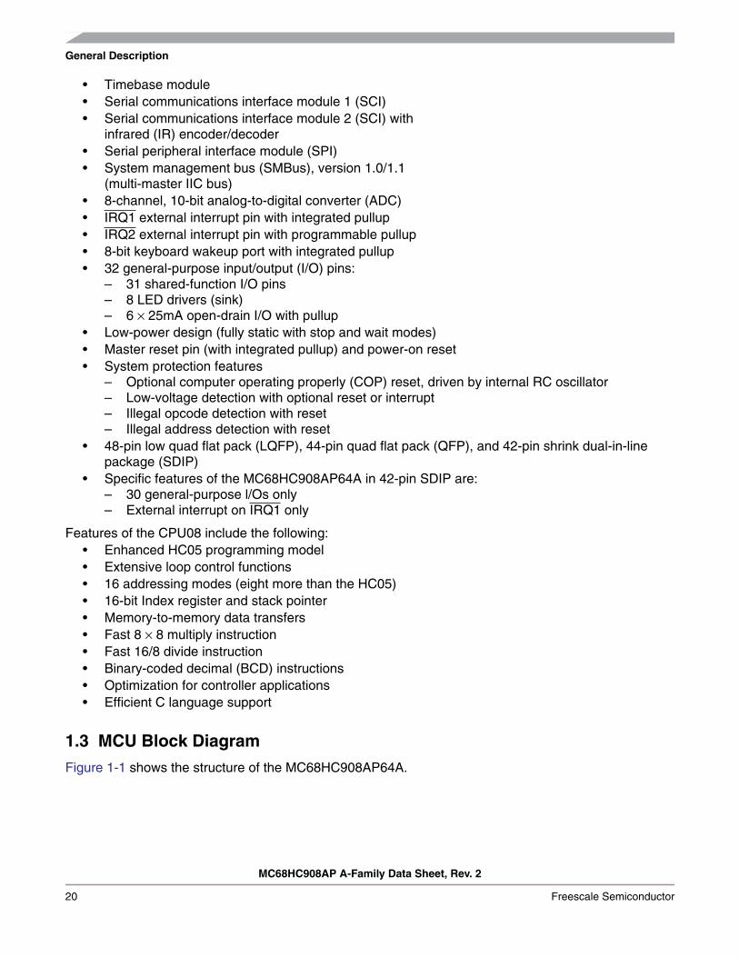
1.3 MCU Block Diagram
Figure 1-1 shows the structure of the MC68HC908AP64A.

MCU Block Diagram
MC68HC908AP A-Family Data Sheet, Rev. 2
Freescale Semiconductor 21
Figure 1-1. MC68HC908AP64A Block Diagram
SYSTEM INTEGRATIONMODULE
ARITHMETIC/LOGICUNIT (ALU)
CPUREGISTERS
M68HC08 CPU
CONTROL AND STATUS REGISTERS — 96 BYTES
USER FLASH — (SEE TABLE)
USER RAM — (SEE TABLE)
MONITOR ROM — 959 BYTES
USER FLASH VECTOR SPACE — 48 BYTES
EXTERNAL INTERRUPTMODULE
DD
RD
POR
TD
INTERNAL BUS
* RST
* IRQ1
COMPUTER OPERATINGPROPERLY MODULE
PTD7/KBI7 ***PTD6/KBI6 ***PTD5/KBI5 ***PTD4/KBI4 ***PTD3/KBI3 ***PTD2/KBI2 ***
POWER-ON RESETMODULE
POWER
PTD1/KBI1 ***PTD0/KBI0 ***
SERIAL COMMUNICATIONSINTERFACE MODULE 1
2-CHANNEL TIMER INTERFACEMODULE 1
2-CHANNEL TIMER INTERFACEMODULE 2
SERIAL PERIPHERALINTERFACE MODULE
KEYBOARD INTERRUPTMODULE
10-BIT ANALOG-TO-DIGITALCONVERTER MODULE
ADC REFERENCEVREFLVREFH
DD
RB
POR
TB
PTB7/T2CH1PTB6/T2CH0PTB5/T1CH1PTB4/T1CH0PTB3/RxD †
PTB2/TxD †
PTB1/SCL †
PTB0/SDA †
DD
RC
POR
TC
PTC7/SCRxD †
PTC6/SCTxD †
PTC5/SPSCKPTC4/SSPTC3/MOSIPTC2/MISOPTC1 #
PTC0/IRQ2 **#
DD
RA
POR
TA
PTA7/ADC7 ‡
PTA6/ADC6 ‡
PTA5/ADC5 ‡
PTA4/ADC4 ‡
PTA3/ADC3 ‡
PTA2/ADC2 ‡
PTA1/ADC1 ‡
PTA0/ADC0 ‡
LOW-VOLTAGE INHIBITMODULE
SERIAL COMMUNICATIONSINTERFACE MODULE 2
(WITH INFRAREDMODULATOR/DEMODULATOR)
† Pin is open-drain when configured as output.‡ LED direct sink pin.# Pin not bonded on 42-pin SDIP.
TIMEBASEMODULE
MULTI-MASTER IIC (SMBUS)INTERFACE MODULE
VDDAVDD
VSSAVSS
VREG
** IRQ2
* Pin contains integrated pullup device.** Pin contains configurable pullup device.
*** Pin contains integrated pullup device when configured as KBI.
CLOCK GENERATOR MODULE
OSC1
OSC2
CGMXFC PHASE-LOCKED LOOP
X-TAL OSCILLATOR
RC OSCILLATOR
INTERNAL OSCILLATOR
OSCILLATORS AND
.
DEVICEUSER RAM
(bytes)USER FLASH
(bytes)
MC68HC908AP64A 2,048 62,368
MC68HC908AP32A 2,048 32,768
MC68HC908AP16A 1,024 16,384
MC68HC908AP8A 1,024 8,192

General Description
MC68HC908AP A-Family Data Sheet, Rev. 2
22 Freescale Semiconductor
1.4 Pin Assignment
Figure 1-2. 48-Pin LQFP Pin Assignments
VS
SA
48
47 46 45 44 43 42 41 40 391
2
3
4
5
6
7
8
9
10
14 15 16 17 18 19 20 21 22
36
32
31
30
29
28
27
26
13PTB6/T2CH0
IRQ1
PTB3/RxD
RST
VREG
PTB5/T1CH1
VDD
OSC1
OSC2
VSS
PTB4/T1CH0
PT
C5/
SP
SC
K
PT
C7/
SC
RxD
PT
B0/
SD
A
PT
B1/
SC
L
PT
C6/
SC
TxD
PT
C4/
SS
PT
C0/
IRQ
2
PT
C1
PT
C2/
MIS
O
PT
A7/
AD
C7
PT
C3/
MO
SI
NC
VREFL
VREFH
PTA1/ADC1
NC
PTA5/ADC5
PTA4/ADC4
PTA2/ADC2
PTA0/ADC0
NC
PTA3/ADC3
CG
MX
FC
12PTB2/TxD 25 PTA6/ADC6
11
24N
C
23
35
34
33
VD
DA
PT
D2/
KB
I2
PT
D1/
KB
I1
PT
D0/
KB
I0
PT
D7/
KB
I7
PT
D6/
KB
I6
PT
D5/
KB
I5
PT
D4/
KB
I4
PT
D3/
KB
I3
PT
B7/
T2C
H1
37
38
NC: No connection

Pin Assignment
MC68HC908AP A-Family Data Sheet, Rev. 2
Freescale Semiconductor 23
Figure 1-3. 44-Pin QFP Pin Assignments
44 34
43 42 41 40 39 38 37 36 351
2
3
4
5
6
7
8
9
10
11
13 14 15 16 17 18 19 20 21
22
33
32
31
30
29
28
27
26
25
24
12
23
PTB6/T2CH0
IRQ1
PTB3/RxD
RST
VREG
PTB5/T1CH1
VDD
OSC1
OSC2
VSS
PTB4/T1CH0P
TC
5/S
PS
CK
PT
C7/
SC
RxD
PT
B0/
SD
A
PT
B1/
SC
L
PT
C6/
SC
TxD
PT
C4/
SS
PT
C0/
IRQ
2
PT
C1
PT
C2/
MIS
O
PT
C3/
MO
SI
PT
B2/
TxD
VREFL
VREFH
PTA1/ADC1
PTA5/ADC5
PTA4/ADC4
PTA2/ADC2
PTA0/ADC0
PTA3/ADC3
PTA6/ADC6
PTA7/ADC7
VS
SA
CG
MX
FC
VD
DA
PT
D2/
KB
I2
PT
D1/
KB
I1
PT
D0/
KB
I0
PT
D6/
KB
I6
PT
D5/
KB
I5
PT
D4/
KB
I4
PT
D3/
KB
I3
PT
B7/
T2C
H1
PTD7/KBI7
General Description
MC68HC908AP A-Family Data Sheet, Rev. 2
24 Freescale Semiconductor
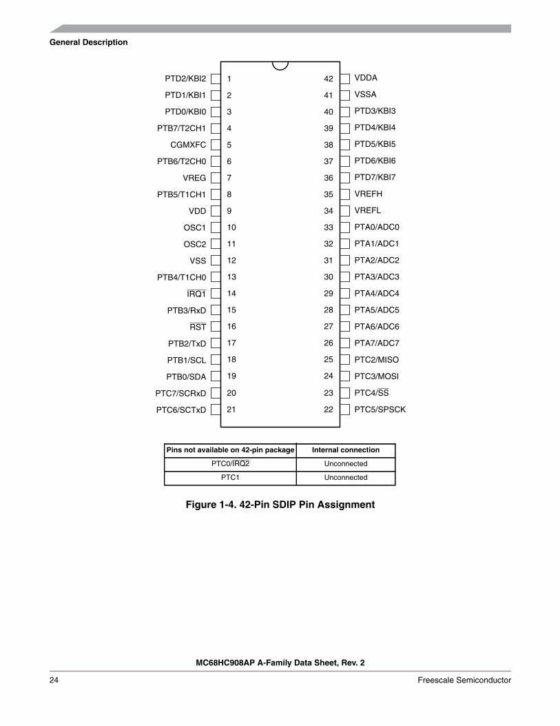
Figure 1-4. 42-Pin SDIP Pin Assignment
21 22PTC6/SCTxD
PTC7/SCRxD
PTC2/MISO
1
2
3
4
5
6
7
8
9
10
11
12
13
14
15
16
17
18
19
42
41
40
39
38
37
36
35
34
33
32
31
30
29
28
27
26
25
24 PTC3/MOSI
PTC4/SS
PTB1/SCL
PTB2/TxD
RST
CGMXFC
PTB4/T1CH0
IRQ1
PTB3/RxD
VREFL
VREFH
PTD7/KBI7
PTD6/KBI6
PTD5/KBI5
PTD4/KBI4
PTD3/KBI3
VSSA
PTA3/ADC3
PTA2/ADC2
PTA6/ADC6
PTA5/ADC5
PTA4/ADC4
PTD2/KBI2 VDDA
PTA1/ADC1
PTA0/ADC0
PTD1/KBI1
PTD0/KBI0
PTB7/T2CH1
PTB6/T2CH0
VREG
PTB5/T1CH1
VDD
OSC1
OSC2
VSS
PTA7/ADC7
20 23
PTC5/SPSCK
PTB0/SDA
Pins not available on 42-pin package Internal connection
PTC0/IRQ2 Unconnected
PTC1 Unconnected
Pin Functions
MC68HC908AP A-Family Data Sheet, Rev. 2
Freescale Semiconductor 25
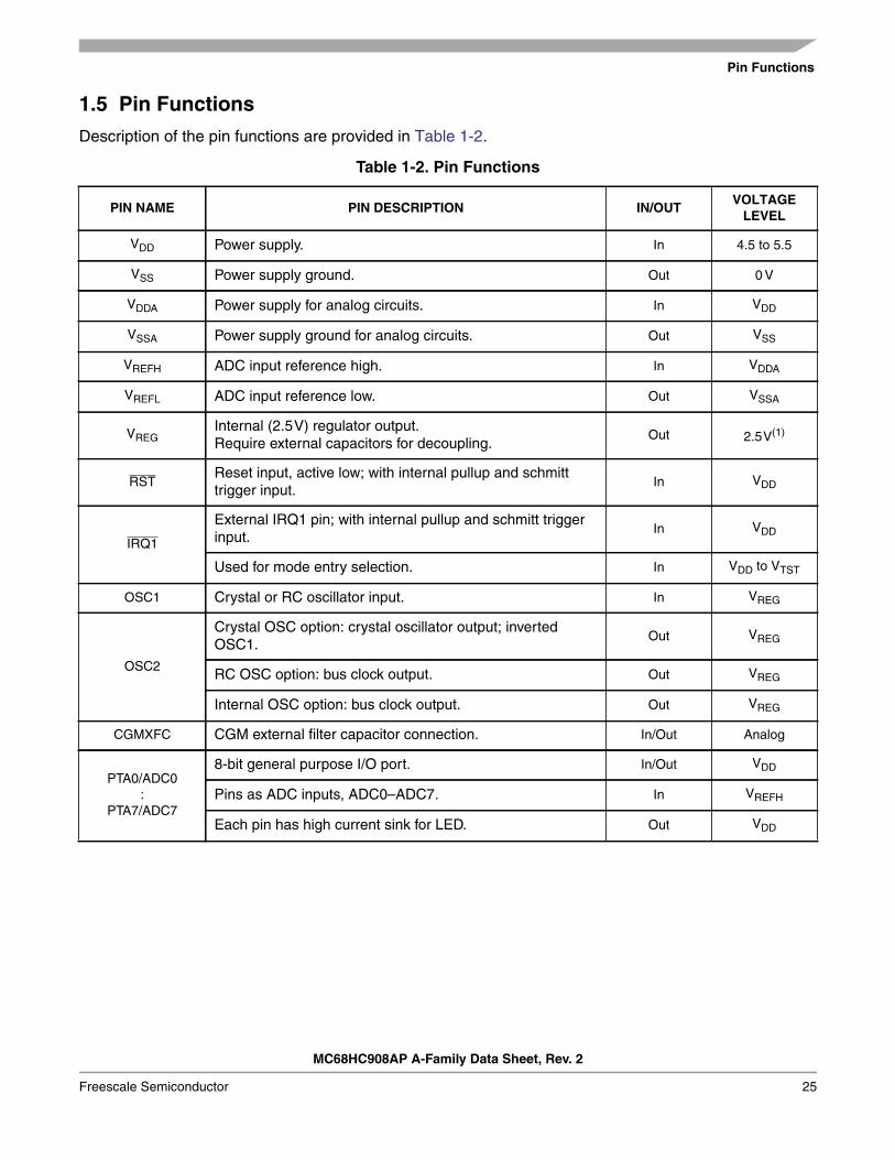
1.5 Pin Functions
Description of the pin functions are provided in Table 1-2.
Table 1-2. Pin Functions
PIN NAME PIN DESCRIPTION IN/OUTVOLTAGE
LEVEL
VDD Power supply. In 4.5 to 5.5
VSS Power supply ground. Out 0 V
VDDA Power supply for analog circuits. In VDD
VSSA Power supply ground for analog circuits. Out VSS
VREFH ADC input reference high. In VDDA
VREFL ADC input reference low. Out VSSA
VREGInternal (2.5V) regulator output.Require external capacitors for decoupling.
Out 2.5V(1)
RSTReset input, active low; with internal pullup and schmitttrigger input.
In VDD
IRQ1
External IRQ1 pin; with internal pullup and schmitt triggerinput.
In VDD
Used for mode entry selection. In VDD to VTST
OSC1 Crystal or RC oscillator input. In VREG
OSC2
Crystal OSC option: crystal oscillator output; invertedOSC1.
Out VREG
RC OSC option: bus clock output. Out VREG
Internal OSC option: bus clock output. Out VREG
CGMXFC CGM external filter capacitor connection. In/Out Analog
PTA0/ADC0:
PTA7/ADC7
8-bit general purpose I/O port. In/Out VDD
Pins as ADC inputs, ADC0–ADC7. In VREFH
Each pin has high current sink for LED. Out VDD

General Description
MC68HC908AP A-Family Data Sheet, Rev. 2
26 Freescale Semiconductor
1.6 Power Supply Bypassing (VDD, VDDA, VSS, VSSA)
VDD and VSS are the power supply and ground pins, the MCU operates from a single power supplytogether with an on chip voltage regulator.
Fast signal transitions on MCU pins place high. short-duration current demands on the power supply. Toprevent noise problems, take special care to provide power supply bypassing at the MCU as Figure 1-5shows. Place the bypass capacitors as close to the MCU power pins as possible. Usehigh-frequency-response ceramic capacitor for CBYPASS, CBULK are optional bulk current bypasscapacitors for use in applications that require the port pins to source high current level.
PTB0/SDAPTB1/SCLPTB2/TxDPTB3/RxD
PTB4/T1CH0PTB5/T1CH1PTB6/T2CH0PTB7/T2CH1
8-bit general purpose I/O port; PTB0–PTB3 are open drain whenconfigured as output. PTB4–PTB7 have schmitt trigger inputs.
In/Out VDD
PTB0 as SDA of MMIIC. In/Out VDD
PTB1 as SCL of MMIIC. In/Out VDD
PTB2 as TxD of SCI; open drain output. Out VDD
PTB3 as RxD of SCI. In VDD
PTB4 as T1CH0 of TIM1. In/Out VDD
PTB5 as T1CH1 of TIM1. In/Out VDD
PTB6 as T2CH0 of TIM2. In/Out VDD
PTB7 as T2CH1 of TIM2. In/Out VDD
PTC0/IRQ2PTC1
PTC2/MISOPTC3/MOSI
PTC4/SSPTC5/SPSCKPTC6/SCTxDPTC7/SCRxD
8-bit general purpose I/O port; PTC6 and PTC7 are open drainwhen configured as output.
In/Out VDD
PTC0 is shared with IRQ2 and has schmitt trigger input. In VDD
PTC2 as MISO of SPI. In VDD
PTC3 as MOSI of SPI. Out VDD
PTC4 as SS of SPI. In VDD
PTC5 as SPSCK of SPI. In/Out VDD
PTC6 as SCTxD of IRSCI; open drain output. Out VDD
PTC7 as SCRxD of IRSCI. In VDD
PTD0/KBI0:
PTD7/KBI7
8-bit general purpose I/O port with schmitt trigger inputs. In/Out VDD
Pins as keyboard interrupts (with pullup), KBI0–KBI7. In VDD
1. See Chapter 22 Electrical Specifications for VREG tolerance.
Table 1-2. Pin Functions
PIN NAME PIN DESCRIPTION IN/OUTVOLTAGE
LEVEL

Regulator Power Supply Configuration (VREG)
MC68HC908AP A-Family Data Sheet, Rev. 2
Freescale Semiconductor 27
VDDA and VSSA are the power supply and ground pins for the analog circuits of the MCU. These pinsshould be decoupled as per the digital power supply pins.
Figure 1-5. Power Supply Bypassing
1.7 Regulator Power Supply Configuration (VREG)
VREG is the output from the on-chip regulator. All internal logics, except for the I/O pads, are powered byVREG output. VREG requires an external ceramic bypass capacitor of 100 nF as Figure 1-6 shows. Placethe bypass capacitor as close to the VREG pin as possible.
Figure 1-6. Regulator Power Supply Bypassing
MCU
VDD
C2(a)
C1(a)0.1 µF
VSSVDD
+
NOTE: Component values shown represent typical applications.
VDD
C2(b)
C1(b)0.1 µF
VSSAVDDA
+
MCU
VSSVREG
CVREGBYPASS
100 nF

General Description
MC68HC908AP A-Family Data Sheet, Rev. 2
28 Freescale Semiconductor

MC68HC908AP A-Family Data Sheet, Rev. 2
Freescale Semiconductor 29
Chapter 2Memory
2.1 Introduction
The CPU08 can address 64k-bytes of memory space. The memory map, shown in Figure 2-1, includes:• 62,368 bytes of user FLASH — MC68HC908AP64A
32,768 bytes of user FLASH — MC68HC908AP32A16,384 bytes of user FLASH — MC68HC908AP16A8,192 bytes of user FLASH — MC68HC908AP8A
• 2,048 bytes of RAM — MC68HC908AP64A and MC68HC908AP32A1,024 bytes of RAM — MC68HC908AP16A and MC68HC908AP8A
• 48 bytes of user-defined vectors• 959 bytes of monitor ROM
2.2 Input/Output (I/O) Section
Most of the control, status, and data registers are in the zero page area of $0000–$005F. Additional I/Oregisters have these addresses:
• $FE00; SIM break status register, SBSR• $FE01; SIM reset status register, SRSR• $FE02; Reserved• $FE03; SIM break flag control register, SBFCR• $FE04; interrupt status register 1, INT1• $FE05; interrupt status register 2, INT2• $FE06; interrupt status register 3, INT3• $FE07; Reserved• $FE08; FLASH control register, FLCR• $FE09; FLASH block protect register, FLBPR• $FE0A; Reserved• $FE0B; Reserved• $FE0C; Break address register high, BRKH• $FE0D; Break address register low, BRKL• $FE0E; Break status and control register, BRKSCR• $FE0F; LVI Status register, LVISR• $FFCF; Mask option register, MOR (FLASH register)• $FFFF; COP control register, COPCTL
2.3 Monitor ROM
The 959 bytes at addresses $FC00–$FDFF and $FE10–$FFCE are reserved ROM addresses thatcontain the instructions for the monitor functions. (See Chapter 8 Monitor ROM (MON).)

Memory
MC68HC908AP A-Family Data Sheet, Rev. 2
30 Freescale Semiconductor
$0000↓
$005F
I/O Registers96 Bytes
MC68HC908AP32A MC68HC908AP16A MC68HC908AP8A
$0060
↓
$085F
RAM2,048 Bytes
(MC68HC908AP64A)
RAM2,048 Bytes
$0060
↓
$085F
RAM1,024 Bytes
$0060$045F
RAM1,024 Bytes
$0060$045F
Unimplemented1,024 Bytes
Unimplemented1,024 Bytes
$0860
↓
$FBFF
FLASH Memory 62,368 Bytes
(MC68HC908AP64A)
FLASH Memory32,768 Bytes
$0860
↓
$885F
FLASH Memory16,384 Bytes
$0860
↓
$485F
FLASH Memory8,192 Bytes
$0860
$285F
Unimplemented54,176 Bytes
$2860
↓
$FBFF
Unimplemented45,984 Bytes
$4860
↓
$FBFF
Unimplemented29,600 Bytes
$8860
↓
$FBFF$FC00
↓$FDFF
Monitor ROM 2512 Bytes
$FE00 SIM Break Status Register$FE01 SIM Reset Status Register$FE02 Reserved$FE03 SIM Break Flag Control Register$FE04 Interrupt Status Register 1$FE05 Interrupt Status Register 2$FE06 Interrupt Status Register 3$FE07 Reserved$FE08 FLASH Control Register$FE09 FLASH Block Protect Register$FE0A Reserved$FE0B Reserved$FE0C Break Address Register High$FE0D Break Address Register Low$FE0E Break Status and Control Register$FE0F LVI Status Register$FE10
↓$FFCE
Monitor ROM 1 447 Bytes
$FFCF Mask Option Register$FFD0
↓$FFFF
FLASH Vectors48 Bytes
Figure 2-1. Memory Map

Monitor ROM
MC68HC908AP A-Family Data Sheet, Rev. 2
Freescale Semiconductor 31
Addr. Register Name Bit 7 6 5 4 3 2 1 Bit 0
$0000Port A Data Register
(PTA)
Read:PTA7 PTA6 PTA5 PTA4 PTA3 PTA2 PTA1 PTA0
Write:
Reset: Unaffected by reset
$0001Port B Data Register
(PTB)
Read:PTB7 PTB6 PTB5 PTB4 PTB3 PTB2 PTB1 PTB0
Write:
Reset: Unaffected by reset
$0002 Port C Data Register (PTC)
Read:PTC7 PTC6 PTC5 PTC4 PTC3 PTC2 PTC1 PTC0
Write:
Reset: Unaffected by reset
$0003 Port D Data Register (PTD)
Read:PTD7 PTD6 PTD5 PTD4 PTD3 PTD2 PTD1 PTD0
Write:
Reset: Unaffected by reset
$0004Data Direction Register A
(DDRA)
Read:DDRA7 DDRA6 DDRA5 DDRA4 DDRA3 DDRA2 DDRA1 DDRA0
Write:
Reset: 0 0 0 0 0 0 0 0
$0005Data Direction Register B
(DDRB)
Read:DDRB7 DDRB6 DDRB5 DDRB4 DDRB3 DDRB2 DDRB1 DDRB0
Write:
Reset: 0 0 0 0 0 0 0 0
$0006Data Direction Register C
(DDRC)
Read:DDRC7 DDRC6 DDRC5 DDRC4 DDRC3 DDRC2 DDRC1 DDRC0
Write:
Reset: 0 0 0 0 0 0 0 0
$0007Data Direction Register D
(DDRD)
Read:DDRD7 DDRD6 DDRD5 DDRD4 DDRD3 DDRD2 DDRD1 DDRD0
Write:
Reset: 0 0 0 0 0 0 0 0
$0008 Unimplemented
Read:
Write:
Reset:
$0009 Unimplemented
Read:
Write:
Reset:
$000A Unimplemented
Read:
Write:
Reset:
$000B Unimplemented
Read:
Write:
Reset:
$000CPort-A LED Control
Register(LEDA)
Read: LEDA7 LEDA6 LEDA5 LEDA4 LEDA3 LEDA2 LEDA1 LEDA0
Write:
Reset: 0 0 0 0 0 0 0 0
U = Unaffected X = Indeterminate = Unimplemented R = Reserved
Figure 2-2. Control, Status, and Data Registers (Sheet 1 of 9)

Memory
MC68HC908AP A-Family Data Sheet, Rev. 2
32 Freescale Semiconductor
$000D Unimplemented
Read:
Write:
Reset:
$000E Unimplemented
Read:
Write:
Reset:
$000F Unimplemented
Read:
Write:
Reset:
$0010SPI Control Register
(SPCR)
Read:SPRIE R SPMSTR CPOL CPHA SPWOM SPE SPTIE
Write:
Reset: 0 0 1 0 1 0 0 0
$0011SPI Status and Control
Register(SPSCR)
Read: SPRFERRIE
OVRF MODF SPTEMODFEN SPR1 SPR0
Write:
Reset: 0 0 0 0 1 0 0 0
$0012SPI Data Register
(SPDR)
Read: R7 R6 R5 R4 R3 R2 R1 R0
Write: T7 T6 T5 T4 T3 T2 T1 T0
Reset: Unaffected by reset
$0013SCI Control Register 1
(SCC1)
Read:LOOPS ENSCI TXINV M WAKE ILTY PEN PTY
Write:
Reset: 0 0 0 0 0 0 0 0
$0014SCI Control Register 2
(SCC2)
Read:SCTIE TCIE SCRIE ILIE TE RE RWU SBK
Write:
Reset: 0 0 0 0 0 0 0 0
$0015SCI Control Register 3
(SCC3)
Read: R8T8 DMARE DMATE ORIE NEIE FEIE PEIE
Write:
Reset: U U 0 0 0 0 0 0
$0016 SCI Status Register 1 (SCS1)
Read: SCTE TC SCRF IDLE OR NF FE PE
Write:
Reset: 1 1 0 0 0 0 0 0
$0017 SCI Status Register 2 (SCS2)
Read: 0 0 0 0 0 0 BKF RPF
Write:
Reset: 0 0 0 0 0 0 0 0
$0018SCI Data Register
(SCDR)
Read: R7 R6 R5 R4 R3 R2 R1 R0
Write: T7 T6 T5 T4 T3 T2 T1 T0
Reset: Unaffected by reset
$0019SCI Baud Rate Register
(SCBR)
Read: 0 0SCP1 SCP0 R SCR2 SCR1 SCR0
Write:
Reset: 0 0 0 0 0 0 0 0
Addr. Register Name Bit 7 6 5 4 3 2 1 Bit 0
U = Unaffected X = Indeterminate = Unimplemented R = Reserved
Figure 2-2. Control, Status, and Data Registers (Sheet 2 of 9)

Monitor ROM
MC68HC908AP A-Family Data Sheet, Rev. 2
Freescale Semiconductor 33
$001AKeyboard Status and Control
Register(KBSCR)
Read: 0 0 0 0 KEYF 0IMASK MODE
Write: ACK
Reset: 0 0 0 0 0 0 0 0
$001BKeyboard Interrupt
Enable Register(KBIER)
Read:KBIE7 KBIE6 KBIE5 KBIE4 KBIE3 KBIE2 KBIE1 KBIE0
Write:
Reset: 0 0 0 0 0 0 0 0
$001CIRQ2 Status and Control Reg-
ister(INTSCR2)
Read: 0PUC0ENB
0 0 IRQ2F 0IMASK2 MODE2
Write: ACK2
Reset: 0 0 0 0 0 0 0 0
$001DConfiguration Register 2
(CONFIG2)†
Read: STOP_ICLKDIS
STOP_RCLKEN
STOP_XCLKEN
OSCCLK1 OSCCLK00 0
SCIBDSRCWrite:
Reset: 0 0 0 0 0 0 0 0
† One-time writable register after each reset.
$001EIRQ1 Status and Control Reg-
ister(INTSCR1)
Read: 0 0 0 0 IRQ1F 0IMASK1 MODE1
Write: ACK1
Reset: 0 0 0 0 0 0 0 0
$001FConfiguration Register 1
(CONFIG1)†
Read:COPRS LVISTOP LVIRSTD LVIPWRD LVIREGD SSREC STOP COPD
Write:
Reset: 0 0 0 0 0 0 0 0
† One-time writable register after each reset.
$0020Timer 1 Status and
Control Register(T1SC)
Read: TOFTOIE TSTOP
0 0PS2 PS1 PS0
Write: 0 TRST
Reset: 0 0 1 0 0 0 0 0
$0021Timer 1 Counter
Register High(T1CNTH)
Read: Bit 15 14 13 12 11 10 9 Bit 8
Write:
Reset: 0 0 0 0 0 0 0 0
$0022Timer 1 Counter
Register Low(T1CNTL)
Read: Bit 7 6 5 4 3 2 1 Bit 0
Write:
Reset: 0 0 0 0 0 0 0 0
$0023Timer 1 Counter Modulo Reg-
ister High(T1MODH)
Read:Bit 15 14 13 12 11 10 9 Bit 8
Write:
Reset: 1 1 1 1 1 1 1 1
$0024Timer 1 Counter Modulo
Register Low(T1MODL)
Read:Bit 7 6 5 4 3 2 1 Bit 0
Write:
Reset: 1 1 1 1 1 1 1 1
$0025Timer 1 Channel 0 Status and
Control Register (T1SC0)
Read: CH0FCH0IE MS0B MS0A ELS0B ELS0A TOV0 CH0MAX
Write: 0
Reset: 0 0 0 0 0 0 0 0
Addr. Register Name Bit 7 6 5 4 3 2 1 Bit 0
U = Unaffected X = Indeterminate = Unimplemented R = Reserved
Figure 2-2. Control, Status, and Data Registers (Sheet 3 of 9)

Memory
MC68HC908AP A-Family Data Sheet, Rev. 2
34 Freescale Semiconductor
$0026Timer 1 Channel 0
Register High(T1CH0H)
Read:Bit 15 14 13 12 11 10 9 Bit 8
Write:
Reset: Indeterminate after reset
$0027Timer 1 Channel 0
Register Low(T1CH0L)
Read:Bit 7 6 5 4 3 2 1 Bit 0
Write:
Reset: Indeterminate after reset
$0028Timer 1 Channel 1 Status and
Control Register (T1SC1)
Read: CH1FCH1IE
0MS1A ELS1B ELS1A TOV1 CH1MAX
Write: 0
Reset: 0 0 0 0 0 0 0 0
$0029Timer 1 Channel 1
Register High(T1CH1H)
Read:Bit 15 14 13 12 11 10 9 Bit 8
Write:
Reset: Indeterminate after reset
$002ATimer 1 Channel 1
Register Low(T1CH1L)
Read:Bit 7 6 5 4 3 2 1 Bit 0
Write:
Reset: Indeterminate after reset
$002BTimer 2 Status and
Control Register(T2SC)
Read: TOFTOIE TSTOP
0 0PS2 PS1 PS0
Write: 0 TRST
Reset: 0 0 1 0 0 0 0 0
$002CTimer 2 Counter
Register High(T2CNTH)
Read: Bit 15 14 13 12 11 10 9 Bit 8
Write:
Reset: 0 0 0 0 0 0 0 0
$002DTimer 2 Counter
Register Low(T2CNTL)
Read: Bit 7 6 5 4 3 2 1 Bit 0
Write:
Reset: 0 0 0 0 0 0 0 0
$002ETimer 2 Counter Modulo Reg-
ister High(T2MODH)
Read:Bit 15 14 13 12 11 10 9 Bit 8
Write:
Reset: 1 1 1 1 1 1 1 1
$002FTimer 2 Counter Modulo
Register Low(T2MODL)
Read:Bit 7 6 5 4 3 2 1 Bit 0
Write:
Reset: 1 1 1 1 1 1 1 1
$0030Timer 2 Channel 0 Status and
Control Register (T2SC0)
Read: CH0FCH0IE MS0B MS0A ELS0B ELS0A TOV0 CH0MAX
Write: 0
Reset: 0 0 0 0 0 0 0 0
$0031Timer 2 Channel 0
Register High(T2CH0H)
Read:Bit 15 14 13 12 11 10 9 Bit 8
Write:
Reset: Indeterminate after reset
$0032Timer 2 Channel 0
Register Low(T2CH0L)
Read:Bit 7 6 5 4 3 2 1 Bit 0
Write:
Reset: Indeterminate after reset
Addr. Register Name Bit 7 6 5 4 3 2 1 Bit 0
U = Unaffected X = Indeterminate = Unimplemented R = Reserved
Figure 2-2. Control, Status, and Data Registers (Sheet 4 of 9)

Monitor ROM
MC68HC908AP A-Family Data Sheet, Rev. 2
Freescale Semiconductor 35
$0033Timer 2 Channel 1 Status and
Control Register (T2SC1)
Read: CH1FCH1IE
0MS1A ELS1B ELS1A TOV1 CH1MAX
Write: 0
Reset: 0 0 0 0 0 0 0 0
$0034Timer 2 Channel 1
Register High(T2CH1H)
Read:Bit 15 14 13 12 11 10 9 Bit 8
Write:
Reset: Indeterminate after reset
$0035Timer 2 Channel 1
Register Low(T2CH1L)
Read:Bit 7 6 5 4 3 2 1 Bit 0
Write:
Reset: Indeterminate after reset
$0036 PLL Control Register (PCTL)
Read:PLLIE
PLLFPLLON BCS PRE1 PRE0 VPR1 VPR0
Write:
Reset: 0 0 1 0 0 0 0 0
$0037PLL Bandwidth Control Reg-
ister(PBWC)
Read:AUTO
LOCKACQ
0 0 0 0R
Write:
Reset: 0 0 0 0 0 0 0 0
$0038PLL Multiplier Select
Register High(PMSH)
Read: 0 0 0 0MUL11 MUL10 MUL9 MUL8
Write:
Reset: 0 0 0 0 0 0 0 0
$0039PLL Multiplier Select
Register Low(PMSL)
Read:MUL7 MUL6 MUL5 MUL4 MUL3 MUL2 MUL1 MUL0
Write:
Reset: 0 1 0 0 0 0 0 0
$003APLL VCO Range Select
Register(PMRS)
Read:VRS7 VRS6 VRS5 VRS4 VRS3 VRS2 VRS1 VRS0
Write:
Reset: 0 1 0 0 0 0 0 0
$003BPLL Reference Divider
Select Register(PMDS)
Read: 0 0 0 0RDS3 RDS2 RDS1 RDS0
Write:
Reset: 0 0 0 0 0 0 0 1
$003C Unimplemented
Read:
Write:
Reset:
$003D Unimplemented
Read:
Write:
Reset:
$003E Unimplemented
Read:
Write:
Reset:
$003F Unimplemented
Read:
Write:
Reset:
Addr. Register Name Bit 7 6 5 4 3 2 1 Bit 0
U = Unaffected X = Indeterminate = Unimplemented R = Reserved
Figure 2-2. Control, Status, and Data Registers (Sheet 5 of 9)

Memory
MC68HC908AP A-Family Data Sheet, Rev. 2
36 Freescale Semiconductor
$0040IRSCI Control Register 1
(IRSCC1)
Read:LOOPS ENSCI
0M WAKE ILTY PEN PTY
Write:
Reset: 0 0 0 0 0 0 0 0
$0041IRSCI Control Register 2
(IRSCC2)
Read:SCTIE TCIE SCRIE ILIE TE RE RWU SBK
Write:
Reset: 0 0 0 0 0 0 0 0
$0042IRSCI Control Register 3
(IRSCC3)
Read: R8T8 DMARE DMATE ORIE NEIE FEIE PEIE
Write:
Reset: U U 0 0 0 0 0 0
$0043IRSCI Status Register 1
(IRSCS1)
Read: SCTE TC SCRF IDLE OR NF FE PE
Write:
Reset: 1 1 0 0 0 0 0 0
$0044IRSCI Status Register 2
(IRSCS2)
Read: BKF RPF
Write:
Reset: 0 0 0 0 0 0 0 0
$0045IRSCI Data Register
(IRSCDR)
Read: R7 R6 R5 R4 R3 R2 R1 R0
Write: T7 T6 T5 T4 T3 T2 T1 T0
Reset: Unaffected by reset
$0046IRSCI Baud Rate Register
(IRSCBR)
Read:CKS
0SCP1 SCP0 R SCR2 SCR1 SCR0
Write:
Reset: 0 0 0 0 0 0 0 0
$0047IRSCI Infrared Control
Register(IRSCIRCR)
Read:R
0 0 0R TNP1 TNP0 IREN
Write:
Reset: 0 0 0 0 0 0 0 0
$0048MMIIC Address Register
(MMADR)Read:
MMAD7 MMAD6 MMAD5 MMAD4 MMAD3 MMAD2 MMAD1 MMEXTADWrite:
Reset: 1 0 1 0 0 0 0 0
$0049MMIIC Control Register 1
(MMCR1)
Read:MMEN MMIEN
0 0MMTXAK REPSEN
MMCRCBYTE
0
Write: MMCLRBB
Reset: 0 0 0 0 0 0 0 0
$004AMMIIC Control Register 2
(MMCR2)Read: MMALIF MMNAKIF MMBB
MMAST MMRW 0 0
MMCRCEFWrite: 0 0
Reset: 0 0 0 0 0 0 0 Unaffected
$004BMMIIC Status Register
(MMSR)Read: MMRXIF MMTXIF MMATCH MMSRW MMRXAK MMCRCBF MMTXBE MMRXBF
Write: 0 0
Reset: 0 0 0 0 1 0 1 0
$004CMMIIC Data Transmit
Register(MMDTR)
Read:MMTD7 MMTD6 MMTD5 MMTD4 MMTD3 MMTD2 MMTD1 MMTD0
Write:
Reset: 0 0 0 0 0 0 0 0
Addr. Register Name Bit 7 6 5 4 3 2 1 Bit 0
U = Unaffected X = Indeterminate = Unimplemented R = Reserved
Figure 2-2. Control, Status, and Data Registers (Sheet 6 of 9)

Monitor ROM
MC68HC908AP A-Family Data Sheet, Rev. 2
Freescale Semiconductor 37
$004DMMIIC Data Receive
Register(MMDRR)
Read: MMRD7 MMRD6 MMRD5 MMRD4 MMRD3 MMRD2 MMRD1 MMRD0
Write:
Reset: 0 0 0 0 0 0 0 0
$004EMMIIC CRC Data Register
(MMCRDR)Read: MMCRCD7 MMCRCD6 MMCRCD5 MMCRCD4 MMCRCD3 MMCRCD2 MMCRCD1 MMCRCD0
Write:
Reset: 0 0 0 0 0 0 0 0
$004FMMIIC Frequency Divider
Register(MMFDR)
Read: 0 0 0 0 0MMBR2 MMBR1 MMBR0
Write:
Reset: 0 0 0 0 0 1 0 0
$0050 Reserved
Read:R R R R R R R R
Write:
Reset:
$0051Timebase Control Register
(TBCR)
Read: TBIFTBR2 TBR1 TBR0
0TBIE TBON R
Write: TACK
Reset: 0 0 0 0 0 0 0 0
$0052 Unimplemented
Read:
Write:
Reset:
$0053 Unimplemented
Read:
Write:
Reset:
$0054 Unimplemented
Read:
Write:
Reset:
$0055 Unimplemented
Read:
Write:
Reset:
$0056 Unimplemented
Read:
Write:
Reset:
$0057ADC Status and Control
Register(ADSCR)
Read: COCOAIEN ADCO ADCH4 ADCH3 ADCH2 ADCH1 ADCH0
Write:
Reset: 0 0 0 1 1 1 1 1
$0058ADC Clock Control Register
(ADICLK)
Read:ADIV2 ADIV1 ADIV0 ADICLK MODE1 MODE0
0 0
Write: R
Reset: 0 0 0 0 0 0 0 0
$0059ADC Data Register High 0
(ADRH0)
Read: ADx ADx ADx ADx ADx ADx ADx ADx
Write: R R R R R R R R
Reset: 0 0 0 0 0 0 0 0
Addr. Register Name Bit 7 6 5 4 3 2 1 Bit 0
U = Unaffected X = Indeterminate = Unimplemented R = Reserved
Figure 2-2. Control, Status, and Data Registers (Sheet 7 of 9)

Memory
MC68HC908AP A-Family Data Sheet, Rev. 2
38 Freescale Semiconductor
$005AADC Data Register Low 0
(ADRL0)Read: ADx ADx ADx ADx ADx ADx ADx ADx
Write: R R R R R R R R
Reset: 0 0 0 0 0 0 0 0
$005BADC Data Register Low 1
(ADRL1)Read: AD9 AD8 AD7 AD6 AD5 AD4 AD3 AD2
Write: R R R R R R R R
Reset: 0 0 0 0 0 0 0 0
$005C ADC Data Register Low 2(ADRL2)
Read: AD9 AD8 AD7 AD6 AD5 AD4 AD3 AD2
Write: R R R R R R R R
Reset: 0 0 0 0 0 0 0 0
$005DADC Data Register Low 3
(ADRL3)Read: AD9 AD8 AD7 AD6 AD5 AD4 AD3 AD2
Write: R R R R R R R R
Reset: 0 0 0 0 0 0 0 0
$005EADC Auto-scan Control
Register(ADASCR)
Read:AUTO1 AUTO0 ASCAN
Write:
Reset: 0 0 0 0 0 0 0 0
$005F Unimplemented
Read:
Write:
Reset:
$FE00SIM Break Status Register
(SBSR)
Read:R R R R R R
SBSWR
Write: Note
Reset: 0
Note: Writing a logic 0 clears SBSW.
$FE01SIM Reset Status Register
(SRSR)
Read: POR PIN COP ILOP ILAD MODRST LVI 0
Write:
Reset: 1 0 0 0 0 0 0 0
$FE02 Reserved
Read:R R R R R R R R
Write:
Reset:
$FE03SIM Break Flag Control Reg-
ister(SBFCR)
Read:BCFE R R R R R R R
Write:
Reset: 0
$FE04Interrupt Status Register 1
(INT1)
Read: IF6 IF5 IF4 IF3 IF2 IF1 0 0
Write: R R R R R R R R
Reset: 0 0 0 0 0 0 0 0
$FE05Interrupt Status Register 2
(INT2)
Read: IF14 IF13 IF12 IF11 IF10 IF9 IF8 IF7
Write: R R R R R R R R
Reset: 0 0 0 0 0 0 0 0
Addr. Register Name Bit 7 6 5 4 3 2 1 Bit 0
U = Unaffected X = Indeterminate = Unimplemented R = Reserved
Figure 2-2. Control, Status, and Data Registers (Sheet 8 of 9)

Monitor ROM
MC68HC908AP A-Family Data Sheet, Rev. 2
Freescale Semiconductor 39
$FE06Interrupt Status Register 3
(INT3)
Read: 0 IF21 IF20 IF19 IF18 IF17 IF16 IF15
Write: R R R R R R R R
Reset: 0 0 0 0 0 0 0 0
$FE07 Reserved
Read:R R R R R R R R
Write:
Reset:
$FE08FLASH Control Register
(FLCR)
Read: 0 0 0 0HVEN MASS ERASE PGM
Write:
Reset: 0 0 0 0 0 0 0 0
$FE09FLASH Block Protect
Register(FLBPR)
Read:BPR7 BPR6 BPR5 BPR4 BPR3 BPR2 BPR1 BPR0
Write:
Reset: 0 0 0 0 0 0 0 0
$FE0A Reserved
Read:R R R R R R R R
Write:
Reset:
$FE0B Reserved
Read:R R R R R R R R
Write:
Reset:
$FE0CBreak AddressRegister High
(BRKH)
Read:Bit 15 14 13 12 11 10 9 Bit 8
Write:
Reset: 0 0 0 0 0 0 0 0
$FE0DBreak Address
Register Low(BRKL)
Read:Bit 7 6 5 4 3 2 1 Bit 0
Write:
Reset: 0 0 0 0 0 0 0 0
$FE0EBreak Status and Control
Register(BRKSCR)
Reset:BRKE BRKA
0 0 0 0 0 0
Read:
Write: 0 0 0 0 0 0 0 0
$FE0F LVI Status Register (LVISR)
Reset: LVIOUT 0 0 0 0 0 0 0
Read:
Write: 0 0 0 0 0 0 0 0
$FFCF Mask Option Register
(MOR)#
Read:OSCSEL1 OSCSEL0 R R R R R R
Write:
Erased: 1 1 1 1 1 1 1 1
Reset: U U U U U U U U
$FFFFCOP Control Register
(COPCTL)
Read: Low byte of reset vector
Write: Writing clears COP counter (any value)
Reset: Unaffected by reset# MOR is a non-volatile FLASH register; write by programming.
Addr. Register Name Bit 7 6 5 4 3 2 1 Bit 0
U = Unaffected X = Indeterminate = Unimplemented R = Reserved
Figure 2-2. Control, Status, and Data Registers (Sheet 9 of 9)
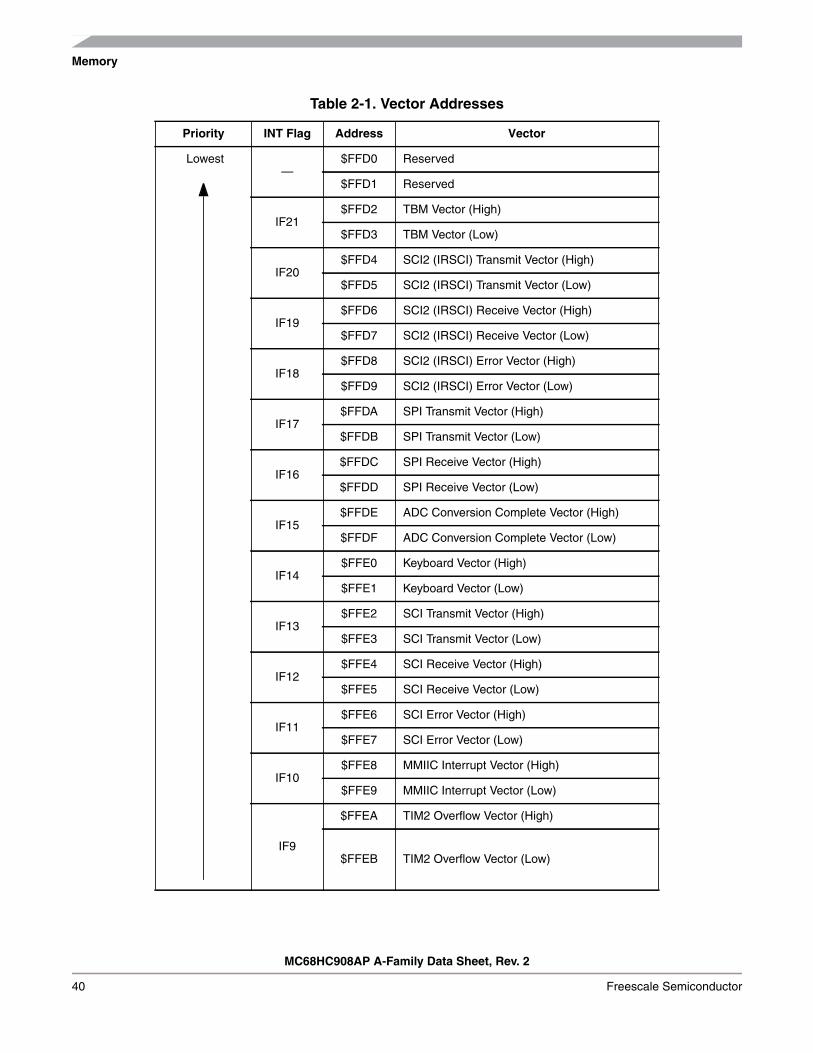
Memory
MC68HC908AP A-Family Data Sheet, Rev. 2
40 Freescale Semiconductor
Table 2-1. Vector Addresses
Priority INT Flag Address Vector
Lowest—
$FFD0 Reserved
$FFD1 Reserved
IF21$FFD2 TBM Vector (High)
$FFD3 TBM Vector (Low)
IF20$FFD4 SCI2 (IRSCI) Transmit Vector (High)
$FFD5 SCI2 (IRSCI) Transmit Vector (Low)
IF19$FFD6 SCI2 (IRSCI) Receive Vector (High)
$FFD7 SCI2 (IRSCI) Receive Vector (Low)
IF18$FFD8 SCI2 (IRSCI) Error Vector (High)
$FFD9 SCI2 (IRSCI) Error Vector (Low)
IF17$FFDA SPI Transmit Vector (High)
$FFDB SPI Transmit Vector (Low)
IF16$FFDC SPI Receive Vector (High)
$FFDD SPI Receive Vector (Low)
IF15$FFDE ADC Conversion Complete Vector (High)
$FFDF ADC Conversion Complete Vector (Low)
IF14$FFE0 Keyboard Vector (High)
$FFE1 Keyboard Vector (Low)
IF13$FFE2 SCI Transmit Vector (High)
$FFE3 SCI Transmit Vector (Low)
IF12$FFE4 SCI Receive Vector (High)
$FFE5 SCI Receive Vector (Low)
IF11$FFE6 SCI Error Vector (High)
$FFE7 SCI Error Vector (Low)
IF10$FFE8 MMIIC Interrupt Vector (High)
$FFE9 MMIIC Interrupt Vector (Low)
IF9
$FFEA TIM2 Overflow Vector (High)
$FFEB TIM2 Overflow Vector (Low)

Random-Access Memory (RAM)
MC68HC908AP A-Family Data Sheet, Rev. 2
Freescale Semiconductor 41
2.4 Random-Access Memory (RAM)
Addresses $0060 through $085F (or $045F) are RAM locations. The location of the stack RAM isprogrammable. The 16-bit stack pointer allows the stack to be anywhere in the 64k-byte memory space.
NOTEFor correct operation, the stack pointer must point only to RAM locations.
Within page zero are 160 bytes of RAM. Because the location of the stack RAM is programmable, all pagezero RAM locations can be used for I/O control and user data or code. When the stack pointer is movedfrom its reset location at $00FF, direct addressing mode instructions can access efficiently all page zeroRAM locations. Page zero RAM, therefore, provides ideal locations for frequently accessed globalvariables.
IF8$FFEC TIM2 Channel 1 Vector (High)
$FFED TIM2 Channel 1 Vector (Low)
IF7$FFEE TIM2 Channel 0 Vector (High)
$FFEF TIM2 Channel 0 Vector (Low)
IF6$FFF0 TIM1 Overflow Vector (High)
$FFF1 TIM1 Overflow Vector (Low)
IF5$FFF2 TIM1 Channel 1 Vector (High)
$FFF3 TIM1 Channel 1 Vector (Low)
IF4$FFF4 TIM1 Channel 0 Vector (High)
$FFF5 TIM1 Channel 0 Vector (Low)
IF3$FFF6 PLL Vector (High)
$FFF7 PLL Vector (Low)
IF2$FFF8 IRQ2 Vector (High)
$FFF9 IRQ2 Vector (Low)
IF1$FFFA IRQ1 Vector (High)
$FFFB IRQ1 Vector (Low)
—$FFFC SWI Vector (High)
$FFFD SWI Vector (Low)
—$FFFE Reset Vector (High)
Highest $FFFF Reset Vector (Low)
Table 2-1. Vector Addresses (Continued)
Priority INT Flag Address Vector
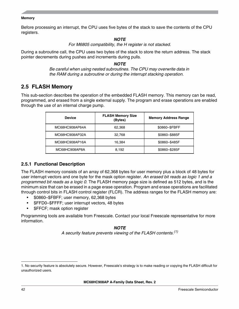
Memory
MC68HC908AP A-Family Data Sheet, Rev. 2
42 Freescale Semiconductor
Before processing an interrupt, the CPU uses five bytes of the stack to save the contents of the CPUregisters.
NOTEFor M6805 compatibility, the H register is not stacked.
During a subroutine call, the CPU uses two bytes of the stack to store the return address. The stackpointer decrements during pushes and increments during pulls.
NOTEBe careful when using nested subroutines. The CPU may overwrite data inthe RAM during a subroutine or during the interrupt stacking operation.
2.5 FLASH Memory
This sub-section describes the operation of the embedded FLASH memory. This memory can be read,programmed, and erased from a single external supply. The program and erase operations are enabledthrough the use of an internal charge pump.
2.5.1 Functional Description
The FLASH memory consists of an array of 62,368 bytes for user memory plus a block of 48 bytes foruser interrupt vectors and one byte for the mask option register. An erased bit reads as logic 1 and aprogrammed bit reads as a logic 0. The FLASH memory page size is defined as 512 bytes, and is theminimum size that can be erased in a page erase operation. Program and erase operations are facilitatedthrough control bits in FLASH control register (FLCR). The address ranges for the FLASH memory are:
• $0860–$FBFF; user memory, 62,368 bytes• $FFD0–$FFFF; user interrupt vectors, 48 bytes• $FFCF; mask option register
Programming tools are available from Freescale. Contact your local Freescale representative for moreinformation.
NOTEA security feature prevents viewing of the FLASH contents.(1)
DeviceFLASH Memory Size
(Bytes)Memory Address Range
MC68HC908AP64A 62,368 $0860–$FBFF
MC68HC908AP32A 32,768 $0860–$885F
MC68HC908AP16A 16,384 $0860–$485F
MC68HC908AP8A 8,192 $0860–$285F
1. No security feature is absolutely secure. However, Freescale’s strategy is to make reading or copying the FLASH difficult forunauthorized users.

FLASH Memory
MC68HC908AP A-Family Data Sheet, Rev. 2
Freescale Semiconductor 43
2.5.2 FLASH Control Register
The FLASH control register (FLCR) controls FLASH program and erase operation.
HVEN — High Voltage Enable BitThis read/write bit enables the charge pump to drive high voltages for program and erase operationsin the array. HVEN can only be set if either PGM = 1 or ERASE = 1 and the proper sequence forprogram or erase is followed.
1 = High voltage enabled to array and charge pump on0 = High voltage disabled to array and charge pump off
MASS — Mass Erase Control BitThis read/write bit configures the memory for mass erase operation or page erase operation when theERASE bit is set.
1 = Mass erase operation selected0 = Page erase operation selected
ERASE — Erase Control BitThis read/write bit configures the memory for erase operation. ERASE is interlocked with the PGM bitsuch that both bits cannot be equal to 1 or set to 1 at the same time.
1 = Erase operation selected0 = Erase operation not selected
PGM — Program Control BitThis read/write bit configures the memory for program operation. PGM is interlocked with the ERASEbit such that both bits cannot be equal to 1 or set to 1 at the same time.
1 = Program operation selected0 = Program operation not selected
2.5.3 FLASH Page Erase Operation
Use the following procedure to erase a page of FLASH memory. A page consists of 512 consecutivebytes starting from addresses $X000, $X200, $X400, $X600, $X800, $XA00, $XC00, or $XE00. The48-byte user interrupt vectors cannot be erased by the page erase operation because of security reasons.Mass erase is required to erase this page.
1. Set the ERASE bit and clear the MASS bit in the FLASH control register.2. Write any data to any FLASH location within the page address range desired.3. Wait for a time, tnvs (5 µs).4. Set the HVEN bit.5. Wait for a time terase (20 ms).6. Clear the ERASE bit.7. Wait for a time, tnvh (5 µs).
Address: $FE08
Bit 7 6 5 4 3 2 1 Bit 0
Read: 0 0 0 0HVEN MASS ERASE PGM
Write:
Reset: 0 0 0 0 0 0 0 0
Figure 2-3. FLASH Control Register (FLCR)

Memory
MC68HC908AP A-Family Data Sheet, Rev. 2
44 Freescale Semiconductor
8. Clear the HVEN bit.9. After time, trcv (1 µs), the memory can be accessed in read mode again.
NOTEProgramming and erasing of FLASH locations cannot be performed bycode being executed from the FLASH memory. While these operationsmust be performed in the order as shown, but other unrelated operationsmay occur between the steps.
2.5.4 FLASH Mass Erase Operation
Use the following procedure to erase the entire FLASH memory:1. Set both the ERASE bit and the MASS bit in the FLASH control register.2. Write any data to any FLASH location within the FLASH memory address range.3. Wait for a time, tnvs (5 µs).4. Set the HVEN bit.5. Wait for a time tme (200 ms). (See NOTE below.)6. Clear the ERASE bit.7. Wait for a time, tnvh1 (100 µs).8. Clear the HVEN bit.9. After time, trcv (1 µs), the memory can be accessed in read mode again.
NOTEDue to the relatively long mass erase time, user should take care in thecode to prevent a COP reset from happening while the HVEN bit is set.
Programming and erasing of FLASH locations cannot be performed bycode being executed from the FLASH memory. While these operationsmust be performed in the order as shown, but other unrelated operationsmay occur between the steps.
2.5.5 FLASH Program Operation
Programming of the FLASH memory is done on a row basis. A row consists of 64 consecutive bytesstarting from addresses $XX00, $XX40, $XX80 or $XXC0. Use the following procedure to program a rowof FLASH memory. (Figure 2-4 shows a flowchart of the programming algorithm.)
1. Set the PGM bit. This configures the memory for program operation and enables the latching ofaddress and data for programming.
2. Write any data to any FLASH location within the address range of the row to be programmed.3. Wait for a time, tnvs (5 µs).4. Set the HVEN bit.5. Wait for a time, tpgs (10 µs).6. Write data to the FLASH location to be programmed.7. Wait for time, tprog (20 µs to 40 µs).8. Repeat steps 6 and 7 until all bytes within the row are programmed.9. Clear the PGM bit.
10. Wait for time, tnvh (5 µs).11. Clear the HVEN bit.

FLASH Memory
MC68HC908AP A-Family Data Sheet, Rev. 2
Freescale Semiconductor 45
12. After time, trcv (1 µs), the memory can be accessed in read mode again.
This program sequence is repeated throughout the memory until all data is programmed.
NOTEThe time between each FLASH address change (step 6 to step 6), or thetime between the last FLASH addressed programmed to clearing the PGMbit (step 6 to step 9), must not exceed the maximum programming time,tprog max.
NOTEProgramming and erasing of FLASH locations cannot be performed bycode being executed from the FLASH memory. While these operationsmust be performed in the order shown, other unrelated operations mayoccur between the steps.
2.5.6 FLASH Protection
Due to the ability of the on-board charge pump to erase and program the FLASH memory in the targetapplication, provision is made to protect pages of memory from unintentional erase or program operationsdue to system malfunction. This protection is done by use of a FLASH block protect register (FLBPR).The FLBPR determines the range of the FLASH memory which is to be protected. The range of theprotected area starts from a location defined by FLBPR and ends to the bottom of the FLASH memory($FFFF). When the memory is protected, the HVEN bit cannot be set in either erase or programoperations.
NOTEThe mask option register ($FFCF) and the 48 bytes of user interrupt vectors($FFD0–$FFFF) are always protected, regardless of the value in theFLASH block protect register. A mass erase is required to erase theselocations.
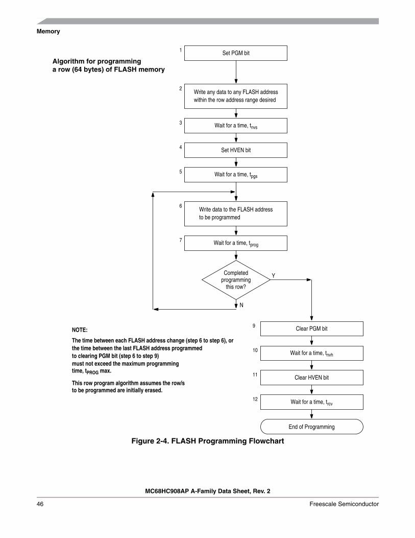
Memory
MC68HC908AP A-Family Data Sheet, Rev. 2
46 Freescale Semiconductor
Figure 2-4. FLASH Programming Flowchart
Set HVEN bit
Write any data to any FLASH addresswithin the row address range desired
Wait for a time, tnvs
Set PGM bit
Wait for a time, tpgs
Write data to the FLASH addressto be programmed
Wait for a time, tprog
Clear PGM bit
Wait for a time, tnvh
Clear HVEN bit
Wait for a time, trcv
Completedprogramming
this row?
Y
N
End of Programming
The time between each FLASH address change (step 6 to step 6), or
must not exceed the maximum programmingtime, tPROG max.
the time between the last FLASH address programmedto clearing PGM bit (step 6 to step 9)
NOTE:
1
2
3
4
5
6
7
9
10
11
12
Algorithm for programminga row (64 bytes) of FLASH memory
This row program algorithm assumes the row/sto be programmed are initially erased.

FLASH Memory
MC68HC908AP A-Family Data Sheet, Rev. 2
Freescale Semiconductor 47
2.5.7 FLASH Block Protect Register
The FLASH block protect register is implemented as an 8-bit I/O register. The value in this registerdetermines the starting address of the protected range within the FLASH memory.
BPR[7:0] — FLASH Block Protect BitsBPR[7:1] represent bits [15:9] of a 16-bit memory address. Bits [8:0] are logic 0’s.
BPR0 is used only for BPR[7:0] = $FF, for no block protection.The resultant 16-bit address is used for specifying the start address of the FLASH memory for blockprotection. The FLASH is protected from this start address to the end of FLASH memory, at $FFFF.With this mechanism, the protect start address can be X000, X200, X400, X0600, X800, XA00, XC00,or XE00 (at page boundaries — 512 bytes) within the FLASH memory.Examples of protect start address:
Address: $FE09
Bit 7 6 5 4 3 2 1 Bit 0
Read:BPR7 BPR6 BPR5 BPR4 BPR3 BPR2 BPR1 BPR0
Write:
Reset: 0 0 0 0 0 0 0 0
Figure 2-5. FLASH Block Protect Register (FLBPR)
16-bit memory address
Start address of FLASH block protect 0 0 0 0 0 0 0 0 0
BPR[7:1]
Table 2-2 FLASH Block Protect Range
BPR[7:0] Protected Range
$00 to $09 The entire FLASH memory is protected.
$0A or $0B(0000 101x)
$0A00 to $FFFF
$0C or $0D(0000 110x)
$0C00 to $FFFF
and so on...
$FA or $FB(1111 1101x)
$FA00 to $FFFF
$FC or $FD or $FE $FFCF to $FFFF
$FF The entire FLASH memory is NOT protected.(1)
1. Except for the mask option register ($FFCF) and the 48-byte user vectors($FFD0–$FFFF). These FLASH locations are always protected.

Memory
MC68HC908AP A-Family Data Sheet, Rev. 2
48 Freescale Semiconductor

MC68HC908AP A-Family Data Sheet, Rev. 2
Freescale Semiconductor 49
Chapter 3Configuration & Mask Option Registers (CONFIG & MOR)
3.1 Introduction
This section describes the configuration registers, CONFIG1 and CONFIG2; and the mask optionregister, MOR.
The configuration registers enable or disable these options:• Computer operating properly module (COP)• COP timeout period (218 – 24 or 213 – 24 ICLK cycles)• Low-voltage inhibit (LVI) on VDD• LVI on VREG• LVI module reset• LVI module in stop mode• STOP instruction• Stop mode recovery time (32 ICLK or 4096 ICLK cycles)• Oscillator (internal, RC, and crystal) during stop mode• Serial communications interface clock source (CGMXCLK or fBUS)
The mask option register selects one of the following oscillator options:• Internal oscillator• RC oscillator• Crystal oscillator
Addr. Register Name Bit 7 6 5 4 3 2 1 Bit 0
$001DConfiguration Register 2
(CONFIG2)†Read: STOP_
ICLKDISSTOP_
RCLKENSTOP_
XCLKENOSCCLK1 OSCCLK0
0 0SCIBDSRC
Write:Reset: 0 0 0 0 0 0 0 0
$001FConfiguration Register 1
(CONFIG1)†
Read:COPRS LVISTOP LVIRSTD LVIPWRD LVIREGD SSREC STOP COPD
Write:Reset: 0 0 0 0 0 0 0 0
$FFCFMask-Option-Register
(MOR)#Read:
OSCSEL1 OSCSEL0 R R R R R RWrite:Erased: 1 1 1 1 1 1 1 1
† One-time writable register after each reset.# MOR is a non-volatile FLASH register; write by programming.
= Unimplemented R = Reserved
Figure 3-1. CONFIG and MOR Registers Summary

Configuration & Mask Option Registers (CONFIG & MOR)
MC68HC908AP A-Family Data Sheet, Rev. 2
50 Freescale Semiconductor
3.2 Functional Description
The configuration registers and the mask option register are used in the initialization of various options.These two types of registers are configured differently:
• Configuration registers — Write-once registers after reset• Mask option register — FLASH register (write by programming)
The configuration registers can be written once after each reset. All of the configuration register bits arecleared during reset. Since the various options affect the operation of the MCU, it is recommended thatthese registers be written immediately after reset. The configuration registers are located at $001D and$001F. The configuration registers may be read at anytime.
NOTEThe CONFIG registers are not in the FLASH memory but are specialregisters containing one-time writable latches after each reset. Upon areset, the CONFIG registers default to predetermined settings as shown inFigure 3-2 and Figure 3-3.
The mask option register (MOR) is used for selecting one of the three clock options for the MCU. TheMOR is a byte located in FLASH memory, and is written to by a FLASH programming routine.
3.3 Configuration Register 1 (CONFIG1)
COPRS — COP Rate Select BitCOPRS selects the COP time out period. Reset clears COPRS. (See Chapter 19 Computer OperatingProperly (COP).)
1 = COP time out period = 213 – 24 ICLK cycles0 = COP time out period = 218 – 24 ICLK cycles
LVISTOP — LVI Enable in Stop Mode BitWhen the LVIPWRD or LVIREGD bit is clear, setting the LVISTOP bit enables the LVI to operateduring stop mode. Reset clears LVISTOP. (See Chapter 20 Low-Voltage Inhibit (LVI).)
1 = LVI enabled during stop mode0 = LVI disabled during stop mode
NOTEIf LVISTOP=0, set LVIRSTD=1 before entering stop mode.
LVIRSTD — LVI Reset Disable BitLVIRSTD disables the reset signal from the LVI module. (See Chapter 20 Low-Voltage Inhibit (LVI).)
1 = LVI module resets disabled0 = LVI module resets enabled
Address: $001F
Bit 7 6 5 4 3 2 1 Bit 0
Read:COPRS LVISTOP LVIRSTD LVIPWRD LVIREGD SSREC STOP COPD
Write:
Reset: 0 0 0 0 0 0 0 0
Figure 3-2. Configuration Register 1 (CONFIG1)

Configuration Register 1 (CONFIG1)
MC68HC908AP A-Family Data Sheet, Rev. 2
Freescale Semiconductor 51
LVIPWRD — VDD LVI Circuit Disable BitLVIPWRD disables the VDD LVI circuit. (See Chapter 20 Low-Voltage Inhibit (LVI).)
1 = VDD LVI circuit disabled0 = VDD LVI circuit enabled
LVIREGD — VREG LVI Circuit Disable BitLVIREGD disables the VREG LVI circuit. (See Chapter 20 Low-Voltage Inhibit (LVI).)
1 = VREG LVI circuit disabled0 = VREG LVI circuit enabled
NOTEIf LVIPWRD=1 and LVIREGD=1, set LVIRSTD=1 before entering stopmode.
SSREC — Short Stop Recovery BitSSREC enables the CPU to exit stop mode with a delay of 32 ICLK cycles instead of a 4096 ICLKcycle delay.
1 = Stop mode recovery after 32 ICLK cycles0 = Stop mode recovery after 4096 ICLK cycles
NOTEExiting stop mode by pulling reset will result in the long stop recovery.
If using an external crystal oscillator, do not set the SSREC bit.
When the LVI is disabled in stop mode (LVISTOP=0), the systemstabilization time for long stop recovery (4096 ICLK cycles) gives a delaylonger than the LVI’s turn-on time. There is no period where the MCU is notprotected from a low power condition. However, when using the short stoprecovery configuration option, the 32 ICLK delay is less than the LVI’sturn-on time and there exists a period in start-up where the LVI is notprotecting the MCU.
STOP — STOP Instruction Enable BitSTOP enables the STOP instruction.
1 = STOP instruction enabled0 = STOP instruction treated as illegal opcode
COPD — COP Disable BitCOPD disables the COP module. (See Chapter 19 Computer Operating Properly (COP).)
1 = COP module disabled0 = COP module enabled

Configuration & Mask Option Registers (CONFIG & MOR)
MC68HC908AP A-Family Data Sheet, Rev. 2
52 Freescale Semiconductor
3.4 Configuration Register 2 (CONFIG2)
STOP_ICLKDIS — Internal Oscillator Stop Mode DisableSTOP_ICLKDIS disables the internal oscillator during stop mode. Setting the STOP_ICLKDIS bitdisables the oscillator during stop mode. (See Chapter 5 Oscillator (OSC).)Reset clears this bit.
1 = Internal oscillator disabled during stop mode0 = Internal oscillator enabled to operate during stop mode
STOP_RCLKEN — RC Oscillator Stop Mode Enable BitSTOP_RCLKEN enables the RC oscillator to continue operating during stop mode. Setting theSTOP_RCLKEN bit allows the oscillator to operate continuously even during stop mode. This is usefulfor driving the timebase module to allow it to generate periodic wake up while in stop mode. (SeeChapter 5 Oscillator (OSC).)Reset clears this bit.
1 = RC oscillator enabled to operate during stop mode0 = RC oscillator disabled during stop mode
STOP_XCLKEN — X-tal Oscillator Stop Mode Enable BitSTOP_XCLKEN enables the crystal (x-tal) oscillator to continue operating during stop mode. Settingthe STOP_XCLKEN bit allows the x-tal oscillator to operate continuously even during stop mode. Thisis useful for driving the timebase module to allow it to generate periodic wake up while in stop mode.(See Chapter 5 Oscillator (OSC).) Reset clears this bit.
1 = X-tal oscillator enabled to operate during stop mode0 = X-tal oscillator disabled during stop mode
OSCCLK1, OSCCLK0 — Oscillator Output Control BitsOSCCLK1 and OSCCLK0 select which oscillator output to be driven out as OSCCLK to the timebasemodule (TBM). Reset clears these two bits.
Address: $001D
Bit 7 6 5 4 3 2 1 Bit 0
Read: STOP_ICLKDIS
STOP_RCLKEN
STOP_XCLKEN
OSCCLK1 OSCCLK00 0 SCIBD-
SRCWrite:
Reset: 0 0 0 0 0 0 0 0
Figure 3-3. Configuration Register 2 (CONFIG2)
OSCCLK1 OSCCLK0 Timebase Clock Source
0 0 Internal oscillator (ICLK)
0 1 RC oscillator (RCCLK)
1 0 X-tal oscillator (XTAL)
1 1 Not used
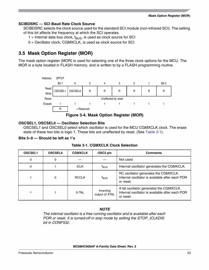
Mask Option Register (MOR)
MC68HC908AP A-Family Data Sheet, Rev. 2
Freescale Semiconductor 53
SCIBDSRC — SCI Baud Rate Clock SourceSCIBDSRC selects the clock source used for the standard SCI module (non-infrared SCI). The settingof this bit affects the frequency at which the SCI operates.
1 = Internal data bus clock, fBUS, is used as clock source for SCI0 = Oscillator clock, CGMXCLK, is used as clock source for SCI
3.5 Mask Option Register (MOR)
The mask option register (MOR) is used for selecting one of the three clock options for the MCU. TheMOR is a byte located in FLASH memory, and is written to by a FLASH programming routine.
OSCSEL1, OSCSEL0 — Oscillator Selection BitsOSCSEL1 and OSCSEL0 select which oscillator is used for the MCU CGMXCLK clock. The erasestate of these two bits is logic 1. These bits are unaffected by reset. (See Table 3-1).
Bits 5–0 — Should be left as 1’s
NOTEThe internal oscillator is a free running oscillator and is available after eachPOR or reset. It is turned-off in stop mode by setting the STOP_ICLKDISbit in CONFIG2.
Address: $FFCF
Bit 7 6 5 4 3 2 1 Bit 0
Read:OSCSEL1 OSCSEL0 R R R R R R
Write:
Reset: Unaffected by reset
Erased: 1 1 1 1 1 1 1 1
R = Reserved
Figure 3-4. Mask Option Register (MOR)
Table 3-1. CGMXCLK Clock Selection
OSCSEL1 OSCSEL0 CGMXCLK OSC2 pin Comments
0 0 — — Not used
0 1 ICLK fBUS Internal oscillator generates the CGMXCLK.
1 0 RCCLK fBUS
RC oscillator generates the CGMXCLK.Internal oscillator is available after each PORor reset.
1 1 X-TALInverting
output of XTAL
X-tal oscillator generates the CGMXCLK.Internal oscillator is available after each PORor reset.

Configuration & Mask Option Registers (CONFIG & MOR)
MC68HC908AP A-Family Data Sheet, Rev. 2
54 Freescale Semiconductor

MC68HC908AP A-Family Data Sheet, Rev. 2
Freescale Semiconductor 55
Chapter 4Central Processor Unit (CPU)
4.1 Introduction
The M68HC08 CPU (central processor unit) is an enhanced and fully object-code-compatible version ofthe M68HC05 CPU. The CPU08 Reference Manual (Freescale document order number CPU08RM/AD)contains a description of the CPU instruction set, addressing modes, and architecture.
4.2 Features• Object code fully upward-compatible with M68HC05 Family• 16-bit stack pointer with stack manipulation instructions• 16-Bit index register with x-register manipulation instructions• 8-MHz CPU internal bus frequency• 64-Kbyte program/data memory space• 16 addressing modes• Memory-to-memory data moves without using accumulator• Fast 8-bit by 8-bit multiply and 16-bit by 8-bit divide instructions• Enhanced binary-coded decimal (BCD) data handling• Modular architecture with expandable internal bus definition for extension of addressing range
beyond 64 Kbytes• Low-power stop and wait modes

Central Processor Unit (CPU)
MC68HC908AP A-Family Data Sheet, Rev. 2
56 Freescale Semiconductor
4.3 CPU Registers
Figure 4-1 shows the five CPU registers. CPU registers are not part of the memory map.
Figure 4-1. CPU Registers
4.3.1 Accumulator
The accumulator is a general-purpose 8-bit register. The CPU uses the accumulator to hold operandsand the results of arithmetic/logic operations.
4.3.2 Index Register
The 16-bit index register allows indexed addressing of a 64-Kbyte memory space. H is the upper byte ofthe index register, and X is the lower byte. H:X is the concatenated 16-bit index register.
In the indexed addressing modes, the CPU uses the contents of the index register to determine theconditional address of the operand.
The index register can serve also as a temporary data storage location.
Bit 7 6 5 4 3 2 1 Bit 0
Read:
Write:
Reset: Unaffected by reset
Figure 4-2. Accumulator (A)
ACCUMULATOR (A)
INDEX REGISTER (H:X)
STACK POINTER (SP)
PROGRAM COUNTER (PC)
CONDITION CODE REGISTER (CCR)
CARRY/BORROW FLAGZERO FLAGNEGATIVE FLAGINTERRUPT MASKHALF-CARRY FLAGTWO’S COMPLEMENT OVERFLOW FLAG
V 1 1 H I N Z C
H X
0
0
0
0
7
15
15
15
7 0

CPU Registers
MC68HC908AP A-Family Data Sheet, Rev. 2
Freescale Semiconductor 57
4.3.3 Stack Pointer
The stack pointer is a 16-bit register that contains the address of the next location on the stack. During areset, the stack pointer is preset to $00FF. The reset stack pointer (RSP) instruction sets the leastsignificant byte to $FF and does not affect the most significant byte. The stack pointer decrements as datais pushed onto the stack and increments as data is pulled from the stack.
In the stack pointer 8-bit offset and 16-bit offset addressing modes, the stack pointer can function as anindex register to access data on the stack. The CPU uses the contents of the stack pointer to determinethe conditional address of the operand.
NOTEThe location of the stack is arbitrary and may be relocated anywhere inRAM. Moving the SP out of page 0 ($0000 to $00FF) frees direct address(page 0) space. For correct operation, the stack pointer must point only toRAM locations.
4.3.4 Program Counter
The program counter is a 16-bit register that contains the address of the next instruction or operand to befetched.
Normally, the program counter automatically increments to the next sequential memory location everytime an instruction or operand is fetched. Jump, branch, and interrupt operations load the programcounter with an address other than that of the next sequential location.
During reset, the program counter is loaded with the reset vector address located at $FFFE and $FFFF.The vector address is the address of the first instruction to be executed after exiting the reset state.
Bit15
14 13 12 11 10 9 8 7 6 5 4 3 2 1 Bit 0
Read:
Write:
Reset: 0 0 0 0 0 0 0 0 X X X X X X X X
X = Indeterminate
Figure 4-3. Index Register (H:X)
Bit15
14 13 12 11 10 9 8 7 6 5 4 3 2 1 Bit 0
Read:
Write:
Reset: 0 0 0 0 0 0 0 0 1 1 1 1 1 1 1 1
Figure 4-4. Stack Pointer (SP)

Central Processor Unit (CPU)
MC68HC908AP A-Family Data Sheet, Rev. 2
58 Freescale Semiconductor
4.3.5 Condition Code Register
The 8-bit condition code register contains the interrupt mask and five flags that indicate the results of theinstruction just executed. Bits 6 and 5 are set permanently to logic 1. The following paragraphs describethe functions of the condition code register.
V — Overflow FlagThe CPU sets the overflow flag when a two's complement overflow occurs. The signed branchinstructions BGT, BGE, BLE, and BLT use the overflow flag.
1 = Overflow0 = No overflow
H — Half-Carry FlagThe CPU sets the half-carry flag when a carry occurs between accumulator bits 3 and 4 during anadd-without-carry (ADD) or add-with-carry (ADC) operation. The half-carry flag is required forbinary-coded decimal (BCD) arithmetic operations. The DAA instruction uses the states of the H andC flags to determine the appropriate correction factor.
1 = Carry between bits 3 and 40 = No carry between bits 3 and 4
I — Interrupt MaskWhen the interrupt mask is set, all maskable CPU interrupts are disabled. CPU interrupts are enabledwhen the interrupt mask is cleared. When a CPU interrupt occurs, the interrupt mask is setautomatically after the CPU registers are saved on the stack, but before the interrupt vector is fetched.
1 = Interrupts disabled0 = Interrupts enabled
NOTETo maintain M6805 Family compatibility, the upper byte of the indexregister (H) is not stacked automatically. If the interrupt service routinemodifies H, then the user must stack and unstack H using the PSHH andPULH instructions.
Bit15
14 13 12 11 10 9 8 7 6 5 4 3 2 1 Bit 0
Read:
Write:
Reset: Loaded with Vector from $FFFE and $FFFF
Figure 4-5. Program Counter (PC)
Bit 7 6 5 4 3 2 1 Bit 0
Read:V 1 1 H I N Z C
Write:
Reset: X 1 1 X 1 X X X
X = Indeterminate
Figure 4-6. Condition Code Register (CCR)

Arithmetic/Logic Unit (ALU)
MC68HC908AP A-Family Data Sheet, Rev. 2
Freescale Semiconductor 59
After the I bit is cleared, the highest-priority interrupt request is serviced first.A return-from-interrupt (RTI) instruction pulls the CPU registers from the stack and restores theinterrupt mask from the stack. After any reset, the interrupt mask is set and can be cleared only by theclear interrupt mask software instruction (CLI).
N — Negative flagThe CPU sets the negative flag when an arithmetic operation, logic operation, or data manipulationproduces a negative result, setting bit 7 of the result.
1 = Negative result0 = Non-negative result
Z — Zero flagThe CPU sets the zero flag when an arithmetic operation, logic operation, or data manipulationproduces a result of $00.
1 = Zero result0 = Non-zero result
C — Carry/Borrow FlagThe CPU sets the carry/borrow flag when an addition operation produces a carry out of bit 7 of theaccumulator or when a subtraction operation requires a borrow. Some instructions — such as bit testand branch, shift, and rotate — also clear or set the carry/borrow flag.
1 = Carry out of bit 70 = No carry out of bit 7
4.4 Arithmetic/Logic Unit (ALU)
The ALU performs the arithmetic and logic operations defined by the instruction set.
Refer to the CPU08 Reference Manual (Freescale document order number CPU08RM/AD) for adescription of the instructions and addressing modes and more detail about the architecture of the CPU.
4.5 Low-Power Modes
The WAIT and STOP instructions put the MCU in low power-consumption standby modes.
4.5.1 Wait Mode
The WAIT instruction:• Clears the interrupt mask (I bit) in the condition code register, enabling interrupts. After exit from
wait mode by interrupt, the I bit remains clear. After exit by reset, the I bit is set.• Disables the CPU clock
4.5.2 Stop Mode
The STOP instruction:• Clears the interrupt mask (I bit) in the condition code register, enabling external interrupts. After
exit from stop mode by external interrupt, the I bit remains clear. After exit by reset, the I bit is set.• Disables the CPU clock
After exiting stop mode, the CPU clock begins running after the oscillator stabilization delay.

Central Processor Unit (CPU)
MC68HC908AP A-Family Data Sheet, Rev. 2
60 Freescale Semiconductor
4.6 CPU During Break Interrupts
If a break module is present on the MCU, the CPU starts a break interrupt by:• Loading the instruction register with the SWI instruction• Loading the program counter with $FFFC:$FFFD or with $FEFC:$FEFD in monitor mode
The break interrupt begins after completion of the CPU instruction in progress. If the break addressregister match occurs on the last cycle of a CPU instruction, the break interrupt begins immediately.
A return-from-interrupt instruction (RTI) in the break routine ends the break interrupt and returns the MCUto normal operation if the break interrupt has been deasserted.
4.7 Instruction Set Summary
Table 4-1 provides a summary of the M68HC08 instruction set.
4.8 Opcode Map
The opcode map is provided in Table 4-2.
Table 4-1. Instruction Set Summary
SourceForm
Operation Description
Effect onCCR
Ad
dre
ssM
od
e
Op
cod
e
Op
eran
d
Cyc
les
V H I N Z C
ADC #oprADC oprADC oprADC opr,XADC opr,XADC ,XADC opr,SPADC opr,SP
Add with Carry A ← (A) + (M) + (C) o o – o o o
IMMDIREXTIX2IX1IXSP1SP2
A9B9C9D9E9F9
9EE99ED9
iiddhh llee ffff
ffee ff
23443245
ADD #oprADD oprADD oprADD opr,XADD opr,XADD ,XADD opr,SPADD opr,SP
Add without Carry A ← (A) + (M) o o – o o o
IMMDIREXTIX2IX1IXSP1SP2
ABBBCBDBEBFB
9EEB9EDB
iiddhh llee ffff
ffee ff
23443245
AIS #opr Add Immediate Value (Signed) to SP SP ← (SP) + (16 « M) – – – – – – IMM A7 ii 2
AIX #opr Add Immediate Value (Signed) to H:X H:X ← (H:X) + (16 « M) – – – – – – IMM AF ii 2

Opcode Map
MC68HC908AP A-Family Data Sheet, Rev. 2
Freescale Semiconductor 61
AND #oprAND oprAND oprAND opr,XAND opr,XAND ,XAND opr,SPAND opr,SP
Logical AND A ← (A) & (M) 0 – – o o –
IMMDIREXTIX2IX1IXSP1SP2
A4B4C4D4E4F4
9EE49ED4
iiddhh llee ffff
ffee ff
23443245
ASL oprASLAASLXASL opr,XASL ,XASL opr,SP
Arithmetic Shift Left(Same as LSL)
o – – o o o
DIRINHINHIX1IXSP1
3848586878
9E68
dd
ff
ff
411435
ASR oprASRAASRXASR opr,XASR opr,XASR opr,SP
Arithmetic Shift Right o – – o o o
DIRINHINHIX1IXSP1
3747576777
9E67
dd
ff
ff
411435
BCC rel Branch if Carry Bit Clear PC ← (PC) + 2 + rel ? (C) = 0 – – – – – – REL 24 rr 3
BCLR n, opr Clear Bit n in M Mn ← 0 – – – – – –
DIR (b0)DIR (b1)DIR (b2)DIR (b3)DIR (b4)DIR (b5)DIR (b6)DIR (b7)
11131517191B1D1F
dddddddddddddddd
44444444
BCS rel Branch if Carry Bit Set (Same as BLO) PC ← (PC) + 2 + rel ? (C) = 1 – – – – – – REL 25 rr 3
BEQ rel Branch if Equal PC ← (PC) + 2 + rel ? (Z) = 1 – – – – – – REL 27 rr 3
BGE oprBranch if Greater Than or Equal To(Signed Operands)
PC ← (PC) + 2 + rel ? (N ⊕ V) = 0 – – – – – – REL 90 rr 3
BGT oprBranch if Greater Than (SignedOperands)
PC ← (PC) + 2 +rel ? (Z) | (N ⊕ V)=0 – – – – – – REL 92 rr 3
BHCC rel Branch if Half Carry Bit Clear PC ← (PC) + 2 + rel ? (H) = 0 – – – – – – REL 28 rr 3
BHCS rel Branch if Half Carry Bit Set PC ← (PC) + 2 + rel ? (H) = 1 – – – – – – REL 29 rr 3
BHI rel Branch if Higher PC ← (PC) + 2 + rel ? (C) | (Z) = 0 – – – – – – REL 22 rr 3
BHS relBranch if Higher or Same(Same as BCC)
PC ← (PC) + 2 + rel ? (C) = 0 – – – – – – REL 24 rr 3
BIH rel Branch if IRQ Pin High PC ← (PC) + 2 + rel ? IRQ = 1 – – – – – – REL 2F rr 3
BIL rel Branch if IRQ Pin Low PC ← (PC) + 2 + rel ? IRQ = 0 – – – – – – REL 2E rr 3
Table 4-1. Instruction Set Summary
SourceForm
Operation Description
Effect onCCR
Ad
dre
ssM
od
e
Op
cod
e
Op
eran
d
Cyc
les
V H I N Z C
C
b0b7
0
b0b7
C

Central Processor Unit (CPU)
MC68HC908AP A-Family Data Sheet, Rev. 2
62 Freescale Semiconductor
BIT #oprBIT oprBIT oprBIT opr,XBIT opr,XBIT ,XBIT opr,SPBIT opr,SP
Bit Test (A) & (M) 0 – – o o –
IMMDIREXTIX2IX1IXSP1SP2
A5B5C5D5E5F5
9EE59ED5
iiddhh llee ffff
ffee ff
23443245
BLE oprBranch if Less Than or Equal To(Signed Operands)
PC ← (PC) + 2 + rel ? (Z) | (N ⊕ V)=1 – – – – – – REL 93 rr 3
BLO rel Branch if Lower (Same as BCS) PC ← (PC) + 2 + rel ? (C) = 1 – – – – – – REL 25 rr 3
BLS rel Branch if Lower or Same PC ← (PC) + 2 + rel ? (C) | (Z) = 1 – – – – – – REL 23 rr 3
BLT opr Branch if Less Than (Signed Operands) PC ← (PC) + 2 + rel ? (N ⊕ V) = 1 – – – – – – REL 91 rr 3
BMC rel Branch if Interrupt Mask Clear PC ← (PC) + 2 + rel ? (I) = 0 – – – – – – REL 2C rr 3
BMI rel Branch if Minus PC ← (PC) + 2 + rel ? (N) = 1 – – – – – – REL 2B rr 3
BMS rel Branch if Interrupt Mask Set PC ← (PC) + 2 + rel ? (I) = 1 – – – – – – REL 2D rr 3
BNE rel Branch if Not Equal PC ← (PC) + 2 + rel ? (Z) = 0 – – – – – – REL 26 rr 3
BPL rel Branch if Plus PC ← (PC) + 2 + rel ? (N) = 0 – – – – – – REL 2A rr 3
BRA rel Branch Always PC ← (PC) + 2 + rel – – – – – – REL 20 rr 3
BRCLR n,opr,rel Branch if Bit n in M Clear PC ← (PC) + 3 + rel ? (Mn) = 0 – – – – – o
DIR (b0)DIR (b1)DIR (b2)DIR (b3)DIR (b4)DIR (b5)DIR (b6)DIR (b7)
01030507090B0D0F
dd rrdd rrdd rrdd rrdd rrdd rrdd rrdd rr
55555555
BRN rel Branch Never PC ← (PC) + 2 – – – – – – REL 21 rr 3
BRSET n,opr,rel Branch if Bit n in M Set PC ← (PC) + 3 + rel ? (Mn) = 1 – – – – – o
DIR (b0)DIR (b1)DIR (b2)DIR (b3)DIR (b4)DIR (b5)DIR (b6)DIR (b7)
00020406080A0C0E
dd rrdd rrdd rrdd rrdd rrdd rrdd rrdd rr
55555555
BSET n,opr Set Bit n in M Mn ← 1 – – – – – –
DIR (b0)DIR (b1)DIR (b2)DIR (b3)DIR (b4)DIR (b5)DIR (b6)DIR (b7)
10121416181A1C1E
dddddddddddddddd
44444444
Table 4-1. Instruction Set Summary
SourceForm
Operation Description
Effect onCCR
Ad
dre
ssM
od
e
Op
cod
e
Op
eran
d
Cyc
les
V H I N Z C

Opcode Map
MC68HC908AP A-Family Data Sheet, Rev. 2
Freescale Semiconductor 63
BSR rel Branch to Subroutine
PC ← (PC) + 2; push (PCL)SP ← (SP) – 1; push (PCH)
SP ← (SP) – 1PC ← (PC) + rel
– – – – – – REL AD rr 4
CBEQ opr,relCBEQA #opr,relCBEQX #opr,relCBEQ opr,X+,relCBEQ X+,relCBEQ opr,SP,rel
Compare and Branch if Equal
PC ← (PC) + 3 + rel ? (A) – (M) = $00PC ← (PC) + 3 + rel ? (A) – (M) = $00PC ← (PC) + 3 + rel ? (X) – (M) = $00PC ← (PC) + 3 + rel ? (A) – (M) = $00PC ← (PC) + 2 + rel ? (A) – (M) = $00PC ← (PC) + 4 + rel ? (A) – (M) = $00
– – – – – –
DIRIMMIMMIX1+IX+SP1
3141516171
9E61
dd rrii rrii rrff rrrrff rr
544546
CLC Clear Carry Bit C ← 0 – – – – – 0 INH 98 1
CLI Clear Interrupt Mask I ← 0 – – 0 – – – INH 9A 2
CLR oprCLRACLRXCLRHCLR opr,XCLR ,XCLR opr,SP
Clear
M ← $00A ← $00X ← $00H ← $00M ← $00M ← $00M ← $00
0 – – 0 1 –
DIRINHINHINHIX1IXSP1
3F4F5F8C6F7F
9E6F
dd
ff
ff
3111324
CMP #oprCMP oprCMP oprCMP opr,XCMP opr,XCMP ,XCMP opr,SPCMP opr,SP
Compare A with M (A) – (M) o – – o o o
IMMDIREXTIX2IX1IXSP1SP2
A1B1C1D1E1F1
9EE19ED1
iiddhh llee ffff
ffee ff
23443245
COM oprCOMACOMXCOM opr,XCOM ,XCOM opr,SP
Complement (One’s Complement)
M ← (M) = $FF – (M)A ← (A) = $FF – (M)X ← (X) = $FF – (M)M ← (M) = $FF – (M)M ← (M) = $FF – (M)M ← (M) = $FF – (M)
0 – – o o 1
DIRINHINHIX1IXSP1
3343536373
9E63
dd
ff
ff
411435
CPHX #oprCPHX opr
Compare H:X with M (H:X) – (M:M + 1) o – – o o oIMMDIR
6575
ii ii+1dd
34
CPX #oprCPX oprCPX oprCPX ,XCPX opr,XCPX opr,XCPX opr,SPCPX opr,SP
Compare X with M (X) – (M) o – – o o o
IMMDIREXTIX2IX1IXSP1SP2
A3B3C3D3E3F3
9EE39ED3
iiddhh llee ffff
ffee ff
23443245
DAA Decimal Adjust A (A)10 U – – o o o INH 72 2
Table 4-1. Instruction Set Summary
SourceForm
Operation Description
Effect onCCR
Ad
dre
ssM
od
e
Op
cod
e
Op
eran
d
Cyc
les
V H I N Z C

Central Processor Unit (CPU)
MC68HC908AP A-Family Data Sheet, Rev. 2
64 Freescale Semiconductor
DBNZ opr,relDBNZA relDBNZX relDBNZ opr,X,relDBNZ X,relDBNZ opr,SP,rel
Decrement and Branch if Not Zero
A ← (A)–1 or M ← (M)–1 or X ← (X)–1PC ← (PC) + 3 + rel ? (result) ≠ 0PC ← (PC) + 2 + rel ? (result) ≠ 0PC ← (PC) + 2 + rel ? (result) ≠ 0PC ← (PC) + 3 + rel ? (result) ≠ 0PC ← (PC) + 2 + rel ? (result) ≠ 0PC ← (PC) + 4 + rel ? (result) ≠ 0
– – – – – –
DIRINHINHIX1IXSP1
3B4B5B6B7B
9E6B
dd rrrrrrff rrrrff rr
533546
DEC oprDECADECXDEC opr,XDEC ,XDEC opr,SP
Decrement
M ← (M) – 1A ← (A) – 1X ← (X) – 1M ← (M) – 1M ← (M) – 1M ← (M) – 1
o – – o o –
DIRINHINHIX1IXSP1
3A4A5A6A7A
9E6A
dd
ff
ff
411435
DIV DivideA ← (H:A)/(X)
H ← Remainder– – – – o o INH 52 7
EOR #oprEOR oprEOR oprEOR opr,XEOR opr,XEOR ,XEOR opr,SPEOR opr,SP
Exclusive OR M with A A ← (A ⊕ M) 0 – – o o –
IMMDIREXTIX2IX1IXSP1SP2
A8B8C8D8E8F8
9EE89ED8
iiddhh llee ffff
ffee ff
23443245
INC oprINCAINCXINC opr,XINC ,XINC opr,SP
Increment
M ← (M) + 1A ← (A) + 1X ← (X) + 1M ← (M) + 1M ← (M) + 1M ← (M) + 1
o – – o o –
DIRINHINHIX1IXSP1
3C4C5C6C7C
9E6C
dd
ff
ff
411435
JMP oprJMP oprJMP opr,XJMP opr,XJMP ,X
Jump PC ← Jump Address – – – – – –
DIREXTIX2IX1IX
BCCCDCECFC
ddhh llee ffff
23432
JSR oprJSR oprJSR opr,XJSR opr,XJSR ,X
Jump to Subroutine
PC ← (PC) + n (n = 1, 2, or 3)Push (PCL); SP ← (SP) – 1Push (PCH); SP ← (SP) – 1PC ← Unconditional Address
– – – – – –
DIREXTIX2IX1IX
BDCDDDEDFD
ddhh llee ffff
45654
LDA #oprLDA oprLDA oprLDA opr,XLDA opr,XLDA ,XLDA opr,SPLDA opr,SP
Load A from M A ← (M) 0 – – o o –
IMMDIREXTIX2IX1IXSP1SP2
A6B6C6D6E6F6
9EE69ED6
iiddhh llee ffff
ffee ff
23443245
LDHX #oprLDHX opr
Load H:X from M H:X ← (M:M + 1) 0 – – o o –IMMDIR
4555
ii jjdd
34
Table 4-1. Instruction Set Summary
SourceForm
Operation Description
Effect onCCR
Ad
dre
ssM
od
e
Op
cod
e
Op
eran
d
Cyc
les
V H I N Z C

Opcode Map
MC68HC908AP A-Family Data Sheet, Rev. 2
Freescale Semiconductor 65
LDX #oprLDX oprLDX oprLDX opr,XLDX opr,XLDX ,XLDX opr,SPLDX opr,SP
Load X from M X ← (M) 0 – – o o –
IMMDIREXTIX2IX1IXSP1SP2
AEBECEDEEEFE
9EEE9EDE
iiddhh llee ffff
ffee ff
23443245
LSL oprLSLALSLXLSL opr,XLSL ,XLSL opr,SP
Logical Shift Left(Same as ASL)
o – – o o o
DIRINHINHIX1IXSP1
3848586878
9E68
dd
ff
ff
411435
LSR oprLSRALSRXLSR opr,XLSR ,XLSR opr,SP
Logical Shift Right o – – 0 o o
DIRINHINHIX1IXSP1
3444546474
9E64
dd
ff
ff
411435
MOV opr,oprMOV opr,X+MOV #opr,oprMOV X+,opr
Move(M)Destination ← (M)Source
H:X ← (H:X) + 1 (IX+D, DIX+)0 – – o o –
DDDIX+IMDIX+D
4E5E6E7E
dd ddddii dddd
5444
MUL Unsigned multiply X:A ← (X) × (A) – 0 – – – 0 INH 42 5
NEG oprNEGANEGXNEG opr,XNEG ,XNEG opr,SP
Negate (Two’s Complement)
M ← –(M) = $00 – (M)A ← –(A) = $00 – (A)X ← –(X) = $00 – (X)M ← –(M) = $00 – (M)M ← –(M) = $00 – (M)
o – – o o o
DIRINHINHIX1IXSP1
3040506070
9E60
dd
ff
ff
411435
NOP No Operation None – – – – – – INH 9D 1
NSA Nibble Swap A A ← (A[3:0]:A[7:4]) – – – – – – INH 62 3
ORA #oprORA oprORA oprORA opr,XORA opr,XORA ,XORA opr,SPORA opr,SP
Inclusive OR A and M A ← (A) | (M) 0 – – o o –
IMMDIREXTIX2IX1IXSP1SP2
AABACADAEAFA
9EEA9EDA
iiddhh llee ffff
ffee ff
23443245
PSHA Push A onto Stack Push (A); SP ← (SP) – 1 – – – – – – INH 87 2
PSHH Push H onto Stack Push (H); SP ← (SP) – 1 – – – – – – INH 8B 2
PSHX Push X onto Stack Push (X); SP ← (SP) – 1 – – – – – – INH 89 2
PULA Pull A from Stack SP ← (SP + 1); Pull (A) – – – – – – INH 86 2
Table 4-1. Instruction Set Summary
SourceForm
Operation Description
Effect onCCR
Ad
dre
ssM
od
e
Op
cod
e
Op
eran
d
Cyc
les
V H I N Z C
C
b0b7
0
b0b7
C0

Central Processor Unit (CPU)
MC68HC908AP A-Family Data Sheet, Rev. 2
66 Freescale Semiconductor
PULH Pull H from Stack SP ← (SP + 1); Pull (H) – – – – – – INH 8A 2
PULX Pull X from Stack SP ← (SP + 1); Pull (X) – – – – – – INH 88 2
ROL oprROLAROLXROL opr,XROL ,XROL opr,SP
Rotate Left through Carry o – – o o o
DIRINHINHIX1IXSP1
3949596979
9E69
dd
ff
ff
411435
ROR oprRORARORXROR opr,XROR ,XROR opr,SP
Rotate Right through Carry o – – o o o
DIRINHINHIX1IXSP1
3646566676
9E66
dd
ff
ff
411435
RSP Reset Stack Pointer SP ← $FF – – – – – – INH 9C 1
RTI Return from Interrupt
SP ← (SP) + 1; Pull (CCR)SP ← (SP) + 1; Pull (A)SP ← (SP) + 1; Pull (X)
SP ← (SP) + 1; Pull (PCH)SP ← (SP) + 1; Pull (PCL)
o o o o o o INH 80 7
RTS Return from SubroutineSP ← SP + 1; Pull (PCH)SP ← SP + 1; Pull (PCL)
– – – – – – INH 81 4
SBC #oprSBC oprSBC oprSBC opr,XSBC opr,XSBC ,XSBC opr,SPSBC opr,SP
Subtract with Carry A ← (A) – (M) – (C) o – – o o o
IMMDIREXTIX2IX1IXSP1SP2
A2B2C2D2E2F2
9EE29ED2
iiddhh llee ffff
ffee ff
23443245
SEC Set Carry Bit C ← 1 – – – – – 1 INH 99 1
SEI Set Interrupt Mask I ← 1 – – 1 – – – INH 9B 2
STA oprSTA oprSTA opr,XSTA opr,XSTA ,XSTA opr,SPSTA opr,SP
Store A in M M ← (A) 0 – – o o –
DIREXTIX2IX1IXSP1SP2
B7C7D7E7F7
9EE79ED7
ddhh llee ffff
ffee ff
3443245
STHX opr Store H:X in M (M:M + 1) ← (H:X) 0 – – o o – DIR 35 dd 4
STOP Enable IRQ Pin; Stop Processing I ← 0; Stop Processing – – 0 – – – INH 8E 1
Table 4-1. Instruction Set Summary
SourceForm
Operation Description
Effect onCCR
Ad
dre
ssM
od
e
Op
cod
e
Op
eran
d
Cyc
les
V H I N Z C
C
b0b7
b0b7
C

Opcode Map
MC68HC908AP A-Family Data Sheet, Rev. 2
Freescale Semiconductor 67
STX oprSTX oprSTX opr,XSTX opr,XSTX ,XSTX opr,SPSTX opr,SP
Store X in M M ← (X) 0 – – o o –
DIREXTIX2IX1IXSP1SP2
BFCFDFEFFF
9EEF9EDF
ddhh llee ffff
ffee ff
3443245
SUB #oprSUB oprSUB oprSUB opr,XSUB opr,XSUB ,XSUB opr,SPSUB opr,SP
Subtract A ← (A) – (M) o – – o o o
IMMDIREXTIX2IX1IXSP1SP2
A0B0C0D0E0F0
9EE09ED0
iiddhh llee ffff
ffee ff
23443245
SWI Software Interrupt
PC ← (PC) + 1; Push (PCL)SP ← (SP) – 1; Push (PCH)
SP ← (SP) – 1; Push (X)SP ← (SP) – 1; Push (A)
SP ← (SP) – 1; Push (CCR)SP ← (SP) – 1; I ← 1
PCH ← Interrupt Vector High BytePCL ← Interrupt Vector Low Byte
– – 1 – – – INH 83 9
TAP Transfer A to CCR CCR ← (A) o o o o o o INH 84 2
TAX Transfer A to X X ← (A) – – – – – – INH 97 1
TPA Transfer CCR to A A ← (CCR) – – – – – – INH 85 1
TST oprTSTATSTXTST opr,XTST ,XTST opr,SP
Test for Negative or Zero (A) – $00 or (X) – $00 or (M) – $00 0 – – o o –
DIRINHINHIX1IXSP1
3D4D5D6D7D
9E6D
dd
ff
ff
311324
TSX Transfer SP to H:X H:X ← (SP) + 1 – – – – – – INH 95 2
TXA Transfer X to A A ← (X) – – – – – – INH 9F 1
TXS Transfer H:X to SP (SP) ← (H:X) – 1 – – – – – – INH 94 2
WAIT Enable Interrupts; Wait for InterruptI ← 0; Inhibit CPU clocking until
interrupted– – 0 – – – INH 8F 1
Table 4-1. Instruction Set Summary
SourceForm
Operation Description
Effect onCCR
Ad
dre
ssM
od
e
Op
cod
e
Op
eran
d
Cyc
les
V H I N Z C

Central Processor Unit (CPU)
MC68HC908AP A-Family Data Sheet, Rev. 2
68 Freescale Semiconductor
A Accumulator n Any bitC Carry/borrow bit opr Operand (one or two bytes)CCR Condition code register PC Program counterdd Direct address of operand PCH Program counter high bytedd rr Direct address of operand and relative offset of branch instruction PCL Program counter low byteDD Direct to direct addressing mode REL Relative addressing modeDIR Direct addressing mode rel Relative program counter offset byteDIX+ Direct to indexed with post increment addressing mode rr Relative program counter offset byteee ff High and low bytes of offset in indexed, 16-bit offset addressing SP1 Stack pointer, 8-bit offset addressing modeEXT Extended addressing mode SP2 Stack pointer 16-bit offset addressing modeff Offset byte in indexed, 8-bit offset addressing SP Stack pointerH Half-carry bit U UndefinedH Index register high byte V Overflow bithh ll High and low bytes of operand address in extended addressing X Index register low byteI Interrupt mask Z Zero bitii Immediate operand byte & Logical ANDIMD Immediate source to direct destination addressing mode | Logical ORIMM Immediate addressing mode ⊕ Logical EXCLUSIVE ORINH Inherent addressing mode ( ) Contents ofIX Indexed, no offset addressing mode –( ) Negation (two’s complement)IX+ Indexed, no offset, post increment addressing mode # Immediate valueIX+D Indexed with post increment to direct addressing mode « Sign extendIX1 Indexed, 8-bit offset addressing mode ← Loaded withIX1+ Indexed, 8-bit offset, post increment addressing mode ? IfIX2 Indexed, 16-bit offset addressing mode : Concatenated withM Memory location o Set or clearedN Negative bit — Not affected
Table 4-1. Instruction Set Summary
SourceForm
Operation Description
Effect onCCR
Ad
dre
ssM
od
e
Op
cod
e
Op
eran
d
Cyc
les
V H I N Z C
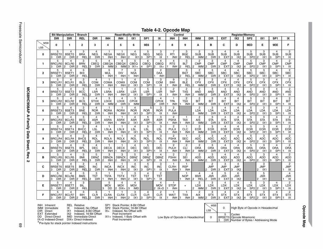
MC
68HC
908AP
A-Fam
ily Data S
heet, R
ev. 2
Freescale S
emiconductor
69
Op
cod
e Map
Table 4-2. Opcode MapBit Manipulation Branch Read-Modify-Write Control Register/Memory
DIR DIR REL DIR INH INH IX1 SP1 IX INH INH IMM DIR EXT IX2 SP2 IX1 SP1 IX
0 1 2 3 4 5 6 9E6 7 8 9 A B C D 9ED E 9EE F
05
BRSET03 DIR
4BSET0
2 DIR
3BRA
2 REL
4NEG
2 DIR
1NEGA
1 INH
1NEGX
1 INH
4NEG
2 IX1
5NEG
3 SP1
3NEG
1 IX
7RTI
1 INH
3BGE
2 REL
2SUB
2 IMM
3SUB
2 DIR
4SUB
3 EXT
4SUB
3 IX2
5SUB
4 SP2
3SUB
2 IX1
4SUB
3 SP1
2SUB
1 IX
15
BRCLR03 DIR
4BCLR0
2 DIR
3BRN
2 REL
5CBEQ
3 DIR
4CBEQA3 IMM
4CBEQX3 IMM
5CBEQ
3 IX1+
6CBEQ
4 SP1
4CBEQ
2 IX+
4RTS
1 INH
3BLT
2 REL
2CMP
2 IMM
3CMP
2 DIR
4CMP
3 EXT
4CMP
3 IX2
5CMP
4 SP2
3CMP
2 IX1
4CMP
3 SP1
2CMP
1 IX
25
BRSET13 DIR
4BSET1
2 DIR
3BHI
2 REL
5MUL
1 INH
7DIV
1 INH
3NSA
1 INH
2DAA
1 INH
3BGT
2 REL
2SBC
2 IMM
3SBC
2 DIR
4SBC
3 EXT
4SBC
3 IX2
5SBC
4 SP2
3SBC
2 IX1
4SBC
3 SP1
2SBC
1 IX
35
BRCLR13 DIR
4BCLR1
2 DIR
3BLS
2 REL
4COM
2 DIR
1COMA
1 INH
1COMX
1 INH
4COM
2 IX1
5COM
3 SP1
3COM
1 IX
9SWI
1 INH
3BLE
2 REL
2CPX
2 IMM
3CPX
2 DIR
4CPX
3 EXT
4CPX
3 IX2
5CPX
4 SP2
3CPX
2 IX1
4CPX
3 SP1
2CPX
1 IX
45
BRSET23 DIR
4BSET2
2 DIR
3BCC
2 REL
4LSR
2 DIR
1LSRA
1 INH
1LSRX
1 INH
4LSR
2 IX1
5LSR
3 SP1
3LSR
1 IX
2TAP
1 INH
2TXS
1 INH
2AND
2 IMM
3AND
2 DIR
4AND
3 EXT
4AND
3 IX2
5AND
4 SP2
3AND
2 IX1
4AND
3 SP1
2AND
1 IX
55
BRCLR23 DIR
4BCLR2
2 DIR
3BCS
2 REL
4STHX
2 DIR
3LDHX
3 IMM
4LDHX
2 DIR
3CPHX
3 IMM
4CPHX
2 DIR
1TPA
1 INH
2TSX
1 INH
2BIT
2 IMM
3BIT
2 DIR
4BIT
3 EXT
4BIT
3 IX2
5BIT
4 SP2
3BIT
2 IX1
4BIT
3 SP1
2BIT
1 IX
65
BRSET33 DIR
4BSET3
2 DIR
3BNE
2 REL
4ROR
2 DIR
1RORA
1 INH
1RORX
1 INH
4ROR
2 IX1
5ROR
3 SP1
3ROR
1 IX
2PULA
1 INH
2LDA
2 IMM
3LDA
2 DIR
4LDA
3 EXT
4LDA
3 IX2
5LDA
4 SP2
3LDA
2 IX1
4LDA
3 SP1
2LDA
1 IX
75
BRCLR33 DIR
4BCLR3
2 DIR
3BEQ
2 REL
4ASR
2 DIR
1ASRA
1 INH
1ASRX
1 INH
4ASR
2 IX1
5ASR
3 SP1
3ASR
1 IX
2PSHA
1 INH
1TAX
1 INH
2AIS
2 IMM
3STA
2 DIR
4STA
3 EXT
4STA
3 IX2
5STA
4 SP2
3STA
2 IX1
4STA
3 SP1
2STA
1 IX
85
BRSET43 DIR
4BSET4
2 DIR
3BHCC
2 REL
4LSL
2 DIR
1LSLA
1 INH
1LSLX
1 INH
4LSL
2 IX1
5LSL
3 SP1
3LSL
1 IX
2PULX
1 INH
1CLC
1 INH
2EOR
2 IMM
3EOR
2 DIR
4EOR
3 EXT
4EOR
3 IX2
5EOR
4 SP2
3EOR
2 IX1
4EOR
3 SP1
2EOR
1 IX
95
BRCLR43 DIR
4BCLR4
2 DIR
3BHCS
2 REL
4ROL
2 DIR
1ROLA
1 INH
1ROLX
1 INH
4ROL
2 IX1
5ROL
3 SP1
3ROL
1 IX
2PSHX
1 INH
1SEC
1 INH
2ADC
2 IMM
3ADC
2 DIR
4ADC
3 EXT
4ADC
3 IX2
5ADC
4 SP2
3ADC
2 IX1
4ADC
3 SP1
2ADC
1 IX
A5
BRSET53 DIR
4BSET5
2 DIR
3BPL
2 REL
4DEC
2 DIR
1DECA
1 INH
1DECX
1 INH
4DEC
2 IX1
5DEC
3 SP1
3DEC
1 IX
2PULH
1 INH
2CLI
1 INH
2ORA
2 IMM
3ORA
2 DIR
4ORA
3 EXT
4ORA
3 IX2
5ORA
4 SP2
3ORA
2 IX1
4ORA
3 SP1
2ORA
1 IX
B5
BRCLR53 DIR
4BCLR5
2 DIR
3BMI
2 REL
5DBNZ
3 DIR
3DBNZA2 INH
3DBNZX2 INH
5DBNZ
3 IX1
6DBNZ
4 SP1
4DBNZ
2 IX
2PSHH
1 INH
2SEI
1 INH
2ADD
2 IMM
3ADD
2 DIR
4ADD
3 EXT
4ADD
3 IX2
5ADD
4 SP2
3ADD
2 IX1
4ADD
3 SP1
2ADD
1 IX
C5
BRSET63 DIR
4BSET6
2 DIR
3BMC
2 REL
4INC
2 DIR
1INCA
1 INH
1INCX
1 INH
4INC
2 IX1
5INC
3 SP1
3INC
1 IX
1CLRH
1 INH
1RSP
1 INH
2JMP
2 DIR
3JMP
3 EXT
4JMP
3 IX2
3JMP
2 IX1
2JMP
1 IX
D5
BRCLR63 DIR
4BCLR6
2 DIR
3BMS
2 REL
3TST
2 DIR
1TSTA
1 INH
1TSTX
1 INH
3TST
2 IX1
4TST
3 SP1
2TST
1 IX
1NOP
1 INH
4BSR
2 REL
4JSR
2 DIR
5JSR
3 EXT
6JSR
3 IX2
5JSR
2 IX1
4JSR
1 IX
E5
BRSET73 DIR
4BSET7
2 DIR
3BIL
2 REL
5MOV
3 DD
4MOV
2 DIX+
4MOV
3 IMD
4MOV
2 IX+D
1STOP
1 INH *2
LDX2 IMM
3LDX
2 DIR
4LDX
3 EXT
4LDX
3 IX2
5LDX
4 SP2
3LDX
2 IX1
4LDX
3 SP1
2LDX
1 IX
F5
BRCLR73 DIR
4BCLR7
2 DIR
3BIH
2 REL
3CLR
2 DIR
1CLRA
1 INH
1CLRX
1 INH
3CLR
2 IX1
4CLR
3 SP1
2CLR
1 IX
1WAIT
1 INH
1TXA
1 INH
2AIX
2 IMM
3STX
2 DIR
4STX
3 EXT
4STX
3 IX2
5STX
4 SP2
3STX
2 IX1
4STX
3 SP1
2STX
1 IX
INH Inherent REL Relative SP1 Stack Pointer, 8-Bit OffsetIMM Immediate IX Indexed, No Offset SP2 Stack Pointer, 16-Bit OffsetDIR Direct IX1 Indexed, 8-Bit Offset IX+ Indexed, No Offset withEXT Extended IX2 Indexed, 16-Bit Offset Post IncrementDD Direct-Direct IMD Immediate-Direct IX1+ Indexed, 1-Byte Offset withIX+D Indexed-Direct DIX+ Direct-Indexed Post Increment*Pre-byte for stack pointer indexed instructions
0 High Byte of Opcode in Hexadecimal
Low Byte of Opcode in Hexadecimal 05
BRSET03 DIR
CyclesOpcode MnemonicNumber of Bytes / Addressing Mode
MSB
LSB
MSB
LSB

Central Processor Unit (CPU)
MC68HC908AP A-Family Data Sheet, Rev. 2
70 Freescale Semiconductor

MC68HC908AP A-Family Data Sheet, Rev. 2
Freescale Semiconductor 71
Chapter 5Oscillator (OSC)
5.1 Introduction
The oscillator module consist of three types of oscillator circuits:• Internal oscillator• RC oscillator• 1MHz to 8MHz crystal (x-tal) oscillator
The reference clock for the CGM and other MCU sub-systems is selected by programming the maskoption register located at $FFCF.
The reference clock for the timebase module (TBM) is selected by the two bits, OSCCLK1 and OSCCLK0,in the CONFIG2 register.
The internal oscillator runs continuously after a POR or reset, and is always available. The RC and crystaloscillator cannot run concurrently; one is disabled while the other is selected; because the RC and x-talcircuits share the same OSC1 pin.
NOTEThe oscillator circuits are powered by the on-chip VREG regulator,therefore, the output swing on OSC1 and OSC2 is from VSS to VREG.
Figure 5-1. shows the block diagram of the oscillator module.
5.2 Clock Selection
Reference clocks are selectable for the following sub-systems:• CGMXCLK and CGMRCLK — Reference clock for clock generator module (CGM) and other MCU
sub-systems other than TBM and COP. This is the main reference clock for the MCU.• OSCCLK — Reference clock for timebase module (TBM).

Oscillator (OSC)
MC68HC908AP A-Family Data Sheet, Rev. 2
72 Freescale Semiconductor
Figure 5-1. Oscillator Module Block Diagram
5.2.1 CGM Reference Clock Selection
The clock generator module (CGM) reference clock (CGMXCLK) is the reference clock input to the MCU.It is selected by programming two bits in a FLASH memory location; the mask option register (MOR), at$FFCF. See 3.5 Mask Option Register (MOR).
Address: $FFCF
Bit 7 6 5 4 3 2 1 Bit 0
Read:OSCSEL1 OSCSEL0 R R R R R R
Write:
Reset: Unaffected by reset
Erased: 1 1 1 1 1 1 1 1
R = Reserved
Figure 5-2. Mask Option Register (MOR)
X-TAL OSCILLATOR RC OSCILLATOR INTERNAL OSCILLATOR
MUX
OSC1 OSC2
BUS CLOCKFrom SIM
MUX
XCLK RCCLK ICLK
OSCCLK0
OSCCLK1
OSCSEL0
OSCSEL1
OSCCLK
To TBM
CGMXCLK CGMRCLK
To CGM and others
MOR CONFIG2
To CGM PLL
X RC IX RC I
To SIM(and COP)

Clock Selection
MC68HC908AP A-Family Data Sheet, Rev. 2
Freescale Semiconductor 73
NOTEThe internal oscillator is a free running oscillator and is available after eachPOR or reset. It is turned-off in stop mode by setting the STOP_ICLKDISbit in CONFIG2.
5.2.2 TBM Reference Clock Selection
The timebase module reference clock (OSCCLK) is selected by configuring two bits in the CONFIG2register, at $001D. See Chapter 3 Configuration & Mask Option Registers (CONFIG & MOR).
NOTEThe RCCLK or XCLK is only available if that clock is selected as the CGMreference clock, whereas the ICLK is always available.
Table 5-1. CGMXCLK Clock Selection
OSCSEL1 OSCSEL0 CGMXCLK OSC2 Pin Comments
0 0 — — Not used
0 1 ICLK fBUS Internal oscillator generates the CGMXCLK.
1 0 RCCLK fBUS
RC oscillator generates the CGMXCLK.Internal oscillator is available after each POR orreset.
1 1 XCLKInvertingoutput of
X-TAL
X-tal oscillator generates the CGMXCLK.Internal oscillator is available after each POR orreset.
Address: $001D
Bit 7 6 5 4 3 2 1 Bit 0
Read: STOP_ICLKDIS
STOP_RCLKEN
STOP_XCLKEN
OSCCLK1 OSCCLK00 0 SCIBD-
SRCWrite:
Reset: 0 0 0 0 0 0 0 0
Figure 5-3. Configuration Register 2 (CONFIG2)
Table 5-2. Timebase Module Reference Clock Selection
OSCCLK1 OSCCLK0 Timebase Clock Source
0 0 Internal oscillator (ICLK)
0 1 RC oscillator (RCCLK)
1 0 X-tal oscillator (XCLK)
1 1 Not used

Oscillator (OSC)
MC68HC908AP A-Family Data Sheet, Rev. 2
74 Freescale Semiconductor
5.3 Internal Oscillator
The internal oscillator clock (ICLK), with a frequency of fICLK, is a free running clock that requires noexternal components. It can be selected as the CGMXCLK for the CGM and MCU sub-systems; and theOSCCLK clock for the TBM. The ICLK is also the reference clock input to the computer operating properly(COP) module.
Due to the simplicity of the internal oscillator, it does not have the accuracy and stability of the RCoscillator or the x-tal oscillator. Therefore, the ICLK is not suitable where an accurate bus clock is requiredand it should not be used as the CGMRCLK to the CGM PLL.
The internal oscillator by default is always available and is free running after POR or reset. It can beturned-off in stop mode by setting the STOP_ICLKDIS bit before executing the STOP instruction.
Figure 5-4 shows the logical representation of components of the internal oscillator circuitry.
Figure 5-4. Internal Oscillator
INTERNAL OSCILLATOR
EN
SIMOSCEN
STOP_ICLKDIS
CONFIG2
ICLK
MCU
From SIM To Clock Selection MUX
BUS CLOCK
From SIM
OSC2
and COP

RC Oscillator
MC68HC908AP A-Family Data Sheet, Rev. 2
Freescale Semiconductor 75
5.4 RC Oscillator
The RC oscillator circuit is designed for use with an external resistor and a capacitor.
In its typical configuration, the RC oscillator requires two external components, one R and one C.Component values should have a tolerance of 1% or less, to obtain a clock source with less than 10%tolerance. The oscillator configuration uses two components:
• CEXT• REXT
Figure 5-5. RC Oscillator
5.5 X-tal Oscillator
The crystal (x-tal) oscillator circuit is designed for use with an external 1–8MHz crystal to provide anaccurate clock source.
In its typical configuration, the x-tal oscillator is connected in a Pierce oscillator configuration, as shownin Figure 5-6. This figure shows only the logical representation of the internal components and may notrepresent actual circuitry. The oscillator configuration uses five components:
• Crystal, X1• Fixed capacitor, C1• Tuning capacitor, C2 (can also be a fixed capacitor)• Feedback resistor, RB
• Series resistor, RS (optional)
REXT CEXTVREG
MCU
OSC1
SIMOSCEN
From SIM
STOP_RCLKEN
CONFIG2
RC OSCILLATOR
EN
See Chapter 22 for component value requirements.
BUS CLOCK
From SIM
OSC2
RCCLK
To Clock Selection MUX

Oscillator (OSC)
MC68HC908AP A-Family Data Sheet, Rev. 2
76 Freescale Semiconductor
Figure 5-6. Crystal Oscillator
The series resistor (RS) is included in the diagram to follow strict Pierce oscillator guidelines and may notbe required for all ranges of operation, especially with high frequency crystals. Refer to the crystalmanufacturer’s data for more information.
5.6 I/O Signals
The following paragraphs describe the oscillator I/O signals.
5.6.1 Crystal Amplifier Input Pin (OSC1)
OSC1 pin is an input to the crystal oscillator amplifier or the input to the RC oscillator circuit.
5.6.2 Crystal Amplifier Output Pin (OSC2)
When the x-tal oscillator is selected, OSC2 pin is the output of the crystal oscillator inverting amplifier.
When the RC oscillator or internal oscillator is selected, OSC2 pin is the output of the internal bus clock.
5.6.3 Oscillator Enable Signal (SIMOSCEN)
The SIMOSCEN signal from the system integration module (SIM) enables/disables the x-tal oscillator, theRC-oscillator, or the internal oscillator circuit.
C1 C2
RB
X1
RS
MCU
OSC2OSC1
See Chapter 22 for component value requirements.
SIMOSCEN
From SIM
STOP_XCLKEN
CONFIG2
XCLK
To Clock Selection MUX
1–8MHz
Low Power Modes
MC68HC908AP A-Family Data Sheet, Rev. 2
Freescale Semiconductor 77
5.6.4 CGM Oscillator Clock (CGMXCLK)
The CGMXCLK clock is output from the x-tal oscillator, RC oscillator or the internal oscillator. This clockdrives to CGM and other MCU sub-systems.
5.6.5 CGM Reference Clock (CGMRCLK)
This is buffered signal of CGMXCLK, it is used by the CGM as the phase-locked-loop (PLL) referenceclock.
5.6.6 Oscillator Clock to Time Base Module (OSCCLK)
The OSCCLK is the reference clock that drives the timebase module. See Chapter 10 Timebase Module(TBM).
5.7 Low Power Modes
The WAIT and STOP instructions put the MCU in low-power consumption standby modes.
5.7.1 Wait Mode
The WAIT instruction has no effect on the oscillator module. CGMXCLK continues to drive to the clockgenerator module, and OSCCLK continues to drive the timebase module.
5.7.2 Stop Mode
The STOP instruction disables the x-tal or the RC oscillator circuit, and hence the CGMXCLK clock stopsrunning. For continuous x-tal or RC oscillator operation in stop mode, set the STOP_XCLKEN (for x-tal)or STOP_RCLKEN (for RC) bit to logic 1 before entering stop mode.
The internal oscillator clock continues operation in stop mode. It can be disabled by setting theSTOP_ICLKDIS bit to logic 1 before entering stop mode.
5.8 Oscillator During Break Mode
The oscillator continues to drive CGMXCLK when the device enters the break state.

Oscillator (OSC)
MC68HC908AP A-Family Data Sheet, Rev. 2
78 Freescale Semiconductor

MC68HC908AP A-Family Data Sheet, Rev. 2
Freescale Semiconductor 79
Chapter 6Clock Generator Module (CGM)
6.1 Introduction
This section describes the clock generator module (CGM). The CGM generates the base clock signal,CGMOUT, which is based on either the oscillator clock divided by two or the divided phase-locked loop(PLL) clock, CGMPCLK, divided by two. CGMOUT is the clock from which the SIM derives the systemclocks, including the bus clock, which is at a frequency of CGMOUT 2.
The PLL is a frequency generator designed for use with a crystal (1 to 8 MHz) to generate a basefrequency and dividing to a maximum bus frequency of 8MHz.
6.2 Features
Features of the CGM include:• Phase-locked loop with output frequency in integer multiples of an integer dividend of the crystal
reference• Low-frequency crystal operation with low-power operation and high-output frequency resolution• Programmable prescaler for power-of-two increases in frequency• Programmable hardware voltage-controlled oscillator (VCO) for low-jitter operation• Automatic bandwidth control mode for low-jitter operation• Automatic frequency lock detector• CPU interrupt on entry or exit from locked condition• Configuration register bit to allow oscillator operation during stop mode
6.3 Functional Description
The CGM consists of three major sub-modules:• Oscillator module — The oscillator module generates the constant reference frequency clock,
CGMRCLK (buffered CGMXCLK).• Phase-locked loop (PLL) — The PLL generates the programmable VCO frequency clock,
CGMVCLK, and the divided VCO clock, CGMPCLK.• Base clock selector circuit — This software-controlled circuit selects either CGMXCLK divided by
two or the divided VCO clock, CGMPCLK, divided by two as the base clock, CGMOUT. The SIMderives the system clocks from either CGMOUT or CGMXCLK.
Figure 6-1 shows the structure of the CGM.
Figure 6-2 is a summary of the CGM registers.
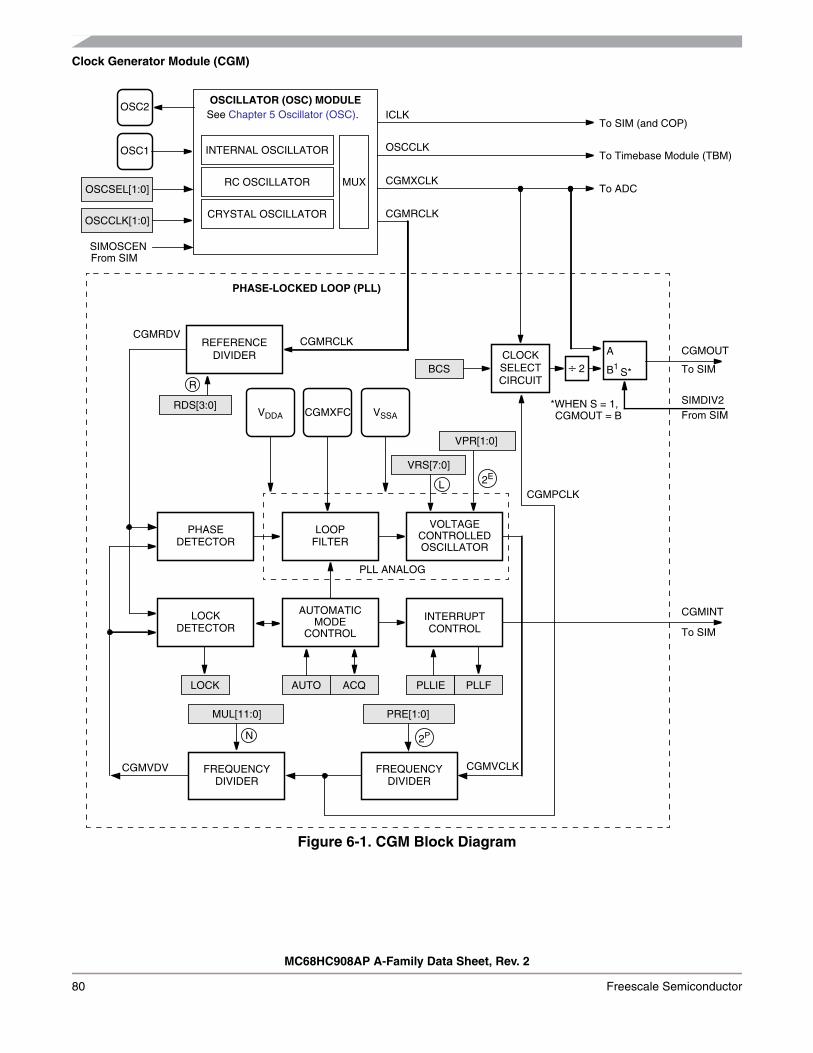
Clock Generator Module (CGM)
MC68HC908AP A-Family Data Sheet, Rev. 2
80 Freescale Semiconductor
Figure 6-1. CGM Block Diagram
BCS
PHASEDETECTOR
LOOPFILTER
FREQUENCYDIVIDER
VOLTAGECONTROLLEDOSCILLATOR
AUTOMATICMODE
CONTROL
LOCKDETECTOR
CLOCK
CGMXCLK
CGMOUT
CGMVDV
INTERRUPTCONTROL
CGMINT
CGMRDV
PLL ANALOG
÷ 2
CGMRCLK
SELECTCIRCUIT
VDDA CGMXFC VSSA
LOCK AUTO ACQ
VPR[1:0]
PLLIE PLLF
MUL[11:0]
REFERENCEDIVIDER
VRS[7:0]
FREQUENCYDIVIDER
PRE[1:0]
To ADC
PHASE-LOCKED LOOP (PLL)
A
B1S*
*WHEN S = 1,CGMOUT = B
SIMDIV2From SIM
To SIM
To SIM
RDS[3:0]
R
CGMPCLK
SIMOSCEN
OSCILLATOR (OSC) MODULEOSC2
OSCSEL[1:0]
OSCCLK[1:0]
OSC1
From SIM
ICLK
CGMRCLK
INTERNAL OSCILLATOR
RC OSCILLATOR
CRYSTAL OSCILLATOR
MUX
See Chapter 5 Oscillator (OSC).
N
OSCCLKTo Timebase Module (TBM)
To SIM (and COP)
L
2P
2E
CGMVCLK

Functional Description
MC68HC908AP A-Family Data Sheet, Rev. 2
Freescale Semiconductor 81
6.3.1 Oscillator Module
The oscillator module provides two clock outputs CGMXCLK and CGMRCLK to the CGM module.CGMXCLK when selected, is driven to SIM module to generate the system bus clock. CGMRCLK is usedby the phase-lock-loop to provide a higher frequency system bus clock. The oscillator module alsoprovides the reference clock for the timebase module (TBM). See Chapter 5 Oscillator (OSC) for detailedoscillator circuit description. See Chapter 10 Timebase Module (TBM) for detailed description on TBM.
6.3.2 Phase-Locked Loop Circuit (PLL)
The PLL is a frequency generator that can operate in either acquisition mode or tracking mode, dependingon the accuracy of the output frequency. The PLL can change between acquisition and tracking modeseither automatically or manually.
6.3.3 PLL Circuits
The PLL consists of these circuits:• Voltage-controlled oscillator (VCO)• Reference divider• Frequency pre-scaler• Modulo VCO frequency divider
Addr. Register Name Bit 7 6 5 4 3 2 1 Bit 0
$0036PLL Control Register
(PTCL)
Read:PLLIE
PLLFPLLON BCS PRE1 PRE0 VPR1 VPR0
Write:Reset: 0 0 1 0 0 0 0 0
$0037PLL Bandwidth Control
Register(PBWC)
Read:AUTO
LOCKACQ
0 0 0 0R
Write:Reset: 0 0 0 0 0 0 0
$0038PLL Multiplier Select
Register High(PMSH)
Read: 0 0 0 0MUL11 MUL10 MUL9 MUL8
Write:Reset: 0 0 0 0 0 0 0 0
$0039PLL Multiplier Select
Register Low(PMSL)
Read:MUL7 MUL6 MUL5 MUL4 MUL3 MUL2 MUL1 MUL0
Write:Reset: 0 1 0 0 0 0 0 0
$003APLL VCO Range Select
Register(PMRS)
Read:VRS7 VRS6 VRS5 VRS4 VRS3 VRS2 VRS1 VRS0
Write:Reset: 0 1 0 0 0 0 0 0
$003BPLL Reference Divider
Select Register(PMDS)
Read: 0 0 0 0RDS3 RDS2 RDS1 RDS0
Write:Reset: 0 0 0 0 0 0 0 1
= Unimplemented R = ReservedNOTES:1. When AUTO = 0, PLLIE is forced clear and is read-only.2. When AUTO = 0, PLLF and LOCK read as clear.3. When AUTO = 1, ACQ is read-only.4. When PLLON = 0 or VRS7:VRS0 = $0, BCS is forced clear and is read-only.5. When PLLON = 1, the PLL programming register is read-only.6. When BCS = 1, PLLON is forced set and is read-only.
Figure 6-2. CGM I/O Register Summary

Clock Generator Module (CGM)
MC68HC908AP A-Family Data Sheet, Rev. 2
82 Freescale Semiconductor
• Phase detector• Loop filter• Lock detector
The operating range of the VCO is programmable for a wide range of frequencies and for maximumimmunity to external noise, including supply and CGMXFC noise. The VCO frequency is bound to a rangefrom roughly one-half to twice the center-of-range frequency, fVRS. Modulating the voltage on theCGMXFC pin changes the frequency within this range. By design, fVRS is equal to the nominalcenter-of-range frequency, fNOM, (125 kHz) times a linear factor, L, and a power-of-two factor, E, or(L × 2E)fNOM.
CGMRCLK is the PLL reference clock, a buffered version of CGMXCLK. CGMRCLK runs at a frequency,fRCLK, and is fed to the PLL through a programmable modulo reference divider, which divides fRCLK by afactor, R. The divider’s output is the final reference clock, CGMRDV, running at a frequency,fRDV = fRCLK/R. With an external crystal(1MHz–8MHz), always set R = 1 for specified performance. With an external high-frequency clocksource, use R to divide the external frequency to between 1MHz and 8MHz.
The VCO’s output clock, CGMVCLK, running at a frequency, fVCLK, is fed back through a programmablepre-scaler divider and a programmable modulo divider. The pre-scaler divides the VCO clock by apower-of-two factor P (the CGMPCLK) and the modulo divider reduces the VCO clock by a factor, N. Thedividers’ output is the VCO feedback clock, CGMVDV, running at a frequency, fVDV = fVCLK/(N × 2P). (See6.3.6 Programming the PLL for more information.)
The phase detector then compares the VCO feedback clock, CGMVDV, with the final reference clock,CGMRDV. A correction pulse is generated based on the phase difference between the two signals. Theloop filter then slightly alters the DC voltage on the external capacitor connected to CGMXFC based onthe width and direction of the correction pulse. The filter can make fast or slow corrections depending onits mode, described in 6.3.4 Acquisition and Tracking Modes. The value of the external capacitor and thereference frequency determines the speed of the corrections and the stability of the PLL.
The lock detector compares the frequencies of the VCO feedback clock, CGMVDV, and the finalreference clock, CGMRDV. Therefore, the speed of the lock detector is directly proportional to the finalreference frequency, fRDV. The circuit determines the mode of the PLL and the lock condition based onthis comparison.
6.3.4 Acquisition and Tracking Modes
The PLL filter is manually or automatically configurable into one of two operating modes:• Acquisition mode — In acquisition mode, the filter can make large frequency corrections to the
VCO. This mode is used at PLL start up or when the PLL has suffered a severe noise hit and theVCO frequency is far off the desired frequency. When in acquisition mode, the ACQ bit is clear inthe PLL bandwidth control register. (See 6.5.2 PLL Bandwidth Control Register.)
• Tracking mode — In tracking mode, the filter makes only small corrections to the frequency of theVCO. PLL jitter is much lower in tracking mode, but the response to noise is also slower. The PLLenters tracking mode when the VCO frequency is nearly correct, such as when the PLL is selectedas the base clock source. (See 6.3.8 Base Clock Selector Circuit.) The PLL is automatically intracking mode when not in acquisition mode or when the ACQ bit is set.

Functional Description
MC68HC908AP A-Family Data Sheet, Rev. 2
Freescale Semiconductor 83
6.3.5 Manual and Automatic PLL Bandwidth Modes
The PLL can change the bandwidth or operational mode of the loop filter manually or automatically.Automatic mode is recommended for most users.
In automatic bandwidth control mode (AUTO = 1), the lock detector automatically switches betweenacquisition and tracking modes. Automatic bandwidth control mode also is used to determine when theVCO clock, CGMVCLK, is safe to use as the source for the base clock, CGMOUT. (See 6.5.2 PLLBandwidth Control Register.) If PLL interrupts are enabled, the software can wait for a PLL interruptrequest and then check the LOCK bit. If interrupts are disabled, software can poll the LOCK bitcontinuously (during PLL start-up, usually) or at periodic intervals. In either case, when the LOCK bit isset, the VCO clock is safe to use as the source for the base clock. (See 6.3.8 Base Clock Selector Circuit.)If the VCO is selected as the source for the base clock and the LOCK bit is clear, the PLL has suffered asevere noise hit and the software must take appropriate action, depending on the application. (See 6.6Interrupts for information and precautions on using interrupts.)
The following conditions apply when the PLL is in automatic bandwidth control mode:• The ACQ bit (See 6.5.2 PLL Bandwidth Control Register.) is a read-only indicator of the mode of
the filter. (See 6.3.4 Acquisition and Tracking Modes.)• The ACQ bit is set when the VCO frequency is within a certain tolerance and is cleared when the
VCO frequency is out of a certain tolerance. (See 6.8 Acquisition/Lock Time Specifications formore information.)
• The LOCK bit is a read-only indicator of the locked state of the PLL.• The LOCK bit is set when the VCO frequency is within a certain tolerance and is cleared when the
VCO frequency is out of a certain tolerance. (See 6.8 Acquisition/Lock Time Specifications formore information.)
• CPU interrupts can occur if enabled (PLLIE = 1) when the PLL’s lock condition changes, togglingthe LOCK bit. (See 6.5.1 PLL Control Register.)
The PLL also may operate in manual mode (AUTO = 0). Manual mode is used by systems that do notrequire an indicator of the lock condition for proper operation. Such systems typically operate well belowfBUSMAX.
The following conditions apply when in manual mode:• ACQ is a writable control bit that controls the mode of the filter. Before turning on the PLL in manual
mode, the ACQ bit must be clear.• Before entering tracking mode (ACQ = 1), software must wait a given time, tACQ (See 6.8
Acquisition/Lock Time Specifications.), after turning on the PLL by setting PLLON in the PLLcontrol register (PCTL).
• Software must wait a given time, tAL, after entering tracking mode before selecting the PLL as theclock source to CGMOUT (BCS = 1).
• The LOCK bit is disabled.• CPU interrupts from the CGM are disabled.
6.3.6 Programming the PLL
The following procedure shows how to program the PLL.
NOTEThe round function in the following equations means that the real numbershould be rounded to the nearest integer number.

Clock Generator Module (CGM)
MC68HC908AP A-Family Data Sheet, Rev. 2
84 Freescale Semiconductor
1. Choose the desired bus frequency, fBUSDES, or the desired VCO frequency, fVCLKDES; and thensolve for the other.The relationship between fBUS and fVCLK is governed by the equation:
where P is the power of two multiplier, and can be 0, 1, 2, or 32. Choose a practical PLL reference frequency, fRCLK, and the reference clock divider, R. Typically,
the reference is 4MHz andR = 1.
Frequency errors to the PLL are corrected at a rate of fRCLK/R. For stability and lock time reduction,this rate must be as fast as possible. The VCO frequency must be an integer multiple of this rate.The relationship between the VCO frequency, fVCLK, and the reference frequency, fRCLK, is
where N is the integer range multiplier, between 1 and 4095.
In cases where desired bus frequency has some tolerance, choose fRCLK to a value determinedeither by other module requirements (such as modules which are clocked by CGMXCLK), costrequirements, or ideally, as high as the specified range allows. See Chapter 22 ElectricalSpecifications.Choose the reference divider, R = 1.
When the tolerance on the bus frequency is tight, choose fRCLK to an integer divisor of fBUSDES,and R = 1. If fRCLK cannot meet this requirement, use the following equation to solve for R withpractical choices of fRCLK, and choose the fRCLK that gives the lowest R.
3. Calculate N:
4. Calculate and verify the adequacy of the VCO and bus frequencies fVCLK and fBUS.
fVCLK 2P
fCGMPCLK× 2P
4× fBUS×= =
fVCLK2
PN
R----------- fRCLK( )=
R round RMAX
fVCLKDES
fRCLK--------------------------
⎝ ⎠⎜ ⎟⎛ ⎞
integerfVCLKDES
fRCLK--------------------------
⎝ ⎠⎜ ⎟⎛ ⎞
–⎩ ⎭⎨ ⎬⎧ ⎫
×=
N roundR fVCLKDES×
fRCLK 2P×
-------------------------------------⎝ ⎠⎜ ⎟⎛ ⎞
=
fBUS
fVCLK
2P
4×-----------=
fVCLK2
PN
R----------- fRCLK( )=
Functional Description
MC68HC908AP A-Family Data Sheet, Rev. 2
Freescale Semiconductor 85
5. Select the VCO’s power-of-two range multiplier E, according to this table:
6. Select a VCO linear range multiplier, L, where fNOM = 125kHz
7. Calculate and verify the adequacy of the VCO programmed center-of-range frequency, fVRS. Thecenter-of-range frequency is the midpoint between the minimum and maximum frequenciesattainable by the PLL.
For proper operation,
8. Verify the choice of P, R, N, E, and L by comparing fVCLK to fVRS and fVCLKDES. For properoperation, fVCLK must be within the application’s tolerance of fVCLKDES, and fVRS must be as closeas possible to fVCLK.
NOTEExceeding the recommended maximum bus frequency or VCO frequencycan crash the MCU.
9. Program the PLL registers accordingly:a. In the PRE bits of the PLL control register (PCTL), program the binary equivalent of P.
b. In the VPR bits of the PLL control register (PCTL), program the binary equivalent of E.
c. In the PLL multiplier select register low (PMSL) and the PLL multiplier select register high(PMSH), program the binary equivalent of N.
d. In the PLL VCO range select register (PMRS), program the binary coded equivalent of L.
e. In the PLL reference divider select register (PMDS), program the binary coded equivalentof R.
NOTEThe values for P, E, N, L, and R can only be programmed when the PLL isoff (PLLON = 0).
Table 6-1 provides numeric examples (numbers are in hexadecimal notation):
Frequency Range E
0 < fVCLK < 9,830,400 0
9,830,400 ≤ fVCLK < 19,660,800 1
19,660,800 ≤ fVCLK < 39,321,600 2
NOTE: Do not program E to a value of 3.
L roundfVCLK
2E
fNOM×--------------------------
⎝ ⎠⎜ ⎟⎛ ⎞
=
fVRS L 2E×( )fNOM=
fVRS fVCLK–fNOM 2
E×2
--------------------------≤
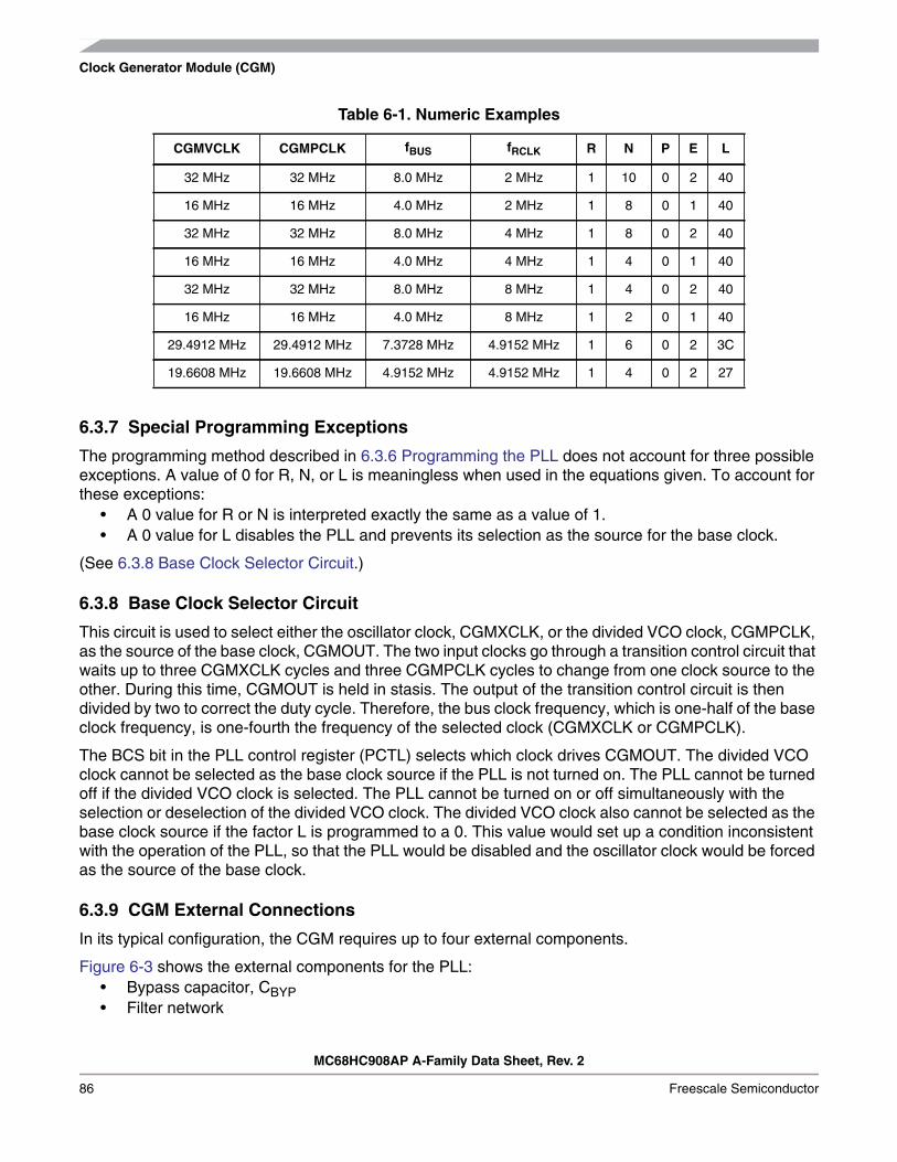
Clock Generator Module (CGM)
MC68HC908AP A-Family Data Sheet, Rev. 2
86 Freescale Semiconductor
6.3.7 Special Programming Exceptions
The programming method described in 6.3.6 Programming the PLL does not account for three possibleexceptions. A value of 0 for R, N, or L is meaningless when used in the equations given. To account forthese exceptions:
• A 0 value for R or N is interpreted exactly the same as a value of 1.• A 0 value for L disables the PLL and prevents its selection as the source for the base clock.
(See 6.3.8 Base Clock Selector Circuit.)
6.3.8 Base Clock Selector Circuit
This circuit is used to select either the oscillator clock, CGMXCLK, or the divided VCO clock, CGMPCLK,as the source of the base clock, CGMOUT. The two input clocks go through a transition control circuit thatwaits up to three CGMXCLK cycles and three CGMPCLK cycles to change from one clock source to theother. During this time, CGMOUT is held in stasis. The output of the transition control circuit is thendivided by two to correct the duty cycle. Therefore, the bus clock frequency, which is one-half of the baseclock frequency, is one-fourth the frequency of the selected clock (CGMXCLK or CGMPCLK).
The BCS bit in the PLL control register (PCTL) selects which clock drives CGMOUT. The divided VCOclock cannot be selected as the base clock source if the PLL is not turned on. The PLL cannot be turnedoff if the divided VCO clock is selected. The PLL cannot be turned on or off simultaneously with theselection or deselection of the divided VCO clock. The divided VCO clock also cannot be selected as thebase clock source if the factor L is programmed to a 0. This value would set up a condition inconsistentwith the operation of the PLL, so that the PLL would be disabled and the oscillator clock would be forcedas the source of the base clock.
6.3.9 CGM External Connections
In its typical configuration, the CGM requires up to four external components.
Figure 6-3 shows the external components for the PLL:• Bypass capacitor, CBYP• Filter network
Table 6-1. Numeric Examples
CGMVCLK CGMPCLK fBUS fRCLK R N P E L
32 MHz 32 MHz 8.0 MHz 2 MHz 1 10 0 2 40
16 MHz 16 MHz 4.0 MHz 2 MHz 1 8 0 1 40
32 MHz 32 MHz 8.0 MHz 4 MHz 1 8 0 2 40
16 MHz 16 MHz 4.0 MHz 4 MHz 1 4 0 1 40
32 MHz 32 MHz 8.0 MHz 8 MHz 1 4 0 2 40
16 MHz 16 MHz 4.0 MHz 8 MHz 1 2 0 1 40
29.4912 MHz 29.4912 MHz 7.3728 MHz 4.9152 MHz 1 6 0 2 3C
19.6608 MHz 19.6608 MHz 4.9152 MHz 4.9152 MHz 1 4 0 2 27
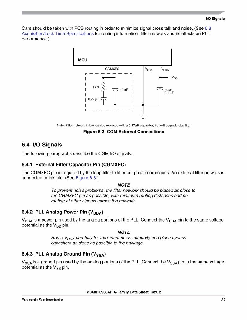
I/O Signals
MC68HC908AP A-Family Data Sheet, Rev. 2
Freescale Semiconductor 87
Care should be taken with PCB routing in order to minimize signal cross talk and noise. (See 6.8Acquisition/Lock Time Specifications for routing information, filter network and its effects on PLLperformance.)
Figure 6-3. CGM External Connections
6.4 I/O Signals
The following paragraphs describe the CGM I/O signals.
6.4.1 External Filter Capacitor Pin (CGMXFC)
The CGMXFC pin is required by the loop filter to filter out phase corrections. An external filter network isconnected to this pin. (See Figure 6-3.)
NOTETo prevent noise problems, the filter network should be placed as close tothe CGMXFC pin as possible, with minimum routing distances and norouting of other signals across the network.
6.4.2 PLL Analog Power Pin (VDDA)
VDDA is a power pin used by the analog portions of the PLL. Connect the VDDA pin to the same voltagepotential as the VDD pin.
NOTERoute VDDA carefully for maximum noise immunity and place bypasscapacitors as close as possible to the package.
6.4.3 PLL Analog Ground Pin (VSSA)
VSSA is a ground pin used by the analog portions of the PLL. Connect the VSSA pin to the same voltagepotential as the VSS pin.
CBYP
Note: Filter network in box can be replaced with a 0.47µF capacitor, but will degrade stability.
1 kΩ10 nF
0.22 µF
0.1 µF
VSSA VDDACGMXFC
VDD
MCU

Clock Generator Module (CGM)
MC68HC908AP A-Family Data Sheet, Rev. 2
88 Freescale Semiconductor
NOTERoute VSSA carefully for maximum noise immunity and place bypasscapacitors as close as possible to the package.
6.4.4 Oscillator Output Frequency Signal (CGMXCLK)
CGMXCLK is the oscillator output signal. It runs at the full speed of the oscillator, and is generated directlyfrom the crystal oscillator circuit, the RC oscillator circuit, or the internal oscillator circuit.
6.4.5 CGM Reference Clock (CGMRCLK)
CGMRCLK is a buffered version of CGMXCLK, this clock is the reference clock for the phase-locked-loopcircuit.
6.4.6 CGM VCO Clock Output (CGMVCLK)
CGMVCLK is the clock output from the VCO.
6.4.7 CGM Base Clock Output (CGMOUT)
CGMOUT is the clock output of the CGM. This signal goes to the SIM, which generates the MCU clocks.CGMOUT is a 50 percent duty cycle clock running at twice the bus frequency. CGMOUT is softwareprogrammable to be either the oscillator output, CGMXCLK, divided by two or the divided VCO clock,CGMPCLK, divided by two.
6.4.8 CGM CPU Interrupt (CGMINT)
CGMINT is the interrupt signal generated by the PLL lock detector.
6.5 CGM Registers
The following registers control and monitor operation of the CGM:• PLL control register (PCTL)
(See 6.5.1 PLL Control Register.)• PLL bandwidth control register (PBWC)
(See 6.5.2 PLL Bandwidth Control Register.)• PLL multiplier select registers (PMSH and PMSL)
(See 6.5.3 PLL Multiplier Select Registers.)• PLL VCO range select register (PMRS)
(See 6.5.4 PLL VCO Range Select Register.)• PLL reference divider select register (PMDS)
(See 6.5.5 PLL Reference Divider Select Register.)

CGM Registers
MC68HC908AP A-Family Data Sheet, Rev. 2
Freescale Semiconductor 89
6.5.1 PLL Control Register
The PLL control register (PCTL) contains the interrupt enable and flag bits, the on/off switch, the baseclock selector bit, the prescaler bits, and the VCO power-of-two range selector bits.
PLLIE — PLL Interrupt Enable BitThis read/write bit enables the PLL to generate an interrupt request when the LOCK bit toggles, settingthe PLL flag, PLLF. When the AUTO bit in the PLL bandwidth control register (PBWC) is clear, PLLIEcannot be written and reads as logic 0. Reset clears the PLLIE bit.
1 = PLL interrupts enabled0 = PLL interrupts disabled
PLLF — PLL Interrupt Flag BitThis read-only bit is set whenever the LOCK bit toggles. PLLF generates an interrupt request if thePLLIE bit also is set. PLLF always reads as logic 0 when the AUTO bit in the PLL bandwidth controlregister (PBWC) is clear. Clear the PLLF bit by reading the PLL control register. Reset clears the PLLFbit.
1 = Change in lock condition0 = No change in lock condition
NOTEDo not inadvertently clear the PLLF bit. Any read or read-modify-writeoperation on the PLL control register clears the PLLF bit.
PLLON — PLL On BitThis read/write bit activates the PLL and enables the VCO clock, CGMVCLK. PLLON cannot becleared if the VCO clock is driving the base clock, CGMOUT (BCS = 1). (See 6.3.8 Base ClockSelector Circuit.) Reset sets this bit so that the loop can stabilize as the MCU is powering up.
1 = PLL on0 = PLL off
BCS — Base Clock Select BitThis read/write bit selects either the oscillator output, CGMXCLK, or the divided VCO clock,CGMPCLK, as the source of the CGM output, CGMOUT. CGMOUT frequency is one-half thefrequency of the selected clock. BCS cannot be set while the PLLON bit is clear. After toggling BCS,it may take up to three CGMXCLK and three CGMPCLK cycles to complete the transition from onesource clock to the other. During the transition, CGMOUT is held in stasis. (See 6.3.8 Base ClockSelector Circuit.) Reset clears the BCS bit.
1 = CGMPCLK divided by two drives CGMOUT0 = CGMXCLK divided by two drives CGMOUT
Address: $0036
Bit 7 6 5 4 3 2 1 Bit 0
Read:PLLIE
PLLFPLLON BCS PRE1 PRE0 VPR1 VPR0
Write:
Reset: 0 0 1 0 0 0 0 0
= Unimplemented
Figure 6-4. PLL Control Register (PCTL)

Clock Generator Module (CGM)
MC68HC908AP A-Family Data Sheet, Rev. 2
90 Freescale Semiconductor
NOTEPLLON and BCS have built-in protection that prevents the base clockselector circuit from selecting the VCO clock as the source of the base clockif the PLL is off. Therefore, PLLON cannot be cleared when BCS is set, andBCS cannot be set when PLLON is clear. If the PLL is off (PLLON = 0),selecting CGMPCLK requires two writes to the PLL control register. (See6.3.8 Base Clock Selector Circuit.)
PRE1 and PRE0 — Prescaler Program BitsThese read/write bits control a prescaler that selects the prescaler power-of-two multiplier, P. (See6.3.3 PLL Circuits and 6.3.6 Programming the PLL.) PRE1 and PRE0 cannot be written when thePLLON bit is set. Reset clears these bits.These prescaler bits affects the relationship between the VCO clock and the final system bus clock.
VPR1 and VPR0 — VCO Power-of-Two Range Select BitsThese read/write bits control the VCO’s hardware power-of-two range multiplier E that, in conjunctionwith L (See 6.3.3 PLL Circuits, 6.3.6 Programming the PLL, and 6.5.4 PLL VCO Range SelectRegister.) controls the hardware center-of-range frequency, fVRS. VPR1:VPR0 cannot be written whenthe PLLON bit is set. Reset clears these bits.
Table 6-2. PRE1 and PRE0 Programming
PRE1 and PRE0 P Prescaler Multiplier
00 0 1
01 1 2
10 2 4
11 3 8
Table 6-3. VPR1 and VPR0 Programming
VPR1 and VPR0 EVCO Power-of-Two
Range Multiplier
00 0 1
01 1 2
10 2 4
NOTE: Do not program E to a value of 3.

CGM Registers
MC68HC908AP A-Family Data Sheet, Rev. 2
Freescale Semiconductor 91
6.5.2 PLL Bandwidth Control Register
The PLL bandwidth control register (PBWC):• Selects automatic or manual (software-controlled) bandwidth control mode• Indicates when the PLL is locked• In automatic bandwidth control mode, indicates when the PLL is in acquisition or tracking mode• In manual operation, forces the PLL into acquisition or tracking mode
AUTO — Automatic Bandwidth Control BitThis read/write bit selects automatic or manual bandwidth control. When initializing the PLL for manualoperation (AUTO = 0), clear the ACQ bit before turning on the PLL. Reset clears the AUTO bit.
1 = Automatic bandwidth control0 = Manual bandwidth control
LOCK — Lock Indicator BitWhen the AUTO bit is set, LOCK is a read-only bit that becomes set when the VCO clock, CGMVCLK,is locked (running at the programmed frequency). When the AUTO bit is clear, LOCK reads as logic 0and has no meaning. The write one function of this bit is reserved for test, so this bit must always bewritten a 0. Reset clears the LOCK bit.
1 = VCO frequency correct or locked0 = VCO frequency incorrect or unlocked
ACQ — Acquisition Mode BitWhen the AUTO bit is set, ACQ is a read-only bit that indicates whether the PLL is in acquisition modeor tracking mode. When the AUTO bit is clear, ACQ is a read/write bit that controls whether the PLL isin acquisition or tracking mode.In automatic bandwidth control mode (AUTO = 1), the last-written value from manual operation isstored in a temporary location and is recovered when manual operation resumes. Reset clears this bit,enabling acquisition mode.
1 = Tracking mode0 = Acquisition mode
Address: $0037
Bit 7 6 5 4 3 2 1 Bit 0
Read:AUTO
LOCKACQ
0 0 0 0R
Write:
Reset: 0 0 0 0 0 0 0
= Unimplemented R = Reserved
Figure 6-5. PLL Bandwidth Control Register (PBWCR)

Clock Generator Module (CGM)
MC68HC908AP A-Family Data Sheet, Rev. 2
92 Freescale Semiconductor
6.5.3 PLL Multiplier Select Registers
The PLL multiplier select registers (PMSH and PMSL) contain the programming information for themodulo feedback divider.
MUL[11:0] — Multiplier Select BitsThese read/write bits control the modulo feedback divider that selects the VCO frequency multiplier N.(See 6.3.3 PLL Circuits and 6.3.6 Programming the PLL.) A value of $0000 in the multiplier selectregisters configure the modulo feedback divider the same as a value of $0001. Reset initializes theregisters to $0040 for a default multiply value of 64.
NOTEThe multiplier select bits have built-in protection such that they cannot bewritten when the PLL is on (PLLON = 1).
6.5.4 PLL VCO Range Select Register
The PLL VCO range select register (PMRS) contains the programming information required for thehardware configuration of the VCO.
VRS[7:0] — VCO Range Select BitsThese read/write bits control the hardware center-of-range linear multiplier L which, in conjunction withE (See 6.3.3 PLL Circuits, 6.3.6 Programming the PLL, and 6.5.1 PLL Control Register.), controls thehardware center-of-range frequency, fVRS. VRS[7:0] cannot be written when the PLLON bit in thePCTL is set. (See 6.3.7 Special Programming Exceptions.) A value of $00 in the VCO range select
Address: $0038
Bit 7 6 5 4 3 2 1 Bit 0
Read: 0 0 0 0MUL11 MUL10 MUL9 MUL8
Write:
Reset: 0 0 0 0 0 0 0 0
= Unimplemented
Figure 6-6. PLL Multiplier Select Register High (PMSH)
Address: $0039
Bit 7 6 5 4 3 2 1 Bit 0
Read:MUL7 MUL6 MUL5 MUL4 MUL3 MUL2 MUL1 MUL0
Write:
Reset: 0 1 0 0 0 0 0 0
Figure 6-7. PLL Multiplier Select Register Low (PMSL)
Address: $003A
Bit 7 6 5 4 3 2 1 Bit 0
Read:VRS7 VRS6 VRS5 VRS4 VRS3 VRS2 VRS1 VRS0
Write:
Reset: 0 1 0 0 0 0 0 0
Figure 6-8. PLL VCO Range Select Register (PMRS)
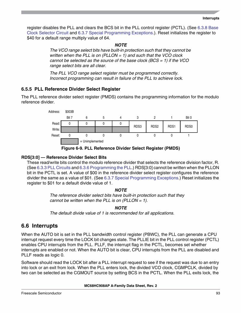
Interrupts
MC68HC908AP A-Family Data Sheet, Rev. 2
Freescale Semiconductor 93
register disables the PLL and clears the BCS bit in the PLL control register (PCTL). (See 6.3.8 BaseClock Selector Circuit and 6.3.7 Special Programming Exceptions.). Reset initializes the register to$40 for a default range multiply value of 64.
NOTEThe VCO range select bits have built-in protection such that they cannot bewritten when the PLL is on (PLLON = 1) and such that the VCO clockcannot be selected as the source of the base clock (BCS = 1) if the VCOrange select bits are all clear.
The PLL VCO range select register must be programmed correctly.Incorrect programming can result in failure of the PLL to achieve lock.
6.5.5 PLL Reference Divider Select Register
The PLL reference divider select register (PMDS) contains the programming information for the moduloreference divider.
RDS[3:0] — Reference Divider Select BitsThese read/write bits control the modulo reference divider that selects the reference division factor, R.(See 6.3.3 PLL Circuits and 6.3.6 Programming the PLL.) RDS[3:0] cannot be written when the PLLONbit in the PCTL is set. A value of $00 in the reference divider select register configures the referencedivider the same as a value of $01. (See 6.3.7 Special Programming Exceptions.) Reset initializes theregister to $01 for a default divide value of 1.
NOTEThe reference divider select bits have built-in protection such that theycannot be written when the PLL is on (PLLON = 1).
NOTEThe default divide value of 1 is recommended for all applications.
6.6 Interrupts
When the AUTO bit is set in the PLL bandwidth control register (PBWC), the PLL can generate a CPUinterrupt request every time the LOCK bit changes state. The PLLIE bit in the PLL control register (PCTL)enables CPU interrupts from the PLL. PLLF, the interrupt flag in the PCTL, becomes set whetherinterrupts are enabled or not. When the AUTO bit is clear, CPU interrupts from the PLL are disabled andPLLF reads as logic 0.
Software should read the LOCK bit after a PLL interrupt request to see if the request was due to an entryinto lock or an exit from lock. When the PLL enters lock, the divided VCO clock, CGMPCLK, divided bytwo can be selected as the CGMOUT source by setting BCS in the PCTL. When the PLL exits lock, the
Address: $003B
Bit 7 6 5 4 3 2 1 Bit 0
Read: 0 0 0 0RDS3 RDS2 RDS1 RDS0
Write:
Reset: 0 0 0 0 0 0 0 1
= Unimplemented
Figure 6-9. PLL Reference Divider Select Register (PMDS)

Clock Generator Module (CGM)
MC68HC908AP A-Family Data Sheet, Rev. 2
94 Freescale Semiconductor
VCO clock frequency is corrupt, and appropriate precautions should be taken. If the application is notfrequency sensitive, interrupts should be disabled to prevent PLL interrupt service routines from impedingsoftware performance or from exceeding stack limitations.
NOTESoftware can select the CGMPCLK divided by two as the CGMOUT sourceeven if the PLL is not locked (LOCK = 0). Therefore, software should makesure the PLL is locked before setting the BCS bit.
6.7 Special Modes
The WAIT instruction puts the MCU in low power-consumption standby modes.
6.7.1 Wait Mode
The WAIT instruction does not affect the CGM. Before entering wait mode, software can disengage andturn off the PLL by clearing the BCS and PLLON bits in the PLL control register (PCTL) to save power.Less power-sensitive applications can disengage the PLL without turning it off, so that the PLL clock isimmediately available at WAIT exit. This would be the case also when the PLL is to wake the MCU fromwait mode, such as when the PLL is first enabled and waiting for LOCK or LOCK is lost.
6.7.2 Stop Mode
The STOP instruction disables the PLL analog circuits and no clock will be driven out of the VCO.
When entering stop mode with the VCO clock (CGMPCLK) selected, before executing the STOPinstruction:
1. Set the oscillator stop mode enable bit (STOP_XCLKEN in CONFIG2) if continuos clock is requiredin stop mode.
2. Clear the BCS bit to select CGMXCLK as CGMOUT.
On exit from stop mode:1. Set the PLLON bit if cleared before entering stop mode.2. Wait for PLL to lock by checking the LOCK bit.3. Set BCS bit to select CGMPCLK as CGMOUT.
6.7.3 CGM During Break Interrupts
The system integration module (SIM) controls whether status bits in other modules can be cleared duringthe break state. The BCFE bit in the SIM break flag control register (SBFCR) enables software to clearstatus bits during the break state. (See 7.7.3 SIM Break Flag Control Register.)
To allow software to clear status bits during a break interrupt, write a logic 1 to the BCFE bit. If a statusbit is cleared during the break state, it remains cleared when the MCU exits the break state.
To protect the PLLF bit during the break state, write a logic 0 to the BCFE bit. With BCFE at logic 0 (itsdefault state), software can read and write the PLL control register during the break state without affectingthe PLLF bit.

Acquisition/Lock Time Specifications
MC68HC908AP A-Family Data Sheet, Rev. 2
Freescale Semiconductor 95
6.8 Acquisition/Lock Time Specifications
The acquisition and lock times of the PLL are, in many applications, the most critical PLL designparameters. Proper design and use of the PLL ensures the highest stability and lowest acquisition/locktimes.
6.8.1 Acquisition/Lock Time Definitions
Typical control systems refer to the acquisition time or lock time as the reaction time, within specifiedtolerances, of the system to a step input. In a PLL, the step input occurs when the PLL is turned on orwhen it suffers a noise hit. The tolerance is usually specified as a percent of the step input or when theoutput settles to the desired value plus or minus a percent of the frequency change. Therefore, thereaction time is constant in this definition, regardless of the size of the step input. For example, considera system with a 5 percent acquisition time tolerance. If a command instructs the system to change from0Hz to 1MHz, the acquisition time is the time taken for the frequency to reach 1MHz ±50kHz. 50kHz =5% of the 1MHz step input. If the system is operating at 1MHz and suffers a –100kHz noise hit, theacquisition time is the time taken to return from 900kHz to 1MHz ±5kHz. 5kHz = 5% of the 100kHz stepinput.
Other systems refer to acquisition and lock times as the time the system takes to reduce the errorbetween the actual output and the desired output to within specified tolerances. Therefore, the acquisitionor lock time varies according to the original error in the output. Minor errors may not even be registered.Typical PLL applications prefer to use this definition because the system requires the output frequency tobe within a certain tolerance of the desired frequency regardless of the size of the initial error.
6.8.2 Parametric Influences on Reaction Time
Acquisition and lock times are designed to be as short as possible while still providing the highest possiblestability. These reaction times are not constant, however. Many factors directly and indirectly affect theacquisition time.
The most critical parameter which affects the reaction times of the PLL is the reference frequency, fRDV.This frequency is the input to the phase detector and controls how often the PLL makes corrections. Forstability, the corrections must be small compared to the desired frequency, so several corrections arerequired to reduce the frequency error. Therefore, the slower the reference the longer it takes to makethese corrections. This parameter is under user control via the choice of crystal frequency fXCLK and theR value programmed in the reference divider. (See 6.3.3 PLL Circuits, 6.3.6 Programming the PLL, and6.5.5 PLL Reference Divider Select Register.)
Another critical parameter is the external filter network. The PLL modifies the voltage on the VCO byadding or subtracting charge from capacitors in this network. Therefore, the rate at which the voltagechanges for a given frequency error (thus change in charge) is proportional to the capacitance. The sizeof the capacitor also is related to the stability of the PLL. If the capacitor is too small, the PLL cannot makesmall enough adjustments to the voltage and the system cannot lock. If the capacitor is too large, the PLLmay not be able to adjust the voltage in a reasonable time. (See 6.8.3 Choosing a Filter.)
Also important is the operating voltage potential applied to VDDA. The power supply potential alters thecharacteristics of the PLL. A fixed value is best. Variable supplies, such as batteries, are acceptable ifthey vary within a known range at very slow speeds. Noise on the power supply is not acceptable,because it causes small frequency errors which continually change the acquisition time of the PLL.

Clock Generator Module (CGM)
MC68HC908AP A-Family Data Sheet, Rev. 2
96 Freescale Semiconductor
Temperature and processing also can affect acquisition time because the electrical characteristics of thePLL change. The part operates as specified as long as these influences stay within the specified limits.External factors, however, can cause drastic changes in the operation of the PLL. These factors includenoise injected into the PLL through the filter capacitor, filter capacitor leakage, stray impedances on thecircuit board, and even humidity or circuit board contamination.
6.8.3 Choosing a Filter
As described in 6.8.2 Parametric Influences on Reaction Time, the external filter network is critical to thestability and reaction time of the PLL. The PLL is also dependent on reference frequency and supplyvoltage.
Either of the filter networks in Figure 6-10 is recommended when using a 4MHz reference clock(CGMRCLK). Figure 6-10 (a) is used for applications requiring better stability. Figure 6-10 (b) is used inlow-cost applications where stability is not critical.
Figure 6-10. PLL Filter
1 kΩ10 nF
0.22 µF
VSSA
0.22 µF
VSSA
(a) (b)
CGMXFC CGMXFC
MC68HC908AP A-Family Data Sheet, Rev. 2
Freescale Semiconductor 97
Chapter 7System Integration Module (SIM)
7.1 Introduction
This section describes the system integration module (SIM). Together with the CPU, the SIM controls allMCU activities. A block diagram of the SIM is shown in Figure 7-1. Figure 7-2 is a summary of the SIMinput/output (I/O) registers. The SIM is a system state controller that coordinates CPU and exceptiontiming. The SIM is responsible for:
• Bus clock generation and control for CPU and peripherals:– Stop/wait/reset/break entry and recovery– Internal clock control
• Master reset control, including power-on reset (POR) and COP timeout• Interrupt control:
– Acknowledge timing– Arbitration control timing– Vector address generation
• CPU enable/disable timing• Modular architecture expandable to 128 interrupt sources
Table 7-1 shows the internal signal names used in this section.
Table 7-1. Signal Name Conventions
Signal Name Description
ICLK Internal oscillator clock
CGMXCLK Selected oscillator clock from oscillator module
CGMVCLK, CGMPCLK PLL output and the divided PLL output
CGMOUTCGMPCLK-based or oscillator-based clock output from CGM module(Bus clock = CGMOUT ÷ 2)
IAB Internal address bus
IDB Internal data bus
PORRST Signal from the power-on reset module to the SIM
IRST Internal reset signal
R/W Read/write signal

System Integration Module (SIM)
MC68HC908AP A-Family Data Sheet, Rev. 2
98 Freescale Semiconductor
Figure 7-1. SIM Block Diagram
Addr. Register Name Bit 7 6 5 4 3 2 1 Bit 0
$FE00SIM Break Status Register
(SBSR)
Read:R R R R R R
SBSWR
Write: NOTEReset: 0 0 0 0 0 0 0 0
Note: Writing a logic 0 clears SBSW.
$FE01SIM Reset Status Register
(SRSR)
Read: POR PIN COP ILOP ILAD MODRST LVI 0Write:POR: 1 0 0 0 0 0 0 0
$FE03SIM Break Flag Control
Register (SBFCR)
Read:BCFE R R R R R R R
Write:Reset: 0
$FE04Interrupt Status Register 1
(INT1)
Read: IF6 IF5 IF4 IF3 IF2 IF1 0 0Write: R R R R R R R R
Reset: 0 0 0 0 0 0 0 0
Figure 7-2. SIM I/O Register Summary
STOP/WAIT
CLOCKCONTROL CLOCK GENERATORS
POR CONTROL
RESET PIN CONTROL
SIM RESET STATUS REGISTER
INTERRUPT CONTROLAND PRIORITY DECODE
MODULE STOP
MODULE WAIT
CPU STOP (FROM CPU)CPU WAIT (FROM CPU)
SIMOSCEN (TO CGM, OSC)
CGMOUT (FROM CGM)
INTERNAL CLOCKS
MASTERRESET
CONTROL
RESETPIN LOGIC
LVI (FROM LVI MODULE)
ILLEGAL OPCODE (FROM CPU)ILLEGAL ADDRESS (FROM ADDRESSMAP DECODERS)COP (FROM COP MODULE)
INTERRUPT SOURCES
CPU INTERFACE
RESET
CONTROL
SIMCOUNTER COP CLOCK
ICLK (FROM OSC)
÷ 2
VDD
INTERNALPULLUPDEVICE
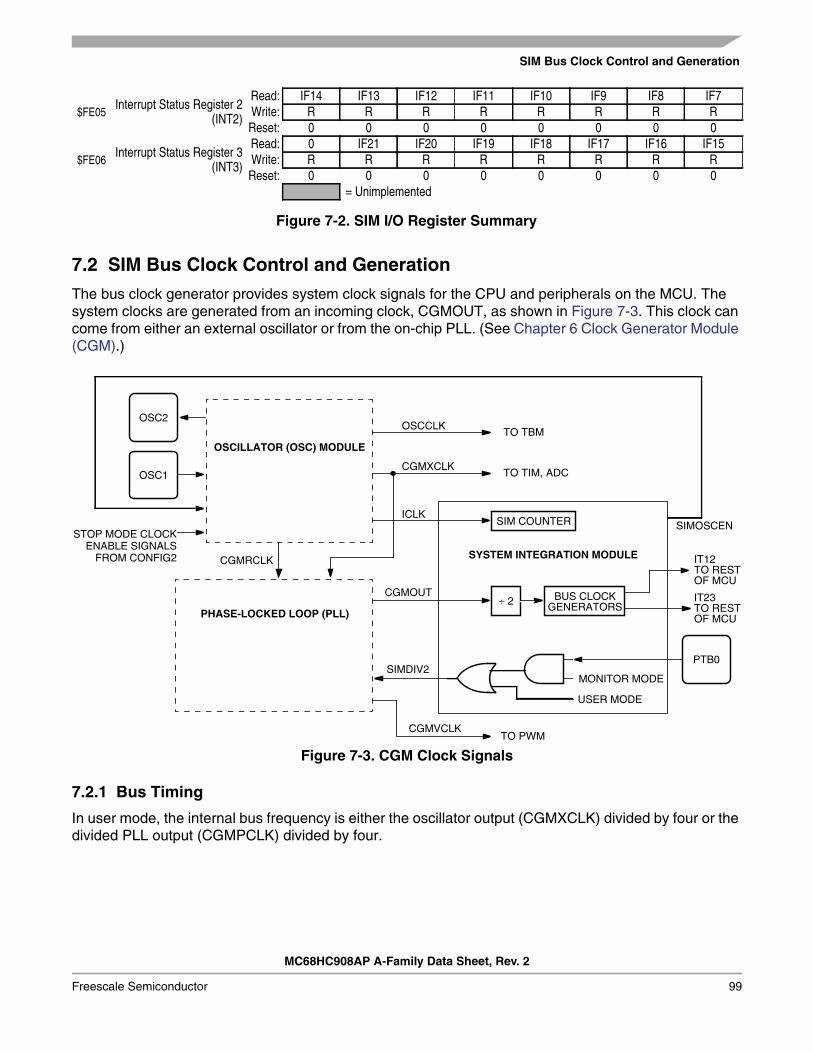
SIM Bus Clock Control and Generation
MC68HC908AP A-Family Data Sheet, Rev. 2
Freescale Semiconductor 99
7.2 SIM Bus Clock Control and Generation
The bus clock generator provides system clock signals for the CPU and peripherals on the MCU. Thesystem clocks are generated from an incoming clock, CGMOUT, as shown in Figure 7-3. This clock cancome from either an external oscillator or from the on-chip PLL. (See Chapter 6 Clock Generator Module(CGM).)
Figure 7-3. CGM Clock Signals
7.2.1 Bus Timing
In user mode, the internal bus frequency is either the oscillator output (CGMXCLK) divided by four or thedivided PLL output (CGMPCLK) divided by four.
$FE05Interrupt Status Register 2
(INT2)
Read: IF14 IF13 IF12 IF11 IF10 IF9 IF8 IF7Write: R R R R R R R R
Reset: 0 0 0 0 0 0 0 0
$FE06Interrupt Status Register 3
(INT3)
Read: 0 IF21 IF20 IF19 IF18 IF17 IF16 IF15Write: R R R R R R R R
Reset: 0 0 0 0 0 0 0 0= Unimplemented
Figure 7-2. SIM I/O Register Summary
÷ 2 BUS CLOCKGENERATORS
SYSTEM INTEGRATION MODULE
MONITOR MODE
USER MODE
SIMOSCEN
OSCILLATOR (OSC) MODULE
OSC2
OSC1
PHASE-LOCKED LOOP (PLL)
CGMXCLK
CGMRCLK IT12
CGMOUT
SIMDIV2PTB0
TO TIM, ADC
STOP MODE CLOCK
TO RESTOF MCU
IT23TO RESTOF MCU
ENABLE SIGNALSFROM CONFIG2
ICLK
TO TBMOSCCLK
CGMVCLKTO PWM
SIM COUNTER

System Integration Module (SIM)
MC68HC908AP A-Family Data Sheet, Rev. 2
100 Freescale Semiconductor
7.2.2 Clock Start-up from POR or LVI Reset
When the power-on reset module or the low-voltage inhibit module generates a reset, the clocks to theCPU and peripherals are inactive and held in an inactive phase until after the 4096 ICLK cycle PORtimeout has completed. The RST pin is driven low by the SIM during this entire period. The IBUS clocksstart upon completion of the timeout.
7.2.3 Clocks in Stop Mode and Wait Mode
Upon exit from stop mode by an interrupt, break, or reset, the SIM allows ICLK to clock the SIM counter.The CPU and peripheral clocks do not become active until after the stop delay timeout. This timeout isselectable as 4096 or 32 ICLK cycles. (See 7.6.2 Stop Mode.)
In wait mode, the CPU clocks are inactive. The SIM also produces two sets of clocks for other modules.Refer to the wait mode subsection of each module to see if the module is active or inactive in wait mode.Some modules can be programmed to be active in wait mode.
7.3 Reset and System Initialization
The MCU has these reset sources:• Power-on reset module (POR)• External reset pin (RST)• Computer operating properly module (COP)• Low-voltage inhibit module (LVI)• Illegal opcode• Illegal address
All of these resets produce the vector $FFFE:$FFFF ($FEFE:$FEFF in monitor mode) and assert theinternal reset signal (IRST). IRST causes all registers to be returned to their default values and allmodules to be returned to their reset states.
An internal reset clears the SIM counter (see 7.4 SIM Counter), but an external reset does not. Each ofthe resets sets a corresponding bit in the SIM reset status register (SRSR). (See 7.7 SIM Registers.)
7.3.1 External Pin Reset
The RST pin circuit includes an internal pull-up device. Pulling the asynchronous RST pin low halts allprocessing. The PIN bit of the SIM reset status register (SRSR) is set as long as RST is held low for aminimum of 67 ICLK cycles, assuming that neither the POR nor the LVI was the source of the reset. SeeTable 7-2 for details. Figure 7-4 shows the relative timing.
Table 7-2. PIN Bit Set Timing
Reset Type Number of Cycles Required to Set PIN
POR/LVI 4163 (4096 + 64 + 3)
All others 67 (64 + 3)

Reset and System Initialization
MC68HC908AP A-Family Data Sheet, Rev. 2
Freescale Semiconductor 101
Figure 7-4. External Reset Timing
7.3.2 Active Resets from Internal Sources
All internal reset sources actively pull the RST pin low for 32 ICLK cycles to allow resetting of externalperipherals. The internal reset signal IRST continues to be asserted for an additional 32 cycles (seeFigure 7-5). An internal reset can be caused by an illegal address, illegal opcode, COP timeout, LVI, orPOR (see Figure 7-6).
NOTEFor LVI or POR resets, the SIM cycles through 4096 + 32 ICLK cyclesduring which the SIM forces the RST pin low. The internal reset signal thenfollows the sequence from the falling edge of RST shown inFigure 7-5.
Figure 7-5. Internal Reset Timing
The COP reset is asynchronous to the bus clock.
Figure 7-6. Sources of Internal Reset
The active reset feature allows the part to issue a reset to peripherals and other chips within a systembuilt around the MCU.
7.3.2.1 Power-On Reset
When power is first applied to the MCU, the power-on reset module (POR) generates a pulse to indicatethat power-on has occurred. The external reset pin (RST) is held low while the SIM counter counts out4096 + 32 ICLK cycles. Thirty-two ICLK cycles later, the CPU and memories are released from reset toallow the reset vector sequence to occur.
RST
IAB PC VECT H VECT L
ICLK
IRST
RST RST PULLED LOW BY MCU
IAB
32 CYCLES 32 CYCLES
VECTOR HIGH
ICLK
ILLEGAL ADDRESS RSTILLEGAL OPCODE RST
COPRSTLVI
POR
INTERNAL RESET

System Integration Module (SIM)
MC68HC908AP A-Family Data Sheet, Rev. 2
102 Freescale Semiconductor
At power-on, these events occur:• A POR pulse is generated.• The internal reset signal is asserted.• The SIM enables CGMOUT.• Internal clocks to the CPU and modules are held inactive for 4096 ICLK cycles to allow stabilization
of the oscillator.• The pin is driven low during the oscillator stabilization time.• The POR bit of the SIM reset status register (SRSR) is set and all other bits in the register are
cleared.
Figure 7-7. POR Recovery
7.3.2.2 Computer Operating Properly (COP) Reset
An input to the SIM is reserved for the COP reset signal. The overflow of the COP counter causes aninternal reset and sets the COP bit in the SIM reset status register (SRSR). The SIM actively pulls downthe RST pin for all internal reset sources.
To prevent a COP module timeout, write any value to location $FFFF. Writing to location $FFFF clearsthe COP counter and bits 12 through 5 of the SIM counter. The SIM counter output, which occurs at leastevery 213 – 24 ICLK cycles, drives the COP counter. The COP should be serviced as soon as possibleout of reset to guarantee the maximum amount of time before the first timeout.
The COP module is disabled if the RST pin or the IRQ1 pin is held at VTST while the MCU is in monitormode. The COP module can be disabled only through combinational logic conditioned with the highvoltage signal on the RST or the IRQ1 pin. This prevents the COP from becoming disabled as a result ofexternal noise. During a break state, VTST on the RST pin disables the COP module.
7.3.2.3 Illegal Opcode Reset
The SIM decodes signals from the CPU to detect illegal instructions. An illegal instruction sets the ILOPbit in the SIM reset status register (SRSR) and causes a reset.
PORRST
OSC1
ICLK
CGMOUT
RST
IAB
4096CYCLES
32CYCLES
32CYCLES
$FFFE $FFFF
IRST
SIM Counter
MC68HC908AP A-Family Data Sheet, Rev. 2
Freescale Semiconductor 103
If the stop enable bit, STOP, in the mask option register is logic 0, the SIM treats the STOP instruction asan illegal opcode and causes an illegal opcode reset. The SIM actively pulls down the RST pin for allinternal reset sources.
7.3.2.4 Illegal Address Reset
An opcode fetch from an unmapped address generates an illegal address reset. The SIM verifies that theCPU is fetching an opcode prior to asserting the ILAD bit in the SIM reset status register (SRSR) andresetting the MCU. A data fetch from an unmapped address does not generate a reset. The SIM activelypulls down the RST pin for all internal reset sources.
7.3.2.5 Low-Voltage Inhibit (LVI) Reset
The low-voltage inhibit module (LVI) asserts its output to the SIM when the VDD voltage falls to theLVITRIPF voltage. The LVI bit in the SIM reset status register (SRSR) is set, and the external reset pin(RST) is held low while the SIM counter counts out 4096 + 32 ICLK cycles. Thirty-two ICLK cycles later,the CPU is released from reset to allow the reset vector sequence to occur. The SIM actively pulls downthe RST pin for all internal reset sources.
7.3.2.6 Monitor Mode Entry Module Reset
The monitor mode entry module reset asserts its output to the SIM when monitor mode is entered in thecondition where the reset vectors are blank ($FF). (See Chapter 8 Monitor ROM (MON).) When MODRSTgets asserted, an internal reset occurs. The SIM actively pulls down the RST pin for all internal resetsources.
7.4 SIM Counter
The SIM counter is used by the power-on reset module (POR) and in stop mode recovery to allow theoscillator time to stabilize before enabling the internal bus (IBUS) clocks. The SIM counter also serves asa prescaler for the computer operating properly module (COP). The SIM counter overflow supplies theclock for the COP module. The SIM counter is 13 bits long and is clocked by the falling edge ofCGMXCLK.
7.4.1 SIM Counter During Power-On Reset
The power-on reset module (POR) detects power applied to the MCU. At power-on, the POR circuitasserts the signal PORRST. Once the SIM is initialized, it enables the clock generation module (CGM) todrive the bus clock state machine.
7.4.2 SIM Counter During Stop Mode Recovery
The SIM counter also is used for stop mode recovery. The STOP instruction clears the SIM counter. Afteran interrupt, break, or reset, the SIM senses the state of the short stop recovery bit, SSREC, in the maskoption register. If the SSREC bit is a logic 1, then the stop recovery is reduced from the normal delay of4096 CGMXCLK cycles down to 32 CGMXCLK cycles. This is ideal for applications using cannedoscillators that do not require long start-up times from stop mode. External crystal applications should usethe full stop recovery time, that is, with SSREC cleared.
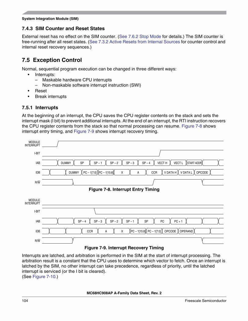
System Integration Module (SIM)
MC68HC908AP A-Family Data Sheet, Rev. 2
104 Freescale Semiconductor
7.4.3 SIM Counter and Reset States
External reset has no effect on the SIM counter. (See 7.6.2 Stop Mode for details.) The SIM counter isfree-running after all reset states. (See 7.3.2 Active Resets from Internal Sources for counter control andinternal reset recovery sequences.)
7.5 Exception Control
Normal, sequential program execution can be changed in three different ways:• Interrupts:
– Maskable hardware CPU interrupts– Non-maskable software interrupt instruction (SWI)
• Reset• Break interrupts
7.5.1 Interrupts
At the beginning of an interrupt, the CPU saves the CPU register contents on the stack and sets theinterrupt mask (I bit) to prevent additional interrupts. At the end of an interrupt, the RTI instruction recoversthe CPU register contents from the stack so that normal processing can resume. Figure 7-8 showsinterrupt entry timing, and Figure 7-9 shows interrupt recovery timing.
Figure 7-8. Interrupt Entry Timing
Figure 7-9. Interrupt Recovery Timing
Interrupts are latched, and arbitration is performed in the SIM at the start of interrupt processing. Thearbitration result is a constant that the CPU uses to determine which vector to fetch. Once an interrupt islatched by the SIM, no other interrupt can take precedence, regardless of priority, until the latchedinterrupt is serviced (or the I bit is cleared).(See Figure 7-10.)
MODULE
IDB
R/W
INTERRUPT
DUMMY SP SP – 1 SP – 2 SP – 3 SP – 4 VECT H VECT L START ADDRIAB
DUMMY PC – 1[7:0] PC – 1[15:8] X A CCR V DATA H V DATA L OPCODE
I-BIT
MODULE
IDB
R/W
INTERRUPT
SP – 4 SP – 3 SP – 2 SP – 1 SP PC PC + 1IAB
CCR A X PC – 1[15:8] PC – 1[7:0] OPCODE OPERAND
I-BIT

Exception Control
MC68HC908AP A-Family Data Sheet, Rev. 2
Freescale Semiconductor 105
Figure 7-10. Interrupt Processing
7.5.1.1 Hardware Interrupts
A hardware interrupt does not stop the current instruction. Processing of a hardware interrupt begins aftercompletion of the current instruction. When the current instruction is complete, the SIM checks all pendinghardware interrupts. If interrupts are not masked (I bit clear in the condition code register) and if thecorresponding interrupt enable bit is set, the SIM proceeds with interrupt processing; otherwise, the nextinstruction is fetched and executed.
If more than one interrupt is pending at the end of an instruction execution, the highest priority interruptis serviced first. Figure 7-11 demonstrates what happens when two interrupts are pending. If an interruptis pending upon exit from the original interrupt service routine, the pending interrupt is serviced before theLDA instruction is executed.
NO
NO
NO
YES
NO
NO
YES
YES
AS MANY INTERRUPTS
I BIT SET?
FROM RESET
BREAK
I-BIT SET?
IRQ1INTERRUPT?
SWIINSTRUCTION?
RTIINSTRUCTION?
FETCH NEXTINSTRUCTION
UNSTACK CPU REGISTERS
STACK CPU REGISTERSSET I-BIT
LOAD PC WITH INTERRUPT VECTOR
EXECUTE INSTRUCTION
YES
YES
AS EXIST ON CHIP
INTERRUPT?

System Integration Module (SIM)
MC68HC908AP A-Family Data Sheet, Rev. 2
106 Freescale Semiconductor
Figure 7-11. Interrupt Recognition Example
The LDA opcode is prefetched by both the INT1 and INT2 RTI instructions. However, in the case of theINT1 RTI prefetch, this is a redundant operation.
NOTETo maintain compatibility with the M6805 Family, the H register is notpushed on the stack during interrupt entry. If the interrupt service routinemodifies the H register or uses the indexed addressing mode, softwareshould save the H register and then restore it prior to exiting the routine.
7.5.1.2 SWI Instruction
The SWI instruction is a non-maskable instruction that causes an interrupt regardless of the state of theinterrupt mask (I bit) in the condition code register.
NOTEA software interrupt pushes PC onto the stack. A software interrupt doesnot push PC – 1, as a hardware interrupt does.
7.5.2 Interrupt Status Registers
The flags in the interrupt status registers identify maskable interrupt sources. Table 7-3 summarizes theinterrupt sources and the interrupt status register flags that they set. The interrupt status registers can beuseful for debugging.
CLI
LDA
INT1
PULHRTI
INT2
BACKGROUND#$FF
PSHH
INT1 INTERRUPT SERVICE ROUTINE
PULHRTI
PSHH
INT2 INTERRUPT SERVICE ROUTINE
ROUTINE

Exception Control
MC68HC908AP A-Family Data Sheet, Rev. 2
Freescale Semiconductor 107
7.5.2.1 Interrupt Status Register 1
IF6–IF1 — Interrupt Flags 6–1These flags indicate the presence of interrupt requests from the sources shown in Table 7-3.
1 = Interrupt request present0 = No interrupt request present
Bit 0 and Bit 1 — Always read 0
7.5.2.2 Interrupt Status Register 2
IF14–IF7 — Interrupt Flags 14–7These flags indicate the presence of interrupt requests from the sources shown in Table 7-3.
1 = Interrupt request present0 = No interrupt request present
7.5.2.3 Interrupt Status Register 3
IF21–IF15 — Interrupt Flags 21–15These flags indicate the presence of an interrupt request from the source shown in Table 7-3.
1 = Interrupt request present0 = No interrupt request present
Address: $FE04
Bit 7 6 5 4 3 2 1 Bit 0
Read: IF6 IF5 IF4 IF3 IF2 IF1 0 0
Write: R R R R R R R R
Reset: 0 0 0 0 0 0 0 0
R = Reserved
Figure 7-12. Interrupt Status Register 1 (INT1)
Address: $FE05
Bit 7 6 5 4 3 2 1 Bit 0
Read: IF14 IF13 IF12 IF11 IF10 IF9 IF8 IF7
Write: R R R R R R R R
Reset: 0 0 0 0 0 0 0 0
R = Reserved
Figure 7-13. Interrupt Status Register 2 (INT2)
Address: $FE06
Bit 7 6 5 4 3 2 1 Bit 0
Read: 0 IF21 IF20 IF19 IF18 IF17 IF16 IF15
Write: R R R R R R R R
Reset: 0 0 0 0 0 0 0 0
R = Reserved
Figure 7-14. Interrupt Status Register 3 (INT3)

System Integration Module (SIM)
MC68HC908AP A-Family Data Sheet, Rev. 2
108 Freescale Semiconductor
Table 7-3. Interrupt Sources
PriorityINTFlag
VectorAddress
Interrupt Source
Lowest—
$FFD0Reserved
$FFD1
IF21$FFD2
Timebase$FFD3
IF20$FFD4
Infrared SCI Transmit$FFD5
IF19$FFD6
Infrared SCI Receive$FFD7
IF18$FFD8
Infrared SCI Error$FFD9
IF17$FFDA
SPI Transmit$FFDB
IF16$FFDC
SPI Receive$FFDD
IF15$FFDE
ADC Conversion Complete$FFDF
IF14$FFE0
Keyboard$FFE1
IF13$FFE2
SCI Transmit$FFE3
IF12$FFE4
SCI Receive$FFE5
IF11$FFE6
SCI Error$FFE7
IF10$FFE8
MMIIC$FFE9
IF9$FFEA
TIM2 Overflow$FFEB
IF8$FFEC
TIM2 Channel 1$FFED
IF7$FFEE
TIM2 Channel 0$FFEF
IF6$FFF0
TIM1 Overflow$FFF1
IF5$FFF2
TIM1 Channel 1$FFF3
IF4$FFF4
TIM1 Channel 0$FFF5
IF3$FFF6
PLL$FFF7
IF2$FFF8
IRQ2$FFF9
IF1$FFFA
IRQ1$FFFB
—$FFFC
SWI$FFFD
—$FFFE
ResetHighest $FFFF

Low-Power Modes
MC68HC908AP A-Family Data Sheet, Rev. 2
Freescale Semiconductor 109
7.5.3 Reset
All reset sources always have equal and highest priority and cannot be arbitrated.
7.5.4 Break Interrupts
The break module can stop normal program flow at a software-programmable break point by assertingits break interrupt output. (See Chapter 21 Break Module (BRK).) The SIM puts the CPU into the breakstate by forcing it to the SWI vector location. Refer to the break interrupt subsection of each module tosee how each module is affected by the break state.
7.5.5 Status Flag Protection in Break Mode
The SIM controls whether status flags contained in other modules can be cleared during break mode. Theuser can select whether flags are protected from being cleared by properly initializing the break clear flagenable bit (BCFE) in the SIM break flag control register (SBFCR).
Protecting flags in break mode ensures that set flags will not be cleared while in break mode. Thisprotection allows registers to be freely read and written during break mode without losing status flaginformation.
Setting the BCFE bit enables the clearing mechanisms. Once cleared in break mode, a flag remainscleared even when break mode is exited. Status flags with a 2-step clearing mechanism — for example,a read of one register followed by the read or write of another — are protected, even when the first stepis accomplished prior to entering break mode. Upon leaving break mode, execution of the second stepwill clear the flag as normal.
7.6 Low-Power Modes
Executing the WAIT or STOP instruction puts the MCU in a low power-consumption mode for standbysituations. The SIM holds the CPU in a non-clocked state. The operation of each of these modes isdescribed in the following subsections. Both STOP and WAIT clear the interrupt mask (I) in the conditioncode register, allowing interrupts to occur.
7.6.1 Wait Mode
In wait mode, the CPU clocks are inactive while the peripheral clocks continue to run. Figure 7-15 showsthe timing for wait mode entry.
A module that is active during wait mode can wake up the CPU with an interrupt if the interrupt is enabled.Stacking for the interrupt begins one cycle after the WAIT instruction during which the interrupt occurred.In wait mode, the CPU clocks are inactive. Refer to the wait mode subsection of each module to see ifthe module is active or inactive in wait mode. Some modules can be programmed to be active in waitmode.
Wait mode also can be exited by a reset or break. A break interrupt during wait mode sets the SIM breakstop/wait bit, SBSW, in the SIM break status register (SBSR). If the COP disable bit, COPD, in the maskoption register is logic 0, then the computer operating properly module (COP) is enabled and remainsactive in wait mode.

System Integration Module (SIM)
MC68HC908AP A-Family Data Sheet, Rev. 2
110 Freescale Semiconductor
Figure 7-15. Wait Mode Entry Timing
Figure 7-16 and Figure 7-17 show the timing for WAIT recovery.
Figure 7-16. Wait Recovery from Interrupt or Break
Figure 7-17. Wait Recovery from Internal Reset
7.6.2 Stop Mode
In stop mode, the SIM counter is reset and the system clocks are disabled. An interrupt request from amodule can cause an exit from stop mode. Stacking for interrupts begins after the selected stop recoverytime has elapsed. Reset or break also causes an exit from stop mode.
The SIM disables the clock generator module output (CGMOUT) in stop mode, stopping the CPU andperipherals. Stop recovery time is selectable using the SSREC bit in the configuration register 1(CONFIG1). If SSREC is set, stop recovery is reduced from the normal delay of 4096 ICLK cycles downto 32. This is ideal for applications using canned oscillators that do not require long start-up times fromstop mode.
NOTEExternal crystal applications should use the full stop recovery time byclearing the SSREC bit.
WAIT ADDR + 1 SAME SAMEIAB
IDB PREVIOUS DATA NEXT OPCODE SAME
WAIT ADDR
SAME
R/W
NOTE: Previous data can be operand data or the WAIT opcode, depending on thelast instruction.
$6E0C$6E0B $00FF $00FE $00FD $00FC
$A6 $A6 $01 $0B $6E$A6
IAB
IDB
EXITSTOPWAIT
NOTE: EXITSTOPWAIT = RST pin OR CPU interrupt OR break interrupt
IAB
IDB
RST
$A6 $A6
$6E0B RST VCT H RST VCT L
$A6
ICLK
32CYCLES
32CYCLES
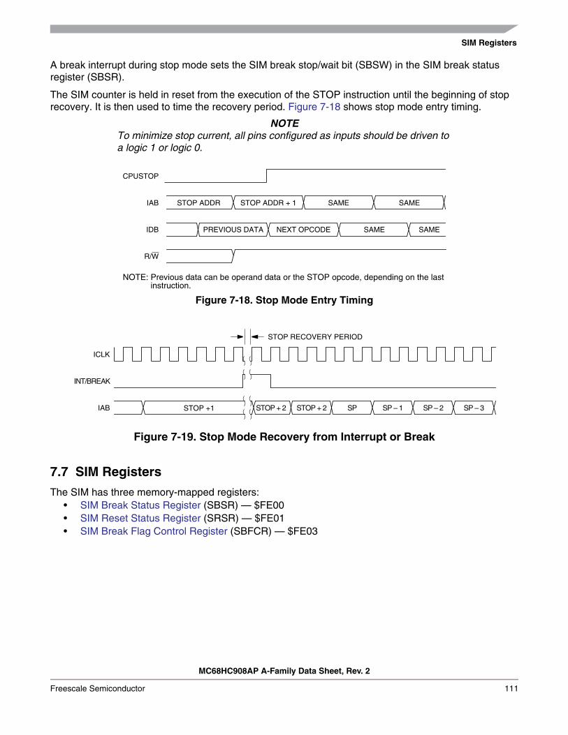
SIM Registers
MC68HC908AP A-Family Data Sheet, Rev. 2
Freescale Semiconductor 111
A break interrupt during stop mode sets the SIM break stop/wait bit (SBSW) in the SIM break statusregister (SBSR).
The SIM counter is held in reset from the execution of the STOP instruction until the beginning of stoprecovery. It is then used to time the recovery period. Figure 7-18 shows stop mode entry timing.
NOTETo minimize stop current, all pins configured as inputs should be driven toa logic 1 or logic 0.
Figure 7-18. Stop Mode Entry Timing
Figure 7-19. Stop Mode Recovery from Interrupt or Break
7.7 SIM Registers
The SIM has three memory-mapped registers:• SIM Break Status Register (SBSR) — $FE00• SIM Reset Status Register (SRSR) — $FE01• SIM Break Flag Control Register (SBFCR) — $FE03
STOP ADDR + 1 SAME SAMEIAB
IDB PREVIOUS DATA NEXT OPCODE SAME
STOP ADDR
SAME
R/W
CPUSTOP
NOTE: Previous data can be operand data or the STOP opcode, depending on the last instruction.
ICLK
INT/BREAK
IAB STOP + 2 STOP + 2 SP SP – 1 SP – 2 SP – 3STOP +1
STOP RECOVERY PERIOD
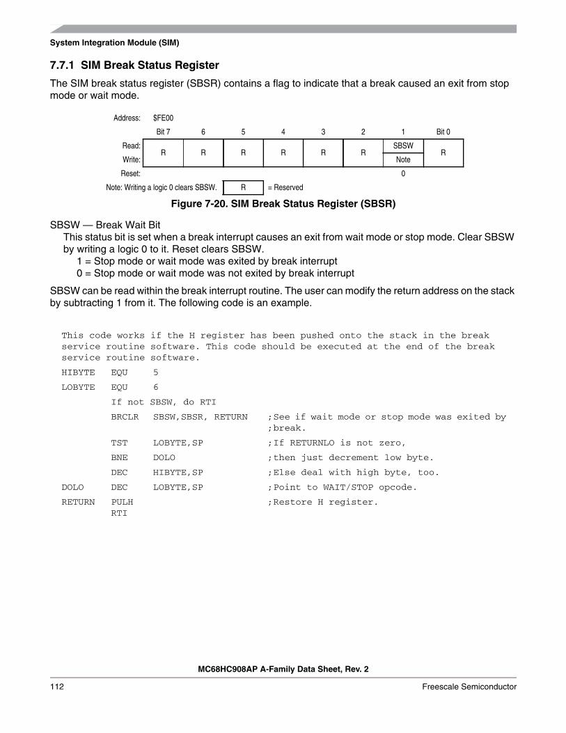
System Integration Module (SIM)
MC68HC908AP A-Family Data Sheet, Rev. 2
112 Freescale Semiconductor
7.7.1 SIM Break Status Register
The SIM break status register (SBSR) contains a flag to indicate that a break caused an exit from stopmode or wait mode.
SBSW — Break Wait BitThis status bit is set when a break interrupt causes an exit from wait mode or stop mode. Clear SBSWby writing a logic 0 to it. Reset clears SBSW.
1 = Stop mode or wait mode was exited by break interrupt0 = Stop mode or wait mode was not exited by break interrupt
SBSW can be read within the break interrupt routine. The user can modify the return address on the stackby subtracting 1 from it. The following code is an example.
Address: $FE00
Bit 7 6 5 4 3 2 1 Bit 0
Read:R R R R R R
SBSWR
Write: Note
Reset: 0
Note: Writing a logic 0 clears SBSW. R = Reserved
Figure 7-20. SIM Break Status Register (SBSR)
This code works if the H register has been pushed onto the stack in the breakservice routine software. This code should be executed at the end of the breakservice routine software.
HIBYTE EQU 5
LOBYTE EQU 6
If not SBSW, do RTI
BRCLR SBSW,SBSR, RETURN ;;See if wait mode or stop mode was exited bybreak.
TST LOBYTE,SP ;If RETURNLO is not zero,
BNE DOLO ;then just decrement low byte.
DEC HIBYTE,SP ;Else deal with high byte, too.
DOLO DEC LOBYTE,SP ;Point to WAIT/STOP opcode.
RETURN PULHRTI
;Restore H register.

SIM Registers
MC68HC908AP A-Family Data Sheet, Rev. 2
Freescale Semiconductor 113
7.7.2 SIM Reset Status Register
This register contains six flags that show the source of the last reset provided all previous reset statusbits have been cleared. Clear the SIM reset status register by reading it. A power-on reset sets the PORbit and clears all other bits in the register.
POR — Power-On Reset Bit1 = Last reset caused by POR circuit0 = Read of SRSR
PIN — External Reset Bit1 = Last reset caused by external reset pin (RST)0 = POR or read of SRSR
COP — Computer Operating Properly Reset Bit1 = Last reset caused by COP counter0 = POR or read of SRSR
ILOP — Illegal Opcode Reset Bit1 = Last reset caused by an illegal opcode0 = POR or read of SRSR
ILAD — Illegal Address Reset Bit (opcode fetches only)1 = Last reset caused by an opcode fetch from an illegal address0 = POR or read of SRSR
MODRST — Monitor Mode Entry Module Reset Bit1 = Last reset caused by monitor mode entry when vector locations $FFFE and $FFFF are $FF after
POR while IRQ1 = VDD0 = POR or read of SRSR
LVI — Low-Voltage Inhibit Reset Bit1 = Last reset caused by the LVI circuit0 = POR or read of SRSR
Address: $FE01
Bit 7 6 5 4 3 2 1 Bit 0
Read: POR PIN COP ILOP ILAD MODRST LVI 0
Write:
Reset: 1 0 0 0 0 0 0 0
= Unimplemented
Figure 7-21. SIM Reset Status Register (SRSR)

System Integration Module (SIM)
MC68HC908AP A-Family Data Sheet, Rev. 2
114 Freescale Semiconductor
7.7.3 SIM Break Flag Control Register
The SIM break control register contains a bit that enables software to clear status bits while the MCU isin a break state.
BCFE — Break Clear Flag Enable BitThis read/write bit enables software to clear status bits by accessing status registers while the MCU isin a break state. To clear status bits during the break state, the BCFE bit must be set.
1 = Status bits clearable during break0 = Status bits not clearable during break
Address: $FE03
Bit 7 6 5 4 3 2 1 Bit 0
Read:BCFE R R R R R R R
Write:
Reset: 0
R = Reserved
Figure 7-22. SIM Break Flag Control Register (SBFCR)

MC68HC908AP A-Family Data Sheet, Rev. 2
Freescale Semiconductor 115
Chapter 8Monitor ROM (MON)
8.1 Introduction
This section describes the monitor ROM (MON) and the monitor mode entry methods. The monitor ROMallows complete testing of the MCU through a single-wire interface with a host computer. Monitor modeentry can be achieved without use of the higher test voltage, VTST, as long as vector addresses $FFFEand $FFFF are blank, thus reducing the hardware requirements for in-circuit programming.In addition, to simplify user coding, routines are also stored in the monitor ROM area for FLASH memoryprogram /erase.
8.2 Features
Features of the monitor ROM include:• Normal user-mode pin functionality• One pin dedicated to serial communication between monitor ROM and host computer• Standard mark/space non-return-to-zero (NRZ) communication with host computer• Execution of code in RAM or FLASH• FLASH memory security feature(1)
• 959 bytes monitor ROM code size($FC00–$FDFF and $FE10–$FFCE)
• Monitor mode entry without high voltage, VTST, if reset vector is blank ($FFFE and $FFFF contain$FF)
• Standard monitor mode entry if high voltage, VTST, is applied to IRQ1• Resident routines for in-circuit programming
8.3 Functional Description
The monitor ROM receives and executes commands from a host computer. Figure 8-1 shows an examplecircuit used to enter monitor mode and communicate with a host computer via a standard RS-232interface.
Simple monitor commands can access any memory address. In monitor mode, the MCU can executecode downloaded into RAM by a host computer while most MCU pins retain normal operating modefunctions. All communication between the host computer and the MCU is through the PTA0 pin. Alevel-shifting and multiplexing interface is required between PTA0 and the host computer. PTA0 is usedin a wired-OR configuration and requires a pullup resistor.
1. No security feature is absolutely secure. However, Freescale’s strategy is to make reading or copying the FLASH difficult forunauthorized users.

Monitor ROM (MON)
MC68HC908AP A-Family Data Sheet, Rev. 2
116 Freescale Semiconductor
Figure 8-1. Monitor Mode Circuit
NOTES:1. Monitor mode entry method:
SW2: Position C — High voltage entry (VTST); must use external OSCBus clock depends on SW1 (note 2).
SW2: Position D — Reset vector must be blank ($FFFE:$FFFF = $FF)Bus clock = 1.2288MHz.
2. Affects high voltage entry to monitor mode only (SW2 at position C):SW1: Position A — Bus clock = OSC1 4SW1: Position B — Bus clock = OSC1 2
5. See Table 22-4 for VTST voltage level requirements.
1M
HC908AP
RST
IRQ1
OSC1
OSC2
VSS
PTA0
6–30 pF
6–30 pF
0.1 µF
4.9152MHz
PTA1
VDD
0.1 µF
VDD
PTA2
10k
PTB0
VDD
10k
10 k
SW1A
B
VREG
(SEE NOTE 2)
C
D
XTAL CIRCUIT
16
15
2
6VDD
MAX232
V+
V–
VDD
10 k
C1+
C1–
5
4 C2+
C2–
+
3
1
1 µF+ +
+
8
7DB9
2
3
5
10
9
+
1
2 3 4
5674HC125
74HC125
1 k
VTST
VCC
GND
1 µF
1 µF
1 µF
1 µF
8.5 V
10 k
CONNECT TO OSC1, WITH OSC2 UNCONNECTED.MUST BE USED IF SW2 IS AT POSITION C.
OSC1
(SEE NOTE 1)SW2
10k
0.033 µF
0.01 µF
CGMXFC
VDDA
VREFL
VSSA
EXT OSC
4.9152MHz/9.8304MHz(50% DUTY)
VREFH
VREG
10k
VDD
VDD

Functional Description
MC68HC908AP A-Family Data Sheet, Rev. 2
Freescale Semiconductor 117
8.3.1 Entering Monitor Mode
Table 8-1 shows the pin conditions for entering monitor mode. As specified in the table, monitor modemay be entered after a POR and will allow communication at 9600 baud provided one of the followingsets of conditions is met:
1. If $FFFE and $FFFF do not contain $FF (programmed state):– The external clock is 4.9152 MHz with PTB0 low or 9.8304 MHz with PTB0 high– IRQ1 = VTST
2. If $FFFE and $FFFF both contain $FF (erased state):– The external clock is 9.8304 MHz– IRQ1 = VDD (this can be implemented through the internal IRQ1 pullup
If VTST is applied to IRQ1 and PTB0 is low upon monitor mode entry (above condition set 1), the busfrequency is a divide-by-two of the input clock. If PTB0 is high with VTST applied to IRQ1 upon monitormode entry, the bus frequency will be a divide-by-four of the input clock. Holding the PTB0 pin low whenentering monitor mode causes a bypass of a divide-by-two stage at the oscillator only if VTST is appliedto IRQ1. In this event, the CGMOUT frequency is equal to the CGMXCLK frequency, and the OSC1 inputdirectly generates internal bus clocks. In this case, the OSC1 signal must have a 50% duty cycle atmaximum bus frequency.
If entering monitor mode without high voltage on IRQ1 (above condition set 2, where applied voltage iseither VDD), then all port A pin requirements and conditions, including the PTB0 frequency divisorselection, are not in effect. This is to reduce circuit requirements when performing in-circuit programming.
NOTEIf the reset vector is blank and monitor mode is entered, the chip will see anadditional reset cycle after the initial POR reset. Once the part has beenprogrammed, the traditional method of applying a voltage, VTST, to IRQ1must be used to enter monitor mode.
The COP module is disabled in monitor mode based on these conditions:• If monitor mode was entered as a result of the reset vector being blank (above condition set 2), the
COP is always disabled regardless of the state of IRQ1 or RST.• If monitor mode was entered with VTST on IRQ1 (condition set 1), then the COP is disabled as long
as VTST is applied to either IRQ1 or RST.
The second condition states that as long as VTST is maintained on the IRQ1 pin after entering monitormode, or if VTST is applied to RST after the initial reset to get into monitor mode (when VTST was appliedto IRQ1), then the COP will be disabled. In the latter situation, after VTST is applied to the RST pin, VTSTcan be removed from the IRQ1 pin in the interest of freeing the IRQ1 for normal functionality in monitormode.
Figure 8-2 shows a simplified diagram of the monitor mode entry when the reset vector is blank and justVDD voltage is applied to the IRQ1 pin. An external oscillator of 9.8304 MHz is required for a baud rate of9600, as the internal bus frequency is automatically set to the external frequency divided by four.
Enter monitor mode with pin configuration shown in Figure 8-1 by pulling RST low and then high. Therising edge of RST latches monitor mode. Once monitor mode is latched, the values on the specified pinscan change.
Once out of reset, the MCU waits for the host to send eight security bytes. (See 8.4 Security.) After thesecurity bytes, the MCU sends a break signal (10 consecutive logic 0’s) to the host, indicating that it isready to receive a command.

MC
68HC
908AP
A-Fam
ily Data S
heet, R
ev. 2
118F
reescale Sem
iconductor
Mo
nito
r RO
M (M
ON
)
Table 8-1. Monitor Mode Signal Requirements and Options
IRQ1 RSTAddress$FFFE/$FFFF
PTA2 PTA1PTA0
(1)
1. PTA0 = 1 if serial communication; PTA0 = 0 if parallel communication
PTB0External
Clock(2)
2. External clock is derived by a 4.9152MHz crystal/off-chip oscillator or a 9.8304MHz off-chip oscillator.
BusFrequency
PLL COPBaudRate
Comment
X GND X X X X X X 0 X Disabled 0No operation untilreset goes high
VTST(3)
3. Monitor mode entry by IRQ1= VTST, a 4.9152/9.8304 MHz off-chip oscillator must be used. The MCU internal crystal oscillator circuit is by-passed.
VDD
orVTST
X 0 1 1 04.9152MHz
2.4576MHz
OFF Disabled 9600
PTA1 and PTA2voltages onlyrequired ifIRQ1 = VTST;PTB0 determinesfrequency divider
VTST(3)
VDDor
VTST
X 0 1 1 19.8304MHz
2.4576MHz
OFF Disabled 9600
PTA1 and PTA2voltages onlyrequired ifIRQ1 = VTST;PTB0 determinesfrequency divider
VDD VDDBlank
"$FFFF"X X 1 X
4.9152MHz
1.2288MHz
OFF Disabled 4800External frequencyalways divided by 4
VDD VDDBlank
"$FFFF"X X 1 X
9.8304MHz
2.4576MHz
OFF Disabled 9600External frequencyalways divided by 4
VDDor
GND
VTSTBlank
"$FFFF"X X X X X — OFF Enabled —
Enters usermode — willencounter an illegaladdress reset
VDDor
GND
VDDor
VTST
Not Blank X X X X X — OFF Enabled — Enters user mode

Functional Description
MC68HC908AP A-Family Data Sheet, Rev. 2
Freescale Semiconductor 119
Figure 8-2. Low-Voltage Monitor Mode Entry Flowchart
In monitor mode, the MCU uses different vectors for reset, SWI (software interrupt), and break interruptthan those for user mode. The alternate vectors are in the $FE page instead of the $FF page and allowcode execution from the internal monitor firmware instead of user code.
NOTEExiting monitor mode after it has been initiated by having a blank resetvector requires a power-on reset (POR). Pulling RST low will not exitmonitor mode in this situation.
Table 8-2 summarizes the differences between user mode and monitor mode vectors.
8.3.2 Data Format
Communication with the monitor ROM is in standard non-return-to-zero (NRZ) mark/space data format.Transmit and receive baud rates must be identical.
Figure 8-3. Monitor Data Format
Table 8-2. Mode Differences (Vectors)
Modes
Functions
ResetVectorHigh
ResetVectorLow
BreakVectorHigh
BreakVectorLow
SWIVectorHigh
SWIVectorLow
User $FFFE $FFFF $FFFC $FFFD $FFFC $FFFD
Monitor $FEFE $FEFF $FEFC $FEFD $FEFC $FEFD
IS VECTORBLANK?
PORTRIGGERED?
NORMAL USERMODE
MONITOR MODE
EXECUTEMONITOR
CODE
NO
NO
YES
YES
POR RESET
BIT 5START
BIT BIT 0 BIT 1
NEXT
STOPBIT
STARTBITBIT 2 BIT 3 BIT 4 BIT 6 BIT 7

Monitor ROM (MON)
MC68HC908AP A-Family Data Sheet, Rev. 2
120 Freescale Semiconductor
8.3.3 Break Signal
A start bit (logic 0) followed by nine logic 0 bits is a break signal. When the monitor receives a break signal,it drives the PTA0 pin high for the duration of two bits and then echoes back the break signal.
Figure 8-4. Break Transaction
8.3.4 Baud Rate
The communication baud rate is controlled by the crystal frequency and the state of the PTB0 pin (whenIRQ1 is set to VTST) upon entry into monitor mode. When PTB0 is high, the divide by ratio is 1024. If thePTB0 pin is at logic 0 upon entry into monitor mode, the divide by ratio is 512.
If monitor mode was entered with VDD on IRQ1, then the divide by ratio is set at 1024, regardless of PTB0.This condition for monitor mode entry requires that the reset vector is blank.
Table 8-3 lists external frequencies required to achieve a standard baud rate of 9600 BPS. Otherstandard baud rates can be accomplished using proportionally higher or lower frequency generators. Ifusing a crystal as the clock source, be aware of the upper frequency limit that the internal clock modulecan handle.
8.3.5 Commands
The monitor ROM firmware uses these commands:• READ (read memory)• WRITE (write memory)• IREAD (indexed read)• IWRITE (indexed write)• READSP (read stack pointer)• RUN (run user program)
The monitor ROM firmware echoes each received byte back to the PTA0 pin for error checking. An 11-bitdelay at the end of each command allows the host to send a break character to cancel the command. Adelay of two bit times occurs before each echo and before READ, IREAD, or READSP data is returned.The data returned by a read command appears after the echo of the last byte of the command.
Table 8-3. Monitor Baud Rate Selection
ExternalFrequency
IRQ1 PTB0Internal
FrequencyBaud Rate
(BPS)
4.9152 MHz VTST 0 2.4576 MHz 9600
9.8304 MHz VTST 1 2.4576 MHz 9600
9.8304 MHz VDD X 2.4576 MHz 9600
0 1 2 3 4 5 6 7 0 1 2 3 4 5 6 7
MISSING STOP BIT2-STOP BIT DELAY BEFORE ZERO ECHO

Functional Description
MC68HC908AP A-Family Data Sheet, Rev. 2
Freescale Semiconductor 121
NOTEWait one bit time after each echo before sending the next byte.
Figure 8-5. Read Transaction
Figure 8-6. Write Transaction
A brief description of each monitor mode command is given in Table 8-4 through Table 8-9.
Table 8-4. READ (Read Memory) Command
Description Read byte from memory
Operand 2-byte address in high-byte:low-byte order
DataReturned
Returns contents of specified address
Opcode $4A
Command Sequence
READREAD
ECHO
FROM HOST
ADDRESSHIGH
ADDRESSHIGH
ADDRESSLOW
ADDRESSLOW DATA
RETURN
1 3, 21 14 4
Notes:
2 = Data return delay, 2 bit times3 = Cancel command delay, 11 bit times4 = Wait 1 bit time before sending next byte.
4 4
1 = Echo delay, 2 bit times
WRITEWRITE
ECHO
FROM HOST
ADDRESSHIGH
ADDRESSHIGH
ADDRESSLOW
ADDRESSLOW
DATA DATA
Notes:
2 = Cancel command delay, 11 bit times3 = Wait 1 bit time before sending next byte.
1 131 13 3 3 2, 3
1 = Echo delay, 2 bit times
READREAD
ECHO
SENT TOMONITOR
ADDRESSHIGH
ADDRESSHIGH
ADDRESSLOW DATA
RETURN
ADDRESSLOW

Monitor ROM (MON)
MC68HC908AP A-Family Data Sheet, Rev. 2
122 Freescale Semiconductor
Table 8-5. WRITE (Write Memory) Command
Description Write byte to memory
Operand2-byte address in high-byte:low-byte order;low byte followed by data byte
DataReturned
None
Opcode $49
Command Sequence
Table 8-6. IREAD (Indexed Read) Command
Description Read next 2 bytes in memory from last address accessed
Operand 2-byte address in high byte:low byte order
DataReturned
Returns contents of next two addresses
Opcode $1A
Command Sequence
WRITEWRITE
ECHO
FROMHOST
ADDRESSHIGH
ADDRESSHIGH
ADDRESSLOW
ADDRESSLOW
DATA DATA
IREADIREAD
ECHO
FROMHOST
DATA
RETURN
DATA
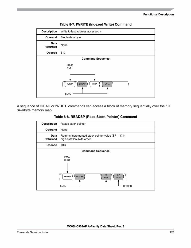
Functional Description
MC68HC908AP A-Family Data Sheet, Rev. 2
Freescale Semiconductor 123
A sequence of IREAD or IWRITE commands can access a block of memory sequentially over the full64-Kbyte memory map.
Table 8-7. IWRITE (Indexed Write) Command
Description Write to last address accessed + 1
Operand Single data byte
DataReturned
None
Opcode $19
Command Sequence
Table 8-8. READSP (Read Stack Pointer) Command
Description Reads stack pointer
Operand None
DataReturned
Returns incremented stack pointer value (SP + 1) inhigh-byte:low-byte order
Opcode $0C
Command Sequence
IWRITEIWRITE
ECHO
FROMHOST
DATA DATA
READSPREADSP
ECHO
FROMHOST
SP
RETURN
SPHIGH LOW

Monitor ROM (MON)
MC68HC908AP A-Family Data Sheet, Rev. 2
124 Freescale Semiconductor
The MCU executes the SWI and PSHH instructions when it enters monitor mode. The RUN commandtells the MCU to execute the PULH and RTI instructions. Before sending the RUN command, the host canmodify the stacked CPU registers to prepare to run the host program. The READSP command returnsthe incremented stack pointer value, SP + 1. The high and low bytes of the program counter are ataddresses SP + 5 and SP + 6.
Figure 8-7. Stack Pointer at Monitor Mode Entry
8.4 Security
A security feature discourages unauthorized reading of FLASH locations while in monitor mode. The hostcan bypass the security feature at monitor mode entry by sending eight security bytes that match thebytes at locations $FFF6–$FFFD. Locations $FFF6–$FFFD contain user-defined data.
NOTEDo not leave locations $FFF6–$FFFD blank. For security reasons, programlocations $FFF6–$FFFD even if they are not used for vectors.
Table 8-9. RUN (Run User Program) Command
Description Executes PULH and RTI instructions
Operand None
DataReturned
None
Opcode $28
Command Sequence
RUNRUN
ECHO
FROMHOST
CONDITION CODE REGISTER
ACCUMULATOR
LOW BYTE OF INDEX REGISTER
HIGH BYTE OF PROGRAM COUNTER
LOW BYTE OF PROGRAM COUNTER
SP + 1
SP + 2
SP + 3
SP + 4
SP + 5
SP
SP + 6
HIGH BYTE OF INDEX REGISTER
SP + 7

Security
MC68HC908AP A-Family Data Sheet, Rev. 2
Freescale Semiconductor 125
During monitor mode entry, the MCU waits after the power-on reset for the host to send the eight securitybytes on pin PTA0. If the received bytes match those at locations $FFF6–$FFFD, the host bypasses thesecurity feature and can read all FLASH locations and execute code from FLASH. Security remainsbypassed until a power-on reset occurs. If the reset was not a power-on reset, security remains bypassedand security code entry is not required. (See Figure 8-8.)
Figure 8-8. Monitor Mode Entry Timing
Upon power-on reset, if the received bytes of the security code do not match the data at locations$FFF6–$FFFD, the host fails to bypass the security feature. The MCU remains in monitor mode, butreading a FLASH location returns an invalid value and trying to execute code from FLASH causes anillegal address reset. After receiving the eight security bytes from the host, the MCU transmits a breakcharacter, signifying that it is ready to receive a command.
NOTEThe MCU does not transmit a break character until after the host sends theeight security bits.
To determine whether the security code entered is correct, check to see if bit 6 of RAM address $60 isset. If it is, then the correct security code has been entered and FLASH can be accessed.
If the security sequence fails, the device should be reset by a power-on reset and brought up in monitormode to attempt another entry. After failing the security sequence, the FLASH module can also be masserased by executing an erase routine that was downloaded into internal RAM. The mass erase operationclears the security code locations so that all eight security bytes become $FF (blank).
BY
TE
1
BY
TE
1 E
CH
O
BY
TE
2
BY
TE
2 E
CH
O
BY
TE
8
BY
TE
8 E
CH
O
CO
MM
AN
D
CO
MM
AN
D E
CH
O
PTA0
RST
VDD
4096 + 32 ICLK CYCLES
256 BUS CYCLES (MINIMUM)
1 4 1 1 2 1
BR
EA
K
NOTES:
2 = Data return delay, 2 bit times.4 = Wait 1 bit time before sending next byte.
4
FROM HOST
FROM MCU
1 = Echo delay, 2 bit times.
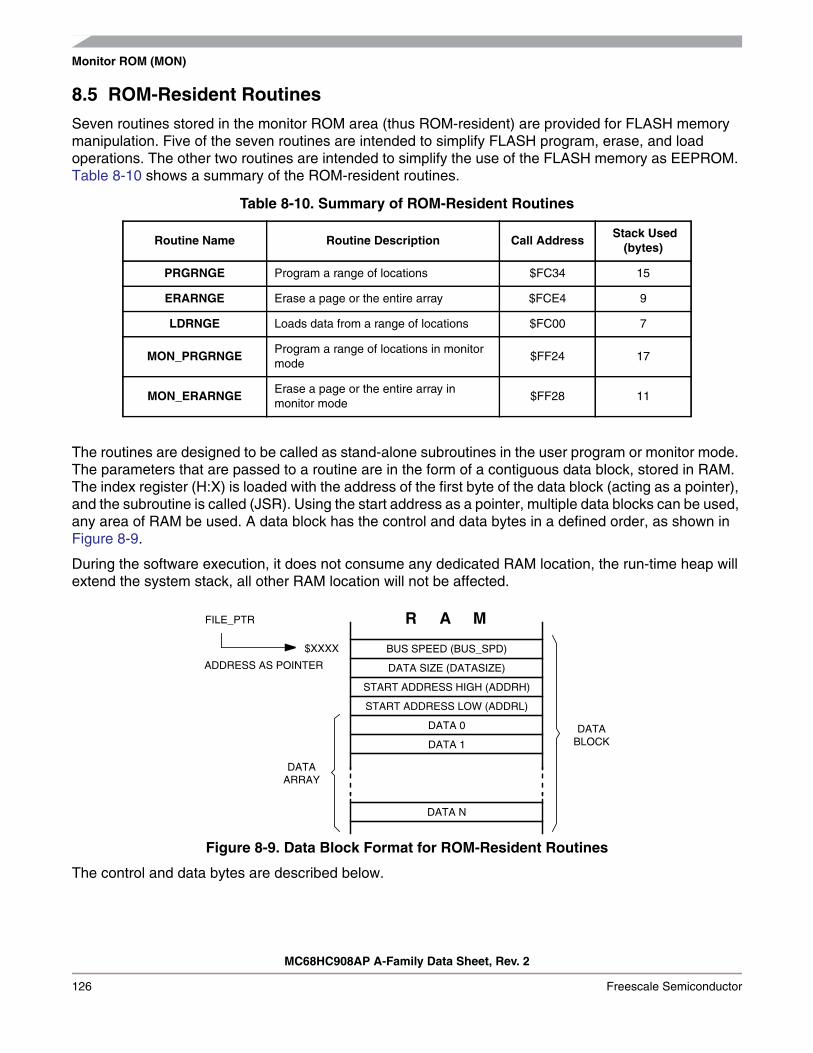
Monitor ROM (MON)
MC68HC908AP A-Family Data Sheet, Rev. 2
126 Freescale Semiconductor
8.5 ROM-Resident Routines
Seven routines stored in the monitor ROM area (thus ROM-resident) are provided for FLASH memorymanipulation. Five of the seven routines are intended to simplify FLASH program, erase, and loadoperations. The other two routines are intended to simplify the use of the FLASH memory as EEPROM.Table 8-10 shows a summary of the ROM-resident routines.
The routines are designed to be called as stand-alone subroutines in the user program or monitor mode.The parameters that are passed to a routine are in the form of a contiguous data block, stored in RAM.The index register (H:X) is loaded with the address of the first byte of the data block (acting as a pointer),and the subroutine is called (JSR). Using the start address as a pointer, multiple data blocks can be used,any area of RAM be used. A data block has the control and data bytes in a defined order, as shown inFigure 8-9.
During the software execution, it does not consume any dedicated RAM location, the run-time heap willextend the system stack, all other RAM location will not be affected.
Figure 8-9. Data Block Format for ROM-Resident Routines
The control and data bytes are described below.
Table 8-10. Summary of ROM-Resident Routines
Routine Name Routine Description Call Address Stack Used
(bytes)
PRGRNGE Program a range of locations $FC34 15
ERARNGE Erase a page or the entire array $FCE4 9
LDRNGE Loads data from a range of locations $FC00 7
MON_PRGRNGEProgram a range of locations in monitormode
$FF24 17
MON_ERARNGEErase a page or the entire array inmonitor mode
$FF28 11
DATA SIZE (DATASIZE)
START ADDRESS HIGH (ADDRH)
START ADDRESS LOW (ADDRL)
DATA 0
DATA 1
BUS SPEED (BUS_SPD)
FILE_PTR
DATA N
DATAARRAY
$XXXX
DATABLOCK
ADDRESS AS POINTER
R A M
ROM-Resident Routines
MC68HC908AP A-Family Data Sheet, Rev. 2
Freescale Semiconductor 127
• Bus speed — This one byte indicates the operating bus speed of the MCU. The value of this byteshould be equal to 4 times the bus speed. E.g., for a 4MHz bus, the value is 16 ($10). This controlbyte is useful where the MCU clock source is switched between the PLL clock and the crystal clock.
• Data size — This one byte indicates the number of bytes in the data array that are to bemanipulated. The maximum data array size is 255. ERARNGE and MON_ERARNGE routines donot manipulate a data array, thus, this data size byte has no meaning.
• Start address — These two bytes, high byte followed by low byte, indicate the start address of theFLASH memory to be manipulated.
• Data array — This data array contains data that are to be manipulated. Data in this array areprogrammed to FLASH memory by the programming routines, PRGRNGE and MON_PRGRNGE.For the read routine, LDRNGE, data is read from FLASH and stored in this array.
8.5.1 PRGRNGE
PRGRNGE is used to program a range of FLASH locations with data loaded into the data array.
The start location of the FLASH to be programmed is specified by the address ADDRH:ADDRL and thenumber of bytes from this location is specified by DATASIZE. The maximum number of bytes that can beprogrammed in one routine call is 255 bytes (max. DATASIZE is 255).
ADDRH:ADDRL do not need to be at a page boundary, the routine handles any boundary misalignmentduring programming. A check to see that all bytes in the specified range are erased is not performed bythis routine prior programming. Nor does this routine do a verification after programming, so there is noreturn confirmation that programming was successful. User must assure that the range specified is firsterased.
The coding example below is to program 64 bytes of data starting at FLASH location $EE00, with a busspeed of 4.9152 MHz. The coding assumes the data block is already loaded in RAM, with the addresspointer, FILE_PTR, pointing to the first byte of the data block.
Table 8-11. PRGRNGE Routine
Routine Name PRGRNGE
Routine Description Program a range of locations
Calling Address $FC34
Stack Used 15 bytes
Data Block Format
Bus speed (BUS_SPD)Data size (DATASIZE)Start address high (ADDRH)Start address (ADDRL)Data 1 (DATA1)
:Data N (DATAN)

Monitor ROM (MON)
MC68HC908AP A-Family Data Sheet, Rev. 2
128 Freescale Semiconductor
ORG RAM:
FILE_PTR:BUS_SPD DS.B 1 ; Indicates 4x bus frequencyDATASIZE DS.B 1 ; Data size to be programmedSTART_ADDR DS.W 1 ; FLASH start addressDATAARRAY DS.B 64 ; Reserved data array
PRGRNGE EQU $FC34FLASH_START EQU $EE00
ORG FLASHINITIALISATION:
MOV #20, BUS_SPDMOV #64, DATASIZELDHX #FLASH_STARTSTHX START_ADDRRTS
MAIN:BSR INITIALISATION::LDHX #FILE_PTRJSR PRGRNGE
8.5.2 ERARNGE
ERARNGE is used to erase a range of locations in FLASH.
There are two sizes of erase ranges: a page or the entire array. The ERARNGE will erase the page (512consecutive bytes) in FLASH specified by the address ADDRH:ADDRL. This address can be any addresswithin the page. Calling ERARNGE with ADDRH:ADDRL equal to $FFFF will erase the entire FLASHarray (mass erase). Therefore, care must be taken when calling this routine to prevent an accidental masserase.
The ERARNGE routine do not use a data array. The DATASIZE byte is a dummy byte that is also notused.
Table 8-12. ERARNGE Routine
Routine Name ERARNGE
Routine Description Erase a page or the entire array
Calling Address $FCE4
Stack Used 9 bytes
Data Block Format
Bus speed (BUS_SPD)Data size (DATASIZE)Starting address (ADDRH)Starting address (ADDRL)
ROM-Resident Routines
MC68HC908AP A-Family Data Sheet, Rev. 2
Freescale Semiconductor 129
The coding example below is to perform a page erase, from $EE00–$EFFF. The Initialization subroutineis the same as the coding example for PRGRNGE (see 8.5.1 PRGRNGE).ERARNGE EQU $FCE4MAIN:
BSR INITIALISATION::LDHX #FILE_PTRJSR ERARNGE:
8.5.3 LDRNGE
LDRNGE is used to load the data array in RAM with data from a range of FLASH locations.
The start location of FLASH from where data is retrieved is specified by the address ADDRH:ADDRL andthe number of bytes from this location is specified by DATASIZE. The maximum number of bytes that canbe retrieved in one routine call is 255 bytes. The data retrieved from FLASH is loaded into the data arrayin RAM. Previous data in the data array will be overwritten. User can use this routine to retrieve data fromFLASH that was previously programmed.
The coding example below is to retrieve 64 bytes of data starting from $EE00 in FLASH. The Initializationsubroutine is the same as the coding example for PRGRNGE (see 8.5.1 PRGRNGE).LDRNGE EQU $FC00MAIN:
BSR INITIALIZATION::LDHX #FILE_PTRJSR LDRNGE:
Table 8-13. LDRNGE Routine
Routine Name LDRNGE
Routine Description Loads data from a range of locations
Calling Address $FC00
Stack Used 7 bytes
Data Block Format
Bus speed (BUS_SPD)Data size (DATASIZE)Starting address (ADDRH)Starting address (ADDRL)Data 1
:Data N
Monitor ROM (MON)
MC68HC908AP A-Family Data Sheet, Rev. 2
130 Freescale Semiconductor
8.5.4 MON_PRGRNGE
In monitor mode, MON_PRGRNGE is used to program a range of FLASH locations with data loaded intothe data array.
The MON_PRGRNGE routine is designed to be used in monitor mode. It performs the same function asthe PRGRNGE routine (see 8.5.1 PRGRNGE), except that MON_PRGRNGE returns to the mainprogram via an SWI instruction. After a MON_PRGRNGE call, the SWI instruction will return the controlback to the monitor code.
8.5.5 MON_ERARNGE
In monitor mode, ERARNGE is used to erase a range of locations in FLASH.
The MON_ERARNGE routine is designed to be used in monitor mode. It performs the same function asthe ERARNGE routine (see 8.5.2 ERARNGE), except that MON_ERARNGE returns to the main programvia an SWI instruction. After a MON_ERARNGE call, the SWI instruction will return the control back tothe monitor code.
Table 8-14. MON_PRGRNGE Routine
Routine Name MON_PRGRNGE
Routine Description Program a range of locations, in monitor mode
Calling Address $FF24
Stack Used 17 bytes
Data Block Format
Bus speedData sizeStarting address (high byte)Starting address (low byte)Data 1
:Data N
Table 8-15. MON_ERARNGE Routine
Routine Name MON_ERARNGE
Routine Description Erase a page or the entire array, in monitor mode
Calling Address $FF28
Stack Used 11 bytes
Data Block Format
Bus speedData sizeStarting address (high byte)Starting address (low byte)

MC68HC908AP A-Family Data Sheet, Rev. 2
Freescale Semiconductor 131
Chapter 9Timer Interface Module (TIM)
9.1 Introduction
This section describes the timer interface (TIM) module. The TIM is a two-channel timer that provides atiming reference with Input capture, output compare, and pulse-width-modulation functions. Figure 9-1 isa block diagram of the TIM.
This particular MCU has two timer interface modules which are denoted as TIM1 and TIM2.
9.2 Features
Features of the TIM include:• Two input capture/output compare channels:
– Rising-edge, falling-edge, or any-edge input capture trigger– Set, clear, or toggle output compare action
• Buffered and unbuffered pulse-width-modulation (PWM) signal generation• Programmable TIM clock input with 7-frequency internal bus clock prescaler selection• Free-running or modulo up-count operation• Toggle any channel pin on overflow• TIM counter stop and reset bits
9.3 Pin Name Conventions
The text that follows describes both timers, TIM1 and TIM2. The TIM input/output (I/O) pin names areT[1,2]CH0 (timer channel 0) and T[1,2]CH1 (timer channel 1), where “1” is used to indicate TIM1 and “2”is used to indicate TIM2. The two TIMs share four I/O pins with four I/O port pins. The external clock inputfor TIM2 is shared with the an ADC channel pin. The full names of the TIM I/O pins are listed in Table 9-1.The generic pin names appear in the text that follows.
NOTEReferences to either timer 1 or timer 2 may be made in the following text byomitting the timer number. For example, TCH0 may refer generically toT1CH0 and T2CH0, and TCH1 may refer to T1CH1 and T2CH1.
Table 9-1. Pin Name Conventions
TIM Generic Pin Names: T[1,2]CH0 T[1,2]CH1
Full TIMPin Names:
TIM1 PTB4/T1CH0 PTB5/T1CH1
TIM2 PTB6/T2CH0 PTB7/T2CH1
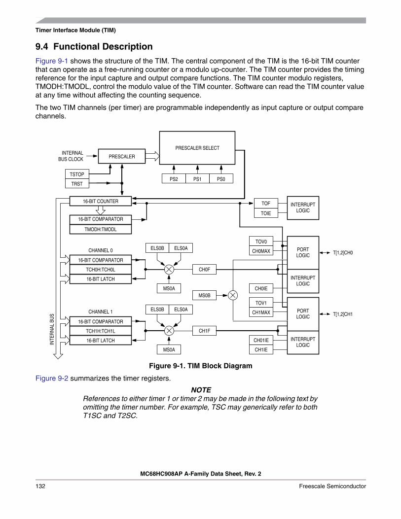
Timer Interface Module (TIM)
MC68HC908AP A-Family Data Sheet, Rev. 2
132 Freescale Semiconductor
9.4 Functional Description
Figure 9-1 shows the structure of the TIM. The central component of the TIM is the 16-bit TIM counterthat can operate as a free-running counter or a modulo up-counter. The TIM counter provides the timingreference for the input capture and output compare functions. The TIM counter modulo registers,TMODH:TMODL, control the modulo value of the TIM counter. Software can read the TIM counter valueat any time without affecting the counting sequence.
The two TIM channels (per timer) are programmable independently as input capture or output comparechannels.
Figure 9-1. TIM Block Diagram
Figure 9-2 summarizes the timer registers.
NOTEReferences to either timer 1 or timer 2 may be made in the following text byomitting the timer number. For example, TSC may generically refer to bothT1SC and T2SC.
PRESCALER
PRESCALER SELECTINTERNAL
16-BIT COMPARATOR
PS2 PS1 PS0
16-BIT COMPARATOR
16-BIT LATCH
TCH0H:TCH0L
TOF
TOIE
16-BIT COMPARATOR
16-BIT LATCH
TCH1H:TCH1L
CHANNEL 0
CHANNEL 1
TMODH:TMODL
TRST
TSTOP
TOV0
CH0IE
CH0F
TOV1
CH1IE
CH1MAX
CH1F
CH0MAX
MS0B
16-BIT COUNTER
INTE
RN
AL B
US
BUS CLOCK
T[1,2]CH0
INTERRUPTLOGIC
PORTLOGIC
INTERRUPTLOGIC
INTERRUPTLOGIC
PORTLOGIC
CH01IE
ELS0B ELS0A
MS0A
ELS0B ELS0A
MS0A
T[1,2]CH1

Functional Description
MC68HC908AP A-Family Data Sheet, Rev. 2
Freescale Semiconductor 133
Addr. Register Name Bit 7 6 5 4 3 2 1 Bit 0
$0020TIM1 Status and Control
Register(T1SC)
Read: TOFTOIE TSTOP
0 0PS2 PS1 PS0
Write: 0 TRSTReset: 0 0 1 0 0 0 0 0
$0021TIM1 Counter Register
High(T1CNTH)
Read: Bit 15 14 13 12 11 10 9 Bit 8Write:
Reset: 0 0 0 0 0 0 0 0
$0022TIM1 Counter Register
Low(T1CNTL)
Read: Bit 7 6 5 4 3 2 1 Bit 0Write:
Reset: 0 0 0 0 0 0 0 0
$0023TIM Counter Modulo
Register High(TMODH)
Read:Bit 15 14 13 12 11 10 9 Bit 8
Write:Reset: 1 1 1 1 1 1 1 1
$0024TIM1 Counter Modulo
Register Low(T1MODL)
Read:Bit 7 6 5 4 3 2 1 Bit 0
Write:Reset: 1 1 1 1 1 1 1 1
$0025TIM1 Channel 0 Status
and Control Register(T1SC0)
Read: CH0FCH0IE MS0B MS0A ELS0B ELS0A TOV0 CH0MAX
Write: 0Reset: 0 0 0 0 0 0 0 0
$0026TIM1 Channel 0
Register High(T1CH0H)
Read:Bit 15 14 13 12 11 10 9 Bit 8
Write:Reset: Indeterminate after reset
$0027TIM1 Channel 0
Register Low(T1CH0L)
Read:Bit 7 6 5 4 3 2 1 Bit 0
Write:Reset: Indeterminate after reset
$0028TIM1 Channel 1 Status
and Control Register(T1SC1)
Read: CH1FCH1IE
0MS1A ELS1B ELS1A TOV1 CH1MAX
Write: 0Reset: 0 0 0 0 0 0 0 0
$0029TIM1 Channel 1
Register High(T1CH1H)
Read:Bit 15 14 13 12 11 10 9 Bit 8
Write:Reset: Indeterminate after reset
$002ATIM1 Channel 1
Register Low(T1CH1L)
Read:Bit 7 6 5 4 3 2 1 Bit 0
Write:Reset: Indeterminate after reset
$002BTIM2 Status and Control
Register(T2SC)
Read: TOFTOIE TSTOP
0 0PS2 PS1 PS0
Write: 0 TRSTReset: 0 0 1 0 0 0 0 0
$002CTIM2 Counter Register
High(T2CNTH)
Read: Bit 15 14 13 12 11 10 9 Bit 8Write:
Reset: 0 0 0 0 0 0 0 0
$002DTIM2 Counter Register
Low(T2CNTL)
Read: Bit 7 6 5 4 3 2 1 Bit 0Write:
Reset: 0 0 0 0 0 0 0 0
$002ETIM2 Counter Modulo
Register High(T2MODH)
Read:Bit 15 14 13 12 11 10 9 Bit 8
Write:Reset: 1 1 1 1 1 1 1 1
= Unimplemented
Figure 9-2. TIM I/O Register Summary (Sheet 1 of 2)
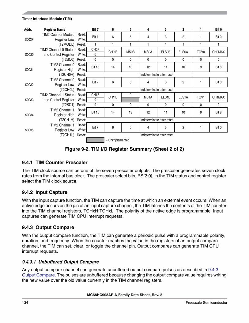
Timer Interface Module (TIM)
MC68HC908AP A-Family Data Sheet, Rev. 2
134 Freescale Semiconductor
9.4.1 TIM Counter Prescaler
The TIM clock source can be one of the seven prescaler outputs. The prescaler generates seven clockrates from the internal bus clock. The prescaler select bits, PS[2:0], in the TIM status and control registerselect the TIM clock source.
9.4.2 Input Capture
With the input capture function, the TIM can capture the time at which an external event occurs. When anactive edge occurs on the pin of an input capture channel, the TIM latches the contents of the TIM counterinto the TIM channel registers, TCHxH:TCHxL. The polarity of the active edge is programmable. Inputcaptures can generate TIM CPU interrupt requests.
9.4.3 Output Compare
With the output compare function, the TIM can generate a periodic pulse with a programmable polarity,duration, and frequency. When the counter reaches the value in the registers of an output comparechannel, the TIM can set, clear, or toggle the channel pin. Output compares can generate TIM CPUinterrupt requests.
9.4.3.1 Unbuffered Output Compare
Any output compare channel can generate unbuffered output compare pulses as described in 9.4.3Output Compare. The pulses are unbuffered because changing the output compare value requires writingthe new value over the old value currently in the TIM channel registers.
$002FTIM2 Counter Modulo
Register Low(T2MODL)
Read:Bit 7 6 5 4 3 2 1 Bit 0
Write:Reset: 1 1 1 1 1 1 1 1
$0030TIM2 Channel 0 Status
and Control Register(T2SC0)
Read: CH0FCH0IE MS0B MS0A ELS0B ELS0A TOV0 CH0MAX
Write: 0Reset: 0 0 0 0 0 0 0 0
$0031TIM2 Channel 0
Register High(T2CH0H)
Read:Bit 15 14 13 12 11 10 9 Bit 8
Write:Reset: Indeterminate after reset
$0032TIM2 Channel 0
Register Low(T2CH0L)
Read:Bit 7 6 5 4 3 2 1 Bit 0
Write:Reset: Indeterminate after reset
$0033TIM2 Channel 1 Status
and Control Register(T2SC1)
Read: CH1FCH1IE
0MS1A ELS1B ELS1A TOV1 CH1MAX
Write: 0Reset: 0 0 0 0 0 0 0 0
$0034TIM2 Channel 1
Register High(T2CH1H)
Read:Bit 15 14 13 12 11 10 9 Bit 8
Write:Reset: Indeterminate after reset
$0035TIM2 Channel 1
Register Low(T2CH1L)
Read:Bit 7 6 5 4 3 2 1 Bit 0
Write:Reset: Indeterminate after reset
Addr. Register Name Bit 7 6 5 4 3 2 1 Bit 0
= Unimplemented
Figure 9-2. TIM I/O Register Summary (Sheet 2 of 2)

Functional Description
MC68HC908AP A-Family Data Sheet, Rev. 2
Freescale Semiconductor 135
An unsynchronized write to the TIM channel registers to change an output compare value could causeincorrect operation for up to two counter overflow periods. For example, writing a new value before thecounter reaches the old value but after the counter reaches the new value prevents any compare duringthat counter overflow period. Also, using a TIM overflow interrupt routine to write a new, smaller outputcompare value may cause the compare to be missed. The TIM may pass the new value before it is written.
Use the following methods to synchronize unbuffered changes in the output compare value on channel x:• When changing to a smaller value, enable channel x output compare interrupts and write the new
value in the output compare interrupt routine. The output compare interrupt occurs at the end ofthe current output compare pulse. The interrupt routine has until the end of the counter overflowperiod to write the new value.
• When changing to a larger output compare value, enable TIM overflow interrupts and write the newvalue in the TIM overflow interrupt routine. The TIM overflow interrupt occurs at the end of thecurrent counter overflow period. Writing a larger value in an output compare interrupt routine (atthe end of the current pulse) could cause two output compares to occur in the same counteroverflow period.
9.4.3.2 Buffered Output Compare
Channels 0 and 1 can be linked to form a buffered output compare channel whose output appears on theTCH0 pin. The TIM channel registers of the linked pair alternately control the output.
Setting the MS0B bit in TIM channel 0 status and control register (TSC0) links channel 0 and channel 1.The output compare value in the TIM channel 0 registers initially controls the output on the TCH0 pin.Writing to the TIM channel 1 registers enables the TIM channel 1 registers to synchronously control theoutput after the TIM overflows. At each subsequent overflow, the TIM channel registers (0 or 1) thatcontrol the output are the ones written to last. TSC0 controls and monitors the buffered output comparefunction, and TIM channel 1 status and control register (TSC1) is unused. While the MS0B bit is set, thechannel 1 pin, TCH1, is available as a general-purpose I/O pin.
NOTEIn buffered output compare operation, do not write new output comparevalues to the currently active channel registers. User software should trackthe currently active channel to prevent writing a new value to the activechannel. Writing to the active channel registers is the same as generatingunbuffered output compares.
9.4.4 Pulse Width Modulation (PWM)
By using the toggle-on-overflow feature with an output compare channel, the TIM can generate a PWMsignal. The value in the TIM counter modulo registers determines the period of the PWM signal. Thechannel pin toggles when the counter reaches the value in the TIM counter modulo registers. The timebetween overflows is the period of the PWM signal.
As Figure 9-3 shows, the output compare value in the TIM channel registers determines the pulse widthof the PWM signal. The time between overflow and output compare is the pulse width. Program the TIMto clear the channel pin on output compare if the state of the PWM pulse is logic 1. Program the TIM toset the pin if the state of the PWM pulse is logic 0.
The value in the TIM counter modulo registers and the selected prescaler output determines thefrequency of the PWM output. The frequency of an 8-bit PWM signal is variable in 256 increments. Writing

Timer Interface Module (TIM)
MC68HC908AP A-Family Data Sheet, Rev. 2
136 Freescale Semiconductor
$00FF (255) to the TIM counter modulo registers produces a PWM period of 256 times the internal busclock period if the prescaler select value is $000. See 9.9.1 TIM Status and Control Register.
Figure 9-3. PWM Period and Pulse Width
The value in the TIM channel registers determines the pulse width of the PWM output. The pulse widthof an 8-bit PWM signal is variable in 256 increments. Writing $0080 (128) to the TIM channel registersproduces a duty cycle of 128/256 or 50%.
9.4.4.1 Unbuffered PWM Signal Generation
Any output compare channel can generate unbuffered PWM pulses as described in 9.4.4 Pulse WidthModulation (PWM). The pulses are unbuffered because changing the pulse width requires writing the newpulse width value over the old value currently in the TIM channel registers.
An unsynchronized write to the TIM channel registers to change a pulse width value could cause incorrectoperation for up to two PWM periods. For example, writing a new value before the counter reaches theold value but after the counter reaches the new value prevents any compare during that PWM period.Also, using a TIM overflow interrupt routine to write a new, smaller pulse width value may cause thecompare to be missed. The TIM may pass the new value before it is written.
Use the following methods to synchronize unbuffered changes in the PWM pulse width on channel x:• When changing to a shorter pulse width, enable channel x output compare interrupts and write the
new value in the output compare interrupt routine. The output compare interrupt occurs at the endof the current pulse. The interrupt routine has until the end of the PWM period to write the newvalue.
• When changing to a longer pulse width, enable TIM overflow interrupts and write the new value inthe TIM overflow interrupt routine. The TIM overflow interrupt occurs at the end of the current PWMperiod. Writing a larger value in an output compare interrupt routine (at the end of the current pulse)could cause two output compares to occur in the same PWM period.
NOTEIn PWM signal generation, do not program the PWM channel to toggle onoutput compare. Toggling on output compare prevents reliable 0% dutycycle generation and removes the ability of the channel to self-correct in theevent of software error or noise. Toggling on output compare also cancause incorrect PWM signal generation when changing the PWM pulsewidth to a new, much larger value.
TCHx
PERIOD
PULSEWIDTH
OVERFLOW OVERFLOW OVERFLOW
OUTPUTCOMPARE
OUTPUTCOMPARE
OUTPUTCOMPARE

Functional Description
MC68HC908AP A-Family Data Sheet, Rev. 2
Freescale Semiconductor 137
9.4.4.2 Buffered PWM Signal Generation
Channels 0 and 1 can be linked to form a buffered PWM channel whose output appears on the TCH0 pin.The TIM channel registers of the linked pair alternately control the pulse width of the output.
Setting the MS0B bit in TIM channel 0 status and control register (TSC0) links channel 0 and channel 1.The TIM channel 0 registers initially control the pulse width on the TCH0 pin. Writing to the TIM channel1 registers enables the TIM channel 1 registers to synchronously control the pulse width at the beginningof the next PWM period. At each subsequent overflow, the TIM channel registers (0 or 1) that control thepulse width are the ones written to last. TSC0 controls and monitors the buffered PWM function, and TIMchannel 1 status and control register (TSC1) is unused. While the MS0B bit is set, the channel 1 pin,TCH1, is available as a general-purpose I/O pin.
NOTEIn buffered PWM signal generation, do not write new pulse width values tothe currently active channel registers. User software should track thecurrently active channel to prevent writing a new value to the activechannel. Writing to the active channel registers is the same as generatingunbuffered PWM signals.
9.4.4.3 PWM Initialization
To ensure correct operation when generating unbuffered or buffered PWM signals, use the followinginitialization procedure:
1. In the TIM status and control register (TSC):a. Stop the TIM counter by setting the TIM stop bit, TSTOP.
b. Reset the TIM counter and prescaler by setting the TIM reset bit, TRST.
2. In the TIM counter modulo registers (TMODH:TMODL), write the value for the required PWMperiod.
3. In the TIM channel x registers (TCHxH:TCHxL), write the value for the required pulse width.4. In TIM channel x status and control register (TSCx):
a. Write 0:1 (for unbuffered output compare or PWM signals) or 1:0 (for buffered output compareor PWM signals) to the mode select bits, MSxB:MSxA. (See Table 9-3.)
b. Write 1 to the toggle-on-overflow bit, TOVx.
c. Write 1:0 (to clear output on compare) or 1:1 (to set output on compare) to the edge/levelselect bits, ELSxB:ELSxA. The output action on compare must force the output to thecomplement of the pulse width level. (See Table 9-3.)
NOTEIn PWM signal generation, do not program the PWM channel to toggle onoutput compare. Toggling on output compare prevents reliable 0% dutycycle generation and removes the ability of the channel to self-correct in theevent of software error or noise. Toggling on output compare can alsocause incorrect PWM signal generation when changing the PWM pulsewidth to a new, much larger value.
5. In the TIM status control register (TSC), clear the TIM stop bit, TSTOP.
Timer Interface Module (TIM)
MC68HC908AP A-Family Data Sheet, Rev. 2
138 Freescale Semiconductor
Setting MS0B links channels 0 and 1 and configures them for buffered PWM operation. The TIM channel0 registers (TCH0H:TCH0L) initially control the buffered PWM output. TIM status control register 0(TSCR0) controls and monitors the PWM signal from the linked channels.
Clearing the toggle-on-overflow bit, TOVx, inhibits output toggles on TIM overflows. Subsequent outputcompares try to force the output to a state it is already in and have no effect. The result is a 0% duty cycleoutput.
Setting the channel x maximum duty cycle bit (CHxMAX) and setting the TOVx bit generates a 100% dutycycle output. (See 9.9.4 TIM Channel Status and Control Registers.)
9.5 Interrupts
The following TIM sources can generate interrupt requests:• TIM overflow flag (TOF) — The TOF bit is set when the TIM counter reaches the modulo value
programmed in the TIM counter modulo registers. The TIM overflow interrupt enable bit, TOIE,enables TIM overflow CPU interrupt requests. TOF and TOIE are in the TIM status and controlregister.
• TIM channel flags (CH1F:CH0F) — The CHxF bit is set when an input capture or output compareoccurs on channel x. Channel x TIM CPU interrupt requests are controlled by the channel xinterrupt enable bit, CHxIE. Channel x TIM CPU interrupt requests are enabled when CHxIE = 1.CHxF and CHxIE are in the TIM channel x status and control register.
9.6 Low-Power Modes
The WAIT and STOP instructions put the MCU in low power- consumption standby modes.
9.6.1 Wait Mode
The TIM remains active after the execution of a WAIT instruction. In wait mode, the TIM registers are notaccessible by the CPU. Any enabled CPU interrupt request from the TIM can bring the MCU out of waitmode.
If TIM functions are not required during wait mode, reduce power consumption by stopping the TIM beforeexecuting the WAIT instruction.
9.6.2 Stop Mode
The TIM is inactive after the execution of a STOP instruction. The STOP instruction does not affectregister conditions or the state of the TIM counter. TIM operation resumes when the MCU exits stop modeafter an external interrupt.
9.7 TIM During Break Interrupts
A break interrupt stops the TIM counter.
The system integration module (SIM) controls whether status bits in other modules can be cleared duringthe break state. The BCFE bit in the break flag control register (BFCR) enables software to clear statusbits during the break state. (See 21.5.4 SIM Break Flag Control Register.)

I/O Signals
MC68HC908AP A-Family Data Sheet, Rev. 2
Freescale Semiconductor 139
To allow software to clear status bits during a break interrupt, write a logic 1 to the BCFE bit. If a statusbit is cleared during the break state, it remains cleared when the MCU exits the break state.
To protect status bits during the break state, write a logic 0 to the BCFE bit. With BCFE at logic 0 (itsdefault state), software can read and write I/O registers during the break state without affecting status bits.Some status bits have a 2-step read/write clearing procedure. If software does the first step on such a bitbefore the break, the bit cannot change during the break state as long as BCFE is at logic 0. After thebreak, doing the second step clears the status bit.
9.8 I/O Signals
Port B shares four of its pins with the TIM. The four TIM channel I/O pins are T1CH0, T1CH1, T2CH0,and T2CH1 as described in 9.3 Pin Name Conventions.
Each channel I/O pin is programmable independently as an input capture pin or an output compare pin.T1CH0 and T2CH0 can be configured as buffered output compare or buffered PWM pins.
9.9 I/O RegistersNOTE
References to either timer 1 or timer 2 may be made in the following text byomitting the timer number. For example, TSC may generically refer to bothT1SC AND T2SC.
These I/O registers control and monitor operation of the TIM:• TIM status and control register (TSC)• TIM counter registers (TCNTH:TCNTL)• TIM counter modulo registers (TMODH:TMODL)• TIM channel status and control registers (TSC0, TSC1)• TIM channel registers (TCH0H:TCH0L, TCH1H:TCH1L)
9.9.1 TIM Status and Control Register
The TIM status and control register (TSC):• Enables TIM overflow interrupts• Flags TIM overflows• Stops the TIM counter• Resets the TIM counter• Prescales the TIM counter clock
Address: T1SC, $0020 and T2SC, $002B
Bit 7 6 5 4 3 2 1 Bit 0
Read: TOFTOIE TSTOP
0 0PS2 PS1 PS0
Write: 0 TRST
Reset: 0 0 1 0 0 0 0 0
= Unimplemented
Figure 9-4. TIM Status and Control Register (TSC)

Timer Interface Module (TIM)
MC68HC908AP A-Family Data Sheet, Rev. 2
140 Freescale Semiconductor
TOF — TIM Overflow Flag BitThis read/write flag is set when the TIM counter reaches the modulo value programmed in the TIMcounter modulo registers. Clear TOF by reading the TIM status and control register when TOF is setand then writing a logic 0 to TOF. If another TIM overflow occurs before the clearing sequence iscomplete, then writing logic 0 to TOF has no effect. Therefore, a TOF interrupt request cannot be lostdue to inadvertent clearing of TOF. Reset clears the TOF bit. Writing a logic 1 to TOF has no effect.
1 = TIM counter has reached modulo value0 = TIM counter has not reached modulo value
TOIE — TIM Overflow Interrupt Enable BitThis read/write bit enables TIM overflow interrupts when the TOF bit becomes set. Reset clears theTOIE bit.
1 = TIM overflow interrupts enabled0 = TIM overflow interrupts disabled
TSTOP — TIM Stop BitThis read/write bit stops the TIM counter. Counting resumes when TSTOP is cleared. Reset sets theTSTOP bit, stopping the TIM counter until software clears the TSTOP bit.
1 = TIM counter stopped0 = TIM counter active
NOTEDo not set the TSTOP bit before entering wait mode if the TIM is requiredto exit wait mode.
TRST — TIM Reset BitSetting this write-only bit resets the TIM counter and the TIM prescaler. Setting TRST has no effect onany other registers. Counting resumes from $0000. TRST is cleared automatically after the TIMcounter is reset and always reads as logic 0. Reset clears the TRST bit.
1 = Prescaler and TIM counter cleared0 = No effect
NOTESetting the TSTOP and TRST bits simultaneously stops the TIM counter ata value of $0000.
PS[2:0] — Prescaler Select BitsThese read/write bits select one of the seven prescaler outputs as the input to the TIM counter asTable 9-2 shows. Reset clears the PS[2:0] bits.
Table 9-2. Prescaler Selection
PS2 PS1 PS0 TIM Clock Source
0 0 0 Internal bus clock ÷ 1
0 0 1 Internal bus clock ÷ 2
0 1 0 Internal bus clock ÷ 4
0 1 1 Internal bus clock ÷ 8
1 0 0 Internal bus clock ÷ 16
1 0 1 Internal bus clock ÷ 32
1 1 0 Internal bus clock ÷ 64
1 1 1 Not available

I/O Registers
MC68HC908AP A-Family Data Sheet, Rev. 2
Freescale Semiconductor 141
9.9.2 TIM Counter Registers
The two read-only TIM counter registers contain the high and low bytes of the value in the TIM counter.Reading the high byte (TCNTH) latches the contents of the low byte (TCNTL) into a buffer. Subsequentreads of TCNTH do not affect the latched TCNTL value until TCNTL is read. Reset clears the TIM counterregisters. Setting the TIM reset bit (TRST) also clears the TIM counter registers.
NOTEIf you read TCNTH during a break interrupt, be sure to unlatch TCNTL byreading TCNTL before exiting the break interrupt. Otherwise, TCNTLretains the value latched during the break.
9.9.3 TIM Counter Modulo Registers
The read/write TIM modulo registers contain the modulo value for the TIM counter. When the TIM counterreaches the modulo value, the overflow flag (TOF) becomes set, and the TIM counter resumes countingfrom $0000 at the next timer clock. Writing to the high byte (TMODH) inhibits the TOF bit and overflowinterrupts until the low byte (TMODL) is written. Reset sets the TIM counter modulo registers.
NOTEReset the TIM counter before writing to the TIM counter modulo registers.
Address: T1CNTH, $0021 and T2CNTH, $002C
Bit 7 6 5 4 3 2 1 Bit 0
Read: Bit 15 14 13 12 11 10 9 Bit 8
Write:
Reset: 0 0 0 0 0 0 0 0
Figure 9-5. TIM Counter Registers High (TCNTH)
Address: T1CNTL, $0022 and T2CNTL, $002D
Bit 7 6 5 4 3 2 1 Bit 0
Read: Bit 7 6 5 4 3 2 1 Bit 0
Write:
Reset: 0 0 0 0 0 0 0 0
Figure 9-6. TIM Counter Registers Low (TCNTL)
Address: T1MODH, $0023 and T2MODH, $002E
Bit 7 6 5 4 3 2 1 Bit 0
Read:Bit 15 14 13 12 11 10 9 Bit 8
Write:
Reset: 1 1 1 1 1 1 1 1
Figure 9-7. TIM Counter Modulo Register High (TMODH)
Address: T1MODL, $0024 and T2MODL, $002F
Bit 7 6 5 4 3 2 1 Bit 0
Read:Bit 7 6 5 4 3 2 1 Bit 0
Write:
Reset: 1 1 1 1 1 1 1 1
Figure 9-8. TIM Counter Modulo Register Low (TMODL)

Timer Interface Module (TIM)
MC68HC908AP A-Family Data Sheet, Rev. 2
142 Freescale Semiconductor
9.9.4 TIM Channel Status and Control Registers
Each of the TIM channel status and control registers:• Flags input captures and output compares• Enables input capture and output compare interrupts• Selects input capture, output compare, or PWM operation• Selects high, low, or toggling output on output compare• Selects rising edge, falling edge, or any edge as the active input capture trigger• Selects output toggling on TIM overflow• Selects 0% and 100% PWM duty cycle• Selects buffered or unbuffered output compare/PWM operation
CHxF — Channel x Flag BitWhen channel x is an input capture channel, this read/write bit is set when an active edge occurs onthe channel x pin. When channel x is an output compare channel, CHxF is set when the value in theTIM counter registers matches the value in the TIM channel x registers.When TIM CPU interrupt requests are enabled (CHxIE = 1), clear CHxF by reading TIM channel xstatus and control register with CHxF set and then writing a logic 0 to CHxF. If another interrupt requestoccurs before the clearing sequence is complete, then writing logic 0 to CHxF has no effect. Therefore,an interrupt request cannot be lost due to inadvertent clearing of CHxF.Reset clears the CHxF bit. Writing a logic 1 to CHxF has no effect.
1 = Input capture or output compare on channel x0 = No input capture or output compare on channel x
CHxIE — Channel x Interrupt Enable BitThis read/write bit enables TIM CPU interrupt service requests on channel x.Reset clears the CHxIE bit.
1 = Channel x CPU interrupt requests enabled0 = Channel x CPU interrupt requests disabled
MSxB — Mode Select Bit BThis read/write bit selects buffered output compare/PWM operation. MSxB exists only in the TIM1channel 0 and TIM2 channel 0 status and control registers.
Address: T1SC0, $0025 and T2SC0, $0030
Bit 7 6 5 4 3 2 1 Bit 0
Read: CH0FCH0IE MS0B MS0A ELS0B ELS0A TOV0 CH0MAX
Write: 0
Reset: 0 0 0 0 0 0 0 0
Figure 9-9. TIM Channel 0 Status and Control Register (TSC0)
Address: T1SC1, $0028 and T2SC1, $0033
Bit 7 6 5 4 3 2 1 Bit 0
Read: CH1FCH1IE
0MS1A ELS1B ELS1A TOV1 CH1MAX
Write: 0
Reset: 0 0 0 0 0 0 0 0
Figure 9-10. TIM Channel 1 Status and Control Register (TSC1)
I/O Registers
MC68HC908AP A-Family Data Sheet, Rev. 2
Freescale Semiconductor 143
Setting MS0B disables the channel 1 status and control register and reverts TCH1 to general-purposeI/O.Reset clears the MSxB bit.
1 = Buffered output compare/PWM operation enabled0 = Buffered output compare/PWM operation disabled
MSxA — Mode Select Bit AWhen ELSxB:ELSxA ≠ 0:0, this read/write bit selects either input capture operation or unbufferedoutput compare/PWM operation.See Table 9-3.
1 = Unbuffered output compare/PWM operation0 = Input capture operation
When ELSxB:ELSxA = 0:0, this read/write bit selects the initial output level of the TCHx pin. SeeTable 9-3. Reset clears the MSxA bit.
1 = Initial output level low0 = Initial output level high
NOTEBefore changing a channel function by writing to the MSxB or MSxA bit, setthe TSTOP and TRST bits in the TIM status and control register (TSC).
ELSxB and ELSxA — Edge/Level Select BitsWhen channel x is an input capture channel, these read/write bits control the active edge-sensing logicon channel x.When channel x is an output compare channel, ELSxB and ELSxA control the channel x outputbehavior when an output compare occurs.When ELSxB and ELSxA are both clear, channel x is not connected to an I/O port, and pin TCHx isavailable as a general-purpose I/O pin. Table 9-3 shows how ELSxB and ELSxA work. Reset clearsthe ELSxB and ELSxA bits.
Table 9-3. Mode, Edge, and Level Selection
MSxB:MSxA ELSxB:ELSxA Mode Configuration
X0 00
Output preset
Pin under port control;initial output level high
X1 00Pin under port control;initial output level low
00 01
Input capture
Capture on rising edge only
00 10 Capture on falling edge only
00 11Capture on rising or
falling edge
01 01Output compare
or PWM
Toggle output on compare
01 10 Clear output on compare
01 11 Set output on compare
1X 01Buffered output
compare orbuffered PWM
Toggle output on compare
1X 10 Clear output on compare
1X 11 Set output on compare

Timer Interface Module (TIM)
MC68HC908AP A-Family Data Sheet, Rev. 2
144 Freescale Semiconductor
NOTEBefore enabling a TIM channel register for input capture operation, makesure that the TCHx pin is stable for at least two bus clocks.
TOVx — Toggle On Overflow BitWhen channel x is an output compare channel, this read/write bit controls the behavior of the channelx output when the TIM counter overflows. When channel x is an input capture channel, TOVx has noeffect.Reset clears the TOVx bit.
1 = Channel x pin toggles on TIM counter overflow0 = Channel x pin does not toggle on TIM counter overflow
NOTEWhen TOVx is set, a TIM counter overflow takes precedence over achannel x output compare if both occur at the same time.
CHxMAX — Channel x Maximum Duty Cycle BitWhen the TOVx bit is at logic 1, setting the CHxMAX bit forces the duty cycle of buffered andunbuffered PWM signals to 100%. As Figure 9-11 shows, the CHxMAX bit takes effect in the cycleafter it is set or cleared. The output stays at the 100% duty cycle level until the cycle after CHxMAX iscleared.
Figure 9-11. CHxMAX Latency
9.9.5 TIM Channel Registers
These read/write registers contain the captured TIM counter value of the input capture function or theoutput compare value of the output compare function. The state of the TIM channel registers after resetis unknown.
In input capture mode (MSxB:MSxA = 0:0), reading the high byte of the TIM channel x registers (TCHxH)inhibits input captures until the low byte (TCHxL) is read.
In output compare mode (MSxB:MSxA ≠ 0:0), writing to the high byte of the TIM channel x registers(TCHxH) inhibits output compares until the low byte (TCHxL) is written.
OUTPUT
OVERFLOW
TCHx
PERIOD
CHxMAX
OVERFLOW OVERFLOW OVERFLOW OVERFLOW
COMPAREOUTPUT
COMPAREOUTPUT
COMPAREOUTPUT
COMPARE
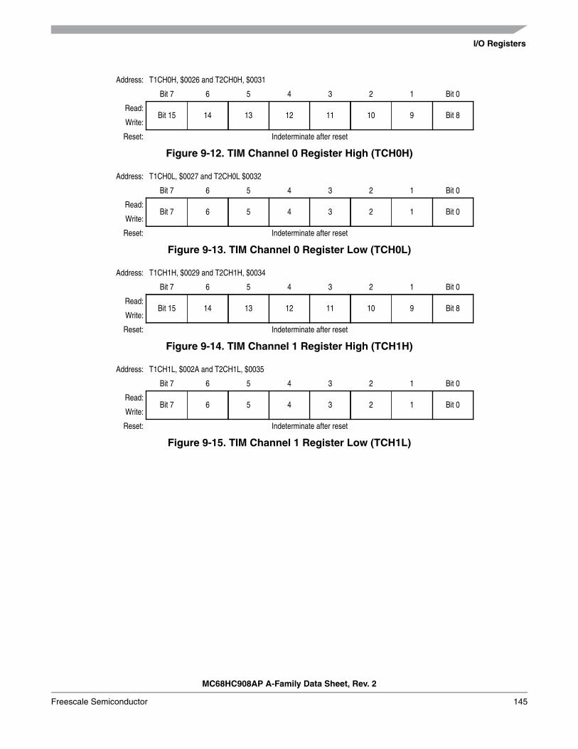
I/O Registers
MC68HC908AP A-Family Data Sheet, Rev. 2
Freescale Semiconductor 145
Address: T1CH0H, $0026 and T2CH0H, $0031
Bit 7 6 5 4 3 2 1 Bit 0
Read:Bit 15 14 13 12 11 10 9 Bit 8
Write:
Reset: Indeterminate after reset
Figure 9-12. TIM Channel 0 Register High (TCH0H)
Address: T1CH0L, $0027 and T2CH0L $0032
Bit 7 6 5 4 3 2 1 Bit 0
Read:Bit 7 6 5 4 3 2 1 Bit 0
Write:
Reset: Indeterminate after reset
Figure 9-13. TIM Channel 0 Register Low (TCH0L)
Address: T1CH1H, $0029 and T2CH1H, $0034
Bit 7 6 5 4 3 2 1 Bit 0
Read:Bit 15 14 13 12 11 10 9 Bit 8
Write:
Reset: Indeterminate after reset
Figure 9-14. TIM Channel 1 Register High (TCH1H)
Address: T1CH1L, $002A and T2CH1L, $0035
Bit 7 6 5 4 3 2 1 Bit 0
Read:Bit 7 6 5 4 3 2 1 Bit 0
Write:
Reset: Indeterminate after reset
Figure 9-15. TIM Channel 1 Register Low (TCH1L)

Timer Interface Module (TIM)
MC68HC908AP A-Family Data Sheet, Rev. 2
146 Freescale Semiconductor

MC68HC908AP A-Family Data Sheet, Rev. 2
Freescale Semiconductor 147
Chapter 10Timebase Module (TBM)
10.1 Introduction
This section describes the timebase module (TBM). The TBM will generate periodic interrupts at userselectable rates using a counter clocked by the selected OSCCLK clock from the oscillator module. ThisTBM version uses 18 divider stages, eight of which are user selectable.
10.2 Features
Features of the TBM module include:• Eight user selectable periodic interrupts• User selectable oscillator clock source enable during stop mode to allow periodic wake-up from
stop
10.3 Functional Description
This module can generate a periodic interrupt by dividing the oscillator clock frequency, OSCCLK. Thecounter is initialized to all 0s when TBON bit is cleared. The counter, shown in Figure 10-1, starts countingwhen the TBON bit is set. When the counter overflows at the tap selected by TBR[2:0], the TBIF bit getsset. If the TBIE bit is set, an interrupt request is sent to the CPU. The TBIF flag is cleared by writing a 1to the TACK bit. The first time the TBIF flag is set after enabling the timebase module, the interrupt isgenerated at approximately half of the overflow period. Subsequent events occur at the exact period.
The reference clock OSCCLK is derived from the oscillator module, see 5.2.2 TBM Reference ClockSelection.

Timebase Module (TBM)
MC68HC908AP A-Family Data Sheet, Rev. 2
148 Freescale Semiconductor
Figure 10-1. Timebase Block Diagram
10.4 Timebase Register Description
The timebase has one register, the TBCR, which is used to enable the timebase interrupts and set therate.
TBIF — Timebase Interrupt FlagThis read-only flag bit is set when the timebase counter has rolled over.
1 = Timebase interrupt pending0 = Timebase interrupt not pending
Address: $0051
Bit 7 6 5 4 3 2 1 Bit 0
Read: TBIFTBR2 TBR1 TBR0
0TBIE TBON R
Write: TACK
Reset: 0 0 0 0 0 0 0 0
= Unimplemented R = Reserved
Figure 10-2. Timebase Control Register (TBCR)
(See Chapter 5 Oscillator (OSC).)
÷ 2
SEL
0 0 0
0 0 1
0 1 0
0 1 1
TBIF
TBR
1
TBR
0
TBIE
TBON
R
TAC
K
TBR
2
1 0 0
1 0 1
1 1 0
1 1 1
OSCCLK ÷ 2 ÷ 2 ÷ 2 ÷ 2 ÷ 2 ÷ 2
÷ 2 ÷ 2 ÷ 2 ÷ 2 ÷ 2 ÷ 2 ÷ 2
÷ 8 ÷ 16 ÷ 32 ÷ 64 ÷ 2048
÷ 32768 ÷ 65536 ÷ 131072
TBMINT
÷ 2 ÷ 2÷ 2 ÷ 2
÷ 262144
From OSC module
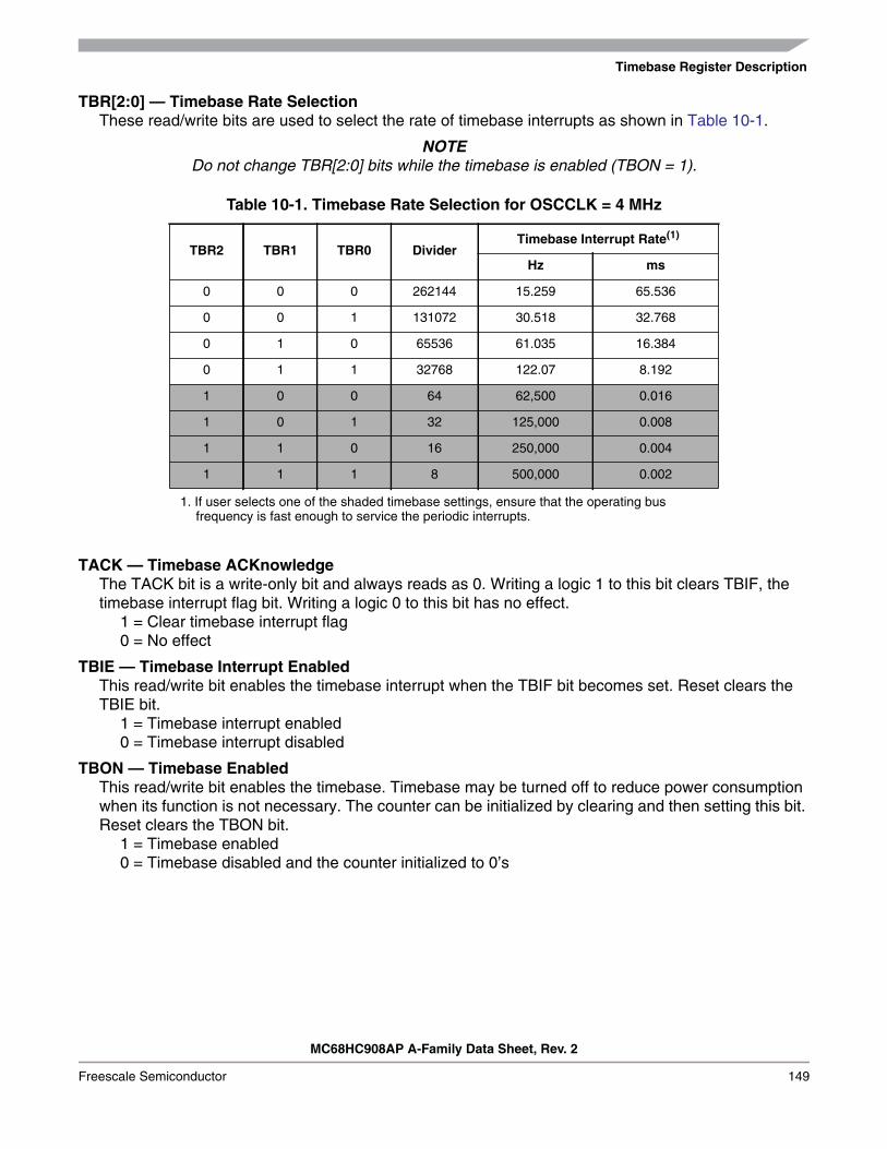
Timebase Register Description
MC68HC908AP A-Family Data Sheet, Rev. 2
Freescale Semiconductor 149
TBR[2:0] — Timebase Rate SelectionThese read/write bits are used to select the rate of timebase interrupts as shown in Table 10-1.
NOTEDo not change TBR[2:0] bits while the timebase is enabled (TBON = 1).
TACK — Timebase ACKnowledgeThe TACK bit is a write-only bit and always reads as 0. Writing a logic 1 to this bit clears TBIF, thetimebase interrupt flag bit. Writing a logic 0 to this bit has no effect.
1 = Clear timebase interrupt flag0 = No effect
TBIE — Timebase Interrupt EnabledThis read/write bit enables the timebase interrupt when the TBIF bit becomes set. Reset clears theTBIE bit.
1 = Timebase interrupt enabled0 = Timebase interrupt disabled
TBON — Timebase EnabledThis read/write bit enables the timebase. Timebase may be turned off to reduce power consumptionwhen its function is not necessary. The counter can be initialized by clearing and then setting this bit.Reset clears the TBON bit.
1 = Timebase enabled0 = Timebase disabled and the counter initialized to 0’s
Table 10-1. Timebase Rate Selection for OSCCLK = 4 MHz
TBR2 TBR1 TBR0 DividerTimebase Interrupt Rate(1)
1. If user selects one of the shaded timebase settings, ensure that the operating busfrequency is fast enough to service the periodic interrupts.
Hz ms
0 0 0 262144 15.259 65.536
0 0 1 131072 30.518 32.768
0 1 0 65536 61.035 16.384
0 1 1 32768 122.07 8.192
1 0 0 64 62,500 0.016
1 0 1 32 125,000 0.008
1 1 0 16 250,000 0.004
1 1 1 8 500,000 0.002

Timebase Module (TBM)
MC68HC908AP A-Family Data Sheet, Rev. 2
150 Freescale Semiconductor
10.5 Interrupts
The timebase module can interrupt the CPU on a regular basis with a rate defined by TBR[2:0]. When thetimebase counter chain rolls over, the TBIF flag is set. If the TBIE bit is set, enabling the timebaseinterrupt, the counter chain overflow will generate a CPU interrupt request. The interrupt vector is definedin Table 2-1 . Vector Addresses.
Interrupts must be acknowledged by writing a logic 1 to the TACK bit.
10.6 Low-Power Modes
The WAIT and STOP instructions put the MCU in low power- consumption standby modes.
10.6.1 Wait Mode
The timebase module remains active after execution of the WAIT instruction. In wait mode, the timebaseregister is not accessible by the CPU.
If the timebase functions are not required during wait mode, reduce the power consumption by stoppingthe timebase before enabling the WAIT instruction.
10.6.2 Stop Mode
The timebase module may remain active after execution of the STOP instruction if the oscillator has beenenabled to operate during stop mode through the stop mode oscillator enable bit (STOP_ICLKDIS,STOP_RCLKEN, or STOP_XCLKEN) for the selected oscillator in the CONFIG2 register. The timebasemodule can be used in this mode to generate a periodic walk-up from stop mode.
If the oscillator has not been enabled to operate in stop mode, the timebase module will not be activeduring stop mode. In stop mode the timebase register is not accessible by the CPU.
If the timebase functions are not required during stop mode, reduce the power consumption by stoppingthe timebase before enabling the STOP instruction.
MC68HC908AP A-Family Data Sheet, Rev. 2
Freescale Semiconductor 151
Chapter 11Serial Communications Interface Module (SCI)
11.1 Introduction
The MC68HC908AP64A has two SCI modules:• SCI1 is a standard SCI module, and• SCI2 is an infrared SCI module.
This section describes SCI1, the serial communications interface (SCI) module, which allows high-speedasynchronous communications with peripheral devices and other MCUs.
NOTEWhen the SCI is enabled, the TxD pin is an open-drain output and requiresa pullup resistor to be connected for proper SCI operation.
11.2 Features
Features of the SCI module include the following:• Full-duplex operation• Standard mark/space non-return-to-zero (NRZ) format• 32 programmable baud rates• Programmable 8-bit or 9-bit character length• Separately enabled transmitter and receiver• Separate receiver and transmitter CPU interrupt requests• Programmable transmitter output polarity• Two receiver wakeup methods:
– Idle line wakeup– Address mark wakeup
• Interrupt-driven operation with eight interrupt flags:– Transmitter empty– Transmission complete– Receiver full– Idle receiver input– Receiver overrun– Noise error– Framing error– Parity error
• Receiver framing error detection• Hardware parity checking• 1/16 bit-time noise detection• Configuration register bit, SCIBDSRC, to allow selection of baud rate clock source

Serial Communications Interface Module (SCI)
MC68HC908AP A-Family Data Sheet, Rev. 2
152 Freescale Semiconductor
11.3 Pin Name Conventions
The generic names of the SCI I/O pins are:• RxD (receive data)• TxD (transmit data)
SCI I/O (input/output) lines are implemented by sharing parallel I/O port pins. The full name of an SCIinput or output reflects the name of the shared port pin. Table 11-1 shows the full names and the genericnames of the SCI I/O pins. The generic pin names appear in the text of this section.
NOTEWhen the SCI is enabled, the TxD pin is an open-drain output and requiresa pullup resistor to be connected for proper SCI operation.
Table 11-1. Pin Name Conventions
Generic Pin Names: RxD TxD
Full Pin Names: PTB3/RxD PTB2/TxD
Addr. Register Name Bit 7 6 5 4 3 2 1 Bit 0
$0013SCI Control Register 1
(SCC1)
Read:LOOPS ENSCI TXINV M WAKE ILTY PEN PTY
Write:Reset: 0 0 0 0 0 0 0 0
$0014SCI Control Register 2
(SCC2)
Read:SCTIE TCIE SCRIE ILIE TE RE RWU SBK
Write:Reset: 0 0 0 0 0 0 0 0
$0015SCI Control Register 3
(SCC3)
Read: R8T8 DMARE DMATE ORIE NEIE FEIE PEIE
Write:Reset: U U 0 0 0 0 0 0
$0016 SCI Status Register 1 (SCS1)Read: SCTE TC SCRF IDLE OR NF FE PEWrite:
Reset: 1 1 0 0 0 0 0 0
$0017 SCI Status Register 2 (SCS2)Read: BKF RPFWrite:
Reset: 0 0 0 0 0 0 0 0
$0018SCI Data Register
(SCDR)
Read: R7 R6 R5 R4 R3 R2 R1 R0Write: T7 T6 T5 T4 T3 T2 T1 T0
Reset: Unaffected by reset
$0019SCI Baud Rate Register
(SCBR)
Read: 0 0SCP1 SCP0 R SCR2 SCR1 SCR0
Write:Reset: 0 0 0 0 0 0 0 0
= Unimplemented R = Reserved U = Unaffected
Figure 11-1. SCI I/O Register Summary

Functional Description
MC68HC908AP A-Family Data Sheet, Rev. 2
Freescale Semiconductor 153
11.4 Functional Description
Figure 11-2 shows the structure of the SCI module. The SCI allows full-duplex, asynchronous, NRZ serialcommunication among the MCU and remote devices, including other MCUs. The transmitter and receiverof the SCI operate independently, although they use the same baud rate generator. During normaloperation, the CPU monitors the status of the SCI, writes the data to be transmitted, and processesreceived data.
The baud rate clock source for the SCI can be selected via the configuration bit, SCIBDSRC, of theCONFIG2 register ($001D).
Figure 11-2. SCI Module Block Diagram
SCTE
TC
SCRF
IDLE
OR
NF
FE
PE
SCTIE
TCIE
SCRIE
ILIE
TE
RE
RWU
SBK
R8
T8
DMATE
ORIE
FEIE
PEIE
BKF
RPF
SCI DATA
RECEIVESHIFT REGISTER
SCI DATAREGISTER
TRANSMITSHIFT REGISTER
NEIE
M
WAKE
ILTY
FLAGCONTROL
TRANSMITCONTROL
RECEIVECONTROL
DATA SELECTIONCONTROL
WAKEUP
PTY
PEN
REGISTER
DM
AIN
TER
RU
PTC
ON
TRO
L
TRAN
SMIT
TER
INTE
RR
UPT
CO
NTR
OL
REC
EIVE
RIN
TER
RU
PTC
ON
TRO
L
ERR
OR
INTE
RR
UPT
CO
NTR
OL
CONTROL
DMARE
ENSCI
LOOPS
ENSCI
INTERNAL BUS
TXINV
LOOPS
÷ 4
÷ 16
PRE-SCALER
BAUDDIVIDER
CGMXCLKIT12
AB
SLX
SCIBDSRCFROM
SL = 0 => X = ASL = 1 => X = B
CONFIG
RxD TxD
CGMXCLK is from CGM moduleIT12 = fBUS

Serial Communications Interface Module (SCI)
MC68HC908AP A-Family Data Sheet, Rev. 2
154 Freescale Semiconductor
11.4.1 Data Format
The SCI uses the standard non-return-to-zero mark/space data format illustrated in Figure 11-3.
Figure 11-3. SCI Data Formats
11.4.2 Transmitter
Figure 11-4 shows the structure of the SCI transmitter.
The baud rate clock source for the SCI can be selected via the configuration bit, SCIBDSRC. Sourceselection values are shown in Figure 11-4.
Figure 11-4. SCI Transmitter
BIT 5START
BIT BIT 0 BIT 1
NEXT
STOPBIT
STARTBIT
8-BIT DATA FORMATBIT M IN SCC1 CLEAR
STARTBIT BIT 0
NEXT
STOPBIT
STARTBIT
9-BIT DATA FORMATBIT M IN SCC1 SET
BIT 1 BIT 2 BIT 3 BIT 4 BIT 5 BIT 6 BIT 7 BIT 8
BIT 2 BIT 3 BIT 4 BIT 6 BIT 7
PARITYBIT
PARITYBIT
DMATE
SCTE
PEN
PTY
H 8 7 6 5 4 3 2 1 0 L
11-BITTRANSMIT
STO
P
STAR
T
T8
DMATE
SCTE
SCTIE
TCIE
SBK
TC
PARITYGENERATION
MSB
SCI DATA REGISTER
LOAD
FR
OM
SC
DR
SHIF
T EN
ABLE
PREA
MBL
EAL
L 1s
BREA
KAL
L 0s
TRANSMITTERCONTROL LOGIC
SHIFT REGISTER
DMATE
TC
SCTIE
TCIE
SCTE
TRAN
SMIT
TER
CPU
INTE
RRUP
TRE
QUE
ST
TRAN
SMIT
TER
DM
A SE
RVI
CE
REQ
UES
T
M
ENSCI
LOOPS
TE
TXINV
INTERNAL BUS
÷ 4PRE-
SCALER
SCP1
SCP0
SCR2
SCR1
SCR0
BAUDDIVIDER ÷ 16
SCTIE
CGMXCLKIT12
AB
SLX
SL = 0 => X = ASL = 1 => X = B
SCIBDSRCFROM
CONFIG2
TxD

Functional Description
MC68HC908AP A-Family Data Sheet, Rev. 2
Freescale Semiconductor 155
11.4.2.1 Character Length
The transmitter can accommodate either 8-bit or 9-bit data. The state of the M bit in SCI control register1 (SCC1) determines character length. When transmitting 9-bit data, bit T8 in SCI control register 3(SCC3) is the ninth bit (bit 8).
11.4.2.2 Character Transmission
During an SCI transmission, the transmit shift register shifts a character out to the TxD pin. The SCI dataregister (SCDR) is the write-only buffer between the internal data bus and the transmit shift register. Toinitiate an SCI transmission:
1. Enable the SCI by writing a logic 1 to the enable SCI bit (ENSCI) in SCI control register 1 (SCC1).2. Enable the transmitter by writing a logic 1 to the transmitter enable bit (TE) in SCI control register
2 (SCC2).3. Clear the SCI transmitter empty bit by first reading SCI status register 1 (SCS1) and then writing
to the SCDR.4. Repeat step 3 for each subsequent transmission.
At the start of a transmission, transmitter control logic automatically loads the transmit shift register witha preamble of logic 1s. After the preamble shifts out, control logic transfers the SCDR data into thetransmit shift register. A logic 0 start bit automatically goes into the least significant bit position of thetransmit shift register. A logic 1 stop bit goes into the most significant bit position.
The SCI transmitter empty bit, SCTE, in SCS1 becomes set when the SCDR transfers a byte to thetransmit shift register. The SCTE bit indicates that the SCDR can accept new data from the internal databus. If the SCI transmit interrupt enable bit, SCTIE, in SCC2 is also set, the SCTE bit generates atransmitter CPU interrupt request.
When the transmit shift register is not transmitting a character, the TxD pin goes to the idle condition,logic 1. If at any time software clears the ENSCI bit in SCI control register 1 (SCC1), the transmitter andreceiver relinquish control of the port pin.
11.4.2.3 Break Characters
Writing a logic 1 to the send break bit, SBK, in SCC2 loads the transmit shift register with a breakcharacter. A break character contains all logic 0s and has no start, stop, or parity bit. Break characterlength depends on the M bit in SCC1. As long as SBK is at logic 1, transmitter logic continuously loadsbreak characters into the transmit shift register. After software clears the SBK bit, the shift register finishestransmitting the last break character and then transmits at least one logic 1. The automatic logic 1 at theend of a break character guarantees the recognition of the start bit of the next character.
The SCI recognizes a break character when a start bit is followed by eight or nine logic 0 data bits and alogic 0 where the stop bit should be.
Receiving a break character has these effects on SCI registers:• Sets the framing error bit (FE) in SCS1• Sets the SCI receiver full bit (SCRF) in SCS1• Clears the SCI data register (SCDR)• Clears the R8 bit in SCC3• Sets the break flag bit (BKF) in SCS2• May set the overrun (OR), noise flag (NF), parity error (PE), or reception in progress flag (RPF) bits

Serial Communications Interface Module (SCI)
MC68HC908AP A-Family Data Sheet, Rev. 2
156 Freescale Semiconductor
11.4.2.4 Idle Characters
An idle character contains all logic 1s and has no start, stop, or parity bit. Idle character length dependson the M bit in SCC1. The preamble is a synchronizing idle character that begins every transmission.
If the TE bit is cleared during a transmission, the TxD pin becomes idle after completion of thetransmission in progress. Clearing and then setting the TE bit during a transmission queues an idlecharacter to be sent after the character currently being transmitted.
NOTEWhen queueing an idle character, return the TE bit to logic 1 before the stopbit of the current character shifts out to the TxD pin. Setting TE after thestop bit appears on TxD causes data previously written to the SCDR to belost.
Toggle the TE bit for a queued idle character when the SCTE bit becomesset and just before writing the next byte to the SCDR.
11.4.2.5 Inversion of Transmitted Output
The transmit inversion bit (TXINV) in SCI control register 1 (SCC1) reverses the polarity of transmitteddata. All transmitted values, including idle, break, start, and stop bits, are inverted when TXINV is atlogic 1. (See 11.8.1 SCI Control Register 1.)
11.4.2.6 Transmitter Interrupts
These conditions can generate CPU interrupt requests from the SCI transmitter:• SCI transmitter empty (SCTE) — The SCTE bit in SCS1 indicates that the SCDR has transferred
a character to the transmit shift register. SCTE can generate a transmitter CPU interrupt request.Setting the SCI transmit interrupt enable bit, SCTIE, in SCC2 enables the SCTE bit to generatetransmitter CPU interrupt requests.
• Transmission complete (TC) — The TC bit in SCS1 indicates that the transmit shift register andthe SCDR are empty and that no break or idle character has been generated. The transmissioncomplete interrupt enable bit, TCIE, in SCC2 enables the TC bit to generate transmitter CPUinterrupt requests.
11.4.3 Receiver
Figure 11-5 shows the structure of the SCI receiver.
11.4.3.1 Character Length
The receiver can accommodate either 8-bit or 9-bit data. The state of the M bit in SCI control register 1(SCC1) determines character length. When receiving 9-bit data, bit R8 in SCI control register 2 (SCC2)is the ninth bit (bit 8). When receiving 8-bit data, bit R8 is a copy of the eighth bit (bit 7).
11.4.3.2 Character Reception
During an SCI reception, the receive shift register shifts characters in from the RxD pin. The SCI dataregister (SCDR) is the read-only buffer between the internal data bus and the receive shift register.
After a complete character shifts into the receive shift register, the data portion of the character transfersto the SCDR. The SCI receiver full bit, SCRF, in SCI status register 1 (SCS1) becomes set, indicating that
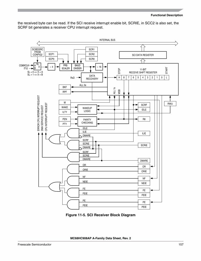
Functional Description
MC68HC908AP A-Family Data Sheet, Rev. 2
Freescale Semiconductor 157
the received byte can be read. If the SCI receive interrupt enable bit, SCRIE, in SCC2 is also set, theSCRF bit generates a receiver CPU interrupt request.
Figure 11-5. SCI Receiver Block Diagram
ALL
1s
ALL 0s
M
WAKE
ILTY
PEN
PTY
BKF
RPF
H 8 7 6 5 4 3 2 1 0 L
11-BITRECEIVE SHIFT REGISTERST
OP
STAR
T
DATARECOVERY
DMARE
SCRF
OR
ORIE
NF
NEIE
FE
FEIE
PE
PEIE
DMARESCRIESCRF
ILIEIDLE
WAKEUPLOGIC
PARITYCHECKING
MSB
ERR
OR
CPU
INTE
RRUP
T R
EQU
EST
DM
A SE
RVI
CE
REQ
UES
T
CPU
INTE
RR
UPT
REQ
UES
T
SCI DATA REGISTER
R8
DMARE
ORIE
NEIE
FEIE
PEIE
SCRIE
ILIE
RWUSCRF
IDLE
OR
NF
FE
PE
INTERNAL BUS
PRE-SCALER
BAUDDIVIDER
÷ 4 ÷ 16
SCP1
SCP0
SCR2
SCR1
SCR0
SCRIE
DMARE
CGMXCLKIT12
AB
SLX
SCIBDSRCFROM
SL = 0 => X = ASL = 1 => X = B
CONFIG2
RxD

Serial Communications Interface Module (SCI)
MC68HC908AP A-Family Data Sheet, Rev. 2
158 Freescale Semiconductor
11.4.3.3 Data Sampling
The receiver samples the RxD pin at the RT clock rate. The RT clock is an internal signal with a frequency16 times the baud rate. To adjust for baud rate mismatch, the RT clock is resynchronized at the followingtimes (see Figure 11-6):
• After every start bit• After the receiver detects a data bit change from logic 1 to logic 0 (after the majority of data bit
samples at RT8, RT9, and RT10 returns a valid logic 1 and the majority of the next RT8, RT9, andRT10 samples returns a valid logic 0)
To locate the start bit, data recovery logic does an asynchronous search for a logic 0 preceded by threelogic 1s. When the falling edge of a possible start bit occurs, the RT clock begins to count to 16.
Figure 11-6. Receiver Data Sampling
To verify the start bit and to detect noise, data recovery logic takes samples at RT3, RT5, and RT7.Table 11-2 summarizes the results of the start bit verification samples.
Table 11-2. Start Bit Verification
RT3, RT5, and RT7Samples
Start BitVerification
Noise Flag
000 Yes 0
001 Yes 1
010 Yes 1
011 No 0
100 Yes 1
101 No 0
110 No 0
111 No 0
RT CLOCKRESET
RT
1
RT
1
RT
1
RT
1
RT
1
RT
1
RT
1
RT
1
RT
1
RT
2
RT
3
RT
4
RT
5
RT
8
RT
7
RT
6
RT
11
RT
10
RT
9
RT
15
RT
14
RT
13
RT
12
RT
16
RT
1
RT
2
RT
3
RT
4
START BITQUALIFICATION
START BITVERIFICATION
DATASAMPLINGSAMPLES
RTCLOCK
RT CLOCKSTATE
START BIT LSB
RxD

Functional Description
MC68HC908AP A-Family Data Sheet, Rev. 2
Freescale Semiconductor 159
Start bit verification is not successful if any two of the three verification samples are logic 1s. If start bitverification is not successful, the RT clock is reset and a new search for a start bit begins.
To determine the value of a data bit and to detect noise, recovery logic takes samples at RT8, RT9, andRT10. Table 11-3 summarizes the results of the data bit samples.
NOTEThe RT8, RT9, and RT10 samples do not affect start bit verification. If anyor all of the RT8, RT9, and RT10 start bit samples are logic 1s following asuccessful start bit verification, the noise flag (NF) is set and the receiverassumes that the bit is a start bit.
To verify a stop bit and to detect noise, recovery logic takes samples at RT8, RT9, and RT10. Table 11-4summarizes the results of the stop bit samples.
Table 11-3. Data Bit Recovery
RT8, RT9, and RT10Samples
Data BitDetermination
Noise Flag
000 0 0
001 0 1
010 0 1
011 1 1
100 0 1
101 1 1
110 1 1
111 1 0
Table 11-4. Stop Bit Recovery
RT8, RT9, and RT10Samples
FramingError Flag
Noise Flag
000 1 0
001 1 1
010 1 1
011 0 1
100 1 1
101 0 1
110 0 1
111 0 0

Serial Communications Interface Module (SCI)
MC68HC908AP A-Family Data Sheet, Rev. 2
160 Freescale Semiconductor
11.4.3.4 Framing Errors
If the data recovery logic does not detect a logic 1 where the stop bit should be in an incoming character,it sets the framing error bit, FE, in SCS1. A break character also sets the FE bit because a break characterhas no stop bit. The FE bit is set at the same time that the SCRF bit is set.
11.4.3.5 Baud Rate Tolerance
A transmitting device may be operating at a baud rate below or above the receiver baud rate.Accumulated bit time misalignment can cause one of the three stop bit data samples to fall outside theactual stop bit. Then a noise error occurs. If more than one of the samples is outside the stop bit, a framingerror occurs. In most applications, the baud rate tolerance is much more than the degree of misalignmentthat is likely to occur.
As the receiver samples an incoming character, it resynchronizes the RT clock on any valid falling edgewithin the character. Resynchronization within characters corrects misalignments between transmitter bittimes and receiver bit times.
Slow Data Tolerance
Figure 11-7 shows how much a slow received character can be misaligned without causing a noise erroror a framing error. The slow stop bit begins at RT8 instead of RT1 but arrives in time for the stop bit datasamples at RT8, RT9, and RT10.
Figure 11-7. Slow Data
For an 8-bit character, data sampling of the stop bit takes the receiver9 bit times × 16 RT cycles + 10 RT cycles = 154 RT cycles.
With the misaligned character shown in Figure 11-7, the receiver counts 154 RT cycles at the point whenthe count of the transmitting device is9 bit times × 16 RT cycles + 3 RT cycles = 147 RT cycles.
The maximum percent difference between the receiver count and the transmitter count of a slow 8-bitcharacter with no errors is
For a 9-bit character, data sampling of the stop bit takes the receiver10 bit times × 16 RT cycles + 10 RT cycles = 170 RT cycles.
With the misaligned character shown in Figure 11-7, the receiver counts 170 RT cycles at the point whenthe count of the transmitting device is10 bit times × 16 RT cycles + 3 RT cycles = 163 RT cycles.
MSB STOP
RT
1
RT
2
RT
3
RT
4
RT
5
RT
6
RT
7
RT
8
RT
9
RT
10
RT
11
RT
12
RT
13
RT
14
RT
15
RT
16
DATASAMPLES
RECEIVERRT CLOCK
154 147–154
-------------------------- 100× 4.54%=
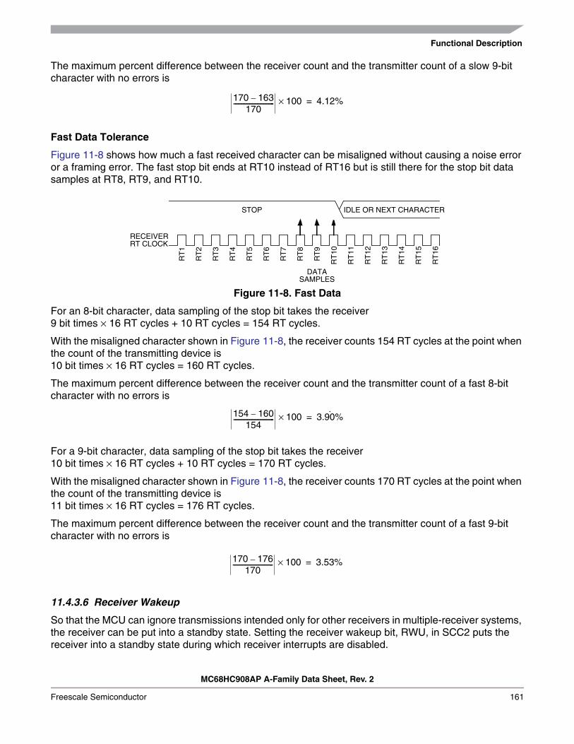
Functional Description
MC68HC908AP A-Family Data Sheet, Rev. 2
Freescale Semiconductor 161
The maximum percent difference between the receiver count and the transmitter count of a slow 9-bitcharacter with no errors is
Fast Data Tolerance
Figure 11-8 shows how much a fast received character can be misaligned without causing a noise erroror a framing error. The fast stop bit ends at RT10 instead of RT16 but is still there for the stop bit datasamples at RT8, RT9, and RT10.
Figure 11-8. Fast Data
For an 8-bit character, data sampling of the stop bit takes the receiver9 bit times × 16 RT cycles + 10 RT cycles = 154 RT cycles.
With the misaligned character shown in Figure 11-8, the receiver counts 154 RT cycles at the point whenthe count of the transmitting device is10 bit times × 16 RT cycles = 160 RT cycles.
The maximum percent difference between the receiver count and the transmitter count of a fast 8-bitcharacter with no errors is
For a 9-bit character, data sampling of the stop bit takes the receiver10 bit times × 16 RT cycles + 10 RT cycles = 170 RT cycles.
With the misaligned character shown in Figure 11-8, the receiver counts 170 RT cycles at the point whenthe count of the transmitting device is11 bit times × 16 RT cycles = 176 RT cycles.
The maximum percent difference between the receiver count and the transmitter count of a fast 9-bitcharacter with no errors is
11.4.3.6 Receiver Wakeup
So that the MCU can ignore transmissions intended only for other receivers in multiple-receiver systems,the receiver can be put into a standby state. Setting the receiver wakeup bit, RWU, in SCC2 puts thereceiver into a standby state during which receiver interrupts are disabled.
170 163–170
-------------------------- 100× 4.12%=
IDLE OR NEXT CHARACTERSTOP
RT
1
RT
2
RT
3
RT
4
RT
5
RT
6
RT
7
RT
8
RT
9
RT
10
RT
11
RT
12
RT
13
RT
14
RT
15
RT
16
DATASAMPLES
RECEIVERRT CLOCK
154 160–154
-------------------------- 100× 3.90%˙=
170 176–170
-------------------------- 100× 3.53%=

Serial Communications Interface Module (SCI)
MC68HC908AP A-Family Data Sheet, Rev. 2
162 Freescale Semiconductor
Depending on the state of the WAKE bit in SCC1, either of two conditions on the RxD pin can bring thereceiver out of the standby state:
• Address mark — An address mark is a logic 1 in the most significant bit position of a receivedcharacter. When the WAKE bit is set, an address mark wakes the receiver from the standby stateby clearing the RWU bit. The address mark also sets the SCI receiver full bit, SCRF. Software canthen compare the character containing the address mark to the user-defined address of thereceiver. If they are the same, the receiver remains awake and processes the characters thatfollow. If they are not the same, software can set the RWU bit and put the receiver back into thestandby state.
• Idle input line condition — When the WAKE bit is clear, an idle character on the RxD pin wakes thereceiver from the standby state by clearing the RWU bit. The idle character that wakes the receiverdoes not set the receiver idle bit, IDLE, or the SCI receiver full bit, SCRF. The idle line type bit,ILTY, determines whether the receiver begins counting logic 1s as idle character bits after the startbit or after the stop bit.
NOTEWith the WAKE bit clear, setting the RWU bit after the RxD pin has beenidle may cause the receiver to wake up immediately.
11.4.3.7 Receiver Interrupts
The following sources can generate CPU interrupt requests from the SCI receiver:• SCI receiver full (SCRF) — The SCRF bit in SCS1 indicates that the receive shift register has
transferred a character to the SCDR. SCRF can generate a receiver CPU interrupt request. Settingthe SCI receive interrupt enable bit, SCRIE, in SCC2 enables the SCRF bit to generate receiverCPU interrupts.
• Idle input (IDLE) — The IDLE bit in SCS1 indicates that 10 or 11 consecutive logic 1s shifted infrom the RxD pin. The idle line interrupt enable bit, ILIE, in SCC2 enables the IDLE bit to generateCPU interrupt requests.
11.4.3.8 Error Interrupts
The following receiver error flags in SCS1 can generate CPU interrupt requests:• Receiver overrun (OR) — The OR bit indicates that the receive shift register shifted in a new
character before the previous character was read from the SCDR. The previous character remainsin the SCDR, and the new character is lost. The overrun interrupt enable bit, ORIE, in SCC3enables OR to generate SCI error CPU interrupt requests.
• Noise flag (NF) — The NF bit is set when the SCI detects noise on incoming data or breakcharacters, including start, data, and stop bits. The noise error interrupt enable bit, NEIE, in SCC3enables NF to generate SCI error CPU interrupt requests.
• Framing error (FE) — The FE bit in SCS1 is set when a logic 0 occurs where the receiver expectsa stop bit. The framing error interrupt enable bit, FEIE, in SCC3 enables FE to generate SCI errorCPU interrupt requests.
• Parity error (PE) — The PE bit in SCS1 is set when the SCI detects a parity error in incoming data.The parity error interrupt enable bit, PEIE, in SCC3 enables PE to generate SCI error CPU interruptrequests.

Low-Power Modes
MC68HC908AP A-Family Data Sheet, Rev. 2
Freescale Semiconductor 163
11.5 Low-Power Modes
The WAIT and STOP instructions put the MCU in low power- consumption standby modes.
11.5.1 Wait Mode
The SCI module remains active after the execution of a WAIT instruction. In wait mode, the SCI moduleregisters are not accessible by the CPU. Any enabled CPU interrupt request from the SCI module canbring the MCU out of wait mode.
If SCI module functions are not required during wait mode, reduce power consumption by disabling themodule before executing the WAIT instruction.
Refer to 7.6 Low-Power Modes for information on exiting wait mode.
11.5.2 Stop Mode
The SCI module is inactive after the execution of a STOP instruction. The STOP instruction does notaffect SCI register states. SCI module operation resumes after an external interrupt.
Because the internal clock is inactive during stop mode, entering stop mode during an SCI transmissionor reception results in invalid data.
Refer to 7.6 Low-Power Modes for information on exiting stop mode.
11.6 SCI During Break Module Interrupts
The system integration module (SIM) controls whether status bits in other modules can be cleared duringthe break state. The BCFE bit in the SIM break flag control register (SBFCR) enables software to clearstatus bits during the break state.
To allow software to clear status bits during a break interrupt, write a logic 1 to the BCFE bit. If a statusbit is cleared during the break state, it remains cleared when the MCU exits the break state.
To protect status bits during the break state, write a logic 0 to the BCFE bit. With BCFE at logic 0 (itsdefault state), software can read and write I/O registers during the break state without affecting status bits.Some status bits have a 2-step read/write clearing procedure. If software does the first step on such a bitbefore the break, the bit cannot change during the break state as long as BCFE is at logic 0. After thebreak, doing the second step clears the status bit.
11.7 I/O Signals
Port B shares two of its pins with the SCI module.The two SCI I/O pins are:
• PTB2/TxD — Transmit data• PTB3/RxD — Receive data
11.7.1 TxD (Transmit Data)
When the SCI is enabled (ENSCI=1), the PTB2/TxD pin becomes the serial data output, TxD, from theSCI transmitter regardless of the state of the DDRB2 bit in data direction register B (DDRB). The TxD pinis an open-drain output and requires a pullup resistor to be connected for proper SCI operation.

Serial Communications Interface Module (SCI)
MC68HC908AP A-Family Data Sheet, Rev. 2
164 Freescale Semiconductor
NOTEThe PTB2/TxD pin is an open-drain pin when configured as an output.Therefore, when configured as a general purpose output pin (PTB2), apullup resistor must be connected to this pin.
11.7.2 RxD (Receive Data)
When the SCI is enabled (ENSCI=1), the PTB3/RxD pin becomes the serial data input, RxD, to the SCIreceiver regardless of the state of the DDRB3 bit in data direction register B (DDRB).
NOTEThe PTB3/RxD pin is an open-drain pin when configured as an output.Therefore, when configured as a general purpose output pin (PTB3), apullup resistor must be connected to this pin.
11.8 I/O Registers
These I/O registers control and monitor SCI operation:• SCI control register 1 (SCC1)• SCI control register 2 (SCC2)• SCI control register 3 (SCC3)• SCI status register 1 (SCS1)• SCI status register 2 (SCS2)• SCI data register (SCDR)• SCI baud rate register (SCBR)
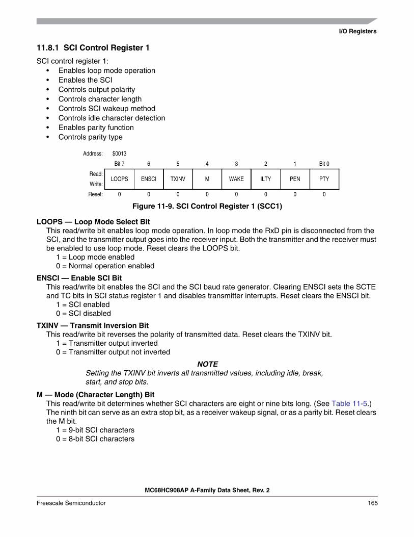
I/O Registers
MC68HC908AP A-Family Data Sheet, Rev. 2
Freescale Semiconductor 165
11.8.1 SCI Control Register 1
SCI control register 1:• Enables loop mode operation• Enables the SCI• Controls output polarity• Controls character length• Controls SCI wakeup method• Controls idle character detection• Enables parity function• Controls parity type
LOOPS — Loop Mode Select BitThis read/write bit enables loop mode operation. In loop mode the RxD pin is disconnected from theSCI, and the transmitter output goes into the receiver input. Both the transmitter and the receiver mustbe enabled to use loop mode. Reset clears the LOOPS bit.
1 = Loop mode enabled0 = Normal operation enabled
ENSCI — Enable SCI BitThis read/write bit enables the SCI and the SCI baud rate generator. Clearing ENSCI sets the SCTEand TC bits in SCI status register 1 and disables transmitter interrupts. Reset clears the ENSCI bit.
1 = SCI enabled0 = SCI disabled
TXINV — Transmit Inversion BitThis read/write bit reverses the polarity of transmitted data. Reset clears the TXINV bit.
1 = Transmitter output inverted0 = Transmitter output not inverted
NOTESetting the TXINV bit inverts all transmitted values, including idle, break,start, and stop bits.
M — Mode (Character Length) BitThis read/write bit determines whether SCI characters are eight or nine bits long. (See Table 11-5.)The ninth bit can serve as an extra stop bit, as a receiver wakeup signal, or as a parity bit. Reset clearsthe M bit.
1 = 9-bit SCI characters0 = 8-bit SCI characters
Address: $0013
Bit 7 6 5 4 3 2 1 Bit 0
Read:LOOPS ENSCI TXINV M WAKE ILTY PEN PTY
Write:
Reset: 0 0 0 0 0 0 0 0
Figure 11-9. SCI Control Register 1 (SCC1)

Serial Communications Interface Module (SCI)
MC68HC908AP A-Family Data Sheet, Rev. 2
166 Freescale Semiconductor
WAKE — Wakeup Condition BitThis read/write bit determines which condition wakes up the SCI: a logic 1 (address mark) in the mostsignificant bit position of a received character or an idle condition on the RxD pin. Reset clears theWAKE bit.
1 = Address mark wakeup0 = Idle line wakeup
ILTY — Idle Line Type BitThis read/write bit determines when the SCI starts counting logic 1s as idle character bits. Thecounting begins either after the start bit or after the stop bit. If the count begins after the start bit, thena string of logic 1s preceding the stop bit may cause false recognition of an idle character. Beginningthe count after the stop bit avoids false idle character recognition, but requires properly synchronizedtransmissions. Reset clears the ILTY bit.
1 = Idle character bit count begins after stop bit0 = Idle character bit count begins after start bit
PEN — Parity Enable BitThis read/write bit enables the SCI parity function. (See Table 11-5.) When enabled, the parity functioninserts a parity bit in the most significant bit position. (See Figure 11-3.) Reset clears the PEN bit.
1 = Parity function enabled0 = Parity function disabled
PTY — Parity BitThis read/write bit determines whether the SCI generates and checks for odd parity or even parity.(See Table 11-5.) Reset clears the PTY bit.
1 = Odd parity0 = Even parity
NOTEChanging the PTY bit in the middle of a transmission or reception cangenerate a parity error.
Table 11-5. Character Format Selection
Control Bits Character Format
M PEN:PTYStartBits
DataBits
ParityStopBits
CharacterLength
0 0X 1 8 None 1 10 bits
1 0X 1 9 None 1 11 bits
0 10 1 7 Even 1 10 bits
0 11 1 7 Odd 1 10 bits
1 10 1 8 Even 1 11 bits
1 11 1 8 Odd 1 11 bits

I/O Registers
MC68HC908AP A-Family Data Sheet, Rev. 2
Freescale Semiconductor 167
11.8.2 SCI Control Register 2
SCI control register 2:• Enables the following CPU interrupt requests:
– Enables the SCTE bit to generate transmitter CPU interrupt requests– Enables the TC bit to generate transmitter CPU interrupt requests– Enables the SCRF bit to generate receiver CPU interrupt requests– Enables the IDLE bit to generate receiver CPU interrupt requests
• Enables the transmitter• Enables the receiver• Enables SCI wakeup• Transmits SCI break characters
SCTIE — SCI Transmit Interrupt Enable BitThis read/write bit enables the SCTE bit to generate SCI transmitter CPU interrupt requests. Resetclears the SCTIE bit.
1 = SCTE enabled to generate CPU interrupt0 = SCTE not enabled to generate CPU interrupt
TCIE — Transmission Complete Interrupt Enable BitThis read/write bit enables the TC bit to generate SCI transmitter CPU interrupt requests. Reset clearsthe TCIE bit.
1 = TC enabled to generate CPU interrupt requests0 = TC not enabled to generate CPU interrupt requests
SCRIE — SCI Receive Interrupt Enable BitThis read/write bit enables the SCRF bit to generate SCI receiver CPU interrupt requests. Reset clearsthe SCRIE bit.
1 = SCRF enabled to generate CPU interrupt0 = SCRF not enabled to generate CPU interrupt
ILIE — Idle Line Interrupt Enable BitThis read/write bit enables the IDLE bit to generate SCI receiver CPU interrupt requests. Reset clearsthe ILIE bit.
1 = IDLE enabled to generate CPU interrupt requests0 = IDLE not enabled to generate CPU interrupt requests
Address: $0014
Bit 7 6 5 4 3 2 1 Bit 0
Read:SCTIE TCIE SCRIE ILIE TE RE RWU SBK
Write:
Reset: 0 0 0 0 0 0 0 0
Figure 11-10. SCI Control Register 2 (SCC2)

Serial Communications Interface Module (SCI)
MC68HC908AP A-Family Data Sheet, Rev. 2
168 Freescale Semiconductor
TE — Transmitter Enable BitSetting this read/write bit begins the transmission by sending a preamble of 10 or 11 logic 1s from thetransmit shift register to the TxD pin. If software clears the TE bit, the transmitter completes anytransmission in progress before the TxD returns to the idle condition (logic 1). Clearing and then settingTE during a transmission queues an idle character to be sent after the character currently beingtransmitted. Reset clears the TE bit.
1 = Transmitter enabled0 = Transmitter disabled
NOTEWriting to the TE bit is not allowed when the enable SCI bit (ENSCI) is clear.ENSCI is in SCI control register 1.
RE — Receiver Enable BitSetting this read/write bit enables the receiver. Clearing the RE bit disables the receiver but does notaffect receiver interrupt flag bits. Reset clears the RE bit.
1 = Receiver enabled0 = Receiver disabled
NOTEWriting to the RE bit is not allowed when the enable SCI bit (ENSCI) isclear. ENSCI is in SCI control register 1.
RWU — Receiver Wakeup BitThis read/write bit puts the receiver in a standby state during which receiver interrupts are disabled.The WAKE bit in SCC1 determines whether an idle input or an address mark brings the receiver outof the standby state and clears the RWU bit. Reset clears the RWU bit.
1 = Standby state0 = Normal operation
SBK — Send Break BitSetting and then clearing this read/write bit transmits a break character followed by a logic 1. The logic1 after the break character guarantees recognition of a valid start bit. If SBK remains set, thetransmitter continuously transmits break characters with no logic 1s between them. Reset clears theSBK bit.
1 = Transmit break characters0 = No break characters being transmitted
NOTEDo not toggle the SBK bit immediately after setting the SCTE bit. TogglingSBK before the preamble begins causes the SCI to send a break characterinstead of a preamble.

I/O Registers
MC68HC908AP A-Family Data Sheet, Rev. 2
Freescale Semiconductor 169
11.8.3 SCI Control Register 3
SCI control register 3:• Stores the ninth SCI data bit received and the ninth SCI data bit to be transmitted• Enables these interrupts:
– Receiver overrun interrupts– Noise error interrupts– Framing error interrupts
• Parity error interrupts
R8 — Received Bit 8When the SCI is receiving 9-bit characters, R8 is the read-only ninth bit (bit 8) of the receivedcharacter. R8 is received at the same time that the SCDR receives the other 8 bits.When the SCI is receiving 8-bit characters, R8 is a copy of the eighth bit (bit 7). Reset has no effecton the R8 bit.
T8 — Transmitted Bit 8When the SCI is transmitting 9-bit characters, T8 is the read/write ninth bit (bit 8) of the transmittedcharacter. T8 is loaded into the transmit shift register at the same time that the SCDR is loaded intothe transmit shift register. Reset has no effect on the T8 bit.
DMARE — DMA Receive Enable Bit
CAUTIONThe DMA module is not included on this MCU. Writing a logic 1 to DMAREor DMATE may adversely affect MCU performance.
1 = DMA not enabled to service SCI receiver DMA service requests generated by the SCRF bit (SCIreceiver CPU interrupt requests enabled)
0 = DMA not enabled to service SCI receiver DMA service requests generated by the SCRF bit (SCIreceiver CPU interrupt requests enabled)
DMATE — DMA Transfer Enable Bit
CAUTIONThe DMA module is not included on this MCU. Writing a logic 1 to DMAREor DMATE may adversely affect MCU performance.
1 = SCTE DMA service requests enabled; SCTE CPU interrupt requests disabled0 = SCTE DMA service requests disabled; SCTE CPU interrupt requests enabled
ORIE — Receiver Overrun Interrupt Enable BitThis read/write bit enables SCI error CPU interrupt requests generated by the receiver overrun bit, OR.
1 = SCI error CPU interrupt requests from OR bit enabled0 = SCI error CPU interrupt requests from OR bit disabled
Address: $0015
Bit 7 6 5 4 3 2 1 Bit 0
Read: R8T8 DMARE DMATE ORIE NEIE FEIE PEIE
Write:
Reset: U U 0 0 0 0 0 0
= Unimplemented U = Unaffected
Figure 11-11. SCI Control Register 3 (SCC3)

Serial Communications Interface Module (SCI)
MC68HC908AP A-Family Data Sheet, Rev. 2
170 Freescale Semiconductor
NEIE — Receiver Noise Error Interrupt Enable BitThis read/write bit enables SCI error CPU interrupt requests generated by the noise error bit, NE.Reset clears NEIE.
1 = SCI error CPU interrupt requests from NE bit enabled0 = SCI error CPU interrupt requests from NE bit disabled
FEIE — Receiver Framing Error Interrupt Enable BitThis read/write bit enables SCI error CPU interrupt requests generated by the framing error bit, FE.Reset clears FEIE.
1 = SCI error CPU interrupt requests from FE bit enabled0 = SCI error CPU interrupt requests from FE bit disabled
PEIE — Receiver Parity Error Interrupt Enable BitThis read/write bit enables SCI error CPU interruptrequests generated by the parity error bit, PE. (See 11.8.4 SCI Status Register 1.) Reset clears PEIE.
1 = SCI error CPU interrupt requests from PE bit enabled0 = SCI error CPU interrupt requests from PE bit disabled
11.8.4 SCI Status Register 1
SCI status register 1 (SCS1) contains flags to signal these conditions:• Transfer of SCDR data to transmit shift register complete• Transmission complete• Transfer of receive shift register data to SCDR complete• Receiver input idle• Receiver overrun• Noisy data• Framing error• Parity error
SCTE — SCI Transmitter Empty BitThis clearable, read-only bit is set when the SCDR transfers a character to the transmit shift register.SCTE can generate an SCI transmitter CPU interrupt request. When the SCTIE bit in SCC2 is set,SCTE generates an SCI transmitter CPU interrupt request. In normal operation, clear the SCTE bit byreading SCS1 with SCTE set and then writing to SCDR. Reset sets the SCTE bit.
1 = SCDR data transferred to transmit shift register0 = SCDR data not transferred to transmit shift register
Address: $0016
Bit 7 6 5 4 3 2 1 Bit 0
Read: SCTE TC SCRF IDLE OR NF FE PE
Write:
Reset: 1 1 0 0 0 0 0 0
= Unimplemented
Figure 11-12. SCI Status Register 1 (SCS1)

I/O Registers
MC68HC908AP A-Family Data Sheet, Rev. 2
Freescale Semiconductor 171
TC — Transmission Complete BitThis read-only bit is set when the SCTE bit is set, and no data, preamble, or break character is beingtransmitted. TC generates an SCI transmitter CPU interrupt request if the TCIE bit in SCC2 is also set.TC is automatically cleared when data, preamble or break is queued and ready to be sent. There maybe up to 1.5 transmitter clocks of latency between queueing data, preamble, and break and thetransmission actually starting. Reset sets the TC bit.
1 = No transmission in progress0 = Transmission in progress
SCRF — SCI Receiver Full BitThis clearable, read-only bit is set when the data in the receive shift register transfers to the SCI dataregister. SCRF can generate an SCI receiver CPU interrupt request. When the SCRIE bit in SCC2 isset, SCRF generates a CPU interrupt request. In normal operation, clear the SCRF bit by readingSCS1 with SCRF set and then reading the SCDR. Reset clears SCRF.
1 = Received data available in SCDR0 = Data not available in SCDR
IDLE — Receiver Idle BitThis clearable, read-only bit is set when 10 or 11 consecutive logic 1s appear on the receiver input.IDLE generates an SCI receiver CPU interrupt request if the ILIE bit in SCC2 is also set. Clear the IDLEbit by reading SCS1 with IDLE set and then reading the SCDR. After the receiver is enabled, it mustreceive a valid character that sets the SCRF bit before an idle condition can set the IDLE bit. Also, afterthe IDLE bit has been cleared, a valid character must again set the SCRF bit before an idle conditioncan set the IDLE bit. Reset clears the IDLE bit.
1 = Receiver input idle0 = Receiver input active (or idle since the IDLE bit was cleared)
OR — Receiver Overrun BitThis clearable, read-only bit is set when software fails to read the SCDR before the receive shiftregister receives the next character. The OR bit generates an SCI error CPU interrupt request if theORIE bit in SCC3 is also set. The data in the shift register is lost, but the data already in the SCDR isnot affected. Clear the OR bit by reading SCS1 with OR set and then reading the SCDR. Reset clearsthe OR bit.
1 = Receive shift register full and SCRF = 10 = No receiver overrun
Software latency may allow an overrun to occur between reads of SCS1 and SCDR in the flag-clearingsequence. Figure 11-13 shows the normal flag-clearing sequence and an example of an overruncaused by a delayed flag-clearing sequence. The delayed read of SCDR does not clear the OR bitbecause OR was not set when SCS1 was read. Byte 2 caused the overrun and is lost. The nextflag-clearing sequence reads byte 3 in the SCDR instead of byte 2.In applications that are subject to software latency or in which it is important to know which byte is lostdue to an overrun, the flag-clearing routine can check the OR bit in a second read of SCS1 afterreading the data register.
NF — Receiver Noise Flag BitThis clearable, read-only bit is set when the SCI detects noise on the RxD pin. NF generates an SCIerror CPU interrupt request if the NEIE bit in SCC3 is also set. Clear the NF bit by reading SCS1 andthen reading the SCDR. Reset clears the NF bit.
1 = Noise detected0 = No noise detected

Serial Communications Interface Module (SCI)
MC68HC908AP A-Family Data Sheet, Rev. 2
172 Freescale Semiconductor
FE — Receiver Framing Error BitThis clearable, read-only bit is set when a logic 0 is accepted as the stop bit. FE generates an SCI errorCPU interrupt request if the FEIE bit in SCC3 also is set. Clear the FE bit by reading SCS1 with FE setand then reading the SCDR. Reset clears the FE bit.
1 = Framing error detected0 = No framing error detected
Figure 11-13. Flag Clearing Sequence
PE — Receiver Parity Error BitThis clearable, read-only bit is set when the SCI detects a parity error in incoming data. PE generatesan SCI error CPU interrupt request if the PEIE bit in SCC3 is also set. Clear the PE bit by reading SCS1with PE set and then reading the SCDR. Reset clears the PE bit.
1 = Parity error detected0 = No parity error detected
BYTE 1
NORMAL FLAG CLEARING SEQUENCE
READ SCS1SCRF = 1
READ SCDRBYTE 1
SC
RF
= 1
SC
RF
= 1
BYTE 2 BYTE 3 BYTE 4
OR = 0
READ SCS1SCRF = 1
OR = 0
READ SCDRBYTE 2
SC
RF
= 0
READ SCS1SCRF = 1
OR = 0
SC
RF
= 1
SC
RF
= 0
READ SCDRBYTE 3
SC
RF
= 0
BYTE 1
READ SCS1SCRF = 1
READ SCDRBYTE 1
SC
RF
= 1
SC
RF
= 1
BYTE 2 BYTE 3 BYTE 4
OR = 0
READ SCS1SCRF = 1
OR = 1
READ SCDRBYTE 3
DELAYED FLAG CLEARING SEQUENCEO
R =
1
SC
RF
= 1
OR
= 1
SC
RF
= 0
OR
= 1
SC
RF
= 0
OR
= 0

I/O Registers
MC68HC908AP A-Family Data Sheet, Rev. 2
Freescale Semiconductor 173
11.8.5 SCI Status Register 2
SCI status register 2 contains flags to signal the following conditions:• Break character detected• Incoming data
BKF — Break Flag BitThis clearable, read-only bit is set when the SCI detects a break character on the RxD pin. In SCS1,the FE and SCRF bits are also set. In 9-bit character transmissions, the R8 bit in SCC3 is cleared. BKFdoes not generate a CPU interrupt request. Clear BKF by reading SCS2 with BKF set and then readingthe SCDR. Once cleared, BKF can become set again only after logic 1s again appear on the RxD pinfollowed by another break character. Reset clears the BKF bit.
1 = Break character detected0 = No break character detected
RPF — Reception in Progress Flag BitThis read-only bit is set when the receiver detects a logic 0 during the RT1 time period of the start bitsearch. RPF does not generate an interrupt request. RPF is reset after the receiver detects false startbits (usually from noise or a baud rate mismatch) or when the receiver detects an idle character. PollingRPF before disabling the SCI module or entering stop mode can show whether a reception is inprogress.
1 = Reception in progress0 = No reception in progress
11.8.6 SCI Data Register
The SCI data register (SCDR) is the buffer between the internal data bus and the receive and transmitshift registers. Reset has no effect on data in the SCI data register.
R7/T7–R0/T0 — Receive/Transmit Data BitsReading the SCDR accesses the read-only received data bits, R7–R0. Writing to the SCDR writes thedata to be transmitted, T7–T0. Reset has no effect on the SCDR.
NOTEDo not use read/modify/write instructions on the SCI data register.
Address: $0017
Bit 7 6 5 4 3 2 1 Bit 0
Read: BKF RPF
Write:
Reset: 0 0 0 0 0 0 0 0
= Unimplemented
Figure 11-14. SCI Status Register 2 (SCS2)
Address: $0018
Bit 7 6 5 4 3 2 1 Bit 0
Read: R7 R6 R5 R4 R3 R2 R1 R0
Write: T7 T6 T5 T4 T3 T2 T1 T0
Reset: Unaffected by reset
Figure 11-15. SCI Data Register (SCDR)

Serial Communications Interface Module (SCI)
MC68HC908AP A-Family Data Sheet, Rev. 2
174 Freescale Semiconductor
11.8.7 SCI Baud Rate Register
The baud rate register (SCBR) selects the baud rate for both the receiver and the transmitter.
SCP1 and SCP0 — SCI Baud Rate Prescaler BitsThese read/write bits select the baud rate prescaler divisor as shown in Table 11-6. Reset clears SCP1and SCP0.
SCR2–SCR0 — SCI Baud Rate Select BitsThese read/write bits select the SCI baud rate divisor as shown in Table 11-7. Reset clearsSCR2–SCR0.
Use this formula to calculate the SCI baud rate:
where:SCI clock source = fBUS or CGMXCLK(selected by SCIBDSRC bit in CONFIG2 register)PD = prescaler divisorBD = baud rate divisor
Address: $0019 6 5 4 3 2 1 Bit 0
Read: 0 0SCP1 SCP0 R SCR2 SCR1 SCR0
Write:
Reset: 0 0 0 0 0 0 0 0
= Unimplemented R = Reserved
Figure 11-16. SCI Baud Rate Register (SCBR)
Table 11-6. SCI Baud Rate Prescaling
SCP1 and SCP0 Prescaler Divisor (PD)
00 1
01 3
10 4
11 13
Table 11-7. SCI Baud Rate Selection
SCR2, SCR1, and SCR0 Baud Rate Divisor (BD)
000 1
001 2
010 4
011 8
100 16
101 32
110 64
111 128
baud rateSCI clock source
64 PD BD××---------------------------------------------=

I/O Registers
MC68HC908AP A-Family Data Sheet, Rev. 2
Freescale Semiconductor 175
Table 11-8 shows the SCI baud rates that can be generated with a 4.9152-MHz bus clock when fBUS isselected as SCI clock source.
Table 11-8. SCI Baud Rate Selection Examples
SCP1 and SCP0Prescaler
Divisor (PD)SCR2, SCR1,
and SCR0Baud Rate
Divisor (BD)Baud Rate
(fBUS = 4.9152 MHz)
00 1 000 1 76,800
00 1 001 2 38,400
00 1 010 4 19,200
00 1 011 8 9600
00 1 100 16 4800
00 1 101 32 2400
00 1 110 64 1200
00 1 111 128 600
01 3 000 1 25,600
01 3 001 2 12,800
01 3 010 4 6400
01 3 011 8 3200
01 3 100 16 1600
01 3 101 32 800
01 3 110 64 400
01 3 111 128 200
10 4 000 1 19,200
10 4 001 2 9600
10 4 010 4 4800
10 4 011 8 2400
10 4 100 16 1200
10 4 101 32 600
10 4 110 64 300
10 4 111 128 150
11 13 000 1 5908
11 13 001 2 2954
11 13 010 4 1477
11 13 011 8 739
11 13 100 16 369
11 13 101 32 185
11 13 110 64 92
11 13 111 128 46

Serial Communications Interface Module (SCI)
MC68HC908AP A-Family Data Sheet, Rev. 2
176 Freescale Semiconductor

MC68HC908AP A-Family Data Sheet, Rev. 2
Freescale Semiconductor 177
Chapter 12Infrared Serial Communications Interface Module (IRSCI)
12.1 Introduction
The MC68HC908AP64A has two SCI modules:• SCI1 is a standard SCI module, and• SCI2 is an infrared SCI module.
This section describes SCI2, the infrared serial communications interface (IRSCI) module which allowshigh-speed asynchronous communications with peripheral devices and other MCUs. This IRSCI consistsof an SCI module for conventional SCI functions and a software programmable infrared encoder/decodersub-module for encoding/decoding the serial data for connection to infrared LEDs in remote controlapplications.
NOTEWhen the IRSCI is enabled, the SCTxD pin is an open-drain output andrequires a pullup resistor to be connected for proper SCI operation.
Features of the SCI module include the following:• Full duplex operation• Standard mark/space non-return-to-zero (NRZ) format• Programmable 8-bit or 9-bit character length• Separately enabled transmitter and receiver• Separate receiver and transmitter CPU interrupt requests• Two receiver wakeup methods:
– Idle line wakeup– Address mark wakeup
• Interrupt-driven operation with eight interrupt flags:– Transmitter empty– Transmission complete– Receiver full– Idle receiver input– Receiver overrun– Noise error– Framing error– Parity error
• Receiver framing error detection• Hardware parity checking• 1/16 bit-time noise detection
Features of the infrared (IR) sub-module include the following:• IR sub-module enable/disable for infrared SCI or conventional SCI on SCTxD and SCRxD pins• Software selectable infrared modulation/demodulation
(3/16, 1/16 or 1/32 width pulses)

Infrared Serial Communications Interface Module (IRSCI)
MC68HC908AP A-Family Data Sheet, Rev. 2
178 Freescale Semiconductor
12.2 Pin Name Conventions
The generic names of the IRSCI I/O pins are:• RxD (receive data)• TxD (transmit data)
IRSCI I/O (input/output) lines are implemented by sharing parallel I/O port pins. The full name of an IRSCIinput or output reflects the name of the shared port pin. Table 12-1 shows the full names and the genericnames of the IRSCI I/O pins. The generic pin names appear in the text of this section.
NOTEWhen the IRSCI is enabled, the SCTxD pin is an open-drain output andrequires a pullup resistor to be connected for proper SCI operation.
Table 12-1. Pin Name Conventions
Generic Pin Names: RxD TxD
Full Pin Names: PTC7/SCRxD PTC6/SCTxD
Addr. Register Name Bit 7 6 5 4 3 2 1 Bit 0
$0040IRSCI Control Register 1
(IRSCC1)
Read:LOOPS ENSCI
0M WAKE ILTY PEN PTY
Write:Reset: 0 0 0 0 0 0 0 0
$0041IRSCI Control Register 2
(IRSCC2)
Read:SCTIE TCIE SCRIE ILIE TE RE RWU SBK
Write:Reset: 0 0 0 0 0 0 0 0
$0042IRSCI Control Register 3
(IRSCC3)
Read: R8T8 DMARE DMATE ORIE NEIE FEIE PEIE
Write:Reset: U U 0 0 0 0 0 0
$0043IRSCI Status Register 1
(IRSCS1)
Read: SCTE TC SCRF IDLE OR NF FE PEWrite:
Reset: 1 1 0 0 0 0 0 0
$0044IRSCI Status Register 2
(IRSCS2)
Read: BKF RPFWrite:
Reset: 0 0 0 0 0 0 0 0
$0045IRSCI Data Register
(IRSCDR)
Read: R7 R6 R5 R4 R3 R2 R1 R0Write: T7 T6 T5 T4 T3 T2 T1 T0
Reset: Unaffected by reset
$0046IRSCI Baud Rate Register
(IRSCBR)
Read:CKS
0SCP1 SCP0 R SCR2 SCR1 SCR0
Write:Reset: 0 0 0 0 0 0 0 0
$0047IRSCI Infrared Control
Register(IRSCIRCR)
Read:R
0 0 0R TNP1 TNP0 IREN
Write:Reset: 0 0 0 0 0 0 0 0
= Unimplemented R = Reserved U = Unaffected
Figure 12-1. IRSCI I/O Registers Summary

IRSCI Module Overview
MC68HC908AP A-Family Data Sheet, Rev. 2
Freescale Semiconductor 179
12.3 IRSCI Module Overview
The IRSCI consists of a serial communications interface (SCI) and a infrared interface sub-module asshown in Figure 12-2.
Figure 12-2. IRSCI Block Diagram
The SCI module provides serial data transmission and reception, with a programmable baud rate clockbased on the bus clock or the CGMXCLK.
The infrared sub-module receives two clock sources from the SCI module: SCI_R16XCLK andSCI_R32XCLK. Both reference clocks are used to generate the narrow pulses during data transmission.The SCI_R16XCLK and SCI_R32XCLK are internal clocks with frequencies that are 16 and 32 times thebaud rate respectively. Both SCI_R16XCLK and SCI_R32XCLK clocks are used for transmitting data.The SCI_R16XCLK clock is used only for receiving data.
NOTEFor proper SCI function (transmit or receive), the bus clock MUST beprogrammed to at least 32 times that of the selected baud rate.When the infrared sub-module is disabled, signals on the TxD and RxDpins pass through unchanged to the SCI module.
12.4 Infrared Functional Description
Figure 12-3 shows the structure of the infrared sub-module.
The infrared sub-module provides the capability of transmitting narrow pulses to an infrared LED andreceiving narrow pulses and transforming them to serial bits, which are sent to the SCI module. Theinfrared sub-module receives two clocks from the SCI. One of these two clocks is selected as the baseclock to generate the 3/16, 1/16, or 1/32 bit width narrow pulses during transmission.
The sub-module consists of two main blocks: the transmit encoder and the receive decoder. Whentransmitting data, the SCI data stream is encoded by the infrared sub-module. For every "0" bit, a narrow"low" pulse is transmitted; no pulse is transmitted for "1" bits. When receiving data, the infrared pulsesshould be detected using an infrared photo diode for conversion to CMOS voltage levels beforeconnecting to the RxD pin for the infrared decoder. The SCI data stream is reconstructed by stretchingthe "0" pulses.
SCTxD
INFRAREDSUB-MODULE
SCI_TxD
SCI_R32XCLK
SCI_R16XCLK
SERIALCGMXCLK
BUS CLOCK
INTERNAL BUS
COMMUNICATIONSINTERFACE MODULE
(SCI)
SCRxDSCI_RxD

Infrared Serial Communications Interface Module (IRSCI)
MC68HC908AP A-Family Data Sheet, Rev. 2
180 Freescale Semiconductor
Figure 12-3. Infrared Sub-Module Diagram
12.4.1 Infrared Transmit Encoder
The infrared transmit encoder converts the "0" bits in the serial data stream from the SCI module to narrow"low" pulses, to the TxD pin. The narrow pulse is sent with a duration of 1/32, 1/16, or 3/16 of a data bitwidth. When two consecutive zeros are sent, the two consecutive narrow pulses will be separated by atime equal to a data bit width.
Figure 12-4. Infrared SCI Data Example
12.4.2 Infrared Receive Decoder
The infrared receive decoder converts low narrow pulses from the RxD pin to standard SCI data bits. Thereference clock, SCI_R16XCLK, clocks a four bit internal counter which counts from 0 to 15. An incomingpulse starts the internal counter and a "0" is sent out to the IR_RxD output. Subsequent incoming pulsesare ignored when the counter count is between 0 and 7; IR_RxD remains "0". Once the counter passes7, an incoming pulse will reset the counter; IR_RxD remains "0". When the counter reaches 15, theIR_RxD output returns to "1", the counter stops and waits for further pulses. A pulse is interpreted as jitterif it arrives shortly after the counter reaches 15; IR_RxD remains "1".
SCI_R16XCLK
TRANSMITENCODER
RECEIVEDECODER
MUX
MUX
SCTxD
SCRxD
IR_TxD
TNP[1:0]
SCI_TxD
IR_RxD
SCI_RxD
IREN
SCI_R32XCLK
SCI DATA
INFRAREDSCI DATA
DATA BIT WIDTH DETERMINED BY BAUD RATE
PULSE WIDTH = 1/32, 1/16, OR 3/16 DATA BIT WIDTH

SCI Functional Description
MC68HC908AP A-Family Data Sheet, Rev. 2
Freescale Semiconductor 181
12.5 SCI Functional Description
Figure 12-5 shows the structure of the SCI.
Figure 12-5. SCI Module Block Diagram
SCTE
TC
SCRF
IDLE
OR
NF
FE
PE
SCTIE
TCIE
SCRIE
ILIE
TE
RE
RWU
SBK
R8
T8
DMATE
ORIE
FEIE
PEIE
BKF
RPF
SCI DATA
RECEIVESHIFT REGISTER
SCI DATAREGISTER
TRANSMITSHIFT REGISTER
NEIE
M
WAKE
ILTY
FLAGCONTROL
TRANSMITCONTROL
RECEIVECONTROL
DATA SELECTIONCONTROL
WAKEUP
PTY
PEN
REGISTER
DM
AIN
TER
RU
PTC
ON
TRO
L
TRAN
SMIT
TER
INTE
RR
UPT
CO
NTR
OL
REC
EIVE
RIN
TER
RU
PTC
ON
TRO
L
ERR
OR
INTE
RR
UPT
CO
NTR
OL
CONTROL
DMARE
ENSCI
LOOPS
ENSCI
INTERNAL BUS
LOOPS
÷16
BAUD RATEGENERATOR
CGMXCLKBUS CLOCK
AB
SLX
SL = 0 => X = ASL = 1 => X = B
CKS
SCI_TxDSCI_RxD
SCI_R32XCLK
SCI_R16XCLK

Infrared Serial Communications Interface Module (IRSCI)
MC68HC908AP A-Family Data Sheet, Rev. 2
182 Freescale Semiconductor
The SCI allows full-duplex, asynchronous, NRZ serial communication between the MCU and remotedevices, including other MCUs. The transmitter and receiver of the SCI operate independently, althoughthey use the same baud rate generator. During normal operation, the CPU monitors the status of the SCI,writes the data to be transmitted, and processes received data.
NOTEFor SCI operations, the IR sub-module is transparent to the SCI module.Data at going out of the SCI transmitter and data going into the SCI receiveris always in SCI format. It makes no difference to the SCI module whetherthe IR sub-module is enabled or disabled.
NOTEThis SCI module is a standard HC08 SCI module with the followingmodifications:
• A control bit, CKS, is added to the SCI baud rate control register to select between two input clocksfor baud rate clock generation
• The TXINV bit is removed from the SCI control register 1
12.5.1 Data Format
The SCI uses the standard non-return-to-zero mark/space data format illustrated in Figure 12-6.
Figure 12-6. SCI Data Formats
12.5.2 Transmitter
Figure 12-7 shows the structure of the SCI transmitter.
The baud rate clock source for the SCI can be selected by the CKS bit, in the SCI baud rate register (see12.9.7 IRSCI Baud Rate Register).
12.5.2.1 Character Length
The transmitter can accommodate either 8-bit or 9-bit data. The state of the M bit in IRSCI control register1 (IRSCC1) determines character length. When transmitting 9-bit data, bit T8 in IRSCI control register 3(IRSCC3) is the ninth bit (bit 8).
BIT 5START
BIT BIT 0 BIT 1
NEXT
STOPBIT
STARTBIT
8-BIT DATA FORMATBIT M IN IRSCC1 CLEAR
STARTBIT BIT 0
NEXT
STOPBIT
STARTBIT
9-BIT DATA FORMATBIT M IN IRSCC1 SET
BIT 1 BIT 2 BIT 3 BIT 4 BIT 5 BIT 6 BIT 7 BIT 8
BIT 2 BIT 3 BIT 4 BIT 6 BIT 7
PARITYBIT
PARITYBIT

SCI Functional Description
MC68HC908AP A-Family Data Sheet, Rev. 2
Freescale Semiconductor 183
Figure 12-7. SCI Transmitter
12.5.2.2 Character Transmission
During an SCI transmission, the transmit shift register shifts a character out to the TxD pin. The IRSCIdata register (IRSCDR) is the write-only buffer between the internal data bus and the transmit shiftregister. To initiate an SCI transmission:
1. Enable the SCI by writing a logic 1 to the enable SCI bit (ENSCI) in IRSCI control register 1(IRSCC1).
2. Enable the transmitter by writing a logic 1 to the transmitter enable bit (TE) in IRSCI control register2 (IRSCC2).
3. Clear the SCI transmitter empty bit by first reading IRSCI status register 1 (IRSCS1) and thenwriting to the IRSCDR.
4. Repeat step 3 for each subsequent transmission.
At the start of a transmission, transmitter control logic automatically loads the transmit shift register witha preamble of logic 1s. After the preamble shifts out, control logic transfers the IRSCDR data into thetransmit shift register. A logic 0 start bit automatically goes into the least significant bit position of thetransmit shift register. A logic 1 stop bit goes into the most significant bit position.
DMATE
SCTE
PEN
PTY
H 8 7 6 5 4 3 2 1 0 L
11-BITTRANSMIT
STO
P
STAR
T
T8
DMATE
SCTE
SCTIE
TCIE
SBK
TC
PARITYGENERATION
MSB
SCI DATA REGISTER
LOAD
FR
OM
IRSC
DR
SHIF
T EN
ABLE
PREA
MBL
EAL
L 1s
BREA
KAL
L 0s
TRANSMITTERCONTROL LOGIC
SHIFT REGISTER
DMATE
TC
SCTIE
TCIE
SCTE
TRAN
SMIT
TER
CPU
INTE
RRUP
T RE
QUE
ST
TRAN
SMIT
TER
DM
A SE
RVI
CE
REQ
UES
T
M
ENSCI
LOOPS
TE
INTERNAL BUS
PRE-SCALER
SCP1
SCP0
SCR2
SCR1
SCR0
BAUDDIVIDER ÷ 16
SCTIE
SCI_TxD
CGMXCLKBUS CLOCK
AB
SLX
SL = 0 => X = ASL = 1 => X = B
CKS
Infrared Serial Communications Interface Module (IRSCI)
MC68HC908AP A-Family Data Sheet, Rev. 2
184 Freescale Semiconductor
The SCI transmitter empty bit, SCTE, in IRSCS1 becomes set when the IRSCDR transfers a byte to thetransmit shift register. The SCTE bit indicates that the IRSCDR can accept new data from the internaldata bus. If the SCI transmit interrupt enable bit, SCTIE, in IRSCC2 is also set, the SCTE bit generatesa transmitter interrupt request.
When the transmit shift register is not transmitting a character, the TxD pin goes to the idle condition, logic1. If at any time software clears the ENSCI bit in IRSCI control register 1 (IRSCC1), the transmitter andreceiver relinquish control of the port pins.
12.5.2.3 Break Characters
Writing a logic 1 to the send break bit, SBK, in IRSCC2 loads the transmit shift register with a breakcharacter. A break character contains all logic 0s and has no start, stop, or parity bit. Break characterlength depends on the M bit in IRSCC1. As long as SBK is at logic 1, transmitter logic continuously loadsbreak characters into the transmit shift register. After software clears the SBK bit, the shift register finishestransmitting the last break character and then transmits at least one logic 1. The automatic logic 1 at theend of a break character guarantees the recognition of the start bit of the next character.
The SCI recognizes a break character when a start bit is followed by eight or nine logic 0 data bits and alogic 0 where the stop bit should be.
Receiving a break character has the following effects on SCI registers:• Sets the framing error bit (FE) in IRSCS1• Sets the SCI receiver full bit (SCRF) in IRSCS1• Clears the SCI data register (IRSCDR)• Clears the R8 bit in IRSCC3• Sets the break flag bit (BKF) in IRSCS2• May set the overrun (OR), noise flag (NF), parity error (PE), or reception in progress flag (RPF) bits
12.5.2.4 Idle Characters
An idle character contains all logic 1s and has no start, stop, or parity bit. Idle character length dependson the M bit in IRSCC1. The preamble is a synchronizing idle character that begins every transmission.
If the TE bit is cleared during a transmission, the TxD pin becomes idle after completion of thetransmission in progress. Clearing and then setting the TE bit during a transmission queues an idlecharacter to be sent after the character currently being transmitted.
NOTEWhen queueing an idle character, return the TE bit to logic 1 before the stopbit of the current character shifts out to the TxD pin. Setting TE after thestop bit appears on TxD causes data previously written to the IRSCDR tobe lost.
Toggle the TE bit for a queued idle character when the SCTE bit becomesset and just before writing the next byte to the IRSCDR.
12.5.2.5 Transmitter Interrupts
The following conditions can generate CPU interrupt requests from the SCI transmitter:

SCI Functional Description
MC68HC908AP A-Family Data Sheet, Rev. 2
Freescale Semiconductor 185
• SCI transmitter empty (SCTE) — The SCTE bit in IRSCS1 indicates that the IRSCDR hastransferred a character to the transmit shift register. SCTE can generate a transmitter CPUinterrupt request. Setting the SCI transmit interrupt enable bit, SCTIE, in IRSCC2 enables theSCTE bit to generate transmitter CPU interrupt requests.
• Transmission complete (TC) — The TC bit in IRSCS1 indicates that the transmit shift register andthe IRSCDR are empty and that no break or idle character has been generated. The transmissioncomplete interrupt enable bit, TCIE, in IRSCC2 enables the TC bit to generate transmitter CPUinterrupt requests.
12.5.3 ReceiverFigure 12-8 shows the structure of the SCI receiver.

Infrared Serial Communications Interface Module (IRSCI)
MC68HC908AP A-Family Data Sheet, Rev. 2
186 Freescale Semiconductor
Figure 12-8. SCI Receiver Block Diagram
12.5.3.1 Character Length
The receiver can accommodate either 8-bit or 9-bit data. The state of the M bit in IRSCI control register 1(IRSCC1) determines character length. When receiving 9-bit data, bit R8 in IRSCI control register 2(IRSCC2) is the ninth bit (bit 8). When receiving 8-bit data, bit R8 is a copy of the eighth bit (bit 7).
ALL
1s
ALL 0s
M
WAKE
ILTY
PEN
PTY
BKF
RPF
H 8 7 6 5 4 3 2 1 0 L
11-BITRECEIVE SHIFT REGISTERST
OP
STAR
T
DATARECOVERY
DMARE
SCRF
OR
ORIE
NF
NEIE
FE
FEIE
PE
PEIE
DMARESCRIESCRF
ILIEIDLE
WAKEUPLOGIC
PARITYCHECKING
MSB
ERR
OR
CPU
INTE
RRUP
T R
EQU
EST
DM
A SE
RVI
CE
REQ
UES
T
CPU
INTE
RR
UPT
REQ
UES
T
SCI DATA REGISTER
R8
DMARE
ORIE
NEIE
FEIE
PEIE
SCRIE
ILIE
RWUSCRF
IDLE
OR
NF
FE
PE
INTERNAL BUS
PRE-SCALER
BAUDDIVIDER
÷ 16
SCP1
SCP0
SCR2
SCR1
SCR0
SCRIE
DMARE
SCI_RxD
CGMXCLKBUS CLOCK
AB
SLX
SL = 0 => X = ASL = 1 => X = B
CKS
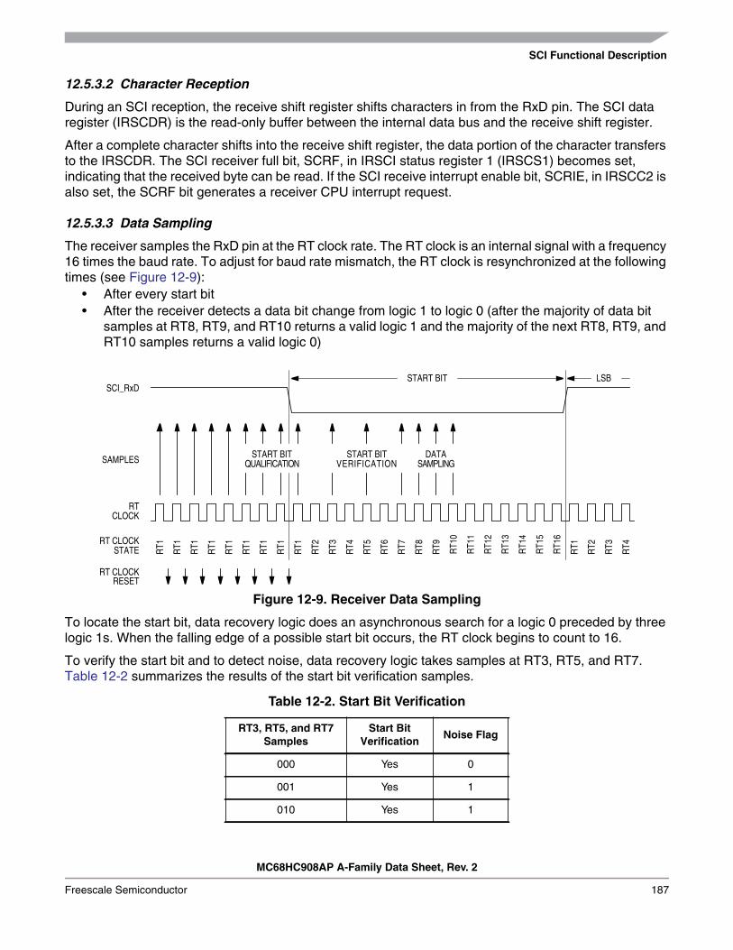
SCI Functional Description
MC68HC908AP A-Family Data Sheet, Rev. 2
Freescale Semiconductor 187
12.5.3.2 Character Reception
During an SCI reception, the receive shift register shifts characters in from the RxD pin. The SCI dataregister (IRSCDR) is the read-only buffer between the internal data bus and the receive shift register.
After a complete character shifts into the receive shift register, the data portion of the character transfersto the IRSCDR. The SCI receiver full bit, SCRF, in IRSCI status register 1 (IRSCS1) becomes set,indicating that the received byte can be read. If the SCI receive interrupt enable bit, SCRIE, in IRSCC2 isalso set, the SCRF bit generates a receiver CPU interrupt request.
12.5.3.3 Data Sampling
The receiver samples the RxD pin at the RT clock rate. The RT clock is an internal signal with a frequency16 times the baud rate. To adjust for baud rate mismatch, the RT clock is resynchronized at the followingtimes (see Figure 12-9):
• After every start bit• After the receiver detects a data bit change from logic 1 to logic 0 (after the majority of data bit
samples at RT8, RT9, and RT10 returns a valid logic 1 and the majority of the next RT8, RT9, andRT10 samples returns a valid logic 0)
Figure 12-9. Receiver Data Sampling
To locate the start bit, data recovery logic does an asynchronous search for a logic 0 preceded by threelogic 1s. When the falling edge of a possible start bit occurs, the RT clock begins to count to 16.
To verify the start bit and to detect noise, data recovery logic takes samples at RT3, RT5, and RT7.Table 12-2 summarizes the results of the start bit verification samples.
Table 12-2. Start Bit Verification
RT3, RT5, and RT7Samples
Start BitVerification
Noise Flag
000 Yes 0
001 Yes 1
010 Yes 1
RT CLOCKRESET
RT1
RT1
RT1
RT1
RT1
RT1
RT1
RT1
RT1
RT2
RT3
RT4
RT5
RT8
RT7
RT6 RT1
1
RT1
0
RT9 RT1
5
RT1
4
RT1
3
RT1
2
RT1
6
RT1
RT2
RT3
RT4
START BITQUALIFICATION
START BITVERIFICATION
DATASAMPLINGSAMPLES
RTCLOCK
RT CLOCKSTATE
START BIT LSBSCI_RxD

Infrared Serial Communications Interface Module (IRSCI)
MC68HC908AP A-Family Data Sheet, Rev. 2
188 Freescale Semiconductor
If start bit verification is not successful, the RT clock is reset and a new search for a start bit begins.
To determine the value of a data bit and to detect noise, recovery logic takes samples at RT8, RT9, andRT10. Table 12-3 summarizes the results of the data bit samples.
NOTEThe RT8, RT9, and RT10 samples do not affect start bit verification. If anyor all of the RT8, RT9, and RT10 start bit samples are logic 1s following asuccessful start bit verification, the noise flag (NF) is set and the receiverassumes that the bit is a start bit.
To verify a stop bit and to detect noise, recovery logic takes samples at RT8, RT9, and RT10. Table 12-4summarizes the results of the stop bit samples.
011 No 0
100 Yes 1
101 No 0
110 No 0
111 No 0
Table 12-3. Data Bit Recovery
RT8, RT9, and RT10Samples
Data BitDetermination
Noise Flag
000 0 0
001 0 1
010 0 1
011 1 1
100 0 1
101 1 1
110 1 1
111 1 0
Table 12-4. Stop Bit Recovery
RT8, RT9, and RT10Samples
FramingError Flag
Noise Flag
000 1 0
001 1 1
Table 12-2. Start Bit Verification
RT3, RT5, and RT7Samples
Start BitVerification
Noise Flag

SCI Functional Description
MC68HC908AP A-Family Data Sheet, Rev. 2
Freescale Semiconductor 189
12.5.3.4 Framing Errors
If the data recovery logic does not detect a logic 1 where the stop bit should be in an incoming character,it sets the framing error bit, FE, in IRSCS1. The FE flag is set at the same time that the SCRF bit is set.A break character that has no stop bit also sets the FE bit.
12.5.3.5 Baud Rate Tolerance
A transmitting device may be operating at a baud rate below or above the receiver baud rate.Accumulated bit time misalignment can cause one of the three stop bit data samples to fall outside theactual stop bit. Then a noise error occurs. If more than one of the samples is outside the stop bit, a framingerror occurs. In most applications, the baud rate tolerance is much more than the degree of misalignmentthat is likely to occur.
As the receiver samples an incoming character, it resynchronizes the RT clock on any valid falling edgewithin the character. Resynchronization within characters corrects misalignments between transmitter bittimes and receiver bit times.
Slow Data Tolerance
Figure 12-10 shows how much a slow received character can be misaligned without causing a noise erroror a framing error. The slow stop bit begins at RT8 instead of RT1 but arrives in time for the stop bit datasamples at RT8, RT9, and RT10.
Figure 12-10. Slow Data
For an 8-bit character, data sampling of the stop bit takes the receiver9 bit times × 16 RT cycles + 10 RT cycles = 154 RT cycles.
With the misaligned character shown in Figure 12-10, the receiver counts 154 RT cycles at the point whenthe count of the transmitting device is 9 bit times × 16 RT cycles + 3 RT cycles = 147 RT cycles.
010 1 1
011 0 1
100 1 1
101 0 1
110 0 1
111 0 0
Table 12-4. Stop Bit Recovery
RT8, RT9, and RT10Samples
FramingError Flag
Noise Flag
MSB STOP
RT
1
RT
2
RT
3
RT
4
RT
5
RT
6
RT
7
RT
8
RT
9
RT
10
RT
11
RT
12
RT
13
RT
14
RT
15
RT
16
DATASAMPLES
RECEIVERRT CLOCK

Infrared Serial Communications Interface Module (IRSCI)
MC68HC908AP A-Family Data Sheet, Rev. 2
190 Freescale Semiconductor
The maximum percent difference between the receiver count and the transmitter count of a slow 8-bitcharacter with no errors is
For a 9-bit character, data sampling of the stop bit takes the receiver10 bit times × 16 RT cycles + 10 RT cycles = 170 RT cycles.
With the misaligned character shown in Figure 12-10, the receiver counts 170 RT cycles at the point whenthe count of the transmitting device is 10 bit times × 16 RT cycles + 3 RT cycles = 163 RT cycles.
The maximum percent difference between the receiver count and the transmitter count of a slow 9-bitcharacter with no errors is
Fast Data Tolerance
Figure 12-11 shows how much a fast received character can be misaligned without causing a noise erroror a framing error. The fast stop bit ends at RT10 instead of RT16 but is still there for the stop bit datasamples at RT8, RT9, and RT10.
Figure 12-11. Fast Data
For an 8-bit character, data sampling of the stop bit takes the receiver9 bit times × 16 RT cycles + 10 RT cycles = 154 RT cycles.
With the misaligned character shown in Figure 12-11, the receiver counts 154 RT cycles at the point whenthe count of the transmitting device is 10 bit times × 16 RT cycles = 160 RT cycles.
The maximum percent difference between the receiver count and the transmitter count of a fast 8-bitcharacter with no errors is
For a 9-bit character, data sampling of the stop bit takes the receiver10 bit times × 16 RT cycles + 10 RT cycles = 170 RT cycles.
With the misaligned character shown in Figure 12-11, the receiver counts 170 RT cycles at the point whenthe count of the transmitting device is 11 bit times × 16 RT cycles = 176 RT cycles.
The maximum percent difference between the receiver count and the transmitter count of a fast 9-bitcharacter with no errors is
154 147–154
-------------------------- 100× 4.54%=
170 163–170
-------------------------- 100× 4.12%=
IDLE OR NEXT CHARACTERSTOP
RT
1
RT
2
RT
3
RT
4
RT
5
RT
6
RT
7
RT
8
RT
9
RT
10
RT
11
RT
12
RT
13
RT
14
RT
15
RT
16
DATASAMPLES
RECEIVERRT CLOCK
154 160–154
-------------------------- 100× 3.90%˙=
SCI Functional Description
MC68HC908AP A-Family Data Sheet, Rev. 2
Freescale Semiconductor 191
12.5.3.6 Receiver Wakeup
So that the MCU can ignore transmissions intended only for other receivers in multiple-receiver systems,the receiver can be put into a standby state. Setting the receiver wakeup bit, RWU, in IRSCC2 puts thereceiver into a standby state during which receiver interrupts are disabled.
Depending on the state of the WAKE bit in IRSCC1, either of two conditions on the RxD pin can bring thereceiver out of the standby state:
• Address mark — An address mark is a logic 1 in the most significant bit position of a receivedcharacter. When the WAKE bit is set, an address mark wakes the receiver from the standby stateby clearing the RWU bit. The address mark also sets the SCI receiver full bit, SCRF. Software canthen compare the character containing the address mark to the user-defined address of thereceiver. If they are the same, the receiver remains awake and processes the characters thatfollow. If they are not the same, software can set the RWU bit and put the receiver back into thestandby state.
• Idle input line condition — When the WAKE bit is clear, an idle character on the RxD pin wakes thereceiver from the standby state by clearing the RWU bit. The idle character that wakes the receiverdoes not set the receiver idle bit, IDLE, or the SCI receiver full bit, SCRF. The idle line type bit,ILTY, determines whether the receiver begins counting logic 1s as idle character bits after the startbit or after the stop bit.
NOTEClearing the WAKE bit after the RxD pin has been idle may cause thereceiver to wake up immediately.
12.5.3.7 Receiver Interrupts
The following sources can generate CPU interrupt requests from the SCI receiver:• SCI receiver full (SCRF) — The SCRF bit in IRSCS1 indicates that the receive shift register has
transferred a character to the IRSCDR. SCRF can generate a receiver interrupt request. Settingthe SCI receive interrupt enable bit, SCRIE, in IRSCC2 enables the SCRF bit to generate receiverCPU interrupts.
• Idle input (IDLE) — The IDLE bit in IRSCS1 indicates that 10 or 11 consecutive logic 1s shifted infrom the RxD pin. The idle line interrupt enable bit, ILIE, in IRSCC2 enables the IDLE bit togenerate CPU interrupt requests.
12.5.3.8 Error Interrupts
The following receiver error flags in IRSCS1 can generate CPU interrupt requests:• Receiver overrun (OR) — The OR bit indicates that the receive shift register shifted in a new
character before the previous character was read from the IRSCDR. The previous characterremains in the IRSCDR, and the new character is lost. The overrun interrupt enable bit, ORIE, inIRSCC3 enables OR to generate SCI error CPU interrupt requests.
• Noise flag (NF) — The NF bit is set when the SCI detects noise on incoming data or breakcharacters, including start, data, and stop bits. The noise error interrupt enable bit, NEIE, inIRSCC3 enables NF to generate SCI error CPU interrupt requests.
170 176–170
-------------------------- 100× 3.53%=

Infrared Serial Communications Interface Module (IRSCI)
MC68HC908AP A-Family Data Sheet, Rev. 2
192 Freescale Semiconductor
• Framing error (FE) — The FE bit in IRSCS1 is set when a logic 0 occurs where the receiver expectsa stop bit. The framing error interrupt enable bit, FEIE, in IRSCC3 enables FE to generate SCI errorCPU interrupt requests.
• Parity error (PE) — The PE bit in IRSCS1 is set when the SCI detects a parity error in incomingdata. The parity error interrupt enable bit, PEIE, in IRSCC3 enables PE to generate SCI error CPUinterrupt requests.
12.6 Low-Power Modes
The WAIT and STOP instructions put the MCU in low power- consumption standby modes.
12.6.1 Wait Mode
The SCI module remains active after the execution of a WAIT instruction. In wait mode, the SCI moduleregisters are not accessible by the CPU. Any enabled CPU interrupt request from the SCI module canbring the MCU out of wait mode.
If SCI module functions are not required during wait mode, reduce power consumption by disabling themodule before executing the WAIT instruction.
Refer to 7.6 Low-Power Modes for information on exiting wait mode.
12.6.2 Stop Mode
The SCI module is inactive after the execution of a STOP instruction. The STOP instruction does notaffect SCI register states. SCI module operation resumes after an external interrupt.
Because the internal clock is inactive during stop mode, entering stop mode during an SCI transmissionor reception results in invalid data.
Refer to 7.6 Low-Power Modes for information on exiting stop mode.
12.7 SCI During Break Module Interrupts
The system integration module (SIM) controls whether status bits in other modules can be cleared duringinterrupts generated by the break module. The BCFE bit in the SIM break flag control register (SBFCR)enables software to clear status bits during the break state.
To allow software to clear status bits during a break interrupt, write a logic 1 to the BCFE bit. If a statusbit is cleared during the break state, it remains cleared when the MCU exits the break state.
To protect status bits during the break state, write a logic 0 to the BCFE bit. With BCFE at logic 0 (itsdefault state), software can read and write I/O registers during the break state without affecting status bits.Some status bits have a two-step read/write clearing procedure. If software does the first step on such abit before the break, the bit cannot change during the break state as long as BCFE is at logic 0. After thebreak, doing the second step clears the status bit.
12.8 I/O Signals
The two IRSCI I/O pins are:• PTC6/SCTxD — Transmit data• PTC7/SCRxD — Receive data

I/O Registers
MC68HC908AP A-Family Data Sheet, Rev. 2
Freescale Semiconductor 193
12.8.1 PTC6/SCTxD (Transmit Data)
The PTC6/SCTxD pin is the serial data (standard or infrared) output from the SCI transmitter. The IRSCIshares the PTC6/SCTxD pin with port C. When the IRSCI is enabled, the PTC6/SCTxD pin is an outputregardless of the state of the DDRC6 bit in data direction register C (DDRC).
NOTEThe PTC6/SCTxD pin is an open-drain pin when configured as an output.Therefore, when configured as SCTxD or a general purpose output pin(PTC6), a pullup resistor must be connected to this pin.
12.8.2 PTC7/SCRxD (Receive Data)
The PTC7/SCRxD pin is the serial data input to the IRSCI receiver. The IRSCI shares the PTC7/SCRxDpin with port C. When the IRSCI is enabled, the PTC7/SCRxD pin is an input regardless of the state ofthe DDRC7 bit in data direction register C (DDRC).
NOTEThe PTC7/SCRxD pin is an open-drain pin when configured as an output.Therefore, when configured as a general purpose output pin (PTC7), apullup resistor must be connected to this pin.
Table 12-5 shows a summary of I/O pin functions when the SCI is enabled.
12.9 I/O Registers
The following I/O registers control and monitor SCI operation:• IRSCI control register 1 (IRSCC1)• IRSCI control register 2 (IRSCC2)• IRSCI control register 3 (IRSCC3)
Table 12-5. SCI Pin Functions (Standard and Infrared)
IRSCC1[ENSCI]
IRSCIRCR[IREN]
IRSCC2[TE]
IRSCC2[RE]
TxD Pin RxD Pin
1 0 0 0 Hi-Z(1)
1. After completion of transmission in progress.
Input ignored (terminate externally)
1 0 0 1 Hi-Z(1) Input sampled, pin should idle high
1 0 1 0 Output SCI (idle high) Input ignored (terminate externally)
1 0 1 1 Output SCI (idle high) Input sampled, pin should idle high
1 1 0 0 Hi-Z(1) Input ignored (terminate externally)
1 1 0 1 Hi-Z(1) Input sampled, pin should idle high
1 1 1 0 Output IR SCI (idle high) Input ignored (terminate externally)
1 1 1 1 Output IR SCI (idle high) Input sampled, pin should idle high
0 X X X Pins under port control (standard I/O port)

Infrared Serial Communications Interface Module (IRSCI)
MC68HC908AP A-Family Data Sheet, Rev. 2
194 Freescale Semiconductor
• IRSCI status register 1 (IRSCS1)• IRSCI status register 2 (IRSCS2)• IRSCI data register (IRSCDR)• IRSCI baud rate register (IRSCBR)• IRSCI infrared control register (IRSCIRCR)
12.9.1 IRSCI Control Register 1
SCI control register 1:• Enables loop mode operation• Enables the SCI• Controls output polarity• Controls character length• Controls SCI wakeup method• Controls idle character detection• Enables parity function• Controls parity type
LOOPS — Loop Mode Select BitThis read/write bit enables loop mode operation for the SCI only. In loop mode the RxD pin isdisconnected from the SCI, and the transmitter output goes into the receiver input. Both the transmitterand the receiver must be enabled to use loop mode. The infrared encoder/decoder is not in the loop.Reset clears the LOOPS bit.
1 = Loop mode enabled0 = Normal operation enabled
ENSCI — Enable SCI BitThis read/write bit enables the SCI and the SCI baud rate generator. Clearing ENSCI sets the SCTEand TC bits in SCI status register 1 and disables transmitter interrupts. Reset clears the ENSCI bit.
1 = SCI enabled0 = SCI disabled
Address: $0040
Bit 7 6 5 4 3 2 1 Bit 0
Read:LOOPS ENSCI
0M WAKE ILTY PEN PTY
Write:
Reset: 0 0 0 0 0 0 0 0
Figure 12-12. IRSCI Control Register 1 (IRSCC1)
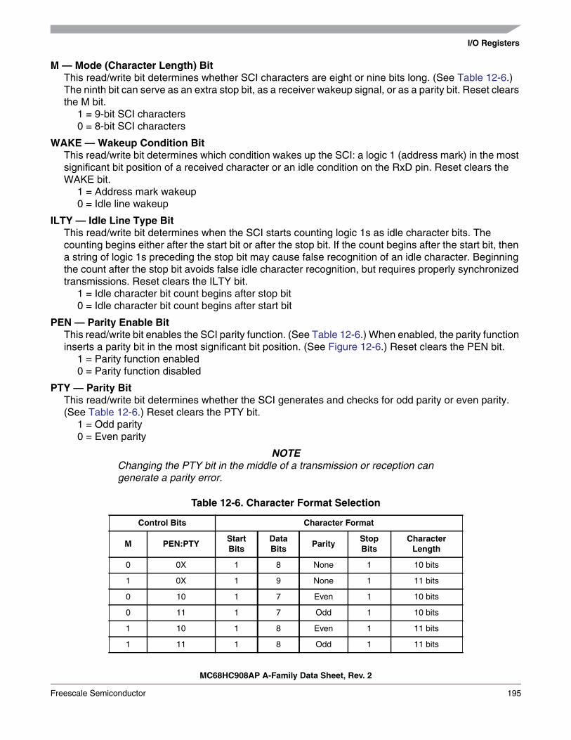
I/O Registers
MC68HC908AP A-Family Data Sheet, Rev. 2
Freescale Semiconductor 195
M — Mode (Character Length) BitThis read/write bit determines whether SCI characters are eight or nine bits long. (See Table 12-6.)The ninth bit can serve as an extra stop bit, as a receiver wakeup signal, or as a parity bit. Reset clearsthe M bit.
1 = 9-bit SCI characters0 = 8-bit SCI characters
WAKE — Wakeup Condition BitThis read/write bit determines which condition wakes up the SCI: a logic 1 (address mark) in the mostsignificant bit position of a received character or an idle condition on the RxD pin. Reset clears theWAKE bit.
1 = Address mark wakeup0 = Idle line wakeup
ILTY — Idle Line Type BitThis read/write bit determines when the SCI starts counting logic 1s as idle character bits. Thecounting begins either after the start bit or after the stop bit. If the count begins after the start bit, thena string of logic 1s preceding the stop bit may cause false recognition of an idle character. Beginningthe count after the stop bit avoids false idle character recognition, but requires properly synchronizedtransmissions. Reset clears the ILTY bit.
1 = Idle character bit count begins after stop bit0 = Idle character bit count begins after start bit
PEN — Parity Enable BitThis read/write bit enables the SCI parity function. (See Table 12-6.) When enabled, the parity functioninserts a parity bit in the most significant bit position. (See Figure 12-6.) Reset clears the PEN bit.
1 = Parity function enabled0 = Parity function disabled
PTY — Parity BitThis read/write bit determines whether the SCI generates and checks for odd parity or even parity.(See Table 12-6.) Reset clears the PTY bit.
1 = Odd parity0 = Even parity
NOTEChanging the PTY bit in the middle of a transmission or reception cangenerate a parity error.
Table 12-6. Character Format Selection
Control Bits Character Format
M PEN:PTYStartBits
DataBits
ParityStopBits
CharacterLength
0 0X 1 8 None 1 10 bits
1 0X 1 9 None 1 11 bits
0 10 1 7 Even 1 10 bits
0 11 1 7 Odd 1 10 bits
1 10 1 8 Even 1 11 bits
1 11 1 8 Odd 1 11 bits

Infrared Serial Communications Interface Module (IRSCI)
MC68HC908AP A-Family Data Sheet, Rev. 2
196 Freescale Semiconductor
12.9.2 IRSCI Control Register 2
IRSCI control register 2:• Enables the following CPU interrupt requests:
– Enables the SCTE bit to generate transmitter CPU interrupt requests– Enables the TC bit to generate transmitter CPU interrupt requests– Enables the SCRF bit to generate receiver CPU interrupt requests– Enables the IDLE bit to generate receiver CPU interrupt requests
• Enables the transmitter• Enables the receiver• Enables SCI wakeup• Transmits SCI break characters
SCTIE — SCI Transmit Interrupt Enable BitThis read/write bit enables the SCTE bit to generate SCI transmitter CPU interrupt requests. Resetclears the SCTIE bit.
1 = SCTE enabled to generate CPU interrupt0 = SCTE not enabled to generate CPU interrupt
TCIE — Transmission Complete Interrupt Enable BitThis read/write bit enables the TC bit to generate SCI transmitter CPU interrupt requests. Reset clearsthe TCIE bit.
1 = TC enabled to generate CPU interrupt requests0 = TC not enabled to generate CPU interrupt requests
SCRIE — SCI Receive Interrupt Enable BitThis read/write bit enables the SCRF bit to generate SCI receiver CPU interrupt requests. Reset clearsthe SCRIE bit.
1 = SCRF enabled to generate CPU interrupt0 = SCRF not enabled to generate CPU interrupt
ILIE — Idle Line Interrupt Enable BitThis read/write bit enables the IDLE bit to generate SCI receiver CPU interrupt requests. Reset clearsthe ILIE bit.
1 = IDLE enabled to generate CPU interrupt requests0 = IDLE not enabled to generate CPU interrupt requests
TE — Transmitter Enable BitSetting this read/write bit begins the transmission by sending a preamble of 10 or 11 logic 1s from thetransmit shift register to the TxD pin. If software clears the TE bit, the transmitter completes anytransmission in progress before the TxD returns to the idle condition (logic 1). Clearing and then settingTE during a transmission queues an idle character to be sent after the character currently beingtransmitted. Reset clears the TE bit.
1 = Transmitter enabled0 = Transmitter disabled
Address: $0041
Bit 7 6 5 4 3 2 1 Bit 0
Read:SCTIE TCIE SCRIE ILIE TE RE RWU SBK
Write:
Reset: 0 0 0 0 0 0 0 0
Figure 12-13. IRSCI Control Register 2 (IRSCC2)

I/O Registers
MC68HC908AP A-Family Data Sheet, Rev. 2
Freescale Semiconductor 197
NOTEWriting to the TE bit is not allowed when the enable SCI bit (ENSCI) is clear.ENSCI is in SCI control register 1.
RE — Receiver Enable BitSetting this read/write bit enables the receiver. Clearing the RE bit disables the receiver but does notaffect receiver interrupt flag bits. Reset clears the RE bit.
1 = Receiver enabled0 = Receiver disabled
NOTEWriting to the RE bit is not allowed when the enable SCI bit (ENSCI) isclear. ENSCI is in SCI control register 1.
RWU — Receiver Wakeup BitThis read/write bit puts the receiver in a standby state during which receiver interrupts are disabled.The WAKE bit in IRSCC1 determines whether an idle input or an address mark brings the receiver outof the standby state and clears the RWU bit. Reset clears the RWU bit.
1 = Standby state0 = Normal operation
SBK — Send Break BitSetting and then clearing this read/write bit transmits a break character followed by a logic 1. The logic1 after the break character guarantees recognition of a valid start bit. If SBK remains set, thetransmitter continuously transmits break characters with no logic 1s between them. Reset clears theSBK bit.
1 = Transmit break characters0 = No break characters being transmitted
NOTEDo not toggle the SBK bit immediately after setting the SCTE bit. TogglingSBK before the preamble begins causes the SCI to send a break characterinstead of a preamble.
12.9.3 IRSCI Control Register 3
IRSCI control register 3:• Stores the ninth SCI data bit received and the ninth SCI data bit to be transmitted• Enables the following interrupts:
– Receiver overrun interrupts– Noise error interrupts– Framing error interrupts– Parity error interrupts
Address: $0042
Bit 7 6 5 4 3 2 1 Bit 0
Read: R8T8 DMARE DMATE ORIE NEIE FEIE PEIE
Write:
Reset: U U 0 0 0 0 0 0
= Unimplemented U = Unaffected
Figure 12-14. IRSCI Control Register 3 (IRSCC3)

Infrared Serial Communications Interface Module (IRSCI)
MC68HC908AP A-Family Data Sheet, Rev. 2
198 Freescale Semiconductor
R8 — Received Bit 8When the SCI is receiving 9-bit characters, R8 is the read-only ninth bit (bit 8) of the receivedcharacter. R8 is received at the same time that the IRSCDR receives the other 8 bits.When the SCI is receiving 8-bit characters, R8 is a copy of the eighth bit (bit 7). Reset has no effecton the R8 bit.
T8 — Transmitted Bit 8When the SCI is transmitting 9-bit characters, T8 is the read/write ninth bit (bit 8) of the transmittedcharacter. T8 is loaded into the transmit shift register at the same time that the IRSCDR is loaded intothe transmit shift register. Reset has no effect on the T8 bit.
DMARE — DMA Receive Enable Bit
CAUTIONThe DMA module is not included on this MCU. Writing a logic 1 to DMAREor DMATE may adversely affect MCU performance.
1 = DMA not enabled to service SCI receiver DMA service requests generated by the SCRF bit (SCIreceiver CPU interrupt requests enabled)
0 = DMA not enabled to service SCI receiver DMA service requests generated by the SCRF bit (SCIreceiver CPU interrupt requests enabled)
DMATE — DMA Transfer Enable Bit
CAUTIONThe DMA module is not included on this MCU. Writing a logic 1 to DMAREor DMATE may adversely affect MCU performance.
1 = SCTE DMA service requests enabled; SCTE CPU interrupt requests disabled0 = SCTE DMA service requests disabled; SCTE CPU interrupt requests enabled
ORIE — Receiver Overrun Interrupt Enable BitThis read/write bit enables SCI error CPU interrupt requests generated by the receiver overrun bit, OR.Reset clears ORIE.
1 = SCI error CPU interrupt requests from OR bit enabled0 = SCI error CPU interrupt requests from OR bit disabled
NEIE — Receiver Noise Error Interrupt Enable BitThis read/write bit enables SCI error CPU interrupt requests generated by the noise error bit, NE.Reset clears NEIE.
1 = SCI error CPU interrupt requests from NE bit enabled0 = SCI error CPU interrupt requests from NE bit disabled
FEIE — Receiver Framing Error Interrupt Enable BitThis read/write bit enables SCI error CPU interrupt requests generated by the framing error bit, FE.Reset clears FEIE.
1 = SCI error CPU interrupt requests from FE bit enabled0 = SCI error CPU interrupt requests from FE bit disabled
PEIE — Receiver Parity Error Interrupt Enable BitThis read/write bit enables SCI error CPU interruptrequests generated by the parity error bit, PE. (See 12.9.4 IRSCI Status Register 1.) Reset clearsPEIE.
1 = SCI error CPU interrupt requests from PE bit enabled0 = SCI error CPU interrupt requests from PE bit disabled

I/O Registers
MC68HC908AP A-Family Data Sheet, Rev. 2
Freescale Semiconductor 199
12.9.4 IRSCI Status Register 1
SCI status register 1 contains flags to signal these conditions:• Transfer of IRSCDR data to transmit shift register complete• Transmission complete• Transfer of receive shift register data to IRSCDR complete• Receiver input idle• Receiver overrun• Noisy data• Framing error• Parity error
SCTE — SCI Transmitter Empty BitThis clearable, read-only bit is set when the IRSCDR transfers a character to the transmit shift register.SCTE can generate an SCI transmitter CPU interrupt request. When the SCTIE bit in IRSCC2 is set,SCTE generates an SCI transmitter CPU interrupt request. In normal operation, clear the SCTE bit byreading IRSCS1 with SCTE set and then writing to IRSCDR. Reset sets the SCTE bit.
1 = IRSCDR data transferred to transmit shift register0 = IRSCDR data not transferred to transmit shift register
TC — Transmission Complete BitThis read-only bit is set when the SCTE bit is set, and no data, preamble, or break character is beingtransmitted. TC generates an SCI transmitter CPU interrupt request if the TCIE bit in IRSCC2 is alsoset. TC is automatically cleared when data, preamble or break is queued and ready to be sent. Theremay be up to 1.5 transmitter clocks of latency between queueing data, preamble, and break and thetransmission actually starting. Reset sets the TC bit.
1 = No transmission in progress0 = Transmission in progress
SCRF — SCI Receiver Full BitThis clearable, read-only bit is set when the data in the receive shift register transfers to the SCI dataregister. SCRF can generate an SCI receiver CPU interrupt request. When the SCRIE bit in IRSCC2is set, SCRF generates a CPU interrupt request. In normal operation, clear the SCRF bit by readingIRSCS1 with SCRF set and then reading the IRSCDR. Reset clears SCRF.
1 = Received data available in IRSCDR0 = Data not available in IRSCDR
IDLE — Receiver Idle BitThis clearable, read-only bit is set when 10 or 11 consecutive logic 1s appear on the receiver input.IDLE generates an SCI receiver CPU interrupt request if the ILIE bit in IRSCC2 is also set. Clear theIDLE bit by reading IRSCS1 with IDLE set and then reading the IRSCDR. After the receiver is enabled,
Address: $0043
Bit 7 6 5 4 3 2 1 Bit 0
Read: SCTE TC SCRF IDLE OR NF FE PE
Write:
Reset: 1 1 0 0 0 0 0 0
= Unimplemented
Figure 12-15. IRSCI Status Register 1 (IRSCS1)

Infrared Serial Communications Interface Module (IRSCI)
MC68HC908AP A-Family Data Sheet, Rev. 2
200 Freescale Semiconductor
it must receive a valid character that sets the SCRF bit before an idle condition can set the IDLE bit.Also, after the IDLE bit has been cleared, a valid character must again set the SCRF bit before an idlecondition can set the IDLE bit. Reset clears the IDLE bit.
1 = Receiver input idle0 = Receiver input active (or idle since the IDLE bit was cleared)
OR — Receiver Overrun BitThis clearable, read-only bit is set when software fails to read the IRSCDR before the receive shiftregister receives the next character. The OR bit generates an SCI error CPU interrupt request if theORIE bit in IRSCC3 is also set. The data in the shift register is lost, but the data already in the IRSCDRis not affected. Clear the OR bit by reading IRSCS1 with OR set and then reading the IRSCDR. Resetclears the OR bit.
1 = Receive shift register full and SCRF = 10 = No receiver overrun
Software latency may allow an overrun to occur between reads of IRSCS1 and IRSCDR in theflag-clearing sequence. Figure 12-16 shows the normal flag-clearing sequence and an example of anoverrun caused by a delayed flag-clearing sequence. The delayed read of IRSCDR does not clear theOR bit because OR was not set when IRSCS1 was read. Byte 2 caused the overrun and is lost. Thenext flag-clearing sequence reads byte 3 in the IRSCDR instead of byte 2.In applications that are subject to software latency or in which it is important to know which byte is lostdue to an overrun, the flag-clearing routine can check the OR bit in a second read of IRSCS1 afterreading the data register.
Figure 12-16. Flag Clearing Sequence
BYTE 1
NORMAL FLAG CLEARING SEQUENCE
READ IRSCS1SCRF = 1
READ IRSCDRBYTE 1
SC
RF
= 1
SC
RF
= 1
BYTE 2 BYTE 3 BYTE 4
OR = 0
READ IRSCS1SCRF = 1
OR = 0
READ IRSCDRBYTE 2
SC
RF
= 0
READ IRSCS1SCRF = 1
OR = 0
SC
RF
= 1
SC
RF
= 0
READ IRSCDRBYTE 3
SC
RF
= 0
BYTE 1
READ IRSCS1SCRF = 1
READ IRSCDRBYTE 1
SC
RF
= 1
SC
RF
= 1
BYTE 2 BYTE 3 BYTE 4
OR = 0
READ IRSCS1SCRF = 1
OR = 1
READ IRSCDRBYTE 3
DELAYED FLAG CLEARING SEQUENCE
OR
= 1
SC
RF
= 1
OR
= 1
SC
RF
= 0
OR
= 1
SC
RF
= 0
OR
= 0

I/O Registers
MC68HC908AP A-Family Data Sheet, Rev. 2
Freescale Semiconductor 201
NF — Receiver Noise Flag BitThis clearable, read-only bit is set when the SCI detects noise on the RxD pin. NF generates an SCIerror CPU interrupt request if the NEIE bit in IRSCC3 is also set. Clear the NF bit by reading IRSCS1and then reading the IRSCDR. Reset clears the NF bit.
1 = Noise detected0 = No noise detected
FE — Receiver Framing Error BitThis clearable, read-only bit is set when a logic 0 is accepted as the stop bit. FE generates an SCI errorCPU interrupt request if the FEIE bit in IRSCC3 also is set. Clear the FE bit by reading IRSCS1 withFE set and then reading the IRSCDR. Reset clears the FE bit.
1 = Framing error detected0 = No framing error detected
PE — Receiver Parity Error BitThis clearable, read-only bit is set when the SCI detects a parity error in incoming data. PE generatesan SCI error CPU interrupt request if the PEIE bit in IRSCC3 is also set. Clear the PE bit by readingIRSCS1 with PE set and then reading the IRSCDR. Reset clears the PE bit.
1 = Parity error detected0 = No parity error detected
12.9.5 IRSCI Status Register 2
IRSCI status register 2 contains flags to signal the following conditions:• Break character detected• Incoming data
BKF — Break Flag BitThis clearable, read-only bit is set when the SCI detects a break character on the RxD pin. In IRSCS1,the FE and SCRF bits are also set. In 9-bit character transmissions, the R8 bit in IRSCC3 is cleared.BKF does not generate a CPU interrupt request. Clear BKF by reading IRSCS2 with BKF set and thenreading the IRSCDR. Once cleared, BKF can become set again only after logic 1s again appear onthe RxD pin followed by another break character. Reset clears the BKF bit.
1 = Break character detected0 = No break character detected
Address: $0044
Bit 7 6 5 4 3 2 1 Bit 0
Read: BKF RPF
Write:
Reset: 0 0 0 0 0 0 0 0
= Unimplemented
Figure 12-17. IRSCI Status Register 2 (IRSCS2)

Infrared Serial Communications Interface Module (IRSCI)
MC68HC908AP A-Family Data Sheet, Rev. 2
202 Freescale Semiconductor
RPF — Reception in Progress Flag BitThis read-only bit is set when the receiver detects a logic 0 during the RT1 time period of the start bitsearch. RPF does not generate an interrupt request. RPF is reset after the receiver detects false startbits (usually from noise or a baud rate mismatch) or when the receiver detects an idle character. PollingRPF before disabling the SCI module or entering stop mode can show whether a reception is inprogress.
1 = Reception in progress0 = No reception in progress
12.9.6 IRSCI Data Register
The IRSCI data register is the buffer between the internal data bus and the receive and transmit shiftregisters. Reset has no effect on data in the IRSCI data register.
R7/T7–R0/T0 — Receive/Transmit Data BitsReading the IRSCDR accesses the read-only received data bits, R7–R0. Writing to the IRSCDR writesthe data to be transmitted, T7–T0. Reset has no effect on the IRSCDR.
NOTEDo not use read/modify/write instructions on the IRSCI data register.
12.9.7 IRSCI Baud Rate Register
The baud rate register selects the baud rate for both the receiver and the transmitter.
CKS — Baud Clock Input SelectThis read/write bit selects the source clock for the baud rate generator. Reset clears the CKS bit,selecting CGMXCLK.
1 = Bus clock drives the baud rate generator0 = CGMXCLK drives the baud rate generator
SCP1 and SCP0 — SCI Baud Rate Prescaler BitsThese read/write bits select the baud rate prescaler divisor as shown in Table 12-7. Reset clears SCP1and SCP0.
Address: $0045
Bit 7 6 5 4 3 2 1 Bit 0
Read: R7 R6 R5 R4 R3 R2 R1 R0
Write: T7 T6 T5 T4 T3 T2 T1 T0
Reset: Unaffected by reset
Figure 12-18. IRSCI Data Register (IRSCDR)
Address: $0046
Bit 7 6 5 4 3 2 1 Bit 0
Read:CKS
0SCP1 SCP0 R SCR2 SCR1 SCR0
Write:
Reset: 0 0 0 0 0 0 0 0
= Unimplemented R = Reserved
Figure 12-19. IRSCI Baud Rate Register (IRSCBR)

I/O Registers
MC68HC908AP A-Family Data Sheet, Rev. 2
Freescale Semiconductor 203
SCR2–SCR0 — SCI Baud Rate Select BitsThese read/write bits select the SCI baud rate divisor as shown in Table 12-8. Reset clearsSCR2–SCR0.
Use this formula to calculate the SCI baud rate:
where:SCI clock source = fBUS or CGMXCLK(selected by CKS bit)PD = prescaler divisorBD = baud rate divisor
Table 12-9 shows the SCI baud rates that can be generated with a 4.9152-MHz bus clock when fBUS isselected as SCI clock source.
Table 12-7. SCI Baud Rate Prescaling
SCP1 and SCP0 Prescaler Divisor (PD)
00 1
01 3
10 4
11 13
Table 12-8. IRSCI Baud Rate Selection
SCR2, SCR1, and SCR0 Baud Rate Divisor (BD)
000 1
001 2
010 4
011 8
100 16
101 32
110 64
111 128
baud rateSCI clock source
16 PD BD××---------------------------------------------=
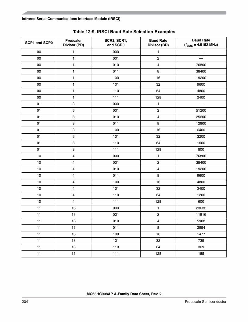
Infrared Serial Communications Interface Module (IRSCI)
MC68HC908AP A-Family Data Sheet, Rev. 2
204 Freescale Semiconductor
Table 12-9. IRSCI Baud Rate Selection Examples
SCP1 and SCP0Prescaler
Divisor (PD)SCR2, SCR1,
and SCR0Baud Rate
Divisor (BD)Baud Rate
(fBUS = 4.9152 MHz)
00 1 000 1 —
00 1 001 2 —
00 1 010 4 76800
00 1 011 8 38400
00 1 100 16 19200
00 1 101 32 9600
00 1 110 64 4800
00 1 111 128 2400
01 3 000 1 —
01 3 001 2 51200
01 3 010 4 25600
01 3 011 8 12800
01 3 100 16 6400
01 3 101 32 3200
01 3 110 64 1600
01 3 111 128 800
10 4 000 1 76800
10 4 001 2 38400
10 4 010 4 19200
10 4 011 8 9600
10 4 100 16 4800
10 4 101 32 2400
10 4 110 64 1200
10 4 111 128 600
11 13 000 1 23632
11 13 001 2 11816
11 13 010 4 5908
11 13 011 8 2954
11 13 100 16 1477
11 13 101 32 739
11 13 110 64 369
11 13 111 128 185

I/O Registers
MC68HC908AP A-Family Data Sheet, Rev. 2
Freescale Semiconductor 205
12.9.8 IRSCI Infrared Control Register
The infrared control register contains the control bits for the infrared sub-module.• Enables the infrared sub-module• Selects the infrared transmitter narrow pulse width
TNP1 and TNP0 — Transmitter Narrow Pulse BitsThese read/write bits select the infrared transmitter narrow pulse width as shown in Table 12-10. Resetclears TNP1 and TNP0.
IREN — Infrared Enable BitThis read/write bit enables the infrared sub-module for encoding and decoding the SCI data stream.When this bit is clear, the infrared sub-module is disabled. Reset clears the IREN bit.
1 = infrared sub-module enabled0 = infrared sub-module disabled
Address: $0047
Bit 7 6 5 4 3 2 1 Bit 0
Read:R
0 0 0R TNP1 TNP0 IREN
Write:
Reset: 0 0 0 0 0 0 0 0
= Unimplemented R = Reserved
Figure 12-20. IRSCI Infrared Control Register (IRSCIRCR)
Table 12-10. Infrared Narrow Pulse Selection
TNP1 and TNP0 Prescaler Divisor (PD)
00 SCI transmits a 3/16 narrow pulse
01 SCI transmits a 1/16 narrow pulse
10SCI transmits a 1/32 narrow pulse
11

Infrared Serial Communications Interface Module (IRSCI)
MC68HC908AP A-Family Data Sheet, Rev. 2
206 Freescale Semiconductor
MC68HC908AP A-Family Data Sheet, Rev. 2
Freescale Semiconductor 205
Chapter 13Serial Peripheral Interface Module (SPI)
13.1 Introduction
This section describes the serial peripheral interface (SPI) module, which allows full-duplex,synchronous, serial communications with peripheral devices.
13.2 Features
Features of the SPI module include the following:• Full-duplex operation• Master and slave modes• Double-buffered operation with separate transmit and receive registers• Four master mode frequencies (maximum = bus frequency ÷ 2)• Maximum slave mode frequency = bus frequency• Serial clock with programmable polarity and phase• Two separately enabled interrupts:
– SPRF (SPI receiver full)– SPTE (SPI transmitter empty)
• Mode fault error flag with CPU interrupt capability• Overflow error flag with CPU interrupt capability• Programmable wired-OR mode
13.3 Pin Name Conventions and I/O Register Addresses
The text that follows describes the SPI. The SPI I/O pin names are SS (slave select), SPSCK (SPI serialclock), CGND (clock ground), MOSI (master out slave in), and MISO (master in/slave out). The SPIshares four I/O pins with four parallel I/O ports.
The full names of the SPI I/O pins are shown in Table 13-1. The generic pin names appear in the text thatfollows.
Figure 13-1 summarizes the SPI I/O registers.
Table 13-1. Pin Name Conventions
SPI GenericPin Names:
MISO MOSI SS SPSCK CGND
Full SPIPin Names:
SPI PTC2/MISO PTC3/MOSI PTC4/SS PTC5/SPSCK VSS

Serial Peripheral Interface Module (SPI)
MC68HC908AP A-Family Data Sheet, Rev. 2
206 Freescale Semiconductor
=
13.4 Functional Description
Figure 13-2 shows the structure of the SPI module.
The SPI module allows full-duplex, synchronous, serial communication between the MCU and peripheraldevices, including other MCUs. Software can poll the SPI status flags or SPI operation can beinterrupt-driven.
The following paragraphs describe the operation of the SPI module.
13.4.1 Master Mode
The SPI operates in master mode when the SPI master bit, SPMSTR, is set.
NOTEConfigure the SPI modules as master or slave before enabling them.Enable the master SPI before enabling the slave SPI. Disable the slave SPIbefore disabling the master SPI. (See 13.13.1 SPI Control Register.)
Only a master SPI module can initiate transmissions. Software begins the transmission from a master SPImodule by writing to the transmit data register. If the shift register is empty, the byte immediately transfersto the shift register, setting the SPI transmitter empty bit, SPTE. The byte begins shifting out on the MOSIpin under the control of the serial clock. (See Figure 13-3.)
The SPR1 and SPR0 bits control the baud rate generator and determine the speed of the shift register.(See 13.13.2 SPI Status and Control Register.) Through the SPSCK pin, the baud rate generator of themaster also controls the shift register of the slave peripheral.
As the byte shifts out on the MOSI pin of the master, another byte shifts in from the slave on the master’sMISO pin. The transmission ends when the receiver full bit, SPRF, becomes set. At the same time thatSPRF becomes set, the byte from the slave transfers to the receive data register. In normal operation,SPRF signals the end of a transmission. Software clears SPRF by reading the SPI status and controlregister with SPRF set and then reading the SPI data register. Writing to the SPI data register clears theSPTE bit.
Addr. Register Name Bit 7 6 5 4 3 2 1 Bit 0
$0010 SPI Control Register (SPCR)Read:
SPRIE R SPMSTR CPOL CPHA SPWOM SPE SPTIEWrite:
Reset: 0 0 1 0 1 0 0 0
$0011SPI Status and Control
Register(SPSCR)
Read: SPRFERRIE
OVRF MODF SPTEMODFEN SPR1 SPR0
Write:Reset: 0 0 0 0 1 0 0 0
$0012SPI Data Register
(SPDR)
Read: R7 R6 R5 R4 R3 R2 R1 R0Write: T7 T6 T5 T4 T3 T2 T1 T0
Reset: Unaffected by reset= Unimplemented R = Reserved
Figure 13-1. SPI I/O Register Summary

Functional Description
MC68HC908AP A-Family Data Sheet, Rev. 2
Freescale Semiconductor 207
Figure 13-2. SPI Module Block Diagram
Figure 13-3. Full-Duplex Master-Slave Connections
TRANSMITTER CPU INTERRUPT REQUEST
RESERVED
RECEIVER/ERROR CPU INTERRUPT REQUEST
7 6 5 4 3 2 1 0
SPR1
SPMSTR
TRANSMIT DATA REGISTER
SHIFT REGISTER
SPR0
CGMOUT ÷ 2
CLOCKSELECT
÷ 2
CLOCKDIVIDER
÷ 8
÷ 32
÷ 128
CLOCKLOGIC
CPHA CPOL
SPI
SPRIE
R
SPE
SPWOM
SPRF
SPTE
OVRF
RESERVED
M
S
PINCONTROL
LOGIC
RECEIVE DATA REGISTER
SPTIE
SPE
INTERNAL BUS
FROM SIM
MODFEN
ERRIE
CONTROL
MODF
SPMSTR
MOSI
MISO
SPSCK
SS
SHIFT REGISTER
SHIFT REGISTER
BAUD RATEGENERATOR
MASTER MCU SLAVE MCU
VDD
MOSI MOSI
MISO MISO
SPSCK SPSCK
SS SS
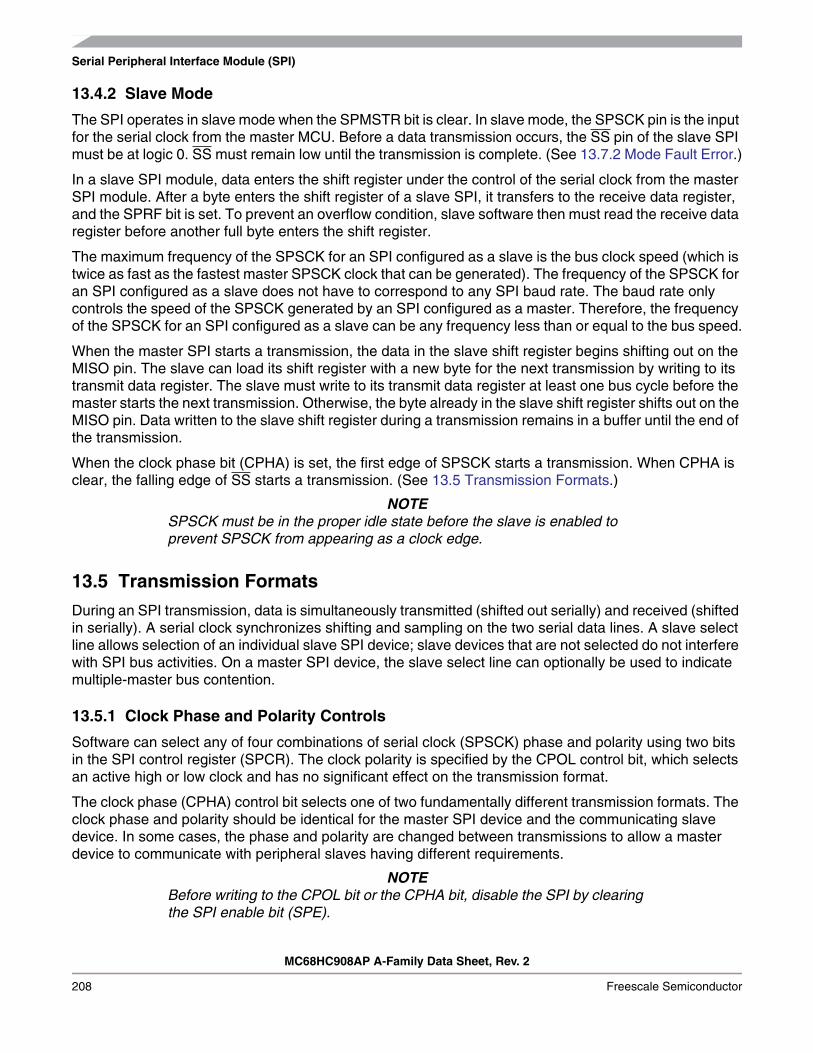
Serial Peripheral Interface Module (SPI)
MC68HC908AP A-Family Data Sheet, Rev. 2
208 Freescale Semiconductor
13.4.2 Slave Mode
The SPI operates in slave mode when the SPMSTR bit is clear. In slave mode, the SPSCK pin is the inputfor the serial clock from the master MCU. Before a data transmission occurs, the SS pin of the slave SPImust be at logic 0. SS must remain low until the transmission is complete. (See 13.7.2 Mode Fault Error.)
In a slave SPI module, data enters the shift register under the control of the serial clock from the masterSPI module. After a byte enters the shift register of a slave SPI, it transfers to the receive data register,and the SPRF bit is set. To prevent an overflow condition, slave software then must read the receive dataregister before another full byte enters the shift register.
The maximum frequency of the SPSCK for an SPI configured as a slave is the bus clock speed (which istwice as fast as the fastest master SPSCK clock that can be generated). The frequency of the SPSCK foran SPI configured as a slave does not have to correspond to any SPI baud rate. The baud rate onlycontrols the speed of the SPSCK generated by an SPI configured as a master. Therefore, the frequencyof the SPSCK for an SPI configured as a slave can be any frequency less than or equal to the bus speed.
When the master SPI starts a transmission, the data in the slave shift register begins shifting out on theMISO pin. The slave can load its shift register with a new byte for the next transmission by writing to itstransmit data register. The slave must write to its transmit data register at least one bus cycle before themaster starts the next transmission. Otherwise, the byte already in the slave shift register shifts out on theMISO pin. Data written to the slave shift register during a transmission remains in a buffer until the end ofthe transmission.
When the clock phase bit (CPHA) is set, the first edge of SPSCK starts a transmission. When CPHA isclear, the falling edge of SS starts a transmission. (See 13.5 Transmission Formats.)
NOTESPSCK must be in the proper idle state before the slave is enabled toprevent SPSCK from appearing as a clock edge.
13.5 Transmission Formats
During an SPI transmission, data is simultaneously transmitted (shifted out serially) and received (shiftedin serially). A serial clock synchronizes shifting and sampling on the two serial data lines. A slave selectline allows selection of an individual slave SPI device; slave devices that are not selected do not interferewith SPI bus activities. On a master SPI device, the slave select line can optionally be used to indicatemultiple-master bus contention.
13.5.1 Clock Phase and Polarity Controls
Software can select any of four combinations of serial clock (SPSCK) phase and polarity using two bitsin the SPI control register (SPCR). The clock polarity is specified by the CPOL control bit, which selectsan active high or low clock and has no significant effect on the transmission format.
The clock phase (CPHA) control bit selects one of two fundamentally different transmission formats. Theclock phase and polarity should be identical for the master SPI device and the communicating slavedevice. In some cases, the phase and polarity are changed between transmissions to allow a masterdevice to communicate with peripheral slaves having different requirements.
NOTEBefore writing to the CPOL bit or the CPHA bit, disable the SPI by clearingthe SPI enable bit (SPE).

Transmission Formats
MC68HC908AP A-Family Data Sheet, Rev. 2
Freescale Semiconductor 209
13.5.2 Transmission Format When CPHA = 0
Figure 13-4 shows an SPI transmission in which CPHA is logic 0. The figure should not be used as areplacement for data sheet parametric information.
Two waveforms are shown for SPSCK: one for CPOL = 0 and another for CPOL = 1. The diagram maybe interpreted as a master or slave timing diagram since the serial clock (SPSCK), master in/slave out(MISO), and master out/slave in (MOSI) pins are directly connected between the master and the slave.The MISO signal is the output from the slave, and the MOSI signal is the output from the master. The SSline is the slave select input to the slave. The slave SPI drives its MISO output only when its slave selectinput (SS) is at logic 0, so that only the selected slave drives to the master. The SS pin of the master isnot shown but is assumed to be inactive. The SS pin of the master must be high or must be reconfiguredas general-purpose I/O not affecting the SPI. (See 13.7.2 Mode Fault Error.) When CPHA = 0, the firstSPSCK edge is the MSB capture strobe. Therefore, the slave must begin driving its data before the firstSPSCK edge, and a falling edge on the SS pin is used to start the slave data transmission. The slave’sSS pin must be toggled back to high and then low again between each byte transmitted as shown inFigure 13-5.
Figure 13-4. Transmission Format (CPHA = 0)
Figure 13-5. CPHA/SS Timing
When CPHA = 0 for a slave, the falling edge of SS indicates the beginning of the transmission. Thiscauses the SPI to leave its idle state and begin driving the MISO pin with the MSB of its data. Once thetransmission begins, no new data is allowed into the shift register from the transmit data register.Therefore, the SPI data register of the slave must be loaded with transmit data before the falling edge ofSS. Any data written after the falling edge is stored in the transmit data register and transferred to the shiftregister after the current transmission.
BIT 6 BIT 5 BIT 4 BIT 3 BIT 2 BIT 1 LSBMSB
BIT 6 BIT 5 BIT 4 BIT 3 BIT 2 BIT 1 LSBMSB
1 2 3 4 5 6 7 8SPSCK CYCLE #FOR REFERENCE
SPSCK; CPOL = 0
SPSCK; CPOL =1
MOSIFROM MASTER
MISOFROM SLAVE
SS; TO SLAVE
CAPTURE STROBE
BYTE 1 BYTE 3MISO/MOSI BYTE 2
MASTER SS
SLAVE SSCPHA = 0
SLAVE SSCPHA = 1

Serial Peripheral Interface Module (SPI)
MC68HC908AP A-Family Data Sheet, Rev. 2
210 Freescale Semiconductor
13.5.3 Transmission Format When CPHA = 1
Figure 13-6 shows an SPI transmission in which CPHA is logic 1. The figure should not be used as areplacement for data sheet parametric information. Two waveforms are shown for SPSCK: one forCPOL = 0 and another for CPOL = 1. The diagram may be interpreted as a master or slave timingdiagram since the serial clock (SPSCK), master in/slave out (MISO), and master out/slave in (MOSI) pinsare directly connected between the master and the slave. The MISO signal is the output from the slave,and the MOSI signal is the output from the master. The SS line is the slave select input to the slave. Theslave SPI drives its MISO output only when its slave select input (SS) is at logic 0, so that only the selectedslave drives to the master. The SS pin of the master is not shown but is assumed to be inactive. The SSpin of the master must be high or must be reconfigured as general-purpose I/O not affecting the SPI. (See13.7.2 Mode Fault Error.) When CPHA = 1, the master begins driving its MOSI pin on the first SPSCKedge. Therefore, the slave uses the first SPSCK edge as a start transmission signal. The SS pin canremain low between transmissions. This format may be preferable in systems having only one master andonly one slave driving the MISO data line.
Figure 13-6. Transmission Format (CPHA = 1)
When CPHA = 1 for a slave, the first edge of the SPSCK indicates the beginning of the transmission. Thiscauses the SPI to leave its idle state and begin driving the MISO pin with the MSB of its data. Once thetransmission begins, no new data is allowed into the shift register from the transmit data register.Therefore, the SPI data register of the slave must be loaded with transmit data before the first edge ofSPSCK. Any data written after the first edge is stored in the transmit data register and transferred to theshift register after the current transmission.
13.5.4 Transmission Initiation Latency
When the SPI is configured as a master (SPMSTR = 1), writing to the SPDR starts a transmission. CPHAhas no effect on the delay to the start of the transmission, but it does affect the initial state of the SPSCKsignal. When CPHA = 0, the SPSCK signal remains inactive for the first half of the first SPSCK cycle.When CPHA = 1, the first SPSCK cycle begins with an edge on the SPSCK line from its inactive to itsactive level. The SPI clock rate (selected by SPR1:SPR0) affects the delay from the write to SPDR andthe start of the SPI transmission. (See Figure 13-7.) The internal SPI clock in the master is a free-runningderivative of the internal MCU clock. To conserve power, it is enabled only when both the SPE andSPMSTR bits are set. SPSCK edges occur halfway through the low time of the internal MCU clock. Sincethe SPI clock is free-running, it is uncertain where the write to the SPDR occurs relative to the slowerSPSCK. This uncertainty causes the variation in the initiation delay shown in Figure 13-7. This delay isno longer than a single SPI bit time. That is, the maximum delay is two MCU bus cycles for DIV2, eightMCU bus cycles for DIV8, 32 MCU bus cycles for DIV32, and 128 MCU bus cycles for DIV128.
BIT 6 BIT 5 BIT 4 BIT 3 BIT 2 BIT 1 LSBMSB
BIT 6 BIT 5 BIT 4 BIT 3 BIT 2 BIT 1 LSBMSB
1 2 3 4 5 6 7 8SPSCK CYCLE #FOR REFERENCE
SPSCK; CPOL = 0
SPSCK; CPOL =1
MOSIFROM MASTER
MISOFROM SLAVE
SS; TO SLAVE
CAPTURE STROBE

Queuing Transmission Data
MC68HC908AP A-Family Data Sheet, Rev. 2
Freescale Semiconductor 211
Figure 13-7. Transmission Start Delay (Master)
13.6 Queuing Transmission Data
The double-buffered transmit data register allows a data byte to be queued and transmitted. For an SPIconfigured as a master, a queued data byte is transmitted immediately after the previous transmissionhas completed. The SPI transmitter empty flag (SPTE) indicates when the transmit data buffer is readyto accept new data. Write to the transmit data register only when the SPTE bit is high. Figure 13-8 showsthe timing associated with doing back-to-back transmissions with the SPI (SPSCK has CPHA: CPOL =1:0).
WRITETO SPDR INITIATION DELAY
BUS
MOSI
SPSCKCPHA = 1
SPSCKCPHA = 0
SPSCK CYCLENUMBER
MSB BIT 6
1 2
CLOCK
WRITETO SPDR
EARLIESTLATEST
SPSCK = INTERNAL CLOCK ÷ 2;
EARLIEST LATEST
2 POSSIBLE START POINTS
SPSCK = INTERNAL CLOCK ÷ 8;8 POSSIBLE START POINTS
EARLIEST LATESTSPSCK = INTERNAL CLOCK ÷ 32;32 POSSIBLE START POINTS
EARLIEST LATESTSPSCK = INTERNAL CLOCK ÷ 128;128 POSSIBLE START POINTS
WRITETO SPDR
WRITETO SPDR
WRITETO SPDR
BUSCLOCK
BIT 5
3
BUSCLOCK
BUSCLOCK
BUSCLOCK
INITIATION DELAY FROM WRITE SPDR TO TRANSFER BEGIN
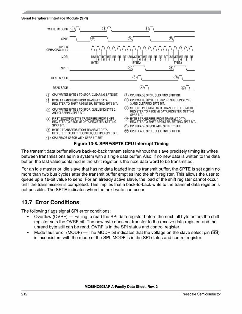
Serial Peripheral Interface Module (SPI)
MC68HC908AP A-Family Data Sheet, Rev. 2
212 Freescale Semiconductor
Figure 13-8. SPRF/SPTE CPU Interrupt Timing
The transmit data buffer allows back-to-back transmissions without the slave precisely timing its writesbetween transmissions as in a system with a single data buffer. Also, if no new data is written to the databuffer, the last value contained in the shift register is the next data word to be transmitted.
For an idle master or idle slave that has no data loaded into its transmit buffer, the SPTE is set again nomore than two bus cycles after the transmit buffer empties into the shift register. This allows the user toqueue up a 16-bit value to send. For an already active slave, the load of the shift register cannot occuruntil the transmission is completed. This implies that a back-to-back write to the transmit data register isnot possible. The SPTE indicates when the next write can occur.
13.7 Error Conditions
The following flags signal SPI error conditions:• Overflow (OVRF) — Failing to read the SPI data register before the next full byte enters the shift
register sets the OVRF bit. The new byte does not transfer to the receive data register, and theunread byte still can be read. OVRF is in the SPI status and control register.
• Mode fault error (MODF) — The MODF bit indicates that the voltage on the slave select pin (SS)is inconsistent with the mode of the SPI. MODF is in the SPI status and control register.
BIT3
MOSI
SPSCK
SPTE
WRITE TO SPDR 1
CPU WRITES BYTE 2 TO SPDR, QUEUEING BYTE 2
CPU WRITES BYTE 1 TO SPDR, CLEARING SPTE BIT.
BYTE 1 TRANSFERS FROM TRANSMIT DATA
3
1
2
2
3
5
REGISTER TO SHIFT REGISTER, SETTING SPTE BIT.
SPRF
READ SPSCR
MSB BIT6
BIT5
BIT4
BIT2
BIT1
LSBMSB BIT6
BIT5
BIT4
BIT3
BIT2
BIT1
LSBMSB BIT6
BYTE 2 TRANSFERS FROM TRANSMIT DATA
CPU WRITES BYTE 3 TO SPDR, QUEUEING BYTE
BYTE 3 TRANSFERS FROM TRANSMIT DATA
5
8
10
8
10
4 FIRST INCOMING BYTE TRANSFERS FROM SHIFT
6 CPU READS SPSCR WITH SPRF BIT SET.
4
6
9
SECOND INCOMING BYTE TRANSFERS FROM SHIFT9
11
AND CLEARING SPTE BIT.
REGISTER TO SHIFT REGISTER, SETTING SPTE BIT.
REGISTER TO RECEIVE DATA REGISTER, SETTINGSPRF BIT.
3 AND CLEARING SPTE BIT.
REGISTER TO SHIFT REGISTER, SETTING SPTE BIT.
REGISTER TO RECEIVE DATA REGISTER, SETTINGSPRF BIT.
12 CPU READS SPDR, CLEARING SPRF BIT.
BIT5
BIT4
BYTE 1 BYTE 2 BYTE 3
7 12READ SPDR
7 CPU READS SPDR, CLEARING SPRF BIT.
11 CPU READS SPSCR WITH SPRF BIT SET.
CPHA:CPOL = 1:0

Error Conditions
MC68HC908AP A-Family Data Sheet, Rev. 2
Freescale Semiconductor 213
13.7.1 Overflow Error
The overflow flag (OVRF) becomes set if the receive data register still has unread data from a previoustransmission when the capture strobe of bit 1 of the next transmission occurs. The bit 1 capture strobeoccurs in the middle of SPSCK cycle 7. (See Figure 13-4 and Figure 13-6.) If an overflow occurs, all datareceived after the overflow and before the OVRF bit is cleared does not transfer to the receive dataregister and does not set the SPI receiver full bit (SPRF). The unread data that transferred to the receivedata register before the overflow occurred can still be read. Therefore, an overflow error always indicatesthe loss of data. Clear the overflow flag by reading the SPI status and control register and then readingthe SPI data register.
OVRF generates a receiver/error CPU interrupt request if the error interrupt enable bit (ERRIE) is alsoset. The SPRF, MODF, and OVRF interrupts share the same CPU interrupt vector. (See Figure 13-11.)It is not possible to enable MODF or OVRF individually to generate a receiver/error CPU interrupt request.However, leaving MODFEN low prevents MODF from being set.
If the CPU SPRF interrupt is enabled and the OVRF interrupt is not, watch for an overflow condition.Figure 13-9 shows how it is possible to miss an overflow. The first part of Figure 13-9 shows how it ispossible to read the SPSCR and SPDR to clear the SPRF without problems. However, as illustrated bythe second transmission example, the OVRF bit can be set in between the time that SPSCR and SPDRare read.
Figure 13-9. Missed Read of Overflow Condition
In this case, an overflow can be missed easily. Since no more SPRF interrupts can be generated until thisOVRF is serviced, it is not obvious that bytes are being lost as more transmissions are completed. Toprevent this, either enable the OVRF interrupt or do another read of the SPSCR following the read of theSPDR. This ensures that the OVRF was not set before the SPRF was cleared and that futuretransmissions can set the SPRF bit. Figure 13-10 illustrates this process. Generally, to avoid this secondSPSCR read, enable the OVRF to the CPU by setting the ERRIE bit.
READ
READ
OVRF
SPRF
BYTE 1 BYTE 2 BYTE 3 BYTE 4
BYTE 1 SETS SPRF BIT.
CPU READS SPSCR WITH SPRF BIT SET
CPU READS BYTE 1 IN SPDR,
BYTE 2 SETS SPRF BIT.
CPU READS SPSCR WITH SPRF BIT SET
BYTE 3 SETS OVRF BIT. BYTE 3 IS LOST.
CPU READS BYTE 2 IN SPDR, CLEARING SPRF BIT,
BYTE 4 FAILS TO SET SPRF BIT BECAUSE
1
1
2
3
4
5
6
7
8
2
3
4
5
6
7
8
CLEARING SPRF BIT. BUT NOT OVRF BIT.
OVRF BIT IS NOT CLEARED. BYTE 4 IS LOST.
AND OVRF BIT CLEAR.
AND OVRF BIT CLEAR.
SPSCR
SPDR
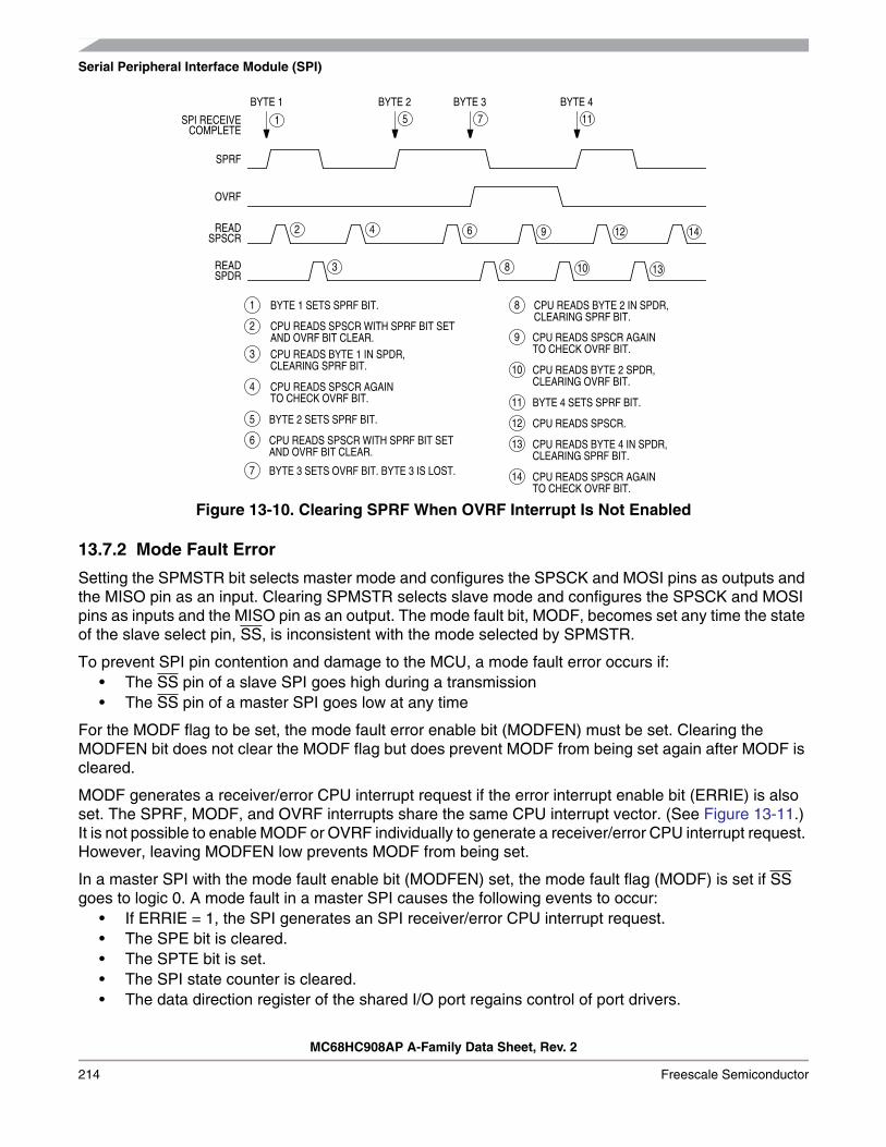
Serial Peripheral Interface Module (SPI)
MC68HC908AP A-Family Data Sheet, Rev. 2
214 Freescale Semiconductor
Figure 13-10. Clearing SPRF When OVRF Interrupt Is Not Enabled
13.7.2 Mode Fault Error
Setting the SPMSTR bit selects master mode and configures the SPSCK and MOSI pins as outputs andthe MISO pin as an input. Clearing SPMSTR selects slave mode and configures the SPSCK and MOSIpins as inputs and the MISO pin as an output. The mode fault bit, MODF, becomes set any time the stateof the slave select pin, SS, is inconsistent with the mode selected by SPMSTR.
To prevent SPI pin contention and damage to the MCU, a mode fault error occurs if:• The SS pin of a slave SPI goes high during a transmission• The SS pin of a master SPI goes low at any time
For the MODF flag to be set, the mode fault error enable bit (MODFEN) must be set. Clearing theMODFEN bit does not clear the MODF flag but does prevent MODF from being set again after MODF iscleared.
MODF generates a receiver/error CPU interrupt request if the error interrupt enable bit (ERRIE) is alsoset. The SPRF, MODF, and OVRF interrupts share the same CPU interrupt vector. (See Figure 13-11.)It is not possible to enable MODF or OVRF individually to generate a receiver/error CPU interrupt request.However, leaving MODFEN low prevents MODF from being set.
In a master SPI with the mode fault enable bit (MODFEN) set, the mode fault flag (MODF) is set if SSgoes to logic 0. A mode fault in a master SPI causes the following events to occur:
• If ERRIE = 1, the SPI generates an SPI receiver/error CPU interrupt request.• The SPE bit is cleared.• The SPTE bit is set.• The SPI state counter is cleared.• The data direction register of the shared I/O port regains control of port drivers.
READ
READ
OVRF
SPRF
BYTE 1 BYTE 2 BYTE 3 BYTE 4
1
BYTE 1 SETS SPRF BIT.
CPU READS SPSCR WITH SPRF BIT SET
CPU READS BYTE 1 IN SPDR,
CPU READS SPSCR AGAIN
BYTE 2 SETS SPRF BIT.
CPU READS SPSCR WITH SPRF BIT SET
BYTE 3 SETS OVRF BIT. BYTE 3 IS LOST.
CPU READS BYTE 2 IN SPDR,
CPU READS SPSCR AGAIN
CPU READS BYTE 2 SPDR,
BYTE 4 SETS SPRF BIT.
CPU READS SPSCR.
CPU READS BYTE 4 IN SPDR,
CPU READS SPSCR AGAIN
1
2
3CLEARING SPRF BIT.
4TO CHECK OVRF BIT.
5
6
7
8
9
CLEARING SPRF BIT.
TO CHECK OVRF BIT.
10CLEARING OVRF BIT.
11
12
13
14
2
3
4
5
6
7
8
9
10
11
12
13
14
CLEARING SPRF BIT.
TO CHECK OVRF BIT.
SPI RECEIVECOMPLETE
AND OVRF BIT CLEAR.
AND OVRF BIT CLEAR.
SPSCR
SPDR

Interrupts
MC68HC908AP A-Family Data Sheet, Rev. 2
Freescale Semiconductor 215
NOTETo prevent bus contention with another master SPI after a mode fault error,clear all SPI bits of the data direction register of the shared I/O port beforeenabling the SPI.
When configured as a slave (SPMSTR = 0), the MODF flag is set if SS goes high during a transmission.When CPHA = 0, a transmission begins when SS goes low and ends once the incoming SPSCK goesback to its idle level following the shift of the eighth data bit. When CPHA = 1, the transmission beginswhen the SPSCK leaves its idle level and SS is already low. The transmission continues until the SPSCKreturns to its idle level following the shift of the last data bit. (See 13.5 Transmission Formats.)
NOTESetting the MODF flag does not clear the SPMSTR bit. The SPMSTR bithas no function when SPE = 0. Reading SPMSTR when MODF = 1 showsthe difference between a MODF occurring when the SPI is a master andwhen it is a slave.
When CPHA = 0, a MODF occurs if a slave is selected (SS is at logic 0) andlater unselected (SS is at logic 1) even if no SPSCK is sent to that slave.This happens because SS at logic 0 indicates the start of the transmission(MISO driven out with the value of MSB) for CPHA = 0. When CPHA = 1, aslave can be selected and then later unselected with no transmissionoccurring. Therefore, MODF does not occur since a transmission wasnever begun.
In a slave SPI (MSTR = 0), the MODF bit generates an SPI receiver/error CPU interrupt request if theERRIE bit is set. The MODF bit does not clear the SPE bit or reset the SPI in any way. Software can abortthe SPI transmission by clearing the SPE bit of the slave.
NOTEA logic 1 voltage on the SS pin of a slave SPI puts the MISO pin in a highimpedance state. Also, the slave SPI ignores all incoming SPSCK clocks,even if it was already in the middle of a transmission.
To clear the MODF flag, read the SPSCR with the MODF bit set and then write to the SPCR register. Thisentire clearing mechanism must occur with no MODF condition existing or else the flag is not cleared.
13.8 Interrupts
Four SPI status flags can be enabled to generate CPU interrupt requests.
Table 13-2. SPI Interrupts
Flag Request
SPTETransmitter empty
SPI transmitter CPU interrupt request(SPTIE = 1, SPE = 1)
SPRFReceiver full
SPI receiver CPU interrupt request (SPRIE = 1)
OVRFOverflow
SPI receiver/error interrupt request (ERRIE = 1)
MODFMode fault
SPI receiver/error interrupt request (ERRIE = 1)

Serial Peripheral Interface Module (SPI)
MC68HC908AP A-Family Data Sheet, Rev. 2
216 Freescale Semiconductor
Reading the SPI status and control register with SPRF set and then reading the receive data registerclears SPRF. The clearing mechanism for the SPTE flag is always just a write to the transmit dataregister.
The SPI transmitter interrupt enable bit (SPTIE) enables the SPTE flag to generate transmitter CPUinterrupt requests, provided that the SPI is enabled (SPE = 1).
The SPI receiver interrupt enable bit (SPRIE) enables the SPRF bit to generate receiver CPU interruptrequests, regardless of the state of the SPE bit. (See Figure 13-11.)
The error interrupt enable bit (ERRIE) enables both the MODF and OVRF bits to generate a receiver/errorCPU interrupt request.
The mode fault enable bit (MODFEN) can prevent the MODF flag from being set so that only the OVRFbit is enabled by the ERRIE bit to generate receiver/error CPU interrupt requests.
Figure 13-11. SPI Interrupt Request Generation
The following sources in the SPI status and control register can generate CPU interrupt requests:• SPI receiver full bit (SPRF) — The SPRF bit becomes set every time a byte transfers from the shift
register to the receive data register. If the SPI receiver interrupt enable bit, SPRIE, is also set,SPRF generates an SPI receiver/error CPU interrupt request.
• SPI transmitter empty (SPTE) — The SPTE bit becomes set every time a byte transfers from thetransmit data register to the shift register. If the SPI transmit interrupt enable bit, SPTIE, is also set,SPTE generates an SPTE CPU interrupt request.
13.9 Resetting the SPI
Any system reset completely resets the SPI. Partial resets occur whenever the SPI enable bit (SPE) islow. Whenever SPE is low, the following occurs:
• The SPTE flag is set.• Any transmission currently in progress is aborted.
SPTE SPTIE
SPRFSPRIE
R
ERRIE
MODF
OVRF
SPE
CPU INTERRUPT REQUEST
CPU INTERRUPT REQUEST
NOT AVAILABLE
SPI TRANSMITTER
NOT AVAILABLE
SPI RECEIVER/ERROR

Low-Power Modes
MC68HC908AP A-Family Data Sheet, Rev. 2
Freescale Semiconductor 217
• The shift register is cleared.• The SPI state counter is cleared, making it ready for a new complete transmission.• All the SPI port logic is defaulted back to being general-purpose I/O.
These items are reset only by a system reset:• All control bits in the SPCR register• All control bits in the SPSCR register (MODFEN, ERRIE, SPR1, and SPR0)• The status flags SPRF, OVRF, and MODF
By not resetting the control bits when SPE is low, the user can clear SPE between transmissions withouthaving to set all control bits again when SPE is set back high for the next transmission.
By not resetting the SPRF, OVRF, and MODF flags, the user can still service these interrupts after theSPI has been disabled. The user can disable the SPI by writing 0 to the SPE bit. The SPI can also bedisabled by a mode fault occurring in an SPI that was configured as a master with the MODFEN bit set.
13.10 Low-Power Modes
The WAIT and STOP instructions put the MCU in low power-consumption standby modes.
13.10.1 Wait Mode
The SPI module remains active after the execution of a WAIT instruction. In wait mode the SPI moduleregisters are not accessible by the CPU. Any enabled CPU interrupt request from the SPI module canbring the MCU out of wait mode.
If SPI module functions are not required during wait mode, reduce power consumption by disabling theSPI module before executing the WAIT instruction.
To exit wait mode when an overflow condition occurs, enable the OVRF bit to generate CPU interruptrequests by setting the error interrupt enable bit (ERRIE). (See 13.8 Interrupts.)
13.10.2 Stop Mode
The SPI module is inactive after the execution of a STOP instruction. The STOP instruction does notaffect register conditions. SPI operation resumes after an external interrupt. If stop mode is exited byreset, any transfer in progress is aborted, and the SPI is reset.
13.11 SPI During Break Interrupts
The system integration module (SIM) controls whether status bits in other modules can be cleared duringthe break state. The BCFE bit in the SIM break flag control register (SBFCR) enables software to clearstatus bits during the break state. (See Chapter 7 System Integration Module (SIM).)
To allow software to clear status bits during a break interrupt, write a logic 1 to the BCFE bit. If a statusbit is cleared during the break state, it remains cleared when the MCU exits the break state.
To protect status bits during the break state, write a logic 0 to the BCFE bit. With BCFE at logic 0 (itsdefault state), software can read and write I/O registers during the break state without affecting status bits.Some status bits have a 2-step read/write clearing procedure. If software does the first step on such a bitbefore the break, the bit cannot change during the break state as long as BCFE is at logic 0. After thebreak, doing the second step clears the status bit.

Serial Peripheral Interface Module (SPI)
MC68HC908AP A-Family Data Sheet, Rev. 2
218 Freescale Semiconductor
Since the SPTE bit cannot be cleared during a break with the BCFE bit cleared, a write to the transmitdata register in break mode does not initiate a transmission nor is this data transferred into the shiftregister. Therefore, a write to the SPDR in break mode with the BCFE bit cleared has no effect.
13.12 I/O Signals
The SPI module has five I/O pins and shares four of them with a parallel I/O port. They are:• MISO — Data received• MOSI — Data transmitted• SPSCK — Serial clock• SS — Slave select• CGND — Clock ground (internally connected to VSS)
The SPI has limited inter-integrated circuit (I2C) capability (requiring software support) as a master in asingle-master environment. To communicate with I2C peripherals, MOSI becomes an open-drain outputwhen the SPWOM bit in the SPI control register is set. In I2C communication, the MOSI and MISO pinsare connected to a bidirectional pin from the I2C peripheral and through a pullup resistor to VDD.
13.12.1 MISO (Master In/Slave Out)
MISO is one of the two SPI module pins that transmits serial data. In full duplex operation, the MISO pinof the master SPI module is connected to the MISO pin of the slave SPI module. The master SPIsimultaneously receives data on its MISO pin and transmits data from its MOSI pin.
Slave output data on the MISO pin is enabled only when the SPI is configured as a slave. The SPI isconfigured as a slave when its SPMSTR bit is logic 0 and its SS pin is at logic 0. To support amultiple-slave system, a logic 1 on the SS pin puts the MISO pin in a high-impedance state.
When enabled, the SPI controls data direction of the MISO pin regardless of the state of the data directionregister of the shared I/O port.
13.12.2 MOSI (Master Out/Slave In)
MOSI is one of the two SPI module pins that transmits serial data. In full-duplex operation, the MOSI pinof the master SPI module is connected to the MOSI pin of the slave SPI module. The master SPIsimultaneously transmits data from its MOSI pin and receives data on its MISO pin.
When enabled, the SPI controls data direction of the MOSI pin regardless of the state of the data directionregister of the shared I/O port.
13.12.3 SPSCK (Serial Clock)
The serial clock synchronizes data transmission between master and slave devices. In a master MCU,the SPSCK pin is the clock output. In a slave MCU, the SPSCK pin is the clock input. In full-duplexoperation, the master and slave MCUs exchange a byte of data in eight serial clock cycles.
When enabled, the SPI controls data direction of the SPSCK pin regardless of the state of the datadirection register of the shared I/O port.

I/O Signals
MC68HC908AP A-Family Data Sheet, Rev. 2
Freescale Semiconductor 219
13.12.4 SS (Slave Select)
The SS pin has various functions depending on the current state of the SPI. For an SPI configured as aslave, the SS is used to select a slave. For CPHA = 0, the SS is used to define the start of a transmission.(See 13.5 Transmission Formats.) Since it is used to indicate the start of a transmission, the SS must betoggled high and low between each byte transmitted for the CPHA = 0 format. However, it can remain lowbetween transmissions for the CPHA = 1 format. See Figure 13-12.
Figure 13-12. CPHA/SS Timing
When an SPI is configured as a slave, the SS pin is always configured as an input. It cannot be used asa general-purpose I/O regardless of the state of the MODFEN control bit. However, the MODFEN bit canstill prevent the state of the SS from creating a MODF error. (See 13.13.2 SPI Status and ControlRegister.)
NOTEA logic 1 voltage on the SS pin of a slave SPI puts the MISO pin in ahigh-impedance state. The slave SPI ignores all incoming SPSCK clocks,even if it was already in the middle of a transmission.
When an SPI is configured as a master, the SS input can be used in conjunction with the MODF flag toprevent multiple masters from driving MOSI and SPSCK. (See 13.7.2 Mode Fault Error.) For the state ofthe SS pin to set the MODF flag, the MODFEN bit in the SPSCK register must be set. If the MODFEN bitis low for an SPI master, the SS pin can be used as a general-purpose I/O under the control of the datadirection register of the shared I/O port. With MODFEN high, it is an input-only pin to the SPI regardlessof the state of the data direction register of the shared I/O port.
The CPU can always read the state of the SS pin by configuring the appropriate pin as an input andreading the port data register. (See Table 13-3.)
Table 13-3. SPI Configuration
SPE SPMSTR MODFEN SPI Configuration State of SS Logic
0 X(1) X Not enabledGeneral-purpose I/O;
SS ignored by SPI
1 0 X Slave Input-only to SPI
1 1 0 Master without MODFGeneral-purpose I/O;
SS ignored by SPI
1 1 1 Master with MODF Input-only to SPI
Note 1. X = Don’t care
BYTE 1 BYTE 3MISO/MOSI BYTE 2
MASTER SS
SLAVE SSCPHA = 0
SLAVE SSCPHA = 1
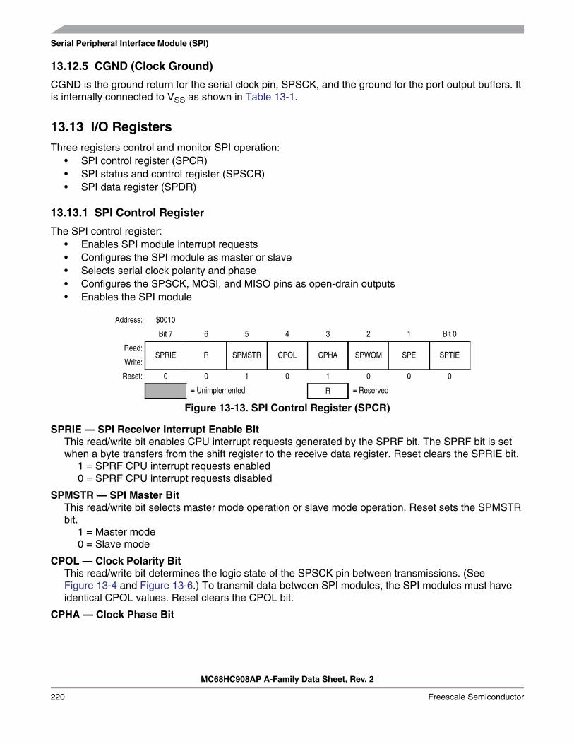
Serial Peripheral Interface Module (SPI)
MC68HC908AP A-Family Data Sheet, Rev. 2
220 Freescale Semiconductor
13.12.5 CGND (Clock Ground)
CGND is the ground return for the serial clock pin, SPSCK, and the ground for the port output buffers. Itis internally connected to VSS as shown in Table 13-1.
13.13 I/O Registers
Three registers control and monitor SPI operation:• SPI control register (SPCR)• SPI status and control register (SPSCR)• SPI data register (SPDR)
13.13.1 SPI Control Register
The SPI control register:• Enables SPI module interrupt requests• Configures the SPI module as master or slave• Selects serial clock polarity and phase• Configures the SPSCK, MOSI, and MISO pins as open-drain outputs• Enables the SPI module
SPRIE — SPI Receiver Interrupt Enable BitThis read/write bit enables CPU interrupt requests generated by the SPRF bit. The SPRF bit is setwhen a byte transfers from the shift register to the receive data register. Reset clears the SPRIE bit.
1 = SPRF CPU interrupt requests enabled0 = SPRF CPU interrupt requests disabled
SPMSTR — SPI Master BitThis read/write bit selects master mode operation or slave mode operation. Reset sets the SPMSTRbit.
1 = Master mode0 = Slave mode
CPOL — Clock Polarity BitThis read/write bit determines the logic state of the SPSCK pin between transmissions. (SeeFigure 13-4 and Figure 13-6.) To transmit data between SPI modules, the SPI modules must haveidentical CPOL values. Reset clears the CPOL bit.
CPHA — Clock Phase Bit
Address: $0010
Bit 7 6 5 4 3 2 1 Bit 0
Read:SPRIE R SPMSTR CPOL CPHA SPWOM SPE SPTIE
Write:
Reset: 0 0 1 0 1 0 0 0
= Unimplemented R = Reserved
Figure 13-13. SPI Control Register (SPCR)

I/O Registers
MC68HC908AP A-Family Data Sheet, Rev. 2
Freescale Semiconductor 221
This read/write bit controls the timing relationship between the serial clock and SPI data. (SeeFigure 13-4 and Figure 13-6.) To transmit data between SPI modules, the SPI modules must haveidentical CPHA values. When CPHA = 0, the SS pin of the slave SPI module must be set to logic 1between bytes. (See Figure 13-12.) Reset sets the CPHA bit.

Serial Peripheral Interface Module (SPI)
MC68HC908AP A-Family Data Sheet, Rev. 2
222 Freescale Semiconductor
SPWOM — SPI Wired-OR Mode BitThis read/write bit disables the pullup devices on pins SPSCK, MOSI, and MISO so that those pinsbecome open-drain outputs.
1 = Wired-OR SPSCK, MOSI, and MISO pins0 = Normal push-pull SPSCK, MOSI, and MISO pins
SPE — SPI EnableThis read/write bit enables the SPI module. Clearing SPE causes a partial reset of the SPI. (See 13.9Resetting the SPI.) Reset clears the SPE bit.
1 = SPI module enabled0 = SPI module disabled
SPTIE— SPI Transmit Interrupt EnableThis read/write bit enables CPU interrupt requests generated by the SPTE bit. SPTE is set when a bytetransfers from the transmit data register to the shift register. Reset clears the SPTIE bit.
1 = SPTE CPU interrupt requests enabled0 = SPTE CPU interrupt requests disabled
13.13.2 SPI Status and Control Register
The SPI status and control register contains flags to signal these conditions:• Receive data register full• Failure to clear SPRF bit before next byte is received (overflow error)• Inconsistent logic level on SS pin (mode fault error)• Transmit data register empty
The SPI status and control register also contains bits that perform these functions:• Enable error interrupts• Enable mode fault error detection• Select master SPI baud rate
SPRF — SPI Receiver Full BitThis clearable, read-only flag is set each time a byte transfers from the shift register to the receive dataregister. SPRF generates a CPU interrupt request if the SPRIE bit in the SPI control register is set also.During an SPRF CPU interrupt, the CPU clears SPRF by reading the SPI status and control registerwith SPRF set and then reading the SPI data register. Reset clears the SPRF bit.
1 = Receive data register full0 = Receive data register not full
Address $0011
Bit 7 6 5 4 3 2 1 Bit 0
Read: SPRFERRIE
OVRF MODF SPTEMODFEN SPR1 SPR0
Write:
Reset: 0 0 0 0 1 0 0 0
= Unimplemented
Figure 13-14. SPI Status and Control Register (SPSCR)
I/O Registers
MC68HC908AP A-Family Data Sheet, Rev. 2
Freescale Semiconductor 223
ERRIE — Error Interrupt Enable BitThis read/write bit enables the MODF and OVRF bits to generate CPU interrupt requests. Reset clearsthe ERRIE bit.
1 = MODF and OVRF can generate CPU interrupt requests0 = MODF and OVRF cannot generate CPU interrupt requests
OVRF — Overflow BitThis clearable, read-only flag is set if software does not read the byte in the receive data register beforethe next full byte enters the shift register. In an overflow condition, the byte already in the receive dataregister is unaffected, and the byte that shifted in last is lost. Clear the OVRF bit by reading the SPIstatus and control register with OVRF set and then reading the receive data register. Reset clears theOVRF bit.
1 = Overflow0 = No overflow
MODF — Mode Fault BitThis clearable, read-only flag is set in a slave SPI if the SS pin goes high during a transmission withthe MODFEN bit set. In a master SPI, the MODF flag is set if the SS pin goes low at any time with theMODFEN bit set. Clear the MODF bit by reading the SPI status and control register (SPSCR) withMODF set and then writing to the SPI control register (SPCR). Reset clears the MODF bit.
1 = SS pin at inappropriate logic level0 = SS pin at appropriate logic level
SPTE — SPI Transmitter Empty BitThis clearable, read-only flag is set each time the transmit data register transfers a byte into the shiftregister. SPTE generates an SPTE CPU interrupt request if the SPTIE bit in the SPI control register isset also.
NOTEDo not write to the SPI data register unless the SPTE bit is high.
During an SPTE CPU interrupt, the CPU clears the SPTE bit by writing to the transmit data register.Reset sets the SPTE bit.
1 = Transmit data register empty0 = Transmit data register not empty
MODFEN — Mode Fault Enable BitThis read/write bit, when set to 1, allows the MODF flag to be set. If the MODF flag is set, clearing theMODFEN does not clear the MODF flag. If the SPI is enabled as a master and the MODFEN bit is low,then the SS pin is available as a general-purpose I/O.If the MODFEN bit is set, then this pin is not available as a general-purpose I/O. When the SPI isenabled as a slave, the SS pin is not available as a general-purpose I/O regardless of the value ofMODFEN. (See 13.12.4 SS (Slave Select).)If the MODFEN bit is low, the level of the SS pin does not affect the operation of an enabled SPIconfigured as a master. For an enabled SPI configured as a slave, having MODFEN low only preventsthe MODF flag from being set. It does not affect any other part of SPI operation. (See 13.7.2 ModeFault Error.)
SPR1 and SPR0 — SPI Baud Rate Select BitsIn master mode, these read/write bits select one of four baud rates as shown in Table 13-4. SPR1 andSPR0 have no effect in slave mode. Reset clears SPR1 and SPR0.

Serial Peripheral Interface Module (SPI)
MC68HC908AP A-Family Data Sheet, Rev. 2
224 Freescale Semiconductor
Use this formula to calculate the SPI baud rate:
where:
CGMOUT = base clock output of the clock generator module (CGM)BD = baud rate divisor
13.13.3 SPI Data Register
The SPI data register consists of the read-only receive data register and the write-only transmit dataregister. Writing to the SPI data register writes data into the transmit data register. Reading the SPI dataregister reads data from the receive data register. The transmit data and receive data registers areseparate registers that can contain different values. (See Figure 13-2.)
R7–R0/T7–T0 — Receive/Transmit Data Bits
NOTEDo not use read-modify-write instructions on the SPI data register since theregister read is not the same as the register written.
Table 13-4. SPI Master Baud Rate Selection
SPR1 and SPR0 Baud Rate Divisor (BD)
00 2
01 8
10 32
11 128
Address: $0012
Bit 7 6 5 4 3 2 1 Bit 0
Read: R7 R6 R5 R4 R3 R2 R1 R0
Write: T7 T6 T5 T4 T3 T2 T1 T0
Reset: Unaffected by reset
Figure 13-15. SPI Data Register (SPDR)
Baud rateCGMOUT
2 BD×--------------------------=

MC68HC908AP A-Family Data Sheet, Rev. 2
Freescale Semiconductor 225
Chapter 14Multi-Master IIC Interface (MMIIC)
14.1 Introduction
The multi-master IIC (MMIIC) interface is a two wire, bidirectional serial bus which provides a simple,efficient way for data exchange between devices. The interface is designed for internal serialcommunication between the MCU and other IIC devices. It has hardware generated START and STOPsignals; and byte by byte interrupt driven software algorithm.
This bus is suitable for applications which need frequent communications over a short distance betweena number of devices. It also provides a flexibility that allows additional devices to be connected to the bus.The maximum data rate is 100k-bps, and the maximum communication distance and number of devicesthat can be connected is limited by a maximum bus capacitance of 400pF.
This MMIIC interface is also SMBus (System Management Bus) version 1.0 and 1.1 compatible, withhardware cyclic redundancy code (CRC) generation, making it suitable for smart battery applications.
14.2 Features
Features of the MMIC module include:• Full SMBus version 1.0/1.1 compliance• Multi-master IIC bus standard• Software programmable for one of eight different serial clock frequencies• Software controllable acknowledge bit generation• Interrupt driven byte by byte data transfer• Calling address identification interrupt• Arbitration loss detection and no-ACK awareness in master mode and automatic mode switching
from master to slave• Auto detection of R/W bit and switching of transmit or receive mode accordingly• Detection of START, repeated START, and STOP signals• Auto generation of START and STOP condition in master mode• Repeated start generation• Master clock generator with eight selectable baud rates• Automatic recognition of the received acknowledge bit• Busy detection• Software enabled 8-bit CRC generation/decoding

Multi-Master IIC Interface (MMIIC)
MC68HC908AP A-Family Data Sheet, Rev. 2
226 Freescale Semiconductor
14.3 I/O Pins
The MMIIC module uses two I/O pins, shared with standard port I/O pins. The full name of the MMIIC I/Opins are listed in Table 14-1. The generic pin name appear in the text that follows.
The SDA and SDL pins are open-drain. When configured as general purpose output pins (PTB0 andPTB1), pullup resistors must be connected to these pins.
14.4 Multi-Master IIC System Configuration
The multi-master IIC system uses a serial data line SDA and a serial clock line SCL for data transfer. Alldevices connected to it must have open collector (drain) outputs and the logical-AND function isperformed on both lines by two pull-up resistors.
Table 14-1. Pin Name Conventions
MMIIC Generic Pin Names: Full MCU Pin Names: Pin Selected for MMIIC Function By:
SDA PTB0/SDAMMEN bit in MMCR1 ($0049)
SCL PTB1/SCL
Addr. Register Name Bit 7 6 5 4 3 2 1 Bit 0
$0048MMIIC Address Register
(MMADR)
Read:MMAD7 MMAD6 MMAD5 MMAD4 MMAD3 MMAD2 MMAD1 MMEXTAD
Write:Reset: 1 0 1 0 0 0 0 0
$0049MMIIC Control Register 1
(MMCR1)
Read:MMEN MMIEN
0 0MMTXAK REPSEN MMCRCBYTE
0Write: MMCLRBB
Reset: 0 0 0 0 0 0 0 0
$004AMMIIC Control Register 2
(MMCR2)
Read: MMALIF MMNAKIF MMBBMMAST MMRW
0 0MMCRCEF
Write: 0 0Reset: 0 0 0 0 0 0 0 Unaffected
$004BMMIIC Status Register
(MMSR)
Read: MMRXIF MMTXIF MMATCH MMSRW MMRXAK MMCRCBF MMTXBE MMRXBFWrite: 0 0
Reset: 0 0 0 0 1 0 1 0
$004CMMIIC Data Transmit
Register(MMDTR)
Read:MMTD7 MMTD6 MMTD5 MMTD4 MMTD3 MMTD2 MMTD1 MMTD0
Write:Reset: 0 0 0 0 0 0 0 0
$004DMMIIC Data Receive
Register(MDDRR)
Read: MMRD7 MMRD6 MMRD5 MMRD4 MMRD3 MMRD2 MMRD1 MMRD0Write:
Reset: 0 0 0 0 0 0 0 0
$004EMMIIC CRC Data Register
(MMCRDR)
Read: MMCRCD7 MMCRCD6 MMCRCD5 MMCRCD4 MMCRCD3 MMCRCD2 MMCRCD1 MMCRCD0Write:
Reset: 0 0 0 0 0 0 0 0
$004FMMIIC Frequency Divider
Register(MMFDR)
Read: 0 0 0 0 0MMBR2 MMBR1 MMBR0
Write:Reset: 0 0 0 0 0 1 0 0
= Unimplemented
Figure 14-1. MMIIC I/O Register Summary

Multi-Master IIC Bus Protocol
MC68HC908AP A-Family Data Sheet, Rev. 2
Freescale Semiconductor 227
14.5 Multi-Master IIC Bus Protocol
Normally a standard communication is composed of four parts:1. START signal,2. slave address transmission,3. data transfer, and4. STOP signal.
These are described briefly in the following sections and illustrated in Figure 14-2.
Figure 14-2. Multi-Master IIC Bus Transmission Signal Diagram
14.5.1 START Signal
When the bus is free, (i.e. no master device is engaging the bus — both SCL and SDA lines are at logichigh) a master may initiate communication by sending a START signal. As shown in Figure 14-2, aSTART signal is defined as a high to low transition of SDA while SCL is high. This signal denotes thebeginning of a new data transfer (each data transfer may contain several bytes of data) and wakes up allslaves.
14.5.2 Slave Address Transmission
The first byte transferred immediately after the START signal is the slave address transmitted by themaster. This is a 7-bit calling address followed by a R/W-bit. The R/W-bit dictates to the slave the desireddirection of the data transfer. A logic 0 indicates that the master wishes to transmit data to the slave; alogic 1 indicates that the master wishes to receive data from the slave.
1 01 0 0 0 1 1 1 01 1 0 0 1 1
1 01 0 0 0 1 1 1 01 1 0 0 1 1
SCL
SDA
SCL
SDA
MSB LSB MSB LSB
MSB LSB MSB LSB
START STOP
RepeatedSTART STOP
9th clock pulse 9th clock pulse
ACK No ACK
signal signal
signalsignalsignal
ACK No ACK
START
Data must be stablewhen SCL is HIGH

Multi-Master IIC Interface (MMIIC)
MC68HC908AP A-Family Data Sheet, Rev. 2
228 Freescale Semiconductor
Only the slave with a matched address will respond by sending back an acknowledge bit by pulling SDAlow on the 9th clock cycle.(See Figure 14-2.)
14.5.3 Data Transfer
Once a successful slave addressing is achieved, the data transfer can proceed byte by byte in thedirection specified by the R/W-bit sent by the calling master.
Each data byte is 8 bits. Data can be changed only when SCL is low and must be held stable when SCLis high as shown in Figure 14-2. The MSB is transmitted first and each byte has to be followed by anacknowledge bit. This is signalled by the receiving device by pulling the SDA low on the 9th clock cycle.Therefore, one complete data byte transfer requires 9 clock cycles.
If the slave receiver does not acknowledge the master, the SDA line should be left high by the slave. Themaster can then generate a STOP signal to abort the data transfer or a START signal (repeated START)to commence a new transfer.
If the master receiver does not acknowledge the slave transmitter after a byte has been transmitted, itmeans an “end of data” to the slave. The slave should release the SDA line for the master to generate aSTOP or START signal.
14.5.4 Repeated START Signal
As shown in Figure 14-2, a repeated START signal is used to generate START signal without firstgenerating a STOP to terminate the communication. This is used by the master to communicate withanother slave or with the same slave in a different mode (transmit/receive mode) without releasing thebus.
14.5.5 STOP Signal
The master can terminate the communication by generating a STOP signal to free the bus. However, themaster may generate a START signal followed by a calling command without first generating a STOPsignal. This is called repeat START. A STOP signal is defined as a low to high transition of SDA whileSCL is at logic high (see Figure 14-2).
14.5.6 Arbitration Procedure
The interface circuit is a multi-master system which allows more than one master to be connected. If twoor more masters try to control the bus at the same time, a clock synchronization procedure determinesthe bus clock. The clock low period is equal to the longest clock low period and the clock high period isequal to the shortest one among the masters. A data arbitration procedure determines the priority. Amaster will lose arbitration if it transmits a logic 1 while another transmits a logic 0. The losing master willimmediately switch over to slave receive mode and stops its data and clock outputs. The transition frommaster to slave will not generate a STOP condition. Meanwhile a software bit will be set by hardware toindicates loss of arbitration.
14.5.7 Clock Synchronization
Since wired-AND logic is performed on SCL line, a high to low transition on the SCL line will affect thedevices connected to the bus. The devices start counting their low period once a device’s clock has gonelow, it will hold the SCL line low until the clock high state is reached. However, the change of low to high

MMIIC I/O Registers
MC68HC908AP A-Family Data Sheet, Rev. 2
Freescale Semiconductor 229
in this device clock may not change the state of the SCL line if another device clock is still in its low period.Therefore the synchronized clock SCL will be held low by the device which last releases SCL to logic high.Devices with shorter low periods enter a high wait state during this time. When all devices concerned havecounted off their low period, the synchronized SCL line will be released and go high, and all devices willstart counting their high periods. The first device to complete its high period will again pull the SCL linelow. Figure 14-3 illustrates the clock synchronization waveforms.
Figure 14-3. Clock Synchronization
14.5.8 Handshaking
The clock synchronization mechanism can be used as a handshake in data transfer. A slave device mayhold the SCL low after completion of one byte data transfer and will halt the bus clock, forcing the masterclock into a wait state until the slave releases the SCL line.
14.5.9 Packet Error Code
The packet error code (PEC) for the MMIIC interface is in the form a cyclic redundancy code (CRC). ThePEC is generated by hardware for every transmitted and received byte of data. The transmission of thegenerated PEC is controlled by user software.
The CRC data register, MMCRCDR, contains the generated PEC byte, with three other bits in the MMIICcontrol registers and status register monitoring and controlling the PEC byte.
14.6 MMIIC I/O Registers
These I/O registers control and monitor MMIIC operation:• MMIIC address register (MMADR) — $0048• MMIIC control register 1 (MMCR1) — $0049• MMIIC control register 2 (MMCR2) — $004A• MMIIC status register (MMSR) — $004B• MMIIC data transmit register (MMDTR) — $004C• MMIIC data receive register (MMDRR) — $004D• MMIIC CRC data register (MMCRCDR) — $004E• MMIIC frequency divide register (MMFDR) — $004F
SCL1
SCL2
SCL
Internal counter reset
WAITStart counting high period

Multi-Master IIC Interface (MMIIC)
MC68HC908AP A-Family Data Sheet, Rev. 2
230 Freescale Semiconductor
14.6.1 MMIIC Address Register (MMADR)
MMAD[7:1] — Multi-Master AddressThese seven bits represent the MMIIC interface’s own specific slave address when in slave mode, andthe calling address when in master mode. Software must update MMAD[7:1] as the calling addresswhile entering master mode and restore its own slave address after master mode is relinquished. Thisregister is cleared as $A0 upon reset.
MMEXTAD — Multi-Master Expanded AddressThis bit is set to expand the address of the MMIIC in slave mode. When set, the MMIIC willacknowledge the following addresses from a calling master: $MMAD[7:1], 0000000, and 0001100.Reset clears this bit.
1 = MMIIC responds to the following calling addresses:$MMAD[7:1], 0000000, and 0001100.
0 = MMIIC responds to address $MMAD[7:1]For example, when MMADR is configured as:
The MMIIC module will respond to the calling address:
or the general calling address:
or the calling address:
Note that bit-0 of the 8-bit calling address is the MMRW bit from the calling master.
Address: $0048
Bit 7 6 5 4 3 2 1 Bit 0
Read:MMAD7 MMAD6 MMAD5 MMAD4 MMAD3 MMAD2 MMAD1 MMEXTAD
Write:
Reset: 1 0 1 0 0 0 0 0
Figure 14-4. MMIIC Address Register (MMADR)
MMAD7 MMAD6 MMAD5 MMAD4 MMAD3 MMAD2 MMAD1 MMEXTAD
1 1 0 1 0 1 0 1
Bit 7 6 5 4 3 2 Bit 1
1 1 0 1 0 1 0
0 0 0 0 0 0 0
Bit 7 6 5 4 3 2 Bit 1
0 0 0 1 1 0 0

MMIIC I/O Registers
MC68HC908AP A-Family Data Sheet, Rev. 2
Freescale Semiconductor 231
14.6.2 MMIIC Control Register 1 (MMCR1)
MMEN — MMIIC EnableThis bit is set to enable the Multi-master IIC module. When MMEN = 0, module is disabled and all flagswill restore to its power-on default states. Reset clears this bit.
1 = MMIIC module enabled0 = MMIIC module disabled
MMIEN — MMIIC Interrupt EnableWhen this bit is set, the MMTXIF, MMRXIF, MMALIF, and MMNAKIF flags are enabled to generate aninterrupt request to the CPU. When MMIEN is cleared, the these flags are prevented from generatingan interrupt request. Reset clears this bit.
1 = MMTXIF, MMRXIF, MMALIF, and/or MMNAKIF bit set will generate interrupt request to CPU0 = MMTXIF, MMRXIF, MMALIF, and/or MMNAKIF bit set will not generate interrupt request to CPU
MMCLRBB — MMIIC Clear Busy FlagWriting a logic 1 to this write-only bit clears the MMBB flag. MMCLRBB always reads as a logic 0.Reset clears this bit.
1 = Clear MMBB flag0 = No affect on MMBB flag
MMTXAK — MMIIC Transmit Acknowledge EnableThis bit is set to disable the MMIIC from sending out an acknowledge signal to the bus at the 9th clockbit after receiving 8 data bits. When MMTXAK is cleared, an acknowledge signal will be sent at the 9thclock bit. Reset clears this bit.
1 = MMIIC does not send acknowledge signals at 9th clock bit0 = MMIIC sends acknowledge signal at 9th clock bit
REPSEN — Repeated Start EnableThis bit is set to enable repeated START signal to be generated when in master mode transfer(MMAST = 1). The REPSEN bit is cleared by hardware after the completion of repeated START signalor when the MMAST bit is cleared. Reset clears this bit.
1 = Repeated START signal will be generated if MMAST bit is set0 = No repeated START signal will be generated
MMCRCBYTE — MMIIC CRC ByteIn receive mode, this bit is set by software to indicate that the next receiving byte will be the packeterror checking (PEC) data.In master receive mode, after completion of CRC generation on the received PEC data, anacknowledge signal is sent if MMTXAK = 0; no acknowledge is sent If MMTXAK = 1.In slave receive mode, no acknowledge signal is sent if a CRC error is detected on the received PECdata. If no CRC error is detected, an acknowledge signal is sent if MMTXAK = 0; no acknowledge issent If MMTXAK = 1.
Address: $0049
Bit 7 6 5 4 3 2 1 Bit 0
Read:MMEN MMIEN
0 0MMTXAK REPSEN MMCRCBYTE
0
Write: MMCLRBB
Reset: 0 0 0 0 0 0 0 0
= Unimplemented
Figure 14-5. MMIIC Control Register 1 (MMCR1)

Multi-Master IIC Interface (MMIIC)
MC68HC908AP A-Family Data Sheet, Rev. 2
232 Freescale Semiconductor
Under normal operation, the user software should clear MMTXAK bit before setting MMCRCBYTE bitto ensure that an acknowledge signal is sent when no CRC error is detected.The MMCRCBYTE bit should not be set in transmit mode. This bit is cleared by the next START signal.Reset also clears this bit.
1 = Next receiving byte is the packet error checking (PEC) data0 = Next receiving byte is not PEC data
14.6.3 MMIIC Control Register 2 (MMCR2)
MMALIF — Arbitration Loss Interrupt FlagThis flag is set when software attempt to set MMAST but the MMBB has been set by detecting the startcondition on the lines or when the MMIIC is transmitting a "1" to SDA line but detected a "0" from SDAline in master mode — an arbitration loss. This bit generates an interrupt request to the CPU if theMMIEN bit in MMCR1 is set. This bit is cleared by writing "0" to it or by reset.
1 = Lost arbitration in master mode0 = No arbitration lost
MMNAKIF — No AcKnowledge Interrupt Flag (Master Mode)This flag is only set in master mode (MMAST = 1) when there is no acknowledge bit detected after onedata byte or calling address is transferred. This flag also clears MMAST. MMNAKIF generates aninterrupt request to CPU if the MMIEN bit in MMCR1 is set. This bit is cleared by writing "0" to it or byreset.
1 = No acknowledge bit detected0 = Acknowledge bit detected
MMBB — MMIIC Bus Busy FlagThis flag is set after a start condition is detected (bus busy), and is cleared when a stop condition (busidle) is detected or the MMIIC is disabled. Reset clears this bit.
1 = Start condition detected0 = Stop condition detected or MMIIC is disabled
MMAST — MMIIC Master ControlThis bit is set to initiate a master mode transfer. In master mode, the module generates a startcondition to the SDA and SCL lines, followed by sending the calling address stored in MMADR.When the MMAST bit is cleared by MMNAKIF set (no acknowledge) or by software, the modulegenerates the stop condition to the lines after the current byte is transmitted.If an arbitration loss occurs (MMALIF = 1), the module reverts to slave mode by clearing MMAST, andreleasing SDA and SCL lines immediately.This bit is cleared by writing "0" to it or by reset.
1 = Master mode operation0 = Slave mode operation
Address: $004A
Bit 7 6 5 4 3 2 1 Bit 0
Read: MMALIF MMNAKIF MMBBMMAST MMRW
0 0MMCRCEF
Write: 0 0
Reset: 0 0 0 0 0 0 0 Unaffected
= Unimplemented
Figure 14-6. MMIIC Control Register 2 (MMCR2)

MMIIC I/O Registers
MC68HC908AP A-Family Data Sheet, Rev. 2
Freescale Semiconductor 233
MMRW — MMIIC Master Read/WriteThis bit is transmitted out as bit 0 of the calling address when the module sets the MMAST bit to entermaster mode. The MMRW bit determines the transfer direction of the data bytes that follows. When itis "1", the module is in master receive mode. When it is "0", the module is in master transmit mode.Reset clears this bit.
1 = Master mode receive0 = Master mode transmit
MMCRCEF — MMIIC CRC Error FlagThis flag is set when a CRC error is detected, and cleared when no CRC error is detected. TheMMCRCEF is only meaningful after receiving a PEC data. This flag is unaffected by reset.
1 = CRC error detected on PEC byte0 = No CRC error detected on PEC byte
14.6.4 MMIIC Status Register (MMSR)
MMRXIF — MMIIC Receive Interrupt FlagThis flag is set after the data receive register (MMDRR) is loaded with a new received data. Once theMMDRR is loaded with received data, no more received data can be loaded to the MMDRR registeruntil the CPU reads the data from the MMDRR to clear MMRXBF flag. MMRXIF generates an interruptrequest to CPU if the MMIEN bit in MMCR is also set. This bit is cleared by writing "0" to it or by reset;or when the MMEN = 0.
1 = New data in data receive register (MMDRR)0 = No data received
MMTXIF — MMIIC Transmit Interrupt FlagThis flag is set when data in the data transmit register (MMDTR) is downloaded to the output circuit,and that new data can be written to the MMDTR. MMTXIF generates an interrupt request to CPU if theMMIEN bit in MMCR is also set. This bit is cleared by writing "0" to it or when the MMEN = 0.
1 = Data transfer completed0 = Data transfer in progress
MMATCH — MMIIC Address Match FlagThis flag is set when the received data in the data receive register (MMDRR) is a calling address whichmatches with the address or its extended addresses (MMEXTAD = 1) specified in the address register(MMADR). The MMATCH flag is set at the 9th clock of the calling address and will be cleared on the9th clock of the next receiving data. Note: slave transmits do not clear MMATCH.
1 = Received address matches MMADR0 = Received address does not match
Address: $004B
Bit 7 6 5 4 3 2 1 Bit 0
Read: MMRXIF MMTXIF MMATCH MMSRW MMRXAK MMCRCBF MMTXBE MMRXBF
Write: 0 0
Reset: 0 0 0 0 1 0 1 0
= Unimplemented
Figure 14-7. MMIIC Status Register (MMSR)

Multi-Master IIC Interface (MMIIC)
MC68HC908AP A-Family Data Sheet, Rev. 2
234 Freescale Semiconductor
MMSRW — MMIIC Slave Read/Write SelectThis bit indicates the data direction when the module is in slave mode. It is updated after the callingaddress is received from a master device. MMSRW = 1 when the calling master is reading data fromthe module (slave transmit mode). MMSRW = 0 when the master is writing data to the module (receivemode).
1 = Slave mode transmit0 = Slave mode receive
MMRXAK — MMIIC Receive AcknowledgeWhen this bit is cleared, it indicates an acknowledge signal has been received after the completion ofeight data bits transmission on the bus. When MMRXAK is set, it indicates no acknowledge signal hasbeen detected at the 9th clock; the module will release the SDA line for the master to generate STOPor repeated START condition. Reset sets this bit.
1 = No acknowledge signal received at 9th clock0 = Acknowledge signal received at 9th clock
MMCRCBF — CRC Data Buffer Full FlagThis flag is set when the CRC data register (MMCRCDR) is loaded with a CRC byte for the currentreceived or transmitted data.In transmit mode, after a byte of data has been sent (MMTXIF = 1), the MMCRCBF will be set whenthe CRC byte has been generated and ready in the MMCRCDR. The content of the MMCRCDR shouldbe copied to the MMDTR for transmission.In receive mode, the MMCRCBF is set when the CRC byte has been generated and ready inMMCRCDR, for the current byte of received data.The MMCRCBF bit is cleared when the CRC data register is read. Reset also clears this bit.
1 = Data ready in CRC data register (MMCRCDR)0 = Data not ready in CRC data register (MMCRCDR)
MMTXBE — MMIIC Transmit Buffer EmptyThis flag indicates the status of the data transmit register (MMDTR). When the CPU writes the data tothe MMDTR, the MMTXBE flag will be cleared. MMTXBE is set when MMDTR is emptied by a transferof its data to the output circuit. Reset sets this bit.
1 = Data transmit register empty0 = Data transmit register full
MMRXBF — MMIIC Receive Buffer FullThis flag indicates the status of the data receive register (MMDRR). When the CPU reads the datafrom the MMDRR, the MMRXBF flag will be cleared. MMRXBF is set when MMDRR is full by a transferof data from the input circuit to the MMDRR. Reset clears this bit.
1 = Data receive register full0 = Data receive register empty
14.6.5 MMIIC Data Transmit Register (MMDTR)
Address: $004C
Bit 7 6 5 4 3 2 1 Bit 0
Read:MMTD7 MMTD6 MMTD5 MMTD4 MMTD3 MMTD2 MMTD1 MMTD0
Write:
Reset: 0 0 0 0 0 0 0 0
Figure 14-8. MMIIC Data Transmit Register (MMDTR)

MMIIC I/O Registers
MC68HC908AP A-Family Data Sheet, Rev. 2
Freescale Semiconductor 235
When the MMIIC module is enabled, MMEN = 1, data written into this register depends on whethermodule is in master or slave mode.
In slave mode, the data in MMDTR will be transferred to the output circuit when:• the module detects a matched calling address (MMATCH = 1), with the calling master requesting
data (MMSRW = 1); or• the previous data in the output circuit has be transmitted and the receiving master returns an
acknowledge bit, indicated by a received acknowledge bit (MMRXAK = 0).
If the calling master does not return an acknowledge bit (MMRXAK = 1), the module will release the SDAline for master to generate a STOP or repeated START condition. The data in the MMDTR will not betransferred to the output circuit until the next calling from a master. The transmit buffer empty flag remainscleared (MMTXBE = 0).
In master mode, the data in MMDTR will be transferred to the output circuit when:• the module receives an acknowledge bit (MMRXAK = 0), after
setting master transmit mode (MMRW = 0), and the calling address has been transmitted; or• the previous data in the output circuit has be transmitted and the receiving slave returns an
acknowledge bit, indicated by a received acknowledge bit (MMRXAK = 0).
If the slave does not return an acknowledge bit (MMRXAK = 1), the master will generate a STOP orrepeated START condition. The data in the MMDTR will not be transferred to the output circuit. Thetransmit buffer empty flag remains cleared (MMTXBE = 0).
The sequence of events for slave transmit and master transmit are illustrated in Figure 14-12.
14.6.6 MMIIC Data Receive Register (MMDRR)
When the MMIIC module is enabled, MMEN = 1, data in this read-only register depends on whethermodule is in master or slave mode.
In slave mode, the data in MMDRR is:• the calling address from the master when the address match flag is set (MMATCH = 1); or• the last data received when MMATCH = 0.
In master mode, the data in the MMDRR is:• the last data received.
When the MMDRR is read by the CPU, the receive buffer full flag is cleared (MMRXBF = 0), and the nextreceived data is loaded to the MMDRR. Each time when new data is loaded to the MMDRR, the MMRXIFinterrupt flag is set, indicating that new data is available in MMDRR.
The sequence of events for slave receive and master receive are illustrated in Figure 14-12.
Address: $004D
Bit 7 6 5 4 3 2 1 Bit 0
Read: MMRD7 MMRD6 MMRD5 MMRD4 MMRD3 MMRD2 MMRD1 MMRD0
Write:
Reset: 0 0 0 0 0 0 0 0
= Unimplemented
Figure 14-9. MMIIC Data Receive Register (MMDRR)

Multi-Master IIC Interface (MMIIC)
MC68HC908AP A-Family Data Sheet, Rev. 2
236 Freescale Semiconductor
14.6.7 MMIIC CRC Data Register (MMCRCDR)
When the MMIIC module is enabled, MMEN = 1, and the CRC buffer full flag is set (MMCRCBF = 1), datain this read-only register contains the generated CRC byte for the last byte of received or transmitted data.
A CRC byte is generated for each received and transmitted data byte and loaded to the CRC dataregister. The MMCRCBF bit will be set to indicate the CRC byte is ready in the CRC data register.
Reading the CRC data register clears the MMCRCBF bit. If the CRC data register is not read, theMMCRCBF bit will be cleared by hardware before the next CRC byte is loaded.
14.6.8 MMIIC Frequency Divider Register (MMFDR)
The three bits in the frequency divider register (MMFDR) selects the divider to divide the bus clock to thedesired baud rate for the MMIIC data transfer.
Table 14-2 shows the divider values for MMBR[2:0].
Address: $004E
Bit 7 6 5 4 3 2 1 Bit 0
Read: MMCRCD7 MMCRCD6 MMCRCD5 MMCRCD4 MMCRCD3 MMCRCD2 MMCRCD1 MMCRCD0
Write:
Reset: 0 0 0 0 0 0 0 0
= Unimplemented
Figure 14-10. MMIIC CRC Data Register (MMCRCDR)
Address: $004F
Bit 7 6 5 4 3 2 1 Bit 0
Read: 0 0 0 0 0MMBR2 MMBR1 MMBR0
Write:
Reset: 0 0 0 0 0 1 0 0
= Unimplemented
Figure 14-11. MMIIC Frequency Divider Register (MMFDR)
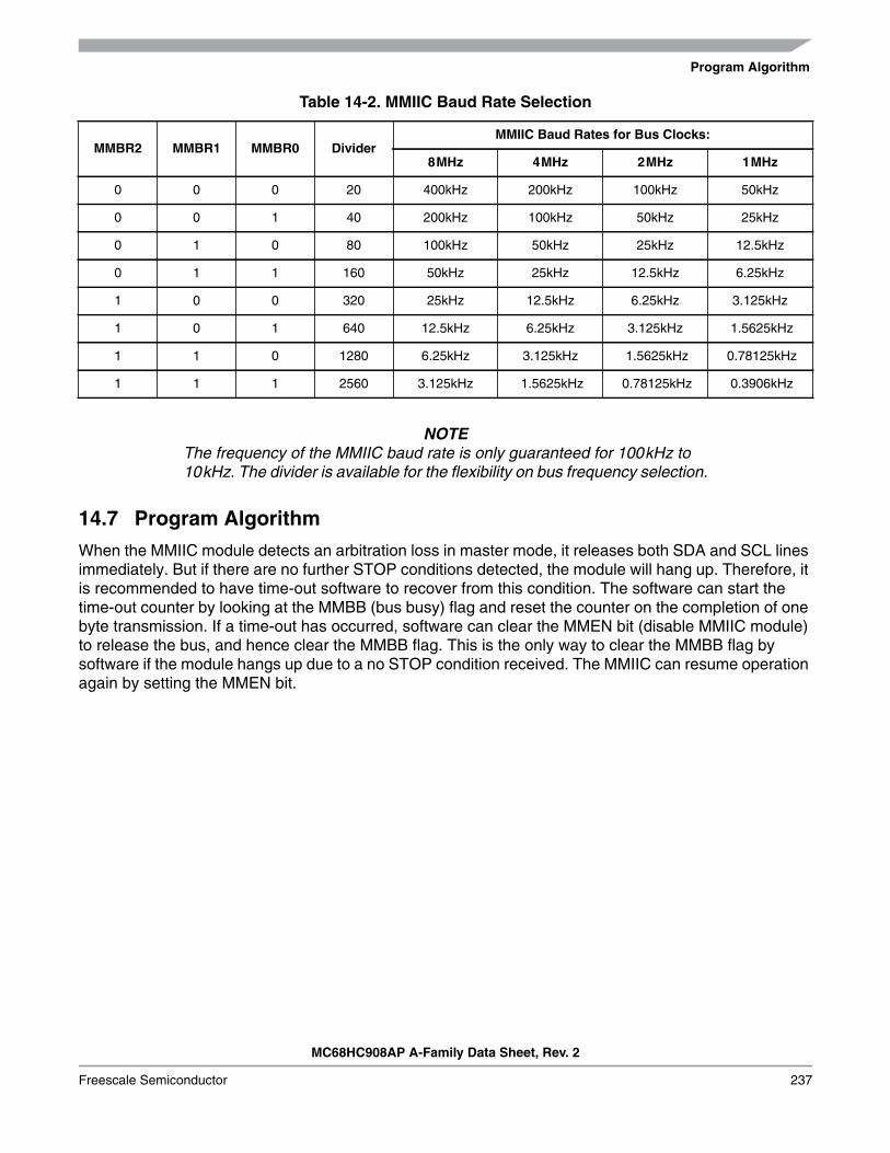
Program Algorithm
MC68HC908AP A-Family Data Sheet, Rev. 2
Freescale Semiconductor 237
NOTEThe frequency of the MMIIC baud rate is only guaranteed for 100kHz to10kHz. The divider is available for the flexibility on bus frequency selection.
14.7 Program Algorithm
When the MMIIC module detects an arbitration loss in master mode, it releases both SDA and SCL linesimmediately. But if there are no further STOP conditions detected, the module will hang up. Therefore, itis recommended to have time-out software to recover from this condition. The software can start thetime-out counter by looking at the MMBB (bus busy) flag and reset the counter on the completion of onebyte transmission. If a time-out has occurred, software can clear the MMEN bit (disable MMIIC module)to release the bus, and hence clear the MMBB flag. This is the only way to clear the MMBB flag bysoftware if the module hangs up due to a no STOP condition received. The MMIIC can resume operationagain by setting the MMEN bit.
Table 14-2. MMIIC Baud Rate Selection
MMBR2 MMBR1 MMBR0 DividerMMIIC Baud Rates for Bus Clocks:
8MHz 4MHz 2MHz 1MHz
0 0 0 20 400kHz 200kHz 100kHz 50kHz
0 0 1 40 200kHz 100kHz 50kHz 25kHz
0 1 0 80 100kHz 50kHz 25kHz 12.5kHz
0 1 1 160 50kHz 25kHz 12.5kHz 6.25kHz
1 0 0 320 25kHz 12.5kHz 6.25kHz 3.125kHz
1 0 1 640 12.5kHz 6.25kHz 3.125kHz 1.5625kHz
1 1 0 1280 6.25kHz 3.125kHz 1.5625kHz 0.78125kHz
1 1 1 2560 3.125kHz 1.5625kHz 0.78125kHz 0.3906kHz

Multi-Master IIC Interface (MMIIC)
MC68HC908AP A-Family Data Sheet, Rev. 2
238 Freescale Semiconductor
14.7.1 Data Sequence
Figure 14-12. Data Transfer Sequences for Master/Slave Transmit/Receive Modes
START Address ACK TX Data1
MMTXBE=0MMRW=0MMAST=1
MMTXIF=1MMTXBE=1 MMNAKIF=1
MMAST=0MMTXBE=1
(a) Master Transmit Mode
(b) Master Receive Mode
(c) Slave Transmit Mode
MMTXIF=1MMTXBE=0
ACK TX DataN ACK STOP
MMTXIF=1MMTXBE=1
START Address ACK RX Data1
MMRXBF=0
MMAST=1MMTXBE=0
MMRXBF=1MMRXIF=1
MMNAKIF=1MMAST=0MMRXIF=1
MMRXBF=1
ACK RX DataN NAK STOP
1START Address ACK TX Data1
MMTXBE=1MMRXBF=0
MMNAKIF=1MMTXBE=0
MMTXBE=1
(d) Slave Receive Mode
MMTXIF=1
ACK TX DataN NAK STOP
MMRXBF=1MMRXIF=1
MMATCH=1MMSRW=1
MMTXIF=1MMTXBE=1
0START Address ACK RX Data1
MMRXBF=1MMRXIF=1 MMRXIF=1
MMRXBF=1
ACK RX DataN ACK STOP
MMTXBE=0MMRXBF=0 MMRXBF=1
MMRXIF=1
MMATCH=1MMSRW=0
Data1 → MMDRR DataN → MMDRR
Data1 → MMDTR
Data2 → MMDTR DataN+2 → MMDTR
Data1 → MMDTRData2 → MMDTR Data3 → MMDTR DataN+2 → MMDTR
(dummy data → MMDTR)
MMRW=1Data1 → MMDRR DataN → MMDRR
0
1
Shaded data packets indicate transmissions by the MCU

SMBus Protocols with PEC and without PEC
MC68HC908AP A-Family Data Sheet, Rev. 2
Freescale Semiconductor 239
14.8 SMBus Protocols with PEC and without PEC
Following is a description of the various MMIIC bus protocols with and without a packet error code (PEC).
14.8.1 Quick Command
Figure 14-13. Quick Command
14.8.2 Send Byte
Figure 14-14. Send Byte
14.8.3 Receive Byte
Figure 14-15. Receive Byte
START Slave Address ACK STOPRW Master to Slave
Slave to Master
Command Bit
Acknowledge
Stop ConditionStart Condition
1 7 1 1 1
START Slave Address ACKW Command Code ACK STOP
ACK STOPPECSTART Slave Address ACKW Command Code ACK
(a) Send Byte Protocol
(b) Send Byte Protocol with PEC
START Slave Address ACKR Data Byte NAK STOP
NAK STOPPECSTART Slave Address ACKR Data Byte ACK
(b) Receive Byte Protocol with PEC
(a) Receive Byte Protocol

Multi-Master IIC Interface (MMIIC)
MC68HC908AP A-Family Data Sheet, Rev. 2
240 Freescale Semiconductor
14.8.4 Write Byte/Word
Figure 14-16. Write Byte/Word
14.8.5 Read Byte/Word
Figure 14-17. Read Byte/Word
ACK Command Code ACK Data Byte Low ACK Data Byte High ACK STOP
ACK Command Code ACK Data Byte ACK STOP
ACK STOPPEC
START Slave Address W
START Slave Address W
ACK Command Code ACK Data Byte ACKSTART Slave Address W
(a) Write Byte Protocol
(b) Write Byte Protocol with PEC
(c) Write Word Protocol
ACK Command Code ACK Data Byte Low ACK Data Byte High ACK
ACK STOPPEC
START Slave Address W
(d) Write Word Protocol with PEC
STOP
ACK Command Code ACK Data Byte LowACK
Data Byte High
PECData Byte High
ACK
NAK
ACK NAK
START
ACK Command Code ACK Data Byte LowACK ACKSTART
STOP
START Slave Address W
START Slave Address W
Slave Address R
Slave Address R
(d) Read Word Protocol with PEC
(c) Read Word Protocol
(b) Read Byte Protocol with PEC
ACK Command Code ACK Data Byte NAK
ACK Command Code ACK
NAK STOPPEC
ACK START
ACK Data Byte ACKSTART
START Slave Address W
START Slave Address W
Slave Address R
Slave Address R
STOP
(a) Read Byte Protocol
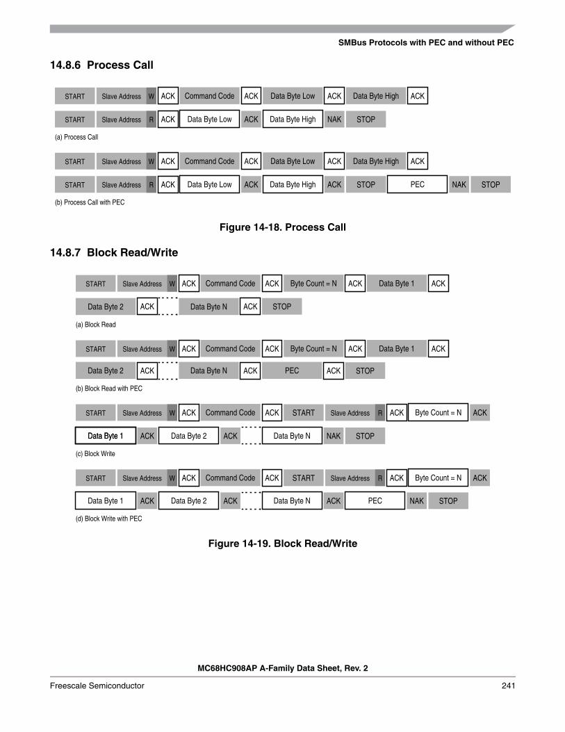
SMBus Protocols with PEC and without PEC
MC68HC908AP A-Family Data Sheet, Rev. 2
Freescale Semiconductor 241
14.8.6 Process Call
Figure 14-18. Process Call
14.8.7 Block Read/Write
Figure 14-19. Block Read/Write
NAK STOP
ACK Command Code Data Byte LowACK ACK Data Byte High ACK
Data Byte Low Data Byte HighACK NAKACK STOP
PEC
START Slave Address W
START Slave Address R
ACK Command Code Data Byte LowACK ACK Data Byte High ACK
Data Byte Low Data Byte HighACK ACKACK STOP
START Slave Address W
START Slave Address R
(b) Process Call with PEC
(a) Process Call
ACK Command Code ACK Byte Count = N ACK
Data Byte 1 ACK Data Byte 2 ACK Data Byte N NAK STOP
START ACK
ACK Command Code ACK Byte Count = N ACK Data Byte 1 ACK
Data Byte 2 ACK Data Byte N ACK STOP
START Slave Address W
START Slave Address W Slave Address R
Data Byte 1
ACK Command Code ACK Byte Count = N ACK
ACK Data Byte 2 ACK Data Byte N NAK STOP
START ACKSTART Slave Address W Slave Address R
Data Byte 1 PECACK
(d) Block Write with PEC
(c) Block Write
(b) Block Read with PEC
ACK Command Code ACK Byte Count = N ACK Data Byte 1 ACK
Data Byte 2 ACK Data Byte N ACK STOP
START Slave Address W
PEC ACK
(a) Block Read

Multi-Master IIC Interface (MMIIC)
MC68HC908AP A-Family Data Sheet, Rev. 2
242 Freescale Semiconductor
14.9 SMBus Protocol Implementation
Figure 14-20. SMBus Protocol Implementation
START Address ACK Command ACK0 START ACK STOPRX Data1 ACK NAKRX DataNAddress 1 ACK
Prepare for Master mode
ACTION:1. Load slave address to MMADR2. Clear MMRW3. Load command to MMDTR4. Set MMAST
OPERATION:
Prepare for repeated START
FLAGS:MMTXIF setMMRXAK clear
OPERATION:
ACTION:1. Set MMRW2. Set REPSEN3. Clear MMTXAK4. Load dummy ($FF) to MMDTR
Get ready to receive data
FLAGS:MMTXIF setMMRXAK clear
OPERATION:
ACTION:Load dummy ($FF) to MMDTR
Generate STOP
FLAGS:MMRXIF set
OPERATION:
ACTION:Read DataN from MMDRR
Read received data and prepare for STOP
FLAGS:MMRXIF set
OPERATION:
ACTION:1. Set MMTXAK2. Read Data(N-1) from MMDRR3. Clear MMAST
Read received data
FLAGS:MMRXIF set
OPERATION:
ACTION:Read Data1 from MMDRR
MASTER MODE
START Address ACK Command ACK0 START ACK STOPTX Data1 ACK NAKTX DataNAddress 1 ACK
Slave address match and
FLAGS:MMRXIF setMMATCH set
OPERATION:
ACTION:1. Check MMSRW2. Read Slave address
Read and decode received command
FLAGS:MMRXIF setMMATCH clear
OPERATION:
ACTION:Load Data1 to MMDTR
Last data sent
FLAGS:MMTXIF setMMRXAK set
OPERATION:
ACTION:Load dummy ($FF) to MMDTR
Last data is going to be sent
FLAGS:MMTXIF set
OPERATION:
ACTION:Load dummy ($FF) to MMDTR
Transmit data
FLAGS:MMTXIF set
OPERATION:
ACTION:Load Data3 to MMDTR
Prepare for Slave mode
ACTION:1. Load slave address to MMADR2. Clear MMTXAK3. Clear MMAST
OPERATION:
MMSRW depends on 8th
Slave address match and
FLAGS:MMRXIF setMMATCH set
OPERATION:
ACTION:Check MMSRW
MMSRW depends on 8th
MMRXAK clear
MMRXAK clear
Transmit data
FLAGS:MMTXIF set
OPERATION:
ACTION:Load Data2 to MMDTR
check for data direction
bit of calling address byte
get ready to transmit data
bit of calling address byte
SLAVE MODE
Shaded data packets indicate transmissions by the MCU

MC68HC908AP A-Family Data Sheet, Rev. 2
Freescale Semiconductor 243
Chapter 15Analog-to-Digital Converter (ADC)
15.1 Introduction
This section describes the analog-to-digital converter (ADC). The ADC is a 8-channel 10-bit linearsuccessive approximation ADC.
15.2 Features
Features of the ADC module include:• Eight channels with multiplexed input• High impedance buffered input• Linear successive approximation with monotonicity• 10-bit resolution• Single or continuous conversion• Auto-scan conversion on four channels• Conversion complete flag or conversion complete interrupt• Selectable ADC clock• Conversion result justification
– 8-bit truncated mode– Right justified mode– Left justified mode– Left justified sign mode
Addr. Register Name Bit 7 6 5 4 3 2 1 Bit 0
$0057ADC Status and Control
Register(ADSCR)
Read: COCOAIEN ADCO ADCH4 ADCH3 ADCH2 ADCH1 ADCH0
Write:Reset: 0 0 0 1 1 1 1 1
$0058ADC Clock Control
Register(ADICLK)
Read:ADIV2 ADIV1 ADIV0 ADICLK MODE1 MODE0
0 0Write: R
Reset: 0 0 0 0 0 1 0 0
$0059ADC Data Register High 0
(ADRH0)
Read: ADx ADx ADx ADx ADx ADx ADx ADxWrite: R R R R R R R R
Reset: 0 0 0 0 0 0 0 0
$005AADC Data Register Low 0
(ADRL0)
Read: ADx ADx ADx ADx ADx ADx ADx ADxWrite: R R R R R R R R
Reset: 0 0 0 0 0 0 0 0
$005BADC Data Register Low 1
(ADRL1)
Read: AD9 AD8 AD7 AD6 AD5 AD4 AD3 AD2Write: R R R R R R R R
Reset: 0 0 0 0 0 0 0 0
Figure 15-1. ADC I/O Register Summary

Analog-to-Digital Converter (ADC)
MC68HC908AP A-Family Data Sheet, Rev. 2
244 Freescale Semiconductor
15.3 Functional Description
The ADC provides eight pins for sampling external sources at pins PTA0/ADC0–PTA7/ADC7. An analogmultiplexer allows the single ADC converter to select one of eight ADC channels as ADC voltage in(VADIN). VADIN is converted by the successive approximation register-based analog-to-digital converter.When the conversion is completed, ADC places the result in the ADC data register, high and low byte(ADRH0 and ADRL0), and sets a flag or generates an interrupt.
An additional three ADC data registers (ADRL1–ADRL3) are available to store the individual converteddata for ADC channels ADC1–ADC3 when the auto-scan mode is enabled. Data from channel ADC0 isstored in ADRL0 in the auto-scan mode.
Figure 15-2 shows the structure of the ADC module.
15.3.1 ADC Port I/O Pins
PTA0–PTA7 are general-purpose I/O pins that are shared with the ADC channels. The channel selectbits, ADCH[4:0], define which ADC channel/port pin will be used as the input signal. The ADC overridesthe port I/O logic by forcing that pin as input to the ADC. The remaining ADC channels/port pins arecontrolled by the port I/O logic and can be used as general-purpose I/O. Writes to the port data registeror data direction register will not have any affect on the port pin that is selected by the ADC. Read of aport pin which is in use by the ADC will return the pin condition if the corresponding DDR bit is at logic 0.If the DDR bit is at logic 1, the value in the port data latch is read.
15.3.2 Voltage Conversion
When the input voltage to the ADC equals VREFH, the ADC converts the signal to $3FF (full scale). If theinput voltage equals VREFL, the ADC converts it to $000. Input voltages between VREFH and VREFL are astraight-line linear conversion. All other input voltages will result in $3FF if greater than VREFH and $000if less than VREFL.
NOTEInput voltage should not exceed the analog supply voltages.
$005CADC Data Register Low 2
(ADRL3)
Read: AD9 AD8 AD7 AD6 AD5 AD4 AD3 AD2Write: R R R R R R R R
Reset: 0 0 0 0 0 0 0 0
$005DADC Data Register Low 3
(ADRL3)
Read: AD9 AD8 AD7 AD6 AD5 AD4 AD3 AD2Write: R R R R R R R R
Reset: 0 0 0 0 0 0 0 0
$005EADC Auto-scan Control
Register(ADASCR)
Read: 0 0 0 0 0AUTO1 AUTO0 ASCAN
Write:Reset: 0 0 0 0 0 0 0 0
= Unimplemented R = Reserved
Figure 15-1. ADC I/O Register Summary
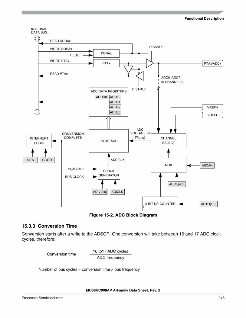
Functional Description
MC68HC908AP A-Family Data Sheet, Rev. 2
Freescale Semiconductor 245
Figure 15-2. ADC Block Diagram
15.3.3 Conversion Time
Conversion starts after a write to the ADSCR. One conversion will take between 16 and 17 ADC clockcycles, therefore:
ADC DATA REGISTERS
INTERNALDATA BUS
READ DDRAx
WRITE DDRAx
RESET
WRITE PTAx
READ PTAx
PTAx/ADCx
DDRAx
PTAx
INTERRUPT
LOGIC
CHANNELSELECT10-BIT ADC
CLOCKGENERATOR
CONVERSIONCOMPLETE
ADC
(VADIN)
ADCICLK
CGMXCLK
BUS CLOCK
ASCAN
DISABLE
DISABLE
(8 CHANNELS)
ADIV[2:0] ADICLK
VOLTAGE IN
VREFL
VREFH
ADCH[4:0]
ADC0–ADC7
MUX
2-BIT UP-COUNTER
COCOAIEN
ADRH0
ADRL1
ADRL0
ADRL2
ADRL3
AUTO[1:0]
16 to17 ADC cyclesConversion time =
ADC frequency
Number of bus cycles = conversion time × bus frequency

Analog-to-Digital Converter (ADC)
MC68HC908AP A-Family Data Sheet, Rev. 2
246 Freescale Semiconductor
The ADC conversion time is determined by the clock source chosen and the divide ratio selected. Theclock source is either the bus clock or CGMXCLK and is selectable by the ADICLK bit located in the ADCclock register. The divide ratio is selected by the ADIV[2:0] bits.
For example, if a 4MHz CGMXCLK is selected as the ADC input clock source, with a divide-by-fourprescale, and the bus speed is set at 2MHz:
NOTEThe ADC frequency must be between fADIC minimum and fADIC maximumto meet A/D specifications. (See 22.5 5V DC Electrical Characteristics.).
Since an ADC cycle may be comprised of several bus cycles (four in the previous example) and the startof a conversion is initiated by a bus cycle write to the ADSCR, from zero to four additional bus cycles mayoccur before the start of the initial ADC cycle. This results in a fractional ADC cycle and is represented asthe 17th cycle.
15.3.4 Continuous Conversion
In the continuous conversion mode, the ADC continuously converts the selected channel, filling the ADCdata register with new data after each conversion. Data from the previous conversion will be overwrittenwhether that data has been read or not. Conversions will continue until the ADCO bit is cleared. TheCOCO bit is set after each conversion and can be cleared by writing to the ADC status and control registeror reading of the ADRL0 data register.
15.3.5 Auto-Scan Mode
In auto-scan mode, the ADC input channel is selected by the value of the 2-bit up-counter, instead of thechannel select bits, ADCH[4:0]. The value of the counter also defines the data register ADRLx to be usedto store the conversion result. When ASCAN bit is set, a write to ADC status and control register (ADSCR)will reset the auto-scan up-counter and ADC conversion will start on the channel 0 up to the channelnumber defined by the integer value of AUTO[1:0]. After a channel conversion is completed, data is storedin ADRLx and the COCO-bit will be set. The counter value will be incremented by 1 and a new conversionwill start. This process will continue until the counter value reaches the value of AUTO[1:0]. When thishappens, it indicates that the current channel is the last channel to be converted. Upon the completion onthe last channel, the counter value will not be incremented and no further conversion will be performed.To start another auto-scan cycle, a write to ADSCR must be performed.
NOTEThe system only provides 8-bit data storage in auto-scan code, user mustclear MODE[1:0] bits to select 8-bit truncation mode before enteringauto-scan mode.
It is recommended that user should disable the auto-scan function before switching channel and alsobefore entering STOP mode.
16 to17 ADC cyclesConversion time =
4MHz ÷ 4
Number of bus cycles = 16 µs × 2MHz = 32 to 34 cycles
= 16 to 17 µs
Interrupts
MC68HC908AP A-Family Data Sheet, Rev. 2
Freescale Semiconductor 247
15.3.6 Result Justification
The conversion result may be formatted in four different ways.• Left justified• Right justified• Left justified sign data mode• 8-bit truncation
All four of these modes are controlled using MODE0 and MODE1 bits located in the ADC clock controlregister (ADICLK).
Left justification will place the eight most significant bits (MSB) in the corresponding ADC data registerhigh (ADRH). This may be useful if the result is to be treated as an 8-bit result where the least significanttwo bits, located in the ADC data register low (ADRL) can be ignored. However, you must read ADRLafter ADRH or else the interlocking will prevent all new conversions from being stored.
Right justification will place only the two MSBs in the corresponding ADC data register high (ADRH) andthe eight LSB bits in ADC data register low (ADRL). This mode of operation typically is used when a 10-bitunsigned result is desired.
Left justified sign data mode is similar to left justified mode with one exception. The MSB of the 10-bitresult, AD9 located in ADRH is complemented. This mode of operation is useful when a result,represented as a signed magnitude from mid-scale, is needed.
Finally, 8-bit truncation mode will place the eight MSBs in ADC data register low (ADRL). The two LSBsare dropped. This mode of operation is used when compatibility with 8-bit ADC designs are required. Nointerlocking between ADRH and ADRL is present.
15.3.7 Data Register Interlocking
Reading ADRH in any 10-bit mode latches the contents of ADRL until ADRL is read. Until ADRL is readall subsequent ADC results will be lost. This register interlocking can also be reset by a write to the ADCstatus and control register, or ADC clock control register. A power-on reset or reset will also clear theinterlocking. Note that an external conversion request will not reset the lock.
15.3.8 Monotonicity
The conversion process is monotonic and has no missing codes.
15.4 Interrupts
When the AIEN bit is set, the ADC module is capable of generating a CPU interrupt after each ADCconversion or after an auto-scan conversion cycle. A CPU interrupt is generated if the COCO bit is atlogic 0. The COCO bit is not used as a conversion complete flag when interrupts are enabled. Theinterrupt vector is defined in Table 2-1 . Vector Addresses.
15.5 Low-Power Modes
The STOP and WAIT instructions put the MCU in low power-consumption standby modes.

Analog-to-Digital Converter (ADC)
MC68HC908AP A-Family Data Sheet, Rev. 2
248 Freescale Semiconductor
15.5.1 Wait Mode
The ADC continues normal operation in wait mode. Any enabled CPU interrupt request from the ADC canbring the MCU out of wait mode. If the ADC is not required to bring the MCU out of wait mode, powerdown the ADC by setting the ADCH[4:0] bits to logic 1’s before executing the WAIT instruction.
15.5.2 Stop Mode
The ADC module is inactive after the execution of a STOP instruction. Any pending conversion is aborted.ADC conversions resume when the MCU exits stop mode. Allow one conversion cycle to stabilize theanalog circuitry before attempting a new ADC conversion after exiting stop mode.
15.6 I/O Signals
The ADC module has eight channels shared with port A I/O pins.
15.6.1 ADC Voltage In (VADIN)
VADIN is the input voltage signal from one of the eight ADC channels to the ADC module.
15.6.2 ADC Analog Power Pin (VDDA)
The ADC analog portion uses VDDA as its power pin. Connect the VDDA pin to the same voltage potentialas VDD. External filtering may be necessary to ensure clean VDDA for good results.
NOTERoute VDDA carefully for maximum noise immunity and place bypasscapacitors as close as possible to the package.
15.6.3 ADC Analog Ground Pin (VSSA)
The ADC analog portion uses VSSA as its ground pin. Connect the VSSA pin to the same voltage potentialas VSS.
15.6.4 ADC Voltage Reference High Pin (VREFH)
VREFH is the power supply for setting the reference voltage VREFH. Connect the VREFH pin to the samevoltage potential as VDDA. There will be a finite current associated with VREFH (see Chapter 22 ElectricalSpecifications).
NOTERoute VREFH carefully for maximum noise immunity and place bypasscapacitors as close as possible to the package.
15.6.5 ADC Voltage Reference Low Pin (VREFL)
VREFL is the lower reference supply for the ADC. Connect the VREFL pin to the same voltage potential asVSSA. There will be a finite current associated with VREFL (see Chapter 22 Electrical Specifications).

I/O Registers
MC68HC908AP A-Family Data Sheet, Rev. 2
Freescale Semiconductor 249
15.7 I/O Registers
These I/O registers control and monitor ADC operation:• ADC status and control register (ADSCR) — $0057• ADC clock control register (ADICLK) — $0058• ADC data register high:low 0 (ADRH0:ADRL0) — $0059:$005A• ADC data register low 1–3 (ADRL1–ADRL3) — $005B–$005D• ADC auto-scan control register (ADASCR) — $005E
15.7.1 ADC Status and Control Register
Function of the ADC status and control register is described here.
COCO — Conversions Complete BitWhen the AIEN bit is a logic 0, the COCO is a read-only bit which is set each time a conversion iscompleted. This bit is cleared whenever the ADSCR is written, or whenever the ADC clock controlregister is written, or whenever the ADC data register low, ADRLx, is read.If the AIEN bit is logic 1, the COCO bit always read as logic 0. ADC interrupt will be generated at theend if an ADC conversion. Reset clears the COCO bit.
1 = Conversion completed (AIEN = 0)0 = Conversion not completed (AIEN = 0)/CPU interrupt (AIEN=1)
AIEN — ADC Interrupt Enable BitWhen this bit is set, an interrupt is generated at the end of an ADC conversion. The interrupt signal iscleared when the data register, ADR0, is read or the ADSCR is written. Reset clears the AIEN bit.
1 = ADC interrupt enabled0 = ADC interrupt disabled
ADCO — ADC Continuous Conversion BitWhen set, the ADC will convert samples continuously and update the ADC data register at the end ofeach conversion. Only one conversion is allowed when this bit is cleared. Reset clears the ADCO bit.
1 = Continuous ADC conversion0 = One ADC conversion
This bit should not be set when auto-scan mode is enabled; i.e. when ASCAN=1.
ADCH[4:0] — ADC Channel Select BitsADCH[4:0] form a 5-bit field which is used to select one of the ADC channels when not in auto-scanmode. The five channel select bits are detailed in Table 15-1.
NOTECare should be taken when using a port pin as both an analog and a digitalinput simultaneously to prevent switching noise from corrupting the analogsignal. Recovery from the disabled state requires one conversion cycle tostabilize.
Address: $0057
Read: COCOAIEN ADCO ADCH4 ADCH3 ADCH2 ADCH1 ADCH0
Write:
Reset: 0 0 0 1 1 1 1 1
Figure 15-3. ADC Status and Control Register (ADSCR)

Analog-to-Digital Converter (ADC)
MC68HC908AP A-Family Data Sheet, Rev. 2
250 Freescale Semiconductor
15.7.2 ADC Clock Control Register
The ADC clock control register (ADICLK) selects the clock frequency for the ADC.
ADIV[2:0] — ADC Clock Prescaler BitsADIV2, ADIV1, and ADIV0 form a 3-bit field which selects the divide ratio used by the ADC to generatethe internal ADC clock.Table 15-2 shows the available clock configurations. The ADC clock should be set to between 500kHzand 1MHz.
Table 15-1. MUX Channel Select
ADCH4 ADCH3 ADCH2 ADCH1 ADCH0 ADC Channel Input Select
0 0 0 0 0 ADC0 PTA0
0 0 0 0 1 ADC1 PTA1
0 0 0 1 0 ADC2 PTA2
0 0 0 1 1 ADC3 PTA3
0 0 1 0 0 ADC4 PTA4
0 0 1 0 1 ADC5 PTA5
0 0 1 1 0 ADC6 PTA6
0 0 1 1 1 ADC7 PTA7
0↓1
1↓1
0↓1
0↓0
0↓0
ADC8↓
ADC28Reserved
1 1 1 0 1 ADC29 VREFH (see Note 2)
1 1 1 1 0 ADC30 VREFL (see Note 2)
1 1 1 1 1 ADC powered-off —
NOTES:1. If any unused channels are selected, the resulting ADC conversion will be unknown.2. The voltage levels supplied from internal reference nodes as specified in the table are used to verify the operation of
the ADC converter both in production test and for user applications.
Address: $0058
Read:ADIV2 ADIV1 ADIV0 ADICLK MODE1 MODE0
0 0
Write: R
Reset: 0 0 0 0 0 1 0 0
= Unimplemented R = Reserved
Figure 15-4. ADC Clock Control Register (ADICLK)

I/O Registers
MC68HC908AP A-Family Data Sheet, Rev. 2
Freescale Semiconductor 251
ADICLK — ADC Input Clock Select BitADICLK selects either bus clock or CGMXCLK as the input clock source to generate the internal ADCclock. Reset selects CGMXCLK as the ADC clock source.If the external clock (CGMXCLK) is equal to or greater than 1MHz, CGMXCLK can be used as theclock source for the ADC. If CGMXCLK is less than 1MHz, use the PLL-generated bus clock as theclock source. As long as the internal ADC clock is at fADIC, correct operation can be guaranteed.
1 = Internal bus clock0 = External clock, CGMXCLK
MODE1 and MODE0 — Modes of Result JustificationMODE1 and MODE0 selects between four modes of operation. The manner in which the ADCconversion results will be placed in the ADC data registers is controlled by these modes of operation.Reset returns right-justified mode.
15.7.3 ADC Data Register 0 (ADRH0 and ADRL0)
The ADC data register 0 consist of a pair of 8-bit registers: high byte (ADRH0), and low byte (ADRL0).This pair form a 16-bit register to store the 10-bit ADC result for the selected ADC result justification mode.
In 8-bit truncated mode, the ADRL0 holds the eight most significant bits (MSBs) of the 10-bit result. TheADRL0 is updated each time an ADC conversion completes. In 8-bit truncated mode, ADRL0 contains nointerlocking with ADRH0. (See Figure 15-5 . ADRH0 and ADRL0 in 8-Bit Truncated Mode.)
Table 15-2. ADC Clock Divide Ratio
ADIV2 ADIV1 ADIV0 ADC Clock Rate
0 0 0 ADC input clock ÷ 1
0 0 1 ADC input clock ÷ 2
0 1 0 ADC input clock ÷ 4
0 1 1 ADC input clock ÷ 8
1 X X ADC input clock ÷ 16
X = don’t care
Table 15-3. ADC Mode Select
MODE1 MODE0 Justification Mode
0 0 8-bit truncated mode
0 1 Right justified mode
1 0 Left justified mode
1 1 Left justified sign data mode
CGMXCLK or bus frequencyfADIC =
ADIV[2:0]

Analog-to-Digital Converter (ADC)
MC68HC908AP A-Family Data Sheet, Rev. 2
252 Freescale Semiconductor
In right justified mode the ADRH0 holds the two MSBs, and the ADRL0 holds the eight least significantbits (LSBs), of the 10-bit result. ADRH0 and ADRL0 are updated each time a single channel ADCconversion completes. Reading ADRH0 latches the contents of ADRL0. Until ADRL0 is read allsubsequent ADC results will be lost. (See Figure 15-6 . ADRH0 and ADRL0 in Right Justified Mode.)
In left justified mode the ADRH0 holds the eight most significant bits (MSBs), and the ADRL0 holds thetwo least significant bits (LSBs), of the 10-bit result. The ADRH0 and ADRL0 are updated each time asingle channel ADC conversion completes. Reading ADRH0 latches the contents of ADRL0. Until ADRL0is read all subsequent ADC results will be lost. (See Figure 15-7 . ADRH0 and ADRL0 in Left JustifiedMode.)
In left justified sign mode the ADRH0 holds the eight MSBs with the MSB complemented, and the ADRL0holds the two least significant bits (LSBs), of the 10-bit result. The ADRH0 and ADRL0 are updated eachtime a single channel ADC conversion completes. Reading ADRH0 latches the contents of ADRL0. UntilADRL0 is read all subsequent ADC results will be lost. (See Figure 15-8 ADRH0 and ADRL0 in LeftJustified Sign Data Mode.)
Addr. Register Name Bit 7 6 5 4 3 2 1 Bit 0
$0059ADC Data Register High 0
(ADRH0)
Read: 0 0 0 0 0 0 0 0Write: R R R R R R R R
Reset: 0 0 0 0 0 0 0 0
$005AADC Data Register Low 0
(ADRL0)
Read: AD9 AD8 AD7 AD6 AD5 AD4 AD3 AD2Write: R R R R R R R R
Reset: 0 0 0 0 0 0 0 0
Figure 15-5. ADRH0 and ADRL0 in 8-Bit Truncated Mode
Addr. Register Name Bit 7 6 5 4 3 2 1 Bit 0
$0059ADC Data Register High 0
(ADRH0)
Read: 0 0 0 0 0 0 AD9 AD8Write: R R R R R R R R
Reset: 0 0 0 0 0 0 0 0
$005AADC Data Register Low 0
(ADRL0)
Read: AD7 AD6 AD5 AD4 AD3 AD2 AD1 AD0Write: R R R R R R R R
Reset: 0 0 0 0 0 0 0 0
Figure 15-6. ADRH0 and ADRL0 in Right Justified Mode
Addr. Register Name Bit 7 6 5 4 3 2 1 Bit 0
$0059ADC Data Register High 0
(ADRH0)
Read: AD9 AD8 AD7 AD6 AD5 AD4 AD3 AD2Write: R R R R R R R R
Reset: 0 0 0 0 0 0 0 0
$005AADC Data Register Low 0
(ADRL0)
Read: AD1 AD0 0 0 0 0 0 0Write: R R R R R R R R
Reset: 0 0 0 0 0 0 0 0
Figure 15-7. ADRH0 and ADRL0 in Left Justified Mode

I/O Registers
MC68HC908AP A-Family Data Sheet, Rev. 2
Freescale Semiconductor 253
15.7.4 ADC Auto-Scan Mode Data Registers (ADRL1–ADRL3)
The ADC data registers 1 to 3 (ADRL1–ADRL3), are 8-bit registers for conversion results in 8-bittruncated mode, for channels ADC1 to ADC3, when the ADC is operating in auto-scan mode(MODE[1:0] = 00).
15.7.5 ADC Auto-Scan Control Register (ADASCR)
The ADC auto-scan control register (ADASCR) enables and controls the ADC auto-scan function.
AUTO[1:0] — Auto-Scan Mode Channel Select BitsAUTO1 and AUTO0 form a 2-bit field which is used to define the number of auto-scan channels usedwhen in auto-scan mode. Reset clears these bits.
Addr. Register Name Bit 7 6 5 4 3 2 1 Bit 0
$0059ADC Data Register High 0
(ADRH0)
Read: AD9 AD8 AD7 AD6 AD5 AD4 AD3 AD2Write: R R R R R R R R
Reset: 0 0 0 0 0 0 0 0
$005AADC Data Register Low 0
(ADRL0)
Read: AD1 AD0 0 0 0 0 0 0Write: R R R R R R R R
Reset: 0 0 0 0 0 0 0 0
Figure 15-8 ADRH0 and ADRL0 in Left Justified Sign Data Mode
Address: ADRL1, $005B; ADRL2, $005C; and ADRL3, $005D
Read: AD9 AD8 AD7 AD6 AD5 AD4 AD3 AD2
Write: R R R R R R R R
Reset: 0 0 0 0 0 0 0 0
R = Reserved
Figure 15-9. ADC Data Register Low 1 to 3 (ADRL1–ADRL3)
Address: $005E
Read: 0 0 0 0 0AUTO1 AUTO0 ASCAN
Write:
Reset: 0 0 0 0 0 0 0 0
= Unimplemented R = Reserved
Figure 15-10. ADC Scan Control Register (ADASCR)
Table 15-4. Auto-scan Mode Channel Select
AUTO1 AUTO0 Auto-Scan Channels
0 0 ADC0 only
0 1 ADC0 to ADC1
1 0 ADC0 to ADC2
1 1 ADC0 to ADC3
Analog-to-Digital Converter (ADC)
MC68HC908AP A-Family Data Sheet, Rev. 2
254 Freescale Semiconductor
ASCAN — Auto-scan Mode Enable BitThis bit enable/disable the auto-scan mode. Reset clears this bit.
1 = Auto-scan mode is enabled0 = Auto-scan mode is disabled
Auto-scan mode should not be enabled when ADC continuous conversion is enabled; i.e. whenADCO=1.
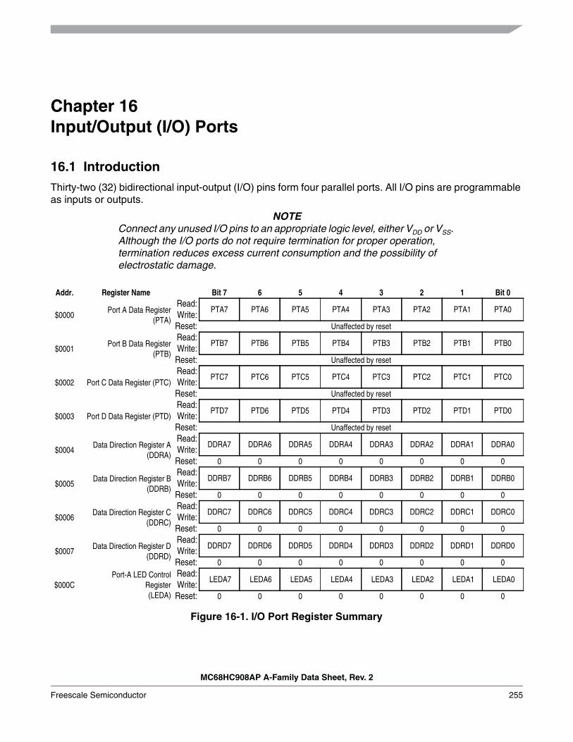
MC68HC908AP A-Family Data Sheet, Rev. 2
Freescale Semiconductor 255
Chapter 16Input/Output (I/O) Ports
16.1 Introduction
Thirty-two (32) bidirectional input-output (I/O) pins form four parallel ports. All I/O pins are programmableas inputs or outputs.
NOTEConnect any unused I/O pins to an appropriate logic level, either VDD or VSS.Although the I/O ports do not require termination for proper operation,termination reduces excess current consumption and the possibility ofelectrostatic damage.
Addr. Register Name Bit 7 6 5 4 3 2 1 Bit 0
$0000Port A Data Register
(PTA)
Read:PTA7 PTA6 PTA5 PTA4 PTA3 PTA2 PTA1 PTA0
Write:Reset: Unaffected by reset
$0001Port B Data Register
(PTB)
Read:PTB7 PTB6 PTB5 PTB4 PTB3 PTB2 PTB1 PTB0
Write:Reset: Unaffected by reset
$0002 Port C Data Register (PTC)Read:
PTC7 PTC6 PTC5 PTC4 PTC3 PTC2 PTC1 PTC0Write:
Reset: Unaffected by reset
$0003 Port D Data Register (PTD)Read:
PTD7 PTD6 PTD5 PTD4 PTD3 PTD2 PTD1 PTD0Write:
Reset: Unaffected by reset
$0004Data Direction Register A
(DDRA)
Read:DDRA7 DDRA6 DDRA5 DDRA4 DDRA3 DDRA2 DDRA1 DDRA0
Write:Reset: 0 0 0 0 0 0 0 0
$0005Data Direction Register B
(DDRB)
Read:DDRB7 DDRB6 DDRB5 DDRB4 DDRB3 DDRB2 DDRB1 DDRB0
Write:Reset: 0 0 0 0 0 0 0 0
$0006Data Direction Register C
(DDRC)
Read:DDRC7 DDRC6 DDRC5 DDRC4 DDRC3 DDRC2 DDRC1 DDRC0
Write:Reset: 0 0 0 0 0 0 0 0
$0007Data Direction Register D
(DDRD)
Read:DDRD7 DDRD6 DDRD5 DDRD4 DDRD3 DDRD2 DDRD1 DDRD0
Write:Reset: 0 0 0 0 0 0 0 0
$000CPort-A LED Control
Register(LEDA)
Read: LEDA7 LEDA6 LEDA5 LEDA4 LEDA3 LEDA2 LEDA1 LEDA0
Write:Reset: 0 0 0 0 0 0 0 0
Figure 16-1. I/O Port Register Summary

Input/Output (I/O) Ports
MC68HC908AP A-Family Data Sheet, Rev. 2
256 Freescale Semiconductor
Table 16-1. Port Control Register Bits Summary
Port Bit DDRModule Control
PinModule Register Control Bit
A
0 DDRA0
ADC ADSCR ($0057) ADCH[4:0]
PTA0/ADC0
1 DDRA1 PTA1/ADC1
2 DDRA2 PTA2/ADC2
3 DDRA3 PTA3/ADC3
4 DDRA4 PTA4/ADC4
5 DDRA5 PTA5/ADC5
6 DDRA6 PTA6/ADC6
7 DDRA7 PTA7/ADC7
B
0 DDRB0MBUS MMCR1 ($0049) MMEN
PTB0/SDA(1)
1. Pin is open-drain when configured as output. Pullup resistor must be connected when configured as output.
1 DDRB1 PTB1/SCL(1)
2 DDRB2SCI SCC1 ($0013) ENSCI
PTB2/TxD(1)
3 DDRB3 PTB3/RxD(1)
4 DDRB4TIM1
T1SC0 ($0025) ELS0B:ELS0A PTB4/T1CH0(2)
2. Pin has schmitt trigger when configured as input.
5 DDRB5 T1SC1 ($0028) ELS1B:ELS1A PTB5/T1CH1(2)
6 DDRB6TIM2
T2SC0 ($0030) ELS0B:ELS0A PTB6/T2CH0(2)
7 DDRB7 T2SC1 ($0033) ELS1B:ELS1A PTB7/T2CH1(2)
C
0 DDRC0 IRQ2 INTSCR2 ($001C) IMASK2 PTC0/IRQ2(2)
1 DDRC1 — — — PTC1
2 DDRC2
SPI SPCR ($0010) SPE
PTC2/MISO
3 DDRC3 PTC3/MOSI
4 DDRC4 PTC4/SS
5 DDRC5 PTC5/SPSCK
6 DDRC6IRSCI IRSCC1 ($0040) ENSCI
PTC6/SCTxD(1)
7 DDRC7 PTC7/SCRxD(1)
D
0 DDRD0
KBI KBIER ($001B)
KBIE0 PTD0/KBI0(2)
1 DDRD1 KBIE1 PTD1/KBI1(2)
2 DDRD2 KBIE2 PTD2/KBI2(2)
3 DDRD3 KBIE3 PTD3/KBI3(2)
4 DDRD4 KBIE4 PTD4/KBI4(2)
5 DDRD5 KBIE5 PTD5/KBI5(2)
6 DDRD6 KBIE6 PTD6/KBI6(2)
7 DDRD7 KBIE7 PTD7/KBI7(2)

Port A
MC68HC908AP A-Family Data Sheet, Rev. 2
Freescale Semiconductor 257
16.2 Port A
Port A is an 8-bit special-function port that shares all of its pins with the analog-to-digital converter (ADC)module. Port A pins also have LED direct drive capability.
16.2.1 Port A Data Register (PTA)
The port A data register contains a data latch for each of the eight port A pins.
PTA[7:0] — Port A Data BitsThese read/write bits are software-programmable. Data direction of each port A pin is under the controlof the corresponding bit in data direction register A. Reset has no effect on port A data.
ADC7–ADC0 — ADC Channels 7 to 0ADC7–ADC0 are pins used for the input channels to the analog-to-digital converter module. Thechannel select bits, ADCH[4:0], in the ADC status and control register define which port pin will be usedas an ADC input and overrides any control from the port I/O logic.
NOTECare must be taken when reading port A while applying analog voltages toADC7–ADC0 pins. If the appropriate ADC channel is not enabled,excessive current drain may occur if analog voltages are applied to thePTAx/ADCx pin, while PTA is read as a digital input. Those ports notselected as analog input channels are considered digital I/O ports.
LED drive — Direct LED drive pinsPTA7–PTA0 pins can be configured for direct LED drive. See 16.2.3 Port-A LED Control Register(LEDA).
16.2.2 Data Direction Register (DDRA)
Data direction register A determines whether each port A pin is an input or an output. Writing a logic 1 toa DDRA bit enables the output buffer for the corresponding port A pin; a logic 0 disables the output buffer.
Address: $0000
Bit 7 6 5 4 3 2 1 Bit 0
Read:PTA7 PTA6 PTA5 PTA4 PTA3 PTA2 PTA1 PTA0
Write:
Reset: Unaffected by reset
Alternative Function: ADC7 ADC6 ADC5 ADC4 ADC3 ADC2 ADC1 ADC0
Additional Function: LED drive LED drive LED drive LED drive LED drive LED drive LED drive LED drive
Figure 16-2. Port A Data Register (PTA)
Address: $0004
Bit 7 6 5 4 3 2 1 Bit 0
Read:DDRA7 DDRA6 DDRA5 DDRA4 DDRA3 DDRA2 DDRA1 DDRA0
Write:
Reset: 0 0 0 0 0 0 0 0
Figure 16-3. Data Direction Register A (DDRA)

Input/Output (I/O) Ports
MC68HC908AP A-Family Data Sheet, Rev. 2
258 Freescale Semiconductor
DDRA[7:0] — Data Direction Register A BitsThese read/write bits control port A data direction. Reset clears DDRA[7:0], configuring all port A pinsas inputs.
1 = Corresponding port A pin configured as output0 = Corresponding port A pin configured as input
NOTEAvoid glitches on port A pins by writing to the port A data register beforechanging data direction register A bits from 0 to 1.
Figure 16-4 shows the port A I/O logic.
Figure 16-4. Port A I/O Circuit
When DDRAx is a logic 1, reading address $0000 reads the PTAx data latch. When DDRAx is a logic 0,reading address $0000 reads the voltage level on the pin. The data latch can always be written,regardless of the state of its data direction bit.
Table 16-2 summarizes the operation of the port A pins.
Table 16-2. Port A Pin Functions
DDRABit
PTA Bit I/O Pin ModeAccesses to DDRA Accesses to PTA
Read/Write Read Write
0 X(1)
1. X = don’t care.
Input, Hi-Z(2)
2. Hi-Z = high impedance.
DDRA[7:0] Pin PTA[7:0](3)
3. Writing affects data register, but does not affect input.
1 X Output DDRA[7:0] PTA[7:0] PTA[7:0]
READ DDRA ($0004)
WRITE DDRA ($0004)
RESET
WRITE PTA ($0000)
READ PTA ($0000)
PTAx
DDRAx
PTAx
INTE
RN
AL D
ATA
BUS

Port B
MC68HC908AP A-Family Data Sheet, Rev. 2
Freescale Semiconductor 259
16.2.3 Port-A LED Control Register (LEDA)
The port-A LED control register (LEDA) controls the direct LED drive capability on PTA7–PTA0 pins. Eachbit is individually configurable and requires that the data direction register, DDRA, bit be configured as anoutput.
LEDA[7:0] — Port A LED Drive Enable BitsThese read/write bits are software programmable to enable the direct LED drive on an output port pin.
1 = Corresponding port A pin is configured for direct LED drive,with 15mA current sinking capability
0 = Corresponding port A pin is configured for standard drive
16.3 Port B
Port B is an 8-bit special-function port that shares two of its pins with the multi-master IIC (MMIIC) module,two of its pins with SCI module, and four of its pins with two timer interface (TIM1 and TIM2) modules.
NOTEPTB3–PTB0 are open-drain pins when configured as outputs regardlesswhether the pins are used as general purpose I/O pins, MMIIC pins, or SCIpins. Therefore, when configured as general purpose output pins, MMIICpins, or SCI pins (the TxD pin), pullup resistors must be connected to thesepins.
16.3.1 Port B Data Register (PTB)
The port B data register contains a data latch for each of the eight port B pins.
PTB[7:0] — Port B Data BitsThese read/write bits are software-programmable. Data direction of each port B pin is under the controlof the corresponding bit in data direction register B. Reset has no effect on port B data.
Address: $000C
Bit 7 6 5 4 3 2 1 Bit 0
Read:LEDA7 LEDA6 LEDA5 LEDA4 LEDA3 LEDA2 LEDA1 LEDA0
Write:
Reset: 0 0 0 0 0 0 0 0
Figure 16-5. Port A LED Control Register (LEDA)
Address: $0001
Bit 7 6 5 4 3 2 1 Bit 0
Read:PTB7 PTB6 PTB5 PTB4 PTB3 PTB2 PTB1 PTB0
Write:
Reset: Unaffected by reset
Alternative Function: T2CH1 T2CH0 T1CH1 T1CH0 RxD TxD SCL SDA
Figure 16-6. Port B Data Register (PTB)

Input/Output (I/O) Ports
MC68HC908AP A-Family Data Sheet, Rev. 2
260 Freescale Semiconductor
SDA and SCL — Multi-Master IIC Data and ClockThe SDA and SCL pins are multi-master IIC data and clock pins. Setting the MMEN bit in the MMIICcontrol register 1 (MMCR1) configures the PTB0/SDA and PTB1/SCL pins for MMIIC function andoverrides any control from the port I/O logic.
TxD and RxD — SCI Transmit and Receive DataThe TxD and RxD pins are SCI transmit and receive data pins. Setting the ENSCI bit in the SCI controlregister 1 (SCC1) configures the PTB2/TxD and PTB3/RxD pins for SCI function and overrides anycontrol from the port I/O logic.
T1CH0 and T1CH1 — Timer 1 Channel I/OThe T1CH0 and T1CH1 pins are the TIM1 input capture/output compare pins. The edge/level selectbits, ELSxB:ELSxA, determine whether the PTB4/T1CH0–PTB5/T1CH1 pins are timer channel I/Opins or general-purpose I/O pins.
T2CH0 and T2CH1 — Timer 2 Channel I/OThe T2CH0 and T2CH1 pins are the TIM2 input capture/output compare pins. The edge/level selectbits, ELSxB:ELSxA, determine whether the PTB6/T2CH0–PTB7/T2CH1 pins are timer channel I/Opins or general-purpose I/O pins.
16.3.2 Data Direction Register B (DDRB)
Data direction register B determines whether each port B pin is an input or an output. Writing a logic 1 toa DDRB bit enables the output buffer for the corresponding port B pin; a logic 0 disables the output buffer.
DDRB[7:0] — Data Direction Register B BitsThese read/write bits control port B data direction. Reset clears DDRB[7:0], configuring all port B pinsas inputs.
1 = Corresponding port B pin configured as output0 = Corresponding port B pin configured as input
NOTEAvoid glitches on port B pins by writing to the port B data register beforechanging data direction register B bits from 0 to 1.
Figure 16-8 shows the port B I/O logic.
Address: $0005
Bit 7 6 5 4 3 2 1 Bit 0
Read:DDRB7 DDRB6 DDRB5 DDRB4 DDRB3 DDRB2 DDRB1 DDRB0
Write:
Reset: 0 0 0 0 0 0 0 0
Figure 16-7. Data Direction Register B (DDRB)
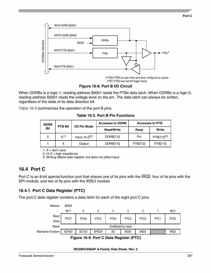
Port C
MC68HC908AP A-Family Data Sheet, Rev. 2
Freescale Semiconductor 261
Figure 16-8. Port B I/O Circuit
When DDRBx is a logic 1, reading address $0001 reads the PTBx data latch. When DDRBx is a logic 0,reading address $0001 reads the voltage level on the pin. The data latch can always be written,regardless of the state of its data direction bit.
Table 16-3 summarizes the operation of the port B pins.
16.4 Port C
Port C is an 8-bit special-function port that shares one of its pins with the IRQ2, four of its pins with theSPI module, and two of its pins with the IRSCI module.
16.4.1 Port C Data Register (PTC)
The port C data register contains a data latch for each of the eight port C pins.
Table 16-3. Port B Pin Functions
DDRBBit
PTB Bit I/O Pin ModeAccesses to DDRB Accesses to PTB
Read/Write Read Write
0 X(1)
1. X = don’t care.
Input, Hi-Z(2)
2. Hi-Z = high impedance.
DDRB[7:0] Pin PTB[7:0](3)
3. Writing affects data register, but does not affect input.
1 X Output DDRB[7:0] PTB[7:0] PTB[7:0]
Address: $0002
Bit 7 6 5 4 3 2 1 Bit 0
Read:PTC7 PTC6 PTC5 PTC4 PTC3 PTC2 PTC1 PTC0
Write:
Reset: Unaffected by reset
Alternative Function: SCRxD SCTxD SPSCK SS MOSI MISO IRQ2
Figure 16-9. Port C Data Register (PTC)
READ DDRB ($0005)
WRITE DDRB ($0005)
RESET
WRITE PTB ($0001)
READ PTB ($0001)
PTBx #
DDRBx
PTBx
INTE
RN
AL D
ATA
BUS
# PTB3–PTB0 are open-drain pins when configured as outputs.PTB7–PTB4 have schmitt trigger inputs.

Input/Output (I/O) Ports
MC68HC908AP A-Family Data Sheet, Rev. 2
262 Freescale Semiconductor
PTC[7:0] — Port C Data BitsThese read/write bits are software-programmable. Data direction of each port C pin is under the controlof the corresponding bit in data direction register C. Reset has no effect on port C data.
IRQ2 — IRQ2 input pinThe PTC0/IRQ2 pin is always available as input pin to the IRQ2 module. Care must be taken toavailable unwanted interrupts when this pin is used as general purpose I/O. PTC0/IRQ2 pin has aninternal pullup, and can be disabled by setting the PUC0ENB bit in the IRQ2 status and control register(INTSCR2).
MISO, MOSI, SS, and SPSCK — SPI Data I/O, Select, and Clock PinsThese pins are the SPI data in/out, select, and clock pins. Setting the SPE bit in the SPI control register(SPCR) configures PTC2/MISO, PTC3/MOSI, PTC4/SS, and PTC5/SPSCK pins for SPI function andoverrides any control from the port I/O logic.
SCTxD and SCRxD — IrSCI Transmit and Receive DataThe SCTxD and SCRxD pins are IRSCI transmit and receive data pins. Setting the ENSCI bit in theIRSCI control register 1 (IRSCC1) configures the PTC6/SCTxD and PTC7/SCRxD pins for IRSCIfunction and overrides any control from the port I/O logic.
16.4.2 Data Direction Register C (DDRC)
Data direction register C determines whether each port C pin is an input or an output. Writing a logic 1 toa DDRC bit enables the output buffer for the corresponding port C pin; a logic 0 disables the output buffer.
DDRC[7:0] — Data Direction Register C BitsThese read/write bits control port C data direction. Reset clears DDRC[7:0], configuring all port C pinsas inputs.
1 = Corresponding port C pin configured as output0 = Corresponding port C pin configured as input
NOTEAvoid glitches on port C pins by writing to the port C data register beforechanging data direction register C bits from 0 to 1.
Figure 16-11 shows the port C I/O logic.
NOTEFor those devices packaged in a 42-pin shrink dual in-line package, PTC0and PTC1 are not connected. DDRC0 and DDRC1 should be set to a 1 toconfigure PTC0 and PTC1 as outputs.
Address: $0006
Bit 7 6 5 4 3 2 1 Bit 0
Read:DDRC7 DDRC6 DDRC5 DDRC4 DDRC3 DDRC2 DDRC1 DDRC0
Write:
Reset: 0 0 0 0 0 0 0 0
Figure 16-10. Data Direction Register C (DDRC)

Port D
MC68HC908AP A-Family Data Sheet, Rev. 2
Freescale Semiconductor 263
Figure 16-11. Port C I/O Circuit
When DDRCx is a logic 1, reading address $0002 reads the PTCx data latch. When DDRCx is a logic 0,reading address $0002 reads the voltage level on the pin. The data latch can always be written,regardless of the state of its data direction bit.
Table 16-4 summarizes the operation of the port C pins.
16.5 Port D
Port D is an 8-bit special function port that shares all of its pins with the keyboard interrupt module.
16.5.1 Port D Data Register (PTD)
The port D data register contains a data latch for each of the eight port D pins.
Table 16-4. Port C Pin Functions
DDRCBit
PTC Bit I/O Pin ModeAccesses to DDRC Accesses to PTC
Read/Write Read Write
0 X(1)
1. X = don’t care.
Input, Hi-Z(2)
2. Hi-Z = high impedance.
DDRC[7:0] Pin PTC[7:0](3)
3. Writing affects data register, but does not affect input.
1 X Output DDRC[7:0] PTC[7:0] PTC[7:0]
Address: $0003
Bit 7 6 5 4 3 2 1 Bit 0
Read:PTD7 PTD6 PTD5 PTD4 PTD3 PTD2 PTD1 PTD0
Write:
Reset: Unaffected by reset
Alternative Function: KBI7 KBI6 KBI5 KBI4 KBI3 KBI2 KBI1 KBI0
Figure 16-12. Port D Data Register (PTD)
READ DDRC ($0006)
WRITE DDRC ($0006)
RESET
WRITE PTC ($0002)
READ PTC ($0002)
PTCx #
DDRCx
PTCx
INTE
RN
AL D
ATA
BUS
# PTC0 has schmitt trigger input.

Input/Output (I/O) Ports
MC68HC908AP A-Family Data Sheet, Rev. 2
264 Freescale Semiconductor
PTD[7:0] — Port D Data BitsThese read/write bits are software programmable. Data direction of each port D pin is under the controlof the corresponding bit in data direction register D. Reset has no effect on port D data.
KBI7–KBI0 — Keyboard Interrupt InputsThe keyboard interrupt enable bits, KBIE[7:0], in the keyboard interrupt enable register (KBIER),enable the port D pins as external interrupt pins. See Chapter 18 Keyboard Interrupt Module (KBI).
16.5.2 Data Direction Register D (DDRD)
Data direction register D determines whether each port D pin is an input or an output. Writing a logic 1 toa DDRD bit enables the output buffer for the corresponding port D pin; a logic 0 disables the output buffer.
DDRD[7:0] — Data Direction Register D BitsThese read/write bits control port D data direction. Reset clears DDRD[7:0], configuring all port D pinsas inputs.
1 = Corresponding port D pin configured as output0 = Corresponding port D pin configured as input
NOTEAvoid glitches on port D pins by writing to the port D data register beforechanging data direction register D bits from 0 to 1.
Figure 16-14 shows the port D I/O logic.
Figure 16-14. Port D I/O Circuit
When bit DDRDx is a logic 1, reading address $0003 reads the PTDx data latch. When bit DDRDx is alogic 0, reading address $0003 reads the voltage level on the pin. The data latch can always be written,regardless of the state of its data direction bit.
Address: $0007
Bit 7 6 5 4 3 2 1 Bit 0
Read:DDRD7 DDRD6 DDRD5 DDRD4 DDRD3 DDRD2 DDRD1 DDRD0
Write:
Reset: 0 0 0 0 0 0 0 0
Figure 16-13. Data Direction Register D (DDRD)
READ DDRD ($0007)
WRITE DDRD ($0007)
RESET
WRITE PTD ($0003)
READ PTD ($0003)
PTDx #
DDRDx
PTDx
INTE
RN
AL D
ATA
BUS
KBIEx
# PTD7–PTD0 have schmitt trigger inputs.

Port D
MC68HC908AP A-Family Data Sheet, Rev. 2
Freescale Semiconductor 265
Table 16-5 summarizes the operation of the port D pins.
Table 16-5. Port D Pin Functions
DDRDBit
PTD Bit I/O Pin ModeAccesses to DDRD Accesses to PTD
Read/Write Read Write
0 X(1)
1. X = don’t care.
Input, Hi-Z(2)
2. Hi-Z = high impedance.
DDRD[7:0] Pin PTD[7:0](3)
3. Writing affects data register, but does not affect input.
1 X Output DDRD[7:0] PTD[7:0] PTD[7:0]

Input/Output (I/O) Ports
MC68HC908AP A-Family Data Sheet, Rev. 2
266 Freescale Semiconductor

MC68HC908AP A-Family Data Sheet, Rev. 2
Freescale Semiconductor 267
Chapter 17External Interrupt (IRQ)
17.1 Introduction
The external interrupt (IRQ) module provides two maskable interrupt inputs: IRQ1 and IRQ2.
17.2 Features
Features of the IRQ module include:• A dedicated external interrupt pin, IRQ1• An external interrupt pin shared with a port pin, PTC0/IRQ2• Separate IRQ interrupt control bits for IRQ1 and IRQ2• Hysteresis buffers• Programmable edge-only or edge and level interrupt sensitivity• Automatic interrupt acknowledge• Internal pullup resistor, with disable option on IRQ2
NOTEReferences to either IRQ1 or IRQ2 may be made in the following text byomitting the IRQ number. For example, IRQF may refer generically toIRQ1F and IRQ2F, and IMASK may refer to IMASK1 and IMASK2.
17.3 Functional Description
A logic 0 applied to the external interrupt pin can latch a CPU interrupt request. Figure 17-2 andFigure 17-3 shows the structure of the IRQ module.
Interrupt signals on the IRQ pin are latched into the IRQ latch. An interrupt latch remains set until one ofthe following actions occurs:
• Vector fetch — A vector fetch automatically generates an interrupt acknowledge signal that clearsthe latch that caused the vector fetch.
Addr. Register Name Bit 7 6 5 4 3 2 1 Bit 0
$001CIRQ2 Status and Control
Register(INTSCR2)
Read: 0PUC0ENB
0 0 IRQ2F 0IMASK2 MODE2
Write: ACK2Reset: 0 0 0 0 0 0 0 0
$001EIRQ1 Status and Control
Register(INTSCR1)
Read: 0 0 0 0 IRQ1F 0IMASK1 MODE1
Write: ACK1Reset: 0 0 0 0 0 0 0 0
= Unimplemented
Figure 17-1. External Interrupt I/O Register Summary

External Interrupt (IRQ)
MC68HC908AP A-Family Data Sheet, Rev. 2
268 Freescale Semiconductor
• Software clear — Software can clear an interrupt latch by writing to the appropriate acknowledgebit in the interrupt status and control register (INTSCR). Writing a logic 1 to the ACK bit clears theIRQ latch.
• Reset — A reset automatically clears the interrupt latch.
The external interrupt pin is falling-edge-triggered and is software-configurable to be either falling-edgeor falling-edge and low-level-triggered. The MODE bit in the INTSCR controls the triggering sensitivity ofthe IRQ pin.
When an interrupt pin is edge-triggered only, the interrupt remains set until a vector fetch, software clear,or reset occurs.
When an interrupt pin is both falling-edge and low-level-triggered, the interrupt remains set until both ofthe following occur:
• Vector fetch or software clear• Return of the interrupt pin to logic 1
The vector fetch or software clear may occur before or after the interrupt pin returns to logic 1. As long asthe pin is low, the interrupt request remains pending. A reset will clear the latch and the MODE1 controlbit, thereby clearing the interrupt even if the pin stays low.
When set, the IMASK bit in the INTSCR mask all external interrupt requests. A latched interrupt requestis not presented to the interrupt priority logic unless the IMASK bit is clear.
NOTEThe interrupt mask (I) in the condition code register (CCR) masks allinterrupt requests, including external interrupt requests.
Figure 17-2. IRQ1 Block Diagram
RESET
IMASK1
D Q
CK
CLRIRQ1
HIGH
INTERRUPT
TO MODESELECTLOGIC
REQUEST
VDD
MODE1
VOLTAGEDETECT
SYNCHRONIZER
IRQ1F
TO CPU FORBIL/BIHINSTRUCTIONS
VECTORFETCH
DECODER
INTE
RN
AL A
DD
RES
S BU
S
ACK1
VDD
INTERNALPULLUPDEVICE
IRQ1

IRQ1 and IRQ2 Pins
MC68HC908AP A-Family Data Sheet, Rev. 2
Freescale Semiconductor 269
Figure 17-3. IRQ2 Block Diagram
17.4 IRQ1 and IRQ2 Pins
A logic 0 on the IRQ pin can latch an interrupt request into the IRQ latch. A vector fetch, software clear,or reset clears the IRQ latch.
If the MODE bit is set, the IRQ pin is both falling-edge-sensitive and low-level-sensitive. With MODE set,both of the following actions must occur to clear IRQ:
• Vector fetch or software clear — A vector fetch generates an interrupt acknowledge signal to clearthe latch. Software may generate the interrupt acknowledge signal by writing a logic 1 to the ACKbit in the interrupt status and control register (INTSCR). The ACK bit is useful in applications thatpoll the IRQ pin and require software to clear the IRQ latch. Writing to the ACK bit prior to leavingan interrupt service routine can also prevent spurious interrupts due to noise. Setting ACK doesnot affect subsequent transitions on the IRQ pin. A falling edge that occurs after writing to the ACKbit another interrupt request. If the IRQ mask bit, IMASK, is clear, the CPU loads the programcounter with the vector address at location defined in Table 2-1 . Vector Addresses.
• Return of the IRQ pin to logic 1 — As long as the IRQ pin is at logic 0, IRQ remains active.
The vector fetch or software clear and the return of the IRQ pin to logic 1 may occur in any order. Theinterrupt request remains pending as long as the IRQ pin is at logic 0. A reset will clear the latch and theMODE control bit, thereby clearing the interrupt even if the pin stays low.
If the MODE bit is clear, the IRQ pin is falling-edge-sensitive only. With MODE clear, a vector fetch orsoftware clear immediately clears the IRQ latch.
The IRQF bit in the INTSCR register can be used to check for pending interrupts. The IRQF bit is notaffected by the IMASK bit, which makes it useful in applications where polling is preferred.
Use the BIH or BIL instruction to read the logic level on the IRQ1 pin.
NOTEThe BIH and BIL instructions do not read the logic level on the IRQ2 pin.
RESET
IMASK2
D Q
CK
CLRIRQ2INTERRUPTREQUEST
VDD
MODE2
IRQ2F
VECTORFETCH
DECODER
INTE
RN
AL A
DD
RES
S BU
SACK2
VDD
INTERNALPULLUPDEVICE
IRQ2
PUC0ENB
SYNCHRONIZER

External Interrupt (IRQ)
MC68HC908AP A-Family Data Sheet, Rev. 2
270 Freescale Semiconductor
NOTEWhen using the level-sensitive interrupt trigger, avoid false interrupts bymasking interrupt requests in the interrupt routine.
The IRQ1 pin has a permanent internal pullup device connected, while the IRQ2 pin has an optionalpullup device that can be enabled or disabled by the PUC0ENB bit in the INTSCR2 register.
17.5 IRQ Module During Break Interrupts
The BCFE bit in the SIM break flag control register (SBFCR) enables software to clear the latch duringthe break state. (See Chapter 21 Break Module (BRK).)
To allow software to clear the IRQ latch during a break interrupt, write a logic 1 to the BCFE bit. If a latchis cleared during the break state, it remains cleared when the MCU exits the break state.
To protect CPU interrupt flags during the break state, write a logic 0 to the BCFE bit. With BCFE at logic0 (its default state), writing to the ACK bit in the IRQ status and control register during the break state hasno effect on the IRQ interrupt flags.
17.6 IRQ Registers
Each IRQ is controlled and monitored by an status and control register.• IRQ1 Status and Control Register — $001E• IRQ2 Status and Control Register — $001C
17.6.1 IRQ1 Status and Control Register
The IRQ1 status and control register (INTSCR1) controls and monitors operation of IRQ1. The INTSCR1has the following functions:
• Shows the state of the IRQ1 flag• Clears the IRQ1 latch• Masks IRQ1 interrupt request• Controls triggering sensitivity of the IRQ1 interrupt pin
IRQ1F — IRQ1 Flag BitThis read-only status bit is high when the IRQ1 interrupt is pending.
1 = IRQ1 interrupt pending0 = IRQ1 interrupt not pending
ACK1 — IRQ1 Interrupt Request Acknowledge BitWriting a logic 1 to this write-only bit clears the IRQ1 latch. ACK1 always reads as logic 0. Reset clearsACK1.
Address: $001E
Bit 7 6 5 4 3 2 1 Bit 0
Read: 0 0 0 0 IRQ1F 0IMASK1 MODE1
Write: ACK1
Reset: 0 0 0 0 0 0 0 0
= Unimplemented
Figure 17-4. IRQ1 Status and Control Register (INTSCR1)

IRQ Registers
MC68HC908AP A-Family Data Sheet, Rev. 2
Freescale Semiconductor 271
IMASK1 — IRQ1 Interrupt Mask BitWriting a logic 1 to this read/write bit disables IRQ1 interrupt requests. Reset clears IMASK1.
1 = IRQ1 interrupt requests disabled0 = IRQ1 interrupt requests enabled
MODE1 — IRQ1 Edge/Level Select BitThis read/write bit controls the triggering sensitivity of the IRQ1 pin. Reset clears MODE1.
1 = IRQ1 interrupt requests on falling edges and low levels0 = IRQ1 interrupt requests on falling edges only
17.6.2 IRQ2 Status and Control Register
The IRQ2 status and control register (INTSCR2) controls and monitors operation of IRQ2. The INTSCR2has the following functions:
• Enables/disables the internal pullup device on IRQ2 pin• Shows the state of the IRQ2 flag• Clears the IRQ2 latch• Masks IRQ2 interrupt request• Controls triggering sensitivity of the IRQ2 interrupt pin
PUC0ENB — IRQ2 Pin Pullup Enable Bit.Setting this bit to logic 1 disables the pullup on PTC0/IRQ2 pin.Reset clears this bit.
1 = IRQ2 pin internal pullup is disabled0 = IRQ2 pin internal pullup is enabled
IRQ2F — IRQ2 Flag BitThis read-only status bit is high when the IRQ2 interrupt is pending.
1 = IRQ2 interrupt pending0 = IRQ2 interrupt not pending
ACK2 — IRQ2 Interrupt Request Acknowledge BitWriting a logic 1 to this write-only bit clears the IRQ2 latch. ACK2 always reads as logic 0. Reset clearsACK2.
IMASK2 — IRQ2 Interrupt Mask BitWriting a logic 1 to this read/write bit disables IRQ2 interrupt requests. Reset clears IMASK2.
1 = IRQ2 interrupt requests disabled0 = IRQ2 interrupt requests enabled
MODE2 — IRQ2 Edge/Level Select BitThis read/write bit controls the triggering sensitivity of the IRQ2 pin. Reset clears MODE2.
1 = IRQ2 interrupt requests on falling edges and low levels0 = IRQ2 interrupt requests on falling edges only
Address: $001C
Bit 7 6 5 4 3 2 1 Bit 0
Read: 0PUC0ENB
0 0 IRQ2F 0IMASK2 MODE2
Write: ACK2
Reset: 0 0 0 0 0 0 0 0
= Unimplemented
Figure 17-5. IRQ2 Status and Control Register (INTSCR2)

External Interrupt (IRQ)
MC68HC908AP A-Family Data Sheet, Rev. 2
272 Freescale Semiconductor

MC68HC908AP A-Family Data Sheet, Rev. 2
Freescale Semiconductor 273
Chapter 18Keyboard Interrupt Module (KBI)
18.1 Introduction
The keyboard interrupt module (KBI) provides eight independently maskable external interrupts which areaccessible via PTD0–PTD7. When a port pin is enabled for keyboard interrupt function, an internal 30kΩpullup device is also enabled on the pin.
18.2 Features
Features of the keyboard interrupt module include the following:• Eight keyboard interrupt pins with pullup devices• Separate keyboard interrupt enable bits and one keyboard interrupt mask• Programmable edge-only or edge- and level- interrupt sensitivity• Exit from low-lower modes
18.3 I/O Pins
The eight keyboard interrupt pins are shared with standard port I/O pins. The full name of the KBI pinsare listed in Table 18-1. The generic pin name appear in the text that follows.
Addr. Register Name Bit 7 6 5 4 3 2 1 Bit 0
$001AKeyboard Status
and Control Register(KBSCR)
Read: 0 0 0 0 KEYF 0IMASKK MODEK
Write: ACKKReset: 0 0 0 0 0 0 0 0
$001BKeyboard Interrupt Enable
Register(KBIER)
Read:KBIE7 KBIE6 KBIE5 KBIE4 KBIE3 KBIE2 KBIE1 KBIE0
Write:Reset: 0 0 0 0 0 0 0 0
= Unimplemented
Figure 18-1. KBI I/O Register Summary
Table 18-1. Pin Name Conventions
KBIGeneric Pin Name
Full MCU Pin NamePin Selected for KBI Function by KBIEx
Bit in KBIER
KBI0–KBI7 PTD0/KBI0–PTD7/KBI7 KBIE0–KBIE7

Keyboard Interrupt Module (KBI)
MC68HC908AP A-Family Data Sheet, Rev. 2
274 Freescale Semiconductor
18.4 Functional Description
Figure 18-2. Keyboard Interrupt Block Diagram
Writing to the KBIE7–KBIE0 bits in the keyboard interrupt enable register independently enables ordisables each port D pin as a keyboard interrupt pin. Enabling a keyboard interrupt pin in port D alsoenables its internal pull-up device. A logic 0 applied to an enabled keyboard interrupt pin latches akeyboard interrupt request.
A keyboard interrupt is latched when one or more keyboard pins goes low after all were high. The MODEKbit in the keyboard status and control register controls the triggering mode of the keyboard interrupt.
• If the keyboard interrupt is edge-sensitive only, a falling edge on a keyboard pin does not latch aninterrupt request if another keyboard pin is already low. To prevent losing an interrupt request onone pin because another pin is still low, software can disable the latter pin while it is low.
• If the keyboard interrupt is falling edge- and low level-sensitive, an interrupt request is present aslong as any keyboard pin is low.
If the MODEK bit is set, the keyboard interrupt pins are both falling edge- and low level-sensitive, and bothof the following actions must occur to clear a keyboard interrupt request:
• Vector fetch or software clear — A vector fetch generates an interrupt acknowledge signal to clearthe interrupt request. Software may generate the interrupt acknowledge signal by writing a logic 1to the ACKK bit in the keyboard status and control register KBSCR. The ACKK bit is useful inapplications that poll the keyboard interrupt pins and require software to clear the keyboardinterrupt request. Writing to the ACKK bit prior to leaving an interrupt service routine can alsoprevent spurious interrupts due to noise. Setting ACKK does not affect subsequent transitions onthe keyboard interrupt pins. A falling edge that occurs after writing to the ACKK bit latches anotherinterrupt request. If the keyboard interrupt mask bit, IMASKK, is clear, the CPU loads the programcounter with the vector address at locations $FFE0 and $FFE1.
• Return of all enabled keyboard interrupt pins to logic 1 — As long as any enabled keyboardinterrupt pin is at logic 0, the keyboard interrupt remains set.
The vector fetch or software clear and the return of all enabled keyboard interrupt pins to logic 1 mayoccur in any order.
KBIE0
KBIE7
.
.
.
D Q
CK
CLR
VDD
MODEK
IMASKKKEYBOARDINTERRUPT FF
VECTOR FETCHDECODERACKK
INTERNAL BUS
RESET
KBI7
KBI0
SYNCHRONIZER
KEYF
KeyboardInterruptRequest
TO PULLUP ENABLE
TO PULLUP ENABLE

Keyboard Interrupt Registers
MC68HC908AP A-Family Data Sheet, Rev. 2
Freescale Semiconductor 275
If the MODEK bit is clear, the keyboard interrupt pin is falling-edge-sensitive only. With MODEK clear, avector fetch or software clear immediately clears the keyboard interrupt request.
Reset clears the keyboard interrupt request and the MODEK bit, clearing the interrupt request even if akeyboard interrupt pin stays at logic 0.
The keyboard flag bit (KEYF) in the keyboard status and control register can be used to see if a pendinginterrupt exists. The KEYF bit is not affected by the keyboard interrupt mask bit (IMASKK) which makesit useful in applications where polling is preferred.
To determine the logic level on a keyboard interrupt pin, use the data direction register to configure thepin as an input and read the data register.
NOTESetting a keyboard interrupt enable bit (KBIEx) forces the correspondingkeyboard interrupt pin to be an input, overriding the data direction register.However, the data direction register bit must be a logic 0 for software toread the pin.
18.4.1 Keyboard Initialization
When a keyboard interrupt pin is enabled, it takes time for the internal pull-up to reach a logic 1. Thereforea false interrupt can occur as soon as the pin is enabled.
To prevent a false interrupt on keyboard initialization:1. Mask keyboard interrupts by setting the IMASKK bit in the keyboard status and control register.2. Enable the KBI pins by setting the appropriate KBIEx bits in the keyboard interrupt enable register.3. Write to the ACKK bit in the keyboard status and control register to clear any false interrupts.4. Clear the IMASKK bit.
An interrupt signal on an edge-triggered pin can be acknowledged immediately after enabling the pin. Aninterrupt signal on an edge- and level-triggered interrupt pin must be acknowledged after a delay thatdepends on the external load.
Another way to avoid a false interrupt:1. Configure the keyboard pins as outputs by setting the appropriate DDR bits in data direction
register.2. Write logic 1s to the appropriate data register bits.3. Enable the KBI pins by setting the appropriate KBIEx bits in the keyboard interrupt enable register.
18.5 Keyboard Interrupt Registers
Two registers control the operation of the keyboard interrupt module:• Keyboard Status and Control Register — $001A• Keyboard Interrupt Enable Register — $001B
18.5.1 Keyboard Status and Control Register• Flags keyboard interrupt requests• Acknowledges keyboard interrupt requests• Masks keyboard interrupt requests• Controls keyboard interrupt triggering sensitivity

Keyboard Interrupt Module (KBI)
MC68HC908AP A-Family Data Sheet, Rev. 2
276 Freescale Semiconductor
KEYF — Keyboard Flag BitThis read-only bit is set when a keyboard interrupt is pending. Reset clears the KEYF bit.
1 = Keyboard interrupt pending0 = No keyboard interrupt pending
ACKK — Keyboard Acknowledge BitWriting a logic 1 to this write-only bit clears the keyboard interrupt request. ACKK always reads as logic0. Reset clears ACKK.
IMASKK — Keyboard Interrupt Mask BitWriting a logic 1 to this read/write bit prevents the output of the keyboard interrupt mask fromgenerating interrupt requests. Reset clears the IMASKK bit.
1 = Keyboard interrupt requests masked0 = Keyboard interrupt requests not masked
MODEK — Keyboard Triggering Sensitivity BitThis read/write bit controls the triggering sensitivity of the keyboard interrupt pins. Reset clearsMODEK.
1 = Keyboard interrupt requests on falling edges and low levels0 = Keyboard interrupt requests on falling edges only
18.5.2 Keyboard Interrupt Enable Register
The port-D keyboard interrupt enable register enables or disables each port-D pin to operate as akeyboard interrupt pin.
KBIE7–KBIE0 — Keyboard Interrupt Enable BitsEach of these read/write bits enables the corresponding keyboard interrupt pin to latch interruptrequests. Reset clears the keyboard interrupt enable register.
1 = KBIx pin enabled as keyboard interrupt pin0 = KBIx pin not enabled as keyboard interrupt pin
Address: $001A
Bit 7 6 5 4 3 2 1 Bit 0
Read: 0 0 0 0 KEYF 0IMASKK MODEK
Write: ACKK
Reset: 0 0 0 0 0 0 0 0
= Unimplemented
Figure 18-3. Keyboard Status and Control Register (KBSCR)
Address: $001B
Bit 7 6 5 4 3 2 1 Bit 0
Read:KBIE7 KBIE6 KBIE5 KBIE4 KBIE3 KBIE2 KBIE1 KBIE0
Write:
Reset: 0 0 0 0 0 0 0 0
Figure 18-4. Keyboard Interrupt Enable Register (KBIER)

Low-Power Modes
MC68HC908AP A-Family Data Sheet, Rev. 2
Freescale Semiconductor 277
18.6 Low-Power Modes
The WAIT and STOP instructions put the MCU in low power-consumption standby modes.
18.6.1 Wait Mode
The keyboard interrupt module remains active in wait mode. Clearing the IMASKK bit in the keyboardstatus and control register enables keyboard interrupt requests to bring the MCU out of wait mode.
18.6.2 Stop Mode
The keyboard interrupt module remains active in stop mode. Clearing the IMASKK bit in the keyboardstatus and control register enables keyboard interrupt requests to bring the MCU out of stop mode.
18.7 Keyboard Module During Break Interrupts
The system integration module (SIM) controls whether the keyboard interrupt latch can be cleared duringthe break state. The BCFE bit in the SIM break flag control register (BFCR) enables software to clearstatus bits during the break state.
To allow software to clear the keyboard interrupt latch during a break interrupt, write a logic 1 to the BCFEbit. If a latch is cleared during the break state, it remains cleared when the MCU exits the break state.
To protect the latch during the break state, write a logic 0 to the BCFE bit. With BCFE at logic 0 (its defaultstate), writing to the keyboard acknowledge bit (ACKK) in the keyboard status and control register duringthe break state has no effect.

Keyboard Interrupt Module (KBI)
MC68HC908AP A-Family Data Sheet, Rev. 2
278 Freescale Semiconductor

MC68HC908AP A-Family Data Sheet, Rev. 2
Freescale Semiconductor 279
Chapter 19Computer Operating Properly (COP)
19.1 Introduction
The computer operating properly (COP) module contains a free-running counter that generates a reset ifallowed to overflow. The COP module helps software recover from runaway code. Prevent a COP resetby clearing the COP counter periodically. The COP module can be disabled through the COPD bit in theconfiguration register 1 (CONFIG1).
19.2 Functional Description
Figure 19-1 shows the structure of the COP module.
Figure 19-1. COP Block Diagram
The COP counter is a free-running 6-bit counter preceded by a 12-bit prescaler counter. If not cleared bysoftware, the COP counter overflows and generates an asynchronous reset after 218 – 24 or 213 – 24
ICLK cycles, depending on the state of the COP rate select bit, COPRS, in the CONFIG1 register. Witha 213 – 24 ICLK cycle overflow option, a 88-kHz ICLK gives a COP timeout period of ~93ms. Writing anyvalue to location $FFFF before an overflow occurs prevents a COP reset by clearing the COP counterand stages 12 through 5 of the prescaler.
COPCTL WRITE
ICLK
RESET VECTOR FETCH
RESET CIRCUIT
RESET STATUS REGISTER
INTERNAL RESET SOURCES
12-BIT COP PRESCALER
CLE
AR
ALL
ST
AG
ES
6-BIT COP COUNTER
COP DISABLE
RESET
COPCTL WRITECLEAR
COPEN (FROM SIM)
COP COUNTER
COP CLOCK
CO
P T
IME
OU
T
STOP INSTRUCTION
(COPD FROM CONFIG1)
COP RATE SEL (COPRS FROM CONFIG1)
CLE
AR
ST
AG
ES
5–1
2

Computer Operating Properly (COP)
MC68HC908AP A-Family Data Sheet, Rev. 2
280 Freescale Semiconductor
NOTEService the COP immediately after reset and before entering or after exitingSTOP Mode to guarantee the maximum time before the first COP counteroverflow.
A COP reset pulls the RST pin low for 32 ICLK cycles and sets the COP bit in the SIM reset status register(SRSR).
In monitor mode, the COP is disabled if the RST pin or the IRQ1 is held at VTST. During the break state,VTST on the RST pin disables the COP.
NOTEPlace COP clearing instructions in the main program and not in an interruptsubroutine. Such an interrupt subroutine could keep the COP fromgenerating a reset even while the main program is not working properly.
19.3 I/O Signals
The following paragraphs describe the signals shown in Figure 19-1.
19.3.1 ICLK
ICLK is the internal oscillator output signal. See Chapter 22 Electrical Specifications for ICLK frequencyspecification.
19.3.2 STOP Instruction
The STOP instruction clears the COP prescaler.
19.3.3 COPCTL Write
Writing any value to the COP control register (COPCTL) (see 19.4 COP Control Register) clears the COPcounter and clears bits 12 through 5 of the prescaler. Reading the COP control register returns the lowbyte of the reset vector.
19.3.4 Power-On Reset
The power-on reset (POR) circuit clears the COP prescaler 4096 ICLK cycles after power-up.
19.3.5 Internal Reset
An internal reset clears the COP prescaler and the COP counter.
19.3.6 Reset Vector Fetch
A reset vector fetch occurs when the vector address appears on the data bus. A reset vector fetch clearsthe COP prescaler.
19.3.7 COPD (COP Disable)
The COPD signal reflects the state of the COP disable bit (COPD) in the CONFIG1 register. (SeeFigure 19-2 . Configuration Register 1 (CONFIG1).)
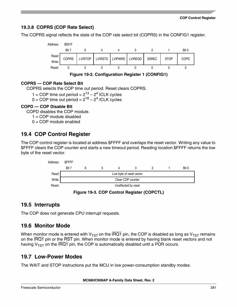
COP Control Register
MC68HC908AP A-Family Data Sheet, Rev. 2
Freescale Semiconductor 281
19.3.8 COPRS (COP Rate Select)
The COPRS signal reflects the state of the COP rate select bit (COPRS) in the CONFIG1 register.
COPRS — COP Rate Select BitCOPRS selects the COP time out period. Reset clears COPRS.
1 = COP time out period = 213 – 24 ICLK cycles0 = COP time out period = 218 – 24 ICLK cycles
COPD — COP Disable BitCOPD disables the COP module.
1 = COP module disabled0 = COP module enabled
19.4 COP Control Register
The COP control register is located at address $FFFF and overlaps the reset vector. Writing any value to$FFFF clears the COP counter and starts a new timeout period. Reading location $FFFF returns the lowbyte of the reset vector.
19.5 Interrupts
The COP does not generate CPU interrupt requests.
19.6 Monitor Mode
When monitor mode is entered with VTST on the IRQ1 pin, the COP is disabled as long as VTST remainson the IRQ1 pin or the RST pin. When monitor mode is entered by having blank reset vectors and nothaving VTST on the IRQ1 pin, the COP is automatically disabled until a POR occurs.
19.7 Low-Power Modes
The WAIT and STOP instructions put the MCU in low power-consumption standby modes.
Address: $001F
Bit 7 6 5 4 3 2 1 Bit 0
Read:COPRS LVISTOP LVIRSTD LVIPWRD LVIREGD SSREC STOP COPD
Write:
Reset: 0 0 0 0 0 0 0 0
Figure 19-2. Configuration Register 1 (CONFIG1)
Address: $FFFF
Bit 7 6 5 4 3 2 1 Bit 0
Read: Low byte of reset vector
Write: Clear COP counter
Reset: Unaffected by reset
Figure 19-3. COP Control Register (COPCTL)
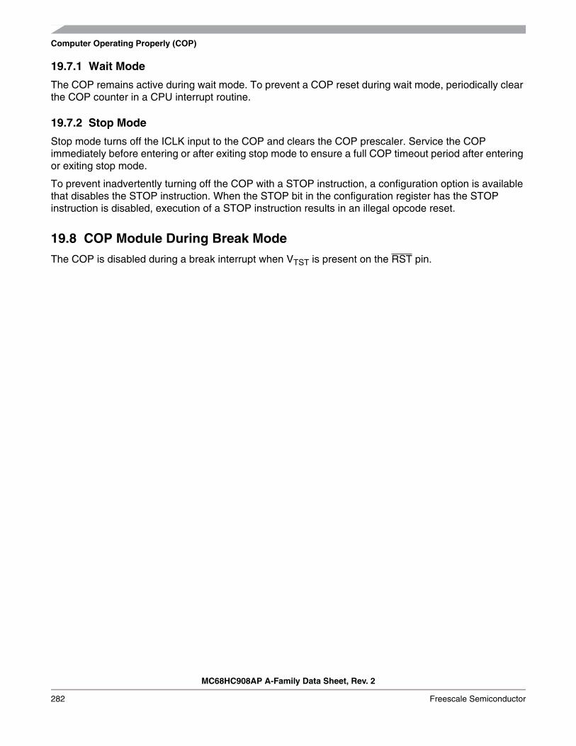
Computer Operating Properly (COP)
MC68HC908AP A-Family Data Sheet, Rev. 2
282 Freescale Semiconductor
19.7.1 Wait Mode
The COP remains active during wait mode. To prevent a COP reset during wait mode, periodically clearthe COP counter in a CPU interrupt routine.
19.7.2 Stop Mode
Stop mode turns off the ICLK input to the COP and clears the COP prescaler. Service the COPimmediately before entering or after exiting stop mode to ensure a full COP timeout period after enteringor exiting stop mode.
To prevent inadvertently turning off the COP with a STOP instruction, a configuration option is availablethat disables the STOP instruction. When the STOP bit in the configuration register has the STOPinstruction is disabled, execution of a STOP instruction results in an illegal opcode reset.
19.8 COP Module During Break Mode
The COP is disabled during a break interrupt when VTST is present on the RST pin.
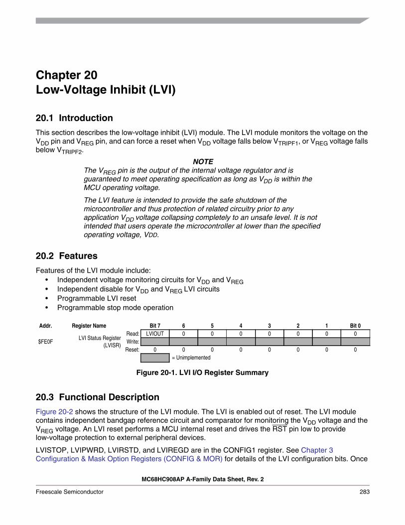
MC68HC908AP A-Family Data Sheet, Rev. 2
Freescale Semiconductor 283
Chapter 20Low-Voltage Inhibit (LVI)
20.1 Introduction
This section describes the low-voltage inhibit (LVI) module. The LVI module monitors the voltage on theVDD pin and VREG pin, and can force a reset when VDD voltage falls below VTRIPF1, or VREG voltage fallsbelow VTRIPF2.
NOTEThe VREG pin is the output of the internal voltage regulator and isguaranteed to meet operating specification as long as VDD is within theMCU operating voltage.
The LVI feature is intended to provide the safe shutdown of themicrocontroller and thus protection of related circuitry prior to anyapplication VDD voltage collapsing completely to an unsafe level. It is notintended that users operate the microcontroller at lower than the specifiedoperating voltage, VDD.
20.2 Features
Features of the LVI module include:• Independent voltage monitoring circuits for VDD and VREG• Independent disable for VDD and VREG LVI circuits• Programmable LVI reset• Programmable stop mode operation
20.3 Functional Description
Figure 20-2 shows the structure of the LVI module. The LVI is enabled out of reset. The LVI modulecontains independent bandgap reference circuit and comparator for monitoring the VDD voltage and theVREG voltage. An LVI reset performs a MCU internal reset and drives the RST pin low to providelow-voltage protection to external peripheral devices.
LVISTOP, LVIPWRD, LVIRSTD, and LVIREGD are in the CONFIG1 register. See Chapter 3Configuration & Mask Option Registers (CONFIG & MOR) for details of the LVI configuration bits. Once
Addr. Register Name Bit 7 6 5 4 3 2 1 Bit 0
$FE0FLVI Status Register
(LVISR)
Read: LVIOUT 0 0 0 0 0 0 0Write:
Reset: 0 0 0 0 0 0 0 0= Unimplemented
Figure 20-1. LVI I/O Register Summary

Low-Voltage Inhibit (LVI)
MC68HC908AP A-Family Data Sheet, Rev. 2
284 Freescale Semiconductor
an LVI reset occurs, the MCU remains in reset until VDD rises above VTRIPR1 and VREG rises aboveVTRIPR2, which causes the MCU to exit reset. The output of the comparator controls the state of theLVIOUT flag in the LVI status register (LVISR).
An LVI reset also drives the RST pin low to provide low-voltage protection to external peripheral devices.
Figure 20-2. LVI Module Block Diagram
20.3.1 Low VDD Detector
The low VDD detector circuit monitors the VDD voltage and forces a LVI reset when the VDD voltage fallsbelow the trip voltage, VTRIPF1. The VDD LVI circuit can be disabled by the setting the LVIPWRD bit inCONFIG1 register.
20.3.2 Low VREG Detector
The low VREG detector circuit monitors the VREG voltage and forces a LVI reset when the VREG voltagefalls below the trip voltage, VTRIPF2. The VREG LVI circuit can be disabled by the setting the LVIREGD bitin CONFIG1 register.
20.3.3 Polled LVI Operation
In applications that can operate at VDD levels below the VTRIPF1 level, software can monitor VDD by pollingthe LVIOUT bit. In the CONFIG1 register, the LVIPWRD bit must be at logic 0 to enable the LVI module,and the LVIRSTD bit must be at logic 1 to disable LVI resets.
LOW VDD
DETECTOR
LVIPWRD
STOP INSTRUCTION
LVI RESET
VDD > VTRIPR1 = 0
VDD ≤ VTRIPF1 = 1
FROM CONFIG1
FROM CONFIG1
VDD
FROM CONFIG1
TO LVISR
LVIOUT
LVISTOP
LVIRSTD
DETECTORLOW VREG
LVIREGD
STOP INSTRUCTION
VREG ≤ VTRIPF2 = 1
VREG > VTRIPR2 = 0
FROM CONFIG1
VREG
FROM CONFIG1
LVISTOP

LVI Status Register
MC68HC908AP A-Family Data Sheet, Rev. 2
Freescale Semiconductor 285
20.3.4 Forced Reset Operation
In applications that require VDD to remain above the VTRIPF1 level, enabling LVI resets allows the LVImodule to reset the MCU when VDD falls below the VTRIPF1 level. In the CONFIG1 register, the LVIPWRDand LVIRSTD bits must be at logic 0 to enable the LVI module and to enable LVI resets.
20.3.5 Voltage Hysteresis Protection
Once the LVI has triggered (by having VDD fall below VTRIPF1), the LVI will maintain a reset condition untilVDD rises above the rising trip point voltage, VTRIPR1. This prevents a condition in which the MCU iscontinually entering and exiting reset if VDD is approximately equal to VTRIPF1. VTRIPR1 is greater thanVTRIPF1 by the hysteresis voltage, VHYS.
20.4 LVI Status Register
The LVI status register (LVISR) indicates if the VDD voltage was detected below VTRIPF1 or VREG voltagewas detected below VTRIPF2.
LVIOUT — LVI Output BitThis read-only flag becomes set when the VDD or VREG falls below their respective trip voltages. Resetclears the LVIOUT bit.
20.5 LVI Interrupts
The LVI module does not generate interrupt requests.
Address: $FE0F
Bit 7 6 5 4 3 2 1 Bit 0
Read: LVIOUT 0 0 0 0 0 0 0
Write:
Reset: 0 0 0 0 0 0 0 0
= Unimplemented
Figure 20-3. LVI Status Register
Table 20-1. LVIOUT Bit Indication
VDD, VREG LVIOUT
VDD > VTRIPR1and
VREG > VTRIPR2
0
VDD < VTRIPF1or
VDD < VTRIPF2
1
VTRIPF1 < VDD < VTRIPR1or
VTRIPF2 < VREG< VTRIPR2
Previous value

Low-Voltage Inhibit (LVI)
MC68HC908AP A-Family Data Sheet, Rev. 2
286 Freescale Semiconductor
20.6 Low-Power Modes
The STOP and WAIT instructions put the MCU in low power-consumption standby modes.
20.6.1 Wait Mode
If enabled, the LVI module remains active in wait mode. If enabled to generate resets, the LVI module cangenerate a reset and bring the MCU out of wait mode.
20.6.2 Stop Mode
If enabled in stop mode (LVISTOP = 1), the LVI module remains active in stop mode. If enabled togenerate resets (LVIRSTD = 0), the LVI module can generate a reset and bring the MCU out of stopmode.

MC68HC908AP A-Family Data Sheet, Rev. 2
Freescale Semiconductor 287
Chapter 21Break Module (BRK)
21.1 Introduction
This section describes the break module. The break module can generate a break interrupt that stopsnormal program flow at a defined address to enter a background program.
21.2 Features
Features of the break module include:• Accessible input/output (I/O) registers during the break interrupt• CPU-generated break interrupts• Software-generated break interrupts• COP disabling during break interrupts
21.3 Functional Description
When the internal address bus matches the value written in the break address registers, the break moduleissues a breakpoint signal to the CPU. The CPU then loads the instruction register with a softwareinterrupt instruction (SWI) after completion of the current CPU instruction. The program counter vectorsto $FFFC and $FFFD ($FEFC and $FEFD in monitor mode).
Addr. Register Name Bit 7 6 5 4 3 2 1 Bit 0
$FE00SIM Break Status Register
(SBSR)
Read:R R R R R R
SBSWR
Write: Note
Reset: 0
$FE03SIM Break Flag Control
Register(SBFCR)
Read:BCFE R R R R R R R
Write:Reset: 0
$FE0CBreak AddressRegister High
(BRKH)
Read:Bit 15 14 13 12 11 10 9 Bit 8
Write:Reset: 0 0 0 0 0 0 0 0
$FE0DBreak Address
Register Low(BRKL)
Read:Bit 7 6 5 4 3 2 1 Bit 0
Write:Reset: 0 0 0 0 0 0 0 0
$FE0EBreak Status and Control
Register(BRKSCR)
Read:BRKE BRKA
0 0 0 0 0 0
Write:Reset: 0 0 0 0 0 0 0 0
Note: Writing a logic 0 clears BW. = Unimplemented R = Reserved
Figure 21-1. Break Module I/O Register Summary

Break Module (BRK)
MC68HC908AP A-Family Data Sheet, Rev. 2
288 Freescale Semiconductor
The following events can cause a break interrupt to occur:• A CPU-generated address (the address in the program counter) matches the contents of the break
address registers.• Software writes a logic 1 to the BRKA bit in the break status and control register.
When a CPU-generated address matches the contents of the break address registers, the break interruptbegins after the CPU completes its current instruction. A return-from-interrupt instruction (RTI) in thebreak routine ends the break interrupt and returns the MCU to normal operation. Figure 21-2 shows thestructure of the break module.
Figure 21-2. Break Module Block Diagram
21.3.1 Flag Protection During Break Interrupts
The BCFE bit in the SIM break flag control register (SBFCR) enables software to clear status bits duringthe break state.
21.3.2 CPU During Break Interrupts
The CPU starts a break interrupt by:• Loading the instruction register with the SWI instruction• Loading the program counter with $FFFC and $FFFD
($FEFC and $FEFD in monitor mode)
The break interrupt begins after completion of the CPU instruction in progress. If the break addressregister match occurs on the last cycle of a CPU instruction, the break interrupt begins immediately.
21.3.3 TIMI and TIM2 During Break Interrupts
A break interrupt stops the timer counters.
21.3.4 COP During Break Interrupts
The COP is disabled during a break interrupt when VTST is present on the RST pin.
21.4 Low-Power Modes
The WAIT and STOP instructions put the MCU in low power-consumption standby modes.
IAB15–IAB8
IAB7–IAB0
8-BIT COMPARATOR
8-BIT COMPARATOR
CONTROL
BREAK ADDRESS REGISTER LOW
BREAK ADDRESS REGISTER HIGH
IAB15–IAB0BREAK

Break Module Registers
MC68HC908AP A-Family Data Sheet, Rev. 2
Freescale Semiconductor 289
21.4.1 Wait Mode
If enabled, the break module is active in wait mode. In the break routine, the user can subtract one fromthe return address on the stack if SBSW is set. (see Chapter 7 System Integration Module (SIM)) Clearthe BW bit by writing logic 0 to it.
21.4.2 Stop Mode
A break interrupt causes exit from stop mode and sets the SBSW bit in the break status register.
21.5 Break Module Registers
These registers control and monitor operation of the break module:• Break status and control register (BRKSCR)• Break address register high (BRKH)• Break address register low (BRKL)• SIM break status register (SBSR)• SIM break flag control register (SBFCR)
21.5.1 Break Status and Control Register
The break status and control register (BRKSCR) contains break module enable and status bits.
BRKE — Break Enable BitThis read/write bit enables breaks on break address register matches. Clear BRKE by writing a logic0 to bit 7. Reset clears the BRKE bit.
1 = Breaks enabled on 16-bit address match0 = Breaks disabled on 16-bit address match
BRKA — Break Active BitThis read/write status and control bit is set when a break address match occurs. Writing a logic 1 toBRKA generates a break interrupt. Clear BRKA by writing a logic 0 to it before exiting the break routine.Reset clears the BRKA bit.
1 = (When read) Break address match0 = (When read) No break address match
Address: $FE0E
Bit 7 6 5 4 3 2 1 Bit 0
Read:BRKE BRKA
0 0 0 0 0 0
Write:
Reset: 0 0 0 0 0 0 0 0
= Unimplemented
Figure 21-3. Break Status and Control Register (BRKSCR)

Break Module (BRK)
MC68HC908AP A-Family Data Sheet, Rev. 2
290 Freescale Semiconductor
21.5.2 Break Address Registers
The break address registers (BRKH and BRKL) contain the high and low bytes of the desired breakpointaddress. Reset clears the break address registers.
21.5.3 SIM Break Status Register
The SIM break status register (SBSR) contains a flag to indicate that a break caused an exit from waitmode. The flag is useful in applications requiring a return to wait mode after exiting from a break interrupt.
SBSW — Break Wait BitThis status bit is set when a break interrupt causes an exit from wait mode or stop mode. Clear SBSWby writing a logic 0 to it. Reset clears SBSW.
1 = Stop mode or wait mode was exited by break interrupt0 = Stop mode or wait mode was not exited by break interrupt
SBSW can be read within the break interrupt routine. The user can modify the return address on the stackby subtracting 1 from it. The following code is an example.
Address: $FE0C
Bit 7 6 5 4 3 2 1 Bit 0
Read:Bit 15 14 13 12 11 10 9 Bit 8
Write:
Reset: 0 0 0 0 0 0 0 0
Figure 21-4. Break Address Register High (BRKH)
Address: $FE0D
Bit 7 6 5 4 3 2 1 Bit 0
Read:Bit 7 6 5 4 3 2 1 Bit 0
Write:
Reset: 0 0 0 0 0 0 0 0
Figure 21-5. Break Address Register Low (BRKL)
Address: $FE00
Bit 7 6 5 4 3 2 1 Bit 0
Read:R R R R R R
SBSWR
Write: Note
Reset: 0
Note: Writing a logic 0 clears SBSW. R = Reserved
Figure 21-6. SIM Break Status Register (SBSR)
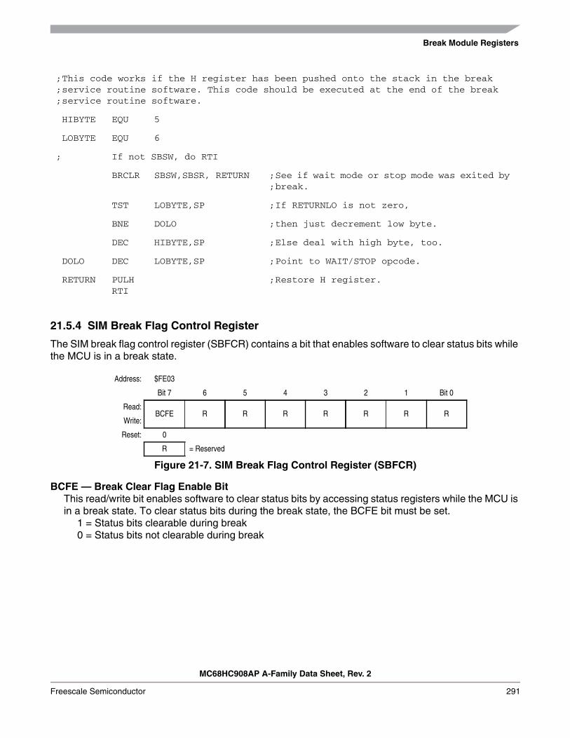
Break Module Registers
MC68HC908AP A-Family Data Sheet, Rev. 2
Freescale Semiconductor 291
21.5.4 SIM Break Flag Control Register
The SIM break flag control register (SBFCR) contains a bit that enables software to clear status bits whilethe MCU is in a break state.
BCFE — Break Clear Flag Enable BitThis read/write bit enables software to clear status bits by accessing status registers while the MCU isin a break state. To clear status bits during the break state, the BCFE bit must be set.
1 = Status bits clearable during break0 = Status bits not clearable during break
;;;
This code works if the H register has been pushed onto the stack in the breakservice routine software. This code should be executed at the end of the breakservice routine software.
HIBYTE EQU 5
LOBYTE EQU 6
; If not SBSW, do RTI
BRCLR SBSW,SBSR, RETURN ;;See if wait mode or stop mode was exited bybreak.
TST LOBYTE,SP ;If RETURNLO is not zero,
BNE DOLO ;then just decrement low byte.
DEC HIBYTE,SP ;Else deal with high byte, too.
DOLO DEC LOBYTE,SP ;Point to WAIT/STOP opcode.
RETURN PULHRTI
;Restore H register.
Address: $FE03
Bit 7 6 5 4 3 2 1 Bit 0
Read:BCFE R R R R R R R
Write:
Reset: 0
R = Reserved
Figure 21-7. SIM Break Flag Control Register (SBFCR)

Break Module (BRK)
MC68HC908AP A-Family Data Sheet, Rev. 2
292 Freescale Semiconductor

MC68HC908AP A-Family Data Sheet, Rev. 2
Freescale Semiconductor 293
Chapter 22Electrical Specifications
22.1 Introduction
This section contains electrical and timing specifications.
22.2 Absolute Maximum Ratings
Maximum ratings are the extreme limits to which the MCU can be exposed without permanently damaging it.
NOTEThis device is not guaranteed to operate properly at the maximum ratings.Refer to 5V DC Electrical Characteristics for guaranteed operatingconditions.
NOTEThis device contains circuitry to protect the inputs against damage due tohigh static voltages or electric fields; however, it is advised that normalprecautions be taken to avoid application of any voltage higher thanmaximum-rated voltages to this high-impedance circuit. For properoperation, it is recommended that VIN and VOUT be constrained to therange VSS ≤ (VIN or VOUT) ≤ VDD. Reliability of operation is enhanced ifunused inputs are connected to an appropriate logic voltage level (forexample, either VSS or VDD.)
Table 22-1. Absolute Maximum Ratings
Characteristic(1)
1. Voltages referenced to VSS.
Symbol Value Unit
Supply voltage VDD –0.3 to +6.0 V
Input voltageAll pins (except IRQ1)IRQ1 pin
VIN VSS–0.3 to VDD +0.3VSS–0.3 to 8.5
VV
Maximum current per pin excludingVDD and VSS
I ±25 mA
Maximum current out of VSS IMVSS 100 mA
Maximum current into VDD IMVDD 100 mA
Storage temperature TSTG –55 to +150 °C

Electrical Specifications
MC68HC908AP A-Family Data Sheet, Rev. 2
294 Freescale Semiconductor
22.3 Functional Operating Range
22.4 Thermal Characteristics
Table 22-2. Operating Range
Characteristic Symbol Value Unit
Operating temperature range TA – 40 to +85 °C
Operating voltage range VDD 4.5 to 5.5 (1)
1. Functionality of the device has been characterized down to the LVI trip voltage, but usershould ensure that the device supply voltage is within the specified range of 4.5 to 5.5Vafter power-up in order for the LVI circuit to configure properly.
V
Table 22-3. Thermal Characteristics
Characteristic Symbol Value Unit
Thermal resistance42-Pin SDIP44-Pin QFP48-Pin LQFP
θJA609580
°C/W°C/W°C/W
I/O pin power dissipation PI/O User determined W
Power dissipation(1)
1. Power dissipation is a function of temperature.
PDPD = (IDD × VDD) + PI/O =
K/(TJ + 273 °C)W
Constant(2)
2. K constant unique to the device. K can be determined for a known TA and measured PD.With this value of K, PD and TJ can be determined for any value of TA.
KPD x (TA + 273 °C)
+ PD2 × θJA
W/°C
Average junction temperature TJ TA + (PD × θJA) °C
Maximum junction temperature TJM 100 °C

5V DC Electrical Characteristics
MC68HC908AP A-Family Data Sheet, Rev. 2
Freescale Semiconductor 295
22.5 5V DC Electrical Characteristics
Table 22-4. DC Electrical Characteristics (5V)
Characteristic(1) Symbol Min Typ(2) Max Unit
Output high voltage(ILOAD = –12mA) PTA[0:7], PTB[4:7], PTC[0:5], PTD[0:7](ILOAD = –15mA) PTA[0:7], PTB[4:7], PTC[0:5], PTD[0:7]
VOHVOH
VDD–0.8VDD–1.0
——
——
VV
Output low voltage(ILOAD = 6mA) PTA[0:7], PTB[4:7], PTC[0:5], PTD[0:7](ILOAD = 12mA) PTB[0:3], PTC[6:7](ILOAD = 15mA) PTA[0:7], PTB[4:7], PTC[0:5], PTD[0:7](ILOAD = 15mA) PTB[0:3], PTC[6:7](ILOAD = 15mA) as TxD, RxD, SCTxD, SCRxD(ILOAD = see Table 22-8) as SDA, SCL
VOLVOLVOLVOL
VOLSCIVOLIIC
——————
——————
0.40.40.80.60.40.4
VVVVVV
LED sink current (VOL = 3V)PTA[0:7]
IOL 9 15 25 mA
Input high voltagePTA[0:7], PTB[0:7], PTC[0:7], PTD[0:7], RST, IRQ1OSC1
VIH 0.7 × VDD0.7 × VREG
——
VDDVREG
VV
Input low voltagePTA[0:7], PTB[0:7], PTC[0:7], PTD[0:7], RST, IRQ1OSC1
VIL VSSVSS
——
0.3 × VDD0.3 × VREG
VV
VDD supply current, fOP = 8 MHz
Run(3)
Wait(4)
——
102.5
2010
mAmA
Stop (25°C)
with OSC, TBM, and LVI modules on(5)
with OSC and TBM modules on(5)
all modules off(6)
IDD———
116020
2.1250125
mAµAµA
Stop (–40 to 85°C)
with OSC, TBM, and LVI modules on(5)
with OSC and TBM modules on(5)
all modules off(6)
———
1.218042
2.5300250
mAµAµA
Digital I/O ports Hi-Z leakage current IIL — — ± 10 µA
Input current IIN — — ± 1 µA
CapacitancePorts (as input or output)
COUTCIN
——
——
128
pFpF
POR rearm voltage(7) VPOR 0 — 100 mV
POR rise time ramp rate(8) RPOR 0.035 — — V/ms
Monitor mode entry voltage VTST 1.4 × VDD 8.5 V
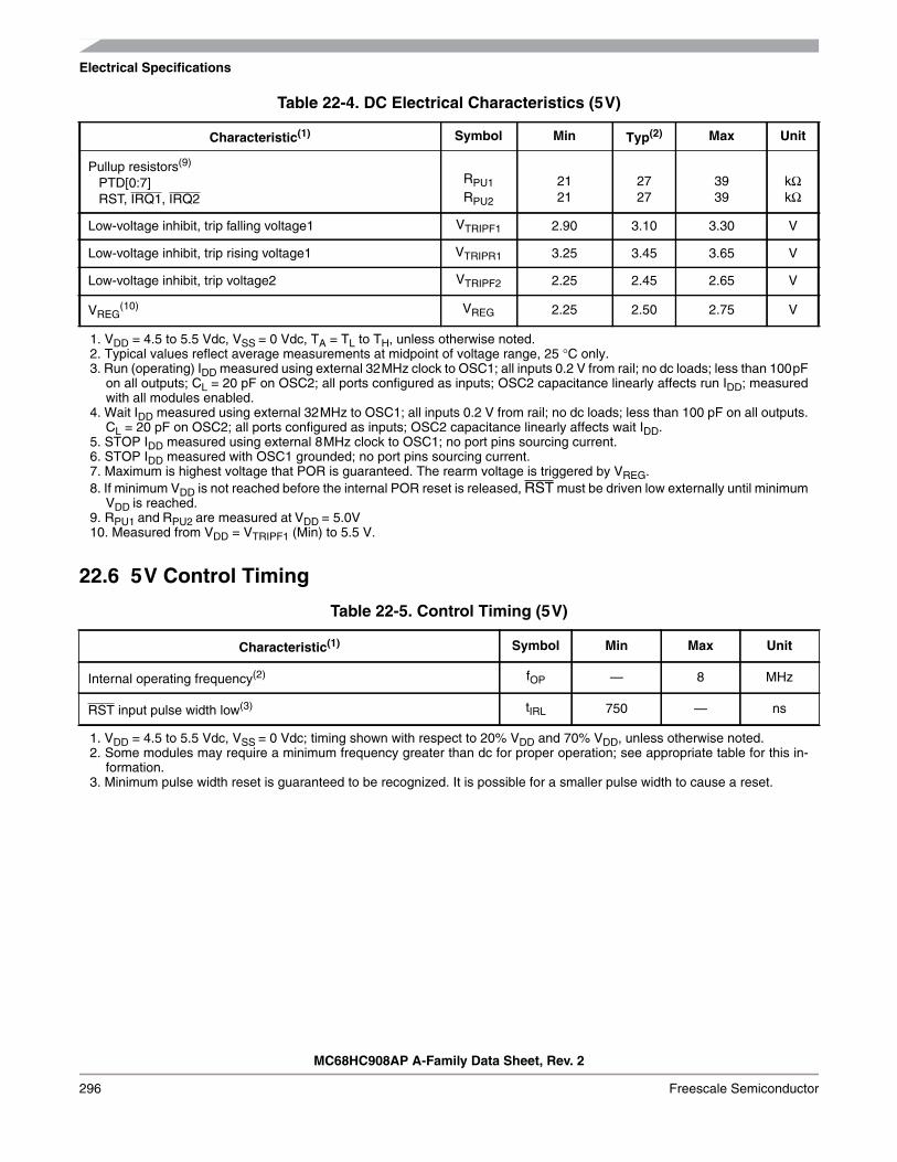
Electrical Specifications
MC68HC908AP A-Family Data Sheet, Rev. 2
296 Freescale Semiconductor
22.6 5V Control Timing
Pullup resistors(9)
PTD[0:7]RST, IRQ1, IRQ2
RPU1RPU2
2121
2727
3939
kΩkΩ
Low-voltage inhibit, trip falling voltage1 VTRIPF1 2.90 3.10 3.30 V
Low-voltage inhibit, trip rising voltage1 VTRIPR1 3.25 3.45 3.65 V
Low-voltage inhibit, trip voltage2 VTRIPF2 2.25 2.45 2.65 V
VREG(10) VREG 2.25 2.50 2.75 V
1. VDD = 4.5 to 5.5 Vdc, VSS = 0 Vdc, TA = TL to TH, unless otherwise noted.2. Typical values reflect average measurements at midpoint of voltage range, 25 °C only.3. Run (operating) IDD measured using external 32MHz clock to OSC1; all inputs 0.2 V from rail; no dc loads; less than 100pF
on all outputs; CL = 20 pF on OSC2; all ports configured as inputs; OSC2 capacitance linearly affects run IDD; measuredwith all modules enabled.
4. Wait IDD measured using external 32MHz to OSC1; all inputs 0.2 V from rail; no dc loads; less than 100 pF on all outputs.CL = 20 pF on OSC2; all ports configured as inputs; OSC2 capacitance linearly affects wait IDD.
5. STOP IDD measured using external 8MHz clock to OSC1; no port pins sourcing current.6. STOP IDD measured with OSC1 grounded; no port pins sourcing current.7. Maximum is highest voltage that POR is guaranteed. The rearm voltage is triggered by VREG.8. If minimum VDD is not reached before the internal POR reset is released, RST must be driven low externally until minimum
VDD is reached.9. RPU1 and RPU2 are measured at VDD = 5.0V10. Measured from VDD = VTRIPF1 (Min) to 5.5 V.
Table 22-5. Control Timing (5V)
Characteristic(1)
1. VDD = 4.5 to 5.5 Vdc, VSS = 0 Vdc; timing shown with respect to 20% VDD and 70% VDD, unless otherwise noted.
Symbol Min Max Unit
Internal operating frequency(2)
2. Some modules may require a minimum frequency greater than dc for proper operation; see appropriate table for this in-formation.
fOP — 8 MHz
RST input pulse width low(3)
3. Minimum pulse width reset is guaranteed to be recognized. It is possible for a smaller pulse width to cause a reset.
tIRL 750 — ns
Table 22-4. DC Electrical Characteristics (5V)
Characteristic(1) Symbol Min Typ(2) Max Unit

5V Oscillator Characteristics
MC68HC908AP A-Family Data Sheet, Rev. 2
Freescale Semiconductor 297
22.7 5V Oscillator Characteristics
Figure 22-1. RC vs. Frequency
Table 22-6. Oscillator Specifications (5V)
Characteristic(1)
1. The oscillator circuit operates at VREG.
Symbol Min Typ Max Unit
Internal oscillator clock frequency fICLK 64k 88k(2)
2. Typical value reflect average measurements at midpoint of voltage range, 25 °C only.
104k Hz
External reference clock to OSC1(3)
3. No more than 10% duty cycle deviation from 50%. The max. frequency is limited by an EMC filter.
fOSC dc 32M Hz
Crystal reference frequency(4)
4. Fundamental mode crystals only.
fXTALCLK 1M — 8M Hz
Crystal load capacitance(5)
5. Consult crystal vendor data sheet.
CL — — —
Crystal fixed capacitance(5) C1 — 2 × CL —
Crystal tuning capacitance(5) C2 — 2 × CL —
Feedback bias resistor RB — 1M — Ω
Series resistor(5) RS — 0 — Ω
External RC clock frequency fRCCLK 7.6M Hz
RC oscillator external R REXT See Figure 22-1 Ω
RC oscillator external C CEXT — 10 — pF
REXT CEXT
OSC1
VREG
MCU
00 10 20 30 40 50
8
6
4
2
Resistor, REXT (kΩ)
RC
freq
uenc
y, f R
CC
LK (
MH
z)
CEXT = 10 pF
VDD = 5V, @ 25°C

Electrical Specifications
MC68HC908AP A-Family Data Sheet, Rev. 2
298 Freescale Semiconductor
22.8 5V ADC Electrical Characteristics
Table 22-7. ADC Electrical Characteristics (5V)
Characteristic(1)
1. VDD = 4.5 to 5.5 Vdc, VSS = 0 Vdc, TA = TL to TH, unless otherwise noted.
Symbol Min Max Unit Notes
Supply voltage VDDA 4.5 5.5 VVDDA is an dedicated pin and shouldbe tied to VDD on the PCB withproper decoupling.
Input range VADIN 0 VDDA V VADIN ≤ VDDA
Resolution BAD 10 10 bits
Absolute accuracy AAD — ± 1.5 LSBIncludes quantization.±0.5 LSB = ±1 ADC step.
ADC internal clock fADIC 500k 1.048M Hz tADIC = 1/fADIC
Conversion range RAD VREFL VREFH V
ADC voltage referencehigh
VREFH — VDDA + 0.1 V
ADC voltage referencelow
VREFL VSSA – 0.1 — V
Conversion time tADC 16 17tADIC
cycles
Sample time tADS 5 —tADIC
cycles
Monotonicity MAD Guaranteed
Zero input reading ZADI 000 001 HEX VADIN = VREFL
Full-scale reading FADI 3FD 3FF HEX VADIN = VREFH
Input capacitance CADI — 20 pF Not tested.
Input impedance RADI 20M — Ω
VREFH/VREFL IVREF — 1.6 mA Not tested.

MMIIC Electrical Characteristics
MC68HC908AP A-Family Data Sheet, Rev. 2
Freescale Semiconductor 299
22.9 MMIIC Electrical Characteristics
Figure 22-2. MMIIC Signal Timings
See Table 22-9 for MMIIC timing parameters.
Table 22-8. MMIIC DC Electrical Characteristics
Characteristic(1)
1. VDD = 4.5 to 5.5Vdc, VSS = 0 Vdc, TA = TL to TH, unless otherwise noted.
Symbol Min Typ Max Unit Comments
Input low VIL –0.5 — 0.8 V Data, clock input low.
Input high VIH 2.1 — 5.5 V Data, clock input high.
Output low VOL — — 0.4 VData, clock output low;@IPULLUP,MAX
Input leakage ILEAK — — ± 5 µA Input leakage current
Pullup current IPULLUP 100 — 350 µACurrent through pull-up resistoror current source.
See note.(2)
2. The IPULLUP (max) specification is determined primarily by the need to accommodate a maximum of 1.1kΩ equivalent se-ries resistor of removable SMBus devices, such as the smart battery, while maintaining the VOL (max) of the bus.
SDA
SCL
tHD.STA tLOW tHIGH tSU.DAT tHD.DAT tSU.STA tSU.STO

Electrical Specifications
MC68HC908AP A-Family Data Sheet, Rev. 2
300 Freescale Semiconductor
Table 22-9. MMIIC Interface Input/Output Signal Timing
Characteristic Symbol Min Typ Max Unit Comments
Operating frequency fSMB 10 — 100 kHz MMIIC operating frequency
Bus free time tBUF 4.7 — — µsBus free time between STOP andSTART condition
Repeated start hold time. tHD.STA 4.0 — — µsHold time after (repeated) STARTcondition. After this period, the firstclock is generated.
Repeated start setup time. tSU.STA 4.7 — — µs Repeated START condition setup time.
Stop setup time tSU.STO 4.0 — — µs Stop condition setup time.
Hold time tHD.DAT 300 — — ns Data hold time.
Setup time tSU.DAT 250 — — ns Data setup time.
Clock low time-out tTIMEOUT 25 — 35 ms Clock low time-out.(1)
Clock low tLOW 4.7 — — µs Clock low period
Clock high tHIGH 4.0 — — µs Clock high period.(2)
Slave clock low extend time tLOW.SEXT — — 25 msCumulative clock low extend time (slave
device)(3)
Master clock low extend time tLOW.MEXT — — 10 msCumulative clock low extend time
(master device) (4)
Fall time tF — — 300 ns Clock/Data Fall Time(5)
Rise time tR — — 1000 ns Clock/Data Rise Time(5)
1. Devices participating in a transfer will timeout when any clock low exceeds the value of TTIMEOUT min. of 25ms. Devicesthat have detected a timeout condition must reset the communication no later than TTIMEOUT max of 35ms. The maximumvalue specified must be adhered to by both a master and a slave as it incorporates the cumulative limit for both a master(10 ms) and a slave (25 ms).Software should turn-off the MMIIC module to release the SDA and SCL lines.
2. THIGH MAX provides a simple guaranteed method for devices to detect the idle conditions.3. TLOW.SEXT is the cumulative time a slave device is allowed to extend the clock cycles in one message from the initial start
to the stop. If a slave device exceeds this time, it is expected to release both its clock and data lines and reset itself.4. TLOW.MEXT is the cumulative time a master device is allowed to extend its clock cycles within each byte of a message as
defined from start-to-ack, ack-to-ack, or ack-to-stop.5. Rise and fall time is defined as follows: TR = (VILMAX – 0.15) to (VIHMIN + 0.15), TF = 0.9×VDD to (VILMAX – 0.15).

CGM Electrical Specification
MC68HC908AP A-Family Data Sheet, Rev. 2
Freescale Semiconductor 301
22.10 CGM Electrical Specification
Table 22-10. CGM Electrical Specifications
Characteristic Symbol Min Typ Max Unit
Reference frequency fRDV 1 — 8 MHz
Range nominal multiplies fNOM — 125 — kHz
VCO center-of-range frequency fVRS 125k — 40M Hz
VCO range linear range multiplier L 1 — 255
VCO power-of-two-range multiplier 2E 1 — 4
VCO multiply factor N 1 — 4095
VCO prescale multiplier 2P 1 — 8
Reference divider factor R 1 1 15
VCO operating frequency fVCLK 125k — 40M Hz
Manual acquisition time tLOCK — — 50 ms
Automatic lock time tLOCK — — 50 ms
PLL jitter(1)
1. Deviation of average bus frequency over 2ms. N = VCO multiplier.
fJ 0 —
fRCLK ×
0.025% × 2P
N/4
Hz

Electrical Specifications
MC68HC908AP A-Family Data Sheet, Rev. 2
302 Freescale Semiconductor
22.11 5V SPI Characteristics
Table 22-11. SPI Characteristics (5V)
Diagram
Number(1)
1. Numbers refer to dimensions in Figure 22-3 and Figure 22-4.
Characteristic(2)
2. All timing is shown with respect to 20% VDD and 70% VDD, unless noted; 100 pF load on all SPI pins.
Symbol Min Max Unit
Operating frequencyMasterSlave
fOP(M)fOP(S)
fOP/128dc
fOP/2fOP
MHzMHz
1Cycle time
MasterSlave
tCYC(M)tCYC(S)
21
128—
tCYC
tCYC
2 Enable lead time tLead(S) 1 — tCYC
3 Enable lag time tLag(S) 1 — tCYC
4Clock (SPSCK) high time
MasterSlave
tSCKH(M)tSCKH(S)
tCYC –251/2 tCYC –25
64 tCYC
—nsns
5Clock (SPSCK) low time
MasterSlave
tSCKL(M)tSCKL(S)
tCYC –251/2 tCYC –25
64 tCYC
—nsns
6Data setup time (inputs)
MasterSlave
tSU(M)tSU(S)
3030
——
nsns
7Data hold time (inputs)
MasterSlave
tH(M)tH(S)
3030
——
nsns
8Access time, slave(3)
CPHA = 0CPHA = 1
3. Time to data active from high-impedance state
tA(CP0)tA(CP1)
00
4040
nsns
9 Disable time, slave(4)
4. Hold time to high-impedance state
tDIS(S) — 40 ns
10Data valid time, after enable edge
Master
Slave(5)
5. With 100 pF on all SPI pins
tV(M)tV(S)
——
5050
nsns
11Data hold time, outputs, after enable edge
MasterSlave
tHO(M)tHO(S)
00
——
nsns
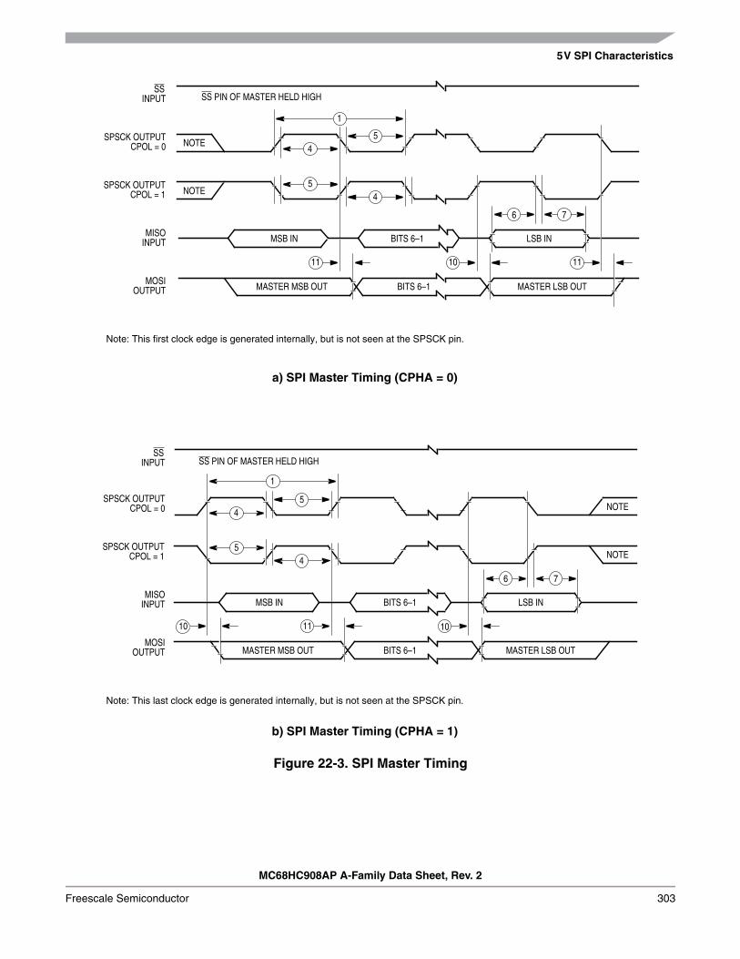
5V SPI Characteristics
MC68HC908AP A-Family Data Sheet, Rev. 2
Freescale Semiconductor 303
Figure 22-3. SPI Master Timing
NOTE
Note: This first clock edge is generated internally, but is not seen at the SPSCK pin.
SS PIN OF MASTER HELD HIGH
MSB IN
SSINPUT
SPSCK OUTPUT
SPSCK OUTPUT
MISOINPUT
MOSIOUTPUT
NOTE
4
5
5
1
4
BITS 6–1 LSB IN
MASTER MSB OUT BITS 6–1 MASTER LSB OUT
11 10 11
76
NOTE
Note: This last clock edge is generated internally, but is not seen at the SPSCK pin.
SS PIN OF MASTER HELD HIGH
MSB IN
SSINPUT
SPSCK OUTPUT
SPSCK OUTPUT
MISOINPUT
MOSIOUTPUT
NOTE4
5
5
1
4
BITS 6–1 LSB IN
MASTER MSB OUT BITS 6–1 MASTER LSB OUT
10 11 10
76
a) SPI Master Timing (CPHA = 0)
b) SPI Master Timing (CPHA = 1)
CPOL = 0
CPOL = 1
CPOL = 0
CPOL = 1
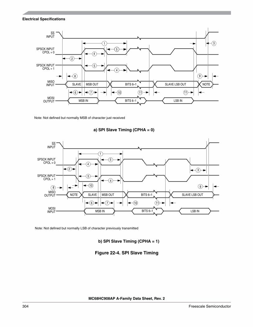
Electrical Specifications
MC68HC908AP A-Family Data Sheet, Rev. 2
304 Freescale Semiconductor
Figure 22-4. SPI Slave Timing
Note: Not defined but normally MSB of character just received
SLAVE
SSINPUT
SPSCK INPUT
SPSCK INPUT
MISOINPUT
MOSIOUTPUT
4
5
5
1
4
MSB IN
BITS 6–1
8
6 10
5
11
NOTESLAVE LSB OUT
9
3
LSB IN
2
7
BITS 6–1
MSB OUT
Note: Not defined but normally LSB of character previously transmitted
SLAVE
SSINPUT
SPSCK INPUT
SPSCK INPUT
MISOOUTPUT
MOSIINPUT
4
5
5
1
4
MSB IN
BITS 6–1
8
6 10
NOTE SLAVE LSB OUT
9
3
LSB IN
2
7
BITS 6–1
MSB OUT
10
a) SPI Slave Timing (CPHA = 0)
b) SPI Slave Timing (CPHA = 1)
11
11
CPOL = 0
CPOL = 1
CPOL = 0
CPOL = 1

Memory Characteristics
MC68HC908AP A-Family Data Sheet, Rev. 2
Freescale Semiconductor 305
22.12 Memory Characteristics
Table 22-12. Memory Characteristics
Characteristic Symbol Min. Max. Unit
Data retention voltage VRDR 1.3 — V
Number of rows per page 8 Rows
Number of bytes per page 512 Bytes
Read bus clock frequency fread(1)
1. fread is defined as the frequency range for which the FLASH memory can be read.
32k 8M Hz
Page erase time terase(2)
2. If the page erase time is longer than terase (Min.), there is no erase-disturb, but it reduces the endurance of the FLASHmemory.
20 — ms
Mass erase time tme(3)
3. If the mass erase time is longer than tme (Min.), there is no erase-disturb, but it reduces the endurance of the FLASHmemory.
200 — ms
PGM/ERASE to HVEN setup time tnvs 5 — µs
High-voltage hold time tnvh 5 — µs
High-voltage hold time (mass erase) tnvh1 100 — µs
Program hold time tpgs 10 — µs
Program time tprog 20 40 µs
Address/data setup time tads 20 — ns
Address/data hold time tadh — 30 ns
Recovery time trcv(4)
4. It is defined as the time it needs before the FLASH can be read after turning off the high voltage charge pump, by clearingHVEN to logic 0.
1 — µs
Cumulative HV period thv(5)
5. thv is the cumulative high voltage programming time to the same row before next erase, and the same address can not beprogrammed twice before next erase.
— 8 ms
Row erase endurance(6)
6. The minimum row endurance value specifies each row of the FLASH memory is guaranteed to work for at least this manyerase/program cycles.
— 10k — Cycles
Row program endurance(7)
7. The minimum row endurance value specifies each row of the FLASH memory is guaranteed to work for at least this manyerase/program cycle.
— 10k — Cycles
Data retention time(8)
8. The FLASH is guaranteed to retain data over the entire operating temperature range for at least the minimum timespecified.
— 10 — Years

Electrical Specifications
MC68HC908AP A-Family Data Sheet, Rev. 2
306 Freescale Semiconductor

MC68HC908AP A-Family Data Sheet, Rev. 2
Freescale Semiconductor 307
Chapter 23Mechanical Specifications
23.1 Introduction
This section gives the dimensions for:• 48-pin plastic low-profile quad flat pack (case #932)• 44-pin plastic quad flat pack (case #824A)• 42-pin shrink dual in-line package (case #858)
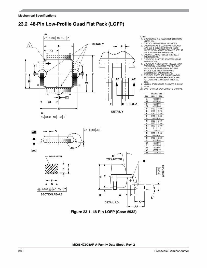
Mechanical Specifications
MC68HC908AP A-Family Data Sheet, Rev. 2
308 Freescale Semiconductor
23.2 48-Pin Low-Profile Quad Flat Pack (LQFP)
Figure 23-1. 48-Pin LQFP (Case #932)
A
A1
Z0.200 AB T–U
4X
Z0.200 AC T–U
4X
B
B1
1
12
13 24
25
36
3748
S1
S
V
V1
P
AE AE
T, U, Z
DETAIL Y
DETAIL Y
BASE METAL
N J
FD
T–UM0.080 ZAC
SECTION AE–AE
AD
G 0.080 AC
M°TOP & BOTTOM
L°W
K
AA
EC
H
0.25
0R
9
DETAIL AD
NOTES:1. DIMENSIONING AND TOLERANCING PER ASME
Y14.5M, 1994.2. CONTROLLING DIMENSION: MILLIMETER.3. DATUM PLANE AB IS LOCATED AT BOTTOM OF
LEAD AND IS COINCIDENT WITH THE LEADWHERE THE LEAD EXITS THE PLASTIC BODY ATTHE BOTTOM OF THE PARTING LINE.
4. DATUMS T, U, AND Z TO BE DETERMINED ATDATUM PLANE AB.
5. DIMENSIONS S AND V TO BE DETERMINED ATSEATING PLANE AC.
6. DIMENSIONS A AND B DO NOT INCLUDE MOLDPROTRUSION. ALLOWABLE PROTRUSION IS0.250 PER SIDE. DIMENSIONS A AND B DOINCLUDE MOLD MISMATCH AND AREDETERMINED AT DATUM PLANE AB.
7. DIMENSION D DOES NOT INCLUDE DAMBARPROTRUSION. DAMBAR PROTRUSION SHALLNOT CAUSE THE D DIMENSION TO EXCEED0.350.
8. MINIMUM SOLDER PLATE THICKNESS SHALL BE0.0076.
9. EXACT SHAPE OF EACH CORNER IS OPTIONAL.
T U
Z
AB
AC
GAU
GE
PLAN
E
DIMA
MIN MAX7.000 BSC
MILLIMETERS
A1 3.500 BSCB 7.000 BSCB1 3.500 BSCC 1.400 1.600D 0.170 0.270E 1.350 1.450F 0.170 0.230G 0.500 BSCH 0.050 0.150J 0.090 0.200K 0.500 0.700
M 12° REFN 0.090 0.160P 0.250 BSC
L 1° 5°
R 0.150 0.250S 9.000 BSCS1 4.500 BSCV 9.000 BSCV1 4.500 BSCW 0.200 REFAA 1.000 REF

44-Pin Quad Flat Pack (QFP)
MC68HC908AP A-Family Data Sheet, Rev. 2
Freescale Semiconductor 309
23.3 44-Pin Quad Flat Pack (QFP)
Figure 23-2. 44-Pin QFP (Case #824A)
NOTES:1. DIMENSIONING AND TOLERANCING PER ANSI
Y14.5M, 1982.2. CONTROLLING DIMENSION: MILLIMETER.3. DATUM PLANE –H– IS LOCATED AT BOTTOM OF
LEAD AND IS COINCIDENT WITH THE LEAD WHERETHE LEAD EXITS THE PLASTIC BODY AT THEBOTTOM OF THE PARTING LINE.
4. DATUMS –A–, –B– AND –D– TO BE DETERMINED ATDATUM PLANE –H–.
5. DIMENSIONS S AND V TO BE DETERMINED ATSEATING PLANE –C–.
6. DIMENSIONS A AND B DO NOT INCLUDE MOLDPROTRUSION. ALLOWABLE PROTRUSION IS 0.25(0.010) PER SIDE. DIMENSIONS A AND B DOINCLUDE MOLD MISMATCH AND ARE DETERMINEDAT DATUM PLANE –H–.
7. DIMENSION D DOES NOT INCLUDE DAMBARPROTRUSION. ALLOWABLE DAMBAR PROTRUSIONSHALL BE 0.08 (0.003) TOTAL IN EXCESS OF THE DDIMENSION AT MAXIMUM MATERIAL CONDITION.DAMBAR CANNOT BE LOCATED ON THE LOWERRADIUS OR THE FOOT.
L
33
34
23
22
44
1 11
12
DETAIL A
–D–
–A–
ASA–BM0.20 (0.008) D SH
SA–BM0.20 (0.008) D SC
0.05 (0.002) A–B
S
BS
A–B
M0.
20 (0
.008
)D
SH
SA–
BM
0.20
(0.0
08)
DS
C
0.05
(0.0
02)
A–B
VL
–B–
–C–SEATINGPLANE
M
M
E
HG
C –H– DATUMPLANE
DETAIL C
0.10 (0.004)
M
–H–DATUMPLANE
T
R
KQW
X
DETAIL C
DIM MIN MAX MIN MAXINCHESMILLIMETERS
A 9.90 10.10 0.390 0.398B 9.90 10.10 0.390 0.398C 2.10 2.45 0.083 0.096D 0.30 0.45 0.012 0.018E 2.00 2.10 0.079 0.083F 0.30 0.40 0.012 0.016G 0.80 BSC 0.031 BSCH — 0.25 — 0.010J 0.13 0.23 0.005 0.009K 0.65 0.95 0.026 0.037L 8.00 REF 0.315 REFM 5° 10° 5° 10°N 0.13 0.17 0.005 0.007Q 0° 7° 0° 7° R 0.13 0.30 0.005 0.012S 12.95 13.45 0.510 0.530T 0.13 — 0.005 —U 0° — 0° —V 12.95 13.45 0.510 0.530W 0.40 — 0.016 —X 1.6 REF 0.063 REF
DETAIL A
B
B
–A–, –B–, –D–
SA–BM0.20 (0.008) D SC
F
N
SECTION B–B
J
D
BASE METAL
VIEW ROTATED 90°

Mechanical Specifications
MC68HC908AP A-Family Data Sheet, Rev. 2
310 Freescale Semiconductor
23.4 42-Pin Shrink Dual In-Line Package (SDIP)
Figure 23-3. 42-Pin SDIP (Case #858)
–A–
42 22
1 21
–B–
SEATINGPLANE
–T–
SAM0.25 (0.010) T SBM0.25 (0.010) T
L
H
MJ 42 PLD 42 PL
F G NK
C
NOTES:1. DIMENSIONING AND TOLERANCING PER ANSI
Y14.5M, 1982.2. CONTROLLING DIMENSION: INCH.3. DIMENSION L TO CENTER OF LEAD WHEN
FORMED PARALLEL.4. DIMENSIONS A AND B DO NOT INCLUDE MOLD
FLASH. MAXIMUM MOLD FLASH 0.25 (0.010).
DIM MIN MAX MIN MAXMILLIMETERSINCHES
A 1.435 1.465 36.45 37.21B 0.540 0.560 13.72 14.22C 0.155 0.200 3.94 5.08D 0.014 0.022 0.36 0.56F 0.032 0.046 0.81 1.17G 0.070 BSC 1.778 BSCH 0.300 BSC 7.62 BSCJ 0.008 0.015 0.20 0.38K 0.115 0.135 2.92 3.43L 0.600 BSC 15.24 BSCM 0° 15° 0° 15° N 0.020 0.040 0.51 1.02

MC68HC908AP A-Family Data Sheet, Rev. 2
Freescale Semiconductor 311
Ordering Information
23.5 Introduction
This section contains device ordering numbers.
23.6 MC Order Numbers
Table 23-1. MC Order Numbers
MC Order NumberRAM Size
(bytes)FLASH Size
(bytes)Package
OperatingTemperature Range
MC908AP64ACB 2,048 62,368 42-pin SDIP – 40 to +85 °C
MC908AP64ACFB 2,048 62,368 44-pin QFP – 40 to +85 °C
MC908AP64ACFA 2,048 62,368 48-pin LQFP – 40 to +85 °C
MC908AP32ACB 2,048 32,768 42-pin SDIP – 40 to +85 °C
MC908AP32ACFB 2,048 32,768 44-pin QFP – 40 to +85 °C
MC908AP32ACFA 2,048 32,768 48-pin LQFP – 40 to +85 °C
MC908AP16ACB 1,024 16,384 42-pin SDIP – 40 to +85 °C
MC908AP16ACFB 1,024 16,384 44-pin QFP – 40 to +85 °C
MC908AP16ACFA 1,024 16,384 48-pin LQFP – 40 to +85 °C
MC908AP8ACB 1,024 8,192 42-pin SDIP – 40 to +85 °C
MC908AP8ACFB 1,024 8,192 44-pin QFP – 40 to +85 °C
MC908AP8ACFA 1,024 8,192 48-pin LQFP – 40 to +85 °C

MC68HC908AP A-Family Data Sheet, Rev. 2
312 Freescale Semiconductor


How to Reach Us:
Home Page:www.freescale.com
E-mail:[email protected]
USA/Europe or Locations Not Listed:Freescale SemiconductorTechnical Information Center, CH3701300 N. Alma School RoadChandler, Arizona 85224+1-800-521-6274 or [email protected]
Europe, Middle East, and Africa:Freescale Halbleiter Deutschland GmbHTechnical Information CenterSchatzbogen 781829 Muenchen, Germany+44 1296 380 456 (English)+46 8 52200080 (English)+49 89 92103 559 (German)+33 1 69 35 48 48 (French)[email protected]
Japan:Freescale Semiconductor Japan Ltd.HeadquartersARCO Tower 15F1-8-1, Shimo-Meguro, Meguro-ku,Tokyo 153-0064Japan0120 191014 or +81 3 5437 [email protected]
Asia/Pacific:Freescale Semiconductor Hong Kong Ltd.Technical Information Center2 Dai King StreetTai Po Industrial EstateTai Po, N.T., Hong Kong+800 2666 [email protected]
For Literature Requests Only:Freescale Semiconductor Literature Distribution CenterP.O. Box 5405Denver, Colorado 802171-800-441-2447 or 303-675-2140Fax: [email protected]
Information in this document is provided solely to enable system and softwareimplementers to use Freescale Semiconductor products. There are no express orimplied copyright licenses granted hereunder to design or fabricate any integratedcircuits or integrated circuits based on the information in this document.
Freescale Semiconductor reserves the right to make changes without further notice toany products herein. Freescale Semiconductor makes no warranty, representation orguarantee regarding the suitability of its products for any particular purpose, nor doesFreescale Semiconductor assume any liability arising out of the application or use of anyproduct or circuit, and specifically disclaims any and all liability, including withoutlimitation consequential or incidental damages. “Typical” parameters that may beprovided in Freescale Semiconductor data sheets and/or specifications can and do varyin different applications and actual performance may vary over time. All operatingparameters, including “Typicals”, must be validated for each customer application bycustomer’s technical experts. Freescale Semiconductor does not convey any licenseunder its patent rights nor the rights of others. Freescale Semiconductor products arenot designed, intended, or authorized for use as components in systems intended forsurgical implant into the body, or other applications intended to support or sustain life,or for any other application in which the failure of the Freescale Semiconductor productcould create a situation where personal injury or death may occur. Should Buyerpurchase or use Freescale Semiconductor products for any such unintended orunauthorized application, Buyer shall indemnify and hold Freescale Semiconductor andits officers, employees, subsidiaries, affiliates, and distributors harmless against allclaims, costs, damages, and expenses, and reasonable attorney fees arising out of,directly or indirectly, any claim of personal injury or death associated with suchunintended or unauthorized use, even if such claim alleges that FreescaleSemiconductor was negligent regarding the design or manufacture of the part.
Freescale™ and the Freescale logo are trademarks of Freescale Semiconductor, Inc.All other product or service names are the property of their respective owners.
© Freescale Semiconductor, Inc. 2007. All rights reserved.
MC68HC908AP64ARev. 2, 01/2007