Embed Size (px)
Citation preview

General DescriptionThe MAX71020A is a single-chip analog front-end (AFE) for use in embedded energy measurement applica-tions. It contains the compute engine (CE) found in Maxim Integrated’s fourth-generation meter system-on-chip (SoC) and an improved analog-to-digital converter (ADC). It interfaces to a host controller of choice over a SPI interface.The MAX71020A comes in a 28-pin TQFN package.
Applications Grid-Friendly Appliances and Smart Plugs Power Distribution Units Building Automation Systems
Benefits and Features Best-in-Class Embedded Algorithms Support Highly
Accurate Electricity Measurements• Voltage, Current, and Frequency • Active, Reactive, and Apparent Power/Energy• Digital Temperature Compensation• 40Hz–70Hz Line Frequency Range and Phase
Compensation (±10°) Advanced AFE with Exceptional Accuracy and
Temperature Stability• Voltage Reference Temperature Coefficient:
40ppm/°C (max)• On-Chip Digital Temperature Sensor• 24-Bit 2nd Order Delta-Sigma ADCs with
Differential and Single-Ended Inputs• ±0.1% Wh Accuracy over 2000:1 Current Range
Highly Integrated Features Support Compact Design Cycles and Reduced Bill of Materials• Small, 28-Pin TQFN Package• Digital Temperature Compensation• Low Power Consumption• Less Than 5mA (typ) Consumption at 3.3V• Simple Host Interface• SPI Slave• Atomic Measurements Outputs• DIO or SPI-Based Status Signals
Ordering Information appears at end of data sheet.
19-7675; Rev 0; 6/15
MAX71020A Energy Measurement AFE
Typical Operating Circuit
IAP
VA
IBP
GNDA GNDD
NEUTRAL
LOAD
POWER SUPPLY
IAN
IBN
SHUNT
LINE
VB
V3P3A V3P3SYS
MAX71020A
RESISTIVEVOLTAGEDIVIDER
LINE
DIO
CS
MISOMOSI
CLKSPI
COMPUTE ENGINE
OSCILLATOR/PLLHOST
XIN
XOUT
9.8304MHz
EVALUATION KIT AVAILABLE
(All voltages with respect to GNDA.)Voltage and Current Supplies and Ground Pins
V3P3SYS, V3P3A ...............................................-0.5V to +4.6V GNDD ...............................................................-0.1V to +0.1V
Analog Input Pins AP, IAN, IBP, IBN, VA, VB ............................(-10mA to +10mA), (-0.5V to +0.5V) XIN, XOUT ......................(-10mA to +10mA), (-0.5V to +3.0V)
Digital Pins Inputs .................................(-10mA to +10mA), (-0.5V to +6V) Outputs ......... (-10mA to +10mA), (-0.5V to (V3P3SYS + 0.5V)
Temperature and ESD Stress Operating Junction Temperature (peak, 100ms) .........+140°C Operating Junction Temperature (continuous) ............+125°C Storage Temperature Range ........................ -45°C to +165°C ESD Stress on All Pins .......................................... ±4kV, HBM Lead Temperature (soldering, 10s) .............................+300°C Soldering Temperature (reflow) ...................................+250°C
TQFN Junction-to-Ambient Thermal Resistance (θJA) ..........35°C/W Junction-to-Case Thermal Resistance (θJC) .................3°C/W
(Note 1)
Note 1: Package thermal resistances were obtained using the method described in JEDEC specification JESD51-7, using a four-layer board. For detailed information on package thermal considerations, refer to www.maximintegrated.com/thermal-tutorial.
MAX71020A Energy Measurement AFE
www.maximintegrated.com Maxim Integrated 2
Absolute Maximum Ratings
Stresses beyond those listed under “Absolute Maximum Ratings” may cause permanent damage to the device. These are stress ratings only, and functional operation of the device at these or any other conditions beyond those indicated in the operational sections of the specifications is not implied. Exposure to absolute maximum rating conditions for extended periods may affect device reliability.
Package Thermal Characteristics
Electrical CharacteristicsPARAMETER CONDITIONS MIN TYP MAX UNITS
RECOMMENDED OPERATING CONDITIONS
V3P3SYS and V3P3A Supply Voltage
Precision metering operation 3.0 3.6V
Digital operation (Notes 2, 3) 2.8 3.6
Operating Temperature -40 +85 °C
INPUT LOGIC LEVELSDigital High-Level Input Voltage (VIH) 2 V
Digital Low-Level Input Voltage (VIL) 0.8 V
Input Pullup Current (IIL) RESETZ V3P3SYS = 3.6V, VIN = 0V 41 78 115 µA
Input Pullup Current (IIL) Other Digital Inputs V3P3SYS = 3.6V, VIN = 0V -1 0 +1 µA
Input Pulldown Current (IIH) All Pins VIN = V3P3SYS -1 0 +1 µA
MAX71020A Energy Measurement AFE
www.maximintegrated.com Maxim Integrated 3
Electrical Characteristics (continued)PARAMETER CONDITIONS MIN TYP MAX UNITS
OUTPUT LOGIC LEVELS
Digital High-Level Output Voltage (VOH)
ILOAD = 1mA V3P3SYS - 0.4 V
ILOAD = 15mA (Note 3) V3P3SYS - 1.1
Digital Low-Level Output Voltage (VOL)
ILOAD = 1mA 0 0.4V
ILOAD = 15mA (Note 3) 0 0.96
TEMPERATURE MONITORTNOM (Nominal value at 22°C) V3P3A = 3.3V 956 LSB
Temperature Measurement Equation Temp = 0.33 x STEMP + 21.77 °C
Temperature Error (Note 4)TA = -40°C to +85°C -6 +6
°CTA = -20°C to +60°C -4.8 +4.8
Duration of Temperature Measurement After Setting TEMP_START
TEMP_PER = 0 15 60 ms
SUPPLY CURRENT PERFORMANCE SPECIFICATIONSV3P3A + V3P3SYS Current (Note 4) V3P3A = V3P3SYS = 3.3V, CE_E = 1, ADC_E = 1 3 4.3 mA
INTERNAL POWER-FAULT COMPARATOR SPECIFICATIONS
Overall Response Time100mV overdrive, falling 20 200
µs100mV overdrive, rising 8 200
Falling Threshold
3.0V comparator 2.83 2.93 3.03 V
2.8V comparator 2.75 2.81 2.89 V
Difference 3.0V and 2.8V comparators 50 136 220 mV
Hysteresis (Rising Threshold Falling Threshold)
3.0V comparator, TA = +22°C 17 45 74mV
2.8V comparator, TA = +22°C 15 42 70
PLL PERFORMANCE SPECIFICATIONS
PLL Power-Up Settling Time V3P3A = 0 to 3.3V step, measured from first edge of MCK 75 µs
PLL_FAST Settling TimeV3P3A = 3.3V, PLL_FAST rise 10
µsV3P3A = 3.3V, PLL_FAST fall 10
PLL Lock Frequency at XOUT V3P3A = 3.3V, MCK frequency error < 1% 7 9.8 13 MHz

MAX71020A Energy Measurement AFE
www.maximintegrated.com Maxim Integrated 4
PARAMETER CONDITIONS MIN TYP MAX UNITSVREF PERFORMANCE SPECIFICATIONSVREF Output Voltage, VREF (22) TA = +22°C 1.200 1.205 1.210 V
VREF Power-Supply Sensitivity (DVREF/DV3P3A) V3P3A = 3.0V to 3.6V -1.5 +1.5 mV/V
VNOM Definition VNOM(T) = VREF(22) + TC1 (T - 22) + TC2(T - 22)2 V
VNOM Temperature Coefficient TC1 29.32 - 1.05 x TRIMT µV/°C
VNOM Temperature Coefficient TC2 -0.56 - 0.004 x TRIMT µV/°C2
VREF(T) Deviation from VNOM(T):
(Note 4) -40 +40 ppm/°C
ADC CONVERTER PERFORMANCE SPECIFICATIONSRecommended Input Range (with Respect to GNDA) VA, VB, IBP, IBN -250 +250 mVPK
Recommended Input Range (with Respect to GNDA)
IAP, IAN: preamplifier enabled -27.78 +27.78mVpk
IAP, IAN: preamplifier disabled -250 +250
Input Impedance, No Preamplifier fIN = 65Hz 50 100 kΩ
ADC Gain Error Vs. % of Supply Variation
VIN = 200mV peak, 65Hz; V3P3A = 3.0V, 3.6V 81 ppm/%
Input Offset IAP = IAN = GNDA -10 +10 mV
Total Harmonic Distortion at 250mVPK
VIN = 55Hz, 250mVPK, 64kpts FFT,Blackman-Harris window -85 dB
Total Harmonic Distortion at 20mVPK
VIN = 55Hz, 20mVPK, 64kpts FFT, Blackman-Harris window -90 dB
LSB Size (LSB Values Do Not Include the 9-Bit Left Shift at the CE Input)
VIN = 55Hz, 20mVPK,64kpts FFT, Blackman-Harris window, 10MHz ADC clock
FIRLEN = 15 120.46
nV
FIRLEN = 14 146.20
FIRLEN = 13 179.82
FIRLEN = 12 224.59
FIRLEN = 11 285.54
FIRLEN = 10 370.71
Electrical Characteristics (continued)
6PK IN3P3A
10 NOUT 357nV/V100 V / 3.3∆
∆
6VREF(T) VNOM(T)10VNOM(T) 62
−
MAX71020A Energy Measurement AFE
www.maximintegrated.com Maxim Integrated 5
Electrical Characteristics (continued)PARAMETER CONDITIONS MIN TYP MAX UNITS
Digital Full Scale VIN = 55Hz, 400mVPK, 10MHz ADC clock
FIRLEN = 15 ±2621440
LSB
FIRLEN = 14 ±2160000
FIRLEN = 13 ±1756160
FIRLEN = 12 ±1406080
FIRLEN = 11 ±1105920
FIRLEN = 10 ±851840PREAMPLIFIER PERFORMANCE SPECIFICATIONSDifferential Gain(VIN = 28mV Differential) TA = +25°C, V3P3A = 3.3V, preamplifier enabled 8.9
Differential Gain(VIN = 15mV Differential) TA = +25°C, V3P3A = 3.3V, preamplifier enabled 8.9 V/V
Gain Variation vs. V3P3A (VIN = 28mV Differential) V3P3A = 3.0V, 3.6V -72 ppm/%
Gain Variation vs. Temperature (VIN = 28mV Differential) TA = -40°C to +85°C -45 ppm/°C
Phase Shift (VIN = 28mV Differential) TA = +25°C, V3P3A = 3.3V (Note 4) 0 8 m°
Preamplifier Input Current (IIAP)Preamplifier enabled, IADC0 = IADC1 = GNDA 9 15 20 µA
Preamplifier Input Current (IIAN)
Preamplifier and ADC Total Harmonic(VIN = 28mV Differential)
TA = +25°C; V3P3A = 3.3V, PRE_E = 1 -80 dB
Preamplifier and ADC Total Harmonic Distortion(VIN = 15mV Differential)
TA = +25°C; V3P3A = 3.3V, PRE_E = 1 -85 dB
SPI SLAVE TIMING SPECIFICATIONSSPI Setup Time SPI_DI to SPI_CK rise 10 ns
SPI Hold Time SPI_CLK rise to SPI_DI 10 ns
SPI Output Delay SPI_CLK fall to SPI_D0 40 ns
SPI Recovery Time SPI_CSZ fall to SPI_CLK 10 ns
SPI Removal Time SPI_CLK to SPI_CSZ rise 15 ns
SPI Clock High 40 ns
SPI Clock Low 40 ns
SPI Clock Frequency 10 MHz
SPI Transaction Space (SPI_CSZ Rise to SPI_CSZ Fall) 1 µs
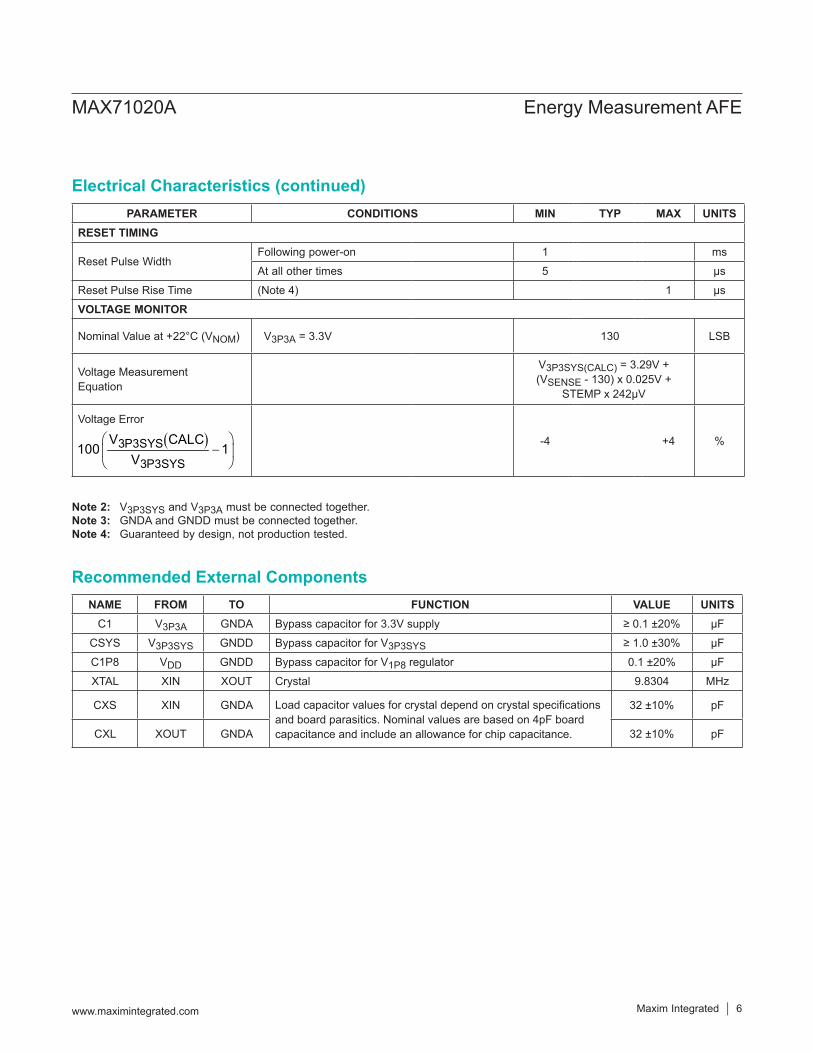
Note 2: V3P3SYS and V3P3A must be connected together.Note 3: GNDA and GNDD must be connected together.Note 4: Guaranteed by design, not production tested.
MAX71020A Energy Measurement AFE
www.maximintegrated.com Maxim Integrated 6
Recommended External Components
Electrical Characteristics (continued)
NAME FROM TO FUNCTION VALUE UNITSC1 V3P3A GNDA Bypass capacitor for 3.3V supply ≥ 0.1 ±20% µF
CSYS V3P3SYS GNDD Bypass capacitor for V3P3SYS ≥ 1.0 ±30% µF
C1P8 VDD GNDD Bypass capacitor for V1P8 regulator 0.1 ±20% µF
XTAL XIN XOUT Crystal 9.8304 MHz
CXS XIN GNDA Load capacitor values for crystal depend on crystal specifications and board parasitics. Nominal values are based on 4pF board capacitance and include an allowance for chip capacitance.
32 ±10% pF
CXL XOUT GNDA 32 ±10% pF
PARAMETER CONDITIONS MIN TYP MAX UNITSRESET TIMING
Reset Pulse WidthFollowing power-on 1 ms
At all other times 5 µs
Reset Pulse Rise Time (Note 4) 1 µs
VOLTAGE MONITOR
Nominal Value at +22°C (VNOM) V3P3A = 3.3V 130 LSB
Voltage Measurement Equation
V3P3SYS(CALC) = 3.29V + (VSENSE - 130) x 0.025V +
STEMP x 242µV
Voltage Error
-4 +4 %( )3P3SYS
3P3SYS
V CALC100 1
V
−
MAX71020A Energy Measurement AFE
www.maximintegrated.com Maxim Integrated 7
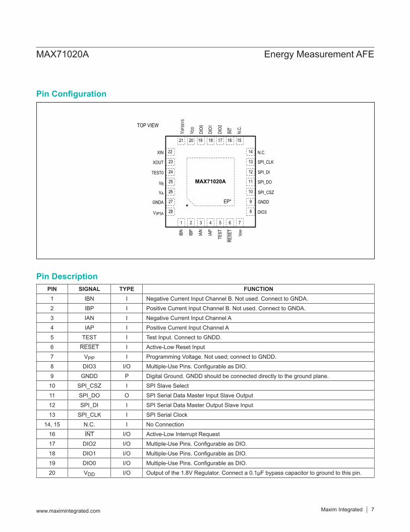
Pin Configuration
Pin Description
IBP
IAP
TEST
RESE
T
V PP
IBN
V DD
DIO1
DIO2
V 3P3
SYS
INT
N.C.
VB
VA
GNDA
SPI_DI
SPI_DO
SPI_CSZ
GNDDIA
NDI
O0
V3P3A DIO3+
TEST0
SPI_CLKXOUT
N.C.XIN
TOP VIEW
14
13
12
11
10
9
8
22
23
24
25
26
27
28
MAX71020A
15161718192021
7654321
EP*
*EP = EXPOSED PAD
PIN SIGNAL TYPE FUNCTION1 IBN I Negative Current Input Channel B. Not used. Connect to GNDA.
2 IBP I Positive Current Input Channel B. Not used. Connect to GNDA.
3 IAN I Negative Current Input Channel A
4 IAP I Positive Current Input Channel A
5 TEST I Test Input. Connect to GNDD.
6 RESET I Active-Low Reset Input
7 VPP I Programming Voltage. Not used; connect to GNDD.
8 DIO3 I/O Multiple-Use Pins. Configurable as DIO.
9 GNDD P Digital Ground. GNDD should be connected directly to the ground plane.
10 SPI_CSZ I SPI Slave Select
11 SPI_DO O SPI Serial Data Master Input Slave Output
12 SPI_DI I SPI Serial Data Master Output Slave Input
13 SPI_CLK I SPI Serial Clock
14, 15 N.C. I No Connection
16 INT I/O Active-Low Interrupt Request
17 DIO2 I/O Multiple-Use Pins. Configurable as DIO.
18 DIO1 I/O Multiple-Use Pins. Configurable as DIO.
19 DIO0 I/O Multiple-Use Pins. Configurable as DIO.
20 VDD I/O Output of the 1.8V Regulator. Connect a 0.1µF bypass capacitor to ground to this pin.
Detailed DescriptionHardware DescriptionThe MAX71020A analog front-end (AFE) integrates the functional blocks required to implement accurate energy measurement functions. Included on the chip are:
An analog front-end (AFE) featuring a 22-bit second order delta-sigma ADC
An independent 32-bit digital computation engine (CE) implementing DSP functions
A precision voltage reference (VREF) A temperature sensor for digital temperature sensing
and compensation Four I/O pins A zero-crossing detector with interrupt output Resistive shunt and current transformers are
supported A SPI slave for connection to a host controller
In a typical application, the 32-bit compute engine (CE) of the MAX71020A sequentially processes ADC samples from the Voltage and Current inputs and performs calcula-tions to measure voltage and current RMS, power, active energy (Wh) and reactive energy (VARh), as well as A2h, and V2h for four-quadrant metering. These measurements are then accessed by the host processor. In addition to the temperature-trimmed ultra-precision voltage reference, the on-chip digital temperature compensation mechanism includes a temperature sensor and associated controls for correction of unwanted temperature effects on measure-ment. Temperature-dependent external components such as crystal oscillator, resistive shunts, current transformers (CTs) and their corresponding signal conditioning circuits can be characterized and their correction factors can be
programmed to further improve system’s accuracy. The MAX71020A features an SPI (slave) interface for com-munication with the host processor. The communication protocol between the host and the MAX71020A provides a redundant information transfer ensuring the correctness of commands transferred from the host to the AFE, and of data transferred from the AFE to the host.In addition, the MAX71020A has one pin dedicated as an interrupt output to the host. This pin notifies the host of asynchronous events.
ADC DescriptionAnalog InputsThe MAX71020A has four analog inputs: two single-end-ed inputs for voltage measurement, and two differential inputs for current measurement.The IAP, IAN, IBP, and IBN pins are current sensor inputs. IBP/IBN input are not used and should be connected to GNDA. The differential inputs feature preamplifiers with a selectable gain of 1 or 9, and are intended for direct con-nection to a shunt resistor sensor or a current transformer (CT).The voltage inputs in the MAX71020A are single-ended, and are intended for sensing the line voltage via resistive dividers. These single-ended inputs are referenced to the GNDA pin..All analog signal input pins measure voltage. In the case of shunt current sensors, currents are sensed as a voltage drop in the shunt resistor sensor. In the case of current transformers (CT), the current is measured as a voltage across a burden resistor that is connected to the secondary winding of the CT. Meanwhile, line voltages are sensed through resistive voltage dividers.
MAX71020A Energy Measurement AFE
www.maximintegrated.com Maxim Integrated 8
Pin Description (continued)PIN SIGNAL TYPE FUNCTION21 V3P3SYS P System 3.3V Supply. Connect V3P3SYS to a 3.3V power supply.
22 XIN I Crystal Input
23 XOUT O Crystal Output
24 TEST0 I Test Input. Connect to GNDD.
25 VB I Line Voltage Sense Input VB. Unused, connect to GNDA.
26 VA I Line Voltage Sense Inputs VA27 GNDA P Analog Ground. Connect GNDA directly to the ground plane.
28 V3P3A P Analog Power Supply. Connect a 3.3V power supply to V3P3A. V3P3A must be the same voltage as V3P3SYS.
— — — Exposed Pad. On bottom.
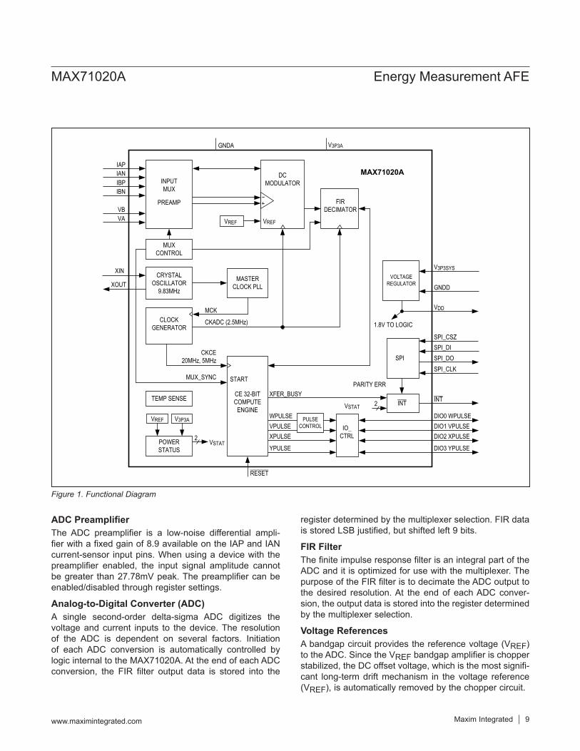
ADC PreamplifierThe ADC preamplifier is a low-noise differential ampli-fier with a fixed gain of 8.9 available on the IAP and IAN current-sensor input pins. When using a device with the preamplifier enabled, the input signal amplitude cannot be greater than 27.78mV peak. The preamplifier can be enabled/disabled through register settings.
Analog-to-Digital Converter (ADC)A single second-order delta-sigma ADC digitizes the voltage and current inputs to the device. The resolution of the ADC is dependent on several factors. Initiation of each ADC conversion is automatically controlled by logic internal to the MAX71020A. At the end of each ADC conversion, the FIR filter output data is stored into the
register determined by the multiplexer selection. FIR data is stored LSB justified, but shifted left 9 bits.
FIR FilterThe finite impulse response filter is an integral part of the ADC and it is optimized for use with the multiplexer. The purpose of the FIR filter is to decimate the ADC output to the desired resolution. At the end of each ADC conver-sion, the output data is stored into the register determined by the multiplexer selection.
Voltage ReferencesA bandgap circuit provides the reference voltage (VREF) to the ADC. Since the VREF bandgap amplifier is chopper stabilized, the DC offset voltage, which is the most signifi-cant long-term drift mechanism in the voltage reference (VREF), is automatically removed by the chopper circuit.
Figure 1. Functional Diagram
MAX71020A Energy Measurement AFE
www.maximintegrated.com Maxim Integrated 9
MAX71020ADCMODULATOR
FIRDECIMATOR
PREAMP
INPUTMUX
START
IAP
GNDA V3P3A
IAN
VOLTAGEREGULATOR
VDD
IBPIBN
VBVA
CKCE20MHz, 5MHz
MUX_SYNC
XIN
XOUT
MCK
MUXCONTROL
VREF
CRYSTALOSCILLATOR
9.83MHz
MASTERCLOCK PLL
VREF
CLOCKGENERATOR
TEMP SENSE
VREF
POWERSTATUS
CE 32-BITCOMPUTE
ENGINE
VSTAT
RESET
V3P3A
2
CKADC (2.5MHz)
GNDD
V3P3SYS
SPI
INT
SPI_CSZ
PARITY ERR
SPI_DISPI_DOSPI_CLK
WPULSE
INTXFER_BUSY
VSTAT 2
VPULSEXPULSE
YPULSE
1.8V TO LOGIC
PULSE CONTROL IO_
CTRL
DIO3 YPULSE
DIO2 XPULSEDIO1 VPULSEDIO0 WPULSE

Digital Computation Engine (CE) The CE, a dedicated 32-bit signal processor, performs the precision computations necessary to accurately measure energy. The CE calculations and processes include:
Multiplication of each current sample with its as-sociated voltage sample to obtain the energy per sample (when multiplied with the constant sample time)
Frequency-insensitive delay cancellation on all four channels (to compensate for the delay between samples caused by the multiplexing scheme)
90° phase shifter (for VAR calculations) Monitoring of the input signal frequency (for fre-
quency and phase information) Monitoring of the input signal amplitude (for sag
detection) Scaling of the processed samples based on cali-
bration coefficients Scaling of samples based on temperature com-
pensation information Gain and phase compensation
Temperature Sensor The MAX71020A includes an on-chip temperature sensor for determining the temperature of its bandgap reference. The primary use of the temperature data is to determine the magnitude of compensation required to offset the ther-mal drift in the system for the compensation of current, voltage, and energy measurement. The temperature sen-sor is awakened on command from the host controller by setting the TEMP_START control bit. The host controller must wait for the TEMP_START bit to clear before read-ing STEMP[15:0] and before setting the TEMP_START bit once again. The result of the temperature measure-ment can be read from the STEMP[15:0] register. The 16-bit value is in two’s complement form and ranges from -1024 to +1023 (decimal). The sensed temperature can be computed from the 16-bit STEMP[15:0] reading using the following formula:
Temp (°C) = 0.33 x STEMP + 21.77
An additional register, VSENSE[7:0], senses the level of the supply voltage. Table 1 shows the registers used for temperature measurement.
Table 1. Temperature Measurement Registers
MAX71020A Energy Measurement AFE
www.maximintegrated.com Maxim Integrated 10
NAME RST DIR DESCRIPTION
TEMP_PER[1:0] 0 R/W
Sets the period between temperature measurements.TEMP_PER TIME
0 Manual updates (see TEMP_START description)1 Every accumulation cycle2 Continuous3 No updates
TEMP_START 0 R/W
TEMP_PER[1:0] must be zero in order for TEMP_START to function. If TEMP_ PER[1:0] = 0, then setting TEMP_START starts a temperature measurement. Hardware clears TEMP_START when the temperature measurement is complete. The host controller must wait for TEMP_START to clear before reading STEMP[10:0] and before setting TEMP_START again.
STEMP[15:0] — R The result of the temperature measurement.
VSENSE[7:0] — R The result of the temperature measurement. See the formula listed in theElectrical Characteristics table.
Digital I/OOn reset or power-up, all DIO pins are configured as high impedance. DIO pins can be configured independently by the host controller by manipulating the D0, D1, D2, and D3 bit fields.
SPI Slave PortThe slave SPI port communicates directly with the host controller and allows it to read and write the device control registers. The interface to the slave port consists of the SPI_CSZ, SPI_CLK, SPI_DI, and SPI_DO pins. The host can also reset the MAX71020A through the SPI port by writing a data pattern to the RESET register.
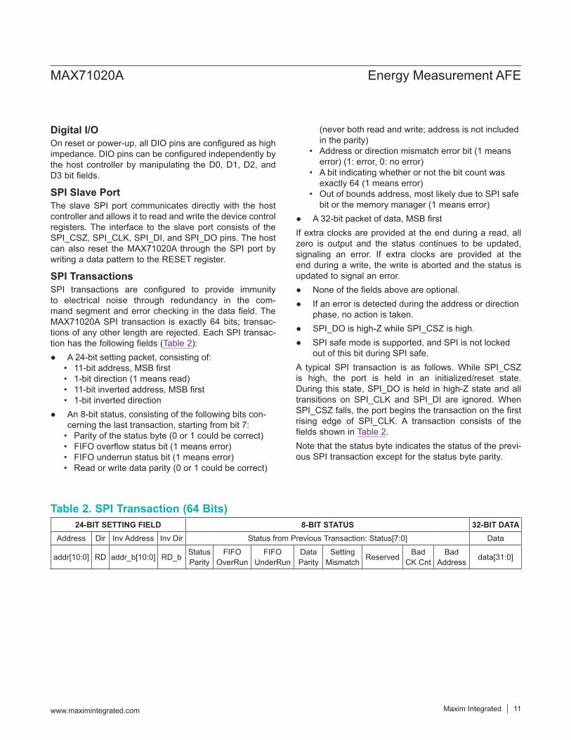
SPI TransactionsSPI transactions are configured to provide immunity to electrical noise through redundancy in the com-mand segment and error checking in the data field. The MAX71020A SPI transaction is exactly 64 bits; transac-tions of any other length are rejected. Each SPI transac-tion has the following fields (Table 2):
A 24-bit setting packet, consisting of:• 11-bit address, MSB first• 1-bit direction (1 means read)• 11-bit inverted address, MSB first• 1-bit inverted direction
An 8-bit status, consisting of the following bits con-cerning the last transaction, starting from bit 7:
• Parity of the status byte (0 or 1 could be correct)• FIFO overflow status bit (1 means error)• FIFO underrun status bit (1 means error)• Read or write data parity (0 or 1 could be correct)
(never both read and write; address is not included in the parity)
• Address or direction mismatch error bit (1 means error) (1: error, 0: no error)
• A bit indicating whether or not the bit count was exactly 64 (1 means error)
• Out of bounds address, most likely due to SPI safe bit or the memory manager (1 means error)
A 32-bit packet of data, MSB firstIf extra clocks are provided at the end during a read, all zero is output and the status continues to be updated, signaling an error. If extra clocks are provided at the end during a write, the write is aborted and the status is updated to signal an error.
None of the fields above are optional. If an error is detected during the address or direction
phase, no action is taken. SPI_DO is high-Z while SPI_CSZ is high. SPI safe mode is supported, and SPI is not locked
out of this bit during SPI safe.A typical SPI transaction is as follows. While SPI_CSZ is high, the port is held in an initialized/reset state. During this state, SPI_DO is held in high-Z state and all transitions on SPI_CLK and SPI_DI are ignored. When SPI_CSZ falls, the port begins the transaction on the first rising edge of SPI_CLK. A transaction consists of the fields shown in Table 2.Note that the status byte indicates the status of the previ-ous SPI transaction except for the status byte parity.
Table 2. SPI Transaction (64 Bits)
MAX71020A Energy Measurement AFE
www.maximintegrated.com Maxim Integrated 11
24-BIT SETTING FIELD 8-BIT STATUS 32-BIT DATAAddress Dir Inv Address Inv Dir Status from Previous Transaction: Status[7:0] Data
addr[10:0] RD addr_b[10:0] RD_b Status Parity
FIFOOverRun
FIFOUnderRun
Data Parity
Setting Mismatch Reserved Bad
CK CntBad
Address data[31:0]

SPI Safe ModeSometimes it is desirable to prevent the SPI interface from writing to arbitrary registers and possibly disturbing the CE operation. For this reason, the SPI_SAFE mode was created. In this mode, all SPI writes are disabled except to the word containing the SPI_SAFE bit. This affords the host one more layer of protection from inadvertent writes.
Fault and Reset BehaviorEvents at power-down power fault detection is performed by internal comparators that monitor the voltage at the V3P3A pin and also monitor the internally generated VDD pin voltage (1.8V DC). V3P3SYS and V3P3A must be con-nected together at the PCB level so that the comparators, which are internally connected only to the V3P3A pin, are able to simultaneously monitor the common V3P3SYS and V3P3A voltage. The following discussion assumes that V3P3A and V3P3SYS are connected together at the PCB level. See Table 3.
During a power failure, as V3P3A falls, two thresholds are detected. The first threshold, at 3.0V, warns the host controller that the analog modules are no longer accurate. The second threshold, at 2.8V, warns the host controller that a serious reduction in supply voltage has occurred and that the reliability of OTP reads may be affected.
Reset SequenceThe MAX71020A does not provide automatic reset gen-eration. The reset needs to be generated by the host controller or by external circuitry connected to the RESET pin. When the MAX71020A receives a reset signal, either from the RESET pin or from the SPI (using a write to the RESET register at address 0x322), it asynchronously halts what it was doing. It then clears the RAM and invokes the load engine (LE). The LE initializes RAM and hardware control registers from the CE code image that is stored in OTP memory. Only RAM cells and hardware registers that need not change dynamically are loaded. All other RAM cells and registers have to be loaded by
Figure 2. SPI Slave Port—Typical Read and Write Operations
Table 3. VSTAT[1:0]
MAX71020A Energy Measurement AFE
www.maximintegrated.com Maxim Integrated 12
VSTAT[1:0] DESCRIPTION00 System Power-OK. V3P3A > 3.0V. Analog modules are functional and accurate.
01 System Power is low. 2.8V < V3P3A < 3.0V. Analog modules not accurate.
11 System power below 2.8V. Ability to monitor power is about to fail.

the host controller. The LE automatically refreshes the values of the registers it is tasked with loading during the operation of the MAX71020A. This refresh happens in increments of one register at a time and at a rate of one register per second. An errant reset can occur during EMI events. If this happens, the host controller is notified. This is accomplished by the holding the INT pin low until the host clears the event (the F_RESET bit in the M_STAT register is set to indicate that a reset has occurred).
Connecting to a Host ProcessorHost connections include the INT pin, the RESET pin. In the host processor, the DIO pin connected to INT should generate an interrupt. This interrupt signals to the host that an accumulation cycle has been completed and the cal-culations performed during it, are available in the relevant transfer registers. They remain constant throughout each accumulation interval.
Sensors ConnectionFigure 3 shows a typical MAX71020A configuration. The IAP-IAN current channel can be directly connected to either a shunt resistor or a CT. The voltage input VA is connected to a resistive voltage divider. The IBP-IBN channel, as well as VB are not used and should be con-nected to GNDA.
Signal Flow DescriptionThis section reviews the signal processing calculations performed by the compute engine (CE) processor. The sample ADC sample rate is 2520 samples/s. Most of the calculations are performed over a fixed accumulation inter-val of 2520 samples corresponding to approximately 1s.
Figure 3. Typical Connection Diagram
MAX71020A Energy Measurement AFE
www.maximintegrated.com Maxim Integrated 13
IAP
VA
IBP
GNDA GNDD
NEUTRAL
LOAD
POWER SUPPLY
IAN
IBN
SHUNT OR CURRENT TRANSFORMER
LINE
VB
V3P3A V3P3SYS
MAX71020A
RESISTIVE VOLTAGE DIVIDER
LINE

Current Input CalculationsThe calculation of the current is performed only on the IAN/IAP differential input. Figure 4 shows the signal pro-cessing relevant to the current input. In the darker boxes are represented the register accessible through the SPI interface.The value of N represents the number of samples (SUM_SAMP) in an accumulation interval and it is fixed.I0SQSUM_X is the sum of the squared voltage samples acquired during the last accumulation interval:
N 1 2
n 0I0SQSUM_X I0n
−
== ∑
The host processor can complete the RMS calculation as follows:
I0SQSUM_XIRMSN
=
or simply access the I0RMS_X register where the RMS is calculated by the compute engine.
14I0SCALEI0RMS_X I0SQSUM_X
2= ×
Voltage Input CalculationsThe calculation of the current is performed only on the VA single ended input. Figure 5 and Figure 6 show the signal processing relevant to the voltage input. The darker boxes represent the registers that are accessible through the SPI interface.The value of N represents the number of samples (SUM_SAMP) in an accumulation interval and it is fixed.V0SQSUM_X is the sum of the squared voltage samples acquired during the last accumulation interval:
N 1 2
n 0V0SQSUM_X V0n
−
== ∑
The host processor can complete the RMS calculation as follows:
V0SQSUM_XVRMSN
=
or simply access the V0RMS_X register where the RMS is calculated by the compute engine.
14V0SCALEV0RMS_X V0SQSUM_X
2= ×
Power CalculationActive power is calculated as the product of the voltage and current waveforms (Figure 7). The resulting wave-form is the instantaneous power signal, and it is equal to the rate of energy flow at every instant of time. The instan-taneous power is available as WATTSUM_X as:
N 1
n 0
14
WATTSUM_X V0n 10n
PSCALEWATTS_X WATTSUM_X2
−
== ×∑
= ×
Reactive Power Calculation EnergyAll variables are signed 32-bit integers. Accumulated vari-ables such as WSUM are internally scaled so that inter-nal values are no more than 50% of the full-scale range when the integration time is 1s. Additionally, the hardware does not permit output values to fold back upon overflow. WSUM_X and VARSUM_X are the Watt hour and VAR hour signed sum of Phase-A and Phase-B Wh or VARh values according to the metering equation implemented by the CE code. WxSUM_X (x = 0 or 1, registers 0x085 and 0x086) is the watt-hour value accumulated for phase x in the last accumulation interval and can be computed based on the specified LSB value.
Compute Engine (CE) Status and ControlThe CE Status Word, CESTATUS, is useful for generat-ing early warnings to the host controller. It contains sag warnings for phase A and B, as well as F0, the derived clock operating at the line frequency. The host controller can read the CE status word at every CE_BUSY interrupt.CESTATUS provides information about the status of voltage and input AC signal frequency that are useful for generat-ing an early power-fail warning to initiate necessary data storage. CESTATUS represents the status flags for the preceding CE code pass (CE_BUSY interrupt). The CE is initialized by the host controller using CECONFIG. This reg-ister contains the SAG_CNT, PULSE_SLOW, and PULSE_FAST fields. The CECONFIG bit. When the SAG_INT bit (register 0x020[20]) is set to 1, a sag event generates.
MAX71020A Energy Measurement AFE
www.maximintegrated.com Maxim Integrated 14
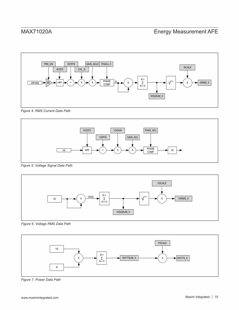
Figure 4. RMS Current Data Path
Figure 5. Voltage Signal Data Path
Figure 6. Voltage RMS Data Path
Figure 7. Power Data Path
MAX71020A Energy Measurement AFE
www.maximintegrated.com Maxim Integrated 15
HPF PHASE COMPX9 XIAP/IAN + X
PHADJ_0
I0RMS_XN-1∑
N = 0
ISCALE
I0SQSUM_X
I0 X X
GAIN_ADJ0
CAL_I0
I0OFFS
ACDCI
PRE_EN
HPF PHASE COMP
XVA + X
ACDCV
VOFFS
V0GAIN PHAS_ADJ
GAIN_ADJ
V0
V0 V0RMS_XN-1∑
N = 0
VSCALE
V0SQSUM_X
X XV0SQ
V0
WATTS_XN-1∑
N = 0
PSCALE
WATTSUM_XX X
I0
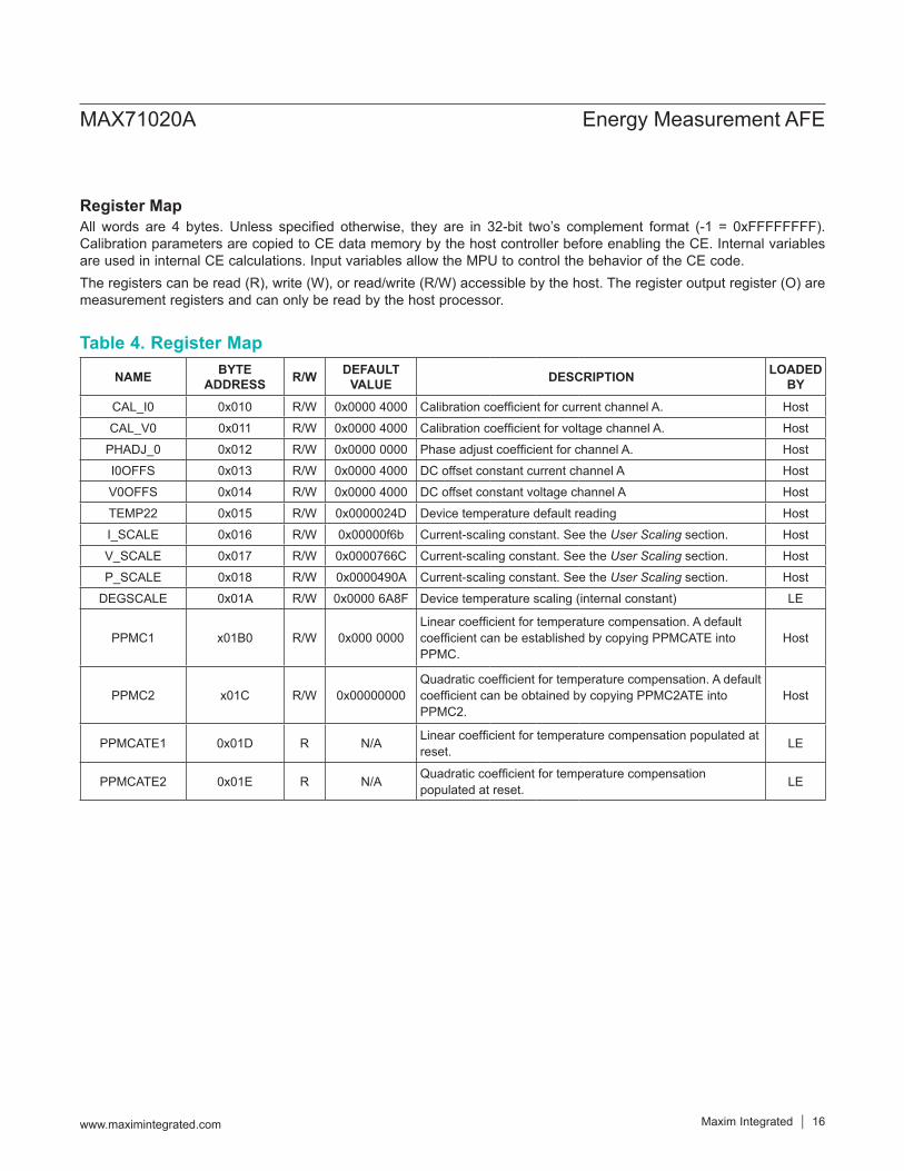
Register MapAll words are 4 bytes. Unless specified otherwise, they are in 32-bit two’s complement format (-1 = 0xFFFFFFFF). Calibration parameters are copied to CE data memory by the host controller before enabling the CE. Internal variables are used in internal CE calculations. Input variables allow the MPU to control the behavior of the CE code.The registers can be read (R), write (W), or read/write (R/W) accessible by the host. The register output register (O) are measurement registers and can only be read by the host processor.
Table 4. Register Map
MAX71020A Energy Measurement AFE
www.maximintegrated.com Maxim Integrated 16
NAME BYTE ADDRESS R/W DEFAULT
VALUE DESCRIPTION LOADED BY
CAL_I0 0x010 R/W 0x0000 4000 Calibration coefficient for current channel A. Host
CAL_V0 0x011 R/W 0x0000 4000 Calibration coefficient for voltage channel A. Host
PHADJ_0 0x012 R/W 0x0000 0000 Phase adjust coefficient for channel A. Host
I0OFFS 0x013 R/W 0x0000 4000 DC offset constant current channel A Host
V0OFFS 0x014 R/W 0x0000 4000 DC offset constant voltage channel A Host
TEMP22 0x015 R/W 0x0000024D Device temperature default reading Host
I_SCALE 0x016 R/W 0x00000f6b Current-scaling constant. See the User Scaling section. Host
V_SCALE 0x017 R/W 0x0000766C Current-scaling constant. See the User Scaling section. Host
P_SCALE 0x018 R/W 0x0000490A Current-scaling constant. See the User Scaling section. Host
DEGSCALE 0x01A R/W 0x0000 6A8F Device temperature scaling (internal constant) LE
PPMC1 x01B0 R/W 0x000 0000Linear coefficient for temperature compensation. A default coefficient can be established by copying PPMCATE into PPMC.
Host
PPMC2 x01C R/W 0x00000000Quadratic coefficient for temperature compensation. A default coefficient can be obtained by copying PPMC2ATE into PPMC2.
Host
PPMCATE1 0x01D R N/A Linear coefficient for temperature compensation populated at reset. LE
PPMCATE2 0x01E R N/A Quadratic coefficient for temperature compensation populated at reset. LE
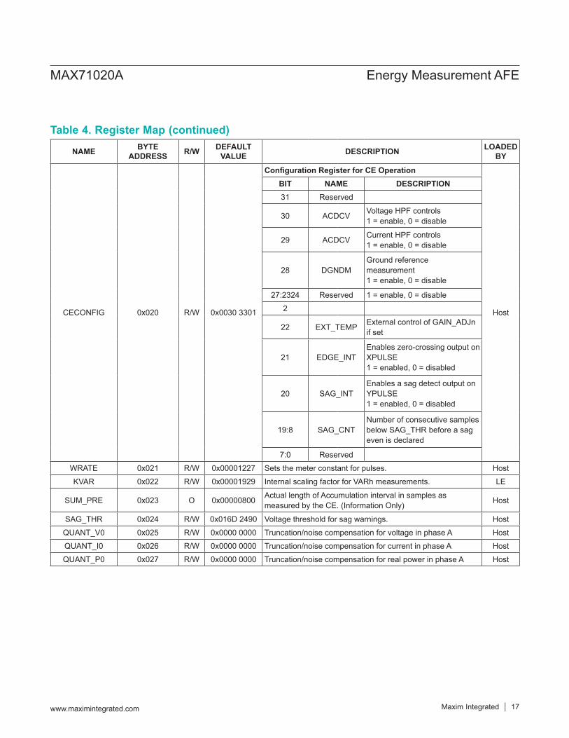
Table 4. Register Map (continued)
MAX71020A Energy Measurement AFE
www.maximintegrated.com Maxim Integrated 17
NAME BYTE ADDRESS R/W DEFAULT
VALUE DESCRIPTION LOADED BY
CECONFIG 0x020 R/W 0x0030 3301
Configuration Register for CE Operation
Host
BIT NAME DESCRIPTION31 Reserved
30 ACDCV Voltage HPF controls 1 = enable, 0 = disable
29 ACDCV Current HPF controls 1 = enable, 0 = disable
28 DGNDMGround reference measurement 1 = enable, 0 = disable
27:2324 Reserved 1 = enable, 0 = disable
2
22 EXT_TEMP External control of GAIN_ADJn if set
21 EDGE_INTEnables zero-crossing output on XPULSE 1 = enabled, 0 = disabled
20 SAG_INTEnables a sag detect output on YPULSE 1 = enabled, 0 = disabled
19:8 SAG_CNTNumber of consecutive samples below SAG_THR before a sag even is declared
7:0 Reserved
WRATE 0x021 R/W 0x00001227 Sets the meter constant for pulses. Host
KVAR 0x022 R/W 0x00001929 Internal scaling factor for VARh measurements. LE
SUM_PRE 0x023 O 0x00000800 Actual length of Accumulation interval in samples as measured by the CE. (Information Only) Host
SAG_THR 0x024 R/W 0x016D 2490 Voltage threshold for sag warnings. Host
QUANT_V0 0x025 R/W 0x0000 0000 Truncation/noise compensation for voltage in phase A Host
QUANT_I0 0x026 R/W 0x0000 0000 Truncation/noise compensation for current in phase A Host
QUANT_P0 0x027 R/W 0x0000 0000 Truncation/noise compensation for real power in phase A Host

Table 4. Register Map (continued)
MAX71020A Energy Measurement AFE
www.maximintegrated.com Maxim Integrated 18
NAME BYTE ADDRESS R/W DEFAULT
VALUE DESCRIPTION LOADED BY
QUANT_QA 0x028 R/W 0x0000 0000 Truncation/noise compensation for reactive power in phase A Host
CREEP_THR 0x029 R/W 0x0000 9C40 WSUM threshold below which the device squelches outputs Host
GAINADJ_V0 0x040 R/W 0x0000 4000 Adjusts the amplitude for voltage input VA for temperature compensation. Default = unity gain. Host
GAINADJ_I0 0x041 R/W 0x0000 4000 Adjusts the amplitude for current input IA. Default = unity gain. Host
Reserved 0x042–0x043 R/W 0x0000 0000 Reserved register Host
Reserved 0x044 R/W 0x0000 0000 Reserved register Host
WPULSE_CTR 0x045 R — Pulse counter for Wh (real power) —
WPULSE_FRAC 0x046 R — Pulse generator numerator for Wh (real power) —
Reserved 0x047 R/W 0x0000 0000 Reserved register Host
Reserved 0x048 R/W 0x0000 0000 Reserved register Host
VPULSE_CTR 0x049 — Pulse counter for VARh (real power) —
VPULSE_FRAC 0x04A — Pulse generator numerator for VARh (real power) —
Reserved 0x04B 0x0000 0000 Reserved register Host
0x04C–0x07F — Used by CE for internal variables —
CESTATUS 0x080 R —
Status of Compute Engine
—
BIT —
0 —
1 Reserved
2 Reserved
3 Square wave at exact line frequency
31:4 Reserved
TEMP_X 0x81 R Temperature deviation from TEMP22 —
FREQ_X 0x82 R Fundamental line frequency (LSB = 2520.6/232Hz) —
MAINEDGE_X 0x83 R Number of voltage zero crossings of either direction during the previous accumulation interval —
— — — — Reserved —
W0SUM_X 0x85 R — Signed sum of real energy (Wh) from wattmeter element A —
— — — — Reserved —
— — — — Reserved —
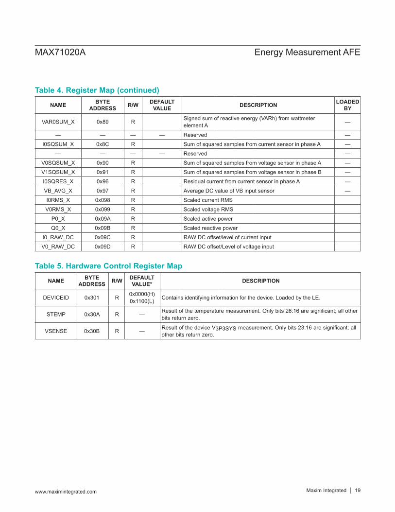
Table 4. Register Map (continued)
Table 5. Hardware Control Register Map
MAX71020A Energy Measurement AFE
www.maximintegrated.com Maxim Integrated 19
NAME BYTE ADDRESS R/W DEFAULT
VALUE DESCRIPTION LOADED BY
VAR0SUM_X 0x89 R Signed sum of reactive energy (VARh) from wattmeter element A —
— — — — Reserved —
I0SQSUM_X 0x8C R Sum of squared samples from current sensor in phase A —
— — — — Reserved —
V0SQSUM_X 0x90 R Sum of squared samples from voltage sensor in phase A —
V1SQSUM_X 0x91 R Sum of squared samples from voltage sensor in phase B —
I0SQRES_X 0x96 R Residual current from current sensor in phase A —
VB_AVG_X 0x97 R Average DC value of VB input sensor —
I0RMS_X 0x098 R Scaled current RMS
V0RMS_X 0x099 R Scaled voltage RMS
P0_X 0x09A R Scaled active power
Q0_X 0x09B R Scaled reactive power
I0_RAW_DC 0x09C R RAW DC offset/level of current input
V0_RAW_DC 0x09D R RAW DC offset/Level of voltage input
NAME BYTE ADDRESS R/W DEFAULT
VALUE* DESCRIPTION
DEVICEID 0x301 R 0x0000(H)0x1100(L) Contains identifying information for the device. Loaded by the LE.
STEMP 0x30A R — Result of the temperature measurement. Only bits 26:16 are significant; all other bits return zero.
VSENSE 0x30B R — Result of the device V3P3SYS measurement. Only bits 23:16 are significant; all other bits return zero.
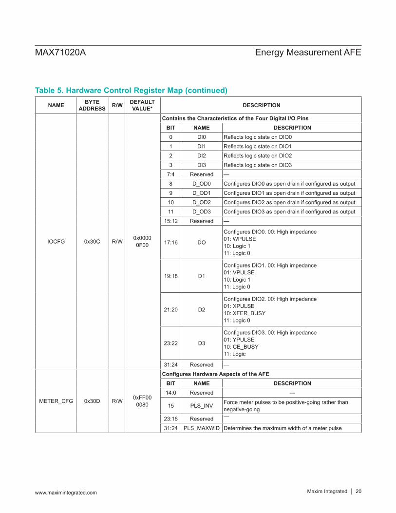
Table 5. Hardware Control Register Map (continued)
MAX71020A Energy Measurement AFE
www.maximintegrated.com Maxim Integrated 20
NAME BYTE ADDRESS R/W DEFAULT
VALUE* DESCRIPTION
IOCFG 0x30C R/W 0x0000 0F00
Contains the Characteristics of the Four Digital I/O PinsBIT NAME DESCRIPTION0 DI0 Reflects logic state on DIO0
1 DI1 Reflects logic state on DIO1
2 DI2 Reflects logic state on DIO2
3 DI3 Reflects logic state on DIO3
7:4 Reserved —
8 D_OD0 Configures DIO0 as open drain if configured as output
9 D_OD1 Configures DIO1 as open drain if configured as output
10 D_OD2 Configures DIO2 as open drain if configured as output
11 D_OD3 Configures DIO3 as open drain if configured as output
15:12 Reserved —
17:16 DO
Configures DIO0. 00: High impedance01: WPULSE10: Logic 111: Logic 0
19:18 D1
Configures DIO1. 00: High impedance01: VPULSE10: Logic 111: Logic 0
21:20 D2
Configures DIO2. 00: High impedance01: XPULSE10: XFER_BUSY11: Logic 0
23:22 D3
Configures DIO3. 00: High impedance01: YPULSE10: CE_BUSY11: Logic
31:24 Reserved —
METER_CFG 0x30D R/W 0xFF00 0080
Configures Hardware Aspects of the AFEBIT NAME DESCRIPTION14:0 Reserved —
15 PLS_INV Force meter pulses to be positive-going rather than negative-going
23:16 Reserved —
31:24 PLS_MAXWID Determines the maximum width of a meter pulse

Table 5. Hardware Control Register Map (continued)
MAX71020A Energy Measurement AFE
www.maximintegrated.com Maxim Integrated 21
NAME BYTE ADDRESS R/W DEFAULT
VALUE* DESCRIPTION
INT_CFG 0x30F R/W 0x0000 8000
Interrupt Configuration Register: Configure the Behavior of the INT PinBIT NAME DESCRIPTION
0 IE_WPULSE Enables an interrupt to occur on the leading edge of WPULSE
1 IE_VPULSE Enables an interrupt to occur on the leading edge of VPULSE
2 IE_YPULSE Enables an interrupt to occur on the leading edge of YPULSE
3 IE_XPULSE Enables an interrupt to occur on the leading edge of XPULSE
4 IE_XDATAEnables an interrupt to occur at the conclusion of the accumulation interval, indicating that fresh data is available
5 IE_CEBUSY Enables an interrupt to occur when the CE cycles is complete
6 Reserved —
7 IE_VSTAT Enables an interrupt to occur when the VSYS status changes
11:8 INT_POL
Interrupt polarity for the PULSE edges. The default polarity is falling edge.INT_POL[3]=1: Interrupt on rising edge of YPULSE INT_POL[2]=1: Interrupt on rising edge of XPULSE INT_POL[1]=1: Interrupt on rising edge of VPULSE INT_POL[0]=1: Interrupt on rising edge of WPULSE
14:12 Reserved —
15 D_ODINTZ Enable open-drain on the INT output. By default, the pin is configured as a CMOS totem-pole output.
31:16 Reserved —

Table 5. Hardware Control Register Map (continued)
MAX71020A Energy Measurement AFE
www.maximintegrated.com Maxim Integrated 22
NAME BYTE ADDRESS R/W DEFAULT
VALUE* DESCRIPTION
M_STAT 0x310 R 0x0100 0100
Reflects the status of several asynchronous events in the AFE. Bits are automatically cleared after the host controller reads M_STAT.
BIT NAME DESCRIPTION0 F_WPULSE Set on start of WPULSE
1 F_VPULSE Set on start of VPULSE
2 F_XPULSE Set on start of XPULSE
3 F_YPULSE Set on start of YPULSE
4 F_XDATA Set when data available
5 F_CEBUSY Set at end of CE code pass
6 Reserved —
7 F_VSTAT Set when VSYS status changes
8 F_RESET Set following AFE reset
15:9 Reserved —
16 F_WPULSE Copy of bit 0
17 F_VPULSE Copy of bit 1
18 F_XPULSE Copy of bit 2
19 F_YPULSE Copy of bit 3
20 F_XDATA Copy of bit 4
21 F_CEBUSY Copy of bit 5
23:22 Reserved —
24 F_RESET Copy of bit 8
31:25 Reserved —

Table 5. Hardware Control Register Map (continued)
MAX71020A Energy Measurement AFE
www.maximintegrated.com Maxim Integrated 23
NAME BYTE ADDRESS R/W DEFAULT
VALUE* DESCRIPTION
M_STAT_B 0x311 R 0x0000 0000
Backup of M_STAT. Updated when M_STAT is read. If M_STAT_B is different from M_STAT, it signals to the host that something has changed (status change detect).
BIT NAME DESCRIPTION0 FB_WPULSE Set on start of WPULSE
1 FB_VPULSE Set on start of VPULSE
2 FB_XPULSE Set on start of XPULSE
3 FB_YPULSE Set on start of YPULSE
4 FB_XDATA Set when data available
5 FB_CEBUSY Set at end of CE code pass
7:6 Reserved —
8 FB_RESET Set following AFE reset
15:9 Reserved —
16 FB_WPULSE Copy of bit 0
17 FB_VPULSE Copy of bit 1
18 FB_XPULSE Copy of bit 2
19 FB_YPULSE Copy of bit 3
20 FB_XDATA Copy of bit 4
21 FB_CEBUSY Copy of bit 5
23:22 Reserved —
24 FB_RESET Copy of bit 8
31:25 Reserved —
VSTAT 0x312 R —
AFE Supply Voltage Status. Bits 1:0 reflect system power status: 00: System power-OK: V3P3A > 3.0V01: System power-low: 2.8V < V3P3A < 3.0V 11: System power-fail: V3P3A < 2.8V
RESET 0x322 WO — Write 0x8100 0000 to this register to reset the AFE.
TEMP_CNF 0x323 R/W 0x0000 0000
Configures Aspects of the Temperature Measurement Subsystem. Loaded by the LE.
BIT NAME DESCRIPTION1:0 Reserved —
3:2 TEMP_PER
Sets the period between temperature measurements. 01: Measure every accumulation cycle10: Continuous measurementOther values disable automatic updates.
4 TEMP_SYS When set, V3P3SYS is measured at every temperature measurement cycle
31:5 Reserved —

Constants DescriptionFS: ADC sampling rate expressed as
f0: Fundamental frequency of the mains phase. SUM_SAMP: Number of ADC samples per accumulation interval. SUM_SAMP = 2520. X: gain constant of the pulse generators. Its value is determined by PULSE_FAST and PULSE_SLOW.FSV: Peak line voltage at which the ADC input reaches 0.250 VPK.VMAX: Represents the line RMS voltage (sine) corre-sponding to a peak of 250mVPK.
MAX RMSFSVV 176.8mV
2= =
FSI: Peak Line current at which the ADC input reaches 0.250 VPK or in case the preamplifer is enabled 27.78mV.IMAX: Line RMS currents corresponding to the maximum allowed voltage on the current inputs. Corresponding
to 176.8mVRMS (or 19.64mVRMS in case the preampli-fier is enabled). Example: For a 250µΩ shunt resistor, IMAX becomes 78A (19.64mVRMS/250µΩ = 78.57A) with preamplifier enabled and 707A (176.8mVRMS/250µΩ = 707.2ARMS) with preamplifier disabled.WOSUM_X LSB = 6.08040 x 10⁻¹³ x VMAX x IMAX WhVAROSUM LSB = 6.08040 x 10⁻¹³ x VMAX x IMAX VARhVSAG_THR LSB = VMAX x 7.879810-9V.The system constants IMAX and VMAX are used by the host controller to convert internal digital quantities (as used by the CE) to external, real-world metering quanti-ties. Their values are determined by the scaling of the voltage and current sensors used in an actual measure-ment. The LSB values used in this document relate digital quantities at the CE or MPU interface to external meter input quantities. For example, if a SAG threshold of 80VRMS is desired at the meter input, the digital value that should be programmed into SAG_THR would be 80VRMS x SQRT(2)/SAG_THRLSB, where SAG_THRLSB is the LSB value in the description of SAG_THR.
152FS 2520.613
= =
Table 5. Hardware Control Register Map (continued)
*Default values given for standard CE code (2520 sample frequency, gain = 9).
MAX71020A Energy Measurement AFE
www.maximintegrated.com Maxim Integrated 24
NAME BYTE ADDRESS R/W DEFAULT
VALUE* DESCRIPTION
TEMP_START 0x324 R/W 0x0000 0000 Write 0x8000 0000 to start a temperature conversion cycle. When conversion is complete, the AFE clears bit 31 and returns the register to zero.
SPI_SAFE 0x325 R/W 0x0000 0000
Write 0x8000 0000 to this word to lock the SPI port. When the SPI port is locked, no read or write operations are possible except to the SPI_SAFE register. Clearing this register to zero disables the SPI lock and restores normal operation.
METER_EN 0x326 R/W 0x0000 0000
Enables Aspects of the AFEBIT NAME DESCRIPTION
0 ADC_E Enable ADC and VREF buffer. Must be set by host following initialization.
1 CE_E Enable CE. Must be set by host following initialization.
31:2 Reserved —
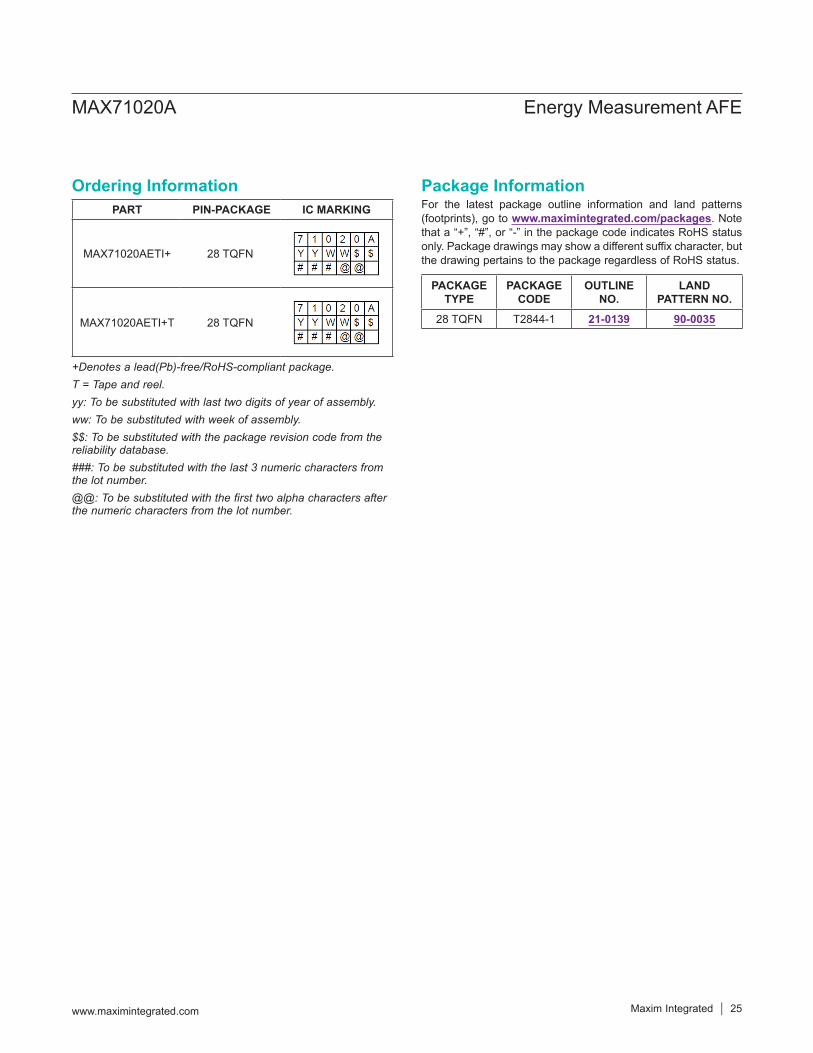
+Denotes a lead(Pb)-free/RoHS-compliant package.T = Tape and reel.yy: To be substituted with last two digits of year of assembly.ww: To be substituted with week of assembly.$$: To be substituted with the package revision code from the reliability database.###: To be substituted with the last 3 numeric characters from the lot number.@@: To be substituted with the first two alpha characters after the numeric characters from the lot number.
MAX71020A Energy Measurement AFE
www.maximintegrated.com Maxim Integrated 25
Ordering Information Package InformationFor the latest package outline information and land patterns (footprints), go to www.maximintegrated.com/packages. Note that a “+”, “#”, or “-” in the package code indicates RoHS status only. Package drawings may show a different suffix character, but the drawing pertains to the package regardless of RoHS status.
PART PIN-PACKAGE IC MARKING
MAX71020AETI+ 28 TQFN
MAX71020AETI+T 28 TQFN
PACKAGE TYPE
PACKAGE CODE
OUTLINE NO.
LAND PATTERN NO.
28 TQFN T2844-1 21-0139 90-0035

Maxim Integrated cannot assume responsibility for use of any circuitry other than circuitry entirely embodied in a Maxim Integrated product. No circuit patent licenses are implied. Maxim Integrated reserves the right to change the circuitry and specifications without notice at any time. The parametric values (min and max limits) shown in the Electrical Characteristics table are guaranteed. Other parametric values quoted in this data sheet are provided for guidance.
Maxim Integrated and the Maxim Integrated logo are trademarks of Maxim Integrated Products, Inc. © 2015 Maxim Integrated Products, Inc. 26
MAX71020A Energy Measurement AFE
Revision HistoryREVISION NUMBER
REVISIONDATE DESCRIPTION PAGES
CHANGED
0 6/15 Initial release —
For pricing, delivery, and ordering information, please contact Maxim Direct at 1-888-629-4642, or visit Maxim Integrated’s website at www.maximintegrated.com.