Embed Size (px)
Citation preview

General DescriptionThe MAX5954 hot-plug controller is designed for PCI Express™ applications. The device provides hot-plug control for 12V, 3.3V, and 3.3V auxiliary supplies of a single PCI Express (PCI-E) slot. The MAX5954’s logic inputs/outputs allow interfacing directly with the system hot-plug management controller or through an SMBus™ with an external I/O expander. Integrated debounced attention switch and present-detect signals are included to simplify system design.The MAX5954 drives two external n-channel MOSFETs to control the 12V and 3.3V main outputs. The 3.3V auxiliary output is controlled through an internal 0.3Ω n-channel MOSFET. An internal charge pump provides gate drive for the 12V output while the gate drive of the 3.3V output is driven by the 12V input supply. The 3.3V auxiliary output is completely independent from the main outputs with its own charge pump.At power-up, the MAX5954 keeps all of the external MOSFETs off until the supplies rise above their respec-tive undervoltage-lockout (UVLO) thresholds. The device keeps the internal MOSFET off only until the auxiliary input supply rises above its UVLO threshold. Upon a turn-on command, the MAX5954 enhances the external and internal MOSFETs slowly with a constant gate current to limit the power-supply inrush current. The MAX5954 actively limits the current of all outputs at all times and shuts down if an overcurrent condition persists for longer than a programmable overcurrent timeout. Thermal-protection circuitry also shuts down all outputs if the die temperature exceeds +150°C. After an overcurrent or overtemperature fault condition, the MAX5954L latches off while the MAX5954A automatically restarts after a restart time delay. The device is available in a 36-pin (6mm × 6mm) thin QFN package and operates over the -40°C to +85°C temperature range.
Features PCI Express Compliant Hot Swaps 12V, 3.3V, and 3.3V Auxiliary for a Single
PCI-E Slot Integrated Power MOSFET for Auxiliary Supply Rail Controls dI/dt and dV/dt Active Current Limiting Protects Against Overcurrent/
Short-Circuit Conditions Programmable Current-Limit Timeout PWRGD Signal Output with Programmable Power-
On Reset (POR) (160ms Default) Latched FAULT Signal Output after Overcurrent or
Overtemperature Fault Attention Switch Input/Output with 4.4ms Debounce Present-Detect Input Forced-On Input Facilitates Testing Thermal Shutdown Allows Control Through SMBus with an I/O Expander
Applications Servers Desktop Mobile Server Platforms Workstations Embedded Devices
19-3914; Rev 2; 7/19
Typical Application Circuit appears at end of data sheet.
Ordering Information appears at end of data sheet.
SMBus is a trademark of Intel Corp.PCI Express is a trademark of PCI-SIG Corp.
N.C.N.C.3.3VAUXIN
PWRGDFAULT3.3G
N.C.282930313233343536
181716151413121110
THIN QFN
MAX5954
TOP VIEW
+
3.3VAUXO
N.C.
T2 T1 N.C.
N.C.
N.C.
N.C.
N.C.
N.C.
N.C.
N.C.OUTPUT
INPUT
GNDPGND
PORADJ
TIM
12VIN
N.C.
ONAU
XON
12S+ 12G
3.3S+
3.3S-
PRES
-DET 12S-
FON
27 26 25 24 23 22 21 20 19
1 2 3 4 5 6 7 8 9
MAX5954 Single PCI Express, Hot-Plug Controller
Pin Configuration
Click here for production status of specific part numbers.
EVALUATION KIT AVAILABLE
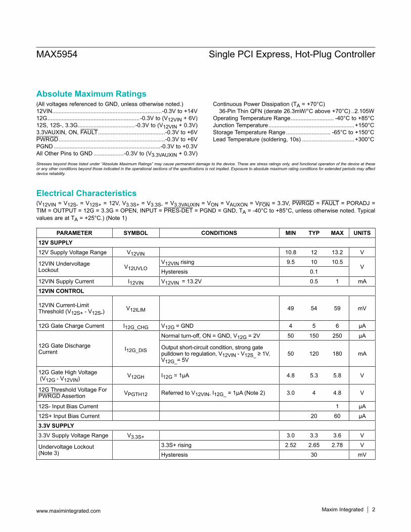
(All voltages referenced to GND, unless otherwise noted.)12VIN.....................................................................-0.3V to +14V12G .......................................................... -0.3V to (V12VIN + 6V)12S, 12S-, 3.3G.................................... -0.3V to (V12VIN + 0.3V)3.3VAUXIN, ON, FAULT ..........................................-0.3V to +6VPWRGD ...................................................................-0.3V to +6VPGND ...................................................................-0.3V to +0.3VAll Other Pins to GND ...................-0.3V to (V3.3VAUXIN + 0.3V)
Continuous Power Dissipation (TA = +70°C) 36-Pin Thin QFN (derate 26.3mW/°C above +70°C) ..2.105W
Operating Temperature Range ........................... -40°C to +85°CJunction Temperature ......................................................+150°CStorage Temperature Range ............................ -65°C to +150°CLead Temperature (soldering, 10s) .................................+300°C
(V12VIN = V12S- = V12S+ = 12V, V3.3S+ = V3.3S- = V3.3VAUXIN = VON = VAUXON = VFON = 3.3V, PWRGD = FAULT = PORADJ = TIM = OUTPUT = 12G = 3.3G = OPEN, INPUT = PRES-DET = PGND = GND, TA = -40°C to +85°C, unless otherwise noted. Typical values are at TA = +25°C.) (Note 1)
PARAMETER SYMBOL CONDITIONS MIN TYP MAX UNITS12V SUPPLY12V Supply Voltage Range V12VIN 10.8 12 13.2 V
12VIN Undervoltage Lockout V12UVLO
V12VIN rising 9.5 10 10.5V
Hysteresis 0.112VIN Supply Current I12VIN V12VIN = 13.2V 0.5 1 mA12VIN CONTROL
12VIN Current-Limit Threshold (V12S+ - V12S-)
V12ILIM 49 54 59 mV
12G Gate Charge Current I12G_CHG V12G = GND 4 5 6 µA
12G Gate Discharge Current I12G_DIS
Normal turn-off, ON = GND, V12G = 2V 50 150 250 µA
Output short-circuit condition, strong gate pulldown to regulation, V12VIN - V12S_ ≥ 1V, V12G_= 5V
50 120 180 mA
12G Gate High Voltage (V12G - V12VIN) V12GH I12G = 1µA 4.8 5.3 5.8 V
12G Threshold Voltage For PWRGD Assertion VPGTH12 Referred to V12VIN, I12G_ = 1µA (Note 2) 3.0 4 4.8 V
12S- Input Bias Current 1 µA12S+ Input Bias Current 20 60 µA3.3V SUPPLY3.3V Supply Voltage Range V3.3S+ 3.0 3.3 3.6 V
Undervoltage Lockout (Note 3)
3.3S+ rising 2.52 2.65 2.78 VHysteresis 30 mV
www.maximintegrated.com Maxim Integrated 2
MAX5954 Single PCI Express, Hot-Plug Controller
Absolute Maximum Ratings
Stresses beyond those listed under “Absolute Maximum Ratings” may cause permanent damage to the device. These are stress ratings only, and functional operation of the device at these or any other conditions beyond those indicated in the operational sections of the specifications is not implied. Exposure to absolute maximum rating conditions for extended periods may affect device reliability.
Electrical Characteristics

(V12VIN = V12S- = V12S+ = 12V, V3.3S+ = V3.3S- = V3.3VAUXIN = VON = VAUXON = VFON = 3.3V, PWRGD = FAULT = PORADJ = TIM = OUTPUT = 12G = 3.3G = OPEN, INPUT = PRES-DET = PGND = GND, TA = -40°C to +85°C, unless otherwise noted. Typical values are at TA = +25°C.) (Note 1)
PARAMETER SYMBOL CONDITIONS MIN TYP MAX UNITS3.3V CONTROL
3.3V Current-Limit Threshold (V3.3S+ - V3.3S-)
V3.3ILIM 17 20 23 mV
3.3G Gate Charge Current I3.3G CHG V3.3G = GND 4 5 6 µA
3.3G Gate Discharge Current I3.3G_DIS
ON = GND, V3.3G = 2V 50 150 250 µA
Output short-circuit condition, strong gate pulldown to regulation, V3.3S+ - V3.3S ≥ 1V, V3.3G = 5V
100 150 220 mA
3.3G Gate High Voltage (V3.3G - V3.3S+) V3.3G_H Sourcing 1µA 4.5 5.5 6.8 V
3.3G Threshold Voltage For PWRGD Assertion VPGTH3.3 Referred to V3.3VAUXIN, I3.3G = 1µA (Note 2) -3.0 +4 +4.5 V
3.3S- Input Bias Current 1 µA3.3S+ Input Bias Current 20 60 µA3.3V AUXILIARY SUPPLY
3.3VAUXIN Supply Voltage Range V3.3VAUXIN 3.0 3.3 3.6 V
3.3VAUXIN Undervoltage Lockout V3.3VAUXUVLO
3.3VAUXIN rising 2.52 2.65 2.78 VHysteresis 30 mV
3.3VAUXIN Supply Current V3.3VAUXIN = 3.6V 1.5 3 mA
3.3VAUXIN to 3.3VAUXO Maximum Dropout I3.3VAUXO = 375mA 225 mV
3.3VAUXO Current-Limit Threshold 3.3VAUXO shorted to GND 376 470 564 mA
3.3VAUXO Threshold For PWRGD Assertion (V3.3VAUXIN - V3.3VAUXO)
VPGTH3.3AUX (Note 3) 400 mV
LOGIC SIGNALSInput-Logic Threshold (ON, FON, AUXON, PRES-DET, INPUT)
Rising edge 1.0 2.0 V
Hysteresis 25 mV
Input Bias Current (ON, AUXON, INPUT) 1 µA
FON, PRES-DET Internal Pullup 25 50 75 kΩ
ON, AUXON High-to-Low Deglitch Time 4 µs
www.maximintegrated.com Maxim Integrated 3
MAX5954 Single PCI Express, Hot-Plug Controller
Electrical Characteristics (continued)

Note 1: 100% production tested at TA = +25°C. Parameters over temperature are guaranteed by design.Note 2: PWRGD asserts a time tPOR_HL after VPGTH12, VPGTH3.3, and VPGTH3.3AUX conditions are met.Note 3: The UVLO for the 3.3V supply is sensed at 3.3S+.Note 4: This is the time that ON or AUXON must stay low when resetting a fault condition.
(V12VIN = V12S- = V12S+ = 12V, V3.3S+ = V3.3S- = V3.3VAUXIN = VON = VAUXON = VFON = 3.3V, PWRGD = FAULT = PORADJ = TIM = OUTPUT = 12G = 3.3G = OPEN, INPUT = PRES-DET = PGND = GND, TA = -40°C to +85°C, unless otherwise noted. Typical values are at TA = +25°C.) (Note 1)
PARAMETER SYMBOL CONDITIONS MIN TYP MAX UNITS
PRES-DET High-to-Low Deglitch Time tDEG 3 5 7 ms
PWRGD Power-On Reset Time (Note 2) tPOR_HL
PORADJ = open 90 160 250 msRPORADJ = 20kΩ 35 55 75RPORADJ = 100kΩ 145 265 380RPORADJ = 200kΩ 570
PWRGD Low-to-High Deglitch Time tPOR_LH 4 µs
PWRGD, FAULT Output Low Voltage
Sinking 2mA 0.1 VSinking 30mA 0.7
PWRGD, FAULT Output-High Leakage Current VPWRGD = VFAULT = 5.5V 1 µA
FAULT Timeout tFAULT
TIM = open 5.5 11 17.0 msRTIM = 15kΩ 1.4 2.6 3.8RTIM = 120kΩ 12 22 32RTIM = 300kΩ 59
FAULT Timeout During Startup tSU 2 x tFAULT ms
Autorestart Delay Time tRESTART 64 x tFAULT ms
Fault Reset Minimum Pulse Width tRESET (Note 4) 100 µs
Thermal-Shutdown Threshold TSD TJ rising +150 °C
Thermal-Shutdown Threshold Hysteresis 20 °C
OUTPUT Debounce Time tDBC 2.6 4.4 6.2 ms
OUTPUT High Voltage Sourcing 2mA V3.3VAUXIN - 0.3 V3.3VAUXIN V
OUTPUT Low Voltage Sinking 2mA 0.4 V
www.maximintegrated.com Maxim Integrated 4
MAX5954 Single PCI Express, Hot-Plug Controller
Electrical Characteristics (continued)

(V12VIN = V12S+ = 12V, V3.3VAUXIN = V3.3S+ = VON = VAUXON = VINPUT = 3.3V, PRES-DET = GND, FON = PORADJ = TIM = float, FAULT = 10kΩ to 3.3VAUXIN, PWRGD = 10kΩ to 3.3VAUXO, TA = +25°C, unless otherwise noted, see the Typical Application Circuit.)
ON AND AUXON LOW-TO-HIGH THRESHOLDVOLTAGE vs. TEMPERATURE
MAX
5954
toc0
3
TEMPERATURE (°C)
THRE
SHOL
D VO
LTAG
E (V
)
603510-15
1.1
1.2
1.3
1.4
1.5
1.6
1.7
1.8
1.9
2.0
1.0-40 85
3.3VAUXIN SUPPLY CURRENTvs. TEMPERATURE
MAX
5954
toc0
2
TEMPERATURE (°C)
SUPP
LY C
URRE
NT (m
A)
603510-15
0.2
0.4
0.6
0.8
1.0
1.2
1.4
1.6
1.8
2.0
0-40 85
12G AND 3.3G GATE DISCHARGECURRENT vs. TEMPERATURE
MAX
5954
toc0
6
TEMPERATURE (°C)
GATE
DIS
CHAR
GE C
URRE
NT (µ
A)
603510-15
150
155
160
165
170
145-40 85
3.3G
12G
AUXILIARY CURRENT LIMITvs. TEMPERATURE
MAX
5954
toc0
9
TEMPERATURE (°C)
AUXI
LIARY
CUR
RENT
LIMI
T (A
)
603510-15
0.455
0.460
0.465
0.470
0.475
0.480
0.485
0.490
0.495
0.500
0.450-40 85
12G AND 3.3G GATE CHARGECURRENT vs. TEMPERATURE
MAX
5954
toc0
5
TEMPERATURE (°C)
GATE
CHA
RGE
CURR
ENT
(µA)
603510-15
4.90
4.95
5.00
5.05
5.10
5.15
5.20
5.25
5.30
5.35
4.85-40 85
12G
3.3G
12V AND 3.3V CURRENT-LIMIT THRESHOLDVOLTAGE vs. TEMPERATURE
MAX
5954
toc0
8
TEMPERATURE (°C)
CURR
ENT-
LIMIT
THR
ESHO
LD V
OLTA
GE (m
V)
603510-15
10
20
30
40
50
60
0-40 85
12V CURRENT-SENSETHRESHOLD
3.3V CURRENT-SENSETHRESHOLD
12VIN INPUT SUPPLY CURRENTvs. TEMPERATURE
MAX
5954
toc0
1
TEMPERATURE (°C)
SUPP
LY C
URRE
NT (m
A)
603510-15
0.4910.4920.4930.4940.4950.4960.4970.4980.4990.5000.5010.5020.5030.5040.505
0.490-40 85
3.3VAUXO OUTPUT VOLTAGE vs. CURRENT
MAX
5954
toc0
4
OUTPUT CURRENT (A)
OUTP
UT V
OLTA
GE (V
)
0.50.40.30.20.1
0.5
1.0
1.5
2.0
2.5
3.0
3.5
00 0.6
3.3VAUX INTERNAL SWITCHMAXIMUM DROPOUT vs. TEMPERATURE
MAX
5954
toc0
7
TEMPERATURE (°C)
DROP
OUT
VOLT
AGE
(V)
603510-15
0.02
0.04
0.06
0.08
0.10
0.12
0.14
0.16
0.18
0.20
0-40 85
AUXILIARY OUTPUT CURRENT = 375mA
Maxim Integrated 5www.maximintegrated.com
MAX5954 Single PCI Express, Hot-Plug Controller
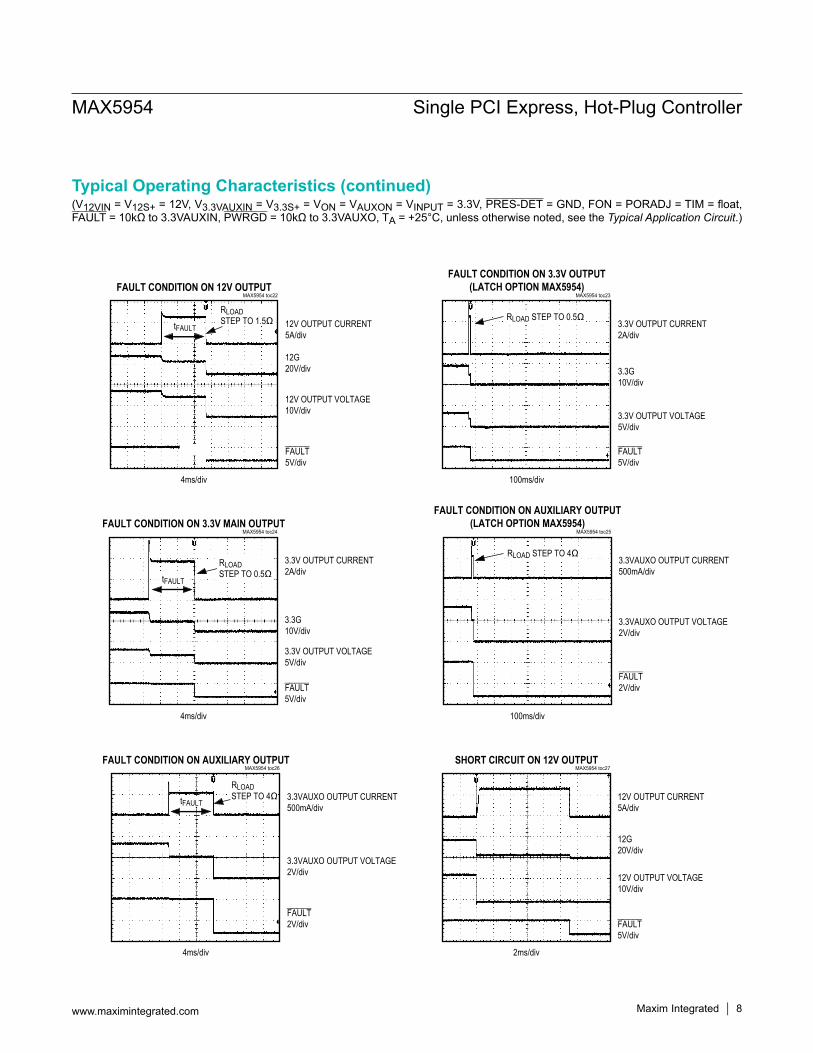
Typical Operating Characteristics

(V12VIN = V12S+ = 12V, V3.3VAUXIN = V3.3S+ = VON = VAUXON = VINPUT = 3.3V, PRES-DET = GND, FON = PORADJ = TIM = float, FAULT = 10kΩ to 3.3VAUXIN, PWRGD = 10kΩ to 3.3VAUXO, TA = +25°C, unless otherwise noted, see the Typical Application Circuit.)
3.3VAUXIN UNDERVOLTAGE-LOCKOUTTHRESHOLD vs. TEMPERATURE
MAX
5954
toc1
1
TEMPERATURE (°C)
UVLO
THR
ESHO
LD (V
)
603510-15
2.62
2.64
2.66
2.68
2.70
2.60-40 85
3.3V TURN-ON/OFF TIMEMAX5954 toc13
3.3G10V/div
PWRGD5V/div
ON5V/div
3.3V OUTPUT5V/div
40ms/div
12V POWER-UPMAX5954 toc15
12V OUTPUT10V/div
PWRGD5V/div
12VIN, 12V INPUT10V/div
12G20V/div
40ms/div
12VIN UNDERVOLTAGE-LOCKOUTTHRESHOLD vs. TEMPERATURE
MAX
5954
toc1
0
TEMPERATURE (°C)
UVLO
THR
ESHO
LD (V
)
6035-15 10
9.85
9.90
9.95
10.00
10.05
10.10
10.15
10.20
9.80-40 85
12V TURN-ON/OFF TIMEMAX5954 toc12
12G20V/div
PWRGD5V/div
ON5V/div
12V OUTPUT10V/div
40ms/div
3.3V AUXILIARY TURN-ON/OFF TIMEMAX5954 toc14
40ms/div
3.3AUXOOUTPUT VOLTAGE2V/div
AUXON2V/div
PWRGD2V/div
Maxim Integrated 6www.maximintegrated.com
MAX5954 Single PCI Express, Hot-Plug Controller
Typical Operating Characteristics (continued)

(V12VIN = V12S+ = 12V, V3.3VAUXIN = V3.3S+ = VON = VAUXON = VINPUT = 3.3V, PRES-DET = GND, FON = PORADJ = TIM = float, FAULT = 10kΩ to 3.3VAUXIN, PWRGD = 10kΩ to 3.3VAUXO, TA = +25°C, unless otherwise noted, see the Typical Application Circuit.)
TURN-ON DELAY 3.3V OUTPUT AND3.3V AUXILIARY OUTPUT
MAX5954 toc17
4ms/div
5V/div
5V/div
5V/div
5V/div
10V/div
3.3VAUXOOUTPUT VOLTAGE
3.3 VOLTAGE
3.3 INPUT,3.3VAUXIN
3.3G
PWRGD
FAULT CONDITION ON 3.3V OUTPUT(AUTORESTART OPTION MAX5954A)
MAX5954 toc19
3.3G10V/div
FAULT5V/div
3.3V MAIN OUTPUT CURRENT2A/div
100ms/div
3.3V OUTPUT VOLTAGE5V/div
tRESTART
RLOAD STEP TO 0.5Ω
FAULT CONDITION ON 12V OUTPUT(LATCH OPTION MAX5954L)
MAX5954 toc21
12G20V/div
FAULT5V/div
12V OUTPUT CURRENT5A/div
100ms/div
12V OUTPUT VOLTAGE10V/div
RLOAD STEP TO 1.5Ω
3.3V INPUT/3.3V AUXILIARY INPUTPOWER-UP
MAX5954 toc16
3.3V OUTPUT5V/div
PWRGD5V/div
3.3VAUXO5V/div
3.3G10V/div
100ms/div
3.3S+5V/div
FAULT CONDITION ON 12V OUTPUT(AUTORESTART OPTION MAX5954A)
MAX5954 toc18
12G20V/div
FAULT5V/div
12V OUTPUT CURRENT5A/div
100ms/div
12V OUTPUT VOLTAGE10V/div
tRESTART
RLOAD STEP TO 1.5W
FAULT CONDITION ON AUXILIARY OUTPUT(AUTORESTART OPTION MAX5954A)
MAX5954 toc20
FAULT2V/div
3.3VAUXO OUTPUT CURRENT500mA/div
100ms/div
3.3VAUXO OUTPUT VOLTAGE2V/div
tRESTART
RLOAD STEP TO 4Ω
Maxim Integrated 7www.maximintegrated.com
MAX5954 Single PCI Express, Hot-Plug Controller
Typical Operating Characteristics (continued)
(V12VIN = V12S+ = 12V, V3.3VAUXIN = V3.3S+ = VON = VAUXON = VINPUT = 3.3V, PRES-DET = GND, FON = PORADJ = TIM = float, FAULT = 10kΩ to 3.3VAUXIN, PWRGD = 10kΩ to 3.3VAUXO, TA = +25°C, unless otherwise noted, see the Typical Application Circuit.)
FAULT CONDITION ON 3.3V OUTPUT(LATCH OPTION MAX5954)
MAX5954 toc23
3.3G10V/div
FAULT5V/div
3.3V OUTPUT CURRENT2A/div
100ms/div
3.3V OUTPUT VOLTAGE5V/div
RLOAD STEP TO 0.5Ω
FAULT CONDITION ON AUXILIARY OUTPUT(LATCH OPTION MAX5954)
MAX5954 toc25
FAULT2V/div
3.3VAUXO OUTPUT CURRENT500mA/div
100ms/div
3.3VAUXO OUTPUT VOLTAGE2V/div
RLOAD STEP TO 4Ω
SHORT CIRCUIT ON 12V OUTPUTMAX5954 toc27
12G20V/div
FAULT5V/div
12V OUTPUT CURRENT5A/div
2ms/div
12V OUTPUT VOLTAGE10V/div
FAULT CONDITION ON 12V OUTPUTMAX5954 toc22
12G20V/div
FAULT5V/div
12V OUTPUT CURRENT5A/div
4ms/div
12V OUTPUT VOLTAGE10V/div
RLOADSTEP TO 1.5ΩtFAULT
FAULT CONDITION ON 3.3V MAIN OUTPUTMAX5954 toc24
3.3G10V/div
FAULT5V/div
3.3V OUTPUT CURRENT2A/div
4ms/div
3.3V OUTPUT VOLTAGE5V/div
RLOADSTEP TO 0.5ΩtFAULT
FAULT CONDITION ON AUXILIARY OUTPUTMAX5954 toc26
FAULT2V/div
3.3VAUXO OUTPUT CURRENT500mA/div
4ms/div
3.3VAUXO OUTPUT VOLTAGE2V/div
RLOADSTEP TO 4ΩtFAULT
Maxim Integrated 8www.maximintegrated.com
MAX5954 Single PCI Express, Hot-Plug Controller
Typical Operating Characteristics (continued)

(V12VIN = V12S+ = 12V, V3.3VAUXIN = V3.3S+ = VON = VAUXON = VINPUT = 3.3V, PRES-DET = GND, FON = PORADJ = TIM = float, FAULT = 10kΩ to 3.3VAUXIN, PWRGD = 10kΩ to 3.3VAUXO, TA = +25°C, unless otherwise noted, see the Typical Application Circuit.)
SHORT CIRCUIT ON 3.3V OUTPUTMAX5954 toc29
3.3G5V/div
FAULT5V/div
3.3V OUTPUT CURRENT2A/div
2ms/div
3.3V OUTPUT VOLTAGE5V/div
SHORT CIRCUIT ON 3.3AUXO_MAX5954 toc31
FAULT5V/div
3.3VAUXO OUTPUT CURRENT500mA/div
2ms/div
3.3VAUXO OUTPUT VOLTAGE2V/div
POWER-UP INTO FAULT(AUXILIARY SUPPLY)
MAX5954 toc33
3.3VAUXO OUTPUT VOLTAGE2V/div
FAULT5V/div
3.3VAUXO OUTPUT CURRENT500mA/div
4ms/div
AUXON5V/div
tSU
RLOAD = 4Ω
SHORT CIRCUIT ON 12V OUTPUTMAX5954 toc28
12G20V/div
FAULT5V/div
12V OUTPUT CURRENT25A/div
4µs/div
12V OUTPUT VOLTAGE10V/div
0V
0V
0V
SHORT CIRCUIT ON 3.3V OUTPUTMAX5954 toc30
3.3G5V/div
FAULT5V/div
3.3V OUTPUT CURRENT10A/div
2µs/div
3.3V OUTPUT VOLTAGE5V/div
0V
SHORT CIRCUIT ON 3.3VAUXO_MAX5954 toc32
FAULT5V/div
3.3VAUXO OUTPUT CURRENT5A/div
2µs/div
3.3VAUXO OUTPUT VOLTAGE2V/div
Maxim Integrated 9www.maximintegrated.com
MAX5954 Single PCI Express, Hot-Plug Controller
Typical Operating Characteristics (continued)

(V12VIN = V12S+ = 12V, V3.3VAUXIN = V3.3S+ = VON = VAUXON = VINPUT = 3.3V, PRES-DET = GND, FON = PORADJ = TIM = float, FAULT = 10kΩ to 3.3VAUXIN, PWRGD = 10kΩ to 3.3VAUXO, TA = +25°C, unless otherwise noted, see the Typical Application Circuit.)
POWER-UP INTO FAULT(12V OUTPUT)
MAX5954 toc35
12V OUTPUT VOLTAGE10V/div
FAULT5V/div
12V OUTPUT CURRENT5A/div
4ms/div
ON, AUXON5V/div
tSU
12G10V/div
PRESENT-DETECT (ON/OFF) OPERATIONMAX5954 toc37
4ms/div
5V/div
5V/div
5V/div
10V/div 12V OUTPUT VOLTAGE
3.3VAUXOOUTPUT VOLTAGE
PWRGD
PRES-DET
FORCED-ON (ON/OFF) OPERATIONMAX5954 toc39
4ms/div
5V/div
5V/div
5V/div
10V/div 12V OUTPUT VOLTAGE
3.3VAUXOOUTPUT VOLTAGE
PWRGD
FON
POWER-UP INTO FAULT(3.3V MAIN)
MAX5954 toc34
3.3V OUTPUT VOLTAGE2V/div
FAULT5V/div
3.3V OUTPUT CURRENT4A/div
4ms/div
ON, AUXON5V/div
tSU
RLOAD = 0.5Ω
3.3G5V/div
PRESENT-DETECT (ON/OFF) OPERATIONMAX5954 toc36
40ms/div
5V/div
5V/div
5V/div
10V/div 12V OUTPUT VOLTAGE
3.3VAUXOOUTPUT VOLTAGE
PWRGD
PRES-DET
FORCED-ON (ON/OFF) OPERATIONMAX5954 toc38
40ms/div
5V/div
5V/div
5V/div
10V/div 12V OUTPUT VOLTAGE
3.3VAUXOOUTPUT VOLTAGE
PWRGD
FON
Maxim Integrated 10www.maximintegrated.com
MAX5954 Single PCI Express, Hot-Plug Controller
Typical Operating Characteristics (continued)

(V12VIN = V12S+ = 12V, V3.3VAUXIN = V3.3S+ = VON = VAUXON = VINPUT = 3.3V, PRES-DET = GND, FON = PORADJ = TIM = float, FAULT = 10kΩ to 3.3VAUXIN, PWRGD = 10kΩ to 3.3VAUXO, TA = +25°C, unless otherwise noted, see the Typical Application Circuit.)
0
400
200
600
1200
1400
1000
800
1600
0 100 150 200 25050 300 350 400 450 500
POWER-ON RESET TIMEvs. PORADJ RESISTOR
MAX
5954
toc4
1
RPORADJ (K)t PO
R_HL
(MS)
0
60
40
20
80
100
120
0 20015050 100 250 300 350 400 450 500
tFAULT TIME DELAYvs. TIM RESISTOR
MAX
5954
toc4
2
RTIM (k)
t FAUL
T (m
s)
DEBOUNCED ON/OFF OPERATIONMAX5954 toc40
INPUT2V/div
10ms/div
OUTPUT2V/div
Maxim Integrated 11www.maximintegrated.com
MAX5954 Single PCI Express, Hot-Plug Controller
Typical Operating Characteristics (continued)

PIN NAME FUNCTION
1 PRES-DETPresent-Detect Input. PRES-DET accepts inputs from the PRSNT#2 pin on a PCI-E connector. PRES-DET has an internal pullup to 3.3VAUXIN. When PRES-DET is low, the outputs follow the command from ON and AUXON after a 4ms debounced time. When PRES-DET goes from low to high, all outputs of the respective slot shut down with no delay (see Table 2).
2 FONForced-On Input. FON has a 50kΩ internal pullup to 3.3VAUXIN. A logic-low on FON turns on all PCI-E outputs as long as the power inputs are within their operating range, regardless of the status of the other input signals. Leave FON open for normal operation (see Table 2).
3 ON 12V and 3.3V Outputs Enable. A logic-high at ON turns on the 12V and 3.3V outputs (see Table 2).4 AUXON 3.3V Auxiliary Output Enable. A logic-high at AUXON turns on the auxiliary output (3.3VAUXO) (see Table 2).
5 12S+ 12V Positive Current-Sense Input. Connect the positive terminal of the current-sense resistor to 12S+ using the Kelvin-sensing technique to assure accurate current sensing.
6 12S- 12V Negative Current-Sense Input. Connect 12S- to the negative side of the current-sense resistor using the Kelvin-sensing technique to assure accurate current sensing.
7 12G 12V Gate-Drive Output. Connect 12G to the gate of the 12V MOSFET. At power-up, V12G is raised to the internal charge-pump voltage level by a constant current.
8 3.3S+3.3V Positive Current-Sense Input. Connect the positive side of the current-sense resistor to 3.3S+ using the Kelvin-sensing technique to assure accurate current sensing. This input is also used for the 3.3V supply’s UVLO function.
9 3.3S- 3.3V Negative Current-Sense Input. Connect to the negative side of the sense resistor using the Kelvin-sensing technique to assure accurate current sensing.
10 3.3G 3.3V Gate-Drive Output. Connect 3.3G to the gate of the 3.3V MOSFET. At power-up, V3.3G is charged to 5.5V above the 3.3V supply by a constant current derived from V12VIN.
11 FAULT
Open-Drain Fault Output Signal. FAULT latches active low whenever the outputs are shut down due to a fault. A fault is either of: • An overcurrent condition lasting longer than the overcurrent timeout. • A device over temperature condition. If the fault is detected in the main outputs, FAULT must be reset by toggling the ON input. If the fault is in the auxiliary output, FAULT must be reset by toggling both ON and AUXON. For the auto-restart version, FAULT is reset when the part initiates the next power-on cycle.
12 PWRGD Open-Drain Power-Good Output. PWRGD goes low tPOR_HL after all outputs reach their final value and the power MOSFETs are fully enhanced.
13 3.3VAUXO 3.3V Auxiliary Power-Supply Output
14 3.3VAUXIN3.3V Auxiliary Supply Input. 3.3VAUXIN is the input to a charge pump that drives the internal MOSFET connecting 3.3VAUXIN to 3.3VAUXO. V3.3VAUXIN is also used to power the internal control logic and analog references of the MAX5954.
15–23, 26, 27, 29, 30
N.C. No Connection. Not internally connected.
24 T1 Test Input. Connect T1 to GND.25 T2 Test Input. Connect T2 to GND.
28 TIM Overcurrent Timeout Programming Input. Connect a resistor between 500Ω and 500kΩ from TIM to GND to program tFAULT. Leave TIM floating for a default timeout of 11ms.
www.maximintegrated.com Maxim Integrated 12
MAX5954 Single PCI Express, Hot-Plug Controller
Pin Description

Detailed DescriptionThe MAX5954 hot-plug controller is designed for PCI Express applications. The device provides hot-plug con-trol for 12V, 3.3V, and 3.3V auxiliary supplies of a single PCI Express slot. The MAX5954’s logic inputs/outputs allow interfacing directly with the system hot-plug-man-agement controller or through an SMBus with an external I/O expander. An integrated debounced attention switch and present-detect signals are included to simplify system design.The MAX5954 drives two external n-channel MOSFETs to control the 12V and 3.3V main outputs. The 3.3V auxiliary output is controlled through an internal 0.3Ω n-channel MOSFET. An internal charge pumps provides a gate drive for the 12V output while the gate drive of the 3.3V output is driven by the 12V input supply. The 3.3V auxiliary out-put is completely independent from the main outputs with its own charge pump.At power-up, the MAX5954 keeps all of the external MOSFETs off until all supplies rise above their respective UVLO thresholds. The device keeps the internal MOSFET off only until the 3.3VAUXIN supply rises above its UVLO threshold. Upon a turn-on command, the MAX5954 enhances the external and internal MOSFETs slowly with a constant gate current to limit the power-supply inrush current. The MAX5954 actively limits the current of all outputs at all times and shuts down if an overcurrent con-dition persists for longer than a programmable overcur-rent timeout. Thermal-protection circuitry also shuts down all outputs if the die temperature exceeds +150°C. After an overcurrent or overtemperature fault condition, the MAX5954L latches off while the MAX5954A automatically restarts after a restart time delay.
The power requirement for PCI Express connectors is defined by the PCI Express card specification and sum-marized in Table 1.
StartupThe main supply outputs can become active only after all the following events have occurred:
V3.3VAUXIN is above its UVLO threshold V12VIN and V3.3S+ are both above their UVLO
threshold ON is driven high PRES-DET is low for more than 5ms
The auxiliary supply output is made available only after the following events have occurred:
V3.3VAUXIN is above its UVLO threshold AUXON is driven high PRES-DET is low for more than 5ms
The FON input overrides all other control signals and turns on the PCI Express slot when driven low, as long as the UVLO thresholds have been reached. Table 2 sum-marizes the logic conditions required for startup.The auxiliary supply input powers the internal control logic and analog references of the MAX5954, so the main sup-plies cannot be enabled if V3.3VAUXIN is not present.When an output is enabled, a programmable startup timer (tSU) begins to count the startup time duration. The value of tSU is set to 2x the fault timeout period (tFAULT). RTIM externally connected from TIM to GND sets the duration of tFAULT.
PIN NAME FUNCTION31 OUTPUT Digital Output. 4ms debounced digital output of INPUT. 32 INPUT Digital Logic Gate Input
33 12VIN 12V Supply Input. V12VIN drives the gate of the MOSFET connected to 3.3G. 12VIN powers an internal charge pump that drives the gate of the MOSFET connected to 12G.
34 GND Ground35 PGND Power Ground. Connect externally to GND.
36 PORADJ Power-On-Reset Programming Input. Connect a resistor between 500Ω and 500kΩ from PORADJ to GND to program the POR timing. Leave floating for a default value of 160ms.
EP Exposed Pad Exposed Pad. Connect to GND (pin 34) with a short trace.
www.maximintegrated.com Maxim Integrated 13
MAX5954 Single PCI Express, Hot-Plug Controller
Pin Description (continued)

Figure 1. Functional Diagram
5mA
12S-
12G
12S+
54mV108mV
RSENSE12
150mA
10mA
100mA
-+
-+
10mA
100mA
5A
3.3S-
3.3G
3.3S+
20mV
40mV
150mA
3.3VAUXIN
3.3AUXO
GNDPGNDPRES-DETFONAUXON
UVLO
VREF
ON
RSENSE3.3
10mA
150mA
-+
-+
10mA
150mA
CHARGEPUMP
-+
RTIM
TIM
IN OUT 12VIN PWRGD FAULT
RPORADJ
PORADJ
DEBOUNCE
CHARGE PUMP
FAST OSCILLATOR
CONTROL LOGICMAIN-CHANNEL
CONTROL LOGICAUX-CHANNEL
INPUT COMPARATORS AND CHIP CONTROL LOGIC
tFAULTOSCILLATOR
tPOROSCILLATOR
BIAS, REFERENCESAND UVLO
MAX5954
www.maximintegrated.com Maxim Integrated 14
MAX5954 Single PCI Express, Hot-Plug Controller

12V and 3.3V Outputs Normal OperationThe MAX5954 monitors and actively limits the current of the 12V and 3.3V outputs after the startup period. Each output has its own overcurrent threshold. If any of the monitored output currents rise above the overcurrent threshold for a period tFAULT, FAULT asserts and the controller disengages both the 12V and 3.3V outputs (see the Fault Management section).
3.3V Auxiliary Output Normal OperationThe auxiliary output current is internally monitored and actively limited to the maximum current-limit value. An overcurrent fault condition occurs when the output current exceeds the overcurrent threshold for longer than tFAULT.
A fault on an auxiliary channel causes all supplies to be disabled after a programmable time period tFAULT (see the Fault Management section).
Power-Good (PWRGD)Power-good (PWRGD) is an open-drain output that pulls low a time (tPOR_HL) after all of the outputs are fully on. All outputs are considered fully on when 3.3G has risen to VPGTH3.3, 12G has risen to VPGTH12, and V3.3AUXO is less than VPGTH3.3AUX. tPOR_HL is adjustable from 2.5ms to 1.5s by connecting a resistor from PORADJ to GND. See the Setting the Power-On- Reset Timeout Period (tPOR) section.
Table 1. Power Requirements for PCI Express Connectors
Table 2. Control Logic Truth Table
*PRES-DET high-to-low transition has a 5ms delay (tDEG).
POWER RAIL X1 CONNECTOR X4/8 CONNECTOR X16 CONNECTOR3.3VVoltage Tolerance ±9% (max) ±9% (max) ±9% (max)Supply Current 3.0A (max) 3.0A (max) 3.0A (max)Capacitive Load 1000µF (max) 1000µF (max) 1000µF (max)12VVoltage Tolerance ±8% (max) ±8% (max) ±8% (max)Supply Current 0.5A (max) 2.1A (max) 5.5A (max)Capacitive Load 300µF (max) 1000µF (max) 2000µF (max)3.3V AUXILIARYVoltage Tolerance ±9% (max) ±9% (max) ±9% (max)Supply Current, Wake Enabled 375mA (max) 375mA (max) 375mA (max)Supply Current, Non-Wake Enabled 20mA (max) 20mA (max) 20mA (max)Capacitive Load 150µF (max) 150µF (max) 150µF (max)
ON AUXON FON PRES-DET 12V AND 3.3V OUTPUTS
3.3VAUXO AUXILIARY
OUTPUT
X X Low X On OnX X High High Off Off
Low Low High Low* Off OffHigh Low High Low* On OffLow High High Low* Off OnHigh High High Low* On On
www.maximintegrated.com Maxim Integrated 15
MAX5954 Single PCI Express, Hot-Plug Controller

Thermal ShutdownWhen the die temperature goes above +150°C (TSD), an overtemperature fault occurs and the MAX5954 shuts down all outputs. The device waits for the junction temperature to decrease below TSD - Hysteresis before entering fault management (see the Fault Management section).
Fault ManagementA fault occurs when an overcurrent lasts longer then tFAULT or when the device experiences an overtempera-ture condition.• A fault on a main output (12V or 3.3V) shuts down both
main outputs. The 3.3V auxiliary is not affected.• A fault on the 3.3V auxiliary output shuts down all three
outputs.The MAX5954A automatically restarts from a fault shut-down after the tRESTART period, while the MAX5954L latches off. If an overcurrent fault occurred on a main output, bring ON low for at least tRESET (100μs) and high again to reset the fault and restart the outputs. If the overcurrent fault occurred on an auxiliary output or an overtemperature fault occurred, bring both ON and AUXON low for a minimum of tRESET to reset the fault. Bring ON and/or AUXON high again to restart the respec-tive outputs. As an extra protection, the MAX5954L waits a minimum of tRESTART before it can be restarted.
Debounced Logic Gate (Input and Output)INPUT accepts an input from a mechanical switch. The corresponding output (OUTPUT) is debounced for 4.4ms. When INPUT goes from high to low, OUTPUT goes low right away and stays low for at least 4.4ms. After the debounce time OUTPUT follows INPUT. If INPUT goes from low to high, OUTPUT goes high right away and
Figure 2. Power-Up Timing, No Fault Figure 3. 12V Power-Up Timing (Turn-On into Output Overcurrent/Short Circuit)
Figure 4. 12V Output Overcurrent/Short Circuit During Normal Operation
VON_,TH
ON, AUXON
PWRGD
FAULT
12G, 3.3G
12VO, 3.3VO
3.3VAUXO
VPGTH12VPGTH3.3
VPGTH3.3AUX
3.3AUXINRISING EDGE
PWRGD IS PULLED UP TO 3.3.FAULT IS PULLED UP TO 3.3AUXIN.
tPOR_HL
FAULT
3.3VAUXINRISING EDGE
PWRGD IS PULLED UP TO 3.3VAUXO.FAULT IS PULLED UP TO 3.3VAUXIN.A FAULT ON THE 3.3V OUTPUT OR 3.3VAUXO OUTPUT PRODUCES SIMILAR RESULTS.
VON_,TH
ON
2 x tFAULT
PWRGD
12G
12V OUTPUT CURRENT
3.3VAUXO
V12ILIM,THRSENSE
FAULTPWRGD IS PULLED UP TO 3.3VAUXO.FAULT IS PULLED UP TO 3.3VAUXIN.A FAULT ON THE 3.3V OUTPUT OR 3.3VAUXO OUTPUT PRODUCES SIMILAR RESULTS.
tFAULT
PWRGD
12G
12V OUTPUT CURRENT
V12ILIM,THRSENSE
www.maximintegrated.com Maxim Integrated 16
MAX5954 Single PCI Express, Hot-Plug Controller

stays high for at least 4ms. After the debounce time, OUTPUT follows INPUT. Figure 5 shows the timing dia-gram describing the INPUT/OUTPUT debounced feature.
Present-Detect and Forced-On Inputs (PRES-DET, FON) PRES-DET input detects the PRSNT#2 pin on a PCI Express connector. When the card is plugged in, PRES-DET goes low and allows the turn-on of the output after a 4ms debounced time. When the card is removed, an internal 50kΩ pullup forces PRES-DET high and the PCI Express slot is shut down with no delay. PRES-DET works in conjunction with ON and AUXON and only enables the device when ON and AUXON are high.A logic-low on FON forces the PCI Express slot (main supplies and auxiliary) to turn on regardless of the status of the other logic inputs provided the UVLO thresholds are exceeded on all of the inputs.
Active Current LimitsActive current limits are provided for all three outputs. Connect a current-sense resistor between 12S+ and 12S- to set the current limit for the 12V output. The current limit is set to 54mV/RSENSE12. Connect a current-sense resis-tor between 3.3S+ and 3.3S- to set the current limit for the 3.3V main output to 20mV/RSENSE3.3. For the auxiliary output (3.3VAUXO) the current limit is fixed at 470mA.When the voltage across RSENSE12 or RSENSE3.3 reaches the current-limit threshold voltage, the MAX5954 regulates the gate voltage to maintain the current-limit threshold voltage across the sense resistor. If the current limit lasts for tFAULT, then an overcurrent fault occurs. The MAX5954 shuts down both the 12V and 3.3V outputs and asserts the FAULT output.When the auxiliary output reaches the current limit (470mA) for longer than tFAULT, a fault occurs and the device shuts down all outputs and asserts FAULT.
Undervoltage-Lockout ThresholdThe UVLO thresholds prevent the internal auxiliary MOSFET and the external main channel MOSFETs (Q1 and Q2 in the Typical Application Circuit) from turning on if V12VIN, V3.3VIN, and V3.3VAUXIN are not present. Internal comparators monitor the main supplies and the auxiliary supply and keep the gate-drive outputs (12G and 3.3G) low until the supplies rise above their UVLO threshold. The 12V main supply is monitored at 12VIN and has a UVLO threshold of 10V. The 3.3V main supply is monitored at 3.3S+ and has a UVLO threshold of 2.65V. The auxiliary supply is monitored at 3.3VAUXIN and has a 2.65V UVLO threshold. For the main outputs to operate, V3.3VAUXIN must be above its UVLO threshold.
External MOSFET Gate Driver (12G and 3.3G)The gate drive for the external MOSFETs is provided at 12G and 3.3G. 12G is the gate drive for the 12V main supply and is boosted to 5.3V above V12VIN by an internal charge pump. During turn-on, 12G sources 5μA into the external gate capacitance to control the turn-on time of the external MOSFET. During turn-off, 12G sinks 150μA from the external gate capacitance to quickly turn off the external MOSFET. During short-circuit events, an internal 120mA current activates to rapidly bring the load current into the regulation limits.3.3G is the gate drive for the 3.3V main supply’s MOSFET and is driven to 5.5V above the 3.3V main supply. The power for 3.3G is supplied from 12VIN and has no internal charge pump. During turn-on, 3.3G sources 5μA into the external gate capacitance to control the turn-on time of the external MOSFET. During turn-off, 3.3G sinks 150μA to quickly turn off the external MOSFET. During short-cir-cuit events, an internal 150mA current activates to rapidly turn off the external MOSFET.
Auxiliary Supply (3.3VAUXIN)3.3VAUXIN provides power to the auxiliary output as well as the internal logic and references. The drain of the internal auxiliary MOSFET connects to 3.3VAUXIN through internal sense resistor and the source connects to the auxiliary output 3.3VAUXO. The MOSFET’s typical on-resistance is 0.3Ω. An internal charge pump boosts the gate-drive voltage to fully turn on the internal n-channel MOSFET. The auxiliary supply has an internal current limit set to 470mA.Figure 5. INPUT and OUTPUT Debounced Feature
INPUT
DEBOUNCEDOUTPUT
tDBC tDBC tDBC
www.maximintegrated.com Maxim Integrated 17
MAX5954 Single PCI Express, Hot-Plug Controller

Figure 6. Fault Management Flow Chart
N
Y
POWER-ON MAINSUPPLIES FAULTAND PWRGD AREHIGH IMPEDANCE
N
ENABLE CHARGE ON12G AND 3.3GPINS. START
COUNTING tSU
HAS tSU ELAPSED?
N
POWER-ON AUXILIARYSUPPLIES FAULTAND PWRGD AREHIGH IMPEDANCEN
ENABLE CHARGE ONINTERNAL AUXILIARY
MOSFET, BEGINCOUNTING tSU
HAS tSU ELAPSED?
N
Y
N
Y
Y
ARE PWRGDTHRESHOLDS
REACHED?
ASSERTPWRGD
AFTER tPOR_HL DELAY
12V AND 3.3VOUTPUTS
ARE ENABLED
WAS CURRENTLIMIT DETECTED ON ANY
12V OR3.3V OUTPUT?
START COUNTINGtFAULT
HAS tFAULTELAPSED?
N
Y
RESET tFAULTCOUNTER
YSHUT DOWN
12V AND 3.3V OUTPUTS.ASSERT FAULT
STAY WAITING FORtRESTART
LATCH-OFFOPTION?
Y
STAY WAITING FORON_ TRANSITION
HIGH->LOW->HIGH
AUX SUPPLY OUTPUTIS ENABLED
WAS CURRENT LIMITDETECTED ON AUXILIARY
OUTPUT?
IS tFAULTELAPSED?
N N
Y
Y
SHUT DOWNALL OUTPUTS,ASSERT FAULT,
STAY WAITING FORtRESTART ELAPSED.
LATCH-OFFOPTION?
Y
RESET FAULTAND
RESTART ALL SUPPLIES
STAY WAITING FORBOTH ON AND AUXON
TRANSITIONHIGH->LOW->HIGH
RESET FAULTAND
RESTART 12V, 3.3VSUPPLIES
IS FAULT STILLPRESENT? Y
N
IS FAULT STILLPRESENT?
N
START COUNTINGtFAULT
RESET tFAULTCOUNTER
RESET PWRGD
AFTER tPOR_LH DELAY
3.3AUXIN IS ONAND ABOVE UVLO
www.maximintegrated.com Maxim Integrated 18
MAX5954 Single PCI Express, Hot-Plug Controller

Applications InformationSetting the Fault Timeout Period (tFAULT)tFAULT is the time an overcurrent or overtemperature fault must remain for the MAX5954 to disable the main or auxiliary outputs. Program the fault timeout period (tFAULT) by connecting a resistor (RTIM) from TIM to GND. tFAULT can be calculated by the following equation:
tFAULT = 166ns/Ω x RTIMThe tFAULT programmed time duration must be chosen according to the total capacitance load connected to 12G and 3.3G. To properly power-up the main supply outputs, the following constraints need to be taken:
GATE LOADSU
CHG
V CtI×
≥
where tSU = 2 x tFAULT and where:1) ICHG = 5μA.2) VGATE = 18.4V for 12G and VGATE = 9.4V for 3.3G.3) CLOAD is the total capacitance load at the gate.Maximum and minimum values for RTIM are 500kΩ and 500Ω, respectively. Leave TIM floating for a default tFAULT of 11ms.
Setting the Power-On-Reset Timeout Period (tPOR_HL)tPOR_HL is the time from when the gate voltages of all outputs reach their power-good threshold to when PWRGD pulls low. Program the power-on-reset timeout period (tPOR) by connecting a resistor (RPORADJ) from PORADJ to GND. tPOR_HL can be calculated by the following equation:
tPOR_HL = 2.5μs/Ω x RPORADJ
Maximum and minimum values for RPORADJ are 500kΩ and 500Ω, respectively. Leave PORADJ floating for a default tPOR of 160ms.
Component SelectionSelect the external n-channel MOSFET according to the applications current requirement. Limit the switch power dissipation by choosing a MOSFET with an RDS_ON low enough to have a minimum voltage drop at full load. High RDS_ON causes larger output ripple if there are pulsed loads. High RDS_ON can also trigger an external under-voltage fault at full load. Determine the MOSFET’s power rating requirement to accommodate a short-circuit condition on the board during startup. Table 3 lists MOSFETs and sense-resistor manufacturers.
Additional External Gate CapacitanceExternal capacitance can be added from the gate of the external MOSFETs to GND to slow down the dV/dt of the 12V and 3.3V outputs.
Maximum Load CapacitanceLarge capacitive loads at the 12V output, the 3.3V output, and the 3.3V auxiliary output can cause a problem when inserting discharged PCI cards into live backplanes. A fault occurs if the time needed to charge the capacitance of the board is greater than the typical startup time (2 x tFAULT). The MAX5954 can withstand large capacitive loads due to their adjustable startup times and adjustable current-limit thresholds. Calculate the maximum load capacitance as follows:
SU LIMLOAD
OUT
t ICV×
<
VOUT is either the 3.3V output, the 12V output, or the 3.3V auxiliary output.
Table 3. Component ManufacturersCOMPONENT MANUFACTURER WEBSITE
Sense ResistorVishay-Dale www.vishay.com
IRC www.irctt.com
MOSFETs
Fairchild www.fairchildsemi.comInternational Rectifier www.irf.com
Motorola www.mot-sps.com/ppd/Vishay-Siliconix www.vishay.com
www.maximintegrated.com Maxim Integrated 19
MAX5954 Single PCI Express, Hot-Plug Controller

Input TransientsThe 12V input (12VIN), the 3.3V input (3.3S+), and the 3.3V auxiliary (3.3VAUXIN) must be above their UVLO thresholds before startup can occur. Input transients can cause the input voltage to sag below the UVLO threshold. The MAX5454 rejects transients on the input supplies that are shorter than 4μs (typ).
Q1SI7448DP-T1
V3.3AUXIN
V12VIN
RTIM = OPEN
V3.3VIN
V3.3AUXIN
RPORADJ = OPEN
R18mΩ
0.1µF
0.1µF
10kΩ
1µF
10kΩ
GND
PGND
PWRGD
IN5819
PORADJ
TIM
R25mΩ
Q2SI7448DP-T1
INTAO-2SMBUS
LEDs
MRL
PRSNT1#
+12V
PWRGD#
3.3VAUX 3.3VAUX0
+3.3V
PRSNT2#
PCI EXPRESSSLOT
ADD-INCARD
GND
ATTE
NTIO
NSW
ITCH
OUTP
UT
INPU
T
ONAUXO
N
FON
FAUL
T
PRES
-DET
3.3S+
3.3S-
3.3G
12G
12S-
12S+
12VI
N
2
2
3
MAX731116-BIT I/O EXPANDER
MAX5954
3.3AU
XIN
www.maximintegrated.com Maxim Integrated 20
MAX5954 Single PCI Express, Hot-Plug Controller
Chip InformationPROCESS: BiCMOS
Typical Application Circuit

www.maximintegrated.com Maxim Integrated 21
MAX5954 Single PCI Express, Hot-Plug Controller
Package InformationFor the latest package outline information and land patterns (footprints), go to www.maximintegrated.com/packages. Note that a “+”, “#”, or “-” in the package code indicates RoHS status only. Package drawings may show a different suffix character, but the drawing pertains to the package regardless of RoHS status.
+Denotes lead free package.
PART TEMP RANGE PIN- PACKAGE
PKG CODE
MAX5954AETX+ -40°C to +85°C 36 Thin QFN T3666-3MAX5954LETX+ -40°C to +85°C 36 Thin QFN T3666-3
PACKAGE TYPE
PACKAGE CODE
OUTLINE NO.
LAND PATTERN NO.
36 TQFN T3666-3 21-0141 90-0049
Ordering Information

REVISION NUMBER
REVISION DATE DESCRIPTION PAGES
CHANGED0 1/06 Initial release —1 9/18 Updated Typical Application Circuit and revision number of data sheet 212 7/19 Added exposed pad connection information to the Pin Description table. 13
Maxim Integrated cannot assume responsibility for use of any circuitry other than circuitry entirely embodied in a Maxim Integrated product. No circuit patent licenses are implied. Maxim Integrated reserves the right to change the circuitry and specifications without notice at any time. The parametric values (min and max limits) shown in the Electrical Characteristics table are guaranteed. Other parametric values quoted in this data sheet are provided for guidance.
Maxim Integrated and the Maxim Integrated logo are trademarks of Maxim Integrated Products, Inc. © 2019 Maxim Integrated Products, Inc. 22
MAX5954 Single PCI Express, Hot-Plug Controller
Revision History
For pricing, delivery, and ordering information, please visit Maxim Integrated’s online storefront at https://www.maximintegrated.com/en/storefront/storefront.html.