Embed Size (px)
Citation preview

General DescriptionThe MAX5871 high-performance interpolating and modu-lating 16-bit 5.9Gsps RF DAC can directly synthesize up to 600MHz of instantaneous bandwidth from DC to frequen cies greater than 2.8GHz. The device enables multi-standard and multi-band transmitters in wireless communications applications. The device meets spectral mask requirements for a broad set of communication standards including multicarrier GSM, UMTS, and LTE.The device integrates interpolation filters, a digital quadra-ture modulator, a numerically controlled oscillator (NCO), clock multiplying PLL+VCO and a 14-bit RF DAC core. The user-configurable 5x, 6x, 6.67x, 8x, 10x, 12x, 13.33x, 16x, 20x or 24x, linear phase interpola tion filters sim-plify reconstruction filtering, while enhancing passband dynamic performance, and reduce the input data band-width required from an FPGA/ASIC. The NCO allows for fully agile modulation of the input baseband signal for direct RF synthesis.The MAX5871 accepts 16-bit input data via a four-lane JESD204B SerDes data input interface that is Subclass-0 and Subclass-1 compliant. The interface can be config-ured for 1, 2, or 4 lanes and supports data rates up to 10Gbps per lane allowing flexibility to optimize the I/O count and speed.The MAX5871 clock input has a flexible clock interface and accepts a differential sine-wave, or square-wave input clock signal. A bypassable clock multiplying PLL and VCO can be used to generate a high-frequency sam-pling clock. The device outputs a divided reference clock to ensure synchronization of the system clock and DAC clock. In addition, multiple devices can be synchronized using JESD204B Subclass-1.The MAX5871 uses a differential current-steering archi-tecture and can produce a 0dBm full-scale output signal level with a 50Ω load. Operating from 1.8V and 1.0V power supplies, the device consumes 2.5W at 4.9Gsps. The device is offered in a compact 144-pin, 10mm x 10mm, FCCSP pack age and is specified for the extended industrial temperature range (-40°C to +85°C).
Benefits and Features Simplifies RF Design and Enables New Wireless
Communication Architectures• Eliminates I/Q Imbalance and LO Feedthrough• Enables Multi-Band RF Modulation
Direct RF Synthesis of 600MHz Bandwidth Up to 2.8GHz• 5.898Gsps DAC Output Update Rate• High-Performance 14-Bit RF DAC Core• Digital Quadrature Modulator and NCO with
1Hz/10Hz/100Hz/1kHz/10kHz Resolution• 5x/6x/6.67x/8x/10x/12x/13.33x/16x/20x/24x
Interpolation• Integrated Clock Multiplying PLL+VCO
Highly Flexible and Configurable• 1, 2, or 4-Lane JESD204B Input Data Interface
Subclass-0 and Subclass-1 Compliant Up to 10Gbps Per Lane
• Reference Clock for System Synchronization• Multiple DAC Synchronization (Subclass-1)• SPI Interface for Device Configuration
Applications Cellular Base-Station Transmitters
• 2.5G/3G - GSM/TDMA/CDMA/UMTS• 4G LTE and WiMAX
Multi-Standard and Multi-Band Transmitters Point-to-Point Microwave Links Wireless Backhaul
Ordering Information appears at end of data sheet.
19-7462; Rev 0; 3/15
QUADRATURE NCO
MOD
OUTP
OUTN
SPI PORT
CLKP CLKN
CSB
SCLK SD
ISD
O
REFERENCE SYSTEM
14-BIT 5.9GspsRF DAC
16
16
14
CLOCK DISTRIBUTION
RCLKP RCLKN
JESD 204B
SYNCNP SYNCNN
DP[3:0]DN[3:0]
MUTE
RESETB
RSYSREFP SYSREFN
INTB
R
4
SYNCOP SYNCON
SYNC
PLL
MUX
VCOBYPPLL_COMP
MAX5871
CSBP
REFIO
FSAD
JDA
CREF
SYNC
VDD
AVDD
AVCL
KGN
D
Simplified Block Diagram
MAX5871 16-Bit, 5.9Gsps Interpolating and Modulating RF DAC with JESD204B Interface
EVALUATION KIT AVAILABLE

www.maximintegrated.com Maxim Integrated 2
MAX5871 16-Bit, 5.9Gsps Interpolating and Modulating RF DAC with JESD204B Interface
General Description . . . . . . . . . . . . . . . . . . . . . . . . . . . . . . . . . . . . . . . . . . . . . . . . . . . . . . . . . . . . . . . . . . . . . . . . . . . . 1Benefits and Features . . . . . . . . . . . . . . . . . . . . . . . . . . . . . . . . . . . . . . . . . . . . . . . . . . . . . . . . . . . . . . . . . . . . . . . . . . 1Applications . . . . . . . . . . . . . . . . . . . . . . . . . . . . . . . . . . . . . . . . . . . . . . . . . . . . . . . . . . . . . . . . . . . . . . . . . . . . . . . . . . 1Simplified Block Diagram. . . . . . . . . . . . . . . . . . . . . . . . . . . . . . . . . . . . . . . . . . . . . . . . . . . . . . . . . . . . . . . . . . . . . . . . 1Absolute Maximum Ratings . . . . . . . . . . . . . . . . . . . . . . . . . . . . . . . . . . . . . . . . . . . . . . . . . . . . . . . . . . . . . . . . . . . . . . 6Package Thermal Characteristics . . . . . . . . . . . . . . . . . . . . . . . . . . . . . . . . . . . . . . . . . . . . . . . . . . . . . . . . . . . . . . . . . 6Electrical Characteristics . . . . . . . . . . . . . . . . . . . . . . . . . . . . . . . . . . . . . . . . . . . . . . . . . . . . . . . . . . . . . . . . . . . . . . . . 6Typical Operating Characteristics . . . . . . . . . . . . . . . . . . . . . . . . . . . . . . . . . . . . . . . . . . . . . . . . . . . . . . . . . . . . . . . . 13Pin Configuration . . . . . . . . . . . . . . . . . . . . . . . . . . . . . . . . . . . . . . . . . . . . . . . . . . . . . . . . . . . . . . . . . . . . . . . . . . . . . 18Pin Description . . . . . . . . . . . . . . . . . . . . . . . . . . . . . . . . . . . . . . . . . . . . . . . . . . . . . . . . . . . . . . . . . . . . . . . . . . . . . . . 19Functional Diagram . . . . . . . . . . . . . . . . . . . . . . . . . . . . . . . . . . . . . . . . . . . . . . . . . . . . . . . . . . . . . . . . . . . . . . . . . . . 21Detailed Description. . . . . . . . . . . . . . . . . . . . . . . . . . . . . . . . . . . . . . . . . . . . . . . . . . . . . . . . . . . . . . . . . . . . . . . . . . . 22
JESD204B Interface . . . . . . . . . . . . . . . . . . . . . . . . . . . . . . . . . . . . . . . . . . . . . . . . . . . . . . . . . . . . . . . . . . . . . . . . . 23JESD204B Data Interface Features . . . . . . . . . . . . . . . . . . . . . . . . . . . . . . . . . . . . . . . . . . . . . . . . . . . . . . . . . . 24High-Speed Input Receiver (Rx) . . . . . . . . . . . . . . . . . . . . . . . . . . . . . . . . . . . . . . . . . . . . . . . . . . . . . . . . . . . . . 24JESD204B Receiver Equalization . . . . . . . . . . . . . . . . . . . . . . . . . . . . . . . . . . . . . . . . . . . . . . . . . . . . . . . . . . . . 26Synchronization with SYSREF. . . . . . . . . . . . . . . . . . . . . . . . . . . . . . . . . . . . . . . . . . . . . . . . . . . . . . . . . . . . . . . 27Link Layer (LINK) . . . . . . . . . . . . . . . . . . . . . . . . . . . . . . . . . . . . . . . . . . . . . . . . . . . . . . . . . . . . . . . . . . . . . . . . . 29Lane Skew Requirement . . . . . . . . . . . . . . . . . . . . . . . . . . . . . . . . . . . . . . . . . . . . . . . . . . . . . . . . . . . . . . . . . . . 30Mapping of Physical to Logical Channels . . . . . . . . . . . . . . . . . . . . . . . . . . . . . . . . . . . . . . . . . . . . . . . . . . . . . . 30
Serial Control Interface . . . . . . . . . . . . . . . . . . . . . . . . . . . . . . . . . . . . . . . . . . . . . . . . . . . . . . . . . . . . . . . . . . . . . . . 31Interrupt and Mute. . . . . . . . . . . . . . . . . . . . . . . . . . . . . . . . . . . . . . . . . . . . . . . . . . . . . . . . . . . . . . . . . . . . . . . . . . . 36Digital Control Pins . . . . . . . . . . . . . . . . . . . . . . . . . . . . . . . . . . . . . . . . . . . . . . . . . . . . . . . . . . . . . . . . . . . . . . . . . . 38Frequency Planning . . . . . . . . . . . . . . . . . . . . . . . . . . . . . . . . . . . . . . . . . . . . . . . . . . . . . . . . . . . . . . . . . . . . . . . . . 38Signal Bandwidth . . . . . . . . . . . . . . . . . . . . . . . . . . . . . . . . . . . . . . . . . . . . . . . . . . . . . . . . . . . . . . . . . . . . . . . . . . . 39Complex Modulator and NCO. . . . . . . . . . . . . . . . . . . . . . . . . . . . . . . . . . . . . . . . . . . . . . . . . . . . . . . . . . . . . . . . . . 39Analog Interface . . . . . . . . . . . . . . . . . . . . . . . . . . . . . . . . . . . . . . . . . . . . . . . . . . . . . . . . . . . . . . . . . . . . . . . . . . . . 41
Reference Interface . . . . . . . . . . . . . . . . . . . . . . . . . . . . . . . . . . . . . . . . . . . . . . . . . . . . . . . . . . . . . . . . . . . . . . . 41Analog Output . . . . . . . . . . . . . . . . . . . . . . . . . . . . . . . . . . . . . . . . . . . . . . . . . . . . . . . . . . . . . . . . . . . . . . . . . . . . . . 41DAC Clock PLL . . . . . . . . . . . . . . . . . . . . . . . . . . . . . . . . . . . . . . . . . . . . . . . . . . . . . . . . . . . . . . . . . . . . . . . . . . . . . 42
VCO Band Select. . . . . . . . . . . . . . . . . . . . . . . . . . . . . . . . . . . . . . . . . . . . . . . . . . . . . . . . . . . . . . . . . . . . . . . . . 43Lock Detect . . . . . . . . . . . . . . . . . . . . . . . . . . . . . . . . . . . . . . . . . . . . . . . . . . . . . . . . . . . . . . . . . . . . . . . . . . . . . 43PLL External Components. . . . . . . . . . . . . . . . . . . . . . . . . . . . . . . . . . . . . . . . . . . . . . . . . . . . . . . . . . . . . . . . . . 43
Interpolation Filters . . . . . . . . . . . . . . . . . . . . . . . . . . . . . . . . . . . . . . . . . . . . . . . . . . . . . . . . . . . . . . . . . . . . . . . . . . 43Register Definition and Description . . . . . . . . . . . . . . . . . . . . . . . . . . . . . . . . . . . . . . . . . . . . . . . . . . . . . . . . . . . . . . . 52
TABLE OF CONTENTS

www.maximintegrated.com Maxim Integrated 3
MAX5871 16-Bit, 5.9Gsps Interpolating and Modulating RF DAC with JESD204B Interface
Register Bank Name, Bytes, Type, Address and Description . . . . . . . . . . . . . . . . . . . . . . . . . . . . . . . . . . . . . . . . . 52Global Configuration Registers Definition and Description . . . . . . . . . . . . . . . . . . . . . . . . . . . . . . . . . . . . . . . . . . . 55DSP and DAC Configuration Registers Definition and Description . . . . . . . . . . . . . . . . . . . . . . . . . . . . . . . . . . . . . 58Link Layer Configuration Registers Definition and Description . . . . . . . . . . . . . . . . . . . . . . . . . . . . . . . . . . . . . . . . 67SERDES Common Registers Definition and Description. . . . . . . . . . . . . . . . . . . . . . . . . . . . . . . . . . . . . . . . . . . . . 90
Applications Information. . . . . . . . . . . . . . . . . . . . . . . . . . . . . . . . . . . . . . . . . . . . . . . . . . . . . . . . . . . . . . . . . . . . . . . . 95Typical Configuration . . . . . . . . . . . . . . . . . . . . . . . . . . . . . . . . . . . . . . . . . . . . . . . . . . . . . . . . . . . . . . . . . . . . . . . . 95MAX5871 Flow Chart . . . . . . . . . . . . . . . . . . . . . . . . . . . . . . . . . . . . . . . . . . . . . . . . . . . . . . . . . . . . . . . . . . . . . . . . 95
Power Up . . . . . . . . . . . . . . . . . . . . . . . . . . . . . . . . . . . . . . . . . . . . . . . . . . . . . . . . . . . . . . . . . . . . . . . . . . . . . . . 95Chip Reset . . . . . . . . . . . . . . . . . . . . . . . . . . . . . . . . . . . . . . . . . . . . . . . . . . . . . . . . . . . . . . . . . . . . . . . . . . . . . . 95Clock Setup . . . . . . . . . . . . . . . . . . . . . . . . . . . . . . . . . . . . . . . . . . . . . . . . . . . . . . . . . . . . . . . . . . . . . . . . . . . . . 95FIFO Reset. . . . . . . . . . . . . . . . . . . . . . . . . . . . . . . . . . . . . . . . . . . . . . . . . . . . . . . . . . . . . . . . . . . . . . . . . . . . . . 96Mode Setup . . . . . . . . . . . . . . . . . . . . . . . . . . . . . . . . . . . . . . . . . . . . . . . . . . . . . . . . . . . . . . . . . . . . . . . . . . . . . 97Interrupt Mode Enables . . . . . . . . . . . . . . . . . . . . . . . . . . . . . . . . . . . . . . . . . . . . . . . . . . . . . . . . . . . . . . . . . . . . 97Start Data. . . . . . . . . . . . . . . . . . . . . . . . . . . . . . . . . . . . . . . . . . . . . . . . . . . . . . . . . . . . . . . . . . . . . . . . . . . . . . . 97Clear and Check Statuses . . . . . . . . . . . . . . . . . . . . . . . . . . . . . . . . . . . . . . . . . . . . . . . . . . . . . . . . . . . . . . . . . . 97Unmute DAC . . . . . . . . . . . . . . . . . . . . . . . . . . . . . . . . . . . . . . . . . . . . . . . . . . . . . . . . . . . . . . . . . . . . . . . . . . . . 97
JESD204B Rx Link and DSP Clocking. . . . . . . . . . . . . . . . . . . . . . . . . . . . . . . . . . . . . . . . . . . . . . . . . . . . . . . . . . . 98Subclass-0 with Device Clock . . . . . . . . . . . . . . . . . . . . . . . . . . . . . . . . . . . . . . . . . . . . . . . . . . . . . . . . . . . . . . . 98Subclass-0 without Device Clock . . . . . . . . . . . . . . . . . . . . . . . . . . . . . . . . . . . . . . . . . . . . . . . . . . . . . . . . . . . . 99Subclass-1 with Device Clock . . . . . . . . . . . . . . . . . . . . . . . . . . . . . . . . . . . . . . . . . . . . . . . . . . . . . . . . . . . . . . . 99Subclass-1 without Device Clock. . . . . . . . . . . . . . . . . . . . . . . . . . . . . . . . . . . . . . . . . . . . . . . . . . . . . . . . . . . . . 99
MAX5871 Configuration . . . . . . . . . . . . . . . . . . . . . . . . . . . . . . . . . . . . . . . . . . . . . . . . . . . . . . . . . . . . . . . . . . . . . 100MAX5871 Example Configuration Option-1. . . . . . . . . . . . . . . . . . . . . . . . . . . . . . . . . . . . . . . . . . . . . . . . . . . . 100MAX5871 Example Configuration Option-2 . . . . . . . . . . . . . . . . . . . . . . . . . . . . . . . . . . . . . . . . . . . . . . . . . . . 103MAX5871 Example Configuration with 2-Lanes . . . . . . . . . . . . . . . . . . . . . . . . . . . . . . . . . . . . . . . . . . . . . . . . 104
JESD204B Subclass-1 SYSREF Signal Functionality . . . . . . . . . . . . . . . . . . . . . . . . . . . . . . . . . . . . . . . . . . . . . . 105Synchronous SYSREF Mode. . . . . . . . . . . . . . . . . . . . . . . . . . . . . . . . . . . . . . . . . . . . . . . . . . . . . . . . . . . . . . . 105Asynchronous SYSREF Mode. . . . . . . . . . . . . . . . . . . . . . . . . . . . . . . . . . . . . . . . . . . . . . . . . . . . . . . . . . . . . . 106
Applications Guidelines. . . . . . . . . . . . . . . . . . . . . . . . . . . . . . . . . . . . . . . . . . . . . . . . . . . . . . . . . . . . . . . . . . . . . . 107
TABLE OF CONTENTS (CONTINUED)

www.maximintegrated.com Maxim Integrated 4
MAX5871 16-Bit, 5.9Gsps Interpolating and Modulating RF DAC with JESD204B Interface
Power Sequence . . . . . . . . . . . . . . . . . . . . . . . . . . . . . . . . . . . . . . . . . . . . . . . . . . . . . . . . . . . . . . . . . . . . . . . . 107Power Supply AVCLK . . . . . . . . . . . . . . . . . . . . . . . . . . . . . . . . . . . . . . . . . . . . . . . . . . . . . . . . . . . . . . . . . . . . 107Power-On RESETB and SPI Configuration. . . . . . . . . . . . . . . . . . . . . . . . . . . . . . . . . . . . . . . . . . . . . . . . . . . . 107Delay Time TD_DivRst Estimation . . . . . . . . . . . . . . . . . . . . . . . . . . . . . . . . . . . . . . . . . . . . . . . . . . . . . . . . . . 107Pin DACREF Consideration. . . . . . . . . . . . . . . . . . . . . . . . . . . . . . . . . . . . . . . . . . . . . . . . . . . . . . . . . . . . . . . . 107DAC PLL Consideration. . . . . . . . . . . . . . . . . . . . . . . . . . . . . . . . . . . . . . . . . . . . . . . . . . . . . . . . . . . . . . . . . . . 107Pin SDO Consideration . . . . . . . . . . . . . . . . . . . . . . . . . . . . . . . . . . . . . . . . . . . . . . . . . . . . . . . . . . . . . . . . . . . 107Clock Requirement. . . . . . . . . . . . . . . . . . . . . . . . . . . . . . . . . . . . . . . . . . . . . . . . . . . . . . . . . . . . . . . . . . . . . . . 107NCO Frequency . . . . . . . . . . . . . . . . . . . . . . . . . . . . . . . . . . . . . . . . . . . . . . . . . . . . . . . . . . . . . . . . . . . . . . . . . 108Latency. . . . . . . . . . . . . . . . . . . . . . . . . . . . . . . . . . . . . . . . . . . . . . . . . . . . . . . . . . . . . . . . . . . . . . . . . . . . . . . . 108Turn off JESD204B Transmitter . . . . . . . . . . . . . . . . . . . . . . . . . . . . . . . . . . . . . . . . . . . . . . . . . . . . . . . . . . . . . 108PRBS Sequence . . . . . . . . . . . . . . . . . . . . . . . . . . . . . . . . . . . . . . . . . . . . . . . . . . . . . . . . . . . . . . . . . . . . . . . . 108DSP FIFO Reading . . . . . . . . . . . . . . . . . . . . . . . . . . . . . . . . . . . . . . . . . . . . . . . . . . . . . . . . . . . . . . . . . . . . . . 108DAC Output Impedance Model and Matching Network . . . . . . . . . . . . . . . . . . . . . . . . . . . . . . . . . . . . . . . . . . . . . . . . . . . . . . . . . . . . . . . . . . . . . . . 108Thermal Considerations. . . . . . . . . . . . . . . . . . . . . . . . . . . . . . . . . . . . . . . . . . . . . . . . . . . . . . . . . . . . . . . . . . . 109
Ordering Information . . . . . . . . . . . . . . . . . . . . . . . . . . . . . . . . . . . . . . . . . . . . . . . . . . . . . . . . . . . . . . . . . . . . . . . . . 109Package Information . . . . . . . . . . . . . . . . . . . . . . . . . . . . . . . . . . . . . . . . . . . . . . . . . . . . . . . . . . . . . . . . . . . . . . . . . 109Revision History . . . . . . . . . . . . . . . . . . . . . . . . . . . . . . . . . . . . . . . . . . . . . . . . . . . . . . . . . . . . . . . . . . . . . . . . . . . . . .110
Figure 1. Simplified Diagram of JESD204B Internal to MAX5871. . . . . . . . . . . . . . . . . . . . . . . . . . . . . . . . . . . . . . . . 23Figure 2. JESD204B Rx Physical Layer Simplified Block Diagram. . . . . . . . . . . . . . . . . . . . . . . . . . . . . . . . . . . . . . . 24Figure 3. VGA Gain Range . . . . . . . . . . . . . . . . . . . . . . . . . . . . . . . . . . . . . . . . . . . . . . . . . . . . . . . . . . . . . . . . . . . . . 25Figure 4. Receiver Equalization Eye Diagram Before and After Lane Training (9.8304Gbps, 30in Nelco Trace) . . . 26Figure 5. Channel Loss Curve (30in) . . . . . . . . . . . . . . . . . . . . . . . . . . . . . . . . . . . . . . . . . . . . . . . . . . . . . . . . . . . . . . 26Figure 6. SYSREF Usage for Sample Clock (DLCK/2) Generation and Synchronization . . . . . . . . . . . . . . . . . . . . . 27Figure 7. SYSREF Usage for Sample Clock (From DACCLK) Generation and Synchronization . . . . . . . . . . . . . . . . 28Figure 8. Interface Timing for Subclass-0 (See JEDEC Standard No. 204B.01, Figure 11) . . . . . . . . . . . . . . . . . . . . 28Figure 9. JESD204B Receive Link Layer Block Diagram . . . . . . . . . . . . . . . . . . . . . . . . . . . . . . . . . . . . . . . . . . . . . . 29Figure 10. JESD204B Receive Lane Block Diagram. . . . . . . . . . . . . . . . . . . . . . . . . . . . . . . . . . . . . . . . . . . . . . . . . . 29Figure 11. Octet To Sample Conversion vs. Modes and Lanes. . . . . . . . . . . . . . . . . . . . . . . . . . . . . . . . . . . . . . . . . . 30Figure 12. Single SPI Write Transaction with MSB-First . . . . . . . . . . . . . . . . . . . . . . . . . . . . . . . . . . . . . . . . . . . . . . . 31Figure 13. Single SPI Read Transaction with MSB-First . . . . . . . . . . . . . . . . . . . . . . . . . . . . . . . . . . . . . . . . . . . . . . . 32Figure 14. Single SPI Write Transaction with LSB-First . . . . . . . . . . . . . . . . . . . . . . . . . . . . . . . . . . . . . . . . . . . . . . . 32
TABLE OF CONTENTS (CONTINUED)
LIST OF FIGURES

LIST OF TABLES
www.maximintegrated.com Maxim Integrated 5
MAX5871 16-Bit, 5.9Gsps Interpolating and Modulating RF DAC with JESD204B Interface
Figure 15. Single SPI Read Transaction with LSB-First . . . . . . . . . . . . . . . . . . . . . . . . . . . . . . . . . . . . . . . . . . . . . . . 33Figure 16. Burst SPI Write Transaction with MSB-First. . . . . . . . . . . . . . . . . . . . . . . . . . . . . . . . . . . . . . . . . . . . . . . . 33Figure 17. Burst SPI Read Transaction with MSB-First . . . . . . . . . . . . . . . . . . . . . . . . . . . . . . . . . . . . . . . . . . . . . . . . 34Figure 18. Burst SPI Write Transaction with LSB-First . . . . . . . . . . . . . . . . . . . . . . . . . . . . . . . . . . . . . . . . . . . . . . . . 34Figure 19. Burst SPI Read Transaction with LSB-First . . . . . . . . . . . . . . . . . . . . . . . . . . . . . . . . . . . . . . . . . . . . . . . . 35Figure 20. MAX5871 Interrupt Tree . . . . . . . . . . . . . . . . . . . . . . . . . . . . . . . . . . . . . . . . . . . . . . . . . . . . . . . . . . . . . . . 36Figure 21. MAX5871 DAC Mute Generation . . . . . . . . . . . . . . . . . . . . . . . . . . . . . . . . . . . . . . . . . . . . . . . . . . . . . . . . 38Figure 22. Example of Multiband Transmission and Dominant Harmonic Locations . . . . . . . . . . . . . . . . . . . . . . . . . 38Figure 23. Complex NCO and Modulator. . . . . . . . . . . . . . . . . . . . . . . . . . . . . . . . . . . . . . . . . . . . . . . . . . . . . . . . . . . 39Figure 24. NCO Block Diagram . . . . . . . . . . . . . . . . . . . . . . . . . . . . . . . . . . . . . . . . . . . . . . . . . . . . . . . . . . . . . . . . . . 40Figure 25a. Reference Architecture, Internal Reference Configuration . . . . . . . . . . . . . . . . . . . . . . . . . . . . . . . . . . . .41Figure 25b. Reference Architecture, External Reference Configuration . . . . . . . . . . . . . . . . . . . . . . . . . . . . . . . . . . . .41Figure 26. Typical DAC Output Configuration . . . . . . . . . . . . . . . . . . . . . . . . . . . . . . . . . . . . . . . . . . . . . . . . . . . . . . . 42Figure 27. Output Configuration for Low-Frequency Operation. . . . . . . . . . . . . . . . . . . . . . . . . . . . . . . . . . . . . . . . . . 42Figure 29. DAC Clock PLL External Components. . . . . . . . . . . . . . . . . . . . . . . . . . . . . . . . . . . . . . . . . . . . . . . . . . . . 44Figure 30. 5x Filter Baseband Frequency Response Normalized to DAC Output Update Rate . . . . . . . . . . . . . . . . . 49Figure 31. 6x Filter Baseband Frequency Response Normalized to DAC Output Update Rate . . . . . . . . . . . . . . . . . 49Figure 32. 6.67x Filter Baseband Frequency Response Normalized to DAC Output Update Rate . . . . . . . . . . . . . . 50Figure 34. 10x Filter Baseband Frequency Response Normalized to DAC Output Update Rate . . . . . . . . . . . . . . . . 50Figure 33. 8x Filter Baseband Frequency Response Normalized to DAC Output Update Rate . . . . . . . . . . . . . . . . . 50Figure 35. 12x Filter Baseband Frequency Response Normalized to DAC Output Update Rate . . . . . . . . . . . . . . . . 50Figure 36. 13.33x Filter Baseband Frequency Response Normalized to DAC Output Update Rate . . . . . . . . . . . . . 51Figure 38. 20x Filter Baseband Frequency Response Normalized to DAC Output Update Rate . . . . . . . . . . . . . . . . 51Figure 37. 16x Filter Baseband Frequency Response Normalized to DAC Output Update Rate . . . . . . . . . . . . . . . . 51Figure 39. 24x Filter Baseband Frequency Response Normalized to DAC Output Update Rate . . . . . . . . . . . . . . . . 51Figure 40. Rx Link and DSP Clocking . . . . . . . . . . . . . . . . . . . . . . . . . . . . . . . . . . . . . . . . . . . . . . . . . . . . . . . . . . . . . 98Figure 41. Asynchronous SYSREF Mode with One-Shot Pulse . . . . . . . . . . . . . . . . . . . . . . . . . . . . . . . . . . . . . . . . 106Figure 42. Asynchronous SYSREF Mode with Continuous Pulses. . . . . . . . . . . . . . . . . . . . . . . . . . . . . . . . . . . . . . 106
Table 1. JESD204B Receiver Power Dissipation. . . . . . . . . . . . . . . . . . . . . . . . . . . . . . . . . . . . . . . . . . . . . . . . . . . . . 23Table 2. MAX5871 Status Register Bits. . . . . . . . . . . . . . . . . . . . . . . . . . . . . . . . . . . . . . . . . . . . . . . . . . . . . . . . . . . . 36Table 3. PLL Configuration Settings and Overall Multiplication Factor . . . . . . . . . . . . . . . . . . . . . . . . . . . . . . . . . . . . 43Table 4. Digital Filter Coefficients for 8x and 10x Interpolation Ratios . . . . . . . . . . . . . . . . . . . . . . . . . . . . . . . . . . . . 45
LIST OF FIGURES (CONTINUED)

VDD2, AVCLK2, AVDD2, AVDD2PLL, VDD2PLL ..........................................................-0.3V to +2.1V
OUTP, OUTN ..................................... -0.3V to (VAVDD2 + 0.5V)MUTE, RESETB, CSB, SCLK, SDO, SDI,
INTB,TDA ...................... -0.3V to (VVDD2 + 0.3V, MAX 2.1V)SYSREFP, SYSREFN, SYNCIP, SYNCIN, SYNCOP, SYNCON,
RCLKP, RCLKN ............. -0.3V to (VVDD2 + 0.3V, MAX 2.1V)DP0, DN0, DP1, DN1, DP2, DN2, DP3, DN3 ................................ -0.3V to (VVDD2 + 0.3V, MAX 2.1V)JRES, CAPT, SYSREFEN ............................. (VVSSPLL - 0.3V) ............................................ to (VVDD2PLL + 0.3V, MAX 2.1V)VCOBYP ..........................-0.3V to (VAVCLK2 + 0.3V, MAX 2.1V)
PLL_COMP ................-0.3V to (VAVDD2PLL + 0.3V, MAX 2.1V)VSSPLL, TDC, DACREF ..........(VGND - 0.3V) to (VGND + 0.3V)VDD, AVDD, AVCLK, AVDD1PLL ........................-0.3V to +1.2VREFIO, FSADJ, CSBP ..... -0.3V to (VAVDD2 + 0.3V, MAX 2.1V)CLKP, CLKN ................-0.3V to (VAVDD1PLL + 0.3V, MAX 1.2V)SDO, INTB Maximum Continuous Current ..........................8mAContinuous Power Dissipation (TA = +85°C) ......................4.0WMaximum Junction Temperature .....................................+150°CStorage Temperature Range ............................ -60°C to +150°CJunction Operating Temperature Range (TJ) ....-40°C to +110°COperating Temperature Range (TA) ................... -40°C to +85°CSoldering Temperature (reflow) .......................................+260°C
FCCSP Junction-to-Ambient Thermal Resistance (θJA) .......16.2°C/W Junction-to-Case Thermal Resistance (θJC) ..............2.5°C/W
(Note 1)
(VDD = VAVCLK = VAVDD= VAVDD1PLL = 1V, VDD2 = VAVCLK2 = VAVDD2 = VAVDD2PLL = VVDD2PLL = 1.8V, PCLK = +7dBm, fCLK = 983.04MHz, fDAC = 4915.2Msps, 6.67x interpolation, 4-lanes, 7372.8Mbps per lane, external reference at 1.20V and RSET = 1.3kΩ between FSADJ and DACREF, IOUTFS = 29.5385mA, output is 50Ω double-terminated and transformer coupled (see Figure 26), PLL ON. TA ≥ -40°C and TJ ≤ +110°C (Note 2), unless otherwise noted. Typical values are at TJ = +65.)
Electrical Characteristics
PARAMETER SYMBOL CONDITIONS MIN TYP MAX UNITSSTATIC PERFORMANCE
Input Data Word Width N 16 Bits
DAC Resolution 14 Bits
Differential Nonlinearity DNL Figure 27 ±1.5 LSB
Integral Nonlinearity INL Figure 27 ±3 LSB
Offset Voltage Error OS 0.003 %FS
Full-Scale Output Current IOUTFS 10 30 mA
Output Voltage Gain Error GEFS fOUT = DC, Figure 27 ±3 %FS
Output Power POUT fOUT = 100MHz 0 dBm
Maximum Output Compliance VAVDD2 + 0.4V V
Minimum Output Compliance VAVDD2 - 0.4V V
Output Resistance ROUT Differential DAC output resistance 50 Ω
www.maximintegrated.com Maxim Integrated 6
MAX5871 16-Bit, 5.9Gsps Interpolating and Modulating RF DAC with JESD204B Interface
Note 1: Package thermal resistances were obtained using the method described in JEDEC specification JESD51-7, using a four-layer board. For detailed information on package thermal considerations, refer to www.maximintegrated.com/thermal-tutorial.
Absolute Maximum Ratings
Stresses beyond those listed under “Absolute Maximum Ratings” may cause permanent damage to the device. These are stress ratings only, and functional operation of the device at these or any other conditions beyond those indicated in the operational sections of the specifications is not implied. Exposure to absolute maximum rating conditions for extended periods may affect device reliability.
Package Thermal Characteristics

(VDD = VAVCLK = VAVDD= VAVDD1PLL = 1V, VDD2 = VAVCLK2 = VAVDD2 = VAVDD2PLL = VVDD2PLL = 1.8V, PCLK = +7dBm, fCLK = 983.04MHz, fDAC = 4915.2Msps, 6.67x interpolation, 4-lanes, 7372.8Mbps per lane, external reference at 1.20V and RSET = 1.3kΩ between FSADJ and DACREF, IOUTFS = 29.5385mA, output is 50Ω double-terminated and transformer coupled (see Figure 26), PLL ON. TA ≥ -40°C and TJ ≤ +110°C (Note 2), unless otherwise noted. Typical values are at TJ = +65.)
PARAMETER SYMBOL CONDITIONS MIN TYP MAX UNITSDYNAMIC PERFORMANCE
Maximum DAC Sample Rate fDAC
Smallest interpolation factor = 5x 3686.4
Msps
Smallest interpolation factor = 6x 4423.68
Smallest interpolation factor = 6.67x (Note 3) 4915.2
PLL ON, fCLK = 1474.56MHz, PCLK = -3dBm, smallest interpolation factor or greater = 8x, fSER_IN = 7372.8Mbps
5898.24
Adjusted DAC Update Rate AURDAC (Note 4) 737.28 Msps
Maximum Input Sample Rate fS_IN For the complex I/Q data set 737.28 MHz
In-Band SFDR (Notes 5 and 6) SFDR CW tone at 1842.5MHz
-15dBFS 68 dBc
-19dBFS 82dBFS
-33dBFS 76
HD2, HD3, fDAC/2-fOUT, Measured in 1st Nyquist Zone
CW tone at 1842.5MHz -3dBFS -71 dBc
1.4MHz LTE carrier at 2140MHz; Measured in a 1.4MHz bandwidth around the harmonic/ spur location
-18dBFS -65 dBc
-33dBFS -87 dBFS
Intermodulation Distortion (Note 6) IMD
Two-tone signal, f1 = 1842MHz and f2 = 1843MHz
Average total power -15dBFS -74 dBc
Average total power -33dBFS -80 dBFS
3rd Order Intermodulation Distortion (Difference Products Only)
IM3
Two-Carrier GSM (GMSK) signal, 600kHz spacing, -13dBFS per carrier at DAC input, f1 = 1842.2MHz, f2 = 1842.8MHz, Both carrier and intermodulation products measured with RBW = 30kHz (Note 7)
-65 -74 dBc
Four-Carrier ACLR for WCDMA, Test Model 1 ACLR
Each a single 5MHz UMTS carrier, f1 = 2131MHz, f2 = 2137MHz, f3 = 2143MHz, f4 = 2149MHz, -15dBFS average total power at DAC input
70 dBc
www.maximintegrated.com Maxim Integrated 7
MAX5871 16-Bit, 5.9Gsps Interpolating and Modulating RF DAC with JESD204B Interface
Electrical Characteristics (continued)

(VDD = VAVCLK = VAVDD= VAVDD1PLL = 1V, VDD2 = VAVCLK2 = VAVDD2 = VAVDD2PLL = VVDD2PLL = 1.8V, PCLK = +7dBm, fCLK = 983.04MHz, fDAC = 4915.2Msps, 6.67x interpolation, 4-lanes, 7372.8Mbps per lane, external reference at 1.20V and RSET = 1.3kΩ between FSADJ and DACREF, IOUTFS = 29.5385mA, output is 50Ω double-terminated and transformer coupled (see Figure 26), PLL ON. TA ≥ -40°C and TJ ≤ +110°C (Note 2), unless otherwise noted. Typical values are at TJ = +65.)
PARAMETER SYMBOL CONDITIONS MIN TYP MAX UNITS
Output Power (CW)0dBFS CW tone at DAC input, fOUT = 2140MHz
Excludes loss from cables and matching network at DAC output (Note 8)
-1.6
dBmExcludes loss from cables and matching network at DAC output, includes sin(x)/x roll-off
-4.5
Noise Density NDCW tone at 1842.5MHz, -15dBFS, measured at 10MHz offset from carrier in 200kHz bandwidth
-160 dBm/Hz
Output Settling Time for Full-Scale Input Step (Note 9)
To -0.024% of output full-scale, 5x interpolation, fDAC = 3686.4Msps 20 ns
Output BandwidthfDAC = 5898.24Msps, -1dB bandwidth, Excludes loss from cables and matching network at DAC output (Note 8)
2600 MHz
DAC RESPONSE CHARACTERISTIC
Gain Flatness In-Band (Note 6)
Over 80MHz bandwidth, fDAC = 4915.2Msps, includes 0.2dB sinc(x) roll-off 0.6
dBOver 300MHz bandwidth, fDAC = 4915.2Msps, includes 0.8dB sinc(x) roll-off 2.2
INTERPOLATION FILTERS
Interpolation Rates (Note 3) R
5x,6x,
6.67x, 8x,
10x, 12x,
13.33x, 16x, 20x, 24x
Passband Width Ripple < 0.01dB 0.407 x fS_IN
Stopband Rejection 0.593 x fS_IN 90 dB
www.maximintegrated.com Maxim Integrated 8
MAX5871 16-Bit, 5.9Gsps Interpolating and Modulating RF DAC with JESD204B Interface
Electrical Characteristics (continued)

(VDD = VAVCLK = VAVDD= VAVDD1PLL = 1V, VDD2 = VAVCLK2 = VAVDD2 = VAVDD2PLL = VVDD2PLL = 1.8V, PCLK = +7dBm, fCLK = 983.04MHz, fDAC = 4915.2Msps, 6.67x interpolation, 4-lanes, 7372.8Mbps per lane, external reference at 1.20V and RSET = 1.3kΩ between FSADJ and DACREF, IOUTFS = 29.5385mA, output is 50Ω double-terminated and transformer coupled (see Figure 26), PLL ON. TA ≥ -40°C and TJ ≤ +110°C (Note 2), unless otherwise noted. Typical values are at TJ = +65.)
PARAMETER SYMBOL CONDITIONS MIN TYP MAX UNITS
Data Latency (Excluding JESD204B Latency)
5x interpolation 371
DAC Update Cycles
6x interpolation 403
6.67x interpolation (Note 3) 455
8x interpolation 438
10x interpolation 662
12x interpolation 749
13.33x interpolation (Note 3) 1260
16x interpolation 689
20x interpolation 923
24x interpolation 1105
NCO
Maximum Frequency fDAC/2 Hz
Frequency Control Word Resolution 33 Bits
SNR (Note 10) 85.5 dB
SFDR (Note 10) 90 dBc
REFERENCE
Reference Input Range 1.10 1.30 V
Reference Output Voltage VREFIO Internal reference 1.10 1.20 1.30 V
Reference Input Resistance RREFIO 10 kΩ
Reference Voltage Drift ±110 ppm/ °C
CMOS LOGIC INPUTS/OUTPUTS (SCLK, CSB, MUTE, RESETB, SDI, SDO, INTB)
Input High Voltage VIH0.7 x VDD2
V
Input Low Voltage VIL0.3 x VDD2
V
Input Current IIN Excluding RESETB -1 ±0.1 +1 µA
RESETB Input Current IINRB -1 55 µA
Input Capacitance CIN 3 pF
Output High Voltage VOHILOAD = 200μA, INTB has a 1kΩ pullup resistor to VDD2
0.8 x VDD2
V
Output Low Voltage VOLISINK = 200μA, INTB has a 1kΩ pullup resistor to VDD2
0.2 x VDD2
V
Output Leakage Current Three-state, SDO pin -4 ±2.5 +4 µA
www.maximintegrated.com Maxim Integrated 9
MAX5871 16-Bit, 5.9Gsps Interpolating and Modulating RF DAC with JESD204B Interface
Electrical Characteristics (continued)

(VDD = VAVCLK = VAVDD= VAVDD1PLL = 1V, VDD2 = VAVCLK2 = VAVDD2 = VAVDD2PLL = VVDD2PLL = 1.8V, PCLK = +7dBm, fCLK = 983.04MHz, fDAC = 4915.2Msps, 6.67x interpolation, 4-lanes, 7372.8Mbps per lane, external reference at 1.20V and RSET = 1.3kΩ between FSADJ and DACREF, IOUTFS = 29.5385mA, output is 50Ω double-terminated and transformer coupled (see Figure 26), PLL ON. TA ≥ -40°C and TJ ≤ +110°C (Note 2), unless otherwise noted. Typical values are at TJ = +65.)
PARAMETER SYMBOL CONDITIONS MIN TYP MAX UNITSJESD204B INPUTS (DP3–DP0, DN3–DN0)
Differential Input Return Loss RLDIFF 8 dB
Common-Mode Input Return Loss RLCM 6 dB
Receiver Differential Impedance ZRDIFF At DC 80 120 Ω
Minimum Differential Input Voltage Vmin_IN 110 mVP-P
Maximum Differential Input Voltage Vmax_IN 1050 mVP-P
Discrete Serial Data Rate per Lane fSER_IN
Also supports ½ and ¼ fractional data rates 9830.4
MbpsAlso supports ½ fractional data rates
7372.8
6144.0
LVDS LOGIC INPUT/OUTPUT (SYNCNP, SYNCNN, SYSREFP, SYSREFN, SYNCIP, SYNCIN, SYNCOP, SYNCON, RCLKP, RCLKN)
Differential Input Logic High VIH 100 mV
Differential Input Logic Low VIL -100 mV
Input Common-Mode Voltage VICM 0.675 1.375 V
Differential Input Resistance RIN 87.5 100 132.5 Ω
Differential Input Capacitance CINLVDS 1 pF
Differential Output Logic High VOH RLOAD = 100Ω differential 250 450 mV
Differential Output Logic Low VOL RLOAD = 100Ω differential -450 -250 mV
Output Common-Mode Voltage VOCM 1.125 1.25 1.375 V
Output Maximum Frequency fRCLK RLOAD = 100Ω differential, CLOAD = 8pF 737.28 MHz
CLOCK INPUT (CLKP, CLKN)
Power Level at Differential CLKP/CLKN Clock Input (Note 11)
PCLK
Sine-wave input, PLL OFF, fCLK = 4915.2MHz > 0
dBm(50Ω)
Sine-wave input, PLL OFF, fCLK = 5898.24MHz > 5
Sine-wave input, PLL ON > –3
Common-Mode Voltage VCOM AC-coupled, internally biased 0.5 V
Differential Input Resistance RCLK 100 Ω
www.maximintegrated.com Maxim Integrated 10
MAX5871 16-Bit, 5.9Gsps Interpolating and Modulating RF DAC with JESD204B Interface
Electrical Characteristics (continued)

(VDD = VAVCLK = VAVDD= VAVDD1PLL = 1V, VDD2 = VAVCLK2 = VAVDD2 = VAVDD2PLL = VVDD2PLL = 1.8V, PCLK = +7dBm, fCLK = 983.04MHz, fDAC = 4915.2Msps, 6.67x interpolation, 4-lanes, 7372.8Mbps per lane, external reference at 1.20V and RSET = 1.3kΩ between FSADJ and DACREF, IOUTFS = 29.5385mA, output is 50Ω double-terminated and transformer coupled (see Figure 26), PLL ON. TA ≥ -40°C and TJ ≤ +110°C (Note 2), unless otherwise noted. Typical values are at TJ = +65.)
PARAMETER SYMBOL CONDITIONS MIN TYP MAX UNITSINTERNAL DAC CLOCK PLL
Internal DAC Clock PLL Frequency Range fPLL
Low-band VCO minimum frequency 4423.68
MHzLow-band VCO maximum frequency 4915.2
High-band VCO minimum frequency 5898.24
High-band VCO maximum frequency 6144.0
PLL Input Frequencies fCLK fPLL/MLT MHz
Minimum PLL Input Frequency Multiplier MLTmin (Note 12) 2 Hz/Hz
Maximum PLL Input Frequency Multiplier MLTmax (Note 12) 60 Hz/Hz
Phase Noise at 6MHz OffsetfDAC = 4915.2Msps, measured at PLL output, does not include DAC core phase noise
-142 dBc/Hz
Cycle-to-Cycle Jitter fDAC = 4915.2Msps, measured at PLL output, does not include DAC core jitter 245 fs
RESET TIMING
RESET to Ready Delay tRRDY 350000 fCLK Cycles
SERIAL PORT INTERFACE TIMING (Note 7)
SCLK Frequency fSCLK 1/tSCLK 25 MHz
SCLK to CSB Setup Time tCSS 10 ns
SCLK to CSB Hold Time tCSH 0 ns
SDI to SCLK Hold Time tSDH Data-write 0 ns
SDI to SCLK Setup Time tSDS Data-write 5 ns
Minimum SCLK to SDO Data Delay tSDD_MIN
Data-read, 10pF load from SDO to Ground 1.5 ns
Data-read, 100pF load from SDO to Ground 3.5 ns
Maximum SCLK to SDO Data Delay tSDD_MAX
Data-read, 10pF load from SDO to Ground 8ns
Data-read, 100pF load from SDO to Ground 11
POWER SUPPLY
1.0V Supply Voltage Range
VDD, VAVDD,
VAVDD1PLL
0.95 1.0 1.05
V
VAVCLK
fDAC sample rate ≤ 4.9152Gsps 0.95 1.0 1.05
fDAC sample rate > 4.9152Gsps and ≤ 5.89824Gsps 1.00 1.02 1.05
www.maximintegrated.com Maxim Integrated 11
MAX5871 16-Bit, 5.9Gsps Interpolating and Modulating RF DAC with JESD204B Interface
Electrical Characteristics (continued)

Note 2: All specifications are guaranteed via test at TJ = +60°C and TJ = +115°C to an accuracy of ±10°C. Specifications at TJ < +60°C are guaranteed by design and characterization. Timing specifications are guaranteed by design and characterization.
Note 3: The 6.67x and 13.33x interpolation rates are precisely (20 ÷ 3)x and (40 ÷ 3)x, respectively.Note 4: Adjusted DAC update rate is defined as the maximum DAC update rate divided by the smallest interpolating factor. Note
this is a mathematically derived specification.Note 5: SFDR is the minimum ratio in carrier power to the power measured in specified bandwidth (RBW) that is offset from the car-
rier and swept over a particular band. The carrier power is measured with a 30kHz bandwidth. The spur RBW is 30kHz or 100kHz depending on the frequency distance from the center of the carrier. In the case of multicarrier SFDR, the frequency distance/offset is measured from the center of either edge carrier. The spur RBW is 30kHz for frequency offsets from 0 to 1.8MHz and 100kHz for frequency offsets greater than 1.8MHz.
Note 6: In-band is considered to be 1710MHz to 2170MHz, inclusive.Note 7: Specification guaranteed by design and characterization, and functionally tested during production.Note 8: Excludes sin(x)/x roll-off.Note 9: Settling time is dominated by the interpolation filter step response.Note 10: Typical values specified based on worst-case simulation with margin.Note 11: Input power is referenced to a 50Ω load.Note 12: DAC PLL reference input frequency multiplier, MLT, is defined by the ratio of the PLL feedback divide value, M, and the
input reference divide value, N. MLT = M ÷ N where M can be 16, 20, 24, 28, 32, 36, 40, 44, 48, 52, 56, or 60 and where N can be 1, 2, 4, or 8.
(VDD = VAVCLK = VAVDD= VAVDD1PLL = 1V, VDD2 = VAVCLK2 = VAVDD2 = VAVDD2PLL = VVDD2PLL = 1.8V, PCLK = +7dBm, fCLK = 983.04MHz, fDAC = 4915.2Msps, 6.67x interpolation, 4-lanes, 7372.8Mbps per lane, external reference at 1.20V and RSET = 1.3kΩ between FSADJ and DACREF, IOUTFS = 29.5385mA, output is 50Ω double-terminated and transformer coupled (see Figure 26), PLL ON. TA ≥ -40°C and TJ ≤ +110°C (Note 2), unless otherwise noted. Typical values are at TJ = +65.)
PARAMETER SYMBOL CONDITIONS MIN TYP MAX UNITS
1.8V Supply Voltage Range
VDD2, VAVCLK2, VAVDD2,
VAVDD2PLL, VDD2PLL
1.71 1.8 1.89 V
1.0V Digital Supply Current IVDD
fDAC = 4915.2Msps, fOUT = 1842.5MHz, 6.67x interpolation, PLL ON, JESD204B Lanes = 4
530 940 mA
1.8V Digital Supply Current IVDD2 390 445 mA
1.0V Clock Supply Current IAVCLK 360 510 mA
1.8V Clock Supply Current IAVCLK2 57 70 mA
1.0V Analog Supply Current IAVDD 237 345 mA
1.8V Analog Supply Current IAVDD2 248 292 mA
1.0V Clock PLL Supply Current IAVDD1PLL 8 15 mA
1.8V Clock PLL Supply Current IAVDD2PLL 28 34 mA
1.8V JESD204B PLL Supply Current IVDD2PLL 30 36 mA
Total Power Dissipation PTOTAL 2490 3389 mW
www.maximintegrated.com Maxim Integrated 12
MAX5871 16-Bit, 5.9Gsps Interpolating and Modulating RF DAC with JESD204B Interface
Electrical Characteristics (continued)

(VDD = VAVCLK = VAVDD = VAVDD1PLL = 1V, VDD2 = VAVCLK2, = VAVDD2, VAVDD2PLL = VDD2PLL = 1.8V, PCLK = 0dBm, signal power is referred to the DAC core input, fCLK = 983.04MHz, fDAC= 4915.2Msps, 6.67x interpolation, 4 lanes, 7.3728Gbps per lane. External reference at 1.2V and RSET = 1.3kΩ, IOUTFS = 29.5385mA, output is 50Ω double-terminated and trans-former coupled (see Figure 26), and TA = +25°C, unless otherwise noted.) (Note 6)
SINGLE-CARRIER GSM (GMSK) NARROW-BAND SPECTRUM(fOUT = 1.82GHz, fCLK = 1.47456GHz,
INPUT AMPLITUDE = -15dBFS, TA = +25°C)1
3∆1 2∆16 87 5 4∆1
-30
-50
-70
-90
-110
Ref = -20dBm10dB/div toc1
Center 1.82GHz Span 25MHzRes BW 30kHz VBW 3.0kHz Sweep 281.7ms (1780pts)
MKR# MEASUREMENT TYPE FREQUENCY BAND
POWER POWER
INTEGRATION BANDWIDTH
UNITS
1 Absolute 1.82GHz -24.48 30kHz dBm
2 Delta to Mkr#1 +600kHz -73.36 30kHz dBc
3 Delta to Mkr#1 -600kHz -73.31 30kHz dBc
4 Delta to Mkr#1 -5.598MHz -80.5 100kHz dBc
5 Absolute 1.814GHz -157.84 100kHz dBm/Hz
6 Absolute 1.826GHz -158.57 100kHz dBm/Hz
7 Absolute 1.810GHz -158.56 200kHz dBm/Hz
8 Absolute 1.830GHz -159.48 200kHz dBm/Hz
SINGLE-CARRIER GSM (GMSK) NARROW-BAND SPECTRUM(fOUT = 1.82GHz, fCLK = 1.47456GHz,
INPUT AMPLITUDE = -15dBFS, TJ = 110°C)
-30
-50
-70
-90
-110
Ref = -20dBm10dB/div
Center 1.82GHz Span 25MHzRes BW 30kHz VBW 3.0kHz Sweep 281.7 ms (1780pts)
2∆1
6 8
1
3∆1
4∆157
toc2
MKR# MEASUREMENT TYPE FREQUENCY BAND
POWER POWER
INTEGRATION BANDWIDTH
UNITS
1 Absolute 1.82GHz -24.27 30kHz dBm
2 Delta to Mkr#1 +600kHz -72.89 30kHz dBc
3 Delta to Mkr#1 -600kHz -72.89 30kHz dBc
4 Delta to Mkr#1 -5.598MHz -80.22 100kHz dBc
5 Absolute 1.814GHz -158.29 100kHz dBm/Hz
6 Absolute 1.826GHz -158.44 100kHz dBm/Hz
7 Absolute 1.810GHz -158.94 200kHz dBm/Hz
8 Absolute 1.830GHz -159.48 200kHz dBm/Hz
SINGLE-CARRIER GSM (GMSK) NARROW-BAND SPECTRUM(fOUT = 1.82GHz, fCLK = 1.47456GHz, 8x INTERPOLATION,
INPUT AMPLITUDE = -15dBFS, TJ = +110°C)
-30
-50
-70
-90
-110
Ref = -20dBm10dB/div
Res BW 30kHz Sweep 281.7ms (1780 pts)Center 1.82GHz VBW 3.0kHz Span 25MHz
toc3
2∆16 8
1
3∆14∆157
MKR# MEASUREMENT TYPE FREQUENCY BAND
POWER POWER
INTEGRATION BANDWIDTH
UNITS
1 Absolute 1.82GHz -23.85 30kHz dBm
2 Delta to Mkr#1 +600kHz -72.85 30kHz dBc
3 Delta to Mkr#1 -600kHz -72.69 30kHz dBc
4 Delta to Mkr#1 -5.598MHz -84.32 100kHz dBc
5 Absolute 1.814GHz -158.81 100kHz dBm/Hz
6 Absolute 1.826GHz -158.56 100kHz dBm/Hz
7 Absolute 1.810GHz -157.62 200kHz dBm/Hz
8 Absolute 1.830GHz -159.48 200kHz dBm/Hz
Maxim Integrated 13www.maximintegrated.com
MAX5871 16-Bit, 5.9Gsps Interpolating and Modulating RF DAC with JESD204B Interface
Typical Operating Characteristics

(VDD = VAVCLK = VAVDD = VAVDD1PLL = 1V, VDD2 = VAVCLK2, = VAVDD2, VAVDD2PLL = VDD2PLL = 1.8V, PCLK = 0dBm, signal power is referred to the DAC core input, fCLK = 983.04MHz, fDAC= 4915.2Msps, 6.67x interpolation, 4 lanes, 7.3728Gbps per lane. External reference at 1.2V and RSET = 1.3kΩ, IOUTFS = 29.5385mA, output is 50Ω double-terminated and trans-former coupled (see Figure 26), and TA = +25°C, unless otherwise noted.) (Note 6)
SIX-CARRIER GSM (fOUT = 1.8425GHz) and 4-CARRIER WCDMA (fOUT = 2.14GHz),
WIDE-BAND SPECTRUM (INPUT AMPLITUDE = -1dBFS)
-34
-54
-74
-94
-114
Ref = -24dBm10dB/div
Center 1.99GHz Span 1.000GHzRes BW 30kHz VBW 3.0kHz Sweep 11.26s (1001pts)
toc4
3
12
MKR# FREQUENCY POWER
1 1.841GHz -47.13dBm
2 2.140GHz -54.87dBm
3 2.4576GHz -90.56dBm
-41
-61
-81
-101
-121
Ref = -31dBm10dB/div
Center 1.8425GHz Span 20MHzRes BW 30kHz VBW 3.0kHz Sweep 225.3ms (1780pts)
toc5
6
1 2
3∆1 4∆15
SIX-CARRIER GSM (fOUT = 1.8425GHz) and 4-CARRIER WCDMA (fOUT = 2.14GHz),
NARROW-BAND GSM SPECTRUM(INPUT AMPLITUDE = -1dBFS)
MKR# MEASUREMENT TYPE FREQUENCY POWER
POWER INTEGRATION BANDWIDTH
UNITS
1 Absolute 1.841GHz -41.17 30kHz dBm
2 Absolute 1.844GHz -40.98 30kHz dBm
3 Delta to Mkr#1 -600kHz -68.83 30KHz dBc
4 Delta to Mkr#1 +3.600MHz -68.38 30kHz dBc
5 Absolute 1.835GHz -158.24 100kHz dBm/Hz
6 Absolute 1.850GHz -158.00 100kHz dBm/Hz
-33
-53
-73
-93
-113
Ref = -23 dBm10dB/div
Center 2.140GHz Span 38.84MHzRes BW 30kHz VBW 3.0kHz Sweep 1.072s
toc6
SIX-CARRIER GSM (fOUT = 1.8425GHz) and 4-CARRIER WCDMA (fOUT = 2.14GHz), NARROW-BAND WCDMA SPECTRUM
(INPUT AMPLITUDE = -1dBFS)
-69.1dBc
-68.0dBc
-67.2dBc
-68.8dBc
-24.3dBm
-24.3dBm
-24.0dBm
-23.8dBm
Maxim Integrated 14www.maximintegrated.com
MAX5871 16-Bit, 5.9Gsps Interpolating and Modulating RF DAC with JESD204B Interface
Typical Operating Characteristics (continued)

(VDD = VAVCLK = VAVDD = VAVDD1PLL = 1V, VDD2 = VAVCLK2, = VAVDD2, VAVDD2PLL = VDD2PLL = 1.8V, PCLK = 0dBm, signal power is referred to the DAC core input, fCLK = 983.04MHz, fDAC= 4915.2Msps, 6.67x interpolation, 4 lanes, 7.3728Gbps per lane. External reference at 1.2V and RSET = 1.3kΩ, IOUTFS = 29.5385mA, output is 50Ω double-terminated and trans-former coupled (see Figure 26), and TA = +25°C, unless otherwise noted.) (Note 6)
70.0
71.0
72.0
73.0
74.0
75.0
76.0
77.0
78.0
79.0
80.0
1800 1820 1840 1860 1880 1900
IN-B
AND
SFDR
(dBc
)
fOUT (MHz)
IN-BAND SFDR vs. CW FREQUENCYMEASUREMENT BAND = 1990MHz ±250MHz
OUTPUT FREQUENCY RANGE = 1805MHz to1880MHz-1dBFS INPUT AMPLITUDE
TJ = 0°C
TJ = 110°CTJ = 65°C
toc07
-85.0
-83.0
-81.0
-79.0
-77.0
-75.0
-73.0
-71.0
-69.0
-67.0
-65.0
1800 1820 1840 1860 1880 1900
IM3 (
dBc)
fOUT (MHz)
TWO-TONE IM3 vs. CW FREQUENCYOUTPUT FREQUENCY RANGE = 1805MHz to 1880MHz
fSPACE = 1MHz, -1dBFS INPUT AMPLITUDE
TJ = 0°C
TJ = 110°CTJ = 65°C
toc10
65.0
67.0
69.0
71.0
73.0
75.0
77.0
79.0
81.0
83.0
85.0
2100 2120 2140 2160 2180 2200
IN-B
AND
SFDR
(dBc
)
fOUT (MHz)
IN-BAND SFDR vs. CW FREQUENCYMEASUREMENT BAND = 1990MHz ±250MHz
OUTPUT FREQUENCY RANGE = 2110MHz to 2170MHz-1dBFS INPUT AMPLITUDE
TJ = 110°C
TJ = 0°C
TJ = 65°C
toc08
-85.0
-83.0
-81.0
-79.0
-77.0
-75.0
-73.0
-71.0
-69.0
-67.0
-65.0
2100 2120 2140 2160 2180 2200
IM3 (
dBc)
fOUT (MHz)
TWO-TONE IM3 vs. CW FREQUENCYOUTPUT FREQUENCY RANGE = 2110MHz to 2170MHz
fSPACE = 1MHz, -1dBFS INPUT AMPLITUDE
TJ = 110°CTJ = 0°C
TJ = 65°C
toc11
40.0
45.0
50.0
55.0
60.0
65.0
70.0
75.0
80.0
85.0
90.0
-20 -15 -10 -5 0
IN-B
AND
SFDR
(dBc
)INPUT AMPLITUDE (dBFS)
IN-BAND SFDR vs. INPUT AMPLITUDEMEASUREMENT BAND = 1990MHz ±250MHz
fOUT = 1840MHz
fOUT = 2140MHz
toc09
-90.0
-85.0
-80.0
-75.0
-70.0
-65.0
-60.0
-25 -20 -15 -10 -5 0
IM3 (
dBc)
INPUT AMPLITUDE (dBFS)
TWO-TONE IM3 vs. INPUT AMPLITUDEfSPACE = 1MHz
fOUT = 1840MHz
fOUT = 2140MHz
toc12
Maxim Integrated 15www.maximintegrated.com
MAX5871 16-Bit, 5.9Gsps Interpolating and Modulating RF DAC with JESD204B Interface
Typical Operating Characteristics (continued)

Typical Operating Characteristics (continued)(VDD = VAVCLK = VAVDD = VAVDD1PLL = 1V, VDD2 = VAVCLK2, = VAVDD2, VAVDD2PLL = VDD2PLL = 1.8V, PCLK = 0dBm, signal power is referred to the DAC core input, fCLK = 983.04MHz, fDAC= 4915.2Msps, 6.67x interpolation, 4 lanes, 7.3728Gbps per lane. External reference at 1.2V and RSET = 1.3kΩ, IOUTFS = 29.5385mA, output is 50Ω double-terminated and trans-former coupled (see Figure 26), and TA = +25°C, unless otherwise noted.) (Note 6)
65.0
70.0
75.0
80.0
85.0
90.0
1800 1820 1840 1860 1880 1900
IN-B
AND
SFDR
(dBc
)
fOUT (MHz)
IN-BAND SFDR vs. CW FREQUENCYMEASUREMENT BAND = 1990MHz ±250MHz
OUTPUT FREQUENCY RANGE = 1805MHz to 1880MHz-1dBFS INPUT AMPLITUDE
TJ = 0°C
TJ = 110°C
fDAC = 5.89824Gsps8x INTERPOLATION
TJ = 65°C
toc13
40.0
45.0
50.0
55.0
60.0
65.0
70.0
75.0
80.0
85.0
90.0
-20 -15 -10 -5 0
IN-B
AND
SFDR
(dBc
)
INPUT AMPLITUDE (dBFS)
IN-BAND SFDR vs. INPUT AMPLITUDEBAND = 1990MHz ±250MHz
fOUT = 1840MHz
fOUT = 2140MHz
fDAC = 5.89824Gsps8x INTERPOLATION
toc15
70.0
72.0
74.0
76.0
78.0
80.0
82.0
84.0
86.0
88.0
90.0
2100 2120 2140 2160 2180 2200
IN-B
AND
SFDR
(dBc
)
fOUT (MHz)
IN-BAND SFDR vs. CW FREQUENCYMEASUREMENT BAND = 1990MHz ±250MHz
OUTPUT FREQUENCY RANGE = 2110MHz to 2170MHz-1dBFS INPUT AMPLITUDE
TJ = 110°C
TJ = 0°C
fDAC = 5.89824Gsps8x INTERPOLATION
TJ = 65°C
toc14
-85.0
-83.0
-81.0
-79.0
-77.0
-75.0
-73.0
-71.0
-69.0
-67.0
-65.0
1800 1820 1840 1860 1880 1900
IM3 (
dBc)
fOUT (MHz)
TWO-TONE IM3 vs. CW FREQUENCYFREQUENCY RANGE = 1805MHz to 1880MHz
fSPACE = 1MHz, -1dBFS INPUT AMPLITUDE
TJ = 0°C
TJ = 110°C
fDAC = 5.89824Gsps8x INTERPOLATION
TJ = 65°C
toc16
Maxim Integrated 16www.maximintegrated.com
MAX5871 16-Bit, 5.9Gsps Interpolating and Modulating RF DAC with JESD204B Interface
Typical Operating Characteristics (continued)

Typical Operating Characteristics (continued)(VDD = VAVCLK = VAVDD = VAVDD1PLL = 1V, VDD2 = VAVCLK2, = VAVDD2, VAVDD2PLL = VDD2PLL = 1.8V, PCLK = 0dBm, signal power is referred to the DAC core input, fCLK = 983.04MHz, fDAC= 4915.2Msps, 6.67x interpolation, 4 lanes, 7.3728Gbps per lane. External reference at 1.2V and RSET = 1.3kΩ, IOUTFS = 29.5385mA, output is 50Ω double-terminated and trans-former coupled (see Figure 26), and TA = +25°C, unless otherwise noted.) (Note 6)
-85
-80
-75
-70
-65
-60
-55
2100 2120 2140 2160 2180 2200
IM3 (
dBc)
fOUT (MHz)
TWO-TONE IM3 vs. CW FREQUENCYFREQUENCY RANGE = 2110MHz to 2170MHz
fSPACE = 1MHz, -1dBFS INPUT AMPLITUDE
TJ = 110°CTJ = 0°C
fDAC = 5.89824Gsps8x INTERPOLATION
TJ = 65°C
toc17
-10.0
-9.0
-8.0
-7.0
-6.0
-5.0
-4.0
-3.0
-2.0
-1.0
0.0
1700 1800 1900 2000 2100 2200
OUTP
UT P
OWER
(dBm
)
fOUT (MHz)
OUTPUT FREQUENCY RESPONSEINCLUDING SIN(X)/X ROLL-OFF
toc19
-90.0
-85.0
-80.0
-75.0
-70.0
-65.0
-60.0
-25 -20 -15 -10 -5 0
IM3 (
dBc)
INPUT AMPLITUDE (dBFS)
TWO-TONE IM3 vs. INPUT AMPLITUDEfSPACE = 1MHz
fOUT = 1840MHz
fOUT = 2140MHz
fDAC = 5.89824Gsps8x INTERPOLATION
toc18
-300
-200
-100
0
100
200
3000 50 100 150 200 250
PhaseECP [0:1:255]
VOLT
AGE
[0:1:6
3]
9.83Gbps DATA EYE AFTER EQUALIZATIONAPPLIED JITTER: 250MUI OF BUJ. 14.53UI (RMS) OF RJ
PATTERN = PRBS7GCDF: 10G_BASEJITTER_PHY0_VTH1_ECP1 TOC20
Maxim Integrated 17www.maximintegrated.com
MAX5871 16-Bit, 5.9Gsps Interpolating and Modulating RF DAC with JESD204B Interface
Typical Operating Characteristics (continued)

A1 A2 A4 A5 A6 A7 A8 A9
B1 B2 B3 B5 B6 B7 B8 B10
C1 C2 C3 C5 C6 C7 C8 C10
D1 D2 D3 D5 D6 D7 D8 D10
E1 E2 E3 E5 E6 E7 E8 E10
F1 F2 F3 F5 F6 F7 F8 F10
G1 G2 G3 G5 G6 G7 G8 G9
H1 H2 H3 H5 H6 H7 H8 H9 H10
J1 J2 J3 J5 J6 J7 J8 J9 J10
K1 K2 K3 K5 K6 K7 K8 K9 K10
OUTN
FSADJ
CSBP
GND
DACREF
AVDD2OUTP
RCLKN
GND
GND
VDD
VDD
GND
GND
VDD2
VDD2
VDD2
GND
GND
GND
GND
GND
GND
GND
VDD
VDD
GND
GND
GND
GND
GND
VDD
GND
GND
RCLKP
GND
GND
GND
VDD
GND
GND
INTB
RESETB
SCLK
GND
SYNCON
SYNCOP
GND
GND
SDO
SDI
CSB
AVDD2
GND
GND
REFIO AVDD2 AVDD2
GND
L1 L3 L5 L6 L7 L8 L9 L10
A11
B11
C11
D11
E11
F11
G11
H11
J11
K11
TDC
GND
GND
AVCLK2
GND
L11
GNDGNDGNDAVDD2AVDD2GND
AVDD2GND AVDD2 AVDD2 AVDD2
M1 M3 M5 M6 M7 M8 M9 M10 M11
A12
B12
C12
D12
E12
G12
H12
J12
K12
GND
GND
GND
CLKN
VCOBYP
CLKP
L12
GND
M12
DIE GND SUPPLIESCRITICAL ANALOGAND RF
RF DATAAND CLOCK
ANALOG,DIGITAL IO
G10
GND
E9
AVDD
F9
GNDGND
F4
A3
AVCLK
A10
AVCLK
MUTE
GND
F12
E4
AVDD
SYSREFN/SYNCIN
SYSREFP/SYNCIP
SYNCNN
SYNCNP
GND GND TDA GND
NC
DN3CAPT DN2
DP2
NC
GND DP3
GNDGND GND
DN0
NC
DN1 JRES
DP0 DP1
NC
GNDGND
SYSREFEN NCNC VDD2PLL
GND GND
VSSPLL
NO CONNECT
AVDD2PLL
GND
AVDD1PLL
PLL_COMP
GND
GND
H4
VDD2
VDD2
L4
M4
G4
VDD2
GND
GND
K4
GND
J4
L2
M2
TOP VIEW
B4
C4
D4
GND
GND
AVDD2
B9
C9
D9
AVDD2
GND
GND
www.maximintegrated.com Maxim Integrated 18
MAX5871 16-Bit, 5.9Gsps Interpolating and Modulating RF DAC with JESD204B Interface
Pin Configuration

PIN NAME FUNCTION
A1 REFIOReference Voltage Input/Output. REFIO outputs an internal 1.2V bandgap reference voltage. REFIO has a 10kΩ series resistance and can be driven using an external 1.2V reference voltage. Connect a 1μF capacitor between REFIO and DACREF.
A2 CSBP DAC current source bypass. Connect 1.0µF capacitor between CSBP and DACREF.
B1 DACREF Internal DAC Reference Ground Used for DAC Current Source Bypass Ground. Do not connect to board ground (GND).
B2 FSADJAnalog Input for DAC Full-Scale Output Current Adjustment. A resistor from FSADJ to DACREF sets the full-scale output current of the DAC. To obtain a 29.5385mA full-scale output current using the internal reference voltage, connect a 1.3kΩ resistor between FSADJ and DACREF ground.
A4, A5, A8, A9, B4-B9,
C2, C3AVDD2 Analog 1.8V Supply Input
A6 OUTP Positive Terminal of Differential DAC Output
A7 OUTN Negative Terminal of Differential DAC Output
A11, B3, B10, C1, C4-C12, D1-D10, E3, E5-E8, E10, F3-F4, F9-
F12, G6-G7, G10-G12,
H5-H8, H10, J5-J8, J10, K1-K5, K8-
K10, K12, L2, L4, L9, L11, M2, M4, M6,
M9
GND Ground
A12 PLL_COMP Analog I/O for DAC PLL Loop Filter Connection D11 AVDD2PLL 1.8V DAC Clock PLL Supply E11 AVDD1PLL 1.0V DAC Clock PLL Supply B12 AVCLK2 1.8V Supply Input for Clock
D12 CLKP
Clock Positive Input. Multipurpose pin that generates following internal clocks based on use case:1) PLL use cases
a) PLL OFF (Bypassed): Clock for RF DAC core (DACCLK) b) PLL ON (Enabled): Reference clock for DAC PLL which in turn generates the DACCLK
2) Device clock (DCLK) for JESD204B interface when frequency is ≤ 1474.56MHz (twice the maxi-mum input sample rate of 737.28MHz)An internal 100Ω termination resistor connects CLKP to CLKN.
E12 CLKN Clock Negative Input B11 VCOBYP Pin for VCO Loop Filter
A3, A10 AVCLK 1.0V Supply Input for Clock E4, E9 AVDD Analog 1.0V Supply Input
www.maximintegrated.com Maxim Integrated 19
MAX5871 16-Bit, 5.9Gsps Interpolating and Modulating RF DAC with JESD204B Interface
Pin Description

PIN NAME FUNCTIONF5-F8, G5,
G8 VDD 1.0V Supply Input for Digital Core
E1 SCLK Digital CMOS Input for Serial Port Interface Clock
E2 CSB Digital CMOS Input for Serial Port Interface Chip Selection Bar. MAX5871 is selected when CSB = low.
F1 SDI
Digital CMOS Input for Serial Port Interface Data Input in 4-Wire SPI Interface Mode. Serial port data is latched on the rising edge of SCLK. Digital CMOS Input/Output for Serial Port Interface data Input and Output in 3-wire SPI interface mode. Equivalent to SDIO pin in a typical 3-wire SPI interface mode. Serial port data is latched on the rising edge of SCLK.
G1 SDO Digital CMOS Output for Serial Port Interface Data Output. Serial port data is clocked out from MAX5871 on the falling edge of SCLK.
G2 INTB Digital CMOS Output for Interrupt
G3 MUTE Digital CMOS Input. MUTE = high puts the device into mute mode. MUTE = low puts the device into normal operation mode.
F2 RESETB Digital CMOS Input with Internal Pulldown to Ground. Device is reset when RESETB = low. Set RESETB low during device startup. RESETB must be set high for normal operation after startup.
K11 TDA Temperature Sensor Diode Anode. Connect TDC and TDA to ground if not used. M11 TDC Temperature Sensor Diode Cathode. Connect TDC and TDA to ground if not used.
G4, H4, J4, G9, H9, J9 VDD2 1.8V Supply Input for Digital I/O
K6, K7 RCLKP, RCLKN
LVDS Reference Clock Output for Sample Rate Synchronization to Internal DACCLK at RF DAC Core. Equals DACCLK frequency at RF DAC core divided by DAC interpolation ratio (R). If not used, terminate with a 100Ω resistor differentially.
L6, L7, J2, H2, J11, H11 NC No Connect
H1, J1 SYNCNP, SYNCNN LVDS Output. Active low JESD204B error reporting signal (SYNC~) from Rx to Tx.
H12, J12 SYSREFP, SYSREFN
LVDS clock input used for JESD204B Subclass-1 operation (deterministic latency). Signal is syn-chronous to the device clock (DCLK = CLKP/CLKN) for all transmit and receive devices. Alternate function for multi-purpose pin SYNCIP, SYNCIN.
H12, J12 SYNCIP, SYNCIN
LVDS Input. Required for Multi-DAC Synchronization (Subclass-1). Alternate function for multipur-pose pin SYSREFP, SYSREFN.
H3, J3 SYNCOP, SYNCON
LVDS Output used for Multi-DAC Synchronization under JESD204B Subclass-1. Multiple DAC syn-chronization is not supported in Subclass-0. If not used, terminate with 100Ω resistor differentially.
L8 VDD2PLL JESD204B PLL 1.8V Power Supply M7 VSSPLL Clock Multiplier Unit (CMU) PLL Ground
L1, L3, L10, L12 DP0–DP3 Analog Input. JESD204B Serial Data Positive Input, Lanes 0-3
M1, M3, M10, M12 DN0–DN3 Analog Input. JESD204B Serial Data Negative Input, Lanes 0-3
M5 JRES Analog Input. JESD204B Current Biasing. M8 CAPT Analog Input. JESD204B PLL Loop Filter Input. L5 SYSREFEN Hardwired SYSREF Enable CMOS Input. Use instead of SPI for improved timing control.
www.maximintegrated.com Maxim Integrated 20
MAX5871 16-Bit, 5.9Gsps Interpolating and Modulating RF DAC with JESD204B Interface
Pin Description (continued)

www.maximintegrated.com Maxim Integrated 21
MAX5871 16-Bit, 5.9Gsps Interpolating and Modulating RF DAC with JESD204B Interface
Functional Diagram
QUADRATURE NCO
MOD
OUTP
OUTN
CLKP CLKN
14-BIT 5.9GspsRF DAC
16
16
14
RCLKP RCLKN
DP[3:0]DN[3:0]
MUTE
RESETB
4x
INTB
4
PLL
MU
X
AV
DD
1PLL
PLL
_CO
MP
MAX5871
CS
BP
RE
FIO
FSA
DJ
DA
CR
EF
1x 2x
1x1.25x1.5x1.67x
1x 2x
4x 1x 2x
1x1.25x1.5x1.67x
1x 2x
REFERENCE SYSTEM
CS
B
SC
LK SD
I
SD
O
SPI PORT
DC
LK
SY
SR
EF
P/N
or
SY
NC
I P/N
SY
NC
O P
/N
SY
NC
N P
/N
SYSREFV
DD
AV
DD
AV
CLK
VD
D2
AV
DD
2A
VC
LK2
GN
D
Cod
e G
roup
Syn
c
Fram
e S
ync
/ Mon
itorin
gIn
ter L
ane
Alig
nmen
t
Des
cram
bler
(Opt
iona
l)
Rx LINK
Rx
FIFO
8B/1
0B D
ecod
er
Rx
Map
per
Rx PHY
Rx CONTROLLER
VG
A
CLOCKMULTIPLIER
UNIT
Dec
isio
n Fe
edba
ckE
qual
izer
Clo
ck+D
ata
Rec
over
yD
emux
JESD204B INTERFACE (4 LANES)
CLOCK GENERATION
AND DISTRIBUTION
AV
DD
2PLL
VD
D2P
LLV
SS
PLL
JRE
S
CA
PT
Cha
ract
er R
epla
cem
ent
VC
OB
YP

Detailed DescriptionThe MAX5871 is a high-performance interpolating and modulating 16-bit, 5.9Gsps RF DAC designed for wire-less communications applications such as cellular base stations, multistandard and multiband transmitters, and point-to-point microwave links. The device can synthesize up to 600MHz of instantaneous bandwidth at frequen cies up to the Nyquist bandwidth (fDAC/2) of the DAC. The major functional blocks of the device include a four-lane JESD204B interface which accepts 16-bit input data (I and Q), a cascade of interpolation filters, a digital quadra-ture modulator and NCO, clock multiplying PLL+VCO and a 14-bit, 5.9Gsps RF DAC core. The supporting functional blocks include the clock distribution system, reference system, and SPI interface. See the detailed Functional Diagram.The 16-bit input data enhances the accuracy of the inter-polation and modula tion functions and ensures true 14-bit data is presented to the RF DAC core. The 16-bit input baseband data (I and Q) is supplied to the device using up to four lanes of JESD204B (DP[3:0]/DN[3:0]). The JESD204B interface can be configured for Subclass-1 for applications requiring deterministic delay and Subclass-0 for normal operation. The interface can be configured for 1, 2, or 4 lanes and supports serial data rates up to 10Gbps providing flexibility to optimize the I/O count, speed, and power to support the required frequency plan.The four-lane JESD204B interface has the following major components:
A high-speed input receiver (Rx) consisting of a physi-cal (PHY) layer for each of the 4 lanes and a common clock multiplier unit (CMU). The PHY layer contains a variable gain amplifier (VGA) which receives the in-coming signal and decision feedback equalizer (DFE) to suppress inter-symbol interference. The PHY layer also includes a clock and data recovery (CDR) unit to latch the incoming single-bit data and a Demux to de-serialize the data and convert it to a 20-bit parallel data bus.
A receiver link layer (Rx Link) which takes the 20 bits from the PHY and restores the 16-bit DAC data for I and Q channel each. The Rx link consists of four Rx lanes, four Rx FIFOs, a Rx mapper and a Rx control-ler. The four Rx lanes perform code group synchroni-zation, 8B/10B decoding, frame synchronization and monitoring, interlane alignment and monitoring, char-acter replacement, and optional descrambling. The four lanes are fed into Rx FIFOs where data is aligned by the Rx controller. Using the Rx mapper, data from each physical channel is mapped to a logical channel.
The DSP path consists of a chain of configurable inter-polation filters for I and Q channel each. Interpolation rates of 5x, 6x, 6.67x, 8x, 10x, 12x, 13.33x, 16x, 20x, or 24x can be selected by bypassing one or more of the interpolation filters. Interpolation reduces the required input data rate to the device relaxing the require ments on the FPGA or ASIC. In addition, interpolation increases the separation between the desired signal and its aliased image easing filter design requirements.After passing through the interpolation stages, the com-plex signal is modulated using the LO signal generated by the NCO and the digital quadrature modulator. The NCO allows for fully agile modulation of the input baseband signal for direct RF synthesis with 32 bits of frequency-setting resolution. Placing the modulator at the output of the interpolator chain allows for fully agile placement of the output carrier frequency within the Nyquist bandwidth of the DAC. The quadrature modulator produces a real signal at its output, which is in turn fed into the 14-bit DAC core where it is converted to an analog RF signal. The analog output produces a full-scale current between 10mA and 30mA driving loads up to 50Ω differential.The clock distribution system provides a low-noise dif-ferential input buffer for the external master DAC clock (CLKP/CLKN) and delivers all necessary clocks to all the DAC blocks. The master DAC clock input accepts a dif-ferential sine-wave or square-wave signal. An integrated clock multiplying PLL and VCO can be used to generate a high-frequency clock in the range from 4.4GHz to 4.9GHz or at 5.9GHz. The PLL can be bypassed allowing use of an external clock source. The device outputs a divided reference clock (RCLKP/RCLKN) that is equal to the DAC clock frequency divided by the DAC interpolation ratio to ensure synchronization with the system clock. The SYSREF clock input is used for Subclass-1 operation (deterministic latency) and is synchronous to the device clock (DCLK = CLKP/CLKN) for all transmit and receive devices. The SYNCN output is used for error reporting from the receiving device (MAX5871) to the transmitting device (FPGA or ASIC). The SYNCO output is used to synchronize multiple MAX5871 devices.The reference system delivers the reference current to the DAC current source array and all bias currents neces-sary for the circuit operation. The reference system also includes a band-gap reference, which can be used as a reference for the DAC full-scale current. The SPI port is a bidirectional interface and is used for configuring the device and reading/writing status and control registers. The device operates from 1.8V and 1.0V power-supply voltages and consumes 2.5W at 4.9Gsps.
www.maximintegrated.com Maxim Integrated 22
MAX5871 16-Bit, 5.9Gsps Interpolating and Modulating RF DAC with JESD204B Interface

JESD204B InterfaceThe MAX5871 JESD204B interface consists of four lanes of physical layer (PHY) with a common clock multiplier unit (CMU). Each lane takes a serial 1-bit stream and converts it to a parallel 20 bit bus. The link layer (LINK)
takes the 20 bits from the PHY and restores the original 16-bit DAC data for the I and Q channels. See Figure 1.The MAX5871 JESD204B receiver specifications are compliant with the LV-OIF-6G-SR and LV-OIF-11G-SR specifications from the JESD204B standard.
SYNC LOGIC
LINK
20b
20b
20b
20b
16b DSP AND NCO
14b RF DAC
CLOCK GENERATION
PLL
MUX
Div1/2/4
SYNCO P/N
SYNCN P/N
DP[3:0]DN[3:0]
( DACCLK/R )RCLK
MULTIPURPOSE INPUTSYSREF P/N or SYNCI P/N CLK P/N
EXTERNAL DAC CLOCK SOURCE AND
SYSTEM CLOCK GENERATION
R = INTERPOLATION RATE
DACCLK
DCLK ( DEVICE CLOCK )
PHY
PHY
CMU
PHY
PHY4
OUTP
OUTN
BLOCKNO. of JESD LANES TOTAL ESTIMATED POWER
(PHY+CMU+LINK) (mW)(7.3728Gbps/LANE)LINK RX-1 1 200LINK RX-2 2 322LINK RX-4 4 563
Table 1. JESD204B Receiver Power DissipationFigure 1. Simplified Diagram of JESD204B Internal to MAX5871
www.maximintegrated.com Maxim Integrated 23
MAX5871 16-Bit, 5.9Gsps Interpolating and Modulating RF DAC with JESD204B Interface

JESD204B Data Interface FeaturesA summary of the MAX5871 SerDes PHY (Rx) and link features are provided below.Rx PHY Key Features
Programmable Gain Decision Feedback Equalizer. Fully configurable as
to which coefficients to enable/disable. Auto adaptation available for all DFE coefficients,
gain, boost.Link Key Features:
8b10b decoding Code Group Synchronization Inter Lane Alignment (ILA) 1 + x14 + x15 Polynomial Scrambling Character Replacement Dynamic on-the-fly frame/lane realignment if the
elastic buffer allows it Multiple Converter Device Alignment-Multiple Lanes
(MCDA-ML) device Subclass-0 and Subclass-1 support Number of lanes (L): 1, 2, 4 Number of data converters or I and Q paths (M): 2 Number of octets per frame (F): 1, 2, 4 Number of samples per frame (S): 1, 2
Other Features: Scrambling disable mode Elastic buffer depth of 320 serial bit periods
Detection of following 8b10b control characters: K28.0, K28.3, K28.4, K28.5, K28.7
Detection of following errors/conditions• 8b10b Running Disparity Error• 8b10b Not-in-table Error• Unexpected Control Character Detection• Code Group Synchronization Error• Frame Realignment Detection• Lane Realignment Detection• ILA Failure Detection• Link Configuration Error• ILA Sequence Error
Various errors can be enabled to trigger resynchroni-zation through SYNC~ interface
Continuous /K/ and continuous ILA sequence detection Error reporting via the SYNC~ interface Data repetition from previous frame/sample on not-in-
table error detection Sample PRBS data for debug SerDes PRBS data for debug
High-Speed Input Receiver (Rx)As shown in Figure 2, the high-speed input receiver con-sists of a variable gain amplifier (VGA), decision feedback equalizer (DFE), clock and data recovery (CDR) unit and deserializer (DEMUX). The VGA and DFE provide autonomous adaptive effective equalization to optimize the input receiver filter coefficients to best recover the data dependent jitter introduced by the incoming chan-nel. The initial receiver gain and equalization settings are shadowed by internal registers and may be overridden and driven by the user.
CDRDFE
DFE COEFFICIENT
VGA
VGA COEFFICIENT
RxP
RxN
EQUALIZERCOEFFICIENT CONTROLS
20bDEMUX
Figure 2. JESD204B Rx Physical Layer Simplified Block Diagram
www.maximintegrated.com Maxim Integrated 24
MAX5871 16-Bit, 5.9Gsps Interpolating and Modulating RF DAC with JESD204B Interface

The VGA is a high-speed input receiver that has high gain, which allows for excellent input sensitivity while still preserving the linearity required for optimal performance of the DFE. The receiver expects the incoming high-speed signal to be differentially driven and AC-coupled to the transmitter. The receiver common-mode voltage is set by a self-biasing network, eliminating the need for any external board circuitry. The receiver provides on-chip ter-mination between the true and complement input signals, RxP and RxN (typically 100Ω differential). The VGA gain settings are set based on the amplitude of the incoming high-speed signal and the optimal setting to the DFE cir-cuitry and the VGA gain range is (±20dB). In addition to the gain function, there is also a boost function in the VGA to compensate for the high-speed frequency loss in the channel as shown in Figure 3. The PHY receiver provides a sophisticated level of equalization to suppress inter-symbol interference (ISI)
caused by a dispersive channel known as decision feed-back equalization. The DFE makes use of previously determined data to estimate the current bit. Any trailing ISI caused by a previous bit is reconstructed and then subtracted. This technique allows for the recovery of very lossy backplane and connector channels. The PHY equalizer is designed to meet or exceed the JESD204B standard.The clock and data recovery unit is responsible for the centering of the incoming data eye for optimal sampling and error-free operation. The PHY clock and data recov-ery unit has multiple loop bandwidth settings to aid in optimal performance for jitter tolerance.The recovered clock generated from CDR is used to latch in the single-bit data, then the DEMUX block deserializes the single bit to 20-bit parallel data bus to be used by Rx Link.
Figure 3. VGA Gain Range
107 108 109 1010 1011 1012
FREQUENCY (Hz)
40
20
0
-20
-40
-60
-80
GAIN
(dB)
±20dB RANGE
HIGH-FREQUENCYBOOST
3GHzUNITY-GAIN BANDWIDTH
www.maximintegrated.com Maxim Integrated 25
MAX5871 16-Bit, 5.9Gsps Interpolating and Modulating RF DAC with JESD204B Interface

JESD204B Receiver EqualizationThis section demonstrates the JESD204B receiver equal-ization capability over a long length of cable (30in); how-ever, use of cables of this length is not recommended. The MAX5871 is designed for and meets the JESD204B 20cm trace length requirement with a given set of internal configurations.
Device ConfigurationSerial Data Rate: 9.8304Gbps Xilinx® VC707 FPGA Data Source Channel: 30in Nelco 4000-13SI plus cables and FMC connector 30in Nelco Traces = -14.7dB loss at 4.914GHz Cables and connector ~ 3dB loss at 4.914GHz
Figure 4. Receiver Equalization Eye Diagram Before and After Lane Training (9.8304Gbps, 30in Nelco Trace)
Before After
Figure 5. Channel Loss Curve (30in)
-50
-40
-30
-20
-10
0
20181614121086420Frequency ( GHz)
Loss
(dB)
4.914GHz, -14.687dB
www.maximintegrated.com Maxim Integrated 26
MAX5871 16-Bit, 5.9Gsps Interpolating and Modulating RF DAC with JESD204B Interface

Synchronization with SYSREFA JESD204B Subclass-1 device achieves deterministic delay through a clock-and-sync interface as specified in the standard. The SYSREF input is synchronous to the device clock (DCLK=CLKP/N) input for all the receive and transmit devices. SYSREF is sampled on the rising edge and then used to reset the phase of the divided clock(s). One of the divided clocks is configured as the sample clock. An extended version of the sampled SYSREF is used to reset the octet and frame counters running on the sample clock. Deterministic delay is achieved by synchronizing the phase of all sample clocks and octet/frame counters and configuring the same point in time for the FIFO read start across all the devices. The transmit logic device (FPGA or ASIC) generates data at the same time for all the receive devices (multiple DACs). After this resynchronization, the data read out of the FIFOs in all the receive devices is triggered at the same time achieving deterministic delay.
The timing diagram (Figure 6) shows the SYSREF signal usage for a JESD204B Subclass-1 device. DCLK is the device clock, SAMCLK is the sample clock, OCNT is the octet counter holding the octet count in a frame and FCNT is the frame counter holding the frame count in a multiframe (as specified in the JESD204B standard). The SYSREF signal essentially sets the phase of the frame and multiframe clocks implemented as octet and frame counters.The maximum device clock (DCLK) frequency is twice the specified maximum input sample rate of 737.28MHz. This means the SYSREF timing window, for the transmit logic device and the receive device together, is 500ps. This results in tight setup and holds constraints on the DCLK/SYSREF timing, even though it is a source synchronous interface. To enable sufficient margins for sampling of SYSREF on DCLK, a programmable delay on SYSREF needs to be implemented with steps of 10's of ps so that the timing can be adjusted at each of the receive device inputs.
DCLK
SYSREF
SETUP HOLD
SAMCLK
OCNTFCNT
XX XX 0 1
Figure 6. SYSREF Usage for Sample Clock (DLCK/2) Generation and Synchronization
www.maximintegrated.com Maxim Integrated 27
MAX5871 16-Bit, 5.9Gsps Interpolating and Modulating RF DAC with JESD204B Interface

An additional mode to replace the device clock source is to generate the sample clock by dividing down the DACCLK in the DSP section. In this mode, there will not be a device clock and the SYSREF input will be an asynchronous signal. For multi-DAC synchronization, the JESD204B link will not have a deterministic delay but the overall skew within one DAC clock cycle. The SYSREF signal will be passed through to the DSP block where it
is used to reset the clock-divider circuit and generate a synchronous signal to RCLK (reference clock at sample rate). This synchronization will occur with one DAC clock uncertainty. The synchronous signal RSYNC is used by the Rx Link block to reset its frame counters. See Figure 7 for the timing diagram for this mode.
SYSREF
RCLK
OCNTFCNT
XX XX 0
RSYNC
XX
UNCERTAINTY OF ONE DAC CLOCK
INTERNAL FRAME
CLOCK AT Rx
JESD204B SIGNALS AT Rx (RF DAC)
HARMONIC DEVICE CLOCK AT Rx
SYNC~ OUTPUT AT RxLAUNCH FROM DEVICE CLOCK
FRAME CLOCK PERIOD TFRAME
CAPTUREHERE
tDS_R(max)
tDS_R(min)
INTERNAL FRAME CLOCK
AT Tx
DEVICE CLOCK AT
Tx
JESD204B SIGNALS AT Tx (FPGA or ASIC)
SYNC~ INPUT AT TxCAPTURE ON
FRAME CLOCK
tSU_T(min) tH_T(min)
VALID
Figure 8. Interface Timing for Subclass-0 (See JEDEC Standard No. 204B.01, Figure 11)
Figure 7. SYSREF Usage for Sample Clock (From DACCLK) Generation and Synchronization
www.maximintegrated.com Maxim Integrated 28
MAX5871 16-Bit, 5.9Gsps Interpolating and Modulating RF DAC with JESD204B Interface

Link Layer (LINK)The Rx link layer for the MAX5871 consists of 4 lanes interfacing to the 4 PHYs. The data from the 4 lanes is passed through FIFOs controlled by a Rx controller used to align the data on all the configured number of lanes in both JESD204B Subclass-0 and Subclass-1 modes. The Rx controller also handles the Subclass-1 deterministic latency using the input device clock (DCLK=CLKP/N) and SYSREF signals. The Rx controller also generates the SYNCN signal for error reporting as specified by the JESD204B standard. The data from the FIFOs, used to absorb the lane skews, is then mapped into I and Q sample data for the DSP to process.
Each of the 4 lanes in the Rx link operates independently and includes code group synchronization operating on the 20-bit input from the PHY, 8b10b decoding, frame syn-chronization and monitoring, lane alignment and monitor-ing, character replacement and optional descrambling. All these functions are specified in the JESD204B standard. In addition to extracting the octets, which are later com-bined into I and Q samples, the Rx Lane also monitors and acts on various error conditions. Most error conditions can be enabled to trigger a resynchronization request from the transmit logic sevice through the SYNCN signal. See Link Layer Configuration Registers for more detail.
On the input side of the Rx lane are 20-bit data and the clock from the PHY along with a synchronous reset. On the output side are 16-bit data (two octets) and frame/multiframe start signals marking the two bytes of data.
Rx LINK
Rx LANE 1 Rx FIFO 1RX
MAPPER
OCTETSTO
SAMPLES
PHY 1
SYNC~DCLK
(DEVICE CLOCK)SYSREF
DATAI1[15:0]
SAMCLK
DATAQ1[15:0]
VALID
Rx LANE 2 Rx FIFO 2PHY 2
Rx LANE 3 Rx FIFO 3PHY 3
Rx LANE 4 Rx FIFO 4PHY 4
Rx CONTROLLER(# LANES CONFIGURABLE)
Rx LANE
Data_In[19:0]CLOCKRESET
Data_Out[15:0]FRAME START
MULTIFRAME START
CODEGROUPSYNC
8b10b DECODING
FRAMESYNC/
MONITORING
CHARACTER REPLACEMENT
LANEALIGNMENT/MONITORING
OPTIONAL DESCRAMBLING
Figure 9. JESD204B Receive Link Layer Block Diagram
Figure 10. JESD204B Receive Lane Block Diagram
www.maximintegrated.com Maxim Integrated 29
MAX5871 16-Bit, 5.9Gsps Interpolating and Modulating RF DAC with JESD204B Interface

Lane Skew RequirementThe skew between the various lanes is absorbed within the FIFOs and through the initial lane alignment process. The FIFO depth determines the amount of lane skew that can be absorbed for a particular Rx Link configuration. A FIFO depth of 32 bytes would account for up to 320 SerDes bit periods of skew between the various lanes. In actuality, the maximum supported skew is smaller than this due to multiple bytes written to and read from the FIFO in a single write/read clock cycle in various modes. The maximum supported skew is also reduced due to the write clock to read clock synchronization uncertainty. A minimum and maximum FIFO depth can be set and the overflow/underflow configured to trigger resynchroniza-
tion from the transmit logic device. The configured FIFO range determines the actual lane skew supported by the MAX5871.
Mapping of Physical to Logical ChannelsEach physical channel can be mapped to any logical channel before the octet to sample conversion. The octet to sample conversion for various modes as determined by the number of lanes (L), number of octets per frame (F) per JESD204B, and the number of samples per frame (S) is according to the formats shown below.
LFS=422 LFS=221 LFS=141
LANE 0
LANE 1
LANE 2
LANE 3
I 0[15
:8]I 1[
15:8]
I 0[7:0
]I 1[
7:0]
I 2[15
:8]I 3[
15:8]
I 2[7:0
]I 3[
7:0]
Q 0[15
:8]Q 1
[15:8]
Q 0[7:
0]Q 1
[7:0]
Q 2[15
:8]Q 3
[15:8]
Q 2[7:
0]Q 3
[7:0]
I 0[15
:8]
I 0[7:0
]
Q 0[15
:8]
Q 0[7:
0]
I 1[15
:8]
I 1[7:0
]
Q 1[15
:8]
Q 1[7:
0]
I 0[15
:8]
I 0[7:0
]
Q 0[15
:8]
Q 0[7:
0]
OCTET TO SAMPLE MAPPING FORMATS FOR SINGLE COMPLEX DAC
LFS=422a
I 0[15
:8]I 0[
7:0]
Q 0[15
:8]Q 0
[7:0]
I 1[15
:8]I 1[
7:0]
Q 1[15
:8]Q 1
[7:0]
I 2[15
:8]I 2[
7:0]
Q 2[15
:8]Q 2
[7:0]
I 3[15
:8]I 3[
7:0]
Q 3[15
:8]Q 3
[7:0]
M=2
Non-JESD204B
LFS=411
I 0[15
:8]I 0[
7:0]
Q 0[15
:8]Q 0
[7:0]
I 1[15
:8]I 1[
7:0]
Q 1[15
:8]Q 1
[7:0]
I 2[15
:8]I 2[
7:0]
Q 2[15
:8]Q 2
[7:0]
I 3[15
:8]I 3[
7:0]
Q 3[15
:8]Q 3
[7:0]
M = NUMBER OF DATA CONVERTERS (I AND Q PATHS)L = NUMBER OF LANESF = NUMBER OF OCTETS PER FRAMES = NUMBER OF SAMPLES PER FRAME
Figure 11. Octet To Sample Conversion vs. Modes and Lanes
www.maximintegrated.com Maxim Integrated 30
MAX5871 16-Bit, 5.9Gsps Interpolating and Modulating RF DAC with JESD204B Interface

Serial Control InterfaceThe serial control interface is composed of the CSB, SCLK, SDI, and SDO pins. It supports typical 4-wire SPI interface (CSB, SCLK, SDI, and SDO) where pin SDI is the digital data input, and a typical 3-wire interface (CSB, SCLK, and SDI) where pin SDI is both digital data input and output. In the 3-wire interface mode, the SDI pin is identical to the SDIO pin, as identified in a typical 3-wire interface in some literature.The MAX5871 is always a slave device with the master controlling CSB, SCLK, and SDI. In 4-wire SPI interface mode, CSB, SCLK, and SDI are CMOS-level digital input pins, with a 1.8V input range. SDO is high impedance except when the MAX5871 is transmitting serial data. SDO is a CMOS output signal with a 1.8V output range. CSB is the chip-select pin. While in the low state, a MAX5871 device is open to communication through the SCLK, SDI, and SDO pins. Each communication cycle is composed of a read/write bit, an address word, and a write data word or a read data word. The serial interface clock, SCLK, latches data into the MAX5871 on the rising edge and clocks data out of the MAX5871 on the falling edge. A one for the R/W bit signifies a read operation and a zero indicates a write operation. A write operation is defined as the controller writing a data word to the MAX5871. A read operation is when the MAX5871 serial interface transmits a data word back to the controller.Both the R/W bit and the address word are sent to the MAX5871 through the SDI pin. The address word is 15
bits wide and is transmitted MSB to LSB in the default MSB-first mode. In the LSB-first mode, the address word is transmitted LSB to MSB followed by the R/W bit.For a write operation, a data word is immediately writ-ten to the MAX5871 after the last control word (R/W or address word) bit. The data word is 8 bits wide and is transmitted from the external controller, MSB to LSB in the default MSB-first mode. For a read operation, the data word is transmitted from the MAX5871 on the SDO signal line. The transmission starts on the falling edge of SCLK immediately after the last control word bit is latched into the MAX5871. Again the data word from the MAX5871 is transmitted MSB to LSB in the default MSB-first mode. The SDO driver enters a high-impedance state on the next falling SCLK edge immediately after the control word LSB is transmitted. CSB must toggle from low to high and then back down to low before another communication cycle can resume if burst mode is turned off. The SDO and SDI signals can be tied together to achieve an SDIO communication pin.In the non-default LSB-first mode, the data word is trans-mitted LSB to MSB both for writes and reads. When burst mode is enabled, a continued assertion of CSB after the data word would auto decrement/increment the address word depending on the configuration for a successive read/write. Every 8 cycles of SCLK would access a suc-cessive address for either write or a read based on the R/W bit in the initial control word.
CSB
SCLK
SDI
SDO
R/W
A14
A13
A12
D0
D1
D2
D3
D4
D5
D6
D7
A0
A1
A2
A3
A11
A10
A9
A8
A7
A6
A5
A4
Figure 12. Single SPI Write Transaction with MSB-First
www.maximintegrated.com Maxim Integrated 31
MAX5871 16-Bit, 5.9Gsps Interpolating and Modulating RF DAC with JESD204B Interface

CSB
SCLK
SDI
SDO
R/W
A14
A13
A12
A0
A1
A2
A3
A11
A10
A9
A8
A7
A6
A5
A4
D0
D1
D2
D3
D4
D5
D6
D7
CSB
SCLK
SDI
SDO
R/W
A1
A2
A3
D7
D6
D5
D4
D3
D2
D1
D0
A0
A14
A13
A12
A4
A5
A6
A7
A8
A9
A10
A11
Figure 13. Single SPI Read Transaction with MSB-First
Figure 14. Single SPI Write Transaction with LSB-First
www.maximintegrated.com Maxim Integrated 32
MAX5871 16-Bit, 5.9Gsps Interpolating and Modulating RF DAC with JESD204B Interface

CSB
SCLK
SDI
SDO
A1
A2
A3
R/W
A14
A13
A12
A4
A5
A6
A7
A8
A9
A10
A11
D7
D6
D5
D4
D3
D2
D1
D0
A0
CSB
SCLK
SDI
SDO
R/W
A14
A13
A12
D0
D1
D2
D3
D4
D5
D6
D7
A0
A1
A2
A3
A11
A10
A9
A8
A7
A6
A5
A4
D0
D1
D2
D3
D4
D5
D6
D7
ADDRESS (a ± 1)ADDRESS (a)
Figure 16. Burst SPI Write Transaction with MSB-First
Figure 15. Single SPI Read Transaction with LSB-First
www.maximintegrated.com Maxim Integrated 33
MAX5871 16-Bit, 5.9Gsps Interpolating and Modulating RF DAC with JESD204B Interface
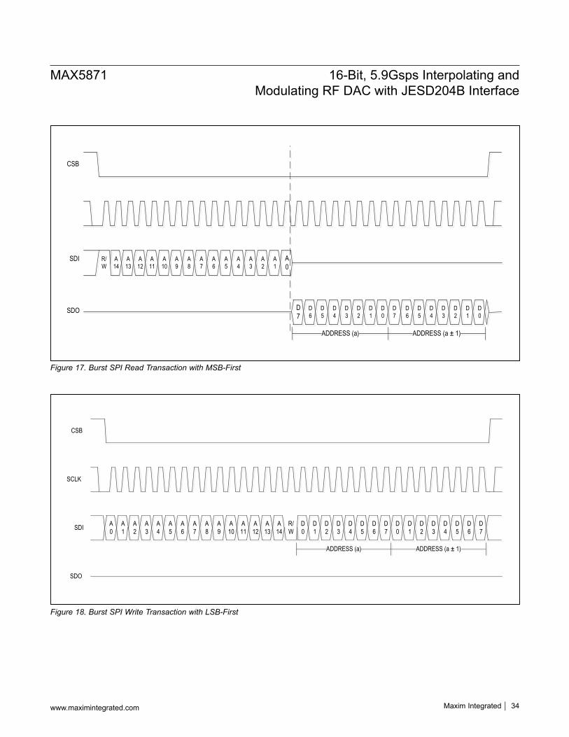
CSB
SDI
SDO
R/W
A14
A13
A12
A0
A1
A2
A3
A11
A10
A9
A8
A7
A6
A5
A4
D0
D1
D2
D3
D4
D5
D6
D7
D0
D1
D2
D3
D4
D5
D6
D7
ADDRESS (a ± 1)ADDRESS (a)
CSB
SCLK
SDI
SDO
R/W
A1
A2
A3
D7
D6
D5
D4
D3
D2
D1
D0
A0
A14
A13
A12
A4
A5
A6
A7
A8
A9
A10
A11
D7
D6
D5
D4
D3
D2
D1
D0
ADDRESS (a ± 1)ADDRESS (a)
Figure 17. Burst SPI Read Transaction with MSB-First
Figure 18. Burst SPI Write Transaction with LSB-First
www.maximintegrated.com Maxim Integrated 34
MAX5871 16-Bit, 5.9Gsps Interpolating and Modulating RF DAC with JESD204B Interface

CSB
SCLK
SDI
SDO
A1
A2
A3
R/W
A14
A13
A12
A4
A5
A6
A7
A8
A9
A10
A11
D7
D6
D5
D4
D3
D2
D1
D0
A0
D7
D6
D5
D4
D3
D2
D1
D0
ADDRESS (a ±1)ADDRESS (a)
Figure 19. Burst SPI Read Transaction with LSB-First
www.maximintegrated.com Maxim Integrated 35
MAX5871 16-Bit, 5.9Gsps Interpolating and Modulating RF DAC with JESD204B Interface

Interrupt and MuteThe INTB pin is a CMOS output port that signals an inter-rupt condition when in the low state. The interrupt system is composed of an interrupt register and an interrupt mask. The interrupt signal is a logic NOR of the bit-wise AND operation of the interrupt register and the interrupt mask. In the MAX5871, 7 interrupt bits are defined: 2 bits for JESD204B mute and interrupt status, 3 bits for a FIFO collision (1-away and 2-away), 1 bit for trim ready, and 1
bit for DAC PLL unlock status. The interrupt tree for the MAX5871 is shown in Figure 20. The JESD204B interface has its own second level of interrupt registers and inter-rupt mask registers as defined in the register interface. The interrupt mask and register can be modified through the serial interface. Table 2 shows all the status register bits that can be enabled to generate an interrupt.
JESD204B STATUS REGISTERS (5)JESD204B INTERRUPT MASKS (5)
DSP STATUS REGISTEREINT REGISTER
BIT-WISE AND
INTB
7
BIT-WISE AND
07 0
DSP STATUS REGISTERS (1ST LEVEL INTERRUPT)BANK.REGISTER.BIT FUNCTION
DSP.STATUS.JSDIM Real-time status indicating DAC mute from JSDI link layer is active
DSP.STATUS.JSDII Real-time status indicating interrupt from JSDI link layer is active
DSP.STATUS.FCOL Latched status set when the input FIFO write and read pointers collide causing FIFO underflow or overflow
DSP.STATUS.F1A Latched status set when the input FIFO write and read pointers are away from each other by one sample
DSP.STATUS.F2A Latched status set when the input FIFO write and read pointers are away from each other by two samples
DSP.STATUS.TRDY Latched status set when trim loading load is complete and the SPI bus is unblocked for external access
DSP.STATUS.PLLlck Latched status set when the DAC PLL is unlocked
Figure 20. MAX5871 Interrupt Tree
Table 2. MAX5871 Status Register Bits
www.maximintegrated.com Maxim Integrated 36
MAX5871 16-Bit, 5.9Gsps Interpolating and Modulating RF DAC with JESD204B Interface

JESD204B STATUS REGISTERS (2ND LEVEL INTERRUPT)BANK.REGISTER.BIT FUNCTION
LNK.StatLane.lnNfnsync Real-time status indicating the frame synchronization state machine is not in sync on Lane N
LNK.StatLane.lnNlnrealgn Latched status set when a lane realignment occurs on Lane N
LNK.StatLane.lnNfrrealgn Latched status set when a frame realignment occurs on Lane N
LNK.StatLane.lnNuk Latched status set when an unexpected /K/ character is received at an unexpected position while code group synchronization is established on Lane N
LNK.StatLane.lnNctrl Latched status set when an unexpected control character other than /K/ is received when not expected on Lane N
LNK.StatLane.lnNdisp Latched status set when a disparity error is detected on Lane N
LNK.StatLane.lnNnit Latched status set when a NIT error is detected on Lane N
LNK.StatLane.lnNcgs Latched status set when code group synchronization state-machine is out of sync on Lane N
LNK.StatFIFO.lnNfafail Latched status set when dynamic FIFO adjustment fails due to not enough FIFO space on Lane N
LNK.StatFIFO.lnNempty Latched status set when the FIFO goes empty on Lane N
LNK.StatFIFO.lnNfull Latched status set when the FIFO goes full on Lane N
LNK.StatILAS.lnNkerr Latched status set when a /K/ character is received at the current CGS boundary while in frame sync on Lane N
LNK.StatILAS.lnNrprbs Latched status set when the SerDes interface PRBS monitor detected an error on Lane N
LNK.StatILAS.lnNkrcv Latched status set when a non-/K/ character is detected on Lane N
LNK.StatILAS.lnNfchkerr Latched status set when an ILA sequence FCHK error is detected on Lane N
LNK.StatILAS.lnNlcfgerr Latched status set when an ILA sequence lane configuration error is detected on Lane N
LNK.StatILAS.lnNilaerr Latched status set when an ILA sequence decode (/R/, /Q/, /A/ character) error is detected on Lane N
LNK.StatILA.nsync Real-time status indicating ILA synchronization has not been achieved
LNK.StatILA.syncn_det Latched status set on a resync request until a SYSREF pulse is detected
LNK.StatILA.sysref_ndet Real-time SYSREF detection status set until first SYSREF detected
LNK.StatILA.fail Latched status set when ILA failure due to not enough FIFO depth or when ILA is based on lanes that are not ready with data
LNK.StatLink.prbs_c2err Latched status set when Converter 2 (Q-sample) PRBS error is detected
LNK.StatLink.prbs_c1err Latched status set when Converter 1 (I-sample) PRBS error is detected
LNK.StatLink.stp_c2err Latched status set when Converter 2 (Q-sample) short test pattern error is detected
LNK.StatLink.stp_c1err Latched status set when Converter 1 (I-sample) short test pattern error is detected
www.maximintegrated.com Maxim Integrated 37
MAX5871 16-Bit, 5.9Gsps Interpolating and Modulating RF DAC with JESD204B Interface

Digital Control PinsThe MAX5871 contains two 1.8V CMOS logic digital con-trol pins, RESETB and MUTE. The device is placed in a reset state when RESETB is low. This control line is level sensitive. On power-up, RESETB should remain low until all supply voltages have stabilized.The MUTE pin defines when the device enters the mute mode. A high logic level places the device in mute mode while a low state establishes normal operation. In mute mode, the DAC digital input is set to midscale. The main purpose of mute is to eliminate any transmit power during the receive time of a TDMA system. In addition, there is a mute configuration programmed through the serial inter-
face that enables the mute mode internally regardless of the state of the MUTE pin. A duplication of the interrupt mask registers as Mute Enable registers generate the internal mute signal. Table 2 shows all the status register bits that can be enabled to generate internal mute. The internal control state of the converter is preserved while the MAX5871 is in the MUTE state.
Frequency PlanningUsing a DAC to generate communications transmit sig-nals requires careful consideration of aliased harmonics and internally generated divided clocks. Figure 22 shows an example of two modulated signals transmitted at 1.8GHz and 2.1GHz. The second harmonic (HD2) and
DACMUTE
MUTE_PIN
JESD204B STATUS REGISTERS (5)JESD204B MUTE ENABLE (5)
DSP STATUS REGISTERDSP EMUTE REGISTER
BIT-WISE AND
BIT-WISE AND
7 0 7 0
fOUT11.8GHz
fOUT22.1GHz
fOUT1 imagefOUT2 image
fDACfDAC/2
fOUT1 HD3
fOUT2 HD3
FREQUENCY
5GHz4GHz3GHz2GHz1GHz
DAC FREQUENCY RESPONSE
fOUT2 HD2
fOUT1 HD2
Figure 21. MAX5871 DAC Mute Generation
Figure 22. Example of Multiband Transmission and Dominant Harmonic Locations
www.maximintegrated.com Maxim Integrated 38
MAX5871 16-Bit, 5.9Gsps Interpolating and Modulating RF DAC with JESD204B Interface

third harmonic (HD3) of the signal are aliased close to the transmitted signal due to the DAC sampling rate.The MAX5871 features a high-performance DAC core and many of the spurs and harmonics are suppressed. However, care must be taken to select the DAC sample rate such that the location of the dominant harmonics, such has HD2 and HD3, do not fall into the band of inter-est. If the board is not carefully designed to isolate the digital and analog portions, the input data may cause spurs to appear at the DAC output. The MAX5871 offers many interpolation settings for upconverting the input data such that a proper update rate can be chosen. For frequency planning, determine the input sample (or data) rate for the DAC and choose the DAC update rate such that the dominant harmonics are aliased outside of the band of interest. Next choose an interpolation rate clos-est to the DAC update rate divided by the input sample rate. Once the interpolation rate is determined, recalcu-late the exact DAC update rate, thereby determining the frequency of the DAC clock input. For new DAC update rate, reverify that the spur or harmonics are within spuri-ous emission requirements.
Signal BandwidthThe MAX5871 can generate a maximum I/Q complex signal bandwidth of 600.15MHz when operating fDAC = 5898.24Msps and 8x interpolation (or fDAC and interpola-tion setting combinations with the maximum input sample rate of 737.28MHz) for output frequencies ranging from DC to Nyquist.The actual signal bandwidth is dependent on the input sample rate (fS_IN), or the DAC update rate (fDAC) divided by the interpolation setting (R), and the interpolation filter passband width (PBW = 0.407, expressed as a percent-age of the input sample rate). The I/Q complex DAC sig-nal bandwidth is calculated as:
DAC Signal Bandwidth = 2 x (fDAC/R) x (PBW) The complex I/Q signals are converted to a real signal using a digital quadrature modulator and quadrature NCO. The real bandwidth is centered around the NCO frequency.
Complex Modulator and NCOThe device includes a complex modulator comprised of a complex NCO driving two multipliers followed by an adder (Figure 23). The complex modulator produces the result:
where I and Q are filtered and interpolated versions of the input I-data and Q-data.
The complex NCO employs a 33-bit phase accumula-tor to provide a programmed signal frequency up to fDAC/2. The DAC sample rate, fDAC, must be an inte-ger multiple of a 30.72MHz reference frequency. The resolution of the MAX5871 can be programmed at 1Hz/10Hz/100Hz/1kHz/10kHz for a range of DAC clock frequency options. The user needs to program the follow-ing three parameters for the NCO, frequency control word (FCW), numerator frequency word (NFW), and denomina-tor frequency word (DFW).The NCO resolution (fSTEP) is defined as:
=× × ×
DACSTEP 10 N
ffM 3 2 10
where fDAC = M x reference frequency. For example, if the reference frequency is 30.72MHz, use M = 192 for a DAC clock frequency (fDAC) of 5898.24Msps. N = 0-4 sets the NCO resolution to 10kHz to 1Hz, respectively. The values of M and N are only used to calculate the FCW, NFW, and DFW that are required to program the required signal frequency.To program the required output frequency (fOUT) of the DAC, the user needs to follow these steps:1) Convert fOUT into an integer number, mapping it on
to the desired frequency resolution scale (fr) that de-pends on the value of N, using the equation:
−= × n 4r sigf f 10
where fOUT is in Hz.2) The frequency control word parameters can be calcu-
lated using the following equation:
I(n) x COS( n) - Q(n) x SIN( n)ω ω QUADRATURENCO
Figure 23. Complex NCO and Modulator
www.maximintegrated.com Maxim Integrated 39
MAX5871 16-Bit, 5.9Gsps Interpolating and Modulating RF DAC with JESD204B Interface

×=
× × ×
33r
10 N2 fFCW
M 3 2 103) The previous calculation results in a rational value
(FCW_full) of the frequency control word. Only the quotient portion is set as the FCW. The remainder fractional value is converted into two integer rational numbers by removing the common integer multiplica-tion factor between them. The numerator of this ratio is set as NFW and the denominator as DFW. Thus:
= +NFWFCW_full FCWDFW
FCW (32-bit), NFW (18-bit), and DFW (19-bit), control words are programmed via the SPI bus. If the above calculation results into an integer number then NFW=DFW=0 should be set:
33 NCODAC
F NFWFCW_full 2 FCWF DFW
= × = +
FCW_full = full resolution of rational number to be pro-grammedFCW = integer part of the FCW_fullNFW = numerator of the fractional part of FCW_fullDFW = denominator of the fractional part of FCW_fullThe NCO block diagram is shown in Figure 24.
When calculating FCW, NFW, and DFW, use long for-mat (more precision) in Matlab code.For example, take M = 163 for fDAC = 163 x 30.72MHz = 5007.36MHz.Case 1 select fNCO = 1796.769375MHz
33 33NCODAC
FFCW_full 2 2F
1796.769375MHz 3082289152.0000005007.36MHz
= × =
× =
Therefore, FCW = 3082289152, NFW = 0, DFW = 0.Case 2 select fNCO = 1796.875MHz
33 33NCODAC
FCW_full 2 2
1796.875MHz 3082470347.648260000005007.36MHz
= × =
× =
Therefore, FCW = 3082470347, NFW/DFW = 317/489 ~ 0.64826000000.
PHASE ACCUMULATOR
NFW
> DFW -DFW REG
DFW
REG
+1
TRUNCATE SIN/COS MAPPING FUNCTION
SIN
COS
FCW
Figure 24. NCO Block Diagram
www.maximintegrated.com Maxim Integrated 40
MAX5871 16-Bit, 5.9Gsps Interpolating and Modulating RF DAC with JESD204B Interface

The following is a simple Matlab code for calculating FCW, NFW, and DFW:
Analog InterfaceReference InterfaceThe device operates with either the on-chip 1.2V band-gap reference or an external reference voltage source as shown in Figures 25a and 25b. REFIO serves as the input for an external, low-impedance reference source, or as the reference output when the internal reference is used. REFIO must be decoupled to DACREF with a 1µF capacitor when using the internal reference. REFIO must be buffered with an external amplifier if heavier loading is required, due to the 10kΩ series resistance.
The reference circuit employs a control amplifier designed to regulate the full-scale, differential output current, IOUTFS. The output current is calculated as follows:
IOUTFS = 32 x IREF
where IREF is the reference output current (IREF = VREFIO/RSET) and IOUTFS is the full-scale output current of the DAC. Using the 1.2V (typical) internal reference and RSET of 1.28kΩ results in a full-scale output current of 30mA. In general, the dynamic performance of the DAC improves with increasing full-scale current.
Analog OutputThe device is a differential current-steering DAC with built-in output termination resistors. The outputs are terminated to AVDD2 providing a 50Ω differential output resistance. In addition to the signal current, a constant current sink (IFIX) equal to one half IOUTFS is connected to each differential DAC output. N = 14 and is the number of bits of resolution of the DAC core. Figure 26 shows an equivalent circuit for the internal output structure of the device. The circuit has some resistive, capacitive and inductive elements. These elements have been mini-mized by design in order to achieve the highest possible output bandwidth (2600MHz typical).In addition, the device requires a differential external ter-mination (i.e. double termination). This external termina-tion can be accomplished with a differential 50Ω load or a single-ended 50Ω load interfaced through a transformer. RF chokes to the AVDD2 supply should be used with the transformer coupled output. A typical transformer coupled configuration for high-frequency operation is shown in Figure 26.
% Find out MAX5871 NCO valuesformat long % Define DAC clock frequency M=1-200M = 163 Fdac = 30.72e6*M % Define desired NCO frequencyFnco = 1796.769375e6; FCW_full = 2^33*Fnco/Fdac; % Calculate FCW, NFW and DFWaFCW = floor(FCW_full)rats(FCW_full-FCW)% END
10kΩ
1µF
1.2VREFERENCE
REFIO
FSADJCURRENTSOURCEARRAY
DAC
IREF
DACREF
OUTP
OUTN
MAX5871
IREF =VREFIO
RSET
RSET
10kΩ
1µF
1.2VREFERENCE
REFIO
FSADJCURRENTSOURCEARRAY
DAC
IREF
DACREF
OUTP
OUTN
MAX5871
IREF =VREFIO
RSET
RSET
IN
OUT
2.5V TO 12.6V
MAX61610.1µF
GND
1.25V
Figure 25a. Reference Architecture, Internal Reference Configuration
Figure 25b. Reference Architecture, External Reference Configuration
www.maximintegrated.com Maxim Integrated 41
MAX5871 16-Bit, 5.9Gsps Interpolating and Modulating RF DAC with JESD204B Interface

For applications where the DC information is important, the output configuration in Figure 27 can be used. 25Ω resistors to AVDD2 are required for DC coupling. The DC configuration will lower the output common-mode which may reduce performance slightly. The device is not com-patible with an unterminated output when using the upper portion of the full-scale current range. Lowering the full-scale current to 20mA or less may allow use of the outputs without external terminations, though performance will be impacted in this configuration.Clock InterfaceThe MAX5871 DAC contains a differential high frequency clock input (CLKP/CLKN) and an optional (bypassable) internal clock multiplying PLL to ease clock distribution. When the PLL is bypassed, the DAC is updated on the rising edge of (CLKP/CLKN) at maximum frequency of 5898.24MHz. See the DAC Clock PLL section for opera-tion with PLL enabled.The high-frequency clock should be a balanced fully dif-ferential signal with a 50%, or near 50%, duty cycle. The clock input has internal (on-chip) 100Ω differential ter-mination. The clock inputs requires a minimum of 0dBm
input power. The clock inputs must be AC-coupled to the clock source as they are self-biased internally.
DAC Clock PLLThe MAX5871 differential high frequency clock input (CLKP/CLKN) also accepts an external reference clock signal that can be multiplied internally by a phase-locked-loop (PLL). The PLL includes user-programmable multi-plication factors which provide flexibility in the reference clock selection. Figure 28 shows the functional block diagram of the PLL.The reference input signal is divided by 1, 2, 4, or 8 under user control before being applied to the phase/frequency detector (PFD). The VCO output is divided by a program-mable divide by 16/20/24/28 divider and fed back to the PFD. In addition to the programmable reference divider and programmable VCO divider, there is an optional out-put divide by 2, before the clock signal is supplied to the RF DAC.Table 3 summarizes frequency multiplication factors between an external reference clock and DACCLK for various PLL settings.
I1 = IFIX + IOUTFS x ((2N – 1) – CODE)/2N
I2 = IFIX + IOUTFS x CODE/2N
1µF
390nHAVDD2
390nH
0.01µF
0.01µF
6
4
1
3T1
OUTN
OUTP25Ω 25Ω
AVDD2
I2I1
MAX5871 I1 = IFIX + IOUTFS x ((2N – 1) – CODE)/2N
I2 = IFIX + IOUTFS x CODE/2N
OUTN
OUTP25Ω 25Ω
AVDD2
I2I1
MAX5871
25Ω 25Ω
AVDD2
Figure 26. Typical DAC Output Configuration Figure 27. Output Configuration for Low-Frequency Operation
www.maximintegrated.com Maxim Integrated 42
MAX5871 16-Bit, 5.9Gsps Interpolating and Modulating RF DAC with JESD204B Interface

REFERENCE DIVIDE-SETTING (N)
FEEDBACK DIVIDE-SETTING (M)
POST DIVIDE-SETTING
VCO MULTIPLICATION FACTOR
OVERALL FREQUENCY
MULTIPLICATION FACTOR
2 16 1 8 82 20 1 10 102 24 1 12 122 28 1 14 142 16 2 8 42 20 2 10 52 24 2 12 62 28 2 14 74 16 1 4 44 20 1 5 54 24 1 6 64 28 1 7 74 16 2 4 24 20 2 5 2.54 24 2 6 34 28 2 7 3.58 16 1 2 28 20 1 2.5 2.58 24 1 3.0 38 28 1 3.5 3.58 16 2 2 18 20 2 2.5 1.258 24 2 3.0 1.508 28 2 3.5 1.75
Table 3. PLL Configuration Settings and Overall Multiplication Factor
www.maximintegrated.com Maxim Integrated 43
MAX5871 16-Bit, 5.9Gsps Interpolating and Modulating RF DAC with JESD204B Interface

VCO Band SelectThe VCO has two frequency ranges. The low range is 4.42368GHz to 4.9152GHz and the high range is 5.89824GHz to 6.1440GHz; however, the DAC sample rate is limited to 5.89824Gsps. The combination of refer-ence frequency, reference and feedback divide values, and VCO band select must be chosen to operate the VCO within its allowed frequency range.
Lock DetectThe DAC clock PLL includes a lock detect indicator which can be read out of the SPI status register (DSP.StatPLL). Bit PLLST3 is set high when the PLL is locked and low when the PLL is unlocked.
PLL External ComponentsThe DAC clock PLL requires external loop filter compo-nents. Figure 29 shows the schematic for the loop filter.
The loop filter components should be placed as close as possible to the MAX5871 to avoid noise coupling into the circuit. In addition to the loop filter, there is a bypass capacitor that must be placed very close to the MAX5871. The C1 nF and C2 pF capacitor values strongly depends on system PCB design and are unique for most designs (see the Application Guidelines section).
Interpolation FiltersThe MAX5871 has powerful digital signal process capa-bility with its built-in digital interpolation filters that can be configured with an interpolation ratio of 5x, 6x, 6.67x, 8x, 10x, 12x, 13.33x, 16x, 20x, 24x. Table 4 shows the digital filter coefficients of 8x and 10x interpolation ratios as examples. Figure 30 to Figure 39 show the frequency response of each of the interpolation ratio settings.
PHASE/FREQENCY DETECTOR (PFD)
REFERENCE DIVIDER(1/2/4/8)
VCO/FEEDBACK DIVIDER
(/16/20/24/28)
CHARGEPUMP
POST DIVIDER(/1/2)
DUAL BANDVCO
LOOP FILTER(EXTERNAL)
DACCLKEXTERNALREFERENCECLOCK
VCOBYP PLL_COMP
MAX5871
C2 pF 650Ω
4.7nF0Ω C1 nF
Figure 28. DAC Clock PLL Functional Block Diagram
Figure 29. DAC Clock PLL External Components
www.maximintegrated.com Maxim Integrated 44
MAX5871 16-Bit, 5.9Gsps Interpolating and Modulating RF DAC with JESD204B Interface

TAPS FILTER 8x FILTER 10x TAPS FILTER 8x FILTER 10x1 0.00000000000000000 0.00000000000000000 171 0.04010009765625000 0.995483398437500002 0.00001525878906250 0.00001525878906250 172 0.05004882812500000 0.995483398437500003 0.00003051757812500 0.00003051757812500 173 0.05175781250000000 0.962738037109375004 0.00004577636718750 0.00003051757812500 174 0.04571533203125000 0.899200439453125005 0.00006103515625000 0.00004577636718750 175 0.03344726562500000 0.808639526367187006 0.00007629394531250 0.00006103515625000 176 0.01730346679687500 0.696411132812500007 0.00006103515625000 0.00007629394531250 177 0.00000000000000000 0.569015502929687008 0.00003051757812500 0.00007629394531250 178 -0.01580810546875000 0.433654785156250009 0.00000000000000000 0.00006103515625000 179 -0.02795410156250000 0.29772949218750000
10 -0.00003051757812500 0.00004577636718750 180 -0.03494262695312500 0.1683807373046870011 -0.00006103515625000 0.00001525878906250 181 -0.03619384765625000 0.0519714355468750012 -0.00013732910156250 0.00000000000000000 182 -0.03198242187500000 -0.0463714599609375013 -0.00018310546875000 -0.00003051757812500 183 -0.02340698242187500 -0.1229553222656250014 -0.00016784667968750 -0.00006103515625000 184 -0.01211547851562500 -0.1757202148437500015 -0.00012207031250000 -0.00010681152343750 185 0.00000000000000000 -0.2043151855468750016 -0.00006103515625000 -0.00015258789062500 186 0.01106262207031250 -0.2100830078125000017 0.00000000000000000 -0.00018310546875000 187 0.01953125000000000 -0.1957550048828120018 0.00012207031250000 -0.00016784667968750 188 0.02439880371093750 -0.1652221679687500019 0.00024414062500000 -0.00012207031250000 189 0.02523803710937500 -0.1231689453125000020 0.00033569335937500 -0.00007629394531250 190 0.02227783203125000 -0.0746154785156250021 0.00039672851562500 -0.00001525878906250 191 0.01629638671875000 -0.0246124267578125022 0.00039672851562500 0.00004577636718750 192 0.00842285156250000 0.0222473144531250023 0.00033569335937500 0.00013732910156250 193 0.00000000000000000 0.0621032714843750024 0.00019836425781250 0.00022888183593750 194 -0.00765991210937500 0.0921173095703125025 0.00000000000000000 0.00030517578125000 195 -0.01348876953125000 0.1105346679687500026 -0.00022888183593750 0.00036621093750000 196 -0.01683044433593750 0.1168212890625000027 -0.00048828125000000 0.00038146972656250 197 -0.01739501953125000 0.1114807128906250028 -0.00070190429687500 0.00038146972656250 198 -0.01530456542968750 0.0961151123046875029 -0.00085449218750000 0.00033569335937500 199 -0.01113891601562500 0.0729827880859375030 -0.00085449218750000 0.00022888183593750 200 -0.00573730468750000 0.0449523925781250031 -0.00070190429687500 0.00009155273437500 201 0.00000000000000000 0.0150451660156250032 -0.00041198730468750 -0.00009155273437500 202 0.00520324707031250 -0.0138397216796875033 0.00000000000000000 -0.00028991699218750 203 0.00915527343750000 -0.0390777587890625034 0.00048828125000000 -0.00048828125000000 204 0.01136779785156250 -0.0585937500000000035 0.00097656250000000 -0.00067138671875000 205 0.01168823242187500 -0.0709991455078125036 0.00138854980468750 -0.00080871582031250 206 0.01025390625000000 -0.0756988525390625037 0.00161743164062500 -0.00085449218750000 207 0.00744628906250000 -0.0728454589843750038 0.00161743164062500 -0.00082397460937500 208 0.00381469726562500 -0.0632629394531250039 0.00134277343750000 -0.00070190429687500 209 0.00000000000000000 -0.0483703613281250040 0.00077819824218750 -0.00047302246093750 210 -0.00343322753906250 -0.0299682617187500041 0.00000000000000000 -0.00016784667968750 211 -0.00601196289062500 -0.01005554199218750
Table 4. Digital Filter Coefficients for 8x and 10x Interpolation Ratios
www.maximintegrated.com Maxim Integrated 45
MAX5871 16-Bit, 5.9Gsps Interpolating and Modulating RF DAC with JESD204B Interface

TAPS FILTER 8x FILTER 10x TAPS FILTER 8x FILTER 10x42 -0.00090026855468750 0.00019836425781250 212 -0.00744628906250000 0.0093536376953125043 -0.00177001953125000 0.00061035156250000 213 -0.00762939453125000 0.0264892578125000044 -0.00247192382812500 0.00099182128906250 214 -0.00666809082031250 0.0398712158203125045 -0.00286865234375000 0.00132751464843750 215 -0.00482177734375000 0.0484771728515625046 -0.00283813476562500 0.00155639648437500 216 -0.00247192382812500 0.0518646240234375047 -0.00231933593750000 0.00164794921875000 217 0.00000000000000000 0.0500793457031250048 -0.00134277343750000 0.00158691406250000 218 0.00219726562500000 0.0436248779296875049 0.00000000000000000 0.00134277343750000 219 0.00381469726562500 0.0334472656250000050 0.00152587890625000 0.00091552734375000 220 0.00469970703125000 0.0207672119140625051 0.00299072265625000 0.00033569335937500 221 0.00479125976562500 0.0069885253906250052 0.00415039062500000 -0.00036621093750000 222 0.00415039062500000 -0.0065155029296875053 0.00479125976562500 -0.00109863281250000 223 0.00299072265625000 -0.0184478759765625054 0.00469970703125000 -0.00177001953125000 224 0.00152587890625000 -0.0278015136718750055 0.00381469726562500 -0.00234985351562500 225 0.00000000000000000 -0.0338439941406250056 0.00219726562500000 -0.00274658203125000 226 -0.00134277343750000 -0.0362548828125000057 0.00000000000000000 -0.00289916992187500 227 -0.00231933593750000 -0.0350341796875000058 -0.00247192382812500 -0.00276184082031250 228 -0.00283813476562500 -0.0305328369140625059 -0.00482177734375000 -0.00231933593750000 229 -0.00286865234375000 -0.0234069824218750060 -0.00666809082031250 -0.00157165527343750 230 -0.00247192382812500 -0.0145263671875000061 -0.00762939453125000 -0.00056457519531250 231 -0.00177001953125000 -0.0048828125000000062 -0.00744628906250000 0.00061035156250000 232 -0.00090026855468750 0.0045471191406250063 -0.00601196289062500 0.00184631347656250 233 0.00000000000000000 0.0128936767578125064 -0.00343322753906250 0.00300598144531250 234 0.00077819824218750 0.0194244384765625065 0.00000000000000000 0.00396728515625000 235 0.00134277343750000 0.0236358642578125066 0.00381469726562500 0.00460815429687500 236 0.00161743164062500 0.0252990722656250067 0.00744628906250000 0.00483703613281250 237 0.00161743164062500 0.0244140625000000068 0.01025390625000000 0.00457763671875000 238 0.00138854980468750 0.0212554931640625069 0.01168823242187500 0.00378417968750000 239 0.00097656250000000 0.0162811279296875070 0.01136779785156250 0.00253295898437500 240 0.00048828125000000 0.0101013183593750071 0.00915527343750000 0.00088500976562500 241 0.00000000000000000 0.0034027099609375072 0.00520324707031250 -0.00102233886718750 242 -0.00041198730468750 -0.0031433105468750073 0.00000000000000000 -0.00299072265625000 243 -0.00070190429687500 -0.0089111328125000074 -0.00573730468750000 -0.00483703613281250 244 -0.00085449218750000 -0.0134124755859375075 -0.01113891601562500 -0.00636291503906250 245 -0.00085449218750000 -0.0163269042968750076 -0.01530456542968750 -0.00736999511718750 246 -0.00070190429687500 -0.0174407958984375077 -0.01739501953125000 -0.00769042968750000 247 -0.00048828125000000 -0.0167999267578125078 -0.01683044433593750 -0.00723266601562500 248 -0.00022888183593750 -0.0145874023437500079 -0.01348876953125000 -0.00598144531250000 249 0.00000000000000000 -0.0111389160156250080 -0.00765991210937500 -0.00398254394531250 250 0.00019836425781250 -0.00689697265625000
Table 4. Digital Filter Coefficients for 8x and 10x Interpolation Ratios (continued)
www.maximintegrated.com Maxim Integrated 46
MAX5871 16-Bit, 5.9Gsps Interpolating and Modulating RF DAC with JESD204B Interface

TAPS FILTER 8x FILTER 10x TAPS FILTER 8x FILTER 10x81 0.00000000000000000 -0.00141906738281250 251 0.00033569335937500 -0.0023193359375000082 0.00842285156250000 0.00152587890625000 252 0.00039672851562500 0.0021514892578125083 0.01629638671875000 0.00459289550781250 253 0.00039672851562500 0.0060729980468750084 0.02227783203125000 0.00746154785156250 254 0.00033569335937500 0.0090942382812500085 0.02523803710937500 0.00978088378906250 255 0.00024414062500000 0.0110321044921875086 0.02439880371093750 0.01127624511718750 256 0.00012207031250000 0.0117492675781250087 0.01953125000000000 0.01174926757812500 257 0.00000000000000000 0.0112762451171875088 0.01106262207031250 0.01103210449218750 258 -0.00006103515625000 0.0097656250000000089 0.00000000000000000 0.00910949707031250 259 -0.00012207031250000 0.0074462890625000090 -0.01211547851562500 0.00607299804687500 260 -0.00016784667968750 0.0046081542968750091 -0.02340698242187500 0.00215148925781250 261 -0.00018310546875000 0.0015411376953125092 -0.03198242187500000 -0.00230407714843750 262 -0.00013732910156250 -0.0014190673828125093 -0.03619384765625000 -0.00689697265625000 263 -0.00006103515625000 -0.0039978027343750094 -0.03494262695312500 -0.01113891601562500 264 -0.00003051757812500 -0.0059661865234375095 -0.02795410156250000 -0.01458740234375000 265 0.00000000000000000 -0.0072021484375000096 -0.01580810546875000 -0.01679992675781250 266 0.00003051757812500 -0.0076599121093750097 0.00000000000000000 -0.01744079589843750 267 0.00006103515625000 -0.0073394775390625098 0.01730346679687500 -0.01631164550781250 268 0.00007629394531250 -0.0063476562500000099 0.03344726562500000 -0.01341247558593750 269 0.00006103515625000 -0.00482177734375000
100 0.04571533203125000 -0.00889587402343750 270 0.00004577636718750 -0.00297546386718750101 0.05175781250000000 -0.00312805175781250 271 0.00003051757812500 -0.00100708007812500102 0.05004882812500000 0.00340270996093750 272 0.00001525878906250 0.00090026855468750103 0.04010009765625000 0.01010131835937500 273 0.00000000000000000 0.00254821777343750104 0.02273559570312500 0.01628112792968750 274 0.00379943847656250105 0.00000000000000000 0.02127075195312500 275 0.00456237792968750106 -0.02496337890625000 0.02442932128906250 276 0.00482177734375000107 -0.04837036132812500 0.02529907226562500 277 0.00460815429687500108 -0.06631469726562500 0.02363586425781250 278 0.00396728515625000109 -0.07537841796875000 0.01942443847656250 279 0.00300598144531250110 -0.07318115234375000 0.01289367675781250 280 0.00183105468750000111 -0.05892944335937500 0.00454711914062500 281 0.00059509277343750112 -0.03358459472656250 -0.00488281250000000 282 -0.00056457519531250113 0.00000000000000000 -0.01452636718750000 283 -0.00155639648437500114 0.03735351562500000 -0.02339172363281250 284 -0.00230407714843750115 0.07293701171875000 -0.03050231933593750 285 -0.00274658203125000116 0.10086059570312500 -0.03501892089843750 286 -0.00289916992187500117 0.11575317382812500 -0.03625488281250000 287 -0.00274658203125000118 0.11360168457031200 -0.03385925292968750 288 -0.00234985351562500119 0.09259033203125000 -0.02781677246093750 289 -0.00177001953125000
Table 4. Digital Filter Coefficients for 8x and 10x Interpolation Ratios (continued)
www.maximintegrated.com Maxim Integrated 47
MAX5871 16-Bit, 5.9Gsps Interpolating and Modulating RF DAC with JESD204B Interface

TAPS FILTER 8x FILTER 10x TAPS FILTER 8x FILTER 10x120 0.05349731445312500 -0.01846313476562500 290 -0.00108337402343750121 0.00000000000000000 -0.00651550292968750 291 -0.00036621093750000122 -0.06158447265625000 0.00698852539062500 292 0.00032043457031250123 -0.12277221679687500 0.02076721191406250 293 0.00091552734375000124 -0.17385864257812500 0.03343200683593750 294 0.00134277343750000125 -0.20507812500000000 0.04360961914062500 295 0.00158691406250000126 -0.20782470703125000 0.05007934570312500 296 0.00164794921875000127 -0.17584228515625000 0.05187988281250000 297 0.00154113769531250128 -0.10620117187500000 0.04849243164062500 298 0.00131225585937500129 0.00000000000000000 0.03987121582031250 299 0.00097656250000000130 0.13760375976562500 0.02648925781250000 300 0.00059509277343750131 0.29754638671875000 0.00936889648437500 301 0.00018310546875000132 0.46774291992187500 -0.01005554199218750 302 -0.00018310546875000133 0.63421630859375000 -0.02996826171875000 303 -0.00048828125000000134 0.78253173828125000 -0.04838562011718750 304 -0.00070190429687500135 0.89944458007812500 -0.06327819824218750 305 -0.00082397460937500136 0.97422790527343700 -0.07286071777343750 306 -0.00086975097656250137 0.99996948242187500 -0.07571411132812500 307 -0.00079345703125000138 0.97422790527343700 -0.07101440429687500 308 -0.00067138671875000139 0.89944458007812500 -0.05859375000000000 309 -0.00048828125000000140 0.78253173828125000 -0.03907775878906250 310 -0.00028991699218750141 0.63421630859375000 -0.01385498046875000 311 -0.00009155273437500142 0.46774291992187500 0.01502990722656250 312 0.00009155273437500143 0.29754638671875000 0.04498291015625000 313 0.00022888183593750144 0.13760375976562500 0.07301330566406250 314 0.00032043457031250145 0.00000000000000000 0.09613037109375000 315 0.00038146972656250146 -0.10620117187500000 0.11149597167968700 316 0.00039672851562500147 -0.17584228515625000 0.11682128906250000 317 0.00038146972656250148 -0.20782470703125000 0.11056518554687500 318 0.00032043457031250149 -0.20507812500000000 0.09213256835937500 319 0.00024414062500000150 -0.17385864257812500 0.06210327148437500 320 0.00015258789062500151 -0.12277221679687500 0.02223205566406250 321 0.00006103515625000152 -0.06158447265625000 -0.02462768554687500 322 -0.00001525878906250153 0.00000000000000000 -0.07464599609375000 323 -0.00009155273437500154 0.05349731445312500 -0.12318420410156200 324 -0.00013732910156250155 0.09259033203125000 -0.16522216796875000 325 -0.00016784667968750156 0.11360168457031200 -0.19572448730468700 326 -0.00016784667968750157 0.11575317382812500 -0.21005249023437500 327 -0.00015258789062500158 0.10086059570312500 -0.20428466796875000 328 -0.00012207031250000
Table 4. Digital Filter Coefficients for 8x and 10x Interpolation Ratios (continued)
www.maximintegrated.com Maxim Integrated 48
MAX5871 16-Bit, 5.9Gsps Interpolating and Modulating RF DAC with JESD204B Interface

0-10
-20-30-40
-50-60
-70-80-90
0 0.1 0.2 0.3 0.4 0.5 0.6 0.7 0.8 0.9NORMALIZED FREQUENCY (xπ rad/sample)
MAGN
ITUD
E (d
B)
5x MAGNITUDE RESPONSE
-100
0
-10-20-30-40
-50-60-70
-80-90
0 0.1 0.2 0.3 0.4 0.5 0.6 0.7 0.8 0.9NORMALIZED FREQUENCY (xπ rad/sample)
MAGN
ITUD
E (d
B)
-100
6x MAGNITUDE RESPONSE
TAPS FILTER 8x FILTER 10x TAPS FILTER 8x FILTER 10x159 0.07293701171875000 -0.17565917968750000 329 -0.00007629394531250160 0.03735351562500000 -0.12292480468750000 330 -0.00003051757812500161 0.00000000000000000 -0.04637145996093750 331 0.00000000000000000162 -0.03358459472656250 0.05195617675781250 332 0.00001525878906250163 -0.05892944335937500 0.16836547851562500 333 0.00003051757812500164 -0.07318115234375000 0.29769897460937500 334 0.00004577636718750165 -0.07537841796875000 0.43363952636718700 335 0.00006103515625000166 -0.06631469726562500 0.56903076171875000 336 0.00006103515625000167 -0.04837036132812500 0.69642639160156200 337 0.00006103515625000168 -0.02496337890625000 0.80863952636718700 338 0.00004577636718750169 0.00000000000000000 0.89920043945312500 339 0.00003051757812500170 0.02273559570312500 0.96275329589843700 340 0.00001525878906250
Table 4. Digital Filter Coefficients for 8x and 10x Interpolation Ratios (continued)
Figure 30. 5x Filter Baseband Frequency Response Normalized to DAC Output Update Rate
Figure 31. 6x Filter Baseband Frequency Response Normalized to DAC Output Update Rate
www.maximintegrated.com Maxim Integrated 49
MAX5871 16-Bit, 5.9Gsps Interpolating and Modulating RF DAC with JESD204B Interface

0-10-20
-30-40
-50-60-70
-80-90
0 0.1 0.2 0.3 0.4 0.5 0.6 0.7 0.8 0.9NORMALIZED FREQUENCY (xπ rad/sample)
MAGN
ITUD
E (d
B)
-100
6.67x MAGNITUDE RESPONSE
0
-20
-40
-60
-80
0 0.1 0.2 0.3 0.4 0.5 0.6 0.7 0.8 0.9NORMALIZED FREQUENCY (xπ rad/sample)
MAGN
ITUD
E (d
B)
-100
8x MAGNITUDE RESPONSE
0
-20
-40
-60
-80
0 0.1 0.2 0.3 0.4 0.5 0.6 0.7 0.8 0.9Normalized Frequency ( xπ rad/sample)
MAGN
ITUD
E (d
B)
-100
10x MAGNITUDE RESPONSE
NORMALIZED FREQUENCY (xπ rad/sample)
0
-20
-40
-60
-80
0 0.1 0.2 0.3 0.4 0.5 0.6 0.7 0.8 0.9NORMALIZED FREQUENCY (xπ rad/sample)
MAGN
ITUD
E (d
B)
-100
-120
12x MAGNITUDE RESPONSE
Figure 32. 6.67x Filter Baseband Frequency Response Normalized to DAC Output Update Rate
Figure 33. 8x Filter Baseband Frequency Response Normalized to DAC Output Update Rate
Figure 34. 10x Filter Baseband Frequency Response Normalized to DAC Output Update Rate
Figure 35. 12x Filter Baseband Frequency Response Normalized to DAC Output Update Rate
www.maximintegrated.com Maxim Integrated 50
MAX5871 16-Bit, 5.9Gsps Interpolating and Modulating RF DAC with JESD204B Interface

0
-20
-40
-60
-80
0 0.1 0.2 0.3 0.4 0.5 0.6 0.7 0.8 0.9NORMALIZED FREQUENCY (xπ rad/sample)
MAGN
ITUD
E (d
B)
-100
13.33x MAGNITUDE RESPONSE0
-20
-40
-60
-80
0 0.1 0.2 0.3 0.4 0.5 0.6 0.7 0.8 0.9NORMALIZED FREQUENCY (xπ rad/sample)
MAGN
ITUD
E (d
B)
-100
16x MAGNITUDE RESPONSE
0
-20
-40
-60
-80
0 0.1 0.2 0.3 0.4 0.5 0.6 0.7 0.8 0.9NORMALIZED FREQUENCY (xπ rad/sample)
MAGN
ITUD
E (d
B)
-100
20x MAGNITUDE RESPONSE
0
-20
-40
-60
-80
0 0.1 0.2 0.3 0.4 0.5 0.6 0.7 0.8 0.9NORMALIZED FREQUENCY (xπ rad/sample)
MAGN
ITUD
E (d
B)
-100
-120
24x MAGNITUDE RESPONSE
Figure 36. 13.33x Filter Baseband Frequency Response Normalized to DAC Output Update Rate
Figure 37. 16x Filter Baseband Frequency Response Normalized to DAC Output Update Rate
Figure 38. 20x Filter Baseband Frequency Response Normalized to DAC Output Update Rate
Figure 39. 24x Filter Baseband Frequency Response Normalized to DAC Output Update Rate
www.maximintegrated.com Maxim Integrated 51
MAX5871 16-Bit, 5.9Gsps Interpolating and Modulating RF DAC with JESD204B Interface

(Note: Do not write to registers with addresses not listed in the table below. Register addresses not listed are reserved for factory use.)
Register Definition and DescriptionThere are four banks of configuration registers in the MAX5871, which can be configured through SPI serial control interface.Configuration Register Banks1) Global Configuration Registers – GLBThis register bank configures SPI serial control interface, device information.2) DSP and DAC Configuration Registers – DSPThis register bank configures the MAX5871 chip operation, DSP engine, NCO, DAC operation, interruption and status, DAC PLL operation.3) Link Layer Configuration Registers for JESD204B – LNKThis register bank configures the JESD204B link layer on the serial data interface lanes, operation, and synchronization.4) SerDes Configuration Registers for JESD204B – SERThis register bank configures the JESD204B SerDes physical layer on the serial data interface lanes, operation, and synchronization.
REGISTER NAME BYTES TYPE ADDRESS DECIMAL DESCRIPTION
Global Configuration Registers–GLBCfgIFA 1 RW 0 Configure Interface ACfgIFB 1 RW 1 Configure Interface BCfgDev 1 RW 2 Device ConfigurationChipType 1 R 3 Chip Type StatusVendorID 2 R 12 Vendor IDCfgIFC 1 RW 15 Configure Interface CCfgDACrate 1 RW 16 Configure DAC Update RateCfgCLKrate 1 RW 17 Configure CLKP/N Input RateCfgREGS 1 RW 18 Configure Register OptionsDSP and DAC Configuration Registers–DSPCfgChipOM 1 RW 256 Configure Chip Operation ModeCfgDSP 1 RW 257 Configure DSP EngineCfgNCOF 4 RW 258 Configure NCO Frequency Control Word for DAC DSP
CfgNCON 3 RW 262 Configure NCO Frequency Control Word Numerator Word for DAC DSP
CfgNCOD 3 RW 265 Configure NCO Frequency Control Word Denominator Word for DAC DSP
CfgNCOU 1 RW 268 Configure NCO Update for DAC DSPCfgNCOUS 3 RW 269 Configure NCO Step Size for DAC DSPCfgPM 1 RW 272 Configure Power Monitor for DAC DSPCfgPMT 1 RW 273 Configure Power Monitor Threshold for DAC DSPCfgPMIC 6 RW 274 Configure Power Monitor Init Count 6x8=48 Bits for DAC DSP
Register Bank Name, Bytes, Type, Address and Description
www.maximintegrated.com Maxim Integrated 52
MAX5871 16-Bit, 5.9Gsps Interpolating and Modulating RF DAC with JESD204B Interface

REGISTER NAME BYTES TYPE ADDRESS DECIMAL DESCRIPTION
StatPM 2 R 280 Power Monitor Status for DAC DSPCfgSync 1 RW 346 Configure Multi-DAC Synchronization for DAC DSPCfgFIFO 1 RW 347 Configure Input FIFO for DACEMUTE 1 RW 354 Mute Enable Mask for DACEINT 1 RW 355 Interrupt Enable Mask for DAC DSPSTATUS 1 R 356 Status Register for DAC DSPiFIFOLevel 1 R 357 Input FIFO Level for DACDieSN 3 R 358 MAX5871 RF DAC Serial Number. Total 8x3 = 24 BitsCfgPLL 3 RW 384 Configure DAC PLLStatPLL 2 R 387 DAC PLL StatusLink Layer Configuration Registers for JESD204B–LNKCfgSRst 1 RW 1024 Configure Soft ResetCfgLnRst 1 RW 1025 Configure Lane ResetCfgLinkSet 1 RW 1026 Configure Link SettingsCfgSYSREF 1 RW 1027 Configure SYSREF SignalCfgSTHRSH 1 RW 1028 Configure SYSREF ThresholdCfgSIGN 1 RW 1029 Configure SYSREF Ignore CountCfgSVLD 1 RW 1030 Configure SYSREF Valid CountCfgSYNCN 1 RW 1031 Configure SYNCN pin optionsCfgSAC 1 RW 1032 Configure SYNCN assert frame countCfgSDC 1 RW 1033 Configure SYNCN deassert frame countCfgLinkMLFS 1 RW 1034 Configure Link for M, L, F and SCfgLinkK 1 RW 1035 Configure Link Multiframe LengthCfgBID 1 RW 1036 Configure Bank IDCfgDID 1 RW 1037 Configure Device IDCfgLID 4 RW 1038 Configure Lane N IDCfgLinkSrc 1 RW 1042 Configure Link Signal SourceCfgClkInv 1 RW 1043 Configure Lane Clock InversionCfgLinkCtl 1 RW 1044 Configure Link ControlCfgBOff 2 RW 1045 Configure Manual Code Group Synch Bit OffsetsCfgRstCnt 1 RW 1047 Configure SYSREF Reset CountsCfgILALck 1 RW 1048 Configure ILA Lock ConfigurationCfgILAC 1 RW 1049 Configure ILA ControlCfgILAD 1 RW 1050 Configure ILA Delay ControlCfgILAM 4 RW 1051 Configure Lane N Manual ILA DelayCfgILAmfs 2 RW 1055 Configure ILA Multiframe startCfgILAsn 2 RW 1057 Configure ILA Sequence NumberCfgLerrM 2 RW 1059 Configure Error Mask for Reporting on SYNCNCfgSerrM 2 RW 1061 Configure Error Mask for Resync Request on SYNCNCfgMDS 2 RW 1063 Configure Multi-DAC Synchronization
www.maximintegrated.com Maxim Integrated 53
MAX5871 16-Bit, 5.9Gsps Interpolating and Modulating RF DAC with JESD204B Interface

Note: In the following Register Definition and Description sections, register and register bit marked with asterisk “*” indi-cates that it needs GLB.CfgIFC.Xfer writing a 1 to transfer the register content into active registers to take effect, when GLB.CfgREGS.ActSel = 1.
REGISTER NAME BYTES TYPE ADDRESS DECIMAL DESCRIPTION
CfgINV 1 RW 1065 Configure Data InversionCfgLnSrc 2 RW 1066 Configure Lane SourceCfgLnEn 1 RW 1068 Configure Lane EnableCfgFIFO 2 RW 1069 Configure FIFO DepthsCfgRepl 1 RW 1071 Configure Sample Replacement on NIT ErrorCfgSamTest 1 RW 1072 Configure Sample Interface TestCfgSTPc1s1 2 RW 1073 Configure Short Test Pattern for Converter 1, Sample 1CfgSTPc1s2 2 RW 1075 Configure Short Test Pattern for Converter 1, Sample 2CfgSTPc2s1 2 RW 1077 Configure Short Test Pattern for Converter 2, Sample 1CfgSTPc2s2 2 RW 1079 Configure Short Test Pattern for Converter 2, Sample 2CfgCnt 1 RW 1280 Configure Counter SettingsCfgCntSel 1 RW 1281 Configure Counter SelectsEIntLane 4 RW 1283 Lane N Interrupt EnableEIntFIFO 4 RW 1287 Lane N FIFO Interrupt EnableEIntILAS 4 RW 1291 Lane N ILA Sequence Interrupt EnableEIntILA 1 RW 1295 Initial Lane Alignment Interrupt EnableEIntLink 1 RW 1296 Link Interrupt EnableEMuteLane 4 RW 1297 Lane N Mute EnableEMuteFIFO 4 RW 1301 Lane N FIFO Mute EnableEMuteILAS 4 RW 1305 Lane N ILA Sequence Mute EnableEMuteILA 1 RW 1309 Initial Lane Alignment Mute EnableEMuteLink 1 RW 1310 Link Mute EnableStatLane 4 R 1408 Lane N StatusStatFIFO 4 R 1412 Lane N FIFO StatusStatILAS 4 R 1416 Lane N ILA Sequence StatusStatILA 1 R 1420 Initial Lane Alignment StatusStatLink 1 R 1421 Link StatusCntInvld 2 R 1422 Counter for Invalid ErrorsCntDbg 2 R 1424 Counter for Lane DebugSERDES Configuration Registers for JESD204B–SERCfgRst 1 RW 1536 Configure Reset for All LanesCfgRate 1 RW 1542 Configure Rate for All LanesCfgTrainLnN 4 RW 1543 Configure Training for Lane NCfgMisc 1 RW 1547 Configure Miscellaneous for All LanesEIntLnN 4 RW 1600 SerDes Phy Logic Interrupt Enable for Lane NEMuteLnN 4 RW 1604 SerDes Phy Logic DAC Mute Enable for Lane NStatusLnN 4 R 1608 SerDes Phy Logic Status for Lane NCfgCMU 8 RW 1792 Configure CMU
www.maximintegrated.com Maxim Integrated 54
MAX5871 16-Bit, 5.9Gsps Interpolating and Modulating RF DAC with JESD204B Interface

ADDRESS BYTE REGISTER NAME DESCRIPTION
0x0000 1 CfgIFA Configure Interface ABit 7 6 5 4 3 2 1 0Name SftRst LSBF AddIncr 4Wire 4Wire AddIncr LSBF SftRstDefault 0 0 0 0 0 0 0 0
Definition
SftRst Writing a 1 to this bit resets all of the digital logic except address 0x0000, 0x0001, and SPI interface. This bit is self-clearing.LSBF0 = MSB first for SPI interface input control/data and output data1 = LSB first for SPI interface input control/data and output dataAddIncr0 = Decrement address for SPI streaming mode1 = Increment address for SPI streaming mode4Wire0 = 3-Wire SPI mode, SDIO used for both input and output1 = 4-Wire SPI mode, SDIO is input and SDO is output
Note Bits[3:0] are mirrored in Bits[4:7], both low and high bits need to be written to the same value
0x0001 1 CfgIFB Configure Interface BBit 7 6 5 4 3 2 1 0Name StrmDis Res RdReg Res Reserved X X ResDefault 0 0 0 0 0 0 0 0
Definition
StrmDis0 = SPI streaming mode is enabled1 = SPI streaming mode is disabled and continued CSB assertion forces instruction-data formatRdReg0 = Register read back from active registers1 = Register read back from buffer registersFor fields that are not implemented with active/buffer registers, this bit has no effect.
0x0002 1 CfgDev Device ConfigurationBit 7 6 5 4 3 2 1 0Name Res Res Res Res Res CDrst* PDM1 PDM0Default 0 0 0 0 0 0 0 0
Definition
PDM[1:0]00 = Normal operation mode01 = Reserved10 = Reserved11 = Sleep mode with lowest power dissipation with chip inactivity except SPI interfaceCDrst 0 = Clock Divider is not reset 1 = Clock Divider is reset
Global Configuration Registers Definition and Description
www.maximintegrated.com Maxim Integrated 55
MAX5871 16-Bit, 5.9Gsps Interpolating and Modulating RF DAC with JESD204B Interface

ADDRESS BYTE REGISTER NAME DESCRIPTION
0x0003 1 ChipType Chip Type StatusBit 7 6 5 4 3 2 1 0Name X X X X Type3 Type2 Type1 Type0Default 0 0 0 0 0 1 0 0
Definition Type[3:0]Read-only field indicating high-speed DAC
0x000C 2 VendorID Maxim Integrated IDBit 7 6 5 4 3 2 1 0Name VID7 VID6 VID5 VID4 VID3 VID2 VID1 VID0Bit 15 14 13 12 11 10 9 8Name VID15 VID14 VID13 VID12 VID11 VID10 VID9 VID8Default 16'h0B6ADefinition Read-only Maxim Integrated ID
0x000F 1 CfgIFC Configure Interface CBit 7 6 5 4 3 2 1 0Name X X X X X X X XferDefault 0 0 0 0 0 0 0 0
DefinitionXferWriting a 1 transfers the buffer registers to active registers. This bit is self-clearing.Note: After the internal configuration is complete, DSP.STATUS.TRDY status is set
0x0010 1 CfgDACrate Configure DAC Update RateBit 7 6 5 4 3 2 1 0Name X X X X Drate3 Drate2 Drate1 Drate0Default 0 0 0 0 1 0 1 0
Definition
Drate[3:0] DAC rate 0000 = 2211.8MHz0001 = 2457.6MHz0010 = 2949.1MHz0011 = 3072.0MHz0100 = 3276.8MHz0101 = 3686.4MHz0110 = 3932.2MHz
0111 = 4096.0MHz1000 = 4423.7MHz1001 = 4915.2MHz1010 = 5898.2MHz1011 = 6144.0MHz
1100–1111 = Reserved
Global Configuration Registers Definition and Description (continued)
www.maximintegrated.com Maxim Integrated 56
MAX5871 16-Bit, 5.9Gsps Interpolating and Modulating RF DAC with JESD204B Interface

ADDRESS BYTE REGISTER NAME DESCRIPTION
0x0011 1 CfgCLKrate Configure CLKP/N Input RateBit 7 6 5 4 3 2 1 0Name X X X X Crate3 Crate2 Crate1 Crate0Default 0 0 0 0 1 1 1 0
Definition
Crate[3:0] CLKP/N rate0000 = 2211.8MHz0001 = 2457.6MHz0010 = 2949.1MHz0011 = 3072.0MHz0100 = 3276.8MHz0101 = 3686.4MHz0110 = 3932.2MHz0111 = 4096.0MHz
1000 = 4423.7MHz1001 = 4915.2MHz1010 = 5898.2MHz1011 = 6144.0MHz1100 = 983.04MHz1101 = 1228.8MHz1110 = 1474.56MHz1111 = Reserved
0x0012 1 CfgREGS Configure Register optionsBit 7 6 5 4 3 2 1 0Name X X X X X X ActSel IntCfgDefault 0 0 0 0 0 0 0 0
Definition
ActSel0 = Buffer register output is used1 = Active register output is used for registers that are updated with CfgIFC.Xfer bitIntCfg0 = Internal register configuration is disabled1 = When CfgIFC.Xfer bit is set, some JESD204B registers are configured internally.(After internal configuration is complete, the DSP.STATUS.TRDY latched status is set.)Contact the chip manufacturer for more details if this function is needed.
Global Configuration Registers Definition and Description (continued)
www.maximintegrated.com Maxim Integrated 57
MAX5871 16-Bit, 5.9Gsps Interpolating and Modulating RF DAC with JESD204B Interface

ADDRESS BYTE REGISTER NAME DESCRIPTION
0x0100 1 CfgChipOM Configure Chip Operation ModeBit 7 6 5 4 3 2 1 0Name Reserved2 RclkM1 RclkM0 INVQ* Reserved1 Mute Reserved0 DFMT*Default 0 0 0 0 0 1 0 0
Definition
Reserved2Reserved – Do not writeRclkM[1:0]00 = RCLK output is DAC clock divided by (interpolation ratio x 1)01 = RCLK output is DAC clock divided by (interpolation ratio x 2)10 = RCLK output is DAC clock divided by (interpolation ratio x 4)11 = ReservedINVQ0 = Disable DAC I-Q data Q being inverted to make I-Q (default)1 = Enable DAC I-Q data Q being inverted to make I+QReserved1Reserved – Do not writeMute0 = DAC in normal mode1 = Enable DAC muteReserved0Reserved – Do not writeDFMT0 = DAC Input data in two's complement format1 = DAC Input data in offset binary format
DSP and DAC Configuration Registers Definition and Description
www.maximintegrated.com Maxim Integrated 58
MAX5871 16-Bit, 5.9Gsps Interpolating and Modulating RF DAC with JESD204B Interface

ADDRESS BYTE REGISTER NAME DESCRIPTION
0x0101 1 CfgDSP Configure DSP EngineBit 7 6 5 4 3 2 1 0Name R3* R2* R1* R0* RstDSP RstFIFO NCOE* NCOLDDefault 0 0 0 0 0 0 0 0
Definition
R[3:0]1001 = DSP interpolation mode is 5x1010 = DSP interpolation mode is 6x1011 = DSP interpolation mode is 8x0000 = DSP interpolation mode is 10x1100 = DSP interpolation mode is 12x
1101 = DSP interpolation mode is 16x 1110 = DSP interpolation mode is 20x1111 = DSP interpolation mode is 24x0010 = DSP interpolation mode is 20/3x0011 = DSP interpolation mode is 40/3x0001, 0100 - 1000 = Reserved
RstDSP0 = No reset1 = Reset DSP (Input FIFO, interpolation filters, complex modulator and NCO)RstFIFO0 = No reset1 = Reset input data FIFONCOE0 = Disable Extended NCO mode for DAC1 = Enable Extended NCO mode using the fractional NCO control words in CfgNCON and CfgNCODNCOLDWriting a 1 loads NCO frequency control words to the DSP, this bit is self-clearingThe NCO frequency control words are also loaded when GLBL.CfgIFC.Xfer bit is set to 1
0x0102 4 CfgNCOF* Configure NCO Frequency Control Word for DSPBit 7 6 5 4 3 2 1 0Name FCW7 FCW6 FCW5 FCW4 FCW3 FCW2 FCW1 FCW0Bit 15 14 13 12 11 10 9 8Name FCW15 FCW14 FCW13 FCW12 FCW11 FCW10 FCW9 FCW8Bit 23 22 21 20 19 18 17 16Name FCW23 FCW22 FCW21 FCW20 FCW19 FCW18 FCW17 FCW16Bit 31 30 29 28 27 26 25 24Name FCW31 FCW30 FCW29 FCW28 FCW27 FCW26 FCW25 FCW24Default 0x00000000
Definition FCW[31:0]NCO Frequency Control Word
DSP and DAC Configuration Registers Definition and Description (continued)
www.maximintegrated.com Maxim Integrated 59
MAX5871 16-Bit, 5.9Gsps Interpolating and Modulating RF DAC with JESD204B Interface

ADDRESS BYTE REGISTER NAME DESCRIPTION
0x0106 3 CfgNCON* Configure NCO Frequency Control Word Numerator Word for DSPBit 7 6 5 4 3 2 1 0Name NFW7 NFW6 NFW5 NFW4 NFW3 NFW2 NFW1 NFW0Bit 15 14 13 12 11 10 9 8Name NFW15 NFW14 NFW13 NFW12 NFW11 NFW10 NFW9 NFW8Bit 23 22 21 20 19 18 17 16Name X X X X X X NFW17 NFW16Default 0x000000
Definition NFW[17:0]Numerator word of the Extended NCO Frequency Control Word
0x0109 3 CfgNCOD* Configure NCO Frequency Control Word Denominator Word for DSPBit 7 6 5 4 3 2 1 0Name DFW7 DFW6 DFW5 DFW4 DFW3 DFW2 DFW1 DFW0Bit 15 14 13 12 11 10 9 8Name DFW15 DFW14 DFW13 DFW12 DFW11 DFW10 DFW9 DFW8Bit 23 22 21 20 19 18 17 16Name X X X X X DFW18 DFW17 DFW16Default 0x000000
Definition DFW[18:0]Denominator word of the Extended NCO Frequency Control Word
0x010C 1 CfgNCOU Configure NCO Update for DSPBit 7 6 5 4 3 2 1 0Name X X Reserved Reserved Reserved Reserved RLM1 ReservedDefault 0 0 0 0 0 0 0 0
Definition
RLM10 = Load immediately with no glitch control1 = Use step increment/decrement mode for a slow change in NCO phase towards the new frequency
0x010D 3 CfgNCOUS Configure NCO Step Size for DSPBit 7 6 5 4 3 2 1 0Name TIM7 TIM6 TIM5 TIM4 TIM3 TIM2 TIM1 TIM0Bit 15 14 13 12 11 10 9 8Name TIM15 TIM14 TIM13 TIM12 TIM11 TIM10 TIM9 TIM8Bit 23 22 21 20 19 18 17 16Name TIM23 TIM22 TIM21 TIM20 TIM19 TIM18 TIM17 TIM16Default 0x000000
Definition TIM[23:0]NCO Step Size in DAC Clock /8 clock cycles when CfgNCOU.RLM1=1
DSP and DAC Configuration Registers Definition and Description (continued)
www.maximintegrated.com Maxim Integrated 60
MAX5871 16-Bit, 5.9Gsps Interpolating and Modulating RF DAC with JESD204B Interface

ADDRESS BYTE REGISTER NAME DESCRIPTION
0x0110 1 CfgPM Configure Power Monitor for DSPBit 7 6 5 4 3 2 1 0Name X X X X X Start Mode ResetDefault 0 0 0 0 0 0 0 0
Definition
Start0 = Power Monitor Stop1 = Power Monitor StartMode0 = Count samples below the threshold1 = Count samples above the thresholdResetWriting a 1 resets the power monitor count, this bit is self-clearing
0x0111 1 CfgPMT Configure Power Monitor Threshold for DSPBit 7 6 5 4 3 2 1 0Name PMT7 PMT6 PMT5 PMT4 PMT3 PMT2 PMT1 PMT0Default 0 0 0 0 0 0 0 0
Definition PMT[7:0]Power Monitor Threshold
0x0112 6 CfgPMIC Configure Power Monitor Initial Count for DSPBit 7 6 5 4 3 2 1 0Name PMIC7 PMIC6 PMIC5 PMIC4 PMIC3 PMIC2 PMIC1 PMIC0Bit 15 14 13 12 11 10 9 8Name PMIC15 PMIC14 PMIC13 PMIC12 PMIC11 PMIC10 PMIC9 PMIC8Bit 23 22 21 20 19 18 17 16Name PMIC23 PMIC22 PMIC21 PMIC20 PMIC19 PMIC18 PMIC17 PMIC16Bit 31 30 29 28 27 26 25 24Name PMIC31 PMIC30 PMIC29 PMIC28 PMIC27 PMIC26 PMIC25 PMIC24Bit 39 38 37 36 35 34 33 32Name PMIC39 PMIC38 PMIC37 PMIC36 PMIC35 PMIC34 PMIC33 PMIC32Bit 47 46 45 44 43 42 41 40Name PMIC47 PMIC46 PMIC45 PMIC44 PMIC43 PMIC42 PMIC41 PMIC40Default 0x000000000000
Definition PMIC[47:0]Power Monitor initial count
DSP and DAC Configuration Registers Definition and Description (continued)
www.maximintegrated.com Maxim Integrated 61
MAX5871 16-Bit, 5.9Gsps Interpolating and Modulating RF DAC with JESD204B Interface

ADDRESS BYTE REGISTER NAME DESCRIPTION
0x0118 2 StatPM Power Monitor Status for DSPBit 7 6 5 4 3 2 1 0Name PMST7 PMST6 PMST5 PMST4 PMST3 PMST2 PMST1 PMST0Bit 15 14 13 12 11 10 9 8Name PMDONE X X X PMST11 PMST10 PMST9 PMST8Default 12'h000
Definition
PMST[11:0]Power Monitor Status indicating the threshold crossing countPMDONE1 = Power Monitor Status update done0 = Power Monitor Status update in progress
0x015A 1 CfgSYNC Configure multiple-DAC synchronization for DSPBit 7 6 5 4 3 2 1 0
Name DSP_ASync* ClkDiv_Sync*
iFIFO_Sync*
NCO_Sync* X Reserved OIF_dinc OIF_ddec
Default 0 0 0 0 0 0 0 0
Definition
DSP_ASync0 = Disable Asynchronous SYSREF reset to the DSP1 = Enable Asynchronous SYSREF reset to the DSP when there is no device cock to the JESD204B LinkClkDiv_SyncWhen DSP_ASync = 00 = Disable synchronous SYSREF reset to the clock-divider block1 = Enable synchronous SYSREF reset to the clock-divider blockWhen DSP_ASync = 10 = Enable first asynchronous SYSREF reset to the clock-divider block1 = Enable continuous asynchronous SYSREF reset to the clock-divider blockiFIFO_Sync0 = Disable synchronous SYSREF reset to the input FIFO1 = Enable synchronous SYSREF reset to the input FIFONCO_Sync0 = Disable synchronous SYSREF reset to the NCO1 = Enable synchronous SYSREF reset to the NCOOIF_dincWriting a 1 increases the DSP latency by one DAC clock cycle, this bit is self-clearingOIF_ddecWriting a 1 decreases the DSP latency by one DAC clock cycle, this bit is self-clearing
DSP and DAC Configuration Registers Definition and Description (continued)
www.maximintegrated.com Maxim Integrated 62
MAX5871 16-Bit, 5.9Gsps Interpolating and Modulating RF DAC with JESD204B Interface

ADDRESS BYTE REGISTER NAME DESCRIPTION
0x015B 1 CfgFIFO Configure Input FIFO for DSPBit 7 6 5 4 3 2 1 0
Name RdPtrAdj3 RdPtrAdj2 RdP-trAdj1
RdP-trAdj0 Off Dupl* SwapIQ* RevBi-
tOrd*Default 0 0 0 0 0 0 0 0
Definition
RdPtrAdj[3:0]0Adjust read pointer by adding this value to the free running read pointerOff0 = Input FIFO is not bypassed1 = Input FIFO is bypassedDupl0 = Do not duplicate I1 = Duplicate I for QSwapIQ0 = Normal I/Q Order1 = Reverse I/Q OrderRevBitOrd0 = Normal LSB/MSB Order1 = Reverse LSB/MSB Order
0x0162 1 EMUTE Mute Enable Register for DACBit 7 6 5 4 3 2 1 0Name EM7 EM6 EM5 EM4 EM3 EM2 EM1 EM0Default 0 0 0 0 0 0 0 0
DefinitionEM[7:0]0 = DAC Mute not enabled when the corresponding bit in STATUS register is set1 = Enable DAC Mute when the corresponding bit in STATUS register is set
0x0163 1 EINT Interrupt Enable Register for DSPBit 7 6 5 4 3 2 1 0Name EINT7 EINT6 EINT5 EINT4 EINT3 EINT2 EINT1 EINT0Default 0 0 0 0 0 1 0 0
DefinitionEINT[7:0]0 = Interrupt not enabled when the corresponding bit in STATUS register is set1 = Enable Interrupt when the corresponding bit in STATUS register is set
DSP and DAC Configuration Registers Definition and Description (continued)
www.maximintegrated.com Maxim Integrated 63
MAX5871 16-Bit, 5.9Gsps Interpolating and Modulating RF DAC with JESD204B Interface

ADDRESS BYTE REGISTER NAME DESCRIPTION
0x0164 1 STATUS Status Register for DAC DSPBit 7 6 5 4 3 2 1 0Name JSDIM JSDII FCOL F1A F2A TRDY Reserved PLLlckDefault 0xXX
Definition
JSDIM0 = JSDI Link layer Mute is not active1 = JSDI Link layer Mute is activeJSDII0 = JSDI Link layer Interrupt is not active1 = JSDI Link layer Interrupt is activeFCOL0 = Input FIFO Rd/Wr pointers are not in collision1 = Input FIFO Rd/Wr pointers are in collision indicating FIFO underflow/overflow. This is a latched state.F1A0 = Input FIFO Rd/Wr pointers are not away by 11 = Input FIFO Rd/Wr pointers are away by 1. This is a latched state.F2A0 = Input FIFO Rd/Wr pointers are not away by 21 = Input FIFO Rd/Wr pointers are away by 2. This is a latched state.TRDY0 = SPI interface access is unavailable out of reset through RESETB.1 = SPI interface access is available after a reset through RESETB. It indicates that trim loading complete after RESETB deassertion, latched status and internal configuration complete after setting GLB.CfgIFC.Xfer, latched statusPLLlckDAC PLL loss-of-lock, latched status. Writing 0 to clear this bit for status" 0 = locked, 1 = loss-of-lock.
Note Writing 0 clears these bits and writing 1 has no effect, except for JSDII and JSDIM which are second-level statuses and cannot be cleared
0x0165 1 iFIFOLevel Input FIFO Level for DSPBit 7 6 5 4 3 2 1 0Name iFL7 iFL6 iFL5 iFL4 iFL3 iFL2 iFL1 iFL0Default 0xXX
Definition iFL[7:0]Input FIFO Level thermometer code, number of 1's indicating the FIFO depth
DSP and DAC Configuration Registers Definition and Description (continued)
www.maximintegrated.com Maxim Integrated 64
MAX5871 16-Bit, 5.9Gsps Interpolating and Modulating RF DAC with JESD204B Interface

ADDRESS BYTE REGISTER NAME DESCRIPTION
0x0166 3 DieSN MAX5871 RF DAC Serial NumberBit 7 6 5 4 3 2 1 0Name SN7 SN6 SN5 SN4 SN3 SN2 SN1 SN0Bit 15 14 13 12 11 10 9 8Name SN15 SN14 SN13 SN12 SN11 SN10 SN9 SN8Bit 23 22 21 20 19 18 17 16Name SN23 SN22 SN21 SN20 SN19 SN18 SN17 SN16Default 0xXXXXXX
Definition SN[23:0]Serial Number of the MAX5871 RF DAC die
DSP and DAC Configuration Registers Definition and Description (continued)
www.maximintegrated.com Maxim Integrated 65
MAX5871 16-Bit, 5.9Gsps Interpolating and Modulating RF DAC with JESD204B Interface

ADDRESS BYTE REGISTER NAME DESCRIPTION
0x0180 3 CfgPLL Configure DAC PLLBit 7 6 5 4 3 2 1 0Name PLL7 PLL6 PLL5 PLL4 PLL3 PLL2 PLL1 PLL0Bit 15 14 13 12 11 10 9 8Name PLL15 PLL14 PLL13 PLL12 PLL11 PLL10 PLL9 PLL8Bit 23 22 21 20 19 18 17 16Name PLL23 PLL22 PLL21 PLL20 PLL19 PLL18 PLL17 PLL16Default 0x004000
Definition
PLL[23:19]Reserved – do not writePLL160 = Selects the lowband VCO1 = Selects the highband VCOPLL17, PLL15Reserved – do not writePLL140 = DAC PLL is not bypassed1 = DAC PLL is bypassedPLL[13:12] (DVAL)00 = Feedback divider set to div-by-1601 = Feedback divider set to div-by-2010 = Feedback divider set to div-by-2411 = Feedback divider set to div-by-28PLL11 (PVAL)0 = Output divider set to div-by-21 = Output divider set to div-by-1PLL18, PLL10 (RVAL)00 = Reference divider control set to div-by-801 = Reference divider control set to div-by-410 = Reference divider control set to div-by-211 = Reference divider control set to div-by-1PLL[9:2]Reserved – Do not writPLL1Reserved – Do not writePLL0Force restart PLL digital tuning by toggling from 1 to 0 and back to 1
DSP and DAC Configuration Registers Definition and Description (continued)
www.maximintegrated.com Maxim Integrated 66
MAX5871 16-Bit, 5.9Gsps Interpolating and Modulating RF DAC with JESD204B Interface

ADDRESS BYTE REGISTER NAME DESCRIPTION
0x0183 2 StatPLL DAC PLL StatusBit 7 6 5 4 3 2 1 0Name PLLST7 PLLST6 PLLST5 PLLST4 PLLST3 PLLST2 PLLST1 PLLST0Bit 15 14 13 12 11 10 9 8Name PLLST15 PLLST14 PLLST13 PLLST12 PLLST11 PLLST10 PLLST9 PLLST8Default 0xXXXX
Definition
PLLST[15:4]ReservedPLLST30 = PLL not locked1 = PLL lockedPLLST[2:0]Reserved
ADDRESS BYTE REGISTER NAME DESCRIPTION
0x0400 1 CfgSRst Configure Soft ResetBit 7 6 5 4 3 2 1 0Name X X X X X X srl ilaDefault 0 0 0 0 0 0 0 0
Definition
srlSoft reset to clear all the latched statusesilaSoft reset for ILA engine
0x0401 1 CfgLnRst Configure Lane ResetBit 7 6 5 4 3 2 1 0Name X X X X ln4 ln3 ln2 ln1Default 0 0 0 0 0 0 0 0
Definition ln[4:1]Soft reset for Lane N
DSP and DAC Configuration Registers Definition and Description (continued)
Link Layer Configuration Registers Definition and Description
www.maximintegrated.com Maxim Integrated 67
MAX5871 16-Bit, 5.9Gsps Interpolating and Modulating RF DAC with JESD204B Interface

ADDRESS BYTE REGISTER NAME DESCRIPTION
0x0402 1 CfgLinkSet Configure Link SettingsBit 7 6 5 4 3 2 1 0Name idisp scrmd* X X ddiv1* ddiv0* sclass1* sclass0*Default 0 0 0 0 0 1 0 0
Definition
idisp0 = Do not ignore running disparity errors for data processing1 = Ignore running disparity errors for data processingscrmd0 = Descrambler is enabled1 = Descrambler is disabledddiv[1:0]00 = Device clock to sample clock frequency ratio is 101 = Device clock to sample clock frequency ratio is 210 = Device clock to sample clock frequency ratio is 411 = Device clock to sample clock frequency ratio is 8sclass[1:0]JESD204B Subclass (0, 1 or 2), only 00 and 01 are valid values
0x0403 1 CfgSYSREF Configure SYSREF SignalBit 7 6 5 4 3 2 1 0
Name X valid_det senext rsync smode1 smode0 ignore_en thrsh_en
Default 0 0 0 0 0 0 0 0
Definition
valid_det0 = SYSREF validity is not checked1 = SYSREF validity is checked to be a number of symbol clocks as configured in CfgSVLD.valid[7:0]senext0 = SYSREF_EN pin is ignored1 = SYSREF enable is controlled by SYSREF_EN pin for better timing than through SPI writesrsync0 = A re-sync request is not output on SYNCN on a new SYSREF multiframe boundary1 = A re-sync request is output on SYNCN on a new SYSREF multiframe boundarysmode[1:0]00 = SYSREF is ignored01 = The first SYSREF pulse is enabled when smode0 is toggled from 0 to 110 = All SYSREF pulses are enabled11 = ReservedThese bits are only used for synchronous SYSREF modeignore_en0 = No SYSREF pulses are dropped before smode[1:0] takes effect1 = SYSREF pulses are dropped as configured in CfgSIGN.ign[7:0] before smode[1:0] takes effectthrsh_en0 = LMFC is reset irrespective of the new SYSREF offset1 = LMFC is reset only if the new SYSREF offset exceeds the threshold from CfgSTHRSH.thrsh[3:0]
Link Layer Configuration Registers Definition and Description (continued)
www.maximintegrated.com Maxim Integrated 68
MAX5871 16-Bit, 5.9Gsps Interpolating and Modulating RF DAC with JESD204B Interface

Link Layer Configuration Registers Definition and Description (continued)
ADDRESS BYTE REGISTER NAME DESCRIPTION
0x0404 1 Cfg-STHRSH Configure SYSREF Threshold
Bit 7 6 5 4 3 2 1 0Name dfath3 dfath2 dfath1 dfath0 thrsh3 thrsh2 thrsh1 thrsh0Default 0 0 0 0 0 0 0 0
Definition
dfath[3:0]0 = No threshold for Dynamic FIFO adjustment1-15 = Dynamic FIFO adjustment is suppressed when the new frame/lane boundary is offset by more than the decimal value of this field in sample clock cyclesthrsh[3:0]SYSREF offset threshold in sample clock cycles when enabled by CfgSYSREF.thrsh_en
0x0405 1 CfgSIGN Configure SYSREF Ignore CountBit 7 6 5 4 3 2 1 0Name ign7 ign6 ign5 ign4 ign3 ign2 ign1 ign0Default 0 0 0 0 0 0 0 0
Definition ign[7:0]SYSREF number of pulses ignored count when enabled by CfgSYSREF.ignore_en
0x0406 1 CfgSVLD Configure SYSREF Valid CountBit 7 6 5 4 3 2 1 0Name valid7 valid6 valid5 valid4 valid3 valid2 valid1 valid0Default 0 0 0 0 0 0 0 0
Definition valid[7:0]SYSREF validity check count of device clock cycles when enabled by CfgSYSREF.valid_det
www.maximintegrated.com Maxim Integrated 69
MAX5871 16-Bit, 5.9Gsps Interpolating and Modulating RF DAC with JESD204B Interface

Link Layer Configuration Registers Definition and Description (continued)
ADDRESS BYTE REGISTER NAME DESCRIPTION
0x0407 1 CfgSYNCN Configure SYNCN pin optionsBit 7 6 5 4 3 2 1 0Name X ret Reserved2 cset Reserved1 Reserved0 init polDefault 0 0 0 0 0 0 0 0
Definition
ret0 = SYNCN is output synchronous to the internal sample clock1 = SYNCN is retimed to device clock, useful for Subclass0 at lower frequenciesThis bit should be cleared when the device clock is not present (CfgLinkSrc.rclk = 1)Reserved2Reserved–Do not writecset0 = Disable manual control of assert/deassert frame cycle of SYNCN error reporting1 = Enable manual control of assert/deassert frame cycle of SYNCN error reporting through Cfg-SAC and CfgSDCReserved1-0Reserved–Do not writeinit0 = Out-of-reset value for SYNCN output is 01 = Out-of-reset value for SYNCN output is 1pol0 = SYNCN polarity is active low according to the JESD204B standard1 = SYNCN polarity is active-high
0x0408 1 CfgSAC Configure SYNCN assert frame countBit 7 6 5 4 3 2 1 0Name X X X acnt4 acnt3 acnt2 acnt1 acnt0Default 0 0 0 0 0 0 0 0
Definitionacnt[4:0]When CfgSYNCN.cset is set, this value determines the SYNCN error reporting assertion frame count
0x0409 1 CfgSDC Configure SYNCN deassert frame countBit 7 6 5 4 3 2 1 0Name X X X dcnt4 dcnt3 dcnt2 dcnt1 dcnt0Default 0 0 0 0 0 0 0 0
Definitiondcnt[4:0]When CfgSYNCN.cset is set, this value determines the SYNCN error reporting deassertion frame count
www.maximintegrated.com Maxim Integrated 70
MAX5871 16-Bit, 5.9Gsps Interpolating and Modulating RF DAC with JESD204B Interface

Link Layer Configuration Registers Definition and Description (continued)
ADDRESS BYTE REGISTER NAME DESCRIPTION
0x040A 1 CfgLink-MLFS Configure Link for M, L, F and S
Bit 7 6 5 4 3 2 1 0Name S F1 F0 X L1 L0 X MDefault 0 0 0 0 1 1 0 1
Definition
SNumber of samples per frame cycle is (S1), restricted to allowed combinations of L/F/SF[1:0]Number of octets per frame cycle per lane is (F1), restricted to allowed combinations of L/F/SL[1:0]Number of active lanes in the Link is (L1), restricted to allowed combinations of L/F/SMNumber of converters in the Link is (M1), should always be set to 1
0x040B 1 CfgLinkK Configure Link multiframe lengthBit 7 6 5 4 3 2 1 0Name X X X K4 K3 K2 K1 K0Default 0 0 0 0 1 1 1 1
Definition K[4:0]Number of frames per multiframe is (K1)
0x040C 1 CfgBID Configure Bank IDBit 7 6 5 4 3 2 1 0Name X X X X bid3 bid2 bid1 bid0Default 0 0 0 0 0 0 0 0
Definition bid[3:0]Bank ID used for ILA sequence checking
0x040D 1 CfgDID Configure Device IDBit 7 6 5 4 3 2 1 0Name did7-0 did6 did5 did4 did3 did2 did1 did0Default 0 0 0 0 0 0 0 0
Definition did[7:0]Device ID used for ILA sequence checking
www.maximintegrated.com Maxim Integrated 71
MAX5871 16-Bit, 5.9Gsps Interpolating and Modulating RF DAC with JESD204B Interface

Link Layer Configuration Registers Definition and Description (continued)
ADDRESS BYTE REGISTER NAME DESCRIPTION
0x040E 4 CfgLID Configure Lane N IDBit 7 6 5 4 3 2 1 0Name X X X lid1_4 lid1_3 lid1_2 lid1_1 lid1_0Bit 15 14 13 12 11 10 9 8Name X X X lid2_4 lid2_3 lid2_2 lid2_1 lid2_0Bit 23 22 21 20 19 18 17 16Name X X X lid3_4 lid3_3 lid3_2 lid3_1 lid3_0Bit 31 30 29 28 27 26 25 24Name X X X lid4_4 lid4_3 lid4_2 lid4_1 lid4_0Default 0x00000000
Definition lidN_[4:0]Lane ID for Lane N used for ILA sequence checking
0x0412 1 CfgLinkSrc Configure Link signal sourceBit 7 6 5 4 3 2 1 0
Name X X X X X X async_avl rclk
Default 0 0 0 0 0 0 0 1
Definition
async_avl0 = Frame synchronization supports re-initialization over the data interface, monitoring the recep-tion of /K/ characters1 = SYNCN signals from all receivers are available and frame synchronization state machine does not support re-initialization over the data interface (no FS_CHECK state)rclk0 = Sample Clock is derived from Device Clock (CLKP/N) with a divide down set by CfgLinkSet.ddiv[1:0]1 = Sample Clock is sourced from the DSP through the DAC Clock divided by interpolation ratio
0x0413 1 CfgClkInv Configure Lane Clock InversionBit 7 6 5 4 3 2 1 0Name X X X X ln4 ln3 ln2 ln1Default 0 0 0 0 0 0 0 0
Definition lnNWhen set, invert Rx clock from SerDes
www.maximintegrated.com Maxim Integrated 72
MAX5871 16-Bit, 5.9Gsps Interpolating and Modulating RF DAC with JESD204B Interface

Link Layer Configuration Registers Definition and Description (continued)
ADDRESS BYTE REGISTER NAME DESCRIPTION
0x0414 1 CfgLinkCtl Configure Link controlBit 7 6 5 4 3 2 1 0Name cgsmen serrc altm dynfadj lcoren fcoren bswap afdetiDefault 0 0 0 1 0 0 0 0
Definition
cgsmenWhen set, enable Manual Code Group Synchronization through CfgBOffserrcWhen set, enable SYNCN error reporting assertion/deassertion on any frame–JESD204AaltmWhen set, enable alternate sample data mapping for MLFS=2422dynfadjWhen set, enable dynamic FIFO pointer adjustment on a frame/lane synchronization changelcorenWhen set, enable Lane Synchronization auto-correctionfcorenWhen set, enable Frame Synchronization auto-correctionbswapWhen set, enable Bit Swap MSB<->LSB in an octet on all lanesafdetiWhen set, enable detection of invalid (Running Disparity) /A/ and /F/ characters
0x0415 2 CfgBOff Configure Manual Code Group Synch Bit OffsetsBit 7 6 5 4 3 2 1 0Name ln2_3 ln2_2 ln2_1 ln2_0 ln1_3 ln1_2 ln1_1 ln1_0Bit 15 14 13 12 11 10 9 8Name ln4_3 ln4_2 ln4_1 ln4_0 ln3_3 ln3_2 ln3_1 ln3_0Default 0x0000
Definition ln[4:1]_[3:0]Lane N manual Code Group Synchronization boundary enabled by CfgLinkCtl.cgsmen
0x0417 1 CfgRstCnt Configure SYSREF reset countsBit 7 6 5 4 3 2 1 0Name X X oi fi4 fi3 fi2 fi1 fi0Default 0 0 0 0 0 0 0 0
Definition
oiInitial value of octet count in the frame cycle from SYSREF samplingfi[4:0]Initial value of frame count in the multiframe cycle from SYSREF samplingThis value along with CfgRstCnt.oi is useful for setting the LMFC boundary relative to SYSREF
www.maximintegrated.com Maxim Integrated 73
MAX5871 16-Bit, 5.9Gsps Interpolating and Modulating RF DAC with JESD204B Interface

Link Layer Configuration Registers Definition and Description (continued)
ADDRESS BYTE REGISTER NAME DESCRIPTION
0x0418 1 CfgILALck Configure ILA Lock configurationBit 7 6 5 4 3 2 1 0Name X X X X lksel4 lksel3 lksel2 lksel1Default 0 0 0 0 1 1 1 1
Definition
lkselNILA Lock Select mask for Lane N based on FIFO write start, 1 indicating the lane is includedThis field is typically set to the same value as CfgLnEn.ln[3:0] but if the lksel bit is set to 0 when the lane is enabled, that particular lane will not be included in the ILA process.
0x0419 1 CfgILAC Configure ILA ControlBit 7 6 5 4 3 2 1 0Name X X X X lsdis ilasd1 ilasd0 dfsyncDefault 0 0 0 0 0 0 0 0
Definition
lsdis0 = Lane synchronization enabled1 = Lane synchronization disabledilasd[1:0]00 = ILA sequence detection is enabled01 = ILA sequence detection is disabled for the first CfgILAsn.snum frames10 = ILA sequence detection is disabled11 = Reserveddfsync0 = Enable ILA restart on frame resynchronization1 = Disable ILA restart on frame resynchronization
0x041A 1 CfgILAD Configure ILA Delay ControlBit 7 6 5 4 3 2 1 0Name ilam X idly5 idly4 idly3 idly2 idly1 idly0Default 0 0 0 0 0 0 0 0
Definition
ilam0 = Manual ILA control is disabled1 = Manual ILA control is enabledidly[5:0]ILA Delay sample clock count from the LMFC boundary for FIFO read startThis field is useful to set the FIFO depths based on the link delay
www.maximintegrated.com Maxim Integrated 74
MAX5871 16-Bit, 5.9Gsps Interpolating and Modulating RF DAC with JESD204B Interface

Link Layer Configuration Registers Definition and Description (continued)
ADDRESS BYTE REGISTER NAME DESCRIPTION
0x041B 4 CfgILAM Configure Lane N Manual ILA DelayBit 7 6 5 4 3 2 1 0Name X X ln1imd5 ln1imd4 ln1imd3 ln1imd2 ln1imd1 ln1imd0Bit 15 14 13 12 11 10 9 8Name X X ln2imd5 ln2imd4 ln2imd3 ln2imd2 ln2imd1 ln2imd0Bit 23 22 21 20 19 18 17 16Name X X ln3imd5 ln3imd4 ln3imd3 ln3imd2 ln3imd1 ln3imd0Bit 31 30 29 28 27 26 25 24Name X X ln4imd5 ln4imd4 ln4imd3 ln4imd2 ln4imd1 ln4imd0Default 0x00000000
Definition ln[4:1]imd[5:0]Manual ILA Delay sample clock count for FIFO read start for Lane N when enabled by CfgILAD.ilam
0x041F 2 CfgILAmfs Configure ILA Multiframe startBit 7 6 5 4 3 2 1 0Name mfsel7 mfsel6 mfsel5 mfsel4 mfsel3 mfsel2 mfsel1 mfsel0Bit 15 14 13 12 11 10 9 8
Name X X X X X X X Re-served0
Default 0x0004
Definition
mfsel[7:0]ILA multiframe count for FIFO write startReserved0Reserved–do not write
0x0421 2 CfgILAsn Configure ILA sequence numberBit 7 6 5 4 3 2 1 0Name snum7 snum6 snum5 snum4 snum3 snum2 snum1 snum0Bit 15 14 13 12 11 10 9 8
Name X X X X X X X Re-served0
Default 0x0003
Definition
snum[7:0]Number of multiframes used for ILA sequence checkingReserved0Reserved–do not write
www.maximintegrated.com Maxim Integrated 75
MAX5871 16-Bit, 5.9Gsps Interpolating and Modulating RF DAC with JESD204B Interface

Link Layer Configuration Registers Definition and Description (continued)
ADDRESS BYTE REGISTER NAME DESCRIPTION
0x0423 2 CfgLerrM* Configure Mask for error reporting on SYNCNBit 7 6 5 4 3 2 1 0Name lerrm7 lerrm6 lerrm5 lerrm4 lerrm3 lerrm2 lerrm1 lerrm0Bit 15 14 13 12 11 10 9 8Name X lerrm14 lerrm13 lerrm12 lerrm11 lerrm10 lerrm9 lerrm8Default 0x0000
Definition
lerrm14When set, ILA Fail error is enabledlerrm13Reservedlerrm12When set, FIFO empty error is enabledlerrm11When set, FIFO full error is enabledlerrm10When set, Lane Configuration in ILA sequence FCS check error is enabledlerrm9When set, Lane Configuration in ILA sequence mismatch error is enabledlerrm8When set, ILA sequence control character error is enabledlerrm7When set, Dynamic FIFO adjustment failure is enabledlerrm6When set, Lane realignment event is enabledlerrm5When set, Frame realignment event is enabledlerrm4When set, 8b10b /K/ character at unexpected alignment error is enabledlerrm3When set, unexpected 8b10b control character other than /K/ error is enabledlerrm2When set, 8b10b Running Disparity error is enabledlerrm1When set, 8b10b Not-in-table error is enabledlerrm0Reserved
www.maximintegrated.com Maxim Integrated 76
MAX5871 16-Bit, 5.9Gsps Interpolating and Modulating RF DAC with JESD204B Interface

Link Layer Configuration Registers Definition and Description (continued)
ADDRESS BYTE REGISTER NAME DESCRIPTION
0x0425 2 CfgSerrM* Configure Mask for re-sync request on SYNCNBit 7 6 5 4 3 2 1 0Name serrm7 serrm6 serrm5 0 0 serrm2 serrm1 0Bit 15 14 13 12 11 10 9 8Name X serrm14 serrm13 serrm12 serrm11 serrm10 serrm9 serrm8Default 0x0000
Definition
serrm14When set, ILA Fail error is enabledserrm13Reservedserrm12When set, FIFO empty error is enabledserrm11When set, FIFO full error is enabledserrm10When set, Lane Configuration in ILA sequence FCS check error is enabledserrm9When set, Lane Configuration in ILA sequence mismatch error is enabledserrm8When set, ILA sequence control character error is enabledserrm7When set, Dynamic FIFO adjustment failure is enabledserrm6When set, Lane realignment event is enabledserrm5When set, Frame realignment event is enabledserrm4Reserved = 0 onlyserrm3Reserved = 0 onlyserrm2When set, 8b10b Running Disparity error is enabledserrm1When set, 8b10b Not-in-table error is enabledserrm0Reserved = 0 only
www.maximintegrated.com Maxim Integrated 77
MAX5871 16-Bit, 5.9Gsps Interpolating and Modulating RF DAC with JESD204B Interface

Link Layer Configuration Registers Definition and Description (continued)
ADDRESS BYTE REGISTER NAME DESCRIPTION
0x0427 2 CfgMDS Configure Multi-DAC SynchronizationBit 7 6 5 4 3 2 1 0
Name X X X rclk Re-served3
Re-served2
Re-served1
Re-served0
Bit 15 14 13 12 11 10 9 8
Name X X X Re-served8
Re-served7
Re-served6
Re-served5
Re-served4
Default 0x0000
Definition
rclkWhen set, RSYNC from DSP replaces SYSREFThis bit should be set to 1 when SYSREF is used for multi-DAC synchronization and no Device Clock is available to sample SYSREF onReserved8-0Reserved–do not write
0x0429 1 CfgINV Configure data inversionBit 7 6 5 4 3 2 1 0Name X X X X ln4 ln3 ln2 ln1Default 0 0 0 0 0 0 0 0
Definitionln[4:1]0 = Lane N octet data inversion is disabled1 = Lane N octet data inversion is enable
0x042A 2 CfgLnSrc Configure Lane SourceBit 7 6 5 4 3 2 1 0Name X X ln2_1 ln2_0 X X ln1_1 ln1_0Bit 15 14 13 12 11 10 9 8Name X X ln4_1 ln4_0 X X ln3_1 ln3_0Default 0x3210
Definition ln[4:1]_[1:0]Physical Lane number source for Logical Lane N at octet-to-sample mapping
www.maximintegrated.com Maxim Integrated 78
MAX5871 16-Bit, 5.9Gsps Interpolating and Modulating RF DAC with JESD204B Interface

Link Layer Configuration Registers Definition and Description (continued)
ADDRESS BYTE REGISTER NAME DESCRIPTION
0x042C 1 CfgLnEn Configure Lane EnableBit 7 6 5 4 3 2 1 0Name X X X X ln4 ln3 ln2 ln1Default 0 0 0 0 1 1 1 1
Definition ln[4:1]Lane N enable
0x042D 2 CfgFIFO Configure FIFO depthsBit 7 6 5 4 3 2 1 0Name X X X minfd4 minfd3 minfd2 minfd1 minfd0Bit 15 14 13 12 11 10 9 8Name X X X maxfd4 maxfd3 maxfd2 maxfd1 maxfd0Default 0x1A06
Definition
maxfd[4:0]Maximum FIFO depth for dynamic adjustment and full/empty statusminfd[4:0]Minimum FIFO depth for dynamic adjustment and full/empty status
0x042F 1 CfgRepl Configure Sample Replacement on NIT errorBit 7 6 5 4 3 2 1 0Name X X X X X ac frm samDefault 0 0 0 0 0 0 0 0
Definition
acWhen set, replace sample/frame for all converters with previous good sample/framefrmWhen set, replace frame with previous good framesamWhen set, replace sample with previous good sample
www.maximintegrated.com Maxim Integrated 79
MAX5871 16-Bit, 5.9Gsps Interpolating and Modulating RF DAC with JESD204B Interface

Link Layer Configuration Registers Definition and Description (continued)
ADDRESS BYTE REGISTER NAME DESCRIPTION
0x0430 1 CfgSamTest Configure SerDes/Sample Interface TestBit 7 6 5 4 3 2 1 0Name prbst1 prbst0 tprbs rprbs X X sprbs2 sprbs1Default 0 0 0 0 0 0 0 0
Definition
prbst[1:0]00 = PRBS7 for SerDes Interface01 = PRBS23 for SerDes Interface10 = PRBS31 for SerDes Interface11 = ReservedtprbsEnable PRBS on transmit SerDes interface, pattern based on prbst1-0rprbsEnable PRBS checking on receive SerDes interface, pattern based on prbst1-0This bit should be toggled from 0 to 1 for restarting the PRBS checksprbsNEnable PRBS15 checker for converter N samplesThis bit should be toggled from 0 to 1 for restarting the PRBS check
0x0431 2 CfgST-Pc1s1 Configure Short Test Pattern for Converter 1, Sample 1
Bit 7 6 5 4 3 2 1 0Name pat7 pat6 pat5 pat4 pat3 pat2 pat1 pat0Bit 15 14 13 12 11 10 9 8Name pat15 pat14 pat13 pat12 pat11 pat10 pat9 pat8Default 0x0000
Definition pat[15:0]Converter 1, Sample 1 short test pattern (alternating sample test pattern)
www.maximintegrated.com Maxim Integrated 80
MAX5871 16-Bit, 5.9Gsps Interpolating and Modulating RF DAC with JESD204B Interface

Link Layer Configuration Registers Definition and Description (continued)
ADDRESS BYTE REGISTER NAME DESCRIPTION
0x0433 2 CfgST-Pc1s2 Configure Short Test Pattern for Converter 1, Sample 2
Bit 7 6 5 4 3 2 1 0Name pat7 pat6 pat5 pat4 pat3 pat2 pat1 pat0Bit 15 14 13 12 11 10 9 8Name pat15 pat14 pat13 pat12 pat11 pat10 pat9 pat8Default 0x0000
Definition pat[15:0]Converter 1, Sample 2 short test pattern (alternating sample test pattern)
0x0435 2 CfgST-Pc2s1 Configure Short Test Pattern for Converter 2, Sample 1
Bit 7 6 5 4 3 2 1 0Name pat7 pat6 pat5 pat4 pat3 pat2 pat1 pat0Bit 15 14 13 12 11 10 9 8Name pat15 pat14 pat13 pat12 pat11 pat10 pat9 pat8Default 0x0000
Definition pat[15:0]Converter 2, Sample 1 short test pattern (alternating sample test pattern)
www.maximintegrated.com Maxim Integrated 81
MAX5871 16-Bit, 5.9Gsps Interpolating and Modulating RF DAC with JESD204B Interface

Link Layer Configuration Registers Definition and Description (continued)
ADDRESS BYTE REGISTER NAME DESCRIPTION
0x0437 2 CfgST-Pc2s2 Configure Short Test Pattern for Converter 2, Sample 2
Bit 7 6 5 4 3 2 1 0Name pat7 pat6 pat5 pat4 pat3 pat2 pat1 pat0Bit 15 14 13 12 11 10 9 8Name pat15 pat14 pat13 pat12 pat11 pat10 pat9 pat8Default 0x0000
Definition pat[15:0]Converter 2, Sample 2 short test pattern (alternating sample test pattern)
0x0500 1 CfgCnt Configure Counter SettingsBit 7 6 5 4 3 2 1 0Name X X X X X samld rxld cdcorDefault 0 0 0 0 0 0 0 0
Definition
samldLoad signal for sample clock domain Lane FIFO depth update, this bit is self-clearingrxldLoad signal for Rx SerDes clock domain counter update, this bit is self-clearingcdcorCounter data clear-on-read enable
www.maximintegrated.com Maxim Integrated 82
MAX5871 16-Bit, 5.9Gsps Interpolating and Modulating RF DAC with JESD204B Interface

Link Layer Configuration Registers Definition and Description (continued)
ADDRESS BYTE REGISTER NAME DESCRIPTION
0x0501 1 CfgCntSel Configure Counter SelectsBit 7 6 5 4 3 2 1 0Name ctsel3 ctsel2 ctsel1 ctsel0 X X rxcsel1 rxcsel0Default 0 0 0 0 0 0 0 0
Definition
ctsel[3:0]Lane debug counter error type select for CntDbg register0000 = No counts0001 = NIT errors0010 = Disparity errors0011 = /K/ detect0100 = /R/ detect0101 = /Q/ detect0110 = /A/ detect0111 = /F/ detect1000 = Unexpected control character error1001 = ILA sequence control character error1010-1111 = No countsrxcsel[1:0]00 = Lane 1 counts enabled for CntDbg register01 = Lane 2 counts enabled for CntDbg register10 = Lane 3 counts enabled for CntDbg register11 = Lane 4 counts enabled for CntDbg register
0x0503 4 EIntLane Lane N Interrupt EnableBit 7 6 5 4 3 2 1 0Name ln1fnsync ln1lnrealgn ln1frrealgn ln1uk ln1ctrl ln1disp ln1nit ln1cgsBit 15 14 13 12 11 10 9 8Name ln2fnsync ln2lnrealgn ln2frrealgn ln2uk ln2ctrl ln2disp ln2nit ln2cgsBit 23 22 21 20 19 18 17 16Name ln3fnsync ln3lnrealgn ln3frrealgn ln3uk ln3ctrl ln3disp ln3nit ln3cgsBit 31 30 29 28 27 26 25 24Name ln4fnsync ln4lnrealgn ln4frrealgn ln4uk ln4ctrl ln4disp ln4nit ln4cgsDefault 0x00000000Definition Interrupt enable for the corresponding bit in StatLane register
www.maximintegrated.com Maxim Integrated 83
MAX5871 16-Bit, 5.9Gsps Interpolating and Modulating RF DAC with JESD204B Interface

Link Layer Configuration Registers Definition and Description (continued)
ADDRESS BYTE REGISTER NAME DESCRIPTION
0x0507 4 EIntFIFO Lane N FIFO Interrupt EnableBit 7 6 5 4 3 2 1 0Name ln1fafail ln1empty ln1full X X X X XBit 15 14 13 12 11 10 9 8Name ln2fafail ln2empty ln2full X X X X XBit 23 22 21 20 19 18 17 16Name ln3fafail ln3empty ln3full X X X X XBit 31 30 29 28 27 26 25 24Name ln4fafail ln4empty ln4full X X X X XDefault 0x00000000Definition Interrupt enable for the corresponding bit in StatFIFO register
0x050B 4 EIntILAS Lane N ILA Sequence Interrupt EnableBit 7 6 5 4 3 2 1 0Name X ln1drcv ln1kerr ln1rprbs ln1krcv ln1fchkerr ln1lcfgerr ln1ilaerrBit 15 14 13 12 11 10 9 8Name X ln2drcv ln2kerr ln2rprbs ln2krcv ln2fchkerr ln2lcfgerr ln2ilaerrBit 23 22 21 20 19 18 17 16Name X ln3drcv ln3kerr ln3rprbs ln3krcv ln3fchkerr ln3lcfgerr ln3ilaerrBit 31 30 29 28 27 26 25 24Name X ln4drcv ln4kerr ln4rprbs ln4krcv ln4fchkerr ln4lcfgerr ln4ilaerrDefault 0x00000000Definition Interrupt enable for the corresponding bit in StatILAS register
0x050F 1 EIntILA Initial Lane Alignment Interrupt EnableBit 7 6 5 4 3 2 1 0
Name X X X sysref_nvld nsync Re-
served0sysref_
ndet fail
Default 0 0 0 0 0 0 1 0Definition Interrupt enable for the corresponding bit in StatILA register
0x0510 1 EIntLink Link Interrupt EnableBit 7 6 5 4 3 2 1 0
Name X X prbs_c2err
prbs_c1err X X stp_
c2errstp_c1err
Default 0 0 0 0 0 0 0 0Definition Interrupt enable for the corresponding bit in StatLink register
www.maximintegrated.com Maxim Integrated 84
MAX5871 16-Bit, 5.9Gsps Interpolating and Modulating RF DAC with JESD204B Interface

Link Layer Configuration Registers Definition and Description (continued)
ADDRESS BYTE REGISTER NAME DESCRIPTION
0x0511 4 EMuteLane Lane N Mute EnableBit 7 6 5 4 3 2 1 0Name ln1fnsync ln1lnrealgn ln1frrealgn ln1uk ln1ctrl ln1disp ln1nit ln1cgsBit 15 14 13 12 11 10 9 8Name ln2fnsync ln2lnrealgn ln2frrealgn ln2uk ln2ctrl ln2disp ln2nit ln2cgsBit 23 22 21 20 19 18 17 16Name ln3fnsync ln3lnrealgn ln3frrealgn ln3uk ln3ctrl ln3disp ln3nit ln3cgsBit 31 30 29 28 27 26 25 24Name ln4fnsync ln4lnrealgn ln4frrealgn ln4uk ln4ctrl ln4disp ln4nit ln4cgsDefault 0x00000000Definition Enable DAC Mute for the corresponding bit in StatLane register
0x0515 4 EMuteFIFO Lane N FIFO Mute EnableBit 7 6 5 4 3 2 1 0Name ln1fafail ln1empty ln1full X X X X XBit 15 14 13 12 11 10 9 8Name ln2fafail ln2empty ln2full X X X X XBit 23 22 21 20 19 18 17 16Name ln3fafail ln3empty ln3full X X X X XBit 31 30 29 28 27 26 25 24Name ln4fafail ln4empty ln4full X X X X XDefault 0x00000000Definition Enable DAC Mute for the corresponding bit in StatFIFO register
0x0519 4 EMuteILAS Lane N ILA Sequence Mute EnableBit 7 6 5 4 3 2 1 0Name X ln1drcv ln1kerr ln1rprbs ln1krcv ln1fchkerr ln1lcfgerr ln1ilaerrBit 15 14 13 12 11 10 9 8Name X ln2drcv ln2kerr ln2rprbs ln2krcv ln2fchkerr ln2lcfgerr ln2ilaerrBit 23 22 21 20 19 18 17 16Name X ln3drcv ln3kerr ln3rprbs ln3krcv ln3fchkerr ln3lcfgerr ln3ilaerrBit 31 30 29 28 27 26 25 24Name X ln4drcv ln4kerr ln4rprbs ln4krcv ln4fchkerr ln4lcfgerr ln4ilaerrDefault 0x00000000Definition Enable DAC Mute for the corresponding bit in StatILAS register
www.maximintegrated.com Maxim Integrated 85
MAX5871 16-Bit, 5.9Gsps Interpolating and Modulating RF DAC with JESD204B Interface

Link Layer Configuration Registers Definition and Description (continued)
ADDRESS BYTE REGISTER NAME DESCRIPTION
0x051D 1 EMuteILA Initial Lane Alignment Mute EnableBit 7 6 5 4 3 2 1 0
Name X X X sysref_nvld nsync Reserved sysref_
ndet fail
Default 0 0 0 0 0 0 1 0Definition Enable DAC Mute for the corresponding bit in StatILA register
0x051E 1 EMuteLink Link Mute EnableBit 7 6 5 4 3 2 1 0Name X X prbs_c2err prbs_c1err X X stp_c2err stp_c1errDefault 0 0 0 0 0 0 0 0Definition Enable DAC Mute for the corresponding bit in StatLink register
0x0580 4 StatLane Lane N StatusBit 7 6 5 4 3 2 1 0Name ln1fnsync ln1lnrealgn ln1frrealgn ln1uk ln1ctrl ln1disp ln1nit ln1cgsBit 15 14 13 12 11 10 9 8Name ln2fnsync ln2lnrealgn ln2frrealgn ln2uk ln2ctrl ln2disp ln2nit ln2cgsBit 23 22 21 20 19 18 17 16Name ln3fnsync ln3lnrealgn ln3frrealgn ln3uk ln3ctrl ln3disp ln3nit ln3cgsBit 31 30 29 28 27 26 25 24Name ln4fnsync ln4lnrealgn ln4frrealgn ln4uk ln4ctrl ln4disp ln4nit ln4cgsDefault 0xXXXXXXXX
Definition
lnNfnsyncFrame synchronization state machine not in Sync real-timelnNlnrealgnLane realignment occurred latchedlnNfrrealgnFrame realignment occurred latchedlnNukLane N unexpected /K/ character latched. When set, this bit is not necessarily indicating an error since /K/ can occur across the character boundaries.lnNctrlLane N unexpected control character latchedlnNdispLane N Disparity error latchedlnNnitLane N NIT error latchedlnNcgsLane N Code Group Synchronization out of Sync latched
www.maximintegrated.com Maxim Integrated 86
MAX5871 16-Bit, 5.9Gsps Interpolating and Modulating RF DAC with JESD204B Interface

Link Layer Configuration Registers Definition and Description (continued)
ADDRESS BYTE REGISTER NAME DESCRIPTION
0x0584 4 StatFIFO Lane N FIFO StatusBit 7 6 5 4 3 2 1 0Name ln1fafail ln1empty ln1full ln1fd4 ln1fd3 ln1fd2 ln1fd1 ln1fd0Bit 15 14 13 12 11 10 9 8Name ln2fafail ln2empty ln2full ln2fd4 ln2fd3 ln2fd2 ln2fd1 ln2fd0Bit 23 22 21 20 19 18 17 16Name ln3fafail ln3empty ln3full ln3fd4 ln3fd3 ln3fd2 ln3fd1 ln3fd0Bit 31 30 29 28 27 26 25 24Name ln4fafail ln4empty ln4full ln4fd4 ln4fd3 ln4fd2 ln4fd1 ln4fd0Default 0xXXXXXXXX
Definition
lnNfafailLane N dynamic FIFO adjustment failure latchedlnNemptyLane N FIFO empty status latchedlnNfullLane N FIFO full status latchedlnNfd[4:0]Lane N FIFO depth real-time loaded when CfgCnt.samld is set to 1
www.maximintegrated.com Maxim Integrated 87
MAX5871 16-Bit, 5.9Gsps Interpolating and Modulating RF DAC with JESD204B Interface

Link Layer Configuration Registers Definition and Description (continued)
ADDRESS BYTE REGISTER NAME DESCRIPTION
0x0588 4 StatILAS Lane N ILA Sequence StatusBit 7 6 5 4 3 2 1 0Name X ln1drcv ln1kerr ln1rprbs ln1krcv ln1fchkerr ln1lcfgerr ln1ilaerrBit 15 14 13 12 11 10 9 8Name X ln2drcv ln2kerr ln2rprbs ln2krcv ln2fchkerr ln2lcfgerr ln2ilaerrBit 23 22 21 20 19 18 17 16Name X ln3drcv ln3kerr ln3rprbs ln3krcv ln3fchkerr ln3lcfgerr ln3ilaerrBit 31 30 29 28 27 26 25 24Name X ln4drcv ln4kerr ln4rprbs ln4krcv ln4fchkerr ln4lcfgerr ln4ilaerrDefault 0xXXXXXXXX
Definition
lnNdrcvLane N continuous D21.5 not-detect latchedlnNkerrLane N /K/ character while in frame sync latchedlnNrprbsLane N SerDes interface PRBS error latchedlnNkrcvLane N continuous /K/ not-detect latchedlnNfchkerrLane N ILA sequence FCHK error latchedlnNlcfgerrLane N ILA sequence lane configuration error latchedlnNilaerrLane N ILA sequence decode error latched
0x058C 1 StatILA Initial Lane Alignment StatusBit 7 6 5 4 3 2 1 0
Name X X X sysref_nvld nsync Re-
served0sysref_
ndet fail
Default 0xXX
Definition
sysref_nvldSYSREF validity detection error status latchednsyncILA synchronization not achieved real-timeReserved0sysref_ndetSYSREF detection status set until a SYSREF pulse is detected and used for LMFC resetfailILA failure latchedThis status is set when a lane FIFO is empty or full when the read starts
www.maximintegrated.com Maxim Integrated 88
MAX5871 16-Bit, 5.9Gsps Interpolating and Modulating RF DAC with JESD204B Interface

*SYNCN behavior per the JESD204B standard is to be asserted while the Rx Link is out of Code Group Synchronization (CGS). The MAX5871 asserts SYNCN (drive low) as long as any of the active lanes are out of CGS.LNK.CfgLerrM register can be used for error reporting on SYNCN which asserts SYNCN for 2 frame clock cycles at the end of the multiframe on an error that is enabled through this register.LNK.CfgSerrM register can be used for resynchronization request on SYNCN which asserts SYNCN for the minimum required period of "5 frames + 9 octets" on an error that is enabled through this register.If LNK.CfgSerrM.serrm0 is set, it would interfere with the required behavior of SYNCN per the JESD204B standard and asserts SYNCN only for the minimum required period and not as long as CGS error persists.
Link Layer Configuration Registers Definition and Description (continued)
ADDRESS BYTE REGISTER NAME DESCRIPTION
0x058D 1 StatLink Link StatusBit 7 6 5 4 3 2 1 0
Name X X prbs_c2err
prbs_c1err X X stp_
c2errstp_c1err
Default 0xXX
Definition
prbs_cNerrConverter N PRBS error latchedstp_cNerrConverter N short test pattern error latched
0x058E 2 CntInvld Counter for Invalid ErrorsBit 7 6 5 4 3 2 1 0Name cnt7 cnt6 cnt5 cnt4 cnt3 cnt2 cnt1 cnt0Bit 15 14 13 12 11 10 9 8Name cnt15 cnt14 cnt13 cnt12 cnt11 cnt10 cnt9 cnt8Default 0xXXXX
Definitioncnt1[5:0]Invalid character count for lane # controlled by CfgCntSel.rxcsel1-0This counter should be loaded by setting CfgCnt.rxld to 1
0x0590 2 CntDbg Counter for Lane DebugBit 7 6 5 4 3 2 1 0Name cnt7 cnt6 cnt5 cnt4 cnt3 cnt2 cnt1 cnt0Bit 15 14 13 12 11 10 9 8Name cnt15 cnt14 cnt13 cnt12 cnt11 cnt10 cnt9 cnt8Default 0xXXXX
Definitioncnt1[5:0]Debug count type controlled by CfgCntSel.ctsel3-0 for lane # controlled by CfgCntSel.rxcsel1-0This counter should be loaded by setting CfgCnt.rxld to 1
www.maximintegrated.com Maxim Integrated 89
MAX5871 16-Bit, 5.9Gsps Interpolating and Modulating RF DAC with JESD204B Interface

ADDRESS BYTE REGISTER NAME DESCRIPTION
0x0600 1 CfgRst Configure Reset for all LanesBit 7 6 5 4 3 2 1 0Name X X X X X PhyKill RstTx RstDefault 0 0 0 0 0 0 0 1
Definition
PhyKillReserved – do not writeRstTxReserved – do not writeRst0 = SerDes PHY Logic is not in reset1 = SerDes PHY Logic is in reset
0x0606 1 CfgRate Configure Rate for all lanesBit 7 6 5 4 3 2 1 0Name X X X X TxRate1 TxRate0 RxRate1 RxRate0Default 0 0 0 0 1 1 1 1
Definition
TxRate[1:0]Reserved – do not writeRxRate[1:0]00 = Reserved01 = Serial Rate for Rx SerDes is CMU clock rate divide-by-410 = Serial Rate for Rx SerDes is CMU clock rate divide-by-211 = Serial Rate for Rx SerDes is CMU clock rate
SERDES Common Registers Definition and Description
www.maximintegrated.com Maxim Integrated 90
MAX5871 16-Bit, 5.9Gsps Interpolating and Modulating RF DAC with JESD204B Interface

ADDRESS BYTE REGISTER NAME DESCRIPTION
0x0607 4 CfgTrain-Ln Configure Training for Lane
Bit 7 6 5 4 3 2 1 0Name X X X X Ln1DnGate Ln1IdleGate Ln1Force1 Ln1Force0Bit 15 14 13 12 11 10 9 8Name X X X X Ln2DnGate Ln2IdleGate Ln2Force1 Ln2Force0Bit 23 22 21 20 19 18 17 16Name X X X X Ln3DnGate Ln3IdleGate Ln3Force1 Ln3Force0Bit 31 30 29 28 27 26 25 24Name X X X X Ln4DnGate Ln4IdleGate Ln4Force1 Ln4Force0Default 0x0D for each lane
Definition
Ln[4:1]DnGate0 = Do not gate data off to Link layer when SerDes Training done status is low for lane N1 = Gate data off to Link layer when SerDes Training done status is low for lane NLn[4:1]IdleGate0 = Do not gate data off to Link layer when SerDes Idle detect is high for lane N1 = Gate data off to Link layer when SerDes Idle detect is high for lane NLn[4:1]Force[1:0]00, 11 = Reserved01 = Deactivate training for Lane N10 = Activate training for Lane N
0x060B 1 CfgMisc Configure Miscellaneous for all LanesBit 7 6 5 4 3 2 1 0Name X X PhyWMde1 PhyWMde0 X BCast Reserved ReservedDefault 0 0 0 0 0 1 0 0
Definition
PhyWMde[1:0]00 = Buffer upper 3 bytes and transfer all 4 bytes on a write to LSB for the 32-bit interface on the PHY01 = Buffer lower 3 bytes and transfer all 4 bytes on a write to MSB for the 32-bit interface on the PHY10 = Enable individual byte writes to the SerDes PHY11 = ReservedBCast0 = SPI writes to one SerDes PHY are not broadcasted to all lanes1 = SPI writes to one SerDes PHY are broadcasted to all lanes
SERDES Common Registers Definition and Description (continued)
www.maximintegrated.com Maxim Integrated 91
MAX5871 16-Bit, 5.9Gsps Interpolating and Modulating RF DAC with JESD204B Interface

ADDRESS BYTE REGISTER NAME DESCRIPTION
0x0640 4 EIntLn SerDes Phy Logic Interrupt EnableBit 7 6 5 4 3 2 1 0Name X X X X X Ln1SigDet Ln1TrainDn Ln1PhyBit 15 14 13 12 11 10 9 8Name X X X X X Ln2SigDet Ln2TrainDn Ln2PhyBit 23 22 21 20 19 18 17 16Name X X X X X Ln3SigDet Ln3TrainDn Ln3PhyBit 31 30 29 28 27 26 25 24Name X X X X X Ln4SigDet Ln4TrainDn Ln4PhyDefault 0x00000000Definition Interrupt enable for the corresponding bit in StatusLn register
0x0644 4 EMuteLn SerDes Phy Logic DAC Mute EnableBit 7 6 5 4 3 2 1 0Name X X X X X Ln1SigDet Ln1TrainDn Ln1PhyBit 15 14 13 12 11 10 9 8Name X X X X X Ln2SigDet Ln2TrainDn Ln2PhyBit 23 22 21 20 19 18 17 16Name X X X X X Ln3SigDet Ln3TrainDn Ln3PhyBit 31 30 29 28 27 26 25 24Name X X X X X Ln4SigDet Ln4TrainDn Ln4PhyDefault 0x00000000Definition DAC Mute enable enable for the corresponding bit in StatusLn register
SERDES Common Registers Definition and Description (continued)
www.maximintegrated.com Maxim Integrated 92
MAX5871 16-Bit, 5.9Gsps Interpolating and Modulating RF DAC with JESD204B Interface
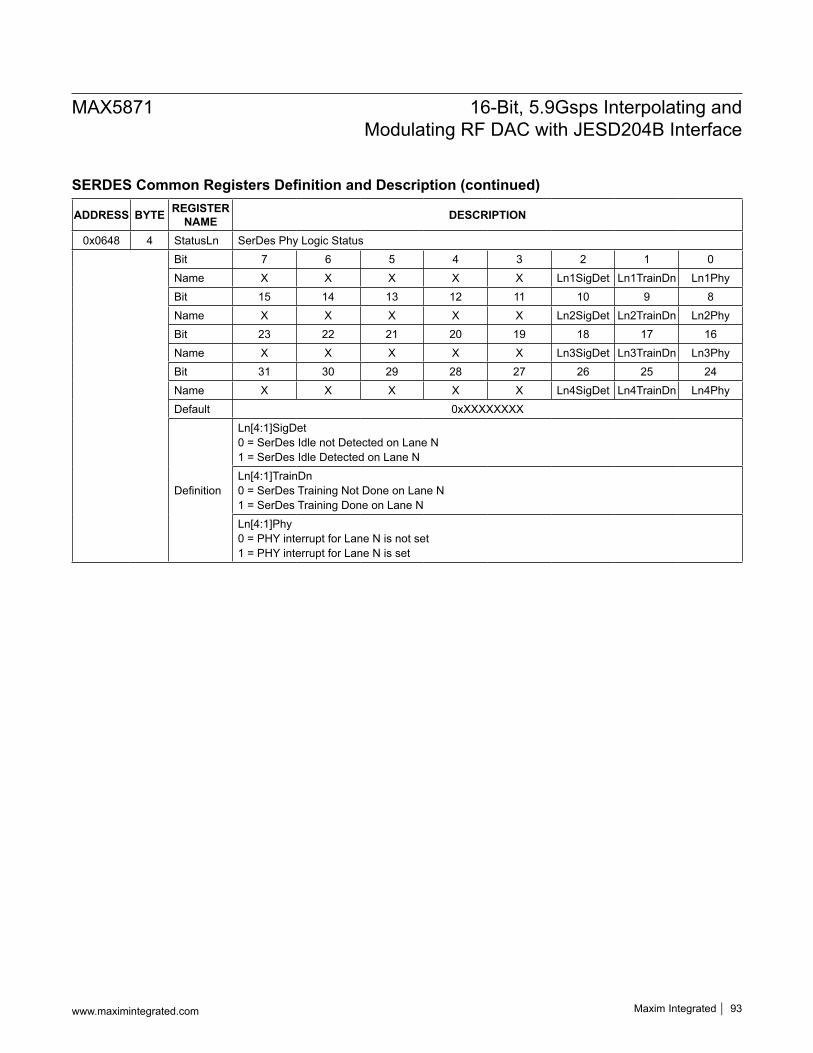
ADDRESS BYTE REGISTER NAME DESCRIPTION
0x0648 4 StatusLn SerDes Phy Logic StatusBit 7 6 5 4 3 2 1 0Name X X X X X Ln1SigDet Ln1TrainDn Ln1PhyBit 15 14 13 12 11 10 9 8Name X X X X X Ln2SigDet Ln2TrainDn Ln2PhyBit 23 22 21 20 19 18 17 16Name X X X X X Ln3SigDet Ln3TrainDn Ln3PhyBit 31 30 29 28 27 26 25 24Name X X X X X Ln4SigDet Ln4TrainDn Ln4PhyDefault 0xXXXXXXXX
Definition
Ln[4:1]SigDet0 = SerDes Idle not Detected on Lane N1 = SerDes Idle Detected on Lane NLn[4:1]TrainDn0 = SerDes Training Not Done on Lane N1 = SerDes Training Done on Lane NLn[4:1]Phy0 = PHY interrupt for Lane N is not set1 = PHY interrupt for Lane N is set
SERDES Common Registers Definition and Description (continued)
www.maximintegrated.com Maxim Integrated 93
MAX5871 16-Bit, 5.9Gsps Interpolating and Modulating RF DAC with JESD204B Interface

ADDRESS BYTE REGISTER NAME DESCRIPTION
0x0700 8 CfgCMU Serdes CMU Configuration Register – to configure the different JESD204B rateBit 7 6 5 4 3 2 1 0Name ReservedBit 15 14 13 12 11 10 9 8Name ReservedBit 23 22 21 20 19 18 17 16Name ReservedBit 31 30 29 28 27 26 25 24Name ReservedBit 39 38 37 36 35 34 33 32Name Reserved FBDIV<1:0> VCOSEL<1:0> ReservedBit 47 46 45 44 43 42 41 40Name ReservedBit 55 54 53 52 51 50 49 48Name Cref_divsel1p0<1:0> ReservedBit 63 62 61 60 59 58 57 56Name Reserved cd_tune1p0<2:0>Default 64'h0000000000000000
Definition
cd_tune1p0<2:0>3'b000 – 10G Mode3'b100 – 7G Mode3'b111 – 6G ModeCref_divsel1p0<1:0>2'b00 – JESD204B internal reference div-12'b01 – JESD204B internal reference div-22'b10 – JESD204B internal reference div-42'b11 – JESD204B internal reference div-8FBDIV<1:0>2'b00 – divide by 40 default2'b01 – divide by 802'b10 – Reserved2'b 11 – divide by 20VCOSEL<1:0>2'b00 – 10G Mode2'b10 – 7G Mode2'b11 – 6G Mode
www.maximintegrated.com Maxim Integrated 94
MAX5871 16-Bit, 5.9Gsps Interpolating and Modulating RF DAC with JESD204B Interface

Applications InformationTypical ConfigurationThe overall configuration of the MAX5871 includes set-ting up the clocking as described in the following sections and setting all other configurations before or after that. Configuration registers other than the clocking includes the DSP, JESD204B Clock Multiplier Unit (CMU), SerDes, and Rx Link registers.
MAX5871 Flow ChartThe following is the overall flowchart from power-up to DAC output enable. Some of the intermediate steps are mode specific and described below.
Power Up
Chip Reset
Clock Setup
FIFO Resets
Mode Setup
Interrupt/MuteEnables
Start Data
Clear and CheckStatuses
Unmute DAC
Power Up
Ramp up power for all supplies and this does not require any particular order.
Chip Reset
Assert chip reset RESETB for 1μs. After reset release, either monitor the INTB pin to go low or poll the DSP.STATUS.TRDY bit to go high. This indicates that device trimming is complete and is ready for configuration.
Clock Setup
Clock setup includes configuring the clock sources for the DAC, DSP, and JESD204B functions. The clocking depends on the required setup including the following. This also includes the JESD204B subclass mode since it determines how the FIFOs come up centered in a known state.1) DAC PLL usage2) Device Clock availability for JESD204B function3) DSP interpolation rateFor JESD204B Subclass-0 with device clock used for generating the sample clock, the following clock setup is required
DAC PLL configDSP.CfgPLL1/2/3
Device Clock configLNK.CfgLinkSet.ddiv[1:0]
DSP Interpolation configDSP.CfgDSP.R[3:0]
DSP Synchronization configDSP.CfgSYNC.ClkDivSync=1
www.maximintegrated.com Maxim Integrated 95
MAX5871 16-Bit, 5.9Gsps Interpolating and Modulating RF DAC with JESD204B Interface

For JESD204B Subclass-0 with DSP used for generating the sample clock, the following clock setup is required.
DAC PLL configDSP.CfgPLL1/2/3
DSP Interpolation configDSP.CfgDSP.R[3:0]
RxLink Sample Clock configLNK.CfgLinkSrc.rclk=1
SYNCN retime configLNK.CfgSYNCN.ret=0
For JESD204B Subclass-1 with device clock used for generating the sample clock and a synchronous SYSREF to device clock, the following clock setup is required.
DAC PLL configDSP.CfgPLL1/2/3
DSP Synchronization configDSP.CfgSYNC.ClkDivSync=1
Device Clock configLNK.CfgLinkSet.ddiv[1:0]LNK.CfgLinkSet.sclass=1
DSP Interpolation configDSP.CsfgDSP.R[3:0]
SYSREFSynchronous?
RxLink SYSREF configLNK.CfgSYSREF.smode=10b
RxLink SYSREF configLNK.CfgSYSREF.smode=10b
YES
NO
For JESD204B Subclass-1 with DSP used for generating the sample clock and an asynchronous SYSREF, the fol-lowing clock setup is required.
NO
DAC PLL configDSP.CfgPLL1/2/3
SYSREFSynchronous?
YES
DSP Synchronization configDSP.CfgSYNC.DSP_Async=1DSP.CfgSYNC.ClkDivSync=1
DSP Synchronization configDSP.CfgSYNC.DSP_Async=1
SYNCN retime configLNK.CfgSYNCN.ret=0
DSP Interpolation configDSP.CfgDSP.R[3:0]
RxLink Sample Clock configLNK.CfgLinkSrc.rclk=1
RxLink Subclass configLNK.CfgLinkSet.sclass=1
RxLink SYSREF configLNK.CfgSYSREF.smode=10b
FIFO Resets
After the clock modes are setup and after a sufficient wait time for the DAC PLL to lock, the DSP clock divider needs to be reset and then the Rx Link and DSP FIFOs need to be centered through configuration in Subclass-0 mode or SYSREF in Subclass-1 mode.
www.maximintegrated.com Maxim Integrated 96
MAX5871 16-Bit, 5.9Gsps Interpolating and Modulating RF DAC with JESD204B Interface

Subclass-0 with Device Clock
Reset Clock DividerGLB.CfgDev.CDrst=1
Remove Clock Divider resetGLB.CfgDev.CDrst=0
Reset DSp FIFODSP.CfgDsp.RstFIFO=1DSP.CfgDsp.RstDSP=1
Remove DSP FIFO resetsDSP.CfgDsp.RstFIFO=0DSP.CfgDsp.RstDSP=0
Subclass-0 without Device Clock
Reset DSP/FIFODSP.CfgDSP.RstDSP=1
Reset Clock DividerGLB.CfgDev.CDrst=1
Remove Clock Divider resetGLB.CfgDev.CDrst=0
Remove DSP/FIFO resetsDSP.CfgDSP.RstDSP=0
Subclass-1 with Device Clock (and Synchronous SYSREF)OrSubclass-1 without Device Clock (and Asynchronous SYSREF)
Pulse SYSREF
Mode Setup
Setup device modes other than DAC PLL, clocking, syn-chronization, and resets.
Interrupt/MuteEnables
Enable internal DAC mute and interrupt enables in the JESD204B RxLink and DSP registers.
Start Data
Start JESD204B link data carrying the signal.
Clear and CheckStatuses
Clear all the latched statuses enabled for internal DAC mute and interrupt.
Unmute DAC
Reset DAC mute register bit (DSP.CfgChipOM.Mute) to enable the DAC output.
www.maximintegrated.com Maxim Integrated 97
MAX5871 16-Bit, 5.9Gsps Interpolating and Modulating RF DAC with JESD204B Interface

Subclass-0 with Device ClockWhen there is a device clock present on the CLKP/N pins, the Rx Link sample clock is generated from it and the DSP input FIFO removes the phase difference between this Rx Link sample clock and DSP sample clock. This mode is set by LNK.CfgLinkSrc.rclk=0. The DSP sample clock is stable when the DAC clock is stable through or bypassing the DAC PLL and Interpolation Mode is set via DSP.CfgDSP.R[4:0]. The Rx Link sample clock is stable when the device clock divide mode is selected via LNK.CfgLinkSet.ddiv[1:0]. Once these clocks for the DSP Input FIFO are stable, it needs to be reset to be centered. The Rx Link Lane FIFOs are controlled by the Subclass-0
behavior with minimum latency through the FIFO. The FIFO latency can be increased via LNK.CfgILAD[5:0] in sample clock period increments. The following is the required configuration order for this mode to be stable.1) Configure DAC PLL registers if DAC PLL is used
(DSP.CfgPLL)2) Configure RxLink device clock divide factor (LNK.
CfgLinkSet.ddiv[1:0])3) Set interpolation mode and reset input FIFO (DSP.
CfgDSP.R[3:0], DSP.CfgDSP.RstFIFO)4) Remove DSP Input FIFO reset (DSP.CfgDSP.Rst-
FIFO)
JESD204B Rx Link and DSP Clocking
DSP
Rx Link
DSPINPUTFIFO
Rx LinkLANEFIFOs
%
Rx LANE CLOCK
DAC CLOCK div-byINTERPOLATION
RATIO
CLKP/N
LNK.CfgLinkSrc.rclk
SAMPLECLOCK
DAC CLOCK%
PLL
0
1
Figure 40. Rx Link and DSP Clocking
www.maximintegrated.com Maxim Integrated 98
MAX5871 16-Bit, 5.9Gsps Interpolating and Modulating RF DAC with JESD204B Interface

Subclass-0 without Device ClockWhen there is no device clock present on CLKP/N pins, the RxLink sample clock is sourced from the DSP sample clock clock. This mode is set by LNK.CfgLinkSrc.rclk=1. The DSP sample clock is stable when DAC clock is stable through or bypassing the DAC PLL and interpola-tion Mode is set via DSP.CfgDSP.R[4:0]. Once this clock for the DSP Input FIFO (same write and read clock) is stable, it needs to be centered by disabling and enabling the FIFO with an adjusted read pointer. The RxLink lane FIFOs are controlled by the subclass0 behavior with mini-mum latency through the FIFO. The FIFO latency can be increased via LNK.CfgILAD[5:0] in sample clock period increments. The following is the required configuration order for this mode to be stable.1) Configure DAC PLL registers if DAC PLL is used
(DSP.CfgPLL)2) Set interpolation mode (DSP.CfgDSP.R[3:0])3) Set the RxLink clock mode (LNK.CfgLinkSrc.rclk=1)4) Disable the input FIFO and set FIFO read pointer
(DSP.CfgFIFO.Off=1, DSP.CfgFIFO.RdPtrAdj[3:0]=6)5) Enable the input FIFO (DSP.CfgFIFO.Off=0)6) Disable SYNCN retiming to device clock (LNK.Cfg-
SYNCN.ret=0)
Subclass-1 with Device ClockThis is the true JESD204B Subclass1 mode with the SYSREF input synchronous to CLKP/N (device clock) input. The RxLink sample clock is generated from a divide down of device clock. The DSP input FIFO removes the phase difference between the RxLink sample clock and the DSP sample clock. This mode is set by LINK.CfgLinkSrc.rclk=0. The DSP sample clock is stable when DAC clock is stable through or bypassing the DAC PLL and interpolation Mode is set via DSP.CfgDSP.R[4:0]. The RxLink sample clock is stable when the device clock divide mode is selected via LINK.CfgLinkSet.ddiv[1:0]. The Subclass1 deterministic delay process including the LINK.CfgILAD[5:0] sets the RxLink FIFO depths followed by a reset of the DSP input FIFO through the DSP clock divider. The following is the required configuration order for this mode to be stable.1) Configure DAC PLL registers if DAC PLL is used
(DSP.CfgPLL)
2) Enable DSP clock-divider reset from RxLink (DSP.CfgSYNC.ClkDiv_Sync=1)
3) Set interpolation mode (DSP.CfgDSP.R[3:0])4) Set RxLink device clock divide factor and subclass1
mode (LNK.CfgLinkSset.ddiv[1:0], LNK.CfgLinkSet.sclass[1:0]=01)
5) Enable SYSREF pulses to set RxLink LMFC bound-ary (LNK.CfgSYSREF.smode[1:0]=10)
Subclass-1 without Device ClockThis is a pseudo JESD204B Subclass1 mode with the SYSREF input asynchronous to the CLKP/N input. The RxLink sample clock is sourced from the DSP sample clock. This mode is set by LNK.CfgLinkSrc.rclk=1. The DSP sample clock is stable when DAC clock is stable through or bypassing the DAC PLL and interpolation mode is set via DSP.CfgDSP.R[4:0]. The SYSREF sig-nal centers the DSP Input FIFO through the DSP clock divider followed by the Subclass1 deterministic delay process including the LNK.CfgILAD[5:0] setting RxLink FIFO depths. DSP input FIFO should not be reset through the DSP.CfgDSP.RstFIFO or DSP.CfgDSP.RstDSP in this mode. The SYSREF signal can be a continuous clock or a one-shot pulse. The following is the required configuration order for this mode to be stable.1) Configure DAC PLL registers if DAC PLL is used
(DSP.CfgPLL)If SYSREF is a continuous clock-like signal:2) Enable first SYSREF pulse to reset DSP clock divider
(DSP.CfgSYNC.DSP_ASync=1)If SYSREF is a one-shot pulse:2) Enable continuous SYSREF pulses to reset DSP
clock divider (DSP.CfgSYNC.DSP_ASync=1, DSP.CfgSYNC.ClkDiv_Sync=1)
3) Disable SYNCN retiming to device clock (LNK.Cfg-SYNCN.ret=0)
4) Set interpolation mode (DSP.CfgDSP.R[3:0])5) Set the RxLink clock mode (LNK.CfgLinkSrc.rclk=1)6) Set RxLink SYSREF mode (LNK.CfgMDS.rclk=1)7) Set Subclass1 mode (LNK.CfgLinkSet.sclass[1:0]=01)8) Enable SYSREF pulses to set RxLink LMFC bound-
ary (LNK.CfgSYSREF.smode[1:0]=10)
www.maximintegrated.com Maxim Integrated 99
MAX5871 16-Bit, 5.9Gsps Interpolating and Modulating RF DAC with JESD204B Interface

MAX5871 ConfigurationThe MAX5871 can be configured by following the exam-ples below. There are two groups of registers: fixed and variable. The fixed group of registers given in this exam-ple should be used independent of your application. The variable group of registers given in this example should be modified based on the MAX5871 register definition and description for your application, such as DAC sam-pling rate, DAC clock input, interpolation ratio, SerDes data rate, JESD204B format, and interrupt handling.
MAX5871 Example Configuration Option-1Application requirement
DAC Rate = 5898.24MHzSerDes Rate = 7372.8MbpsCLKP/N Rate = 1474.56MHzEquivalent I or Q Sample Rate = 737.28MspsJESD204B LFS = 411Interpolation = 8xNCO Frequency = 2395.297MHz
SPI_WR(15'h0000,8'h99); //GLB.CfgIFA.SftRst=1 (self-clearing), 4-Wire SPISPI_WR(15'h0181,8'h0C); //DSP.CfgPLL2.DVAL=00b, RVAL=1, PVAL=1, Bypass=0SPI_WR(15'h0182,8'h01); //DSP.CfgPLL3.VCOSel=1
SPI_WR(15'h0180,8'h02); //Reset DAC PLLSPI_WR(15'h0180,8'h03); //DSP.CfgPLL1.DigTune=1, Reserved=1
SPI_WR(15'h0101,8'hB0); //DSP.CfgDSP.R=1011b 8x interpolation ratio*** INSERT DELAY TIME TD_DivRst HERE ***SPI_WR(15'h0002,8'h04); //GLB.CfgDev.CDrst=1SPI_WR(15'h0002,8'h00); //GLB.CfgDev.CDrst=0SPI_WR(15'h0704,8'h38); //SER.CfgCMU.VCOSEL=10b, FBDIV=11bSPI_WR(15'h0706,8'h10); //SER.CfgCMU.Cref_divsel=01bSPI_WR(15'h0707,8'h04); //SER.CfgCMU.cd_tune1p0=100b
SPI_WR(15'h015A,8'h80); //DSP.CfgSYNC.DSP_ASync=1SPI_WR(15'h0407,8'h00); //LNK.CfgSYNCN.ret=0SPI_WR(15'h0427,8'h10); //LNK.CfgMDS.rclk=1SPI_WR(15'h0412,8'h01); //LNK.CfgLinkSrc.rclk=1SPI_WR(15'h0402,8'h01); //LNK.CfgLinkSet.sclass=01SPI_WR(15'h0403,8'h18); //LNK.CfgSYSREF.rsync=1, smode=10bSPI_WR(15'h041F,8'h04); //LNK.CfgILAmfs.mfsel=4SPI_WR(15'h0421,8'h03); //LNK.CfgILAsn.snum=3SPI_WR(15'h040A,8'h0D); //LNK.CfgMLFS.L=3, F=0, S=0, M=1SPI_WR(15'h042C,8'h0F); //LNK.CfgLnEn.ln=1111bSPI_WR(15'h0418,8'h0F); //LNK.CfgILALck.lksel=1111bSPI_WR(15'h041A,8'h05); //LNK.CfgILAD.idly=10SPI_WR(15'h0414,8'h1C); //LNK.CfgLinkCtl.lcoren=1, fcoren=1, dynfadj=1SPI_WR(15'h042D,8'h06); //LNK.CfgFIFO.minfd=6SPI_WR(15'h042E,8'h1A); //LNK.CfgFIFO.maxfd=26SPI_WR(15'h0600,8'h00); //SER.CfgRst.Rst=0SPI_WR(15'h0607,8'h01); //SER.CfgTrainLn.Ln1IdleGate=0, Ln1DnGate=0SPI_WR(15'h0608,8'h01); //SER.CfgTrainLn.Ln2IdleGate=0, Ln2DnGate=0SPI_WR(15'h0609,8'h01); //SER.CfgTrainLn.Ln3IdleGate=0, Ln3DnGate=0SPI_WR(15'h060A,8'h01); //SER.CfgTrainLn.Ln4IdleGate=0, Ln4DnGate=0SPI_WR(15'h060B,8'h04); //SER.CfgMisc.BCast=1
SPI_WR(15'h089B,8'h00); //DefaultSPI_WR(15'h089A,8'h00);SPI_WR(15'h0899,8'hB7);SPI_WR(15'h0898,8'h4B);
SPI_WR(15'h084B,8'hFF); //Non-DefaultSPI_WR(15'h084A,8'h7F);SPI_WR(15'h0849,8'hC1); // Turn off TXSPI_WR(15'h0848,8'h40);
www.maximintegrated.com Maxim Integrated 100
MAX5871 16-Bit, 5.9Gsps Interpolating and Modulating RF DAC with JESD204B Interface

SPI_WR(15'h0803,8'h02); //Non-DefaultSPI_WR(15'h0802,8'h10);SPI_WR(15'h0801,8'h21);SPI_WR(15'h0800,8'h08);
SPI_WR(15'h0807,8'h04); //Non-DefaultSPI_WR(15'h0806,8'hAF);SPI_WR(15'h0805,8'h40);SPI_WR(15'h0804,8'h00);
SPI_WR(15'h0857,8'hFC); //Non-DefaultSPI_WR(15'h0856,8'h01);SPI_WR(15'h0855,8'h00);SPI_WR(15'h0854,8'h35);
SPI_WR(15'h0863,8'h00); //Non-DefaultSPI_WR(15'h0862,8'h54);SPI_WR(15'h0861,8'h00);SPI_WR(15'h0860,8'h06);
SPI_WR(15'h0893,8'h00); //Non-DefaultSPI_WR(15'h0892,8'h51);SPI_WR(15'h0891,8'h23);SPI_WR(15'h0890,8'h26);
SPI_WR(15'h080B,8'h0C); //Non-DefaultSPI_WR(15'h080A,8'h87);SPI_WR(15'h0809,8'hD3);SPI_WR(15'h0808,8'hFF);
SPI_WR(15'h080F,8'h4C); //Non-DefaultSPI_WR(15'h080E,8'h15);SPI_WR(15'h080D,8'h02);SPI_WR(15'h080C,8'h4E);
SPI_WR(15'h0813,8'h42); //Non-DefaultSPI_WR(15'h0812,8'h00);SPI_WR(15'h0811,8'h20);SPI_WR(15'h0810,8'h7D);
SPI_WR(15'h0817,8'hFB); //Non-DefaultSPI_WR(15'h0816,8'h0A);SPI_WR(15'h0815,8'h19);SPI_WR(15'h0814,8'hE9);
SPI_WR(15'h081B,8'h00); //Non-DefaultSPI_WR(15'h081A,8'h00);SPI_WR(15'h0819,8'h07);SPI_WR(15'h0818,8'h75);
SPI_WR(15'h081F,8'h80); //Non-DefaultSPI_WR(15'h081E,8'hFF);SPI_WR(15'h081D,8'h08);SPI_WR(15'h081C,8'h00);
SPI_WR(15'h0823,8'h07); //Non-DefaultSPI_WR(15'h0822,8'h20);SPI_WR(15'h0821,8'h10);SPI_WR(15'h0820,8'h00);
SPI_WR(15'h0827,8'h00); //Non-DefaultSPI_WR(15'h0826,8'h3F);SPI_WR(15'h0825,8'h10);SPI_WR(15'h0824,8'h00);
SPI_WR(15'h082B,8'h00); //DefaultSPI_WR(15'h082A,8'h00);SPI_WR(15'h0829,8'h00);SPI_WR(15'h0828,8'h00);
SPI_WR(15'h082F,8'h00); //Non-DefaultSPI_WR(15'h082E,8'h1E);SPI_WR(15'h082D,8'h00);SPI_WR(15'h082C,8'h00);
SPI_WR(15'h0833,8'h1F); //Non-DefaultSPI_WR(15'h0832,8'h7F);SPI_WR(15'h0831,8'h20);SPI_WR(15'h0830,8'h00);
www.maximintegrated.com Maxim Integrated 101
MAX5871 16-Bit, 5.9Gsps Interpolating and Modulating RF DAC with JESD204B Interface

SPI_WR(15'h0883,8'h00); //DefaultSPI_WR(15'h0882,8'h00);SPI_WR(15'h0881,8'h00);SPI_WR(15'h0880,8'h00);
SPI_WR(15'h0887,8'h00); //DefaultSPI_WR(15'h0886,8'h00);SPI_WR(15'h0885,8'h00);SPI_WR(15'h0884,8'h00);
SPI_WR(15'h088B,8'h03); //DefaultSPI_WR(15'h088A,8'h06);SPI_WR(15'h0889,8'h00);SPI_WR(15'h0888,8'h00);
SPI_WR(15'h088F,8'h00); //Non-DefaultSPI_WR(15'h088E,8'h00);SPI_WR(15'h088D,8'h80);SPI_WR(15'h088C,8'h80);
SPI_WR(15'h08A7,8'hE0); //DefaultSPI_WR(15'h08A6,8'h00);SPI_WR(15'h08A5,8'h00);SPI_WR(15'h08A4,8'h00);
SPI_WR(15'h08AB,8'h00); //Non-DefaultSPI_WR(15'h08AA,8'h04);SPI_WR(15'h08A9,8'h43);SPI_WR(15'h08A8,8'h01);
SPI_WR(15'h0837,8'h10); //DefaultSPI_WR(15'h0836,8'h00);SPI_WR(15'h0835,8'h00);SPI_WR(15'h0834,8'h00);
SPI_WR(15'h083B,8'h00); //DefaultSPI_WR(15'h083A,8'h00);SPI_WR(15'h0839,8'h00);SPI_WR(15'h0838,8'h00);
SPI_WR(15'h083F,8'hAF); //Non-DefaultSPI_WR(15'h083E,8'h34);SPI_WR(15'h083D,8'hAF);SPI_WR(15'h083C,8'h80);
SPI_WR(15'h0843,8'h00); //StatusSPI_WR(15'h0842,8'h00);SPI_WR(15'h0841,8'h00);SPI_WR(15'h0840,8'h00);
SPI_WR(15'h0847,8'h10); //Non-DefaultSPI_WR(15'h0846,8'h00);SPI_WR(15'h0845,8'h80);SPI_WR(15'h0844,8'h80);
SPI_WR(15'h0853,8'h2A); //Non-DefaultSPI_WR(15'h0852,8'h8B);SPI_WR(15'h0851,8'h40);SPI_WR(15'h0850,8'h20);
SPI_WR(15'h085F,8'h7F); //Non-DefaultSPI_WR(15'h085E,8'h01);SPI_WR(15'h085D,8'h3F);SPI_WR(15'h085C,8'hFF);
SPI_WR(15'h08A3,8'h00); //DefaultSPI_WR(15'h08A2,8'h00);SPI_WR(15'h08A1,8'h00);SPI_WR(15'h08A0,8'h00);
SPI_WR(15'h084F,8'h00); //Non-DefaultSPI_WR(15'h084E,8'h40);SPI_WR(15'h084D,8'h00);SPI_WR(15'h084C,8'h18);
SPI_WR(15'h085B,8'h20); //DefaultSPI_WR(15'h085A,8'h00);SPI_WR(15'h0859,8'h60);SPI_WR(15'h0858,8'h20);
www.maximintegrated.com Maxim Integrated 102
MAX5871 16-Bit, 5.9Gsps Interpolating and Modulating RF DAC with JESD204B Interface

SPI_WR(15'h0867,8'h00); //Non-DefaultSPI_WR(15'h0866,8'h40);SPI_WR(15'h0865,8'h08);SPI_WR(15'h0864,8'hF0);
SPI_WR(15'h086B,8'h00); //Non-DefaultSPI_WR(15'h086A,8'h00);SPI_WR(15'h0869,8'h2A);SPI_WR(15'h0868,8'h25);
SPI_WR(15'h086F,8'hC0); //Non-DefaultSPI_WR(15'h086E,8'h00);SPI_WR(15'h086D,8'h02);SPI_WR(15'h086C,8'hEE);
SPI_WR(15'h0873,8'h00); //Non-DefaultSPI_WR(15'h0872,8'h00);SPI_WR(15'h0871,8'h00);SPI_WR(15'h0870,8'h00);
SPI_WR(15'h0877,8'h00); //DefaultSPI_WR(15'h0876,8'h00);SPI_WR(15'h0875,8'h00);SPI_WR(15'h0874,8'h00);
SPI_WR(15'h087B,8'h00); //Non-DefaultSPI_WR(15'h087A,8'h7F);SPI_WR(15'h0879,8'hD5);SPI_WR(15'h0878,8'h56);
SPI_WR(15'h087F,8'hC5); //Non-DefaultSPI_WR(15'h087E,8'h46);SPI_WR(15'h087D,8'h1C);SPI_WR(15'h087C,8'h17);
SPI_WR(15'h0897,8'h00); //DefaultSPI_WR(15'h0896,8'h00);SPI_WR(15'h0895,8'h02);SPI_WR(15'h0894,8'hCC);
SPI_WR(15'h089F,8'h14); //DefaultSPI_WR(15'h089E,8'h28);SPI_WR(15'h089D,8'h07);SPI_WR(15'h089C,8'h0D);
SPI_WR(0x0102,0x7D) //DSP.CfgNCOF.FCW=0xCFECD27DSPI_WR(0x0103,0xD2)SPI_WR(0x0104,0xEC)SPI_WR(0x0105,0xCF)SPI_WR(0x0106,0xA5) //DSP.CfgNCON.NFW=0x04FA5SPI_WR(0x0107,0x4F)SPI_WR(0x0108,0x00)SPI_WR(0x0109,0x00) //DSP.CfgNCOD.DFW=0x20000SPI_WR(0x010A,0x00)SPI_WR(0x010B,0x02)
SPI_WR(15'h0100,8'h01); //DSP.CfgChipOM.DFMT=1, Mute=0
MAX5871 Example Configuration Option-2Application requirement
DAC Rate = 5898.24MHzSerDes Rate = 7372.8MbpsCLKP/N Rate = 1474.56MHzEquivalent I or Q Sample Rate = 737.28MspsJESD204B LFS = 411Interpolation = 8x
SPI_WR(15'h0000,8'h99); //GLB.CfgIFA.SftRst=1 (self-clearing), 4-Wire SPISPI_WR(0x0010,0x0A) //GLB.CfgDACrate.Rate=1010bSPI_WR(0x0011,0x0E) //GLB.CfgCLKrate.Rate=1010bSPI_WR(0x0012,0x03) //GLB.CfgReg.Act=1, IntCfg=1
SPI_WR(15'h0181,8'h0C); //DSP.CfgPLL2.DVAL=00b, RVAL=1, PVAL=1, Bypass=0SPI_WR(15'h0182,8'h01); //DSP.CfgPLL3.VCOSel=1
www.maximintegrated.com Maxim Integrated 103
MAX5871 16-Bit, 5.9Gsps Interpolating and Modulating RF DAC with JESD204B Interface

SPI_WR(15'h0180,8'h02); //Reset DAC PLLSPI_WR(15'h0180,8'h03); //DSP.CfgPLL1.DigTune=1, Reserved=1
SPI_WR(15'h0101,8'hB0); //DSP.CfgDSP.R=1011b 8x interpolation ratio*** INSERT DELAY TIMETD_DivRstHERE ***SPI_WR(15'h0002,8'h04); //GLB.CfgDev.CDrst=1SPI_WR(15'h0002,8'h00); //GLB.CfgDev.CDrst=0SPI_WR(15'h0412,8'h01); //LNK.CfgLinkSrc.rclk=1SPI_WR(15'h0402,8'h01); //LNK.CfgLinkSet.sclass=01SPI_WR(15'h0403,8'h18); //LNK.CfgSYSREF.rsync=1, smode=10bSPI_WR(15'h041F,8'h04); //LNK.CfgILAmfs.mfsel=4SPI_WR(15'h0421,8'h03); //LNK.CfgILAsn.snum=3SPI_WR(15'h040A,8'h0D); //LNK.CfgMLFS.L=3, F=0, S=0, M=1SPI_WR(15'h041A,8'h05); //LNK.CfgILAD.idly=10SPI_WR(15'h0414,8'h1C); //LNK.CfgLinkCtl.lcoren=1, fcoren=1, dynfadj=1SPI_WR(15'h042D,8'h06); //LNK.CfgFIFO.minfd=6SPI_WR(15'h042E,8'h1A); //LNK.CfgFIFO.maxfd=26SPI_WR(15'h0600,8'h00); //SER.CfgRst.Rst=0SPI_WR(15'h0607,8'h01); //SER.CfgTrainLn.Ln1IdleGate=0, Ln1DnGate=0SPI_WR(15'h0608,8'h01); //SER.CfgTrainLn.Ln2IdleGate=0, Ln2DnGate=0SPI_WR(15'h0609,8'h01); //SER.CfgTrainLn.Ln3IdleGate=0, Ln3DnGate=0SPI_WR(15'h060A,8'h01); //SER.CfgTrainLn.Ln4IdleGate=0, Ln4DnGate=0
SPI_WR(0x0102,0x7D) //DSP.CfgNCOF.FCW=0xCFECD27DSPI_WR(0x0103,0xD2)SPI_WR(0x0104,0xEC)SPI_WR(0x0105,0xCF)
SPI_WR(0x0106,0xA5) //DSP.CfgNCON.NFW=0x04FA5SPI_WR(0x0107,0x4F)SPI_WR(0x0108,0x00)SPI_WR(0x0109,0x00) //DSP.CfgNCOD.DFW=0x20000SPI_WR(0x010A,0x00)SPI_WR(0x010B,0x02)
SPI_WR(0x000F,0x01) //GLB.CfgIFC.Xfer=1 (self-clearing)SPI_RD(0x0164,0x04) //Wait for DSP.STATUS.TRDY=1
SPI_WR(15'h0100,8'h01); //DSP.CfgChipOM.DFMT=1, Mute=0
MAX5871 Example Configuration with 2-LanesTo operate JESD204B with two lanes under the new application settings below, the following configuration changes are required.
DAC Rate = 5898.24MHzSerDes Rate = 7372.8MbpsCLKP/N Rate = 1474.56MHzEquivalent I or Q Sample Rate = 368.64MspsJESD204B LFS = 211Interpolation = 16xNCO Frequency = 2395.297MHz
SPI_WR(0x0101,0xD2) // 16x
SPI_WR(0x040A,0x25) // Configure SFLMSPI_WR(0x040B,0x1F) // Configure multi-frameSPI_WR(0x042C,0x03)SPI_WR(0x0418,0x03)
SPI_WR(0x0706,0x00) // Configure CMU
www.maximintegrated.com Maxim Integrated 104
MAX5871 16-Bit, 5.9Gsps Interpolating and Modulating RF DAC with JESD204B Interface

JESD204B Subclass-1 SYSREF Signal Func-tionalityThere are two modes of JESD204B Subclass-1 operation: synchronous SYSREF mode and asynchronous SYSREF mode. The synchronous SYSREF mode is as described in the standard with SYSREF timed synchronously to the device clock. The asynchronous SYSREF mode does not require a device clock and so SYSREF has no timing reference. The JESD204B sample clock is sourced from the DSP in this case.
Synchronous SYSREF ModeAs described for the JESD204B Subclass-1 determin-istic delay, the SYSREF input signal is synchronous to the device clock input (CLKP/N) and the sample clock is sourced from the device clock. The SYSREF signal can be generated from a clock generator module in which case the SYSREF will be a divided down version of the device clock. Register configurations exist as below to respond to either the first SYSREF pulse or all SYSREF pulses.LNK.CfgSYSREF.smode[1:0] – when smode[1] is high, all SYSREF pulses are acted upon. When smode[1] is low, only the first SYSREF pulse after smode[0] is
toggled 0->1 will be acted upon. If CfgSYSREF.ignore_en is set, then the ignore function is given a higher priority smode[1:0]=01 will enable first SYSREF only after the CfgSIGN.ign[7:0] pulses are ignored.This is required for the case of the device clock frequency being higher than what is supported by the MAX5871 and SYSREF timing to the device clock is not truly syn-chronous. An uncertainty of one device clock in sampling SYSREF is allowed in this case. If all SYSREF pulses are enabled, the internal frame/multiframe clocks may not be stable and so only one SYSREF pulse needs to be enabled for link establishment.In the case where multiple converters need to be aligned, a register write to enable a single SYSREF pulse may not be suitable as the synchronization of these register writes may be harder. This can be handled by using a hardware enable of SYSREF through the SYSREF_EN pin as shown in the timing diagram below.LNK.CfgSYSREF.senext – When this bit is set, the CfgSYSREF.smode[1:0] are ignored and the external pin sysref_en is used instead. This allows for better timing control of enabling SYSREF pulses to affect LMFC.
www.maximintegrated.com Maxim Integrated 105
MAX5871 16-Bit, 5.9Gsps Interpolating and Modulating RF DAC with JESD204B Interface

Asynchronous SYSREF ModeIn this mode, a device clock is not required and SYSREF is used for JESD204B Subclass1 mode through the DSP. The DSP generates the sample clock and a synchronous signal to replace the JESD204B RxLink SYSREF input. This mode is enabled by setting the following configura-tion register bits.LNK.CfgLinkSrc.rclk – when set, the sample clock is sourced from RCLK input instead of the device clock. Along with setting this bit high, an equivalent bit in the DSP, CfgSync.DSP_ASync, needs to be set to ignore the VALID output from this block and instead use the SYNCO output (SYSREF passed through) and generate RSYNC based on it. This affects the multi-DAC synchronization and the CfgMDS.rclk also needs to be set for the link to replace SYSREF with RSYNC at the same time RCLK is used for sample clock.LNK.CfgMDS.rclk – when set, RSYNC input from DSP/DAC replaces the SYSREF input for multi-DAC synchro-nization when there is no device clock supplied. This bit should be used in conjunction with CfgLinkSrc.rclk.
DSP.CfgSync.DSP_ASync – when set, asynchronous SYSREF reset to the DSP is enabled.The SYSREF_EN input signal is ignored in this mode, the SYSREF_EN pin (also called SYSREFEN) should be connected to the VDD2 supply. The same issue described in the synchronous SYSREF mode exists here if SYSREF is a continuous clock-like signal due to its asynchronous timing. Instead, if SYSREF is generated as a one-shot pulse, then the register bit DSP.CfgSync.ClkDiv_Sync should be set high for the DSP to respond to all the SYSREF pulses as shown below.DSP.CfgSync.ClkDiv_Sync – when set and DSP_Async=1, enable continuous asynchronous SYSREF reset to the clock-divider block. When cleared and DSP_Async=1, enable first asynchronous SYSREF reset to the clock-divider block.If the SYSREF signal is generated as a continuous clock, then the register bit DSP.CfgSync.ClkDiv_Sync should be set low for the DSP to respond to one of the SYSREF pulses as shown below.
SYSREF_Gate
SYSREF_Int
SYSREF_Gate
SYSREF_Int
Figure 42. Asynchronous SYSREF Mode with Continuous Pulses
Figure 41. Asynchronous SYSREF Mode with One-Shot Pulse
www.maximintegrated.com Maxim Integrated 106
MAX5871 16-Bit, 5.9Gsps Interpolating and Modulating RF DAC with JESD204B Interface

Applications GuidelinesPower SequenceThe MAX5871 typically does not require a specific power sequence on which power supplies should be up first, and which is next. It is recommended that all the supplies are powered up around the same time.
Power Supply AVCLKPower supply AVCLK is the most sensitive clock. To achieve specified DAC performance, this supply should NOT be shared with other 1.0V supplies. It should abso-lutely not be shared with digital VDD 1.0V supply.
Power-On RESETB and SPI ConfigurationDuring the initial power-on, the RESETB pin should be held low during the power-on of the device. In addition, RESETB has an internal pulldown resistor about 32kΩ. This pin should be pull-high after all the power supplies are completely on.Another way to handle the RESETB is to pull the RESETB to low after the power supplies are fully up, and then pull the RESETB to high.There is a delay time required after the RESETB is high to SPI configuration can be started. The delay time is to allow the device finishing the initialization process. The delay is related to the CLKP/N frequency. It is about 250μs with CLKP/N device clock frequency of 1.47GHz.
Delay Time TD_DivRst EstimationAdding proper delay time before resetting the internal divider is important to make sure that the internal divider starts with a stable clock after the DAC PLL (or external CLKP/N) is fully locked and settled. The minimum time is estimated as (220/PFD_FREQ), where PFD_FREQ is the input frequency of the DAC PLL phase frequency detector in PLL on mode. For example, when CLKP/N frequency is at 982.68MHz, the reference divider RVAL is set to be 1/4, PFD_FREQ = 982.68/4 = 245.67MHz. The TD_DivRst is estimated as 4.3ms.
Pin DACREF ConsiderationThe 1.27kΩ resistor from FSADJ (B2) should connect directly to DACREF (B1). This should be placed on the same side as the MAX5871 package and as close as pos-sible to the package. Also, 1μF capacitors connected to REFIO(A1) and CSBP (A2) should connect to DACREF, not GND. These should also be placed on the same layer as the DAC package, avoiding VIAs in all these traces if possible. DACREF is not connected to GND externally.
DAC PLL ConsiderationConnections to PLL_COMP(A12) and VCOBYP(B11)— loop filter for the PLL (see Figure 29). Place external com-ponents on the PCB layer opposite the CLK and OUTPUT circuits to prevent them from coupling. The recommended filter between PLL_COMP(A12) and VCOBYP(B11) is 650Ω in series with 4.7nF. The capacitor, C1, reduces noise from GND(A11) to VCOBYP(B11). Place C1 directly under the balls/vias of the package to make this loop as small as possible. The exact values of C1 and C2 vary because they depend on PCB layout, and may or may not be required for optimal performance.
Pin SDO ConsiderationIn 4-wire SPI interface mode, SDO is used as a data output. When connecting multiple SDOs together using CSB to access the MAX5871, it is recommended to have a pullup 10kΩ resistor on the input of FPGA or ASIC to prevent floating (need a different term) bus. When SDO is not selected, it outputs tri-state (need a different term due to copyright issues),
Clock RequirementThe MAX5871 can be operated with DAC PLL ON or DAC PLL OFF.When DAC PLL is OFF, a clock requirement document is available upon request.When DAC PLL is ON, the DAC PLL bandwidth is set to around 100kHz. It means that any phase noise/jitter of the reference clock at frequency offsets higher than 100kHz will be filtered out by the PLL loop and its impact on the DAC performance will be minimal.However, for offsets smaller than 100kHz, the reference clock phase noise will dominate. At those offsets, the reference clock phase noise will be translated to the DAC output phase noise according to the formula:
PNout [dBc/Hz] = PNref [dBc/Hz] + 20 x log(fC/fREF)Where:PNout – DAC output phase noisePNref – PLL reference clock phase noisefC – DAC output frequencyfREF – PLL reference clock frequencyIn addition to the reference clock phase noise and jitter, the allowable spur level in the reference clock spectrum should be calculated using graphs and equations that are available upon request.
www.maximintegrated.com Maxim Integrated 107
MAX5871 16-Bit, 5.9Gsps Interpolating and Modulating RF DAC with JESD204B Interface

NCO FrequencyNCO frequency can have two types of errors from the NCO and DAC clocks used. One type of error is from NCO itself due to finite word length. The frequency error can be calculated by ferror = fdesired - fDAC/((218) x (233) x 2). This is about 1.11μHz error at 5GHz DAC clock rate that is negligible.Register DFW has 19 bits and NFW has 18 bits. To minimize NCO frequency error, DFW can be always pro-grammed to 0x3FFFF and set NFW based on the frac-tional portion of the calculated FCW. This limits the NCO frequency error to 1.11μHz. The MATLAB code however can give an error of 0Hz if possible.Another error is related to DAC input sampling clock. The NCO synthesizes frequency, which is an exact faction of the DAC core clock frequency. That fraction value can be calculated using equation provided in the data sheet. Any percentage error in the DAC input clock, either with PLL enabled or disabled will result in the same percent-age error at the NCO output. For example, if the DAC input clock has a tolerance of 10ppm, the NCO output frequency will also have a tolerance of 10ppm.The DAC PLL does not introduce any frequency error once it is locked. The PLL output frequency is exactly equal to the input reference frequency multiplied by the selected PLL multiplication factor.
LatencyThere are two types of latencies in MAX5871: JESD204B latency and DAC latency.The JESD204B Rx link layer includes a lane processing latency and this combined with the transmit link latency and the channel latency, the Subclass-1 deterministic delay should be set through the MAX5871 configuration. This process is to be characterized from silicon evalua-tion. The lane processing delay portion of the JESD204B RxLink is 200 SerDes bit clocks. In addition to this, there would be a FIFO delay in sample clock periods as config-ured for Subclass1 deterministic delay.The DAC latency is given in the Electrical Characteristics table in the unit of DAC clock periods.
Turn off JESD204B TransmitterThe MAX5871 JESD204B consists of both receiver and transmitter blocks. The transmitter is only for manufactur-er test purposes. To make sure the transmitters are turned off to save power consumption, the following configuration can be used:
Write 0x0849 = 0xC1 to turn off SerDes TX
PRBS SequencePRBS7 and PRBS 23 are supposed to be inverted according to Table 3 in http://www.xilinx.com/support/documentation/application_notes/xapp884_PRBS_GeneratorChecker.pdfThe MAX5871 Rx PHY has an option to invert the data by setting PHY.MISC_REG2.Rx_parallel_data_invert (bit 4).
DSP FIFO ReadingWhen reading the DSP FIFO register, the number of ones indicates the FIFO level. The 0x1F depth indicates that the level is 5, meaning that the read pointer is behind the write pointer by 5. The FIFO level should be used only for debug. The error conditions are DSP.STATUS.FCOL and DSP.STATUS.F1A while the third status DSP.STATUS.F2A is a warning condition (close to overflow or underflow, one specifically can be determined through DSP.iFIFOLevel).
DAC Output Impedance Model and Matching NetworkThe DAC output impedance model is available in an s-parameter file that can be used to design an output matching network if needed.For the best engineering practice, the following guidelines can help in the output PCB design:
DAC OUTP and OUTN routes to the matching network should be as short as possible. From the matching network to any filter should be as short as possible.
DAC OUTP and OUTN should be routed symmetri-cally to eliminate any mismatch.
The environment around OUTP and OUTN should be symmetrical. This means that the environment on one signal needs to match the other signal.
If OUTP and OUTN cannot be made to be short trace routes, then the routes need to match length with mirror symmetry and 50Ω routed impedance.
When crossing other signals/supplies routed on other layers, OUTP and OUTN should cross at a 90-degree angle to these signals/supplies.
OUTP and OUTN should be routed on an outer board layer and away from supply decoupling.
AVCLK network should not be placed and routed in the proximity of OUTP and OUTN.
www.maximintegrated.com Maxim Integrated 108
MAX5871 16-Bit, 5.9Gsps Interpolating and Modulating RF DAC with JESD204B Interface

Thermal ConsiderationsThe use of as much ground plane as possible on the com-ponent layer is recommended for the PCB design. The system design should make use of additional heatsink-ing directly in contact with the MAX5871 to improve the thermal performance. The thermal numbers are based on JEDEC standard 51-12. All the application thermal mod-eling is required at the system design. A Delphi model is available for system thermal simulation.
Ordering InformationPART TEMP RANGE PIN-PACKAGE
MAX5871EXE+ -40ºC to +85ºC 144-FCCSP
PIN-PACKAGE PACKAGE CODE
OUTLINE NO.
LAND PATTERN NO.
144 FCCSP X14400F+1 21-0732 —
+Denotes a lead-free/RoHS-compliant package.
www.maximintegrated.com Maxim Integrated 109
MAX5871 16-Bit, 5.9Gsps Interpolating and Modulating RF DAC with JESD204B Interface
Package InformationFor the latest package outline information and land patterns (footprints), go to www.maximintegrated.com/packages. Note that a “+”, “#”, or “-” in the package code indicates RoHS status only. Package drawings may show a different suffix character, but the drawing pertains to the package regardless of RoHS status.

REVISIONNUMBER
REVISIONDATE DESCRIPTION PAGES
CHANGED0 3/15 Initial release —
Maxim Integrated cannot assume responsibility for use of any circuitry other than circuitry entirely embodied in a Maxim Integrated product. No circuit patent licenses are implied. Maxim Integrated reserves the right to change the circuitry and specifications without notice at any time. The parametric values (min and max limits) shown in the Electrical Characteristics table are guaranteed. Other parametric values quoted in this data sheet are provided for guidance.
Maxim Integrated and the Maxim Integrated logo are trademarks of Maxim Integrated Products, Inc. © 2015 Maxim Integrated Products, Inc. 110
MAX5871 16-Bit, 5.9Gsps Interpolating and Modulating RF DAC with JESD204B Interface
Revision History
For pricing, delivery, and ordering information, please contact Maxim Direct at 1-888-629-4642, or visit Maxim Integrated’s website at www.maximintegrated.com.


![16bit Language Tool Libraries 51456c[1]](https://img.dokumen.tips/doc/110x75/5465ade4af79596e458b4c06/16bit-language-tool-libraries-51456c1.jpg)