Embed Size (px)
Citation preview
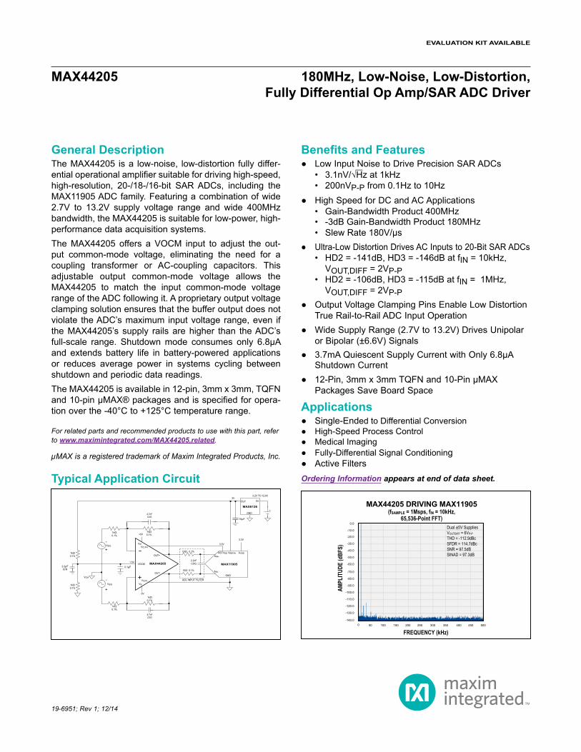
General DescriptionThe MAX44205 is a low-noise, low-distortion fully differ-ential operational amplifier suitable for driving high-speed, high-resolution, 20-/18-/16-bit SAR ADCs, including the MAX11905 ADC family. Featuring a combination of wide 2.7V to 13.2V supply voltage range and wide 400MHz bandwidth, the MAX44205 is suitable for low-power, high-performance data acquisition systems.The MAX44205 offers a VOCM input to adjust the out-put common-mode voltage, eliminating the need for a coupling transformer or AC-coupling capacitors. This adjustable output common-mode voltage allows the MAX44205 to match the input common-mode voltage range of the ADC following it. A proprietary output voltage clamping solution ensures that the buffer output does not violate the ADC’s maximum input voltage range, even if the MAX44205’s supply rails are higher than the ADC’s full-scale range. Shutdown mode consumes only 6.8µA and extends battery life in battery-powered applications or reduces average power in systems cycling between shutdown and periodic data readings. The MAX44205 is available in 12-pin, 3mm x 3mm, TQFN and 10-pin μMAX® packages and is specified for opera-tion over the -40°C to +125°C temperature range.
Benefits and Features Low Input Noise to Drive Precision SAR ADCs
• 3.1nV/√Hz at 1kHz• 200nVP-P from 0.1Hz to 10Hz
High Speed for DC and AC Applications• Gain-Bandwidth Product 400MHz• -3dB Gain-Bandwidth Product 180MHz• Slew Rate 180V/µs
Ultra-Low Distortion Drives AC Inputs to 20-Bit SAR ADCs• HD2 = -141dB, HD3 = -146dB at fIN = 10kHz,
VOUT,DIFF = 2VP-P• HD2 = -106dB, HD3 = -115dB at fIN = 1MHz,
VOUT,DIFF = 2VP-P Output Voltage Clamping Pins Enable Low Distortion
True Rail-to-Rail ADC Input Operation Wide Supply Range (2.7V to 13.2V) Drives Unipolar
or Bipolar (±6.6V) Signals 3.7mA Quiescent Supply Current with Only 6.8µA
Shutdown Current 12-Pin, 3mm x 3mm TQFN and 10-Pin μMAX
Packages Save Board Space
Applications Single-Ended to Differential Conversion High-Speed Process Control Medical Imaging Fully-Differential Signal Conditioning Active Filters
Ordering Information appears at end of data sheet.
For related parts and recommended products to use with this part, refer to www.maximintegrated.com/MAX44205.related.
19-6951; Rev 1; 12/14
Typical Application Circuit
VS+VCLPH
VCLPLVS-
OUT+
OUT-
10Ω 0.1%
10Ω 0.1%
2.2nF COG
+5V
-5V
MAX44205VOCM MAX11905
MAX6126
OUT
VREFIN AVDD
GND
GND
IN3V
3.3V
3.2V TO 12.6V
AIN+
AIN-
10µF
1.5V
0.1µF
4.7nFC0G
-
+
+
-VCM
VSIG
VSIG
1kΩ 0.1%
1kΩ 0.1%
1kΩ 0.1%
4.7nF C0G
1kΩ0.1%
1kΩ 0.1%
1kΩ 0.1%
2.2µF X7R
REFVDD
ADC INPUT FILTER
3.3V
MAX44205 DRIVING MAX11905(fSAMPLE = 1Msps, fIN = 10kHz,
65,536-Point FFT)Dual ±5V SuppliesVOUTDIFF = 6VP-PTHD = -112.9dBcSFDR = 114.7dBcSNR = 97.5dBSINAD = 97.3dB
0 10050 150 200 250 300 350 400 450 500
FREQUENCY (kHz)
AMPL
ITUD
E (d
BFS)
-10.0
0.0
-20.0
-30.0
-40.0
-50.0
-60.0
-70.0
-80.0
-90.0
-100.0
-110.0
-120.0
-130.0
-140.0
µMAX is a registered trademark of Maxim Integrated Products, Inc.
MAX44205 180MHz, Low-Noise, Low-Distortion, Fully Differential Op Amp/SAR ADC Driver
EVALUATION KIT AVAILABLE
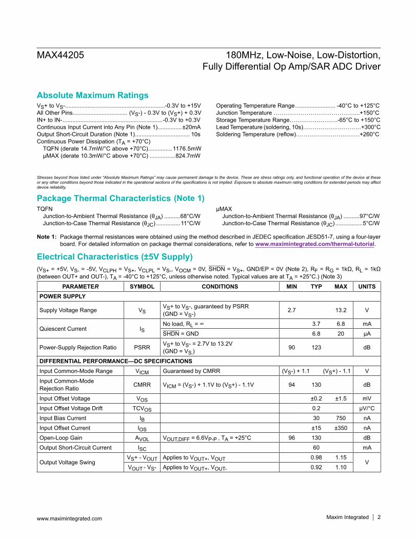
VS+ to VS-..............................................................-0.3V to +15VAll Other Pins.................................. (VS-) - 0.3V to (VS+) + 0.3VIN+ to IN- ..............................................................-0.3V to +0.3VContinuous Input Current into Any Pin (Note 1) ...............±20mAOutput Short-Circuit Duration (Note 1) .................................. 10sContinuous Power Dissipation (TA = +70°C) TQFN (derate 14.7mW/°C above +70°C)...............1176.5mW
µMAX (derate 10.3mW/°C above +70°C) ................824.7mW
Operating Temperature Range ......................... -40°C to +125°CJunction Temperature ……………………………………...+150°CStorage Temperature Range…………………….-65°C to +150°CLead Temperature (soldering, 10s)…………………………+300°CSoldering Temperature (reflow)……………………………+260°C
TQFN Junction-to-Ambient Thermal Resistance (θJA) ..........68°C/W Junction-to-Case Thermal Resistance (θJC) ...............11°C/W
μMAX Junction-to-Ambient Thermal Resistance (θJA) ..........97°C/W Junction-to-Case Thermal Resistance (θJC) .................5°C/W
(Note 1)
Electrical Characteristics (±5V Supply)(VS+ = +5V, VS- = -5V, VCLPH = VS+, VCLPL = VS-, VOCM = 0V, SHDN = VS+, GND/EP = 0V (Note 2), RF = RG = 1kΩ, RL = 1kΩ (between OUT+ and OUT-), TA = -40°C to +125°C, unless otherwise noted. Typical values are at TA = +25°C.) (Note 3)
PARAMETER SYMBOL CONDITIONS MIN TYP MAX UNITSPOWER SUPPLY
Supply Voltage Range VSVS+ to VS-, guaranteed by PSRR (GND = VS-) 2.7 13.2 V
Quiescent Current ISNo load, RL = ∞ 3.7 6.8 mA
SHDN = GND 6.8 20 µA
Power-Supply Rejection Ratio PSRR VS+ to VS- = 2.7V to 13.2V (GND = VS-)
90 123 dB
DIFFERENTIAL PERFORMANCE—DC SPECIFICATIONSInput Common-Mode Range VICM Guaranteed by CMRR (VS-) + 1.1 (VS+) - 1.1 V
Input Common-Mode Rejection Ratio CMRR VICM = (VS-) + 1.1V to (VS+) - 1.1V 94 130 dB
Input Offset Voltage VOS ±0.2 ±1.5 mV
Input Offset Voltage Drift TCVOS 0.2 µV/°C
Input Bias Current IB 30 750 nA
Input Offset Current IOS ±15 ±350 nA
Open-Loop Gain AVOL VOUT,DIFF = 6.6VP-P , TA = +25°C 96 130 dB
Output Short-Circuit Current ISC 60 mA
Output Voltage SwingVS+ - VOUT Applies to VOUT+, VOUT 0.98 1.15
VVOUT - VS- Applies to VOUT+, VOUT- 0.92 1.10
MAX44205 180MHz, Low-Noise, Low-Distortion, Fully Differential Op Amp/SAR ADC Driver
www.maximintegrated.com Maxim Integrated 2
Note 1: Package thermal resistances were obtained using the method described in JEDEC specification JESD51-7, using a four-layer board. For detailed information on package thermal considerations, refer to www.maximintegrated.com/thermal-tutorial.
Absolute Maximum Ratings
Stresses beyond those listed under “Absolute Maximum Ratings” may cause permanent damage to the device. These are stress ratings only, and functional operation of the device at these or any other conditions beyond those indicated in the operational sections of the specifications is not implied. Exposure to absolute maximum rating conditions for extended periods may affect device reliability.
Package Thermal Characteristics
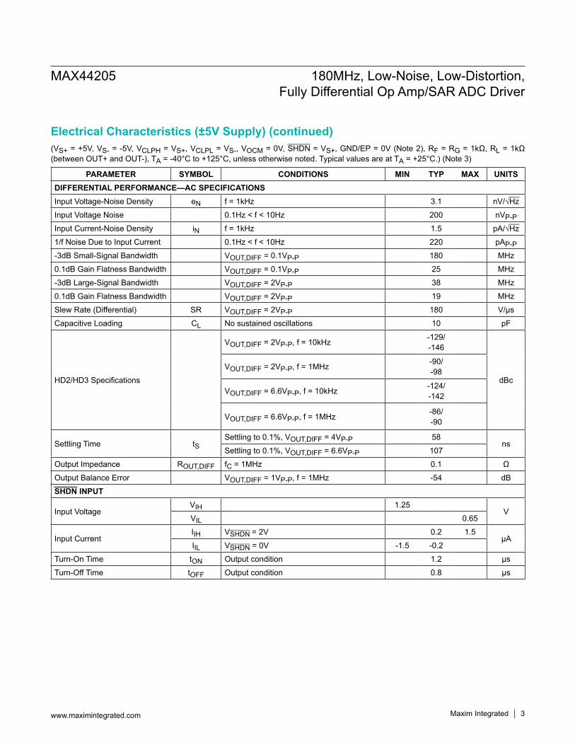
Electrical Characteristics (±5V Supply) (continued)(VS+ = +5V, VS- = -5V, VCLPH = VS+, VCLPL = VS-, VOCM = 0V, SHDN = VS+, GND/EP = 0V (Note 2), RF = RG = 1kΩ, RL = 1kΩ (between OUT+ and OUT-), TA = -40°C to +125°C, unless otherwise noted. Typical values are at TA = +25°C.) (Note 3)
PARAMETER SYMBOL CONDITIONS MIN TYP MAX UNITSDIFFERENTIAL PERFORMANCE—AC SPECIFICATIONSInput Voltage-Noise Density eN f = 1kHz 3.1 nV/√Hz
Input Voltage Noise 0.1Hz < f < 10Hz 200 nVP-PInput Current-Noise Density iN f = 1kHz 1.5 pA/√Hz
1/f Noise Due to Input Current 0.1Hz < f < 10Hz 220 pAP-P-3dB Small-Signal Bandwidth VOUT,DIFF = 0.1VP-P 180 MHz
0.1dB Gain Flatness Bandwidth VOUT,DIFF = 0.1VP-P 25 MHz
-3dB Large-Signal Bandwidth VOUT,DIFF = 2VP-P 38 MHz
0.1dB Gain Flatness Bandwidth VOUT,DIFF = 2VP-P 19 MHz
Slew Rate (Differential) SR VOUT,DIFF = 2VP-P 180 V/µs
Capacitive Loading CL No sustained oscillations 10 pF
HD2/HD3 Specifications
VOUT,DIFF = 2VP-P, f = 10kHz -129/ -146
dBc
VOUT,DIFF = 2VP-P, f = 1MHz -90/ -98
VOUT,DIFF = 6.6VP-P, f = 10kHz -124/ -142
VOUT,DIFF = 6.6VP-P, f = 1MHz -86/ -90
Settling Time tSSettling to 0.1%, VOUT,DIFF = 4VP-P 58
nsSettling to 0.1%, VOUT,DIFF = 6.6VP-P 107
Output Impedance ROUT,DIFF fC = 1MHz 0.1 Ω
Output Balance Error VOUT,DIFF = 1VP-P, f = 1MHz -54 dB
SHDN INPUT
Input VoltageVIH 1.25
VVIL 0.65
Input CurrentIIH VSHDN = 2V 0.2 1.5
µAIIL VSHDN = 0V -1.5 -0.2
Turn-On Time tON Output condition 1.2 µs
Turn-Off Time tOFF Output condition 0.8 µs
MAX44205 180MHz, Low-Noise, Low-Distortion, Fully Differential Op Amp/SAR ADC Driver
www.maximintegrated.com Maxim Integrated 3
Electrical Characteristics (±5V Supply) (continued)(VS+ = +5V, VS- = -5V, VCLPH = VS+, VCLPL = VS-, VOCM = 0V, SHDN = VS+, GND/EP = 0V (Note 2), RF = RG = 1kΩ, RL = 1kΩ (between OUT+ and OUT-), TA = -40°C to +125°C, unless otherwise noted. Typical values are at TA = +25°C.) (Note 3)
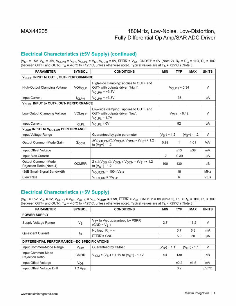
Electrical Characteristics (+5V Supply)(VS+ = +5V, VS- = 0V, VCLPH = VS+, VCLPL = VS-, VOCM = 2.5V, SHDN = VS+, GND/EP = 0V (Note 2), RF = RG = 1kΩ, RL = 1kΩ (between OUT+ and OUT-), TA = -40°C to +125°C, unless otherwise noted. Typical values are at TA = +25°C.) (Note 3)
PARAMETER SYMBOL CONDITIONS MIN TYP MAX UNITSVCLPH INPUT to OUT+, OUT- PERFORMANCE
High-Output Clamping Voltage VOHCLP
High-side clamping: applies to OUT+ and OUT- with outputs driven “high”, VCLPH = +3.3V
VCLPH + 0.34 V
Input Current ICLPH VCLPH = +3.3V -38 µA
VCLPL INPUT to OUT+, OUT- PERFORMANCE
Low-Output Clamping Voltage VOLCLP
Low-side clamping: applies to OUT+ and OUT- with outputs driven “low”, VCLPL = 1.7V
VCLPL - 0.42 V
Input Current ICLPL VCLPL = 0V 92 µA
VOCM INPUT to VOUT,CM PERFORMANCEInput Voltage Range Guaranteed by gain parameter (VS-) + 1.2 (VS+) - 1.2 V
Output Common-Mode Gain GOCM∆(VOUT,CM)/∆(VOCM), VOCM = (VS-) + 1.2 to (VS+) - 1.2 0.99 1 1.01 V/V
Input Offset Voltage ±13 ±38 mV
Input Bias Current -2 -0.30 µA
Output Common-Mode Rejection Ratio (Note 4) OCMRR 2 x ∆(VOS,)/∆(VOCM), VOCM = (VS-) + 1.2
to (VS+) - 1.2 100 130 dB
-3dB Small-Signal Bandwidth VOUT,CM = 100mVP-P 16 MHz
Slew Rate VOUT,CM = 1VP-P 6 V/µs
PARAMETER SYMBOL CONDITIONS MIN TYP MAX UNITSPOWER SUPPLY
Supply Voltage Range VSVS+ to VS-, guaranteed by PSRR (GND = VS-) 2.7 13.2 V
Quiescent Current ISNo load, RL = ∞ 3.7 6.8 mA
SHDN = GND 5.9 20 µA
DIFFERENTIAL PERFORMANCE—DC SPECIFICATIONSInput Common-Mode Range VICM Guaranteed by CMRR (VS-) + 1.1 (VS+) - 1.1 V
Input Common-Mode Rejection Ratio CMRR VICM = (VS-) + 1.1V to (VS+) - 1.1V 94 130 dB
Input Offset Voltage VOS ±0.2 ±1.5 mV
Input Offset Voltage Drift TC VOS 0.2 µV/°C
MAX44205 180MHz, Low-Noise, Low-Distortion, Fully Differential Op Amp/SAR ADC Driver
www.maximintegrated.com Maxim Integrated 4
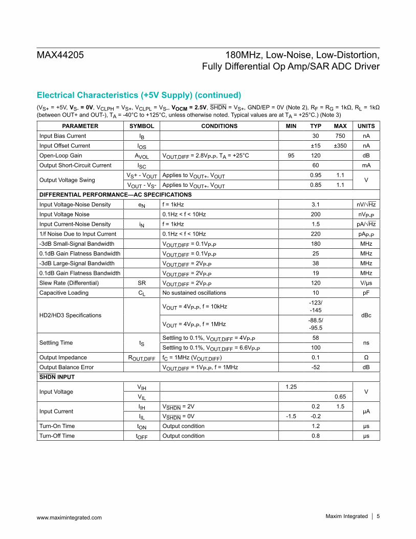
Electrical Characteristics (+5V Supply) (continued)(VS+ = +5V, VS- = 0V, VCLPH = VS+, VCLPL = VS-, VOCM = 2.5V, SHDN = VS+, GND/EP = 0V (Note 2), RF = RG = 1kΩ, RL = 1kΩ (between OUT+ and OUT-), TA = -40°C to +125°C, unless otherwise noted. Typical values are at TA = +25°C.) (Note 3)
PARAMETER SYMBOL CONDITIONS MIN TYP MAX UNITSInput Bias Current IB 30 750 nA
Input Offset Current IOS ±15 ±350 nA
Open-Loop Gain AVOL VOUT,DIFF = 2.8VP-P, TA = +25°C 95 120 dB
Output Short-Circuit Current ISC 60 mA
Output Voltage SwingVS+ - VOUT Applies to VOUT+, VOUT 0.95 1.1
VVOUT - VS- Applies to VOUT+, VOUT 0.85 1.1
DIFFERENTIAL PERFORMANCE—AC SPECIFICATIONSInput Voltage-Noise Density eN f = 1kHz 3.1 nV/√Hz
Input Voltage Noise 0.1Hz < f < 10Hz 200 nVP-PInput Current-Noise Density iN f = 1kHz 1.5 pA/√Hz
1/f Noise Due to Input Current 0.1Hz < f < 10Hz 220 pAP-P-3dB Small-Signal Bandwidth VOUT,DIFF = 0.1VP-P 180 MHz
0.1dB Gain Flatness Bandwidth VOUT,DIFF = 0.1VP-P 25 MHz
-3dB Large-Signal Bandwidth VOUT,DIFF = 2VP-P 38 MHz
0.1dB Gain Flatness Bandwidth VOUT,DIFF = 2VP-P 19 MHz
Slew Rate (Differential) SR VOUT,DIFF = 2VP-P 120 V/µs
Capacitive Loading CL No sustained oscillations 10 pF
HD2/HD3 SpecificationsVOUT = 4VP-P, f = 10kHz -123/
-145dBc
VOUT = 4VP-P, f = 1MHz -88.5/ -95.5
Settling Time tSSettling to 0.1%, VOUT,DIFF = 4VP-P 58
nsSettling to 0.1%, VOUT,DIFF = 6.6VP-P 100
Output Impedance ROUT,DIFF fC = 1MHz (VOUT,DIFF) 0.1 Ω
Output Balance Error VOUT,DIFF = 1VP-P, f = 1MHz -52 dB
SHDN INPUT
Input VoltageVIH 1.25
VVIL 0.65
Input CurrentIIH VSHDN = 2V 0.2 1.5
µAIIL VSHDN = 0V -1.5 -0.2
Turn-On Time tON Output condition 1.2 µs
Turn-Off Time tOFF Output condition 0.8 µs
MAX44205 180MHz, Low-Noise, Low-Distortion, Fully Differential Op Amp/SAR ADC Driver
www.maximintegrated.com Maxim Integrated 5
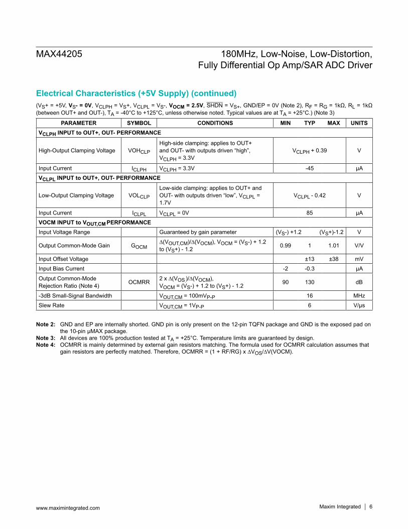
Electrical Characteristics (+5V Supply) (continued)(VS+ = +5V, VS- = 0V, VCLPH = VS+, VCLPL = VS-, VOCM = 2.5V, SHDN = VS+, GND/EP = 0V (Note 2), RF = RG = 1kΩ, RL = 1kΩ (between OUT+ and OUT-), TA = -40°C to +125°C, unless otherwise noted. Typical values are at TA = +25°C.) (Note 3)
Note 2: GND and EP are internally shorted. GND pin is only present on the 12-pin TQFN package and GND is the exposed pad on the 10-pin µMAX package.
Note 3: All devices are 100% production tested at TA = +25°C. Temperature limits are guaranteed by design.Note 4: OCMRR is mainly determined by external gain resistors matching. The formula used for OCMRR calculation assumes that
gain resistors are perfectly matched. Therefore, OCMRR = (1 + RF/RG) x ∆VOS/∆V(VOCM).
PARAMETER SYMBOL CONDITIONS MIN TYP MAX UNITSVCLPH INPUT to OUT+, OUT- PERFORMANCE
High-Output Clamping Voltage VOHCLP
High-side clamping: applies to OUT+ and OUT- with outputs driven “high”, VCLPH = 3.3V
VCLPH + 0.39 V
Input Current ICLPH VCLPH = 3.3V -45 µA
VCLPL INPUT to OUT+, OUT- PERFORMANCE
Low-Output Clamping Voltage VOLCLP
Low-side clamping: applies to OUT+ and OUT- with outputs driven “low”, VCLPL = 1.7V
VCLPL - 0.42 V
Input Current ICLPL VCLPL = 0V 85 µA
VOCM INPUT to VOUT,CM PERFORMANCEInput Voltage Range Guaranteed by gain parameter (VS-) +1.2 (VS+)-1.2 V
Output Common-Mode Gain GOCM∆(VOUT,CM)/∆(VOCM), VOCM = (VS-) + 1.2 to (VS+) - 1.2 0.99 1 1.01 V/V
Input Offset Voltage ±13 ±38 mV
Input Bias Current -2 -0.3 µA
Output Common-Mode Rejection Ratio (Note 4) OCMRR 2 x ∆(VOS,)/∆(VOCM),
VOCM = (VS-) + 1.2 to (VS+) - 1.2 90 130 dB
-3dB Small-Signal Bandwidth VOUT,CM = 100mVP-P 16 MHz
Slew Rate VOUT,CM = 1VP-P 6 V/µs
MAX44205 180MHz, Low-Noise, Low-Distortion, Fully Differential Op Amp/SAR ADC Driver
www.maximintegrated.com Maxim Integrated 6
(VS+ = +5V, VS- = -5V, VCLPH = VS+, VCLPL = VS-, VOCM = 0V, SHDN = VS+, GND/EP = 0V, RF = RG = 1kΩ, RL = 1kΩ (between OUT+ and OUT-), TA = -40°C to +125°C, unless otherwise noted.)
-1500-1300-1100-900-700-500-300-100100300500700900
110013001500
-50 -25 0 25 50 75 100 125 150
V OS
(µV)
TEMPERATURE (°C)
INPUT OFFSET VOLTAGE (IN+, IN-) vs. TEMPERATURE (100 UNITS)
toc4
VS+ = +5VVS- = -5V
0
0.5
1
1.5
2
2.5
3
3.5
4
4.5
5
0 2.5 5 7.5 10 12.5 15
SUPP
LY C
URRE
NT(m
A)
SUPPLY VOLTAGE (V)
SUPPLY CURRENTvs. SUPPLY VOLTAGE
toc01
TA = -40°C
TA = +25°C
TA = +125°C
200
220
240
260
280
300
-50 -25 0 25 50 75 100 125 150
INPU
T OF
FSET
VOT
LAGE
(µV)
TEMPERATURE (°C)
INPUT OFFSET VOLTAGE (IN+, IN-) vs. TEMPERATURE
Vs+ = +1.5VVs- = -1.5V
Vs+ = +5VVs- = -5V
Vs = +2.5VVs- = -2.5V
toc07
3
3.2
3.4
3.6
3.8
4
4.2
4.4
4.6
-50 -25 0 25 50 75 100 125 150
SUPP
LY C
URRE
NT (m
A)
TEMPERATURE (°C)
SUPPLY CURRENTvs. TEMPERATURE
toc02
VS+ = +5VVS- = -5V
VS+ = +2.5VVS- = -2.5V
VS+ = +1.5VVS- = -1.5V
-0.7
-0.6
-0.5
-0.4
-0.3
-0.2
-0.1
0
0.1
0.2
0.3
-6 -4 -2 0 2 4 6
INPU
T OF
FSET
VOL
TAGE
VAR
IATI
ON (m
V)
VOCM (V)
INPUT OFFSET VOLTAGE VARIATIONvs. VOCM
toc08
TA = +25°C
TA = -40°C
TA = +125°C
5.8
6
6.2
6.4
6.6
6.8
7
7.2
-50 -25 0 25 50 75 100 125 150
SHUT
DOW
N SU
PPLY
CUR
RENT
(µA)
TEMPERATURE (°C)
SHUTDOWN SUPPLY CURRENTvs. TEMPERATURE
toc03
VS+ = +5VVS- = -5V
VS+ = +2.5VVS- = -2.5V
-1.5
-1
-0.5
0
0.5
1
1.5
2
-1.6 -1.2 -0.8 -0.4 0 0.4 0.8 1.2 1.6
INPU
T OF
FSET
VOL
TAGE
DRI
FT
OVER
TEM
PERA
TURE
(µV)
VICM (V)
INPUT OFFSET VOLTAGE CHANGE OVER TEMPERATURE vs. VICM
Vs+ = +2.5VVs- = -2.5V
TA = -40°C
TA = +25°C
TA = +125°C
toc09a
0
2
4
6
8
10
12
-0.8 -0.6 -0.4 -0.2 0 0.2 0.4 0.6 0.8
OCCU
RREN
CE (N
)
INPUT OFFSET VOLTAGE (μV)
INPUT OFFSET VOLTAGE (IN+, IN-) HISTOGRAM
toc05
HISTOGRAMTA = +25°C
200
220
240
260
280
2.5 3.5 4.5 5.5 6.5 7.5 8.5 9.5 10.5 11.5 12.5 13.5
INPU
T OF
FSET
VOT
LAGE
(µV)
SUPPLY VOLTAGE (V)
IIN+, IN- INPUT OFFSET VOLTAGE vs. SUPPLY VOLTAGE
TA = +25°C
TA = -40°C
TA = +125°C
toc06
Maxim Integrated 7www.maximintegrated.com
MAX44205 180MHz, Low-Noise, Low-Distortion, Fully Differential Op Amp/SAR ADC Driver
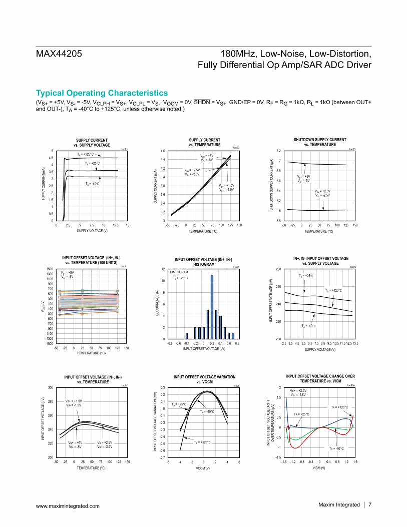
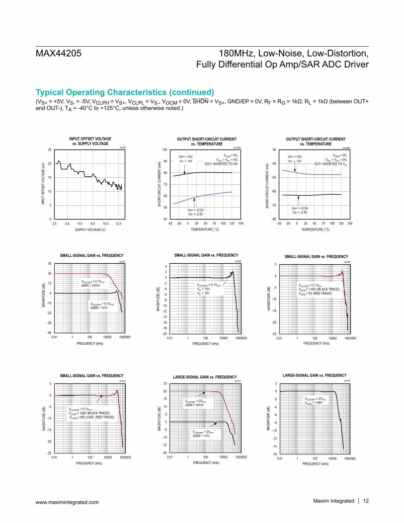
Typical Operating Characteristics
(VS+ = +5V, VS- = -5V, VCLPH = VS+, VCLPL = VS-, VOCM = 0V, SHDN = VS+, GND/EP = 0V, RF = RG = 1kΩ, RL = 1kΩ (between OUT+ and OUT-), TA = -40°C to +125°C, unless otherwise noted.)
-1
-0.5
0
0.5
1
1.5
2
2.5
-0.4 -0.3 -0.2 -0.1 0 0.1 0.2 0.3 0.4
INPU
T OF
FSET
VOL
TAGE
DRI
FT
OVER
TEM
PERA
TURE
(µV)
VICM (V)
INPUT OFFSET VOLTAGE CHANGE OVER TEMPERATURE vs. VICM
VS+ = +1.35VVS- = -1.35V
TA = -40°C
TA = +25°C
TA = +125°C
toc09b
-2
-1.5
-1
-0.5
0
0.5
1
1.5
2
-4.2 -3 -1.8 -0.6 0.6 1.8 3 4.2
INPU
T OF
FSET
VOL
TAGE
DRI
FT
OVER
TEM
PERA
TURE
(µV)
VICM (V)
INPUT OFFSET VOLTAGE CHANGE OVER TEMPERATURE vs. VICM
Vs+ = +5VVs- = -5V
TA = -40˚C
TA = +25˚C
TA = +125˚C
toc09c
-20
-10
0
10
20
30
40
50
60
1.2 1.3 1.4 1.5 1.6
OUTP
UT V
OCM
ERR
OR O
VER
TEM
PERA
TURE
(mV)
INPUT VOCM VOLTAGE (V)
VOCM ERROR OVER TEMPERATURE vs. VOCM INPUT
SUPPLY VOLTAGE : 3VSUPPLY VOLTAGE : 3VSUPPLY VOLTAGE : 3VVOCM RANGE = -0.5V to +0.5VSUPPLY VOLTAGE : 3VSUPPLY VOLTAGE : 3VSUPPLY VOLTAGE : 3VVOCM RANGE = 1.2V to 1.5VVcc+ = +2.5VVcc- = -2.5V TA = -40˚C
TA = +25˚C
TA = +125˚C
toc11b
-20
-10
0
10
20
30
40
50
60
-1.6 -1.2 -0.8 -0.4 0 0.4 0.8 1.2 1.6
OUTP
UT V
OCM
ERRO
R OV
ER T
EMPE
RATU
RE (m
V)
INPUT VOCM VOLTAGE (V)
VOCM ERROR OVER TEMPERATURE vs. VOCM INPUT
SUPPLY VOLTAGE : 3VSUPPLY VOLTAGE : 3VSUPPLY VOLTAGE : 3VVOCM RANGE = -0.5V to +0.5VSUPPLY VOLTAGE : 3VSUPPLY VOLTAGE : 3VSUPPLY VOLTAGE : 3VVOCM RANGE = -1.5V to +1.5VVcc+ = +2.5VVcc- = -2.5V TA = -40˚C
TA = +25˚C
TA = +125˚C
toc11b
INCREASED SCALE
0
2
4
6
8
10
12
14
-25 -23 -21 -19 -17 -15 -13 -11 -9 -7 -5
OCCU
RREN
CE (
N)
OUTPUT COMMON-MODE VOLTAGE ERROR (mV)
OUTPUT COMMON-MODE VOLTAGE ERROR HISTOGRAM
toc10
TA = +25˚CVOCM = 0V
-20
-10
0
10
20
30
40
50
60
-4.2 -3 -1.8 -0.6 0.6 1.8 3 4.2
OUTP
UT V
OCM
ERRO
R OV
ER T
EMPE
RATU
RE (m
V)
INPUT VOCM VOLTAGE (V)
VOCM ERROR OVER TEMPERATURE vs. VOCM INPUT
SUPPLY VOLTAGE : 3VSUPPLY VOLTAGE : 3VSUPPLY VOLTAGE : 3VVOCM RANGE = -0.5V to +0.5VSUPPLY VOLTAGE : 3VSUPPLY VOLTAGE : 3VSUPPLY VOLTAGE : 3VVOCM RANGE = -4V to +4V
VS+ = +5VVS- = -5V TA = -40˚C
TA = +25˚CTA = +125˚C
toc11
-20
-10
0
10
20
30
40
50
60
3 3.2 3.4 3.6 3.8 4 4.2
OUTP
UT V
OCM
ERRO
R OV
ER T
EMPE
RATU
RE (m
V)
INPUT VOCM VOLTAGE (V)
VOCM ERROR OVER TEMPERATURE vs. VOCM INPUT
SUPPLY VOLTAGE : 3VSUPPLY VOLTAGE : 3VSUPPLY VOLTAGE : 3VVOCM RANGE = -0.5V to +0.5VSUPPLY VOLTAGE : 3VSUPPLY VOLTAGE : 3VSUPPLY VOLTAGE : 3VVOCM RANGE = -4V to +4VVS+ = +5VVS- = -5V TA = -40˚C
TA = +25˚CTA = +125˚C
toc11a
INCREASED SCALE
Maxim Integrated 8www.maximintegrated.com
MAX44205 180MHz, Low-Noise, Low-Distortion, Fully Differential Op Amp/SAR ADC Driver
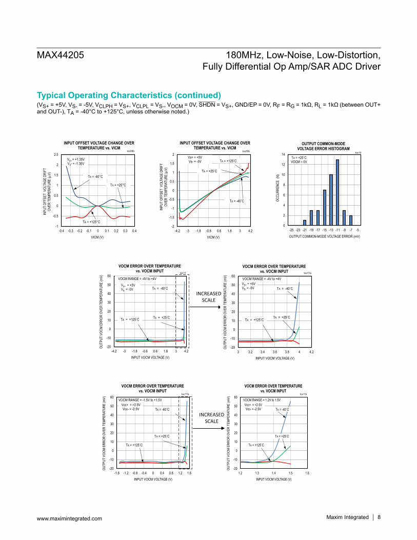
Typical Operating Characteristics (continued)
(VS+ = +5V, VS- = -5V, VCLPH = VS+, VCLPL = VS-, VOCM = 0V, SHDN = VS+, GND/EP = 0V, RF = RG = 1kΩ, RL = 1kΩ (between OUT+ and OUT-), TA = -40°C to +125°C, unless otherwise noted.)
-150-125-100-75-50-25
0255075
100125150
-50 -25 0 25 50 75 100 125 150
I OS(n
A)
TEMPERATURE (°C)
INPUT OFFSET CURRENT (IN+/IN-) vs. TEMPERATURE (100 UNITS)
toc14b
-14
-13.8
-13.6
-13.4
-13.2
-13
-12.8
-12.6
-12.4
-12.2
-12
-50 -25 0 25 50 75 100 125 150
OUTP
UT V
OCM
ERRO
R (m
V)
TEMPERATURE (°C)
OUTPUT VOCM ERROR vs. TEMPERATURE
VOCM INPUT= 0V
Vs+ = +5VVs- = -5V
Vs+ = +2.5VVs- = -2.5V
toc12
-20
-10
0
10
20
30
40
50
60
70
-4 -3 -2 -1 0 1 2 3 4
INPU
T BI
AS C
URRE
NT (n
A)
INPUT COMMON-MODE RANGE VICM (V)
INPUT BIAS CURRENT (IN+/IN-) vs. INPUT COMMON-MODE VOLTAGE
TA = -40˚C
TA = +125˚C
TA = +25˚C
Vs+ = +5VVs- = -5V
toc13
-200
-170
-140
-110
-80
-50
-20
10
40
70
100
-50 -25 0 25 50 75 100 125 150
INPU
T BI
AS C
URRE
NT (n
A)
TEMPERATURE (°C)
INPUT BIAS CURRENT (IN+/IN-)vs. TEMPERATURE
Vs+ = +5VVs- = -5VVICM = 0V
toc14a
0
5
10
15
20
25
30
35
-50 -40 -30 -20 -10 0 10 20 30 40 50
OCCU
RREN
CE (
N)
INPUT OFFSET CURRENT (nA)
INPUT OFFSET CURRENT HISTOGRAMtoc15
TA = +25˚C
-0.5
-0.45
-0.4
-0.35
-0.3
-0.25
-0.2
-0.15
-0.1
-0.05
-4.2 -3 -1.8 -0.6 0.6 1.8 3 4.2
VOCM
INPU
T BI
AS C
URRE
NT (µ
A)
INPUT VOCM VOLTAGE (V)
VOCM INPUT BIAS CURRENTvs. VOCM INPUT VOLTAGE
toc16
TA = -40˚C
TA = +25˚C
TA = +125˚C-0.45
-0.4
-0.35
-0.3
-0.25
-0.2
-0.15
-0.1
-0.05
0
-50 -25 0 25 50 75 100 125 150
VOCM
INPU
T BI
AS C
URRE
NT (µ
A)
TEMPERATURE (°C)
VOCM INPUT BIAS CURRENTvs. TEMPERATURE
toc17
VOCM = 0V
VOCM = 4V
VOCM = 3.5V
Maxim Integrated 9www.maximintegrated.com
MAX44205 180MHz, Low-Noise, Low-Distortion, Fully Differential Op Amp/SAR ADC Driver
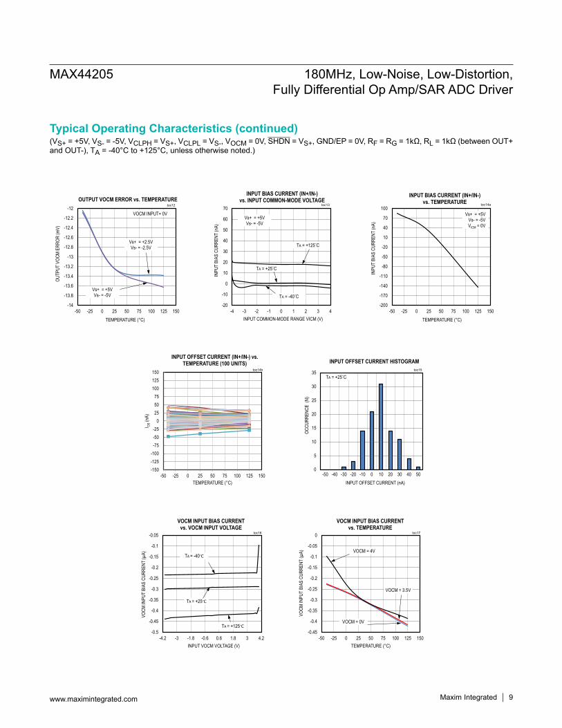
Typical Operating Characteristics (continued)
(VS+ = +5V, VS- = -5V, VCLPH = VS+, VCLPL = VS-, VOCM = 0V, SHDN = VS+, GND/EP = 0V, RF = RG = 1kΩ, RL = 1kΩ (between OUT+ and OUT-), TA = -40°C to +125°C, unless otherwise noted.)
0
0.2
0.4
0.6
0.8
1
1.2
-50 -25 0 25 50 75 100 125 150
OUTP
UT V
OLTA
GE H
IGH
V OL
(V)
TEMPERATURE (ᵒC)
VOL vs. TEMPERATURE vs. LOAD RESISTOR
RLOAD = 1kΩ
RLOAD = 200Ω
RLOAD = 10kΩ
toc19a
Vs+ = +1.5VVs- = -1.5V
0
0.2
0.4
0.6
0.8
1
1.2
-50 -25 0 25 50 75 100 125 150
OUTP
UT V
OLTA
GE H
IGH
V OH
(V)
TEMPERATURE (°C)
VOH vs. TEMPERATURE vs. LOAD RESISTOR
RLOAD = 200Ω
RLOAD = 1kΩRLOAD = 10kΩ
RLOAD = 200Ω
RLOAD = 1kΩRLOAD = 10kΩ
RLOAD = 200Ω
RLOAD = 1kΩRLOAD = 10kΩ
RLOAD = 200Ω
toc18a
Vs+ = +1.5VVs- = -1.5V
0.25
0.27
0.29
0.31
0.33
0.35
0.37
3 3.1 3.2 3.3 3.4 3.5 3.6
OUTP
UT P
OSIT
IVE
CLAM
PING
VOL
TAGE
ERR
OR (V
)
VCLPH INPUT VOLTAGE (V)
OUT+ AND OUT- POSITIVE CLAMPING VOLTAGE ERROR vs. VCLPH INPUT VOLTAGE
toc20a
Vs+ = +5VVs- = -5V
VOUT+
VOUT-
TA = +25˚C
0
0.2
0.4
0.6
0.8
1
1.2
-50 -25 0 25 50 75 100 125 150
OUTP
UT V
OLTA
GE H
IGH
V OH
(V)
TEMPERATURE (ᵒC)
VOH vs. TEMPERATURE vs. LOAD RESISTOR
RLOAD = 1kΩRLOAD = 10kΩ
RLOAD = 1kΩRLOAD = 10kΩ
RLOAD = 1kΩRLOAD = 10kΩ
RLOAD = 200Ω
RLOAD = 1kΩRLOAD = 10kΩ
toc18b
Vs+ = +2.5VVs- = -2.5V
0.3
0.31
0.32
0.33
0.34
0.35
0.36
0.37
0.38
0.39
0.4
3 3.1 3.2 3.3 3.4 3.5 3.6
OUTP
UT P
OSIT
IVE
CLAM
PING
VOL
TAGE
ERR
OR (V
)
VCLPH INPUT VOLTAGE (V)
OUT+ AND OUT- POSITIVE CLAMPING VOLTAGE ERRROR vs. VCLPH INPUT VOLTAGE
toc20b
Vs+ = +5VVs- = -5V
VOUT+
VOUT-
TA = -40˚C
0
0.2
0.4
0.6
0.8
1
1.2
1.4
1.6
-50 -25 0 25 50 75 100 125 150
OUTP
UT V
OLTA
GE H
IGH
V OH
(V)
TEMPERATURE (ᵒC)
VOH vs. TEMPERATURE vs. LOAD RESISTOR
RLOAD = 1kΩ
RLOAD = 200Ω
RLOAD = 10kΩ
toc18c
Vs+ = +5VVs- = -5V
0.22
0.24
0.26
0.28
0.3
0.32
3 3.1 3.2 3.3 3.4 3.5 3.6
OUTP
UT P
OSIT
IVE
CLAM
PING
VOL
TAGE
ERR
OR (V
)
VCLPH INPUT VOLTAGE (V)
OUT+ AND OUT- POSITIVE CLAMPING VOLTAGE ERROR vs. VCLPH INPUT VOLTAGE
toc20c
Vs+ = +5VVs- = -5V
VOUT+
VOUT-
TA = +125˚C
0
0.2
0.4
0.6
0.8
1
1.2
-50 -25 0 25 50 75 100 125 150
OUTP
UT V
OLTA
GE H
IGH
V OH
(V)
TEMPERATURE (ᵒC)
VOL vs. TEMPERATURE vs. LOAD RESISTOR
RLOAD = 1kΩ
RLOAD = 200Ω
RLOAD = 10kΩ
toc19b
Vs+ = +2.5VVs- = -2.5V
0
0.2
0.4
0.6
0.8
1
1.2
1.4
1.6
-50 -25 0 25 50 75 100 125 150
OUTP
UT V
OLTA
GE H
IGH
VOH
(V)
TEMPERATURE (ᵒC)
VOL vs. TEMPERATURE vs. LOAD RESISTOR
RLOAD = 1kΩ
RLOAD = 200Ω
RLOAD = 10kΩ
toc19c
SHORT-CIRCUIT PROTECTION OCCURS AT RLOAD = 200Ω at 125°C
Maxim Integrated 10www.maximintegrated.com
MAX44205 180MHz, Low-Noise, Low-Distortion, Fully Differential Op Amp/SAR ADC Driver
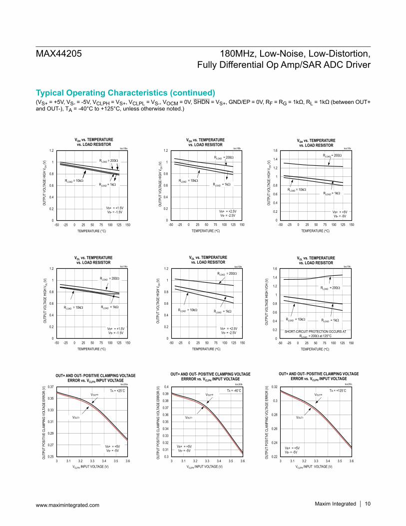
Typical Operating Characteristics (continued)

(VS+ = +5V, VS- = -5V, VCLPH = VS+, VCLPL = VS-, VOCM = 0V, SHDN = VS+, GND/EP = 0V, RF = RG = 1kΩ, RL = 1kΩ (between OUT+ and OUT-), TA = -40°C to +125°C, unless otherwise noted.)
-60
-50
-40
-30
-20
-10
0
10
-50 -25 0 25 50 75 100 125 150
V CLP
HIN
PUT
CURR
ENT
(µA)
TEMPERATURE (°C)
VCLPH INPUT CURRENT vs. TEMPERATUREtoc22a
Vs+ = +5VVs- = -5V
VCLPH = 5V VCLPH = 3.6V
VCLPH = 3.3V
VCLPH = 3V
0.4
0.405
0.41
0.415
0.42
0.425
0.43
0.435
0.44
-0.4 -0.2 0 0.2 0.4
OUTP
UT P
OSIT
IVE
CLAM
PING
VOL
TAGE
ERR
OR (V
)
VCLPL INPUT VOLTAGE (V)
OUT+ AND OUT- POSITIVE CLAMPING VOLTAGE ERROR vs. VCLPL INPUT VOLTAGE
toc21a
Vs+ = +5VVs- = -5V
VOUT+
VOUT-
TA = +25˚C
0
50
100
150
200
250
300
350
-50 -25 0 25 50 75 100 125 150
SHDN
INPU
TCU
RREN
T(n
A)
SHDN INPUT VOLTAGE (V)
SHDN INPUT CURRENTvs. SHDN INPUT VOLTAGE toc23b
VSHDN = 2V
0.42
0.425
0.43
0.435
0.44
0.445
0.45
0.455
0.46
-0.4 -0.2 0 0.2 0.4
OUTP
UT P
OSIT
IVE
CLAM
PING
VOL
TAGE
ERR
OR (V
)
VCLPL INPUT VOLTAGE (V)
OUT+ AND OUT- POSITIVE CLAMPING VOLTAGE ERROR vs. VCLPL INPUT VOLTAGE
toc21b
Vs+ = +5VVs- = -5V
VOUT+
VOUT-
TA = -40˚C
0.9
0.91
0.92
0.93
0.94
0.95
0.96
0.97
0.98
0.99
1
-50 -25 0 25 50 75 100 125 150
SHDN
INPU
TTH
RESH
OLD
VOLT
AGE
(V)
TEMPERATURE (°C)
SHDN INPUT THRESHOLD VOLTAGEvs. TEMPERATURE toc24a
VSHDNTH+
VSHDNTH-
Vs+ = +5VVs- = -5V
0.39
0.395
0.4
0.405
0.41
0.415
0.42
-0.4 -0.2 0 0.2 0.4
OUTP
UT P
OSIT
IVE
CLAM
PING
VOL
TAGE
ERR
OR (V
)
VCLPL INPUT VOLTAGE (V)
OUT+ AND OUT- POSITIVE CLAMPING VOLTAGE ERROR vs. VCLPL INPUT VOLTAGE
toc21c
Vs+ = +5VVs- = -5V
VOUT+
VOUT-
TA = +125˚C
0.9
0.91
0.92
0.93
0.94
0.95
0.96
0.97
0.98
0.99
1
-50 -25 0 25 50 75 100 125 150
SHDN
INPU
TTH
RESH
OLD
VOLT
AGE
(V)
TEMPERATURE (°C)
SHDN INPUT THRESHOLD VOLTAGEvs. TEMPERATURE
toc24b
VSHDNTH+
VSHDNTH-
Vs+ = +2.5VVs- = -2.5V
-70
-60
-50
-40
-30
-20
-10
0
10
-50 -25 0 25 50 75 100 125 150
V CLP
H IN
PUT
CURR
ENT
(µA)
TEMPERATURE (°C)
VCLPH INPUT CURRENT vs. TEMPERATUREtoc22b
Vs+ = +2.5VVs- = -2.5V
VCLP+ = 3.3V VCLP+ = 3.3V
VCLPH = 3V
VCLPH = 5V VCLPH = 3.6V
VCLPH = 3.3V
-300
-250
-200
-150
-100
-50
0
-50 -25 0 25 50 75 100 125 150
SHDN
INPU
TCU
RREN
T(n
A)
SHDN INPUT VOLTAGE (V)
SHDN INPUT CURRENTvs. SHDN VOLTAGE vs. TEMPERATURE
toc23a
VSHDN = 0V
Maxim Integrated 11www.maximintegrated.com
MAX44205 180MHz, Low-Noise, Low-Distortion, Fully Differential Op Amp/SAR ADC Driver
Typical Operating Characteristics (continued)
(VS+ = +5V, VS- = -5V, VCLPH = VS+, VCLPL = VS-, VOCM = 0V, SHDN = VS+, GND/EP = 0V, RF = RG = 1kΩ, RL = 1kΩ (between OUT+ and OUT-), TA = -40°C to +125°C, unless otherwise noted.)
-40
-30
-20
-10
0
10
20
30
0.01 1 100 10000 1000000
MAGN
ITUD
E (d
B)
FREQUENCY (kHz)
SMALL-SIGNAL GAIN vs. FREQUENCY
VOUTDIFF = 0.1VP-PGAIN = 1V/V
VOUTDIFF = 0.1VP-PGAIN = 10V/V
toc27
0
5
10
15
20
25
2.5 4.5 6.5 8.5 10.5 12.5
INPU
T OF
FSET
VOL
TAGE
(uV)
SUPPLY VOLTAGE (V)
INPUT OFFSET VOLTAGE vs. SUPPLY VOLTAGE
toc25
-25
-20
-15
-10
-5
0
5
0.01 1 100 10000 1000000
MAGN
ITUD
E (d
B)
FREQUENCY (kHz)
SMALL-SIGNAL GAIN vs. FREQUENCY
ENTER TEXT HERE
VOUTDIFF = 0.1VP-PCLOAD = 10pF (BLACK TRACE),CLOAD = NO LOAD (RED TRACE)
toc30
40
50
60
70
80
90
100
-50 -25 0 25 50 75 100 125 150
SHOR
T-CI
RCUI
T CU
RREN
T (m
A)
TEMPERATURE (°C)
OUTPUT SHORT-CIRCUIT CURRENTvs. TEMPERATURE
toc26a
Vs+ = +5VVs- = -5V
Vs+ = +2.5VVs- = -2.5V
VOCM = 0V,VIN+ = VIN- = 0V,
OUT+ SHORTED TO VS-
-20
-15
-10
-5
0
5
10
15
20
25
0.01 1 100 10000 1000000
MAGN
ITUD
E (d
B)
FREQUENCY (kHz)
LARGE-SIGNAL GAIN vs. FREQUENCY
VOUTDIFF = 2VP-PGAIN = 1V/V
toc31
VOUTDIFF = 2VP-PGAIN = 10V/V
-80
-70
-60
-50
-40
-30
-50 -25 0 25 50 75 100 125 150
SHOR
T-CI
RCUI
T CU
RREN
T (m
A)
TEMPERATURE (°C)
OUTPUT SHORT-CIRCUIT CURRENTvs. TEMPERATURE
toc26b
Vs+ = +5VVs- = -5V
Vs+ = +2.5VVs- = -2.5V
VOCM = 0V,VIN+ = VIN- = 0V,
OUT+ SHORTED TO VS+
-16
-14
-12
-10
-8
-6
-4
-2
0
2
0.01 1 100 10000 1000000
MAGN
ITUD
E (d
B)
FREQUENCY (kHz)
LARGE-SIGNAL GAIN vs. FREQUENCY
VOUTDIFF = 2VP-P,VOCM = 1.65V
toc32
-20-18-16-14-12-10-8-6-4-2024
0.01 1 100 10000 1000000
MAGN
ITUD
E (d
B)
FREQUENCY (kHz)
SMALL-SIGNAL GAIN vs. FREQUENCY
VOUTDIFF = 0.1VP-PVS+ = +5V,VS- = -5V
toc28
-25
-20
-15
-10
-5
0
5
0.01 1 100 10000 1000000
MAGN
ITUD
E (d
B)
FREQUENCY (kHz)
SMALL-SIGNAL GAIN vs. FREQUENCY
VOUTDIFF = 0.1VP-PVOCM = 1.65V (BLACK TRACE), VOCM = 0V (RED TRACE)
toc29
Maxim Integrated 12www.maximintegrated.com
MAX44205 180MHz, Low-Noise, Low-Distortion, Fully Differential Op Amp/SAR ADC Driver
Typical Operating Characteristics (continued)
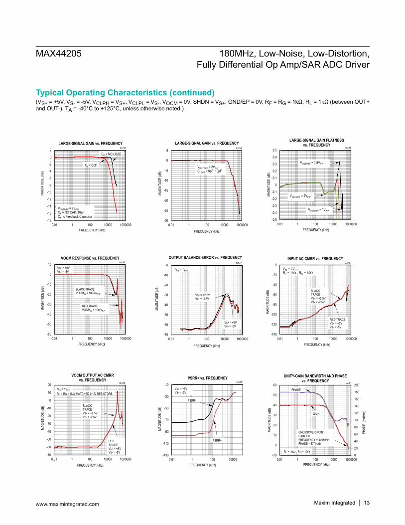
(VS+ = +5V, VS- = -5V, VCLPH = VS+, VCLPL = VS-, VOCM = 0V, SHDN = VS+, GND/EP = 0V, RF = RG = 1kΩ, RL = 1kΩ (between OUT+ and OUT-), TA = -40°C to +125°C, unless otherwise noted.)
-18
-16
-14
-12
-10
-8
-6
-4
-2
0
2
0.01 1 100 10000 1000000
MAGN
ITUD
E (d
B)
FREQUENCY (kHz)
LARGE-SIGNAL GAIN vs. FREQUENCY
CF=10pF
VOUTDIFF = 2VP-PCF = NO CAP, 10pFCF is Feedback Capacitor
CF = NO LOAD
toc33
-30
-25
-20
-15
-10
-5
0
5
0.01 1 100 10000 1000000
MAGN
ITUD
E (d
B)
FREQUENCY (kHz)
LARGE-SIGNAL GAIN vs. FREQUENCYtoc34
VOUTDIFF = 2VP-PCLOAD = 0pF, 10pF
-0.5
-0.4
-0.3
-0.2
-0.1
0
0.1
0.2
0.3
0.4
0.5
0.01 1 100 10000 1000000
MAGN
ITUD
E (d
B)
FREQUENCY (kHz)
LARGE-SIGNAL GAIN FLATNESSvs. FREQUENCY
toc35
VOUTDIFF = 0.5VP-P
VOUTDIFF = 2VP-P
VOUTDIFF = 1VP-P
-60
-50
-40
-30
-20
-10
0
10
0.01 1 100 10000 1000000
MAGN
ITUD
E (d
B)
FREQUENCY (kHz)
VOCM RESPONSE vs. FREQUENCYtoc36
BLACK TRACE: VOCMIN = 100mVP-P
VS+ = +5VVS- = -5V
RED TRACE: VOCMIN = 10mVP-P
-70
-60
-50
-40
-30
-20
-10
0
0.01 1 100 10000 1000000
MAGN
ITUD
E (d
B)
FREQUENCY (kHz)
OUTPUT BALANCE ERROR vs. FREQUENCY toc37
VIN = 1VP-P
VS+ = +2.5VVS- = -2.5V
VS+ = +5VVS- = -5V
-140
-120
-100
-80
-60
-40
-20
0
0.01 1 100 10000 1000000
MAGN
ITUD
E (d
B)
FREQUENCY (kHz)
INPUT AC CMRR vs. FREQUENCYtoc38
VIN = 1VP-PRF = 1kΩ , RG = 10Ω
BLACK TRACEVS+ = +2.5VVS- = -2.5V
RED TRACEVS+ = +5VVS- = -5V
-70
-60
-50
-40
-30
-20
-10
0
10
20
0.01 1 100 10000 1000000
MAGN
ITUD
E (d
B)
FREQUENCY (kHz)
VOCM OUTPUT AC CMRR vs. FREQUENCY
toc39
VIN = 1VP-P
BLACK TRACEVS+ = +2.5VVS- = -2.5V
RED TRACEVS+ = +5VVS- = -5V
RF = RG = 1kΩ MATCHED 0.1% RESISTORS
-130
-110
-90
-70
-50
-30
-10
0.01 1 100 10000
MAGN
ITUD
E (d
B)
FREQUENCY (kHz)
PSRR+ vs. FREQUENCYtoc40
VS+ = +5VVS- = -5V
PSRR-
PSRR+
0
20
40
60
80
100
120
140
160
180
200
-10
0
10
20
30
40
50
60
0.01 1 100 10000 1000000
MAGN
ITUD
E (d
B)
FREQUENCY (kHz)
UNITY-GAIN BANDWIDTH AND PHASE vs. FREQUENCY
toc41
RF = 1kΩ , RG = 10Ω
PHAS
E (r
adian
s)GAIN
PHASE
CROSSOVER POINT:GAIN = 0FREQUENCY = 400MHzPHASE = 87°(rad)
Maxim Integrated 13www.maximintegrated.com
MAX44205 180MHz, Low-Noise, Low-Distortion, Fully Differential Op Amp/SAR ADC Driver
Typical Operating Characteristics (continued)
(VS+ = +5V, VS- = -5V, VCLPH = VS+, VCLPL = VS-, VOCM = 0V, SHDN = VS+, GND/EP = 0V, RF = RG = 1kΩ, RL = 1kΩ (between OUT+ and OUT-), TA = -40°C to +125°C, unless otherwise noted.)
-60
-50
-40
-30
-20
-10
0
10
0.01 1 100 10000 1000000
MAGN
ITUD
E (d
B)
FREQUENCY (kHz)
VOCM RESPONSE vs. FREQUENCYtoc36
BLACK TRACE: VOCMIN = 100mVP-P
VS+ = +5VVS- = -5V
RED TRACE: VOCMIN = 10mVP-P
-70
-60
-50
-40
-30
-20
-10
0
0.01 1 100 10000 1000000
MAGN
ITUD
E (d
B)
FREQUENCY (kHz)
OUTPUT BALANCE ERROR vs. FREQUENCY toc37
VIN = 1VP-P
VS+ = +2.5VVS- = -2.5V
VS+ = +5VVS- = -5V
0
20
40
60
80
100
120
140
160
180
200
-10
0
10
20
30
40
50
60
0.01 1 100 10000 1000000
MAGN
ITUD
E (d
B)
FREQUENCY (kHz)
UNITY-GAIN BANDWIDTH AND PHASE vs. FREQUENCY
toc41
RF = 1kΩ , RG = 10Ω
PHAS
E (r
adian
s)GAIN
PHASE
CROSSOVER POINT:GAIN = 0FREQUENCY = 400MHzPHASE = 87°(rad)
-160
-140
-120
-100
-80
-60
-40
-20
0
10 100 1000 10000
MAGN
ITUD
E (d
B)
INPUT FREQUENCY (kHz)
HD2,1k load
HD2 AND HD3 vs. FREQUENCYtoc45
HD3,1k load
HD2, no load
HD3, No load
VOUTDIFF = 2VP-P
-160
-140
-120
-100
-80
-60
-40
-20
0
10 100 1000 10000
MAGN
ITUD
E (d
B)
INPUT FREQUENCY (kHz)
HD2,1k load
HD2 AND HD3 vs. FREQUENCYtoc47
HD3, 1k load
HD2, no load
HD3, No load
VOUTDIFF = 6.6VP-P
-140
-120
-100
-80
-60
-40
-20
0
1 2.4 3.8 5.2 6.6
MAGN
ITUD
E (d
B)
OUTPUT VOLTAGE SWING (VP-P)
fIN = 11.5MHz
HD2 vs. OUTPUT SWINGtoc48
fIN = 1MHz
fIN = 100kHz
fIN = 10kHz
-160
-140
-120
-100
-80
-60
-40
-20
0
1 2.4 3.8 5.2 6.6
MAGN
ITUD
E (d
B)
OUTPUT VOLTAGE SWING (VP-P)
fIN = 11.5MHz
HD3 vs. OUTPUT SWINGtoc49
fIN = 1MHz
fIN = 100kHz
fIN = 10kHz
-160
-140
-120
-100
-80
-60
-40
-20
0
10 100 1000 10000
MAGN
ITUD
E (d
B)
INPUT FREQUENCY (kHz)
HD2, 1K load
HD2 AND HD3 vs. FREQUENCYtoc46
HD3, 1K load
HD2, no load
HD3, No load
VOUTDIFF = 4VP-P
Maxim Integrated 14www.maximintegrated.com
MAX44205 180MHz, Low-Noise, Low-Distortion, Fully Differential Op Amp/SAR ADC Driver
-160
-140
-120
-100
-80
-60
-40
-20
0
10 100 1000 10000
MAGN
ITUD
E (d
B)
INPUT FREQUENCY (kHz)
HD2,1K load
HD2 AND HD3 vs. FREQUENCYtoc44
HD3,1k load
HD2,No loadHD3, No load
VOUTDIFF = 1VP-P
1
10
100
0.1 1 10 100 1000 10000 100000
INPU
T CU
RREN
T-NO
ISE
DENS
ITY
(pA/
√Hz)
FREQUENCY (Hz)
INPUT CURRENT-NOISE SPECTRAL DENSITY vs. FREQUENCY
toc43
1
10
100
0.1 1 10 100 1000 10000 100000
INPU
T VO
LTAG
E-NO
ISE
DENS
ITY
(nV/
√Hz)
FREQUENCY (Hz)
INPUT VOLTAGE-NOISE DENSITYvs. FREQUENCY
toc42
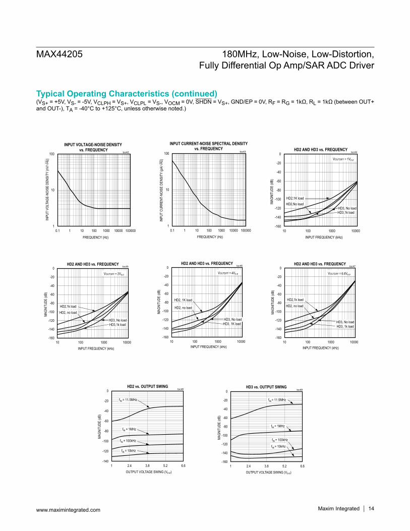
Typical Operating Characteristics (continued)
(VS+ = +5V, VS- = -5V, VCLPH = VS+, VCLPL = VS-, VOCM = 0V, SHDN = VS+, GND/EP = 0V, RF = RG = 1kΩ, RL = 1kΩ (between OUT+ and OUT-), TA = -40°C to +125°C, unless otherwise noted.)
Typical Operating Characteristics (continued)
-150
-100
-50
0
50
100
150
INPU
T VO
LTAG
E NO
ISE
(nV P
-P)
4s/div
0.1Hz to 10Hz INPUT VOLTAGE NOISE toc50
0.1Hz TO 10Hz INPUT VOLTAGE NOISE: 200nVP-P
-150
-100
-50
0
50
100
150
INPU
T CU
RREN
T NO
ISE
(pA P
-P)
4s/div
INPUT CURRENT NOISE 0.1Hz to 10Hztoc51
INPUT CURRENT NOISE = 220pAP-P
SMALL-SIGNAL RESPONSE
100mV/div
100mV/div
toc52
50ns/div
VINDIFF
VOUTDIFF
CLOAD = 10pF CLOAD = 10pF
LARGE-SIGNAL TRANSIENT RESPONSE
500mV/div
500mV/div
toc53a
50ns/div
VINDIFF
VOUTDIFF
CLOAD = 10pFCLOAD = 10pF
LARGE-SIGNAL TRANSIENT RESPONSE
500mV/div
500mV/div
toc53b
50ns/div
VINDIFF
VOUTDIFF
CLOAD = NO LOAD
VOCM SMALL-SIGNAL TRANSIENT RESPONSE
100mV/div
100mV/div
toc54
100ns/div
VOCM
VOUT+
VOCM LARGE-SIGNAL TRANSIENT RESPONSE
2V/div
2V/div
toc55
500ns/div
VOCM
VOUT+
OUTPUT-TRANSIENT RESPONSE vs. SHUTDOWN PULSE
2V/div
1V/div
toc56a
5µs/div
VSHDN
VOUT-
OUTPUT+ TRANSIENT RESPONSE vs. SHUTDOWN PULSE
2V/div
1V/div
toc56b
5µs/div
VSHDN
VOUT+
Maxim Integrated 15www.maximintegrated.com
MAX44205 180MHz, Low-Noise, Low-Distortion, Fully Differential Op Amp/SAR ADC Driver
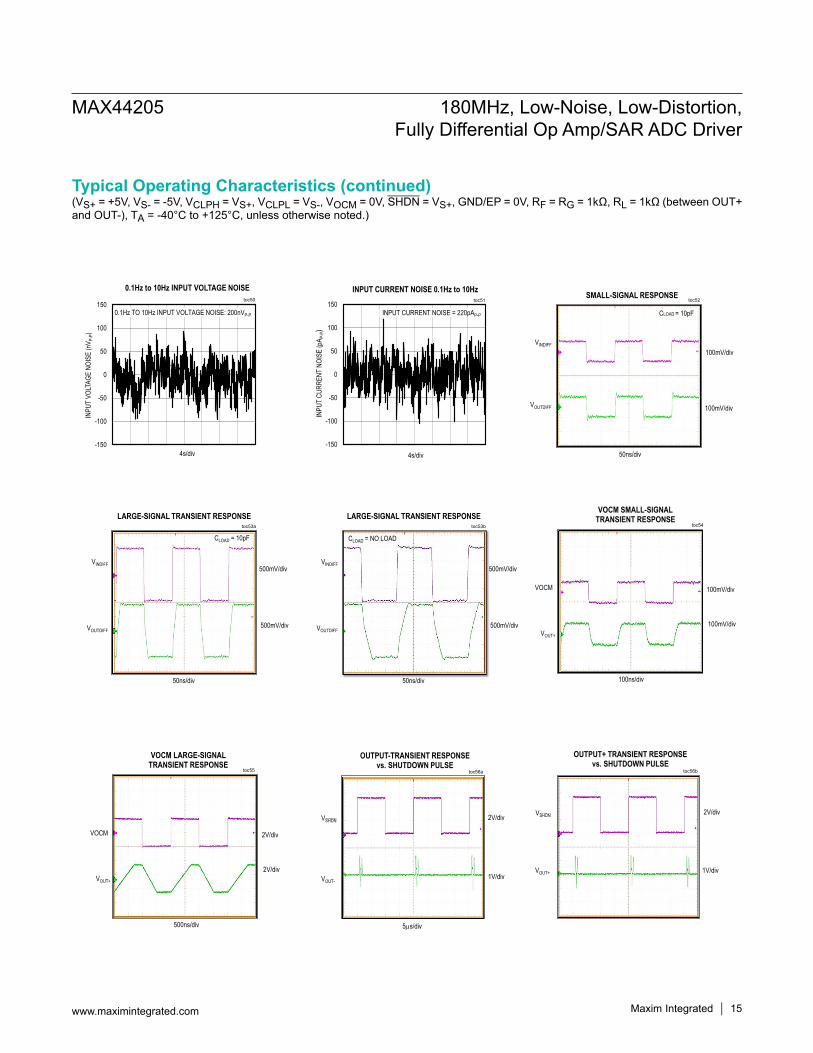
(VS+ = +5V, VS- = -5V, VCLPH = VS+, VCLPL = VS-, VOCM = 0V, SHDN = VS+, GND/EP = 0V, RF = RG = 1kΩ, RL = 1kΩ (between OUT+ and OUT-), TA = -40°C to +125°C, unless otherwise noted.)
Typical Operating Characteristics (continued)
1V/div
1V/div
1V/div
toc57
20ns/div
VOUTN
VINSIDE
VBACKUP
VCLPH CLAMP ENGAGING TIME
1V/div
VINDIFF
OUT+
OUT-
VOUTDIFF
VIN+ = 1VP-P + 0.5Vdc, VIN-= GND, VCLPH = 3.3V, VCLPL = -5V, VOCM = 3.3V, RL = 1kΩ
3.7V3.3V
2.9V
1V/div
1V/div
1V/div
toc59
20ns/div
VOUTN
VINSIDE
VBACKUP
VCLPL CLAMP ENGAGING TIME
1V/div
VINDIFF
OUT+
OUT-
VOUTDIFF
VIN+ = 1VP-P - 0.5Vdc, VIN- = GND, VCLPH = 3.3V, VCLPL = 0V, VOCM = 0V,
RL = 1kΩ
0V -0.44V
0.44V
1V/div
1V/div
1V/div
toc60
40ns/div
VOUTN
VINSIDE
VBACKUP
VCLPL CLAMP DISENGAGING TIME
1V/div
VINDIFF
OUT+OUT-
VOUTDIFF
VIN+ = 1VP-P - 0.5Vdc,VIN- = GND,VCLPH = 3.3V, VCLPL = 0V, VOCM = 0V,RL = 1kΩ
-0.44V
0.44V
0V
5V/div
2V/div
2V/div
toc62
20µs/div
VINDIFF
VOUT+
OUTPUT TRANSIENT RESPONSE WITH SOFT CLAMPING
VOUT-
VOUTDIFF 5V/div
3.5V
VIN+ = 4.3VP-P,VIN- = VIN+ - 180°, VCLPH = 3.3V,
VCLPL = 0V, VOCM = 1.65V
3.65V
-0.36V
1V/div
1V/div
1V/div
toc58
100ns/div
VOUTN
VINSIDE
VBACKUP
VCLPH CLAMP DISENGAGING TIME
1V/div
VINDIFF
OUT+OUT-
VOUTDIFF
VIN+ = 1VP-P + 0.5Vdc,VIN- = GND,VCLPH = 3.3V,
VCLPL = -5V, VOCM = 3.3V,RL = 1kΩ
3.7V 3.3V
2.9V
5V/div
2V/div
2V/div
toc61
20µs/div
VINDIFF
VOUT+
OUTPUT TRANSIENT RESPONSE WITH NO CLAMPING
VOUT-
VOUTDIFF 5V/div
3.65V3.72V
-0.4V
3.3V
0V
VIN+ = 3.3VP-P,VIN- = VIN+ - 180°, VCLPH = 3.3V,
VCLPL = 0V, VOCM = 1.65V
Maxim Integrated 16www.maximintegrated.com
MAX44205 180MHz, Low-Noise, Low-Distortion, Fully Differential Op Amp/SAR ADC Driver
(VS+ = +5V, VS- = -5V, VCLPH = VS+, VCLPL = VS-, VOCM = 0V, SHDN = VS+, GND/EP = 0V, RF = RG = 1kΩ, RL = 1kΩ (between OUT+ and OUT-), TA = -40°C to +125°C, unless otherwise noted.)
Typical Operating Characteristics (continued)
5V/div
2V/div
2V/div
toc63
VINDIFF
VOUT+
OUTPUT TRANSIENT RESPONSE WITH HARD CLAMPING
VOUT-
VOUTDIFF 5V/div
3.5V
VIN+ = 5VP-P,VIN- = VIN+ - 180°, VCLPH = 3.3V,
VCLPL = 0V, VOCM = 1.65V
3.65V3.72V
-0.4V
20µs/div
5V/div
2V/div
2V/div
toc64
20µs/div
VINDIFF
VOUT+
OUTPUT TRANSIENT RESPONSE WITH NO CLAMPING
VOUT-
VOUTDIFF 5V/div
VIN+ = 3.3VP-P,VIN- = VIN+ -180°, VCLPH = 3.3V, VCLPL =0V, VOCM = 1.65V
3.65V3.72V
-0.4V3.3V
0V
5V/div
2V/div
2V/div
toc65
20µs/div
VINDIFF
VOUT+
OUTPUT TRANSIENT RESPONSE WITH SOFT CLAMPING
VOUT-
VOUTDIFF 5V/div
VIN+ = 4.3VP-P,VIN- = VIN+ -180° VCLPH = 3.3V, VCLPL = 0V, VOCM = 1.65V
3.65V3.72V
-0.4V
3.68V
-0.32V
5V/div
2V/div
2V/div
toc66
20µs/div
VINDIFF
VOUT+
OUTPUT TRANSIENT RESPONSE WITH HARD CLAMPING
VOUT-
VOUTDIFF 5V/div
VIN+ = 5VP-P,VIN- = VIN+-180°VCLPH = 3.3V, VCLPL = 0V, VOCM = 1.65V
3.65V3.72V
-0.4V
3.76V
-0.36V
Maxim Integrated 17www.maximintegrated.com
MAX44205 180MHz, Low-Noise, Low-Distortion, Fully Differential Op Amp/SAR ADC Driver

PINNAME FUNCTION
TQFN µMAX1 2 VOCM Output Common-Mode Voltage Input
2 3 VS+ Positive Supply Voltage Input
3 4 VCLPH High-Output Voltage Clamping Input
4 5 OUT+ Noninverting Differential Output
5 * GND External Ground Input. *The µMAX exposed pad also functions as GND.
6 6 OUT- Inverting Differential Output
7 7 VCLPL Low-Output Voltage Clamping Input
8 8 VS- Negative Supply Voltage Input
9 9 SHDN Shutdown Mode Input (active low)
10 10 IN+ Noninverting Input
11 — N.C. No Connection. Not connected internally
12 1 IN- Inverting Input
— — EP Exposed Pad. Connected to GND internally. The µMAX exposed pad is also GND.
VS+
VCLPH
VOCM
VS-
VCLPL
SHDN
N.C.IN-
OUT-GNDOUT+
IN+
TQFN3mm x 3mm
TOP VIEW
+
4 5 6
7
8
9
101112
3
2
1
MAX44205
EP*
1
2
3
4
5
9
8
7
6
10 IN+
SHDN
VS-
VCLPLVCLPH
VS+
VOCM
IN-
µMAX
TOP VIEW
OUT-OUT+
*EXPOSED PAD
*
MAX44205
+
MAX44205 180MHz, Low-Noise, Low-Distortion, Fully Differential Op Amp/SAR ADC Driver
www.maximintegrated.com Maxim Integrated 18
Pin Configurations
Pin Description
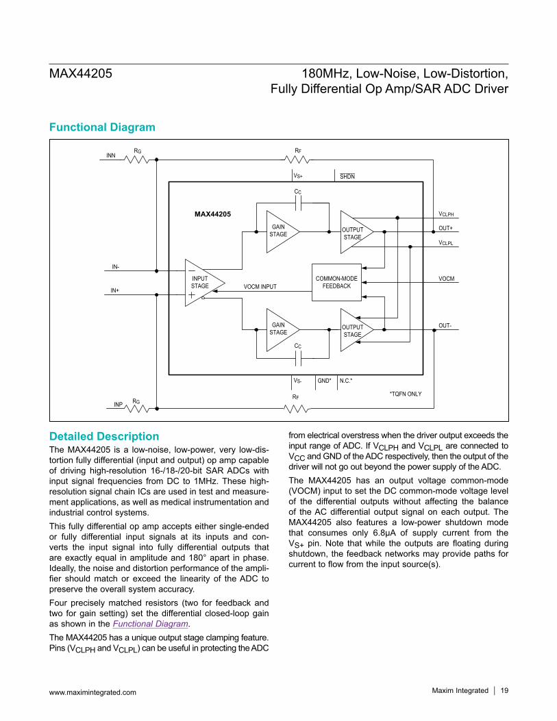
Detailed DescriptionThe MAX44205 is a low-noise, low-power, very low-dis-tortion fully differential (input and output) op amp capable of driving high-resolution 16-/18-/20-bit SAR ADCs with input signal frequencies from DC to 1MHz. These high-resolution signal chain ICs are used in test and measure-ment applications, as well as medical instrumentation and industrial control systems. This fully differential op amp accepts either single-ended or fully differential input signals at its inputs and con-verts the input signal into fully differential outputs that are exactly equal in amplitude and 180° apart in phase. Ideally, the noise and distortion performance of the ampli-fier should match or exceed the linearity of the ADC to preserve the overall system accuracy.Four precisely matched resistors (two for feedback and two for gain setting) set the differential closed-loop gain as shown in the Functional Diagram.The MAX44205 has a unique output stage clamping feature. Pins (VCLPH and VCLPL) can be useful in protecting the ADC
from electrical overstress when the driver output exceeds the input range of ADC. If VCLPH and VCLPL are connected to VCC and GND of the ADC respectively, then the output of the driver will not go out beyond the power supply of the ADC. The MAX44205 has an output voltage common-mode (VOCM) input to set the DC common-mode voltage level of the differential outputs without affecting the balance of the AC differential output signal on each output. The MAX44205 also features a low-power shutdown mode that consumes only 6.8µA of supply current from the VS+ pin. Note that while the outputs are floating during shutdown, the feedback networks may provide paths for current to flow from the input source(s).
CC
VCLPH
VCLPL
OUT+
VOCM
OUT-
VS-
VS+ SHDN
OUTPUTSTAGE
COMMON-MODEFEEDBACK
GAINSTAGE
IN+
IN-
MAX44205
VOCM INPUT
RF
RGRF
INN
INP
N.C.*GND*
OUTPUTSTAGE
CC
INPUTSTAGE
RG
GAINSTAGE
*TQFN ONLY
MAX44205 180MHz, Low-Noise, Low-Distortion, Fully Differential Op Amp/SAR ADC Driver
www.maximintegrated.com Maxim Integrated 19
Functional Diagram
Terminology and Definitions
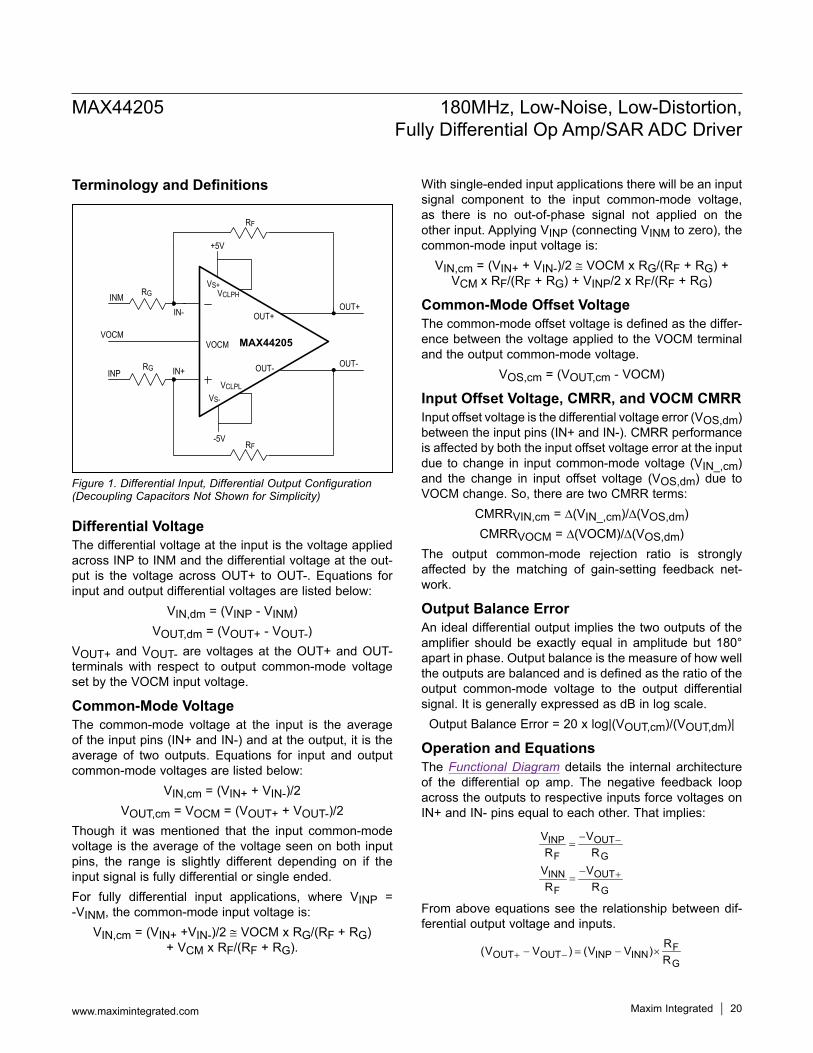
Differential VoltageThe differential voltage at the input is the voltage applied across INP to INM and the differential voltage at the out-put is the voltage across OUT+ to OUT-. Equations for input and output differential voltages are listed below:
VIN,dm = (VINP - VINM)VOUT,dm = (VOUT+ - VOUT-)
VOUT+ and VOUT- are voltages at the OUT+ and OUT- terminals with respect to output common-mode voltage set by the VOCM input voltage.
Common-Mode VoltageThe common-mode voltage at the input is the average of the input pins (IN+ and IN-) and at the output, it is the average of two outputs. Equations for input and output common-mode voltages are listed below:
VIN,cm = (VIN+ + VIN-)/2VOUT,cm = VOCM = (VOUT+ + VOUT-)/2
Though it was mentioned that the input common-mode voltage is the average of the voltage seen on both input pins, the range is slightly different depending on if the input signal is fully differential or single ended.For fully differential input applications, where VINP = -VINM, the common-mode input voltage is:
VIN,cm = (VIN+ +VIN-)/2 ≅ VOCM x RG/(RF + RG) + VCM x RF/(RF + RG).
With single-ended input applications there will be an input signal component to the input common-mode voltage, as there is no out-of-phase signal not applied on the other input. Applying VINP (connecting VINM to zero), the common-mode input voltage is:
VIN,cm = (VIN+ + VIN-)/2 ≅ VOCM x RG/(RF + RG) + VCM x RF/(RF + RG) + VINP/2 x RF/(RF + RG)
Common-Mode Offset VoltageThe common-mode offset voltage is defined as the differ-ence between the voltage applied to the VOCM terminal and the output common-mode voltage.
VOS,cm = (VOUT,cm - VOCM)
Input Offset Voltage, CMRR, and VOCM CMRRInput offset voltage is the differential voltage error (VOS,dm) between the input pins (IN+ and IN-). CMRR performance is affected by both the input offset voltage error at the input due to change in input common-mode voltage (VIN_,cm) and the change in input offset voltage (VOS,dm) due to VOCM change. So, there are two CMRR terms:
CMRRVIN,cm = ∆(VIN_,cm)/∆(VOS,dm)CMRRVOCM = ∆(VOCM)/∆(VOS,dm)
The output common-mode rejection ratio is strongly affected by the matching of gain-setting feedback net-work.
Output Balance ErrorAn ideal differential output implies the two outputs of the amplifier should be exactly equal in amplitude but 180° apart in phase. Output balance is the measure of how well the outputs are balanced and is defined as the ratio of the output common-mode voltage to the output differential signal. It is generally expressed as dB in log scale.
Output Balance Error = 20 x log|(VOUT,cm)/(VOUT,dm)|
Operation and EquationsThe Functional Diagram details the internal architecture of the differential op amp. The negative feedback loop across the outputs to respective inputs force voltages on IN+ and IN- pins equal to each other. That implies:
OUTINPF G
OUTINNF G
VVR R
VVR R
−
+
−=
−=
From above equations see the relationship between dif-ferential output voltage and inputs.
FOUT OUT INP INN
G
R(V V ) (V V )R+ −− = − ×
Figure 1. Differential Input, Differential Output Configuration (Decoupling Capacitors Not Shown for Simplicity)
OUT+
VS+VCLPH
VCLPLVS-
OUT+
OUT-
RF
RF
+5V
-5V
MAX44205VOCM
RG
RG
INM
INP
VOCM
OUT-
IN-
IN+
MAX44205 180MHz, Low-Noise, Low-Distortion, Fully Differential Op Amp/SAR ADC Driver
www.maximintegrated.com Maxim Integrated 20
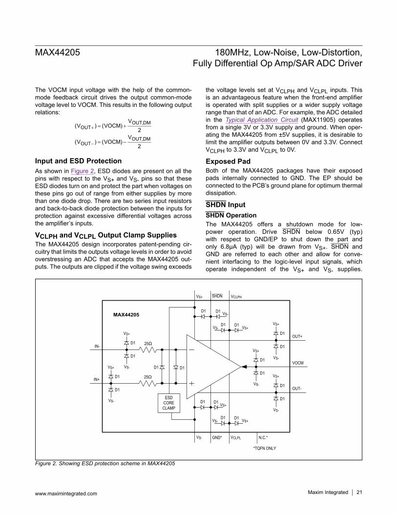
The VOCM input voltage with the help of the common-mode feedback circuit drives the output common-mode voltage level to VOCM. This results in the following output relations:
OUT,DMOUT
OUT,DMOUT
V(V ) (VOCM)
2V
(V ) (VOCM)2
+
−
= +
= −
Input and ESD ProtectionAs shown in Figure 2, ESD diodes are present on all the pins with respect to the VS+ and VS- pins so that these ESD diodes turn on and protect the part when voltages on these pins go out of range from either supplies by more than one diode drop. There are two series input resistors and back-to-back diode protection between the inputs for protection against excessive differential voltages across the amplifier’s inputs.
VCLPH and VCLPL Output Clamp SuppliesThe MAX44205 design incorporates patent-pending cir-cuitry that limits the outputs voltage levels in order to avoid overstressing an ADC that accepts the MAX44205 out-puts. The outputs are clipped if the voltage swing exceeds
the voltage levels set at VCLPH and VCLPL inputs. This is an advantageous feature when the front-end amplifier is operated with split supplies or a wider supply voltage range than that of an ADC. For example, the ADC detailed in the Typical Application Circuit (MAX11905) operates from a single 3V or 3.3V supply and ground. When oper-ating the MAX44205 from ±5V supplies, it is desirable to limit the amplifier outputs between 0V and 3.3V. Connect VCLPH to 3.3V and VCLPL to 0V.
Exposed PadBoth of the MAX44205 packages have their exposed pads internally connected to GND. The EP should be connected to the PCB’s ground plane for optimum thermal dissipation.
SHDN InputSHDN OperationThe MAX44205 offers a shutdown mode for low-power operation. Drive SHDN below 0.65V (typ) with respect to GND/EP to shut down the part and only 6.8µA (typ) will be drawn from VS+. SHDN and GND are referred to each other and allow for conve-nient interfacing to the logic-level input signals, which operate independent of the VS+ and VS- supplies.
Figure 2. Showing ESD protection scheme in MAX44205
OUT+
VOCM
OUT-
N.C.*VS-
IN-
MAX44205
IN+
25Ω
25Ω
VCLPL
VS+
VS-
ESDCORE CLAMP
GND*
VS+D1D1
VCLPHVS+ SHDN
VS+D1D1VS-
D1
D1
VS+
VS-
D1
D1
VS+
VS-
D1
D1
VS+D1D1VS-
D1D1
VS+
VS-
D1
D1
VS+
VS-
D1
D1
VS-D1D1
*TQFN ONLY
MAX44205 180MHz, Low-Noise, Low-Distortion, Fully Differential Op Amp/SAR ADC Driver
www.maximintegrated.com Maxim Integrated 21
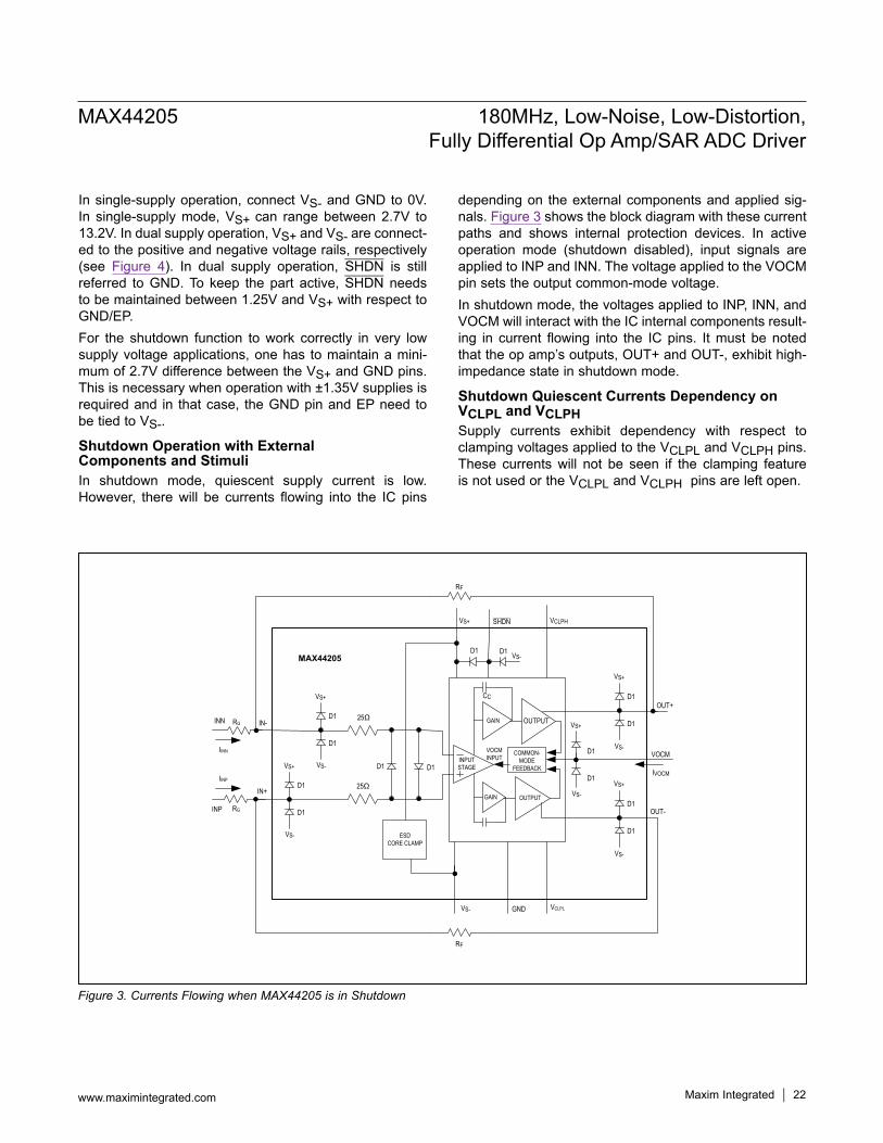
In single-supply operation, connect VS- and GND to 0V. In single-supply mode, VS+ can range between 2.7V to 13.2V. In dual supply operation, VS+ and VS- are connect-ed to the positive and negative voltage rails, respectively (see Figure 4). In dual supply operation, SHDN is still referred to GND. To keep the part active, SHDN needs to be maintained between 1.25V and VS+ with respect to GND/EP. For the shutdown function to work correctly in very low supply voltage applications, one has to maintain a mini-mum of 2.7V difference between the VS+ and GND pins. This is necessary when operation with ±1.35V supplies is required and in that case, the GND pin and EP need to be tied to VS-.
Shutdown Operation with External Components and StimuliIn shutdown mode, quiescent supply current is low. However, there will be currents flowing into the IC pins
depending on the external components and applied sig-nals. Figure 3 shows the block diagram with these current paths and shows internal protection devices. In active operation mode (shutdown disabled), input signals are applied to INP and INN. The voltage applied to the VOCM pin sets the output common-mode voltage.In shutdown mode, the voltages applied to INP, INN, and VOCM will interact with the IC internal components result-ing in current flowing into the IC pins. It must be noted that the op amp’s outputs, OUT+ and OUT-, exhibit high-impedance state in shutdown mode.
Shutdown Quiescent Currents Dependency on VCLPL and VCLPHSupply currents exhibit dependency with respect to clamping voltages applied to the VCLPL and VCLPH pins. These currents will not be seen if the clamping feature is not used or the VCLPL and VCLPH pins are left open.
Figure 3. Currents Flowing when MAX44205 is in Shutdown
OUT+
VOCM
OUT-
VS-
IN-
MAX44205
IN+
25Ω
25Ω VS+
VS-
ESDCORE CLAMP
VS+ SHDN
D1
D1
VS+
VS-
D1
D1
VS+
VS-
D1
D1
D1D1
VS+
VS-
D1
D1
VS+
VS-
D1
D1
VS-D1D1
INPUT STAGE
CC
OUTPUT
OUTPUT
GAIN
GAIN
COMMON-MODE
FEEDBACK
VOCM INPUT
IVOCM
RF
RF
RG
RG
INP
INN
IINN
IINP
VCLPL
VCLPH
GND
MAX44205 180MHz, Low-Noise, Low-Distortion, Fully Differential Op Amp/SAR ADC Driver
www.maximintegrated.com Maxim Integrated 22
Applications InformationThe fully differential op amp is shown in Figure 5 for refer-ence. Fully differential op amps provide a lot of advantag-es, including rejecting common-mode noise coupled to the input, the output, and from the power supply. The effective output swing is increased by a factor of two as the outputs are equal in amplitude and 180° apart in phase. For example, by applying a fully differential input signal of 1VP-P across INP and INN on Figure 1 there is a 2VP-P differential output voltage swing. Another advantage of having fully differential outputs is that even order harmon-ics will be suppressed at the output.
Input Impedance Mismatch Due to Source ImpedanceThe impedance looking into the IN+ and IN- nodes of Figure 5 depends on how the inputs are driven. For a fully differential input signal, i.e., VINP = -VINM, the input impedance looking into inputs is shown in Figure 6.
RINP = RINM = RGFor a single-ended input signal, since the inputs are not balanced, the input impedance actually increases relative to the fully differential case. The input impedance looking into either input is:
GINP INM
FG F
RR R
R1[1 ]2 (R R )
= = − × +
Apart from the single-ended input and differential input signal cases, an input signal source from a nonzero source impedance may cause imbalance between feed-back resistor networks for single-ended input driving case as shown in the Figure 7. A terminating resistor RT as shown in Figure 7 is used to impedance match to the source such that:
ST INM
INM S
RR R
R R= ×
−
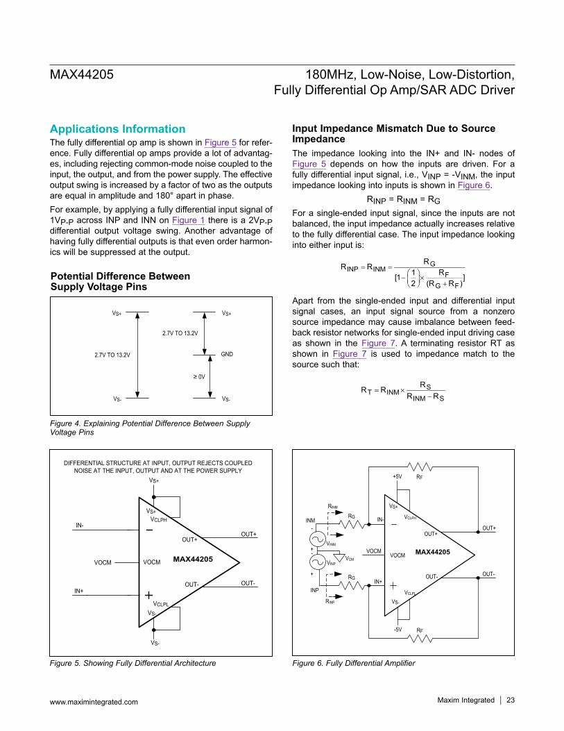
Potential Difference Between Supply Voltage Pins
Figure 4. Explaining Potential Difference Between Supply Voltage Pins
2.7V TO 13.2V
VS+
GND
VS-
2.7V TO 13.2V
≥ 0V
VS+
VS-
Figure 5. Showing Fully Differential Architecture
VS+VCLPH
VCLPLVS-
OUT+
OUT-
VS+
VS-
MAX44205VOCM
IN-
IN+
VOCM
OUT-
OUT+
DIFFERENTIAL STRUCTURE AT INPUT, OUTPUT REJECTS COUPLED NOISE AT THE INPUT, OUTPUT AND AT THE POWER SUPPLY
Figure 6. Fully Differential Amplifier
VS+
VS-
OUT+
OUT-
+5V
-5V
MAX44205VOCM
INM
INP
VOCM
OUT-
OUT+IN-
IN+
RG
RG
RF
RF
VCM
-
+-
+
VINM
VINP
RINP
RINM
VCLPH
VCLPL
MAX44205 180MHz, Low-Noise, Low-Distortion, Fully Differential Op Amp/SAR ADC Driver
www.maximintegrated.com Maxim Integrated 23
A terminating resistor is inserted to correct for impedance mismatch between the source and input. The gain resis-tor mismatch across feedback networks is created due to the parallel combination of RT and RS. So, to balance out the gain resistor mismatch on the other input, insert RB such that:
SB T
T S
RR R
R R= ×
−
Effects of Input Resistor MismatchIf there is a mismatch between the feedback resistor (RF) pair and gain resistor (RG) pair, there will be a small delta in the feedback factor across the input pins. This delta in the feedback factor is a source of common-mode error. To apply an AC CMRR test without a differential input signal, the common-mode rejection is proportional to the resistor mismatch. Using 0.1% or better resistors will mitigate most of the problems and will yield good CMRR performance.
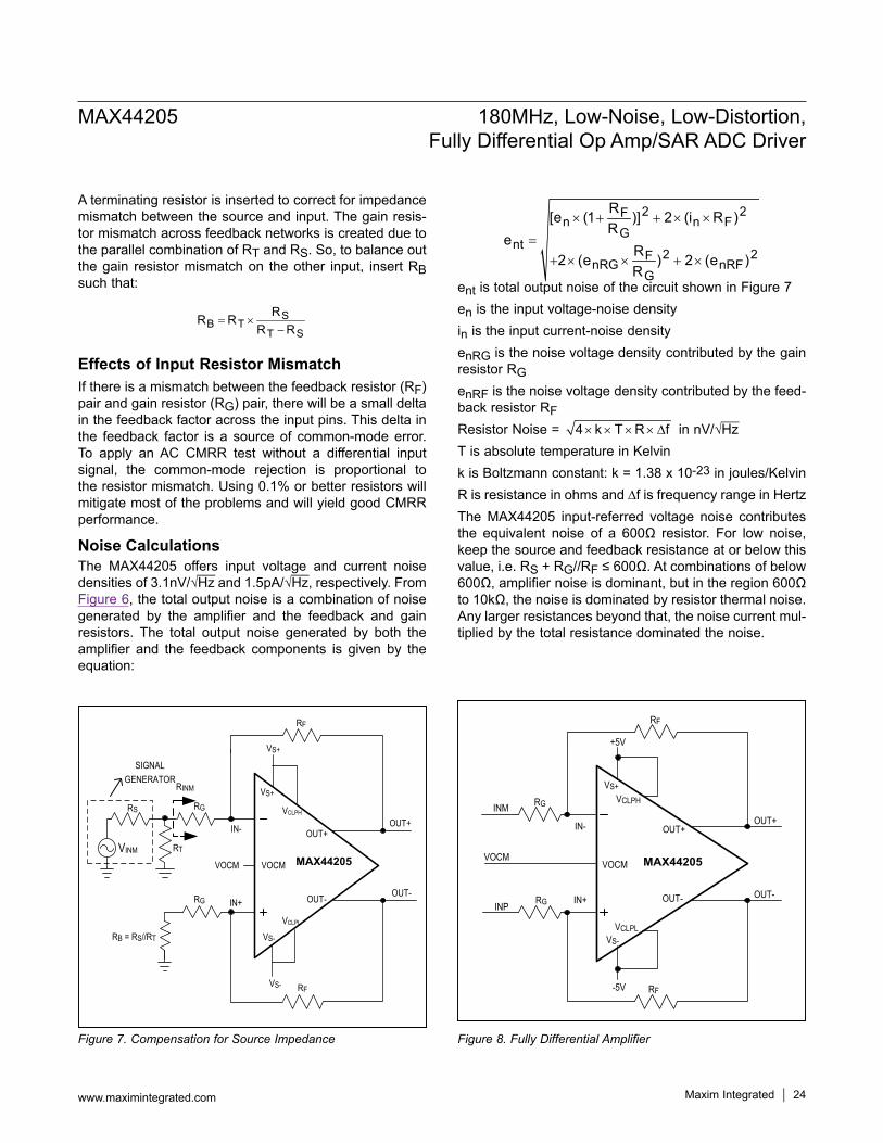
Noise CalculationsThe MAX44205 offers input voltage and current noise densities of 3.1nV/√Hz and 1.5pA/√Hz, respectively. From Figure 6, the total output noise is a combination of noise generated by the amplifier and the feedback and gain resistors. The total output noise generated by both the amplifier and the feedback components is given by the equation:
2 2Fn n F
Gnt
2 2FnRG nRF
G
R[e (1 )] 2 (i R )R
eR2 (e ) 2 (e )R
× + + × ×
=+ × × + ×
ent is total output noise of the circuit shown in Figure 7en is the input voltage-noise densityin is the input current-noise densityenRG is the noise voltage density contributed by the gain resistor RGenRF is the noise voltage density contributed by the feed-back resistor RFResistor Noise = 4 k T R f× × × × ∆ in nV/√HzT is absolute temperature in Kelvink is Boltzmann constant: k = 1.38 x 10⁻²³ in joules/KelvinR is resistance in ohms and ∆f is frequency range in HertzThe MAX44205 input-referred voltage noise contributes the equivalent noise of a 600Ω resistor. For low noise, keep the source and feedback resistance at or below this value, i.e. RS + RG//RF ≤ 600Ω. At combinations of below 600Ω, amplifier noise is dominant, but in the region 600Ω to 10kΩ, the noise is dominated by resistor thermal noise. Any larger resistances beyond that, the noise current mul-tiplied by the total resistance dominated the noise.
Figure 7. Compensation for Source Impedance
OUT-
OUT+
VS+
VS-
OUT+
OUT-
RF
VS+
VS-
MAX44205VOCM
RG
VOCM
IN-
IN+
RS
RT
RB = RS//RT
RINM
RG
RF
VINM
SIGNAL GENERATOR
VCLPH
VCLPL
Figure 8. Fully Differential Amplifier
VS+VCLPH
VCLPLVS-
OUT+
OUT-
RF
RF
+5V
-5V
MAX44205VOCM
RG
RG
INM
INP
VOCM
OUT-
OUT+IN-
IN+
MAX44205 180MHz, Low-Noise, Low-Distortion, Fully Differential Op Amp/SAR ADC Driver
www.maximintegrated.com Maxim Integrated 24
Lower resistor values are ideal for low-noise performance at the cost of increased distortion due to increased load-ing of the feedback network on the output stage. Higher resistor values will yield better distortion performance due to less loading on the output stage but at the cost of increase in higher output noise.
Improving Stability using Feedback CapacitorsWhen the MAX44205 is configured such that a combina-tion of parasitic capacitances at the inverting input form a pole whose frequency lies within the closed-loop band-width of the amplifier, a feedback capacitor across the feedback resistor is needed to form a zero at a frequency close to the frequency of the parasitic pole to recover the lost phase margin.Adding larger value feedback capacitors will reduce the peaking of the amplifier but decreases the closed-loop -3dB bandwidth.
Layout and Bypass CapacitorsFor single-supply applications, it is recommended to place a 0.1µF NPO or C0G ceramic capacitor within 1/8th of an inch from the VS+ pin to ground and to also connect a 10µF ceramic capacitor within 1in of the VS+ pin to GND. One can short VS-, GND, and EP in that case.In dual-supply applications, it is recommended to place a 0.1µF NPO or C0G ceramic capacitor within 1/8th of an inch from the VS+ and VS- pins to GND and place 10µF ceramic capacitors within 1in of the VS+ and VS- pins to GND. Low ESR\ESL NPO capacitors are recommended for 0.1µF or smaller decoupling capacitors. A 0.1µF or 0.22µF capacitor should be placed as close as possible between the VOCM input pin to ground.Signal routing into and out of the part should be direct and as short as possible into and out of the op amp inputs and outputs. The feedback path should be carefully routed with the shortest path possible without any para-sitic capacitance forming between feedback trace and board power planes. Ground and power planes should be removed from directly under the amplifier input and output pins. Also, care should be taken such that there will be no parasitic capacitance formed around the summing nodes at the inputs that could affect the phase margin of the part.Any load capacitance beyond a few picofarads needs to be isolated using series output resistors placed as close as possible to the output pins to avoid excessive peaking or instability.
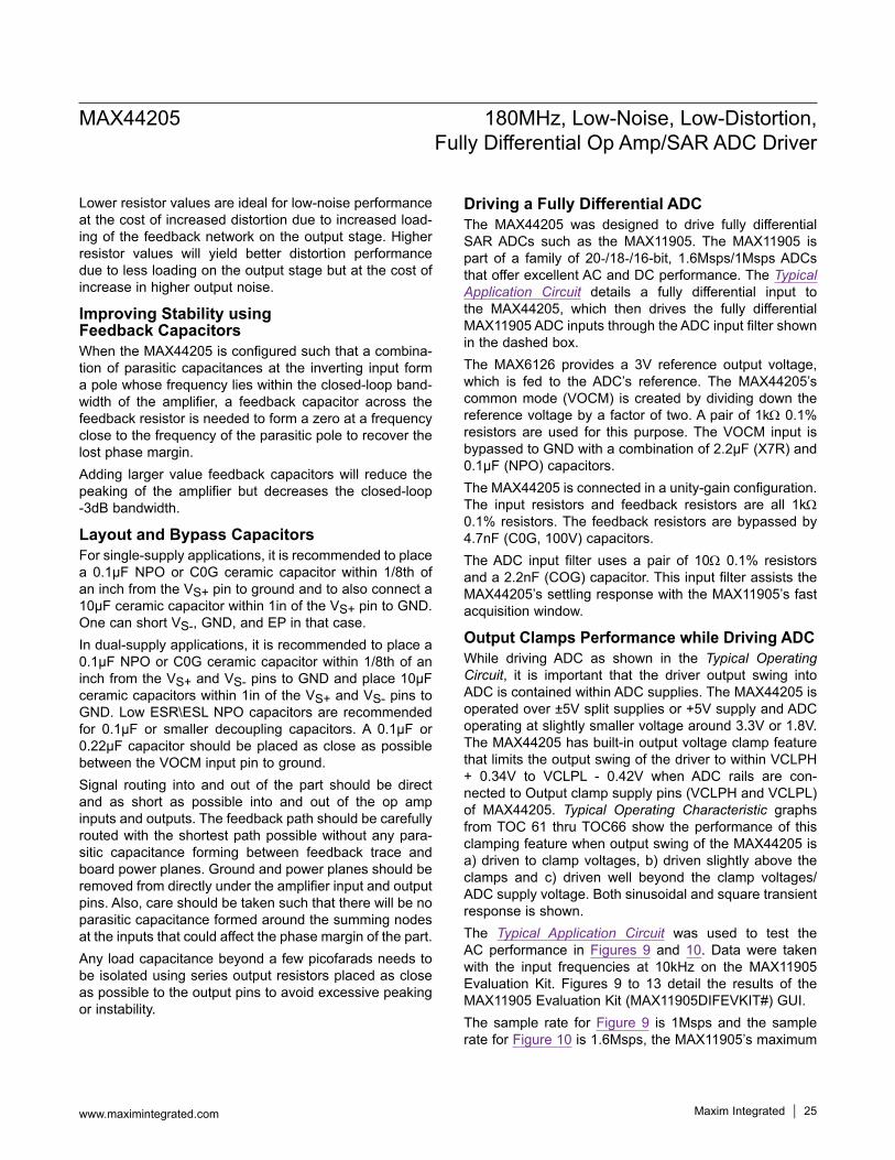
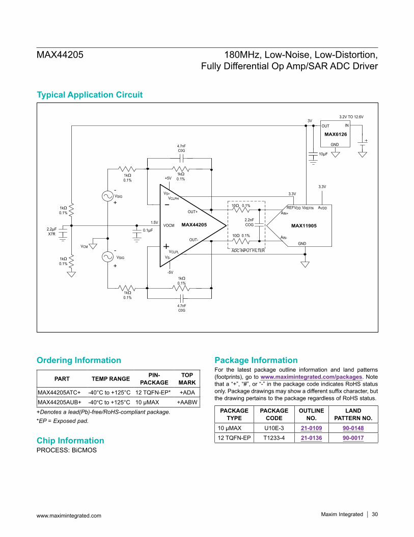
Driving a Fully Differential ADCThe MAX44205 was designed to drive fully differential SAR ADCs such as the MAX11905. The MAX11905 is part of a family of 20-/18-/16-bit, 1.6Msps/1Msps ADCs that offer excellent AC and DC performance. The Typical Application Circuit details a fully differential input to the MAX44205, which then drives the fully differential MAX11905 ADC inputs through the ADC input filter shown in the dashed box. The MAX6126 provides a 3V reference output voltage, which is fed to the ADC’s reference. The MAX44205’s common mode (VOCM) is created by dividing down the reference voltage by a factor of two. A pair of 1kΩ 0.1% resistors are used for this purpose. The VOCM input is bypassed to GND with a combination of 2.2µF (X7R) and 0.1µF (NPO) capacitors.The MAX44205 is connected in a unity-gain configuration. The input resistors and feedback resistors are all 1kΩ 0.1% resistors. The feedback resistors are bypassed by 4.7nF (C0G, 100V) capacitors. The ADC input filter uses a pair of 10Ω 0.1% resistors and a 2.2nF (COG) capacitor. This input filter assists the MAX44205’s settling response with the MAX11905’s fast acquisition window.
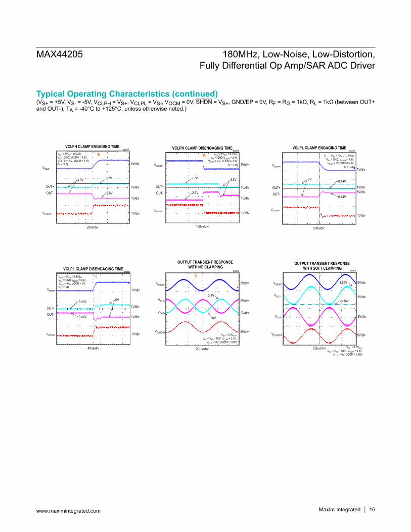
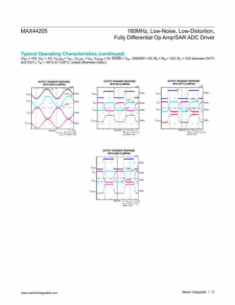
Output Clamps Performance while Driving ADCWhile driving ADC as shown in the Typical Operating Circuit, it is important that the driver output swing into ADC is contained within ADC supplies. The MAX44205 is operated over ±5V split supplies or +5V supply and ADC operating at slightly smaller voltage around 3.3V or 1.8V. The MAX44205 has built-in output voltage clamp feature that limits the output swing of the driver to within VCLPH + 0.34V to VCLPL - 0.42V when ADC rails are con-nected to Output clamp supply pins (VCLPH and VCLPL) of MAX44205. Typical Operating Characteristic graphs from TOC 61 thru TOC66 show the performance of this clamping feature when output swing of the MAX44205 is a) driven to clamp voltages, b) driven slightly above the clamps and c) driven well beyond the clamp voltages/ADC supply voltage. Both sinusoidal and square transient response is shown.The Typical Application Circuit was used to test the AC performance in Figures 9 and 10. Data were taken with the input frequencies at 10kHz on the MAX11905 Evaluation Kit. Figures 9 to 13 detail the results of the MAX11905 Evaluation Kit (MAX11905DIFEVKIT#) GUI.The sample rate for Figure 9 is 1Msps and the sample rate for Figure 10 is 1.6Msps, the MAX11905’s maximum
MAX44205 180MHz, Low-Noise, Low-Distortion, Fully Differential Op Amp/SAR ADC Driver
www.maximintegrated.com Maxim Integrated 25
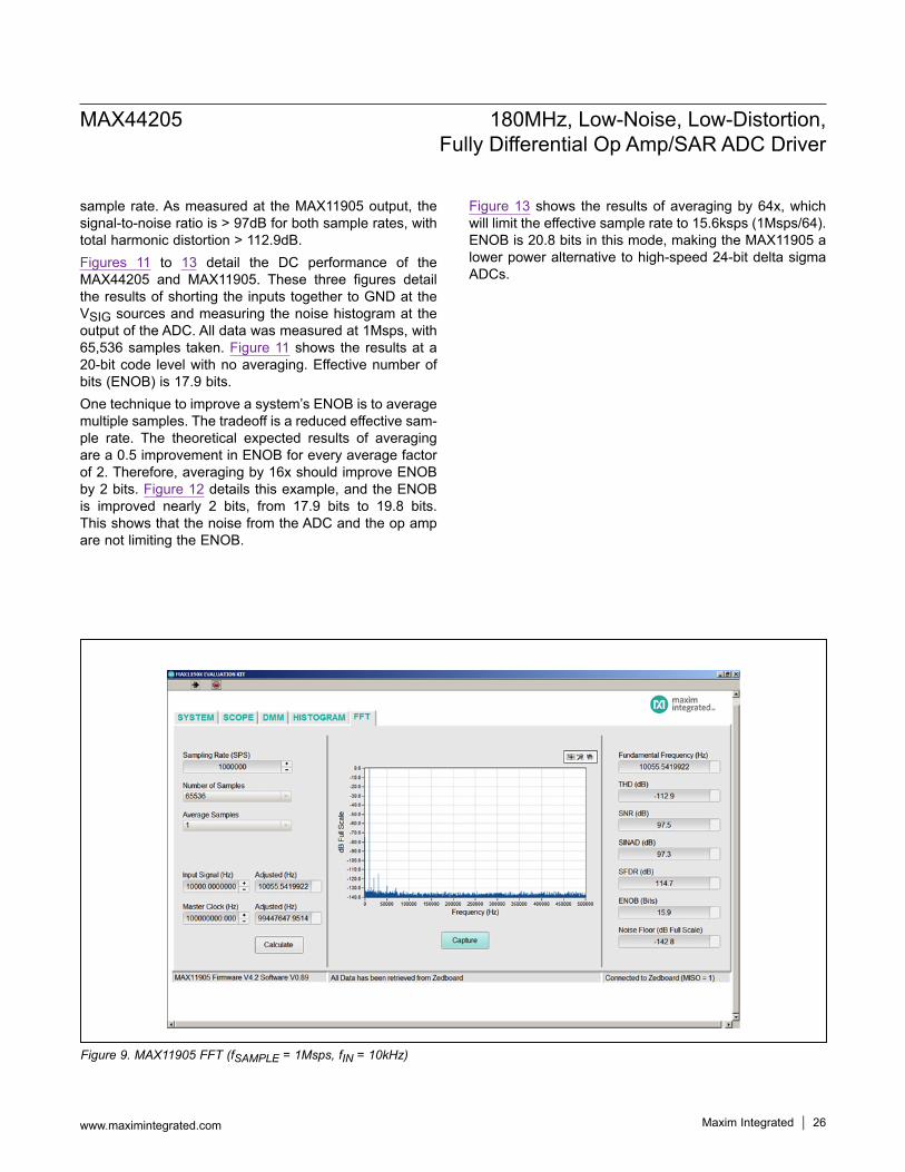
sample rate. As measured at the MAX11905 output, the signal-to-noise ratio is > 97dB for both sample rates, with total harmonic distortion > 112.9dB.Figures 11 to 13 detail the DC performance of the MAX44205 and MAX11905. These three figures detail the results of shorting the inputs together to GND at the VSIG sources and measuring the noise histogram at the output of the ADC. All data was measured at 1Msps, with 65,536 samples taken. Figure 11 shows the results at a 20-bit code level with no averaging. Effective number of bits (ENOB) is 17.9 bits. One technique to improve a system’s ENOB is to average multiple samples. The tradeoff is a reduced effective sam-ple rate. The theoretical expected results of averaging are a 0.5 improvement in ENOB for every average factor of 2. Therefore, averaging by 16x should improve ENOB by 2 bits. Figure 12 details this example, and the ENOB is improved nearly 2 bits, from 17.9 bits to 19.8 bits. This shows that the noise from the ADC and the op amp are not limiting the ENOB.
Figure 13 shows the results of averaging by 64x, which will limit the effective sample rate to 15.6ksps (1Msps/64). ENOB is 20.8 bits in this mode, making the MAX11905 a lower power alternative to high-speed 24-bit delta sigma ADCs.
Figure 9. MAX11905 FFT (fSAMPLE = 1Msps, fIN = 10kHz)
MAX44205 180MHz, Low-Noise, Low-Distortion, Fully Differential Op Amp/SAR ADC Driver
www.maximintegrated.com Maxim Integrated 26
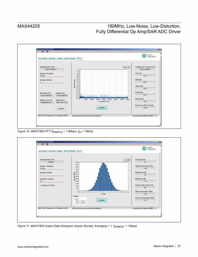
Figure 10. MAX11905 FFT (fSAMPLE = 1.6Msps, fIN = 10kHz)
Figure 11. MAX11905 Output Data Histogram (Inputs Shorted, Averaging = 1, fSAMPLE = 1Msps)
MAX44205 180MHz, Low-Noise, Low-Distortion, Fully Differential Op Amp/SAR ADC Driver
www.maximintegrated.com Maxim Integrated 27
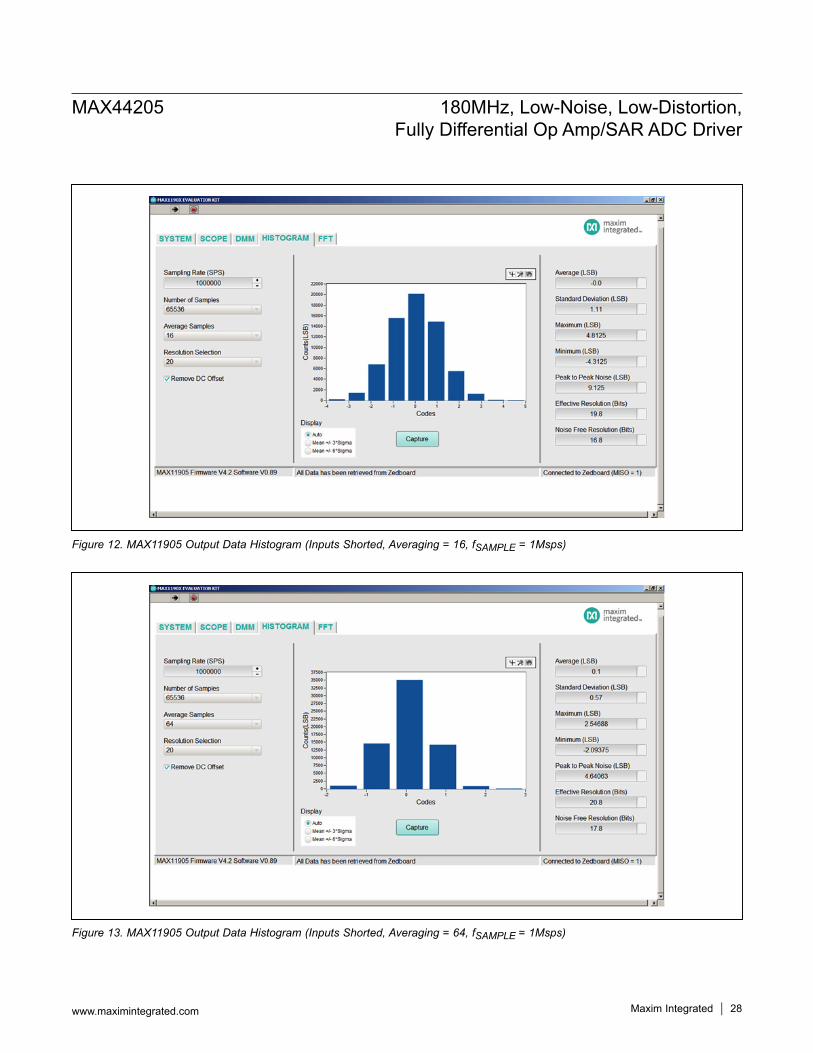
Figure 12. MAX11905 Output Data Histogram (Inputs Shorted, Averaging = 16, fSAMPLE = 1Msps)
Figure 13. MAX11905 Output Data Histogram (Inputs Shorted, Averaging = 64, fSAMPLE = 1Msps)
MAX44205 180MHz, Low-Noise, Low-Distortion, Fully Differential Op Amp/SAR ADC Driver
www.maximintegrated.com Maxim Integrated 28
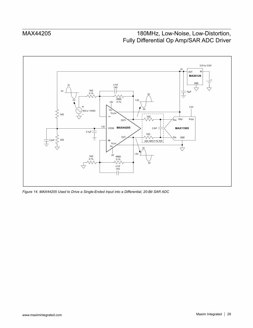
Figure 14. MAX44205 Used to Drive a Single-Ended Input into a Differential, 20-Bit SAR ADC
3.2V to 12.6V
VS+VCLPH
VCLPLVS-
OUT+
OUT-
10Ω
10Ω
1kΩ 0.1%
499Ω0.1%
2.2nF
+5V
MAX44205VOCM MAX11905
MAX6126OUT
VREF AVDD
GND
GND
IN3V
3.3V
AIN+
AIN-
10µF
1.5V
0.1µF
+
-6VP-P + 0VDC
3V
-3V
0V
0V
3V
1.5V
3V
0V
1.5V-5V
4.7nFC0G
1kΩ0.1%
499Ω0.1%
1kΩ
1kΩ
2.2nF ADC INPUT FILTER
4.7nF C0G
MAX44205 180MHz, Low-Noise, Low-Distortion, Fully Differential Op Amp/SAR ADC Driver
www.maximintegrated.com Maxim Integrated 29
Package InformationFor the latest package outline information and land patterns (footprints), go to www.maximintegrated.com/packages. Note that a “+”, “#”, or “-” in the package code indicates RoHS status only. Package drawings may show a different suffix character, but the drawing pertains to the package regardless of RoHS status.
Ordering Information
+Denotes a lead(Pb)-free/RoHS-compliant package.*EP = Exposed pad.
PART TEMP RANGE PIN-PACKAGE
TOP MARK
MAX44205ATC+ -40°C to +125°C 12 TQFN-EP* +ADA
MAX44205AUB+ -40°C to +125°C 10 µMAX +AABWPACKAGE
TYPEPACKAGE
CODEOUTLINE
NO.LAND
PATTERN NO.10 µMAX U10E-3 21-0109 90-014812 TQFN-EP T1233-4 21-0136 90-0017
VS+VCLPH
VCLPLVS-
OUT+
OUT-
10Ω 0.1%
10Ω 0.1%
2.2nF COG
+5V
-5V
MAX44205VOCM MAX11905
MAX6126
OUT
VREFIN AVDD
GND
GND
IN3V
3.3V
3.2V TO 12.6V
AIN+
AIN-
10µF
1.5V
0.1µF
4.7nFC0G
-
+
+
-VCM
VSIG
VSIG
1kΩ 0.1%
1kΩ 0.1%
1kΩ 0.1%
4.7nF C0G
1kΩ0.1%
1kΩ 0.1%
1kΩ 0.1%
2.2µF X7R
REFVDD
ADC INPUT FILTER
3.3V
Typical Application Circuit
MAX44205 180MHz, Low-Noise, Low-Distortion, Fully Differential Op Amp/SAR ADC Driver
www.maximintegrated.com Maxim Integrated 30
Chip InformationPROCESS: BiCMOS
Revision HistoryREVISIONNUMBER
REVISIONDATE DESCRIPTION PAGES
CHANGED0 6/14 Initial release —
1 12/14
Updated the Benefits and Features, Typical Application Circuit, Electrical Characteristics, Typical Operating Characteristics, Pin Description, Functional Diagram, Detailed Description, SHDN Operation, Applications Information, and Ordering Information sections. Added the Output Clamps Performance While Driving ADCs section. Updated Figures 2, 5, 6, 7, and 14.
1–17, 19, 21–26, 29, 30
Maxim Integrated cannot assume responsibility for use of any circuitry other than circuitry entirely embodied in a Maxim Integrated product. No circuit patent licenses are implied. Maxim Integrated reserves the right to change the circuitry and specifications without notice at any time. The parametric values (min and max limits) shown in the Electrical Characteristics table are guaranteed. Other parametric values quoted in this data sheet are provided for guidance.
Maxim Integrated and the Maxim Integrated logo are trademarks of Maxim Integrated Products, Inc. © 2014 Maxim Integrated Products, Inc. 31
MAX44205 180MHz, Low-Noise, Low-Distortion, Fully Differential Op Amp/SAR ADC Driver
For pricing, delivery, and ordering information, please contact Maxim Direct at 1-888-629-4642, or visit Maxim Integrated’s website at www.maximintegrated.com.