Embed Size (px)
Citation preview

General DescriptionThe MAX30100 is an integrated pulse oximetry and heart-rate monitor sensor solution. It combines two LEDs, a photodetector, optimized optics, and low-noise analog signal processing to detect pulse oximetry and heart-rate signals. The MAX30100 operates from 1.8V and 3.3V power sup-plies and can be powered down through software with negligible standby current, permitting the power supply to remain connected at all times.
Applications Wearable Devices Fitness Assistant Devices Medical Monitoring Devices
Benefits and Features Complete Pulse Oximeter and Heart-Rate Sensor
Solution Simplifies Design• Integrated LEDs, Photo Sensor, and
High-Performance Analog Front -End• Tiny 5.6mm x 2.8mm x 1.2mm 14-Pin Optically
Enhanced System-in-Package Ultra-Low-Power Operation Increases Battery Life for
Wearable Devices• Programmable Sample Rate and LED Current for
Power Savings• Ultra-Low Shutdown Current (0.7µA, typ)
Advanced Functionality Improves Measurement Performance• High SNR Provides Robust Motion Artifact Resil-
ience• Integrated Ambient Light Cancellation• High Sample Rate Capability• Fast Data Output Capability
Ordering Information appears at end of data sheet.
19-7065; Rev 0; 9/14
ADC
CONTROL SIGNAL PROCESSING
COVER GLASS
10
0.1RED IR
HbO2
Hb
NO INK
MAX30100 Pulse Oximeter and Heart-Rate Sensor IC for Wearable Health
System Block Diagram
EVALUATION KIT AVAILABLE

VDD to GND .........................................................-0.3V to +2.2VGND to PGND ......................................................-0.3V to +0.3Vx_DRV, x_LED+ to PGND ....................................-0.3V to +6.0VAll Other Pins to GND ..........................................-0.3V to +6.0V Output Short-Circuit Current Duration .......................ContinuousContinuous Input Current into Any Terminal ....................±20mA
Continuous Power Dissipation (TA = +70°C) OESIP (derate 5.8mW/°C above +70°C) ....................464mWOperating Temperature Range ........................... -40°C to +85°CSoldering Temperature (reflow) .......................................+260°C Storage Temperature Range ............................ -40°C to +105°C
OESIP Junction-to-AmbientThermalResistance(θJA) ........150°C/W Junction-to-CaseThermalResistance(θJC) .............170°C/W
(Note 1)
(VDD = 1.8V, VIR_LED+ = VR_LED+ = 3.3V, TA = +25°C, min/max are from TA = -40°C to +85°C, unless otherwise noted.) (Note 2)
PARAMETER SYMBOL CONDITIONS MIN TYP MAX UNITS
POWER SUPPLY
Power-Supply Voltage VDD Guaranteed by RED and IR count tolerance 1.7 1.8 2.0 V
LED Supply Voltage(R_LED+ or IR_LED+ to PGND) VLED+ Guaranteed by PSRR of LED Driver 3.1 3.3 5.0 V
Supply Current IDD
SpO2 and heart rate modes,PW = 200µs, 50sps 600 1200
µAHeart rate only mode,PW = 200µs, 50sps 600 1200
Supply Current in Shutdown ISHDN TA = +25°C, MODE = 0x80 0.7 10 µA
SENSOR CHARACTERISTICS
ADC Resolution 14 bits
Red ADC Count(Note 3) REDC
Propriety ATE setup RED_PA = 0x05, LED_PW = 0x00, SPO2_SR = 0x07, TA = +25°C
23,000 26,000 29,000 Counts
IR ADC Count(Note 3) IRC
Propriety ATE setup IR_PA = 0x09, LED_PW = 0x00, SPO2_SR = 0x07, TA = +25°C
23,000 26,000 29,000 Counts
Dark Current Count DCCRED_PA = IR_PA = 0x00, LED_PW = 0x03, SPO2_SR = 0x01 0 3 Counts
DC Ambient Light Rejection(Note 4) ALR
Number of ADC counts with fingeronsensorunderdirectsunlight (100K lux)LED_PW = 0x03,SPO2_SR = 0x01
RED LED 0
Counts
IR LED 0
www.maximintegrated.com Maxim Integrated 2
MAX30100 Pulse Oximeter and Heart-Rate Sensor IC for Wearable Health
Note 1: Package thermal resistances were obtained using the method described in JEDEC specification JESD51-7, using a four-layer board. For detailed information on package thermal considerations, refer to www.maximintegrated.com/thermal-tutorial.
Absolute Maximum Ratings
Package Thermal Characteristics
Electrical Characteristics

(VDD = 1.8V, VIR_LED+ = VR_LED+ = 3.3V, TA = +25°C, min/max are from TA = -40°C to +85°C, unless otherwise noted.) (Note 2)
PARAMETER SYMBOL CONDITIONS MIN TYP MAX UNITS
IR ADC Count—PSRR (VDD) PSRRVDD
Propriety ATE setup 1.7V < VDD < 2.0V, LED_PW = 0x03, SPO2_SR = 0x01, IR_PA = 0x09, IR_PA = 0x05, TA = +25°C
0.25 2 %
Frequency = DC to 100kHz, 100mVP-P 10 LSB
RED/IR ADC Count—PSRR (X_LED+) PSRRLED
Propriety ATE setup 3.1V < X_LED+ < 5V, LED_PW = 0x03, SPO2_SR = 0x01, IR_PA = 0x09, IR_PA = 0x05, TA = +25°C
0.05 2 %
Frequency = DC to 100kHz, 100mVP-P 10 LSB
ADC Integration Time INTLED_PW = 0x00 200 µs
LED_PW = 0x03 1600 µs
IR LED CHARACTERISTICS (Note 4)
LED Peak Wavelength λP ILED = 20mA, TA = +25°C 870 880 900 nm
Full Width at Half Max Δλ ILED = 20mA, TA = +25°C 30 nm
Forward Voltage VF ILED = 20mA, TA = +25°C 1.4 V
Radiant Power PO ILED = 20mA, TA = +25°C 6.5 mW
RED LED CHARACTERISTICS (Note 4)
LED Peak Wavelength λP ILED = 20mA, TA = +25°C 650 660 670 nm
Full Width at Half Max Δλ ILED = 20mA, TA = +25°C 20 nm
Forward Voltage VF ILED = 20mA, TA = +25°C 2.1 V
Radiant Power PO ILED = 20mA, TA = +25°C 9.8 mW
TEMPERATURE SENSOR
Temperature ADC Acquisition Time TT TA = +25°C 29 ms
Temperature Sensor Accuracy TA TA = +25°C ±1 °C
Temperature Sensor Minimum Range TMIN -40 °C
Temperature Sensor Maximum Range TMAX 85 °C
www.maximintegrated.com Maxim Integrated 3
MAX30100 Pulse Oximeter and Heart-Rate Sensor IC for Wearable Health
Electrical Characteristics (continued)
(VDD = 1.8V, VIR_LED+ = VR_LED+ = 3.3V, TA = +25°C, min/max are from TA = -40°C to +85°C, unless otherwise noted.) (Note 2)
Note 2: All devices are 100% production tested at TA = +25°C. Specifications over temperature limits are guaranteed by Maxim Integrated’s bench or proprietary automated test equipment (ATE) characterization.
Note 3: Specifications are guaranteed by Maxim Integrated’s bench characterization and by 100% production test using proprietary ATE setup and conditions.
Note 4: For design guidance only. Not production tested.
PARAMETER SYMBOL CONDITIONS MIN TYP MAX UNITS
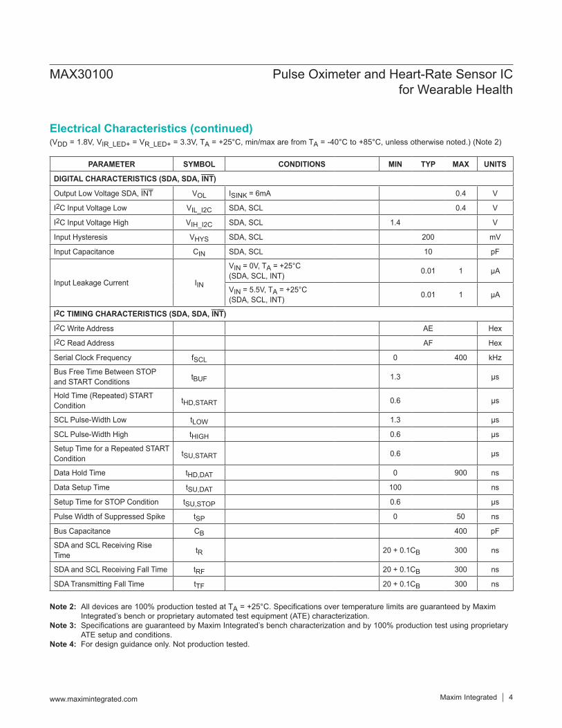
DIGITAL CHARACTERISTICS (SDA, SDA, INT)
Output Low Voltage SDA, INT VOL ISINK = 6mA 0.4 V
I2C Input Voltage Low VIL_I2C SDA, SCL 0.4 V
I2C Input Voltage High VIH_I2C SDA, SCL 1.4 V
Input Hysteresis VHYS SDA, SCL 200 mV
Input Capacitance CIN SDA, SCL 10 pF
Input Leakage Current IIN
VIN = 0V, TA = +25°C(SDA, SCL, INT) 0.01 1 µA
VIN = 5.5V, TA = +25°C(SDA, SCL, INT) 0.01 1 µA
I2C TIMING CHARACTERISTICS (SDA, SDA, INT)
I2C Write Address AE Hex
I2C Read Address AF Hex
Serial Clock Frequency fSCL 0 400 kHz
Bus Free Time Between STOP and START Conditions tBUF 1.3 µs
Hold Time (Repeated) START Condition tHD,START 0.6 µs
SCL Pulse-Width Low tLOW 1.3 µs
SCL Pulse-Width High tHIGH 0.6 µs
Setup Time for a Repeated START Condition tSU,START 0.6 µs
Data Hold Time tHD,DAT 0 900 ns
Data Setup Time tSU,DAT 100 ns
Setup Time for STOP Condition tSU,STOP 0.6 µs
Pulse Width of Suppressed Spike tSP 0 50 ns
Bus Capacitance CB 400 pF
SDA and SCL Receiving Rise Time tR 20 + 0.1CB 300 ns
SDA and SCL Receiving Fall Time tRF 20 + 0.1CB 300 ns
SDA Transmitting Fall Time tTF 20 + 0.1CB 300 ns
www.maximintegrated.com Maxim Integrated 4
MAX30100 Pulse Oximeter and Heart-Rate Sensor IC for Wearable Health
Electrical Characteristics (continued)

Figure 1. I2C-Compatible Interface Timing Diagram
SDA
SCLtHD,STA
START CONDITION
tR tF
tLOW
tSU,DAT
tHD,DAT
tSU,STAtHD,STA
REPEATED START CONDITION
tSP tSU,STO
tBUF
STOPCONDITION
STARTCONDITION
tHIGH
www.maximintegrated.com Maxim Integrated 5
MAX30100 Pulse Oximeter and Heart-Rate Sensor IC for Wearable Health

(VDD = 1.8V, VIR_LED+ = VR_LED+ = 3.3V, TA = +25°C, unless otherwise noted.)
0.0
0.1
0.2
0.3
0.4
0.5
0.6
0.7
0.8
0.9
1.0
0.00 0.50 1.00 1.50 2.00 2.50
SUPP
LY C
URRE
NT (m
A)
SUPPLY VOLTAGE (V)
VDD SUPPLY CURRENT vs.SUPPLY VOLTAGE toc03
MODE 0
MODE 2
MODE 3
0.04
0.05
0.06
0.07
0.08
0.09
0 10 20 30 40 50 60 70
DRV
PIN
COMP
LIANC
E VO
LTAG
E (V
)
LED PULSE CURRENT (mA)
IR LED SUPPLY HEADROOM(-10% CURRENT)
toc02
TA = +25°C
0
10000
20000
30000
40000
50000
60000
70000
0 5 10 15 20
COUN
TS (S
UM)
DISTANCE (mm)
DC COUNTS vs. DISTANCE FORWHITE HIGH IMPACT STYRENE CARD
toc04
RED
IR
MODE[2:0] = 011SPO2_HI_RES_EN = 1SPO2_ADC_RGE = 0SPO2_SR[2:0] = 001RED or IR_PA[3:0] = 0101
0
1
2
3
4
5
6
7
-50 0 50 100 150
V DD
SHUT
DOW
N CU
RREN
T (µ
A)
TEMPERATURE (°C)
VDD SHUTDOWN CURRENTvs. TEMPERATURE
VDD = 1.7V
toc05
VDD = 2.0V
VDD = 1.8V
0.06
0.07
0.08
0.09
0.10
0.11
0.12
0.13
0.14
-50 0 50 100 150
LED
SHUT
DOW
N CU
RREN
T (µ
A)
TEMPERATURE (°C)
LED SHUTDOWN CURRENTvs. TEMPERATURE
VDD = 3.1V
toc06
VDD = 3.6V
VDD = 3.3V
-4
-3
-2
-1
0
1
2
3
-40 10 60 110
TEMP
ERAT
URE
ERRO
R (°C
)
ACTUAL TEMPERATURE (°C)
ON-BOARD TEMPERATURE vs. ERRORtoc07
-20
0
20
40
60
80
100
120
500 600 700 800
NORM
ALIZ
E PO
WER
(%)
WAVELENGTH (nm)
RED LED SPECTRA at +30°Ctoc08
0.05
0.06
0.07
0.08
0.09
0.10
0.11
0.12
0.13
0.14
0 10 20 30 40 50 60 70 80
DRV
PIN
COMP
LIANC
E VO
LTAG
E (V
)
LED PULSE CURRENT (mA)
RED LED SUPPLY HEADROOM(-10% CURRENT)
toc01
TA = +25°C
Maxim Integrated 6www.maximintegrated.com
MAX30100 Pulse Oximeter and Heart-Rate Sensor IC for Wearable Health
Typical Operating Characteristics

(VDD = 1.8V, VIR_LED+ = VR_LED+ = 3.3V, TA = +25°C, unless otherwise noted.)
860
865
870
875
880
885
890
895
900
-40 10 60 110
PEAK
WAV
ELEN
GTH
(nm)
TEMPERATURE (°C)
IR LED WAVELENGTH vs. TEMPERATUREAT LED CURRENT = 25mA
toc11
650
655
660
665
670
675
-40 10 60 110
PEAK
WAV
ELEN
GTH
(nm)
TEMPERATURE (°C)
RED LED WAVELENGTH vs. TEMPERATUREAT LED CURRENT = 25mA
toc10
0
10
20
30
40
50
60
70
1.30 1.35 1.40 1.45 1.50 1.55
FORW
ARD
CURR
ENT
(mA)
FORWARD VOLTAGE (V)
RED LED FORWARD VOLTAGE vs.FORWARD CURRENT toc12
0
10
20
30
40
50
60
70
80
1.70 1.80 1.90 2.00 2.10 2.20 2.30 2.40
FORW
ARD
CURR
ENT
(mA)
FORWARD VOLTAGE (V)
IR LED FORWARD VOLTAGE vs.FORWARD CURRENT toc13
-20
0
20
40
60
80
100
120
700 800 900 1000
NORM
ALIZ
E PO
WER
(%)
WAVELENGTH (nm)
IR LED SPECTRA at +30°Ctoc09
Maxim Integrated 7www.maximintegrated.com
MAX30100 Pulse Oximeter and Heart-Rate Sensor IC for Wearable Health
Typical Operating Characteristics (continued)

PIN NAME FUNCTION
1, 7, 8, 14 N.C. No Connection. Connect to PCB Pad for Mechanical Stability.
2 SCL I2C Clock Input
3 SDA I2C Clock Data, Bidirectional (Open-Drain)
4 PGND Power Ground of the LED Driver Blocks
5 IR_DRV IRLEDCathodeandLEDDriverConnectionPoint.Leavefloatingincircuit.
6 R_DRV RedLEDCathodeandLEDDriverConnectionPoint.Leavefloatingincircuit.
9 R_LED+ Power Supply (Anode Connection) for Red LED. Bypass to PGND for best performance. Connected to IR_LED+ internally.
10 IR_LED+ Power Supply (Anode Connection) for IR LED. Bypass to PGND for best performance. Con-nected to R_LED+ internally.
11 VDD Analog Power Supply Input. Bypass to GND for best performance.
12 GND Analog Ground
13 INT Active-Low Interrupt (Open-Drain)
N.C. 1
SCL 2
SDA 3
PGND 4
IR_DRV 5
R_DRV 6
N.C. 7
14 N.C.
13 INT
12 GND
11 VDD
10 IR_LED+
9 R_LED+
8 N.C.
MAX30100
SENSOR
LED
www.maximintegrated.com Maxim Integrated 8
MAX30100 Pulse Oximeter and Heart-Rate Sensor IC for Wearable Health
Pin Description
Pin Configuration

880nm660nm
ADC
AMBIENT LIGHT CANCELLATION ANALOG
ADCTEMP
OSCILLATOR
DIGITAL FILTER
DIGITAL
DATAREGISTER
LED DRIVERS
I2CCOMMUNICATION
INT
SDA
SCL
VDDIR_LED+R_LED+
IR_DRVR_DRV GND PGND
RED IR
RED+IR
www.maximintegrated.com Maxim Integrated 9
MAX30100 Pulse Oximeter and Heart-Rate Sensor IC for Wearable Health
Detailed DescriptionThe MAX30100 is a complete pulse oximetry and heart-rate sensor system solution designed for the demanding requirements of wearable devices. The MAX30100 pro-vides very small total solution size without sacrificing opti-cal or electrical performance. Minimal external hardware components are needed for integration into a wearable device.The MAX30100 is fully configurable through software reg-isters, and the digital output data is stored in a 16-deep FIFO within the device. The FIFO allows the MAX30100 to be connected to a microcontroller or microprocessor on a shared bus, where the data is not being read continu-ously from the device’s registers.
SpO2 SubsystemThe SpO2 subsystem in the MAX30100 is composed of ambient light cancellation (ALC), 16-bit sigma delta ADC, and proprietary discrete time filter.The SpO2 ADC is a continuous time oversampling sigma delta converter with up to 16-bit resolution. The ADC out-put data rate can be programmed from 50Hz to 1kHz. The
MAX30100 includes a proprietary discrete time filter to reject 50Hz/60Hz interference and low-frequency residual ambient noise.
Temperature SensorThe MAX30100 has an on-chip temperature sensor for (optionally) calibrating the temperature dependence of the SpO2 subsystem.The SpO2 algorithm is relatively insensitive to the wave-length of the IR LED, but the red LED’s wavelength is criti-cal to correct interpretation of the data. The temperature sensor data can be used to compensate the SpO2 error with ambient temperature changes.
LED DriverThe MAX30100 integrates red and IR LED drivers to drive LED pulses for SpO2 and HR measurements. The LED current can be programmed from 0mA to 50mA (typical only) with proper supply voltage. The LED pulse width can be programmed from 200µs to 1.6ms to optimize measurement accuracy and power consumption based on use cases.
Functional Diagram
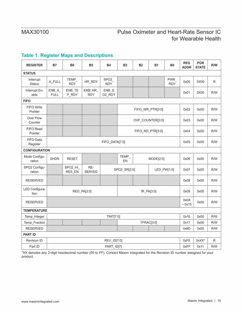
Table 1. Register Maps and Descriptions
REGISTER B7 B6 B5 B4 B3 B2 B1 B0 REGADDR
PORSTATE R/W
STATUS
Interrupt Status A_FULL TEMP_
RDY HR_RDY SPO2_ RDY
PWR_ RDY 0x00 0X00 R
Interrupt En-able
ENB_A_FULL
ENB_TE P_RDY
ENB_HR_RDY
ENB_S O2_RDY 0x01 0X00 R/W
FIFO
FIFO Write Pointer FIFO_WR_PTR[3:0] 0x02 0x00 R/W
Over Flow Counter OVF_COUNTER[3:0] 0x03 0x00 R/W
FIFO Read Pointer FIFO_RD_PTR[3:0] 0x04 0x00 R/W
FIFO Data Register FIFO_DATA[7:0] 0x05 0x00 R/W
CONFIGURATION
ModeConfigu-ration SHDN RESET TEMP_
EN MODE[2:0] 0x06 0x00 R/W
SPO2Configu-ration
SPO2_HI_RES_EN
RE-SERVED SPO2_SR[2:0] LED_PW[1:0] 0x07 0x00 R/W
RESERVED 0x08 0x00 R/W
LEDConfigura-tion RED_PA[3:0] IR_PA[3:0] 0x09 0x00 R/W
RESERVED 0x0A – 0x15 0x00 R/W
TEMPERATURE
Temp_Integer TINT[7:0] 0x16 0x00 R/W
Temp_Fraction TFRAC[3:0] 0x17 0x00 R/W
RESERVED 0x8D 0x00 R/W
PART ID
Revision ID REV_ID[7:0] 0xFE 0xXX* R
Part ID PART_ID[7] 0xFF 0x11 R/W
*XX denotes any 2-digit hexidecimal number (00 to FF). Contact Maxim Integrated for the Revision ID number assigned for your product.
www.maximintegrated.com Maxim Integrated 10
MAX30100 Pulse Oximeter and Heart-Rate Sensor IC for Wearable Health

Interrupt Status (0x00)
There are 5 interrupts and the functionality of each is exactly the same: pulling the active-low interrupt pin into its low state until the interrupt is cleared.The interrupts are cleared whenever the interrupt status register is read, or when the register that triggered the interrupt is read. For example, if the SpO2 sensor triggers an interrupt due to finishing a conversion, reading either the FIFO data register or the interrupt register clears the interrupt pin (which returns to its normal high state), and also clears all the bits in the interrupt status register to zero.Bit 7: FIFO Almost Full Flag (A_FULL)In SpO2 and heart-rate modes, this interrupt triggers when the FIFO write pointer is the same as the FIFO read pointer minus one, which means that the FIFO has only one unwritten space left. If the FIFO is not read within the next conver-sion time, the FIFO becomes full and future data is lost.Bit 6: Temperature Ready Flag (TEMP_RDY)When an internal die temperature conversion is finished, this interrupt is triggered so the processor can read the tem-perature data registers.Bit 5: Heart Rate Data Ready (HR_RDY)In heart rate or SPO2 mode, this interrupt triggers after every data sample is collected. A heart rate data sample consists of one IR data point only. This bit is automatically cleared when the FIFO data register is read.Bit 4: SpO2 Data Ready (SPO2_RDY)In SpO2 mode, this interrupt triggers after every data sample is collected. An SpO2 data sample consists of one IR and one red data points. This bit is automatically cleared when the FIFO data register is read.Bit 3: RESERVEDThis bit should be ignored and always be zero in normal operation.Bit 2: RESERVEDThis bit should be ignored and always be zero in normal operation.Bit 1: RESERVEDThis bit should be ignored and always be zero in normal operation.Bit 0: Power Ready Flag (PWR_RDY)On power-up or after a brownout condition, when the supply voltage VDD transitions from below the UVLO voltage to above the UVLO voltage, a power-ready interrupt is triggered to signal that the IC is powered up and ready to collect data.
REGISTER B7 B6 B5 B4 B3 B2 B1 B0 REGADDR
PORSTATE R/W
Interrupt Status A_FULL TEMP_
RDY HR_RDY SPO2_ RDY
PWR_ RDY 0x00 0X00 R
www.maximintegrated.com Maxim Integrated 11
MAX30100 Pulse Oximeter and Heart-Rate Sensor IC for Wearable Health

Interrupt Enable (0x01)
Each source of hardware interrupt, with the exception of power ready, can be disabled in a software register within the MAX30100 IC. The power-ready interrupt cannot be disabled because the digital state of the MAX30100 is reset upon a brownout condition (low power-supply voltage), and the default state is that all the interrupts are disabled. It is important for the system to know that a brownout condition has occurred, and the data within the device is reset as a result.When an interrupt enable bit is set to zero, the corresponding interrupt appears as 1 in the interrupt status register, but the INT pin is not pulled low.The four unused bits (B3:B0) should always be set to zero (disabled) for normal operation.FIFO (0x02–0x05)
FIFO Write PointerThe FIFO write pointer points to the location where the MAX30100 writes the next sample. This pointer advances for each sample pushed on to the FIFO. It can also be changed through the I2C interface when MODE[2:0] is nonzero.FIFO Overflow CounterWhen the FIFO is full, samples are not pushed on to the FIFO, samples are lost. OVF_COUNTER counts the number of samples lost. It saturates at 0xF. When a complete sample is popped from the FIFO (when the read pointer advances), OVF_COUNTER is reset to zero.FIFO Read PointerThe FIFO read pointer points to the location from where the processor gets the next sample from the FIFO via the I2C interface. This advances each time a sample is popped from the FIFO. The processor can also write to this pointer after reading the samples, which would allow rereading samples from the FIFO if there is a data communication error.FIFO DataThe circular FIFO depth is 16 and can hold up to 16 samples of SpO2 channel data (Red and IR). The FIFO_DATA reg-ister in the I2C register map points to the next sample to be read from the FIFO. FIFO_RD_PTR points to this sample. Reading FIFO_DATA register does not automatically increment the register address; burst reading this register reads the same address over and over. Each sample is 4 bytes of data, so this register has to be read 4 times to get one sample.The above registers can all be written and read, but in practice, only the FIFO_RD_PTR register should be written to in operation. The others are automatically incremented or filled with data by the MAX30100. When starting a new SpO2
REGISTER B7 B6 B5 B4 B3 B2 B1 B0 REGADDR
PORSTATE R/W
Interrupt Enable
ENB_A_FULL
ENB_TE P_RDY
ENB_HR_RDY
ENB_S O2_RDY 0x01 0X00 R/W
REGISTER B7 B6 B5 B4 B3 B2 B1 B0 REGADDR
PORSTATE R/W
FIFO Write Pointer FIFO_WR_PTR[3:0] 0x02 0x00 R/W
Over Flow Counter OVF_COUNTER[3:0] 0x03 0x00 R/W
FIFO Read Pointer FIFO_RD_PTR[3:0] 0x04 0x00 R/W
FIFO Data Register FIFO_DATA[7:0] 0x05 0x00 R/W
www.maximintegrated.com Maxim Integrated 12
MAX30100 Pulse Oximeter and Heart-Rate Sensor IC for Wearable Health

or heart-rate conversion, it is recommended to first clear the FIFO_WR_PTR, OVF_COUNTER, and FIFO_RD_PTR registers to all zeros (0x00) to ensure the FIFO is empty and in a known state. When reading the MAX30100 registers in one burst-read I2C transaction, the register address pointer typically increments so that the next byte of data sent is from the next register, etc. The exception to this is the FIFO data register, register 0x05. When reading this register, the address pointer does not increment, but the FIFO_RD_PTR does. So the next byte of data sent will represent the next byte of data available in the FIFO.Reading from the FIFONormally, reading registers from the I2C interface autoincrements the register address pointer, so that all the registers can be read in a burst read without an I2C restart event. In the MAX30100, this holds true for all registers except for the FIFO_DATA register (0x05).Reading the FIFO_DATA register does not automatically increment the register address; burst reading this register reads the same address over and over. Each sample is 4 bytes of data, so this register has to be read 4 times to get one sample.The other exception is 0xFF, reading more bytes after the 0xFF register does not advance the address pointer back to 0x00, and the data read is not meaningful.FIFO Data StructureThe data FIFO consists of a 16-sample memory bank that stores both IR and RED ADC data. Since each sample consists of one IR word and one RED word, there are 4 bytes of data for each sample, and therefore, 64 total bytes of data can be stored in the FIFO. Figure 2 shows the structure of the FIFO graphically.The FIFO data is left-justified as shown in Table 1; i.e. the MSB bit is always in the bit 15 position regardless of ADC resolution.Each data sample consists of an IR and a red data word (2 registers), so to read one sample requires 4 I2C byte reads in a row. The FIFO read pointer is automatically incremented after each 4-byte sample is read.In heart-rate only mode, the 3rd and 4th bytes of each sample return zeros, but the basic structure of the FIFO remains the same.Write/Read Pointers
Table 2. FIFO Data
Figure 2. Graphical Representation of the FIFO Data Register
ADC RESOLUTION
IR [15]
IR [14]
IR [13]
IR [12]
IR [11]
IR [10]
IR [9]
IR [8]
IR [7]
IR [6]
IR [5]
IR [4]
IR [3]
IR [2]
IR [1]
IR [0]
16-bit
14-bit
12-bit
10-bit
IR[15:8]
IR[7:0]
RED[15:8]
RED[7:0]
NEWER SAMPLES
OLDER SAMPLESREGISTER 0x05
IR[15:8](START OF SAMPLE #2)
www.maximintegrated.com Maxim Integrated 13
MAX30100 Pulse Oximeter and Heart-Rate Sensor IC for Wearable Health
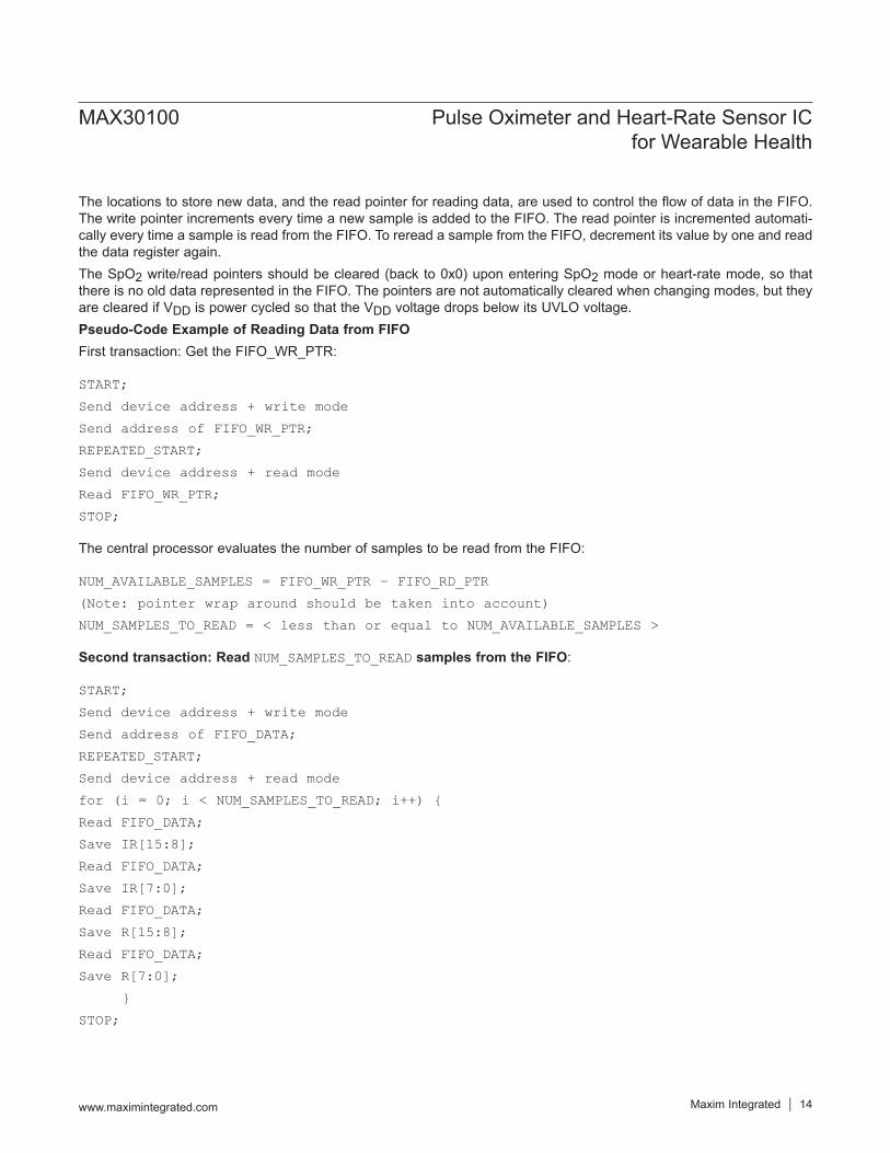
The locations to store new data, and the read pointer for reading data, are used to control the flow of data in the FIFO. The write pointer increments every time a new sample is added to the FIFO. The read pointer is incremented automati-cally every time a sample is read from the FIFO. To reread a sample from the FIFO, decrement its value by one and read the data register again.The SpO2 write/read pointers should be cleared (back to 0x0) upon entering SpO2 mode or heart-rate mode, so that there is no old data represented in the FIFO. The pointers are not automatically cleared when changing modes, but they are cleared if VDD is power cycled so that the VDD voltage drops below its UVLO voltage.Pseudo-Code Example of Reading Data from FIFOFirst transaction: Get the FIFO_WR_PTR:
START;
Send device address + write mode
Send address of FIFO_WR_PTR;
REPEATED_START;
Send device address + read mode
Read FIFO_WR_PTR;
STOP;
The central processor evaluates the number of samples to be read from the FIFO:
NUM_AVAILABLE_SAMPLES = FIFO_WR_PTR – FIFO_RD_PTR
(Note: pointer wrap around should be taken into account)
NUM_SAMPLES_TO_READ = < less than or equal to NUM_AVAILABLE_SAMPLES >
Second transaction: Read NUM_SAMPLES_TO_READ samples from the FIFO:
START;
Send device address + write mode
Send address of FIFO_DATA;
REPEATED_START;
Send device address + read mode
for (i = 0; i < NUM_SAMPLES_TO_READ; i++)
Read FIFO_DATA;
Save IR[15:8];
Read FIFO_DATA;
Save IR[7:0];
Read FIFO_DATA;
Save R[15:8];
Read FIFO_DATA;
Save R[7:0];
STOP;
www.maximintegrated.com Maxim Integrated 14
MAX30100 Pulse Oximeter and Heart-Rate Sensor IC for Wearable Health
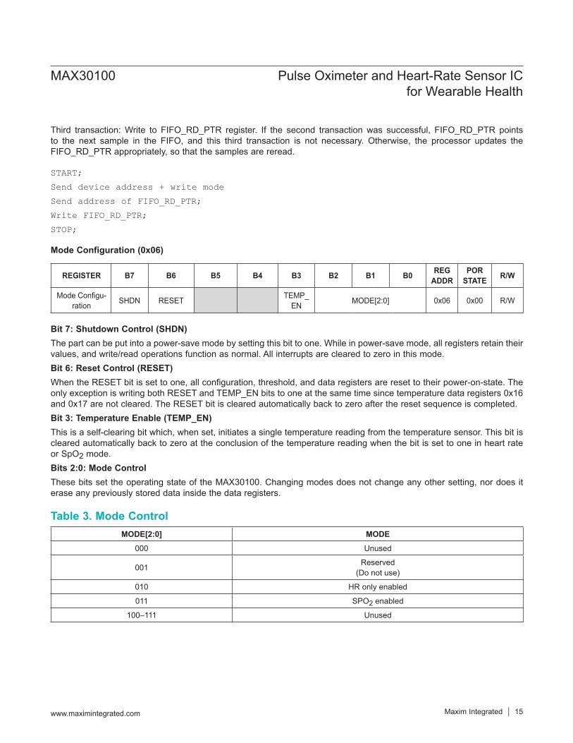
Third transaction: Write to FIFO_RD_PTR register. If the second transaction was successful, FIFO_RD_PTR points to the next sample in the FIFO, and this third transaction is not necessary. Otherwise, the processor updates the FIFO_RD_PTR appropriately, so that the samples are reread.
START;
Send device address + write mode
Send address of FIFO_RD_PTR;
Write FIFO_RD_PTR;
STOP;
Mode Configuration (0x06)
Bit 7: Shutdown Control (SHDN)The part can be put into a power-save mode by setting this bit to one. While in power-save mode, all registers retain their values, and write/read operations function as normal. All interrupts are cleared to zero in this mode.Bit 6: Reset Control (RESET)When the RESET bit is set to one, all configuration, threshold, and data registers are reset to their power-on-state. The only exception is writing both RESET and TEMP_EN bits to one at the same time since temperature data registers 0x16 and 0x17 are not cleared. The RESET bit is cleared automatically back to zero after the reset sequence is completed.Bit 3: Temperature Enable (TEMP_EN)This is a self-clearing bit which, when set, initiates a single temperature reading from the temperature sensor. This bit is cleared automatically back to zero at the conclusion of the temperature reading when the bit is set to one in heart rate or SpO2 mode.Bits 2:0: Mode ControlThese bits set the operating state of the MAX30100. Changing modes does not change any other setting, nor does it erase any previously stored data inside the data registers.
Table 3. Mode Control
REGISTER B7 B6 B5 B4 B3 B2 B1 B0 REGADDR
PORSTATE R/W
ModeConfigu-ration SHDN RESET TEMP_
EN MODE[2:0] 0x06 0x00 R/W
MODE[2:0] MODE
000 Unused
001 Reserved(Do not use)
010 HR only enabled
011 SPO2 enabled
100–111 Unused
www.maximintegrated.com Maxim Integrated 15
MAX30100 Pulse Oximeter and Heart-Rate Sensor IC for Wearable Health

SpO2 Configuration (0x07)
Bit 6: SpO2 High Resolution Enable (SPO2_HI_RES_EN)Set this bit high. The SpO2 ADC resolution is 16-bit with 1.6ms LED pulse width.Bit 5: Reserved. Set low (default).Bit 4:2: SpO2 Sample Rate ControlThese bits define the effective sampling rate, with one sample consisting of one IR pulse/conversion and one RED pulse/conversion.The sample rate and pulse width are related, in that the sample rate sets an upper bound on the pulse width time. If the user selects a sample rate that is too high for the selected LED_PW setting, the highest possible sample rate will instead be programmed into the register.Bits 1:0: LED Pulse Width ControlThese bits set the LED pulse width (the IR and RED have the same pulse width), and therefore, indirectly set the integra-tion time of the ADC in each sample. The ADC resolution is directly related to the integration time.
Table 4. SpO2 Sample Rate Control
REGISTER B7 B6 B5 B4 B3 B2 B1 B0 REGADDR
PORSTATE R/W
SPO2 Configuration
SPO2_HI_RES_EN Reserved SPO2_SR[2:0] LED_PW[1:0] 0x07 0x00 R/W
SPO2_SR[2:0] SAMPLES (PER SECOND)
000 50
001 100
010 167
011 200
100 400
101 600
110 800
111 1000
www.maximintegrated.com Maxim Integrated 16
MAX30100 Pulse Oximeter and Heart-Rate Sensor IC for Wearable Health
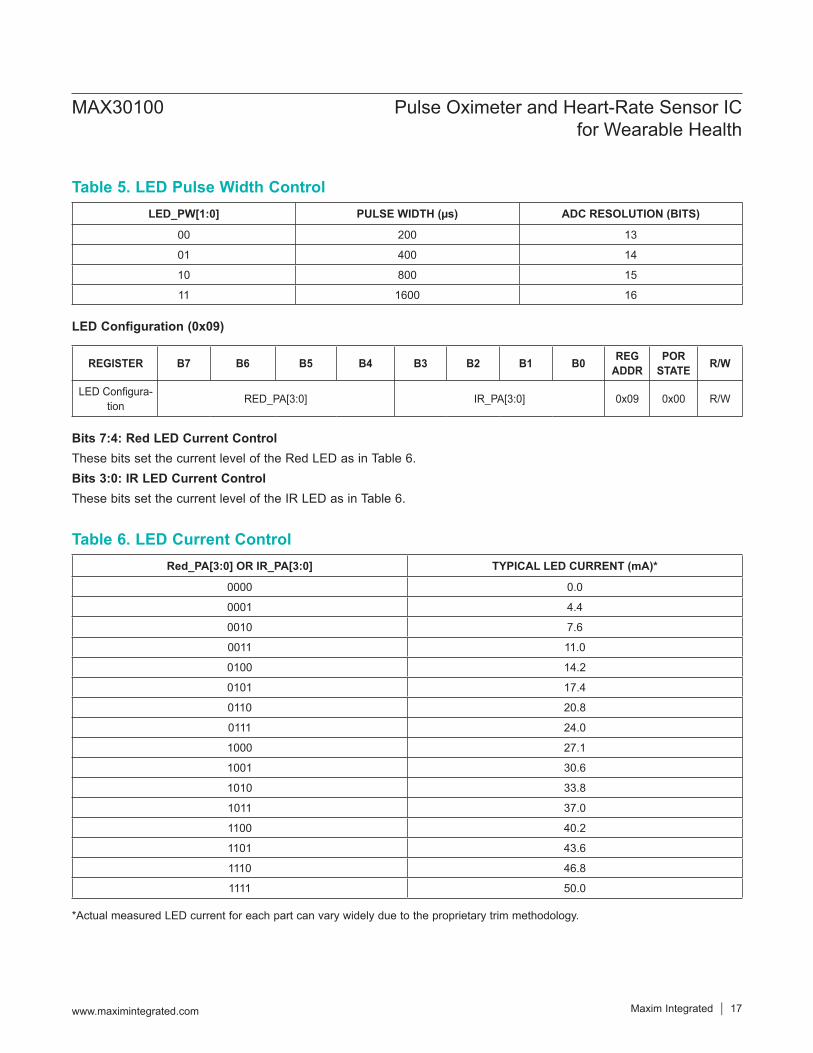
LED Configuration (0x09)
Bits 7:4: Red LED Current ControlThese bits set the current level of the Red LED as in Table 6.Bits 3:0: IR LED Current ControlThese bits set the current level of the IR LED as in Table 6.
Table 5. LED Pulse Width Control
Table 6. LED Current Control
*Actual measured LED current for each part can vary widely due to the proprietary trim methodology.
REGISTER B7 B6 B5 B4 B3 B2 B1 B0 REGADDR
PORSTATE R/W
LEDConfigura-tion RED_PA[3:0] IR_PA[3:0] 0x09 0x00 R/W
LED_PW[1:0] PULSE WIDTH (µs) ADC RESOLUTION (BITS)
00 200 13
01 400 14
10 800 15
11 1600 16
Red_PA[3:0] OR IR_PA[3:0] TYPICAL LED CURRENT (mA)*
0000 0.0
0001 4.4
0010 7.6
0011 11.0
0100 14.2
0101 17.4
0110 20.8
0111 24.0
1000 27.1
1001 30.6
1010 33.8
1011 37.0
1100 40.2
1101 43.6
1110 46.8
1111 50.0
www.maximintegrated.com Maxim Integrated 17
MAX30100 Pulse Oximeter and Heart-Rate Sensor IC for Wearable Health
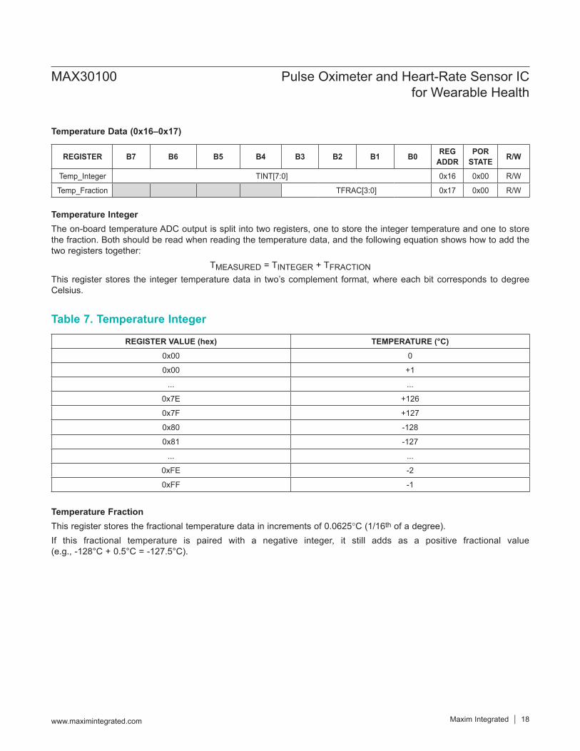
Temperature Data (0x16–0x17)
REGISTER B7 B6 B5 B4 B3 B2 B1 B0 REGADDR
PORSTATE R/W
Temp_Integer TINT[7:0] 0x16 0x00 R/W
Temp_Fraction TFRAC[3:0] 0x17 0x00 R/W
Temperature IntegerThe on-board temperature ADC output is split into two registers, one to store the integer temperature and one to store the fraction. Both should be read when reading the temperature data, and the following equation shows how to add the two registers together:
TMEASURED = TINTEGER + TFRACTIONThis register stores the integer temperature data in two’s complement format, where each bit corresponds to degree Celsius.
Temperature FractionThis register stores the fractional temperature data in increments of 0.0625NC (1/16th of a degree).If this fractional temperature is paired with a negative integer, it still adds as a positive fractional value (e.g., -128°C + 0.5°C = -127.5°C).
Table 7. Temperature Integer
REGISTER VALUE (hex) TEMPERATURE (°C)
0x00 0
0x00 +1
... ...
0x7E +126
0x7F +127
0x80 -128
0x81 -127
... ...
0xFE -2
0xFF -1
www.maximintegrated.com Maxim Integrated 18
MAX30100 Pulse Oximeter and Heart-Rate Sensor IC for Wearable Health

Applications InformationSampling Rate and PerformanceThe MAX30100 ADC is a 16-bit sigma delta converter. The ADC sampling rate can be configured from 50sps to 1ksps. The maximum sample rate for the ADC depends on the selected pulse width, which in turn, determines the ADC resolution. For instance, if the pulse width is set to 200µs, then the ADC resolution is 13 bits and all sample rates from 50sps to 1ksps are selectable. However, if the pulse width is set to 1600µs, then only sample rates of 100sps and 50sps can be set. The allowed sample rates for both SpO2 and HR mode are summarized in Table 8 and Table 9.
Power ConsiderationsThe LEDs in MAX30100 are pulsed with a low duty cycle for power savings, and the pulsed currents can cause ripples in the LED power supply. To ensure these pulses do not translate into optical noise at the LED outputs, the power supply must be designed to handle peak LED cur-rent. Ensure that the resistance and inductance from the
power supply (battery, DC/DC converter, or LDO) to the deviceLED+pinsismuchsmallerthan1Ω,andthatthereis at least 1µF of power-supply bypass capacitance to a low impedance ground plane. The decoupling capacitor should be located physically as close as possible to the MAX30100 device.In the heart-rate only mode, the red LED is inactive, and only the IR LED is used to capture optical data and deter-mine the heart rate. This mode allows power savings due to the red LED being off; in addition, the IR_LED+ power supply can be reduced to save power because the for-ward voltage of the IR LED is significantly less than that of the red LED.The average IDD and LED current as function of pulse width and sampling rate is summarized in Table 10 to Table 13.
Table 8. SpO2 Mode (Allowed Settings) Table 9. Heart-Rate Mode (Allowed Settings)SAMPLES
(per second)PULSE WIDTH (µs)
200 400 800 1600
50 O O O O
100 O O O O
167 O O O
200 O O O
400 O O
600 O
800 O
1000 O
Resolution(bits) 13 14 15 16
SAMPLES (per second)
PULSE WIDTH (µs)
200 400 800 1600
50 O O O O
100 O O O O
167 O O O
200 O O O
400 O O
600 O O
800 O O
1000 O O
Resolution(bits) 13 14 15 16
www.maximintegrated.com Maxim Integrated 19
MAX30100 Pulse Oximeter and Heart-Rate Sensor IC for Wearable Health
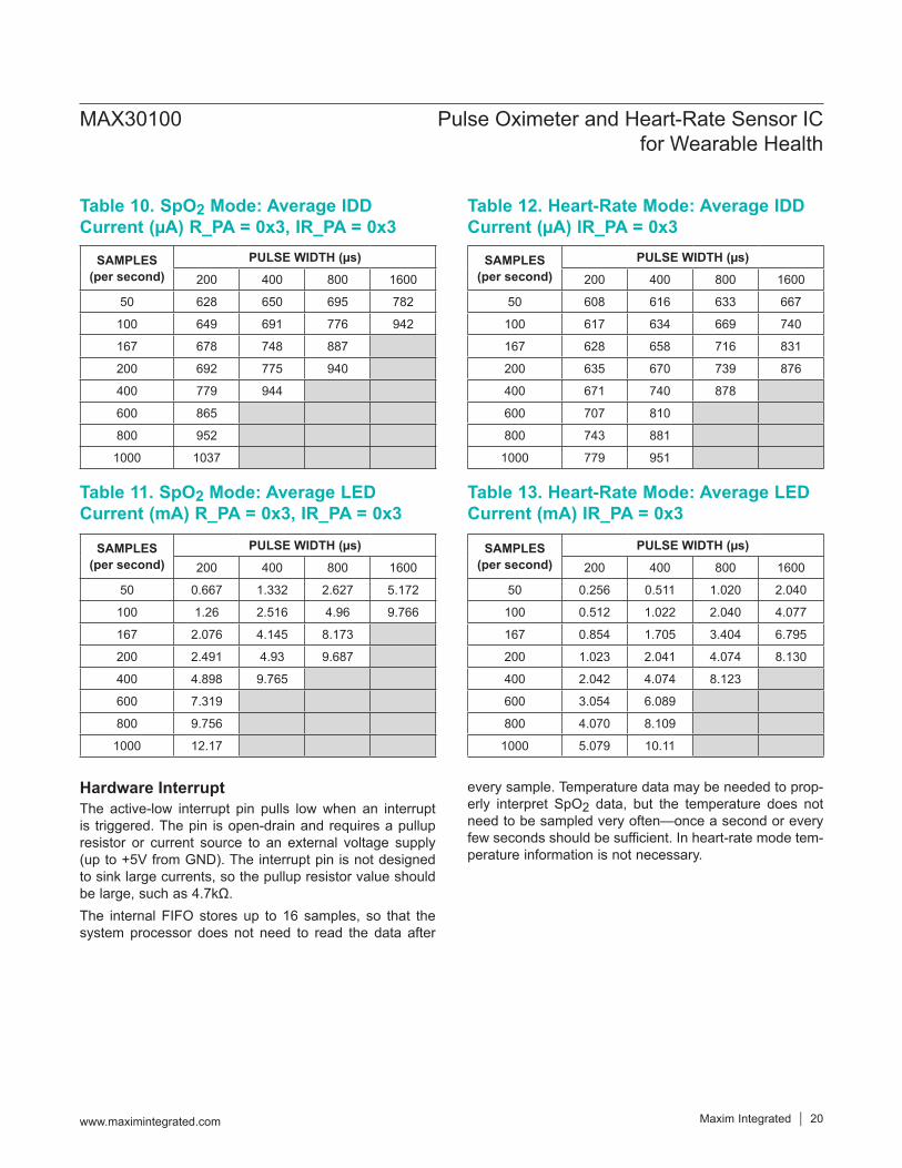
Hardware InterruptThe active-low interrupt pin pulls low when an interrupt is triggered. The pin is open-drain and requires a pullup resistor or current source to an external voltage supply (up to +5V from GND). The interrupt pin is not designed to sink large currents, so the pullup resistor value should belarge,suchas4.7kΩ.The internal FIFO stores up to 16 samples, so that the system processor does not need to read the data after
every sample. Temperature data may be needed to prop-erly interpret SpO2 data, but the temperature does not need to be sampled very often—once a second or every few seconds should be sufficient. In heart-rate mode tem-perature information is not necessary.
Table 12. Heart-Rate Mode: Average IDD Current (µA) IR_PA = 0x3
Table 13. Heart-Rate Mode: Average LED Current (mA) IR_PA = 0x3
Table 10. SpO2 Mode: Average IDD Current (µA) R_PA = 0x3, IR_PA = 0x3
Table 11. SpO2 Mode: Average LED Current (mA) R_PA = 0x3, IR_PA = 0x3
SAMPLES (per second)
PULSE WIDTH (µs)
200 400 800 1600
50 608 616 633 667
100 617 634 669 740
167 628 658 716 831
200 635 670 739 876
400 671 740 878
600 707 810
800 743 881
1000 779 951
SAMPLES (per second)
PULSE WIDTH (µs)
200 400 800 1600
50 628 650 695 782
100 649 691 776 942
167 678 748 887
200 692 775 940
400 779 944
600 865
800 952
1000 1037
SAMPLES (per second)
PULSE WIDTH (µs)
200 400 800 1600
50 0.256 0.511 1.020 2.040
100 0.512 1.022 2.040 4.077
167 0.854 1.705 3.404 6.795
200 1.023 2.041 4.074 8.130
400 2.042 4.074 8.123
600 3.054 6.089
800 4.070 8.109
1000 5.079 10.11
SAMPLES (per second)
PULSE WIDTH (µs)
200 400 800 1600
50 0.667 1.332 2.627 5.172
100 1.26 2.516 4.96 9.766
167 2.076 4.145 8.173
200 2.491 4.93 9.687
400 4.898 9.765
600 7.319
800 9.756
1000 12.17
www.maximintegrated.com Maxim Integrated 20
MAX30100 Pulse Oximeter and Heart-Rate Sensor IC for Wearable Health
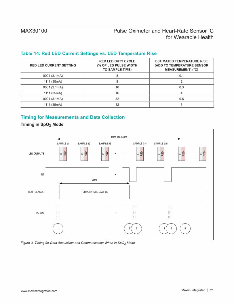
Table 14. Red LED Current Settings vs. LED Temperature Rise
Figure 3. Timing for Data Acquisition and Communication When in SpO2 Mode
RED LED CURRENT SETTINGRED LED DUTY CYCLE
(% OF LED PULSE WIDTH TO SAMPLE TIME)
ESTIMATED TEMPERATURE RISE (ADD TO TEMPERATURE SENSOR
MEASUREMENT) (°C)
0001 (3.1mA) 8 0.1
1111 (35mA) 8 2
0001 (3.1mA) 16 0.3
1111 (35mA) 16 4
0001 (3.1mA) 32 0.6
1111 (35mA) 32 8
INT
I2C BUS
LED OUTPUTS REDIR REDIR REDIR ~
~
~
REDIR REDIR REDIR REDIR
SAMPLE #1 SAMPLE #2 SAMPLE #3 SAMPLE #14 SAMPLE #15
1 4 5 6
TEMP SENSOR TEMPERATURE SAMPLE
2 3
29ms
15ms TO 300ms
www.maximintegrated.com Maxim Integrated 21
MAX30100 Pulse Oximeter and Heart-Rate Sensor IC for Wearable Health
Timing for Measurements and Data CollectionTiming in SpO2 Mode

Table 15. Events Sequence for Figure 3 in SpO2 Mode
Figure 4. Timing for Data Acquisition and Communication When in Heart Rate Mode
EVENT DESCRIPTION COMMENTS
1 Enter into SpO2 mode. Initiate a tem-perature measurement.
I2C Write Command Sets MODE[2:0] = 0x03. At the same time, set the TEMP_EN bit to initiate a single temperature measurement. Mask the SPO2_RDY Interrupt.
2 Temperature measurement complete, interrupt generated
TEMP_RDY interrupt triggers, alerting the central processor to read the data.
3 Temp data is read, interrupt cleared
4 FIFO is almost full, interrupt generated Interrupt is generated when the FIFO has only one empty space left.
5 FIFO data is read, interrupt cleared
6 Next sample is stored New sample is stored at the new read pointer location. Effectively, itisnowthefirstsampleintheFIFO.
INT
I2C BUS
LED OUTPUTS IR IR IR ~
~
~
IR IR IR IR
SAMPLE #1 SAMPLE #2 SAMPLE #3 SAMPLE #14 SAMPLE #15
1 2 3 4
15ms to 300ms
www.maximintegrated.com Maxim Integrated 22
MAX30100 Pulse Oximeter and Heart-Rate Sensor IC for Wearable Health
Timing in Heart-Rate Mode

Power Sequencing and RequirementsPower-Up SequencingFigure 5 shows the recommended power-up sequence for the MAX30100.It is recommended to power the VDD supply first, before the LED power supplies (R_LED+, IR_LED+). The inter-rupt and I2C pins can be pulled up to an external voltage even when the power supplies are not powered up.After the power is established, an interrupt occurs to alert the system that the MAX30100 is ready for operation. Reading the I2C interrupt register clears the interrupt, as shown in Figure 5.
Power-Down SequencingThe MAX30100 is designed to be tolerant of any power- supply sequencing on power-down.
I2C InterfaceThe MAX30100 features an I2C/SMBus-compatible, 2-wire serial interface consisting of a serial data line (SDA) and a serial clock line (SCL). SDA and SCL facilitate communication between the MAX30100 and the master at clock rates up to 400kHz. Figure 1 shows the 2-wire interface timing diagram. The master generates SCL and initiates data transfer on the bus. The master device writes data to the MAX30100 by transmitting the proper slave address followed by data. Each transmit sequence is framed by a START (S) or REPEATED START (Sr) condition and a STOP (P) condition. Each word transmitted to the MAX30100 is 8 bits long and is followed by an acknowledge clock pulse. A master read-ing data from the MAX30100 transmits the proper slave address followed by a series of nine SCL pulses.
The MAX30100 transmits data on SDA in sync with the master-generated SCL pulses. The master acknowl-edges receipt of each byte of data. Each read sequence is framed by a START (S) or REPEATED START (Sr) condition, a not acknowledge, and a STOP (P) condition. SDA operates as both an input and an open-drain output. Apullupresistor,typicallygreaterthan500Ω,isrequiredon SDA. SCL operates only as an input. A pullup resistor, typicallygreaterthan500Ω,isrequiredonSCLiftherearemultiple masters on the bus, or if the single master has an open-drain SCL output.
Bit TransferOne data bit is transferred during each SCL cycle. The data on SDA must remain stable during the high period of the SCL pulse. Changes in SDA while SCL is high are control signals. See the START and STOP Conditions section.
Table 16. Events Sequence for Figure 4 in Heart-Rate Mode
Figure 5. Power-Up Sequence of the Power-Supply Rails
EVENT DESCRIPTION COMMENTS
1 Enter into heart rate mode I2C Write Command Sets MODE[2:0] = 0x02. Mask the HR_RDY interrupt.
2 FIFO is almost full, interrupt generated Interrupt is generated when the FIFO has only one empty space left.
3 FIFO data is read, interrupt cleared
4 Next sample is stored New sample is stored at the new read pointer location. Effectively, it is nowthefirstsampleintheFIFO.
R_LED+, IR_LED+
VDD
INT
SDA, SCL
HIGH (I/O PULLUP)
HIGH (I/O PULLUP)
PWR_RDY INTERRUPT
READ TO CLEAR INTERRUPT
www.maximintegrated.com Maxim Integrated 23
MAX30100 Pulse Oximeter and Heart-Rate Sensor IC for Wearable Health

START and STOP ConditionsSDA and SCL idle high when the bus is not in use. A mas-ter initiates communication by issuing a START condition. A START condition is a high-to-low transition on SDA with SCL high. A STOP condition is a low-to-high transition on SDA while SCL is high (Figure 6). A START condition from the master signals the beginning of a transmission to the MAX30100. The master terminates transmission, and frees the bus, by issuing a STOP condition. The bus remains active if a REPEATED START condition is gener-ated instead of a STOP condition.
Early STOP ConditionsThe MAX30100 recognizes a STOP condition at any point during data transmission except if the STOP condition occurs in the same high pulse as a START condition. For proper operation, do not send a STOP condition during the same SCL high pulse as the START condition.
Slave AddressA bus master initiates communication with a slave device by issuing a START condition followed by the 7-bit slave ID. When idle, the MAX30100 waits for a START condition followed by its slave ID. The serial interface compares each slave ID bit by bit, allowing the interface to power down and disconnect from SCL immediately if an incor-rect slave ID is detected. After recognizing a START condition followed by the correct slave ID, the MAX30100 is ready to accept or send data. The LSB of the slave
ID word is the Read/Write (R/W) bit. R/W indicates whether the master is writing to or reading data from the MAX30100. R/W = 0 selects a write condition, R/W = 1 selects a read condition). After receiving the proper slave ID, the MAX30100 issues an ACK by pulling SDA low for one clock cycle.The MAX30100 slave ID consists of seven fixed bits, B7–B1 (set to 0b1010111). The most significant slave ID bit (B7) is transmitted first, followed by the remaining bits. Table 18 shows the possible slave IDs of the device.
AcknowledgeThe acknowledge bit (ACK) is a clocked 9th bit that the MAX30100 uses to handshake receipt each byte of data when in write mode (Figure 7). The MAX30100 pulls down SDA during the entire master-generated 9th clock pulse if the previous byte is successfully received. Monitoring ACK allows for detection of unsuccessful data transfers. An unsuccessful data transfer occurs if a receiving device is busy or if a system fault has occurred. In the event of an unsuccessful data transfer, the bus master will retry communication. The master pulls down SDA during the 9th clock cycle to acknowledge receipt of data when the MAX30100 is in read mode. An acknowledge is sent by the master after each read byte to allow data transfer to continue. A not-acknowledge is sent when the master reads the final byte of data from the MAX30100, followed by a STOP condition.
Table 17. Slave ID Description
Figure 6. START, STOP, and REPEATED START Conditions Figure 7. Acknowledge
B7 B6 B5 B4 B3 B2 B1 B0 WRITE AD-DRESS
READ AD-DRESS
1 0 1 0 1 1 1 R/W 0xAE 0xAF
S Sr P
SCL1
SDA1
SCL1
SDA1
START CONDITION
1 2 8 9
CLOCK PULSE FORACKNOWLEDGMENT
NOT ACKNOWLEDGE
ACKNOWLEDGE
Figure 7
www.maximintegrated.com Maxim Integrated 24
MAX30100 Pulse Oximeter and Heart-Rate Sensor IC for Wearable Health
Write Data FormatFor the write operation, send the slave ID as the first byte followed by the register address byte and then one or more data bytes. The register address pointer incre-ments automatically after each byte of data received. For example, the entire register bank can be written by at one time. Terminate the data transfer with a STOP condition. The write operation is shown in Figure 8.The internal register address pointer increments auto-matically, so writing additional data bytes fill the data registers in order.
Read Data FormatFor the read operation, two I2C operations must be per-formed. First, the slave ID byte is sent followed by the I2C register that you wish to read. Then a REPEATED START (Sr) condition is sent, followed by the read slave ID. The MAX30100 then begins sending data beginning with the register selected in the first operation. The read pointer
increments automatically, so the MAX30100 continues sending data from additional registers in sequential order until a STOP (P) condition is received. The exception to this is the FIFO_DATA register, at which the read pointer no longer increments when reading additional bytes. To read the next register after FIFO_DATA, an I2C write command is necessary to change the location of the read pointer.An initial write operation is required to send the read reg-ister address.Data is sent from registers in sequential order, starting from the register selected in the initial I2C write operation. If the FIFO_DATA register is read, the read pointer does not automatically increment, and subsequent bytes of data contain the contents of the FIFO.
Figure 8. Writing One Data Byte to the MAX30100
Figure 9. Reading One Byte of Data from the MAX30100
S R/W = 01 0 1 0 0 0 1 ACK A7 A6 A5 A4 A3 A2 A1 A0 ACK
SLAVE ID REGISTER ADDRESS
D7 D6 D5 D4 D3 D2 D1 D0 ACK P
DATA BYTE
S = START CONDITIONP = STOP CONDITIONACK = ACKNOWLEDGE BY THE RECEIVER
INTERNAL ADDRESS POINTER AUTO-INCREMENT (FOR WRITING MULTIPLE BYTES)
S R/W = 01 0 1 0 0 0 1 ACK A7 A6 A5 A4 A3 A2 A1 A0 ACK
SLAVE ID REGISTER ADDRESS
S = START CONDITIONSr = REPEATED START CONDITIONP = STOP CONDITION
ACK = ACKNOWLEDGE BY THE RECEIVERNACK = NOT ACKNOWLEDGE
S R/W = 01 0 1 0 0 0 1 ACK D7 D6 D5 D4 D3 D2 D1 D0 NACK
SLAVE ID DATA BYTE
P
Figure 9
www.maximintegrated.com Maxim Integrated 25
MAX30100 Pulse Oximeter and Heart-Rate Sensor IC for Wearable Health

Figure 10. Reading Multiple Bytes of Data from the MAX30100
+Denotes a lead(Pb)-free/RoHS-compliant package.
PART TEMP RANGE PIN-PACKAGE
MAX30100EFD+ -40°C to +85°C 14 OESIP(0.8mm pitch)
880nm660nm
ADC
AMBIENT LIGHT CANCELLATION ANALOG
ADCTEMP
OSCILLATOR
DIGITAL FILTER
DIGITAL
DATAREGISTER
LED DRIVERS
I2CCOMMUNICATION
INT
SDA
SCL
VDDIR_LED+IR_LED+
IR_DRVR_DRV GND PGND
RED IRRED+IR
10µF
+3.3V50mA PEAK (TYPICAL)
1µF
+1.8V
4.7kΩ 4.7kΩ 4.7kΩ
VDDIO
µcOR
APPS PROC
S R/W = 01 0 1 0 0 0 1 ACK A7 A6 A5 A4 A3 A2 A1 A0 ACK
SLAVE ID REGISTER ADDRESS
S = START CONDITIONSr = REPEATED START CONDITIONP = STOP CONDITION
ACK = ACKNOWLEDGE BY THE RECEIVERAM = ACKNOWLEDGE BY THE MASTERNACK = NOT ACKNOWLEDGE
Sr R/W = 01 0 1 0 0 0 1 ACK D7 D6 D5 D4 D3 D2 D1 D0 AM
SLAVE ID DATA 1
D0D7 D6 D5 D4 D3 D2 D1 AM D7 D6 D5 D4 D3 D2 D1 D0 NACK
DATA n-1 DATA n
P
www.maximintegrated.com Maxim Integrated 26
MAX30100 Pulse Oximeter and Heart-Rate Sensor IC for Wearable Health
Ordering Information Chip InformationPROCESS: BiCMOS
Typical Application Circuit

PACKAGE TYPE PACKAGE CODE OUTLINE NO. LAND PATTERN NO.
14 OESIP F142D5+2 21-0880 90-0461
www.maximintegrated.com Maxim Integrated 27
MAX30100 Pulse Oximeter and Heart-Rate Sensor IC for Wearable Health
Package InformationFor the latest package outline information and land patterns (footprints), go to www.maximintegrated.com/packages. Note that a “+”, “#”, or “-” in the package code indicates RoHS status only. Package drawings may show a different suffix character, but the drawing pertains to the package regardless of RoHS status.
www.maximintegrated.com Maxim Integrated 28
MAX30100 Pulse Oximeter and Heart-Rate Sensor IC for Wearable Health
Package Information (continued)For the latest package outline information and land patterns (footprints), go to www.maximintegrated.com/packages. Note that a “+”, “#”, or “-” in the package code indicates RoHS status only. Package drawings may show a different suffix character, but the drawing pertains to the package regardless of RoHS status.

REVISIONNUMBER
REVISIONDATE DESCRIPTION PAGES
CHANGED
0 9/14 Initial release —
Maxim Integrated cannot assume responsibility for use of any circuitry other than circuitry entirely embodied in a Maxim Integrated product. No circuit patent licenses are implied. Maxim Integrated reserves the right to change the circuitry and specifications without notice at any time. The parametric values (min and max limits) shown in the Electrical Characteristics table are guaranteed. Other parametric values quoted in this data sheet are provided for guidance.
Maxim Integrated and the Maxim Integrated logo are trademarks of Maxim Integrated Products, Inc. © 2014 Maxim Integrated Products, Inc. 29
MAX30100 Pulse Oximeter and Heart-Rate Sensor IC for Wearable Health
Revision History
For pricing, delivery, and ordering information, please contact Maxim Direct at 1-888-629-4642, or visit Maxim Integrated’s website at www.maximintegrated.com.


![Self-Adaptive Matrix Completion for Heart Rate Estimation …jeffcohn/biblio/HeartRate-CVPR2016.pdf · Self-Adaptive Matrix Completion for Heart Rate Estimation ... 21, 13, 14, 29],](https://img.dokumen.tips/doc/110x75/5ac9df2d7f8b9a7d548d7aa5/self-adaptive-matrix-completion-for-heart-rate-estimation-jeffcohnbiblioheartrate-.jpg)