Embed Size (px)
Citation preview
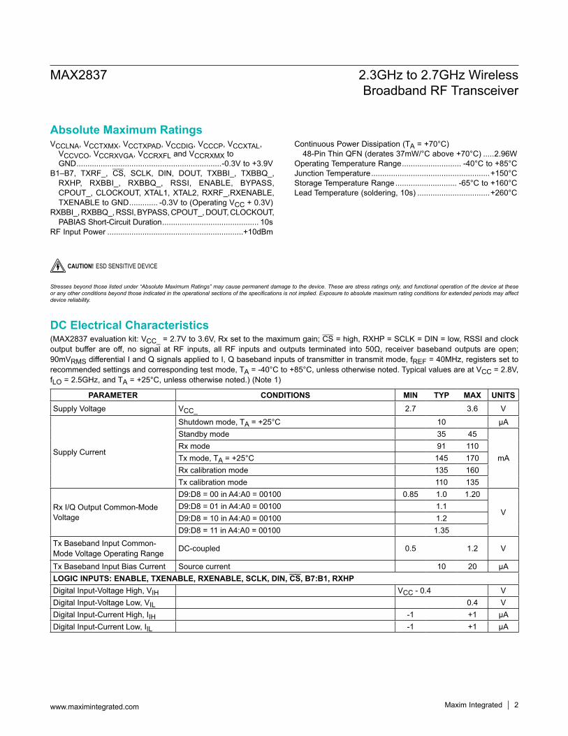
General DescriptionThe MAX2837 direct-conversion zero-IF RF transceiver is designed specifically for 2.3GHz to 2.7GHz wireless broadband systems. The MAX2837 completely integrates all circuitry required to implement the RF transceiver function, providing RF-to-baseband receive path; and baseband-to-RF transmit path, VCO, frequency synthe-sizer, crystal oscillator, and baseband/control interface. The device includes a fast-settling sigma-delta RF syn-thesizer with smaller than 20Hz frequency steps and a crystal oscillator, which allows the use of a low-cost crys-tal in place of a TCXO. The transceiver IC also integrates circuits for on-chip DC offset cancellation, I/Q error, and carrier-leakage detection circuits. Only an RF bandpass filter (BPF), crystal, RF switch, PA, and a small number of passive components are needed to form a complete wire-less broadband RF radio solution.The MAX2837 completely eliminates the need for an external SAW filter by implementing on-chip monolithic filters for both the receiver and transmitter. The baseband filters along with the Rx and Tx signal paths are optimized to meet stringent noise figure and linearity specifica-tions. The device supports up to 2048 FFT OFDM and implements programmable channel filters for 1.75MHz to 28MHz RF channel bandwidths. The transceiver requires only 2μs Tx-Rx switching time, which includes frequency transient settling. The IC is available in a small, 48-pin thin QFN package measuring only 6mm x 6mm x 0.8mm.
Applications 802.16-2004 Fixed WiMAX® Korea Wibro and 802.16e Mobile WiMAX Dual Mode™ WiMAX/802.11b/g Wi-Fi Proprietary Wireless Broadband Systems 4G/LTE Systems
Features 2.3GHz to 2.7GHz Wideband Operation Complete RF Transceiver, PA Driver, and Crystal
Oscillator • 0dBm Linear OFDM Transmit Power • -70dBr Tx Spectral Emission Mask • 2.3dB Rx Noise Figure • Tx/Rx I/Q Error and LO Leakage Detection • Monolithic Low-Noise VCO with -39dBc Integrated Phase Noise • Programmable Tx I/Q Lowpass Anti-Aliasing Filter • Sigma-Delta Fractional-N PLL with 20Hz Step Size • 45dB Tx Gain-Control Range • 94dB Receive Gain-Control Range • 60dB Analog RSSI Instantaneous Dynamic Range • 4-Wire SPI Digital Interface • I/Q Analog Baseband Interface • Digitally Tuned Crystal Oscillator • On-Chip Digital Temperature Sensor Read-Out
+2.7V to +3.6V Transceiver Supply Low-Power Shutdown Current Small 48-Pin Thin QFN Package
(6mm x 6mm x 0.8mm)
19-0806; Rev 2; 7/15
Dual Mode is a trademark of Maxim Integrated Products, Inc.WiMAX is a registered certification mark and registered service mark of the WiMAX Forum.
Pin Configuration appears at end of data sheet.
*EP = Exposed pad.+Denotes a lead(Pb)-free/RoHS-compliant package.
PART TEMP RANGE PIN-PACKAGEMAX2837ETM+TD -40°C to +85°C 48 TQFN-EP*
MAX2837 2.3GHz to 2.7GHz WirelessBroadband RF Transceiver
Ordering Information
EVALUATION KIT AVAILABLE
VCCLNA, VCCTXMX, VCCTXPAD, VCCDIG, VCCCP, VCCXTAL, VCCVCO, VCCRXVGA, VCCRXFL and VCCRXMX to GND ..................................................................-0.3V to +3.9V
B1–B7, TXRF_, CS, SCLK, DIN, DOUT, TXBBI_, TXBBQ_, RXHP, RXBBI_, RXBBQ_, RSSI, ENABLE, BYPASS, CPOUT_, CLOCKOUT, XTAL1, XTAL2, RXRF_,RXENABLE, TXENABLE to GND ............. -0.3V to (Operating VCC + 0.3V)
RXBBI_, RXBBQ_, RSSI, BYPASS, CPOUT_, DOUT, CLOCKOUT, PABIAS Short-Circuit Duration ............................................ 10s
RF Input Power ..............................................................+10dBm
Continuous Power Dissipation (TA = +70°C) 48-Pin Thin QFN (derates 37mW/°C above +70°C) .....2.96W
Operating Temperature Range ........................... -40°C to +85°CJunction Temperature ......................................................+150°CStorage Temperature Range ............................ -65°C to +160°CLead Temperature (soldering, 10s) .................................+260°C
CAUTION! ESD SENSITIVE DEVICE
(MAX2837 evaluation kit: VCC_ = 2.7V to 3.6V, Rx set to the maximum gain; CS = high, RXHP = SCLK = DIN = low, RSSI and clock output buffer are off, no signal at RF inputs, all RF inputs and outputs terminated into 50Ω, receiver baseband outputs are open; 90mVRMS differential I and Q signals applied to I, Q baseband inputs of transmitter in transmit mode, fREF = 40MHz, registers set to recommended settings and corresponding test mode, TA = -40°C to +85°C, unless otherwise noted. Typical values are at VCC = 2.8V, fLO = 2.5GHz, and TA = +25°C, unless otherwise noted.) (Note 1)
PARAMETER CONDITIONS MIN TYP MAX UNITSSupply Voltage VCC_ 2.7 3.6 V
Supply Current
Shutdown mode, TA = +25°C 10 µAStandby mode 35 45
mARx mode 91 110Tx mode, TA = +25°C 145 170Rx calibration mode 135 160Tx calibration mode 110 135
Rx I/Q Output Common-Mode Voltage
D9:D8 = 00 in A4:A0 = 00100 0.85 1.0 1.20
VD9:D8 = 01 in A4:A0 = 00100 1.1D9:D8 = 10 in A4:A0 = 00100 1.2D9:D8 = 11 in A4:A0 = 00100 1.35
Tx Baseband Input Common-Mode Voltage Operating Range DC-coupled 0.5 1.2 V
Tx Baseband Input Bias Current Source current 10 20 µALOGIC INPUTS: ENABLE, TXENABLE, RXENABLE, SCLK, DIN, CS, B7:B1, RXHPDigital Input-Voltage High, VIH VCC - 0.4 VDigital Input-Voltage Low, VIL 0.4 VDigital Input-Current High, IIH -1 +1 µADigital Input-Current Low, IIL -1 +1 µA
MAX2837 2.3GHz to 2.7GHz WirelessBroadband RF Transceiver
www.maximintegrated.com Maxim Integrated 2
Absolute Maximum Ratings
Stresses beyond those listed under “Absolute Maximum Ratings” may cause permanent damage to the device. These are stress ratings only, and functional operation of the device at these or any other conditions beyond those indicated in the operational sections of the specifications is not implied. Exposure to absolute maximum rating conditions for extended periods may affect device reliability.
DC Electrical Characteristics

(MAX2837 evaluation kit: VCC_ = 2.8V, fRF = 2.502GHz, fLO = 2.5GHz; receiver baseband I/Q outputs at 90mVRMS (-21dBV), fREF = 40MHz, ENABLE = RXENABLE = CS = high, TXENABLE = SCLK = DIN = low, with power matching for the differential RF pins using the typical applications and registers set to default settings and corresponding test mode, TA = +25°C, unless otherwise noted. Lowpass filter is set to 10MHz RF channel BW. Unmodulated single-tone RF input signal is used, unless otherwise indicated.) (Note 1)
(MAX2837 evaluation kit: VCC_ = 2.7V to 3.6V, Rx set to the maximum gain; CS = high, RXHP = SCLK = DIN = low, RSSI and clock output buffer are off, no signal at RF inputs, all RF inputs and outputs terminated into 50Ω, receiver baseband outputs are open; 90mVRMS differential I and Q signals applied to I, Q baseband inputs of transmitter in transmit mode, fREF = 40MHz, registers set to recommended settings and corresponding test mode, TA = -40°C to +85°C, unless otherwise noted. Typical values are at VCC = 2.8V, fLO = 2.5GHz, and TA = +25°C, unless otherwise noted.) (Note 1)
PARAMETER CONDITIONS MIN TYP MAX UNITSLOGIC OUTPUTS: DOUTDigital Output-Voltage High, VOH Sourcing 100µA VCC - 0.4 VDigital Output-Voltage Low, VOL Sinking 100µA 0.4 V
PARAMETER CONDITIONS MIN TYP MAX UNITSRECEIVER SECTION: LNA RF INPUT TO BASEBAND I/Q OUTPUTSRF Input Frequency Range 2.3 2.7 GHzPeak-to-Peak Gain Variation over RF Input Frequency Range Tested at band edges and band center 0.8 dB
RF Input Return Loss All LNA gain settings 13 dB
Total Voltage Gain TA = -40°C to +85°CMaximum gain, B7:B1 = 0000000 90 99
dBMinimum gain, B7:B1 = 1111111 5 13
RF Gain StepsFrom max RF gain to max RF gain - 8dB 8
dBFrom max RF gain to max RF gain - 16dB 16From max RF gain to max RF gain - 32dB 32
Gain Change Settling Time
Any RF or baseband gain change; gain settling to within P1dB of steady state; RXHP = 1 0.2
µsAny RF or baseband gain change; gain settling to within P0.1dB of steady state; RXHP = 1 2
Baseband Gain Range From maximum baseband gain (B5:B1 = 00000) to minimum baseband gain (B5:B1 = 11111),TA = -40°C to +85°C
58 62 66 dB
Baseband Gain MinimumStep Size 2 dB
DSB Noise Figure
Voltage gain R 65dB with max RF gain (B7:B6 = 00) 2.3
dB
Voltage gain = 50dB with max RF gain - 8dB(B7:B6 = 01) 5.5
Voltage gain = 45dB with max RF gain - 16dB(B7:B6 = 10) 17
Voltage gain = 15dB with max RF gain - 32dB(B7:B6 = 11) 27
MAX2837 2.3GHz to 2.7GHz WirelessBroadband RF Transceiver
www.maximintegrated.com Maxim Integrated 3
AC Electrical Characteristics—Rx MODE
DC Electrical Characteristics (continued)
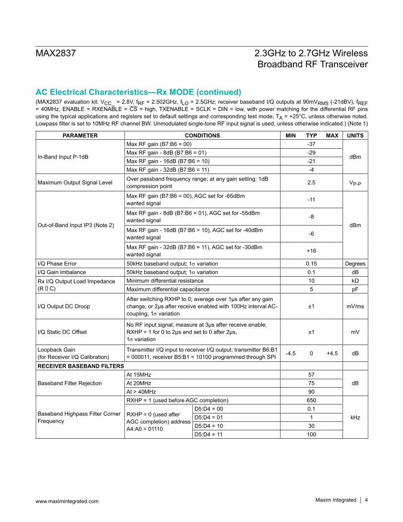
(MAX2837 evaluation kit: VCC_ = 2.8V, fRF = 2.502GHz, fLO = 2.5GHz; receiver baseband I/Q outputs at 90mVRMS (-21dBV), fREF = 40MHz, ENABLE = RXENABLE = CS = high, TXENABLE = SCLK = DIN = low, with power matching for the differential RF pins using the typical applications and registers set to default settings and corresponding test mode, TA = +25°C, unless otherwise noted. Lowpass filter is set to 10MHz RF channel BW. Unmodulated single-tone RF input signal is used, unless otherwise indicated.) (Note 1)
PARAMETER CONDITIONS MIN TYP MAX UNITS
In-Band Input P-1dB
Max RF gain (B7:B6 = 00) -37
dBmMax RF gain - 8dB (B7:B6 = 01) -29Max RF gain - 16dB (B7:B6 = 10) -21Max RF gain - 32dB (B7:B6 = 11) -4
Maximum Output Signal Level Over passband frequency range; at any gain setting; 1dB compression point 2.5 VP-P
Out-of-Band Input IP3 (Note 2)
Max RF gain (B7:B6 = 00), AGC set for -65dBmwanted signal -11
dBm
Max RF gain - 8dB (B7:B6 = 01), AGC set for -55dBm wanted signal -8
Max RF gain - 16dB (B7:B6 = 10), AGC set for -40dBm wanted signal -6
Max RF gain - 32dB (B7:B6 = 11), AGC set for -30dBm wanted signal +16
I/Q Phase Error 50kHz baseband output; 1s variation 0.15 DegreesI/Q Gain Imbalance 50kHz baseband output; 1s variation 0.1 dBRx I/Q Output Load Impedance (R || C)
Minimum differential resistance 10 kΩMaximum differential capacitance 5 pF
I/Q Output DC DroopAfter switching RXHP to 0; average over 1µs after any gain change, or 2µs after receive enabled with 100Hz interval AC-coupling, 1s variation
±1 mV/ms
I/Q Static DC OffsetNo RF input signal; measure at 3µs after receive enable; RXHP = 1 for 0 to 2µs and set to 0 after 2µs,1s variation
±1 mV
Loopback Gain(for Receiver I/Q Calibration)
Transmitter I/Q input to receiver I/Q output; transmitter B6:B1 = 000011, receiver B5:B1 = 10100 programmed through SPI -4.5 0 +4.5 dB
RECEIVER BASEBAND FILTERS
Baseband Filter Rejection At 15MHz 57
dBAt 20MHz 75At > 40MHz 90
Baseband Highpass Filter Corner Frequency
RXHP = 1 (used before AGC completion) 650
kHzRXHP = 0 (used after AGC completion) address A4:A0 = 01110
D5:D4 = 00 0.1D5:D4 = 01 1D5:D4 = 10 30D5:D4 = 11 100
MAX2837 2.3GHz to 2.7GHz WirelessBroadband RF Transceiver
www.maximintegrated.com Maxim Integrated 4
AC Electrical Characteristics—Rx MODE (continued)
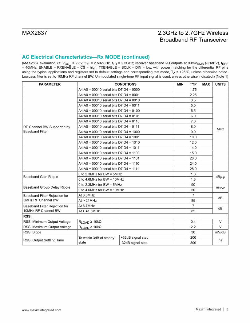
(MAX2837 evaluation kit: VCC_ = 2.8V, fRF = 2.502GHz, fLO = 2.5GHz; receiver baseband I/Q outputs at 90mVRMS (-21dBV), fREF = 40MHz, ENABLE = RXENABLE = CS = high, TXENABLE = SCLK = DIN = low, with power matching for the differential RF pins using the typical applications and registers set to default settings and corresponding test mode, TA = +25°C, unless otherwise noted. Lowpass filter is set to 10MHz RF channel BW. Unmodulated single-tone RF input signal is used, unless otherwise indicated.) (Note 1)
PARAMETER CONDITIONS MIN TYP MAX UNITS
RF Channel BW Supported by Baseband Filter
A4:A0 = 00010 serial bits D7:D4 = 0000 1.75
MHz
A4:A0 = 00010 serial bits D7:D4 = 0001 2.25A4:A0 = 00010 serial bits D7:D4 = 0010 3.5A4:A0 = 00010 serial bits D7:D4 = 0011 5.0A4:A0 = 00010 serial bits D7:D4 = 0100 5.5A4:A0 = 00010 serial bits D7:D4 = 0101 6.0A4:A0 = 00010 serial bits D7:D4 = 0110 7.0A4:A0 = 00010 serial bits D7:D4 = 0111 8.0A4:A0 = 00010 serial bits D7:D4 = 1000 9.0A4:A0 = 00010 serial bits D7:D4 = 1001 10.0A4:A0 = 00010 serial bits D7:D4 = 1010 12.0A4:A0 = 00010 serial bits D7:D4 = 1011 14.0A4:A0 = 00010 serial bits D7:D4 = 1100 15.0A4:A0 = 00010 serial bits D7:D4 = 1101 20.0A4:A0 = 00010 serial bits D7:D4 = 1110 24.0A4:A0 = 00010 serial bits D7:D4 = 1111 28.0
Baseband Gain Ripple0 to 2.3MHz for BW = 5MHz 1.3
dBP-P0 to 4.6MHz for BW = 10MHz 1.3
Baseband Group Delay Ripple0 to 2.3MHz for BW = 5MHz 90
nsP-P0 to 4.6MHz for BW = 10MHz 50Baseband Filter Rejection for 5MHz RF Channel BW
At 3.3MHz 7dB
At > 21MHz 85Baseband Filter Rejection for 10MHz RF Channel BW
At 6.7MHz 7dB
At > 41.6MHz 85RSSIRSSI Minimum Output Voltage RLOAD ≥ 10kΩ 0.4 VRSSI Maximum Output Voltage RLOAD ≥ 10kΩ 2.2 VRSSI Slope 30 mV/dB
RSSI Output Settling Time To within 3dB of steady state
+32dB signal step 200ns
-32dB signal step 800
MAX2837 2.3GHz to 2.7GHz WirelessBroadband RF Transceiver
www.maximintegrated.com Maxim Integrated 5
AC Electrical Characteristics—Rx MODE (continued)
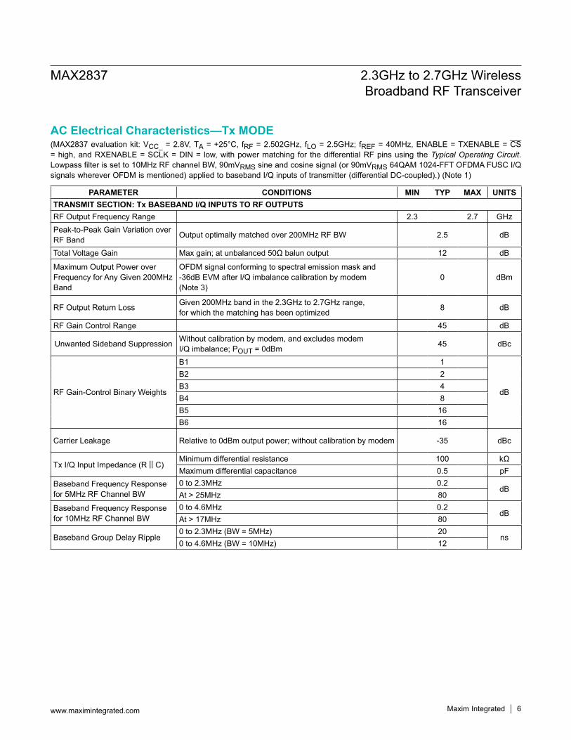
(MAX2837 evaluation kit: VCC_ = 2.8V, TA = +25°C, fRF = 2.502GHz, fLO = 2.5GHz; fREF = 40MHz, ENABLE = TXENABLE = CS = high, and RXENABLE = SCLK = DIN = low, with power matching for the differential RF pins using the Typical Operating Circuit. Lowpass filter is set to 10MHz RF channel BW, 90mVRMS sine and cosine signal (or 90mVRMS 64QAM 1024-FFT OFDMA FUSC I/Q signals wherever OFDM is mentioned) applied to baseband I/Q inputs of transmitter (differential DC-coupled).) (Note 1)
PARAMETER CONDITIONS MIN TYP MAX UNITSTRANSMIT SECTION: Tx BASEBAND I/Q INPUTS TO RF OUTPUTSRF Output Frequency Range 2.3 2.7 GHzPeak-to-Peak Gain Variation over RF Band Output optimally matched over 200MHz RF BW 2.5 dB
Total Voltage Gain Max gain; at unbalanced 50Ω balun output 12 dB
Maximum Output Power over Frequency for Any Given 200MHz Band
OFDM signal conforming to spectral emission mask and -36dB EVM after I/Q imbalance calibration by modem (Note 3)
0 dBm
RF Output Return Loss Given 200MHz band in the 2.3GHz to 2.7GHz range,for which the matching has been optimized 8 dB
RF Gain Control Range 45 dB
Unwanted Sideband Suppression Without calibration by modem, and excludes modemI/Q imbalance; POUT = 0dBm 45 dBc
RF Gain-Control Binary Weights
B1 1
dB
B2 2B3 4B4 8B5 16B6 16
Carrier Leakage Relative to 0dBm output power; without calibration by modem -35 dBc
Tx I/Q Input Impedance (R || C)Minimum differential resistance 100 kΩMaximum differential capacitance 0.5 pF
Baseband Frequency Response for 5MHz RF Channel BW
0 to 2.3MHz 0.2dB
At > 25MHz 80Baseband Frequency Response for 10MHz RF Channel BW
0 to 4.6MHz 0.2dB
At > 17MHz 80
Baseband Group Delay Ripple0 to 2.3MHz (BW = 5MHz) 20
ns0 to 4.6MHz (BW = 10MHz) 12
MAX2837 2.3GHz to 2.7GHz WirelessBroadband RF Transceiver
www.maximintegrated.com Maxim Integrated 6
AC Electrical Characteristics—Tx MODE
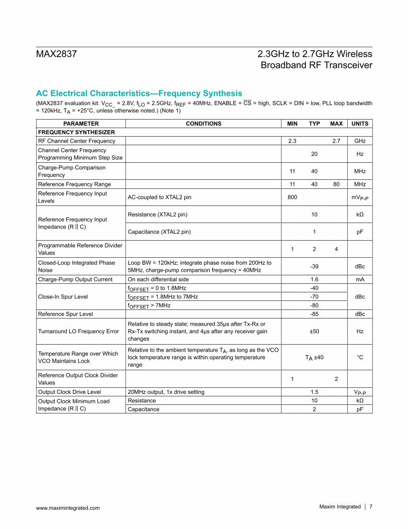
(MAX2837 evaluation kit: VCC_ = 2.8V, fLO = 2.5GHz, fREF = 40MHz, ENABLE = CS = high, SCLK = DIN = low, PLL loop bandwidth = 120kHz, TA = +25°C, unless otherwise noted.) (Note 1)
PARAMETER CONDITIONS MIN TYP MAX UNITSFREQUENCY SYNTHESIZERRF Channel Center Frequency 2.3 2.7 GHzChannel Center Frequency Programming Minimum Step Size 20 Hz
Charge-Pump Comparison Frequency 11 40 MHz
Reference Frequency Range 11 40 80 MHzReference Frequency Input Levels AC-coupled to XTAL2 pin 800 mVP-P
Reference Frequency Input Impedance (R || C)
Resistance (XTAL2 pin) 10 kΩ
Capacitance (XTAL2 pin) 1 pF
Programmable Reference DividerValues 1 2 4
Closed-Loop Integrated Phase Noise
Loop BW = 120kHz; integrate phase noise from 200Hz to 5MHz, charge-pump comparison frequency = 40MHz -39 dBc
Charge-Pump Output Current On each differential side 1.6 mA
Close-In Spur LevelfOFFSET = 0 to 1.8MHz -40
dBcfOFFSET = 1.8MHz to 7MHz -70fOFFSET > 7MHz -80
Reference Spur Level -85 dBc
Turnaround LO Frequency ErrorRelative to steady state; measured 35µs after Tx-Rx or Rx-Tx switching instant, and 4µs after any receiver gain changes
±50 Hz
Temperature Range over Which VCO Maintains Lock
Relative to the ambient temperature TA, as long as the VCO lock temperature range is within operating temperature range
TA ±40 °C
Reference Output Clock Divider Values 1 2
Output Clock Drive Level 20MHz output, 1x drive setting 1.5 VP-POutput Clock Minimum Load Impedance (R || C)
Resistance 10 kΩCapacitance 2 pF
MAX2837 2.3GHz to 2.7GHz WirelessBroadband RF Transceiver
www.maximintegrated.com Maxim Integrated 7
AC Electrical Characteristics—Frequency Synthesis
(MAX2837 evaluation kit: VCC_ = 2.8V, fREF = 40MHz, ENABLE = CS = high, SCLK = DIN = low, TA = +25°C, unless otherwise noted.) (Note 1)
(MAX2837 evaluation kit: VCC_ = 2.8V, fLO = 2.5GHz, fREF = 40MHz, ENABLE = CS = high, SCLK = DIN = low, PLL loop bandwidth = 120kHz, TA = +25°C, unless otherwise noted.) (Note 1)
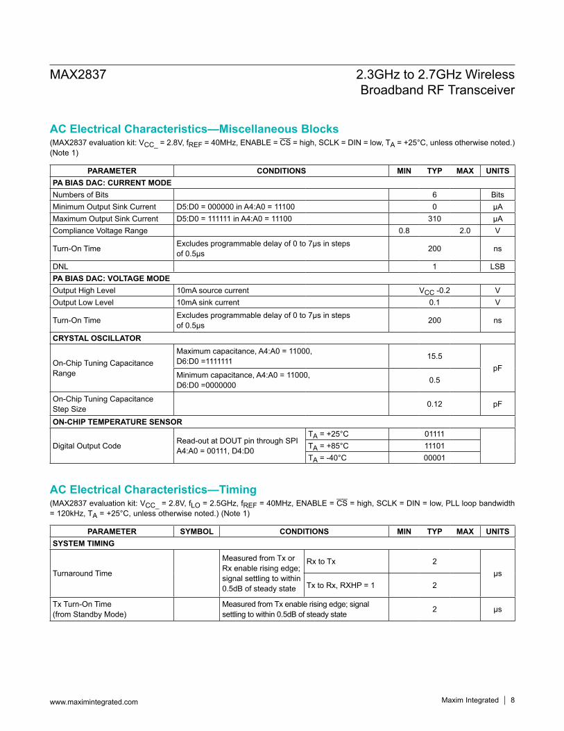
PARAMETER CONDITIONS MIN TYP MAX UNITSPA BIAS DAC: CURRENT MODENumbers of Bits 6 BitsMinimum Output Sink Current D5:D0 = 000000 in A4:A0 = 11100 0 µAMaximum Output Sink Current D5:D0 = 111111 in A4:A0 = 11100 310 µACompliance Voltage Range 0.8 2.0 V
Turn-On Time Excludes programmable delay of 0 to 7µs in stepsof 0.5µs 200 ns
DNL 1 LSBPA BIAS DAC: VOLTAGE MODEOutput High Level 10mA source current VCC -0.2 VOutput Low Level 10mA sink current 0.1 V
Turn-On Time Excludes programmable delay of 0 to 7µs in stepsof 0.5µs 200 ns
CRYSTAL OSCILLATOR
On-Chip Tuning Capacitance Range
Maximum capacitance, A4:A0 = 11000,D6:D0 =1111111 15.5
pFMinimum capacitance, A4:A0 = 11000,D6:D0 =0000000 0.5
On-Chip Tuning Capacitance Step Size 0.12 pF
ON-CHIP TEMPERATURE SENSOR
Digital Output Code Read-out at DOUT pin through SPIA4:A0 = 00111, D4:D0
TA = +25°C 01111TA = +85°C 11101TA = -40°C 00001
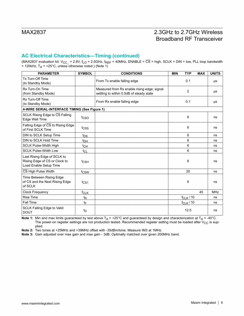
PARAMETER SYMBOL CONDITIONS MIN TYP MAX UNITSSYSTEM TIMING
Turnaround Time
Measured from Tx or Rx enable rising edge; signal settling to within 0.5dB of steady state
Rx to Tx 2µs
Tx to Rx, RXHP = 1 2
Tx Turn-On Time(from Standby Mode)
Measured from Tx enable rising edge; signal settling to within 0.5dB of steady state 2 µs
MAX2837 2.3GHz to 2.7GHz WirelessBroadband RF Transceiver
www.maximintegrated.com Maxim Integrated 8
AC Electrical Characteristics—Miscellaneous Blocks
AC Electrical Characteristics—Timing
(MAX2837 evaluation kit: VCC_ = 2.8V, fLO = 2.5GHz, fREF = 40MHz, ENABLE = CS = high, SCLK = DIN = low, PLL loop bandwidth = 120kHz, TA = +25°C, unless otherwise noted.) (Note 1)
Note 1: Min and max limits guaranteed by test above TA = +25°C and guaranteed by design and characterization at TA = -40°C. The power-on register settings are not production tested. Recommended register setting must be loaded after VCC is sup-plied.
Note 2: Two tones at +25MHz and +39MHz offset with -35dBm/tone. Measure IM3 at 1MHz.Note 3: Gain adjusted over max gain and max gain - 3dB. Optimally matched over given 200MHz band.
PARAMETER SYMBOL CONDITIONS MIN TYP MAX UNITSTx Turn-Off Time(to Standby Mode) From Tx enable falling edge 0.1 µs
Rx Turn-On Time(from Standby Mode)
Measured from Rx enable rising edge; signal settling to within 0.5dB of steady state 2 µs
Rx Turn-Off Time(to Standby Mode) From Rx enable falling edge 0.1 µs
4-WIRE SERIAL-INTERFACE TIMING (See Figure 1)SCLK Rising Edge to CS Falling Edge Wait Time tCSO 6 ns
Falling Edge of CS to Rising Edge of First SCLK Time tCSS 6 ns
DIN to SCLK Setup Time tDS 6 nsDIN to SCLK Hold Time tDH 6 nsSCLK Pulse-Width High tCH 6 nsSCLK Pulse-Width Low tCL 6 ns
Last Rising Edge of SCLK to Rising Edge of CS or Clock to Load Enable Setup Time
tCSH 6 ns
CS High Pulse Width tCSW 20 ns
Time Between Rising Edgeof CS and the Next Rising Edge of SCLK
tCS1 6 ns
Clock Frequency fCLK 45 MHzRise Time tR fCLK / 10 nsFall Time tF fCLK / 10 nsSCLK Falling Edge to ValidDOUT tD 12.5 ns
MAX2837 2.3GHz to 2.7GHz WirelessBroadband RF Transceiver
www.maximintegrated.com Maxim Integrated 9
AC Electrical Characteristics—Timing (continued)
(MAX2837 evaluation kit: VCC_ = 2.8V, fLO = 2.5GHz, 10MHz channel 16E UL/DL WiMax signal, fREF = 40MHz, ENABLE = CS = high, RXHP = SCLK = DIN = low, TA = +25°C, unless otherwise noted.)
NOISE FIGUREvs. BASEBAND VGA GAIN SETTING
BASEBAND VGA CODE
NOIS
E FI
GURE
(dB)
MAX
2837
toc0
2
0 8 16 24 320
5
10
15
20
25
30
35
40
LNA = MAX - 8dBLNA = MAX
LNA = MAX - 16dB
LNA = MAX - 32dB
Rx VOLTAGE GAINvs. BASEBAND GAIN SETTING
BASEBAND VGA CODE
Rx V
OLTA
GE G
AIN
(dB)
MAX
2837
toc0
3
0 8 16 24 320
20
40
60
80
100
LNA = MAX
LNA = MAX - 32dB
LNA = MAX - 8dB
LNA = MAX - 16dB
Rx VOLTAGE GAIN VARIATION vs. RF FREQUENCY
RF FREQUENCY (GHz)
Rx V
OLTA
GE G
AIN
VARI
ATIO
N (d
B)
MAX
2837
toc0
4
2.3 2.4 2.5 2.6 2.7-2
-1
0
1
2
LNA = MAX - 32dB
LNA = MAX LNA = MAX - 8dBLNA = MAX - 16dB
Rx IN-BAND OUTPUT V1dBvs. BASEBAND GAIN SETTING
BASEBAND VGA CODE
Rx IN
-BAN
D OU
TPUT
V1d
B (V
RMS)
MAX
2837
toc0
5
0 8 16 24 320
0.3
0.6
0.9
1.2
1.5Rx EVM vs. PIN
PIN (dBm)
EVM
(%)
MAX
2837
toc0
6
-90 -80 -70 -60 -50 -40 -30 -20 -10 002468
10121416182022
LNA = MAXLN
A =
MAX
-16d
B
LNA
= MA
X - 3
2dB
LNA
= MA
X - 8
dB
WiMAX EVM WITH OFDM JAMMERvs. OFFSET FREQUENCY
PJAMMER (dBm)
EVM
(%)
MAX
2837
toc0
7
-65 -55 -45 -35 -250123456789
101112131415
fOFFSET = 10MHz
fOFFSET = 20MHz
PIN = -60dBm
Rx CURRENT vs. SUPPLY VOLTAGE
SUPPLY VOLTAGE (V)
CURR
ENT
(mA)
MAX
2837
toc0
1
2.7 3.0 3.3 3.685
87
89
91
93
95
97
TA = -40°C
TA = +85°C
TA = +25°C
Rx EMISSION SPECTRUM AT LNA INPUT
MAX
2837
toc0
8
(dBm
)
DC 26.5GHz
-140
-130
-120
-110
-100
-90
-80
-70
-60
-50
-150
4/3LO
2LO
8/3LO 4L
O
8LO
MIN LNA GAINRBW = 300kHz
MAX2837 2.3GHz to 2.7GHz WirelessBroadband RF Transceiver
Maxim Integrated 10www.maximintegrated.com
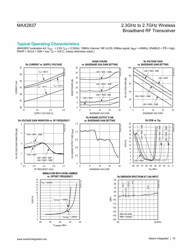
Typical Operating Characteristics

(MAX2837 evaluation kit: VCC_ = 2.8V, fLO = 2.5GHz, 10MHz channel 16E UL/DL WiMax signal, fREF = 40MHz, ENABLE = CS = high, RXHP = SCLK = DIN = low, TA = +25°C, unless otherwise noted.)
INPUT RETURN LOSS vs. RF FREQUENCY
RF FREQUENCY (GHz)
INPU
T RE
TURN
LOSS
(dB)
MAX
2837
toc0
9
2.0 2.2 2.4 2.6 2.8 3.0-40
-30
-20
-10
0LNA = MAX - 32dB
LNA = MAX - 8dB, LNA = MAX - 16dB
LNA = MAX
RSSI VOLTAGE vs. INPUT POWER
INPUT POWER (dBm)
RSSI
VOL
TAGE
(V)
MAX
2837
toc1
0
-120 -100 -80 -60 -40 -20 00
0.5
1.0
1.5
2.0
2.5
3.0
LNA = MAX - 32dB
LNA = MAX - 16dB
LNA = MAX - 8dB
LNA = MAX
CW TONE
MAX2837 toc11
3V
1.45V
200ns/div
0V
0.45V
Rx RSSI STEP RESPONSE(+40dB SIGNAL STEP)
MAX2837 toc12
3V
1.5V
200ns/div
0V
0.45V
Rx RSSI STEP RESPONSE(-40dB SIGNAL STEP) Rx LPF GROUP DELAY vs. FREQUENCY
FREQUENCY (MHz)
LPF
GROU
P DE
LAY
(ns)
MAX
2837
toc1
3
0 2 4 6 8 10 12 14 160
50
100
150
200
250
300
350CHANNEL BW = 5MHz
CHANNEL BW = 8MHz
CHANNEL BW = 10MHz
CHANNEL BW = 9MHz
0
26
13
52
39
65
78HISTOGRAM: Rx STATIC DC OFFSET
MAX
2837
toc1
4
1σ/div
MEAN: 0mVSTD: 0.977mVSAMPLE SIZE: 1006
Tx CURRENT vs. SUPPLY VOLTAGE
SUPPLY VOLTAGE (V)
CURR
ENT
(mA)
MAX
2837
toc1
5
2.7 3.0 3.3 3.6135
140
145
150
TA = -40°C
TA = +85°C
TA = +25°C
Tx OUTPUT POWER vs. RF FREQUENCY
RF FREQUENCY (GHz)
Tx P
OWER
(dBm
)
MAX
2837
toc1
6
2.3 2.4 2.5 2.6 2.7-3
-2
-1
1
0
VCC = 2.7V
VCC = 3V, 3.6V
MAX2837 2.3GHz to 2.7GHz WirelessBroadband RF Transceiver
Maxim Integrated 11www.maximintegrated.com
Typical Operating Characteristics (continued)

(MAX2837 evaluation kit: VCC_ = 2.8V, fLO = 2.5GHz, 10MHz channel 16E UL/DL WiMax signal, fREF = 40MHz, ENABLE = CS = high, RXHP = SCLK = DIN = low, TA = +25°C, unless otherwise noted.)
Tx OUTPUT POWER vs. TEMPERATURE
TEMPERATURE (°C)
Tx P
OWER
(dBm
)
MAX
2837
toc1
7
-40 -15 10 35 60 85-3.0
-2.5
-2.0
-1.5
-1.0
-0.5
0Tx VGA SET TO MAX - 3dB
Tx OUTPUT SPECTRUM
MAX
2837
toc1
8
5MHz/div
POUT = -3dBmEVM = 1.35%fRF = 2.5GHz
10dB
/div (
dBm)
Tx POUT vs. GAIN SETTING
Tx VGA GAIN CODE
Tx P
OWER
(dBm
)
MAX
2837
toc1
9
0 8 16 24 32 40 48 56 64-50
-40
-30
-20
-10
0
10-40°C
+25°C
-40°C+85°C
+85°C
+25°C
FORB
IDDE
N CO
DE
Tx TRANSMIT SPECTRUM FROMDC TO 26.5GHz
MAX
2837
toc2
0
(dBm
)
DC 26.5GHz
-90
-80
-70
-60
-50
-40
-30
-20
-10
0
-100
RBW = 1MHz2RF
4RF
RF
16/3RF
4/3RF
8/3RF
EVM vs. Tx OUTPUT POWER
OUTPUT POWER (dBm)
EVM
(%)
MAX
2837
toc2
1
-30 -24 -18 -12 -6 01.0
1.2
1.4
1.6
1.8
2.0PHASE NOISE vs. OFFSET FREQUENCY
OFFSET FREQUENCY (MHz)
PHAS
E NO
ISE
(dBc
/Hz)
MAX
2837
toc2
2
-150
-140
-130
-120
-110
-100
-90
-80
-70
-60
-50
0.001 0.01 0.1 1 10
2.5kHz
-2.5kHz
500Hz/div
0s 1ms
PLL SETTLING TIME FROM SHUTDOWN
MAX
2837
toc2
3
CRYSTAL OFFSET FREQUENCYvs. CTUNE BITS
CTUNE (DIGITAL BITS)
CRYS
TAL O
FFSE
T FR
EQUE
NCY
(Hz)
MAX
2837
toc2
4
0 10 20 30 40 50 60 70 80 90 100110120130-800-700-600-500-400-300-200-100
0100200300400500600700800
KYOCERA(CX-3225SB)
MAX2837 2.3GHz to 2.7GHz WirelessBroadband RF Transceiver
Maxim Integrated 12www.maximintegrated.com
Typical Operating Characteristics (continued)
B2
1
2
3
4
5
6
7
8
9
10
11
12
13 14 15 16 17 18 19 20 21 22 23 24
48 47 46 45 44 43 42 41 40 39 38 37
36
35
34
33
32
31
30
29
28
27
26
25
VCCRXLNA
B5
GNDRXLNA
RXRF+
RXRF-
B4
VCCTXPAD
TXRF+
TXRF-
B1
SERIALINTERFACE
SERIALINTERFACE
AMDETECTOR
V CCT
XMX
PABI
AS
SCLK
CLOC
KOUT
XTAL
2
XTAL
1
V CCX
TAL
V CCD
IG
V CCC
P
GNDC
P
CPOU
T+
CPOU
T-
RXBBQ+
RXBBQ-Rx QOUTPUTS
Rx/Tx GAINCONTROL
MODECONTROL
SERIALINPUTSSERIALINPUTSSERIALOUTPUT
SERIALINPUTS
B6
B7
RSSI
DIN
DOUT
CS
VCCVCO
PLL
+
GNDVCO
BYPASS
ENABLE
RXEN
ABLE
TXEN
ABLE
V CCR
XMX
TXBB
Q-
TXBB
Q+
TXBB
I+
TXBB
I-
V CCR
XFL
RXHP
V CCR
XVGA
RXBB
I+
RXBB
I-
MAX2837
MODECONTROL
Rx/Tx GAINCONTROL
PLL LOOPFILTER
REFERENCECLOCK BUFFER
OUTPUT
B3
Rx GAINCONTROL
Rx INPUT
TxOUTPUT
Rx/Tx GAINCONTROL
Rx/Tx GAINCONTROL
Rx/Tx GAINCONTROL
Rx/Tx GAINCONTROL
Tx INPUTS Rx I OUTPUTSRx BASEBANDHPF CONTROL
0
90RSSIMUXRSSI
SCLK
TEMP SENSOR
CRYSTALOSCILLATOR/
BUFFER
RSSITORSSIMUX
QMUX
IMUX QMUX
IMUX
MAX2837 2.3GHz to 2.7GHz WirelessBroadband RF Transceiver
www.maximintegrated.com Maxim Integrated 13
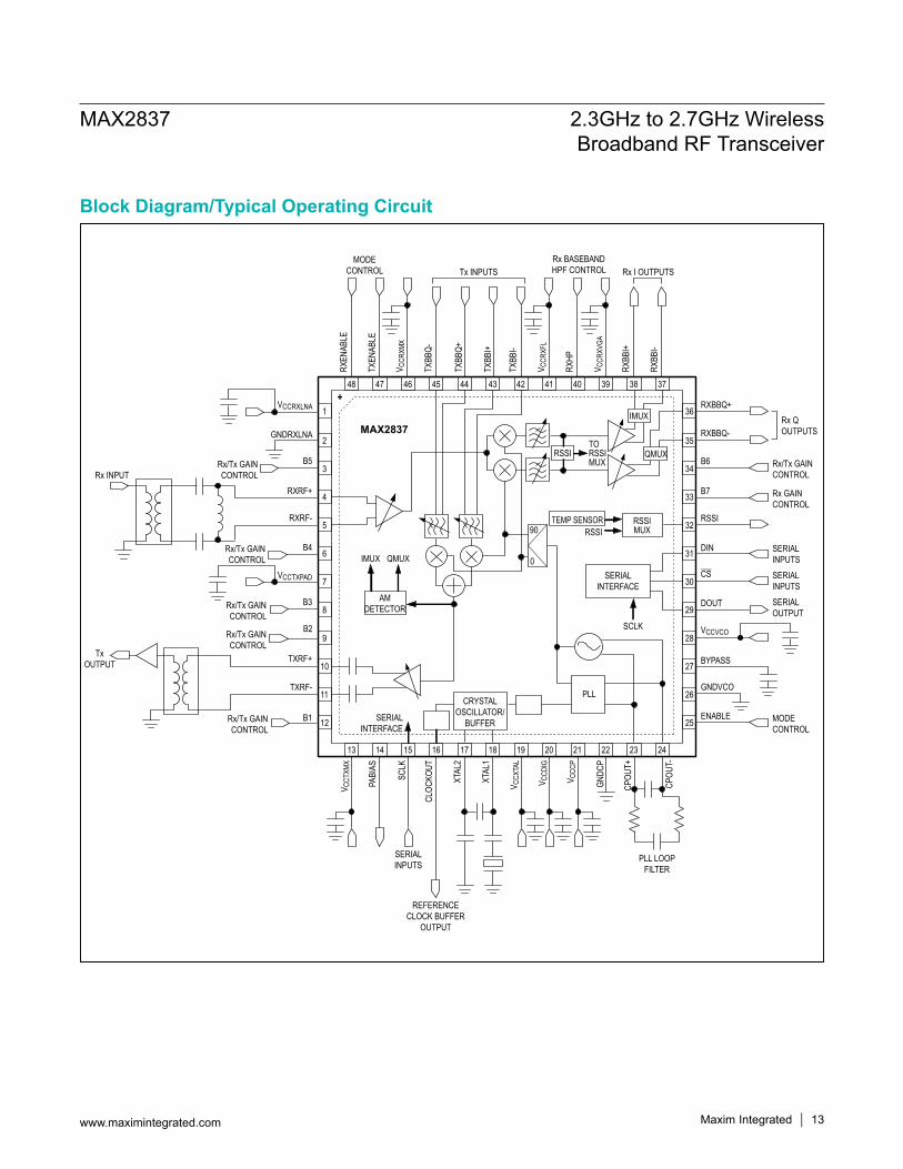
Block Diagram/Typical Operating Circuit

PIN NAME FUNCTION1 VCCRXLNA LNA Supply Voltage. Bypass with a capacitor as close as possible to the pin.2 GNDRXLNA LNA Ground3 B5 Receiver and Transmitter Gain-Control Logic Input Bit 54 RXRF+ LNA Differential Inputs. Inputs are internally DC-coupled. An external shunt inductor and series
capacitors match the inputs to 100Ω differential.5 RXRF-6 B4 Receiver and Transmitter Gain-Control Logic Input Bit 47 VCCTXPAD Supply Voltage for Power-Amplifier Driver. Bypass with a capacitor as close as possible to the pin.8 B3 Receiver and Transmitter Gain-Control Logic Input Bit 39 B2 Receiver and Transmitter Gain-Control Logic Input Bit 2
10 TXRF+ Power-Amplifier Driver Differential Output. PA driver output is internally matched to a 100I differential. The pins have internal DC-blocking capacitors.11 TXRF-
12 B1 Receiver and Transmitter Gain-Control Logic Input Bit 113 VCCTXMX Transmitter Upconverter Supply Voltage. Bypass with a capacitor as close as possible to the pin.14 PABIAS Transmit PA Bias DAC Output15 SCLK Serial-Clock Logic Input of 4-Wire Serial Interface (See Figure 1)16 CLOCKOUT Reference Clock Buffer Output17 XTAL2 Crystal or Reference Clock Input. AC-couple a crystal or a reference clock to this analog input.
18 XTAL1 Connection for Crystal-Oscillator Off-Chip Capacitors. When using an external reference clock input, leave XTAL1 unconnected.
19 VCCXTAL Crystal-Oscillator Supply Voltage. Bypass with a capacitor as close as possible to the pin.20 VCCDIG Digital Circuit Supply Voltage. Bypass with a capacitor as close as possible to the pin.21 VCCCP PLL Charge-Pump Supply Voltage. Bypass with a capacitor as close as possible to the pin.22 GNDCP Charge-Pump Circuit Ground 23 CPOUT+ Differential Charge-Pump Output. Connect the frequency synthesizer’s loop filter between CPOUT+
and CPOUT-. (See the Typical Operating Circuit.)24 CPOUT-25 ENABLE Operation Mode Logic Input. See Table 1 for operating modes. 26 GNDVCO VCO Ground
27 BYPASS On-Chip VCO Regulator Output Bypass. Bypass with a 1µF capacitor to GND. Do not connect other circuitry to this point.
28 VCCVCO VCO Supply Voltage. Bypass with a capacitor as close as possible to the pin.29 DOUT Data Logic Output of 4-Wire Serial Interface (See Figure 1)30 CS Chip-Select Logic Input of 4-Wire Serial Interface (See Figure 1)31 DIN Data Logic Input of 4-Wire Serial Interface (See Figure 1)32 RSSI RSSI or Temperature Sensor Multiplexed Analog Output33 B7 Receiver Gain-Control Logic Input Bit 734 B6 Receiver and Transmitter Gain-Control Logic Input Bit 635 RXBBQ- Receiver Baseband Q-Channel Differential Outputs. In Tx calibration mode, these pins are the
LO leakage and sideband detector outputs.36 RXBBQ+37 RXBBI- Receiver Baseband I-Channel Differential Outputs. In Tx calibration mode, these pins are the
LO leakage and sideband detector outputs. 38 RXBBI+39 VCCRXVGA Receiver VGA Supply Voltage40 RXHP Receiver Baseband AC-Coupling Highpass Corner Frequency Control Logic Input41 VCCRXFL Receiver Baseband Filter Supply Voltage
MAX2837 2.3GHz to 2.7GHz WirelessBroadband RF Transceiver
www.maximintegrated.com Maxim Integrated 14
Pin Description
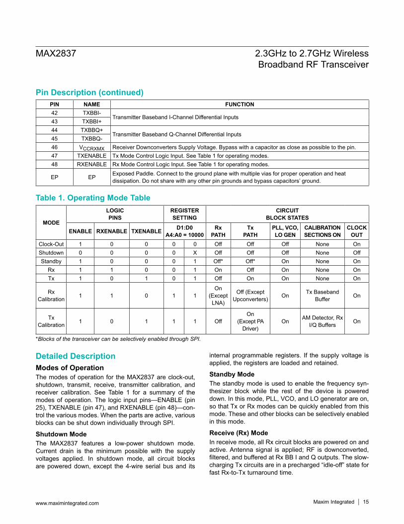
Detailed DescriptionModes of OperationThe modes of operation for the MAX2837 are clock-out, shutdown, transmit, receive, transmitter calibration, and receiver calibration. See Table 1 for a summary of the modes of operation. The logic input pins—ENABLE (pin 25), TXENABLE (pin 47), and RXENABLE (pin 48)—con-trol the various modes. When the parts are active, various blocks can be shut down individually through SPI.
Shutdown ModeThe MAX2837 features a low-power shutdown mode. Current drain is the minimum possible with the supply voltages applied. In shutdown mode, all circuit blocks are powered down, except the 4-wire serial bus and its
internal programmable registers. If the supply voltage is applied, the registers are loaded and retained.
Standby ModeThe standby mode is used to enable the frequency syn-thesizer block while the rest of the device is powered down. In this mode, PLL, VCO, and LO generator are on, so that Tx or Rx modes can be quickly enabled from this mode. These and other blocks can be selectively enabled in this mode.
Receive (Rx) ModeIn receive mode, all Rx circuit blocks are powered on and active. Antenna signal is applied; RF is downconverted, filtered, and buffered at Rx BB I and Q outputs. The slow-charging Tx circuits are in a precharged “idle-off” state for fast Rx-to-Tx turnaround time.
Table 1. Operating Mode Table
*Blocks of the transceiver can be selectively enabled through SPI.
PIN NAME FUNCTION42 TXBBI-
Transmitter Baseband I-Channel Differential Inputs43 TXBBI+44 TXBBQ+
Transmitter Baseband Q-Channel Differential Inputs45 TXBBQ-46 VCCRXMX Receiver Downconverters Supply Voltage. Bypass with a capacitor as close as possible to the pin.47 TXENABLE Tx Mode Control Logic Input. See Table 1 for operating modes.48 RXENABLE Rx Mode Control Logic Input. See Table 1 for operating modes.
EP EP Exposed Paddle. Connect to the ground plane with multiple vias for proper operation and heat dissipation. Do not share with any other pin grounds and bypass capacitors’ ground.
MODE
LOGICPINS
REGISTERSETTING
CIRCUITBLOCK STATES
ENABLE RXENABLE TXENABLE D1:D0A4:A0 = 10000
RxPATH
TxPATH
PLL, VCO,LO GEN
CALIBRATION SECTIONS ON
CLOCK OUT
Clock-Out 1 0 0 0 0 Off Off Off None OnShutdown 0 0 0 0 X Off Off Off None OffStandby 1 0 0 0 1 Off* Off* On None On
Rx 1 1 0 0 1 On Off On None OnTx 1 0 1 0 1 Off On On None On
Rx Calibration 1 1 0 1 1
On(Except LNA)
Off (Except Upconverters) On Tx Baseband
Buffer On
Tx Calibration 1 0 1 1 1 Off
On(Except PA
Driver)On AM Detector, Rx
I/Q Buffers On
MAX2837 2.3GHz to 2.7GHz WirelessBroadband RF Transceiver
www.maximintegrated.com Maxim Integrated 15
Pin Description (continued)

Transmit (Tx) ModeIn transmit mode, all Tx circuit blocks are powered on. The external PA is powered on after a programmable delay using the on-chip PA bias DAC. The slow-charging Rx circuits are in a precharged “idle-off” state for fast Tx-to-Rx turnaround time.
Clock-Out OnlyIn clock-out mode, the entire transceiver is off except the divided reference clock output on the CLKOUT pin and the clock divider, which remains on.
Figure 1. 4-Wire SPI Serial-Interface Timing Diagram
BIT 6
SPI REGISTER WRITE
DON'T CARE
BIT 2BIT 1 BIT 14BIT 13BIT 5
tCH
DIN
DOUT
tCSS
SCLK
tCSO
tDS
tDH
tCL
tCSWtCSH
tCS1
CS
SPI REGISTER READ
DON'T CARE
DON'T CAREBIT 2BIT 1 BIT 5DIN
DOUT
SCLK
tD
CS
BIT 6 BIT 14BIT 13
MAX2837 2.3GHz to 2.7GHz WirelessBroadband RF Transceiver
www.maximintegrated.com Maxim Integrated 16
Temperature Sensor Readout Through DOUT PinTo estimate chip temperature, on-chip temperature sen-sor is enabled by programming Address 9 D<1> = 1. The procedure is as follows:1) Enable temp-sensor by setting Address 9 D<1> = 1.
Roughly 100µs to 1ms time is needed to let the tem-perature sensor output settle to within 5 to 1 degrees.
2) To trigger temperature sensor ADC, program Address 9 D<0> from “0” to “1”. The ADC will acquire the 5-bit logic output in 2µs, temperature sensor needs to be ON (Address 9 D<1> = 1) to maintain the ADC logic output. Note that the ADC trigger should happen AFTER the temp sensor is enabled to get the correct result. Therefore, step 1 and step 2 of this procedure should be carried out on two separate SPI program-ming events separated by the temp sensor settling time.
3) Note that after the ADC latches its output and you desire to retake another temp sensor temperature reading value, the ADC has to be retriggered to reac-quire a new temp sensor value (assuming the temp sensor is already enabled). To do so, program Address 9 D<0> from “1” to “0” then from “0” to “1”. After the ADC latches it digital output in 2µs it shuts off.
4) To read the 5-bit logic output through DOUT pin, apply 4-wire SPI readout programming sequence to Address 7.
VAS Operating ProcedureAfter power-up, program Address 22 D<1> = 0 such that VAS frequency acquisition starts from VCO band 15, it reduces the worst-case acquisition time by half. VAS acquisition starts after Address 17 is programmed (i.e. rising edge of CSB), it takes the worst-case 896µs to acquire lock.
Wireless LAN or MAN systems do not switch channel frequency often, die temperature may change quite a bit over time and makes PLL out of lock. To relock PLL as soon as possible, the user can program Address 22 D<1> = 1 after the first power-up frequency acquisition. VAS starts from the previous frequency subband and should relock PLL within 112µs.
VAS ReadoutThe selected VCO subband, Vtune ADC output and VAS accomplished (VASA) signal can be read out through DOUT pin by programming Address 9 D<7:5> = 010 and corresponding Address 26 D<9:6>.
VCO Subband Selection Through SPIFor very fast band selection operation, the user can characterize the mapping between VCO frequencies and corresponding subbands during factory calibration. After programming Address 22 D<0> = 0, the VCO subband can be selected by Address 23 D<4:0>.
Programmable Registers and 4-Wire SPI InterfaceThe MAX2837 includes 32 programmable 16-bit registers. The most significant bit (MSB) is the read/write selection bit. The next 5 bits are register address. The 10 least significant bits (LSBs) are register data. Register data is loaded through the 4-wire SPI/MICROWIRE®-compatible serial interface. Data at DIN is shifted in MSB first and is framed by CS. When CS is low, the clock is active, and input data is shifted at the rising edge of the clock. During the read mode, register data selected by address bits is shifted out to DOUT at the falling edges of the clock. At the CS rising edge, the 10-bit data bits are latched into the register selected by address bits. See Figure 1. The reg-ister values are preserved in shutdown mode as long as the power-supply voltage is maintained. However, every time the power-supply voltage is turned on, the registers are reset to the default values. Note that default register states are not guaranteed, and the user should always reprogram all registers after power-up.
MICROWIRE is a registered trademark of National Semiconductor Corp.
MAX2837 2.3GHz to 2.7GHz WirelessBroadband RF Transceiver
www.maximintegrated.com Maxim Integrated 17
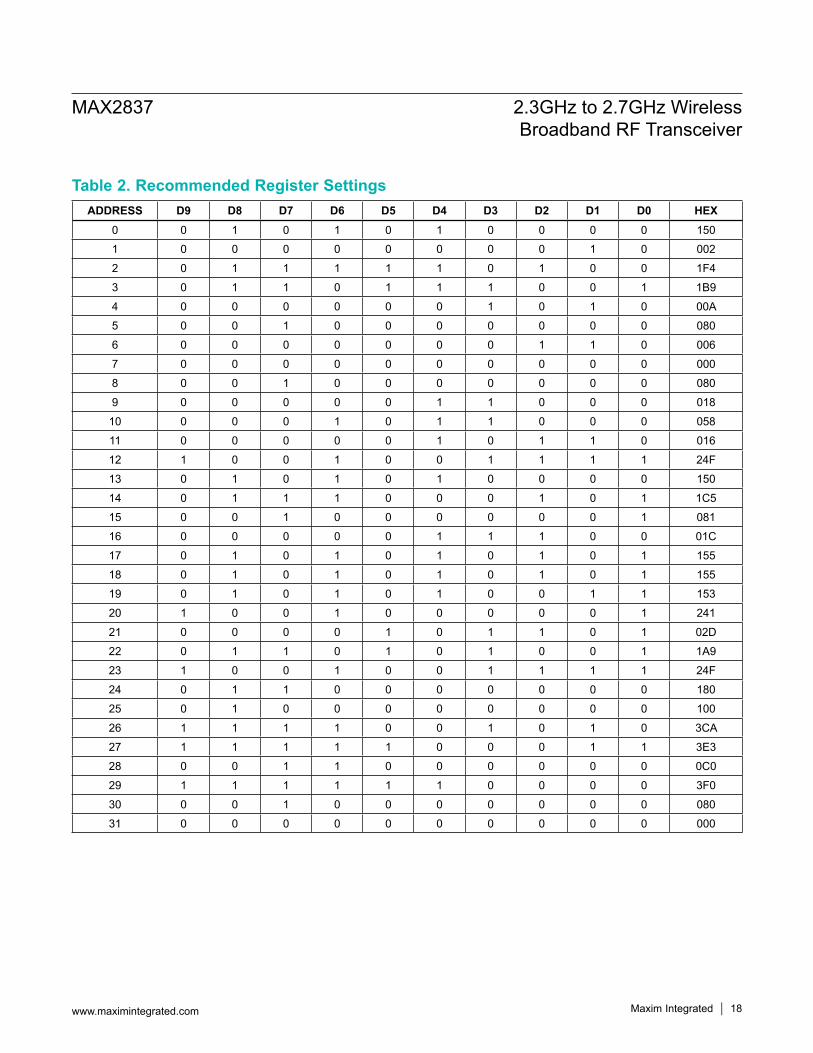
Table 2. Recommended Register SettingsADDRESS D9 D8 D7 D6 D5 D4 D3 D2 D1 D0 HEX
0 0 1 0 1 0 1 0 0 0 0 150
1 0 0 0 0 0 0 0 0 1 0 002
2 0 1 1 1 1 1 0 1 0 0 1F4
3 0 1 1 0 1 1 1 0 0 1 1B9
4 0 0 0 0 0 0 1 0 1 0 00A
5 0 0 1 0 0 0 0 0 0 0 080
6 0 0 0 0 0 0 0 1 1 0 006
7 0 0 0 0 0 0 0 0 0 0 000
8 0 0 1 0 0 0 0 0 0 0 080
9 0 0 0 0 0 1 1 0 0 0 018
10 0 0 0 1 0 1 1 0 0 0 058
11 0 0 0 0 0 1 0 1 1 0 016
12 1 0 0 1 0 0 1 1 1 1 24F
13 0 1 0 1 0 1 0 0 0 0 150
14 0 1 1 1 0 0 0 1 0 1 1C5
15 0 0 1 0 0 0 0 0 0 1 081
16 0 0 0 0 0 1 1 1 0 0 01C
17 0 1 0 1 0 1 0 1 0 1 155
18 0 1 0 1 0 1 0 1 0 1 155
19 0 1 0 1 0 1 0 0 1 1 153
20 1 0 0 1 0 0 0 0 0 1 241
21 0 0 0 0 1 0 1 1 0 1 02D
22 0 1 1 0 1 0 1 0 0 1 1A9
23 1 0 0 1 0 0 1 1 1 1 24F
24 0 1 1 0 0 0 0 0 0 0 180
25 0 1 0 0 0 0 0 0 0 0 100
26 1 1 1 1 0 0 1 0 1 0 3CA
27 1 1 1 1 1 0 0 0 1 1 3E3
28 0 0 1 1 0 0 0 0 0 0 0C0
29 1 1 1 1 1 1 0 0 0 0 3F0
30 0 0 1 0 0 0 0 0 0 0 080
31 0 0 0 0 0 0 0 0 0 0 000
MAX2837 2.3GHz to 2.7GHz WirelessBroadband RF Transceiver
www.maximintegrated.com Maxim Integrated 18
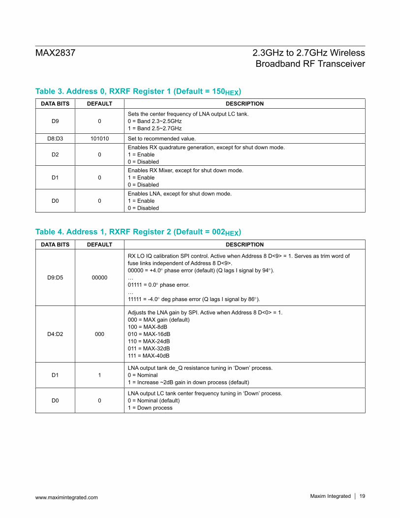
Table 3. Address 0, RXRF Register 1 (Default = 150HEX)
Table 4. Address 1, RXRF Register 2 (Default = 002HEX)
DATA BITS DEFAULT DESCRIPTION
D9 0Sets the center frequency of LNA output LC tank.0 = Band 2.3~2.5GHz1 = Band 2.5~2.7GHz
D8:D3 101010 Set to recommended value.
D2 0Enables RX quadrature generation, except for shut down mode. 1 = Enable0 = Disabled
D1 0Enables RX Mixer, except for shut down mode.1 = Enable0 = Disabled
D0 0Enables LNA, except for shut down mode. 1 = Enable0 = Disabled
DATA BITS DEFAULT DESCRIPTION
D9:D5 00000
RX LO IQ calibration SPI control. Active when Address 8 D<9> = 1. Serves as trim word of fuse links independent of Address 8 D<9>.00000 = +4.0° phase error (default) (Q lags I signal by 94°).…01111 = 0.0° phase error.…11111 = -4.0° deg phase error (Q lags I signal by 86°).
D4:D2 000
Adjusts the LNA gain by SPI. Active when Address 8 D<0> = 1.000 = MAX gain (default)100 = MAX-8dB010 = MAX-16dB110 = MAX-24dB011 = MAX-32dB111 = MAX-40dB
D1 1LNA output tank de_Q resistance tuning in ‘Down’ process. 0 = Nominal1 = Increase ~2dB gain in down process (default)
D0 0LNA output LC tank center frequency tuning in ‘Down’ process. 0 = Nominal (default)1 = Down process
MAX2837 2.3GHz to 2.7GHz WirelessBroadband RF Transceiver
www.maximintegrated.com Maxim Integrated 19
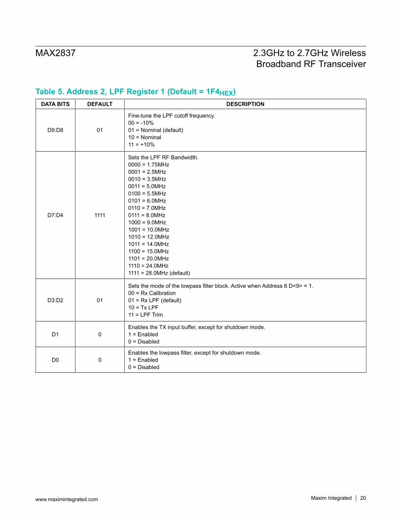
Table 5. Address 2, LPF Register 1 (Default = 1F4HEX)DATA BITS DEFAULT DESCRIPTION
D9:D8 01
Fine-tune the LPF cutoff frequency. 00 = -10%01 = Nominal (default) 10 = Nominal11 = +10%
D7:D4 1111
Sets the LPF RF Bandwidth.0000 = 1.75MHz0001 = 2.5MHz0010 = 3.5MHz0011 = 5.0MHz0100 = 5.5MHz0101 = 6.0MHz0110 = 7.0MHz0111 = 8.0MHz1000 = 9.0MHz1001 = 10.0MHz1010 = 12.0MHz1011 = 14.0MHz1100 = 15.0MHz1101 = 20.0MHz1110 = 24.0MHz1111 = 28.0MHz (default)
D3:D2 01
Sets the mode of the lowpass filter block. Active when Address 6 D<9> = 1.00 = Rx Calibration01 = Rx LPF (default)10 = Tx LPF11 = LPF Trim
D1 0Enables the TX input buffer, except for shutdown mode. 1 = Enabled0 = Disabled
D0 0Enables the lowpass filter, except for shutdown mode. 1 = Enabled 0 = Disabled
MAX2837 2.3GHz to 2.7GHz WirelessBroadband RF Transceiver
www.maximintegrated.com Maxim Integrated 20

Table 6. Address 3, LPF Register 2 (Default = 1B9HEX)
Table 7. Address 4, LPF Register 3 and VGA Register 1 (Default = 00AHEX)
Table 8. Address 5, VGA Register 2 (Default = 080HEX)
DATA BITS DEFAULT DESCRIPTION
D9:D7 011
Tx output (real pole) common-mode voltage adjustment. 000 = 1.00 V001 = 1.05010 = 1.10011 = 1.15 (default)100 = 1.20101 = 1.25110 = 1.30111 = Not allowed
D6:D0 0111001 Set to recommended value.
DATA BITS DEFAULT DESCRIPTION
D9:D8 00
Sets the RX VGA output common-mode voltage. 00 = 0.9V (default)01 = 1.0V10 = 1.1V11 = 1.25V
D7:D6 00 Set to recommended value.
D5 0RXVGA output MUX and buffer enable, except for shutdown mode. 1 = Enable 0 = Disabled
D4 0Enables RxVGA, except for shutdown mode.1 = Enable 0 = Disabled
D3:D0 1010 Set to recommended value.
DATA BITS DEFAULT DESCRIPTIOND9:D6 0010 Set to recommended value.
D5 0
RX baseband output select.Used to select RX mode and TX calibration mode output.0 = RXVGA (default)1 = TX AM detector for TX calibration mode.
D4:D0 00000
Sets attenuation in the RxVGA. Active when Address 8 D<1 > = 1.00000 = MAX gain (default)00001 = MAX - 2dB…11111 = MIN gain
MAX2837 2.3GHz to 2.7GHz WirelessBroadband RF Transceiver
www.maximintegrated.com Maxim Integrated 21
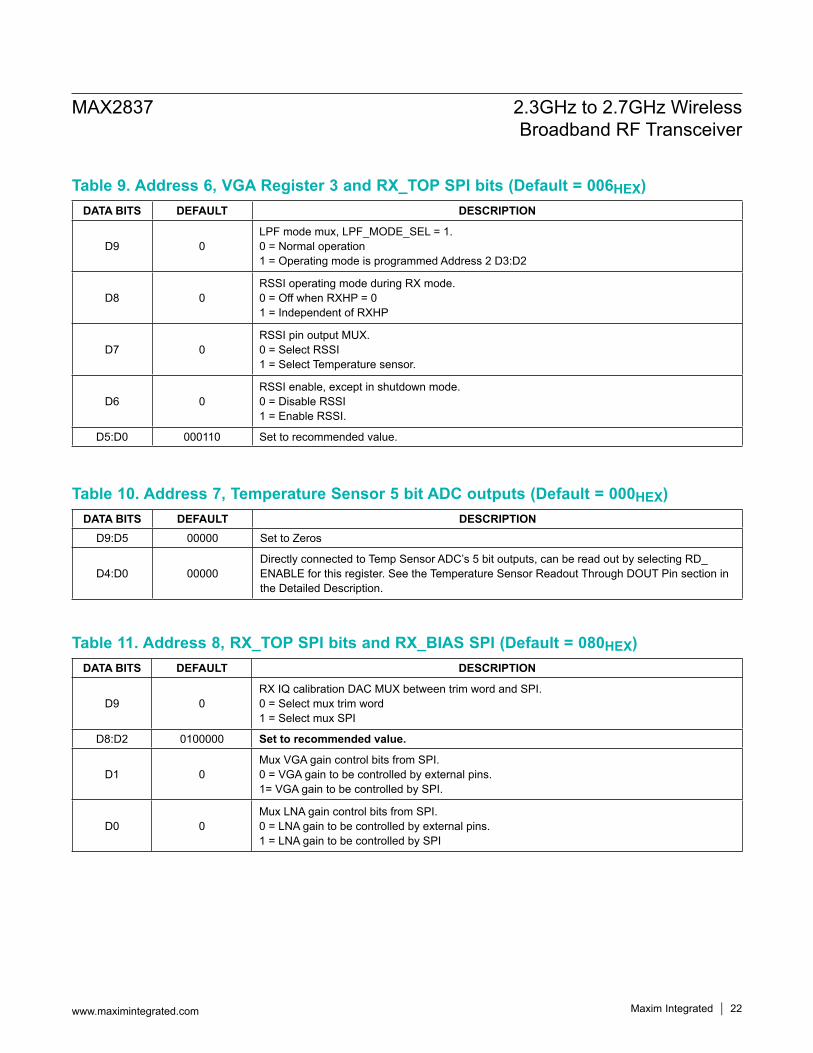
Table 9. Address 6, VGA Register 3 and RX_TOP SPI bits (Default = 006HEX)
Table 10. Address 7, Temperature Sensor 5 bit ADC outputs (Default = 000HEX)
Table 11. Address 8, RX_TOP SPI bits and RX_BIAS SPI (Default = 080HEX)DATA BITS DEFAULT DESCRIPTION
D9 0RX IQ calibration DAC MUX between trim word and SPI.0 = Select mux trim word 1 = Select mux SPI
D8:D2 0100000 Set to recommended value.
D1 0Mux VGA gain control bits from SPI. 0 = VGA gain to be controlled by external pins.1= VGA gain to be controlled by SPI.
D0 0Mux LNA gain control bits from SPI. 0 = LNA gain to be controlled by external pins.1 = LNA gain to be controlled by SPI
DATA BITS DEFAULT DESCRIPTIOND9:D5 00000 Set to Zeros
D4:D0 00000Directly connected to Temp Sensor ADC’s 5 bit outputs, can be read out by selecting RD_ENABLE for this register. See the Temperature Sensor Readout Through DOUT Pin section in the Detailed Description.
DATA BITS DEFAULT DESCRIPTION
D9 0LPF mode mux, LPF_MODE_SEL = 1. 0 = Normal operation 1 = Operating mode is programmed Address 2 D3:D2
D8 0RSSI operating mode during RX mode. 0 = Off when RXHP = 0 1 = Independent of RXHP
D7 0RSSI pin output MUX. 0 = Select RSSI 1 = Select Temperature sensor.
D6 0RSSI enable, except in shutdown mode. 0 = Disable RSSI 1 = Enable RSSI.
D5:D0 000110 Set to recommended value.
MAX2837 2.3GHz to 2.7GHz WirelessBroadband RF Transceiver
www.maximintegrated.com Maxim Integrated 22
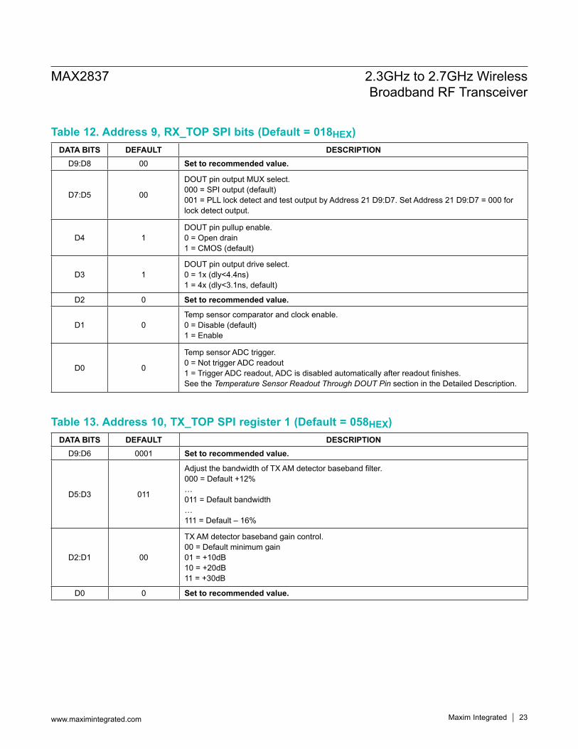
Table 12. Address 9, RX_TOP SPI bits (Default = 018HEX)
Table 13. Address 10, TX_TOP SPI register 1 (Default = 058HEX)
DATA BITS DEFAULT DESCRIPTIOND9:D8 00 Set to recommended value.
D7:D5 00
DOUT pin output MUX select. 000 = SPI output (default)001 = PLL lock detect and test output by Address 21 D9:D7. Set Address 21 D9:D7 = 000 for lock detect output.
D4 1DOUT pin pullup enable.0 = Open drain1 = CMOS (default)
D3 1DOUT pin output drive select.0 = 1x (dly<4.4ns)1 = 4x (dly<3.1ns, default)
D2 0 Set to recommended value.
D1 0Temp sensor comparator and clock enable.0 = Disable (default)1 = Enable
D0 0
Temp sensor ADC trigger.0 = Not trigger ADC readout1 = Trigger ADC readout, ADC is disabled automatically after readout finishes.See the Temperature Sensor Readout Through DOUT Pin section in the Detailed Description.
DATA BITS DEFAULT DESCRIPTIOND9:D6 0001 Set to recommended value.
D5:D3 011
Adjust the bandwidth of TX AM detector baseband filter.000 = Default +12%…011 = Default bandwidth…111 = Default – 16%
D2:D1 00
TX AM detector baseband gain control.00 = Default minimum gain01 = +10dB10 = +20dB11 = +30dB
D0 0 Set to recommended value.
MAX2837 2.3GHz to 2.7GHz WirelessBroadband RF Transceiver
www.maximintegrated.com Maxim Integrated 23
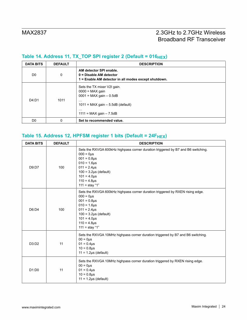
Table 14. Address 11, TX_TOP SPI register 2 (Default = 016HEX)
Table 15. Address 12, HPFSM register 1 bits (Default = 24FHEX)
DATA BITS DEFAULT DESCRIPTION
D0 0AM detector SPI enable. 0 = Disable AM detector1 = Enable AM detector in all modes except shutdown.
D4:D1 1011
Sets the TX mixer V2I gain.0000 = MAX gain0001 = MAX gain – 0.5dB…1011 = MAX gain – 5.5dB (default)…1111 = MAX gain – 7.5dB
D0 0 Set to recommended value.
DATA BITS DEFAULT DESCRIPTION
D9:D7 100
Sets the RXVGA 600kHz highpass corner duration triggered by B7 and B6 switching.000 = 0µs001 = 0.8µs010 = 1.6µs011 = 2.4µs100 = 3.2µs (default)101 = 4.0µs110 = 4.8µs111 = stay “1”
D6:D4 100
Sets the RXVGA 600kHz highpass corner duration triggered by RXEN rising edge.000 = 0µs001 = 0.8µs010 = 1.6µs011 = 2.4µs100 = 3.2µs (default)101 = 4.0µs110 = 4.8µs111 = stay “1”
D3:D2 11
Sets the RXVGA 10MHz highpass corner duration triggered by B7 and B6 switching.00 = 0µs01 = 0.4µs10 = 0.8µs11 = 1.2µs (default)
D1:D0 11
Sets the RXVGA 10MHz highpass corner duration triggered by RXEN rising edge.00 = 0µs01 = 0.4µs10 = 0.8µs11 = 1.2µs (default)
MAX2837 2.3GHz to 2.7GHz WirelessBroadband RF Transceiver
www.maximintegrated.com Maxim Integrated 24
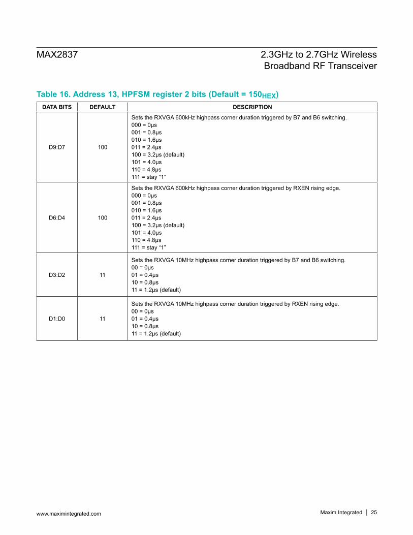
Table 16. Address 13, HPFSM register 2 bits (Default = 150HEX)DATA BITS DEFAULT DESCRIPTION
D9:D7 100
Sets the RXVGA 600kHz highpass corner duration triggered by B7 and B6 switching.000 = 0µs001 = 0.8µs010 = 1.6µs011 = 2.4µs100 = 3.2µs (default)101 = 4.0µs110 = 4.8µs111 = stay “1”
D6:D4 100
Sets the RXVGA 600kHz highpass corner duration triggered by RXEN rising edge.000 = 0µs001 = 0.8µs010 = 1.6µs011 = 2.4µs100 = 3.2µs (default)101 = 4.0µs110 = 4.8µs111 = stay “1”
D3:D2 11
Sets the RXVGA 10MHz highpass corner duration triggered by B7 and B6 switching.00 = 0µs01 = 0.4µs10 = 0.8µs11 = 1.2µs (default)
D1:D0 11
Sets the RXVGA 10MHz highpass corner duration triggered by RXEN rising edge.00 = 0µs01 = 0.4µs10 = 0.8µs11 = 1.2µs (default)
MAX2837 2.3GHz to 2.7GHz WirelessBroadband RF Transceiver
www.maximintegrated.com Maxim Integrated 25
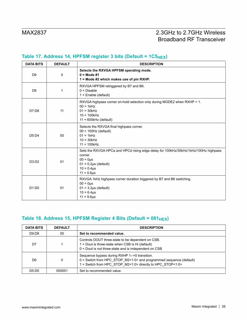
Table 17. Address 14, HPFSM register 3 bits (Default = 1C5HEX)
Table 18. Address 15, HPFSM Register 4 Bits (Default = 081HEX)
DATA BITS DEFAULT DESCRIPTION
D9 0Selects the RXVGA HPFSM operating mode. 0 = Mode #1 1 = Mode #2 which makes use of pin RXHP.
D8 1RXVGA HPFSM retriggered by B7 and B6.0 = Disable1 = Enable (default)
D7:D6 11
RXVGA highpass corner on-hold selection only during MODE2 when RXHP = 1.00 = 1kHz01 = 30kHz10 = 100kHz11 = 600kHz (default)
D5:D4 00
Selects the RXVGA final highpass corner.00 = 100Hz (default)01 = 1kHz10 = 30kHz11 = 100kHz
D3:D2 01
Sets the RXVGA HPCa and HPCd rising edge delay for 100kHz/30kHz/1kHz/100Hz highpass corner.00 = 0µs01 = 0.2µs (default)10 = 0.4µs11 = 0.6µs
D1:D0 01
RXVGA 1kHz highpass corner duration triggered by B7 and B6 switching.00 = 0µs01 = 3.2µs (default)10 = 6.4µs11 = 9.6µs
DATA BITS DEFAULT DESCRIPTIOND9:D8 00 Set to recommended value.
D7 1Controls DOUT three-state to be dependent on CSB.1 = Dout is three-state when CSB is Hi (default) 0 = Dout is not three-state and is independent on CSB
D6 0Sequence bypass during RXHP 1-->0 transition. 0 = Switch from HPC_STOP_M2<1:0> and programmed sequence (default)1 = Switch from HPC_STOP_M2<1:0> directly to HPC_STOP<1:0>
D5:D0 000001 Set to recommended value.
MAX2837 2.3GHz to 2.7GHz WirelessBroadband RF Transceiver
www.maximintegrated.com Maxim Integrated 26
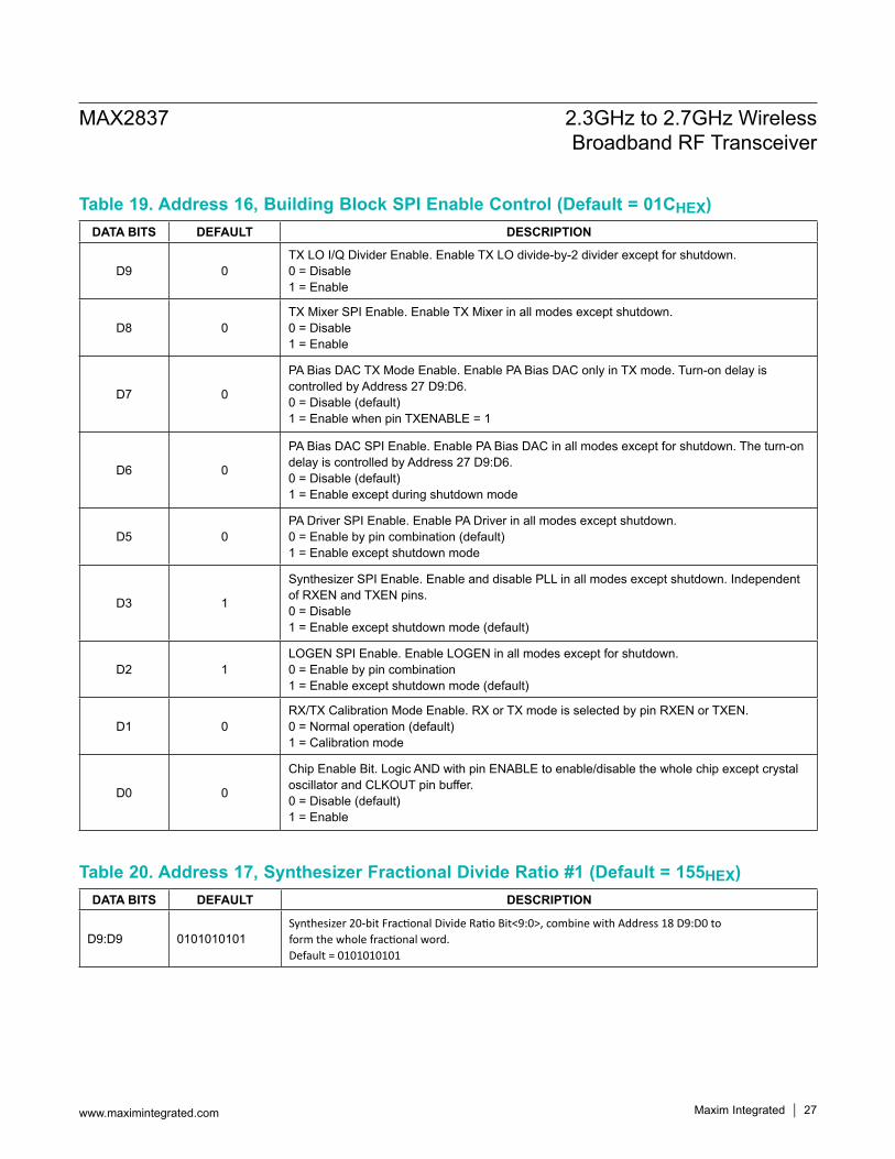
Table 19. Address 16, Building Block SPI Enable Control (Default = 01CHEX)
Table 20. Address 17, Synthesizer Fractional Divide Ratio #1 (Default = 155HEX)
DATA BITS DEFAULT DESCRIPTION
D9 0TX LO I/Q Divider Enable. Enable TX LO divide-by-2 divider except for shutdown.0 = Disable 1 = Enable
D8 0TX Mixer SPI Enable. Enable TX Mixer in all modes except shutdown. 0 = Disable 1 = Enable
D7 0
PA Bias DAC TX Mode Enable. Enable PA Bias DAC only in TX mode. Turn-on delay is controlled by Address 27 D9:D6.0 = Disable (default)1 = Enable when pin TXENABLE = 1
D6 0
PA Bias DAC SPI Enable. Enable PA Bias DAC in all modes except for shutdown. The turn-on delay is controlled by Address 27 D9:D6.0 = Disable (default)1 = Enable except during shutdown mode
D5 0PA Driver SPI Enable. Enable PA Driver in all modes except shutdown.0 = Enable by pin combination (default)1 = Enable except shutdown mode
D3 1
Synthesizer SPI Enable. Enable and disable PLL in all modes except shutdown. Independent of RXEN and TXEN pins.0 = Disable1 = Enable except shutdown mode (default)
D2 1LOGEN SPI Enable. Enable LOGEN in all modes except for shutdown.0 = Enable by pin combination1 = Enable except shutdown mode (default)
D1 0RX/TX Calibration Mode Enable. RX or TX mode is selected by pin RXEN or TXEN.0 = Normal operation (default)1 = Calibration mode
D0 0
Chip Enable Bit. Logic AND with pin ENABLE to enable/disable the whole chip except crystal oscillator and CLKOUT pin buffer.0 = Disable (default)1 = Enable
DATA BITS DEFAULT DESCRIPTION
D9:D9 0101010101Synthesizer 20-bit Fractional Divide Ratio Bit<9:0>, combine with Address 18 D9:D0 to form the whole fractional word.Default = 0101010101
MAX2837 2.3GHz to 2.7GHz WirelessBroadband RF Transceiver
www.maximintegrated.com Maxim Integrated 27
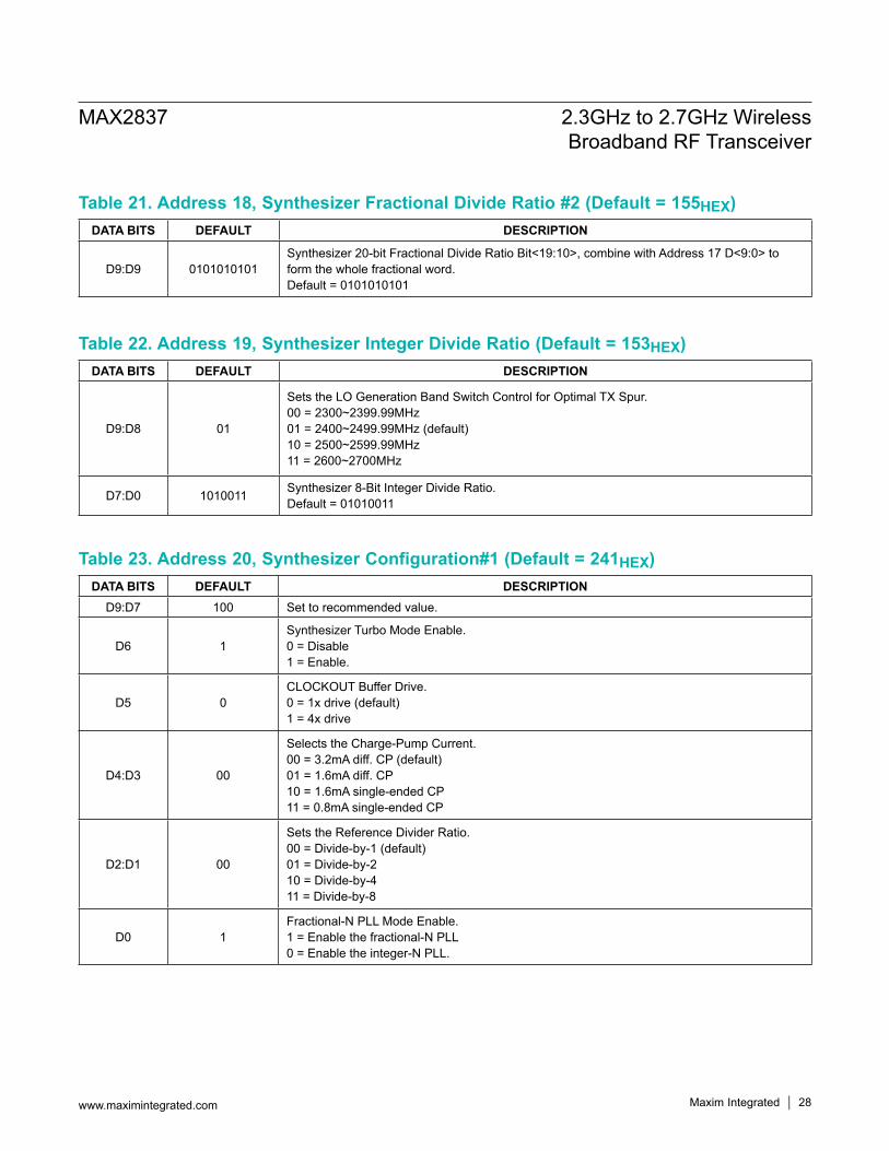
Table 21. Address 18, Synthesizer Fractional Divide Ratio #2 (Default = 155HEX)
Table 22. Address 19, Synthesizer Integer Divide Ratio (Default = 153HEX)
Table 23. Address 20, Synthesizer Configuration#1 (Default = 241HEX)
DATA BITS DEFAULT DESCRIPTION
D9:D9 0101010101Synthesizer 20-bit Fractional Divide Ratio Bit<19:10>, combine with Address 17 D<9:0> to form the whole fractional word.Default = 0101010101
DATA BITS DEFAULT DESCRIPTION
D9:D8 01
Sets the LO Generation Band Switch Control for Optimal TX Spur.00 = 2300~2399.99MHz01 = 2400~2499.99MHz (default)10 = 2500~2599.99MHz11 = 2600~2700MHz
D7:D0 1010011 Synthesizer 8-Bit Integer Divide Ratio.Default = 01010011
DATA BITS DEFAULT DESCRIPTIOND9:D7 100 Set to recommended value.
D6 1Synthesizer Turbo Mode Enable. 0 = Disable1 = Enable.
D5 0CLOCKOUT Buffer Drive.0 = 1x drive (default)1 = 4x drive
D4:D3 00
Selects the Charge-Pump Current.00 = 3.2mA diff. CP (default)01 = 1.6mA diff. CP10 = 1.6mA single-ended CP11 = 0.8mA single-ended CP
D2:D1 00
Sets the Reference Divider Ratio.00 = Divide-by-1 (default)01 = Divide-by-210 = Divide-by-411 = Divide-by-8
D0 1Fractional-N PLL Mode Enable. 1 = Enable the fractional-N PLL 0 = Enable the integer-N PLL.
MAX2837 2.3GHz to 2.7GHz WirelessBroadband RF Transceiver
www.maximintegrated.com Maxim Integrated 28
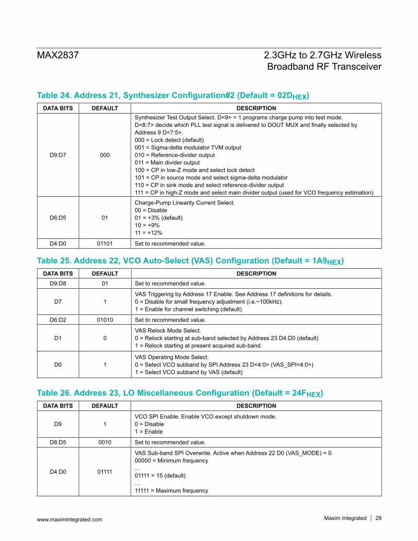
Table 24. Address 21, Synthesizer Configuration#2 (Default = 02DHEX)
Table 25. Address 22, VCO Auto-Select (VAS) Configuration (Default = 1A9HEX)
Table 26. Address 23, LO Miscellaneous Configuration (Default = 24FHEX)
DATA BITS DEFAULT DESCRIPTION
D9:D7 000
Synthesizer Test Output Select. D<9> = 1 programs charge pump into test mode.D<8:7> decide which PLL test signal is delivered to DOUT MUX and finally selected by Address 9 D<7:5>.000 = Lock detect (default)001 = Sigma-delta modulator TVM output010 = Reference-divider output011 = Main divider output100 = CP in low-Z mode and select lock detect101 = CP in source mode and select sigma-delta modulator110 = CP in sink mode and select reference-divider output111 = CP in high-Z mode and select main divider output (used for VCO frequency estimation)
D6:D5 01
Charge-Pump Linearity Current Select.00 = Disable01 = +3% (default)10 = +9%11 = +12%
D4:D0 01101 Set to recommended value.
DATA BITS DEFAULT DESCRIPTIOND9:D8 01 Set to recommended value.
D7 1VAS Triggering by Address 17 Enable. See Address 17 definitions for details.0 = Disable for small frequency adjustment (i.e.~100kHz).1 = Enable for channel switching (default)
D6:D2 01010 Set to recommended value.
D1 0VAS Relock Mode Select.0 = Relock starting at sub-band selected by Address 23 D4:D0 (default)1 = Relock starting at present acquired sub-band.
D0 1VAS Operating Mode Select.0 = Select VCO subband by SPI Address 23 D<4:0> (VAS_SPI<4:0>)1 = Select VCO subband by VAS (default)
DATA BITS DEFAULT DESCRIPTION
D9 1VCO SPI Enable. Enable VCO except shutdown mode. 0 = Disable1 = Enable
D8:D5 0010 Set to recommended value.
D4:D0 01111
VAS Sub-band SPI Overwrite. Active when Address 22 D0 (VAS_MODE) = 0.00000 = Minimum frequency…01111 = 15 (default)…11111 = Maximum frequency
MAX2837 2.3GHz to 2.7GHz WirelessBroadband RF Transceiver
www.maximintegrated.com Maxim Integrated 29

Table 27. Address 24, Crystal Oscillator Configuration (Default = 180HEX)
Table 29. Address 26, LO Generation (LOGEN) Configuration (Default = 3CAHEX)
Table 28. Address 25, Voltage Controlled Oscillator (VCO) Configuration (Default = 100HEX)
DATA BITS DEFAULT DESCRIPTION
D9 0Crystal Oscillator Core Enable. Enable except shutdown mode.0 = Disable (default)1 = Enable
D8 1Sets the CLKOUT Divide Ratio.0 = Divide-by-11 = Divide-by-2 (default)
D7 1CLKOUT Pin Enable.0 = Disable1 = Enable (default)
D6:D0 0000000
Crystal Oscillator Frequency Tuning.000000 = Maximum frequency (default)…111111 = Minimum frequency
DATA BITS DEFAULT DESCRIPTION
D9:D8 01
VCO Buffer Bias Control.00 = 800µA01 = 1200µA (default)10 = 1600µA11 = 2000µA
D7:D5 000 Set to recommended value.
D4:D1 0000
VCO Bias Trim SPI Code. Active when Address 25 D<0> (VCO_BIAS_SPI_EN) = 1.Trim word for VCO bias trim.0000 = Minimum bias (default)…1000 = Nominal process…1111 = Maximum bias
D0 0VCO Bias Trim SPI Overwrite Enable.0 = By trim block (default)1 = By SPI
DATA BITS DEFAULT DESCRIPTIOND9:D0 1111001010 Set to recommended value.
MAX2837 2.3GHz to 2.7GHz WirelessBroadband RF Transceiver
www.maximintegrated.com Maxim Integrated 30
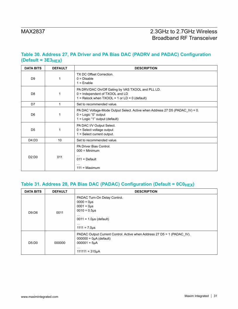
Table 30. Address 27, PA Driver and PA Bias DAC (PADRV and PADAC) Configuration (Default = 3E3HEX)
Table 31. Address 28, PA Bias DAC (PADAC) Configuration (Default = 0C0HEX)
DATA BITS DEFAULT DESCRIPTION
D9 1TX DC Offset Correction. 0 = Disable 1 = Enable
D8 1PA DRV/DAC On/Off Gating by VAS TXOOL and PLL LD. 0 = Independent of TXOOL and LD1 = Relock when TXOOL = 1 or LD = 0 (default)
D7 1 Set to recommended value.
D6 1PA DAC Voltage-Mode Output Select. Active when Address 27 D5 (PADAC_IV) = 0.0 = Logic “0” output1 = Logic “1” output (default)
D5 1PA DAC I/V Output Select. 0 = Select voltage output 1 = Select current output.
D4:D3 10 Set to recommended value.
D2:D0 011
PA Driver Bias Control.000 = Minimum…011 = Default…111 = Maximum
DATA BITS DEFAULT DESCRIPTION
D9:D6 0011
PADAC Turn-On Delay Control.0000 = 0µs 0001 = 0µs0010 = 0.5µs…0011 = 1.0µs (default)…1111 = 7.0µs
D5:D0 000000
PADAC Output Current Control. Active when Address 27 D5 = 1 (PADAC_IV).000000 = 0µA (default)000001 = 5µA…111111 = 315µA
MAX2837 2.3GHz to 2.7GHz WirelessBroadband RF Transceiver
www.maximintegrated.com Maxim Integrated 31
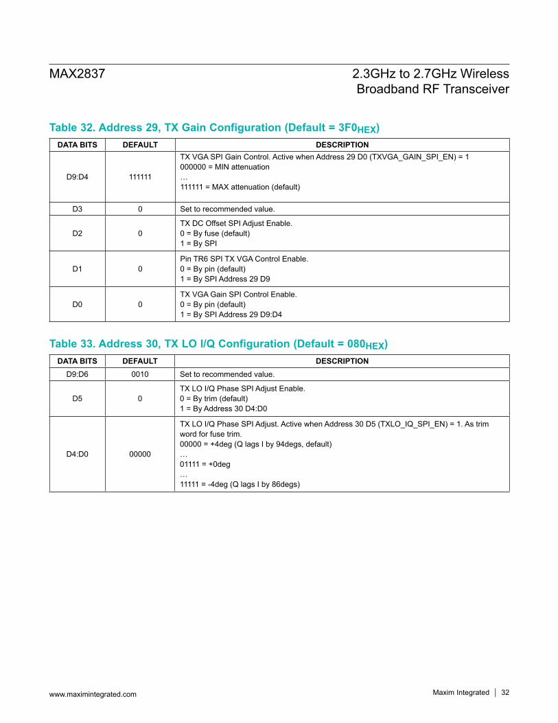
Table 32. Address 29, TX Gain Configuration (Default = 3F0HEX)
Table 33. Address 30, TX LO I/Q Configuration (Default = 080HEX)
DATA BITS DEFAULT DESCRIPTION
D9:D4 111111
TX VGA SPI Gain Control. Active when Address 29 D0 (TXVGA_GAIN_SPI_EN) = 1000000 = MIN attenuation…111111 = MAX attenuation (default)
D3 0 Set to recommended value.
D2 0TX DC Offset SPI Adjust Enable.0 = By fuse (default)1 = By SPI
D1 0Pin TR6 SPI TX VGA Control Enable.0 = By pin (default)1 = By SPI Address 29 D9
D0 0TX VGA Gain SPI Control Enable.0 = By pin (default)1 = By SPI Address 29 D9:D4
DATA BITS DEFAULT DESCRIPTIOND9:D6 0010 Set to recommended value.
D5 0TX LO I/Q Phase SPI Adjust Enable. 0 = By trim (default)1 = By Address 30 D4:D0
D4:D0 00000
TX LO I/Q Phase SPI Adjust. Active when Address 30 D5 (TXLO_IQ_SPI_EN) = 1. As trim word for fuse trim.00000 = +4deg (Q lags I by 94degs, default)…01111 = +0deg…11111 = -4deg (Q lags I by 86degs)
MAX2837 2.3GHz to 2.7GHz WirelessBroadband RF Transceiver
www.maximintegrated.com Maxim Integrated 32
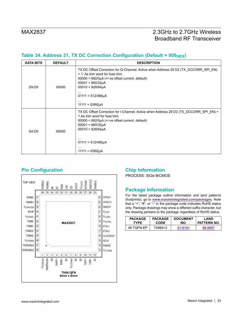
Table 34. Address 31, TX DC Correction Configuration (Default = 000HEX)DATA BITS DEFAULT DESCRIPTION
D9:D5 00000
TX DC Offset Correction for Q-Channel. Active when Address 29 D2 (TX_DCCORR_SPI_EN) = 1. As trim word for fuse trim.00000 = 992/0µA (+/-ve offset current, default)00001 = 960/32µA00010 = 928/64µA…01111 = 512/480µA…11111 = 0/992µA
D4:D0 00000
TX DC Offset Correction for I-Channel. Active when Address 29 D2 (TX_DCCORR_SPI_EN) = 1.As trim word for fuse trim.00000 = 992/0µA (+/-ve offset current, default)00001 = 960/32µA00010 = 928/64µA
…01111 = 512/480µA…11111 = 0/992µA
PACKAGE TYPE
PACKAGE CODE
DOCUMENT NO.
LAND PATTERN NO.
48 TQFN-EP T4866+2 21-0141 90-0007
MAX2837 2.3GHz to 2.7GHz WirelessBroadband RF Transceiver
www.maximintegrated.com Maxim Integrated 33
TOP VIEW
MAX2837
THIN QFN6mm x 6mm
13
14
15
16
17
18
19
20
21
22
23
24
ENAB
LE
GNDV
CO
BYPA
SS
V CCV
CO
DOUT
CS
SCLK
DIN
RSSI
B7B6RXBB
Q-
RXBB
Q+
RXBBI-
RXBBI+VCCRXVGA
RXHPVCCRXFL
TXBBI-
TXBBI+
TXBBQ+
TXBBQ-VCCRXMX
TXENABLE
RXENABLE 48+47
46
45
44
43
42
41
40
39
38
37
1 2 3 4 5 6 7 8 9 10 11 12
B1
TXRF
-
TXRF
+B2B3
V CCT
XPADB4
RXRF
-
RXRF
+B5
GNDR
XLNA
V CCR
XLNA
VCCTXMX
VCCXTAL
VCCDIG
VCCCP
36 35 34 33 32 31 30 29 28 27 26 25
CLOCKOUT
GNDCP
CPOUT+
CPOUT-
XTAL2
XTAL1
PABIAS
Pin Configuration
Package InformationFor the latest package outline information and land patterns (footprints), go to www.maximintegrated.com/packages. Note that a “+”, “#”, or “-” in the package code indicates RoHS status only. Package drawings may show a different suffix character, but the drawing pertains to the package regardless of RoHS status.
Chip InformationPROCESS: SiGe BiCMOS
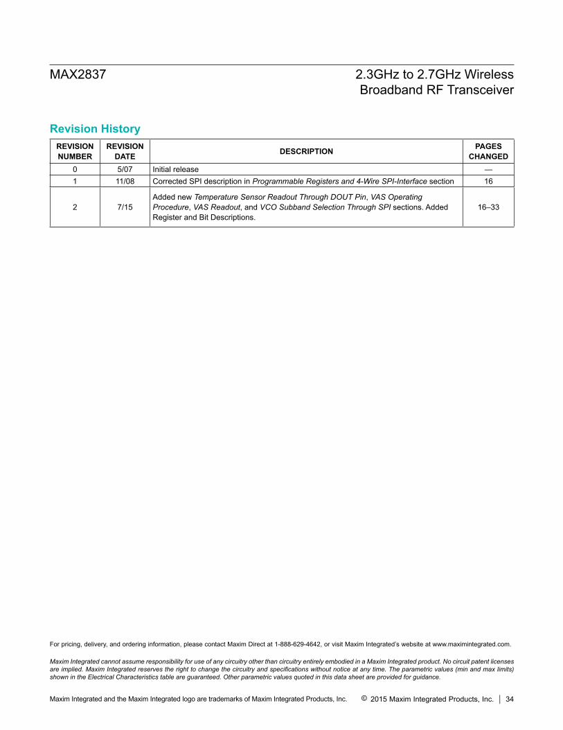
REVISIONNUMBER
REVISIONDATE DESCRIPTION PAGES
CHANGED0 5/07 Initial release —1 11/08 Corrected SPI description in Programmable Registers and 4-Wire SPI-Interface section 16
2 7/15Added new Temperature Sensor Readout Through DOUT Pin, VAS Operating Procedure, VAS Readout, and VCO Subband Selection Through SPI sections. Added Register and Bit Descriptions.
16–33
Maxim Integrated cannot assume responsibility for use of any circuitry other than circuitry entirely embodied in a Maxim Integrated product. No circuit patent licenses are implied. Maxim Integrated reserves the right to change the circuitry and specifications without notice at any time. The parametric values (min and max limits) shown in the Electrical Characteristics table are guaranteed. Other parametric values quoted in this data sheet are provided for guidance.
Maxim Integrated and the Maxim Integrated logo are trademarks of Maxim Integrated Products, Inc.
MAX2837 2.3GHz to 2.7GHz WirelessBroadband RF Transceiver
© 2015 Maxim Integrated Products, Inc. 34
Revision History
For pricing, delivery, and ordering information, please contact Maxim Direct at 1-888-629-4642, or visit Maxim Integrated’s website at www.maximintegrated.com.