Embed Size (px)
Citation preview
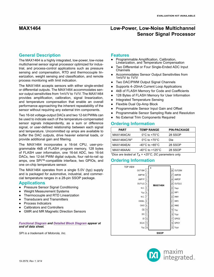
General DescriptionThe MAX1464 is a highly integrated, low-power, low-noise multichannel sensor signal processor optimized for indus-trial, and process-control applications such as pressure sensing and compensation, RTD and thermocouple lin-earization, weight sensing and classification, and remote process monitoring with limit indication.The MAX1464 accepts sensors with either single-ended or differential outputs. The MAX1464 accommodates sen-sor output sensitivities from 1mV/V to 1V/V. The MAX1464 provides amplification, calibration, signal linearization, and temperature compensation that enable an overall performance approaching the inherent repeatability of the sensor without requiring any external trim components.Two 16-bit voltage-output DACs and two 12-bit PWMs can be used to indicate each of the temperature-compensated sensor signals independently, as a sum or difference signal, or user-defined relationship between each signal and temperature. Uncommitted op amps are available to buffer the DAC outputs, drive heavier external loads, or provide additional gain and filtering.The MAX1464 incorporates a 16-bit CPU, user-pro-grammable 4kB of FLASH program memory, 128 bytes of FLASH user information, one 16-bit ADC, two 16-bit DACs, two 12-bit PWM digital outputs, four rail-to-rail op amps, one SPI™-compatible interface, two GPIOs, and one on-chip temperature sensor.The MAX1464 operates from a single 5.0V (typ) supply and is packaged for automotive, industrial, and commer-cial temperature ranges in a 28-pin SSOP package.Applications
Pressure Sensor Signal Conditioning Weight Measurement Systems Thermocouple and RTD Linearization Transducers and Transmitters Process Indicators Calibrators and Controllers GMR and MR Magnetic Direction Sensors
Features Programmable Amplification, Calibration,
Linearization, and Temperature Compensation Two Differential or Four Single-Ended ADC Input
Channels Accommodates Sensor Output Sensitivities from
1mV/V to 1V/V Two DAC/PWM Output Signal Channels Supports 4–20mA Current Loop Applications 4kB of FLASH Memory for Code and Coefficients 128 Bytes of FLASH Memory for User Information Integrated Temperature Sensing Flexible Dual Op-Amp Block Programmable Sensor Input Gain and Offset Programmable Sensor Sampling Rate and Resolution No External Trim Components Required
Functional Diagram and Detailed Block Diagram appear at end of data sheet.
19-3579; Rev 1; 9/14
*Dice are tested at TA = +25°C, DC parameters only.
SPI is a trademark of Motorola, Inc.
28
27
26
25
24
23
22
21
20
19
18
17
16
15
1
2
3
4
5
6
7
8
9
10
11
12
13
14
OUT2SM
AMP2M
AMP2P
OUT2LG
VREF
INP1
VDDF
INM1
INP2
INM2
VSS
VSSF
GPIO2
GPIO1
VSS
SCLK
DI
DO
CS
CKIO
CKSEL
N.C.
VDD
N.C.
OUT1LG
AMP1P
AMP1M
OUT1SM
SSOP
TOP VIEW
MAX1464
MAX1464 Low-Power, Low-Noise Multichannel Sensor Signal Processor
PART TEMP RANGE PIN-PACKAGEMAX1464CAI 0°C to +70°C 28 SSOP
MAX1464C/W* 0°C to +70°C Die
MAX1464EAI -40°C to +85°C 28 SSOP
MAX1464AAI -40°C to +125°C 28 SSOP
Ordering Information
Ordering Information
EVALUATION KIT AVAILABLE

VDD to VSS............................................................-0.3V to +6.0VVDDF to VSS.........................................................-0.3V to +6.0VVSSF to VSS..........................................................-0.3V to +0.3VAll Other Pins to VSS..................................-0.3V to (VDD + 0.3V)Continuous Power Dissipation (TA = +70°C)
28-Pin SSOP (derate 9.1mW/°C above +70°C) ..........727mW
Operating Temperature Ranges MAX1464CAI .....................................................0°C to +70°C MAX1464C/W.....................................................0°C to +70°C MAX1464EAI...................................................-40°C to +85°C MAX1464AAI ................................................-40°C to +125°C
Junction Temperature......................................................+150°CStorage Temperature Range .............................-65°C to +150°CLead Temperature (soldering, 10s) ................................ +300°C
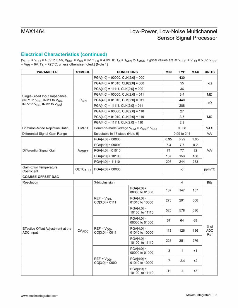
(VDDF = VDD = 4.5V to 5.5V, VSSF = VSS = 0V, fCLK = 4.0MHz, TA = TMIN to TMAX. Typical values are at VDDF = VDD = 5.0V, VSSF = VSS = 0V, TA = +25°C, unless otherwise noted.) (Note 1)
MAX1464 Low-Power, Low-Noise Multichannel Sensor Signal Processor
www.maximintegrated.com Maxim Integrated 2
PARAMETER SYMBOL CONDITIONS MIN TYP MAX UNITSSUPPLYSupply Voltage VDD VSS = VSSF = 0V 4.5 5.0 5.5 V
FLASH Supply Voltage VDDF VSS = VSSF = 0V 4.5 5.0 5.5 V
Base Operating Current IBO CPU stopped (Note 2) 575 720 890 µA
CPU Current ICPUAll modules off, CPU = on, additive to IBO, ICPU = IDD + IDDF (Note 3) 540 840 1240 µA
ADC Current (Note 3) IADC
All modules off, ADC = on, ADC clk = 1MHz, additive to IBO; the CPU and ADC are not on at the same time
690 1040 1394
µAAll modules off, ADC = on, ADC clk = 7kHz, additive to IBO; the CPU and ADC are not on at the same time
465 765 1060
DAC Current IDACnAll modules off, DAC = on, additive to IBO (n = 1 or 2) (Note 4) 425 550 730 µA
Large Op-Amp Current IOPLGnAll modules off, CPU stopped, large op amp = on (n = 1 or 2) 430 673 1020 µA
Small Op-Amp Current IOPSMnAll modules off, CPU stopped, small op amp = on (n = 1 or 2) 110 190 265 µA
POWER-ON RESETVDDF POR Threshold VDD > VDDF 3.6 4.0 4.3 V
VDDF POR Hysteresis -0.85 V
ANALOG INPUT
Differential Input Impedance (INP1 to INM1 and INP2 to INM2)
RDIN
PGA[4:0] = 00000, CLK[2:0] = 000 430
kΩPGA[4:0] = 01010, CLK[2:0] = 000 55
PGA[4:0] = 11111, CLK[2:0] = 000 36
PGA[4:0] = 00000, CLK[2:0] = 011 3.4 MΩ
PGA[4:0] = 01010, CLK[2:0] = 011 440kΩ
PGA[4:0] = 11111, CLK[2:0] = 011 288
PGA[4:0] = 00000, CLK[2:0] = 110 27
MΩPGA[4:0] = 01010, CLK[2:0] = 110 3.5
PGA[4:0] = 11111, CLK[2:0] = 110 2.3
Absolute Maximum Ratings
Stresses beyond those listed under “Absolute Maximum Ratings” may cause permanent damage to the device. These are stress ratings only, and functional operation of the device at these or any other conditions beyond those indicated in the operational sections of the specifications is not implied. Exposure to absolute maximum rating conditions for extended periods may affect device reliability.
Electrical Characteristics
(VDDF = VDD = 4.5V to 5.5V, VSSF = VSS = 0V, fCLK = 4.0MHz, TA = TMIN to TMAX. Typical values are at VDDF = VDD = 5.0V, VSSF = VSS = 0V, TA = +25°C, unless otherwise noted.) (Note 1)
MAX1464 Low-Power, Low-Noise Multichannel Sensor Signal Processor
www.maximintegrated.com Maxim Integrated 3
PARAMETER SYMBOL CONDITIONS MIN TYP MAX UNITS
Single-Sided Input Impedance (INP1 to VSS, INM1 to VSS, INP2 to VSS, INM2 to VSS)
RSIN
PGA[4:0] = 00000, CLK[2:0] = 000 430
kΩPGA[4:0] = 01010, CLK[2:0] = 000 55
PGA[4:0] = 11111, CLK[2:0] = 000 36
PGA[4:0] = 00000, CLK[2:0] = 011 3.4 MΩ
PGA[4:0] = 01010, CLK[2:0] = 011 440kΩ
PGA[4:0] = 11111, CLK[2:0] = 011 288
PGA[4:0] = 00000, CLK[2:0] = 110 27
MΩPGA[4:0] = 01010, CLK[2:0] = 110 3.5
PGA[4:0] = 11111, CLK[2:0] = 110 2.3
Common-Mode Rejection Ratio CMRR Common-mode voltage VCM = VSS to VDD 0.008 %FS
Differential Signal-Gain Range Selectable in 17 steps (Note 5) 0.99 to 244 V/V
Differential Signal Gain AVDIFF
PGA[4:0] = 00000 0.95 0.99 1.05
V/V
PGA[4:0] = 00001 7.3 7.7 8.2
PGA[4:0] = 01010 71 77 82
PGA[4:0] = 10100 137 153 168
PGA[4:0] = 11110 203 244 283
Gain-Error Temperature Coefficient GETCADC PGA[4:0] = 00000 -8 ppm/°C
COARSE-OFFSET DACResolution 3-bit plus sign 4 Bits
Effective Offset Adjustment at the ADC Input OAADC
REF = VDD,CO[3:0] = 0111
PGA[4:0] = 00000 to 01000 137 147 157
% of ADCRef
PGA[4:0] = 01010 to 10000 273 291 308
PGA[4:0] = 10100 to 11110 525 578 630
REF = VDD,CO[3:0] = 0011
PGA[4:0] = 00000 to 01000 57 64 69
PGA[4:0] = 01010 to 10000 113 126 136
PGA[4:0] = 10100 to 11110 228 251 276
REF = VDD,CO[3:0] = 0000
PGA[4:0] = 00000 to 01000 -3 -1 +1
PGA[4:0] = 01010 to 10000 -7 -2.4 +2
PGA[4:0] = 10100 to 11110 -11 -4 +3
Electrical Characteristics (continued)
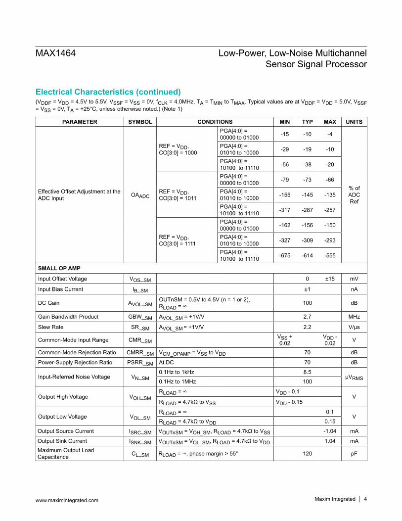
(VDDF = VDD = 4.5V to 5.5V, VSSF = VSS = 0V, fCLK = 4.0MHz, TA = TMIN to TMAX. Typical values are at VDDF = VDD = 5.0V, VSSF = VSS = 0V, TA = +25°C, unless otherwise noted.) (Note 1)
MAX1464 Low-Power, Low-Noise Multichannel Sensor Signal Processor
www.maximintegrated.com Maxim Integrated 4
PARAMETER SYMBOL CONDITIONS MIN TYP MAX UNITS
Effective Offset Adjustment at the ADC Input OAADC
REF = VDD,CO[3:0] = 1000
PGA[4:0] = 00000 to 01000 -15 -10 -4
% of ADCRef
PGA[4:0] = 01010 to 10000 -29 -19 -10
PGA[4:0] = 10100 to 11110 -56 -38 -20
REF = VDD,CO[3:0] = 1011
PGA[4:0] = 00000 to 01000 -79 -73 -66
PGA[4:0] = 01010 to 10000 -155 -145 -135
PGA[4:0] = 10100 to 11110 -317 -287 -257
REF = VDD,CO[3:0] = 1111
PGA[4:0] = 00000 to 01000 -162 -156 -150
PGA[4:0] = 01010 to 10000 -327 -309 -293
PGA[4:0] = 10100 to 11110 -675 -614 -555
SMALL OP AMP
Input Offset Voltage VOS_SM 0 ±15 mV
Input Bias Current IB_SM ±1 nA
DC Gain AVOL_SMOUTnSM = 0.5V to 4.5V (n = 1 or 2), RLOAD = ∞ 100 dB
Gain Bandwidth Product GBW_SM AVOL_SM = +1V/V 2.7 MHz
Slew Rate SR_SM AVOL_SM = +1V/V 2.2 V/µs
Common-Mode Input Range CMR_SMVSS + 0.02
VDD - 0.02 V
Common-Mode Rejection Ratio CMRR_SM VCM_OPAMP = VSS to VDD 70 dB
Power-Supply Rejection Ratio PSRR_SM At DC 70 dB
Input-Referred Noise Voltage VN_SM0.1Hz to 1kHz 8.5
µVRMS0.1Hz to 1MHz 100
Output High Voltage VOH_SMRLOAD = ∞ VDD - 0.1
VRLOAD = 4.7kΩ to VSS VDD - 0.15
Output Low Voltage VOL_SMRLOAD = ∞ 0.1
VRLOAD = 4.7kΩ to VDD 0.15
Output Source Current ISRC_SM VOUTnSM = VOH_SM, RLOAD = 4.7kΩ to VSS -1.04 mA
Output Sink Current ISNK_SM VOUTnSM = VOL_SM, RLOAD = 4.7kΩ to VDD 1.04 mAMaximum Output Load Capacitance CL_SM RLOAD = ∞, phase margin > 55° 120 pF
Electrical Characteristics (continued)
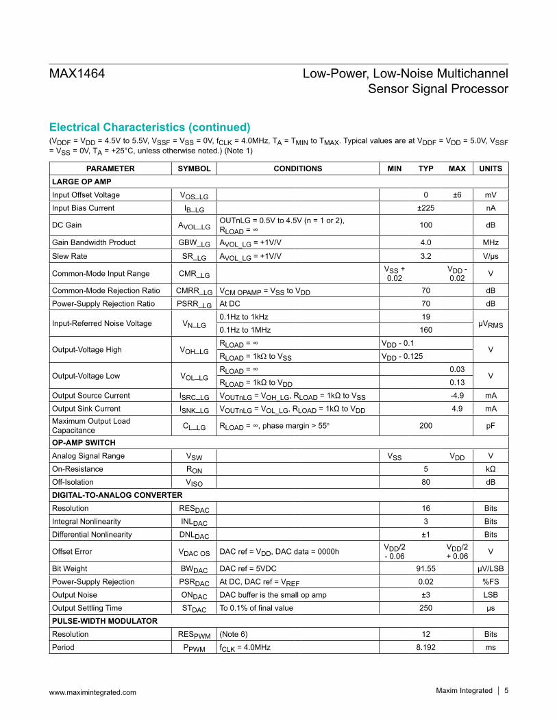
(VDDF = VDD = 4.5V to 5.5V, VSSF = VSS = 0V, fCLK = 4.0MHz, TA = TMIN to TMAX. Typical values are at VDDF = VDD = 5.0V, VSSF = VSS = 0V, TA = +25°C, unless otherwise noted.) (Note 1)
MAX1464 Low-Power, Low-Noise Multichannel Sensor Signal Processor
www.maximintegrated.com Maxim Integrated 5
PARAMETER SYMBOL CONDITIONS MIN TYP MAX UNITSLARGE OP AMPInput Offset Voltage VOS_LG 0 ±6 mV
Input Bias Current IB_LG ±225 nA
DC Gain AVOL_LGOUTnLG = 0.5V to 4.5V (n = 1 or 2), RLOAD = ∞ 100 dB
Gain Bandwidth Product GBW_LG AVOL_LG = +1V/V 4.0 MHz
Slew Rate SR_LG AVOL_LG = +1V/V 3.2 V/µs
Common-Mode Input Range CMR_LGVSS + 0.02
VDD - 0.02 V
Common-Mode Rejection Ratio CMRR_LG VCM OPAMP = VSS to VDD 70 dB
Power-Supply Rejection Ratio PSRR_LG At DC 70 dB
Input-Referred Noise Voltage VN_LG0.1Hz to 1kHz 19
µVRMS0.1Hz to 1MHz 160
Output-Voltage High VOH_LGRLOAD = ∞ VDD - 0.1
VRLOAD = 1kW to VSS VDD - 0.125
Output-Voltage Low VOL_LGRLOAD = ∞ 0.03
VRLOAD = 1kΩ to VDD 0.13
Output Source Current ISRC_LG VOUTnLG = VOH_LG, RLOAD = 1kΩ to VSS -4.9 mA
Output Sink Current ISNK_LG VOUTnLG = VOL_LG, RLOAD = 1kΩ to VDD 4.9 mAMaximum Output Load Capacitance CL_LG RLOAD = ∞, phase margin > 55° 200 pF
OP-AMP SWITCHAnalog Signal Range VSW VSS VDD V
On-Resistance RON 5 kΩ
Off-Isolation VISO 80 dB
DIGITAL-TO-ANALOG CONVERTERResolution RESDAC 16 Bits
Integral Nonlinearity INLDAC 3 Bits
Differential Nonlinearity DNLDAC ±1 Bits
Offset Error VDAC OS DAC ref = VDD, DAC data = 0000h VDD/2 - 0.06
VDD/2 + 0.06 V
Bit Weight BWDAC DAC ref = 5VDC 91.55 µV/LSB
Power-Supply Rejection PSRDAC At DC, DAC ref = VREF 0.02 %FS
Output Noise ONDAC DAC buffer is the small op amp ±3 LSB
Output Settling Time STDAC To 0.1% of final value 250 µs
PULSE-WIDTH MODULATORResolution RESPWM (Note 6) 12 Bits
Period PPWM fCLK = 4.0MHz 8.192 ms
Electrical Characteristics (continued)
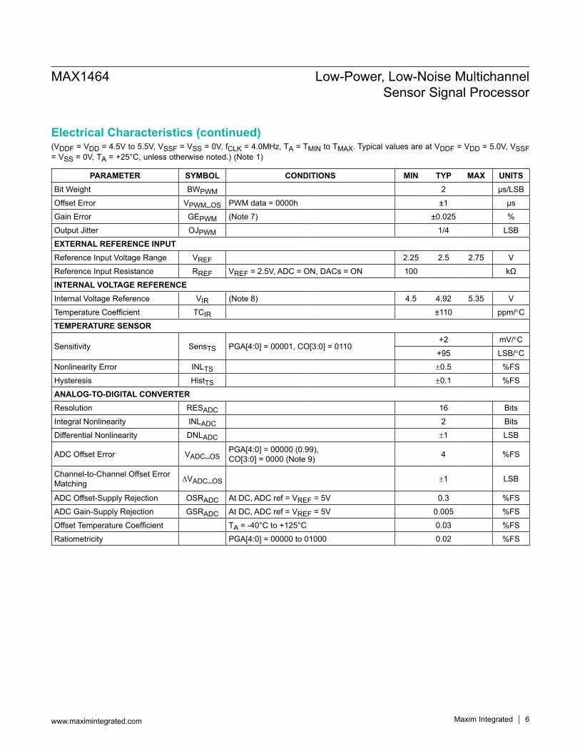
(VDDF = VDD = 4.5V to 5.5V, VSSF = VSS = 0V, fCLK = 4.0MHz, TA = TMIN to TMAX. Typical values are at VDDF = VDD = 5.0V, VSSF = VSS = 0V, TA = +25°C, unless otherwise noted.) (Note 1)
MAX1464 Low-Power, Low-Noise Multichannel Sensor Signal Processor
www.maximintegrated.com Maxim Integrated 6
PARAMETER SYMBOL CONDITIONS MIN TYP MAX UNITSBit Weight BWPWM 2 µs/LSB
Offset Error VPWM_OS PWM data = 0000h ±1 µs
Gain Error GEPWM (Note 7) ±0.025 %
Output Jitter OJPWM 1/4 LSB
EXTERNAL REFERENCE INPUTReference Input Voltage Range VREF 2.25 2.5 2.75 V
Reference Input Resistance RREF VREF = 2.5V, ADC = ON, DACs = ON 100 kΩ
INTERNAL VOLTAGE REFERENCEInternal Voltage Reference VIR (Note 8) 4.5 4.92 5.35 V
Temperature Coefficient TCIR ±110 ppm/°C
TEMPERATURE SENSOR
Sensitivity SensTS PGA[4:0] = 00001, CO[3:0] = 0110+2 mV/°C
+95 LSB/°C
Nonlinearity Error INLTS ±0.5 %FS
Hysteresis HistTS ±0.1 %FS
ANALOG-TO-DIGITAL CONVERTERResolution RESADC 16 Bits
Integral Nonlinearity INLADC 2 Bits
Differential Nonlinearity DNLADC ±1 LSB
ADC Offset Error VADC_OSPGA[4:0] = 00000 (0.99), CO[3:0] = 0000 (Note 9) 4 %FS
Channel-to-Channel Offset Error Matching DVADC_OS ±1 LSB
ADC Offset-Supply Rejection OSRADC At DC, ADC ref = VREF = 5V 0.3 %FS
ADC Gain-Supply Rejection GSRADC At DC, ADC ref = VREF = 5V 0.005 %FS
Offset Temperature Coefficient TA = -40°C to +125°C 0.03 %FS
Ratiometricity PGA[4:0] = 00000 to 01000 0.02 %FS
Electrical Characteristics (continued)
Note 1: Current into a pin is defined as positive. Current out of a pin is defined as negative. All voltages are referenced to VSS.Note 2: All modules are off, except internal reference, oscillator, and power-on reset (POR) and CKSEL bit is set to zero.Note 3: The CPU and ADC are not on at the same time. The ADC and CPU currents are not additive.Note 4: IDACn does not include output buffer currents (IOPLGn or IOPSMn).Note 5: For gains above 240, an additional digital gain can be provided by the CPU.Note 6: The PWM input data is the 12-bit left-justified data in the 16-bit input field.Note 7: PWM gain error measured as:
OUT OUTPWM
PWM (F00 h) PWM (100 h)GE 100%3584
× − ×= ×
Note 8: The internal reference voltage has a nominal value of 5V (4 x VBG) even when VDD is greater or less than 5VDC.Note 9: A Input-referred offset error is the ADC offset error divided by the PGA gain.Note 10: When the CKIO is configured in output mode to observe the internal oscillator signal, the total current is above the speci-
fied limits.Note 11: fCLK must be within 5% of 4MHz.Note 12: Allow a minimum elapsed time of 4.2ms when executing a FLASH erase command, before sending any other command.
Allow a minimum elapsed time of 80μs between FLASH write commands.Note 13: FLASH programming current is guaranteed by design.
(VDDF = VDD = 4.5V to 5.5V, VSSF = VSS = 0V, fCLK = 4.0MHz, TA = TMIN to TMAX. Typical values are at VDDF = VDD = 5.0V, VSSF = VSS = 0V, TA = +25°C, unless otherwise noted.) (Note 1)
MAX1464 Low-Power, Low-Noise Multichannel Sensor Signal Processor
www.maximintegrated.com Maxim Integrated 7
PARAMETER SYMBOL CONDITIONS MIN TYP MAX UNITSDIGITAL INPUTS (GPIO1, GPIO2, SCLK, DI, CKSEL, CKIO, CS)Input High Threshold Voltage VIH 0.8 x VDD V
Input Low Threshold Voltage VIL 0.2 x VDD V
Input Hysteresis VIHYS 0.2 V
Input Leakage Current IINCKSEL, CS = VSS 38 -90
µAGPIO1, GPIO2, SCLK, DI, CKIO = VDD 38 +90
Input Capacitance CIN 5 pF
DIGITAL OUTPUTS (GPIO1, GPIO2, DO, CKIO)
Output-Voltage High VOH
RLOAD = ∞GPIO1, GPIO2, DO VDD - 0.1
VCKIO (Note 10) 4.9
RLOAD = 2kΩ to VSSGPIO1, GPIO2, DO VDD - 0.15
CKIO (Note 10) 4.6
Output-Voltage Low VOL
RLOAD = ∞GPIO1, GPIO2, DO 0.05
VCKIO (Note 10) 0.1
RLOAD = 2kΩ to VDD
GPIO1, GPIO2, DO 0.2
CKIO (Note 10) 0.4
FLASH MEMORYMaximum Erase Cycles (Notes 11, 12) 10k Cycles
Minimum Erase Time tERASE (Notes 11, 12) 4.2 ms
Minimum Write Time tWRITE (Notes 11, 12) 80 µs
FLASH Programming Current IDDFPWriting to the FLASH or erasing the FLASH (Note 13) 30 mA
Electrical Characteristics (continued)
(VDDF = VDD = 4.5V to 5.5V, VSSF = VSS = 0V, fCLK = 4.0MHz, TA = TMIN to TMAX. Typical values are at VDDF = VDD = 5.0V, VSSF = VSS = 0V, TA = +25°C, unless otherwise noted.) (Note 1)
MAX1464 Low-Power, Low-Noise Multichannel Sensor Signal Processor
www.maximintegrated.com Maxim Integrated 8
PARAMETER SYMBOL CONDITIONS MIN TYP MAX UNITSProgramming Temperature TPROG 125 °C
Internal Oscillator Clock Frequency fICLK OSC[4:0] = 00000 3.3 4.15 5.3 MHz
External Clock Frequency fECLK VCKSEL = 0Min 0.2
MHzMax 5
External Master Clock Input Low Time fECLKIN_LO tECLK = 1 / fECLK 40 60 %
tECLK
External Master Clock Input High Time fECLKIN_HI tECLK = 1 / fECLK 40 60 %
tECLK
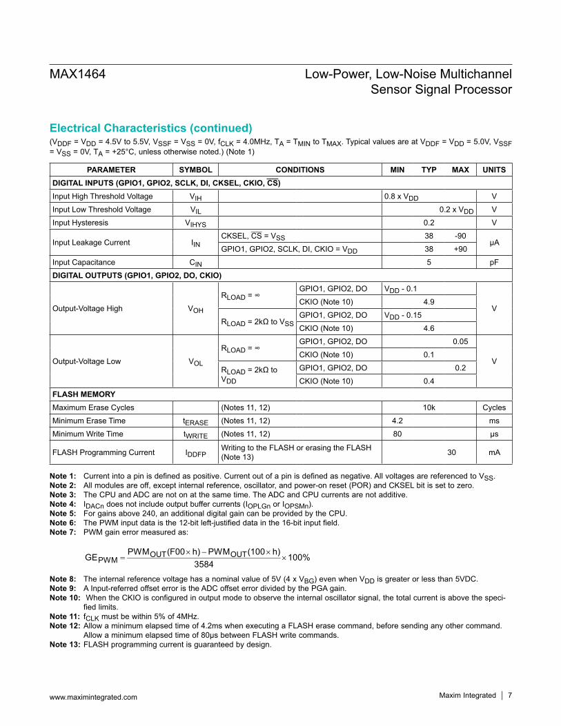
SERIAL INTERFACE (Figure 1)
SCLK Setup to Falling Edge CS tSC 30 ns
CS Falling Edge to SCLK Rising Edge Setup Time
tCSS 30 ns
CS Idle Time tCSI fCLK = 4MHz 1.5 µs
CS Period tCS fCLK = 4MHz 4 µs
SCLK Falling Edge to Data Valid Delay tDO CLOAD = 200pF 80 ns
Data Valid to SCLK Rising Edge Setup Time tDS 30 ns
Data Valid to SCLK Rising Edge Hold Time tDH 30 ns
SCLK High Pulse Width tCH 100 ns
SCLK Low Pulse Width tCL 100 ns
CS Rising Edge to SCLK Rising Edge Hold Time
tCSH 30 ns
CS Falling Edge to Output Enable tDV CLOAD = 200pF 25 ns
CS Rising Edge to Output Disable tTR CLOAD = 200pF 25 ns
Timing Characteristics
(VADD = 5.0V, TA = +25°C, unless otherwise noted.)
Figure 1. Serial Interface Timing Diagram
DO
DI
SCLK
CS
tCSS tCL tCHtCSHtSC
tCS
tDStDH
tDStDH
tCSI
tCSS tCL tCHtSC tCSH
tDO tTR tDVtDV tDO tTR
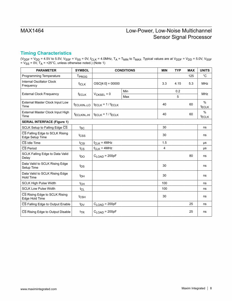
SUPPLY CURRENTvs. INTERNAL CLOCK FREQUENCY
MAX
1464
toc0
2
INTERNAL CLOCK FREQUENCY (MHz)
SUPP
LY C
URRE
NT, I D
D (m
A)
4.54.03.5
2.25
2.30
2.35
2.40
2.45
2.50
2.55
2.60
2.65
2.70
2.203.0 5.0
CPU ON 2% OF TIMEADC ON 98% OF TIMEADCCLK = 1MHzDAC1 ONSMALL OP AMP ON
MODULE CURRENTvs. TEMPERATURE
MAX
1464
toc0
3
TEMPERATURE (°C)
MODU
LE C
URRE
NT (m
A)
98704315-13
0.7
0.9
1.1
1.3
1.5
1.7
1.9
2.1
2.3
2.5
0.5-40 125
DAC + LARGE OP AMP
DAC + SMALL OP AMP
ADC
BASE
BASE OPERATING CURRENTvs. SUPPLY VOLTAGE
MAX
1464
toc0
4
SUPPLY VOLTAGE, VDD (V)
BASE
OPE
RATI
NG C
URRE
NT, I B
O (m
A)
5.35.14.7 4.9
0.67
0.69
0.71
0.73
0.75
0.77
0.79
0.81
0.654.5 5.5
TA = +125°C
TA = +25°C
TA = -40°C
ADC RATIOMETRICITY ERRORvs. SUPPLY VOLTAGE
MAX
1464
toc0
5
SUPPLY VOLTAGE, VDD (V)
ADC
RATI
OMET
RICI
TY E
RROR
(%FS
)
5.35.14.7 4.9
-0.03
-0.02
-0.01
0
0.01
0.02
0.03
0.04
-0.044.5 5.5
ADC INPUT = 0.75 x VDD
ADC INPUT = 0.5 x VDDADC INPUT = 0
ADC INPUT = -0.75 x VDD
ADC INPUT = -0.5 x VDD
ADCREF = VDDPGA[4:0] = 00000
ADC INLM
AX14
64 to
c06
1.00.5-0.5 0-1.0INPUT VOLTAGE NORMALIZED TO FULL SCALE
ADC
NONL
INEA
RITY
ERR
OR (%
FS)
-0.004
-0.002
0
0.002
0.004
0.006
-0.006PGA[4:0] = 01000
SUPPLY CURRENTvs. SUPPLY VOLTAGE
MAX
1464
toc0
1
SUPPLY VOLTAGE, VDD (V)
SUPP
LY C
URRE
NT, I D
D (m
A)
5.35.14.7 4.9
2.30
2.35
2.40
2.45
2.50
2.55
2.60
2.65
2.254.5 5.5
CPU ON 2% OF TIMEADC ON 98% OF TIMEADCCLK = 1MHzDAC1 ONSMALL OP AMP ON
TA = +125°C
TA = +25°C
TA = -40°C
MAX1464 Low-Power, Low-Noise Multichannel Sensor Signal Processor
www.maximintegrated.com Maxim Integrated 9
Typical Operating Characteristics
(VADD = 5.0V, TA = +25°C, unless otherwise noted.)
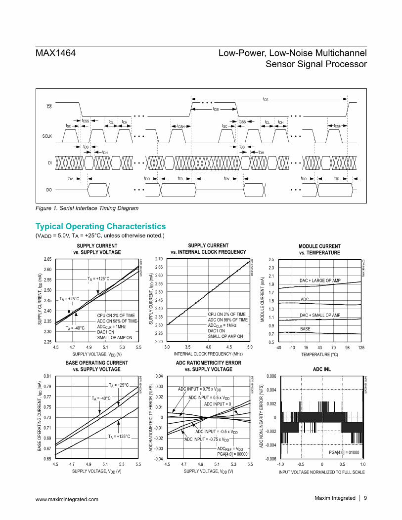
ADC DNL
MAX
1464
toc0
7
INPUT VOLTAGE NORMALIZED TO FULL SCALE
ADC
DNL E
RROR
(LSB
)
0.50-0.5
-3
-2
-1
0
1
2
3
4
-4-1.0 1.0
PGA[4:0] = 01000
DAC INL
MAX
1464
toc0
8
INPUT NORMALIZED TO FULL SCALE
DAC
NONL
INEA
RITY
ERR
OR (%
FS)
0.60.4-0.6 -0.4 -0.2 0 0.2
-0.03
-0.02
-0.01
0
0.01
0.02
0.03
0.04
-0.04-0.8 0.8
DAC DNL
MAX
1464
toc0
9
INPUT VOLTAGE NORMALIZED TO FULL SCALE
DAC
DNL E
RROR
(LSB
)
0.60.40.20-0.2-0.4-0.6
-2
-1
0
1
2
3
-3-0.8 0.8
DAC DYNAMIC RESPONSE
200µs/div
4
5
0
2
3
1
1V/div
DAC CODE = 4000h
DAC CODE = C000h
MAX
1464
toc1
0
DAC RATIOMETRICITY ERRORvs. SUPPLY VOLTAGE
MAX
1464
toc1
1
SUPPLY VOLTAGE, VDD (V)
ERRO
R (%
FS)
5.35.14.94.7
-0.04
-0.03
-0.02
-0.01
0
0.01
0.02
0.03
0.04
0.05
-0.054.5 5.5
DAC INPUT = 5555CH (4.5V AT VDD = 5V)
DAC INPUT = 0000CH (2.5V AT VDD = 5V)
DAC INPUT = AAABCH (0.5V AT VDD = 5V)
INTERNAL OSCILLATOR FREQUENCYvs. SUPPLY VOLTAGE
MAX
1464
toc1
2
SUPPLY VOLTAGE, VDD (V)
INTE
RNAL
OSC
ILLAT
OR F
REQU
ENCY
(MHz
)
5.35.14.94.7
3.85
3.90
3.95
4.00
4.05
4.10
4.15
3.804.5 5.5
TA = -40°C
TA = +125°C
TA = +25°C
OSCILLATORFREQUENCY TRIMMEDTO 4MHz AT +25°C, VDD = 5V
TEMPERATURE SENSOR OUTPUTvs. TEMPERATURE
MAX
1464
toc1
3
TEMPERATURE (°C)
TEMP
ERAT
URE
SENS
OR O
UTPU
T (A
DC C
ODE)
97.5 125.070.042.515.0-12.5
0
-2000
4000
2000
8000
12,000
10,000
14,000
6000
16,000
-4000-40.0
PGA[4:0] = [00001]CO[3:0] = 0110
Maxim Integrated 10www.maximintegrated.com
MAX1464 Low-Power, Low-Noise Multichannel Sensor Signal Processor
Typical Operating Characteristics (continued)
MAX1464 Low-Power, Low-Noise Multichannel Sensor Signal Processor
www.maximintegrated.com Maxim Integrated 11
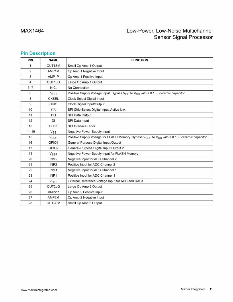
PIN NAME FUNCTION1 OUT1SM Small Op Amp 1 Output
2 AMP1M Op Amp 1 Negative Input
3 AMP1P Op Amp 1 Positive Input
4 OUT1LG Large Op Amp 1 Output
5, 7 N.C. No Connection
6 VDD Positive Supply Voltage Input. Bypass VDD to VSS with a 0.1µF ceramic capacitor.
8 CKSEL Clock-Select Digital Input
9 CKIO Clock Digital Input/Output
10 CS SPI Chip-Select Digital Input. Active low.
11 DO SPI Data Output
12 DI SPI Data Input
13 SCLK SPI Interface Clock
14, 19 VSS Negative Power-Supply Input
15 VDDF Positive Supply Voltage for FLASH Memory. Bypass VDDF to VSS with a 0.1µF ceramic capacitor.
16 GPIO1 General-Purpose Digital Input/Output 1
17 GPIO2 General-Purpose Digital Input/Output 2
18 VSSF Negative Power-Supply Input for FLASH Memory
20 INM2 Negative Input for ADC Channel 2
21 INP2 Positive Input for ADC Channel 2
22 INM1 Negative Input for ADC Channel 1
23 INP1 Positive Input for ADC Channel 1
24 VREF External Reference Voltage Input for ADC and DACs
25 OUT2LG Large Op Amp 2 Output
26 AMP2P Op Amp 2 Positive Input
27 AMP2M Op Amp 2 Negative Input
28 OUT2SM Small Op Amp 2 Output
Pin Description
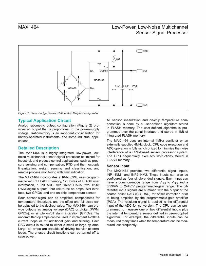
Typical Application CircuitAnalog ratiometric output configuration (Figure 2) pro-vides an output that is proportional to the power-supply voltage. Ratiometricity is an important consideration for battery-operated instruments, and some industrial appli-cations.
Detailed DescriptionThe MAX1464 is a highly integrated, low-power, low-noise multichannel sensor signal processor optimized for industrial, and process-control applications, such as pres-sure sensing and compensation, RTD and thermocouple linearization, weight sensing and classification, and remote process monitoring with limit indication.The MAX1464 incorporates a 16-bit CPU, user-program-mable 4kB of FLASH memory, 128 bytes of FLASH user information, 16-bit ADC, two 16-bit DACs, two 12-bit PWM digital outputs, four rail-to-rail op amps, SPI inter-face, two GPIOs, and one on-chip temperature sensor.Each sensor signal can be amplified, compensated for temperature, linearized, and the offset and full scale can be adjusted to the desired value. The MAX1464 can pro-vide outputs as analog voltage (DAC) or digital (PWM, GPIOs), or simple on/off alarm indication (GPIOs). The uncommitted op amps can be used to implement 4–20mA current loops or for additional gain and filtering. Each DAC output is routed to either a small or large op amp. Large op amps are capable of driving heavier external loads. The unused circuit functions can be turned off to save power.
All sensor linearization and on-chip temperature com-pensation is done by a user-defined algorithm stored in FLASH memory. The user-defined algorithm is pro-grammed over the serial interface and stored in 4kB of integrated FLASH memory.The MAX1464 uses an internal 4MHz oscillator or an externally supplied 4MHz clock. CPU code execution and ADC operation is fully synchronized to minimize the noise interference of a CPU-based sensor processor system. The CPU sequentially executes instructions stored in FLASH memory.
Sensor InputThe MAX1464 provides two differential signal inputs, INP1-INM1 and INP2-INM2. These inputs can also be configured as four single-ended signals. Each input can have a common-mode range from VDD to VSS and a 0.99V/V to 244V/V programmable-gain range. The dif-ferential input signals are summed with the output of the coarse offset DAC (CO DAC) for offset correction prior to being amplified by the programmable-gain amplifier (PGA). The resulting signal is applied to the differential input of the ADC for conversion. The CPU can be pro-grammed to measure one or two differential inputs plus the internal temperature sensor defined in user-supplied algorithm. For example, the differential inputs can be measured many times while the temperature can be mea-sured less frequently.
Figure 2. Basic Bridge Sensor Ratiometric Output Configuration
5VDC
VDD
SENSOR
VSS
VDDF
OUTnSM OUT
0.1µF 0.1µF 100pF
INPn
INMn
GND
22Ω
MAX1464
MAX1464 Low-Power, Low-Noise Multichannel Sensor Signal Processor
www.maximintegrated.com Maxim Integrated 12
On-Chip Temperature SensingThe on-chip temperature sensor changes +2mV/°C over the operating range. The ADC converts the temperature sensor in a similar manner as the sensor inputs. During an ADC conversion of the temperature sensor, the ADC automatically uses four times the internal 1.25V reference as the ADC full-scale reference (5V). The temperature data format is 15-bit plus sign in two’s-complement for-mat. Gain offset compensation can be programmed to utilize the full-scale range of the ADC. Offset compen-sation by the CO DAC is provided so that the nominal temperature measurement can be centered at the ADC output value. Use the CPU to provide additional digital gain and offset correction.
Output FormatThere are two output modules in the MAX1464—DOP1 (DAC Op Amp PWM 1) and DOP2 (DAC Op Amp PWM 2). Each of the DOP modules contains a 16-bit DAC, a 12-bit digital PWM converter, a small op amp, and a large op amp with high-output-drive capability. Each module can be configured in several different modes to suit a wide range of output signal requirements. Either the DAC or the PWM can be selected as the primary output signal. The DAC output signal must be routed to one of the two op amps before being made available to a device pin. See the DAC, Op Amp, PWM Modules (DPOn) section for details. Additional digital outputs are available on the GPIOs.
InitializationA user-defined initialization routine is required to config-ure the oscillator frequency and various analog modules, e.g., PGA gain, ADC resolution, ADC clock settings, etc. After the initialization routine, the CPU can start execution of the main program.
Power-On Reset (POR)The MAX1464 contains a POR circuit to disable CPU execu-tion until adequate VDD and VDDF voltage are available for operation. Once the power-on state has been reached, the MAX1464 is kept under reset condition for 250μs before the CPU starts execution. Below the POR threshold, all internal CPU registers are set to their POR default state. Power-on control bits for internal modules are reset to the OFF condition.
CPU ArchitectureThe CPU provides a wide range of functionality to be incorporated in an embedded system. The CPU can com-pensate nonlinear and temperature-dependent sensors, check for over/underlimit conditions, output sensor or temperature data as an analog signal or pulse-widthmod-ulated digital signal, and execute control strategies.
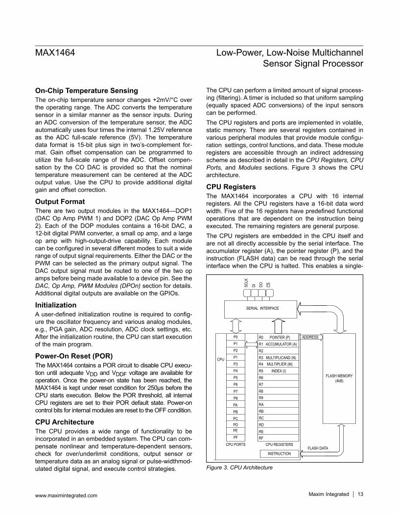
The CPU can perform a limited amount of signal process-ing (filtering). A timer is included so that uniform sampling (equally spaced ADC conversions) of the input sensors can be performed.The CPU registers and ports are implemented in volatile, static memory. There are several registers contained in various peripheral modules that provide module configu-ration settings, control functions, and data. These module registers are accessible through an indirect addressing scheme as described in detail in the CPU Registers, CPU Ports, and Modules sections. Figure 3 shows the CPU architecture.
CPU RegistersThe MAX1464 incorporates a CPU with 16 internal registers. All the CPU registers have a 16-bit data word width. Five of the 16 registers have predefined functional operations that are dependent on the instruction being executed. The remaining registers are general purpose.The CPU registers are embedded in the CPU itself and are not all directly accessible by the serial interface. The accumulator register (A), the pointer register (P), and the instruction (FLASH data) can be read through the serial interface when the CPU is halted. This enables a single-
Figure 3. CPU Architecture
FLASH MEMORY(4kB)
SERIAL INTERFACE
SCLK
DI DO CS
R0 POINTER (P)R1 ACCUMULATOR (A)R2R3 MULTIPLICAND (N)R4 MULTIPLIER (M)
R6R7R8R9RARBRCRDRERF
P0P1P2P1P3P4P5P6P7P8PAPBPCPDPEPF
CPU REGISTERS
INSTRUCTION
CPU
FLASH DATA
ADDRESS
CPU PORTS
R5 INDEX (I)
MAX1464 Low-Power, Low-Noise Multichannel Sensor Signal Processor
www.maximintegrated.com Maxim Integrated 13
step mode of code execution to ease code writing and debugging. A special program instruction sequence is required to observe the other CPU registers. Table 1 lists the CPU registers.
CPU PortsThe MAX1464 incorporates 16 CPU ports that are directly accessible by the serial interface. All the CPU ports have a 16-bit data word width. The contents of the ports can be read and written by transferring data to and from the accumulator register (A) using the RDX and WRX instruc-tions. No other CPU instructions act on the CPU ports. Three CPU ports PD, PE, and PF have uniquely defined operation for reading and writing data to and from the peripheral modules. All CPU ports are static and volatile. Table 2 lists the CPU ports.
ModulesThe MAX1464 modules are the functional blocks used to process analog and digital signals to and from the CPU. Each module is addressed through CPU ports PD, PE, and PF, as described in the CPU Ports section. All modules use static, volatile registers for data retention. There are three types of module registers: configuration, data, and control. They are used to put a module into a particular mode of operation. Configuration registers hold configuration bits that control static settings such as PGA gain, coarse offset, etc. Data registers hold input data such as DAC and PWM input words or output data such as the result of an ADC conversion. Control registers are used to initiate a process (such as an ADC conversion or a timer) or to turn modules on and off (such as op amps, DAC outputs, PWM outputs, etc.) Table 3 lists the module registers.
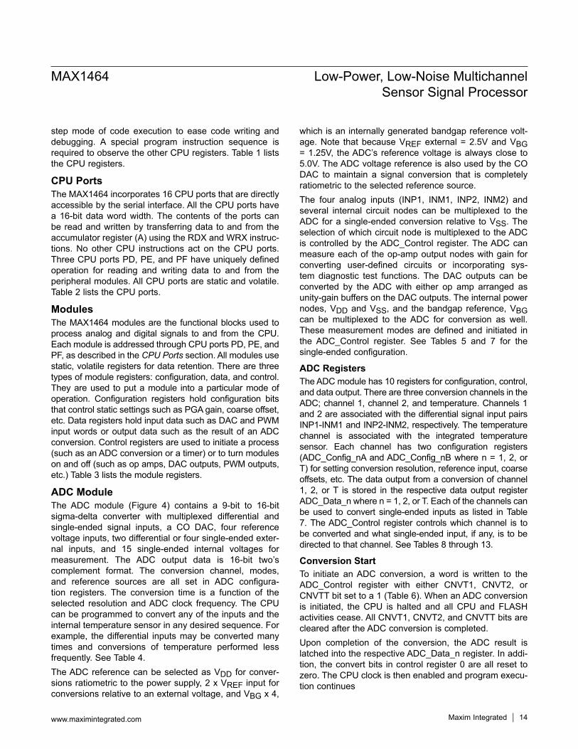
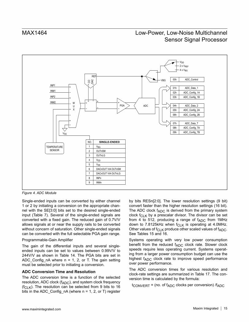
ADC ModuleThe ADC module (Figure 4) contains a 9-bit to 16-bit sigma-delta converter with multiplexed differential and single-ended signal inputs, a CO DAC, four reference voltage inputs, two differential or four single-ended exter-nal inputs, and 15 single-ended internal voltages for measurement. The ADC output data is 16-bit two’s complement format. The conversion channel, modes, and reference sources are all set in ADC configura-tion registers. The conversion time is a function of the selected resolution and ADC clock frequency. The CPU can be programmed to convert any of the inputs and the internal temperature sensor in any desired sequence. For example, the differential inputs may be converted many times and conversions of temperature performed less frequently. See Table 4.The ADC reference can be selected as VDD for conver-sions ratiometric to the power supply, 2 x VREF input for conversions relative to an external voltage, and VBG x 4,
which is an internally generated bandgap reference volt-age. Note that because VREF external = 2.5V and VBG = 1.25V, the ADC’s reference voltage is always close to 5.0V. The ADC voltage reference is also used by the CO DAC to maintain a signal conversion that is completely ratiometric to the selected reference source.The four analog inputs (INP1, INM1, INP2, INM2) and several internal circuit nodes can be multiplexed to the ADC for a single-ended conversion relative to VSS. The selection of which circuit node is multiplexed to the ADC is controlled by the ADC_Control register. The ADC can measure each of the op-amp output nodes with gain for converting user-defined circuits or incorporating sys-tem diagnostic test functions. The DAC outputs can be converted by the ADC with either op amp arranged as unity-gain buffers on the DAC outputs. The internal power nodes, VDD and VSS, and the bandgap reference, VBG can be multiplexed to the ADC for conversion as well. These measurement modes are defined and initiated in the ADC_Control register. See Tables 5 and 7 for the single-ended configuration.
ADC RegistersThe ADC module has 10 registers for configuration, control, and data output. There are three conversion channels in the ADC; channel 1, channel 2, and temperature. Channels 1 and 2 are associated with the differential signal input pairs INP1-INM1 and INP2-INM2, respectively. The temperature channel is associated with the integrated temperature sensor. Each channel has two configuration registers (ADC_Config_nA and ADC_Config_nB where n = 1, 2, or T) for setting conversion resolution, reference input, coarse offsets, etc. The data output from a conversion of channel 1, 2, or T is stored in the respective data output register ADC_Data_n where n = 1, 2, or T. Each of the channels can be used to convert single-ended inputs as listed in Table 7. The ADC_Control register controls which channel is to be converted and what single-ended input, if any, is to be directed to that channel. See Tables 8 through 13.
Conversion StartTo initiate an ADC conversion, a word is written to the ADC_Control register with either CNVT1, CNVT2, or CNVTT bit set to a 1 (Table 6). When an ADC conversion is initiated, the CPU is halted and all CPU and FLASH activities cease. All CNVT1, CNVT2, and CNVTT bits are cleared after the ADC conversion is completed. Upon completion of the conversion, the ADC result is latched into the respective ADC_Data_n register. In addi-tion, the convert bits in control register 0 are all reset to zero. The CPU clock is then enabled and program execu-tion continues
MAX1464 Low-Power, Low-Noise Multichannel Sensor Signal Processor
www.maximintegrated.com Maxim Integrated 14
Single-ended inputs can be converted by either channel 1 or 2 by initiating a conversion on the appropriate chan-nel with the SE[3:0] bits set to the desired single-ended input (Table 7). Several of the single-ended signals are converted with a fixed gain. The reduced gain of 0.7V/V allows signals at or near the supply rails to be converted without concern of saturation. Other single-ended signals can be converted with the full selectable PGA gain range. Programmable-Gain AmplifierThe gain of the differential inputs and several single-ended inputs can be set to values between 0.99V/V to 244V/V as shown in Table 14. The PGA bits are set in ADC_Config_nA where n = 1, 2, or T. The gain setting must be selected prior to initiating a conversion.
ADC Conversion Time and ResolutionThe ADC conversion time is a function of the selected resolution, ADC clock (fADC), and system clock frequency (fCLK). The resolution can be selected from 9 bits to 16 bits in the ADC_Config_nA (where n = 1, 2, or T) register
by bits RESn[2:0]. The lower resolution settings (9 bit) convert faster than the higher resolution settings (16 bit). The ADC clock fADC is derived from the primary system clock fCLK by a prescalar divisor. The divisor can be set from 4 to 512, producing a range of fADC from 1MHz down to 7.8125kHz when fCLK is operating at 4.0MHz. Other values of fCLK produce other scaled values of fADC. See Tables 15 and 16.Systems operating with very low power consumption benefit from the reduced fADC clock rate. Slower clock speeds require less operating current. Systems operat-ing from a larger power consumption budget can use the highest fADC clock rate to improve speed performance over power performance.The ADC conversion times for various resolution and clock-rate settings are summarized in Table 17. The con-version time is calculated by the formula:
tCONVERT = (no. of fADC clocks per conversion) /fADC
Figure 4. ADC Module
INP1
INM1
INP2
INM2
CO DAC
REF
TEMPERATURESENSOR
VBG
VDD
4 x VBG
2 x VREF
ADC
INMn
VBG
OUTnSMOUTnLGVDD
VSS
DACnOUT VIA OUTnSM
INPn
123456789
NO. SINGLE-ENDED
DACnOUT VIA OUTnLG
00h ADC_Control
08h ADC_Config_TA07h ADC_Data_T
06h ADC_Config_2B
09h ADC_Config_TB
02h ADC_Config_1A
05h ADC_Config_2A04h ADC_Data_2
03h
01h ADC_Data_1
ADC_Config_1B
PGA
VSS
MUX
MAX1464 Low-Power, Low-Noise Multichannel Sensor Signal Processor
www.maximintegrated.com Maxim Integrated 15
Coarse-Input Offset AdjustmentDifferential input signals that have an offset can be par-tially nulled by the input coarse-offset (CO) DAC. An offset voltage is added to the input signal prior to gaining the signal. This allows a maximum gain to be applied to the differential input signal without saturating the conversion channel. The CO signal added to the differential signal is a percentage of the full-scale ADC reference voltage as referred to the ADC inputs. Low PGA gain settings add smaller amounts of coarse offset to the differential input. Large PGA gain settings enable correspondingly larger amounts of coarse offset to be added to the input signal. The CO DAC also applies to the temperature channel enabling offset compensation of the temperature signal. See Table 18.
Bias Current SettingsThe analog circuitry within the ADC module operates from a current bias setting that is programmable. The program-mable levels of operation are fractions of the full bias cur-rent. The operating power consumption of the ADC can be reduced at the penalty of increased conversion times that may be desirable in very-lowpower applications. It is recommended operating the ADC at full bias when pos-sible. The amount of bias as a fraction of full bias is shown in Table 19. The setting is controlled by the BIASn[2:0] bits in the ADC_config_nb registers where n = 1, 2, or T.
Reference Input Voltage SelectThe ADC can use one of three different reference voltage inputs depending on the conversion channel and REFn setting as shown in Table 20. The differential inputs can be converted ratiometrically to the supply voltage (VDD), converted ratiometrically to an externally supplied voltage at VREF, or converted nonratiometrically using a fixed voltage source derived from the internal bandgap voltage source. The temperature channel is always converted using the internal bandgapderived voltage source and therefore is not selectable.
Output Sample RateGenerally, the sensor and temperature data are converted and calculated by an algorithm in the execution loop. The output sample rate of the data depends on the conver-sion time, the CPU algorithm loop time, and the time to store the result in the DOPn_DATA register. To achieve uniform sampling, the instruction code must be written to provide a consistent algorithm loop time, including branch instruction variations. This total loop time interval should be repeatable for a uniform output rate.The MAX1464 has a built-in timer that can be used to ensure that the sampling interval is uniform. The timeout value can be set so the CPU computations and the read-
ing of the serial interface, if required, can be completed before timeout. The GPIO pins can be utilized to interrupt an external master microcontroller when the ADC conver-sion is done and/or when the CPU computations are done so the serial interface can be read quickly.
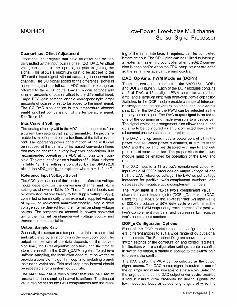
DAC, Op Amp, PWM Modules (DOPn)There are two output modules in the MAX1464—DOP1 and DOP2 (Figure 5). Each of the DOP modules contains a 16-bit DAC, a 12-bit digital PWM converter, a small op amp, and a large op amp with high-outputdrive capability. Switches in the DOP module enable a range of intercon-nectivity among the converters, op amps, and the external pins. Either the DAC or the PWM can be selected as the primary output signal. The DAC output signal is routed to one of the op amps and made available to a device pin. The signal-switching arrangement also allows the unused op amp to be configured as an uncommitted device with all connections available to external pins.The DAC and op amps have a power-control bit in the power module. When power is disabled, all circuits in the DAC and the op amp are disabled with inputs and out-puts in a tri-state condition. The proper bits in the power module must be enabled for operation of the DAC and op amps.The DAC input is a 16-bit two’s-complement value. An input value of 0000h produces an output voltage of one half the DAC reference voltage. The DAC output voltage increases for positive two’s-complement numbers, and decreases for negative two’s-complement numbers.The PWM input is a 12-bit two’s complement value. It shares the same input register (DOPn_Data) as the DAC, using the 12 MSBs of the 16-bit register. An input value of 000Xh produces a 50% duty cycle waveform at the output. The PWM output duty cycle increases for positive two’s-complement numbers, and decreases for negative two’s-complement numbers.
DOP_n Configuration OptionsEach of the DOP modules can be configured in sev-eral different modes to suit a wide range of output signal requirements. The Functional Diagram shows the various switch settings of the configuration and control registers. In situations where configuration settings create a conflict in switch activation, a priority is applied to the switch logic to prevent the conflict.The DAC and/or the PWM can be selected as the output signal source. The DAC output signal is routed to one of the op amps and made available to a device pin. Selecting the large op amp as the DAC output driver device enables a robust current drive capability for driving signals into low-impedance loads or across long lengths of wire. The
MAX1464 Low-Power, Low-Noise Multichannel Sensor Signal Processor
www.maximintegrated.com Maxim Integrated 16

unity-gain buffer configuration is automatically selected, and it provides the DAC output signal directly to the device pin OUTnLG. With the large op amp selected, the small op amp can be used as an independent device for external cir-cuit applications when the PWM is disabled. Alternatively, the PWM can also be enabled to drive the OUTnSM device pin, in which case the small op amp is OFF.Selecting the small op amp as the DAC output driver device is useful for routing the output signal to other cir-cuits in an embedded control system with high-impedance load connections. The unity-gain buffer configuration is automatically selected, and it provides the DAC output signal directly to the device pin OUTnSM. With the small op amp selected, the large op amp can be used as an independent device for external circuit applications when the PWM is disabled. Alternatively, the PWM can also be enabled to drive the OUTnLG device pin, in which case the large op amp is OFF.The DAC has two reference voltage sources available by selection, VDD and VREF input. When the external refer-ence is selected (VREF), the actual DAC reference is 2 x VREF. See VREF to 2.5V for nominal operation. The out-put of the DAC is a voltage proportional to the reference voltage selected, where the proportionality scaling (DAC input) is set in the data input register DOPn_Data.
The DOP module also provides a 12-bit digital PWM output. At a nominal 4MHz frequency, the frequency of the PWM is 122Hz (PWM period = 8.192ms). The DAC and the PWM share the same input register, DOPn_Data, where the PWM uses the 12 MSBs, in two’s-complement format. An input of 000Xh (4 LSBs are ignored) outputs a 50% duty cycle waveform at the selected output pin (either OUTnSM or OUTnLG). The PWM bit weight is 2μs, at a nominal frequency of 4MHz. The minimum duty cycle is obtained when the input is 800Xh (duty cycle is 0 / 4096 = 0), and the maximum duty cycle at 7FFXh (duty cycle is 4095 / 4096 = 99.98%). A new PWM input word is only effective at the end of a current PWM cycle, therefore preventing PWM glitches on the output.Either the small or the large op amp in the DOP module can also be selected as an uncommitted op amp in the MAX1464. The op amps can be configured as a unitygain buffer, where the output is internally connected to the negative terminal of the op amp, or a stand-alone op amp, where both AMPnM and AMPnP can be externally con-nected for various analog functions. In the case of a buffer, the device pin AMPnM is in high-impedance mode, as the feedback loop around the op amp is connected internally.
Figure 5. DOP1 and DOP2 Modules
DAC 10h OR 13h DOPn_Data
12h OR 15h DOPn_Config
30h OpAmp_Config
11h OR 14h DOPn_Control
REF
PWM
SW0
SW1SW2
SW3
SW4
SW5
SW6 SW7
SW8
SW9
2 x VREF
VDD
OUTnSM
AMPnM
AMPnP
OUTnLG
SW10
SW11
SM
LG
MAX1464 Low-Power, Low-Noise Multichannel Sensor Signal Processor
www.maximintegrated.com Maxim Integrated 17
Every function of the DOP module can be selected indi-vidually (DAC, PWM, or op amp), or two out of the three functions of the DOP module can be selected at the same time (PWM and op amp, or DAC and PWM, or DAC and op amp), as there are only two output pins for the mod-ule, OUTnSM and OUTnLG. The various configuration options for the DOP are shown in Table 21. The PWRDAC and PWROP bits are in the power-on control register (address = 31h), and the remaining bits are in the DOP registers. See Tables 21 through 27.
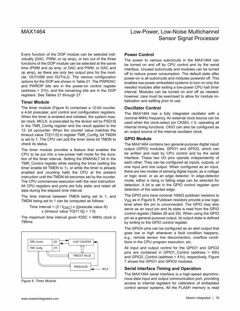
Timer ModuleThe timer module (Figure 6) comprises a 12-bit counter, a 4-bit prescalar, and control and configuration registers. When the timer is enabled and initiated, the system mas-ter clock, MCLK, is prescaled by the divisor set by PS[3:0] in the TMR_Config register and the result applied to the 12- bit upcounter. When the counter value matches the timeout value TO[11:0] in register TMR_Config, bit TMDN is set to 1. The CPU can poll the timer done bit TMDN to check its status.The timer module provides a feature that enables the CPU to be put into a low-power halt mode for the dura-tion of the timer interval. Setting the ENAHALT bit in the TMR_Control register while starting the timer (setting the timer enable bit TMEN to 1), or while the timer is already enabled and counting halts the CPU at the present instruction until the TMDN bit becomes set by the counter. The CPU commences execution with the next instruction. All CPU registers and ports are fully static and retain all data during the elapsed time interval.The time interval between TMEN being set to 1, and TMDN being set to 1 can be computed as follows:
Time Interval = (2 / fOSC) x (prescale value N) x (timeout value TO[11:0]) + 1.5
The maximum time interval given fOSC = 4MHz clock is 786ms.
Power ControlThe power to various subcircuits in the MAX1464 can be turned on and off by CPU control and by the serial interface. Unused subcircuits and modules can be turned off to reduce power consumption. The default state after power-on is all subcircuits and modules powered off. This enables low-power embedded systems to turn on only the needed modules after exiting a low-power CPU halt timer interval. Modules can be turned on and off as needed; however, care must be exercised to allow for module ini-tialization and settling prior to use.
Oscillator ControlThe MAX1464 has a fully integrated oscillator with a nominal 4MHz frequency. An external clock source can be used when the clock-select pin CKSEL = 0, operating all internal timing functions. CKIO can also be configured as an output source of the internal oscillator clock.
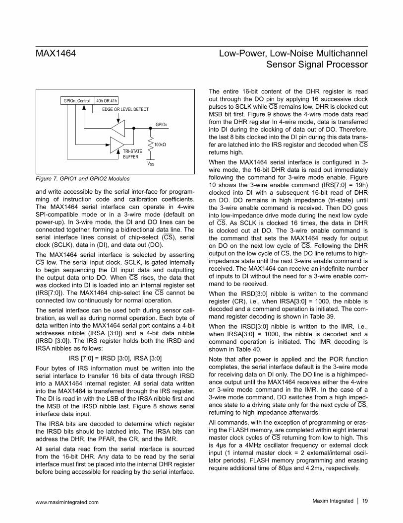
GPIO ModuleThe MAX1464 contains two general-purpose digital input/output (GPIO) modules, GPIO1 and GPIO2, which can be written and read by CPU control and by the serial interface. These two I/O pins operate independently of each other. They can be configured as inputs, outputs, or one input and one output. When configured as an input, there are two modes of sensing digital inputs; as a voltage or logic level, or as an edge detector. In edge-detector mode, either a rising or falling edge can be selected for detection. A bit is set in the GPIO control register upon detection of the selected edge.The GPIO pins have nominal 100kΩ pulldown resistors to VSS as in Figure 6. Pulldown resistors provide a low logic level when the pin is unconnected. The GPIO may also serve as an input pin and its state is read from the GPIO control register (Tables 28 and 29). When using the GPIO pin as a general-purpose output, its output state is defined by writing to the GPIO control register.The GPIOn pins can be configured as an alert output that goes low or high whenever a fault condition happens, e.g., remote sensor line disconnection, overflow condi-tions in the CPU program execution, etc.All input and output control for the GPIO1 and GPIO2 pins are contained in GPIO1_Control (address = 40h) and GPIO2_Control (address = 41h), respectively. Figure 7 shows the GPIO1 and GPIO2 modules.
Serial Interface Timing and OperationThe MAX1464 serial interface is a high-speed asynchro-nous data input and output communication port, providing access to internal registers for calibration of embedded control sensor systems. All the FLASH memory is read
Figure 6. Timer Module
20hTMR_Control
21hTMR_Config
PRESCALER
12-BIT COUNTER
TIMEOUT VALUE
MCLK
MAX1464 Low-Power, Low-Noise Multichannel Sensor Signal Processor
www.maximintegrated.com Maxim Integrated 18
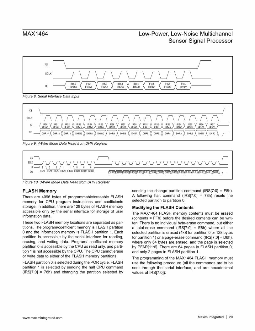
and write accessible by the serial inter-face for program-ming of instruction code and calibration coefficients. The MAX1464 serial interface can operate in 4-wire SPI-compatible mode or in a 3-wire mode (default on power-up). In 3-wire mode, the DI and DO lines can be connected together, forming a bidirectional data line. The serial interface lines consist of chip-select (CS), serial clock (SCLK), data in (DI), and data out (DO).The MAX1464 serial interface is selected by asserting CS low. The serial input clock, SCLK, is gated internally to begin sequencing the DI input data and outputting the output data onto DO. When CS rises, the data that was clocked into DI is loaded into an internal register set (IRS[7:0]). The MAX1464 chip-select line CS cannot be connected low continuously for normal operation.The serial interface can be used both during sensor cali-bration, as well as during normal operation. Each byte of data written into the MAX1464 serial port contains a 4-bit addresses nibble (IRSA [3:0]) and a 4-bit data nibble (IRSD [3:0]). The IRS register holds both the IRSD and IRSA nibbles as follows:
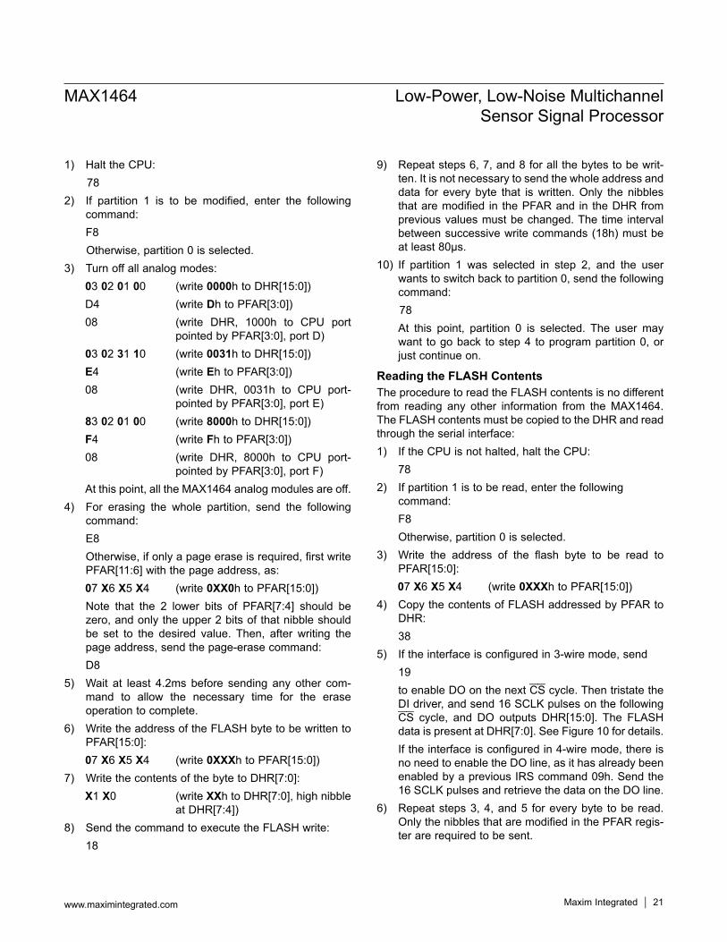
IRS [7:0] = IRSD [3:0], IRSA [3:0]Four bytes of IRS information must be written into the serial interface to transfer 16 bits of data through IRSD into a MAX1464 internal register. All serial data written into the MAX1464 is transferred through the IRS register. The DI is read in with the LSB of the IRSA nibble first and the MSB of the IRSD nibble last. Figure 8 shows serial interface data input.The IRSA bits are decoded to determine which register the IRSD bits should be latched into. The IRSA bits can address the DHR, the PFAR, the CR, and the IMR.All serial data read from the serial interface is sourced from the 16-bit DHR. Any data to be read by the serial interface must first be placed into the internal DHR register before being accessible for reading by the serial interface.
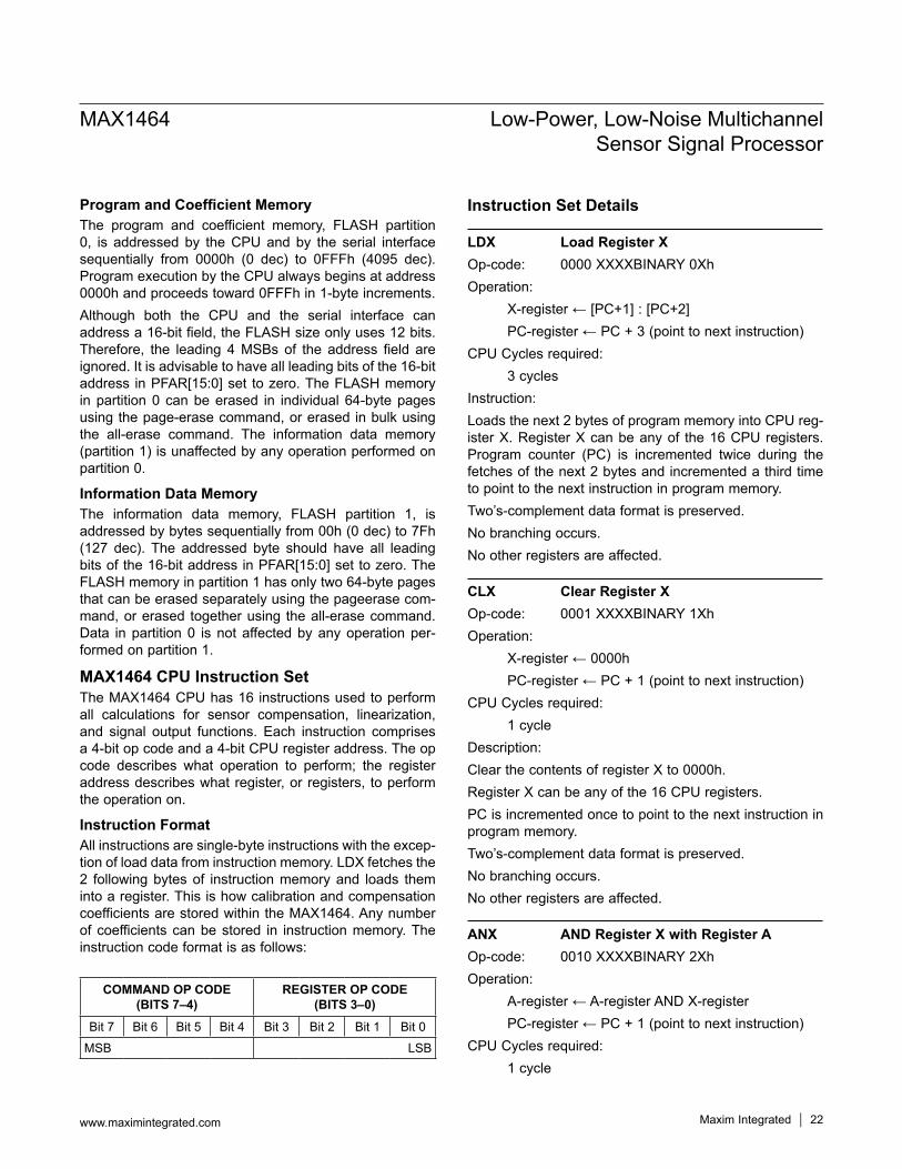
The entire 16-bit content of the DHR register is read out through the DO pin by applying 16 successive clock pulses to SCLK while CS remains low. DHR is clocked out MSB bit first. Figure 9 shows the 4-wire mode data read from the DHR register In 4-wire mode, data is transferred into DI during the clocking of data out of DO. Therefore, the last 8 bits clocked into the DI pin during this data trans-fer are latched into the IRS register and decoded when CS returns high.When the MAX1464 serial interface is configured in 3- wire mode, the 16-bit DHR data is read out immediately following the command for 3-wire mode enable. Figure 10 shows the 3-wire enable command (IRS[7:0] = 19h) clocked into DI with a subsequent 16-bit read of DHR on DO. DO remains in high impedance (tri-state) until the 3-wire enable command is received. Then DO goes into low-impedance drive mode during the next low cycle of CS. As SCLK is clocked 16 times, the data in DHR is clocked out at DO. The 3-wire enable command is the command that sets the MAX1464 ready for output on DO on the next low cycle of CS. Following the DHR output on the low cycle of CS, the DO line returns to high-impedance state until the next 3-wire enable command is received. The MAX1464 can receive an indefinite number of inputs to DI without the need for a 3-wire enable com-mand to be received.When the IRSD[3:0] nibble is written to the command register (CR), i.e., when IRSA[3:0] = 1000, the nibble is decoded and a command operation is initiated. The com-mand register decoding is shown in Table 39.When the IRSD[3:0] nibble is written to the IMR, i.e., when IRSA[3:0] = 1000, the nibble is decoded and a command operation is initiated. The IMR decoding is shown in Table 40.Note that after power is applied and the POR function completes, the serial interface default is the 3-wire mode for receiving data on DI only. The DO line is a highimped-ance output until the MAX1464 receives either the 4-wire or 3-wire mode command in the IMR. In the case of a 3-wire mode command, DO switches from a high imped-ance state to a driving state only for the next cycle of CS, returning to high impedance afterwards.All commands, with the exception of programming or eras-ing the FLASH memory, are completed within eight internal master clock cycles of CS returning from low to high. This is 4μs for a 4MHz oscillator frequency or external clock input (1 internal master clock = 2 external/internal oscil-lator periods). FLASH memory programming and erasing require additional time of 80μs and 4.2ms, respectively.
Figure 7. GPIO1 and GPIO2 Modules
GPIOn
40h OR 41hGPIOn_Control
EDGE OR LEVEL DETECT
VSS
100kΩTRI-STATEBUFFER
MAX1464 Low-Power, Low-Noise Multichannel Sensor Signal Processor
www.maximintegrated.com Maxim Integrated 19
FLASH MemoryThere are 4096 bytes of programmable/erasable FLASH memory for CPU program instructions and coefficients storage. In addition, there are 128 bytes of FLASH memory accessible only by the serial interface for storage of user information data.These two FLASH memory locations are separated as par-titions. The program/coefficient memory is FLASH partition 0 and the information memory is FLASH partition 1. Each partition is accessible by the serial interface for reading, erasing, and writing data. Program/ coefficient memory partition 0 is accessible by the CPU as read only, and parti-tion 1 is not accessible by the CPU. The CPU cannot erase or write data to either of the FLASH memory partitions.FLASH partition 0 is selected during the POR cycle. FLASH partition 1 is selected by sending the halt CPU command (IRS[7:0] = 78h) and changing the partition selected by
sending the change partition command (IRS[7:0] = F8h). A following halt command (IRS[7:0] = 78h) resets the selected partition to partition 0.
Modifying the FLASH ContentsThe MAX1464 FLASH memory contents must be erased (contents = FFh) before the desired contents can be writ-ten. There is no individual byte-erase command, but either a total-erase command (IRS[7:0] = E8h) where all the selected partition is erased (4kB for partition 0 or 128 bytes for partition 1) or a page-erase command (IRS[7:0] = D8h), where only 64 bytes are erased, and the page is selected by PFAR[11:6]. There are 64 pages in FLASH partition 0, and only 2 pages in FLASH partition 1.The programming of the MAX1464 FLASH memory must use the following procedure (all the commands are to be sent through the serial interface, and are hexadecimal values of IRS[7:0]):
Figure 8. Serial Interface Data Input
Figure 9. 4-Wire Mode Data Read from DHR Register
Figure 10. 3-Wire Mode Data Read from DHR Register
IRS0IRSA0
IRS1IRSA1
IRS2IRSA2
IRS3IRSA3
IRS4IRSD0
IRS5IRSD1
IRS6IRSD2
IRS7IRSD3
SCLK
DI
CS
IRS0IRSA0
IRS2IRSA2
IRS3IRSA3
IRS4IRSD0
IRS5IRSD1
IRS6IRSD2
IRS7IRSD3
IRS0IRSA0
IRS1IRSA1
IRS2IRSA2
IRS3IRSA3
IRS4IRSD0
IRS5IRSD1
IRS6IRSD2
IRS7IRSD3
DHR15 DHR14 DHR13 DHR12 DHR11 DHR10 DHR9 DHR8 DHR7 DHR6 DHR5 DHR4 DHR3 DHR2 DHR1 DHR0
CS
SCLK
DI
DO
IRS1IRSA1
DHR15 DHR14 DHR13 DHR12 DHR11 DHR10 DHR9 DHR8 DHR7 DHR6 DHR5 DHR4 DHR3 DHR2 DHR1 DHR01
IRSA00
IRSA10
IRSA21
IRSA31
IRSD00
IRSD10
IRSD20
IRSD3
CSSCLK
DIDO
MAX1464 Low-Power, Low-Noise Multichannel Sensor Signal Processor
www.maximintegrated.com Maxim Integrated 20
1) Halt the CPU:78
2) If partition 1 is to be modified, enter the following command:F8Otherwise, partition 0 is selected.
3) Turn off all analog modes:03 02 01 00 (write 0000h to DHR[15:0])D4 (write Dh to PFAR[3:0])08 (write DHR, 1000h to CPU port
pointed by PFAR[3:0], port D)03 02 31 10 (write 0031h to DHR[15:0])E4 (write Eh to PFAR[3:0])08 (write DHR, 0031h to CPU port-
pointed by PFAR[3:0], port E)83 02 01 00 (write 8000h to DHR[15:0])F4 (write Fh to PFAR[3:0])08 (write DHR, 8000h to CPU port-
pointed by PFAR[3:0], port F)At this point, all the MAX1464 analog modules are off.
4) For erasing the whole partition, send the following command:E8Otherwise, if only a page erase is required, first write PFAR[11:6] with the page address, as:07 X6 X5 X4 (write 0XX0h to PFAR[15:0])Note that the 2 lower bits of PFAR[7:4] should be zero, and only the upper 2 bits of that nibble should be set to the desired value. Then, after writing the page address, send the page-erase command:D8
5) Wait at least 4.2ms before sending any other com-mand to allow the necessary time for the erase operation to complete.
6) Write the address of the FLASH byte to be written to PFAR[15:0]:07 X6 X5 X4 (write 0XXXh to PFAR[15:0])
7) Write the contents of the byte to DHR[7:0]:X1 X0 (write XXh to DHR[7:0], high nibble
at DHR[7:4])8) Send the command to execute the FLASH write:
18
9) Repeat steps 6, 7, and 8 for all the bytes to be writ-ten. It is not necessary to send the whole address and data for every byte that is written. Only the nibbles that are modified in the PFAR and in the DHR from previous values must be changed. The time interval between successive write commands (18h) must be at least 80μs.
10) If partition 1 was selected in step 2, and the user wants to switch back to partition 0, send the following command:78At this point, partition 0 is selected. The user may want to go back to step 4 to program partition 0, or just continue on.
Reading the FLASH ContentsThe procedure to read the FLASH contents is no different from reading any other information from the MAX1464. The FLASH contents must be copied to the DHR and read through the serial interface:1) If the CPU is not halted, halt the CPU:
782) If partition 1 is to be read, enter the following
command:F8Otherwise, partition 0 is selected.
3) Write the address of the flash byte to be read to PFAR[15:0]:07 X6 X5 X4 (write 0XXXh to PFAR[15:0])
4) Copy the contents of FLASH addressed by PFAR to DHR:38
5) If the interface is configured in 3-wire mode, send19to enable DO on the next CS cycle. Then tristate the DI driver, and send 16 SCLK pulses on the following CS cycle, and DO outputs DHR[15:0]. The FLASH data is present at DHR[7:0]. See Figure 10 for details.If the interface is configured in 4-wire mode, there is no need to enable the DO line, as it has already been enabled by a previous IRS command 09h. Send the 16 SCLK pulses and retrieve the data on the DO line.
6) Repeat steps 3, 4, and 5 for every byte to be read. Only the nibbles that are modified in the PFAR regis-ter are required to be sent.
MAX1464 Low-Power, Low-Noise Multichannel Sensor Signal Processor
www.maximintegrated.com Maxim Integrated 21
Program and Coefficient MemoryThe program and coefficient memory, FLASH partition 0, is addressed by the CPU and by the serial interface sequentially from 0000h (0 dec) to 0FFFh (4095 dec). Program execution by the CPU always begins at address 0000h and proceeds toward 0FFFh in 1-byte increments. Although both the CPU and the serial interface can address a 16-bit field, the FLASH size only uses 12 bits. Therefore, the leading 4 MSBs of the address field are ignored. It is advisable to have all leading bits of the 16-bit address in PFAR[15:0] set to zero. The FLASH memory in partition 0 can be erased in individual 64-byte pages using the page-erase command, or erased in bulk using the all-erase command. The information data memory (partition 1) is unaffected by any operation performed on partition 0.
Information Data MemoryThe information data memory, FLASH partition 1, is addressed by bytes sequentially from 00h (0 dec) to 7Fh (127 dec). The addressed byte should have all leading bits of the 16-bit address in PFAR[15:0] set to zero. The FLASH memory in partition 1 has only two 64-byte pages that can be erased separately using the pageerase com-mand, or erased together using the all-erase command. Data in partition 0 is not affected by any operation per-formed on partition 1.
MAX1464 CPU Instruction SetThe MAX1464 CPU has 16 instructions used to perform all calculations for sensor compensation, linearization, and signal output functions. Each instruction comprises a 4-bit op code and a 4-bit CPU register address. The op code describes what operation to perform; the register address describes what register, or registers, to perform the operation on.
Instruction FormatAll instructions are single-byte instructions with the excep-tion of load data from instruction memory. LDX fetches the 2 following bytes of instruction memory and loads them into a register. This is how calibration and compensation coefficients are stored within the MAX1464. Any number of coefficients can be stored in instruction memory. The instruction code format is as follows:
Instruction Set Details LDX Load Register XOp-code: 0000 XXXXBINARY 0XhOperation:
X-register ← [PC+1] : [PC+2]PC-register ← PC + 3 (point to next instruction)
CPU Cycles required:3 cycles
Instruction:Loads the next 2 bytes of program memory into CPU reg-ister X. Register X can be any of the 16 CPU registers. Program counter (PC) is incremented twice during the fetches of the next 2 bytes and incremented a third time to point to the next instruction in program memory.Two’s-complement data format is preserved.No branching occurs.No other registers are affected. CLX Clear Register XOp-code: 0001 XXXXBINARY 1XhOperation:
X-register ← 0000hPC-register ← PC + 1 (point to next instruction)
CPU Cycles required:1 cycle
Description:Clear the contents of register X to 0000h.Register X can be any of the 16 CPU registers.PC is incremented once to point to the next instruction in program memory.Two’s-complement data format is preserved.No branching occurs.No other registers are affected. ANX AND Register X with Register AOp-code: 0010 XXXXBINARY 2XhOperation:
A-register ← A-register AND X-registerPC-register ← PC + 1 (point to next instruction)
CPU Cycles required:1 cycle
MAX1464 Low-Power, Low-Noise Multichannel Sensor Signal Processor
www.maximintegrated.com Maxim Integrated 22
COMMAND OP CODE (BITS 7–4)
REGISTER OP CODE (BITS 3–0)
Bit 7 Bit 6 Bit 5 Bit 4 Bit 3 Bit 2 Bit 1 Bit 0
MSB LSB
Description:Perform a 16-bit logical AND operation, bit for bit, on the contents of the A-register and the contents of the Xregister. Store the 16-bit result back into the A-register. The previous contents of the A-register are overwritten and lost.Register X can be any of the 16 CPU registers.PC is incremented once to point to the next instruction in program memory.Two’s-complement data format is not preserved.No branching occurs.No other registers are affected. ORX OR Register X with Register AOp-code: 0011 XXXXBINARY 3XhOperation:
A-register ← A-register OR X-registerPC-register ← PC + 1 (point to next instruction)
CPU Cycles required:1 cycle
Description:Perform a 16-bit logical OR operation, bit for bit, on the contents of the A-register and the contents of the X-register. Store the 16-bit result back into the A-register. The previous contents of the A-register are overwritten and lost.Register X can be any of the 16 CPU registers.PC is incremented once to point to the next instruction in program memory.Two’s-complement data format is not preserved.No branching occurs.No other registers are affected. ADX ADD Register X to Register AOp-code: 0100 XXXXBINARY 4XhOperation:
A-register ← A-register + X-registerPC-register ← PC + 1 (point to next instruction)
CPU Cycles required:1 cycle
Description:Perform a 16-bit arithmetic addition of the A-register and the contents of the X-register. Store the low 16 bits of the result back into the A-register. Any overflow bit resulting
from the addition operation is lost. The previous contents of the A-register are overwritten and lost.Register X can be any of the 16 CPU registers.PC is incremented once to point to the next instruction in program memory.Two’s-complement data format is preserved.No branching occurs.No other registers are affected. STX Store Register XOp-code: 0101 XXXXBINARY 5XhOperation:
X-register ← A-registerPC-register ← PC + 1 (point to next instruction)
CPU Cycles required:1 cycle
Description:Perform a 16-bit move operation from the A-register into the X-register. The A-register contents are unchanged. The previous contents of the X-register are overwritten and lost.Register X can be any of the 16 CPU registers.PC is incremented once to point to the next instruction in program memory.Two’s-complement data format is preserved.No branching occurs.No other registers are affected. SLX Shift Left Register XOp-code: 0110 XXXXBINARY 6Xh
1415 13 12 11 10 9 8 7 6 5 4 3 2 1 00
BIT:
1415 13 12 11 10 9 8 7 6 5 4 3 2 1 0BIT:
1415 13 12 11 10 9 8 7 6 5 4 3 2 1 0BIT:
REGISTER X
Operation when X 6h:
REGISTER R6
REGISTER M: R4
Operation when X = 6h:
PC-register ← PC + 1 (point to next instruction)CPU Cycles required:
1 cycle
MAX1464 Low-Power, Low-Noise Multichannel Sensor Signal Processor
www.maximintegrated.com Maxim Integrated 23
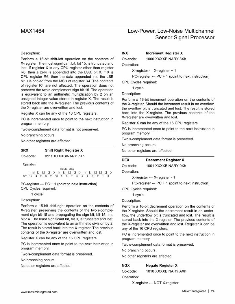
Description:Perform a 16-bit shift-left operation on the contents of X-register. The most significant bit, bit 15, is truncated and lost. If register X is any CPU register other than register R6, then a zero is appended into the LSB, bit 0. If X is CPU register R6, then the data appended into the LSB bit 0 is copied from the MSB of register R4. The contents of register R4 are not affected. The operation does not preserve the two’s-complement sign bit-15. The operation is equivalent to an arithmetic multiplication by 2 on an unsigned integer value stored in register X. The result is stored back into the X-register. The previous contents of the X-register are overwritten and lost.Register X can be any of the 16 CPU registers.PC is incremented once to point to the next instruction in program memory.Two’s-complement data format is not preserved.No branching occurs.No other registers are affected. SRX Shift Right Register XOp-code: 0111 XXXXBINARY 7Xh
1415 13 12 11 10 9 8 7 6 5 4 3 2 1 0BIT:
REGISTER XOperation
PC-register ← PC + 1 (point to next instruction)CPU Cycles required:
1 cycleDescription:Perform a 15-bit shift-right operation on the contents of X-register, preserving the contents of the two’s-comple-ment sign bit-15 and propagating the sign bit, bit-15, into bit-14. The least significant bit, bit 0, is truncated and lost. The operation is equivalent to an arithmetic division by 2. The result is stored back into the X-register. The previous contents of the X-register are overwritten and lost. Register X can be any of the 16 CPU registers.PC is incremented once to point to the next instruction in program memory.Two’s-complement data format is preserved.No branching occurs.No other registers are affected.
INX Increment Register XOp-code: 1000 XXXXBINARY 8XhOperation:
X-register ← X-register + 1PC-register ← PC + 1 (point to next instruction)
CPU Cycles required:1 cycle
Description:Perform a 16-bit increment operation on the contents of the X-register. Should the increment result in an overflow, the overflow bit is truncated and lost. The result is stored back into the X-register. The previous contents of the X-register are overwritten and lost.Register X can be any of the 16 CPU registers.PC is incremented once to point to the next instruction in program memory.Two’s-complement data format is preserved.No branching occurs.No other registers are affected. DEX Decrement Register XOp-code: 1001 XXXXBINARY 9XhOperation:
X-register ← X-register - 1PC-register ← PC + 1 (point to next instruction)
CPU Cycles required:1 cycle
Description:Perform a 16-bit decrement operation on the contents of the X-register. Should the decrement result in an under-flow, the underflow bit is truncated and lost. The result is stored back into the X-register. The previous contents of the X-register are overwritten and lost. Register X can be any of the 16 CPU registers.PC is incremented once to point to the next instruction in program memory.Two’s-complement data format is preserved.No branching occurs.No other registers are affected. NGX Negate Register XOp-code: 1010 XXXXBINARY AXhOperation:
X-register ← NOT X-register
MAX1464 Low-Power, Low-Noise Multichannel Sensor Signal Processor
www.maximintegrated.com Maxim Integrated 24
PC-register ← PC-register + 1 (point to next instruction)
CPU Cycles required:1 cycle
Description:Perform a 16-bit logical NOT operation on the contents of the X-register. Each bit is flipped to its complementary value. The result is stored back into the X-register. The previous contents of X-register are overwritten and lost.Register X can be any of the 16 CPU registers.PC is incremented once to point to the next instruction in program memory.Two’s-complement data format is not preserved.No branching occurs.No other registers are affected. BPX Branch If Positive Or ZeroOp-code: 1011 XXXXBINARY BXhOperation:
If MSB(Register I) = 0 then:PC-register ← PC-register + X-register
Else:PC-register ← PC + 1 (point to next instruction)
CPU Cycles required:1 cycle
Description:Perform a 16-bit check of I-register for a positive (two’s complement) or zero value and branch the number of instructions indicated in register-X. The test operation checks the most significant bit, bit-15, for a 0B and, if true, adds the contents of the X-register to the program counter register. This causes an immediate jump to the new pro-gram memory location. The next instruction to execute is fetched from the program memory byte pointed to by the new contents of the PC-register.A 1B in bit-15 of the I-register is indicative of a negative number (two’s complement) to which the test for positive-or-zero value fails. This causes the “else” operation to be performed and the PC-register is incremented by one pointing to the next sequential instruction in pro-gram memory to be executed. The effect bypasses the branch mechanism and normal, sequential, code execu-tion results.
The next instruction to execute is fetched from the pro-gram memory byte pointed to by the new contents of the PC-register. The previous contents of the PC-register are overwritten and lost.Two’s-complement data format is preserved.Branching may occur.No other registers are affected. BNX Branch If Not ZeroOp-code: 1100 XXXXBINARY CXhOperation:
If I-register ≠ 0000h then:PC-register ← PC-register + X-register
Else:PC-register ← PC-register + 1 (point to next instruction)
CPU Cycles required:1 cycle
Description:Perform a 16-bit check of the I-register for a nonzero con-dition and, if true, add the contents of the X-register to the program pointer register. This causes an immediate jump to the new program memory location. The next instruc-tion to execute is fetched from the program memory byte pointed to by the new contents of the PC register.A 1B in any bit of the I-register is indicative of a non-zero number to which the test for a zero value fails. This causes the “else” operation to be performed and the PC-register is incremented by one pointing to the next sequential instruction in program memory to be executed. The effect bypasses the branch mechanism and normal, sequential, code execution results.The next instruction to execute is fetched from the pro-gram memory byte pointed to by the new contents of the PC-register. The previous contents of the PC-register are overwritten and lost.Two’s-complement data format is preserved.Branching may occur.No other registers are affected. RDX Read Port XOp-code: 1101XXXXBINARY DXhOperation:
A-register ← port-XPC-register ← PC + 1 (point to next instruction)
MAX1464 Low-Power, Low-Noise Multichannel Sensor Signal Processor
www.maximintegrated.com Maxim Integrated 25
CPU Cycles required:1 cycle
Description:Perform a 16-bit move operation from port-X to the Aregister.The port-X contents are unchanged.The previous contents of A-register are overwritten and lost.The port-X can be any of the CPU ports.PC is incremented once to point to the next instruction in program memory.Two’s-complement data format is preserved.No branching occurs.No other registers are affected. WRX Write Port XOp-code: 1110 XXXXBINARY EXhOperation:
Port-X ← A-registerPC-register ← PC + 1 (point to next instruction)
CPU Cycles required:1 cycle
Description:Perform a 16-bit move operation from the A-register to port-X.The A-register contents are unchanged.The previous contents of port-X are overwritten and lost.The port-X can be any of the CPU ports.PC is incremented once to point to the next instruction in program memory.Two’s-complement data format is preserved.No branching occurs.No other registers are affected.
MLT MultiplyOp-code: 1111 0011BINARY F3hOperation:
A-register | M-register ← N-register x M-registerPC-register ← PC + 1 (point to next instruction)
CPU Cycles required:16 cycles
Description:Perform a 16-bit by 16-bit arithmetic multiplication of the M-register and the N-register producing a 32-bit result. The 32-bit result is stored in two 16-bit registers; the A-register receives the most significant word of the result and the M-register receives the least significant word of the result.The A-register must be cleared to zero (CLX A) before executing the MLT instruction. The previous contents of the A-register are overwritten and lost.The previous contents of the M-register are overwritten and lost.The contents of the N-register are not altered.The register op code must be 3h.PC is incremented once to point to the next instruction in program memory.Two’s-complement data format is preserved.No branching occurs.No other registers are affected.
MAX1464 Low-Power, Low-Noise Multichannel Sensor Signal Processor
www.maximintegrated.com Maxim Integrated 26
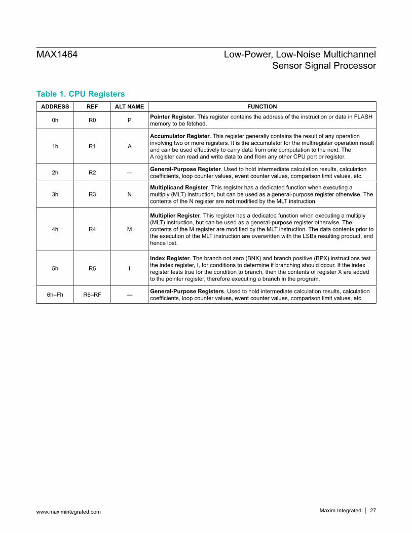
Table 1. CPU Registers
MAX1464 Low-Power, Low-Noise Multichannel Sensor Signal Processor
www.maximintegrated.com Maxim Integrated 27
ADDRESS REF ALT NAME FUNCTION
0h R0 P Pointer Register. This register contains the address of the instruction or data in FLASH memory to be fetched.
1h R1 A
Accumulator Register. This register generally contains the result of any operation involving two or more registers. It is the accumulator for the multiregister operation result and can be used effectively to carry data from one computation to the next. The A register can read and write data to and from any other CPU port or register.
2h R2 — General-Purpose Register. Used to hold intermediate calculation results, calculation coefficients, loop counter values, event counter values, comparison limit values, etc.
3h R3 NMultiplicand Register. This register has a dedicated function when executing a multiply (MLT) instruction, but can be used as a general-purpose register otherwise. The contents of the N register are not modified by the MLT instruction.
4h R4 M
Multiplier Register. This register has a dedicated function when executing a multiply (MLT) instruction, but can be used as a general-purpose register otherwise. The contents of the M register are modified by the MLT instruction. The data contents prior to the execution of the MLT instruction are overwritten with the LSBs resulting product, and hence lost.
5h R5 I
Index Register. The branch not zero (BNX) and branch positive (BPX) instructions test the index register, I, for conditions to determine if branching should occur. If the index register tests true for the condition to branch, then the contents of register X are added to the pointer register, therefore executing a branch in the program.
6h–Fh R6–RF — General-Purpose Registers. Used to hold intermediate calculation results, calculation coefficients, loop counter values, event counter values, comparison limit values, etc.
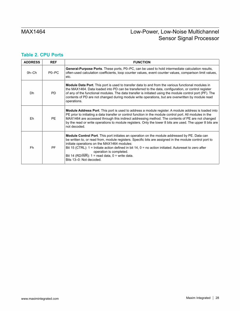
Table 2. CPU Ports
MAX1464 Low-Power, Low-Noise Multichannel Sensor Signal Processor
www.maximintegrated.com Maxim Integrated 28
ADDRESS REF FUNCTION
0h–Ch P0–PCGeneral-Purpose Ports. These ports, P0–PC, can be used to hold intermediate calculation results, often-used calculation coefficients, loop counter values, event counter values, comparison limit values, etc.
Dh PD
Module Data Port. This port is used to transfer data to and from the various functional modules in the MAX1464. Data loaded into PD can be transferred to the data, configuration, or control register of any of the functional modules. The data transfer is initiated using the module control port (PF). The contents of PD are not changed during module write operations, but are overwritten by module read operations.
Eh PE
Module Address Port. This port is used to address a module register. A module address is loaded into PE prior to initiating a data transfer or control function in the module control port. All modules in the MAX1464 are accessed through this indirect addressing method. The contents of PE are not changed by the read or write operations to module registers. Only the lower 8 bits are used. The upper 8 bits are not decoded.
Fh PF
Module Control Port. This port initiates an operation on the module addressed by PE. Data can be written to, or read from, module registers. Specific bits are assigned in the module control port to initiate operations on the MAX1464 modules: Bit 15 (CTRL): 1 = Initiate action defined in bit 14, 0 = no action initiated. Autoreset to zero after operation is completed. Bit 14 (RD/WR): 1 = read data, 0 = write data. Bits 13–0: Not decoded.
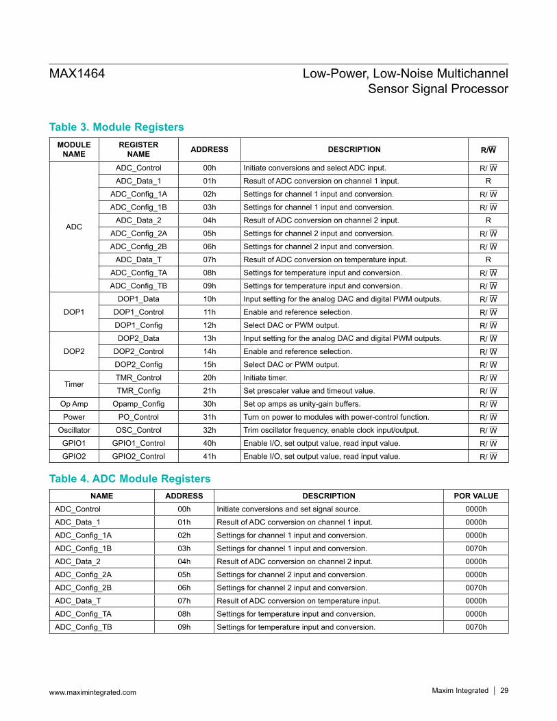
Table 4. ADC Module Registers
Table 3. Module Registers
MAX1464 Low-Power, Low-Noise Multichannel Sensor Signal Processor
www.maximintegrated.com Maxim Integrated 29
MODULE NAME
REGISTER NAME ADDRESS DESCRIPTION R/W
ADC
ADC_Control 00h Initiate conversions and select ADC input. R/ WADC_Data_1 01h Result of ADC conversion on channel 1 input. R
ADC_Config_1A 02h Settings for channel 1 input and conversion. R/ WADC_Config_1B 03h Settings for channel 1 input and conversion. R/ W
ADC_Data_2 04h Result of ADC conversion on channel 2 input. R
ADC_Config_2A 05h Settings for channel 2 input and conversion. R/ WADC_Config_2B 06h Settings for channel 2 input and conversion. R/ W
ADC_Data_T 07h Result of ADC conversion on temperature input. R
ADC_Config_TA 08h Settings for temperature input and conversion. R/ WADC_Config_TB 09h Settings for temperature input and conversion. R/ W
DOP1
DOP1_Data 10h Input setting for the analog DAC and digital PWM outputs. R/ WDOP1_Control 11h Enable and reference selection. R/ WDOP1_Config 12h Select DAC or PWM output. R/ W
DOP2
DOP2_Data 13h Input setting for the analog DAC and digital PWM outputs. R/ WDOP2_Control 14h Enable and reference selection. R/ WDOP2_Config 15h Select DAC or PWM output. R/ W
TimerTMR_Control 20h Initiate timer. R/ WTMR_Config 21h Set prescaler value and timeout value. R/ W
Op Amp Opamp_Config 30h Set op amps as unity-gain buffers. R/ WPower PO_Control 31h Turn on power to modules with power-control function. R/ W
Oscillator OSC_Control 32h Trim oscillator frequency, enable clock input/output. R/ WGPIO1 GPIO1_Control 40h Enable I/O, set output value, read input value. R/ WGPIO2 GPIO2_Control 41h Enable I/O, set output value, read input value. R/ W
NAME ADDRESS DESCRIPTION POR VALUEADC_Control 00h Initiate conversions and set signal source. 0000h
ADC_Data_1 01h Result of ADC conversion on channel 1 input. 0000h
ADC_Config_1A 02h Settings for channel 1 input and conversion. 0000h
ADC_Config_1B 03h Settings for channel 1 input and conversion. 0070h
ADC_Data_2 04h Result of ADC conversion on channel 2 input. 0000h
ADC_Config_2A 05h Settings for channel 2 input and conversion. 0000h
ADC_Config_2B 06h Settings for channel 2 input and conversion. 0070h
ADC_Data_T 07h Result of ADC conversion on temperature input. 0000h
ADC_Config_TA 08h Settings for temperature input and conversion. 0000h
ADC_Config_TB 09h Settings for temperature input and conversion. 0070h
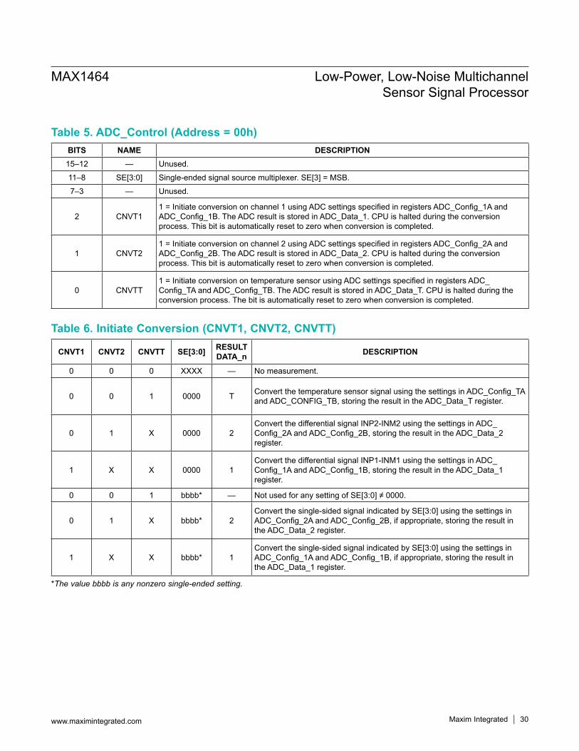
*The value bbbb is any nonzero single-ended setting.
Table 6. Initiate Conversion (CNVT1, CNVT2, CNVTT)
Table 5. ADC_Control (Address = 00h)
MAX1464 Low-Power, Low-Noise Multichannel Sensor Signal Processor
www.maximintegrated.com Maxim Integrated 30
BITS NAME DESCRIPTION15–12 — Unused.
11–8 SE[3:0] Single-ended signal source multiplexer. SE[3] = MSB.
7–3 — Unused.
2 CNVT11 = Initiate conversion on channel 1 using ADC settings specified in registers ADC_Config_1A and ADC_Config_1B. The ADC result is stored in ADC_Data_1. CPU is halted during the conversion process. This bit is automatically reset to zero when conversion is completed.
1 CNVT21 = Initiate conversion on channel 2 using ADC settings specified in registers ADC_Config_2A and ADC_Config_2B. The ADC result is stored in ADC_Data_2. CPU is halted during the conversion process. This bit is automatically reset to zero when conversion is completed.
0 CNVTT1 = Initiate conversion on temperature sensor using ADC settings specified in registers ADC_Config_TA and ADC_Config_TB. The ADC result is stored in ADC_Data_T. CPU is halted during the conversion process. The bit is automatically reset to zero when conversion is completed.
CNVT1 CNVT2 CNVTT SE[3:0] RESULT DATA_n DESCRIPTION
0 0 0 XXXX — No measurement.
0 0 1 0000 T Convert the temperature sensor signal using the settings in ADC_Config_TA and ADC_CONFIG_TB, storing the result in the ADC_Data_T register.
0 1 X 0000 2Convert the differential signal INP2-INM2 using the settings in ADC_Config_2A and ADC_Config_2B, storing the result in the ADC_Data_2 register.
1 X X 0000 1Convert the differential signal INP1-INM1 using the settings in ADC_Config_1A and ADC_Config_1B, storing the result in the ADC_Data_1 register.
0 0 1 bbbb* — Not used for any setting of SE[3:0] ≠ 0000.
0 1 X bbbb* 2Convert the single-sided signal indicated by SE[3:0] using the settings in ADC_Config_2A and ADC_Config_2B, if appropriate, storing the result in the ADC_Data_2 register.
1 X X bbbb* 1Convert the single-sided signal indicated by SE[3:0] using the settings in ADC_Config_1A and ADC_Config_1B, if appropriate, storing the result in the ADC_Data_1 register.
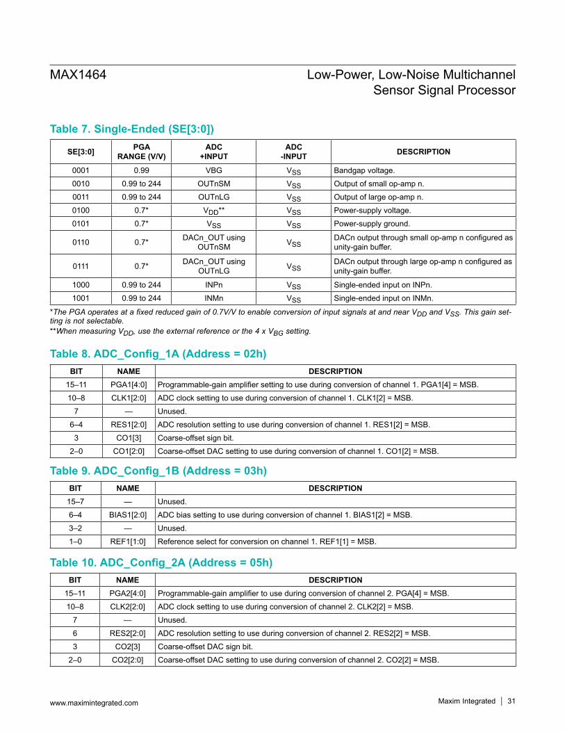
*The PGA operates at a fixed reduced gain of 0.7V/V to enable conversion of input signals at and near VDD and VSS. This gain set-ting is not selectable.**When measuring VDD, use the external reference or the 4 x VBG setting.
Table 9. ADC_Config_1B (Address = 03h)
Table 10. ADC_Config_2A (Address = 05h)
Table 7. Single-Ended (SE[3:0])
Table 8. ADC_Config_1A (Address = 02h)
MAX1464 Low-Power, Low-Noise Multichannel Sensor Signal Processor
www.maximintegrated.com Maxim Integrated 31
SE[3:0] PGA RANGE (V/V)
ADC +INPUT
ADC -INPUT DESCRIPTION
0001 0.99 VBG VSS Bandgap voltage.
0010 0.99 to 244 OUTnSM VSS Output of small op-amp n.
0011 0.99 to 244 OUTnLG VSS Output of large op-amp n.
0100 0.7* VDD** VSS Power-supply voltage.
0101 0.7* VSS VSS Power-supply ground.
0110 0.7* DACn_OUT using OUTnSM VSS
DACn output through small op-amp n configured as unity-gain buffer.
0111 0.7* DACn_OUT using OUTnLG VSS
DACn output through large op-amp n configured as unity-gain buffer.
1000 0.99 to 244 INPn VSS Single-ended input on INPn.
1001 0.99 to 244 INMn VSS Single-ended input on INMn.
BIT NAME DESCRIPTION15–11 PGA1[4:0] Programmable-gain amplifier setting to use during conversion of channel 1. PGA1[4] = MSB.
10–8 CLK1[2:0] ADC clock setting to use during conversion of channel 1. CLK1[2] = MSB.
7 — Unused.
6–4 RES1[2:0] ADC resolution setting to use during conversion of channel 1. RES1[2] = MSB.
3 CO1[3] Coarse-offset sign bit.
2–0 CO1[2:0] Coarse-offset DAC setting to use during conversion of channel 1. CO1[2] = MSB.
BIT NAME DESCRIPTION15–7 — Unused.
6–4 BIAS1[2:0] ADC bias setting to use during conversion of channel 1. BIAS1[2] = MSB.
3–2 — Unused.
1–0 REF1[1:0] Reference select for conversion on channel 1. REF1[1] = MSB.
BIT NAME DESCRIPTION15–11 PGA2[4:0] Programmable-gain amplifier to use during conversion of channel 2. PGA[4] = MSB.
10–8 CLK2[2:0] ADC clock setting to use during conversion of channel 2. CLK2[2] = MSB.
7 — Unused.
6 RES2[2:0] ADC resolution setting to use during conversion of channel 2. RES2[2] = MSB.
3 CO2[3] Coarse-offset DAC sign bit.
2–0 CO2[2:0] Coarse-offset DAC setting to use during conversion of channel 2. CO2[2] = MSB.
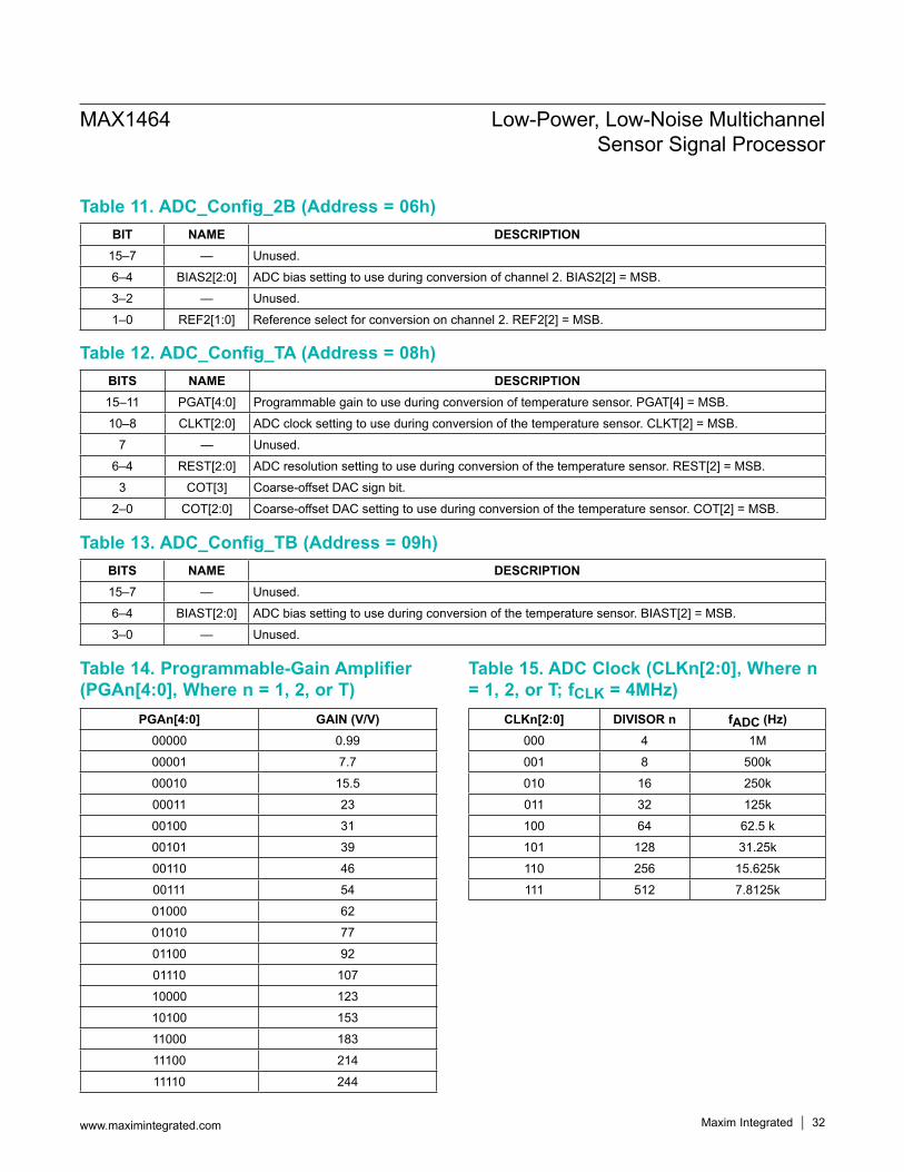
Table 11. ADC_Config_2B (Address = 06h)
Table 12. ADC_Config_TA (Address = 08h)
Table 13. ADC_Config_TB (Address = 09h)
Table 14. Programmable-Gain Amplifier (PGAn[4:0], Where n = 1, 2, or T)
Table 15. ADC Clock (CLKn[2:0], Where n = 1, 2, or T; fCLK = 4MHz)
MAX1464 Low-Power, Low-Noise Multichannel Sensor Signal Processor
www.maximintegrated.com Maxim Integrated 32
BIT NAME DESCRIPTION15–7 — Unused.
6–4 BIAS2[2:0] ADC bias setting to use during conversion of channel 2. BIAS2[2] = MSB.
3–2 — Unused.
1–0 REF2[1:0] Reference select for conversion on channel 2. REF2[2] = MSB.
BITS NAME DESCRIPTION15–11 PGAT[4:0] Programmable gain to use during conversion of temperature sensor. PGAT[4] = MSB.
10–8 CLKT[2:0] ADC clock setting to use during conversion of the temperature sensor. CLKT[2] = MSB.
7 — Unused.
6–4 REST[2:0] ADC resolution setting to use during conversion of the temperature sensor. REST[2] = MSB.
3 COT[3] Coarse-offset DAC sign bit.
2–0 COT[2:0] Coarse-offset DAC setting to use during conversion of the temperature sensor. COT[2] = MSB.
BITS NAME DESCRIPTION15–7 — Unused.
6–4 BIAST[2:0] ADC bias setting to use during conversion of the temperature sensor. BIAST[2] = MSB.
3–0 — Unused.
PGAn[4:0] GAIN (V/V)00000 0.99
00001 7.7
00010 15.5
00011 23
00100 31
00101 39
00110 46
00111 54
01000 62
01010 77
01100 92
01110 107
10000 123
10100 153
11000 183
11100 214
11110 244
CLKn[2:0] DIVISOR n fADC (Hz)000 4 1M
001 8 500k
010 16 250k
011 32 125k
100 64 62.5 k
101 128 31.25k
110 256 15.625k
111 512 7.8125k
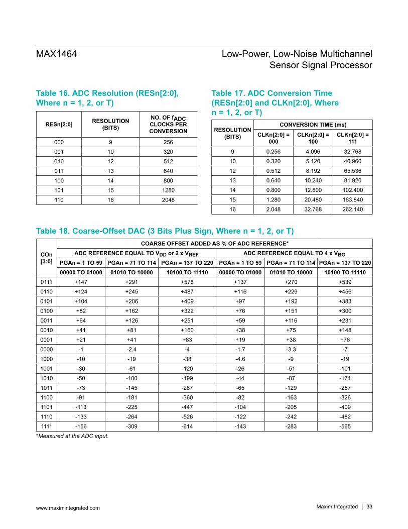
Table 18. Coarse-Offset DAC (3 Bits Plus Sign, Where n = 1, 2, or T)
Table 16. ADC Resolution (RESn[2:0], Where n = 1, 2, or T)
Table 17. ADC Conversion Time (RESn[2:0] and CLKn[2:0], Where n = 1, 2, or T)
*Measured at the ADC input.
MAX1464 Low-Power, Low-Noise Multichannel Sensor Signal Processor
www.maximintegrated.com Maxim Integrated 33
RESn[2:0] RESOLUTION (BITS)
NO. OF fADC CLOCKS PER CONVERSION
000 9 256
001 10 320
010 12 512
011 13 640
100 14 800
101 15 1280
110 16 2048
RESOLUTION (BITS)
CONVERSION TIME (ms)
CLKn[2:0] = 000
CLKn[2:0] = 100
CLKn[2:0] = 111
9 0.256 4.096 32.768
10 0.320 5.120 40.960
12 0.512 8.192 65.536
13 0.640 10.240 81.920
14 0.800 12.800 102.400
15 1.280 20.480 163.840
16 2.048 32.768 262.140
COn [3:0]
COARSE OFFSET ADDED AS % OF ADC REFERENCE*ADC REFERENCE EQUAL TO VDD or 2 x VREF ADC REFERENCE EQUAL TO 4 x VBG
PGAn = 1 TO 59 PGAn = 71 TO 114 PGAn = 137 TO 220 PGAn = 1 TO 59 PGAn = 71 TO 114 PGAn = 137 TO 22000000 TO 01000 01010 TO 10000 10100 TO 11110 00000 TO 01000 01010 TO 10000 10100 TO 11110
0111 +147 +291 +578 +137 +270 +539
0110 +124 +245 +487 +116 +229 +456
0101 +104 +206 +409 +97 +192 +383
0100 +82 +162 +322 +76 +151 +300
0011 +64 +126 +251 +59 +116 +231
0010 +41 +81 +160 +38 +75 +148
0001 +21 +41 +83 +19 +38 +76
0000 -1 -2.4 -4 -1.7 -3.3 -7
1000 -10 -19 -38 -4.6 -9 -19
1001 -30 -61 -120 -26 -51 -101
1010 -50 -100 -199 -44 -87 -174
1011 -73 -145 -287 -65 -129 -257
1100 -91 -181 -360 -82 -163 -326
1101 -113 -225 -447 -104 -205 -409
1110 -133 -264 -526 -122 -242 -482
1111 -156 -309 -614 -143 -283 -565
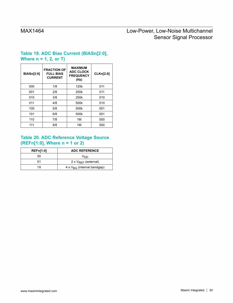
Table 19. ADC Bias Current (BIASn[2:0], Where n = 1, 2, or T)
Table 20. ADC Reference Voltage Source (REFn[1:0], Where n = 1 or 2)
MAX1464 Low-Power, Low-Noise Multichannel Sensor Signal Processor
www.maximintegrated.com Maxim Integrated 34
BIASn[2:0]FRACTION OF
FULL BIAS CURRENT
MAXIMUM ADC CLOCK FREQUENCY
(Hz)
CLKn[2:0]
000 1/8 125k 011
001 2/8 250k 011
010 3/8 250k 010
011 4/8 500k 010
100 5/8 500k 001
101 6/8 500k 001
110 7/8 1M 000
111 8/8 1M 000
REFn[1:0] ADC REFERENCE00 VDD01 2 x VREF (external)
1X 4 x VBG (internal bandgap)

Table 21. DOPn Configuration Options
MAX1464 Low-Power, Low-Noise Multichannel Sensor Signal Processor
www.maximintegrated.com Maxim Integrated 35
DOP CONFIGURATION PWRDAC PWROP SELDAC SELPWM ENDAC ENPWM BUFDAC OFF, PWM OFF, op amp OFF. 0 0 X X 0 0 X
DAC OFF, PWM OFF, op amp ON. AMPnP and AMPnM routed to LG op amp. 0 1 0 X 0 0 0
DAC OFF, PWM OFF, op amp ON. LG op amp configured as unity-gain buffer. 0 1 0 X 0 0 1
DAC OFF, PWM OFF, op amp ON. AMPnP and AMPnM routed to SM op amp. 0 1 1 X 0 0 0
DAC OFF, PWM OFF, op amp ON. SM op amp configured as unity-gain buffer. 0 1 1 X 0 0 1
DAC OFF, PWM ON, op amp OFF. PWM output on OUTnSM. AMPnP and AMPnM disabled. 0 0 0 0 0 1 X
DAC OFF, PWM ON, op amp OFF. PWM output on OUTnLG. AMPnP and AMPnM disabled. 0 0 0 1 0 1 X
DAC OFF, PWM ON, op amp ON. AMPnP and AMPnM routed to LG op amp. PWM output on OUTnSM.
0 1 0 0 0 1 0
DAC OFF, PWM ON, op amp ON. LG op amp configured as unity-gain buffer. PWM output on OUTnSM.
0 1 0 0 0 1 1
DAC OFF, PWM ON, op amp ON. AMPnP and AMPnM routed to SM op amp. PWM output on OUTnLG.
0 1 1 1 0 1 0
DAC OFF, PWM ON, op amp ON. SM op amp configured as unity-gain buffer. PWM output on OUTnLG.
0 1 1 1 0 1 1
DAC ON, PWM OFF, op amp OFF. DAC output on OUTnSM. AMPnP and AMPnM disabled. 1 0 0 X 1 0 X
DAC ON, PWM OFF, op amp OFF. DAC output on OUTnLG. AMPnP and AMPnM disabled. 1 0 1 X 1 0 X
DAC ON, PWM OFF, op amp ON. DAC output on OUTnSM. AMPnP and AMPnM routed to LG op amp. 1 1 0 X 1 0 0
DAC ON, PWM OFF, op amp ON. DAC output on OUTnSM. LG op amp configured as unity-gain buffer. 1 1 0 X 1 0 1
DAC ON, PWM OFF, op amp ON. DAC output on OUTnLG. AMPnP and AMPnM routed to SM op amp. 1 1 1 X 1 0 0
DAC ON, PWM OFF, op amp ON. DAC output on OUTnLG. SM op amp configured as unity-gain buffer. 1 1 1 X 1 0 1
DAC ON, PWM ON, op amp OFF. DAC output on OUTnSM. PWM output on OUTnLG. AMPnP and AMPnM disabled.
1 X 0 1 1 1 X
DAC ON, PWM ON, op amp OFF. DAC output on OUTnLG. PWM output on OUTnSM. AMPnP and AMPnM disabled.
1 X 1 0 1 1 X
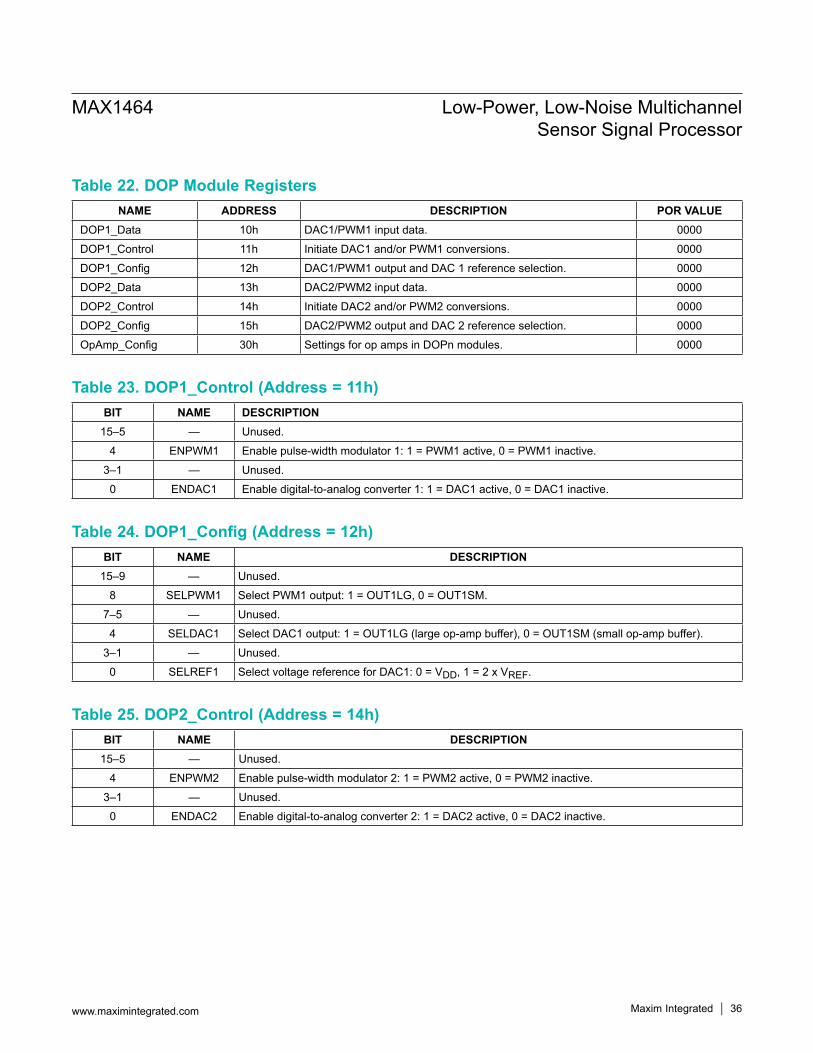
Table 22. DOP Module Registers
Table 23. DOP1_Control (Address = 11h)
Table 24. DOP1_Config (Address = 12h)
Table 25. DOP2_Control (Address = 14h)
MAX1464 Low-Power, Low-Noise Multichannel Sensor Signal Processor
www.maximintegrated.com Maxim Integrated 36
NAME ADDRESS DESCRIPTION POR VALUEDOP1_Data 10h DAC1/PWM1 input data. 0000
DOP1_Control 11h Initiate DAC1 and/or PWM1 conversions. 0000
DOP1_Config 12h DAC1/PWM1 output and DAC 1 reference selection. 0000
DOP2_Data 13h DAC2/PWM2 input data. 0000
DOP2_Control 14h Initiate DAC2 and/or PWM2 conversions. 0000
DOP2_Config 15h DAC2/PWM2 output and DAC 2 reference selection. 0000
OpAmp_Config 30h Settings for op amps in DOPn modules. 0000
BIT NAME DESCRIPTION15–5 — Unused.
4 ENPWM1 Enable pulse-width modulator 1: 1 = PWM1 active, 0 = PWM1 inactive.
3–1 — Unused.
0 ENDAC1 Enable digital-to-analog converter 1: 1 = DAC1 active, 0 = DAC1 inactive.
BIT NAME DESCRIPTION15–9 — Unused.
8 SELPWM1 Select PWM1 output: 1 = OUT1LG, 0 = OUT1SM.
7–5 — Unused.
4 SELDAC1 Select DAC1 output: 1 = OUT1LG (large op-amp buffer), 0 = OUT1SM (small op-amp buffer).
3–1 — Unused.
0 SELREF1 Select voltage reference for DAC1: 0 = VDD, 1 = 2 x VREF.
BIT NAME DESCRIPTION15–5 — Unused.
4 ENPWM2 Enable pulse-width modulator 2: 1 = PWM2 active, 0 = PWM2 inactive.
3–1 — Unused.
0 ENDAC2 Enable digital-to-analog converter 2: 1 = DAC2 active, 0 = DAC2 inactive.
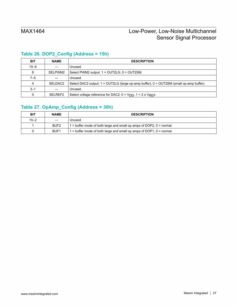
Table 26. DOP2_Config (Address = 15h)
Table 27. OpAmp_Config (Address = 30h)
MAX1464 Low-Power, Low-Noise Multichannel Sensor Signal Processor
www.maximintegrated.com Maxim Integrated 37
BIT NAME DESCRIPTION15–9 — Unused.
8 SELPWM2 Select PWM2 output: 1 = OUT2LG, 0 = OUT2SM.
7–5 — Unused.
4 SELDAC2 Select DAC2 output: 1 = OUT2LG (large op-amp buffer), 0 = OUT2SM (small op-amp buffer).
3–1 — Unused.
0 SELREF2 Select voltage reference for DAC2: 0 = VDD, 1 = 2 x VREF.
BIT NAME DESCRIPTION15–2 — Unused.
1 BUF2 1 = buffer mode of both large and small op amps of DOP2, 0 = normal.
0 BUF1 1 = buffer mode of both large and small op amps of DOP1, 0 = normal.
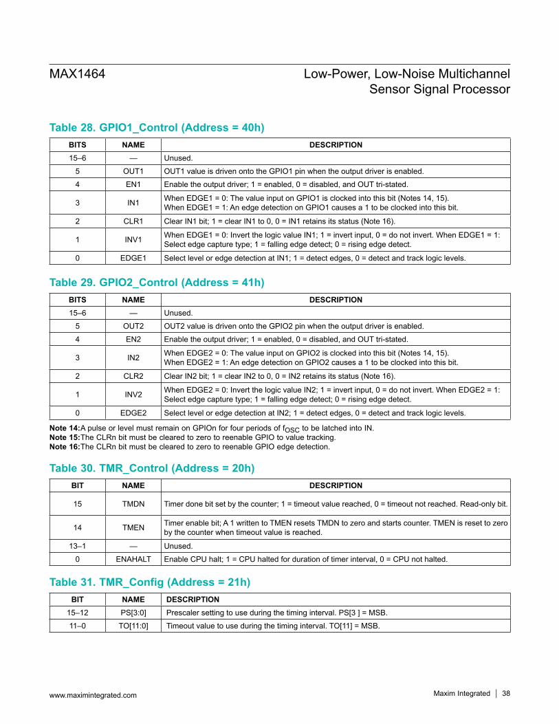
Note 14: A pulse or level must remain on GPIOn for four periods of fOSC to be latched into IN.Note 15: The CLRn bit must be cleared to zero to reenable GPIO to value tracking.Note 16: The CLRn bit must be cleared to zero to reenable GPIO edge detection.
Table 28. GPIO1_Control (Address = 40h)
Table 29. GPIO2_Control (Address = 41h)
Table 30. TMR_Control (Address = 20h)
Table 31. TMR_Config (Address = 21h)
MAX1464 Low-Power, Low-Noise Multichannel Sensor Signal Processor
www.maximintegrated.com Maxim Integrated 38
BITS NAME DESCRIPTION15–6 — Unused.
5 OUT1 OUT1 value is driven onto the GPIO1 pin when the output driver is enabled.
4 EN1 Enable the output driver; 1 = enabled, 0 = disabled, and OUT tri-stated.
3 IN1 When EDGE1 = 0: The value input on GPIO1 is clocked into this bit (Notes 14, 15). When EDGE1 = 1: An edge detection on GPIO1 causes a 1 to be clocked into this bit.
2 CLR1 Clear IN1 bit; 1 = clear IN1 to 0, 0 = IN1 retains its status (Note 16).
1 INV1 When EDGE1 = 0: Invert the logic value IN1; 1 = invert input, 0 = do not invert. When EDGE1 = 1: Select edge capture type; 1 = falling edge detect; 0 = rising edge detect.
0 EDGE1 Select level or edge detection at IN1; 1 = detect edges, 0 = detect and track logic levels.
BITS NAME DESCRIPTION15–6 — Unused.
5 OUT2 OUT2 value is driven onto the GPIO2 pin when the output driver is enabled.
4 EN2 Enable the output driver; 1 = enabled, 0 = disabled, and OUT tri-stated.
3 IN2 When EDGE2 = 0: The value input on GPIO2 is clocked into this bit (Notes 14, 15). When EDGE2 = 1: An edge detection on GPIO2 causes a 1 to be clocked into this bit.
2 CLR2 Clear IN2 bit; 1 = clear IN2 to 0, 0 = IN2 retains its status (Note 16).
1 INV2 When EDGE2 = 0: Invert the logic value IN2; 1 = invert input, 0 = do not invert. When EDGE2 = 1: Select edge capture type; 1 = falling edge detect; 0 = rising edge detect.
0 EDGE2 Select level or edge detection at IN2; 1 = detect edges, 0 = detect and track logic levels.
BIT NAME DESCRIPTION
15 TMDN Timer done bit set by the counter; 1 = timeout value reached, 0 = timeout not reached. Read-only bit.
14 TMEN Timer enable bit; A 1 written to TMEN resets TMDN to zero and starts counter. TMEN is reset to zero by the counter when timeout value is reached.
13–1 — Unused.
0 ENAHALT Enable CPU halt; 1 = CPU halted for duration of timer interval, 0 = CPU not halted.
BIT NAME DESCRIPTION15–12 PS[3:0] Prescaler setting to use during the timing interval. PS[3 ] = MSB.
11–0 TO[11:0] Timeout value to use during the timing interval. TO[11] = MSB.
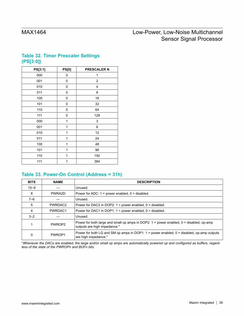
Table 32. Timer Prescaler Settings (PS[3:0])
Table 33. Power-On Control (Address = 31h)
*Whenever the DACs are enabled, the large and/or small op amps are automatically powered up and configured as buffers, regard-less of the state of the PWROPn and BUFn bits.
MAX1464 Low-Power, Low-Noise Multichannel Sensor Signal Processor
www.maximintegrated.com Maxim Integrated 39
PS[3:1] PS[0] PRESCALER N000 0 1
001 0 2
010 0 4
011 0 8
100 0 16
101 0 32
110 0 64
111 0 128
000 1 3
001 1 6
010 1 12
011 1 24
100 1 48
101 1 96
110 1 192
111 1 384
BITS NAME DESCRIPTION15–9 — Unused.
8 PWRA2D Power for ADC: 1 = power enabled, 0 = disabled.
7–6 — Unused.
5 PWRDAC2 Power for DAC2 in DOP2: 1 = power enabled, 0 = disabled.
4 PWRDAC1 Power for DAC1 in DOP1: 1 = power enabled, 0 = disabled.
3–2 — Unused.
1 PWROP2 Power for both large and small op amps in DOP2: 1 = power enabled, 0 = disabled, op-amp outputs are high impedance.*
0 PWROP1 Power for both LG and SM op amps in DOP1: 1 = power enabled, 0 = disabled, op-amp outputs are high impedance.*
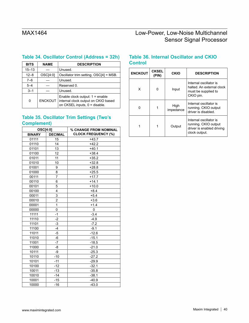
Table 34. Oscillator Control (Address = 32h) Table 36. Internal Oscillator and CKIO Control
Table 35. Oscillator Trim Settings (Two’s Complement)
MAX1464 Low-Power, Low-Noise Multichannel Sensor Signal Processor
www.maximintegrated.com Maxim Integrated 40
BITS NAME DESCRIPTION15–13 — Unused.12–8 OSC[4:0] Oscillator trim setting. OSC[4] = MSB.7–6 — Unused.5–4 — Reserved 0. 3–1 — Unused.
0 ENCKOUTEnable clock output: 1 = enable internal clock output on CKIO based on CKSEL inputs, 0 = disable.
OSC[4:0] % CHANGE FROM NOMINAL CLOCK FREQUENCY (%)BINARY DECIMAL
01111 15 +43.701110 14 +42.201101 13 +40.101100 12 +38.401011 11 +35.201010 10 +32.801001 9 +28.801000 8 +25.500111 7 +17.700110 6 +14.100101 5 +10.000100 4 +8.400011 3 +5.400010 2 +3.600001 1 +1.400000 0 011111 -1 -3.411110 -2 -4.911101 -3 -7.211100 -4 -9.111011 -5 -12.611010 -6 -15.111001 -7 -18.511000 -8 -21.010111 -9 -25.310110 -10 -27.210101 -11 -29.910100 -12 -32.110011 -13 -35.810010 -14 -38.110001 -15 -40.910000 -16 -43.0
ENCKOUT CKSEL (PIN) CKIO DESCRIPTION
X 0 Input
Internal oscillator is halted. An external clock must be supplied to CKIO pin.
0 1 High impedance
Internal oscillator is running. CKIO output driver is disabled.
1 1 Output
Internal oscillator is running. CKIO output driver is enabled driving clock output.
Table 37. Module Registers Summary
MAX1464 Low-Power, Low-Noise Multichannel Sensor Signal Processor
www.maximintegrated.com Maxim Integrated 41
Bit 15 Bit 14 Bit 13 Bit 12 Bit 11 Bit 10 Bit 9 Bit 8 Bit 7 Bit 6 Bit 5 Bit 4 Bit 3 Bit 2 Bit 1 Bit 0Register 00h ADC_Control
X X X X SE[3] SE[2] SE[1] SE[0] X X X X X CNVT1 CNVT2 CNVTTRegister 01h ADC_Data_1 (for Channel Input 1, Uncompensated, and Read-Only Register)
MSB LSBRegister 02h ADC_Config_1A (for Channel 1)PGA1[4] PGA1[3] PGA1[2] PGA1[1] PGA1[0] CLK1[2] CLK1[1] CLK1[0] X RES1[2] RES1[1] RES1[0] CO1[3] CO1[2] CO1[1] CO1[0]
Register 03h ADC_Config_1B (for Channel 1)X X X X X X X X X BIAS1[2] BIAS1[1] BIAS1[0] X X REF1[1] REF1[0]
Register 04h ADC_Data_2 (for Channel Input 1, Uncompensated, and Read-Only Register)MSB LSB
Register 05h ADC_Config_2A (for Channel 2A)PGA2[4] PGA2[3] PGA2[2] PGA2[1] PGA2[0] CLK2[2] CLK2[1] CLK2[0] X RES2[2] RES2[1] RES2[0] CO2[3] CO2[2] CO2[1] CO2[0]
Register 06h ADC_Config_2B (for Channel 2B)X X X X X X X X X BIAS2[2] BIAS2[1] BIAS2[0] X X REF2[1] REF2[0]
Register 07h ADC Data_T (for Internal Temperature Input, Uncompensated, and Read-Only Register)MSB LSB
Register 08h ADC_Config_TA (for Internal Temperature Input TA)PGAT[4] PGAT[3] PGAT[2] PGAT[1] PGAT[0] CLKT[2] CLKT[1] CLKT[0] X REST[2] REST[1] REST[0] COT[3] COT[2] COT[1] COT[0]
Register 09h ADC_Config_TB (for Internal Temperature Input TB)X X X X X X X X X BIAST[2] BIAST[1] BIAST[0] X X X X
Register 10h DOP1 Data (for DAC/PWM 1)MSB LSB
Register 11h DOP1 Control (for DAC/PWM 1)X X X X X X X X X X X ENPWM1 X X X ENDAC1
Register 12h DOP1 Configuration (for DAC/PWM 1)X X X X X X X SELPWM1 X X X SELDAC1 X X X SELREF1
Register 13h DOP2 Data (for DAC/PWM 2)MSB LSB
Register 14h DOP2 Control (for DAC/PWM 2)X X X X X X X X X X X ENPWM2 X X X ENDAC2
Register 15h DOP2 Configuration (for DAC/PWM 2)X X X X X X X SELPWM2 X X X SELDAC2 X X X SELREF2
Register 20h Timer Control TMDN TMEN X X X X X X X X X X X X X ENAHALTBit 15 Bit 14 Bit 13 Bit 12 Bit 11 Bit 10 Bit 9 Bit 8 Bit 7 Bit 6 Bit 5 Bit 4 Bit 3 Bit 2 Bit 1 Bit 0
Register 21h Timer Configuration PS[3] PS[2] PS[1] PS[0] TO[11] TO[10] TO[9] TO[8] TO[7] TO[6] TO[5] TO[4] TO[3] TO[2] TO[1] TO[1]
Register 30h OP AMP Configuration X X X X X X X X X X X X X X BUF1_LG BUF1_SM
Register 31h Power-On Control X X X X X X X PWRA2D X X PWRDAC2 PWRDAC1 X X PWROP2 PWROP1
Register 32h Oscillator Control X X X OSC[4] OSC[3] OSC[2] OSC[1] OSC[0] X X X X X X X ENCKOUT
Register 40h GPIO1 Control X X X X X X X X X X OUT1 EN1 IN1 CLR1 INV1 EDGE1
Register 41h GPIO2 Control X X X X X X X X X X OUT2 EN2 IN2 CLR2 INV2 EDGE2
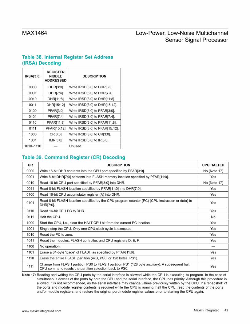
Note 17: Reading and writing the CPU ports by the serial interface is allowed while the CPU is executing its program. In the case of simultaneous access of the ports by both the CPU and the serial interface, the CPU has priority. Although this procedure is allowed, it is not recommended, as the serial interface may change values previously written by the CPU. If a “snapshot” of the ports and module register contents is required while the CPU is running, halt the CPU, read the contents of the ports and/or module registers, and restore the original port/module register values prior to starting the CPU again.
Table 38. Internal Register Set Address (IRSA) Decoding
Table 39. Command Register (CR) Decoding
MAX1464 Low-Power, Low-Noise Multichannel Sensor Signal Processor
www.maximintegrated.com Maxim Integrated 42
IRSA[3:0]REGISTER
NIBBLE ADDRESSED
DESCRIPTION
0000 DHR[3:0] Write IRSD[3:0] to DHR[3:0].
0001 DHR[7:4] Write IRSD[3:0] to DHR[7:4].
0010 DHR[11:8] Write IRSD[3:0] to DHR[11:8].
0011 DHR[15:12] Write IRSD[3:0] to DHR[15:12].
0100 PFAR[3:0] Write IRSD[3:0] to PFAR[3:0].
0101 PFAR[7:4] Write IRSD[3:0] to PFAR[7:4].
0110 PFAR[11:8] Write IRSD[3:0] to PFAR[11:8].
0111 PFAR[15:12] Write IRSD[3:0] to PFAR[15:12].
1000 CR[3:0] Write IRSD[3:0] to CR[3:0].
1001 IMR[3:0] Write IRSD[3:0] to IR[3:0].
1010–1110 — Unused.
CR DESCRIPTION CPU HALTED0000 Write 16-bit DHR contents into the CPU port specified by PFAR[3:0]. No (Note 17)
0001 Write 8-bit DHR[7:0] contents into FLASH memory location specified by PFAR[11:0]. Yes
0010 Read 16-bit CPU port specified by PFAR[3:0] into DHR. No (Note 17)
0011 Read 8-bit FLASH location specified by PFAR[11:0] into DHR[7:0]. Yes
0100 Read 16-bit CPU accumulator register (A) into DHR. Yes
0101 Read 8-bit FLASH location specified by the CPU program counter (PC) (CPU instruction or data) to DHR[7:0]. Yes
0110 Read 16-bit CPU PC to DHR. Yes
0111 Halt the CPU. No
1000 Start the CPU, i.e., clear the HALT CPU bit from the current PC location. Yes
1001 Single step the CPU. Only one CPU clock cycle is executed. Yes
1010 Reset the PC to zero. Yes
1011 Reset the modules, FLASH controller, and CPU registers D, E, F. Yes
1100 No operation. —
1101 Erase a 64-byte “page” of FLASH as specified by PFAR[11:6]. Yes
1110 Erase the entire FLASH partition (4kB, PS0, or 128 bytes, PS1). Yes
1111 Change from FLASH partition PS0 to FLASH partition PS1 (128 byte auxiliary). A subsequent halt CPU command resets the partition selection back to PS0. Yes
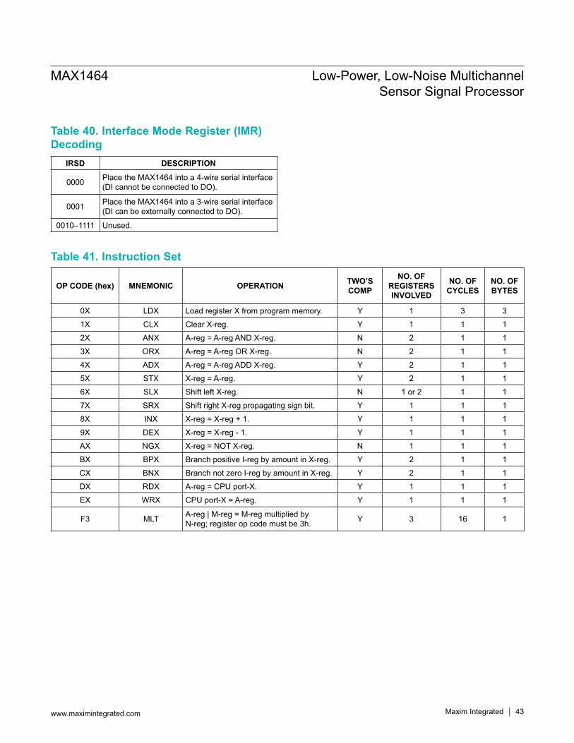
Table 40. Interface Mode Register (IMR) Decoding
Table 41. Instruction Set
MAX1464 Low-Power, Low-Noise Multichannel Sensor Signal Processor
www.maximintegrated.com Maxim Integrated 43
IRSD DESCRIPTION
0000 Place the MAX1464 into a 4-wire serial interface (DI cannot be connected to DO).
0001 Place the MAX1464 into a 3-wire serial interface (DI can be externally connected to DO).
0010–1111 Unused.
OP CODE (hex) MNEMONIC OPERATION TWO’S COMP
NO. OF REGISTERS INVOLVED
NO. OF CYCLES
NO. OF BYTES
0X LDX Load register X from program memory. Y 1 3 3
1X CLX Clear X-reg. Y 1 1 1
2X ANX A-reg = A-reg AND X-reg. N 2 1 1
3X ORX A-reg = A-reg OR X-reg. N 2 1 1
4X ADX A-reg = A-reg ADD X-reg. Y 2 1 1
5X STX X-reg = A-reg. Y 2 1 1
6X SLX Shift left X-reg. N 1 or 2 1 1
7X SRX Shift right X-reg propagating sign bit. Y 1 1 1
8X INX X-reg = X-reg + 1. Y 1 1 1
9X DEX X-reg = X-reg - 1. Y 1 1 1
AX NGX X-reg = NOT X-reg. N 1 1 1
BX BPX Branch positive I-reg by amount in X-reg. Y 2 1 1
CX BNX Branch not zero I-reg by amount in X-reg. Y 2 1 1
DX RDX A-reg = CPU port-X. Y 1 1 1
EX WRX CPU port-X = A-reg. Y 1 1 1
F3 MLT A-reg | M-reg = M-reg multiplied by N-reg; register op code must be 3h. Y 3 16 1
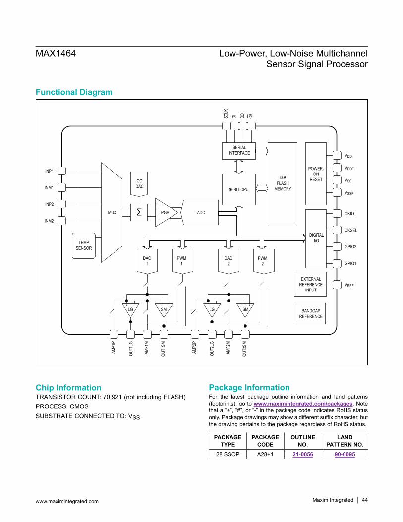
POWER-ON
RESET4kBFLASH
MEMORY16-BIT CPU
SERIALINTERFACE
SCLK
DI DO CS
EXTERNALREFERENCE
INPUTVREF
BANDGAPREFERENCE
DIGITALI/O
CKIO
CKSEL
GPIO2
GPIO1
ADC
CODAC
TEMPSENSOR
INP1
INM1
INP2
INM2
PGAMUX
OUT2
SM
AMP2
M
OUT2
LG
AMP2
P
DAC2
PWM2
LG SM
OUT1
SM
AMP1
M
OUT1
LG
AMP1
P
DAC1
PWM1
LG SM
VDD
VSS
VDDF
VSSF
∑
MAX1464 Low-Power, Low-Noise Multichannel Sensor Signal Processor
www.maximintegrated.com Maxim Integrated 44
PACKAGE TYPE
PACKAGE CODE
OUTLINE NO.
LAND PATTERN NO.
28 SSOP A28+1 21-0056 90-0095
Functional Diagram
Chip InformationTRANSISTOR COUNT: 70,921 (not including FLASH)PROCESS: CMOSSUBSTRATE CONNECTED TO: VSS
Package InformationFor the latest package outline information and land patterns (footprints), go to www.maximintegrated.com/packages. Note that a “+”, “#”, or “-” in the package code indicates RoHS status only. Package drawings may show a different suffix character, but the drawing pertains to the package regardless of RoHS status.
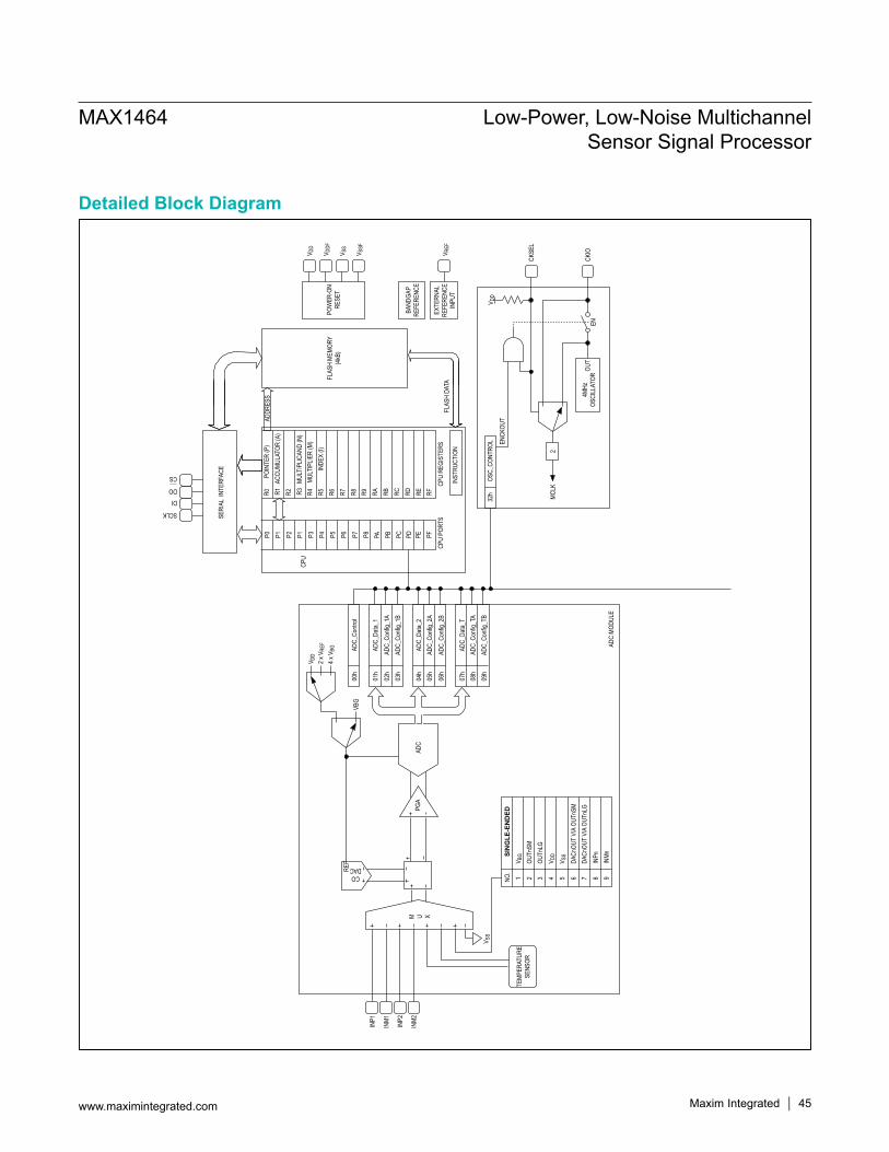
ADC
MODU
LE
FLAS
H ME
MORY
(4kB
)
SERI
AL IN
TERF
ACE
SCLK
DIDO
CS
R0
POI
NTER
(P)
R1 A
CCUM
ULAT
OR (A
)R2 R3
MUL
TIPL
ICAN
D (N
)R4
MU
LTIP
LIER
(M)
R5
INDE
X (I)
R6 R7 R8 R9 RA RB RC RD RE RF
P0 P1 P2 P1 P3 P4 P5 P6 P7 P8 PA PB PC PD PE PFCP
U RE
GIST
ERS
INST
RUCT
ION
CPU
FLAS
H DA
TA
ADDR
ESS
CPU
PORT
S
INM2INP2
INM1INP1
POW
ER-O
NRE
SET
BAND
GAP
REFE
RENC
E
EXTE
RNAL
REFE
RENC
EIN
PUT
V REF
CKSE
L
CKIO
32h
OSC_
CONT
ROL
V DD
4MHz
OSCI
LLAT
OR
2MC
LK
EN
ENCK
OUT
OUT
V DD
V SS
V DDF
V SSF
CODACRE
F
TEMP
ERAT
URE
SENS
OR
VBG
V DD
4 x V
BG
2 x V
REF
ADC
INMn
V BG
OUTn
SMOU
TnLG
V DD
V SS
DACn
OUT
VIA
OUTn
SM
INPn
1 2 3 4 5 6 7 8 9NO.
SIN
GLE
-EN
DED
DACn
OUT
VIA
OUTn
LG
00h
ADC_
Contr
ol
08h
ADC_
Confi
g_TA
07h
ADC_
Data_
T
06h
ADC_
Confi
g_2B
09h
ADC_
Confi
g_TB
02h
ADC_
Confi
g_1A
05h
ADC_
Confi
g_2A
04h
ADC_
Data_
2
03h
01h
ADC_
Data_
1
ADC_
Confi
g_1B
PGA
V SS
M U X
MAX1464 Low-Power, Low-Noise Multichannel Sensor Signal Processor
www.maximintegrated.com Maxim Integrated 45
Detailed Block Diagram
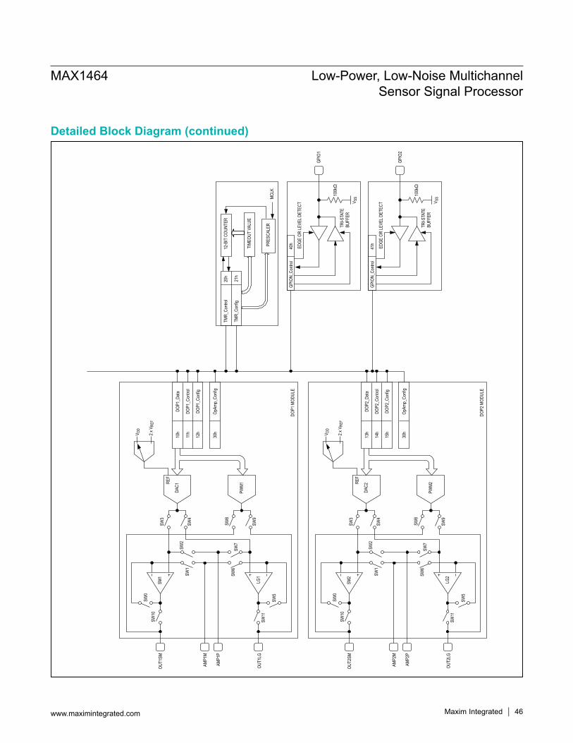
DOP1
MOD
ULE
GPIO
1
GPIO
2
DAC1
10h
DOP1
_Data
12h
DOP1
_Con
fig
30h
OpAm
p_Co
nfig
11h
DOP1
_Con
trol
REF
PWM1
SW0
SW1
SW2
SW3
SW4
SW5
SW6
SW7
SW8
SW9
2 x V
REF
V DD
OUT1
SM
AMP1
M
AMP1
P
OUT1
LG
SW10
SW11
SM1
LG1
DOP2
MOD
ULE
DAC2
13h
DOP2
_Data
15h
DOP2
_Con
fig
30h
OpAm
p_Co
nfig
14h
DOP2
_Con
trol
REF
PWM2
SW0
SW1
SW2
SW3
SW4
SW5
SW6
SW7
SW8
SW9
2 x V
REF
V DD
OUT2
SM
AMP2
M
AMP2
P
OUT2
LG
SW10
SW11
SM2
LG2
20h
TMR_
Contr
ol
21h
TMR_
Confi
g
PRES
CALE
R
12-B
IT C
OUNT
ER
TIME
OUT
VALU
E
MCLK
40h
GPIO
N_Co
ntrol
EDGE
OR
LEVE
L DET
ECT V S
S
100kΩ
TRI-S
TATE
BUFF
ER
41h
GPIO
N_Co
ntrol
EDGE
OR
LEVE
L DET
ECT V S
S
100kΩ
TRI-S
TATE
BUFF
ER
MAX1464 Low-Power, Low-Noise Multichannel Sensor Signal Processor
www.maximintegrated.com Maxim Integrated 46
Detailed Block Diagram (continued)
Maxim Integrated cannot assume responsibility for use of any circuitry other than circuitry entirely embodied in a Maxim Integrated product. No circuit patent licenses are implied. Maxim Integrated reserves the right to change the circuitry and specifications without notice at any time. The parametric values (min and max limits) shown in the Electrical Characteristics table are guaranteed. Other parametric values quoted in this data sheet are provided for guidance.
Maxim Integrated and the Maxim Integrated logo are trademarks of Maxim Integrated Products, Inc. © 2014 Maxim Integrated Products, Inc. 47
MAX1464 Low-Power, Low-Noise Multichannel Sensor Signal Processor
REVISIONNUMBER
REVISION DATE DESCRIPTION PAGES
CHANGED
0 9/14 Removed automotive references 1, 12
Revision History
For pricing, delivery, and ordering information, please contact Maxim Direct at 1-888-629-4642, or visit Maxim Integrated’s website at www.maximintegrated.com.