Embed Size (px)
Citation preview

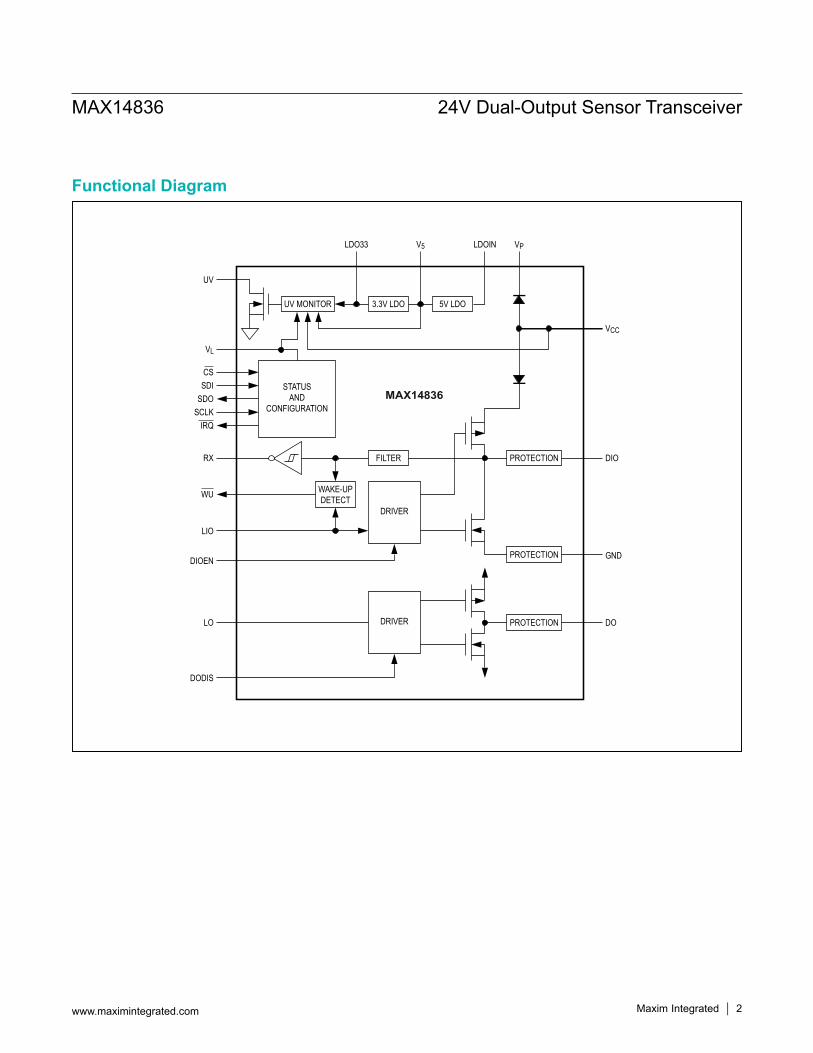
General DescriptionThe MAX14836 transceiver is suitable for 24V binary sensors. Additional 24V digital inputs and outputs are provided. Two internal linear regulators generate common sensor power requirements: 5V and 3.3V.On-board DIO and DO drivers are independently configurable for push-pull, high-side (pnp), or low-side (npn) operation. The device detects a wake-up condition and generates a wake-up signal on the active-low WU output. An SPI interface allows configuration and monitoring of the devices. Extensive alarm conditions are detected and communicated through the IRQ output and the SPI inter-face. The device features reverse-polarity, short-circuit, and thermal protection. All power lines are monitored for undervoltage conditions.Both DIO and DO drivers are specified for sinking/sourc-ing 200mA.The MAX14836 is available in a 4mm x 4mm, 24-pin TQFN package, and is specified over the -40NC to +105NC temperature range.
Applications Industrial Sensors
Features and Benefits High Configurability and Integration Enable Faster
Time-to-Market and Reduce SKUs• Push-Pull, High-Side, or Low-Side Outputs• DIO and DO Drivers Can Be Connected in Parallel
to Increase Current and Reduce Output Resistance • 200mA Specified DIO and DO Output Drive• 2.5V to 5V Logic Interface Levels • 5V and 3.3V Linear Regulators • 400μs Wake-Up Detection on DIO Line • 3μF DIO Load-Drive Capability • 2μF DO Load-Drive Capability • EMI Emission Control Through Slew-Controlled
Driver Integrated Protection Enables Robust Solutions
• Reverse-Polarity-Protected 24V Supply Output • SPI Interface for Configuration and Monitoring • Reverse-Polarity and Short-Circuit Protection on All
24V Inputs/Outputs • High-Temperature Warning and Thermal Shutdown • Extensive Fault Monitoring and Reporting • -40°C to +105°C Operating Temperature Range
Space-Saving 4mm x 4mm TQFN Package Saves Circuit FootprintOrdering Information appears at end of data sheet.
12
43
10kΩ
MAX14836
0.8Ω
1μF
1μF
10Ω
1μF 0.1μF
VCCUV
LDOIN
DOSPI
DIO
L+
L-GNDDODISGND
VPV5VCC LDO33DIOENVL
MICROCONTROLLER
LIO
LO
3.3V5V
Typical Application Circuit
MAX14836 24V Dual-Output Sensor Transceiver
19-6738; Rev 2; 9/14
MAX14836
UV MONITOR
UV
VCC
V5LDO33 LDOIN
STATUSAND
CONFIGURATION
3.3V LDO
FILTER
DRIVER
DRIVER
WAKE-UPDETECT
5V LDO
VL
SDICS
RX
LO
DODIS
DIO
DO
GND
SDOSCLK
IRQ
WU
LIO
DIOEN
VP
PROTECTION
PROTECTION
PROTECTION
Functional Diagram
MAX14836 24V Dual-Output Sensor Transceiver
www.maximintegrated.com Maxim Integrated 2

(All voltages referenced to GND, unless otherwise noted.)VCC .........................................................................-40V to +40V VP..............................MIN: the higher of -0.3V and (VCC - 0.3V)
MAX: the higher of 40V and (VCC + 40V)LDOIN....................................................................-0.3V to +40VV5 .................... -0.3V to the lesser of (VLDOIN + 0.3V) and +6VLDO33 ..................... -0.3V to the lesser of (V5 + 0.3V) and +6VVL ............................................................................-0.3V to +6VDIO, DO ...................... MIN: the higher of -40V and (VCC - 40V)
MAX: the lesser of +40V and (VCC + 40V)Logic Inputs LIO, DODIS, DIOEN, LO, CS, SDI, SCLK ............................................... -0.3V to (VL + 0.3V)
Logic Outputs RX, WU, SDO, IRQ ................................. -0.3V to (VL + 0.3V)
UV ........................................................................-0.3V to +6VContinuous Current Into VP...............................................±50mAContinuous Current Into Any Logic Pin ............................±50mAContinuous Power Dissipation TQFN (derate 27.8mW/°C above +70°C)..................2222mWOperating Temperature Range ......................... -40°C to +105°CMaximum Junction Temperature .....................................+150°CStorage Temperature Range ............................ -65°C to +150°CLead Temperature (soldering, 10s) .................................+300°CSoldering Temperature (reflow) .......................................+260°C
TQFN Junction-to-Ambient Thermal Resistance (θJA) ..........36°C/W
Junction-to-Case Thermal Resistance (θJC) .................3°C/W
(Note 1)
(VCC = 9V to 36V, VL = 2.3V to 5.5V, VGND = 0V; all logic inputs at VL or GND; TA = -40NC to +105NC, unless otherwise noted. Typical values are at VCC = 24V, VL = 3.3V, and TA = +25NC, unless otherwise noted.) (Note 2)
PARAMETER SYMBOL CONDITIONS MIN TYP MAX UNITSVCC Supply Voltage VCC 9 36 V
VCC Supply Current ICC
DIO and DO enabled, push-pull and output low, no load on V5 or LDO33, LDOIN is not connected to VD
0.65 1.2 mA
VCC Undervoltage-Lockout Threshold VCCUVLO VCC falling 6 7.5 8.4 V
VCC Undervoltage-Lockout Threshold Hysteresis VCCUVLO_HYST 200 mV
VL Logic-Level Supply Voltage VL 2.3 5.5 V
VL Logic-Level Supply Current IL All logic inputs at VL or GND 5 µA
VL Undervoltage Threshold VLUVLO VL falling 0.65 0.95 1.30 V
Absolute Maximum Ratings
Package Thermal Characteristics
Stresses beyond those listed under “Absolute Maximum Ratings” may cause permanent damage to the device. These are stress ratings only, and functional operation of the device at these or any other conditions beyond those indicated in the operational sections of the specifications is not implied. Exposure to absolute maximum rating conditions for extended periods may affect device reliability.
Note 1: Package thermal resistances were obtained using the method described in JEDEC specification JESD51-7, using a four-layer board. For detailed information on package thermal considerations, refer to www.maximintegrated.com/thermal-tutorial.
DC Electrical Characteristics
MAX14836 24V Dual-Output Sensor Transceiver
www.maximintegrated.com Maxim Integrated 3
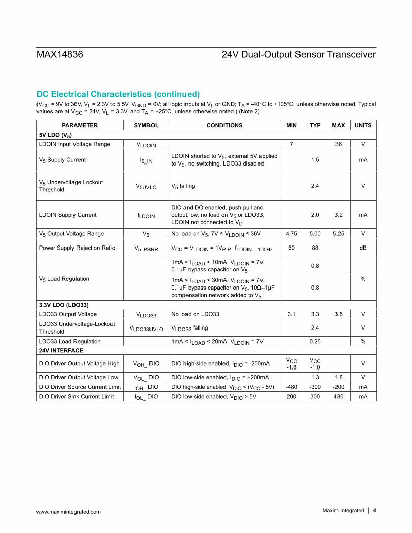
(VCC = 9V to 36V, VL = 2.3V to 5.5V, VGND = 0V; all logic inputs at VL or GND; TA = -40NC to +105NC, unless otherwise noted. Typical values are at VCC = 24V, VL = 3.3V, and TA = +25NC, unless otherwise noted.) (Note 2)
PARAMETER SYMBOL CONDITIONS MIN TYP MAX UNITS5V LDO (V5)LDOIN Input Voltage Range VLDOIN 7 36 V
V5 Supply Current I5_INLDOIN shorted to V5, external 5V applied to V5, no switching, LDO33 disabled 1.5 mA
V5 Undervoltage Lockout Threshold V5UVLO V5 falling 2.4 V
LDOIN Supply Current ILDOIN
DIO and DO enabled, push-pull and output low, no load on V5 or LDO33, LDOIN not connected to VD
2.0 3.2 mA
V5 Output Voltage Range V5 No load on V5, 7V ≤ VLDOIN ≤ 36V 4.75 5.00 5.25 V
Power Supply Rejection Ratio V5_PSRR VCC = VLDOIN = 1VP-P, fLDOIN = 100Hz 60 88 dB
V5 Load Regulation
1mA < ILOAD < 10mA, VLDOIN = 7V, 0.1µF bypass capacitor on V5
0.8
%1mA < ILOAD < 30mA, VLDOIN = 7V, 0.1µF bypass capacitor on V5, 10Ω–1µF compensation network added to V5
0.8
3.3V LDO (LDO33)LDO33 Output Voltage VLDO33 No load on LDO33 3.1 3.3 3.5 V
LDO33 Undervoltage-Lockout Threshold VLDO33UVLO VLDO33 falling 2.4 V
LDO33 Load Regulation 1mA < ILOAD < 20mA, VLDOIN = 7V 0.25 %24V INTERFACE
DIO Driver Output Voltage High VOH_ DIO DIO high-side enabled, IDIO = -200mA VCC -1.8
VCC -1.0 V
DIO Driver Output Voltage Low VOL_ DIO DIO low-side enabled, IDIO = +200mA 1.3 1.8 V
DIO Driver Source Current Limit IOH_ DIO DIO high-side enabled, VDIO < (VCC - 5V) -480 -300 -200 mA
DIO Driver Sink Current Limit IOL_ DIO DIO low-side enabled, VDIO > 5V 200 300 480 mA
DC Electrical Characteristics (continued)
MAX14836 24V Dual-Output Sensor Transceiver
www.maximintegrated.com Maxim Integrated 4
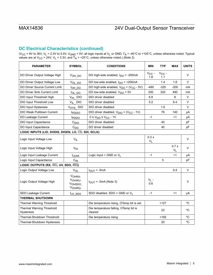
(VCC = 9V to 36V, VL = 2.3V to 5.5V, VGND = 0V; all logic inputs at VL or GND; TA = -40NC to +105NC, unless otherwise noted. Typical values are at VCC = 24V, VL = 3.3V, and TA = +25NC, unless otherwise noted.) (Note 2)
PARAMETER SYMBOL CONDITIONS MIN TYP MAX UNITS
DO Driver Output Voltage High VOH_DO DO high-side enabled, IDO = -200mA VCC - 1.8
VCC - 1.1 V
DO Driver Output Voltage Low VOL_DO DO low-side enabled, IDO = +200mA 1.4 1.8 V
DO Driver Source Current Limit IOH_DO DO high-side enabled, VDO < (VCC - 5V) -490 -320 -200 mA
DO Driver Sink Current Limit IOL_DO DO low-side enabled, VDO > 5V 200 320 490 mA
DIO Input Threshold High VIH_ DIO DIO driver disabled 6.8 8 V
DIO Input Threshold Low VIL_ DIO DIO driver disabled 5.2 6.4 V
DIO Input Hysteresis VHYS_ DIO DIO driver disabled 1.6 V
DIO Weak Pulldown Current IPDDIO DIO driver disabled, VDIO = (VCC - 1V) 76 140 µA
DO Leakage Current IPDDO 0 ≤ VDO ≤ VCC - 1V -1 +1 µA
DIO Input Capacitance CDIO DIO driver disabled 40 pF
DO Input Capacitance CDO DO driver disabled 40 pF
LOGIC INPUTS (LIO, DODIS, DIOEN, LO, CS, SDI, SCLK)
Logic Input Voltage Low VIL0.3 x VL
V
Logic Input Voltage High VIH0.7 x VL
V
Logic Input Leakage Current ILEAK Logic input = GND or VL -1 +1 µA
Logic Input Capacitance CIN 5 pF
LOGIC OUTPUTS (RX, WU, UV, SDO, IRQ)Logic Output Voltage Low VOL IOUT = -5mA 0.4 V
Logic Output Voltage High
VOHRX, VOHWU, VOHSDO, VOHIRQ,
IOUT = -5mA (Note 3) VL - 0.6 V
SDO Leakage Current ILK_SDO SDO disabled, SDO = GND or VL -1 +1 µA
THERMAL SHUTDOWNThermal Warning Threshold Die temperature rising, OTemp bit is set +127 ºC
Thermal Warning Threshold Hysteresis
Die temperature falling, OTemp bit is cleared 23 ºC
Thermal-Shutdown Threshold Die temperature rising +165 ºC
Thermal-Shutdown Hysteresis 20 ºC
DC Electrical Characteristics (continued)
MAX14836 24V Dual-Output Sensor Transceiver
www.maximintegrated.com Maxim Integrated 5
(VCC = 9V to 36V, VL = 2.3V to 5.5V, VGND = 0V; all logic inputs at VL or GND; TA = -40NC to +105NC, unless otherwise noted. Typical values are at VCC = 24V, VL = 3.3V, and TA = +25NC, unless otherwise noted.) (Note 2)
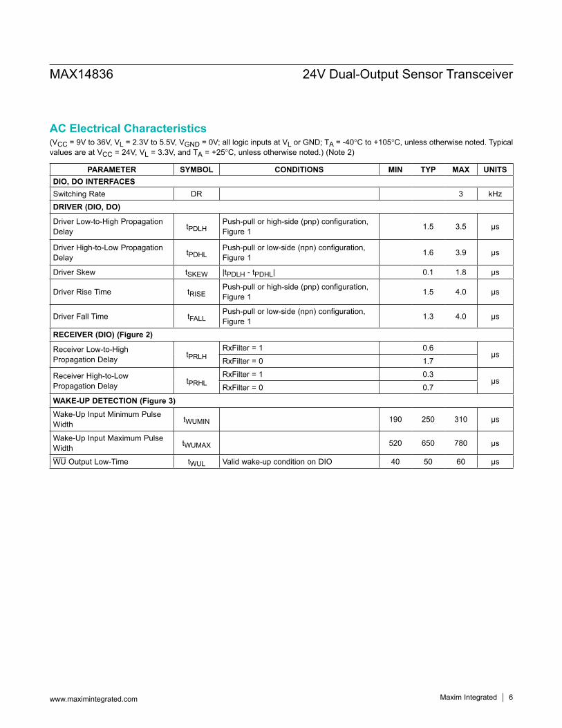
PARAMETER SYMBOL CONDITIONS MIN TYP MAX UNITSDIO, DO INTERFACESSwitching Rate DR 3 kHz
DRIVER (DIO, DO)
Driver Low-to-High Propagation Delay tPDLH
Push-pull or high-side (pnp) configuration, Figure 1 1.5 3.5 µs
Driver High-to-Low Propagation Delay tPDHL
Push-pull or low-side (npn) configuration, Figure 1 1.6 3.9 µs
Driver Skew tSKEW |tPDLH - tPDHL| 0.1 1.8 µs
Driver Rise Time tRISEPush-pull or high-side (pnp) configuration, Figure 1 1.5 4.0 µs
Driver Fall Time tFALLPush-pull or low-side (npn) configuration, Figure 1 1.3 4.0 µs
RECEIVER (DIO) (Figure 2)
Receiver Low-to-High Propagation Delay tPRLH
RxFilter = 1 0.6µs
RxFilter = 0 1.7
Receiver High-to-Low Propagation Delay tPRHL
RxFilter = 1 0.3µs
RxFilter = 0 0.7
WAKE-UP DETECTION (Figure 3)Wake-Up Input Minimum Pulse Width tWUMIN 190 250 310 µs
Wake-Up Input Maximum Pulse Width tWUMAX 520 650 780 µs
WU Output Low-Time tWUL Valid wake-up condition on DIO 40 50 60 µs
AC Electrical Characteristics
MAX14836 24V Dual-Output Sensor Transceiver
www.maximintegrated.com Maxim Integrated 6

Note 2: All devices are 100% production tested at TA = +25NC. Limits over the operating temperature range are guaranteed by design.
Note 3: UV is an open-drain output. Connect UV to a voltage less than 5.5V through an external pullup resistor.
(VCC = 9V to 36V, VL = 2.3V to 5.5V, VGND = 0V; all logic inputs at VL or GND; TA = -40NC to +105NC, unless otherwise noted. Typical values are at VCC = 24V, VL = 3.3V, and TA = +25NC, unless otherwise noted.) (Note 2)
PARAMETER SYMBOL CONDITIONS MIN TYP MAX UNITSSPI TIMING (CS, SCLK, SDI, SDO) (Figure 4)SCLK Clock Period tCH+CL 84 ns
SCLK Pulse-Width High tCH 42 ns
SCLK Pulse-Width Low tCL 42 ns
CS Fall to SCLK Rise Time tCSS 20 ns
SCLK Rise to CS Rise Hold Time tCSH 20 ns
SDI Hold Time tDH 10 ns
SDI Setup Time tDS 10 ns
SDO Propagation Delay tDOVL ≥ 3.0V 32
nsVL ≥ 2.3V 36
SDO Rise and Fall Times tFT 20 ns
Minimum CS Pulse tCSW 77 ns
AC Electrical Characteristics (continued)
MAX14836 24V Dual-Output Sensor Transceiver
www.maximintegrated.com Maxim Integrated 7

Figure 2. DIO Receiver Propagation Delay
Figure 1. DIO and DO Driver Propagation Delays and Rise/Fall Times
LIO/LO
DIO/DO
LIOOR LO
DIO/DO
tPDHL
tFALL
NOTE: DRIVERS DIO AND DO ENABLED: DIODEN = 1, DIODIS = 0
tRISE
tPDLH90%
VL
VCC
0V
0V
50%
50%
10%
3.3nF 5kΩ
DIOEN/DIODIS
GND
MAX14836
RX
DIO
RX
tPRLH tPRHL
VCC
VL
0V
0V
50%
50%
15pF
GND DIOEN
MAX14836DIO
MAX14836 24V Dual-Output Sensor Transceiver
www.maximintegrated.com Maxim Integrated 8

Figure 3. Wake-Up Detection Timing
Figure 4. SPI Timing Diagram
DIOEN
LIO
NOTE: THE MAX14836 RECOGNIZES A WAKE-UP PULSE WHEN DIO IS SHORTED FROM HIGH-TO-LOW OR FROM LOW-TO-HIGH FOR tWUMIN < tWU < tWUMAX.
DIO
tWUMIN < tWU < tWUMAX
tWUL
< tWUMINNO WAKE-UP
LIO
DIOEN
GNDDIO
WU
WU
MAX14836
tCSH tCLtCSS tCH tCSH
CS
SCLK
SDI
SDO
tDStDH
tDO
MAX14836 24V Dual-Output Sensor Transceiver
www.maximintegrated.com Maxim Integrated 9

(VCC = 24V, LDOIN = VP, VL = LDO33, DIO and DO in push-pull configuration, TA = +25°C, unless otherwise noted.)
DIO DRIVER OUTPUT HIGHvs. LOAD CURRENT
MAX
1483
6 to
c01
LOAD CURRENT (mA)
V OH_
DIO
(V)
140012001000800600400200
18
19
20
21
22
23
24
170
DIOEN = VLLIO = GND
SHORT CIRCUIT ON DIOIS PULSED FOR 30µs, 50msPERIOD DIO IN PUSH-PULL
CONFIGURATION
TA = -40°CTA = +25°C
TA = +105°C
DIO DRIVER OUTPUT LOWvs. SINK CURRENT
MAX
1483
6 to
c02
SINK CURRENT (mA)
V OL_
DIO
(V)
900800700600500400300200100
1
2
3
4
5
00 1000
DIOEN = VL, LIO = VLDIO IS SHORTED HIGH
FOR 30µs, 50ms PERIODDIO IN PUSH-PULL
CONFIGURATION
TA = -40°CTA = +25°C
TA = +105°C
DO DRIVER OUTPUT HIGHvs. LOAD CURRENT
MAX
1483
6 to
c03
LOAD CURRENT (mA)
V OH_
DO (V
)
19
20
21
22
23
24
180 200 400 600 800 1000 1200 1400
DODIS = GNDLO = GND
LOAD ON DO IS PULSEDFOR 30µs, 50ms PERIOD
DO IN PUSH-PULLCONFIGURATION
TA = +105°C
TA = +25°C
TA = -40°C
DIO DRIVER OUTPUT LOWvs. SINK CURRENT
MAX
1483
6 to
c04
SINK CURRENT (mA)
V OL_
DO (V
)
900800700600500400300200100
1
2
3
4
5
00 1000
DIDIS = GND, LO = VLDO IN PUSH-PULLCONFIGURATION
DO IS SHORTED HIGH FOR30µs, WITH 50ms PERIOD
TA = -40°C
TA = +25°CTA = +105°C
DIO/DO DRIVER PROPAGATION DELAYvs. TEMPERATURE
MAX
1483
6 to
c07
TEMPERATURE (°C)
PROP
AGAT
ION
DELA
YL (µ
s)
8560-15 10 35
1.10
1.20
1.30
1.40
1.50
1.60
1.70
1.00-40 110
DIOEN = VLDODIS = GNDLIO = VLDIO/DO IS INPUSH-PULL CONFIGURATION
DIO tPDHL
DO tPDHL DIO tPDLH
DIO tPDLH
DIO/DO DRIVER OUTPUT VOLTAGE LOWvs. SUPPLY VOLTAGE
MAX
1483
6 to
c05
SUPPLY VOLTAGE (V)
OUTP
UT V
OLTA
GE LO
W (V
)
333024 2715 18 2112
0.2
0.4
0.6
0.8
1.0
1.2
1.4
1.6
1.8
2.0
09 36
DIOEN = VLDODIS = GND
DIO/DO IN PUSH-PULLCONFIGURATION
ILOAD = ±200mA
VOL_DO
VOL_DIO
DIO DRIVER OUTPUTSWITCHING (1nF LOAD)
MAX14836 toc08a
10µs/div
Ch1VLIO
2V/div
0V
0V
Ch2VDIO
5V/div
DIO/DO DRIVER OUTPUT VOLTAGE HIGHvs. SUPPLY VOLTAGE
MAX
1483
6 to
c06
SUPPLY VOLTAGE (V)
OUTP
UT V
OLTA
GE LO
W (V
)
333024 2715 18 2112
22.2
22.4
22.6
22.8
23.0
23.2
23.4
23.6
23.8
24.0
22.09 36
DIOEN = VLDODIS = GND
DIO/DO IN PUSH-PULLCONFIGURATION
ILOAD = ±200mA
VOH_DIO
VOH_DO
DIO DRIVER OUTPUTSWITCHING (3µF LOAD)
MAX14836 toc08b
400µs/div
Ch2VDIO
5V/div
0V
0V
Ch1VLIO
2V/div
Typical Operating Characteristics
MAX14836 24V Dual-Output Sensor Transceiver
Maxim Integrated 10www.maximintegrated.com
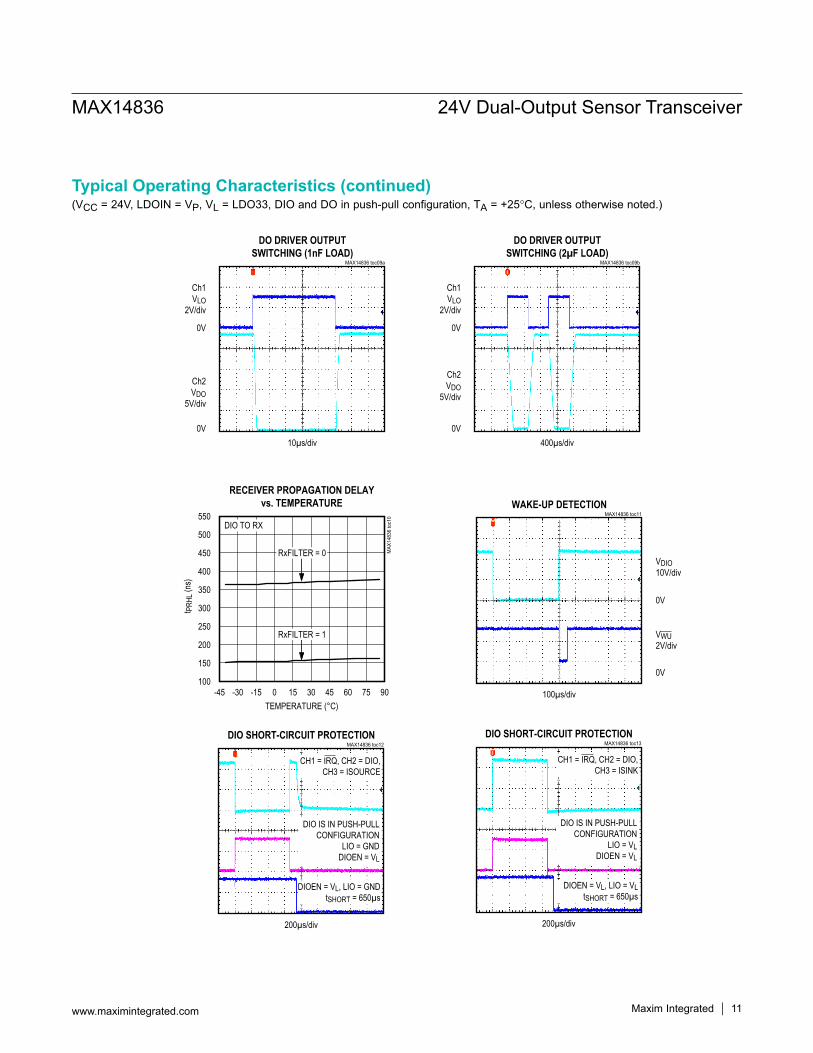
(VCC = 24V, LDOIN = VP, VL = LDO33, DIO and DO in push-pull configuration, TA = +25NC, unless otherwise noted.)
DO DRIVER OUTPUTSWITCHING (1nF LOAD)
MAX14836 toc09a
10µs/div
Ch2VDO
5V/div
0V
0V
Ch1VLO
2V/div
DO DRIVER OUTPUTSWITCHING (2µF LOAD)
MAX14836 toc09b
400µs/div
Ch2VDO
5V/div
0V
0V
Ch1VLO
2V/div
RECEIVER PROPAGATION DELAYvs. TEMPERATURE
MAX
1483
6 to
c10
TEMPERATURE (°C)
t PRHL
(ns)
756030 45-15 0 15-30
150
200
250
300
350
400
450
500
550
100-45 90
DIO TO RX
RxFILTER = 0
RxFILTER = 1
WAKE-UP DETECTIONMAX14836 toc11
100µs/div
VDIO10V/div
0V
0V
VWU2V/div
DIO SHORT-CIRCUIT PROTECTIONMAX14836 toc12
200µs/div
DIOEN = VL, LIO = GNDtSHORT = 650µs
CH1 = IRQ, CH2 = DIO,CH3 = ISOURCE
DIO IS IN PUSH-PULLCONFIGURATION
LIO = GNDDIOEN = VL
DIO SHORT-CIRCUIT PROTECTIONMAX14836 toc13
200µs/div
DIOEN = VL, LIO = VLtSHORT = 650µs
CH1 = IRQ, CH2 = DIO,CH3 = ISINK
DIO IS IN PUSH-PULLCONFIGURATION
LIO = VLDIOEN = VL
Typical Operating Characteristics (continued)
MAX14836 24V Dual-Output Sensor Transceiver
Maxim Integrated 11www.maximintegrated.com

(VCC = 24V, LDOIN = VP, VL = LDO33, DIO and DO in push-pull configuration, TA = +25NC, unless otherwise noted.)
V5 LOAD REGULATION
MAX
1483
6 to
c14
LOAD CURRENT (mA)
% V
OLTA
GE C
HANG
E
252015105
-0.45
-0.40
-0.35
-0.30
-0.25
-0.20
-0.15
-0.10
-0.05
0
-0.500 30
TA = -40°C
TA = +25°C
TA = +85°CTA = +125°C
VCC SUPPLY CURRENT vs. VCC VOLTAGE
MAX
1483
6 to
c16
VCC VOLTATGE (V)
I CC
(mA)
333024 2715 18 2112
0.1
0.2
0.3
0.4
0.5
0.6
0.7
0.8
0.9
1.0
09 36
VLDOIN = 7VDIO DRIVER IS ENABLEDDO DRIVER IS ENABLED
LIO = LO = VL
TA = +25°C TA = +105°CTA = -40°C
LDO33 LOAD REGULATION
MAX
1483
6 to
c15
LOAD CURRENT (mA)
% V
OLTA
GE C
HANG
E252015105
-0.6
-0.5
-0.4
-0.3
-0.2
-0.1
0
-0.70 30
TA = -40°C
TA = +25°CTA = +85°C
TA = +125°C
ILDOIN SUPPLY CURRENTvs. ILDOIN VOLTAGE
MAX
1483
6 to
c17
VLDOIN (V)
I LDOI
N (m
A)
0.5
1.0
1.5
2.0
2.5
0333024 2715 18 21129 36
VCC = 36VDIO DRIVER IS ENABLEDDO DRIVER IS ENABLED
LIO = LO = VL
TA = -40°CTA = +25°C
TA = +105°C
Typical Operating Characteristics (continued)
MAX14836 24V Dual-Output Sensor Transceiver
Maxim Integrated 12www.maximintegrated.com
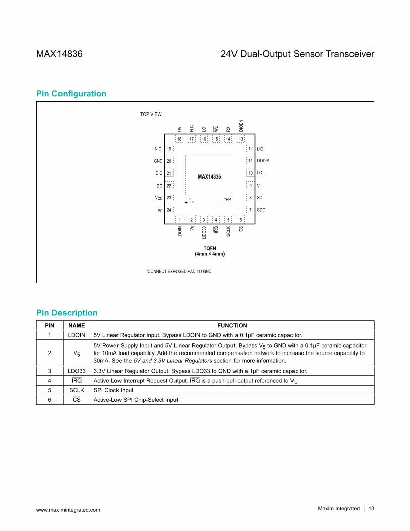
PIN NAME FUNCTION1 LDOIN 5V Linear Regulator Input. Bypass LDOIN to GND with a 0.1µF ceramic capacitor.
2 V5
5V Power-Supply Input and 5V Linear Regulator Output. Bypass V5 to GND with a 0.1µF ceramic capacitor for 10mA load capability. Add the recommended compensation network to increase the source capability to 30mA. See the 5V and 3.3V Linear Regulators section for more information.
3 LDO33 3.3V Linear Regulator Output. Bypass LDO33 to GND with a 1µF ceramic capacitor.
4 IRQ Active-Low Interrupt Request Output. IRQ is a push-pull output referenced to VL.
5 SCLK SPI Clock Input
6 CS Active-Low SPI Chip-Select Input
23
24
22
21
8
7
9V 5 IRQ
SCLK CS
10LD
OIN
N.C.
WU
RXUV DIOE
N
1 2
DO
4 5 6
1718 16 14 13
VCC
VP
I.C.
VL
SDI
SDO
*EP
*CONNECT EXPOSED PAD TO GND.
LDO3
3LO
3
15
DIO
20 11 DODISGND
19 12 LION.C.
TQFN(4mm × 4mm)
TOP VIEW
+
MAX14836
Pin Configuration
Pin Description
MAX14836 24V Dual-Output Sensor Transceiver
www.maximintegrated.com Maxim Integrated 13
PIN NAME FUNCTION7 SDO SPI Serial-Data Output
8 SDI SPI Serial-Data Input
9 VLLogic-Level Supply Input. VL defines the logic levels on all the logic inputs and outputs. Bypass VL to GND with a 0.1µF ceramic capacitor.
10 I.C. Internally Connected. Connect to VL or leave unconnected. It is recommended to connect to VL.
11 DODIS DO Driver Disable Input. Drive DODIS low to enable the DO driver. Drive DODIS high to disable the DO drive.
12 LIO DIO Input. The logic on the DIO output is the inverse logic level of the signals on the LIO inputs.
13 DIOEN DIO Driver Enable. Drive DIOEN high to enable the DIO transmitter. DIOEN is referenced to VL
14 RX DIO Output. RX is the inverse logic level of DIO. RX is always high when the RxDis bit in the DIOConfig register is set to 1.
15 WU Active-Low Wake-Up Output. WU is a push-pull output referenced to VL. WU pulses low for 50µs (typ) when a valid wake-up pulse is detected on the DIO line.
16 LO Logic Input of the DO Output. LO is the logic input that drives DO. LO is referenced to VL.
17, 19 N.C. Not Connected. Leave N.C. unconnected.
18 UV Open-Drain Undervoltage Indicator Output. In case of an undervoltage, the UV open-drain transistor is off.
20 GND Ground
21 DIODriver Input/Output. Drive DIOEN high to enable the DIO driver. The logic on the DIO output is the inverse logic level of the signals on the LIO. RX is the logic inverse of DIO. The DIO driver output level can be set by the LIO input or programmed by the Q bit. The level on DIO can be read by the RX output or the QLvl bit.
22 DO 24V Logic-Level Digital Output. DO is the inverse logic level of the LO input and can be digitally-controlled through the DIOConfig register.
23 VCC Power-Supply Input. Bypass VCC to GND with a 1µF ceramic capacitor.
24 VPProtected 24V Supply Output. VP is one diode drop below VCC. VP is reverse-polarity protected and can be used as a 24V protected supply to the sensor.
— EP Exposed Pad. Connect EP to GND.
Pin Description (continued)
MAX14836 24V Dual-Output Sensor Transceiver
www.maximintegrated.com Maxim Integrated 14

Detailed DescriptionThe MAX14836 is a dual-sensor driver. The device con-tains two 24V digital outputs. Two internal linear regula-tors generate common sensor voltages.The device detects short-circuit wake-up conditions on the DIO line and generates a wake-up signal on the WU output. The DIO and DO drivers are independently-config-urable to any one of three driver output types: push-pull, high-side (pnp), or low-side (npn).The device is configured and monitored through an SPI™ interface. Extensive alarms are available through SPI.
24V InterfaceThe device features an IO transceiver interface capable of operating with voltages up to 36V. This is the 24V interface and includes the DIO input/output, the logic-level digital output (DO).
Configurable DriversThe device features selectable push-pull, high-side (pnp), or low-side (npn) switching drivers at DIO and DO.Set the DIO_N/P and DIO_PP bits in the DIOConfig register to select the driver mode for the DIO driver. When configured as a push-pull output, DIO switches between VP and ground. Set the DIO_PP bit to 1 to select push-pull operation at DIO. Set the DIO_PP bit to 0 to configure the DIO output for open-drain operation. The DIO_N/P bit selects npn or pnp operation when DIO is configured as an open-drain output.Set the DoN/P and DoPP bits in the DOConfig regis-ter to select the driver mode for the DO output. When configured as a push-pull output, DO switches between VCC and ground. Set the DoPP bit to 1 for push-pull oper-ation. The DoN/P bit selects npn or pnp operation when DO is configured as an open-drain output. Set the DoPP bit to 0 to select high-side or low-side operation at DO.
DIO Driver and ReceiverThe DIOEN input enables the DIO driver. Drive DIOEN high to enable the DIO driver. Drive DIOEN low to disable the driver.The device’s DIO driver is specified for 200mA to drive current to large capacitive loads of up to 3FF and dynamic impedances like incandescent lamps.
The DIO receiver is always on. Disable the RX output through the RxDis bit in the DIOConfig register. Set the RxDis bit to 1 to set the RX output high. Set the RxDis bit to 0 for normal receive operation.The DIO receiver has an analog lowpass filter to reduce high-frequency noise present on the line. Set the RxFilter bit in the DIOConfig register to 0 to set the filter corner frequency to 250kHz (typ). Set the RxFilter bit to 1 to set the corner frequency of the filter to 500MHz (typ). Noise filter is present on the DIO receiver and controlled simul-taneously by the RxFilter bit.
DIO Fault DetectionThe device registers a DIOFault condition when it detects a short circuit for longer than 650µs (typ). A short condi-tion exists when DIO driver’s VOH or VOL exceeds 2.8V (typ).When a DIOFault error occurs, the DIOFault and DIOFaultInt bits are set, IRQ asserts, and the driver is turned off 650µs (typ) blanking time after the start of the fault condition.When a short-circuit event occurs on DIO, the driver enters autoretry mode. In autoretry mode, the device periodically checks whether the short is still present and attempts to correct the driver output. Autoretry attempts last for 770µs (typ) and occur every 26ms (typ).
DO Fault DetectionThe device registers a DoFault event when a short-circuit is present at the DO output for 440µs. A short condition exists when the DO driver’s VOH or VOL exceeds the 2.8V (typ). When a short-circuit condition is detected, the DO driver enters autoretry mode. In autoretry mode, the device periodically checks whether the overcurrent is still present. Autoretry attempts last for 440µs (typ) and occur every 26ms (typ). When a DoFault error is detected, the DoFault and DoFaultInt bits are set, IRQ asserts, and the driver is turned off 440µs (typ) after the start of the DO faults.
Reverse-Polarity ProtectionThe device is protected against reverse-polarity connec-tions on VCC, DIO, DO, DI, and GND. Any combination of these pins can be connected to DC voltages up to 40V (max). A short to 40V results in a current flow of less than 500FA.Ensure that the maximum voltage between any of these pins does not exceed 40V.
MAX14836 24V Dual-Output Sensor Transceiver
www.maximintegrated.com Maxim Integrated 15
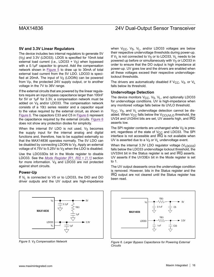
5V and 3.3V Linear RegulatorsThe device includes two internal regulators to generate 5V (V5) and 3.3V (LDO33). LDO5 is specified for 10mA total external load current (i.e., LDO33 + V5) when bypassed with a 0.1µF capacitor to ground. Add the compensation network shown in Figure 5 to draw up to 30mA of total external load current from the 5V LDO. LDO33 is speci-fied at 20mA. The input of V5 (LDOIN) can be powered from VP, the protected 24V supply output, or to another voltage in the 7V to 36V range.If the external circuits that are powered by the linear regula-tors require an input bypass capacitance larger than 100nF for 5V or 1µF for 3.3V, a compensation network must be added on V5 and/or LDO33. The compensation network consists of a 10W series resistor and a capacitor equal to the value required by the external circuit, as shown in Figure 6. The capacitors C33 and C5 in Figure 6 represent the capacitance required by the external circuits. Figure 6 does not show any protection diodes for simplicity.When the internal 5V LDO is not used, V5 becomes the supply input for the internal analog and digital functions and, therefore, has to be supplied externally so that the MAX14836 operates normally. The 5V LDO can be disabled by connecting LDOIN to V5. Apply an external voltage of 4.75V to 5.25V to V5 when the LDO is disabled. Use the LDO33Dis bit in the Mode register to disable LDO33. See the Mode Register [R1, R0] = [1,1] section for more information. V5 and LDO33 are not protected against short circuits.
Power-UpIf VL is connected to V5 or to LDO33, the DIO and DO driver outputs and the UV output are high-impedance
when VCC, V5, VL, and/or LDO33 voltages are below their respective undervoltage thresholds during power-up. If VL is not connected to V5 or to LDO33, VL needs to be powered up before or simultaneously with V5 or LDO33 in order to ensure that the DO output is high impedance at power-up. UV goes low and the drivers are enabled when all these voltages exceed their respective undervoltage-lockout thresholds.The drivers are automatically disabled if VCC, V5, or VL falls below its threshold.
Undervoltage DetectionThe device monitors VCC, V5, VL, and optionally LDO33 for undervoltage conditions. UV is high-impedance when any monitored voltage falls below its UVLO threshold.VCC, V5, and VL undervoltage detection cannot be dis-abled. When VCC falls below the VCCUVLO threshold, the UV24 and UV24Int bits are set, UV asserts high, and IRQ asserts low. The SPI register contents are unchanged while V5 is pres-ent, regardless of the state of VCC and LDO33. The SPI interface is not accessible and IRQ is not available when UV is asserted due to a V5 or VL undervoltage event.When the internal 3.3V LDO regulator voltage (VLDO33) falls below the LDO33 undervoltage lockout threshold, the UV33Int bit in the Status register is set and IRQ asserts. UV asserts if the UV33En bit in the Mode register is set to 1.The UV output deasserts once the undervoltage condition is removed. However, bits in the Status register and the IRQ output are not cleared until the Status register has been read.
Figure 6. Larger Bypass Capacitance for Powering External Circuits
Figure 5. V5 Compensation Network
MAX14836
V5
0.1∝F
10W
3.3V
5V
LDO33
C5
1∝F
10W
C33
MAX1483610Ω
0.1µF
1µF
1µF
V5
VL
5V
LDO33 3.3V
MAX14836 24V Dual-Output Sensor Transceiver
www.maximintegrated.com Maxim Integrated 16

Wake-Up DetectionThe device detects a wake-up condition on the DIO line in push-pull, high-side (pnp), or low-side (npn) operation modes. A wake-up condition is detected when the DIO output is shorted for 410Fs (typ). WU pulses low for 50Fs (typ) when the device detects a wake-up pulse on DIO (Figure 3).Set the WuIntEn bit in the Mode register to set the WuInt bit in the Status register and generate an interrupt on IRQ when a wake-up pulse is detected. WuInt is set and IRQ asserts immediately after DIO is released when WuIntEn = 1.
Thermal Protection and ConsiderationsThe internal LDOs and drivers can generate more power than the package for the devices can safely dissipate. Ensure that the driver and LDO loading is less than the package can dissipate. Total power dissipation for the device is calculated using the following equation:
PTOTAL = PDIO + PDO + P5 + PLDO33 + PQwhere PDIO is the power generated in the DIO driver, PDO is the power dissipated by the DO driver, P5 and PLDO33 are the power generated by the LDOs, PQ is the quies-cent power generated by the MAX14836.Ensure that the total power dissipation is less than the limits listed in the Absolute Maximum Ratings section.Use the following to calculate the power dissipation (in mW) due to the DIO driver:
PDIO = [IDIO(max)] × [VO_(max)] where VO_ = the larger of VOL_DIO and VOH_DIO(See the Typical Operating Characteristics on page 11.)
Calculate the internal power dissipation of the DO driver using the following equation:
PDO = [IDO(max)] × [VO_(max)]Calculate the power dissipation in the 5V LDO (V5) using the following equation:
P5 = (VLDOIN - V5) × I5where I5 VO_ includes the ILDO33 current sourced from LDO33.Calculate the power dissipated in the 3.3V LDO (LDO33) using the following equation:
PLDO33 = 1.7V × ILDO33Calculate the quiescent power dissipation in the device using the following equation:
PQ = ICC(max) × VCC(max)
Overtemperature WarningBits in the Status and Mode registers are set when the temperature of the device exceeds +125NC (typ). The OTempInt bit in the Status register is set and IRQ asserts when the OTemp bit in the Mode register is set. Read the Status register to clear the OTempInt bit and IRQ.The OTemp bit is cleared when the die temperature falls to +102NC.The device continues to operate normally unless the die temperature reaches the +165NC thermal-shutdown threshold, when the device enters thermal shutdown.
Thermal ShutdownAll regulators and the DIO and DO output drivers are automatically switched off when the internal die tempera-ture exceeds the +165NC (typ) thermal-shutdown thresh-old. SPI communication is available, and register content is maintained, during a thermal shutdown event.
MAX14836 24V Dual-Output Sensor Transceiver
www.maximintegrated.com Maxim Integrated 17
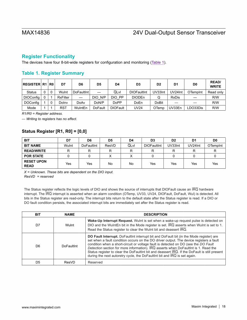
Status Register [R1, R0] = [0,0]
Register FunctionalityThe devices have four 8-bit-wide registers for configuration and monitoring (Table 1).
R1/R0 = Register address.— Writing to registers has no effect.
Table 1. Register Summary
REGISTER R1 R0 D7 D6 D5 D4 D3 D2 D1 D0 READ/ WRITE
Status 0 0 WuInt DoFaultInt — QLvl DIOFaultInt UV33Int UV24Int OTempInt Read onlyDIOConfig 0 1 RxFilter — DIO_N/P DIO_PP DIODEn Q RxDis — R/WDOConfig 1 0 DoInv DoAv DoN/P DoPP DoEn DoBit — — R/W
Mode 1 1 RST WuIntEn DoFault DIOFault UV24 OTemp UV33En LDO33Dis R/W
BIT D7 D6 D5 D4 D3 D2 D1 D0BIT NAME WuInt DoFaultInt ResVD QLvl DIOFaultInt UV33Int UV24Int OTempIntREAD/WRITE R R R R R R R RPOR STATE 0 0 X X 0 0 0 0RESET UPON READ Yes Yes No No Yes Yes Yes Yes
X = Unknown. These bits are dependent on the DIO input.ResVD = reserved
The Status register reflects the logic levels of DIO and shows the source of interrupts that DIOFault cause an IRQ hardware interrupt. The IRQ interrupt is asserted when an alarm condition (OTemp, UV33, UV24, DIOFault, DoFault, WuI) is detected. All bits in the Status register are read-only. The interrupt bits return to the default state after the Status register is read. If a DIO or DO fault condition persists, the associated interrupt bits are immediately set after the Status register is read.
BIT NAME DESCRIPTION
D7 WulntWake-Up Interrupt Request. WuInt is set when a wake-up request pulse is detected on DIO and the WuIntEn bit in the Mode register is set. IRQ asserts when WuInt is set to 1. Read the Status register to clear the WuInt bit and deassert IRQ.
D6 DoFaultInt
DO Fault Interrupt. DoFaultInt interrupt bit and DoFault bit (in the Mode register) are set when a fault condition occurs on the DO driver output. The device registers a fault condition when a short-circuit or voltage fault is detected on DO (see the DO Fault Detection section for more information). IRQ asserts when DoFaultInt is 1. Read the Status register to clear the DoFaultInt bit and deassert IRQ. If the DoFault is still present during the next autoretry cycle, the DoFaultInt bit and IRQ is set again.
D5 ResVD Reserved
MAX14836 24V Dual-Output Sensor Transceiver
www.maximintegrated.com Maxim Integrated 18

Table 2. DO Driver Enable, Disable Table 3. QLvl and RX Output
X = Don’t care.
DODIS Pin DOEn Bit DO StateLow x Enabled
High 0 Disabled
High 1 Enabled
VDIO (V) QLvl BIT RX OUTPUT< 5.2 1 High
> 8 0 Low
BIT NAME DESCRIPTION
D4 QLvl
DIO Logic Level. The QLvl bit is the inverse of the logic level at DIO. QLvl is 1 when the DIO input level is low (< 5.2V) and is 0 when the DIO logic level is high (> 8V) (Table 3). QLvl remains active when the DIO receiver is disabled (RxDis = 1). QLvl does not affect IRQ. QLvl is not changed when the Status register is read.
D3 DIOFaultInt
DIO Fault Interrupt. The DIOFaultInt interrupt bit and DIOFault bit (in the Mode register) are set when a short circuit or voltage fault occurs on the DIO driver output (see the DIO Fault Detection section for more information). IRQ asserts when DIOFault is 1. Read the Status register to clear the DIOFaultInt bit and deassert IRQ. If DIO fault is still present during the next autoretry cycle, the DIOFault bit and IRQ is set again.
D2 UV33Int
Internal 3.3V LDO (LDO33) Undervoltage Warning. Both the UV33Int interrupt bit and the UV33En bit (in the Mode register) are set when VLDO33 falls below the 2.4V LDO33 undervoltage threshold. If UV33En is set in the Mode register, IRQ asserts low when the UV33Int bit is 1. Read the Status register to clear the UV33Int bit and deassert IRQ. Set the UV33En bit to 1 in the Mode register to enable undervoltage monitoring for UV33Int. When enabled, UV asserts high when the UV33Int bit is 1. UV deasserts when VLDO33 rises above the LDO33 undervoltage threshold.
D1 UV24Int
VCC Undervoltage Interrupt. The UV24Int interrupt bit and the UV24 bit (in the Mode register) are set when the VCC voltage falls below the 6V undervoltage threshold. IRQ asserts low when the UV24Int bit is 1. Read the Status register to clear the UV24Int bit and deassert IRQ. VCC undervoltage detection cannot be disabled.
D0 OTempInt
Overtemperature Warning. The OTempInt interrupt bit and the OTemp bit (in the Mode register) are set when a high-temperature condition is detected by the devices. OTemp is set when the temperature of the die exceeds +125°C (typ). OTempInt is set and IRQ asserts when the OTemp bit is 1. The OTempInt bit is cleared and IRQ deasserts when the Status register is read. Once cleared, OTempInt is not reset if the die temperature remains above the thermal-warning threshold and does not fall below +102°C.
MAX14836 24V Dual-Output Sensor Transceiver
www.maximintegrated.com Maxim Integrated 19
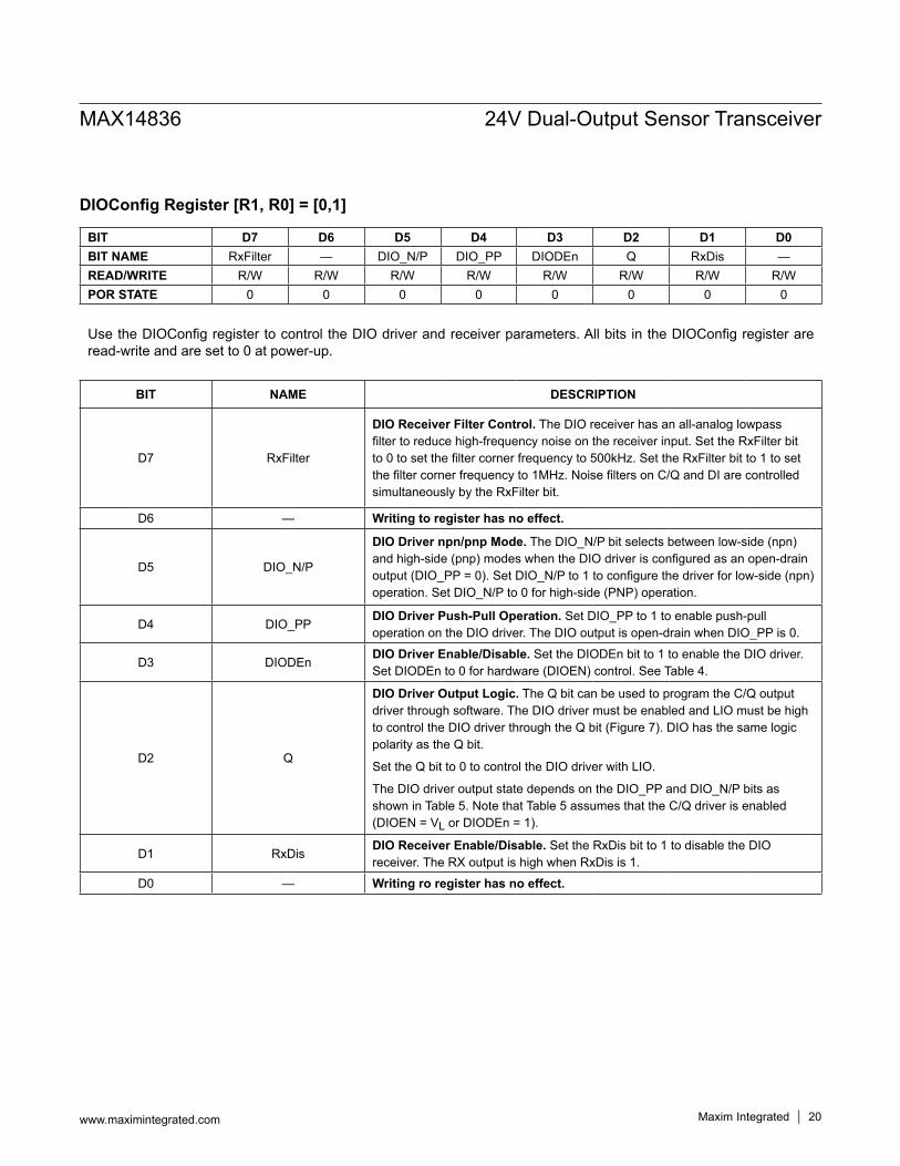
DIOConfig Register [R1, R0] = [0,1]
BIT D7 D6 D5 D4 D3 D2 D1 D0BIT NAME RxFilter — DIO_N/P DIO_PP DIODEn Q RxDis —READ/WRITE R/W R/W R/W R/W R/W R/W R/W R/WPOR STATE 0 0 0 0 0 0 0 0
Use the DIOConfig register to control the DIO driver and receiver parameters. All bits in the DIOConfig register are read-write and are set to 0 at power-up.
BIT NAME DESCRIPTION
D7 RxFilter
DIO Receiver Filter Control. The DIO receiver has an all-analog lowpass filter to reduce high-frequency noise on the receiver input. Set the RxFilter bit to 0 to set the filter corner frequency to 500kHz. Set the RxFilter bit to 1 to set the filter corner frequency to 1MHz. Noise filters on C/Q and DI are controlled simultaneously by the RxFilter bit.
D6 — Writing to register has no effect.
D5 DIO_N/P
DIO Driver npn/pnp Mode. The DIO_N/P bit selects between low-side (npn) and high-side (pnp) modes when the DIO driver is configured as an open-drain output (DIO_PP = 0). Set DIO_N/P to 1 to configure the driver for low-side (npn) operation. Set DIO_N/P to 0 for high-side (PNP) operation.
D4 DIO_PPDIO Driver Push-Pull Operation. Set DIO_PP to 1 to enable push-pull operation on the DIO driver. The DIO output is open-drain when DIO_PP is 0.
D3 DIODEnDIO Driver Enable/Disable. Set the DIODEn bit to 1 to enable the DIO driver. Set DIODEn to 0 for hardware (DIOEN) control. See Table 4.
D2 Q
DIO Driver Output Logic. The Q bit can be used to program the C/Q output driver through software. The DIO driver must be enabled and LIO must be high to control the DIO driver through the Q bit (Figure 7). DIO has the same logic polarity as the Q bit.
Set the Q bit to 0 to control the DIO driver with LIO.
The DIO driver output state depends on the DIO_PP and DIO_N/P bits as shown in Table 5. Note that Table 5 assumes that the C/Q driver is enabled (DIOEN = VL or DIODEn = 1).
D1 RxDisDIO Receiver Enable/Disable. Set the RxDis bit to 1 to disable the DIO receiver. The RX output is high when RxDis is 1.
D0 — Writing ro register has no effect.
MAX14836 24V Dual-Output Sensor Transceiver
www.maximintegrated.com Maxim Integrated 20
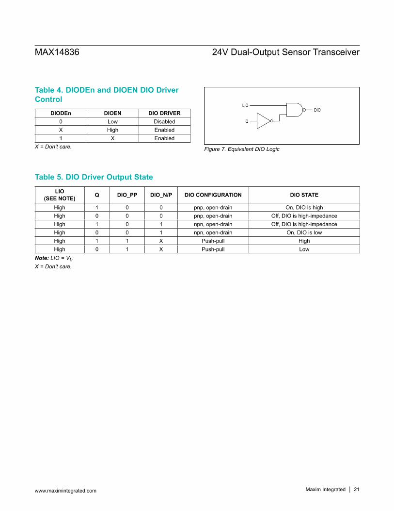
Table 5. DIO Driver Output State
Table 4. DIODEn and DIOEN DIO Driver Control
Note: LIO = VL.X = Don’t care.
X = Don’t care. Figure 7. Equivalent DIO Logic
DIODEn DIOEN DIO DRIVER0 Low DisabledX High Enabled1 X Enabled
LIO (SEE NOTE) Q DIO_PP DIO_N/P DIO CONFIGURATION DIO STATE
High 1 0 0 pnp, open-drain On, DIO is highHigh 0 0 0 pnp, open-drain Off, DIO is high-impedanceHigh 1 0 1 npn, open-drain Off, DIO is high-impedanceHigh 0 0 1 npn, open-drain On, DIO is lowHigh 1 1 X Push-pull HighHigh 0 1 X Push-pull Low
LIODIO
Q
Figure 7
MAX14836 24V Dual-Output Sensor Transceiver
www.maximintegrated.com Maxim Integrated 21
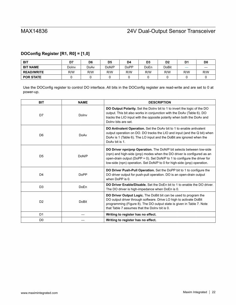
DOConfig Register [R1, R0] = [1,0]
BIT D7 D6 D5 D4 D3 D2 D1 D0BIT NAME DoInv DoAv DoN/P DoPP DoEn DoBit — —READ/WRITE R/W R/W R/W R/W R/W R/W R/W R/WPOR STATE 0 0 0 0 0 0 0 0
Use the DOConfig register to control DO interface. All bits in the DOConfig register are read-write and are set to 0 at power-up.
BIT NAME DESCRIPTION
D7 DoInv
DO Output Polarity. Set the DoInv bit to 1 to invert the logic of the DO output. This bit also works in conjunction with the DoAv (Table 6). DO tracks the LIO input with the opposite polarity when both the DoAv and DoInv bits are set.
D6 DoAv
DO Antivalent Operation. Set the DoAv bit to 1 to enable antivalent output operation on DO. DO tracks the LIO and input (and the Q bit) when DoAv is 1 (Table 6). The LO input and the DoBit are ignored when the DoAv bit is 1.
D5 DoN/P
DO Driver npn/pnp Operation. The DoN/P bit selects between low-side (npn) and high-side (pnp) modes when the DO driver is configured as an open-drain output (DoPP = 0). Set DoN/P to 1 to configure the driver for low-side (npn) operation. Set DoN/P to 0 for high-side (pnp) operation.
D4 DoPPDO Driver Push-Pull Operation. Set the DoPP bit to 1 to configure the DO driver output for push-pull operation. DO is an open-drain output when DoPP is 0.
D3 DoEnDO Driver Enable/Disable. Set the DoEn bit to 1 to enable the DO driver. The DO driver is high-impedance when DoEn is 0.
D2 DoBit
DO Driver Output Logic. The DoBit bit can be used to program the DO output driver through software. Drive LO high to activate DoBit programming (Figure 8). The DO output state is given in Table 7. Note that Table 7 assumes that the DoInv bit is 0.
D1 — Writing to register has no effect.D0 — Writing to register has no effect.
MAX14836 24V Dual-Output Sensor Transceiver
www.maximintegrated.com Maxim Integrated 22
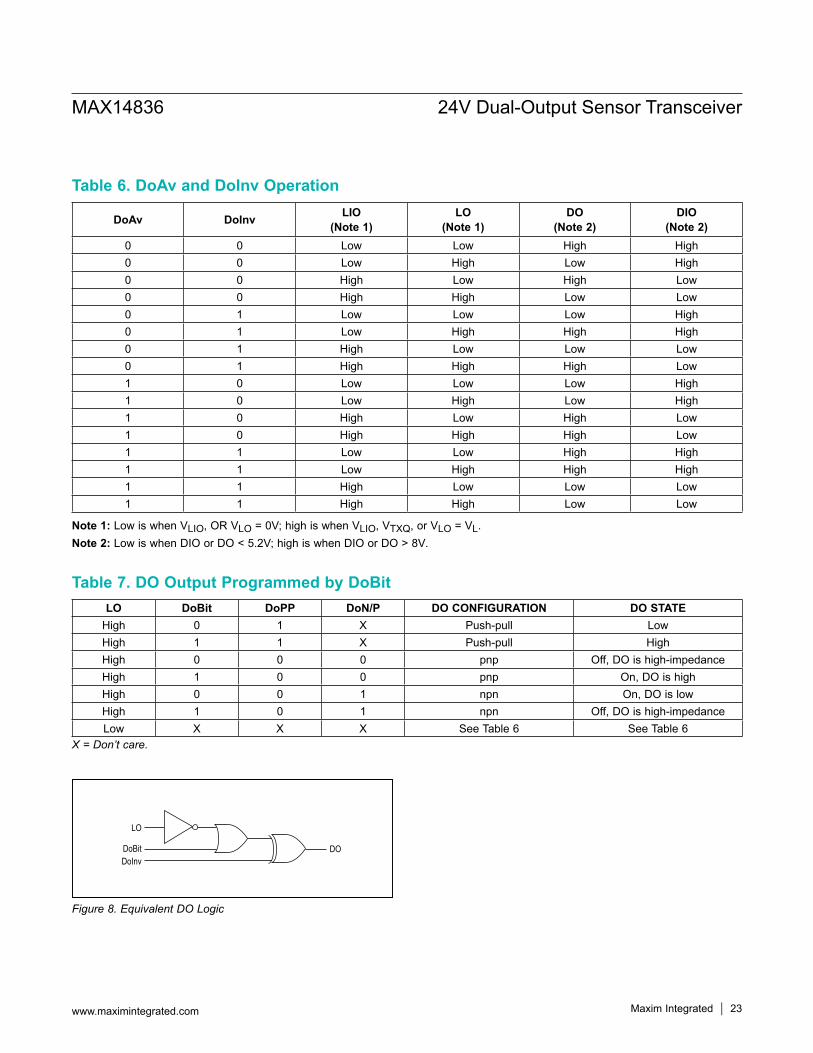
Table 6. DoAv and DoInv Operation
Table 7. DO Output Programmed by DoBit
X = Don’t care.
Figure 8. Equivalent DO Logic
Note 1: Low is when VLIO, OR VLO = 0V; high is when VLIO, VTXQ, or VLO = VL.Note 2: Low is when DIO or DO < 5.2V; high is when DIO or DO > 8V.
DoAv DoInv LIO (Note 1)
LO(Note 1)
DO(Note 2)
DIO(Note 2)
0 0 Low Low High High0 0 Low High Low High0 0 High Low High Low0 0 High High Low Low0 1 Low Low Low High0 1 Low High High High0 1 High Low Low Low0 1 High High High Low1 0 Low Low Low High1 0 Low High Low High1 0 High Low High Low1 0 High High High Low1 1 Low Low High High1 1 Low High High High1 1 High Low Low Low1 1 High High Low Low
LO DoBit DoPP DoN/P DO CONFIGURATION DO STATEHigh 0 1 X Push-pull LowHigh 1 1 X Push-pull HighHigh 0 0 0 pnp Off, DO is high-impedanceHigh 1 0 0 pnp On, DO is highHigh 0 0 1 npn On, DO is lowHigh 1 0 1 npn Off, DO is high-impedanceLow X X X See Table 6 See Table 6
LO
DoBit DODoInv
MAX14836 24V Dual-Output Sensor Transceiver
www.maximintegrated.com Maxim Integrated 23
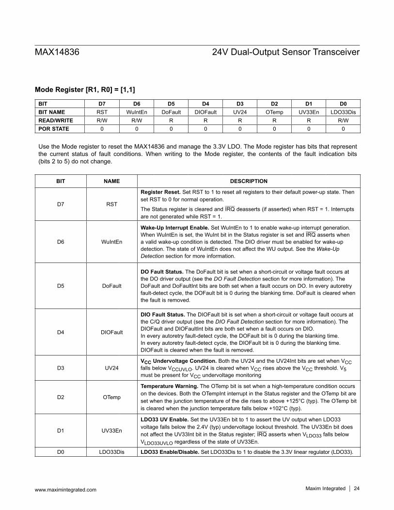
Mode Register [R1, R0] = [1,1]
BIT D7 D6 D5 D4 D3 D2 D1 D0BIT NAME RST WuIntEn DoFault DIOFault UV24 OTemp UV33En LDO33DisREAD/WRITE R/W R/W R R R R R R/WPOR STATE 0 0 0 0 0 0 0 0
Use the Mode register to reset the MAX14836 and manage the 3.3V LDO. The Mode register has bits that represent the current status of fault conditions. When writing to the Mode register, the contents of the fault indication bits (bits 2 to 5) do not change.
BIT NAME DESCRIPTION
D7 RST
Register Reset. Set RST to 1 to reset all registers to their default power-up state. Then set RST to 0 for normal operation.
The Status register is cleared and IRQ deasserts (if asserted) when RST = 1. Interrupts are not generated while RST = 1.
D6 WuIntEn
Wake-Up Interrupt Enable. Set WuIntEn to 1 to enable wake-up interrupt generation. When WuIntEn is set, the WuInt bit in the Status register is set and IRQ asserts when a valid wake-up condition is detected. The DIO driver must be enabled for wake-up detection. The state of WuIntEn does not affect the WU output. See the Wake-Up Detection section for more information.
D5 DoFault
DO Fault Status. The DoFault bit is set when a short-circuit or voltage fault occurs at the DO driver output (see the DO Fault Detection section for more information). The DoFault and DoFaultInt bits are both set when a fault occurs on DO. In every autoretry fault-detect cycle, the DOFault bit is 0 during the blanking time. DoFault is cleared when the fault is removed.
D4 DIOFault
DIO Fault Status. The DIOFault bit is set when a short-circuit or voltage fault occurs at the C/Q driver output (see the DIO Fault Detection section for more information). The DIOFault and DIOFaultInt bits are both set when a fault occurs on DIO. In every autoretry fault-detect cycle, the DOFault bit is 0 during the blanking time. In every autoretry fault-detect cycle, the DIOFault bit is 0 during the blanking time. DIOFault is cleared when the fault is removed.
D3 UV24VCC Undervoltage Condition. Both the UV24 and the UV24Int bits are set when VCC falls below VCCUVLO. UV24 is cleared when VCC rises above the VCC threshold. V5 must be present for VCC undervoltage monitoring
D2 OTemp
Temperature Warning. The OTemp bit is set when a high-temperature condition occurs on the devices. Both the OTempInt interrupt in the Status register and the OTemp bit are set when the junction temperature of the die rises to above +125°C (typ). The OTemp bit is cleared when the junction temperature falls below +102°C (typ).
D1 UV33En
LDO33 UV Enable. Set the UV33En bit to 1 to assert the UV output when LDO33 voltage falls below the 2.4V (typ) undervoltage lockout threshold. The UV33En bit does not affect the UV33Int bit in the Status register; IRQ asserts when VLDO33 falls below VLDO33UVLO regardless of the state of UV33En.
D0 LDO33Dis LDO33 Enable/Disable. Set LDO33Dis to 1 to disable the 3.3V linear regulator (LDO33).
MAX14836 24V Dual-Output Sensor Transceiver
www.maximintegrated.com Maxim Integrated 24
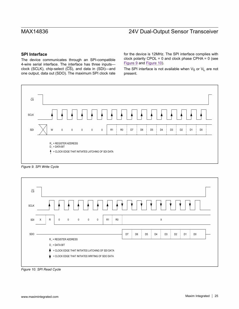
SPI InterfaceThe device communicates through an SPI-compatible 4-wire serial interface. The interface has three inputs— clock (SCLK), chip-select (CS), and data in (SDI)—and one output, data out (SDO). The maximum SPI clock rate
for the device is 12MHz. The SPI interface complies with clock polarity CPOL = 0 and clock phase CPHA = 0 (see Figure 9 and Figure 10).The SPI interface is not available when V5 or VL are not present.
Figure 9. SPI Write Cycle
Figure 10. SPI Read Cycle
R0 D7 D6 D5 D4 D3 D2 D1 D0
SCLK
R_ = REGISTER ADDRESSD_ = DATA BIT
= CLOCK EDGE THAT INITIATES LATCHING OF SDI DATA
SDI W 0 0 0 0 0 R1
CS
CS
SCLK
SDI 0 0 0 0 0 R1 R0R
D7 D6 D5 D4 D3 D2 D1 D0SDO
XX
R_ = REGISTER ADDRESS
D_ = DATA BIT
= CLOCK EDGE THAT INITIATES LATCHING OF SDI DATA
= CLOCK EDGE THAT INITIATES WRITING OF SDO DATA
MAX14836 24V Dual-Output Sensor Transceiver
www.maximintegrated.com Maxim Integrated 25

Applications InformationUART InterfacingThe logic levels of the microcontroller interface I/Os (LIO, DODIS, DIOEN, and RX) are defined by VL.
Transient ProtectionInductive load-switching, surges, and bursts create high transient voltages. DIO and DO should be protected against high overvoltage and undervoltage transients. Positive voltage transients on DIO and DO must be limited to +55V relative to GND and negative voltage transients must be limited to -55V (relative to VCC) on DO. Figure 11 shows suitable protection using TVS diodes to meet both the IEC 61000-4-2 ESD and IEC 61000-4-5 surge testing. Other protection schemes may also be suitable.The external TVS diodes can be biased via the inter-nal VP diode, or by using an external diode, as shown in Figure 12. The scheme shown in Figure 12 has the benefit of not supplying the sensor power supply when the external 24V L+ supply is not present and an external voltage is applied to DIO or DO. The device has to be protected against transients that occur during hot-plugging of the L+ sensor supply (VCC input). This is achieved by placing a 10W resistor with 1µF capacitor before LDOIN and connecting an RC between the sensor supply input and the VCC pin, as shown in
Figure 11. The RC time constant of the filter on VCC should be larger or equal to 0.8µs. In case that VL is sup-plied by V5 and the bypass capacitor on V5 is 100nF, the 10W resistor in series with LDOIN is not needed.
Optional External PoweringThe MAX14836 is powered by VCC and V5. VL is a reference voltage input to set the logic levels of the microcontroller interface. The logic and SPI interface are operational when V5 and VL are present even if VCC is not present.The VP output provides a reverse-polarity-protected voltage one diode drop below VCC and can be used for supplying external circuitry, like power supplies. The current drawn from VP cannot exceed 50mA. Be aware that capacitance on VP can cause transient currents at power-up equal to C x dVCC/dt.V5 is typically powered by the internal 5V regulator, but can alternatively be powered by an external 5V regula-tor. When powering V5 externally, connect LDOIN to V5 (Figure 12). This configuration disables operation of the internal 5V regulator and reduces power consumption. When an external 5V regulator is used to power V5, the V5 bypass capacitance is determined by that regulator, and is not limited to 100nF.
Figure 11. MAX14836 Operating Circuit with TVS Protection
MAX14836
0.8Ω
1μF
1μF
10Ω
VCCLDOIN
DO
1/2SDC36
1/2SDC36
GND
DIO
1/2SDC36
VP
MAX14836 24V Dual-Output Sensor Transceiver
www.maximintegrated.com Maxim Integrated 26
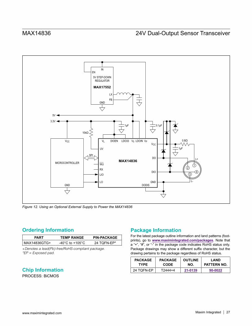
Figure 12. Using an Optional External Supply to Power the MAX14836
+Denotes a lead(Pb)-free/RoHS-compliant package.*EP = Exposed pad.
PART TEMP RANGE PIN-PACKAGEMAX14836GTG+ -40°C to +105°C 24 TQFN-EP*
PACKAGE TYPE
PACKAGE CODE
OUTLINE NO.
LAND PATTERN NO.
24 TQFN-EP T2444+4 21-0139 90-0022
12
43
10kΩ
MAX14836
0.8Ω
1μF
0.1μF1μF
VCC
UV
LDOIN
DO
LX
FBGND
SPI
IN
5V STEP-DOWNREGULATOR
EN
DIO
L+
L-GNDDODISGND
VPV5VCC LDO33VL
MICROCONTROLLER WU
RX
LIO
DIOEN
LO
3.3V
MAX17552
5V
Ordering Information
Chip InformationPROCESS: BiCMOS
Package InformationFor the latest package outline information and land patterns (foot-prints), go to www.maximintegrated.com/packages. Note that a “+”, “#”, or “-” in the package code indicates RoHS status only. Package drawings may show a different suffix character, but the drawing pertains to the package regardless of RoHS status.
MAX14836 24V Dual-Output Sensor Transceiver
www.maximintegrated.com Maxim Integrated 27
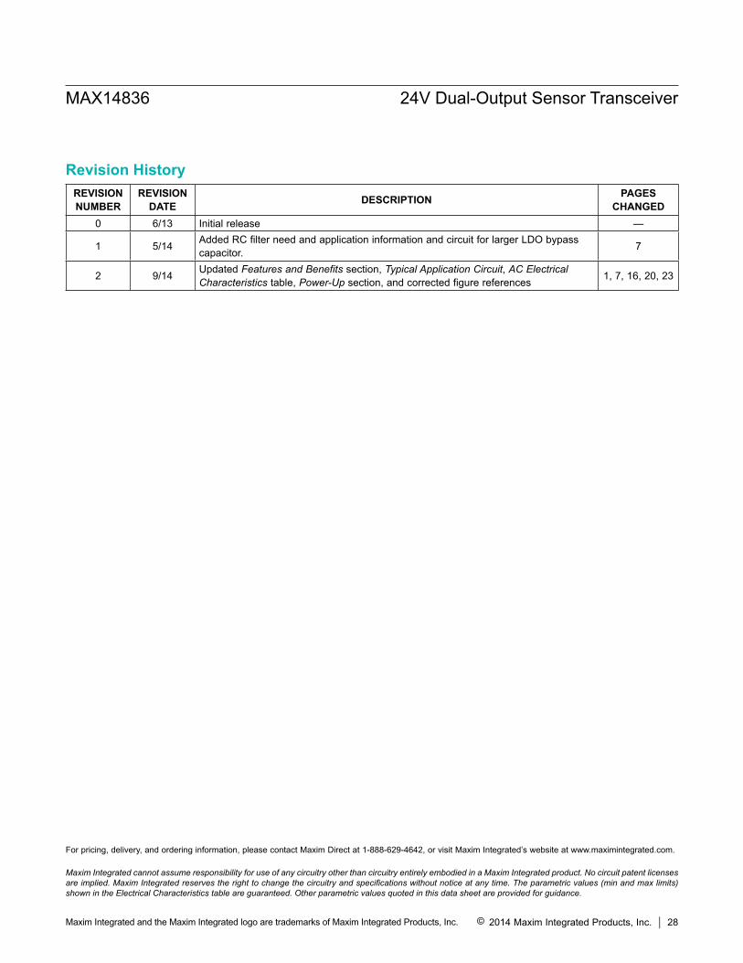
REVISIONNUMBER
REVISIONDATE DESCRIPTION PAGES
CHANGED0 6/13 Initial release —
1 5/14 Added RC filter need and application information and circuit for larger LDO bypass capacitor. 7
2 9/14 Updated Features and Benefits section, Typical Application Circuit, AC Electrical Characteristics table, Power-Up section, and corrected figure references 1, 7, 16, 20, 23
Revision History
Maxim Integrated cannot assume responsibility for use of any circuitry other than circuitry entirely embodied in a Maxim Integrated product. No circuit patent licenses are implied. Maxim Integrated reserves the right to change the circuitry and specifications without notice at any time. The parametric values (min and max limits) shown in the Electrical Characteristics table are guaranteed. Other parametric values quoted in this data sheet are provided for guidance.
Maxim Integrated and the Maxim Integrated logo are trademarks of Maxim Integrated Products, Inc.
MAX14836 24V Dual-Output Sensor Transceiver
© 2014 Maxim Integrated Products, Inc. 28
For pricing, delivery, and ordering information, please contact Maxim Direct at 1-888-629-4642, or visit Maxim Integrated’s website at www.maximintegrated.com.