Embed Size (px)
Citation preview

MAX11606–MAX11611
Low-Power, 4-/8-/12-Channel, I2C,10-Bit ADCs in Ultra-Small Packages
EVALUATION KIT AVAILABLE
19-4560; Rev 4; 7/13
For pricing, delivery, and ordering information, please contact Maxim Directat 1-888-629-4642, or visit Maxim’s website at www.maximintegrated.com.
Handheld PortableApplicationsMedical InstrumentsBattery-Powered TestEquipment
Solar-Powered RemoteSystemsReceived-Signal-StrengthIndicatorsSystem Supervision
General DescriptionThe MAX11606–MAX11611 low-power, 10-bit, multichan-nel analog-to-digital converters (ADCs) feature internaltrack/hold (T/H), voltage reference, clock, and an I2C-compatible 2-wire serial interface. These devicesoperate from a single supply of 2.7V to 3.6V (MAX11607/MAX11609/MAX11611) or 4.5V to 5.5V (MAX11606/MAX11608/MAX11610) and require only 670µA at themaximum sampling rate of 94.4ksps. Supply current fallsbelow 230µA for sampling rates under 46ksps.AutoShutdown™ powers down the devices between conver-sions, reducing supply current to less than 1µA at lowthroughput rates. The MAX11606/MAX11607 have 4 analoginput channels each, the MAX11608/MAX11609 have 8 ana-log input channels each, while the MAX11610/MAX11611have 12 analog input channels each. The fully differentialanalog inputs are software configurable for unipolar or bipo-lar, and single ended or differential operation.The full-scale analog input range is determined by theinternal reference or by an externally applied referencevoltage ranging from 1V to VDD. The MAX11607/MAX11609/MAX11611 feature a 2.048V internal referenceand the MAX11606/MAX11608/MAX11610 feature a4.096V internal reference.The MAX11606/MAX11607 are available in an 8-pinµMAX® package. The MAX11607 is also available in anultra-small 1.9mm x 2.2mm WLP package. TheMAX11608–MAX11611 are available in a 16-pin QSOPpackage. The MAX11606–MAX11611 are guaranteedover the extended temperature range (-40°C to +85°C).For pin-compatible 12-bit parts, refer to theMAX11612–MAX11617 data sheet. For pin-compatible8-bit parts, refer to the MAX11600–MAX11605 data sheet.
Applications
Features� High-Speed I2C-Compatible Serial Interface
400kHz Fast Mode1.7MHz High-Speed Mode
� Single-Supply 2.7V to 3.6V (MAX11607/MAX11609/MAX11611)4.5V to 5.5V (MAX11606/MAX11608/MAX11610)
� Ultra-Small Packages8-Pin µMAX (MAX11606/MAX11607)12-Pin 1.9mm x 2.2mm, Wafer-Level Package
(MAX11607)16-Pin QSOP (MAX11608–MAX11611)
� Internal Reference2.048V (MAX11607/MAX11609/MAX11611)4.096V (MAX11606/MAX11608/MAX11610)
� External Reference: 1V to VDD� Internal Clock� 4-Channel Single-Ended or 2-Channel Fully
Differential (MAX11606/MAX11607)� 8-Channel Single-Ended or 4-Channel Fully
Differential (MAX11608/MAX11609)� 12-Channel Single-Ended or 6-Channel Fully
Differential (MAX11610/MAX11611)� Internal FIFO with Channel-Scan Mode� Low Power
670µA at 94.4ksps230µA at 40ksps60µA at 10ksps6µA at 1ksps0.5µA in Power-Down Mode
� Software-Configurable Unipolar/Bipolar
Ordering Information
PART TEMP RANGEPIN-PACKAGE
I2C SLAVEADDRESS
MAX11606EUA+ -40°C to +85°C 8 µMAX 0110100
MAX11607EUA+ -40°C to +85°C 8 µMAX 0110100
MAX11607EWC+* -40°C to +85°C 12 WLP 0110100
MAX11608EEE+ -40°C to +85°C 16 QSOP 0110011
MAX11609EEE+ -40°C to +85°C 16 QSOP 0110011
MAX11610EEE+ -40°C to +85°C 16 QSOP 0110101
MAX11611EEE+ -40°C to +85°C 16 QSOP 0110101
AutoShutdown is a trademark of Maxim Integrated Products, Inc.µMAX is a registered trademark of Maxim Integrated Products, Inc.
+Denotes a lead(Pb)-free/RoHs-compliant package.*Future product—contact factory for availability.
Pin Configurations, Typical Operating Circuit, and SelectorGuide appear at end of data sheet.

MAX11606–MAX11611
Low-Power, 4-/8-/12-Channel, I2C,10-Bit ADCs in Ultra-Small Packages
2 Maxim Integrated
ABSOLUTE MAXIMUM RATINGS
ELECTRICAL CHARACTERISTICS(VDD = 2.7V to 3.6V (MAX11607/MAX11609/MAX11611), VDD = 4.5V to 5.5V (MAX11606/MAX11608/MAX11610), VREF = 2.048V(MAX11607/MAX11609/MAX11611), VREF = 4.096V (MAX11606/MAX11608/MAX11610), fSCL = 1.7MHz, TA = TMIN to TMAX, unless other-wise noted. Typical values are at TA = +25°C. See Tables 1–5 for programming notation.) (Note 1)
Stresses beyond those listed under “Absolute Maximum Ratings” may cause permanent damage to the device. These are stress ratings only, and functionaloperation of the device at these or any other conditions beyond those indicated in the operational sections of the specifications is not implied. Exposure toabsolute maximum rating conditions for extended periods may affect device reliability.
VDD to GND..............................................................-0.3V to +6VAIN0–AIN11,
REF to GND............-0.3V to the lower of (VDD + 0.3V) and 6VSDA, SCL to GND.....................................................-0.3V to +6VMaximum Current into Any Pin .........................................±50mAContinuous Power Dissipation (TA = +70°C)
8-Pin µMAX (derate 5.9mW/°C above +70°C) ..........470.6mW12-Pin WLP (derate 16.1mW/°C above +70°C) .........1288mW16-Pin QSOP (derate 8.3mW/°C above +70°C)........666.7mW
Operating Temperature Range ...........................-40°C to +85°CJunction Temperature ......................................................+150°CStorage Temperature Range .............................-60°C to +150°CLead Temperature (soldering, 10s) .................................+300°CSoldering Temperature (reflow) .......................................+260°C
PARAMETER SYMBOL CONDITIONS MIN TYP MAX UNITS
DC ACCURACY (Note 2)
Resolution 10 Bits
Relative Accuracy INL (Note 3) ±1 LSB
Differential Nonlinearity DNL No missing codes over temperature ±1 LSB
Offset Error ±1 LSB
Offset-Error TemperatureCoefficient
Relative to FSR 0.3 ppm/°C
Gain Error (Note 4) ±1 LSB
Gain-Temperature Coefficient Relative to FSR 0.3 ppm/°C
Channel-to-Channel OffsetMatching
±0.1 LSB
Channel-to-Channel GainMatching
±0.1 LSB
DYNAMIC PERFORMANCE (fIN(SINE-WAVE) = 10kHz, VIN(P-P) = VREF, fSAMPLE = 94.4ksps)
Signal-to-Noise Plus Distortion SINAD 60 dB
Total Harmonic Distortion THD Up to the 5th harmonic -70 dB
Spurious Free Dynamic Range SFDR 70 dB
Full-Power Bandwidth SINAD > 57dB 3.0 MHz
Full-Linear Bandwidth -3dB point 5.0 MHz
CONVERSION RATE
Internal clock 6.8Conversion Time (Note 5) tCONV
External clock 10.6µs
Internal clock, SCAN[1:0] = 01 53
Internal clock, SCAN[1:0] = 00CS[3:0] = 1011 (MAX11610/MAX11611)
53Throughput Rate fSAMPLE
External clock 94.4
ksps
Track/Hold Acquisition Time 800 ns

MAX11606–MAX11611
Low-Power, 4-/8-/12-Channel, I2C,10-Bit ADCs in Ultra-Small Packages
3Maxim Integrated
ELECTRICAL CHARACTERISTICS (continued)(VDD = 2.7V to 3.6V (MAX11607/MAX11609/MAX11611), VDD = 4.5V to 5.5V (MAX11606/MAX11608/MAX11610), VREF = 2.048V(MAX11607/MAX11609/MAX11611), VREF = 4.096V (MAX11606/MAX11608/MAX11610), fSCL = 1.7MHz, TA = TMIN to TMAX, unless other-wise noted. Typical values are at TA = +25°C. See Tables 1–5 for programming notation.) (Note 1)
PARAMETER SYMBOL CONDITIONS MIN TYP MAX UNITS
Internal Clock Frequency 2.8 MHz
External clock, fast mode 60Aperture Delay (Note 6) tAD
External clock, high-speed mode 30ns
ANALOG INPUT (AIN0–AIN11)
Unipolar 0 VREFInput-Voltage Range, Single-Ended and Differential (Note 7) Bipolar 0 ±VREF/2
V
Input Multiplexer Leakage Current On/off leakage current, VAIN_ = 0V or VDD ±0.01 ±1 µA
Input Capacitance CIN 22 pF
INTERNAL REFERENCE (Note 8)
M AX 11607/M AX11609/M AX 11611 1.968 2.048 2.128Reference Voltage VREF TA = + 25° C
M AX 11606/M AX11608/M AX 11610 3.939 4.096 4.256V
Reference-Voltage TemperatureCoefficient
TCVREF 25 ppm/°C
REF Short-Circuit Current 2 mA
REF Source Impedance 1.5 kΩEXTERNAL REFERENCE
REF Input-Voltage Range VREF (Note 9) 1 VDD V
REF Input Current IREF fSAMPLE = 94.4ksps 40 µA
DIGITAL INPUTS/OUTPUTS (SCL, SDA)
Input High Voltage VIH 0.7 x VDD V
Input Low Voltage VIL 0.3 x VDD V
Input Hysteresis VHYST 0.1 x VDD V
Input Current IIN VIN = 0 to VDD ±10 µA
Input Capacitance CIN 15 pF
Output Low Voltage VOL ISINK = 3mA 0.4 V
POWER REQUIREMENTS
MAX11607/MAX11609/MAX11611 2.7 3.6Supply Voltage VDD
MAX11606/MAX11608/MAX11610 4.5 5.5V
Internal reference 900 1150fSAMPLE = 94.4kspsexternal clock External reference 670 900
Internal reference 530fSAMPLE = 40kspsinternal clock External reference 230
Internal reference 380fSAMPLE = 10kspsinternal clock External reference 60
Internal reference 330fSAMPLE =1kspsinternal clock External reference 6
Supply Current IDD
Shutdown (internal reference off) 0.5 10
µA

MAX11606–MAX11611
Low-Power, 4-/8-/12-Channel, I2C,10-Bit ADCs in Ultra-Small Packages
4 Maxim Integrated
ELECTRICAL CHARACTERISTICS (continued)(VDD = 2.7V to 3.6V (MAX11607/MAX11609/MAX11611), VDD = 4.5V to 5.5V (MAX11606/MAX11608/MAX11610), VREF = 2.048V(MAX11607/MAX11609/MAX11611), VREF = 4.096V (MAX11606/MAX11608/MAX11610), fSCL = 1.7MHz, TA = TMIN to TMAX, unless other-wise noted. Typical values are at TA = +25°C. See Tables 1–5 for programming notation.) (Note 1)
TIMING CHARACTERISTICS (Figure 1)(VDD = 2.7V to 3.6V (MAX11607/MAX11609/MAX11611), VDD = 4.5V to 5.5V (MAX11606/MAX11608/MAX11610), VREF = 2.048V(MAX11607/MAX11609/MAX11611), VREF = 4.096V (MAX11606/MAX11608/MAX11610), fSCL = 1.7MHz, TA = TMIN to TMAX, unless other-wise noted. Typical values are at TA = +25°C. See Tables 1–5 for programming notation.) (Note 1)
PARAMETER SYMBOL CONDITIONS MIN TYP MAX UNITS
POWER REQUIREMENTS
Power-Supply Rejection Ratio PSRR Full-scale input (Note 10) ±0.01 ±0.5 LSB/V
PARAMETER SYMBOL CONDITIONS MIN TYP MAX UNITS
TIMING CHARACTERISTICS FOR FAST MODE
Serial-Clock Frequency fSCL 400 kHz
Bus Free Time Between aSTOP (P) and aSTART (S) Condition
tBUF 1.3 µs
Hold Time for START (S) Condition tHD,STA 0.6 µs
Low Period of the SCL Clock tLOW 1.3 µs
High Period of the SCL Clock tHIGH 0.6 µs
Setup Time for a Repeated STARTCondition (Sr)
tSU,STA 0.6 µs
Data Hold Time tHD,DAT (Note 11) 0 900 ns
Data Setup Time tSU,DAT 100 ns
Rise Time of Both SDA and SCLSignals, Receiving
tR Measured from 0.3VDD to 0.7VDD 20 + 0.1CB 300 ns
Fall Time of SDA Transmitting tF Measured from 0.3VDD to 0.7VDD (Note 12) 20 + 0.1CB 300 ns
Setup Time for STOP (P) Condition tSU,STO 0.6 µs
Capacitive Load for Each Bus Line CB 400 pF
Pulse Width of Spike Suppressed tSP 50 ns
TIMING CHARACTERISTICS FOR HIGH-SPEED MODE (CB = 400pF, Note 13)
Serial-Clock Frequency fSCLH (Note 14) 1.7 MHz
Hold Time, Repeated STARTCondition (Sr)
tHD,STA 160 ns
Low Period of the SCL Clock tLOW 320 ns
High Period of the SCL Clock tHIGH 120 ns
Setup Time for a Repeated STARTCondition (Sr)
tSU,STA 160 ns
Data Hold Time tHD,DAT (Note 11) 0 150 ns
Data Setup Time tSU,DAT 10 ns

MAX11606–MAX11611
Low-Power, 4-/8-/12-Channel, I2C,10-Bit ADCs in Ultra-Small Packages
5Maxim Integrated
Note 1: All WLP devices are 100% production tested at TA = +25°C. Specifications over temperature limits are guaranteed bydesign and characterization.
Note 2: For DC accuracy, the MAX11606/MAX11608/MAX11610 are tested at VDD = 5V and the MAX11607/MAX11609/MAX11611are tested at VDD = 3V. All devices are configured for unipolar, single-ended inputs.
Note 3: Relative accuracy is the deviation of the analog value at any code from its theoretical value after the full-scale range and offsets have been calibrated.
Note 4: Offset nulled.Note 5: Conversion time is defined as the number of clock cycles needed for conversion multiplied by the clock period. Conversion
time does not include acquisition time. SCL is the conversion clock in the external clock mode. Note 6: A filter on the SDA and SCL inputs suppresses noise spikes and delays the sampling instant.Note 7: The absolute input-voltage range for the analog inputs (AIN0–AIN11) is from GND to VDD.Note 8: When the internal reference is configured to be available at AIN_/REF (SEL[2:1] = 11), decouple AIN_/REF to GND with a
0.1µF capacitor and a 2kΩ series resistor (see the Typical Operating Circuit).Note 9: ADC performance is limited by the converter’s noise floor, typically 300µVP-P.
Note 10: Measured as follows for the MAX11607/MAX11609/MAX11611:
and for the MAX11606/MAX11608/MAX11610, where N is the number of bits:
Note 11: A master device must provide a data hold time for SDA (referred to VIL of SCL) to bridge the undefined region of SCL’sfalling edge (see Figure 1).
Note 12: The minimum value is specified at TA = +25°C.Note 13: CB = total capacitance of one bus line in pF.Note 14: fSCL must meet the minimum clock low time plus the rise/fall times.
V V V VV
V V
FS FSREF
N
( . ) ( . )
( . . )
5 5 4 52 1
5 5 4 5
−−
−
[ ] ×⎡
⎣⎢
⎤
⎦⎥
V V V VV
V V
FS FSREF
N
( . ) ( . )
( . . )
3 6 2 72 1
3 6 2 7
−−
−
[ ] ×⎡
⎣⎢
⎤
⎦⎥
TIMING CHARACTERISTICS (Figure 1) (continued)(VDD = 2.7V to 3.6V (MAX11607/MAX11609/MAX11611), VDD = 4.5V to 5.5V (MAX11606/MAX11608/MAX11610), VREF = 2.048V(MAX11607/MAX11609/MAX11611), VREF = 4.096V (MAX11606/MAX11608/MAX11610), fSCL = 1.7MHz, TA = TMIN to TMAX, unless other-wise noted. Typical values are at TA = +25°C. See Tables 1–5 for programming notation.) (Note 1)
PARAMETER SYMBOL CONDITIONS MIN TYP MAX UNITS
Rise Time of SCL Signal(Current Source Enabled)
tRCL Measured from 0.3VDD to 0.7VDD 20 80 ns
Rise Time of SCL Signal afterAcknowledge Bit
tRCL1 Measured from 0.3VDD to 0.7VDD 20 160 ns
Fall Time of SCL Signal tFCL Measured from 0.3VDD to 0.7VDD 20 80 ns
Rise Time of SDA Signal tRDA Measured from 0.3VDD to 0.7VDD 20 160 ns
Fall Time of SDA Signal tFDA Measured from 0.3VDD to 0.7VDD (Note 12) 20 160 ns
Setup Time for STOP (P) Condition tSU,STO 160 ns
Capacitive Load for Each Bus Line CB 400 pF
Pulse Width of Spike Suppressed tSP (Notes 11 and 14) 0 10 ns

MAX11606–MAX11611
Low-Power, 4-/8-/12-Channel, I2C,10-Bit ADCs in Ultra-Small Packages
6 Maxim Integrated
Typical Operating Characteristics(VDD = 3.3V (MAX11607/MAX11609/MAX11611), VDD = 5V (MAX11606/MAX11608/MAX11610), fSCL = 1.7MHz, external clock,fSAMPLE = 94.4ksps, single-ended, unipolar, TA = +25°C, unless otherwise noted.)
-0.3
-0.1
-0.2
0.1
0
0.2
0.3
0 1000
DIFFERENTIAL NONLINEARITYvs. DIGITAL CODE
MAX
1160
6 to
c01
DIGITAL OUTPUT CODE
DNL
(LSB
)
400200 600 800-0.5
-0.2
-0.3
-0.4
-0.1
0
0.1
0.2
0.3
0.4
0.5
0 400200 600 800 1000
INTEGRAL NONLINEARITYvs. DIGITAL CODE
MAX
1160
6 to
c02
DIGITAL OUTPUT CODE
INL
(LSB
)
-160
-140
-120
-100
-80
-60
-40
-20
0
0 10k 20k 30k 40k 50k
FFT PLOT
MAX
1160
6 to
c03
FREQUENCY (Hz)
AMPL
ITUD
E (d
Bc)
fSAMPLE = 94.4kspsfIN = 10kHz
300
400
350
500
450
600
550
650
750
700
800
-40 -10 5-25 20 35 50 65 80
SUPPLY CURRENTvs. TEMPERATURE
MAX
1160
6 to
c04
TEMPERATURE (°C)
SUPP
LY C
URRE
NT (μ
A)
INTERNAL REFERENCEMAX11610/MAX11608/
MAX11606
MAX11610/MAX11608/MAX11606
MAX11611/MAX11609/MAX11607
MAX11611/MAX11609/MAX11607INTERNAL REFERENCE
EXTERNAL REFERENCE
EXTERNAL REFERENCE
SETUP BYTEEXT REF: 10111011INT REF: 11011011
0
0.2
0.1
0.4
0.3
0.5
0.6
2.7 5.2
SHUTDOWN SUPPLY CURRENTvs. SUPPLY VOLTAGE
MAX
1160
6 to
c05
SUPPLY VOLTAGE (V)
I DD
(μA)
3.73.2 4.2 4.7
SDA = SCL = VDD
0
0.10
0.05
0.20
0.15
0.30
0.25
0.35
0.45
0.40
0.50
-40 -10 5-25 20 35 50 65 80
SHUTDOWN SUPPLY CURRENTvs. TEMPERATURE
MAX
1160
6 to
c06
TEMPERATURE (°C)
SUPP
LY C
URRE
NT (μ
A)
MAX11611/MAX11609/MAX11607
MAX11610/MAX11608/MAX11606
200
300250
350400450500550600650700750800
0 20 30 40 60 80 100
AVERAGE SUPPLY CURRENT vs.CONVERSION RATE (EXTERNAL CLOCK)
MAX
1160
6 to
c07
CONVERSION RATE (ksps)
AVER
AGE
I DD
(μA)
0 10 50 70 90
A
B
A) INTERNAL REFERENCE ALWAYS ONB) EXTERNAL REFERENCE
MAX11610/MAX11608/MAX11606200
300
400
600
500
700
800
0 20 40 60 80 100
AVERAGE SUPPLY CURRENTvs. CONVERSION RATE (EXTERNAL CLOCK)
MAX
1160
6 to
c08
CONVERSATION RATE (ksps)
AVER
AGE
I DD
(μA)
A
B
MAX11611/MAX11609/MAX11607
A) INTERNAL REFERENCE ALWAYS ONB) EXTERNAL REFERENCE

MAX11606–MAX11611
Low-Power, 4-/8-/12-Channel, I2C,10-Bit ADCs in Ultra-Small Packages
7Maxim Integrated
0.9990
0.9994
0.9992
0.9998
0.9996
1.0002
1.0000
1.0004
1.0008
1.0006
1.0010
-40 -10 5-25 20 35 50 65 80
INTERNAL REFERENCE VOLTAGEvs. TEMPERATURE
MAX
1160
6 to
c09
TEMPERATURE (°C)
V REF
NOR
MAL
IZED
MAX11610/MAX11608/MAX11606
MAX11611/MAX11609/MAX11607
NORMALIZED TO REFERENCE VALUE TA = +25°C
0.99990
0.99994
0.99992
0.99998
0.99996
1.00002
1.00000
1.00004
1.00008
1.00006
1.00010
2.7 3.3 3.6 3.93.0 4.2 4.5 4.8 5.1 5.4
NORMALIZED REFERENCE VOLTAGEvs. SUPPLY VOLTAGE
MAX
1160
6 to
c10
VDD (V)
V REF
NOR
MAL
IZED
MAX11610/11608/MAX11606, NORMALIZED TOREFERENCE VALUE ATVDD = 5V
MAX11611/11609/MAX11607, NORMALIZED TOREFERENCE VALUE ATVDD = 3.3V
Typical Operating Characteristics (continued)(VDD = 3.3V (MAX11607/MAX11609/MAX11611), VDD = 5V (MAX11606/MAX11608/MAX11610), fSCL = 1.7MHz, external clock,fSAMPLE = 94.4ksps, single-ended, unipolar, TA = +25°C, unless otherwise noted.)
-1.0
-0.8
-0.9
-0.6
-0.7
-0.4
-0.5
-0.3
-0.1
-0.2
0
-40 -10 5-25 20 35 50 65 80
OFFSET ERROR vs. TEMPERATURE
MAX
1160
6 to
c11
TEMPERATURE (°C)
OFFS
ET E
RROR
(LSB
)
-1.0
-0.8
-0.9
-0.6
-0.7
-0.4
-0.5
-0.3
-0.1
-0.2
0
2.7 3.3 3.6 3.93.0 4.2 4.5 4.8 5.1 5.4
OFFSET ERROR vs. SUPPLY VOLTAGE
MAX
1160
6 to
c12
VDD (V)
OFFS
ET E
RROR
(LSB
)
0
0.2
0.1
0.4
0.3
0.6
0.5
0.7
0.9
0.8
1.0
-40 -10 5-25 20 35 50 65 80
GAIN ERROR vs. TEMPERATURE
MAX
1160
6 to
c13
TEMPERATURE (°C)
GAIN
ERR
OR (L
SB)
0
0.3
0.2
0.1
0.4
0.5
0.6
0.7
0.8
0.9
1.0
2.7 3.73.2 4.2 4.7 5.2
GAIN ERROR vs. SUPPLY VOLTAGE
MAX
1160
6 to
c14
VDD (V)
GAIN
ERR
OR (L
SB)

MAX11606–MAX11611
Low-Power, 4-/8-/12-Channel, I2C,10-Bit ADCs in Ultra-Small Packages
8 Maxim Integrated
Pin Description
PIN
MAX11606MAX11607
MAX11607MAX11608MAX11609
MAX11610MAX11611
µMAX WLP QSOP
NAME FUNCTION
1, 2, 3 A1, A2, A3 5, 6, 7 5, 6, 7 AIN0, AIN1, AIN2
— — 8–12 8–12 AIN3–AIN7
— — — 4, 3, 2 AIN8, AIN9, AIN10
Analog Inputs
4 A4 — — AIN3/REFAnalog Input 3/Reference Input or Output. Selected inthe setup register (see Tables 1 and 6).
— — 1 — REFReference Input or Output. Selected in the setupregister (see Tables 1 and 6).
— — — 1 AIN11/REFAnalog Input 11/Reference Input or Output. Selected inthe setup register (see Tables 1 and 6).
5 C4 13 13 SCL Clock Input
6 C3 14 14 SDA Data Input/Output
7 B1–B4, C2 15 15 GND Ground
8 C1 16 16 VDD Positive Supply. Bypass to GND with a 0.1_F capacitor.
— — 2, 3, 4 — N.C. No Connection. Not internally connected.
tHD:STA
tSU:DAT
tHIGHtR tF
tHD:DAT tHD:STA
S Sr A
SCL
SDA
tSU:STAtLOW
tBUFtSU:STO
P S
tHD:STA
tSU:DAT
tHIGHtFCL
tHD:DAT tHD:STA
S Sr A
SCL
SDA
tSU:STAtLOW
tBUFtSU:STO
S
tRCL tRCL1
HS MODE F/S MODE
A. F/S-MODE 2-WIRE SERIAL-INTERFACE TIMING
B. HS-MODE 2-WIRE SERIAL-INTERFACE TIMINGtFDAtRDA
ttR tF
P
Figure 1. 2-Wire Serial-Interface Timing

MAX11606–MAX11611
Low-Power, 4-/8-/12-Channel, I2C,10-Bit ADCs in Ultra-Small Packages
9Maxim Integrated
Detailed DescriptionThe MAX11606–MAX11611 analog-to-digital converters(ADCs) use successive-approximation conversion tech-niques and fully differential input track/hold (T/H) cir-cuitry to capture and convert an analog signal to aserial 12-bit digital output. The MAX11606/MAX11607are 4-channel ADCs, the MAX11608/MAX11609 are8-channel ADCs, and the MAX11610/MAX11611 are12-channel ADCs. These devices feature a high-speed2-wire serial interface supporting data rates up to
1.7MHz. Figure 2 shows the simplified internal structurefor the MAX11610/MAX11611.
Power SupplyThe MAX11606–MAX11611 operates from a single sup-ply and consumes 670µA (typ) at sampling rates up to94.4ksps. The MAX11607/MAX11609/MAX11611 featurea 2.048V internal reference and the MAX11606/MAX11608/MAX11610 feature a 4.096V internal refer-ence. All devices can be configured for use with anexternal reference from 1V to VDD.
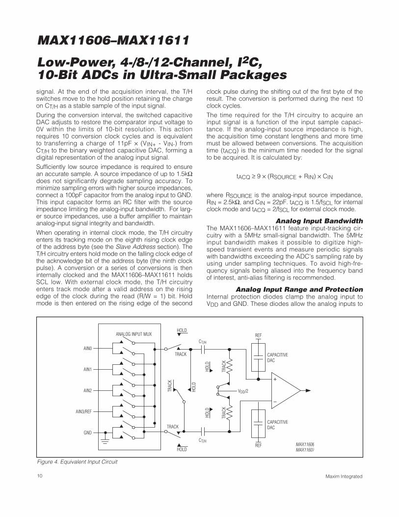
Analog Input and Track/HoldThe MAX11606–MAX11611 analog-input architecturecontains an analog-input multiplexer (mux), a fully dif-ferential track-and-hold (T/H) capacitor, T/H switches, acomparator, and a fully differential switched capacitivedigital-to-analog converter (DAC) (Figure 4).
In single-ended mode, the analog-input multiplexer con-nects CT/H between the analog input selected byCS[3:0] (see the Configuration/Setup Bytes (WriteCycle) section) and GND (Table 3). In differential mode,the analog- input multiplexer connects CT/H to the + and- analog inputs selected by CS[3:0] (Table 4).
During the acquisition interval, the T/H switches are inthe track position and CT/H charges to the analog input
ANALOGINPUTMUX
AIN1
AIN11/REF
AIN2AIN3AIN4AIN5AIN6AIN7AIN8AIN9
AIN10
AIN0
SCLSDA
INPUT SHIFT REGISTER
SETUP REGISTER
CONFIGURATION REGISTER
CONTROLLOGIC
REFERENCE4.096V (MAX11610)2.048V (MAX11611)
INTERNALOSCILLATOR
OUTPUT SHIFTREGISTER AND RAM
REF
T/H 10-BITADC
VDD
GND
MAX11610 MAX11611
Figure 2. MAX11610/MAX11611 Functional Diagram
VDD
IOL
IOH
VOUT
400pF
SDA
Figure 3. Load Circuit
MAX11606–MAX11611
Low-Power, 4-/8-/12-Channel, I2C,10-Bit ADCs in Ultra-Small Packages
10 Maxim Integrated
signal. At the end of the acquisition interval, the T/Hswitches move to the hold position retaining the chargeon CT/H as a stable sample of the input signal.
During the conversion interval, the switched capacitiveDAC adjusts to restore the comparator input voltage to0V within the limits of 10-bit resolution. This actionrequires 10 conversion clock cycles and is equivalentto transferring a charge of 11pF � (VIN+ - VIN-) fromCT/H to the binary weighted capacitive DAC, forming adigital representation of the analog input signal.
Sufficiently low source impedance is required to ensurean accurate sample. A source impedance of up to 1.5kΩdoes not significantly degrade sampling accuracy. Tominimize sampling errors with higher source impedances,connect a 100pF capacitor from the analog input to GND.This input capacitor forms an RC filter with the sourceimpedance limiting the analog-input bandwidth. For larg-er source impedances, use a buffer amplifier to maintainanalog-input signal integrity and bandwidth.
When operating in internal clock mode, the T/H circuitryenters its tracking mode on the eighth rising clock edgeof the address byte (see the Slave Address section). TheT/H circuitry enters hold mode on the falling clock edge ofthe acknowledge bit of the address byte (the ninth clockpulse). A conversion or a series of conversions is theninternally clocked and the MAX11606–MAX11611 holdsSCL low. With external clock mode, the T/H circuitryenters track mode after a valid address on the risingedge of the clock during the read (R/W = 1) bit. Holdmode is then entered on the rising edge of the second
clock pulse during the shifting out of the first byte of theresult. The conversion is performed during the next 10clock cycles.
The time required for the T/H circuitry to acquire aninput signal is a function of the input sample capaci-tance. If the analog-input source impedance is high,the acquisition time constant lengthens and more timemust be allowed between conversions. The acquisitiontime (tACQ) is the minimum time needed for the signalto be acquired. It is calculated by:
tACQ ≥ 9 � (RSOURCE + RIN) � CIN
where RSOURCE is the analog-input source impedance,RIN = 2.5kΩ, and CIN = 22pF. tACQ is 1.5/fSCL for internalclock mode and tACQ = 2/fSCL for external clock mode.
Analog Input BandwidthThe MAX11606–MAX11611 feature input-tracking cir-cuitry with a 5MHz small-signal bandwidth. The 5MHzinput bandwidth makes it possible to digitize high-speed transient events and measure periodic signalswith bandwidths exceeding the ADC’s sampling rate byusing under sampling techniques. To avoid high-fre-quency signals being aliased into the frequency bandof interest, anti-alias filtering is recommended.
Analog Input Range and ProtectionInternal protection diodes clamp the analog input toVDD and GND. These diodes allow the analog inputs to
TRAC
KTR
ACK
HOLD
CT/H
CT/H
TRAC
K
TRACK
HOLD
AIN0
AIN1
AIN2
AIN3/REF
GND
ANALOG INPUT MUX
CAPACITIVEDAC
REF
CAPACITIVEDAC
REF MAX11606 MAX11607
HOLD
HOLD
TRACK
HOLD
VDD/2
Figure 4. Equivalent Input Circuit

MAX11606–MAX11611
Low-Power, 4-/8-/12-Channel, I2C,10-Bit ADCs in Ultra-Small Packages
11Maxim Integrated
swing from (VGND - 0.3V) to (VDD + 0.3V) without caus-ing damage to the device. For accurate conversionsthe inputs must not go more than 50mV below VGND orabove VDD.
Single-Ended/Differential InputThe SGL/DIF of the configuration byte configures theMAX11606–MAX11611 analog-input circuitry for single-ended or differential inputs (Table 2). In single-endedmode (SGL/DIF = 1), the digital conversion results arethe difference between the analog input selected byCS[3:0] and GND (Table 3). In differential mode (SGL/DIF = 0), the digital conversion results are the differ-ence between the + and the - analog inputs selectedby CS[3:0] (Table 4).
Unipolar/BipolarWhen operating in differential mode, the BIP/UNI bit ofthe setup byte (Table 1) selects unipolar or bipolaroperation. Unipolar mode sets the differential inputrange from 0 to VREF. A negative differential analoginput in unipolar mode causes the digital output codeto be zero. Selecting bipolar mode sets the differentialinput range to ±VREF/2. The digital output code is bina-ry in unipolar mode and two’s complement in bipolarmode. See the Transfer Functions section.
In single-ended mode, the MAX11606–MAX11611always operate in unipolar mode irrespective ofBIP/UNI. The analog inputs are internally referenced toGND with a full-scale input range from 0 to VREF.
2-Wire Digital InterfaceThe MAX11606–MAX11611 feature a 2-wire interfaceconsisting of a serial-data line (SDA) and serial-clock line(SCL). SDA and SCL facilitate bidirectional communica-tion between the MAX11606–MAX11611 and the masterat rates up to 1.7MHz. The MAX11606–MAX11611 areslaves that transfer and receive data. The master (typi-cally a microcontroller) initiates data transfer on the busand generates the SCL signal to permit that transfer.
SDA and SCL must be pulled high. This is typically donewith pullup resistors (750Ω or greater) (see the TypicalOperating Circuit). Series resistors (RS) are optional.They protect the input architecture of the MAX11606–MAX11611 from high voltage spikes on the bus lines,minimize crosstalk, and undershoot of the bus signals.
Bit TransferOne data bit is transferred during each SCL clockcycle. A minimum of 18 clock cycles are required totransfer the data in or out of the MAX11606–MAX11611. The data on SDA must remain stable dur-ing the high period of the SCL clock pulse. Changes in
SDA while SCL is stable are considered control signals(see the START and STOP Conditions section). BothSDA and SCL remain high when the bus is not busy.
START and STOP ConditionsThe master initiates a transmission with a START condi-tion (S), a high-to-low transition on SDA while SCL is high.The master terminates a transmission with a STOP condi-tion (P), a low-to-high transition on SDA while SCL is high(Figure 5). A repeated START condition (Sr) can be usedin place of a STOP condition to leave the bus active andthe mode unchanged (see the HS Mode section).
Acknowledge BitsData transfers are acknowledged with an acknowledgebit (A) or a not-acknowledge bit (A). Both the masterand the MAX11606–MAX11611 (slave) generateacknowledge bits. To generate an acknowledge, thereceiving device must pull SDA low before the risingedge of the acknowledge-related clock pulse (ninthpulse) and keep it low during the high period of theclock pulse (Figure 6). To generate a not-acknowledge,the receiver allows SDA to be pulled high before therising edge of the acknowledge-related clock pulseand leaves SDA high during the high period of theclock pulse. Monitoring the acknowledge bits allows fordetection of unsuccessful data transfers. An unsuc-cessful data transfer happens if a receiving device isbusy or if a system fault has occurred. In the event ofan unsuccessful data transfer, the bus master shouldreattempt communication at a later time.
SCL
SDA
S PSr
Figure 5. START and STOP Conditions
SCL
SDA
S NOT ACKNOWLEDGE
ACKNOWLEDGE
1 2 8 9
Figure 6. Acknowledge Bits

MAX11606–MAX11611
Low-Power, 4-/8-/12-Channel, I2C,10-Bit ADCs in Ultra-Small Packages
12 Maxim Integrated
Slave Address A bus master initiates communication with a slave deviceby issuing a START condition followed by a slaveaddress. When idle, the MAX11606–MAX11611 continu-ously wait for a START condition followed by their slaveaddress. When the MAX11606–MAX11611 recognizetheir slave address, they are ready to accept or senddata. The slave address has been factory programmedand is always 0110100 for the MAX11606/MAX11607,0110011 for the MAX11608/MAX11609, and 0110101 forMAX11610/MAX11611 (Figure 7). The least significant bit(LSB) of the address byte (R/W) determines whether themaster is writing to or reading from the MAX11606–MAX11611 (R/W = 0 selects a write condition, R/W = 1selects a read condition). After receiving the address, theMAX11606–MAX11611 (slave) issues an acknowledge bypulling SDA low for one clock cycle.
Bus TimingAt power-up, the MAX11606–MAX11611 bus timing isset for fast mode (F/S mode), allowing conversion rates
up to 22.2ksps. The MAX11606–MAX11611 must oper-ate in high-speed mode (HS mode) to achieve conver-sion rates up to 94.4ksps. Figure 1 shows the bus timingfor the MAX11606–MAX11611’s 2-wire interface.
HS ModeAt power-up, the MAX11606–MAX11611 bus timing isset for F/S mode. The bus master selects HS mode byaddressing all devices on the bus with the HS-modemaster code 0000 1XXX (X = don’t care). After success-fully receiving the HS-mode master code, theMAX11606–MAX11611 issue a not-acknowledge, allow-ing SDA to be pulled high for one clock cycle (Figure 8).After the not-acknowledge, the MAX11606–MAX11611are in HS mode. The bus master must then send arepeated START followed by a slave address to initiateHS-mode communication. If the master generates aSTOP condition the MAX11606–MAX11611 returns toF/S mode.
0 1 1 10 0 0 R/W A
SLAVE ADDRESSMAX11606/MAX11607
S
SCL
SDA
1 2 3 4 5 6 7 8 9
DEVICE SLAVE ADDRESS
0110100
0110011
MAX11606/MAX11607
MAX11608/MAX11609
0110101MAX11610/MAX11611
Figure 7. MAX11606/MAX11607 Slave Address Byte
0 0 0 10 X X X A
HS-MODE MASTER CODE
SCL
SDA
S Sr
F/S MODE HS MODE
Figure 8. F/S-Mode to HS-Mode Transfer

MAX11606–MAX11611
Low-Power, 4-/8-/12-Channel, I2C,10-Bit ADCs in Ultra-Small Packages
13Maxim Integrated
Configuration/Setup Bytes (Write Cycle)A write cycle begins with the bus master issuing aSTART condition followed by seven address bits (Figure7) and a write bit (R/W = 0). If the address byte is suc-cessfully received, the MAX11606–MAX11611 (slave)issues an acknowledge. The master then writes to theslave. The slave recognizes the received byte as thesetup byte (Table 1) if the most significant bit (MSB) is1. If the MSB is 0, the slave recognizes that byte as the
configuration byte (Table 2). The master can write eitherone or two bytes to the slave in any order (setup bytethen configuration byte; configuration byte then setupbyte; setup byte or configuration byte only; Figure 9). Ifthe slave receives a byte successfully, it issues anacknowledge. The master ends the write cycle by issu-ing a STOP condition or a repeated START condition.When operating in HS mode, a STOP condition returnsthe bus into F/S mode (see the HS Mode section).
B. TWO-BYTE WRITE CYCLE
SLAVE TO MASTER
MASTER TO SLAVE
S
1
SLAVE ADDRESS A
7 1 1
W SETUP ORCONFIGURATION BYTE
SETUP ORCONFIGURATION BYTE
8
P or Sr
1
A
1
MSB DETERMINES WHETHERSETUP OR CONFIGURATION BYTE
S
1
SLAVE ADDRESS A
7 1 1
W SETUP ORCONFIGURATION BYTE
8
P or Sr
1
A
1
MSB DETERMINES WHETHERSETUP OR CONFIGURATION BYTE
A
1 8
A. ONE-BYTE WRITE CYCLE
NUMBER OF BITS
NUMBER OF BITS
Figure 9. Write Cycle
BIT 7(MSB)
BIT 6 BIT 5 BIT 4 BIT 3 BIT 2 BIT 1BIT 0(LSB)
REG SEL2 SEL1 SEL0 CLK BIP/UNI RST X
BIT NAME DESCRIPTION
7 REG Register bit. 1 = setup byte, 0 = configuration byte (see Table 2).
6 SEL2
5 SEL1
4 SEL0
Three bits select the reference voltage and the state of AIN_/REF(MAX11606/MAX11607/MAX11610/MAX11611) or REF (MAX11608/MAX11609) (Table 6).Defaulted to 000 at power-up.
3 CLK 1 = external clock, 0 = internal clock. Defaulted to 0 at power-up.
2 BIP/UNI 1 = bipolar, 0 = unipolar. Defaulted to 0 at power-up (see the Unipolar/Bipolar section).
1 RST 1 = no action, 0 = resets the configuration register to default. Setup register remains unchanged.
0 X Don’t-care bit. This bit can be set to 1 or 0.
Table 1. Setup Byte Format

MAX11606–MAX11611
Low-Power, 4-/8-/12-Channel, I2C,10-Bit ADCs in Ultra-Small Packages
14 Maxim Integrated
BIT 7(MSB)
BIT 6 BIT 5 BIT 4 BIT 3 BIT 2 BIT 1BIT 0(LSB)
REG SCAN1 SCAN0 CS3 CS2 CS1 CS0 SGL/DIF
BIT NAME DESCRIPTION
7 REG Register bit. 1= setup byte (see Table 1), 0 = configuration byte.
6 SCAN1
5 SCAN0S can sel ect b i ts. Tw o b i ts sel ect the scanni ng confi g ur ati on ( Tab l e 5) . D efaul ts to 00 at p ow er - up .
4 CS3
3 CS2
2 CS1
1 CS0
Channel select bits. Four bits select which analog input channels are to be used for conversion(Tables 3 and 4). Defaults to 0000 at power-up. For MAX11606/MAX11607, CS3 and CS2 areinternally set to 0. For the MAX11608/MAX11609, CS3 is internally set to 0.
0 SGL/DIF1 = single-ended, 0 = differential (Tables 3 and 4). Defaults to 1 at power-up. See the Single-Ended/Differential Input section.
Table 2. Configuration Byte Format
CS31 CS21 CS1 CS0 AIN0 AIN1 AIN2 AIN32 AIN4 AIN5 AIN6 AIN7 AIN8 AIN9 AIN10 AIN112 GND
0 0 0 0 + -
0 0 0 1 + -
0 0 1 0 + -
0 0 1 1 + -
0 1 0 0 + -
0 1 0 1 + -
0 1 1 0 + -
0 1 1 1 + -
1 0 0 0 + -
1 0 0 1 + -
1 0 1 0 + -
1 0 1 1 + -
1 1 0 0 RESERVED
1 1 0 1 RESERVED
1 1 1 0 RESERVED
1 1 1 1 RESERVED
1For the MAX11606/MAX11607, CS3 and CS2 are internally set to 0. For the MAX11608/MAX11609, CS3 is internally set to 0.2When SEL1 = 1, a single-ended read of AIN3/REF (MAX11606/MAX11607) or AIN11/REF (MAX11610/MAX11611) is ignored; scanstops at AIN2 or AIN10. This does not apply to the MAX11608/MAX11609 as each provides separate pins for AIN7 and REF.
Table 3. Channel Selection in Single-Ended Mode (SGL/DIF = 1)

MAX11606–MAX11611
Low-Power, 4-/8-/12-Channel, I2C,10-Bit ADCs in Ultra-Small Packages
15Maxim Integrated
Data Byte (Read Cycle)A read cycle must be initiated to obtain conversionresults. Read cycles begin with the bus master issuinga START condition followed by seven address bits anda read bit (R/W = 1). If the address byte is successfullyreceived, the MAX11606–MAX11611 (slave) issues anacknowledge. The master then reads from the slave.The result is transmitted in two bytes; first six bits of thefirst byte are high, then MSB through LSB are consecu-tively clocked out. After the master has received thebyte(s), it can issue an acknowledge if it wants to con-tinue reading or a not-acknowledge if it no longer wish-es to read. If the MAX11606–MAX11611 receive a not-acknowledge, they release SDA, allowing the master togenerate a STOP or a repeated START condition. Seethe Clock Modes and Scan Mode sections for detailedinformation on how data is obtained and converted.
Clock ModesThe clock mode determines the conversion clock andthe data acquisition and conversion time. The clockmode also affects the scan mode. The state of the set-up byte’s CLK bit determines the clock mode (Table 1).At power-up, the MAX11606–MAX11611 are defaultedto internal clock mode (CLK = 0).
Internal ClockWhen configured for internal clock mode (CLK = 0), theMAX11606–MAX11611 use their internal oscillator as theconversion clock. In internal clock mode, the MAX11606–MAX11611 begin tracking the analog input after a validaddress on the eighth rising edge of the clock. On thefalling edge of the ninth clock, the analog signal isacquired and the conversion begins. While converting theanalog input signal, the MAX11606–MAX11611 holds SCLlow (clock stretching). After the conversion completes, theresults are stored in internal memory. If the scan mode isset for multiple conversions, they all happen in successionwith each additional result stored in memory. TheMAX11606/MAX11607 contain four 10-bit blocks of memo-ry, the MAX11608/MAX11609 contain eight 10-bit blocks ofmemory, and the MAX11610/MAX11611 contain twelve 10-bit blocks of memory. Once all conversions are complete,the MAX11606–MAX11611 release SCL, allowing it to bepulled high. The master may now clock the results outof the memory in the same order the scan conversionhas been done at a clock rate of up to 1.7MHz. SCL isstretched for a maximum of 7.6µs per channel (seeFigure 10).
CS31 CS21 CS1 CS0 AIN0 AIN1 AIN2 AIN32 AIN4 AIN5 AIN6 AIN7 AIN8 AIN9 AIN10 AIN112
0 0 0 0 + -
0 0 0 1 - +
0 0 1 0 + -
0 0 1 1 - +
0 1 0 0 + -
0 1 0 1 - +
0 1 1 0 + -
0 1 1 1 - +
1 0 0 0 + -
1 0 0 1 - +
1 0 1 0 + -
1 0 1 1 - +
1 1 0 0 RESERVED
1 1 0 1 RESERVED
1 1 1 0 RESERVED
1 1 1 1 RESERVED
1For the MAX11606/MAX11607, CS3 and CS2 are internally set to 0. For the MAX11608/MAX11609, CS3 is internally set to 0.2When SEL1 = 1, a differential read between AIN2 and AIN3/REF (MAX11606/MAX11607) or AIN10 and AIN11/REF(MAX11610/MAX11611) returns the difference between GND and AIN2 or AIN10, respectively. For example, a differential read of 1011returns the negative difference between AIN10 and GND. This does not apply to the MAX11608/MAX11609 as each provides separatepins for AIN7 and REF. In differential scanning, the address increments by 2 until the limit set by CS3–CS1 has been reached.
Table 4. Channel Selection in Differential Mode (SGL/DIF = 0)

MAX11606–MAX11611
Low-Power, 4-/8-/12-Channel, I2C,10-Bit ADCs in Ultra-Small Packages
16 Maxim Integrated
The device memory contains all of the conversion resultswhen the MAX11606–MAX11611 release SCL. The con-verted results are read back in a first-in-first-out (FIFO)sequence. If AIN_/REF is set to be a reference input oroutput (SEL1 = 1, Table 6), AIN_/REF is excluded from amultichannel scan. This does not apply to theMAX11608/MAX11609 as each provides separate pinsfor AIN7 and REF. The memory contents can be readcontinuously. If reading continues past the result storedin memory, the pointer wraps around and point to the
first result. Note that only the current conversion resultsare read from memory. The device must be addressedwith a read command to obtain new conversion results.
The internal clock mode’s clock stretching quiets theSCL bus signal, reducing the system noise during con-version. Using the internal clock also frees the busmaster (typically a microcontroller) from the burden ofrunning the conversion clock, allowing it to performother tasks that do not need to use the bus.
B. SCAN MODE CONVERSIONS WITH INTERNAL CLOCK
S
1
SLAVE ADDRESS A
7 1 1
R CLOCK STRETCH
NUMBER OF BITS
P or Sr
18
RESULT 8 LSBs
8
RESULT 2 MSBs AA
1
A. SINGLE CONVERSION WITH INTERNAL CLOCK
S
1
SLAVE ADDRESS
7 1 1
R CLOCK STRETCHA
NUMBER OF BITS
P or Sr
18
RESULT 1 ( 2MSBs) A
1
A
8
RESULT 1 (8 LSBs) A
8
RESULT N (8LSBs)A
18
RESULT N (8MSBs)
SLAVE TO MASTER
MASTER TO SLAVE
CLOCK STRETCH
tACQ1tCONV2
tACQ2tCONVN
tACQN
tCONV
tACQ
11
tCONV1
Figure 10. Internal Clock Mode Read Cycles
SLAVE ADDRESS
tCONV1
tACQ1 tACQ2tCONVN
tACQN
tCONV
tACQ
NUMBER OF BITS
NUMBER OF BITS
18
A
1
S
1
A
7 1 1
R
S
1 7 1 1
R P OR Sr
18
A
1
A
8
A
8
B. SCAN MODE CONVERSIONS WITH EXTERNAL CLOCK
11
SLAVE ADDRESS P OR SrRESULT (8 LSBs)
8
A
1
RESULT (2 MSBs)
A. SINGLE CONVERSION WITH EXTERNAL CLOCK
SLAVE TO MASTER
MASTER TO SLAVE
RESULT 1 (2 MSBs) RESULT 2 (8 LSBs) RESULT N (8 LSBs)A
18
RESULT N (2 MSBs)A
Figure 11. External Clock Mode Read Cycle

MAX11606–MAX11611
Low-Power, 4-/8-/12-Channel, I2C,10-Bit ADCs in Ultra-Small Packages
17Maxim Integrated
External ClockWhen configured for external clock mode (CLK = 1),the MAX11606–MAX11611 use the SCL as the conver-sion clock. In external clock mode, the MAX11606–MAX11611 begin tracking the analog input on the ninthrising clock edge of a valid slave address byte. TwoSCL clock cycles later the analog signal is acquiredand the conversion begins. Unlike internal clock mode,converted data is available immediately after the firstfour empty high bits. The device continuously convertsinput channels dictated by the scan mode until given anot acknowledge. There is no need to re-address thedevice with a read command to obtain new conversionresults (see Figure 11).
The conversion must complete in 1ms or droop on thetrack-and-hold capacitor degrades conversion results.Use internal clock mode if the SCL clock periodexceeds 60µs.
The MAX11606–MAX11611 must operate in externalclock mode for conversion rates from 40ksps to94.4ksps. Below 40ksps internal clock mode is recom-mended due to much smaller power consumption.
Scan ModeSCAN0 and SCAN1 of the configuration byte set thescan mode configuration. Table 5 shows the scanningconfigurations. If AIN_/REF is set to be a reference inputor output (SEL1 = 1, Table 6), AIN_/REF is excluded
from a multichannel scan. The scanned results are writ-ten to memory in the same order as the conversion. Readthe results from memory in the order they were convert-ed. Each result needs a 2-byte transmission, the first bytebegins with six empty bits during which SDA is left high.Each byte has to be acknowledged by the master or thememory transmission is terminated. It is not possible toread the memory independently of conversion.
Applications InformationPower-On Reset
The configuration and setup registers (Tables 1 and 2)default to a single-ended, unipolar, single-channel con-version on AIN0 using the internal clock with VDD as thereference and AIN_/REF configured as an analog input.The memory contents are unknown after power-up.
Automatic ShutdownAutomatic shutdown occurs between conversions whenthe MAX11606–MAX11611 are idle. All analog circuitsparticipate in automatic shutdown except the internalreference due to its prohibitively long wake-up time.When operating in external clock mode, a STOP, not-acknowledge or repeated START, condition must beissued to place the devices in idle mode and benefitfrom automatic shutdown. A STOP condition is not nec-essary in internal clock mode to benefit from automaticshutdown because power-down occurs once all con-version results are written to memory (Figure 10). When
SCAN1 SCAN0 SCANNING CONFIGURATION
0 0Scans up from AIN0 to the input selected by CS3–CS0. When CS3–CS0 exceeds 1011, the scanning stops atAIN11. When AIN_/REF is set to be a REF input/output, scanning stops at AIN2 or AIN10.
0 1 *Converts the input selected by CS3–CS0 eight times (see Tables 3 and 4).
MAX11606/MAX11607: Scans upper half of channels.Scans up from AIN2 to the input selected by CS1 and CS0. When CS1 and CS0 are set for AIN0, AIN1, andAIN2, the only scan that takes place is AIN2 (MAX11606/MAX11607). When AIN/REF is set to be a REFinput/output, scanning stops at AIN2.
MAX11608/MAX11609: Scans upper quartile of channels.Scans up from AIN6 to the input selected by CS3–CS0. When CS3–CS0 is set for AIN0–AIN6, the only scanthat takes place is AIN6 (MAX11608/MAX11609).
1 0
MAX11610/MAX11611: Scans upper half of channels.Scans up from AIN6 to the input selected by CS3–CS0. When CS3–CS0 is set for AIN0–AIN6, the only scanthat takes place is AIN6 (MAX11610/MAX11611). When AIN/REF is set to be a REF input/output, scanningstops at selected channel or AIN10.
1 1 *Converts channel selected by CS3–CS0.
*When operating in external clock mode, there is no difference between SCAN[1:0] = 01 and SCAN[1:0] = 11, and converting occursperpetually until not acknowledge occurs.
Table 5. Scanning Configuration

MAX11606–MAX11611
Low-Power, 4-/8-/12-Channel, I2C,10-Bit ADCs in Ultra-Small Packages
18 Maxim Integrated
using an external reference or VDD as a reference, allanalog circuitry is inactive in shutdown and supply cur-rent is less than 0.5µA (typ). The digital conversionresults obtained in internal clock mode are maintainedin memory during shutdown and are available foraccess through the serial interface at any time prior to aSTOP or a repeated START condition.
When idle, the MAX11606–MAX11611 continuously waitfor a START condition followed by their slave address (seeSlave Address section). Upon reading a valid addressbyte the MAX11606–MAX11611 power-up. The internalreference requires 10ms to wake up, so when using theinternal reference it should be powered up 10ms prior toconversion or powered continuously. Wake-up is invisiblewhen using an external reference or VDD as the reference.
Automatic shutdown results in dramatic power savings,particularly at slow conversion rates and with internalclock. For example, at a conversion rate of 10ksps, theaverage supply current for the MAX11607 is 60µA (typ)and drops to 6µA (typ) at 1ksps. At 0.1ksps the averagesupply current is just 1µA, or a minuscule 3µW of powerconsumption, see Average Supply Current vs. ConversionRate in the Typical Operating Characteristics).
Reference VoltageSEL[2:0] of the setup byte (Table 1) control the referenceand the AIN_/REF configuration (Table 6). WhenAIN_/REF is configured to be a reference input or refer-ence output (SEL1 = 1), differential conversions onAIN_/REF appear as if AIN_/REF is connected to GND(see note 2 of Table 4). Single-ended conversion in scanmode on AIN_/REF is ignored by internal limiter, whichsets the highest available channel at AIN2 or AIN10.
Internal ReferenceThe internal reference is 4.096V for the MAX11606/MAX11608/MAX11610 and 2.048V for the MAX11607/MAX11609/MAX11611. SEL1 of the setup byte controlswhether AIN_/REF is used for an analog input or a refer-ence (Table 6). When AIN_/REF is configured to be aninternal reference output (SEL[2:1] = 11), decoupleAIN_/REF to GND with a 0.1µF capacitor and a 2kΩ seriesresistor (see the Typical Operating Circuit). Once poweredup, the reference always remains on until reconfigured.The internal reference requires 10ms to wake up and isaccessed using SEL0 (Table 6). When in shutdown, theinternal reference output is in a high-impedance state. Thereference should not be used to supply current for exter-nal circuitry. The internal reference does not require an
SEL2 SEL1 SEL0REFERENCE
VOLTAGE
AIN_/REF(MAX11606/MAX11607/MAX11610/MAX11611)
REF(MAX11608/MAX11609)
INTERNALREFERENCE STATE
0 0 X VDD Analog input Not connected Always off
0 1 X External reference Reference input Reference input Always off
1 0 0 Internal reference Analog input Not connected Always off
1 0 1 Internal reference Analog input Not connected Always on
1 1 0 Internal reference Reference output Reference output Always off
1 1 1 Internal reference Reference output Reference output Always on
Table 6. Reference Voltage, AIN_/REF, and REF Format
OUTPUT CODE
FULL-SCALETRANSITION11 . . . 111
11 . . . 110
11 . . . 101
00 . . . 011
00 . . . 010
00 . . . 001
00 . . . 0001 2 30 FS
FS - 3/2 LSB
FS = VREF
ZS = GND
INPUT VOLTAGE (LSB)
MAX11606–MAX11611
1 LSB = VREF 1024
Figure 12. Unipolar Transfer Function
X = Don’t care.
MAX11606–MAX11611
Low-Power, 4-/8-/12-Channel, I2C,10-Bit ADCs in Ultra-Small Packages
19Maxim Integrated
external bypass capacitor and works best when leftunconnected (SEL1 = 0).
External ReferenceThe external reference can range from 1V to VDD. Formaximum conversion accuracy, the reference must beable to deliver up to 40µA and have an output imped-ance of 500Ω or less. If the reference has a higher out-put impedance or is noisy, bypass it to GND as closeas possible to AIN_/REF with a 0.1µF capacitor.
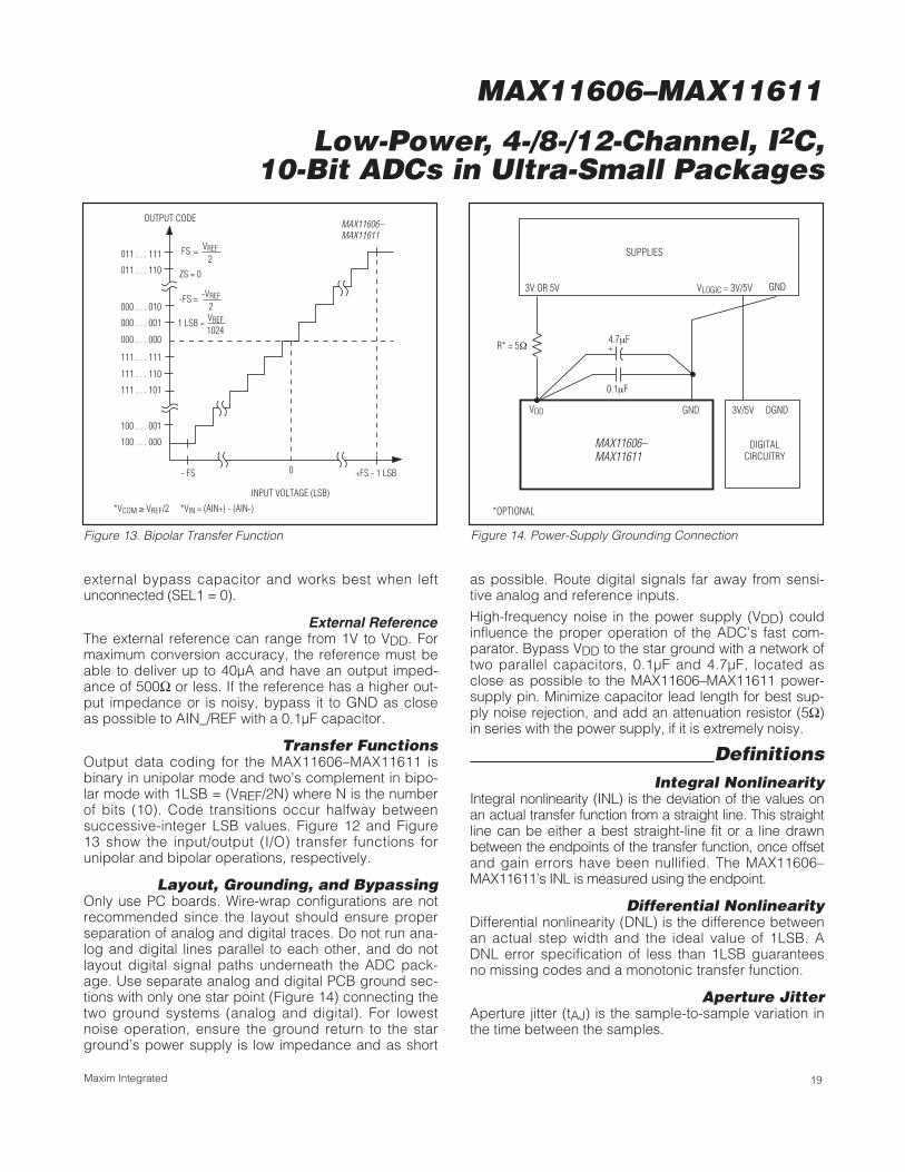
Transfer FunctionsOutput data coding for the MAX11606–MAX11611 isbinary in unipolar mode and two’s complement in bipo-lar mode with 1LSB = (VREF/2N) where N is the numberof bits (10). Code transitions occur halfway betweensuccessive-integer LSB values. Figure 12 and Figure13 show the input/output (I/O) transfer functions forunipolar and bipolar operations, respectively.
Layout, Grounding, and BypassingOnly use PC boards. Wire-wrap configurations are notrecommended since the layout should ensure properseparation of analog and digital traces. Do not run ana-log and digital lines parallel to each other, and do notlayout digital signal paths underneath the ADC pack-age. Use separate analog and digital PCB ground sec-tions with only one star point (Figure 14) connecting thetwo ground systems (analog and digital). For lowestnoise operation, ensure the ground return to the starground’s power supply is low impedance and as short
as possible. Route digital signals far away from sensi-tive analog and reference inputs.
High-frequency noise in the power supply (VDD) couldinfluence the proper operation of the ADC’s fast com-parator. Bypass VDD to the star ground with a network oftwo parallel capacitors, 0.1µF and 4.7µF, located asclose as possible to the MAX11606–MAX11611 power-supply pin. Minimize capacitor lead length for best sup-ply noise rejection, and add an attenuation resistor (5Ω)in series with the power supply, if it is extremely noisy.
Definitions Integral Nonlinearity
Integral nonlinearity (INL) is the deviation of the values onan actual transfer function from a straight line. This straightline can be either a best straight-line fit or a line drawnbetween the endpoints of the transfer function, once offsetand gain errors have been nullified. The MAX11606–MAX11611’s INL is measured using the endpoint.
Differential NonlinearityDifferential nonlinearity (DNL) is the difference betweenan actual step width and the ideal value of 1LSB. ADNL error specification of less than 1LSB guaranteesno missing codes and a monotonic transfer function.
Aperture JitterAperture jitter (tAJ) is the sample-to-sample variation inthe time between the samples.
011 . . . 111
011 . . . 110
000 . . . 010
000 . . . 001
000 . . . 000
111 . . . 111
111 . . . 110
111 . . . 101
100 . . . 001
100 . . . 000
- FS 0
INPUT VOLTAGE (LSB)
OUTPUT CODE
ZS = 0
+FS - 1 LSB
*VCOM ≥ VREF/2 *VIN = (AIN+) - (AIN-)
FS = VREF 2
-FS = -VREF 2
MAX11606– MAX11611
1 LSB = VREF 1024
Figure 13. Bipolar Transfer Function
GNDVLOGIC = 3V/5V3V OR 5V
SUPPLIES
DGND3V/5VGND
*OPTIONAL
4.7μFR* = 5Ω
0.1μF
VDD
DIGITALCIRCUITRY
MAX11606–MAX11611
Figure 14. Power-Supply Grounding Connection

MAX11606–MAX11611
Low-Power, 4-/8-/12-Channel, I2C,10-Bit ADCs in Ultra-Small Packages
20 Maxim Integrated
Aperture DelayAperture delay (tAD) is the time between the fallingedge of the sampling clock and the instant when anactual sample is taken.
Signal-to-Noise Ratio For a waveform perfectly reconstructed from digital sam-ples, the theoretical maximum SNR is the ratio of the full-scale analog input (RMS value) to the RMS quantizationerror (residual error). The ideal, theoretical minimum ana-log-to-digital noise is caused by quantization error onlyand results directly from the ADC’s resolution (N Bits):
SNRMAX[dB] = 6.02dB � N + 1.76dB
In reality, there are other noise sources besides quanti-zation noise: thermal noise, reference noise, clock jitter,etc. SNR is computed by taking the ratio of the RMSsignal to the RMS noise, which includes all spectralcomponents minus the fundamental, the first five har-monics, and the DC offset.
Signal-to-Noise Plus Distortion Signal-to-noise plus distortion (SINAD) is the ratio of thefundamental input frequency’s RMS amplitude to RMSequivalent of all other ADC output signals.
SINAD (dB) = 20 � log (SignalRMS/NoiseRMS)
Effective Number of Bits Effective number of bits (ENOB) indicates the globalaccuracy of an ADC at a specific input frequency and
sampling rate. An ideal ADC’s error consists of quanti-zation noise only. With an input range equal to theADC’s full-scale range, calculate the ENOB as follows:
ENOB = (SINAD - 1.76)/6.02
Total Harmonic DistortionTotal harmonic distortion (THD) is the ratio of the RMSsum of the input signal’s first five harmonics to the fun-damental itself. This is expressed as:
where V1 is the fundamental amplitude, and V2 through V5are the amplitudes of the 2nd through 5th order harmonics.
Spurious-Free Dynamic RangeSpurious-free dynamic range (SFDR) is the ratio of RMSamplitude of the fundamental (maximum signal compo-nent) to the RMS value of the next largest distortioncomponent.
THDV V V V
V= ×
+ + +⎛
⎝⎜⎜
⎞
⎠⎟⎟
⎛
⎝
⎜⎜⎜
⎞
⎠
⎟⎟⎟
20 22
32
42
52
1log
SINAD dBSignalRMS
NoiseRMS THDRMS( ) log= ×
+⎡
⎣⎢
⎤
⎦⎥20
Chip InformationPROCESS: BiCMOS

MAX11606–MAX11611
Low-Power, 4-/8-/12-Channel, I2C,10-Bit ADCs in Ultra-Small Packages
21Maxim Integrated
*OPTIONAL**AIN11/REF (MAX11610/MAX11611)
RS*
RS*
ANALOGINPUTS
μC SDA
SCL
GND
VDD
SDA
SCL
AIN0AIN1
RC NETWORK*AIN3**/REF
3.3V or 5V
5V
RP
CREF 0.1μF
RP
5V
MAX11606– MAX11611
0.1μF
2kΩ
Typical Operating Circuit
SDA
SCLAIN3/REF
1
2
8
7
VDD
GNDAIN1
AIN2
AIN0
µMAX
TOP VIEW
3
4
6
5
MAX11606 MAX11607
16
15
14
13
12
11
10
9
1
2
3
4
5
6
7
8
(REF) AIN11/REF VDD
GND
SDA
SCL
AIN7
AIN6
AIN5
AIN4
( ) INDICATES PINS ON THE MAX11608/MAX11609.
MAX11608– MAX11611
QSOP
+
+
(N.C.) AIN10
(N.C.) AIN9
AIN1
(N.C.) AIN8
AIN0
AIN2
AIN3
Pin Configurations
Selector Guide
PARTINPUT
CHANNELS
INTERNALREFERENCE
(V)
SUPPLYVOLTAGE
(V)
INL(LSB)
MAX11606 4 4.096 4.5 to 5.5 ±1
MAX11607 4 2.048 2.7 to 3.6 ±1
MAX11608 8 4.096 4.5 to 5.5 ±1
MAX11609 8 2.048 2.7 to 3.6 ±1
MAX11610 12 4.096 4.5 to 5.5 ±1
MAX11611 12 2.048 2.7 to 3.6 ±1
MAX11607TOP VIEW
(BUMPS ON BOTTOM)
A
B
C
WLP
1 2 3 4
AIN0 AIN1 AIN2 AIN3/REF
GND GND GND GND
VDD GND SDA SCL
+
PACKAGETYPE
PACKAGECODE
OUTLINENO.
LANDPATTERN NO.
8 µMAX U8CN+1 21-0036 90-0092
12 WLP W121C2+1 21-0009Refer to Application
Note 1891
16 QSOP E16+1 21-0055 90-0167
Package InformationFor the latest package outline information and land patterns (foot-prints), go to www.maximintegrated.com/packages. Note that a“+”, “#”, or “-” in the package code indicates RoHS status only.Package drawings may show a different suffix character, but thedrawing pertains to the package regardless of RoHS status.

Maxim Integrated cannot assume responsibility for use of any circuitry other than circuitry entirely embodied in a Maxim Integrated product. No circuit patentlicenses are implied. Maxim Integrated reserves the right to change the circuitry and specifications without notice at any time. The parametric values (min andmax limits) shown in the Electrical Characteristics table are guaranteed. Other parametric values quoted in this data sheet are provided for guidance.
22 ________________________________Maxim Integrated 160 Rio Robles, San Jose, CA 95134 USA 1-408-601-1000
© 2013 Maxim Integrated Products, Inc. Maxim Integrated and the Maxim Integrated logo are trademarks of Maxim Integrated Products, Inc.
MAX11606–MAX11611
Low-Power, 4-/8-/12-Channel, I2C,10-Bit ADCs in Ultra-Small Packages
Revision History
REVISIONNUMBER
REVISIONDATE
DESCRIPTIONPAGES
CHANGED
0 4/09 Introduction of the MAX11606/MAX11607 —
1 7/09 Introduction of the MAX11608–MAX116011 1
2 3/10 Changed Absolute Maximum Ratings and timing diagram 2, 12
3 2/11Added MAX11607 WLP package and updated notes in Electrical Characteristicstable
1–5, 8, 21
4 7/13 Updated the Ordering Information table. 1