Embed Size (px)
Citation preview

101 Innovation DriveSan Jose, CA 95134www.altera.com
MAX V Device Handbook
Subscribe
MAX V Device Handbook

MAX V Device Handbook June 2017 Altera Corporation
© 2017 Altera Corporation. All rights reserved. ALTERA, ARRIA, CYCLONE, HARDCOPY, MAX, MEGACORE, NIOS, QUARTUS and STRATIX are Reg. U.S. Pat.& Tm. Off. and/or trademarks of Altera Corporation in the U.S. and other countries. All other trademarks and service marks are the property of their respectiveholders as described at www.altera.com/common/legal.html. Altera warrants performance of its semiconductor products to current specifications in accordancewith Altera’s standard warranty, but reserves the right to make changes to any products and services at any time without notice. Altera assumes no responsibility orliability arising out of the application or use of any information, product, or service described herein except as expressly agreed to in writing by Altera. Alteracustomers are advised to obtain the latest version of device specifications before relying on any published information and before placing orders for products orservices.

June 2017 Altera Corporation
Contents
Section I. MAX V Device Core
Chapter 1. MAX V Device Family OverviewFeature Summary . . . . . . . . . . . . . . . . . . . . . . . . . . . . . . . . . . . . . . . . . . . . . . . . . . . . . . . . . . . . . . . . . . . . . . . 1–1Integrated Software Platform . . . . . . . . . . . . . . . . . . . . . . . . . . . . . . . . . . . . . . . . . . . . . . . . . . . . . . . . . . . . . 1–3Device Pin-Outs . . . . . . . . . . . . . . . . . . . . . . . . . . . . . . . . . . . . . . . . . . . . . . . . . . . . . . . . . . . . . . . . . . . . . . . . . 1–3Ordering Information . . . . . . . . . . . . . . . . . . . . . . . . . . . . . . . . . . . . . . . . . . . . . . . . . . . . . . . . . . . . . . . . . . . . 1–4Document Revision History . . . . . . . . . . . . . . . . . . . . . . . . . . . . . . . . . . . . . . . . . . . . . . . . . . . . . . . . . . . . . . 1–4
Chapter 2. MAX V ArchitectureFunctional Description . . . . . . . . . . . . . . . . . . . . . . . . . . . . . . . . . . . . . . . . . . . . . . . . . . . . . . . . . . . . . . . . . . . 2–1Logic Array Blocks . . . . . . . . . . . . . . . . . . . . . . . . . . . . . . . . . . . . . . . . . . . . . . . . . . . . . . . . . . . . . . . . . . . . . . 2–4
LAB Interconnects . . . . . . . . . . . . . . . . . . . . . . . . . . . . . . . . . . . . . . . . . . . . . . . . . . . . . . . . . . . . . . . . . . . . 2–6LAB Control Signals . . . . . . . . . . . . . . . . . . . . . . . . . . . . . . . . . . . . . . . . . . . . . . . . . . . . . . . . . . . . . . . . . . . 2–6
Logic Elements . . . . . . . . . . . . . . . . . . . . . . . . . . . . . . . . . . . . . . . . . . . . . . . . . . . . . . . . . . . . . . . . . . . . . . . . . . 2–8LUT Chain and Register Chain . . . . . . . . . . . . . . . . . . . . . . . . . . . . . . . . . . . . . . . . . . . . . . . . . . . . . . . . . . 2–9addnsub Signal . . . . . . . . . . . . . . . . . . . . . . . . . . . . . . . . . . . . . . . . . . . . . . . . . . . . . . . . . . . . . . . . . . . . . . . 2–9LE Operating Modes . . . . . . . . . . . . . . . . . . . . . . . . . . . . . . . . . . . . . . . . . . . . . . . . . . . . . . . . . . . . . . . . . . 2–9
Normal Mode . . . . . . . . . . . . . . . . . . . . . . . . . . . . . . . . . . . . . . . . . . . . . . . . . . . . . . . . . . . . . . . . . . . . . 2–10Dynamic Arithmetic Mode . . . . . . . . . . . . . . . . . . . . . . . . . . . . . . . . . . . . . . . . . . . . . . . . . . . . . . . . . . 2–10Carry-Select Chain . . . . . . . . . . . . . . . . . . . . . . . . . . . . . . . . . . . . . . . . . . . . . . . . . . . . . . . . . . . . . . . . . 2–11Clear and Preset Logic Control . . . . . . . . . . . . . . . . . . . . . . . . . . . . . . . . . . . . . . . . . . . . . . . . . . . . . . 2–13
LE RAM . . . . . . . . . . . . . . . . . . . . . . . . . . . . . . . . . . . . . . . . . . . . . . . . . . . . . . . . . . . . . . . . . . . . . . . . . . . . 2–13MultiTrack Interconnect . . . . . . . . . . . . . . . . . . . . . . . . . . . . . . . . . . . . . . . . . . . . . . . . . . . . . . . . . . . . . . . . . 2–14Global Signals . . . . . . . . . . . . . . . . . . . . . . . . . . . . . . . . . . . . . . . . . . . . . . . . . . . . . . . . . . . . . . . . . . . . . . . . . 2–19User Flash Memory Block . . . . . . . . . . . . . . . . . . . . . . . . . . . . . . . . . . . . . . . . . . . . . . . . . . . . . . . . . . . . . . . 2–21
UFM Storage . . . . . . . . . . . . . . . . . . . . . . . . . . . . . . . . . . . . . . . . . . . . . . . . . . . . . . . . . . . . . . . . . . . . . . . . 2–22Internal Oscillator . . . . . . . . . . . . . . . . . . . . . . . . . . . . . . . . . . . . . . . . . . . . . . . . . . . . . . . . . . . . . . . . . . . . 2–22Program, Erase, and Busy Signals . . . . . . . . . . . . . . . . . . . . . . . . . . . . . . . . . . . . . . . . . . . . . . . . . . . . . . 2–23Auto-Increment Addressing . . . . . . . . . . . . . . . . . . . . . . . . . . . . . . . . . . . . . . . . . . . . . . . . . . . . . . . . . . . 2–23Serial Interface . . . . . . . . . . . . . . . . . . . . . . . . . . . . . . . . . . . . . . . . . . . . . . . . . . . . . . . . . . . . . . . . . . . . . . . 2–23UFM Block to Logic Array Interface . . . . . . . . . . . . . . . . . . . . . . . . . . . . . . . . . . . . . . . . . . . . . . . . . . . . 2–24
Core Voltage . . . . . . . . . . . . . . . . . . . . . . . . . . . . . . . . . . . . . . . . . . . . . . . . . . . . . . . . . . . . . . . . . . . . . . . . . . . 2–25I/O Structure . . . . . . . . . . . . . . . . . . . . . . . . . . . . . . . . . . . . . . . . . . . . . . . . . . . . . . . . . . . . . . . . . . . . . . . . . . 2–26
Fast I/O Connection . . . . . . . . . . . . . . . . . . . . . . . . . . . . . . . . . . . . . . . . . . . . . . . . . . . . . . . . . . . . . . . . . . 2–27I/O Blocks . . . . . . . . . . . . . . . . . . . . . . . . . . . . . . . . . . . . . . . . . . . . . . . . . . . . . . . . . . . . . . . . . . . . . . . . . . 2–28I/O Standards and Banks . . . . . . . . . . . . . . . . . . . . . . . . . . . . . . . . . . . . . . . . . . . . . . . . . . . . . . . . . . . . . 2–29
PCI Compliance . . . . . . . . . . . . . . . . . . . . . . . . . . . . . . . . . . . . . . . . . . . . . . . . . . . . . . . . . . . . . . . . . . . 2–32LVDS and RSDS Channels . . . . . . . . . . . . . . . . . . . . . . . . . . . . . . . . . . . . . . . . . . . . . . . . . . . . . . . . . . 2–32
Schmitt Trigger . . . . . . . . . . . . . . . . . . . . . . . . . . . . . . . . . . . . . . . . . . . . . . . . . . . . . . . . . . . . . . . . . . . . . . 2–32Output Enable Signals . . . . . . . . . . . . . . . . . . . . . . . . . . . . . . . . . . . . . . . . . . . . . . . . . . . . . . . . . . . . . . . . 2–33Programmable Drive Strength . . . . . . . . . . . . . . . . . . . . . . . . . . . . . . . . . . . . . . . . . . . . . . . . . . . . . . . . . 2–33Slew-Rate Control . . . . . . . . . . . . . . . . . . . . . . . . . . . . . . . . . . . . . . . . . . . . . . . . . . . . . . . . . . . . . . . . . . . . 2–34Open-Drain Output . . . . . . . . . . . . . . . . . . . . . . . . . . . . . . . . . . . . . . . . . . . . . . . . . . . . . . . . . . . . . . . . . . 2–34Programmable Ground Pins . . . . . . . . . . . . . . . . . . . . . . . . . . . . . . . . . . . . . . . . . . . . . . . . . . . . . . . . . . . 2–34Bus-Hold . . . . . . . . . . . . . . . . . . . . . . . . . . . . . . . . . . . . . . . . . . . . . . . . . . . . . . . . . . . . . . . . . . . . . . . . . . . 2–34Programmable Pull-Up Resistor . . . . . . . . . . . . . . . . . . . . . . . . . . . . . . . . . . . . . . . . . . . . . . . . . . . . . . . . 2–35Programmable Input Delay . . . . . . . . . . . . . . . . . . . . . . . . . . . . . . . . . . . . . . . . . . . . . . . . . . . . . . . . . . . . 2–35
MAX V Device Handbook
iv Contents
MultiVolt I/O Interface . . . . . . . . . . . . . . . . . . . . . . . . . . . . . . . . . . . . . . . . . . . . . . . . . . . . . . . . . . . . . . . 2–35Document Revision History . . . . . . . . . . . . . . . . . . . . . . . . . . . . . . . . . . . . . . . . . . . . . . . . . . . . . . . . . . . . . 2–36
Chapter 3. DC and Switching Characteristics for MAX V DevicesOperating Conditions . . . . . . . . . . . . . . . . . . . . . . . . . . . . . . . . . . . . . . . . . . . . . . . . . . . . . . . . . . . . . . . . . . . . 3–1
Absolute Maximum Ratings . . . . . . . . . . . . . . . . . . . . . . . . . . . . . . . . . . . . . . . . . . . . . . . . . . . . . . . . . . . . 3–1Recommended Operating Conditions . . . . . . . . . . . . . . . . . . . . . . . . . . . . . . . . . . . . . . . . . . . . . . . . . . . . 3–2Programming/Erasure Specifications . . . . . . . . . . . . . . . . . . . . . . . . . . . . . . . . . . . . . . . . . . . . . . . . . . . . 3–3DC Electrical Characteristics . . . . . . . . . . . . . . . . . . . . . . . . . . . . . . . . . . . . . . . . . . . . . . . . . . . . . . . . . . . . 3–3Output Drive Characteristics . . . . . . . . . . . . . . . . . . . . . . . . . . . . . . . . . . . . . . . . . . . . . . . . . . . . . . . . . . . 3–5I/O Standard Specifications . . . . . . . . . . . . . . . . . . . . . . . . . . . . . . . . . . . . . . . . . . . . . . . . . . . . . . . . . . . . 3–5Bus Hold Specifications . . . . . . . . . . . . . . . . . . . . . . . . . . . . . . . . . . . . . . . . . . . . . . . . . . . . . . . . . . . . . . . . 3–8Power-Up Timing . . . . . . . . . . . . . . . . . . . . . . . . . . . . . . . . . . . . . . . . . . . . . . . . . . . . . . . . . . . . . . . . . . . . . 3–9
Power Consumption . . . . . . . . . . . . . . . . . . . . . . . . . . . . . . . . . . . . . . . . . . . . . . . . . . . . . . . . . . . . . . . . . . . . 3–10Timing Model and Specifications . . . . . . . . . . . . . . . . . . . . . . . . . . . . . . . . . . . . . . . . . . . . . . . . . . . . . . . . . 3–10
Preliminary and Final Timing . . . . . . . . . . . . . . . . . . . . . . . . . . . . . . . . . . . . . . . . . . . . . . . . . . . . . . . . . 3–11Performance . . . . . . . . . . . . . . . . . . . . . . . . . . . . . . . . . . . . . . . . . . . . . . . . . . . . . . . . . . . . . . . . . . . . . . . . . 3–11Internal Timing Parameters . . . . . . . . . . . . . . . . . . . . . . . . . . . . . . . . . . . . . . . . . . . . . . . . . . . . . . . . . . . 3–12External Timing Parameters . . . . . . . . . . . . . . . . . . . . . . . . . . . . . . . . . . . . . . . . . . . . . . . . . . . . . . . . . . . 3–19External Timing I/O Delay Adders . . . . . . . . . . . . . . . . . . . . . . . . . . . . . . . . . . . . . . . . . . . . . . . . . . . . . 3–23Maximum Input and Output Clock Rates . . . . . . . . . . . . . . . . . . . . . . . . . . . . . . . . . . . . . . . . . . . . . . . 3–26LVDS and RSDS Output Timing Specifications . . . . . . . . . . . . . . . . . . . . . . . . . . . . . . . . . . . . . . . . . . . 3–27JTAG Timing Specifications . . . . . . . . . . . . . . . . . . . . . . . . . . . . . . . . . . . . . . . . . . . . . . . . . . . . . . . . . . . 3–29
Document Revision History . . . . . . . . . . . . . . . . . . . . . . . . . . . . . . . . . . . . . . . . . . . . . . . . . . . . . . . . . . . . . 3–30
Section II. System Integration in MAX V Devices
Chapter 4. Hot Socketing and Power-On Reset in MAX V DevicesMAX V Hot-Socketing Specifications . . . . . . . . . . . . . . . . . . . . . . . . . . . . . . . . . . . . . . . . . . . . . . . . . . . . . . . 4–1
Devices Can Be Driven Before Power Up . . . . . . . . . . . . . . . . . . . . . . . . . . . . . . . . . . . . . . . . . . . . . . . . . 4–2I/O Pins Remain Tri-Stated During Power Up . . . . . . . . . . . . . . . . . . . . . . . . . . . . . . . . . . . . . . . . . . . . 4–2Signal Pins Do Not Drive the VCCIO or VCCINT Power Supplies . . . . . . . . . . . . . . . . . . . . . . . . . . . . . 4–2AC and DC Specifications . . . . . . . . . . . . . . . . . . . . . . . . . . . . . . . . . . . . . . . . . . . . . . . . . . . . . . . . . . . . . . 4–2
Hot-Socketing Feature Implementation in MAX V Devices . . . . . . . . . . . . . . . . . . . . . . . . . . . . . . . . . . . . 4–3Power-On Reset Circuitry . . . . . . . . . . . . . . . . . . . . . . . . . . . . . . . . . . . . . . . . . . . . . . . . . . . . . . . . . . . . . . . . 4–5
Power-Up Characteristics . . . . . . . . . . . . . . . . . . . . . . . . . . . . . . . . . . . . . . . . . . . . . . . . . . . . . . . . . . . . . . 4–5Document Revision History . . . . . . . . . . . . . . . . . . . . . . . . . . . . . . . . . . . . . . . . . . . . . . . . . . . . . . . . . . . . . . 4–6
Chapter 5. Using MAX V Devices in Multi-Voltage SystemsI/O Standards . . . . . . . . . . . . . . . . . . . . . . . . . . . . . . . . . . . . . . . . . . . . . . . . . . . . . . . . . . . . . . . . . . . . . . . . . . 5–1MultiVolt I/O Operation . . . . . . . . . . . . . . . . . . . . . . . . . . . . . . . . . . . . . . . . . . . . . . . . . . . . . . . . . . . . . . . . . 5–35.0-V Device Compatibility . . . . . . . . . . . . . . . . . . . . . . . . . . . . . . . . . . . . . . . . . . . . . . . . . . . . . . . . . . . . . . . 5–3Recommended Operating Conditions for 5.0-V Compatibility . . . . . . . . . . . . . . . . . . . . . . . . . . . . . . . . . 5–7Power-Up Sequencing . . . . . . . . . . . . . . . . . . . . . . . . . . . . . . . . . . . . . . . . . . . . . . . . . . . . . . . . . . . . . . . . . . . 5–8Document Revision History . . . . . . . . . . . . . . . . . . . . . . . . . . . . . . . . . . . . . . . . . . . . . . . . . . . . . . . . . . . . . . 5–8
Chapter 6. JTAG and In-System Programmability in MAX V DevicesIEEE Std. 1149.1 Boundary-Scan Support . . . . . . . . . . . . . . . . . . . . . . . . . . . . . . . . . . . . . . . . . . . . . . . . . . . 6–1
JTAG Block . . . . . . . . . . . . . . . . . . . . . . . . . . . . . . . . . . . . . . . . . . . . . . . . . . . . . . . . . . . . . . . . . . . . . . . . . . 6–4Parallel Flash Loader . . . . . . . . . . . . . . . . . . . . . . . . . . . . . . . . . . . . . . . . . . . . . . . . . . . . . . . . . . . . . . . . 6–4
In-System Programmability . . . . . . . . . . . . . . . . . . . . . . . . . . . . . . . . . . . . . . . . . . . . . . . . . . . . . . . . . . . . . . . 6–5IEEE 1532 Support . . . . . . . . . . . . . . . . . . . . . . . . . . . . . . . . . . . . . . . . . . . . . . . . . . . . . . . . . . . . . . . . . . . . 6–6Jam Standard Test and Programming Language . . . . . . . . . . . . . . . . . . . . . . . . . . . . . . . . . . . . . . . . . . . 6–6
MAX V Device Handbook June 2017 Altera Corporation

Contents v
Programming Sequence . . . . . . . . . . . . . . . . . . . . . . . . . . . . . . . . . . . . . . . . . . . . . . . . . . . . . . . . . . . . . . . . 6–6User Flash Memory Programming . . . . . . . . . . . . . . . . . . . . . . . . . . . . . . . . . . . . . . . . . . . . . . . . . . . . . . 6–7In-System Programming Clamp . . . . . . . . . . . . . . . . . . . . . . . . . . . . . . . . . . . . . . . . . . . . . . . . . . . . . . . . . 6–7Real-Time ISP . . . . . . . . . . . . . . . . . . . . . . . . . . . . . . . . . . . . . . . . . . . . . . . . . . . . . . . . . . . . . . . . . . . . . . . . 6–8Design Security . . . . . . . . . . . . . . . . . . . . . . . . . . . . . . . . . . . . . . . . . . . . . . . . . . . . . . . . . . . . . . . . . . . . . . . 6–8Programming with External Hardware . . . . . . . . . . . . . . . . . . . . . . . . . . . . . . . . . . . . . . . . . . . . . . . . . . 6–8
Document Revision History . . . . . . . . . . . . . . . . . . . . . . . . . . . . . . . . . . . . . . . . . . . . . . . . . . . . . . . . . . . . . . 6–9
Chapter 7. User Flash Memory in MAX V DevicesUFM Array Description . . . . . . . . . . . . . . . . . . . . . . . . . . . . . . . . . . . . . . . . . . . . . . . . . . . . . . . . . . . . . . . . . . 7–1
Memory Organization Map . . . . . . . . . . . . . . . . . . . . . . . . . . . . . . . . . . . . . . . . . . . . . . . . . . . . . . . . . . . . 7–2Using and Accessing UFM Storage . . . . . . . . . . . . . . . . . . . . . . . . . . . . . . . . . . . . . . . . . . . . . . . . . . . . . . 7–2
UFM Functional Description . . . . . . . . . . . . . . . . . . . . . . . . . . . . . . . . . . . . . . . . . . . . . . . . . . . . . . . . . . . . . . 7–3UFM Address Register . . . . . . . . . . . . . . . . . . . . . . . . . . . . . . . . . . . . . . . . . . . . . . . . . . . . . . . . . . . . . . . . . 7–5UFM Data Register . . . . . . . . . . . . . . . . . . . . . . . . . . . . . . . . . . . . . . . . . . . . . . . . . . . . . . . . . . . . . . . . . . . . 7–6UFM Program/Erase Control Block . . . . . . . . . . . . . . . . . . . . . . . . . . . . . . . . . . . . . . . . . . . . . . . . . . . . . 7–6Oscillator . . . . . . . . . . . . . . . . . . . . . . . . . . . . . . . . . . . . . . . . . . . . . . . . . . . . . . . . . . . . . . . . . . . . . . . . . . . . 7–7
Instantiating the Oscillator without the UFM . . . . . . . . . . . . . . . . . . . . . . . . . . . . . . . . . . . . . . . . . . . 7–7UFM Operating Modes . . . . . . . . . . . . . . . . . . . . . . . . . . . . . . . . . . . . . . . . . . . . . . . . . . . . . . . . . . . . . . . . . . . 7–8
Read/Stream Read . . . . . . . . . . . . . . . . . . . . . . . . . . . . . . . . . . . . . . . . . . . . . . . . . . . . . . . . . . . . . . . . . . . . 7–9Program . . . . . . . . . . . . . . . . . . . . . . . . . . . . . . . . . . . . . . . . . . . . . . . . . . . . . . . . . . . . . . . . . . . . . . . . . . . . 7–10Erase . . . . . . . . . . . . . . . . . . . . . . . . . . . . . . . . . . . . . . . . . . . . . . . . . . . . . . . . . . . . . . . . . . . . . . . . . . . . . . . 7–11
Programming and Reading the UFM with JTAG . . . . . . . . . . . . . . . . . . . . . . . . . . . . . . . . . . . . . . . . . . . . 7–12Jam Files . . . . . . . . . . . . . . . . . . . . . . . . . . . . . . . . . . . . . . . . . . . . . . . . . . . . . . . . . . . . . . . . . . . . . . . . . 7–12Jam Players . . . . . . . . . . . . . . . . . . . . . . . . . . . . . . . . . . . . . . . . . . . . . . . . . . . . . . . . . . . . . . . . . . . . . . . 7–12
Software Support for UFM Block . . . . . . . . . . . . . . . . . . . . . . . . . . . . . . . . . . . . . . . . . . . . . . . . . . . . . . . . . 7–13Inter-Integrated Circuit . . . . . . . . . . . . . . . . . . . . . . . . . . . . . . . . . . . . . . . . . . . . . . . . . . . . . . . . . . . . . . . 7–13
I2C Protocol . . . . . . . . . . . . . . . . . . . . . . . . . . . . . . . . . . . . . . . . . . . . . . . . . . . . . . . . . . . . . . . . . . . . . . . 7–13Device Addressing . . . . . . . . . . . . . . . . . . . . . . . . . . . . . . . . . . . . . . . . . . . . . . . . . . . . . . . . . . . . . . . . . 7–15Byte Write Operation . . . . . . . . . . . . . . . . . . . . . . . . . . . . . . . . . . . . . . . . . . . . . . . . . . . . . . . . . . . . . . 7–16Page Write Operation . . . . . . . . . . . . . . . . . . . . . . . . . . . . . . . . . . . . . . . . . . . . . . . . . . . . . . . . . . . . . . 7–17Acknowledge Polling . . . . . . . . . . . . . . . . . . . . . . . . . . . . . . . . . . . . . . . . . . . . . . . . . . . . . . . . . . . . . . 7–17Write Protection . . . . . . . . . . . . . . . . . . . . . . . . . . . . . . . . . . . . . . . . . . . . . . . . . . . . . . . . . . . . . . . . . . . 7–17Erase Operation . . . . . . . . . . . . . . . . . . . . . . . . . . . . . . . . . . . . . . . . . . . . . . . . . . . . . . . . . . . . . . . . . . . 7–17Read Operation . . . . . . . . . . . . . . . . . . . . . . . . . . . . . . . . . . . . . . . . . . . . . . . . . . . . . . . . . . . . . . . . . . . 7–20ALTUFM_I2C Interface Timing Specification . . . . . . . . . . . . . . . . . . . . . . . . . . . . . . . . . . . . . . . . . . 7–22Instantiating the I2C Interface Using the Quartus II ALTUFM_I2C Megafunction . . . . . . . . . . . 7–23
Serial Peripheral Interface . . . . . . . . . . . . . . . . . . . . . . . . . . . . . . . . . . . . . . . . . . . . . . . . . . . . . . . . . . . . . 7–23Opcodes . . . . . . . . . . . . . . . . . . . . . . . . . . . . . . . . . . . . . . . . . . . . . . . . . . . . . . . . . . . . . . . . . . . . . . . . . . 7–25ALTUFM SPI Timing Specification . . . . . . . . . . . . . . . . . . . . . . . . . . . . . . . . . . . . . . . . . . . . . . . . . . . 7–35Instantiating SPI Using Quartus II ALTUFM_SPI Megafunction . . . . . . . . . . . . . . . . . . . . . . . . . 7–35
Parallel Interface . . . . . . . . . . . . . . . . . . . . . . . . . . . . . . . . . . . . . . . . . . . . . . . . . . . . . . . . . . . . . . . . . . . . . 7–36ALTUFM Parallel Interface Timing Specification . . . . . . . . . . . . . . . . . . . . . . . . . . . . . . . . . . . . . . . 7–37Instantiating Parallel Interface Using Quartus II ALTUFM_PARALLEL Megafunction . . . . . . 7–37
None (Altera Serial Interface) . . . . . . . . . . . . . . . . . . . . . . . . . . . . . . . . . . . . . . . . . . . . . . . . . . . . . . . . . . 7–38Instantiating None Using Quartus II ALTUFM_NONE Megafunction . . . . . . . . . . . . . . . . . . . . 7–38
Creating Memory Content File . . . . . . . . . . . . . . . . . . . . . . . . . . . . . . . . . . . . . . . . . . . . . . . . . . . . . . . . . . . 7–39Memory Initialization for the ALTUFM_PARALLEL Megafunction . . . . . . . . . . . . . . . . . . . . . . 7–39Memory Initialization for the ALTUFM_SPI Megafunction . . . . . . . . . . . . . . . . . . . . . . . . . . . . . . 7–39Memory Initialization for the ALTUFM_I2C Megafunction . . . . . . . . . . . . . . . . . . . . . . . . . . . . . . 7–40
Simulation Parameters . . . . . . . . . . . . . . . . . . . . . . . . . . . . . . . . . . . . . . . . . . . . . . . . . . . . . . . . . . . . . . . . . . 7–43Document Revision History . . . . . . . . . . . . . . . . . . . . . . . . . . . . . . . . . . . . . . . . . . . . . . . . . . . . . . . . . . . . . 7–43
June 2017 Altera Corporation MAX V Device Handbook

vi Contents
Chapter 8. JTAG Boundary-Scan Testing in MAX V DevicesIEEE Std. 1149.1 BST Architecture . . . . . . . . . . . . . . . . . . . . . . . . . . . . . . . . . . . . . . . . . . . . . . . . . . . . . . . . . 8–2IEEE Std. 1149.1 Boundary-Scan Register . . . . . . . . . . . . . . . . . . . . . . . . . . . . . . . . . . . . . . . . . . . . . . . . . . . 8–3
Boundary-Scan Cells of a MAX V Device I/O Pin . . . . . . . . . . . . . . . . . . . . . . . . . . . . . . . . . . . . . . . . . 8–4JTAG Pins and Power Pins . . . . . . . . . . . . . . . . . . . . . . . . . . . . . . . . . . . . . . . . . . . . . . . . . . . . . . . . . . . . . 8–5
IEEE Std. 1149.1 BST Operation Control . . . . . . . . . . . . . . . . . . . . . . . . . . . . . . . . . . . . . . . . . . . . . . . . . . . . 8–6SAMPLE/PRELOAD Instruction Mode . . . . . . . . . . . . . . . . . . . . . . . . . . . . . . . . . . . . . . . . . . . . . . . . . . 8–8EXTEST Instruction Mode . . . . . . . . . . . . . . . . . . . . . . . . . . . . . . . . . . . . . . . . . . . . . . . . . . . . . . . . . . . . . 8–10BYPASS Instruction Mode . . . . . . . . . . . . . . . . . . . . . . . . . . . . . . . . . . . . . . . . . . . . . . . . . . . . . . . . . . . . 8–12IDCODE Instruction Mode . . . . . . . . . . . . . . . . . . . . . . . . . . . . . . . . . . . . . . . . . . . . . . . . . . . . . . . . . . . . 8–12USERCODE Instruction Mode . . . . . . . . . . . . . . . . . . . . . . . . . . . . . . . . . . . . . . . . . . . . . . . . . . . . . . . . . 8–13CLAMP Instruction Mode . . . . . . . . . . . . . . . . . . . . . . . . . . . . . . . . . . . . . . . . . . . . . . . . . . . . . . . . . . . . . 8–13HIGHZ Instruction Mode . . . . . . . . . . . . . . . . . . . . . . . . . . . . . . . . . . . . . . . . . . . . . . . . . . . . . . . . . . . . . 8–13
I/O Voltage Support in the JTAG Chain . . . . . . . . . . . . . . . . . . . . . . . . . . . . . . . . . . . . . . . . . . . . . . . . . . . 8–13Boundary-Scan Test for Programmed Devices . . . . . . . . . . . . . . . . . . . . . . . . . . . . . . . . . . . . . . . . . . . . . . 8–14Disabling IEEE Std. 1149.1 BST Circuitry . . . . . . . . . . . . . . . . . . . . . . . . . . . . . . . . . . . . . . . . . . . . . . . . . . 8–15Guidelines for IEEE Std. 1149.1 Boundary-Scan Testing . . . . . . . . . . . . . . . . . . . . . . . . . . . . . . . . . . . . . . 8–15Boundary-Scan Description Language Support . . . . . . . . . . . . . . . . . . . . . . . . . . . . . . . . . . . . . . . . . . . . . 8–15Document Revision History . . . . . . . . . . . . . . . . . . . . . . . . . . . . . . . . . . . . . . . . . . . . . . . . . . . . . . . . . . . . . 8–16
Additional InformationDocument Revision History . . . . . . . . . . . . . . . . . . . . . . . . . . . . . . . . . . . . . . . . . . . . . . . . . . . . . . . . . . . Info–1How to Contact Altera . . . . . . . . . . . . . . . . . . . . . . . . . . . . . . . . . . . . . . . . . . . . . . . . . . . . . . . . . . . . . . . . Info–1Typographic Conventions . . . . . . . . . . . . . . . . . . . . . . . . . . . . . . . . . . . . . . . . . . . . . . . . . . . . . . . . . . . . . Info–1
MAX V Device Handbook June 2017 Altera Corporation

June 2017 Altera Corporation
Section I. MAX V Device Core
This section provides a complete overview of all features relating to the MAX® V device family.
This section includes the following chapters:
■ Chapter 1, MAX V Device Family Overview
■ Chapter 2, MAX V Architecture
■ Chapter 3, DC and Switching Characteristics for MAX V Devices
MAX V Device Handbook

I–2 Section I: MAX V Device Core
MAX V Device Handbook June 2017 Altera Corporation

MAX V Device HandbookMay 2011
MV51001-1.2
© 2011 Altera Corporation. All rights reserved. ALTERA, ARRand/or trademarks of Altera Corporation in the U.S. and otherwww.altera.com/common/legal.html. Altera warrants performreserves the right to make changes to any products and servicesinformation, product, or service described herein except as expspecifications before relying on any published information and
1. MAX V Device Family Overview
The MAX® V family of low cost and low power CPLDs offer more density and I/Os per footprint versus other CPLDs. Ranging in density from 40 to 2,210 logic elements (LEs) (32 to 1,700 equivalent macrocells) and up to 271 I/Os, MAX V devices provide programmable solutions for applications such as I/O expansion, bus and protocol bridging, power monitoring and control, FPGA configuration, and analog IC interface.
MAX V devices feature on-chip flash storage, internal oscillator, and memory functionality. With up to 50% lower total power versus other CPLDs and requiring as few as one power supply, MAX V CPLDs can help you meet your low power design requirement.
This chapter contains the following sections:
■ “Feature Summary” on page 1–1
■ “Integrated Software Platform” on page 1–3
■ “Device Pin-Outs” on page 1–3
■ “Ordering Information” on page 1–4
Feature SummaryThe following list summarizes the MAX V device family features:
■ Low-cost, low-power, and non-volatile CPLD architecture
■ Instant-on (0.5 ms or less) configuration time
■ Standby current as low as 25 µA and fast power-down/reset operation
■ Fast propagation delay and clock-to-output times
■ Internal oscillator
■ Emulated RSDS output support with a data rate of up to 200 Mbps
■ Emulated LVDS output support with a data rate of up to 304 Mbps
■ Four global clocks with two clocks available per logic array block (LAB)
■ User flash memory block up to 8 Kbits for non-volatile storage with up to 1000 read/write cycles
■ Single 1.8-V external supply for device core
■ MultiVolt I/O interface supporting 3.3-V, 2.5-V, 1.8-V, 1.5-V, and 1.2-V logic levels
■ Bus-friendly architecture including programmable slew rate, drive strength, bus-hold, and programmable pull-up resistors
■ Schmitt triggers enabling noise tolerant inputs (programmable per pin)
Subscribe
IA, CYCLONE, HARDCOPY, MAX, MEGACORE, NIOS, QUARTUS and STRATIX are Reg. U.S. Pat. & Tm. Off. countries. All other trademarks and service marks are the property of their respective holders as described at
ance of its semiconductor products to current specifications in accordance with Altera’s standard warranty, but at any time without notice. Altera assumes no responsibility or liability arising out of the application or use of any ressly agreed to in writing by Altera. Altera customers are advised to obtain the latest version of device before placing orders for products or services.

1–2 Chapter 1: MAX V Device Family OverviewFeature Summary
■ I/Os are fully compliant with the PCI-SIG® PCI Local Bus Specification, revision 2.2 for 3.3-V operation
■ Hot-socket compliant
■ Built-in JTAG BST circuitry compliant with IEEE Std. 1149.1-1990
Table 1–1 lists the MAX V family features.
MAX V devices accept 1.8 V on their VCCINT pins. The 1.8-V VCCINT external supply powers the device core directly. MAX V devices operate internally at 1.8 V. The supported MultiVolt I/O interface voltage levels (VCCIO) are 1.2 V, 1.5 V, 1.8 V, 2.5 V, and 3.3 V.
MAX V devices are available in two speed grades: –4 and –5, with –4 being the fastest. For commercial applications, speed grades –C4 and –C5 are available. For industrial and automotive applications, speed grade –I5 and –A5 are available, respectively. These speed grades represent the overall relative performance, not any specific timing parameter.
f For propagation delay timing numbers within each speed grade and density, refer to the DC and Switching Characteristics for MAX V Devices chapter.
MAX V devices are available in space-saving FineLine BGA (FBGA), Micro FineLine BGA (MBGA), plastic enhanced quad flat pack (EQFP), and thin quad flat pack (TQFP) packages (refer to Table 1–2 and Table 1–3). MAX V devices support vertical migration within the same package (for example, you can migrate between the 5M570Z, 5M1270Z, and 5M2210Z devices in the 256-pin FineLine BGA package). Vertical migration means that you can migrate to devices whose dedicated pins and JTAG pins are the same and power pins are subsets or supersets for a given package across device densities. The largest density in any package has the highest number of power pins; you must lay out for the largest planned density in a package to provide
Table 1–1. MAX V Family Features
Feature 5M40Z 5M80Z 5M160Z 5M240Z 5M570Z 5M1270Z 5M2210Z
LEs 40 80 160 240 570 1,270 2,210
Typical Equivalent Macrocells 32 64 128 192 440 980 1,700
User Flash Memory Size (bits) 8,192 8,192 8,192 8,192 8,192 8,192 8,192
Global Clocks 4 4 4 4 4 4 4
Internal Oscillator 1 1 1 1 1 1 1
Maximum User I/O pins 54 79 79 114 159 271 271
tPD1 (ns) (1) 7.5 7.5 7.5 7.5 9.0 6.2 7.0
fCNT (MHz) (2) 152 152 152 152 152 304 304
tSU (ns) 2.3 2.3 2.3 2.3 2.2 1.2 1.2
tCO (ns) 6.5 6.5 6.5 6.5 6.7 4.6 4.6
Notes to Table 1–1:
(1) tPD1 represents a pin-to-pin delay for the worst case I/O placement with a full diagonal path across the device and combinational logic implemented in a single LUT and LAB that is adjacent to the output pin.
(2) The maximum global clock frequency, fCNT, is limited by the I/O standard on the clock input pin. The 16-bit counter critical delay will run faster than this number.
MAX V Device Handbook June 2017 Altera Corporation

Chapter 1: MAX V Device Family Overview 1–3Integrated Software Platform
the necessary power pins for migration. For I/O pin migration across densities, cross reference the available I/O pins using the device pin-outs for all planned densities of a given package type to identify which I/O pins can be migrated. The Quartus® II software can automatically cross-reference and place all pins for you when given a device migration list.
Integrated Software PlatformThe Quartus II software provides an integrated environment for HDL and schematic design entry, compilation and logic synthesis, full simulation and advanced timing analysis, and programming of MAX V devices.
f For more information about the Quartus II software features, refer to the Quartus II Handbook.
You can debug your MAX V designs using In-System Sources and Probes Editor in the Quartus II software. This feature allows you to easily control any internal signal and provides you with a completely dynamic debugging environment.
f For more information about the In-System Sources and Probes Editor, refer to the Design Debugging Using In-System Sources and Probes chapter of the Quartus II Handbook.
Device Pin-Outs
f For more information, refer to the MAX V Device Pin-Out Files page.
Table 1–2. MAX V Packages and User I/O Pins (Note 1)
Device 64-Pin MBGA
64-Pin EQFP
68-Pin MBGA
100-Pin TQFP
100-Pin MBGA
144-Pin TQFP
256-Pin FBGA
324-Pin FBGA
5M40Z 30 54 — — — — — —
5M80Z 30 54 52 79 — — — —
5M160Z — 54 52 79 79 — — —
5M240Z — — 52 79 79 114 — —
5M570Z — — — 74 74 114 159 —
5M1270Z — — — — — 114 211 271
5M2210Z — — — — — — 203 271
Note to Table 1–2:
(1) Device packages under the same arrow sign have vertical migration capability.
Table 1–3. MAX V Package Sizes
Package 64-Pin MBGA
64-Pin EQFP
68-Pin MBGA
100-Pin TQFP
100-Pin MBGA
144-Pin TQFP
256-Pin FBGA
324-Pin FBGA
Pitch (mm) 0.5 0.4 0.5 0.5 0.5 0.5 1 1
Area (mm2) 20.25 81 25 256 36 484 289 361
Length × width(mm × mm) 4.5 × 4.5 9 × 9 5 × 5 16 × 16 6 × 6 22 × 22 17 × 17 19 × 19
June 2017 Altera Corporation MAX V Device Handbook

1–4 Chapter 1: MAX V Device Family OverviewOrdering Information
Ordering InformationFigure 1–1 shows the ordering codes for MAX V devices.
Document Revision HistoryTable 1–4 lists the revision history for this chapter.
Figure 1–1. MAX V Device Packaging Ordering Information
Package Type
T: Thin quad flat pack (TQFP) F: FineLine BGA (FBGA) M: Micro FineLine BGA (MBGA) E: Plastic Enhanced Quad Flat Pack (EQFP)
Speed Grade
Family Signature
5M: MAX V
Operating Temperature
Pin Count
Device Type
40Z: 40 Logic Elements 80Z: 80 Logic Elements 160Z: 160 Logic Elements 240Z: 240 Logic Elements 570Z: 570 Logic Elements 1270Z: 1,270 Logic Elements 2210Z: 2,210 Logic Elements
Optional Suffix
4 or 5, with 4 being the fastest
Number of pins for a particular package
C: Commercial temperature (TJ = 0° C to 85° C)
I: Industrial temperature (TJ = -40° C to 100° C)
A: Automotive temperature (TJ = -40° C to 125° C)
5M 40Z E 64 C 4 N
Indicates specific device options or shipment method
N: Lead-free packaging
Table 1–4. Document Revision History
Date Version Changes
May 2011 1.2■ Updated Figure 1–1.
■ Updated Table 1–3.
January 2011 1.1 Updated “Feature Summary” section.
December 2010 1.0 Initial release.
MAX V Device Handbook June 2017 Altera Corporation
MAX V Device HandbookDecember 2010
MV51002-1.0
© 2010 Altera Corporation. All rights reserved. ALTERA, ARRand/or trademarks of Altera Corporation in the U.S. and otherwww.altera.com/common/legal.html. Altera warrants performreserves the right to make changes to any products and servicesinformation, product, or service described herein except as expspecifications before relying on any published information and
2. MAX V Architecture
This chapter describes the architecture of the MAX® V device and contains the following sections:
■ “Functional Description” on page 2–1
■ “Logic Array Blocks” on page 2–4
■ “Logic Elements” on page 2–8
■ “MultiTrack Interconnect” on page 2–14
■ “Global Signals” on page 2–19
■ “User Flash Memory Block” on page 2–21
■ “Internal Oscillator” on page 2–22
■ “Core Voltage” on page 2–25
■ “I/O Structure” on page 2–26
Functional DescriptionMAX V devices contain a two-dimensional row- and column-based architecture to implement custom logic. Row and column interconnects provide signal interconnects between the logic array blocks (LABs).
Each LAB in the logic array contains 10 logic elements (LEs). An LE is a small unit of logic that provides efficient implementation of user logic functions. LABs are grouped into rows and columns across the device. The MultiTrack interconnect provides fast granular timing delays between LABs. The fast routing between LEs provides minimum timing delay for added levels of logic versus globally routed interconnect structures.
The I/O elements (IOEs) located after the LAB rows and columns around the periphery of the MAX V device feeds the I/O pins. Each IOE contains a bidirectional I/O buffer with several advanced features. I/O pins support Schmitt trigger inputs and various single-ended standards, such as 33-MHz, 32-bit PCI™, and LVTTL.
MAX V devices provide a global clock network. The global clock network consists of four global clock lines that drive throughout the entire device, providing clocks for all resources within the device. You can also use the global clock lines for control signals such as clear, preset, or output enable.
Subscribe
IA, CYCLONE, HARDCOPY, MAX, MEGACORE, NIOS, QUARTUS and STRATIX are Reg. U.S. Pat. & Tm. Off. countries. All other trademarks and service marks are the property of their respective holders as described at
ance of its semiconductor products to current specifications in accordance with Altera’s standard warranty, but at any time without notice. Altera assumes no responsibility or liability arising out of the application or use of any ressly agreed to in writing by Altera. Altera customers are advised to obtain the latest version of device before placing orders for products or services.

2–2 Chapter 2: MAX V ArchitectureFunctional Description
Figure 2–1 shows a functional block diagram of the MAX V device.
Each MAX V device contains a flash memory block within its floorplan. This block is located on the left side of the 5M40Z, 5M80Z, 5M160Z, and 5M240Z devices. On the 5M240Z (T144 package), 5M570Z, 5M1270Z, and 5M2210Z devices, the flash memory block is located on the bottom-left area of the device. The majority of this flash memory storage is partitioned as the dedicated configuration flash memory (CFM) block. The CFM block provides the non-volatile storage for all of the SRAM configuration information. The CFM automatically downloads and configures the logic and I/O at power-up, providing instant-on operation.
f For more information about configuration upon power-up, refer to the Hot Socketing and Power-On Reset for MAX V Devices chapter.
A portion of the flash memory within the MAX V device is partitioned into a small block for user data. This user flash memory (UFM) block provides 8,192 bits of general-purpose user storage. The UFM provides programmable port connections to the logic array for reading and writing. There are three LAB rows adjacent to this block, with column numbers varying by device.
Figure 2–1. Device Block Diagram
Logic ArrayBLock (LAB)
MultiTrackInterconnect
MultiTrackInterconnect
LogicElement
LogicElement
IOE
IOE
IOE IOE
LogicElement
LogicElement
IOE
IOE
LogicElement
LogicElement
IOE IOE
LogicElement
LogicElement
LogicElement
LogicElement
IOE IOE
LogicElement
LogicElement
MAX V Device Handbook June 2017 Altera Corporation

Chapter 2: MAX V Architecture 2–3Functional Description
Table 2–1 lists the number of LAB rows and columns in each device, as well as the number of LAB rows and columns adjacent to the flash memory area. The long LAB rows are full LAB rows that extend from one side of row I/O blocks to the other. The short LAB rows are adjacent to the UFM block; their length is shown as width in LAB columns.
Table 2–1. Device Resources for MAX V Devices
Device UFM Blocks LAB ColumnsLAB Rows
Total LABsLong LAB Rows Short LAB Rows (Width) (1)
5M40Z 1 6 4 — 24
5M80Z 1 6 4 — 24
5M160Z 1 6 4 — 24
5M240Z (2) 1 6 4 — 24
5M240Z (3) 1 12 4 3 (3) 57
5M570Z 1 12 4 3 (3) 57
5M1270Z (4) 1 16 7 3 (5) 127
5M1270Z (5) 1 20 10 3 (7) 221
5M2210Z 1 20 10 3 (7) 221
Notes to Table 2–1:
(1) The width is the number of LAB columns in length.(2) Not applicable to T144 package of the 5M240Z device.(3) Only applicable to T144 package of the 5M240Z device.(4) Not applicable to F324 package of the 5M1270Z device.(5) Only applicable to F324 package of the 5M1270Z device.
June 2017 Altera Corporation MAX V Device Handbook

2–4 Chapter 2: MAX V ArchitectureLogic Array Blocks
Figure 2–2 shows a floorplan of a MAX V device.
Logic Array BlocksEach LAB consists of 10 LEs, LE carry chains, LAB control signals, a local interconnect, a look-up table (LUT) chain, and register chain connection lines. There are 26 possible unique inputs into an LAB, with an additional 10 local feedback input lines fed by LE outputs in the same LAB. The local interconnect transfers signals between LEs in the same LAB. LUT chain connections transfer the LUT output from one LE to the
Figure 2–2. Device Floorplan for MAX V Devices (Note 1)
Note to Figure 2–2:
(1) The device shown is a 5M570Z device. 5M1270Z and 5M2210Z devices have a similar floorplan with more LABs. For 5M40Z, 5M80Z, 5M160Z, and 5M240Z devices, the CFM and UFM blocks are located on the left side of the device.
UFM Block
CFM Block
I/O Blocks
Logic ArrayBlocks
I/O Blocks
Logic ArrayBlocks
2 GCLKInputs
2 GCLKInputs
I/O Blocks
MAX V Device Handbook June 2017 Altera Corporation

Chapter 2: MAX V Architecture 2–5Logic Array Blocks
adjacent LE for fast sequential LUT connections within the same LAB. Register chain connections transfer the output of one LE’s register to the adjacent LE’s register within an LAB. The Quartus® II software places associated logic within an LAB or adjacent LABs, allowing the use of local, LUT chain, and register chain connections for performance and area efficiency. Figure 2–3 shows the MAX V LAB.
Figure 2–3. LAB Structure for MAX V Devices
Note to Figure 2–3:
(1) Only from LABs adjacent to IOEs.
DirectLinkinterconnect fromadjacent LAB or IOE
DirectLinkinterconnect toadjacent LAB or IOE
Row Interconnect
Column Interconnect
Local InterconnectLAB
DirectLinkinterconnect from adjacent LAB or IOE
DirectLinkinterconnect toadjacent LAB or IOE
Fast I/O connectionto IOE (1)
Fast I/O connectionto IOE (1)
LE0
LE1
LE2
LE3
LE4
LE6
LE7
LE8
LE9
LE5
Logic Element
June 2017 Altera Corporation MAX V Device Handbook

2–6 Chapter 2: MAX V ArchitectureLogic Array Blocks
LAB InterconnectsColumn and row interconnects and LE outputs within the same LAB drive the LAB local interconnect. Adjacent LABs, from the left and right, can also drive an LAB’s local interconnect through the DirectLink connection. The DirectLink connection feature minimizes the use of row and column interconnects, providing higher performance and flexibility. Each LE can drive 30 other LEs through fast local and DirectLink interconnects. Figure 2–4 shows the DirectLink connection.
LAB Control SignalsEach LAB contains dedicated logic for driving control signals to its LEs. The control signals include two clocks, two clock enables, two asynchronous clears, a synchronous clear, an asynchronous preset/load, a synchronous load, and add/subtract control signals, providing a maximum of 10 control signals at a time. Synchronous load and clear signals are generally used when implementing counters but they can also be used with other functions.
Each LAB can use two clocks and two clock enable signals. Each LAB’s clock and clock enable signals are linked. For example, any LE in a particular LAB using the labclk1 signal also uses labclkena1. If the LAB uses both the rising and falling edges of a clock, it also uses both LAB-wide clock signals. Deasserting the clock enable signal turns off the LAB-wide clock.
Each LAB can use two asynchronous clear signals and an asynchronous load/preset signal. By default, the Quartus II software uses a NOT gate push-back technique to achieve preset. If you disable the NOT gate push-back option or assign a given register to power-up high using the Quartus II software, the preset is then achieved using the asynchronous load signal with asynchronous load data input tied high.
Figure 2–4. DirectLink Connection
LAB
DirectLinkinterconnectto right
DirectLink interconnect fromright LAB or IOE output
DirectLink interconnect fromleft LAB or IOE output
LocalInterconnect
DirectLinkinterconnect
to left
LE0
LE1
LE2
LE3
LE4
LE6
LE7
LE8
LE9
LE5
Logic Element
MAX V Device Handbook June 2017 Altera Corporation

Chapter 2: MAX V Architecture 2–7Logic Array Blocks
With the LAB-wide addnsub control signal, a single LE can implement a one-bit adder and subtractor. This signal saves LE resources and improves performance for logic functions such as correlators and signed multipliers that alternate between addition and subtraction depending on data.
The LAB column clocks [3..0], driven by the global clock network, and LAB local interconnect generate the LAB-wide control signals. The MultiTrack interconnect structure drives the LAB local interconnect for non-global control signal generation. The MultiTrack interconnect’s inherent low skew allows clock and control signal distribution in addition to data signals. Figure 2–5 shows the LAB control signal generation circuit.
Figure 2–5. LAB-Wide Control Signals
labclkena1
labclk2labclk1
labclkena2
asyncloador labpre
syncload
DedicatedLAB ColumnClocks
LocalInterconnect
LocalInterconnect
LocalInterconnect
LocalInterconnect
LocalInterconnect
LocalInterconnect
labclr1
labclr2
synclr
addnsub
4
June 2017 Altera Corporation MAX V Device Handbook

2–8 Chapter 2: MAX V ArchitectureLogic Elements
Logic ElementsThe smallest unit of logic in the MAX V architecture, the LE, is compact and provides advanced features with efficient logic utilization. Each LE contains a four-input LUT, which is a function generator that can implement any function of four variables. In addition, each LE contains a programmable register and carry chain with carry-select capability. A single LE also supports dynamic single-bit addition or subtraction mode that is selected by an LAB-wide control signal. Each LE drives all types of interconnects: local, row, column, LUT chain, register chain, and DirectLink interconnects as shown in Figure 2–6.
You can configure each LE’s programmable register for D, T, JK, or SR operation. Each register has data, true asynchronous load data, clock, clock enable, clear, and asynchronous load/preset inputs. Global signals, general purpose I/O (GPIO) pins, or any LE can drive the register’s clock and clear control signals. Either GPIO pins or LEs can drive the clock enable, preset, asynchronous load, and asynchronous data. The asynchronous load data input comes from the data3 input of the LE. For combinational functions, the LUT output bypasses the register and drives directly to the LE outputs.
Each LE has three outputs that drive the local, row, and column routing resources. The LUT or register output can drive these three outputs independently. Two LE outputs drive either a column or row and DirectLink routing connections while one output drives the local interconnect resources. This configuration allows the LUT to drive one output while the register drives another output. This register packing feature
Figure 2–6. LE for MAX V Devices
labclk1
labclk2
labclr2labpre/aload
Carry-In1
Carry-In0
LAB Carry-In
Clock andClock Enable
Select
LAB Carry-Out
Carry-Out1
Carry-Out0
Look-UpTable(LUT)
CarryChain
Row, column,and DirectLink routing
Row, column,and DirectLink routing
ProgrammableRegister
PRN/ALD
CLRN
D Q
ENA
Register Bypass
PackedRegister Select
Chip-WideReset (DEV_CLRn)
labclkena1labclkena2
SynchronousLoad andClear Logic
LAB-wideSynchronous
LoadLAB-wide
SynchronousClear
AsynchronousClear/Preset/Load Logic
data1
data2data3
data4
LUT chainrouting to next LE
labclr1
Local routing
Register chainoutput
ADATA
addnsub
RegisterFeedback
Register chainrouting fromprevious LE
MAX V Device Handbook June 2017 Altera Corporation

Chapter 2: MAX V Architecture 2–9Logic Elements
improves device utilization because the device can use the register and the LUT for unrelated functions. Another special packing mode allows the register output to feed back into the LUT of the same LE so that the register is packed with its own fan-out LUT. This mode provides another mechanism for improved fitting. The LE can also drive out registered and unregistered versions of the LUT output.
LUT Chain and Register ChainIn addition to the three general routing outputs, the LEs within a LAB have LUT chain and register chain outputs. LUT chain connections allow LUTs within the same LAB to cascade together for wide input functions. Register chain outputs allow registers within the same LAB to cascade together. The register chain output allows a LAB to use LUTs for a single combinational function and the registers for an unrelated shift register implementation. These resources speed up connections between LABs while saving local interconnect resources. For more information about LUT chain and register chain connections, refer to “MultiTrack Interconnect” on page 2–14.
addnsub SignalThe LE’s dynamic adder/subtractor feature saves logic resources by using one set of LEs to implement both an adder and a subtractor. This feature is controlled by the LAB-wide control signal addnsub. The addnsub signal sets the LAB to perform either A + B or A – B. The LUT computes addition; subtraction is computed by adding the two’s complement of the intended subtractor. The LAB-wide signal converts to two’s complement by inverting the B bits within the LAB and setting carry-in to 1, which adds one to the LSB. The LSB of an adder/subtractor must be placed in the first LE of the LAB, where the LAB-wide addnsub signal automatically sets the carry-in to 1. The Quartus II Compiler automatically places and uses the adder/subtractor feature when using adder/subtractor parameterized functions.
LE Operating ModesThe MAX V LE can operate in one of the following modes:
■ “Normal Mode”
■ “Dynamic Arithmetic Mode”
Each mode uses LE resources differently. In each mode, eight available inputs to the LE, the four data inputs from the LAB local interconnect, carry-in0 and carry-in1 from the previous LE, the LAB carry-in from the previous carry-chain LAB, and the register chain connection are directed to different destinations to implement the desired logic function. LAB-wide signals provide clock, asynchronous clear, asynchronous preset/load, synchronous clear, synchronous load, and clock enable control for the register. These LAB-wide signals are available in all LE modes. The addnsub control signal is allowed in arithmetic mode.
The Quartus II software, along with parameterized functions such as the library of parameterized modules (LPM) functions, automatically chooses the appropriate mode for common functions such as counters, adders, subtractors, and arithmetic functions.
June 2017 Altera Corporation MAX V Device Handbook

2–10 Chapter 2: MAX V ArchitectureLogic Elements
Normal ModeThe normal mode is suitable for general logic applications and combinational functions. In normal mode, four data inputs from the LAB local interconnect are inputs to a four-input LUT as shown in Figure 2–7. The Quartus II Compiler automatically selects the carry-in or the data3 signal as one of the inputs to the LUT. Each LE can use LUT chain connections to drive its combinational output directly to the next LE in the LAB. Asynchronous load data for the register comes from the data3 input of the LE. LEs in normal mode support packed registers.
Dynamic Arithmetic ModeThe dynamic arithmetic mode is ideal for implementing adders, counters, accumulators, wide parity functions, and comparators. A LE in dynamic arithmetic mode uses four 2-input LUTs configurable as a dynamic adder/subtractor. The first two 2-input LUTs compute two summations based on a possible carry-in of 1 or 0; the other two LUTs generate carry outputs for the two chains of the carry-select circuitry. As shown in Figure 2–8, the LAB carry-in signal selects either the carry-in0 or carry-in1 chain. The selected chain’s logic level in turn determines which parallel sum is generated as a combinational or registered output. For example, when implementing an adder, the sum output is the selection of two possible calculated sums:
data1 + data2 + carry-in0
or
data1 + data2 + carry-in1
Figure 2–7. LE in Normal Mode
Note to Figure 2–7:
(1) This signal is only allowed in normal mode if the LE is after an adder/subtractor chain.
data1
4-InputLUT
data2
data3cin (from coutof previous LE)
data4
addnsub (LAB Wide)
clock (LAB Wide)
ena (LAB Wide)
aclr (LAB Wide)
aload(LAB Wide)
ALD/PRE
CLRN
DQ
ENA
ADATA
sclear(LAB Wide)
sload(LAB Wide)
Register chainconnection
LUT chainconnection
Registerchain output
Row, column, andDirectLink routing
Row, column, andDirectLink routing
Local routing
Register Feedback
(1)
MAX V Device Handbook June 2017 Altera Corporation

Chapter 2: MAX V Architecture 2–11Logic Elements
The other two LUTs use the data1 and data2 signals to generate two possible carry-out signals: one for a carry of 1 and the other for a carry of 0. The carry-in0 signal acts as the carry-select for the carry-out0 output and carry-in1 acts as the carry-select for the carry-out1 output. LEs in arithmetic mode can drive out registered and unregistered versions of the LUT output.
The dynamic arithmetic mode also offers clock enable, counter enable, synchronous up/down control, synchronous clear, synchronous load, and dynamic adder/subtractor options. The LAB local interconnect data inputs generate the counter enable and synchronous up/down control signals. The synchronous clear and synchronous load options are LAB-wide signals that affect all registers in the LAB. The Quartus II software automatically places any registers that are not used by the counter into other LABs. The addnsub LAB-wide signal controls whether the LE acts as an adder or subtractor.
Carry-Select ChainThe carry-select chain provides a very fast carry-select function between LEs in dynamic arithmetic mode. The carry-select chain uses the redundant carry calculation to increase the speed of carry functions. The LE is configured to calculate outputs for a possible carry-in of 0 and carry-in of 1 in parallel. The carry-in0 and carry-in1 signals from a lower-order bit feed forward into the higher-order bit via the parallel carry chain and feed into both the LUT and the next portion of the carry chain. Carry-select chains can begin in any LE within an LAB.
Figure 2–8. LE in Dynamic Arithmetic Mode
Note to Figure 2–8:
(1) The addnsub signal is tied to the carry input for the first LE of a carry chain only.
data1 LUTdata2data3
addnsub(LAB Wide)
clock (LAB Wide)
ena (LAB Wide)
aclr (LAB Wide)
ALD/PRE
CLRN
DQ
ENA
ADATA
Register chainconnection
LUT
LUT
LUT
Carry-Out1Carry-Out0
LAB Carry-In
Carry-In0Carry-In1
(1)
sclear(LAB Wide)
sload(LAB Wide)
LUT chainconnection
Registerchain output
Row, column, anddirect link routing
Row, column, anddirect link routing
Local routing
aload(LAB Wide)
Register Feedback
June 2017 Altera Corporation MAX V Device Handbook
2–12 Chapter 2: MAX V ArchitectureLogic Elements
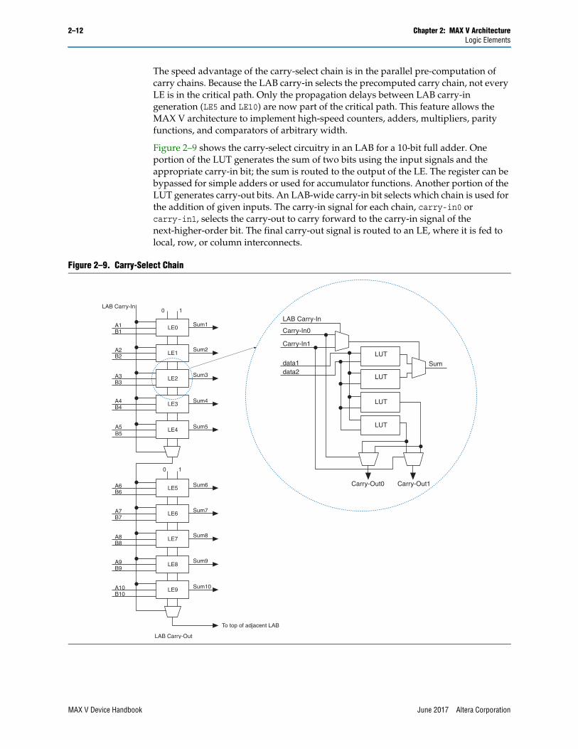
The speed advantage of the carry-select chain is in the parallel pre-computation of carry chains. Because the LAB carry-in selects the precomputed carry chain, not every LE is in the critical path. Only the propagation delays between LAB carry-in generation (LE5 and LE10) are now part of the critical path. This feature allows the MAX V architecture to implement high-speed counters, adders, multipliers, parity functions, and comparators of arbitrary width.
Figure 2–9 shows the carry-select circuitry in an LAB for a 10-bit full adder. One portion of the LUT generates the sum of two bits using the input signals and the appropriate carry-in bit; the sum is routed to the output of the LE. The register can be bypassed for simple adders or used for accumulator functions. Another portion of the LUT generates carry-out bits. An LAB-wide carry-in bit selects which chain is used for the addition of given inputs. The carry-in signal for each chain, carry-in0 or carry-in1, selects the carry-out to carry forward to the carry-in signal of the next-higher-order bit. The final carry-out signal is routed to an LE, where it is fed to local, row, or column interconnects.
Figure 2–9. Carry-Select Chain
LE3
LE2
LE1
LE0A1B1
A2B2
A3B3
A4B4
Sum1
Sum2
Sum3
Sum4
LE9
LE8
LE7
LE6A7B7
A8B8
A9B9
A10B10
Sum7
LE5A6B6
Sum6
LE4A5B5
Sum5
Sum8
Sum9
Sum10
0 1
0 1LAB Carry-In
LAB Carry-Out
LUT
LUT
LUT
LUT
data1
LAB Carry-In
data2
Carry-In0
Carry-In1
Carry-Out0 Carry-Out1
Sum
To top of adjacent LAB
MAX V Device Handbook June 2017 Altera Corporation

Chapter 2: MAX V Architecture 2–13Logic Elements
The Quartus II software automatically creates carry chain logic during design processing, or you can create it manually during design entry. Parameterized functions such as LPM functions automatically take advantage of carry chains for the appropriate functions. The Quartus II software creates carry chains longer than 10 LEs by linking adjacent LABs within the same row together automatically. A carry chain can extend horizontally up to one full LAB row, but does not extend between LAB rows.
Clear and Preset Logic ControlLAB-wide signals control the logic for the register’s clear and preset signals. The LE directly supports an asynchronous clear and preset function. The register preset is achieved through the asynchronous load of a logic high. MAX V devices support simultaneous preset/asynchronous load and clear signals. An asynchronous clear signal takes precedence if both signals are asserted simultaneously. Each LAB supports up to two clears and one preset signal.
In addition to the clear and preset ports, MAX V devices provide a chip-wide reset pin (DEV_CLRn) that resets all registers in the device. An option set before compilation in the Quartus II software controls this pin. This chip-wide reset overrides all other control signals and uses its own dedicated routing resources without using any of the four global resources. Driving this signal low before or during power-up prevents user mode from releasing clears within the design. This allows you to control when clear is released on a device that has just been powered-up. If not set for its chip-wide reset function, the DEV_CLRn pin is a regular I/O pin.
By default, all registers in MAX V devices are set to power-up low. However, this power-up state can be set to high on individual registers during design entry using the Quartus II software.
LE RAMThe Quartus II memory compiler can configure the unused LEs as LE RAM.
MAX V devices support the following memory types:
■ FIFO synchronous R/W
■ FIFO asynchronous R/W
■ 1 port SRAM
■ 2 port SRAM
■ 3 port SRAM
■ shift registers
f For more information about memory, refer to the Internal Memory (RAM and ROM) User Guide.
June 2017 Altera Corporation MAX V Device Handbook

2–14 Chapter 2: MAX V ArchitectureMultiTrack Interconnect
MultiTrack InterconnectIn the MAX V architecture, connections between LEs, the UFM, and device I/O pins are provided by the MultiTrack interconnect structure. The MultiTrack interconnect consists of continuous, performance-optimized routing lines used for inter- and intra-design block connectivity. The Quartus II Compiler automatically places critical design paths on faster interconnects to improve design performance.
The MultiTrack interconnect consists of row and column interconnects that span fixed distances. A routing structure with fixed length resources for all devices allows predictable and short delays between logic levels instead of large delays associated with global or long routing lines. Dedicated row interconnects route signals to and from LABs within the same row. These row resources include:
■ DirectLink interconnects between LABs
■ R4 interconnects traversing four LABs to the right or left
The DirectLink interconnect allows an LAB to drive into the local interconnect of its left and right neighbors. The DirectLink interconnect provides fast communication between adjacent LABs and blocks without using row interconnect resources.
The R4 interconnects span four LABs and are used for fast row connections in a four-LAB region. Every LAB has its own set of R4 interconnects to drive either left or right. Figure 2–10 shows R4 interconnect connections from an LAB. R4 interconnects can drive and be driven by row IOEs. For LAB interfacing, a primary LAB or horizontal LAB neighbor can drive a given R4 interconnect. For R4 interconnects that drive to the right, the primary LAB and right neighbor can drive on to the interconnect. For R4 interconnects that drive to the left, the primary LAB and its left neighbor can drive on to the interconnect. R4 interconnects can drive other R4 interconnects to extend the range of LABs they can drive. R4 interconnects can also drive C4 interconnects for connections from one row to another.
MAX V Device Handbook June 2017 Altera Corporation

Chapter 2: MAX V Architecture 2–15MultiTrack Interconnect
The column interconnect operates similarly to the row interconnect. Each column of LABs is served by a dedicated column interconnect, which vertically routes signals to and from LABs and row and column IOEs. These column resources include:
■ LUT chain interconnects within an LAB
■ Register chain interconnects within an LAB
■ C4 interconnects traversing a distance of four LABs in an up and down direction
MAX V devices include an enhanced interconnect structure within LABs for routing LE output to LE input connections faster using LUT chain connections and register chain connections. The LUT chain connection allows the combinational output of an LE to directly drive the fast input of the LE right below it, bypassing the local interconnect. These resources can be used as a high-speed connection for wide fan-in functions from LE 1 to LE 10 in the same LAB. The register chain connection allows the register output of one LE to connect directly to the register input of the next LE in the LAB for fast shift registers. The Quartus II Compiler automatically takes advantage of these resources to improve utilization and performance. Figure 2–11 shows the LUT chain and register chain interconnects.
Figure 2–10. R4 Interconnect Connections
Notes to Figure 2–10:
(1) C4 interconnects can drive R4 interconnects.(2) This pattern is repeated for every LAB in the LAB row.
PrimaryLAB (2)
R4 InterconnectDriving Left
Adjacent LAB candrive onto anotherLAB’s R4 Interconnect
C4 Column Interconnects (1)R4 InterconnectDriving Right
LABNeighbor
LABNeighbor
June 2017 Altera Corporation MAX V Device Handbook

2–16 Chapter 2: MAX V ArchitectureMultiTrack Interconnect
The C4 interconnects span four LABs up or down from a source LAB. Every LAB has its own set of C4 interconnects to drive either up or down. Figure 2–12 shows the C4 interconnect connections from an LAB in a column. The C4 interconnects can drive and be driven by column and row IOEs. For LAB interconnection, a primary LAB or its vertical LAB neighbor can drive a given C4 interconnect. C4 interconnects can drive each other to extend their range as well as drive row interconnects for column-to-column connections.
Figure 2–11. LUT Chain and Register Chain Interconnects
LE0
LE1
LE2
LE3
LE4
LE5
LE6
LE7
LE8
LE9
LUT ChainRouting to
Adjacent LE
LocalInterconnect
Register ChainRouting to AdjacentLE's Register Input
Local InterconnectRouting Among LEsin the LAB
MAX V Device Handbook June 2017 Altera Corporation

Chapter 2: MAX V Architecture 2–17MultiTrack Interconnect
Figure 2–12. C4 Interconnect Connections (Note 1)
Note to Figure 2–12:
(1) Each C4 interconnect can drive either up or down four rows.
C4 InterconnectDrives Local and R4InterconnectsUp to Four Rows
Adjacent LAB candrive onto neighboringLAB's C4 interconnect
C4 InterconnectDriving Up
C4 InterconnectDriving Down
LAB
RowInterconnect
LocalInterconnect
June 2017 Altera Corporation MAX V Device Handbook
2–18 Chapter 2: MAX V ArchitectureMultiTrack Interconnect
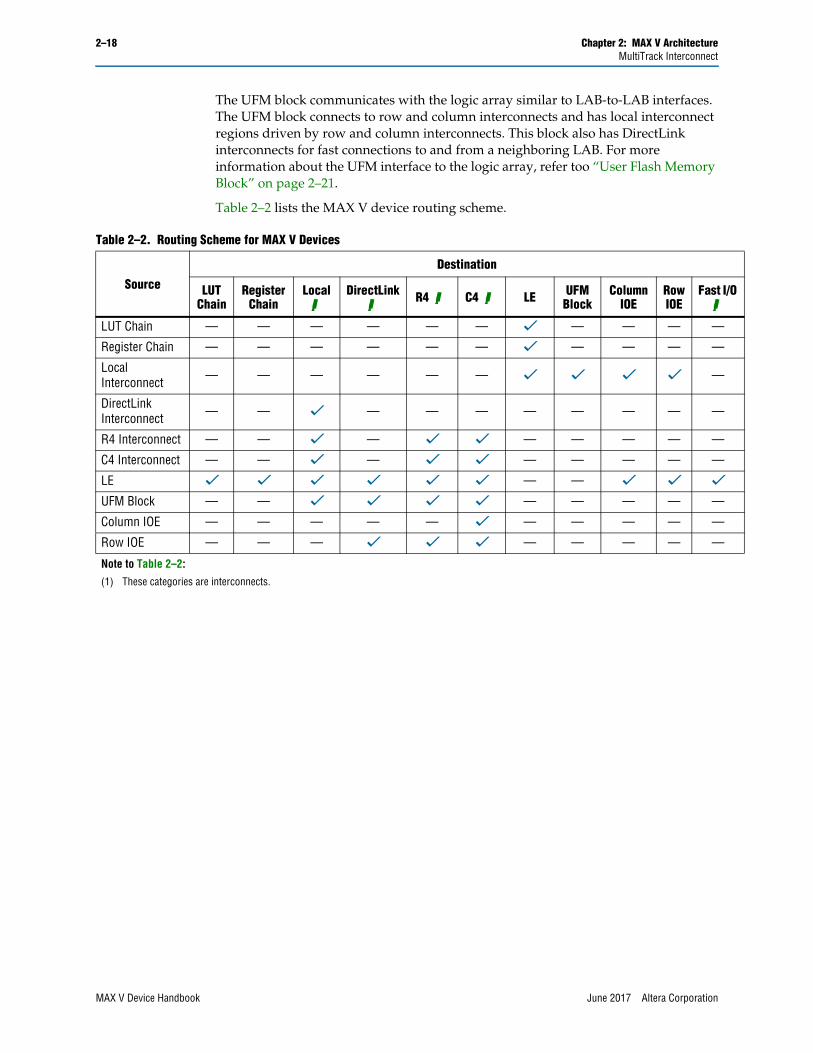
The UFM block communicates with the logic array similar to LAB-to-LAB interfaces. The UFM block connects to row and column interconnects and has local interconnect regions driven by row and column interconnects. This block also has DirectLink interconnects for fast connections to and from a neighboring LAB. For more information about the UFM interface to the logic array, refer too “User Flash Memory Block” on page 2–21.
Table 2–2 lists the MAX V device routing scheme.
Table 2–2. Routing Scheme for MAX V Devices
Source
Destination
LUT Chain
Register Chain
Local (1)
DirectLink (1) R4 (1) C4 (1) LE UFM
BlockColumn
IOERow IOE
Fast I/O(1)
LUT Chain — — — — — — v — — — —
Register Chain — — — — — — v — — — —
Local Interconnect — — — — — — v v v v —
DirectLink Interconnect — — v — — — — — — — —
R4 Interconnect — — v — v v — — — — —
C4 Interconnect — — v — v v — — — — —
LE v v v v v v — — v v vUFM Block — — v v v v — — — — —
Column IOE — — — — — v — — — — —
Row IOE — — — v v v — — — — —
Note to Table 2–2:
(1) These categories are interconnects.
MAX V Device Handbook June 2017 Altera Corporation

Chapter 2: MAX V Architecture 2–19Global Signals
Global SignalsEach MAX V device has four dual-purpose dedicated clock pins (GCLK[3..0], two pins on the left side and two pins on the right side) that drive the global clock network for clocking, as shown in Figure 2–13. These four pins can also be used as GPIOs if they are not used to drive the global clock network.
The four global clock lines in the global clock network drive throughout the entire device. The global clock network can provide clocks for all resources within the device including LEs, LAB local interconnect, IOEs, and the UFM block. The global clock lines can also be used for global control signals, such as clock enables, synchronous or asynchronous clears, presets, output enables, or protocol control signals such as TRDY and IRDY for the PCI I/O standard. Internal logic can drive the global clock network for internally-generated global clocks and control signals. Figure 2–13 shows the various sources that drive the global clock network.
The global clock network drives to individual LAB column signals, LAB column clocks [3..0], that span an entire LAB column from the top to the bottom of the device. Unused global clocks or control signals in an LAB column are turned off at the LAB column clock buffers shown in Figure 2–14. The LAB column clocks [3..0] are multiplexed down to two LAB clock signals and one LAB clear signal. Other control signal types route from the global clock network into the LAB local interconnect. For more information, refer to “LAB Control Signals” on page 2–6.
Figure 2–13. Global Clock Generation
Note to Figure 2–13:(1) Any I/O pin can use a MultiTrack interconnect to route as a logic array-generated global clock signal.
4
4
GCLK0
Global ClockNetwork
GCLK1GCLK2GCLK3
Logic Array(1)
June 2017 Altera Corporation MAX V Device Handbook

2–20 Chapter 2: MAX V ArchitectureGlobal Signals
Figure 2–14. Global Clock Network (Note 1)
Notes to Figure 2–14:
(1) LAB column clocks in I/O block regions provide high fan-out output enable signals.(2) LAB column clocks drive to the UFM block.
UFM Block (2)
CFM Block
I/O Block Region
I/O Block Region
I/O Block Region
LAB Column clock[3..0]
LAB Columnclock[3..0]
4 4 4 4 4 4 4 4
MAX V Device Handbook June 2017 Altera Corporation

Chapter 2: MAX V Architecture 2–21User Flash Memory Block
User Flash Memory BlockMAX V devices feature a single UFM block, which can be used like a serial EEPROM for storing non-volatile information up to 8,192 bits. The UFM block connects to the logic array through the MultiTrack interconnect, allowing any LE to interface to the UFM block. Figure 2–15 shows the UFM block and interface signals. The logic array is used to create customer interface or protocol logic to interface the UFM block data outside of the device. The UFM block offers the following features:
■ Non-volatile storage up to 16-bit wide and 8,192 total bits
■ Two sectors for partitioned sector erase
■ Built-in internal oscillator that optionally drives logic array
■ Program, erase, and busy signals
■ Auto-increment addressing
■ Serial interface to logic array with programmable interface
Figure 2–15. UFM Block and Interface Signals
OSC 4
ProgramErase
Control
UFM Sector 1
UFM Sector 0
:_
AddressRegister
PROGRAM
ERASE
OSC_ENA
RTP_BUSY
BUSY
OSC
Data Register
UFM Block
DRDin DRDout
ARCLK
ARSHFT
ARDin
DRCLK
DRSHFT
16 16
9
June 2017 Altera Corporation MAX V Device Handbook

2–22 Chapter 2: MAX V ArchitectureUser Flash Memory Block
UFM StorageEach device stores up to 8,192 bits of data in the UFM block. Table 2–3 lists the data size, sector, and address sizes for the UFM block.
There are 512 locations with 9-bit addressing ranging from 000h to 1FFh. The sector 0 address space is 000h to 0FFh and the sector 1 address space is from 100h to 1FFh. The data width is up to 16 bits of data. The Quartus II software automatically creates logic to accommodate smaller read or program data widths. Erasure of the UFM involves individual sector erasing (that is, one erase of sector 0 and one erase of sector 1 is required to erase the entire UFM block). Because sector erase is required before a program or write operation, having two sectors enables a sector size of data to be left untouched while the other sector is erased and programmed with new data.
Internal OscillatorAs shown in Figure 2–15, the dedicated circuitry within the UFM block contains an oscillator. The dedicated circuitry uses this oscillator internally for its read and program operations. This oscillator's divide by 4 output can drive out of the UFM block as a logic interface clock source or for general-purpose logic clocking. The typical OSC output signal frequency ranges from 3.9 to 5.3 MHz, and its exact frequency of operation is not programmable.
The UFM internal oscillator can be instantiated using the MegaWizard™ Plug-In Manager. You can also use the MAX II/MAX V Oscillator megafunction to instantiate the UFM oscillator without using the UFM memory block.
Table 2–3. UFM Array Size
Device Total Bits Sectors Address Bits Data Width
5M40Z 8,192 2 (4,096 bits per sector) 9 16
5M80Z 8,192 2 (4,096 bits per sector) 9 16
5M160Z 8,192 2 (4,096 bits per sector) 9 16
5M240Z 8,192 2 (4,096 bits per sector) 9 16
5M570Z 8,192 2 (4,096 bits per sector) 9 16
5M1270Z 8,192 2 (4,096 bits per sector) 9 16
5M2210Z 8,192 2 (4,096 bits per sector) 9 16
MAX V Device Handbook June 2017 Altera Corporation

Chapter 2: MAX V Architecture 2–23User Flash Memory Block
Program, Erase, and Busy SignalsThe UFM block’s dedicated circuitry automatically generates the necessary internal program and erase algorithm after the PROGRAM or ERASE input signals have been asserted. The PROGRAM or ERASE signal must be asserted until the busy signal deasserts, indicating the UFM internal program or erase operation has completed. The UFM block also supports JTAG as the interface for programming and reading.
f For more information about programming and erasing the UFM block, refer to the User Flash Memory in MAX V Devices chapter.
Auto-Increment AddressingThe UFM block supports standard read or stream read operations. The stream read is supported with an auto-increment address feature. Deasserting the ARSHIFT signal while clocking the ARCLK signal increments the address register value to read consecutive locations from the UFM array.
Serial InterfaceThe UFM block supports a serial interface with serial address and data signals. The internal shift registers within the UFM block for address and data are 9 bits and 16 bits wide, respectively. The Quartus II software automatically generates interface logic in LEs for a parallel address and data interface to the UFM block. Other standard protocol interfaces such as SPI are also automatically generated in LE logic by the Quartus II software.
f For more information about the UFM interface signals and the Quartus II LE-based alternate interfaces, refer to the User Flash Memory in MAX V Devices chapter.
June 2017 Altera Corporation MAX V Device Handbook

2–24 Chapter 2: MAX V ArchitectureUser Flash Memory Block
UFM Block to Logic Array InterfaceThe UFM block is a small partition of the flash memory that contains the CFM block, as shown in Figure 2–1 and Figure 2–2. The UFM block for the 5M40Z, 5M80Z, 5M160Z, and 5M240Z devices is located on the left side of the device adjacent to the left most LAB column. The UFM blocks for the 5M570Z, 5M1270Z, and 5M2210Z devices are located at the bottom left of the device. The UFM input and output signals interface to all types of interconnects (R4 interconnect, C4 interconnect, and DirectLink interconnect to/from adjacent LAB rows). The UFM signals can also be driven from global clocks, GCLK[3..0]. The interface regions for the 5M40Z, 5M80Z, 5M160Z, and 5M240Z devices are shown in Figure 2–16. The interface regions for 5M570Z, 5M1270Z, and 5M2210Z devices are shown in Figure 2–17.
Figure 2–16. 5M40Z, 5M80Z, 5M160Z, and 5M240Z UFM Block LAB Row Interface (Note 1), (2)
Notes to Figure 2–16:
(1) The UFM block inputs and outputs can drive to and from all types of interconnects, not only DirectLink interconnects from adjacent row LABs.
(2) Not applicable to the T144 package of the 5M240Z device.
UFM Block
CFM Block
PROGRAM
ERASE
OSC_ENA
DRDinDRCLK
DRSHFTARin
ARCLKARSHFTDRDout
OSCBUSY
RTP_BUSY
LAB
LAB
LAB
MAX V Device Handbook June 2017 Altera Corporation

Chapter 2: MAX V Architecture 2–25Core Voltage
Core VoltageThe MAX V architecture supports a 1.8-V core voltage on the VCCINT supply. You must use a 1.8-V VCC external supply to power the VCCINT pins.
Figure 2–17. 5M240Z, 5M570Z, 5M1270Z, and 5M2210Z UFM Block LAB Row Interface (Note 1)
Note to Figure 2–17:
(1) Only applicable to the T144 package of the 5M240Z device.
RTP_BUSYBUSY
OSCDRDout
DRDin
PROGRAMERASE
OSC_ENAARCLK
ARSHFT
DRDCLKDRDSHFT
ARDin
UFM Block
CFM Block
LAB
LAB
LAB
Figure 2–18. Core Voltage Feature in MAX V Devices
MAX V Device
1.8-V onVCCINT Pins
1.8-V CoreVoltage
June 2017 Altera Corporation MAX V Device Handbook
2–26 Chapter 2: MAX V ArchitectureI/O Structure
I/O StructureIOEs support many features, including:
■ LVTTL, LVCMOS, LVDS, and RSDS I/O standards
■ 3.3-V, 32-bit, 33-MHz PCI compliance
■ JTAG boundary-scan test (BST) support
■ Programmable drive strength control
■ Weak pull-up resistors during power-up and in system programming
■ Slew-rate control
■ Tri-state buffers with individual output enable control
■ Bus-hold circuitry
■ Programmable pull-up resistors in user mode
■ Unique output enable per pin
■ Open-drain outputs
■ Schmitt trigger inputs
■ Fast I/O connection
■ Programmable input delay
MAX V device IOEs contain a bidirectional I/O buffer. Figure 2–19 shows the MAX V IOE structure. Registers from adjacent LABs can drive to or be driven from the IOE’s bidirectional I/O buffers. The Quartus II software automatically attempts to place registers in the adjacent LAB with fast I/O connection to achieve the fastest possible clock-to-output and registered output enable timing. When the fast input registers option is enabled, the Quartus II software automatically routes the register to guarantee zero hold time. You can set timing assignments in the Quartus II software to achieve desired I/O timing.
MAX V Device Handbook June 2017 Altera Corporation

Chapter 2: MAX V Architecture 2–27I/O Structure
Fast I/O ConnectionA dedicated fast I/O connection from the adjacent LAB to the IOEs within an I/O block provides faster output delays for clock-to-output and tPD propagation delays. This connection exists for data output signals, not output enable signals or input signals. Figure 2–20, Figure 2–21, and Figure 2–22 illustrate the fast I/O connection.
Figure 2–19. IOE Structure for MAX V Devices
Notes to Figure 2–19:
(1) Available only in I/O bank 3 of 5M1270Z and 5M2210Z devices.(2) The programmable pull-up resistor is active during power-up, in-system programming (ISP), and if the device is unprogrammed.
Data_in
Optional SchmittTrigger Input
Drive Strength ControlOpen-Drain Output
Slew Control
Fast_out
Data_out OE
OptionalPCI Clamp (1)
ProgrammablePull-Up (2)
VCCIO VCCIO
I/O Pin
Optional Bus-Hold Circuit
DEV_OE
ProgrammableInput Delay
June 2017 Altera Corporation MAX V Device Handbook

2–28 Chapter 2: MAX V ArchitectureI/O Structure
I/O BlocksThe IOEs are located in I/O blocks around the periphery of the MAX V device. There are up to seven IOEs per row I/O block and up to four IOEs per column I/O block. Each column or row I/O block interfaces with its adjacent LAB and MultiTrack interconnect to distribute signals throughout the device. The row I/O blocks drive row, column, or DirectLink interconnects. The column I/O blocks drive column interconnects.
1 5M40Z, 5M80Z, 5M160Z, and 5M240Z devices have a maximum of five IOEs per row I/O block.
Figure 2–20 shows how a row I/O block connects to the logic array.
Figure 2–20. Row I/O Block Connection to the Interconnect (Note 1)
Note to Figure 2–20:
(1) Each of the seven IOEs in the row I/O block can have one data_out or fast_out output, one OE output, and one data_in input.
7
R4 Interconnects C4 Interconnects
I/O Block Local Interconnect
data_in[6..0]
data_out[6..0]
7
OE[6..0]
7
7
fast_out[6..0]
Row I/O BlockContains up to
Seven IOEs
Direct LinkInterconnect
to Adjacent LAB
Direct LinkInterconnect
from Adjacent LAB
LAB Columnclock [3..0]
LAB LocalInterconnect
LAB RowI/O Block
MAX V Device Handbook June 2017 Altera Corporation

Chapter 2: MAX V Architecture 2–29I/O Structure
Figure 2–21 shows how a column I/O block connects to the logic array.
I/O Standards and BanksTable 2–4 lists the I/O standards supported by MAX V devices.
Figure 2–21. Column I/O Block Connection to the Interconnect (Note 1)
Note to Figure 2–21:
(1) Each of the four IOEs in the column I/O block can have one data_out or fast_out output, one OE output, and one data_in input.
Column I/O Block ContainsUp To 4 IOEs
I/O BlockLocal Interconnect
R4 Interconnects
LAB LocalInterconnect
C4 Interconnects
LAB LocalInterconnect
C4 Interconnects
4
LAB LAB LAB
data_out[3..0]
4
OE[3..0]
4
fast_out[3..0]
Fast I/OInterconnect
Path
4
data_in[3..0]
Column I/O Block
LAB LocalInterconnect
LAB ColumnClock [3..0]
Table 2–4. MAX V I/O Standards (Part 1 of 2)
I/O Standard Type Output Supply Voltage (VCCIO) (V)
3.3-V LVTTL/LVCMOS Single-ended 3.3
2.5-V LVTTL/LVCMOS Single-ended 2.5
1.8-V LVTTL/LVCMOS Single-ended 1.8
1.5-V LVCMOS Single-ended 1.5
1.2-V LVCMOS Single-ended 1.2
June 2017 Altera Corporation MAX V Device Handbook

2–30 Chapter 2: MAX V ArchitectureI/O Structure
The 5M40Z, 5M80Z, 5M160Z, 5M240Z, and 5M570Z devices support two I/O banks, as shown in Figure 2–22. Each of these banks support all the LVTTL, LVCMOS, LVDS, and RSDS standards shown in Table 2–4. PCI compliant I/O is not supported in these devices and banks.
3.3-V PCI (1) Single-ended 3.3
LVDS (2) Differential 2.5
RSDS (3) Differential 2.5
Notes to Table 2–4:
(1) The 3.3-V PCI compliant I/O is supported in Bank 3 of the 5M1270Z and 5M2210Z devices.(2) MAX V devices only support emulated LVDS output using a three resistor network (LVDS_E_3R).(3) MAX V devices only support emulated RSDS output using a three resistor network (RSDS_E_3R).
Figure 2–22. I/O Banks for 5M40Z, 5M80Z, 5M160Z, 5M240Z, and 5M570Z Devices (Note 1), (2)
Notes to Figure 2–22:
(1) Figure 2–22 is a top view of the silicon die.
(2) Figure 2–22 is a graphical representation only. Refer to the pin list and the Quartus II software for exact pin locations.
(3) This I/O standard is not supported in Bank 1.(4) Emulated LVDS output using a three resistor network (LVDS_E_3R).(5) Emulated RSDS output using a three resistor network (RSDS_E_3R).
Table 2–4. MAX V I/O Standards (Part 2 of 2)
I/O Standard Type Output Supply Voltage (VCCIO) (V)
All I/O Banks Support3.3-V LVTTL/LVCMOS,2.5-V LVTTL/LVCMOS,1.8-V LVTTL/LVCMOS,1.5-V LVCMOS,1.2-V LVDS (4)RSDS (5)
, LVCMOS (3),
I/O Bank 2I/O Bank 1
MAX V Device Handbook June 2017 Altera Corporation

Chapter 2: MAX V Architecture 2–31I/O Structure
The 5M1270Z and 5M2210Z devices support four I/O banks, as shown in Figure 2–23. Each of these banks support all of the LVTTL, LVCMOS, LVDS, and RSDS standards shown in Table 2–4. PCI compliant I/O is supported in Bank 3. Bank 3 supports the PCI clamping diode on inputs and PCI drive compliance on outputs. You must use Bank 3 for designs requiring PCI compliant I/O pins. The Quartus II software automatically places I/O pins in this bank if assigned with the PCI I/O standard.
Each I/O bank has dedicated VCCIO pins that determine the voltage standard support in that bank. A single device can support 1.2-V, 1.5-V, 1.8-V, 2.5-V, and 3.3-V interfaces; each individual bank can support a different standard. Each I/O bank can support multiple standards with the same VCCIO for input and output pins. For example, when VCCIO is 3.3 V, Bank 3 can support LVTTL, LVCMOS, and 3.3-V PCI. VCCIO powers both the input and output buffers in MAX V devices.
The JTAG pins for MAX V devices are dedicated pins that cannot be used as regular I/O pins. The pins TMS, TDI, TDO, and TCK support all the I/O standards shown in Table 2–4 on page 2–29 except for PCI and 1.2-V LVCMOS. These pins reside in Bank 1 for all MAX V devices and their I/O standard support is controlled by the VCCIO setting for Bank 1.
Figure 2–23. I/O Banks for 5M1270Z and 5M2210Z Devices (Note 1), (2)
Notes to Figure 2–23:
(1) Figure 2–23 is a top view of the silicon die.(2) Figure 2–23 is a graphical representation only. Refer to the pin list and the Quartus II software for exact pin locations.(3) This I/O standard is not supported in Bank 1.(4) Emulated LVDS output using a three resistor network (LVDS_E_3R).(5) Emulated RSDS output using a three resistor network (RSDS_E_3R).
I/O Bank 2
I/O Bank 3
I/O Bank 4
I/O Bank 1
Also Supportsthe 3.3-V PCII/O StandardAll I/O Banks Support
3.3-V LVTTL/LVCMOS,2.5-V LVTTL/LVCMOS,1.8-V LVTTL/LVCMOS,1.5-V LVCMOS,1.2-V LVCMOS (3),LVDS (4),RSDS(5)
June 2017 Altera Corporation MAX V Device Handbook

2–32 Chapter 2: MAX V ArchitectureI/O Structure
PCI ComplianceThe MAX V 5M1270Z and 5M2210Z devices are compliant with PCI applications as well as all 3.3-V electrical specifications in the PCI Local Bus Specification Revision 2.2. These devices are also large enough to support PCI intellectual property (IP) cores. Table 2–5 shows the MAX V device speed grades that meet the PCI timing specifications.
LVDS and RSDS ChannelsThe MAX V device supports emulated LVDS and RSDS outputs on both row and column I/O banks. You can configure the rows and columns as emulated LVDS or RSDS output buffers that use two single-ended output buffers with three external resistor networks.
Schmitt TriggerThe input buffer for each MAX V device I/O pin has an optional Schmitt trigger setting for the 3.3-V and 2.5-V standards. The Schmitt trigger allows input buffers to respond to slow input edge rates with a fast output edge rate. Most importantly, Schmitt triggers provide hysteresis on the input buffer, preventing slow-rising noisy input signals from ringing or oscillating on the input signal driven into the logic array. This provides system noise tolerance on MAX V inputs, but adds a small, nominal input delay.
The JTAG input pins (TMS, TCK, and TDI) have Schmitt trigger buffers that are always enabled.
1 The TCK input is susceptible to high pulse glitches when the input signal fall time is greater than 200 ns for all I/O standards.
Table 2–5. 3.3-V PCI Electrical Specifications and PCI Timing Support for MAX V Devices
Device 33-MHz PCI
5M1270Z All Speed Grades
5M2210Z All Speed Grades
Table 2–6. LVDS and RSDS Channels supported in MAX V Devices (Note 1)
Device 64 MBGA 64 EQFP 68 MBGA 100 TQFP 100 MBGA 144 TQFP 256 FBGA 324 FBGA
5M40Z 10 eTx 20 eTx — — — — — —
5M80Z 10 eTx 20 eTx 20 eTx 33 eTx — — — —
5M160Z — 20 eTx 20 eTx 33 eTx 33 eTx — — —
5M240Z — — 20 eTx 33 eTx 33 eTx 49 eTx — —
5M570Z — — — 28 eTx 28 eTx 49 eTx 75 eTx —
5M1270Z — — — — — 42 eTx 90 eTx 115 eTx
5M2210Z — — — — — — 83 eTx 115 eTx
Note to Table 2–6:
(1) eTx = emulated LVDS output buffers (LVDS_E_3R) or emulated RSDS output buffers (RSDS_E_3R).
MAX V Device Handbook June 2017 Altera Corporation

Chapter 2: MAX V Architecture 2–33I/O Structure
Output Enable SignalsEach MAX V IOE output buffer supports output enable signals for tri-state control. The output enable signal can originate from the GCLK[3..0] global signals or from the MultiTrack interconnect. The MultiTrack interconnect routes output enable signals and allows for a unique output enable for each output or bidirectional pin.
MAX V devices also provide a chip-wide output enable pin (DEV_OE) to control the output enable for every output pin in the design. An option set before compilation in the Quartus II software controls this pin. This chip-wide output enable uses its own routing resources and does not use any of the four global resources. If this option is turned on, all outputs on the chip operate normally when DEV_OE is asserted. When the pin is deasserted, all outputs are tri-stated. If this option is turned off, the DEV_OE pin is disabled when the device operates in user mode and is available as a user I/O pin.
Programmable Drive StrengthThe output buffer for each MAX V device I/O pin has two levels of programmable drive strength control for each of the LVTTL and LVCMOS I/O standards. Programmable drive strength provides system noise reduction control for high performance I/O designs. Although a separate slew-rate control feature exists, using the lower drive strength setting provides signal slew-rate control to reduce system noise and signal overshoot without the large delay adder associated with the slew-rate control feature. Table 2–7 lists the possible settings for the I/O standards with drive strength control. The Quartus II software uses the maximum current strength as the default setting. The PCI I/O standard is always set at 20 mA with no alternate setting.
1 The programmable drive strength feature can be used simultaneously with the slew-rate control feature.
Table 2–7. Programmable Drive Strength (Note 1)
I/O Standard IOH/IOL Current Strength Setting (mA)
3.3-V LVTTL16
8
3.3-V LVCMOS8
4
2.5-V LVTTL/LVCMOS14
7
1.8-V LVTTL/LVCMOS6
3
1.5-V LVCMOS4
2
1.2-V LVCMOS 3
Note to Table 2–7:
(1) The IOH current strength numbers shown are for a condition of a VOUT = VOH minimum, where the VOH minimum is specified by the I/O standard. The IOL current strength numbers shown are for a condition of a VOUT = VOL maximum, where the VOL maximum is specified by the I/O standard. For 2.5-V LVTTL/LVCMOS, the IOH condition is VOUT = 1.7 V and the IOL condition is VOUT = 0.7 V.
June 2017 Altera Corporation MAX V Device Handbook

2–34 Chapter 2: MAX V ArchitectureI/O Structure
Slew-Rate ControlThe output buffer for each MAX V device I/O pin has a programmable output slew-rate control that can be configured for low noise or high-speed performance. A faster slew rate provides high-speed transitions for high-performance systems. However, these fast transitions may introduce noise transients into the system. A slow slew rate reduces system noise, but adds a nominal output delay to rising and falling edges. The lower the voltage standard (for example, 1.8-V LVTTL) the larger the output delay when slow slew is enabled. Each I/O pin has an individual slew-rate control, allowing you to specify the slew rate on a pin-by-pin basis. The slew-rate control affects both the rising and falling edges. If no slew-rate control is specified, the Quartus II software defaults to a fast slew rate.
1 The slew-rate control feature can be used simultaneously with the programmable drive strength feature.
Open-Drain OutputMAX V devices provide an optional open-drain (equivalent to open-collector) output for each I/O pin. This open-drain output enables the device to provide system-level control signals (for example, interrupt and write enable signals) that can be asserted by any of several devices. This output can also provide an additional wired-OR plane.
Programmable Ground PinsEach unused I/O pin on MAX V devices can be used as an additional ground pin. This programmable ground feature does not require the use of the associated LEs in the device. In the Quartus II software, unused pins can be set as programmable GND on a global default basis or they can be individually assigned. Unused pins also have the option of being set as tri-stated input pins.
Bus-HoldEach MAX V device I/O pin provides an optional bus-hold feature. The bus-hold circuitry can hold the signal on an I/O pin at its last-driven state. Because the bus-hold feature holds the last-driven state of the pin until the next input signal is present, an external pull-up or pull-down resistor is not necessary to hold a signal level when the bus is tri-stated.
The bus-hold circuitry also pulls un-driven pins away from the input threshold voltage where noise can cause unintended high-frequency switching. You can select this feature individually for each I/O pin. The bus-hold output will drive no higher than VCCIO to prevent overdriving signals. If the bus-hold feature is enabled, the device cannot use the programmable pull-up option.
The bus-hold circuitry is only active after the device has fully initialized. The bus-hold circuit captures the value on the pin present at the moment user mode is entered.
MAX V Device Handbook June 2017 Altera Corporation

Chapter 2: MAX V Architecture 2–35I/O Structure
Programmable Pull-Up ResistorEach MAX V device I/O pin provides an optional programmable pull-up resistor during user mode. If you enable this feature for an I/O pin, the pull-up resistor holds the output to the VCCIO level of the output pin’s bank.
1 The programmable pull-up resistor feature should not be used at the same time as the bus-hold feature on a given I/O pin.
1 The programmable pull-up resistor is active during power-up, ISP, and if the device is unprogrammed.
Programmable Input DelayThe MAX V IOE includes a programmable input delay that is activated to ensure zero hold times. A path where a pin directly drives a register, with minimal routing between the two, may require the delay to ensure zero hold time. However, a path where a pin drives a register through long routing or through combinational logic may not require the delay to achieve a zero hold time. The Quartus II software uses this delay to ensure zero hold times when needed.
MultiVolt I/O InterfaceThe MAX V architecture supports the MultiVolt I/O interface feature, which allows MAX V devices in all packages to interface with systems of different supply voltages. The devices have one set of VCC pins for internal operation (VCCINT), and up to four sets for input buffers and I/O output driver buffers (VCCIO), depending on the number of I/O banks available in the devices where each set of VCCIO pins powers one I/O bank. The 5M40Z, 5M80Z, 5M160Z, 5M240Z, and 5M570Z devices each have two I/O banks while the 5M1270Z and 5M2210Z devices each have four I/O banks.
Connect VCCIO pins to either a 1.2-, 1.5-, 1.8-, 2.5-, or 3.3-V power supply, depending on the output requirements. The output levels are compatible with systems of the same voltage as the power supply (that is, when VCCIO pins are connected to a 1.5-V power supply, the output levels are compatible with 1.5-V systems). When VCCIO pins are connected to a 3.3-V power supply, the output high is 3.3 V and is compatible with 3.3-V or 5.0-V systems. Table 2–8 summarizes MAX V MultiVolt I/O support.
Table 2–8. MultiVolt I/O Support in MAX V Devices (Part 1 of 2) (Note 1)
VCCIO (V)Input Signal Output Signal
1.2 V 1.5 V 1.8 V 2.5 V 3.3 V 5.0 V 1.2 V 1.5 V 1.8 V 2.5 V 3.3 V 5.0 V
1.2 v — — — — — v — — — — —
1.5 — v v v v — v v — — — —
1.8 — v v v v — v (2) v (2) v — — —
2.5 — — — v v — v (3) v (3) v (3) v — —
June 2017 Altera Corporation MAX V Device Handbook

2–36 Chapter 2: MAX V ArchitectureDocument Revision History
Document Revision HistoryTable 2–9 lists the revision history for this chapter.
3.3 — — — v (4) v v (5) v (6) v (6) v (6) v (6) v v (7)
Notes to Table 2–8:
(1) To drive inputs higher than VCCIO but less than 4.0 V including the overshoot, disable the I/O clamp diode. However, to drive 5.0-V signals to the device, enable the I/O clamp diode to prevent VI from rising above 4.0 V. Use an external diode if the I/O pin does not support the clamp diode.
(2) When VCCIO = 1.8 V, a MAX V device can drive a 1.2-V or 1.5-V device with 1.8-V tolerant inputs.(3) When VCCIO = 2.5 V, a MAX V device can drive a 1.2-V, 1.5-V, or 1.8-V device with 2.5-V tolerant inputs.(4) When VCCIO = 3.3 V and a 2.5-V input signal feeds an input pin, the VCCIO supply current will be slightly larger than expected.(5) MAX V devices can be 5.0-V tolerant with the use of an external resistor and the internal I/O clamp diode on the 5M1270Z and 5M2210Z devices.
Use an external clamp diode if the internal clamp diode is not available.(6) When VCCIO = 3.3 V, a MAX V device can drive a 1.2-V, 1.5-V, 1.8-V, or 2.5-V device with 3.3-V tolerant inputs.(7) When VCCIO = 3.3 V, a MAX V device can drive a device with 5.0-V TTL inputs but not 5.0-V CMOS inputs. For 5.0-V CMOS, open-drain setting
with internal I/O clamp diode (available only on 5M1270Z and 5M2210Z devices) and external resistor is required. Use an external clamp diode if the internal clamp diode is not available.
Table 2–8. MultiVolt I/O Support in MAX V Devices (Part 2 of 2) (Note 1)
VCCIO (V)Input Signal Output Signal
1.2 V 1.5 V 1.8 V 2.5 V 3.3 V 5.0 V 1.2 V 1.5 V 1.8 V 2.5 V 3.3 V 5.0 V
Table 2–9. Document Revision History
Date Version Changes
December 2010 1.0 Initial release.
MAX V Device Handbook June 2017 Altera Corporation

MAX V Device HandbookMay 2011
MV51003-1.2
© 2011 Altera Corporation. All rights reserved. ALTERA, ARRand/or trademarks of Altera Corporation in the U.S. and otherwww.altera.com/common/legal.html. Altera warrants performreserves the right to make changes to any products and servicesinformation, product, or service described herein except as expspecifications before relying on any published information and
May 2011MV51003-1.2
3. DC and Switching Characteristics forMAX V Devices
This chapter covers the electrical and switching characteristics for MAX® V devices. Electrical characteristics include operating conditions and power consumptions. This chapter also describes the timing model and specifications.
You must consider the recommended DC and switching conditions described in this chapter to maintain the highest possible performance and reliability of the MAX V devices.
This chapter contains the following sections:
■ “Operating Conditions” on page 3–1
■ “Power Consumption” on page 3–10
■ “Timing Model and Specifications” on page 3–10
Operating ConditionsTable 3–1 through Table 3–15 on page 3–9 list information about absolute maximum ratings, recommended operating conditions, DC electrical characteristics, and other specifications for MAX V devices.
Absolute Maximum RatingsTable 3–1 lists the absolute maximum ratings for the MAX V device family.
Table 3–1. Absolute Maximum Ratings for MAX V Devices (Note 1), (2)
Symbol Parameter Conditions Minimum Maximum Unit
VCCINT Internal supply voltage With respect to ground –0.5 2.4 V
VCCIO I/O supply voltage — –0.5 4.6 V
VI DC input voltage — –0.5 4.6 V
IOUT DC output current, per pin — –25 25 mA
TSTG Storage temperature No bias –65 150 °C
TAMB Ambient temperature Under bias (3) –65 135 °C
TJ Junction temperature TQFP and BGA packages under bias — 135 °C
Notes to Table 3–1:
(1) For more information, refer to the Operating Requirements for Altera Devices Data Sheet.(2) Conditions beyond those listed in Table 3–1 may cause permanent damage to a device. Additionally, device operation at the absolute maximum
ratings for extended periods of time may have adverse affects on the device.(3) For more information about “under bias” conditions, refer to Table 3–2.
Subscribe
IA, CYCLONE, HARDCOPY, MAX, MEGACORE, NIOS, QUARTUS and STRATIX are Reg. U.S. Pat. & Tm. Off. countries. All other trademarks and service marks are the property of their respective holders as described at
ance of its semiconductor products to current specifications in accordance with Altera’s standard warranty, but at any time without notice. Altera assumes no responsibility or liability arising out of the application or use of any ressly agreed to in writing by Altera. Altera customers are advised to obtain the latest version of device before placing orders for products or services.

3–2 Chapter 3: DC and Switching Characteristics for MAX V DevicesOperating Conditions
Recommended Operating ConditionsTable 3–2 lists recommended operating conditions for the MAX V device family.
Table 3–2. Recommended Operating Conditions for MAX V Devices
Symbol Parameter Conditions Minimum Maximum Unit
VCCINT (1) 1.8-V supply voltage for internal logic and in-system programming (ISP) MAX V devices 1.71 1.89 V
VCCIO (1)
Supply voltage for I/O buffers, 3.3-V operation — 3.00 3.60 V
Supply voltage for I/O buffers, 2.5-V operation — 2.375 2.625 V
Supply voltage for I/O buffers, 1.8-V operation — 1.71 1.89 V
Supply voltage for I/O buffers, 1.5-V operation — 1.425 1.575 V
Supply voltage for I/O buffers, 1.2-V operation — 1.14 1.26 V
VI Input voltage (2), (3), (4) –0.5 4.0 V
VO Output voltage — 0 VCCIO V
TJ Operating junction temperature
Commercial range 0 85 °C
Industrial range –40 100 °C
Extended range (5) –40 125 °C
Notes to Table 3–2:
(1) MAX V device ISP and/or user flash memory (UFM) programming using JTAG or logic array is not guaranteed outside the recommended operating conditions (for example, if brown-out occurs in the system during a potential write/program sequence to the UFM, Altera recommends that you read back the UFM contents and verify it against the intended write data).
(2) The minimum DC input is –0.5 V. During transitions, the inputs may undershoot to –2.0 V for input currents less than 100 mA and periods shorter than 20 ns.
(3) During transitions, the inputs may overshoot to the voltages shown below based on the input duty cycle. The DC case is equivalent to 100% duty cycle. For more information about 5.0-V tolerance, refer to the Using MAX V Devices in Multi-Voltage Systems chapter.VIN Max. Duty Cycle4.0 V 100% (DC)4.1 V 90%4.2 V 50%4.3 V 30%4.4 V 17%4.5 V 10%
(4) All pins, including the clock, I/O, and JTAG pins, may be driven before VCCINT and VCCIO are powered.(5) For the extended temperature range of 100 to 125°C, MAX V UFM programming (erase/write) is only supported using the JTAG interface. UFM
programming using the logic array interface is not guaranteed in this range.
MAX V Device Handbook May 2011 Altera Corporation

Chapter 3: DC and Switching Characteristics for MAX V Devices 3–3Operating Conditions
Programming/Erasure SpecificationsTable 3–3 lists the programming/erasure specifications for the MAX V device family.
DC Electrical CharacteristicsTable 3–4 lists DC electrical characteristics for the MAX V device family.
Table 3–3. Programming/Erasure Specifications for MAX V Devices
Parameter Block Minimum Typical Maximum Unit
Erase and reprogram cyclesUFM — — 1000 (1) Cycles
Configuration flash memory (CFM) — — 100 Cycles
Note to Table 3–3:
(1) This value applies to the commercial grade devices. For the industrial grade devices, the value is 100 cycles.
Table 3–4. DC Electrical Characteristics for MAX V Devices (Note 1) (Part 1 of 2)
Symbol Parameter Conditions Minimum Typical Maximum Unit
II Input pin leakage current VI = VCCIO max to 0 V (2) –10 — 10 µA
IOZTri-stated I/O pin leakage current VO = VCCIO max to 0 V (2) –10 — 10 µA
ICCSTANDBYVCCINT supply current (standby) (3)
5M40Z, 5M80Z, 5M160Z, and 5M240Z (Commercial grade) (4), (5)
— 25 90 µA
5M240Z (Commercial grade) (6) — 27 96 µA
5M40Z, 5M80Z, 5M160Z, and 5M240Z (Industrial grade) (5), (7)
— 25 139 µA
5M240Z (Industrial grade) (6) — 27 152 µA
5M570Z (Commercial grade) (4) — 27 96 µA
5M570Z (Industrial grade) (7) — 27 152 µA
5M1270Z and 5M2210Z — 2 — mA
VSCHMITT (8) Hysteresis for Schmitt trigger input (9)
VCCIO = 3.3 V — 400 — mV
VCCIO = 2.5 V — 190 — mV
ICCPOWERUPVCCINT supply current during power-up (10) MAX V devices — — 40 mA
RPULLUP
Value of I/O pin pull-up resistor during user mode and ISP
VCCIO = 3.3 V (11) 5 — 25 k
VCCIO = 2.5 V (11) 10 — 40 k
VCCIO = 1.8 V (11) 25 — 60 k
VCCIO = 1.5 V (11) 45 — 95 k
VCCIO = 1.2 V (11) 80 — 130 k
May 2011 Altera Corporation MAX V Device Handbook

3–4 Chapter 3: DC and Switching Characteristics for MAX V DevicesOperating Conditions
IPULLUP
I/O pin pull-up resistor current when I/O is unprogrammed
— — — 300 µA
CIOInput capacitance for user I/O pin — — — 8 pF
CGCLK
Input capacitance for dual-purpose GCLK/user I/O pin
— — — 8 pF
Notes to Table 3–4:
(1) Typical values are for TA = 25°C, VCCINT = 1.8 V and VCCIO = 1.2, 1.5, 1.8, 2.5, or 3.3 V.(2) This value is specified for normal device operation. The value may vary during power-up. This applies to all VCCIO settings (3.3, 2.5, 1.8, 1.5,
and 1.2 V).(3) VI = ground, no load, and no toggling inputs.(4) Commercial temperature ranges from 0°C to 85°C with the maximum current at 85°C.(5) Not applicable to the T144 package of the 5M240Z device.(6) Only applicable to the T144 package of the 5M240Z device.(7) Industrial temperature ranges from –40°C to 100°C with the maximum current at 100°C.(8) This value applies to commercial and industrial range devices. For extended temperature range devices, the VSCHMITT typical value is 300 mV
for VCCIO = 3.3 V and 120 mV for VCCIO = 2.5 V.(9) The TCK input is susceptible to high pulse glitches when the input signal fall time is greater than 200 ns for all I/O standards. (10) This is a peak current value with a maximum duration of tCONFIG time.(11) Pin pull-up resistance values will lower if an external source drives the pin higher than VCCIO.
Table 3–4. DC Electrical Characteristics for MAX V Devices (Note 1) (Part 2 of 2)
Symbol Parameter Conditions Minimum Typical Maximum Unit
MAX V Device Handbook May 2011 Altera Corporation

Chapter 3: DC and Switching Characteristics for MAX V Devices 3–5Operating Conditions
Output Drive CharacteristicsFigure 3–1 shows the typical drive strength characteristics of MAX V devices.
I/O Standard SpecificationsTable 3–5 through Table 3–13 on page 3–8 list the I/O standard specifications for the MAX V device family.
Figure 3–1. Output Drive Characteristics of MAX V Devices (Note 1)
Notes to Figure 3–1:
(1) The DC output current per pin is subject to the absolute maximum rating of Table 3–1 on page 3–1.(2) 1.2-V VCCIO is only applicable to the maximum drive strength.
0
5
10
15
20
25
30
35
0.0 0.5 1.0 1.5 2.0 2.5 3.0 3.5
Voltage (V)
Typ
ical
I OO
utpu
tCur
rent
(mA
)
3.3-V VCCIO
2.5-V VCCIO
1.8-V VCCIO
1.5-V VCCIO
(Minimum Drive Strength)MAX V Output Drive IOH Characteristics
0
5
10
15
20
25
30
0.0 0.5 1.0 1.5 2.0 2.5 3.0 3.5
Voltage (V)
Typ
ical
I OO
utpu
tCur
rent
(mA
)
3.3-V VCCIO
2.5-V VCCIO
1.8-V VCCIO
1.5-V VCCIO
(Minimum Drive Strength)MAX V Output Drive IOL Characteristics
0
10
20
30
40
50
60
0.0 0.5 1.0 1.5 2.0 2.5 3.0 3.5
Voltage (V)
Typ
ical
I OO
utpu
tCur
rent
(mA
)
3.3-V VCCIO
2.5-V VCCIO
1.8-V VCCIO
1.5-V VCCIO
(Maximum Drive Strength)MAX V Output Drive IOL Characteristics
1.2-V VCCIO (2)
MAX V Output Drive IOH Characteristics(Maximum Drive Strength)
0
10
20
30
40
50
60
70
0.0 0.5 1.0 1.5 2.0 2.5 3.0 3.5Voltage (V)
Typ
ical
I OO
utpu
tCur
rent
(mA
)
3.3-V VCCIO
2.5-V VCCIO
1.8-V VCCIO
1.5-V VCCIO
1.2-V VCCIO (2)
Table 3–5. 3.3-V LVTTL Specifications for MAX V Devices
Symbol Parameter Conditions Minimum Maximum Unit
VCCIO I/O supply voltage — 3.0 3.6 V
VIH High-level input voltage — 1.7 4.0 V
VIL Low-level input voltage — –0.5 0.8 V
VOH High-level output voltage IOH = –4 mA (1) 2.4 — V
VOL Low-level output voltage IOL = 4 mA (1) — 0.45 V
Note to Table 3–5:
(1) This specification is supported across all the programmable drive strength settings available for this I/O standard, as shown in theMAX V Device Architecture chapter.
May 2011 Altera Corporation MAX V Device Handbook

3–6 Chapter 3: DC and Switching Characteristics for MAX V DevicesOperating Conditions
Table 3–6. 3.3-V LVCMOS Specifications for MAX V Devices
Symbol Parameter Conditions Minimum Maximum Unit
VCCIO I/O supply voltage — 3.0 3.6 V
VIH High-level input voltage — 1.7 4.0 V
VIL Low-level input voltage — –0.5 0.8 V
VOH High-level output voltage VCCIO = 3.0, IOH = –0.1 mA (1) VCCIO – 0.2 — V
VOL Low-level output voltage VCCIO = 3.0,IOL = 0.1 mA (1) — 0.2 V
Note to Table 3–6:
(1) This specification is supported across all the programmable drive strength settings available for this I/O standard, as shown in theMAX V Device Architecture chapter.
Table 3–7. 2.5-V I/O Specifications for MAX V Devices
Symbol Parameter Conditions Minimum Maximum Unit
VCCIO I/O supply voltage — 2.375 2.625 V
VIH High-level input voltage — 1.7 4.0 V
VIL Low-level input voltage — –0.5 0.7 V
VOH High-level output voltage
IOH = –0.1 mA (1) 2.1 — V
IOH = –1 mA (1) 2.0 — V
IOH = –2 mA (1) 1.7 — V
VOL Low-level output voltage
IOL = 0.1 mA (1) — 0.2 V
IOL = 1 mA (1) — 0.4 V
IOL = 2 mA (1) — 0.7 V
Note to Table 3–7:
(1) This specification is supported across all the programmable drive strength settings available for this I/O standard, as shown in theMAX V Device Architecture chapter.
Table 3–8. 1.8-V I/O Specifications for MAX V Devices
Symbol Parameter Conditions Minimum Maximum Unit
VCCIO I/O supply voltage — 1.71 1.89 V
VIH High-level input voltage — 0.65 × VCCIO 2.25 (2) V
VIL Low-level input voltage — –0.3 0.35 × VCCIO V
VOH High-level output voltage IOH = –2 mA (1) VCCIO – 0.45 — V
VOL Low-level output voltage IOL = 2 mA (1) — 0.45 V
Notes to Table 3–8:
(1) This specification is supported across all the programmable drive strength settings available for this I/O standard, as shown in theMAX V Device Architecture chapter.
(2) This maximum VIH reflects the JEDEC specification. The MAX V input buffer can tolerate a VIH maximum of 4.0, as specified by the VI parameter in Table 3–2 on page 3–2.
MAX V Device Handbook May 2011 Altera Corporation

Chapter 3: DC and Switching Characteristics for MAX V Devices 3–7Operating Conditions
Table 3–9. 1.5-V I/O Specifications for MAX V Devices
Symbol Parameter Conditions Minimum Maximum Unit
VCCIO I/O supply voltage — 1.425 1.575 V
VIH High-level input voltage — 0.65 × VCCIO VCCIO + 0.3 (2) V
VIL Low-level input voltage — –0.3 0.35 × VCCIO V
VOH High-level output voltage IOH = –2 mA (1) 0.75 × VCCIO — V
VOL Low-level output voltage IOL = 2 mA (1) — 0.25 × VCCIO V
Notes to Table 3–9:
(1) This specification is supported across all the programmable drive strength settings available for this I/O standard, as shown in theMAX V Device Architecture chapter.
(2) This maximum VIH reflects the JEDEC specification. The MAX V input buffer can tolerate a VIH maximum of 4.0, as specified by the VI parameter in Table 3–2 on page 3–2.
Table 3–10. 1.2-V I/O Specifications for MAX V Devices
Symbol Parameter Conditions Minimum Maximum Unit
VCCIO I/O supply voltage — 1.14 1.26 V
VIH High-level input voltage — 0.8 × VCCIO VCCIO + 0.3 V
VIL Low-level input voltage — –0.3 0.25 × VCCIO V
VOH High-level output voltage IOH = –2 mA (1) 0.75 × VCCIO — V
VOL Low-level output voltage IOL = 2 mA (1) — 0.25 × VCCIO V
Note to Table 3–10:
(1) This specification is supported across all the programmable drive strength settings available for this I/O standard, as shown in theMAX V Device Architecture chapter.
Table 3–11. 3.3-V PCI Specifications for MAX V Devices (Note 1)
Symbol Parameter Conditions Minimum Typical Maximum Unit
VCCIO I/O supply voltage — 3.0 3.3 3.6 V
VIH High-level input voltage — 0.5 × VCCIO — VCCIO + 0.5 V
VIL Low-level input voltage — –0.5 — 0.3 × VCCIO V
VOH High-level output voltage IOH = –500 µA 0.9 × VCCIO — — V
VOL Low-level output voltage IOL = 1.5 mA — — 0.1 × VCCIO V
Note to Table 3–11:
(1) 3.3-V PCI I/O standard is only supported in Bank 3 of the 5M1270Z and 5M2210Z devices.
Table 3–12. LVDS Specifications for MAX V Devices (Note 1)
Symbol Parameter Conditions Minimum Typical Maximum Unit
VCCIO I/O supply voltage — 2.375 2.5 2.625 V
VOD Differential output voltage swing — 247 — 600 mV
VOS Output offset voltage — 1.125 1.25 1.375 V
Note to Table 3–12:
(1) Supports emulated LVDS output using a three-resistor network (LVDS_E_3R).
May 2011 Altera Corporation MAX V Device Handbook

3–8 Chapter 3: DC and Switching Characteristics for MAX V DevicesOperating Conditions
Bus Hold SpecificationsTable 3–14 lists the bus hold specifications for the MAX V device family.
Table 3–13. RSDS Specifications for MAX V Devices (Note 1)
Symbol Parameter Conditions Minimum Typical Maximum Unit
VCCIO I/O supply voltage — 2.375 2.5 2.625 V
VOD Differential output voltage swing — 247 — 600 mV
VOS Output offset voltage — 1.125 1.25 1.375 V
Note to Table 3–13:
(1) Supports emulated RSDS output using a three-resistor network (RSDS_E_3R).
Table 3–14. Bus Hold Specifications for MAX V Devices
Parameter Conditions
VCCIO Level
Unit1.2 V 1.5 V 1.8 V 2.5 V 3.3 V
Min Max Min Max Min Max Min Max Min Max
Low sustaining current VIN > VIL (maximum) 10 — 20 — 30 — 50 — 70 — µA
High sustaining current VIN < VIH (minimum) –10 — –20 — –30 — –50 — –70 — µA
Low overdrive current 0 V < VIN < VCCIO — 130 — 160 — 200 — 300 — 500 µA
High overdrive current 0 V < VIN < VCCIO — –130 — –160 — –200 — –300 — –500 µA
MAX V Device Handbook May 2011 Altera Corporation
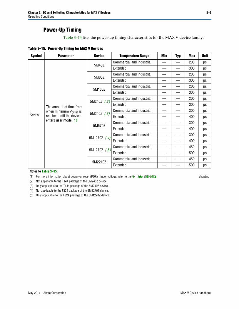
Chapter 3: DC and Switching Characteristics for MAX V Devices 3–9Operating Conditions
Power-Up TimingTable 3–15 lists the power-up timing characteristics for the MAX V device family.
Table 3–15. Power-Up Timing for MAX V Devices
Symbol Parameter Device Temperature Range Min Typ Max Unit
tCONFIG
The amount of time from when minimum VCCINT is reached until the device enters user mode (1)
5M40ZCommercial and industrial — — 200 µs
Extended — — 300 µs
5M80ZCommercial and industrial — — 200 µs
Extended — — 300 µs
5M160ZCommercial and industrial — — 200 µs
Extended — — 300 µs
5M240Z (2)Commercial and industrial — — 200 µs
Extended — — 300 µs
5M240Z (3)Commercial and industrial — — 300 µs
Extended — — 400 µs
5M570ZCommercial and industrial — — 300 µs
Extended — — 400 µs
5M1270Z (4)Commercial and industrial — — 300 µs
Extended — — 400 µs
5M1270Z (5)Commercial and industrial — — 450 µs
Extended — — 500 µs
5M2210ZCommercial and industrial — — 450 µs
Extended — — 500 µs
Notes to Table 3–15:
(1) For more information about power-on reset (POR) trigger voltage, refer to the Hot Socketing and Power-On Reset in MAX V Devices chapter.(2) Not applicable to the T144 package of the 5M240Z device.(3) Only applicable to the T144 package of the 5M240Z device.(4) Not applicable to the F324 package of the 5M1270Z device.(5) Only applicable to the F324 package of the 5M1270Z device.
May 2011 Altera Corporation MAX V Device Handbook

3–10 Chapter 3: DC and Switching Characteristics for MAX V DevicesPower Consumption
Power ConsumptionYou can use the Altera® PowerPlay Early Power Estimator and PowerPlay Power Analyzer to estimate the device power.
f For more information about these power analysis tools, refer to the PowerPlay Early Power Estimator for Altera CPLDs User Guide and the PowerPlay Power Analysis chapter in volume 3 of the Quartus II Handbook.
Timing Model and SpecificationsMAX V devices timing can be analyzed with the Altera Quartus® II software, a variety of industry-standard EDA simulators and timing analyzers, or with the timing model shown in Figure 3–2.
MAX V devices have predictable internal delays that allow you to determine the worst-case timing of any design. The software provides timing simulation, point-to-point delay prediction, and detailed timing analysis for device-wide performance evaluation.
You can derive the timing characteristics of any signal path from the timing model and parameters of a particular device. You can calculate external timing parameters, which represent pin-to-pin timing delays, as the sum of the internal parameters.
f For more information, refer to AN629: Understanding Timing in Altera CPLDs.
Figure 3–2. Timing Model for MAX V Devices
I/O PinI/O Input DelaytIN
INPUT
Global Input Delay
tC4
tR4
OutputDelaytODtXZtZXt LO
CA
L
tGLOB
Logic Element
I/O Pin
tFASTIO
Output RoutingDelay
UserFlash
Memory
From Adjacent LE
To Adjacent LE
Input RoutingDelay
tDL
tLUT
tC
LUT Delay
Register Control Delay
Register Delays
tCOtSUtH
tPREtCLR
Data-In/LUT Chain
Data-Out
tIODR
Output and Output Enable Data Delay
tIOE
tCOMB
Combinational Path Delay
MAX V Device Handbook May 2011 Altera Corporation

Chapter 3: DC and Switching Characteristics for MAX V Devices 3–11Timing Model and Specifications
Preliminary and Final TimingThis section describes the performance, internal, external, and UFM timing specifications. All specifications are representative of the worst-case supply voltage and junction temperature conditions.
Timing models can have either preliminary or final status. The Quartus II software issues an informational message during the design compilation if the timing models are preliminary. Table 3–16 lists the status of the MAX V device timing models.
Preliminary status means the timing model is subject to change. Initially, timing numbers are created using simulation results, process data, and other known parameters. These tests are used to make the preliminary numbers as close to the actual timing parameters as possible.
Final timing numbers are based on actual device operation and testing. These numbers reflect the actual performance of the device under the worst-case voltage and junction temperature conditions.
PerformanceTable 3–17 lists the MAX V device performance for some common designs. All performance values were obtained with the Quartus II software compilation of megafunctions.
Table 3–16. Timing Model Status for MAX V Devices
Device Final
5M40Z v5M80Z v
5M160Z v5M240Z v5M570Z v5M1270Z v5M2210Z v
Table 3–17. Device Performance for MAX V Devices (Part 1 of 2)
Resource Used
Design Size and Function
Resources Used
Performance
Unit5M40Z/ 5M80Z/ 5M160Z/
5M240Z/ 5M570Z 5M1270Z/ 5M2210Z
Mode LEs UFM Blocks C4 C5, I5 C4 C5, I5
LE
16-bit counter (1) — 16 0 184.1 118.3 247.5 201.1 MHz
64-bit counter (1) — 64 0 83.2 80.5 154.8 125.8 MHz
16-to-1 multiplexer — 11 0 17.4 20.4 8.0 9.3 ns
32-to-1 multiplexer — 24 0 12.5 25.3 9.0 11.4 ns
16-bit XOR function — 5 0 9.0 16.1 6.6 8.2 ns
16-bit decoder with single address line — 5 0 9.2 16.1 6.6 8.2 ns
May 2011 Altera Corporation MAX V Device Handbook

3–12 Chapter 3: DC and Switching Characteristics for MAX V DevicesTiming Model and Specifications
Internal Timing ParametersInternal timing parameters are specified on a speed grade basis independent of device density. Table 3–18 through Table 3–25 on page 3–19 list the MAX V device internal timing microparameters for LEs, input/output elements (IOEs), UFM blocks, and MultiTrack interconnects.
f For more information about each internal timing microparameters symbol, refer to AN629: Understanding Timing in Altera CPLDs.
UFM
512 × 16 None 3 1 10.0 10.0 10.0 10.0 MHz
512 × 16 SPI (2) 37 1 9.7 9.7 8.0 8.0 MHz
512 × 8 Parallel (3) 73 1 (4) (4) (4) (4) MHz
512 × 16 I2C (3) 142 1 100 (5) 100 (5) 100 (5) 100 (5) kHz
Notes to Table 3–17:
(1) This design is a binary loadable up counter. (2) This design is configured for read-only operation in Extended mode. Read and write ability increases the number of logic elements (LEs) used.(3) This design is configured for read-only operation. Read and write ability increases the number of LEs used.(4) This design is asynchronous.(5) The I2C megafunction is verified in hardware up to 100-kHz serial clock line rate.
Table 3–17. Device Performance for MAX V Devices (Part 2 of 2)
Resource Used
Design Size and Function
Resources Used
Performance
Unit5M40Z/ 5M80Z/ 5M160Z/
5M240Z/ 5M570Z 5M1270Z/ 5M2210Z
Mode LEs UFM Blocks C4 C5, I5 C4 C5, I5
Table 3–18. LE Internal Timing Microparameters for MAX V Devices (Part 1 of 2)
Symbol Parameter
5M40Z/ 5M80Z/ 5M160Z/5M240Z/ 5M570Z 5M1270Z/ 5M2210Z
UnitC4 C5, I5 C4 C5, I5
Min Max Min Max Min Max Min Max
tLUTLE combinational look-up table (LUT) delay — 1,215 — 2,247 — 742 — 914 ps
tCOMB Combinational path delay — 243 — 309 — 192 — 236 ps
tCLR LE register clear delay 401 — 545 — 309 — 381 — ps
tPRE LE register preset delay 401 — 545 — 309 — 381 — ps
tSULE register setup time before clock 260 — 321 — 271 — 333 — ps
tHLE register hold time after clock 0 — 0 — 0 — 0 — ps
tCOLE register clock-to-output delay — 380 — 494 — 305 — 376 ps
MAX V Device Handbook May 2011 Altera Corporation

Chapter 3: DC and Switching Characteristics for MAX V Devices 3–13Timing Model and Specifications
tCLKHLMinimum clock high or low time 253 — 339 — 216 — 266 — ps
tC Register control delay — 1,356 — 1,741 — 1,114 — 1,372 ps
Table 3–18. LE Internal Timing Microparameters for MAX V Devices (Part 2 of 2)
Symbol Parameter
5M40Z/ 5M80Z/ 5M160Z/5M240Z/ 5M570Z 5M1270Z/ 5M2210Z
UnitC4 C5, I5 C4 C5, I5
Min Max Min Max Min Max Min Max
Table 3–19. IOE Internal Timing Microparameters for MAX V Devices
Symbol Parameter
5M40Z/ 5M80Z/ 5M160Z/5M240Z/ 5M570Z 5M1270Z/ 5M2210Z
UnitC4 C5, I5 C4 C5, I5
Min Max Min Max Min Max Min Max
tFASTIO Data output delay from adjacent LE to I/O block — 170 — 428 — 207 — 254 ps
tINI/O input pad and buffer delay — 907 — 986 — 920 — 1,132 ps
tGLOB (1)I/O input pad and buffer delay used as global signal pin
— 2,261 — 3,322 — 1,974 — 2,430 ps
tIOEInternally generated output enable delay — 530 — 1,410 — 374 — 460 ps
tDL Input routing delay — 318 — 509 — 291 — 358 ps
tOD (2) Output delay buffer and pad delay — 1,319 — 1,543 — 1,383 — 1,702 ps
tXZ (3) Output buffer disable delay — 1,045 — 1,276 — 982 — 1,209 ps
tZX (4) Output buffer enable delay — 1,160 — 1,353 — 1,303 — 1,604 ps
Notes to Table 3–19:
(1) Delay numbers for tGLOB differ for each device density and speed grade. The delay numbers for tGLOB, shown in Table 3–19, are based on a 5M240Z device target.
(2) For more information about delay adders associated with different I/O standards, drive strengths, and slew rates, refer to Table 3–34 on page 3–24 and Table 3–35 on page 3–25.
(3) For more information about tXZ delay adders associated with different I/O standards, drive strengths, and slew rates, refer to Table 3–22 on page 3–15 and Table 3–23 on page 3–15.
(4) For more information about tZX delay adders associated with different I/O standards, drive strengths, and slew rates, refer to Table 3–20 on page 3–14 and Table 3–21 on page 3–14.
May 2011 Altera Corporation MAX V Device Handbook

3–14 Chapter 3: DC and Switching Characteristics for MAX V DevicesTiming Model and Specifications
Table 3–20 through Table 3–23 list the adder delays for tZX and tXZ microparameters when using an I/O standard other than 3.3-V LVTTL with 16 mA drive strength.
Table 3–20. tZX IOE Microparameter Adders for Fast Slew Rate for MAX V Devices
Standard
5M40Z/ 5M80Z/ 5M160Z/5M240Z/ 5M570Z 5M1270Z/ 5M2210Z
UnitC4 C5, I5 C4 C5, I5
Min Max Min Max Min Max Min Max
3.3-V LVTTL16 mA — 0 — 0 — 0 — 0 ps
8 mA — 72 — 74 — 101 — 125 ps
3.3-V LVCMOS8 mA — 0 — 0 — 0 — 0 ps
4 mA — 72 — 74 — 101 — 125 ps
2.5-V LVTTL / LVCMOS
14 mA — 126 — 127 — 155 — 191 ps
7 mA — 196 — 197 — 545 — 671 ps
1.8-V LVTTL / LVCMOS
6 mA — 608 — 610 — 721 — 888 ps
3 mA — 681 — 685 — 2012 — 2477 ps
1.5-V LVCMOS4 mA — 1162 — 1157 — 1590 — 1957 ps
2 mA — 1245 — 1244 — 3269 — 4024 ps
1.2-V LVCMOS 3 mA — 1889 — 1856 — 2860 — 3520 ps
3.3-V PCI 20 mA — 72 — 74 — –18 — –22 ps
LVDS — — 126 — 127 — 155 — 191 ps
RSDS — — 126 — 127 — 155 — 191 ps
Table 3–21. tZX IOE Microparameter Adders for Slow Slew Rate for MAX V Devices
Standard
5M40Z/ 5M80Z/ 5M160Z/5M240Z/ 5M570Z 5M1270Z/ 5M2210Z
UnitC4 C5, I5 C4 C5, I5
Min Max Min Max Min Max Min Max
3.3-V LVTTL16 mA — 5,951 — 6,063 — 6,012 — 5,743 ps
8 mA — 6,534 — 6,662 — 8,785 — 8,516 ps
3.3-V LVCMOS8 mA — 5,951 — 6,063 — 6,012 — 5,743 ps
4 mA — 6,534 — 6,662 — 8,785 — 8,516 ps
2.5-V LVTTL / LVCMOS
14 mA — 9,110 — 9,237 — 10,072 — 9,803 ps
7 mA — 9,830 — 9,977 — 12,945 — 12,676 ps
1.8-V LVTTL / LVCMOS
6 mA — 21,800 — 21,787 — 21,185 — 20,916 ps
3 mA — 23,020 — 23,037 — 24,597 — 24,328 ps
1.5-V LVCMOS4 mA — 39,120 — 39,067 — 34,517 — 34,248 ps
2 mA — 40,670 — 40,617 — 39,717 — 39,448 ps
1.2-V LVCMOS 3 mA — 69,505 — 70,461 — 55,800 — 55,531 ps
3.3-V PCI 20 mA — 6,534 — 6,662 — 35 — 44 ps
MAX V Device Handbook May 2011 Altera Corporation

Chapter 3: DC and Switching Characteristics for MAX V Devices 3–15Timing Model and Specifications
Table 3–22. tXZ IOE Microparameter Adders for Fast Slew Rate for MAX V Devices
Standard
5M40Z/ 5M80Z/ 5M160Z/5M240Z/ 5M570Z 5M1270Z/ 5M2210Z
UnitC4 C5, I5 C4 C5, I5
Min Max Min Max Min Max Min Max
3.3-V LVTTL16 mA — 0 — 0 — 0 — 0 ps
8 mA — –69 — –69 — –74 — –91 ps
3.3-V LVCMOS8 mA — 0 — 0 — 0 — 0 ps
4 mA — –69 — –69 — –74 — –91 ps
2.5-V LVTTL / LVCMOS
14 mA — –7 — –10 — –46 — –56 ps
7 mA — –66 — –69 — –82 — –101 ps
1.8-V LVTTL / LVCMOS
6 mA — 45 — 37 — –7 — –8 ps
3 mA — 34 — 25 — 119 — 147 ps
1.5-V LVCMOS4 mA — 166 — 155 — 339 — 418 ps
2 mA — 190 — 179 — 464 — 571 ps
1.2-V LVCMOS 3 mA — 300 — 283 — 817 — 1,006 ps
3.3-V PCI 20 mA — –69 — –69 — 80 — 99 ps
LVDS — — –7 — –10 — –46 — –56 ps
RSDS — — –7 — –10 — –46 — –56 ps
Table 3–23. tXZ IOE Microparameter Adders for Slow Slew Rate for MAX V Devices
Standard
5M40Z/ 5M80Z/ 5M160Z/5M240Z/ 5M570Z 5M1270Z/ 5M2210Z
UnitC4 C5, I5 C4 C5, I5
Min Max Min Max Min Max Min Max
3.3-V LVTTL16 mA — 171 — 174 — 73 — –132 ps
8 mA — 112 — 116 — 758 — 553 ps
3.3-V LVCMOS8 mA — 171 — 174 — 73 — –132 ps
4 mA — 112 — 116 — 758 — 553 ps
2.5-V LVTTL / LVCMOS
14 mA — 213 — 213 — 32 — –173 ps
7 mA — 166 — 166 — 714 — 509 ps
1.8-V LVTTL / LVCMOS
6 mA — 441 — 438 — 96 — –109 ps
3 mA — 496 — 494 — 963 — 758 ps
1.5-V LVCMOS4 mA — 765 — 755 — 238 — 33 ps
2 mA — 903 — 897 — 1,319 — 1,114 ps
1.2-V LVCMOS 3 mA — 1,159 — 1,130 — 400 — 195 ps
3.3-V PCI 20 mA — 112 — 116 — 303 — 373 ps
May 2011 Altera Corporation MAX V Device Handbook

3–16 Chapter 3: DC and Switching Characteristics for MAX V DevicesTiming Model and Specifications
1 The default slew rate setting for MAX V devices in the Quartus II design software is “fast”.
Table 3–24. UFM Block Internal Timing Microparameters for MAX V Devices (Part 1 of 2)
Symbol Parameter
5M40Z/ 5M80Z/ 5M160Z/5M240Z/ 5M570Z 5M1270Z/ 5M2210Z
UnitC4 C5, I5 C4 C5, I5
Min Max Min Max Min Max Min Max
tACLKAddress register clock period 100 — 100 — 100 — 100 — ns
tASU
Address register shift signal setup to address register clock
20 — 20 — 20 — 20 — ns
tAH
Address register shift signal hold to address register clock
20 — 20 — 20 — 20 — ns
tADS
Address register data in setup to address register clock
20 — 20 — 20 — 20 — ns
tADH
Address register data in hold from address register clock
20 — 20 — 20 — 20 — ns
tDCLK Data register clock period 100 — 100 — 100 — 100 — ns
tDSS
Data register shift signal setup to data register clock
60 — 60 — 60 — 60 — ns
tDSH
Data register shift signal hold from data register clock
20 — 20 — 20 — 20 — ns
tDDS
Data register data in setup to data register clock
20 — 20 — 20 — 20 — ns
tDDHData register data in hold from data register clock 20 — 20 — 20 — 20 — ns
tDPProgram signal to data clock hold time 0 — 0 — 0 — 0 — ns
tPB
Maximum delay between program rising edge to UFM busy signal rising edge
— 960 — 960 — 960 — 960 ns
tBP
Minimum delay allowed from UFM busy signal going low to program signal going low
20 — 20 — 20 — 20 — ns
tPPMXMaximum length of busy pulse during a program — 100 — 100 — 100 — 100 µs
MAX V Device Handbook May 2011 Altera Corporation

Chapter 3: DC and Switching Characteristics for MAX V Devices 3–17Timing Model and Specifications
tAE
Minimum erase signal to address clock hold time
0 — 0 — 0 — 0 — ns
tEB
Maximum delay between the erase rising edge to the UFM busy signal rising edge
— 960 — 960 — 960 — 960 ns
tBE
Minimum delay allowed from the UFM busy signal going low to erase signal going low
20 — 20 — 20 — 20 — ns
tEPMXMaximum length of busy pulse during an erase — 500 — 500 — 500 — 500 ms
tDCO
Delay from data register clock to data register output
— 5 — 5 — 5 — 5 ns
tOE
Delay from OSC_ENA signal reaching UFM to rising clock of OSC leaving the UFM
180 — 180 — 180 — 180 — ns
tRAMaximum read access time — 65 — 65 — 65 — 65 ns
tOSCS
Maximum delay between the OSC_ENA rising edge to the erase/program signal rising edge
250 — 250 — 250 — 250 — ns
tOSCH
Minimum delay allowed from the erase/program signal going low to OSC_ENA signal going low
250 — 250 — 250 — 250 — ns
Table 3–24. UFM Block Internal Timing Microparameters for MAX V Devices (Part 2 of 2)
Symbol Parameter
5M40Z/ 5M80Z/ 5M160Z/5M240Z/ 5M570Z 5M1270Z/ 5M2210Z
UnitC4 C5, I5 C4 C5, I5
Min Max Min Max Min Max Min Max
May 2011 Altera Corporation MAX V Device Handbook

3–18 Chapter 3: DC and Switching Characteristics for MAX V DevicesTiming Model and Specifications
Figure 3–3 through Figure 3–5 show the read, program, and erase waveforms for UFM block timing parameters listed in Table 3–24.
Figure 3–3. UFM Read Waveform
tDCO
tDCLKtDSS
tDSH
tADH
tADS
tASUtACLK tAH
ARShft
ARClk
ARDin
DRShft
DRClk
DRDinDRDout
Program
Erase
Busy
16 Data Bits
9 Address Bits
OSC_ENA
Figure 3–4. UFM Program Waveform
tADS
tASU tACLK
tADH
tAH
tDDS
tDCLKtDSStDSH
tDDH
tPB tBP
tPPMX
tOSCS tOSCH
ARShft
ARClk
ARDin
DRShft
DRClk
DRDin
DRDout
Program
Erase
Busy
16 Data Bits
9 Address Bits
OSC_ENA
MAX V Device Handbook May 2011 Altera Corporation

Chapter 3: DC and Switching Characteristics for MAX V Devices 3–19Timing Model and Specifications
External Timing ParametersExternal timing parameters are specified by device density and speed grade. All external I/O timing parameters shown are for the 3.3-V LVTTL I/O standard with the maximum drive strength and fast slew rate. For external I/O timing using standards other than LVTTL or for different drive strengths, use the I/O standard input and output delay adders in Table 3–32 on page 3–23 through Table 3–36 on page 3–25.
f For more information about each external timing parameters symbol, refer to AN629: Understanding Timing in Altera CPLDs.
Figure 3–5. UFM Erase Waveform
ARShft
ARClk
ARDin
DRShft
DRClk
DRDin
DRDout
Program
Erase
Busy
9 Address BitstASU
tACLK tAH
tADH
tADS
tEB
tEPMX
tOSCS tOSCH
OSC_ENA
tBE
Table 3–25. Routing Delay Internal Timing Microparameters for MAX V Devices
Routing
5M40Z/ 5M80Z/ 5M160Z/5M240Z/ 5M570Z 5M1270Z/ 5M2210Z
UnitC4 C5, I5 C4 C5, I5
Min Max Min Max Min Max Min Max
tC4 — 860 — 1,973 — 561 — 690 ps
tR4 — 655 — 1,479 — 445 — 548 ps
tLOCAL — 1,143 — 2,947 — 731 — 899 ps
May 2011 Altera Corporation MAX V Device Handbook
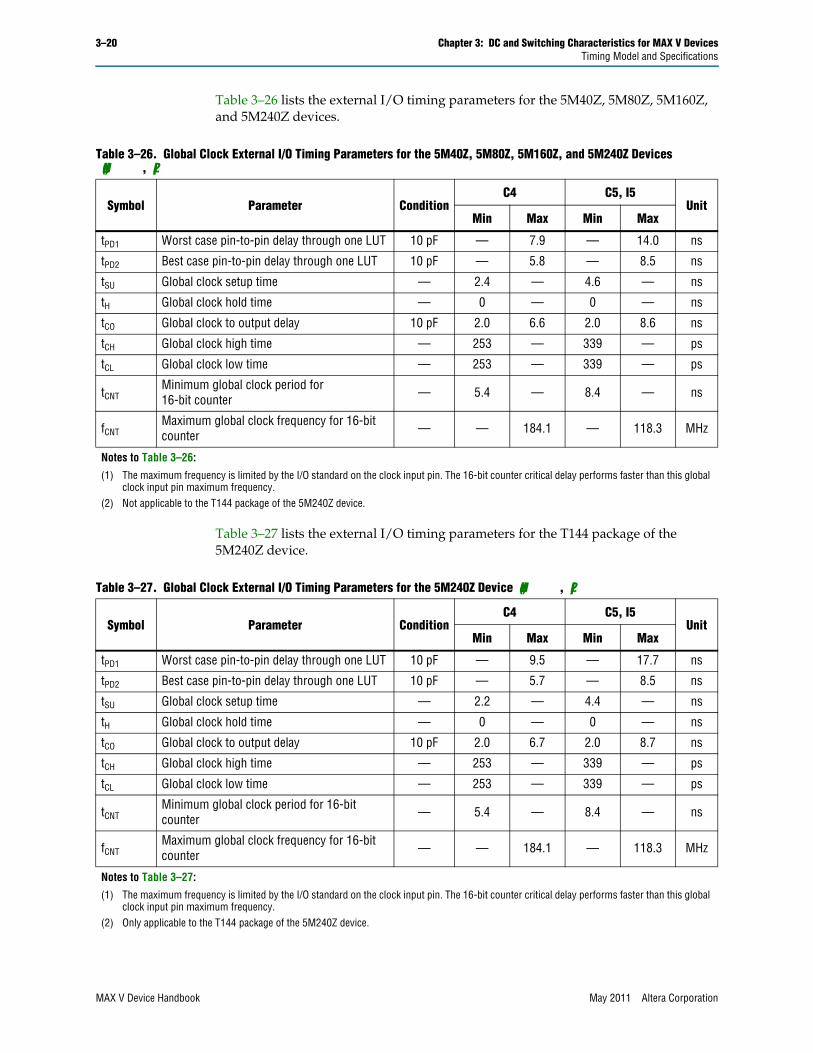
3–20 Chapter 3: DC and Switching Characteristics for MAX V DevicesTiming Model and Specifications
Table 3–26 lists the external I/O timing parameters for the 5M40Z, 5M80Z, 5M160Z, and 5M240Z devices.
Table 3–27 lists the external I/O timing parameters for the T144 package of the 5M240Z device.
Table 3–26. Global Clock External I/O Timing Parameters for the 5M40Z, 5M80Z, 5M160Z, and 5M240Z Devices(Note 1), (2)
Symbol Parameter ConditionC4 C5, I5
UnitMin Max Min Max
tPD1 Worst case pin-to-pin delay through one LUT 10 pF — 7.9 — 14.0 ns
tPD2 Best case pin-to-pin delay through one LUT 10 pF — 5.8 — 8.5 ns
tSU Global clock setup time — 2.4 — 4.6 — ns
tH Global clock hold time — 0 — 0 — ns
tCO Global clock to output delay 10 pF 2.0 6.6 2.0 8.6 ns
tCH Global clock high time — 253 — 339 — ps
tCL Global clock low time — 253 — 339 — ps
tCNTMinimum global clock period for 16-bit counter — 5.4 — 8.4 — ns
fCNTMaximum global clock frequency for 16-bit counter — — 184.1 — 118.3 MHz
Notes to Table 3–26:
(1) The maximum frequency is limited by the I/O standard on the clock input pin. The 16-bit counter critical delay performs faster than this global clock input pin maximum frequency.
(2) Not applicable to the T144 package of the 5M240Z device.
Table 3–27. Global Clock External I/O Timing Parameters for the 5M240Z Device (Note 1), (2)
Symbol Parameter ConditionC4 C5, I5
UnitMin Max Min Max
tPD1 Worst case pin-to-pin delay through one LUT 10 pF — 9.5 — 17.7 ns
tPD2 Best case pin-to-pin delay through one LUT 10 pF — 5.7 — 8.5 ns
tSU Global clock setup time — 2.2 — 4.4 — ns
tH Global clock hold time — 0 — 0 — ns
tCO Global clock to output delay 10 pF 2.0 6.7 2.0 8.7 ns
tCH Global clock high time — 253 — 339 — ps
tCL Global clock low time — 253 — 339 — ps
tCNTMinimum global clock period for 16-bit counter — 5.4 — 8.4 — ns
fCNTMaximum global clock frequency for 16-bit counter — — 184.1 — 118.3 MHz
Notes to Table 3–27:
(1) The maximum frequency is limited by the I/O standard on the clock input pin. The 16-bit counter critical delay performs faster than this global clock input pin maximum frequency.
(2) Only applicable to the T144 package of the 5M240Z device.
MAX V Device Handbook May 2011 Altera Corporation

Chapter 3: DC and Switching Characteristics for MAX V Devices 3–21Timing Model and Specifications
Table 3–28 lists the external I/O timing parameters for the 5M570Z device.
Table 3–29 lists the external I/O timing parameters for the 5M1270Z device.
Table 3–28. Global Clock External I/O Timing Parameters for the 5M570Z Device (Note 1)
Symbol Parameter ConditionC4 C5, I5
UnitMin Max Min Max
tPD1 Worst case pin-to-pin delay through one LUT 10 pF — 9.5 — 17.7 ns
tPD2 Best case pin-to-pin delay through one LUT 10 pF — 5.7 — 8.5 ns
tSU Global clock setup time — 2.2 — 4.4 — ns
tH Global clock hold time — 0 — 0 — ns
tCO Global clock to output delay 10 pF 2.0 6.7 2.0 8.7 ns
tCH Global clock high time — 253 — 339 — ps
tCL Global clock low time — 253 — 339 — ps
tCNTMinimum global clock period for 16-bit counter — 5.4 — 8.4 — ns
fCNTMaximum global clock frequency for 16-bit counter — — 184.1 — 118.3 MHz
Note to Table 3–28:
(1) The maximum frequency is limited by the I/O standard on the clock input pin. The 16-bit counter critical delay performs faster than this global clock input pin maximum frequency.
Table 3–29. Global Clock External I/O Timing Parameters for the 5M1270Z Device (Note 1), (2)
Symbol Parameter ConditionC4 C5, I5
UnitMin Max Min Max
tPD1 Worst case pin-to-pin delay through one LUT 10 pF — 8.1 — 10.0 ns
tPD2 Best case pin-to-pin delay through one LUT 10 pF — 4.8 — 5.9 ns
tSU Global clock setup time — 1.5 — 1.9 — ns
tH Global clock hold time — 0 — 0 — ns
tCO Global clock to output delay 10 pF 2.0 5.9 2.0 7.3 ns
tCH Global clock high time — 216 — 266 — ps
tCL Global clock low time — 216 — 266 — ps
tCNTMinimum global clock period for 16-bit counter — 4.0 — 5.0 — ns
fCNTMaximum global clock frequency for 16-bit counter — — 247.5 — 201.1 MHz
Notes to Table 3–29:
(1) The maximum frequency is limited by the I/O standard on the clock input pin. The 16-bit counter critical delay performs faster than this global clock input pin maximum frequency.
(2) Not applicable to the F324 package of the 5M1270Z device.
May 2011 Altera Corporation MAX V Device Handbook

3–22 Chapter 3: DC and Switching Characteristics for MAX V DevicesTiming Model and Specifications
Table 3–30 lists the external I/O timing parameters for the F324 package of the 5M1270Z device.
Table 3–31 lists the external I/O timing parameters for the 5M2210Z device.
Table 3–30. Global Clock External I/O Timing Parameters for the 5M1270Z Device (Note 1), (2)
Symbol Parameter ConditionC4 C5, I5
UnitMin Max Min Max
tPD1 Worst case pin-to-pin delay through one LUT 10 pF — 9.1 — 11.2 ns
tPD2 Best case pin-to-pin delay through one LUT 10 pF — 4.8 — 5.9 ns
tSU Global clock setup time — 1.5 — 1.9 — ns
tH Global clock hold time — 0 — 0 — ns
tCO Global clock to output delay 10 pF 2.0 6.0 2.0 7.4 ns
tCH Global clock high time — 216 — 266 — ps
tCL Global clock low time — 216 — 266 — ps
tCNTMinimum global clock period for 16-bit counter — 4.0 — 5.0 — ns
fCNTMaximum global clock frequency for 16-bit counter — — 247.5 — 201.1 MHz
Notes to Table 3–30:
(1) The maximum frequency is limited by the I/O standard on the clock input pin. The 16-bit counter critical delay performs faster than this global clock input pin maximum frequency.
(2) Only applicable to the F324 package of the 5M1270Z device.
Table 3–31. Global Clock External I/O Timing Parameters for the 5M2210Z Device (Note 1)
Symbol Parameter ConditionC4 C5, I5
UnitMin Max Min Max
tPD1 Worst case pin-to-pin delay through one LUT 10 pF — 9.1 — 11.2 ns
tPD2 Best case pin-to-pin delay through one LUT 10 pF — 4.8 — 5.9 ns
tSU Global clock setup time — 1.5 — 1.9 — ns
tH Global clock hold time — 0 — 0 — ns
tCO Global clock to output delay 10 pF 2.0 6.0 2.0 7.4 ns
tCH Global clock high time — 216 — 266 — ps
tCL Global clock low time — 216 — 266 — ps
tCNTMinimum global clock period for 16-bit counter — 4.0 — 5.0 — ns
fCNTMaximum global clock frequency for 16-bit counter — — 247.5 — 201.1 MHz
Note to Table 3–31:
(1) The maximum frequency is limited by the I/O standard on the clock input pin. The 16-bit counter critical delay performs faster than this global clock input pin maximum frequency.
MAX V Device Handbook May 2011 Altera Corporation

Chapter 3: DC and Switching Characteristics for MAX V Devices 3–23Timing Model and Specifications
External Timing I/O Delay AddersThe I/O delay timing parameters for the I/O standard input and output adders and the input delays are specified by speed grade, independent of device density.
Table 3–32 through Table 3–36 on page 3–25 list the adder delays associated with I/O pins for all packages. If you select an I/O standard other than 3.3-V LVTTL, add the input delay adder to the external tSU timing parameters listed in Table 3–26 on page 3–20 through Table 3–31. If you select an I/O standard other than 3.3-V LVTTL with 16 mA drive strength and fast slew rate, add the output delay adder to the external tCO and tPD listed in Table 3–26 on page 3–20 through Table 3–31.
Table 3–32. External Timing Input Delay Adders for MAX V Devices
I/O Standard
5M40Z/ 5M80Z/ 5M160Z/5M240Z/ 5M570Z 5M1270Z/ 5M2210Z
UnitC4 C5, I5 C4 C5, I5
Min Max Min Max Min Max Min Max
3.3-V LVTTL
Without Schmitt Trigger — 0 — 0 — 0 — 0 ps
With Schmitt Trigger — 387 — 442 — 480 — 591 ps
3.3-V LVCMOS
Without Schmitt Trigger — 0 — 0 — 0 — 0 ps
With Schmitt Trigger — 387 — 442 — 480 — 591 ps
2.5-V LVTTL / LVCMOS
Without Schmitt Trigger — 42 — 42 — 246 — 303 ps
With Schmitt Trigger — 429 — 483 — 787 — 968 ps
1.8-V LVTTL / LVCMOS
Without Schmitt Trigger — 378 — 368 — 695 — 855 ps
1.5-V LVCMOS Without Schmitt Trigger — 681 — 658 — 1,334 — 1,642 ps
1.2-V LVCMOS Without Schmitt Trigger — 1,055 — 1,010 — 2,324 — 2,860 ps
3.3-V PCI Without Schmitt Trigger — 0 — 0 — 0 — 0 ps
Table 3–33. External Timing Input Delay tGLOB Adders for GCLK Pins for MAX V Devices (Part 1 of 2)
I/O Standard
5M40Z/ 5M80Z/ 5M160Z/5M240Z/ 5M570Z 5M1270Z/ 5M2210Z
UnitC4 C5, I5 C4 C5, I5
Min Max Min Max Min Max Min Max
3.3-V LVTTL
Without Schmitt Trigger — 0 — 0 — 0 — 0 ps
With Schmitt Trigger — 387 — 442 — 400 — 493 ps
May 2011 Altera Corporation MAX V Device Handbook
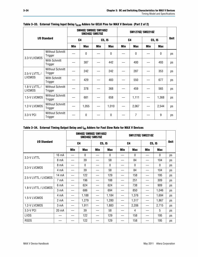
3–24 Chapter 3: DC and Switching Characteristics for MAX V DevicesTiming Model and Specifications
3.3-V LVCMOS
Without Schmitt Trigger — 0 — 0 — 0 — 0 ps
With Schmitt Trigger — 387 — 442 — 400 — 493 ps
2.5-V LVTTL / LVCMOS
Without Schmitt Trigger — 242 — 242 — 287 — 353 ps
With Schmitt Trigger — 429 — 483 — 550 — 677 ps
1.8-V LVTTL / LVCMOS
Without Schmitt Trigger — 378 — 368 — 459 — 565 ps
1.5-V LVCMOS Without Schmitt Trigger — 681 — 658 — 1,111 — 1,368 ps
1.2-V LVCMOS Without Schmitt Trigger — 1,055 — 1,010 — 2,067 — 2,544 ps
3.3-V PCI Without Schmitt Trigger — 0 — 0 — 7 — 9 ps
Table 3–33. External Timing Input Delay tGLOB Adders for GCLK Pins for MAX V Devices (Part 2 of 2)
I/O Standard
5M40Z/ 5M80Z/ 5M160Z/5M240Z/ 5M570Z 5M1270Z/ 5M2210Z
UnitC4 C5, I5 C4 C5, I5
Min Max Min Max Min Max Min Max
Table 3–34. External Timing Output Delay and tOD Adders for Fast Slew Rate for MAX V Devices
I/O Standard
5M40Z/ 5M80Z/ 5M160Z/5M240Z/ 5M570Z 5M1270Z/ 5M2210Z
UnitC4 C5, I5 C4 C5, I5
Min Max Min Max Min Max Min Max
3.3-V LVTTL16 mA — 0 — 0 — 0 — 0 ps
8 mA — 39 — 58 — 84 — 104 ps
3.3-V LVCMOS8 mA — 0 — 0 — 0 — 0 ps
4 mA — 39 — 58 — 84 — 104 ps
2.5-V LVTTL / LVCMOS14 mA — 122 — 129 — 158 — 195 ps
7 mA — 196 — 188 — 251 — 309 ps
1.8-V LVTTL / LVCMOS6 mA — 624 — 624 — 738 — 909 ps
3 mA — 686 — 694 — 850 — 1,046 ps
1.5-V LVCMOS4 mA — 1,188 — 1,184 — 1,376 — 1,694 ps
2 mA — 1,279 — 1,280 — 1,517 — 1,867 ps
1.2-V LVCMOS 3 mA — 1,911 — 1,883 — 2,206 — 2,715 ps
3.3-V PCI 20 mA — 39 — 58 — 4 — 5 ps
LVDS — — 122 — 129 — 158 — 195 ps
RSDS — — 122 — 129 — 158 — 195 ps
MAX V Device Handbook May 2011 Altera Corporation

Chapter 3: DC and Switching Characteristics for MAX V Devices 3–25Timing Model and Specifications
Table 3–35. External Timing Output Delay and tOD Adders for Slow Slew Rate for MAX V Devices
I/O Standard
5M40Z/ 5M80Z/ 5M160Z/5M240Z/ 5M570Z 5M1270Z/ 5M2210Z
UnitC4 C5, I5 C4 C5, I5
Min Max Min Max Min Max Min Max
3.3-V LVTTL16 mA — 5,913 — 6,043 — 6,612 — 6,293 ps
8 mA — 6,488 — 6,645 — 7,313 — 6,994 ps
3.3-V LVCMOS8 mA — 5,913 — 6,043 — 6,612 — 6,293 ps
4 mA — 6,488 — 6,645 — 7,313 — 6,994 ps
2.5-V LVTTL / LVCMOS14 mA — 9,088 — 9,222 — 10,021 — 9,702 ps
7 mA — 9,808 — 9,962 — 10,881 — 10,562 ps
1.8-V LVTTL / LVCMOS6 mA — 21,758 — 21,782 — 21,134 — 20,815 ps
3 mA — 23,028 — 23,032 — 22,399 — 22,080 ps
1.5-V LVCMOS4 mA — 39,068 — 39,032 — 34,499 — 34,180 ps
2 mA — 40,578 — 40,542 — 36,281 — 35,962 ps
1.2-V LVCMOS 3 mA — 69,332 — 70,257 — 55,796 — 55,477 ps
3.3-V PCI 20 mA — 6,488 — 6,645 — 339 — 418 ps
Table 3–36. IOE Programmable Delays for MAX V Devices
Parameter
5M40Z/ 5M80Z/ 5M160Z/5M240Z/ 5M570Z 5M1270Z/ 5M2210Z
UnitC4 C5, I5 C4 C5, I5
Min Max Min Max Min Max Min Max
Input Delay from Pin to Internal Cells = 1 — 1,858 — 2,214 — 1,592 — 1,960 ps
Input Delay from Pin to Internal Cells = 0 — 569 — 616 — 115 — 142 ps
May 2011 Altera Corporation MAX V Device Handbook

3–26 Chapter 3: DC and Switching Characteristics for MAX V DevicesTiming Model and Specifications
Maximum Input and Output Clock RatesTable 3–37 and Table 3–38 list the maximum input and output clock rates for standard I/O pins in MAX V devices.
Table 3–37. Maximum Input Clock Rate for I/Os for MAX V Devices
I/O Standard
5M40Z/ 5M80Z/ 5M160Z/5M240Z/ 5M570Z/5M1270Z/
5M2210Z Unit
C4, C5, I5
3.3-V LVTTLWithout Schmitt Trigger 304 MHz
With Schmitt Trigger 304 MHz
3.3-V LVCMOSWithout Schmitt Trigger 304 MHz
With Schmitt Trigger 304 MHz
2.5-V LVTTLWithout Schmitt Trigger 304 MHz
With Schmitt Trigger 304 MHz
2.5-V LVCMOSWithout Schmitt Trigger 304 MHz
With Schmitt Trigger 304 MHz
1.8-V LVTTL Without Schmitt Trigger 200 MHz
1.8-V LVCMOS Without Schmitt Trigger 200 MHz
1.5-V LVCMOS Without Schmitt Trigger 150 MHz
1.2-V LVCMOS Without Schmitt Trigger 120 MHz
3.3-V PCI Without Schmitt Trigger 304 MHz
Table 3–38. Maximum Output Clock Rate for I/Os for MAX V Devices
I/O Standard
5M40Z/ 5M80Z/ 5M160Z/5M240Z/ 5M570Z/5M1270Z/
5M2210Z Unit
C4, C5, I5
3.3-V LVTTL 304 MHz
3.3-V LVCMOS 304 MHz
2.5-V LVTTL 304 MHz
2.5-V LVCMOS 304 MHz
1.8-V LVTTL 200 MHz
1.8-V LVCMOS 200 MHz
1.5-V LVCMOS 150 MHz
1.2-V LVCMOS 120 MHz
3.3-V PCI 304 MHz
LVDS 304 MHz
RSDS 200 MHz
MAX V Device Handbook May 2011 Altera Corporation
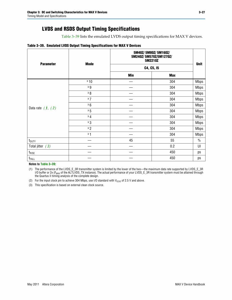
Chapter 3: DC and Switching Characteristics for MAX V Devices 3–27Timing Model and Specifications
LVDS and RSDS Output Timing SpecificationsTable 3–39 lists the emulated LVDS output timing specifications for MAX V devices.
Table 3–39. Emulated LVDS Output Timing Specifications for MAX V Devices
Parameter Mode
5M40Z/ 5M80Z/ 5M160Z/5M240Z/ 5M570Z/5M1270Z/
5M2210ZUnit
C4, C5, I5
Min Max
Data rate (1), (2)
10 — 304 Mbps
9 — 304 Mbps
8 — 304 Mbps
7 — 304 Mbps
6 — 304 Mbps
5 — 304 Mbps
4 — 304 Mbps
3 — 304 Mbps
2 — 304 Mbps
1 — 304 Mbps
tDUTY — 45 55 %
Total jitter (3) — — 0.2 UI
tRISE — — 450 ps
tFALL — — 450 ps
Notes to Table 3–39:
(1) The performance of the LVDS_E_3R transmitter system is limited by the lower of the two—the maximum data rate supported by LVDS_E_3R I/O buffer or 2x (FMAX of the ALTLVDS_TX instance). The actual performance of your LVDS_E_3R transmitter system must be attained through the Quartus II timing analysis of the complete design.
(2) For the input clock pin to achieve 304 Mbps, use I/O standard with VCCIO of 2.5 V and above.(3) This specification is based on external clean clock source.
May 2011 Altera Corporation MAX V Device Handbook

3–28 Chapter 3: DC and Switching Characteristics for MAX V DevicesTiming Model and Specifications
Table 3–40 lists the emulated RSDS output timing specifications for MAX V devices.
Table 3–40. Emulated RSDS Output Timing Specifications for MAX V Devices
Parameter Mode
5M40Z/ 5M80Z/ 5M160Z/5M240Z/ 5M570Z/5M1270Z/
5M2210ZUnit
C4, C5, I5
Min Max
Data rate (1)
10 — 200 Mbps
9 — 200 Mbps
8 — 200 Mbps
7 — 200 Mbps
6 — 200 Mbps
5 — 200 Mbps
4 — 200 Mbps
3 — 200 Mbps
2 — 200 Mbps
1 — 200 Mbps
tDUTY — 45 55 %
Total jitter (2) — — 0.2 UI
tRISE — — 450 ps
tFALL — — 450 ps
Notes to Table 3–40:
(1) For the input clock pin to achieve 200 Mbps, use I/O standard with VCCIO of 1.8 V and above.(2) This specification is based on external clean clock source.
MAX V Device Handbook May 2011 Altera Corporation

Chapter 3: DC and Switching Characteristics for MAX V Devices 3–29Timing Model and Specifications
JTAG Timing SpecificationsFigure 3–6 shows the timing waveform for the JTAG signals for the MAX V device family.
Table 3–41 lists the JTAG timing parameters and values for the MAX V device family.
Figure 3–6. JTAG Timing Waveform for MAX V Devices
TDI
TMS
TDO
TCK
Signalto be
Captured
Signalto be
Driven
tJCP
tJCH tJCL
tJPSU tJPH
tJPCO tJPXZtJPZX
tJSSU tJSH
tJSZX tJSCO tJSXZ
Table 3–41. JTAG Timing Parameters for MAX V Devices (Part 1 of 2)
Symbol Parameter Min Max Unit
tJCP (1)
TCK clock period for VCCIO1 = 3.3 V 55.5 — ns
TCK clock period for VCCIO1 = 2.5 V 62.5 — ns
TCK clock period for VCCIO1 = 1.8 V 100 — ns
TCK clock period for VCCIO1 = 1.5 V 143 — ns
tJCH TCK clock high time 20 — ns
tJCL TCK clock low time 20 — ns
tJPSU JTAG port setup time (2) 8 — ns
tJPH JTAG port hold time 10 — ns
tJPCO JTAG port clock to output (2) — 15 ns
tJPZX JTAG port high impedance to valid output (2) — 15 ns
tJPXZ JTAG port valid output to high impedance (2) — 15 ns
tJSSU Capture register setup time 8 — ns
tJSH Capture register hold time 10 — ns
tJSCO Update register clock to output — 25 ns
tJSZX Update register high impedance to valid output — 25 ns
May 2011 Altera Corporation MAX V Device Handbook

3–30 Chapter 3: DC and Switching Characteristics for MAX V DevicesDocument Revision History
Document Revision HistoryTable 3–42 lists the revision history for this chapter.
tJSXZ Update register valid output to high impedance — 25 ns
Notes to Table 3–41:
(1) Minimum clock period specified for 10 pF load on the TDO pin. Larger loads on TDO degrades the maximum TCK frequency.(2) This specification is shown for 3.3-V LVTTL/LVCMOS and 2.5-V LVTTL/LVCMOS operation of the JTAG pins. For 1.8-V LVTTL/LVCMOS and
1.5-V LVCMOS operation, the tJPSU minimum is 6 ns and tJPCO, tJPZX, and tJPXZ are maximum values at 35 ns.
Table 3–41. JTAG Timing Parameters for MAX V Devices (Part 2 of 2)
Symbol Parameter Min Max Unit
Table 3–42. Document Revision History
Date Version Changes
May 2011 1.2 Updated Table 3–2, Table 3–15, Table 3–16, and Table 3–33.
January 2011 1.1 Updated Table 3–37, Table 3–38, Table 3–39, and Table 3–40.
December 2010 1.0 Initial release.
MAX V Device Handbook May 2011 Altera Corporation

June 2017 Altera Corporation
Section II. System Integration in MAX VDevices
This section provides information about system integration in MAX® V devices.
This section includes the following chapters:
■ Chapter 4, Hot Socketing and Power-On Reset in MAX V Devices
■ Chapter 5, Using MAX V Devices in Multi-Voltage Systems
■ Chapter 6, JTAG and In-System Programmability in MAX V Devices
■ Chapter 7, User Flash Memory in MAX V Devices
■ Chapter 8, JTAG Boundary-Scan Testing in MAX V Devices
MAX V Device Handbook

II–2 Section II: System Integration in MAX V Devices
MAX V Device Handbook June 2017 Altera Corporation

MAX V Device HandbookDecember 2010
MV51004-1.0
© 2010 Altera Corporation. All rights reserved. ALTERA, ARRand/or trademarks of Altera Corporation in the U.S. and otherwww.altera.com/common/legal.html. Altera warrants performreserves the right to make changes to any products and servicesinformation, product, or service described herein except as expspecifications before relying on any published information and
December 2010MV51004-1.0
4. Hot Socketing and Power-On Reset inMAX V Devices
This chapter provides information about hot-socketing specifications, power-on reset (POR) requirements, and their implementation in MAX V devices.
MAX V devices offer hot socketing, also known as hot plug-in or hot swap, and power sequencing support. You can insert or remove a MAX V device in a system during system operation without causing undesirable effects to the running system bus. The hot-socketing feature removes some of the difficulty when using MAX V devices on PCBs that contain a mixture of 3.3-, 2.5-, 1.8-, and 1.5-V devices.
The MAX V hot-socketing feature provides the following:
■ Board or device insertion and removal
■ Support for any power-up sequence
■ Non-intrusive I/O buffers to system buses during hot insertion
This chapter contains the following sections:
■ “MAX V Hot-Socketing Specifications” on page 4–1
■ “Hot-Socketing Feature Implementation in MAX V Devices” on page 4–3
■ “Power-On Reset Circuitry” on page 4–5
MAX V Hot-Socketing SpecificationsMAX V devices offer the hot-socketing feature without the need for external components or special design requirements. The advantages of hot-socketing support in MAX V devices includes the following:
■ The device can be driven before and during power up or power down without damaging the device.
■ I/O pins remain tri-stated during power up. The device does not drive out before or during power up, thereby affecting other operating buses.
■ Signal pins do not drive the VCCIO or VCCINT power supplies. External input signals to the device I/O pins do not power the device VCCIO or VCCINT power supplies using internal paths. This is true if the VCCINT and VCCIO power supplies are held at GND.
1 Altera uses GND as a reference for the hot-socketing and I/O buffers circuitry designs. To ensure device reliability and compliance to the hot-socketing specifications, you must connect GND between boards before connecting the VCCINT and VCCIO power supplies.
Subscribe
IA, CYCLONE, HARDCOPY, MAX, MEGACORE, NIOS, QUARTUS and STRATIX are Reg. U.S. Pat. & Tm. Off. countries. All other trademarks and service marks are the property of their respective holders as described at
ance of its semiconductor products to current specifications in accordance with Altera’s standard warranty, but at any time without notice. Altera assumes no responsibility or liability arising out of the application or use of any ressly agreed to in writing by Altera. Altera customers are advised to obtain the latest version of device before placing orders for products or services.

4–2 Chapter 4: Hot Socketing and Power-On Reset in MAX V DevicesMAX V Hot-Socketing Specifications
Devices Can Be Driven Before Power UpYou can drive signals into the I/O pins and GCLK[3..0] pins of MAX V devices before or during power up or power down without damaging the device. To simplify the system-level design, MAX V devices support any power-up or power-down sequence (VCCIO1, VCCIO2, VCCIO3, VCCIO4, and VCCINT).
I/O Pins Remain Tri-Stated During Power UpA device that does not support hot socketing may interrupt system operation or cause contention by driving out before or during power up. In a hot-socketing situation, the MAX V device’s output buffers are turned off during system power up. MAX V devices do not drive out until the device attains proper operating conditions and is fully configured. For more information about turn-on voltages, refer to “Power-On Reset Circuitry” on page 4–5.
Signal Pins Do Not Drive the VCCIO or VCCINT Power SuppliesMAX V devices do not have a current path from the I/O pins or GCLK[3..0] pins to the VCCIO or VCCINT power supplies before or during power up. A MAX V device may be inserted into (or removed from) a system board that is powered up without damaging or interfering with system-board operation. When hot socketing, MAX V devices may have a minimal effect on the signal integrity of the backplane.
AC and DC SpecificationsYou can power up or power down the VCCIO and VCCINT power supplies in any sequence. During hot socketing, the I/O pin capacitance is less than 8 pF. MAX V devices meet the following hot-socketing specifications:
■ DC specification: | IIOPIN | < 300 A.
■ AC specification: | IIOPIN | < 8 mA for 10 ns or less.
1 MAX V devices are immune to latch-up when hot socketing. If the TCK JTAG input pin is driven high during hot socketing, the current on that pin might exceed the specifications listed above.
IIOPIN is the current for any user I/O pin on the device. The AC specification applies when the device is being powered up or powered down. This specification takes into account the pin capacitance but not the board trace and external loading capacitance. You must consider additional capacitance for trace, connector, and loading separately. The peak current duration due to power-up transients is 10 ns or less.
The DC specification applies when all VCC supplies to the device are stable in the powered-up or powered-down conditions.
MAX V Device Handbook December 2010 Altera Corporation

Chapter 4: Hot Socketing and Power-On Reset in MAX V Devices 4–3Hot-Socketing Feature Implementation in MAX V Devices
Hot-Socketing Feature Implementation in MAX V DevicesThe hot-socketing feature tri-states the output buffer during the power-up event (either the VCCINT or VCCIO power supplies) or power-down event. The hot-socketing circuitry generates an internal HOTSCKT signal when either VCCINT or VCCIO is below the threshold voltage during power up or power down. The HOTSCKT signal cuts off the output buffer to ensure that no DC current leaks through the pin (except for weak pull-up leaking). When VCC ramps up very slowly during power up, VCC may still be relatively low even after the POR signal is released and device configuration is complete.
1 Ensure that VCCINT is within the recommended operating range even though SRAM download has completed.
Figure 4–1 shows the circuitry for each I/O and clock pin.
The POR circuit monitors the VCCINT and VCCIO voltage levels and keeps the I/O pins tri-stated until the device has completed its flash memory configuration of the SRAM logic. The weak pull-up resistor (R) from the I/O pin to VCCIO is enabled during download to keep the I/O pins from floating. The 3.3-V tolerance control circuit permits the I/O pins to be driven by 3.3 V before VCCIO and/or VCCINT are powered, and it prevents the I/O pins from driving out when the device is not fully powered or operational. The hot-socketing circuitry prevents the I/O pins from internally powering VCCIO and VCCINT when driven by external signals before the device is powered.
f For more information about the 5.0-V tolerance, refer to the Using MAX V Devices in Multi-Voltage Systems chapter.
Figure 4–1. Hot-Socketing Circuitry for MAX V Devices
Output Enable
VCCIO
Hot SocketVoltageTolerance
Control
Power OnReset
Monitor
WeakPull-Up
Resistor
PAD
Input Bufferto Logic Array
December 2010 Altera Corporation MAX V Device Handbook

4–4 Chapter 4: Hot Socketing and Power-On Reset in MAX V DevicesHot-Socketing Feature Implementation in MAX V Devices
Figure 4–2 shows a transistor-level cross section of the MAX V device I/O buffers. This design ensures that the output buffers do not drive when VCCIO is powered before VCCINT or if the I/O pad voltage is higher than VCCIO. This also applies for sudden voltage spikes during hot insertion. The VPAD leakage current charges the 3.3-V tolerant circuit capacitance.
The CMOS output drivers in the I/O pins intrinsically provide electrostatic discharge (ESD) protection. There are two cases to consider for ESD voltage strikes—positive voltage zap and negative voltage zap.
A positive ESD voltage zap occurs when a positive voltage is present on an I/O pin due to an ESD charge event. This can cause the N+ (Drain)/ P-Substrate junction of the N-channel drain to break down and the N+ (Drain)/P-Substrate/N+ (Source) intrinsic bipolar transistor turn on to discharge ESD current from I/O pin to GND. The dashed line in Figure 4–3 shows the ESD current discharge path during a positive ESD zap.
Figure 4–2. Transistor-Level I/O Buffers for MAX V Devices
p - substrate
p+ p+
n - well
n+
VCCIO
n+ n+
p - well
IOE Signal
VPAD
IOE Signal or theLarger of VCCIO or VPAD
The Larger ofVCCIO or VPAD
Ensures 3.3-VTolerance andHot-SocketProtection
Figure 4–3. ESD Protection During Positive Voltage Zap
I/O
I/O
Gate
Gate
Drain
Drain
PMOS
NMOS
Source
Source
GND GND
N+
N+
P-Substrate G
S
D
MAX V Device Handbook December 2010 Altera Corporation

Chapter 4: Hot Socketing and Power-On Reset in MAX V Devices 4–5Power-On Reset Circuitry
When the I/O pin receives a negative ESD zap at the pin that is less than –0.7 V (0.7 V is the voltage drop across a diode), the intrinsic P-Substrate/N+ drain diode is forward biased. Therefore, the discharge ESD current path is from GND to the I/O pin, as shown in Figure 4–4.
Power-On Reset CircuitryMAX V devices have POR circuits to monitor the VCCINT and VCCIO voltage levels during power up. The POR circuit monitors these voltages, triggering download from the non-volatile configuration flash memory block to the SRAM logic, maintaining the tri-state of the I/O pins (with weak pull-up resistors enabled) before and during this process. When the MAX V device enters user mode, the POR circuit releases the I/O pins to user functionality. The POR circuit of the MAX V device does not monitor the VCCINT voltage level after the device enters into user mode.
Power-Up CharacteristicsWhen power is applied to a MAX V device, the POR circuit monitors VCCINT and begins SRAM download at 1.55 V for MAX V devices. From this voltage reference, the SRAM download and entry into user mode takes 200 to 450 µs maximum, depending on your device density. This period of time is specified as tCONFIG in the power-up timing section of the DC and Switching Characteristics for MAX V Devices chapter.
Entry into user mode is gated by whether all the VCCIO banks are powered with sufficient operating voltage. If VCCINT and VCCIO are powered simultaneously, the device enters user mode within the tCONFIG specifications. If VCCIO is powered more than tCONFIG after VCCINT, the device does not enter user mode until 2 µs after all VCCIO banks are powered.
Figure 4–4. ESD Protection During Negative Voltage Zap
I/O
I/O
Gate
Gate
Drain
Drain
PMOS
NMOS
Source
Source
GND GND
N+
N+
P-Substrate G
S
D
December 2010 Altera Corporation MAX V Device Handbook

4–6 Chapter 4: Hot Socketing and Power-On Reset in MAX V DevicesDocument Revision History
For MAX V devices, the POR circuitry does not monitor the VCCINT and VCCIO voltage levels after the device enters user mode. If there is a VCCINT voltage sag below 1.4 V during user mode, the functionality of the device is not guaranteed and you must power down VCCINT to 250 mV for a minimum of 10 µs before powering VCCINT and VCCIO up again. After VCCINT rises from 250 mV back to approximately 1.55 V, the SRAM download restarts and the device begins to operate after the tCONFIG time has passed.
Figure 4–5 shows the voltages for POR of MAX V devices during power up into user mode and from user mode to power down or brown out.
1 All VCCINT and VCCIO power supplies of all banks must be powered on before entering user mode.
1 After SRAM configuration, all registers in the device are cleared and released into user function before the I/O tri-states are released. To release clears after the tri-states are released, use the DEV_CLRn pin option. To hold the tri-states beyond the power-up configuration time, use the DEV_OE pin option.
Document Revision HistoryTable 4–1 lists the revision history for this chapter.
Figure 4–5. Power-Up Characteristics for MAX V Devices (Note 1), (2)
Notes to Figure 4–5:
(1) Time scale is relative.(2) For this figure, all the VCCIO banks are powered up simultaneously with the VCCINT profile shown. If this is not the case, tCONFIG stretches out until all
VCCIO banks are powered.
3.3 V
1.55 V
Tri-StateUser ModeOperation
250 mV
1.8 V
Tri-State
1.4 V
MAX V Device
Approximate Voltage for SRAM Download Start
VCCINT must be powered down to 250 mV if the VCCINT
dips below this level
tCONFIGtCONFIG
User ModeOperation
VCCINT
minimum 10 µs
Table 4–1. Document Revision History
Date Version Changes
December 2010 1.0 Initial release.
MAX V Device Handbook December 2010 Altera Corporation

MAX V Device HandbookJune 2017
MV51005-2017.06.16
© 2017 Altera Corporation. All rights reserved. ALTERA, ARRand/or trademarks of Altera Corporation in the U.S. and otherwww.altera.com/common/legal.html. Altera warrants performreserves the right to make changes to any products and servicesinformation, product, or service described herein except as expspecifications before relying on any published information and
June 2017MV51005-2017.06.16
5. Using MAX V Devices in Multi-VoltageSystems
This chapter describes how to implement Altera® devices in multi-voltage systems without damaging the device or the system.
Technological advancements in deep submicron processes have lowered the supply voltage levels of semiconductor devices, creating a design environment where devices on a system board may potentially use many different supply voltages such as 5.0, 3.3, 2.5, 1.8, 1.5, and 1.2 V, which can ultimately lead to voltage conflicts.
To accommodate interfacing with a variety of devices on system boards, MAX® V devices have MultiVolt I/O interfaces that allow devices in a mixed-voltage design environment to communicate directly with MAX V devices. The MultiVolt interface separates the power supply voltage (VCCINT) from the output voltage (VCCIO), allowing MAX V devices to interface with other devices using a different voltage level on the same PCB. The 1.8-V input directly powers the core of the MAX V devices.
f For more information about hot socketing and power-on reset (POR), refer to the Hot Socketing and Power-On Reset in MAX V Devices chapter.
This chapter contains the following sections:
■ “I/O Standards” on page 5–1
■ “MultiVolt I/O Operation” on page 5–3
■ “5.0-V Device Compatibility” on page 5–3
■ “Recommended Operating Conditions for 5.0-V Compatibility” on page 5–7
■ “Power-Up Sequencing” on page 5–8
I/O StandardsThe I/O buffer of MAX V devices is programmable and supports a wide range of I/O voltage standards. You can program each I/O bank in a MAX V device to comply with a different I/O standard. You can configure all I/O banks with the following standards:
■ 3.3-V LVTTL/LVCMOS
■ 2.5-V LVTTL/LVCMOS
■ 1.8-V LVTTL/LVCMOS
■ 1.5-V LVCMOS
■ 1.2-V LVCMOS (Not supported in Bank 1)
■ Emulated LVDS output (LVDS_E_3R)
■ Emulated RSDS output (RSDS_E_3R)
Subscribe
IA, CYCLONE, HARDCOPY, MAX, MEGACORE, NIOS, QUARTUS and STRATIX are Reg. U.S. Pat. & Tm. Off. countries. All other trademarks and service marks are the property of their respective holders as described at
ance of its semiconductor products to current specifications in accordance with Altera’s standard warranty, but at any time without notice. Altera assumes no responsibility or liability arising out of the application or use of any ressly agreed to in writing by Altera. Altera customers are advised to obtain the latest version of device before placing orders for products or services.

5–2 Chapter 5: Using MAX V Devices in Multi-Voltage SystemsI/O Standards
The Schmitt trigger input option is supported by the 3.3-V and 2.5-V I/O standards. The I/O Bank 3 also includes the 3.3-V PCI I/O standard interface capability on the 5M1270Z and 5M2210Z devices. Figure 5–1 shows the I/O standards supported by MAX V devices.
Figure 5–1. I/O Standards Supported by MAX V Devices (Note 1), (2), (3), (4), (5)
Notes to Figure 5–1:
(1) Figure 5–1 is a top view of the silicon die.
(2) Figure 5–1 is a graphical representation only. For the exact pin locations, refer to the pin list and the Quartus® II software.
(3) 5M40Z, 5M80Z, 5M160Z, 5M240Z, and 5M570Z devices only have two I/O banks.(4) The 3.3-V PCI I/O standard is only supported in 5M1270Z and 5M2210Z devices. (5) The Schmitt trigger input option for 3.3-V and 2.5-V I/O standards is supported for all I/O pins.(6) This I/O standard is not supported in Bank 1.
I/O Bank 1
I/O Bank 2
I/O Bank 3
I/O Bank 4
I/O Bank 3 also supports the 3.3-V PCI I/O Standard
All I/O Banks Support■ 3.3-V LVTTL/LVCMOS■ 2.5-V LVTTL/LVCMOS■ 1.8-V LVTTL/LVCMOS■ 1.5-V LVCMOS■ 1.2-V LVCMOS (6)■ Emulated LVDS output (LVDS_E_3R)■ Emulated RSDS output (RSDS_E_3R)
IndividualPower Bus
MAX V Device Handbook June 2017 Altera Corporation

Chapter 5: Using MAX V Devices in Multi-Voltage Systems 5–3MultiVolt I/O Operation
MultiVolt I/O OperationMAX V devices allow the device core and I/O blocks to be powered-up with separate supply voltages. The VCCINT pins supply power to the device core and the VCCIO pins supply power to the device I/O buffers. The VCCINT pins are powered-up with 1.8 V for MAX V devices. All the VCCIO pins for a given I/O bank that have MultiVolt capability must be supplied from the same voltage level (for example, 5.0, 3.3, 2.5, 1.8, 1.5, or 1.2 V). Figure 5–2 shows how to implement a multiple-voltage system for MAX V devices.
5.0-V Device CompatibilityA MAX V device can drive a 5.0-V TTL device by connecting the VCCIO pins of the MAX V device to 3.3 V. This is possible because the output high voltage (VOH) of a 3.3-V interface meets the minimum high-level voltage of 2.4 V of a 5.0-V TTL device.
A MAX V device may not correctly interoperate with a 5.0-V CMOS device if the output of the MAX V device is connected directly to the input of the 5.0-V CMOS device. If the MAX V device‘s VOUT is greater than VCCIO, the PMOS pull-up transistor still conducts if the pin is driving high, preventing an external pull-up resistor from pulling the signal to 5.0 V. To make MAX V device outputs compatible with 5.0-V CMOS devices, configure the output pins as open-drain pins with the I/O clamp diode enabled and use an external pull-up resistor.
Figure 5–2. Implementing a Multi-Voltage System with a MAX V Device (Note 1), (2)
Notes to Figure 5–2:
(1) MAX V devices can drive a 5.0-V transistor-to-transistor logic (TTL) input when VCCIO = 3.3 V. To drive a 5.0-V CMOS, you must have an open-drain setting with an internal I/O clamp diode and external resistor.
(2) MAX V devices can be 5.0-V tolerant with the use of an external resistor and the internal I/O clamp diode on 5M1270Z and 5M2210Z devices.
MAX VDevice
3.3-, 2.5-, 1.8-,1.5-, 1.2-V
Device
5.0-VDevice
1.8-V Power Supply
VCCINT
VCCIO VCCIO
June 2017 Altera Corporation MAX V Device Handbook

5–4 Chapter 5: Using MAX V Devices in Multi-Voltage Systems5.0-V Device Compatibility
Figure 5–3 shows MAX V device compatibility with 5.0-V CMOS devices.
The open-drain pin never drives high, only low or tri-state. When the open-drain pin is active, it drives low. When the open-drain pin is inactive, the pin is tri-stated and the trace pulls up to 5.0 V by the external resistor. The purpose of enabling the I/O clamp diode is to protect the MAX V device’s I/O pins. The 3.3-V VCCIO supplied to the I/O clamp diodes causes the voltage at point A to clamp at 4.0 V, which meets the MAX V device’s reliability limits when the trace voltage exceeds 4.0 V. The device operates successfully because a 5.0-V input is within its input specification.
1 The I/O clamp diode is only supported in the 5M1270Z and 5M2210Z devices’ I/O Bank 3. You must have an external protection diode for the other I/O banks in the 5M1270Z and 5M2210Z devices and all the I/O pins in the 5M40Z, 5M80Z, 5M160Z, 5M240Z, and 5M570Z devices.
The pull-up resistor value must be small enough for a sufficient signal rise time, but large enough so that it does not violate the IOL (output low) specification of the MAX V devices.
The maximum MAX V device IOL depends on the programmable drive strength of the I/O output. Table 5–1 lists the programmable drive strength settings that are available for the 3.3-V LVTTL/LVCMOS I/O standard for MAX V devices. The Quartus II software uses the maximum current strength as the default setting. The PCI I/O standard is always set to 20 mA with no alternate setting.
Figure 5–3. MAX V Device Compatibility with 5.0-V CMOS Devices
Note to Figure 5–3:
(1) This diode is only active after power-up. MAX V devices require an external diode if driven by 5.0 V before power-up.
VCCIO
3.3 V
VCCIO
5.0 V ± 0.5 V
Model as RINT
VIN
VSS
VCCIO
REXT
5.0-V CMOSDevice
A
VOUT
Open Drain
(1)
Table 5–1. 3.3-V LVTTL/LVCMOS Programmable Drive Strength (Part 1 of 2)
I/O Standard IOH/IOL Current Strength Setting (mA)
3.3-V LVTTL16
8
MAX V Device Handbook June 2017 Altera Corporation

Chapter 5: Using MAX V Devices in Multi-Voltage Systems 5–55.0-V Device Compatibility
To compute the required value of REXT, first calculate the model of the open-drain transistors on the MAX V device. You can model this output resistor (REXT) by dividing VOL by IOL (REXT = VOL/IOL). Table 5–2 lists the maximum VOL for the 3.3-V LVTTL/LVCMOS I/O standard for MAX V devices.
f For more information about I/O standard specifications, refer to the DC and Switching Characteristics for MAX V Devices chapter.
Select REXT so that the MAX V device’s IOL specification is not violated. You can compute the required pull-up resistor value of REXT by using the equation: REXT = (VCC/IOL) – RINT. For example, if an I/O pin is configured as a 3.3-V LVTTL with a 16 mA drive strength, given that the maximum power supply (VCC) is 5.5 V, you can calculate the value of REXT as follows:
This resistor value computation assumes worst-case conditions. You can adjust the REXT value according to the device configuration drive strength. Additionally, if your system does not see a wide variation in voltage-supply levels, you can adjust these calculations accordingly.
Because MAX V devices are 3.3-V, 32-bit, 66-MHz PCI compliant, the input circuitry accepts a maximum high-level input voltage (VIH) of 4.0 V. To drive a MAX V device with a 5.0-V device, you must connect a resistor (R2) between the MAX V device and the 5.0-V device.
3.3-V LVCMOS8
4
Table 5–1. 3.3-V LVTTL/LVCMOS Programmable Drive Strength (Part 2 of 2)
I/O Standard IOH/IOL Current Strength Setting (mA)
Table 5–2. 3.3-V LVTTL/LVCMOS Maximum VOL
I/O Standard Voltage (V)
3.3-V LVTTL 0.45
3.3-V LVCMOS 0.20
Equation 5–1.
REXT5.5 V 0.45 V–
16 mA----------------------------------------- 315.6 = =
June 2017 Altera Corporation MAX V Device Handbook

5–6 Chapter 5: Using MAX V Devices in Multi-Voltage Systems5.0-V Device Compatibility
Figure 5–4 shows how to drive a MAX V PCI-compliant device with a 5.0-V device.
If VCCIO for the MAX V devices is 3.3 V and you enabled the I/O clamp diode, the voltage at point B in Figure 5–4 is 4.0 V, which meets the MAX V devices reliability limits when the trace voltage exceeds 4.0 V. To limit large current draw from the 5.0-V device, R2 must be small enough for a fast signal rise time and large enough so that it does not violate the high-level output current (IOH) specifications of the devices driving the trace.
To compute the required value of R2, first calculate the model of the pull-up transistors on the 5.0-V device. You can model this output resistor (R1) by dividing the 5.0-V device supply voltage (VCC) by IOH: R1 = VCC/IOH.
Figure 5–5 shows an example of typical output drive characteristics of a 5.0 V device.
Figure 5–4. Driving a MAX V PCI-Compliant Device with a 5.0-V Device
Note to Figure 5–4:
(1) This diode is only active after power-up. MAX V devices require an external diode if driven by 5.0 V before power-up.
Figure 5–5. Output Drive Characteristics of a 5.0-V Device
VCC
R2I I
5.0 V ± 0.5 V
Model as R1
5.0-V Device MAX V Device
VCCIO
VCCIO
3.3 V
PCI Clamp
B
(1)
150
90
54321
30
60
120
135
VO Output Voltage (V)
Typical Output Current (mA)
IO
IOH
IOL
VCCINT = 5.0 V
VCCIO = 5.0 V
MAX V Device Handbook June 2017 Altera Corporation

Chapter 5: Using MAX V Devices in Multi-Voltage Systems 5–7Recommended Operating Conditions for 5.0-V Compatibility
As shown in Figure 5–5, R1 = 5.0 V/135 mA.
The values usually shown in the data sheets reflect typical operating conditions. Subtract 20% from the data sheet value for guard band. When you subtract the 20% from the previous example, the R1 value is 30.
Select R2 so that the MAX V device’s IOH specification is not violated. For example, if the above device has a maximum IOH of 8 mA, given the I/O clamp diode, VIN = VCCIO + 0.7 V = 3.7 V. Given that the maximum supply load of a 5.0-V device (VCC) is 5.5 V, calculate value of R2 as follows:
This analysis assumes worst-case conditions. If your system does not see a wide variation in voltage-supply levels, you can adjust these calculations accordingly.
Because 5.0-V device tolerance in MAX V devices requires the use of the I/O clamp, and this clamp is activated only after power-up, 5.0-V signals may not be driven into the device until it is configured. The I/O clamp diode is only supported in the 5M1270Z and 5M2210Z devices’ I/O Bank 3. You must have an external protection diode for the other I/O banks for the 5M1270Z and 5M2210Z devices and all the I/O pins in the 5M40Z, 5M80Z, 5M160Z, 5M240Z, and 5M570Z devices.
Recommended Operating Conditions for 5.0-V CompatibilityAs mentioned earlier, a 5.0-V tolerance can be supported with the I/O clamp diode enabled with external series/pull-up resistance. To guarantee long term reliability of the device’s I/O buffer, there are restrictions on the signal duty cycle that drive the MAX V I/O, which is based on the maximum clamp current. Table 5–3 lists the maximum signal duty cycle for the 3.3-V VCCIO given a PCI clamp current-handling capability.
Equation 5–2.
R25.5 V 3.7 V– 8 mA 30 –
8 mA------------------------------------------------------------------------------------ 194 = =
Table 5–3. Maximum Signal Duty Cycle
VIN (V) (1) ICH (mA) (2) Max Duty Cycle (%)
4.0 5.00 100
4.1 11.67 90
4.2 18.33 50
4.3 25.00 30
4.4 31.67 17
4.5 38.33 10
4.6 45.00 5
Notes to Table 5–3:
(1) VIN is the voltage at the package pin.(2) The ICH is calculated with a 3.3-V VCCIO. A higher VCCIO value will have a lower ICH value with the same VIN.
June 2017 Altera Corporation MAX V Device Handbook

5–8 Chapter 5: Using MAX V Devices in Multi-Voltage SystemsPower-Up Sequencing
1 For signals with a duty cycle greater than 30% on MAX V input pins, Altera recommends using a VCCIO voltage of 3.0 V to guarantee long-term I/O reliability. For signals with a duty cycle less than 30%, the VCCIO voltage can be 3.3 V.
Power-Up SequencingMAX V devices are designed to operate in multi-voltage environments where it may be difficult to control power sequencing. Therefore, MAX V devices are designed to tolerate any possible power-up sequence. Either VCCINT or VCCIO can initially supply power to the device and 3.3-, 2.5-, 1.8-, 1.5-, or 1.2-V input signals can drive the devices without special precautions before VCCINT or VCCIO is applied. MAX V devices can operate with a VCCIO voltage level that is higher than the VCCINT level.
When VCCIO and VCCINT are supplied from different power sources to a MAX V device, a delay between VCCIO and VCCINT may occur. Normal operation does not occur until both power supplies are in their recommended operating range. When VCCINT is powered-up, the IEEE Std. 1149.1 JTAG circuitry is active. If TMS and TCK are connected to VCCIO and VCCIO is not powered-up, the JTAG signals are left floating. Thus, any transition on TCK can cause the state machine to transition to an unknown JTAG state, leading to incorrect operation when VCCIO is finally powered-up. To disable the JTAG state during the power-up sequence, pull TCK low to ensure that an inadvertent rising edge does not occur on TCK.
Document Revision HistoryTable 5–4 lists the revision history for this chapter.
Table 5–4. Document Revision History
Date Version Changes
June 2017 2017.06.16 Added note to state that 1.2-V LVCMOS is not supported in Bank 1.
December 2010 1.0 Initial release.
MAX V Device Handbook June 2017 Altera Corporation

MAX V Device HandbookMay 2011
MV51006-1.1
© 2011 Altera Corporation. All rights reserved. ALTERA, ARRand/or trademarks of Altera Corporation in the U.S. and otherwww.altera.com/common/legal.html. Altera warrants performreserves the right to make changes to any products and servicesinformation, product, or service described herein except as expspecifications before relying on any published information and
May 2011MV51006-1.1
6. JTAG and In-System Programmabilityin MAX V Devices
This chapter describes the IEEE Standard 1149.1 JTAG BST circuitry that is supported in MAX® V devices and how you can enable concurrent in-system programming of multiple devices in a minimum time with the IEEE Standard 1532 in-system programmability (ISP). This chapter also describes the programming sequence, types of programming with the Quartus® II software or external hardware, and design security.
This chapter includes the following sections:
■ “IEEE Std. 1149.1 Boundary-Scan Support” on page 6–1
■ “In-System Programmability” on page 6–5
IEEE Std. 1149.1 Boundary-Scan SupportAll MAX V devices provide JTAG BST circuitry that complies with the IEEE Std. 1149.1-2001 specification. You can only perform JTAG boundary-scan testing after you have fully powered the VCCINT and all VCCIO banks and a certain amount of configuration time (tCONFIG) have passed. For in-system programming, MAX V devices can use the JTAG port with either the Quartus II software or hardware with Programmer Object File (.pof), Jam™ Standard Test and Programming Language (STAPL) Format File (.jam), or Jam Byte Code Files (.jbc).
JTAG pins support 1.5-V, 1.8-V, 2.5-V, and 3.3-V I/O standards. The VCCIO of the bank where it is located determines the supported voltage level and standard. The dedicated JTAG pins reside in Bank 1 of all MAX V devices.
Table 6–1 lists the JTAG instructions supported in MAX V devices.
Table 6–1. JTAG Instructions for MAX V Devices (Part 1 of 2)
JTAG Instruction Instruction Code Description
SAMPLE/PRELOAD 00 0000 0101Allows you to capture and examine a snapshot of signals at the device pins if the device is operating in normal mode. Permits an initial data pattern to be an output at the device pins.
EXTEST (1) 00 0000 1111Allows you to test the external circuitry and board-level interconnects by forcing a test pattern at the output pins and capturing test results at the input pins.
BYPASS 11 1111 1111
Places the 1-bit bypass register between the TDI and TDO pins, which allows the boundary-scan test (BST) data to pass synchronously through target devices to adjacent devices during normal device operation.
USERCODE 00 0000 0111
Selects the 32-bit USERCODE register and places it between the TDI and TDO pins, allowing you to shift the USERCODE register out of the TDO pin serially. If you do not specify the USERCODE in the Quartus II software, the 32-bit USERCODE register defaults to all 1’s.
Subscribe
IA, CYCLONE, HARDCOPY, MAX, MEGACORE, NIOS, QUARTUS and STRATIX are Reg. U.S. Pat. & Tm. Off. countries. All other trademarks and service marks are the property of their respective holders as described at
ance of its semiconductor products to current specifications in accordance with Altera’s standard warranty, but at any time without notice. Altera assumes no responsibility or liability arising out of the application or use of any ressly agreed to in writing by Altera. Altera customers are advised to obtain the latest version of device before placing orders for products or services.

6–2 Chapter 6: JTAG and In-System Programmability in MAX V DevicesIEEE Std. 1149.1 Boundary-Scan Support
w You must not issue unsupported JTAG instructions to the MAX V device because this may put the device into an unknown state, requiring a power cycle to recover device operation.
IDCODE 00 0000 0110Selects the IDCODE register and places it between the TDI and TDO pins, allowing you to shift the IDCODE register out of the TDO pin serially.
HIGHZ (1) 00 0000 1011
Places the 1-bit bypass register between the TDI and TDO pins, which allows the BST data to pass synchronously through target devices to adjacent devices if the device is operating in normal mode and tri-stating all the I/O pins.
CLAMP (1) 00 0000 1010
Places the 1-bit bypass register between the TDI and TDO pins, which allows the BST data to pass synchronously through target devices to adjacent devices during normal device operation and holding I/O pins to a state defined by the data in the boundary-scan register.
USER0 00 0000 1100Allows you to define the scan chain between the TDI and TDO pins in the MAX V logic array. Use this instruction for custom logic and JTAG interfaces.
USER1 00 0000 1110Allows you to define the scan chain between the TDI and TDO pins in the MAX V logic array. Use this instruction for custom logic and JTAG interfaces.
IEEE 1532 instructions
For the instruction codes of the IEEE 1532 instructions, refer to the IEEE 1532 BSDL Files page of the Altera website.
IEEE 1532 in-system concurrent (ISC) instructions used if programming a MAX V device through the JTAG port.
Note to Table 6–1:
(1) HIGHZ, CLAMP, and EXTEST instructions do not disable weak pull-up resistors or bus hold features.
Table 6–1. JTAG Instructions for MAX V Devices (Part 2 of 2)
JTAG Instruction Instruction Code Description
MAX V Device Handbook May 2011 Altera Corporation

Chapter 6: JTAG and In-System Programmability in MAX V Devices 6–3IEEE Std. 1149.1 Boundary-Scan Support
The MAX V device instruction register length is 10 bits and the USERCODE register length is 32 bits. Table 6–2 and Table 6–3 list the boundary-scan register length and device IDCODE information for MAX V devices.
f For JTAG direct current (DC) characteristics, refer to the DC and Switching Characteristics for MAX V Devices chapter.
Table 6–2. Boundary-Scan Register Length for MAX V Devices
Device Boundary-Scan Register Length
5M40Z 240
5M80Z 240
5M160Z 240
5M240Z (1) 240
5M240Z (2) 480
5M570Z 480
5M1270Z (3) 636
5M1270Z (4) 816
5M2210Z 816
Notes to Table 6–2:
(1) Not applicable to T144 package of the 5M240Z device.(2) Only applicable to T144 package of the 5M240Z device.(3) Not applicable to F324 package of the 5M1270Z device.(4) Only applicable to F324 package of the 5M1270Z device.
Table 6–3. 32-Bit IDCODE for MAX V Devices
Device
Binary IDCODE (32 Bits) (1)
HEX IDCODEVersion (4 Bits) Part Number Manufacturer
Identity (11 Bits)LSB
(1 Bit) (2)
5M40Z 0000 0010 0000 1010 0101 000 0110 1110 1 0x020A50DD
5M80Z 0000 0010 0000 1010 0101 000 0110 1110 1 0x020A50DD
5M160Z 0000 0010 0000 1010 0101 000 0110 1110 1 0x020A50DD
5M240Z (3) 0000 0010 0000 1010 0101 000 0110 1110 1 0x020A50DD
5M240Z (4) 0000 0010 0000 1010 0110 000 0110 1110 1 0x020A60DD
5M570Z 0000 0010 0000 1010 0110 000 0110 1110 1 0x020A60DD
5M1270Z (5) 0000 0010 0000 1010 0011 000 0110 1110 1 0x020A30DD
5M1270Z (6) 0000 0010 0000 1010 0100 000 0110 1110 1 0x020A40DD
5M2210Z 0000 0010 0000 1010 0100 000 0110 1110 1 0x020A40DD
Notes to Table 6–2:
(1) The MSB is on the left.(2) The LSB for IDCODE is always 1.(3) Not applicable to T144 package of the 5M240Z device.(4) Only applicable to T144 package of the 5M240Z device.(5) Not applicable to F324 package of the 5M1270Z device.(6) Only applicable to F324 package of the 5M1270Z device.
May 2011 Altera Corporation MAX V Device Handbook

6–4 Chapter 6: JTAG and In-System Programmability in MAX V DevicesIEEE Std. 1149.1 Boundary-Scan Support
f For more information about JTAG BST, refer to the JTAG Boundary-Scan Testing for MAX V Devices chapter.
JTAG BlockIf you issue either the USER0 or USER1 instruction to the JTAG test access port (TAP) controller, the MAX V JTAG block feature allows you to access the JTAG TAP controller and state signals. The USER0 and USER1 instructions bring the JTAG boundary-scan chain (TDI) through the user logic instead of the boundary-scan cells (BSCs) of MAX V devices. Each USER instruction allows for one unique user-defined JTAG chain into the logic array.
Parallel Flash LoaderMAX V devices have the ability to interface JTAG to non-JTAG devices and are suitable to use with the general flash memory devices that require programming during the in-circuit test. You can use the flash memory devices for FPGA configuration or be part of the system memory. In many cases, you can use the MAX V device as a bridge device that controls configuration between FPGA and flash devices. Unlike ISP-capable CPLDs, bulk flash devices do not have JTAG TAP pins or connections. For small flash devices, it is common to use the serial JTAG scan chain of a connected device to program the non-JTAG flash device but this is slow, inefficient, and impractical for large parallel flash devices. Using the MAX V JTAG block as a parallel flash loader (PFL) with the Quartus II software to program and verify flash contents provides a fast and cost-effective means of in-circuit programming during testing.
f For more information about PFL, refer to the Parallel Flash Loader Megafunction User Guide.
MAX V Device Handbook May 2011 Altera Corporation

Chapter 6: JTAG and In-System Programmability in MAX V Devices 6–5In-System Programmability
Figure 6–1 shows how you can use the MAX V JTAG block as a PFL.
In-System ProgrammabilityYou can program MAX V devices in-system through the industry standard 4-pin IEEE Std. 1149.1 interface. ISP offers quick and efficient iterations during design development and debugging cycles. The flash-based SRAM configuration elements configure the logic, circuitry, and interconnects in the MAX V architecture. Each time the device is powered up, the configuration data is loaded into the SRAM elements. The process of loading the SRAM data is called configuration. The on-chip configuration flash memory (CFM) block stores the configuration data of the SRAM element. The CFM block stores the configuration pattern of your design in a reprogrammable flash array. During ISP, the MAX V JTAG and ISP circuitry programs the design pattern into the non-volatile flash array of the CFM block.
The MAX V JTAG and ISP controller internally generate the high programming voltages required to program the CFM cells, allowing in-system programming with any of the recommended operating external voltage supplies. You can configure the ISP anytime after you have fully powered VCCINT and all VCCIO banks, and the device has completed the configuration power-up time. By default, during in-system programming, the I/O pins are tri-stated and weakly pulled-up to VCCIO banks to eliminate board conflicts. The in-system programming clamp and real-time ISP feature allow user control of the I/O state or behavior during ISP.
For more information, refer to “In-System Programming Clamp” on page 6–7 and “Real-Time ISP” on page 6–8.
These devices also offer an ISP_DONE bit that provides safe operation if in-system programming is interrupted. This ISP_DONE bit, which is the last bit programmed, prevents all I/O pins from driving until the bit is programmed.
Figure 6–1. PFL for MAX V Devices
Notes to Figure 6–1:
(1) This block is implemented in logic elements (LEs).(2) This function is supported in the Quartus II software.
PFLConfiguration
Logic
FlashMemory Device
MAX V Device
DQ[7..0]
RY/BY
A[20..0]OEWECE
DQ[7..0]
RY/BY
A[20..0]OEWECE
TDITMSTCK
TDI_UTDO_U
TMS_UTCK_U
SHIFT_UCLKDR_U
UPDATE_URUNIDLE_U
USER1_U
TDO
Altera FPGA
CONF_DONEnSTATUSnCE
DCLK
DATA0nCONFIG
(1), (2)
May 2011 Altera Corporation MAX V Device Handbook

6–6 Chapter 6: JTAG and In-System Programmability in MAX V DevicesIn-System Programmability
IEEE 1532 SupportThe JTAG circuitry and ISP instruction set in MAX V devices are compliant to the IEEE-1532-2002 programming specification. This provides industry-standard hardware and software for in-system programming among multiple vendor programmable logic devices (PLDs) in a JTAG chain.
f For more information about MAX V 1532 Boundary-Scan Description Language (.bsd) files, refer to the IEEE 1532 BSDL Files page of the Altera website.
Jam Standard Test and Programming LanguageYou can use the Jam STAPL to program MAX V devices with in-circuit testers, PCs, or embedded processors. The Jam byte code is also supported for MAX V devices. These software programming protocols provide a compact embedded solution for programming MAX V devices.
f For more information, refer to AN 425: Using Command-Line Jam STAPL Solution for Device Programming.
Programming SequenceDuring in-system programming, 1532 instructions, addresses, and data are shifted into the MAX V device through the TDI input pin. Data is shifted out through the TDO output pin and compared with the expected data.
To program a pattern into the device, follow these steps:
1. Enter ISP—The enter ISP stage ensures that the I/O pins transition smoothly from user mode to ISP mode.
2. Check ID—The silicon ID is checked before any Program or Verify process. The time required to read this silicon ID is relatively small compared to the overall programming time.
3. Sector Erase—Erasing the device in-system involves shifting in the instruction to erase the device and applying an erase pulse or pulses. The erase pulse is automatically generated internally by waiting in the run, test, or idle state for the specified erase pulse time of 500 ms for the CFM block and 500 ms for each sector of the user flash memory (UFM) block.
4. Program—Programming the device in-system involves shifting in the address, data, and program instruction and generating the program pulse to program the flash cells. The program pulse is automatically generated internally by waiting in the run/test/idle state for the specified program pulse time of 75 µs. This process is repeated for each address in the CFM and UFM blocks.
5. Verify—Verifying a MAX V device in-system involves shifting in addresses, applying the verify instruction to generate the read pulse, and shifting out the data for comparison. This process is repeated for each CFM and UFM address.
6. Exit ISP—An exit ISP stage ensures that the I/O pins transition smoothly from ISP mode to user mode.
MAX V Device Handbook May 2011 Altera Corporation

Chapter 6: JTAG and In-System Programmability in MAX V Devices 6–7In-System Programmability
it
c
c
c
c
c
c
A stand-alone verification of a programmed pattern involves only steps 1, 2, 5, and 6. These steps are automatically executed by third-party programmers, the Quartus II software, or the Jam STAPL and Jam Byte-Code Players.
Table 6–4 lists the programming times for MAX V devices with in-circuit testers to execute the algorithm vectors in hardware. Because of data processing and data transfer limitations, software-based programming tools used with download cables are slightly slower.
User Flash Memory ProgrammingThe Quartus II software (with the use of .pof, .jam, or .jbc files) supports programming of the UFM block independent of the logic array design pattern stored in the CFM block. This allows updating or reading UFM contents through ISP without altering the current logic array design, or vice versa. By default, these programming files and methods program the entire flash memory contents, which includes the CFM block and UFM contents. The stand-alone embedded Jam STAPL Player and Jam Byte-Code Player provide action commands for programming or reading the entire flash memory (UFM and CFM together) or each independently.
f For more information, refer to AN 425: Using the Command-Line Jam STAPL Solution for Device Programming.
In-System Programming ClampBy default, the IEEE 1532 instruction used for entering ISP automatically tri-states all I/O pins with weak pull-up resistors for the duration of the ISP sequence. However, some systems may require certain pins on MAX V devices to maintain a specific DC logic level during an in-field update. For these systems, you can use the optional in-system programming clamp instruction in the MAX V circuitry to control I/O
Table 6–4. Family Programming Times for MAX V Devices
Description
5M40Z/ 5M80Z/
5M160Z/5M240Z (1)
5M240Z (2) 5M570Z 5M1270Z (3) 5M1270Z (4) 5M2210Z Un
Erase + Program (1 MHz) 1.72 2.16 2.16 2.90 3.92 3.92 se
Erase + Program (10 MHz) 1.65 1.99 1.99 2.58 3.40 3.40 se
Verify (1 MHz) 0.09 0.17 0.17 0.30 0.49 0.49 se
Verify (10 MHz) 0.01 0.02 0.02 0.03 0.05 0.05 se
Complete Program Cycle (1 MHz) 1.81 2.33 2.33 3.20 4.41 4.41 se
Complete Program Cycle (10 MHz) 1.66 2.01 2.01 2.61 3.45 3.45 se
Notes to Table 6–4:
(1) Not applicable to T144 package of the 5M240Z device.(2) Only applicable to T144 package of the 5M240Z device.(3) Not applicable to F324 package of the 5M1270Z device.(4) Only applicable to F324 package of the 5M1270Z device.
May 2011 Altera Corporation MAX V Device Handbook

6–8 Chapter 6: JTAG and In-System Programmability in MAX V DevicesIn-System Programmability
behavior during the ISP sequence. The in-system programming clamp instruction allows the device to sample and sustain the value on an output pin (an input pin remains tri-stated if sampled) or to set a logic high, logic low, or tri-state value explicitly on any pin. Setting these options is controlled on an individual pin basis with the Quartus II software.
f For more information, refer to AN 630: Real-Time ISP and ISP Clamp for Altera CPLDs.
Real-Time ISPFor systems that require more than the DC logic level control of I/O pins, the real-time ISP feature allows you to update the CFM block with a new design image, while the current design continues to operate in the SRAM logic array and I/O pins. A new programming file is updated into the MAX V device without halting the original operation of your design, saving down-time costs for remote or field upgrades. The updated CFM block configures the new design into the SRAM after the next power cycle. You can execute an immediate SRAM configuration without a power cycle with a specific sequence of ISP commands. The SRAM configuration without a power cycle takes a specific amount of time (tCONFIG). During this time, the I/O pins are tri-stated and weakly pulled-up to VCCIO.
Design SecurityAll MAX V devices contain a programmable security bit that controls access to the data programmed into the CFM block. If this bit is programmed, you cannot copy or retrieve the design programming information stored in the CFM block. This feature provides a high-level design security because programmed data within flash memory cells is invisible. You can only reset the security bit that controls this function and other programmed data if the device is erased. The SRAM is also invisible and cannot be accessed regardless of the security bit setting. The security bit does not protect the UFM block data, and the UFM is accessible through JTAG or logic array connections.
Programming with External HardwareYou can program MAX V devices by downloading the information through in-circuit testers, embedded processors, the Altera® ByteBlaster™ II, EthernetBlaster II, EthernetBlaster, and USB-Blaster™ cables. You need to power up these cable’s VCC(TRGT) with VCCIO of Bank 1.
f For more information about the respective cables, refer to the Cable & Adapter Drivers Information page.
BP Microsystems, System General, and other programming hardware manufacturers provide programming support for Altera devices. For device support information, refer to their websites.
MAX V Device Handbook May 2011 Altera Corporation

Chapter 6: JTAG and In-System Programmability in MAX V Devices 6–9Document Revision History
Document Revision HistoryTable 6–5 lists the revision history for this chapter.
Table 6–5. Document Revision History
Date Version Changes
May 2011 1.1 Updated “Programming with External Hardware” section.
December 2010 1.0 Initial release.
May 2011 Altera Corporation MAX V Device Handbook

6–10 Chapter 6: JTAG and In-System Programmability in MAX V DevicesDocument Revision History
MAX V Device Handbook May 2011 Altera Corporation

MAX V Device HandbookMay 2014
MV51007-1.1
© 2014 Altera Corporation. All rights reserved. ALTERA, ARRand/or trademarks of Altera Corporation in the U.S. and otherwww.altera.com/common/legal.html. Altera warrants performreserves the right to make changes to any products and servicesinformation, product, or service described herein except as expspecifications before relying on any published information and
May 2014MV51007-1.1
7. User Flash Memory in MAX V Devices
This chapter provides guidelines for user flash memory (UFM) applications by describing the features and functionality of the MAX® V UFM block and the Quartus® II ALTUFM megafunction.
Altera® MAX V devices feature a UFM block that can be used for storing non-volatile information up to 8 Kbits, similar to a serial EEPROM. The UFM provides an ideal storage solution that supports all protocols (serial peripheral interface (SPI), parallel, and other protocols) for interfacing through bridging logic designed into the MAX V logic array.
This chapter contains the following sections:
■ “UFM Array Description” on page 7–1
■ “UFM Functional Description” on page 7–3
■ “UFM Operating Modes” on page 7–8
■ “Programming and Reading the UFM with JTAG” on page 7–12
■ “Software Support for UFM Block” on page 7–13
■ “Creating Memory Content File” on page 7–39
■ “Simulation Parameters” on page 7–43
UFM Array DescriptionEach UFM array is organized as two separate sectors with 4,096 bits per sector. Each sector can be erased independently. Table 7–1 lists the dimensions of the UFM array.
Table 7–1. UFM Array Size
Device Total Bits Sectors Address Bits Data Width
5M40Z 8,192 2 (4,096 bits per sector) 9 16
5M80Z 8,192 2 (4,096 bits per sector) 9 16
5M160Z 8,192 2 (4,096 bits per sector) 9 16
5M240Z 8,192 2 (4,096 bits per sector) 9 16
5M570Z 8,192 2 (4,096 bits per sector) 9 16
5M1270Z 8,192 2 (4,096 bits per sector) 9 16
5M2210Z 8,192 2 (4,096 bits per sector) 9 16
Subscribe
IA, CYCLONE, HARDCOPY, MAX, MEGACORE, NIOS, QUARTUS and STRATIX are Reg. U.S. Pat. & Tm. Off. countries. All other trademarks and service marks are the property of their respective holders as described at
ance of its semiconductor products to current specifications in accordance with Altera’s standard warranty, but at any time without notice. Altera assumes no responsibility or liability arising out of the application or use of any ressly agreed to in writing by Altera. Altera customers are advised to obtain the latest version of device before placing orders for products or services.

7–2 Chapter 7: User Flash Memory in MAX V DevicesUFM Array Description
Memory Organization MapTable 7–2 lists the memory organization for the MAX V UFM block. There are 512 locations with 9 bits addressing a range of 000h to 1FFh. Each location stores 16-bit wide data. The MSB of the address register indicates the sector in operation.
Using and Accessing UFM StorageYou can use the UFM to store data of different memory sizes and data widths. Even though the UFM storage width is 16 bits, you can implement different data widths or a serial interface with the ALTUFM megafunction. Table 7–3 lists the different data widths available for the three types of interfaces supported in the Quartus II software, as well as no interface.
For more details about the logic array interface options in the ALTUFM megafunction, refer to “Software Support for UFM Block” on page 7–13.
1 The UFM block is accessible through the logic array interface and the JTAG interface. However, the UFM logic array interface does not have access to the configuration flash memory (CFM) block.
Table 7–2. Memory Organization
Sector Address Range
1 100h 1FFh
0 000h 0FFh
Table 7–3. Data Widths for Logic Array Interfaces
Logic Array Interfaces Data Widths (Bits) Interface Types
I2C 8 Serial
SPI 8 or 16 Serial
Parallel Options of 3 to 16 Parallel
None 16 Serial
MAX V Device Handbook May 2014 Altera Corporation

Chapter 7: User Flash Memory in MAX V Devices 7–3UFM Functional Description
UFM Functional DescriptionFigure 7–1 is the block diagram of the MAX V UFM block and the interface signals.
Table 7–4 lists the MAX V UFM block input and output interface signals.
Figure 7–1. UFM Block and Interface Signals
OSC 4
ProgramErase
Control
UFM Sector 1
UFM Sector 0
:_
AddressRegister
PROGRAM
ERASE
OSC_ENA
RTP_BUSY
BUSY
OSC
Data Register
UFM Block
DRDin DRDout
ARCLK
ARSHFT
ARDin
DRCLK
DRSHFT
16 16
9
Table 7–4. UFM Interface Signals (Part 1 of 2)
Port Name Port Type Description
DRDin InputSerial input to the data register. It is used to enter a data word when writing to the UFM. The data register is 16 bits wide and data is shifted serially from the LSB to the MSB with each DRCLK. This port is required for writing, but unused if the UFM is in read-only mode.
DRCLK InputClock input that controls the data register. It is required and takes control when data is shifted from DRDin to DRDout or loaded in parallel from the flash memory. The maximum frequency for DRCLK is 10 MHz.
DRSHFT Input
Signal that determines whether to shift the data register or load it on a DRCLK edge. A high value shifts the data from DRDin into the LSB of the data register and from the MSB of the data register out to DRDout. A low value loads the value of the current address in the flash memory to the data register.
ARDin Input Serial input to the address register. It is used to enter the address of a memory location to read, program, or erase. The address register is 9 bits wide for the UFM size of 8,192 bits.
ARCLK InputClock input that controls the address register. It is required when shifting the address data from ARDin into the address register or during the increment stage. The maximum frequency for ARCLK is 10 MHz.
ARSHFT Input
Signal that determines whether to shift the address register or increment it on an ARCLK edge. A high value shifts the data from ARDin serially into the address register. A low value increments the current address by 1. The address register rolls over to 0 when the address space is at the maximum.
May 2014 Altera Corporation MAX V Device Handbook

7–4 Chapter 7: User Flash Memory in MAX V DevicesUFM Functional Description
f For more information about the interaction between the UFM block and the logic array of MAX V devices, refer to the MAX V Device Architecture chapter.
PROGRAM InputSignal that initiates a program sequence. On the rising edge, the data in the data register is written to the address pointed to by the address register. The BUSY signal asserts until the program sequence is completed.
ERASE InputSignal that initiates an erase sequence. On a rising edge, the memory sector indicated by the MSB of the address register is erased. The BUSY signal asserts until the erase sequence is completed.
OSC_ENA Input
This signal turns on the internal oscillator in the UFM block. It is required when the OSC output is used, but optional otherwise. If OSC_ENA is driven high, the internal oscillator is enabled and the OSC output will toggle. If OSC_ENA is driven low, the internal oscillator is disabled and the OSC output drives constant high.
DRDout Output
Serial output of the data register. Each time the DRCLK signal is applied, a new value is available. The DRDout data depends on the DRSHFT signal. When the DRSHFT signal is high, DRDout contains the new value that is shifted into the MSB of the data register. If DRSHFT is low, DRDout contains the MSB of the memory location read into the data register.
BUSY OutputSignal that indicates when the memory is BUSY performing a PROGRAM or ERASE instruction. When it is high, the address and data register should not be clocked. The new PROGRAM or ERASE instruction is not executed until the BUSY signal is deasserted.
OSC Output Output of the internal oscillator. It can be used to generate a clock to control user logic with the UFM. It requires an OSC_ENA input to produce an output.
RTP_BUSY Output
This output signal is optional and only needed if the real-time ISP feature is used. The signal is asserted high during real-time ISP and stays in the RUN_STATE for 500 ms before initiating real-time ISP to allow for the final read/erase/write operation. No read, write, erase, or address and data shift operations are allowed to be issued after the RTP_BUSY signal goes high. The data and address registers do not retain the contents of the last read or write operation for the UFM block during real-time ISP.
Table 7–4. UFM Interface Signals (Part 2 of 2)
Port Name Port Type Description
MAX V Device Handbook May 2014 Altera Corporation

Chapter 7: User Flash Memory in MAX V Devices 7–5UFM Functional Description
UFM Address RegisterThe MAX V UFM block is organized as a 512 × 16 memory. Because the UFM block is organized into two sectors, the MSB of the address indicates the sector that is used; 0 is for sector 0 (UFM0) while 1 is for sector 1 (UFM1). An ERASE instruction erases the content of the specific sector that is indicated by the MSB of the address register. Figure 7–2 shows the selection of the UFM sector using the MSB of the address register.
For more information about the erase mode, refer to “Erase” on page 7–11.
Three control signals exist for the address register: ARSHFT, ARCLK, and ARDin. ARSHFT is used as both a shift-enable control signal and an auto-increment signal. If the ARSHFT signal is high, a rising edge on ARCLK loads address data serially from the ARDin port and moves data serially through the register. A clock edge with the ARSHFT signal low increments the address register by 1. This implements an auto-increment of the address to allow data streaming. When a program, read, or erase sequence is executing, the address that is in the address register becomes the active UFM location.
Figure 7–2. Selection of the UFM Sector Using the MSB of the Address Register
1
0
ARDin
ARClk
Address Register
Sector 0
Sector 1
UFM Block
UFM Block
A0 A1 A2 A3 A4 A5 A6 A7 A8
LSB MSB
May 2014 Altera Corporation MAX V Device Handbook

7–6 Chapter 7: User Flash Memory in MAX V DevicesUFM Functional Description
UFM Data RegisterThe UFM data register is 16 bits wide with four control signals: DRSHFT, DRCLK, DRDin, and DRDout. DRSHFT distinguishes between clock edges that move data serially from DRDin to DRDout and clock edges that latch parallel data from the UFM sectors. If the DRSHFT signal is high, a clock edge moves data serially through the registers from DRDin to DRDout. If the DRSHFT signal is low, a clock edge captures data from the UFM sector pointed by the address register in parallel. The MSB is the first bit that is seen at DRDout. The data register DRSHFT signal is also used to enable the UFM for reading data. When the DRSHFT signal is low, the UFM latches data into the data register. Figure 7–3 shows the UFM data register.
UFM Program/Erase Control BlockThe UFM program/erase control block is used to generate all the control signals necessary to program and erase the UFM block independently. This block reduces the number of logic elements (LEs) necessary to implement a UFM controller in the logic array. It also guarantees correct timing of the control signals to the UFM. A rising edge on either PROGRAM or ERASE signal causes this control signal block to activate and begin sequencing through the program or erase cycle. At this point, for a program instruction, the data currently in the data register is written to the address pointed to by the address register.
Only sector erase is supported by the UFM. When an ERASE command is executed, this control block erases the sector whose address is stored in the address register. When the PROGRAM or ERASE command first activates the program/erase control block, the BUSY signal will be driven high to indicate an operation in progress in the UFM. After the program or erase algorithm is completed, the BUSY signal is forced low.
Figure 7–3. UFM Data Register
LSB MSB
MAX V UFM Block
DRDin
DRCLK
DRDout
Data Register
D0 D1 D3 D4 D11 D12 D13 D14 D15D5 D6 D7 D8 D9 D10
16 16
D2
MAX V Device Handbook May 2014 Altera Corporation

Chapter 7: User Flash Memory in MAX V Devices 7–7UFM Functional Description
OscillatorOSC_ENA, one of the input signals in the UFM block, is used to enable the oscillator signal to output through the OSC output port. You can use this OSC output port to connect with the interface logic in the logic array. It can be routed through the logic array and fed back as an input clock for the address register (ARCLK) and the data register (DRCLK). The output frequency of the OSC port is one-fourth that of the oscillator frequency. As a result, the frequency range of the OSC port is 3.9 to 5.3 MHz. The maximum clock frequency accepted by ARCLK and DRCLK is 10 MHz and the duty cycle accepted by the DRCLK and ARCLK input ports is approximately 45% to 50%.
When the OSC_ENA input signal is asserted, the oscillator is enabled and the output is routed to the logic array through the OSC output. When the OSC_ENA signal is set low, the OSC output drives constant high. The routing delay from the OSC port of the UFM block to OSC output pin depends on placement. You can analyze this delay using the TimeQuest timing analyzer.
The undivided internal oscillator, which is not accessible, operates in a frequency range from 15.6 to 21.2 MHz. The internal oscillator is enabled during power-up, in-system programming, and real-time ISP. At all other times, the oscillator is not running unless the UFM is instantiated in the design and the OSC_ENA port is asserted. To see how specific operating modes of the ALTUFM megafunction handle OSC_ENA and the oscillator, refer to “Software Support for UFM Block” on page 7–13. For user-generated logic interfacing to the UFM, the oscillator must be enabled during program or erase operations, but not during read operations. The OSC_ENA signal can be tied low if you are not issuing any PROGRAM or ERASE commands.
1 During real-time ISP operation, the internal oscillator automatically enables and outputs through the OSC output port (if this port is instantiated) even though the OSC_ENA signal is tied low. You can use the RTP_BUSY signal to detect the beginning and ending of the real-time ISP operation for gated control of this self-enabled OSC output condition.
1 The internal oscillator is not enabled all the time. The internal oscillator for the program or erase operation is only activated when the flash memory block is being programmed or erased. During a read operation, the internal oscillator is activated whenever the flash memory block is reading data.
Instantiating the Oscillator without the UFMYou can use the MAX II/MAX V Oscillator megafunction selection in the MegaWizard™ Plug-In Manager to instantiate the UFM oscillator if you intend to use this signal without using the UFM memory block. Figure 7–4 shows the ALTUFM_OSC megafunction instantiation in the Quartus II software.
Figure 7–4. The Quartus II ALTUFM_OSC Megafunction
May 2014 Altera Corporation MAX V Device Handbook

7–8 Chapter 7: User Flash Memory in MAX V DevicesUFM Operating Modes
This megafunction is in the I/O folder on page 2a of the MegaWizard Plug-In Manager. On page 3 of the MAX II/MAX V Oscillator megafunction, you have an option to choose to simulate the OSC output port at its maximum or minimum frequency during the design simulation. The frequency chosen is only used as a timing parameter simulation and does not affect the real MAX V device OSC output frequency.
UFM Operating ModesThere are three different modes for the UFM block:
■ Read/Stream Read
■ Program (Write)
■ Erase
During program mode, address and data can be loaded concurrently. You can manipulate the UFM interface controls as necessary to implement the specific protocol provided the UFM timing specifications are met. Figure 7–5 through Figure 7–8 show the control waveforms for accessing UFM in three different modes. For program mode (Figure 7–7) and erase mode (Figure 7–8), the PROGRAM and ERASE signals can be asserted anytime after the address register and data register have been loaded. Do not assert the READ, PROGRAM, and ERASE signals or shift data and address into the UFM after entering the real-time ISP mode. You can use the RTP_BUSY signal to detect the beginning and end of real-time ISP operation and generate control logic to stop all UFM port operations. This user-generated control logic is only necessary for the ALTUFM_NONE megafunction, which provides no auto-generated logic. The other interfaces for the ALTUFM megafunction (ALTUFM_PARALLEL, ALTUFM_SPI, ALTUFM_I2C) contain control logic to automatically monitor the RTP_BUSY signal and will cease operations to the UFM when a real-time ISP operation is in progress.
1 You can program the UFM or CFM block independently without overwriting the other block, which is not programmed. The Quartus II programmer provides the options to program the UFM and CFM blocks individually or together (the entire MAX V Device).
f For guidelines about using ISP and real-time ISP while using the UFM block within your design, refer to AN 100: In-System Programmability Guidelines.
f For a complete description of the device architecture, and for the specific values of the timing parameters listed in this chapter, refer to the MAX V Device Architecture chapter.
MAX V Device Handbook May 2014 Altera Corporation

Chapter 7: User Flash Memory in MAX V Devices 7–9UFM Operating Modes
Read/Stream ReadThe three control signals, PROGRAM, ERASE, and BUSY are not required during a read or stream read operation. To perform a read operation, the address register must be loaded with the reference address where the data is or is going to be located in the UFM. The address register can be stopped from incrementing or shifting addresses from ARDin by stopping the ARCLK clock pulse. DRSHFT must be asserted low at the next rising edge of DRCLK to load the data from the UFM to the data register. To shift the bits from the register, 16 clock pulses must be provided to read 16-bit wide data. You can use DRCLK to control the read time or disable the data register by discontinuing the DRCLK clock pulse. Figure 7–5 shows the UFM control waveforms during read mode.
The UFM block can also perform a stream read operation, using the address increment feature to read continuously from the UFM. Stream read mode is started by loading the base address into the address register. DRSHFT must then be asserted low at the first rising edge of DRCLK to load data into the data register from the address pointed to by the address register. DRSHFT will then assert high to shift out the 16-bit wide data with the MSB out first. Figure 7–6 shows the UFM control waveforms during stream read mode.
Figure 7–5. UFM Read Waveforms
Figure 7–6. UFM Stream Read Waveforms
tDCO
tDCLKtDSS
tDSH
tADH
tADS
tASUtACLK tAH
ARSHFT
ARCLK
ARDin
DRSHFT
DRCLK
DRDin
DRDout
PROGRAM
ERASE
BUSY
16 Data Bits
9 Address Bits
OSC_ENA
16 Data Bits
IncrementAddress
9 Address Bits
IncrementAddress
ARSHFT
ARCLK
ARDin
DRSHFT
DRCLK
DRDin
DRDout
PROGRAM
ERASE
BUSY
OSC_ENA
May 2014 Altera Corporation MAX V Device Handbook

7–10 Chapter 7: User Flash Memory in MAX V DevicesUFM Operating Modes
ProgramTo program or write to the UFM, you must first perform a sequence to load the reference address into the address register. DRSHFT must then be asserted high to load the data serially into the data register starting with the MSB. Loading an address into the address register and loading data into the data register can be done concurrently. After the 16 bits of data have been successfully shifted into the data register, the PROGRAM signal must be asserted high to start writing to the UFM. On the rising edge, the data currently in the data register is written to the location currently in the address register. The BUSY signal is asserted until the program sequence is completed. The data and address register should not be modified until the BUSY signal is de-asserted, or the flash content will be corrupted. The PROGRAM signal is ignored if the BUSY signal is asserted. When the PROGRAM signal is applied at exactly the same time as the ERASE signal, the behavior is undefined and the flash content is corrupted. Figure 7–7 shows the UFM waveforms during program mode.
Figure 7–7. UFM Program Waveforms
tADS
tASU tACLK
tADH
tAH
tDDS
tDCLKtDSStDSH
tDDH
tPB tBP
tPPMX
tOSCS tOSCH
16 Data Bits
9 Address BitsARSHFT
ARCLK
ARDin
DRSHFT
DRCLK
DRDin
DRDout
PROGRAM
ERASE
BUSY
OSC_ENA
MAX V Device Handbook May 2014 Altera Corporation

Chapter 7: User Flash Memory in MAX V Devices 7–11UFM Operating Modes
EraseThe ERASE signal initiates an erase sequence to erase one sector of the UFM. The data register is not needed to perform an erase sequence. To indicate the sector of the UFM to be erased, the MSB of the address register should be loaded with 0 to erase UFM sector 0, or 1 to erase UFM sector 1 (Figure 7–2 on page 7–5). On a rising edge of the ERASE signal, the memory sector indicated by the MSB of the address register will be erased. The BUSY signal is asserted until the erase sequence is completed. The address register should not be modified until the BUSY signal is de-asserted to prevent the flash content from being corrupted. This ERASE signal is ignored when the BUSY signal is asserted. Figure 7–8 illustrates the UFM waveforms during erase mode.
1 When the UFM sector is erased, it has 16-bit locations all filled with FFFF. Each UFM storage bit can be programmed only once between erase sequences. You can write to any word up to two times providing the second programming attempt at that location only adds 0s. 1s are mask bits for your input word that cannot overwrite 0s in the flash array. New 1s in the location can only be achieved by an erase. Therefore, it is possible for you to perform byte writes because the UFM array is 16 bits for each location.
Figure 7–8. UFM Erase Waveforms
9 Address BitstASU
tACLK tAH
tADH
tADS
tEB
tEPMX
tOSCS tOSCH
tBE
ARSHFT
ARCLK
ARDin
DRSHFT
DRCLK
DRDin
DRDout
PROGRAM
ERASE
BUSY
OSC_ENA
May 2014 Altera Corporation MAX V Device Handbook

7–12 Chapter 7: User Flash Memory in MAX V DevicesProgramming and Reading the UFM with JTAG
Programming and Reading the UFM with JTAGIn MAX V devices, you can write data to or read data from the UFM using the IEEE Std. 1149.1 JTAG interface. You can use a PC or UNIX workstation, the Quartus II Programmer, or the ByteBlasterMVTM or ByteBlasterTM II parallel port download cable to download Programmer Object File (.pof), JamTM Standard Test and Programming Language (STAPL) Files (.jam), or Jam Byte-Code Files (.jbc) from the Quartus II software targeting the MAX V device UFM block.
1 The .pof, .jam, and .jbc files can be generated using the Quartus II software.
Jam FilesBoth .jam STAPL and .jbc files support programming for the UFM block.
Jam PlayersJam Players read the descriptive information in Jam files and translate them into data that programs the target device. Jam Players do not program a particular device architecture or vendor; they only read and understand the syntax defined by the Jam file specification. In-field changes are confined to the Jam file, not the Jam Player. As a result, you do not need to modify the Jam Player source code for each in-field upgrade.
There are two types of Jam Players to accommodate the two types of Jam files: an ASCII Jam STAPL Player and a Jam STAPL Byte-Code Player. Both ASCII Jam STAPL Player and Jam STAPL Byte-Code Player are coded in the C programming language for 16-bit and 32-bit processors.
f For information about UFM operation during ISP, refer to AN 100: In-System Programmability Guidelines.
MAX V Device Handbook May 2014 Altera Corporation
Chapter 7: User Flash Memory in MAX V Devices 7–13Software Support for UFM Block
Software Support for UFM BlockThe Altera Quartus II software includes sophisticated tools that fully utilize the advantages of the UFM block in MAX V devices, while maintaining simple, easy-to-use procedures that accelerate the design process. The following section describes how the ALTUFM megafunction supports a simple design methodology for instantiating standard interface protocols for the UFM block, such as:
■ I2C
■ SPI
■ Parallel
■ None (Altera Serial Interface)
This section includes the megafunction symbol, the input and output ports, and a description of the MegaWizard Plug-In Manager options. Refer to Quartus II Help for the ALTUFM megafunction Altera Hardware Description Language (AHDL) functional prototypes (applicable to Verilog HDL), VHDL component declarations, and parameter descriptions. You can access this megafunction from the Memory Compiler directory on page 2a of the MegaWizard Plug-In Manager.
The ALTUFM MegaWizard Plug-In Manager has separate pages that apply to the MAX V UFM block. During compilation, the Quartus II Compiler verifies the ALTUFM parameters selected against the available logic array interface options, and any specific assignments.
Inter-Integrated CircuitInter-Integrated Circuit (I2C) is a bidirectional two-wire interface protocol, requiring only two bus lines: a serial data/address line (SDA), and a serial clock line (SCL). Each device connected to the I2C bus is software addressable by a unique address. The I2C bus is a multi-master bus where more than one integrated circuit (IC) capable of initiating a data transfer can be connected to it, which allows masters to function as transmitters or receivers.
The ALTUFM_I2C megafunction features a serial, 8-bit bidirectional data transfer up to 100 Kbits per second. With the ALTUFM_I2C megafunction, the MAX V UFM and logic can be configured as a slave device for the I2C bus. The ALTUFM megafunction’s I2C interface is designed to function similar to I2C serial EEPROMs.
The Quartus II software supports four different memory sizes:
■ (128 × 8) 1 Kbits
■ (256 × 8) 2 Kbits
■ (512 × 8) 4 Kbits
■ (1,024 × 8) 8 Kbits
I2C ProtocolThe following defines the characteristics of the I2C bus protocol:
■ Only two bus lines are required: SDA and SCL. Both SDA and SCL are bidirectional lines that remain high when the bus is free.
May 2014 Altera Corporation MAX V Device Handbook

7–14 Chapter 7: User Flash Memory in MAX V DevicesSoftware Support for UFM Block
■ Data transfer can be initiated only when the bus is free.
■ The data on the SDA line must be stable during the high period of the clock. The high or low state of the data line can only change when the clock signal on the SCL line is low.
■ Any transition on the SDA line while the SCL is high indicates a start or stop condition.
Table 7–5 lists the ALTUFM_I2C megafunction input and output interface signals.
START and STOP Condition
The master always generates start (S) and stop (P) conditions. After the start condition, the bus is considered busy. Only a stop (P) condition frees the bus. The bus stays busy if the repeated start (Sr) condition is executed instead of a stop condition. In this occurrence, the start (S) and repeated start (Sr) conditions are functionally identical.
A high-to-low transition on the SDA line while the SCL is high indicates a start condition. A low-to-high transition on the SDA line while the SCL is high indicates a stop condition. Figure 7–9 shows the start and stop conditions.
Table 7–5. ALTUFM_I2C Interface Signals
Pin Description Function
SDA Serial Data/Address Line The bidirectional SDA port is used to transmit and receive serial data from the UFM. The output stage of the SDA port is configured as an open drain pin to perform the wired-AND function.
SCL Serial Clock Line The bidirectional SCL port is used to synchronize the serial data transfer to and from the UFM. The output stage of the SCL port is configured as an open drain pin to perform a wired-AND function.
WP Write Protect Optional active high signal that disables the erase and write function for read/write mode. The ALTUFM_I2C megafunction gives you an option to protect the entire UFM memory or only the upper half of memory.
A2, A1, A0 Slave Address Input These inputs set the UFM slave address. The A6, A5, A4, A3 slave address bits are programmable, set internally to 1010 by default.
Figure 7–9. Start and Stop Conditions
SDA
SCL
SDA
SCLS P
Start Condition Stop Condition
MAX V Device Handbook May 2014 Altera Corporation

Chapter 7: User Flash Memory in MAX V Devices 7–15Software Support for UFM Block
Acknowledge
Acknowledged data transfer is a requirement of I2C. The master must generate a clock pulse to signify the acknowledge bit. The transmitter releases the SDA line (high) during the acknowledge clock pulse.
The receiver (slave) must pull the SDA line low during the acknowledge clock pulse so that SDA remains a stable low during the clock high period, indicating positive acknowledgement from the receiver. If the receiver pulls the SDA line high during the acknowledge clock pulse, the receiver sends a not-acknowledge condition indicating that it is unable to process the last byte of data. If the receiver is busy (for example, executing an internally-timed erase or write operation), it will not acknowledge any new data transfer. Figure 7–10 shows the acknowledge condition on the I2C bus.
Device AddressingAfter the start condition, the master sends the address of the particular slave device it is requesting. The four most significant bits (MSBs) of the 8-bit slave address are usually fixed while the next three significant bits (A2, A1, A0) are device address bits that define which device the master is accessing. The last bit of the slave address specifies whether a read or write operation is to be performed. When this bit is set to 1, a read operation is selected. When this bit is set to 0, a write operation is selected.
The four MSBs of the slave address (A6, A5, A4, A3) are programmable and can be defined on page 3 of the ALTUFM MegaWizard Plug-In Manager. The default value for these four MSBs is 1010. The next three significant bits are defined using the three A2, A1, A0 input ports of the ALTUFM_I2C megafunction. You can connect these ports to input pins in the design file and connect them to switches on the board. The other option is to connect them to VCC and GND primitives in the design file, which conserves pins. Figure 7–11 shows the slave address bits.
Figure 7–10. Acknowledge on the I2C Bus
Data OutputBy Transmitter
Data OutputBy Receiver
SCL FromMaster
S
Start ConditionClock Pulse For
Acknowledgement
Acknowledge
Not Acknowledge
May 2014 Altera Corporation MAX V Device Handbook

7–16 Chapter 7: User Flash Memory in MAX V DevicesSoftware Support for UFM Block
After the master sends a start condition and the slave address byte, the ALTUFM_I2C logic monitors the bus and responds with an acknowledge (on the SDA line) when its address matches the transmitted slave address. The ALTUFM_I2C megafunction then performs a read or write operation to or from the UFM, depending on the state of the bit.
Byte Write OperationThe master initiates a transfer by generating a start condition, then sending the correct slave address (with the R/W bit set to 0) to the slave. If the slave address matches, the ALTUFM_I2C slave acknowledges on the ninth clock pulse. The master then transfers an 8-bit byte address to the UFM, which acknowledges the reception of the address. The master transfers the 8-bit data to be written to the UFM. After the ALTUFM_I2C logic acknowledges the reception of the 8-bit data, the master generates a stop condition. The internal write from the MAX V logic array to the UFM begins only after the master generates a stop condition. While the UFM internal write cycle is in progress, the ALTUFM_I2C logic ignores any attempt made by the master to initiate a new transfer. Figure 7–12 shows the byte write sequence.
Figure 7–11. Slave Address Bits
Notes to Figure 7–11:
(1) For the 4-Kbit memory size, the A0 location in the slave address becomes the MSB (a8) of the memory byte address.
(2) For the 8-Kbit memory size, the A0 location in the slave address becomes a8 of the memory byte address, while the A1 location in the slave address becomes the MSB (a9) of the memory byte address.
14-Kbit Memory Size (1)
MSB LSB
0 1 0 A2 A1 a8 R/W
18-Kbit Memory Size (2)
MSB LSB
0 1 0 A2 a9 a8 R/W
11- or 2-Kbit Memory Size
MSB LSB
0 1 0 A2 A1 A0 R/W
Figure 7–12. Byte Write Sequence
S A Byte AddressSlave Address A Data A P
From Master to Slave
From Slave to Master
R/W
"0" (write)S – Start ConditionP – Stop ConditionA – Acknowledge
MAX V Device Handbook May 2014 Altera Corporation

Chapter 7: User Flash Memory in MAX V Devices 7–17Software Support for UFM Block
Page Write OperationPage write operation has a similar sequence as the byte write operation, except that several bytes of data are transmitted in sequence before the master issues a stop condition. The internal write from the MAX V logic array to the UFM begins only after the master generates a stop condition. While the UFM internal write cycle is in progress, the ALTUFM_I2C logic ignores any attempt made by the master to initiate a new transfer. The ALTUFM_I2C megafunction only allow 16 bytes for the page write operation.
A write operation is only possible to an erased UFM block or word location. The UFM block differs from serial EEPROMs, requiring an erase operation before writing new data in the UFM block. A special erase sequence is required, as discussed in “Erase Operation”.
Acknowledge PollingThe master can detect whether the internal write cycle is completed by polling for an acknowledgement from the slave. The master can re-send the start condition together with the slave address as soon as the byte write sequence is finished. The slave does not acknowledge if the internal write cycle is still in progress. The master can repeat the acknowledge polling and proceed with the next instruction after the slave acknowledges.
Write ProtectionThe ALTUFM_I2C megafunction includes an optional Write Protection (WP) port available on page 4 of the ALTUFM MegaWizard Plug-In Manager. In the MegaWizard Plug-In Manager, you can choose the WP port to protect either the full or upper half memory.
When WP is set to 1, the upper half or the entire memory array (depending on the write protection level selected) is protected, and the write and erase operations are not allowed. The ALTUFM_I2C megafunction acknowledges the slave address and memory address. After the master transfers the first data byte, the ALTUFM_I2C megafunction sends a not-acknowledge condition to the master to indicate that the instruction will not execute. When WP is set to 0, the write and erase operations are allowed.
Erase OperationCommercial serial EEPROMs automatically erase each byte of memory before writing into that particular memory location during a write operation. However, the MAX V UFM block is flash based and only supports sector erase operations. Byte erase operations are not supported. When using read/write mode, a sector or full memory erase operation is required before writing new data into any location that previously contained data. The block cannot be erased when the ALTUFM_I2C megafunction is in read-only mode.
Data can be initialized into memory for read/write and read-only modes by including a memory initialization file (.mif) or hexadecimal file (.hex) in the ALTUFM MegaWizard Plug-In Manager. This data is automatically written into the UFM during device programming by the Quartus II software or third-party programming tool.
May 2014 Altera Corporation MAX V Device Handbook

7–18 Chapter 7: User Flash Memory in MAX V DevicesSoftware Support for UFM Block
The ALTUFM_I2C megafunction supports four different erase operation methods shown on page 4 of the ALTUFM MegaWizard Plug-In Manager:
■ Full Erase (Device Slave Address Triggered)
■ Sector Erase (Byte Address Triggered)
■ Sector Erase (A2 Triggered)
■ No Erase
These erase options only work as described if that particular option is selected in the MegaWizard Plug-In Manager before compiling the design files and programming the device. Only one option can be selected for the ALTUFM_I2C megafunction.
Each erase option is discussed in more detail in the following sections.
Full Erase (Device Slave Address Triggered)
The full erase option uses the A2, A1, A0 bits of the slave address to distinguish between an erase or read/write operation. This slave operation decoding occurs when the master transfers the slave address to the slave after generating the start condition. If the A2, A1, and A0 slave address bits transmitted to the UFM slave equals 111 and the four remaining MSBs match the rest of the slave addresses, then the Full Erase operation is selected. If the A6, A5, A4, A3 A2, A1, and A0 slave address bits transmitted to the UFM match its unique slave address setting, the read/write operation is selected and functions as expected. As a result, this erase option utilizes two slave addresses on the bus reserving A6, A5, A4, A3, 1, 1, 1 as the erase trigger. Both sectors of the UFM block will be erased when the Full Erase operation is executed. This operation requires acknowledge polling. The internal UFM erase function only begins after the master generates a stop condition. Figure 7–13 shows the full erase sequence triggered by using the slave address.
If the memory is write-protected (WP = 1), the slave does not acknowledge the erase trigger slave address (A6, A5, A4, A3, 1, 1, 1) sent by the master. The master should then send a stop condition to terminate the transfer. The full erase operation will not be executed.
Figure 7–13. Full Erase Sequence Triggered Using the Slave Address
SSlave AddressA6A5A4A3111
A P
From Master to Slave
From Slave to Master
S – Start ConditionP – Stop ConditionA – Acknowledge
R/W
'0' (write)
MAX V Device Handbook May 2014 Altera Corporation
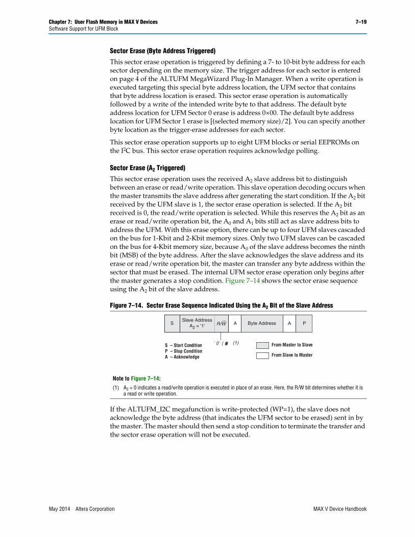
Chapter 7: User Flash Memory in MAX V Devices 7–19Software Support for UFM Block
Sector Erase (Byte Address Triggered)
This sector erase operation is triggered by defining a 7- to 10-bit byte address for each sector depending on the memory size. The trigger address for each sector is entered on page 4 of the ALTUFM MegaWizard Plug-In Manager. When a write operation is executed targeting this special byte address location, the UFM sector that contains that byte address location is erased. This sector erase operation is automatically followed by a write of the intended write byte to that address. The default byte address location for UFM Sector 0 erase is address 0×00. The default byte address location for UFM Sector 1 erase is [(selected memory size)/2]. You can specify another byte location as the trigger-erase addresses for each sector.
This sector erase operation supports up to eight UFM blocks or serial EEPROMs on the I2C bus. This sector erase operation requires acknowledge polling.
Sector Erase (A2 Triggered)
This sector erase operation uses the received A2 slave address bit to distinguish between an erase or read/write operation. This slave operation decoding occurs when the master transmits the slave address after generating the start condition. If the A2 bit received by the UFM slave is 1, the sector erase operation is selected. If the A2 bit received is 0, the read/write operation is selected. While this reserves the A2 bit as an erase or read/write operation bit, the A0 and A1 bits still act as slave address bits to address the UFM. With this erase option, there can be up to four UFM slaves cascaded on the bus for 1-Kbit and 2-Kbit memory sizes. Only two UFM slaves can be cascaded on the bus for 4-Kbit memory size, because A0 of the slave address becomes the ninth bit (MSB) of the byte address. After the slave acknowledges the slave address and its erase or read/write operation bit, the master can transfer any byte address within the sector that must be erased. The internal UFM sector erase operation only begins after the master generates a stop condition. Figure 7–14 shows the sector erase sequence using the A2 bit of the slave address.
If the ALTUFM_I2C megafunction is write-protected (WP=1), the slave does not acknowledge the byte address (that indicates the UFM sector to be erased) sent in by the master. The master should then send a stop condition to terminate the transfer and the sector erase operation will not be executed.
Figure 7–14. Sector Erase Sequence Indicated Using the A2 Bit of the Slave Address
Note to Figure 7–14:
(1) A2 = 0 indicates a read/write operation is executed in place of an erase. Here, the R/W bit determines whether it is a read or write operation.
SSlave Address
A2 = '1' A Byte Address A P
From Master to Slave
From Slave to Master
S – Start ConditionP – Stop ConditionA – Acknowledge
R/W
'0' (write) (1)
May 2014 Altera Corporation MAX V Device Handbook
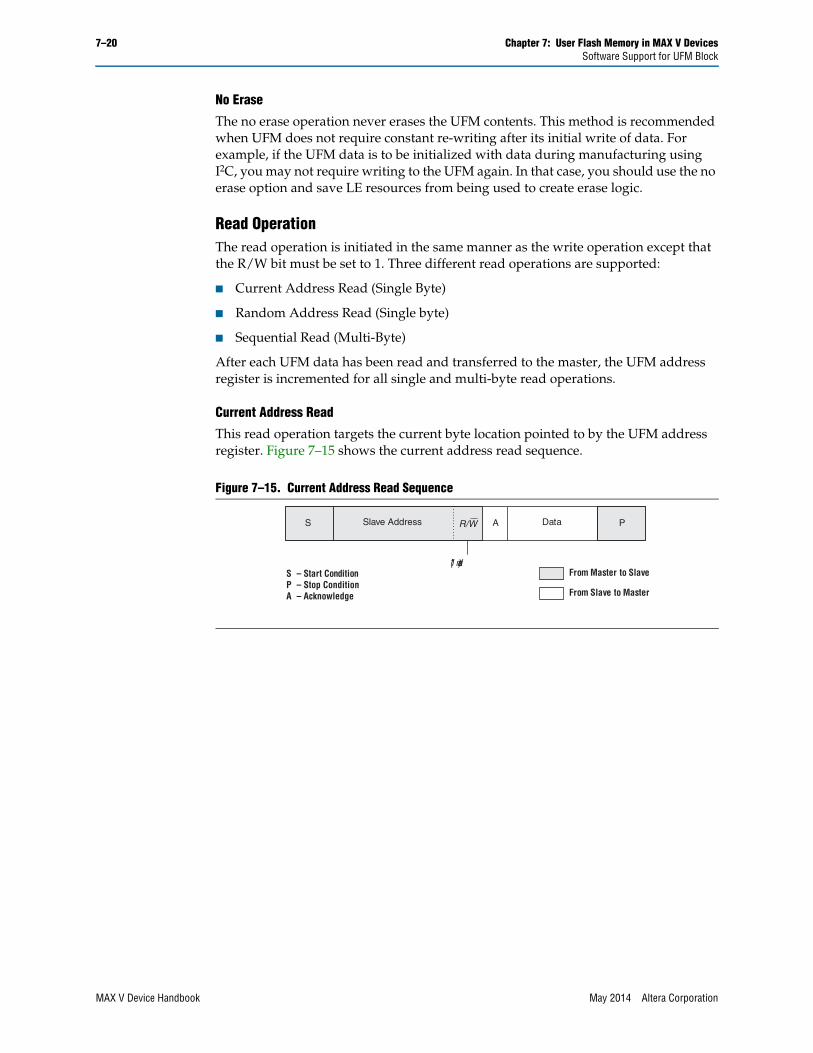
7–20 Chapter 7: User Flash Memory in MAX V DevicesSoftware Support for UFM Block
No Erase
The no erase operation never erases the UFM contents. This method is recommended when UFM does not require constant re-writing after its initial write of data. For example, if the UFM data is to be initialized with data during manufacturing using I2C, you may not require writing to the UFM again. In that case, you should use the no erase option and save LE resources from being used to create erase logic.
Read OperationThe read operation is initiated in the same manner as the write operation except that the R/W bit must be set to 1. Three different read operations are supported:
■ Current Address Read (Single Byte)
■ Random Address Read (Single byte)
■ Sequential Read (Multi-Byte)
After each UFM data has been read and transferred to the master, the UFM address register is incremented for all single and multi-byte read operations.
Current Address Read
This read operation targets the current byte location pointed to by the UFM address register. Figure 7–15 shows the current address read sequence.
Figure 7–15. Current Address Read Sequence
‘1’ (read)
S A DataSlave Address P
From Master to Slave
From Slave to Master
S – Start ConditionP – Stop ConditionA – Acknowledge
R/W
MAX V Device Handbook May 2014 Altera Corporation

Chapter 7: User Flash Memory in MAX V Devices 7–21Software Support for UFM Block
Random Address Read
Random address read operation allows the master to select any byte location for a read operation. The master first performs a “dummy” write operation by sending the start condition, slave address, and byte address of the location it wishes to read. After the ALTUFM_I2C megafunction acknowledges the slave and byte address, the master generates a repeated start condition, the slave address, and the R/W bit is set to 1. The ALTUFM_I2C megafunction then responds with acknowledge and sends the 8-bit data requested. The master then generates a stop condition. Figure 7–16 shows the random address read sequence.
Sequential Read
Sequential read operation can be initiated by either the current address read operation or the random address read operation. Instead of sending a stop condition after the slave has transmitted one byte of data to the master, the master acknowledges that byte and sends additional clock pulses (on the SCL line) for the slave to transmit data bytes from consecutive byte addresses. The operation is terminated when the master generates a stop condition instead of responding with an acknowledge. Figure 7–17 shows the sequential read sequence.
Figure 7–16. Random Address Read Sequence
‘1’ (read)‘0’ (write)
SSlave
AddressByte
AddressSlave
AddressA A Sr DataA P
From Master to Slave
From Slave to Master
S – Start ConditionSr – Repeated StartP – Stop ConditionA – Acknowledge
R/W R/W
Figure 7–17. Sequential Read Sequence
…
‘0’ (write)
SSlave
AddressByte
AddressSlave
AddressA A Sr A Data A Data P
From Master to Slave
From Slave to Master
S – Start ConditionSr – Repeated StartP – Stop ConditionA – Acknowledge
R/W R/W
‘1’ (read) Data (n - bytes) + Acknowledgment (n - 1 bytes)
May 2014 Altera Corporation MAX V Device Handbook
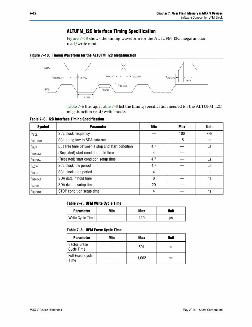
7–22 Chapter 7: User Flash Memory in MAX V DevicesSoftware Support for UFM Block
ALTUFM_I2C Interface Timing SpecificationFigure 7–18 shows the timing waveform for the ALTUFM_I2C megafunction read/write mode.
Table 7–6 through Table 7–8 list the timing specification needed for the ALTUFM_I2C megafunction read/write mode.
Figure 7–18. Timing Waveform for the ALTUFM_I2C Megafunction
SDA
SCL
tSU:STA tHD:STAtHD:DAT tSU:DAT tSU:STO
tBUF
tLOW
tHIGH
tSCLSDA
Table 7–6. I2C Interface Timing Specification
Symbol Parameter Min Max Unit
FSCL SCL clock frequency — 100 kHz
tSCL:SDA SCL going low to SDA data out — 15 ns
tBUF Bus free time between a stop and start condition 4.7 — µs
tHD:STA (Repeated) start condition hold time 4 — µs
tSU:STA (Repeated) start condition setup time 4.7 — µs
tLOW SCL clock low period 4.7 — µs
tHIGH SCL clock high period 4 — µs
tHD:DAT SDA data in hold time 0 — ns
tSU:DAT SDA data in setup time 20 — ns
tSU:STO STOP condition setup time 4 — ns
Table 7–7. UFM Write Cycle Time
Parameter Min Max Unit
Write Cycle Time — 110 µs
Table 7–8. UFM Erase Cycle Time
Parameter Min Max Unit
Sector Erase Cycle Time — 501 ms
Full Erase Cycle Time — 1,002 ms
MAX V Device Handbook May 2014 Altera Corporation

Chapter 7: User Flash Memory in MAX V Devices 7–23Software Support for UFM Block
Instantiating the I2C Interface Using the Quartus II ALTUFM_I2C MegafunctionFigure 7–19 shows the ALTUFM_I2C megafunction symbol for a I2C interface instantiation in the Quartus II software.
ALTUFM_I2C megafunction is under the Memory Compiler folder on page 2a of the MegaWizard Plug-In Manager. On page 3, you can choose whether to implement the Read/Write or Read Only mode for the UFM. You also have an option to choose the memory size for the ALTUFM_I2C megafunction as well as defining the four MSBs of the slave address (default 1010).
You can select the optional write protection and erase operation methods on page 4 of the ALTUFM MegaWizard Plug-In Manager.
1 The UFM block’s internal oscillator is always running when the ALTUFM_I2C megafunction is instantiated for both read-only and read/write interfaces.
Serial Peripheral InterfaceSerial peripheral interface (SPI) is a four-pin serial communication subsystem included on the Motorola 6805 and 68HC11 series microcontrollers. It allows the microcontroller unit to communicate with peripheral devices, and is also capable of inter-processor communications in a multiple-master system.
The SPI bus consists of masters and slaves. The master device initiates and controls the data transfers and provides the clock signal for synchronization. The slave device responds to the data transfer request from the master device. The master device in an SPI bus initiates a service request with the slave devices responding to the service request.
With the ALTUFM megafunction, the UFM and MAX V logic can be configured as a slave device for the SPI bus. The OSC_ENA is always asserted to enable the internal oscillator when the SPI megafunction is instantiated for both read only and read/write interfaces.
Figure 7–19. ALTUFM_I2C Megafunction Symbol for the I2C Interface Instantiation in the Quartus II Software
May 2014 Altera Corporation MAX V Device Handbook

7–24 Chapter 7: User Flash Memory in MAX V DevicesSoftware Support for UFM Block
The Quartus II software supports both the Base mode (uses 8-bit address and data) and the Extended mode (uses 16-bit address and data). Base mode uses only UFM sector 0 (2,048 bits), while Extended mode uses both UFM sector 0 and sector 1 (8,192 bits). There are only four pins in SPI: SI, SO, SCK, and nCS. Table 7–9 describes the SPI pins and functions.
Data transmitted to the SI port of the slave device is sampled by the slave device at the positive SCK clock. Data transmits from the slave device through SO at the negative SCK clock edge. When nCS is asserted, it means the current device is being selected by the master device from the other end of the SPI bus for service. When nCS is not asserted, the SI and SCK ports should be blocked from receiving signals from the master device, and SO should be in High Impedance state to avoid causing contention on the shared SPI bus. All instructions, addresses, and data are transferred with the MSB first and start with high-to-low nCS transition. The circuit diagram is shown in Figure 7–20.
Table 7–9. SPI Interface Signals
Pin Description Function
SI Serial Data Input Receive data serially.
SO Serial Data Output Transmit data serially.
SCK Serial Data Clock The clock signal produced from the master device to synchronize the data transfer.
nCS Chip Select Active low signal that enables the slave device to receive or transfer data from the master device.
Figure 7–20. Circuit Diagram for SPI Interface Read or Write Operations
Read, Write, and Erase State Machine
Op-Code Decoder
Eight-Bit Status Shift Register
Address and Data Hub
UFM BlockSPI InterfaceControl Logic
SI SO SCK nCS
MAX V Device Handbook May 2014 Altera Corporation

Chapter 7: User Flash Memory in MAX V Devices 7–25Software Support for UFM Block
OpcodesTable 7–10 lists the 8-bit instruction opcodes. After nCS is pulled low, the indicated opcode must be provided. Otherwise, the interface assumes that the master device has internal logic errors and ignores the rest of the incoming signals. When nCS is pulled back to high, the interface is back to normal. nCS should be pulled low again for a new service request.
The READ and WRITE opcodes are instructions for transmission, which means the data will be read from or written to the UFM.
WREN, WRDI, RDSR, and WRSR are instructions for the status register, where they do not have any direct interaction with UFM, but read or set the status register within the interface logic. The status register provides status on whether the UFM block is available for any READ or WRITE operation, whether the interface is WRITE enabled, and the state of the UFM WRITE protection. Table 7–11 lists the status register format. For the read only implementation of ALTUFM SPI (Base or Extended mode), the status register does not exist, saving LE resources.
The following sections describe the instructions for SPI.
Table 7–10. Instruction Set for SPI
Name Opcode Operation
WREN 00000110 Enable Write to UFM
WRDI 00000100 Disable Write to UFM
RDSR 00000101 Read Status Register
WRSR 00000001 Write Status Register
READ 00000011 Read data from UFM
WRITE 00000010 Write data to UFM
SECTOR-ERASE 00100000 Sector erase
UFM-ERASE 01100000 Erase the entire UFM block (both sectors)
Table 7–11. Status Register Format
Position Status Default at Power-Up Description
Bit 7 X 0 —
Bit 6 X 0 —
Bit 5 X 0 —
Bit 4 X 0 —
Bit 3 BP1 0 Indicate the current level of block write protection (1)
Bit 2 BP0 0 Indicate the current level of block write protection (1)
Bit 1 WEN 01= SPI WRITE enabled state
0= SPI WRITE disabled state
Bit 0 nRDY 01 = Busy, UFM WRITE or ERASE cycle in progress
0 = No UFM WRITE or ERASE cycle in progress
Note to Table 7–11:
(1) For more information about status register bits BP1 and BP0, refer to Table 7–12 and Table 7–13 on page 7–34.
May 2014 Altera Corporation MAX V Device Handbook

7–26 Chapter 7: User Flash Memory in MAX V DevicesSoftware Support for UFM Block
READ
READ is the instruction for data transmission, where the data is read from the UFM block. When data transfer is taking place, the MSB is always the first bit to be transmitted or received. The data output stream is continuous through all addresses until it is terminated by a low-to-high transition at the nCS port. The READ operation is always performed through the following sequence in SPI, as shown in Figure 7–21:
1. nCS is pulled low to indicate the start of transmission.
2. An 8-bit READ opcode (00000011) is received from the master device. (If internal programming is in progress, READ is ignored and not accepted).
3. A 16-bit address is received from the master device. The LSB of the address is received last. Because the UFM block can take only nine bits of address maximum, the first seven address bits received are discarded.
4. Data is transmitted for as many words as needed by the slave device through SO for READ operation. When the end of the UFM storage array is reached, the address counter rolls over to the start of the UFM to continue the READ operation.
5. nCS is pulled back to high to indicate the end of transmission.
For SPI Base mode, the READ operation is always performed through the following sequence in SPI:
1. nCS is pulled low to indicate the start of transmission.
2. An 8-bit READ opcode (00000011) is received from the master device, followed by an 8-bit address. If internal programming is in progress, the READ operation is ignored and not accepted.
3. Data is transmitted for as many words as needed by the slave device through SO for READ operation. The internal address pointer automatically increments until the highest memory address is reached (address 255 only because the UFM sector 0 is used). The address counter will not roll over when address 255 is reached. The SO output is set to high-impedance (Z) when all eight data bits from address 255 have been shifted out through the SO port.
4. nCS is pulled back to high to indicate the end of transmission.
Figure 7–21. READ Operation Sequence for Extended Mode
0 1 2 3 4 5 6 7 8 9 10 11 20 21 22 23 24 25 26 27 36 37 38 39
nCS
SCK
SI
SOHigh Impedance
03H
MSB
MSB MSB
MSB
16-bit Data Out 1 16-bit Data Out 2
8-bitInstruction
16-bitAddress
MAX V Device Handbook May 2014 Altera Corporation

Chapter 7: User Flash Memory in MAX V Devices 7–27Software Support for UFM Block
Figure 7–22 shows the READ operation sequence for Base mode.
WRITE
WRITE is the instruction for data transmission, where the data is written to the UFM block. The targeted location in the UFM block that will be written must be in the erased state (FFFFH) before initiating a WRITE operation. When data transfer is taking place, the MSB is always the first bit to be transmitted or received. nCS must be driven high before the instruction is executed internally. You may poll the nRDY bit in the software status register for the completion of the internal self-timed WRITE cycle. For SPI Extended mode, the WRITE operation is always done through the following sequence, as shown in Figure 7–23:
1. nCS is pulled low to indicate the start of transmission.
2. An 8-bit WRITE opcode (00000010) is received from the master device. If internal programming is in progress, the WRITE operation is ignored and not accepted.
3. A 16-bit address is received from the master device. The LSB of the address will be received last. Because the UFM block can take only nine bits of address maximum, the first seven address bits received are discarded.
4. A check is carried out on the status register (see Table 7–11) to determine if the WRITE operation has been enabled, and the address is outside of the protected region; otherwise, Step 5 is bypassed.
5. One word (16 bits) of data is transmitted to the slave device through SI.
6. nCS is pulled back to high to indicate the end of transmission.
For SPI Base mode, the WRITE operation is always performed through the following sequence in SPI:
1. nCS is pulled low to indicate the start of transmission.
2. An 8-bit WRITE opcode (00000010) is received. If the internal programming is in progress, the WRITE operation is ignored and not accepted.
3. An 8-bit address is received. A check is carried out on the status register (see Table 7–11) to determine if the WRITE operation has been enabled, and the address is outside of the protected region; otherwise, Step 4 is skipped.
Figure 7–22. READ Operation for Base Mode
1 2 3 4 5 6 7 8 9 10 11 12 13 14 15 16 17 18 19
nCS
SCK
SI
SOHigh Impedance
03H
MSB
MSB MSB
MSB
8-bit Data Out 1 8-bit Data Out 2
8-bitInstruction
8-bit
20 21 22 23 23
Address
May 2014 Altera Corporation MAX V Device Handbook

7–28 Chapter 7: User Flash Memory in MAX V DevicesSoftware Support for UFM Block
4. An 8-bit data is transmitted through SI.
5. nCS is pulled back to high to indicate the end of transmission.
Figure 7–24 shows the WRITE operation sequence for Base mode.
SECTOR-ERASE
SECTOR-ERASE (SE) is the instruction of erasing one sector of the UFM block. Each sector contains 256 words. WEN bit and the sector must not be protected for SE operation to be successful. nCS must be driven high before the instruction is executed internally. You may poll the nRDY bit in the software status register for the completion of the internal self-timed SECTOR-ERASE cycle. For SPI Extended mode, the SE operation is performed in the following sequence, as shown in Figure 7–25:
1. nCS is pulled low.
2. Opcode 00100000 is transmitted into the interface.
3. The 16-bit address is sent. The eighth bit (the first seven bits will be discarded) of the address indicates which sector is erased; a 0 means sector 0 (UFM0) is erased, and a 1 means sector 1 (UFM1) is erased.
Figure 7–23. WRITE Operation Sequence for Extended Mode
0 1 2 3 4 5 6 7 8 9 10 11 20 21 22 23 24 25 26 27 36 37 38 39
nCS
SCK
SI
SOHigh Impedance
02H 16-bit Data In
MSB MSB MSB
8-bitInstruction
16-bitAddress
Figure 7–24. WRITE Operation Sequence for Base Mode
0 1 2 3 4 5 6 7 8 9 10 11 12 13 14 15 16 17 18 19 20 21 22 23
nCS
SCK
SI
SOHigh Impedance
02H
MSB MSB
8-bit Data In
8-bitInstruction
8-bitAddress
MAX V Device Handbook May 2014 Altera Corporation

Chapter 7: User Flash Memory in MAX V Devices 7–29Software Support for UFM Block
4. nCS is pulled back to high.
For SPI Base mode, the SE instruction erases UFM sector 0. Because there are no choices of UFM sectors to be erased, there is no address component to this instruction. The SE operation is always done through the following sequence in SPI Base mode:
1. nCS is pulled low.
2. Opcode 00100000 is transmitted into the interface.
3. nCS is pulled back to high.
Figure 7–26 shows the SECTOR-ERASE operation sequence for Base mode.
Figure 7–25. SECTOR-ERASE Operation Sequence for Extended Mode
Figure 7–26. SECTOR_ERASE Operation Sequence for Base Mode
0 1 2 3 4 5 6 7 8 9 10 11 20 21 22 23
nCS
SCK
SI
SOHigh Impedance
20H
MSB MSB
8-bitInstruction
16-bitAddress
0 1 2 3 4 5 6 7
nCS
SCK
SI
SO
High Impedance
20H
MSB
8-bitInstruction
May 2014 Altera Corporation MAX V Device Handbook

7–30 Chapter 7: User Flash Memory in MAX V DevicesSoftware Support for UFM Block
UFM-ERASE
The UFM-ERASE (CE) instruction erases both UFM sector 0 and sector 1 for SPI Extended Mode. While for SPI Base mode, the CE instruction has the same functionality as the SECTOR-ERASE (SE) instruction, which erases UFM sector 0 only. WEN bit and the UFM sectors must not be protected for CE operation to be successful. nCS must be driven high before the instruction is executed internally. You may poll the nRDY bit in the software status register for the completion of the internal self-timed CE cycle. For both SPI Extended mode and Base mode, the CE operation is performed in the following sequence as shown in Figure 7–27:
1. nCS is pulled low.
2. Opcode 01100000 is transmitted into the interface.
3. nCS is pulled back to high.
Figure 7–27 shows the UFM-ERASE operation sequence.
Figure 7–27. UFM-ERASE Operation Sequence
0 1 2 3 4 5 6 7
nCS
SCK
SI
SO
High Impedance
60H
MSB
8-bitInstruction
MAX V Device Handbook May 2014 Altera Corporation

Chapter 7: User Flash Memory in MAX V Devices 7–31Software Support for UFM Block
WREN (Write Enable)
The interface is powered-up in the write disable state. Therefore, WEN in the status register (refer to Table 7–11) is 0 at power-up. Before any write is allowed to take place, WREN must be issued to set WEN in the status register to 1. If the interface is in read-only mode, WREN does not have any effect on WEN, because the status register does not exist. After WEN is set to 1, it can be reset by the WRDI instruction; the WRITE and SECTOR-ERASE instructions will not reset the WEN bit. WREN is issued through the following sequence, as shown in Figure 7–28:
1. nCS is pulled low.
2. Opcode 00000110 is transmitted into the interface to set WEN to 1 in the status register.
3. After the transmission of the eighth bit of WREN, the interface is in wait state (waiting for nCS to be pulled back to high). Any transmission after this is ignored.
4. nCS is pulled back to high.
Figure 7–28. WREN Operation Sequence
0 1 2 3 4 5 6 7
nCS
SCK
SI
SOHigh Impedance
06H
MSB
8-bitInstruction
May 2014 Altera Corporation MAX V Device Handbook

7–32 Chapter 7: User Flash Memory in MAX V DevicesSoftware Support for UFM Block
WRDI (Write Disable)
After the UFM is programmed, WRDI can be issued to set WEN back to 0, disabling WRITE and preventing inadvertent writing to the UFM. WRDI is issued through the following sequence, as shown in Figure 7–29:
1. nCS is pulled low.
2. Opcode 00000100 is transmitted to set WEN to 0 in the status register.
3. After the transmission of the eighth bit of WRDI, the interface is in wait state (waiting for nCS to be pulled back to high). Any transmission after this is ignored.
4. nCS is pulled back to high.
Figure 7–29. WRDI Operation Sequence
0 1 2 3 4 5 6 7
nCS
SCK
SI
SOHigh Impedance
04H
MSB
8-bitInstruction
MAX V Device Handbook May 2014 Altera Corporation

Chapter 7: User Flash Memory in MAX V Devices 7–33Software Support for UFM Block
RDSR (Read Status Register)
The content of the status register can be read by issuing RDSR. After RDSR is received, the interface outputs the content of the status register through the SO port. Although the four most significant bits (Bit 7 to Bit 4) do not hold valuable information, all eight bits in the status register will output through the SO port. This allows future compatibility when Bit 7 to Bit 4 have new meaning in the status register. During the internal program cycle in the UFM, RDSR is the only valid opcode recognized by the interface (therefore, the status register can be read at any time), and nRDY is the only valid status bit. Other status bits are frozen and remain unchanged until the internal program cycle is ended. RDSR is issued through the following sequence, as shown in Figure 7–30:
1. nCS is pulled low.
2. Opcode 00000101 is transmitted into the interface.
3. SI ignores incoming signals; SO outputs the content of the status register, Bit 7 first and Bit 0 last.
4. If nCS is kept low, repeat step 3.
5. nCS is pulled back to high to terminate the transmission.
Figure 7–30. RDSR Operation Sequence
Status Register Out
0 1 2 3 4 5 6 7 8 9 10 11 12 13 14 15 16 17 18 19 20 21 22 23
nCS
SCK
SI
SOHigh Impedance
05H
MSB MSB
MSB MSB
8-bitInstruction
May 2014 Altera Corporation MAX V Device Handbook

7–34 Chapter 7: User Flash Memory in MAX V DevicesSoftware Support for UFM Block
WRSR (Write Status Register)
The block protection bits(BP1 and BP0) are the status bits used to protect certain sections of the UFM from inadvertent write. The BP1 and BP0 status are updated by WRSR. During WRSR, only BP1 and BP0 in the status register can be written with valid information. The rest of the bits in the status register are ignored and not updated. When both BP1 and BP0 are 0, there is no protection for the UFM. When both BP1 and BP0 are 1, there is full protection for the UFM. BP0 and BP1 are set to 0 upon power-up. Table 7–12 lists the Block Write Protect Bits for Extended mode, while Table 7–13 lists the Block Write Protect Bits for Base mode. WRSR is issued through the following sequence, as shown in Figure 7–31:
1. nCS is pulled low.
2. Opcode 00000001 is transmitted into the interface.
3. An 8-bit status is transmitted into the interface to update BP1 and BP0 of the status register.
4. If nCS is pulled high too early (before all the eight bits in Step 2 or Step 3 are transmitted) or too late (the ninth bit or more is transmitted), WRSR is not executed.
5. nCS is pulled back to high to terminate the transmission.
Figure 7–31. WRSR Operation Sequence
Table 7–12. Block Write Protect Bits for Extended Mode
LevelStatus Register Bits UFM Array Address
ProtectedBP1 BP0
0 (No protection) 0 0 None
3 (Full protection) 1 1 000 to 1FF
Table 7–13. Block Write Protect Bits for Base Mode
LevelStatus Register Bits UFM Array Address
ProtectedBP1 BP0
0 (No protection) 0 0 None
3 (Full protection) 1 1 000 to 0FF
0 1 2 3 4 5 6 7 8 9 10 11 12 13 14 15
nCS
SCK
SI
SOHigh Impedance
01H
MSB MSB
Status Register In
8-bitInstruction
MAX V Device Handbook May 2014 Altera Corporation

Chapter 7: User Flash Memory in MAX V Devices 7–35Software Support for UFM Block
ALTUFM SPI Timing SpecificationFigure 7–32 shows the timing specification needed for the SPI Extended mode (read/write). These nCS timing specifications do not apply to the SPI Extended read-only mode nor to any of the SPI Base modes. However, for the SPI Extended mode (read only) and the SPI Base mode (both read only and read/write), the nCS signal and SCK are not allowed to toggle at the same time. Table 7–14 lists the timing parameters that only apply to the SPI Extended mode (read/write).
Instantiating SPI Using Quartus II ALTUFM_SPI MegafunctionFigure 7–33 shows the ALTUFM_SPI megafunction symbol for SPI instantiation in the Quartus II software.
ALTUFM_SPI megafunction is under the Memory Compiler folder on page 2a of the MegaWizard Plug-In Manager. On page 3, you can choose whether to implement the Read/Write or Read Only mode as the access mode for the UFM. You can also select the configuration mode (Base or Extended) for SPI on this page. You can specify the initial content of the UFM block on page of the ALTUFM MegaWizard Plug-In Manager as discussed in “Creating Memory Content File” on page 7–39.
1 The UFM block’s internal oscillator is always running when the ALTUFM_SPI megafunction is instantiated for read/write interface. The UFM block’s internal oscillator is disabled when the ALTUFM_SPI megafunction is instantiated for read only interface.
Figure 7–32. SPI Timing Waveform
nCS
SCK
tHNCSHIGH
tNCS2SCKtSCK2NCS
Table 7–14. SPI Timing Parameters for Extended Mode
Symbol Description Minimum (ns) Maximum (ns)
tSCK2NCS The time required for the SCK signal falling edge to nCS signal rising edge 50 —
tHNCSHIGH The time that the nCS signal must be held high 600 —
tNCS2SCK The time required for the nCS signal falling edge to SCK signal rising edge 750 —
Figure 7–33. ALTUFM_SPI Megafunction Symbol for SPI Instantiation
May 2014 Altera Corporation MAX V Device Handbook

7–36 Chapter 7: User Flash Memory in MAX V DevicesSoftware Support for UFM Block
Parallel InterfaceThis interface allows for parallel communication between the UFM block and outside logic. After the READ request, WRITE request, or ERASE request is asserted (active low assertion), the outside logic or device (such as a microcontroller) can continue its operation while the data in the UFM is retrieved, written, or erased. During this time, the nBUSY signal is driven “low” to indicate that it is not available to respond to any further request. After the operation is complete, the nBUSY signal is brought back to “high” to indicate that it is now available to service a new request. If it was the Read request, the DATA_VALID is driven “high” to indicate that the data at the DO port is the valid data from the last read address.
Asserting READ, WRITE, and ERASE at the same time is not allowed. Multiple requests are ignored and nothing is read from, written to, or erased in the UFM block. There is no support for sequential read and page write in the parallel interface. For both the read only and the read/write modes of the parallel interface, OSC_ENA is always asserted, enabling the internal oscillator. Table 7–15 lists the parallel interface pins and functions.
Even though the ALTUFM megafunction allows you to select the address widths range from 3 bits to 9 bits, the UFM block always expects a full 9 bits for the width of the address register. Therefore, the ALTUFM megafunction will always pad the remaining LSBs of the address register with '0's if the register width selected is less than 9 bits. The address register will point to sector 0 if the address received at the address register starts with a '0'. The address register will point to sector 1 if the address received starts with a '1'.
Even though you can select an optional data register width of 3 to 16 bits using the ALTUFM megafunction, the UFM block always expects full 16 bits width for the data register. Reading from the data register always proceeds from MSB to LSB. The ALTUFM megafunction always pads the remaining LSBs of the data register with 1s if the user selects a data width of less than 16-bits.
Table 7–15. Parallel Interface Signals
Pin Description Function
DI[15..0] 16-bit data Input Receive 16-bit data in parallel. You can select an optional width of 3 to 16 bits using the ALTUFM megafunction.
DO[15..0] 16-bit data Output Transmit 16-bit data in parallel. You can select an optional width of 3 to 16 bits using the ALTUFM megafunction.
ADDR[8..0] Address RegisterOperation sequence refers to the data that is pointed to by the address register. You can determine the address bus width using the ALTUFM megafunction.
nREAD READ Instruction Signal Initiates a read sequence.
nWRITE WRITE Instruction Signal Initiates a write sequence.
nERASE ERASE Instruction Signal Initiates a SECTOR-ERASE sequence indicated by the MSB of the ADDR[] port.
nBUSY BUSY Signal Driven low to notify that it is not available to respond to any further request.
DATA_VALID Data Valid Driven high to indicate that the data at the DO port is the valid data from the last read address for read request.
MAX V Device Handbook May 2014 Altera Corporation

Chapter 7: User Flash Memory in MAX V Devices 7–37Software Support for UFM Block
ALTUFM Parallel Interface Timing SpecificationFigure 7–34 shows the timing specifications for the parallel interface. Table 7–16 lists the parallel interface instruction signals. The nREAD, nWRITE, and nERASE signals are active low signals.
Instantiating Parallel Interface Using Quartus II ALTUFM_PARALLEL MegafunctionFigure 7–35 shows the ALTUFM_PARALLEL megafunction symbol for a parallel interface instantiation in the Quartus II software.
Figure 7–34. Parallel Interface Timing Waveform
nBusy
Command
Data or Address Bus
tCOMMAND
tHNBUSY
tHBUS
Table 7–16. Parallel Interface Timing Parameters
Symbol Description Minimum (ns) Maximum (ns)
tCOMMANDThe time required for the command signal (nREAD/nWRITE/nERASE) to be asserted and held low to initiate a read/write/erase sequence 600 3,000
tHNBUSYMaximum delay between command signal’s falling edge to the nBUSY signal’s falling edge — 300
tHBUS
The time that the data and address buses must be present at the data input and address register ports after the command signal has been asserted low
600 —
Figure 7–35. ALTUFM_PARALLEL Megafunction Symbol for Parallel Interface Instantiation
May 2014 Altera Corporation MAX V Device Handbook

7–38 Chapter 7: User Flash Memory in MAX V DevicesSoftware Support for UFM Block
ALTUFM_PARALLEL megafunction is under the Memory Compiler folder on page 2a of the MegaWizard Plug-In Manager. On page 3, you can choose whether to implement the Read/Write or Read Only mode for the UFM. You also have an option to choose the width for address bus (up to 9 bits) and for the data bus (up to 16 bits). You can specify the initial content of the UFM block on page 4 of the ALTUFM MegaWizard Plug-In Manager as discussed in “Creating Memory Content File” on page 7–39.
1 The UFM block’s internal oscillator is always running when the ALTUFM_PARALLEL megafunction is instantiated for read/write interface. The UFM block’s internal oscillator is disabled when the ALTUFM_PARALLEL megafunction is instantiated for a read only interface.
None (Altera Serial Interface)Select None for the interface protocol to use the dedicated UFM serial interface. The built-in UFM interface uses 13 pins for the communication. The functional description of the 13 pins are described in Table 7–4 on page 7–3. You can produce your own interface design to communicate to/from the dedicated UFM interface and implement it in the logic array.
Instantiating None Using Quartus II ALTUFM_NONE MegafunctionFigure 7–36 shows the ALTUFM_NONE megafunction symbol for None instantiation in the Quartus II software.
ALTUFM_NONE megafunction is under the Memory Compiler folder on page 2a of the MegaWizard Plug-In Manager. You can specify the initial content of the UFM block on page 3 of the ALTUFM MegaWizard Plug-In Manager as discussed in “Creating Memory Content File”.
Figure 7–36. ALTUFM_NONE Megafunction Symbol for None Instantiation
MAX V Device Handbook May 2014 Altera Corporation

Chapter 7: User Flash Memory in MAX V Devices 7–39Creating Memory Content File
Creating Memory Content FileYou can initialize the content of the UFM through a memory content file. The Quartus II software supports two types of initial memory content file format: Memory Initialization File (.mif) and Hexadecimal File (.hex). A new memory content file for the UFM block can be created by clicking New on the File menu. Select the .mif or .hex file in the Other Files tab.
After clicking OK, a dialog box appears. In this dialog box, the Number of words represents the numbers of address lines while the Word size represents the data width. To create a memory content file for the ALTUFM megafunction, enter 512 for the number of words and 16 for the word size.
The memory content is written into a .hex file. On the Tools menu, click MegaWizard Plug-In Manager. The memory content file (data.hex) is included on the respective ALTUFM MegaWizard Plug-In Manager. Click Yes to use this file for the memory content file. Click Browse to include the memory content file.
Memory Initialization for the ALTUFM_PARALLEL MegafunctionFor the parallel interface, if a .hex file is used to initialize the memory content for the ALTUFM megafunction, you must fully specify all 16 bits in each memory address, regardless of the data width selected. If your data width is less than 16 bits wide, your data must be placed in the MSBs of the data word and the remaining LSBs must be padded with 1’s.
For an example, if address_width = 3 and data_width = 8 are selected for the ALTUFM_PARALLEL megafunction, the .hex file should contain eight addresses of data (23 addresses), each word containing 16 bits. If the initial content at the location 000 is intended to be 10101010, you should specify 1010101011111111 for address 000 in the .hex file.
1 This specification applies only to .hex files used with the parallel interface. .mifs do not require you to fully specify 16 bits for each data word. However, both .mif and .hex files require you to specify all addresses of data according to the address_width selected in the megafunction.
Memory Initialization for the ALTUFM_SPI MegafunctionThe same 16-bit data padding mentioned for ALTUFM_PARALLEL is required for .hex files used with the SPI Base (8 bits) and Extended (16 bits) mode interface. In addition, for SPI Base and Extended modes, you must fully specify memory content for all 512 addresses (both sector 0 and sector 1) in the .mif and .hex files, even if sector 1 is not used. You can put valid data for SPI Base mode addresses 0 to 255 (sector 0), and initialize sector 1 to all ones.
May 2014 Altera Corporation MAX V Device Handbook

7–40 Chapter 7: User Flash Memory in MAX V DevicesCreating Memory Content File
Memory Initialization for the ALTUFM_I2C MegafunctionThe MAX V UFM physical memory block contains a 16-bit wide and 512 deep (9-bit address) array. The ALTUFM_I2C megafunction uses the following smaller array sizes:
■ An 8-bit wide and 128 deep (7-bit address) mapping for 1 Kbit memory size
■ An 8-bit wide and 256 deep (8-bit address) mapping for 2 Kbits memory size
■ An 8-bit wide and 512 deep (9-bit address) mapping for 4 Kbits memory size
■ An 8-bit wide and 1,024 deep (10-bit address) mapping for 8 Kbits memory size
Altera recommends that you pad the .mif or .hex file for both address and data width to fill the physical memory map for the UFM block and ensure the .mif or .hex file represents a full 16-bit word size and a 9-bit address space.
Memory Map for 1-Kbit Memory Initialization
Figure 7–37 shows the memory map initialization for the ALTUFM_I2C megafunction of 1-Kbit memory size. The ALTUFM_I2C megafunction byte address location of 00h to 3Fh is mapped to the UFM block address location of 000h to 03Fh. The ALTUFM_I2C megafunction byte address location of 40h to 7Fh is mapped to the UFM block address location of 1C0h to 1FFh. Altera recommends that you pad the unused address locations of the UFM block with all 1s.
Figure 7–37. Memory Map for 1-Kbit Memory Initialization
Upper Half – Addresses40h to 7Fh
Lower Half – Addresses00h to 3Fh
00h
000h
3Fh
03Fh
40h
7Fh
1C0h
1FFhAddress 40h in logical memory maps to
1C0h in the MIF/HEX file. Address 7Fh in logicalmemory maps to 1FFh in the MIF/HEX file, and all
data in between follows the order in thelogical memory
Address 00h in logical memory maps toaddress 000h in the MIF/HEX file. Address 3Fh in logical memory maps to 03Fh in the MIF/HEX file,
and all data in between follows the order in thelogical memory
040h
1BFh
This section of the UFM is unused –the MIF/HEX file contents should be set to
all '1' for addresses 040h to 1BFh
1-Kbit ALTUFM_I2C MegafunctionLogical Memory Contents
MIF or HEX File Contents – to representthe actual data and address size for the UFM block
MAX V Device Handbook May 2014 Altera Corporation

Chapter 7: User Flash Memory in MAX V Devices 7–41Creating Memory Content File
Memory Map for 2-Kbit Memory Initialization
Figure 7–38 shows the memory map initialization for the ALTUFM_I2C megafunction of 2 Kbits of memory. The ALTUFM_I2C megafunction byte address location of 00h to 7Fh is mapped to the UFM block address location of 000h to 07Fh. The ALTUFM_I2C megafunction byte address location of 80h to FFh is mapped to the UFM block address location of 180h to 1FFh. Altera recommends that you pad the unused address location of the UFM block with all 1s.
Figure 7–38. Memory Map for 2-Kbit Memory Initialization
Upper Half – Addresses80h to FFh
Lower Half – Addresses00h to 7Fh
00h
000h
7Fh
07Fh
80h
FFh
180h
1FFh
Address 80h in logical memory maps toaddress 180h in the MIF/HEX file. FFh in logical
memory maps to 1FFh in the MIF/HEX file, and alldata in between follows the order in the
logical memory
Address 00h in logical memory maps toaddress 000h in the MIF/HEX file. Address 7Fh in logical memory maps to 07Fh in the MIF/HEX file,
and all data in between follows the order in thelogical memory
080h
17FhThis section of the UFM is unused –
the MIF/HEX file contents should be set toall '1' for addresses 080h to 17Fh
2-Kbit ALTUFM_I2C MegafunctionLogical Memory Contents
MIF or HEX File Contents – to representthe actual data and address size for the UFM block
May 2014 Altera Corporation MAX V Device Handbook

7–42 Chapter 7: User Flash Memory in MAX V DevicesCreating Memory Content File
Memory Map for 4-Kbit Memory Initialization
Figure 7–39 shows the memory map initialization for the ALTUFM_I2C megafunction of 4-Kbit memory. The ALTUFM_I2C megafunction byte address location of 00h to FFh is mapped to the UFM block address location of 000h to 0FFh. The ALTUFM_I2C megafunction byte address location of 100h to 1FFh is mapped to the UFM block address location of 100h to 1FFh.
Memory Map for 8-Kbit Memory Initialization
Figure 7–40 shows the memory map initialization for the ALTUFM_I2C megafunction of 8-Kbit memory. The ALTUFM_I2C megafunction of 8-Kbit memory fully utilizes all the memory locations in the UFM block.
Figure 7–39. Memory Map for 4-Kbit Memory Initialization
Upper Half – Addresses100h to 1FFh
Lower Half – Addresses00h to FFh
00h 000h
FFh 0FFh
100h
1FFh
100h
1FFh
Address 100h in logical memory maps to100h in the MIF/HEX file. Address 1FFh in logicalmemory maps to 1FFh in the MIF/HEX file, and all
data in between follows the order in thelogical memory
Address 00h in logical memory maps to000h in the MIF/HEX file. Address FFh in logical
memory maps to 0FFh in the MIF/HEX file, and alldata in between follows the order in the
logical memory
4-Kbit ALTUFM_I2C MegafunctionLogical Memory Contents
MIF or HEX File Contents – to representthe data and address size for the UFM block
Figure 7–40. Memory Map for 8-Kbit Memory Initialization
000h
0FFh
100h
1FFh
200h
2FFh
300h
3FFh
Upper 8-bit (byte) Lower 8-bit (byte)
16-bit data in UFM
000h
0FFh
100h
1FFh
8-Kbit ALTUFM_I2C MegafunctionLogical Memory Contents
Upper Quarter Addresses300h to 3FFh
Mid-Upper Quarter Addresses200h to 2FFh
Mid-Lower Quarter Addresses100h to 1FFh
Lower Quarter Addresses000h to 0FFh
MIF or HEX File Contents - to represent theactual data and address size for the UFM Block
The upper quarter oflogical memory mapsto the upper byte ofsector 1. Address 300hin logical memorymaps to address 100hin physical memoryand all addressesfollow the order inlogical memory.
The mid-upper quarter oflogical memory mapsto the lower byte ofsector 1. Address 200hin logical memorymaps to address 100hin physical memoryand all addressesfollow the order inlogical memory.
The lower quarter oflogical memory mapsto the lower byte ofsector 0. Address 000hin logical memorymaps to address 000hin physical memoryand all addressesfollow the order inlogical memory.
The mid-lower quarter oflogical memory mapsto the lower byte ofsector 0. Address 100hin logical memorymaps to address 000hin physical memoryand all addressesfollow the order inlogical memory.
MAX V Device Handbook May 2014 Altera Corporation

Chapter 7: User Flash Memory in MAX V Devices 7–43Simulation Parameters
Padding Data into Memory Map
The ALTUFM_I2C megafunction uses the upper 8 bits of the UFM 16-bit word; therefore, the 8 least significant bits should be padded with 1s, as shown in Figure 7–41.
Simulation ParametersIn the ALTUFM megafunction, you have an option to simulate the OSC output port at the maximum or the minimum frequency during the design simulation. The frequency chosen is only used as the timing parameter for the Quartus II simulator and does not affect the real MAX V device OSC output frequency.
Document Revision HistoryTable 7–17 lists the revision history for this chapter.
Figure 7–41. Padding Data into Memory Map
8-bit valid data to be placedin the upper byte
Pad the lower byte with eight '1's
1 0 1 0 1 0 1 0 1 1 1 1 1 1 1 1
Table 7–17. Document Revision History
Date Version Changes
May 2014 1.2 Updated “Page Write Operation” on page 7–17
January 2011 1.1 Updated “Oscillator” section.
December 2010 1.0 Initial release.
May 2014 Altera Corporation MAX V Device Handbook

7–44 Chapter 7: User Flash Memory in MAX V DevicesDocument Revision History
MAX V Device Handbook May 2014 Altera Corporation

MAX V Device HandbookDecember 2010
MV51008-1.0
© 2010 Altera Corporation. All rights reserved. ALTERA, ARRand/or trademarks of Altera Corporation in the U.S. and otherwww.altera.com/common/legal.html. Altera warrants performreserves the right to make changes to any products and servicesinformation, product, or service described herein except as expspecifications before relying on any published information and
December 2010MV51008-1.0
8. JTAG Boundary-Scan Testing in MAX VDevices
This chapter describes the IEEE Std.1149.1 (JTAG) boundary-scan testing for Altera® MAX® V devices. The IEEE Std. 1149.1 BST circuitry available in MAX V devices provides a cost-effective and efficient way to test systems that contain devices with tight lead spacing. Circuit boards with Altera and other IEEE Std. 1149.1-compliant devices can use EXTEST, SAMPLE/PRELOAD, and BYPASS modes to create serial patterns that internally test the pin connections between devices and check device operation.
As PCBs become more complex, the requirement for thorough testing becomes increasingly important. Advances in surface-mount packaging and PCB manufacturing have resulted in smaller boards, making traditional test methods (for example, external test probes and “bed-of-nails” test fixtures) harder to implement. As a result, cost savings from PCB space reductions are sometimes offset by cost increases in traditional testing methods.
In the 1980s, JTAG developed a specification for boundary-scan testing that was later standardized as the IEEE Std. 1149.1 specification. This boundary-scan test (BST) architecture offers the capability to efficiently test components on PCBs with tight lead spacing.
BST architecture can test pin connections without using physical test probes and capture functional data while a device is operating normally. Boundary-scan cells (BSCs) in a device can force signals onto pins, or capture data from pin or core logic signals. Forced test data is serially shifted into the BSCs. Captured data is serially shifted out and externally compared to expected results.
Figure 8–1 shows the concept of boundary-scan testing.
This chapter describes the following topics:
■ “IEEE Std. 1149.1 BST Architecture” on page 8–2
■ “IEEE Std. 1149.1 Boundary-Scan Register” on page 8–3
■ “IEEE Std. 1149.1 BST Operation Control” on page 8–6
■ “I/O Voltage Support in the JTAG Chain” on page 8–13
■ “Boundary-Scan Test for Programmed Devices” on page 8–14
Figure 8–1. IEEE Std. 1149.1 Boundary-Scan Testing
CoreLogic
SerialData In
Boundary-Scan Cell
IC
CoreLogic
SerialData Out
Interconnectionto Be Tested
JTAG Device 1 JTAG Device 2
Pin Signal
Subscribe
IA, CYCLONE, HARDCOPY, MAX, MEGACORE, NIOS, QUARTUS and STRATIX are Reg. U.S. Pat. & Tm. Off. countries. All other trademarks and service marks are the property of their respective holders as described at
ance of its semiconductor products to current specifications in accordance with Altera’s standard warranty, but at any time without notice. Altera assumes no responsibility or liability arising out of the application or use of any ressly agreed to in writing by Altera. Altera customers are advised to obtain the latest version of device before placing orders for products or services.

8–2 Chapter 8: JTAG Boundary-Scan Testing in MAX V DevicesIEEE Std. 1149.1 BST Architecture
■ “Disabling IEEE Std. 1149.1 BST Circuitry” on page 8–15
■ “Guidelines for IEEE Std. 1149.1 Boundary-Scan Testing” on page 8–15
■ “Boundary-Scan Description Language Support” on page 8–15
In addition to BST, you can use the IEEE Std. 1149.1 controller for in-system programming for MAX V devices. MAX V devices support IEEE 1532 programming, which uses the IEEE Std. 1149.1 test access port (TAP) interface. However, this chapter only describes the BST feature of the IEEE Std. 1149.1 circuitry.
IEEE Std. 1149.1 BST ArchitectureA MAX V device operating in IEEE Std. 1149.1 BST mode uses four required pins, TDI, TDO, TMS, and TCK.
Table 8–1 lists the functions of each of these pins. MAX V devices do not have a TRST pin.
The IEEE Std. 1149.1 BST circuitry requires the following registers:
■ The instruction register determines which action to perform and which data register to access.
■ The bypass register (which is a 1-bit long data register) provides a minimum-length serial path between the TDI and TDO pins.
■ The boundary-scan register that is a shift register composed of all the BSCs of the device.
Table 8–1. IEEE Std. 1149.1 Pin Descriptions
Pin Description Function
TDI (1) Test data input Serial input pin for instructions as well as test and programming data. Data is shifted in on the rising edge of TCK.
TDO Test data output
Serial data output pin for instructions as well as test and programming data. Data is shifted out on the falling edge of TCK. The pin is tri-stated if data is not being shifted out of the device.
TMS (1) Test mode select
Input pin that provides the control signal to determine the transitions of the TAP controller state machine. Transitions within the state machine occur at the rising edge of TCK. Therefore, you must set up the TMS before the rising edge of TCK. TMS is evaluated on the rising edge of TCK.
TCK (2) Test clock input The clock input to the BST circuitry. Some operations occur at the rising edge, while others occur at the falling edge.
Notes to Table 8–1:
(1) The TDI and TMS pins have internal weak pull-up resistors(2) The TCK pin has an internal weak pull-down resistor
MAX V Device Handbook December 2010 Altera Corporation

Chapter 8: JTAG Boundary-Scan Testing in MAX V Devices 8–3IEEE Std. 1149.1 Boundary-Scan Register
Figure 8–2 shows a functional model of the IEEE Std. 1149.1 circuitry.
The TAP controller controls the IEEE Std. 1149.1 boundary-scan testing, as described in “IEEE Std. 1149.1 BST Operation Control” on page 8–6. The TMS and TCK pins operate the TAP controller and the TDI and TDO pins provide the serial path for the data registers. The TDI pin also provides data to the instruction register, which then generates the control logic for the data registers.
IEEE Std. 1149.1 Boundary-Scan RegisterThe boundary-scan register is a large serial shift register that uses the TDI pin as an input and the TDO pin as an output. The boundary-scan register consists of 3-bit peripheral elements that are associated with the I/O pins of the MAX V devices. You can use the boundary-scan register to test the external pin connections or to capture internal data.
Figure 8–2. IEEE Std. 1149.1 Circuitry
Note to Figure 8–2:
(1) For the boundary-scan register length in MAX V devices, refer to the JTAG and In-System Programmability in MAX V Devices chapter.
a
UPDATEIRCLOCKIR
SHIFTIR
UPDATEDRCLOCKDR
SHIFTDR
TDI
Instruction Register
Bypass Register
Boundary-Scan Register (1)
Instruction Decode
TMS
TCK
TAPController
ISP Registers
TDO
Data Registers
Device ID Register
December 2010 Altera Corporation MAX V Device Handbook

8–4 Chapter 8: JTAG Boundary-Scan Testing in MAX V DevicesIEEE Std. 1149.1 Boundary-Scan Register
Figure 8–3 shows how test data is serially shifted around the periphery of the IEEE Std. 1149.1 device.
Boundary-Scan Cells of a MAX V Device I/O PinExcept for the four JTAG pins and power pins, you can use all the pins of a MAX V device (including clock pins) as user I/O pins and have a BSC. The 3-bit BSC consists of a set of capture registers and a set of update registers. The capture registers can connect to internal device data through the OUTJ and OEJ signals, while the update registers connect to external data through the PIN_OUT and PIN_OE signals. The TAP controller internally generates the SHIFT, CLOCK, and UPDATE global control signals for the IEEE Std. 1149.1 BST registers; a decode of the instruction register generates the MODE signal. The data signal path for the boundary-scan register runs from the serial data in (SDI) signal to the serial data out (SDO) signal. The scan register begins at the TDI pin and ends at the TDO pin of the device.
Figure 8–3. Boundary-Scan Register
TCKTMS
TAP Controller
TDI
Internal Logic
TDO
Each peripheralelement is either anI/O pin, dedicatedinput pin, ordedicatedconfiguration pin.
MAX V Device Handbook December 2010 Altera Corporation

Chapter 8: JTAG Boundary-Scan Testing in MAX V Devices 8–5IEEE Std. 1149.1 Boundary-Scan Register
Figure 8–4 shows the user I/O BSC for MAX V devices.
Table 8–2 lists the capture and update register capabilities of all BSC within MAX V devices.
JTAG Pins and Power PinsMAX V devices do not have BSCs for dedicated JTAG pins (TDI, TDO, TMS, and TCK) and power pins (VCCINT, VCCIO, GNDINT, and GNDIO).
Figure 8–4. User I/O BSC with IEEE Std. 1149.1 BST Circuitry for MAX V Devices
MODEHIGHZ
PIN_IN
PIN_OE
PIN_OUT
PinOutputBuffer
INJ
OEJ
OUTJ
SDO
UPDATECLOCKSHIFT
SDI
D QInput
01
D QOE
D QOE
01
D QOutput
D QOutput
01
01
01
CaptureRegisters
UpdateRegisters
Global Signals
01
From or To DeviceI/O Cell CircuitryAnd/Or Logic Core
Table 8–2. BSC Description for MAX V Devices (Note 1)
Pin Type
Captures Drives
NotesOutput Capture Register
OE Capture Register
Input Capture Register
Output Update
Register
OE Update Register
Input Update Register
User I/O OUTJ OEJ PIN_IN PIN_OUT PIN_OE — Includes user clocks
Note to Table 8–2:
(1) TDI, TDO, TMS, and TCK pins and all VCC and GND pin types do not have BSCs.
December 2010 Altera Corporation MAX V Device Handbook

8–6 Chapter 8: JTAG Boundary-Scan Testing in MAX V DevicesIEEE Std. 1149.1 BST Operation Control
IEEE Std. 1149.1 BST Operation ControlMAX V devices implement the SAMPLE/PRELOAD, EXTEST, BYPASS, IDCODE, USERCODE, CLAMP and HIGHZ IEEE Std. 1149.1 BST instructions. The length of the BST instructions is 10 bits. These instructions are described in detail later in this chapter.
f For a summary of the BST instructions and their instruction codes, refer to the JTAG and In-System Programmability in MAX V Devices chapter.
The IEEE Std. 1149.1 TAP controller, a 16-state state machine clocked on the rising edge of TCK, uses the TMS pin to control IEEE Std. 1149.1 operation in the device.
Figure 8–5 shows the TAP controller state machine.
Figure 8–5. IEEE Std. 1149.1 TAP Controller State Machine
SELECT_DR_SCAN
CAPTURE_DR
SHIFT_DR
EXIT1_DR
PAUSE_DR
EXIT2_DR
UPDATE_DR
SHIFT_IR
EXIT1_IR
PAUSE_IR
EXIT2_IR
UPDATE_IR
TMS = 0
TMS = 0
TMS = 0
TMS = 1
TMS = 0
TMS = 1
TMS = 1
TMS = 0
TMS = 1
TMS = 0
TMS = 1
TMS = 1
TMS = 0TMS = 0
TMS = 1
TMS = 1
TMS = 0
TMS = 1
TMS = 0
TMS = 0
TMS = 1
TMS = 0
TMS = 0
TMS = 1
TMS = 0
RUN_TEST/IDLETMS = 0
TEST_LOGIC/RESETTMS = 1
TMS = 0
TMS = 1 TMS = 1
TMS = 1 TMS = 1
CAPTURE_IR
SELECT_IR_SCAN
MAX V Device Handbook December 2010 Altera Corporation

Chapter 8: JTAG Boundary-Scan Testing in MAX V Devices 8–7IEEE Std. 1149.1 BST Operation Control
When the TAP controller is in the TEST_LOGIC/RESET state, the BST circuitry is disabled, the device is in normal operation, and the instruction register is initialized with IDCODE as the initial instruction. During device power up, the TAP controller starts in this TEST_LOGIC/RESET state. In addition, the TAP controller may be forced to the TEST_LOGIC/RESET state by holding TMS high for five TCK clock cycles. After the TEST_LOGIC/RESET state, the TAP controller remains in this state as long as TMS continues to be held high while TCK is clocked.
Figure 8–6 shows the timing requirements for the IEEE Std. 1149.1 signals.
To start the IEEE Std. 1149.1 operation, select an instruction mode by advancing the TAP controller to the shift instruction register (SHIFT_IR) state and shift in the appropriate instruction code on the TDI pin.
Figure 8–7 shows the entry of the instruction code into the instruction register. From the RESET state, TMS is clocked with the pattern 01100 to advance the TAP controller to SHIFT_IR state.
Figure 8–6. IEEE Std. 1149.1 Timing Waveforms (Note 1)
Note to Figure 8–6:(1) For timing parameter values, refer to the DC and Switching Characteristics for MAX V Devices chapter.
TDI
TMS
TDO
TCK
Signalto Be
Captured
Signalto Be
Driven
tJCP tJPSU tJPHtJCH tJCL
tJPZX tJPCO
tJSSU tJSH
tJSZX tJSCO tJSXZ
tJPXZ
Figure 8–7. Selecting the Instruction Mode
SELECT_DR_SCAN
SELECT_IR_SCAN
CAPTURE_IR
RUN_TEST/IDLE EXIT1_IR
TCK
TMS
TDI
TDO
TAP_STATE
TEST_LOGIC/RESET
SHIFT_IR
December 2010 Altera Corporation MAX V Device Handbook

8–8 Chapter 8: JTAG Boundary-Scan Testing in MAX V DevicesIEEE Std. 1149.1 BST Operation Control
The TDO pin is tri-stated in all states except the SHIFT_IR and SHIFT_DR states. The TDO pin is activated at the first falling edge of TCK after entering either of the shift states and is tri-stated at the first falling edge of TCK after leaving either of the shift states.
When the SHIFT_IR state is activated, TDO is no longer tri-stated, and the initial state of the instruction register is shifted out on the falling edge of TCK. TDO continues to shift out the contents of the instruction register as long as the SHIFT_IR state is active. The TAP controller remains in the SHIFT_IR state as long as TMS remains low.
During the SHIFT_IR state, an instruction code is entered by shifting data on the TDI pin on the rising edge of TCK. You must clock the last bit of the OPCODE at the same time that the next state, EXIT1_IR, is activated; EXIT1_IR is entered by clocking a logic high on TMS. After in the EXIT1_IR state, TDO becomes tri-stated again. TDO is always tri-stated except in the SHIFT_IR and SHIFT_DR states. After an instruction code is entered correctly, the TAP controller advances to perform the serial shifting of test data in one of three modes (SAMPLE/PRELOAD, EXTEST, or BYPASS).
For MAX V devices, there are weak pull-up resistors for TDI and TMS, and pull-down resistors for TCK. However, in a JTAG chain, there might be some devices that do not have internal pull-up or pull-down resistors. In this case, Altera recommends pulling the TMS pin high (through an external 10-k resistor), and pulling TCK low (through an external 1-k resistor) during BST or in-system programmability (ISP) to prevent the TAP controller from going into an unintended state. Pulling-up the TDI signal externally for the MAX V device is optional.
f For more information about the pull-up and pull-down resistors, refer to AN 100: In-System Programmability Guidelines.
SAMPLE/PRELOAD Instruction ModeSAMPLE/PRELOAD instruction mode allows you to take a snapshot of device data without interrupting normal device operation. However, SAMPLE/PRELOAD instruction mode is most often used to preload the test data into the update registers before loading the EXTEST instruction.
During the capture phase, multiplexers preceding the capture registers select the active device data signals and clocked data into the capture registers. The multiplexers at the outputs of the update registers also select active device data to prevent functional interruptions to the device.
During the shift phase, the boundary-scan shift register is formed by clocking data through capture registers around the device periphery and then out of the TDO pin. New test data can simultaneously be shifted into TDI and replace the contents of the capture registers. During the update phase, data in the capture registers is transferred to the update registers.You can then use this data in EXTEST instruction mode. For more information, refer to “EXTEST Instruction Mode” on page 8–10.
MAX V Device Handbook December 2010 Altera Corporation

Chapter 8: JTAG Boundary-Scan Testing in MAX V Devices 8–9IEEE Std. 1149.1 BST Operation Control
Figure 8–8 shows the capture, shift, and update phases of SAMPLE/PRELOAD mode.
SAMPLE/PRELOAD instruction code shifts in through the TDI pin. The TAP controller advances to the CAPTURE_DR state and then to the SHIFT_DR state, where it remains if TMS is held low. The data shifted out of the TDO pin consists of the data that was present in the capture registers after the capture phase. New test data shifted into the TDI pin appears at the TDO pin after being clocked through the entire boundary-scan register.
Figure 8–8. IEEE Std. 1149.1 BST SAMPLE/PRELOAD Mode
MODEHIGHZ
PIN_IN
PIN_OE
PIN_OUT
PinOutputBuffer
INJ
OEJ
OUTJ
SDO
UPDATECLOCKSHIFT
SDI
D QInput
01
D QOE
D QOE
01
D QOutput
D QOutput
01
01
01
CaptureRegisters
UpdateRegisters
Global Signals
01
MODEHIGHZ
PIN_IN
PIN_OE
PIN_OUT
PinOutputBuffer
INJ
OEJ
OUTJ
SDO
UPDATECLOCKSHIFT
SDI
D QInput
01
D QOE
D QOE
01
D QOutput
D QOutput
01
01
01
CaptureRegisters
UpdateRegisters
Global Signals
01
(Capture Phase)
(Shift and Update Phase)
December 2010 Altera Corporation MAX V Device Handbook

8–10 Chapter 8: JTAG Boundary-Scan Testing in MAX V DevicesIEEE Std. 1149.1 BST Operation Control
Figure 8–9 shows that the test data that shifted into TDI does not appear at the TDO pin until after the capture register data that is shifted out. If TMS is held high on two consecutive TCK clock cycles, the TAP controller advances to the UPDATE_DR state for the update phase.
If you enable the device output enable feature but the DEV_OE pin is not asserted during boundary-scan testing, the output enable boundary-scan registers of the BSCs capture data from the core of the device during SAMPLE/PRELOAD. These values are not high impedance, although the I/O pins are tri-stated.
Figure 8–9 shows the SAMPLE/PRELOAD waveforms.
EXTEST Instruction ModeUse EXTEST instruction mode to check the external pin connections between devices. Unlike SAMPLE/PRELOAD mode, EXTEST allows test data to be forced onto the pin signals. By forcing known logic high and low levels on output pins, you can detect opens and shorts at pins of any device in the scan chain.
EXTEST selects data differently than SAMPLE/PRELOAD. EXTEST chooses data from the update registers as the source of the output and output enable signals. After the EXTEST instruction code is entered, the multiplexers select the update register data; thus, you can force the data stored in these registers from a previous EXTEST or SAMPLE/PRELOAD test cycle onto the pin signals. In the capture phase, the results of this test data are stored in the capture registers and then shifted out of TDO during the shift phase. You can store the new test data in the update registers during the update phase.
Figure 8–9. SAMPLE/PRELOAD Shift Data Register Waveforms
Data stored in
boundary- scan
register is shifted
out of TDO.
UPDATE_IR
SHIFT_DR
SELECT_DR_SCAN
CAPTURE_DR
EXIT1_IR EXIT1_DR
UPDATE_DR
TCK
TMS
TDI
TDO
TAP_STATE
Instruction Code
SHIFT_IR
After boundry-scanregister data has beenshifted out, dataentered into TDI willshift out of TDO.
MAX V Device Handbook December 2010 Altera Corporation

Chapter 8: JTAG Boundary-Scan Testing in MAX V Devices 8–11IEEE Std. 1149.1 BST Operation Control
Figure 8–10 shows the capture, shift, and update phases of EXTEST mode.
Figure 8–10. IEEE Std. 1149.1 BST EXTEST Mode
MODEHIGHZ
PIN_IN
PIN_OE
PIN_OUT
PinOutputBuffer
INJ
OEJ
OUTJ
SDO
UPDATECLOCKSHIFT
SDI
D QInput
01
D QOE
D QOE
01
D QOutput
D QOutput
01
01
01
CaptureRegisters
UpdateRegisters
Global Signals
01
(Capture Phase)
MODEHIGHZ
PIN_IN
PIN_OE
PIN_OUT
PinOutputBuffer
INJ
OEJ
OUTJ
SDO
UPDATECLOCKSHIFT
SDI
D QInput
01
D QOE
D QOE
01
D QOutput
D QOutput
01
01
01
CaptureRegisters
UpdateRegisters
Global Signals
01
(Shift and Update Phase)
December 2010 Altera Corporation MAX V Device Handbook
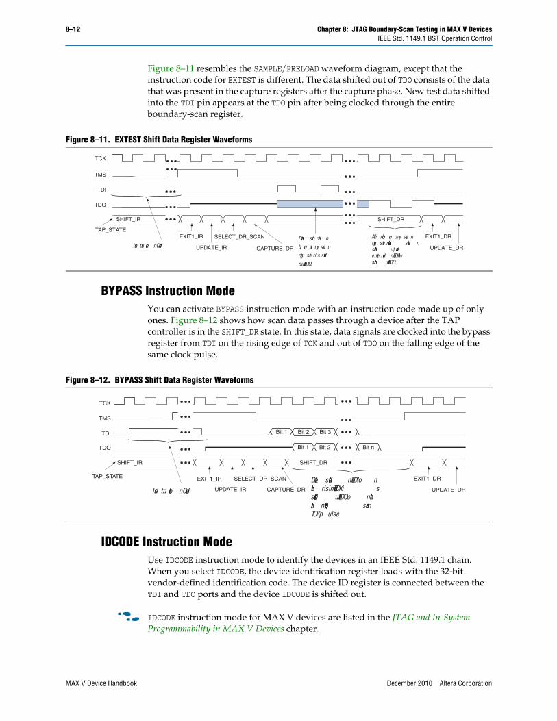
8–12 Chapter 8: JTAG Boundary-Scan Testing in MAX V DevicesIEEE Std. 1149.1 BST Operation Control
Figure 8–11 resembles the SAMPLE/PRELOAD waveform diagram, except that the instruction code for EXTEST is different. The data shifted out of TDO consists of the data that was present in the capture registers after the capture phase. New test data shifted into the TDI pin appears at the TDO pin after being clocked through the entire boundary-scan register.
BYPASS Instruction ModeYou can activate BYPASS instruction mode with an instruction code made up of only ones. Figure 8–12 shows how scan data passes through a device after the TAP controller is in the SHIFT_DR state. In this state, data signals are clocked into the bypass register from TDI on the rising edge of TCK and out of TDO on the falling edge of the same clock pulse.
IDCODE Instruction ModeUse IDCODE instruction mode to identify the devices in an IEEE Std. 1149.1 chain. When you select IDCODE, the device identification register loads with the 32-bit vendor-defined identification code. The device ID register is connected between the TDI and TDO ports and the device IDCODE is shifted out.
f IDCODE instruction mode for MAX V devices are listed in the JTAG and In-System Programmability in MAX V Devices chapter.
Figure 8–11. EXTEST Shift Data Register Waveforms
Data stored in
boundary- scan
register is shifted
out of TDO.
UPDATE_IR
SHIFT_DR
SELECT_DR_SCAN
CAPTURE_DR
EXIT1_IR EXIT1_DR
UPDATE_DR
TCK
TMS
TDI
TDO
TAP_STATE
Instruction Code
SHIFT_IR
After boundry-scanregister data has beenshifted out, dataentered into TDI willshift out of TDO.
Figure 8–12. BYPASS Shift Data Register Waveforms
Data shifted into TDI onthe rising edge of TCK isshifted out of TDO on thefalling edge of the sameTCK pulse.
UPDATE_IR
SELECT_DR_SCAN
CAPTURE_DR
EXIT1_IR EXIT1_DR
UPDATE_DR
SHIFT_DR
Instruction Code
TCK
TMS
TDI
TDO
TAP_STATE
SHIFT_IR
Bit 2 Bit 3
Bit 1 Bit 2 Bit n
Bit 1
MAX V Device Handbook December 2010 Altera Corporation

Chapter 8: JTAG Boundary-Scan Testing in MAX V Devices 8–13I/O Voltage Support in the JTAG Chain
USERCODE Instruction ModeUse USERCODE instruction mode to examine the user electronic signature (UES) within the devices along an IEEE Std. 1149.1 chain. When you select this instruction, the device identification register is connected between the TDI and TDO ports. The user-defined UES shifts into the device ID register in parallel from the 32-bit USERCODE register. The UES then shifts out through the device ID register. The USERCODE information is only available after the device is successfully configured.
Non-volatile USERCODE data is written to the configuration flash memory (CFM) block and then written to the SRAM at power up. The USERCODE instruction reads the data values from the SRAM. When you use real-time ISP to update the CFM block and write new USERCODE data, executing the USERCODE instruction returns the USERCODE of the current running design (stored in the SRAM), not the new USERCODE data. The USERCODE of the new design (stored in the CFM) can only be read back correctly if a power cycle or forced SRAM download has transpired after the real-time ISP update.
In the Quartus® II software, there is an Auto Usercode feature where you can choose to use the checksum value of a programming file as the JTAG user code. If selected, the checksum is automatically loaded to the USERCODE register.
To enable the Auto Usercode feature, follow these steps:
1. On the Assignments menu, click Device.
2. In the Device dialog box, click Device and Pin Options and click the General tab.
3. Turn on Auto Usercode.
CLAMP Instruction ModeUse CLAMP instruction mode to allow the state of the signals driven from the pins to be determined from the boundary-scan register while the bypass register is selected as the serial path between the TDI and Tmv51008.fmDO ports. Data held in the boundary-scan register completely defines the state of all signals driven from the output pins. However, CLAMP instruction mode will not override the I/O weak pull-up resistor or the I/O bus hold if you have any of them selected.
HIGHZ Instruction ModeUse HIGHZ instruction mode to set all of the user I/O pins to an inactive drive state. These pins are tri-stated until you execute a new JTAG instruction. When you select this instruction, the bypass register is connected between the TDI and TDO ports. HIGHZ instruction mode will not override the I/O weak pull-up resistor or I/O bus hold if you have any of them selected.
I/O Voltage Support in the JTAG ChainThere can be several different Altera or non-Altera devices in a JTAG chain. However, you must pay attention to whether or not the chain contains devices with different VCCIO levels. The TDO pin of a device drives out at the voltage level according to the VCCIO of the device. For MAX V devices, the TDO pin drives out at the voltage level according to the VCCIO of I/O Bank 1. Although the devices may have different VCCIO
December 2010 Altera Corporation MAX V Device Handbook

8–14 Chapter 8: JTAG Boundary-Scan Testing in MAX V DevicesBoundary-Scan Test for Programmed Devices
levels, the devices can interface with each other. For example, a device with 3.3-V VCCIO can drive to a device with 5.0-V VCCIO because 3.3 V meets the minimum VIH on transistor-to-transistor logic (TTL)-level input for the 5.0-V VCCIO device. JTAG pins on MAX V devices can support 1.5-, 1.8-, 2.5-, or 3.3-V input levels, depending on the VCCIO voltage of I/O Bank 1.
f For more information about MultiVolt I/O support, refer to the MAX V Device Architecture chapter.
You can interface the TDI and TDO lines of the JTAG pins of devices that have different VCCIO levels by inserting a level shifter between the devices. If possible, the JTAG chain must be built such that a device with a higher VCCIO level drives to a device with an equal or lower VCCIO level. By building the JTAG chain in this manner, a level shifter may be required only to shift the TDO level to a level acceptable to the JTAG tester.
Figure 8–13 shows the JTAG chain of mixed voltages and how a level shifter is inserted in the chain.
Boundary-Scan Test for Programmed DevicesFor a programmed device, the input buffers are turned off by default for I/O pins that are set as output only in the design file. You cannot sample on the programmed device output pins with the default boundary-scan description language (BSDL) file when the input buffers are turned off.
For boundary-scan testing, you can set the Quartus II software to always enable the input buffers on a programmed device so it behaves the same as an unprogrammed device, allowing sample function on output pins in the design. This aspect can cause slight increase in standby current as the unused input buffer is always on.
To enable the unused input buffers on a programmed device, follow these steps:
1. On the Assignments menu, click Settings.
2. Under Category, select Assembler.
3. Turn on Always Enable Input Buffers.
Figure 8–13. JTAG Chain of Mixed Voltages
2.5-VVCCIO
1.8-VVCCIO
1.8-VVCCIO
TDI
TDO
Tester
Shift TDO to LevelAccepted by Tester
if Necessary
Must be 5.0-VTolerant
Must be 3.3-VTolerant
Must be 2.5-VTolerant
1.5-VVCCIO
Must be 1.8-VTolerant
LevelShifter
3.3-VVCCIO
5.0-VVCCIO
MAX V Device Handbook December 2010 Altera Corporation

Chapter 8: JTAG Boundary-Scan Testing in MAX V Devices 8–15Disabling IEEE Std. 1149.1 BST Circuitry
Disabling IEEE Std. 1149.1 BST CircuitryYou can enable the IEEE Std. 1149.1 BST circuitry for MAX V devices after device powers up. You must enable this circuitry only if you use the BST or ISP features. This section describes how to disable the IEEE Std. 1149.1 circuitry to ensure that the circuitry is not inadvertently enabled when it is not required.
Table 8–3 lists the pin connections necessary for disabling JTAG in MAX V devices that have dedicated IEEE Std. 1149.1 pins.
Guidelines for IEEE Std. 1149.1 Boundary-Scan TestingWhen performing boundary-scan testing with IEEE Std. 1149.1 devices, use the following guidelines:
■ If a pattern (for example, a 10-bit 1010101010 pattern) does not shift out of the instruction register through the TDO pin during the first clock cycle of the SHIFT_IR state, the proper TAP controller state has not been reached. To solve this problem, try one of the following procedures:
■ Verify that the TAP controller has reached the SHIFT_IR state correctly. To advance the TAP controller to the SHIFT_IR state, return to the RESET state and clock the code 01100 on the TMS pin.
■ Check the connections to the VCC, GND, and JTAG pins on the device.
■ Perform a SAMPLE/PRELOAD test cycle before the first EXTEST test cycle to ensure that known data is present at the device pins when EXTEST mode is entered. If the OEJ update register contains a 0, the data in the OUTJ update register will be driven out. The state must be known and correct to avoid contention with other devices in the system.
■ Do not perform EXTEST and SAMPLE/PRELOAD tests during ISP. These instructions are supported before and after ISP but not during ISP.
1 If problems persist, contact Technical Support.
Boundary-Scan Description Language SupportThe BSDL—a subset of VHDL—provides a syntax that allows you to describe the features of an IEEE Std. 1149.1 BST-capable device that can be tested. Test software development systems then use the BSDL files for test generation, analysis, failure diagnostics, and in-system programming.
Table 8–3. Disabling IEEE Std. 1149.1 Circuitry for MAX V Devices
JTAG Pins (1)
TMS TCK TDI TDO
VCC (2) GND (3) VCC (2) Leave Open
Notes to Table 8–3:
(1) There is no software option to disable JTAG in MAX V devices. The JTAG pins are dedicated.(2) VCC refers to VCCIO of Bank 1.(3) The TCK signal may also be tied high. If TCK is tied high, power-up conditions must ensure that TMS is pulled high
before TCK. Pulling TCK low avoids this power-up condition.
December 2010 Altera Corporation MAX V Device Handbook

8–16 Chapter 8: JTAG Boundary-Scan Testing in MAX V DevicesDocument Revision History
f For more information, or to receive BSDL files for IEEE Std. 1149.1-compliant MAX V devices, refer to the IEEE 1149.1 BSDL Files page on the Altera website.
Document Revision HistoryTable 8–4 shows the revision history for this chapter.
Table 8–4. Document Revision History
Date Version Changes
December 2010 1.0 Initial release.
MAX V Device Handbook December 2010 Altera Corporation

June 2017 Altera Corporation
Additional Information
This chapter provides additional information about the document and Altera.
Document Revision HistoryThe following table shows the revision history for this document.
How to Contact AlteraTo locate the most up-to-date information about Altera® products, refer to the following table.
Typographic ConventionsThe following table shows the typographic conventions this document uses.
Date Version Changes
January 2011 1.1 Updated MAX V Device Family Overview, DC and Switching Characteristics for MAX V Devices, and User Flash Memory in MAX V Devices chapters.
December 2010 1.0 Initial release.
Contact (1) Contact Method Address
Technical support Website www.altera.com/support
Technical trainingWebsite www.altera.com/training
Email [email protected]
Product literature Website www.altera.com/literature
Non-technical support (General) Email [email protected]
(Software Licensing) Email [email protected]
Note to Table:
(1) You can also contact your local Altera sales office or sales representative.
Visual Cue Meaning
Bold Type with Initial Capital Letters
Indicate command names, dialog box titles, dialog box options, and other GUI labels. For example, Save As dialog box. For GUI elements, capitalization matches the GUI.
bold typeIndicates directory names, project names, disk drive names, file names, file name extensions, software utility names, and GUI labels. For example, \qdesigns directory, D: drive, and chiptrip.gdf file.
Italic Type with Initial Capital Letters Indicate document titles. For example, Stratix IV Design Guidelines.
italic typeIndicates variables. For example, n + 1.
Variable names are enclosed in angle brackets (< >). For example, <file name> and <project name>.pof file.
MAX V Device Handbook

Info–2 Additional InformationTypographic Conventions
Initial Capital Letters Indicate keyboard keys and menu names. For example, the Delete key and the Options menu.
“Subheading Title” Quotation marks indicate references to sections within a document and titles of Quartus II Help topics. For example, “Typographic Conventions.”
Courier type
Indicates signal, port, register, bit, block, and primitive names. For example, data1, tdi, and input. The suffix n denotes an active-low signal. For example, resetn.
Indicates command line commands and anything that must be typed exactly as it appears. For example, c:\qdesigns\tutorial\chiptrip.gdf.
Also indicates sections of an actual file, such as a Report File, references to parts of files (for example, the AHDL keyword SUBDESIGN), and logic function names (for example, TRI).
r An angled arrow instructs you to press the Enter key.
1., 2., 3., anda., b., c., and so on
Numbered steps indicate a list of items when the sequence of the items is important, such as the steps listed in a procedure.
■ ■ ■ Bullets indicate a list of items when the sequence of the items is not important.
1 The hand points to information that requires special attention.
? A question mark directs you to a software help system with related information.
f The feet direct you to another document or website with related information.
c A caution calls attention to a condition or possible situation that can damage or destroy the product or your work.
w A warning calls attention to a condition or possible situation that can cause you injury.
The envelope links to the Email Subscription Management Center page of the Altera website, where you can sign up to receive update notifications for Altera documents.
Visual Cue Meaning
MAX V Device Handbook June 2017 Altera Corporation