Embed Size (px)
Citation preview
HAL Id: hal-01688624https://hal.archives-ouvertes.fr/hal-01688624
Submitted on 28 Aug 2020
HAL is a multi-disciplinary open accessarchive for the deposit and dissemination of sci-entific research documents, whether they are pub-lished or not. The documents may come fromteaching and research institutions in France orabroad, or from public or private research centers.
L’archive ouverte pluridisciplinaire HAL, estdestinée au dépôt et à la diffusion de documentsscientifiques de niveau recherche, publiés ou non,émanant des établissements d’enseignement et derecherche français ou étrangers, des laboratoirespublics ou privés.
Materials for Transparent Electrodes: From MetalOxides to Organic Alternatives
Anna Isabel Hofmann, Eric Cloutet, Georges Hadziioannou
To cite this version:Anna Isabel Hofmann, Eric Cloutet, Georges Hadziioannou. Materials for Transparent Elec-trodes: From Metal Oxides to Organic Alternatives. Advanced Electronic Materials, Wiley, 2018,�10.1002/aelm.201700412�. �hal-01688624�
1
Article type: Review
Materials for Transparent Electrodes: From Metal Oxides to Organic Alternatives
Anna I. Hofmann, Eric Cloutet*, Georges Hadziioannou*
Dr. A. I. Hofmann, Dr. E. Cloutet, Prof. G. Hadziioannou
Université Bordeaux/CNRS/INP, Laboratoire de Chimie des Polymères Organiques, Allée
Geoffroy Saint Hilaire, Bâtiment B8, 33615 Pessac Cedex, France
E-mail : [email protected]
Dr. A. I. Hofmann
Chalmers University of Technology, Department of Chemistry and Chemical Engineering,
41296 Göteborg, Sweden
Keywords: Transparent Conductors, Composite Materials, Conducting Polymers,
Nanostructures, Flexible Electronics
Abstract
Nowadays, opto-electronic devices, such as displays, are omnipresent in our daily life. A crucial
component of these devices is a transparent electrode, which allows the in- and out-coupling of
light. With the goal of optimizing the electrode characteristics and improving device
efficiencies, many approaches for the fabrication of thin, transparent conducting films have
been studied. This review gives an overview of the different material classes which have been

2
used as transparent electrodes, ranging from metal oxides, such as Indium Tin Oxide, metal and
carbonaceous nanostructures, to conducting polymers and composites. For every material class
a brief description of the fundamental principles, processing routes and the latest achievements
is given. Furthermore, the different electrodes are compared regarding their opto-electronic
performance, flexibility and surface roughness. Ultimately, advantages and drawbacks of the
respective electrodes are discussed. This critical comparison of fundamentally different
transparent conducting materials allows, on one hand, to make a sensible choice of electrode
for specific applications, and, on the other hand, to point out scientific challenges that must still
be addressed.
1. Introduction
Nowadays electronic devices are omnipresent in our everyday life and have improved the
standard of living in so many fields, such as communication, entertainment, health and security,
that our modern society can not be imagined without electronics. A new class of electronics
which has recently attracted a lot of attention are organic electronics, which pave the way for
the development of cost-efficient, flexible, light-weight and bio-compatible electronic devices.
Prominent examples for opto-electronic, organic devices are organic light emitting diodes
(OLEDs) and organic photovoltaics (OPVs). OLEDs and OPVs are sandwich structures, which
are composed of several layers.. Each of these layers serves a specific purpose and the judicious
choice of the different materials, layer thicknesses and processing methods allows the
optimization of the device performanceIndependently of the exact device structure, a common
crucial component in all OLED and OPV devices is a transparent electrode, which allows the
in- or out-coupling of light.
The crucial characteristics of transparent electrodes are a low sheet resistance Rs in combination
with a high transmittance T in the UV/Vis to near IR region. To simplify the comparison of
different materials, it is common use to measure the transmittance T at 550 nm, even if a single

3
transmittance value is not necessarily representative for the whole UV/Vis-NIR absorption
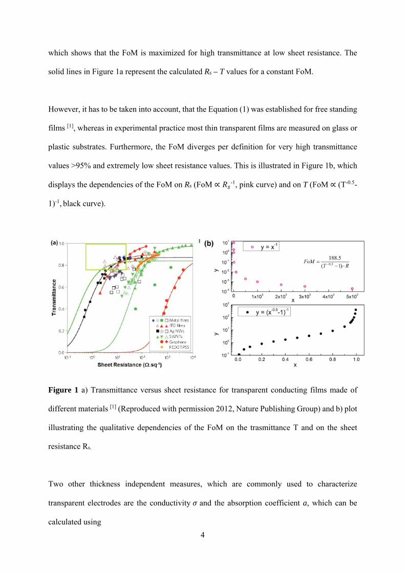
spectrum. By plotting T as a function of Rs the opto-electronic properties of different materials
and of films with different thicknesses can be compared (see Figure 1). Materials with the
"best" opto-electronic performance can be found in the top left of the graph, as indicated by the
green box. For thin conducting films the sheet resistance Rs and the transmittance T can be
related via [1]
𝑇 1.
(1)
with 𝜎 being the optical conductivity and 𝜎 being the direct current (DC) conductivity.
The DC conductivity 𝜎 is frequency independent and relates the current density 𝚥 with the
applied static electrical field �⃗� 𝜔 0 via the Ohm’s law
𝚥 𝜎 �⃗�. (2)
The optical conductivity 𝜎 is the frequency dependent conductivity 𝜎 𝜔 under the
influence of an external alternating electromagnetic field �⃗� 𝜔 0 , with 𝜔 in the optical
frequency range. Using the Lambert-Beer’s law 𝜎 𝜔 can be related to the film transmission.
In order to facilitate the comparison of the opto-electronic properties of transparent conducting
films the ratio 𝜎 /𝜎 can be used as figure of merit (FoM). Via transformation of Equation
1 we obtain
𝐹𝑜𝑀 .
√
(3)
4
which shows that the FoM is maximized for high transmittance at low sheet resistance. The
solid lines in Figure 1a represent the calculated Rs – T values for a constant FoM.
However, it has to be taken into account, that the Equation (1) was established for free standing
films [1], whereas in experimental practice most thin transparent films are measured on glass or
plastic substrates. Furthermore, the FoM diverges per definition for very high transmittance
values >95% and extremely low sheet resistance values. This is illustrated in Figure 1b, which
displays the dependencies of the FoM on Rs (FoM ∝ 𝑅 -1, pink curve) and on T (FoM ∝ (T-0.5-
1)-1, black curve).
Figure 1 a) Transmittance versus sheet resistance for transparent conducting films made of
different materials [1] (Reproduced with permission 2012, Nature Publishing Group) and b) plot
illustrating the qualitative dependencies of the FoM on the trasmittance T and on the sheet
resistance Rs.
Two other thickness independent measures, which are commonly used to characterize
transparent electrodes are the conductivity 𝜎 and the absorption coefficient a, which can be
calculated using
5
𝜎 (4)
𝑎 (5)
with 𝑅 being the sheet resistance, T the transmittance, d the film thickness and A the
absorbance.
The conductivity of a material depends on the charge carrier density N and on the charge
carrier mobility µ and can be expressed as
𝜎 𝑁µ𝑞 (6)
with q being the elementary charge. Therefore, both the charge carrier density and the charge
carrier mobility must be maximized in order to obtain a highly conducting material. While the
charge carrier density of a semiconductor can be enhanced by the so-called doping, the charge
carrier mobility is strongly dependent on the micro and nano structure of the film.
Generally speaking, the device performance will be improved for a transparent electrode with
maximum conductivity at minimum absorption.
In order to be considered for industrial application, a transparent electrode material should show
a sheet resistance of less than 100 Ohm sq-1 at more than 90% transmittance, which corresponds
to a FoM of higher than 34.[2] However, the exact requirements on the electrode performance
depend strongly on each specific application.[3,4] For the fabrication of OLEDs, for instance,
the decisive criterion is a high conductivity[3], whereas the integration in OPV devices
necessitates a very high transparency.[4]
6
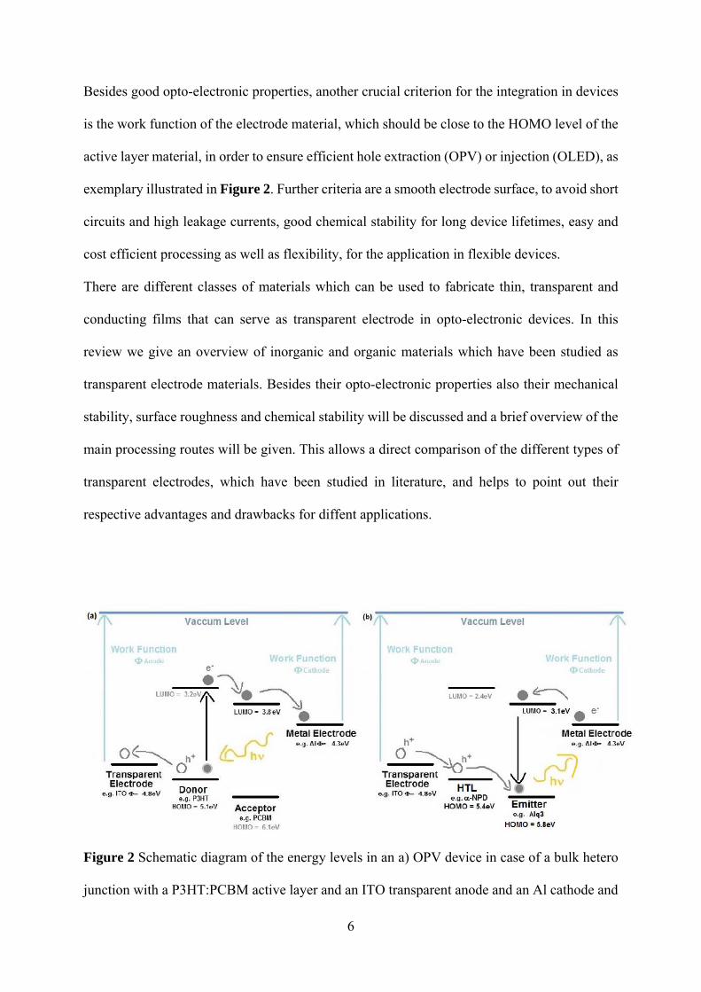
Besides good opto-electronic properties, another crucial criterion for the integration in devices
is the work function of the electrode material, which should be close to the HOMO level of the
active layer material, in order to ensure efficient hole extraction (OPV) or injection (OLED), as
exemplary illustrated in Figure 2. Further criteria are a smooth electrode surface, to avoid short
circuits and high leakage currents, good chemical stability for long device lifetimes, easy and
cost efficient processing as well as flexibility, for the application in flexible devices.
There are different classes of materials which can be used to fabricate thin, transparent and
conducting films that can serve as transparent electrode in opto-electronic devices. In this
review we give an overview of inorganic and organic materials which have been studied as
transparent electrode materials. Besides their opto-electronic properties also their mechanical
stability, surface roughness and chemical stability will be discussed and a brief overview of the
main processing routes will be given. This allows a direct comparison of the different types of
transparent electrodes, which have been studied in literature, and helps to point out their
respective advantages and drawbacks for diffent applications.
Figure 2 Schematic diagram of the energy levels in an a) OPV device in case of a bulk hetero
junction with a P3HT:PCBM active layer and an ITO transparent anode and an Al cathode and

7
b) OLED device with an -NPD hole transport layer (HTL) and an Alq3 emitting layer and an
ITO transparent anode and an Al cathode
1. Inorganic Transparent Conducting Films
1.1. Metal Oxides
1.1.1. Indium Tin Oxide (ITO)
Due to its outstanding opto-electronic properties the current bench mark material for transparent
electrodes is the inorganic metal oxide Indium Tin Oxide (ITO). It is formed by doping of
indium oxide In2O3 with tin (Sn) impurities, which substitute indium cations in the In2O3 cubic
bixbyite lattice. The In2O3 cubic bixbyite lattice can be described as a face-centered-cubic (fcc)
In3+ lattice, in which O-2 anions occupy three fourths of the tetrahedral sites of. Upon oxidation
of the tin impurities, electrons are released to the conduction band of ITO, which results in an
increase of the charge carrier density in the conduction band of the material and leads to an
enhancement of its conductivity. Therefore, Sn can be regarded as a n-type donor for indium
oxide. A detailed discussion of the electronic structure, optical properties and conduction
mechanism can be found in reference [5].[5]
As already mentioned, ITO displays a very high electric conductivity in the range of 104 S cm-
1 and a high charge carrier concentration of approximately 1021 cm-3.[6,7] Furthermore, it shows
a very high transmittance of more than 80 % in the visible range (370 nm < < 1000nm) [6,7],
which is related to its wide band gap of more than 3.75 eV. Together with its high conductivity,
this results in a FoM of up to 500. The work function of ITO was reported to be between 4.3
eV and 4.8 eV, depending on the fabrication method and on the surface post-treatment of the
film.[8–11] Several studies have shown, that mechanical cleaning of the ITO surface with paper
8
or Teflon, as well as wet chemical cleaning in common organic solvents resulted in a decrease
of the measured work function, whereas a treatment with aqua regina, UV/Ozone or oxygen
plasma lead to an increase of the work function.[8,9,11] This can be partially explained by the
influence of organic contaminations and the surface composition on the work function. The
predominant influence factor, however, was found to be the oxygen concentration on the ITO
surface.[9] Using simple surface treatments on ITO electrodes is of big interest for the device
fabrication, as it allows to increase the work function for better hole injection, while the high
bulk conductivity is retained.[12] In this way the device efficiency can be drastically
increased.[13]
The production of thin ITO films with controlled thickness and doping can be realized by
different methods like sputtering, thermal or electron beam evaporation, pulsed laser deposition,
chemical vapor deposition (CVD) or sol-gel processes. A more detailed overview and
description of the main fabrication techniques of ITO and other metal oxides was given by
Chopra et al. [14] , Bel Hadj Tahar et al.[15] and Yu et al.[16]
The most studied processing routes of ITO are based on evaporation and sputtering methods.
Particularly magnetron sputtering is widely used as it allows the deposition of ITO at high rates
on large areas at relatively low substrate temperatures.[15] It has been demonstrated that the
chosen fabrication method and the exact processing parameters, such as the geometry of the
setup, the temperature of the substrate, the gas pressure, the film thickness and annealing steps,
have a decisive influence on the structure and the opto-electronic properties of the obtained ITO
films (see Figure 3).[15,17–22] In the case of sputtered ITO for instance, the sputtering power has
a major influence on the charge carrier concentration and charge carrier mobility, the
preferential grain orientation, as well as on the optical film properties.[18–20] Also the oxygen
pressure was shown to affect the charge carrier density and mobility [22], as well as the grain
size.[18] The surface roughness of sputtered ITO films (Rs ≈ 10 Ohm sq-1, 85 % transmittance,
FoM=223) on glass is in the range of several nanometers to tenths of nanometers, depending
9
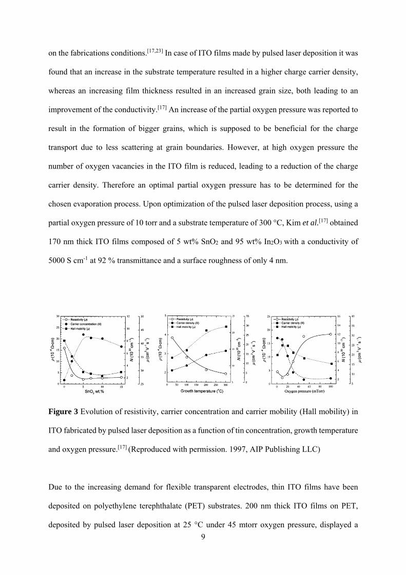
on the fabrications conditions.[17,23] In case of ITO films made by pulsed laser deposition it was
found that an increase in the substrate temperature resulted in a higher charge carrier density,
whereas an increasing film thickness resulted in an increased grain size, both leading to an
improvement of the conductivity.[17] An increase of the partial oxygen pressure was reported to
result in the formation of bigger grains, which is supposed to be beneficial for the charge
transport due to less scattering at grain boundaries. However, at high oxygen pressure the
number of oxygen vacancies in the ITO film is reduced, leading to a reduction of the charge
carrier density. Therefore an optimal partial oxygen pressure has to be determined for the
chosen evaporation process. Upon optimization of the pulsed laser deposition process, using a
partial oxygen pressure of 10 torr and a substrate temperature of 300 °C, Kim et al.[17] obtained
170 nm thick ITO films composed of 5 wt% SnO2 and 95 wt% In2O3 with a conductivity of
5000 S cm-1 at 92 % transmittance and a surface roughness of only 4 nm.
Figure 3 Evolution of resistivity, carrier concentration and carrier mobility (Hall mobility) in
ITO fabricated by pulsed laser deposition as a function of tin concentration, growth temperature
and oxygen pressure.[17] (Reproduced with permission. 1997, AIP Publishing LLC)
Due to the increasing demand for flexible transparent electrodes, thin ITO films have been
deposited on polyethylene terephthalate (PET) substrates. 200 nm thick ITO films on PET,
deposited by pulsed laser deposition at 25 °C under 45 mtorr oxygen pressure, displayed a

10
conductivity of about 1400 S cm-1 at 87 % transmittance and were integrated in LED devices,
which showed comparable performance as the ITO/glass reference devices (1.6 lm W-1 and 100
cd m-2).[21] Commercially available ITO/PET films are fabricated by sputtering and reach
conductivities of maximum 1700 S cm-1 (Rs 60 to 400 Ohm sq-1) at 80 % transmittance (FoM:
4 to 26), the limiting factor for the conductivity being the low substrate temperature and the
high deposition rates.[24]
Considering the big number of different parameters and the complexity of the ITO system, the
processing parameters must be optimized for each specific deposition process. Nevertheless,
upon optimization of the individual processing routes ITO films with very similar opto-
electronic properties can be obtained. Typically ITO films, deposited on glass by evaporation
or sputtering, contain 5 wt% to 10 wt% tin, and their conductivities are in the range of 10 to 104
S cm-1 with the transmittance attaining more than 85 % in the visible range.[15]
As these above discussed fabrication routes are cost intensive, efforts have been made to
fabricate thin ITO films using wet chemical processes, such as sol-gel processes [25–29], solutions
of dispersed nanoparticles [28,30] or spray pyrolysis [31–33]. The big advantage of the fabrication
of ITO films from solutions of dispersed nanocrystals is the simplicity of a one-pot coating
process. However, the obtained conductivities are rather low (approximately 330 S cm-1, Rs =
100 Ohm sq-1 at 88 % transmittance, FoM=29), which could be related by a high contact
resistance between the single nano-particles.[28,30] For the fabrication of ITO via spray pyrolysis
a solution of Indium and tin salts (e.g. indium (III) acetate and SnCl2) is sprayed onto a heated
substrate, on which a thin ITO film is formed.[31–33] Only recently Fellahi et al.[33] reported
promising opto-electronic properties for such ITO films (5 wt% Sn, 3 103 S cm-1 at 94 %
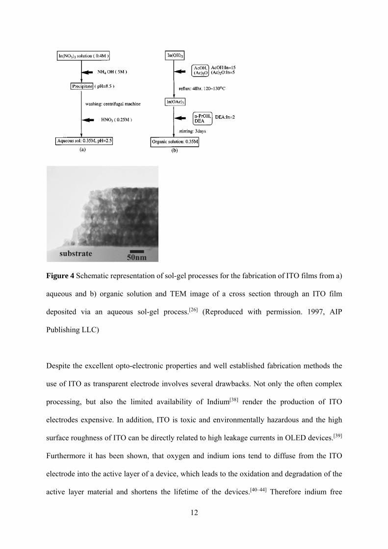
transmittance). In a typical sol-gel process an aqueous or organic precursor solution, containing
an indium salt and an organic stabilizing agent, is spun or spray coated into a thin film, which
is subsequently annealed in order to densify the film and remove volatile organic components
(see Figure 4).[25–27,29] Already in 1991 Mattox[25] reported the fabrication of thin ITO films (8
11
at% of Sn) by sol-gel processing, which, after annealing at 500 °C in air, displayed a
conductivity of approximately 100 S cm-1 and a transmittance higher than 85 %. More recently
Alam et al.[27] reported the fabrication of 250 nm thick sol-gel processed ITO films with
conductivities of up to 1250 S cm-1 and 89 % transmittance A direct comparison of the opto-
electronic properties of sputtered and sol-gel processed ITO was made by Duta et al.[29],
demonstrating that, upon optimization, sol-gel processed ITO film can display comparable
performance as sputtered ITO films. The main common advantage of the discussed wet
chemical processes for the fabrication of ITO is that they allow the relatively cost efficient
production of ITO films on large areas by the means of simple equipment.
All the examples given in this section so far concerned Sn doped indium oxide, as it is currently
the benchmark materials for inorganic transparent electrodes. However, it has been shown that
indium oxide can also be efficiently doped by other elements such as Si, Ga or Mo[34–37].
Gallium doped In2O3 for instance, was reported to display conductivities in the range of 103 to
104 Scm-1 and extremely high electron mobilities of 50 cm2V-1s-1[34,36,37], whereas doping of
In2O3 with molybdenum resulted in improved transmittance in the visible regime as compared
to tin doped InO[35].
12
Figure 4 Schematic representation of sol-gel processes for the fabrication of ITO films from a)
aqueous and b) organic solution and TEM image of a cross section through an ITO film
deposited via an aqueous sol-gel process.[26] (Reproduced with permission. 1997, AIP
Publishing LLC)
Despite the excellent opto-electronic properties and well established fabrication methods the
use of ITO as transparent electrode involves several drawbacks. Not only the often complex
processing, but also the limited availability of Indium[38] render the production of ITO
electrodes expensive. In addition, ITO is toxic and environmentally hazardous and the high
surface roughness of ITO can be directly related to high leakage currents in OLED devices.[39]
Furthermore it has been shown, that oxygen and indium ions tend to diffuse from the ITO
electrode into the active layer of a device, which leads to the oxidation and degradation of the
active layer material and shortens the lifetime of the devices.[40–44] Therefore indium free

13
alternative material are needed for the production of less expensive devices with longer
lifetimes.
1.1.2. Indium free Metal Oxides
One approach to replace ITO is the use of other metal oxides, which contain less Indium or no
Indium at all, with the objective to reduce the toxicity of the material. Therefore multi-
component oxides based on Ga-In-Sn-O (GITO), Zn-In-Sn-O (ZITO), Ga-In-O (GIO) and Zn-
In-O (ZIO) have been investigated.[45–47] Although GIO and ZIO based films display
conductivities of only some hundreds of S cm-1, GITO and ZITO systems, grown by metal-
organic chemical vapor deposition, show conductivities in the range of 104 S cm-1, which are
comparable to the conductivity of ITO. In addition, such GITO and ZITO based films were
reported to have a lower absorption in the visible range than ITO and considerably higher work
functions of 5.4 eV (GITO) to 6.1 eV (ZITO), which are comparable to the work functions of
gold (5.4 eV) platinum (5.7 eV).[45] Flexible, amorphous Zn-In-Sn-O (ZITO) films fabricated
by Zhou et al.[46] showed a sheet resistance lower 20 Ohm sq-1 at 80 % transmittance (FoM 80).
However, by varying the In content it was shown that the conductivity of Zn-In-Sn-O systems
increase with increasing In2O3 content, leading to the conclusion that ITO shows the highest
conductivity.[48]
Completely Indium free, conducting films can also be obtained by doping of SnO2 with Fluorine
(F), Niobium (Nb), Tantalum (Ta) or Antimony (Sb).[3,49–56] These films are commonly
fabricated by spray pyrolysis, which consists in spraying an aqueous/alcoholic solution of a tin
and a dopant salt (e.g. SnCl4 and NH4F) onto a heated substrate (typically 300 °C to 500 °C),
on which thin layers of doped SnO2 are formed.[14] Fluorine doped SnO2 (FTOs) with a film
thickness of approximately 1100 nm display sheet resistances of 2 to 5 Ohm sq-1 at 75 % to
90 % transmittance (FoM:600 to 700) (see Figure 5), which corresponds to a conductivity in

14
the range of 103 S cm-1.[51,52,54,56] With a work function of 4.4 eV [53,57] to 5.0 eV [58] these FTO
films are suitable for the integration in solar cell and LED devices. Even if the conductivity of
FTO films is about one order of magnitude lower than the conductivity of ITO, FTO is widely
used as electrode in solar cells[59] and LEDs[53], as it is considerably less expensive than ITO[3,60]
and shows excellent thermal and chemical stability[3,54,60].
Figure 5 FE-SEM images of (a) the surface morphology and (b) cross-sectional image of
SnO2:F film before the heat treatment[54] (Reproduced with permission. 2004, Elsevier) and c)
transmittance in the visible regime of ITO and FTO films[59] (Reproduced with permission. 2010,
AIP Publishing LLC)
Another family of metal oxides that displays very promising opto-electronic properties are
titanium based oxides in the anatase phase. Films made of TiO2 doped with Fluorine (F),
Niobium (Nb), Tantalum (Ta) or Tungsten (W) show conductivities in the range of 103 S cm-1
and transparencies of about 95 %.[61] However, these highly conducting and transparent films
15
were produced by epitaxial growth, which makes them too expensive for broad base
application.[61–64]
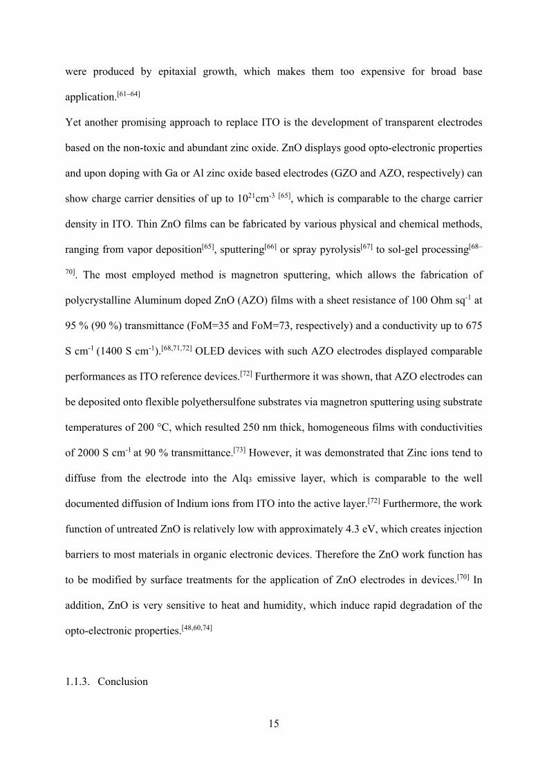
Yet another promising approach to replace ITO is the development of transparent electrodes
based on the non-toxic and abundant zinc oxide. ZnO displays good opto-electronic properties
and upon doping with Ga or Al zinc oxide based electrodes (GZO and AZO, respectively) can
show charge carrier densities of up to 1021cm-3 [65], which is comparable to the charge carrier
density in ITO. Thin ZnO films can be fabricated by various physical and chemical methods,
ranging from vapor deposition[65], sputtering[66] or spray pyrolysis[67] to sol-gel processing[68–
70]. The most employed method is magnetron sputtering, which allows the fabrication of
polycrystalline Aluminum doped ZnO (AZO) films with a sheet resistance of 100 Ohm sq-1 at
95 % (90 %) transmittance (FoM=35 and FoM=73, respectively) and a conductivity up to 675
S cm-1 (1400 S cm-1).[68,71,72] OLED devices with such AZO electrodes displayed comparable
performances as ITO reference devices.[72] Furthermore it was shown, that AZO electrodes can
be deposited onto flexible polyethersulfone substrates via magnetron sputtering using substrate
temperatures of 200 °C, which resulted 250 nm thick, homogeneous films with conductivities
of 2000 S cm-1 at 90 % transmittance.[73] However, it was demonstrated that Zinc ions tend to
diffuse from the electrode into the Alq3 emissive layer, which is comparable to the well
documented diffusion of Indium ions from ITO into the active layer.[72] Furthermore, the work
function of untreated ZnO is relatively low with approximately 4.3 eV, which creates injection
barriers to most materials in organic electronic devices. Therefore the ZnO work function has
to be modified by surface treatments for the application of ZnO electrodes in devices.[70] In
addition, ZnO is very sensitive to heat and humidity, which induce rapid degradation of the
opto-electronic properties.[48,60,74]
1.1.3. Conclusion
16
In summary, metal oxide thin films display extremely high conductivities in the range of 104 S
cm-1 with excellent transparencies of higher than 85 % in the visible range and work functions
in the range of 4.3 eV to 6.1 eV, which makes them attractive as transparent electrode material.
However, they are not suitable for flexible applications, owing to their brittle nature. Another
common drawback of metal oxide based transparent electrodes is the often complex processing
at high temperatures, which renders the production expensive and limits the compatibility with
plastic substrates. In addition, some of the best performing metal oxides contain toxic and rare
elements, e.g. indium in indium tin oxide. The non-toxic and solution processable ZnO,
however, shows a very low work function and low resistance to heat and humidity. In addition,
when integrated in devices, certain metal ions such as zinc or indium tend to diffuse into the
active layer, which limits the lifetime of the optoelectronic devices.
1.2. Metallic Electrodes
1.2.1. Thin Metal Films
Metals are known for their high conductivity, which results from the free electron character of
the valence electrons. At the same time bulk metals are famous for their colored and shiny
appearance, which indicates that metals absorb in the visible range and are therefore not
transparent. Therefore only ultra-thin metal films with a thickness below 10 nm become
transparent. However, with decreasing thickness the resistivity of metal films increases due to
electron scattering at the surface and grain boundaries.[75] Hence, a compromise between
sufficient transparency and conductivity must be found for the fabrication of transparent metal
electrodes.
Silver (Ag), Gold (Au), Chromium (Cr), Nickel (Ni) and Platinum (Pt) films and metal bi-layers
with the thickness of some nanometers expose both a high conductivity and a high transparency
and can compete with ITO films in terms of their opto-electronic performance.[76–79] O’Connor
17
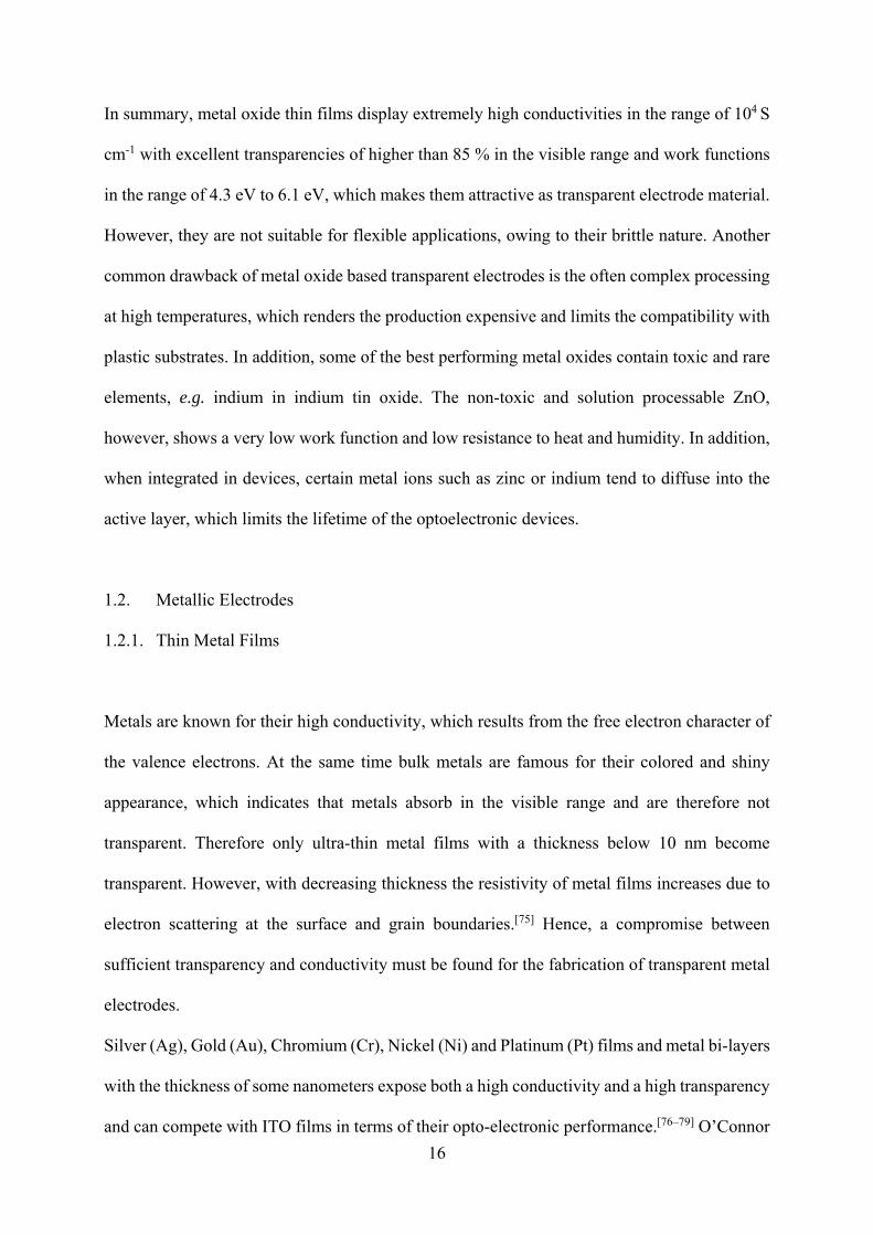
et al.[80] reported, that a photovoltaic cell with a 9 nm thick evaporated silver (Ag) electrode
displayed an even slightly higher efficiency than the ITO reference cell (see Figure 6). Thin
films evaporated from a Ca:Ag blend were reported to display a sheet resistance of 27 Ohm sq-
1 at 93 % transmittance (FoM 190)[81] and OPV devices based on these Ca:Ag electrodes
showed a higher efficiency than the ITO reference device, but underwent rapid degradation.
Another approach was presented by Ghosh et al.[82], who replaced the ITO electrode by a semi-
transparent, 8 nm thick Cu-Ni bilayer (Rs=16 Ohm sq-1, T=57 %, FoM=36), which resulted in
a device efficiency of 76 % as compared to the ITO reference device. The relatively high
efficiency despite the low transparency of the electrode was explained by the high reflectance
of the Cu-Ni layer, which leads to a microcavity effect and a higher light harvesting efficiency
in the device. Despite the good performance in devices, the application of ultra-thin metal films
as electrodes faces problems due the fragility and the relatively high surface roughness of the
thin metallic films.
Figure 6 Sheet resistance versus film thickness for thin Ag, Al and Au films compared to the
sheet resistance of ITO (left) and J -V characteristics of OPV devices under 106 mW cm-1
illumination with 9 nm Ag and 150 nm ITO anodes[80] (Reproduced with permission. 2008, AIP
Publishing LLC)
18
1.2.2. Metal Grids
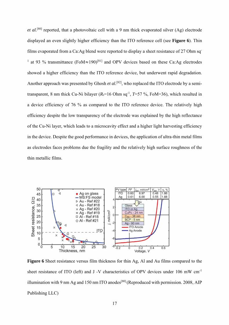
A simple and cheap way to produce transparent conducting electrodes from various metals is
the fabrication of metal nanoscale grids by nanoimprint lithography (see Figure 7). By varying
the thickness and the pattern size of the grid the conductivity and transmittance of the electrode
can be tuned. However, if the pattern dimensions are in the range of the wavelength of visible
light, interference effects, which can affect the transmittance of the electrode, have to be taken
into account.[83] Furthermore it has been demonstrated that the discontinuous character of the
electrode induces an increase in resistance in the neighboring semiconducting layer, which is
why different criteria than the commonly used FoM should be considered for the evaluation of
metal grid electrodes.[84] Upon optimization of the pattern dimensions, films with a sheet
resistance between 5 Ohm sq-1 to 24 Ohm sq-1 with 70% to 80% transmittance (FoM between
60 and 190) in the visible range can be obtained.[85–87] Photovoltaic cells based on such metal
grid electrodes exhibited the same performance as ITO reference cells.[85–87]
Figure 7 Scheme of the fabrication of nano patterned Cu by nano imprinting using a PDMS
stamp and SEM image of the Cu electrode on a PEDOT:PSS coated glass substrate [86]
(Reproduced with permission. 2016, Royal Society of Chemistry)
By using a combination of soft imprint lithography and solution processing (see Figure 8)
Sciacca et al.[87] fabricated patterned Ag electrodes, which showed a higher conductivity than

19
thermally evaporated networks. Another approach to fabricate Ag nanogrids from solution was
presented by Kang et al.[89], who deposited Ag nanoparticles into nanogrid templates via
capillary assembly. The obtained electrodes displayed a sheet resistance of 15 Ohm sq-1 and an
optical transmittance of 85 % (FoM=148).
Figure 8 a) Scheme for the fabrication of solution grown Ag nano structures and b) SEM image
of the solution grown Ag network before rapid thermal annealing (RTA)[88] (Reproduced with
permission. 2015, John Wiley and Sons)
Only recently printing methods, such as electrohydrodynamic printing, were developed, which
allow the fabrication of Ag and Au nanogrids with line widths down to 80 nm (see Figure
8).[90,91] These electrodes display very high transparencies of 94 % to 97 % at 8 Ohm sq-1 to 20
Ohm sq-1 sheet resistance (FoM: 615 to 750), respectively.[90]
A top down method for the fabrication of micro structured metal electrodes consists in the
patterning of thin metal films using three beam direct laser interference patterning[92]. With this
technique Al electrodes with sheet resistance of 25 Ohm sq-1 to 50 Ohm sq-1 at 81 %
transmittance (FoM:35 to 70) were obtained (see Figure 9c).[93]
To summarize, nanopatterned metal films display a very good opto-electronic performance, are
mechanically and chemically stable, are compatible with flexible substrates and can be
produced cost efficiently on a large scale. Therefore, the main drawback for their application in

20
devices is their extremely high surface roughness, which can render it difficult to ensure good
contact between the electrode and the active layer.
Figure 9 a), b) demonstration of NanoDrip printing[90] (Reproduced with permission. 2015,
John Wiley and Sons) c) SEM image of a laser patterned Al film with a spatial pattern period
of =1.7µm[93]
1.2.3. Metal Nanowires
Another approach to transparent, metallic electrodes is the fabrication of thin films from metal
nanowires.[4] The nanowires which are commonly used for this purpose display diameters
smaller than 100 nm and a length of several micrometers, as it was shown that the use of
nanowires with high aspect ratios improves the mechanical stability of the films. Most of the
nanowires are made of silver or copper, as these nanowires can be easily synthesized in solution
via the reduction of silver nitrate or of copper ion complexes, respectively.[94–100] The obtained
dispersions can then be directly coated onto a substrate using roll-to-roll techniques, which
results in flexible films with good opto-electronic properties, such as a sheet resistance of about
10 Ohm sq-1 to 13 Ohm sq-1 at 85 % to 90 % transmittance (FoM of 190 to 280).[2,101,102] OPV
devices based on such Ag nanowire electrodes showed very similar performance to the ITO
reference devices.[101] Lee et al.[103] reported that the conductivity of Ag nanowire electrodes
can be enhanced by using extra-long Ag nanowires with a length of up to 500 µm. Furthermore
21
it was demonstrated that the electronic properties of those Ag wire electrodes (sheet resistance
of 9 Ohm sq-1 at 90 % transmittance, FoM=387) were maintained upon stretching of the
electrodes up to 250 % elongation, which allowed the fabrication of highly flexible devices.
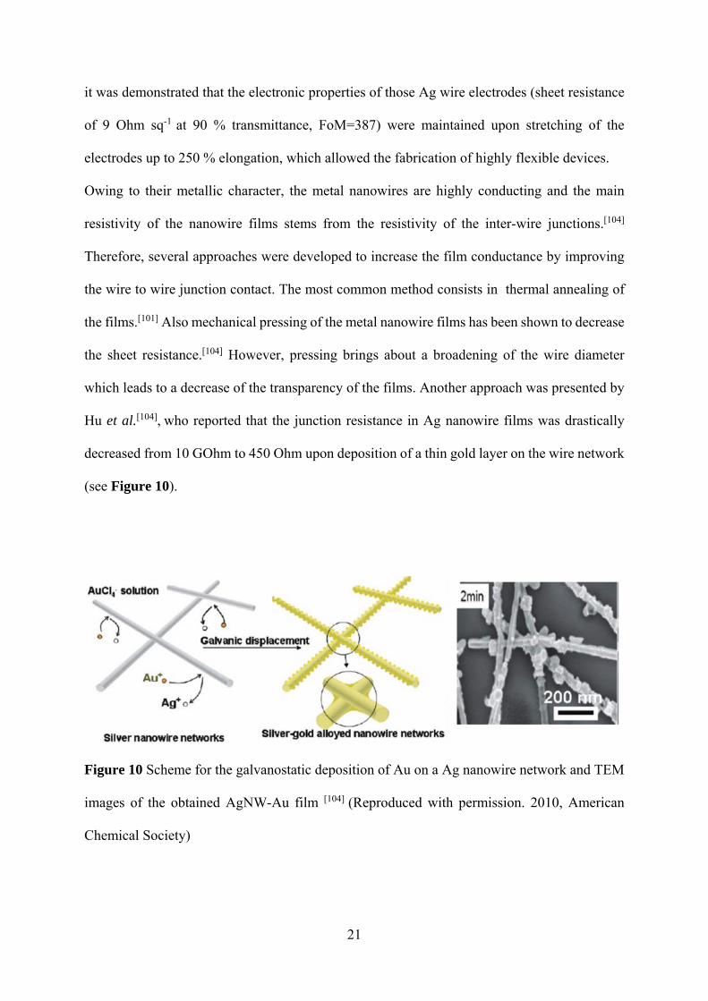
Owing to their metallic character, the metal nanowires are highly conducting and the main
resistivity of the nanowire films stems from the resistivity of the inter-wire junctions.[104]
Therefore, several approaches were developed to increase the film conductance by improving
the wire to wire junction contact. The most common method consists in thermal annealing of
the films.[101] Also mechanical pressing of the metal nanowire films has been shown to decrease
the sheet resistance.[104] However, pressing brings about a broadening of the wire diameter
which leads to a decrease of the transparency of the films. Another approach was presented by
Hu et al.[104], who reported that the junction resistance in Ag nanowire films was drastically
decreased from 10 GOhm to 450 Ohm upon deposition of a thin gold layer on the wire network
(see Figure 10).
Figure 10 Scheme for the galvanostatic deposition of Au on a Ag nanowire network and TEM
images of the obtained AgNW-Au film [104] (Reproduced with permission. 2010, American
Chemical Society)
22
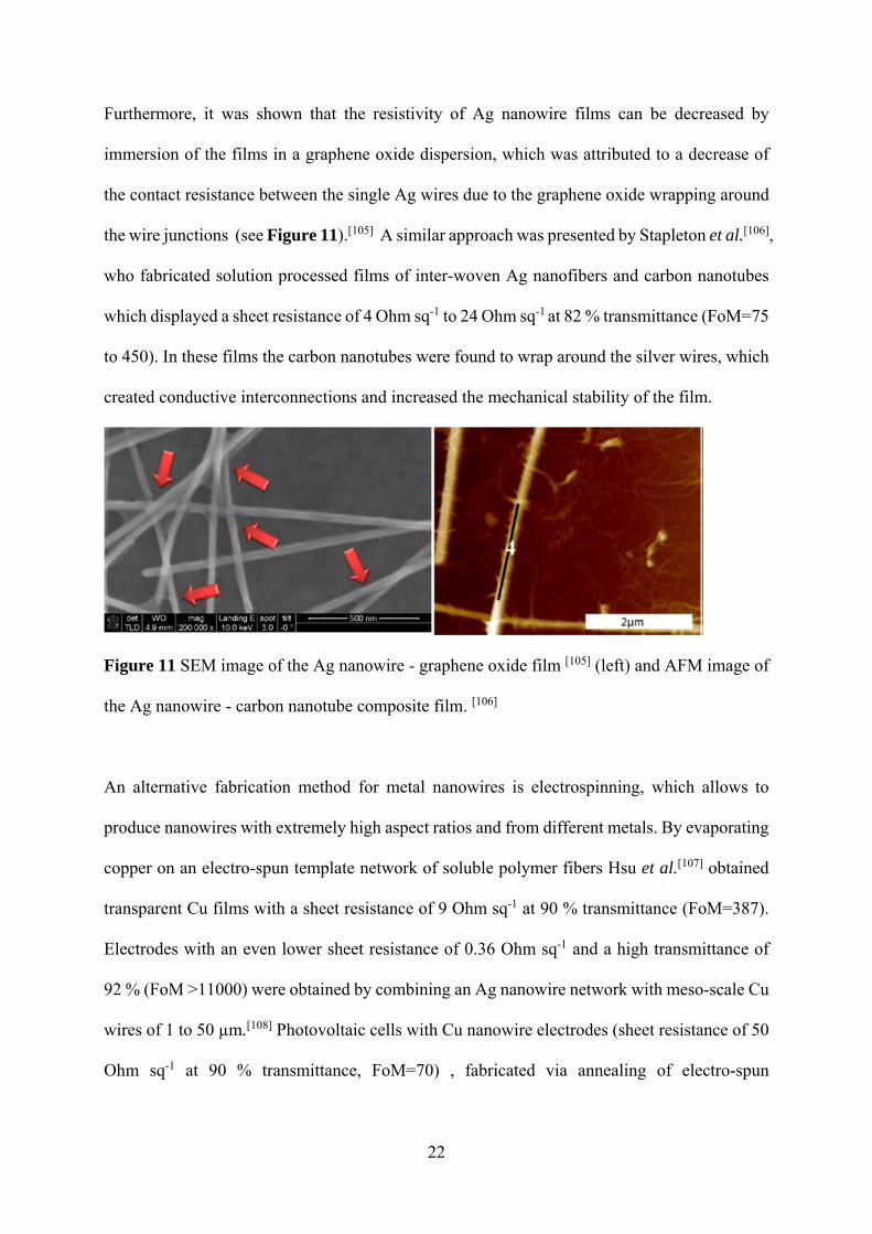
Furthermore, it was shown that the resistivity of Ag nanowire films can be decreased by
immersion of the films in a graphene oxide dispersion, which was attributed to a decrease of
the contact resistance between the single Ag wires due to the graphene oxide wrapping around
the wire junctions (see Figure 11).[105] A similar approach was presented by Stapleton et al.[106],
who fabricated solution processed films of inter-woven Ag nanofibers and carbon nanotubes
which displayed a sheet resistance of 4 Ohm sq-1 to 24 Ohm sq-1 at 82 % transmittance (FoM=75
to 450). In these films the carbon nanotubes were found to wrap around the silver wires, which
created conductive interconnections and increased the mechanical stability of the film.
Figure 11 SEM image of the Ag nanowire - graphene oxide film [105] (left) and AFM image of
the Ag nanowire - carbon nanotube composite film. [106]
An alternative fabrication method for metal nanowires is electrospinning, which allows to
produce nanowires with extremely high aspect ratios and from different metals. By evaporating
copper on an electro-spun template network of soluble polymer fibers Hsu et al.[107] obtained
transparent Cu films with a sheet resistance of 9 Ohm sq-1 at 90 % transmittance (FoM=387).
Electrodes with an even lower sheet resistance of 0.36 Ohm sq-1 and a high transmittance of
92 % (FoM >11000) were obtained by combining an Ag nanowire network with meso-scale Cu
wires of 1 to 50 µm.[108] Photovoltaic cells with Cu nanowire electrodes (sheet resistance of 50
Ohm sq-1 at 90 % transmittance, FoM=70) , fabricated via annealing of electro-spun
23
polymer/Cu-precursor fibers, reached efficiencies of 3 %, which was comparable to the
efficiency of cells with ITO electrodes.[109]
In analogy to the nano-patterned metal electrodes, the main drawback of the highly conducting
and transparent metal nanowire films is their high surface roughness, which hinders good
contact of the film to the active layer.
1.2.4. Conclusion
There are several approaches to take advantage of the extremely high conductivity of metals
for the fabrication of metallic transparent electrodes, such as the preparation of nanometer thin
films, the nanopatterning of metallic films into grids or the use of metallic nanowire networks.
Such metal electrodes can display extremely low sheet resistances of below 10 Ohm sq-1 at a
transmittance of 90 % or higher. In addition, the metallic nanostructures display high chemical
and mechanical stability, are compatible with flexible substrates and can be produced cost
efficiently on a large scale via solution processing or lithography. However, they display a high
surface roughness which prevents good contact to the neighboring layers in a device.
2. Organic Conducting Materials
2.1. Graphene and Carbon Nanotubes
Graphene is a monolayer of graphite in which sp2- hybridized carbon atoms form a 2-
dimensional honeycomb structure. This bonding situation results in a 2D delocalization of
electrons which enables scattering free in plane transport of the charge carriers.[38] This results
in an extremely high charge carrier mobility of about 2 105 cm2 Vs [110] and a very low
theoretical sheet resistance of about 30 Ohm sq-1 [110] for the single graphene sheets. Therefore,
24
graphene is potentially interesting as material for transparent electrode applications. However,
the experimentally measured sheet resistance of graphene is in the range of several hundreds of
Ohms per layer. This discrepancy between the theoretical sheet resistance and the
experimentally measured value can be explained by defects and grain boundaries in the
graphene sheets, which represent energy barriers for the charge transport. In macroscopic
graphene films, which are composed of several graphene sheets, the resistivity is even higher
due to the high resistivity of the sheet to sheet contacts.[38]
The fabrication of graphene using the simple scotch peel method has attracted much attention,
however, this method is not suitable for the production of graphene on large scales. Therefore,
the graphene sheets used for the fabrication of conducting electrodes are either synthesized by
chemical vapor deposition (CVD) or from large organic precursor molecules.
CVD grown graphene shows a sheet resistance of 230 Ohm sq-1 or higher, a maximum
transmittance of 91 % and is highly transparent in the infra-red regime.[110] The specific
electrical and optical properties, however, depend on the synthesis conditions during the CVD
process. It was found, that, for instance, the thickness of the graphene films increased with
increasing process temperature. Choe et al.[111] reported, that graphene films grown at 1000 °C
displayed a sheet resistance of 600 Ohm sq-1 at a transmittance of 87 % (FoM=4), whereas films
grown at 800 °C were thinner and showed a sheet resistance of 1700 Ohm sq-1 at 91%
transmittance (FoM=2). The sheet resistance of CVD graphene sheets can be reduced by
chemical doping with AuCl3, HNO3 or SOCl2.[112–114] Kim et al.[113] observed a drop in the sheet
resistance of graphene of 77 % upon doping with AuCl3, resulting in films with a sheet
resistance of 150 Ohm sq-1 at 87 % transmittance (FoM=17). This trend was confirmed by Park
et al. [112] who found, that the doping of graphene electrodes with AuCl3 lead to a significant
increase in the power conversion efficiency of OPV devices. More recently, Chen et al. [115]
presented carbon enclosed CVD as novel method for the synthesis of graphene, by which
25
graphene sheets with a sheet resistance of 5 Ohm sq-1 at 93 % transmittance (FoM=1020) were
obtained.
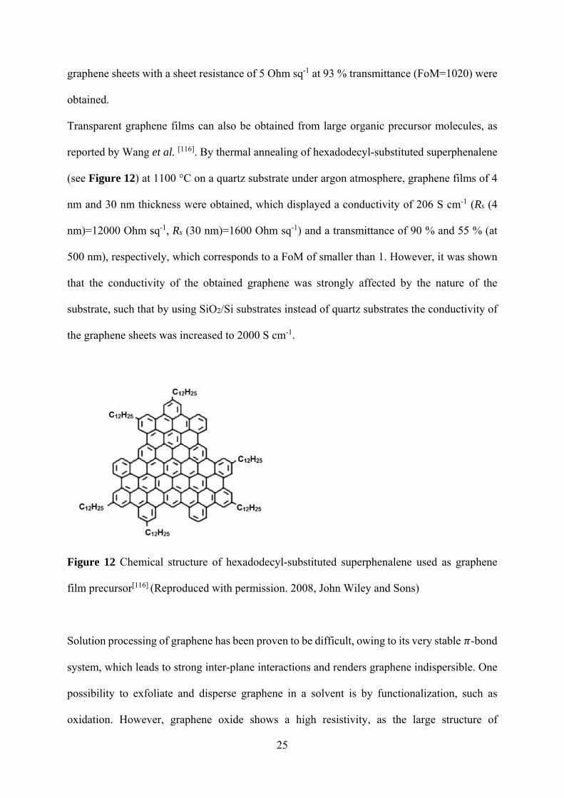
Transparent graphene films can also be obtained from large organic precursor molecules, as
reported by Wang et al. [116]. By thermal annealing of hexadodecyl-substituted superphenalene
(see Figure 12) at 1100 °C on a quartz substrate under argon atmosphere, graphene films of 4
nm and 30 nm thickness were obtained, which displayed a conductivity of 206 S cm-1 (Rs (4
nm)=12000 Ohm sq-1, Rs (30 nm)=1600 Ohm sq-1) and a transmittance of 90 % and 55 % (at
500 nm), respectively, which corresponds to a FoM of smaller than 1. However, it was shown
that the conductivity of the obtained graphene was strongly affected by the nature of the
substrate, such that by using SiO2/Si substrates instead of quartz substrates the conductivity of
the graphene sheets was increased to 2000 S cm-1.
Figure 12 Chemical structure of hexadodecyl-substituted superphenalene used as graphene
film precursor[116] (Reproduced with permission. 2008, John Wiley and Sons)
Solution processing of graphene has been proven to be difficult, owing to its very stable 𝜋-bond
system, which leads to strong inter-plane interactions and renders graphene indispersible. One
possibility to exfoliate and disperse graphene in a solvent is by functionalization, such as
oxidation. However, graphene oxide shows a high resistivity, as the large structure of

26
delocalized electrons is destroyed. Therefore, oxidized graphene films have to be reduced again
before being used as electrodes. Films produced from functionalized graphene can show high
transparencies, but due to incomplete reduction even post treated films display very high
resistivities of 800 Ohm sq-1 to 5 kOhm sq-1 or higher.[117,118] Thus, OPV devices with electrodes
fabricated by solution processing of graphene oxide displayed poorer performance than ITO
reference devices.[117,118]
Independently of the synthesis method and properties of the graphene, most devices with
transparent graphene electrodes can hardly compete with ITO reference devices. This is not
only related to the opto-electronic performance of the graphene sheets, but also to the electrode
- active layer interface.[112,119,120] On one hand, the graphene layers are rough and very
hydrophobic, which leads to inhomogeneities with the adjacent hole injecting layer, such as
PEDOT:PSS. On the other hand, graphene has a very low work function with respect to the
active layer materials, which leads to poor charge collection and a high electrode resistance.
Thus, the surface of graphene electrodes has to be modified, for instance by the deposition of
MoO3 layers[119,120], in order to increase the device performance.
Figure 13 Scheme of a carbon nanotubes with different chiralities [121] (Reproduced with
permission. 2010, Elsevier)
27
Another type of carbon nanostructures, composed of sp2 hybridized carbon and very similar to
graphene, are carbon nanotubes (CNTs). CNTs are artificial allotropes of carbon and can be
described as graphene sheets, which are rolled up into cylinders with an approximate diameter
of one nanometer and whose ends are partly closed by fullerene like structures (see Figure 13).
With an extremely high aspect ratio of up to 1000, CNTs are thought of as one dimensional
material. However, CNTs are heterogeneous materials, which show differences in structure and
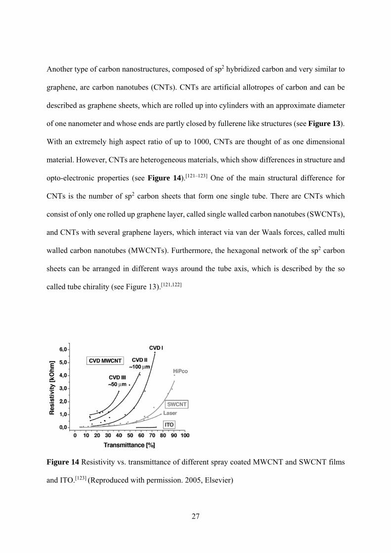
opto-electronic properties (see Figure 14).[121–123] One of the main structural difference for
CNTs is the number of sp2 carbon sheets that form one single tube. There are CNTs which
consist of only one rolled up graphene layer, called single walled carbon nanotubes (SWCNTs),
and CNTs with several graphene layers, which interact via van der Waals forces, called multi
walled carbon nanotubes (MWCNTs). Furthermore, the hexagonal network of the sp2 carbon
sheets can be arranged in different ways around the tube axis, which is described by the so
called tube chirality (see Figure 13).[121,122]
Figure 14 Resistivity vs. transmittance of different spray coated MWCNT and SWCNT films
and ITO.[123] (Reproduced with permission. 2005, Elsevier)
28
Depending on their chirality CNTs display either semiconducting or metallic behavior. Metallic
CNTs show similar band structures as metals and very high conductivities up to 105 S cm-1.
However, just as for bulk metals, the absorption of metallic CNTs in the optical range is very
high, whereas semiconducting CNTs are transparent. Furthermore, the optical transitions vary
with the tube diameter, as the tube diameter is inversely proportional to the band gap of the
CNTs.[124] As in most production processes none of the three chiralities is formed preferentially,
customary CNT samples contain semiconducting and metallic CNTs in the ratio 2:1. However,
the fabrication of films with uniform electrical and optical properties requires CNTs batches,
which are monodisperse in electronic type and diameter. Consequently, much effort is made to
efficiently separate CNTs regarding to their electrical properties and their diameter.[121,124–128]
Another challenge working with CNTs is their limited dispersability, caused by strong van der
Waals forces between the tubes, which renders the fabrication of homogeneous thin films
difficult. Attempts to disperse CNTs by sonication showed, that upon sonication the nanotubes
tend to break into shorter pieces, which lowers the conductivity of the obtained films.[129]
Another approach is to disperse CNTs by non-covalent functionalization of the CNT surface
with surfactants, such as sodium dodecyl sulfate (SDS), or polymers, such as poly(3-
hexylthiophene) (P3HT), poly(vinyl pyrrolidone) (PVP) or sodium carboxymethyl cellulose
(CMC) [103,129,130]. However, after film deposition these molecules are often difficult to remove.
Despite the difficult processing, CNTs are of interest for the fabrication of transparent
electrodes, owing to their extremely high conductivity and a suitable work function in the range
of 4.8eV to 5.1eV.[131,132]
The fabrication of flexible transparent electrodes from double walled CNTs (DWCNTs) via
solution processing was reported by Imazu et al.[133]. Upon optimization of the key parameters,
such as the DWCNT length, their dispersion and the concentration of the dispersant CMC, films
with a sheet resistance of 320 Ohm sq-1 at 94 % transmittance (FoM=17) and a surface
roughness Rq of 8 to 10 nm were obtained. Electrodes made from SWCNTs via solution
29
processing with CMC and doped by post-treatment with nitric acid, displayed a sheet resistance
of 50 Ohm sq-1 and 150 Ohm sq-1 at 77 % and 85 % average transmittance (400 nm – 1800 nm)
and a FoM of 27 and 15, respectively.[129] The percolation threshold in these films was
calculated to be extremely low with 0.011 µg cm-2 and upon integration into an OPV device
with a P3HT:PCBM active layer efficiencies of 3.1 % were reached.[129]
Kaskela et al.[134] reported the fabrication of transparent SWCNT films by aerosol chemical
vapor deposition, in which SWCNT are formed upon the thermal decomposition of ferrocene
vapor in carbon monoxide atmosphere. After chemical doping with HNO3 the transparent
electrodes showed a sheet resistance of 110 Ohm sq-1 at 90 % transmittance (FoM=32). Similar
transparent electrodes fabricated by aerosol chemical vapor deposition were successfully
integrated in OPVs and perovskite solar cells.[135,136] However, these OPV devices showed only
low efficiencies of 1.9 %.[135]
The low efficiency of devices with pure CNT electrodes can be explained by the high surface
roughness and porosity of CNT electrodes, which causes bad contact between the electrode and
the active layer, as well as diffusion of the active layer components such as P3HT:PCBM into
the CNT film.[38,132] A common approach to address this problem is the embedding of CNTs
films in conducting polymers, which will be discussed in detail in the section Composite
Materials.
Furthermore, carbon nanotube - graphene hybrid electrodes have also been studied. Tung et
al.[137], for instance, fabricated transparent hybrid films from CNTs and chemically converted
graphene by solution processing, which showed a resistance of 240 Ohm sq-1 at 86 %
transmittance (FoM=10). Films made from SWCNT and CVD deposited graphene displayed a
similar sheet resistance of 300 Ohm sq-1, but a much higher transmittance of 96 %, resulting in
a FoM of 30.[138] Similar hybrid films made of MWCNT and CVD graphene were studied by
Kholmanov et al.[139], who showed that the opto-electronic properties of the hybrid electrodes
depended strongly on the processing protocol, such as the order in which the graphene and CNT
30
layers are deposited. The integration of a SWCNT - graphene oxide hybrid system in an OPV
device with a P3HT/PCBM active layer was reported by Tu et al.[140]. This OPV device,
comprising a SWCNT electrode and separate hole transporting interfacial layer of graphene
oxide, showed power conversion efficiency of 3.1 %.
In summary it can be stated, that, despite the extremely high conductivity of CNTs and graphene,
the opto-electronic properties of thin graphene and CNT films cannot compete with those of
metal or metal oxide based transparent electrodes, which can be attributed to structural defects
and high junction resistances. In addition, the solution processing of graphene and CNT was
proven to be difficult, owing to the poor dispersability of the chemically inert carbon structure.
Furthermore, the obtained graphene and CNT films show a high surface roughness, which is
detrimental for the integration in devices.
2.2. Conducting polymers
Among polymers, traditionally known as good insulating materials, (semi)conducting polymers
have attracted a great deal of attention as new class of materials and have been extensively
studied since their discovery in the 1970s. The conductivity in conducting polymers is based
on a conjugated -electron system, which enables charge transport via delocalized electrons
along the polymer backbone. Therefore the electronic properties depend strongly on the
chemical structure of the polymer backbone. Even if the first polymer, in which conductivity
was observed, is the linear polyacetylene, most conducting polymers are aromatic, such as
polyaniline (PANI), Polypyrrole (PPy), poly (para-phenylene) (PPP) and polythiophene (PT)
and their substituted derivatives.
31
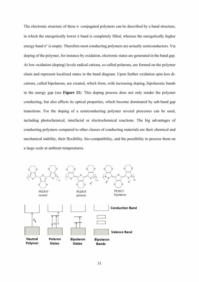
The electronic structure of these -conjugated polymers can be described by a band structure,
in which the energetically lower band is completely filled, whereas the energetically higher
energy band is empty. Therefore most conducting polymers are actually semiconductors. Via
doping of the polymer, for instance by oxidation, electronic states are generated in the band gap.
At low oxidation (doping) levels radical cations, so called polarons, are formed on the polymer
chain and represent localized states in the band diagram. Upon further oxidation spin-less di-
cations, called bipolarons, are created, which form, with increasing doping, bipolaronic bands
in the energy gap (see Figure 15). This doping process does not only render the polymer
conducting, but also affects its optical properties, which become dominated by sub-band gap
transitions. For the doping of a semiconducting polymer several processes can be used,
including photochemical, interfacial or electrochemical reactions. The big advantages of
conducting polymers compared to other classes of conducting materials are their chemical and
mechanical stability, their flexibility, bio-compatibility, and the possibility to process them on
a large scale at ambient temperatures.
32
Figure 15 Chemical structure of neutral, simple and double oxidized poly(3,4-
ethylenedioxythiophene) (PEDOT) and schematic of the corresponding band diagram
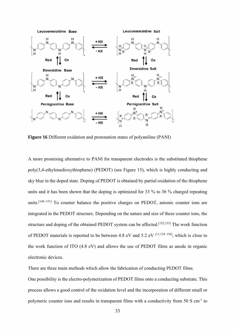
One of the most studied conducting polymers is PANI, which exist in several oxidation and
protonation states (see Figure 16), of which the most stable and conducting form is the
emeraldine salt.[141] The conducting PANI is soluble in common organic solvents and absorbs
in the range of 300 nm to 500 nm, which gives it a greenish color. Thin PANI films can be
obtained by either chemical oxidation of aniline in acidic aqueous medium or by electro-
polymerization and typically show a conductivity in the range of 5 S cm-1 to 20 S cm-1.[141–144]
Especially in the early stages of the research on conducting polymers several attempts were
made to fabricate PANI transparent electrodes.[41,145–147] Heeger and coworkers[145] fabricated
thin PANI films with 100 Ohm sq-1 at 70 % transmittance at 475 nm to 675 nm (FoM=10). A
simple flexible OLED device (PANI/MEH-PPV/Ca) with similar PANI electrodes showed a
quantum efficiency of 1 % and a turn on voltage of 1.8 V.[146] The main limiting factor for the
performance of these devices was the low transmittance of the electrodes.[147] In addition, the
work function of PANI was reported to be 4.4 eV[145], which is very low compared to commonly
used active layer materials and results therefore in a high energy barrier and a high series
resistance in the devices.
33
Figure 16 Different oxidation and protonation states of polyaniline (PANI)
A more promising alternative to PANI for transparent electrodes is the substituted thiophene
poly(3,4-ethylenedioxythiophene) (PEDOT) (see Figure 15), which is highly conducting and
sky blue in the doped state. Doping of PEDOT is obtained by partial oxidation of the thiophene
units and it has been shown that the doping is optimized for 33 % to 36 % charged repeating
units.[148–151] To counter balance the positive charges on PEDOT, anionic counter ions are
integrated in the PEDOT structure. Depending on the nature and size of these counter ions, the
structure and doping of the obtained PEDOT system can be affected.[152,153] The work function
of PEDOT materials is reported to be between 4.8 eV and 5.2 eV [11,154–156], which is close to
the work function of ITO (4.8 eV) and allows the use of PEDOT films as anode in organic
electronic devices.
There are three main methods which allow the fabrication of conducting PEDOT films.
One possibility is the electro-polymerization of PEDOT films onto a conducting substrate. This
process allows a good control of the oxidation level and the incorporation of different small or
polymeric counter ions and results in transparent films with a conductivity from 50 S cm-1 to
34
700 S cm-1.[152,157–162] However, electro-polymerization is not possible on insulating substrates,
such as poly(ethylene terephthalate) (PET), and is not compatible with the large scale printing
of organic electronic devices.
An alternative process is the oxidative polymerization of EDOT, which has been described in
innumerable protocols, using different oxidants, counter ions, catalysts, temperatures and
synthesis times.[149,150,163–171]
One possibility is the in-situ oxidative polymerization of EDOT in liquid phase, for which the
PEDOT film is directly polymerized from a solution containing the EDOT monomer and the
oxidizing agents, such as FeCl3, onto the substrate. By using a solution of EDOT and FeCl3 in
acetonitrile, Hohnholz et al.[172] obtained PEDOT:Cl films with a sheet resistance of 945 Ohm
sq-1. However, it was shown that the conductivity can be significantly increased by choosing
Fe(III) p-toluenesulfonate (Fe(Tos)3) as oxidant, a low molecular weight alcohol, such as
butanol, as solvent and by the addition of a weak base, such as imidazole or pyridine, which
slows down the reaction kinetics.[171,173–176] From a solution of EDOT, Fe(Tos)3 and imidazole
in methanol Ha et al.[171] fabricated thin PEDOT:Tos films with a sheet resistance of 150 Ohm
sq-1 at a transmittance higher than 80 % (FoM=11) and a conductivity of 900 S cm-1. More
recently Bubnova et al.[175] reported an even higher conductivity of semi-crystalline
PEDOT:Tos films of 1500 S cm-1.
The same reaction, which is used for the liquid in-situ polymerization of EDOT, can also be
performed in the vapor phase. For this process a substrate coated with a mixture of the oxidant,
e.g. Fe(Tos)3, and a base, such as pyridine, is exposed to EDOT vapors under ambient
conditions or in vacuum[177], which results in the slow formation of a PEDOT:anion film on the
substrate. In this way PEDOT:Tos films with extremely high conductivities of up to 3400 S cm-
1 can be obtained, which show opto-electronic properties (Rs = 45 Ohm sq-1 at T > 80 %,
FoM=35) that meet the requirements for transparent electrode applications.[178] The integration
of less conducting vapor polymerized PEDOT:Tos films, for instance with Rs = 215 Ohm sq-1
35
at T > 84 %, in OPV devices resulted in comparable device performance as the benchmark
devices.[179,180] An analogous route was presented by Gleason and co-workers[149], who obtained
100 nm thick PEDOT films with a conductivity of 105 S cm-1 at 84 % transmittance by exposing
a substrate coated with EDOT monomer to oxidants and pyridine vapors. However, the
synthesis of PEDOT from vapor phase is time consuming and not straight forward to set up.
For the sake of simple processing, aqueous PEDOT dispersions have been developed, which
make it possible to fabricate PEDOT thin films by various coating techniques, such as spin
coating, roll-to-roll coating or printing. In order to stabilize the insoluble PEDOT in aqueous
medium, the EDOT is polymerized in the presence of an anionic polyelectrolyte, which acts in
the same time as counter ion, template and stabilizer for the doped PEDOT. The polyanion
commonly used for this purpose is poly(styrene sulfonate) (PSS), which is the polymeric
homolog of p-toluene sulfonate (Tos) and which is transparent in the visible range. The
resulting PEDOT:PSS dispersions show excellent film-forming properties, flexibility, thermal
stability up to about 200 °C and an adequate transparency in the visible range. Upon drying of
the PEDOT:PSS films PEDOT rich domains are formed, which are embedded in a PSS rich
phase [181]. This insulating PSS phase represents an energy barrier for the charge transport in
the film. Therefore PEDOT:PSS shows a much lower conductivity than PEDOT:Tos of only
about 0.1 S cm-1 to 10 S cm-1.[167,182,183] As this conductivity is far too low for an efficient
application of PEDOT:PSS as transparent electrode in opto-electronic devices, a huge effort
has been made to improve the conductivity of PEDOT:PSS by formulation and post-treatments.
It is well established that the conductivity of PEDOT:PSS can be enhanced for more than three
orders of magnitude via formulation or post-treatment with high boiling point solvents, such as
ethylene glycol (EG), diethylene glycol (DEG), dimethylsulfoxide (DMSO), N,N-
dimethylformamide (DMF) or sorbitol.[156,175,182,184–192] PEDOT:PSS films, fabricated with
different co-solvents showing conductivities of 300 S cm-1 to 600 S cm-1 (e.g. 80 Ohm sq-1 at
74 % transmittance, FoM=15), were successfully integrated as transparent electrode in flexible
36
OPV devices . The devices showed an efficiency of about 3 %, which was comparable to the
efficiency of the ITO reference devices[193–195] and the efficiency was stable over 300 bending
cycles.[193] Ouyang et al.[184] reported the integration of EG treated PEDOT:PSS electrodes (
= 160 S cm-1) in OLEDs, which displayed a power efficiency of 1.5 % and similar
characteristics as the ITO reference device.
The underlying mechanism, which leads to the increase in conductivity, has been widely
discussed, but is yet not fully understood. However, it was shown that the oxidation state of
PEDOT was not affected and that the change in conductivity is related to morphological
changes on the nanometric and micrometric scale. A widely supported explanation is, that the
presence of a high boiling point solvent induces a phase segregation of the PEDOT rich and the
PSS rich phase, which leads to the growth of the PEDOT rich domains[191,196], better percolation
[152,175,182,188,190,191] and the reduction of the PSS rich surface layer[182,188,192,197]. In addition, the
co-solvents can act as plasticizer, which incites the re-arrangement and better packing of the
PEDOT chains.[156,186,197–201]
Furthermore, it was reported that the treatment of PEDOT:PSS with certain salts, zwitterions
and ionic liquids can induce a similar increase in the film conductivity.[202–208] This was
explained by the charge screening effect of the ions, which weakens the PEDOT - PSS
interactions and allows a rearrangement of the polymer chains.[203–205] By using a treatment with
methylammonium iodide in DMF Ouyang and co-workers[207] obtained PEDOT:PSS films with
a conductivity of up to 2200 S cm-1. The integration of such films into OPV devices revealed,
that similar characteristics and performance can be obtained with highly conducting
PEDOT:PSS electrodes as for ITO electrodes. Very similar results were presented by Badre et
al.[208], who obtained PEDOT:PSS films with a sheet resistance of 31 Ohm sq-1 at T > 96 % (
= 2084 S cm-1, FoM=295), upon formulation of PEDOT:PSS with the ionic liquid 1-ethyl-3-
methylimidazolium tetracyanoborate. However, potential residual ions which remain in the
37
films will move through the film under the application of an electric field, which could influence
the device performance.
Another approach to enhance the conductivity of PEDOT:PSS is the post coating treatment of
PEDOT:PSS films with strong acids.[202,209–211] Upon repeated rinsing with sulfuric acid
PEDOT:PSS films with conductivities of higher than 3000 S cm-1 were obtained, which
displayed metallic conduction behavior at room temperature.[202] OPV devices fabricated with
H2SO4 treated PEDOT:PSS electrodes of 109 nm thickness with Rs = 39 Ohm sq-1 and T > 80 %
(FoM=41), displayed comparable characteristics and efficiencies as ITO reference devices.[202]
However, the treatment with strong acids is not adapted to large scale processing, owing to the
corrosivity of the acids, which can damage other materials involved in the process and raises
safety issues during processing.
More recently it has been demonstrated that other anionic polyelectrolytes than PSS can be used
to successfully dope and disperse PEDOT in water[153,212]. This opens up possibilities for the
design of new conducting PEDOT systems with tailored properties for specific applications.
The use of a polyanion bearing bis(sulfonyl)imide groups, for example, allowed the fabrication
of conducting electrodes with an extremely high transparency, much higher then PEDOT:PSS,
and an intermediate conductivity of 220 S cm-1.[212] OLED devices based on such electrodes
(FoM=16, Rs = 100 Ohm sq-1 at T = 80 % and Rs = 200 Ohm sq-1 at T = 90 %) displayed slightly
higher efficiencies than the PEDOT:PSS reference devices.[212]
In conclusion, it can be stated, that the only state of the art conducting polymer which displays
suitable conductivities to serve as transparent electrode is PEDOT. Transparent conducting
films based on PEDOT show good opto-electronic properties with conductivities of up to 3000
S cm-1 and high transparency, which are comparable to the characteristics of metal based
transparent electrodes. In addition, the aqueous dispersion PEDOT:PSS allows the solution
processing of PEDOT into thin, conducting, smooth and flexible films, which display
38
comparable performance in devices as ITO reference electrodes. However, the use of
PEDOT:PSS in devices was shown to accelerate device degradation, due to its hygroscopic and
corrosive nature.[213–215]
3. Composite Materials
3.1. Metal - metal oxide composites
As discussed earlier, thin films of metal oxides can display high conductivities of up to 104 S
cm-1 combined with high transparency in the visible range and are currently used as state of the
art transparent electrodes. However, it still is of interest to decrease the sheet resistance of the
transparent electrodes to further improve the device performance. One approach consists in
combining metal oxides with metals, which show conductivities that are about one order of
magnitude higher than the conductivities of the most performant metal oxides. A multi-layer
electrode made of ITO/Ag/ITO, presented by Guillen et al.[216], displayed a sheet resistance of
6 Ohm sq-1 and a transmittance of higher than 90 % (FoM=580). Jeong and Kim demonstrated,
that the opto-electronic properties of such ITO/Ag/ITO sandwich structures strongly depend on
the thickness of the Ag interlayer and that organic solar cells comprising an optimized
ITO/Ag/ITO electrode (Rs = 4.4 Ohm sq-1) outperformed the ITO reference device.[217] Also
indium free multilayer electrodes, based on ZnO[218] or SnO[219] and Ag, were reported to show
excellent performance with sheet resistances as low as 3 Ohm sq-1 at 90 % transmittance
(FoM 1100).[218] However, these multilayer systems do not address the demand for low cost
electrodes for large scale, flexible devices.
Another promising type of metal-metal oxide composites are Ag nanowire networks coated
with ZnO[220], ZnO nanoparticles[221], SnOx[222] or ITO nano-particles[223]. Due to the metal
oxide coating the conductivity as well as the mechanical and thermal stability of the nanowire
films were enhanced and the surface roughness was reduced. In this way, indium free and all
39
solution processed Ag/ZnO[220] and Ag/SnOx[222] films with sheet resistances of 11 Ohm sq-1
and 5 Ohm sq-1 at 93 % and 87 % transmittance (FoM≈450), respectively, were obtained.
3.2. Metal - polymer composites
A very promising approach for high performance transparent electrodes are composite materials
of metal nano-structures and conducting polymers, as they combine the high conductivity of
the nano-structures and the high transparency, flexibility and smooth surface of polymer films.
The fabrication process of metal nanowire - polymer composites commonly includes several
steps. One possible fabrication method is the deposition of the metal nanowire film in the first
step and the subsequent over-coating of the metal network with the transparent polymer.[224–226]
Another possibility is the separate preparation of the two films, which are then laminated onto
each other.[227–230] As metal nanowire films show a very high conductivity, any transparent and
flexible polymer can be used in the composite film to assure the mechanical stability of the
electrode. Therefore several combinations of silver nanowire films with different polymers,
such as polyimides[224], polymethacrylate[225], polyvinylacetate (PVAc)[226] and polyurethane
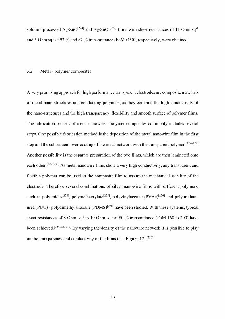
urea (PUU) - polydimethylsiloxane (PDMS)[230] have been studied. With these systems, typical
sheet resistances of 8 Ohm sq-1 to 10 Ohm sq-1 at 80 % transmittance (FoM 160 to 200) have
been achieved.[224,225,230] By varying the density of the nanowire network it is possible to play
on the transparency and conductivity of the films (see Figure 17).[230]
40
Figure 17 Transmittance of the AgNW/PUU/PDMS film: (a) comparison of transmittance for
AgNW/PUU/PDMS, AgNW/PUU, and AgNW layers (Rs = 30 Ohm sq-1) and (b) effect of
nanowire density on transmittance of AgNW layer.[230] (Reproduced with permission. 2015,
American Chemical Society)
In order to reduce the cost of the integrated nanowires, the use of the more abundant Cu is of
interest. Promising results for the replacement of Ag by Cu nanowires were presented by Song
et al.[228], who reported PDMS - Cu nanowire based composite electrodes with a sheet
resistances of 62 Ohm sq-1 and 80 % transmittance (FoM=26), which were integrated in highly
flexible and stretchable OLED devices (35 lm W-1, 57 Cd A-1, 10 mA m-2). For all metal
nanowire composites, in which insulating polymers are used as matrix material, it is crucial,
that the metal structure is exposed to the surface of the electrode, in order to ensure good electric
contact with the active layer in devices. This can either be assured by choosing an appropriate
fabrication process or by the post-treatment of the film by plasma etching, which removes
polymer on the film surface.[224] Therefore, the use of insulating polymers as support for metal
nanowires films enhances the mechanical stability of the films, but does not drastically decrease
the surface roughness. However, by using a conducting polymer, such as PEDOT:PSS, as
matrix material, the metal nano-structure can be fully embedded in a smooth film. In addition,

41
PEDOT:PSS can provide electrical contact at the nanowires junctions, which allows to omit the
thermal annealing step that is commonly used to improve the electrical contact between the
single Ag wires.[231] McGehee and co-workers presented PEDOT:PSS - Ag nanowire composite
electrodes, which were obtained by lamination of a Ag network on PEDOT:PSS with different
film thicknesses (see Figure 18).[227] These electrodes showed a very good opto-electronic
performance with Rs = 12 Ohm sq-1 at 86 % transmittance (FoM=200) and good flexibility. By
over-coating of a Ag nanowire network with PEDOT:PSS, composite electrodes with Rs=14
Ohm sq-1 to 25 Ohm sq-1 and T > 80 % were obtained[231,232], which were successfully integrated
in an A4-size touch screen panel[231] and OPV devices with an efficiency of 3.1 % (ITO
reference: 3.5 %).[232] Similar results were obtained for hydrothermally synthesized Cu
nanowires embedded in PEDOT:PSS, which displayed a sheet resistance of 46 Ohm sq-1 at
93 % transmittance, FoM=111.[233] Apart from nanowire networks also metal nano-grids were
successfully combined with PEDOT:PSS films. Kang et al.[234], for instance, fabricated a
transparent composite electrode with Rs =22 Ohm sq-1 at 78 % transmittance (FoM=65) by roll-
to-roll processing of a nano-imprinted Cu mesh on a PEDOT:PSS film, which showed
comparable performance to ITO electrodes in OPV devices.
42
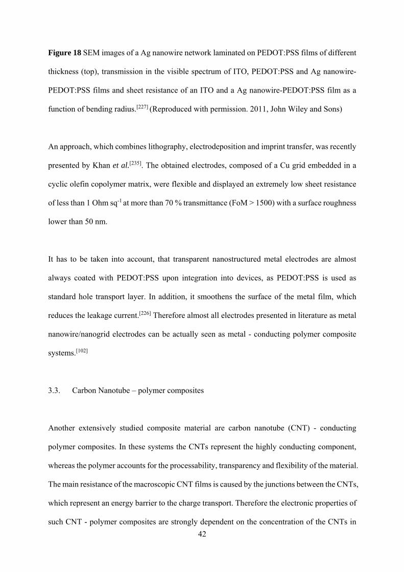
Figure 18 SEM images of a Ag nanowire network laminated on PEDOT:PSS films of different
thickness (top), transmission in the visible spectrum of ITO, PEDOT:PSS and Ag nanowire-
PEDOT:PSS films and sheet resistance of an ITO and a Ag nanowire-PEDOT:PSS film as a
function of bending radius.[227] (Reproduced with permission. 2011, John Wiley and Sons)
An approach, which combines lithography, electrodeposition and imprint transfer, was recently
presented by Khan et al.[235]. The obtained electrodes, composed of a Cu grid embedded in a
cyclic olefin copolymer matrix, were flexible and displayed an extremely low sheet resistance
of less than 1 Ohm sq-1 at more than 70 % transmittance (FoM > 1500) with a surface roughness
lower than 50 nm.
It has to be taken into account, that transparent nanostructured metal electrodes are almost
always coated with PEDOT:PSS upon integration into devices, as PEDOT:PSS is used as
standard hole transport layer. In addition, it smoothens the surface of the metal film, which
reduces the leakage current.[226] Therefore almost all electrodes presented in literature as metal
nanowire/nanogrid electrodes can be actually seen as metal - conducting polymer composite
systems.[102]
3.3. Carbon Nanotube – polymer composites
Another extensively studied composite material are carbon nanotube (CNT) - conducting
polymer composites. In these systems the CNTs represent the highly conducting component,
whereas the polymer accounts for the processability, transparency and flexibility of the material.
The main resistance of the macroscopic CNT films is caused by the junctions between the CNTs,
which represent an energy barrier to the charge transport. Therefore the electronic properties of
such CNT - polymer composites are strongly dependent on the concentration of the CNTs in
43
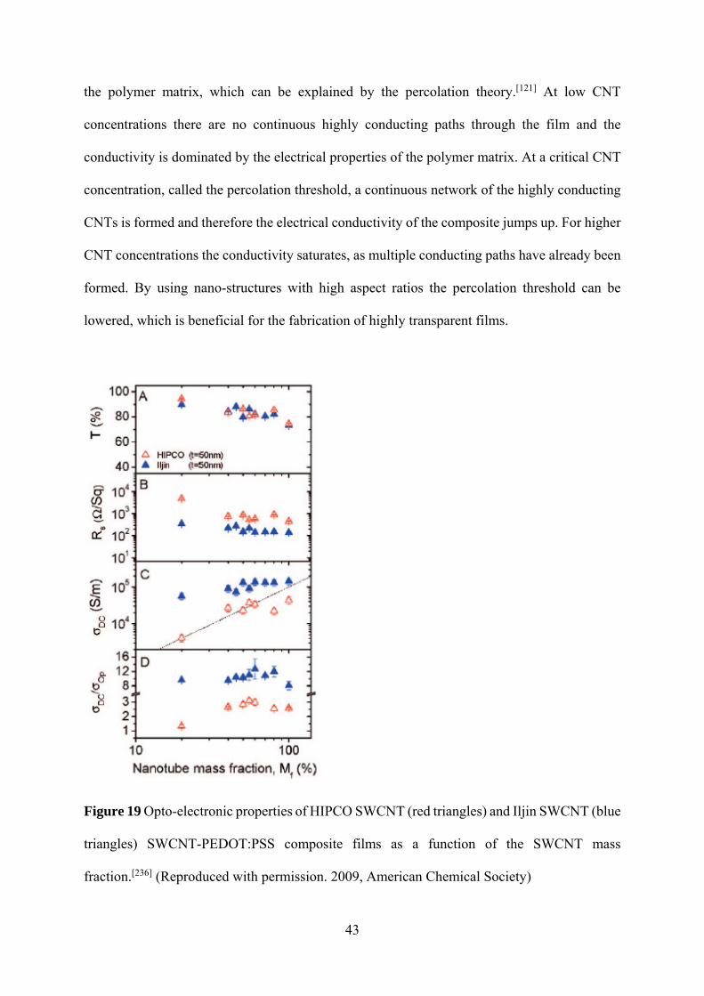
the polymer matrix, which can be explained by the percolation theory.[121] At low CNT
concentrations there are no continuous highly conducting paths through the film and the
conductivity is dominated by the electrical properties of the polymer matrix. At a critical CNT
concentration, called the percolation threshold, a continuous network of the highly conducting
CNTs is formed and therefore the electrical conductivity of the composite jumps up. For higher
CNT concentrations the conductivity saturates, as multiple conducting paths have already been
formed. By using nano-structures with high aspect ratios the percolation threshold can be
lowered, which is beneficial for the fabrication of highly transparent films.
Figure 19 Opto-electronic properties of HIPCO SWCNT (red triangles) and Iljin SWCNT (blue
triangles) SWCNT-PEDOT:PSS composite films as a function of the SWCNT mass
fraction.[236] (Reproduced with permission. 2009, American Chemical Society)
44
A straight forward approach to the fabrication of CNT-polymer composite films is the mixing
of the two components in dispersion, which allows the film fabrication in one coating step. By
using this approach flexible SWCNT-PEDOT:PSS electrodes with typical sheet resistances of
80 Ohm sq-1 to 130 Ohm sq-1 at 75 % transmittance (FoM=15) were obtained.[236–240] De et al.
[236] reported that the opto-electronic performance was maximized for a SWCNT content of
60%, at which the composite film even outperformed the pure SWCNT in terms of the FoM
(see Erreur ! Source du renvoi introuvable.). SWCNT-PEDOT:PSS electrodes fabricated by
layer-by-layer coating of SWCNT and pristine PEDOT:PSS displayed a very similar
performance[132,239]. An important parameter, which must be considered for the fabrication of
CNT-PEDOT:PSS electrodes, is the quality of the CNT dispersion, as it strongly affects the
opto-electronic performance of the composite material.[239]
In OPV devices SWCNT-PEDOT:PSS composite electrodes clearly outperformed the SWCNT
electrodes, despite the higher sheet resistance of the composite films,[132] which was explained
by a smoother interface between the electrode and the active layer. Flexible OLEDs comprising
SWCNT-PEDOT:PSS electrode showed a higher luminance than the ITO reference device for
low driving voltages < 15 V, which can be related to the higher work function of PEDOT:PSS
compared to ITO. At higher driving voltage the composite device displayed lower luminance
than the ITO device, owing to the higher sheet resistance of the SWCNT-PEDOT:PSS electrode.
[238]
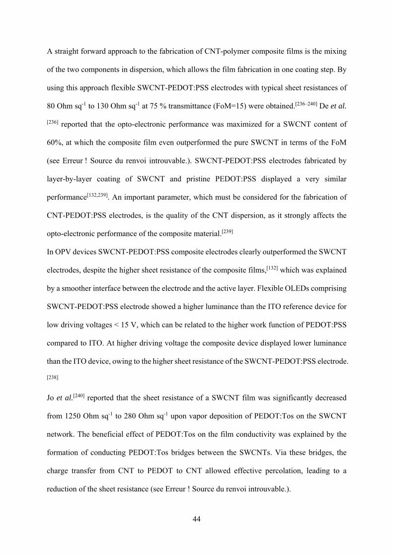
Jo et al.[240] reported that the sheet resistance of a SWCNT film was significantly decreased
from 1250 Ohm sq-1 to 280 Ohm sq-1 upon vapor deposition of PEDOT:Tos on the SWCNT
network. The beneficial effect of PEDOT:Tos on the film conductivity was explained by the
formation of conducting PEDOT:Tos bridges between the SWCNTs. Via these bridges, the
charge transfer from CNT to PEDOT to CNT allowed effective percolation, leading to a
reduction of the sheet resistance (see Erreur ! Source du renvoi introuvable.).
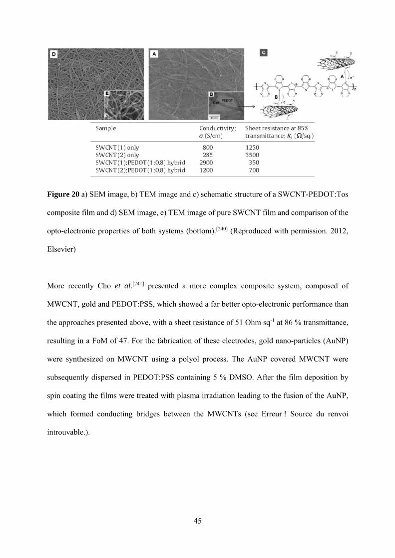
45
Figure 20 a) SEM image, b) TEM image and c) schematic structure of a SWCNT-PEDOT:Tos
composite film and d) SEM image, e) TEM image of pure SWCNT film and comparison of the
opto-electronic properties of both systems (bottom).[240] (Reproduced with permission. 2012,
Elsevier)
More recently Cho et al.[241] presented a more complex composite system, composed of
MWCNT, gold and PEDOT:PSS, which showed a far better opto-electronic performance than
the approaches presented above, with a sheet resistance of 51 Ohm sq-1 at 86 % transmittance,
resulting in a FoM of 47. For the fabrication of these electrodes, gold nano-particles (AuNP)
were synthesized on MWCNT using a polyol process. The AuNP covered MWCNT were
subsequently dispersed in PEDOT:PSS containing 5 % DMSO. After the film deposition by
spin coating the films were treated with plasma irradiation leading to the fusion of the AuNP,
which formed conducting bridges between the MWCNTs (see Erreur ! Source du renvoi
introuvable.).
46
Figure 21 a) TEM image of AuNP covered MWCNT, b) SEM image of a AuNP - MWCNT
film after plasma treatment and c) IV characteristics and schematic structure of OPV devices
with MWCNT-Au-PEDOT:PSS or ITO electrode.[241] (Reproduced with permission. 2015,
American Chemical Society)
Apart from PEDOT, other conducting polymers have been investigated as matrix material for
CNT composite electrodes. Both, Polyaniline (PANI) and polypyrrole (PPy), for instance, are
cheap, flexible and show a high conductivity and are therefore interesting candidates for the
fabrication of CNT-polymer composite electrodes. Ferrer-Anglada et al.[242] fabricated
transparent CNT-PANI and CNT-PPy electrodes by electro-polymerization of PANI or PPy on
CNT films. Upon the deposition of the conducting polymer layer on the CNT network, the
conductivity of the films increased from 3-20 S cm-1 to up to 60 S cm-1 for film transmittance
between 75 % and 90 %. Taking into account that the conductivity of the pure polymers is much
poorer than the conductivity of the pure nanotubes, the increasing conductivity of the composite
was attributed to a decreasing contact resistance between the nanotubes.
The conjugated polymer poly(3-hexylthiophene-2,5-diyl) (P3HT), well known as active layer
component in organic solar cells, was found to disperse CNTs in chlorinated solvents. This
allows the solution processing of thin, transparent conducting CNT-P3HT composite films, as
it was shown by Hellstrom et al.[243]. After a post treatment with SOCl2, which dopes the CNTs
and removes excess polymer, the composite films displayed a sheet resistance of 170 Ohm sq-
47
1 at 81% transmittance (FoM=10) and of 80 Ohm sq-1 at 72 % transmittance (FoM=13) for
P3HT to CNT ratios of 15:1 and 5:1, respectively.
4. Summary and Conclusion
The above presented materials show promising characteristics for the application as transparent
conducting electrode in organic devices. Nevertheless, a breakthrough material has not been
found yet. Metal oxides display excellent opto-electronic properties, but their brittleness makes
them unsuitable for the integration in flexible devices. Furthermore, the need for low cost
solutions and simple processing with high quality is another limiting factor for the broad base
application of metal oxides. Metallic nano-structures, such as metal grids or metal nano-wires,
allow the fabrication of thin and flexible films with an extremely low sheet resistance and good
transparency. However, their high surface roughness and mechanical fragility renders the
application difficult. Similar problems are encountered for carbon nanotube and graphene films.
In addition, their opto-electronic are poorer, despite the extremely high conductivity of the
single carbon nano-structures, caused high junction resistances between the nano-structures.
The big advantage of conducting polymer electrodes, mainly based on PEDOT, are their
solution processability, extremely high flexibility and smooth surface roughness. For a long
time their application was limited due to their insufficient opto-electronic properties. Recent
developments, however, allow the fabrication of transparent polymer electrodes which can
compete with CNT and metal nanowire electrodes in terms of the figure of merit. By combining
metallic nano-structures with conducting polymers in hybrid films, the outstanding conductivity
of the metal structure and the high transparency and mechanical stability of polymer result in
thin films with excellent opto-electronic performance.

48
Table 1 Qualitative comparison of the opto-electronic performance, advantages (indicated as
+) and drawbacks (indicated as -) of different transparent electrode materials
Material
Class
Typical
Range of
FoM
Flexibility,
Mechanical
Stability
Large Scale Processing/
Printing
Surface
Roughness
Toxicity/
Biocompatibility
Metal
Oxides
300 - 600 - - 0 - / 0
Metals Ultra-thin
films
200 - - 0 +
Nanogrids 200-700 0 0 - +
Nanowires 400 -
10000
0 + - +
Graphene/
CNTs
5-30 0 + - 0
Conducting
Polymers
40-300 + + + +
Composites Metal –
Metal Oxide
500-1000 - - 0 0
Metal -
Polymer
200-1500 + 0/+ + +
CNT –
Polymer
5-15 + + + 0
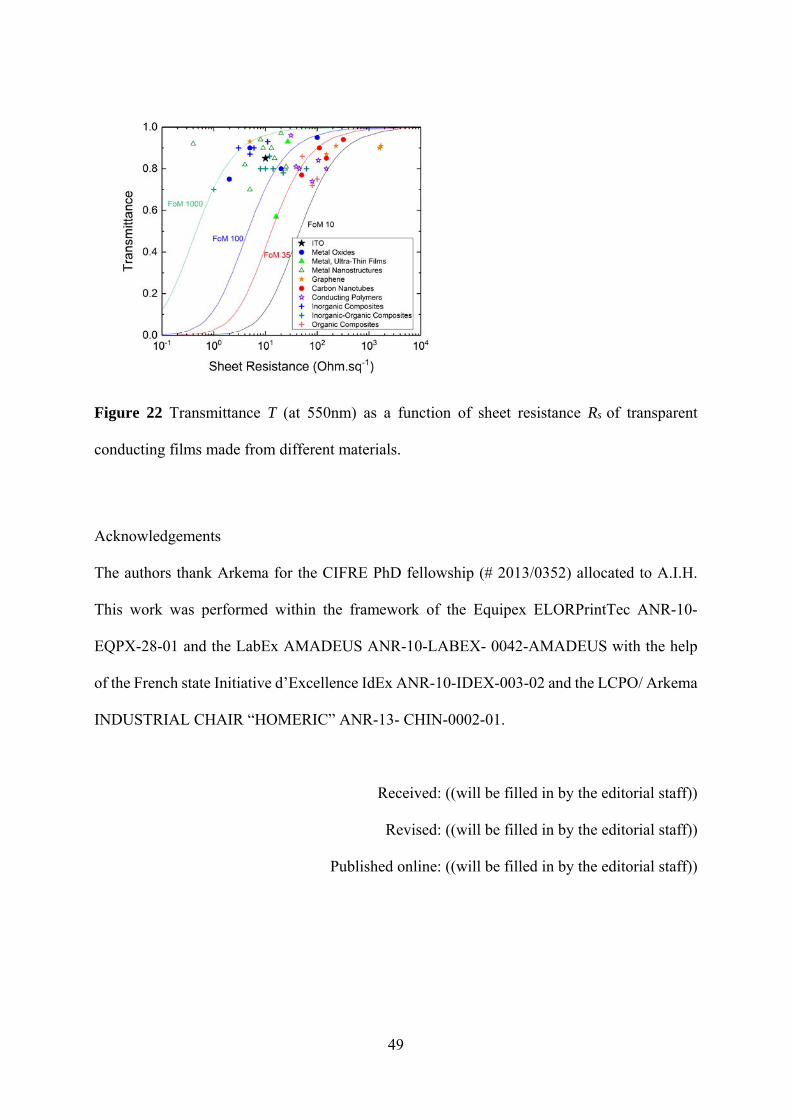
49
Figure 22 Transmittance T (at 550nm) as a function of sheet resistance Rs of transparent
conducting films made from different materials.
Acknowledgements
The authors thank Arkema for the CIFRE PhD fellowship (# 2013/0352) allocated to A.I.H.
This work was performed within the framework of the Equipex ELORPrintTec ANR-10-
EQPX-28-01 and the LabEx AMADEUS ANR-10-LABEX- 0042-AMADEUS with the help
of the French state Initiative d’Excellence IdEx ANR-10-IDEX-003-02 and the LCPO/ Arkema
INDUSTRIAL CHAIR “HOMERIC” ANR-13- CHIN-0002-01.
Received: ((will be filled in by the editorial staff))
Revised: ((will be filled in by the editorial staff))
Published online: ((will be filled in by the editorial staff))

50
[1] K. Ellmer, Nat. Photonics 2012, 6, 809.
[2] S. De, T. M. Higgins, P. E. Lyons, E. M. Doherty, P. N. Nirmalraj, W. J. Blau, J. J.
Boland, J. N. Coleman, ACS Nano 2009, 3, 1767.
[3] R. G. Gordon, MRS Bull. 2000, 25, 52.
[4] D. Langley, G. Giusti, C. Mayousse, C. Celle, D. Bellet, J.-P. Simonato,
Nanotechnology 2013, 24, 452001.
[5] I. Hamberg, C. G. Granqvist, J. Appl. Phys. 1986, 60, R123.
[6] C. G. Granqvist, Appl. Phys. A 1993, 57, 19.
[7] S. Ray, R. Banerjee, N. Basu, A. K. Batabyal, A. K. Barua, J. Appl. Phys. 1983, 54,
3497.
[8] J. S. Kim, M. Granström, R. H. Friend, N. Johansson, W. R. Salaneck, R. Daik, W. J.
Feast, F. Cacialli, J. Appl. Phys. 1998, 84, 6859.
[9] K. Sugiyama, H. Ishii, Y. Ouchi, K. Seki, J. Appl. Phys. 1999, 87, 295.
[10] Y. Park, V. Choong, Y. Gao, B. R. Hsieh, C. W. Tang, Appl. Phys. Lett. 1996, 68, 2699.
[11] A. Solanki, Mater. Sci. Appl. 2011, 02, 1702.
[12] M. G. Mason, L. S. Hung, C. W. Tang, S. T. Lee, K. W. Wong, M. Wang, J. Appl. Phys.
1999, 86, 1688.
[13] C. C. Wu, C. I. Wu, J. C. Sturm, A. Kahn, Appl. Phys. Lett. 1997, 70, 1348.
[14] K. L. Chopra, S. Major, D. K. Pandya, Thin Solid Films 1983, 102, 1.
[15] R. Bel Hadj Tahar, T. Ban, Y. Ohya, Y. Takahashi, J. Appl. Phys. 1998, 83, 2631.
[16] X. Yu, T. J. Marks, A. Facchetti, Nat. Mater. 2016, 15, 383.
[17] H. Kim, C. M. Gilmore, A. Piqué, J. S. Horwitz, H. Mattoussi, H. Murata, Z. H. Kafafi,
D. B. Chrisey, J. Appl. Phys. 1999, 86, 6451.
[18] A. K. Kulkarni, K. H. Schulz, T. S. Lim, M. Khan, Thin Solid Films 1999, 345, 273.
51
[19] W.-F. Wu, B.-S. Chiou, Thin Solid Films 1994, 247, 201.
[20] M. Kamei, Y. Shigesato, S. Takaki, Thin Solid Films 1995, 259, 38.
[21] H. Kim, J. S. Horwitz, G. P. Kushto, Z. H. Kafafi, D. B. Chrisey, Appl. Phys. Lett. 2001,
79, 284.
[22] C. G. Choi, K. No, W.-J. Lee, H.-G. Kim, S. O. Jung, W. J. Lee, W. S. Kim, S. J. Kim,
C. Yoon, Thin Solid Films 1995, 258, 274.
[23] C. Guillén, J. Herrero, Thin Solid Films 2005, 480, 129.
[24] B. G. Lewis, D. C. Paine, MRS Bull. 2000, 25, 22.
[25] D. M. Mattox, Thin Solid Films 1991, 204, 25.
[26] R. Bel Hadj Tahar, T. Ban, Y. Ohya, Y. Takahashi, J. Appl. Phys. 1997, 82, 865.
[27] M. J. Alam, D. C. Cameron, Thin Solid Films 2002, 420, 76.
[28] J. Song, S. A. Kulinich, J. Li, Y. Liu, H. Zeng, Angew. Chem. 2015, 127, 472.
[29] M. Duta, M. Anastasescu, J. M. Calderon-Moreno, L. Predoana, S. Preda, M. Nicolescu,
H. Stroescu, V. Bratan, I. Dascalu, E. Aperathitis, M. Modreanu, M. Zaharescu, M. Gartner, J.
Mater. Sci. Mater. Electron. 2016, 27, 4913.
[30] J. Ederth, P. Heszler, A. Hultåker, G. A. Niklasson, C. G. Granqvist, Thin Solid Films
2003, 445, 199.
[31] S. Servaty, G. Michael, C. Heyer, S. Katusic, H. Miess, P. Kress, S. Servaty, G. Michael,
C. Heyer, S. Katusic, H. Miess, P. Kress, Indium-Tin Oxides, 2002.
[32] S. Marikkannu, C. Sanjeeviraja, S. Piraman, A. Ayeshamariam, J. Mater. Sci. Mater.
Electron. 2015, 26, 2531.
[33] N. Fellahi, M. Addou, A. Kachouane, M. E. Jouad, Z. Sofiani, Eur. Phys. J. Appl. Phys.
2016, 74, 24611.
[34] T. Maruyama, T. Tago, Appl. Phys. Lett. 1994, 64, 1395.
[35] J. E. Medvedeva, Phys. Rev. Lett. 2006, 97, DOI 10.1103/PhysRevLett.97.086401.

52
[36] Z. Chen, L. Huang, Q. Zhang, Y. Xi, R. Li, W. Li, G. Xu, H. Cheng, J. Phys. Chem. C
2015, 119, 4789.
[37] K. L. Hoyer, A. H. Hubmann, A. Klein, Phys. Status Solidi A 2017, 214, 1600486.
[38] A. Kumar, C. Zhou, ACS Nano 2010, 4, 11.
[39] Y.-H. Tak, K.-B. Kim, H.-G. Park, K.-H. Lee, J.-R. Lee, Thin Solid Films 2002, 411,
12.
[40] A. R. Schlatmann, D. W. Floet, A. Hilberer, F. Garten, P. J. M. Smulders, T. M.
Klapwijk, G. Hadziioannou, Appl. Phys. Lett. 1996, 69, 1764.
[41] S. A. Carter, M. Angelopoulos, S. Karg, P. J. Brock, J. C. Scott, Appl. Phys. Lett. 1997,
70, 2067.
[42] M. P. de Jong, D. P. L. Simons, M. A. Reijme, L. J. van IJzendoorn, A. W. Denier van
der Gon, M. J. A. de Voigt, H. H. Brongersma, R. W. Gymer, Synth. Met. 2000, 110, 1.
[43] S. T. Lee, Z. Q. Gao, L. S. Hung, Appl. Phys. Lett. 1999, 75, 1404.
[44] D. E. Gallardo, C. Bertoni, S. Dunn, N. Gaponik, A. Eychmüller, Adv. Mater. 2007, 19,
3364.
[45] J. Cui, A. Wang, N. L. Edleman, J. Ni, P. Lee, N. R. Armstrong, T. J. Marks, Adv. Mater.
2001, 13, 1476.
[46] N. Zhou, D. B. Buchholz, G. Zhu, X. Yu, H. Lin, A. Facchetti, T. J. Marks, R. P. H.
Chang, Adv. Mater. 2014, 26, 1098.
[47] S. Edinger, N. Bansal, M. Bauch, R. A. Wibowo, G. Újvári, R. Hamid, G. Trimmel, T.
Dimopoulos, J. Mater. Sci. 2017, 52, 8591.
[48] T. Minami, Thin Solid Films 2008, 516, 5822.
[49] J. Bruneaux, H. Cachet, M. Froment, A. Messad, Thin Solid Films 1991, 197, 129.
[50] R. Pommier, C. Gril, J. Marucchi, Thin Solid Films 1981, 77, 91.
[51] E. Elangovan, K. Ramamurthi, Appl. Surf. Sci. 2005, 249, 183.
[52] A. E. Rakhshani, Y. Makdisi, H. A. Ramazaniyan, J. Appl. Phys. 1998, 83, 1049.

53
[53] A. Andersson, N. Johansson, P. Broms, N. Yu, D. Lupo, W. R. Salaneck, others, Adv.
Mater. 1998, 10, 859.
[54] T. Fukano, T. Motohiro, Sol. Energy Mater. Sol. Cells 2004, 82, 567.
[55] S. Major, S. Kumar, M. Bhatnagar, K. L. Chopra, Appl. Phys. Lett. 1986, 49, 394.
[56] A. V. Moholkar, S. M. Pawar, K. Y. Rajpure, C. H. Bhosale, J. H. Kim, Appl. Surf. Sci.
2009, 255, 9358.
[57] Q. Qiao, J. Beck, R. Lumpkin, J. Pretko, J. T. Mcleskey, Sol. Energy Mater. Sol. Cells
2006, 90, 1034.
[58] M. G. Helander, M. T. Greiner, Z. B. Wang, W. M. Tang, Z. H. Lu, J. Vac. Sci. Technol.
Vac. Surf. Films 2011, 29, 011019.
[59] W.-H. Baek, M. Choi, T.-S. Yoon, H. H. Lee, Y.-S. Kim, Appl. Phys. Lett. 2010, 96,
133506.
[60] H. Liu, V. Avrutin, N. Izyumskaya, Ü. Özgür, H. Morkoç, Superlattices Microstruct.
2010, 48, 458.
[61] Y. Furubayashi, T. Hitosugi, Y. Yamamoto, K. Inaba, G. Kinoda, Y. Hirose, T. Shimada,
T. Hasegawa, Appl. Phys. Lett. 2005, 86, 252101.
[62] D. Chen, G. Xu, L. Miao, S. Nakao, P. Jin, Surf. Coat. Technol. 2011, 206, 1020.
[63] U. Takeuchi, A. Chikamatsu, T. Hitosugi, H. Kumigashira, M. Oshima, Y. Hirose, T.
Shimada, T. Hasegawa, J. Appl. Phys. 2010, 107, 023705.
[64] S. Mohri, Y. Hirose, S. Nakao, N. Yamada, T. Shimada, T. Hasegawa, J. Appl. Phys.
2012, 111, 093528.
[65] H. Liu, Y. F. Liu, P. P. Xiong, P. Chen, H. Y. Li, J. W. Hou, B. N. Kang, Y. Duan, IEEE
Trans. Nanotechnol. 2017, PP, 1.
[66] H. Nanto, T. Minami, S. Shooji, S. Takata, J. Appl. Phys. 1984, 55, 1029.
[67] A. F. Aktaruzzaman, G. L. Sharma, L. K. Malhotra, Thin Solid Films 1991, 198, 67.
[68] W. Tang, D. C. Cameron, Thin Solid Films 1994, 238, 83.
54
[69] J.-P. Lin, J.-M. Wu, Appl. Phys. Lett. 2008, 92, 134103.
[70] I. Lange, S. Reiter, J. Kniepert, F. Piersimoni, M. Pätzel, J. Hildebrandt, T. Brenner, S.
Hecht, D. Neher, Appl. Phys. Lett. 2015, 106, 113302.
[71] T. L. Yang, D. H. Zhang, J. Ma, H. L. Ma, Y. Chen, Thin Solid Films 1998, 326, 60.
[72] J. Zhao, S. Xie, S. Han, Z. Yang, L. Ye, T. Yang, Synth. Met. 2000, 114, 251.
[73] J. H. Park, Y. C. Cho, J. M. Shin, S. Cha, C. R. Cho, H. S. Kim, S. J. Yoon, S. Jeong, S.
E. Park, A. Lim, J.-KOREAN Phys. Soc. 2007, 51, 1968.
[74] T. Minami, Thin Solid Films 2008, 516, 1314.
[75] L. Hu, H. Wu, Y. Cui, MRS Bull. 2011, 36, 760.
[76] R. A. Hatton, M. R. Willis, M. A. Chesters, D. Briggs, J. Mater. Chem. 2003, 13, 722.
[77] R. B. Pode, C. J. Lee, D. G. Moon, J. I. Han, Appl. Phys. Lett. 2004, 84, 4614.
[78] S. Conoci, S. Petralia, P. Samorì, F. M. Raymo, S. Di Bella, S. Sortino, Adv. Funct.
Mater. 2006, 16, 1425.
[79] D. S. Ghosh, L. Martinez, S. Giurgola, P. Vergani, V. Pruneri, Opt. Lett. 2009, 34, 325.
[80] B. O’Connor, C. Haughn, K.-H. An, K. P. Pipe, M. Shtein, Appl. Phys. Lett. 2008, 93,
223304.
[81] S. Schubert, L. Müller-Meskamp, K. Leo, Adv. Funct. Mater. 2014, 24, 6668.
[82] D. S. Ghosh, R. Betancur, T. L. Chen, V. Pruneri, J. Martorell, Sol. Energy Mater. Sol.
Cells 2011, 95, 1228.
[83] P. B. Catrysse, S. Fan, Nano Lett. 2010, 10, 2944.
[84] C. P. Muzzillo, Sol. Energy Mater. Sol. Cells 2017, 169, 68.
[85] M.-G. Kang, L. J. Guo, Adv. Mater. 2007, 19, 1391.
[86] M.-G. Kang, M.-S. Kim, J. Kim, L. J. Guo, Adv. Mater. 2008, 20, 4408.
[87] J. Zou, H.-L. Yip, S. K. Hau, A. K.-Y. Jen, Appl. Phys. Lett. 2010, 96, 203301.
[88] B. Sciacca, J. van de Groep, A. Polman, E. C. Garnett, Adv. Mater. 2016, 28, 905.
[89] J. Kang, C.-G. Park, S.-H. Lee, C. Cho, D.-G. Choi, J.-Y. Lee, Nanoscale 2016, 8, 11217.
55
[90] J. Schneider, P. Rohner, D. Thureja, M. Schmid, P. Galliker, D. Poulikakos, Adv. Funct.
Mater. 2016, 26, 833.
[91] S. M. Yang, Y. S. Lee, Y. Jang, D. Byun, S.-H. Choa, Microelectron. Reliab. 2016, 65,
151.
[92] L. Müller-Meskamp, S. Schubert, T. Roch, S. Eckhardt, A.-F. Lasagni, K. Leo, Adv.
Eng. Mater. 2015, 17, 1215.
[93] S. Eckhardt, M. Siebold, A. F. Lasagni, Opt. Express 2016, 24, A553.
[94] J. Jiu, T. Araki, J. Wang, M. Nogi, T. Sugahara, S. Nagao, H. Koga, K. Suganuma, E.
Nakazawa, M. Hara, H. Uchida, K. Shinozaki, J. Mater. Chem. A 2014, 2, 6326.
[95] F. Cui, Y. Yu, L. Dou, J. Sun, Q. Yang, C. Schildknecht, K. Schierle-Arndt, P. Yang,
Nano Lett. 2015, 15, 7610.
[96] M. Mohl, P. Pusztai, A. Kukovecz, Z. Konya, J. Kukkola, K. Kordas, R. Vajtai, P. M.
Ajayan, Langmuir 2010, 26, 16496.
[97] W. Wang, G. Li, Z. Zhang, J. Cryst. Growth 2007, 299, 158.
[98] A. R. Rathmell, B. J. Wiley, Adv. Mater. 2011, 23, 4798.
[99] F. Meng, S. Jin, Nano Lett. 2012, 12, 234.
[100] D. Zhang, R. Wang, M. Wen, D. Weng, X. Cui, J. Sun, H. Li, Y. Lu, J. Am. Chem. Soc.
2012, 134, 14283.
[101] J.-Y. Lee, S. T. Connor, Y. Cui, P. Peumans, Nano Lett. 2008, 8, 689.
[102] J. Krantz, M. Richter, S. Spallek, E. Spiecker, C. J. Brabec, Adv. Funct. Mater. 2011,
21, 4784.
[103] P. Lee, J. Lee, H. Lee, J. Yeo, S. Hong, K. H. Nam, D. Lee, S. S. Lee, S. H. Ko, Adv.
Mater. 2012, 24, 3326.
[104] L. Hu, H. S. Kim, J.-Y. Lee, P. Peumans, Y. Cui, ACS Nano 2010, 4, 2955.
[105] J. Liang, L. Li, K. Tong, Z. Ren, W. Hu, X. Niu, Y. Chen, Q. Pei, ACS Nano 2014, 8,
1590.
56
[106] A. J. Stapleton, R. A. Afre, A. V. Ellis, J. G. Shapter, G. G. Andersson, J. S. Quinton,
D. A. Lewis, Sci. Technol. Adv. Mater. 2013, 14, 035004.
[107] P.-C. Hsu, D. Kong, S. Wang, H. Wang, A. J. Welch, H. Wu, Y. Cui, J. Am. Chem. Soc.
2014, 136, 10593.
[108] P.-C. Hsu, S. Wang, H. Wu, V. K. Narasimhan, D. Kong, H. R. Lee, Y. Cui, Nat.
Commun. 2013, 4, 2522.
[109] H. Wu, L. Hu, M. W. Rowell, D. Kong, J. J. Cha, J. R. McDonough, J. Zhu, Y. Yang,
M. D. McGehee, Y. Cui, Nano Lett. 2010, 10, 4242.
[110] A. Iwan, A. Chuchmała, Prog. Polym. Sci. n.d., DOI
10.1016/j.progpolymsci.2012.08.001.
[111] M. Choe, B. H. Lee, G. Jo, J. Park, W. Park, S. Lee, W.-K. Hong, M.-J. Seong, Y. H.
Kahng, K. Lee, T. Lee, Org. Electron. 2010, 11, 1864.
[112] H. Park, J. A. Rowehl, K. K. Kim, V. Bulovic, J. Kong, Nanotechnology 2010, 21,
505204.
[113] K. K. Kim, A. Reina, Y. Shi, H. Park, L.-J. Li, Y. H. Lee, J. Kong, Nanotechnology
2010, 21, 285205.
[114] Y. Sun, W. Zhang, H. Chi, Y. Liu, C. L. Hou, D. Fang, Renew. Sustain. Energy Rev.
2015, 43, 973.
[115] Y.-Z. Chen, H. Medina, H.-W. Tsai, Y.-C. Wang, Y.-T. Yen, A. Manikandan, Y.-L.
Chueh, Chem. Mater. 2015, 27, 1646.
[116] X. Wang, L. Zhi, N. Tsao, Ž. Tomović, J. Li, K. Müllen, Angew. Chem. 2008, 120, 3032.
[117] J. Wu, M. Agrawal, H. A. Becerril, Z. Bao, Z. Liu, Y. Chen, P. Peumans, ACS Nano
2010, 4, 43.
[118] E. Kymakis, E. Stratakis, M. M. Stylianakis, E. Koudoumas, C. Fotakis, Thin Solid
Films 2011, 520, 1238.

57
[119] P. Paletti, R. Pawar, G. Ulisse, F. Brunetti, G. Iannaccone, G. Fiori, 2D Mater. 2015, 2,
045006.
[120] Y. Wang, S. W. Tong, X. F. Xu, B. Özyilmaz, K. P. Loh, Adv. Mater. 2011, 23, 1514.
[121] P.-C. Ma, N. A. Siddiqui, G. Marom, J.-K. Kim, Compos. Part Appl. Sci. Manuf. 2010,
41, 1345.
[122] M. F. L. D. Volder, S. H. Tawfick, R. H. Baughman, A. J. Hart, Science 2013, 339, 535.
[123] M. Kaempgen, G. S. Duesberg, S. Roth, Appl. Surf. Sci. 2005, 252, 425.
[124] M. C. Hersam, Nat. Nanotechnol. 2008, 3, 387.
[125] R. Krupke, F. Hennrich, H. v Löhneysen, M. M. Kappes, Science 2003, 301, 344.
[126] M. Zheng, A. Jagota, E. D. Semke, B. A. Diner, R. S. Mclean, S. R. Lustig, R. E.
Richardson, N. G. Tassi, Nat. Mater. 2003, 2, 338.
[127] R. Voggu, K. V. Rao, S. J. George, C. N. R. Rao, J. Am. Chem. Soc. 2010, 132, 5560.
[128] M. S. Arnold, A. A. Green, J. F. Hulvat, S. I. Stupp, M. C. Hersam, Nat. Nanotechnol.
2006, 1, 60.
[129] R. C. Tenent, T. M. Barnes, J. D. Bergeson, A. J. Ferguson, B. To, L. M. Gedvilas, M.
J. Heben, J. L. Blackburn, Adv. Mater. 2009, 21, 3210.
[130] M. Giulianini, E. R. Waclawik, J. M. Bell, M. De Crescenzi, P. Castrucci, M. Scarselli,
N. Motta, Appl. Phys. Lett. 2009, 95, 013304.
[131] K. Okazaki, Phys. Rev. B 2003, 68, DOI 10.1103/PhysRevB.68.035434.
[132] J. van de Lagemaat, T. M. Barnes, G. Rumbles, S. E. Shaheen, T. J. Coutts, C. Weeks,
I. Levitsky, J. Peltola, P. Glatkowski, Appl. Phys. Lett. 2006, 88, 233503.
[133] N. Imazu, T. Fujigaya, N. Nakashima, Sci. Technol. Adv. Mater. 2014, 15, 025005.
[134] A. Kaskela, A. G. Nasibulin, M. Y. Timmermans, B. Aitchison, A. Papadimitratos, Y.
Tian, Z. Zhu, H. Jiang, D. P. Brown, A. Zakhidov, E. I. Kauppinen, Nano Lett. 2010, 10, 4349.
[135] I. Jeon, K. Cui, T. Chiba, A. Anisimov, A. G. Nasibulin, E. I. Kauppinen, S. Maruyama,
Y. Matsuo, J. Am. Chem. Soc. 2015, 137, 7982.

58
[136] Z. Li, S. A. Kulkarni, P. P. Boix, E. Shi, A. Cao, K. Fu, S. K. Batabyal, J. Zhang, Q.
Xiong, L. H. Wong, N. Mathews, S. G. Mhaisalkar, ACS Nano 2014, 8, 6797.
[137] V. C. Tung, L.-M. Chen, M. J. Allen, J. K. Wassei, K. Nelson, R. B. Kaner, Y. Yang,
Nano Lett. 2009, 9, 1949.
[138] S. H. Kim, W. Song, M. W. Jung, M.-A. Kang, K. Kim, S.-J. Chang, S. S. Lee, J. Lim,
J. Hwang, S. Myung, K.-S. An, Adv. Mater. 2014, 26, 4247.
[139] I. N. Kholmanov, C. W. Magnuson, R. Piner, J.-Y. Kim, A. E. Aliev, C. Tan, T. Y. Kim,
A. A. Zakhidov, G. Sberveglieri, R. H. Baughman, R. S. Ruoff, Adv. Mater. 2015, 27, 3053.
[140] K.-H. Tu, S.-S. Li, W.-C. Li, D.-Y. Wang, J.-R. Yang, C.-W. Chen, Energy Environ.
Sci. 2011, 4, 3521.
[141] P.-C. Wang, L.-H. Liu, D. Alemu Mengistie, K.-H. Li, B.-J. Wen, T.-S. Liu, C.-W. Chu,
Displays 2013, 34, 301.
[142] W. W. Focke, G. E. Wnek, Y. Wei, J. Phys. Chem. 1987, 91, 5813.
[143] D. L. Cowan, V. Priest, T. R. Marrero, D. W. Slaughter, J. Phys. Chem. Solids 1990, 51,
307.
[144] J. Stejskal, I. Sapurina, J. Prokeš, J. Zemek, Synth. Met. 1999, 105, 195.
[145] Y. Cao, G. M. Treacy, P. Smith, A. J. Heeger, Appl. Phys. Lett. 1992, 60, 2711.
[146] G. Gustafsson, G. M. Treacy, Y. Cao, F. Klavetter, N. Colaneri, A. J. Heeger, Synth.
Met. 1993, 57, 4123.
[147] Y. Yang, A. J. Heeger, Appl. Phys. Lett. 1994, 64, 1245.
[148] O. Bubnova, Z. U. Khan, A. Malti, S. Braun, M. Fahlman, M. Berggren, X. Crispin, Nat.
Mater. 2011, 10, 429.
[149] J. P. Lock, S. G. Im, K. K. Gleason, Macromolecules 2006, 39, 5326.
[150] T. A. Skotheim, Handbook of Conducting Polymers, Second Edition, CRC Press, 1997.
[151] A. Elschner, S. Kirchmeyer, W. Lovenich, U. Merker, K. Reuter, PEDOT: Principles
and Applications of an Intrinsically Conductive Polymer, CRC Press, 2010.

59
[152] G. Zotti, S. Zecchin, G. Schiavon, F. Louwet, L. Groenendaal, X. Crispin, W. Osikowicz,
W. Salaneck, M. Fahlman, Macromolecules 2003, 36, 3337.
[153] A. I. Hofmann, D. Katsigiannopoulos, M. Mumtaz, I. Petsagkourakis, G. Pecastaings,
G. Fleury, C. Schatz, E. Pavlopoulou, C. Brochon, G. Hadziioannou, E. Cloutet,
Macromolecules 2017, 50, 1959.
[154] L. Lindell, A. Burquel, F. L. E. Jakobsson, V. Lemaur, M. Berggren, R. Lazzaroni, J.
Cornil, W. R. Salaneck, X. Crispin, Chem. Mater. 2006, 18, 4246.
[155] F. L. E. Jakobsson, X. Crispin, L. Lindell, A. Kanciurzewska, M. Fahlman, W. R.
Salaneck, M. Berggren, Chem. Phys. Lett. 2006, 433, 110.
[156] A. M. Nardes, M. Kemerink, M. M. de Kok, E. Vinken, K. Maturova, R. A. J. Janssen,
Org. Electron. 2008, 9, 727.
[157] L. Groenendaal, G. Zotti, P.-H. Aubert, S. m. Waybright, J. r. Reynolds, Adv. Mater.
2003, 15, 855.
[158] J. Xia, N. Masaki, K. Jiang, S. Yanagida, J. Mater. Chem. 2007, 17, 2845.
[159] E. Poverenov, M. Li, A. Bitler, M. Bendikov, Chem. Mater. 2010, 22, 4019.
[160] J. Yan, C. Sun, F. Tan, X. Hu, P. Chen, S. Qu, S. Zhou, J. Xu, Sol. Energy Mater. Sol.
Cells 2010, 94, 390.
[161] S. Ahmad, J.-H. Yum, Z. Xianxi, M. Grätzel, H.-J. Butt, M. K. Nazeeruddin, J. Mater.
Chem. 2010, 20, 1654.
[162] C. Louet, S. Cantin, J.-P. Dudon, P.-H. Aubert, F. Vidal, C. Chevrot, Sol. Energy Mater.
Sol. Cells 2015, 143, 141.
[163] R. Corradi, S. P. Armes, Synth. Met. 1997, 84, 453.
[164] F. Louwet, L. Groenendaal, J. Dhaen, J. Manca, J. Van Luppen, E. Verdonck, L.
Leenders, Synth. Met. 2003, 135–136, 115.
[165] N. Paradee, A. Sirivat, Polym. Int. 2013, n/a.
[166] J. Wang, G. Cai, X. Zhu, X. Zhou, J. Appl. Polym. Sci. 2012, 124, 109.

60
[167] L. Groenendaal, F. Jonas, D. Freitag, H. Pielartzik, J. R. Reynolds, Adv. Mater. 2000,
12, 481.
[168] C.-H. Wu, T.-M. Don, W.-Y. Chiu, Polymer 2011, 52, 1375.
[169] C. Jiang, G. Chen, X. Wang, Synth. Met. 2012, 162, 1968.
[170] M. R. Nabid, S. Asadi, M. Shamsianpour, R. Sedghi, S. Osati, N. Safari, React. Funct.
Polym. 2010, 70, 75.
[171] Y.-H. Ha, N. Nikolov, S. K. Pollack, J. Mastrangelo, B. D. Martin, R. Shashidhar, Adv.
Funct. Mater. 2004, 14, 615.
[172] D. Hohnholz, A. G. MacDiarmid, D. M. Sarno, J. Wayne E. Jones, Chem. Commun.
2001, 2444.
[173] D. M. de Leeuw, P. A. Kraakman, P. F. G. Bongaerts, C. M. J. Mutsaers, D. B. M.
Klaassen, Synth. Met. 1994, 66, 263.
[174] J. H. Chen, C.-A. Dai, W.-Y. Chiu, J. Polym. Sci. Part Polym. Chem. 2008, 46, 1662.
[175] O. Bubnova, Z. U. Khan, H. Wang, S. Braun, D. R. Evans, M. Fabretto, P. Hojati-Talemi,
D. Dagnelund, J.-B. Arlin, Y. H. Geerts, S. Desbief, D. W. Breiby, J. W. Andreasen, R.
Lazzaroni, W. M. Chen, I. Zozoulenko, M. Fahlman, P. J. Murphy, M. Berggren, X. Crispin,
Nat. Mater. 2013, 13, 190.
[176] J. S. Choi, J.-H. Yim, D.-W. Kim, J.-K. Jeon, Y. S. Ko, Y. Kim, Synth. Met. 2009, 159,
2506.
[177] B. Winther-Jensen, K. West, Macromolecules 2004, 37, 4538.
[178] M. V. Fabretto, D. R. Evans, M. Mueller, K. Zuber, P. Hojati-Talemi, R. D. Short, G.
G. Wallace, P. J. Murphy, Chem. Mater. 2012, 24, 3998.
[179] S. Admassie, O. Inganäs, W. Mammo, E. Perzon, M. R. Andersson, Synth. Met. 2006,
156, 614.
[180] B. Winther-Jensen, F. C. Krebs, Sol. Energy Mater. Sol. Cells 2006, 90, 123.

61
[181] A. M. Nardes, M. Kemerink, R. A. J. Janssen, J. A. M. Bastiaansen, N. M. M. Kiggen,
B. M. W. Langeveld, A. J. J. M. van Breemen, M. M. de Kok, Adv. Mater. 2007, 19, 1196.
[182] S. K. . Jönsson, J. Birgerson, X. Crispin, G. Greczynski, W. Osikowicz, A. . Denier van
der Gon, W. . Salaneck, M. Fahlman, Synth. Met. 2003, 139, 1.
[183] H. Shi, C. Liu, Q. Jiang, J. Xu, Adv. Electron. Mater. 2015, 1, 1500017.
[184] J. Ouyang, C.-W. Chu, F.-C. Chen, Q. Xu, Y. Yang, Adv. Funct. Mater. 2005, 15, 203.
[185] J. Y. Kim, J. H. Jung, D. E. Lee, J. Joo, Synth. Met. 2002, 126, 311.
[186] J. Ouyang, Q. Xu, C.-W. Chu, Y. Yang, G. Li, J. Shinar, Polymer 2004, 45, 8443.
[187] Y. Xia, J. Ouyang, J. Mater. Chem. 2011, 21, 4927.
[188] X. Crispin, F. L. E. Jakobsson, A. Crispin, P. C. M. Grim, P. Andersson, A. Volodin, C.
van Haesendonck, M. Van der Auweraer, W. R. Salaneck, M. Berggren, Chem. Mater. 2006,
18, 4354.
[189] X. Crispin, S. Marciniak, W. Osikowicz, G. Zotti, A. W. D. van der Gon, F. Louwet, M.
Fahlman, L. Groenendaal, F. De Schryver, W. R. Salaneck, J. Polym. Sci. Part B Polym. Phys.
2003, 41, 2561.
[190] A. M. Nardes, R. A. J. Janssen, M. Kemerink, Adv. Funct. Mater. 2008, 18, 865.
[191] I. Cruz-Cruz, M. Reyes-Reyes, M. A. Aguilar-Frutis, A. G. Rodriguez, R. López-
Sandoval, Synth. Met. 2010, 160, 1501.
[192] Y. H. Kim, C. Sachse, M. L. Machala, C. May, L. Müller-Meskamp, K. Leo, Adv. Funct.
Mater. 2011, 21, 1076.
[193] S.-I. Na, S.-S. Kim, J. Jo, D.-Y. Kim, Adv. Mater. 2008, 20, 4061.
[194] H. Do, M. Reinhard, H. Vogeler, A. Puetz, M. F. G. Klein, W. Schabel, A. Colsmann,
U. Lemmer, Thin Solid Films 2009, 517, 5900.
[195] E. Ahlswede, W. Mühleisen, M. W. bin Moh Wahi, J. Hanisch, M. Powalla, Appl. Phys.
Lett. 2008, 92, 143307.
62
[196] S. Timpanaro, M. Kemerink, F. J. Touwslager, M. M. De Kok, S. Schrader, Chem. Phys.
Lett. 2004, 394, 339.
[197] L. Ouyang, C. Musumeci, M. J. Jafari, T. Ederth, O. Inganäs, ACS Appl. Mater.
Interfaces 2015, 7, 19764.
[198] N. Kim, B. H. Lee, D. Choi, G. Kim, H. Kim, J.-R. Kim, J. Lee, Y. H. Kahng, K. Lee,
Phys. Rev. Lett. 2012, 109, 106405.
[199] L. A. A. Pettersson, S. Ghosh, O. Inganäs, Org. Electron. 2002, 3, 143.
[200] J. Zhou, D. H. Anjum, G. Lubineau, E. Q. Li, S. T. Thoroddsen, Macromolecules 2015,
48, 5688.
[201] Q. Wei, M. Mukaida, Y. Naitoh, T. Ishida, Adv. Mater. 2013, 25, 2831.
[202] J. Ouyang, Displays 2013, 34, 423.
[203] Y. Xia, J. Ouyang, Macromolecules 2009, 42, 4141.
[204] Y. Xia, J. Ouyang, Org. Electron. 2010, 11, 1129.
[205] R. J. Murphy, K. M. Weigandt, D. Uhrig, A. Alsayed, C. Badre, L. Hough, M.
Muthukumar, Macromolecules 2015, 48, 8989.
[206] M. Reyes-Reyes, I. Cruz-Cruz, R. López-Sandoval, J. Phys. Chem. C 2010, 114, 20220.
[207] Z. Yu, Y. Xia, D. Du, J. Ouyang, ACS Appl. Mater. Interfaces 2016, 8, 11629.
[208] C. Badre, L. Marquant, A. M. Alsayed, L. A. Hough, Adv. Funct. Mater. 2012, 22, 2723.
[209] R. M. Howden, E. D. McVay, K. K. Gleason, J Mater Chem A 2013, 1, 1334.
[210] Y. Xia, J. Ouyang, ACS Appl. Mater. Interfaces 2010, 2, 474.
[211] S. Mukherjee, R. Singh, S. Gopinathan, S. Murugan, S. Gawali, B. Saha, J. Biswas, S.
Lodha, A. Kumar, ACS Appl. Mater. Interfaces 2014, 6, 17792.
[212] A. I. Hofmann, W. T. T. Smaal, M. Mumtaz, D. Katsigiannopoulos, C. Brochon, F.
Schütze, O. R. Hild, E. Cloutet, G. Hadziioannou, Angew. Chem. Int. Ed. 2015, 8506.
[213] M. Jørgensen, K. Norrman, F. C. Krebs, Sol. Energy Mater. Sol. Cells 2008, 92, 686.
[214] W. Greenbank, L. Hirsch, G. Wantz, S. Chambon, Appl. Phys. Lett. 2015, 107, 263301.
63
[215] R. Rösch, D. M. Tanenbaum, M. Jørgensen, M. Seeland, M. Bärenklau, M. Hermenau,
E. Voroshazi, M. T. Lloyd, Y. Galagan, B. Zimmermann, U. Würfel, M. Hösel, H. F. Dam, S.
A. Gevorgyan, S. Kudret, W. Maes, L. Lutsen, D. Vanderzande, R. Andriessen, G. Teran-
Escobar, M. Lira-Cantu, A. Rivaton, G. Y. Uzunoğlu, D. Germack, B. Andreasen, M. V.
Madsen, K. Norrman, H. Hoppe, F. C. Krebs, Energy Environ. Sci. 2012, 5, 6521.
[216] C. Guillén, J. Herrero, Sol. Energy Mater. Sol. Cells 2008, 92, 938.
[217] J.-A. Jeong, H.-K. Kim, Sol. Energy Mater. Sol. Cells 2009, 93, 1801.
[218] D. R. Sahu, S.-Y. Lin, J.-L. Huang, Appl. Surf. Sci. 2006, 252, 7509.
[219] C.-H. Lee, R. Pandey, B.-Y. Wang, W.-K. Choi, D.-K. Choi, Y.-J. Oh, Sol. Energy
Mater. Sol. Cells 2015, 132, 80.
[220] A. Kim, Y. Won, K. Woo, S. Jeong, J. Moon, Adv. Funct. Mater. 2014, 24, 2462.
[221] F. S. F. Morgenstern, D. Kabra, S. Massip, T. J. K. Brenner, P. E. Lyons, J. N. Coleman,
R. H. Friend, Appl. Phys. Lett. 2011, 99, 183307.
[222] K. Zilberberg, F. Gasse, R. Pagui, A. Polywka, A. Behrendt, S. Trost, R. Heiderhoff, P.
Görrn, T. Riedl, Adv. Funct. Mater. 2014, 24, 1671.
[223] C.-C. Chen, L. Dou, R. Zhu, C.-H. Chung, T.-B. Song, Y. B. Zheng, S. Hawks, G. Li,
P. S. Weiss, Y. Yang, ACS Nano 2012, 6, 7185.
[224] K.-H. Ok, J. Kim, S.-R. Park, Y. Kim, C.-J. Lee, S.-J. Hong, M.-G. Kwak, N. Kim, C.
J. Han, J.-W. Kim, Sci. Rep. 2015, 5, 9464.
[225] Z. Yu, L. Li, Q. Zhang, W. Hu, Q. Pei, Adv. Mater. 2011, 23, 4453.
[226] X.-Y. Zeng, Q.-K. Zhang, R.-M. Yu, C.-Z. Lu, Adv. Mater. 2010, 22, 4484.
[227] W. Gaynor, G. F. Burkhard, M. D. McGehee, P. Peumans, Adv. Mater. 2011, 23, 2905.
[228] J. Song, J. Li, J. Xu, H. Zeng, Nano Lett. 2014, 14, 6298.
[229] B. Deng, P.-C. Hsu, G. Chen, B. N. Chandrashekar, L. Liao, Z. Ayitimuda, J. Wu, Y.
Guo, L. Lin, Y. Zhou, M. Aisijiang, Q. Xie, Y. Cui, Z. Liu, H. Peng, Nano Lett. 2015, 15, 4206.
[230] D.-H. Kim, K.-C. Yu, Y. Kim, J.-W. Kim, ACS Appl. Mater. Interfaces 2015, 7, 15214.
64
[231] J. Lee, P. Lee, H. B. Lee, S. Hong, I. Lee, J. Yeo, S. S. Lee, T.-S. Kim, D. Lee, S. H.
Ko, Adv. Funct. Mater. 2013, 23, 4171.
[232] J.-H. Lee, H.-S. Shin, Y.-J. Noh, S.-I. Na, H.-K. Kim, Sol. Energy Mater. Sol. Cells
2013, 114, 15.
[233] C. Mayousse, C. Celle, A. Carella, J.-P. Simonato, Nano Res. 2014, 7, 315.
[234] M.-G. Kang, H. Joon Park, S. Hyun Ahn, L. Jay Guo, Sol. Energy Mater. Sol. Cells
2010, 94, 1179.
[235] A. Khan, S. Lee, T. Jang, Z. Xiong, C. Zhang, J. Tang, L. J. Guo, W.-D. Li, Small 2016,
12, 3021.
[236] S. De, P. E. Lyons, S. Sorel, E. M. Doherty, P. J. King, W. J. Blau, P. N. Nirmalraj, J. J.
Boland, V. Scardaci, J. Joimel, J. N. Coleman, ACS Nano 2009, 3, 714.
[237] L. Valentini, M. Cardinali, D. Bagnis, J. M. Kenny, Carbon 2008, 46, 1513.
[238] G.-F. Wang, X.-M. Tao, R.-X. Wang, Nanotechnology 2008, 19, 145201.
[239] H. T. Ham, Y. S. Choi, M. G. Chee, M. H. Cha, I. J. Chung, Polym. Eng. Sci. 2008, 48,
1.
[240] S.-H. Jo, Y.-K. Lee, J.-W. Yang, W.-G. Jung, J.-Y. Kim, Synth. Met. 2012, 162, 1279.
[241] E.-C. Cho, C.-P. Li, J.-H. Huang, K.-C. Lee, J.-H. Huang, ACS Appl. Mater. Interfaces
2015, 7, 11668.
[242] N. Ferrer-Anglada, V. Gomis, Z. El-Hachemi, U. D. Weglikovska, M. Kaempgen, S.
Roth, Phys. Status Solidi A 2006, 203, 1082.
[243] S. L. Hellstrom, H. W. Lee, Z. Bao, ACS Nano 2009, 3, 1423.
65
Dr. Anna I. Hofmann received a double Master degree in Material Science from the University
of Bordeaux, France, and from the University of Augsburg, Germany, in 2013. In 2016 she
completed her doctoral studies on aqueous dispersions of conducting PEDOT:polyelectrolyte
complexes under the supervision of Professor Georges Hadziioannou and Dr. Eric Cloutet at
the University of Bordeaux. Currently she is working as postdoctoral researcher in the group of
Professor Christian Müller at the Chalmers University of Technology, Sweden, focusing on
organic thermoelectrics.
Dr. Eric CLOUTET received a PhD in polymer chemistry from the University of Bordeaux
(1996) and did a postdoc at the University of Akron (Ohio, USA) in 1997. Then, he joined the
CNRS at the University of Paris 13 and moved to the Laboratoire de Chimie des Polymères
Organiques (LCPO, Univ. Bordeaux) in 2001. He is currently a CNRS senior researcher at
LCPO working on the design and formulation of advanced functional polymers for applications
in energy, lithography, optoelectronics, displays, etc. His research interests include the
66
development of various (co)polymers via various polymerization routes both in homogeneous
and heterogeneous media.
Georges Hadziioannou is Chemistry Professor at the University of Bordeaux since 2/2009,
Holder of the Industrial Chair of ARKEMA/ANR HOMERIC “Hierarchical assembled Organic
Materials for ElctRonICs”, Member of the ARKEMA Corporate Scientific Board and Senior
Member of the IUF, Chair of “Physical chemistry of Polymers”. He was elected in 2017 foreign
member of the US National Academy of Engineering. His career is characterized by a strong
commitment to fundamental research at different universities and research institutes worldwide
and an important industrial tenure at IBM Almaden Research Laboratory (San Jose, California).
He has pioneered work on nanostructured polymers materials with innovations in flexible and
printable organic electronic materials as well as energy and information technologies. He is the
author of 447 publications (H = 62), 167 invited talks and 45 patents, 50 PhD’s, he wrote a
Textbook on “Polymer Electronics”, and he was co-founder of 2 startups.
Education: 1975-1980: Univ. Louis Pasteur and Centre de Recherches sur les Macromolécules,
Strasbourg – Thèses d’Etat ès Sciences Physiques and These of 3e cycle, DEA in
Macromolecular Physical Chemistry; 1971-1975: Aristotle University of Thessaloniki (Greece),
Master in Chemistry

67
A. I. Hofmann, E. Cloutet*, G. Hadziioannou*
Materials for Transparent Electrodes: From Metal Oxides to Organic Alternatives
Different classes of transparent conductors and their potential for the application as
transparent electrodes are presented, comprising brief descriptions of the fundamental
principles as well as the latest achievements in the field. Various inorganic and organic
materials are compared, not only regarding their opto-electronic performance, but also
regarding their processability, flexibility and potential for the integration in devices.