Embed Size (px)
Citation preview

1 of 30
Rafael J. Betancourt-Zamorahttp://www.betasoft.org/
May 16, 2002
Noise Tutorial: Low-frequency CMOS
Analog Design

2 of 30
Noise Tutorial: Low-frequency CMOS Analog Design
© 2002, Rafael J. Betancourt-Zamora • http://www.betasoft.org/
Outline
• Goals
• Noise Overview• Resistor Noise Sources
• MOSFET Noise Sources• Noise of Common Amplifier Topologies• Examples
• Summary

3 of 30
Noise Tutorial: Low-frequency CMOS Analog Design
© 2002, Rafael J. Betancourt-Zamora • http://www.betasoft.org/
• Grasp the importance of noise performance in low-frequency instrumentation design
• Understand the types of noise present in integrated resistors and MOS devices.
• Understand the noise trade-offs of different circuit topologies
• Perform simple noise analysis
Goals

4 of 30
Noise Tutorial: Low-frequency CMOS Analog Design
© 2002, Rafael J. Betancourt-Zamora • http://www.betasoft.org/
Outline
• Goals• Noise Overview
• Resistor Noise Sources
• MOSFET Noise Sources• Noise of Common Amplifier Topologies• Examples
• Summary

5 of 30
Noise Tutorial: Low-frequency CMOS Analog Design
© 2002, Rafael J. Betancourt-Zamora • http://www.betasoft.org/
What is noise?
• Unwanted disturbance that interferes with a desired signal• External: power supply & substrate coupling, crosstalk, EMI, etc.• Internal: random fluctuations that result from the physics of the devices or materials• Smallest detectable signal, signal-to-noise ratio (SNR), and dynamic range are
determined by noise
SNRPsignalPnoise--------------------
Vrms signal,2
Vrms noise,2
-------------------------= =
We will look at internal noise sources and how they affect key performance metrics.

6 of 30
Noise Tutorial: Low-frequency CMOS Analog Design
© 2002, Rafael J. Betancourt-Zamora • http://www.betasoft.org/
t
V t( )
P x( )
FUZZ 6σ≈
• Random process with zero mean• Instantateous amplitude is unpredictable• Average noise power can be measured (variance)
What does it look like?
WHITE NOISE (GAUSSIAN DISTRIBUTION)
m 0=
σ Vrms=
STANDARD DEVIATION
VARIANCE
MEAN
σ2V rms
2=
f
V rms2
Hz⁄
Noise Power Spectral Density(Normalized Noise Power)
7 of 30
Noise Tutorial: Low-frequency CMOS Analog Design
© 2002, Rafael J. Betancourt-Zamora • http://www.betasoft.org/
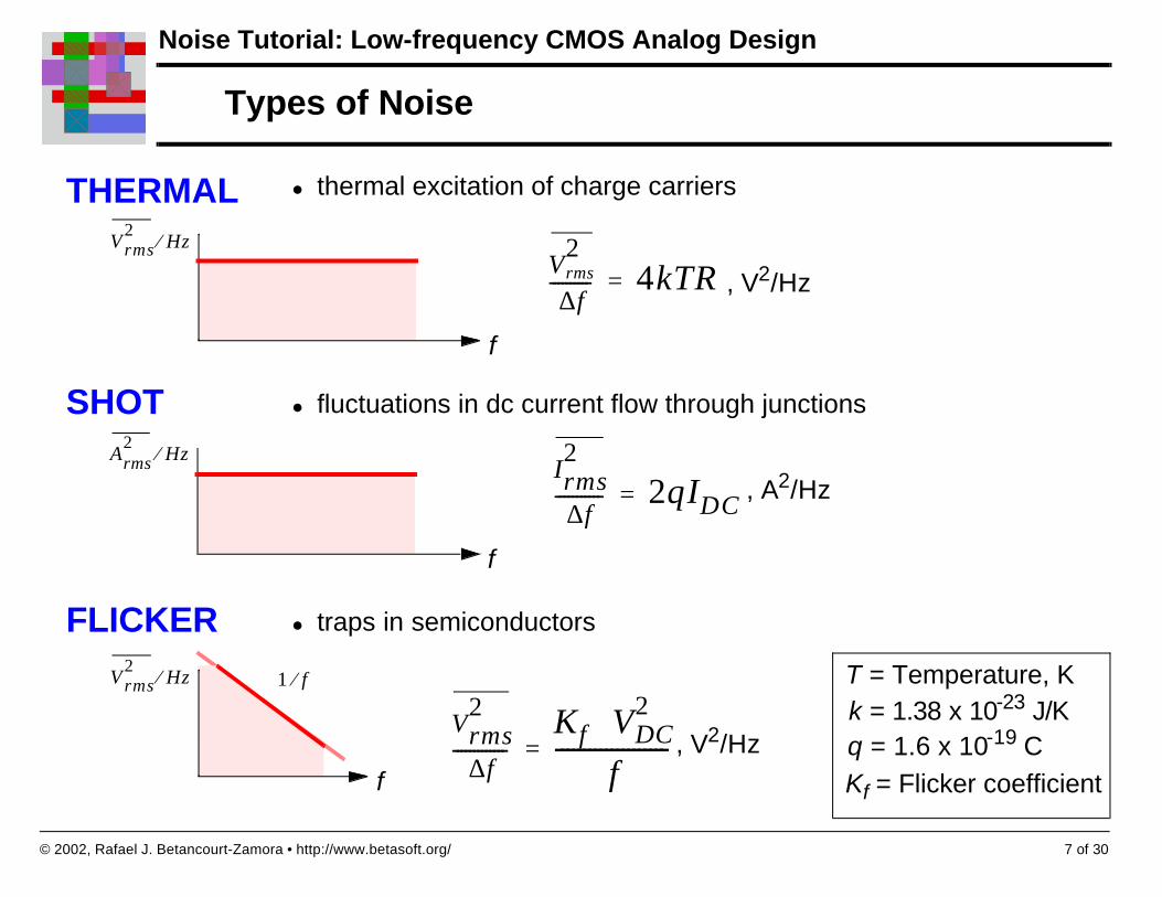
Types of Noise
THERMAL
SHOT
FLICKER
• thermal excitation of charge carriers
• fluctuations in dc current flow through junctions
• traps in semiconductors
f
V rms2
Hz⁄
f
V rms2
Hz⁄
f
Arms2
Hz⁄
1 f⁄
Vrms2
∆f---------- 4kTR=
Irms2
∆f----------- 2qIDC=
Vrms2
∆f-------------
Kf VDC2⋅
f--------------------=
, V2/Hz
, A2/Hz
, V2/Hzk = 1.38 x 10⁻²³ J/Kq = 1.6 x 10⁻¹⁹ C
T = Temperature, K
Kf = Flicker coefficient

8 of 30
Noise Tutorial: Low-frequency CMOS Analog Design
© 2002, Rafael J. Betancourt-Zamora • http://www.betasoft.org/
Outline
• Goals• Noise Overview• Resistor Noise Sources
• MOSFET Noise Sources• Noise of Common Amplifier Topologies• Examples
• Summary

9 of 30
Noise Tutorial: Low-frequency CMOS Analog Design
© 2002, Rafael J. Betancourt-Zamora • http://www.betasoft.org/
Resistor Thermal Noise
Vn2
∆f------ 4kTR= , V2/Hz
R
* R
Vn2 4kTR∆fn=
Vn2
In2 4kT
R---------------- ∆fn=
In2
, V2 , A2
NOISE DENSITY
NOISE POWER
In2
∆f-------
4kTR
----------------= , A2/Hz
1kΩ @ 25 ºC
nV Hz⁄
pA Hz⁄
4.05
4.05
∆fn = NOISE BANDWIDTH
• Integrate noise PSD over frequency to arrive at total noise power.• For white noise, multiply PSD by noise bandwidth.

10 of 30
Noise Tutorial: Low-frequency CMOS Analog Design
© 2002, Rafael J. Betancourt-Zamora • http://www.betasoft.org/
Noise Bandwidth
NOISE BW
• Noise bandwidth is defined for a brickwall transfer function• Noise bandwidth is not the same as 3dB bandwidth
f f3dB ∆fn
Avo2
Avo2 ∆fn⋅ Av f( )
2
0
∞
∫ df=
No. Poles
1
2
3
2nd-order BPF
∆fnπ2--- ∆f3dB⋅=
∆fn 1.22 ∆f3dB⋅=
∆fn 1.16 ∆f3dB⋅=
∆fnπ2--- ∆f3dB⋅=
Av f( )2

11 of 30
Noise Tutorial: Low-frequency CMOS Analog Design
© 2002, Rafael J. Betancourt-Zamora • http://www.betasoft.org/
kT/C Limit
C
R
*Vn
2Vo
2
∆ fnπ2--- ∆f3dB⋅=
∆f3dB1
2πRC---------------=
∆fn1
4RC-----------=
Vo2 4kTR∆fn= , V2
Vo
2 4kTR 14RC-----------
=
Vo2 kT
C------=
• Total noise power is independent of R• Capacitor is noiseless, but accumulates noise from resistor• This fundamental limit is important for sampled systems
, V2

12 of 30
Noise Tutorial: Low-frequency CMOS Analog Design
© 2002, Rafael J. Betancourt-Zamora • http://www.betasoft.org/
Combining Noise Sources
R1
*R2 Vn1
2 In22
R2
*Vn2
2
R1+R2
*Vn1
2Vn2
2+
R1 In12
R1||R2 In12
In22
+
• For uncorrelated noise sources, just add the noise powers.• For correlated sources use:
Vo2 Vn1
2 Vn22 2cVn1Vn2+ +=
c 1≤ CORRELATION COEFFICIENT
SERIES PARALLEL
Vo2 4kT R1 R2+( )∆fn= Io
2 4kT 1R1------- 1
R2-------+( )∆fn=

13 of 30
Noise Tutorial: Low-frequency CMOS Analog Design
© 2002, Rafael J. Betancourt-Zamora • http://www.betasoft.org/
Resistor Flicker (1/f) Noise
f
Vn2
Hz⁄1 f⁄ Vnf
2
∆f-------
Kf VDC2⋅
f---------------------= , V2/Hz
THERMAL
fcfff Vnf
2 Kf VDC2⋅
f---------------------
fL
fH
∫ df Kf VDC2 fH
fL-----
ln⋅= =
Vo2 4kTR∆fn Kf VDC
2 fH
fL------
ln⋅+=
TOTAL RESISTOR NOISE
, V2
• Constant noise power per decade• fc defines 1/f corner frequency where
flicker noise is equal to thermal noise.
Vnf2 2.3Kf VDC
2⋅= FOR fH/fL = 10
fL fH, V2
ASSUMES∆fn fc»

14 of 30
Noise Tutorial: Low-frequency CMOS Analog Design
© 2002, Rafael J. Betancourt-Zamora • http://www.betasoft.org/
Noise Index
Vnf2
VDC2
-------------
DEC
Kf VDC2 10( )ln⋅
VDC2
----------------------------------------------------- 2.3Kf= =
• Normalize 1/f noise per Volt, per decade of frequency• Can express 1/f noise PSD and fc in terms of NI
NI 2.3Kf 106–⋅= , µµV/V/decade
Vnf2 NI
2VDC
2⋅
2.3 1012–×
-----------------------------1f---⋅= , V2/Hz
fcNI2 VDC
2⋅
2.3 1012–× 4kTR⋅
--------------------------------------------------= , Hz20log(NI)
poly
pdiffndiff -10dB
-5dB
-15dB
[Motchenbacher’93]

15 of 30
Noise Tutorial: Low-frequency CMOS Analog Design
© 2002, Rafael J. Betancourt-Zamora • http://www.betasoft.org/
Outline
• Goals• Noise Overview• Resistor Noise Sources
• MOSFET Noise Sources
• Noise of Common Amplifier Topologies• Examples
• Summary

16 of 30
Noise Tutorial: Low-frequency CMOS Analog Design
© 2002, Rafael J. Betancourt-Zamora • http://www.betasoft.org/
Noise Sources in a MOSFET
*Vnf
2
Ind2
*Vng
2DRAIN THERMAL NOISE
FLICKER NOISE
GATE THERMAL NOISEVng
2
∆f-------- 4kTRG 3⁄=
Ind2
∆ f------- 4kTγgm=
, V2/Hz
, A2/Hz
γγ = 2/3, long channel
2-3, short channel
Rds = 1/gm
Long ChannelSaturation
• due to limited channel conductance
• can be neglected with good layout
Vnf2
∆f-------
KfWLCoxf-------------------= , V2/Hz Kf 1.2 10
24–×= V2
F⋅FOR NMOS
[Razavi’01]
SPICE
Inf2
∆f------
Kf IDCAF⋅
LEFF2
Cox f-----------------------= , A2/Hz

17 of 30
Noise Tutorial: Low-frequency CMOS Analog Design
© 2002, Rafael J. Betancourt-Zamora • http://www.betasoft.org/
Input-referred Noise
*Vnf
2
Ind2
*Vni
2
Ini2
• Define equivalent input voltage and current noise sources.
• MOSFET input current noise source can be neglected at low frequencies.
*Vni
2
Vnd2
∆f--------
Ind2
∆f------- gm
2⁄ 4kTγgm
---------------------= = , V2/Hz
INPUT-REFERRED DRAIN NOISE
TOTAL INPUT-REFERRED NOISE
Vni2
∆f------- 4kTγ
gm---------------------
KfWLCox f-------------------+= , V2/Hz

18 of 30
Noise Tutorial: Low-frequency CMOS Analog Design
© 2002, Rafael J. Betancourt-Zamora • http://www.betasoft.org/
1/f Corner Frequency
4kTγgm
---------------------Kf
WLCox fc----------------------=
f
Vn2
Hz⁄
1 f⁄
THERMAL
fcfff
• Defines where flicker noise is equal to thermal noise.• Need to increase transistor area to reduce flicker noise.
fcKf gm⋅
4kTγWLCox---------------------------------------=

19 of 30
Noise Tutorial: Low-frequency CMOS Analog Design
© 2002, Rafael J. Betancourt-Zamora • http://www.betasoft.org/
Outline
• Goals• Noise Overview• Resistor Noise Sources
• MOSFET Noise Sources• Noise of Common Amplifier Topologies
• Examples
• Summary

20 of 30
Noise Tutorial: Low-frequency CMOS Analog Design
© 2002, Rafael J. Betancourt-Zamora • http://www.betasoft.org/
Current Source
In12
I1
VBIAS
In12
∆ f------- 4kTγgm=
• Neglected flicker noise of M1• Need to minimize output current noise• Minimize gm for low noise
Vo2
Vo2
∆f--------
In12
∆f------- ro
2⋅= , V2/Hz
, A2/Hz
VDD
M1
Vo2
∆ f-------- 4kTγgmro
2= , V2/Hz

21 of 30
Noise Tutorial: Low-frequency CMOS Analog Design
© 2002, Rafael J. Betancourt-Zamora • http://www.betasoft.org/
Common Source
RL
VDD
M1
InL2
*Vnf
2
In12
Vo2
Vi
• Neglected output conductance of M1• Maximize gm , RL, and transistor area for low noise
• For a differential pair, double the noise
Vni2
∆f------- 4kTγ
gm---------------------
KfWLCoxf-------------------
4kT
gm2 RL
----------------------+ += , V2/Hz
In12
∆ f------- 4kTγgm= , A2/Hz
InL2
∆f---------
4kTRL
----------------= , A2/Hz Vnf2
∆f-------
KfWLCoxf-------------------= , V2/Hz

22 of 30
Noise Tutorial: Low-frequency CMOS Analog Design
© 2002, Rafael J. Betancourt-Zamora • http://www.betasoft.org/
Source Follower
M1
In22
Vo2
*Vn1
2VDD
Vi
VBIAS M2
• Neglected flicker noise of M2• VERY NOISY, AVOID
Vni2
∆f-------
Vn12
∆f--------
In22
∆f-------
1gm1--------------- ro1
2 ro22
|| || 2
⋅
Av2
---------------------------------------------------------------------------+= , V2/Hz
Vn12
∆f-------- 4kTγ
gm1---------------------
KfWLCox f-------------------+= , V2/Hz
In22
∆ f------- 4kTγgm= , A2/Hz
Av 1≈WHERE

23 of 30
Noise Tutorial: Low-frequency CMOS Analog Design
© 2002, Rafael J. Betancourt-Zamora • http://www.betasoft.org/
Common Gate
In12
Vo2
VBIAS M1
RL
VDD
InL2
Vi
• Neglected output conductance of M1• Define equivalent input voltage and current noise sources• Input noise current cannot be ignored• Transfers load current noise to the input
InL2
∆f---------
4kTRL
----------------= , A2/Hz
In12
∆f------- 4kTγgm= , A2/Hz
Ini2
∆f-------
4kTRL
----------------gm
2Kf
WLCoxf-------------------+= , A2/Hz
Vni2
∆f------- 4kTγ
gm---------------------
4kT
gm2 RL
----------------------Kf
WLCox f-------------------+ += , V2/Hz
Rs = 1/gm
(neglectingbody effect)
*Vnf
2
Vnf2
∆f-------
KfWLCoxf-------------------= , V2/Hz

24 of 30
Noise Tutorial: Low-frequency CMOS Analog Design
© 2002, Rafael J. Betancourt-Zamora • http://www.betasoft.org/
Cascode
Vo2
VBIAS
M1
RL
VDD
InL2
*Vn1
2
Vi
In22M2
Vn12
∆f-------- 4kTγ
gm1---------------------
KfWLCox f-------------------+= , V2/Hz
InL2
∆f---------
4kTRL
----------------= , A2/Hz
• Neglected output conductance of M1• M2’s noise contribution is negligible at low frequencies• Capacitance at M1’s drain increase noise at high frequencies
Vni2
∆f------- 4kTγ
gm1---------------------
KfWLCox f-------------------
4kT
gm12 RL
--------------------------+ += , V2/Hz

25 of 30
Noise Tutorial: Low-frequency CMOS Analog Design
© 2002, Rafael J. Betancourt-Zamora • http://www.betasoft.org/
Outline
• Goals• Noise Overview• Resistor Noise Sources
• MOSFET Noise Sources• Noise of Common Amplifier Topologies• Examples
• Summary

26 of 30
Noise Tutorial: Low-frequency CMOS Analog Design
© 2002, Rafael J. Betancourt-Zamora • http://www.betasoft.org/
Variable Resistor
(1-k)RT In22
kRT In12
Vo
Vi
(1-k)RT
In2
kRT
Vo
Req = k(1-k)RTWORST CASEk = 0.5
Req = RT/4
In2
∆f-------
4kTReq
----------------= , A2/Hz
In2
∆f-------
16kTRT
---------------------= , A2/Hz

27 of 30
Noise Tutorial: Low-frequency CMOS Analog Design
© 2002, Rafael J. Betancourt-Zamora • http://www.betasoft.org/
Inverting Operational Amplifier Filter
R1 * R2 *
C
*
Vn12
Vn22
Vo
Vi
Vna2
-
+
• Negligible input noise current• Ignore 1/f noise• Low frequency operationwhere
Vni2
∆f------- Vn1
2 Vn22
Avi2
--------+=
AviR2R1-------–=
1. SHORT Vna
2. SHORT Vi
Vni2
∆f------- Vna
2 Avni2
Avi2
------------
Vna2
1 R1R2-------+
2= =
Avni 1 R2R1-------+=
3. APPLY SUPERPOSITION
Vni2
∆f------- Vn1
2 Vn22
Avi2
--------+ Vna2
1 R1R2-------+
2
+=
FOR LARGE GAIN, R2 >> R1
Vni2
∆f------- Vn1
2 Vn22
Avi2
--------+ Vna2
+= , V2/Hz
∆fnπ2--- 1
2πR2C-----------------⋅ 1
4R2C-------------= =

28 of 30
Noise Tutorial: Low-frequency CMOS Analog Design
© 2002, Rafael J. Betancourt-Zamora • http://www.betasoft.org/
Outline
• Goals• Noise Overview• Resistor Noise Sources
• MOSFET Noise Sources• Noise of Common Amplifier Topologies• Examples
• Summary

29 of 30
Noise Tutorial: Low-frequency CMOS Analog Design
© 2002, Rafael J. Betancourt-Zamora • http://www.betasoft.org/
What We Learned
• Thermal noise and flicker noise are the major sources of headaches for low-noise, low frequency instrumentation design in CMOS.
• Noise bandwidth is not the same as 3dB bandwidth.• Capacitors are noiseless, but they can accumulate noise.• Resistors can have flicker noise, but only when there is current flow.
NOISE IN GENERAL
NOISE IN MOSFETS• Need to increase transistor area to reduce flicker noise.• Current source: Minimize gm for low noise current• Common source: Maximize gm , RL, and transistor area for low noise
• Source follower: VERY NOISY, AVOID• Common gate: Transfers load current noise to the input. Input noise
current cannot be ignored.• Cascode: Cascode transistor noise contribution is negligible at low
frequencies.

30 of 30
Noise Tutorial: Low-frequency CMOS Analog Design
© 2002, Rafael J. Betancourt-Zamora • http://www.betasoft.org/
1. P.H. Garret, “Analog I/O Design: Acquisition, Conversion, Recovery,” Reston Publishing, Reston, VA, pp. 264, 1981.
2. D.A. Johns, K. Martin “Analog Integrated Circuit Design,” John Wiley & Sons, pp. 706, 1997.
3. C.D. Motchenbacher, J.A. Connelly, “Low Noise Electronic System Design,” John Wiley & Sons, pp. 422, 1993.
4. B. Razavi, “Design of Analog CMOS Integrated Circuits,” McGraw-Hill, pp. 684, 2001.
References