Embed Size (px)
Citation preview
1
(continued on page 4)
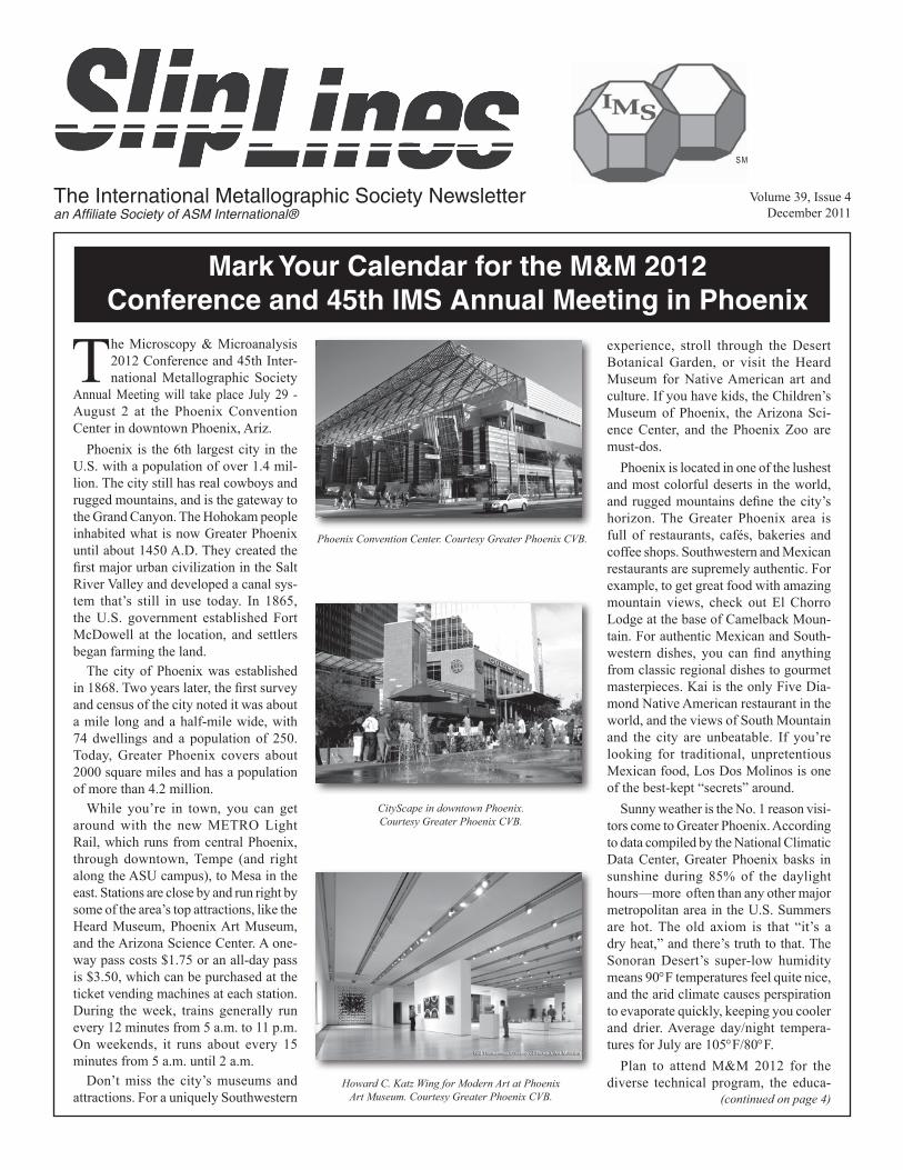
Mark Your Calendar for the M&M 2012Conference and 45th IMS Annual Meeting in Phoenix
CityScape in downtown Phoenix. Courtesy Greater Phoenix CVB.
Phoenix Convention Center. Courtesy Greater Phoenix CVB.
The Microscopy & Microanalysis 2012 Conference and 45th Inter-national Metallographic Society
Annual Meeting will take place July 29 - August 2 at the Phoenix Convention Center in downtown Phoenix, Ariz.
Phoenix is the 6th largest city in the U.S. with a population of over 1.4 mil-lion. The city still has real cowboys and rugged mountains, and is the gateway to the Grand Canyon. The Hohokam people inhabited what is now Greater Phoenix until about 1450 A.D. They created the first major urban civilization in the Salt River Valley and developed a canal sys-tem that’s still in use today. In 1865, the U.S. government established Fort McDowell at the location, and settlers began farming the land.
The city of Phoenix was established in 1868. Two years later, the first survey and census of the city noted it was about a mile long and a half-mile wide, with 74 dwellings and a population of 250. Today, Greater Phoenix covers about 2000 square miles and has a population of more than 4.2 million.
While you’re in town, you can get around with the new METRO Light Rail, which runs from central Phoenix, through downtown, Tempe (and right along the ASU campus), to Mesa in the east. Stations are close by and run right by some of the area’s top attractions, like the Heard Museum, Phoenix Art Museum, and the Arizona Science Center. A one-way pass costs $1.75 or an all-day pass is $3.50, which can be purchased at the ticket vending machines at each station. During the week, trains generally run every 12 minutes from 5 a.m. to 11 p.m. On weekends, it runs about every 15 minutes from 5 a.m. until 2 a.m.
Don’t miss the city’s museums and attractions. For a uniquely Southwestern
Volume 39, Issue 4December 2011
The International Metallographic Society Newsletteran Affiliate Society of ASM International®
SM
experience, stroll through the Desert Botanical Garden, or visit the Heard Museum for Native American art and culture. If you have kids, the Children’s Museum of Phoenix, the Arizona Sci-ence Center, and the Phoenix Zoo are must-dos.
Phoenix is located in one of the lushest and most colorful deserts in the world, and rugged mountains define the city’s horizon. The Greater Phoenix area is full of restaurants, cafés, bakeries and coffee shops. Southwestern and Mexican restaurants are supremely authentic. For example, to get great food with amazing mountain views, check out El Chorro Lodge at the base of Camelback Moun-tain. For authentic Mexican and South-western dishes, you can find anything from classic regional dishes to gourmet masterpieces. Kai is the only Five Dia-mond Native American restaurant in the world, and the views of South Mountain and the city are unbeatable. If you’re looking for traditional, unpretentious Mexican food, Los Dos Molinos is one of the best-kept “secrets” around.
Sunny weather is the No. 1 reason visi-tors come to Greater Phoenix. According to data compiled by the National Climatic Data Center, Greater Phoenix basks in sunshine during 85% of the daylight hours—more often than any other major metropolitan area in the U.S. Summers are hot. The old axiom is that “it’s a dry heat,” and there’s truth to that. The Sonoran Desert’s super-low humidity means 90°F temperatures feel quite nice, and the arid climate causes perspiration to evaporate quickly, keeping you cooler and drier. Average day/night tempera-tures for July are 105°F/80°F.
Plan to attend M&M 2012 for the di verse technical program, the educa-Howard C. Katz Wing for Modern Art at Phoenix
Art Museum. Courtesy Greater Phoenix CVB.

2
Welcome all to this issue of SlipLines. There have been many exciting IMS
activities since our annual meeting that I would like to share with you. But first of all, congratulations goes to our IMS past president, David Fitzgerald,
for being elected to the Class of 2011 ASM Fellows. David has volunteered many years of service to both ASM and IMS. Thank you, David for your help in making IMS what it is today.
Have you been to our updated IMS website yet? The IMS website (www.metallography.net) has been revamped to better serve the needs of our members. We now have one place to find information about the International Metal-lographic Society (IMS), our events, ASM International/IMS-sponsored education classes, and more. The website will always be a work in progress as we strive to make it innovative and informative. To accomplish this, we need your feedback. Let us know what you like or dislike, what you would like to see, and how we can make it more useful. The IMS board wants the IMS website to be your first stop for all your metallographic questions and needs.
A Message From the President
Our new IMS journal, Metallography, Microstructure, and Analysis, or MMA, will debut in February 2012, and there will be six issues per year initially. Ryan M. Deacon, Johns Hopkins University Applied Physics Laboratory, will serve as the Editor of MMA, and Chris Bagnall, MCS Associates Inc., will be Advisory Editor. More details about the journal are presented elsewhere in this issue. Visit the IMS website for details on how to submit a manuscript for consideration for publication.
Mark your calendar for the Microscopy & Microanalysis 2012 Conference and 45th International Metallographic Society Annual Meeting to be held July 29 – August 2 in Phoenix, Ariz. We have planned some excellent metallog-raphy sessions, and we will be sponsoring a Sunday short course entitled “Metallography for Failure Analysis,” with IMS past president Frauke Hogue as instructor. For more details, visit the IMS website.
I hope to see you all in Phoenix.
Nat Saenz, PresidentInternational Metallographic Society
This is the last print version of SlipLines. Look for the new SlipLines eNewsletter launching in February 2012. Visit the IMS web site at www.metallography.net for more details.
IMS BenefactorsBuehler Ltd. – www.buehler.com
ESI - Engineering and Scientific Investigation – www.esi-website.com
IMS PatronsAllied High Tech Products Inc. – www.alliedhightech.com
IMR Test Labs — www.imrtest.comMetallurgical Supply Co. Inc. — www.metlabsupply.comPrecision Surfaces International — www.psidragon.com
Struers Inc. — www.struers.com
IMS AssociatesB&W Y-12 – www.y12doe.gov
Hoeganaes Corp. — www.hoeganaes.comTed Pella Inc. – www.tedpella.com
Carl Zeiss MicroImaging LLC – www.zeiss.comIMS Sponsors
MetLab Corp. – www.metlabcorp.com Nikon Metrology Inc. – www.nikon.comScot Forge Co. — www.scot-forge.com
A quarterly publication of the International Metallographic Society, providing organizational news and technical briefs.(Copyright 2011 by ASM International®. All rights reserved.)
IMS Board of DirectorsNatalio T. Saenz, PresidentRichard Blackwell, FASM, Vice PresidentFrauke Hogue, Past PresidentJudith L. Arner, SecretaryDavid Rollings, Finance OfficerDaniel P. Dennies, FASM, DirectorJaret J. Frafjord, DirectorMichael L. He, DirectorSamuel J. Lawrence, DirectorGabriel M. Lucas, DirectorJames E. Martinez, DirectorJeffry A. Hawk, FASM, ASM Board LiaisonRichard Knight, FASM, ASM Board Liaison
Executive Director Randall S. BarnesAdministrator, Affiliate Societies Sarina PastoricSlipLines Design and Layout Design By J, LLC–www.designbyj.comSlipLines Editor Ed Kubel
Contact IMS at:9639 Kinsman RoadMaterials Park, OH 44073-0002 USAphone 440/338-5151, ext. 0fax 440/338-4634e-mail: MemberServiceCenter@ asminternational.org
SM
3
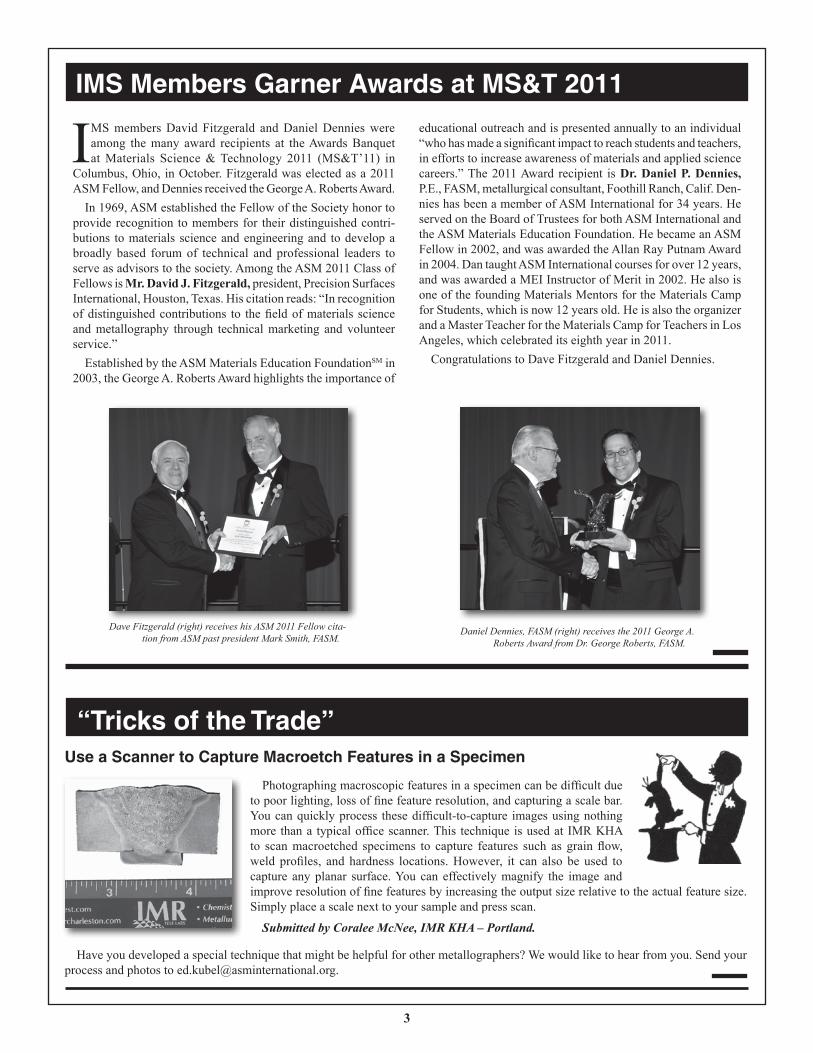
IMS Members Garner Awards at MS&T 2011
IMS members David Fitzgerald and Daniel Dennies were among the many award recipients at the Awards Banquet at Materials Science & Technology 2011 (MS&T’11) in
Columbus, Ohio, in October. Fitzgerald was elected as a 2011 ASM Fellow, and Dennies received the George A. Roberts Award.
In 1969, ASM established the Fellow of the Society honor to provide recognition to members for their distinguished contri-butions to materials science and engineering and to develop a broadly based forum of technical and professional leaders to serve as advisors to the society. Among the ASM 2011 Class of Fellows is Mr. David J. Fitzgerald, president, Precision Surfaces International, Houston, Texas. His citation reads: “In recognition of distinguished contributions to the field of materials science and metallography through technical marketing and volunteer service.”
Established by the ASM Materials Education FoundationSM in 2003, the George A. Roberts Award highlights the importance of
educational outreach and is presented annually to an individual “who has made a significant impact to reach students and teachers, in efforts to increase awareness of materials and applied science careers.” The 2011 Award recipient is Dr. Daniel P. Dennies, P.E., FASM, metallurgical consultant, Foothill Ranch, Calif. Den-nies has been a member of ASM International for 34 years. He served on the Board of Trustees for both ASM International and the ASM Materials Education Foundation. He became an ASM Fellow in 2002, and was awarded the Allan Ray Putnam Award in 2004. Dan taught ASM International courses for over 12 years, and was awarded a MEI Instructor of Merit in 2002. He also is one of the founding Materials Mentors for the Materials Camp for Students, which is now 12 years old. He is also the organizer and a Master Teacher for the Materials Camp for Teachers in Los Angeles, which celebrated its eighth year in 2011.
Congratulations to Dave Fitzgerald and Daniel Dennies.
Dave Fitzgerald (right) receives his ASM 2011 Fellow cita-tion from ASM past president Mark Smith, FASM.
Daniel Dennies, FASM (right) receives the 2011 George A. Roberts Award from Dr. George Roberts, FASM.
Use a Scanner to Capture Macroetch Features in a Specimen
Photographing macroscopic features in a specimen can be difficult due to poor lighting, loss of fine feature resolution, and capturing a scale bar. You can quickly process these difficult-to-capture images using nothing more than a typical office scanner. This technique is used at IMR KHA to scan macroetched specimens to capture features such as grain flow, weld profiles, and hardness locations. However, it can also be used to capture any planar surface. You can effectively magnify the image and improve resolution of fine features by increasing the output size relative to the actual feature size. Simply place a scale next to your sample and press scan.
Submitted by Coralee McNee, IMR KHA – Portland.
Have you developed a special technique that might be helpful for other metallographers? We would like to hear from you. Send your process and photos to [email protected].
“Tricks of the Trade”
4
IMS 2012 in Phoenix — Mark Your Calendarcontinued from page 1
tional short courses, the excellent vendor exhibits, and the fun social activities. The conference symposia cover a wide array of microscopy techniques and a variety of materials, with sessions in metallography for failure analysis, SEM, EBSD, and microscopy of joining techniques including welding, brazing, and cladding. The events of interest to IMS are listed below, and the full list of events can be found on the IMS web site at www.metallography.net.
The Sunday reception will be held at the Phoenix Convention Center, and there will be a Plenary Session on Monday.
Short Course of Interest to IMS Members (Sunday)
Metallography for Failure AnalysisInstructor: Frauke Hogue
This course can be beneficial for any-body involved in metallurgical failure analysis—metallurgists, engineers, and technicians. Special practical techniques such as making very large mounts, grind-ing to a specific location, cleaning, and replication will be discussed. The most important structures of various alloy groups, failure modes, and manufactur-ing methods are illustrated. More than two dozen case studies are presented to demonstrate the use and importance of optical metallography in failure analysis.
Sessions of Interest to IMS Members (Monday-Thursday)
A02 — Robert Gray Memorial Sym-posium on Metallography of Reactive Materials Organizers: Jaret Frafjord, Rod McCabe, and Steve Dekanich
This symposium honors the work of Robert Gray, who helped establish the Metallography Group at Oak Ridge Na-tional Laboratory, Tenn. Presentations will discuss work on sample preparation and metallography of reactive and radioactive materials. Sample preparation of many metals and alloys is extremely challenging because they react with the atmosphere or water during polishing or analysis. Some metals are radioactive and require special procedures to prevent contamination and radiation hazards. This symposium is not limited to metals, but will also discuss challenging reactive materials such as hy-drides, battery materials, and explosives.
“It’s a Family Affair” will be held again this year, so bring the kids to learn about microscopes and materials science through exciting demonstrations and tours of the exhibit hall.
We look forward to seeing you in Phoenix!Dustin Turnquist and Doug Puerta —M&M/IMS 2012 Co-Chairs
P04: Microscopy and Microanalysis of Joining and Coating MaterialsOrganizers: Steven R. Claves, Chad M. Parish, and Donald F. Susan
Joining and coating technologies, such as welding, soldering, brazing, and clad-ding, are used to join multiple pieces into components and to protect the resulting component surfaces from wear and cor-rosion. These processes often involve complex, multi-component phase trans-formations, which can produce intricate micro- and nanostructures. Characteriza-tion of these microstructures is required to understand how the joining and coating processes influence the properties of the materials in service. This symposium covers nondestructive and destructive mi-croscopy and microanalysis of advanced joining and coating processes, including a broad range of techniques from mac-roscale optical metallography to single-atom high resolution imaging.
P05: High-resolution Microscopy and Microanalysis of Meteorites, Minerals and AerosolsOrganizers: John Armstrong , David Smith, Lindsey Keller, and David Bell
High-resolution electron microscopy and x-ray microanalysis played major roles in the characterization of geological, extraterrestrial and environmental materi-als since their invention. High-resolution electron microscopy is responsible for moving the study of minerals from the macro to the atomic level. X-ray micro-analysis has proven to be the most accurate analytical method for determining the el-emental composition of geological and ex-traterrestrial specimens at the micro- and nano-scale. For more than 40 years, Peter R. Buseck in the Chemistry Department and School of Earth and Space Explora-tion has been in the forefront of research in combining high-resolution electron
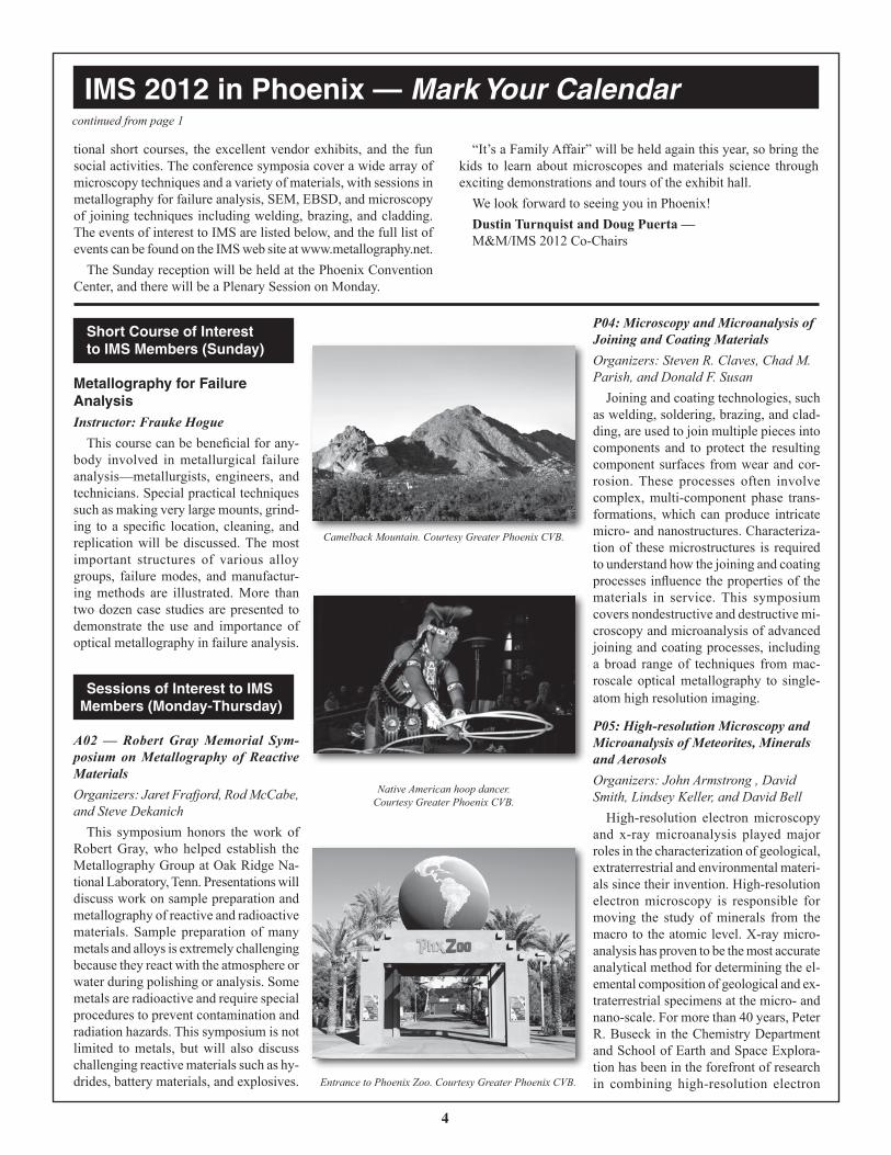
Camelback Mountain. Courtesy Greater Phoenix CVB.
Native American hoop dancer. Courtesy Greater Phoenix CVB.
Entrance to Phoenix Zoo. Courtesy Greater Phoenix CVB.
5
IMS 2012 in Phoenix — Mark Your Calendar
microscopy and x-ray microanalysis in the study of minerals, meteorites, and environmental aerosols. This symposium focuses on the important contributions that have been and are continuing to be made by the synergistic use of these imag-ing and analysis procedures in studies of the solid materials of our solar system as demonstrated by Peter Buseck, his many students and colleagues, and those influ-enced by them.P06 — Failure Analysis of Structural MaterialsOrganizers: James Martinez and Daniel Dennies
Failure analysis is an important function crossing all disciplines. This symposium
includes real-world applications and re-search case studies to determine the root cause in the failure of structural materials. In particular, the symposium highlights the application of all materials used as structural members and components. Any and all optical, scanning, transmis-sion, and microanalytical techniques used throughout the investigation will be discussed. Topics covered include metal fatigue and fracture; environmental fac-tors such as corrosion, embrittlement, and overload; biomaterials/medical implants; semiconductor; multi-mode failures; and more. Contributions are encouraged from industry failure analysts and researchers active in these areas.
Abstract submission deadline is February 15, 2012.For details on how to submit an abstract, visit www.metallography.net
The M&M 2012 Call for Papers is Ready!
Visit www.microscopy.org/MandM/2012/ to get your copy today.The Call includes detailed information on symposia, workshops, tutorials,
short courses, awards, and paper submission.
PAPER SUBMISSION DEADLINE: FEBRUARY 15, 2012.M&M 2012 is July 29 – August 2 in Phoenix, Arizona.
Don’t miss this premier microscopy meeting of the year!
Hot Air Balloons and a Saguaro Cactus. Courtesy Greater Phoenix CVB.
Phoenix skyline from South Mountain. Courtesy Greater Phoenix CVB.
METRO LightRail. Courtesy Greater Phoenix CVB.

6
2012 International Metallographic Contest
The International Metallographic Contest and Exhibit is being held in conjunction with M&M 2012 in Phoenix, Ariz. The contest features the best work of metallographers and microstructure analysts from around the world. Entrants need not be members of the International Metal-
lographic Society (IMS) or ASM International. Highlights of the rules are shown below. Please visit www.metallography.net for detailed rules, and be sure to read the excellent articles by Jim Nelson for tips on creating a winning entry and for insight into the judging process.
The primary goal of the contest is to advance the science of microstructural analysis by providing an opportunity for those interested in material properties and characterization to display their work and communicate significant scientific information. There are 11 different classes of competition covering all fields of optical and electron microscopy. In Classes 1 through 8, multiple images and captions are expected to be used to describe how metallography was used to help solve a problem, or to describe a unique or unusual technique. Classes 9, 10, and 11 are for artistic pictures. The contest is open to all, including nonmembers. Entrants do not have to be present to win.
Officers of IMS and ASM International, class award sponsors, and commercial exhibitors may enter in any class to compete for cash awards including Best in Show. If an entry submitted by officers of IMS or ASM, class award sponsors, or commercial exhibitors receives a first place award in any class, the author is prohibited from entering the same class the following year.
All monetary awards will be issued in U.S. dollars:• Best in Show will receive the Jacquet-Lucas Award (the IMS Pierre Jacquet Medal and the ASM Francis F. Lucas Award) and
$3,000.00. • First Place winners will receive $200.00.• First Place undergraduate student winners in Classes 7 and 8 also receive the George L. Kehl Plaque. • Second Place winners will receive $100.00. • Third Place winners will receive $50.00. • Honorable Mention will receive a certificate of appreciation.If in the opinion of the judges the standards expected of prize winners are not met, one or more awards in that class may be omitted.Entries are prominently displayed at the annual M&M conference following judging and again in the fall at the annual ASM International
MS&T Conference and Exhibition. Winning entries will also be displayed at ASM International headquarters in Materials Park, Ohio.
Classes1. Light Microscopy - Metals and Metal Alloys Only - sponsored by Struers Inc.2. Light Microscopy - All Other Materials - sponsored by Allied High Tech Products Inc.3. Electron Microscopy - Transmission and Analytical4. Electron Microscopy - Scanning5. Color Microscopy (this class is based on the use of color microscopy to express or clearly define the story in a manner definitely supe-
rior to black and white microscopy. This is best accomplished by showing both B&W and color images so the judges can compare them.) 6. The DuBose-Crouse Award for Unique, Unusual, and New Techniques in Microscopy 7. Undergraduate Student Entries - Metals and Metal Alloys Only - sponsored by Precision Surfaces International8. Undergraduate Student Entries - All Other MaterialsThe following Classes are for “pretty” pictures (images of artistic or aesthetic value). One image per entry. Not eligible for best in
show. Entries in these classes may be submitted by ftp or e-mail:9. Artistic Microscopy - Black & White Only 10. Artistic Microscopy - Color Only11. Digital Microscopy - Artistic (images may be created by digitally combining and enhancing multiple images to create one artistic
image, which would otherwise not exist in a specimen)To encourage exhibitors to enter only their best work, no more than three entries per individual (or team) will be accepted with no more
than two entries allowed in any one class. Only one photograph per entry may be submitted in Classes 9, 10, and 11. Entries must be received by July 14, 2012. Send to:Mr. Mitchell WitkowskiGeneral Dynamics – AIS8201 E. McDowell Rd.M/D: H1149FScottsdale, AZ 85257-3812Tel: 480/441-2348
7
ASM and Springer Launch New Journal:Metallography, Microstructure, and Analysis
ASM International and Springer Science+Business Media officially announced the launch of the new journal Metal-lography, Microstructure, and Analysis (MMA). The jour-
nal is affiliated with International Metallographic Society (IMS), an affiliate society of ASM International. Of interest to practicing metallographers, microscopists, physical metallurgists, and engi-neers, it will serve as a forum to exchange the latest information regarding the evaluation of microstructures in a variety of materials. The first issue will be published in February 2012.
Metallography, Microstructure, and Analysis will publish original, peer-reviewed research articles. With six issues a year, the journal will focus on emerging techniques in analyzing microstruc-tures, designed to assist engineers who work with microstructural properties in a variety of different materials. Articles will cover the methods of evaluation of materials for use in the aerospace industry, the automotive industry, and parts of the construction industry. Advanced materials developers, the applied R&D com-munity, and those working in energy technologies will also find the journal of interest.
Ryan M. Deacon, Johns Hopkins University Applied Physics Laboratory, will serve as Editor, and Chris Bagnall, MCS Associ-ates Inc., as Advisory Editor.
Dr. Deacon announced the journal’s inaugural editorial board:
• Dr. Gunter E. Petzow, Max Planck Institute, Consultant-Advisor to the Board
• Mr. Arlan O. Benscoter, Lehigh University
• Prof. Krishan K. Chawla, University of Alabama at Birmingham
• Dr. Sunniva Collins, Swagelok Co.
• Mr. Steve Dekanich, Y-12 National Security Complex
• Dr. Isabel Fernandes, University of Porto
• Dr. Iain LeMay, Metallurgical Consulting Services
• Dr. Frank Muecklich, Saarland University
• Dr. Lawrence E. Murr, University of Texas - El Paso
• Prof. Tony Rollett, Carnegie Mellon University
• Dr. Donald F. Susan, Sandia National Laboratory
• Dr. Jeffrey Wadsworth, Battelle
IMS President Nat Saenz stated, “I’m very excited about the launch of our new IMS journal Metallography, Microstructure, and Analysis. MMA is geared specifically to the founding principles of IMS, the art and science of preparing, interpreting, and analyz-ing microstructures for the purpose of understanding materials behavior and performance. This new journal will provide a unique forum for IMS members and all of those working in this field to share their work and to increase their technical expertise by learn-ing from the work of others.”
Springer Editorial Director Alexander Greene added, “We are pleased to be publishing Metallography, Microstructure, and Analysis with ASM International and IMS. By co-publishing with ASM and IMS, this journal will reach the prominent and suc-cessful audience of metallurgists and engineers who will benefit directly from its presence. With Ryan Deacon and Chris Bagnall appointed as Editors, we look forward to a successful launch for this journal in 2012.”
MMA welcomes submission of manuscripts focused on the role of microstructure in engineering processes and materials properties at http://mc.manuscriptcentral.com/IMS-MMA. For more infor-mation, visit the MMA homepage at www.springer.com/13632.
Dr. Ryan Deacon
8
Certified Metallographer Program Update
VISIT THE IMS WEB SITE:www.metallography.net
ASM International®9639 Kinsman RoadMaterials Park, Ohio 44073-0002
ADDRESS SERVICE REQUESTED
The Certified Metallographer Com-mittee is hard at work developing a certification program for the entry
level metallographer; a person having two years of experience and the educational equivalent of a two-year associate’s degree. The Committee developed an outline of what the Certified Metallographer does on the job. This list, or job analysis, was sent to a group of subject matter experts (SMEs) for input, their input was presented to the committee, and an updated job analysis was developed into a practice survey and deployed to the metallographic community.
This survey was sent out on November 10, 2011 and will be open until December 18, 2011. The practice analysis forms the nucleus of the certification program and provides the exam blueprint, as well as being a focus for educational and training products. Metallog-raphers are encouraged to provide their input
and comments so that we can be assured that the certification program has the best foundation possible.
Results of the job analysis will be col-lected and analyzed after December 18 and
will be published; look for results early next year in an issue of SlipLines eNews.
The Metallographer Certification Com-mittee has also developed a program outline (a written general knowledge exam and a practical exam), a description of a certi-fied metallographer, selected a logo for the program, and are hard at work creating the requirements for a practical exam. A section of the IMS website is devoted to the certifica-tion program; visit http://www.asminterna-tional.org/portal/site/ims/Certification/ for new and updated information.
For more information about the work of the Certified Metallographer Committee, contact Louise Wehrle at 440/338-5151, ext. 5694, or email at certification@ asminternational.org.