Embed Size (px)
Citation preview

L
Global DriveDrive PLC
Manual

This Manual for the Drive PLC Developer Studio is valid for the following Lenzeautomation systems:
Automation system Type as from hardware version as from software versionDrive PLC EPL10200 Px 10
Important Note :
The software is made available to the user in the currently existing form. All risks with regard to the quality and the results arising from itsuse remain the responsibility of the user. The user must implement the appropriate security precautions against possible erroneousapplication.
We do not accept any responsibilty for direct or consequential damages, such as loss of profits, loss of orders, or effects on the course ofbusiness of any kind.
. 2000 Lenze GmbH & Co KG
No part of this documentation may be copied or made available to third parties without the express written permission ofLenze GmbH & Co KG.
We have take great care in assembling the information in this documentation, and checked that it corresponds to the hardware and softwarethat is described. Nevertheless, we cannot guarantee that there are no discrepancies. We do not accept any legal responsibility or liabilityfor damage that may thereby ensue. Any necessary corrections will be implemented in subsequent versions.
Windows, WindowsNTandMS-DOSare either registered trademarksor trademarksof MicrosoftCorporation in the UnitedStatesand/orothercountries.IBM and VGA are registered trademarks of International Business Machines, Inc.All other designations are trade names of their owners.
Version 1.1 09/2000 TD27

Drive PLCContents
i DrivePLC EN 1.1
1 Preface and general information 1-1. . . . . . . . . . . . . . . . . . . . . . . . . . . . . . . . . . . . . . . . . . .1.1 About this Manual 1-1. . . . . . . . . . . . . . . . . . . . . . . . . . . . . . . . . . . . . . . . . . . . . . . . . . . . . . . . . . . . . . . .
1.1.1 Conventions in this Manual 1-1. . . . . . . . . . . . . . . . . . . . . . . . . . . . . . . . . . . . . . . . . . . . . . . . . .1.1.2 Pictograms in this manual 1-1. . . . . . . . . . . . . . . . . . . . . . . . . . . . . . . . . . . . . . . . . . . . . . . . . . .1.1.3 Terminology used 1-1. . . . . . . . . . . . . . . . . . . . . . . . . . . . . . . . . . . . . . . . . . . . . . . . . . . . . . . . .1.1.4 What’s new? 1-1. . . . . . . . . . . . . . . . . . . . . . . . . . . . . . . . . . . . . . . . . . . . . . . . . . . . . . . . . . . . .
1.2 Lenze software guidelines for variable names 1-2. . . . . . . . . . . . . . . . . . . . . . . . . . . . . . . . . . . . . . . . . . . .1.2.1 Hungarian Notation 1-2. . . . . . . . . . . . . . . . . . . . . . . . . . . . . . . . . . . . . . . . . . . . . . . . . . . . . . . .
1.2.1.1 Recommendation for designating variable types 1-3. . . . . . . . . . . . . . . . . . . . . . . . .1.2.1.2 Designation of the signal type in the variable name 1-4. . . . . . . . . . . . . . . . . . . . . . .1.2.1.3 Special handling of system variables 1-4. . . . . . . . . . . . . . . . . . . . . . . . . . . . . . . . . .
2 System blocks 2-1. . . . . . . . . . . . . . . . . . . . . . . . . . . . . . . . . . . . . . . . . . . . . . . . . . . . . . . . .2.1 Introduction 2-1. . . . . . . . . . . . . . . . . . . . . . . . . . . . . . . . . . . . . . . . . . . . . . . . . . . . . . . . . . . . . . . . . . . . .
2.1.1 Access through absolute addresses 2-2. . . . . . . . . . . . . . . . . . . . . . . . . . . . . . . . . . . . . . . . . . . .2.1.2 Module numbers 2-2. . . . . . . . . . . . . . . . . . . . . . . . . . . . . . . . . . . . . . . . . . . . . . . . . . . . . . . . . .2.1.3 Definition of the system-block inputs/outputs 2-3. . . . . . . . . . . . . . . . . . . . . . . . . . . . . . . . . . . . .
2.2 Automation interface (AIF1_IO_AutomationInterface) 2-4. . . . . . . . . . . . . . . . . . . . . . . . . . . . . . . . . . . . . . .2.2.1 Inputs_AIF1 (AIF1_IN) 2-4. . . . . . . . . . . . . . . . . . . . . . . . . . . . . . . . . . . . . . . . . . . . . . . . . . . . . .2.2.2 Outputs_AIF1 (AIF1_OUT) 2-7. . . . . . . . . . . . . . . . . . . . . . . . . . . . . . . . . . . . . . . . . . . . . . . . . . . .
2.3 Automation interface (AIF2_IO_AutomationInterface) 2-10. . . . . . . . . . . . . . . . . . . . . . . . . . . . . . . . . . . . . . .2.3.1 Inputs_AIF2 (AIF2_IN) 2-10. . . . . . . . . . . . . . . . . . . . . . . . . . . . . . . . . . . . . . . . . . . . . . . . . . . . . .2.3.2 Outputs_AIF2 (AIF2_OUT) 2-12. . . . . . . . . . . . . . . . . . . . . . . . . . . . . . . . . . . . . . . . . . . . . . . . . . . .
2.4 Automation interface (AIF3_IO_AutomationInterface) 2-15. . . . . . . . . . . . . . . . . . . . . . . . . . . . . . . . . . . . . . .2.4.1 Inputs_AIF3 (AIF3_IN) 2-15. . . . . . . . . . . . . . . . . . . . . . . . . . . . . . . . . . . . . . . . . . . . . . . . . . . . . .2.4.2 Outputs_AIF3 (AIF3_OUT) 2-17. . . . . . . . . . . . . . . . . . . . . . . . . . . . . . . . . . . . . . . . . . . . . . . . . . . .
2.5 AIF_IO_Management 2-20. . . . . . . . . . . . . . . . . . . . . . . . . . . . . . . . . . . . . . . . . . . . . . . . . . . . . . . . . . . . . .
2.6 Analog input/output 1 (ANALOG1_IO) 2-21. . . . . . . . . . . . . . . . . . . . . . . . . . . . . . . . . . . . . . . . . . . . . . . . . . .2.6.1 Inputs_ANALOG1_CPU1 (AIN1) 2-21. . . . . . . . . . . . . . . . . . . . . . . . . . . . . . . . . . . . . . . . . . . . . . . .2.6.2 Outputs_ANALOG1_CPU1 (AOUT1) 2-22. . . . . . . . . . . . . . . . . . . . . . . . . . . . . . . . . . . . . . . . . . . . .
2.7 Analog input 2 (ANALOG2_IO) 2-23. . . . . . . . . . . . . . . . . . . . . . . . . . . . . . . . . . . . . . . . . . . . . . . . . . . . . . . .2.7.1 Inputs_ANALOG2_CPU1 (AIN2) 2-23. . . . . . . . . . . . . . . . . . . . . . . . . . . . . . . . . . . . . . . . . . . . . . . .
2.8 Analog input 3 (ANALOG3_IO) 2-24. . . . . . . . . . . . . . . . . . . . . . . . . . . . . . . . . . . . . . . . . . . . . . . . . . . . . . . .2.8.1 Inputs_ANALOG3_CPU1 (AIN3) 2-24. . . . . . . . . . . . . . . . . . . . . . . . . . . . . . . . . . . . . . . . . . . . . . . .
2.9 Digital inputs/outputs (DIGITAL_IO) 2-25. . . . . . . . . . . . . . . . . . . . . . . . . . . . . . . . . . . . . . . . . . . . . . . . . . . .2.9.1 Inputs_DIGITAL_CPU1 (DIGIN) 2-25. . . . . . . . . . . . . . . . . . . . . . . . . . . . . . . . . . . . . . . . . . . . . . . . .2.9.2 Outputs_DIGITAL_CPU1 (DIGOUT) 2-26. . . . . . . . . . . . . . . . . . . . . . . . . . . . . . . . . . . . . . . . . . . . . .
2.10 Free Codes (FCODE_FreeCodes) 2-27. . . . . . . . . . . . . . . . . . . . . . . . . . . . . . . . . . . . . . . . . . . . . . . . . . . . . .
2.11 System markers (SYSTEM_FLAGS) 2-29. . . . . . . . . . . . . . . . . . . . . . . . . . . . . . . . . . . . . . . . . . . . . . . . . . . .

Drive PLCContents
ii DrivePLC EN 1.1
3 System blocks - FIF modules 3-1. . . . . . . . . . . . . . . . . . . . . . . . . . . . . . . . . . . . . . . . . . . . .3.1 Standard-I/O 3-1. . . . . . . . . . . . . . . . . . . . . . . . . . . . . . . . . . . . . . . . . . . . . . . . . . . . . . . . . . . . . . . . . . . .
3.1.1 Analog inputs/outputs Standard-I/O (ANALOG_IO_STDIO) 3-1. . . . . . . . . . . . . . . . . . . . . . . . . . . . .3.1.1.1 Input_ANALOG1_STDIO (AIN1_STDIO) 3-1. . . . . . . . . . . . . . . . . . . . . . . . . . . . . . . . .3.1.1.2 Output_ANALOG1_STDIO (AOUT1_STDIO) 3-2. . . . . . . . . . . . . . . . . . . . . . . . . . . . . .
3.1.2 Digital inputs/outputs Standard-I/O (DIGITAL_IO_STDIO) 3-3. . . . . . . . . . . . . . . . . . . . . . . . . . . . .3.1.2.1 Inputs_DIGITAL_STDIO (DIGIN_STDIO) 3-3. . . . . . . . . . . . . . . . . . . . . . . . . . . . . . . . .3.1.2.2 Output_DIGITAL_STDIO (DIGOUT_STDIO) 3-4. . . . . . . . . . . . . . . . . . . . . . . . . . . . . . .
4 System blocks - internal extensions modules 4-1. . . . . . . . . . . . . . . . . . . . . . . . . . . . . . . .4.1 Extension Board 1 4-1. . . . . . . . . . . . . . . . . . . . . . . . . . . . . . . . . . . . . . . . . . . . . . . . . . . . . . . . . . . . . . . .
4.1.1 Digital inputs/outputs Extension Board 1 (DIGITAL_IO_EB1) 4-1. . . . . . . . . . . . . . . . . . . . . . . . . . .4.1.1.1 Inputs_DIGITAL_EB1 (DIGIN_EB1) 4-1. . . . . . . . . . . . . . . . . . . . . . . . . . . . . . . . . . . .4.1.1.2 Outputs_DIGITAL_EB1 (DIGOUT_EB1) 4-2. . . . . . . . . . . . . . . . . . . . . . . . . . . . . . . . .
4.2 Extension Board 2 4-3. . . . . . . . . . . . . . . . . . . . . . . . . . . . . . . . . . . . . . . . . . . . . . . . . . . . . . . . . . . . . . . .4.2.1 Digital inputs/outputs Extension Board 2 (DIGITAL_IO_EB2) 4-3. . . . . . . . . . . . . . . . . . . . . . . . . . .
4.2.1.1 Inputs_DIGITAL_EB2 (DIGIN_EB2) 4-3. . . . . . . . . . . . . . . . . . . . . . . . . . . . . . . . . . . .4.2.1.2 Outputs_DIGITAL_EB2 (DIGOUT_EB2) 4-4. . . . . . . . . . . . . . . . . . . . . . . . . . . . . . . . .
4.3 Extension Board 3 4-5. . . . . . . . . . . . . . . . . . . . . . . . . . . . . . . . . . . . . . . . . . . . . . . . . . . . . . . . . . . . . . . .4.3.1 Digital inputs/outputs Extension Board 3 (DIGITAL_IO_EB3) 4-5. . . . . . . . . . . . . . . . . . . . . . . . . . .
4.3.1.1 Inputs_DIGITAL_EB3 (DIGIN_EB3) 4-5. . . . . . . . . . . . . . . . . . . . . . . . . . . . . . . . . . . .4.3.1.2 Outputs_DIGITAL_EB3 (DIGOUT_EB3) 4-6. . . . . . . . . . . . . . . . . . . . . . . . . . . . . . . . .
4.3.2 Analog input 4 (ANALOG4_IO_EB3) 4-7. . . . . . . . . . . . . . . . . . . . . . . . . . . . . . . . . . . . . . . . . . . . .4.3.2.1 Inputs_ANALOG4 (AIN4) 4-7. . . . . . . . . . . . . . . . . . . . . . . . . . . . . . . . . . . . . . . . . . .
4.3.3 Analog input 5 (ANALOG5_IO_EB3) 4-8. . . . . . . . . . . . . . . . . . . . . . . . . . . . . . . . . . . . . . . . . . . . .4.3.3.1 Inputs_ANALOG5 (AIN5) 4-8. . . . . . . . . . . . . . . . . . . . . . . . . . . . . . . . . . . . . . . . . . .
4.3.4 Encoder input (DFIN_IO_DigitalFrequency) 4-9. . . . . . . . . . . . . . . . . . . . . . . . . . . . . . . . . . . . . . .
Drive PLCContents
iii DrivePLC EN 1.1
5 Networking 5-1. . . . . . . . . . . . . . . . . . . . . . . . . . . . . . . . . . . . . . . . . . . . . . . . . . . . . . . . . . .5.1 System bus (CAN) in the Lenze drive system 5-2. . . . . . . . . . . . . . . . . . . . . . . . . . . . . . . . . . . . . . . . . . . . .
5.1.1 Contact assignment 5-2. . . . . . . . . . . . . . . . . . . . . . . . . . . . . . . . . . . . . . . . . . . . . . . . . . . . . . . .5.1.2 Wiring of the system bus 5-3. . . . . . . . . . . . . . . . . . . . . . . . . . . . . . . . . . . . . . . . . . . . . . . . . . . .
5.1.2.1 System bus wiring complying to EMC 5-4. . . . . . . . . . . . . . . . . . . . . . . . . . . . . . . . .5.1.3 Technical data 5-5. . . . . . . . . . . . . . . . . . . . . . . . . . . . . . . . . . . . . . . . . . . . . . . . . . . . . . . . . . . .
5.1.3.1 General data of the system bus network 5-5. . . . . . . . . . . . . . . . . . . . . . . . . . . . . . .5.1.3.2 Feasible bus length 5-5. . . . . . . . . . . . . . . . . . . . . . . . . . . . . . . . . . . . . . . . . . . . . .5.1.3.3 Communication times 5-5. . . . . . . . . . . . . . . . . . . . . . . . . . . . . . . . . . . . . . . . . . . . .
5.1.4 Commissioning 5-6. . . . . . . . . . . . . . . . . . . . . . . . . . . . . . . . . . . . . . . . . . . . . . . . . . . . . . . . . . .5.1.5 Programming 5-6. . . . . . . . . . . . . . . . . . . . . . . . . . . . . . . . . . . . . . . . . . . . . . . . . . . . . . . . . . . .
5.1.5.1 General 5-6. . . . . . . . . . . . . . . . . . . . . . . . . . . . . . . . . . . . . . . . . . . . . . . . . . . . . . .5.1.5.2 Parameter channels 5-7. . . . . . . . . . . . . . . . . . . . . . . . . . . . . . . . . . . . . . . . . . . . . .5.1.5.3 Process data channels 5-8. . . . . . . . . . . . . . . . . . . . . . . . . . . . . . . . . . . . . . . . . . . .
5.2 System blocks for the system bus 5-10. . . . . . . . . . . . . . . . . . . . . . . . . . . . . . . . . . . . . . . . . . . . . . . . . . . . .5.2.1 System bus (CAN1_IO) 5-10. . . . . . . . . . . . . . . . . . . . . . . . . . . . . . . . . . . . . . . . . . . . . . . . . . . . . .
5.2.1.1 Inputs_CAN1 (CAN1_IN) 5-10. . . . . . . . . . . . . . . . . . . . . . . . . . . . . . . . . . . . . . . . . . .5.2.1.2 Outputs_CAN1 (CAN1_OUT) 5-13. . . . . . . . . . . . . . . . . . . . . . . . . . . . . . . . . . . . . . . .
5.2.2 System bus (CAN2_IO) 5-15. . . . . . . . . . . . . . . . . . . . . . . . . . . . . . . . . . . . . . . . . . . . . . . . . . . . . .5.2.2.1 Inputs_CAN2 (CAN2_IN) 5-15. . . . . . . . . . . . . . . . . . . . . . . . . . . . . . . . . . . . . . . . . . .5.2.2.2 Outputs_CAN2 (CAN2_OUT) 5-17. . . . . . . . . . . . . . . . . . . . . . . . . . . . . . . . . . . . . . . .
5.2.3 System bus (CAN3_IO) 5-19. . . . . . . . . . . . . . . . . . . . . . . . . . . . . . . . . . . . . . . . . . . . . . . . . . . . . .5.2.3.1 Inputs_CAN3 (CAN3_IN) 5-19. . . . . . . . . . . . . . . . . . . . . . . . . . . . . . . . . . . . . . . . . . .5.2.3.2 Outputs_CAN3 (CAN3_OUT) 5-21. . . . . . . . . . . . . . . . . . . . . . . . . . . . . . . . . . . . . . . .
5.3 Synchronization of control program cycles 5-23. . . . . . . . . . . . . . . . . . . . . . . . . . . . . . . . . . . . . . . . . . . . . . .5.3.1 CAN_Synchronization 5-23. . . . . . . . . . . . . . . . . . . . . . . . . . . . . . . . . . . . . . . . . . . . . . . . . . . . . . .
5.4 Application example 5-29. . . . . . . . . . . . . . . . . . . . . . . . . . . . . . . . . . . . . . . . . . . . . . . . . . . . . . . . . . . . . . .5.4.1 Programming the application example 5-29. . . . . . . . . . . . . . . . . . . . . . . . . . . . . . . . . . . . . . . . . .5.4.2 Description of the codes for the system bus 5-30. . . . . . . . . . . . . . . . . . . . . . . . . . . . . . . . . . . . . .
5.4.2.1 Baud-rate setting C0351 5-30. . . . . . . . . . . . . . . . . . . . . . . . . . . . . . . . . . . . . . . . . . .5.4.2.2 Defining a master in a drive group C0352 5-30. . . . . . . . . . . . . . . . . . . . . . . . . . . . . .5.4.2.3 General address assignment C0350 5-31. . . . . . . . . . . . . . . . . . . . . . . . . . . . . . . . . .5.4.2.4 Selective addressing of the individual process-data objects C0353, C0354 5-32. . . . . .5.4.2.5 Display code of the resulting identifier C0355 5-33. . . . . . . . . . . . . . . . . . . . . . . . . . .5.4.2.6 Boot-Up setting C0356/1 5-33. . . . . . . . . . . . . . . . . . . . . . . . . . . . . . . . . . . . . . . . . .5.4.2.7 Diagnosis codes 5-34. . . . . . . . . . . . . . . . . . . . . . . . . . . . . . . . . . . . . . . . . . . . . . . . .5.4.2.8 Monitoring 5-36. . . . . . . . . . . . . . . . . . . . . . . . . . . . . . . . . . . . . . . . . . . . . . . . . . . . .
5.4.3 Communication profile of the system bus 5-37. . . . . . . . . . . . . . . . . . . . . . . . . . . . . . . . . . . . . . . .5.4.3.1 Data description 5-37. . . . . . . . . . . . . . . . . . . . . . . . . . . . . . . . . . . . . . . . . . . . . . . . .5.4.3.2 Addressing the drives 5-38. . . . . . . . . . . . . . . . . . . . . . . . . . . . . . . . . . . . . . . . . . . . .
5.4.4 The communication phases of the CAN network 5-39. . . . . . . . . . . . . . . . . . . . . . . . . . . . . . . . . . .5.4.5 Parameterization 5-41. . . . . . . . . . . . . . . . . . . . . . . . . . . . . . . . . . . . . . . . . . . . . . . . . . . . . . . . . .
5.4.5.1 Example: Write a parameter 5-44. . . . . . . . . . . . . . . . . . . . . . . . . . . . . . . . . . . . . . . .5.4.5.2 Example: Read a parameter 5-45. . . . . . . . . . . . . . . . . . . . . . . . . . . . . . . . . . . . . . . .
5.4.6 Process data 5-46. . . . . . . . . . . . . . . . . . . . . . . . . . . . . . . . . . . . . . . . . . . . . . . . . . . . . . . . . . . . .5.4.6.1 Cyclical process-data objects 5-47. . . . . . . . . . . . . . . . . . . . . . . . . . . . . . . . . . . . . . .5.4.6.2 Event-controlled process-data objects, optionally with adjustable cycle time 5-50. . . . .

Drive PLCContents
iv DrivePLC EN 1.1
6 Appendix 6-1. . . . . . . . . . . . . . . . . . . . . . . . . . . . . . . . . . . . . . . . . . . . . . . . . . . . . . . . . . . . .6.1 PLC functionality 6-1. . . . . . . . . . . . . . . . . . . . . . . . . . . . . . . . . . . . . . . . . . . . . . . . . . . . . . . . . . . . . . . . .
6.2 System POUs 6-1. . . . . . . . . . . . . . . . . . . . . . . . . . . . . . . . . . . . . . . . . . . . . . . . . . . . . . . . . . . . . . . . . . . .
6.3 Code table 6-2. . . . . . . . . . . . . . . . . . . . . . . . . . . . . . . . . . . . . . . . . . . . . . . . . . . . . . . . . . . . . . . . . . . . . .
6.4 Error messages 6-12. . . . . . . . . . . . . . . . . . . . . . . . . . . . . . . . . . . . . . . . . . . . . . . . . . . . . . . . . . . . . . . . . .
6.5 Index 6-15. . . . . . . . . . . . . . . . . . . . . . . . . . . . . . . . . . . . . . . . . . . . . . . . . . . . . . . . . . . . . . . . . . . . . . . . . .

Drive PLCPreface and general information
1-1 DrivePLC EN 1.1
1 Preface and general information
1.1 About this Manual
This Manual describes the functions of the system blocks which you can select and parameterize inthe control configuration of the Drive PLC Developer Studio (DDS)for the automation system DrivePLC.
1.1.1 Conventions in this Manual
This Manual uses the following conventions to distinguish between different types of information:
Variable names
are shown in the explanatory texts in italics:
• “The signal at nIn_a ...”
1.1.2 Pictograms in this manual
Use ofPictographs
Signal words
Warning ofmaterial damage
Stop! Warns of potential damage to material.Possible consequences if disregarded:Damage of the Drive PLC or its environment.
Other notes Tip! This note designates general, useful notes.If you observe it, handling of the Drive PLC is made easier.
1.1.3 Terminology used
Term In the following text used forSB System blockParameter codes Codes for setting the functionality of a function blockDDS Drive PLC Developer StudioGDC Global Drive Control (parameterization program from Lenze)
1.1.4 What’s new?
Version ID-No. Changes1.1 08/2000 revised edition for the Drive PLC Developer Studio V01.00

Drive PLCPreface and general information
1-2 DrivePLC EN 1.1
1.2 Lenze software guidelines for variable names
The previous concepts for Lenze drive controllers were based on codes that represented the inputand output signals, and the parameters of function blocks.
• For the sake of clarity, names were defined for the codes in the documentation.
• In addition, the signal types were defined by graphical symbols.
The user could see at a glance which kind of signal (analog, phase-angle etc.) had to be present atthe particular interface.
The concept for the new automation system does not use direct codes in theprogramming. The IEC1131-3 standard is used instead.
• This standard is based on a structure of variable names.
• If the user applies variables in his project, then he can name the variables as he chooses.
In order to avoid the growth of a multitude of different conventions for naming variables in existingand future projects and function libraries that are programmed by Lenze personnel, we have set upsoftware guidelines that must be followed by all Lenze staff.
In this convention for creating variable names, Lenze keeps to the Hungarian Notation, that has beenspecifically expanded by Lenze.
If you make use of Lenze-specific functions or function blocks, you will immediately be able to see,for instance, which data type you must transfer to a function block, and which type of data you willreceive as an output value.
1.2.1 Hungarian Notation
These conventions are used so that the most significant characteristics of a program variable caninstantly be recognized from its name.
Variable names
consist of
• a prefix (optional)
• a data-type entry
• and an identifier
The prefix and data-type entry are usually formed by one or two characters. The identifier (the“proper” name) should indicate the application, and is therefore usually somewhat longer.
Prefix examples
Prefix Meaninga array (combined type), fieldp pointer

Drive PLCPreface and general information
1-3 DrivePLC EN 1.1
Examples of the data-type entry
Examples of a data-type Meaningb Boolby Byter Integerw Worddn Double-integerdw Double Words Stringf Real (Float)sn Short Integert Timeun Unsigned Integerudn Unsigned Double Integerusn Unsigned Short Integer
Identifier (the proper variable name)
• An identifier begins with a capital letter.
• If an identifier is assembled from several ”words”, then each “word” must start with a capitalletter.
• All other letters are written in lower case.
Examples:
Array of integers anJogValue[10];
Bool bIsEmpty;
Word wNumberOfValues;
Integer nLoop;
Byte byCurrentSelectedJogValue;
1.2.1.1 Recommendation for designating variable types
In order to be able to recognize the type of variable in a program according to the name, it makessense to use the following designations, which are placed in front of the proper variable name andseparated from it by an underline stroke:
I_<Variablename> VAR_INPUTQ_<Variablename> VAR_OUTPUTIQ_<Variablename> VAR_IN_OUTR_<Variablename> VAR RETAINC_<Variablename> VAR CONSTANTCR_<Variablename> VAR CONSTANT RETAINg_<Variablename> VAR_GLOBALgR_<Variablename> VAR_GLOBAL RETAINgC_<Variablename> VAR_GLOBAL CONSTANTgCR_<Variablename> VAR_GLOBAL CONSTANT RETAIN
Example
for a global array of type integer, that includes fixed setpoints (analog) for a speed setting:
g_anFixSetSpeedValue_a

Drive PLCPreface and general information
1-4 DrivePLC EN 1.1
1.2.1.2 Designation of the signal type in the variable name
The inputs and outputs of the Lenze function blocks each have a specific signal type assigned. Thesemay be: digital, analog, position or speed signals.
For this reason, each variable name has an ending attached that provides information on the type ofsignal.
Signal type Ending Previous designationanalog _a (analog) H
digital _b (binary) G
phase-angle difference or speed (rot.) _v (velocity) F
phase-angle or position _p (position) E
Tip!Normalizing to signal type phase-angle difference/speed: 16384 (INT) 15000 rpm
Normalizing to signal type analog: 16384 100 % value under [C0011] = Nmax
Normalizing to signal type angle or position: 65536 1 motor turn
Examples:
Variable name Signal type Variable typenIn_a Analog input value IntegerdnPhiSet_p Phase signals Double-integerbLoad_b Binary value (TRUE/FALSE) BoolnDigitalFrequencyIn_v Speed input value Integer
1.2.1.3 Special handling of system variables
System variables require special handling, since the system functions are only available for the useras I/O connections in the control configuration.
In order to be able to access a system variable quickly during programming, the variable name mustinclude a label for the system function.
For this reason, the name of the corresponding system block is placed before the name of thevariable.
Examples:
AIN1_nIn_a
CAN1_bCtrlTripSet_b
DIGIN_bIn3_b

Drive PLCSystem blocks
2.1 Introduction
2-1 DrivePLC EN 1.1
2 System blocks
2.1 Introduction
For a long time, Lenze has followed the principle of describing inverter functions with the aid offunction blocks (FB’s). This principle may also be found in the IEC1131-3 standard.
• The function library includes functions that you can apply as software functions in yourproject.
• In addition, quasi-hardware functions are available, as system blocks. (SBs).
System blocks - principle:
The system-block principle can be explained very well by a PLC system in a rack:
• One element in the rack is the CPU, and next to it there can also be found digital I/Os, analogI/Os, counter cards, positioning cards etc.
CPU x x x x xx
Abb. 2-1 Principle of a PLC system (x = expansion cards)
• The CPU can access the inserted cards directly, and process the resulting information.
• The individual expansion cards each have a fixed address for access.
With the Lenze Automation System, the system blocks correspond to these inserted cards!
System blocks are thus special (quasi-hardware)function blocks that arepermanently integrated intothe run-time system (e.g. 9300 Servo PLC, Drive PLC).
• These function blocks can also partially address real hardware.
• The assignment/identification of the system blocks is made through module numbers.
• The access to the inputs/outputs of the system blocks is made directly through I/O-variablesor fixed memory addresses.
Example:
On example of a system block is the digital I/O-function block “DIGITAL_IO”.
• Access to the digital input 1 of this SB can be made through the absolute address(e.g. %IX1.0.1) or via the corresponding I/O-variable (DIGIN_bIn1_b).

Drive PLCSystem blocks
2.1 Introduction
2-2 DrivePLC EN 1.1
2.1.1 Access through absolute addresses
The access to system blocks through absolute addresses is made in accordance with the IEC1131-3standard.
• For inputs: %IXa.b.c
• For outputs: %QXa.b.c
(a = module number, b = word address and c = bit address)
Example: system block DIGITAL_IO (DIGIN):
VariableName DataType SignalType Address DIS *) DIS format Note
DIGIN_bIn1_b Bool binary %IX1.0.0 C0443/1 bin
DIGIN_bIn2_b Bool binary %IX1.0.1 C0443/2 bin
DIGIN_bIn3_b Bool binary %IX1.0.2 C0443/3 bin
DIGIN_bIn4_b Bool binary %IX1.0.3 C0443/4 bin
DIGIN_bIn5_b Bool binary %IX1.0.4 C0443/5 bin
DIGIN_bIn6_b Bool binary %IX1.0.5 C0443/6 bin
DIGIN_bIn7_b Bool binary %IX1.0.6 C0443/7 bin
DIGIN_bIn8_b Bool binary %IX1.0.7 C0443/8 bin
*) DISplay code
2.1.2 Module numbers
The system blocks of the automation system Drive PLC carry the following module numbers:
Module number System block Notes1 DIGITAL_IO2 DIGITAL_IO_EB1 Internal extension module Extension Board 111 ANALOG1_IO12 ANALOG2_IO13 ANALOG3_IO31 CAN1_IO32 CAN2_IO33 CAN3_IO41 AIF1_IO_AutomationInterface42 AIF2_IO_AutomationInterface43 AIF3_IO_AutomationInterface101 CAN_Management141 FCODE_FreeCodes151 SYSTEM_FLAGS161 AIF_IO_Management200 ANALOG1_IO_STDIO FIF module Standard-I/O200 DIGITAL_IO_STDIO FIF module Standard-I/O
The module number is a part of the absolute address of an SB.
• Example of an input address: %IXa.b.c
(a = module number, b = word address and c = bit address)

Drive PLCSystem blocks
2.1 Introduction
2-3 DrivePLC EN 1.1
2.1.3 Definition of the system-block inputs/outputs
In order to implement a connection of the user program with the hardware, system blocks are joinedto program-organisation elements (POEs):
SB
SB-Output
POE-Input POE-Output
SB-Input
SBPOE
Abb. 2-2 Connecting system blocks to a program-organisation element (schematic)
POE Program-organisation element
SB System block
Tip!The assignments as inputs and outputs are always made from the program viewpoint!
This means that logical system-block outputs are seen by the POEs as hardware-side inputs, andsystem-block inputs are seen as outputs.
Example: system block DIGITAL_IO (DIGIN):
For example, to connect the digital input 1 of the PLC run/stop to a POE, the output 1 of the systemblock DIGITAL_IO must be connected to an input of the POE:
E1
E2
E3
E4
E5
1
0
C0114/1...5
DIGIN
DIGIN_bIn1_b
DIGIN_bIn2_b
DIGIN_bIn3_b
DIGIN_bIn4_b
DIGIN_bIn5_b
C0443
28
DCTRL -X5/28X5
DIGIN_bCInh_b
1
A1
A2
A3
A4
1
0
C0118/1...4
DIGOUT
C0444/4
C0444/3
C0444/2
C0444/1
X5
1
DIGOUT_bOut1_b
DIGOUT_bOut2_b
DIGOUT_bOut3_b
DIGOUT_bOut4_b
SB-OUT
SB-INPOE
POE-IN
POE-OUT
Abb. 2-3 Connecting the system block DIGITAL_IO to a POE
Access to the digital input 1 can only be made through the absolute address %IX1.0.1 or throughthe system-variable names DIGIN_bIn1_b:
POE POE%IX1.0.1 DIGIN_bIn1_b
Tip!According to IEC1131, only one copy of the digital input can be transferred, and this system variablemust be of type VAR_INPUT

Drive PLCSystem blocks
2.2 Automation interface (AIF1_IO_AutomationInterface)
2-4 DrivePLC EN 1.1
2.2 Automation interface (AIF1_IO_AutomationInterface)
2.2.1 Inputs_AIF1 (AIF1_IN)
Automation interface (module number 41)
This SB is used as an interface for input signals from plugged-in fieldbus modules (e.g. INTERBUS,PROFIBUS-DP) for setpoint/actual values as binary, analog or phase-angle information.
• The process image is– created in a cyclic task in a fixed time period of 10 ms– created in an interval task within the time set for this task.
When the task is started, the process image is read and when the task is completed, thetask is written.
Tip!Please observe the corresponding Operating Instructions for the fieldbus module that is plugged in.
1 6 B i t
1 6 B i tA I F 1 _ n I n W 2 _ a
1 6b i n a r ys i g n a l s
1 6 B i tL o w W o r d
1 6 B i tH i g h W o r d
1 6 B i tA I F 1 _ n I n W 1 _ a
A I F 1 _ b I n B 1 5 _ b
A I F 1 _ b I n B 0 _ b
A I F 1 _ d n I n D 1 _ p
Byte 3,4
Byte 5,6
Byte 7,8
A u t o m a t i o nI n t e r f a c e
B i t 0
B i t 1 5
Byte 1,2
A I F 1 _ b I n B 1 4 _ b
A I F 1 _ b I n B 2 _ b
A I F 1 _ b I n B 3 1 _ b
A I F 1 _ b I n B 1 6 _ b
A I F 1 _ b I n B 3 0 _ b
A I F 1 _ b I n B 1 7 _ b
...
C 0 8 5 7
C 0 8 5 6 / 1
C 0 8 5 6 / 2
C 0 8 5 5 / 1
C 0 8 5 5 / 2
C 0 8 5 6 / 3
C 0 1 3 6 / 3
A I F 1 _ n I n W 3 _ a
1 6 B i t A I F 1 _ w D c t r l C t r l
...
A I F 1 _ I N
1 6b i n a r ys i g n a l s
A I F 1 _ b C t r l B 0 _ b
A I F 1 _ b C t r l Q u i c k s t o p _ b
A I F 1 _ b C t r l T r i p R e s e t _ b
A I F 1 _ b C t r l T r i p S e t _ b
A I F 1 _ b C t r l C I n h i b i t _ b
A I F 1 _ b C t r l D i s a b l e _ b
A I F 1 _ b C t r l B 1 _ b
A I F 1 _ b C t r l B 2 _ b
A I F 1 _ b C t r l B 4 _ b
A I F 1 _ b C t r l B 5 _ b
A I F 1 _ b C t r l B 6 _ b
A I F 1 _ b C t r l B 7 _ b
A I F 1 _ b C t r l B 1 2 _ b
A I F 1 _ b C t r l B 1 3 _ b
A I F 1 _ b C t r l B 1 4 _ b
A I F 1 _ b C t r l B 1 5 _ b
1 6b i n a r ys i g n a l s
Abb. 2-4 Inputs_AIF1 (AIF1_IN)

Drive PLCSystem blocks
2.2 Automation interface (AIF1_IO_AutomationInterface)
2-5 DrivePLC EN 1.1
VariableName DataType SignalType Address DIS DIS format Note
AIF1_wDctrlCtrl Word - %IX41.0 C0136/3 hex
AIF1_nInW1_a Integer analog %IW41.1 C0856/1 dec [%] +16384 = +100 %
AIF1_nInW2_a Integer analog %IW41.2 C0856/2 dec [%] +16384 = +100 %
AIF1_nInW3_a Integer analog %IW41.3 C0856/3 dec [%] +16384 = +100 %
AIF1_bCtrlQuickstop_b Bool binary %IX41.0.3 - -
AIF1_bCtrlDisable_b Bool binary %IX41.0.8 - -
AIF1_bCtrlCInhibit_b Bool binary %IX41.0.9 - -
AIF1_bCtrlTripSet_b Bool binary %IX41.0.10 - -
AIF1_bCtrlTripReset_b Bool binary %IX41.0.11 - -
AIF1_bCtrlB0_b Bool binary %IX41.0.0 C0136/3 bin
AIF1_bCtrlB1_b Bool binary %IX41.0.1 C0136/3 bin
AIF1_bCtrlB2_b Bool binary %IX41.0.2 C0136/3 bin
AIF1_bCtrlB3_b Bool binary %IX41.0.3 C0136/3 bin
AIF1_bCtrlB4_b Bool binary %IX41.0.4 C0136/3 bin
AIF1_bCtrlB5_b Bool binary %IX41.0.5 C0136/3 bin
AIF1_bCtrlB6_b Bool binary %IX41.0.6 C0136/3 bin
AIF1_bCtrlB7_b Bool binary %IX41.0.7 C0136/3 bin
AIF1_bCtrlB12_b Bool binary %IX41.0.12 C0136/3 bin
AIF1_bCtrlB13_b Bool binary %IX41.0.13 C0136/3 bin
AIF1_bCtrlB14_b Bool binary %IX41.0.14 C0136/3 bin
AIF1_bCtrlB15_b Bool binary %IX41.0.15 C0136/3 bin
AIF1_bInB0_b Bool binary %IX41.2.0 C0855/1 hex
AIF1_bInB1_b Bool binary %IX41.2.1 C0855/1 hex
AIF1_bInB2_b Bool binary %IX41.2.2 C0855/1 hex
AIF1_bInB3_b Bool binary %IX41.2.3 C0855/1 hex
AIF1_bInB4_b Bool binary %IX41.2.4 C0855/1 hex
AIF1_bInB5_b Bool binary %IX41.2.5 C0855/1 hex
AIF1_bInB6_b Bool binary %IX41.2.6 C0855/1 hex
AIF1_bInB7_b Bool binary %IX41.2.7 C0855/1 hex
AIF1_bInB8_b Bool binary %IX41.2.8 C0855/1 hex
AIF1_bInB9_b Bool binary %IX41.2.9 C0855/1 hex
AIF1_bInB10_b Bool binary %IX41.2.10 C0855/1 hex
AIF1_bInB11_b Bool binary %IX41.2.11 C0855/1 hex
AIF1_bInB12_b Bool binary %IX41.2.12 C0855/1 hex
AIF1_bInB13_b Bool binary %IX41.2.13 C0855/1 hex
AIF1_bInB14_b Bool binary %IX41.2.14 C0855/1 hex
AIF1_bInB15_b Bool binary %IX41.2.15 C0855/1 hex

Drive PLCSystem blocks
2.2 Automation interface (AIF1_IO_AutomationInterface)
2-6 DrivePLC EN 1.1
VariableName NoteDIS formatDISAddressSignalTypeDataType
AIF1_bInB16_b Bool binary %IX41.3.0 C0855/2 hex
AIF1_bInB17_b Bool binary %IX41.3.1 C0855/2 hex
AIF1_bInB18_b Bool binary %IX41.3.2 C0855/2 hex
AIF1_bInB19_b Bool binary %IX41.3.3 C0855/2 hex
AIF1_bInB20_b Bool binary %IX41.3.4 C0855/2 hex
AIF1_bInB21_b Bool binary %IX41.3.5 C0855/2 hex
AIF1_bInB22_b Bool binary %IX41.3.6 C0855/2 hex
AIF1_bInB23_b Bool binary %IX41.3.7 C0855/2 hex
AIF1_bInB24_b Bool binary %IX41.3.8 C0855/2 hex
AIF1_bInB25_b Bool binary %IX41.3.9 C0855/2 hex
AIF1_bInB26_b Bool binary %IX41.3.10 C0855/2 hex
AIF1_bInB27_b Bool binary %IX41.3.11 C0855/2 hex
AIF1_bInB28_b Bool binary %IX41.3.12 C0855/2 hex
AIF1_bInB29_b Bool binary %IX41.3.13 C0855/2 hex
AIF1_bInB30_b Bool binary %IX41.3.14 C0855/2 hex
AIF1_bInB31_b Bool binary %IX41.3.15 C0855/2 hex
AIF1_dnInD1_p Double integer position %ID41.1 C0857 dec [inc] 65536 = 1 revolution
Function
The input signals of the 8 byte user data of the AIF-object are converted into corresponding signaltypes.
Byte 1 and 2
Byte 1,2 can be used simultaneously as
• binary information (up to 16 bits),
• as word (e.g. as control word)
Bytes 3 and 4
Bytes 3-4 form the signal for AIF1_nInW1_a.
Bytes 5-6 and bytes 7-8
The meaning of these user data can be selected among different signal types. Depending on therequirement, these data can be evaluated as up to 2 integer signals, 32 boolean/digital signals or onedouble-integer signal.
Address range from byte 1 - 7
Byte Address1, 2 %IB41.0 and %IB41.13, 4 %IB41.2 and %IB41.35, 6 %IB41.4 and %IB41.57, 8 %IB41.6 and %IB41.7

Drive PLCSystem blocks
2.2 Automation interface (AIF1_IO_AutomationInterface)
2-7 DrivePLC EN 1.1
2.2.2 Outputs_AIF1 (AIF1_OUT)
Automation interface (module number 41)
This SB is used as an interface for output signals from plugged-in fieldbus modules (e.g. INTERBUS,PROFIBUS-DP) for setpoint/actual values as binary, analog or phase-angle information.
• The process image is– created in a cyclic task in a fixed time period of 10 ms– created in an interval task within the time set for this task.
When the task is started, the process image is read and when the task is completed, thetask is written.
Tip!Please observe the corresponding Operating Instructions for the fieldbus module that is plugged in.
A I F 1 _ O U T
Byte 1,2
B i t 1 5
Byte 7,8
Byte 5,6
A u t o m a t i o nI n t e r f a c eB
yte 3,4
A I F 1 _ d n O u t D 1 _ p
1 6 B i tL o w W o r d
1 6 B i tH i g h W o r d
1 6 B i tL o w W o r d
1 6 B i tH i g h W o r d
C 0 8 5 9
A I F 1 _ b F D O 0 _ b
A I F 1 _ n O u t W 1 _ a
C 0 8 5 8 / 1
A I F 1 _ b F D O 1 5 _ b
...
A I F 1 _ n O u t W 2 _ a
A I F 1 _ n O u t W 3 _ a C 0 8 5 8 / 2
C 0 8 5 8 / 3
A I F 1 _ b F D O 1 6 _ b
A I F 1 _ b F D O 3 1 _ b
...
B i t 0
C 0 1 5 1 / 4
A I F 1 _ w D c t r l S t a t1 6 B i t
Abb. 2-5 Outputs_AIF1 (AIF1_OUT)

Drive PLCSystem blocks
2.2 Automation interface (AIF1_IO_AutomationInterface)
2-8 DrivePLC EN 1.1
VariableName DataType SignalType Address DIS DIS format Note
AIF1_wDctrlStat Word - %QW41.0 - -
AIF1_nOutW1_a Integer analog %QW41.1 C0858/1 dec [%] +100 % = +16384
AIF1_nOutW2_a Integer analog %QW41.2 C0858/2 dec [%] +100 % = +16384
AIF1_nOutW3_a Integer analog %QW41.3 C0858/3 dec [%] +100 % = +16384
AIF1_bFDO0_b Bool binary %QX41.2.0 C0151/4 hex Display code in hex asd bl dAIF1_bFDO1_b Bool binary %QX41.2.1 C0151/4 hex
sp ay code e asdouble-word
AIF1_bFDO2_b Bool binary %QX41.2.2 C0151/4 hex
AIF1_bFDO3_b Bool binary %QX41.2.3 C0151/4 hex
AIF1_bFDO4_b Bool binary %QX41.2.4 C0151/4 hex
AIF1_bFDO5_b Bool binary %QX41.2.5 C0151/4 hex
AIF1_bFDO6_b Bool binary %QX41.2.6 C0151/4 hex
AIF1_bFDO7_b Bool binary %QX41.2.7 C0151/4 hex
AIF1_bFDO8_b Bool binary %QX41.2.8 C0151/4 hex
AIF1_bFDO9_b Bool binary %QX41.2.9 C0151/4 hex
AIF1_bFDO10_b Bool binary %QX41.2.10 C0151/4 hex
AIF1_bFDO11_b Bool binary %QX41.2.11 C0151/4 hex
AIF1_bFDO12_b Bool binary %QX41.2.12 C0151/4 hex
AIF1_bFDO13_b Bool binary %QX41.2.13 C0151/4 hex
AIF1_bFDO14_b Bool binary %QX41.2.14 C0151/4 hex
AIF1_bFDO15_b Bool binary %QX41.2.15 C0151/4 hex
AIF1_bFDO16_b Bool binary %QX41.3.0 C0151/4 hex
AIF1_bFDO17_b Bool binary %QX41.3.1 C0151/4 hex
AIF1_bFDO18_b Bool binary %QX41.3.2 C0151/4 hex
AIF1_bFDO19_b Bool binary %QX41.3.3 C0151/4 hex
AIF1_bFDO20_b Bool binary %QX41.3.4 C0151/4 hex
AIF1_bFDO21_b Bool binary %QX41.3.5 C0151/4 hex
AIF1_bFDO22_b Bool binary %QX41.3.6 C0151/4 hex
AIF1_bFDO23_b Bool binary %QX41.3.7 C0151/4 hex
AIF1_bFDO24_b Bool binary %QX41.3.8 C0151/4 hex
AIF1_bFDO25_b Bool binary %QX41.3.9 C0151/4 hex
AIF1_bFDO26_b Bool binary %QX41.3.10 C0151/4 hex
AIF1_bFDO27_b Bool binary %QX41.3.11 C0151/4 hex
AIF1_bFDO28_b Bool binary %QX41.3.12 C0151/4 hex
AIF1_bFDO29_b Bool binary %QX41.3.13 C0151/4 hex
AIF1_bFDO30_b Bool binary %QX41.3.14 C0151/4 hex
AIF1_bFDO31_b Bool binary %QX41.3.15 C0151/4 hex
AIF1_dnOutD1_p Double integer position %QD41.1 C0859 dec [inc] 1 revolution = 65536

Drive PLCSystem blocks
2.2 Automation interface (AIF1_IO_AutomationInterface)
2-9 DrivePLC EN 1.1
Function
The input signals of this function block are copied to the 8 byteuser data of the AIFobject and appliedto the plugged-in fieldbus module.
Byte 1 and 2
Byte 1, 2 can be used as word information.
Bytes 3 and 4
You can freely link bytes 3 and 4 with variables of the corresponding data type, as a 16-bit data word(quasi-analog signal).
Bytes 5-6 and bytes 7-8
It is possible, using different variables, to write simultaneously to bytes 5-6 or bytes 7-8. Avoid thissituation, since the data in bytes 5-6 or bytes 7-8 are then not unambiguous.
The variables ... write data simultaneously to ...AIF1_nOutW2_a Byte 5 and 6AIF1_bFDO0_b ... AIF1_bFDO15_b
y e 5 a d 6
AIF1_dnOutD1_pAIF1_nOutW3_a Bytes 7, 8AIF1_bFDO16_b ... AIF1_bFDO31_b
y es , 8
AIF1_dnOutD1_p
Example:
If you write to bytes 3-4, using the variables AIF1_nOutW3_a and AIF1_dnOutD1_p then bytes 7-8will be rewritten every time a variable is processed. The data in bytes 7-8 are thus not unambiguous.
Address range from byte 1 - 7
Byte Address1, 2 %QB41.0 and %QB41.13, 4 %QB41.2 and %QB41.3
5, 6 %QB41.4 and %QB41.57, 8 %QB41.6 and %QB41.7

Drive PLCSystem blocks
2.3 Automation interface (AIF2_IO_AutomationInterface)
2-10 DrivePLC EN 1.1
2.3 Automation interface (AIF2_IO_AutomationInterface)
2.3.1 Inputs_AIF2 (AIF2_IN)
Automation interface (module number 42)
This SB is used as an interface for input signals from plugged-in fieldbus modules (e.g. INTERBUS,PROFIBUS-DP) for setpoint/actual values as binary, analog or phase-angle information.
• The process image is– created in a cyclic task in a fixed time period of 10 ms– created in an interval task within the time set for this task.
When the task is started, the process image is read and when the task is completed, thetask is written.
Tip!Please observe the corresponding Operating Instructions for the fieldbus module that is plugged in.
1 6 B i t
1 6 B i tA I F 2 _ n I n W 1 _ a
1 6 B i tL o w W o r d
1 6 B i tH i g h W o r d
1 6b i n a r ys i g n a l s
1 6 B i tA I F 2 _ n I n W 3 _ a
A I F 2 _ b I n B 0 _ b
A I F 2 _ d n I n D 1 _ p
Byte 3,4
Byte 5,6
Byte 7,8
A u t o m a t i o nI n t e r f a c e
A I F 2 _ I N
B i t 0
B i t 1 5
......
Byte 1,2
1 6 B i tA I F 2 _ n I n W 4 _ a
A I F 2 _ n I n W 2 _ a
A I F 2 _ b I n B 1 _ b
A I F 2 _ b I n B 1 4 _ b
A I F 2 _ b I n B 1 5 _ b
A I F 2 _ b I n B 1 6 _ b
A I F 2 _ b I n B 1 7 _ b
A I F 2 _ b I n B 3 0 _ b
A I F 2 _ b I n B 3 1 _ b
1 6b i n a r ys i g n a l s
Abb. 2-6 Inputs_AIF2 (AIF2_IN)

Drive PLCSystem blocks
2.3 Automation interface (AIF2_IO_AutomationInterface)
2-11 DrivePLC EN 1.1
VariableName DataType SignalType Address DIS DIS format Note
AIF2_nInW1_a Integer analog %IW42.0 +16384 = +100 %
AIF2_nInW2_a Integer analog %IW42.1 +16384 = +100 %
AIF2_nInW3_a Integer analog %IW42.2 +16384 = +100 %
AIF2_nInW4_a Integer analog %IW42.3 +16384 = +100 %
AIF2_bInB0_b Bool binary %IX42.0.0
.. .. .. ..
.. .. .. ..
AIF2_bInB15_b Bool binary %IX42.0.15
AIF2_bInB16_b Bool binary %IX42.1.0
.. .. .. ..
.. .. .. ..
AIF2_bInB31_b Bool binary %IX42.1.15
AIF2_dnInD1_p Double integer position %ID42.0 65536 = 1 revolution
Function
The input signals of the 8 byte user data of the AIF-object are converted into corresponding signaltypes.
Bytes 1-2 and bytes 3-4
• Byte 1, 2 and byte 3, 4 can be used as binary information (2 x 16 bit)
• Byte 1, 2 and byte 3, 4 can be used as double word (32 bit)
Byte 5 and 6
Bytes 5, 6 form the signal for AIF2_nInW3_a.
Bytes 7, 8
Bytes 7, 8 form the signal for AIF2_nInW4_a.
Address range from byte 1 - 7
Byte Address1, 2 %IB42.0 and %IB42.13, 4 %IB42.2 and %IB42.35, 6 %IB42.4 and %IB42.57, 8 %IB42.6 and %IB42.7

Drive PLCSystem blocks
2.3 Automation interface (AIF2_IO_AutomationInterface)
2-12 DrivePLC EN 1.1
2.3.2 Outputs_AIF2 (AIF2_OUT)
Automation interface (module number 42)
This SB is used as an interface for output signals to the plugged-in fieldbus modules (e.g. INTERBUS,PROFIBUS-DP) for setpoint/actual values as binary, analog or phase-angle information.
• The process image is– created in a cyclic task in a fixed time period of 10 ms– created in an interval task within the time set for this task.
When the task is started, the process image is read and when the task is completed, thetask is written.
Tip!Please observe the corresponding Operating Instructions for the fieldbus module that is plugged in.
A I F 2 _ O U T
Byte 1,2
B i t 0
B i t 1 5
B i t 0
B i t 3 1
Byte 7,8
Byte 5,6
A u t o m a t i o nI n t e r f a c e
Byte 3,4
A I F 2 _ d n O u t D 1 _ p
1 6 B i tL o w W o r d
1 6 B i tH i g h W o r d
1 6 B i tL o w W o r d
1 6 B i tH i g h W o r d
A I F 2 _ n O u t W 1 _ a
A I F 2 _ n O u t W 2 _ a
B i t 0
B i t 1 5
A I F 2 _ n O u t W 3 _ a
A I F 2 _ n O u t W 4 _ a
B i t 1 5
A I F 2 _ b F D O 0 _ b
A I F 2 _ b F D O 1 5 _ b
...
A I F 2 _ b F D O 1 6 _ b
A I F 2 _ b F D O 3 1 _ b
...
Abb. 2-7 Outputs_AIF2 (AIF2_OUT)

Drive PLCSystem blocks
2.3 Automation interface (AIF2_IO_AutomationInterface)
2-13 DrivePLC EN 1.1
VariableName DataType SignalType Address DIS DIS format Note
AIF2_nOutW1_a Integer analog %QW42.0 +100 % = +16384
AIF2_nOutW2_a Integer analog %QW42.1 +100 % = +16384
AIF2_nOutW3_a Integer analog %QW42.2 +100 % = +16384
AIF2_nOutW4_a Integer analog %QW42.3 +100 % = +16384
AIF2_bFDO0_b Bool binary %QX42.0.0
AIF2_bFDO1_b Bool binary %QX42.0.1
AIF2_bFDO2_b Bool binary %QX42.0.2
AIF2_bFDO3_b Bool binary %QX42.0.3
AIF2_bFDO4_b Bool binary %QX42.0.4
AIF2_bFDO5_b Bool binary %QX42.0.5
AIF2_bFDO6_b Bool binary %QX42.0.6
AIF2_bFDO7_b Bool binary %QX42.0.7
AIF2_bFDO8_b Bool binary %QX42.0.8
AIF2_bFDO9_b Bool binary %QX42.0.9
AIF2_bFDO10_b Bool binary %QX42.0.10
AIF2_bFDO11_b Bool binary %QX42.0.11
AIF2_bFDO12_b Bool binary %QX42.0.12
AIF2_bFDO13_b Bool binary %QX42.0.13
AIF2_bFDO14_b Bool binary %QX42.0.14
AIF2_bFDO15_b Bool binary %QX42.0.15
AIF2_bFDO16_b Bool binary %QX42.1.0
AIF2_bFDO17_b Bool binary %QX42.1.1
AIF2_bFDO18_b Bool binary %QX42.1.2
AIF2_bFDO19_b Bool binary %QX42.1.3
AIF2_bFDO20_b Bool binary %QX42.1.4
AIF2_bFDO21_b Bool binary %QX42.1.5
AIF2_bFDO22_b Bool binary %QX42.1.6
AIF2_bFDO23_b Bool binary %QX42.1.7
AIF2_bFDO24_b Bool binary %QX42.1.8
AIF2_bFDO25_b Bool binary %QX42.1.9
AIF2_bFDO26_b Bool binary %QX42.1.10
AIF2_bFDO27_b Bool binary %QX42.1.11
AIF2_bFDO28_b Bool binary %QX42.1.12
AIF2_bFDO29_b Bool binary %QX42.1.13
AIF2_bFDO30_b Bool binary %QX42.1.14
AIF2_bFDO31_b Bool binary %QX42.1.15
AIF2_dnOutD1_p Double integer position %QD42.0 1 revolution = 65536

Drive PLCSystem blocks
2.3 Automation interface (AIF2_IO_AutomationInterface)
2-14 DrivePLC EN 1.1
Function
The input signals of this function block are copied to the 8 byte user data of the AIFobject and appliedto the plugged-in fieldbus module.
Bytes 1-2 and bytes 3-4
It is possible, using different variables, to write simultaneously to bytes 1-2 or bytes 3-4. Avoid thissituation, since the data in bytes 1-2 or bytes 3-4 are then not unambiguous.
The variables ... write data simultaneously to ...AIF2_nOutW1_a Byte 1 and 2AIF2_bFDO0_b ... AIF2_bFDO15_b
y e a d
AIF2_dnOutD1_pAIF2_nOutW2_a Bytes 3 and 4AIF2_bFDO16_b ... AIF2_bFDO31_b
y es 3 a d
AIF2_dnOutD1_p
Example:
If you write to bytes 3-4, using the variables AIF2_nOutW2_a and AIF2_dnOutD1_p then bytes 3-4will be rewritten every time a variable is processed. The data in bytes 3-4 are thus not unambiguous.
Byte 5 and 6
You can freely link bytes 5 and 6 with variables of the corresponding data type, as a 16-bit data word(quasi-analog signal).
Bytes 7, 8
You can freely link bytes 7 and 8 with variables of the corresponding data type, as a 16-bit data word(quasi-analog signal).
Address range from byte 1 - 7
Byte Address1, 2 %QB42.0 and %QB42.13, 4 %QB42.2 and %QB42.3
5, 6 %QB42.4 and %QB42.57, 8 %QB42.6 and %QB42.7

Drive PLCSystem blocks
2.4 Automation interface (AIF3_IO_AutomationInterface)
2-15 DrivePLC EN 1.1
2.4 Automation interface (AIF3_IO_AutomationInterface)
2.4.1 Inputs_AIF3 (AIF3_IN)
Automation interface (module number 43)
This SB is used as an interface for input signals from plugged-in fieldbus modules (e.g. INTERBUS,PROFIBUS-DP) for setpoint/actual values as binary, analog or phase-angle information.
• The process image is– created in a cyclic task in a fixed time period of 10 ms– created in an interval task within the time set for this task.
When the task is started, the process image is read and when the task is completed, thetask is written.
Tip!Please observe the corresponding Operating Instructions for the fieldbus module that is plugged in.
1 6 B i t
1 6 B i tA I F 3 _ n I n W 1 _ a
1 6 B i tL o w W o r d
1 6 B i tH i g h W o r d
1 6 B i tA I F 3 _ n I n W 3 _ a
A I F 3 _ b I n B 0 _ b
A I F 3 _ d n I n D 1 _ p
Byte 3,4
Byte 5,6
Byte 7,8
A I F 3 _ I N
B i t 0
B i t 1 5
......
Byte 1,2
1 6 B i tA I F 3 _ n I n W 4 _ a
A I F 3 _ n I n W 2 _ a
A I F 3 _ b I n B 1 _ b
A I F 3 _ b I n B 1 4 _ b
A I F 3 _ b I n B 1 5 _ b
A I F 3 _ b I n B 1 6 _ b
A I F 3 _ b I n B 1 7 _ b
A I F 3 _ b I n B 3 0 _ b
A I F 3 _ b I n B 3 1 _ b
A u t o m a t i o nI n t e r f a c e
1 6b i n a r ys i g n a l s
1 6b i n a r ys i g n a l s
Abb. 2-8 Inputs_AIF3 (AIF3_IN)

Drive PLCSystem blocks
2.4 Automation interface (AIF3_IO_AutomationInterface)
2-16 DrivePLC EN 1.1
VariableName DataType SignalType Address DIS DIS format Note
AIF3_nInW1_a Integer analog %IW43.0 +16384 = +100 %
AIF3_nInW2_a Integer analog %IW43.1 +16384 = +100 %
AIF3_nInW3_a Integer analog %IW43.2 +16384 = +100 %
AIF3_nInW4_a Integer analog %IW43.3 +16384 = +100 %
AIF3_bInB0_b Bool binary %IX43.0.0
.. .. .. ..
.. .. .. ..
AIF3_bInB15_b Bool binary %IX43.0.15
AIF3_bInB16_b Bool binary %IX43.1.0
.. .. .. ..
.. .. .. ..
AIF3_bInB31_b Bool binary %IX43.1.15
AIF3_dnInD1_p Double integer position %ID43.0 65536 = 1 revolution
Function
The input signals of the 8 byte user data of the AIF-object are converted into corresponding signaltypes.
Bytes 1-2 and bytes 3-4
• Byte 1, 2 and byte 3, 4 can be used as binary information (2 x 16 bit)
• Byte 1, 2 and byte 3, 4 can be used as double word (32 bit)
Byte 5 and 6
Bytes 5, 6 form the signal for AIF3_nInW3_a.
Bytes 7, 8
Bytes 7, 8 form the signal for AIF3_nInW4_a.
Address range from byte 1 - 7
Byte Address1, 2 %IB43.0 and %IB43.13, 4 %IB43.2 and %IB43.35, 6 %IB43.4 and %IB43.57, 8 %IB43.6 and %IB43.7

Drive PLCSystem blocks
2.4 Automation interface (AIF3_IO_AutomationInterface)
2-17 DrivePLC EN 1.1
2.4.2 Outputs_AIF3 (AIF3_OUT)
Automation interface (module number 43)
This SB is used as an interface for output signals to the plugged-in fieldbus modules (e.g. INTERBUS,PROFIBUS-DP) for setpoint/actual values as binary, analog or phase-angle information.
• The process image is– created in a cyclic task in a fixed time period of 10 ms– created in an interval task within the time set for this task.
When the task is started, the process image is read and when the task is completed, thetask is written.
Tip!Please observe the corresponding Operating Instructions for the fieldbus module that is plugged in.
A I F 3 _ O U T
Byte 1,2
B i t 0
B i t 1 5
B i t 0
B i t 3 1
Byte 7,8
Byte 5,6
A u t o m a t i o nI n t e r f a c e
Byte 3,4
A I F 3 _ d n O u t D 1 _ p
1 6 B i tL o w W o r d
1 6 B i tH i g h W o r d
1 6 B i tL o w W o r d
1 6 B i tH i g h W o r d
A I F 3 _ n O u t W 1 _ a
A I F 3 _ n O u t W 2 _ a
B i t 0
B i t 1 5
A I F 3 _ n O u t W 3 _ a
A I F 3 _ n O u t W 4 _ a
B i t 1 5
A I F 3 _ b F D O 0 _ b
A I F 3 _ b F D O 1 5 _ b
...
A I F 3 _ b F D O 1 6 _ b
A I F 3 _ b F D O 3 1 _ b
...
Abb. 2-9 Outputs_AIF3 (AIF3_OUT)

Drive PLCSystem blocks
2.4 Automation interface (AIF3_IO_AutomationInterface)
2-18 DrivePLC EN 1.1
VariableName DataType SignalType Address DIS DIS format Note
AIF3_nOutW1_a Integer analog %QW43.0 +100 % = +16384
AIF3_nOutW2_a Integer analog %QW43.1 +100 % = +16384
AIF3_nOutW3_a Integer analog %QW43.2 +100 % = +16384
AIF3_nOutW4_a Integer analog %QW43.3 +100 % = +16384
AIF3_bFDO0_b Bool binary %QX43.0.0
AIF3_bFDO1_b Bool binary %QX43.0.1
AIF3_bFDO2_b Bool binary %QX43.0.2
AIF3_bFDO3_b Bool binary %QX43.0.3
AIF3_bFDO4_b Bool binary %QX43.0.4
AIF3_bFDO5_b Bool binary %QX43.0.5
AIF3_bFDO6_b Bool binary %QX43.0.6
AIF3_bFDO7_b Bool binary %QX43.0.7
AIF3_bFDO8_b Bool binary %QX43.0.8
AIF3_bFDO9_b Bool binary %QX43.0.9
AIF3_bFDO10_b Bool binary %QX43.0.10
AIF3_bFDO11_b Bool binary %QX43.0.11
AIF3_bFDO12_b Bool binary %QX43.0.12
AIF3_bFDO13_b Bool binary %QX43.0.13
AIF3_bFDO14_b Bool binary %QX43.0.14
AIF3_bFDO15_b Bool binary %QX43.0.15
AIF3_bFDO16_b Bool binary %QX43.1.0
AIF3_bFDO17_b Bool binary %QX43.1.1
AIF3_bFDO18_b Bool binary %QX43.1.2
AIF3_bFDO19_b Bool binary %QX43.1.3
AIF3_bFDO20_b Bool binary %QX43.1.4
AIF3_bFDO21_b Bool binary %QX43.1.5
AIF3_bFDO22_b Bool binary %QX43.1.6
AIF3_bFDO23_b Bool binary %QX43.1.7
AIF3_bFDO24_b Bool binary %QX43.1.8
AIF3_bFDO25_b Bool binary %QX43.1.9
AIF3_bFDO26_b Bool binary %QX43.1.10
AIF3_bFDO27_b Bool binary %QX43.1.11
AIF3_bFDO28_b Bool binary %QX43.1.12
AIF3_bFDO29_b Bool binary %QX43.1.13
AIF3_bFDO30_b Bool binary %QX43.1.14
AIF3_bFDO31_b Bool binary %QX43.1.15
AIF3_dnOutD1_p Double integer position %QD43.0 1 revolution = 65536

Drive PLCSystem blocks
2.4 Automation interface (AIF3_IO_AutomationInterface)
2-19 DrivePLC EN 1.1
Function
The input signals of this function block are copied to the 8 byte user data of the AIFobject and appliedto the plugged-in fieldbus module.
Bytes 1-2 and bytes 3-4
It is possible, using different variables, to write simultaneously to bytes 1-2 or bytes 3-4. Avoid thissituation, since the data in bytes 1-2 or bytes 3-4 are then not unambiguous.
The variables ... write data simultaneously to ...AIF3_nOutW1_a Byte 1 and 2AIF3_bFDO0_b ... AIF3_bFDO15_b
y e a d
AIF3_dnOutD1_pAIF3_nOutW2_a Bytes 3 and 4AIF3_bFDO16_b ... AIF3_bFDO31_b
y es 3 a d
AIF3_dnOutD1_p
Example:
If you write to bytes 3-4, using the variables AIF3_nOutW2_a and AIF3_dnOutD1_p then bytes 3-4will be rewritten every time a variable is processed. The data in bytes 3-4 are thus not unambiguous.
Byte 5 and 6
You can freely link bytes 5 and 6 with variables of the corresponding data type, as a 16-bit data word(quasi-analog signal).
Bytes 7, 8
You can freely link bytes 7 and 8 with variables of the corresponding data type, as a 16-bit data word(quasi-analog signal).
Address range from byte 1 - 7
Byte Address1, 2 %QB43.0 and %QB43.13, 4 %QB43.2 and %QB43.3
5, 6 %QB43.4 and %QB43.57, 8 %QB43.6 and %QB43.7

Drive PLCSystem blocks
2.5 AIF_IO_Management
2-20 DrivePLC EN 1.1
2.5 AIF_IO_Management
Automation interface management (module number 161)
This SB is used for the control and monitoring of special AIF-modules (fieldbus modules).
Tip!Please observe the corresponding Operating Instructions for the fieldbus module that is plugged in.
AIF_IO_Management
AIF_bFieldBusStateBit1_b
AIFCommunication Error
AIFField Bus State
AIF_bCe1CommErr_b
AIF_bFieldBusStateBit2_b
AIF_bFieldBusStateBit3_b
AIF_bFieldBusStateBit5_b
AIF_bFieldBusStateBit0_b
AIF_bFieldBusStateBit6_b
AIF_bFieldBusStateBit7_b
AIF_bFieldBusStateBit4_b
Abb. 2-10 AIF_IO_Management
VariableName DataType SignalType Address DIS DIS format Note
AIF_bCe0CommErr_b Bool binary %IX161.0.0 hex Communication error
AIF_bFieldBusStateBit0_b Bool binary %IX161.1.0 hex Field bus state bit 0
AIF_bFieldBusStateBit1_b Bool binary %IX161.1.1 hex Field bus state bit 1
AIF_bFieldBusStateBit2_b Bool binary %IX161.1.2 hex Field bus state bit 2
AIF_bFieldBusStateBit3_b Bool binary %IX161.1.3 hex Field bus state bit 3
AIF_bFieldBusStateBit4_b Bool binary %IX161.1.4 hex Field bus state bit 4
AIF_bFieldBusStateBit5_b Bool binary %IX161.1.5 hex Field bus state bit 5
AIF_bFieldBusStateBit6_b Bool binary %IX161.1.6 hex Field bus state bit 6
AIF_bFieldBusStateBit7_b Bool binary %IX161.1.7 hex Field bus state bit 7
Function
Monitoring for communication errors through a field bus module connected to the automationinterface. (Communication error CE0; LECOM-Nr.: 61; Reaction: TRIP)

Drive PLCSystem blocks
2.6 Analog input/output 1 (ANALOG1_IO)
2-21 DrivePLC EN 1.1
2.6 Analog input/output 1 (ANALOG1_IO)
2.6.1 Inputs_ANALOG1_CPU1 (AIN1)
Analog input 1 (module number 11)
This SB forms the interface for analog signals via terminal AI1, A⊥ as setpoint input or actual valueinput.
AI1
A
AIN1_nIn_a
AIN1
C0400/1
Abb. 2-11 Inputs_ANALOG1_CPU1 (AIN1)
VariableName DataType SignalType Address DIS DIS format Note
AIN1_nIn_a Integer analog %IW11.0 C0400/1 dec [%] Analog input 1
Terminal assignment
Terminal Use level DataAI1 Analog input 1 -10 V ... +10 V Resolution: 10 bit + sign
±10 V ≡ ±16384 ≡ ±100 %A⊥ Internal ground, GND - -

Drive PLCSystem blocks
2.6 Analog input/output 1 (ANALOG1_IO)
2-22 DrivePLC EN 1.1
2.6.2 Outputs_ANALOG1_CPU1 (AOUT1)
Analog output 1 (module number: 11)
You can use this SB as a monitor output. You can output internal analog signals via
• terminal AOV as voltage signals and
• terminal AOI as current signals
and use them e.g. as display or setpoint values for following drives.
AOV
A
AOUT1_nOut_a
AOUT1
C0434 AOI
Abb. 2-12 Outputs_ANALOG1_CPU1 (AOUT1)
VariableName DataType SignalType Address DIS DIS format Note
AOUT1_nOut_a Integer analog %QW11.0 C0434 dec [%] Analog output 1
Function
• A voltage of 10 V is output at terminal A0V, if the signal on AOUT1_nOut_a = 16384 = 100 %
• A current of 20 mA is output at terminal AOI, if the signal onAOUT1_nOut_a = 16384 = 100 %
Terminal assignment
Terminal Use level DataAOV Analog output 1 (voltage signal) -10 V ... +10 V (max. 2 mA) Resolution: 10 bit + sign
±10 V ≡ ±16384 ≡ ±100 %AOI Analog output 1 (current signal) -20 mA ... +20 mA Resolution: 10 bit + sign
±20 mA ≡ ±16384 ≡ ±100 %A⊥ Internal ground, GND - -

Drive PLCSystem blocks
2.7 Analog input 2 (ANALOG2_IO)
2-23 DrivePLC EN 1.1
2.7 Analog input 2 (ANALOG2_IO)
2.7.1 Inputs_ANALOG2_CPU1 (AIN2)
Analog input 2 (module number 12)
This SB forms the interface for analog signals via terminal AI2, A⊥.
AI2
A
AIN2_nIn_a
AIN2
C0400/2
Abb. 2-13 Inputs_ANALOG2_CPU1 (AIN2)
VariableName DataType SignalType Address DIS DIS format Note
AIN2_nIn_a Integer analog %IW12.0 C0400/2 dec [%] Analog input 2
Terminal assignment
Terminal Use level DataAI2 Analog input 2 -10 V ... +10 V Resolution: 10 bit + sign
±10 V ≡ ±16384 ≡ ±100 %A⊥ Internal ground, GND - -

Drive PLCSystem blocks
2.8 Analog input 3 (ANALOG3_IO)
2-24 DrivePLC EN 1.1
2.8 Analog input 3 (ANALOG3_IO)
2.8.1 Inputs_ANALOG3_CPU1 (AIN3)
Analog input 3 (module number 13)
This SB forms the interface for analog signals via terminal AI3, A⊥.
AI3
A
AIN3_nIn_a
AIN3
C0400/3
Abb. 2-14 Inputs_ANALOG3_CPU1 (AIN3)
VariableName DataType SignalType Address DIS DIS format Note
AIN3_nIn_a Integer analog %IW13.0 C0400/3 dec [%] Analog input 3
Terminal assignment
Terminal Use level DataAI3 Analog input 3 -10 V ... +10 V Resolution: 10 bit + sign
±10 V ≡ ±16384 ≡ ±100 %A⊥ Internal ground, GND - -
Drive PLCSystem blocks
2.9 Digital inputs/outputs (DIGITAL_IO)
2-25 DrivePLC EN 1.1
2.9 Digital inputs/outputs (DIGITAL_IO)
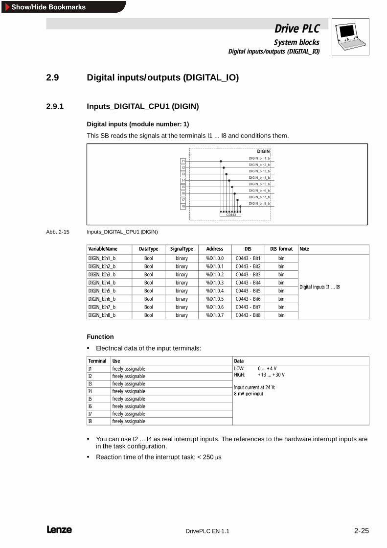
2.9.1 Inputs_DIGITAL_CPU1 (DIGIN)
Digital inputs (module number: 1)
This SB reads the signals at the terminals I1 ... I8 and conditions them.
I1
I2
DIGIN_bIn1_b
DIGIN
C0443
I3
I4
I5
I6
I7
I8
DIGIN_bIn2_b
DIGIN_bIn3_b
DIGIN_bIn4_b
DIGIN_bIn5_b
DIGIN_bIn6_b
DIGIN_bIn7_b
DIGIN_bIn8_b
Abb. 2-15 Inputs_DIGITAL_CPU1 (DIGIN)
VariableName DataType SignalType Address DIS DIS format Note
DIGIN_bIn1_b Bool binary %IX1.0.0 C0443 - Bit1 bin
DIGIN_bIn2_b Bool binary %IX1.0.1 C0443 - Bit2 bin
DIGIN_bIn3_b Bool binary %IX1.0.2 C0443 - Bit3 bin
DIGIN_bIn4_b Bool binary %IX1.0.3 C0443 - Bit4 binDigital inp ts I1 I8
DIGIN_bIn5_b Bool binary %IX1.0.4 C0443 - Bit5 binDigital inputs I1 ... I8
DIGIN_bIn6_b Bool binary %IX1.0.5 C0443 - Bit6 bin
DIGIN_bIn7_b Bool binary %IX1.0.6 C0443 - Bit7 bin
DIGIN_bIn8_b Bool binary %IX1.0.7 C0443 - Bit8 bin
Function
• Electrical data of the input terminals:
Terminal Use DataI1 freely assignable LOW: 0 ... +4 VI2 freely assignable
O 0HIGH: +13 ... +30 V
I3 freely assignableInp t c rrent at 24 V:
I4 freely assignableInput current at 24 V:8 mA per inp t
I5 freely assignable8 mA per input
I6 freely assignableI7 freely assignableI8 freely assignable
• You can use I2 ... I4 as real interrupt inputs. The references to the hardware interrupt inputs arein the task configuration.
• Reaction time of the interrupt task: < 250 µs

Drive PLCSystem blocks
2.9 Digital inputs/outputs (DIGITAL_IO)
2-26 DrivePLC EN 1.1
2.9.2 Outputs_DIGITAL_CPU1 (DIGOUT)
Digital outputs (module number: 1)
This SB conditions the digital signals, and outputs them at terminals O1 ... O4.
O1
O2
DIGOUT_bOut1_b
DIGOUT
O3
O4
DIGOUT_bOut2_b
DIGOUT_bOut3_b
DIGOUT_bOut4_b
C0444
Abb. 2-16 Outputs_DIGITAL_CPU1 (DIGOUT)
VariableName DataType SignalType Address DIS DIS format Note
DIGOUT_bOut1_b Bool binary %QX1.0.0 C0444 - Bit1 bin
DIGOUT_bOut2_b Bool binary %QX1.0.1 C0444 - Bit2 binDigital o tp ts O1 O4
DIGOUT_bOut3_b Bool binary %QX1.0.2 C0444 - Bit3 binDigital outputs O1 ... O4
DIGOUT_bOut4_b Bool binary %QX1.0.3 C0444 - Bit4 bin
Function
• Electrical data of the output terminals:
Terminal Use DataO1 freely assignable LOW: 0 ... +4 V
HIGH 13 30 VO2 freely assignable HIGH: +13 ... +30 V
O3 freely assignable Output current:O4 freely assignable
Output current:max. 1 A per output
Tip!After mains connection all outputs have the defined state: “LOW”

Drive PLCSystem blocks
2.10 Free Codes (FCODE_FreeCodes)
2-27 DrivePLC EN 1.1
2.10 Free Codes (FCODE_FreeCodes)The entire parameter set of Lenze controllers is organized in codes. Its drive parameters can becustomized without any additional programming, just by changing the parameters stored in thecodes.The SB FCODEsupplies a number of free codes which can be assigned directly to the variables usedin the PLC.
Module number: 141
The code value that is entered is converted into the corresponding variable value by a fixed scalingroutine.
F C O D E
F C O D E _ b C 2 5 0 _ bB O O LC 0 2 5 0
C 0 4 7 1
F C O D E _ b C 4 7 1 B i t 0 _ b
F C O D E _ b C 4 7 1 B i t 1 _ b
F C O D E _ b C 4 7 1 B i t 1 _ b
...
D W O R DT O
B I T / B O O L
F C O D E _ n C 4 7 2 _ 1 _ a% T O I N TC 0 4 7 2 / 1
...
F C O D E _ n C 4 7 2 _ 2 0 _ a% T O I N TC 0 4 7 2 / 2 0
F C O D E _ n C 4 7 3 _ 1 _ aI N TC 0 4 7 3 / 1
...
F C O D E _ n C 4 7 3 _ 1 0 _ aC 0 4 7 3 / 1 0 I N T
F C O D E _ d n C 4 7 4 _ 1 _ pD I N TC 0 4 7 4 / 1
...
F C O D E _ d n C 4 7 4 _ 5 _ pC 0 4 7 4 / 5 D I N T
F C O D E _ n C 4 7 5 _ 1 _ vC 0 4 7 5 / 1
F C O D E _ n C 4 7 5 _ 2 _ vC 0 4 7 5 / 2
I N T
I N T
C 0 1 3 5
F C O D E _ b C 1 3 5 B i t 0 _ b
F C O D E _ b C 1 3 5 B i t 1 5 _ b
...1 6 B i t
Abb. 2-17 Free codes (FCODE)
VariableName DataType SignalType Address DIS DIS format Note
FCODE_bC135Bit0_b...FCODE_bC135Bit15_b
Bool...
Bool
binary %IX141.58.0...
%IX141.58.15
- - default = 0
FCODE_bC250_b Bool binary %IX141.13.0 - - default = 0
FCODE_bC471Bit0_b...FCODE_bC471Bit15_b
Bool...
Bool
binary %IX141.14.0...
%IX141.14.15
- - default = 0
FCODE_bC471Bit16_b...FCODE_bC471Bit31_b
Bool...
Bool
binary %IX141.15.0...
%IX141.15.15
- - default = 0
FCODE_nC472_1_a...FCODE_nC472_20_a
Integer...
Integer
analog %IW141.16...
%IW141.35
- - default = 0.00 %C0472/3 = 100.00 %
FCODE_nC473_1_a...FCODE_nC473_10_a
Integer...
Integer
analog %IW141.36...
%IW141.45
- - default = 0C0473/1,2 = 1

Drive PLCSystem blocks
2.10 Free Codes (FCODE_FreeCodes)
2-28 DrivePLC EN 1.1
VariableName NoteDIS formatDISAddressSignalTypeDataType
FCODE_dnC474_1_p Double-integer position %ID141.23 - - default = 0
FCODE_dnC474_2_p Double-integer position %ID141.24 - - default = 0
FCODE_dnC474_3_p Double-integer position %ID141.25 - - default = 0
FCODE_dnC474_4_p Double-integer position %ID141.26 - - default = 0
FCODE_dnC474_5_p Double-integer position %ID141.27 - - default = 0
FCODE_nC475_1_v Integer velocity %IW141.56 - - default = 0
FCODE_nC475_2_v Integer velocity %IW141.57 - - default = 0
Function
• In Abb. 2-17 you will find code names in You can configure these codes. Theirvalues are assigned directly to the corresponding variables.– A fixed scaling routine relates the codes to the variable values.– In the code table, you can find the options that can be set, and the Lenze settings. ( 6-2)
• Example:– You can enter a percentage [%] under C0472/1. This value is assigned to the variables
FCODE_nC472_1_a with the data type “Integer”.
Important
The code C0470 is not available as a system variable. This code occupies the same memory addressas code C0471. The double-word is divided into 4 bytes (C0470/1...4). Code C0470 can be writtento via the keypad/GDC.
Scaling
• % Õ INT
• 100 % 16384

Drive PLCSystem blocks
2.11 System markers (SYSTEM_FLAGS)
2-29 DrivePLC EN 1.1
2.11 System markers (SYSTEM_FLAGS)
Module number: 151
System markers are global variables that are permanently integrated into the run-time system. Theyinclude functions that facilitate the programming.
The following system markers are integrated into the automation system Drive PLC:
VariableName DataType Address Note
SYSTEM_bClock01Hz Bool %IX151.0.0 0.1 Hz System clock
SYSTEM_bClock1Hz Bool %IX151.0.8 1.0 Hz System clock
SYSTEM_bClock10Hz Bool %IX151.1.0 10 Hz System clock
SYSTEM_bClock0100Hz Bool %IX151.1.8 100 Hz System clock
SYSTEM_bTogCycleTask Bool %IX151.2.0 Toggle marker cyclic task
SYSTEM_b1LoopCyclicTask Bool %IX151.2.8 First loop cyclic task
SYSTEM_b1LoopTask2 Bool %IX151.3.0 First loop task ID2
SYSTEM_b1LoopTask3 Bool %IX151.3.8 First loop task ID3
SYSTEM_b1LoopTask4 Bool %IX151.4.0 First loop task ID4
SYSTEM_b1LoopTask5 Bool %IX151.4.8 First loop task ID5
SYSTEM_b1LoopTask6 Bool %IX151.5.0 First loop task ID6
SYSTEM_b1LoopTask7 Bool %IX151.5.8 First loop task ID7
SYSTEM_b1LoopTask8 Bool %IX151.6.0 First loop task ID8
SYSTEM_b1LoopTask9 Bool %IX151.6.8 First loop task ID9
SYSTEM_nTaskInterval Integer %IW151.7 Interval of current task
SYSTEM_nTaskID Integer %IW151.8 ID-number of current task
Tip!The system variables are not generated in simulation mode.
Function
SYSTEM_bClockxHz
• These system markers output a fixed clock with equal pulse/pause ratios.
• The marker is toggled in real time.
• If you use this system marker, take care with the frequency that is used for polling the marker(aliasing effect). You should use at least twice the toggle frequency.
Example:
You would like to use the system marker SYSTEM_bClock100Hz as a clock for a counter. Thepulse/pause ratio is 5 msec/5 msec.
To avoid an aliasing effect, the counter must always be polled with an INTERVAL-TASK <5msec.

Drive PLCSystem blocks
2.11 System markers (SYSTEM_FLAGS)
2-30 DrivePLC EN 1.1
SYSTEM_bTogCycleTask
• This system marker toggles with the cyclical task:1. cycle = FALSE2. cycle = TRUE3. cycle = FALSE4. cycle = TRUEetc.
SYSTEM_nTaskInterval
• This system marker shows the interval for the current task, with a resolution of 250 µsec.– If, for instance, a 10-millisecond task is being processed, the system marker indicates 40
(10 msec = 40 x 250 µsec).– If a different type of task is being processed, instead of an interval task, the system marker
indicates 0.
SYSTEM_nTaskID
• This system marker shows the task-ID for the current task.
SYSTEM_b1LoopCyclicTask/SYSTEM_b1Loop Task X
• These system markers only have the state TRUE during the first cycle of the particular task.– After the first cycle of the specific task, the system variable is set to FALSE.– A change back to the TRUE state will occur after a reset, or a fresh start of the program in
the target system.

Drive PLCSystem blocks - FIF modules
3.1 Standard-I/O
3-1 DrivePLC EN 1.1
3 System blocks - FIF modules(FIF =FunctionInterFace)
3.1 Standard-I/O
The FIF module Standard-I/O extends the Lenze automation system Drive PLC by
• one analog input: Input_ANALOG1_STDIO (AIN1_STDIO)
• one analog output: Output_ANALOG1_STDIO (AOUT1_STDIO)
• five digital inputs: Inputs_DIGITAL_STDIO (DIGIN_STDIO)
• one digital output: Output_DIGITAL_STDIO (DIGOUT_STDIO)
Tip!Observe the installation kit of the FIF module Standard-I/O!
3.1.1 Analog inputs/outputs Standard-I/O (ANALOG_IO_STDIO)
3.1.1.1 Input_ANALOG1_STDIO (AIN1_STDIO)
Analog input standard I/O (module number: 200)
This SB forms the interface for analog signals via terminal 8 of the FIF module Standard-I/O assetpoint input or actual value input.
E1
E2
DIGIN_bIn1_FIFSTDIO_b
DIGIN_STDIO
C0477
E3
E4
28
DIGIN_bIn2_FIFSTDIO_b
DIGIN_bIn3_FIFSTDIO_b
DIGIN_bIn4_FIFSTDIO_b
DIGIN_bIn28_FIFSTDIO_b
Abb. 3-1 Input_ANALOG1_STDIO (AIN1_STDIO)
VariableName DataType SignalType Address DIS DIS format Note
AIN1_nIn_FIFSTDIO_a Integer analog %IW200.0 C0481 dec [%] Analog input 1Standard-I/O

Drive PLCSystem blocks - FIF modules
3.1 Standard-I/O
3-2 DrivePLC EN 1.1
Function
By suitable switch settings at the FIF module Standard-I/O and in code C0480, the following inputsignals can be processed:
Signal at terminal 8(L d f lt tti i b ld i t)
Switch setting C0480S g a at te a 8(Lenze default setting in bold print) 1 2 3 4 5
C0 80
0 ... +5 V OFF OFF ON OFF OFF 00 ... +10 V OFF OFF ON OFF ON 0-10 ... +10 V OFF OFF ON ON OFF 00 ... +20 mA OFF OFF ON ON OFF 1+4 ... +20 mA OFF OFF ON ON OFF 3+4 ... +20 mA (wire breakage monitoring) ON ON OFF OFF OFF 2
Electrical data of the input terminals:
Terminal Use Level(Lenze default setting in bold print)
Data
8 Analog input 1 0 ... +5 V0 ... +10 V-10 ... +10 V0 ... +20 mA+4 ... +20 mA+4 ... +20 mA (wire breakage monitoring)
Resolution: 10 bitLinearity error: ±0.5 %Temperature error: ±0.3 % (0 ... 60 °C)Input resistance:• Voltage signal: > 50 kΩ• Current signal: 250 Ω
7 GND1, reference potentialfor analog signals
- -
3.1.1.2 Output_ANALOG1_STDIO (AOUT1_STDIO)
Analog output standard I/O (module number: 200)
This SB can be used as a monitor output. Internal signals can be given out as voltage signals viaterminal 62 of the FIF module Standard-I/O and used, e.g. as display or setpoint values for followingdrives.
62AOUT1_nOut_FIFSTDIO_a
AOUT1_STDIO
C04847
Abb. 3-2 Output_ANALOG1_STDIO (AOUT1_STDIO)
VariableName DataType SignalType Address DIS DIS format Note
AOUT1_nOut_FIFSTDIO_a Integer analog %QW200.0 C0484 dec [%] Analog output 1Standard-I/O
Function
A voltage of 10 V is given out at terminal 62 of the FIF module Standard-I/O if the signalatAOUT1_nOut_STDIO_a = 16384 = 100 %
Electrical data of the output terminals:
Terminal Use Level Data62 Analog output 1 0 ... +10 V Resolution: 10 bit
Linearity error: ±0.5 %Temperature error: ±0.3 % (0 ... 60 °C)Load capacity: max. 2 mA
7 GND1, reference potentialfor analog signals
- -

Drive PLCSystem blocks - FIF modules
3.1 Standard-I/O
3-3 DrivePLC EN 1.1
3.1.2 Digital inputs/outputs Standard-I/O (DIGITAL_IO_STDIO)
3.1.2.1 Inputs_DIGITAL_STDIO (DIGIN_STDIO)
Digital inputs standard I/O (module number: 200)
This SB reads the signals at terminals E1 ... E4, 28 of the FIF module Standard-I/O and conditionsthem.
E1
E2
DIGIN_bIn1_FIFSTDIO_b
DIGIN_STDIO
C0447
E3
E4
28
DIGIN_bIn2_FIFSTDIO_b
DIGIN_bIn3_FIFSTDIO_b
DIGIN_bIn4_FIFSTDIO_b
DIGIN_bIn28_FIFSTDIO_b
Abb. 3-3 Inputs_DIGITAL_STDIO (DIGIN_STDIO)
VariableName DataType SignalType Address DIS DIS format Note
DIGIN_bIn1_FIFSTDIO_b Bool binary %IX200.0.0 C0477 - Bit1 bin
DIGIN_bIn2_FIFSTDIO_b Bool binary %IX200.0.1 C0477 - Bit2 bin
DIGIN_bIn3_FIFSTDIO_b Bool binary %IX200.0.2 C0477 - Bit3 bin
DIGIN_bIn4_FIFSTDIO_b Bool binary %IX200.0.3 C0477 - Bit4 bin
DIGIN_bIn28_FIFSTDIO_b Bool binary %IX200.0.4 C0477 - Bit5 bin
Electrical data of the input terminals:
Terminal Use DataE1 freely assignable Input resistance: 3.3 kΩE2 freely assignable
pu es s a ce 3 30 = LOW: 0 ... +3 V1 HIGH: 12 30 VE3 freely assignable 1 = HIGH: +12 ... +30 V(PLC level HTL)
E4 freely assignable(PLC level, HTL)
28 freely assignable

Drive PLCSystem blocks - FIF modules
3.1 Standard-I/O
3-4 DrivePLC EN 1.1
3.1.2.2 Output_DIGITAL_STDIO (DIGOUT_STDIO)
Digital output standard I/O (module number: 200)
This SB conditions a digital signals and transmits it to terminal A1 of the FIF module Standard-I/O.
A1
DIGOUT_STDIO
DIGOUT_bOut1_FIFSTDIO_b
C0479
Abb. 3-4 Outputs_DIGITAL_STDIO (DIGOUT_STDIO)
VariableName DataType SignalType Address DIS DIS format Note
DIGOUT_bOut1_FIFSTDIO_b Bool binary %QX200.0.0 C0479 - Bit1 bin
Electrical data of the output terminal
Terminal Use DataA1 freely assignable Output voltage:
• 0/+20 V with DC internal• 0/+24 V with DC externalOutput current:• 10 mA with DC internal• 50 mA with DC external

Drive PLCSystem blocks - Internal extension modules
4.1 Extension Board 1
4-1 DrivePLC EN 1.1
4 System blocks - internal extensions modules
4.1 Extension Board 1
The internal extension board Extension Board 1 extends the Lenze automation system Drive PLCby
• 6 digital inputs: Inputs_DIGITAL_EB1 (DIGIN_EB1)
• 6 digital outputs: Outputs_DIGITAL_EB1 (DIGOUT_EB1)
4.1.1 Digital inputs/outputs Extension Board 1 (DIGITAL_IO_EB1)
4.1.1.1 Inputs_DIGITAL_EB1 (DIGIN_EB1)
Digital inputs Extension Board 1 (module number: 2)
This SB reads the signals at the terminals I9 ... I14 of the Extension Board 1 and conditions them.
I9
I10
DIGIN_bIn9_b
DIGIN_EB1
C0446
I11
I12
I13
I14
DIGIN_bIn10_b
DIGIN_bIn11_b
DIGIN_bIn12_b
DIGIN_bIn13_b
DIGIN_bIn14_b
Abb. 4-1 Inputs_DIGITAL_EB1 (DIGIN_EB1)
VariableName DataType SignalType Address DIS DIS format Note
DIGIN_bIn9_b Bool binary %IX2.0.0 C0446-Bit1 bin
DIGIN_bIn10_b Bool binary %IX2.0.1 C0446-Bit2 bin
DIGIN_bIn11_b Bool binary %IX2.0.2 C0446-Bit3 bin
DIGIN_bIn12_b Bool binary %IX2.0.3 C0446-Bit4 bin
DIGIN_bIn13_b Bool binary %IX2.0.4 C0446-Bit5 bin
DIGIN_bIn14_b Bool binary %IX2.0.5 C0446-Bit6 bin
Electrical data of the input terminals
Terminal Use DataI9 freely assignable LOW: 0 V ... +4 VI10 freely assignable
O 0HIGH: +13 V ... +30 V
I11 freely assignableInp t c rrent at 24 V:
I12 freely assignableInput current at 24 V:8 mA per inp t
I13 freely assignable8 mA per input
I14 freely assignable

Drive PLCSystem blocks - Internal extension modules
4.1 Extension Board 1
4-2 DrivePLC EN 1.1
4.1.1.2 Outputs_DIGITAL_EB1 (DIGOUT_EB1)
Digital outputs Extension Board 1 (module number: 2)
This SB conditions the digital signals, and outputs them at terminals O5 ... O10 Extension Board1.
O5
O6
DIGOUT_bOut5_b
DIGOUT_EB1
O7
O8
DIGOUT_bOut6_b
DIGOUT_bOut7_b
DIGOUT_bOut8_b
O9
O10
DIGOUT_bOut9_b
DIGOUT_bOut10_b
C0448
Abb. 4-2 Outputs_DIGITAL_EB1 (DIGOUT_EB1)
VariableName DataType SignalType Address DIS DIS format Note
DIGOUT_bOut5_b Bool binary %QX2.0.0 C0448-Bit1 bin
DIGOUT_bOut6_b Bool binary %QX2.0.1 C0448-Bit2 bin
DIGOUT_bOut7_b Bool binary %QX2.0.2 C0448-Bit3 bin
DIGOUT_bOut8_b Bool binary %QX2.0.3 C0448-Bit4 bin
DIGOUT_bOut9_b Bool binary %QX2.0.4 C0448-Bit5 bin
DIGOUT_bOut10_b Bool binary %QX2.0.5 C0448-Bit6 bin
Electrical data of the output terminals
Terminal Use (Lenze setting in bold print) DataO5 freely assignableO6 freely assignable LOW: 0 V ... +4 V
HIGH: 13 V 30 VO7 freely assignable HIGH: +13 V ... +30 V
O8 freely assignable O tp t c rrent:O9 freely assignable
Output current:max. 1 A per output
O10 freely assignablemax. 1 A per output

Drive PLCSystem blocks - Internal extension modules
4.2 Extension Board 2
4-3 DrivePLC EN 1.1
4.2 Extension Board 2The internal extension board Extension Board 2 extends the Lenze automation system Drive PLCby• 14 digital inputs: Inputs_DIGITAL_EB2 (DIGIN_EB2)
• 8 digital outputs: Outputs_DIGITAL_EB2 (DIGOUT_EB2)
4.2.1 Digital inputs/outputs Extension Board 2 (DIGITAL_IO_EB2)
4.2.1.1 Inputs_DIGITAL_EB2 (DIGIN_EB2)
Digital inputs Extension Board 2 (module number: 3)
This SB reads the signals at terminals I9 ... I22 of the Extension Board 2 and conditions them.
I9
I10
DIGIN_bIn9_b
DIGIN_EB2
C0446/1Bit 1 … Bit 8
I11
I12
I13
I14
DIGIN_bIn10_b
DIGIN_bIn11_b
DIGIN_bIn12_b
DIGIN_bIn13_b
DIGIN_bIn14_b
I15
I16
DIGIN_bIn15_b
I17
I18
I19
I21
I20
I22
DIGIN_bIn16_b
DIGIN_bIn17_b
DIGIN_bIn18_b
DIGIN_bIn19_b
DIGIN_bIn21_b
DIGIN_bIn20_b
DIGIN_bIn22_b
C0446/2Bit 1 … Bit 6
Abb. 4-3 Inputs_DIGITAL_EB2 (DIGIN_EB2)
VariableName DataType SignalType Address DIS DIS format Note
DIGIN_bIn9_b Bool binary %IX3.0.0 C0446/1-Bit1 bin
DIGIN_bIn10_b Bool binary %IX3.0.1 C0446/1-Bit 2 bin
DIGIN_bIn11_b Bool binary %IX3.0.2 C0446/1-Bit 3 bin
DIGIN_bIn12_b Bool binary %IX3.0.3 C0446/1-Bit 4 bin
DIGIN_bIn13_b Bool binary %IX3.0.4 C0446/1-Bit 5 bin
DIGIN_bIn14_b Bool binary %IX3.0.5 C0446/1-Bit 6 bin
DIGIN_bIn15_b Bool binary %IX3.0.6 C0446/1-Bit 7 bin
DIGIN_bIn16_b Bool binary %IX3.0.7 C0446/1-Bit 8 bin
DIGIN_bIn17_b Bool binary %IX3.0.8 C0446/2-Bit 1 bin
DIGIN_bIn18_b Bool binary %IX3.0.9 C0446/2-Bit 2 bin
DIGIN_bIn19_b Bool binary %IX3.0.10 C0446/2-Bit 3 bin
DIGIN_bIn20_b Bool binary %IX3.0.11 C0446/2-Bit 4 bin
DIGIN_bIn21_b Bool binary %IX3.0.12 C0446/2-Bit 5 bin
DIGIN_bIn22_b Bool binary %IX3.0.13 C0446/2-Bit 6 bin
Electrical data of the input terminals
Terminal Use DataI9 LOW: 0 V ... +4 V
HIGH 13 V 30 V...freely assignable
HIGH: +13 V ... +30 V
...freely assignable
Input current at 24 V:I22
Input current at 24 V:8 mA per input

Drive PLCSystem blocks - Internal extension modules
4.2 Extension Board 2
4-4 DrivePLC EN 1.1
4.2.1.2 Outputs_DIGITAL_EB2 (DIGOUT_EB2)
Digital inputs Extension Board 2 (module number: 3)
This SB conditions the digital signals, and outputs them at terminals O5 ... O12 Extension Board 2
O5
O6
DIGOUT_bOut5_b
DIGOUT_EB2
O7
O8
DIGOUT_bOut6_b
DIGOUT_bOut7_b
DIGOUT_bOut8_b
O9
O11
O10
O12
DIGOUT_bOut9_b
DIGOUT_bOut11_b
DIGOUT_bOut10_b
DIGOUT_bOut12_b
C0448
Abb. 4-4 Outputs_DIGITAL_EB2 (DIGOUT_EB2)
VariableName DataType SignalType Address DIS DIS format Note
DIGOUT_bOut5_b Bool binary %QX3.0.0 C0448-Bit1 bin
DIGOUT_bOut6_b Bool binary %QX3.0.1 C0448-Bit2 bin
DIGOUT_bOut7_b Bool binary %QX3.0.2 C0448-Bit3 bin
DIGOUT_bOut8_b Bool binary %QX3.0.3 C0448-Bit4 bin
DIGOUT_bOut9_b Bool binary %QX3.0.4 C0448-Bit5 bin
DIGOUT_bOut10_b Bool binary %QX3.0.5 C0448-Bit6 bin
DIGOUT_bOut11_b Bool binary %QX3.0.6 C0448-Bit7 bin
DIGOUT_bOut12_b Bool binary %QX3.0.7 C0448-Bit8 bin
Electrical data of the output terminals
Terminal Use DataO5 LOW: 0 V ... +4 V
HIGH 13 V 30 V..freely assignable
HIGH: +13 V ... +30 V
..freely assignable
Output current:O12
Output current:max. 1 A per output

Drive PLCSystem blocks - Internal extension modules
4.3 Extension Board 3
4-5 DrivePLC EN 1.1
4.3 Extension Board 3
The internal extension board Extension Board 3 extends the Lenze automation system Drive PLCby
• 6 digital inputs: Inputs_DIGITAL_EB3 (DIGIN_EB3)
• 6 digital outputs: Outputs_DIGITAL_EB3 (DIGOUT_EB3)
• 1 encoder input
• 2 analog inputs
4.3.1 Digital inputs/outputs Extension Board 3 (DIGITAL_IO_EB3)
4.3.1.1 Inputs_DIGITAL_EB3 (DIGIN_EB3)
Digital inputs Extension Board 3 (module number: 4)
This SB reads the signals at terminals I9 ... I16 of the Extension Board 3 and conditions them.
I9
I10
DIGIN_bIn9_b
DIGIN_EB3
C0446
I11
I12
I13
I14
DIGIN_bIn10_b
DIGIN_bIn11_b
DIGIN_bIn12_b
DIGIN_bIn13_b
DIGIN_bIn14_b
I15
I16
DIGIN_bIn15_b
DIGIN_bIn16_b
Abb. 4-5 Inputs_DIGITAL_EB3 (DIGIN_EB3)
VariableName DataType SignalType Address DIS DIS format Note
DIGIN_bIn9_b Bool binary %IX4.0.0 C0446-Bit1 bin
DIGIN_bIn10_b Bool binary %IX4.0.1 C0446-Bit2 bin
DIGIN_bIn11_b Bool binary %IX4.0.2 C0446-Bit3 bin
DIGIN_bIn12_b Bool binary %IX4.0.3 C0446-Bit4 bin
DIGIN_bIn13_b Bool binary %IX4.0.4 C0446-Bit5 bin
DIGIN_bIn14_b Bool binary %IX4.0.5 C0446-Bit6 bin
DIGIN_bIn15_b Bool binary %IX4.0.6 C0446-Bit7 bin
DIGIN_bIn16_b Bool binary %IX4.0.7 C0446-Bit8 bin
Electrical data of the input terminals
Terminal Use DataI9 LOW: 0 V ... +4 V
HIGH 13 V 30 V..freely assignable
HIGH: +13 V ... +30 V
..freely assignable
Input current at 24 V:I16
Input current at 24 V:8 mA per input

Drive PLCSystem blocks - Internal extension modules
4.3 Extension Board 3
4-6 DrivePLC EN 1.1
4.3.1.2 Outputs_DIGITAL_EB3 (DIGOUT_EB3)
Digital inputs Extension Board 3 (module number: 4)
This SB conditions the digital signals, and outputs them at terminals O5 ... O8 Extension Board 3.
O5
O6
DIGOUT_bOut5_b
DIGOUT_EB3
O7
O8
DIGOUT_bOut6_b
DIGOUT_bOut7_b
DIGOUT_bOut8_b
C0448
Abb. 4-6 Outputs_DIGITAL_EB3 (DIGOUT_EB3)
VariableName DataType SignalType Address DIS DIS format Note
DIGOUT_bOut5_b Bool binary %QX4.0.0 C0448-Bit1 bin
DIGOUT_bOut6_b Bool binary %QX4.0.1 C0448-Bit2 bin
DIGOUT_bOut7_b Bool binary %QX4.0.2 C0448-Bit3 bin
DIGOUT_bOut8_b Bool binary %QX4.0.3 C0448-Bit4 bin
Electrical data of the output terminals
Terminal Use DataO5 LOW: 0 V ... +4 V
HIGH 13 V 30 VO6freely assignable
HIGH: +13 V ... +30 V
O7freely assignable
Output current:O8
Output current:max. 1 A per output

Drive PLCSystem blocks - Internal extension modules
4.3 Extension Board 3
4-7 DrivePLC EN 1.1
4.3.2 Analog input 4 (ANALOG4_IO_EB3)
4.3.2.1 Inputs_ANALOG4 (AIN4)
Analog input 4 (module number 14)
This SB forms the interface for analog signals via terminal AI4, A⊥.
AI4
A
AIN4_nIn_a
AIN4
Abb. 4-7 Inputs_ANALOG4 (AIN4)
VariableName DataType SignalType Address DIS DIS format Note
AIN4_nIn_a Integer analog %IW14.0 - dec [%] Analog input 4
Terminal assignment
TerminalX2
Use level Data
AI4 Analog input 4 -10 V ... +10 V Resolution: 10 bit + sign±10 V ≡ ±16384 ≡ ±100 %
A⊥ Internal ground, GND - -

Drive PLCSystem blocks - Internal extension modules
4.3 Extension Board 3
4-8 DrivePLC EN 1.1
4.3.3 Analog input 5 (ANALOG5_IO_EB3)
4.3.3.1 Inputs_ANALOG5 (AIN5)
Analog input 5 (module number 15)
This SB forms the interface for analog signals via terminal AI5, A⊥.
AI5
A
AIN5_nIn_a
AIN5
Abb. 4-8 Inputs_ANALOG5 (AIN5)
VariableName DataType SignalType Address DIS DIS format Note
AIN5_nIn_a Integer analog %IW15.0 - - Analog input 5
Terminal assignment
TerminalX2
Use level Data
AI5 Analog input 5 -10 V ... +10 V Resolution: 10 bit + sign±10 V ≡ ±16384 ≡ ±100 %
A⊥ Internal ground, GND - -

Drive PLCSystem blocks - Internal extension modules
4.3 Extension Board 3
4-9 DrivePLC EN 1.1
4.3.4 Encoder input (DFIN_IO_DigitalFrequency)
Module number: 21
This SB can convert and normalize a pulse current at the encoder input X9 into a speed andphase-angle setpoint. The transmission is very precise without offset and gain errors.
C 0 4 2 5
D F _ I ND F I N _ n I n _ v
C 0 4 2 6
X 3
T P / M P- C t r l
C 0 4 2 9C 0 4 2 8
0
1
M P
I 1
D F I N _ b T P R e c e i v e d _ b
D F I N _ d n I n c L a s t S c a n _ p
Abb. 4-9 Encoder input (DFIN_IO)
VariableName DataType SignalType Address DIS DIS format Note
DFIN_nIn_v Integer velocity %IW21.0 C0426 dec [rpm] Value in incr./msec
DFIN_bTPReceived_b Bool binary %IX21.4.0 - -
DFIN_dnIncLastScan_p Double-integer position %ID21.1 - -
Range of functions
• Encoder input X3
• Technical data for the connection of X3
• Touch-probe

Drive PLCSystem blocks - Internal extension modules
4.3 Extension Board 3
4-10 DrivePLC EN 1.1
4.3.4.1 Encoder input X3
• The encoder input X3 is dimensioned for signals with TTL levels.
• You can use C0425 to adapt the drive to the sensor/encoder that is connected or to thepreceding drive controller in the case of digital-frequency cascade or digital-frequency-busoperation.
C0425 Constant in increments per turn0 256 inc/rev1 512 inc/rev2 1024 inc/rev3 2048 inc/rev4 4096 inc/rev5 8192 inc/rev6 16384 inc/rev
• The input of a zero track is optional.
• The process image of SB DFIN_IO is newly created again for each task in which it is applied.
Evaluation of the digital frequency signals (C0427 = 0 (2-phases))
AA
BB
ZZ
Abb. 4-10 Signal sequence with phase shift (CW rotation)
• CW rotation:– Track A leads track B by 90 ° (positive value at DFIN_nIn_v).
• CCW rotation:– Track A lags track B by 90 ° (negative value at DFIN_nIn_v).

Drive PLCSystem blocks - Internal extension modules
4.3 Extension Board 3
4-11 DrivePLC EN 1.1
Transmission function
DFIN_nIn_v f [Hz] ô 60Increments from C0425
ô 214
15000
Example:
Input frequency = 200 kHz
C0425 = 3 (corresponds to 2048 increments/turn)
Solution:
DFIN_nIn_v [rpm] 200000 Hz ô 602048
5859 rpm
Signal adaptation
Finer resolutions can be achieved by adding a following FB (e.g. L_CONV from LenzeDrive.lib).
Example:
nOut_a f [Hz] ô 60Increments from C0425
ô nNumeratornDenominator
ô 214
15000
C 0 4 2 5
D F _ I ND F I N _ n I n _ v
C 0 4 2 6
X 3
T P / M P- C t r l
C 0 4 2 9C 0 4 2 8
0
1
M P
I 1
D F I N _ b T P R e c e i v e d _ b
D F I N _ d n I n c L a s t S c a n _ p
n I n _ a n O u t _ aL _ C O N V
n N u m e r a t o r
n D e n o m i n a t o r
Abb. 4-11 Encoder input (DF_IN) with following FB for normalization

Drive PLCSystem blocks - Internal extension modules
4.3 Extension Board 3
4-12 DrivePLC EN 1.1
4.3.4.2 Connection of incremental encoders to terminal X3
Incremental encoders with TTL level
Stop!Observe connection voltage of the incremental encoder used!
Incremental encoder with TTL levelSignal shape with CW rotation
ó
B
VCC5 _ E
GND
Z
1
2
3
4
5
6
7
8
9
A
X3
l = max. 50 m
0.14 26
1.0
0.14 26
Æ
AWG
17
A
mm2
B
Z
A
A
B
Z
B
Z
• You can connect incremental encoders with two 5V complementary signals shifted by 90°.
Assignment of the Sub-D connector (X3)PIN 1 2 3 4 5 6 7 8 9
Signal B A A Vcc5_E GND Z Z - B
• The connection is as shown in the figures:– Use twisted pair cables and screened pair cables– Connect the screen at both ends– Maintain specified cable cross-sections

Drive PLCSystem blocks - Internal extension modules
4.3 Extension Board 3
4-13 DrivePLC EN 1.1
Incremental encoders with HTL level
Incremental encoder with HTL levelSignal shape with CW rotationSupply voltage for incremental encoder
ó
ì
A
A
B
Z
B
Z
B
GND
Z
1
2
3
4
5
6
7
8
9
A
X3
l = max. 50 m
0.14 26
1.0
0.14
0.14
26
26
Æ
AWG
17
A
mm2
B
Z
+
-
Assignment of the Sub-D connector (X3)PIN 1 2 3 4 5 6 7 8 9
Signal B A A +5 V GND Z Z - B
Tip!You can connect incremental encoders with HTL level that supply signals A and B only, to PIN 2 andPIN 9. The inputs at PIN 3 and PIN 1 must then be connected to the supply voltage of the incrementalencoder.
• The connection is as shown in the figures:– Use twisted pair cables and screened pair cables– Connect the screen at both ends– Maintain specified cable cross-sections

Drive PLCSystem blocks - Internal extension modules
4.3 Extension Board 3
4-14 DrivePLC EN 1.1
4.3.4.3 Touch-Probe (TP)
T P
ϕ D F I N _ d n I n c L a s t S c a n _ p
Abb. 4-12 Function diagram of a TP
Time-equidistant start of an interval-task
ϕ Phase-angle signal
Functional sequence
1. The TP is triggered by a FALSE-TRUE edge at the digital input X5/E5 or by a zero pulse from I1(only if an encoder is attached).– Use C0428 to select whether the TP should be carried out by the MP (marker pulse “zero
pulse from encoder”) or from the X5/E5 input.– Use C0429 to set a delay (unit: incr.) for a TP. This means that the TP/MP-Ctrl has a delayed
response to a TP.– Through C0431 you can set up whether the TP from E5 should be triggered by a rising or
falling edge (0 = rising edge, 1 = falling edge).
2. If a TP has occurred, then DFIN_bTPReceived_b switches immediately = TRUE.
3. After the start of the task, DFIN_dnIncLastScan_p gives the number of increments [inc/msec]that have been counted since the TP.
4. Following, DFIN_bTPReceived_b = FALSE is set.
Tip!It is also necessary that DFIN_nIn_v is processed in the task so that DFIN_bTPReceived_b andDFIN_dnIncLastScan_p can be read.
DFIN_nIn_v
• The value DFIN_nIn_v is scaled in increments per millisecond.(INT) 16384 corresponds to 15000 rpm.
• For every task in which DFIN_nIn_v is used, the operating system creates an individual counterthat is reset after every start of the task.

Drive PLCSystem blocks - Internal extension modules
4.3 Extension Board 3
4-15 DrivePLC EN 1.1
Example (DFIN_nIn_v in a 10 msec task):
• When the 10 msec task starts, the value of the counter is stored in a local area of the taskand the counter is reset. The value in the local area gives an average value in increments per1 msec.
• If a position value is to be derived from this value, then it must be multiplied bySYSTEM_nTaskInterval / 4, to get the result in increments per 10 msec, as in the example.Example: In a 1 msec task, SYSTEM_nTaskInterval has the value 4 (4 * 250 µs = 1 msec)
• For Lenze FBs, this procedure has already been implemented in the FBs.

Drive PLCSystem blocks - Internal extension modules
4.3 Extension Board 3
4-16 DrivePLC EN 1.1

Drive PLCConnection
5-1 DrivePLC EN 1.1
5 Networking
8200DPL001
The production factor ” information” becomes increasingly important for the networking ofproduction plants. This applies particularly to a drive network and automation of decentralizeddrives.
Drives of the Lenze range can easily be networked and implemented into a comprehensiveautomation concept.
The control and parameterization of the devices can be carried out, depending on the task, usingdifferent communication interfaces:
• terminals (analog, digital, digital master-frequency)
• built-in system bus interface (CAN)
• plug-in field module for the following bus systems or communication profiles– RS232/485 LECOM-A/B/LI with or without optical fibres (type 2102)
– INTERBUS (type 2111)– INTERBUS-Loop (type 2112)– PROFIBUS-DP (type 2131 and 2133)
– DeviceNet/CANopen (type 2175)
• plug-in operating module (keypad).
The communication to higher-level hosts is possible via a simple plug&play interface at the front sideof the device.The above figure shows such a communication with fieldbus modules 2133PROFIBUS-DP.
In an existing connection via field bus modules to a higher-level master system the system bus (CAN)can additionally be used for communication between Lenze devices. Time-critical data such assetpoint and actual values, can be exchanged in real-time using the system bus.
Special handling features of the system bus (CAN):
• simple communication
• no special knowledge of bus systems required.

Drive PLCConnection
5-2 DrivePLC EN 1.1
5.1 System bus (CAN) in the Lenze drive system
5.1.1 Contact assignment
GN
DLO
HI
Terminal X4
9300 Servo controller /9300 Servo PLC
CG LO HI CG LO HI
Terminal X3
8200 vector
Terminal X5
Drive PLC
GND LO HI
9300 Servo controller / 9300 Servo PLC
Terminal designation Explanation
GND CAN-GND Ground reference for CAN-bus; with internal series resistance of 100 Ω andmax. load current of 30 mA
LO CAN-LOW System bus LOW
HI CAN-HIGH System bus HIGH
8200 vector / Drive PLC
Terminal designation ExplanationCG (:8200 vector)GND (:Drive PLC)
CAN-GND System bus ground reference with internal series resistor 100 Ω,max. current load 30 mA
LO CAN-LOW System bus LOW (data line)HI CAN-HIGH System bus HIGH (data line)

Drive PLCConnection
5-3 DrivePLC EN 1.1
5.1.2 Wiring of the system bus
Basic structure shown at a Drive PLC with 8200 vector
plc014
Drive PLC Controller 1 Controller 2
GND LOW HI GG LO HI GG LO HI GG LO HI GG LO
120120
HI
PES PES
Abb. 5-1 Basic structure of a system bus network
Comments on wiring
We recommend the following signal cable for the wiring:
Specification system bus cable Total length up to 300 m Total length up to 1000 m
Cable type LIYCY 2 x 2 x 0.5 mm2
(twisted pairs, with screening)CYPIMF 2 x 2 x 0.5 mm2
(twisted pairs, with screening)
Cable resistance ≤ 40 Ω/km ≤ 40 Ω/km
Capacitance per unit length ≤ 130 nF/km ≤ 60 nF/km
Connection Pair 1 (white/brown): LO and HIPair 2 (green/yellow): GND
Tab. 5-1 Specification of the system bus cable
Tip!• A terminating resistor of R = 120Ω must be connected to the first and last physically
connected device (see Abb. 5-1).
• Connect cable screen over a large surface to PE potential (PES).

Drive PLCConnection
5-4 DrivePLC EN 1.1
5.1.2.1 System bus wiring complying to EMC
K 1
K 1
L 3
N
P E
L 1L 2
U V W
L 1 L 2 L 3
F 1
9 3 2 X - 9 3 3 X
P E + U G - U G
P E
Z 1
K 1
U V W
L 1 L 2 L 3
9 3 2 X - 9 3 3 X
P E + U G - U G
P E
Z 1
F 1
O N
O F F
2 8 A 4P E2 8 A 4
R F R
P E U V W
L 1 L 2 L 3
9 3 2 X - 9 3 3 X
P E + U G - U G
P E
Z 1
F 1
2 8 A 4P E
R F R R F R
G N DH I L O G N DH I L O
R A 2
G N DH I L O
R A 1
F 2 F 3 F 2 F 3 F 2 F 3
7 7 7
9300PLC123
1. Every device in the system bus must have a good PE connection.
2. Control cabinets, which include bus devices should be interconnected by a separateequipotential bonding cable.
3. Motor cables should be screened; connect the screen to both ends:– at the motor– at the controller.
Attach the screen using the supplied clamps to the screen sheet or to the conductingmounting plate of the control cabinet. This means that the cable is stripped in the contactarea of the clamp thus providing a large-surface contact to the clamp and to PE.
4. Select system bus cables according to the specification in the Tab. 5-1.– Connect the screen at both ends.– Attach using the supplied screen plate:
K35.0021
Strip cable in the contact area of the clamp and make a large-surface contact to the clampand to PE.
5. Connect terminating resistor RA = 120Ω at the physical bus ends.
6. Separate control and fieldbus cables from the motor cable!
7. The CAN-GND cable must also be separated from the motor cable.
8. Connect terminal 7 with the screen plate of the controller.
9. Avoid stubs

Drive PLCConnection
5-5 DrivePLC EN 1.1
5.1.3 Technical data
5.1.3.1 General data of the system bus network
Communication media DIN ISO 11898
Baud rate [kBit/s] • 50• 125• 250• 500• 1000
5.1.3.2 Feasible bus length
Depending on the data-transmission speed, the following bus lengths are possible:
Baud rate [kBit/s] 50 125 250 500 1000
Cable length [m] 1000 550 250 120 25
5.1.3.3 Communication times
The communication times for the system bus depend on
• the priority of the data
• the loading of the bus
• the data-transmission speed
• the processing time in the drive controller
Telegram throughput times
The telegram throughput time for 8 bytes of user data depends on the data-transmission speed:
Baud rate [kBit/s] 50 125 250 500 1000
Telegram throughput time[msec]
2.7 1.05 0.52 0.26 0.13
Processing times in a LENZE controller
• Parameter: typically 30...50 msec
• Process data: 1...2 msec

Drive PLCConnection
5-6 DrivePLC EN 1.1
5.1.4 Commissioning
1. Switch on the controller or PLC (main supply or external 24 V supply).
2. If necessary, change the transmission speed (C0351) using the operating module 9371 BB orthe PC (default setting 500 kBaud).– This setting must be identical for all participating bus devices.
3. Set the CAN address (C0350) using the operating module 9371BB or the PC ( 5-32)
– This CAN address must be unique for every bus device.A multiple assignment of the sameaddress results in a BUS-OFF (error code CE4, error number 65; see chapter Monitoring( LEERER MERKER) and chapter Error messages ( 6-12)).The default setting of the controllers is C0350 = 1.
4. The communication of all devices connected to the system bus is possible now. You can readall codes and change all codes which can be written.
5.1.5 Programming
5.1.5.1 General
The integrated system bus provides a considerable extension of the bus device functionality. Theseare, among others:
• Parameter entries
• Data exchange between drive controllers
The connection of other modules is easily possible. These are, among others:
• decentralized terminals
• controls and input devices
• external controls and control systems
The user can, for example, implement an exchange of data between one drive controller and another,with digital control, speed and torque signals, without having knowledge of the bus system.
A total of 5 input signals and 5 output channels are available for data communication, that can all beused independently.They include 2 parameter channels (SDO = Service Data Object).

Drive PLCConnection
5-7 DrivePLC EN 1.1
5.1.5.2 Parameter channels
Parameters are values that are stored in the Lenze drive controllers in a code position. Parametersare set, for example, for one-off system settings or a change of materials in a machine.
Parameter are transmitted with a low priority.
Parameter channel 2Parameter channel 1
write
readread
write
Parameters(Code)
Parameters(Code)
HMI PC
Abb. 5-2 Connection of devices through two parameter channels
With 2 parameter channels it is possible to connect of 2 different devices for parameter setting, e.g.the simultaneous connection of a PC and an operating unit (see Abb. 5-2).
Tip for 9300 Servo PLC!The blocksL_ParRead / L_ParWrite (from: LenzeDrive.lib) read and write access to other Lenzedevices is possible.

Drive PLCConnection
5-8 DrivePLC EN 1.1
5.1.5.3 Process data channels
Process data are data with a high priority, and are optimised for high speed in transmission andprocessing.
A cyclic process data channel CAN1_IO (PDO = Process Data Objekt)
The process data via CAN1_IO are intended for a higher-level control system.
Cyclic process dataProcess data channel 1
(Setpoint and actual values)
CAN1_IN
CAN1_OUT
Control system
Abb. 5-3 Process data CAN1_IO for a higher-level control system

Drive PLCConnection
5-9 DrivePLC EN 1.1
Two event-controlled process data channels with selectable and adjustable cycles(PDOs)CAN2_IO, CAN3_IO
These process data channels are intended for exchanging data between one drive controller andanother. Another application of these process data is for decentralised input and output terminal.Higher-level control systems can also use these channels.
Event-controlled process dataProcess data channel 2
CAN2_OUT
CAN2_IN
CAN3_OUT CAN3_IN
Event-controlled process dataProcess data channel 3
CAN2_IN
CAN2_OUT
Abb. 5-4 Event-controlled process data channels with adjustable cycles
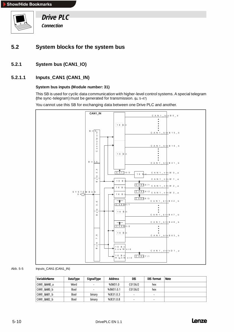
Drive PLCConnection
5-10 DrivePLC EN 1.1
5.2 System blocks for the system bus
5.2.1 System bus (CAN1_IO)
5.2.1.1 Inputs_CAN1 (CAN1_IN)
System bus inputs (Module number: 31)
This SB is used for cyclic data communication with higher-level control systems. A special telegram(the sync-telegram) must be generated for transmission. ( 5-47)
You cannot use this SB for exchanging data between one Drive PLC and another.
1 6 B i t
1 6 B i t
1 6 B i tL o w W o r d
1 6 B i tH i g h W o r d
1 6 B i tC A N 1 _ n I n W 1 _ a
C A N 1 _ b I n B 3 2 _ b
C A N 1 _ d n I n D 1 _ p
Byte 3,4
Byte 5,6
Byte 7,8
S Y S T E M B U SX 4
B i t 0
B i t 1 5
Controlword
C 0 8 6 7 / 1
C 0 8 6 6 / 1
C 0 8 6 6 / 2
C 0 8 6 3 / 1
C 0 8 6 3 / 2
C 0 8 6 6 / 3
C A N 1 _ n I n W 2 _ a
C A N 1 _ n I n W 3 _ a
C A N 1 _ b I n B 4 7 _ b
C A N 1 _ b I n B 4 8 _ b
C A N 1 _ b I n B 6 3 _ b
C 0 1 3 6 / 2
C A N 1 _ b I n B 0 _ bC A N 1 _ I N
C A N 1 _ b I n B 1 6 _ b
C A N 1 _ b I n B 1 5 _ b
C A N 1 _ b I n B 3 1 _ b
1 6 B i t
1 6 B i tC A N 1 _ n I n W 0 _ a
1 6 B i t
1 6 B i t
1 6 B i t
Abb. 5-5 Inputs_CAN1 (CAN1_IN)
VariableName DataType SignalType Address DIS DIS format Note
CAN1_bInW0_a Word - %IW31.0 C0136/2 hex
CAN1_bInB0_b Bool - %IW31.0.1 C0136/2 hex
CAN1_bInB1_b Bool binary %IX31.0.3 - -
CAN1_bInB2_b Bool binary %IX31.0.8 - -

Drive PLCConnection
5-11 DrivePLC EN 1.1
VariableName NoteDIS formatDISAddressSignalTypeDataType
CAN1_bInB17_b Bool binary %IX31.0.9 - -
CAN1_bInB18_b Bool binary %IX31.0.10 - -
CAN1_bInB19_b Bool binary %IX31.0.11 - -
CAN1_bInB20_b Bool binary %IX31.0.0 C0136/2 bin
CAN1_bInB21_b Bool binary %IX31.0.1 C0136/2 bin
CAN1_bInB22_b Bool binary %IX31.0.2 C0136/2 bin
CAN1_bInB23_b Bool binary %IX31.0.3 C0136/2 bin
CAN1_bInB24_b Bool binary %IX31.0.4 C0136/2 bin
CAN1_bInB25_b Bool binary %IX31.0.5 C0136/2 bin
CAN1_bInB26_b Bool binary %IX31.0.6 C0136/2 bin
CAN1_bInB27_b Bool binary %IX31.0.7 C0136/2 bin
CAN1_bInB28_b Bool binary %IX31.0.12 C0136/2 bin
CAN1_bInB29_b Bool binary %IX31.0.13 C0136/2 bin
CAN1_bInB30_b Bool binary %IX31.0.14 C0136/2 bin
CAN1_bInB31_b Bool binary %IX31.0.15 C0136/2 bin
CAN1_nInW1_a Integer analog %IW31.1 C0866/1 dec [%] +16384 = +100 %
CAN1_nInW2_a Integer analog %IW31.2 C0866/2 dec [%] +16384 = +100 %
CAN1_nInW3_a Integer analog %IW31.3 C0866/3 dec [%] +16384 = +100 %
CAN1_bInB0_b Bool binary %IX31.2.0 C0863/1 hex
CAN1_bInB1_b Bool binary %IX31.2.1 C0863/1 hex
CAN1_bInB2_b Bool binary %IX31.2.2 C0863/1 hex
CAN1_bInB3_b Bool binary %IX31.2.3 C0863/1 hex
CAN1_bInB4_b Bool binary %IX31.2.4 C0863/1 hex
CAN1_bInB5_b Bool binary %IX31.2.5 C0863/1 hex
CAN1_bInB6_b Bool binary %IX31.2.6 C0863/1 hex
CAN1_bInB7_b Bool binary %IX31.2.7 C0863/1 hex
CAN1_bInB8_b Bool binary %IX31.2.8 C0863/1 hex
CAN1_bInB9_b Bool binary %IX31.2.9 C0863/1 hex
CAN1_bInB10_b Bool binary %IX31.2.10 C0863/1 hex
CAN1_bInB11_b Bool binary %IX31.2.11 C0863/1 hex
CAN1_bInB12_b Bool binary %IX31.2.12 C0863/1 hex
CAN1_bInB13_b Bool binary %IX31.2.13 C0863/1 hex
CAN1_bInB14_b Bool binary %IX31.2.14 C0863/1 hex
CAN1_bInB15_b Bool binary %IX31.2.15 C0863/1 hex
CAN1_bInB16_b Bool binary %IX31.3.0 C0863/2 hex
CAN1_bInB17_b Bool binary %IX31.3.1 C0863/2 hex
CAN1_bInB18_b Bool binary %IX31.3.2 C0863/2 hex
CAN1_bInB19_b Bool binary %IX31.3.3 C0863/2 hex
CAN1_bInB20_b Bool binary %IX31.3.4 C0863/2 hex
CAN1_bInB21_b Bool binary %IX31.3.5 C0863/2 hex
CAN1_bInB22_b Bool binary %IX31.3.6 C0863/2 hex
CAN1_bInB23_b Bool binary %IX31.3.7 C0863/2 hex
CAN1_bInB24_b Bool binary %IX31.3.8 C0863/2 hex
CAN1_bInB25_b Bool binary %IX31.3.9 C0863/2 hex
CAN1_bInB26_b Bool binary %IX31.3.10 C0863/2 hex
CAN1_bInB27_b Bool binary %IX31.3.11 C0863/2 hex
CAN1_bInB28_b Bool binary %IX31.3.12 C0863/2 hex
CAN1_bInB29_b Bool binary %IX31.3.13 C0863/2 hex
CAN1_bInB30_b Bool binary %IX31.3.14 C0863/2 hex

Drive PLCConnection
5-12 DrivePLC EN 1.1
VariableName NoteDIS formatDISAddressSignalTypeDataType
CAN1_bInB31_b Bool binary %IX31.3.15 C0863/2 hex
CAN1_dnInD1_p Double-integer position %ID31.1 C0867/1 dec [inc] 65536 = 1 revolution
Function
8 bytes are available for data communication with the drive controller.
Control word (byte 1, 2)
The device-internal control word is fixed to bytes 1-2. You can apply any boolean variable to aselection of the free binary/logic signals of the control word.
The signals for the functions Quickstop (QSP), DISABLE, CINH, TRIP-SET and TRIP-RESET can bewritten to the SB DCTRL via the control word. To do this, connect the variables CAN1_wDctrlCtrl andDCTRL_wCAN1Ctrl .
These functions are also available through the variable CAN1_bCtrlQuickstop_b,CAN1_bCtrlDisable_b, CAN1_bCtrlCInhibit_b, CAN1_bCtrlTripSet_b and CAN1_bCtrlTripReset_b:You can read out these signals and apply further processing to them.
The other 11 bits can be used to control further function blocks.
Bytes 3 and 4
Bytes 3-4 can be selected as a 16-bit data word with the individual signals for quasi-analog signals.
Bytes 5-6 and bytes 7-8
Bytes 5-6 and bytes 7-8 can be used simultaneously as two quasi-analog values and as phase-angleinformation, with up to 32 bits of binary information (value 1 or 0). The functional assignment is madethrough variables of the appropriate data type.

Drive PLCConnection
5-13 DrivePLC EN 1.1
5.2.1.2 Outputs_CAN1 (CAN1_OUT)
System bus outputs (Module number: 31)
This SB is used for data communication with higher-level control systems. A special telegram, thesync-telegram, must be generated for transmission. ( 5-47)
You cannot use this SB for exchanging data between one Drive PLC and another.
C A N 1 _ O U T
Byte 1,2
Byte 7,8
Byte 5,6
S y s t e m b u s
Byte 3,4
C A N 1 _ d n O u t D 1 _ p
1 6 B i tL o w W o r d
1 6 B i tH i g h W o r d
1 6 B i tL o w W o r d
1 6 B i tH i g h W o r d
C 0 8 6 9 / 1
C A N 1 _ n O u t W 1 _ a
C 0 8 6 8 / 1C A N 1 _ n O u t W 2 _ a
C A N 1 _ n O u t W 3 _ aC 0 8 6 8 / 2
C 0 8 6 8 / 3
C A N 1 _ b F D O 3 2 _ b
C A N 1 _ b F D O 4 7 _ b
...
C A N 1 _ b F D O 4 8 _ b
C A N 1 _ b F D O 6 3 _ b...
C A N 1 _ n O u t W 0 _ a
C A N 1 _ n F D O 0 _ b
C A N 1 _ b F D O 3 1 _ b
1 6 B i tL o w W o r d
1 6 B i tH i g h W o r d
C A N 1 _ n F D O 1 5 _ b
C A N 1 _ n F D O 1 6 _ b
Abb. 5-6 Outputs_CAN1 (CAN1-OUT)
VariableName DataType SignalType Address DIS DIS format Note
CAN1_nOutW0_a %QW31.0 - -
CAN1_nOutW1_aInteger analog
%QW31.1 C0868/1+100 % +16384
CAN1_nOutW2_aInteger analog
%QW31.2 C0868/2 dec [%]+100 % = +16384
CAN1_nOutW3_a %QW31.3 C0868/3dec [%]
CAN1_bFDO0_b %QX31.0.0
.. ..
CAN1_bFDO15_b %QX31.0.15
CAN1_bFDO16_b %QX31.1.0
.. ..
CAN1_bFDO31_bBool binary
%QX31.1.15hex Display code in hex as
CAN1_bFDO32_bBool binary
%QX31.2.0- hex Display code in hex as
double-word
.. ..
CAN1_bFDO47_b %QX31.2.15
CAN1_bFDO48_b %QX31.3.0
.. ..
CAN1_bFDO63_b %QX31.3.15CAN1_dnOutD1_p Double-integer position %QD31.1 C0869/1 dec [inc] 1 revolution = 65536

Drive PLCConnection
5-14 DrivePLC EN 1.1
Function
8 bytes are available for data communication with the drive controller.
Bytes 1-2 and bytes 3-4
Bytes 1 and 2 form the control word for the controller.
The signals for functions such as IMP, CINH etc. can be written from SB DCTRL to the SB CAN1_OUTby using the status word from SB DCTRL. To do this, connect the variablesDCTRL_wStat andCAN1_wDctrlStat.
Several bits in SB DCTRL are freely assignable. They are configured through the variablesDCTRL_bStatB0_b, DCTRL_bStatB1_b, DCTRL_bStatB2_b, DCTRL_bStatB3_b,DCTRL_bStatB4_b, DCTRL_bStatB5_b, DCTRL_bStatB14_b and DCTRL_bStatB15_b
You can freely link bytes 3 and 4 with variables of the corresponding data type or use them as binaryinformation, as a 16-bit data word (quasi-analog signal).
Bytes 5-6 and bytes 7-8
It is possible, using different variables, to write simultaneously to bytes 5-6 or bytes 7-8. Avoid thissituation, since the data in bytes 5-6 or bytes 7-8 are then not unambiguous.
The variables ... write data simultaneously to ...CAN1_nOutW2_a Byte 5 and 6CAN1_bFDO0_b ... CAN1_bFDO15_b
y e 5 a d 6
CAN1_dnOutD1_pCAN1_nOutW3_a Bytes 7-8CAN1_bFDO16_b ... CAN1_bFDO31_b
y es 8
CAN1_dnOutD1_p
Example:
If you write to bytes 7-8, using the variables CAN1_nOutW3_aand CAN1_dnOutD1_p then bytes 7-8will be rewritten every time a variable is processed. The data in bytes 7-8 are thus not unambiguous.

Drive PLCConnection
5-15 DrivePLC EN 1.1
5.2.2 System bus (CAN2_IO)
5.2.2.1 Inputs_CAN2 (CAN2_IN)
System bus inputs (Module number: 32)
This SB is used for data communication between one Drive PLC and another, and the exchange ofdata with decentralised input and output terminals and to higher-level hosts.
1 6 B i t
1 6 B i t C A N 2 _ n I n W 1 _ a
1 6b i n a r ys i g n a l s
1 6 B i tL o w W o r d
1 6 B i tH i g h W o r d
1 6 B i tC A N 2 _ n I n W 3 _ a
C A N 2 _ b I n B 0 _ b
C A N 2 _ d n I n D 1 _ p
Byte 3,4
Byte 5,6
Byte 7,8
S y s t e m b u s
C A N 2 _ I N
C 0 8 6 7 / 2
C 0 8 6 6 / 6
C 0 8 6 6 / 4
C 0 8 6 3 / 3
C 0 8 6 3 / 4
C 0 8 6 6 / 5
Byte 1,2
1 6 B i tC A N 2 _ n I n W 4 _ a
C 0 8 6 6 / 7
C A N 2 _ n I n W 2 _ a
C A N 2 _ b I n B 1 5 _ b
C A N 2 _ b I n B 1 6 _ b
C A N 2 _ b I n B 3 1 _ b
1 6b i n a r ys i g n a l s
Abb. 5-7 Inputs_CAN2 (CAN2_IN)
VariableName DataType SignalType Address DIS DIS format Note
CAN2_nInW1_a %IW32.0 C0866/4
.. Integer analog .. .. dec [%] +16384 = +100 %CAN2_nInW4_a
Integer analog%IW32.3 C0866/7
dec [%] +16384 +100 %
CAN2_bInB0_b %IX32.0.0.. .. C0863/3
CAN2_bInB15_bBool binary
%IX32.0.15C0863/3
hexCAN2_bInB16_b
Bool binary%IX32.1.0
hex
.. .. C0863/4CAN2_bInB31_b %IX32.1.15
C0863/4
CAN2_dnInD1_p Double-integer position %ID32.0 C0867/2 dec [inc] 65536 = 1 revolution
Drive PLCConnection
5-16 DrivePLC EN 1.1
Function
For data communication with the drive controller, 2 ⋅ 8 bytes are available.
Bytes 1-2 and bytes 3-4
The control word (bytes 1-2) and bytes 3-4 can at the same time be used as
• binary information (up to 32 bits),
• 2 values of data type Integer,
• 1 value of data type Double Integer.
Bytes 5-6 and bytes 7-8
Bytes 5-6 and bytes 7-8 can be selected to be a 16-bit data word (data type Integer).

Drive PLCConnection
5-17 DrivePLC EN 1.1
5.2.2.2 Outputs_CAN2 (CAN2_OUT)
System bus outputs (Module number: 32)
This SB is used for data communication between one drive controller and another, and the exchangeof data with decentralised inputs and output terminals. It is also possible to exchange data withhigher-level control systems.
CAN2_OUT
Byt
e 1
,2
Bit 0
Bit 15
Byt
e 7
,8B
yte
5,6
SYSTEMBUSX4
Byt
e 3
,4
CAN2_dnOutD1_p
16 BitLowWord
16 BitHighWord
16 BitLowWord
16 BitHighWord
C0869/2
CAN2_nOutW1_a
CAN2_nOutW2_aC0868/4
C0868/5
CAN2_nOutW3_a
CAN2_nOutW4_a
C0868/6
C0868/7
CAN2_bFDO0_b
CAN2_bFDO15_b
...
CAN2_bFDO16_b
CAN2_bFDO31_b
... C0151/2
Abb. 5-8 Outputs_CAN2 (CAN2_OUT)
VariableName DataType SignalType Address DIS DIS format Note
CAN2_nOutW1_a Integer analog %QW32.0 C0868/4 dec [%] +100 % = +16384
CAN2_nOutW2_a Integer analog %QW32.1 C0868/5 dec [%] +100 % = +16384
CAN2_nOutW3_a Integer analog %QW32.2 C0868/6 dec [%] +100 % = +16384
CAN2_nOutW4_a Integer analog %QW32.3 C0868/7 dec [%] +100 % = +16384
CAN2_bFDO0_b Bool binary %QX32.0.0 C0151/2 hex Display code in hex asd bl dCAN2_bFDO1_b Bool binary %QX32.0.1 C0151/2 hex
sp ay code e asdouble-word
CAN2_bFDO2_b Bool binary %QX32.0.2 C0151/2 hex
CAN2_bFDO3_b Bool binary %QX32.0.3 C0151/2 hex
CAN2_bFDO4_b Bool binary %QX32.0.4 C0151/2 hex
CAN2_bFDO5_b Bool binary %QX32.0.5 C0151/2 hex
CAN2_bFDO6_b Bool binary %QX32.0.6 C0151/2 hex
CAN2_bFDO7_b Bool binary %QX32.0.7 C0151/2 hex
CAN2_bFDO8_b Bool binary %QX32.0.8 C0151/2 hex
CAN2_bFDO9_b Bool binary %QX32.0.9 C0151/2 hex
CAN2_bFDO10_b Bool binary %QX32.0.10 C0151/2 hex
CAN2_bFDO11_b Bool binary %QX32.0.11 C0151/2 hex
CAN2_bFDO12_b Bool binary %QX32.0.12 C0151/2 hex
CAN2_bFDO13_b Bool binary %QX32.0.13 C0151/2 hex
CAN2_bFDO14_b Bool binary %QX32.0.14 C0151/2 hex
CAN2_bFDO15_b Bool binary %QX32.0.15 C0151/2 hex
CAN2_bFDO16_b Bool binary %QX32.1.0 C0151/2 hex
CAN2_bFDO17_b Bool binary %QX32.1.1 C0151/2 hex

Drive PLCConnection
5-18 DrivePLC EN 1.1
VariableName NoteDIS formatDISAddressSignalTypeDataType
CAN2_bFDO18_b Bool binary %QX32.1.2 C0151/2 hex Display code in hex asd bl dCAN2_bFDO19_b Bool binary %QX32.1.3 C0151/2 hex
sp ay code e asdouble-word
CAN2_bFDO20_b Bool binary %QX32.1.4 C0151/2 hex
CAN2_bFDO21_b Bool binary %QX32.1.5 C0151/2 hex
CAN2_bFDO22_b Bool binary %QX32.1.6 C0151/2 hex
CAN2_bFDO23_b Bool binary %QX32.1.7 C0151/2 hex
CAN2_bFDO24_b Bool binary %QX32.1.8 C0151/2 hex
CAN2_bFDO25_b Bool binary %QX32.1.9 C0151/2 hex
CAN2_bFDO26_b Bool binary %QX32.1.10 C0151/2 hex
CAN2_bFDO27_b Bool binary %QX32.1.11 C0151/2 hex
CAN2_bFDO28_b Bool binary %QX32.1.12 C0151/2 hex
CAN2_bFDO29_b Bool binary %QX32.1.13 C0151/2 hex
CAN2_bFDO30_b Bool binary %QX32.1.14 C0151/2 hex
CAN2_bFDO31_b Bool binary %QX32.1.15 C0151/2 hex
CAN2_dnOutD1_p Double-integer position %QD32.1 C0869/2 dec [inc] 1 revolution = 65536
Function
For data communication with the drive controller, 2 ⋅ 8 bytes are available.
Bytes 1-2 and bytes 3-4
You can freely link bytes 1-2 and 3-4 with variables of the corresponding data type, as a 16-bit dataword (data type Integer).
It is possible, using different variables, to write simultaneously to bytes 1-2 or bytes 3-4. Avoid thissituation, since the data in bytes 1-2 or bytes 3-4 are then not unambiguous.
The variables ... write data simultaneously to ...CAN2_nOutW1_a Byte 1 and 2CAN2_bFDO0_b ... CAN2_bFDO15_b
y e a d
CAN2_dnOutD1_pCAN2_nOutW2_a Byte 3 and 4CAN2_bFDO16_b ... CAN2_bFDO31_b
y e 3 a d
CAN2_dnOutD1_p
Example:
If you write to bytes 3-4, using the variables CAN2_nOutW2_aand CAN2_dnOutD1_p then bytes 3-4will be rewritten every time a variable is processed. The data in bytes 3-4 are thus not unambiguous.

Drive PLCConnection
5-19 DrivePLC EN 1.1
5.2.3 System bus (CAN3_IO)
5.2.3.1 Inputs_CAN3 (CAN3_IN)
System bus inputs (Module number: 33)
This SB is used for data communication between one drive controller and another, and the exchangeof data with decentralised inputs and output terminals. It is also possible to exchange data withhigher-level control systems.
16 Bit
16 Bit CAN3_nInW1_a
16binarysignals
16 BitLowWord
16 BitHighWord
16 BitCAN3_nInW3_a
CAN3_bInB0_b
CAN3_dnInD1_p
Byt
e 3
,4B
yte
5,6
Byt
e 7
,8
SYSTEMBUS X4
CAN3_IN
Bit 0
Bit 15
......
C0867/3
C0866/10
C0866/8
C0863/5
C0863/6
C0866/9
Con
trol
wor
d
16 BitCAN3_nInW4_a
C0866/11
CAN3_nInW2_a
CAN3_bInB1_b
CAN3_bInB14_b
CAN3_bInB15_b
CAN3_bInB16_b
CAN3_bInB17_b
CAN3_bInB30_b
CAN3_bInB31_b
16binarysignals
Abb. 5-9 Inputs_CAN3 (CAN3_IN)
VariableName DataType SignalType Address DIS DIS format Note
CAN3_nInW1_a Integer analog %IW33.0 C0866/8 dec [%] +16384 = +100 %
CAN3_nInW2_a Integer analog %IW33.1 C0866/9 dec [%] +16384 = +100 %
CAN3_nInW3_a Integer analog %IW33.2 C0866/10 dec [%] +16384 = +100 %
CAN3_nInW4_a Integer analog %IW33.3 C0866/11 dec [%] +16384 = +100 %
CAN3_bInB0_b Bool binary %IX33.0.0 C0863/5 hex
CAN3_bInB1_b Bool binary %IX33.0.1 C0863/5 hex
CAN3_bInB2_b Bool binary %IX33.0.2 C0863/5 hex
CAN3_bInB3_b Bool binary %IX33.0.3 C0863/5 hex
CAN3_bInB4_b Bool binary %IX33.0.4 C0863/5 hex
CAN3_bInB5_b Bool binary %IX33.0.5 C0863/5 hex
CAN3_bInB6_b Bool binary %IX33.0.6 C0863/5 hex
CAN3_bInB7_b Bool binary %IX33.0.7 C0863/5 hex
CAN3_bInB8_b Bool binary %IX33.0.8 C0863/5 hex
CAN3_bInB9_b Bool binary %IX33.0.9 C0863/5 hex
CAN3_bInB10_b Bool binary %IX33.0.10 C0863/5 hex
CAN3_bInB11_b Bool binary %IX33.0.11 C0863/5 hex
CAN3_bInB12_b Bool binary %IX33.0.12 C0863/5 hex
CAN3_bInB13_b Bool binary %IX33.0.13 C0863/5 hex

Drive PLCConnection
5-20 DrivePLC EN 1.1
VariableName NoteDIS formatDISAddressSignalTypeDataType
CAN3_bInB14_b Bool binary %IX33.0.14 C0863/5 hex
CAN3_bInB15_b Bool binary %IX33.0.15 C0863/5 hex
CAN3_bInB16_b Bool binary %IX33.1.0 C0863/6 hex
CAN3_bInB17_b Bool binary %IX33.1.1 C0863/6 hex
CAN3_bInB18_b Bool binary %IX33.1.2 C0863/6 hex
CAN3_bInB19_b Bool binary %IX33.1.3 C0863/6 hex
CAN3_bInB20_b Bool binary %IX33.1.4 C0863/6 hex
CAN3_bInB21_b Bool binary %IX33.1.5 C0863/6 hex
CAN3_bInB22_b Bool binary %IX33.1.6 C0863/6 hex
CAN3_bInB23_b Bool binary %IX33.1.7 C0863/6 hex
CAN3_bInB24_b Bool binary %IX33.1.8 C0863/6 hex
CAN3_bInB25_b Bool binary %IX33.1.9 C0863/6 hex
CAN3_bInB26_b Bool binary %IX33.1.10 C0863/6 hex
CAN3_bInB27_b Bool binary %IX33.1.11 C0863/6 hex
CAN3_bInB28_b Bool binary %IX33.1.12 C0863/6 hex
CAN3_bInB29_b Bool binary %IX33.1.13 C0863/6 hex
CAN3_bInB30_b Bool binary %IX33.1.14 C0863/6 hex
CAN3_bInB31_b Bool binary %IX33.1.15 C0863/6 hex
CAN3_dnInD1_p Double-integer position %ID33.0 C0867/3 dec [inc] 65536 = 1 revolution
Function
For data communication with the drive controller, 2 ⋅ 8 bytes are available.
Control word (bytes 1-2) and bytes 3-4
The control word (bytes 1-2) and bytes 3-4 can at the same time be used as
• binary information (up to 32 bits),
• 2 values of data type Integer,
• 1 value of data type Double Integer.
Bytes 5-6 and bytes 7-8
Bytes 5-6 and bytes 7-8 can be selected to be a 16-bit data word (data type Integer).

Drive PLCConnection
5-21 DrivePLC EN 1.1
5.2.3.2 Outputs_CAN3 (CAN3_OUT)
System bus outputs (Module number: 33)
This SB is used for data communication between one drive controller and another, and the exchangeof data with decentralised input and output terminals. It is also possible to exchange data withhigher-level control systems.
CAN3_OUT
Byt
e 1
,2
Bit 0
Bit 15
Byt
e 7
,8B
yte
5,6
SYSTEMBUSX4
Byt
e 3
,4
CAN3_dnOutD1_p
16 BitLowWord
16 BitHighWord
16 BitLowWord
16 BitHighWord
C0869/3
CAN3_nOutW1_a
CAN3_nOutW2_aC0868/8
C0868/9
CAN3_nOutW3_a
CAN3_nOutW4_a
C0868/10
C0868/11
CAN3_bFDO0_b
CAN3_bFDO15_b
...
CAN3_bFDO16_b
CAN3_bFDO31_b
... C0151/3
Abb. 5-10 Outputs_CAN3 (CAN3_OUT3)
VariableName DataType SignalType Address DIS DIS format Note
CAN3_nOutW1_a Integer analog %QW33.0 C0868/8 dec [%] +100 % = +16384
CAN3_nOutW2_a Integer analog %QW33.1 C0868/9 dec [%] +100 % = +16384
CAN3_nOutW3_a Integer analog %QW33.2 C0868/10 dec [%] +100 % = +16384
CAN3_nOutW4_a Integer analog %QW33.3 C0868/11 dec [%] +100 % = +16384
CAN3_bFDO0_b Bool binary %QX33.2.0 C0151/3 hex Display code in hex asd bl dCAN3_bFDO1_b Bool binary %QX33.2.1 C0151/3 hex
sp ay code e asdouble-word
CAN3_bFDO2_b Bool binary %QX33.2.2 C0151/3 hex
CAN3_bFDO3_b Bool binary %QX33.2.3 C0151/3 hex
CAN3_bFDO4_b Bool binary %QX33.2.4 C0151/3 hex
CAN3_bFDO5_b Bool binary %QX33.2.5 C0151/3 hex
CAN3_bFDO6_b Bool binary %QX33.2.6 C0151/3 hex
CAN3_bFDO7_b Bool binary %QX33.2.7 C0151/3 hex
CAN3_bFDO8_b Bool binary %QX33.2.8 C0151/3 hex
CAN3_bFDO9_b Bool binary %QX33.2.9 C0151/3 hex
CAN3_bFDO10_b Bool binary %QX33.2.10 C0151/3 hex
CAN3_bFDO11_b Bool binary %QX33.2.11 C0151/3 hex
CAN3_bFDO12_b Bool binary %QX33.2.12 C0151/3 hex
CAN3_bFDO13_b Bool binary %QX33.2.13 C0151/3 hex
CAN3_bFDO14_b Bool binary %QX33.2.14 C0151/3 hex
CAN3_bFDO15_b Bool binary %QX33.2.15 C0151/3 hex
CAN3_bFDO16_b Bool binary %QX33.3.0 C0151/3 hex
CAN3_bFDO17_b Bool binary %QX33.3.1 C0151/3 hex

Drive PLCConnection
5-22 DrivePLC EN 1.1
VariableName NoteDIS formatDISAddressSignalTypeDataType
CAN3_bFDO18_b Bool binary %QX33.3.2 C0151/3 hex Display code in hex asd bl dCAN3_bFDO19_b Bool binary %QX33.3.3 C0151/3 hex
sp ay code e asdouble-word
CAN3_bFDO20_b Bool binary %QX33.3.4 C0151/3 hex
CAN3_bFDO21_b Bool binary %QX33.3.5 C0151/3 hex
CAN3_bFDO22_b Bool binary %QX33.3.6 C0151/3 hex
CAN3_bFDO23_b Bool binary %QX33.3.7 C0151/3 hex
CAN3_bFDO24_b Bool binary %QX33.3.8 C0151/3 hex
CAN3_bFDO25_b Bool binary %QX33.3.9 C0151/3 hex
CAN3_bFDO26_b Bool binary %QX33.3.10 C0151/3 hex
CAN3_bFDO27_b Bool binary %QX33.3.11 C0151/3 hex
CAN3_bFDO28_b Bool binary %QX33.3.12 C0151/3 hex
CAN3_bFDO29_b Bool binary %QX33.3.13 C0151/3 hex
CAN3_bFDO30_b Bool binary %QX33.3.14 C0151/3 hex
CAN3_bFDO31_b Bool binary %QX33.3.15 C0151/3 hex
CAN3_dnOutD1_p Double-integer position %QD33.1 C0869/3 dec [inc] 1 revolution = 65536
Function
For data communication with the drive controller, 2 ⋅ 8 bytes are available.
Bytes 1-2 and bytes 3-4
You can freely link bytes 1-2 and 3-4 with variables of the corresponding data type, as a 16-bit dataword (data type Integer).
It is possible, using different variables, to write simultaneously to bytes 1-2 or bytes 3-4. Avoid thissituation, since the data in bytes 1-2 or bytes 3-4 are then not unambiguous.
The variables ... write data simultaneously to ...CAN3_nOutW1_a Bytes 1, 2CAN3_bFDO0_b ... CAN3_bFDO15_b
y es ,
CAN3_dnOutD1_pCAN3_nOutW2_a Bytes 3 and 4CAN3_bFDO16_b ... CAN3_bFDO31_b
y es 3 a d
CAN3_dnOutD1_p
Example:
If you write to bytes 3-4, using the variables CAN3_nOutW2_aand CAN3_dnOutD1_p then bytes 3-4will be rewritten every time a variable is processed. The data in bytes 3-4 are thus not unambiguous.

Drive PLCConnection
5-23 DrivePLC EN 1.1
5.3 Synchronization of control program cycles
5.3.1 CAN_Synchronization
Module number: 102
CAN_bSyncForInterpolator_b
CAN_bResetSyncForInterpolatord_b
CAN_bSyncInsideWindow_b
CAN_nSyncDeviation
CAN_Synchronization
Synchronizes the control program cycle of the drives to the cycle of a higher-level control. This canalso be a Lenze Servo controller of the 9300 series.
Variable Name Data Type Signal Type Address DIS DIS format Note
CAN_bSyncInsideWindow_b
Bool binary %IX102.0.0 TRUE:Sync-Telegram/signal within thetime window (C1123)FALSE:• Synchronization left• no Sync-telegram/signal• Time window (C1123) too small
CAN_bSyncForInterpolator_b
Bool binary %IX102.0.1 TRUE:Sync-telegram/signal recognized.
CAN_nSyncDeviation
Integer %IX102.1 current sync difference
CAN_bResetSyncForInterpolator_b
Bool binary %QX102.0.0 TRUE:Reset CAN_bSyncForInterpolator_b
Range of functions
• Possible axis synchronizations
• Sync cycle time (SYNC CYCLE)
• Phase shift (SYNC PHASE)
• Time window (SYNC WINDOW)
• Display, CAN sync cycle (Sync cycle)
• Correction value phase controller (SYNC CORRECT)
• CAN sync reaction (Sync Response)
• CAN sync identifier (Sync Rx ID, Sync Tx ID)
• CAN sync Tx transmission cycle (Sync Tx Time)
• Application examples

Drive PLCConnection
5-24 DrivePLC EN 1.1
Possible axis synchronizations• Synchronization via system bus (CAN) by sync telegram
• Synchronization via terminal by sync signal at terminal X5/E5
Tip!• The system block CAN_Synchronization must previously be entered into the control
configuration.
• Synchronization via system bus:– The system bus must previously be correctly installed (see Part 3, Automation).
• Synchronization via terminal:– The system block DIGITAL_IO must be entered into the control configuration.
Control mode
Code LCD Possible settings IMPORTANTCode C
Lenze Choice
O
[C1121] Sync mode 0 0 1 20: Off1: CAN Sync2: Terminal Sync
CAN Sync source0: Synchronization deactivated1: Synchronizes the controllers onthe sync telegram of the systembus2: Synchronizes the controllers onthe sync signal of terminal X5/E5.
Synchronization time
After mains connection and the initialization time of the controller, additional time is needed forsynchronization.
The synchronization time depends on
• the baud rate of the system bus,
• the start time (input of the first sync telegram/signal),
• the time between the sync telegrams/signals,
• the sync correction factor (C0363),
• the control mode (C1120)

Drive PLCConnection
5-25 DrivePLC EN 1.1
Axis synchronization via system bus (CAN)
The system bus (CAN) transmits the sync telegram as well as the process signals (for furtherinformation refer to Part 3 ”Networking”).
Application examples:
• Input of cyclic, synchronized position setpoint information for multi-axis applications via thesystem bus (CAN).
Axis synchronization via terminal control (X5/E5)
The sync signal and the process signals have different transmission routes.
• The process signals are added via a selectable input channel (e.g. AIF interface, DF input).
• The sync signal is entered via terminals X5 / E5.
Application examples:
• Input of cyclic, synchronized position setpoint information for multi-axis applications via otherbus systems (e.g. INTERBUS).
• Synchronization of internal processing cycles of the FB on higher-level process controls.
Synchronization cycle time
For the synchronization via the system bus (CAN) the master (e.g. PLC) sends a periodic synctelegram.
For the synchronization via Terminal the master sends a periodic sync signal.
The controllers (slaves) receive the sync telegram/signal and compare the time between twoLOW-HIGH edges of the signal to the cycle time set (C1121).
Code LCD Possible settings IMPORTANTCode C
Lenze Choice
O
[C1121] Sync cycle 2 1 1 msec 13 Synchronization cycleDefinition of the cycle time of thesync telegram/signal.A parameterization is required onlyfor the slave.
• C1120 = 1 (Synchronization via system bus)
The value set under C1121 is the time between two sync telegrams of the master.
• C1120 = 2 (Synchronization via terminal)
The value set under C1121 is the time between two sync signals (LOW-HIGH edge) of the master atX5/E5.
Phase shift
Code LCD Possible settings IMPORTANTCode C
Lenze Choice
O
[C1122] Sync phase 0 0 0.001 ms 6.5 Synchronization phasePhase shift between the synctelegram/signal and the start of theinternal control program.

Drive PLCConnection
5-26 DrivePLC EN 1.1
Time window
The variable CAN_bSyncInsideWindow_b can be used for synchronization monitoring.
Code LCD Possible settings IMPORTANTCode C
Lenze Choice
O
[C1123] Sync-window 0 0 0.001 ms 6.5 Synchronization windowIf the sync telegram/signal from themaster is within this ”time window”,CAN_bSyncInsideWindow_b = switches to TRUE.
Sync-Signal
Sync-Window
SyncCycle SyncCycle
Abb. 5-11 ”Time window” for the LOW-HIGH edges of the sync signal
Tip!A jitter* up to +200 µs on the LOW-HIGH edges of the sync signal is permissible. The size of the jitteraffects the parameterization of the ”time window”.*) Jitters are time differences of the signal frequencies. These are differences of fixed times (e.g. thetransition time from one signal amplitude to another)of a digital signal. Jitter occurs mainly with highfrequencies and can result in loss of data.
Display, CAN sync cycle
Code LCD Possible settings IMPORTANTCode C
Lenze Choice
O
C0362 Sync cycle g 0 1 msec 30 Time between two sync telegramson the system bus

Drive PLCConnection
5-27 DrivePLC EN 1.1
Correction value phase controller
Code LCD Possible settings IMPORTANTCode C
Lenze Choice
O
C0363 Sync corr 1 0 1 5 CAN Sync correctionChange correction value untilCAN_nSyncDeviation has reached aminimum.1 = 0.2 µs/ms2 = 0.4 µs/ms3 = 0.6 µs/ms4 = 0.8 µs/ms5 = 1.0 µs/ms
CAN sync reaction
Code LCD Possible settings IMPORTANTCode C
Lenze Choice
O
C0366 Sync Response 1 0 no sync response1 sync response
CAN sync. responseWhen C366 = 1, the controllerreacts on a sync telegram bysending the CAN1_OUT object.
CAN Sync identifier
Transmission or receive identifier of the sync telegram.
Code LCD Possible settings IMPORTANTCode C
Lenze Choice
O
C0367 Sync Rx ID 128 1 1 256 CAN Sync Rx IdentifierReceive identifier of the synctelegram.
C0368 Sync Tx ID 128 1 1 256 CAN Sync Tx IdentifierTransmit identifier of the synctelegram.
CAN Sync Tx transmit cycle
Code LCD Possible settings IMPORTANTCode C
Lenze Choice
O
C0369 Sync Tx Time 0 0 1 65000 CAN sync transmit telegramcycle timeA sync telegram with the identifierof C0368 is sent with the set cycletime (C369 = 0, off).
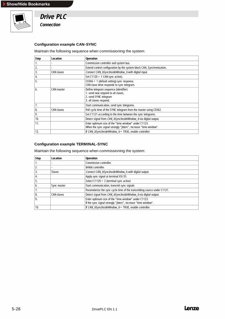
Drive PLCConnection
5-28 DrivePLC EN 1.1
Configuration example CAN-SYNC
Maintain the following sequence when commissioning the system:
Step Location Operation1. - Commission controller and system bus.2. - Extend control configuration by the system block CAN_Synchronization.3. CAN slaves Connect CAN_bSyncInsideWindow_b with digital input.4. Set C1120 = 1 CAN sync active).5. C0366 = 1 (default setting) sync response,
CAN slave drive responds to sync telegram.6. CAN master Define telegram sequence (identifier)
1. send new setpoint to all slaves,2. send SYNC telegram3. all slaves respond.
7. Start communication, send sync telegrams.8. CAN slaves Poll cycle time of the SYNC telegram from the master using C0362.9. Set C1121 according to the time between the sync telegrams.10. Detect signal from CAN_bSyncInsideWindow_b via digital output.11. Enter optimum size of the ”time window” under C1123.
When the sync signal strongly ”jitters”, increase ”time window”.12. If CAN_bSyncInsideWindow_b = TRUE, enable controller.
Configuration example TERMINAL-SYNC
Maintain the following sequence when commissioning the system:
Step Location Operation1. - Commission controller.2. - Inhibit controller.3. Slaves Connect CAN_bSyncInsideWindow_b with digital output.4. Apply sync signal at terminal X5/ E55. Select C1120 = 2 (terminal sync active)6. Sync master Start communication, transmit sync signals7. Parameterize the sync cycle time of the transmitting source under C1121.8. CAN slaves Detect signal from CAN_bSyncInsideWindow_b via digital output.9. Enter optimum size of the ”time window” under C1123.
If the sync signal strongly ”jitters”, increase ”time window”.10. If CAN_bSyncInsideWindow_b = TRUE, enable controller.
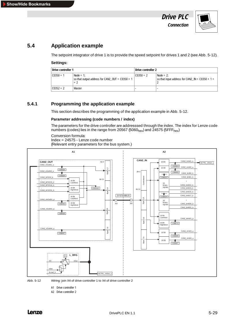
Drive PLCConnection
5-29 DrivePLC EN 1.1
5.4 Application example
The setpoint integrator of drive 1 is to provide the speed setpoint for drives 1 and 2 (see Abb. 5-12).
Settings:
Drive controller 1 Drive controller 2
C0350 = 1 Node = 1;so that output address for CAN2_OUT = C0350 + 1= 2
C0350 = 2 Node = 2;so that input address for CAN2_IN = C0350 + 1 =2
C0352 = 2 Master - -
5.4.1 Programming the application example
This section describes the programming of the application example in Abb. 5-12.
Parameter addressing (code numbers / index)
The parameters for the drive controller are addresssed through the index. The index for Lenze codenumbers (codes) lies in the range from 20567 (5060hex) and 24575 (5FFFhex)
Conversion formula:Index = 24575 - Lenze code number(Relevant entry parameters for the bus system.)
CAN2_OUT
Byt
e 1
,2
Bit 0
Bit 15
Byt
e 7
,8B
yte
5,6
Byt
e 3
,4
CAN2_dnOutD1_p
16 BitLowWord
16 BitHighWord
16 BitLowWord
16 BitHighWord
C0869/2
CAN2_nOutW1_a
CAN2_nOutW2_aC0868/4
C0868/5
CAN2_nOutW3_a
CAN2_nOutW4_a
C0868/6
C0868/7
CAN2_bFDO0_b
CAN2_bFDO15_b
...
CAN2_bFDO16_b
CAN2_bFDO31_b
... C0151/2
16 Bit
16 Bit CAN2_nInW1_a
16binarysignals
16 BitLowWord
16 BitHighWord
16 BitCAN2_nInW3_a
CAN2_bInB0_b
CAN2_dnInD1_p
Byt
e 3
,4B
yte
5,6
Byt
e 7
,8
CAN2_IN
Bit 0
Bit 15
......
C0867/2
C0866/6
C0866/4
C0863/3
C0863/4
C0866/5
Con
trol
wor
d
16 BitCAN2_nInW4_a
C0866/7
CAN2_nInW2_a
CAN2_bInB1_b
CAN2_bInB14_b
CAN2_bInB15_b
CAN2_bInB16_b
CAN2_bInB17_b
CAN2_bInB30_b
CAN2_bInB31_b
16binarysignals
L_RFG
nIn nOut
dnTir
0
1nSet
bLoad_b
dnTif
MCTRL_nNSet_a
MCTRL_nNSet_a
X4 X4
A2A1
SYSTEMBUS
Abb. 5-12 Wiring: join X4 of drive controller 1 to X4 of drive controller 2
A1 Drive controller 1A2 Drive controller 2

Drive PLCConnection
5-30 DrivePLC EN 1.1
5.4.2 Description of the codes for the system bus
5.4.2.1 Baud-rate setting C0351
The following settings are possible:
C0351 Value [kBit/s]
0 500 (Lenze setting)
1 250
2 125
3 50
4 1000
Save changes with C0003.
The settings only become effective after the following actions:
• A new power-on
• A ”Reset-Node” command via the bus system
• A Reset-Node through code C0358
5.4.2.2 Defining a master in a drive group C0352
If information is exchanged between one drive and another in a drive group, without a higher-levelcontrol system being present to provide the master function, then one drive controller must bedefined as the master.The following assignments are valid:
• C0352 = 0: drive is slave (factory setting)
• C0352 = 1: drive is master
The master functionality is only required for the initialisation phase of the drive system.
The master effects a change of state from Pre-Operational to Operational.
An exchange of data through process-data objects is only possible in the Operational state.( 5-34 C0359 bus status)
In addition, you can define a Boot-Up time for the master during the initialisation phase.( 5-33 Boot-Up setting C0356/1)

Drive PLCConnection
5-31 DrivePLC EN 1.1
5.4.2.3 General address assignment C0350
C0350 can be used to set the addressing for all the data objects (parameter-and process-datachannels).
Save changes with C0003.
The settings only become effective after the following actions:
• A new power-on
• A ”Reset-Node” command via the bus system
• A Reset-Node through code C0358
If the drive controllers are provided with an unbroken sequence of addresses, then theevent-controlled data objects are so connected that communication is possible from one drivecontroller to another (see also the application example).
Example:
• Drive controller 1: Address C0350 = 1
• Drive controller 2: Address C0350 = 2
• Drive controller 3: Address C0350 = 3
The data are thus assigned within the drive group as follows:
• The output information from drive controller 1 is the input information for drive controller 2– CAN2_OUT drive controller 1 → CAN2_IN drive controller 2– CAN3_OUT drive controller 1 → CAN3_IN drive controller 2
• The output information from drive controller 2 is the input information for drive controller 3– CAN2_OUT drive controller 2 → CAN2_IN drive controller 3– CAN3_OUT drive controller 2 → CAN3_IN drive controller 3
• etc.
An exchange of the cyclical process-data CAN1_IN and CAN1_OUT from one drive controller toanother is not possible.
Save the changes with C0003. The settings only become effective after the following actions:
• A new power-on
• A ”Reset-Node” command via the bus system
• A Reset-Node through code C0358

Drive PLCConnection
5-32 DrivePLC EN 1.1
5.4.2.4 Selective addressing of the individual process-data objects C0353, C0354
If the desired data distribution through code C0350 is not possible, then each process-data input andprocess-data output object can be provided with its own address. In this case, the data input objectsto be addressed must match the identifier of the data output object. The identifier is aCAN-specificassignment criterion for a message. If equipment from other manufacturers is used,such as decentralised digital inputs and outputs, the resulting identifiers must be observed. Theidentifiers can be called up under code C0355.
Three subcodes are available under C0353 for the selective assignment of the data objects. These3 subcodes select whether the address entry is made under C0350 or C0354. This is valid for all theprocess-data objects, as follows:
C0353/x C0353/x = 0 or 1 Meaning
C0353/1;Address selection for the cyclicalprocess-data CAN1_IN and CAN1_OUT
C0353/1 = 0
C0353/1 = 1
Addresses are determined by C0350 (Lenze setting)Address for CAN1_IN is determined by C0354/1, address for CAN1_OUTis determined by C0354/2
C0353/2;Address selection for the event-controlledprocess-data CAN2_IN and CAN2_OUT
C0353/2 = 0
C0353/2 = 1
Addresses are determined by C0350 (Lenze setting)Address for CAN2_IN is determined by C0354/3, address for CAN2_OUTis determined by C0354/4
C0353/3;Address selection for the event-controlledprocess-data CAN3_IN and CAN3_OUT
C0353/3 = 0
C0353/3 = 1
Addresses are determined by C0350 (Lenze setting)Address for CAN3_IN is determined by C0354/5, address for CAN3_OUTis determined by C0354/6
Save changes with C0003.
The settings only become effective after the following actions:
• A new power-on
• A ”Reset-Node” command via the bus system
• A Reset-Node through code C0358

Drive PLCConnection
5-33 DrivePLC EN 1.1
5.4.2.5 Display code of the resulting identifier C0355
C0355 is a display code for the resulting identifier. You cannot enter any values here.
The identifiers are calculated from the basis identifier and the valid address for the individualprocess-data objects. ( 5-38)
The following assignments are valid:
• C0355/1: Identifier CAN1_IN
• C0355/2: Identifier CAN1_OUT
• C0355/3: Identifier CAN2_IN
• C0355/4: Identifier CAN2_OUT
• C0355/5: Identifier CAN3_IN
• C0355/6: Identifier CAN3_OUT
5.4.2.6 Boot-Up setting C0356/1
With C0356 you can alter the times required for the data exchange.
C0356/x Meaning
C0356/1 Time setting for the Boot-Up of the master (only valid if C0352 = 1)In general, the Lenze setting will be sufficient here.If several drive controllers are in a group, without a higher-level control system that takes on the initialisation of the CANnetwork, this must be done through a drive controller. To do this, the master must, at a certain moment, make a single activationof the entire CAN network and thus start the process-data transmission.(change of state from Pre-Operational to Operational).Here the moment is set for this activation after the power-on.
Setting the cycle time for CAN output data:
C0356/x Meaning
C0356/2 Cycle time for the process-data object CAN2_OUT.• C0356/2 = 0: event-controlled process-data transfer
– The process-data output object is only transmitted if a value has changed in the output object• C0356/2 > 0
– The transmission of the process data object CAN2_OUT is made with the factor that is set here for the task-time of the taskin which the process output image has been created.
C0356/3 Cycle time for the process-data object CAN3_OUT.• C0356/3 = 0: event-controlled process-data transfer
– The process-data output object is only transmitted if a value has changed in the output object• C0356/3 > 0
– The transmission of the process data object CAN3_OUT is made with the factor that is set here for the task-time of the taskin which the process output image has been created.
Example:
• The process output image of the SB CAN2_OUT is created at the end of a 10 msec task.
• C0356/2 = 3
• ⇒ The process data object is sent every 30 ms (3 * 10 ms)
Tip!Check in DDS, above the dialog field Process image creation, in which task the process image wascreated (Object OrganizerÞ Register card ResourcesÞ Object Process image).

Drive PLCConnection
5-34 DrivePLC EN 1.1
5.4.2.7 Diagnosis codesYou can use the following diagnosis codes to observe the events on the bus:• C0359 bus status• C0360 telegram counter• C0361 bus load
C0359 bus status
This code shows the present operating state of the bus system.
Value of C0359 Operating state Description0 Operational The bus system is fully functional1 Pre-Operational Only parameters (codes) can be transmitted through the bus system. Data exchange between drive
controllers is not possible. To change to theOperational state, a special signal must be put out on the bus.The following actions effect a change of state from Pre-Operational to Operational.• A drive is defined a the master with C0352. On power-on, after theBoot-Up time C0356/1 that has
been set, an automatic change of stateis made for the entire drive group.• With C0358 Reset node• With the binary input signal Reset-Node, that can be appropriately set• A Node-Reset through a connected higher-level control system
2 Warning Faulty telegrams have arrived. The drive controller is only passively involved, no further data are sentfrom the drive controller. The cause may be:• A missing bus termination• Insufficient screening• Potential differences in the grounding of the control electronics• An excessive bus load• Drive controller is not connected to the bus
3 Bus Off The frequency of faulty telegrams has caused the drive controller to decouple itself from the bus. It canbe reconnected by:• A TRIP-reset• A node reset• A fresh power-on
C0360 telegram counter
All the telegrams for all function blocks and all parameter channels are counted here, which are validfor the drive controller. The counters have a capacity of 16 bits. If a counter exceeds the value 65535,the count begins again at 0.The following messages are counted:
C0360/x Meaning
C0360/1 All transmitted telegrams
C0360/2 All received telegrams
C0360/3 Transmitted telegrams from CAN1_OUT
C0360/4 Transmitted telegrams from CAN2_OUT
C0360/5 Transmitted telegrams from CAN3_OUT
C0360/6 Transmitted telegrams from parameter channel 1
C0360/7 Transmitted telegrams from parameter channel 2
C0360/8 Received telegrams from CAN1_IN
C0360/9 Received telegrams from CAN2_IN
C0360/10 Received telegrams from CAN3_IN
C0360/11 Received telegrams from parameter channel 1
C0360/12 Received telegrams from parameter channel 2
C0361 Bus load
With these codes you can find out which percentage loading of the bus is required by the drivecontroller, or is occupied by the individual data channels or system blocks. Faulty telegrams are nottaken into account in this case.

Drive PLCConnection
5-35 DrivePLC EN 1.1
The individual subcodes indicate the following bus loadings:
C0361/x Meaning
C0361/1 All transmitted telegrams
C0361/2 All received telegrams
C0361/3 Transmitted telegrams from CAN1_OUT
C0361/4 Transmitted telegrams from CAN2_OUT
C0361/5 Transmitted telegrams from CAN3_OUT
C0361/6 Transmitted telegrams from parameter channel 1
C0361/7 Transmitted telegrams from parameter channel 2
C0361/8 Received telegrams from CAN1_IN
C0361/9 Received telegrams from CAN2_IN
C0361/10 Received telegrams from CAN3_IN
C0361/11 Received telegrams from parameter channel 1
C0361/12 Received telegrams from parameter channel 2
The data transmission has limitations that are given by the number of telegrams per time interval andthe data transmission rate.
You can establish these limits for data exchange within a pure drive group, by adding the codeC0361/1 values for all the participating drives.
Example:
3 drives are grouped together through the system bus.
C0361/1 for drive controller 1 23.5% bus loadingC0361/1 for drive controller 2 12.6% bus loadingC0361/1 for drive controller 3 16.0% bus loading
52.1% total bus loading
Tip!• The bus loading for all participating devices should not exceed 80%.
• If other devices are connected, such as decentralised inputs and outputs, then their telegramsmust also be taken into account.
• A bus-overloading can, for instance, be caused by the event-controlled transmission ofcontinuously changing signals.– Remedy: set the cycle time for the system blocks that are involved (CAN2_OUTand
CAN3_OUT) under C0356/2 and C0356/3 to an appropriate value, such that the sum of allthe bus loadings is not excessive.

Drive PLCConnection
5-36 DrivePLC EN 1.1
5.4.2.8 Monitoring
Monitoring times C0357
Each individual process-data object can monitor whether a telegram has arrived within the timedefined here. If a telegram has arrived, then the corresponding monitoring time is restarted(retrigerrable monostable function).
The following assignments are valid:
C0357/1 Monitoring time CAN1_IN
C0357/2 Monitoring time CAN2_IN
C0357/3 Monitoring time CAN3_IN
The response to this monitoring is set by:
• C0591 for CAN1_IN (commErrCANIN1 “CE1”)
• C0592 for CAN2_IN (commErrCANIN2 “CE2”)
• C0593 for CAN3_IN (commErrCANIN3 “CE3”)
The following can be set:
0 = TRIP (the drive controller sets the controller disable)
1 = warning
2 = monitoring is switched off
You can also use the signals as binary output signals, for instance, for the assignment of outputterminals.
Bus Off
If the drive controller has decoupled itself from the bus, because of faulty telegrams, the signal“BusOffState” (CE4) is set.
Just like the signals “commErrCANIN1” (CE1), “commErrCANIN2”(CE2), “commErrCANIN3” (CE3),this signal can trigger a TRIP or warning, or you can switch it off. The response is set with C0595. Itis also possible to assign a terminal output in this case.
Reset-Node C0358
Entries of altered transmission rates or changed addresses for the process-data objects or deviceaddresses will only become effective after a Reset-Node.
A Reset-Node can be made by:
• A fresh power-on
• Reset-Node through the bus system
• Reset-Node through C0358

Drive PLCConnection
5-37 DrivePLC EN 1.1
5.4.3 Communication profile of the system bus
Description of the CAL-based communication profile DS 301 (CANopen) for the 93XX series ofcontrollers.
Simplified repesentation of the structure of a CAN-telegram:
11-bit identifier 8-byte user data
Abb. 5-13 Structure of a CAN-telegram (simplified representation)
5.4.3.1 Data description
Identifier
The identifier fixes the priority for the message. Also coded here in CANopen are:
• The device address ( 5-38)
• The definition of which user data are to be transmitted
User data
There are 3 distinctions made for the application of user data:
• Initialisation– User data for establishing communication across the CAN-bus.
• Parameterization– User data for the parameterization of the drive controller. For Lenze drive controllers, the
parameters are stored under the code positions or the variables.
• Process data– User data intended for rapid, often cyclical, procedures (e.g. speed setpoint and actual
value)

Drive PLCConnection
5-38 DrivePLC EN 1.1
5.4.3.2 Addressing the drives
The CANbus system is oriented around messages, not participants. Each message has a uniquelabel, the identifier. With CANopen, participant orientation is achieved by having only one sender foreach message. The identifiers are derived from the addresses that are entered in the drive controller.However, this does not apply for the identifier for the network management.
The identifiers are derived with this formula:
Identifier = base-identifier + adjustable address
Identifier Base-identifier Adjustable address
Network managementSync-telegram
0128
Parameter channel 1 to driveParameter channel 2 to drive
15361600
Address in C0350Address in C0350
Parameter channel 1 from driveParameter channel 2 from drive
14081472
Address in C0350Address in C0350
cyclical process-data channel to drive (CAN1_IN)cyclical process-data channel from drive (CAN1_OUT)
512384
Address in C0350Address in C0350
event-controlled process-data channel to drive (CAN2_IN)event-controlled process-data channel from drive (CAN2_OUT)
640641
Address in C0350Address in C0350
event-controlled process-data channel to drive (CAN3_IN)event-controlled process-data channel from drive (CAN3_OUT)
768769
Address in C0350Address in C0350
Tab. 5-2 Identifier definition for addressing the drives
Selective identifier definition for process-data objects
You can give each process-data object (SB CAN1_IO, CAN2_IO, CAN3_IO) its own address.
To do this, C0353 is used to select whether the identifiers for the process data are derived fromC0350, or whether C0354 determines the individual identifier.
The following relationships apply:
C0353/x Meaning
C0353/1 = 0 (C0350)C0353/1 = 1 (C0354)
Addresses of CAN1_IN and CAN1_OUT are determined by C0350Address of CAN1_IN1 is determined by C0354/1Address of CAN1_OUT is determined by C0354/2
C0353/2 = 0 (C0350)C0353/2 = 1 (C0354)
Addresses ofn CAN2_IN and CAN2_OUT are determined by C0350Address of CAN2_IN is determined by C0354/3Address of CAN2_OUT is determined by C0354/4
C0353/3 = 0 (C0350)C0353/3 = 1 (C0354)
Addresses of CAN3_IN and CAN3_OUT are determined by C0350Address of CAN3_IN is determined by C0354/5Address of CAN3_OUT is determined by C0354/6
Tab. 5-3 Selective identifier definition for process-data objects
Valid for all process-data input and output objects:
Identifier = 384 + value under C0354/xx = subcode 1 ... 6, for assignment see Tab. 5-3

Drive PLCConnection
5-39 DrivePLC EN 1.1
5.4.4 The communication phases of the CAN network
11-bit Identifier 2-byte user data
Abb. 5-14 Telegram for changing over the communication phase
To be able to change over between the various communication phases, telegrams are used with anIdentifier 0 and 2 bytes of user data.
For communication purposes, the drive recognizes three states:
State Explanation
a State ”Initialisation”The drive is not participating in the data traffic on the bus. This state is achieved after the drive controller is switched on. It is stillpossible to repeat the whole or a part of the initialisation, by transmitting various telegrams. In this case, all the parameters thathave already been set will be overwritten by the default/standard values. After initialisation is completed, the drive goes automati-cally into the ”Pre-Operational” state.
b State ”Pre-Operational”The drive can receive parameterization data. The process data are ignored.
c State ”Operational”The drive can receive parameterization and process data.
The changeover between the communication phases is controlled by one bus participant (thenetwork master) for the entire network.
This can also be carried out by a 93XX drive controller. To do this, set up this drive controller as themaster (C0352 = 1).
A telegram is transmitted once after switching on the power, after a delay. This sets the entire drivegroup to the ”Operational” state.
The delay time can be set under C0356/1.

Drive PLCConnection
5-40 DrivePLC EN 1.1
When certain telegrams have to be transmitted, a change is made to a different state:
from after Data (hex) Remarks
Pre-Operational Operational 01xx Process and parameterization data are active
Operational Pre-Operational 80xx only parameterization data are active
Operational Initialisation 81xx resets the drive; all parameters are overwritten with the standard values
Pre-Operational Initialisation 81xx
Operational Initialisation 82xx resets the drive; only parameter relevant to communication are reset
Pre-Operational Initialisation 82xx
The following applies to the assignment of the bytes marked by ”xx” in the column:
• xx = 00hex
– With this assignment, the telegram applies to all connected devices. A change of state canbe made for all devices at the same time.
• xx = device address– If a device address is given, then the change of state is only carried out for the device with
the corresponding address.
Tip!Communication of the process data is only possible when the state is changed to Operational !

Drive PLCConnection
5-41 DrivePLC EN 1.1
5.4.5 Parameterization
Two separate software channels are available for parameterization, which are defined by thecontroller address.
The structure of the telegram for parameterization is as follows:
11-bit identifier 8-byte user data
CommandCode
IndexLow-byte
Sub-index Data 1Index
High-byte Data 2 Data 3 Data 4
Abb. 5-15 Structure of the telegram for parameterization
Command code:
In the command code, the services must be entered, or services are entered such as transmitting orwriting a parameter, and how long these data are.
Structure of the command code:
Bit 7 (MSB) Bit 6 Bit 5 Bit 4 Bit 3 Bit 2 Bit 1 Bit 0
Command Specifier (cs) 0 Length e s
cs Length e s
Write Request 0 0 1 0 x x 1 1
Write Response 0 1 1 0 x x 0 0
Read Request 0 1 0 0 x x 0 0
Read Response 0 1 0 0 x x 1 1
Error Response 1 0 0 0 0 0 0 0
The length of the user data for these services are coded in Bit 2 and Bit 3 as follows:
• 00 = 4-byte
• 01 = 3-byte
• 10 = 2-byte
• 11 = 1-byte
The most frequent parameters are data with 4 bytes (32-bit) and 2 bytes (16-bit) data length.
So the following values result in the command code for these parameters:
Services 4-byte (32-bit) data 2-byte (16-bit) data Meaning
hex dec hex dec
Write Request 23hex 35 2Bhex 43 Transmit parameter to drive
Write Response 60hex 96 60hex 64 Reponse of the drive controller to the write request(acknowledgement)
Read Request 40hex 64 40hex 64 Request to read a parameter from the drive controller
Read Response 43hex 67 4Bhex 75 Response to the read request with the actual value
Error Response 80hex 128 80hex 128 The drive controller reports a communication error

Drive PLCConnection
5-42 DrivePLC EN 1.1
Index LOW-byte, Index HIGH-byte
The selection of the parameter or the selection of the Lenze code is made with these two bytesaccording to the formula:
Index = 24575 - Lenze code number
Example:
The parameter C0012 (acceleration time) ist to be addressed:
24575 - 12 = 24563 = 5FF3hex
According to the left-aligned Intel data format, the entries are as follows (see “Description of a dataformat”):
• Index LOW-byte = F3hex
• Index HIGH-byte = 5Fhex
Subindex
A subindex is a table position of a parameter under the index.
Example:
Terminal X5/A1, Subcode 1 unter dem Parameter C0117 soll angesprochen werden.
Index = 24575 - 117 = 24458 = 5F8Ahex (Index LOW-byte = 8A, Index HIGH-byte = 5F)
Subindex = 1
If a parameter is addressed, that does not have a subindex, then 0 must be entered here.

Drive PLCConnection
5-43 DrivePLC EN 1.1
Data 1 ... Data 4
The value to be transmitted, in up to 4 bytes.
The parameters for the 93XX series of controllers are stored in various formats. The most commonis the Fixed-32 format. This is a fixed-point format with 4 decimal places. Please note, that theseparameters must be multiplied by 10,000. The description and assignment of the individual formatscan be found in the code table.
Fault
Command code = 128 = 80hexIf a fault occurs, an error-response is generated by the drive. In this case, the user-data section ofthe transmission always has a 6 in Data 4 and an error code in Data 3.
Possible error-codes:
Command code: Data 3 Data 4 Meaning
80hex 6 6 wrong index
80hex 5 6 wrong subindex
80hex 3 6 Access denied
Example: Description of a data format
The user-data are presented in the Intel format, left-aligned.
An example of a telegram clarifies the left-aligned Intel data format:
For code C0012, a value of 20 sec is to be transmitted.
Index = 24575 - Lenze code = 24575 - 12 = 24563 = 5FF3hex
Value (Data 1 ... Data 4) = 20 sec ⋅ 10.000 = 200.000 = 00 03 0D 40hex
CommandCode
IndexLow-byte
Sub-index Data 1Index
High-byte Data 2 Data 3 Data 4Identifier
F3 5F 40 0D 03 00
Index = 5F F3 Value = 00 03 0D 40
Abb. 5-16 Example of the description of a data format

Drive PLCConnection
5-44 DrivePLC EN 1.1
5.4.5.1 Example: Write a parameter
The acceleration time C0012 of the drive controller with the device address 1 is to be altered from1 to 20 sec through parameter channel 1.
Calculation of identifier:
Identifier from parameter channel 1 to drive controller = 1536 + device address = 1536 + 1 = 1537
Command code = Write Request (transmit parameter to drive) = 23hex
Calculation of the index
Index = 24575 - code no. = 24575 - 12 = 24563 = 5FF3hex
Subindex for C0012 = 0
Calculation of the value for the acceleration time
20 sec ⋅ 10.000 = 200.000 = 00030D40hex
Telegram to drive:
CommandCode
IndexLow-byte
Sub-index Data 1Index
High-byte Data 2 Data 3 Data 4Identifier
F3 5F 40 0D 03 001537 23 00
Abb. 5-17 Telegram to drive:
Response of the drive to correct implementation:
CommandCode
IndexLow-byte
Sub-index Data 1Index
High-byte Data 2 Data 3 Data 4Identifier
F3 5F 00 00 00 001409 60 00
Abb. 5-18 Response of the drive to correct implementation:
Identifier for parameter channel 1 from drive controller: 1408 + device address = 1409
Command code = Write Response (response of the drive controller (acknowledgement)) = 60hex

Drive PLCConnection
5-45 DrivePLC EN 1.1
5.4.5.2 Example: Read a parameter
The heatsink temperature (value 43°C) C0061 is to be read from the drive controller with the deviceaddress 5 through parameter channel 1.
Calculation of identifier:
Identifier from parameter channel 1 to drive controller = 1536 + device address = 1536 + 5 = 1541
Command code = Read Request (request to read a parameter from the drive controller) = 40hex
Calculation of the index
Index = 24575 - code no. = 24575 - 61 = 24514 = 5FC2hex
Telegram to drive:
CommandCode
IndexLow-byte
Sub-index Data 1Index
High-byte Data 2 Data 3 Data 4Identifier
C2 5F 00 00 00 001541 40 00
Abb. 5-19 Telegram to drive
Telegram from drive:
CommandCode
IndexLow-byte
Sub-index Data 1Index
High-byte Data 2 Data 3 Data 4Identifier
C2 5F B0 8F 06 001413 43 00
Abb. 5-20 Telegram from drive:
Identifier for parameter channel 1 from drive controller= 1408 + device address = 1413
Command code = Response to the read request with the actual value = 43hex
Index of the read request = 5FC2hex
Subindex = 0 (no subindex available for C0061)
Data 1 ... Data 4 = 43 °C ⋅ 10.000 = 430.000 = 00068FB0hex

Drive PLCConnection
5-46 DrivePLC EN 1.1
5.4.6 Process data
For the rapid exchange of data between drive controllers, or with a higher-level control system, thereare 3 process-data objects (PDO)available for input information, and 3 PDOs for output information.
With these PDO you can transmit simple binary signals, such as the states of digital input terminals,or even complete values in 16 or 32 bits, such as analog signals.
These data objects are stored as system blocks under the inputs and outputs.
(The PDOs are included in the 93XX drive controller as CANx_IO system blocks).
Cyclical process-data objects
For rapid cyclical data communication, there is a PDO available for input signals and a PDO foroutputs signals, each with 8-byte user data.
These data are intended for higher-level control systems, such as a PLC (system block CAN1_IO).
Event-controlled process-data objects
For event-controlled data communication, there are 2 PDOs available for input signals and 2 PDOsfor outputs signals, each with 8-byte user data.
The data will always be transmitted if a value changes in the user data. These PDOs are especiallysuited for the data communication between drive controllers, and for decentralised terminalexpansion.
However, they can also be used by a higher-level control system (system blocks CAN2_IO andCAN3_IO).

Drive PLCConnection
5-47 DrivePLC EN 1.1
5.4.6.1 Cyclical process-data objects
In order to be able to read process-data from the drive controller, or to accept the process-data bythe drive controller, a special additional telegram is required - the sync telegram.
The sync-telegram is the trigger point for the acceptance of data by the drive controller, and initiatesthe transmission procedure at the controller. For a cyclical processing of process-data thesync-telegram must be generated accordingly.
The synchronization of cyclical process-data
Process-data fromController
Process-data toController
Sync-telegram Sync-telegram
Abb. 5-21 Sync-telegram
After a sync-telegram, the cyclical process-data are transmitted by the drive controllers. The datatransfer to the drive controllers follows next, that is again accepted by the individual controllers withthe next sync-telegram.
All other telegrams, such as parameters or the event-controlled process-data, are acceptedasynchronously by the drive controllers after the transmission has taken place.
The asynchronous data are not considered in Abb. 5-21.

Drive PLCConnection
5-48 DrivePLC EN 1.1
Cyclical process-data telegram to the drive CAN1_IN
The process-data telegram to the drive has 8-byte user-data length. It is structured as follows:
Byte 1
Identifier
Byte 2 Byte 3 Byte 4 Byte 5 Byte 6 Byte 7 Byte 8
Abb. 5-22 Cyclical process-data telegram to the drive
Assignment of the user data:
Byte Word assignment (16-bit) Individual bit assignment Double-word assignment (32-bit)
1 control word (LOW-byte)
2 control word (HIGH-byte)
3 CAN1_nInW1_a (LOW-Byte)
4 CAN1_nInW1_a (HIGH-Byte)
5 CAN1_nInW2_a (LOW-Byte) CAN1_bInB0_b 0 CAN1_bInB15_b CAN1_dnInD1_p
6 CAN1_nInW2_a (HIGH-Byte)
7 CAN1_nInW3_a (LOW-Byte) CAN1_bInB16_b 0 CAN1_bInB31_b
8 CAN1_nInW3_a (HIGH-Byte)
Bytes 5-6 and/or 7-8 can be simultaneously used as
• 32 individual binary/logic signals,
• 2 separate 16-bit values (”quasi-analog signal”),
• one double-word (32-bit)
( 5-10, CAN1_IN)

Drive PLCConnection
5-49 DrivePLC EN 1.1
Cyclical process-data telegram from the drive CAN1_OUT
The structure of the process-data telegram from the drive is as follows:
Byte 1
Identifier
Byte 2 Byte 3 Byte 4 Byte 5 Byte 6 Byte 7 Byte 8
Abb. 5-23 Cyclical process-data telegram from the drive
Assignment of the user data:
Byte Word assignment (16-bit) Individual bit assignment Double-word assignment (32-bit)
1 Status-word (LOW-byte)
2 Status-word (HIGH-byte)
3 CAN1_nOutW1_a (LOW-Byte)
4 CAN1_nOutW1_a (HIGH-Byte)
5 CAN1_nOutW2_a (LOW-Byte) CAN1_bFDO0_b 0 CAN1_bFDO15_b CAN1_dnOutD1_p
6 CAN1_nOutW2_a (HIGH-byte)
7 CAN1_nOutW3_a (LOW-Byte) CAN1_bFDO16_b 0 CAN1_bFDO31_b
8 CAN1_nOutW3_a (HIGH-Byte)

Drive PLCConnection
5-50 DrivePLC EN 1.1
5.4.6.2 Event-controlled process-data objects, optionally with adjustable cycletime
The event-controlled process-data must be linked to the individual system blocks, like the cyclicalprocess-data.
Here too, there are 8 bytes available for a data object.
A transmission of the output data follows:
• always, if a value has altered in the 8-byte user-data
• with the cycle time set under C0356/2 (CAN2_OUT) and 356/3 (CAN3_OUT)
You can set the appropriate monitoring times for the inputs under C0357/2 (CAN2_IN) and C0357/3(CAN3_IN).
Event-controlled process-data telegram CAN1_IN to the drive
The process-data telegrams to the drive have a user-data length of 8 bytes, and the followingstructure:
Byte 1
Identifier
Byte 2 Byte 3 Byte 4 Byte 5 Byte 6 Byte 7 Byte 8
Abb. 5-24 Event-controlled process-data telegram to the drive
Assignment of the user data:
Byte Word assignment (16-bit) Individual bit assignment Double-word assignment (32-bit)
1 CAN1_nInW1_a (LOW-Byte) CAN1_bInB0_b 0 CAN1_bInB15_b CAN1_dnInD1_p
2 CAN1_nInW1_a (HIGH-Byte)
3 CAN1_nInW2_a (LOW-Byte) CAN1_bInB16_b 0 CAN1_bInB31_b
4 CAN1_nInW2_a (HIGH-byte)
5 CAN1_nInW3_a (LOW-byte)
6 CAN1_nInW3_a (HIGH-byte)
7 CAN1_nInW4_a (LOW-byte)
8 CAN1_nInW4_a (HIGH-byte)
Bytes 1-2 and bytes 3-4 can be simultaneously used as 32 individual binary/logic signals, as 2separate 16-bit data-words (”quasi-analog signal”) or as one double-word (32-bit).
( 5-10, CAN1_IN)

Drive PLCConnection
5-51 DrivePLC EN 1.1
Event-controlled process-data telegram CAN2_IN to the drive
The process-data telegrams to the drive have a user-data length of 8 bytes, and the followingstructure:
Byte 1
Identifier
Byte 2 Byte 3 Byte 4 Byte 5 Byte 6 Byte 7 Byte 8
Abb. 5-25 Event-controlled process-data telegram to the drive
Assignment of the user data:
Byte Word assignment (16-bit) Individual bit assignment Double-word assignment (32-bit)
1 CAN2_nInW1_a (LOW-byte) CAN2_bInB0_b 0 CAN2_bInB15_b CAN2_dnInD1_p
2 CAN2_nInW1_a (HIGH-byte)
3 CAN2_nInW2_a (LOW-byte) CAN2_bInB16_b 0 CAN2_bInB31_b
4 CAN2_nInW2_a (HIGH-byte)
5 CAN2_nInW3_a (LOW-byte)
6 CAN2_nInW3_a (HIGH-byte)
7 CAN2_nInW4_a (LOW-byte)
8 CAN2_nInW4_a (HIGH-byte)
Bytes 1-2 and bytes 3-4 can be simultaneously used as 32 individual binary/logic signals, as 2separate 16-bit data-words (”quasi-analog signal”) or as one double-word (32-bit).
( 5-15, CAN2_IN)

Drive PLCConnection
5-52 DrivePLC EN 1.1
Event-controller process-data telegram to the drive CAN3_IN
The process-data telegrams to the drive have a user-data length of 8 bytes, and the followingstructure:
Byte 1
Identifier
Byte 2 Byte 3 Byte 4 Byte 5 Byte 6 Byte 7 Byte 8
Abb. 5-26 Event-controlled process-data telegram to the drive
Assignment of the user data:
Byte Word assignment (16-bit) Individual bit assignment Double-word assignment (32-bit)
1 CAN3_nInW1_a (LOW-byte) CAN3_bInB0_b 0 CAN3_bInB15_b CAN3_dnInD1_p
2 CAN3_nInW1_a (HIGH-byte)
3 CAN3_nInW2_a (LOW-byte) CAN3_bInB16_b 0 CAN3_bInB31_b
4 CAN3_nInW2_a (HIGH-byte)
5 CAN3_nInW3_a (LOW-byte)
6 CAN3_nInW3_a (HIGH-byte)
7 CAN3_nInW4_a (LOW-byte)
8 CAN3_nInW4_a (HIGH-byte)
Bytes 1-2 and bytes 3-4 can be simultaneously used as
• 32 individual binary/logic signals,
• 2 separate 16-bit values (”quasi-analog signal”),
• one double-word (32-bit)
( 5-19, CAN3_IN)

Drive PLCConnection
5-53 DrivePLC EN 1.1
Event-controlled process-data telegram CAN2_OUT from the drive
The process-data telegrams from the drive have a user-data length of 8 bytes, and the followingstructure:
Byte 1
Identifier
Byte 2 Byte 3 Byte 4 Byte 5 Byte 6 Byte 7 Byte 8
Abb. 5-27 Event-controlled process-data telegram from the drive
Assignment of the user data:
Byte Word assignment (16-bit) Individual bit assignment Double-word assignment (32-bit)
1 CAN2_nOutW1_a (LOW-byte) CAN2_bFDO0_b 0 CAN2_bFDO15_b CAN2_dnOutD1_p
2 CAN2_nOutW1_a (HIGH-byte)
3 CAN2_nOutW2_a (LOW-byte) CAN2_bFDO16_b 0 CAN2_bFDO31_b
4 CAN2_nOutW2_a (HIGH-byte)
5 CAN2_nOutW3_a (LOW-byte)
6 CAN2_nOutW3_a (HIGH-byte)
7 CAN2_nOutW4_a (LOW-byte)
8 CAN2_nOutW4_a (HIGH-byte)
( 5-17, CAN2_OUT)

Drive PLCConnection
5-54 DrivePLC EN 1.1
Event-controlled process-data telegram CAN3_OUT from the drive
The process-data telegrams from the drive have a user-data length of 8 bytes, and the followingstructure:
Byte 1
Identifier
Byte 2 Byte 3 Byte 4 Byte 5 Byte 6 Byte 7 Byte 8
Abb. 5-28 Event-controlled process-data telegram from the drive
Assignment of the user data:
Byte Word assignment (16-bit) Individual bit assignment Double-word assignment (32-bit)
1 CAN3_nOutW1_a (LOW-byte) CAN3_bFDO0_b 0 CAN3_bFDO15_b CAN3_dnOutD1_p
2 CAN3_nOutW1_a (HIGH-byte)
3 CAN3_nOutW2_a (LOW-byte) CAN3_bFDO16_b 0 CAN3_bFDO31_b
4 CAN3_nOutW2_a (HIGH-byte)
5 CAN3_nOutW3_a (LOW-byte)
6 CAN3_nOutW3_a (HIGH-byte)
7 CAN3_nOutW4_a (LOW-byte)
8 CAN3_nOutW4_a (HIGH-byte)
( 5-21, CAN3_OUT)

Drive PLCAppendix
6-1 DrivePLC EN 1.1
6 Appendix
6.1 PLC functionality
Field Number DescriptionInputs digital 8 free inputs (3 of them interruptible) 24 V DC / 8 mA each inputInputs
analog 3 free inputs (10 bit + sign) ñ10 VOutputs digital 4 free outputs 24 V DC / max. 1 A each outputOutputs
analog 1 free output (10 bit + sign) ñ10 V / max. 2 mAExpandability of digital inputs/outputs 8 system bus modules (9374) with 8 configurable inputs/outputsCounter/times According to IEC1131-3, depending on the data memory availableLabel selectable to IEC1131Fast counter 1 0 ... 500 kHzProgram memory 128 kByteData memory 10 kByteProcessing time 1 ms (per 1000 binary instructions)Task 8
1EVENT or INTERVAL tasks (1 ms ... 16 s)Cyclic task
Networking • INTERBUS - Slave• PROFIBUS - Slave• RS232/RS485 - Slave• System bus (CANopen)Others in preparation
E2PROM buffered memory 2 kByte, 20 byte of it remanent area

Drive PLCAppendix
6-1 DrivePLC EN 1.1
6.2 System POUs
Abb. 6-1 System POUs and PLC_PRG
The PLC provides a number of system POUs.These POUs have defined features (see table)and arecalled only once per polling.
POU name Program Feature POU starts, if ...PLC_TaskOverrun Task overflow the task monitoring time is exceededPLC_RealError Floating point error a floating point error occurredPLC_FailTripping TRIP a trip has been causedPLC_WarningTripping WARNING a warning was outputPLC_MessageTripping MESSAGE a message was outputPLC_FailQspTripping *)
max 1000 statements FAIL- QSP a FAIL-QSP has been causedPLC_CANError
max. 1000 statementsCAN-BUS error a CAN bus error occurs, e.g. BUS-OFF, Cex warning
PLC_AIFError AIF-BUS error a AIF-Bus error has been causedPLC_Restart Start after a STOP the START command has been activatedPLC_ColdStart Cold start after a RESET/program download the START command has
been activated.After the execution of these POU the CAN/AIFbus is ready.
*) not available for Drive PLC
POUs are created, as for the cyclic task ”PLC_PRG”, by creating a PROGRAM-POE with thesymbolic POU name.
System POUs are supported as from hardware version 1.0.

Drive PLCAppendix
6-2 DrivePLC EN 1.1
6.3 Code table
Special feature: Temporary codes
The values written in the codes C2500 and C2501 will be deleted after the device is switched off.Temporary codes are suitable for those parameters to which access is made during one switch-onperiod only.It is possible to access the flag area of the PLC directly (e.g. via HMI) using codes C2500/2501without applying a variable.
Code LCD Possible settings IMPORTANTCode C
Lenze Choice
O
C25001...
255
- - %MW 0 ... 254 The data of these codes• have no memory location in the EEPROM of
the device• cannot be saved with C0003 = 1 in the
parameter set of the deviceC25011...
255
- - %MW255 ... 509 parameter set of the device• will be lost after mains disconnection or
mains failure• are linked with the flag area of the PLC
How to read the code table:
Column Abbreviation MeaningCode C0039
12
01415
Code C0039Subcode 1 of code C0039Subcode 2 of code C00390Subcode 14 of code C0039Subcode 15 of code C0039
[C0156] Parameter value of the code can only be modified when the controller isinhibitedLCD Keypad LCDLenze Factory setting of the codee e
g Display code• Display possible only
* The column ”Important” contains further informationChoice 1 1 % 99 Minimum value smallest step/unit maximum valueIMPOR-TANT
- Additional, important explanation of the code
Code LCD Possible settings IMPORTANTCode C
Lenze Choice
O
C0002 Par load 0 Load parameter set0 Load default Load factory setting into RAM1 Load PS1 Load parameter set 1 into the RAM and
activate• Parameter set1 is loaded automatically
after every mains connection.C0003 Par save 0 Save parameter set
0 Ready Saving completed1 Save PS1 Non-volatile saving of parameter set 1
C0004 Op-display 56 All available codes Operating displayOperating module shows selected code inthe operating level, if no other status indica-tions of C0183 are active.

Drive PLCAppendix
6-3 DrivePLC EN 1.1
Code IMPORTANTPossible settingsLCDCode IMPORTANT
ChoiceLenze
LCD
C0009 LECOM address 9 1 1 99 Controller addressBus device number when operated viainterface• 10, 20, ..., 90 reserved for broadcast to
device groups for RS232,RS485, fibreoptics.
C0011 3000 500 16000 Reference code for speed scalingC0043 Trip reset Reset of an active trip:
• Set C0043 = 00 no/trip reset1 trip active
reset latest tripactive fault TRIP
C0067 Act trip g All error messages latest error message
C0093 g Controller identification
C0094 Password 0 0 9999 Password• Parameter-access protection for the
operating module. When the password isactivated, only user-menu codes can beaccessed.
C0099 S/W version g x.xx Software version
C0125 Baud rate 0 0 9600 baud1 4800 baud2 2400 baud3 1200 baud4 19200 baud
LECOM baud ratefor accessory module 2102
C0126 MONIT CE0 3 0 Trip2 Warning3 Off
Configuration monitoring: communicationerror with automation interface”CommErr“(CE0)
C0135 Internal codeC0150 Status word g 0 1 65535 Hexadecimal control word when networked
with automation interfaces
C0161 Act trip g All error messages Latest error message (as in C0168/1)
C0167 Reset failmem 0 0 No reset1 Reset clears the history buffer
C0168 g All error messages errors occurredHistory buffer• List of faults occurred
12345678
Fail no. actFail no. old1Fail no. old2Fail no. old3Fail no. old4Fail no. old5Fail no. old6Fail no. old7
now activelatestlast but onelast but twolast but threelast but fourlast but fivelast but six
C0169 g corresponding power switch-on time Occurrence of the faultsHistory buffer• List of times when the faultshave
occurred underC0168• referred to C0179
12345678
Failtime actFailtime old1Failtime old2Failtime old3Failtime old4Failtime old5Failtime old6Failtime old7
now activelatestlast but onelast but twolast but threelast but fourlast but fivelast but six

Drive PLCAppendix
6-4 DrivePLC EN 1.1
Code IMPORTANTPossible settingsLCDCode IMPORTANT
ChoiceLenze
LCD
C0170 g corresponding power switch-on time error frequencyHistory buffer• List of how often the faults have
occurred consecutively under C0168
12345678
Counter actCounter old1Counter old2Counter old3Counter old4Counter old5Counter old6Counter old7
now activelatestlast but onelast but twolast but threelast but fourlast but fivelast but six
C0179 Mains timer g 0 1 sec 4294967295 Mains switch-on time meter• Time when the mains was switched on
C0183 Diagnostics g Drive diagnostics• Displays fault or
status information• If several pieces of fault or
status information are output at thesame time, the information with thesmallest number is displayed
0 OK10 Init91 Trip-Set C13592 Trip-Set AIF93 Trip-Set CAN102 Trip103 RFG P-OFF104 IMP Message105 Power off111 BSP C135112 BSP AIF113 BSP CAN121 CINH term 28122 CINH int 1123 CINH int 2124 CINH C135/STP125 CINH AIF126 CINH CAN141 Lock mode
No faultInitialization phase
TRIP activeEmergency stop was releasedMessage active
Operation inhibited
Controller inhibited via X5/28DCTRL-CINH1DCTRL-CINH2STOP key of 9371BBController inhibited via AIFController inhibited via CANRestart protection active
142 IMP Power outputs with high resistance151 QSP ext term152 QSP C135/STP153 QSP AIF154 QSP CAN250 Warning
QSP via MCTRL-QSPQSP via STOP keyQSP via AIFQSP via CANWarning active
C0200 S/W Id g Software identification
C0201 S/W date g Software release date
C02021234
Internal ID g 0 0.001 100 Internal designation
C0203 Comm.-No. g x / xxxx / xxxxx Commission number
C0204 Serial-No. g 0 1 65535 Serial number
C0206 Product date g Production date
C0207 DL info 1 g Download-Info 1
C0208 DL info 2 g Download-Info 2
C0209 DL info 3 g Download-Info 3

Drive PLCAppendix
6-5 DrivePLC EN 1.1
Code IMPORTANTPossible settingsLCDCode IMPORTANT
ChoiceLenze
LCD
C0210 Module identification g Extension Board
C0211 Internal codeC0300 Internal error diagnosticC0301 Internal error diagnosticC0304 Internal codeC0306 Internal codeC0307 Internal codeC0309 Internal code
[C0350] CAN address 1 1 1 63 CAN bus node address[C0351] CAN baud rate 0 0 500 kbit/s
1 250 kbit/s2 125 kbit/s3 50 kbit/s4 1000 kbit/s
CAN bus baud rate
[C0352] CAN mst 0 0 slave1 Master
Install CAN bus master operation
C0353123
CAN addr sel1CAN addr sel2CAN addr sel3
000
0 C3501 C354
Source for CAN bus IN/OUT addresses
C0354123456
IN1 addr2OUT1 addr2IN2 addr2OUT2 addr2IN3 addr2OUT3 addr2
1291257258385386
1 1 512 CAN bus IN/OUT node addresses
C0355123456
CAN1_IN IdCAN1_OUT IdCAN2_IN IdCAN2_OUT IdCAN3_IN IdCAN3_OUT Id
g 0 1 2047 CAN bus identifier
C03561234
CAN boot upCAN2_OUT TCAN3_OUT TCAN delay
30000020
0 1 msec 65000 CAN bus time settings• CANx_OUT T:
Factor on the task time for sending theprocess data object.
[C0357]123
CE1monit timeCE2monit timeCE3monit time
300030003000
0 1 msec 65000 CAN bus monitoring time for Iratedx
C0358 Reset node 0 0 no function1 CAN reset
Install the CAN bus reset-node
C0359 CAN state g 0 Operational1 Pre-Operational2 Warning3 Bus off
CAN-bus status:
C0360 g 0 1 65535 Telegram counter(number of telegrams)• for values > 65535, the counting
restarts with 0

Drive PLCAppendix
6-6 DrivePLC EN 1.1
Code IMPORTANTPossible settingsLCDCode IMPORTANT
ChoiceLenze
LCD
123456789
101112
Message OUTMessage INMessage OUT1Message OUT2Message OUT3Message POUT1Message POUT2Message IN1Message IN2Message IN3Message PIN1Message PIN2
all sentall receivedsent to CAN-OUT1sent to CAN-OUT2sent to CAN-OUT3sent to parameter channel 1sent to parameter channel 2received from CAN-IN1received from CAN-IN2received from CAN-IN3received from parameter channel 1received from parameter channel 2
C0361 g 0 1 % 100 CAN bus load• For a trouble-free operation, the entire
bus load (all connected devices) shouldbe less than 80 %
123456789
101112
Load OUTLoad INLoad OUT1Load OUT2Load OUT3Load POUT1Load POUT2Load IN1Load IN2Load IN3Load PIN1Load PIN2
all sentall receivedsent to CAN-OUT1sent to CAN-OUT2sent to CAN-OUT3sent to parameter channel 1sent to parameter channel 2received from CAN-IN1received from CAN-IN2received from CAN-IN3received from parameter channel 1received from parameter channel 2
C0365 CAN active g 0 1 Input signal CAN active
C0368 Sync Tx ID 128 1 1 256 CAN Sync Tx IDC0369C0370 0 Deactivated
1 CAN address 12 CAN address 2
...63 CAN address 63
Activate CAN teleparameterization
C0372 g 0 no module1 Standard-I/O2 CAN module6 intelligent module
FIF module HW identification
C0373 g 0 no module1 Standard module (Extension Board 1)2 CAN module3 intelligent module
Extension Board HW identification
C0400123
AIN1_nIn_aAIN2_nIn_aAIN3_nIn_a
-199.99 0,01 % 199.99 Display analog inputsAIN1AIN2AIN3
C040512
g
C0425 DFIN coNst 3 0 1 6 Increments of the encoder input0 256 inc/rev1 512 inc/rev2 1024 inc/rev3 2048 inc/rev4 4096 inc/rev5 8192 inc/rev6 16384 inc/rev
C0426 g
C0428

Drive PLCAppendix
6-7 DrivePLC EN 1.1
Code IMPORTANTPossible settingsLCDCode IMPORTANT
ChoiceLenze
LCD
C0429C0434
AOUT1_nOut_ag -199.99 0.01 % 199.99 Display analog output
AOUT1C0443 DIGIN_bIn1-8 g 0 1 255 Display digital inputs I1 to I8
• Decimal value is bit-coded:Bit1 ≡ DIGIN_bIn1_bBit2 ≡ DIGIN_bIn2_bBit3 ≡ DIGIN_bIn3_bBit4 ≡ DIGIN_bIn4_bBit5 ≡ DIGIN_bIn5_bBit6 ≡ DIGIN_bIn6_bBit7 ≡ DIGIN_bIn7_bBit8 ≡ DIGIN_bIn8_b
C0444 DIGOUT_bOut1-4 g 0 1 255 Display digital outputs O1 to O4• Decimal value is bit-coded:
Bit1 ≡ DIGOUT_bOut1_bBit2 ≡ DIGOUT_bOut2_bBit3 ≡ DIGOUT_bOut3_bBit4 ≡ DIGOUT_bOut4_b
C044612
DIGIN_bIn9-14 g 0 1 255 Display digital inputs I9 to I14Extension Board 1• Decimal value is bit-coded:
Bit1 ≡ DIGIN_bIn9_bBit2 ≡ DIGIN_bIn10_bBit3 ≡ DIGIN_bIn11_bBit4 ≡ DIGIN_bIn12_bBit5 ≡ DIGIN_bIn13_bBit6 ≡ DIGIN_bIn14_b
C0448 DIGOUT_bOut5-10 g 0 1 255 Display digital outputs O5 to O10Extension Board 1• Decimal value is bit-coded:
Bit1 ≡ DIGOUT_bOut5_bBit2 ≡ DIGOUT_bOut6_bBit3 ≡ DIGOUT_bOut7_bBit4 ≡ DIGOUT_bOut8_bBit5 ≡ DIGOUT_bOut9_bBit6 ≡ DIGOUT_bOut10_b
C0469 no functionC0470
1234
FCODE 8 Bit 0 0 1 255 Freely assignable codefor digital signals
C0471 FCODE 32 Bit 0 0 1 4294967296 Freely assignable codefor digital signals
C04721234...20
FCODE analog001000...0
-199.99 0.01 % 199.99 Freely assignable codefor relative analog signals
C0473123456789
10
FCODE abs -32767 1 32767 Freely assignable codefor absolute analog signals

Drive PLCAppendix
6-8 DrivePLC EN 1.1
Code IMPORTANTPossible settingsLCDCode IMPORTANT
ChoiceLenze
LCD
C0477 DIGIN_bIn_FIFSTDIO g 0 1 255 Display digital inputs E1 .. .E4, 28FIF modules standard-I/O• Decimal value is bit-coded:
Bit1 ≡ DIGIN_bIn1_FIFSTDIO_bBit2 ≡ DIGIN_bIn2_FIFSTDIO_bBit3 ≡ DIGIN_bIn3_FIFSTDIO_bBit4 ≡ DIGIN_bIn4_FIFSTDIO_bBit5 ≡ DIGIN_bIn28_FIFSTDIO_b
C0479 DIGOUT_bOut_FIFSTDIO g 0 1 255 Display digital output A1FIF module standard-I/O• Decimal value is bit-coded:
Bit1 ≡ DIGOUT_bOut1_FIFSTDIO_bC0481 AIN1_nIn_STDIO_a g Display analog input term. 8
FIF module standard-I/OC0484 AOUT1_nOut_STDIO_a g Display analog output term. 62
FIF module standard-I/OC0514 Internal codeC0515 Internal codeC0516 Internal codeC0517
123456789
101112131415161718...3132
User Menu
51.0054.0056.0046.0049.00183.00168.0186.0022.005.0011.0012.0013.00105.0039.0170.0071.000094.003.00
0.00 0.01 1999.00C0051/0 MCTRL-NACTC0054/0 ImotC0056/0 MCTRL-MSET2C0046/0 NC0049/0 NADDC0183/0 DiagnosticsC0168/1 Fault no. actC0086/0 Mot typeC0022/0 Imax currentC0005/0 Signal cfgC0011/0 NmaxC0012/0 TirC0013/0 TifC0105/0 QSP TifC0039/1 JOG setpointC0070/0 Vp speed CTRLC0071/0 Tn speed CTRLnot assignednot assignedC0094/0 PasswordC0003/0 Par save
User menu with up to 32 entries• The numbers of the desired codes are
entered under the subcodes.• The input is done in the formatxxx.yy
– xxx: Code number– yy: Subcode for code
• There is no check whether the enteredcode exists.
C0518 Internal codeC0519 Internal codeC0591 CommErrCANIN1 3 0 Trip
2 Warning3 Off
Configuration monitoring: CAN1_IN error“CommErrCANIN1” (CAN1 CE1)
C0592 CommErrCANIN2 3 0 Trip2 Warning3 Off
Configuration monitoring: CAN2_IN error“CommErrCANIN2” (CAN2 CE2)
C0593 CommErrCANIN3 3 0 Trip2 Warning3 Off
Configuration monitoring: CAN3_IN error“CommErrCANIN3” (CAN3 CE3)
C0594 CommErrBusOff 0 Trip2 Warning3 Off
Configuration CE4
C0595 MONIT CE5 0 Trip2 Warning3 Off
Configuration CE5
C0855 IN (0-15)IN (16-31)
g Bit 00 1 Bit 15 Process input words hexadecimal forautomation interfaceX1

Drive PLCAppendix
6-9 DrivePLC EN 1.1
Code IMPORTANTPossible settingsLCDCode IMPORTANT
ChoiceLenze
LCD
C0856 g
C0858 g
C0863123456
IN1 Dig0IN1 Dig16IN2 Dig0IN2 Dig16IN3 Dig0IN3 Dig16
g 0 1 Display parameterIN1 (0-15)CAN-IN1 (digital 1-16)
C0866123456789
1011
IN1.W1IN1.W2IN1.W3IN2.W1IN2.W2IN2.W3IN2.W4IN3.W1IN3.W2IN3.W3IN3.W4
g -32768.00 0.01% 32767.00 Display parameterCAN-IN1.W1 (analog)
C0868123456789
1011
OUT1.W1OUT1.W2OUT1.W3OUT2.W1OUT2.W2OUT2.W3OUT2.W4OUT3.W1OUT3.W2OUT3.W3OUT3.W4
g -199.99 0.01% 199.99
C1810 g
C1811 g
C1921 LECOM communicationC1922
CO co u ca o• See operating instructions
Field b s mod le type 2102C1923 Field bus module type 2102
C2100 Time Slice 13 6 1 msec 23 Time-Slice-ValueC2102 TASK Switch Task-Switch at the end of the cyclic taskC2103 Read-HeaderC2104 PLC Autorun 0 0 does not start
1 startsAutomatic start of the PLC program afterpower switch-on
C2106 Downl. protect 0 0 new download not possible1 new download possible
Write protection for the PLC program
C2108 PLC run/stop 1 0 no function1 run2 stop3 reset
PLC programstart/stop/reset
C2109 PLC run/stop 0 Program started1 Program stopped
Display PLC program start/stop
C2110 Internal codeC2111 g Compiling time / date of the PLC application
program

Drive PLCAppendix
6-10 DrivePLC EN 1.1
Code IMPORTANTPossible settingsLCDCode IMPORTANT
ChoiceLenze
LCD
C21121234
g Internal code
C2113 PLC ProgName g Name of the PLC program
C2114123456789
10111213
g Internal code
C2120 AIF control byteC2350 1 1 1 63 Node address AIF-CAN
[C2351] AIF-CAN baud rate 0 0 500 kbit/s1 250 kbit/s2 125 kbit/s3 50 kbit/s4 1000 kbit/s5 20 kbit/s6 10 kbit/s
AIF-CAN baud rate
[C2352] AIF-CAN mst 0 0 slave1 Master
Install AIF-CAN bus master operation
C2353123
AIF-CAN addr sel1AIF-CAN addr sel2AIF-CAN addr sel3
000
0 C23501 C2354
Source for AIF-CAN IN/OUT addresses
C2354123456
XCAN IN1XCAN OUT1XCAN IN2XCAN OUT2XCAN IN3XCAN OUT3
1291257258385386
1 1 512 AIF-CAN IN/OUT node addresses
C2355123456
XCAN1_IN IdXCAN1_OUT IdXCAN2_IN IdXCAN2_OUT IdXCAN3_IN IdXCAN3_OUT Id
g 0 1 2047 AIF-CAN identifier PDOs
C23561234
XCAN boot upXCAN_OUT1XCAN_OUT2XCAN_OUT3
3000000
0 1 msec 65000 AIF-CAN time settings
[C2357]123
CE1monit timeCE2monit timeCE3monit time
300030003000
0 1 msec 65000 AIF-CAN bus monitoring time for Iratedx

Drive PLCAppendix
6-11 DrivePLC EN 1.1
Code IMPORTANTPossible settingsLCDCode IMPORTANT
ChoiceLenze
LCD
C2359 CAN state g 0 Operational1 Pre-Operational2 Warning3 Bus off
AIF-CAN status
C2373123
XCAN IN1XCAN IN2XCAN IN3
0 1 msec 65000 AIF-CAN-IN Syncrate
C2374123
XCAN OUT1XCAN OUT2XCAN OUT3
0 1 msec 65000 AIF-CAN-OUT Syncrate
C2375123
XCAN OUT1XCAN OUT2XCAN OUT3
0 Sync with response1 Sync without response2 Event-triggered (with mask)/cyclically3 Event-triggered (with mask)
with cyclic overlay
AIF-CAN-OUT TX mode• Selection cycle time via C2356
C23761234
Word1Word2Word3Word4
FFFFFFFFFFFFFFFF
0 hex FFFF AIF-CAN-OUT1 mask
C23771234
Word1Word2Word3Word4
FFFFFFFFFFFFFFFF
0 hex FFFF AIF-CAN-OUT2 mask
C23781234
Word1Word2Word3Word4
FFFFFFFFFFFFFFFF
0 hex FFFF AIF-CAN-OUT3 mask
C23821234
XCAN IN1XCAN IN2XCAN IN3Bus-Off
3333
0 Off1 Trip2 QSP
Configuration monitoring
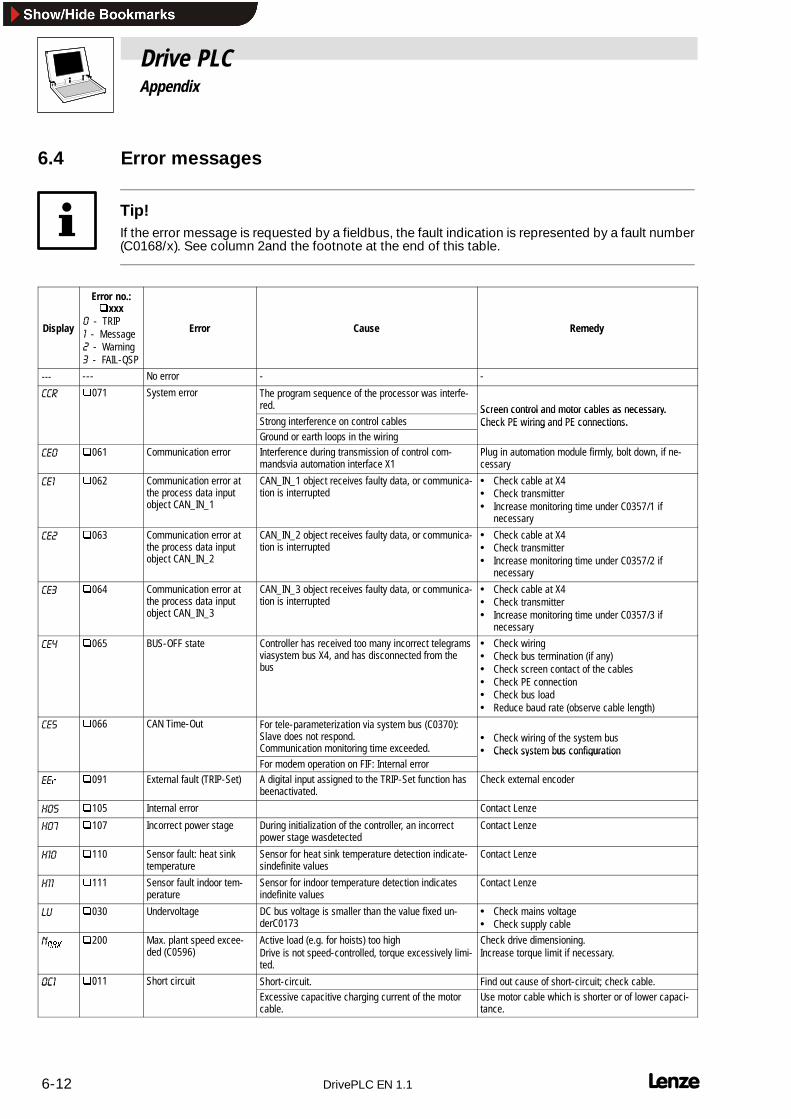
Drive PLCAppendix
6-12 DrivePLC EN 1.1
6.4 Error messages
Tip!If the error message is requested by a fieldbus, the fault indication is represented by a fault number(C0168/x). See column 2and the footnote at the end of this table.
Display
Error no.:qxxx
- TRIP - Message - Warning - FAIL-QSP
Error Cause Remedy
--- No error - -
&&5 q071 System error The program sequence of the processor was interfe-red. Screen control and motor cables as necessary.Strong interference on control cables
Screen control and motor cables as necessary.Check PE wiring and PE connections.
Ground or earth loops in the wiringCheck PE wiring and PE connections.
&( q061 Communication error Interference during transmission of control com-mandsvia automation interface X1
Plug in automation module firmly, bolt down, if ne-cessary
&( q062 Communication error atthe process data inputobject CAN_IN_1
CAN_IN_1 object receives faulty data, or communica-tion is interrupted
• Check cable at X4• Check transmitter• Increase monitoring time under C0357/1 if
necessary
&( q063 Communication error atthe process data inputobject CAN_IN_2
CAN_IN_2 object receives faulty data, or communica-tion is interrupted
• Check cable at X4• Check transmitter• Increase monitoring time under C0357/2 if
necessary
&( q064 Communication error atthe process data inputobject CAN_IN_3
CAN_IN_3 object receives faulty data, or communica-tion is interrupted
• Check cable at X4• Check transmitter• Increase monitoring time under C0357/3 if
necessary
&( q065 BUS-OFF state Controller has received too many incorrect telegramsviasystem bus X4, and has disconnected from thebus
• Check wiring• Check bus termination (if any)• Check screen contact of the cables• Check PE connection• Check bus load• Reduce baud rate (observe cable length)
&( q066 CAN Time-Out For tele-parameterization via system bus (C0370):Slave does not respond.Communication monitoring time exceeded.
• Check wiring of the system bus• Check system bus configuration
For modem operation on FIF: Internal error• Check system bus configuration
(( q091 External fault (TRIP-Set) A digital input assigned to the TRIP-Set function hasbeenactivated.
Check external encoder
+ q105 Internal error Contact Lenze
+ q107 Incorrect power stage During initialization of the controller, an incorrectpower stage wasdetected
Contact Lenze
+ q110 Sensor fault: heat sinktemperature
Sensor for heat sink temperature detection indicate-sindefinite values
Contact Lenze
+ q111 Sensor fault indoor tem-perature
Sensor for indoor temperature detection indicatesindefinite values
Contact Lenze
/8 q030 Undervoltage DC bus voltage is smaller than the value fixed un-derC0173
• Check mains voltage• Check supply cable
10$;
q200 Max. plant speed excee-ded (C0596)
Active load (e.g. for hoists) too highDrive is not speed-controlled, torque excessively limi-ted.
Check drive dimensioning.Increase torque limit if necessary.
2& q011 Short circuit Short-circuit. Find out cause of short-circuit; check cable.2& 0 S o c cuExcessive capacitive charging current of the motorcable.
Use motor cable which is shorter or of lower capaci-tance.

Drive PLCAppendix
6-13 DrivePLC EN 1.1
Display RemedyCauseError
Error no.:qxxx
- TRIP - Message - Warning - FAIL-QSP
2& q012 Earth fault One of the motor phases has earth contact. • Check motor• Check supply module
Excessive capacitive charging current of the motorcable.
Use motor cable which is shorter or of lowercapacitance.
2& q015 I x t overload Frequent and too long acceleration with overcurrentContinuous overload with Imotor > 1.05 x Irx.
Check drive dimensioning.
2+ q050 Heat sink temperature ishigher than the value setin the controller
Ambient temperature Tamb > 40 5C or 50 5C. • Allow controller to cool and ensure betterventilation.
• Check ambient temperature in the control cabinet.Heat sink very dirty. Clean heat sinkIncorrect mounting position. Change mounting position.
2+ q053 Heat sink temperature ishigher than the value seti th t ll
Motor too hot because of excessive current orfrequent and too long acceleration
Check drive dimensioning.g
in the controller No PTC connected. Connect PTC or switch-off monitoring (C0583=3).2+ q054 Heat sink temperature is
higher than the value setunder C0122.
Ambient temperature Tamb > 40 5C or 50 5C. • Allow controller to cool and ensure betterventilation.
• Check ambient temperature in the control cabinet.Heat sink very dirty. Clean heat sinkIncorrect mounting position. Change mounting position.Value set under C0122 was too low. Enter higher value.
2+ q057 Motor temperature ishigher than the value set
d C0121
Motor too hot because of excessive current orfrequent and too long acceleration
Check drive dimensioning.g
under C0121. No PTC connected. Connect PTC or switch-off monitoring (C0584=3).Value set under C0121 was too low. Enter higher value.
2+ q58 PTC at terminals T1, T2indicates motor overheat.
Motor too hot because of excessive current orfrequent and too long acceleration
Check drive dimensioning.
Terminals T1, T2 are not assigned. Connect PTC or thermostat or switch off monitoring(C0585=3).
3(5 q074 Program fault A fault in the program was detected. Send controller with data (on diskette) to Lenze.
3, q079 Initializing error • A fault was detected during transfer of parameterset between the controllers
• Parameter set does not match the controller (e.g.when data were transmitted from a controller withmore performance to a controller with lessperformance.)
Correct parameter set.
3535
q075q072
Parameter set error • Fault when loading a parameter set.CAUTION: The Lenze default setting is loadedautomatically.• Interrupt during the transmission of PS with the
keypad (e.g. by disconnecting the keypad), ifnecessary.
• Set the required parameters and store them underC0003.
• For PRO the supply voltage must be switched offadditionally.
The saved parameters do not match the loaded soft-ware version.The Lenze default setting is loaded automatically.
Before acknowledging the error, first save allparameter sets manually under C0003.
6' q082 Resolver fault Resolver cable interrupted. • Check the resolver cable for open circuit• Check resolver.• or switch off monitoring (C0586 = 3).
6' q083 Encoder fault at X9/8 Cable interrupted. Check cable for open circuit.6' 083 code au a 9/8Input X9 PIN 8 not assigned. Assign input X9 PIN 8 with 5V or switch off
monitoring (C0587 = 3).
6' q085 Master current source de-fective
Master current at X6/1 X6/2 < 2mA. • Check cable for open circuit.• Check master current source.
6' q086 Sensor fault Encoder of the motor temperature detection at X7 orX8 indicates indefinite values.
Check supply cable for firm connection.Switch off monitoring with C0594 = 3 if necessary.

Drive PLCAppendix
6-14 DrivePLC EN 1.1
Display RemedyCauseError
Error no.:qxxx
- TRIP - Message - Warning - FAIL-QSP
6' q087 Encoder fault Absolute encoder with RS485 interface does nottransmit data.
Check supply cable.Check encoder.Check voltage supply C0421.No Stegmann encoder connected.
OTF55817$6.
q201 Time-out task with Id.2(see task configuration)
OTF55817$6.
q202 Time-out task with Id.3(see task configuration)
OTF55817$6.
q203 Time-out task with Id.4(see task configuration)
OTF55817$6.
q204 Time-out task with Id.5(see task configuration)
Task processing takes longer than the monitoring
• Set task runtime• Modify monitoring time, if necessary• Determine the cause of time-out by checking the
OTF55817$6.
q205 Time-out task with Id.6(see task configuration)
Task processing takes longer than the monitoringtime set
• Determine the cause of time out by checking thetask runtimes at the task monitor.
• Swap out time-critical program parts in a slowertask
OTF55817$6.
q206 Time-out task with Id.7(see task configuration)
OTF55817$6.
q207 Time-out task with Id.8(see task configuration)
OTF55817$6.
q208 Time-out task with Id.9(see task configuration)
)/2$76<67
q209 Floating point error (REAL)in the system task
Error in the real calculationThe task in which the error occurred was incorrectly
The fault is eliminated as in a task overflow.NOTE: Please check yo r real calc lation before
)/2$7&<&/7
q210 Floating point error (REAL)in the system task
The task in which the error occurred was incorrectlycalculated.A real error can occur when dividing by 0.
NOTE: Please check your real calculation beforeacknowledging the trip.
)/2$77$6.
q211 Floating point error (REAL)in the task with Id2
)/2$77$6.
q212 Floating point error (REAL)in task with Id.3
)/2$77$6.
q213 Floating point error (REAL)in task with Id.4
)/2$77$6.
q214 Floating point error (REAL)in task with Id.5
Division by 0 Browse program code)/2$77$6.
q215 Floating point error (REAL)in task with Id.6
Division by 0 Browse program code
)/2$77$6.
q216 Floating point error (REAL)in task with Id.7
)/2$77$6.
q217 Floating point error (REAL)in task with Id.8
)/2$77$6.
q218 Floating point error (REAL)in task with Id.9
1O7).7&5(',7
q220 Insufficient units on thetarget system
The system attempts to load a program withtechnology functions on a Servo PLC with insufficientunits.
Extend the instance of your Servo PLC
1) Temperature detection via resolver or incremental encoder.

Drive PLCAppendix
6-15 DrivePLC EN 1.1
6.5 Index
A
Absolute addresses, 2-2
Addresses, absolute , 2-2
Analog inputsInputs_ANALOG1_CPU1 (AIN1), 2-21
Inputs_ANALOG2_CPU1 (AIN2), 2-23
Inputs_ANALOG3_CPU1 (AIN3), 2-24
Inputs_ANALOG4_CPU1 (AIN4), 4-7
Inputs_ANALOG5_CPU1 (AIN5), 4-8
Appendix, 6-1
Automation interfaceInputs_AIF1 (AIF1_IN), 2-4
Inputs_AIF2 (AIF2_IN), 2-10
Inputs_AIF3 (AIF3_IN), 2-15
Management, 2-20
Outputs_AIF1 (AIF1_OUT), 2-7
Outputs_AIF2 (AIF2_OUT), 2-12
Outputs_AIF3 (AIF3_OUT), 2-17
Automation interface (AIF1_IO_AutomationInterface), 2-4
Automation interface (AIF2_IO_AutomationInterface), 2-10
Automation interface (AIF3_IO_AutomationInterface), 2-15
C
CAN network, Communication phases, 5-39
CAN-busBaud-rate setting , 5-30
Boot-Up setting , 5-33
Bus load, 5-34
Bus Off, 5-36
Bus status, 5-34
Codes (description), 5-30
Defining a master in a drive group , 5-30
General address assignment , 5-31
Identifier, 5-33
Monitoring, 5-36
Monitoring times , 5-36
Parameterization, 5-41Example of a data format, 5-43Index LOW/HIGH-byte, 5-42
Read a parameter (example), 5-45
Reset-Node, 5-36
selective addressing, 5-32
Telegram counter, 5-34
Write a parameter (example), 5-44
CANopenAdressing the drives , 5-38Communication profile of the system bus , 5-37Data description , 5-37Identifier, 5-37Selective identifier definition, 5-38User data , 5-37
Code number, Index, 5-29
Code table, 6-2
CodesCAN-bus, 5-30CAN-bus: Diagnosis, 5-34Index, 5-29
Comments on wiring, Function module LECOM-B (RS485),5-3
Communication profile DS 301, 5-37
Cyclical process-data objects, 5-47
DData-type entry, Explanation of, 1-3
Definitions, 1-1
Diagnosis codes , for CAN-bus, 5-34
Digital frequency input (DF_IN), Touch-probe, 4-14
Digital frequency input (DFIN_IO), 4-9Technical data for connection, 4-12
DS 301, 5-37
EError messages, 6-12
Event-controlled process-data objects, 5-50
FField bus module, 5-1
FIF modules, 3-1Standard-I/O, 3-1
Free codes (FCODE), 2-27
Function module system bus (CAN)Comments on wiring, 5-3Wiring with host, Basic structure, 5-3
HHost, 5-1

Drive PLCAppendix
6-16 DrivePLC EN 1.1
IIdentifier, Explanation of, 1-3
Input_ANALOG1_STDIO (AIN1_STDIO), 3-1
Inputs_AIF1 (AIF1_IN), 2-4
Inputs_AIF2 (AIF2_IN), 2-10
Inputs_AIF3 (AIF3_IN), 2-15
Inputs_ANALOG1_CPU1 (AIN1), 2-21
Inputs_ANALOG2_CPU1 (AIN2), 2-23
Inputs_ANALOG3_CPU1 (AIN3), 2-24
Inputs_ANALOG4_CPU1 (AIN4), 4-7
Inputs_ANALOG5_CPU1 (AIN5), 4-8
Inputs_CAN1 (CAN1_IN), 5-10
Inputs_CAN2 (CAN2_IN), 5-15
Inputs_CAN3 (CAN3_IN), 5-19
Inputs_DIGITAL_CPU1 (DIGIN), 2-25
Inputs_DIGITAL_EB1 (DIGIN_EB1), 4-1
Inputs_DIGITAL_EB2 (DIGIN_EB2), 4-3
Inputs_DIGITAL_EB3 (DIGIN_EB3), 4-5
Inputs_DIGITAL_STDIO (DIGIN_STDIO), 3-3
LLenze software guidelines, Hungarian Notation, 1-2
MMessages, Error, 6-12
Module numbers, 2-2
Monitor output, 3-2
OOutput_ANALOG1_STDIO (AOUT1_STDIO), 3-2
Output_DIGITAL_STDIO (DIGOUT_STDIO), 3-4
Outputs_AIF1 (AIF1_OUT), 2-7
Outputs_AIF2 (AIF2_OUT), 2-12
Outputs_AIF3 (AIF3_OUT), 2-17
Outputs_ANALOG1_CPU1 (AOUT1), 2-22
Outputs_CAN2 (CAN2_OUT), 5-17
Outputs_CAN3 (CAN3_OUT), 5-21
Outputs_DIGITAL_CPU1 (DIGOUT), 2-26
Outputs_DIGITAL_EB1 (DIGOUT_EB1), 4-2
Outputs_DIGITAL_EB2 (DIGOUT_EB2), 4-4
Outputs_DIGITAL_EB3 (DIGOUT_EB3), 4-6
PParameter channels, 5-7
Parameterization, CAN-bus, 5-41
PLC functionality, 6-1
Prefix, Explanation of, 1-2
Process data, 5-46
Process data channels, 5-8cyclic, 5-8event-controlled, 5-9
Process-data objects, 5-47event-controlled, 5-50
SSafety information, Layout
Other notes, 1-1Warning of damage to material, 1-1
Signal type, Explanation of, 1-4
Sync-Management, 5-23
Synchronization of control program cycles, 5-23
System blocksAbsolute addresses, 2-2Automation interface (AIF1_IO), 2-4Automation interface (AIF2_IO), 2-10Automation interface (AIF3_IO), 2-15Digital frequency input (DFIN_IO), 4-9
Technical data for connection, 4-12Free codes (FCODE), 2-27Input_ANALOG1_STDIO (AIN1_STDIO), 3-1Inputs_ANALOG1_CPU1 (AIN1), 2-21Inputs_ANALOG2_CPU1 (AIN2), 2-23Inputs_ANALOG3_CPU1 (AIN3), 2-24Inputs_ANALOG4_CPU1 (AIN4), 4-7Inputs_ANALOG5_CPU1 (AIN5), 4-8Inputs_DIGITAL_CPU1 (DIGIN), 2-25Inputs_DIGITAL_EB1 (DIGIN_EB1), 4-1Inputs_DIGITAL_EB2 (DIGIN_EB2), 4-3Inputs_DIGITAL_EB3 (DIGIN_EB3), 4-5Inputs_DIGITAL_STDIO (DIGIN_STDIO), 3-3Module numbers, 2-2Output_ANALOG1_STDIO (AOUT1_STDIO), 3-2Output_DIGITAL_STDIO (DIGOUT_STDIO), 3-4Outputs_AIF2 (AIF2_OUT), 2-12Outputs_ANALOG1_CPU1 (AOUT1), 2-22Outputs_DIGITAL_CPU1 (DIGOUT), 2-26Outputs_DIGITAL_EB1 (DIGOUT_EB1), 4-2Outputs_DIGITAL_EB2 (DIGOUT_EB2), 4-4Outputs_DIGITAL_EB3 (DIGOUT_EB3), 4-6System bus (CAN1_IO), Inputs_CAN1 (CAN1_IN), 5-10System bus (CAN2_IO)
Inputs_CAN2 (CAN2_IN), 5-15Outputs_CAN2 (CAN2_OUT), 5-17

Drive PLCAppendix
6-17 DrivePLC EN 1.1
System bus (CAN3_IO)Inputs_CAN3 (CAN3_IN), 5-19Outputs_CAN3 (CAN3_OUT), 5-21
System markers (SYSTEM_FLAGS), 2-29
System bus, 5-1, 5-2data, 5-5
Bus length, 5-5Communication times, 5-5Processing times, 5-5Telegram throughput times, 5-5
Application example, 5-29Commissioning, 5-6Programming, 5-6
Parameter channels, 5-7Process data channels, 5-8
programming, Application example, 5-29Wiring, 5-3Wiring complying to EMC, 5-4
System bus (CAN1_IO), 5-10Inputs_CAN1 (CAN1_IN), 5-10
System bus (CAN2_IO), 5-15Inputs_CAN2 (CAN2_IN), 5-15Outputs_CAN2 (CAN2_OUT), 5-17
System bus (CAN3_IO), 5-19Inputs_CAN3 (CAN3_IN), 5-19Outputs_CAN3 (CAN3_OUT), 5-21
System marker (SYSTEM_FLAGS), 2-29
System variables, Explanation of, 1-4
T
Temporary codes, 6-2
Touch-probe, with SB DF_IN, 4-14
V
Variable names
Conventions, Hungarian Notation, 1-2
Lenze software guidelines, Explanation of, 1-2
Variable type , Labelling, 1-3
W
Wiring complying to EMC, 5-4

Drive PLCAppendix
6-18 DrivePLC EN 1.1