Embed Size (px)
Citation preview

Manual
CircuitCAM 6.1
Item
num
be
r: 1
25
23
6


Manual CircuitCAM 6.1 English, Version 1.0
LPKF Laser & Electronics AGOsteriede 7D-30827 Garbsen, Germany
Telephone : ++ 49 - 51 31 - 70 95 - 0 Fax : ++ 49 - 51 31 - 70 95 - 90E-mail : [email protected] : http: //www.lpkf.de

2 Status: 18.2.09 Version 1.0 CircuitCAM 6.1
Copyright (c) 2009 LPKF AGDistribution and reproduction of this manual and use of its content is only permitted with written permission from LPKF AG. The contents of this manual are subject to change without notice. No liability is accepted for the information contained within this manual or, in particular, for damages resulting from information contained in this manual, information missing from this manual or erroneous information in this manual. HP-GL is a registered trademark of Hewlett-Packard Comp. All other trademarks are registered by their respective owners.
Item number: 125236

CircuitCAM 6.1 Status: 18.2.09 Version 1.0 3
About this manualThis manual is an introduction to using CircuitCAM 6.1 for Windows TM .
CircuitCAM is a combined Computer Aided Design (CAD) and Computer Aided Manufacturing (CAM) program.
You can use CircuitCAM to import, check and edit circuit board production data in various CAM formats, and then output them into a CAM format (LMD). CircuitCAM is particularly useful for calculating the insulation channels between the conductor tracks in circuit board prototype production using LPKF circuit board plotters.
In addition to explaining how to install the CircuitCAM software and providing a general introduction to the CircuitCAM user surface, it teaches you the basic features and concept of CircuitCAM through using exercises.
This manual does not provide basic information on how to run the Windows interface. If you are not yet familiar with the different Windows objects, please refer to the Windows documentation first.
In order to improve the quality of presentation in this tutorial, some of the colours in the illustrations differ from the original presentation on the screen.
The software user is responsible for checking that the following points are followed. You must ensure that
• the software is only used as directed in association with the system which has been supplied;
• the complete manual is kept in a legible condition and is always readily available at the place where the software is being used;
• only authorised and sufficiently qualified personnel are entrusted with operating the software;
• the member of staff has read and understood this manual, particularly the safety instructions which it contains.

4 Status: 18.2.09 Version 1.0 CircuitCAM 6.1
I. Conventions used in this manual
Bold text is used to emphasise important information.
Illustrations (figures) are numbered sequentially. Example: Fig. 5
Prompts for actions are identified with an arrow: “>“.
Paragraphs in italics are used to indicate the responses to an action.
Words in italics indicate proper names.
Key inscriptions and menu terms are printed in BOLD CAPITALS.
II. Notes on the symbols used Danger!This symbol is used to highlight risks to life or health.
Caution! This symbol is used to identify hazards which may cause damage.
Note: This symbol is for advice on avoiding faults during operation or on improving operation
III. Legend
CircuitCAM : Software for data processing
BoardMaster : Machine control software
IV. Target GroupThis Manual is intended for personnel who are familiar with the basic use of Windows as well as exporting the corresponding data from the CAD programs used (Eagle, Protel... etc.).
CircuitCAM 6.1 Status: 18.2.09 Version 1.0 5
Contents
1.0 Installation . . . . . . . . . . . . . . . . . . . . . . . . 9
1.1 System requirements . . . . . . . . . . . . . . . . . . . . . . . . . . . 91.2 Materials supplied . . . . . . . . . . . . . . . . . . . . . . . . . . . . . . 91.3 Installation . . . . . . . . . . . . . . . . . . . . . . . . . . . . . . . . . . . . 91.4 Directories installed . . . . . . . . . . . . . . . . . . . . . . . . . . . 101.5 Starting CircuitCAM . . . . . . . . . . . . . . . . . . . . . . . . . . . . 101.6 Registration and activation . . . . . . . . . . . . . . . . . . . . . . 11 1.6.1 Online Registration . . . . . . . . . . . . . . . . . . . . . . . . . . 12 1.6.2 Offline Registration . . . . . . . . . . . . . . . . . . . . . . . . . . 15 1.6.3 Activating the program later . . . . . . . . . . . . . . . . . . . . 191.7 User settings . . . . . . . . . . . . . . . . . . . . . . . . . . . . . . . . . 20 1.7.1 Configurable shortcuts ........................................... ... 21
2.0 Getting started . . . . . . . . . . . . . . . . . . . . 22
2.1 Using online help . . . . . . . . . . . . . . . . . . . . . . . . . . . . . 222.2 Showing program information . . . . . . . . . . . . . . . . . . . 232.3 CircuitCAM application window . . . . . . . . . . . . . . . . . . 24 2.3.1 Graphics window. . . . . . . . . . . . . . . . . . . . . . . . . . . . 25 2.3.2 List window . . . . . . . . . . . . . . . . . . . . . . . . . . . . . . . . 26 2.3.3 Report window . . . . . . . . . . . . . . . . . . . . . . . . . . . . . 27 2.3.4 Toolbars . . . . . . . . . . . . . . . . . . . . . . . . . . . . . . . . . . 27 2.3.5 Status bar . . . . . . . . . . . . . . . . . . . . . . . . . . . . . . . . . 302.4 Opening the "Tutor" sample circuit board . . . . . . . . . . 302.5 Closing CircuitCAM . . . . . . . . . . . . . . . . . . . . . . . . . . . 30
3.0 Preface to the exercises . . . . . . . . . . . . 31
3.1 "Tutor" sample circuit board . . . . . . . . . . . . . . . . . . . . 313.2 List of the exercise files . . . . . . . . . . . . . . . . . . . . . . . . 32
4.0 Exercise 1 . . . . . . . . . . . . . . . . . . . . . . . . 33
4.1 Creating a new document . . . . . . . . . . . . . . . . . . . . . . . 334.2 Grid, units and coordinates display . . . . . . . . . . . . . . . . 344.3 Importing production data . . . . . . . . . . . . . . . . . . . . . . . 36 4.3.1 Importing . . . . . . . . . . . . . . . . . . . . . . . . . . . . . . . . . . 36
6 Status: 18.2.09 Version 1.0 CircuitCAM 6.1
5.0 Exercise 2 48
5.1 Checking production data . . . . . . . . . . . . . . . . . . . . . . . 48 5.1.1 Working with the view functions . . . . . . . . . . . . . . . . . 48 5.1.2 Working in the layer list window . . . . . . . . . . . . . . . . . 495.2 Preparing production data for prototyping . . . . . . . . . . 54 5.2.1 Deleting graphic objects outside the circuit board . . . 54 5.2.2 Moving the circuit board outline to a separate layer. . 585.3 Improved coordinate entry . . . . . . . . . . . . . . . . . . . . . . 60 5.3.1 Placing text objects on separate layers . . . . . . . . . . . 61 5.3.2 Insulation with the default job . . . . . . . . . . . . . . . . . . . 62
5.3.2.1 Exporting production data............................... ... 63 5.3.3 Importing the data using the import assignment . . . . 65
6.0 Exercise 3 . . . . . . . . . . . . . . . . . . . . . . . 66
6.1 Using contour generator . . . . . . . . . . . . . . . . . . . . . . . . 66 6.1.1 Modifiable milling direction and sequence . . . . . . . . . 706.2 Creating rubout areas . . . . . . . . . . . . . . . . . . . . . . . . . . 71
7.0 Exercise 4 . . . . . . . . . . . . . . . . . . . . . . . 76
7.1 Customising insulation jobs . . . . . . . . . . . . . . . . . . . . . 76 7.1.1 CircuitCAM - Lite . . . . . . . . . . . . . . . . . . . . . . . . . . . . 76 7.1.2 CircuitCAM - PCB. . . . . . . . . . . . . . . . . . . . . . . . . . . . 80 7.1.3 Insulating areas (PCBs only) . . . . . . . . . . . . . . . . . . . 83 7.1.4 Colour assignment for isolating tools . . . . . . . . . . . . . 85
8.0 Exercise 5 . . . . . . . . . . . . . . . . . . . . . . . 86
8.1 Creating a CircuitCAM template file . . . . . . . . . . . . . . . 86
9.0 Exercise 6 . . . . . . . . . . . . . . . . . . . . . . . 89
9.1 Using import assignments . . . . . . . . . . . . . . . . . . . . . . 899.2 Moving layers . . . . . . . . . . . . . . . . . . . . . . . . . . . . . . . . 949.3 Rotating layers . . . . . . . . . . . . . . . . . . . . . . . . . . . . . . . 96
10.0 Appendix . . . . . . . . . . . . . . . . . . . . . . 101
10.1 Gerber format . . . . . . . . . . . . . . . . . . . . . . . . . . . . . . 101 10.1.1 Use of Gerber format . . . . . . . . . . . . . . . . . . . . . . . 101 10.1.2 Setting up a photoplotter . . . . . . . . . . . . . . . . . . . . 101

CircuitCAM 6.1 Status: 18.2.09 Version 1.0 7
10.1.3 Gerber format Syntax . . . . . . . . . . . . . . . . . . . . . . . 102 10.1.3.1 Drawing . . . . . . . . . . . . . . . . . . . . . . . . . . . . . 102 10.1.3.2 Flashing . . . . . . . . . . . . . . . . . . . . . . . . . . . . . 103
10.1.4 Aperture list. . . . . . . . . . . . . . . . . . . . . . . . . . . . . . . 104 10.1.5 Units, format and suppressed zeros . . . . . . . . . . . . 105 10.1.6 Extended Gerber. . . . . . . . . . . . . . . . . . . . . . . . . . . 10610.2 Predefined Layer . . . . . . . . . . . . . . . . . . . . . . . . . . . . 10810.3 Importing DXF files . . . . . . . . . . . . . . . . . . . . . . . . . . 10910.4 Text Function . . . . . . . . . . . . . . . . . . . . . . . . . . . . . . . 11510.5 Generating earth areas . . . . . . . . . . . . . . . . . . . . . . . 11610.6 Design Rule Check . . . . . . . . . . . . . . . . . . . . . . . . . . 11910.7 CircuitCAM template files . . . . . . . . . . . . . . . . . . . . . 123 10.7.1 Creating your own template file . . . . . . . . . . . . . . . 124 10.7.2 Saving an aperture list in the template file . . . . . . . 125 10.7.3 Saving a modified insulation job . . . . . . . . . . . . . . . 127 10.7.4 Saving a new layer . . . . . . . . . . . . . . . . . . . . . . . . . 128 10.7.5 Saving the parameters . . . . . . . . . . . . . . . . . . . . . . 12910.8 Prepared insulation jobs . . . . . . . . . . . . . . . . . . . . . . 13010.9 Creating drilling/milling tools . . . . . . . . . . . . . . . . . . . 130 10.9.1 Defining a new drilling tool . . . . . . . . . . . . . . . . . . . 132 10.9.2 Defining a new milling tool . . . . . . . . . . . . . . . . . . . 13610.10 Export jobs . . . . . . . . . . . . . . . . . . . . . . . . . . . . . . . 14110.11 Processing AL-front panels (PCB version) . . . . . . . 144 10.11.1 Preparing front panel outline data. . . . . . . . . . . . . 145 10.11.2 Preparing cutting and drilling data . . . . . . . . . . . . 146 10.11.3 Setting text data . . . . . . . . . . . . . . . . . . . . . . . . . . 14910.12 Exporting and saving . . . . . . . . . . . . . . . . . . . . . . . . 15010.13 Preparing data for fiducial recognition . . . . . . . . . . . 15010.14 Producing step-and-repeats (PCB version only) . . . 15210.15 CircuitCAM 6.1 Hotkeys . . . . . . . . . . . . . . . . . . . . . 15410.16 Adapting translation file . . . . . . . . . . . . . . . . . . . . . . 156 10.16.1 Structure of translation files . . . . . . . . . . . . . . . . . 157 10.16.2 Tips for adapting translation files . . . . . . . . . . . . . 163
11.0 Index . . . . . . . . . . . . . . . . . . . . . . . . . . 168

8 Status: 18.2.09 Version 1.0 CircuitCAM 6.1

Installation
CircuitCAM 6.1 Status: 18.2.09 Version 1.0 9
1.0 Installation
1.1 System requirementsThe minimum system requirements for installing CircuitCAM are:
IBM PC or compatible system with
• Pentium IV or similar processor,
• 512 MB Main memory (1 GB recommended),
• VGA colour monitor (recommended resolution: 1280 x 1024 pixels),
• Microsoft Windows 2000 or Windows XP operating system,
• CD-ROM drive (4x speed).
CircuitCAM requires approximately 20 MB free hard disk space for its installation.
1.2 Materials supplied The materials supplied with CircuitCAM include:
• 1 x CD-ROM,
• This manual,
• Licence card.
1.3 InstallationAs soon as you have inserted the CD in the CD-ROM drive of your PC (provided the autostart-function of this drive is activated) the CD browser will start automatically. The installation procedure for your LPKF program is menu driven.If the autostart function is not activated on your PC, then proceed as follows:
› Select RUN from the WINDOWS START MENU.
› Then click on BROWSE.
› Now select the CircuitCAM installation directory and double click on “Setup.exe”.
The installation routine for CircuitCAM will start running.
› Follow the instructions in the installation program.
Note: Clicking on CANCEL allows you to close the dialog box and cancel the installation.
Installation
10 Status: 18.2.09 Version 1.0 CircuitCAM 6.1
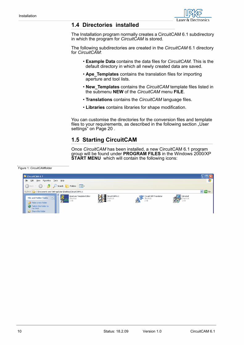
1.4 Directories installedThe Installation program normally creates a CircuitCAM 6.1 subdirectory in which the program for CircuitCAM is stored.
The following subdirectories are created in the CircuitCAM 6.1 directory for CircuitCAM:
• Example Data contains the data files for CircuitCAM. This is the default directory in which all newly created data are saved.
• Ape_Templates contains the translation files for importing aperture and tool lists.
• New_Templates contains the CircuitCAM template files listed in the submenu NEW of the CircuitCAM menu FILE.
• Translations contains the CircuitCAM language files.
• Libraries contains libraries for shape modification.
You can customise the directories for the conversion files and template files to your requirements, as described in the following section „User settings“ on Page 20 .
1.5 Starting CircuitCAM Once CircuitCAM has been installed, a new CircuitCAM 6.1 program group will be found under PROGRAM FILES in the Windows 2000/XP START MENU which will contain the following icons:
Figure 1: CircuitCAMfolder

Installation
CircuitCAM 6.1 Status: 18.2.09 Version 1.0 11
How to start CircuitCAM:
In the START MENU under Programs, select CIRCUITCAM 6.1.
Figure 2: Starting the program
Note: you can also start CircuitCAM via the link on the desktop of your computer.
1.6 Registration and activationNote: for the registration procedure, you will need the LPKF CircuitCAM licence card supplied with the software.
Before you can use CircuitCAM, you must activate the program first. When the program is first invoked after it is installed, the “CircuitCAM activation” dialog box opens.
Figure 3:Activating CircuitCAM
› Click on the box “User name” and enter your name.
› Click on the box “Organisation” and enter your company name.
› Click on the box “Location” and enter the head office address of your company.
› Click on the box “Serial number” and enter the serial number of your CircuitCAM licence card.
› Click on the box “Licence ID” and enter the activation number of your CircuitCAM licence card.
Installation
12 Status: 18.2.09 Version 1.0 CircuitCAM 6.1
Note: you can activate a trial version of the CircuitCAM software by clicking on the button “Viewer variant”. You do not need the serial number or the activation number for this trial version.
› Now click on NEXT in order to continue with the activation.CircuitCAM now starts to activate your CircuitCAM licence.
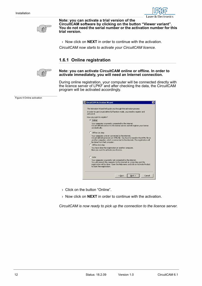
1.6.1 Online registration
Note: you can activate CircuitCAM online or offline. In order to activate immediately, you will need an Internet connection.
During online registration, your computer will be connected directly with the licence server of LPKF and after checking the data, the CircuitCAM program will be activated accordingly.
Figure 4:Online activation
› Click on the button “Online”.
› Now click on NEXT in order to continue with the activation.
CircuitCAM is now ready to pick up the connection to the licence server.
Installation
CircuitCAM 6.1 Status: 18.2.09 Version 1.0 13
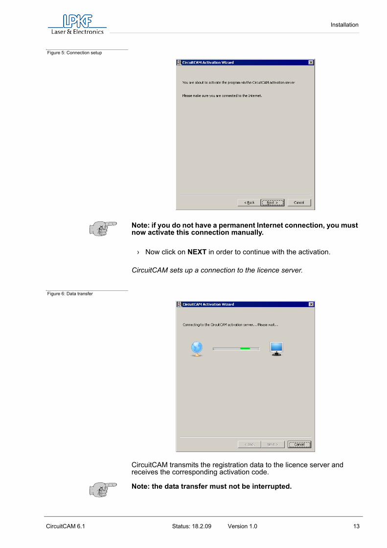
Figure 5: Connection setup
Note: if you do not have a permanent Internet connection, you must now activate this connection manually.
› Now click on NEXT in order to continue with the activation.
CircuitCAM sets up a connection to the licence server.
Figure 6: Data transfer
CircuitCAM transmits the registration data to the licence server and receives the corresponding activation code.
Note: the data transfer must not be interrupted.

Installation
14 Status: 18.2.09 Version 1.0 CircuitCAM 6.1
Figure 7: Terminating registration
After the CircuitCAM version has been successfully registered, you can terminate the activation.
› Click on Finish.
Note: If the activation was not successful, this may be due to the safety settings of your internet connection (firewall). In this case you can alternatively choose the offline-registration.
Installation
CircuitCAM 6.1 Status: 18.2.09 Version 1.0 15
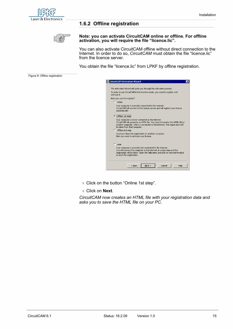
1.6.2 Offline registration
Note: you can activate CircuitCAM online or offline. For offline activation, you will require the file “licence.lic”.
You can also activate CircuitCAM offline without direct connection to the Internet. In order to do so, CircuitCAM must obtain the file “licence.lic” from the licence server.
You obtain the file “licence.lic” from LPKF by offline registration.
Figure 8: Offline registration
› Click on the button “Online 1st step”.
› Click on Next.CircuitCAM now creates an HTML file with your registration data and asks you to save the HTML file on your PC.
Installation
16 Status: 18.2.09 Version 1.0 CircuitCAM 6.1
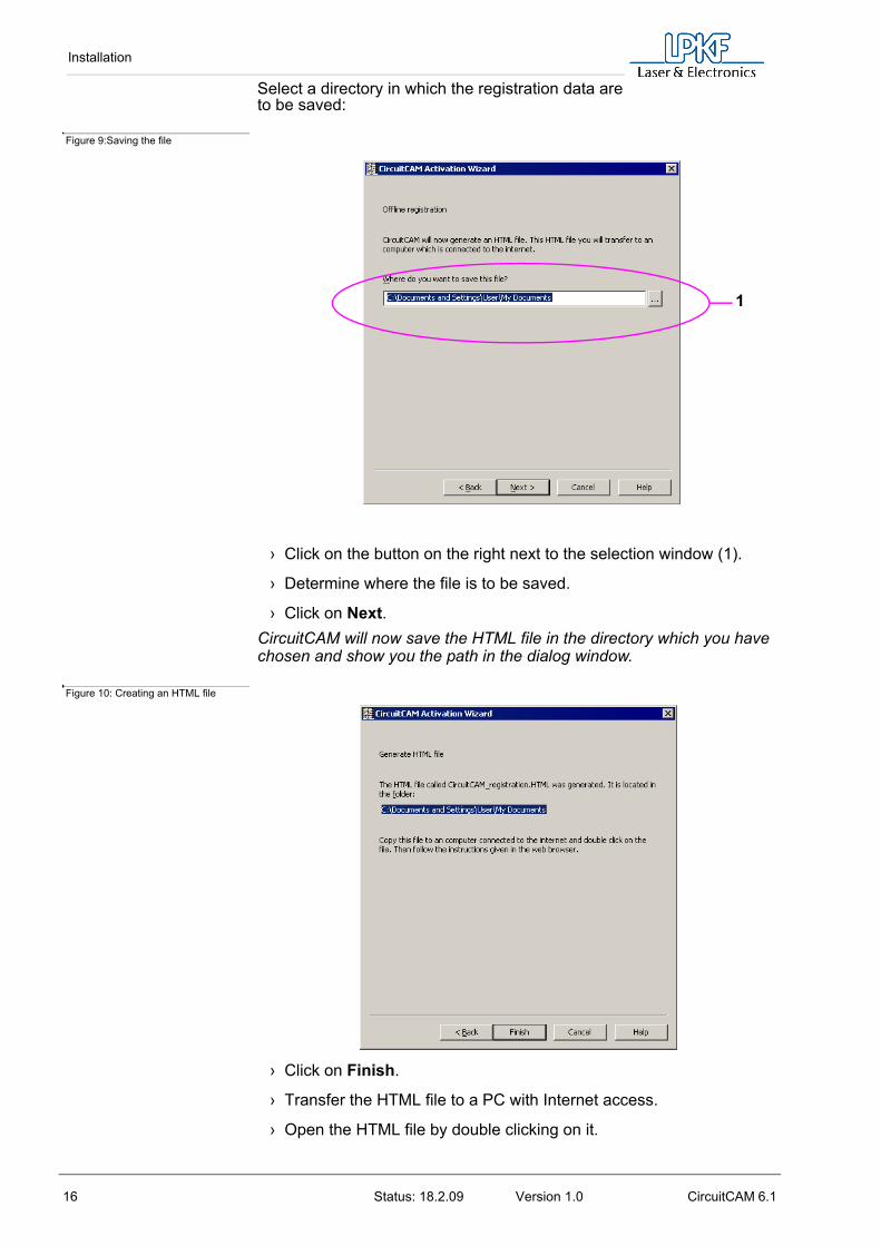
Select a directory in which the registration data are to be saved:
Figure 9:Saving the file
› Click on the button on the right next to the selection window (1).
› Determine where the file is to be saved.
› Click on Next. CircuitCAM will now save the HTML file in the directory which you have chosen and show you the path in the dialog window.
Figure 10: Creating an HTML file
› Click on Finish.
› Transfer the HTML file to a PC with Internet access.
› Open the HTML file by double clicking on it.
1

Installation
CircuitCAM 6.1 Status: 18.2.09 Version 1.0 17
The HTML file will open with a browser.The registration data will now be transmitted to the licence server. After registration has been successfully completed, the licence server will send the activation file “licence.lic”.
Figure 11: Registration .
› In order for this to take place, click on REQUEST LICENCE FILE.
› Save the activation file in a directory.
› Transfer the activation file to the PC with the CircuitCAM software installed on it.
› Open the HELP menu and click on ACTIVE PRODUCT.
› Click on NEXT.
› Click on Offline 2nd step.
Figure 12: Offline, second step .
› Click on NEXT.
Installation
18 Status: 18.2.09 Version 1.0 CircuitCAM 6.1
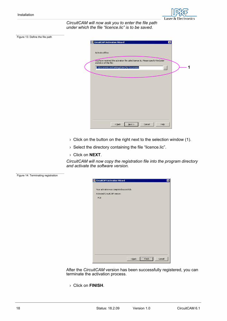
CircuitCAM will now ask you to enter the file path under which the file “licence.lic” is to be saved.
Figure 13: Define the file path
› Click on the button on the right next to the selection window (1).
› Select the directory containing the file “licence.lic”.
› Click on NEXT.CircuitCAM will now copy the registration file into the program directory and activate the software version.
Figure 14: Terminating registration
After the CircuitCAM version has been successfully registered, you can terminate the activation process.
› Click on FINISH.
1
Installation
CircuitCAM 6.1 Status: 18.2.09 Version 1.0 19
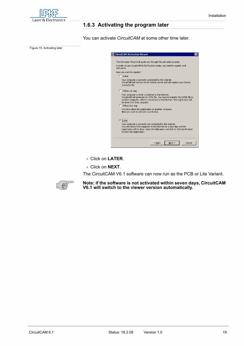
1.6.3 Activating the program later
You can activate CircuitCAM at some other time later.
Figure 15: Activating later
› Click on LATER.
› Click on NEXT.The CircuitCAM V6.1 software can now run as the PCB or Lite Variant.
Note: if the software is not activated within seven days, CircuitCAM V6.1 will switch to the viewer version automatically.
Installation
20 Status: 18.2.09 Version 1.0 CircuitCAM 6.1
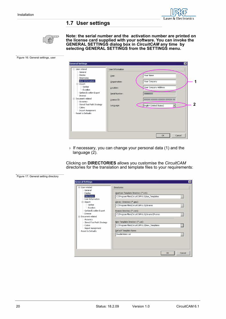
1.7 User settings
Note: the serial number and the activation number are printed on the license card supplied with your software. You can invoke the GENERAL SETTINGS dialog box in CircuitCAM any time by selecting GENERAL SETTINGS from the SETTINGS menu.
Figure 16: General settings, user
› If necessary, you can change your personal data (1) and the language (2).
Clicking on DIRECTORIES allows you customise the CircuitCAM directories for the translation and template files to your requirements:
Figure 17: General setting directory
1
2

Installation
CircuitCAM 6.1 Status: 18.2.09 Version 1.0 21
1.7.1 Configurable shortcuts
A key combination can be assigned to any program function of CircuitCAM. In order to add new key combinations or modify existing ones, click on the tab KEYBOARD under CUSTOMISE. The different function keys can be used to create new shortcuts and to modify or delete existing ones (see Illustration 18).
Figure 18: Shortcuts
Introduction
22 Status: 18.2.09 Version 1.0 CircuitCAM 6.1
2.0 Introduction
This chapter will give you an initial overview of CircuitCAM and familiarise you with the CircuitCAM user interface. It will show you how to customise CircuitCAM to your requirements and how to use the online help when you require more information on a particular topic.
Note: this tutorial deals with the default settings which were recommended during the installation and relates to the names of the program groups and the directories created.
2.1 Using the online helpCircuitCAM has a context sensitive online help. A help may also appear on a CircuitCAM function which has just been enabled. The online help also offers a contents, an index and a search function to enable you to find the required topic or term quickly.
How to invoke the online help topics:
› Select HELP TOPICS from the HELP menu.
Figure 19: HELP TOPICs
How to obtain help on the function just enabled:
› Press the F1 function key.
Please refer to your Windows documentation for information regarding the use of the online help.

Introduction
CircuitCAM 6.1 Status: 18.2.09 Version 1.0 23
2.2 Showing program informationYou can display the CircuitCAM version number by selecting ABOUT CIRCUITCAM... from the HELP menu.
Figure 20: Info CircuitCAM
This dialog box also contains information on how to contact us.
Introduction
24 Status: 18.2.09 Version 1.0 CircuitCAM 6.1
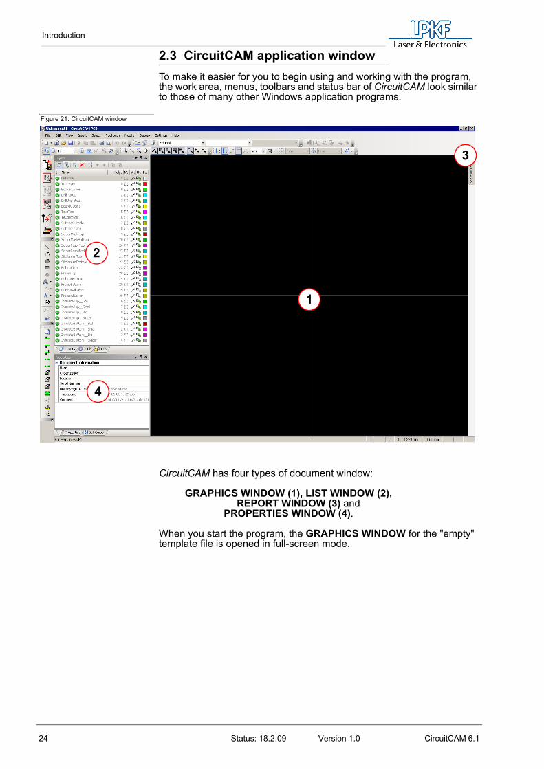
2.3 CircuitCAM application windowTo make it easier for you to begin using and working with the program, the work area, menus, toolbars and status bar of CircuitCAM look similar to those of many other Windows application programs.
Figure 21: CircuitCAM window
CircuitCAM has four types of document window:
GRAPHICS WINDOW (1), LIST WINDOW (2), REPORT WINDOW (3) and
PROPERTIES WINDOW (4).
When you start the program, the GRAPHICS WINDOW for the "empty" template file is opened in full-screen mode.
1
2
4
3

Introduction
CircuitCAM 6.1 Status: 18.2.09 Version 1.0 25
2.3.1 Graphics window
The production data imported for your circuit board are presented graphically in the graphics window. This allows you to check that all the data meet the desired requirements.
Note: the view is always of the circuit board top face, so the circuit board bottom face is shown as a mirror image.
Figure 22: Graphics window
The graphics window also gives you access to functions for editing the production data.

Introduction
26 Status: 18.2.09 Version 1.0 CircuitCAM 6.1
Note: when the mouse pointer is in the graphics window, clicking with the right mouse button will open a context menu for editing selected objects:
Figure 23: Context menu
2.3.2 List window
The list window displays the apertures and tools which have been imported and the layers in tabular form with their corresponding definitions. You can edit, delete or add new entries. Access to the following windows will be described later („Importing“ on Page 36).
Figure 24: List window
Introduction
CircuitCAM 6.1 Status: 18.2.09 Version 1.0 27
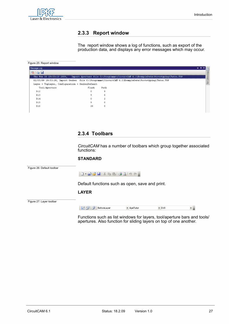
2.3.3 Report window
The report window shows a log of functions, such as export of the production data, and displays any error messages which may occur.
Figure 25: Report window
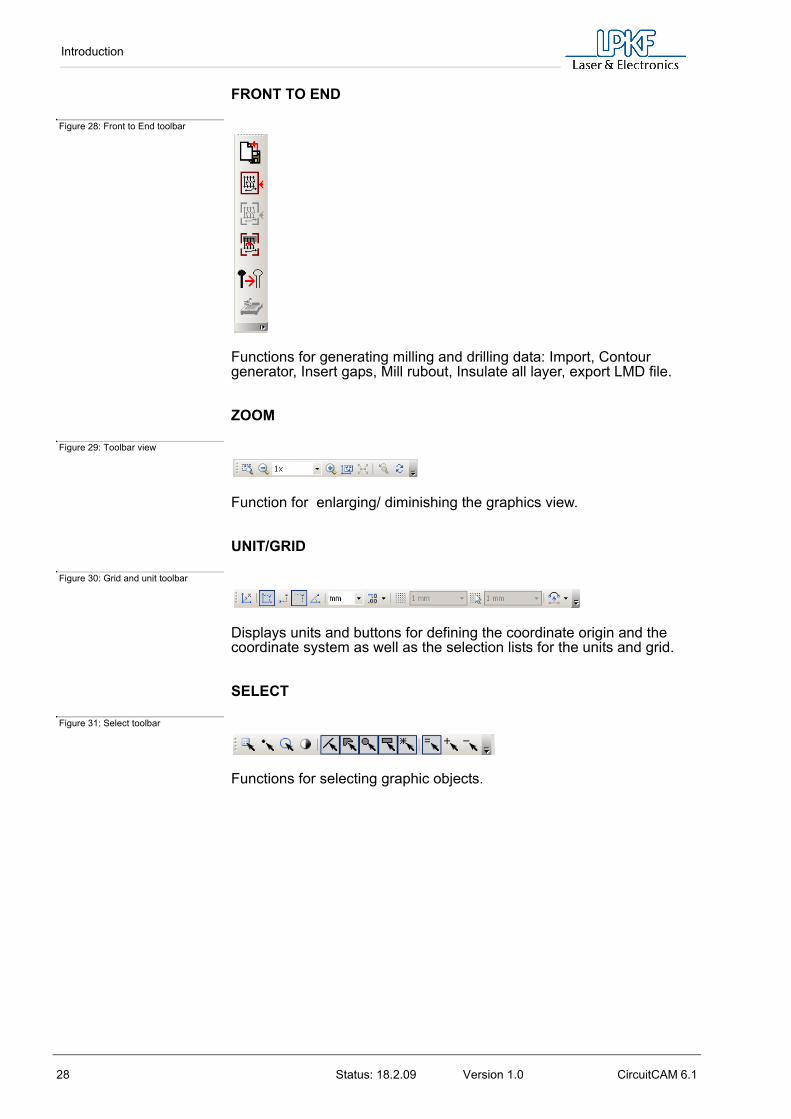
2.3.4 Toolbars
CircuitCAM has a number of toolbars which group together associated functions:
STANDARD
Figure 26: Default toolbar
Default functions such as open, save and print.
LAYER
Figure 27: Layer toolbar
Functions such as list windows for layers, tool/aperture bars and tools/apertures. Also function for sliding layers on top of one another.
Introduction
28 Status: 18.2.09 Version 1.0 CircuitCAM 6.1
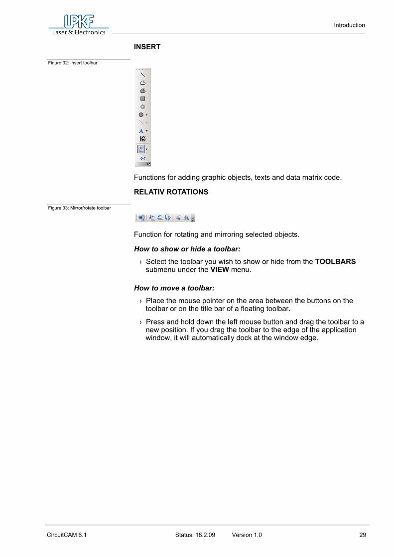
FRONT TO END
Figure 28: Front to End toolbar
Functions for generating milling and drilling data: Import, Contour generator, Insert gaps, Mill rubout, Insulate all layer, export LMD file.
ZOOM
Figure 29: Toolbar view
Function for enlarging/ diminishing the graphics view.
UNIT/GRID
Figure 30: Grid and unit toolbar
Displays units and buttons for defining the coordinate origin and the coordinate system as well as the selection lists for the units and grid.
SELECT
Figure 31: Select toolbar
Functions for selecting graphic objects.
Introduction
CircuitCAM 6.1 Status: 18.2.09 Version 1.0 29
INSERT
Figure 32: Insert toolbar
Functions for adding graphic objects, texts and data matrix code.
RELATIV ROTATIONS
Figure 33: Mirror/rotate toolbar
Function for rotating and mirroring selected objects.
How to show or hide a toolbar:
› Select the toolbar you wish to show or hide from the TOOLBARS submenu under the VIEW menu.
How to move a toolbar:
› Place the mouse pointer on the area between the buttons on the toolbar or on the title bar of a floating toolbar.
› Press and hold down the left mouse button and drag the toolbar to a new position. If you drag the toolbar to the edge of the application window, it will automatically dock at the window edge.

Introduction
30 Status: 18.2.09 Version 1.0 CircuitCAM 6.1
2.3.5 Status bar
The status bar at the bottom of the application window displays information regarding the object or function selected.
Figure 34: Status bar
The status bar is divided into four information areas:
• Textual information
• Number of objects selected
• Current coordinates of the cursor
• Coordinates of the anchor point
You can also show and hide the status bar by selecting STATUS BAR from the VIEW menu.
2.4 Opening the "Tutor" sample circuit boardProduction data for two sample circuit boards are supplied with CircuitCAM. We recommend using the "Tutor" sample circuit board when trying out the CircuitCAM functions for yourself.
How to open the "Tutor" sample circuit board:
› Select OPEN from the FILE menu.
› Select the directory Prototyping from the folder “C:\Programme\CircuitCAM 6.1\ExampleData”.
› Select the file TUTOR in the dialog box OPEN.
› Click on OPEN to open the file "TUTOR.CAM" or click on CANCEL to abort the process.
Note: if you have not opened CircuitCAM yet, then you can open the sample circuit board together with CircuitCAM. When you double click on Tutor. CAM in Windows Explorer, CircuitCAM starts and opens the sample circuit board automatically.
2.5 Closing CircuitCAM
How to exit CircuitCAM:
1. using the keyboard:
› Press ALT + F4.
2. using the mouse:
› Select EXIT from the FILE menu
or click on the top right-hand corner of the application window .
Preface to the exercises
CircuitCAM 6.1 Status: 18.2.09 Version 1.0 31
3.0 Preface to the exercises
The following sections will enable you to familiarise yourself with the basic functions of CircuitCAM by working through the exercises.
In the first exercise, you will load production data and prepare it for circuit board prototyping. This exercise is somewhat more extensive than the exercises which follow it because it covers the entire sequence of operations required to generate production data suitable for passing on to LPKF BoardMaster.
The rest of the exercises show you how to correct production data which do not match, for example, because a layer has been rotated or mirrored while exporting production data from the circuit board CAD program used or because there is an offset between the various types of production data. These sections will also introduce you to functions in CircuitCAM which will help you, so far as is possible, to prepare the production data for prototyping.
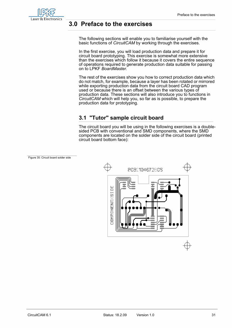
3.1 "Tutor" sample circuit boardThe circuit board you will be using in the following exercises is a double-sided PCB with conventional and SMD components, where the SMD components are located on the solder side of the circuit board (printed circuit board bottom face):
Figure 35: Circuit board solder side
Preface to the exercises
32 Status: 18.2.09 Version 1.0 CircuitCAM 6.1
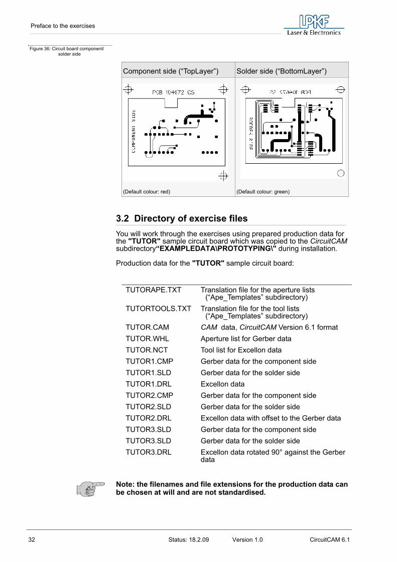
Figure 36: Circuit board component/solder side
3.2 Directory of exercise filesYou will work through the exercises using prepared production data for the "TUTOR" sample circuit board which was copied to the CircuitCAM subdirectory“EXAMPLEDATA\PROTOTYPING\" during installation.
Production data for the "TUTOR" sample circuit board:
Note: the filenames and file extensions for the production data can be chosen at will and are not standardised.
Component side (“TopLayer”) Solder side (“BottomLayer”)
(Default colour: red) (Default colour: green)
TUTORAPE.TXT Translation file for the aperture lists (“Ape_Templates” subdirectory)
TUTORTOOLS.TXT Translation file for the tool lists (“Ape_Templates” subdirectory)
TUTOR.CAM CAM data, CircuitCAM Version 6.1 format TUTOR.WHL Aperture list for Gerber dataTUTOR.NCT Tool list for Excellon data TUTOR1.CMP Gerber data for the component sideTUTOR1.SLD Gerber data for the solder sideTUTOR1.DRL Excellon dataTUTOR2.CMP Gerber data for the component sideTUTOR2.SLD Gerber data for the solder sideTUTOR2.DRL Excellon data with offset to the Gerber data TUTOR3.SLD Gerber data for the component sideTUTOR3.SLD Gerber data for the solder sideTUTOR3.DRL Excellon data rotated 90° against the Gerber
data
Exercise 1
CircuitCAM 6.1 Status: 18.2.09 Version 1.0 33
4.0 Exercise 1
This section will teach you how set the UNIT AND GRID, open a new document and import CAD production data.
The sequence of operations in CircuitCAM can be divided into the following three phases:
1. Import production data 2. Prepare production data for Prototyping 3. Export production data
4.1 Creating a new document In order to edit production data in CircuitCAM, you must first open a CircuitCAM document into which the production data will be imported.
CircuitCAM offers two ways of creating a new document:
• You can use the document based on the template file "DOUBLESIDED" which opens automatically in CircuitCAM when the program starts.
• You can create a new document by selecting a preconfigured template file from the NEW submenu under the FILE menu.
(You will find out more about template files in „Creating a CircuitCAM- template file“ on Page 86 and in „Appendix“ on Page 101)
Note: new documents are always named "UNTITLED" followed by a number. You can save these documents as a file by selecting SAVE AS from the FILE menu.
In this exercise, use the document based on the template file "DOUBLESIDED" in order to import the production data. This document opens automatically in CircuitCAM after the program starts.
How to create a new CircuitCAM document:
› Start the CircuitCAM program. After the program has started, the document "UNTITLED1" will already be open.
› Select SAVE AS from the FILE menu.
› Enter the filename TUTOR1in the text box FILE NAME in the dialog box SAVE AS.
› Click on SAVE to save the document as a file under the name "TUTOR1.CAM".
Note: to close the dialog box and abort the function, click on CANCEL or press the ESC key. This works in all dialog boxes.
The file extension ".CAM" is automatically appended to the filename.

Exercise 1
34 Status: 18.2.09 Version 1.0 CircuitCAM 6.1
4.2 Grid, unit and coordinates display
CircuitCAM has preference options for the grid, unit and coordinates display to enable you to work accurately in the graphics window.
So far, you have been using the default settings for CircuitCAM while working in the graphic window. This section will show you how you can customise these settings to your requirements. It is well worth customising these preferences, particularly when you have significant amounts of work to do on graphic objects.
The functions for setting the grid, unit and coordinates display are grouped in the DISPLAY menu:
Figure 37: Display menu
The functions in the DISPLAY menu are as follows:
Absolute CoordinatesThe absolute coordinates are shown on the status bar.
Relative CoordinatesThe relative coordinates are shown on the status bar.
Cartesian CoordinatesThis display format is shown on the status bar.
Polar CoordinatesThis display format is shown on the status bar.
Large cursorWith this setting, the selection cross appears and extends over the whole screen.
Exercise 1
CircuitCAM 6.1 Status: 18.2.09 Version 1.0 35
Measurement Units
Figure 38: Defining units
All values will be displayed in the units which are selected here.
Decimal Places
Figure 39: Defining decimal places
All values will be displayed with the decimal places which are selected here.
Show Grid
Click on the menu item Show Grid in order to enable the grid display.
Grid Spacing
Figure 40: Setting grid points
The grid is displayed with the grids points which are selected here.
Snap to Grid
Click on the menu item Snap to Grid in order to enable the grid.

Exercise 1
36 Status: 18.2.09 Version 1.0 CircuitCAM 6.1
Cursor Grid Spacing
Figure 41: Adjust grid
The grid is activated with the grids width which is selected here.
4.3 Import production data In the following steps, you will import into CircuitCAM the production data generated by a circuit board CAD program for the production of the circuit board. The following data formats can be imported into CircuitCAM:
In the first exercise, these are:
• the aperture and tool lists with the corresponding definitions
• the circuit board data for the component side in default Gerber format
• the circuit board data for the solder side in standard Gerber format
• the drilling data in Excellon format
4.3.1 Importing
The aperture list is an ASCII file containing the apertures required with the corresponding definition, e.g. aperture number, type and size. The Gerber data can only be correctly converted graphically with the matching aperture list. More information on Gerber format can be found in the Chapter „Gerber format“ on Page 101 .
Note: if an aperture list has been defined incorrectly, the presentation of the pads and conductor tracks in the graphics window will be incorrect. In this case, the dimensions of these objects will be displayed too small or too large or with the wrong shape.
- Default Gerber - HPGL
- Extended Gerber - DXF (PCB version only)
- Excellon - ODB++ (PCB version only)
- Sieb & Meyer
- Barco DPF (PCB version only)
Exercise 1
CircuitCAM 6.1 Status: 18.2.09 Version 1.0 37
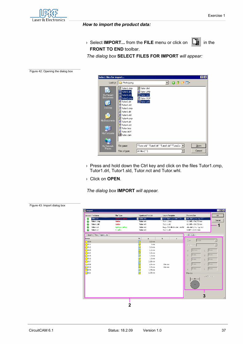
How to import the product data:
› Select IMPORT... from the FILE menu or click on in the FRONT TO END toolbar.
The dialog box SELECT FILES FOR IMPORT will appear:
Figure 42: Opening the dialog box
› Press and hold down the Ctrl key and click on the files Tutor1.cmp, Tutor1.drl, Tutor1.sld, Tutor.nct and Tutor.whl.
› Click on OPEN.
The dialog box IMPORT will appear.
Figure 43: Import dialog box
1
3
2

Exercise 1
38 Status: 18.2.09 Version 1.0 CircuitCAM 6.1
The dialog box “Import” is divided into three areas:
1 – list of files which can be imported. The columns of the list contain information about the file concerned or about the settings.2 – Display of file contents. With aperture lists and tool lists, the corresponding apertures or tools are displayed. With Gerber and Excellon files, a preview of the corresponding file is superimposed. The preview corresponds to the CircuitCAM presentation after the file has been imported.3 – Display of information about the apertures or tools. If a Gerber or Excellon file has been selected, the format settings are displayed.
The columns of the file list (1) contain the following information: Column DescriptionImport Choice of files for importing:
selected not selected
File name Displays the filename concerned
File type Automatically displays the file type
Aperture/Tool list Displays the aperture/tool list
Layer/Template Displays the layers/templates
Format/Size Displays the format settings
CircuitCAM analyses each import file and sorts or groups the file list (1) into the following order: 1. Aperture list – 2. Gerber files – 3. Tool list – 4. Excellon file. A CircuitCAM of an unknown file format is labelled “unknown”.
The name of the aperture or tool list is transferred from the file name. Under this name, CircuitCAM compiles an internal list to accept the imported apertures and tools. If the Gerber file is imported during the following step, the aperture information is used from this list.
Since the aperture or tool lists for the circuit board CAD program are not based on one standard, CircuitCAM requires a translation file (see „Adapting a translation File“ on Page 156). The translation file converts the aperture or tool lists and is displayed in the Layer/Template column.
With Gerber and Excellon files, the layer to which the graphics for this file is imported is displayed in the column “Layer/Template”. The layer name is then transferred from the file name. Here, it is advisable to select from the list a name corresponding to the file contents, e.g. TopLayer for the Gerber file which contained the conductor track data for the component side.
With aperture and tool lists, the format settings are displayed in the column “Format/Size”. Either the information is transferred from the set translation file or, if no format settings have been defined in the translation file, the default settings are used.
With Gerber and Excellon files, the dimensions of the graphics are displayed in the column “Format/Size”. The dimensions do not depend on the format settings, i.e. values which are very small or much too large are indicative of an incorrect format setting.

Exercise 1
CircuitCAM 6.1 Status: 18.2.09 Version 1.0 39
For the aperture list, you must first check whether the translation file has supplied the correct result. The conversion result is displayed on the list at the bottom left. You can display the contents of the aperture list file Tutor.whl by clicking on the tab “Text”. You can switch back and forth between Text and Aperture/Tools for comparison.
Checking the translation result
In Fig. 43, you can see that the aperture D10 is circular with a diameter of 0.2 mm.
› Click on the tab “Text”.
Figure 44: Text tab
In this text view, you can see that the aperture D10 has been defined as a circle with a diameter of 0.2 mm.
› Inspect other apertures in order to check the conversion result.If all the apertures have been converted correctly, you can start with the assignments for the Gerber files.
The layer must be assigned for both Gerber files so that the Gerber files lie on these layers after importing them.
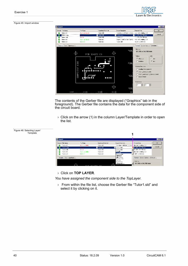
› From within the file list, choose the Gerber file “Tutor1.cmp” and select it by clicking on it.
Exercise 1
40 Status: 18.2.09 Version 1.0 CircuitCAM 6.1
Figure 45: Import window
The contents of the Gerber file are displayed (“Graphics” tab in the foreground). The Gerber file contains the data for the component side of the circuit board.
› Click on the arrow (1) in the column Layer/Template in order to open the list.
Figure 46: Selecting Layer/Template
› Click on TOP LAYER.You have assigned the component side to the TopLayer.
› From within the file list, choose the Gerber file “Tutor1.sld” and select it by clicking on it.
1

Exercise 1
CircuitCAM 6.1 Status: 18.2.09 Version 1.0 41
Figure 47: Select file
The contents of the Gerber file are displayed (“Graphics” tab in the foreground). The Gerber file contains the data for the solder side of the circuit board, mirrored presentation.
› Click on the arrow (1) in the column Layer/Template in order to open the list.
Figure 48: Layer/Template list
› Click on “BottomLayer”.You have assigned the solder side to the “BOTTOM LAYER”.
When the layer is assigned, the colour of the object in the preview changes. The colour used is always the one which has been assigned to the layer in the preview.
1
Exercise 1
42 Status: 18.2.09 Version 1.0 CircuitCAM 6.1
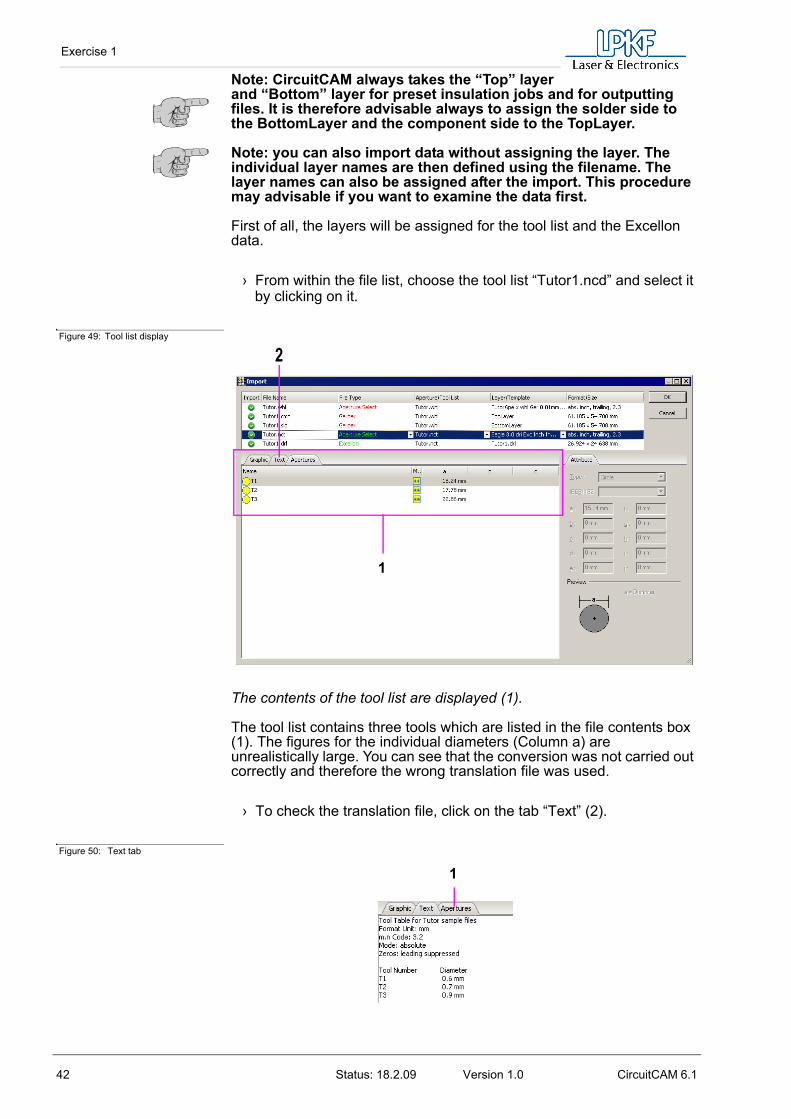
Note: CircuitCAM always takes the “Top” layer and “Bottom” layer for preset insulation jobs and for outputting files. It is therefore advisable always to assign the solder side to the BottomLayer and the component side to the TopLayer.
Note: you can also import data without assigning the layer. The individual layer names are then defined using the filename. The layer names can also be assigned after the import. This procedure may advisable if you want to examine the data first.
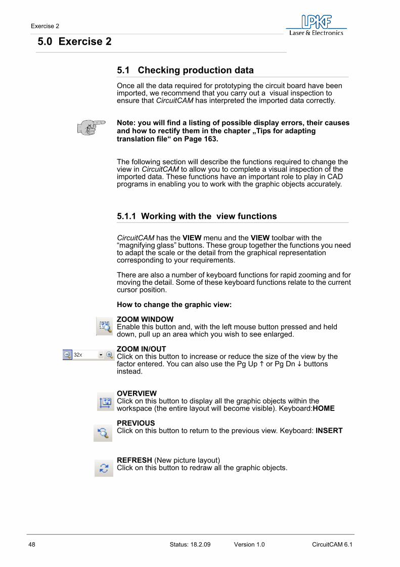
First of all, the layers will be assigned for the tool list and the Excellon data.
› From within the file list, choose the tool list “Tutor1.ncd” and select it by clicking on it.
Figure 49: Tool list display
The contents of the tool list are displayed (1).
The tool list contains three tools which are listed in the file contents box (1). The figures for the individual diameters (Column a) are unrealistically large. You can see that the conversion was not carried out correctly and therefore the wrong translation file was used.
› To check the translation file, click on the tab “Text” (2).
Figure 50: Text tab
1
2
1

Exercise 1
CircuitCAM 6.1 Status: 18.2.09 Version 1.0 43
The text file shows that the tool was defined with the diameters T1 = 0.6 mm, T2 = 0.7 mm and T3 = 0.9 mm.
› Click on the tab “Aperture“ (1).You will now select a translation file which will convert the tool list correctly.
› Click on the arrow (2) in the column Layer/Template in order to open the translation files.
Figure 51: List of translation files
The list contains translation files which are named according to the circuit board CAD programs.
› Select the second translation file from the list.This translation file also does not achieve the desired result.
› Try out some other translation files.After trying out some others for a short while, you will discover that the translation file “Eagle 3.0 drl Exc mm Inch23AbsTrail.txt” produces the desired result and is the correct one for the conversion.
Figure 52: Finding the conversion file
Now start with the assignments for the Excellon file.
2

Exercise 1
44 Status: 18.2.09 Version 1.0 CircuitCAM 6.1
› From within the file list, select the Excellon file “Tutor1.drl”.
Figure 53: Open Tutor1.drl file
On examining the preview, you will very soon see that the format settings are not correct. The holes overlap one another significantly and the dimensions which appear on the file list do not correspond to those of the Gerber file. The dimensions on the graphics must be multiplied by approx. 10 in order agree with those of the Gerber file. The size can be changed by a factor of 10 by moving the decimal place.
You can change the format settings bottom right.
› Open the list of decimal places under DIGITS.
Figure 54: Defining decimal places
› Select the value 2.

Exercise 1
CircuitCAM 6.1 Status: 18.2.09 Version 1.0 45
Figure 55: Import window
After CircuitCAM has implemented this change, the dimensions of the graphics and the Gerber file approximate one another and the holes no longer overlap. The correct format setting has been found.
Now assign a layer to the Excellon file. After the import, the holes of the Excellon file will lie on the layer.
› Click on the column Layer/Template in order to open the list for the layer.
Figure 56: Select Layer/Template
› Select DrillPlated.You have assigned the holes to the layer DrillPlated.
Since this is a two-sided circuit board, the holes are plated through. With single-sided circuit boards, the layer Drill Unplated must be used.
All the settings and assignments have now been completed and the files can be imported.
2

Exercise 1
46 Status: 18.2.09 Version 1.0 CircuitCAM 6.1
Figure 57: Importing file
› Click on OK.CircuitCAM displays the imported files in the graphics window.
Figure 58: Work file
Note: data can be imported to the existing data in CircuitCAM at any time.

Exercise 1
CircuitCAM 6.1 Status: 18.2.09 Version 1.0 47
Save your data to protect against data loss!
› By selecting SAVE from the FILE menu. The document will be saved under the filename "TUTOR1" already entered.
The DXF data import will be explained in the appendix because it is not part of this exercise.
Exercise 2
48 Status: 18.2.09 Version 1.0 CircuitCAM 6.1
5.0 Exercise 2
5.1 Checking production dataOnce all the data required for prototyping the circuit board have been imported, we recommend that you carry out a visual inspection to ensure that CircuitCAM has interpreted the imported data correctly.
Note: you will find a listing of possible display errors, their causes and how to rectify them in the chapter „Tips for adapting translation file“ on Page 163.
The following section will describe the functions required to change the view in CircuitCAM to allow you to complete a visual inspection of the imported data. These functions have an important role to play in CAD programs in enabling you to work with the graphic objects accurately.
5.1.1 Working with the view functions
CircuitCAM has the VIEW menu and the VIEW toolbar with the “magnifying glass” buttons. These group together the functions you need to adapt the scale or the detail from the graphical representation corresponding to your requirements.
There are also a number of keyboard functions for rapid zooming and for moving the detail. Some of these keyboard functions relate to the current cursor position.
How to change the graphic view:
ZOOM WINDOWEnable this button and, with the left mouse button pressed and held down, pull up an area which you wish to see enlarged.
ZOOM IN/OUTClick on this button to increase or reduce the size of the view by the factor entered. You can also use the Pg Up or Pg Dn buttons instead.
OVERVIEWClick on this button to display all the graphic objects within the workspace (the entire layout will become visible). Keyboard:HOME
PREVIOUSClick on this button to return to the previous view. Keyboard: INSERT
REFRESH (New picture layout)Click on this button to redraw all the graphic objects.

Exercise 2
CircuitCAM 6.1 Status: 18.2.09 Version 1.0 49
ZOOM SELECTEDThe selected elements will be enlarged to fill the screen.
To move the detail area, use the ARROW KEYS on the keyboard and the scrollbars.
Press END to centre the detail area on the mouse position.
Use the mouse wheel to change the image detail
The image detail can be changed another way using the mouse wheel. Position the mouse pointer inside the image detail which you wish to make larger or smaller. Then, rotate the mouse wheel forwards in order to make the image detail larger. While doing so, the graphics at the current mouse position will be moved to the centre of the screen. The centre of the screen will be maintained as you continue to rotate the mouse wheel forwards without moving the mouse. Rotate the mouse wheel backwards in order to make the image detail smaller.
Using the mouse wheel to move the image detail
Figure 59:Mouse wheel pressed
The image detail can be moved another way using the mouse wheel. When you press down the mouse wheel, the symbol “mouse wheel pressed” appears on the monitor. If you move the mouse pointer so that it moves away from the symbol, the image detail will move in the same direction as the mouse.
5.1.2 Working with the layer list window Layer
The properties of each layer are listed in the layer list. The layer list is a docked window on the left of the screen. The display for the layer list can be enabled by clicking on the layer view symbol on the layer toolbar. Alternatively, you can also enable the layer list via the sub item LAYERS in the VIEW menu.

Exercise 2
50 Status: 18.2.09 Version 1.0 CircuitCAM 6.1
The status of the layer is indicated by the text style or the text colour as follows:
Figure 60:Layer window
Grey (1) The layer is not assigned, i.e. no object data available.
Black(3) The layer is assigned, i.e. object data are available.
Red (2) The layer is assigned and some object data of this layer are selected.
As an attribute for all text colours:
Bold(2) The layer is active, i.e. new object data are saved. in this layer.
Switch the active layer by double clicking on the layer name with the Alt key pressed and held down. Make sure that no objects are selected otherwise they will be moved onto the new active layer.
Each of the three colours for the layer names can be displayed in bold simultaneously. For example, if an individual object is selected in the graphics then the corresponding layer name appears in red and bold text. This means that you can see very quickly whether graphic objects are selected and which layer is active.
The layer list is divided into seven columns as follows:
Figure 61:Layer list columns
The following settings are enabled by clicking on the symbols concerned:
1 - Visible Show all the objects of a layer. Hide all the objects of a layer.
2 - Name List layer names
3 - Order [1 ... n] Display order number.
4 - Selectable Make all the objects of a layer selectable. None of the objects of a layer are
selectable.
123
1 2 3 4 5 6 7
Exercise 2
CircuitCAM 6.1 Status: 18.2.09 Version 1.0 51
5 - True Width Presentation of conductor tracks in their actual width. The actual width is determined by apertures. The value 0 corresponds to a centre line.
True width Centre line
6 - Outline Display all graphic objects of a layer filled.
All graphic objects of a layer are displayed in outline.
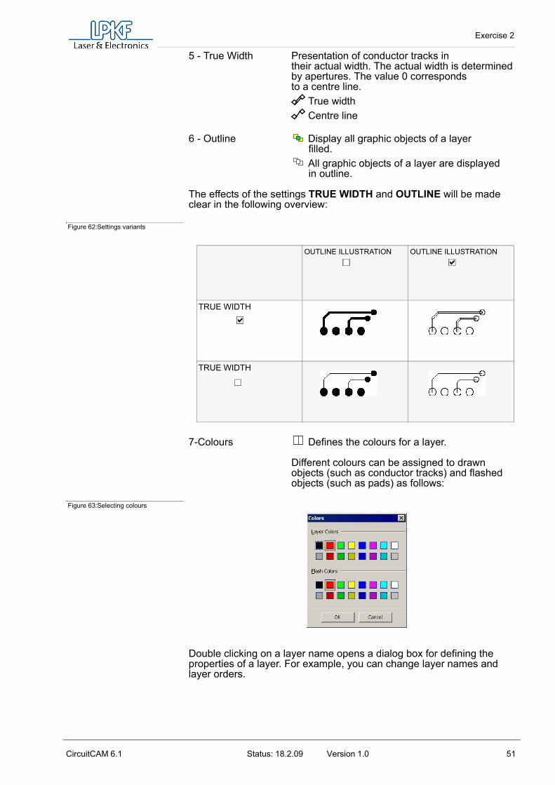
The effects of the settings TRUE WIDTH and OUTLINE will be made clear in the following overview:
Figure 62:Settings variants
7-Colours Defines the colours for a layer.
Different colours can be assigned to drawn objects (such as conductor tracks) and flashed objects (such as pads) as follows:
Figure 63:Selecting colours
Double clicking on a layer name opens a dialog box for defining the properties of a layer. For example, you can change layer names and layer orders.
OUTLINE ILLUSTRATION
OUTLINE ILLUSTRATION
TRUE WIDTH
TRUE WIDTH
Exercise 2
52 Status: 18.2.09 Version 1.0 CircuitCAM 6.1
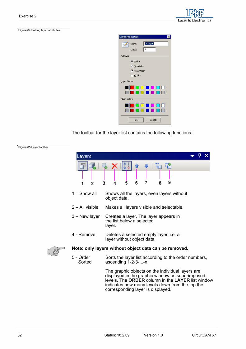
Figure 64:Setting layer attributes
The toolbar for the layer list contains the following functions:
Figure 65:Layer toolbar
1 – Show all Shows all the layers, even layers without object data.
2 – All visible Makes all layers visible and selectable.
3 – New layer Creates a layer. The layer appears inthe list below a selected layer.
4 - Remove Deletes a selected empty layer, i.e. a layer without object data.
Note: only layers without object data can be removed.
5 - Order Sorts the layer list according to the order numbers, Sorted ascending 1-2-3-...-n.
The graphic objects on the individual layers are displayed in the graphic window as superimposed levels. The ORDER column in the LAYER list window indicates how many levels down from the top the corresponding layer is displayed.
1 2 3 4 5 6 7 8 9

Exercise 2
CircuitCAM 6.1 Status: 18.2.09 Version 1.0 53
Figure 66:Presentation of levels
Remember that graphic objects on a lower level can be concealed by graphic objects on a higher level.
6 - Up Moves a selected layer including all object data up by one position in theorder. In the graphics, the objects of this layerare set one level higher.
7 - Down Moves a selected layer including all the object data down by one position in theorder. In the graphics, the objects of this layerare set one level lower.
Note: the layers or object data can only be moved when the “Sort order” button has been enabled.
8 - Move Moves all the selected object data to a selected layer, i.e. to the original layer deleted.
9 - Copy Copies all the selected object data to a selected layer.
Note: you will find a full description of the other functions of the list window in the CircuitCAM online help.
The new layers which are available in CircuitCAM 6.1 - Insulate bottom (small, standard, big and bigger) - are layers for optimising the milling process.A corresponding narrow to extremely wide tool is assigned to the layers. For example, during the insulate production phase, a tool which is as wide as possible is selected or requested automatically for large or wide milling surfaces. If the insulating strip to be cut is extremely small, a very small tool is selected. This software carries out the selection automatically.
How to carry out a visual inspection of the imported data:
› Click on ZOOM on the toolbar or move the mouse pointer over the graphic and press HOME in order to display all the graphic objects inside the workspace.
› Press the right mouse button and now click on MEASURE in the context menu which has just opened.
› Select a point in the graphic from which the measurement should be taken, e.g. the lower left corner of the circuit board frame.
› Move the mouse pointer to the target position of your measurement, e.g. the top right corner.

Exercise 2
54 Status: 18.2.09 Version 1.0 CircuitCAM 6.1
Distance is indicated as Cartesian and polar coordinates on the status bar (centre).
Our sample circuit board has the dimensions 55.88 x 38.1 mm.
Note: in CircuitCAM, you can choose between millimetres, microns, inches and mils (thou) (1/1000 inch) for the units; the default unit is millimetre.The unit changes on the UNIT/GRID toolbar via the MEASUREMENT UNIT list box.
› To finish the measurement, press the ESC key on your keyboard.
Use the VIEW functions in CircuitCAM to zoom in on areas of the circuit board and to check the layers for cover.
5.2 Preparing production data for prototypingIn this section, you will learn how to prepare the production data for manufacturing a prototype circuit board. This involves deleting superfluous graphic objects, adding milling data and moving graphic objects to other layers.
5.2.1 Deleting graphic objects outside the circuit board
The various layers often have registration marks outside the circuit board outline, as in the case of our sample circuit board. You might also think of other objects instead of the registration marks, such as labelling fields, company logos, etc.
However, only those objects inside the circuit board outline are of interest for the production of the prototype circuit board, so all the objects outside circuit board outline can be deleted.
Objects must be selected before they can be deleted:
• You can select individual objects by clicking in the immediate vicinity of the object to be selected using the left mouse button.
• To select larger areas, press and hold down the mouse button while dragging the mouse pointer diagonally across the surface to be selected.
CircuitCAM has a number of functions which you can use to influence the way in which objects are selected to ensure that only the object desired is selected and not other objects beneath, above or near it.

Exercise 2
CircuitCAM 6.1 Status: 18.2.09 Version 1.0 55
These functions can be found in the SELECT menu or via the SELECT toolbar:
SELECT LAYERClick on this button to select the entire active layer. The active
layer is selected by double clicking on a layer on the layer list with the ALT key pressed and held down or by selecting a
graphic object (the function can also be enabled by clicking onLAYER in the main menu SELECT).
SELECT APERTURE/TOOL Click on this button to select all the graphics objects which have
been generated with the active aperture or active tool (The function can also be enabled by clicking on APERTURE/TOOL in the main menu SELECT.). The active aperture-/ tool is selected by double clicking on an aperture or tool with the ALT key pressed and held downin the aperture/ tool list or by selecting a graphic object.
SELECT ALLClick on this button to select all the objects of a graphic. (The function can also be enabled by clicking on ALL in the main menu SELECT.).
The following switches or the SELECT menu may be used to determine what kind of graphic objects may or may not be selected:
PATH SELECTABLELine drawings can be selected if this button is enabled.
POLYGON SELECTABLEPolygons can be selected if this button is enabled.
CIRCLE SELECTABLECircles can be selected if this button is enabled.
RECTANGLE SELECTABLERectangles can be selected if this button is enabled.
FLASH SELECTABLEPads (flash) can be selected if this button is enabled and alsoholes are selectable. In the default setting, all switchesare enabled (everything selectable).
Note: you can change temporarily from the current selection mode to the PLUS mode by holding down CTRL and switching to the MINUS mode, by holding down SHIFT. The original mode is re-enabled when the key is released.

Exercise 2
56 Status: 18.2.09 Version 1.0 CircuitCAM 6.1
You can undo the selection by moving the mouse pointer over the graphic and pressing the Esc key.
If just one object is selected, the handles for the selected object will be displayed:
Figure 67:Selecting object
The handle which is closest to the cursor position when you clicked is displayed as a cross and is used as the anchor point. The selected object can therefore also be displayed as follows:
Figure 68:Anchor point
The anchor point coordinates are displayed on the STATUS BAR.
Note: use the + or - keys to move the anchor point to the next handle on the selected object.
Selected objects are shown in a different colour and the number of objects selected is shown on the STATUS BAR.
Note: to view or modify the properties of a selected object, select PROPERTIES from the CONTEXT MENU (right mouse button).
How to delete objects outside the circuit board: › Make sure that all the selection switches (1) on the SELECT toolbar
are enabled. So that all the graphic objects are selectable:
Figure 69:Selection switches
› Drag a box around the two upper registration marks using the left mouse button to select them and the text between them:
1

Exercise 2
CircuitCAM 6.1 Status: 18.2.09 Version 1.0 57
Figure 70:Presentation of printed circuit board
› On the SELECT toolbar, click on to enable thePLUS selection mode.
› Drag a box around the lower registration mark using the left mouse button to select it as well.
Figure 71:Editing conductor tracks
All the objects outside the circuit board are now selected.
› Open the EDIT menu and click on REMOVE or press the DEL key in order to delete the selected objects.
› Click on the SELECT toolbar in order to enable the selection mode NEW.
Tips & tricks:
• You can cancel an action by pressing the ESC key.
• If you wish to undo one or more actions, click on on the DEFAULT toolbar or press CTRL + Z.
• If you wish to redo an action you have undone, click on on the DEFAULT toolbar or press CTRL + Y.
Exercise 2
58 Status: 18.2.09 Version 1.0 CircuitCAM 6.1
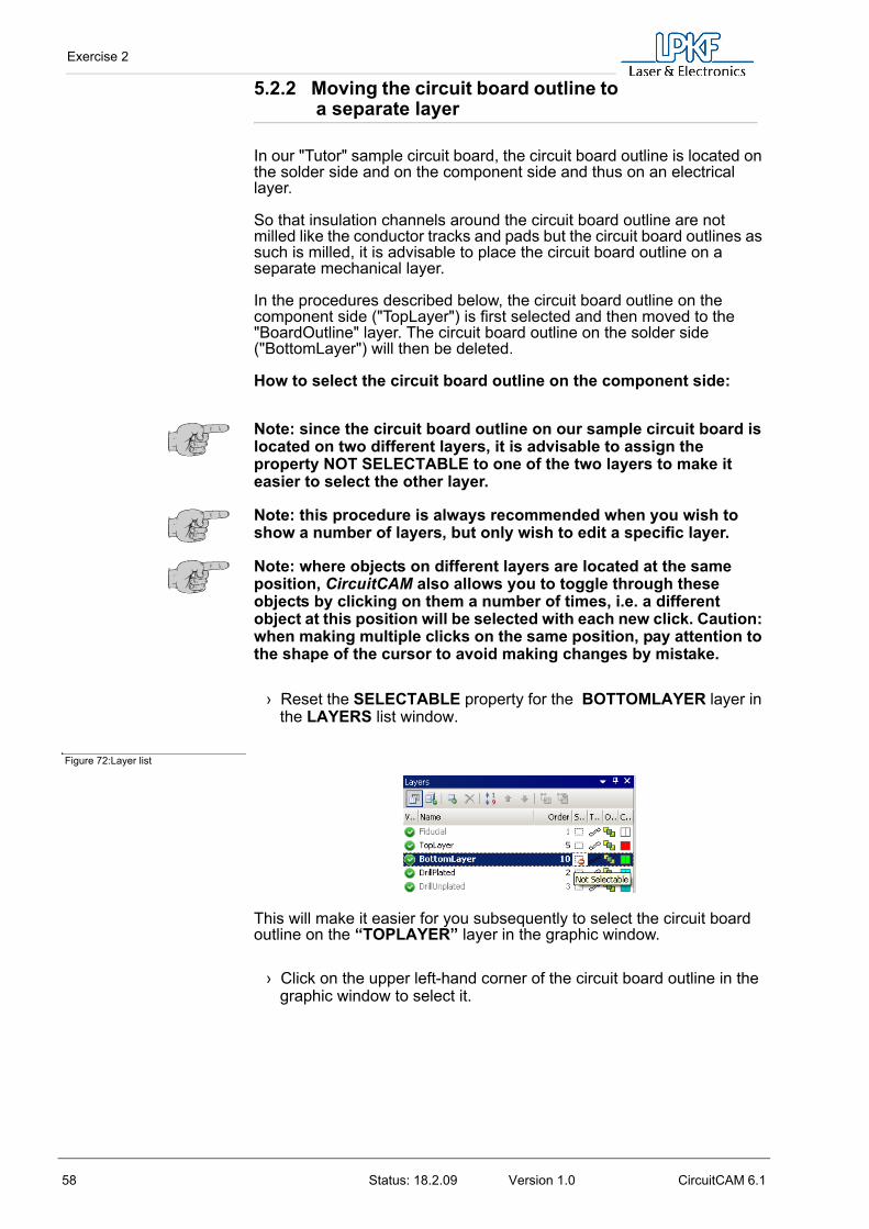
5.2.2 Moving the circuit board outline to a separate layer
In our "Tutor" sample circuit board, the circuit board outline is located on the solder side and on the component side and thus on an electrical layer.
So that insulation channels around the circuit board outline are notmilled like the conductor tracks and pads but the circuit board outlines as such is milled, it is advisable to place the circuit board outline on a separate mechanical layer.
In the procedures described below, the circuit board outline on the component side ("TopLayer") is first selected and then moved to the "BoardOutline" layer. The circuit board outline on the solder side ("BottomLayer") will then be deleted.
How to select the circuit board outline on the component side:
Note: since the circuit board outline on our sample circuit board is located on two different layers, it is advisable to assign the property NOT SELECTABLE to one of the two layers to make it easier to select the other layer.
Note: this procedure is always recommended when you wish to show a number of layers, but only wish to edit a specific layer.
Note: where objects on different layers are located at the same position, CircuitCAM also allows you to toggle through these objects by clicking on them a number of times, i.e. a different object at this position will be selected with each new click. Caution: when making multiple clicks on the same position, pay attention to the shape of the cursor to avoid making changes by mistake.
› Reset the SELECTABLE property for the BOTTOMLAYER layer in the LAYERS list window.
Figure 72:Layer list
This will make it easier for you subsequently to select the circuit board outline on the “TOPLAYER” layer in the graphic window.
› Click on the upper left-hand corner of the circuit board outline in the graphic window to select it.

Exercise 2
CircuitCAM 6.1 Status: 18.2.09 Version 1.0 59
Figure 73:Graphic window
Note: you must always click on a handle of an object, i.e. a corner point, to select it. If you click on an object between two handles, another object nearby may be selected.
The circuit board outline on the component side (TopLayer) is selected and the solder side layer (BottomLayer) has the property NOT SELECTABLE:
Figure 74:Graphic window
How to move selected objects to a different layer:
› With the ALT key pressed, move the selected circuit board outline to the BOARD OUTLINE Layer by double clicking on the BOARD OUTLINE Layer on the layer list.
› Move the mouse pointer over the graphic and press ESC in order to set the objects not selected.
The circuit board outline on the solder side can now be deleted:
› Set the property SELECTABLE in the LAYER list window for the BOTTOM LAYER layer.
› Set the property NOT SELECTABLE in the LAYERS list window for the layer BOARD OUTLINE.

Exercise 2
60 Status: 18.2.09 Version 1.0 CircuitCAM 6.1
› Select the circuit board outline on the BOTTOM LAYER layer in the graphic window.
› Press DELETE to delete the selected circuit board outline.
› Press HOME to redraw the picture.
› Set the property SELECTABLE for the BOARD OUTLINE layer .
5.3 Improved coordinate entriesIn CircuitCAM, you can also enable mouse clicks by coordinate entry. Both selecting a certain position and redrawing an object have been improved. Several coordinates can be entered one after another without cancelling functions. This considerably speeds up generating front panels or RF layouts.
The following description is an example and is not part of the exercise. However, you can practice this function on any open file as follows:
Activate the layer on which you want to add and object:
› Press and hold down the Alt key and double click on the selected layer from the layer list.
Select the object type and open the coordinate entry.
› Open the INSERT menu and click on OPEN PATH or Polygon.
› Open the EDIT menu and click on SET CURSOR.

Exercise 2
CircuitCAM 6.1 Status: 18.2.09 Version 1.0 61
The SET CURSOR window is now in the foreground below the layer list.
Figure 75:Setting the cursor
› Enter the following in the SET CURSOR window:
x= 0 x= 10 y= 0 => SET y= 0 => SET
x= 10 x= 0 x= 0y= 10 => SET y= 10 => SET y= 0 => SET
After entering each coordinate (x and y), confirm with SET.
You now have represented a square polygon or a square as an outline.
› Move the mouse pointer over the graphic and press Esc in order to terminate the INSERT function.
› Click on the PROPERTIES tab below the SET CURSOR window in order to bring the window properties into the foreground again.
5.3.1 Placing text objects on separate layers
It is also advisable to move text objects to a separate layer. Since CircuitCAM does not distinguish between text objects and conductor tracks when these are located on the same layer, text objects would otherwise be insulated just like conductor tracks:
Text on electrical layer: Text on separate layer:
Since the procedure for moving text objects onto a separate layer is similar to moving the circuit board outline to the BOARDOUTLINE layer, the various operations will only described in general terms at this point.

Exercise 2
62 Status: 18.2.09 Version 1.0 CircuitCAM 6.1
How to place text objects on a separate layer:› Select the text objects on the component side.
› Press Alt or hold down Alt and double click on the TEXT TOP layer in order to move the selected text objects to the layer.
› Select the text objects on the solder side.
› Press Alt or hold down Alt and double click on the TEXT BOTTOM layer in the layer list to move the selected text objects to this layer.
› Move the mouse pointer over the graphic and press Esc in order to deselect.
Note: you should also move the fastening holes from an electrical layer to a mechanical layer, e.g DRILL UNPLATED just like the circuit board outline and the text objects.
Note: save your work to protect against data loss.
› Do this by selecting SAVE AS... from the FILE menu. Enter the name “TUTOR2" and click on SAVE. The document will be saved under the filename "TUTOR2".
5.3.2 Insulating with the default job
To calculate the insulation channels, CircuitCAM offers standard jobs which may be used for most circuit boards without modifying the insulation parameters. Later you will learn how the defaults for calculating the insulation channels can be calculated individually.
The FRONT TO END toolbar groups together the functions required for preparing production data for passing on to BoardMaster, including the function for insulation using the default job:
INSULATE ALL LAYERS
How to calculate the insulation channels using the default settings:
› Click on in the FRONT TO END toolbar menu to calculate the insulation channels for the solder side and the component side in a single operation.
Note:It may take some time to calculate the insulation channels, depending on the number of graphic objects and the parameters set, such as the insulation grid. The processor speed and the amount of memory in your computer will also greatly affect the amount of time required.
After calculation, the insulation channels are represented graphically. In this case, the cutting paths are illustrated in the colours assigned in each case depending on the tools used („Colour assignment for the insulating Tools“ on Page 85).
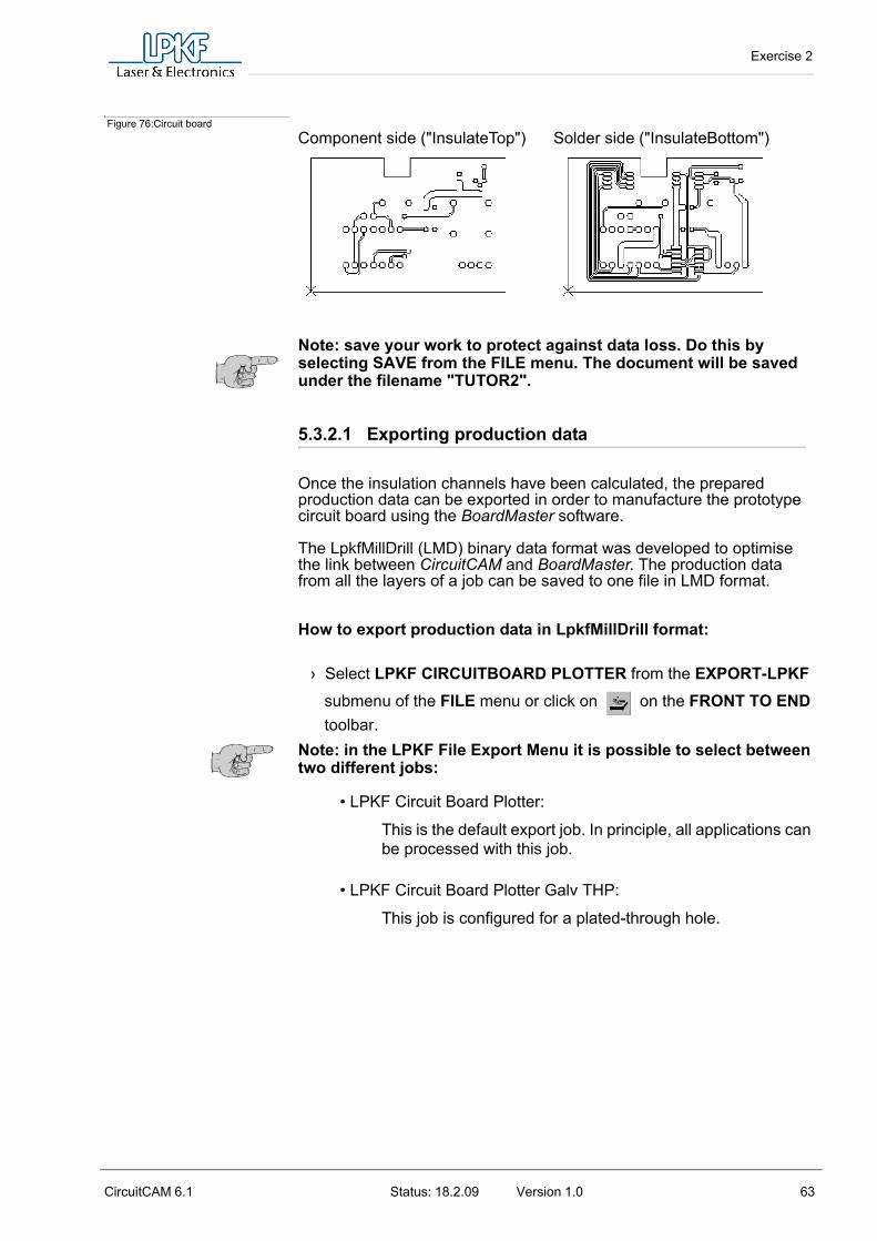
The insulation channels on the component side are located on the "INSULATE TOP"layer and those on the solder side on the "INSULATE BOTTOM" layer:
Exercise 2
CircuitCAM 6.1 Status: 18.2.09 Version 1.0 63
Figure 76:Circuit boardComponent side ("InsulateTop") Solder side ("InsulateBottom")
Note: save your work to protect against data loss. Do this by selecting SAVE from the FILE menu. The document will be saved under the filename "TUTOR2".
5.3.2.1 Exporting production data
Once the insulation channels have been calculated, the prepared production data can be exported in order to manufacture the prototype circuit board using the BoardMaster software.
The LpkfMillDrill (LMD) binary data format was developed to optimise the link between CircuitCAM and BoardMaster. The production data from all the layers of a job can be saved to one file in LMD format.
How to export production data in LpkfMillDrill format:
› Select LPKF CIRCUITBOARD PLOTTER from the EXPORT-LPKF
submenu of the FILE menu or click on on the FRONT TO END toolbar.
Note: in the LPKF File Export Menu it is possible to select between two different jobs:
• LPKF Circuit Board Plotter:
This is the default export job. In principle, all applications can be processed with this job.
• LPKF Circuit Board Plotter Galv THP:
This job is configured for a plated-through hole.

Exercise 2
64 Status: 18.2.09 Version 1.0 CircuitCAM 6.1
• LPKF Circuit Board Plotter No THP:
With this job, no plated-through holes of any type are provided. Some of the production phases are consolidated (e.g. all drilling phases). This enables the work to be carried out efficiently on machines with tool changes.
• LPKF CircuitBoardPlotter+ProConduct
This job is configured for a through-plating process with ProConduct.
• LPKF CircuitBoardPlotter+AutoContac
this job is configured for a through-plating with AutoContac.
The file which is created will be saved to the working directory (Folder: ExampleData\Prototyping) under the same name as the CircuitCAM file, but with the file extension “.LMD”.
Following the export, the information regarding the exported data will be output to the MESSAGE LOG, together with any error messages.
Note: you can also export the production data in the most common CAD formats such as Gerber, Excellon and HP-GL (PCB version only) in addition to the LpkfMillDrill format.
Do this by selecting the appropriate item in the EXPORT submenu of the FILE menu.
Figure 77:Export format
To conclude the second exercise, you can now close the "TUTOR2" document by selecting EXIT from the FILE menu.
Note: if the BoardMaster program has started before the exporting the data, the exported LMD file is immediately imported by BoardMaster and placed in the centre of the working area or base material.

Exercise 2
CircuitCAM 6.1 Status: 18.2.09 Version 1.0 65
5.3.3 Importing the data using the import assignment
Importing data is significantly easier and quicker if you work using import assignment. Before importing, the parameters that were previously assigned manually in this exercise are predefined in a dialog box. This means that the data are displayed on the screen as soon as they have been selected for import.
› Starting the CircuitCAM program.
› Select “TUTOR“ from the FILE -> NEW menu.
The import assignment for the Tutor files has already been defined in this template file.
› Open the dialog box “General Settings” via SETTINGS and click on IMPORT ASSIGMENT.
Figure 78: Importing assignments
All the settings required for importing the Tutor files quickly have been predefined here. You should carry out the “Import assignment” in the same way for the data you wish to import and save it in a separate template file. („Exercise 6“ on Page 89).
› Click on CANCEL.
› Now repeat the import as described above. But select all the files to be imported (Tutor1.nct, Tutor1.whl, Tutor1.cmp, Tutor1.sld and Tutor1.drl) using the CTRL key.
Once you have confirmed the selection with OPEN, the data will be imported and displayed on the screen immediately, without you accessing the IMPORT dialog box beforehand.
› Terminating the CircuitCAM program.
Exercise 3
66 Status: 18.2.09 Version 1.0 CircuitCAM 6.1
6.0 Exercise 3
In this chapter, you will learn, how to use the contour generator and how to insert breakout-tabs. You will also be shown how to generate surfaces by removing all the residual copper.
6.1 Using contour generatorIf you wish to have the circuit board milled out by the circuit board plotter rather than having it cut to size by a circuit board guillotine, you can use Contour generator to calculate the milling contour.
Use the CircuitCAM File “TUTOR1.CAM” again for the following exercise:
› Start CircuitCAM.
› Select OPEN from the FILE menu.
› Select the “TUTOR1” file and click on OPEN.
Note: once you have opened the file “TUTOR1.CAM” in CircuitCAM, you should save this document under a different filename to ensure that the original data are still available to you for further exercises.
› Select SAVE AS from the FILE menu.
› Enter “TUTOR3” as the filename and click on SAVE.
You may select either a selection or a layer as the source for the milling contour. Here, a line which surrounds the entire circuit board must always be used (see “Tutor1” example). A selection will be used as a source in this exercise, since the circuit board outline for this circuit board is located on the “TOP LAYER” und “BOTTOM LAYER” layers together with the conductor tracks and pads.
Note: if the circuit board is going to be milled out by circuit board plotter, the circuit board outline no longer has to be placed on a separate layer as was the case in Exercise 2.

Exercise 3
CircuitCAM 6.1 Status: 18.2.09 Version 1.0 67
How to create a milling contour:
› Select the circuit board outline on the “TOP LAYER” layer.
Figure 79:Circuit board outline
› Click on on the FRONT TO END toolbar to open the
CONTOUR MILLING dialog box:
Figure 80:Contour milling
Note: if the circuit board outline is already lying on a separate layer, e.g. on the “BOARD OUTLINE" layer, you can use this as the source for calculating the milling contour by clicking on the options button LAYER and selecting BOARDOUTLINE in the list box LAYER.
› Click on RUN to generate the milling contour.
Exercise 3
68 Status: 18.2.09 Version 1.0 CircuitCAM 6.1
Once the calculation is complete, the milling contour will be displayed in the graphic window:
Figure 81: Milling contour
Since the milling contour has now been generated on the layer “CUTTING OUTSIDE”, you can delete the circuit board outline on the layers “TOP LAYER” and “BOTTOM LAYER”:
› Select the circuit board outline on the TopLayer.
› Press DEL, to delete the circuit board outline which is still selected on the layer “TOP LAYER”.
› Select the circuit board outline on the layer "BOTTOMLAYER” .
› Press DEL to delete this circuit board outline.
Caution! With the current contour, the circuit board would be completely milled out of the board material and could be thrown about by the rotating milling head.
Caution! It may therefore be desirable to leave the circuit boardconnected to the board material by at least two breakout-tabs to prevent personal injury and damage to the circuit board plotter. The width of the breakout tabs is defined in the general settings under Miscellaneous.
Exercise 3
CircuitCAM 6.1 Status: 18.2.09 Version 1.0 69
How to insert the breakout-tabs in the milling contour › Select the contour generated on the layer "CUTTING OUTSIDE":
Figure 82: Selecting contour
› Use the + and - keys to move the anchor point on the contour line to where the breakout tab is to be inserted.
Figure 83: Setting anchor points
› To insert a tab at the anchor point position, press CTRL + G or click
on on the FRONT TO END toolbar:
Figure 84: Inserting anchor points

Exercise 3
70 Status: 18.2.09 Version 1.0 CircuitCAM 6.1
› Repeat the previous two steps to insert breakout-tabs at subsequent positions:
Figure 85: Setting anchor points
You have now generated a milling contour where the circuit board is connected to the board material via five breakout-tabs:
Figure 86:Contour with breakout tabs
Note: to save the exercise in its current status, select SAVE AS from the FILE menu. Enter the filename “TUTOR3” and click on OK.
6.1.1 Modifiable milling direction and sequence
In order to process interior and exterior contours optimally, you can define the milling sequence as well as milling direction. You can take into consideration your special requirements with various applications when the contours are extensive and/or irregular and when there are numerous breakout tabs. To use this function, proceed as follows:
› Select a cutting path by pressing the left mouse button.
› On the main menu bar TOOL PATH , select SWAP.

Exercise 3
CircuitCAM 6.1 Status: 18.2.09 Version 1.0 71
The following menu appears:
Figure 87: Swap
Here, you can select whether the cutting path is to be cut first or last.
Move to first: The conductor track is cut first.
Move to last: This conductor track is cut last.
Move to next; Move to prev: Moves the cutting path one step forwards or backwards in the sequence.
You can check where the conductor track is being milled (1) at the bottom of the screen.
Figure 88:Information bar
If the lines are to be checked, you must click on each individual line in order to check it.
To check the cutting direction of a track, click on it with the left mouse button. The properties of the cutting path are shown on the status display line (see Illustration 88). While the track is selected, you can also determine the direction by using the + or - keys on the keyboard. If the selection moves along with the + key, then this is the actual cutting direction.
The optimum cutting direction for a cutting path depends on which side of the cut is to be the “good” side. You can change the cutting direction using the function TOOL PATH- SWAP. By selecting the cutting path and pressing the <+> key, the anchor point will move in the cutting direction. However, pay attention to the circuit board layer. Data for the solder side are mirrored in BoardMaster, which also reverses the cutting direction.
6.2 Creating a rubout areaA rubout area is a zone in which both the insulation channels around conductor tracks and pads are milled and all the residual copper between the conductor tracks and the pads is removed from the circuit board. This operation is advisable for technical reasons (e.g. EMC) since no electrical potential is assigned to this residual copper.
You will find the functions for creating a rubout area in the INSERT menu, in the RUBOUT submenu and on the FRONT TO END toolbar:
1

Exercise 3
72 Status: 18.2.09 Version 1.0 CircuitCAM 6.1
RUBOUT ALL LAYER creates a square rubout area on the circuit board top andbottom side.
You can define the size of the rubout area using the following drawing functions which are located on the INSERT toolbar and in the INSERT menu:
POLYGON is defined by any number of handles set by mouse click.The polygon is finished by pressing ESC once the last handlehas been set. The operation is completed by pressingESC again.
Figure 89: Polygon shapes
RECTANGLE (default setting for rubout area) defined by two mouse clicks:
Figure 90: Rectangle
The RECTANGLE function is aborted by pressing ESC.
CIRCLE defined by the centre to the perimeter by two mouse clicks:
Figure 91: Circle

Exercise 3
CircuitCAM 6.1 Status: 18.2.09 Version 1.0 73
The CIRCLE function is aborted by pressing ESC or by entering a circle diameter manually.
Note: instead of clicking with the mouse, you can enter the cursor position numerically via the keyboard by selecting SET CURSOR from the EDIT menu.
The SET CURSOR dialog box will appear and you can enter the new cursor position in the text boxes:
Figure 92: Setting the cursor
› Click on SET to accept the values.
The SET CURSOR function corresponds to a mouse click at the position entered and can thus be used for drawing graphic objects accurately.
Three predefined layers are available for drawing rubout areas, “RUBOUT BOTTOM" for the circuit board bottom face, “RUBOUT TOP" for the circuit board top face and “RUBOUT ALL LAYER" for both circuit board layers (default setting).
In the following exercise, you will be creating the rubout area on both sides of the circuit board around the 14 pin SMD IC.
How to generate a rubout area:
› Click on in the FRONT TO END toolbar to create a rubout area on both sides of the circuit board.
This enables the RECTANGLE function on the RUBOUT ALL LAYER layer.
Note: you can select a different shape for the rubout area by clicking on (POLYGON) or (CIRCLE) on the INSERT toolbar.
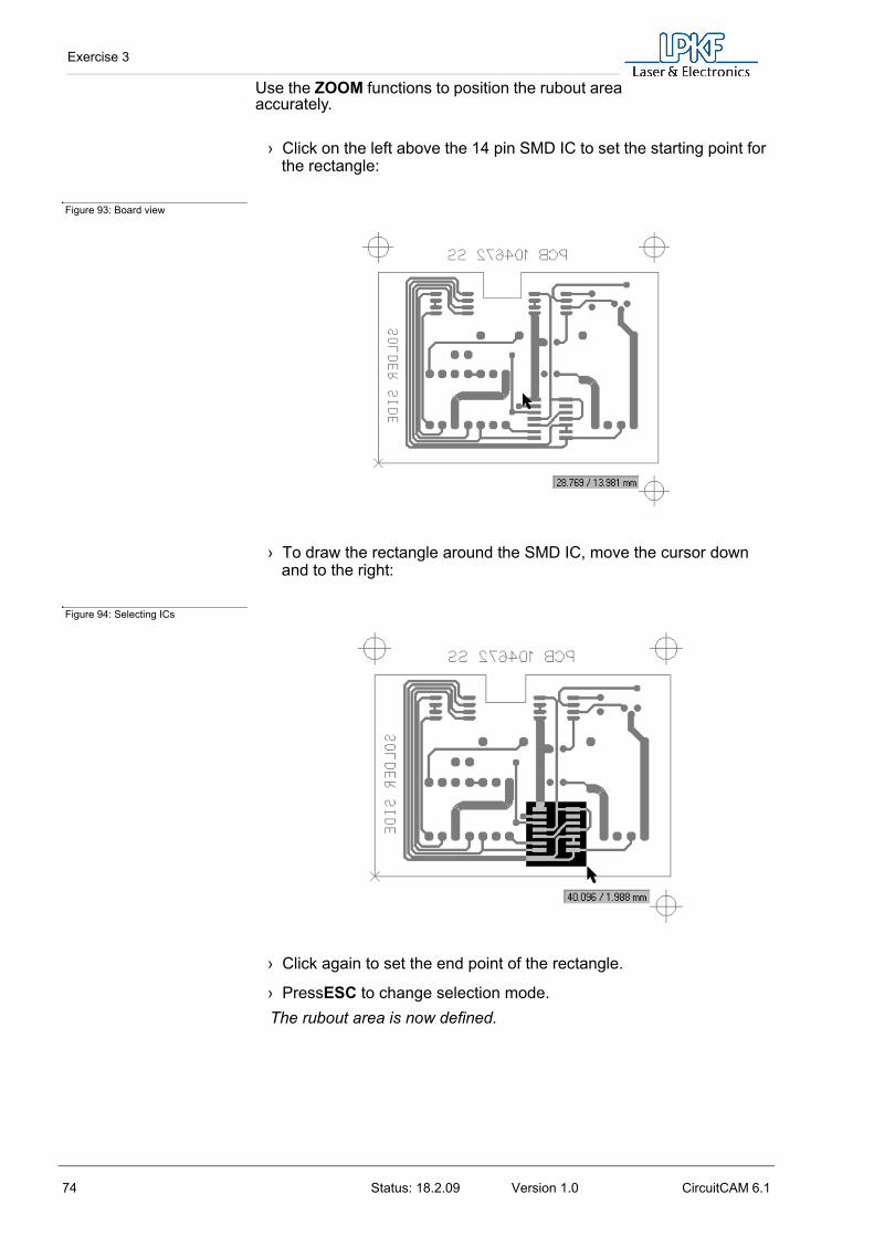
Exercise 3
74 Status: 18.2.09 Version 1.0 CircuitCAM 6.1
Use the ZOOM functions to position the rubout area accurately.
› Click on the left above the 14 pin SMD IC to set the starting point for the rectangle:
Figure 93: Board view
› To draw the rectangle around the SMD IC, move the cursor down and to the right:
Figure 94: Selecting ICs
› Click again to set the end point of the rectangle.
› PressESC to change selection mode. The rubout area is now defined.

Exercise 3
CircuitCAM 6.1 Status: 18.2.09 Version 1.0 75
› Select SAVE from the FILE menu . The document will be saved under the filename “TUTOR3” already entered.
› To conclude the third exercise, you can now close the “TUTOR3” document by selecting EXIT from the FILE menu.
Note: If a rubout area should be defined only on one circuit board
layer, , after clicking on the corresponding layer (RUBOUT TOP / RUBOUT BOTTOM), select from the LAYER list box on the layer tool bar.
Note: You can also define a number of rubout areas of different shapes on one circuit board.
Note: Since a rubout area is a graphic object just like any other, you can also select rubout areas and resize, reshape, move and delete them.
Note: The residual copper area to be removed does not need to be defined precisely but can simply be drawn over the conductor tracks and pads just like in the exercise. All the conductor tracks and pads located in this area are taken into consideration when calculating the insulation channels.
Note: Any text objects over which the rubout area is positioned must be located on an electrical layer, so that they are also be taken into consideration when calculating the insulation channels for the rubout area.
Note: You will find a list of predefined layer and insulation jobs in CircuitCAM. You will also be shown which parameters are used to define an output job and how you can adjust a translation file on your circuit board CAD program in order to obtain your prototype circuit board quickly.
Note: Also use the other sample circuit board “TUTOR” to familiarise yourself with other CircuitCAMfunctions.
Note: Detailed information on each function is provided in the CircuitCAM online help and in the reference manual.

Exercise 4
76 Status: 18.2.09 Version 1.0 CircuitCAM 6.1
7.0 Exercise 4
7.1 Customising insulation jobsCircuitCAM incorporates a number of pre-configured jobs which you can use for calculating the insulation channels („Saving the parameters“ on Page 129).
› Start the CircuitCAM program.
Thus, in the FRONT-TO-END toolbar, the jobs “INSULATE DEFAULT TOP” and “INSULATE DEFAULT BOTTOM” are assigned to the
button with the functions INSULATE ALL LAYER ( ) by default.
CircuitCAM has the INSULATE dialog box in the TOOL PATH menu for customising the pre-configured jobs and for creating new jobs.
› Open the exercise file “TUTOR 3”.
› Open the INSULATE dialog box by selecting INSULATE from the “TOOL PATH” menu.
The dialog box is divided into two pages which you can access by clicking on the tab.
The Illustration 95 shows the configuration for the default job “INSULATEDEFAULTBOTTOM”.
7.1.1 CircuitCAM - Lite
Settings on the MENU tab
Figure 95: Insulate Start tab
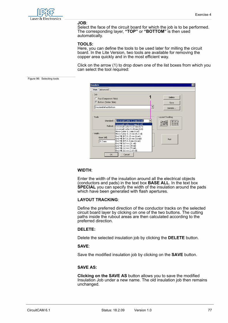
Exercise 4
CircuitCAM 6.1 Status: 18.2.09 Version 1.0 77
JOB:Select the face of the circuit board for which the job is to be performed. The corresponding layer, “TOP” or “BOTTOM” is then used automatically.
TOOLS:Here, you can define the tools to be used later for milling the circuit board. In the Lite Version, two tools are available for removing the copper area quickly and in the most efficient way.
Click on the arrow (1) to drop down one of the list boxes from which you can select the tool required:
Figure 96: Selecting tools
WIDTH:
Enter the width of the insulation around all the electrical objects (conductors and pads) in the text box BASE ALL. In the text box SPECIAL you can specify the width of the insulation around the pads which have been generated with flash apertures.
LAYOUT TRACKING:
Define the preferred direction of the conductor tracks on the selected circuit board layer by clicking on one of the two buttons. The cutting paths inside the rubout areas are then calculated according to the preferred direction.
DELETE:
Delete the selected insulation job by clicking the DELETE button.
SAVE:
Save the modified insulation job by clicking on the SAVE button.
SAVE AS: Clicking on the SAVE AS button allows you to save the modified Insulation Job under a new name. The old insulation job then remains unchanged.
1

Exercise 4
78 Status: 18.2.09 Version 1.0 CircuitCAM 6.1
Settings on the ADVANCED tab
Figure 97: Insulate extended
LAYERS:
Specify which layers are to be used in calculating the insulation channels and on which layer the result will be saved in the LAYERS box. The layer RuboutTop or RuboutBottom and RuboutAllLayers are used as the source for defining the areas from which all residual copper is to be removed.
REMOVE SPIKES:
When this function is switched on, all small copper spikes or hairs are removed down to the size of the diameter of the standard tool. Caution! Longer calculation and milling time!
INSULATION GRID:
This value specifies the accuracy with which the insulation pads are to be calculated. A smaller value results in higher accuracy and a longer calculation time. A value of 0.005 mm should be selected for structures with a conductor width of 0.2 mm and minimum spacing. Higher values (0.05 mm) can produce an erroneous result.
Note: Since the insulating operation is grid-based, the calculation time is lineally related to the number of grid points to be calculated. Therefore, the finer the insulation grid, the longer the calculation operation required. Recommended insulation grid: 0.005 mm

Exercise 4
CircuitCAM 6.1 Status: 18.2.09 Version 1.0 79
PRIMARY OVERLAP:
In order to machine large surfaces efficiently, it is advisable to use different milling tools. For high accuracy, the conductors and pads are insulated first with a small milling tool. The other insulation surfaces are then cut out with a larger milling tool. Enter the value in the PRIMARY OVERLAY text box by which the milling channel of the next larger tool is to overlap the milling channel of the smaller tool. If this value is too small, at many points (at the corners), the standard tool will be used unnecessarily, resulting in a longer milling time. If the value is too large, the rubout tool will come too close to the conductor tracks.
Figure 98:Milling channel
Note: the next largest milling channel should overlap the smaller milling channel by 50 % to 90 %.

Exercise 4
80 Status: 18.2.09 Version 1.0 CircuitCAM 6.1
7.1.2 CircuitCAM - PCB
All of the features of the CircuitCAM - Lite Version are also available in the PCB version. However, this version has additional features as described below.
Settings on the MAIN tab
Figure 99: Insulate Start tab
TOOLS:
As well as the two tools in the Lite Version, the PCB Version has two additional tools: The SMALL tool, which is used on points on the circuit board which cannot be reached with the standard tool because of its diameter. The LARGE tool, which is used as an additional rubout tool for removing larger copper areas.
Settings on the ADVANCED tab:
Figure 100: Insulate tab extended
Exercise 4
CircuitCAM 6.1 Status: 18.2.09 Version 1.0 81
Note: the new features in CircuitCAM 6.1 are the source layer FRAME, the function INVERSE and the CLEAR RESULTING LAYER function. In areas on circuit boards with high voltage or high frequencies, it may be necessary to process the various areas using different insulation methods. When an area is defined using the graphic function “Rectangle” or “Polygon” on the layer entered here and the INVERSE, function is switched off, the insulating job is only performed in this area. If the INVERSE function is switched on, the insulation job is performed outside this defined area only. In each case, two insulation passes are required.
Caution! During the second pass, always switch off the CLEAR RESULTING LAYER function otherwise the result of the previous insulation pass is lost!
RUBOUT MILLING:
As well as the X or Y parallel rubout paths, concentric or X and Y parallel cutting paths can also be produced.
INNER INSULATION:
When this function is switched off and the conductor line is closed, only the outer insulation channels are created around the conductor and not the inner insulation channels.
INDEPENDENT PRIMARY:
When this function is switched off, no primary cutting channel is generated between two elements which are closer together than the diameter of the standard tool (risk of short circuit). If the function is switched on, a milling channel is always generated (risk of reducing the width of a conductor track).
CLEAR RESULTING LAYER:
When this function is switched on, the milling paths for the layers resulting from insulating operations performed previously are deleted (default setting).If the function is switched off, the new result is added to the previous one.
Note: With multiple insulating passes and the function switched off, more milling paths than are necessary are generated. This can drastically increase the milling time.
Note: On the FRONT-TO-END toolbar, the jobs “INSULATE DEFAULT TOP” and “INSULATE DEFAULT BOTTOM”are assigned to the button with the function INSULATE ALL LAYER as the default setting. Adapt these jobs to your requirements to obtain quick access to the desired insulating functions via the toolbar.

Exercise 4
82 Status: 18.2.09 Version 1.0 CircuitCAM 6.1
You can adapt the default job to your requirements as follows:
› Select the job “INSULATEDEFAULTBOTTOM“ in the dialog box INSULATE on the MAIN tab.
Note: As a precautionary measure, you can store the standard job under another name so that it will still be available later. Click on SAVE AS... to store the default job under a different name.Enter the new name in the text box and click on SAVE. After you have stored the job under a new name, select the job “INSULATEDEFAULTBOTTOM“ again on the JOB tab.
› Change the parameters on the MAIN und ADVANCED tabs to meet your requirements.
› Click on SAVE on the MAIN tab to save the job "INSULATE DEFAULT BOTTOM" with the new parameters.
› Repeat this step for the job “INSULATEDEFAULTTOP“.
If you now click on on the FRONT-TO-END toolbar, the default jobs with the parameters which you have changed will be executed immediately.
You can create a new job as follows:
› Select the job which you want to use as the basis for creating the new job in the INSULATE dialog box on the tab MAIN.
› Change the parameters on the tabs MAIN and ADVANCED to meet your requirements (see „CircuitCAM - Lite“ on Page 76 and „CircuitCAM - PCB“ on Page 80).
› Click on SAVE AS on the tab MAIN to store the modified job under a new name.
› Enter the new name in the text box and click on OK.
› Click on OK to close the INSULATE dialog box.
Note: You can delete a job by selecting it on the JOB tab and clicking on DELETE.

Exercise 4
CircuitCAM 6.1 Status: 18.2.09 Version 1.0 83
7.1.3 Insulating areas (PCBs only)
If you want to create circuit boards to be used in the high-voltage range or high-frequency range, you can use this function to increase or reduce the insulation gaps separately in specific areas. This function can also be helpful for optimising the milling times and tool costs. A frame around an area on the circuit board layer can be defined so that this area can be assigned different insulating parameters to the rest of the circuit board layer. The tools to be used can be redefined as well as the insulation gaps between the conductor tracks for this framed area.
An example is shown in the following description. The file used in this example is the same as the one used in the exercises and should be opened beforehand. When this has been done, proceed as follows to familiarise yourself with this function:
› Press Alt or hold Alt down and double click on the layer “FRAME TOP” from the layer list in order to activate the layer.
› Switch the layer “BOTTOM LAYER” to hide.
› Open the INSERT menu and click on the function “CLOSED PATH”.
› Enclose the desired area with the mouse and press the ESC key to switch off the tool.
› Press the HOME key on your keyboard to refresh the display.
› Select the INSULATE submenu from the TOOL PATH menu.
The following window will appear:
Figure 101: Insulate Start tab

Exercise 4
84 Status: 18.2.09 Version 1.0 CircuitCAM 6.1
Settings on MAIN tab› Select the radio button TOP (COMPONENT SIDE).
› Click on the tab “ADVANCED”.
› Open the list “Area” and select the layer “FrameTOP”.
› Click on the “MAIN” tab.
› Click on RUN and the insulation for the “TOP LAYER” will be executed.
Figure 102: Insulation with area
During this process, you will see that insulations are only generated for the conductor tracks which you have defined by enclosing them with a continuous line. If you would like to insulate the area outside the line enclosure, you must switch on the Inverse check box in front of the Area list.

Exercise 4
CircuitCAM 6.1 Status: 18.2.09 Version 1.0 85
7.1.4 Colour assignment for the insulating Tools
To obtain a better overview of the tools used for insulation, different colours can be assigned to the tools. This option is particularly useful because 4 different insulation tools (small, standard, big, bigger) can be used to make optimum use of the tools (not using small insulation tools for wide insulation tracks etc.). To differentiate these four tools from one another, a layer will be created for each tool. These layers can be assigned different colours.
› Use the left mouse button to click on the colour box for a layer in which the colour is to be changed.
The window “Colours” opens (see also Abbildung 63, „Selecting colours,“ on page 51).
› Using the left mouse button, click on the desired colour.
› Click on OK.
The corresponding colour will be assigned.

Exercise 5
86 Status: 18.2.09 Version 1.0 CircuitCAM 6.1
8.0 Exercise 5
In this chapter, you will learn how to create user-specific template files for CircuitCAM and how to correct production data in which the layers do not coincide.
8.1 Creating a CircuitCAM- template file CircuitCAM make it possible to create a template file with user-specific basic settings (similar to a format template in a word processing program for a fax, letter or report).
For example, if you use the same aperture and tool list again and again, you can create your own template file which already contains both these lists. You will then not need to import these aperture and tool lists again for new circuit boards.
All current settings, such as name and colour of the layers are also saved in the template file. More information can be found in the chapter „Creating your own template file“ on Page 124.
CircuitCAM templates are also saved in CAM format but they have the file extension “.cat” and should not contain any graphics information. They are saved in the sub directory “NEW_TEMPLATES”.
When you select the directory NEW in the FILE menu, the available template files appear in this submenu:
Figure 103: Menu, New

Exercise 5
CircuitCAM 6.1 Status: 18.2.09 Version 1.0 87
When you install CircuitCAM, there are already various template files saved in the templates directory:
As well as this, you can also open self-generating templates via the menu item BROWSE FOR TEMPLATE.
Use the “TUTOR1.CAM” file you created in the first exercise as the basis for creating the template file.
Note: in order to open existing files quickly, the current files which have been edited are shown in the menu FILE -> RECENT FILES.
Note: if you have already closed the document “TUTOR1”, click on “TUTOR1.CAM”in the FILE -> RECENT FILES menu in order to open the document again.
How to create a template file for the following exercises:
› Click on ALL in the SELECT menu to select all graphic objects.
› Press DELETE to delete the selected objects.
› Select SAVE AS from the FILE menu.
› Switch to the templates directory “NEW_TEMPLATE” in the SAVE AS dialog box. This directory is located in the “CircuitCAM 6.1” directory.
› Select CIRCUITCAM TEMPLATE FILE (*.CAT) from the FILE TYPE list box.
› Enter FILE NAME “TUTOR1” in the text box.
Template file PurposeDoubleSided Default template file for double sided circuit boards
tutor Template file for exercises in this manual
eagle Like double sided but with import assignments for Eagle files
MicroLine Template for MicroLine systems
4Layer_9x12inch Template for circuit boards 4 layers
6Layer_9x12inch Template for circuit boards 6 layers
8Layer_9x12inch Template for circuit boards 8 layers
ProtoLaser100 Template for ProtoLaser100
ProtoLaser200 Template for ProtoLaser200
Stencil Template for StencilLaser
ZRS_210x297 Template for ZRS stencils
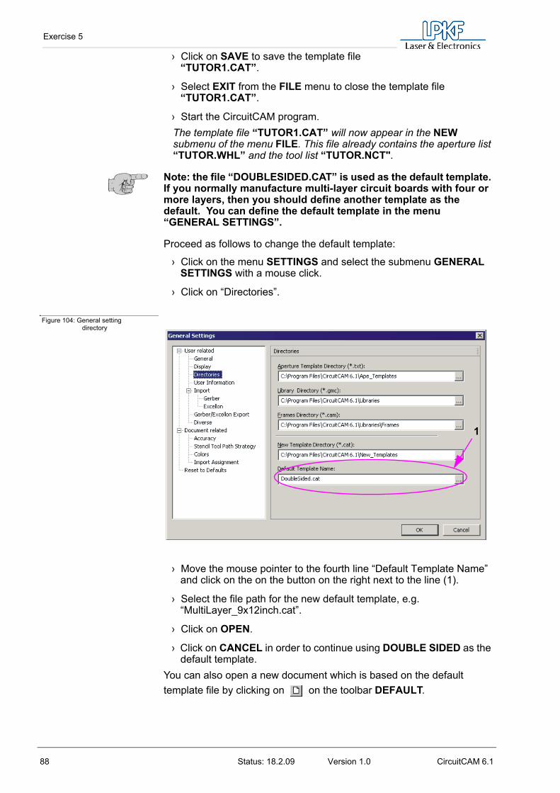
Exercise 5
88 Status: 18.2.09 Version 1.0 CircuitCAM 6.1
› Click on SAVE to save the template file “TUTOR1.CAT”.
› Select EXIT from the FILE menu to close the template file “TUTOR1.CAT”.
› Start the CircuitCAM program.The template file “TUTOR1.CAT” will now appear in the NEW submenu of the menu FILE. This file already contains the aperture list “TUTOR.WHL” and the tool list “TUTOR.NCT".
Note: the file “DOUBLESIDED.CAT” is used as the default template. If you normally manufacture multi-layer circuit boards with four or more layers, then you should define another template as the default. You can define the default template in the menu “GENERAL SETTINGS”.
Proceed as follows to change the default template:
› Click on the menu SETTINGS and select the submenu GENERAL SETTINGS with a mouse click.
› Click on “Directories”.
Figure 104: General setting directory
› Move the mouse pointer to the fourth line “Default Template Name” and click on the on the button on the right next to the line (1).
› Select the file path for the new default template, e.g. “MultiLayer_9x12inch.cat”.
› Click on OPEN.
› Click on CANCEL in order to continue using DOUBLE SIDED as the default template.
You can also open a new document which is based on the default template file by clicking on on the toolbar DEFAULT.
1
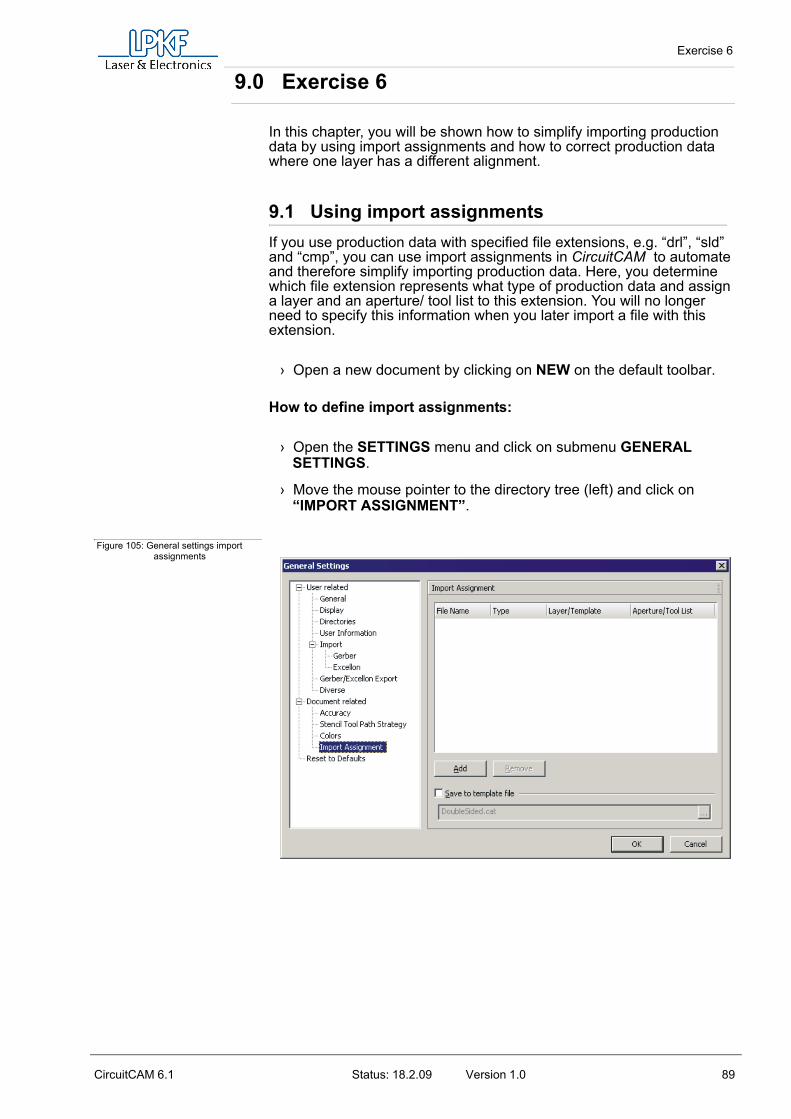
Exercise 6
CircuitCAM 6.1 Status: 18.2.09 Version 1.0 89
9.0 Exercise 6
In this chapter, you will be shown how to simplify importing production data by using import assignments and how to correct production data where one layer has a different alignment.
9.1 Using import assignmentsIf you use production data with specified file extensions, e.g. “drl”, “sld” and “cmp”, you can use import assignments in CircuitCAM to automate and therefore simplify importing production data. Here, you determine which file extension represents what type of production data and assign a layer and an aperture/ tool list to this extension. You will no longer need to specify this information when you later import a file with this extension.
› Open a new document by clicking on NEW on the default toolbar.
How to define import assignments:
› Open the SETTINGS menu and click on submenu GENERAL SETTINGS.
› Move the mouse pointer to the directory tree (left) and click on “IMPORT ASSIGNMENT”.
Figure 105: General settings import assignments

Exercise 6
90 Status: 18.2.09 Version 1.0 CircuitCAM 6.1
As in Exercise 1 (see chapter „Exercise 1“ on Page 33) the number of files which must be imported for a double sided circuit board is five: an aperture list, a tool list, two Gerber files for the conductor tracks and one hole file. The filenames or extensions are issued by the circuit board CAD system. The file extensions may also differ from the file extensions used in this manual.
The following table shows the corresponding extensions and the associated assignments which must be carried out:
› Click on ADD.In the following, enter “*.” and the corresponding file extension in the column “Filenames”.
Note: You can also use wildcards when defining the file specification: The question mark “?” stands for a single character. The asterisk “*” stands for a complete word or a group of characters.
Aperture list Tool list
FILE SPECIFICATATION *.whl *.nct
APERTURE/TOOL LIST Apertures Tools
FILE TYPE Aperture/tool list Aperture/tool list
TEMPLATE TutorApe.txt TutorTools.txt
Excellon data Gerber data Component
side
Gerber data solder side
FILE SPECIFICATATION *.drl *.cmp *.sld
APERTURE/TOOL LIST Tools Apertures Apertures
FILE TYPE Excellon Gerber Gerber
LAYER DrillPlated TopLayer BottomLayer

Exercise 6
CircuitCAM 6.1 Status: 18.2.09 Version 1.0 91
› Enter “*.whl” in the filename column
› Open the list TYPE and select “Select aperture”.
› Open the list LAYER/TEMPLATE and select “TutorApe.txt”.
› Click on the column Aperture/Tool List. Enter the name of the aperture list which CircuitCAM is to use internally for imported apertures.
› Enter the name “Apertures”.
Figure 106: General settings import assignments
The import assignment for the aperture list is completed.
Now create the import assignment for the tool list:
› Click on ADD.
› Enter “*.nct” in the column FILE NAME.
› Open the list TYPE and select “Aperture Select”.
› Open the list LAYER/TEMPLATE and select “TutorTools.txt”.
› Click on the column Aperture/Tool list.

Exercise 6
92 Status: 18.2.09 Version 1.0 CircuitCAM 6.1
Enter the name of the tool list which CircuitCAM is to use internally for the imported tools.
› Enter the name “Tools”.
Figure 107: Import assignments tools
The import assignment for the tools list is completed.
Now create the import assignment for the Gerber files:
› Click on ADD.
› Enter “*.cmp” in the column FILE NAME.
› Open the list TYPE and select “Gerber”.The Gerber file with the file extension “.cmp” contains the layout data for the component side of the circuit board. These data are assigned to the TopLayer.
Now assign the aperture list to the “TOP LAYER”:
› Open the list LAYER/TEMPLATE and select “TopLayer”.
› Click on the column APERTURE/TOOL LIST. Enter the name of the aperture list which CircuitCAM will use internally for imported apertures.
› Enter the name “Apertures”.
› Click on ADD.
› Assign the filename, file type, layer and aperture list for the Gerber file with the extension “.sld”.
› Click on ADD.
› Enter “.drl” in the column FILE NAME.
› Open the list TYPE and select “Excellon”.The holes in the Excellon file should be through-plated. They should therefore be assigned to the layer “DRILL PLATED” .

Exercise 6
CircuitCAM 6.1 Status: 18.2.09 Version 1.0 93
› Open the list LAYER/TEMPLATE and select “DrillPlated”.
› Click on the column APERTURE/TOOL LIST. Enter the name of the tool list which CircuitCAM will use internally for the imported tools.
› Enter the name “Tools”.
Figure 108: Import assignment DrillPlated
The import assignments should now be set as shown in the illustration above.
Save the import assignments in “Tutor.cat” so that the data can be used when other circuit boards are imported by enabling the checkbox “Save to template file” and selecting “Tutor.cat” as the template.
› Click on the checkbox “Save to template file”.
› Click on the button “...“, right beside the file display.
› Click on “Tutor.cat”.
› Click on OPEN.
› Click on OK to close the dialog box GENERAL SETTINGS and save the import assignments in the template file “Tutor.CAT”.
Note: The file-specifications, file types and layers etc. given above refer exclusively to the tutorial data supplied with the software. The filename and the import assignments are unique in each case and depend on the user concerned. The list box LAYER or the list box TEMPLATE will appear in the dialog box IMPORT ASSIGMENT depending on the file type selected.

Exercise 6
94 Status: 18.2.09 Version 1.0 CircuitCAM 6.1
9.2 Moving a layerThe production data used in Exercise 1 represented the ideal case. Of course, in practice, the various production data may not match because they come from different data origins and must therefore be corrected first.
To illustrate the problem, first import the production data into CircuitCAM as you have been shown in Exercise 1.
Do this by opening a new document based on the “TUTOR.CAT” template file:
› Select “TUTOR” from the submenu NEW in the menu FILE.
› Import the following production data from the subdirectory “EXAMPLEDATA\PROTOTYPING” into the new document:
• Tutor2.cmp
• Tutor2.sld
• Tutor2.drl
• Tutor.whl
• Tutor.nct
Once the production data are imported, the following image appears in the graphic window:
Figure 109: Circuit board graphic window
This exercise includes Excellon data which do not coincide with the Gerber data because a different origin was specified when they were output from the circuit board CAD program.
CircuitCAM offers the following function to make the layers coincide again:
MATCH UP LAYERS
How to move a layer:
For your reference coordinates, use a significant object which is present on both the layers which have to coincide:

Exercise 6
CircuitCAM 6.1 Status: 18.2.09 Version 1.0 95
Figure 110: Moving a layer
Note: A significant object could be a drill hole and the associated solder pad, providing this is represented by a flash aperture. Both graphic objects have a centre coordinate, so that a clearly defined position can be selected very accurately. Only flashed elements can be processed with this function since only these have a clearly defined centre.
› Click on in the LAYER toolbar.
› Now click on the lower hole in the “DRILLPLATED” layer to select it as the reference point (1).
When you move the mouse-pointer, you will see an “elastic band” which stretches from the selected point.
› Now select the upper pad of the layer “TOP LAYER” as target-point (2) by clicking on it.
The layer “DRILL PLATED” will move and the layers now coincide.
Note: To save the current status of the exercise, select SAVE AS from the FILE menu. Enter the filename “TUTOR5” and click on SAVE.
You have now learned how to make layers which are offset coincide (match up). Since the other steps in preparing for prototyping are identical to those in Exercise 1, they will not be repeated here.
› Now, close the document “TUTOR5” by selecting EXIT in the FILE menu.
2
1

Exercise 6
96 Status: 18.2.09 Version 1.0 CircuitCAM 6.1
9.3 Rotating a layer You have already been shown how to correct production data where the layers do not coincide. This exercise includes Excellon data which are offset against the Gerber data and are also rotated by 90°.
For this exercise, open a new document based on the “TUTOR.CAT” template file:
› Select “TUTOR.CAT” from the submenu NEW in the FILE menu .
› Import the production data from the “EXAMPLEDATA\PROTOTYPING” subdirectory into the new document:
• Tutor3.cmp
• Tutor3.sld
• Tutor3.drl
• Tutor.whl
• Tutor.nct
Note: import the five files in a single operation. Since the import assignments are defined, it is not necessary to assign the layer and tool/aperture list again in the dialog box IMPORT.
Once the production data are imported, the following image appears in the graphic window:
Figure 111: Production data graphic window
In addition to the “Match Up Layers” functions you have already used, you will also need the functions for mirroring/rotating graphic objects.
These functions can be found in the submenu ROTATE RELATIVE in the EDIT menu:

Exercise 6
CircuitCAM 6.1 Status: 18.2.09 Version 1.0 97
Figure 112: Mirror/rotate menu
You will see the effect of each function with the aid of the example object
:
A selected object always rotates around the anchor point:
Figure 113: Mirror/rotate anchor point
You can also mirror/rotate around the anchor point of an object which itself will not be mirrored/rotated:
VALUE ... MIRROR X
90° MIRROR X+90°
180° MIRROR Y
270° MIRROR Y+90°

Exercise 6
98 Status: 18.2.09 Version 1.0 CircuitCAM 6.1
› Select the anchor point by clicking on the object. The anchor point is indicated by a cross:
Figure 114: Defining an anchor point
› Select the objects you wish to MIRROR/ROTATE by dragging them using the left mouse button rather than by clicking on them:
Figure 115: Selecting an object
By doing this, the anchor point of the object previously clicked on is retained and can be used as the reference point for mirroring/rotation:
Figure 116: Positioning an anchor point
You can also position this anchor point completely independently of any object:
› Select SET ANCHOR POINT from the EDIT menu .
The SET ANCHOR POINT dialog box will appear showing the current coordinates of the anchor point:
Figure 117: Entering anchor coordinates
› Enter the new coordinates for the anchor point in the text boxes and click on OK.
In the following exercise, you will use the position of a drill hole as the reference point for rotating the entire layer.
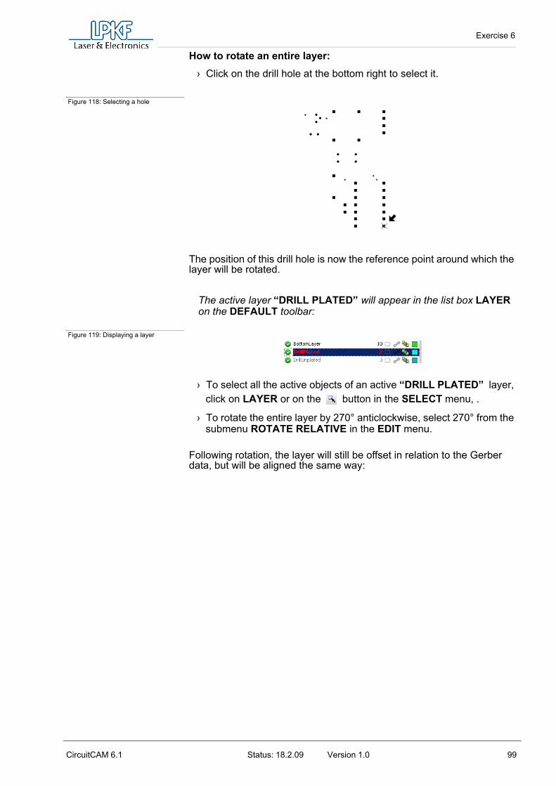
Exercise 6
CircuitCAM 6.1 Status: 18.2.09 Version 1.0 99
How to rotate an entire layer:› Click on the drill hole at the bottom right to select it.
Figure 118: Selecting a hole
The position of this drill hole is now the reference point around which the layer will be rotated.
The active layer “DRILL PLATED” will appear in the list box LAYER on the DEFAULT toolbar:
Figure 119: Displaying a layer
› To select all the active objects of an active “DRILL PLATED” layer, click on LAYER or on the button in the SELECT menu, .
› To rotate the entire layer by 270° anticlockwise, select 270° from the submenu ROTATE RELATIVE in the EDIT menu.
Following rotation, the layer will still be offset in relation to the Gerber data, but will be aligned the same way:

Exercise 6
100 Status: 18.2.09 Version 1.0 CircuitCAM 6.1
Figure 120: Matching up a layer
You can now make the layers coincide using the MATCH UP LAYERS function, as shown in the previous exercise.
Note: You can correct layers that are mirrored using the same procedure by selecting MIRROR X or MIRROR Y from the submenu ROTATE RELATIVE in the EDIT menu .
Note: If you wish to practise mirroring layers, you can use the tutorial files “TUTOR4.CMP”, “TUTOR4.DRL” and “TUTOR4.SLD”.
Note: We recommend that you first rotate or mirror the layer and then move it.
Note: To save the current status of the exercise, select SAVE AS from the FILE menu. Enter “TUTOR6” as the filename and click on OK.
You have now been shown how to define import assignments and how to make rotated and offset layers coincide. Since the other steps in preparing for prototyping are identical to those in Exercise 2, they will not be repeated.
To conclude the sixth exercise, you can now close the document by selecting EXIT from the FILE menu.

Appendix
CircuitCAM 6.1 Status: 18.2.09 Version 1.0 101
10.0 Appendix
10.1 Gerber format
This chapter shows you:
• Where Gerber is used
• The Gerber format syntax
• The difference between drawing and flashing
• The data format
• The structure of the aperture lists
10.1.1 Use of Gerber Format
The Gerber format is used for photoplotter control. The photoplotter is used to create films used for etching, e.g. for the production of circuit boards. Films are not required for producing circuit board prototypes with circuit board plotters. However, by using the CircuitCAM software it is possible to use the same data for controlling photoplotters in order to generate the required milling data.
10.1.2 Layout of a Photoplotter
To understand the Gerber format better, it is advisable to familiarise yourself with the principle layout of a photoplotter first. For us, the most important components of a photoplotter are:
• the aperture wheel
• the shutter
• the bulb required for exposing the film.
Figure 121: Schematic layout of a photoplotter
Light source
Aperture wheel
y axis
x axis

Appendix
102 Status: 18.2.09 Version 1.0 CircuitCAM 6.1
As shown in the illustration above, the aperture plate is a disc with apertures arranged around its circumference. Each of these apertures has a designation.As a rule, the smallest aperture has is designated D10, the next largest, D11... and so on. These apertures have different shapes. For example, they are circular, square or rectangular.
The shutter is located between the film and aperture plate. Its purpose is to allow the light from the bulb to pass through to the film only at certain moments.
10.1.3 Gerber format syntax
10.1.3.1 Drawing
Example 1:
A line is to be drawn using the photoplotters. This line is to be 0.3 mm wide and 2.3 mm long. It is to be round at the ends.
In order for this to happen, a number of commands are sent to the photoplotter. These commands are explained below.
First, the photoplotter has to rotate the aperture plate so that a round aperture with a diameter of 0.3 mm is placed in front of the shutter. In this example, this is aperture D12.
The command is: G54D12*
G54 is the command to rotate the aperture plate.D12 indicates the new position of the aperture plate.
Next, the photoplotter has to move to the starting point of the line without drawing anything. This means that the shutter must remain closed.The starting coordinates for this line are to be X=100 and Y=150.
The command is: X100Y150D02*
X100Y150 indicates the position to be moved to.D02 is the command to move with the shutter closed.
At the starting point for the line, the photoplotter is to open the shutter and move to the end point of the line. The end point is at the coordinates X:102 and Y:150.
The command is: X102Y150D01*
X102Y150 indicates the position to be moved to.D01 is the command to move with the shutter open.

Appendix
CircuitCAM 6.1 Status: 18.2.09 Version 1.0 103
Example 2:Now, another line is to be drawn. This line is to have the same dimensions, however, the ends are to be rectangular. For this purpose, it is necessary to use a rectangular aperture. The edge length of this aperture is also 0.3mm. On our aperture plate, this is aperture D17.
The command is: G54D17* G54 is the command to rotate the aperture plate.D17 is the rectangular aperture with edge length of 0.3 mm.
Next, the photoplotter has to move to the starting point of the line without drawing anything. This means that the shutter must remain closed. The starting coordinates for this line are X=100 and Y=100.
The command is: X100Y100D02*X100Y100 indicates the position to be moved to.D02 is the command to move with the shutter closed.
Now, the photoplotter is to open the shutter and move to the end point of the line. The end point is at the coordinates X=102 and Y=100.
The command is: X102Y100D01*X102Y100 indicates the position to be moved to.D01 is the command to move with the shutter open.
10.1.3.2 Flashing
The last command sequence resulted a rectangle.
Example 3:A rectangle can also be generated with fewer commands. This assumes that the desired shape is available as an aperture on the aperture plate.A rectangular aperture with dimensions of 2.3 x 0.3 mm is required on the aperture plate. In our example, this is aperture D20.The photoplotter must rotate this aperture in front of the shutter.
The command is: G54D20*G54 is the command to rotate the aperture plate.D20 is the command to select aperture D20.
The photoplotter must now move to position X:101 and Y:50 and open and close the shutter there.
The command is: X101Y50D03* X101Y50 indicates the position to be moved to.D03 is the command to open the shutter and close it again without moving.
The last command in any Gerber file must be the command M02* to define the end of the Gerber file.
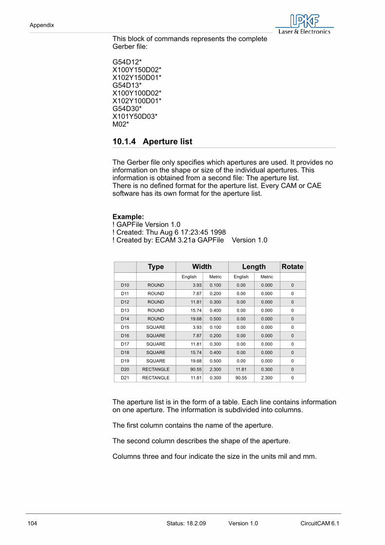
Appendix
104 Status: 18.2.09 Version 1.0 CircuitCAM 6.1
This block of commands represents the complete Gerber file:
G54D12* X100Y150D02* X102Y150D01* G54D13* X100Y100D02* X102Y100D01* G54D30* X101Y50D03* M02*
10.1.4 Aperture list
The Gerber file only specifies which apertures are used. It provides no information on the shape or size of the individual apertures. This information is obtained from a second file: The aperture list. There is no defined format for the aperture list. Every CAM or CAE software has its own format for the aperture list.
Example:! GAPFile Version 1.0 ! Created: Thu Aug 6 17:23:45 1998 ! Created by: ECAM 3.21a GAPFile Version 1.0
The aperture list is in the form of a table. Each line contains information on one aperture. The information is subdivided into columns.
The first column contains the name of the aperture.
The second column describes the shape of the aperture.
Columns three and four indicate the size in the units mil and mm.
Type Width Length RotateEnglish Metric English Metric
D10 ROUND 3.93 0.100 0.00 0.000 0
D11 ROUND 7.87 0.200 0.00 0.000 0
D12 ROUND 11.81 0.300 0.00 0.000 0
D13 ROUND 15.74 0.400 0.00 0.000 0
D14 ROUND 19.68 0.500 0.00 0.000 0
D15 SQUARE 3.93 0.100 0.00 0.000 0
D16 SQUARE 7.87 0.200 0.00 0.000 0
D17 SQUARE 11.81 0.300 0.00 0.000 0
D18 SQUARE 15.74 0.400 0.00 0.000 0
D19 SQUARE 19.68 0.500 0.00 0.000 0
D20 RECTANGLE 90.55 2.300 11.81 0.300 0
D21 RECTANGLE 11.81 0.300 90.55 2.300 0

Appendix
CircuitCAM 6.1 Status: 18.2.09 Version 1.0 105
The diameter is specified here for round apertures and the edge length for square apertures.
With rectangular apertures, the elongation in the X direction is specified in these columns.
Columns five and six contain the elongation in the Y direction. These columns are not used for round or square apertures.
10.1.5 Units, format and suppressed zeros
The coordinates for the Gerber file do not provide any information on whether the values are to be interpreted in millimetres or inches. Moreover, the Gerber file does not indicate where the decimal point should be. For example, the second line of the sample Gerber file could be interpreted as follows:
X100Y150D02* could mean X: 10.0 mm, Y: 15.0 mm or X:1.00 inch, Y: 1.50 inch.
This information may be present in the aperture list or may be contained in an additional file also containing production instructions. One such file is used in our example:
! DSNFile Version 1.3 ! Created: Thu Aug 6 17:23:45 1998 ! Created by: ECAM 3.21a ! DSNFile Version 1.3
Database_type: RS274X Database_format: 2.3 Coordinate_mode: Absolute Zero_suppression: Leading Coordinate_units: Metric
The question regarding the units can be quickly answered. In the last line, the expression Coordinate_units means: metric, which means that the coordinates must be read in mm.
The position of the decimal point must be read from a combination of two pieces of information. These are the Database_format and the Zero_suppression. Format 2.3 indicates a number with two digits in front of the decimal point and three digits behind the decimal point. Actually, the coordinates in the sample Gerber file should have five digits.However, as you can see, only two or three digits are used. The reason for this is that the zeros at the beginning of the coordinates (leading zeros) and at the end of the coordinates (trailing zeros)are not written. These are referred to as suppressed zeros (zero suppression).
There are two options for suppressing the zeros:The coordinates contain either the leading zeros alone or the trailing zeros alone.

Appendix
106 Status: 18.2.09 Version 1.0 CircuitCAM 6.1
From the first line of the sample Gerber file, when all the zeros are written: X00100Y00150D02*, the following shows when the leading zeros are suppressed: X100Y150D02*, and the following shows when the trailing zeros are suppressed: X001Y0015D02*.
In order to correct the decimal point, it is necessary to know which zeros have been suppressed.If the leading zeros were suppressed, the number of digits following the decimal point is crucial. If trailing zeros were suppressed, the number of digits in front of the decimal point is crucial for the position of the decimal point.
In this example, you can see the line Zero_suppression: Leading. This means that the leading zeros are suppressed. This can also be seen by the fact that the coordinates in the sample Gerber file never start with a zero.
10.1.6 Extended Gerber
When the Gerber data are transferred from the customer to the template manufacturer, the manufacturer frequently does not receive the information (such as the aperture list) required for production. In this case, it is necessary to discuss the missing information with the customer and this often leads to unnecessary telephone calls and delays in production.
For this reason, the Gerber format has been extended. This extended format is called “Extended Gerber” or “RS247X”.The advantage of this format is that all the necessary information for reading the Gerber file correctly is already contained in the file itself. This means that no separate aperture list is required since the definition of the aperture is already contained in the Extended Gerber file.
The following example shows the syntax for defining units, formats and the apertures. This definition block is always located at the beginning of the Extended Gerber file:
%FSLAX23Y23*% %MOMM*% %ADD10C,0.10000*% %ADD11C,0.20000*% %ADD12C,0.30000*% %ADD13C,0.40000*% %ADD14C,0.50000*%
%ADD15R,0.10000X0.10000*% %ADD16R,0.20000X0.20000*% %ADD17R,0.30000X0.30000*% %ADD18R,0.40000X0.40000*%
%ADD19R,0.50000X0.50000*% %ADD20R,2.30000X0.30000*% %ADD21R,0.30000X2.30000*%
The following line is used to define the format:

Appendix
CircuitCAM 6.1 Status: 18.2.09 Version 1.0 107
%FSLAX23Y23*% FS stands for Format Statement. L stands for leading zero suppression.Zeros therefore only appear at the end of the coordinates.
A stands for absolute coordinates meaning that all coordinates are based on the origin.
X23Y23 stands for the number of digits in front (2) and behind (3) of the decimal point. It is possible to define this differently for the X and Y-axis.
The units for the Gerber data are defined in the next line: %MOMM*% MO stands for mode. MM stands for millimetre.
In the event that the Gerber data are given in inches, IN would be used instead of MM.
The apertures are defined by the following lines:
%ADD15R,0.10000X0.10000*% AD stands for aperture definition
D15 is the name of the aperture
R is the shape of the aperture. R stands for rectangle; C for circle
0.10000X0.10000 stands for the size of the aperture in the X and Y direction.
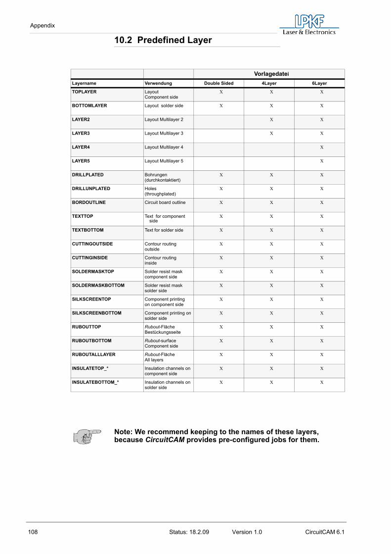
Appendix
108 Status: 18.2.09 Version 1.0 CircuitCAM 6.1
10.2 Predefined Layer
Note: We recommend keeping to the names of these layers, because CircuitCAM provides pre-configured jobs for them.
VorlagedateiLayername Verwendung Double Sided 4Layer 6Layer
TOPLAYER LayoutComponent side
X X X
BOTTOMLAYER Layout solder side X X X
LAYER2 Layout Multilayer 2 X X
LAYER3 Layout Multilayer 3 X X
LAYER4 Layout Multilayer 4 X
LAYER5 Layout Multilayer 5 X
DRILLPLATED Bohrungen (durchkontaktiert)
X X X
DRILLUNPLATED Holes (throughplated)
X X X
BORDOUTLINE Circuit board outline X X X
TEXTTOP Text for component side
X X X
TEXTBOTTOM Text for solder side X X X
CUTTINGOUTSIDE Contour routing outside
X X X
CUTTINGINSIDE Contour routing inside
X X X
SOLDERMASKTOP Solder resist maskcomponent side
X X X
SOLDERMASKBOTTOM Solder resist masksolder side
X X X
SILKSCREENTOP Component printing on component side
X X X
SILKSCREENBOTTOM Component printing on solder side
X X X
RUBOUTTOP Rubout-Fläche Bestückungsseite
X X X
RUBOUTBOTTOM Rubout-surface Component side
X X X
RUBOUTALLLAYER Rubout-FlächeAll layers
X X X
INSULATETOP_* Insulation channels oncomponent side
X X X
INSULATEBOTTOM_* Insulation channels onsolder side
X X X
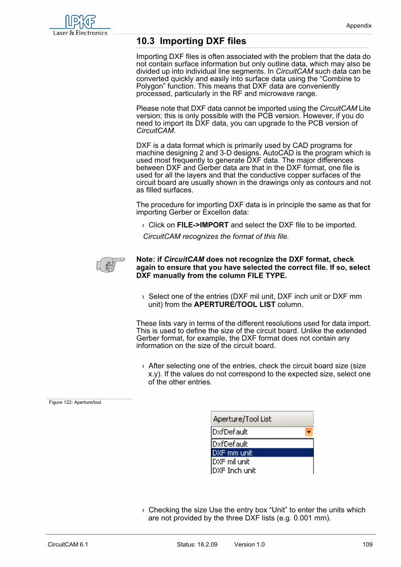
Appendix
CircuitCAM 6.1 Status: 18.2.09 Version 1.0 109
10.3 Importing DXF filesImporting DXF files is often associated with the problem that the data do not contain surface information but only outline data, which may also be divided up into individual line segments. In CircuitCAM such data can be converted quickly and easily into surface data using the “Combine to Polygon” function. This means that DXF data are conveniently processed, particularly in the RF and microwave range.
Please note that DXF data cannot be imported using the CircuitCAM Lite version; this is only possible with the PCB version. However, if you do need to import its DXF data, you can upgrade to the PCB version of CircuitCAM.
DXF is a data format which is primarily used by CAD programs for machine designing 2 and 3-D designs. AutoCAD is the program which is used most frequently to generate DXF data. The major differences between DXF and Gerber data are that in the DXF format, one file is used for all the layers and that the conductive copper surfaces of the circuit board are usually shown in the drawings only as contours and not as filled surfaces.
The procedure for importing DXF data is in principle the same as that for importing Gerber or Excellon data:
› Click on FILE->IMPORT and select the DXF file to be imported.CircuitCAM recognizes the format of this file.
Note: if CircuitCAM does not recognize the DXF format, check again to ensure that you have selected the correct file. If so, select DXF manually from the column FILE TYPE.
› Select one of the entries (DXF mil unit, DXF inch unit or DXF mm unit) from the APERTURE/TOOL LIST column.
These lists vary in terms of the different resolutions used for data import. This is used to define the size of the circuit board. Unlike the extended Gerber format, for example, the DXF format does not contain any information on the size of the circuit board.
› After selecting one of the entries, check the circuit board size (size x.y). If the values do not correspond to the expected size, select one of the other entries.
Figure 122: Aperture/tool
› Checking the size Use the entry box “Unit” to enter the units which are not provided by the three DXF lists (e.g. 0.001 mm).
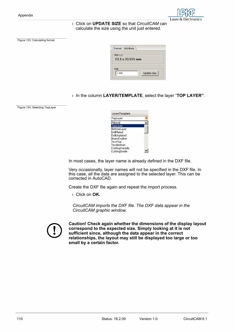
Appendix
110 Status: 18.2.09 Version 1.0 CircuitCAM 6.1
› Click on UPDATE SIZE so that CircuitCAM can calculate the size using the unit just entered.
Figure 123: Calculating format
› In the column LAYER/TEMPLATE, select the layer “TOP LAYER”.
Figure 124: Selecting TopLayer
In most cases, the layer name is already defined in the DXF file.
Very occasionally, layer names will not be specified in the DXF file. In this case, all the data are assigned to the selected layer. This can be corrected in AutoCAD.
Create the DXF file again and repeat the import process.
› Click on OK.
CircuitCAM imports the DXF file. The DXF data appear in the CircuitCAM graphic window.
Caution! Check again whether the dimensions of the display layout correspond to the expected size. Simply looking at it is not sufficient since, although the data appear in the correct relationships, the layout may still be displayed too large or too small by a certain factor.

Appendix
CircuitCAM 6.1 Status: 18.2.09 Version 1.0 111
› Click on the lower left corner of the layout or on an element close to it for checking exactly.
› Click using the right mouse button.The context menu opens.
› Select MEASURE from this menu.
› Click on the lower left corner of the layout.
› Move the mouse pointer to the opposite corner.
An elastic band stretches between the mouse pointer and the selected element and the length of the elastic band as well as the Y and Y path (short side of the right-angled triangle) is displayed in the bottom left corner of the CircuitCAM window (on the status bar).
You can check the layout size using these values.
If graphic objects do not lie on the “TOP LAYER” or “BOTTOM LAYER”, they must be moved to these layers in order for CircuitCAM to use them for prepared insulation or export jobs.
› With the right mouse button, click on the layer with the objects which must be moved.
› Click on SELECT GRAFIC OBJECTS in the context menu.
› Press the mouse button or hold the mouse button down and select the layer to which the objects are to be moved by a double click.
› Move the mouse pointer over the graphic and press Esc in order to deselect.
Use the same procedure for all the other DXF data layers.
All copper surfaces which are required as conductive copper (conductors and pads) on the circuit board must be displayed as filled surfaces in CircuitCAM. If this is not the case in the DXF files, the data must be modified.There are four different options for defining copper surfaces in the DXF data:
Option 1: As a continuous, enclosing line.
Figure 125: Continuous line
Option 2: As a continuous enclosing line, but with individual line segments.

Appendix
112 Status: 18.2.09 Version 1.0 CircuitCAM 6.1
Figure 126:Continuous enclosing line
Option 3: A continuous enclosing line surrounds one or more other lines. The differences between these surfaces defines the remaining copper surface.
Figure 127:Continuous line frame
Option 4: Same as 3, but with individual line segments.
Figure 128:Line segment
How are these data modified?
Option 1:
› Select the enclosing line surrounding the surface to be filled by clicking on it with the left mouse button.
› Select the function COMBINE TO POLYGON from the MODIFY menu.
The selected element appears as a filled surface (Polygon). Use the same procedure for all the other elements.
Note: If the result is not as expected, use the UNDO function and check the element selected.Multiple selection of more than one element can be used before executing the function COMBINE TO POLYGON. However, ensure that the selected elements are of the same type as those described under Option 1.

Appendix
CircuitCAM 6.1 Status: 18.2.09 Version 1.0 113
Option 2:
For this situation, the modification is similar to Option 1. However, the individual line segments of an enclosing line must be joined together to form a continuous line.
› Select all the individual line segments of one or more enclosing lines using the different selection methods (left mouse click, Ctrl + left mouse click, Shift + left mouse click, left mouse click and drawing up a rectangle – details are in the CircuitCAM Manual).
Once they have been successfully selected, select the function COMBINE from the MODIFY CURVE menu or use the key combination Ctrl+B. Then proceed as described under Option 1.
Note: If the result of the COMBINE function gives an incorrect result (line segments connected which should not have been connected), ensure that the value for the capture range for the combine function was set realistically. This value defines the max. distance between the line segments to be connected to one another. If the value is too large, adjacent segments which should not be connected will be connected to one another. If the value is too small, segments which should be connected to one another may not be connected because their starting or finishing points are not precisely on top of one another due to inaccuracies in the DXF data. The value for the capture range is given on the DIVERSE tab in the GENERAL SETTINGS menu. The value for the parameter “Threshold Curve Combine” should be 0.01 to 0.05 mm. This value depends on the structure of the layout.
Option 3:
With this option, one or more polygons must be subtracted from another larger polygon. This modification must be carried out step-by-step.
First, the enclosing lines must be modified to form polygons as described under Option 1.
After this, only the smaller (inner) polygons are selected and converted to a cutout by using the “CUTOUT” function in the INSERT menu. This cutout is inserted into a copper surface which is yet to be selected.
› Select all the objects which are changed to cutouts.
› Open the INSERT menu and click on “CUTOUT”.
› Select the copper surface from which the cutout is to be extracted.The result is a polygon with openings, which has precisely the expected design – providing all the selections have been carried out correctly.
Note: If the result is not what you expected, use the UNDO function and check the elements selected.

Appendix
114 Status: 18.2.09 Version 1.0 CircuitCAM 6.1
Option 4:
With this situation, the modification is similar to Option 3. However, the individual line segments of an enclosing line must be joined together to form a continuous line. Then proceed as described under Option 3.
After completing the above modifications, your layout can be processed further with all the prepared insulating and export jobs. All the jobs which are available for this purpose can be used.
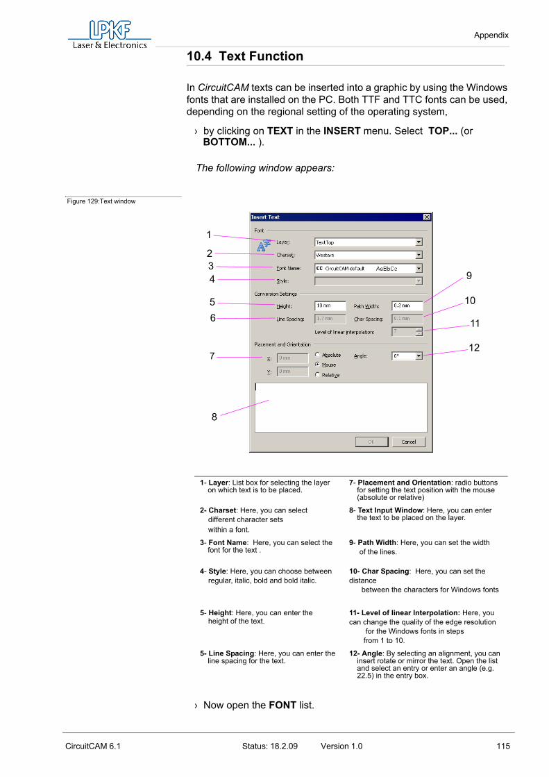
Appendix
CircuitCAM 6.1 Status: 18.2.09 Version 1.0 115
10.4 Text Function
In CircuitCAM texts can be inserted into a graphic by using the Windows fonts that are installed on the PC. Both TTF and TTC fonts can be used, depending on the regional setting of the operating system,
› by clicking on TEXT in the INSERT menu. Select TOP... (or BOTTOM... ).
The following window appears:
Figure 129:Text window
› Now open the FONT list.
1- Layer: List box for selecting the layer on which text is to be placed.
7- Placement and Orientation: radio buttons for setting the text position with the mouse (absolute or relative)
2- Charset: Here, you can select different character sets within a font.
8- Text Input Window: Here, you can enter the text to be placed on the layer.
3- Font Name: Here, you can select the font for the text .
9- Path Width: Here, you can set the width of the lines.
4- Style: Here, you can choose between regular, italic, bold and bold italic.
10- Char Spacing: Here, you can set the distance between the characters for Windows fonts
5- Height: Here, you can enter the height of the text.
11- Level of linear Interpolation: Here, you can change the quality of the edge resolution for the Windows fonts in steps from 1 to 10.
5- Line Spacing: Here, you can enter the line spacing for the text.
12- Angle: By selecting an alignment, you can insert rotate or mirror the text. Open the list and select an entry or enter an angle (e.g. 22.5) in the entry box.
7
1
234
56
8
9
10
11
12

Appendix
116 Status: 18.2.09 Version 1.0 CircuitCAM 6.1
The selection list for the fonts appears.
› Select a font.The selected font appears in the FONT NAME display box.
› Click once on the bottom, white, text entry window.The entry cursor is then enabled and flashes in the text entry box.
› You can then enter the desired text in the bottom window.
› Click on OK.
› Now position the text on the layer and fix it by clicking once with the left mouse button.
A text which has been created in this way can only be processed by using a tool. The tool which should be used is defined in the TOOLS list as LPKFMILLINGTEXT TOOL and can changed from there.
Note: In the PCB version of CircuitCAM, DXF files with texts can also be imported and interpreted correctly. This assumes, however, that True Type fonts are used! MTEXT entities in the DXF file are not supported. One of the main advantages is that the texts no longer have to be divided into vectors in AutoCAD, and this results in less data and a more appealing appearance.
10.5 Generating earth areas
CircuitCAM makes it possible to generate earth areas in the PCB layout, automatically and easily. This means that laborious design work is no longer necessary for earth areas when the EDA system does not provide such a function. This then reduces the milling work and provides a simple EMC-oriented design of the layout.
The following instructions are an example. In this case, the same file has been used as that used for the main exercises. If other files are used, the circuit board illustrations will of course look different.
To familiarise yourself with this function, proceed as follows:
› Open the file “TUTOR1.CAM”
› With the right button, click on the layer “TOP LAYER” in the layout list.
› Click on “Visible selected only” in the layer context menu.You have switched all the other layers to invisible and defined the layer “TOP LAYER” as the active layer.

Appendix
CircuitCAM 6.1 Status: 18.2.09 Version 1.0 117
Figure 130:Layer for earth area
› Design the desired earth area using the RECTANGLE or POLYGON function. Then press Esc to terminate this function.
Figure 131: Toplayer
› Select all the objects which are located inside the designed surface or intersect it. Make sure that the area (1) itself is not selected.
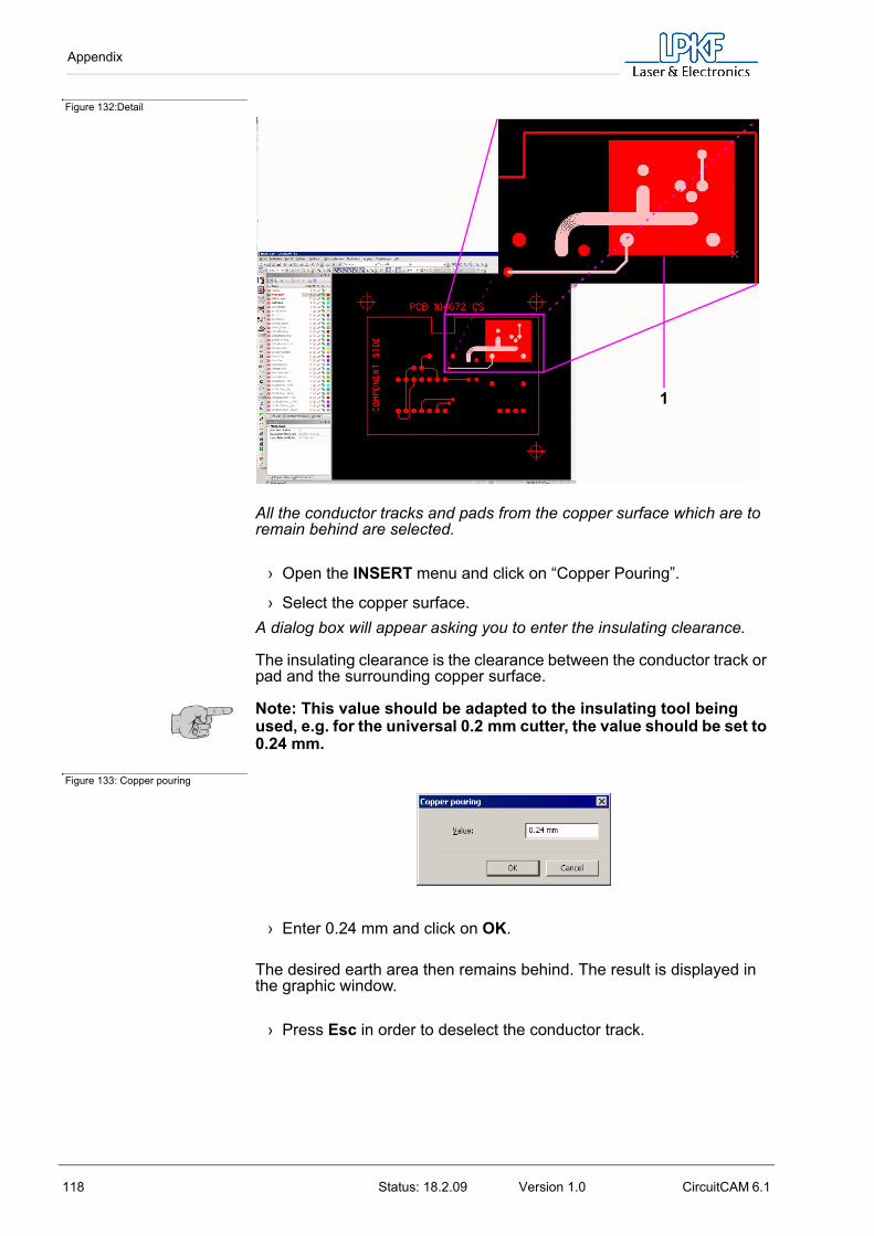
Appendix
118 Status: 18.2.09 Version 1.0 CircuitCAM 6.1
Figure 132:Detail
All the conductor tracks and pads from the copper surface which are to remain behind are selected.
› Open the INSERT menu and click on “Copper Pouring”.
› Select the copper surface.A dialog box will appear asking you to enter the insulating clearance.
The insulating clearance is the clearance between the conductor track or pad and the surrounding copper surface.
Note: This value should be adapted to the insulating tool being used, e.g. for the universal 0.2 mm cutter, the value should be set to 0.24 mm.
Figure 133: Copper pouring
› Enter 0.24 mm and click on OK.
The desired earth area then remains behind. The result is displayed in the graphic window.
› Press Esc in order to deselect the conductor track.
1

Appendix
CircuitCAM 6.1 Status: 18.2.09 Version 1.0 119
Figure 134:Earth area
10.6 Design Rule Check
The CircuitCAM PCB version provides a “Design Rule Check”. This means that before starting the insulation or data output, it is possible to check whether the desired minimum clearances have been maintained between the conductor tracks and/or pads.
For this purpose, the layer to be checked and the dimension of the minimum clearance are simply defined. Those points at which the minimum clearance is not maintained are shown graphically on the layout. The following clearances can also be measured:
1. Clearance from hole to hole 2. Clearance from hole to conductor track 3. Clearance from hole or conductor track to circuit board frame 4. Minimum width of remaining copper ring around holes
These measurement options increase the reliability of circuit board prototyping considerably since many errors can be eliminated before they cause any damage.
With the following work instructions also, it should be pointed out that this is an example. The layout illustrations are based on the files from the exercises in the main chapter. Where other data are used, some illustrations appear different.
To familiarise yourself with this function, proceed as follows.
› Open the file TUTOR2.CAM in the FILE menu

Appendix
120 Status: 18.2.09 Version 1.0 CircuitCAM 6.1
Checking the clearance between two Layers:
› Switch all layers used except “TOP LAYER“, “DRILL PLATED LAYER“ and “BOARD OUTLINE LAYER“ to invisible.
Figure 135: Closing the layer list
1. Checking the clearance inside a layer:
This Design Rule Check checks the minimum desired clearance inside a layer. This is used to check whether a milling tool of the desired width (0.2 mm) can be used. On the other hand, it is also possible to check for the minimum clearance required for the electrical properties.
› Select the menu EDIT.
› Then select the sub-menu DESIGN RULE CHECK.
› Then select the function PRINTED CIRCUIT BOARD.
The following window appears:
Figure 136: Design Rule Processing
The display may vary depending on whether the radio button “Inter min. Spacing” or “Intra min. spacing” is selected.
› Select the layer to be checked from the LAYER1 list.
› Enter any desired name under LAYER RESULT for the layer result on which the positions of any errors present are to be displayed graphically.
› Enter the minimum clearance to be checked under WIDTH.

Appendix
CircuitCAM 6.1 Status: 18.2.09 Version 1.0 121
If the possible use of a milling tool is to be checked, enter a value approx. 0.02 mm larger than the diameter of the tool in order to avoid flaws resulting later from rounding errors when insulating.
› Select the value 0.5 mm here to provoke errors.
› Click on RUN.
The following message will appear:
Figure 137: Design Rule Check, Message
CircuitCAM reports 2 errors, i.e. the minimum clearance of 0.5 mm has not been maintained at 2 points. These two points are indicated graphically in the layout (see arrows).
2. Checking the clearance between 2 layers:
This Design Rule Check is used to check the minimum clearance between holes or components and the circuit board outline.
› Select the menu EDIT.
› Then select the sub-menu DESIGN RULE CHECK.
› Then select the function PRINTED CIRCUIT BOARD.

Appendix
122 Status: 18.2.09 Version 1.0 CircuitCAM 6.1
The following window will appear:
Figure 138: Design Rule Check
The presentation may vary depending on whether the radio button “Inter min. Spacing” or “Intra min. spacing” is selected.
› Select the first layer to be checked from the LAYER1 list.
› Select the second layer to be checked from the LAYER2 list.
› Under LAYER RESULT, enter any desired name for the layer result on which the positions of any errors present are to be shown graphically.
› Enter the minimum clearance to be checked under WIDTH.
› Select the value 2.5 mm here to provoke errors.
› Click on RUN.The following message will appear:
Figure 139: Design Rule Check, Message
CircuitCAM reports 1 error, i.e. the minimum clearance of 2.5 mm has not been maintained at 1 point. This point is shown graphically on the layout (see arrow).
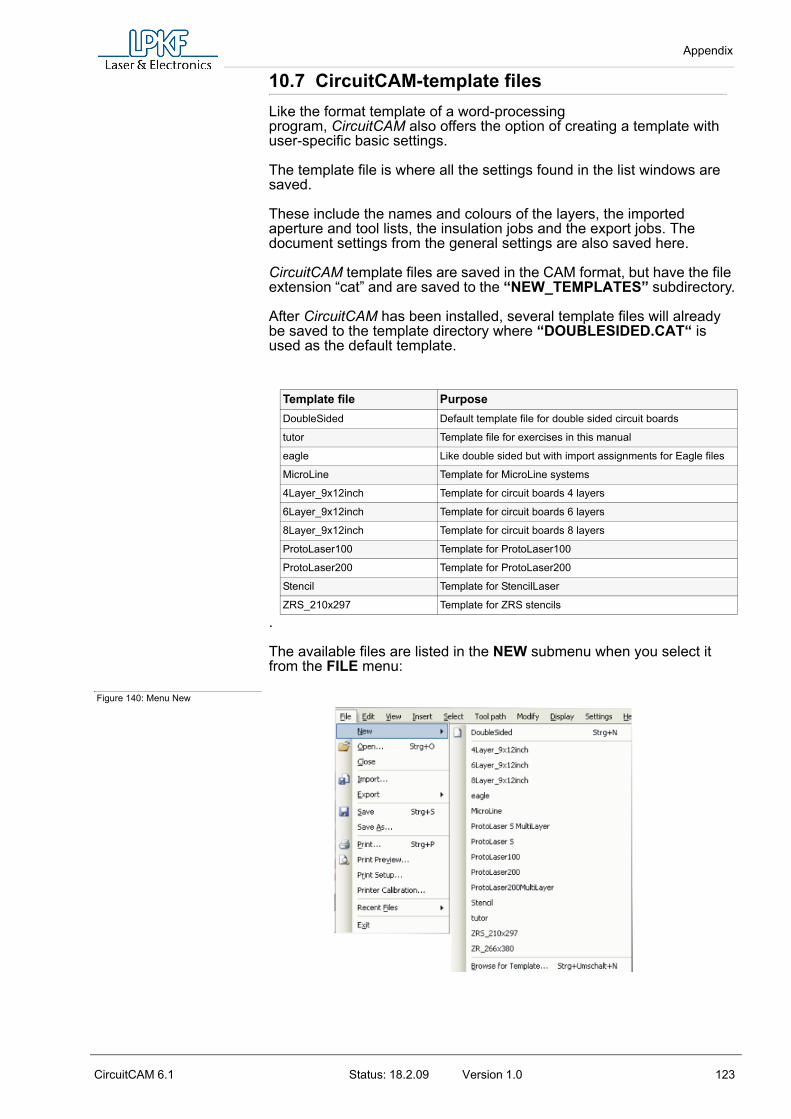
Appendix
CircuitCAM 6.1 Status: 18.2.09 Version 1.0 123
10.7 CircuitCAM-template filesLike the format template of a word-processingprogram, CircuitCAM also offers the option of creating a template with user-specific basic settings.
The template file is where all the settings found in the list windows are saved.
These include the names and colours of the layers, the imported aperture and tool lists, the insulation jobs and the export jobs. The document settings from the general settings are also saved here.
CircuitCAM template files are saved in the CAM format, but have the file extension “cat” and are saved to the “NEW_TEMPLATES” subdirectory.
After CircuitCAM has been installed, several template files will already be saved to the template directory where “DOUBLESIDED.CAT“ is used as the default template.
.
The available files are listed in the NEW submenu when you select it from the FILE menu:
Figure 140: Menu New
Template file PurposeDoubleSided Default template file for double sided circuit boards
tutor Template file for exercises in this manual
eagle Like double sided but with import assignments for Eagle files
MicroLine Template for MicroLine systems
4Layer_9x12inch Template for circuit boards 4 layers
6Layer_9x12inch Template for circuit boards 6 layers
8Layer_9x12inch Template for circuit boards 8 layers
ProtoLaser100 Template for ProtoLaser100
ProtoLaser200 Template for ProtoLaser200
Stencil Template for StencilLaser
ZRS_210x297 Template for ZRS stencils
Appendix
124 Status: 18.2.09 Version 1.0 CircuitCAM 6.1
For example, if you use the same aperture and tool list again and again, you can create your own template file which already contains both these lists. You will then not need to import these aperture and tool lists again for new circuit boards.
All current settings, such as name and colour of the layers are also saved in the template file. Here, you have the opportunity to remove layers that you do not require from the layer list or insert new layers, furnish them with unique colour tags and assign these new functions permanently.
Note: The file “DOUBLESIDED.CAT” is used as the default template. With multi-layer circuit boards consisting of four or more layers, it is advisable to adapt another file as the default template.
The file for the default template is selected at the directories line under the menu SETTINGS, “GENERAL SETTINGS”.
The selected default template is opened automatically when CircuitCAM is started or when a new file is created.
10.7.1 Creating your own template file
As already described previously, CircuitCAM gives you the opportunity to save your own settings in the form of template files.
An example of this would be changing an apertures/tool list and modifying insulation jobs for your own purposes. The default template file “DOUBLESIDED.CAT”. will be used as the basis for this.
› Start CircuitCAMWhen CircuitCAM starts, the template file “DOUBLESIDED.CAT” opens automatically.
› Store this template file under its own name.
› Click on SAVE AS in the FILE menu.
› Now select CIRCUITCAM TEMPLATE FILES (*.CAT) as the file type in the dialog box. Then select the directory NEW_ TEMPLATE where all the other template files are located.
› Enter MY TEMPLATE as the filename and click on SAVE.
Your new template file “MY TEMPLATE.CAT” has now been saved. This contains precisely the same settings as the template file “DOUBLESIDED.CAT”.
All subsequent changes, however, will be saved to your own file MY TEMPLATE.CAT. This CAT file is available at the start of a new project in the menu FILE -> NEW.
Appendix
CircuitCAM 6.1 Status: 18.2.09 Version 1.0 125
10.7.2 Saving an aperture list in the template file
› Select IMPORT from the FILE menu.The OPEN menu box will appear:
Figure 141:Open window
› Select the file “TUTOR.WHL” and click on OPEN.
The file “TUTOR.WHL” is only an example in this case. You should carry out the same procedure with your own aperture list from now on.
Figure 142: Import window
› Click on OK to import the aperture list.
› Open the VIEW menu and click on TOOLS.
Note: If the aperture/tools list is already open and is located behind the layer list, you can click on the TOOLS tab underneath the layer list.
Appendix
126 Status: 18.2.09 Version 1.0 CircuitCAM 6.1
Figure 143: Levels
The aperture/tools list shows lists for all the document formats in a tree structure. The “+” sign in front of the name of a data format indicates that lists are available for this data format.
› Click on + in front of Gerber.
Figure 144: Gerber data
Presuming that you will only be wanting to use aperture lists in future which you have prepared yourself, all the other lists can be deleted.
› Left click to select “APETUTOR” and click on .This list has now been deleted.
› Open the format setting by double clicking on TUTOR.WHL.These format settings are used to import Gerber files. Now, you can change all the format settings and the name of the aperture list.
› Click on the entry box TOOLS LIST NAME and enter “Aperture”.
› Click on OK to close the window.
› By double clicking on an aperture, you can change the properties, such as the shape or size of the apertures selected.

Appendix
CircuitCAM 6.1 Status: 18.2.09 Version 1.0 127
Figure 145:Changing apertures
› Click on CANCEL if you want to close the window without saving the changes.
› To save the aperture list in the file “MY TEMPLATE.CAT”, click on the save symbol on the default toolbar.
10.7.3 Saving a modified insulation job
Another important point is defining your own customised insulation job. To define your own insulation job, select the menu item INSULATE... in the TOOL PATH menu.
Figure 146: Start insulate
As an example, the insulation width will be redefined for a special and the preferred direction for the conductor tracks for a job on the solder side (bottom).
› Open the TOOL PATH menu and click on INSULATE.
› Click on the SPECIAL entry box and enter the value 0.7 mm. Then click on the button for the vertical conductor track direction.
Appendix
128 Status: 18.2.09 Version 1.0 CircuitCAM 6.1
If you click on SAVE, the change will be saved under to the name “INSULATEDEFAULT BOTTOM” and therefore automatically assigned to the button on the FRONT-TO-END toolbar. Or, click on SAVE AS and save a new, additional job.
› Click on OK to close the INSULATE dialog box.
› Click on the save symbol on the program toolbar to save the aperture list in the file “MY TEMPLATE.CAT”.
10.7.4 Saving a new layer
Layer information, such as new layers or the layer parameters can also be changed and saved to the CAT file.
› Click on to open the layer list.
Figure 147: Layer list
In this list, you can now change the individual parameters by clicking on VISIBLE or SELECTABLE, or even add a new layer.
› Do this by clicking on and entering a new name for the layer. Once you have also assigned all the necessary parameters to this layer, click on OK.
Figure 148: New layer

Appendix
CircuitCAM 6.1 Status: 18.2.09 Version 1.0 129
The new layer will now appear on the layer list, below the layer selected previously.
› Click on the save symbol on the program toolbar to save the aperture list in the file “MY TEMPLATE.CAT”.
› Open the file menu and click on EXIT.This will close the file MY TEMPLATE.CAT.
10.7.5 Saving the parameters
The settings for the parameters under GENERAL SETTINGS very much depend on whoever is running the program and are determined, on the one hand, by individual preferences and, on the other hand, by the characteristics of the layout to be processed. For this reason, the GENERAL SETTINGS are either “User related” or “Document related”.
Open the GENERAL SETTINGS dialog box by clicking on GENERAL SETTINGS in the SETTINGS menu. Take a look at all the tabs and your entries.
Detailed information on the various tabs is given in the CircuitCAM online help under GENERAL SETTINGS.
When closing GENERAL SETTINGS with OK, all “User related Data” are saved in the configuration file. All the settings are therefore retained even after CircuitCAM has shut down.
The “Document settings” are saved in the file “.CAM” with which you opened GENERAL SETTINGS. In order to save the document settings permanently, you must enable the check box “Save to template file.” You can select another template in which to save the documents settings by clicking on the button with the three points.

Appendix
130 Status: 18.2.09 Version 1.0 CircuitCAM 6.1
10.8 Prepared insulation jobs The software supplied contains two prepared insulation jobs. You can find the settings for these jobs in the table below:
10.9 Creating drilling/milling toolsWhen working with CircuitCAM and the circuit board plotter, it may be necessary to modify the existing drilling or milling tools, i.e. change their parameters, or define new tools.
There are basically two types of tools: drilling tools and milling tools for milling the contours of the circuit board or structuring the copper laminate.
The tools can be defined in a very similar way to defining the apertures used for Gerber data. The terminology flash, for drills, and draw, for cutters, is used in the same that the aperture definitions are used because CircuitCAM uses the same program routines.
The various LPKF tool lists can be found in the TOOLS list.
› Start the CircuitCAM program.
› Open the VIEW menu and click on TOOLS.If TOOLS is already open and located behind the LAYER list, you must click on the TOOLS tab beneath the LAYER list.
› Click on the “+“-sign in front of LPKF Mill/Drill. The following list window will appear:
Job*:InsulateDefaultBottom InsulateDefaultTop
Insulation widthBase 0.2 mm 0.2 mm
Special 0.3 mm 0.3 mmTool
Default Universal Cutter 0.2 mm Universal Cutter 0.2 mm
Big End Mill Cutter 1.0 mm End Mill Cutter 1.0 mmLayer
Base BottomLayer TopLayer Special - Flashed Pads Only - - Flashed Pads Only -
Rubout1 RuboutBottom RuboutTopRubout2 RuboutAll RuboutAllResult InsulateBottom InsulatTop
Insulation grid 0.005 mm 0.005 mmRubout milling X-parallel Y-parallelPrimary overlapping 80 % 80 %

Appendix
CircuitCAM 6.1 Status: 18.2.09 Version 1.0 131
Figure 149: Selecting aperture/tool
All the lists displayed here contain LPKF tools which are used for rapid prototyping. The most important ones are:
Two examples are given to show how a new drilling tool and new milling tool can be generated. You can also change the parameters for existing tools in the same way that you re-define the individual parameters. The various parameters should be defined extremely carefully because incorrect entries can affect the result.
LpkfDrillingTools contains all the tools for drilling the circuit board
LpkfMillingTools contains all the tools which can be used for the insulation
LpkfCuttingTools contains all tools for contour milling on the circuit board

Appendix
132 Status: 18.2.09 Version 1.0 CircuitCAM 6.1
10.9.1 Defining a new drilling Tool
› Click on LPKF DRILLING TOOLS.
The list of drilling tools opens and the following will appear:
Figure 150: List of LPKF Drilling Tools
As an example, a drilling tool with a diameter of 2.5 mm will be added to the list.
› Select the tool under which the new tool is to be entered and click on the button .
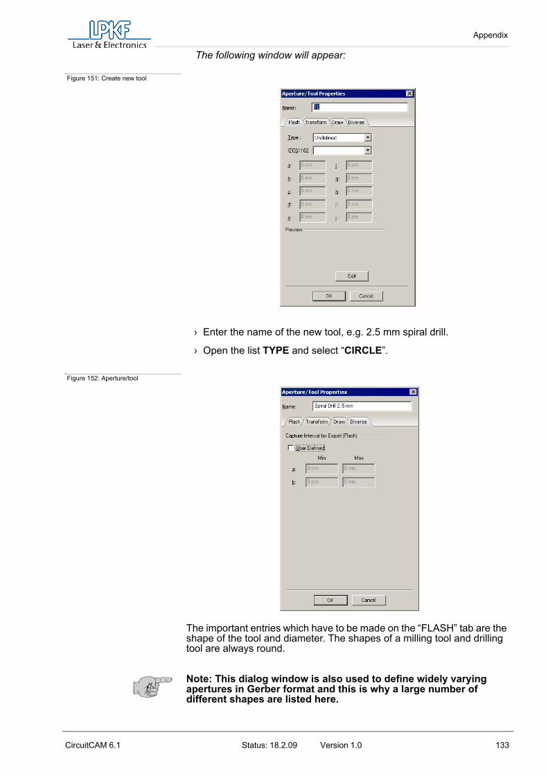
Appendix
CircuitCAM 6.1 Status: 18.2.09 Version 1.0 133
The following window will appear:
Figure 151: Create new tool
› Enter the name of the new tool, e.g. 2.5 mm spiral drill.
› Open the list TYPE and select “CIRCLE”.
Figure 152: Aperture/tool
The important entries which have to be made on the “FLASH” tab are the shape of the tool and diameter. The shapes of a milling tool and drilling tool are always round.
Note: This dialog window is also used to define widely varying apertures in Gerber format and this is why a large number of different shapes are listed here.
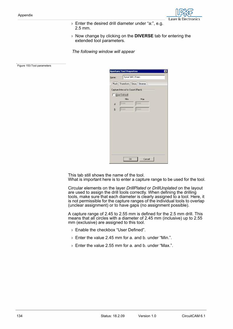
Appendix
134 Status: 18.2.09 Version 1.0 CircuitCAM 6.1
› Enter the desired drill diameter under “a:”, e.g. 2.5 mm.
› Now change by clicking on the DIVERSE tab for entering the extended tool parameters.
The following window will appear
Figure 153:Tool parameters
This tab still shows the name of the tool. What is important here is to enter a capture range to be used for the tool.
Circular elements on the layer DrillPlated or DrillUnplated on the layout are used to assign the drill tools correctly. When defining the drilling tools, make sure that each diameter is clearly assigned to a tool. Here, it is not permissible for the capture ranges of the individual tools to overlap (unclear assignment) or to have gaps (no assignment possible).
A capture range of 2.45 to 2.55 mm is defined for the 2.5 mm drill. This means that all circles with a diameter of 2.45 mm (inclusive) up to 2.55 mm (exclusive) are assigned to this tool.
› Enable the checkbox “User Defined”.
› Enter the value 2.45 mm for a. and b. under “Min.”.
› Enter the value 2.55 mm for a. and b. under “Max.”.

Appendix
CircuitCAM 6.1 Status: 18.2.09 Version 1.0 135
Switch off two options under the DRAW tab to make sure that no drill tools are used for milling.
› Click on the DRAW tab.
Figure 154: Drawing tab
› Disable the checkbox Derived from Flash Definition.
› Disable the checkbox AVAILABLE.
› To save the settings for the tool, click on OK.Make sure that the settings for the adjacent tools are adjusted to these new entries. In this example, this means that the capture range for the 2 mm contour mill (last tool) will have to be checked and corrected if necessary. This milling tool is now used for all holes with a diameter larger than 2.55 mm, i.e. all holes with a diameter larger than 2.5 mm are milled automatically.
› Double click on the tool CONTOUR ROUTER in the tool list.
› Select the DRAW tab in the dialog window.
› Change the values under capture range according to the definition of the new drilling tool:
Figure 155: Capture range
This will ensure that the milling tool will only be used for holes larger than 2.55 mm. If the capture range is not matched, it will not be clear to

Appendix
136 Status: 18.2.09 Version 1.0 CircuitCAM 6.1
CircuitCAM whether the drill or mill is to be used for a diameter of 2.53 mm. This diameter would be assigned to both tools.
› After changing, close the dialog window with OK.
If the change is to kept and saved for future layouts, save the new tool list as a template file (see „Creating a CircuitCAM- template file“ on Page 86).
10.9.2 Defining a new milling tool
› Click on the entry LPKF MILLINGTOOLS.
The list of insulating milling tools will open and the following will appear:
Figure 156:Insulation milling tools
For a better overview, click on the - sign in front of LPKFDrillingTools in order to close the list of drills.
To serve as an example, a new milling tool with diameter of 0.26 mm is to be added to the list.
› Select the milling tool, below which the new tool is to be added and click on the button .
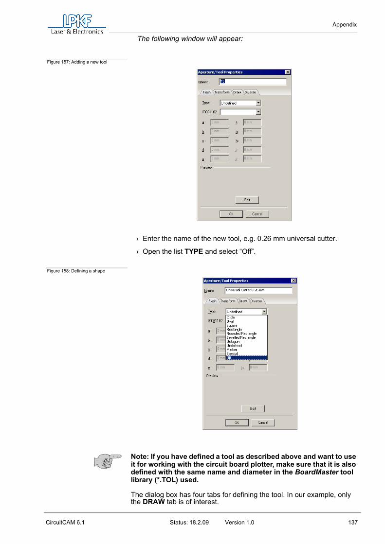
Appendix
CircuitCAM 6.1 Status: 18.2.09 Version 1.0 137
The following window will appear:
Figure 157: Adding a new tool
› Enter the name of the new tool, e.g. 0.26 mm universal cutter.
› Open the list TYPE and select “Off”.
Figure 158: Defining a shape
Note: If you have defined a tool as described above and want to use it for working with the circuit board plotter, make sure that it is also defined with the same name and diameter in the BoardMaster tool library (*.TOL) used.
The dialog box has four tabs for defining the tool. In our example, only the DRAW tab is of interest.
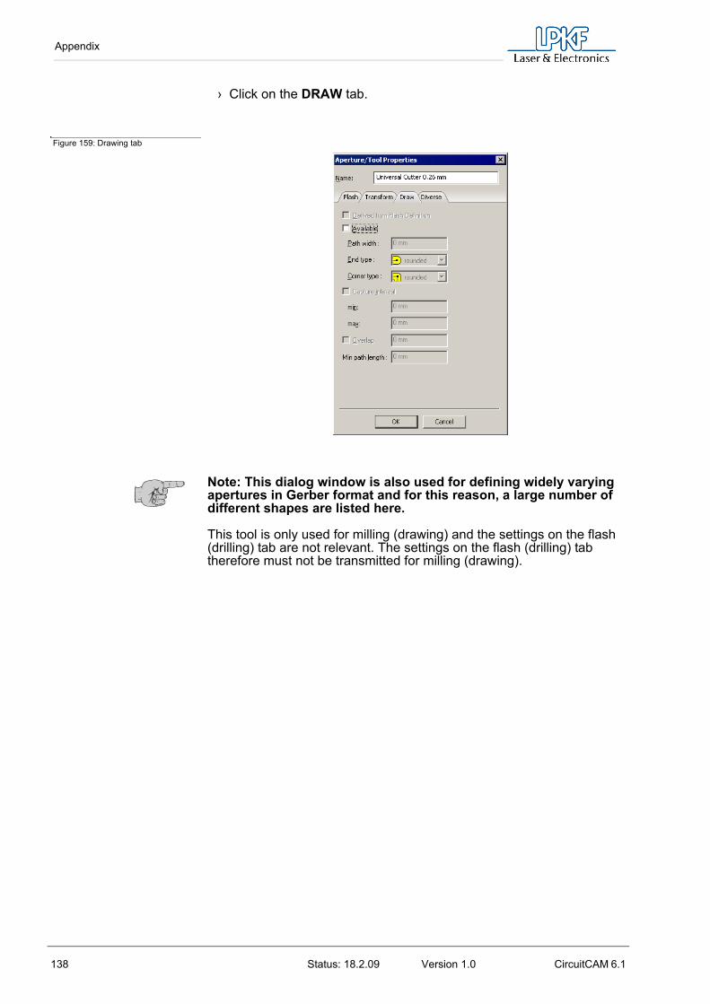
Appendix
138 Status: 18.2.09 Version 1.0 CircuitCAM 6.1
› Click on the DRAW tab.
Figure 159: Drawing tab
Note: This dialog window is also used for defining widely varying apertures in Gerber format and for this reason, a large number of different shapes are listed here.
This tool is only used for milling (drawing) and the settings on the flash (drilling) tab are not relevant. The settings on the flash (drilling) tab therefore must not be transmitted for milling (drawing).

Appendix
CircuitCAM 6.1 Status: 18.2.09 Version 1.0 139
› Enable the checkbox “AVAILABLE”.
› Under “Path width“, enter the desired drill diameter under e.g. 0.26 mm.
Figure 160: Defining a shape
The shape of a milling tool or drilling tool is always round. The shape of the milling tool is defined by the parameters “End Type” and “ Corner Type”. This setting is a default setting for a new tool and does not need to be adjusted.
Figure 161: Setting parameters
Other important parameters for a milling tool are CAPTURE INTERVALL, OVERLAP and MIN. PATH LENGTH. Enter the values for these 3 parameters as shown in the following illustration:

Appendix
140 Status: 18.2.09 Version 1.0 CircuitCAM 6.1
Figure 162: Capture range
As with the drilling tools, for the capture range, a range is entered within which this tool is to be used. In our example, all the lines with a width of 0.258 (inclusive) and 0.262 are produced by a cutting path using this tool.
Any lines which are narrower than this are filled out with a smaller tool. Any lines which are wider are filled out with this tool by cutting a number of paths until the exact width is achieved.Unlike the drilling tools, the list of milling tools can have overlaps and gaps within the capture ranges. A line which is located outside a capture range can still be produced by cutting a number of paths with a smaller tool. This is not possible with drills.
The overlap indicates the amount by which parallel cutting paths with the same tool are to overlap without the risk of leaving fine copper hairs between the paths. CircuitCAM sets this value to 10% of the tool diameter as the default (function switched off). We recommend using a value of 15% of the tool diameter. Switch on the function and enter the value.
The parameter min. path length indicates the minimum length of a cutting path which can be produced during the insulating process. This parameter is particularly important for rubout tools such as end mills. These tools have a hollow grinding so copper could remain if the cutting path is shorter than the tool diameter. We recommend entering a value equal to the diameter of the tool for this parameter.
› Complete the entry by clicking on OK.
› Save the change in the MY TEMPLATE.CAT template
Note: Define the tool parameters carefully to avoid errors when exporting the BoardMaster production data.

Appendix
CircuitCAM 6.1 Status: 18.2.09 Version 1.0 141
10.10 Exporting jobs As CAM software, CircuitCAM can be used both for circuit board plotters and for preparing production data for the circuit board manufacturer. In producing multiple boards, earth areas and milling data etc., all these modifications can be exported as Gerber or Excellon data (with PCB version only).
CircuitCAM already has a number of prepared output jobs for the LPKF circuit board plotters:
Use one of these jobs to output the production data you have generated and make it available for use by LPKF BoardMaster or other software.
The LPKFCircuitBoardPlotter-Job is assigned to the button on the FRONT-TO-END toolbar. By clicking on this button, the production data will be saved in an LMD file. If BoardMaster is open, the LMD file will be automatically imported into BoardMaster and placed on the screen in the centre of the working area.
In the following, you will see which parameters are defined for the exported job.
› Open the VIEW menu and click on JOBS.If the list JOBS is already open and located behind the LAYER list, click on the JOBS tab below the LAYER list.
The following illustration shows all the CircuitCAM routines which are based on jobs in the form of a tree structure. This means that the parameter sets of each routine can be saved under one name. Some of these routines are not available in the PCB version of CircuitCAM. No jobs are prepared for these routines. You will recognise this by the missing “+” in front of the routine names.
Job ApplicationLpkfCircuitBoardPlotter: Default export job for circuit board plotters
LpkfCircuitBoardPlotterGalvTHP: Export job for circuit board plotters is recommended for use with a galvanic through-plating plant
LpkfCircuitBoardPlotterNoTHP: Export job for circuit board plotter recommended when no through-plating facilities are used whatsoever.
LpkfCircuitBoardPlotter+ProConduct
Export job for circuit board plotter with ProConduct data output
LpkfCircuitBoardPlotter+AutoContac
Export job for circuit board plotters with AutoContac-
Data output
LpkfSolderMaskCutting: Export job for circuit board plotters for cutting Solder resist of the EasySolder system

Appendix
142 Status: 18.2.09 Version 1.0 CircuitCAM 6.1
Figure 163:Jobs menu
› Click on + in front of Export.
› The “Export job properties” window is opened by double clicking on LPKFCircuitBoardPlotter.
The following window will appear:
Figure 164: Export job
The format in which the data are to be exported, the name of the exported file and whether the data are to be rotated, mirrored or offset (transformed) during export are defined in this window.
› Click on OK to close the window.
Note: In the TRANSFORM dialog window, you can change the origin, scaling and orientation of the corresponding layer for the output. Layers which are not visible are ignored during the output.
By double clicking on LPKFCircuitBoardPlotter, the export job from the tree structure has opened and, in the window, you can see the list of layers which this job will export.
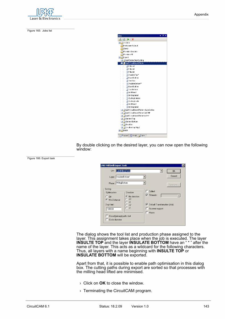
Appendix
CircuitCAM 6.1 Status: 18.2.09 Version 1.0 143
Figure 165: Jobs list
By double clicking on the desired layer, you can now open the following window:
Figure 166: Export task
The dialog shows the tool list and production phase assigned to the layer. This assignment takes place when the job is executed. The layer INSULTE TOP and the layer INSULATE BOTTOM have an “ * ” after the name of the layer. This acts as a wildcard for the following characters. Thus, all layers with a name beginning with INSULTE TOP or INSULATE BOTTOM will be exported.
Apart from that, it is possible to enable path optimisation in this dialog box. The cutting paths during export are sorted so that processes with the milling head lifted are minimised.
› Click on OK to close the window.
› Terminating the CircuitCAM program.
Appendix
144 Status: 18.2.09 Version 1.0 CircuitCAM 6.1
Note: The different production phases are described in the LPKF BoardMaster manual. In the TRANSFORM dialog window, you can change the origin, scaling and orientation of the corresponding layer for the output by clicking on Transformation. In order to do so, the checkbox “Standard Transform” must be disabled first. Layers which are not visible are ignored during the output.
Note: Changes to the original job should never be saved under the same CAT filename otherwise you will destroy the original job. If it is necessary to make changes to the jobs, either create new jobs or save any changes to the original job as a new CAT file.
To make processing simpler and quicker in BoardMaster, a second output job is available for double-sided circuit boards which are not to be through-hole-plated:
"LPKF CIRCUIT BOARD PLOTTER NOTHP" produces an almost identical LMD file. The difference is that the various production phases have been condensed into just two production phases: MillingBottom and MillingTop.
10.11 Al Front Panel Processing (PCB Version)
This aluminium processing is based on sample data. It is only meant to show the procedure as an example.If you have to process your own front panel, then you need to replace the sample co-ordinates with your own data.
Note: Key labels and menu terms are shown in bold type.
Note: To avoid processing disruptions and breakdowns in functions, follow the working steps described below exactly.
Notes on working with aluminium
- Harder aluminium alloys are more suitable for processing than soft alloys.
- The two-fluted cutter end mill is particularly suitable, because it is good as removing swarf.
Caution! The cutting depth per pass must not be more than half the diameter of the working tool.
› Start CircuitCAM from the Windows start menu or by double-clicking on the CircuitCAM icon on the desktop.

Appendix
CircuitCAM 6.1 Status: 18.2.09 Version 1.0 145
10.11.1 Preparing front panel outline data
First determine the size of the front panel.
› To do this, select layer “BOARD OUTLINE” from the layer list field. The front panel in the example has the dimensions 100 mm x 130 mm.
› Click on the button on the INSERT toolbar (see picture below).
Figure 167: Graphic toolbar
› From the EDIT menu, select the function SET CURSOR or press SHIFT + C.
The following window will appear:
Figure 168: Setting the cursor
› The following information has to be entered into the corresponding window:
x= 0 x= 100 y= 0 -> SET y= 130 -> SET
A yellow rectangle will appear on the screen.
1. Entry 2. Entry

Appendix
146 Status: 18.2.09 Version 1.0 CircuitCAM 6.1
› Move the mouse pointer over the graphic.
› Press ESC on your keyboardin order to switch off the tool.
› Press the HOME key on your keyboard in order to gain an overview of the drawn rectangle.
The filled rectangle which is still represented by a polygon must now be converted into an empty rectangle.
› Select the rectangle by clicking on it. The rectangle is now displayed in pale yellow.
› Select the function CONVERT TO CLOSED OUTLINE PATH from the MODIFY menu, or via the shortcuts SHIFT + W.
The previously filled rectangle will change to a closed rectangular box which describes the dimensions of the front panel.
10.11.2 Preparing breakout and drilling data
› Select the layer “BOARD OUTLINE” from the layer list box.
› Click on the arrow on the right next to the circle symbol on the INSERT toolbar.
Figure 169: Setting the cursor
› Select “Circuit in Closed Path”.
› Enter a diameter of 12 mm (following illustration) and close the window by clicking on OK.
Figure 170: Diameter
› Now position this object on the front panel with the coordinates (x= 50 mm and y= 30 mm). Do this by invoking the SET CURSOR function again by pressing SHIFT + C and enter the specified coordinates. Then click on SET.
› Press Esc on the keyboard.
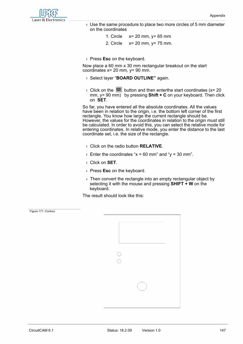
Appendix
CircuitCAM 6.1 Status: 18.2.09 Version 1.0 147
› Use the same procedure to place two more circles of 5 mm diameter on the coordinates
1. Circle x= 20 mm, y= 65 mm 2. Circle x= 20 mm, y= 75 mm.
› Press Esc on the keyboard.Now place a 60 mm x 30 mm rectangular breakout on the start coordinates x= 20 mm, y= 90 mm.
› Select layer “BOARD OUTLINE” again.
› Click on the button and then enterthe start coordinates (x= 20 mm, y= 90 mm) by pressing Shift + C on your keyboard. Then click on SET.
So far, you have entered all the absolute coordinates. All the values have been in relation to the origin, i.e. the bottom left corner of the first rectangle. You know how large the current rectangle should be. However, the values for the coordinates in relation to the origin must still be calculated. In order to avoid this, you can select the relative mode for entering coordinates. In relative mode, you enter the distance to the last coordinate set, i.e. the size of the rectangle.
› Click on the radio button RELATIVE.
› Enter the coordinates “x = 60 mm” and “y = 30 mm”.
› Click on SET.
› Press Esc on the keyboard.
› Then convert the rectangle into an empty rectangular object by selecting it with the mouse and pressing SHIFT + W on the keyboard.
The result should look like this:
Figure 171: Contour

Appendix
148 Status: 18.2.09 Version 1.0 CircuitCAM 6.1
Now use the features of the contour generator to create the milling data for the breakouts.
› Select the 4 inner objects with the mouse by opening a rectangle.
› In the TOOL PATH menu, open the CONTOUR MILLING dialog and select the settings as in the following illustration.
Figure 172:Contour milling dialog
› Start the process by clicking on RUN.Following this, the corresponding milling lines and start drill holes are created for all breakouts. The start drill hole provides the optimum and gentle start point for the milling process which follows.

Appendix
CircuitCAM 6.1 Status: 18.2.09 Version 1.0 149
10.11.3 Setting text data
From CircuitCAM Version 6.1 onwards, all the fonts (TTF and TTC) installed on the computer can be used for writing texts.
› Now select the text function on the GRAPHIC toolbar.The following window will appear:
Figure 173: Entering text
› Choose all the settings according to Illustration 173 and leave this dialog with OK.
› To position the text, use the mouse to place it above the large round drill hole and then press the left mouse button.
Repeat the process for labelling the small drill holes. Try to place the text “Standby” with a character height of 3 mm at the top drill hole and the text “Online” at the bottom drill hole.

Appendix
150 Status: 18.2.09 Version 1.0 CircuitCAM 6.1
The result should look like the following:
Figure 174:Contour thickness
10.12 Exporting and saving
› Click on the symbol SAVE and save the object under a new name.
› From the FILE menu bar, select->EXPORT->LPKF, “LPKFCIRCUITBOARDPLOTTER” .
10.13 Preparing data for fiducial recognition
Circuit board plotters that are provided with a camera system for fiducial recognition (registration marks) must be given the required positioning information via CircuitCAM. Fiducials which are easy to use are simple round drilled holes of 1.5 mm diameter.
After having finished the insulation of your layout, you then place the fiducial holes.
› First, set the cursor and screen grid to an appropriate value.

Appendix
CircuitCAM 6.1 Status: 18.2.09 Version 1.0 151
› Then select the layer “FIDUCIAL” from the layer list box .
› Click on the arrow on the right next to the circle symbol on the INSERT toolbar.
Figure 175: Circle with diameter
› Select the “Fixed Diameter Circle”.
› Enter a diameter of 1.5 mm. Set the four fiducial circles at right angles around the layout.
Note: Using the LARGE CROSS cursor makes it easier to position the circles at right angles.
The result should look like the following:
Figure 176:Positioning circles
The four circles around the layout represent the fiducial points (see arrows in Illustration 176).
› Now output the data as an LMD file using the corresponding output job.

Appendix
152 Status: 18.2.09 Version 1.0 CircuitCAM 6.1
10.14 Producing step-and-repeats (PCB Version only)
CircuitCAM can be used to create step-and-repeat directly on the CAM file.
When all the processing steps (insulation and contour generation etc.) on your layout are finished, you can set up the step-and-repeat.
› First select all the objects on all the layers by using the button on the SELECT symbol bar.
All the objects are now displayed in a pale colour.
› Under MODIFY , open the dialog STEP AND REPEAT or press SHIFT + R on the keyboard.
The following figure will appear:
Figure 177:Step and repeat dialog
› Add the desired distance to the value already entered and enter that value under DISTANCE.
› Then enter the desired number of repeats.
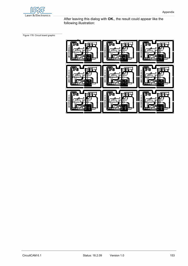
Appendix
CircuitCAM 6.1 Status: 18.2.09 Version 1.0 153
After leaving this dialog with OK., the result could appear like the following illustration:
Figure 178: Circuit board graphic

Appendix
154 Status: 18.2.09 Version 1.0 CircuitCAM 6.1
10.15 CircuitCAM 6.1 Hotkeys
button function referenceGeneral F1 Help about current
subject
Strg+Tab Toggle within CircuitCAM windows
Ins View - Previous View
Pos 1 View - Overview
End View - Pan Cursor Position
Page up View - Zoom in Cursor Position
Page down View - Zoom out Cursor Position
Del Delete Selected Elements
Esc Cancel
Cursor keys Move grafic: up, down, left, right
Strg + Shift + Left Mouse click
Set anchor point Cursor Position
FileMenu
Strg + N New grafic window (default.cat)
Strg + O Open
Strg + S Save
Strg + P Print
Edit Menu Strg + Z Undo Last Action
Strg + Y Redo Last Action
Strg + X Cut Selected Elements
Strg + C Copy Selected Elements
Strg + V Paste ClipBoard
Strg + Space Duplicate Selected Elements
Space Move Selected Elements
Shift + C Set Cursor Enter Coordinates
Shift + A Set Anchor Point Enter Coordinates
Shift + N Set Zero Point Anchor Point
Shift + L Move layer to Zero Point Anchor Point
Shift + X Measuring Anchor Point
Strg + Q Property Selected Elements
Curve Menu
Ctrl + A Add Point Anchor Point
Ctrl + U Cut Point/Segment Anchor Point
Ctrl + D Delete Point/Segment Anchor Point
Ctrl + M Move Point/Segment Anchor Point
Ctrl + E Move/Create Arc Anchor Point
Ctrl + G Create Gab Anchor Point
Ctrl + R Inverse Direction Selected Elements
Ctrl + B Combine Selected Elements
Ctrl + K Connect to Polygon Selected Elements
Diverse Menu
Schift + Q Close Curve Selected Elements
Shift + P Path to Ploygon Selected Elements

Appendix
CircuitCAM 6.1 Status: 18.2.09 Version 1.0 155
Shift + Y Object to Polaygon Selected Elements
Shift + W Convert to Close Outline Path
Selected Elements
Shift + K Convert to Circle Selected Elements
Shift + Z Center Point Selected Elements
Shift + M Mass Point Selected Elements
Shift + R Step and Repeat Selected Elements
Shift + G Create Bounding Box Selected Elements
Change Order Menu
Ctrl + J Move to Next Position Selected Elements
Ctrl + I Move to Previous Position Selected Elements
Ctrl + F Move to First Position Selected Elements
Ctrl + L Move to Last Position Selected Elements
Configu-ration - General Setting Method
Temp. A + Left Mouse Click and Drag
Add/Append Point Active if Cursor changes its Shape Above Selected Elements
Temp. E + Left Mouse Click and Drag
Create/Move Arc Active if Cursor changes its Shape Above Selected Elements
Temp. U + Left Mouse Click
Cut Point/Segment Active if Cursor changes its Shape Above Selected Elements
Temp. M + Left Mouse Click and Drag
Delete Point/Segment Active if Cursor changes its Shape Above Selected Elements
Temp. L + Left Mouse Click
Select Only Active if Cursor changes its Shape Above Selected Elements
button function reference

Appendix
156 Status: 18.2.09 Version 1.0 CircuitCAM 6.1
10.16 Adapting a translation File
A translation file is used to convert the aperture list (ASCII file) of any CAD system so that it can be read into CircuitCAM without any further modification. This allows users who continually have to work with different aperture lists to work considerably faster since it is no longer necessary to define the individual apertures manually. They can also use the translation files to convert tool lists in Excellon or Sieb&Meyer format.
CircuitCAM already has a series of prepared translation files for the common CAD systems but it may still be necessary to adapt a translation file to your specific requirements.
Note: The translation files must have the file extension .txt.
Note: The translation files are located in the CircuitCAM- subdirectory “Ape_Templates” or in the directory you have specified for the aperture/tool templates in CircuitCAM under GENERAL SETTINGS.

Appendix
CircuitCAM 6.1 Status: 18.2.09 Version 1.0 157
10.16.1 Structure of translation files
Translation files are files in ASCII format which you can edit with any text editor. For example, Windows provides the text editors EDITOR and WORDPAD.
However, it is simpler to use the Aperture Template Editor program supplied with CircuitCAM Version 5.0 than using a text editor.
This program has a graphic, syntax-oriented surface and prevents typing errors of the kind which can occur when using a text editor. The Aperture Template Editor button was placed in the Start menu and on the desktop while CircuitCAM was installed. Information on using this program is provided in its online help.
Figure 179: Aperture template editor
A translation file is subdivided into three sections:
• Permanently defined parameters
• Aperture definition
• Variable parameters
Note: the permanently defined and variable parameters only need to be defined in the translation file when the format and aperture definition in the aperture list do not correspond to the default settings.

Appendix
158 Status: 18.2.09 Version 1.0 CircuitCAM 6.1
Section 1: Permanently defined parameters
The following table is a list of the permanently defined parameters which are available with possible parameter values and the corresponding default setting.
APE_SCALEIf the units for the aperture size do not coincide with any of the available parameters under APE_UNITS, it is possible to scale the units with these parameters. Example: the aperture sizes are specified in 1/100 mm. Then APE_UNITS is set to MM and APE_SCALE is set to 0.01.
APE_UNITSDefines the units for the aperture size on the aperture list. (MIL, INCH or MM)
COMMENTDefines one or more characters preceding a comment line. A number of characters/character pairs are separated from one another by a space. Example: COMMENT @ # // Means that each line beginning with “@”, “#” or “//” is a comment line.
CONFIGURATION Defines for which format this translation file has been defined. (Gerber, Excellon, HP-GL or Sieb&Meyer)
COOR_MNDefines the M.N-Code for the Gerber format. If the Gerber data are always generated with the same number of digits before and after the decimal point, the corresponding values are set here.
Parameter name Parameter value Default setting for parameter value
APE_SCALE <Real number> 1
APE_UNITS INCHMILMM
MIL
COMMENT <character> | <character pair> [ <character> | <character pair> ]
CONFIGURATION ConfigExcellon ConfigGerber ConfigHpgl ConfigSiebMeyer
ConfigGerber
COOR_MN <whole number>.<whole number> 2,3
COOR_MODE ABSOLUTE INCREMENTAL
ABSOLUTE
COOR_UNITS INCHMM
INCH
COOR_ZEROS DECIMAL LEADING TRAILING
TRAILING
KEY_STRING <Character string>
REQUIRED_STRING <Character string>
Character declaration:|Alternative (or) [...]0 or multiple repetition

Appendix
CircuitCAM 6.1 Status: 18.2.09 Version 1.0 159
COOR_MODEDefines the coordinate mode for the Gerber format. COOR_MODE ABSOLUTE is set for Gerber data with absolute values and COOR_MODE INCREMENTAL is set for relative values.
COOR_UNITSDefines the units for the Gerber data as imperial (INCH) or metric (MM).
COOR_ZEROSDefines the setting for zeros in the Gerber format. This is set to LEADING if the Gerber data are always generated with leading zeros, and set to TRAILING if they are always generated with trailing zeros. If leading as well as trailing zeros are output, this can be set to either TRAILING or LEADING.
KEY_STRING(for automatic recognition only) Defines the key word which must be on the aperture list so that this translation file is used for converting the aperture list. If the key word agrees, the scanning process is terminated immediately.
REQUIRED_STRING (for automatic recognition only)Defines the keyword which must be on the aperture list to narrow the choice for this translation file during automatic recognition. Even when the keyword matches, the scanning process continues in order to find the most suitable translation file. All translation files without this keyword are immediately ignored during the scanning process. This enables the range of translation files which could be used to be limited.

Appendix
160 Status: 18.2.09 Version 1.0 CircuitCAM 6.1
Section 2: Aperture definition
Each aperture on the aperture list must be capable of being assigned precisely to the translation file by one of the entries in the aperture definition. The apertures differ in terms of the D code, mode, shape and size. Each line in the aperture list is compared with entries in the translation file to see if they match. If a match is found, the aperture information is converted, otherwise the corresponding aperture is ignored.
The following syntax is used for the aperture definitions:1,<DRAW_FORMAT><FLASH_FORMAT>:"<APE_FORMAT>"
Parameter <DRAW_FORMAT>
Meaning
N Aperture is only used as a flash aperture, never as a draw aperture C Aperture is used as a round or circular draw aperture Q Aperture is used as a square draw aperture
Parameter <FLASH_FORMAT>
Meaning Dimension parameter in <APE_FORMAT>
N Aperture is only used as a draw aperture, never as a flash aperture
C Aperture is used as a round or circular flash aperture
%a (diameter)
Q Aperture is used as a square flash aperture %a (side length)R Aperture is used as a rectangular flash
aperture%a (side length X) %b
(side length Y)O Aperture is used as an oval or
finger-shaped flash aperture%a (side length X) %b
(side length Y)
T Aperture is used as an octagonal shaped flash aperture
%a (diameter)
D Aperture is used as a rectangular flash aperture with rounded corners
%a (side length X) %b (side length Y) %c (corner radius)
B Aperture is used as a rectangular flash aperture with cut corners
%a (side length X) %b (side length Y) %c (diagonal length)
S Aperture is used as a special flash aperture. The actual shape must be designed and implemented in CircuitCAM
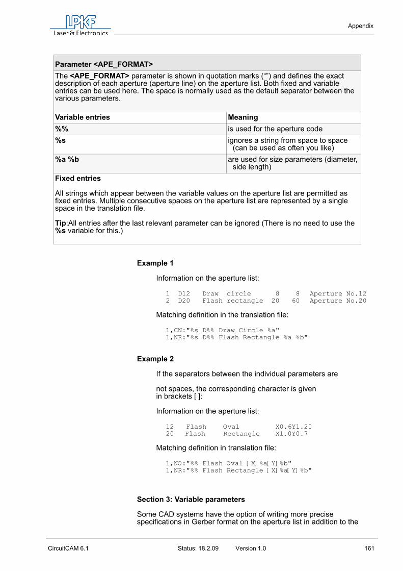
Appendix
CircuitCAM 6.1 Status: 18.2.09 Version 1.0 161
Example 1
Information on the aperture list:
1 D12 Draw circle 8 8 Aperture No.12 2 D20 Flash rectangle 20 60 Aperture No.20
Matching definition in the translation file:
1,CN:"%s D%% Draw Circle %a" 1,NR:"%s D%% Flash Rectangle %a %b"
Example 2
If the separators between the individual parameters are
not spaces, the corresponding character is givenin brackets [ ]:
Information on the aperture list:
12 Flash Oval X0.6Y1.20 20 Flash Rectangle X1.0Y0.7
Matching definition in translation file:
1,NO:"%% Flash Oval [X]%a[Y]%b" 1,NR:"%% Flash Rectangle [X]%a[Y]%b"
Section 3: Variable parameters
Some CAD systems have the option of writing more precise specifications in Gerber format on the aperture list in addition to the
Parameter <APE_FORMAT>The <APE_FORMAT> parameter is shown in quotation marks (“”) and defines the exact description of each aperture (aperture line) on the aperture list. Both fixed and variable entries can be used here. The space is normally used as the default separator between the various parameters.
Variable entries Meaning%% is used for the aperture code%s ignores a string from space to space
(can be used as often you like)%a %b are used for size parameters (diameter,
side length)Fixed entries
All strings which appear between the variable values on the aperture list are permitted as fixed entries. Multiple consecutive spaces on the aperture list are represented by a single space in the translation file.
Tip:All entries after the last relevant parameter can be ignored (There is no need to use the %s variable for this.)

Appendix
162 Status: 18.2.09 Version 1.0 CircuitCAM 6.1
aperture information. Variable parameters can be used to evaluate this information so as to eliminate the need to re-adapt the translation file each time this additional information is changed.
After conversion, the aperture list is searched for the character chains defined for the variable parameters and, when a match is found, they are assigned to the corresponding parameter.
Example 1
Information on the aperture list:
The units in the Gerber data are metric m.n format = 3.2 absolute values Leading zeros suppressed
Matching definition in the translation file:
101 : “The units in the Gerber data are metric” 110 : “absolute values” 122 : “m.n format = 1%d.1%d” 131 : “Leading zeros suppressed”
Variable parameters MeaningCoordinates unit 100 : "<text>" The string entered for <text> defines the coordinates unit INCH.101 : “<text>” The string entered for <text> defines the coordinates unit MM.Coordinates mode110 : "<text>” The string entered for <text> defines the coordinates mode
ABSOLUTE.111 : "<text>” The string entered for <text> defines the coordinates mode
RELATIVE.Places before and after the decimal point120 :
“<text>%d<text>”The string entered for <text> defines the M code (Number of places
in front of the decimal point). &d represents the figure which defines the M code on the aperture list
121 : "<text>%d<text>”
The string entered for<text> defines the N code (number of places after the decimal point). &d presents the figure which defines the N code on the aperture list.
122 : "<text>%1d.%1d<text>"
The string entered for <text> defines the M.N code (number of the placed before and after the decimal point). The first variable &1d represents the figure which defines the M code on the aperture list. The second variable &1d presents the figure which defines the N code on the aperture list.
Coordinate zeroes130 : "<text>" The string entered for <text> defines the coordination-zeros as
LEADING. (trailing suppressed.) 131 : “<text>” The string entered for <text> defines the coordination-zeros as
TRAILING. (leading suppressed)132 : “<text>” The string entered for <text> defines the coordinates zeros as
DECIMAL.

Appendix
CircuitCAM 6.1 Status: 18.2.09 Version 1.0 163
10.16.2 Tips for adapting translation file
If the graphic display of the circuit board does not coincide with the desired result, this is usually because the corresponding translation file has not converted the aperture/tool list correctly.
For example, if conductor tracks or pads are displayed in the wrong shape or size, the aperture/tool definitions in the translation file will not agree with the format of the aperture/tool list which must be read in. The remedy for this is (as previously described) to match the translation file to the aperture/tool list on an individual basis.
However, it is often only one parameter value in the translation file which is incorrectly defined, so the problems can be solved quickly. The following table provides a list of the parameters which could be the cause of an incorrect graphic display:
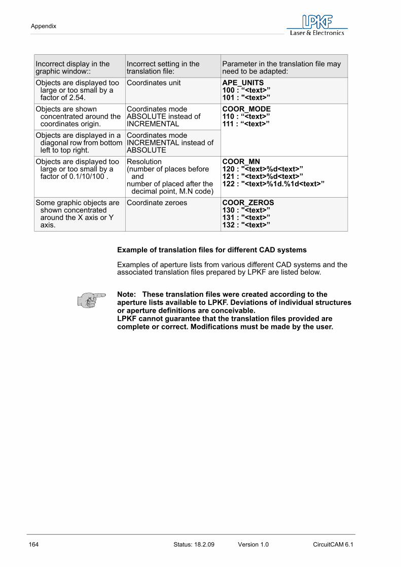
Appendix
164 Status: 18.2.09 Version 1.0 CircuitCAM 6.1
Example of translation files for different CAD systems
Examples of aperture lists from various different CAD systems and the associated translation files prepared by LPKF are listed below.
Note: These translation files were created according to the aperture lists available to LPKF. Deviations of individual structures or aperture definitions are conceivable. LPKF cannot guarantee that the translation files provided are complete or correct. Modifications must be made by the user.
Incorrect display in the graphic window::
Incorrect setting in the translation file:
Parameter in the translation file may need to be adapted:
Objects are displayed too large or too small by a factor of 2.54.
Coordinates unit APE_UNITS 100 : “<text>” 101 : "<text>”
Objects are shown concentrated around the coordinates origin.
Coordinates modeABSOLUTE instead ofINCREMENTAL
COOR_MODE110 : “<text>” 111 : “<text>”
Objects are displayed in a diagonal row from bottom left to top right.
Coordinates modeINCREMENTAL instead ofABSOLUTE
Objects are displayed too large or too small by a factor of 0.1/10/100 .
Resolution (number of places before
and number of placed after the
decimal point, M.N code)
COOR_MN 120 : "<text>%d<text>” 121 : "<text>%d<text>” 122 : "<text>%1d.%1d<text>”
Some graphic objects are shown concentrated around the X axis or Y axis.
Coordinate zeroes COOR_ZEROS 130 : "<text>” 131 : "<text>” 132 : "<text>”
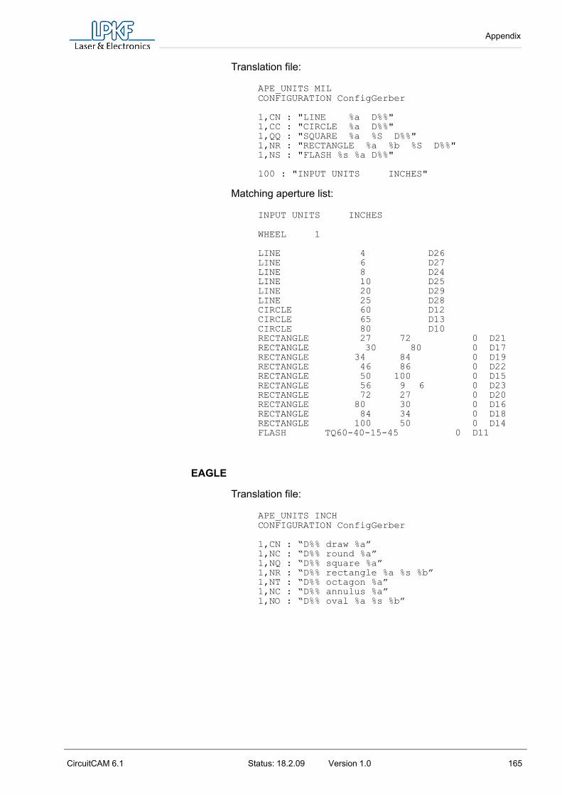
Appendix
CircuitCAM 6.1 Status: 18.2.09 Version 1.0 165
Translation file:
APE_UNITS MILCONFIGURATION ConfigGerber
1,CN : "LINE %a D%%" 1,CC : "CIRCLE %a D%%" 1,QQ : "SQUARE %a %S D%%" 1,NR : "RECTANGLE %a %b %S D%%" 1,NS : "FLASH %s %a D%%"
100 : "INPUT UNITS INCHES"
Matching aperture list:
INPUT UNITS INCHES
WHEEL 1
LINE 4 D26 LINE 6 D27LINE 8 D24 LINE 10 D25LINE 20 D29 LINE 25 D28 CIRCLE 60 D12 CIRCLE 65 D13 CIRCLE 80 D10 RECTANGLE 27 72 0 D21 RECTANGLE 30 80 0 D17 RECTANGLE 34 84 0 D19 RECTANGLE 46 86 0 D22 RECTANGLE 50 100 0 D15 RECTANGLE 56 9 6 0 D23 RECTANGLE 72 27 0 D20 RECTANGLE 80 30 0 D16 RECTANGLE 84 34 0 D18 RECTANGLE 100 50 0 D14 FLASH TQ60-40-15-45 0 D11
EAGLE
Translation file:
APE_UNITS INCH CONFIGURATION ConfigGerber
1,CN : “D%% draw %a” 1,NC : “D%% round %a” 1,NQ : “D%% square %a” 1,NR : “D%% rectangle %a %s %b” 1,NT : “D%% octagon %a” 1,NC : “D%% annulus %a” 1,NO : “D%% oval %a %s %b”
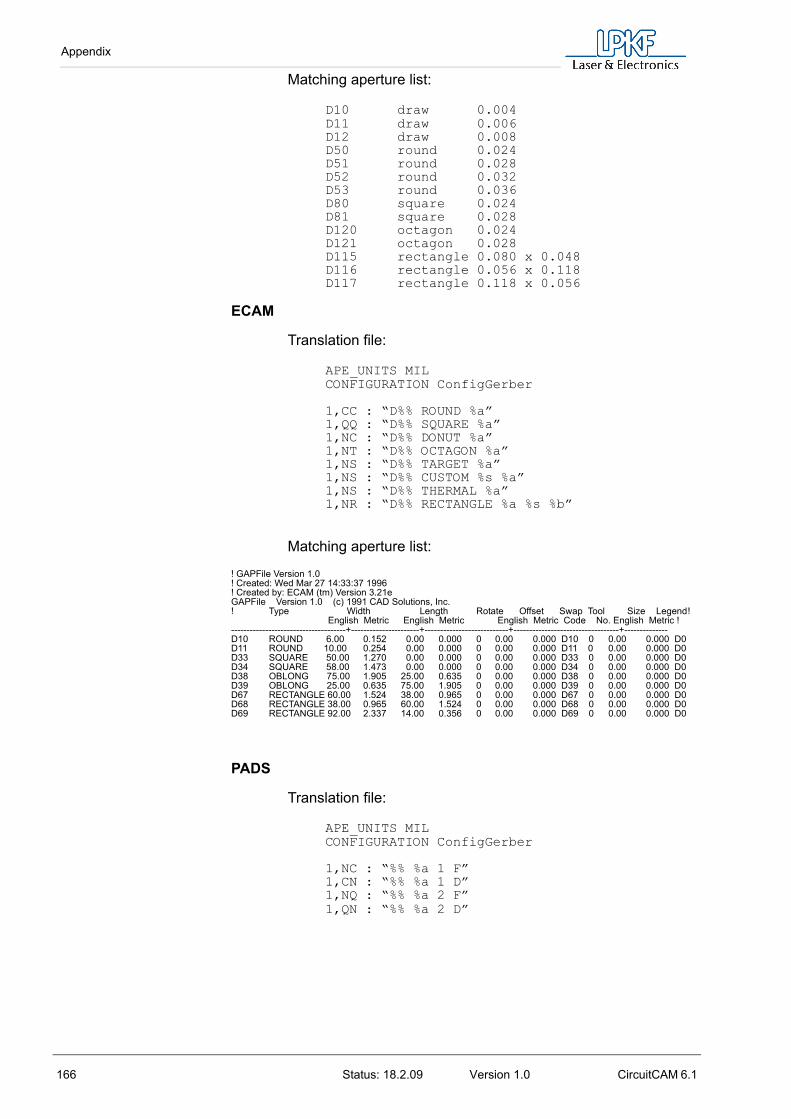
Appendix
166 Status: 18.2.09 Version 1.0 CircuitCAM 6.1
Matching aperture list:
D10 draw 0.004 D11 draw 0.006 D12 draw 0.008 D50 round 0.024 D51 round 0.028 D52 round 0.032 D53 round 0.036 D80 square 0.024 D81 square 0.028 D120 octagon 0.024 D121 octagon 0.028 D115 rectangle 0.080 x 0.048 D116 rectangle 0.056 x 0.118 D117 rectangle 0.118 x 0.056
ECAM
Translation file:
APE_UNITS MIL CONFIGURATION ConfigGerber
1,CC : “D%% ROUND %a” 1,QQ : “D%% SQUARE %a” 1,NC : “D%% DONUT %a” 1,NT : “D%% OCTAGON %a” 1,NS : “D%% TARGET %a” 1,NS : “D%% CUSTOM %s %a” 1,NS : “D%% THERMAL %a” 1,NR : “D%% RECTANGLE %a %s %b”
Matching aperture list:
! GAPFile Version 1.0 ! Created: Wed Mar 27 14:33:37 1996 ! Created by: ECAM (tm) Version 3.21e GAPFile Version 1.0 (c) 1991 CAD Solutions, Inc. ! Type Width Length Rotate Offset Swap Tool Size Legend !
English Metric English Metric English Metric Code No. English Metric !-------------------------------------+----------------------+---------------------------+----------------------------------+-------------- D10 ROUND 6.00 0.152 0.00 0.000 0 0.00 0.000 D10 0 0.00 0.000 D0 D11 ROUND 10.00 0.254 0.00 0.000 0 0.00 0.000 D11 0 0.00 0.000 D0 D33 SQUARE 50.00 1.270 0.00 0.000 0 0.00 0.000 D33 0 0.00 0.000 D0 D34 SQUARE 58.00 1.473 0.00 0.000 0 0.00 0.000 D34 0 0.00 0.000 D0 D38 OBLONG 75.00 1.905 25.00 0.635 0 0.00 0.000 D38 0 0.00 0.000 D0 D39 OBLONG 25.00 0.635 75.00 1.905 0 0.00 0.000 D39 0 0.00 0.000 D0 D67 RECTANGLE 60.00 1.524 38.00 0.965 0 0.00 0.000 D67 0 0.00 0.000 D0 D68 RECTANGLE 38.00 0.965 60.00 1.524 0 0.00 0.000 D68 0 0.00 0.000 D0 D69 RECTANGLE 92.00 2.337 14.00 0.356 0 0.00 0.000 D69 0 0.00 0.000 D0
PADS
Translation file:
APE_UNITS MIL CONFIGURATION ConfigGerber
1,NC : “%% %a 1 F” 1,CN : “%% %a 1 D” 1,NQ : “%% %a 2 F” 1,QN : “%% %a 2 D”

Appendix
CircuitCAM 6.1 Status: 18.2.09 Version 1.0 167
Matching aperture list:
POST PROCESSOR REPORT --------------------- LAYOUT NAME :- S4224D LAYOUT TITLE :- LISTA APERTURE PHOTOPLOTTER
SYMBOL AVAILABILITY REPORT--------------------------
SHAPE: 1 = ROUND 2 = SQUARE
PROTEL
Translation file:
APE_UNITS MIL CONFIGURATION ConfigGerber
1,CC : “D%% ROUNDED %a %s %s MULTI” 1,NC : “D%% ROUNDED %a %s %s FLASH” 1,NR : “D%% RECTANGULAR %a %b %s FLASH” 1,QR : “D%% RECTANGULAR %a %b %s MULTI” 1,NO : “D%% ROUNDED %a %b %s FLASH” 1,NT : “D%% OCTAGONAL %a %b %s FLASH”
Matching aperture list:
D11 ROUNDED 1.000 1.000 0.000 MULTI D12 ROUNDED 7.333 7.333 0.000 MULTI D26 RECTANGULAR 62.000 62.000 0.000 FLASHD27 RECTANGULAR 66.000 66.000 0.000 FLASH D28 RECTANGULAR 75.000 75.000 0.000 FLASH
Position Size Shape Usage Orient Length Count
126 30 1 F 101
10 8 1 D 0
71 12 1 D 0
73 20 1 D 0
78 5 1 D 0
21 80 1 F 7
144 52 1 D 0
145 52 2 F 20
136 44 1 D 0
137 44 2 F 244
57 58 1 D 0
58 58 2 F 20
76 40 1 D 0
20 40 2 F 90
48 60 1 D 0
56 60 2 F 4
82 120 1 D 0
33 48 1 D 0
34 48 2 F 6
30 36 1 D 0

Index
168 Status: 18.2.09 Version 1.0 CircuitCAM 6.1
11.0 IndexAActivation number ........................................................................................... 20Aluminium front panel processing ........................................................ 144Ape_Templates ................................................................................................ 10Aperture list ................................................................................................ 90, 104Aperture plate ................................................................................................. 101APERTURE-/TOOL LIST ............................................................................ 41APERTURE/TOOL LIST ....................... 42, 43, 44, 45, 46, 49, 50, 51, 52, 56
BBulb ...................................................................................................................... 101Button ...................................................................................................................... 4
CCaution ................................................................................................................... 4Circuit board outline ....................................................................................... 58CircuitCAM ....................................................................................................... 3, 4CircuitCAM - PCB ........................................................................................... 80CircuitCAM Lite ................................................................................................ 76Contents ................................................................................................................. 5Contour generator .................................................................................. 66, 148Coordinate entry .............................................................................................. 60Coordinates ...................................................................................................... 105Coordinates display ....................................................................................... 34Creating a template file .............................................................................. 124
DDanger .................................................................................................................... 4Data ........................................................................................................................ 10Data export ......................................................................................................... 63Delete .................................................................................................................... 54Design Rule Check ...................................................................................... 119Diminish ............................................................................................................... 28Directories ........................................................................................................... 10Drawing ................................................................................................................ 62Drilling tool (defining) .................................................................................. 132Drilling/milling tools (creating) ................................................................ 130DXF files ............................................................................................................ 109
Importing ........................................................................................................ 109
EEAGLE ................................................................................................................ 165Earth area (generating) .............................................................................. 116Earth areas ....................................................................................................... 116ECAM .................................................................................................................. 166Editing production data ................................................................................ 10Enlarge ................................................................................................................. 28Exercise files ..................................................................................................... 32Export jobs ........................................................................................................ 141Extended Gerber ........................................................................................... 106
FFiducial ............................................................................................................... 151Flashing ........................................................................................................ 62, 103Format ................................................................................................................. 105

Index
CircuitCAM 6.1 Status: 18.2.09 Version 1.0 169
Front panel ........................................................................................................145FRONT TO END ..............................................................................................23
GGerber
Aperture list ...................................................................................................104Extended ........................................................................................................106Syntax ..............................................................................................................102Unit/format .....................................................................................................104Use ....................................................................................................................101
Gerber format ..................................................................................................101Grid .........................................................................................................................34
HHard disk capacity .............................................................................................9Hotkeys ...............................................................................................................154
IImport (production data) ..............................................................................36Import assignment ..........................................................................................65Import assignments ..................................................................................56, 89Import production data ..................................................................................36INNER INSULATION TRACK ...................................................................81Inserting breakout tabs .................................................................................70Insulating ..............................................................................................................62Insulating (areas) .............................................................................................83INSULATION GRID ........................................................................................78Insulation job
Customising ....................................................................................................76Insulation job (Customising) ......................................................................76Insulation tools
Colour assignment ......................................................................................85INSULATION WIDTH ....................................................................................77
JJob ...........................................................................................................................82
re-create ...........................................................................................................82
LLayer ......................................................................................................................49
Clearance check ........................................................................................120Mirroring ...........................................................................................................98Predefined .............................................................................................106, 108Rotate ................................................................................................................96Separator .........................................................................................................57
Layer (predefined) .........................................................................................108Legend ....................................................................................................................4List window .........................................................................................................26
MMain memory .......................................................................................................9Materials supplied .............................................................................................9Milling direction (modifying) .......................................................................70Milling sequence (modifying) .....................................................................70Milling tool (defining) ....................................................................................136Modifying milling direction ...........................................................................70Move layer ...........................................................................................................94
NNew picture layout ..........................................................................................48
Index
170 Status: 18.2.09 Version 1.0 CircuitCAM 6.1
New_Templates 10Notations ................................................................................................................ 4Note .......................................................................................................................... 4
OOn-line help ........................................................................................................ 22Operating system .............................................................................................. 9OVERVIEW ........................................................................................................ 48
PPADS ................................................................................................................... 166Parameters ....................................................................................................... 129Photoplotter ...................................................................................................... 101Photoplotters ............................................................................................. 58, 101Plotter actuation ............................................................................................. 101POLYGON .......................................................................................................... 72PRIMARY OVERLAP
.............................................................................................................................. 79Production data (checking) ........................................................................ 48Production data (preparation) ................................................................... 54PROTEL ............................................................................................................. 167
RReport window .................................................................................................. 27Rubout area ....................................................................................................... 71
Create ................................................................................................................ 71RUBOUT MILLING ......................................................................................... 81
SSample circuit boards ................................................................................... 30Select ..................................................................................................................... 55Selectable
Flash .................................................................................................................. 55Polygon ............................................................................................................. 55
Shortcuts .............................................................................................................. 21Shutter ................................................................................................................ 101START MENU ................................................................................................... 10Status bar ............................................................................................................ 30Step-and-repeat ............................................................................................. 152Symbols ................................................................................................................. 4Symbols used ..................................................................................................... 4System requirements ...................................................................................... 9
TTarget Group ........................................................................................................ 4Template file
Creation ............................................................................................................ 87Template file (creating) ................................................................................. 86Template files .................................................................................................. 123Text ......................................................................................................................... 61
BoardOutline .................................................................................................. 61On a separate layer ................................................................................... 61
Text Function ................................................................................................... 115Text objects ........................................................................................................ 61Tool list .................................................................................................................. 90Translation files (structure) ........................................................................ 87
UUnit ......................................................................................................................... 34UNIT + GRID ..................................................................................................... 33

Index
CircuitCAM 6.1 Status: 18.2.09 Version 1.0 171
Units .....................................................................................................................105
VVersion number ................................................................................................23View functions ...................................................................................................48Visual inspection ..............................................................................................48
ZZOOM ....................................................................................................................48ZOOM IN ..............................................................................................................48ZOOM WINDOW .............................................................................................48

Index
172 Status: 18.2.09 Version 1.0 CircuitCAM 6.1