Embed Size (px)
Citation preview

Manipulating Terahertz
Radiation Using Nanostructures
A thesis submitted for the partial fulfilment of the
requirements for the degree of
Doctor of Philosophy (Science)
in
Physics (Experimental)
By
Debanjan Polley
Department of Physics
University of Calcutta
2016

dedicated to my parents…

III
Abstract
With the increasing popularity of terahertz (THz) frequency band and the unforeseen development in
THz instrumentation in recent years, it is imperative to indulge in the study of THz devices and the
theoretical interpretation of their performances. The present thesis is devoted in understanding different
possible ways of using nanostructures and their composites in the passive modulation of the response
in the THz frequency range. A new type of low-cost durable THz polarizer is demonstrated using
magnetically aligned nickel nanostructures with tunable degree of polarization and frequency
bandwidth. THz electromagnetic shielding effectiveness (SE) of single walled carbon nanotubes
(SWNT)/polymer composite films is studied and its relation with the weight fraction of SWNT
inclusion is established. The modification of the THz properties of composite materials is thoroughly
investigated by varying the material parameters and morphology. We have established that while the
real conductivity (also SE) can be increased up to ~ 80% by simply changing the average length and
weight fraction of the SWNT inside the polymer matrix, it can be tuned in a minuscule range (± 15%)
by decorating the sidewalls of SWNT with gold nanoparticles (AuNP). The results are discussed in the
light of a modified universal di-electric relaxation (UDR) model. The intrinsic THz conductivity and
SE of self-standing multi-walled carbon nanotubes (MWNT) is studied as a function of MWNT
structure parameters and the results are discussed to shed some light on the controversial origin of the
THz conductivity peak (TCP) in carbon nanotubes (CNT). The intrinsic conductivity spectra are
analysed using a combination of Maxwell-Garnett (MG) effective medium theory (EMT) and Drude-
Lorentz (DL) model. The results indicate that the TCP arises mainly due to the surface plasmon
resonance along the length of the MWNT and does not depend systematically on MWNT diameter. We
have also performed a detailed analysis on the different contribution (reflection, absorption or multiple
internal reflection) of shielding to the total SE and its dependence on the length and diameter of MWNT.
It is found that the mechanism of shielding can be tuned significantly upon MWNT diameter variation.
Lastly, the effect of oxidation on the THz conductivity of copper (Cu) thin films is studied. The
conductivity spectra are analysed using a Drude model with reduced d.c. conductivity and increased
scattering rate. The findings of this thesis open up exciting possibilities of the realization of new types
of THz opto-electronic devices for the passive manipulation of THz radiation. The detailed study of
THz conductivity and SE properties of CNT composites may lead to the better understanding of their
performances in THz frequency range.
IV
Acknowledgement
I would graciously take this pleasant opportunity to acknowledge a lot of nice people who
helped and encouraged me in one or another way during my PhD and without their help
this work could not have been completed.
I am heartily thankful to my supervisor, Dr. Rajib Kmar Mitra and my co-supervisor,
Prof. Anjan Barman for providing me the opportunity to work in their lab and guiding
me to accomplish my goal. Their contagious encouragement, continuous support,
numerous valuable discussions, helpful suggestions and insightful comments helped me
to grow as a researcher and embrace my job whole-heartedly. Besides being patient guides
and wonderful teachers, they are great human being and possess a beautiful sense of
humour. It is always satisfying to talk with them, listen their views in different aspects
of science and life as well. It has been a real privilege to work with both of you for five
long years.
I would like to thank my labmates from “THz Spectroscopy Lab” and “Ultrafast
Nanomagnetism Lab” for their supports and unconditional help. I would like to thank
Semanti di for helping in my projects, teaching me to prepare presentable graphs, slides
and to write scientific reports with all her love and care. I would like to thank Susmita
di for her never ending enthusiasm in my research works, for always encouraging me to
do well in life and above all for always believing in me. Again a big thanks to her for proof-
checking my thesis. I would like to thank Animesh da and Nirnay for all those cheerful
discussions and for helping me to understand THz spectroscopy in chemist’s point of view.
I would like to thank Dr. Dipak Das for the fruitful discussions on lasers, optics and their
alignments. I would like to thank Dr. Jaivardhan Sinha and Samiran for preparing
thin films and lithographically patterned structures. I would like to thank Arnab, who is
also my M.Sc. batch-mate, for all his helps. I would like to thank Arindam, Debashis,
Neeraj, Kallol, Chandrima, Sucheta, Santanu, Avinash and Kartik for creating a
cheerful and friendly lab environment. Arnab and Santanu are also good table tennis
players and we spent a lot of evenings in the TT room. They are a great bunch of guys and
I am really happy to share the labs with them.
I would like to thank Carnival Cinemas for all those wonderful and not-so-wonderful
movie shows and ABCOS for those special and not-so-special dinners.

V
I would like to thank my friends at S. N. Bose National Centre for Basic Sciences; Arijit
(now at SINP), Arghya, Biplab, J.B. (now in Germany), Subhashis, and Sayani. I
really enjoyed spending those beautiful moments with them. I would also like to thank
my friends Arnab, Arpan, Abhrajit, Sannak, Subhojit and Nabadyuti. We do not
meet that much as we all are busy in pursuing our dreams in different parts of India, but
we maintain a healthy and cheerful relationship.
A special thanks to my parents for their unconditional love, support and guidance
throughout my life. They are the biggest inspiration of my life. They sacrificed a lot for
me and I am indebted to them. I would like to thank Kritanjan (my brother) for being
the perfect sibling; respecting me and pulling my leg at the same time.
Many great thanks to my childhood friend and colleague Ishita (who also happens to be
my girlfriend) for always being there for me through the ups and downs of my life, for
encouraging me to be myself, for those lovely moments, for all her love, for all those
wonderful fights we had and for accepting me with all my madness. A special thanks to
her for helping me in my last minute proof checking.
I would like to acknowledge the financial support of S. N. Bose National Centre for Basic
Sciences and its common research facilities for all the basic characterization of the
samples.
VI
LIST OF PUBLICATIONS
Included in this thesis
1. "Polarizing effect of aligned nanoparticles in terahertz frequency region", D. Polley, A.
Ganguly, A. Barman, and R. K. Mitra; Optics Letters 38, 2754 (2013).
2. "EMI shielding and conductivity of carbon nanotube-polymer composites at terahertz
frequency", D. Polley, A. Barman, and R. K. Mitra; Optics Letters 39, 1541 (2014).
3. "Controllable terahertz conductivity in single walled carbon nanotube/polymer
composites", D. Polley, A. Barman, and R. K. Mitra; Journal of Applied Physics 117, 023115
(2015).
4. "Length Dependent Terahertz Conductivity and Shielding Effect of Self-Standing Multi-
walled Carbon Nanotubes Films" by D. Polley, A. Barman and R. K. Mitra (Manuscript to
be submitted)
5. “Diameter Dependent Shielding Effectiveness and Terahertz Conductivity of
Multi-walled Carbon Nanotubes”, D. Polley, Kumar Neeraj, A. Barman and R. K. Mitra
(Accepted for publication)
6. "THz Conductivity Engineering in Surface Decorated Carbon Nanotube Films" by D.
Polley, A. Patra, A. Barman and R. K. Mitra (Manuscript being prepared)
Not included in this thesis
7. "Magnetization reversal dynamics in Co nanowires with competing magnetic
anisotropies", S. Pal, S. Saha, D. Polley, and A. Barman; Solid State Communications 151,
1994 (2011).
8. "Dielectric relaxation of the extended hydration sheathe of DNA in the THz frequency
region", D Polley, A. Patra, and R. K. Mitra; Chemical Physics Letters 586, 143 (2013).
9. "Ultrafast Dynamics and THz Oscillation in [Co/Pd]8 Multilayers" by S. Pal, D. Polley, R. K.
Mitra and A. Barman; Solid State Communication 221, 50 (2015).
Conference Proceedings
1. "Modulating Conductivity of Au/CNT composites in THz Frequency Range: A THz
Resistor", D.Polley, A. Patra, A. Barman, and R. K. Mitra, IRMMW_THz 2014, The University
of Arizona, Tucson, USA, 14-19 September, 2014. [Oral]
VII
2. "Controlling Terahertz Conductivity in SWNT/Polymer Composites", R. K. Mitra, D.
Polley, and A. Barman, IRMMW_THz 2015, The Chinese University of Hong Kong, Hong-
Kong, 23-28 August, 2015. [Poster]
3. "Nickel nanochain composite: An improved terahertz shielding material", D. Polley, A.
Barh, A. Barman, and R. K. Mitra, 2015 Applied Electromagnetic Conference (AEMC 2015),
IIT Guwahati, Assam, 18-21 December, 2015. [Oral]
VIII
Some Useful Abbreviations
2D: two-dimensional
a.c.: alternating current
ADC: analog to digital converter
AR: aspect ratio
ARC: anti-reflection coating
AuNP: gold nanoparticles
BG: Bruggeman
BSE: back scattered electrons
BSP: back substrate polarizer
CCD: charge coupled device
CNF: carbon nanofiber
CNT: carbon nanotubes
CVD: chemical vapour deposition
d.c.: direct current
DI: de-ionized
DL: Drude-Lorentz
DOP: degree of polarization
DSO: digital storage oscilloscope
DWNT: double walled carbon nanotubes
EBSD: diffracted backscattered electrons
EDX: energy dispersive x-ray analysis
EG: ethylene glycol
EMI: electromagnetic interference
EMIS: electromagnetic interference shielding
EMT: effective medium theory
ER: extinction ratio
FFT: fast Fourier transform
FP: Fabry Perot
FSP: free standing polarizer
FTIR: Fourier transform infrared spectroscopy
GHz: gigahertz (109 Hz)
GO: graphene oxide
HDPE: high density polyethylene
KK: Kramers-Kronig
LDr: reduced linear dichroism
LN: lithium niobate
LT-GaAs: low temperature grown GaAs
MG: Maxwell-Garnett
MHz: megahertz (106 Hz)
MWNT: multi walled carbon nanotubes
NiNC: nickel nanochains
NiNP: nickel nanoparticles
PBS: polarizing beam splitter
PC: photo conductive
PPLN: periodically poled lithium niobate
PVA: poly vinyl alcohol
QCL: quantum cascade laser
QS: quasi space
RF: radio frequency
rGO: reduced graphene oxide
S/N: signal to noise
SE: shielding effectiveness
SEM: scanning electron microscope
SHG: second harmonic generation
SI: semi insulating
SP: surface plasmon
SVMAF: spatially moving average filter
SWNT: single walled carbon nanotubes
TCP: terahertz conductivity peak
TEM: transmission electron microscope
TES: terahertz emission spectroscopy
THz: terahertz (1012 Hz)
THz-TDS: THz time domain spectroscopy
TRTS: THz time resolved spectroscopy (optical
pump-THz probe)
TV: total variation
UHV: ultra-high vacuum
UV: ultra-violate
WGP: wire grid polarizer

IX
Contents
1. INTRODUCTION .................................................................................................................... 14
2. GENERAL BACKGROUND .................................................................................................. 21
Brief History of Generation and Detection of THz Radiation Using Photo-Conductive
Antenna ........................................................................................................................................... 21
Generation and Detection of THz Radiation ....................................................................... 25
2.2.1. Generation of THz Radiation ...................................................................................... 27
2.2.2. Detection of THz Radiation ........................................................................................ 30
THz Spectroscopy of Exotic Nanostructures ....................................................................... 31
2.3.1. Nanowires ................................................................................................................... 32
2.3.2. Graphene and Other Two Dimensional Materials....................................................... 33
3. INSTRUMENTS AND DATA ANALYSIS ............................................................................ 38
THz Time Domain Spectrometer ......................................................................................... 38
3.1.1. T-Light 780 ................................................................................................................. 38
3.1.2. Second Harmonic Generation ..................................................................................... 40
3.1.3. Periodically Poled Lithium Niobate Crystal ............................................................... 40
3.1.4. Absorptive Neutral Density Filter ............................................................................... 41
3.1.5. Mirrors ........................................................................................................................ 41
3.1.6. Wave Plates ................................................................................................................. 41
3.1.7. Polarizing Beam Splitter ............................................................................................. 42
3.1.8. Motorized Delay Stage and Vibration Generator ........................................................ 43
3.1.9. Antenna for THz Generation and Detection ............................................................... 43
3.1.10. Direct Digital Synthesizer ........................................................................................... 45
3.1.11. Lock-in Amplifier ....................................................................................................... 46
3.1.12. Oscilloscope ................................................................................................................ 47
3.1.13. Working Principle ....................................................................................................... 49
3.1.14. Alignment of the Spectrometer ................................................................................... 51
Scanning Electron Microscopy ............................................................................................ 55

X
Transmission Electron Microscopy ..................................................................................... 58
UV-Visible Spectrometer .................................................................................................... 60
Data Analysis ....................................................................................................................... 61
3.5.1. Measurement and Data Recording .............................................................................. 61
3.5.2. Transmittance Calculation .......................................................................................... 62
3.5.3. Optical Parameter Extraction ...................................................................................... 62
4. TERAHERTZ POLARIZER ................................................................................................... 69
Introduction.......................................................................................................................... 69
Background Study ............................................................................................................... 70
4.2.1. Wire Grid THz Polarizer ............................................................................................. 71
4.2.2. Aligned Carbon Nanotube Polarizer ........................................................................... 72
4.2.3. Other types of Polarizers ............................................................................................. 73
Basic Theory ........................................................................................................................ 74
Sample Preparation .............................................................................................................. 75
Measurement and Analysis .................................................................................................. 77
Conclusion ........................................................................................................................... 85
5. TERAHERTZ ELECTROMAGNETIC SHIELDING ......................................................... 88
Introduction.......................................................................................................................... 88
Background Study ............................................................................................................... 89
Basic Theory ........................................................................................................................ 90
Sample Preparation .............................................................................................................. 92
Measurement and Analysis .................................................................................................. 92
Conclusion ........................................................................................................................... 97
6. CONDUCTIVITY MANIPULATION IN SWNT/POLYMER COMPOSITE FILMS ..... 99

XI
Introduction.......................................................................................................................... 99
Background Study ............................................................................................................. 100
Basic Theory ...................................................................................................................... 104
Length Dependent Conductivity in SWNT/Polymer Composite ....................................... 105
6.4.1. Introduction ............................................................................................................... 105
6.4.2. Sample Preparation ................................................................................................... 106
6.4.3. Results and Discussions ............................................................................................ 106
Conductivity Manipulation in Surface Decorated Carbon Nanotube Composite .............. 110
6.5.1. Introduction ............................................................................................................... 110
6.5.2. Sample Preparation ................................................................................................... 111
6.5.3. Results and Discussions ............................................................................................ 113
Conclusion ......................................................................................................................... 120
7. TERAHERTZ SHIELDING EFFECTIVENESS AND CONDUCTIVITY OF SELF-
STANDING MWNT FILM .............................................................................................................. 122
Introduction........................................................................................................................ 122
Background Study ............................................................................................................. 123
Basic Theory ...................................................................................................................... 126
7.3.1. Shielding Analysis .................................................................................................... 126
7.3.2. Effective Medium Theory ......................................................................................... 126
7.3.3. Drude-Lorentz Theory .............................................................................................. 129
Length Dependent Shielding and THz Conductivity ......................................................... 133
7.4.1. Sample Preparation ................................................................................................... 133
7.4.2. Results and Discussions ............................................................................................ 134
Diameter Dependent Shielding and THz Conductivity ..................................................... 140
7.5.1. Sample Preparation ................................................................................................... 140
7.5.2. Results and Discussions ............................................................................................ 141
Conclusion ......................................................................................................................... 147

XII
8. PROBING OXIDATION IN COPPER THIN FILM .......................................................... 150
Introduction........................................................................................................................ 150
Background Study ............................................................................................................. 150
Basic Theory ...................................................................................................................... 152
Sample Preparation ............................................................................................................ 153
Measurement and Analysis ................................................................................................ 153
Conclusion ......................................................................................................................... 158
9. CONCLUSION AND FUTURE DIRECTION .................................................................... 160
Conclusion ......................................................................................................................... 161
Future Direction ................................................................................................................. 164
10. REFERENCES ........................................................................................................................ 166
11. APPENDICES ......................................................................................................................... 179
Kramers Kronig relation ................................................................................................ 179
Transmittance Calculation ............................................................................................. 179
Analysis of THz Polarizer ............................................................................................. 181
Shielding Analysis ......................................................................................................... 182
Universal Di-electric Relaxation Model ........................................................................ 184
Thin Film Conductivity ................................................................................................. 185

Chapter One
Chapter 1: Introduction
14
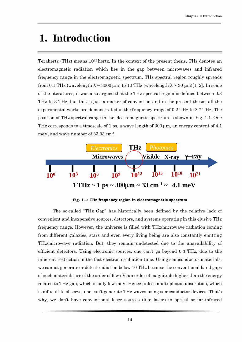
1. Introduction
Terahertz (THz) means 1012 hertz. In the context of the present thesis, THz denotes an
electromagnetic radiation which lies in the gap between microwaves and infrared
frequency range in the electromagnetic spectrum. THz spectral region roughly spreads
from 0.1 THz (wavelength λ ~ 3000 m) to 10 THz (wavelength λ ~ 30 μm)[1, 2]. In some
of the literatures, it was also argued that the THz spectral region is defined between 0.3
THz to 3 THz, but this is just a matter of convention and in the present thesis, all the
experimental works are demonstrated in the frequency range of 0.2 THz to 2.7 THz. The
position of THz spectral range in the electromagnetic spectrum is shown in Fig. 1.1. One
THz corresponds to a timescale of 1 ps, a wave length of 300 m, an energy content of 4.1
meV, and wave number of 33.33 cm-1.
Fig. 1.1: THz frequency region in electromagnetic spectrum
The so-called “THz Gap” has historically been defined by the relative lack of
convenient and inexpensive sources, detectors, and systems operating in this elusive THz
frequency range. However, the universe is filled with THz/microwave radiation coming
from different galaxies, stars and even every living being are also constantly emitting
THz/microwave radiation. But, they remain undetected due to the unavailability of
efficient detectors. Using electronic sources, one can’t go beyond 0.3 THz, due to the
inherent restriction in the fast electron oscillation time. Using semiconductor materials,
we cannot generate or detect radiation below 10 THz because the conventional band gaps
of such materials are of the order of few eV, an order of magnitude higher than the energy
related to THz gap, which is only few meV. Hence unless multi-photon absorption, which
is difficult to observe, one can’t generate THz waves using semiconductor devices. That’s
why, we don’t have conventional laser sources (like lasers in optical or far-infrared
100 1021101810151012109106103
THz
Microwaves Visible X-ray g-ray
1 THz ~ 1 ps ~ 300m ~ 33 cm-1 ~ 4.1 meV
Electronics Photonics
Chapter 1: Introduction
15
frequency range) working in THz frequency range. However, for frequencies below 0.3
THz, electronic components are commercially available, and millimetre-wave imaging
systems are also becoming available. Above 10 THz, thermal (black-body) sources are an
increasingly efficient means for generating electromagnetic radiation, thermal cameras
are also commercially available, and optical techniques are more readily and easily
applicable. Due to its unique energy range, THz radiation can’t be produced or detected
using common lasers or commercial photodiodes. Special techniques by combining both
electronics and optics have been invented and vigorously studied to manipulate THz
waves. In the THz regime, energy level (1 𝑇𝐻𝑧 ≅ 4.1 𝑚𝑒𝑉) is much smaller than the
quantized thermal unit of radiation 𝑘𝐵𝑇, which is the thermal energy at room temperature
(1 𝑘𝐵𝑇 ≅ 25 𝑚𝑒𝑉 𝑎𝑡 𝑇 = 300 𝐾). So, one can generally neglect the quantized nature of the
radiation field. THz regime is therefore a natural bridge between the quantum mechanical
and classical descriptions of electromagnetic waves and their interactions with materials.
The two orders of magnitude of frequency spectrum in between were, relatively speaking,
much less explored because of these difficulties until the last decade. Because of the works
of various devoted research groups all around the world, the term “THz Gap” has now
become practically non-existent. Within last 15 years many new THz techniques have
been studied, which were motivated in part by the vast range of possible applications for
THz imaging, sensing, and spectroscopy. The research field of THz radiation has been
experiencing an unprecedented growth and a paradigm shift since last few years due to
the invention of new THz generators and THz detectors. In the 1990s and early 2000s,
researchers were mainly interested in studying efficient ways to generate and detect THz
radiation with sufficient energy which includes the use of new types of photo-conductive
(PC) antennas, electro-optic materials, multi-ferroic materials and intense femtosecond
lasers down to 15 fs and some basic spectroscopic study of polar liquids and thin films.
Riding on the advantage of extremely low energy, broadband nature, high signal-to-noise
(S/N) ratio and the information of both the amplitude and the phase of this unique
frequency range, THz spectroscopy has been used in various aspects of science in the last
few years. There are many applications of THz spectroscopy covering diverse areas of
science including solid state physics, semiconductors physics, nano-science and molecular
spectroscopy, biology, pharmaceuticals, standoff detection and security, and art
conservation. Now-a-days, researchers are mostly interested in application based THz
research ranging from THz manipulating devices (like THz polarizers and wave-plates[3-
8], THz shielding[9-11], THz conductivity manipulation), THz giant-magneto resistance

Chapter 1: Introduction
16
materials and spintronics[12-16], ultrafast data storage[17-21], computer performing
operations at the rates of teraflops[22, 23], THz communication systems[24-27], gas
sensing electronic devices on the picoseconds time scale[28] to THz astronomy[29-32], THz
applications in security, imaging and healthcare[1, 33-41] etc.. A beautiful review about
the progress of THz technology in different aspect of science has been provided by
Tonouchi et al.[42] in 2007. THz radiation can be transmitted to a reasonable distance
through air, many plastics, cardboard, paper, clothing, and many other materials, with
the notable exceptions of metals and water. THz radiation is therefore useful for imaging
applications. In the simplest case, the sample is scanned across the focus of the THz beam
and the amplitude and phase of either the broadband pulse or the individual frequency
components can be mapped. THz imaging has potential applications including security
screening, biomedical testing, pharmaceuticals, and art conservation. THz spectroscopy
provides important information on the basic structure of molecules and is a useful tool of
radio astronomy. Rotational frequencies of light molecules fall in this spectral region, as
do vibrational modes of large molecules with many functional groupings, including many
biologic molecules that have broad resonances at THz frequencies. Several research
groups are also involved in studying exotic fundamental studies in the field of
superconductor carrier dynamics, ultrafast demagnetization mechanisms, magnon
propagation in anti-ferromagnets, phonon modes in nanostructures, understanding water
dynamics, carrier relaxation mechanism in two-dimensional (2D) systems (like graphene,
molybdenum sulphide, boron nitrate) etc.. Undoubtedly, from the early days of
adolescence, THz research has reached its vibrant youth. A recent report from the
National Academics outlines that electronic and optics are combining to open up a new
“Tera-Era”[43]. There are three different types of THz spectroscopy measurements carried
out, namely i) THz time domain spectroscopy (THz-TDS), ii) THz time resolved
spectroscopy (TRTS) and iii) THz emission spectroscopy (TES). In THz-TDS, the ground
state properties of the samples can be obtained in a non-invasive way. THz-TDS has
become a widely used technique, and the great majority of THz studies have employed
this method. Even though the measurement is made in the time domain, it is not a time-
resolved technique. It is equivalent to a Fourier transform infrared spectroscopy (FTIR)
method, and does not provide time-resolved dynamical information. It has several notable
advantages relative to other methods in the far-infrared and a detailed discussion is given
later. In TRTS, the sample is excited via an optical pulse and a THz pulse passes through
the sample to detect the photo-excited carrier dynamics of the sample. In TES, a sample
Chapter 1: Introduction
17
is photo-excited and radiates a THz pulse due to a change in the current and/or a change
in the polarization in the sample, and the radiated THz waveform is analyzed to uncover
the dynamics of the underlying process. In the present thesis we have studied the ground
state THz properties of various nanostructures using THz-TDS.
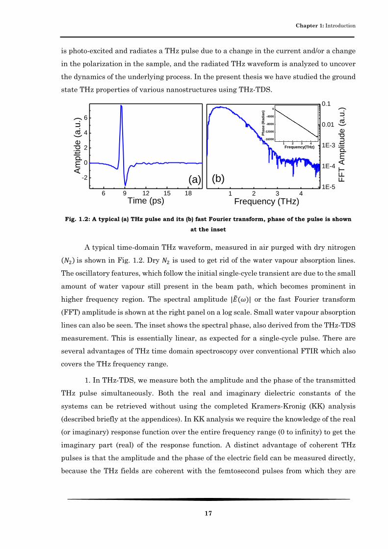
Fig. 1.2: A typical (a) THz pulse and its (b) fast Fourier transform, phase of the pulse is shown
at the inset
A typical time-domain THz waveform, measured in air purged with dry nitrogen
(𝑁2) is shown in Fig. 1.2. Dry 𝑁2 is used to get rid of the water vapour absorption lines.
The oscillatory features, which follow the initial single-cycle transient are due to the small
amount of water vapour still present in the beam path, which becomes prominent in
higher frequency region. The spectral amplitude |�̃�(𝜔)| or the fast Fourier transform
(FFT) amplitude is shown at the right panel on a log scale. Small water vapour absorption
lines can also be seen. The inset shows the spectral phase, also derived from the THz-TDS
measurement. This is essentially linear, as expected for a single-cycle pulse. There are
several advantages of THz time domain spectroscopy over conventional FTIR which also
covers the THz frequency range.
1. In THz-TDS, we measure both the amplitude and the phase of the transmitted
THz pulse simultaneously. Both the real and imaginary dielectric constants of the
systems can be retrieved without using the completed Kramers-Kronig (KK) analysis
(described briefly at the appendices). In KK analysis we require the knowledge of the real
(or imaginary) response function over the entire frequency range (0 to infinity) to get the
imaginary part (real) of the response function. A distinct advantage of coherent THz
pulses is that the amplitude and the phase of the electric field can be measured directly,
because the THz fields are coherent with the femtosecond pulses from which they are
6 9 12 15 18
-2
0
2
4
6
1 2 3 41E-5
1E-4
1E-3
0.01
0.1
1 2 3 4
-16000
-12000
-8000
-4000
0
(b)
Am
pltid
e (
a.u
.)
Time (ps)
(a)
Frequency (THz)
FF
T A
mplit
ude (
a.u
.)
Ph
ase (
Rad
ian
)
Frequency(THz)

Chapter 1: Introduction
18
generated. Using THz-TDS, both the real and imaginary parts of the response functions,
such as the complex dielectric function as shown below;
휀̃(𝜔) = 휀𝑅𝑒𝑎𝑙(𝜔) + 𝑖휀𝐼𝑚𝑎𝑔(𝜔), (1)
where, 휀̃ is the complex di-electric function, 휀𝑅𝑒𝑎𝑙 and 휀𝐼𝑚𝑎𝑔 are the real and imaginary
component of the di-electric function respectively and 𝜔 is the probing frequency, can be
obtained directly without the need for KK transforms. The complex dielectric constant of
the material is related to the complex conductivity (�̃�(𝜔)) of the system according to the
following equation;
�̃�(𝜔) ≡ 𝜎𝑅𝑒𝑎𝑙(𝜔) + 𝑖𝜎𝐼𝑚𝑎𝑔(𝜔) = 𝑖𝜔휀0[1 − 휀̃(𝜔)], (2)
where 𝜎𝑅𝑒𝑎𝑙 and 𝜎𝐼𝑚𝑎𝑔 are the real and imaginary component of the conductivity and 휀0 is
the d.c. di-electric constant of the material. The conductivity describes the current
response as the following;
𝐽(𝜔) = �̃� (𝜔)�̃�(𝜔), (3)
of a many-body system to an electric field, an ideal tool to study conducting systems. Here
𝐽 is the complex current density and �̃� is the complex electric field.
2. THz-TDS is a coherent detection technique and the signal to noise ratio is quite
high. For example, in our experimental setup the highest S/N ratio is around 50 dB at 0.4
THz.
3. THz-TDS is a useful technique to measure the optical properties of a sample in
a non-invasive manner, which is extremely advantageous in case of measuring
nanostructured samples because there is no chance of getting the samples damaged by
any kind of contact and also one does not need to put any kind of connecting wires to the
sample which may slightly alter the response of the sample.
In the present thesis entitled “Manipulating Terahertz Radiation Using
Nanostructures”, I shall be describing the works that I have carried out during my Ph.D.
tenure. It is basically centred around the fabrication of different types of nanostructures
and films, their structure and morphology characterization, extracting their THz opto-
electronic properties and/or their demonstration in manipulating the THz radiation.
The structure of the present thesis is as follows. The thesis can be divided into two
main parts. Chapter 1 to chapter 3 discuss the introduction of THz radiation, its history
and the instruments and data analysis techniques. Chapter 4 to Chapter 8 discuss all the
works that I have done during my PhD. An overall conclusion is provided in chapter 9 and

Chapter 1: Introduction
19
references are given in chapter 10. In chapter 1, a general introduction is given about the
THz radiation, it’s unique properties and its advantages. The second chapter briefly
describes the history of the progress of filling up the so called “THz Gap” by using antenna
structures and also some important THz-TDS studies in nanostructures are revisited.
The major instruments and the data analysis procedure are described in chapter 3. In
chapter 4, the preparation of a low-cost durable THz polarizer using magnetically aligned
nickel nanostructures is described and the THz polarizing behaviour is demonstrated.
THz electromagnetic shielding (EMIS) of single walled carbon nanotube (SWNT)/polymer
composites with increasing SWNT content is described in chapter 5. The conductivity
manipulation in two different and efficient ways is described in chapter 6. In chapter 7,
the conductivity and EMIS of self-standing multi-walled carbon nanotube (MWNT) films
is described as a function average length and diameter of MWNT. The oxidation in copper
thin films and its effect on the THz conductivity properties of the Cu film is discussed in
chapter 8. Finally, chapter 9 presents the overall summary of the main findings of the
thesis and offers some recommendations for future works based on this thesis.

Chapter Two

Chapter 2: General Background
21
2. General Background
Brief History of Generation and Detection of
THz Radiation Using Photo-Conductive
Antenna
THz spectroscopy grew out primarily due to the efforts of Daniel Grischkowsky (who was
working at IBM Watson Research Center) and David Auston and Martin Nuss (who were
working at the Bell Labs) to generate and detect ultrashort electrical transients as they
propagated down a transmission line. David H. Auston started working in femtosecond
excitation of electro-optic crystals to generate sub-ps pulses at Bell Lab. They found that
defects in lithium niobate (LN) favour the far-infrared generation by optical
excitation[44]. The idea of using photoconductors rather than ion doped crystals to
generate the electrical signals came shortly afterwards he began experimenting with
silicon-based transmission-line structures. In the earliest experiments, very fast rise time
electrical signals could be generated, but long carrier recombination times in silicon
limited the bandwidth through the rather slow decay times. To terminate the electrical
pulse, he deployed a second optical pulse to create a short-circuit in the transmission line.
Detection of the signal was accomplished by using a second pair of optical pulses further
down the transmission line, which is used to open and close the circuit in a similar fashion.
This general approach for generating and detecting extremely fast electrical pulses by
optical techniques became known as the "Auston Switch"[45, 46]. At that time, the idea
of using the optical pulses not just to excite a photo conductor, but to actually generate a
localized current that could be swept up and radiated by a localized radio frequency (RF)
antenna, began to take shape and the coherent generation and detection of free space
radiating RF fields using fast optical pulses was demonstrated[47, 48]. At about this time,
would be THz pioneer Daniel Grischkowsky started working with sub-ps pulses and was
able to launch and detect sub picosecond electrical pulses propagating on a coplanar
waveguide transmission line[49], after his important innovation (which was later
commercially implemented by Spectra Physics) on the area of pulse compression and
pulse reshaping[50, 51]. They generated electrical pulses (shorter than 0.6 ps) in a
coplanar transmission line with 80 fs laser pulses which broadened to only 2.6 ps after

Chapter 2: General Background
22
propagating 8 mm on the transmission line. For the reduction of this pulse broadening
effect, he started to work on the propagation of sub-ps radiation in free spaces and
succeeded in the demonstration of THz generation, its free propagation in air up to 10 cm
and then its detection using dipolar antennas[52]. As understood from Maxwell’s
equations, a time-varying electric current will radiate an electromagnetic pulse. Thus, it
was realized that these transmission lines were also radiating short bursts of
electromagnetic radiation. These reports[48, 52], where THz pulse propagated through
air between the generator and detector antenna paved the way for modern day THz
spectrometers. At this stage, significant number of studies were focused on the generation
of THz radiation via photo-mixing two diode laser on suitable antenna structure.
McIantosh et al.[53] studied the performance of photo-mixer structure on low temperature
grown GaAs (LT-GaAs) and excited it with optical pump power generated from two
Ti:Al2O3 (Ti-Sapphire) lasers operating in the range of 720-820 nm to get THz radiation
across the range 0-5 THz. By reducing the area of the electrode region, they had pushed
the RC limit (RC constant of an equivalent circuit is defined as the time required to charge
the capacitor, through the resistor, by ≈ 63.2% of the difference between the initial value
and final value and here the frequency (𝑓) is related with the RC time constant 𝜏 as; 𝜏 =
12𝜋𝑓⁄ ) for the photo-mixer beyond 2 THz. This allowed them to measure a lifetime-limited
3 dB bandwidth of 650 GHz in a mixer with a 250 fs photo-carrier lifetime, and leads to a
50 times increase in power at a frequency of 2.5 THz. Matsuura et al.[54] demonstrated
the generation of continuous-wave THz radiation at frequencies up to 3.5 THz by photo-
mixing in LT-GaAs photoconductors with printed dipole antennas.
Kono et al.[55] prepared a dipole type PC detector antenna on an LT-GaAs wafer.
The 1.5 mm thick LT-GaAs layer was grown at 250 0C on the GaAs substrate whose
thickness was 0.4 mm. Using a 12 fs Ti-Sapphire light, they succeeded in detecting THz
radiation up to 20 THz, however, with a strong phonon resonance dip around 8 THz. Tani
et al.[56] studied PC dipole antennas fabricated on semi-insulating (SI) GaAs and SI-InP
to detect THz pulses. The SI-InP based photoconductive detector showed a higher
responsivity and a better S/N ratio than the LT-GaAs based photoconductive detector at
low gating laser powers. They have also studied[57] THz emission with several designs of
PC antennas (three dipoles, a bow tie, and a coplanar strip line) fabricated on LT-GaAs
and SI-GaAs, and compared them. The radiation spectra for the antennas fabricated on
LT-GaAs and SI-GaAs did not show significant differences, indicating that the high-
frequency components of radiation were not greatly limited by the carrier lifetime of the
Chapter 2: General Background
23
substrate semiconductor. Liu et al.[58] studied the performance of InP:H+ PC antennas
as the ultra-broadband THz detector and compared it with an LT-GaAs. They found that
the peak THz signal of the InP:H+ (1015 ions.cm-2) PC antenna was slightly higher than
that of the LT-GaAs one, while the SNR of the former was about half as high as the latter.
Salem et al.[59] measured the characteristics of PC antenna emitters fabricated on
GaAs:As, GaAs:H, GaAs:O and GaAs:N ion-implanted substrates and compared them
with those obtained for a similar emitter fabricated on SI-GaAs substrate. In all the cases
(except for GaAs:N), they found better THz integrated intensity for emitters made on ion-
implanted substrates. Dreyhaupt et al.[60] demonstrated a planar large-area PC emitter
for impulsive generation of THz radiation. The device consisted of an interdigitated
electrode (metal-semiconductor-metal (MSM)) structure which was masked by a second
metallization layer isolated from the MSM electrodes. The second layer blocked optical
excitation in every second period of the MSM finger structure. Hence charge carriers were
excited only in those periods of the MSM structure which exhibited a unidirectional
electric field. Constructive interference of the THz emission from accelerated carriers led
to THz electric field amplitudes up to 85 V.cm-1 when excited with fs optical pulses from
a Ti:sapphire oscillator with an average power of 100 mW at a bias voltage of 65 V applied
to the MSM structure. Upadhya et al.[61] studied the generation of THz transients in
photoconductive emitters by varying the spatial extent and density of the optically excited
photo-carriers in asymmetrically excited, biased LT-GaAs antenna structures. They found
a pronounced dependence of the THz pulse intensity and broadband (> 6.0 THz) spectral
distribution on the pump excitation density and simulate this with a three-dimensional
carrier dynamics model. Miyamaru et al.[62] studied the dependence of the emission
spectrum of THz radiation on the geometrical parameters of the dipole antenna, and the
relationship between these parameters and the temporal characteristics of the transient
current that generate THz radiation. They found that the frequency bandwidth became
narrower as the dipole length increased and the emission efficiency of the dipole antenna
decreased with decreasing aspect ratio (AR) of the dipole antenna. Park et al.[63]
presented a nanoplasmonic PC antenna with metal nanoislands for enhancing THz pulse
emission. The whole photoconductive area was fully covered with metal nanoislands by
using thermal dewetting of thin metal film at relatively low temperature. The metal
nanoislands served as plasmonic nanoantennas to locally enhance the electric field of an
ultrashort pulsed pump beam for higher photo-carrier generation and two times higher
enhancement for THz pulse emission power than a conventional PC antenna was

Chapter 2: General Background
24
demonstrated. Hou et al.[64] investigated the relationship between THz wave emission
efficiency, noise, and stability to the material properties of fabricated LT-GaAs and SI-
GaAs antennas with the same structure, and compared their emission power, S/N ratio,
and stability under the same experimental conditions. Using both theoretical and
experimental analysis, they concluded that the LT-GaAs antenna provides high THz wave
emission efficiency, low noise, and high stability due to its short carrier lifetime and high
resistivity. Ropagnol et al.[65] demonstrated the generation of intense THz pulses at low
frequencies, and THz pulse shaping, using a ZnSe interdigitated large aperture PC
antenna. They experimentally measured a THz pulse energy of 3.6 ± 0.8 μJ, corresponding
to a calculated peak THz electric field of 143 ± 17 kV.cm-1. The focused THz intensity spot
size was 7.3 mm2; close to the diffraction limit. They also used a binary phase mask
instead of a traditional shadow mask with their interdigitated PC antenna, which allowed
them to generate THz field profiles that ranged from a symmetric single-cycle THz pulse
to an asymmetric half-cycle THz pulse.
THz systems operated at 1.5 µm wavelength can benefit from the large variety of
lasers and fiber components developed and matured originally for telecom applications.
Thus, compact, flexible and cost effective THz sensor systems can be assembled. So, people
got excited to use the advantage of lossless well-known communication wavelength 1.5
m for excitation of THz radiation. Unfortunately, GaAs is usually not sensitive at 1.5 m
wavelength because the optical band gap is 1.43 eV at room temperature, corresponding
to a wavelength of 867 nm. Gupta et al.[66] prepared LT-GaAs and LT-InGaAs using MBE
technique at various growth temperatures and studied the corresponding ultrafast carrier
lifetime. The carrier lifetime of un-annealed LT-GaAs decreased from 70 ps to less than
0.4 ps as the growth temperature decreased from 400 0C to 190 0C. Carrier lifetime of un-
annealed LT-InGaAs decreased from ~ 70 ps to 2.5 ps with decreasing growth
temperature. Application of THz detector using LT-InGaAs and 1.55 m excitation
wavelength was studied. Sekine et al.[67] studied the ultrafast carrier response of ion-
implanted Ge thin films and found a photo-carrier mobility as high as 100 cm2V-1s-1 and
carrier lifetime as low as 0.6 ps. They akso studied THz emission using PC antenna array
excited by 1.55 m radiation. Erlig et al.[68] studied the THz radiation from LT-GaAs
antenna using 1.55 m wavelength and concluded that two-photon absorption was the
origin of the radiation, however, Tani et al.[69] suggested that the two-step photon
absorption mediated by mid-gap states, formed by the excess As (1% - 2%) in LT-GaAs,
contributed to the photoconductivity at relatively low excitation power (5 mW) rather than

Chapter 2: General Background
25
the two-photon absorption at 1.55 m and found 10% higher efficiency than 780 nm
excitation. Suzuki et al.[70] deposited un-doped 1.5 μm thick In0.53Ga0.47As layers using
metalorganic chemical vapour deposition on semi-insulating InP:Fe substrates and
implanted with Fe ion of 340 keV at the dose of 1.0×1015 cm−2 which was then annealed
at different temperatures (400, 580, and 640 0C). They found that annealing at 580 0C of
Fe-implanted PC antennas affected the shape of photocurrent signals, and increased the
amplitude of the signals and concluded that Fe-implanted InGaAs PC antennas after
annealing was one of the potential candidates for applications as an efficient THz detector
triggered by the optical communication light of 1.55 μm wavelength. The Group of Martin
Schell at the Fraunhofer Institute for Telecommunications, Berlin was engaged in
fabricating THz generators and detectors operating at 1.5 μm telecom wavelength for the
realization of all-fiber THz time domain spectrometer. They[71, 72] studied the novel LT-
InGaAs/InAlAs multi-layer structures at various growth temperatures to prepare efficient
THz emitter and detector antennas working at 1.55 μm. To overcome the problem of
decreasing in-plane electrical field component, they also studied the mesa-type structures
with electrical side contacts. The electrical field was directly applied even to deeper layers,
and the current in the receiver did not need to traverse hetero-structure barriers which
increased the THz peak-to-peak voltage about ~ 27 times than planar THz antenna. Bekar
et al.[73] demonstrated an all-optoelectronic continuous-wave THz photo-mixing system
from microwave frequencies to beyond 1.0 THz that uses LT-InGaAs devices both for
emitters and coherent homodyne detectors. The photo-conductive InGaAs layers were
grown on SI-GaAs by MBE at a nominal growth temperature of 230 0C. The excellent
material properties were achieved by applying a post-growth anneal, in which the
surfaces were passivated by contact with SI-GaAs wafers. Ramer et al.[74] studied the
generation and detection of THz radiation at 1560 nm based on LT-GaAs PC antennas. A
THz-TDS system employing LT-GaAs PC antennas pumped at 1560 nm was also
demonstrated which reached a bandwidth of 4.5 THz and a peak S/N ratio of 29 dB, while
the reference measurement at 780 nm reached 40 dB and a bandwidth of approximately
3 THz.
Generation and Detection of THz Radiation
Generation and detection of THz pulses occur through the non-linear interactions of the
driving optical pulse with a material with fast response. Any process that crates time-
dependent change in the material properties 𝜇, 𝜎, or 휀 can act as a source term that can

Chapter 2: General Background
26
result in emission of THz radiation. There are mainly two major classifications of
producing THz generation and detection namely i) photo-conductive antenna and ii) non-
linear electro-optic crystals. But, there are also some other techniques like i) photo-
mixing, ii) THz quantum cascade laser (QCL), iii) THz generation from air plasma etc.
Since all the studies reported in this thesis are based on PC antenna, in this chapter, only
the mechanism of THz generation and detection using PC antenna will be discussed.
As the main equations governing the generation and detection of any radiation are
the Maxwell’s equations, in this section, the Maxwell’s equations in vacuum and in
material will be briefly revisited in the context of wave equation, whose solution gives us
an electric field as a function of time (or frequency). Electromagnetic radiation and its
properties can be efficiently expressed by the Maxwell’s equations[75, 76] as given below;
∇. 𝑬 =𝜌휀0⁄ , (4)
∇ × 𝑬 = −𝜕𝑩 𝜕𝑡⁄ , (5)
∇.𝑩 = 0, (6)
∇ × 𝑩 = 𝜇0휀0𝜕𝑬
𝜕𝑡⁄ + 𝜇0𝑱, (7)
where, 𝑬 and 𝑩 are the electric field vector and magnetic induction vectors, 휀0 and 𝜇0 are
the vacuum permittivity and permeability, 𝜌 and 𝑱 are the charge and current density.
The speed of light is defined as, 𝑐 =1
√𝜇0𝜀0 . Now, using the identity ∇. (∇ × 𝑩) = 0, we find
the following equation which is also known as the continuity equation,
𝜕𝜌𝜕𝑡⁄ = ∇. 𝑱. (8)
The charge density (𝜌) of a medium can be expressed as the combination of external
charges due to free electrons (𝜌𝑒𝑥𝑡) and the polarization charges (𝜌𝑝𝑜𝑙) which is related to
the polarization density 𝑷 according to 𝜌𝑝𝑜𝑙 = −∇.𝑷. The total current density (𝑱) is also
expressed as a combination of conduction current density (𝑱𝑐𝑜𝑛𝑑) and displacement
current density (𝑱𝑑𝑖𝑠𝑝), which is related with the polarization density according to 𝑱𝑑𝑖𝑠𝑝 =
𝜕𝑷𝜕𝑡⁄ .
The electric displacement 𝑫 and magnetic field strength 𝑯 are the material-related
parameters, which for a linear isotropic non-magnetic dielectric are given by,
𝑫 = 휀𝑬 = 휀0𝑬 + 𝑷 = 휀0(1 + 𝜒)𝑬, (9)
Chapter 2: General Background
27
𝑯 = 𝑩 𝜇0⁄ , (10)
where, 휀 is the dielectric constant and 𝜒 the dielectric susceptibility.
So, the Maxwell’s equations in the presence of materials[76, 77] can be written as;
∇.𝑫 =𝜌𝑒𝑥𝑡
휀0⁄ , (11)
∇ × 𝑬 = −𝜕𝑩 𝜕𝑡⁄ , (12)
∇.𝑩 = 0, (13)
∇ × 𝑯 = 휀0𝜕𝑫
𝜕𝑡⁄ + 𝑱𝑐𝑜𝑛𝑑. (14)
These are the Maxwell’s equations in presence of materials. Now, in the absence of free
charges, these equations can be combined into the general wave equation as given below,
∇2𝑬 −1
𝑐2𝜕2𝑬
𝜕𝑡2= 𝜇0 (
𝜕𝑱𝑐𝑜𝑛𝑑𝜕𝑡
+𝜕2𝑷
𝜕𝑡2). (15)
The two time-varying source terms are the conduction current 𝑱𝑐𝑜𝑛𝑑 and the polarization
𝑷. The far-field on-axis solution of this equation relates the temporal shape of an
electromagnetic signal emitted by a slab of material with a time-varying spatially uniform
conduction current 𝑱𝑐𝑜𝑛𝑑 and/or the polarization 𝑷 at the axis normal to the slab at a
distance. The solution has been presented by several authors[78-82] which looks like the
following,
𝑬𝑟𝑎𝑑(𝑡) ≈𝜇04𝜋
𝑆
𝑧(𝜕𝑱𝑐𝑜𝑛𝑑(𝑡)
𝜕𝑡+𝜕2𝑷(𝑡)
𝜕𝑡2), (16)
where, 𝑆 is the emitting area and 𝑧 stands for the distance between the emitter surface
and the detection surface. This solution is important since it allows for reconstruction of
the polarization and carrier dynamics in an electromagnetic signal, under the assumption
that the radiated field is properly detected.
2.2.1. Generation of THz Radiation
Photoconductive THz generation occurs when optical excitation induces conductivity
changes in a semiconductor. This is a resonant interaction and the photons are absorbed
through inter-band transitions. For THz generation using PC antennas an ultrashort
optical pulse incident on the semiconductor causes rapid transient changes to the
macroscopic parameters represented by 𝜇(𝑡), 𝜎(𝑡), and 휀(𝑡). The major change caused by
the optical pulse is assumed to be in the conductivity 𝜎. The rapid, optically induced
Chapter 2: General Background
28
change of 𝜎 on a femto-second time scale is the origin of the ultrafast THz pulses generated
through photoconduction. It is important to note that many physical processes occur when
ultrafast pulses are absorbed by semiconductors, and, from an experimental point of view,
they are not easily separable. Both resonant (absorption of a photon to create charge
carriers), and non-resonant effects (nonlinear optical difference frequency generation),
can contribute to THz pulse generation. A common example of a material in which both
processes contribute to THz generation is LT-GaAs. The geometry of a photoconductive
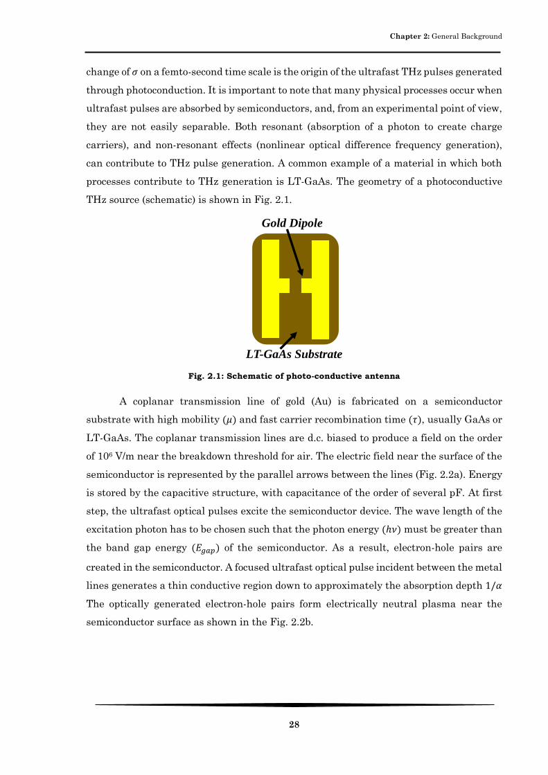
THz source (schematic) is shown in Fig. 2.1.
Fig. 2.1: Schematic of photo-conductive antenna
A coplanar transmission line of gold (Au) is fabricated on a semiconductor
substrate with high mobility (𝜇) and fast carrier recombination time (𝜏), usually GaAs or
LT-GaAs. The coplanar transmission lines are d.c. biased to produce a field on the order
of 106 V/m near the breakdown threshold for air. The electric field near the surface of the
semiconductor is represented by the parallel arrows between the lines (Fig. 2.2a). Energy
is stored by the capacitive structure, with capacitance of the order of several pF. At first
step, the ultrafast optical pulses excite the semiconductor device. The wave length of the
excitation photon has to be chosen such that the photon energy (ℎ𝜈) must be greater than
the band gap energy (𝐸𝑔𝑎𝑝) of the semiconductor. As a result, electron-hole pairs are
created in the semiconductor. A focused ultrafast optical pulse incident between the metal
lines generates a thin conductive region down to approximately the absorption depth 1/𝛼
The optically generated electron-hole pairs form electrically neutral plasma near the
semiconductor surface as shown in the Fig. 2.2b.
Gold Dipole
LT-GaAs Substrate

Chapter 2: General Background
29
Fig. 2.2: Schematic of THz generation via photo-conductive antenna (schematic is based from
Ref. 43)
The time evolution of the charge density is given by 𝑁(𝑡) with the total carrier density as
the sum of that of the electrons and the holes i.e.,
𝑁(𝑡) = 𝑁𝑒(𝑡) + 𝑁ℎ(𝑡). (17)
At low-excitation influences, the charge density is proportional to the intensity profile of
the optical pulse 𝐼(𝑡). The time evolution of the carrier density is given by this expression,
𝑁(𝑡) = ∫ 𝐺(𝑡)𝛿𝑡𝑡
0
− 𝑁0𝑒𝑥𝑝 (−𝑡
𝑡𝑐), (18)
where, 𝑡𝑐 , 𝑁0 are respectively the carrier lifetime and total number of generated carrier.
The first term describes carrier density at time scales of the laser pulse and the second
term describes the evolution of the carrier density at longer times. Here 𝐺(𝑡) is the optical
carrier generation rate determined by the optical pulse profile. The free carriers affect the
conductivity by,
𝜎(𝑡) = 𝑁(𝑡)𝑒𝜇. (19)
The current density is,
𝐽(𝑡) = 𝜎(𝑡)𝐸, or 𝐽(𝑡) = 𝑁(𝑡)𝑒𝑣(𝑡), (20)
with 𝑣(𝑡) being the carrier velocity. Immediately after the generation of the carriers in
the semiconductor the accelerating field is 𝐸(𝑡 = 0+) = 𝐸𝐷𝐶. The time dependence has
EDC
(a)
ETHz
(d)
-+- - +
+
(e)
++- +
+ - -- -
- +
Laser Pulse
(b)
N(t)--- +- + +- +- +
J(t)
(c)
+-

Chapter 2: General Background
30
been written explicitly to illustrate the transient nature of the photoconductivity on sub-
picosecond time scales. It is the transient current, 𝐽(𝑡), that generates the THz pulse. The
carriers are accelerated in the applied electric field, 𝐸𝐷𝐶. The time evolution of carrier
velocity is determined by the initial acceleration of carriers with effective mass 𝑚∗ and by
rapid carrier scattering with a characteristic time, which is determined by phonon
scattering, carrier scattering from the dopants and the photon energy, or where in the
conduction band carriers are generated. In summary, a d.c. biased semiconductor (Fig.
2.2a) has electron-hole plasma created in femtosecond time scales by an optical pulse (Fig.
2.2b). The rapid acceleration and separation of the electrons and holes create a current
transient (Fig. 2.2c). The transient electric field determined (approximately) by the time
derivative of the current results in a radiated pulse front in THz frequency range (Fig.
2.2d). Equilibrium is reached after long time (Fig. 2.2e).
2.2.2. Detection of THz Radiation
The detections of THz pulses are performed by using the phenomenon of ultrafast pulse
excitation in a semiconductor causing rapid changes in conductivity. The photoconductive
detection process is shown schematically in Fig. 2.3. The ultrafast laser pulse is incident
on the antenna from the left and the THz pulse propagating from the right. As in the case
of the generation of THz pulse where an ultrafast laser pulse generates an electron and
hole plasma. The arrival of the laser pulse is analogous to closing a switch, which allows
the antenna gap to conduct due to the creation of electron-hole plasma. But, these
electron-hole plasma cannot conduct due to the absence of any electric field. It can only
conduct when the THz field falls on the antenna providing the necessary bias voltage. The
short recombination time of the semiconductor causes the gap resistance to change from
nearly insulating to conducting (closing the switch) then back to insulating (opening the
switch) on a picoseconds time scale. The coplanar strip line is connected to a high-
sensitivity current amplifier that detects any current flow through the antenna gap with
sub-pA resolution. If the resistance of the metal lines is negligible the resistance of the
antenna is determined by the antenna gap. The current flows according to Ohms law
𝐼(𝑡) = 𝑉(𝑡)
𝑅(𝑡)⁄ , where the antenna bias voltage is provided by the THz pulse: 𝑉(𝑡) ≅
𝐸𝑇𝐻𝑍(𝑡)ℎ. In Fig. 2.3a, the THz pulse has not arrived at the antenna, the bias voltage is
zero, and there is no net current flowing through the antenna. In Fig. 2.3b, the positive
gating peak of THz pulse is incident on the antenna and at the same instance the optical

Chapter 2: General Background
31
gating pulse arrives. In this case ETHz > 0, and the current flows from the lower half of the
antenna to the upper are determined by the electric field direction.
Fig. 2.3: Schematic of THz detection using photo-conductive antenna (Schematic is taken from
Ref. 43)
The measured time average current is proportional to the THz electric filed. After the
current is measured, the delay between the laser generating and gating pulses is again
changed to advance the THz pulse in time. Fig. 2.3c corresponds to a point on the pulse
where the electric field is opposite in sign. The time resolved measurement of the THz
pulse electric field is thus made by changing the delay between the optical gating pulse
and the generating pulse, i.e. the time delay between the pump and probe laser beams. It
is clear that to measure the electric field with high temporal resolution, the response time
of the semiconductor must be short compared to the rate of change of the THz field. The
two semiconductor materials most commonly used for photoconductive THz detectors are
LT-GaAs and ion-implanted silicon on sapphire.
THz Spectroscopy of Exotic Nanostructures
The application of THz spectroscopy in the field of THz optics (THz polarizer, THz EMIS,
THz neutral density filter), THz conductivity in CNT and their composites, THz
conductivity of thin metallic films has been reviewed in this thesis at the beginning of the
later chapters in this thesis. However, here a brief review of some recent THz
spectroscopic works on carrier dynamics (both time-resolved and time domain study) of
THz Pulse
Laser
Antenna (a)
THz Pulse
Antenna
THz Pulse
Antenna (b) (c)

Chapter 2: General Background
32
nanostructured semiconductors and active THz devices using novel 2D materials
(graphene, transition metal dichalcogenides MoS2 and WeS2) is provided.
2.3.1. Nanowires
Parkinson et al.[83] investigated the time-resolved conductivity of isolated GaAs
nanowires by TRTS. They found that the electronic response exhibited a pronounced
surface plasmon mode within 300 fs before decaying within 10 ps as a result of charge
trapping at the nanowire surface. Hendry et al.[84] studied the electron mobility in
nanoporous and single-crystal titanium dioxide using THz-TDS. They determined the
electron mobility after carrier thermalization with the lattice but before equilibration with
defect trapping states. The electron mobility reported for single-crystal rutile (1 cm2 V-1 s-
1) and porous TiO2 (10-2 cm2 V-1s-1) therefore represent upper limits for electron transport
at room temperature for defect-free materials. The large difference in mobility between
bulk and porous samples was explained using Maxwell-Garnett (MG) effective medium
theory (EMT). They demonstrated that electron mobility is strongly dependent on the
material morphology in nanostructured polar materials due to local field effects and
cannot be used as a direct measure of the diffusion coefficient. George et al.[85] studied
the ultrafast relaxation and recombination dynamics of photo-generated electrons and
holes in epitaxial graphene using TRTS. They found that the conductivity in graphene at
THz frequencies depend on the carrier concentration as well as the carrier distribution in
energy. They concluded that carrier cooling occurred on sub-picosecond (sub-ps) time
scales and that inter-band recombination times were carrier density dependent.
Hoffmann et al.[86] demonstrated the ability to accelerate free carriers in doped
semiconductors to high energies by single cycle THz pulses. They observed that, for GaAs,
a fraction of carriers undergoes inter-valley scattering, leading to a drastic change in the
effective mass. They also found that, in the case of InSb, the carrier energy could exceed
the impact ionization threshold, leading to an increase of carrier concentration of about
one order of magnitude. They observed the energy exchange between the hot electrons
and the lattice, lead to population change of the longitudinal optical phonon. Hebling et
al.[87] observed the non-equilibrium carrier distribution in n-type Ge, Si and GaAs
semiconductors at room temperature using intense single cycle THz pulses. A review on
the THz conductivity of different types of bulk and nanostructured semiconductors was
given by Ulbricht et al.[88]. A detailed description of the ultrafast carrier dynamics of
various types of semiconductor nanostructures could be found in a recent book by Jagdeep
Chapter 2: General Background
33
Shah[89]. Joyce et al.[90] performed a comparative study of ultrafast charge carrier
dynamics in a range of III-V nanowires using TRTS. InAs nanowires exhibited the highest
electron mobilities of 6000 cm2 V−1 s−1, which highlighted their potential for high mobility
applications, such as field effect transistors. InP nanowires exhibited the longest carrier
lifetimes and the lowest surface recombination velocity of 170 cm s−1. Such low surface
recombination velocity made InP nanowires suitable for applications in photovoltaics. In
contrast, the carrier lifetimes in GaAs nanowires were extremely short, of the order of
picoseconds, due to the high surface recombination velocity, which was measured to be
5.4 × 105 cm s−1.
2.3.2. Graphene and Other Two Dimensional Materials
Ryzhii et al.[91] studied the dynamic a.c. conductivity of a non-equilibrium 2D electron-
hole system in optically pumped graphene. Considering the contribution of both inter-
band and intra-band transitions, they demonstrated that at sufficiently strong pumping
the population inversion in graphene can lead to the negative net a.c. conductivity in the
THz frequency range. Hong et al.[92] performed THz spectroscopy on reduced graphene
oxide (rGO) network films coated on quartz substrates from dispersion solutions by
spraying method. They obtained the frequency-dependent conductivities and the
refractive indexes of the rGO films and analyzed the results using Drude free-electron
model. They concluded that the THz conductivities could be manipulated by controlling
the reduction process, which was correlated well with the d.c. conductivity above the
percolation limit. Tamagnone et al.[93] demonstrated a graphene based THz frequency-
reconfigurable antenna. The antenna exploited dipole-like plasmonic resonances, which
could be frequency-tuned on large range via the electric field effect in a graphene stack.
Vakil et al.[94] theoretically showed that by designing and manipulating spatially
inhomogeneous, non-uniform conductivity patterns across a flake of graphene, one could
obtain a one-atom-thick platform for infrared metamaterials and transformation optical
devices. Varying the graphene chemical potential by using static electric field, the authors
had shown tunable conductivity in the THz and infrared frequencies. Horng et at.[95]
reported measurements of high-frequency conductivity of graphene from THz to mid-IR
at different carrier concentrations. The conductivity exhibited Drude like frequency
dependence and increased dramatically at THz frequencies, but its absolute strength was
lower than theoretical predictions. This anomalous reduction of free-electron oscillator
strength was corroborated by corresponding changes in graphene inter-band transitions,
Chapter 2: General Background
34
as required by the sum rule. Jnawali et al.[96] measured the THz frequency dependent
sheet conductivity and its transient response following femtosecond optical excitation for
single-layer graphene samples grown by chemical vapour deposition (CVD). The THz
conductivity was analysed using Drude model, which yielded an average carrier
scattering time of 70 fs. Upon photoexcitation, they observed a transient decrease in
graphene conductivity. The THz frequency-dependence of the graphene photo-response
differed from that of the unexcited material but remained compatible with a Drude form.
They showed that the negative photoconductive response arises from an increase in the
carrier scattering rate, with a minor offsetting increase in the Drude weight. The photo-
induced conductivity transient had a picosecond lifetime and was associated with non-
equilibrium excitation conditions in the graphene. Bonaccoroso et al.[97] wrote a review
on the different synthesis procedure of graphene and its use in opto-electronic devices. Ju
et al.[98] explored plasmon excitations in engineered graphene micro-ribbon arrays and
demonstrate that graphene plasmon resonances could be tuned over a broad THz
frequency range by changing micro-ribbon width and electrostatic doping. The ribbon
width and carrier doping dependences of graphene plasmon frequency demonstrated a
power-law behaviour characteristic of 2D massless Dirac electrons. Vicarelli et al.[99]
demonstrated THz detectors operating at 0.3 THz based on antenna-coupled graphene
field-effect transistors by exploiting the nonlinear response to the oscillating radiation
field at the gate electrode, with contributions of thermoelectric and photoconductive
origin. Lee et al.[100] demonstrated substantial gate-induced persistent switching and
linear modulation of THz radiation by inserting an atomically thin, gated 2D graphene
layer in a 2D metamaterial. Their device could modulate both the amplitude of the
transmitted wave by up to 47% and its phase by 32.20 at room temperature. Hwang et
al.[101] reported strong THz-induced transparency in CVD grown graphene where 92-
96% of the peak-field is transmitted compared to 74% at lower field strength. TRTS
studies revealed that the absorption recovered in 2-3 ps. The induced transparency was
believed to be arising from nonlinear pumping of carriers in graphene, which suppressed
the mobility, and consequently the conductivity in a spectral region where the light-
matter interaction is particularly strong. Xia et al.[102] showed ultrafast transistor-based
photodetectors made from single and few layer graphene whose photo-response remained
un-degraded for optical intensity modulations up to 40 GHz. Meang et al.[103] measured
the frequency dependent optical sheet conductivity of graphene which showed electron-
density dependence characteristics, and can be understood by a simple Drude model. In a
Chapter 2: General Background
35
low carrier density regime, the optical sheet conductivity of graphene was constant
regardless of the applied gate voltage, but in a high carrier density regime, it showed
nonlinear behaviour with respect to the applied gate voltage.
Shen et al.[104] used THz absorption and spectroscopic ellipsometry to investigate
the charge dynamics and electronic structures of CVD grown monolayer MoS2 films. THz
conductivity displayed a coherent response of itinerant charge carriers at zero frequency.
Drude plasma frequency (~ 7 THz) was found to be decreasing with decreasing
temperature while carrier relaxation time (~ 26 fs) remained temperature independent.
The absorption spectrum of monolayer MoS2 showed a direct 1.95 eV band gap and charge
transfer excitations that were ~ 0.2 eV higher than those of the bulk counterpart.
Docherty et al.[105] measured the ultrafast charge carrier dynamics in monolayers and
tri-layers of MoS2 and WSe2 using a combination of time-resolved photoluminescence and
TRTS. They observed a photoconductivity and photoluminescence response time of 350 fs
from CVD grown monolayer MoS2, and 1 ps from trilayer MoS2 and monolayer WSe2. Lui
et al.[106] observed a pronounced transient decrease of conductivity in doped MoS2, using
ultrafast TRTS. In particular, the conductivity was reduced to only 30% of its equilibrium
value at high pump fluence. This anomalous phenomenon arouses from the strong many-
body interactions in the 2D system, where photo-excited electron-hole pairs joined the
doping-induced charges to form trions, bound states of two electrons and one hole. The
resultant substantial increase of the carrier effective mass helped in diminishing the
conductivity. Kar et al.[107] reported the dynamics of photo-induced carriers in a free-
standing MoS2 laminate consisting of a few layers (1-6 layers) using TRTS. The relaxation
of the non-equilibrium carriers shows both the fast and slow relaxation dynamics. They
established that the fast relaxation time occurred due to the capture of electrons and holes
by defects via Auger processes, while the slower relaxation happened since the excitons
are bound to the defects, preventing the defect-assisted Auger recombination of the
electrons and the holes. Kong et al.[108] theoretically demonstrated the feasibility of
ultra-high-frequency operation in a vertical three-terminal electronic device by exploiting
the advantages of 2D crystal heterostructures. They modelled a gapped 2D material as
the tunnel barrier between a graphene base and a metallic emitter, while the Schottky
contact with an n-type substrate formed the base-collector junction. With proper
optimization, they showed that their device was capable of reaching the intrinsic cut-off
frequencies over a few THz even under realistic constraints, indicating a technological
pathway beyond the current limit. Cao et al.[109] demonstrated a new type of optically

Chapter 2: General Background
36
tunable THz modulator based on multilayer MoS2 and silicon. They showed that the THz
transmission could be significantly modulated by changing the power of the pumping laser
and the modulation was better than graphene based devices. Lee et al.[110] for the first
time reported MoS2 based metal semiconductor field-effect transistors (MESFETs) with
NiOx Schottky electrode, where the maximum mobilities or carrier transport behaviour of
the Schottky devices may hardly be interfered by on-state gate field. Our MESFETs with
single-, double-, and triple-layered MoS2 respectively showed high mobilities of 6000,
3500, and 2800 cm2/Vs at a certain low threshold voltage of -1 ~ -2 V. The thickness-
dependent mobility difference in MESFETs was theoretically explained with electron
scattering reduction mechanisms.

Chapter Three

Chapter 3: Instruments and Data Analysis
38
3. Instruments and Data Analysis
THz Time Domain Spectrometer
A compact and affordable table-top THz spectrometer, developed by Menlo Instruments
and named as Tera K8 Terahertz Spectrometer, is being used for all the THz
measurements. The detailed description of different components of the instrument is
given below.
The list of components that are needed to develop the spectrometer is the following;
1) T-Light 780 (a femtosecond fibre laser)
2) Absorptive Neutral Density Filter
3) Mirrors
4) Wave Plates
5) Polarizing Beam Splitter
6) Motorized Delay Stage and Vibration Generator
7) Antenna for Generation and Detection of THz Waves
8) Direct Digital Synthesizer
9) Lock-in-Amplifier
10) Oscilloscope
11) Working Principle
12) Alignment of the THz Spectrometer
The set-up is covered with a glass-top and we purge extra-pure N2 gas into the covered
area and keep the humidity strictly < 10% inside the whole box to get rid of unwanted
water vapours affecting our measurements.
3.1.1. T-Light 780
This is an erbium doped fiber laser with 780 nm and 65 mW output. The fiber laser uses
the same physics principles as any other laser, but there are several properties that made
it special and very useful. Unlike a conventional laser which is constructed from
components such as mirrors, dispersive crystals, rods and lenses, fiber laser is an all bulk
material device. The laser rod is effectively substituted by several meters long doped
active fiber. The rest of the components are also all fibre devices each of which are spliced
together to form a laser resonator. There is no need for alignment, adjustment or
subsequent cleaning of optical surfaces once the laser has been built, which means little
or effectively no maintenance is required.

Chapter 3: Instruments and Data Analysis
39
Fig. 3.1: Schematic of the fiber laser working principle
Very small amount of rare earth material erbium is added to the core of the glass
fibre to prepare the erbium doped fibre laser. The erbium atoms have very useful energy
levels. There is an energy level that can absorb photons with a wavelength of 980nm, and
then it decays to a meta-stable state of 1560 nm. A diode laser of 980 nm is used to pump
the fibre laser via a pump coupler and we get an output of 1560 nm. The microcontroller
driven actuators built into the fiber ring rotate and maintain stable mode-locking
automatically. The mode-lock controller consists of four wave plates and these can be
rotated along their axis manually or automatically using a rotatable motor via a software
interface. The fundamental wavelength at 1560 nm is then efficiently frequency doubled
using a periodically poled lithium niobate crystal via second harmonic generation
technique, which offers higher quasi phase matching, and therefore high conversion
efficiency when compared to conventional wavelength conversion crystals, and we get a
780 nm laser beam in free space. ER3+ doped silica fiber is used as gain medium instead
of a laser crystal. The schematic of the working principle of the fibre laser is shown in Fig.
3.1. The main features of the laser are tabulated below:
1. Repetition rate: 100 MHz ± 1 MHz
2. Centre wavelength: 780 ± 10 nm
3. Average output power: ~ 65 mW
4. Pulse width: 100-120 fs
5. Polarization: Linearly Polarized
Pump Coupler
Output Coupler
ModelockController
Pump Laser
Free Space Output
Laser Resonator

Chapter 3: Instruments and Data Analysis
40
3.1.2. Second Harmonic Generation
Second harmonic generation (SHG; also called frequency doubling) is a technique via
which the fundamental wavelength is passed through a non-linear crystal and is
frequency doubled i.e. wavelength becomes half of its fundamental value. The non-linear
material efficiently combines two incident photon of same energy to a new photon of twice
the energy. The optical response of a material can be written as;
�⃗� = 휀0𝜒�⃗� , (21)
where, 𝜒 is the susceptibility tensor, �⃗� is the polarization vector and �⃗� is the electric field
vector. Now, if we expand the above equation in a Taylor series each component of the
polarization vector 𝑃𝑘 (𝑘 = 𝑥, 𝑦, 𝑧) can be written as;
𝑃𝑘 = 휀0(𝜒𝑖𝑗1 𝐸𝑖 + 𝜒𝑖𝑗𝑘
2 𝐸𝑖𝐸𝑗 + 𝜒𝑖𝑗𝑘𝑙3 𝐸𝑖𝐸𝑗𝐸𝑘 +⋯), (22)
where, the coefficients 𝜒𝑛 correspond to the tensor of the n-th order nonlinear process. We
can consider up to 2nd order non-linear process for sufficiently strong incident radiation
for most of the practical applications. If we write the incident radiation component as 𝐸𝑖 =
ℇ𝑖 exp(−𝑖𝜔𝑡) + 𝑐. 𝑐, then the 2nd order non-linear term of kth component of polarization can
be written as;
𝑃𝑘2(𝑛𝑙) = 휀0(𝜒𝑖𝑗𝑘
2 ℇ𝑖ℇ𝑗exp (−𝑖2𝜔𝑡) + 𝑐. 𝑐 + ℇ𝑖ℇ𝑗∗ + ℇ𝑖
∗ℇ𝑗). (23)
Neglecting the d.c. term, we can see that a polarization component arises with a frequency
twice to that of the fundamental incident radiation. This polarization component gives
rises to the frequency doubled radiation. The SHG is possible only with non-linear crystals
having broken inversion symmetry and strong incident radiation.
3.1.3. Periodically Poled Lithium Niobate Crystal
Periodically poled lithium niobate crystals (PPLN) are highly efficient, engineered, and
quasi-phase matched non-linear material for SHG. For effective non-linear frequency
doubling, it is necessary that the phase relation of the incident and generated photons
remain constant throughout the length of the crystal otherwise the photons will
destructively interfere and the resultant intensity for frequency doubled photons will be
negligible. For a particular wavelength, we can calculate the length (𝑙𝑛𝑙) of the crystal
when the phase of the generated photon of frequency 2𝜔 will be 1800 out of the phase with
the incident photon of frequency 𝜔. Lithium niobate (LN) being a ferroelectric material,
Chapter 3: Instruments and Data Analysis
41
its structural direction can be flipped spatially by introducing a spatially variable
electrode and strong radiation. Thus, LN is periodically poled with a period determined
by 𝑙𝑛𝑙, as a result, the number of generated photons will grow as the light propagates
through the PPLN, yielding a high conversion efficiency of input to generated photons.
The fundamental wavelength 1560 nm of the Erbium doped fiber laser can be effectively
converted to the 780 nm laser light by frequency doubling in the PPLN crystal, which
offers higher quasi phase matching and therefore high conversion efficiency when
compared to conventional wavelength conversion crystals. The PPLN crystal used in the
setup has multiple grating structures. This allows phase matching to a wide range of
wavelengths via combination of temperature and selection of poled period.
3.1.4. Absorptive Neutral Density Filter
We use two filters directly after the laser beam output i) to get rid of any unwanted 1560
nm laser in the output beam and ii) to get the required laser power for the excitation of
THz generator and THz detector antenna.
The first absorber A1 with an optical density of 0.05 (T ~ 89 % at 780 nm) is mainly
used to get rid of any unwanted 1560 nm signal present in the laser beam. Then (A2) a
neutral density filter (NE506A, ThorLabs) with optical density 0.5 (T ~ 35 % at 780 nm)
is used to reduce the laser power at 780 nm at a value (~ 20 mW) which is suitable for
THz generator and detector antenna excitation otherwise they will get burnt due to
excessive laser heating.
3.1.5. Mirrors
Silver-coated highly reflecting mirrors (PF10-03-PO1, ThorLabs) are used to guide the
780 nm laser beam through the setup. A SiO2 coating of 100 nm is applied on the coated
surface to prevent oxidation. The typical reflectivity of these mirrors at 780 nm is > 97.5
%, thereby ensuring negligible power loss even after multiple passes.
3.1.6. Wave Plates
Wave plates are made of birefringent crystal (Quartz, Mica) of appropriate thickness such
that they change the polarization state of the light beam passing through it. The crystal
is cut into a plate in such a way that the optic axis of the crystal is parallel to the surfaces
of the plate. These results in two axes in the plane of the cut: the ordinary axis, with index
of refraction 𝑛𝑜, and the extraordinary axis, with index of refraction 𝑛𝑒. The ordinary axis

Chapter 3: Instruments and Data Analysis
42
is perpendicular to the optic axis. The extraordinary axis is parallel to the optic axis. For
a normally incident light beam, polarization component along the ordinary axis travels
through the crystal with a speed 𝑣𝑜 =𝑐
𝑛0, while the polarization component along the
extraordinary axis travels with a speed 𝑣𝑒 =𝑐
𝑛𝑒. This leads to a phase difference (𝛤)
between the two components as they exit the crystal. The relative phase that is imparted
between the two components for a crystal length L and wavelength 𝜆0 is given by the
following relation;
Γ =2𝜋(𝑛𝑒 − 𝑛𝑜)𝐿
𝜆0. (24)
Quarter wave plates introduce a phase shift of 𝜋
2 and half wave plates introduce a phase
shift of 𝜋 between the two components and thereby changing the polarization state of the
emitting light beam. Linearly polarized light from laser falls on a half wave plate (W1) in
such an angel that it becomes diagonally polarized. This diagonally polarized light is
incident on a polarizing beam splitter and p-polarized light is transmitted and s-polarized
light is reflected. The reflected s-polarized light passes through a quarter wave plate (W2)
at 450, falls on a mirror mounted on a motorized delay stage and reflects back through W2
and thereby changing its polarization state orthogonally i.e. become p-polarized.
3.1.7. Polarizing Beam Splitter
A polarizing beam splitter (PBS) is an optical device which can split any unpolarized
light beam into two light beams with mutually orthogonal (s and p) polarization. Two
birefringent prisms of same material are mounted together using a commercial gum such
that their optic axis remains perpendicular to each other. The light whose polarization is
perpendicular to the optic axis of the 1st prism passes un-deviated through it and the other
polarized light reflects at the interface of two prisms and deviated by 900. Designed for
broadband applications, TECHSPEC® broadband polarizing cube beam-splitters offer a
transmission of greater than 90% for p-polarized light and a reflection efficiency of greater
than 99% for s-polarized light across the entire design wavelength range. Each
beamsplitter consists of a pair of precision high tolerance right angle prisms cemented
together with a dielectric coating on the hypotenuse of one of the prisms. An anti-reflection
coating (ARC) has been applied to each face of the beamsplitter to achieve less than 0.5%
reflection per surface.

Chapter 3: Instruments and Data Analysis
43
3.1.8. Motorized Delay Stage and Vibration Generator
The motorized delay (Physik Instrumente, PI-M403.42S) stage offers a maximum 100 mm
travel range, i.e. a time delay as high as 300 ps, which is extremely useful when measuring
thick samples and their Fabry-Perot (FP) reflections. A two phase stepper motor (24 Volt,
4.8 W) with maximum speed of 6400 rev/minute and minimum incremental motion of 0.2
m is used to drive the delay stage.
Fig. 3.2: Motorized delay stage and vibration generator
The vibration generator is mounted on this delay stage over which a mirror is
attached to reflect the pump laser beam and to provide the required time delay between
pump and probe laser beam. A small sinusoidal voltage (1-2 V, 3 Hz) is applied to this
vibration generator to create the vibration. The mirror vibrates around its mean position.
During alignment, this helps us to find the position of the THz peak and we also use it
during peak-to-peak THz amplitude optimization. During experimental scan, this
vibration generator remains off and only delay line operates.
3.1.9. Antenna for THz Generation and Detection
Similar types of PC antenna have been used both for THz generation and detection. LT-
GaAs is used as the semiconductor substrate offering fast carrier recombination time due
to increased defect state and on top of that a unique spiral-dipole Au antenna (dipole
length = 20 m and dipole gap = 5 m) has been deposited. The active region of the
antenna is of the order of ~ 5 m2.
Delay Line
Mirror
Vibration Generator

Chapter 3: Instruments and Data Analysis
44
Fig. 3.3: THz photo-conductive antenna
An external bias voltage of 20V/30V (depending on the dark and photo current
produced at the antenna at the time of experiment and also on the absorptive nature of
the sample), 10 kHz is provided to the antenna for THz generation. The optical image of
the THz antenna and the THz holder is shown in Fig. 3.3 and the zoomed in view
schematically shows the dipole structure at the middle of the antenna and spiral structure
at the periphery of the antenna. An infrared focussing lens (𝑓 = 7.5 𝑚𝑚, ARC for 600-1050
nm) is used at the front side of the antenna to focus the laser beam at the THz antenna
structure. A high resistive silicon lens is also used (hyper-hemispherical shape, 𝜑 =
10 𝑚𝑚) to focus the generated THz radiation in air (for THz emitter) and also to direct the
incoming THz radiation efficiently into the THz dipole structure (for THz detector).
THz HolderTHz Antenna
Dipole Gap ~ 5 m
Dip
ole
Len
gth
~ 2
0
m
Metallic Cross Structure
Infrared
Focussing Lens
(at the front side)
Hyper-hemispherical
Silicon Lens
(at the back side)
Laser In THz Out
Zoomed
View

Chapter 3: Instruments and Data Analysis
45
3.1.10. Direct Digital Synthesizer
It is basically a two channel waveform generator (MiniDDS) from Menlo Systems GmbH,
which uses direct digital synthesis technique to generate highly stable and high voltage
sine waves, square waves and d.c. in channel 1 and highly stable and high current sine
wave (up to 1 A) in channel 2. The MiniDDS is operated with a touch screen and wheel
knob. Remote computer operation is supported vis USB and RS232 interface. The optical
image of the miniDDS and the lock-in amplifier is shown in Fig. 3.4.
Fig. 3.4: MiniDDS and lock-in amplifier
For the control electronics it requires a power of ± 15 V and for the voltage amplifier in
channel 1 it requires ± 75 V. The current amplifier in channel 2 require ± 15 V power. The
specifications for the two channels are given below.
Channel 1
Waveform: Symmetric Sine Wave, Positive Sine Wave, Symmetric Square Wave,
Positive Square Wave and DC. 50% Duty Cycle and the frequency range is 0-100 kHz with
a frequency resolution of 1 Hz. Maximum current produced is 100 mA.
Amplitude: 0 V to 40 V, 0.25 V step resolution.
Channel 2
Waveform: Symmetric Sine Wave. 50% Duty Cycle and the frequency range is 0-100 kHz
with a frequency resolution of 1 Hz. Maximum RMS current produced is 1 A.
MiniDDS
Lock-in Amplifier
Laser Operating Box

Chapter 3: Instruments and Data Analysis
46
Amplitude: 0 V to 10 V, 0.1 V step resolution.
3.1.11. Lock-in Amplifier
A lock-in or phase-sensitive, amplifier is a type of amplifier that can extract a signal with
a known carrier wave from an extremely noisy environment. It may also be looked upon
simply as a fancy a.c. voltmeter. Along with the input, one supplies it with a periodic
reference signal. The amplifier then responds only to the portion of the input signal that
occurs at the reference frequency with a fixed phase relationship. Depending on the
dynamic reserve of the instrument, signals up to 1 million times smaller than noise
components, potentially fairly close by in frequency, can still be reliably detected. By
designing experiments that exploit this feature, it’s possible to measure quantities that
would otherwise be overwhelmed by noise. Lock-in amplifier is an integrated part of any
time of spectroscopic precision measurement technique. In the present THz spectrometer,
we use a lock-in amplifier to efficiently record the THz spectra. The control parameters of
the lock-in amplifier is added as an additional menu in the MiniDDS system, from where
(touch screen) we can change the time constant, sensitivity and phase parameters of the
lock-in amplifier. The simplified working procedure of a typical lock-in amplifier is given
below. Let us consider a sinusoidal a.c. signal of the form: 𝑉𝑖𝑛(𝑡) = 𝑉0 sin(𝜔𝑡 + 𝜑). Suppose
we also have a reference signal as 𝑉𝑅(𝑡) = 𝑉0 𝑠𝑖𝑛(𝛺𝑡). The product of these two signals
gives beats at sum and difference frequency,
𝑉𝑖𝑛(𝑡)𝑉𝑅(𝑡) =𝑉02{cos[(𝜔 − Ω)𝑡 + 𝜙] −cos[(𝜔 + Ω)𝑡 + 𝜙]}. (25)
When the input signal has a frequency different from the reference frequency 𝛺, the
product oscillates in time with an average value of zero. However, if 𝜔 = 𝛺 we get a
sinusoidal output, offset by a d.c. (zero frequency) level,
𝑉𝑖𝑛(𝑡)𝑉𝑅(𝑡) =𝑉0
2{cos[𝜙] −cos[2𝜔𝑡 + 𝜙]}; 𝜔 = 𝛺. (26)
If we can extract the d.c. component of this product, and are able to adjust 𝜙, we get a
direct measure of the signal amplitude 𝑉0.
The schematic of the working procedure of a simple lock-in amplifier is given in
Fig. 3.5. The input signal 𝑉𝑖𝑛(𝑡) passes through a capacitor, blocking any pre-existing d.c.
offset, and is then amplified. The reference signal 𝑉𝑅(𝑡) passes through an adjustable
phase-shifter (𝜙). These two results are then multiplied, and any resulting d.c. component
is extracted by the low-pass filter. In the THz spectrometer, a square wave a.c. voltage

Chapter 3: Instruments and Data Analysis
47
(30 V, 10 kHz) is applied at the THz generator antenna for the efficient generation of THz
radiation. So, a frequency modulation of 10 kHz in the emitted THz field is inherently
introduced. The input voltage is modulated at 10 kHz and the same reference signal is
provided at the lock-in amplifier for the phase sensitive detection of THz signal.
Fig. 3.5: Schematic of working principle of a lock-in amplifier
The reference frequency is chosen in such a way that it is much larger than the electrical
connection frequency (50 Hz) and also much smaller than the THz frequency.
3.1.12. Oscilloscope
An oscilloscope, previously called an oscillograph and informally known as a scope, CRO
(for cathode-ray oscilloscope), or DSO (for the more modern digital storage oscilloscope),
is a type of electronic test instrument that allows observation of constantly varying
signal voltages, usually as a 2D plot of one or more signals as a function of time. Other
signals (such as sound or vibration) can be converted to voltages and displayed. We have
used such a DSO (Tektronix, DPO 4104B-L) in our lab to monitor the THz signal
especially during laser alignment as shown in Fig. 3.6. An analog oscilloscope works by
directly applying a voltage being measured to an electron beam moving across the
oscilloscope screen. The voltage deflects the beam up and down proportionally, tracing the
waveform on the screen. This gives an immediate picture of the waveform. In contrast, a
digital oscilloscope samples the waveform and uses an analog-to-digital converter (ADC)
to convert the voltage being measured into digital information. Finally, it converts the
resulting signal in a picture format to be displayed on the screen of the scope. Since the
waveform is stored in a digital format, the data can be processed either within the
oscilloscope itself, or even by a computer connected to it. One advantage of using the DSO
is that the stored data can be used to visualize or process the signal at any time. Another
Vin(t) Amplifier X
Phase Shifter
Capacitor
Low-passFilter
VR(t)

Chapter 3: Instruments and Data Analysis
48
important advantage of DSO compared to analogue instruments is the possibility of
internally executing some calculations on the stored data.
Fig. 3.6: Digital oscilloscope
Thus peak values of signals, temporal and amplitude differences, time periods, signal
frequencies etc. are easy to measure. The analog to digital conversion is not continuous,
but at discrete periodic times, the so called sampling points. The frequency at which a
signal is scanned is determined by the sampling rate or sampling frequency (ƒ𝑎); its
reciprocal value is the sampling interval (𝑇𝑎 =1ƒ𝑎⁄ ). The higher the sampling rate ƒ𝑎, that
is the smaller 𝑇𝑎, the more precisely the temporal course of the input signal can be
represented. The DSO used for the measurements has a sampling rate of 5 GHz/s and
bandwidth of 1 GHz. According to the sampling theorem, the highest possible sampling
frequency ƒ𝑎 simultaneously determines the maximum frequency ƒ𝑠 of a harmonic input
signal that can be acquired by a DSO. The correct signal recording the condition is given
below, otherwise error will occur.
ƒ𝑎 > 2ƒ𝑠 (27)
So, it is pretty obvious that we cannot truly measure THz radiation using the Tektronics
oscilloscope. During the alignment, we actually perturb or modify the THz wave at a
particular frequency (3 Hz, from channel 2 of the MiniDDS) using the mechanical
oscillation of the mirror attached with the delay stage using the vibration generator. So,
the THz waves oscillate at a much lower frequency (3 Hz) and we measure the peak-to-
Chapter 3: Instruments and Data Analysis
49
peak amplitude of this THz wave. During laser alignment, we optimize this peak-to-peak
voltage by properly focussing the laser spot at the dipole gap. Another important factor of
a DSO is its bandwidth. We know, the more the bandwidth, the more it will cost. The
bandwidth of an oscilloscope actually indicates the point at which the measured
amplitude on an amplitude/frequency chart has decreased by -3 dB (or 70.7%) of the
original value. The measure frequency will be good up to and perhaps even slightly beyond
the maximum rating of the scope, but at the maximum rated frequency, the amplitude
will be ~ 70% the actual value. So if we are measuring 5 V signal at the highest frequency,
it will actually show up as ~ 3.5 V. We need to be careful not only about the bandwidth of
the oscilloscope but the about the bandwidth of the probe as well. The other important
feature of a DSO is its rising time. The faster the rise time, the more accurately we can
measure the fast transitions in the signal. Rise time is defined as,
𝑡𝑟 =𝑘𝑏𝑎𝑛𝑑𝑤𝑖𝑑𝑡ℎ⁄ , [𝑘~0.35 − 0.45]. (28)
To measure a 4 ns rising time, ideally one should have a DSO with 800 ps rise-time.
3.1.13. Working Principle
We get a 780 nm laser beam in free space from the erbium doped fiber laser after
frequency doubling. A frequency selective filter (transmission close to 1 in 400-800 nm
and close to 0 beyond that) blocks any unwanted 1560 nm laser that might be present in
the output and passes only the 780 nm laser. A neutral density filter with optical density
(𝑂𝐷 = − log𝑃𝑜𝑢𝑡
𝑃𝑖𝑛) 0.5 is used to control the power of the laser, which restricts the output
laser to the desired level (20 mW). The linearly polarized (s-polarized) 20 mW output laser
is now reflected through two lenses before passing through a half wave plate and changes
the angle of the linear polarization from vertical to approximately 450 between horizontal
and vertical. Now, this diagonally polarized light is incident upon a polarizing beam
splitter (PBS) which splits the beam into two parts that are commensurate with the
projection of that “diagonal” polarization onto the vertical (s-polarized) and horizontal (p-
polarized) axes of the beam splitter. P-polarized beam transmits through the PBS and
goes to the THz detector antenna. The s-polarized passes through the quarter wave plate
at 450 angle, becomes circularly polarized, gets reflected from a mirror attached on the tip
of a vibrator mounted on the motorized delay stage, again passes through the quarter
wave plate and becomes p-polarized. This beam passes through the PBS and excites the
THz emitter antenna guided by two mirrors. The THz antenna is basically a gold dipole-
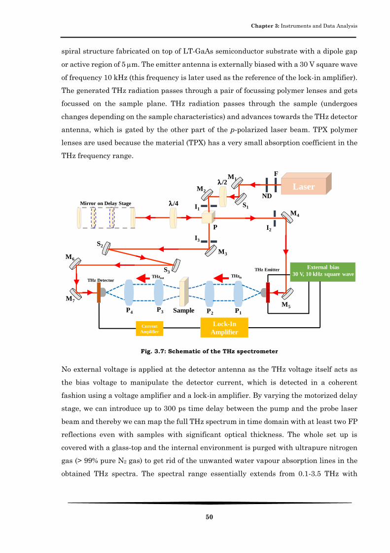
Chapter 3: Instruments and Data Analysis
50
spiral structure fabricated on top of LT-GaAs semiconductor substrate with a dipole gap
or active region of 5 m. The emitter antenna is externally biased with a 30 V square wave
of frequency 10 kHz (this frequency is later used as the reference of the lock-in amplifier).
The generated THz radiation passes through a pair of focussing polymer lenses and gets
focussed on the sample plane. THz radiation passes through the sample (undergoes
changes depending on the sample characteristics) and advances towards the THz detector
antenna, which is gated by the other part of the p-polarized laser beam. TPX polymer
lenses are used because the material (TPX) has a very small absorption coefficient in the
THz frequency range.
Fig. 3.7: Schematic of the THz spectrometer
No external voltage is applied at the detector antenna as the THz voltage itself acts as
the bias voltage to manipulate the detector current, which is detected in a coherent
fashion using a voltage amplifier and a lock-in amplifier. By varying the motorized delay
stage, we can introduce up to 300 ps time delay between the pump and the probe laser
beam and thereby we can map the full THz spectrum in time domain with at least two FP
reflections even with samples with significant optical thickness. The whole set up is
covered with a glass-top and the internal environment is purged with ultrapure nitrogen
gas (> 99% pure N2 gas) to get rid of the unwanted water vapour absorption lines in the
obtained THz spectra. The spectral range essentially extends from 0.1-3.5 THz with
External bias
30 V, 10 kHz square wave
Current
Amplifier
Lock-In
Amplifier
l/4
P
M1
M3
M2
S1
S2
S3
M6
M5
M4
M7
l/2
THz Emitter
THz Detector
P4 P3 P1P2
I3
I2
I1
ND
THzinTHzout
F
Sample
Mirror on Delay Stage
Laser

Chapter 3: Instruments and Data Analysis
51
highest S/N ratio of 50 dB at 0.4 THz which then reduces to 30 dB at 3.5 THz. 3.5 THz.
The schematic of the spectrometer is shown in Fig. 3.7.
Fig. 3.8: Optical image of the THz spectrometer
When a THz pulse is incident on a sample it undergoes an amplitude reduction
according to the absorption characteristics of the sample and a finite time shift with
respect to the THz radiation passing through air due to the finite optical thickness of the
sample. We analyze the transmission spectra of the sample to obtain the complex
refractive index of the sample using Fresnel’s transmission coefficient. The complex
dielectric function and the complex conductivity of the sample can be extracted from the
complex refractive index of the system. The optical image of the THz Spectrometer (Tera
K-8) is shown in Fig. 3.8.
3.1.14. Alignment of the Spectrometer
The THz spectrometer from Menlo systems is in general very stable and does not require
daily alignment. But, if the laser gates misaligned or if we need to change the emitter or
detector, we need to thoroughly align the THz spectrometer. The alignment procedure is
explained in detail in the following paragraph.
1. At first, we need to check the power of the fiber laser. Immediately after the
laser output head, we have a filter to block any unwanted 1560 nm laser output that might

Chapter 3: Instruments and Data Analysis
52
be present in the system. After removing this filter and the ND filter, we check the laser
power. The laser power is in general ~ 65 mW. After putting the filters, the laser power
should be 20 mW, which gets divided equally after the PBS in the two arms.
Fig. 3.9: Control panel of the FiberLaser software
So, both in the emitter and detector arm, lase power would be ~ 10 mW. The laser power
can be increased by optimizing the mode-lock state, but one should be careful that the
power does not exceed beyond 10 mW in any arms. If the laser is emitting, then it is in
the mode lock state. But, sometimes a new optimized mode-lock state increases the output
power of the laser. We can search for a new mode-lock state (only if the laser power at the
output is less than 60 mW) using the software namely FiberLaser associated with the
laser system. The basic window displays the laser power button, the mode-lock and the
temperature status. The position of the four waveplates can also be seen in the control
panel. The image of the control panel of this software is shown in Fig. 3.9. There are two
different mode-lock options; i) global mode lock search and ii) vicinity mode-lock search.
Global mode-lock search is the default process and it performs a wide search (rotate the
waveplates) and tries to reach a maximum waveplates combination and runs until a
Chapter 3: Instruments and Data Analysis
53
mode-lock state is found. In case of vicinity mode-lock search, all the waveplates move
together in a small range or the waveplates move inside the same range but one at a time.
Manual adjustment of the waveplates using the scroll bars is also possible but not
recommended. Memory bank remembers the position of waveplates for the last eight
mode-lock states and can be recalled. When the laser is turned on, the mode-lock search
tab and controls window is enabled, showing the current position of the waveplates and
using these controls it is possible to perform automatic mode lock search. The AC value
characterizes the quality of the mode-lock state and the DC value is proportional to the
average power in the fundamental wavelength of the laser. The optimized laser power can
be verified using the power meter and a qualitative idea can be obtained by checking the
higher AC and DC value provided by the software. Sometimes, it also happens that
although the laser power after P is ~ 20 mW, they are not evenly distributed along the
emitter and detector arm. Then we need to adjust the two wave plates (𝜆 2⁄ and 𝜆 4⁄ ) such
that the polarization state of the laser gets properly modified and hence the laser power
gets distributed evenly along the two arms.
2. After the laser power is optimized, we need to make sure that the laser pulse
passes through the three irises (I1, I2 and I3) by adjusting the mirrors M1, M2 and the
mirror attached at the delay stage.
3. Guiding by the lenses, both the pump and probe laser pulse are made to pass
through the view-pointer hanging in the THz emitter and detector holder (the emitter and
detector antenna is already removed). At first we block the probe beam and remove all
the TPX lenses (P1, P2, P3 and P4). The pump beam is made to go through the view-pointer
hanging at the front side (the side which faces the pump laser) of the THz emitter holder
and adjusted by using the M4 mirror (near adjustment). Then the view pointer is hanged
at the backside (the side which faces the incoming THz beam) of THz detector holder and
made to pass through it using the M5 mirror (far adjustment). This process is repeated
until the pump laser passes through the view-pointer hanging on THz emitter holder and
THz detector holder simultaneously. Similar procedure is applied to align the probe laser
beam (after blocking the pump laser beam) using M6 and M7 mirrors. Now, both the pump
and probe laser becomes parallel and coincides with each other and passes through the
view pointers.
4. Now THz antennas are inserted in the THz emitter and THz detector holders.
An infrared focussing lens is inserted on top of the antenna to focus the pump and probe

Chapter 3: Instruments and Data Analysis
54
laser beam at the antenna. Both the antenna and holder are similar in nature and design.
Silicon lenses are inserted at the front side of the antenna holders to guide THz waves
effectively and in a unidirectional way into the free space. The four TPX lenses are also
inserted between the two THz antennas to guide the generated THz wave to the detector
antenna.
5. Now we try to measure the photo current for THz emitter antenna. An external
bias voltage (20 V, d.c.) is applied at the antenna and moving the horizontal and vertical
displacement screws we try to make sure the laser pulse hits the dipole region. This part
is a bit tricky because the dipole active region is ~ 5 m2 and we don’t have any
illumination system so that we can view the laser pulse falling on the antenna structure.
Some metallic cross structures and concentric circles are therefore patterned on the
antenna structure (shown in Fig. 3.3). Whenever laser beam falls on these structures, it
reflects and the reflected beam can be viewed if we place a white card with a small hole
in the path of the laser beam. The laser beam passes through the hole and the reflected
beam falls on the white card. Thus seeing the reflection images, we get the idea about the
position of the laser pulse on the antenna and by moving the horizontal and vertical
screws, we coincide the dipole gap with the laser beam. When the laser beam falls near
the dipole region, the photo current suddenly increases and we maximize this
photocurrent. When the laser falls exactly at the dipole gap, a beautiful reflection pattern
can be seen which confirms the position of the dipole. Similar techniques are also used to
focus the probe laser beam on the THz detector antenna. The photo currents are in the
range 20-30 A (for both the antennas at 20 V bias) depending on the laser alignment.
6. Now, a bias voltage (30V, 10 kHz) is provided to the THz emitter antenna and
the detector antenna is attached with the current amplifier. A fast scan is performed to
find the zero delay position (position of the THz peak).
7. Now, the delay is kept fixed at the zero delay position and vibration generator
is started (channel 2 of the MiniDDS is ON and a sinusoidal voltage of 1V, 10 Hz is given)
so that the mirror moves slowly around the THz peak position, time is set at 100 s and
using an oscilloscope we can now view the THz pulse. If the pulse shape is distorted, it
means that THz radiation is not getting properly focused and is not unidirectional. This
can be rectified using the silicon lens position at the emitter and detector antenna and the
positon of the TPX lenses. Next, the THz peak to peak voltage is maximized using the
small movement of the lenses (M4, M5, M6 and M7) and the horizontal and vertical
displacement screws of the emitter and detector antennas. As we can directly observe the

Chapter 3: Instruments and Data Analysis
55
THz pulse in oscilloscope, this adjustment is relatively easy although time consuming.
Thus we can align the THz spectrometer. For a perfectly aligned setup, we get the
following parameters as listed in Table 1.
Table 1: Typical THz antenna parameters for an aligned THz spectrometer
Optical
Power at
each
antenna
DC Bias
Voltage
Emitter
Dark
Current
Detector
Dark
Current
Emitter
Photo
Current
Detector
Photo
Current
AC Bias
Voltage
THz
peak-to-
peak
amplitude
10 mW at
780 nm
20 V 0.3 A 0.3 A 30 A 26 A 30 V, 10
kHz
8 (a.u.)
Scanning Electron Microscopy
Scanning electron microscope (SEM) is a type of electron microscope that produces images
of a sample by scanning over it with a focused beam of electrons. The focused beam of
high-energy electrons generates a variety of signals at the surface of solid specimens. The
signals that derive from electron-sample interactions reveal information about the sample
including external morphology (texture), chemical composition, and crystalline structure
and orientation of materials making up the sample. Specimens can be observed in high
vacuum, low vacuum and in environmental SEM specimens can be observed in wet
conditions. The SEM is an instrument (schematic is shown in Fig. 3.10) that produces a
largely magnified image (magnification ranging from 20X to 30,000X) by using electrons
instead of light to form an image. A beam of electrons is produced at the top of the
microscope by an electron gun. The electron beam follows a vertical path through the
microscope, which is held within a vacuum. The beam travels through electromagnetic
fields and lenses, which focus the beam down toward the sample. When the primary
electron beam interacts with the sample, the electrons lose energy by repeated random
scattering and absorption within a teardrop-shaped volume of the specimen known as the
interaction volume, which extends from less than 100 nm to around 5 μm into the surface.
The size of the interaction volume depends on the electron's landing energy, the atomic
number of the specimen and the specimen's density. The energy exchange between the
electron beam and the sample results in the reflection of high-energy electrons by elastic

Chapter 3: Instruments and Data Analysis
56
scattering, emission of secondary electrons by inelastic scattering and the emission of
electromagnetic radiation, each of which can detected by specialized detectors.
Fig. 3.10: Schematic of scanning electron microscope
Accelerated electrons in an SEM carry significant amounts of kinetic energy, and this
energy is dissipated as a variety of signals produced by electron-sample interactions when
the incident electrons are decelerated in the solid sample. These signals include secondary
electrons (that produce SEM images), backscattered electrons (BSE), diffracted
backscattered electrons (EBSD that are used to determine crystal structures and
orientations of minerals), photons (characteristic X-rays that are used for elemental
analysis and continuum X-rays), visible light (cathodoluminescence, CL), and heat. This
is also schematically shown in Fig. 3.11. The secondary electrons are first collected by
attracting them towards an electrically biased grid at about +400 V, and then further
accelerated towards a phosphor or scintillator positively biased to about +2,000 V. The
accelerated secondary electrons are now sufficiently energetic to cause the scintillator to
emit flashes of light, which are conducted to a photomultiplier outside the SEM column
Electron Gun
Secondary ElectronDetector
Alignment Coils
Vacuum
StigmatorDeflection Coil
Condenser Lens 3
Specimen Chamber
Condenser Lens 2
Condenser Lens 1
Anode
Variable Aperture Holder
Variable Aperture Holder
Specimen onStage

Chapter 3: Instruments and Data Analysis
57
via a light pipe and a window in the wall of the specimen chamber. The amplified electrical
signal output by the photomultiplier is displayed as a 2D intensity distribution that can
be viewed and photographed on an analogue video display, or subjected to analog to digital
conversion and displayed and saved as a digital image. This process relies on a raster
scanned primary beam. The brightness of the signal depends on the number of secondary
electrons reaching the detector.
Secondary electrons and backscattered electrons are commonly used for imaging
samples: secondary electrons are most valuable for showing morphology and topography
on samples and backscattered electrons are most valuable for illustrating contrasts in
composition in multiphase samples (i.e. for rapid phase discrimination). X-ray generation
is produced by inelastic collisions of the incident electrons with electrons in discrete
orbitals (shells) of atoms in the sample. As the excited electrons return to lower energy
states, they yield X-rays that are of a fixed wavelength (that is related to the difference in
energy levels of electrons in different shells for a given element).
Fig. 3.11: Electron beam-sample interaction
Thus, characteristic X-rays are produced for each element in a mineral that is "excited"
by the electron beam. SEM analysis is considered to be "non-destructive"; that is, x-rays
generated by electron interactions do not lead to volume loss of the sample, so it is possible
to analyze the same materials repeatedly.
Because the SEM utilizes vacuum conditions and uses electrons to form an image,
special precautions must be taken to prepare the sample. In the present thesis, SEM is
used to characterize different types of CNT and their polymer composite films. All water
must be removed from the samples because the water would vaporize in the vacuum. All
Sample
Primary Backscattered ElectronsAtomic Number and
Topographical Information
Secondary ElectronsTopographical InformationAugur Electrons
Surface Sensitive Compositional Information
X-RaysThrough Thickness
Composition Information
Incident Beam
CathodoluminescenceElectrical Information

Chapter 3: Instruments and Data Analysis
58
metals are conductive and require no preparation before being used. Nanostructure
dispersion (in alcohol) are drop-casted on small piece (1 cm2) Si substrates and attached
with the sample holder. Flims or structured samples on Si substrates can also be
measured easily. All non-metals need to be made conductive by covering the sample with
a thin layer of gold conductive material using a "sputter coater".
Transmission Electron Microscopy
Transmission electron microscopy (TEM) is a microscopy technique whereby a beam of
electrons is transmitted through an ultra-thin specimen, interacting with the specimen
as it passes through. An image is formed from the interaction of the electrons transmitted
through the specimen. From the top down (schematically shown in Fig. 3.12), the TEM
consists of an emission source, which may be a tungsten filament, for tungsten, this will
be of the form of either a hairpin-style filament, or a small spike-shaped filament. By
connecting this gun to a high voltage source (typically ~ 100-300 kV) the gun will, given
sufficient current, begin to emit electrons by thermionic emission in vacuum. The upper
lenses of the TEM allow for the formation of the electron probe to the desired size and
location for later interaction with the sample. Manipulation of the electron beam is
performed using two physical effects.
1. The interaction of electrons with a magnetic field will cause electrons to move
according to the right hand rule, thus allowing for electromagnets for manipulating
electron beams. The use of magnetic fields allows for the formation of a magnetic lens of
variable focusing power, the lens shape originating due to the distribution of magnetic
flux.
2. Additionally, electrostatic fields can cause the electrons to be deflected through
a constant angle. Coupling of two deflections in opposing directions with a small
intermediate gap allows for the formation of a shift in the beam path, this being used in
TEM for beam shifting, subsequently this is extremely important to STEM.
The optical configuration of a TEM can be rapidly changed, unlike that for an
optical microscope, as lenses in the beam path can be enabled, have their strength
changed, or be disabled entirely simply via rapid electrical switching, the speed of which
is limited by effects such as the magnetic hysteresis of the lenses. The original form of
electron microscope, the TEM uses a high voltage electron beam to create an image. The
electrons are emitted by an electron gun, commonly fitted with a tungsten filament
cathode as the electron source.

Chapter 3: Instruments and Data Analysis
59
Fig. 3.12: Schematic of transmission electron microscope
When the electron beam transmits through the specimen, it carries information about the
structure of the specimen that is magnified by the objective lens system of the microscope.
The spatial variation in this information (the "image") is viewed by projecting the
magnified electron image onto a fluorescent viewing screen coated with a phosphor or
scintillator material such as zinc sulfide. The image can be photographically recorded by
exposing a photographic nanostructures or plate directly to the electron beam, or a high-
resolution phosphor may be coupled by means of a lens optical system or a fiber optic
light-guide to the sensor of a CCD (charge-coupled device) camera. The image detected by
the CCD may be displayed on a monitor or computer. Because the TEM utilizes vacuum
conditions and uses electrons to form an image, special preparations must be done to the
sample. All water must be removed from the samples because the water would vaporize
in the vacuum. In the present thesis, TEM is used to characterize different types of carbon
nanotubes and gold nanoparticles.
In general, very small amount of the sample is dispersed in ethanol and then
carefully drop casted (100-300 l) on a Cu mess (300 × 300). Then the Cu mess is kept
Electron Gun
Detector[ESD]
Specimen Chamber
Gas Inlet0-3000 Pa
Condenser Lens
Scan Coils
Objective Lens
Specimen Stage
Specimen Stub
Stigmator
Projection Aperture
10-2 Pa
10-4 Pa
10-5 Pa
20 Pa

Chapter 3: Instruments and Data Analysis
60
under normal bulb for 4-6 hours for drying. Slight increase in the sample concentration
will cause agglomerated particles or carbon nanotubes and we will not be able to spatially
resolute them. Specially designed finger tweezers have been used to handle the fine Cu
mess structures, because the use of normal tweezers can damage the mess easily due to
excessive pressure.
UV-Visible Spectrometer
When continuous radiation passes through a material, a portion of the radiation gets
absorbed depending on the absorption coefficient of the sample in the prescribed
frequency range. If such a situation occurs, the transmitted radiation has some gaps in
the electromagnetic spectrum which is called the absorption spectrum. In the case of
ultra-violate (UV)-visible spectroscopy, the absorption of electromagnetic radiation occurs
due to the transitions between lower energy electronic state to higher energy state. An
electronic transition of a molecule is always associated with both vibrational and
rotational transitions. So each electronic transition consists of a vast number of lines
spaced so closely that spectrophotometer cannot resolve them. Rather, the instrument
traces an ‘envelope’. That’s why the UV spectrum of a molecule usually consists of a broad
band centered near the wavelength of the major transition.
Regarding the extent of absorption of a molecule there is an empirical equation known as
Beer-Lambert law.
𝐴 = log10 (𝐼0𝐼⁄ ) = 𝜖𝑐𝑑 (29)
Where 𝐴 is the absorption, 𝐼0 is the intensity of light incident upon sample cell, 𝐼 is the
intensity of light leaving sample cell, 𝜖 is molar absorptivity, 𝑐 is the molar concentration
of solute and 𝑑 is the length of sample cell.
UV-visible absorption spectra were measured with Shimadzu UV-2450 in our lab
and the schematic ray diagram is shown in Fig. 3.13. It can measure absorption spectrum
from 190-1100 nm with a spectral resolution of 0.1 nm. A Deuterium light (D2) is used as
ultraviolet light source and tungsten light (W1) used as visible light source with a lamp
interchange wavelength of 290-370 nm. The monochromator used in this instrument
consist high performance blazed holographic diffraction grating; its role is to spread the
beam of light into its component wavelengths.
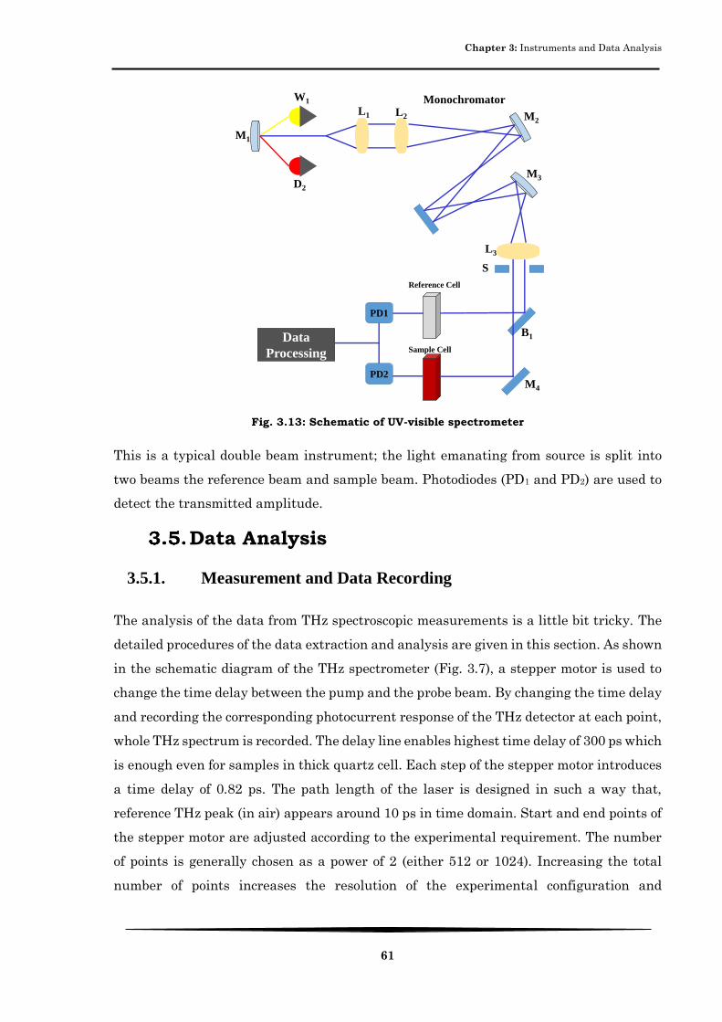
Chapter 3: Instruments and Data Analysis
61
Fig. 3.13: Schematic of UV-visible spectrometer
This is a typical double beam instrument; the light emanating from source is split into
two beams the reference beam and sample beam. Photodiodes (PD1 and PD2) are used to
detect the transmitted amplitude.
Data Analysis
3.5.1. Measurement and Data Recording
The analysis of the data from THz spectroscopic measurements is a little bit tricky. The
detailed procedures of the data extraction and analysis are given in this section. As shown
in the schematic diagram of the THz spectrometer (Fig. 3.7), a stepper motor is used to
change the time delay between the pump and the probe beam. By changing the time delay
and recording the corresponding photocurrent response of the THz detector at each point,
whole THz spectrum is recorded. The delay line enables highest time delay of 300 ps which
is enough even for samples in thick quartz cell. Each step of the stepper motor introduces
a time delay of 0.82 ps. The path length of the laser is designed in such a way that,
reference THz peak (in air) appears around 10 ps in time domain. Start and end points of
the stepper motor are adjusted according to the experimental requirement. The number
of points is generally chosen as a power of 2 (either 512 or 1024). Increasing the total
number of points increases the resolution of the experimental configuration and
Data
Processing
PD1
PD2M4
B1
M3
M2
M1
Reference Cell
Sample Cell
D2
L1
W1
S
L3
L2
Monochromator

Chapter 3: Instruments and Data Analysis
62
increasing number of point, increases the measurable highest frequency according to the
Fast Fourier Transform (FFT) theorem. The highest measurable frequency (𝑓𝑛) and
resolution (∆𝑓 = 𝑓𝑛+1 − 𝑓𝑛) of the setup depends on the total number of points (𝑛) and data
sampling (∆) according to the following equation.
𝑓𝑛 =𝑛
𝑁∆, 𝑛 = −
𝑁
2,… . ,
𝑁
2 (30)
The time constant is kept fixed at 100 ms during the experiment. It means that, the
stepper motor will wait for 100 ms at each point and the average photo-response of the
THz detector antenna will be recorded. An external bias voltage (30 V, 10 kHZ square
wave) is provided at the THz emitter antenna to excite THz radiation. The time constant
of the lock-in amplifier is kept three times (300 ms) than the time constant of the stepper
motor for better averaging of the measured data. A typical datasheet contains three
columns; i) first column gives provides the time domain data, ii) second column provides
the THz electric field and iii) third column provides the relative position of the delay line
(stepper motor) starting from zero. Reference spectra (air) and sample spectra are
recorded three times and for several positions of the sample to minimize the error.
3.5.2. Transmittance Calculation
The calculation of transmission is required for extracting different parameters like degree
of polarization (DOP), extinction ratio (ER) and shielding effectiveness (SE). First of all,
using FFT technique from time domain data is converted to the frequency domain data.
The FFT spectra consists of frequency, FFT amplitude and phase. The transmittance of a
sample is calculated using the following formula;
𝑇(𝜔) = |�̃�𝑠𝑎𝑚𝑝𝑙𝑒(𝜔)
�̃�𝑟𝑒𝑓𝑒𝑟𝑒𝑛𝑐𝑒(𝜔)|
2
, (31)
where, �̃�𝑠𝑎𝑚𝑝𝑙𝑒(𝜔) and �̃�𝑟𝑒𝑓𝑒𝑟𝑒𝑛𝑐𝑒(𝜔) are the complex THz field passing through sample
and reference. Transmittance have been usually calculated using Origin Software or
MATLAB programming. A typical matlab code is given in the appendices.
3.5.3. Optical Parameter Extraction
A commercial software namely teralyzer is used to calculate the optical parameters
(complex refractive index and complex dielectric function) of the samples in the
corresponding frequency range. We will only discuss the required theories for complex

Chapter 3: Instruments and Data Analysis
63
optical parameter extraction for single layered films. The theoretical background of the
software is based on various literatures, some of which are briefly described below.
Duvillaret et al.[111] presented a novel method for improving the determination of optical
constants in THz-TDS. This method, which could be applied to any material of low
absorption, could be used to determine the thickness of the sample with accuracy better
than 1%. They minimized the error in determination of optical constants by the accurate
measurement of sample thickness. They obtained the refractive index with enhanced
precision (~ ∆𝑛 ≈ 10−2 for a sample thickness of ~ 1 mm). They concluded that their
method could be applied not only to THz-TDS but also to any kind of optical constant
measurement in the time domain. Dorney et al.[112] presented a robust algorithm for
extracting material parameters from measured THz waveforms. Their algorithm
simultaneously obtained both the thickness and the complex refractive index of an
unknown sample under certain conditions. Most spectroscopic transmission
measurements required the knowledge of the sample’s thickness for an accurate
determination of its optical parameters. Their approach relied on a model-based
estimation, a gradient descent search, and the total variation measure. They explored the
limits of their technique and compared the results with literature data for optical
parameters of several different materials. Pupeza et al.[113] tried to improve the existing
data extraction algorithms for THz-TDS in two aspects. They merged the up-to-date
knowledge of THz-TDS signal processing into a single powerful optical material
parameter extraction algorithm and also introduced a novel iterative algorithm that
further enhanced the accuracy of the parameter extraction. They were able to reliably
investigate samples with thicknesses as small as 100 μm, samples with low indexes of
refraction, i.e. close to 1, as well as samples with sharp peaks in the material parameter
curves. Scheller et al.[114] proposed a method for the extraction of material parameter
and thickness information from sub-100-μm thin samples using non-differential
transmission THz-TDS. Their approach relied on an additional Fourier transform of the
frequency dependent material parameters to a quasi-space regime. By iterative
minimization of the discrete peaks arising due to periodic FP oscillations, the highly
precise thickness information along with the refractive index and absorption coefficient
of the sample was extracted. Experimental verification of the approach was also provided.
We need to acquaint with some of the terminologies used in the algorithm as well as in
the abovementioned studies described below.

Chapter 3: Instruments and Data Analysis
64
Fabry-Perot (FP) Oscillation
When a THz electromagnetic pulse passes through a material a significant amount
(depending on the absorption coefficient of the sample in the corresponding frequency
range) of the THz radiation transmits but some part of the radiation reflects from the 2nd
surface of the sample. This reflected radiation traverses through the sample backwards
and then again reflects from the 1st surface and traverses in forward direction. The
abovementioned process is repeated until the radiation dies down. This causes multiple
peaks in the transmitted THz pulse which is called FP oscillation. These FP oscillation
causes ripples in the measured optical constants if the thickness of the sample is not
calculated accurately.
Fig. 3.14: Appearance of the Fabry-Perot oscillation peak
For successful determination of the optical constant, we need to get rid of this unwanted
ripples in the frequency dependent optical constants of the sample. If the sample is thin
and low absorptive in nature, the FP oscillation coincides with the main transmitted THz
pulse and hence becomes difficult to extract optical parameters. The appearance of the FP
oscillations in case of a silicon substrate is shown in the following figure. The 2nd and 3rd
transmitted THz peak as shown in Fig. 3.14 is called the FP oscillation peak while the 1st
THz peak is the main transmitted THz radiation.
Dynamic Range
Dynamic range is the difference between the smallest and largest usable signal
through a transmission or processing chain or storage medium. It is measured as a ratio,
0 10 20 30 40
-1
0
1
2
3 Silicon Substrate
Ele
ctr
ic F
ield
(a.u
)
Time(ps)air Silicon air
1st peak
2nd peak
3rd peak

Chapter 3: Instruments and Data Analysis
65
or as a base-10 (decibel) logarithmic value. The noise floor of the THz spectrometer that
we have used in all my works is shown in Fig. 3.15.
Fig. 3.15: Noise floor and cut-off frequency
As rightfully described by Jepson et al.[115], owing to the typical single-cycle nature of
the THz pulse, the corresponding frequency spectrum extends from the low GHz to several
THz. At high frequencies the spectrum is characterized by a gradual roll-off, until the
detected signal level approaches that of the noise floor of the experiment. The noise floor
is normally independent of frequency and corresponds to the spectrum recorded with a
completely blocked THz beam path. The origin of this noise is of an electronic nature,
whereas fluctuations of the THz signal itself are caused mainly by laser intensity
fluctuations.
Nelder-Mead Simplex Algorithm
It is a renowned optimization technique used by various scientist in different fields
of research. It is a simplex method for finding a local minimum of a function of several
variables which has been devised by Nelder and Mead in 1965[116]. For two variables, a
simplex is a triangle, and the method is a pattern search that compares function values
at the three vertices of a triangle. The worst vertex, where 𝑓 (𝑥, 𝑦) is largest, is rejected
and replaced with a new vertex. A new triangle is formed and the search is continued.
The process generates a sequence of triangles (which might have different shapes), for
which the function values at the vertices get smaller and smaller. The size of the triangles
is reduced and the coordinates of the minimum point are found. The algorithm is stated
0 1 2 3 4 5 6
1E-5
1E-4
1E-3
0.01
Cut-off Frequency
Frequency (THz)
TH
z A
mp
litude (
a.u
.)
Noise Floor

Chapter 3: Instruments and Data Analysis
66
using the term simplex (a generalized triangle in N dimensions) and will find the
minimum of a function of N variables. It is effective and computationally compact.
A reference pulse with an empty THz-TDS system and a sample pulse with the
sample in the THz beam path are measured. The ratio of the corresponding Fourier
spectra yields the measured transfer function as given below,
𝐻𝑚𝑒𝑎𝑠(𝜔) = |�̃�𝑠𝑎𝑚𝑝𝑙𝑒
�̃�𝑟𝑒𝑓𝑒𝑟𝑒𝑛𝑐𝑒|. (32)
In case of a single layer sample, the theoretical transfer function takes the following form,
𝐻𝑡ℎ𝑒𝑜𝑟𝑦(𝜔) = (1 − 𝑟2)𝑒−𝑖(�̃�−1)𝑘0∆. ∑(𝑟2𝑒−𝑖2�̃�𝑘0∆)𝑚
𝑀
𝑚=0
, (33)
where, 𝑟 is Fresnel reflection coefficient, 𝑘0 is the free-space wave number, 𝑐0 is the speed
of light in vacuum, is the thickness of the sample, �̃� is the complex index of refraction
and 𝑚 is the number of echo pulses included in the corresponding measured transfer
function accounting for the limited length of the measurement time window. The
difference between the measured and the theoretical transfer function was minimized
using an implementation of the Nelder-Mead simplex algorithm. The thickness of the
sample is determined by superimposing the FP oscillations on the refractive index data.
These oscillations are the results of FP oscillation pulses which are included in the time
window of the measurement and should disappear at the correct sample thickness. For
analysing the FP oscillations two approaches are employed: The first one is the quasi-
space (QS) method. Here, a Fourier transform of the frequency dependent refractive index
and the frequency dependent extinction coefficient is performed so that the sinusoidal FP
oscillations result in a distinct peak. By minimizing this peak, the correct thickness is
determined and the correct complex refractive index of the sample is obtained. As second
approach, the total-variation (TV) method is employed. The TV denotes the total variation
of the neighbouring values of the refractive index and the extinction coefficient. The FP-
oscillations will result in an increased TV value. However, since all variations are
considered, also absorption peaks and noise induced features will result in a high TV.
Thus, in most cases the QS-approach is the method of choice for analysing the thickness,
especially for samples that are thinner than 500 µm as the TV method starts to fail for
very thin samples. For relatively thick samples in the range of several tens of mm, the TV
approach perform better. The reason for that is that the TV method also works if the FP
oscillation period is close to the frequency resolution of the measurement. The FP
Chapter 3: Instruments and Data Analysis
67
oscillation pulses are essential for employing the thickness determination feature of the
TeraLyzer software. One has to be careful that the chosen time window of the
measurement includes at least one of these oscillation pulses. One can estimate the
necessary length of the time window by considering the time difference between the FP
oscillation and the pulse that propagates directly through the sample,
∆𝑇𝐹𝑃 =2𝑛∆
𝑐0. (34)
Keeping in mind that the first FP oscillation is delayed by 𝑇𝐹𝑃 in respect to the directly
transmitted sample pulse, a too short time window will compromise the thickness
extraction process. As rule of thumb, it is advisable to choose a time window that includes
at least one FP oscillation. In this case, the frequency resolution of the measurement will
be sufficient to be enabled for a reliable thickness determination. The second important
parameter is the bandwidth of the measurement. The time difference between the FP
oscillations is the inverse of the FP oscillation period 𝐹𝐹𝑃:
∆𝐹𝐹𝑃 =𝑐02𝑛∆
. (35)
To analyze the perturbing FP oscillations, it is necessary that the extracted material
parameters comprise at least a single complete FP period. That means the bandwidth of
the measurement has to be larger than 𝐹𝐹𝑃. The difference 𝐷 between the measured and
theoretical transfer function is minimized by Nelder-Mead algorithm based code.
𝐷 = 𝐻𝑡ℎ𝑒𝑜𝑟𝑦 −𝐻𝑚𝑒𝑎𝑠 (36)
The optimized complex refractive index �̃�(𝜔) is extracted. From the complex refractive
index all the required optical functions are measured according to the following relation
as described below;
�̃�(𝜔) = 𝑛(𝜔) + 𝑖𝑘(𝜔), (37)
휀̃(𝜔) = �̃�2(𝜔) = (𝑛2(𝜔) − 𝑘2(𝜔)) + 𝑖2𝑛(𝜔)𝑘(𝜔) =
휀𝑟𝑒𝑎𝑙(𝜔) + 𝑖휀𝑖𝑚𝑎(𝜔). (38)
It is essential to notice that the extracted material parameters are just valid in the
range of the confidence interval of the measurement. That means within this interval
there is no evidential truth which value is the real physical one but depending on the
chosen width of the confidence interval there is a given probability that the true value lies
within its borders.

Chapter Four

Chapter 4: Terahertz Polarizer
69
4. Terahertz Polarizer
Introduction
With the advent of new compact devices for generating and detecting high power THz
radiation[117, 118] and the simultaneous advancement in bridging the THz gap[119], the
application of THz spectroscopy has increased by leaps and bounds in various fields of
research[33, 120-126]. With such a dramatic advancement comes the great demand of
high quality quasi-optic components like phase shifters, filters, polarizers, etc. efficiently
working in the THz frequency range.
Fig. 4.1: Schematic of the working procedure of the THz polarizer
For several applications like THz ellipsometry[127-130] polarizers are the most important
optical components as the accuracy of these measurements strongly depends on the
polarization degree of the electromagnetic waves. Although some efforts have already
been made in the realization of THz polarizers, preparation of a high performance, robust,
durable, and cheap THz polarizer remains a challenging job.
THz in THz out
THz Polarizer Sample
00
900
THz
Polarization Direction

Chapter 4: Terahertz Polarizer
70
In the present chapter, we explore the idea of using aligned magnetic
nanostructures (nickel nanoparticles and nickel nanochains) in PVA matrix as a potential
robust polarizer in the THz frequency range. The novelty of the work lies on the simple
preparation procedure as well as the robustness and durability of the so obtained
polarizer. The schematic of the project studied in this chapter is pictorially depicted in
Fig. 4.1. The work presented in this chapter is largely based on our published paper[6].
Background Study
There are mainly two types of polarizers available in the present literatures; i) wire-grid
type reflective polarizer (WGP) and ii) aligned nanotube absorptive polarizer, while some
scattered efforts have also been made in other types of polarizers like i) nematic crystal
polarizer, ii) brewster angle polarizer, but with severe limitation either in frequency
bandwidth or incident angel of THz radiation.
Table 2: Advantages and disadvantages of different types of polarizers
Types of Polarizer Advantages Disadvantages
Wire-grid Polarizer High Degree of Polarization
High Extinction Ratio
Complicated Preparation Technique
(Lithography, Nano-imprinting Technique)
Multiple internal reflection
Nematic Crystal
Polarizer
High Degree of Polarization
High Extinction Ratio
Works in a limited frequency and temperature
range
Complicated preparation technique
Brewester angle
Polarizer
High DOP in a limited
frequency window
Limited range of THz incident angel
Aligned Carbon
Nanotube
High DOP over a large
frequency range
Costly Preparation, Small Extinction Ratio,
Careful Handling of the sample
Depending on the effect of substrate it can also be divided into two groups namely i) back
substrate polarizer (BSP) and ii) free standing polarizer (FSP). Compared with FSP, BSP
requires a substrate as a mechanical backup to sustain the shape of the metal wire or
stripes. Commercially available wire-grid FSPs usually have large apertures, high ER,
and high DOP. However, such FSPs require a tedious, labour intensive coil-winding
manufacturing process[131]. Though BSP type wire-grid polarizers offer comparable

Chapter 4: Terahertz Polarizer
71
extinction ratio to the FSP polarizers, they also introduced FP reflection in the
transmitted THz signal due to high refractive index and finite width of the substrate. The
advantages and disadvantages of the different types of polarizers are given below in the
Table 2.
4.2.1. Wire Grid THz Polarizer
This type of polarizer is the oldest among all the THz polarizers available. They can be
both FSP and BSP types. FSPs are even commercially available in the market. BSPs are
basically lithographically patterned metallic stripes on high resistive silicon or quartz
substrates. The width and spacing of the structure, thickness of the metallic layer
determines the DOP, ER and the frequency bandwidth of the device. Yamada et al.[8]
fabricated aluminium WGP with a grating constant of 3 mm on Si substrate and
demonstrated an ER of ~ 23 dB in the frequency range of 0.5-3 THz. Young et al.[8]
fabricated THz WGP and THz band-pass filter devices on high-density polyethylene
substrates using simple photolithographic fabrication technique. They had successfully
demonstrated the use of standard fabrication techniques to produce large-aperture free-
standing THz optical devices on low-absorption polymer materials with the advantage of
low cost using a simple fabrication process. The fabricated polarizer had better than 30
dB ER at 3 THz. Band-pass filters were demonstrated at three different centre frequencies
(1.5, 1.8, 2.9 THz) with a 3 dB insertion loss. Sun et al.[132] proposed a layout for high
ER polarizer which was composed two dense metal wire gratings separated in parallel
and by numerical analysis they showed very high ER (~ 180 dB) in the frequency range
of 0.3-3 THz. Deng et al.[133] experimentally verified the idea proposed by Sun et al. and
they prepared a bilayer WGP by UV-lithography, one step etching and metal
decomposition process and showed an ER of ~ 70 dB in the frequency range of 0.5-3 THz.
Shiraishi et al.[134] reported a simple, robust, and large-aperture polarizer that utilizes
thin metal-film gratings with sinusoidal or triangular cross section profile. The calculated
ER using numerical simulation between the TM- and TE-waves for a 50 nm-thick gold
film grating (period = height = 30 m) on a tsurupica resin substrate was greater than 60
dB for the frequency range of 0.5-3 THz. Furthermore, the polarizer was shown to have
high tolerance to deviations in structural parameters and input angle. The polarizer with
a 25 nm-thick gold-film triangular grating (period = 25 m, height = 40 m) was fabricated
using a simple mechanical fabrication method. The measured transmission loss for the
TE-waves was greater than 50 dB while the corresponding transmission loss for the TM-
Chapter 4: Terahertz Polarizer
72
waves was lower than 1 dB in the frequency range of 1.0-2.5 THz. Cetnar et al.[135]
designed a THz polarizer based on aluminium stripes on polycarbonate substrate and by
varying the separation of the structures they achieved variable ER as high as ~ 40 dB in
the frequency range of 100-550 GHz. Huang et al.[131] prepared a single layer WGP of
alumunium deposited on a thin layer of SiO2 supported by a Si substrate and coated the
metallic layer with polymer to get rid of the FP reflections in similar WGPs. Their
structure offered a high ER and very low insertion loss in the frequency range of 0.2-2
THz. Berry et al.[136] reported the design and experimental characterization of a PBS
based on a sub-wavelength metallic grating fabricated on a high density polyethylene
(HDPE) substrate. The THz polarizing beam splitter consisted of a silver grating on a
HDPE substrate. The grating consisted of 2 μm thick, 12 μm wide silver lines with 20 μm
periodicity. When placed at an oblique angle relative to an incident THz beam, TE
polarization was reflected while TM polarization was found to be transmitted. Their
device offered less than 0.3 dB transmission loss over 0.1-2 THz, and ERs of 21 dB and 16
dB at 0.5 THz and 1 THz, respectively. Das et al.[137] studied the performance of a
polarizer prepared by inkjet printing method. Short length CNF stripes were printed on
marlyn film with a width and separation of 100 μm each and they found a promising DOP
of ~ 0.32 in the frequency range of 0.57 THz to 0.63 THz and concluded that DOP and ER
can be increased by decreasing the width and separation of the structure. Grady et al.[138]
showed that polarization of reflected THz beam could be rotated by 900 (s to p polarization)
in the frequency range of 0.7-1.9 THz by using a gold ground plane and gold cut wires
aligned 450 with respect to the incident THz polarization separated by a dielectric spacer.
Hunag et al.[139] proposed a tuneable bilayer aluminium wire-grid structure on thin
silica layer by micro-fabrication technique working in the frequency range of 0.2-2.0 THz.
They achieved ER ~ 50 dB and transmission loss < 1 dB in the frequency range of interest.
4.2.2. Aligned Carbon Nanotube Polarizer
Anisotropic one dimensional conduction properties of CNTs has recently been deployed in
manufacturing prototype polarizer devices working in THz frequency range although the
anisotropic conduction of aligned CNT in THz frequency range had been experimentally
demonstrated almost ten years back by Jeon et al.[140]. Ren et. al.[3] first experimentally
observed the excellent polarizing properties of aligned CNT structures. Vertically aligned
SWNTs were grown on silicon substrate using a CVD technique and then they were
efficiently transferred onto a sapphire substrate. Polarization dependent THz

Chapter 4: Terahertz Polarizer
73
transmission measurements were performed on both the SWNT film sample on a sapphire
substrate and a reference sapphire sample with the same thickness as the sample
substrate. The symmetry axis of the structure was rotated corresponding to the
polarization axis of the THz radiation and the corresponding transmitted signal was
recorded. For perpendicular orientation of the sample (θ = 90°), there was virtually no
interaction (THz absorption). For parallel orientation (θ = 0°), transmitted THz signal was
found to be the smallest dictating strongest interaction and highest THz conductivity in
this orientation. The measured DOP was ~ 1, while the measured reduced linear
dichroism (LDr) was ~ 3, corresponding to an order parameter of 1 in the frequency range
of 0.1-1.8 THz. Kyoung et al.[4] studied the polarizing performance of micro-meter thick
freestanding CNT polarizer excellently working in the frequency range of 0.1-2.0 THz. A
MWNT forest was deposited using CVD technique and then using a motorized coil-
winding process freestanding MWNT polarizer was prepared using a polyethylene
support. DOP was found to be 0.999 and ER ~ 37 dB in the measured frequency range.
Ren et. al.[5] had showed excellent polarizing behaviour of aligned SWNT polarizer using
multilayer stacks of aligned SWNT in the frequency range of 0.4-2.2 THz. Fragouli et
al.[141] decorated the surface walls of CNFs and then dispersed them in polymer matrix
in the presence of external magnetic field thereby aligning the CNFs. Besides, anisotropic
magnetic and electric properties, the aligned CNFs showed anisotropic THz transmission
in the frequency range of 570-630 GHz and a DOP ~ 0.5 was found in the measured
frequency range.
4.2.3. Other types of Polarizers
Some other types of THz polarizers and wave plates has also been demonstrated in recent
past. Hirota et al.[142] fabricated a four-contact PC antenna, which has four metal
contacts on a LT-GaAs substrate by a standard photolithographic and chemical etching
method. By rotating the bias voltages by 900, the polarization direction of THz radiation
was alternated between the +450 and −450 direction at a rate of more than several kHz.
These linearly polarized THz radiations were converted to circularly polarized radiations
by using the total reflection within a high-resistivity Si prism; the s polarized component
of electromagnetic radiation was phase-retarded against p polarized one by the total
reflection and its phase-shift depends on the reflection angle. The internal reflection angle
of the Si prism was designed to give rise to a 𝜋/2 phase-shift so that the linearly polarized
radiations at +450 becomes left-handed circularly polarized radiations, and, in the same

Chapter 4: Terahertz Polarizer
74
way, the ones at −450 become right-handed circularly polarized radiations. Thus using the
combination of a four-contact PC antenna and a Si prism, they had built a broadband,
circularly polarized THz radiation source and modulator. Masson et al.[7] prepared an
achromatic THz quarter wave plate by precisely stacking six birefringent quartz plates.
The de-phasing was found to be in the range of 900 ± 3% in the broad frequency range of
0.25-1.75 THz. A Feussner-type THz polarizer with a nematic liquid crystal (NLC) layer
between two fused-silica prisms was demonstrated[143]. The DOP and ER of the polarizer
exceeded 0.99 and 10-5, respectively in the frequency range of 0.3-1.0 THz. NLC was
introduced in a rectangular parallelepiped space in a fused silica crystal and external
magnetic field is used to align the NLC. Wojdyla et al.[144] demonstrated the performance
of a THz linear polarizer made from a stack of silicon wafers at aligned at the Brewsters
angel. Using four industrial grade silicon wafers they obtained a power 𝐸𝑅 > 6 × 10³ in
the frequency range of interest. Scherger et al.[145] prepared a low-cost THz wave plate
based on the birefringence of normal paper/air gaps working in 100-450 GHz frequency
range. The performance of the device as an efficient half-wave plate was shown at 244
GHz. Cong et al.[146] discovered a unique approach to efficiently rotate the polarization
state of incoming THz radiation by using a tri-layer meta-surface. Three sets of metallic
gratings were separated by a dielectric spacer and the axis of the gratings were rotated
with the previous by 450. The device was tailored to rotate the polarization axis of a
linearly polarized terahertz wave by any desired angle, especially to the orthogonal
direction, and the rotation occurred with a high power conversion efficiency of about 85%
at a broadband frequency. The FP interference theory explained the underlying
mechanism of the ultrahigh transmittance.
Basic Theory
The performance of a polarizer is depicted by its DOP, which is defined as the amount of
a particular type of polarization present in the transmitted radiation if unpolarised
radiation passes through the polarizer and the ER, which is defined as the ratio of
transmittance of a plane polarized radiation when the polarizer axis is placed in parallel
and perpendicular orientation with respect to the incident polarization direction. The
DOP is calculated as,
𝐷𝑂𝑃 = 𝐴00 − 𝐴900 𝐴00 + 𝐴900
, 𝐴00(900) = − log10 (𝑇00(900)) , (39)

Chapter 4: Terahertz Polarizer
75
where 𝐴00(900), 𝑎𝑛𝑑 𝑇00(900) are the absorbance and transmittance in parallel and
perpendicular orientations, respectively and the ER is defined as;
𝐸𝑅(𝜔) = −10 log10 (𝑇00
𝑇900) in dB. (40)
A simple MATLAB code as described in the appendices is used to extract the necessary
parameters required to describe a THz polarizer.
Sample Preparation
Nickel nanoparticles (NiNP) and nickel nanochains (NiNC) were prepared by a simple
chemical route. Nickel chloride salt was reduced by hydrazine hydrate in the ethylene
glycol (EG) matrix in the presence of sodium hydroxide.
Fig. 4.2: Schematic of nickel nanostructure preparation
EG provided the spherical structure of the nanoparticles while diameter of the NiNP were
optimized by concentration of the reactants and the reaction environment. Nickel chloride
(NiCl2,6H2O; Merck) was reduced by hydrazine hydrate (N2H5OH; Merck) in ehtylene
glycol (HO-CH2-CH2-OH; Merck) environment (provides the spherical shape of the
nanostructures) at ~ 80 0C by vigorous magnetic stirring in presence of sodium hydroxide
(NaOH; Merck), which controled the length of the nanostructures (important in the
preperation of NiNC). The colour of the solution progressively turned green to violet to
black indicating the formation of nickel nanostructures. The collected nanostructures
were washed throughly with ethanol (CH2-CH-OH; Merck) and de-ionized (DI) water
(Millipore) and then seperated magnetically prior to further use. The nanostructures were
anisotropically dispersed in polymer solution in presence of external magnetic field to
align them along the magnetic field lines for the preparation of a wire grid like structure.
The main idea behind preparing these two structures are to create nanostructures with
0.9 M N2H5OH + Required amount of
NaOHis added
2
45 mM NiCl2
in Ethylene Glycol
1
Formation of NiNP/NiNC
3

Chapter 4: Terahertz Polarizer
76
drastically different magnetic anisotropy so that they can be aligned differently using
optimized external magnetic field.
Fig. 4.3: Schematic of magnetic alignment of nickel nanostructures
1 g PVA is dissolved in 10 ml DI water, freshly prepared NiNP (NiNC) are mixed with it
and ultrasonicated for 15 minutes. The solution is then poured it in a Petri dish for slow
drying process and placed in external magnetic field of ~ 6 kOe for NiNP (300 Oe for
NiNC) to align the NiNP (NiNC) inside the polymer matrix and then slow drying of the
liquefied polymer. The schematic of the magnetic alignment procedure of the chemically
synthesized nickel nanostructures in polymer matrix is shown in Fig. 4.3.
Table 3: Reactants for preparation of nickel nanostructures and the THz polarizer
Reactants or External Perturbations Amount
Ethylene Glycol Required Amount
Nickel Chloride 45 mM
Hydrazine Hydrate 0.9 M
Sodium Hydroxide 0.1 M for NiNPs and 0.15 M for NiNCs
Temperature while stirring 80 0C
Poly-Vinyl Alcohol 1 g
00900
N S
Nickel Nanostructures
in Polymer Matrix

Chapter 4: Terahertz Polarizer
77
Two opposite poles of bar magnets are kept in a structured groove in thermocol and the
Petri dish containing the nickel nanostructures immersed in liquefied PVA is kept in the
middle point of these two bar magnets. The magnitude of the magnetic field is varied by
changing the distance between the bar magnets and their strength. PVA has been used
as the matrix because of the twofold reason; i) it has an uncharacteristic optical response
in the THz frequency range (n ~ 1.8 and = 40 cm-1 at 1 THz) and ii) it provides robustness
to the polarizer[8, 147, 148]. The concentration of the different reactants required for the
preparation of the nickel nanostructures and the aligned THz polarizer are given in Table
3.
Measurement and Analysis
SEM imges in Fig. 4.4 show that the average diameter of the NiNP are ~ 165 nm and the
average diameter and length of NiNC are ~ 300 nm and ~ 4 m, respectively. The NiNPs
are shperical in structure as seen in the image and the NiNCs seems to be formed by
adding the individual NPs in a chain like fashion. The chemical purity of the samples
have been confirmed using EDX study (not shown here). The optical image of both the
NiNP and NiNC THz polarizer structure is given in Fig. 4.5. The anisotropy of the
chemically synthesized NiNC are much larger than the NiNC due to the structure or
shape anisotropy of the sample and we have also optimized the external magnetic field
(for nickel nanostructure alignment) and thus we have efficiently changed the structure
constants (width and separation of the structure). The average width of the aligned NiNP
and NiNC structures are 40 and 90 m respectively and the corresponding average
separations are 170 and 80 m.
Fig. 4.4: SEM images of the chemically synthesized (a) NiNPs and (b) NiNCs
(a)
3 m
(b)
5 m

Chapter 4: Terahertz Polarizer
78
Width of the structure increases with increasing anisotropy and decreasing external
magnetic field (for the case of NiNC polarizer) due to higher cohesion energy of longer
wire like structures and the separation decreases due to weaker magnetic field.
Fig. 4.5: Optical image of the a) NiNP and b) NiNC THz polarizer
The use of the word ‘average’ is important because the width and separation may be varied
due to various reasons like i) non-uniformity of the external magnetic field, ii) non-
uniform size of the nanostructures, iii) thermal fluctuations in the polymer matrix, iv)
misalignment of the polymer matrix plane with that of the external magnetic field. So, we
have analysed several images and then calculated an average measurement. The
thickness of the NiNC and NiNP THz polarizers are 210 ± 30 and 300 ± 30 m respectively
and bare PVA films of similar thicknesses are also prepared for reference measurements.
THz measurements were carried out in a commercial THz spectrophotometer
(TERA K8, Menlo Systems) at room temperature in transmission geometry (details given
Chapter 3). A 780 nm Er doped fiber laser having pulse width of < 100 fs and repetition
rate ~ 100 MHz is used to excite a dipolar type PC antenna which produces a THz
radiation having bandwidth up to 2.5 THz (< 50 dB). The radiation transmitted through
the sample was then focused on a similar antenna and detected coherently. The frequency
dependent power and phase of the transmitted pulse was obtained using Fourier analysis
of the measured electric field amplitude. Polarization of THz pulse depends on the pump
500 m500 m
a) b)
500 m500 m
a) b)
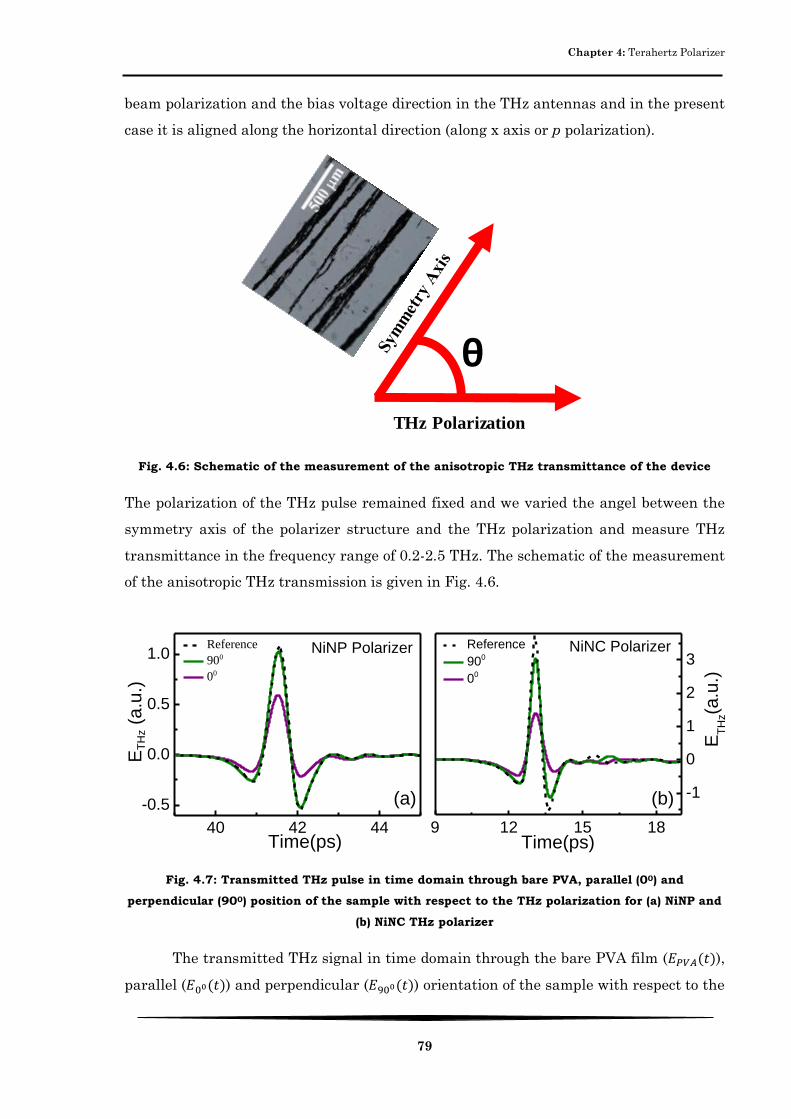
Chapter 4: Terahertz Polarizer
79
beam polarization and the bias voltage direction in the THz antennas and in the present
case it is aligned along the horizontal direction (along x axis or p polarization).
Fig. 4.6: Schematic of the measurement of the anisotropic THz transmittance of the device
The polarization of the THz pulse remained fixed and we varied the angel between the
symmetry axis of the polarizer structure and the THz polarization and measure THz
transmittance in the frequency range of 0.2-2.5 THz. The schematic of the measurement
of the anisotropic THz transmission is given in Fig. 4.6.
Fig. 4.7: Transmitted THz pulse in time domain through bare PVA, parallel (00) and
perpendicular (900) position of the sample with respect to the THz polarization for (a) NiNP and
(b) NiNC THz polarizer
The transmitted THz signal in time domain through the bare PVA film (𝐸𝑃𝑉𝐴(𝑡)),
parallel (𝐸00(𝑡)) and perpendicular (𝐸900(𝑡)) orientation of the sample with respect to the
θ
THz Polarization
9 12 15 18
-1
0
1
2
3
Reference
900
00
Time(ps)
ET
Hz(a
.u.)
NiNC Polarizer
(b)
40 42 44
-0.5
0.0
0.5
1.0
Reference
900
00
Time(ps)
ET
Hz (
a.u
.)
NiNP Polarizer
(a)

Chapter 4: Terahertz Polarizer
80
THz polarization is shown in Fig. 4.7 for both the polarizers. In perpendicular
configuration transmitted pulse is almost identical with the bare PVA film for both the
cases indicating very small interaction of THz photons with the free electrons in the
system. However, if we analyze NiNP and NiNC polarizer, the transmittance (in
perpendicular orientation) is smaller in NiNC polarizer (as shown in Fig. 4.8). This is due
to the increased width of the NiNC structure which allows more interaction with the
horizontally polarized THz photons with the free electrons of the system.
Fig. 4.8: THz transmittance for different angel of rotation for (a) NiNP and (b) NiNC polarizer
If we consider �̃�𝑃𝑉𝐴(𝜔), �̃�00(𝜔), and �̃�900(𝜔) as the frequency domain complex transmitted
THz signal in frequency domain through bare PVA, parallel and perpendicular
orientation of the sample, then the transmittance is calculated as 𝑇𝜃(𝜔) = |�̃�𝜃0(𝜔)
�̃�𝑃𝑉𝐴(𝜔)|2
;
0.3 0.6 0.9 1.2 1.5
0.0
0.4
0.8
1.2 T_900
T_600
T_300
T_00
Tra
nsm
itta
nce
(a) NiNP
0.5 1.0 1.5 2.0
0.0
0.4
0.8
1.2
T_900
T_600
T_300
T_00
Frequency (THz)
(b)
Tra
nsm
itta
nce
NiNC
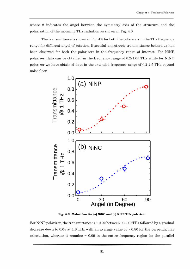
Chapter 4: Terahertz Polarizer
81
where 𝜃 indicates the angel between the symmetry axis of the structure and the
polarization of the incoming THz radiation as shown in Fig. 4.6.
The transmittance is shown in Fig. 4.8 for both the polarizers in the THz frequency
range for different angel of rotation. Beautiful anisotropic transmittance behaviour has
been observed for both the polarizers in the frequency range of interest. For NiNP
polarizer, data can be obtained in the frequency range of 0.2-1.65 THz while for NiNC
polarizer we have obtained data in the extended frequency range of 0.2-2.5 THz beyond
noise floor.
Fig. 4.9: Malus’ law for (a) NiNC and (b) NiNP THz polarizer
For NiNP polarizer, the transmittance is ~ 0.92 between 0.2-0.9 THz followed by a gradual
decrease down to 0.65 at 1.6 THz with an average value of ~ 0.86 for the perpendicular
orientation, whereas it remains ~ 0.09 in the entire frequency region for the parallel
0 30 60 900.0
0.2
0.4
0.6
0.8
1.0
Angel (in Degree)
(b)
Tra
nsm
itta
nce
@
1 T
Hz
NiNC
0.0
0.2
0.4
0.6
0.8
1.0
Tra
nsm
itta
nce
@ 1
TH
z
(a) NiNP

Chapter 4: Terahertz Polarizer
82
orientation. The observed anisotropic nature of the transmittance is due to the one-
dimensional character of confined carriers and phonons in aligned NP structure.
Fig. 4.10: DOP of the NiNP polarizer in the frequency range of (a) 0.2-1.65 THz and the zoomed
in view in the frequency range of (b) 0.2-0.9 THz with DOP ~ 0.98 ± 0.03. (b) A constant DOP of
0.76 ± 0.03 is found for NiNC polarizer in the extended frequency range of 0.2-2.4 THz
This can be explained in the following manner: Fig. 4.5 reveals a wire like structure of the
aligned NP in PVA film and the calculated width of the wire-like structure is ~ 40 m and
the average separation is ~ 170 m, which is of the same order of magnitude as that of
THz wavelength. So, the conduction electrons follow effectively a one-dimensional path
through the wire-like structures. When THz polarization is parallel to the symmetry axis
0.3 0.6 0.9 1.2 1.50.0
0.5
1.0
DO
P
Frequency (THz)
(a)
NiNP
0.5 1.0 1.5 2.00.0
0.3
0.6
0.9
Frequency (THz)
03.076.0
DO
P
(c)
NiNC
0.2 0.4 0.6 0.80.0
0.5
1.0
DO
PFrequency (THz)
03.098.0

Chapter 4: Terahertz Polarizer
83
of the structure, THz photons can interact with the conduction electrons inside the wire-
like structure and hence cannot pass through the polarizer producing a minimum in the
transmission. No such interaction occurs in the perpendicular orientation and a maximum
in transmission is observed. A regular increase in the transmittance with increasing the
angle of orientation strongly supports this argument. In addition, ideally the periodicity
or pitch, of the grid of parallel lines should be as small as possible, but to be efficient as a
polarizer the pitch must be about less than the wavelength of the light to be polarized.
Here, the condition is reasonably satisfied for frequencies between 0.2 and 0.9 THz (1500
and 333 µm). However, at larger frequencies the condition does not satisfy anymore and
the efficiency of polarization reduces[149]. Similar interpretation is also applied for the
case of NiNC polarizer. As the pitch of the NiNC polarizer (~ 170 µm) is much smaller
than the pitch of the NiNP polarizer (~ 210 µm), the anisotropic behaviour is observed
over a larger frequency bandwidth of 0.2 and 2.4 THz (1500 and 125 µm). However, the
transmittance in perpendicular orientation decreases rapidly with increasing frequency
due to larger width of the structure.
According to Malus’ law, which is named after Étienne-Louis Malus, when a
perfect polarizer is placed in a polarized beam of light, the intensity (𝐼) of the light that
passes through is given by 𝐼 = 𝐼0 cos2𝜙, where 𝐼0 is the initial intensity, and 𝜙 is the angle
between the light's initial polarization direction and the axis of the polarizer. Here, the
axis of the polarizer means the pass axis of the polarizer and not the symmetry axis of the
polarizer (these two axes are perpendicular with each other). So, in our case 𝜙 = 𝜋 2⁄ − 𝜃
and the redefined Malus’ law is 𝐼 = 𝐼0 sin2 𝜃 where 𝜃 is defined in Fig. 4.6. Our devices
obey the abovementioned law excellently and the transmittance at different angel of
rotation (θ) for both the NiNP and NiNC polarizer are fitted with this redefined malus’s
law and plotted in Fig. 4.9. One of the most important factors for a polarizer is its DOP
and ER. It is a measure of the polarizing performance of the device in the measured
frequency range of interest. DOP describes the amount of a particular type of polarization
present in the transmitted radiation if unpolarised radiation passes through the polarizer
while ER denotes the ratio of transmittance of a plane polarized radiation when the
polarizer axis is placed in parallel and perpendicular orientation with respect to the
incident polarization direction. A good polarizer should have DOP close to 1 and high ER
over the allowed frequency range. The DOP is calculated as 𝐷𝑂𝑃 = 𝐴00−𝐴
900
𝐴00+ 𝐴900, 𝐴00(900) =
− log10 (𝑇00(900)) ; , where 𝐴00(900), 𝑎𝑛𝑑 𝑇00(900) are the absorbance and transmittance in

Chapter 4: Terahertz Polarizer
84
parallel and perpendicular orientations, respectively and the ER is defined as 𝐸𝑅(𝜔) =
−10 log10 (𝑇00
𝑇900) in dB. The DOP of both the polarizers are shown in Fig. 4.10. For NiNP
polarizer in the lower frequency range DOP remains very high almost ~ 1 but with
increasing frequency DOP decreases and at 1.65 THz it becomes ~ 0.6. The DOP is as high
as 0.98 ± 0.03 in the frequency range of 0.2-0.9 THz. However, in higher frequency range,
the corresponding wavelength becomes comparable or much lower than the grating
constant of the polarizer, and its performance deteriorates. However, for the NiNP
polarizer, as the grating constant is much smaller it works in the large frequency range
and we get a constant DOP ~ 0.76 ± 0.03 in the extended frequency range of 0.2-2.4 THz.
Although the DOP is somewhat lower than the NiNC polarizer, it remains constant over
a larger frequency range of interest and we have also option to optimize the DOP by
manipulating the thickness, NiNC length and grating constant of the device. The ER of
both the polarizers is shown in Fig. 4.11. The ER is relatively smaller than the
conventional wire-grid type polarizers. For, NiNP polarizer, ER is ~ 11 dB in the higher
frequency range of interest however, for the NiNC polarizer, ER increases linearly with
increasing frequency and reaches a maximum value of ~ 25 dB at 2.2 THz before
decreasing slightly. It could be noted here that MWG and aligned SWNT often offer a
DOP ~ 0.9 or greater in the frequency range of interest.
Fig. 4.11: Extinction ration of (a) NiNP and (b) NiNC polarizer
So, considering the ease of preparation without deploying any sophisticated lithographic
technique the observed DOP is of considerable interest for both the polarizers even though
the presence of the restricted frequency bandwidth in NiNP polarizer and lower value of
DOP in an extended frequency bandwidth for NiNC polarizer. The average ER value is
obtained to be ~ 11.08 0.56 dB in the frequency range of 0.5-1.65 THz for NiNP polarizer.
0.3 0.6 0.9 1.2 1.50
5
10
15
ER
(dB
)
Frequency (THz)
(a) NiNP
0.5 1.0 1.5 2.00
5
10
15
20
25
Frequency (THz)
(b) NiNC
ER
(d
B)

Chapter 4: Terahertz Polarizer
85
This value is in comparable interest with that obtained in commercially available
polarizer (25 dB)[8] or CNT polarizers (10-37 dB)[3-5] .
The other important parameter for a good polarizer are reduced linear dichroism
(LDr) [150, 151]. LDr is defined as 𝐿𝐷𝑟 =𝐿𝐷
𝐴0 where 𝐿𝐷 = 𝐴00 − 𝐴900 and 𝐴0 =
𝐴00+2𝐴
900
3. LD
is a measure of the degree of alignment of NPs in PVA matrix, whereas LDr is normalized
by the unpolarised, isotropic absorbance (A0) of the system[152]. From microscopic theory,
LDr can also be expressed as 𝐿𝐷𝑟 = 3 [3𝑐𝑜𝑠2𝛼−1
2] 𝑆, where α is the angle between the
transition moment and the long axis of the sample (assumed to be 0 for the present
samples) and S is the nematic order parameter which describes the degree of alignment
of the sample; S = 0 when the NPs are randomly oriented while for perfectly oriented NPs,
S = 1. An ideally aligned polarizer should offer LDr = 3 and S = 1. We have plotted LDr
and S as a function of frequency. The average value of LDr and S is found to be 2.59 0.25
and 0.86 0.11 in this frequency range of 0.2-1.65 THz for NiNP polarizer respectively.
The average value of LDr and S is found respectively to be 2.04 0.07 and 0.68 0.02 in
this frequency range of 0.2-2.4 THz for NiNC polarizer as shown in Fig. 4.12. Keeping in
mind that anisotropy is entirely due to confined motion of carriers, the obtained average
DOP of the present polarizer concludes that the alignment of the NPs inside the matrix
is not perfect which is also reflected from the measured nematic order parameter.
Fig. 4.12: Reduced linear dichroism (LDr) and nematic order parameter (S) for the (a) NiNP and
(b) NiNC polarizer
Conclusion
In summary, we demonstrate an easy route to prepare robust and durable THz polarizer
using NiNP and NiNC in polymer matrix. We have synthesized NiNP of average diameter
0.3 0.6 0.9 1.2 1.50
1
2
3
LDr
S
Frequency (THz)
LD
r or
S
(a) NiNP
0.5 1.0 1.5 2.00
1
2
3 LDr
S
Frequency (THz)
LD
r o
r S
(b) NiNC

Chapter 4: Terahertz Polarizer
86
~ 165 nm and NiNC of diameter ~ 300 nm and length ~ 4 m via simple chemical route.
The nanostructures are aligned inside polymer matrix using an optimized external
magnetic field for the preparation of the polarizer. The width and separation of the NiNP
polarizer structure are found to be ~ 40 m and ~ 170 m respectively and for the NiNC
polarizer the width and separation are found to be ~ 90 m and ~ 80 m respectively. THz
transmittance of both the polarizers decreases systematically with increasing θ. Thus, we
have demonstrated the fabrication and realization of a robust, easy to prepare and low
cost polymer based THz polarizer which provide a high and constant DOP in an extended
frequency range. For NiNP polarizer, the average DOP is found to be ~ 0.98 0.03 in the
frequency range of 0.2-0.9 THz which decreases to ~ 0.6 at 1.65 THz and using the NiNC
polarizer, we have found a constant DOP of ~ 0.76 0.03 in the frequency range of 0.2-2.4
THz. The alignment of NPs and NCs could easily be tuned by using more uniform external
magnetic field, which could increase the nematic order parameter and DOP and
consequently its polarizing behaviour. Considering its good polarizing performance, easy
and cheap preparation process, durability, robustness and low maintenance, aligned
magnetic nanostructures offer bright prospect to emerge as a popular THz polarizer.

Chapter Five

Chapter 5: Terahertz Electromagnetic Shielding
88
5. Terahertz Electromagnetic Shielding
Introduction
With the development of high frequency electronic devices comes the essential need of
electromagnetic interference (EMI) shielding in the corresponding frequency range. EMI
is defined as the adverse effect caused by the electromagnetic waves emanating from some
sources on the performance of other equipment’s operating nearby at similar frequency
range[153]. Therefore, development of EMI shielding materials is gaining much needed
attention of scientific community in the present era. Researchers have used both SWNT
and MWNT, CNF with large AR and dispersed in different polymer matrices for the
preparation of composite materials to use as effective shielding materials. Most of the
works till today regarding SE are concentrated in MHz to GHz frequency range[154-157],
mainly due the large number of commercially available and technologically important
microwave communication systems like mobile phones, radars, wireless communication.
Only recently with the increasing popularity and significance of THz spectroscopy new
types of devices and optical components are being investigated in this elusive frequency
regime. Here, comes the importance of studying shielding mechanism in THz frequency
range. SWNTs have extensively been used in a broad spectrum of science including
electromagnetic shielding in a large frequency range due to their fascinating electronic,
optical and mechanical properties. SWNTs dispersed in polymer matrices have attracted
a great deal of attention for their unique combination of conductivity, mechanical
flexibility, resistance to corrosion and processing advantages.[154] SWNT/polymer
composites have been explored extensively for their excellent lightweight shielding
properties at frequencies ranging from 10 MHz to several GHz using network analyzer
systems[154, 158]. Scientists are now paying attention on the shielding properties in the
elusive THz frequency range[9, 11, 159, 160], mainly using CNT/polymer composites and
also including metallic nanostructural inclusions in it. The schematic of the THz shielding
procedure as discussed in detail in this chapter is schematically shown in Fig. 5.1. The
works presented in this chapter are largely based on our published paper[161].

Chapter 5: Terahertz Electromagnetic Shielding
89
Fig. 5.1: Schematic of THz shielding
Background Study
EMIS of SWNT/Polymer composite had been studied for a long time mainly in the MHz
and GHz frequency range. Recently with the invention of efficient THz sources and THz
detectors, those studied have been extended in THz frequency region as well. A few of
those important works have been mentioned in the present section. Liu et al.[156] studied
the SE of SWNT/Polyurathin composites in X-band (8.0-12.0 GHz). They studied the
mechanism of shielding in detail and found out that the shielding mechanism was initially
reflection type but with increasing SWNT content in the polymer matrix and also with
increasing probing frequency absorptive shielding started dominating. They had also
theoretically showed how to extract the effect of absorption, reflection and multiple
internal reflection to the total shielding of the composite. We have applied these methods
to extract the proper mechanism of shielding for our composites also. Al-Saleh et al.[155]
investigated the mechanism of CNT composites shielding in detail in microwave
frequency range. They showed both analytically and experimentally that the contribution
of multiple internal reflection remained negative for such composites in microwave
frequency region and by properly tuning the thickness of the system, such negative effect
can be minimized over a particular frequency range of interest. Berres et al.[162] had
air SWNT
composite
film
air
E0tastsaP0
E0
E0ras
E0tasP0tsa(rsap0)2
Absorption
ReflectionInternal
Reflection
Transmission
MIRARtotal SESESESE
Chapter 5: Terahertz Electromagnetic Shielding
90
analytically studied the response of an isolated, infinitely long MWNT in RF-THz
frequency range using a semi-classical approach. They discussed the effect of number of
tube walls, the radius of the outermost tube wall and the presence of an inner gold core
on the scattering and shielding of the MWNT. Agnandji et al.[10] studied the
experimental SE in the frequency range of 0.1-4 THz using ~ 0.15 mm thick polyaniline
films with different amount of doping (0.2, 0.5, 1, 5 and 10%). They had also studied the
conductivity of the system and made a comparison between the theoretical and
experimentally found SE in THz frequency range. They obtained ~ 40 dB SE for 10%
doped polyaniline film in the frequency range of interest which was interesting in
application point of view. Arindam das et al.[159] prepared a super-hydrophobic
CNF/polymer composite and studied the SE and composite conductivity of the system and
there dependence on the hydrophobicity of the system in the frequency range of 570 GHz
to 630 GHz. They found out a maximum attenuation of 32 dB in the frequency range of
interest and the attenuation increased with increasing CNF content in the sample.
Macutkevic et al.[163] studied the THz spectroscopy of onion like carbon (OLC)
nanofiber/PMMA polymer composites in recent past. The EMI shielding quasi-resonant
behaviour in the frequency range near 0.3-0.5 THz and the observed resonant properties
depend significantly on the composite films preparation and concentration of OLC
inclusions. The observed absorption bands were supposed to be associated with excitation
of plasmon modes. Seo et al.[9] studied the dielectric constant engineering and shieling
mechanism of graphite powder/PMMA composites by varying weight fractions of graphite
powders inside the polymer matrix in the frequency range of 0.1-1.6 THz. For the highest
graphite (35.7%) powder weight fraction, the absorption was mainly due to absorption
particularly in the higher frequency range (> 1 THz). At a particular frequency, SE was
found to be increasing linearly with increasing graphite content in the matrix. The real
dielectric function of the composite containing highest graphite powder showed Drude
behaviour but the other composites did not.
Basic Theory
Total SE of a system is governed by three processes namely reflection, absorption and
multiple internal reflection;
𝑆𝐸𝑡𝑜𝑡(𝜔) = 𝑆𝐸𝑅(𝜔) + 𝑆𝐸𝐴(𝜔) + 𝑆𝐸𝑀𝐼𝑅(𝜔) (41)
Shielding also depends upon various physical parameters like i) conductivity, ii)
permittivity and permeability and iii) thickness with most of these factors being cross-

Chapter 5: Terahertz Electromagnetic Shielding
91
linked to each other. Now-a-days composite materials (conductive filler in dielectric host)
are particularly gaining much attention as a potential shield material due to their unique
properties like i) tunable conductivity, ii) resistance to corrosion, iii) flexibility and iv) low
cost[154]. Experimentally, one can calculate the transmittance in frequency domain
(𝑇(𝜔)) and from that total SE can be easily achievable using the following formula;
𝑆𝐸(𝜔) = −10 log10 (|�̃�𝑠𝑎𝑚𝑝(𝜔)
�̃�𝑟𝑒𝑓(𝜔)|
2
) (42)
where �̃�𝑠𝑎𝑚𝑝(𝜔) and �̃�𝑟𝑒𝑓(𝜔) are the complex transmitted field in frequency domain
passing through sample and air. There are three different contributions to the SE of a
system, namely absorption, reflection and multiple internal reflection. The SE of a
composite system can be written as[75, 76, 156, 164],
𝑆𝐸(𝜔) = 𝑆𝐸𝐴(𝜔) + 𝑆𝐸𝑅(𝜔) + 𝑆𝐸𝑀𝐼𝑅(𝜔)
= 8.68𝛼(𝜔)𝑙 + 20 log10 (|1 + �̃�(𝜔)|2
4|�̃�(𝜔)|)
+ 20 log10 |1 −(1 − �̃�(𝜔))2
(1 + �̃�(𝜔))2𝑒(−2𝛼(𝜔)𝑙)|
(43)
where �̃�(𝜔), �̃�(𝜔) and l are the complex refractive index, complex propagation constant
and thickness of the sample under consideration. The complex propagation constant is
described as;
�̃�(𝜔) = 𝛼(𝜔) + 𝑖𝛽(𝜔);
𝛼(𝜔) =2𝜋
𝜆(√(√1 + tan2 𝛿 (𝜔) − 1) 휀𝑟(𝜔)
2),
𝛽(𝜔) =2𝜋
𝜆(√(√1 + tan2 𝛿 (𝜔) + 1)휀𝑟(𝜔)
2),
(44)
where tan 𝛿(𝜔) =𝜀𝑖(𝜔)
𝜀𝑟(𝜔) is the loss tangent. Shielding due to multiple internal reflection
(𝑆𝐸𝑀𝐼𝑅(𝜔)) is dominant for films where the thickness of the film is comparable or smaller
than the skin depth of the material at that particular frequency. If the thickness of the
film is thicker than the skin depth, the conductive material will absorb the reflected wave
from the internal surface, and thus multiple-reflection can be ignored. However, if the
shield is thinner than the skin depth, the influence of multiple-reflection will be
significant in decreasing overall EMI shielding[155]. It was argued in many

Chapter 5: Terahertz Electromagnetic Shielding
92
literatures[164, 165] that the effect of multiple internal reflection can be neglected if
𝑆𝐸𝑅(𝜔) ≥ 15 𝑑𝐵. The matlab code given in the appendices is used to extract the different
contributions to the total shielding and their subsequent analysis. The complex optical
parameters are obtained using teralyzer software, which is then fed into the matlab code
for further analysis.
Sample Preparation
SWNT (> 90% carbon content, > 77% SWNT, diameter ~ 0.9-1.2 nm) and PVA (> 99%
hydrolyzed) were purchased from Sigma-Aldrich and used without further purification. 1
g granular PVA was dissolved in 10 ml DI water with continuous magnetic stirring for 45
minutes at 80 0C to produce a clear solution. Required amount of SWNT powder was
mixed with 5 ml DI water and ultrasonicated for 30 minutes to produce a uniform
dispersion. Uniformly dispersed SWNT solution was then added with the clear PVA
solution and magnetically stirred for another 45 minutes before pouring into a glass Petri
dish, which was then kept at an ambient condition for slow drying for 10 days to prepare
the samples for spectroscopic measurements. A pure PVA film was also prepared for the
reference measurements.
Measurement and Analysis
Different concentration of SWNT powder is mixed with the polymer solution for the
preparation of the composite and we have prepared six composite films namely S1, S2,
S3, S4, S5 and S6; containing 1, 4, 8, 10, 16 and 20 mg SWNT powder respectively. A bare
PVA film has also been prepared. The optical image of the S2 and S5 is shown in the Fig.
5.2.
Fig. 5.2: Optical image of (a) S2 and (b) S5 film
(b)(a)

Chapter 5: Terahertz Electromagnetic Shielding
93
The importance of using PVA as the matrix is twofold: i) it provides the necessary tensile
strength to the film besides supporting the dispersed CNTs and also ii) PVA has a flat
refractive index over the frequency range of interest and provides some attenuation
especially in larger frequency. The refractive index and absorption coefficient of a bare
PVA film of thickness 290 m is shown in Fig. 5.3. The refractive index remains constant
at 1.82 ± 0.02 in the frequency range of 0.3-2.2 THz whereas absorption coefficient
continuously increases and reaches 135 cm-1 at 2.2 THz.
Fig. 5.3: (a) Refractive index (b) absorption coefficient of a bare PVA film
The thickness of the films has been calculated from cross sectional SEM images
(not shown here) and found to be around 300 ± 30 m. The THz time domain amplitude
through bare PVA sample and SWNT/PVA composites and the corresponding FFT
amplitude in frequency domain are shown in Fig. 5.4.
Fig. 5.4: Transmitted THz amplitude through the composite films in (a) time domain and (b)
frequency domain
0.5 1.0 1.5 2.01.2
1.5
1.8
2.1
2.4
0.5 1.0 1.5 2.00
50
100
150
(a)
Re
fra
ctive
In
de
x
Frequency (THz)
(b)
Frequency (THz)
A
bsorp
tion
Co
eff
icie
nt
(cm
-1)
8 10 12 14 16 18-0.4
0.0
0.4
0.8
PVA
1mg CNT (S1)
4mg CNT (S2)
8mg CNT (S3)
10mg CNT (S4)
16mg CNT (S5)
20mg CNT (S6)
ET
Hz(a
.u.)
Time (ps)
(a)
0.5 1.0 1.5 2.0 2.51E-3
0.01
0.1
1
10
Frequency (THz)
ET
Hz(a
.u.)
(b)

Chapter 5: Terahertz Electromagnetic Shielding
94
The peak-to-peak THz amplitude decreases with increasing SWNT content in the polymer
due to highly percolated behaviour of the SWNTs with increasing weight fraction which
is also clearly visible from the frequency domain spectrum. The FFT spectrum of the
sample S6 is limited by the S/N ratio of up to 1.4 THz, whereas for the remaining samples
FFT spectra can be analyzed from 0.3 to 2.1 THz frequency range with good S/N ratio. We
have not considered sample S6 for further analysis. Transmittance (T) profile of all the
samples in the aforementioned frequency range is depicted in Fig. 5.5a. Transmittance is
defined as T(ω) = |�̃�𝑠𝑎𝑚𝑝(𝜔)
�̃�𝑟𝑒𝑓(𝜔)|2
where �̃�𝑠𝑎𝑚𝑝(𝜔) and �̃�𝑟𝑒𝑓(𝜔) are the complex THz electric
fields passing through the sample and incident on the sample, respectively in frequency
domain.
Fig. 5.5: (a) Frequency dependent transmittance, (b) SE at three different frequencies fitted
with a straight line as a function of SWNT weight fraction. Inset shows the slopes of these
fitted straight lines as a function of frequency.
As evident from the figure, transmittance for all the samples decreases steadily with
increasing frequency due to high absorption of SWNT at higher THz frequencies. This
also indicates that the present composites are capable of acting as good low band-pass
filters that effectively screen THz wave beyond 1.25 THz especially for samples with
higher SWNT content (S3, S4 and S5). SE of the samples are calculated using the
formulae; 𝑆𝐸𝑡𝑜𝑡(𝜔) = −10𝑙𝑜𝑔(𝑇(𝜔)). It can be noted that total SE is a combination of
absorptive, reflective and multiple internal reflection type shielding and later we have
extracted the contribution of each type of shielding separately for a proper understanding
of the shielding mechanism in our polymer composites. We have plotted the total shielding
at three different frequencies at; 0.5, 1.0 and 2.0 THz for all the composites with

Chapter 5: Terahertz Electromagnetic Shielding
95
increasing SWNT content and fitted with a straight line as a function of increasing SWNT
weight fraction as shown in Fig. 5.5b.
Table 4: SE at different probing frequencies
Frequency Expression of measured SE
(SE of bare PVA matrix at that particular frequency) + (SWNT
weight fraction x 1000 x slope)
0.5 THz (3.02 ± 0.07) + (SWNT weight fraction x 1000 x 0.45)
1.0 THz (7.19 ± 0.42) + (SWNT weight fraction x 1000 x 0.63)
2.0 THz (16.49 ± 0.50) + (SWNT weight fraction x 1000 x 0.75)
We found that, at a particular probing frequency, SE increases linearly with
increasing SWNT content in the composite and the fitted parameters are given in Table
4 at three different probing frequencies. So, to estimate the SE of a composite at a
particular frequency, we need three factors; i) SE of the bare PVA matrix at that
particular frequency, ii) SWNT weight fraction, iii) Slope of the fitted straight line. SE of
a bare PVA matrix can be experimentally measured easily in the frequency range of
interest and we know the slope of fitted straight lines at different frequencies for over a
significant range of SWNT inclusions. This enables us to prepare a shielding device
working at a particular frequency, according to the required SE using appropriate amount
of SWNT inclusion inside the polymer matrix.
Fig. 5.6: Shielding effectiveness of the composite films in the frequency range of 0.3-2.1 THz
and fitted with a phenomenological model
0.5 1.0 1.5 2.00
10
20
30
40
S1
S2
S3
S4
S5
SE
(d
B)
Frequency (THz)

Chapter 5: Terahertz Electromagnetic Shielding
96
Thus SE of these composites can be predicted in the prescribed frequency range without
performing direct measurements if one knows the SWNT weight fraction in the composite.
The slopes of the fitted straight lines are found to be increasing with increasing probing
frequency. But, in higher frequency range (1.2 THz to 2.1 THz), the slope remains constant
at 0.73 ± 0.07 as shown in the inset of Fig. 5.5b.
Fig. 5.7: The contribution of (a) absorption, (b) reflection and (c) multiple internal reflection to
shielding of the composite films in the frequency range of 0.3-2.1 THz
It can be shown[75, 156] that SE of a composite system can be written as;
𝑆𝐸(𝜔) = 𝑆𝐸𝐴(𝜔) + 𝑆𝐸𝑅(𝜔) + 𝑆𝐸𝑀𝐼𝑅(𝜔)
= 8.68𝛼(𝜔)𝑙 + 20 log10 (|1 + �̃�(𝜔)|2
4|�̃�(𝜔)|) + 20 log10 |1 −
(1 − �̃�(𝜔))2
(1 + �̃�(𝜔))2𝑒(−2𝛼(𝜔)𝑙)| ,
where �̃�(𝜔), �̃�(𝜔) and l are the complex refractive index, complex propagation constant
and thickness of the sample under consideration. The details of the equation have been
described in the theory section. 𝑆𝐸𝑡𝑜𝑡𝑎𝑙 increases with increasing probing frequency and
also with increasing SWNT content (as shown in Fig. 5.6) due to i) high absorption of THz
waves by SWNT at high frequencies and ii) well percolated region with increasing SWNT
content, respectively. Experimentally obtained 𝑆𝐸𝑡𝑜𝑡𝑎𝑙(𝜔) has been plotted in Fig. 5.6 and
fitted with the theoretical model described earlier. We have also extracted the
0.5 1.0 1.5 2.00
10
20
30
0.5 1.0 1.5 2.00.0
0.5
1.0
1.5
2.0
0.5 1.0 1.5 2.0-1.00
-0.75
-0.50
-0.25
0.00
(c)
(a)
S1
S2
S3
S4
SE
A(d
B)
Frequency (THz)
SE
R(d
B)
(b)
Frequency (THz)
SE
MIR
(TH
z)
Frequency (THz)

Chapter 5: Terahertz Electromagnetic Shielding
97
contribution of absorption (𝑆𝐸𝐴(𝜔)), reflection (𝑆𝐸𝑅(𝜔))and multiple internal reflection
(𝑆𝐸𝑀𝐼𝑅(𝜔)) to the total shielding using and plotted in Fig. 5.7. Absorption is the
dominating factor in shielding for all the composites and it increases with increasing
frequency and increasing SWNT weight fraction. Such absorptive nature of the EMIS has
been found in various literatures studying the shielding of CNT/Polymer composite in
different frequency range of interest mainly in MHz and GHz frequency region. Reflection
remains very small (< 1.5 dB) and decreases with increasing frequency. Multiple internal
reflection remains very small (< 0.75 dB) and negative (which increases to 0 with
increasing frequency) and can be neglected for all the composites.
Conclusion
In summary, we have prepared SWNT-polymer composite samples via slow drying
method with varying SWNT content in PVA matrices. Transmittance is found to be
significant at lower frequencies (between 0.3 and 0.8 THz) but is close to zero at higher
frequencies (beyond 1.25 THz) showing a possible application of these composites
especially with higher amount of SWNT contents for low band-pass THz filters. Shielding
properties of the samples were studied in the frequency range of 0.3 THz to 2.1 THz. SE
shows a linear relationship with SWNT weight fraction at a particular probing frequency
and in a broad frequency range from 1.2 to 2.0 THz, SE can be expressed as 𝑆𝐸 ∝
(0.73 ± 0.075).𝑤 where 𝑤 is the SWNT weight fraction. SE of the 1.6% SWNT composite
was found to be greater than 20 dB at 1.25 THz and rises steadily up to 29 dB at 2.1 THz.
The different contributions (absorption, reflection and multiple internal reflection) to the
total shielding is extracted using a theoretical formula. The effect of absorption is found
to be dominating and it increases with increasing probing frequency.

Chapter Six

Chapter 6: Conductivity Manipulation in SWNT/Polymer Composite Films
99
6. Conductivity Manipulation in
SWNT/Polymer Composite Films
Introduction
In last decade, THz spectroscopy has emerged as a salient technique to explore the high
frequency optical properties of thin films[166-168], nanomaterials[83, 169-171], CNT[140,
172-175] in a non-invasive way due to the availability of powerful and compact THz
sources and THz detectors. Scientists are now trying to develop different types of THz
optics like THz shielding devices[11, 159, 161, 176], THz attenuator[161], THz polarizer[3,
5, 6, 8], THz band-pass filter[177, 178] to manipulate THz radiation in an effective way
and high quality SWNT’s[179, 180] are acting as a building block in most of the cases due
to their fascinating optoelectronic response in this frequency range. Significant amount
of work has already been conducted to understand the frequency dependent conductivity
properties of CNT/polymer composite materials from d.c. to GHz frequency[181-183]
range and now with the newly unfolded THz technique, significant amount of work are
being carried out in this frequency window[161] particularly in the last decade.
Conductivity of SWNTs and MWNTs in THz frequency region has been studied
extensively in the last decade, although its origin remains a debatable issue. The inclusion
of CNTs in a polymer matrix results in an increased electrical conductivity as well as
mechanical stability of the polymer and it depends on various cross related issues like AR,
weight fraction, chirality, conductivity, tube-tube interaction, functionalization and
solubility of CNTs. Conductivities of 0.01-0.1 Scm-1 can be obtained for CNT/polymer
composites with a CNT loading of 5%. CNT/polymer materials have important
applications in the field of solar cells, charge storage and electromagnetic shielding
devices hence governing electrical properties of such composites seems to be very
important for successful device applications. Electromagnetic frequency response of such
materials can be tuned by chemically modifying the CNT or controlling CNT aggregate
structure[184]; however they are extremely complicated and difficult process. A recent
study has shown that dimensions of CNTs specially their length are effective[184] in
modifying frequency dependent (near d.c. to GHz) conductivity of such composites using
a modified UDR theory[185]. Scientists have also tried to modulate the conductivity of

Chapter 6: Conductivity Manipulation in SWNT/Polymer Composite Films
100
CNT composites by functionalization, acid treatment, sidewall modification etc. In a
recent report[186], it was shown that nanoparticles (both metallic and semiconductor)
attached at the CNT surfaces act as a local carrier trapping potential and thereby reduce
conductivity of pristine SWNT in THz frequency range.
Here in the present chapter, we have tried to manipulate the conductivity
properties of SWNT/Polymer composites by two distinct methods; i) SWNT length
variation and ii) SWNT sidewall modification with Au nanoparticles. The Schematic of
these two methods is shown in Fig. 6.1. The works described in this chapter are largely
based on one of our published papers[187] and a conference presentation[188].
Fig. 6.1: The two conductivity manipulation mechanisms; (a) SWNT of different lengths and (b)
different concentration of AuNP decoration on the sidewalls of SWNT
Background Study
THz conductivity of different types of CNT films have been investigated extensively in
last few years. Manipulation of THz conductivity by aligned, doped or acid treated CNTs
has also been experimented in a handful of studies. CNTs show a broad TCP in the
frequency range of 1.5-30 THz[189, 190]. According to one group of scientists, THz
conductivity depends on the inter-band transitions in a narrow gap in the vicinity of the
Fermi point arising out due to the finite radial curvature of CNTs[191] and TCP depends
on tube diameter (𝑓𝑇𝐶𝑃∞1
𝐷2). Whereas, the other group says the electromagnetic response
of a single or a collection of SWNT’s depend strongly on its length (𝑓𝑇𝐶𝑃∞1
𝐿) in THz regime
where localised surface plasmon resonance is responsible for its conductivity and the TCP
THz Conductivity Manipulation
Using Two Different Types of
SWNT Having Different Effective
Length
Free Carriers of CNT
absorbs THz radiation
Free Carriers of CNT gets
trapped in local potential
???How Conductivity
Changes?
Chapter 6: Conductivity Manipulation in SWNT/Polymer Composite Films
101
increases with decreasing SWNT length[189, 190, 192]. The increase in TCP is also
related with intensity decrement of THz conductivity of short SWNT’s due to their weak
scattering ability, damaged sidewalls and smaller electron relaxation time. Recently
Shuba et. al.[192] showed that TCP was increased from 4.5 to 30 THz which decreasing
SWNT length and the effect has been solely attributed to excitation of localized surface
plasmon resonance. Whatever, the reason may be due this appearance of TCP in CNT
composites, the THz conductivity of such composites and their manipulation became very
important aspect of research for the application of CNT based devices in THz opto-
electronics. The composite conductivity of the system becomes important rather than the
intrinsic conductivity of the CNTs for its successful function as a composite material. The
composite dielectric function and the conductivity of such composite materials has been
studied significantly in MHz-GHz frequency region over the last two decades and with the
increasing popularity of THz technology, such studies are now being extended in THz
frequency range. Cramer et al.[193] presented a complete dynamic conductivity spectra
of the fast-ion conducting silver iodied/silver selenite glasses at frequencies between 4 Hz
and 10 THz and at temperatures between 93 K and 573 K (this temperature range covers
the glassy and molten state of matter). In the spectra, they clearly distinguished between
the hopping conductivity at low frequencies, and the vibrational regime at very high
frequencies. After removing the vibrational contributions, they had studied the spectra in
terms of the hopping motion of the silver ions. They proposed a superposition of two power
laws to describe the complete hopping spectra. One of them was the ‘Jonscher power law’
with an exponent 0.62, while the additional power law had an exponent larger than one.
Barrau et al.[183] studied the d.c. and a.c. conductivities of CNT/polyepoxy composites
from 20 to 110 °C in the frequency range 102-106 Hz as a function of the conductive weight
fraction ‘p’ ranging from 0.04 to 2.5 weight percentage. The frequency dependence of the
measured conductivity was found to be obeying the UDR model with a power law exponent
s ∼ 0.6-1.0. They found that the conduction behaviour was governed by tunnelling type
conduction and the nature of conduction process was independent of the nature of the
polymer used in preparing the matrix. Chakroborty et al.[182] studied the d.c. and a.c.
electrical transport properties of MWNT/PVA composites within a temperature range 77-
300 K and in the frequency range 20 Hz-1 MHz in presence as well as in absence of a
transverse magnetic field up to 1 T. The d.c. conductivity followed variable range hopping
model. The magneto-conductivity of the samples changed sign from positive to negative
with an increase in temperature, which was interpreted by the dominancy of the quantum

Chapter 6: Conductivity Manipulation in SWNT/Polymer Composite Films
102
interference effect over the wave function shrinkage effect. The a.c. conductivity followed
a power law and the temperature dependence of frequency exponent ‘s’ was explained by
correlated barrier hopping model. The dielectric behaviour of the samples was found to be
governed by the grain and grain boundary resistance and capacitance. The a.c.
conductivity got reduced with the application of magnetic field. Kilbride et al.[181] studied
a.c. and d.c. conductivities for a range of concentrations of MWNTs in two different
polymer hosts. In general, the a.c. conductivity displayed two distinct regions, a frequency
independent region of magnitude 𝜎0 at low frequency and a frequency dependent region
at higher frequency. Both 𝜎𝐷𝐶 and 𝜎0 followed a percolation scaling law of the form 𝜎 ∝
(𝑝 − 𝑝𝑐)𝑡 with 𝑝𝑐 = 0.055% by mass and 𝑡 = 1.36, which when extrapolated gave to a
conductivity of 10-3 S/m for 100% nanotube content. The presence of a thick polymer
coating, resulting in poor electrical connection between tubes was reflected by such a low
conductivity value. The charge transport was found to be controlled by fluctuation induced
tunnelling. In the high frequency regime, the conductivity was found to be increasing with
frequency according to an approximate power law with exponent 𝑠 ≈ 0.92, indicative of
hopping transport. Dyre et al.[185] reviewed the conduction mechanism in different
disordered materials in the frequency region of d.c. to several GHz using two different
approaches; i) symmetric hopping model and ii) macroscopic model. Despite their
fundamental differences, both models predicted a.c. universality in the extreme disorder
limit and the two universal a.c. conductivities were found to be similar. Kahouli et al.[194]
studied the electrical conduction mechanisms of semicrystalline thermoplastic parylene
C thin films in a large temperature and frequency regions. The a.c. electrical conduction
in parylene C was governed by two processes namely: i) correlated barrier hopping (CBH)
model at low[77-155 K] and high[473-533 K] temperature and ii) the small polaron
tunnelling mechanism (SPTM) from 193 to 413 K within the framework of the UDR law.
They explained the conduction mechanism with the help of Elliot’s theory and determined
the Elliot’s parameters. From frequency and temperature dependent conductivity
characteristics, the activation energy was found to be 1.27 eV for d.c. conduction
interpreted in terms of ionic conduction mechanism. The power law dependence of a.c.
conductivity was interpreted in terms of electron hopping with a density 𝑁(𝐸𝐹) (∼1018 eV
cm3) over a 0.023-0.03 eV high barrier across a distance of 1.46-1.54 Å.
Scientists were trying to manipulate the conductivity of CNT composites using
various techniques ranging from acid treatment of CNT, CNT doping, CNT sidewall
decoration etc.. Shehzad et al.[184] studied the effect of AR (of MWNT) on the conductivity

Chapter 6: Conductivity Manipulation in SWNT/Polymer Composite Films
103
and dielectric properties of MWNT/polymer composites in the frequency range of 100 Hz
to 10 MHz. Quantitatively, the frequency responses of electrical properties were found to
be independent of nominal AR, concentration, percolation threshold, and the diameter of
the MWNT. Instead, frequency response of electrical properties was dependent on the
MWNT length and initial electrical conductivity of the composites. With the same initial
conductivity of the MWNT composites, frequency-conductivity sensitivity varied inversely
with the nominal length of the MWNTs.
The surface walls of CNTs decorated via a variety of nanoparticles offers an easy
and exciting way to tune the frequency dependent conductivity properties of the respective
CNTs. McAndrew et al.[195] studied electrical conductance enhancement in sparse SWNT
networks by decoration with Au nanoparticles (AuNP). Their optimized hybrid network
exhibited a sheet resistance of 650 Ω sq-1, 1/1500 of the resistance of the host undecorated
network, with a negligible optical transmission penalty (> 90% transmittance at 550 nm
wavelength). The electrical transport at room temperature in the host and decorated
networks were dominated by 2D variable range hopping. The high conductance
enhancement was due to positive charge transfer from the decorating AuNP in intimate
contact with the host network causing a Fermi energy shift into the high density of states
at a van Hove singularity and enhanced electron delocalization relative to the host
network. For higher than optimal values of nanoparticle coverage or nanoparticle
diameter, the conductance enhancement was countered by metallic inclusions in the
current pathways that are of higher resistance than the variable range hopping-controlled
elements. Jung et al.[186] studied the effect of metallic, semiconducting and insulating
nanocrystal decoration on the surfaces of SWNT, DWNT, MWNT and graphene oxide
(GO) flakes in their THz conductivity properties. They found that, the presence of
nanocrystals was responsible for the decrement of the THz conductivity of CNTs
irrespective of the electronic nature of the nanocrystals. The effect being decreasing in the
following order (SWNT > DWNT > MWNT > GO). They explained their experimental
results in terms of coulomb trap potential of nanocrystals trapping the necessary free
electrons of the CNTs. Subramaniam et al.[196] reported a CNT/copper composite
exhibiting similar conductivity (2.3-4.7 × 10⁵ S cm−1) as copper (5.8 × 10⁵ S cm−1), but with
a hundred times higher ampacity (6 × 10⁸ A cm−2). Using vacuum experiments, they
demonstrated that CNTs suppressed the primary failure pathways in copper due to the
increased copper diffusion activation energy (~ 2.0 eV) in CNT/copper composite,
explaining its higher ampacity. There composite material was the only material with both

Chapter 6: Conductivity Manipulation in SWNT/Polymer Composite Films
104
high conductivity and high ampacity, making it uniquely suited for applications in
microscale electronics and inverters.
Basic Theory
For a composite system like SWNT/PVA composite film, the total conductivity of the
composite material rather than the intrinsic conductivity of the SWNT is the most
important parameter. In such materials, SWNT inclusion is considered to be the
conductive inclusion in the otherwise non-conducting or poorly conducting dielectric
(polymer) matrix. The conductivity spectra of such a disordered composite material obey
a power law behaviour described by the following relation[183];
𝜎𝑟𝑒𝑎𝑙(𝜔) = 𝜎𝐷.𝐶. + 𝐴𝜔𝑠, (45)
where, 𝜎𝐷.𝐶. is the d.c. plateau observed in the low frequency regime, A is a parameter
which depends on the temperature, s is the frequency exponent which in turn depends
upon the conductive properties of the sample and the temperature and can take values in
the limit of 0 < s < 1. The d. c. plateau region (𝜎𝐷.𝐶.) is obtained up to a critical frequency
𝜔𝐶 defined as 𝜎𝑟𝑒𝑎𝑙(𝜔=𝜔𝐶) = 1.1𝜎𝐷.𝐶.[183] and beyond this critical frequency limit,
conductivity spectra maintain a sub linear frequency dependence (s < 1). In a large
number of earlier studies[181-185, 193], this model has been used to analyze the dielectric
relaxation of a composite material in MHz or GHz frequency range. The d.c. plateau region
was found to be a function of the temperature and the concentration of CNT in a particular
composite film. The critical frequency for CNT/PVA composites in general lies in the MHz
frequency range and therefore does not appear in the present THz spectroscopic
investigation where the frequency range of interest is several orders of magnitude higher.
Such power law behaviour is a characteristic of different transient phenomenon in
disordered systems including a.c. conductivity due to the random walk of charge carriers
through the percolation pathways. This is referred to as the UDR model, as it finds
applicability to a wide class of disordered materials. The conductivity spectra of
SWNT/PVA films in the probed frequency range are analyzed using a modified UDR
model as explained below. As the probing frequency reaches near the phonon frequency
(1012 Hz), deviation from UDR model can be anticipated as the conductivity spectra get
affected by the lowest lying vibrational component or some cross terms resulting from a
coupling between vibrational and hopping motion of some carriers[193]. Treatment of all
these effects in separate ways is a challenging task and a super-linear frequency
dependence (i.e., 1 < s < 2) has been proposed to qualitatively explain such spectra[193].

Chapter 6: Conductivity Manipulation in SWNT/Polymer Composite Films
105
The physical interpretation of such behaviour has been elucidated by confined motion of
carriers in the vicinity of coulomb traps. Hopping or tunnelling type of conduction of
carriers is described by a sub-linear frequency dependence (0 < s <1) and in case of 1 < s
< 2, motion of carriers get disturbed by columbic traps and there movement is limited only
in the local environment[193]. A matlab code as given in the appendices is used to analyse
the real conductivity spectra using the UDR model.
Length Dependent Conductivity in
SWNT/Polymer Composite
6.4.1. Introduction
It was already reported that, the AR, and more importantly the length of CNT and CNT
weight fraction in a CNT/polymer composite were the dominant factor in determining the
conductivity and dielectric relaxation of the composite material [184]. Here, we have
employed similar idea in the THz frequency range, where the THz response of
SWNT/polymer composite material has been studied by varying the SWNT effective
length and SWNT weight fraction in the composite material.
In this chapter, we have dispersed two different types of SWNT samples namely
S_L (dia ~ 1-2 nm, average length ~ 15 m) and S_S (dia ~ 1-2 nm, average length ~ 2 m)
in PVA matrix at room temperature via slow drying process at three different weight
fractions (0.1%, 0.8% and 1.6%). They are denoted as S_L1, S_L8, S_L16, S_S1, S_S8,
S_S16 respectively. THz-TDS measurements are performed at room temperature in
transmission geometry in the frequency window of 0.3-2.0 THz. THz conductivity spectra
of the composite films are extracted from the time domain data and analyzed using a
modified UDR model[193]. A super linear frequency exponent is found for all S_S and
S_L1 samples whereas sub linear frequency exponent (s < 1) is observed for S_L8 and
S_L16 samples and are explained in the light of motion of electrons in restricted
atmosphere. THz conductivity is shown to be increased significantly from S_S to S_L in
the entire frequency window for all weight fractions in a controlled manner. The
discussions based on these results have exposed intriguing aspects on THz response of
SWNT/Polymer composite films and their possible application in future THz devices.

Chapter 6: Conductivity Manipulation in SWNT/Polymer Composite Films
106
6.4.2. Sample Preparation
SWNTs (> 90% carbon content, dia ∼ 1.0-1.2 nm) of two different lengths (15 µm and 2
µm) were purchased from NanoAmor, USA at highest available purity and processed
without further purification. All the SWNT’s were bundled and no special isolation
technique was employed to separate them. PVA (99% hydrolyzed, M.W. 89,000) was
purchased from Sigma Aldrich and Millipore DI water was used for sample preparations.
1 gm granular PVA was dissolved in 10 ml DI water with continuous magnetic stirring
for 45 min at 80 °C to produce a clear solution. Required amount of SWNT powder was
mixed with 5 ml DI water, ultrasonicated for 30 min and added to the clear PVA solution.
The SWNT/PVA solution was then magnetically stirred for another 45 min before pouring
into a glass Petri dish, which was kept at an ambient condition for slow drying for 10 days
to prepare composite films of thickness 300 ± 20 µm for spectroscopic measurements.
6.4.3. Results and Discussions
Fig. 6.2 shows the THz time domain waveform (and frequency domain as shown at the
inset) passing through S_L1, S_S1, S_L8, S_S8 and S_L16, S_S16 samples respectively in
the frequency range of 0.3-2.0 THz. It is distinctly evident from the FFT amplitude that
optical parameters of the films can effectively be extracted in the frequency range of 0.3-
2.0 THz due to reduced S/N ratio beyond that. The peak to peak time domain THz
amplitude is found out to be larger in shorter length SWNT films compared to longer
length SWNT films for all the three SWNT weight fractions. The change in the
transmission spectra between the long and short SWNT films increases with increasing
the SWNT weight fraction of the composites, which is more clearly visible in the frequency
domain spectra. This implies higher THz conductivity (i.e. larger absorption of THz waves
by the samples) for the longer length SWNT composites and the increment in conductivity
is larger for larger SWNT weight fraction in the composite. The frequency dependent
complex refractive index and the complex dielectric constants for the composite films are
deduced by numerically solving Fresnel’s transmission coefficient for each film by using
the THz transmission spectra[197]. Special care has also been taken to account for the
thickness distribution of different films during calculation of frequency dependent optical
properties.

Chapter 6: Conductivity Manipulation in SWNT/Polymer Composite Films
107
Fig. 6.2: Transmitted THz amplitude in time domain and the corresponding FFT amplitude in
frequency domain (shown at the inset of every graph) for a) 1 mg, b) 8 mg and c) 16 mg SWNT
long and short samples
THz conductivity is retrieved from complex optical constant using the following
relations;
�̃�(𝜔) = 𝑛(𝜔) + 𝑖𝑘(𝜔), (46)
휀̃(𝜔) = �̃�2(𝜔) = 𝑛2(𝜔) − 𝑘2(𝜔) + 𝑖2𝑛(𝜔)𝑘(𝜔)
= 휀𝑟𝑒𝑎𝑙(𝜔) + 𝑖휀𝑖𝑚𝑎(𝜔), (47)
휀̃(𝜔) = 휀∞ + 𝑖�̃�(𝜔)
𝜀0𝜔, (48)
�̃�(𝜔) = 𝜎𝑟𝑒𝑎𝑙(𝜔) + 𝑖𝜎𝑖𝑚𝑎(𝜔), (49)
where, �̃�(𝜔) is the complex refractive index with 𝑛(𝜔) as its real part and 𝑘(𝜔) as its
imaginary part, 휀̃(𝜔) is the complex dielectric constant of the system, 휀∞ is the infinite
dielectric constant, 휀0 is the permittivity of free space, 𝜔 is the angular frequency of
10 15 20 25 30
1 2 31E-5
1E-4
1E-3
0.01
TH
z A
mplitu
de (
a.u
.)
Time (ps)
8mg SWNT_long
8mg SWNT_short(b)
FF
T A
mp
litu
de
(a
.u.)
Frequency (THz)
10 15 20 25 30
1mg SWNT_long
1mg SWNT_short
TH
z A
mplit
ude (
a.u
.)
Time (ps)
(a)
0 1 2 3
1E-5
1E-4
1E-3
0.01
FF
T A
mp
litu
de (
a.u
.)
Frequency (THz)
10 15 20 25 30
16 mg SWNT_long
16 mg SWNT_short
TH
z A
mplit
ude (
a.u
.)
Time (ps)
(c)
1 2 3
1E-5
1E-4
1E-3
0.01
FF
T A
mplit
ud
e (
a.u
.)
Frequency (THz)

Chapter 6: Conductivity Manipulation in SWNT/Polymer Composite Films
108
radiation and �̃�(𝜔) is the complex conductivity of the system with 𝜎𝑟𝑒𝑎𝑙(𝜔) and 𝜎𝑖𝑚𝑎(𝜔)
representing its real and imaginary part, respectively.
Fig. 6.3: Real THz conductivity in the frequency range of 0.3-2.0 THz for S_L and S_S samples
at different SWNT weight fractions (a, b, c) in the polymer composite. THz conductivity of a
bare PVA film of similar thickness is given for reference
The frequency dependent real conductivity spectra of S_L and S_S films at different
SWNT weight fractions are shown in Fig. 6.3. It is observed that conductivity of all the
samples increases with increasing probing frequency corroborating the observations
reported in pervious experiments[161]. Conductivity of short SWNT composites is found
to be always smaller than that of the long SWNT composites due to weak scattering
capability and more damaged sidewall of the latter. Previously, the appearance of a broad
THz peak near 3 THz in SWNT/Polymer composites has been reported by Akima et
al.[189]. They explained the appearance of the peak in the light of surface plasmonic
excitation. We probe only the tail part of this TCP due to our restricted frequency window
0
30
60
0
40
80
120
0.5 1.0 1.5 2.0
0
50
100
150
200
1mg SWNT_short
1mg SWNT_long
(a)
8mg SWNT_short
8mg SWNT_long
(b)
16mg SWNT_short
16mg SWNT_long
PVA
Con
du
ctivity (
Sm
-1)
Frequency (THz)
(c)

Chapter 6: Conductivity Manipulation in SWNT/Polymer Composite Films
109
(0.3-2.0 THz). According to the plasmon excitation model TCP frequency increases with
decreasing SWNT effective length and the intensity of the tail of the conductivity spectra
decreases simultaneously. We found out this decreased conductivity tail for the short
SWNT sample as a fingerprint of plasmonic excitation model. For both types of SWNTs,
conductivity increases with increasing SWNT weight fraction in the PVA matrix, a
phenomenon[161] attributed to the introduction of conductive element well above the
percolation threshold and local aggregation, and offers important application is THz
shielding devices and THz attenuator devices.
Fig. 6.4: (a) Real THz conductivities at 1.5 THz of S_L and S_S films and (b) the relative
increment of real THz conductivity as a function of SWNT weight fraction. Inset shows the
increment in shielding efficiency as a function of SWNT weight fraction
Real THz conductivities at 1.5 THz of SWNT_long and SWNT_short samples have been
plotted as a function of SWNT weight fractions in Fig. 6.4a. It is found that, THz
conductivity of SWNT/PVA composites at 1.5 THz increases linearly with increasing
SWNT weight fraction in the polymer inclusion. Good linear fits are obtained with the
slope being higher for longer SWNT films. Real THz conductivity of such a composite at
any particular frequency and SWNT inclusion can be estimated using only three factors;
i) real THz conductivity of the bare PVA matrix at that particular frequency, ii) SWNT
weight fraction, iii) slope of the fitted straight line at that particular frequency as shown
later. Real THz conductivity of a bare PVA matrix can be experimentally measured easily
in the frequency range of interest and we know the slope of fitted straight lines at different
frequencies for over a significant range of SWNT inclusions. This enables us to prepare a
conducting composite device working at a particular frequency, according to the required
THz conductivity using appropriate amount of SWNT inclusion inside the polymer matrix.
THz conductivity at 1.5 THz can be calculated for any given SWNT weight fraction within
0 4 8 12 16
40
80
120
0 4 8 12 160
20
40
60
80
100
(b) SWNT_long
SWNT_short
Cond. at 1.5
TH
z (
Sm
-1)
SWNT wt Fraction (x103)
(a)
SWNT wt Fraction (x103)
% in
cre
ase
in
Co
nd
.
0 4 8 12 16 20
40
60
80
% incre
ase in S
E
SWNT wt Fraction (x 103)
Chapter 6: Conductivity Manipulation in SWNT/Polymer Composite Films
110
the range of the present measurement window using the relation [39.4 +
(𝑆𝑊𝑁𝑇 𝑤𝑡 𝑓𝑟𝑎𝑐𝑡𝑖𝑜𝑛 × 1000 × 5.24)] in Sm-1 for longer SWNT/PVA composites and [29.9 +
(𝑆𝑊𝑁𝑇 𝑤𝑡 𝑓𝑟𝑎𝑐𝑡𝑖𝑜𝑛 × 1000 × 2.47)] in Sm-1 for shorter SWNT/PVA composites. The
relative increment of real THz conductivity at different SWNT weight fraction is given by
% 𝑐ℎ𝑎𝑛𝑔𝑒 𝑖𝑛 𝑐𝑜𝑛𝑑𝑢𝑐𝑡𝑖𝑣𝑖𝑡𝑦 = (|𝜎𝑆𝑊𝑁𝑇_𝑙𝑜𝑛𝑔 − 𝜎𝑆𝑊𝑁𝑇_𝑠ℎ𝑜𝑟𝑡|
𝜎𝑆𝑊𝑁𝑇_𝑠ℎ𝑜𝑟𝑡 × 100), (50)
and plotted in Fig. 6.4b at the probing frequency of 1.5 THz. It is evident from the figure
that THz conductivity can be increased up to as high as 80% for the highest SWNT weight
fraction upon SWNT length modification and the increment can be modulated by simply
varying the SWNT weight fraction in the PVA matrix. Such an easy conductivity tuning
is important in different high frequency device applications such as EMIS and storage
devices. As the conductivity of a composite is closely related with its shielding
capability[161], we have also studied the EMIS property of the composite films and
calculated the SE using the following relation; 𝑆𝐸 = −10 log10 (|𝐸𝑡
𝐸𝑖|2) where, 𝐸𝑡 and 𝐸𝑖 are
the complex electric field transmitted through the sample and incident on the sample. The
relative increment of SE is given by;
% 𝑐ℎ𝑎𝑛𝑔𝑒 𝑖𝑛 𝑆𝐸 = (|𝑆𝐸𝑆𝑊𝑁𝑇_𝑙𝑜𝑛𝑔 − 𝑆𝐸𝑆𝑊𝑁𝑇_𝑠ℎ𝑜𝑟𝑡|
𝑆𝐸𝑆𝑊𝑁𝑇_𝑠ℎ𝑜𝑟𝑡 × 100), (51)
and shown in the inset of Fig. 6.4b as a function of SWNT weight fraction. SE can also be
engineered by changing the effective SWNT length in the composite as clearly observed
in the figure. The highest relative increment in SE is found out to be more than 75% in
longer SWNT samples.
Conductivity Manipulation in Surface
Decorated Carbon Nanotube Composite
6.5.1. Introduction
In some recent studies[186, 195, 196], the conductivity of CNT composites have been tried
to modulate by decorating the sidewalls of CNT with nanostructures. Different studies in
various frequency region suggests either an increment or decrement in the observed
composite conductivity after the decoration. However, as the deposited nanostructures
either acts as carrier trapping potential to decrease the effective conductivity or as an
alternative carrier conduction pathway to increase the effective conductivity, we tried to
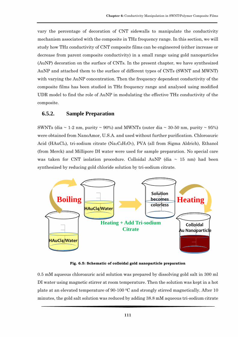
Chapter 6: Conductivity Manipulation in SWNT/Polymer Composite Films
111
vary the percentage of decoration of CNT sidewalls to manipulate the conductivity
mechanism associated with the composite in THz frequency range. In this section, we will
study how THz conductivity of CNT composite films can be engineered (either increase or
decrease from parent composite conductivity) in a small range using gold nanoparticles
(AuNP) decoration on the surface of CNTs. In the present chapter, we have synthesized
AuNP and attached them to the surface of different types of CNTs (SWNT and MWNT)
with varying the AuNP concentration. Then the frequency dependent conductivity of the
composite films has been studied in THz frequency range and analysed using modified
UDR model to find the role of AuNP in modulating the effective THz conductivity of the
composite.
6.5.2. Sample Preparation
SWNTs (dia ~ 1-2 nm, purity ~ 90%) and MWNTs (outer dia ~ 30-50 nm, purity ~ 95%)
were obtained from NanoAmor, U.S.A. and used without further purification. Chloroauric
Acid (HAuCl4), tri-sodium citrate (Na3C6H5O7), PVA (all from Sigma Aldrich), Ethanol
(from Merck) and Millipore DI water were used for sample preparation. No special care
was taken for CNT isolation procedure. Colloidal AuNP (dia ~ 15 nm) had been
synthesized by reducing gold chloride solution by tri-sodium citrate.
Fig. 6.5: Schematic of colloidal gold nanoparticle preparation
0.5 mM aqueous chloroauric acid solution was prepared by dissolving gold salt in 300 ml
DI water using magnetic stirrer at room temperature. Then the solution was kept in a hot
plate at an elevated temperature of 90-100 0C and strongly stirred magnetically. After 10
minutes, the gold salt solution was reduced by adding 38.8 mM aqueous tri-sodium citrate
HAuCl4/Water
Boiling
Heating + Add Tri-sodium
Citrate
Solution becomes colorless
Colloidal Au Nanoparticle
HeatingHAuCl4/Water

Chapter 6: Conductivity Manipulation in SWNT/Polymer Composite Films
112
(30 ml). The solution became colourless from light golden. Now, the solution was kept on
the hot plate with strong magnetic stirring and after around 40 minutes the formation of
the colloidal gold nanoparticles were indicated by the change of the colour of the solution
to dark red wine. After cooling, the colloidal AuNP were used for characterization and
CNT decoration. The process of the AuNP preparation is pictorially depicted in Fig. 6.5.
Table 5: Reactants for the sample preparation
Reactants or External Perturbations Amount
Gold Salt 0.5 mM
Tri-sodium Citrate 38.8 mM
Poly-Vinyl Alcohol 1 g
Ethanol Required Amount
A simple wet chemical method following the prescription described by Yu Shi et
al.[198] is employed to decorate the sidewalls of CNTs with these AuNP. The reactants
for the preparation of the AuNP colloidal solution and the CNT surface decoration are
tabulated in Table 5.
Fig. 6.6: Schematic of CNT surface decoration with AuNP
For the successful decoration of CNT sidewalls with the chemically synthesized AuNP, we
have followed the following procedure, which is also pictorially depicted in Fig. 6.6. In a
typical procedure, a measured amount of CNTs (8 mg) was added to 1-40 mL of the as-
SWNT/Water
Ultrasoni
cation
Strong Magnetic
Stirring (10 hour)
Au Attached
CNT
Centrifuge
Add:
Au Colloid+ Ethanol
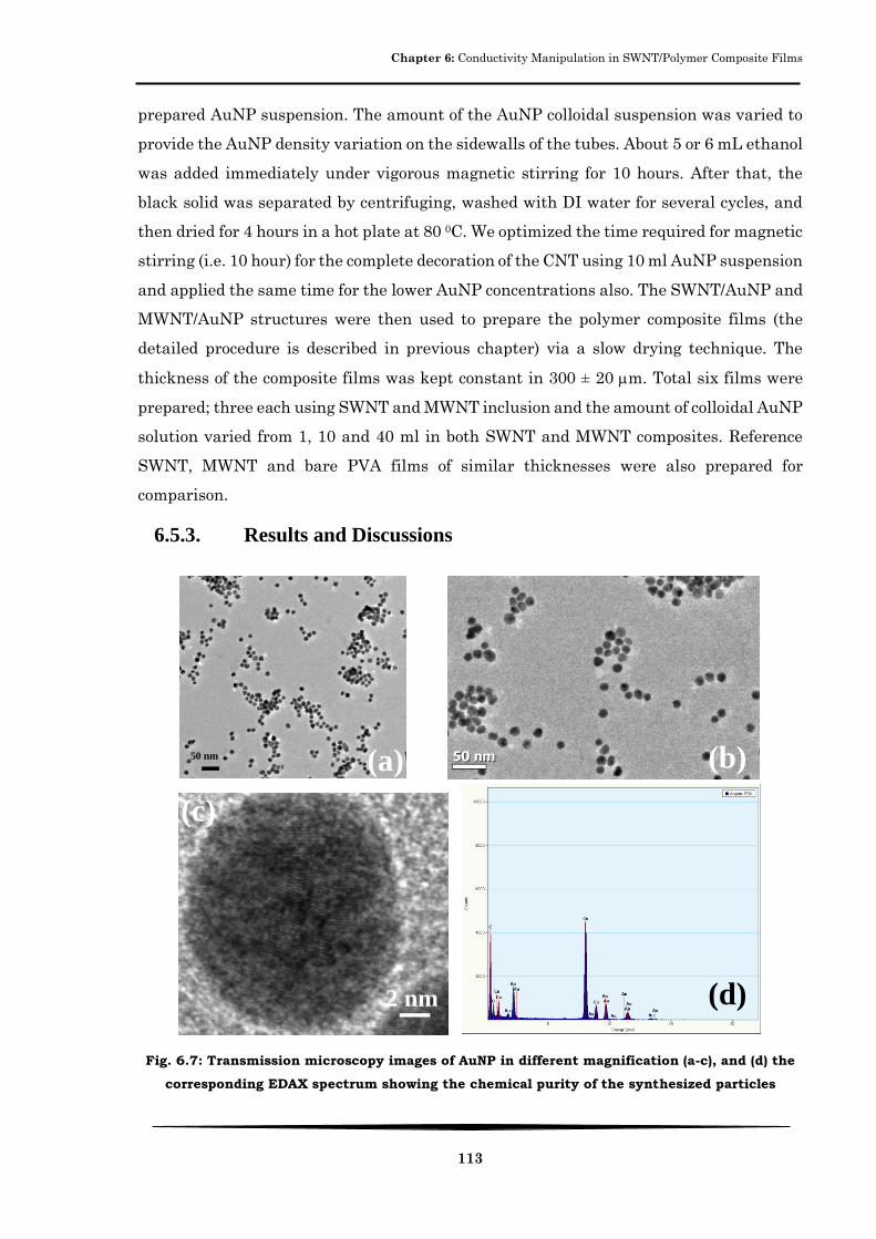
Chapter 6: Conductivity Manipulation in SWNT/Polymer Composite Films
113
prepared AuNP suspension. The amount of the AuNP colloidal suspension was varied to
provide the AuNP density variation on the sidewalls of the tubes. About 5 or 6 mL ethanol
was added immediately under vigorous magnetic stirring for 10 hours. After that, the
black solid was separated by centrifuging, washed with DI water for several cycles, and
then dried for 4 hours in a hot plate at 80 0C. We optimized the time required for magnetic
stirring (i.e. 10 hour) for the complete decoration of the CNT using 10 ml AuNP suspension
and applied the same time for the lower AuNP concentrations also. The SWNT/AuNP and
MWNT/AuNP structures were then used to prepare the polymer composite films (the
detailed procedure is described in previous chapter) via a slow drying technique. The
thickness of the composite films was kept constant in 300 ± 20 m. Total six films were
prepared; three each using SWNT and MWNT inclusion and the amount of colloidal AuNP
solution varied from 1, 10 and 40 ml in both SWNT and MWNT composites. Reference
SWNT, MWNT and bare PVA films of similar thicknesses were also prepared for
comparison.
6.5.3. Results and Discussions
Fig. 6.7: Transmission microscopy images of AuNP in different magnification (a-c), and (d) the
corresponding EDAX spectrum showing the chemical purity of the synthesized particles
50 nm (a) (b)
(d)2 nm
(c)
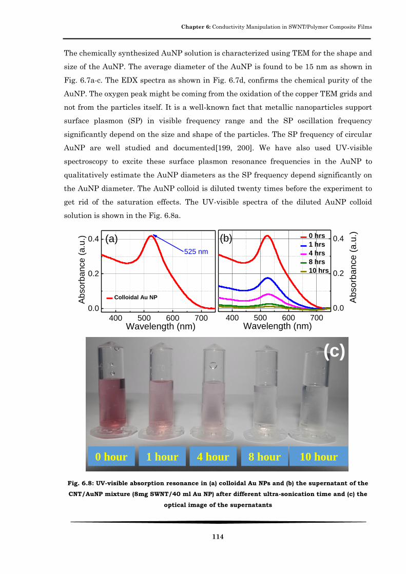
Chapter 6: Conductivity Manipulation in SWNT/Polymer Composite Films
114
The chemically synthesized AuNP solution is characterized using TEM for the shape and
size of the AuNP. The average diameter of the AuNP is found to be 15 nm as shown in
Fig. 6.7a-c. The EDX spectra as shown in Fig. 6.7d, confirms the chemical purity of the
AuNP. The oxygen peak might be coming from the oxidation of the copper TEM grids and
not from the particles itself. It is a well-known fact that metallic nanoparticles support
surface plasmon (SP) in visible frequency range and the SP oscillation frequency
significantly depend on the size and shape of the particles. The SP frequency of circular
AuNP are well studied and documented[199, 200]. We have also used UV-visible
spectroscopy to excite these surface plasmon resonance frequencies in the AuNP to
qualitatively estimate the AuNP diameters as the SP frequency depend significantly on
the AuNP diameter. The AuNP colloid is diluted twenty times before the experiment to
get rid of the saturation effects. The UV-visible spectra of the diluted AuNP colloid
solution is shown in the Fig. 6.8a.
Fig. 6.8: UV-visible absorption resonance in (a) colloidal Au NPs and (b) the supernatant of the
CNT/AuNP mixture (8mg SWNT/40 ml Au NP) after different ultra-sonication time and (c) the
optical image of the supernatants
400 500 600 700
0.0
0.2
0.4
Ab
so
rba
nce
(a
.u.)
Colloidal Au NP
Wavelength (nm)
525 nm
(a)
400 500 600 700
0.0
0.2
0.4
0 hrs
1 hrs
4 hrs
8 hrs
10 hrs
Wavelength (nm)
Absorb
ance
(a.u
.)(b)
1 hour0 hour 4 hour 8 hour 10 hour
(c)

Chapter 6: Conductivity Manipulation in SWNT/Polymer Composite Films
115
The resonance frequency appears at ~ 525 nm (corresponds to the AuNP diameter of ~ 15
nm), as observed in the figure. Now the AuNP decoration on the sidewalls of different
types of CNTs are performed by strong ultrasonication (for 10 hours) of CNT (8 mg) and
the required amount of AuNP solution in presence of a small amount of ethanol (5-6 ml
for 10 ml AuNP solution). We have also studied how well the AuNP got attached to the
CNT walls as we are increasing the sonication time. For this measurement, we performed
ultrasonication at different times (0, 1, 4, 8 and 10 hours) and then centrifuged the
solution to extract the AuNP coated CNT. A small amount from the supernatant in each
cases are transferred to the cell for UV-visible spectroscopy and the UV-visible spectra is
shown in Fig. 6.8b. With increasing ultra-sonication time, larger amount of AuNP got
attached to the CNT surface. Hence, the UV-visible absorption intensity decreases with
increasing sonication time as seen in the figure as lower number of AuNP are present in
the supernatant.
Fig. 6.9: TEM images of (a) SWNT/AuNP, (b) SEM images of MWNT/AuNP, (c) TEM image of
MWNT/AuNP and SEM image of SWNT/AuNP structures with varying AuNP density (d-f)
After 10 hours of ultra-sonication, the UV-visible peak almost vanishes confirming the
attachment of all the Au NP that were previously present in the solution at the CNT
sidewalls and the supernatant contains very small amount of AuNP. This is also clearly
visible in the optical images of the supernatants as shown in Fig. 6.8c. The dark red wine
MWNT + Au NP
(b)
SWNT+1 ml Au NP
(d)
SWNT+10 ml Au NP
(e)SWNT+40 ml Au NP(f)
(c)
MWNT + Au NP
(a)
SWNT + Au NP

Chapter 6: Conductivity Manipulation in SWNT/Polymer Composite Films
116
colour, which is the signature of the colloidal gold nanoparticles, is continuously getting
faded in the supernatant with increasing sonication time. This implies that more number
of AuNP are being attached to the tube surface and hence less number of particles are
present in the supernatant with increasing sonication time. SEM and TEM images as
shown in Fig. 6.9 confirms the attachment of AuNP on the tube surfaces. SWNT/AuNP
and MWNT/AuNP structures with different AuNP density are clearly visible giving us a
fare idea about the AuNP attachment with different types of CNTs. In the SEM images
as shown in Fig. 6.9 (d-f), the AuNP density variation has been clearly observed with
increasing AuNP solution in SWNT/PVA composites. THz spectroscopic measurements
are carried out at room temperature in transmission geometry in the frequency range of
0.3-2.0 THz using SWNT/AuNP and MWNT/AuNP composites with varying AuNP
density. Transmitted THz field in SWNT and MWNT composites are shown in Fig. 6.10.
The change observed in transmitted THz amplitude in SWNT/AuNP composites has been
explained rigorously using THz conductivity concepts later. Qualitatively we can say that,
after introducing 1 ml AuNP in the SWNT composites, THz absorption increases and then
it decreases with increasing AuNP content. The MWNT/AuNP samples does not show any
visible change in the THz spectrum (not shown here).
Fig. 6.10: (a) Transmitted THz field through SWNT/AuNP composites and the (b) zoomed in view
Small changes in the THz peak amplitude occurs due to the change in THz conductivity
of the system. THz conductivity has been derived from complex optical constants using
the following relation,
휀̃(𝜔) = �̃�2(𝜔), 휀̃(𝜔) = 휀∞ + 𝑖 (�̃�(𝜔)
휀0𝜔) (52)
14 15 16 17
-0.2
0.0
0.2
0.4
0.6 SWNT
SWNT+1 ml AuNP
SWNT+10 ml AuNP
SWNT+40 ml AuNP
TH
z A
mplit
ude (
a.u
.)
Frequency (THz)
(a)
14.5 14.6 14.7 14.8 14.9 15.0
SWNT
SWNT+1 ml AuNP
SWNT+10 ml AuNP
SWNT+40 ml AuNP
Frequency (THz)
(b)

Chapter 6: Conductivity Manipulation in SWNT/Polymer Composite Films
117
where, �̃�(𝜔) is the complex refractive index, 휀̃(𝜔) is the complex dielectric constant of the
system, 휀∞ is the dielectric constant at infinite frequency, 휀0 is the permittivity of free
space, 𝜔 is the angular frequency of radiation and �̃�(𝜔) is the complex conductivity. Real
THz conductivity profiles of SWNT and MWNT films are shown in Fig. 6.11 and fitted
with UDR model. THz conductivity of CNTs increases with increasing probing frequency
and can be evaluated as the tail of THz conductivity peak near 3 THz as observed in
different CNT films. AuNP on the sidewalls of CNTs act as a local potential in which free
carriers of CNTs get trapped, consequently THz conductivity decreases and in SWNT/1
ml AuNP sample THz conductivity is smaller than pristine SWNT sample (17% decrement
at 1.5 THz) confirming this concept. However, with sufficiently increased AuNP
concentration (SWNT/40 ml Au NP), THz conductivity offers a higher value than that of
bare SWNT (12% increment at 1.5 THz). This is possibly due to carrier conduction through
percolated SWNT/Au NP path at higher concentration, wherein AuNP act as a conduction
path instead of a local carrier trapping potential. SWNT/10 ml composite suffers a
competition between carrier trapping and variable range hopping conduction and THz
conductivity is lower than pristine SWNT but higher than SWNT/40 ml Au NP film. Such
controlled conductivity tuning could be found useful in different THz device applications
like THz resistor. THz conductivity does not change much for MWNT/AuNP composites
as seen in Fig. 6.11b.
Fig. 6.11: Real THz conductivity in (a) SWNT/AuNP and (b) MWNT/AuNP composites and fitted
with UDR model
The percentage change in THz conductivity in SWNT/AuNP composites is calculated
using the following relation;
% 𝑐ℎ𝑎𝑛𝑔𝑒 𝑖𝑛 𝑐𝑜𝑛𝑑𝑢𝑐𝑡𝑖𝑣𝑖𝑡𝑦 =|𝜎𝑆𝑊𝑁𝑇+𝑥 𝑚𝑙 𝐴𝑢𝑁𝑃 − 𝜎𝑆𝑊𝑁𝑇|
𝜎𝑆𝑊𝑁𝑇× 100, (53)
0.5 1.0 1.5 2.0
30
60
90
120
SWNT
SWNT+1ml AuNP
SWNT+10ml AuNP
SWNT+40ml AuNP
Conductivity (
Sm
-1)
Frequency (THz)
(a)
0.5 1.0 1.5 2.0
20
40
60
Frequency (THz)
MWNT
MWNT/1ml AuNP
MWNT/10ml AuNP
MWNT/40ml AuNP
Conductivity (
Sm
-1)
(b)
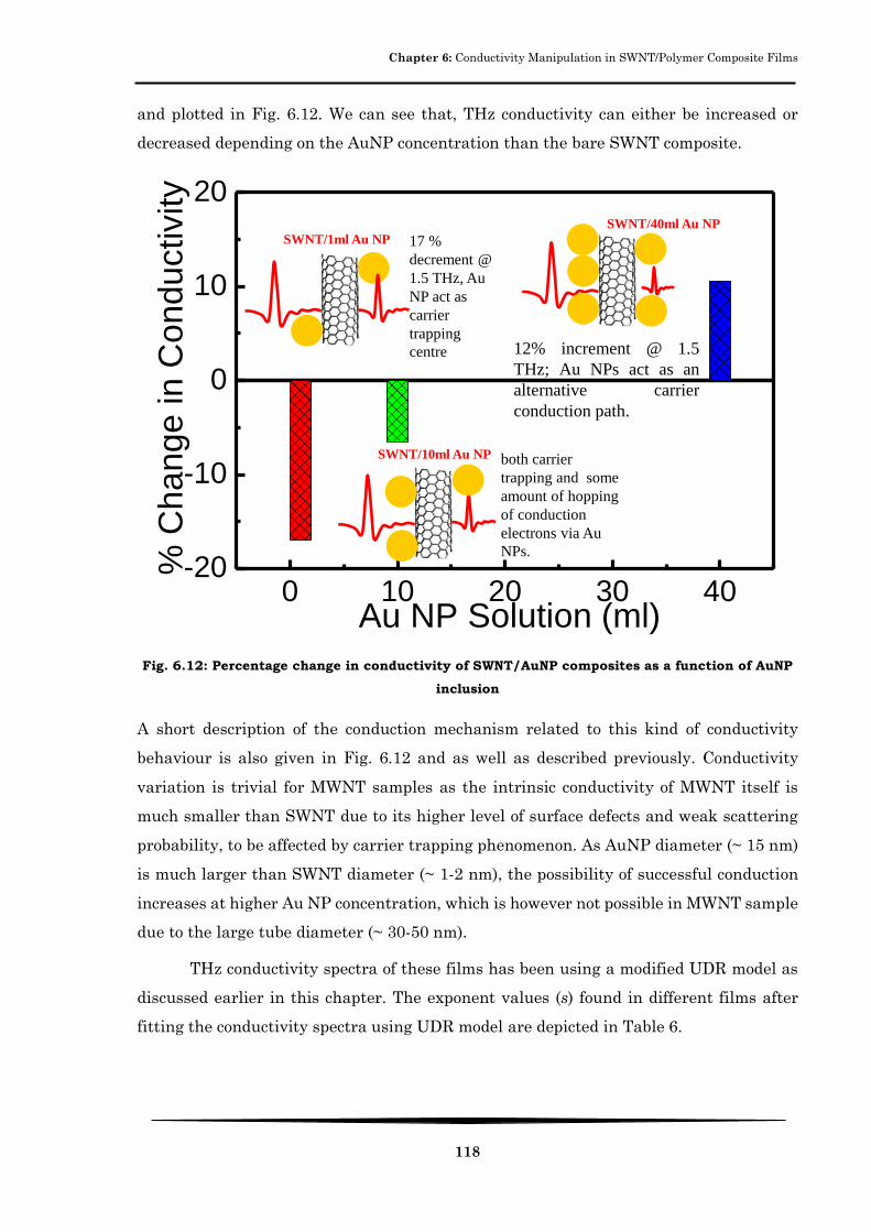
Chapter 6: Conductivity Manipulation in SWNT/Polymer Composite Films
118
and plotted in Fig. 6.12. We can see that, THz conductivity can either be increased or
decreased depending on the AuNP concentration than the bare SWNT composite.
Fig. 6.12: Percentage change in conductivity of SWNT/AuNP composites as a function of AuNP
inclusion
A short description of the conduction mechanism related to this kind of conductivity
behaviour is also given in Fig. 6.12 and as well as described previously. Conductivity
variation is trivial for MWNT samples as the intrinsic conductivity of MWNT itself is
much smaller than SWNT due to its higher level of surface defects and weak scattering
probability, to be affected by carrier trapping phenomenon. As AuNP diameter (~ 15 nm)
is much larger than SWNT diameter (~ 1-2 nm), the possibility of successful conduction
increases at higher Au NP concentration, which is however not possible in MWNT sample
due to the large tube diameter (~ 30-50 nm).
THz conductivity spectra of these films has been using a modified UDR model as
discussed earlier in this chapter. The exponent values (s) found in different films after
fitting the conductivity spectra using UDR model are depicted in Table 6.
0 10 20 30 40-20
-10
0
10
20
%
Ch
an
ge
in
Co
nd
uctivity
Au NP Solution (ml)
17 %
decrement @
1.5 THz, Au
NP act as
carrier
trapping
centre
SWNT/1ml Au NP
SWNT/10ml Au NP both carrier
trapping and some
amount of hopping
of conduction
electrons via Au
NPs.
12% increment @ 1.5
THz; Au NPs act as an
alternative carrier
conduction path.
SWNT/40ml Au NP

Chapter 6: Conductivity Manipulation in SWNT/Polymer Composite Films
119
Table 6: The fitted s parameters for different SWNT/AuNP and MWNT/AuNP films
Property Type SWNT Films MWNT Films
Exponent “s”
Pristine 0.62 ± 0.005 1. 21 ± 0.014
1ml Au NP 1.09 ± 0.020 1.58 ± 0.020
10 ml Au NP 0.92 ± 0.006 1.60 ± 0.031
40 ml Au NP 0.88 ± 0.015 1.51 ± 0.021
In pristine SWNT film, s is 0.62 and hopping type conduction mechanism is predominant.
With increasing Au NP content, at first s value increases to 1.09 for SWNT/1ml Au NP
film indicating increasing coulomb traps and confined motion of carriers in the vicinity of
those traps. As we further increase Au NP content, conductivity increases indicating a
possible conduction mechanism through percolated Au NP/SWNT structures itself and
that motion is reflected in the decreasing value of s indicating somewhat less confined
movement of the carriers.
Fig. 6.13: The value of s for SWNT/AuNP and MWNT/AuNP (shown at the inset) films
The value of s is larger than 1 in all MWNT films indicating the semiconducting nature
of those samples as it should be due to the damaged sidewalls, higher surface defects and
weak scattering capability of MWNT films. The value of s for all the SWNT/AuNP and
SWNT SWNT/1 ml SWNT/10 ml SWNT/40 ml
0.4
0.6
0.8
1.0
MWNT MWNT/1 ml MWNT/10 mlMWNT/40 ml
1.2
1.4
1.6
s
Sample
s
Chapter 6: Conductivity Manipulation in SWNT/Polymer Composite Films
120
MWNT/AuNP films are shown in Fig. 6.13. With the inclusion of Au NP in MWNT
samples, s value initially increases and then remains almost constant at 1.55 ± 0.5 for all
higher Au NP concentrations. This indicates confined motion of carriers near coulomb
traps for all the samples and negligible dependence of the motion of carriers on AuNP
concentration, which is reflected in the conductivity spectra of MWNT samples.
Conclusion
In this chapter we have investigated two different procedures, namely; i) changing the
effective length and weight fraction of the SWNT inclusion inside the PVA matrix and ii)
variation of AuNP decoration at the sidewalls of SWNT, to modulate the THz conductivity
of SWNT/PVA composites. We found out that increasing the effective length of the SWNT
from 2 m to 15 m, THz conductivity of the composite can be increased ~ 80% at 1.5 THz.
We also found that, surface wall modification of SWNT can be emerged as a useful
technique to engineer the THz conductivity of the polymer composite material and THz
conductivity of the composite can either be increased or decreased ~ 15% by varying the
density of AuNP decoration on the SWNT wall. The length dependent high frequency
conductivity of SWNTs is discussed in the light of surface plasmon resonance. Adjustable
THz conductivity of SWNT/PVA composites is successfully analysed with a modified UDR
model. A tunable THz conductivity is observed with SWNT/AuNP films and such a system
can emerge as a simple and potential THz resistor, whereas the conductivity spectra of
MWNT/AuNP films remains unchanged with varying AuNP content. THz conductivity of
the composites decreased form the parent composite upon 1ml AuNP attachment and then
it increased with increasing AuNP content. A modified UDR theory is applied to analyse
the conductivity spectra of SWNT/AuNP and MWNT/AuNP samples. A controlled way of
THz conductivity modulation of SWNT/PVA composites will help the possible future
applications of such composites in solar cells and high frequency EMI shielding devices.

Chapter Seven
Chapter 7: Terahertz Shielding Effectiveness and Conductivity of Self-Standing MWNT Film
122
7. Terahertz Shielding Effectiveness
and Conductivity of Self-Standing
MWNT Film
Introduction
One of the primary advantages of using THz spectroscopy in material sciences is the
possibility of label free non-destructive measurement of different nanostructures,
recording the full complex optical constants of the material over a frequency range (which
remains unpolluted by the present day wireless technology) and offering an unexplored
regime for future communication bandwidth. Researchers have already demonstrated
CNT and graphene based THz transistors[201], THz amplifiers[202] and wireless
communication[24] as fast as 2.5 GB/s at 0.625 THz, paving the gateway of this frequency
bandwidth, which extends roughly from 0.1-10 THz, as a potential candidate for future
day electronics and communication systems. Different types of CNT, namely SWNT,
DWNT and MWNT are being widely explored as the core material for different devices
like transistors, polarizers, absorbers, frequency selective devices, EMIS devices working
in the THz frequency range[5, 6, 161, 162, 187, 201]. THz EMIS devices and the
modulation of THz shielding are becoming key research areas with the invention of
different THz electronic devices, which need to be properly shielded from unwanted
external THz radiations for their unhindered operations. Manipulation of conductivity
and SE have also been demonstrated using different dopant on CNT, surface modification
of CNT, conductive filler in CNT composites, changing the AR of CNT etc.[159, 203]. In
all such applications the primarily important property is the high and anisotropic THz
conductivity provided by different types of CNT and their composites. Researchers are
intrigued about the origin of this extremely high THz conductivity and the much debated
TCP of CNT, which has universally been observed in the frequency range of 4-30 THz[192]
and the peak frequency is a function of CNT structure parameters. The origin of this TCP
remains a topic of discussion with two possible explanations being offered. One of the
theories states that TCP arises due to the excitation of surface plasmon resonance and

Chapter 7: Terahertz Shielding Effectiveness and Conductivity of Self-Standing MWNT Film
123
the peak frequency varies inversely with the length of the CNT[190, 192]. According to
the other theory the peak frequency arises due to the intra-band transition at the
curvature induced band gap in CNT and the peak frequency varies inversely with the
diameter of CNT[204]. In a recent study from our group, we have examined the composite
SE and THz conductivity of SWNT/Polymer film[187] and found out that both can be
controlled by tailoring the length of the SWNT but any conclusive idea on the intrinsic
nature of THz conductivity and TCP cannot be drawn due to the composite nature of the
material. In the present chapter, we will study the THz conductivity and SE of MWNT as
a function of MWNT average length and diameter.
Fig. 7.1: Schematic of two competing theories about the origin of THz conductivity peak in
carbon nanotube films; (a) surface plasmon resonance mechanism and (b) curvature induced
band gap
Background Study
In the last few years, researchers have studied the appearance of the universally observed
broad TCP in different types of CNTs and there composites with the peak frequency
varying from ~ 0.5 THz [140] to 30 THz depending on the different types of CNTs. The
fTCP
Eg
(~Few THz)
VB
CB
fTCP
(a) Plasmon Resonance (b) Curvature Induced
Band gap

Chapter 7: Terahertz Shielding Effectiveness and Conductivity of Self-Standing MWNT Film
124
two competing theories; i) surface plasmon resonance, ii) curvature induced badgap,
explaining the origin of the THz conductivity peak is pictorially depicted in Fig. 7.1.
Jeon et al.[205] studied the THz spectroscopy of anisotropically oriented SWNTs
in the frequency range of 0.1-0.8 THz. SWCNT powder was synthesized using a traditional
arc discharge with catalytic transition metals and then the film was prepared on glass
slides. The power absorption showed maximum at parallel film orientation to the THz
beam polarization, and reached minimum for perpendicular orientation. The a.c.
conductivity of the aligned films increased with increasing frequency, following the
Maxwell-Garnett (MG) model. A persistent decrease in anisotropy with increasing
frequency was explained by the electromagnetic wave interactions between CNTs in the
mat. They also performed a similar study[140] in the extended frequency range of 0.2-2.0
THz and theoretically modelled there experimental results using MG theory and Drude-
Lorentz (DL) theory. Han et al.[206] made a theoretical study on the THz conductivity of
SWNT films in the frequency range of 0.1-10 THz using a combination of DL theory and
MG theory. They found that the THz conductivity decreased beyond 1 THz and the related
dielectric constant reached a negative value. Kang et al.[207] studied the THz
conductivity of hydrogen functionalized SWNT in the frequency range of 0.2-1.5 THz.
They found that the magnitude of the index of refraction and electrical conductivity
decreased after hydrogen functionalization. The reduced plasma frequency in
functionalized CNTs resulted in a decrease in the number of free carriers, which could be
the evidence of bonding change from sp2 to sp3 by hydrogen functionalization. In other
words, the bonding change by functionalization induced the reduction of free carriers,
resulting in the reduction of conductivity. Akima et al.[189] used two types of SWNTs
namely L-SWNT (laser-ablation grown) and H-SWNT (commercially available high-
pressure CO disproportionation process grown) and conducted optical spectroscopy in the
wide frequency range of 6-10,000 cm-1 in stretched and un-stretched condition in a
polymer matrix. They found that the far-infrared peak was strongly polarized parallel to
the tube direction, which also displayed remarkable morphology dependence, in sharp
contrast to the morphology-insensitive spectra in the near-infrared region. They
postulated an alternative model (plasmon-resonance model) for the peak around near 100
cm1. Kampfrath et al.[208] studied optical properties of SWNT sheets over a wide
frequency range from 1 THz to 40 THz. They derived the complex dielectric function of
the nanotube sample and excellently reproduced it with DL model. The found that the
centre and width of the Lorentz absorption peak reflect the average gap energy of the
Chapter 7: Terahertz Shielding Effectiveness and Conductivity of Self-Standing MWNT Film
125
small-gap tubes and the width of the gap distribution, respectively. After a few years later,
they published another article[204] on the far-infrared absorption mechanisms in CNTs
in the frequency range of 1-40 THz. They concluded that the THz conductivity peak
around ~ 4 THz appeared due to inter-band transition in tubes with an energy gap ~ 10
meV. They also constructed a simple model based on an ensemble of two-level systems
naturally explaining the weak temperature dependence of the far-infrared conductivity
by the tube-to-tube variation of the chemical potential. Meang et al.[172] studied the
comparative THz conductivity of SWNT and DWNT in the frequency range of 0.1-2.5 THz.
They mixed CNT powder with the KBr powder, because KBr has a good transparency and
a low refractive index in the far-infrared range and prepared pellets for measurements.
They found that the power absorption, complex indices of refraction, and conductivity of
DWNTs were smaller than those of SWNTs and concluded that this was because of the
smaller carrier density of the DWNTs due to the smaller number of their tubes and
interlayer interaction. Pekker et al.[191] presented a wide-range (3 meV-6 eV) optical
characterization on freestanding transparent CNT films, made from nanotubes with
different diameter distributions. In the far-infrared region, they found a low-energy gap
in all investigated films. They determined that the average diameters of both the
semiconducting and metallic species from the near-infrared and visible features of the
spectra and established the dependence of the gap value on the mean diameter. They
concluded that the frequency of the low-energy gap was increasing with increasing
curvature. There results strongly supported the explanation of the low-frequency feature
as arising from a curvature-induced gap instead of effective-medium effects. Zhang et
al.[190] studied the conductivity properties of metallic and semiconducting SWNT in both
annealed and un-annealed state in a wide range of frequencies starting from 0.1-1000
THz to disclose the true nature of the conductivity peak in SWNT composites. There
experimental results showed that the broad THz peak originated from a plasmon
resonance in both the metallic and the doped semiconducting CNT rather than the inter-
band excitation of the curvature-induced gap in non-armchair metallic nanotubes. The
intra-band free electron response also contributed to the low-energy excitation spectrum,
especially in the metal-enriched film after annealing. They provided fundamental insight
into the low-energy excitation in SWCNTs, while the broadband spectroscopy of
semiconducting and metallic type-separated nanotube samples also provided basic
knowledge useful for emerging applications of SWCNTs in plasmonics and optoelectronics
in the technologically important THz frequency range. In recent review article[209] by
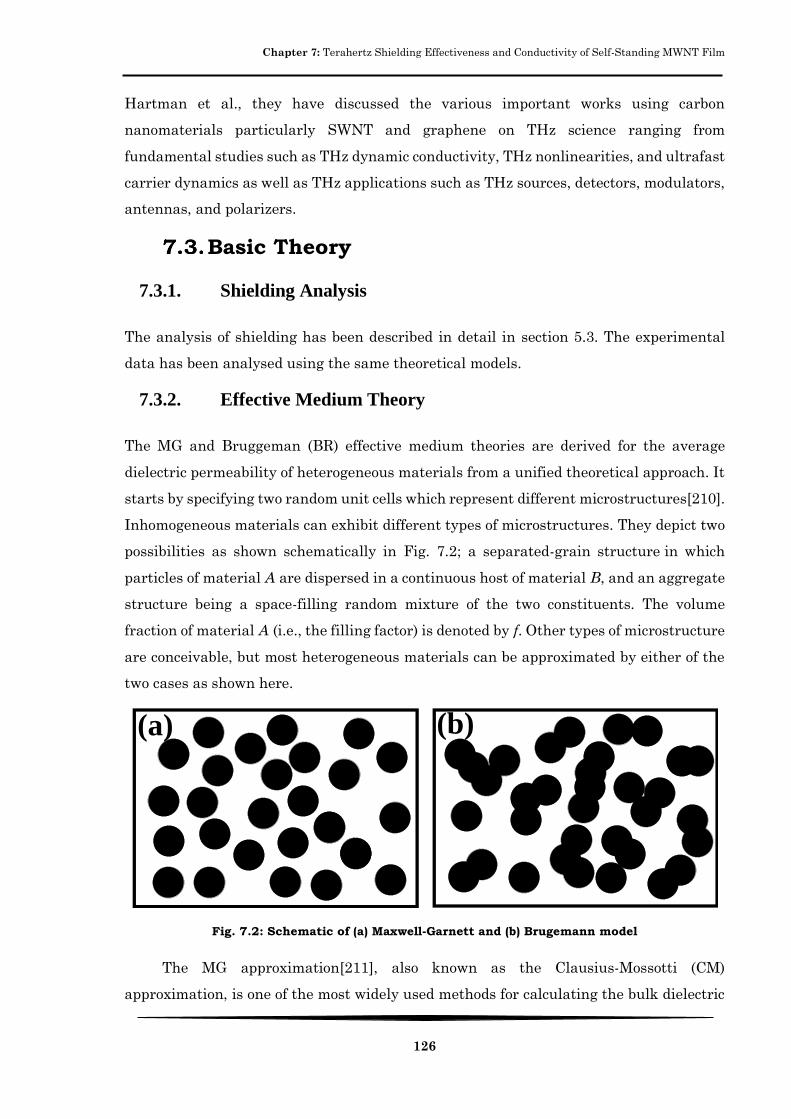
Chapter 7: Terahertz Shielding Effectiveness and Conductivity of Self-Standing MWNT Film
126
Hartman et al., they have discussed the various important works using carbon
nanomaterials particularly SWNT and graphene on THz science ranging from
fundamental studies such as THz dynamic conductivity, THz nonlinearities, and ultrafast
carrier dynamics as well as THz applications such as THz sources, detectors, modulators,
antennas, and polarizers.
Basic Theory
7.3.1. Shielding Analysis
The analysis of shielding has been described in detail in section 5.3. The experimental
data has been analysed using the same theoretical models.
7.3.2. Effective Medium Theory
The MG and Bruggeman (BR) effective medium theories are derived for the average
dielectric permeability of heterogeneous materials from a unified theoretical approach. It
starts by specifying two random unit cells which represent different microstructures[210].
Inhomogeneous materials can exhibit different types of microstructures. They depict two
possibilities as shown schematically in Fig. 7.2; a separated-grain structure in which
particles of material A are dispersed in a continuous host of material B, and an aggregate
structure being a space-filling random mixture of the two constituents. The volume
fraction of material A (i.e., the filling factor) is denoted by f. Other types of microstructure
are conceivable, but most heterogeneous materials can be approximated by either of the
two cases as shown here.
Fig. 7.2: Schematic of (a) Maxwell-Garnett and (b) Brugemann model
The MG approximation[211], also known as the Clausius-Mossotti (CM)
approximation, is one of the most widely used methods for calculating the bulk dielectric
(a) (b)

Chapter 7: Terahertz Shielding Effectiveness and Conductivity of Self-Standing MWNT Film
127
properties of inhomogeneous materials. It is useful when one of the components can be
considered as a host in which inclusions of the other components are embedded. It involves
an exact calculation of the field induced in the uniform host by a single spherical or
ellipsoidal inclusion and an approximate treatment of its distortion by the electrostatic
interaction between the different inclusions. This distortion is caused by the charge
dipoles and higher multipoles induced in the other inclusions. The induced dipole
moments cause the longest range distortions and their average effect is included in the
MG approximation which results in a uniform field inside all the inclusions. This
approach has been extensively used for studying the properties of two-component
mixtures in which both the host and the inclusions are isotropic materials with scalar
dielectric coefficients[212]. In the derivation of the MG theory[213], it is assumed that the
composite material consists of grains that are much smaller than the wavelength of light,
but are large enough so that they can be characterized by macroscopic dielectric constants.
In linear dielectric, the polarization is,
�⃗� = 휀0𝜒𝑒�⃗� , (54)
when the electric field �⃗� is weak. However, this electric field is the total field i.e. �⃗� 𝑡𝑜𝑡 =
�⃗� 𝑒𝑥𝑡 + �⃗� 𝑝𝑜𝑙 external and that due to polarization. For non-polar material, the induced
dipole moment is 𝑝 ⃗⃗⃗ = 𝛼�⃗� 𝑒𝑥𝑡, where 𝛼 is the atomic polarizability. If we are working with
weak fields, then we may approximate,
�⃗� = 𝑁𝑝 ,
휀0𝜒𝑒�⃗� = 𝑁𝛼�⃗� 𝑒𝑥𝑡 ,
𝜒𝑒 = 𝑁𝛼
휀0,
(55)
where N is the number of molecules per unit volume and is small. If we consider the
non-polar molecule to be a uniformly charged sphere of radius R, then total charge is equal
to the volume integration of the charge density over the entire volume of sphere with
radius R and,
𝑁 =1
43⁄ 𝜋𝑅3
. (56)
Next, let us calculate �⃗� 𝑝𝑜𝑙 when the molecule is placed in �⃗� 𝑒𝑥𝑡, using Gauss’s law.
According to Gauss Law, the electric flux through any closed surface S, enclosing a volume
V is related by the following equation;

Chapter 7: Terahertz Shielding Effectiveness and Conductivity of Self-Standing MWNT Film
128
𝜙 =𝑄휀0⁄ 𝑜𝑟 ∯�⃗� 𝑝𝑜𝑙 . 𝑑𝐴 =
∫𝜌𝑑𝑉
휀0. (57)
Where the surface integral is over the surface S which encloses the volume V.
�⃗� 𝑝𝑜𝑙 . 4𝜋𝑟2 =
43⁄ 𝜋𝑟3𝜌
휀0�̂�
=43⁄ 𝜋𝑟3
휀0.
𝑄
43⁄ 𝜋𝑅3
�̂�
(58)
So, this can be simplified as,
�⃗� 𝑝𝑜𝑙 =1
4𝜋휀0.𝑄𝑟
𝑅3
�⃗� 𝑝𝑜𝑙 =𝑝
4𝜋휀0𝑅3.
(59)
Now, this polarization field will act opposite to the external field. So,
�⃗� 𝑝𝑜𝑙 =−𝛼�⃗� 𝑒𝑥𝑡4𝜋휀0𝑅
3. (60)
Hence, the total field is,
�⃗� 𝑡𝑜𝑡 = �⃗� 𝑒𝑥𝑡 + �⃗� 𝑝𝑜𝑙 = �⃗� 𝑒𝑥𝑡 (1 −𝛼
4𝜋휀0𝑅3),
�⃗� 𝑡𝑜𝑡 = �⃗� 𝑒𝑥𝑡 (1 −𝑁𝛼
3휀0).
(61)
The susceptibility (𝜒𝑒) and polarizability (𝛼) get connected by the following relation,
�⃗� = 𝑁𝑝 = 𝑁𝛼�⃗� 𝑒𝑥𝑡 =𝑁𝛼�⃗� 𝑡𝑜𝑡
(1 −𝑁𝛼3휀0),
휀0𝜒𝑒�⃗� 𝑡𝑜𝑡 =𝑁𝛼�⃗� 𝑡𝑜𝑡
(1 −𝑁𝛼3휀0) ,
(62)
So,
𝜒𝑒 =
𝑁𝛼
휀0 (1 −𝑁𝛼3휀0).
(63)
Solving for 𝛼, we obtain Clausius-Mossotti relation for non-polar molecule;
Chapter 7: Terahertz Shielding Effectiveness and Conductivity of Self-Standing MWNT Film
129
𝑁𝛼
3휀0=
𝜒𝑒3 + 𝜒𝑒
=휀𝑟 − 1
휀𝑟 + 2. (64)
Where the relative permittivity (휀𝑟) is defined as 휀𝑟 = 𝜒𝑒 + 1. This can be exploited to
calculate the effective permittivity (휀𝑒𝑓𝑓) of this inhomogeneous medium, where 𝑓𝑃 is the
volumetric content of the particles,
휀𝑒𝑓𝑓 − 1
휀𝑒𝑓𝑓 + 2= 𝑓𝑃
휀𝑃 − 1
휀𝑃 + 2. (65)
If the particles are embedded in a host material with given permittivity 휀ℎ, the equation
changes into the MG equation as the following;
휀𝑒𝑓𝑓 − 휀ℎ
휀𝑒𝑓𝑓 + 2휀ℎ= 𝑓𝑃
휀𝑃 − 휀ℎ휀𝑃 + 2휀ℎ
. (66)
So, if we write the relative permittivity of the in terms of the permittivity of host and
particle, it would look like the following;
휀𝑒𝑓𝑓 = 휀ℎ (휀𝑃(1 + 2𝑓𝑃) + 2휀ℎ(1 − 𝑓𝑃)
휀𝑃(1 − 𝑓𝑃) + 휀ℎ(2 + 𝑓𝑃) ). (67)
Now, if we include a term ‘g’ to include the effect of finite AR and anisotropic nature of
the tubes, the modified MG equation looks like the following[214, 215];
휀𝑒𝑓𝑓 = 휀ℎ (휀𝑃[𝑔 + 𝑓𝑃(1 − 𝑔)] + 휀ℎ[(1 − 𝑓𝑃)(1 − 𝑔)]
휀𝑃[𝑔(1 − 𝑓𝑃)] + 휀ℎ(𝑓𝑃𝑔 + 1 − 𝑔)). (68)
This equation has been used to extract the permittivity and consequently the THz
conductivity of the MWNT in this chapter.
7.3.3. Drude-Lorentz Theory
The Drude model was developed at the turn of the 20th century by Paul Drude.
It came a few years after J.J. Thompson discovered the electron in 1897. It predates
quantum theory, but still can tell us a lot about electrons in metals. It is basically the
application of kinetic theory of gases in electron conduction in a metal. The basic
assumptions of the Drude model are the following;
1. Between collisions electrons move in straight line (in the absence of any
electromagnetic field), effect of electron-electron interaction is ignored (independent
electron approximation), effect of electron-ion in ignored (independent-electron
approximation). We will treat collisions between electrons and ions are instantaneous,
uncorrelated events.
Chapter 7: Terahertz Shielding Effectiveness and Conductivity of Self-Standing MWNT Film
130
2. Mean free time between collisions is (probability of collision per unit time is 1/;
probability of having a collision in infinitesimal time interval 𝑑𝑡 is 𝑑𝑡/, is independent
of electron’s position or velocity.
3. Electrons achieve thermal equilibrium by collisions with lattice, they emerge after
collision at a random direction with speed appropriate to the temperature of the region
where collision happened. The hotter the region; the higher the speed of the emerging
electrons.
At first, we will establish the average equation of motion for an electron. To find this let’s
start with the momentum of an electron (mass m) at time 𝑡, 𝑝𝑚(𝑡), and find it at time 𝑡 +
𝑑𝑡. If the electrons had a collision it would on average have no momentum (𝑝 𝐶(𝑡 + 𝑑𝑡) =
0) at time 𝑡 + 𝑑𝑡 and by the third assumption above this has the probability, 𝑃𝑐 = 𝑑𝑡/𝜏.
This means that the probability of no collision is 𝑃𝑛𝑐 = (1 − 𝑑𝑡/𝜏) this is because 𝑃𝑐 +
𝑃𝑛𝑐 = 1. If there were no collision the electrons would have evolved normally and the
electrons momentum becomes,
𝑝 𝑛𝑐(𝑡 + 𝑑𝑡) = 𝑝 𝑚(𝑡) + 𝐹 (𝑡)𝑑𝑡. (69)
This makes the new momentum;
𝑝 𝑚(𝑡 + 𝑑𝑡) = 𝑃𝑐 . 𝑝 𝑐(𝑡 + 𝑑𝑡) + 𝑃𝑛𝑐 . 𝑝 𝑛𝑐(𝑡 + 𝑑𝑡)
= (1 –𝑑𝑡
𝜏) [𝑝 𝑚(𝑡) + 𝐹 (𝑡)𝑑𝑡].
(70)
Using this to find the derivative take,
𝑑𝑝 𝑚(𝑡)
𝑑𝑡=𝑝 𝑚(𝑡 + 𝑑𝑡) − 𝑝 𝑚(𝑡)
𝑑𝑡=−𝑝 𝑚(𝑡)
𝜏+ 𝐹 (𝑡). (71)
This is the equation of motion averaged over electrons. If we consider 𝑥 (𝑡) to be the
displacement vector at time t for the electron with mass m, and 1 𝜏⁄ = Γ𝑃, then the equation
of motion becomes the following;
𝑚𝑑2𝑥 (𝑡)
𝑑𝑡2= −𝑚Γ𝑃
𝑑𝑥 (𝑡)
𝑑𝑡+ 𝐹 (𝑡). (72)
We can extract the a.c. conductivity of a metallic system using this equation of motion.
The a.c. electric field �⃗� (𝑡) = 𝐸0𝑒−𝑖𝜔𝑡 provides a force −𝑒�⃗� to an electron. So, the equation
of motion becomes,
𝑚𝑑2𝑥 (𝑡)
𝑑𝑡2= −𝑚Γ𝑃
𝑑𝑥 (𝑡)
𝑑𝑡− 𝑒�⃗� (𝑡). (73)
Chapter 7: Terahertz Shielding Effectiveness and Conductivity of Self-Standing MWNT Film
131
The well-known solution of this differential equation is 𝑥 (𝑡) = 𝑥𝑜𝑒−𝑖𝜔𝑡 and putting this
solution into the equation we get,
−𝑚𝜔2𝑥 (𝑡) = 𝑖𝑚𝜔Γ𝑃𝑥 (𝑡) − 𝑒�⃗� (𝑡), (74)
𝑥 (𝑡) =𝑒𝑚⁄
𝜔2 + 𝑖𝜔Γ𝑃�⃗� (𝑡), (75)
Now, if 𝑝 = −𝑒𝑥 , is the polarization due to the electron displacement and the polarization
density is �⃗� = 𝑛𝑝 , then we can write;
�⃗� = 𝑛𝑝 = −𝑛𝑒𝑥 = −𝑛𝑒2
𝑚⁄
𝜔2 + 𝑖𝜔Γ𝑃�⃗� = 휀0𝜒𝑒�⃗� , (76)
where, 𝜒𝑒 is the susceptibility of the material. Hence, we can write,
𝜒𝑒 = −
𝑛𝑒2𝑚휀0⁄
𝜔2 + 𝑖𝜔Γ𝑃,
휀𝑟 = 1 + 𝜒𝑒 .
(77)
휀𝑟 = 1 −𝑛𝑒2
𝑚휀0⁄
𝜔2 + 𝑖𝜔Γ𝑃 . (78)
Now, this theory is not always applicable for real life materials, especially in
nanostructured materials, thin films and in resonant materials. So, alternative
modifications to the very simplified Drude model has been proposed to satisfactorily
explain the experimentally observed behaviour of metals and semiconductors. One of the
mostly used such a modified model is called the Drude-Lorentz model. Now, we will
establish the DL theory.
Now, we will establish the Lorentz theory. In this theory, to describe he interaction
between atoms and electric fields in classical terms, Lorentz proposed that the electron (a
particle with some small mass) is bound to the nucleus of the atom (with a much larger
mass) by a force that behaves according to Hooke’s Law - that is, a spring-like force
(−𝑚𝜔02𝑥 (𝑡)). An applied electric field would then interact with the charge of the electron,
causing “stretching” or “compression” of the spring, which would set the electron into
oscillating motion. This is the so-called Lorentz oscillator model. We have the
conventional damping term (−𝑚Γ𝑘𝑑𝑥 (𝑡)
𝑑𝑡) and the force on the electron due to the
Chapter 7: Terahertz Shielding Effectiveness and Conductivity of Self-Standing MWNT Film
132
application of an electric field (−𝑒�⃗� (𝑡)) as usual. So, the equation of motion becomes the
following,
𝑚𝑑2𝑥 (𝑡)
𝑑𝑡2= −𝑚Γ𝑘
𝑑𝑥 (𝑡)
𝑑𝑡−𝑚𝜔0
2𝑥 (𝑡) − 𝑒�⃗� (𝑡). (79)
Again, the well-known solution of this differential equation is 𝑥 (𝑡) = 𝑥𝑜𝑒−𝑖𝜔𝑡 and putting
this solution into the equation we get,
−𝑚𝜔2𝑥 (𝑡) = 𝑖𝑚𝜔Γ𝑃𝑥 (𝑡) − 𝑚𝜔02𝑥 (𝑡) − 𝑒�⃗� (𝑡), (80)
𝑥 (𝑡) =−𝑒 𝑚⁄
(𝜔02 −𝜔2) − 𝑖𝜔Γ𝑘
�⃗� (𝑡). (81)
Now, following the procedures of Drude theory, we can establish the effective permittivity
of the system is,
휀𝑟 = 1 +𝑛𝑒2
𝑚휀0⁄
(𝜔02 − 𝜔2) − 𝑖𝜔Γ𝑘
. (82)
Now, in real life materials, sometimes both the Drude and Lorentz model is required to
explain the di-electric properties and conductivity of a system. The analysis of MWNT in
this study is also incorporated both the theories and the combined di-electric function or
the Drude-Lorentz Model as applied in the analysis is the following formula;
휀�̃�𝐿(𝜔) = 휀∞ −Ω𝑃2
𝜔2 + 𝑖Γ𝑃𝜔+∑
Ω𝑘2
(𝜔𝑘2 −𝜔2) − 𝑖Γ𝑘𝜔𝑘
, (83)
where, where, 휀∞ is the high frequency dielectric constant, Ω𝑝
2𝜋 is the Drude plasma
frequency, Γ𝑃
2𝜋 is the free electron scattering rate,
Ω𝑘
2𝜋 is the oscillator strength,
ω𝑘
2𝜋 is the
exciton frequency (plasmon in this case) and Γ𝑘
2𝜋 is the plasmon scattering rate. The
summation over k for Lorentz oscillator term extends over all possible oscillatory phonon
modes in the frequency region of consideration.

Chapter 7: Terahertz Shielding Effectiveness and Conductivity of Self-Standing MWNT Film
133
Length Dependent Shielding and THz
Conductivity
7.4.1. Sample Preparation
Fig. 7.3: Vacuum Filtration Unit used for self-standing MWNT film preparation and an image of
a self-standing MWNT film is given at the inset
MWNT (> 90% carbon content, dia ∼ 25 nm) of two different lengths (average length of ~
15 and 2 m; henceforth denoted as L_MWNT and S_MWNT, respectively) were
purchased from NanoAmor, USA at the highest available purity and used without further
purification. N,N-dimethylformamide (DMF), dichloromethane (DCM) were purchased
from Merck. Nucleopore polycarbonate track etched (PCTE) membrane having a pore size
of 0.2 µm was purchased from Whatman. Millipore DI water was used in different steps
of sample preparations. Required amount of MWNT was dispersed in 15 ml DMF by
strong ultrasonication for 20 minutes. Dispersed MWNT were mixed with required
amount of DI water and then filtered through PCTE membrane using a vacuum filtration
unit and then washed several times with DI water. MWNT film on PCTE template was
then transferred onto a silicon substrate and treated with DCM and DI water repeatedly
MWNT Solution
PCTE
Template
Pump

Chapter 7: Terahertz Shielding Effectiveness and Conductivity of Self-Standing MWNT Film
134
to dissolve the PCTE membrane and obtain the self-standing MWNT film of thickness ~
14 µm. Two films of similar thickness were prepared using the two different MWNTs
following the same procedure. The optical image of the vacuum filtration unit along with
the pump which is installed in the lab and an optical image of the self-standing MWNT
film is shown in Fig. 7.3. THz measurements were carried out in a commercial THz time
domain spectrometer[197] (TERA K8, Menlo Systems). The frequency dependent power
and phase of the transmitted pulse was obtained by using Fourier analysis of the
measured time domain electric field amplitude 𝐸𝑇𝐻𝑧(𝑡). Dielectric properties of the
samples are analysed using a combination of MG model and DL model. THz conductivity
of MWNT is extracted for both the films in the extended frequency region of 0-20 THz
using the DL parameters which gives important insight about the electronic structures
and origin of the TCP in MWNTs.
7.4.2. Results and Discussions
Fig. 7.4: (a) TEM image of S_MWNT, (b) SEM image of the MWNT film and the corresponding
EDAX spectra, (c) cross-sectional SEM image of MWNT self-standing film, (d) optical image of
the self-standing MWNT paper
50 nmS_MWNT
(a)
50 m
(c) (d)
1 m
Energy (keV)
Co
un
t
C K
Si K
(b)

Chapter 7: Terahertz Shielding Effectiveness and Conductivity of Self-Standing MWNT Film
135
TEM image of the S_MWNT film is shown in Fig. 7.4a and the detailed analysis using the
TEM images confirm the diameter of the MWNT to be ~ 25 ± 3 nm which is close to the
nominal value. Cross sectional view of the self-standing L_MWNT film is shown in the
SEM image of Fig. 7.4c and the thickness of the film is found to be ~ 14 m. This thickness
is later used while analyzing the measured data. EDX spectrum of the S_MWNT film is
given in the index of Fig. 7.4b and it shows the chemical purity of the MWNT (greater
than 95% carbon content). A photograph of the self-standing L_MWNT film of diameter
1.5 cm is shown in Fig. 7.4d. Transmitted THz spectra in time domain for both S_MWNT
and L_MWNT films are shown in Fig. 7.5a and the corresponding FFT amplitude is shown
in Fig. 7.5b.
Fig. 7.5: (c) Transmitted THz spectra for L-MWNT and S_MWNT self-standing film and the
corresponding (b) Fast Fourier Transfer (FFT) spectra of those samples
Transmitted THz radiation is found to be much smaller in L_MWNT than that of
S_MWNT having the same MWNT weight fraction indicating higher THz absorption in
the former as observed in earlier THz studies in SWNT. It can be shown[75, 156] that SE
of a composite system can be written as (also elaborately described in chapter 5);
𝑆𝐸(𝜔) = 𝑆𝐸𝐴(𝜔) + 𝑆𝐸𝑅(𝜔) + 𝑆𝐸𝑀𝐼𝑅(𝜔)
= 8.68𝛼(𝜔)𝑙 + 20 log10 (|1 + �̃�(𝜔)|2
4|�̃�(𝜔)|) + 20 log10 |1 −
(1 − �̃�(𝜔))2
(1 + �̃�(𝜔))2𝑒(−2𝛼(𝜔)𝑙)|,
where �̃�(𝜔), �̃�(𝜔) and l are the complex refractive index, complex propagation constant
and thickness of the sample under consideration. The contributions of reflection and
absorption to the total shielding are shown in Fig. 3a for all the MWNT films. Shielding
due to multiple internal reflection (𝑆𝐸𝑀𝐼𝑅(𝜔)) are dominant for films where the thickness
of the film is comparable or smaller than the skin depth at a particular frequency. If the
12 15 18-0.4
0.0
0.4
0.8
1 2 3 4
0.01
0.1
1
(b)
L_MWNT
S_MWNT
TH
z S
pectr
a (
a.u
.)
Time (ps)
(a)
Frequency (THz)
FF
T A
mp
litu
de
(a
.u.)

Chapter 7: Terahertz Shielding Effectiveness and Conductivity of Self-Standing MWNT Film
136
thickness of the film is thicker than the skin depth, the reflected wave from the internal
surface will be absorbed by the conductive material, and thus multiple-reflection can be
ignored. However, if the shield is thinner than the skin depth, the influence of multiple-
reflection will be significant in decreasing overall EMI shielding[155]. It was theoretically
shown in many literatures that the effect of multiple internal reflection can be neglected
if 𝑆𝐸𝑅(𝜔) ≥ 15 𝑑𝐵[164, 165]. It was also found that the contribution of multiple internal
reflection may be negative in some samples[155, 216].
Fig. 7.6: (a) Total SE of L_MWNT and S_MWNT films, contribution of absorption and reflection
and multiple internal reflection for (b) L_MWNT and (c) S_MWNT films, and (d) relative
contribution of absorption to reflection in L_MWNT and S_MWNT films
The total shielding as shown in Fig. 7.6a has been excellently fitted using Eq. 43 in the
frequency range of 0.4-2.7 THz. SE is much larger in L_MWNT films than S_MWNT films
due to larger THz attenuation in long MWNT samples as observed in other literatures for
longer SWNTs. This is mainly due to presence of larger number of free electrons, relatively
less number of defect states and less junction resistance (MWNT-MWNT junction acts as
a resistive lump in the otherwise conducting MWNT forest structure) in L_MWNT film
than S_MWNT films. The individual contribution of absorptive shielding (𝑆𝐸𝐴(𝜔)),
0.5 1.0 1.5 2.0 2.5
5
10
15
20
25
0.5 1.0 1.5 2.0 2.5
0
5
10
15
20
0.5 1.0 1.5 2.0 2.5
0
5
10
15
0.5 1.0 1.5 2.0 2.5
1
2
3
4
(d)(c)
(a)
L_MWNT
S_MWNT
SE
(dB
)
(a)
SEA
SER
SEMIR
L_MWNT
SEA
SER
SEMIR
SE
(dB
)
Frequency (THz)
S_MWNT L_MWNT
S_MWNT
Frequency (THz)S
EA/S
ER
SE
(d
B)
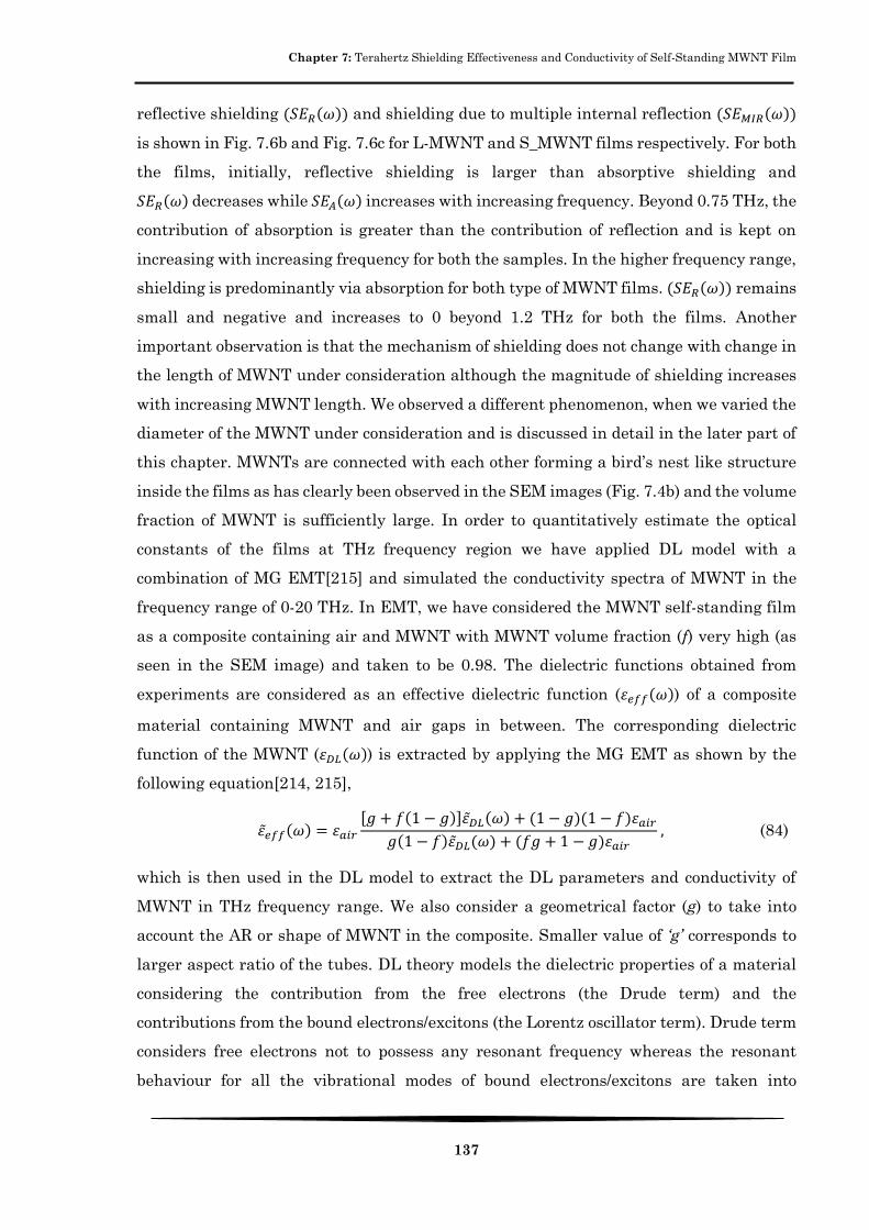
Chapter 7: Terahertz Shielding Effectiveness and Conductivity of Self-Standing MWNT Film
137
reflective shielding (𝑆𝐸𝑅(𝜔)) and shielding due to multiple internal reflection (𝑆𝐸𝑀𝐼𝑅(𝜔))
is shown in Fig. 7.6b and Fig. 7.6c for L-MWNT and S_MWNT films respectively. For both
the films, initially, reflective shielding is larger than absorptive shielding and
𝑆𝐸𝑅(𝜔) decreases while 𝑆𝐸𝐴(𝜔) increases with increasing frequency. Beyond 0.75 THz, the
contribution of absorption is greater than the contribution of reflection and is kept on
increasing with increasing frequency for both the samples. In the higher frequency range,
shielding is predominantly via absorption for both type of MWNT films. (𝑆𝐸𝑅(𝜔)) remains
small and negative and increases to 0 beyond 1.2 THz for both the films. Another
important observation is that the mechanism of shielding does not change with change in
the length of MWNT under consideration although the magnitude of shielding increases
with increasing MWNT length. We observed a different phenomenon, when we varied the
diameter of the MWNT under consideration and is discussed in detail in the later part of
this chapter. MWNTs are connected with each other forming a bird’s nest like structure
inside the films as has clearly been observed in the SEM images (Fig. 7.4b) and the volume
fraction of MWNT is sufficiently large. In order to quantitatively estimate the optical
constants of the films at THz frequency region we have applied DL model with a
combination of MG EMT[215] and simulated the conductivity spectra of MWNT in the
frequency range of 0-20 THz. In EMT, we have considered the MWNT self-standing film
as a composite containing air and MWNT with MWNT volume fraction (f) very high (as
seen in the SEM image) and taken to be 0.98. The dielectric functions obtained from
experiments are considered as an effective dielectric function (휀𝑒𝑓𝑓(𝜔)) of a composite
material containing MWNT and air gaps in between. The corresponding dielectric
function of the MWNT (휀𝐷𝐿(𝜔)) is extracted by applying the MG EMT as shown by the
following equation[214, 215],
휀�̃�𝑓𝑓(𝜔) = 휀𝑎𝑖𝑟[𝑔 + 𝑓(1 − 𝑔)]휀�̃�𝐿(𝜔) + (1 − 𝑔)(1 − 𝑓)휀𝑎𝑖𝑟
𝑔(1 − 𝑓)휀�̃�𝐿(𝜔) + (𝑓𝑔 + 1 − 𝑔)휀𝑎𝑖𝑟 , (84)
which is then used in the DL model to extract the DL parameters and conductivity of
MWNT in THz frequency range. We also consider a geometrical factor (g) to take into
account the AR or shape of MWNT in the composite. Smaller value of ‘g’ corresponds to
larger aspect ratio of the tubes. DL theory models the dielectric properties of a material
considering the contribution from the free electrons (the Drude term) and the
contributions from the bound electrons/excitons (the Lorentz oscillator term). Drude term
considers free electrons not to possess any resonant frequency whereas the resonant
behaviour for all the vibrational modes of bound electrons/excitons are taken into

Chapter 7: Terahertz Shielding Effectiveness and Conductivity of Self-Standing MWNT Film
138
consideration in the Lorentz oscillator term[173, 190]. The DL model is mathematically
represented by the following equation (described before),
휀�̃�𝐿(𝜔) = 휀∞ −Ω𝑃2
𝜔2 + 𝑖Γ𝑃𝜔+∑
Ω𝑘2
(𝜔𝑘2 −𝜔2) − 𝑖Γ𝑘𝜔𝑘
, (85)
where, 휀∞ is the high frequency dielectric constant, Ω𝑝
2𝜋 is the Drude plasma frequency,
Γ𝑃
2𝜋
is the free electron scattering rate, Ω𝑘
2𝜋 is the oscillator strength,
ω𝑘
2𝜋 is the exciton frequency
(plasmon in this case) and Γ𝑘
2𝜋 is the plasmon scattering rate. The summation over k for
Lorentz oscillator term extends over all possible oscillatory phonon modes in the
frequency region of consideration, however in the present scenario only one phonon mode
is enough[173, 190] to successfully reproduce the data. We have applied MG EMT where
the film is considered as an effective medium. The effective dielectric constant of the
S_MWNT and L_MWNT films fitted with the combination of MG and DL models are
shown in Fig. 7.7 in the frequency range of 0.3-2.7 THz and the obtained DL parameters
are shown in Table 7. The DL parameters are closely related to the electronic structure of
the samples in consideration hence, by analyzing the parameters listed in Table 7, one
can have an insight to the electronic structure of S_MWNT and L_MWNT films.
Table 7: DL Parameters for L_MWNT and S_MWNT Films
Sample 𝛆∞ 𝛀𝒑
𝟐𝝅 (THz)
𝚪𝑷
𝟐𝝅 (THz)
𝛀𝒌
𝟐𝝅 (THz)
𝛚𝒌
𝟐𝝅 (THz) 𝚪𝒌
𝟐𝝅
(THz)
g
L_MWNT 4.00 32.25 14.46 32.33 6.95 7.02 0.09
S_MWNT 4.00 10.60 3.51 48.70 9.37 35.66 0.16
The plasma frequency Ωp
2π is proportional to the square root of free electron density of the
system which is found to be 32.25 THz for L_MWNT and 10.60 THz for S_MWNT film,
indicating higher abundance of free electrons in L_MWNT films which satisfactorily
justifies its high THz conductivity and SE. During the fitting procedure we have kept the
volume fraction of the MWNT (𝑓) fixed at 0.98 for both the films which is approximated
from their SEM images. The free electron scattering rate Γ𝑃
2𝜋, which is also proportional
with the free electron density of the sample, decreased from 14.46 THz to 3.51 THz
confirming the abundance of free electrons in the L_MWNT films than S_MWNT.

Chapter 7: Terahertz Shielding Effectiveness and Conductivity of Self-Standing MWNT Film
139
Plasmon frequency increases from 6.95 THz to 9.37 THz as the length of the MWNT get
shortened. Such a decrement in plasmon frequency confirms that the resonance term is
indeed arising due to the length dependent surface plasmon phenomenon in the MWNTs.
It can also be noted that the width of the lorentzian peak Γ𝑘
2𝜋 is of the same order with the
exciton frequency for longer MWNTs, however, for shorter MWNTs, it increases almost
four times than the exciton frequency. This may be due to the presence of closely placed
additional vibrational peaks (which are of course not resolved) in S_MWNTs.
Fig. 7.7: (a) Real and (b) Imaginary dielectric function of L_MWNT and S_MWNT films fitted with
MG and DL Model
From the fitted DL parameters, we have also extracted the complex THz conductivity of
the MWNTs using the following formula;
𝜎(𝜔) = (Ω𝑃2
𝜔2 + 𝑖Γ𝑃𝜔−
Ω𝑘2
(𝜔𝑘2 −𝜔2) − 𝑖Γ𝑘𝜔
) 𝑖휀0𝜔. (86)
Real THz conductivity is found to be positive and increasing while the imaginary THz
conductivity found to be negative and decreasing in the measured frequency range which
indicates that the famous THz conductivity peak lies outside the measured frequency
range for the present samples. Hence, we have extrapolated the complex THz conductivity
in the frequency range of 0-20 THz (measured frequency range is 0.4-2.7 THz) to observe
the behaviour of the THz conductivity peak as a function of MWNT effective length. We
indeed observed the TCP while the imaginary THz conductivity undergoes a change in
sign (from negative to positive). The THz conductivity peak is observed at 6.6 THz for
L_MWNT films and at 7.5 THz for S_MWNT films. The increment of THz peak frequency
is found to be 0.9 THz in the shorter MWNT samples. Such a change has been proposed
0.5 1.0 1.5 2.0 2.5
0
70
140
210
0.5 1.0 1.5 2.0 2.5
0
40
80
120
L_MWNT
S_MWNT
im
a
Frequency (THz)
(b)
Real
Frequency (THz)
(a)

Chapter 7: Terahertz Shielding Effectiveness and Conductivity of Self-Standing MWNT Film
140
by surface plasmonic excitation model of THz conductivity in carbon nanotubes and has
been experimentally realized in a handful of studies.
Fig. 7.8: Real and Imaginary conductivity of (a) L_MWNT and (b) S_MWNT films extracted from
DL parameters in the frequency range 0-20 THz.
Diameter Dependent Shielding and THz
Conductivity
7.5.1. Sample Preparation
MWNT (> 90% carbon content, average length ∼ 1 µm) of three different diameters (7 nm,
25 nm and 40 nm) were purchased from NanoAmor, USA at the highest available purity
and used without further purification and named as MWNT_7nm, MWNT_25nm and
MWNT_40nm respectively. DMF and DCM were purchased from MERCK at highest
available purity. PCTE membrane of pore diameter 0.2 m were purchased from
Whatman. Same amount of the required type of MWNT powder was dispersed in 15 ml
DMF via strong ultra-sonication for 20 minutes and then poured in the vacuum filtration
unit with sufficient amount of DI water to be filtered through PCTE membrane.
Depending on the nature of the solution, 10-20 hours were required for the complete
filtration process. MWNT coated PCTE template was then transferred onto silicon
substrate, carefully washed with DI water several times, dissolved in DCM and dried to
obtain the self-standing MWNT film of thickness ~ 15-25 m.
0 5 10 15-35
0
35
70
105
0 5 10 15-10
0
10
20
30
40(b)
Real
Imaginary
C
ond
uctivity (
-cm
-1)
Frequency (THz)
Co
nd
uctivity(
-cm
-1)
(a)
L_MWNT
Real
Imaginary
Frequency (THz)
S_MWNT
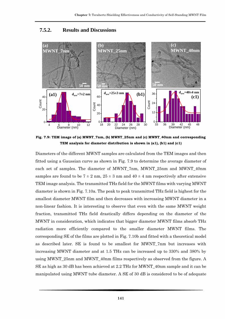
Chapter 7: Terahertz Shielding Effectiveness and Conductivity of Self-Standing MWNT Film
141
7.5.2. Results and Discussions
Fig. 7.9: TEM image of (a) MWNT_7nm, (b) MWNT_25nm and (c) MWNT_40nm and corresponding
TEM analysis for diameter distribution is shown in (a1), (b1) and (c1)
Diameters of the different MWNT samples are calculated from the TEM images and then
fitted using a Gaussian curve as shown in Fig. 7.9 to determine the average diameter of
each set of samples. The diameter of MWNT_7nm, MWNT_25nm and MWNT_40nm
samples are found to be 7 ± 2 nm, 25 ± 3 nm and 40 ± 4 nm respectively after extensive
TEM image analysis. The transmitted THz field for the MWNT films with varying MWNT
diameter is shown in Fig. 7.10a. The peak to peak transmitted THz field is highest for the
smallest diameter MWNT film and then decreases with increasing MWNT diameter in a
non-linear fashion. It is interesting to observe that even with the same MWNT weight
fraction, transmitted THz field drastically differs depending on the diameter of the
MWNT in consideration, which indicates that bigger diameter MWNT films absorb THz
radiation more efficiently compared to the smaller diameter MWNT films. The
corresponding SE of the films are plotted in Fig. 7.10b and fitted with a theoretical model
as described later. SE is found to be smallest for MWNT_7nm but increases with
increasing MWNT diameter and at 1.5 THz can be increased up to 330% and 380% by
using MWNT_25nm and MWNT_40nm films respectively as observed from the figure. A
SE as high as 30 dB has been achieved at 2.2 THz for MWNT_40nm sample and it can be
manipulated using MWNT tube diameter. A SE of 30 dB is considered to be of adequate
18 20 22 24 26 28 300
20
40
60
Count
Diameter (nm)
50 nm50 nm
4 6 8 10 120
20
40
Cou
nt
Diameter (nm)33 36 39 42 45 48
0
12
24
36
Count
Diameter (nm)
(b)
MWNT_25nm
(a1)
(c)
MWNT_40nm
(c1)(b1)
dave=40 4 nmdave=25 3 nmdave=7 2 nm
50 nm
(a)
MWNT_7nm

Chapter 7: Terahertz Shielding Effectiveness and Conductivity of Self-Standing MWNT Film
142
level for EMI shielding in the case of many applications as it can attenuate ∼ 99.9% of
EMI radiation power[155].
Fig. 7.10: (a) Transmitted THz pulse in time domain passing through the samples and (b) the
corresponding SE in the frequency range of 0.4-2.2 THz
The shielding properties of these films has been analysed using the Eqn. 43 and
Eqn. 44 which is already described in the chapter 5 and the contribution of each type of
shielding (absorption, reflection and multiple internal reflection) has also been extracted.
Shielding due to multiple internal reflection (𝑆𝐸𝑀𝐼𝑅(𝜔)) is dominant for films where the
thickness of the film is comparable or smaller than the skin depth at a particular
frequency. If the thickness of the film is thicker than the skin depth, the reflected wave
from the internal surface will be absorbed by the conductive material, and thus multiple-
reflection can be ignored.
Fig. 7.11: Contribution of absorption and reflection to the total shielding and (b) the relative
ration of contribution of absorption to reflection in the frequency range of 0.4-2.2 THz
However, if the shield is thinner than the skin depth, the influence of multiple-reflection
will be significant in decreasing the overall EMI shielding. In the present experiment, we
10 12 14 16
-0.5
0.0
0.5
1.0
1.5
0.5 1.0 1.5 2.00
10
20
30
(b)
MWNT_7nm
MWNT_25nm
MWNT_40nm
E
TH
z (
a.u
.)
Time (ps)
(a)
MWNT_7nm
MWNT_25nm
MWNT_40nm
Frequency (THz)
SE
(dB
)
0.5 1.0 1.5 2.00
10
20
0
4
8
12
SE
A(d
B)
Frequency (THz)
MWNT_7nm
MWNT_25nm
MWNT_40nm
(a)
S
ER (
dB
)
0.5 1.0 1.5 2.00
2
4
6
8
MWNT_7nm
MWNT_25nm
MWNT_40nm
Frequency (THz)
(b)
SE
A/S
ER

Chapter 7: Terahertz Shielding Effectiveness and Conductivity of Self-Standing MWNT Film
143
find that 𝑆𝐸𝑅(𝜔) decreases and 𝑆𝐸𝐴(𝜔) increases with increasing frequency as also
theoretically prescribed by Shuba et al.[217] in sub-THz and THz frequency range. The
dominant shielding mechanism is absorption for the three different MWNT films
particularly in higher frequency range. For a particular frequency, 𝑆𝐸𝑅(𝜔) increases with
increasing MWNT diameter. However, for MWNT_25nm and MWNT_40nm films,
𝑆𝐸𝐴(𝜔) is almost the same and much larger than MWNT_7nm at a particular frequency.
The ratio of absorption to reflection is shown in Fig. 7.7b. The relative contribution of
absorption to reflection is larger in higher frequency range and it decreases with
increasing MWNT diameter. Such diameter dependent change in THz shielding
mechanism which is being studied here for the first time is really interesting. It was
previously reported in numerous literatures that high frequency (~ GHz) shielding of CNT
based composites are primarily due to reflection and contribution form absorption is
pretty less[156-158] and with increasing frequency contribution of reflection decreases
and absorption increases. So, it can be understood that in sufficiently higher frequency
range (THz) as in the present study, the effect of absorption may be the dominant
shielding mechanism rather than reflection. It was also observed that, depending on the
concentration of MWNT in a composite system, absorptive shielding or reflective shielding
may dominate in a particular frequency range of interest[155].
Fig. 7.12: Contribution of Multiple internal reflection to the total shielding for different MWNT
films
It was also speculated that either reflection based or absorption based shielding is
required for particular applications. Here, we have observed that, by choosing appropriate
0.5 1.0 1.5 2.0-2.5
-2.0
-1.5
-1.0
-0.5
0.0
SE
MIR
(dB
)
Frequency (THz)
MWNT_7nm
MWNT_25nm
MWNT_40nm
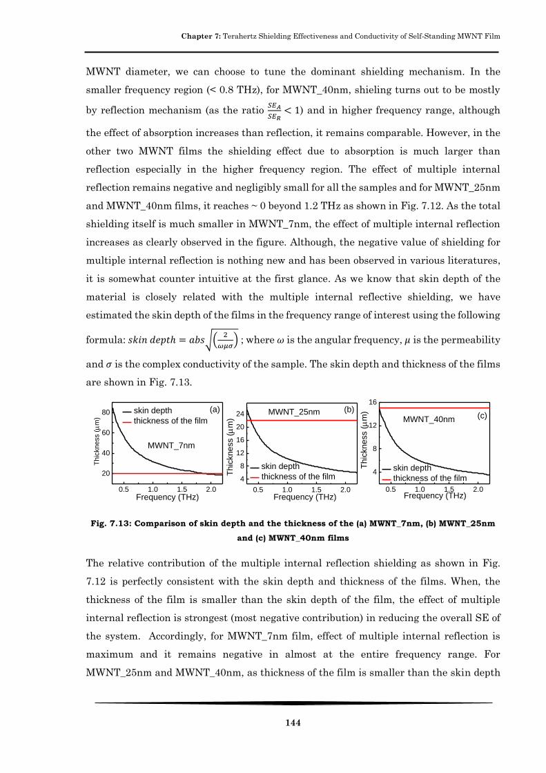
Chapter 7: Terahertz Shielding Effectiveness and Conductivity of Self-Standing MWNT Film
144
MWNT diameter, we can choose to tune the dominant shielding mechanism. In the
smaller frequency region (< 0.8 THz), for MWNT_40nm, shieling turns out to be mostly
by reflection mechanism (as the ratio 𝑆𝐸𝐴
𝑆𝐸𝑅< 1) and in higher frequency range, although
the effect of absorption increases than reflection, it remains comparable. However, in the
other two MWNT films the shielding effect due to absorption is much larger than
reflection especially in the higher frequency region. The effect of multiple internal
reflection remains negative and negligibly small for all the samples and for MWNT_25nm
and MWNT_40nm films, it reaches ~ 0 beyond 1.2 THz as shown in Fig. 7.12. As the total
shielding itself is much smaller in MWNT_7nm, the effect of multiple internal reflection
increases as clearly observed in the figure. Although, the negative value of shielding for
multiple internal reflection is nothing new and has been observed in various literatures,
it is somewhat counter intuitive at the first glance. As we know that skin depth of the
material is closely related with the multiple internal reflective shielding, we have
estimated the skin depth of the films in the frequency range of interest using the following
formula: 𝑠𝑘𝑖𝑛 𝑑𝑒𝑝𝑡ℎ = 𝑎𝑏𝑠√(2
𝜔𝜇𝜎) ; where 𝜔 is the angular frequency, 𝜇 is the permeability
and 𝜎 is the complex conductivity of the sample. The skin depth and thickness of the films
are shown in Fig. 7.13.
Fig. 7.13: Comparison of skin depth and the thickness of the (a) MWNT_7nm, (b) MWNT_25nm
and (c) MWNT_40nm films
The relative contribution of the multiple internal reflection shielding as shown in Fig.
7.12 is perfectly consistent with the skin depth and thickness of the films. When, the
thickness of the film is smaller than the skin depth of the film, the effect of multiple
internal reflection is strongest (most negative contribution) in reducing the overall SE of
the system. Accordingly, for MWNT_7nm film, effect of multiple internal reflection is
maximum and it remains negative in almost at the entire frequency range. For
MWNT_25nm and MWNT_40nm, as thickness of the film is smaller than the skin depth
0.5 1.0 1.5 2.0
20
40
60
80
Thic
kness (
m)
Frequency (THz)
skin depth
thickness of the film
MWNT_7nm
(a)
0.5 1.0 1.5 2.0
4
8
12
16
20
24
Thic
kness (
m)
Frequency (THz)
skin depth
thickness of the film
MWNT_25nm (b)
0.5 1.0 1.5 2.0
4
8
12
16
MWNT_40nm
Thic
kness (
m)
Frequency (THz)
skin depth
thickness of the film
(c)
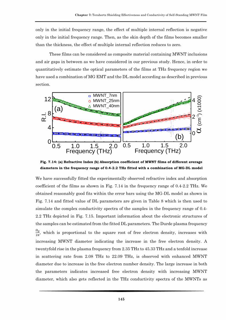
Chapter 7: Terahertz Shielding Effectiveness and Conductivity of Self-Standing MWNT Film
145
only in the initial frequency range, the effect of multiple internal reflection is negative
only in the initial frequency range. Then, as the skin depth of the films becomes smaller
than the thickness, the effect of multiple internal reflection reduces to zero.
These films can be considered as composite material containing MWNT inclusions
and air gaps in between as we have considered in our previous study. Hence, in order to
quantitatively estimate the optical parameters of the films at THz frequency region we
have used a combination of MG EMT and the DL model according as described in previous
section.
Fig. 7.14: (a) Refractive Index (b) Absorption coefficient of MWNT films of different average
diameters in the frequency range of 0.4-2.2 THz fitted with a combination of MG-DL model
We have successfully fitted the experimentally observed refractive index and absorption
coefficient of the films as shown in Fig. 7.14 in the frequency range of 0.4-2.2 THz. We
obtained reasonably good fits within the error bars using the MG-DL model as shown in
Fig. 7.14 and fitted value of DL parameters are given in Table 8 which is then used to
simulate the complex conductivity spectra of the samples in the frequency range of 0.4-
2.2 THz depicted in Fig. 7.15. Important information about the electronic structures of
the samples can be estimated from the fitted DL parameters. The Durde plasma frequency
Ω𝑝
2𝜋, which is proportional to the square root of free electron density, increases with
increasing MWNT diameter indicating the increase in the free electron density. A
twentyfold rise in the plasma frequency from 2.35 THz to 45.33 THz and a tenfold increase
in scattering rate from 2.08 THz to 22.09 THz, is observed with enhanced MWNT
diameter due to increase in the free electron number density. The large increase in both
the parameters indicates increased free electron density with increasing MWNT
diameter, which also gets reflected in the THz conductivity spectra of the MWNTs as
0.5 1.0 1.5 2.0
0
2
4
0.5 1.0 1.5 2.00
4
8
12 MWNT_7nm
MWNT_25nm
MWNT_40nm
Frequency (THz)
(b)
R.I.
Frequency (THz)
(
cm
-1)
(x1000)
(a)

Chapter 7: Terahertz Shielding Effectiveness and Conductivity of Self-Standing MWNT Film
146
observed in Fig. 7.15. The plasma frequency has been found to be much larger than
isolated small gap nanotubes as they are bundled together and no special care has been
taken during the sample fabrication for nanotube isolation. For the largest MWNT
diameter, free electron response (Ω𝑝
2𝜋) is much larger than the Lorenzian response (
Ω𝑘
2𝜋),
while for the other two smaller diameter MWNT samples Ω𝑘
2𝜋>
Ω𝑝
2𝜋. This result indicates
that intertube free carrier migration is enhanced because of the enhanced contact area
between the carbon nanotubes due to its large diameter in MWNT_40 nm sample. The
exciton frequency (ω𝑘
2𝜋) has been explained by different groups either originating from
diameter dependent phenomenon or from length dependent phenomenon. The exciton
frequency which is related to the TCP frequency does not vary monotonically with MWNT
diameter as shown in table 8. This indicates that TCP does not necessarily arise only due
to the curvature induced band gap of the CNTs, otherwise TCP frequency would have
decreased with increasing MWNT diameter and this trend would have got reflected in the
decreased exciton frequency as observed in previous literatures. The peak frequency is
found to be 2.12, 9.37 and 5.01 THz for MWNT_7 nm, MWNT_25 nm and MWNT_40 nm
films, respectively. In the present experiment, the average length is same for all the
samples are kept same however average diameters have been changed as given in the
TEM image in Fig. 7.9.
Table 8: Fitted DL parameters for different MWNT films
Type of CNT 𝛆∞ 𝛀𝒑
𝟐𝝅 (THz)
𝚪𝑷
𝟐𝝅 (THz)
𝛀𝒌
𝟐𝝅 (THz)
𝛚𝒌
𝟐𝝅 (THz)
𝚪𝒌
𝟐𝝅(THz)
MWNT_7nm 4.00 2.35 2.08 4.42 2.12 3.78
MWNT_30nm 4.00 10.60 4.11 50.13 9.37 37.98
MWNT_50nm 4.00 45.33 22.09 43.45 5.01 14.99
So, the change in the exciton frequency as observed in Table 8, might be coming from the
diameter dependence phenomenon. In the two larger diameter MWNT films, exciton
frequency monotonically decreases with increasing diameter however the corresponding
peak frequencies are quite large considering the large diameter of the tubes. People have
observed TCP in the range of 3-10 THz in SWNT samples with diameters of the order of
~ 1 nm[189, 208, 218]. Here, similar TCP have been found but in MWNTs with large
diameter and this may be due to the screening effect of MWNTs under consideration[219].
These indicates that TCP does not necessarily arise only due to the curvature induced

Chapter 7: Terahertz Shielding Effectiveness and Conductivity of Self-Standing MWNT Film
147
band gap of the CNTs, otherwise TCP frequency would decrease with increasing MWNT
diameter and this trend would get reflected in the decreased exciton frequency as observed
in various literatures. Using the fitted DL parameters according to the following equation;
𝜎(𝜔) = (Ω𝑃2
𝜔2 + 𝑖Γ𝑃𝜔−
Ω𝑘2
(𝜔𝑘2 −𝜔2) − 𝑖Γ𝑘𝜔
) 𝑖휀0𝜔. (87)
we have extracted the conductivity spectra of intrinsic MWNT in the frequency range of
0.4-2.2 THz. Although the TCP does not vary systematically with the MWNT diameter,
THz conductivity systematically increases with increasing MWNT diameter under
consideration. Macutkevic et al.[220] have also showed that the TCP frequency does not
necessarily vary with MWNT diameter.
Fig. 7.15: (a) Real and (b) Imaginary THz conductivity of MWNT films with varying diameters
extracted from the fitted DL parameters in the frequency range of 0.4-2.2 THz
They also showed THz conductivity does not change much with increasing MWNT
diameter, which must be due to their limited choice of MWNT diameters (~ 9 and 12-14
nm) as observed from our detailed study.
Conclusion
We have prepared self-standing MWNT films with varying diameter and lengths using
vacuum filtration technique and performed THz spectroscopic measurements at room
temperature in transmission geometry. The effect of MWNT length and diameter on the
shielding effectiveness and conductivity has been studied in THz frequency range. The
shielding mechanism remains same with varying the MWNT length but depends
significantly on MWNT diameter. THz conductivity of these films has been analysed using
0.5 1.0 1.5 2.00
30
60
90
0.5 1.0 1.5 2.0
-30
-20
-10
0
re
al (
Scm
-1)
Frequency (THz)
MWNT_7nm
MWNT_25nm
MWNT_40nm
(b)
Frequency (THz)
im
ag(S
cm
-1)
(a)

Chapter 7: Terahertz Shielding Effectiveness and Conductivity of Self-Standing MWNT Film
148
a combination of MG EMT and DL model and dependence of TCP on the MWNT structure
parameters has been observed.
S_MWNT and L_MWNT films of thickness 14 ± 1 µm are prepared by using
vacuum filtration technique. SE of these films are extracted in the frequency range of 0.4-
2.7 THz and analysed using a phenomenological model. SE is found to be larger than 34
dB for S_MWNT and 46 dB for L_MWNT in the entire frequency range and it increases
weakly with increasing frequency. SE can be increased by ~ 30% at 1.5 THz by simply
changing the average MWNT length and thereby emerges as a potential candidate for
application in THz EMIS devices. The relative contributions of absorption, multiple
internal reflection and reflection to the total SE of the films are calculated using
theoretical models and the weak frequency dependence observed in the SE occurs solely
from the absorption mechanism in the films. The origin of THz conductivity peak is
discussed in the light of excitation of surface plasmon resonance in MWNT by analyzing
the obtained DL parameters and the conductivity spectra. Our investigation concludes
that the TCP arises due to the excitation of plasmon resonances in MWNT films and the
peak frequency is inversely proportional to the length of the MWNT.
We have also prepared self-standing MWNT films using three different MWNT’s
having the same average length (~ 1 m) but of different average diameters (~ 7 nm, 25
nm and 40 nm). Detailed TEM analysis has been showed to confirm the variation of
diameters in different MWNT samples. SE of the films are found to be increased to a
gigantic 350 % by simply migrating to a suitable MWNT diameter. The SE has been
analysed using a modified phenomenological model after carefully considering the skin
depth and thickness of the samples. For MWNT_7nm and MWNT_25nm films SEA turns
out to be as the dominant shielding mechanism, but for the largest diameter MWNT film
(MWNT_40nm), SER becomes the dominant contributor to the total shielding mechanism
especially in smaller frequency region (< 0.8 THz). A MG-DL model has been applied to
extract important electronic information of the samples and extract the THz conductivity
of the MWNT itself. Though TCP does not found to vary systematically on MWNT
diameter, THz conductivity is found to be significantly dependent on the MWNT diameter
and is mainly due to the enhanced free electron number density with increasing MWNT
diameter. A controlled way of THz conductivity modulation of MWNT films will help the
possible future applications of such composites in solar cells and high frequency EMI
shielding device.

Chapter Eight

Chapter 8: Probing Oxidation in Copper Thin Film
150
8. Probing Oxidation in Copper Thin
Film
Introduction
Metallic thin films are continuously being studied as transparent conducting electrode,
ARC, shielding coating in THz frequency range. Oxidation of the films remains a grave
concern upon the performance of these devices. In the present study, we have used THz
spectroscopy as a delicate tool to detect and study the oxidation of Copper (Cu) thin films.
Cu thin films of 20 nm are deposited via UHV d.c. magnetron sputtering technique and
oxidized at 150 0C for 1, 4 and 6 hours. Further analysis on the complex THz conductivity
of these films have been performed using Drude model. Ultrafast relaxation timescales
increase from 20 fs to 200 fs upon oxidation. Thus, we have provided the use of THz
spectroscopy as a sensitive tool to detect oxidation in Cu thin films.
Background Study
The complex frequency dependent conductivity of different types of semiconducting,
metallic thin films and carbon nanostructures had been studied using THz spectroscopy
in a non-invasive way in the last few years. Important conclusions about the electronic
structure of the material had been extracted by analysing the THz conductivity spectra.
Walther et al.[167] used THz-TDS to measure the complex conductivity of nanometer-
thick gold films evaporated on silicon substrates in the frequency region from 0.2 to 2.7
THz. Laman et al.[168] prepared thin films of different metallic systems namely
aluminium (Al), gold (Au) and silver (Ag) and studied their complex conductivity in THz
frequency range at two different temperatures (77 K and 295 K). They found that the Ag
film had much higher conductivity than Al and Au films of the same thickness, although
their conductivity was much smaller than their d.c. value. Jameson et al.[221] studied the
carrier dynamics of nickel-titanium (Ni-Ti) alloy using THz-TDS by varying the Ti
concentration which also changed the thickness of the sample. They found that
transmitted THz amplitude increased linearly with increasing Ti concentration in the
alloy. They also studied the resistivity of the system and found sudden and sharp jumps
in the resistivity curve for Ti concentration 22%, 44% and 62%, at which phase transitions

Chapter 8: Probing Oxidation in Copper Thin Film
151
occurred at the growth temperature. They had also confirmed their THz spectroscopic
data from conventional four probe measurements. Their results implied that the alloy
films undergo significant structural disordering near the phase-transition concentrations.
Zhu et al.[222] reported the THz transmission through vanadium dioxide (VO2) thin films
grown on 𝑐-, 𝑚-, and 𝑟-plane sapphire substrates. Their results revealed that THz
amplitude modulation as large as 84% for VO2 films grown on 𝑟-plane sapphire substrates
was possible upon crossing the metal–insulator phase transition temperature.
Ramanandan et al.[223] studied the oxidation kinetics of Cu thin films using THz-
TDS. They measured the transmission of broadband THz pulses from 1 to 7 THz through
the Cu film (21 nm) while the film got oxidized at an elevated temperature (120, 130, 140
and 150 0C) in ambient air for up to three hours. The THz transmission through a freshly
deposited Cu film was very low, which increased with time as the film was oxidized at
different elevated temperature. The rate of increase was much higher at a temperature of
150 0C than at 120 0C, even though the temperature difference was only 30 0C. For the
three highest temperatures used, the transmission had reached its highest, final value
within 3 hours, suggesting that the oxidation was complete. The change in the
transmitted THz electric field was correlated with the growth of the cuprous oxide layer
and the decrease in thickness of the Cu layer. According to their analysis, a thin layer of
cuprous oxide, which fully transmitted the THz pulses, was grown during Cu oxidation.
The THz transmission through the oxidizing sample was found to be depended only on
the thickness of the existing Cu film. Knowing the thickness of the Cu film which
corresponded to a particular value of the THz transmission, one could determine the
instantaneous remaining Cu film thickness during oxidation. Using Arrhenius law, they
calculated the activation energy for diffusion to be 0.55-0.06 eV, which suggested a fast
diffusion mechanism, such as diffusion of Cu atoms through the grain boundaries as the
dominant diffusion mechanism. Yang et al.[224] studied the frequency-dependent
complex conductivities, refractive indices and absorption coefficients of indium-tin oxide
(ITO) nanowhiskers, which were also considered as a graded refractive index material,
using THz-TDS in the frequency range of 0.2-2.0 THz. They had studied the conductivity
spectra using Drude-Smith model and found that the ITO nanowhiskers exhibited longer
carrier scattering times than ITO thin films. For whiskers with different heights (418 and
698 nm), 𝜔𝑝 were in the range of 864~920 rad. THz, and 𝜏 was in the range of 60~69 fs.
Hong et al.[92] studied the THz conductivity of GO and rGO in the frequency range of 0.3-
2.0 THz. They had prepared GO and rGO films of varying thickness ranging from 5 nm to

Chapter 8: Probing Oxidation in Copper Thin Film
152
30 nm and studied the THz conductivity using the well-known Drude model. Their films
demonstrated good shielding of electromagnetic waves with the conductivity of ~103 S/cm
in the THz range. For 30 nm rGO film, fitted value of plasma frequency and scattering
rate were 100 THz and 26 fs respectively indicating a Drude roll-off frequency larger than
probing frequency. Minami et al.[225] studied linear and nonlinear electron dynamics of
polycrystalline Au ultrathin films with thicknesses ranging from 1.4 to 5.8 nm using THz
spectroscopy.
Basic Theory
A thin film conductivity formula is used to extract the THz conductivity of 20 nm thick
as-prepared and oxidized Cu films. The complex transmitted THz field through the
substrate (�̃�𝑠𝑢𝑏𝑠) and deposited film (�̃�𝑠𝑢𝑏𝑠+𝑓𝑖𝑙𝑚) is related with the complex refractive
index of the substrate (�̃�𝑠𝑢𝑏𝑠) and complex conductivity of the sample �̃�(𝜔) according to
the following equation,
|�̃�𝑠𝑢𝑏𝑠+𝑓𝑖𝑙𝑚
�̃�𝑠𝑢𝑏𝑠| =
1 + �̃�𝑆𝑢𝑏𝑠𝑡𝑟𝑎𝑡𝑒1 + �̃�𝑆𝑢𝑏𝑠𝑡𝑟𝑎𝑡𝑒 + 𝑍0�̃�(𝜔)𝑑
, (88)
where, 𝑍0 and 𝑑 are the free space resistance (377 Ω) and the thickness of the thin film.
The complex THz conductivity is then extracted easily using the following reconfigured
formula,
�̃�(𝜔) = (
(
1+ 𝑛𝑠𝑢𝑏𝑠
|�̃�𝑠𝑢𝑏𝑠+𝐹𝑖𝑙𝑚�̃�𝑠𝑢𝑏𝑠
|)
− 1 − �̃�𝑠𝑢𝑏𝑠
)
𝑍0𝑑 .
(89)
High resistive silicon is used as a substrate for growing the Cu films because of its very
low THz absorption and almost constant refractive index (~3.4) in the probed frequency
range. A MATLAB code given at the appendices is used to extract the complex THz
conductivity of the Cu thin films. The complex THz conductivity extracted using the
abovementioned formula is analysed using the famous Drude formula. The Drude formula
is given below,
�̃�(𝜔) =휀0𝜔𝑃
2𝜏
1 − 𝑖𝜔𝜏 , (90)
where, 𝜔𝑃 and 𝜏 are the plasma frequency and the carrier scattering time, respectively.
The parameters 𝜔𝑃 and 𝜏 can be extracted by fitting the experimentally obtained

Chapter 8: Probing Oxidation in Copper Thin Film
153
conductivity with the Drude model. Further, the carrier concentration (𝑁𝑒) and mobility
(𝜇) can also be determined from the relations
𝑁𝑒 = 휀0𝜔𝑃2𝑚∗/𝑒2 and 𝜇 = 𝑒𝜏/𝑚∗ (91)
respectively, where 𝑚∗ is the electron effective mass; 𝑚𝑒 = 9.109 × 10⁻¹²𝑘𝑔, is the
electron’s mass; 𝑒 = 1.602 × 10⁻¹⁹ 𝐶, is the electron charge. DC conductivity (𝜎𝐷𝐶) can
be calculated from the following formula,
𝜎𝐷𝐶 = 휀0𝜔𝑃2𝜏. (92)
The complex conductivity is analysed using origin software to extract the electronic
parameters of the films.
Sample Preparation
Four Cu thin films of 20 nm thickness are deposited on top of a high resistive silicon
substrate using a d.c. magnetron sputtering unit and then three of those films are put in
an oven which is previously set at 150 0C. The films are taken out after 1 h, 4 h and 6 h
respectively to perform different degree of oxidation in the Cu thin films and these films
are named as Cu_1, Cu_4 and Cu_6 respectively. Cu_0 corresponds to un-oxidized Cu film.
Measurement and Analysis
Transmitted THz amplitude increases with increasing oxidation time as clearly shown in
Fig. 8.1.
Fig. 8.1: Transmitted THz amplitude in time domain through the oxidized Cu films
14 15 16 17 18-1
0
1
2 Silicon
Cu_0
Cu_1
Cu_4
Cu_6
TH
z A
mplit
ude (
a.u
.)
Time (ps)

Chapter 8: Probing Oxidation in Copper Thin Film
154
This is due to the fact that with increasing oxidation time, the metallic nature of the Cu
film decreases and the semiconductor nature increases. The transmittance in frequency
domain has been calculated using the following relation 𝑇(𝜔) = |�̃�𝑠𝑢𝑏𝑠+𝑓𝑖𝑙𝑚(𝜔)
�̃�𝑠𝑢𝑏𝑠(𝜔)|2
, where
�̃�𝑠𝑢𝑏𝑠+𝑓𝑖𝑙𝑚(𝜔) and �̃�𝑠𝑢𝑏𝑠(𝜔) are the complex THz field passing through the sample and
silicon substrate respectively. Transmittance spectrum has been shown in Fig. 8.2a. For
as prepared Cu film, THz transmittance is nearly zero and then with increasing oxidation
time it increases non-linearly, as observed in other studies[223] also. It is also noticeable
that transmittance is nearly frequency independent for the as-prepared Cu film and also
for low oxidized Cu films, but it increases with increasing frequency for Cu_6. This
frequency dependence has been explained later in the chapter. The transmittance at 1
THz is plotted in Fig. 8.2b and fitted with an exponential curve. So, the transmittance
increases exponentially with increasing oxidation time.
Fig. 8.2: (a) Transmittance spectrum of the Cu films, (b) transmittance at 1 THz as a function of
oxidation time and fitted with exponential law
Copper can oxidize to form two oxides, cuprous oxide (Cu2O) or cupric oxide (CuO).
However, for heating temperatures below 2250 C, it is known[223] that the oxide formed
is predominantly cuprous oxide. So, in the present scenario, we can safely assume that,
Cu gets oxidized due to the formation Cu2O layer because of heating and the greater the
oxidation or heating time, larger amount of Cu2O layer is formed. Ramachandan et al.
analysed this oxide layer as a fully THz transparent thin layer (as most dielectric, non-
absorbing thin layers behave in THz frequency range). They studied the transmission
through the oxidized sample, which was dependent only on the thickness of the copper
film and this thickness got decreased with increasing oxidation temperature. However,
we have tried to visualize this phenomenon from a different angel. Because in our
experimental transmittance data, we observe that, THz transmittance not only increased
0.5 1.0 1.5 2.00.000
0.003
0.006
0.25
0.50
0.75
1.00
Tra
nsm
itta
nce
Frequency (THz)
Cu_0
Cu_1
Cu_4
Cu_6
(a)
0 1 2 3 4 5 6
0.0
0.2
0.4
0.6
Oxidation Time (hour)
Tra
nsm
itta
nce @
1 T
Hz
(b)

Chapter 8: Probing Oxidation in Copper Thin Film
155
with increasing oxidation time but also becomes highly frequency dependent. For the
conductivity analysis, at first, we extracted the frequency dependent THz conductivity of
the films using the thin film formula as given below (described in the theory section earlier
in this chapter);
�̃�(𝜔) = (
(
1 + 𝑛𝑠𝑢𝑏𝑠
|�̃�𝑠𝑢𝑏𝑠+𝑓𝑖𝑙𝑚�̃�𝑠𝑢𝑏𝑠
|)
− 1 − �̃�𝑠𝑢𝑏𝑠
)
𝑍0𝑑 ,
(93)
where �̃�𝑠𝑢𝑏𝑠 is the complex refractive index of the silicon substrate (almost constant ~3.41
in the frequency range of interest), 𝑍0 is the free space impedance (377 ) and 𝑑 is the
thickness of the Cu film (~ 20 nm).
We modelled oxidized Cu film as a poor metallic layer having the same thickness of the
as-prepared Cu film (Cu_0). In our calculation, the thickness of the material remains
same, only the average electronic properties of the oxidized Cu film changes with
increasing oxidation time.
Fig. 8.3: (a) Real and (b) imaginary THz conductivity of the Cu films fitted with Drude model
The complex conductivity spectra of the Cu films are shown in Fig. 8.3. The real THz
conductivity of the as prepared 20 nm Cu film is ~ 107 Sm-1 and is almost frequency
independent which matches well with the published values. The real and imaginary
conductivity of these films at 1 THz has been tabulated in the Table 9. We can see that
the real THz conductivity spectra not only decreases with increasing oxidation time but
also becomes highly frequency dependent (for Cu_4 and Cu_6 films). So, we infer that, the
conductivity changes may be related to the intrinsic changes in electronic properties of
0.5 1.0 1.5 2.0
10-1
100
101
102
103
104
0.5 1.0 1.5 2.0
101
102
103
(a) Cu_0
Cu_1
Cu_4
Cu_6
Frequency (THz)
r(x
10
6)
(Sm
-1) (b)
Frequency (THz)
im
a (
x1
04)(
Sm
-1)
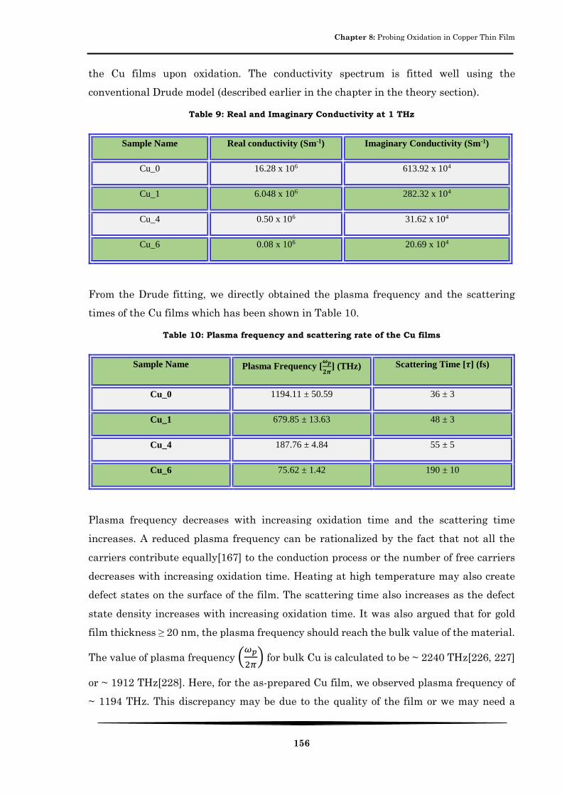
Chapter 8: Probing Oxidation in Copper Thin Film
156
the Cu films upon oxidation. The conductivity spectrum is fitted well using the
conventional Drude model (described earlier in the chapter in the theory section).
Table 9: Real and Imaginary Conductivity at 1 THz
Sample Name Real conductivity (Sm-1) Imaginary Conductivity (Sm-1)
Cu_0 16.28 x 10⁶ 613.92 x 10⁴
Cu_1 6.048 x 10⁶ 282.32 x 10⁴
Cu_4 0.50 x 10⁶ 31.62 x 10⁴
Cu_6 0.08 x 10⁶ 20.69 x 10⁴
From the Drude fitting, we directly obtained the plasma frequency and the scattering
times of the Cu films which has been shown in Table 10.
Table 10: Plasma frequency and scattering rate of the Cu films
Sample Name Plasma Frequency [𝝎𝒑
𝟐𝝅] (THz) Scattering Time [𝝉] (fs)
Cu_0 1194.11 ± 50.59 36 ± 3
Cu_1 679.85 ± 13.63 48 ± 3
Cu_4 187.76 ± 4.84 55 ± 5
Cu_6 75.62 ± 1.42 190 ± 10
Plasma frequency decreases with increasing oxidation time and the scattering time
increases. A reduced plasma frequency can be rationalized by the fact that not all the
carriers contribute equally[167] to the conduction process or the number of free carriers
decreases with increasing oxidation time. Heating at high temperature may also create
defect states on the surface of the film. The scattering time also increases as the defect
state density increases with increasing oxidation time. It was also argued that for gold
film thickness ≥ 20 nm, the plasma frequency should reach the bulk value of the material.
The value of plasma frequency (𝜔𝑝
2𝜋) for bulk Cu is calculated to be ~ 2240 THz[226, 227]
or ~ 1912 THz[228]. Here, for the as-prepared Cu film, we observed plasma frequency of
~ 1194 THz. This discrepancy may be due to the quality of the film or we may need a

Chapter 8: Probing Oxidation in Copper Thin Film
157
thicker sample to reproduce the bulk value in Cu films. The scattering time for as
prepared 20 nm Cu film is found to be ~ 36 fs which is pretty close to the bulk value of
~20 fs[228]. The plasma frequency (𝜔𝑃) and the scattering time (𝜏) along with the error
bars are plotted in Fig. 8.4.
Fig. 8.4: Scattering time (a) and DC conductivity (b) as a function of oxidation time
The d.c. conductivity (𝜎𝐷𝐶), free carrier density (𝑁𝑒) and mobilty (𝜇) can be obtained from
the Drude parameters using the previously mentioned formula and the obtained values
for the Cu thin films are shown in Table 11.
Table 11: Different electronic parameters for the Cu films
Sample 𝝈𝑫𝑪 (Sm-1) 𝑵𝒆 (cm-3) 𝝁 (cm-2V-1s-1)
Cu_0 1.76 x 10⁷ 2.5 x 10²² 44.5
Cu_1 7.7 x 10⁶ 8.1 x 10²¹ 59.4
Cu_4 6.7 x 10⁵ 6.2 x 10²⁰ 68.1
Cu_6 3.8 x 10⁵ 1.0 x 10²⁰ 235.2
The effective mass for Cu is taken 1.42𝑚𝑒 according to published values. So, we observe a
decreasing trend in d.c. conductivity and carrier density with increasing oxidation time
0 1 2 3 4 5 6
0
400
800
1200
40
80
120
160
200 Plasma Frequency
Pla
sm
a F
req
ue
ncy
[
2 p/2] (T
Hz)
Oxidation Time (hour)
Scattering Time
Scatteri
ng
Tim
e (
fs)

Chapter 8: Probing Oxidation in Copper Thin Film
158
as the metallic character of the Cu films gets destroyed due to heating. Upon 6 hour of
heating at 1500 C, d.c. conductivity has been destroyed to 22 % than its original value.
Conclusion
We have prepared Cu thin films of 20 nm thicknesses using a sputtered d.c. magnetron
deposition unit and then heated the films at 150 0C in air for different times (1, 4 and 6
hours) for oxidation. THz spectroscopic measurements are performed on these oxidized
Cu films at room temperature in transmission geometry. One as-prepared Cu film (Cu_0)
of similar thickness was also studied. We know that the due to the oxidation of Cu films,
a layer of Cu2O forms on the surface of the Cu films which creates a severe problem
destroying the metallic character of the film. Previously, it was concluded that, the
oxidized Cu films can be considered safely as a Cu film with reduced thickness to
characterize it because Cu2O layer does not interact with the probing THz frequency. We
found from the THz transmittance behaviour, that after oxidation, not only the
transmittance increases but also a frequency dependence is introduced to the otherwise
frequency independent transmittance spectra. We studied samples as thin films of same
thickness but with degraded electronic properties with increasing oxidation time.
Complex THz conductivity of these films were extracted using a well-known thin film
formula and studied using the Drude model. Both the real and imaginary THz
conductivity is found to be decreasing with increasing oxidation time. We found out that
upon oxidation the plasma frequency decreases and scattering time increases due to
decreasing free carrier density and increasing defect states/scattering centres
respectively.

Chapter Nine
Chapter 9: Conclusion and Future Direction
160
9. Conclusion and Future Direction
This thesis is devoted in understanding the electro-optic properties of different types of
nanostructures in the THz frequency range and using those nanostructures efficiently in
manipulating THz radiation in application purposes. Some of these nanomaterials have
been prepared in the lab while other types of nanostructures (different types of CNTs)
have been commercially procured. In this crucial time, thanks to the pioneering works of
many groups, THz spectroscopy is leaving behind its initial problems regarding efficient
and compact THz sources and detectors, which has limited the applications of this
techniques in the initial years of late 1980s to early 2000s, and moving towards a direction
of unlimited and unforeseen opportunities in terms of its application in diverse gasp of
science ranging from medical imaging, weather and space science, public security to
ultrafast communication, THz opto-electronic devices, THz metamaterials, THz field
induced demagnetization and THz ultrafast dynamics of nanostructures. Although the
search for powerful THz sources is still ongoing which would eventually solve this
technique’s limited applicability in the fields of free space ultrafast communication and
open air imaging, most of the studies are now being directed either in understanding
fundamental physical properties of low energy ultrafast dynamics or applicability of THz
devices. In this significant junction, we have studied the ground state opto-electronic
properties of aligned Ni nanostructures, CNTs and their polymer (PVA) composites and
Cu thin films in this frequency range and their use in manipulating this frequency band.
As large number of studies are now motivated towards the THz electronic device
fabrication and THz ultrafast communications, low cost durable THz manipulating
devices like THz polarizer, THz EMIS films are becoming essential. CNTs act as the
building block of these passive devices due to their fascinating high frequency properties
and often the performance of the devices boils down to the efficient tuning of high
frequency conductivity of these tubes. Although CNTs are being studied using THz
spectroscopy since 2000s, the origin of extremely high THz conductivity in CNTs still
remains a subject of debate and its relation with the geometrical parameters of the tubes
is worth investigating.
Nanostructures other than CNTs have been prepared using chemical synthesis and
vacuum filtration technique and characterized using conventional SEM, TEM and UV-

Chapter 9: Conclusion and Future Direction
161
visible spectrometer. The experiments are performed using THz-TDS at room
temperature in transmission geometry. Data is analysed using a commercial software
(Teralyzer) for complex optical refractive index extraction and using matlab interface for
others. Sufficient theoretical analysis has also been performed to explain the
experimentally obtained data mainly using matlab interface.
Conclusion
Chapter 1 provides the general introduction of the THz radiation, its potential application
in diverse areas of science and the spectroscopic measurements possible using this
technique and its advantage over the conventional spectroscopic technique.
Chapter 2 provides the general background of this spectroscopic technique. It includes
brief history about the development of this field starting from the early 1980s, which
mainly consists of the study of new types of antenna based, and photo-mixer based
structures for THz generation and THz detection and the subsequent optimization of the
field and also the theory and demonstration of THz generation and detection using photo
conductive antenna. A brief description of different application based recent works (within
last ten years) on THz spectroscopy of different types of exotic nanostructures which is
not within the scope of the present thesis is also provided.
Chapter 3 is dedicated for the description of the instruments and data analysis procedure.
The different components of the THz spectrometer (Menlo Tera K-8 spectrometer) that I
have used is described in detail. The alignment procedure and working principle of the
spectrometer is discussed. Though the alignment procedure is not unique and it depends
on the individual, an overall idea about the alignment procedure can be found here. It
mainly combines the ideas provided by the Menlo system engineers Rafal and Chris
during their installation, technical visits, email assistance, my own hand-on experience
while handling the instrument over four years and valuable inputs from my lab mates.
General description about SEM, TEM, UV-visible Spectrometer has also been provided.
These instruments are mainly used for additional sample characterization during
experiments. The data analysis procedure and the corresponding theory is also discussed.
Chapter 4 to chapter 8 is based upon the experimental works that I have performed during
my PhD. In chapter 4, we demonstrate an easy route to prepare robust and durable THz
polarizer and its performance in THz frequency range. NiNP with average diameter ~ 165
nm and NiNC with average diameter ~ 300 nm and average length ~ 4 m has been
chemically synthesized and aligned in liquefied polymer matrices under the influence of

Chapter 9: Conclusion and Future Direction
162
external magnetic field. Anisotropic THz transmittance is observed with these structures
in THz frequency range. For NiNP polarizer, the effective polarizer bandwidth is 0.2 to
0.9 THz with very high DOP ~ 0.98 ± 0.03 which then decreases with increasing probing
frequency further. However, using the NiNC polarizer, we obtained a large polarizer
bandwidth of 0.3-2.4 THz but with limited DOP of 0.76 ± 0.03. Our study revealed that
the alignment of nanostructures could easily be tuned by using more uniform external
magnetic field, which could ultimately control the DOP and polarizer bandwidth of the
structure. Considering the good polarizing performance, easy and cheap preparation
process, durability, robustness and tunability, we found that aligned magnetic
nanostructures offer bright prospect to emerge as a popular THz polarizer.
Chapter 5 is based on the study of THz electromagnetic shielding in SWNT-polymer
composites. The composite polymer films are prepared via slow drying method with
varying SWNT content in PVA matrices. Transmittance is found to be significant at lower
frequencies (between 0.3 and 0.8 THz) but close to zero at higher frequencies (beyond 1.25
THz) showing a possible application of these composites especially with higher amount of
SWNT contents for low band-pass THz filters. Shielding properties of the samples are
studied in the frequency range of 0.3 THz to 2.1 THz with highest SE of ~ 29 dB at 2.1
THz. SE shows a linear relationship with SWNT weight fraction at a particular probing
frequency and in a broad frequency range from 1.2 to 2.0 THz, SE can be expressed as
𝑆𝐸 ∝ (0.73 ± 0.075)w where 𝑤 is the SWNT weight fraction. Thus we have showed the
performance of a low-cost and durable THz EMI shield using SWNT composites.
Chapter 6 is dedicated in studying two different and unique ways of conductivity
manipulation in SWNT/polymer composites.
In the first part we have demonstrated how the average length of SWNTs effect the
overall THz conductivity of the SWNT/PVA composite films. The films are prepared via a
slow drying process with a constant thickness of 300 ± 20 µm with varying SWNT length
(~ 2 m and ~15 m) and SWNT weight fraction in the PVA matrix. THz conductivity
spectra are obtained for these films in transmission geometry in the frequency range of
0.3 - 2.0 THz. It is explicitly shown that real conductivity of such films can be tuned up to
80% in a controlled manner by carefully choosing the length and weight fraction of the
SWNT’s. The length dependent high frequency conductivity of SWNTs is discussed in the
light of surface plasmon resonance.
Chapter 9: Conclusion and Future Direction
163
In the next part, we have tried to modulate the THz conductivity of SWNT/PVA and
MWNT/PVA composites by decorating the sidewalls of the tubes with chemically
synthesized AuNP and varying the density of AuNP decoration. The attachment of Au NP
on the sidewalls of CNTs are confirmed by UV- visible spectroscopy as well as from SEM
and TEM images. Surfaced decorated SWNT composites show either conductivity
decrement or enhancement up to ± 15% depending on the AuNP concentration than the
undecorated SWNT composites. The results are explained qualitatively by suggesting the
role of AuNP as carrier trapping potential or alternative carrier conduction path
depending on its density.
A controlled way of THz conductivity modulation of SWNT/PVA composites will help
the possible future applications of such composites in solar cells and high frequency EMI
shielding devices.
In chapter 7, we have discussed the THz shielding effectiveness and THz conductivity of
self-standing MWNT films as a function of MWNT diameter and MWNT length. The
relative contributions of absorption, multiple internal reflection and reflection to the total
SE of the films are calculated using theoretical models. Intrinsic THz conductivity of the
MWNTs have been extracted using MG EMT and analysed with DL model.
Self-standing MWNT films of thicknesses ~15-25 m is prepared using vacuum
filtration technique of two different MWNT average lengths (S_MWNT and L_MWNT
having average length ~ 2 m and 15 m) and three different MWNT average outer
diameters (MWNT_7nm, MWNT_25nm and MWNT_40nm). SE can be increased by ~ 30%
at 1.5 THz by simply changing the average MWNT length whereas the increment can be
as high as 350% by changing the MWNT diameter. The mechanism of shielding does not
change with length variation; absorptive shielding increases while reflective shielding
decreases with increasing frequency and the effect of multiple internal reflection is
negative and almost negligible. However, the shielding mechanism is found to be MWNT
diameter dependent. For the two smaller diameter MWNT films SEA turns out to be the
dominant shielding mechanism in the entire frequency range, but for the largest diameter
MWNT film, SER becomes the dominant contributor to the total shielding mechanism in
smaller frequency region (< 0.8 THz), although their frequency response remains the
same. Our study on THz conductivity spectra concludes that the TCP arises due to the
excitation of plasmon resonances in MWNT films and the peak frequency is inversely
proportional to the length of the MWNT and it does not vary systematically on MWNT
Chapter 9: Conclusion and Future Direction
164
diameter. However, THz conductivity is found to be significantly and systematically
increasing both with increasing MWNT length and diameter.
In chapter 8, on a slightly different note, we have studied the effect of oxidation in Cu thin
films on the THz conductivity property of the films. We have prepared Cu thin films of 20
nm thicknesses using a sputtered magnetron d.c. deposition unit and then heated the
films at 150 0C in air for different times for oxidation. We found that the THz conductivity
of the oxidized Cu films can be described using the conventional Drude model but with
significantly reduced metallic properties. Both the real and imaginary THz conductivity
are found to be decreasing with increasing oxidation time. We found out that upon
oxidation the plasma frequency decreases due to decreasing free carrier density and
scattering time increases due to increasing defect states/scattering centres. The relation
of the opto-electronic properties of Cu films with the oxidation time is experimentally
established.
Future Direction
Ample scope exists to extend the works of the present thesis for more complete
understanding of the fundamental properties of the nanostructures and their fruitful
applications.
We have studied aligned nanoparticles and nanochains for the preparation of THz
polarizer. However, from my understanding aligned nanowires and CNTs should provide
a better DOP because of the large anisotropic AR of the structures. People have studied
aligned CNTs grown on Si or quartz substrates using CVD technique however that makes
the procedure to be expensive and the sample to be brittle. Some studies have shown
promising ways to align CNTs inside polymer matrices which would provide a durable
film. One can systematically study the THz polarizing behavior of such high AR
nanostructures. One can also study metallic wire grid like polarizer structure on Si
substrates and a graphene film and electrode sandwiched between them. The gate voltage
will significantly alter the resistance of the graphene in THz frequency range which
should in turn effect the THz transmittance of the polarizer both parallel and
perpendicular orientation. Such an active THz polarizer may provide us interesting
pathways to manipulate the polarization property of THz waves. Numerous literatures
exist in studying THz metamaterials, however, there are plenty of room in studying the
ARC in THz frequency range to minimize the problem of FP reflections in THz devices.
We have started some preliminary measurements on anti-dot metallic structures and they
Chapter 9: Conclusion and Future Direction
165
gave us better ARC performance than the conventional metallic thin film coatings.
Thorough investigation is ongoing to study the effect of anti-dot thickness and structure
constants on the ARC behavior. While anti-dot structure will provide the high
transmission of main THz pulse, the geometry of the anti-dot will provide the necessary
impedance matching condition for FP reflection peak suppression.
We have studied the SE and THz conductivity of SWNT/PVA composite films. One
immediate extension of this works should be measuring the temperature dependent THz
conductivity of the polymer composites, which would actually enable us to dictate the
exact conductivity mechanism like variable range hopping, correlated barrier hopping, or
small polaron tunneling mechanisms associated with the polymer composite structures.
The role of SWNT and MWNT structure constants can also be explored. The highest SE
we have obtained in SWNT composites is ~ 30 dB in THz frequency range. One can also
try to increase the SE of the composites by introducing conductive polymer instead of PVA
to disperse the CNTs and also additional conductive inclusion like metallic
nanowires/nanochains can be incorporated into the composite material to make it much
more absorptive thus helping to increase its shielding behavior.
Due to limited frequency window of our spectrometer, we have studied the
conductivity spectra of the self-standing MWNT films up to 2.7 THz and then simulated
the spectra up to 20 THz to get knowledge about the TCP of the MWNT. However, using
an ultra-broadband THz spectrometer, it is possible to directly measure the THz response
of the films in the frequency range of interest and obtain a first-hand knowledge about
the relation of TCP with the geometrical parameters of the tubes. Although such studies
have already been performed using THz and FTIR technique; a thorough study using a
single THz spectrometer with large number of different types of carefully chosen MWNT
samples may provide us some much needed conclusive results.
I have studied the effect of nanostructured materials and their composites in
manipulating THz radiation, now I am interested in using external influences like
magnetic field, temperature, current to the material under investigation to manipulate
THz radiation like magnetic field or temperature induced THz transparency, current
induced THz conductivity etc.. It is also high time to study THz spintronics using
ferromagnetic/non-magnetic multiplayer films and their interaction with polarized THz
waves in the presence of external magnetic field. Such studies will also provide us the
fundamental carrier lifetimes of the system in a neutral way because of the extremely low
temperature/energy of THz radiation.

166
10. References
1. C. Wai Lam, D. Jason, and M. M. Daniel, "Imaging with terahertz radiation," Reports on Progress in Physics 70, 1325-1379 (2007).
2. B. Ferguson and X.-C. Zhang, "Materials for terahertz science and technology," Nature Materials 1, 26-33 (2002).
3. L. Ren, C. L. Pint, L. G. Booshehri, W. D. Rice, X. Wang, D. J. Hilton, K. Takeya, I. Kawayama, M. Tonouchi, R. H. Hauge, and J. Kono, "Carbon Nanotube Terahertz Polarizer," Nano Letters 9, 2610-2613 (2009).
4. J. Kyoung, E. Y. Jang, M. D. Lima, H.-R. Park, R. O. Robles, X. Lepró, Y. H. Kim, R. H. Baughman, and D.-S. Kim, "A Reel-Wound Carbon Nanotube Polarizer for Terahertz Frequencies," Nano Letters 11, 4227-4231 (2011).
5. L. Ren, C. L. Pint, T. Arikawa, K. Takeya, I. Kawayama, M. Tonouchi, R. H. Hauge, and J. Kono, "Broadband Terahertz Polarizers with Ideal Performance Based on Aligned Carbon Nanotube Stacks," Nano Letters 12, 787-790 (2012).
6. D. Polley, A. Ganguly, A. Barman, and R. K. Mitra, "Polarizing effect of aligned nanoparticles in terahertz frequency region," Optics Letters 38, 2754-2756 (2013).
7. J.-B. Masson and G. Gallot, "Terahertz achromatic quarter-wave plate," Optics Letters 31, 265-267 (2006).
8. I. Yamada, K. Takano, M. Hangyo, M. Saito, and W. Watanabe, "Terahertz wire-grid polarizers with micrometer-pitch Al gratings," Optics Letters 34, 274-276 (2009).
9. M. A. Seo, J. W. Lee, and D. S. Kim, "Dielectric constant engineering with polymethylmethacrylate-graphite metastate composites in the terahertz region," Journal of Applied Physics 99, 066103, (2006).
10. E. N. Agnandji, V. Vigneras, J. L. Miane, and P. Mounaix, "Shielding effectiveness in terahertz domain of monolayer-doped polyaniline films," in Electronics Letters, (2007), pp. 1271-1273.
11. M. A. Seo, J. H. Yim, Y. H. Ahn, F. Rotermund, D. S. Kim, S. Lee, and H. Lim, "Terahertz electromagnetic interference shielding using single-walled carbon nanotube flexible films " Applied Physics Letters 93, 231905 (2008).
12. Q. Shi, W. Huang, Y. Zhang, J. Yan, Y. Zhang, M. Mao, Y. Zhang, and M. Tu, "Giant Phase Transition Properties at Terahertz Range in VO2 films Deposited by Sol–Gel Method," ACS Applied Materials & Interfaces 3, 3523-3527 (2011).
13. Z. Jin, A. Tkach, F. Casper, V. Spetter, H. Grimm, A. Thomas, T. Kampfrath, M. Bonn, M. Klaui, and D. Turchinovich, "Accessing the fundamentals of magnetotransport in metals with terahertz probes," Nature Physics 11, 761-766 (2015).
14. D. E. Endean, J. N. Heyman, S. Maat, and E. D. Dahlberg, "Quantitative analysis of the giant magnetoresistance effect at microwave frequencies," Physical Review B 84, 212405 (2011).
15. C. J. E. Straatsma, M. Johnson, and A. Y. Elezzabi, "Terahertz spinplasmonics in random ensembles of Ni and Co microparticles," Journal of Applied Physics 112, 103904 (2012).
16. N. Horiuchi, "Terahertz spectroscopy: Magneto measurements," Nature Photonics 9, 553-553 (2015).
17. C. Vicario, C. Ruchert, F. Ardana Lamas, P. M. Derlet, B. Tudu, J. Luning, and C. P. Hauri, "Off-resonant magnetization dynamics phase-locked to an intense phase-stable terahertz transient," Nature Photonics 7, 720-723 (2013).

167
18. J. Ahn, D. Hutchinson, C. Rangan, and P. Bucksbaum, "Quantum phase retrieval of a Rydberg wave packet using a half-cycle pulse," Physical Review Letters 86, 1179-1182 (2001).
19. T. Qi, Y.-H. Shin, K.-L. Yeh, K. A. Nelson, and A. M. Rappe, "Collective coherent control: synchronization of polarization in ferroelectric PbTiO3 by shaped THz fields," Physical Review Letters 102, 247603 (2009).
20. D. S. Rana, I. Kawayama, K. Mavani, K. Takahashi, H. Murakami, and M. Tonouchi, "Understanding the nature of ultrafast polarization dynamics of ferroelectric memory in the multiferroic BiFeO3," Advanced Materials 21, 2881-2885 (2009).
21. K. Lee, B. Sussman, M. Sprague, P. Michelberger, K. Reim, J. Nunn, N. Langford, P. Bustard, D. Jaksch, and I. Walmsley, "Macroscopic non-classical states and terahertz quantum processing in room-temperature diamond," Nature Photonics 6, 41-44 (2012).
22. J. A. Hutchby, G. I. Bourianoff, V. V. Zhirnov, and J. E. Brewer, "Extending the road beyond CMOS," IEEE Circuits and Devices Magazine 18, 28-41 (2002).
23. X. Wang, M. Afzelius, N. Ohlsson, U. Gustafsson, and S. Kröll, "Coherent transient data-rate conversion and data transformation," Optics Letters 25, 945-947 (2000).
24. L. Moeller, J. Federici, and K. Su, "2.5 Gbit/s duobinary signalling with narrow bandwidth 0.625 terahertz source," in Electronics Letters, (2011), pp. 856-858.
25. T. Kleine-Ostmann and T. Nagatsuma, "A review on terahertz communications research," Journal of Infrared, Millimeter, and Terahertz Waves 32, 143-171 (2011).
26. J. M. Jornet and I. F. Akyildiz, "Joint energy harvesting and communication analysis for perpetual wireless nanosensor networks in the terahertz band," Nanotechnology, IEEE Transactions on 11, 570-580 (2012).
27. T. Schneider, A. Wiatrek, S. Preußler, M. Grigat, and R.-P. Braun, "Link budget analysis for terahertz fixed wireless links," Terahertz Science and Technology, IEEE Transactions on 2, 250-256 (2012).
28. M. D. Rotaru and J. K. Sykulski, "Improved sensitivity of terahertz label free bio-sensing application through trapped-mode resonances in planar resonators," Magnetics, IEEE Transactions on 47, 1026-1029 (2011).
29. T. de Graauw, "THz Astronomy from Space," in New Directions in Terahertz Technology (Springer, 1997), pp. 237-244.
30. E. Klisch, T. Klaus, S. Belov, G. Winnewisser, and E. Herbst, "Laboratory rotational spectrum of CN in the 1 THz region," Astronomy and Astrophysics 304, L5 (1995).
31. S. Withington, "Terahertz astronomical telescopes and instrumentation," Philosophical Transactions of the Royal Society of London A: Mathematical, Physical and Engineering Sciences 362, 395-402 (2004).
32. B. J. Drouin, S. Yu, J. C. Pearson, and H. Gupta, "Terahertz spectroscopy for space applications: 2.5–2.7 THz spectra of HD, H2O and NH3," Journal of molecular structure 1006, 2-12 (2011).
33. S. Nakajima, H. Hoshina, M. Yamashita, C. Otani, and N. Miyoshi, "Terahertz imaging diagnostics of cancer tissues with a chemometrics technique," Applied Physics Letters 90, 41102 (2007).
34. Q. Wu, T. Hewitt, and X. C. Zhang, "Two‐dimensional electro‐optic imaging of THz beams," Applied Physics Letters 69, 1026-1028 (1996).
35. S. Hunsche, M. Koch, I. Brener, and M. Nuss, "THz near-field imaging," Optics Communications 150, 22-26 (1998).
36. Q. Chen, Z. Jiang, G. Xu, and X.-C. Zhang, "Near-field terahertz imaging with a dynamic aperture," Optics Letters 25, 1122-1124 (2000).
37. P. Knobloch, C. Schildknecht, T. Kleine-Ostmann, M. Koch, S. Hoffmann, M. Hofmann, E. Rehberg, M. Sperling, K. Donhuijsen, and G. Hein, "Medical THz imaging: an

168
investigation of histo-pathological samples," Physics in Medicine and Biology 47, 3875-3884 (2002).
38. H.-T. Chen, R. Kersting, and G. C. Cho, "Terahertz imaging with nanometer resolution," Applied Physics Letters 83, 3009-3011 (2003).
39. J. F. Federici, B. Schulkin, F. Huang, D. Gary, R. Barat, F. Oliveira, and D. Zimdars, "THz imaging and sensing for security applications—explosives, weapons and drugs," Semiconductor Science and Technology 20, S266 (2005).
40. J. Chen, Y. Chen, H. Zhao, G. J. Bastiaans, and X.-C. Zhang, "Absorption coefficients of selected explosives and related compounds in the range of 0.1–2.8 THz," Optics Express 15, 12060-12067 (2007).
41. W. Fan, A. Burnett, P. Upadhya, J. Cunningham, E. Linfield, and A. Davies, "Far-infrared spectroscopic characterization of explosives for security applications using broadband terahertz time-domain spectroscopy," Applied spectroscopy 61, 638-643 (2007).
42. M. Tonouchi, "Cutting-edge terahertz technology," Nature Photonics 1, 97-105 (2007). 43. S. L. Dexheimer, ed., Terahertz Spectroscopy Principles and Applications (CRC Press, 2007).
44. D. H. Auston, A. M. Glass, and P. LeFur, "Tunable far‐infrared generation by difference frequency mixing of dye lasers in reduced (black) lithium niobate," Applied Physics Letters 23, 47-48 (1973).
45. D. H. Auston, "Picosecond optoelectronic switching and gating in silicon," Applied Physics Letters 26, 101-103 (1975).
46. P. LeFur and D. H. Auston, "A kilovolt picosecond optoelectronic switch and Pockel’s cell," Applied Physics Letters 28, 21-23 (1976).
47. D. H. Auston, K. P. Cheung, and P. R. Smith, "Picosecond photoconducting Hertzian dipoles," Applied Physics Letters 45, 284-286 (1984).
48. P. R. Smith, D. H. Auston, and M. C. Nuss, "Subpicosecond photoconducting dipole antennas," IEEE Journal of Quantum Electronics 24, 255-260 (1988).
49. M. B. Ketchen, D. Grischkowsky, T. C. Chen, C. C. Chi, I. N. Duling, N. J. Halas, J. M. Halbout, J. A. Kash, and G. P. Li, "Generation of subpicosecond electrical pulses on coplanar transmission lines," Applied Physics Letters 48, 751-753 (1986).
50. D. Grischkowsky, "Optical pulse compression," Applied Physics Letters 25, 566-568 (1974).
51. H. Nakatsuka and D. Grischkowsky, "Recompression of optical pulses broadened by passage through optical fibers," Optics Letters 6, 13-15 (1981).
52. C. Fattinger and D. Grischkowsky, "Terahertz beams," Applied Physics Letters 54, 490-492 (1989).
53. K. A. McIntosh, E. R. Brown, K. B. Nichols, O. B. McMahon, W. F. DiNatale, and T. M.
Lyszczarz, "Terahertz photomixing with diode lasers in low‐temperature‐grown GaAs," Applied Physics Letters 67, 3844-3846 (1995).
54. S. Matsuura, M. Tani, and K. Sakai, "Generation of coherent terahertz radiation by photomixing in dipole photoconductive antennas," Applied Physics Letters 70, 559-561 (1997).
55. S. Kono, M. Tani, P. Gu, and K. Sakai, "Detection of up to 20 THz with a low-temperature-grown GaAs photoconductive antenna gated with 15 fs light pulses," Applied Physics Letters 77, 4104-4106 (2000).
56. M. Tani, K. Sakai, and H. Mimura, "Ultrafast Photoconductive Detectors Based on Semi-Insulating GaAs and InP," Japanese Journal of Applied Physics 36, L1175 (1997).
57. M. Tani, S. Matsuura, K. Sakai, and S.-i. Nakashima, "Emission characteristics of photoconductive antennas based on low-temperature-grown GaAs and semi-insulating GaAs," Applied Optics 36, 7853-7859 (1997).

169
58. T.-A. Liu, M. Tani, M. Nakajima, M. Hangyo, K. Sakai, S.-i. Nakashima, and C.-L. Pan, "Ultrabroadband terahertz field detection by proton-bombarded InP photoconductive antennas," Optics Express 12, 2954-2959 (2004).
59. B. Salem, D. Morris, V. Aimez, J. Beerens, J. Beauvais, and D. Houde, "Pulsed photoconductive antenna terahertz sources made on ion-implanted GaAs substrates," Journal of Physics: Condensed Matter 17, 7327-7333 (2005).
60. A. Dreyhaupt, S. Winnerl, T. Dekorsy, and M. Helm, "High-intensity terahertz radiation from a microstructured large-area photoconductor," Applied Physics Letters 86, 121114 (2005).
61. P. C. Upadhya, W. Fan, A. Burnett, J. Cunningham, A. G. Davies, E. H. Linfield, J. Lloyd-Hughes, E. Castro-Camus, M. B. Johnston, and H. Beere, "Excitation-density-dependent generation of broadband terahertz radiation in an asymmetrically excited photoconductive antenna," Optics Letters 32, 2297-2299 (2007).
62. F. Miyamaru, Y. Saito, K. Yamamoto, T. Furuya, S. Nishizawa, and M. Tani, "Dependence of emission of terahertz radiation on geometrical parameters of dipole photoconductive antennas," Applied Physics Letters 96, 211104 (2010).
63. S.-G. Park, Y. Choi, Y.-J. Oh, and K.-H. Jeong, "Terahertz photoconductive antenna with metal nanoislands," Optics Express 20, 25530-25535 (2012).
64. L. Hou and W. Shi, "An LT-GaAs Terahertz Photoconductive Antenna With High Emission Power, Low Noise, and Good Stability," IEEE Transactions on Electron Devices 60, 1619-1624 (2013).
65. X. Ropagnol, F. Blanchard, T. Ozaki, and M. Reid, "Intense terahertz generation at low frequencies using an interdigitated ZnSe large aperture photoconductive antenna," Applied Physics Letters 103, 161108 (2013).
66. S. Gupta, J. F. Whitaker, and G. A. Mourou, "Ultrafast carrier dynamics in III-V semiconductors grown by molecular-beam epitaxy at very low substrate temperatures," IEEE Journal of Quantum Electronics 28, 2464-2472 (1992).
67. N. Sekine, K. Hirakawa, F. Sogawa, Y. Arakawa, N. Usami, Y. Shiraki, and T. Katoda, "Ultrashort lifetime photocarriers in Ge thin films," Applied Physics Letters 68, 3419-3421 (1996).
68. H. Erlig, S. Wang, T. Azfar, A. Udupa, H. R. Fetterman, and D. C. Streit, "LT-GaAs detector with 451 fs response at 1.55 μm via two-photon absorption," Electronics Letters 35, 173-174 (1999).
69. M. Tani, K.-S. Lee, and X.-C. Zhang, "Detection of terahertz radiation with low-temperature-grown GaAs-based photoconductive antenna using 1.55 μm probe," Applied Physics Letters 77, 1396-1398 (2000).
70. M. Suzuki and M. Tonouchi, "Fe-implanted InGaAs photoconductive terahertz detectors triggered by 1.56μm femtosecond optical pulses," Applied Physics Letters 86, 163504 (2005).
71. H. Roehle, R. J. B. Dietz, H. J. Hensel, J. Böttcher, H. Künzel, D. Stanze, M. Schell, and B. Sartorius, "Next generation 1.5 µm terahertz antennas: mesa-structuring of InGaAs/InAlAs photoconductive layers," Optics Express 18, 2296-2301 (2010).
72. B. Sartorius, H. Roehle, H. Künzel, J. Böttcher, M. Schlak, D. Stanze, H. Venghaus, and M. Schell, "All-fiber terahertz time-domain spectrometer operating at 1.5 µm telecom wavelengths," Optics Express 16, 9565-9570 (2008).
73. C. Baker, I. S. Gregory, M. J. Evans, W. R. Tribe, E. H. Linfield, and M. Missous, "All-optoelectronic terahertz system using low-temperature-grown InGaAs photomixers," Optics Express 13, 9639-9644 (2005).
170
74. J.-M. Rämer, F. Ospald, G. von Freymann, and R. Beigang, "Generation and detection of
terahertz radiation up to 4.5 THz by low-temperature grown GaAs photoconductive
antennas excited at 1560 nm," Applied Physics Letters 103, 021119 (2013). 75. D. Griffiths, Introduction to Electrodynamics (3rd Edition) (Benjamin Cummings, 1998). 76. J. D. Jackson, Classical Electrodynamics, 3rd Edition (Wiley, 1998). 77. M. Dressel and G. Gruner, Electrodynamics of Solids (Chembridge University Press, 2002). 78. S. Sirbu, "Induced Excitations In Some Metal Oxides," (Ph. D. Thesis, Rijksuniversiteit
Groningen, 2008). 79. D. Turchinovich, "Study of ultrafast polarization and carrier dynamics in semiconductor
nanostructures: a THz spectroscopy approach," (Ph. D. Thesis, University of Freiburg, 2004).
80. J. T. Darrow, X. C. Zhang, D. H. Auston, and J. D. Morse, "Saturation properties of large-aperture photoconducting antennas," IEEE Journal of Quantum Electronics 28, 1607-1616 (1992).
81. Y. R. Shen, The Principles of Nonlinear Optics (Willey, 2002). 82. A. J. Taylor, P. K. Benicewicz, and S. M. Young, "Modeling of femtosecond
electromagnetic pulses from large-aperture photoconductors," Optics Letters 18, 1340-1342 (1993).
83. P. Parkinson, J. Lloyd-Hughes, Q. Gao, H. H. Tan, C. Jagadish, M. B. Johnston, and L. M. Herz, "Transient Terahertz Conductivity of GaAs Nanowires," Nano Letters 7, 2162-2165 (2007).
84. E. Hendry, M. Koeberg, B. O'Regan, and M. Bonn, "Local Field Effects on Electron Transport in Nanostructured TiO2 Revealed by Terahertz Spectroscopy," Nano Letters 6, 755-759 (2006).
85. P. A. George, J. Strait, J. Dawlaty, S. Shivaraman, M. Chandrashekhar, F. Rana, and M. G. Spencer, "Ultrafast optical-pump terahertz-probe spectroscopy of the carrier relaxation and recombination dynamics in epitaxial graphene," Nano Letters 8, 4248-4251 (2008).
86. M. C. Hoffmann, J. Hebling, H. Y. Hwang, K.-L. Yeh, and K. A. Nelson, "THz-pump/THz-probe spectroscopy of semiconductors at high field strengths [Invited]," Journal of the Optical Society of America B 26, A29-A34 (2009).
87. J. Hebling, M. C. Hoffmann, H. Y. Hwang, K.-L. Yeh, and K. A. Nelson, "Observation of nonequilibrium carrier distribution in Ge, Si, and GaAs by terahertz pump–terahertz probe measurements," Physical Review B 81, 035201 (2010).
88. R. Ulbricht, E. Hendry, J. Shan, T. F. Heinz, and M. Bonn, "Carrier dynamics in semiconductors studied with time-resolved terahertz spectroscopy," Reviews of Modern Physics 83, 543 (2011).
89. J. Shah, Ultrafast spectroscopy of semiconductors and semiconductor nanostructures (Springer Science & Business Media, 2013), Vol. 115.
90. J. J. Hannah, J. D. Callum, G. Qiang, H. H. Tan, J. Chennupati, L.-H. James, M. H. Laura, and B. J. Michael, "Electronic properties of GaAs, InAs and InP nanowires studied by terahertz spectroscopy," Nanotechnology 24, 214006 (2013).
91. V. Ryzhii, M. Ryzhii, and T. Otsuji, "Negative dynamic conductivity of graphene with optical pumping," Journal of Applied Physics 101, 083114 (2007).
92. J. T. Hong, K. M. Lee, B. H. Son, S. J. Park, D. J. Park, J.-Y. Park, S. Lee, and Y. H. Ahn, "Terahertz conductivity of reduced graphene oxide films," Optics Express 21, 7633-7640 (2013).
93. M. Tamagnone, J. S. Gómez-Díaz, J. R. Mosig, and J. Perruisseau-Carrier, "Reconfigurable terahertz plasmonic antenna concept using a graphene stack," Applied Physics Letters 101, 214102 (2012).

171
94. A. Vakil and N. Engheta, "Transformation optics using graphene," Science 332, 1291-1294 (2011).
95. J. Horng, C.-F. Chen, B. Geng, C. Girit, Y. Zhang, Z. Hao, H. A. Bechtel, M. Martin, A. Zettl, M. F. Crommie, Y. R. Shen, and F. Wang, "Drude conductivity of Dirac fermions in graphene," Physical Review B 83, 165113 (2011).
96. G. Jnawali, Y. Rao, H. Yan, and T. F. Heinz, "Observation of a Transient Decrease in Terahertz Conductivity of Single-Layer Graphene Induced by Ultrafast Optical Excitation," Nano Letters 13, 524-530 (2013).
97. F. Bonaccorso, Z. Sun, T. Hasan, and A. Ferrari, "Graphene photonics and optoelectronics," Nature Photonics 4, 611-622 (2010).
98. L. Ju, B. Geng, J. Horng, C. Girit, M. Martin, Z. Hao, H. A. Bechtel, X. Liang, A. Zettl, Y. R. Shen, and F. Wang, "Graphene plasmonics for tunable terahertz metamaterials," Nature Nanotechnology 6, 630-634 (2011).
99. L. Vicarelli, M. S. Vitiello, D. Coquillat, A. Lombardo, A. C. Ferrari, W. Knap, M. Polini, V. Pellegrini, and A. Tredicucci, "Graphene field-effect transistors as room-temperature terahertz detectors," Nature Materials 11, 865-871 (2012).
100. S. H. Lee, M. Choi, T.-T. Kim, S. Lee, M. Liu, X. Yin, H. K. Choi, S. S. Lee, C.-G. Choi, S.-Y. Choi, X. Zhang, and B. Min, "Switching terahertz waves with gate-controlled active graphene metamaterials," Nature Materials 11, 936-941 (2012).
101. H. Y. Hwang, N. C. Brandt, H. Farhat, A. L. Hsu, J. Kong, and K. A. Nelson, "Nonlinear THz Conductivity Dynamics in P-Type CVD-Grown Graphene," The Journal of Physical Chemistry B 117, 15819-15824 (2013).
102. F. Xia, T. Mueller, Y.-m. Lin, A. Valdes-Garcia, and P. Avouris, "Ultrafast graphene photodetector," Nature Nanotechnology 4, 839-843 (2009).
103. I. Maeng, S. Lim, S. J. Chae, Y. H. Lee, H. Choi, and J.-H. Son, "Gate-Controlled Nonlinear Conductivity of Dirac Fermion in Graphene Field-Effect Transistors Measured by Terahertz Time-Domain Spectroscopy," Nano Letters 12, 551-555 (2012).
104. S. Chih-Chiang, H. Yu-Te, L. Lain-Jong, and L. Hsiang-Lin, "Charge Dynamics and Electronic Structures of Monolayer MoS2 Films Grown by Chemical Vapor Deposition," Applied Physics Express 6, 125801 (2013).
105. C. J. Docherty, P. Parkinson, H. J. Joyce, M.-H. Chiu, C.-H. Chen, M.-Y. Lee, L.-J. Li, L. M. Herz, and M. B. Johnston, "Ultrafast transient terahertz conductivity of monolayer MoS2 and WSe2 grown by chemical vapor deposition," ACS nano 8, 11147-11153 (2014).
106. C. H. Lui, A. J. Frenzel, D. V. Pilon, Y. H. Lee, X. Ling, G. M. Akselrod, J. Kong, and N. Gedik, "Trion-Induced Negative Photoconductivity in Monolayer MoS2," Physical Review Letters 113, 166801 (2014).
107. S. Kar, Y. Su, R. Nair, and A. Sood, "Probing Photoexcited Carriers in a Few-Layer MoS2 Laminate by Time-Resolved Optical Pump–Terahertz Probe Spectroscopy," ACS nano 9, 12004 (2015).
108. B. D. Kong, Z. Jin, and K. W. Kim, "Hot-Electron Transistors for Terahertz Operation Based on Two-Dimensional Crystal Heterostructures," Physical Review Applied 2, 054006 (2014).
109. Y. Cao, S. Gan, Z. Geng, J. Liu, Y. Yang, Q. Bao, and H. Chen, "Optically tuned terahertz modulator based on annealed multilayer MoS2," Scientific reports 6, 22899 (2016).
110. H. S. Lee, S. S. Baik, S.-W. Min, P. J. Jeon, J. S. Kim, K. Choi, S. Ryu, H. J. Choi, J. H. Kim, and S. Im, "Extremely high mobility over 5000 cm2/Vs obtained from MoS2 nanosheet transistor with NiOx Schottky gate," arXiv preprint arXiv:1406.6779 (2014).
111. L. Duvillaret, F. Garet, and J.-L. Coutaz, "Highly precise determination of optical constants and sample thickness in terahertz time-domain spectroscopy," Applied Optics 38, 409-415 (1999).

172
112. T. D. Dorney, R. G. Baraniuk, and D. M. Mittleman, "Material parameter estimation with terahertz time-domain spectroscopy," Journal of the Optical Society of America A 18, 1562-1571 (2001).
113. I. Pupeza, R. Wilk, and M. Koch, "Highly accurate optical material parameter determination with THz time-domain spectroscopy," Optics Express 15, 4335-4350 (2007).
114. M. Scheller, C. Jansen, and M. Koch, "Analyzing sub-100-μm samples with transmission terahertz time domain spectroscopy," Optics Communications 282, 1304-1306 (2009).
115. P. U. Jepsen and B. M. Fischer, "Dynamic range in terahertz time-domain transmission and reflection spectroscopy," Optics Letters 30, 29-31 (2005).
116. J. A. Nelder and R. Mead, "A Simplex Method for Function Minimization," The Computer Journal 7, 308-313 (1965).
117. M. A. Belkin, F. Capasso, A. Belyanin, D. L. Sivco, A. Y. Cho, D. C. Oakley, C. J. Vineis, and G. W. Turner, "Terahertz quantum-cascade laser source based on intracavity difference-frequency generation," Nature Photonics 1, 288 (2007).
118. J. F. O’Hara, J. M. O. Zide, A. C. Gossard, A. J. Taylor, and R. D. Averitt, "Enhanced terahertz detection via ErAs:GaAs nanoisland superlattices," Applied Physics Letters 88, 251119 (2006).
119. G. P. Williams, "Filling the THz gap-high power sources and applications," Reports on Progress in Physics 69, 301-326 (2006).
120. C. Kulesa, "Terahertz Spectroscopy for Astronomy: From Comets to Cosmology," IEEE Transactions on Terahertz Science and Technology 1, 232-240 (2011).
121. M. C. Beard, G. M. Turner, and C. A. Schmuttenmaer, "Terahertz Spectroscopy," Journal of Physical Chemistry B 106, 7146-7159 (2002).
122. B. B. Hu and M. C. Nuss, "Imaging with terahertz waves," Optics Letters 16, 1716-1718 (1995).
123. D. F. Plusquellic, K. Siegrist, E. J. Heilweil, and O. Esenturk, "Applications of Terahertz Spectroscopy in Biosystems," ChemPhysChem 8, 2412-2431 (2007).
124. T. K. Ostmann and T. Nagatsuma, "A Review on Terahertz Communications Research," Journal of Infrared, Millimeter, and Terahertz Waves 32, 143-171 (2011).
125. D. Qu, D. Grischkowsky, and W. Zhang, "Terahertz transmission properties of thin, subwavelength metallic hole arrays," Optics Letters 29, 896-898 (2004).
126. V. Juve, A. Crut, P. Maioli, M. Pellarin, M. Broyer, N. Del Fatti, and F. Valle, "Probing Elasticity at the Nanoscale: Terahertz Acoustic Vibration of Small Metal Nanoparticles," Nano Letters 10, 1853−1858 (2010).
127. T. Nagashima and M. Hangyo, "Measurement of complex optical constants of a highly doped Si wafer using terahertz ellipsometry," Applied Physics Letters 79, 3917-3919 (2001).
128. T. Hofmann, C. M. Herzinger, A. Boosalis, T. E. Tiwald, J. A. Woollam, and M. Schubert, "Variable-wavelength frequency-domain terahertz ellipsometry," Review of Scientific Instruments 81, 023101 (2010).
129. M. Neshat and N. P. Armitage, "Terahertz time-domain spectroscopic ellipsometry: instrumentation and calibration," Optics Express 20, 29063-29075 (2012).
130. T. Hofmann, C. M. Herzinger, J. L. Tedesco, D. K. Gaskill, J. A. Woollam, and M. Schubert, "Terahertz ellipsometry and terahertz optical-Hall effect," Thin Solid Films 519, 2593-2600 (2011).
131. H. Zhe, P. Hongkyu, E. P. J. Parrott, C. Hau Ping, and E. Pickwell-MacPherson, "Robust Thin-Film Wire-Grid THz Polarizer Fabricated Via a Low-Cost Approach," IEEE Photonics Technology Letters 25, 81-84 (2013).

173
132. L. Sun, Z.-H. Lv, W. Wu, W.-T. Liu, and J.-M. Yuan, "Double-grating polarizer for terahertz radiation with high extinction ratio," Applied Optics 49, 2066-2071 (2010).
133. L. Y. Deng, J. H. Teng, L. Zhang, Q. Y. Wu, H. Liu, X. H. Zhang, and S. J. Chua, "Extremely high extinction ratio terahertz broadband polarizer using bilayer subwavelength metal wire-grid structure," Applied Physics Letters 101, 011101 (2012).
134. K. Shiraishi, S. Oyama, and C. S. Tsai, "A Polarizer Using Thin Metallic-Film Subwavelength Grating for Infrared to Terahertz Region," Journal of Lightwave Technology 29, 670-676 (2011).
135. J. S. Cetnar, J. R. Middendorf, and E. R. Brown, "Extraordinary optical transmission and extinction in a Terahertz wire-grid polarizer," Applied Physics Letters 100, 231912 (2012).
136. C. Berry and M. Jarrahi, "Broadband Terahertz Polarizing Beam Splitter on a Polymer Substrate," Journal of Infrared, Millimeter, and Terahertz Waves 33, 127-130 (2012).
137. A. Das, T. M. Schutzius, C. M. Megaridis, S. Subhechha, T. Wang, and L. Liu, "Quasi-optical terahertz polarizers enabled by inkjet printing of carbon nanocomposites," Applied Physics Letters 101, 243108 (2012).
138. N. K. Grady, J. E. Heyes, D. R. Chowdhury, Y. Zeng, M. T. Reiten, A. K. Azad, A. J. Taylor, D. A. R. Dalvit, and H.-T. Chen, "Terahertz Metamaterials for Linear Polarization Conversion and Anomalous Refraction," Science 340, 1304-1307 (2013).
139. Z. Huang, E. P. J. Parrott, H. Park, H. P. Chan, and E. Pickwell-MacPherson, "High extinction ratio and low transmission loss thin-film terahertz polarizer with a tunable bilayer metal wire-grid structure," Optics Letters 39, 793-796 (2014).
140. T.-I. Jeon, K.-J. Kim, C. Kang, I. H. Maeng, J.-H. Son, K. H. An, J. Y. Lee, and Y. H. Lee, "Optical and electrical properties of preferentially anisotropic single-walled carbon-nanotube films in terahertz region," Journal of Applied Physics 95, 5736-5740 (2004).
141. D. Fragouli, A. Das, C. Innocenti, Y. Guttikonda, S. Rahman, L. Liu, V. Caramia, C. M. Megaridis, and A. Athanassiou, "Polymeric films with electric and magnetic anisotropy due to magnetically assembled functional nanofibers," ACS Applied Materials & Interfaces 6, 4535-4541 (2014).
142. Y. Hirota, R. Hattori, M. Tani, and M. Hangyo, "Polarization modulation of terahertz electromagnetic radiation by four-contact photoconductive antenna," Optics Express 14, 4486-4493 (2006).
143. C.-F. Hsieh, Y.-C. Lai, R.-P. Pan, and C.-L. Pan, "Polarizing terahertz waves with nematic liquid crystals," Optics Letters 33, 1174-1176 (2008).
144. A. Wojdyla and G. Gallot, "Brewster’s angle silicon wafer terahertz linear polarizer," Optics Express 19, 14099-14107 (2011).
145. B. Scherger, M. Scheller, N. Vieweg, S. T. Cundiff, and M. Koch, "Paper terahertz wave plates," Optics Express 19, 24884-24889 (2011).
146. L. Cong, W. Cao, X. Zhang, Z. Tian, J. Gu, R. Singh, J. Han, and W. Zhang, "A perfect metamaterial polarization rotator," Applied Physics Letters 103, 171107 (2013).
147. F. Liu, S. Wang, M. Zhang, M. Ma, C. Wang, and J. Li, "Improvement of mechanical robustness of the superhydrophobic wood surface by coating PVA/SiO2 composite polymer," Applied Surface Science 280, 686-692 (2013).
148. S. Ensslin, K. P. Moll, T. Haefele-Racin, and K. Mäder, "Safety and Robustness of Coated Pellets: Self-Healing Film Properties and Storage Stability," Pharmaceutical Research 26, 1534-1543 (2009).
149. J. J. Wang, F. Walters, X. Liu, P. Sciortino, and X. Deng, "High-performance, large area, deep ultraviolet to infrared polarizers based on 40 nm line/78 nm space nanowire grids," Applied Physics Letters 90, 061104 (2007).
150. A. Rodger, "Linear Dichroism Spectroscopy: Theory," in Encyclopedia of Biophysics, G. C. K. Roberts, ed. (Springer Berlin Heidelberg, Berlin, Heidelberg, 2013), pp. 1244-1248.

174
151. M. Kargarian, M. Randeria, and N. Trivedi, "Theory of Kerr and Faraday rotations and linear dichroism in Topological Weyl Semimetals," Scientific reports 5, 12683 (2015).
152. A. Rodger and B. Norden, Circular Dichroism and Linear Dichroism (Oxford University Press, Oxford, 1997).
153. D. D. L. Chung, "Electromagnetic interference shielding effectiveness of carbon materials," Carbon 39, 279-285 (2001).
154. N. Li, Y. Huang, F. Du, X. He, X. Lin, H. Gao, Y. Ma, F. Li, Y. Chen, and P. C. Eklund, "Electromagnetic Interference (EMI) Shielding of Single-Walled Carbon Nanotube Epoxy Composites," Nano Letters 6, 1141-1145 (2006).
155. M. H. Al-Saleh and U. Sundararaj, "Electromagnetic interference shielding mechanisms of CNT/polymer composites," Carbon 47, 1738-1746 (2009).
156. Z. Liu, G. Bai, Y. Huang, Y. Ma, F. Du, F. Li, T. Guo, and Y. Chen, "Reflection and absorption contributions to the electromagnetic interference shielding of single-walled carbon nanotube/polyurethane composites," Carbon 45, 821-827 (2007).
157. P. Saini, V. Choudhary, B. P. Singh, R. B. Mathur, and S. K. Dhawan, "Polyaniline–MWCNT nanocomposites for microwave absorption and EMI shielding," Materials Chemistry and Physics 113, 919-926 (2009).
158. Y. Yang, M. C. Gupta, K. L. Dudley, and R. W. Lawrence, "Novel Carbon Nanotube−Polystyrene Foam Composites for Electromagnetic Interference Shielding," Nano Letters 5, 2131-2134 (2005).
159. A. Das, C. M. Megaridis, L. Liu, T. Wang, and A. Biswas, "Design and synthesis of superhydrophobic carbon nanofiber composite coatings for terahertz frequency shielding and attenuation," Applied Physics Letters 98, 174101 (2011).
160. D. Polley, A. Barh, A. Barman, and R. K. Mitra, "Nickel nanochain composite: An improved terahertz shielding material," in 2015 IEEE Applied Electromagnetics Conference (AEMC), 2015), 1-2.
161. D. Polley, A. Barman, and R. K. Mitra, "EMI shielding and conductivity of carbon nanotube-polymer composites at terahertz frequency," Optics Letters 39, 1541-1544 (2014).
162. J. A. Berres and G. W. Hanson, "Multiwall Carbon Nanotubes at RF-THz Frequencies: Scattering, Shielding, Effective Conductivity, and Power Dissipation," Antennas and Propagation, IEEE Transactions on 59, 3098-3103 (2011).
163. J. Macutkevic, R. Adomavicius, A. Krotkus, D. Seliuta, G. Valusis, S. Maksimenko, P. Kuzhir, K. Batrakov, V. Kuznetsov, S. Moseenkov, O. Shenderova, A. V. Okotrub, R. Langlet, and P. Lambin, "Terahertz probing of onion-like carbon-PMMA composite films," Diamond and Related Materials 17, 1608-1612 (2008).
164. R. B. Schulz, V. C. Plantz, and D. R. Brush, "Shielding theory and practice," IEEE Transactions on Electromagnetic Compatibility 30, 187-201 (1988).
165. J. Joo and A. J. Epstein, "Electromagnetic radiation shielding by intrinsically conducting polymers," Applied Physics Letters 65, 2278-2280 (1994).
166. J. B. Baxter and C. A. Schmuttenmaer, "Conductivity of ZnO Nanowires, Nanoparticles, and Thin Films Using Time-Resolved Terahertz Spectroscopy," The Journal of Physical Chemistry B 110, 25229-25239 (2006).
167. M. Walther, D. G. Cooke, C. Sherstan, M. Hajar, M. R. Freeman, and F. A. Hegmann, "Terahertz conductivity of thin gold films at the metal-insulator percolation transition," Physical Review B 76, 125408 (2007).
168. N. Laman and D. Grischkowsky, "Terahertz conductivity of thin metal films," Applied Physics Letters 93, 051105 (2008).
169. J. Lloyd-Hughes and T.-I. Jeon, "A Review of the Terahertz Conductivity of Bulk and Nano-Materials," Journal of Infrared, Millimeter, and Terahertz Waves 33, 871-925 (2012).

175
170. H. Němec, P. Kužel, and V. Sundström, "Charge transport in nanostructured materials for solar energy conversion studied by time-resolved terahertz spectroscopy," Journal of Photochemistry and Photobiology A: Chemistry 215, 123-139 (2010).
171. M. C. Beard, G. M. Turner, and C. A. Schmuttenmaer, "Size-Dependent Photoconductivity in CdSe Nanoparticles as Measured by Time-Resolved Terahertz Spectroscopy," Nano Letters 2, 983-987 (2002).
172. I. Maeng, C. Kang, S. J. Oh, J.-H. Son, K. H. An, and Y. H. Lee, "Terahertz electrical and optical characteristics of double-walled carbon nanotubes and their comparison with single-walled carbon nanotubes," Applied Physics Letters 90, 051914 (2007).
173. E. P. J. Parrott, J. A. Zeitler, J. McGregor, S.-P. Oei, H. E. Unalan, W. I. Milne, J.-P. Tessonnier, D. S. Su, R. Schlögl, and L. F. Gladden, "The Use of Terahertz Spectroscopy as a Sensitive Probe in Discriminating the Electronic Properties of Structurally Similar Multi-Walled Carbon Nanotubes," Advanced Materials 21, 3953-3957 (2009).
174. L. Min, Z. Wu, C. Liwei, S. Li, P. Ajayan, and X. Hao, "Terahertz Characterization of Single-Walled Carbon Nanotube and Graphene On-Substrate Thin Films," IEEE Transaction on Microwave Theory and Techniques 59, 2719-2725 (2011).
175. C. Kang, I. H. Maeng, S. J. Oh, S. C. Lim, K. H. An, Y. H. Lee, and J.-H. Son, "Terahertz optical and electrical properties of hydrogen-functionalized carbon nanotubes," Physical Review B 75, 085410 (2007).
176. D. J. P. Jung Taek Hong, Jin Young Moon, Soo Bong Choi, Jae Ku Park, and J.-Y. P. Farbian Rotermund, Soonil Lee, and Yeong Hwan Ahn, "Terahertz Wave Applications of Single-Walled Carbon Nanotube Films with High Shielding Effectiveness," Applied Physics Express 5, 015102 (2012).
177. Y.-J. Chiang, C.-S. Yang, Y.-H. Yang, C.-L. Pan, and T.-J. Yen, "An ultrabroad terahertz bandpass filter based on multiple-resonance excitation of a composite metamaterial," Applied Physics Letters 99, 191909 (2011).
178. M. E. MacDonald, A. Alexanian, R. A. York, Z. Popovic, and E. N. Grossman, "Spectral transmittance of lossy printed resonant-grid terahertz bandpass filters," IEEE Transactions on Microwave Theory and Techniques 48, 712-718 (2000).
179. S. Iijima, "Helical microtubules of graphitic carbon," Nature 354, 56-58 (1991). 180. S. Iijima and T. Ichihashi, "Single-shell carbon nanotubes of 1-nm diameter," Nature 363,
603-605 (1993). 181. B. E. Kilbride, J. N. Coleman, J. Fraysse, P. Fournet, M. Cadek, A. Drury, S. Hutzler, S.
Roth, and W. J. Blau, "Experimental observation of scaling laws for alternating current and direct current conductivity in polymer-carbon nanotube composite thin films," Journal of Applied Physics 92, 4024-4030 (2002).
182. G. Chakraborty, K. Gupta, A. K. Meikap, R. Babu, and W. J. Blau, "Anomalous electrical transport properties of polyvinyl alcohol-multiwall carbon nanotubes composites below room temperature," Journal of Applied Physics 109, 033707 (2011).
183. S. Barrau, P. Demont, A. Peigney, C. Laurent, and C. Lacabanne, "DC and AC Conductivity of Carbon Nanotubes−Polyepoxy Composites," Macromolecules 36, 5187-5194 (2003).
184. K. Shehzad, Z.-M. Dang, M. N. Ahmad, R. U. R. Sagar, S. Butt, M. U. Farooq, and T.-B. Wang, "Effects of carbon nanotubes aspect ratio on the qualitative and quantitative aspects of frequency response of electrical conductivity and dielectric permittivity in the carbon nanotube/polymer composites," Carbon 54, 105-112 (2013).
185. J. C. Dyre and T. B. Schrøder, "Universality of ac conduction in disordered solids," Reviews of Modern Physics 72, 873-892 (2000).
186. G. B. Jung, Y. Myung, Y. J. Cho, Y. J. Sohn, D. M. Jang, H. S. Kim, C.-W. Lee, J. Park, I. Maeng, J.-H. Son, and C. Kang, "Terahertz Spectroscopy of Nanocrystal−Carbon

176
Nanotube and −Graphene Oxide Hybrid Nanostructures," The Journal of Physical Chemistry C 114, 11258-11265 (2010).
187. D. Polley, A. Barman, and R. K. Mitra, "Controllable terahertz conductivity in single walled carbon nanotube/polymer composites," Journal of Applied Physics 117, 023115 (2015).
188. D. Polley, A. Patra, A. Barman, and R. K. Mitra, "Modulating conductivity of Au/CNT composites in THz frequency range: A THz resistor," in 2014 39th International Conference on Infrared, Millimeter, and Terahertz waves (IRMMW-THz), 2014), 1-2.
189. N. Akima, Y. Iwasa, S. Brown, A. M. Barbour, J. Cao, J. L. Musfeldt, H. Matsui, N. Toyota, M. Shiraishi, H. Shimoda, and O. Zhou, "Strong Anisotropy in the Far-Infrared Absorption Spectra of Stretch-Aligned Single-Walled Carbon Nanotubes," Advanced Materials 18, 1166-1169 (2006).
190. Q. Zhang, E. H. Hároz, Z. Jin, L. Ren, X. Wang, R. S. Arvidson, A. Lüttge, and J. Kono, "Plasmonic Nature of the Terahertz Conductivity Peak in Single-Wall Carbon Nanotubes," Nano Letters 13, 5991-5996 (2013).
191. Á. Pekker and K. Kamarás, "Wide-range optical studies on various single-walled carbon nanotubes: Origin of the low-energy gap," Physical Review B 84, 075475 (2011).
192. M. V. Shuba, A. G. Paddubskaya, A. O. Plyushch, P. P. Kuzhir, G. Y. Slepyan, S. A. Maksimenko, V. K. Ksenevich, P. Buka, D. Seliuta, I. Kasalynas, J. Macutkevic, G. Valusis, C. Thomsen, and A. Lakhtakia, "Experimental evidence of localized plasmon resonance in composite materials containing single-wall carbon nanotubes," Physical Review B 85, 165435 (2012).
193. C. Cramer and M. Buscher, "Complete conductivity spectra of fast ion conducting silver iodide/silver selenate glasses," Solid State Ionics 105, 109-120 (1998).
194. A. Kahouli, A. Sylvestre, F. Jomni, B. Yangui, and J. Legrand, "Experimental and Theoretical Study of AC Electrical Conduction Mechanisms of Semicrystalline Parylene C Thin Films," The Journal of Physical Chemistry A 116, 1051-1058 (2012).
195. F. M. Calum and B. Mark, "High electrical conductance enhancement in Au-nanoparticle decorated sparse single-wall carbon nanotube networks," Nanotechnology 24, 305202 (2013).
196. C. Subramaniam, T. Yamada, K. Kobashi, A. Sekiguchi, D. N. Futaba, M. Yumura, and K. Hata, "One hundred fold increase in current carrying capacity in a carbon nanotube-copper composite," Nature Communications 4, 1-7 (2013).
197. D. Polley, A. Patra, and R. K. Mitra, "Dielectric relaxation of the extended hydration sheathe of DNA in the THz frequency region," Chemical Physics Letters 586, 143-147 (2013).
198. Y. Shi, R. Yang, and P. K. Yuet, "Easy decoration of carbon nanotubes with well dispersed gold nanoparticles and the use of the material as an electrocatalyst," Carbon 47, 1146-1151 (2009).
199. S. Eustis and M. A. El-Sayed, "Why gold nanoparticles are more precious than pretty gold: Noble metal surface plasmon resonance and its enhancement of the radiative and nonradiative properties of nanocrystals of different shapes," Chemical Society Reviews 35, 209-217 (2006).
200. S. K. Ghosh and T. Pal, "Interparticle Coupling Effect on the Surface Plasmon Resonance
of Gold Nanoparticles: From Theory to Applications," Chemical Reviews 107, 4797-4862 (2007).
201. Y. Hu, J. Xiang, G. Liang, H. Yan, and C. M. Lieber, "Sub-100 Nanometer Channel Length Ge/Si Nanowire Transistors with Potential for 2 THz Switching Speed," Nano Letters 8, 925-930 (2008).
202. W. R. Deal, X. B. Mei, V. Radisic, K. Leong, S. Sarkozy, B. Gorospe, J. Lee, P. H. Liu, W. Yoshida, J. Zhou, M. Lange, J. Uyeda, and R. Lai, "Demonstration of a 0.48 THz Amplifier

177
Module Using InP HEMT Transistors," IEEE Microwave and Wireless Components Letters 20, 289-291 (2010).
203. J.-M. Thomassin, X. Lou, C. Pagnoulle, A. Saib, L. Bednarz, I. Huynen, R. Jérôme, and C. Detrembleur, "Multiwalled Carbon Nanotube/Poly(ε-caprolactone) Nanocomposites with Exceptional Electromagnetic Interference Shielding Properties," The Journal of Physical Chemistry C 111, 11186-11192 (2007).
204. T. Kampfrath, K. von Volkmann, C. M. Aguirre, P. Desjardins, R. Martel, M. Krenz, C. Frischkorn, M. Wolf, and L. Perfetti, "Mechanism of the Far-Infrared Absorption of Carbon-Nanotube Films," Physical Review Letters 101, 267403 (2008).
205. T.-I. Jeon, K.-J. Kim, C. Kang, S.-J. Oh, J.-H. Son, K. H. An, D. J. Bae, and Y. H. Lee, "Terahertz conductivity of anisotropic single walled carbon nanotube films," Applied Physics Letters 80, 3403-3405 (2002).
206. J. Han, Z. Zhu, Z. Wang, W. Zhang, L. Yu, L. Sun, T. Wang, F. He, and Y. Liao, "The conductivity of single walled nanotube films in Terahertz region," Physics Letters A 310, 457-459 (2003).
207. C. Kang, I. H. Maeng, S. J. Oh, J.-H. Son, T.-I. Jeon, K. H. An, S. C. Lim, and Y. H. Lee, "Frequency-dependent optical constants and conductivities of hydrogen-functionalized single-walled carbon nanotubes," Applied Physics Letters 87, 041908 (2005).
208. T. Kampfrath, L. Perfetti, K. von Volkmann, C. M. Aguirre, P. Desjardins, R. Martel, C. Frischkorn, and M. Wolf, "Optical response of single-wall carbon nanotube sheets in the far-infrared spectral range from 1 THz to 40 THz," physica status solidi (b) 244, 3950-3954 (2007).
209. R. R. Hartmann, J. Kono, and M. E. Portnoi, "Terahertz science and technology of carbon nanomaterials," Nanotechnology 25, 322001 (2014).
210. G. A. Niklasson, C. G. Granqvist, and O. Hunderi, "Effective medium models for the optical properties of inhomogeneous materials," Applied Optics 20, 26-30 (1981).
211. J. C. M. Garnett, "Colours in Metal Glasses and in Metallic Films," Philosophical Transactions of the Royal Society of London A: Mathematical, Physical and Engineering Sciences 203, 385-420 (1904).
212. O. Levy and D. Stroud, "Maxwell Garnett theory for mixtures of anisotropic inclusions: Application to conducting polymers," Physical Review B 56, 8035-8046 (1997).
213. J. I. Gittleman and B. Abeles, "Comparison of the effective medium and the Maxwell-Garnett predictions for the dielectric constants of granular metals," Physical Review B 15, 3273-3275 (1977).
214. T.-I. Jeon, J.-H. Son, K. H. An, Y. H. Lee, and Y. S. Lee, "Terahertz absorption and dispersion of fluorine-doped single-walled carbon nanotube," Journal of Applied Physics 98, 34316-34316 (2005).
215. J. Kim, I. Maeng, J. Jung, H. Song, J.-H. Son, K. Kim, J. Lee, C.-H. Kim, G. Chae, M. Jun, Y. Hwang, S. Jeong Lee, J.-M. Myoung, and H. Choi, "Terahertz time-domain measurement of non-Drude conductivity in silver nanowire thin films for transparent electrode applications," Applied Physics Letters 102, 011109 (2013).
216. W.-L. Song, M.-S. Cao, M.-M. Lu, S. Bi, C.-Y. Wang, J. Liu, J. Yuan, and L.-Z. Fan, "Flexible graphene/polymer composite films in sandwich structures for effective electromagnetic interference shielding," Carbon 66, 67-76 (2014).
217. M. V. Shuba, A. V. Melnikov, A. G. Paddubskaya, P. P. Kuzhir, S. A. Maksimenko, and C. Thomsen, "Role of finite-size effects in the microwave and subterahertz electromagnetic response of a multiwall carbon-nanotube-based composite: Theory and interpretation of experiments," Physical Review B 88, 045436 (2013).
218. H. Nishimura, N. Minami, and R. Shimano, "Dielectric properties of single-walled carbon nanotubes in the terahertz frequency range," Applied Physics Letters 91, 011108 (2007).

178
219. S. A. Maksimenko, G. Y. Slepyan, M. V. Shuba, and A. Lakhtakia, "Terahertz and sub-terahertz responses of finite-length multiwall carbon nanotubes," in Electrical Design of Advanced Packaging and Systems Symposium (EDAPS), 2011 IEEE, 2011), 1-4.
220. J. Macutkevic, D. Seliuta, G. Valusis, R. Adomavicius, A. Krotkus, P. Kuzhir, A. Paddubskaya, S. Maksimenko, V. Kuznetsov, I. Mazov, and I. Simonova, "Multi-walled carbon nanotubes/PMMA composites for THz applications," Diamond and Related Materials 25, 13-18 (2012).
221. A. D. Jameson, J. W. Kevek, J. L. Tomaino, M. Hemphill-Johnston, M. J. Paul, M. Koretsky, E. D. Minot, and Y.-S. Lee, "Terahertz spectroscopy of Ni–Ti alloy thin films," Applied Physics Letters 98, 221111 (2011).
222. Y. Zhu, Y. Zhao, M. Holtz, Z. Fan, and A. A. Bernussi, "Effect of substrate orientation on terahertz optical transmission through VO2 thin films and application to functional antireflection coatings," Journal of the Optical Society of America B 29, 2373-2378 (2012).
223. G. K. P. Ramanandan, G. Ramakrishnan, and P. C. M. Planken, "Oxidation kinetics of nanoscale copper films studied by terahertz transmission spectroscopy," Journal of Applied Physics 111, 123517 (2012).
224. C.-S. Yang, C.-H. Chang, M.-H. Lin, P. Yu, O. Wada, and C.-L. Pan, "THz conductivities of indium-tin-oxide nanowhiskers as a graded-refractive-index structure," Optics Express 20, A441-A451 (2012).
225. Y. Minami, J. Takeda, T. D. Dao, T. Nagao, M. Kitajima, and I. Katayama, "Nonlinear electron dynamics of gold ultrathin films induced by intense terahertz waves," Applied Physics Letters 105, 241107 (2014).
226. H. Ehrenreich and H. R. Philipp, "Optical Properties of Ag and Cu," Physical Review 128, 1622-1629 (1962).
227. J. P. Marton and B. D. Jordan, "Optical properties of aggregated metal systems: Interband transitions," Physical Review B 15, 1719-1727 (1977).
228. M. A. Ordal, L. L. Long, R. J. Bell, S. E. Bell, R. R. Bell, R. W. Alexander, and C. A. Ward, "Optical properties of the metals Al, Co, Cu, Au, Fe, Pb, Ni, Pd, Pt, Ag, Ti, and W in the infrared and far infrared," Applied Optics 22, 1099-1119 (1983).
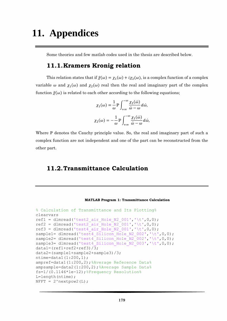
179
11. Appendices
Some theories and few matlab codes used in the thesis are described below.
Kramers Kronig relation
This relation states that if �̃�(𝜔) = 𝜒1(𝜔) + 𝑖𝜒2(𝜔), is a complex function of a complex
variable 𝜔 and 𝜒1(𝜔) and 𝜒2(𝜔) real then the real and imaginary part of the complex
function �̃�(𝜔) is related to each other according to the following equations;
𝜒1(𝜔) =1
𝜔ℙ∫
𝜒2(�́�)
�́� − 𝜔
−∞
+∞
𝑑𝜔,́
𝜒2(𝜔) = −1
𝜔ℙ∫
𝜒1(�́�)
�́� − 𝜔
−∞
+∞
𝑑�́�,
Where ℙ denotes the Cauchy principle value. So, the real and imaginary part of such a
complex function are not independent and one of the part can be reconstructed from the
other part.
Transmittance Calculation
MATLAB Program 1: Transmittance Calculation
% Calculation of Transmittance and Its Plotting% clearvars ref1 = dlmread('test2_air_Hole_N2_001','\t',0,0); ref2 = dlmread('test2_air_Hole_N2_001','\t',0,0); ref3 = dlmread('test4_air_Hole_N2_001','\t',0,0); sample1= dlmread('test4_Silicon_Hole_N2_002','\t',0,0); sample2= dlmread('test4_Silicon_Hole_N2_002','\t',0,0); sample3= dlmread('test4_Silicon_Hole_N2_003','\t',0,0); data1=(ref1+ref2+ref3)/3; data2=(sample1+sample2+sample3)/3; ntime=data1(1:200,1); ampref=data1(1:200,2);%Average Reference Data% ampsample=data2(1:200,2);%Average Sample Data% fs=1/(0.1146*1e-12);%Frequency Resolution% L=length(ntime); NFFT = 2^nextpow2(L);

180
REF = fft(ampref,NFFT);%Fast Fourier Transform% SAMPLE =fft(ampsample,NFFT); f1= ((fs*(0:NFFT/2+1)/NFFT))'; f = ((fs*(0:NFFT/2+1)/NFFT)/1e12)'; %THz Frequency% L2=length(f); REFmag=abs(REF); REFmag=smooth(REFmag,0.05,'loess'); SAMPLEmag=abs(SAMPLE); SAMPLEmag=smooth(SAMPLEmag,0.05,'loess'); T=abs((SAMPLE(1:NFFT/2)./REF(1:NFFT/2))).^2;%Transmittance or
simplified Transfer Function% plot(f(10:64),T(10:64),'--k','LineWidth',4) title('Transmittance of Silicon Substrate') xlabel('Frequency (THz)') ylabel('Transmittance)

181
Analysis of THz Polarizer
MATLAB Program 2: Analysis of THz Polarizer
%Analysis of a Polarizer%
clearvars
ref1 = dlmread('test4_PVA_hole_N2_002','\t',0,0);
ref2 = dlmread('test4_PVA_hole_N2_002','\t',0,0);
ref3 = dlmread('test4_PVA_hole_N2_002','\t',0,0);
samp1_0 = dlmread('test3_NiNW_parallel_hole_N2_001','\t',0,0);
samp2_0 = dlmread('test3_NiNW_parallel_hole_N2_001','\t',0,0);
samp3_0 = dlmread('test3_NiNW_parallel_hole_N2_001','\t',0,0);
samp1_90 = dlmread('test3_NiNW_perpendicular_hole_N2_002','\t',0,0);
samp2_90 = dlmread('test3_NiNW_perpendicular_hole_N2_002','\t',0,0);
samp3_90 = dlmread('test3_NiNW_perpendicular_hole_N2_002','\t',0,0);
ntime=ref1(1:511,1);
ampref = (ref1(1:511,2)+ref2(1:511,2)+ref3(1:511,2))/3;
ampsamp_0 = ((samp1_0(1:511,2)+samp2_0(1:511,2)+samp3_0(1:511,2))/3);
ampsamp_90 = ((samp1_90(1:511,2)+samp2_90(1:511,2)+samp3_90(1:511,2))/3);
fs=1/(0.1146*1e-12);
NFFT = length(ntime)+1;
REF = fft(ampref,NFFT);
SAMP_0 =fft(ampsamp_0,NFFT);
SAMP_90 =fft(ampsamp_90,NFFT);
f = ((fs*(0:NFFT/2-1)/NFFT)/1e12)';%Frequency%
T_0 = smooth(((abs((SAMP_0(1:NFFT/2)./REF(1:NFFT/2)))).^2),0.2,'rloess');
T_90 = smooth(((abs((SAMP_90(1:NFFT/2)./REF(1:NFFT/2)))).^2),0.2,'rloess');
A_0 = -10*log10(T_0);%Parallel Absorption%
A_90 = -10*log10(T_90);%Perpendicular Absorption%
LD=A_0-A_90; %Linear Dicroism%
A_tot=(A_0+2.*A_90./3);
LDR=LD./A_tot;%Reduced Linear Dicroism%
DOP=(A_0-A_90)./(A_0+A_90);%Degree of Polarization%
ER=-10*log10(T_90./T_0);%Extinction Ratio%
subplot(1,2,1)
plot(f(7:142,1),T_0(7:142,1),':',f(7:142,1),T_90(7:142,1),'x');
Title('Transmittence')
subplot(1,2,2)
plot(f(7:142,1),DOP(7:142,1));
Title('Degree of Polarization')

182
Shielding Analysis
MATLAB Program 3: Shielding Analysis
%Analysis of Shielding% clearvars ref1 = dlmread('test6_air_N2_001','\t',0,0); ref2 = dlmread('test6_air_N2_002','\t',0,0); ref3 = dlmread('test6_air_N2_003','\t',0,0); sample1= dlmread('test6_4mgSWNT_N2_001','\t',0,0); sample2= dlmread('test6_4mgSWNT_N2_002','\t',0,0); sample3= dlmread('test6_4mgSWNT_N2_003','\t',0,0); data1=(ref1+ref2+ref3)/3; data2=(sample1+sample2+sample3)/3; ntime=data1(1:511,1); ampref=data1(1:511,2);%Reference Amplitude% ampsample=data2(1:511,2);%Sample Amplitude% fs=1/(0.1125*1e-12); L=length(ntime); NFFT = 2^nextpow2(L); REF = fft(ampref,NFFT); SAMPLE =fft(ampsample,NFFT); f1= ((fs*(0:NFFT/2+1)/NFFT))'; f = ((fs*(0:NFFT/2+1)/NFFT)/1e12)'; L2=length(f); REFmag=abs(REF); REFmag=smooth(REFmag,0.05,'loess'); SAMPLEmag=abs(SAMPLE); SAMPLEmag=smooth(SAMPLEmag,0.05,'loess'); T=abs((SAMPLE./REF)).^2;%Transmittance% SE=-10*log10(T(18:157));%Total Shielding% filename = '4mgSWNT_D=306'; ext='.csv'; data = xlsread(strcat(filename,ext)); thick=306*10^-6;%Thickness of the Sample% neu1=data(:,1); neu=data(:,1)/1e12; omega=2*pi*neu; wavelength=((3.*10.^8)./neu1);%wavelength in m% e1=data(:,11);%Real Dielectric Constant% e2=data(:,12);%Imaginary Dielectric Constant% SE1=interp1(f(18:157),SE,neu); D=e2./e1; alpha=((2.*pi)./wavelength).*(sqrt(e1.*(sqrt((1+D.*D))-1)./2)); alpha1=((2.*pi)./wavelength).*(sqrt(e1.*(sqrt((1+D.*D))+1)./2)); e=(e1+1i*e2); ein=1.00; e0=8.854; ep=e0.*e;

183
A=sqrt(2.*pi.*neu1.*4.*pi.*10.^-7); con=(1i.*e0.*omega.*(ein-e)); real_con=e0.*omega.*e2; del=(sqrt(sqrt(1+(omega.*ep./con).^2)+(omega.*ep./con)).*sqrt(2./(om
ega.*con.*4.*pi.*10^5))); gamma=alpha+1i.*alpha1; n=sqrt(e1+1i.*e2); k=(imag(n))./(omega.*10.^12); B=(1-n.*n)./(1+n.*n); SEA=real(8.68.*thick.*alpha);%Absorption% SER=20.*log10((abs(1+n).^2)./abs(4.*n));%Reflection% SEMIR=20.*log10(abs((1-((1-n).^2./(1+n).^2).*(exp(-
2.*alpha.*thick)))));%Multiple Internal Reflection% SET=SEA+SER+SEMIR;%Total Shielding% plot(neu,SE1,'go',neu,SET,'--k','LineWidth',2)
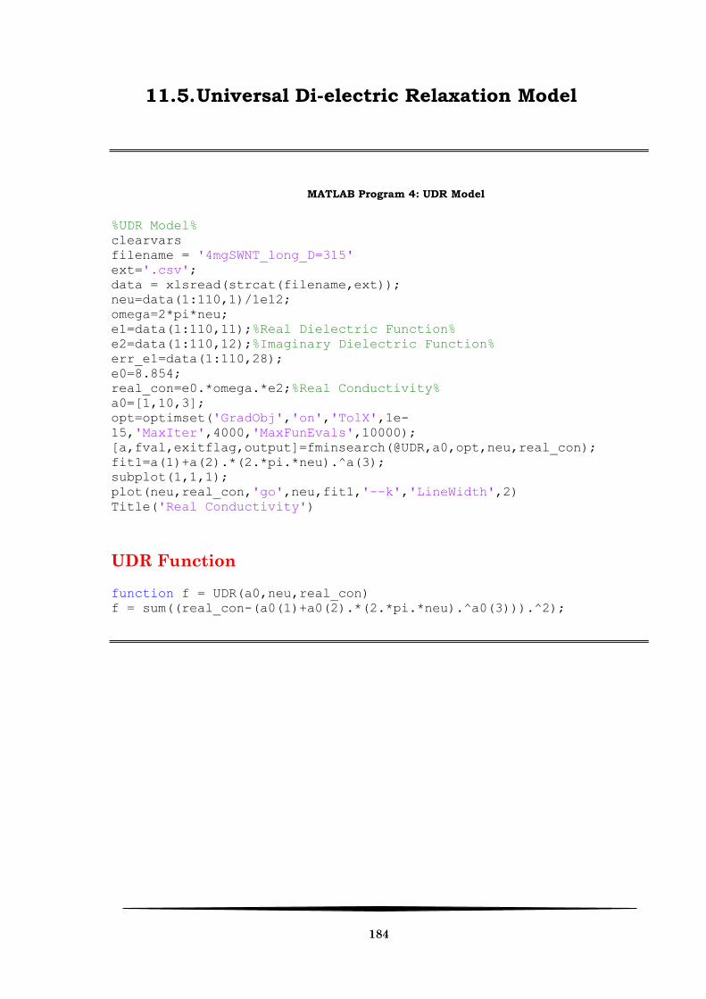
184
Universal Di-electric Relaxation Model
MATLAB Program 4: UDR Model
%UDR Model% clearvars filename = '4mgSWNT_long_D=315' ext='.csv'; data = xlsread(strcat(filename,ext)); neu=data(1:110,1)/1e12; omega=2*pi*neu; e1=data(1:110,11);%Real Dielectric Function% e2=data(1:110,12);%Imaginary Dielectric Function% err_e1=data(1:110,28); e0=8.854; real_con=e0.*omega.*e2;%Real Conductivity% a0=[1,10,3]; opt=optimset('GradObj','on','TolX',1e-
15,'MaxIter',4000,'MaxFunEvals',10000); [a,fval,exitflag,output]=fminsearch(@UDR,a0,opt,neu,real_con); fit1=a(1)+a(2).*(2.*pi.*neu).^a(3); subplot(1,1,1); plot(neu,real_con,'go',neu,fit1,'--k','LineWidth',2) Title('Real Conductivity')
UDR Function
function f = UDR(a0,neu,real_con) f = sum((real_con-(a0(1)+a0(2).*(2.*pi.*neu).^a0(3))).^2);

185
Thin Film Conductivity
MATLAB Program 5: Thin Film Conductivity
%Thin Film Conductiity% clearvars ref1 = dlmread('test2_air_hole_N2_Si_001','\t',0,0); ref2 = dlmread('test2_air_hole_N2_Si_001','\t',0,0); ref3 = dlmread('test2_air_hole_N2_Si_001','\t',0,0); sample1= dlmread('test2_Cu(0hour)_hole_N2_001','\t',0,0); sample2= dlmread('test2_Cu(0hour)_hole_N2_001','\t',0,0); sample3= dlmread('test2_Cu(0hour)_hole_N2_001','\t',0,0); data1=(ref1+ref2+ref3)/3; data2=(sample1+sample2+sample3)/3; ntime=data1(1:200,1); ampref=data1(1:200,2); ampsample=data2(1:200,2); fs=1/(0.1146*1e-12); L=length(ntime); NFFT = 2^nextpow2(L); REF = fft(ampref,NFFT); SAMPLE =fft(ampsample,NFFT); f1= ((fs*(0:NFFT/2+1)/NFFT))'; f = ((fs*(0:NFFT/2+1)/NFFT)/1e12)'; L2=length(f); REFmag=abs(REF); REFmag=smooth(REFmag,0.05,'loess'); SAMPLEmag=abs(SAMPLE); SAMPLEmag=smooth(SAMPLEmag,0.05,'loess'); subplot(2,2,1); plot(ntime(1:L,1),ampref(1:L,1),'-
',ntime(1:L,1),ampsample(1:L,1),':') xlabel('Time(ps)') ylabel('amplitude(a.u.)') title('Time Domain Data') subplot(2,2,2); semilogy(f(1:L2,1),REFmag(1:L2,1),'-
',f(1:L2,1),SAMPLEmag(1:L2,1),':') title('Frequency Domain Data') xlabel('Frequency(THz)') ylabel('FFTamplitude') T1=(SAMPLE./REF); T = abs(T1).^2;%Transmittance or simplified Transfer Function% SE=-10*log10(T); subplot(2,2,3); plot(f(8:70,1),T(8:70,1)) title('Shielding Effectiveness') xlabel('Frequency(THz)') ylabel('SE') nsub=3.418+1i*0.03; d=20*10^-9; A=(1+nsub)./T1;
186
B=A-1-nsub; sigma2 = (((1+nsub)./(T1))-1-nsub)./(377.*d); sigmare=real(sigma2); sigmaim=imag(sigma2); sigma=smooth(sigma2,0.05,'loess'); subplot(2,2,4);plot(f(8:100,1),sigmare(8:100,1),'b',f(8:100,1),sigma
im(8:100,1),'r') title('Complex Conductivity') xlabel('Frequency(THz)') ylabel('Real and Imaginary Conductivity')