Embed Size (px)
Citation preview

MAGICAL: Toward Fully Automated Analog ICLayout Leveraging Human and Machine Intelligence
(Invited Paper)
Biying Xu, Keren Zhu, Mingjie Liu, Yibo Lin, Shaolan Li, Xiyuan Tang, Nan Sun, and David Z. PanECE Department, The University of Texas at Austin, Austin, Texas, USA
{biying, keren.zhu, jay liu, yibolin, slliandy, xitang}@utexas.edu, [email protected], [email protected]
Abstract—Despite tremendous advancement of digital IC de-sign automation tools over the last few decades, analog IClayout is still heavily manual which is very tedious and error-prone. This paper will first review the history, challenges,and current status of analog IC layout automation. Then, wewill present MAGICAL, a human-intelligence inspired, fully-automated analog IC layout system currently being developedunder the DARPA IDEA program. It starts from an unannotatednetlist, performs automatic layout constraint extraction anddevice generation, then performs placement and post-placementoptimization, followed by routing to obtain the final GDSII layout.Various analytical, heuristic, and machine learning algorithmswill be discussed. MAGICAL has obtained promising preliminaryresults. We will conclude the paper with further discussions onchallenges and future directions for fully-automated analog IClayout.
I. INTRODUCTION
The demand for analog integrated circuits (ICs) has beenincreasing in many emerging applications, including Internetof Things (IoT), 5G networks, advanced computing, healthcareelectronics, etc., which necessitates a shorter design cycle ofanalog ICs. Despite the tremendous advancement of digitalIC layout design automation tools, analog IC layout is still aheavily manual, time-consuming, and error-prone task, due toits high design flexibility and significant impact on the circuitperformance.
Early endeavors of analog IC layout automation, includingILAC [1], KOAN/ANAGRAM II [2], LAYLA [3], appliedsimulated annealing to optimize the layout. More recent works[4]–[6] improved the analog layout constraint handling andthe design space pruning. Algorithmic revolution on placement[7]–[13] and routing [14]–[17] further enhanced the scalability,efficiency, and design considerations specific to analog IClayouts. Nonetheless, existing analog layout tools usuallyrequire human designers to prepare very detailed constraintsas inputs, which could be a tedious practice. Meanwhile,the poor accessibility of most tools prohibits testing andimprovement from the circuit designers’ side. The acceptanceof the automated analog IC layout tools has thus been limited.
Recently, DARPA announced the IDEA program, with themission to create a “no human in the loop” 24-hour turnaroundcircuit layout generator. The program is expected to spurthe development of state-of-the-art IC design flows that areeasier to use and more readily available. As part of the
program efforts, we present our work MAGICAL, a fullyautomated analog IC layout system leveraging human andmachine intelligence inherently. The main contributions aresummarized as follows:
• MAGICAL is a fully automated, end-to-end analog IClayout system that generates a completed layout from acircuit netlist. The source code1 is released on GitHub.
• Designer insights and expertise are strategically embed-ded into MAGICAL through pattern matching, heuristic,and deep learning techniques.
• The layouts completed by MAGICAL are validated us-ing industrial standard verification tools, demonstratingcircuit performances close to those handcrafted by expe-rienced designers.
II. MAGICAL DESIGN FLOW
The overall flow of MAGICAL is shown in Fig. 1. It takesan unannotated circuit netlist and design rules as inputs, andproduces a complete GDSII layout as output fully automat-ically without human designers in the loop. The entire flowconsists of four major modules: automatically layout constraintextractor, parametric device generator, analytical analog placerwith post-placement optimization, and analog router. Thedesign rules and the extracted layout constraints are honoredthroughout the entire back-end flow. All the completed layoutresults are validated and evaluated by industrial standard tools.In the subsequent sections, the major tasks of the MAGICALanalog layout generation tool will be elaborated.
III. PARAMETRIC DEVICE GENERATION
Before running the core layout flow, the device generationstep first generates the GDSII layout of the devices and extractstheir pins to facilitate the subsequent placement and routingstages. The inputs to device generation are instance parametersand process technology-dependent design rules. The generatedGDSII layout are correct by construction based on the designrules.
MAGICAL supports different device types, includingPMOS, NMOS, MOM capacitors, and poly resisters. Transis-tors can have additional attributes such as lvt (low thresholdvoltage), hvt (high threshold voltage) and na (native device).
1https://github.com/magical-eda/MAGICAL
978-1-7281-2350-9/19/$31.00 ©2019 IEEE

MAGICALINPUTS
Circuit Netlist
Design Rules
DEVICE GENERATOR
Parametric Instances
PLACER
Analytical Placement
ROUTER
Multi-pin A* Search
Post-Placement Optimization
VALIDATION&
EVALUATION
MAGICALOUTPUT
GDSII Layout
MAGICALLAYOUT CONSTRAINT EXTRACTOR
Pattern Matching + Small Signal Analysis
Fig. 1. Overall flow of MAGICAL analog layout system.
The automatic parametric device generation considers thenumber of fingers for transistors, the number of segmentsfor resistors, the metal layers for Metal-Oxide-Metal (MOM)capacitors, etc. Fig. 2 shows examples of the layouts ofdifferent types of devices generated by MAGICAL.
Pin information of the devices is extracted in this step. Thepin shape with the minimal area is selected as the drain of atransistor to reduce drain parasitic capacitance. Lower metallayer shapes connected to the terminals of the devices areselected as the pins used for routing.
(a) (b) (c) (d)
Fig. 2. Examples of generated devices from MAGICAL. (a) NMOS, (b)PMOS with guard ring, (c) MOM capacitor, and (d) poly resistor.
IV. ANALOG LAYOUT CONSTRAINT EXTRACTION
The layout constraint extractor takes circuit netlist as inputand generates constraints to guide the later stages. Sym-metry constraints are one of the most essential and widelyadopted constraints applied during analog layout synthesis.Analog designs frequently use differential topologies to re-ject common-mode noise and enhance circuit robustness andperformance [18]. Mismatch of sensitive devices in the layoutsoften cause performance degradation to offset and common-mode rejection ratio (CMRR) [19]. Thus correctly identifyingsymmetry constraints between sensitive devices are crucial forensuring the quality of placement and routing.
The constraint extraction reads in the input netlist and gener-ates constraints for placement and routing based on the circuitconnections. A significant challenge for constraint extraction isin generating high-quality constraints and resolving constraint
(a)
(b) (c)
Fig. 3. Layout constraint extraction illustration. (a) Pattern library, (b) biascircuit symmetry detection, and (c) signal flow based traversal.
ambiguity. The automated placement and routing symmetryconstraint extraction mainly consist of four stages listed below.
A. Graph Abstraction
Our constraint extraction is based on analysis of the graphabstracted from the circuit netlist. Firstly, the netlist file isparsed, and the circuit is abstracted into a graph represen-tation. Since the pin connection information is crucial tothe topological structure of analog circuits, we preserve pininformation during the abstraction. Devices, pins, and nets areall represented as nodes. Pins are connected to the device theybelong to. Nets connect to pins based on the circuit netlist

connections. Nets are never directly connected to devices inour graph representation since they alway connect to pins first.
B. Seed Pattern DetectionTransistor pairs that form certain structural patterns are
detected as seed symmetric device pairs. These seed patternsare the starting or ending points for graph traversal in the nextstage. Seed patterns are those in the pattern library where thesource of the transistor pins are connected. Instead of usingexpensive graph isomorphism algorithms [20]–[23], we checkthe connection relationships and device attributes between thepairs of devices for matching. As an example, for recognizingdifferential pairs, we iterate all pairs of transistors connectedto the same net through source pins and check if the gatepins are connected to different nets and the device attributesmatch. To better resolve constraint ambiguity, especially wheredigital circuits are extensively used in mixed-signal designs,we recognize differential pairs as seed patterns only if theconnected source net is the virtual ground node (not power orground nets).
C. Signal Flow Based Graph TraversalWe traverse the graph from the seed symmetric device
pairs while recognizing new constraint patterns. This step isanalogous to following the differential current in small-signalanalysis [18]. Graph traversal not only expands the recognizedconstraints but also helps with reducing constraint ambiguitysince the graph connections with other patterns guide thepattern matching process. Matching between passive deviceelements are also considered. For each pattern, we definecurrent directions to guide the graph traversal process. As anexample, if a cascode transistor pair pattern is reached throughthe source pins, the nets to proceed with graph traversalare the nets connected to the drain pins. Graph traversalends when the two flow paths meet at the source connectedtransistors such as other seed patterns, or connected passivedevice elements. The visited symmetric transistor patternsfrom the same seed pattern during graph traversal form asymmetric group which would share the same symmetry axisin the placement. Nets connecting symmetric device pairs arerecognized as symmetric nets.
D. Constraints Post-processingIn the last step, we post-process the symmetric groups
and recognize additional symmetry constraints, including self-symmetric devices connected to virtual ground nodes andsymmetric transistor pairs in the bias circuits. Virtual groundand certain clock nets are identified as self-symmetric nets.Bias circuit symmetry is detected by checking common-gate connected transistors and searching for diode-connectedtransistors. Additional symmetry constraints in the bias circuitsare detected in this step. Since it may not be feasible tosatisfy all the extracted constraints in the placement stage,to guarantee feasibility, we currently only allow a device haveat most one symmetry constraint. More advanced matching-oriented constraints such as regularity and common-centroidwould be supported in future versions of MAGICAL.
Fig. 3 shows the library of some transistor patterns, detec-tion of bias circuit symmetry, and an example of signal flowbased graph traversal for constraint extraction.
V. ANALOG PLACEMENT
Given the placement constraints and devices generated inthe previous steps, we develop an analog placement en-gine. The inputs to the placer include the circuit netlist, ex-tracted constraints, generated devices, and process technology-dependent design rules. The outputs are the legalized GDSIIlayout of the placement result and pin information for routing.Besides symmetric group constraints, it also supports netcriticality constraints if specified, by minimizing the weightednet lengths according to the its criticality. The placementengine consists of a core placement stage and a post-placementoptimization stage.
A. Placement Algorithm
The core placer follows an analytical framework as in [24].First, the global placement simultaneously optimizes multi-ple objectives in a non-linear objective function. Then, thelegalization step generates a legal placement solution honoringthe global placement result while satisfying the symmetryconstraints and design rules. Finally, a linear programming(LP) based detailed placement is used to further optimize thewirelength.
1) Global Placement: Our global placement is similar tothe non-linear global placement algorithms as in [13], [25],which simultaneously considers the following: (1) wirelength,(2) device overlapping, (3) placement boundary, and (4) sym-metry constraints from the constraint extraction stage. To bespecific, it minimizes the objective shown in Equation (1)using unconstrained non-linear conjugate gradient method.
Objective = fWL + a · fOL + b · fBND + c · fSYM . (1)
where:• fWL is the wirelength objective, which is defined as the
total half-perimeter wirelength (HPWL).• fOL is the overlap penalty, which is modeled as an area
overlap function similar to [26].• fBND is the penalty of violating the boundary con-
straints. To control the circuit area, white space ratio,and aspect ratio, a desirable placement bounding box forthe design is derived.
• The last term fSYM penalizes the violation of symmetryconstraint, which requires: (1) each symmetric device pairwithin the same group to be symmetric with respect tothe same axis; (2) the self-symmetric devices to be self-symmetric with respect to the same axis of the group.
• a, b, and c are the coefficients to realize the trade-offbetween different objective terms.
Log-sum-exponential (LSE) models [27] are used to smooththe max and min functions in the objective. Our non-linearoptimization-based global placement runs iteratively, until allthe penalties are below the specified thresholds, or the prede-fined maximum number of iterations is reached. By gradually

adjusting the coefficient values a, b, and c of different penaltyfunctions in each iteration, we can get a global placementresult encouraging symmetry and boundary constraints withshort wirelength and small device overlapping.
2) Legalization and Detailed Placement: After globalplacement, we perform a legalization step to get a place-ment free from device overlapping, design rule violation, andsymmetry constraint violation. During this step, we developalgorithms to construct the constraint graphs, and legalize theglobal placement result using LP-based compaction given theconstructed constraint graphs.
Our constraint graph construction algorithm is based onthe plane sweep algorithm presented in [28]. This algorithmencounters problems when the global placement result hasoverlaps between devices, which may over-constrain the legal-ization and result in a sub-optimal area. To get a more compactplacement after legalization, we will remove the excessiveconstraint edges between each pair of overlapping devicesby determining their relative positions greedily, i.e., to spreadthem in the direction that would induce less displacement. Wewill only keep the constraint edge corresponding to the chosenspreading direction, while other edges between them will beremoved.
Nevertheless, there may be missing positional constraintsin the constraint graphs obtained. A depth-first-search (DFS)based algorithm is developed in order to detect those missingpositional constraint edges. Readers are referred to [24] forthe detailed implementation. If both horizontal and verticalpositional constraints are missing according to the DFS-basedalgorithm, we will add one edge to either the vertical orhorizontal constraint graph greedily. To be specific, if thevertical spacing is larger than the horizontal spacing betweenthe two devices in the global placement solution, we willadd an edge to the vertical constraint graph. The horizontalconstraint edges can be added similarly. We will also performtransitive reduction on both horizontal and vertical constraintgraphs to remove the transitive edges.
After constructing the constraint graphs, we can get a legalcompact placement solution using LP in accordance with theconstraint graphs. There are two sets of constraints whichare topology order (non-overlap) and symmetry constraints.The topology order constraints are from the constraint graphsobtained, while the symmetry constraints are from the layoutconstraint extraction stage.
Finally, we will perform LP-based detailed placement tofurther optimize the wirelength for the given legal placement.Symmetric group constraints and design rules are also honoredduring this step.
B. Post-Placement Optimization
After the device locations are determined in the placementstage, the post-placement step generates the well islands, andestablishes the bulk and substrate connection pins for routing.
Our well island generation supports different approaches.The polygon-based approach follows WellGAN [29], a deepneural network-guided well generation framework. A trained
generative adversarial network (GAN) model provides theguidance of the well island shapes, and a refinement stepis performed to legalize the layout result given the GANguidance. In general, this approach may generate more com-pact layout designs. However, legalizing the polygonal wellislands can be challenging, and it may degrade the post-layoutcircuit performance due to layout-dependent effects if handledimproperly, especially in advanced process technology nodes.
In face of the challenges posed by the polygon-basedwell generation approach, MAGICAL also supports generatingrectangular well islands for each individual devices with wells.This approach can overcome the legalization difficulty and per-formance effects of WellGAN, at the cost of slightly increasedtotal area and routing complexity. In fact, for high-performanceanalog designs, circuit performance is often considered moreimportant than the total area. Moreover, the number of nets inan analog circuit is usually relatively few compared with thelayout area. Hence, routability is generally not a critical issuefor analog circuit layouts. From this perspectives, generatingindividual wells for certain devices could also be a desirablepractice.
After well generation, MAGICAL will automatically es-tablish the well island and substrate connection points. Bothguard rings and contacts are supported and can be insertedfree from design rule violation by construction. After that,we will legalize and spread out the well islands with theconsideration of design rules. Finally, the placement result inGDSII format as well as the pins of the devices, well islands,and the substrate will be output for routing.
VI. ANALOG ROUTING
After the placement and post-placement optimization stage,an end-to-end router connects all the pins with metal wiresin aware of the analog circuit-specific constraints and designconsideration.
In addition to connectivity and design rules, analog routingproblem is also imposed with symmetric net constraints formatching [30]. In MAGICAL, the routing engine takes inputsfrom the layout constraint generator and honors the symmetricand self-symmetric constraints for nets. Out analog routingconsists of two stages, global and detailed routing, similarto the conventional digital routing flow. In the global routingstage, the design is divided into rough grids, and the topologyof routing is generated. The purpose of global routing is toefficiently find a global routing solution without extensivelyspending computational resources in the detailed design ruleand congestion resolving. While in the detailed routing stage,the physical geometry of metal wires are implemented fol-lowing the global routing guide, symmetric constraints, anddesign rules.
A. Global Routing
A sequential symmetry-aware grid-based A* search routingengine is employed in global routing stage.
Before performing the routing, several steps are executedon the input placement solution and the process technology

information. The placement is firstly divided into grid cellsunified in size. By default, MAGICAL decides on the widthand height of each grid cell based on track width on M1layer. To be specific, the global routing will attempt to dividethe layout into 3D grid so that the width and height ofeach grid cell are four-track widths. However, as computationefficiency is low when the number of grid cells is relativelylarge, MAGICAL limits the amount of grid cells to be below200 × 200 × Nlayers, where Nlayers denotes the number oflayers. After generating the routing grid, routing capacity iscalculated on 2D grid edges based on the actual grid cell widthand track width.
Besides the global routing grid, the input pins are pre-processed before routing. Unlike cell-based digital physicaldesign flow, customized analog circuit devices do not havean identical convention of pins such as layer and shape. Pinshapes could be polygons varied in size and shape, dependingon the device type and parameters. In MAGICAL routingengine, the pins are decomposed into searching points in thepath search scheme. The polygon is firstly separated intorectangles. The intersection points between the center linesof the resulting rectangles and the tracks of the metal layerabove are identified as the search points. If no search pointis identified based on the strategy above, the center points ofthe rectangles are considered as the search points in the A*search algorithm.
After processing the input placement, every multi-pin net issplit into two-pin nets based on minimum spanning tree withHPWL as the edge costs. The two-pin net splitting is matchedfor symmetric net pairs so that the symmetry is maintained.Then symmetric net pairs and self-symmetric nets are routedon the 3D global routing grid with exact symmetry along thesymmetric axis. A rip-up and reroute scheme is applied whenfailing to achieve a feasible solution in the early iterations.
B. Detailed Routing
After determining the rough routing topology in the globalrouting stage, detailed routing engine completes the routingand assigns metal wire geometries to each net. Similar tothe global routing, a sequential A* search kernel is applied.However, instead of routing abstract nets on the rough globalrouting grid, detailed router explicitly handles design rules inphysical layouts.
Since the input pins and previously generated search pointsare not necessarily aligned with the routing tracks, the detailedanalog routing engine does not restrict the wire segmentsand VIAs to be exactly aligned with routing tracks as itsdigital counterpart. Instead, they only need to align to themanufacturing grid specified in the process technology designrules. The detailed router will attempt to search for the pathfor the nets on multiple layers with default search step of trackwidth. The design rules of metal wires and VIAs are checkedduring the A* search. When routing the symmetric net pairsor self-symmetric nets, both the two sides are routed at thesame time. Therefore the resulting routing solution is feasiblefor both sides of the symmetric axis.
After the detailed routing stage, a complete placed androuted layout is generated fully automatically, and a GDSIIformat layout file is exported.
Due to the complexity of analog routing, other analogcircuit-specific routing considerations will also be incorporatedinto MAGICAL to improve the post-layout circuit perfor-mance. The preliminary results in GeniusRoute [31] demon-strate the effectiveness of our neural network guided analogrouting techniques.
VII. EXPERIMENTAL RESULTS
The MAGICAL flow is implemented in Python and C/C++,and the experiments are performed on a Linux server with an8-core 3.4GHz Intel(R) CPU and 32GB memory. The layoutresults are validated using Calibre DRC/LVS/PEX, and eval-uated using Cadence Virtuoso ADE simulation environment.
TABLE IRESULTS OF THE COMPARATOR CIRCUIT (COMP).
Metrics OutputDelay (ps)
Input-referredNoise (µVrms)
Power(µW)
Input-referredOffset (mV)
Manual 150 380 16.8 0.15MAGICAL 152 334 18.7 0.50
TABLE IIRESULTS OF THE MILLER-COMPENSATED OTA (OTA1).
Metrics Gain(dB)
UGB(MHz)
PM(degree)
Noise(µVrms)
CMRR(dB)
Offset(mV)
Manual 37.7 110.0 67.8 219.0 103.0 0.20MAGICAL 38.0 107.5 62.3 221.5 92.5 0.48
TABLE IIIRESULTS OF THE FEED-FORWARD COMPENSATED OTA (OTA2).
Metrics Gain(dB)
UGB(MHz)
PM(degree)
CMRR(dB)
Offset(mV)
Manual 35.3 2200 77.6 126.1 <0.01MAGICAL 35.3 2200 77.9 88.9 0.161
TABLE IVRESULTS OF THE INVERTER-BASED OTA (OTA3).
Metrics Gain(dB)
UGB(MHz)
PM(degree)
CMRR(dB)
Offset(mV)
Manual 69 1300 58 94.5 0.016MAGICAL 69 1130 56.5 110 0.001
The circuit performances of the layout results generatedby MAGICAL are compared against tape-out quality manuallayouts by experienced analog IC designers, under the sametest bench suites. The post-layout simulation results for 3benchmark circuits, a comparator (COMP), a 2-stage miller-compensated operational transconductance amplifier (OTA1),a 2-stage feed-forward compensated OTA (OTA2), and aninverter-based OTA (OTA3), are shown in Table I, II, III,and IV, respectively, where UGB means unity-gain bandwidth,PM refers to phase margin, and CMRR is common-moderejection ratio. The results demonstrate that MAGICAL canautomatically generate validated layouts from unannotated

(a) circuit schematic
(b) manual layout (c) layout from MAGICAL
Fig. 4. Comparator circuit schematic, manual layout, and layout result fromMAGICAL.
circuit netlist (supporting both Spectre and HSPICE format),and the post-layout performances are close to the manualdesigns by experienced designers. Some performance metricsincluding input-referred offset and CMRR could be furtherimproved by extensively considering layout dependent effects,minimizing coupling to sensitive nets, etc. Figures 4, 5, 6, and7 show the circuit schematics, the handcrafted layouts, andthe layout results by MAGICAL of the benchmark circuits.Note that some device parameters of the manual layout maynot necessary match the schematic after adjustment by layoutdesigners, e.g., number of fingers for transistors, while MAGI-CAL generates the device layouts corresponding to the circuitnetlist. Therefore, the devices in the manual layout may appearto be different from those generated by MAGICAL.
TABLE VRUNTIME OF MAGICAL.
Circuit COMP OTA1 OTA2 OTA3Runtime (s) 3.91 10.51 6.03 26.6
Table V shows the runtime for the full MAGICAL flow. Asshown in the table, it can generate the complete routed layoutin seconds, while manual layouts usually take hours. The fastturn-around time could significantly shorten the design cycleand facilitate the design closure.
VIII. FUTURE DIRECTIONS
Future directions of MAGICAL include the followings.1) Interaction with Open-Sourced EDA Ecosystem: En-
couraged by the DARPA IDEA/POSH program, a numberof open-source projects have emerged recently [32]–[34].
VDD
VBP
VBNVBN VBNCMFB
VIP VIN
VOP VON
VDD
VBN
VBP
IBIAS
VDD
VCMVOPVON
VBP VBP
CMFB
Gain PathBias Common-mode Feedback
(a) circuit schematic
(b) manual layout
(c) layout from MAGICAL
Fig. 5. Miller-compensated OTA circuit schematic, manual layout, and layoutresult from MAGICAL.
Being part of the open hardware/EDA ecosystem, the futuredevelopment of the MAGICAL will both benefit from andcontribute to the community.
MGICAL can learn from the recent emerging open-sourceEDA tools. Both AMS and digital layout automation flowsshare many common infrastructural components with MAGI-CAL, e.g., OpenROAD [33] which aims to build a completelyopen-source digital physical design flow and ALIGN [34]which is another AMS layout generator. Although the ex-isting components in different open-source EDA tools mayhave different algorithms and methodologies, there are someoverlapping between their functionality. For example, ALIGN,RAIL [35], and MAGICAL all contain modules for generatingthe device layouts. Similarly, ALIGN, TritonRoute [36], DR.CU [37], and MAGICAL all provide different implementationsof detailed router. It would be beneficial for the communityto leverage some well-established efforts from each other andfocus on the key differentiation. Besides the physical designframework, there are also open-source utilities that couldbe valuable for applying in MAGICAL. For instance, Cpp-taskflow [38] can potentially be applied in MAGICAL forimproving efficiency by parallelizing the algorithm, and circuitsanitizer [39] would make sharing designs easier among thecommunity by avoiding disclosing process design kit (PDK)related information.
Besides the EDA tools, open-sourcing AMS circuit designsis another driving force for AMS layout automation. On onehand, lacking of training data has been a major challenge in
VDD
VBP
IBIAS
Bias
CMFB
VDD
VBP
VCM VCMO
Common-mode Feedback
VDD
VIN
VBP
VIP
OP1 ON1VOPVON
VCMO
VDD
VIN
CMFB
VBP
VIP
ON1 OP1
Gain Path
VCAS
(a) circuit schematic
(b) manual layout (c) layout from MAGICAL
Fig. 6. Feed-foward compensated OTA circuit schematic, manual layout, andlayout result from MAGICAL.
machine learning-based EDA algorithm, e.g., [29], [31]. Onthe other hand, the lack of a unified test circuit benchmarksuite makes it difficult to evaluate and compare differentAMS EDA tools. Recently, both MAGICAL and the otherDARPA IDEA/POSH teams have released a number of PDKinformation stripped state-of-the-art AMS designs, includingstate-of-the-art SAR ADCs [40], ∆Σ ADCs [41], [42], VCO-based ADCs [43], [44], and temperature sensors [45], [46], etc.Open-source designs not only make it possible for the EDAtools to have common evaluation metrics, but also providetraining data for machine learning-basd EDA algorithms.
2) Performance-aware Layout Constraint Generation,Place and Route (P&R) Flow: While MAGICAL hasdemonstrated satisfactory results, it currently only minimizespost-layout circuit performance degradation implicitly byconsidering the analog layout constraints. Approaches fordirectly optimizing circuit performance still need to beintegrated into the current flow. In the future researchand development, MAGICAL will investigate into theperformance-aware techniques, especially machine learningalgorithms, throughout its entire flow. As an example,in addition to the component-level symmetry constraintgeneration, MAGICAL will try to extract net criticalityconstraints and system-level symmetry from the netlists.On the other hand, with the recent advancement in neuralnetwork-guided physical design algorithms including [31],MAGICAL will further leverage human and machineintelligence in the P&R flow.
3) System-level Hierarchical Layout Optimization: Modernmixed-signal circuits, such as data converters, are hierarchical
Bias
IBIAS
VCM
VDD
NTAILN2TAIL
VDD
CMFB VCM
NTAIL
Common-mode Feedback
PBCMO
VDD
IBIAS
PCAS
VIP
VIP
VIN
VIN
NTAIL
PBCMO
OP1 ON1
NBCMO
NBCMO
VDD
OP1 ON1
VON VOP
VIN
N2TAIL
VIP
N2TAIL
CMFB
Gain Path
NBCMO
(a) circuit schematic
(b) manual layout (c) layout from MAGI-CAL
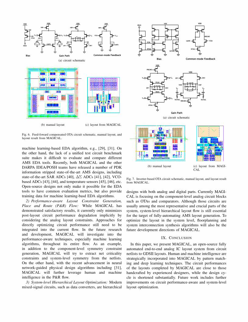
Fig. 7. Inverter-based OTA circuit schematic, manual layout, and layout resultfrom MAGICAL.
designs with both analog and digital parts. Currently MAGI-CAL is focusing on the component-level analog circuit blockssuch as OTAs and comparators. Although those circuits areusually among the most representative and crucial parts of thesystem, system-level hierarchical layout flow is still essentialfor the target of fully-automating AMS layout generation. Tooptimize the layout in the system level, floorplanning andsystem interconnection synthesis algorithms will also be thefuture development directions of MAGICAL.
IX. CONCLUSION
In this paper, we present MAGICAL, an open-source fullyautomated end-to-end analog IC layout system from circuitnetlists to GDSII layouts. Human and machine intelligence arestrategically incorporated into MAGICAL by pattern match-ing and deep learning techniques. The circuit performancesof the layouts completed by MAGICAL are close to thosehandcrafted by experienced designers, while the design cy-cle is shortened substantially. Future work includes furtherimprovements on circuit performance-aware and system-levellayout optimization.

ACKNOWLEDGEMENT
This work is supported in part by the NSF under Grant No.1704758, and the DARPA ERI IDEA program.
REFERENCES
[1] J. Rijmenants, J. B. Litsios, T. R. Schwarz, and M. G. Degrauwe, “Ilac:An automated layout tool for analog cmos circuits,” IEEE Journal Solid-State Circuits, vol. 24, no. 2, pp. 417–425, 1989.
[2] J. M. Cohn, D. J. Garrod, R. A. Rutenbar, and L. R. Carley,“Koan/anagram ii: New tools for device-level analog placement androuting,” IEEE Journal Solid-State Circuits, vol. 26, no. 3, pp. 330–342, 1991.
[3] K. Lampaert, G. Gielen, and W. M. Sansen, “A performance-drivenplacement tool for analog integrated circuits,” IEEE Journal Solid-StateCircuits, vol. 30, no. 7, pp. 773–780, 1995.
[4] N. Lourenco, M. Vianello, J. Guilherme, and N. Horta, “Laygen-automatic layout generation of analog ics from hierarchical templatedescriptions,” in 2006 Ph. D. Research in Microelectronics and Elec-tronics. IEEE, 2006, pp. 213–216.
[5] R. Martins, N. Lourenco, and N. Horta, “Laygen ii-automatic layoutgeneration of analog integrated circuits,” IEEE TCAD, vol. 32, no. 11,pp. 1641–1654, 2013.
[6] K. Lampaert, G. Gielen, and W. M. Sansen, Analog layout generationfor performance and manufacturability. Springer Science & BusinessMedia, 2013, vol. 501.
[7] M. Strasser, M. Eick, H. Grab, U. Schlichtmann, and F. M. Johannes,“Deterministic analog circuit placement using hierarchically boundedenumeration and enhanced shape functions,” in Proc. ICCAD, 2008, pp.306–313.
[8] P.-H. Lin, Y.-W. Chang, and S.-C. Lin, “Analog placement based onsymmetry-island formulation,” IEEE TCAD, vol. 28, no. 6, pp. 791–804, 2009.
[9] Q. Ma, L. Xiao, Y.-C. Tam, and E. F. Young, “Simultaneous handling ofsymmetry, common centroid, and general placement constraints,” IEEETCAD, vol. 30, no. 1, pp. 85–95, 2011.
[10] M. P.-H. Lin, Y.-T. He, V.-H. Hsiao, R.-G. Chang, and S.-Y. Lee,“Common-centroid capacitor layout generation considering devicematching and parasitic minimization,” IEEE TCAD, vol. 32, no. 7, pp.991–1002, 2013.
[11] B. Xu, S. Li, X. Xu, N. Sun, and D. Z. Pan, “Hierarchical andanalytical placement techniques for high-performance analog circuits,”in Proc. ISPD, 2017, pp. 55–62.
[12] B. Xu, B. Basaran, M. Su, and D. Z. Pan, “Analog placement constraintextraction and exploration with the application to layout retargeting,” inProc. ISPD, 2018, pp. 98–105.
[13] H.-C. Ou, K.-H. Tseng, J.-Y. Liu, I.-P. Wu, and Y.-W. Chang, “Layout-dependent effects-aware analytical analog placement,” IEEE TCAD,vol. 35, no. 8, pp. 1243–1254, 2016.
[14] M. M. Ozdal and R. F. Hentschke, “An algorithmic study of exact routematching for integrated circuits,” IEEE TCAD, vol. 30, no. 12, pp. 1842–1855, 2011.
[15] ——, “Algorithms for maze routing with exact matching constraints,”IEEE TCAD, vol. 33, no. 1, pp. 101–112, 2014.
[16] R. Martins, N. Loureno, A. Canelas, and N. Horta, “Electromigration-aware and ir-drop avoidance routing in analog multiport terminal struc-tures,” in Proc. DATE, March 2014, pp. 1–6.
[17] Q. Gao, Y. Shen, Y. Cai, and H. Yao, “Analog circuit shielding routingalgorithm based on net classification,” in Proc. ISLPED, Aug 2010, pp.123–128.
[18] B. Razavi, Design of Analog CMOS Integrated Circuits, 1st ed. NewYork, NY, USA: McGraw-Hill, Inc., 2001.
[19] H. Ou, K. Tseng, J. Liu, I. Wu, and Y. Chang, “Layout-dependenteffects-aware analytical analog placement,” IEEE TCAD, vol. 35, no. 8,pp. 1243–1254, Aug 2016.
[20] M. Eick, M. Strasser, K. Lu, U. Schlichtmann, and H. E. Graeb,“Comprehensive generation of hierarchical placement rules for analogintegrated circuits,” IEEE TCAD, vol. 30, no. 2, pp. 180–193, Feb 2011.
[21] T. Massier, H. Graeb, and U. Schlichtmann, “The sizing rules methodfor cmos and bipolar analog integrated circuit synthesis,” IEEE TCAD,vol. 27, no. 12, pp. 2209–2222, Dec 2008.
[22] Qinsheng Hao, Sheqin Dong, Song Chen, Xianlong Hong, Yi Su, andZhiyi Qu, “Constraints generation for analog circuits layout,” in 2004International Conference on Communications, Circuits and Systems,vol. 2, June 2004, pp. 1339–1343 Vol.2.
[23] P. Wu, M. P. Lin, and T. Ho, “Analog layout synthesis with knowl-edge mining,” in European Conference on Circuit Theory and Design(ECCTD), Aug 2015, pp. 1–4.
[24] B. Xu, S. Li, C.-W. Pui, D. Liu, L. Shen, Y. Lin, N. Sun, and D. Z.Pan, “Device layer-aware analytical placement for analog circuits,” inProc. ISPD, 2019, pp. 19–26.
[25] T.-C. Chen, Z.-W. Jiang, T.-C. Hsu, H.-C. Chen, and Y.-W. Chang,“Ntuplace3: An analytical placer for large-scale mixed-size designs withpreplaced blocks and density constraints,” IEEE TCAD, vol. 27, no. 7,pp. 1228–1240, 2008.
[26] S. Kuwabara, Y. Kohira, and Y. Takashima, “An effective overlapremovable objective for analytical placement,” IEICE transactions onfundamentals of electronics, communications and computer sciences,vol. 96, no. 6, pp. 1348–1356, 2013.
[27] W. Naylor, “Non-linear optimization system and method for wire lengthand delay optimization for an automatic electric circuit placer,” USPatent No. 6301693, 2001.
[28] J. Doenhardt and T. Lengauer, “Algorithmic aspects of one-dimensionallayout compaction,” IEEE TCAD, vol. 6, no. 5, pp. 863–878, 1987.
[29] B. Xu, Y. Lin, X. Tang, S. Li, L. Shen, N. Sun, and D. Z. Pan,“Wellgan: Generative-adversarial-network-guided well generation foranalog/mixed-signal circuit layout,” in Proc. DAC, 2019, p. 66.
[30] L. Xiao, E. F. Y. Young, X. He, and K. P. Pun, “Practical placementand routing techniques for analog circuit designs,” in Proc. ICCAD, Nov2010, pp. 675–679.
[31] K. Zhu, M. Liu, Y. Lin, B. Xu, S. Li, X. Tang, N. Sun, and D. Z. Pan,“Geniusroute: A new analog routing paradigm using generative neuralnetwork guidance,” in Proc. ICCAD, 2019.
[32] T.-W. Huang, C.-X. Lin, G. Guo, and M. D. F. Wong, “Essential buildingblocks for creating an open-source eda project,” in Proc. DAC, 2019.
[33] T. Ajayi, V. A. Chhabria, M. Fogaca, S. Hashemi, A. Hosny, A. B.Kahng, M. Kim, J. Lee, U. Mallappa, M. Neseem, G. Pradipta, S. Reda,M. Saligane, S. S. Sapatnekar, C. Sechen, M. Shalan, W. Swartz,L. Wang, Z. Wang, M. Woo, and B. Xu, “Toward an open-source digitalflow: First learnings from the openroad project,” in Proc. DAC, 2019,pp. 76:1–76:4.
[34] K. Kunal, M. Madhusudan, A. K. Sharma, W. Xu, S. M. Burns,R. Harjani, J. Hu, D. A. Kirkpatrick, and S. S. Sapatnekar, “Align: Open-source analog layout automation from the ground up,” in Proc. DAC,2019, pp. 77:1–77:4.
[35] “RAIL12,” https://github.com/uwidea/rail12, accessed: 2019-8-1.[36] A. B. Kahng, L. Wang, and B. Xu, “Tritonroute: An initial detailed
router for advanced vlsi technologies,” in Proc. ICCAD, 2018, pp. 1–8.[37] G. Chen, C.-W. Pui, H. Li, J. Chen, B. Jiang, and E. F. Y. Young,
“Detailed routing by sparse grid graph and minimum-area-captured pathsearch,” in Proc. ASPDAC, 2019, pp. 754–760.
[38] T.-W. Huang, C.-X. Lin, G. Guo, and M. D. F. Wong, “Cpp-taskflow:Fast task-based parallel programming using modern c++,” in Interna-tional Parallel and Distributed Processing Symposium (IPDPS), 2019.
[39] “Sanitizer,” https://github.com/USCPOSH/Sanitizer, accessed: 2019-8-1.
[40] X. Tang, L. Chen, J. Song, and N. Sun, “A 1.5fj/conv-step 10b 100ks/ssar adc with gain-boosted dynamic comparator,” in Proc. ASSCC, Nov2017, pp. 229–232.
[41] J. Liu, S. Li, W. Guo, G. Wen, and N. Sun, “A 0.029mm2 17-fj/conv.-stepct δσ adc with 2nd-order noise-shaping sar quantizer,” in Proc. VLSI,June 2018, pp. 201–202.
[42] “MAGICAL-CIRCUITS,” https://github.com/magical-eda/MAGICAL-CIRCUITS, accessed: 2019-8-1.
[43] M. Hassanpourghadi, P. K. Sharma, and M. S. Chen, “A 6-b, 800-ms/s,3.62-mw nyquist rate ac-coupled vco-based adc in 65-nm cmos,” IEEETCAS I, vol. 64, no. 6, pp. 1354–1367, June 2017.
[44] “AMPSE,” https://github.com/USCPOSH/AMPSE, accessed: 2019-8-1.[45] A. Wang, C. Chen, and C. R. Shi, “A 9-bit resistor-based all-digital
temperature sensor with a sar-quantization embedded differential low-pass filter in 65nm cmos consuming 57pj with a 2.5 µs conversion time,”in Proc. CICC, 2019.
[46] “UW-IDEA AnalogTestCases,” https://github.com/uwidea/UW-IDEAAnalogTestCases, accessed: 2019-8-1.