Embed Size (px)
Citation preview

INTRODUCTION
This application note discusses the use of the MPASMassembler's conditional assembly to automaticallyswitch between program memory pages or to set thedata memory banks. These macros, along with the longcall technique (Application Note AN581), ease thedevelopment of software. Though the use of these mac-ros can simplify program memory paging and datamemory banking with minimal software overhead, theuse of these macros without thought can cause unnec-essary (duplicate) instructions to be used, by settingpage or bank bits unnecessarily.
The PIC16C5X family of devices has an architecture inwhich program memory has up to four pages of pro-gram memory (512 words / page) and four banks ofdata memory (16 bytes / bank). Two bits in the STATUSregister, PA1:PA0, are used to manage the programmemory pages. Two bits of the FSR register, bits 6 and
Author: Mark PalmerMicrochip Technology Inc.
Contributions: Mike MorseSr. Field Applications Engineer(Dallas)
1997 Microchip Technology Inc.
5, manage the data memory banks. We will call theFSR<5> bit RP0 and the FSR<6> bit RP1 (for RegisterPage 0 and 1). The naming of these bits RP1 and RP0should not be confused with the similarly named bits inthe PIC16CXX family (PIC16C64, PIC16C71, etc.). TheRP bits for the PIC16CXX family are found in the STA-TUS register, as opposed to the FSR register for thePIC16C5X family. The use of these macros can bemodified to support the PIC16CXX family.
The program memory organization is shown in Figure 1and the data memory organization is shown in Figure 2.To use the macros for the data memory, the data mem-ory locations must be EQUated for the absoluteaddress, and not the relative address in the bank. Therelative address is the lower 5-bits of the data memoryaddress.
When the address of the data memory has the MSb(bit4) of the direct address cleared, or FSR<4> cleared(for indirect addressing), the address 0h through 0Fh isaccessed. That is, when accessing addresses 0hthrough 0Fh the bank selection (FSR<6:5>) bits areignored. This means that data memory addresses'xxx0 xxxx'b access the data memory address 0xh(x is anywhere from 0 - F).
Macros for Page and Bank Switching
AN586
DS00586B-page 1

AN586
FIGURE 1: PROGRAM MEMORY ORGANIZATION
00h01h02h03h04h05h06h07h08h09h0Ah0Bh0Ch0Dh0Eh0Fh
General
Purpose
Register
File
A10TMR0PCL
STATUSFSR
PORTAPORTBPORTC
A9 A8
CALLRETLW
STACK 1
OPTION
TRISATRISBTRISC
W
From Program Memory
To and from register file via ALU
STACK 2
10 9 8 7 6 5 4 3 2 1 0 10 9 8 7 6 5 4 3 2 1 0
7 6 5 4 3 2 1 0
5 4 3 2 1 0
7 6 5 4 3 2 1 0File
Address
FSR<6:5> Data Memory Bank Select
00
30h
01 10 11
50h 70h10h11h12h13h14h15h16h17h18h19h1Ah1Bh1Ch1Dh1Eh1Fh
General PurposeRegister
File(All Types)
General PurposeRegister File
(PIC16C57 Only)
(Bank 0) (2) (Bank 1) (2) (Bank 2) (2) (Bank 3) (2)
3F 5Fh 7Fh
Note 1: Not a physically implemented register.2: Bank 0 is available on all microcontrollers while Bank 1, Bank 2, and Bank 3 are only available on the PIC16C57
and PIC16C58.
Indirect Addr. (1)
DS00586B-page 2 1997 Microchip Technology Inc.
AN586
FIGURE 2: DATA MEMORY MAP
GOTO, CALL instruction with PC as destination ................... from STATUS<6> (PIC16C57 Only)GOTO, CALL instruction with PC as destination ................... from STATUS<5> (PIC16C56/57/58 Only)GOTO direct from instruction wordCALL instruction with PC as destination always '0'
GOTO, CALL ................................................................ direct from instruction wordInstruction with PC as destination .............................. from ALU
A10 A9 A8 A<7:0>RETLW, CALL
9-11 bits STACK LEVEL 1
STACK LEVEL 2
00
01
1 82
000h
0FFh
100h
1FFh
200h
2FFh
300h
3FFh
4FFh500h
10
400h
5FFh
600h
6FFh
700h
7FFh
11
PAGE 0
PAGE 1
PAGE 2
PAGE 3
PIC16C54\PIC16C55
PIC16C57/PIC16C58
MAX. EPROM/ROM ADDRESS
PIC16C56
PC
1997 Microchip Technology Inc. DS00586B-page 3

AN586
The use of MPASM’s conditional assembly, allows theselection of source code to be assembled based on theaddress of the symbol / label. The macros supplied areshow in Table 1.
DS00586B-page 4
They can be grouped into three categories:
1. Configuring of the program memory pages.2. Configuring of the data memory banks.3. Other.
TABLE 1: MACROS
Program Calling Paging Operands Operation
CALLM address Sets page bits, then CALLs the specified routine
GOTOM address Sets page bits, then GOTOs the specified address
PAGE_MAC address Sets the specified page bits
Data Memory Banking
ADDWF_MAC Reg, dest Sets Bank bits, then executes the ADDWF
ANDWF_MAC Reg, dest Sets Bank bits, then executes the ANDWF
BCF_MAC Reg, bit Sets Bank bits, then executes the BCF
BSF_MAC Reg, bit Sets Bank bits, then executes the BSF
BTFSC_MAC Reg, bit Sets Bank bits, then executes the BTFSC
BTFSS_MAC Reg, bit Sets Bank bits, then executes the BTFSS
CLRF_MAC Reg Sets Bank bits, then executes the CLRF
COMF_MAC Reg, dest Sets Bank bits, then executes the COMF
DECF_MAC Reg, dest Sets Bank bits, then executes the DECF
DECFSZ_MAC Reg, dest Sets Bank bits, then executes the DECFSZ
INCF_MAC Reg, dest Sets Bank bits, then executes the INCF
INCFSZ_MAC Reg, dest Sets Bank bits, then executes the INCFSZ
IORWF_MAC Reg, dest Sets Bank bits, then executes the IORWF
MOVF_MAC Reg, dest Sets Bank bits, then executes the MOVF
MOVWF_MAC Reg Sets Bank bits, then executes the MOVWF
RLF_MAC Reg, dest Sets Bank bits, then executes the RLF
RRF_MAC Reg, dest Sets Bank bits, then executes the RRF
SUBWF_MAC Reg, dest Sets Bank bits, then executes the SUBWF
SWAPF_MAC Reg, dest Sets Bank bits, then executes the SWAPF
XORWF_MAC Reg, dest Sets Bank bits, then executes the XORWF
BANK_MAC Reg Sets the specified Bank bits
Other
SAVE_W_STATUS - Saves the W and STATUS registers
RESTORE_W_STATUS - Restores the W and STATUS registers
1997 Microchip Technology Inc.

AN586
These macros (Appendix A) ease the development ofprograms, but care should be taken in their use so thatredundant instructions are not caused. An example ofthis (Example 1) is if you wanted to do the operations,INCF and BTFSS, on data memory location CNTR (inBank 3) and the FSR was pointing to some other bank.The use of the macros for both operations would causesix program memory locations to be assembled, whilewith some thought only four words are needed(Example 2).
1997 Microchip Technology Inc.
CONCLUSION
The use of these macros simplify program developmentby managing the memory resources of the PIC16C5Xdevice. If the application program becomes too large forthe device’s program memory, it is recommended tostudy the listing file for any unnecessary code due tonon-optimum usage of these macros. TheMAC_TST.ASM file, is supplied to show how thesemacros work in a program.
EXAMPLE 1: GENERATION OF UNNECESSARY CODE
INCF_MAC CNTR, F —> BSF FSR, 5 BSF FSR, 6 INCF CNTR, FBTFSS_MAC CNTR, 5 —> BSF FSR, 5 ; Unnecessary, already in bank BSF FSR, 6 ; Unnecessary, already in bank BTFSS CNTR, 5
EXAMPLE 2: GENERATION OF OPTIMUM CODE
INCF_MAC CNTR, F —> BSF FSR, 5 BSF FSR, 6 INCF CNTR, FBTFSS CNTR, 5 —> BTFSS CNTR, 5
DS00586B-page 5

A
N586
DS
00586B-page 6
1997 Microchip T
echnology Inc.
chip.com;
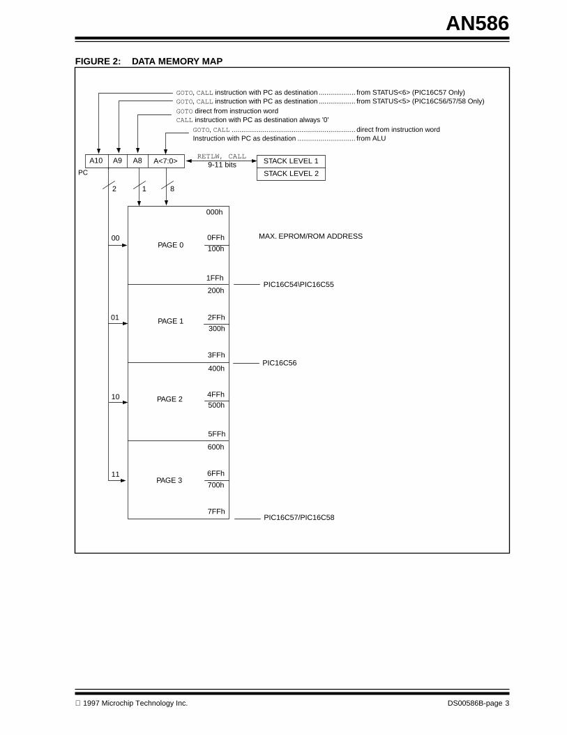
APPENDIX A: MACRO FILEMPASM 01.40 Released LCALL_5X.ASM 1-16-1997 17:13:33 PAGE 1
LOC OBJECT CODE LINE SOURCE TEXT VALUE
00001 LIST P = 16C57, n = 66 00002 ERRORLEVEL -302, -306 00003 ; 00004 ; Program = LCALL_5x.asm 00005 ; Revision Date: 5-07-94 00006 ; 1-15-97 Compatibility with MPASMWIN 1.40 00007 ; 00008 ; 00000000 00009 P1_TOP EQU 0x0000 000001FF 00010 P1_BOTTOM EQU 0x01FF 00000200 00011 P2_TOP EQU 0x0200 000003FF 00012 P2_BOTTOM EQU 0x03FF 00000400 00013 P3_TOP EQU 0x0400 000005FF 00014 P3_BOTTOM EQU 0x05FF 00000600 00015 P4_TOP EQU 0x0600 000007FF 00016 P4_BOTTOM EQU 0x07FF 000007FF 00017 RESET_V EQU 0x07FF 00018 ; 00000003 00019 STATUS EQU 0x03 ; Status Register 00000005 00020 PA0 EQU 0x05 ; Program Memory Page Address bit 0 00000006 00021 PA1 EQU 0x06 ; Program Memory Page Address bit 1 00022 ; 00000004 00023 FSR EQU 0x04 ; FSR Register 00000005 00024 RP0 EQU 0x05 ; Direct Addressing Register Bank bit 0 00000006 00025 RP1 EQU 0x06 ; Direct Addressing Register Bank bit 1 00026 ; 00000010 00027 BANK0_T EQU 0x10 00000030 00028 BANK1_T EQU 0x30 00000050 00029 BANK2_T EQU 0x50 00000070 00030 BANK3_T EQU 0x70 00031 ;0000 00032 org P1_TOP 00033 ;0000 0A07 00034 P1_CALL_1_V GOTO P1_CALL_10001 0A0A 00035 P1_CALL_2_V GOTO P1_CALL_2
Please check the Microchip BBS for the latest version of the source code. Microchip’s Worldwide Web Address: www.microBulletin Board Support: MCHIPBBS using CompuServe® (CompuServe membership not required).
1997 Microchip T
echnology Inc.D
S00586B
-page 7
A
N586
0002 0A0D 00036 P1_CALL_3_V GOTO P1_CALL_30003 0A1F 00037 P1_CALL_4_V GOTO P1_CALL_40004 0A64 00038 P1_CALL_5_V GOTO P1_CALL_5 00039 ; 00040 ; 00000010 00041 D_address EQU 0x10 00000001 00042 F EQU 1 00000000 00043 W EQU 0 00044 ; 00045 include <AUTO_PG.MAC> 00408 list 00409 00046 ;0005 090D 00047 START CALL P1_CALL_3 00048 ;0006 0A06 00049 LOOP GOTO LOOP 00050 ; 00051 ;0007 00052 P1_CALL_1 00053 ; 00054 if ( (P1_CALL_1_V & 0x0600) != (P1_CALL_1 & 0x0600) ) 00055 MESSG “ERROR - User Defined: CALL VECTOR and CALL routine NOT in same page” 00056 endif 00057 ;0007 0000 00058 NOP0008 0000 00059 NOP0009 0800 00060 P1_CALL_1_END RETURN 00061 ; 00062 if ( (P1_CALL_1 & 0x0600) != (P1_CALL_1_END & 0x0600) ) 00063 MESSG “Warning - User Defined: Call routine crosses page boundry” 00064 endif 00065 ; 00066 00067 000A 00068 P1_CALL_2 00069 ; 00070 if ( (P1_CALL_2_V & 0x0600) != (P1_CALL_2 & 0x0600) ) 00071 MESSG “ERROR - User Defined: CALL VECTOR and CALL routine NOT in same page” 00072 endif 00073 ;000A 0000 00074 NOP000B 0000 00075 NOP000C 0800 00076 P1_CALL_2_END RETURN 00077 ; 00078 if ( (P1_CALL_2 & 0x0600) != (P1_CALL_2_END & 0x0600) ) 00079 MESSG “Warning - User Defined: Call routine crosses page boundry” 00080 endif

A
N586
DS
00586B-page 8
1997 Microchip T
echnology Inc.
00081 ; 00082 00083 000D 00084 P1_CALL_3 00085 ; 00086 if ( (P1_CALL_3_V & 0x0600) != (P1_CALL_3 & 0x0600) ) 00087 MESSG “ERROR - User Defined: CALL VECTOR and CALL routine NOT in same page” 00088 endif 00089 ;000D 0000 00090 NOP000E 0000 00091 NOP000F 0800 00092 P1_CALL_3_END RETURN 00093 ; 00094 if ( (P1_CALL_3 & 0x0600) != (P1_CALL_3_END & 0x0600) ) 00095 MESSG “Warning - User Defined: Call routine crosses page boundry” 00096 endif 00097 ; 00098 00099 CALLM P2_CALL_3_V M ; M if ( ( P2_CALL_3_V & 0x0200 ) == 0x0200 )0010 05A3 M BSF STATUS, PA0 ; Set PA0 for Program Memory Page M else M BCF STATUS, PA0 ; Clear PA0 for Program Memory Page M endif M ; M if ( ( P2_CALL_3_V & 0x0400 ) == 0x0400 ) M BSF STATUS, PA1 ; Set PA1 for Program Memory Page M else0011 04C3 M BCF STATUS, PA1 ; Clear PA1 for Program Memory Page M endif M ;0012 0905 M CALL P2_CALL_3_V0013 0000 00100 nop0014 0000 00101 nop 00102 ; 00103 CALLM P4_CALL_2_V M ; M if ( ( P4_CALL_2_V & 0x0200 ) == 0x0200 )0015 05A3 M BSF STATUS, PA0 ; Set PA0 for Program Memory Page M else M BCF STATUS, PA0 ; Clear PA0 for Program Memory Page M endif M ; M if ( ( P4_CALL_2_V & 0x0400 ) == 0x0400 )0016 05C3 M BSF STATUS, PA1 ; Set PA1 for Program Memory Page M else

1997 Microchip T
echnology Inc.D
S00586B
-page 9
A
N586
M BCF STATUS, PA1 ; Clear PA1 for Program Memory Page M endif M ;0017 0901 M CALL P4_CALL_2_V0018 0000 00104 nop0019 0000 00105 nop 00106 ; 00107 CALLM P3_CALL_1_V M ; M if ( ( P3_CALL_1_V & 0x0200 ) == 0x0200 ) M BSF STATUS, PA0 ; Set PA0 for Program Memory Page M else001A 04A3 M BCF STATUS, PA0 ; Clear PA0 for Program Memory Page M endif M ; M if ( ( P3_CALL_1_V & 0x0400 ) == 0x0400 )001B 05C3 M BSF STATUS, PA1 ; Set PA1 for Program Memory Page M else M BCF STATUS, PA1 ; Clear PA1 for Program Memory Page M endif M ;001C 0900 M CALL P3_CALL_1_V001D 0000 00108 nop001E 0000 00109 nop 00110 00111 ;001F 00112 P1_CALL_4 00113 ; 00114 if ( (P1_CALL_4_V & 0x0600) != (P1_CALL_4 & 0x0600) ) 00115 MESSG “ERROR - User Defined: CALL VECTOR and CALL routine NOT in same page” 00116 endif 00117 ;001F 0000 00118 NOP0020 0000 00119 NOP0021 0800 00120 P1_CALL_4_END RETURN 00121 ; 00122 if ( (P1_CALL_4 & 0x0600) != (P1_CALL_4_END & 0x0600) ) 00123 MESSG “Warning - User Defined: Call routine crosses page boundry” 00124 endif 00125 ;0022 0000 00126 nop0023 0000 00127 nop 00128 00129 ADDWF_MAC D_address, F M ; M if ( ( D_address & 0x020 ) == 0x020 ) M BSF FSR, RP0 ; Set RP0 for Data Memory Page

A
N586
DS
00586B-page 10
1997 Microchip T
echnology Inc.
M else0024 04A4 M BCF FSR, RP0 ; Clear RP0 for Data Memory Bank M endif M ; M if ( ( D_address & 0x040 ) == 0x040 ) M BSF FSR, RP1 ; Set RP1 for Data Memory Bank M else0025 04C4 M BCF FSR, RP1 ; Clear RP1 for Data Memory Bank M endif0026 01F0 M ADDWF D_address, F 00130 ANDWF_MAC D_address, F M ; M if ( ( D_address & 0x020 ) == 0x020 ) M BSF FSR, RP0 ; Set RP0 for Data Memory Bank M else0027 04A4 M BCF FSR, RP0 ; Clear RP0 for Data Memory Bank M endif M ; M if ( ( D_address & 0x040 ) == 0x040 ) M BSF FSR, RP1 ; Set RP1 for Data Memory Bank M else0028 04C4 M BCF FSR, RP1 ; Clear RP1 for Data Memory Bank M endif0029 0170 M ANDWF D_address, F 00131 BCF_MAC D_address, 7 M ; M if ( ( D_address & 0x020 ) == 0x020 ) M BSF FSR, RP0 ; Set RP0 for Data Memory Bank M else002A 04A4 M BCF FSR, RP0 ; Clear RP0 for Data Memory Bank M endif M ; M if ( ( D_address & 0x040 ) == 0x040 ) M BSF FSR, RP1 ; Set RP1 for Data Memory Bank M else002B 04C4 M BCF FSR, RP1 ; Clear RP1 for Data Memory Bank M endif002C 04F0 M BCF D_address, 7 00132 BSF_MAC D_address, 7 M ; M if ( ( D_address & 0x020 ) == 0x020 ) M BSF FSR, RP0 ; Set RP0 for Data Memory Bank M else002D 04A4 M BCF FSR, RP0 ; Clear RP0 for Data Memory Bank M endif M ; M if ( ( D_address & 0x040 ) == 0x040 )

1997 Microchip T
echnology Inc.D
S00586B
-page 11
A
N586
M BSF FSR, RP1 ; Set RP1 for Data Memory Bank M else002E 04C4 M BCF FSR, RP1 ; Clear RP1 for Data Memory Bank M endif002F 05F0 M BSF D_address, 7 00133 BTFSC_MAC D_address, 7 M ; M if ( ( D_address & 0x020 ) == 0x020 ) M BSF FSR, RP0 ; Set RP0 for Data Memory Bank M else0030 04A4 M BCF FSR, RP0 ; Clear RP0 for Data Memory Bank M endif M ; M if ( ( D_address & 0x040 ) == 0x040 ) M BSF FSR, RP1 ; Set RP1 for Data Memory Bank M else0031 04C4 M BCF FSR, RP1 ; Clear RP1 for Data Memory Bank M endif0032 06F0 M BTFSC D_address, 7 00134 BTFSS_MAC D_address, 7 M ; M if ( ( D_address & 0x020 ) == 0x020 ) M BSF FSR, RP0 ; Set RP0 for Data Memory Bank M else0033 04A4 M BCF FSR, RP0 ; Clear RP0 for Data Memory Bank M endif M ; M if ( ( D_address & 0x040 ) == 0x040 ) M BSF FSR, RP1 ; Set RP1 for Data Memory Bank M else0034 04C4 M BCF FSR, RP1 ; Clear RP1 for Data Memory Bank M endif0035 07F0 M BTFSS D_address, 7 00135 CLRF_MAC D_address M ; M if ( ( D_address & 0x020 ) == 0x020 ) M BSF FSR, RP0 ; Set RP0 for Data Memory Bank M else0036 04A4 M BCF FSR, RP0 ; Clear RP0 for Data Memory Bank M endif M ; M if ( ( D_address & 0x040 ) == 0x040 ) M BSF FSR, RP1 ; Set RP1 for Data Memory Bank M else0037 04C4 M BCF FSR, RP1 ; Clear RP1 for Data Memory Bank M endif0038 0070 M CLRF D_address

A
N586
DS
00586B-page 12
1997 Microchip T
echnology Inc.
00136 COMF_MAC D_address, F M ; M if ( ( D_address & 0x020 ) == 0x020 ) M BSF FSR, RP0 ; Set RP0 for Data Memory Bank M else0039 04A4 M BCF FSR, RP0 ; Clear RP0 for Data Memory Bank M endif M ; M if ( ( D_address & 0x040 ) == 0x040 ) M BSF FSR, RP1 ; Set RP1 for Data Memory Bank M else003A 04C4 M BCF FSR, RP1 ; Clear RP1 for Data Memory Bank M endif003B 0270 M COMF D_address, F 00137 DECF_MAC D_address, F M ; M if ( ( D_address & 0x020 ) == 0x020 ) M BSF FSR, RP0 ; Set RP0 for Data Memory Bank M else003C 04A4 M BCF FSR, RP0 ; Clear RP0 for Data Memory Bank M endif M ; M if ( ( D_address & 0x040 ) == 0x040 ) M BSF FSR, RP1 ; Set RP1 for Data Memory Bank M else003D 04C4 M BCF FSR, RP1 ; Clear RP1 for Data Memory Bank M endif003E 00F0 M DECF D_address, F 00138 DECFSZ_MAC D_address, F M ; M if ( ( D_address & 0x020 ) == 0x020 ) M BSF FSR, RP0 ; Set RP0 for Data Memory Bank M else003F 04A4 M BCF FSR, RP0 ; Clear RP0 for Data Memory Bank M endif M ; M if ( ( D_address & 0x040 ) == 0x040 ) M BSF FSR, RP1 ; Set RP1 for Data Memory Bank M else0040 04C4 M BCF FSR, RP1 ; Clear RP1 for Data Memory Bank M endif0041 02F0 M DECFSZ D_address, F 00139 INCF_MAC D_address, F M ; M if ( ( D_address & 0x020 ) == 0x020 ) M BSF FSR, RP0 ; Set RP0 for Data Memory Bank M else

1997 Microchip T
echnology Inc.D
S00586B
-page 13
A
N586
0042 04A4 M BCF FSR, RP0 ; Clear RP0 for Data Memory Bank M endif M ; M if ( ( D_address & 0x040 ) == 0x040 ) M BSF FSR, RP1 ; Set RP1 for Data Memory Bank M else0043 04C4 M BCF FSR, RP1 ; Clear RP1 for Data Memory Bank M endif0044 02B0 M INCF D_address, F 00140 INCFSZ_MAC D_address, F M ; M if ( ( D_address & 0x020 ) == 0x020 ) M BSF FSR, RP0 ; Set RP0 for Data Memory Bank M else0045 04A4 M BCF FSR, RP0 ; Clear RP0 for Data Memory Bank M endif M ; M if ( ( D_address & 0x040 ) == 0x040 ) M BSF FSR, RP1 ; Set RP1 for Data Memory Bank M else0046 04C4 M BCF FSR, RP1 ; Clear RP1 for Data Memory Bank M endif0047 03F0 M INCFSZ D_address, F 00141 IORWF_MAC D_address, F M ; M if ( ( D_address & 0x020 ) == 0x020 ) M BSF FSR, RP0 ; Set RP0 for Data Memory Bank M else0048 04A4 M BCF FSR, RP0 ; Clear RP0 for Data Memory Bank M endif M ; M if ( ( D_address & 0x040 ) == 0x040 ) M BSF FSR, RP1 ; Set RP1 for Data Memory Bank M else0049 04C4 M BCF FSR, RP1 ; Clear RP1 for Data Memory Bank M endif004A 0130 M IORWF D_address, F 00142 MOVF_MAC D_address, F M ; M if ( ( D_address & 0x020 ) == 0x020 ) M BSF FSR, RP0 ; Set RP0 for Data Memory Bank M else004B 04A4 M BCF FSR, RP0 ; Clear RP0 for Data Memory Bank M endif M ; M if ( ( D_address & 0x040 ) == 0x040 ) M BSF FSR, RP1 ; Set RP1 for Data Memory Bank

AN
586 D
S00586B
-page 14
1997 Microchip T
echnology Inc.
M else004C 04C4 M BCF FSR, RP1 ; Clear RP1 for Data Memory Bank M endif004D 0230 M MOVF D_address, F 00143 MOVWF_MAC D_address M ; M if ( ( D_address & 0x020 ) == 0x020 ) M BSF FSR, RP0 ; Set RP0 for Data Memory Bank M else004E 04A4 M BCF FSR, RP0 ; Clear RP0 for Data Memory Bank M endif M ; M if ( ( D_address & 0x040 ) == 0x040 ) M BSF FSR, RP1 ; Set RP1 for Data Memory Bank M else004F 04C4 M BCF FSR, RP1 ; Clear RP1 for Data Memory Bank M endif0050 0030 M MOVWF D_address 00144 RLF_MAC D_address, F M ; M if ( ( D_address & 0x020 ) == 0x020 ) M BSF FSR, RP0 ; Set RP0 for Data Memory Bank M else0051 04A4 M BCF FSR, RP0 ; Clear RP0 for Data Memory Bank M endif M ; M if ( ( D_address & 0x040 ) == 0x040 ) M BSF FSR, RP1 ; Set RP1 for Data Memory Bank M else0052 04C4 M BCF FSR, RP1 ; Clear RP1 for Data Memory Bank M endif0053 0370 M RLF D_address, F 00145 RRF_MAC D_address, F M ; M if ( ( D_address & 0x020 ) == 0x020 ) M BSF FSR, RP0 ; Set RP0 for Data Memory Bank M else0054 04A4 M BCF FSR, RP0 ; Clear RP0 for Data Memory Bank M endif M ; M if ( ( D_address & 0x040 ) == 0x040 ) M BSF FSR, RP1 ; Set RP1 for Data Memory Bank M else0055 04C4 M BCF FSR, RP1 ; Clear RP1 for Data Memory Bank M endif0056 0330 M RRF D_address, F 00146 SUBWF_MAC D_address, F

1997 Microchip T
echnology Inc.D
S00586B
-page 15
A
N586
M ; M if ( ( D_address & 0x020 ) == 0x020 ) M BSF FSR, RP0 ; Set RP0 for Data Memory Bank M else0057 04A4 M BCF FSR, RP0 ; Clear RP0 for Data Memory Bank M endif M ; M if ( ( D_address & 0x040 ) == 0x040 ) M BSF FSR, RP1 ; Set RP1 for Data Memory Bank M else0058 04C4 M BCF FSR, RP1 ; Clear RP1 for Data Memory Bank M endif0059 00B0 M SUBWF D_address, F 00147 SWAPF_MAC D_address, F M ; M if ( ( D_address & 0x020 ) == 0x020 ) M BSF FSR, RP0 ; Set RP0 for Data Memory Bank M else005A 04A4 M BCF FSR, RP0 ; Clear RP0 for Data Memory Bank M endif M ; M if ( ( D_address & 0x040 ) == 0x040 ) M BSF FSR, RP1 ; Set RP1 for Data Memory Bank M else005B 04C4 M BCF FSR, RP1 ; Clear RP1 for Data Memory Bank M endif005C 03B0 M SWAPF D_address, F 00148 XORWF_MAC D_address, F M ; M if ( ( D_address & 0x020 ) == 0x020 ) M BSF FSR, RP0 ; Set RP0 for Data Memory Bank M else005D 04A4 M BCF FSR, RP0 ; Clear RP0 for Data Memory Bank M endif M ; M if ( ( D_address & 0x040 ) == 0x040 ) M BSF FSR, RP1 ; Set RP1 for Data Memory Bank M else005E 04C4 M BCF FSR, RP1 ; Clear RP1 for Data Memory Bank M endif005F 01B0 M XORWF D_address, F 00149 PAGE_MAC P1_CALL_4 M ; M if ( ( P1_CALL_4 & 0x0200 ) == 0x0200 ) M BSF STATUS, PA0 ; Set PA0 for Program Memory Page M else0060 04A3 M BCF STATUS, PA0 ; Clear PA0 for Program Memory Page

A
N586
DS
00586B-page 16
1997 Microchip T
echnology Inc.
M endif M ; M if ( ( P1_CALL_4 & 0x0400 ) == 0x0400 ) M BSF STATUS, PA1 ; Set PA1 for Program Memory Page M else0061 04C3 M BCF STATUS, PA1 ; Clear PA1 for Program Memory Page M endif M ; 00150 BANK_MAC D_address M ; M if ( ( D_address & 0x020 ) == 0x020 ) M BSF FSR, RP0 ; Set RP0 for Data Memory Bank M else0062 04A4 M BCF FSR, RP0 ; Clear RP0 for Data Memory Bank M endif M ; M if ( ( D_address & 0x040 ) == 0x040 ) M BSF FSR, RP1 ; Set RP1 for Data Memory Bank M else0063 04C4 M BCF FSR, RP1 ; Clear RP1 for Data Memory Bank M endif 00151 00152 00153 0064 00154 P1_CALL_5 00155 ; 00156 if ( (P1_CALL_5_V & 0x0600) != (P1_CALL_5 & 0x0600) ) 00157 MESSG “ERROR - User Defined: CALL VECTOR and CALL routine NOT in same page” 00158 endif 00159 ;0064 0000 00160 NOP0065 0000 00161 NOP 00162 ;0200 00163 org P2_TOP ; This is to force an intentional User Defined Message 00164 ;0200 0000 00165 NOP0201 0000 00166 NOP0202 0800 00167 P1_CALL_5_END RETURN 00168 ; 00169 if ( (P1_CALL_5 & 0x0600) != (P1_CALL_5_END & 0x0600) )Message[301]: MESSAGE: (Warning - User Defined: Call routine crosses page boundry) 00170 MESSG “Warning - User Defined: Call routine crosses page boundry” 00171 endif 00172 ; 00173 0203 0A08 00174 P2_CALL_1_V GOTO P2_CALL_10204 0A0B 00175 P2_CALL_2_V GOTO P2_CALL_2

1997 Microchip T
echnology Inc.D
S00586B
-page 17
A
N586
0205 0A13 00176 P2_CALL_3_V GOTO P2_CALL_30206 0A19 00177 P2_CALL_4_V GOTO P2_CALL_40207 0A1C 00178 P2_CALL_5_V GOTO P2_CALL_5 00179 00180 0208 0000 00181 P2_CALL_1 NOP0209 0000 00182 NOP020A 0800 00183 RETURN 00184 ; 00185 if ( (P2_CALL_1_V & 0x0600) != (P2_CALL_1 & 0x0600) ) 00186 MESSG “ERROR - User Defined: CALL VECTOR and CALL routine NOT in same page” 00187 endif 00188 00189 ;020B 0000 00190 P2_CALL_2 NOP020C 0000 00191 NOP020D 0800 00192 RETURN 00193 ; 00194 if ( (P2_CALL_2_V & 0x0600) != (P2_CALL_2 & 0x0600) ) 00195 MESSG “ERROR - User Defined: CALL VECTOR and CALL routine NOT in same page” 00196 endif 00197 00198 ; 00199 CALLM P1_CALL_3_V M ; M if ( ( P1_CALL_3_V & 0x0200 ) == 0x0200 ) M BSF STATUS, PA0 ; Set PA0 for Program Memory Page M else020E 04A3 M BCF STATUS, PA0 ; Clear PA0 for Program Memory Page M endif M ; M if ( ( P1_CALL_3_V & 0x0400 ) == 0x0400 ) M BSF STATUS, PA1 ; Set PA1 for Program Memory Page M else020F 04C3 M BCF STATUS, PA1 ; Clear PA1 for Program Memory Page M endif M ;0210 0902 M CALL P1_CALL_3_V0211 0000 00200 nop0212 0000 00201 nop 00202 0213 0000 00203 P2_CALL_3 NOP0214 0000 00204 NOP0215 0800 00205 RETURN 00206 ; 00207 if ( (P2_CALL_3_V & 0x0600) != (P2_CALL_3 & 0x0600) ) 00208 MESSG “ERROR - User Defined: CALL VECTOR and CALL routine NOT in same page”
AN
586
DS
00586B-page 18
1997 M
icrochip Technology Inc.
00209 endif 00210 00211 ; 00212 GOTOM P1_CALL_2 M ; M if ( ( P1_CALL_2 & 0x0200 ) == 0x0200 ) M BSF STATUS, PA0 ; Set PA0 for Program Memory Page M else0216 04A3 M BCF STATUS, PA0 ; Clear PA0 for Program Memory Page M endif M ; M if ( ( P1_CALL_2 & 0x0400 ) == 0x0400 ) M BSF STATUS, PA1 ; Set PA1 for Program Memory Page M else0217 04C3 M BCF STATUS, PA1 ; Clear PA1 for Program Memory Page M endif M ;0218 0A0A M GOTO P1_CALL_2 00213 00214 ;0219 0000 00215 P2_CALL_4 NOP021A 0000 00216 NOP021B 0800 00217 RETURN 00218 ; 00219 if ( (P2_CALL_4_V & 0x0600) != (P2_CALL_4 & 0x0600) ) 00220 MESSG “ERROR - User Defined: CALL VECTOR and CALL routine NOT in same page” 00221 endif 00222 00223 ;021C 0000 00224 P2_CALL_5 NOP021D 0000 00225 NOP021E 0800 00226 RETURN 00227 ; 00228 if ( (P2_CALL_5_V & 0x0600) != (P2_CALL_5 & 0x0600) ) 00229 MESSG “ERROR - User Defined: CALL VECTOR and CALL routine NOT in same page” 00230 endif 00231 00232 ; 00233 MOVF_MAC BANK0_T, 0 M ; M if ( ( BANK0_T & 0x020 ) == 0x020 ) M BSF FSR, RP0 ; Set RP0 for Data Memory Bank M else021F 04A4 M BCF FSR, RP0 ; Clear RP0 for Data Memory Bank M endif M ; M if ( ( BANK0_T & 0x040 ) == 0x040 )

1997 M
icrochip Technology Inc.
DS
00586B-page 19
AN
586
M BSF FSR, RP1 ; Set RP1 for Data Memory Page M else0220 04C4 M BCF FSR, RP1 ; Clear RP1 for Data Memory Page M endif0221 0210 M MOVF BANK0_T, 0 00234 MOVWF_MAC BANK1_T M ; M if ( ( BANK1_T & 0x020 ) == 0x020 )0222 05A4 M BSF FSR, RP0 ; Set RP0 for Data Memory Page M else M BCF FSR, RP0 ; Clear RP0 for Data Memory Page M endif M ; M if ( ( BANK1_T & 0x040 ) == 0x040 ) M BSF FSR, RP1 ; Set RP1 for Data Memory Page M else0223 04C4 M BCF FSR, RP1 ; Clear RP1 for Data Memory Page M endif0224 0030 M MOVWF BANK1_T 00235 MOVF_MAC BANK2_T, 0 M ; M if ( ( BANK2_T & 0x020 ) == 0x020 ) M BSF FSR, RP0 ; Set RP0 for Data Memory Page M else0225 04A4 M BCF FSR, RP0 ; Clear RP0 for Data Memory Page M endif M ; M if ( ( BANK2_T & 0x040 ) == 0x040 )0226 05C4 M BSF FSR, RP1 ; Set RP1 for Data Memory Page M else M BCF FSR, RP1 ; Clear RP1 for Data Memory Page M endif0227 0210 M MOVF BANK2_T, 0 00236 MOVWF_MAC BANK3_T M ; M if ( ( BANK3_T & 0x020 ) == 0x020 )0228 05A4 M BSF FSR, RP0 ; Set RP0 for Data Memory Page M else M BCF FSR, RP0 ; Clear RP0 for Data Memory Page M endif M ; M if ( ( BANK3_T & 0x040 ) == 0x040 )0229 05C4 M BSF FSR, RP1 ; Set RP1 for Data Memory Page M else M BCF FSR, RP1 ; Clear RP1 for Data Memory Page M endif022A 0030 M MOVWF BANK3_T

AN
586
DS
00586B-page 20
1997 M
icrochip Technology Inc.
00237 00238 ;0400 00239 org P3_TOP 00240 ;0400 0A05 00241 P3_CALL_1_V GOTO P3_CALL_10401 0A08 00242 P3_CALL_2_V GOTO P3_CALL_20402 0A0B 00243 P3_CALL_3_V GOTO P3_CALL_30403 0A0E 00244 P3_CALL_4_V GOTO P3_CALL_40404 0A05 00245 P3_CALL_5_V GOTO P3_CALL_5 00246 00247 0405 0000 00248 P3_CALL_1 NOP0406 0000 00249 NOP0407 0800 00250 RETURN 00251 ; 00252 if ( (P3_CALL_1_V & 0x0600) != (P3_CALL_1 & 0x0600) ) 00253 MESSG “ERROR - User Defined: CALL VECTOR and CALL routine NOT in same page” 00254 endif 00255 00256 ;0408 0000 00257 P3_CALL_2 NOP0409 0000 00258 NOP040A 0800 00259 RETURN 00260 ; 00261 if ( (P3_CALL_2_V & 0x0600) != (P3_CALL_2 & 0x0600) ) 00262 MESSG “ERROR - User Defined: CALL VECTOR and CALL routine NOT in same page” 00263 endif 00264 00265 ;040B 0000 00266 P3_CALL_3 NOP040C 0000 00267 NOP040D 0800 00268 RETURN 00269 ; 00270 if ( (P3_CALL_3_V & 0x0600) != (P3_CALL_3 & 0x0600) ) 00271 MESSG “ERROR - User Defined: CALL VECTOR and CALL routine NOT in same page” 00272 endif 00273 00274 ;040E 0000 00275 P3_CALL_4 NOP040F 0000 00276 NOP0410 0800 00277 RETURN 00278 ; 00279 if ( (P3_CALL_4_V & 0x0600) != (P3_CALL_4 & 0x0600) ) 00280 MESSG “ERROR - User Defined: CALL VECTOR and CALL routine NOT in same page” 00281 endif 00282 00283 ;

1997 M
icrochip Technology Inc.
DS
00586B-page 21
AN
586
0600 00284 org P4_TOP 00285 ;0600 0A08 00286 P4_CALL_1_V GOTO P4_CALL_10601 0A0B 00287 P4_CALL_2_V GOTO P4_CALL_20602 0A0E 00288 P4_CALL_3_V GOTO P4_CALL_30603 0A11 00289 P4_CALL_4_V GOTO P4_CALL_40604 0A14 00290 P4_CALL_5_V GOTO P4_CALL_5 00291 00292 ;0605 0000 00293 P3_CALL_5 NOP ; This is to force an intentional User Defined Message0606 0000 00294 NOP0607 0800 00295 RETURN 00296 ; 00297 if ( (P3_CALL_5_V & 0x0600) != (P3_CALL_5 & 0x0600) )Message[301]: MESSAGE: (ERROR - User Defined: CALL VECTOR and CALL routine NOT in same page) 00298 MESSG “ERROR - User Defined: CALL VECTOR and CALL routine NOT in same page” 00299 endif 00300 00301 ;0608 0000 00302 P4_CALL_1 NOP0609 0000 00303 NOP060A 0800 00304 RETURN 00305 ; 00306 if ( (P4_CALL_1_V & 0x0600) != (P4_CALL_1 & 0x0600) ) 00307 MESSG “ERROR - User Defined: CALL VECTOR and CALL routine NOT in same page” 00308 endif 00309 00310 ;060B 0000 00311 P4_CALL_2 NOP060C 0000 00312 NOP060D 0800 00313 RETURN 00314 ; 00315 if ( (P4_CALL_2_V & 0x0600) != (P4_CALL_2 & 0x0600) ) 00316 MESSG “ERROR - User Defined: CALL VECTOR and CALL routine NOT in same page” 00317 endif 00318 00319 ;060E 0000 00320 P4_CALL_3 NOP060F 0000 00321 NOP0610 0800 00322 RETURN 00323 ; 00324 if ( (P4_CALL_3_V & 0x0600) != (P4_CALL_3 & 0x0600) ) 00325 MESSG “ERROR - User Defined: CALL VECTOR and CALL routine NOT in same page” 00326 endif 00327 00328 ;0611 0000 00329 P4_CALL_4 NOP
AN
586
DS
00586B-page 22
1997 M
icrochip Technology Inc.
0612 0000 00330 NOP0613 0800 00331 RETURN 00332 ; 00333 if ( (P4_CALL_4_V & 0x0600) != (P4_CALL_4 & 0x0600) ) 00334 MESSG “ERROR - User Defined: CALL VECTOR and CALL routine NOT in same page” 00335 endif 00336 00337 ;0614 0000 00338 P4_CALL_5 NOP0615 0000 00339 NOP0616 0800 00340 RETURN 00341 ; 00342 if ( (P4_CALL_5_V & 0x0600) != (P4_CALL_5 & 0x0600) ) 00343 MESSG “ERROR - User Defined: CALL VECTOR and CALL routine NOT in same page” 00344 endif 00345 ; 00346 ;07FF 00347 org RESET_V 00348 ;07FF 0A05 00349 GOTO START ; Goto the begining of the program 00350 00351 end
MEMORY USAGE MAP (‘X’ = Used, ‘-’ = Unused)
0000 : XXXXXXXXXXXXXXXX XXXXXXXXXXXXXXXX XXXXXXXXXXXXXXXX XXXXXXXXXXXXXXXX0040 : XXXXXXXXXXXXXXXX XXXXXXXXXXXXXXXX XXXXXX---------- ----------------0200 : XXXXXXXXXXXXXXXX XXXXXXXXXXXXXXXX XXXXXXXXXXX----- ----------------0400 : XXXXXXXXXXXXXXXX X--------------- ---------------- ----------------0600 : XXXXXXXXXXXXXXXX XXXXXXX--------- ---------------- ----------------07C0 : ---------------- ---------------- ---------------- ---------------X
All other memory blocks unused.
Program Memory Words Used: 186Program Memory Words Free: 1862
Errors : 0Warnings : 0 reported, 0 suppressedMessages : 2 reported, 10 suppressed

2002 Microchip Technology Inc.
Information contained in this publication regarding deviceapplications and the like is intended through suggestion onlyand may be superseded by updates. It is your responsibility toensure that your application meets with your specifications.No representation or warranty is given and no liability isassumed by Microchip Technology Incorporated with respectto the accuracy or use of such information, or infringement ofpatents or other intellectual property rights arising from suchuse or otherwise. Use of Microchip’s products as critical com-ponents in life support systems is not authorized except withexpress written approval by Microchip. No licenses are con-veyed, implicitly or otherwise, under any intellectual propertyrights.
Trademarks
The Microchip name and logo, the Microchip logo, FilterLab,KEELOQ, microID, MPLAB, PIC, PICmicro, PICMASTER,PICSTART, PRO MATE, SEEVAL and The Embedded ControlSolutions Company are registered trademarks of Microchip Tech-nology Incorporated in the U.S.A. and other countries.
dsPIC, ECONOMONITOR, FanSense, FlexROM, fuzzyLAB,In-Circuit Serial Programming, ICSP, ICEPIC, microPort,Migratable Memory, MPASM, MPLIB, MPLINK, MPSIM,MXDEV, PICC, PICDEM, PICDEM.net, rfPIC, Select Modeand Total Endurance are trademarks of Microchip TechnologyIncorporated in the U.S.A.
Serialized Quick Turn Programming (SQTP) is a service markof Microchip Technology Incorporated in the U.S.A.
All other trademarks mentioned herein are property of theirrespective companies.
© 2002, Microchip Technology Incorporated, Printed in theU.S.A., All Rights Reserved.
Printed on recycled paper.
Microchip received QS-9000 quality system certification for its worldwide headquarters, design and wafer fabrication facilities in Chandler and Tempe, Arizona in July 1999. The Company’s quality system processes and procedures are QS-9000 compliant for its PICmicro® 8-bit MCUs, KEELOQ® code hopping devices, Serial EEPROMs and microperipheral products. In addition, Microchip’s quality system for the design and manufacture of development systems is ISO 9001 certified.
Note the following details of the code protection feature on PICmicro® MCUs.
• The PICmicro family meets the specifications contained in the Microchip Data Sheet.• Microchip believes that its family of PICmicro microcontrollers is one of the most secure products of its kind on the market today,
when used in the intended manner and under normal conditions.• There are dishonest and possibly illegal methods used to breach the code protection feature. All of these methods, to our knowl-
edge, require using the PICmicro microcontroller in a manner outside the operating specifications contained in the data sheet. The person doing so may be engaged in theft of intellectual property.
• Microchip is willing to work with the customer who is concerned about the integrity of their code.• Neither Microchip nor any other semiconductor manufacturer can guarantee the security of their code. Code protection does not
mean that we are guaranteeing the product as “unbreakable”.• Code protection is constantly evolving. We at Microchip are committed to continuously improving the code protection features of
our product.
If you have any further questions about this matter, please contact the local sales office nearest to you.

2002 Microchip Technology Inc.
MAMERICASCorporate Office2355 West Chandler Blvd.Chandler, AZ 85224-6199Tel: 480-792-7200 Fax: 480-792-7277Technical Support: 480-792-7627Web Address: http://www.microchip.comRocky Mountain2355 West Chandler Blvd.Chandler, AZ 85224-6199Tel: 480-792-7966 Fax: 480-792-7456
Atlanta500 Sugar Mill Road, Suite 200BAtlanta, GA 30350Tel: 770-640-0034 Fax: 770-640-0307Boston2 Lan Drive, Suite 120Westford, MA 01886Tel: 978-692-3848 Fax: 978-692-3821Chicago333 Pierce Road, Suite 180Itasca, IL 60143Tel: 630-285-0071 Fax: 630-285-0075Dallas4570 Westgrove Drive, Suite 160Addison, TX 75001Tel: 972-818-7423 Fax: 972-818-2924DetroitTri-Atria Office Building 32255 Northwestern Highway, Suite 190Farmington Hills, MI 48334Tel: 248-538-2250 Fax: 248-538-2260Kokomo2767 S. Albright Road Kokomo, Indiana 46902Tel: 765-864-8360 Fax: 765-864-8387Los Angeles18201 Von Karman, Suite 1090Irvine, CA 92612Tel: 949-263-1888 Fax: 949-263-1338New York150 Motor Parkway, Suite 202Hauppauge, NY 11788Tel: 631-273-5305 Fax: 631-273-5335San JoseMicrochip Technology Inc.2107 North First Street, Suite 590San Jose, CA 95131Tel: 408-436-7950 Fax: 408-436-7955Toronto6285 Northam Drive, Suite 108Mississauga, Ontario L4V 1X5, CanadaTel: 905-673-0699 Fax: 905-673-6509
ASIA/PACIFICAustraliaMicrochip Technology Australia Pty LtdSuite 22, 41 Rawson StreetEpping 2121, NSWAustraliaTel: 61-2-9868-6733 Fax: 61-2-9868-6755China - BeijingMicrochip Technology Consulting (Shanghai)Co., Ltd., Beijing Liaison OfficeUnit 915Bei Hai Wan Tai Bldg.No. 6 Chaoyangmen Beidajie Beijing, 100027, No. ChinaTel: 86-10-85282100 Fax: 86-10-85282104China - ChengduMicrochip Technology Consulting (Shanghai)Co., Ltd., Chengdu Liaison OfficeRm. 2401, 24th Floor, Ming Xing Financial TowerNo. 88 TIDU StreetChengdu 610016, ChinaTel: 86-28-6766200 Fax: 86-28-6766599China - FuzhouMicrochip Technology Consulting (Shanghai)Co., Ltd., Fuzhou Liaison OfficeUnit 28F, World Trade PlazaNo. 71 Wusi RoadFuzhou 350001, ChinaTel: 86-591-7503506 Fax: 86-591-7503521China - ShanghaiMicrochip Technology Consulting (Shanghai)Co., Ltd.Room 701, Bldg. BFar East International PlazaNo. 317 Xian Xia RoadShanghai, 200051Tel: 86-21-6275-5700 Fax: 86-21-6275-5060China - ShenzhenMicrochip Technology Consulting (Shanghai)Co., Ltd., Shenzhen Liaison OfficeRm. 1315, 13/F, Shenzhen Kerry Centre,Renminnan LuShenzhen 518001, ChinaTel: 86-755-2350361 Fax: 86-755-2366086Hong KongMicrochip Technology Hongkong Ltd.Unit 901-6, Tower 2, Metroplaza223 Hing Fong RoadKwai Fong, N.T., Hong KongTel: 852-2401-1200 Fax: 852-2401-3431IndiaMicrochip Technology Inc.India Liaison OfficeDivyasree Chambers1 Floor, Wing A (A3/A4)No. 11, O’Shaugnessey RoadBangalore, 560 025, IndiaTel: 91-80-2290061 Fax: 91-80-2290062
JapanMicrochip Technology Japan K.K.Benex S-1 6F3-18-20, ShinyokohamaKohoku-Ku, Yokohama-shiKanagawa, 222-0033, JapanTel: 81-45-471- 6166 Fax: 81-45-471-6122KoreaMicrochip Technology Korea168-1, Youngbo Bldg. 3 FloorSamsung-Dong, Kangnam-KuSeoul, Korea 135-882Tel: 82-2-554-7200 Fax: 82-2-558-5934SingaporeMicrochip Technology Singapore Pte Ltd.200 Middle Road#07-02 Prime CentreSingapore, 188980Tel: 65-334-8870 Fax: 65-334-8850TaiwanMicrochip Technology Taiwan11F-3, No. 207Tung Hua North RoadTaipei, 105, TaiwanTel: 886-2-2717-7175 Fax: 886-2-2545-0139
EUROPEDenmarkMicrochip Technology Nordic ApSRegus Business CentreLautrup hoj 1-3Ballerup DK-2750 DenmarkTel: 45 4420 9895 Fax: 45 4420 9910FranceMicrochip Technology SARLParc d’Activite du Moulin de Massy43 Rue du Saule TrapuBatiment A - ler Etage91300 Massy, FranceTel: 33-1-69-53-63-20 Fax: 33-1-69-30-90-79GermanyMicrochip Technology GmbHGustav-Heinemann Ring 125D-81739 Munich, GermanyTel: 49-89-627-144 0 Fax: 49-89-627-144-44ItalyMicrochip Technology SRLCentro Direzionale Colleoni Palazzo Taurus 1 V. Le Colleoni 120041 Agrate BrianzaMilan, Italy Tel: 39-039-65791-1 Fax: 39-039-6899883United KingdomArizona Microchip Technology Ltd.505 Eskdale RoadWinnersh TriangleWokingham Berkshire, England RG41 5TUTel: 44 118 921 5869 Fax: 44-118 921-5820
01/18/02
WORLDWIDE SALES AND SERVICE