Embed Size (px)
Citation preview

MEMS-Enabled Micro-Electro-Discharge Machining (M3EDM)
by
Alla Chaitanya Chakravarty Reddy
B.Tech, Jawaharlal Nehru Technological University, 2004
A THESIS SUBMITTED IN PARTIAL FULFILLMENT OF THE REQUIREMENTS FOR THE DEGREE OF
Master of Applied Science
in
The Faculty of Graduate Studies
(Electrical and Computer Engineering)
The University of British Columbia
(Vancouver)
October 2008
© Alla Chaitanya Chakravarty Reddy 2008

ii
Abstract A MEMS-based micro-electro-discharge machining technique that is enabled by the
actuation of micromachined planar electrodes defined on the surfaces of the workpiece is
developed that eliminates the need of numerical control machines. First, the planar
electrodes actuated by hydrodynamic force is developed. The electrode structures are
defined by patterning 18-µm-thick copper foil laminated on the stainless steel workpiece
through an intermediate photoresist layer and released by sacrificial etching of the resist layer.
The planer electrodes are constructed to be single layer structures without particular features
underneath. All the patterning and sacrificial etching steps are performed using dry-film
photoresists towards achieving high scalability of the machining technique to large-area
applications. A DC voltage of 80-140 V is applied between the electrode and the workpiece
through a resistance-capacitance circuit that controls the pulse energy and timing of spark
discharges. The parasitic capacitance of the electrode structure is used to form a resistance-
capacitance circuit for the generation of pulsed spark discharge between the electrode and the
workpiece. The suspended electrodes are actuated towards the workpiece using the
downflow of dielectric machining fluid, initiating and sustaining the machining process.
Micromachining of stainless steel is experimentally demonstrated with the machining voltage
of 90V and continuous flow of the fluid at the velocity of 3.4-3.9 m/s, providing removal
depth of 20 µm. The experimental results of the electrode actuation match well with the
theoretical estimations. Second, the planar electrodes are electrostatically actuated towards
workpiece for machining. In addition to the single-layer, this effort uses double-layer
structures defined on the bottom surface of the electrode to create custom designed patterns
on the workpiece material. The suspended electrode is electrostatically actuated towards the
wafer based on the pull-in, resulting in a breakdown, or spark discharge. This instantly
lowers the gap voltage, releasing the electrode, and the gap value recovers as the capacitor is
charged up through the resistor. Sequential pulses are produced through the self-regulated
discharging-charging cycle. Micromachining of the stainless-steel wafer is demonstrated
using the electrodes with single-layer and double-layer structures. The experimental results
of the dynamic built-capacitance and mechanical behavior of the electrode devices are also
analyzed.
iii
Table of Contents
Abstract . . . . . . . . . . . . . . . . . . . . . . . . . . . . . . . . . . . . . ii Table of Contents . . . . . . . . . . . . . . . . . . . . . . . . . . . . . . . . iii List of Tables . . . . . . . . . . . . . . . . . . . . . . . . . . . . . . . . . . v List of Figures . . . . . . . . . . . . . . . . . . . . . . . . . . . . . . . . . . vi Acknowledgements . . . . . . . . . . . . . . . . . . . . . . . . . . . . . . . . . ix Statement of Co-Authorship . . . . . . . . . . . . . . . . . . . . . . . . . . . x 1 Introduction . . . . . . . . . . . . . . . . . . . . . . . . . . . . . . . . . 1
1.1 Non-traditional Micromachining Processes . . . . . . . . . . . . . 3
1.2 Micro-Electro-Discharge Machining . . . . . . . . . . . . . . . . . 4
1.2.1 Principle of µEDM Operation . . . . . . . . . . . . . . . . . 6
1.2.2 Setup for µEDM . . . . . . . . . . . . . . . . . . . . . . . . . 7
1.2.3 Applications Areas of µEDM . . . . . . . . . . . . . . . . . 9
1.3 Advanced µEDM . . . . . . . . . . . . . . . . . . . . . . . . . . . . . 10
1.3.1 Batch-Mode µEDM . . . . . . . . . . . . . . . . . . . . . 11
1.3.2 New Approach to µEDM . . . . . . . . . . . . . . . . . . . . . 13
1.4 Thesis Outline . . . . . . . . . . . . . . . . . . . . . . . . . . . . . 13
References . . . . . . . . . . . . . . . . . . . . . . . . . . . . . . . . . 14
2 M3EDM: MEMS-enabled micro-electro-discharge machining . . . . . 17
2.1 Introduction . . . . . . . . . . . . . . . . . . . . . . . . . . . . . 17
2.2 Machining Principle . . . . . . . . . . . . . . . . . . . . . . . . . 18
2.3 Electrode Design and Actuation Mechanisms . . . . . . . . . . . . . 20
2.4 Fabrication . . . . . . . . . . . . . . . . . . . . . . . . . . . . . 22
2.5 Experimental Results . . . . . . . . . . . . . . . . . . . . . . . . . 25
2.6 Analysis and Discussion . . . . . . . . . . . . . . . . . . . . . . . . . 29
2.7 Conclusions . . . . . . . . . . . . . . . . . . . . . . . . . . . . . 31

iv
References . . . . . . . . . . . . . . . . . . . . . . . . . . . . . . . . . 32
3 MEMS-based micro-electro-discharge machining (M3EDM) by electrostatic actuation
of machining electrodes on the workpiece . . . . . . . . . . . . . . . . . 34
3.1 Introduction . . . . . . . . . . . . . . . . . . . . . . . . . . . . . 34
3.2 Machining Principle . . . . . . . . . . . . . . . . . . . . . . . . . 35
3.3 Device Design . . . . . . . . . . . . . . . . . . . . . . . . . . . . . 37
3.4 Fabrication . . . . . . . . . . . . . . . . . . . . . . . . . . . . . 40
3.5 Experimental Results . . . . . . . . . . . . . . . . . . . . . . . . . 45
3.6 Analysis and Discussion . . . . . . . . . . . . . . . . . . . . . . . . . 49
3.7 Conclusions . . . . . . . . . . . . . . . . . . . . . . . . . . . . . 52
References . . . . . . . . . . . . . . . . . . . . . . . . . . . . . . . . . 53
4 Conclusions . . . . . . . . . . . . . . . . . . . . . . . . . . . . . . . . . 55
References . . . . . . . . . . . . . . . . . . . . . . . . . . . . . . . . . 57

v
List of Tables 1.1 Non-traditional micromachining processes . . . . . . . . . . . . . 5

vi
List of Figures
1.1 Mechanism of µEDM . . . . . . . . . . . . . . . . . . . . . . . . . 6
1.2 Setup for µEDM tests . . . . . . . . . . . . . . . . . . . . . . . . . 7
1.3 A transistor-type pulse generation circuit . . . . . . . . . . . . . 8
1.4 3D geometry by µEDM using single electrode . . . . . . . . . . . . . 9
1.5 An SEM image of a machined sample . . . . . . . . . . . . . . . . . 9
1.6 Wire electro discharge grinding . . . . . . . . . . . . . . . . . . . . . 10
1.7 Batch-mode µEDM using single pulse generation circuit . . . . . . . . 12
1.8 Batch-mode µEDM pulse timing circuits (a) electrodes connected to a single
pulse generation circuit; (b) electrodes connected to individual pulse generation
circuits . . . . . . . . . . . . . . . . . . . . . . . . . . . . . . . . . 12
2.1 Cross sectional view of MEMS-based µEDM and its process steps . . 19
2.2 Sample design of the µEDM devices with (a) fixed-fixed and (b) cantilever
configurations . . . . . . . . . . . . . . . . . . . . . . . . . . . . . 22
2.3 Two dry-film processes developed for the fabrication of the movable electrode
devices on the workpiece . . . . . . . . . . . . . . . . . . . . . . . . . 23
2.4 An SEM image of (a) a fixed-fixed electrode and (b) a cantilever electrode both
with the layouts shown in Figure 2.2, and (c) an optical image of the fabricated
devices . . . . . . . . . . . . . . . . . . . . . . . . . . . . . . . . . 24
2.5 A 6×6-cm2 piece of sacrificial dry-film photoresist with patterned electrode
devices (the 3” wafer underneath the resist film was placed for dimensional
comparison with the film) . . . . . . . . . . . . . . . . . . . . . . . . . 25
2.6 A set used for the characterization of the electrode actuation and µEDM tests
. . . . . . . . . . . . . . . . . . . . . . . . . . . . . . . . . . . . . 26
2.7 Built-in capacitance vs. fluid flow velocity measured with a fabricated device
with the design shown in Figure 2.2a . . . . . . . . . . . . . . . . . 26
2.8 (a) Measured pulses of discharge current at the voltage of 90 V with an inset
vii
of single pulse close-up, and (b) an optical image of spark light captured through
electrode’s holes . . . . . . . . . . . . . . . . . . . . . . . . . . . . . 27
2.9 Micromachined result obtained with a cantilever electrode: (a) an SEM image and
(b) optically measured geometry of the machined structured (electrode removed
after machining); (c) a top view at one of the holes of an electrode that was stuck
to the workpiece during the machining, showing a circular surface of the
workpiece through the hole with a discharge gap of ~ 10 µm
. . . . . . . . . . . . . . . . . . . . . . . . . . . . . . . . . . . . . 28
2.10 Theoretical deflections vs. fluid flow velocity for the two electrodes in Figure 2.2
calculated using the experimental conditions of the fluidic set-up used (Figure
2.6) . . . . . . . . . . . . . . . . . . . . . . . . . . . . . . . . . . . . . 30
3.1 Cross sectional view of the MEMS-based µEDM based on electrostatic actuation
and its steps; (b) dynamic behavior of discharge voltage and current corresponding
to the steps . . . . . . . . . . . . . . . . . . . . . . . . . . . . . . . . . 36
3.2 A sample layout of the µEDM device for (a) torsional design with the single-layer
scheme; (b) custom design structures with double-layer scheme
. . . . . . . . . . . . . . . . . . . . . . . . . . . . . . . . . . . . . . . . . 39
3.3 Two processes developed for electrode fabrication with (a) single-layer structures;
(b) double-layer structures . . . . . . . . . . . . . . . . . . . . . 41
3.4 (a) An optical image of the fabricated devices on a stainless-steel substrate; (b) an
SEM image of a sample device fabricated for the single-layer design in Figure
3.2a . . . . . . . . . . . . . . . . . . . . . . . . . . . . . . . . . . . . . 43
3.5 Fabrication results for the double-layer design: (a) an SEM image of the
electroplated copper on the copper supporting electrode; (b) an optical image of
the fabricated device with the design in Figure 3.2b; (c) an SEM image of the
close-up . . . . . . . . . . . . . . . . . . . . . . . . . . . . . . . . . 44
3.6 A set-up for device characterizationµEDM tests . . . . . . . . . . . . . 45
3.7 (a) Measured current pulses of micro spark discharge; (b) single pulse close-up;

viii
(c) an optical image of the micro sparks captured through electrode’s holes
. . . . . . . . . . . . . . . . . . . . . . . . . . . . . . . . . . . . . . . . . 46
3.8 (a) An SEM image of the µEDMed stainless-steel substrate (electrode removed
after machining) with inset of close-up; (b) optically measured geometry of the
machined structures. Using WykoTM NT1100 profiler, batch structures are
measured to have the depth of ~ 20 µm . . . . . . . . . . . . . . . . . 47
3.9 Vertical displacement of the electrode measured while switching on and off the
EDM process using the single-layer electrodes; (a) fixed-fixed device with 15 µm
gap spacing; (b) cantilever device with 40 µm gap spacing . . . . . . . . . 48
3.10 (a) Measured machining voltage showing charging cycles with different time
constants for the electrodes with different areas; (b) built-in capacitance in static
(Cb) and dynamic (Cbb) modes vs. device area . . . . . . . . . . . . . 50

ix
Acknowledgements
I would like to take this opportunity to acknowledge my advisor and supervisor Dr.
Kenichi Takahata for his guidance and insight into the research I have been involved in.
This work would not have been possible without his dedication and commitment towards
research and I appreciate all his work. It has been a good learning experience and I
cherish the entire period I have worked.
I would also take the opportunity to thank Dr Edmond Cretu for initiating and
introducing me to this research field. I would also like to acknowledge Dr. John Madden
for his suggestions on different aspects during my entire education. I would like to thank
Ms. Vijayalakshmi Sridhar and Mr. Greg Wong for assisting me with the fabrication
process. I would also like to thank Mr. Mrigank Sharma and Ms. Akila Kannan for their
fruitful discussions on various topics during the research work. I would like to thank all
others who have helped me during the entire period of my research work.

x
Statement of Co-Authorship
The research work presented in this thesis has been done in conjunction with the
members of the Microsystems and Nanotechnology Group during the period 2006 – 2008.
This statement is to confirm that the author of this thesis is solely responsible for the
research performed. The author would like to acknowledge the contribution of co-
authors for the manuscript preparation, written during the course of the research work.

1
Chapter 1 Introduction
Micromachining is a key manufacturing technology to produce microstructures and
micromechanical parts with sizes ranging from sub millimeters to microns for
microelectromechanical systems (MEMS). The fabrication techniques developed for
integrated circuit industry can be utilized for micromachining and manufacturing by
adding mechanical components like beams, springs, gears to the devices. Surface
micromachining has been one of the earliest developed machining techniques and to a
certain extent the mainstay of the industry. They were mainly used to form two-
dimensional structures on the surface of a silicon wafer. The main advantage of surface-
micromachined structures is the easy integration with integrated circuit (IC) components
on the same silicon wafer, resulting in mass production of microsensors and actuators.
But the structures fabricated were planar and with limited aspect ratio. High-aspect-ratio
microstructures are often demanded in MEMS in order to achieve higher performance in
terms of larger force, higher sensitivity and mechanical robustness. These constraints
were overcome by using bulk micromachining that were able to build complex three-
dimensional shapes. However, the materials that can be manufactured using these
technologies were mainly applicable to silicon and other limited materials like titanium.
Special lithography techniques such as LIGA (a German acronym for lithography,
electroplating and injection molding based on deep X-ray lithography) and SU-8 based
processes (SU-8 is a negative, epoxy-type photoresist that can be used to pattern high
aspect ratio micro structures) can be used to fabricate mechanical parts but machining
real 3-dimensional (3-D) with free form shapes are still very difficult. Another constraint
with the LIGA process is the high cost involved in the fabrication process based on the
use of synchrotron radiation.
The requirement for small dimensions, high precision, diverse materials and complex
three-dimensional structures has opened up avenues for manufacturing technologies that
does not follow traditional lithography-based approaches. Non-traditional

2
micromachining processes is a group of processes that remove excess material by various
methods including mechanical (physical removing by milling, cutting, stamping, etc),
abrasive (removal of material by stream of abrasive particles like water jet machining,
ultrasonic machining, etc), thermal (thermal energy usually applied to small portion of
workpiece, causing the portion to be removed by fusion or vaporization), and
electrochemical (electrochemical energy to remove material) without using a sharp
cutting tool as is the case with the conventional machining. For example the mechanical
machining uses a sharp tool to mechanically cut the material to obtain the desired
geometry and are capable of producing free-form structures in wide range of materials
including common engineering alloys. Complex 3-D structures can be generated with
shape accuracies by means of various mechanical processes that include micro-milling,
micro-drilling and micro-grinding.
Micro-electro-discharge machining (µEDM) is an electrothermal micromachining
process for electrically conductive materials by using controlled sparks that occur
between a microscopic electrode and a workpiece material in the presence of a dielectric
fluid. When two electrodes are in close proximity in a dielectric liquid, application of a
voltage pulse between them can break down the dielectric and produce a spark which
thermally erodes the material of the workpiece at the breakdown point. The µEDM
process is a high repetition of this single removal cycle that erodes the material from the
workpiece until the shape of the electrode is formed on the workpiece. µEDM can be
used for machining complex shapes by the use of numerical control (NC) machines for
the positioning of the electrode on the workpiece but the throughput is low as it is a serial
process and involves high costs due to NC machines. The thesis presented in the
following sections is based on the principle of µEDM. A new approach to
micromachining using MEMS-based actuators is presented in this report for high-
throughput, low-cost and high-precision machining.
In the following sections, Section 1.1 gives a brief overview of some of the non-
traditional machining processes, Section 1.2 gives the principles and technologies of
µEDM technique, Section 1.3 summarizes the past efforts for advanced µEDM
techniques, and Section 1.4 gives the outline of this thesis.

3
1.1 Non-traditional Micromachining Processes In general, the use of non-traditional techniques allows one to utilize a broad range of
engineering materials for microfabrication. The major drawback of the mechanical
micromachining processes is the high machining force that affects the machining
accuracy and the elastic deformation of the electrode or the workpiece [1]. These are a
lot of challenges in the industry for machining materials (ceramics and composites) to
meet the design considerations (high precision, high surface quality and complex
geometry). Advanced materials are increasingly used in industries like aircraft,
automobile, tool, die and mold making industries. The mechanical machining processes
are one of the common methods (e.g. thermal, abrasive and chemical) for machining of
components in such fields. However for micromachining they are not efficient and are
expensive to machine the materials. To overcome these constraints other non-traditional
machining processes can be used. Some of the non-traditional machining processes are
discussed below.
Electro-chemical machining is a method of removing metal by an electrochemical
process [1]. An electrolytic cell is formed using the electrode as cathode and the
workpiece as anode in an electrolytic solution. The workpiece is removed in the form of
sludge formed by the chemical reactions that takes place in the electrolytic cell. It is used
for working with hard materials and can cut contours or cavities in hard steel and metals
such as titanium and carbide. Electrochemical grinding (ECG) is a form of
electrochemical machining that combines both electrochemical attack and abrasion to
remove material from electrically conductive workpiece, hard, tough materials [2]. ECG
makes use of a rotating grinding wheel (electrode) where direct current is passed through
an electrolyte between the wheel and the workpiece. The majority of the workpiece
material is removed by the electrochemical attack whereas the abrasive action removes
only a part of the workpiece material. ECG can be used to grind any electrically
conductive material, steel or alloy steel part, hard and tough materials. ECG can be used
for variety of applications in the aerospace, automotive instrumentation, textile and
medical manufacturing industries. Some of the features of the non-traditional machining
processes are given in Table 1.1 along with the applicable materials [3].

4
Laser beam machining is a thermal removal process where an intense beam of
collimated, single wavelength, in-phase light is focused by an optical lens onto the
workpiece material to be machined [4]. It can be used for variety of materials: metals,
composites, plastics and ceramics.
In ultrasonic machining, the cutting is performed by abrasive particles suspended in a
fluid. The abrasives contained in a slurry are driven at high velocity against workpiece
by a tool vibrating at low amplitude and high frequency [5, 6]. The tool oscillation is
perpendicular to the workpiece and is slowly fed into the workpiece creating a shape of
the tool in the workpiece [7]. Ultrasonic machining can be used for machining brittle
materials such as single crystals, glasses and polycrystalline ceramics and for increasing
complex operations to obtain intricate shapes and workpiece profiles. Since the
ultrasonic machining is non-thermal and non-chemical, there is no change in the chemical
or physical properties of the workpiece thereby offering stress-free machined surfaces [5].
It is used extensively in manufacturing hard and brittle materials that are otherwise
difficult to machine using the conventional processes.
Abrasive waterjet machining can be used to cut metals and hard materials. The
cutting is performed by a high speed, small-scale erosion process that enables abrasive
waterjet to cut difficult to machine materials with very limited thermal and mechanical
effects. It is widely used in cutting metals such as aluminum, brass, steel, titanium and
nickel based alloys, as well as glass, stone and composites [8]. Abrasive waterjet
machining can be used in a number of applications such as drilling, polishing, turning and
milling.
µEDM is a machining process based on material removal by melting and partly by
vaporization with miniaturized discharge spark pulses [9]. µEDM has been leveraged for
fabricating small features and micro-components such as nozzle holes, slots, and shafts in
any conductive material including all kinds of metals and alloys offering exceptional
micromachining opportunities. In the next section, details of µEDM is reviewed.
1.2 Micro-Electro-Discharge Machining The µEDM process involves thermal erosion induced by miniaturized spark discharge
pulses generated between a microscopic electrode tip and the workpiece in a dielectric

5
Table 1.1: Non-traditional Micromachining Processes.
Machining
method
Size Aspect ratio
(depth/widt
h)
Mode
(Serial/Batch)
Materials &
Structures
Electrochemical
Machining
(ECM) [10, 11]
Holes size
as small as
100 µm
100 Serial Thin films of
metals and
alloys, turbine
blades, pistons,
fuel-injection
nozzles
µEDM [9] Min size of
5 µm
20-30 Serial/Batch Any electrically
conductive
materials such as
stainless steel,
graphite and
doped
semiconductors
Laser Beam
Machining
(LBM) [3, 12]
Holes from
10 µm to
1.5 mm
50 Serial Complex profiles
in hard materials
Plasma Beam
Machining
(PBM) [3]
Used for
thick films:
25 µm
- Serial/Batch Very high
temperature
materials
Ultrasonic
machining [3,
13, 14]
Holes from
50 µm to 75
mm
2.5 µm for a
250 µm hole
Serial/Batch Hard and brittle
materials such as
ceramics, glass
and carbides
6
fluid. µEDM is a non-contact process that requires little force between electrode and
workpiece and is capable of machining ductile, brittle or super hardened materials. It is
possible to achieve high precision and quality machining. It can micromachine any
electrical conductor (e.g. hard steel graphite, permanent magnet) including doped
semiconductors. The technique is capable of producing real three- dimensional
microstructures while achieving the smallest size of 5 µm with submicron tolerance with
aspect ratio of 20-30 [15]. These attractive features have been leveraged for producing
micro components as well as prototyping various bulk-metal-based MEMS such as
antenna stent, micro Kelvin probe and capacitive pressure sensor [16, 17].
1.2.1 Principle of µEDM Operation
The basic components of the µEDM process consists of an electrode tool and the
workpiece material with the electrode immersed in dielectric fluid. The principle and
operation of µEDM is illustrated in Figure 1.1. The electrode and the workpiece are
separated from each other by a dielectric fluid. A voltage difference is applied between
the electrode (that serves as a cathode) and the workpiece (which acts as an anode). If the
electrode and the workpiece are moved close enough together and the voltage is high
Figure 1.1: Mechanism of µEDM [18].

7
enough, the dielectric fluid will break down and conduct an electric current, causing an
electrical discharge (a spark) between them. The sparks will produce an extremely high
temperature (of the order of 10,000K) at localized spots on the workpiece and brings
particles of the workpiece to a vaporized state [7]. These particles immediately resolidify
into small particles and are flushed away by the dielectric fluid, leaving a small crater
eroded in the workpiece for a single spark. µEDM is an EDM technique that uses low
discharge energies (10-9 – 10-5 Joules) and low volume rate of removal (0.05 – 500 µm3)
of workpiece material for producing small features [9].
1.2.2 Setup for µEDM
Figure 1.2 shows a basic setup of µEDM apparatus. A sample is held on an X-Y stage
and an electrode is on a Z stage. There are two types of pulse generation circuits that can
be used with EDM: transistor type pulse generator and resistance capacitance (RC) pulse
generator [19]. During µEDM, the removal of material in each discharge should be
controlled to ensure a stable processing. The material removal is related to the discharge
energy of each pulse. The discharge energy depends on the discharge voltage, discharge
current peak value and the pulse-on time. The short pulse-on time enables the small
removal of material per discharge which is required for µEDM. The transistor-type pulse
generator has been used in conventional EDM (Figure 1.3). The pulse discharge is
achieved using the switching component. The discharge process can be controlled by
Figure 1.2: Setup for µEDM tests [18].

8
Figure 1.3: A transistor-type pulse generation circuit.
monitoring the discharge state at the gap using the transistor-type pulse generator. But
there is a delay of the transmission due to the switching component and the pulse control
circuit components that makes it difficult to use for µEDM due to the difficulty in the
pulse formation on the order of nanoseconds [19]. Many of µEDM techniques uses a RC
pulse generation circuit as it provides a short pulse on-time and ceramics for selected
mechanical components, which is very important for minimizing parasitic capacitance
(C’) to lower the discharge energy E=(C + C’)V2/ 2 for better quality and surface
roughness of the machined structures (Figure 1.2). The pulse energy is about one
hundred times smaller than that in macro-scale EDM [18]. The typical electrode material
used for µEDM is tungsten as its high melting point reduces the electrode wear. The
µEDM technique can be used for three-dimensional machining using the NC machines
(Figure 1.4 and Figure 1.5) [20]. The sample shown in Figure 1.5 was produced with a 5-
axis µEDM system with two rotational axes.
The microelectrodes used for µEDM are typically fabricated by different types of
µEDM and other methods. One of the most common methods is wire electro discharge
grinding (WEDG). WEDG is a fabrication process that uses electrical discharges in a
dielectric fluid to erode material from conductive wires. The electro discharge is
conducted between the wire that is guided by a wireguide and the workpiece. The wire
that is melted or diminished is replaced by new wire as it is continuously run around the
wireguide. WEDG can be used for high precision micromachining of cylindrical

9
electrodes as the desired shape can be machined by having the wire electrode rotate
during the machining reducing the machining error (Figure 1.6).
1.2.3 Application Areas of µEDM
µEDM is used to machine a wide variety of miniature and microparts from
electrically conductive materials such as metals, alloys, sintered metals, cemented
carbides, ceramics and silicon. µEDM may also be used to produce molds and dies that
can themselves be utilized to manufacture other microparts from both conductive and
Figure 1.4: 3D geometry by µEDM using single electrode [18].
Figure 1.5: An SEM image of a machined sample [20].

10
Figure 1.6: Wire electro discharge grinding.
non-conductive materials such as plastics. There are number of applications using
µEDM process. µEDM can be used to obtain microshafts and pins that are important in
the assembly of miniature devices [21, 22]. Micropunches with a diameter of 70 µm,
used for the mass production of inkjet printer heads, have been fabricated by µEDM [23].
µEDM allows precision holes to be made on conductive materials with high aspect ratios
[24]. The fabrication of ink-jet nozzles are one of the major applications for µEDM [25].
Some of the other commercial applications include magnetic heads for digital VCRs [18].
Fuel injector valves, parts and components for medical devices, fiber optic connectors,
micromachining, micro-mold making, stamping tools, and microelectronic parts are some
of the examples of miniaturized and smaller size parts produced by the µEDM
technology. Some other applications include machining gear trains [26], photomasks
[27], and forming tools [28].
1.3 Advanced µEDM
µEDM offers exceptional capabilities to micromachine a variety of bulk metals and
alloys with high precision. However µEDM has some drawbacks associated with it,
mainly low throughput as pointed out earlier. µEDM is a serial process that uses a single
electrode tip for the machining resulting in low throughput. This approach also affects
the precision for long processing as the corner wear of the electrode increases during

11
serial machining and the electrode tip degrades the machining accuracy of the workpiece
(Figure 1.4). Microelectrodes are manufactured using µEDM process such as WEDG
(described in previous section) which are then used for making holes by drilling, forming
complex molds by µEDM milling process [23]. During this entire process, the
microelectrode is consumed continuously and the electrode has to be replaced when it
cannot maintain high dimensional accuracy. It also takes time to shape and produce the
electrode since they are individually produced. There are some techniques to compensate
the electrode wear to minimize the degradation of machining precision [29, 30]. A very
long electrode is generally required to remove large amount of material, to compensate
for the electrode wear that results in instability of the electrode. However generally such
electrodes tend to have bending issues. To overcome these issues associated with serial
processing µEDM, new types of methods have been developed towards achieving batch
processing for µEDM.
The following sections summarizes about the batch-mode µEDM and outlines the
new approach for µEDM using MEMS actuators investigated in this effort.
1.3.1 Batch-Mode µEDM To overcome the constraints of low throughput and to avoid the use of numerical control
of the electrode tip and the workpiece, a batch-mode µEDM that uses arrays of high-
aspect-ratio microelectrodes was demonstrated to achieve high parallelism/throughput of
the process [16]. In this approach, the arrays were fabricated using the LIGA process [31,
32] and were advanced into the workpiece using the vertical NC stage in an µEDM
apparatus (Figure 1.7). It was observed that the throughput was substantially improved
over the traditional process due to the use of the arrays. All the electrodes in the initial
study were connected to a single pulse generation circuit. It was reported that the
machining rate was reduced as the number of electrodes increased since individual sparks
were generated thereby increasing the time of discharge spark cycle. It was found that
there was an improvement in the machining rate when the electrodes were connected to
individual pulse generation circuits thus allowing several sparks at the same time (Figure
1.8). The process still requires the NC capability for vertical positioning of the arrays. In
another effort, µEDM was used to fabricate the electrode arrays instead of LIGA process.

12
It provided the advantage of wide range of materials and also the cost was reduced
further [33]. However, the electrode arrays were fabricated using wire electro-discharge
Figure 1.7: Batch-mode µEDM using single pulse generating circuit [17].
Figure 1.8: Batch-mode µEDM pulse-timing circuits (a) electrodes connected to a single
pulse generation circuit; (b) electrodes connected to individual pulse generation circuits
[18].

13
machining (WEDM) that results in reduced dimensional accuracy and loss of
compatibility with batch production for lithography.
1.3.2 New Approach to µEDM
The use of MEMS to control the µEDM is proposed in this study to overcome the
constraints associated with the batch-mode µEDM. The new approach involves a µEDM
method where planar electrodes are microfabricated directly on the surfaces of the work
material and are electrostatically actuated for controlled generation of discharge pulses.
This approach potentially results in high-throughput by extending it to large-area
micromachining by using array of electrodes. The precision accuracy is also increased as
only a single electrode is used to machine a single structure on the workpiece material.
The new approach also intends to eliminate the need for NC machines thereby drastically
reducing the equipment costs for the machining process.
1.4 Thesis Outline In the following chapters, two manuscripts are presented on µEDM done over the course
of research in the Microsystems and Nanotechnology Group. In Chapter 2, the planar
electrodes are actuated towards the workpiece using the hydrodynamic force. In Chapter
3, a MEMS-based µEDM is presented where the planar electrodes are electrostatically
actuated towards the workpiece for machining purposes. All the experimental results and
the theoretical estimations for the electrode devices are presented in this report. Chapter
4 concludes the overall effort.

14
References
[1] H. El-Hofy, Fundamentals of Machining Processes: Convectional and
Nonconventional Processes, CRC Press, 2006.
[2] W. Cubberly and R. Bakerjian, Tool and Manufacturing Engineers Handbook,
Society of Manufacturing Engineers, 1989.
[3] B. Bhushan, Tribology Issues and Opportunities in MEMS, Springer, 1997.
[4] R. Crowson, The Handbook of Manufacturing Engineering, CRC Press, 2006.
[5] D. Kramer, “Ultrasonically assisted machining”, Mech. Ind. Mater., vol. 48, pp. 15-
21, 1995.
[6] T. B. Thoe, D. K. Aspinwall, and M. L. H. Wise, “Review on ultrasonic
machining”, Int. J. Mach. Tools Manufact., vol. 38, no. 4, pp. 239-255, 1998.
[7] J. McGeough, Micromachining of Engineering Materials, Marcel Dekker, 2002.
[8] M. Hashish, “Deep hole drilling in metals using abrasive materials”, Proc. 13th Int.
Conf. on Jetting Technology, vol. 38, no. 4, pp. 239-255, 1998.
[9] T. Masuzawa, “State of the art micromachining”, Annals of the CIRP, vol. 49, pp.
473-488, 2000.
[10] K. P. Rajurkar, G. Levy, A. Malshe, M. M. Sundaram, J. McGeough, X. Hu, R.
Resnick, and A. DeSilva, “Micro and nano machining by electro-physical and
chemical processes”, CIRP Annals, vol. 55, pp. 643-666, 2006.
[11] W. Zhao, X. Li, and Z. Wang, “Study on micro electrochemical machining at micro
to meso-scale”, Proc. IEEE Conf. NEMS, pp. 325-329, 2006.
[12] M. Henry, P. M. Harrison, I. Henderson, and M. F. Brownell, “Laser milling: a
practical industrial solution for machining a wide variety of materials”, Proc. SPIE,
pp. 627-632, 2004.
[13] R. Singh, and J. S. Khamba, “Ultrasonic machining of titanium and its alloys: A
review”, J. Mater. Process. Tech., vol. 173, pp. 125-135, 2006.
[14] T. Li, and Y. B. Gianchandani, “A micromachining process for die-scale pattern
transfer in ceramics and its application to bulk piezoelectric actuators”, J. MEMS,
vol. 15, pp. 605-612, 2006.
[15] L. L. Chu, K. Takahata, P. Selvaganapathy, Y. B. Gianchandani, and J. L. Shohet,

15
“A micromachined Kelvin probe with integrated actuator for microfluidic and
solid-state applications”, J. MEMS, vol. 14, pp. 691-698, 2005.
[16] K. Takahata, and Y. B. Gianchandani, “Bulk-metal-based MEMS fabricated by
micro-elecctro-discharge machining”, Proc. IEEE Canadian Conf. Electr. Comput.
Eng. (CCECE), pp. 1-4, 2007.
[17] K. Takahata and Y. B. Gianchandani, “Batch mode micro-electro-discharge
machining”, J. MEMS, vol. 11, pp. 102-110, 2002.
[18] K. Takahata, Batch manufacturing technology based on micro-electro-discharge
machining and its applications to cardiovascular stents. PhD Thesis The University
of Michigan, 2005.
[19] F. Han, L. Chen, D. Yu, and X Zhou, “Basic study on pulse generator for micro-
EDM”, Int. J. Adv. Manuf. Technol., vol. 33, pp. 474-479, 2007.
[20] K. Takahata, S. Aoki, and T. Sato, “Fine surface finishing method for 3-
dimensional micro structures”, IEICE Trans. Electronics, E80-C, 2, pp. 291-296,
1997.
[21] H. H. Langen, T. Masuzawa, and M. Fujino, “Modular method for microparts
machining and assembly with self-alignment”, Annals of the CIRP, vol. 44, pp.
173-176, 1995.
[22] H. H. Langen, T. Masuzawa, and M. Fujino, “Reverse micro-EDM and its
applicability to microassembly”, Int. J. Electrical Machining, vol. 1, pp. 53-57,
1996.
[23] T. Masuzawa, M. Fujino, K. Kobayashi, and T. Suzuki, “Wire electro-discharge
grinding for micro-machining”, Annals of the CIRP, vol. 34, pp. 431-434, 1985.
[24] D. M. Allen, “Micro-electrodischarge machining”, PCMI J., vol. 66, pp. 7-8, 1996.
[25] D. M. Allen and A. Lecheheb, “Micro electro-discharge machining of ink jet
nozzles: Optimum selection of material and machining parameters”, J. Materials
Processing Technology, vol. 58, pp. 53-66, 1996.
[26] N. Shibaike, H. Takeuchi, K. Nakamura, and N. Shimizu, “Approach to higher
reliability in 3d micro-mechanisms”, Proc. SPIE: Micromachining Technology for
Micro-Optics, 2000.
[27] S. H. Yeo, and G. G. Yap, “A feasibility study on the micro-electro-discharge

16
machining process for photomask fabrication”, Int. J. Manufacturing Technology,
2001.
[28] E. Uhlmann, G. Spur, N. A. Daus, and U. Doll, “Application of micro-edm in the
machining of micro structures forming tools”, SME Technical Paper MF 99-285,
1999.
[29] Y. Z. Yu, T. Masuzawam and M. Fujino, “Micro EDM for three-dimensional
cavities: development of uniform wear method”, Annals of the CIRP, vol. 47, pp-
169-182, 1998.
[30] P. Bleys, J. P. Kruth, and B. Lauwers, “Sensing and compensation of tool wear in
milling EDM”, J. Mater. Process. Technol., vol. 149, pp. 139-146, 2004.
[31] H. Guckel, K. J. Skrobis, T. R. Christenson, and J. Klein, “Micromechanics for
actuators via deep X-ray lithography”, Proc. SPIE Symposium on Microlithography,
pp. 39-47, 1994.
[32] H. Guckel, “High-aspect ratio micromachining vs deep X-ray lithography”, Proc.
IEEE, pp. 1586-1593, 1998.
[33] Y. M. Sang, P. S. Min, L. S. Young, and C. N. Chong, “Fabrication of stainless
steel shadow mask using batch mode micro-EDM”, J. Microsyst. Technol., vol. 14,
no. 3, pp. 411-417, 2007.
.

17
Chapter 2*
M3EDM: MEMS-enabled micro-electro-discharge
machining
2.1 Introduction Micro-electro-discharge machining (µEDM) is a non-contact micromachining technique
that can be used to cut any type of electrically conductive materials. The technique is
capable of producing real three-dimensional microstructures while achieving the smallest
size of 5 µm with submicron tolerance [1]. These attractive features have been leveraged
for producing micro mechanical components as well as prototyping various micro-
electro-mechanical systems (MEMS) and devices [2, 3]. However, the throughput is
inherently low because the traditional technique is essentially a serial process that uses a
single electrode tip together with numerical control (NC) of the tip and the workpiece,
producing structures individually. Batch-mode µEDM that uses microelectrode arrays
fabricated by a deep x-ray lithography (LIGA) process [4] was demonstrated to achieve
high parallelism/throughput of the process [5]. The use of LIGA, however, incurs high
costs in the electrode fabrication. There have been some efforts that attempt to address
the cost-effectiveness issue in the electrode fabrication, at the expense of compatibility
with photolithography-based methods [6, 7]. In addition, the batch-mode method still
requires an NC stage for advancing the arrays into the material.
It has recently been shown that µEDM can be implemented using electrodes that are
microfabricated directly on the surfaces of the workpiece using standard
photolithography and etching processes [8]. This method exploits the machining voltage
to electrostatically actuate movable microelectrodes, eliminating the need of NC
machines from the machining process. This approach is suitable for selected electrode
structures and applications for relatively shallow machining due to the limitation of the
* Copyright © Institute of Physics and IOP Publishing Limited 2008. “A version of this chapter has been published”. Alla Chaitanya Chakravarty Reddy and Kenichi Takahata, “M3EDM: MEMS-enabled micro-electro-discharge machining”, J. Micromech. Microeng., vol. 18, 105009, 7pp, 2008.

18
electrostatic actuation range. This paper reports a new MEMS-based micro-EDM
(M3EDM) method where planar electrodes microfabricated on the workpiece are actuated
with an external force for controlled generation of discharge pulses. The method aims to
enable the machining process without the constraint attributed to the electrostatic
actuation thereby achieving high applicability of the technique. The movable electrodes
are microfabricated using dry-film photoresist processes, targeting at potential application
of µEDM to very-large-area and/or non-planar samples with high precision and
throughput at low cost.
This paper is constituted as follows. Section 2.2 describes the machining principle and
method. The design of the movable electrode devices is discussed in conjunction with
the actuation mechanisms in Section 2.3. Section 2.4 presents details of the fabrication
processes for the devices. The results of experimental characterization for the fabricated
devices and the demonstration of µEDM with the devices are reported in Section 2.5,
followed by discussion including the analysis of the experimental results in Section 2.6.
Section 2.7 concludes the overall effort.
2.2 Machining Principle The developed M3EDM method uses planar electrodes that are suspended by the anchors
above the surfaces of the conductive workpiece with a relatively large gap in a dielectric
liquid (Figure 2.1). A resistance-capacitance (RC) pulse generation/timing circuit [1, 5]
is coupled between the device and a DC voltage source (80-100 V) so that the electrode
serves as a cathode whereas the workpiece is an anode. The parasitic/built-in capacitance
that is present between the electrode-anchor structure and the workpiece is leveraged to
form the RC circuit as shown in Figure 2.1 [8]. The voltage applied between the
workpiece and the suspended electrode causes a breakdown when the gap separation
between them reaches the threshold distance (typically a few microns in µEDM). The
breakdown leads to a spark current and an instant voltage drop due to a discharge from
the capacitor. The spark current causes a thermal impact that removes the material,
leaving a crater-like shape at the breakdown point on the workpiece surface. The voltage
is restored with time as the capacitor is recharged through the resistor of the circuit for
the next breakdown. The machining is implemented by the repeated removal of the

19
material by pulses of the spark discharge while feeding the electrode into the material.
The tolerance and surface quality of µEDM depends on the energy of the single electric
discharge, EDSC, which is expressed as [1]:
2D 2
1 CVE SC = (2.1)
where C is the capacitance of the RC circuit and V is the machining voltage. If the
electrode is supported by a spring so as to be movable in the vertical direction, with a
proper structural design and certain operating conditions, it can be displaced towards the
workpiece with electrostatic force produced by the machining voltage to reach the
breakdown gap and generate a discharge current. The “pull-in” mechanism can
Figure 2.1: Cross sectional view of MEMS-based µEDM and its process steps.
optionally be used to obtain a relatively large displacement [8, 9]. The repeated cycle of
attraction of the electrode, breakdown and voltage drop, release of the electrode, and
recovery of the voltage maintains the pulse generation and automatically advances the
electrode in a self-regulated manner while removing the material. However, as the
material is removed, it reaches a state where the electrostatic force is no longer large
enough to pull the electrode down towards the machining surface and sustain the
breakdown gap against the restoring force through the spring, limiting further machining.
The force can be increased by raising the voltage V, however, this results in larger

20
discharge energy EDSC leading to the degradation of tolerance and surface roughness in
the machined structures. The application of force to the electrode externally can be a
solution to this constraint. In addition, this approach permits one to make the original
gap spacing larger beyond the range that the pull-in method is available, which, in fact, is
required for the sacrificial removal of the dry-film photoresist described in the next
section. The larger original gap also promotes easier flushing of the byproducts, which
contains the particles removed from the workpiece and carbon residues produced from
the EDM fluid during the process, when the electrodes are in resting state.
There are various potential methods for applying external force to the electrode for the
actuation towards the workpiece surfaces. Some micromachined actuators have been
reported to use externally assisted actuation mechanisms [10-12]. For the µEDM
application, one of the simplest and most effective methods would be the use of
downflow of the EDM fluid in which the electrodes and workpiece are immersed. The
flow rate, i.e., hydrodynamic pressure can be controlled so that the electrodes are
externally displaced to induce the repeated cycle of the pulse generation, implementing
the EDM process. Furthermore, the downflow is expected to enhance the removal of the
byproducts from the machining area during the process.
2.3 Electrode Design and Actuation Mechanisms To experimentally demonstrate the machining method, various test electrodes were
designed and fabricated for fixed-fixed and cantilever type configurations with sizes
ranging from hundred’s of microns to millimeters. Sample designs are shown in Figure
2.2. For the feasibility study, this effort utilized simple construction and fabrication for
the electrodes with single-layer structures without particular features underneath (as
illustrated in Figure 2.1). The electrode structures are formed using stock copper foil
with 18-µm thickness as the original material, providing a relatively thick yet uniform
layer of copper with no residual stress. (Copper has been used as an electrode material
for µEDM [5, 7, 8]). All the anchors used in the devices have the common dimensions of
2.5×2.5 mm2. The maximum vertical deflection of a fixed-fixed or cantilever electrode, y,
with uniformly applied pressure, p, due to the fluid flow can be described by [13]:

21
EIpwlyα
4
= (2.2)
where E is the Young’s modulus of the electrode material, l is the length of the electrode,
I is the moment of inertia given by I=wh3/12 where w and h are the width and thickness
of the electrode respectively, and α is a constant that depends on the electrode
configuration (384 for fixed-fixed and 8 for cantilever). As discussed in the next section,
the gap separation between the electrodes and the substrate used in this study is 70 µm
that corresponds to the thickness of the dry-film sacrificial layer necessary for the
electrode release. This separation requires high voltages to pull the electrodes down to
the breakdown position. The pull-in voltage, VPI, for the suspended electrodes can be
described by [9]:
AKgVPI ε27
8 3
= (2.3)
where g is the initial gap separation, A is the area of the capacitive electrode, and ε is the
permittivity of the EDM fluid. The parameter K is the effective stiffness of the
suspended structures, which is defined for the fixed-fixed structure as
[ ])4/tanh()4/(/2 klklkPK FF −= where )/(EIPk = and P is the axial force created by
the combination of the intrinsic stress in the suspended structure and the non-linear stress
that arises due to the deflection of the structure. The effective stiffness for the cantilever
can be represented as )3/(2 33 lEwhKCL = . Using equation (2.3) with the relevant
constants (h=18 µm, ε=1.59× 10⁻¹¹ F/m for kerosene as the main component of typical
EDM fluids, E=120 GPa for copper, and the intrinsic stress assumed to be negligible), the
pull-in voltages for the 70-µm gap are calculated to be approximately 730 V and 420 V
for the fixed-fixed and cantilever electrodes in Figure 2.2, respectively. In either case,
the pull-in voltage is far greater than a typical range of µEDM voltage (60-110V) [1].
The external actuation using hydrodynamic force can be an effective means to address
the limitation in not only the feed depth but also initiating the breakdown even when the
gap separations between the electrodes and the workpiece are large.

22
Figure 2.2: Sample designs of the µEDM devices with (a) fixed-fixed and (b) cantilever
configurations.
2.4 Fabrication Figure 2.3 illustrates the cross-sectional view of the fabrication process for the suspended
planar electrodes. As described earlier, this effort explores the use of dry film
photoresists for all the lithography steps. The lamination of the dry films is commonly
performed using a hot-roll laminator (XRL-120, Western Magnum Co., CA, USA) with a
feed speed of 1.3 cm/s at 120 °C. The type-304 stainless steel in a form of 3” wafer was
selected as the work material and served as the substrate for the fabrication in this effort.
Two processes, shown as (a) and (b) in Figure 2.3, were developed for the device
fabrication. In the process (a), the devices are fabricated directly on the substrate,
whereas in the process (b), they are formed and supplied on a piece of the dry film that
can be laminated and released on a selected surface of the workpiece. The latter
approach can potentially be useful for processing the workpieces that have non-planar
surfaces to be machined or very large dimensions that are not compatible with standard
photolithography tools.

23
Figure 2.3: Two dry-film processes developed for the fabrication of the movable
electrode devices on the workpiece.
For the process (a), a negative photoresist (PM240, DuPont Co., DE, USA) with 35-
µm thickness is first laminated twice on a thoroughly cleaned wafer to form a sacrificial
layer with the total thickness of 70 µm (step a1). This thickness or greater was observed
to be required for proper release of the designed electrodes performed at the last step of
the process. Next, the 18-µm-thick copper foil is laminated on the sacrificial layer with
the same laminator (step a2). Then, a 15-µm-thick negative photoresist (SF306,
Macdermid Co., CO, USA) is laminated on the copper foil (step a3) and patterned using
the mylar mask with the layout of the devices and a standard mask aligner (step a4). The
SF306 photoresist is developed in an alkaline aqueous developer, which is then used as a
mask for wet etching of copper in a ferric chloride solution (step a5). Finally, to release
the electrodes, timed etching of the sacrificial resist is performed in the developer for 2.5
hours at room temperature without agitation (step a6). The 30×30-µm2 perforations
defined in the electrodes (Figure 2.2) promote the undercutting during the sacrificial
etching process, while leaving the resist to be the spacers at the anchors that have no
holes. The stream of the developer is used for the last 5 minutes of the sacrificial etch to
flush the resist residues, followed by cleaning in acetone. Figure 2.4 shows the electrode

24
devices fabricated by this process. The built-in capacitances of the fabricated fixed-fixed
and cantilever electrodes in Figure 2.2 are measured in air to be 7.2 pF and 3.4 pF,
respectively.
For the process (b), the copper foil is laminated with the double-layer sacrificial film
of PM240 photoresist on one side and with the SF306 photoresist on the other side of the
foil (steps b1 and b2). The SF306 resist is patterned (step b3) and used as a mask for the
wet etching of copper while the protective film of the PM240 photoresist is kept intact to
avoid any damage to the sacrificial layer during the etching process (step b4). Figure 2.5
shows a piece of the sacrificial dry film with arrays of the patterned copper electrodes
prior to the lamination on a workpiece. After the completion of the electrode fabrication,
the protective film of the sacrificial resist is removed and laminated on the sample to be
machined (step b5). The sacrificial etch is performed in the similar manner as described
in the process (a) above.
Figure 2.4: An SEM image of (a) a fixed-fixed electrode and (b) a cantilever electrode
both with the layouts shown in Figure 2.2, and (c) an optical image of the fabricated
devices.

25
Figure 2.5: A 6×6-cm2 piece of sacrificial dry-film photoresist with patterned electrode
devices (the 3” wafer underneath the resist film was placed for dimensional comparison
with the film).
2.5 Experimental Results Figure 2.6 shows a set-up used for µEDM tests as well as characterization of the
electrode structures. The substrate with the fabricated devices was placed in an ultrasonic
bath filled with low-viscosity dielectric EDM oil (EDM 185TM, Commonwealth Oil Co.,
ON, Canada). A 20-KΩ resistor was connected between the device and the DC voltage
source to form the RC circuit with the built-in capacitance as shown in Figure 2.6. The
electrical discharge pulses were monitored using an AC current probe, which has a
minimal loading on the discharge circuit. A variable-speed motor pump was used to
inject the EDM oil at a controlled rate to apply fluidic pressure to the electrodes for their
actuation. The ultrasonic wave was applied to the fluid bath during the process to assist
in the dispersion of the byproducts. As described earlier with equation (2.1), the
discharge energy EDSC, or machining quality depends on the built-in capacitance of the
device, which is a dynamic parameter as it is partially determined by the movable
electrode (in addition to the fixed anchors). The behavior of the capacitance was
characterized using an HP 4275A LCR meter with varying flow rate of the EDM fluid as
shown in Figure 2.6.

26
Figure 2.7 shows the built-in capacitance of the fixed-fixed electrode structure vs.
flow rate, in both increasing and decreasing directions, measured while applying no
voltage to the electrode. Compared to the 7.2 pF built-in capacitance measured in air, the
increased static capacitance was expected due to the operation in liquid ambient. The
plot in Figure 2.7 indicates a non-linear rise of the capacitance, i.e., decrease of the
capacitive gap with the flow velocity as well as a highly elastic behavior of the electrode
structure during the actuation. The capacitance was observed to become immeasurable at
Figure 2.6: A set-up used for the characterization of electrode actuation and µEDM tests.
Figure 2.7 Built-in capacitance vs. fluid flow velocity measured with a fabricated device
with the design shown in Figure 2.2a.

27
the flow velocity of ~5.4 m/s and greater, indicating physical contact of the electrode to
the substrate. The resist spacers at the anchors were measured to show no detectable
change in the thickness after immersing the devices in the EDM oil for 2-3 days,
suggesting that the swelling effect due to the absorption of the oil from their sidewalls is
negligible.
With the application of machining voltage and the injection of the fluid to the
electrodes, sequential pulses of micro spark discharge were successfully generated and
sustained at the flow velocities of 3.9 m/s and 3.4 m/s for the fixed-fixed and cantilever
Figure 2.8: (a) Measured pulses of discharge current at the voltage of 90 V with an inset
of single pulse close-up, and (b) an optical image of spark light captured through
electrode’s holes.
electrodes, respectively (Figure 2.8). The typical peak current and pulse duration were
measured to be 2-3 A and 50 ns, respectively, in the set-up used. Figure 2.9a shows the
stainless-steel workpiece machined using the cantilever device (Figure 2.2b) at 90 V for

28
about 15 minutes. The pattern of the cylindrical structures in the machined area
corresponds to that of the holes of the electrodes. The machined structures were
characterized using a WykoTM NT1100 optical profiler (Figure 2.9b). The measurement
indicates the removal depth of ~20 µm and the average surface roughness of 520 nm in
the machined areas. Figure 2.9c shows an optical image at one of the holes in the
electrode. The image was taken after machining but before removing the electrode
structure from the workpiece, indicating a discharge gap of about 10 µm between the
machined cylindrical structure and the perimeter of the electrode hole.
Figure 2.9: Micromachined result obtained with a cantilever electrode: (a) An SEM
image and (b) optically measured geometry of the machined structures (electrode
removed after machining); (c) a top view at one of the holes of an electrode that was
stuck to the workpiece during the machining, showing a circular surface of the workpiece
through the hole with a discharge gap of ~10 µm.

29
2.6 Analysis and Discussion It is worth evaluating the measurement results and their consistency with theoretical
estimations. The pressure applied onto the electrode immersed in a fluid by a flow of the
fluid that is injected from a circular nozzle perpendicular to the electrode plane can be
represented by [14]:
2)/(
50 2
2v
dHp ρ= (2.4)
where H is the normal distance between the exit of the nozzle and the electrode, d is the
diameter of the nozzle, ρ is the density of the fluid, and v is the velocity of the fluid flow
at the nozzle exit. Figure 2.10 plots the deflections of the sample electrodes with varying
flow velocity of the EDM fluid obtained by equations (2.2) and (2.4) with the relevant
constants associated with the experimental set-up used (H=19 mm, d=1.3 mm, and
ρ=796 kg/m3 for the EDM fluid used). The hydrodynamic pressure p is assumed to be
uniform over the electrodes for this approximated estimation. The plot indicates the
calculated displacement of 75 µm for the fixed-fixed electrode with the flow velocity of
5.4 m/s at which the short circuit was observed, which matches well with the actual gap
separation (70 µm) between the electrode and the workpiece under the assumption. In
addition, with the same equations, the flow velocities that were required to initiate the
breakdown are estimated to produce ~40 µm displacement as seen in Figure 2.10, leaving
30 µm gap spacing. This is approximately consistent with the estimated pull-in gap of
25 µm at 90 V for the cantilever electrode obtained using equation (2.3). (For the fixed-
fixed, this gap is estimated to be somewhat smaller as it is stiffened by the non-linear
stress due to the forced deflection by flow already).
The machining process/system as well as the device construction will need some
improvement and optimization for increased performance and practicality of the process.
It was observed that some of the electrodes were stuck to the substrates while
implementing the process, preventing further machining (Figure 2.9c). This is likely
caused by local welding of the electrodes to the substrates (as they were measured to be
short-circuited to the substrates). The result can be partially due to open-loop control of
fluid flow in the set-up used in this study, which could force the electrodes to physically

30
Figure 2.10: Theoretical deflections vs. fluid flow velocity for the two electrodes in
Figure 2.2 calculated using the experimental conditions of the fluidic set-up used (Figure
2.6).
touch the substrate. In addition, it was visually observed that the carbon residues tended
to adhere to the electrodes and remained around the machining space. This can lead to
two deleterious phenomena. One is the generation of secondary discharges through the
carbon particles, which can cause excess material removal. The result of the relatively
large discharge gap of 10 µm (Figure 2.9c) may be related to this effect. The other is the
generation of irregular arcing between the electrode and the workpiece that produces a
significant amount of heat [15]. This may have contributed to both the local welding,
possibly along with the physical contact of the electrode to the workpiece, and the excess
removal effect. These issues will be addressed by using feedback control for the fluid
flow in synchronization with the discharge pulse generation as well as enhancing the
dispersion of the carbon byproducts (by optimizing ultrasonic wave application, use of
flushing steps, etc.) and/or minimize the carbon production using pure water as a
dielectric fluid for the EDM process [16].
The electrodes need to be multi-layer constructions that incorporate custom features

31
onto the bottom of suspended plates (corresponding to the single-layer electrodes used in
this effort). The addition of the microstructures at the bottom of the support can vary the
electrostatic force depending on the geometry of the custom features. The use of external
force for the electrode actuation would contribute to minimizing such dependences of the
M3EDM method on application-associated factors. The microfabrication of the
suspended multi-layer structures can potentially be approached using similar dry-film
processes with additional patterning and electroplating steps − the sacrificial etching of
the dry-film resist will need to be optimized accordingly.
2.7 Conclusions A MEMS-based µEDM method using hydrodynamic force for the actuation of
microelectrodes fabricated on the workpiece has been studied. The dry-film photoresist
processes with its sacrificial etching were developed for the fabrication of suspended
electrode structures of copper with 18-µm thickness. The fabricated devices were
successfully utilized, as both movable electrodes and capacitive elements of the pulse
generation circuitry, to produce pulsed micro sparks with the electrodes driven by
controlled flow of the EDM fluid. Micromachining of stainless steel was experimentally
demonstrated using the devices, achieving removal depth of 20 µm with the machining
voltage of 90 V. The results obtained suggest that µEDM can potentially serve as a non-
NC, large-area batch processing technique with high applicability enabled by the external
actuation approach. The theoretical analysis of the measured results obtained with the
fabricated devices revealed that the behavior of the electrodes actuated by fluidic flow
could be described well with the analytical models used.
Acknowledgments The authors would like to thank NSERC for their financial support to this research and
Ms. Vijayalakshmi Sridhar at the University of British Columbia for assisting in the
fabrication process.

32
References [1] Masaki T, Kawata K and Masuzawa T 1990 Micro electro-discharge machining and
its applications Proc. IEEE Conf. on Micro Electro Mechanical Systems pp 21-6
[2] Takahata K and Gianchandani Y B 2007 Bulk-metal-based MEMS fabricated by
micro-electro-discharge machining Canadian Conf. on Electrical and Computer
Engineering (Vancouver, Canada, 22-26 April) pp 1-4
[3] Reynaerts D, Meeusen W, Song X, Van Brussel H, Reyntjens S, De Bruyker D and
Puers R 2000 Integrating electro-discharge machining and photolithography: work
in progress J. Micromech. Microeng. 10 189-95
[4] Guckel H 1998 High-aspect-ratio micromachining via deep X-Ray lithography
Proc. IEEE 86 pp 1586-93
[5] Takahata K and Gianchandani Y B 2002 Batch mode micro-electro-discharge
machining IEEE J. Microelectromech. Syst. 11 102-10
[6] Liao Y, Chen S, Lin C and Chuang T 2005 Fabrication of high aspect ratio
microstructure arrays by micro reverse wire-EDM J. Micromech. Microeng. 15
1547-55
[7] Yi S M, Park M S, Lee Y S and Chu C N 2008 Fabrication of a stainless steel
shadow mask using batch mode micro-EDM Microsyst. Technol. 14 411-7
[8] Alla Chaitanya C R and Takahata K 2008 Micro-electro-discharge machining by
MEMS actuators with planar electrodes microfabricated on the work surfaces IEEE
Int. Conf. on Micro Electro Mechanical Systems (MEMS 2008) pp 375-8
[9] Pamidighantam S, Puers R, Baert K and Tilmans H A C 2002 Pull-in voltage
analysis of electrostatically actuated beam structures with fixed-fixed and fixed-free
end conditions J. Micromech. Microeng. 12 458-64
[10] Judy J W, Muller R S and Zappe H H 1995 Magnetic microactuation of polysilicon
flexure structures IEEE J. Microelectromech. Syst. 4 162-9
[11] Nguyen N T, Troung T Q, Wong K K, Ho S S and Low C L N 2004 Micro check
valves for integration into polymeric microfluidic devices J. Micromech. Microeng.
14 69-75

33
[12] Lee S W, Kim D J, Ahn Y and Chai Y G 2006 Simple structured
polydimethylsiloxane microvalve actuated by external air pressure J. Mech. Sci.
220 1283-8
[13] Young W C 2002 Roark’s formulas for stress and strain (New York: McGraw-
Hill)
[14] Rajaratnam N 1976 Turbulent jets (New York: Elsevier Scientific Pub. Co.)
[15] Jameson E C 2001 Electric discharge machining (Society of Manufacturing
Engineers)
[16] Lin C T, Chow H M, Yang L D and Chen Y F 2007 Feasibility study of micro-slit
EDM machining using pure water Int. J. Adv. Manuf. Technol. 34 104-10

34
Chapter 3†
MEMS-based micro-electro-discharge machining
(M3EDM) by electrostatic actuation of machining
electrodes on the workpiece
3.1 Introduction Micro-electro-discharge machining (µEDM) is a micromachining technique applicable to
any electrically conductive material and is used to produce micromechanical structures.
EDM is a machining process where the sequential discharge of electrical pulses between
the electrode and workpiece is used to remove the workpiece material in the presence of
dielectric fluid. The technique is capable of producing real three-dimensional
microstructures and offers smallest feature size of 5 µm with submicron tolerance [1].
µEDM has been used for producing micro components as well as prototyping various
bulk-metal-based MEMS [2, 3]. However, the throughput is inherently low because the
technique is essentially a serial process that uses a single electrode tip and the machining
also relies on numerical control (NC) of the electrode’s position. Batch-mode µEDM
that uses arrays of high-aspect-ratio microelectrodes has been demonstrated to achieve
high parallelism/throughput of the process [4]. In this approach, the arrays were
fabricated using a LIGA process (a combination of X-ray lithography and electroplating)
[5] and were advanced into the workpiece using the vertical NC stage in an µEDM
apparatus. It was observed that the throughput was substantially improved over the
traditional process due to the use of the arrays, but the drawback is the high costs
incurred in the LIGA process. In addition, the process still requires the NC capability for
vertical positioning of the arrays.
† “A version of this chapter is in preparation for journal submission”. Alla Chaitanya Chakravarty Reddy and Kenichi Takahata, “MEMS-based micro-electro-discharge machining (M3EDM) by electrostatic actuation of machining electrodes on the workpiece”.

35
In general, non-traditional micromachining techniques such as EDM, mechanical, and
electrochemical machining that use single-tip microtools are performed with ultra-
precision NC apparatus, which incur high costs of ownership, and the energy and space
required to operate such machines are as large as those for macro-scale machining
apparatus and do not scale well with the size of the objects to be machined. There have
been some efforts for the realization of “micro factory” to address such issue. A micro
lathe was developed as part of the concept [6]. The basic approach was an extension of
precision engineering, i.e., the miniaturization of conventional NC systems. The use of
MEMS may be one way to implement selected micromachining processes. This paper‡
describes a MEMS-enabled micro-electro-discharge machining (M3EDM) method where
planar electrodes are microfabricated directly on the surfaces of the work material and
actuated for controlled generation of discharge pulses towards high-throughput, low-cost,
and high-precision processing that does not require NC machines. This study
investigates the M3EDM method based on the electrostatic actuation of the electrodes
using machining voltage of the µEDM. The design and fabrication of the movable
microelectrode arrays for custom machining and the experimental results are reported.
This paper is constituted as follows. Section 3.2 describes the machining principle
using the developed M3EDM method. The design of the movable electrode devices with
different configurations for the electrostatic actuation is discussed in Section 3.3. Section
3.4 deals with the fabrication of the electrode devices. Section 3.5 presents the results of
experimental characterization for the fabricated devices and the demonstration of µEDM
with the devices. Section 3.6 discusses the analysis of the experimental results from
Section 3.5. Section 3.7 concludes the overall effort.
3.2 Machining Principle
The developed M3EDM method uses planar electrodes that are suspended by the anchors
through the tethers above the surfaces of the conductive workpiece with a relatively large
gap as shown in Figure 3.1a. A resistance-capacitance (RC) pulse generation/timing
circuit, which is a typical configuration for µEDM to achieve reduced parasitic
capacitance in the circuit [1], is coupled between the device and a DC voltage source (80- ‡ Portion of this manuscript has appeared in the conference abstract in [7].
36
140 V) so that the electrode serves as a cathode whereas the workpiece is an anode. The
workpiece with the electrode is immersed in dielectric EDM oil. In addition to the
external capacitance Ce as part of the RC circuit, as indicated in Figure 3.1a, there is a
parasitic/built-in capacitance, Cb, between the electrode-anchor and the workpiece, which
contributes to an increase in the total capacitance of the system.
Figure 3.1b illustrates the mechanical and electrical behaviors of the device in the
Figure 3.1: (a) Cross sectional view of the MEMS-based µEDM and its steps; (b)
dynamic behavior of discharge voltage and current corresponding to the steps.

37
machining process. Initially, the device is disconnected from the power supply and the
RC circuit (Ce is fully charged) hence the electrode is stationary (step-1). Upon the
connection to the circuit, Cb is also charged up to the supply voltage, electrostatically
driving the electrode towards the workpiece. With properly designed structures at a
selected voltage, the phenomenon known as “pull-in” takes place when the restoring
spring force through the tethers can no longer balance the electrostatic force with the
decrease of the gap spacing [9]. This results in a breakdown before the electrode
physically touches the surface of the workpiece, producing a spark current due to a
discharge from the capacitors (step-2). The thermal impact generated by the spark
removes the material and leaves a crater-like shape on the surface. The discharge lowers
the voltage at the capacitors, i.e., between the electrode and the workpiece, releasing the
electrode (step-3). Simultaneously, the capacitors are charged through the resistor,
restoring the voltage at the gap and inducing the electrostatic actuation again. This
sequence of pull-in and release of the electrode is used to achieve self-regulated
generation of discharge pulses that etch the material by repeating the unit removal by a
single discharge. The mechanism with the large separation at the static state is also
intended to automatically prevent irregular continuous arcing as it lowers the gap voltage,
releasing the electrode back to the original position and physically terminating the arc.
The wide gap also promotes easier flushing of byproducts produced during the machining.
Another M3EDM method using external (hydrodynamic) force produced by controlled
flow of EDM fluid was reported in [8]. The method using electrostatic actuation with the
machining voltage is useful for etching with relatively smaller depth compared to the
externally actuated method. This approach enables a significantly simpler machining set-
up as it utilizes the standard µEDM generator for the actuation without using an external
force generator such as the fluidic control module in the system.
3.3 Device Design
In this study, two types of electrode devices were designed. The first design uses a
single-layer construction for the planar electrode-suspension structures without particular
features underneath the planar structure. This design was intended to serve for feasibility
testing of the method using the electrostatic actuation principle with the simple

38
construction and fabrication of the devices. The single-layer design is also useful for
custom machining for certain patterns where electrodes can be continuous planar
structures with some holes corresponding to the target patterns. (For example, machining
of micro pillars can be implemented with this type of single-layer electrodes with through
holes). Various planar electrodes were designed and fabricated with sizes ranging from
hundred’s of microns to millimeters for vertical (fixed-fixed and cantilever) and torsional
actuation. A sample layout of the electrode structure designed for the torsional actuation
is shown in Figure 3.2a. The electrode-tether structures were constructed by thin-layer of
copper that has been used as an electrode material for µEDM [4]. A fixed-fixed and
cantilever electrodes were also designed with length and width dimensions of 5.0×0.95-
mm2 electrode and 2.05×0.80-mm2 electrode respectively. All the above mentioned
designs were using single layer structures and common 2.5×2.5-mm2 anchors. As
described later, a copper layer with 18-µm thickness was used for both types of designs
to fabricate the suspended electrode-tether structures, and 30×30-µm2 holes are provided
in the structures to enhance the sacrificial etching for releasing during the fabrication
process.
The other design uses the electrodes with double-layer structures to incorporate micro
features on the bottom surfaces of the planar electrodes with custom patterns to be
machined that require individual electrode structures and a supporting base for the
structures. (For example, micro-hole machining can be implemented by this type of
double-layer electrodes with micro-pillar structures underneath). The supporting base
structures of this design are structurally identical to the single-layer electrodes with the
tethers, anchors, and through-hole arrays for the sacrificial-etching purpose. Figure 3.2b
shows the sample layout design of the electrode device using the multiple-layer
construction. To support larger planer electrodes, this particular design selected a crab-
leg-type tether/suspension.
A pull-in voltage, VPI-TS, for torsional actuation in the similar configuration can be
described by [10, 11]:
WLdK
V TLTSPI 3
383.0ε
=−;
−−=
4
43
12136.3
3162
ab
abab
lGKTL
(3.1)

39
Figure 3.2: A sample layout of the µEDM device for (a) torsional design with the single-
layer scheme; (b) custom design structures with the double-layer scheme.
where d is the original separation between the electrode and the workpiece, ε is the
permittivity of the EDM oil, L is the length of the electrode, W is the width of the
electrode, KTL is the torsional spring constant, G is the shear modulus of elasticity, 2a is
the width of the tether, 2b is the thickness of the tether and l is the length of the tether.
(The lateral dimensions are noted in Figure 3.2a.). Similarly, a pull-in voltage, VPI for
vertical actuation of the electrode can be described by [9]:
AdK
VPI ε278 3
= ;[ ])4/tanh()4/(
2
11 klklkPK FF −
= ;3
1
3
32
lEwhKCL = (3.2)
where A is the area of the capacitive electrode. The parameter K is the effective stiffness

40
of the suspended structures, defined as KFF for the fixed-fixed and KCL for cantilever
structures respectively, l1 is the length of both the electrodes and )/(EIPk = where P is
the axial force created by the combination of the intrinsic stress in the suspended
structure and the non-linear stress that arises due to the deflection of the structure, E is
the Young’s modulus of the electrode material and I is the moment of inertia given by
I=wh3/12 where w and h are the width and thickness of the electrode respectively. These
expressions were used to design the device structures for torsional and vertical actuation
of the electrode using the relevant constants (G=45 GPa , E=120 GPa h=18 µm for
copper and ε=1.59×10⁻¹¹ F/m for kerosene-based EDM oil). For an EDM voltage of 80 –
140 V the structures in Figure 3.2a were designed to be pulled in when the gap, d, varies
from 16 - 23 µm for torsional design whereas the fixed-fixed and cantilever designs with
the dimensions mentioned above were designed to be pulled in relatively large gaps of 20
– 28 µm and 23 -33 µm, respectively, with the same voltage range.
3.4 Fabrication
Figure 3.3 illustrates the cross-sectional view of the fabrication process for the suspended
planar electrodes, which uses stock copper foil as the starting material [8]. The type-304
stainless steel in a form of 3” wafer was selected as work material and served as the
substrate for the fabrication in this effort. Figure 3.3 shows two processes (a) and (b) that
are developed to fabricate the electrode devices with single-layer and double-layer
structures described in the preceding section respectively with different design
configurations.
For the process (a), first, a stainless-steel wafer is thoroughly cleaned and degreased
with acetone. A layer of hexamethyldisilazane adhesion promoter is spun on the wafer.
A thick photoresist (SPR220, Rohm and Haas Co., PA, USA) is then double coated on
the wafer to form a sacrificial layer with the thickness of 30-40 µm, which is followed by
a soft baking process on a hot plate C90° for 5 min (step a-1). The sacrificial layer can
also be a single coating on the wafer with the thickness of 15 – 18 µm depending on the
electrode designs. Next, a 1-µm-thick photoresist (S1813, Rohm and Haas Co., PA,
USA) is spun on the sacrificial layer (step a-2), and then the copper foil with 18-µm
thickness is laminated on the S1813 that serves as an adhesive layer between the copper
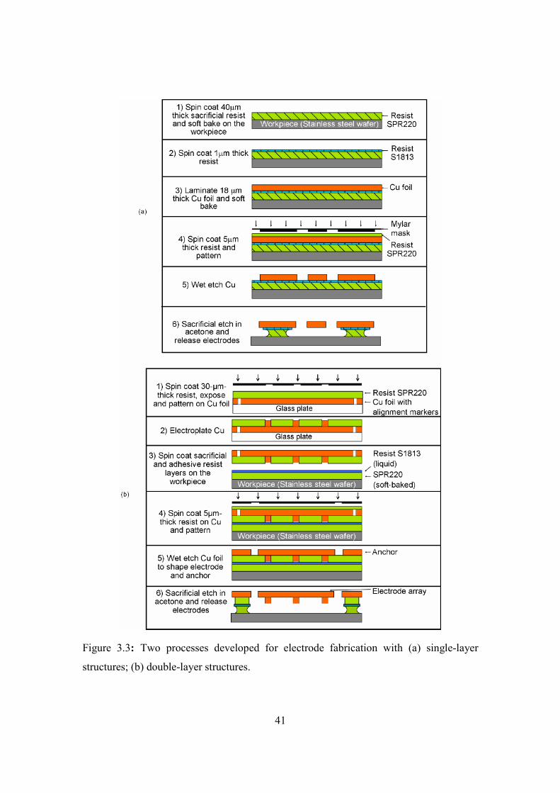
41
Figure 3.3: Two processes developed for electrode fabrication with (a) single-layer
structures; (b) double-layer structures.

42
foil and the sacrificial layer. The S1813 resist is soft baked on a hot plate C90° for 10
min to solidify the layer, making the copper foil rigidly fixed down to the substrate
through the sacrificial layer (step a-3). Then, a 5-µm-thick layer of SPR220 is spun on
the copper foil and patterned using a mylar mask with the layout of the devices (step a-4).
The developed SPR220 is used as a mask for wet etching of copper in a commercially
available ferric chloride solution (CE-100, Transene Co., Inc., MA, USA) (step a-5).
Finally, timed etching of the sacrificial layer is performed in acetone, providing
suspended electrodes while leaving the anchors attached to the substrate (step a-6). As
noted earlier, the holes created in the electrode-tether structures promote undercutting
during the sacrificial etching process while leaving the sacrificial layer as the anchors
without the holes. Figure 3.4 shows the fabricated devices after the sacrificial etching
using single layer structures.
In the process (b), microstructures to be formed on the bottom of the electrode are
fabricated by copper electroplating on the same copper foil used in the process (a). First,
a 30-µm-thick resist SPR220 is coated on the copper foil, followed by a soft baking
process on a hot plate C90° for 30 min. Prior to the resist coating through-hole markers
are created in the copper foil for the alignment of the patterns to be created on the top and
bottom of the copper foil. The resist is then exposed and patterned using the mylar mask
to create the molds (step b-1). Next, copper is electroplated in the mold of the patterned
SPR220 forming the 25-µm-thick microstructures on the copper foil (step b-2). Figure
3.5a shows an example of electroplated structures obtained after this step. As a separate
process, 25-µm-thick resist SPR220 is coated on the stainless-steel workpiece to form the
sacrificial layer, followed by a soft baking process on a hot plate C90° for 5 min. Next, a
1-µm-thick resist S1813 is coated on the sacrificial layer to serve as an adhesive layer for
the bonding of the copper foil with microstructures underneath. The bonding is followed
by the soft baking process on a hot plate C90° for 10 min (step b-3). Then, a 5-µm-thick
SPR220 is coated on the top of the copper foil and patterned (step b-4) to be used as a
mask for wet etching of copper to define the overall shapes (step b-5). The final timed
sacrificial etching in acetone to obtain suspended electrodes is performed in the similar
manner as described in process (a) above (step b-6). Figure 3.5 shows the fabricated
devices for the custom design structures with the crab-leg design and electroplated arrays

43
of microstructures on the backside of the planar electrodes.
Figure 3.4: (a) An optical image of the fabricated devices on a stainless-steel substrate;
(b) an SEM image of a sample device fabricated for the single-layer design in Figure
3.2a;

44
Figure 3.5: Fabrication results for the double-layer design: (a) an SEM image of the
electroplated copper on the copper supporting electrode; (b) an optical image of the
fabricated device with the design in Figure 3.2b; (c) an SEM image of the close-up.

45
3.5 Experimental Results A set-up shown in Figure 3.6 was used for electromechanical characterization of the
electrode devices and µEDM tests. The fabricated device was placed in an ultrasonic
bath filled with the EDM oil (EDM 185TM, Commonwealth Oil Co., ON, Canada). An
RC circuit with a 20-KΩ resistor and a 100-pF (corresponding to the Ce in Figure 3.1a)
capacitor was connected to the device and the DC voltage source as shown in Figure 3.6.
The electrical discharge pulses were monitored using a current probe (CT-2, Tektronix,
Inc., TX, USA) inserted between the capacitor and the electrode. A laser displacement
gauge (LK-G82, Keyence Co., NJ, USA) that provided the spot size of 70 µm with the
resolution and response speed of 0.2 µm and 20 µs, respectively, was used to measure the
vertical actuation of the electrode in situ. An µEDM process produces byproducts that
Figure 3.6: A set-up for device characterization and µEDM tests.
include the particles removed from the workpiece and carbon residues produced from the
EDM oil. The removal of the byproducts is important to prevent irregular arcing and
stabilizing the process. This was achieved by applying ultrasonic waves during µEDM,
(i.e., machining was performed while continuously “cleaning” the workpiece in the
ultrasonic bath).
The sequential pulses of micro spark discharge were successfully generated using the
electrostatic actuation mechanism (Figure 3.7). The peak current, pulse duration, and
charging time constant were approximately measured to be 2.5 A, 50 ns, and 1 µs,
respectively, in the set-up used. Figure 3.8a shows the stainless-steel workpiece
machined using the torsional electrode in Figure 3.4b with 100 V for 10 min. The

46
removed depth was measured to be up to 20 µm. The machining voltage used is
theoretically not large enough to pull-in this particular torsional with an initial gap
separation of 40 µm. The successful pull-in and machining may be attributed to the aid
of vertical actuation in addition to the torsional one of the design. Figure 3.9 shows a
result of the in-situ measurement of the displacement of a single-layer fixed-fixed and
cantilever electrodes with the designs noted in Section 3.3, which had approximate initial
gap separations of 15 µm and 40 µm, respectively. The thickness of 15 µm corresponds
to the single-coated sacrificial layer and that of 40 µm to the double-coated one. For a
clear visibility of the actuation effect, the temporal measurement was performed while
switching the machining voltage (of 50V for fixed-fixed electrode and 100 V for
cantilever electrode), i.e., EDMing on and off manually. The result indicates the
approximate vertical actuation of 10 µm and 30 µm respectively at their measurement
points (the center and at the tip) for the fixed-fixed and cantilever electrodes. From the
result, the discharge/breakdown gap is estimated to be 5 – 10 µm for the electrodes and
setup.
Figure 3.7: (a) Measured current pulses of micro spark discharge; (b) single pulse close-
up; (c) an optical image of the micro sparks captured through electrode’s holes.

47
The machining that only used the built-in capacitance Cb as the capacitive element of
the RC circuit without using the external capacitor Ce was also tested. The machining
tests for the double-layer electrodes were implemented with this set-up. Figure 3.8b
shows the hole arrays obtained using the crab-leg electrode with the machining voltage of
90V. It was observed that many of the double-layer electrodes did not provide
displacements large enough to initiate and generate discharge pulses. It is expected that
Figure 3.8: (a) An SEM image of the µEDMed stainless-steel substrate (electrode
removed after machining) with inset of close-up; (b) optically measured geometry of the
machined structures using WykoTM NT1100 profiler. Batch structures are measured to
have the depth of ~ 20 µm..

48
the used voltage was not high enough, i.e. the electrostatic force to pull-in due to the
relatively large gap of 55 µm between the workpiece and the supporting plate that
provides the major part of the capacitive area.
Figure 3.9: Vertical displacement of the electrode measured while switching on and off
the EDM process using the single-layer electrodes; (a) fixed-fixed device with 15 µm gap
spacing; (b) cantilever device with 40 µm gap spacing.

49
3.6 Analysis and Discussion For better understanding of the machining process, it is worthwhile analyzing the
electromechanical characteristics of the developed electrode device, which is used as both
an electrostatic actuator and a capacitive element for the discharge pulse formation. This
section discusses theoretical analysis of the experimental results for the built-in
capacitance as well as mechanical behavior of the devices.
A. Built-in capacitance
The discharge energy of a single pulse is given by CV2/2 [1], where C is the total
capacitance that is the sum of the external capacitance (Ce) and the built-in capacitance
(Cb) in the set-up shown in Figure 3.6 and V is the applied voltage. The energy
determines the degree of the thermal impact and the size of the resultant crater-like shape
hence the roughness and quality of the machined surfaces. In order to reduce the
discharge energy for finer machining along with a simple circuit configuration, µEDM
can be effectively implemented by using only Cb to form the RC circuit without Ce (as
demonstrated in the result in Figure 3.8b). For this implementation, it is important to
evaluate the value of Cb, however, the direct measurement is difficult because Cb is a
dynamic parameter as the actuation of the electrode modulates it, and Cb at the timing of
a breakdown, Cbb, is the value of interest. The time constant, τ=RCbb, in a charging cycle
can be used to indirectly estimate Cbb. The constant τ was determined by probing the
voltage at the electrode and measuring the charging time. Figure 3.10a shows the
measured time constant for single-layer electrode devices which were calculated from the
time taken to drop to 90 % of the voltage. Figure 3.10b plots τ measured in the dynamic
mode (i.e., while EDM is on) for various devices with different electrode-tether areas as
well as Cbb calculated from the results. The static value, Cb, measured directly by
probing the devices without applying machining voltage using HP 4275A LCR meter is
also plotted in Figure 3.10b for comparison. The result indicates approximate linear
dependence of both Cb and Cbb (or τ) on the area of the device. Figure 3.10b also
suggests, as predicted, that Cbb is substantially increased from Cb, modulating the
discharge energy.

50
Figure 3.10: (a) Measured machining voltage showing charging cycles with different time
constants for the electrodes with different areas; (b) built-in capacitance in static (Cb) and
dynamic (Cbb) modes vs. device area.

51
B. Mechanical Response
The planar electrodes used in this process are actuated toward the workpiece against thin
film of the EDM oil that is present in the gap spacing between the electrode and the
workpiece. The actuation mechanism of the electrodes under the influence of the applied
voltage can be modeled using d’Alembert’s principle and is given by [13]:
em Fxkdtdxc
dtxdm =++2
2
;( )
3
212dN
SAGcπ
µ= (3.3)
where m is the mass of the copper electrode, c is the squeeze film damping coefficient
attributed to the narrow gap spacing between the suspended electrode and the workpiece,
x is the displacement of the electrode, t is the time taken by the electrode to make the
displacement, , km is spring constant corresponding to the spring constant discussed in
Section 3.3), Fe is the electrostatic force, µ is the fluid viscosity of EDM oil, S is the area
of the electrode, N is the number of holes in the electrode and ( ) ( )83
4ln
82
2−−−=
AAAAG
where A is the fraction of the open area in the electrode.
The mechanical response of the fixed-fixed electrode and cantilever electrode is
analyzed based on the following assumptions. The electrode is at the breakdown gap
(assuming 5 µm from the experimental result) after a spark discharge, the velocity at this
position for the electrode is 0 and the electrostatic force (Fe) is negligible when compared
to the spring force to pull-back the electrode to its initial gap separation. The mechanical
response of the fixed-fixed and cantilever electrode using the equation (3.3) with the
constants used in the experimental set-up for this study ( µ =2.1×10⁻³ Pa-s) and the
mathematical modeling software MapleTM was measured for the fixed-fixed and
cantilever electrodes with single-layer structures. The displacements that are made with
these electrodes are calculated to be on the order of nanometers to sub-nanometers within
1 µs that is a typical measured pulse interval. They will be even smaller as the machining
voltage, i.e. electrostatic force is restored during the cycle. This suggests the position of
the electrode around the discharge gap during the µEDM process. The in-situ
measurement of the displacement of the cantilever electrode in Figure 3.9b suggests the

52
electrode is stabilized at the discharge gap for a relatively long-on time (~ 80 sec) which
agrees well with the mechanical response analysis.
3.7 Conclusions A new technique for µEDM using the electrostatic actuation of the planar electrodes
microfabricated on the workpiece has been studied. Laminated 18-µm-thick copper foil
was patterned to construct the planar electrodes suspended with the anchors, which were
actuated with the machining voltage for well-controlled pulse formation of micro spark
discharges. The planar electrodes microfabricated directly on the stainless steel
workpiece material using standard UV lithography and wet etching of copper foil are
suspended above the anchors using the sacrificial etching of the resist layers.
Micromachining of stainless steel with the voltage of 90 – 100 V was demonstrated using
both the single-layer electrodes and the double-layer electrodes with custom patterns
providing approximate removal depth of 20 µm for the machining time of 10-15 minutes.
The built-in capacitance of the electrode structure was exploited to form the pulse
generation circuitry and experimentally characterized both in dynamic and static modes.
The mechanical response of the electrode was theoretically analyzed to estimate the
vertical position of the electrode after each discharge spark cycle. It was observed that
the mechanical response of the electrode was far slower than the electrical response
resulting in stable µEDM process. The developed method offers an opportunity to
eliminate the need for high-precision NC machines for µEDM thereby potentially
achieving dramatic improvements of the process in not only the cost reduction but also
the machinable area by introducing large-area patterning techniques for the device
fabrication.
Acknowledgments The authors would like to thank NSERC for their financial support to this research. They
also thank Ms. Vijayalakshmi Sridhar and Mr. Greg Wong at the University of British
Columbia for their assistance in the fabrication process.

53
References
[1] T. Masaki, K. Kawata, and T. Masuzawa, “Micro Electro-Discharge Machining and
its Applications,” Proc. IEEE Int. Workshop on Micro Electro Mechanical Systems
(MEMS ’90), Feb. 1990, pp. 21-26.
[2] L.L. Chu, K. Takahata, P. Selvaganapathy, Y.B. Gianchandani, and J.L. Shohet, “A
Micromachined Kelvin Probe with Integrated Actuator for Microfluidic and Solid-
State Applications,” J. Microelectromech. Syst., vol. 14, no. 4, Aug. 2005, pp. 691-
698.
[3] K. Takahata, and Y.B. Gianchandani, “Bulk-Metal-Based MEMS Fabricated by
Micro-Electro-Discharge Machining,” Proc. IEEE Canadian Conf. Electr. Comput.
Eng. (CCECE ‘07), Vancouver, Canada, Apr. 2007, pp. 1-4.
[4] K. Takahata, and Y.B. Gianchandani, “Batch Mode Micro-Electro- Discharge
Machining,” J. Microelectromech. Syst., vol. 11, no. 2, Apr. 2002, pp.102-110.
[5] H. Guckel, “High-Aspect-Ratio Micromachining via Deep X-Ray Lithography,”
Proc. IEEE, vol. 86, no. 8, 1998, pp. 1586-1593.
[6] Y. Okazaki, N. Mishima, and K. Ashida, “Microfactory - Concept, History, and
Developments,” J. Manuf. Sci. Eng., vol. 126, no. 4, Nov. 2004, pp. 837-844.
[7] C. R. Alla Chaitanya, and K. Takahata, “Micro-electro-discharge machining by
MEMS actuators with planar electrodes microfabricated on the work surfaces,” in
Tech. Dig. IEEE Int. Conf. on Micro Electro Mechanical Systems (MEMS ’08),
Tucson, AZ, Jan. 2008, pp. 375-378.
[8] C. R. Alla Chaitanya, and K. Takahata, “M3EDM: MEMS-enabled micro-electro-
discharge machining”, J. Microelectromech. Syst., vol. 18, 105009, Sep. 2008, 7pp.
[9] S. Pamidighantam, R. Puers, K. Baert, and H.A.C. Tilmans, “Pull-in Voltage
Analysis of Electrostatically Actuated Beam Structures with Fixed-Fixed and
Fixed-Free End Conditions,” J. Micromech. Microeng., vol. 12, July 2002, pp. 458-
464.
[10] J. Cheng, J. Zhe, and X. Wu, “Analytical and finite element model pull-in study of
rigid and deformable electrostatic microactuators,” J. Micromech. Microeng., vol.
14, Jan. 2004, pp. 57-68.

54
[11] W.C. Young, Roark’s Formulas for Stress and Strain, 7th ed., McGraw-Hill, 2002.
[12] F. Zhang, A.K. Prasad, and S.G. Advani, “Investigation of a Copper Etching
Technique to Fabricate Metallic Gas Diffusion Media,” J. Micromech. Microeng.,
vol. 16, Sep. 2006, pp. N23-N27.
[13] W. Weaver Jr., S. P. Timoshenko, and D. H. Young, Vibration Problems in
Engineering, 5th ed., John Wiley & Sons, New York, 1990.
[14] T. B. Gabrielson, “Mechanical-thermal noise in micromachined acoustic and
vibration sensors,” IEEE Trans. On Electron Devices, vol. 40, May 1993, pp. 903-
909.

55
Chapter 4 Conclusions The goal of the µEDM technique developed in this research effort is to increase the
throughput, cost-effectiveness and to achieve high-precision machining. In Chapter 2, a
MEMS-based µEDM method that uses the hydrodynamic force for the actuation of the
electrode towards the workpiece was developed. The use of dry film photoresist was also
implemented to fabricate the planer electrodes. A resistance-capacitance circuit
connected between the electrode and the workpiece was used to achieve controlled
generation of discharge pulses with the applied DC voltage of 80 – 140V. The planar
electrodes were then actuated using the downflow of the EDM fluid. Micromachining of
stainless steel was demonstrated with a removal depth of 20 µm at 90V. The built-
capacitance between the electrode and the workpiece was utilized to control the discharge
energy which defines the roughness and quality of the machined surfaces. The
experimental results obtained were also verified with the theoretical models of electrode
deflection using the hydrodynamic force. The fabrication approach using the
hydrodynamic force offers the scalability towards large-area, high-throughput batch
processing with µEDM at low cost. Some of the applications where MEMS-based
µEDM can be targeted include machining precision holes, ink-jet nozzles and fabrication
of micro-stencils. In Chapter 2, the µEDM method enables the large deflection of the
electrode using the external fluid control module. The control module requires additional
setup for µEDM process thereby increasing the equipment costs.
In Chapter 3, the planar electrodes are electrostatically actuated towards the
workpiece thereby eliminating the need for the external fluid module. First, the planar
electrodes were constructed to be single-layer structures using 18-µm-thick Cu foil as
electrode material that were suspended with the anchors, to demonstrate the machining
principle with the electrostatic actuation. Micromachining of stainless steel for the
single-layer electrode structure was demonstrated with a removal depth of 20 µm at 100V.
Second, the planar electrodes were constructed to be double-layer structures for custom
machining. The microelectrodes with the patterns to be machined on the workpiece were

56
formed on the bottom surface of the planar structure suspended by anchors.
Micromachining of stainless steel was demonstrated with custom design structures
patterned on the workpiece. In Chapter 3, the mechanical response of the planar
electrodes during the actuation mechanism was also analyzed. It was observed that the
mechanical response of the electrode to pull-back to its original gap separation was slow
when compared to the electrical response of 1 µs after each discharge cycle. It suggested
that the electrode was around the breakdown gap during the µEDM process.
In the electrostatic actuation method developed in Chapter 3, the machinable depth is
limited as the machining enlarges the gap spacing between the electrode and the
workpiece, lowering the electrostatic force to pull in the electrode. Higher voltages can
be used to increase the force while compromising the surface roughness and quality in the
machined structures as they increase the discharge energy as well. To extend the
machinable depth, applying external force to the electrodes towards the workpiece
instead of using the electrostatic actuation to sustain the machining process can be used
with the need of an extra module for the actuation. The method in Chapter 2
implemented this approach using the hydrodynamic force with the use of the fluid control
module. The µEDM techniques developed in concluding chapters eliminates the need of
NC machines resulting in high throughput, low costs and potentially offers an
opportunity for extending the technology to large-area patterning for the device
fabrication. It was observed that the copper foil which was used as electrode material
was deformed partially during µEDM. This could be attributed to the high temperature
zones created during the spark discharge cycle [1]. The future work would involve the
thermal analysis of the copper foil during the µEDM process [2]. The use of alternative
electrode materials (like tungsten) that provides higher melting point can be used to
minimize electrode wear and damage due to the thermal effect.

57
References
[1] J. McGeough, Micromachining of Engineering Materials, Marcel Dekker, 2002.
[2] S. H. Yeo, W. Kurnia, and P. C. Tan, “Electro-thermal modeling of anode and
cathode in micro-EDM”, J. Phys. D: Appl. Phys., vol. 40, pp. 2513-2521, 2007.