Embed Size (px)
Citation preview

L.V. COOPERTHIS device differs from most i.c. testers in as much thatthe logic states of all the i.c. pins can be seen at a glance.
Not only are the high and low states displayed, but thischecker differentiates between high, low, inadmissible, andopen circuit states.
Although the tester does not check all the differentaspects of a logic i.c. it does allow go/no-go devices to beidentified quickly and can, with practice, go a long way toidentifying an unknown i.c.
The circuit design allows the use of cheap calculator typemultiplexed displays.
The operation of the device is basically simple and con-sists of a set of three comparators which are very rapidlyswitched around the pins of the i.c. under test, whilst at thesame time enabling the appropriate display digit.
CD4016 quad analogue switches i.c.'s 1 to 4 are em-ployed to switch the comparators onto each pin.
The switching sequence is controlled by a four to sixteenline decoder (IC5) which operates the switch controls andalso enables the digit drivers (IC's 7, 8 &9).
The decoder is fed by a binary counter IC6 which is in turnclocked by a 500Hz oscillator made up from two of thegates in IC12.
Interdigit blanking is necessary and is achieved by feedingclock pulses from the oscillator, after inversion by TR2, tothe blanking input of the binary to seven segment decoderIC13. This ensures that all displays are off during the firsthalf of the clock pulse.
t7CICI 0 (LM324) is a quad op -amp and three of the four am-
plifiers in the package are used as comparators to detect thelogic state of the pin being sampled.Logic "1" is detected by IC10c, the output of which goes
high if a voltage greater than +2.4 volts ispresent at its input.
Logic "0" The outputs of all three comparators arearranged to be low when a voltage between0 and +0.4 volts is present on the inputs.
Inadmissable levels (+0.4 volts to +2.4 volts) are detec-ted by IC10a. The output is high when avoltage greater than +0.4 volts is present onits input.
Open circuit Any pin that is open circuit either by design ora fault condition is detected by IC1 Ob.
A negative voltage is fed onto each test pin by means of1 M1 resistors 1-16, and clamped by germanium diodes D1-16 to approximately -0.2 volts. When an i.c. is plugged intothe test socket this small negative voltage, when connectedto a live pin, will be clamped to zero or overridden by thepositive voltage present on that pin, provided of course thatthe supply is connected to the i.c. under test by means of theterminals provided.
IC10b detects the presence or absence of this negativevoltage, and if present its output goes high, the output fromthe gating circuitry presents a binary code greater than nineto the decoder IC13 and it automatically blanks the display.Any other condition causes ICI Ob to produce a low output,leaving the display format to be decided by the other twocomparators.
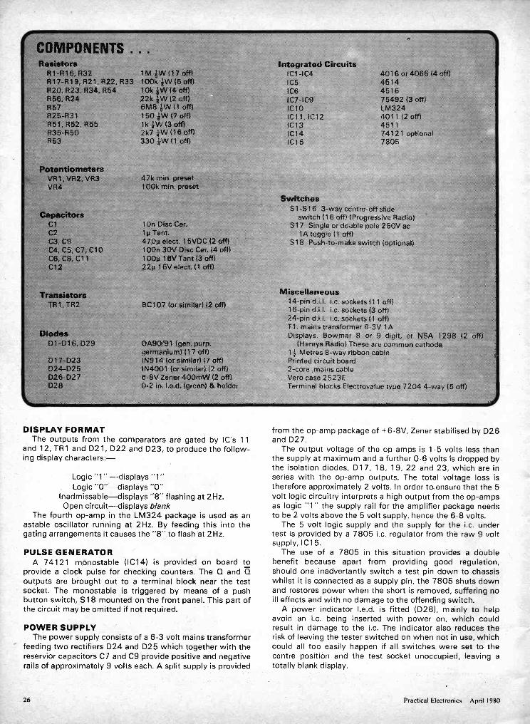
COMPONENTS . . .
Resistors51-516, 532R17 -R19, R21, R22, R33R20, R23, R34, 854556, R24R57525-531R51, R52, R55R35 -R50553
1M (17 off)100k (6 off)10k {4 off)22k iW (2 off)6M8 iW (1 off)150 (7 off)lk (3 off)2k7 1.W (16 off)330 (1 off)
PotentiometersVR1, VR2, VR3 47k min. presetVR4 100k min. preset
CapacitorsClC2C3, C9C4, C5 C7 C10C6, CS, C11C12
TransistorsTR1 TR2
Diodes01 016 D29
017-D23D24 -D25D26 -D27D28
10n Disc Cer.1p Tent.470p elect. 15VDC {2 off)100n 30V Disc Cer. (4 off)100µ 16V Tent (3 off)22µ 16V elect. {I off)
BC107 (or similar) (2 off)
0A90/91 (gen. purp.germanium) (17 off)1N914 (or similar) (7 off)IN4001 (or similar) (2 off)6.8V Zener 400mW (2 off)10,2 in. I.e.d. (green) & holder
Integrated CircuitsIC1-1C4IC51061C7 -1C9IC10IC1 1,1C12IC131C14IC15
4016 or 4066 (4 off)4514451675492 (3 off)LM3244011 (2 off)451174121 optional7805
SwitchesS1 -S16 3 -way centre -off slide
switch (16 off) {Progressive Radio)517 Single or double pole 250V ac
lA toggle (1 off)S18 Push -to -make switch {optional>
Miscellaneous14 -pin d.i.l. i.c. sockets {1 1 off>16 -pin i.c. sockets {3 off)24 -pin d.i.l. i.c. sockets (1 off)T1. mains transformer 6.3V 1ADisplays. Bowmar 8 or 9 digit, or NSA 1298 (2 off)
(Henrys Radio) These are common cathode1.1 Metres 8 -way ribbon cablePrinted circuit board2 -core ,mains cableVero case 2523ETerminal blocks Electrovalue type 7204 4 -way (5 off)
DISPLAY FORMATThe outputs from the comparators are gated by IC's 11
and 12, TR 1 and D21, D22 and D23, to produce the follow-ing display characters:-
Logic "1" -displays "1"Logic "0"-displays "0"
Inadmissable-displays "8" flashing at 2Hz.Open circuit-displays blank
The fourth op -amp in the LM324 package is used as anastable oscillator running at 2Hz. By feeding this into thegating arrangements it causes the "8" to flash at 2Hz.
PULSE GENERATORA 74121 monostable (IC14) is provided on board to
provide a clock pulse for checking counters. The Q and Qoutputs are brought out to a terminal block near the testsocket. The monostable is triggered by means of a pushbutton switch, S18 mounted on the front panel. This part ofthe circuit may be omitted if not required.
POWER SUPPLYThe power supply consists of a 6.3 volt mains transformer
feeding two rectifiers D24 and D25 which together with thereservior capacitors C7 and C9 provide positive and negativerails of approximately 9 volts each. A split supply is provided
from the op -amp package of +6.8V, Zener stabilised by D26and D27.
The output voltage of the op -amps is 1-5 volts less thanthe supply at maximum and a further 0.6 volts is dropped bythe isolation diodes, D17, 18, 19, 22 and 23, which are inseries with the op -amp outputs. The total voltage loss istherefore approximately 2 volts. In order to ensure that the 5volt logic circuitry interprets a high output from the op -ampsas logic "1" the supply rail for the amplifier package needsto be 2 volts above the 5 volt supply, hence the 6.8 volts.
The 5 volt logic supply and the supply for the i.c. undertest is provided by a 7805 i.c. regulator from the raw 9 voltsupply, IC15.
The use of a 7805 in this situation provides a doublebenefit because apart from providing good regulation,should one inadvertantly switch a test pin down to chassiswhilst it is connected as a supply pin, the 7805 shuts downand restores power when the short is removed, suffering noill effects and with no damage to the offending switch.
A power indicator I.e.d. is fitted (D28), mainly to helpavoid an i.c. being inserted with power on, which couldresult in damage to the i.c. The indicator also reduces therisk of leaving the tester switched on when not in use, whichcould all too easily happen if all switches were set to thecentre position and the test socket unoccupied, leaving atotally blank display.
26 Practical Electronics April 1980

IC TESTSOCKETSWITCHES
1-16
16 CONTROLLINES
1E0295 j
CHO'SSWITCHESICS 1-4
4- 6LINE
DECODERIC5
R35 -R50
S1 -S160
01-016A R1 -R16
-6 8V
REPEATED FOR ALL16 TEST PI NS
1E02261
COMPARATORSIC10a, b,c.
COUNTERIC6
pin
pinta-Q-0-
pin14.4-L
1HzOS C.
IC10 d
IC140 16
BLANKING
500 Hz
DECODERIC13
%I C12
11=11 12pin 16-4- -iki-IC5 pin 151 13pin 15.0- -O. -ICS pin 16
pin 8.....4 5--iiiIC5pin 14pin 7.04 -iii8 I 6 IC5pin13
4016C32
11=,11 12pin12-4- ..IC5pin 19
pin 1144-pin 4
pin 3IC44016
Fig. 3. CMOS switching stage
SEG.LINESIa-g)
16 X7 SEGODISPLAYS
DIGITDRIVERS.
TO COMPARATOR
IEG2971
IC4pin 6
Fig. 1. Block diagram of Chip Checker
IN 4001
ci C3 C6T470p
Fig. 2. Power supply
IC9 pin 10
IC4 pins IC9 pin 8
IC4pin 12 IC9 pin 3IC4pin 13 IC9 pin 5IC3 pin 6 ICEI pin 5
IC3 pin 5 ICI3 pin 3
IC3 pin 12 IC9 pin 12
IC3 pin 13 IC9 pin14IC2 pin 5 IC8 pin 14
IC2 pin 6 IC8pin 12
IC2 pin 13 IC8pin 10
IC2 pin 12 IC8pin 8IC1 pin 5 IC7pin 14
ICI pin 6 IC7pin 12
IC1 pin 13 IC7pin 10IC1 pin 12 IC7pin 8
17 18 19 20 13 14 15 16 8 9 10 11 4 5 6 1712
IC5 1+5V
23 4514
2 3 21 22 24
6 2 14 11TO R24
IC645 16
-16
0
10 11
13
10
8 I IC124011
4 5 8 9 12 1315
C1 I.10n
12 VR4100k
9
_ ,
Fig. 4. Clock, and switch sequence control

+5V+5V
VR1
47k 13
IC10 aLM324 12
TO CMOS SWITCHES 1C1-40
D24
C21p
I En 29e1
R576-8M
-68V
VR247k
+5V
VR3A 479
+6 8 Vrt-
11
-6-8V
IC5 pin 7
ICS pin 6
IC5 pin 5
IC5 pin
10
R321MW-
17114914
R17100k
A
18114914
2 4011
IC114011
IC10C R18LM 324 100k
D1919 914
IC10dLM 324
IC5 pi n 11 IIC5 pin 10
12IC5 pin 9
14ICS pill -8
ICS pin 14
ICSpin 135
+5V
+5V
10
ICS pin18
ICS pin 17
ICS pin 15
IC5 pin 16ICS pin 19
ICS pin 20
1E0300]
IC875 492
R33100k
R3410k
7
A
1AR19100 k
DIGIT 5
DIGIT 6
DIGIT 13
DIGIT 14
3
6
2
DIGIT 1
V DIGIT 2
P DIGIT 7 DIGIT 8
DIGIT 9
--Iv-DIGIT 104
+5V
Fig. 6. Digit drivers
DIGIT 3
DIGIT 4
DIGIT 11
DIGIT 12DIGIT 15
DIGIT 16
02016914
01
FROM1C12pin 11 R 24
229
D21.1N914
R21100k
D22 A1N914
D23 A114914
+5V
R2310k
i15R22 ...."'" R25 -R31
8 4 700k 159
+5V
3 16
SEGS
IC13 IL___AA/4_,_-d4511
TR 2BC107
A
Fig. 5. Comparitors and segment decoding
DISPLAY CONECTIONSFRONT VIEW
rinnnnnrina e
DIGIT DIGIT DIGIT DIGIT DIGIT DIGIT DIGIT DIGIT16 1512 10 9
SEGMENTS CONNECTEDIN PARALLEL
e.g. a to a,b to b etc.nnnnnnnna e b f
4
DIGIT DIGIT DIGIT DIGIT DIGIT DIGIT DIGIT DIGIT
R5410k
C1222p
PULSE GENERATOR(OPTIONAL)
28 Practica
I'LL-7111d° CIIIITCY '0-1-0°I
lfl 0 11 811 1°
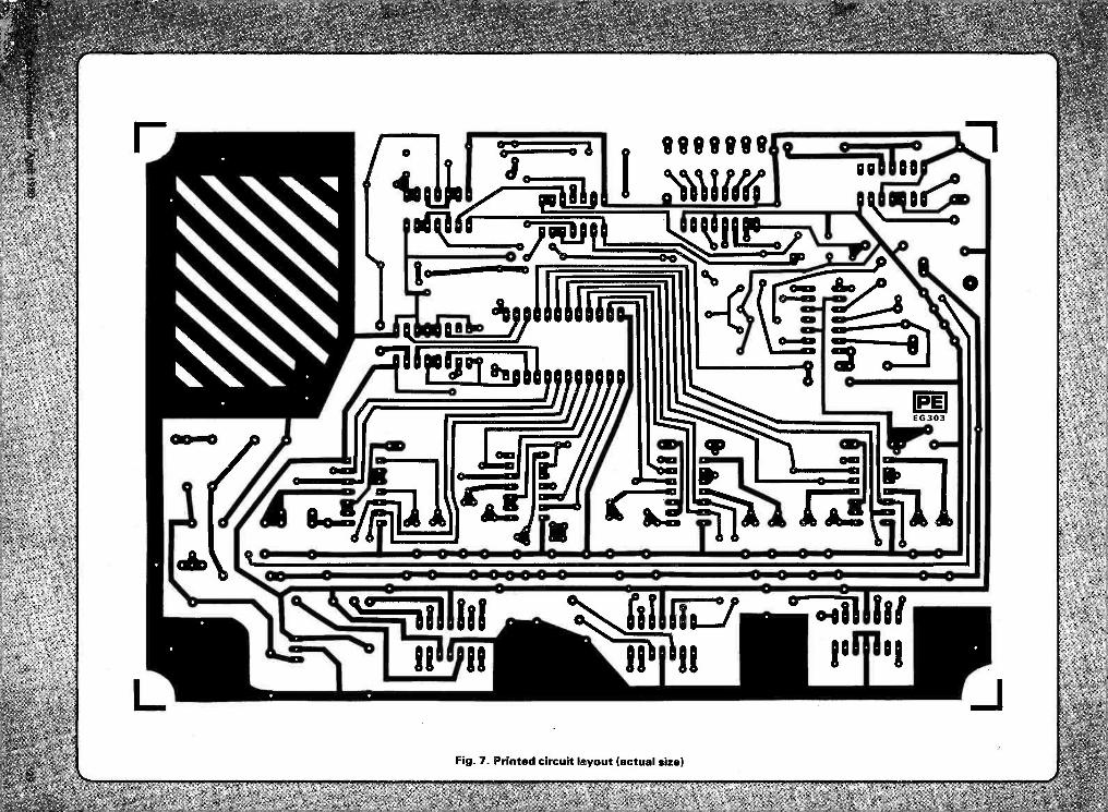
Fig. 7. Printed circuit layout (actual size)
EG303
S18
TO
PANEL'
PIN 14
PIN 6
DIGIT 6
DIGIT 13
j4,41254 1.4
E, lOG
Li)
"' }--"D29* 11.
SEGMENTS+5V TOPANEL
R25 R26 R211213131*41 )10 _t
D21
918
R17
022
R32 I-.fol R33 j*d
Lh0190.1 P19
P N13
DIGIT 14 DIGIT 5
017 X018
PIN1
/C\DIGIT 2 DIGIT DIGIT DIGIT DIGIT DIGITS
10 8 7 1
TR IVR20 I.
956
PIN15 PIN 16
09I R10
1 D 7
PI N 11P154
0101716 DIGIT DIGIT DIGIT DIGIT DIGIT 415 12 11 3
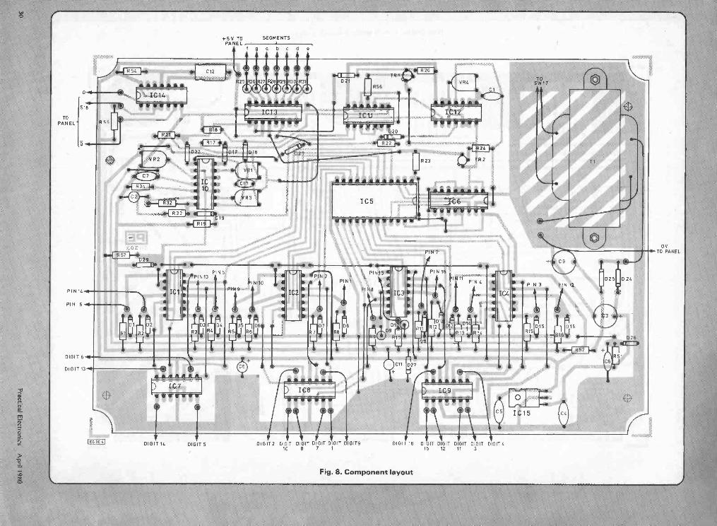
Fig. 8. Component layout
TOSW17
DvTO PANEL
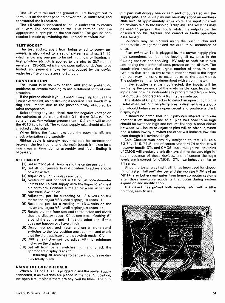
The +5 volts rail and the ground rail are brought out toterminals on the front panel to power the i.c. under test, andfor external use if required.
The +5 volts is connected to the i.c. under test by meansof a wire link connected to the +5V terminal and theappropriate supply pin on the test socket. The ground con-nection is made by switching the appropriate switch low.
TEST SOCKETThe test socket, apart from being wired to screw ter-
minals, is also wired to a set of sixteen switches, S1-16,which allow any one pin to be set high, low or floating. Inhigh position +5 volt is applied to the pins by 2k7 pull upresistors (R35-50), which allow open collector devices to betested, and prevent smoke being produced by the deviceunder test if two inputs are short circuit.
CONSTRUCTIONThe layout is in no way critical and should present no
problems to anyone wishing to use a different form of con-struction.
If the printed circuit layout is used it may help to fit all thejumper wires first, using sleeving if required. This avoids mis-sing and jumpers due to the position being obscured byother components.
Before fitting any i.c.s, check that the negative voltage onthe cathodes of the clamp diodes D1-16 and D24 is -0.2volts or less. Any voltage greater than -0.2 volts will causethe 4016 i.c.s to fail. The various supply rails should also bechecked at this point.
When fitting the i.c.s, make sure the power is off, andcheck orientation very carefully.
Ribbon cable is strongly recommended for connectionsbetween the front panel and the main board; it makes for amuch easier time during assembly and fault finding ifnecessary.
SETTING UP(1) Set all front panel switches to the centre position.(2) Set all four presets to mid position. Displays should
now be active.(3) Adjust VR2 until displays are just off.(4) Switch off and connect a 1K or 5K potentiometer
across the +5 volt supply with the wiper to any testpin terminal. Connect a meter between wiper andzero volts. Switch on.
(5) Adjust the pot. for a reading of +2.4 volts on themeter and adjust VR3 until display just reads "1".
(6) Reset the pot. for a reading of +0.4 volts on themeter and adjust VR1 until display just reads "0".
(7) Rotate the pot. from one end to the other and checkthat the display reads "0" at one end, "flashing 8"around the centre and "1" at the other end. If thisdoes not happen you have a fault.
(8) Disconnect pot. and meter and set all front panelswitches to the low position one at a time, and checkthat the digit applicable to that switch reads "0".
(9) With all switches set low adjust VR4 for minimumflicker on the displays.
(10) Set all front panel switches high and check theappropriate display reads "1".
Returning all switches to centre should leave dis-play totally blank.
USING THE CHIP CHECKERWhen a TTL or DTL i.c. is plugged in and the power supply
connected, if all switches are placed in the floating position,the open circuit pins if there are any, will be blank. The out-
put pins will display one or zero and of course so will thesupply pins. The input pins will normally adopt an inadmis-sible level of approximately +1.4 volts. The input pins willbe obvious due to the flashing 8 displays. The switches maybe used to program the inputs whilst the outputs can beobserved on the displays and correct or faulty operationascertained.
Counters may be clocked using the push button andmonostable arrangement and the outputs all monitored atonce.
If an unknown i.c. is plugged in, the power supply pinsmay sometimes be found by leaving all switches in thefloating position and applying +5V only to each pin in turnand noting the number of ones present on the display. Thesupply pins produce the largest number of ones, thus thetwo pins that produce the same number as well as the largernumber, may normally be assumed to be the supply pins.The polarity can then be determined with an ohmmeter.
If the supplies are then connected, the inputs will bevisible by the presence of the inadmissible logic levels. Theinputs can now be systematically programmed high or low,the outputs monitored and a truth table made up.
The ability of Chip Checker to detect an open circuit pin isuseful when testing tri-state devices, a disabled tri-state out-put should behave as an open circuit and produce a blankdisplay digit.
It should be noted that input pins can interact with oneanother if left floating and so all pins that need to be highshould be switched high and not left floating. A short circuitbetween two inputs or adjacent pins will be obvious, whenone is taken low by a switch the other will indicate low alsoeven though it is switched high.
Chip Checker was primarily designed to test TTL i.c.s.EG 74L, 74S, 74LS, and of course standard 74 series. It willhowever handle DTL and CMOS i.c.s although the input pinsof CMOS will produce blank displays due to the very high in-put impedance of these devices, and of course the logiclevels are incorrect for CMOS. DTL i.c.s behave similar to74 series.
Since the tester was first built it has been used for check-ing untested "fall out" devices and the monitor ROM's of anM K14, also buffers and gates from home computer systemsafter those inevitable accidents that occur during systemexpansion and modification.
The device has proved both reliable, and with a littlepractice, easy to use.
Practical Electronics April 1980 31


![Manuale d'uso Rivelatore di gas serie 47K [SIL 2]€¦ · MSA DESCRIZIONE IT Rivelatore di gas serie 47K [SIL 2] 9 2.2. Principio di funzionamento I sensori MSA serie 47K operano](https://img.dokumen.tips/doc/110x75/5fa6943f2e2a5e322d71b385/manuale-duso-rivelatore-di-gas-serie-47k-sil-2-msa-descrizione-it-rivelatore.jpg)