Embed Size (px)
Citation preview

LTM4661
1Rev. A
For more information www.analog.com
TYPICAL APPLICATION
FEATURES DESCRIPTION
15V, 4A Step-Up µModule Regulator
The LTM®4661 is a synchronous step-up switching mode µModule® (power module) regulator in a 6.25mm × 6.25mm × 2.42mm BGA package. Included in the pack-age are the switching controller, power FETs, inductor and all support components. Operating over an input voltage of 1.8V to 5.5V, down to 0.7V after start-up, the LTM4661 regulates an output voltage of 2.5V to 15V set by an exter-nal resistor. It provides up to 4A switch current. Only bulk input and output capacitors are needed.
The LTM4661 1MHz switching frequency and dual phase single output architecture enable fast transient response to line and load changes and a significant reduction of output ripple voltage. It supports frequency synchroni-zation, PolyPhase® operation and selectable Burst Mode operation.
The LTM4661 features a true output disconnect during shutdown and inrush current limit at start-up. It also has short-circuit, overvoltage and overtemperature protection.
The LTM4661 is Pb-free and RoHS compliant.
5V/2A DC/DC Step-Up µModule Regulator Efficiency vs Output Current at 3.3V Input
APPLICATIONS
n Complete Solution in <1cm2 (Single-Sided PCB) or 0.5cm2 (Dual-Sided PCB)
n Input Voltage Range: 1.8V to 5.5V, Down to 0.7V After Start-Up
n Output Voltage Range: 2.5V to 15V n 4A Switch Current n Dual Phase Operation n ±3% Maximum Total DC Output Voltage Regulation
Over Load, Line and Temperature n Output Disconnect in Shut Down n Inrush Current Limit n External Frequency Synchronization n Selectable Burst Mode® Operation n Output Overvoltage and Overtemperature Protection n 6.25mm × 6.25mm × 2.42mm BGA package
n RF Microwave Power Amplifiers n Battery Powered DC Motors n 3.3V Bus Telecom Transceivers
All registered trademarks and trademarks are the property of their respective owners.
22µF ×216V
22µF ×26.3V
2.2µF
R131.6k
4661 TA01a
LTM4661 VOUT
FB
VOUT5V/2AVIN
SDB
MODE/SYNC
INTVCC
FREQ COMP
GND
VIN3.3V
LOAD CURRENT (A)0
EFFI
CIEN
CY (%
)
100
75
95
85
90
80
701 1.80.6 1.4
4661 TA01b
20.8 1.60.4 1.20.2
VOUT = 5V
Document Feedback

LTM4661
2Rev. A
For more information www.analog.com
PIN CONFIGURATIONABSOLUTE MAXIMUM RATINGS
VIN .............................................................. –0.3V to 6VVOUT ........................................................... –0.3V to 18VCOMP, FREQ .........................................–0.3V to INTVCCSYNC/MODE, SDB ....................................... –0.3V to 6VOperating Internal Temperature Range
(Note 2) ............................................. –40°C to 125°CStorage Temperature Range .................. –55°C to 125°CPeak Solder Reflow Body Temperature ................. 250°C
(Note 1)
1
2
3
4
5
SDB
FB
GND
COMP
INTVCC
FREQ
SYNC/MODE
GND
VIN
EDCBABGA PACKAGE
25-Lead (6.25mm × 6.25mm × 2.42mm)TJMAX = 125°C, θJCtop = 17°C/W, θJCbottom = 11°C/W,
θJB + θBA = 22°C/W, θJA = 22°C/WWEIGHT = 0.25g
BGA PACKAGE25-Lead (6.25mm × 6.25mm × 2.42mm)
TJMAX = 125°C, θJCtop = 17°C/W, θJCbottom = 11°C/W,θJB + θBA = 22°C/W, θJA = 22°C/W
WEIGHT = 0.25g
TOP VIEW
VOUT
ORDER INFORMATION
(See Pin Functions, Pin Configuration Table)
PART NUMBER PAD OR BALL FINISHPART MARKING* PACKAGE
TYPEMSL
RATINGTEMPERATURE RANGE (Note 2)DEVICE FINISH CODE
LTM4661EY#PBF SAC305 (RoHS) LTM4661Y e1 BGA 4 –40°C to 125°CLTM4661IY#PBF SAC305 (RoHS) LTM4661Y e1 BGA 4 –40°C to 125°CLTM4661IY SnPb (63/37) LTM4661Y e0 BGA 4 –40°C to 125°C
• Contact the factory for parts specified with wider operating temperature ranges. *Pad or ball finish code is per IPC/JEDEC J-STD-609.
• Recommended LGA and BGA PCB Assembly and Manufacturing Procedures
• LGA and BGA Package and Tray Drawings

LTM4661
3Rev. A
For more information www.analog.com
ELECTRICAL CHARACTERISTICS
SYMBOL PARAMETER CONDITIONS MIN TYP MAX UNITS
Switching Regulator Section: per Channel
VIN Input DC Voltage VOUT ≥ 2.5V l 0.7 5.5 V
VIN(MIN) Minimum Start-Up Voltage VOUT = 0V l 1.6 1.8
VOUT(RANGE) Output Voltage Range l 2.5 15 V
VOUT(DC) Output Voltage, Total Variation with Line and Load
RFB = 31.6k, SYNC/MODE = INTVCC VIN = 3.3V, VOUT = 5V, IOUT = 0A to 2A
l 4.85 5 5.15 V
IQ(VIN) Input Supply Bias Current VIN = 3.3V, VOUT = 5V, SYNC/MODE = INTVCC, IOUT = 5mA VIN = 3.3V, VOUT = 5V, SYNC/MODE = GND, IOUT = 5mA Shutdown, SDB = 0, VIN = 3.3V
10 8.5 0.5
mA mA µA
IS(VIN) Input Supply Current VIN = 3.3V, VOUT = 5V, IOUT = 2A 3.7 A
IOUT(DC) Output Continuous Current Range
VIN = 3.3V, VOUT = 5V (Note 3) VIN = 3.3V, VOUT = 12V
0 0
2 0.7
A A
ΔVOUT (Line)/VOUT Line Regulation Accuracy VOUT = 12V, VIN = 1.8V to 5.5V, IOUT = 0A l 0.1 0.5 %/V
ΔVOUT (Load)/VOUT Load Regulation Accuracy VIN = 3.3V, VOUT = 5V, IOUT = 0A to 2A l 0.1 2 %
VOUT(AC) Output Ripple Voltage IOUT = 0A, COUT = 2×22µF Ceramic VIN = 3.3V, VOUT = 5V
3 mV
ΔVOUT(START) Turn-On Overshoot IOUT = 0A, COUT = 2×22µF Ceramic, VIN = 3.3V, VOUT = 5V
30 mV
tSTART Turn-On Time COUT = 2×22µF Ceramic, No Load, VIN = 3.3V, VOUT = 5V
10 ms
ΔVOUTLS Peak Deviation for Dynamic Load
Load: 0% to 25% to 0% of Full Load COUT = 2×22µF Ceramic, VIN = 3.3V, VOUT = 5V
200 mV
tSETTLE Settling Time for Dynamic Load Step
Load: 0% to 25% to 0% of Full Load COUT = 2×22µF Ceramic, VIN = 3.3V, VOUT = 5V
500 uS
VFB Voltage at VFB Pin IOUT = 0A, VIN = 3.3V, VOUT = 5V, SYNC/MODE = INTVCC l 1.17 1.2 1.23 V
IFB Current at VFB Pin (Note 4) 1 50 nA
RFBHI Resistor Between VOUT and VFB Pins
99.5 100 100.5 kΩ
Duty(MIN) Minimum Duty Cycle FB = 1.4V (Note 4) 0 %
Duty(MAX) Maximum Duty Cycle FB = 1.0V (Note 4) 90 94 %
SDB Input Voltage SDB Input High SDB Input Low
1.2 0.35
V V
ISDB SDB Input Current SDB = 5.5V 1 2 µA
VINTVCC Internal VCC Voltage VIN < 2.8V, VOUT > 5V 3.9 4.25 4.6 V
fOSC Switching Frequency 1 MHz
SYNC Range SYNC Frequency Range 0.5 1.5 MHz
SYNC/MODE Sync Input High Voltage Sync Input Low Voltage
1.6 0.35
V V
ISYNC/MODE SYNC/MODE = 5.5V 1 2 µA
The l denotes the specifications which apply over the specified internal operating temperature range, otherwise specifications are at TA = 25°C (Note 2), VIN = 3.3V, per the typical application.

LTM4661
4Rev. A
For more information www.analog.com
TYPICAL PERFORMANCE CHARACTERISTICSEfficiency vs Output Current, VIN = 3.3V
Efficiency vs Output Current, VIN = 5V
Burst vs Continuous Mode Efficiency, VIN = 3.3V
5V Output Load Transient Response
12V Output Load Transient Response
ELECTRICAL CHARACTERISTICSNote 1: Stresses beyond those listed under Absolute Maximum Ratings may cause permanent damage to the device. Exposure to any Absolute Maximum Rating condition for extended periods may affect device reliability and lifetime.Note 2: The LTM4661 is tested under pulsed load conditions such that TJ ≈ TA. The LTM4661E is guaranteed to meet performance specifications over the 0°C to 125°C internal operating temperature range. Specifications over the full –40°C to 125°C internal operating temperature range are assured by design, characterization and correlation with statistical process controls. The LTM4661I is guaranteed to meet specifications over the full –40°C to 125°C internal operating temperature range. Note that the maximum ambient temperature consistent with these specifications is determined by specific operating conditions in conjunction with board layout, the rated package thermal resistance and other environmental factors.
Note 3: See output current derating curves for different VIN, VOUT and TA.Note 4: 100% tested at wafer level.Note 5: The LTM4661 includes overtemperature protection that is intended to protect the device during momentary overload conditions. Junction temperature will exceed 170°C when overtemperature shutdown is active. Continuous operation above the specified maximum operation junction temperature may result in device degradation or failure.
LOAD CURRENT (A)0
EFFI
CIEN
CY (%
)
93
75
91
87
83
79
89
85
81
77
731 1.80.6 1.4
4661 G01
20.8 1.60.4 1.20.2
VOUT = 5V, 2A DCVOUT = 8V, 1A DCVOUT = 12V, 0.65A DCVOUT = 15V, 0.5A DC
LOAD CURRENT (A)0
EFFI
CIEN
CY (%
)
93
75
91
87
83
79
89
85
81
77
731 1.80.6 1.4
4661 G02
20.8 1.60.4 1.20.2
VOUT = 8V, 1.7A DCVOUT = 12V, 1A DCVOUT = 15V, 0.8A DC
500µs/DIV
VOUT (AC)200mV/DIV
LOAD STEP500mA
TO 1A
4661 G04
VIN = 3.3V, VOUT = 5VfS = 1MHz (DEFAULT)500mA TO 1A LOAD STEPCOUT = 2×22µF CERAMIC
500µs/DIV
VOUT (AC)200mV/DIV
LOAD STEP200mA
TO 400mA
4661 G05
VIN = 3.3V, VOUT = 12VfS = 1MHz (DEFAULT)200mA TO 400mA LOAD STEPCOUT = 2×22µF CERAMIC
LOAD CURRENT (A)0
EFFI
CIEN
CY (%
)
100
75
95
85
90
80
700.1
4661 G03
1
CONTINUOUS MODEBurst Mode OPERATION

LTM4661
5Rev. A
For more information www.analog.com
Steady State Output RippleStart-Up Waveform with No Load Applied
Start-Up Waveform with 0.5A Load Applied Short-Circuit Response
TYPICAL PERFORMANCE CHARACTERISTICS
500µs/DIV
VOUT (AC)5mV/DIV
4661 G06
VIN = 3.3V, VOUT = 5VfS = 1MHz (DEFAULT)COUT = 2×22µF CERAMIC
500µs/DIV
VIN2V/DIV
IIN200mA/DIV
SDB2V/DIV
VOUT10V/DIV
4661 G07
VIN = 3.3V, VOUT = 12VfS = 1MHz (DEFAULT)COUT = 2×22µF CERAMIC
500µs/DIV
VIN2V/DIV
IIN200mA/DIV
SDB2V/DIV
VOUT10V/DIV
4661 G08
VIN = 3.3V, VOUT = 12VfS = 1MHz (DEFAULT)COUT = 2×22µF CERAMIC
500µs/DIV
IIN1A/DIV
VOUT5V/DIV
4661 G09
VIN = 3.3V, VOUT = 12VfS = 1MHz (DEFAULT)COUT = 2×22µF CERAMIC

LTM4661
6Rev. A
For more information www.analog.com
PIN FUNCTIONSVIN (A1, B1, C1, D1, E1): Power Input Pins. Apply input voltage between these pins and GND pins. Recommend placing input decoupling capacitance directly between VIN pins and GND pins.
VOUT (A4, A5, B5, C5): Power Output Pins of the Switching Mode Regulator. Apply output load between these pins and GND pins. Recommend placing output decoupling capacitance directly between these pins and GND pins.
GND (A2, A3, B2 to B4, C2 to C4, D4, E2): Power Ground Pins for Both Input and Output Returns.
SYNC/MODE (D2): Burst Mode Operation Selection Pin and External Synchronization Input to Phase Detector Pin. Connect this pin to INTVCC to operate the module in forced continuous mode. Connect this pin to GND to enable Burst Mode operation. A clock more than 100ns on the pin will force the module operating in continuous mode and synchronized to the external clock applied to this pin. The external clock frequency must be higher than the self-running frequency programmed by FREQ pin. See frequency programming in the Applications Information section.
INTVCC (D3): Internal Regulator Output. The internal power drivers and control circuits are powered from this voltage. Decouple this pin to power ground with a mini-mum of 2.2µF low ESR ceramic capacitor. The INTVCC
voltage is regulated at the lower of VIN and 4.25V. When VIN falls below 3V and VOUT is higher than VIN, INTVCC will regulate to the lower of approximately VOUT and 4.25V. A UVLO event occurs if INTVCC drops below 1.5V, typical.
FREQ (E3): Frequency Set Internally to 1MHz. An external resistor can be placed from this pin to ground to increase frequency or from this pin to INTVCC to reduce frequency. See the Applications Information section for frequency adjustment.
SDB (D5): Shutdown Control Input of the µModule Regulator. Pulling this pin above 1.6V enables normal, free-running operation. Forcing this pin below 0.25V shuts the regulator off, with quiescent current below 1µA. Do not leave this pin floating.
COMP (E4): Current Control Threshold and Error Amplifier Compensation Point of the Switching Mode Regulator. Tie the COMP pins together for parallel operation. The device is internal compensated.
FB (E5): The Negative Input of the Error Amplifier for the Switching Mode Regulator. Internally, this pin is connected to VOUT with a 100kΩ 0.5% precision resistor. Different output voltages can be programmed with an additional resistor between FB and GND pins. In PolyPhase opera-tion, tying the FB pins together allows for parallel opera-tion. See the Applications Information section for details.

LTM4661
7Rev. A
For more information www.analog.com
BLOCK DIAGRAM
FB
INTVCC
SYNC/MODE
SDB
COMP
FREQ
VIN
VOUT
VIN3.3V
VOUT5V/2A
4661 BD
2.2µF2.2µF4.7µF
2.2µF
22µF
47µF
28k
31.6k
100k
GND
VOUT
INTERNALCOMP
POWER CONTROL 2.2µH
2.2µH
VIN
OPERATIONThe LTM4661 is a dual-phase single-output standalone non-isolated step-up switching mode DC/DC power sup-ply. This module provides a precisely regulated output voltage programmable via one external resistor from 1.2V to 15V and provides up to 4A switch current (see Table 1) with few external input and output ceramic capacitors. It also offers the unique ability to start up from inputs as low as 1.8V and continue to operate from inputs as low as 0.7V for output voltages greater than 2.5V. The typical application schematic is shown in Figure 17.
The LTM4661 contains an integrated fixed frequency, cur-rent mode regulator, power MOSFETs, inductor and other supporting discrete components. The default switching frequency is 1MHz. For switching noise-sensitive applica-tions, the switching frequency can be adjusted by external
resistors and the µModule regulator can be externally syn-chronized to a clock at least 100ns minimum.
With current mode control and internal feedback loop compensation, the LTM4661 module has sufficient sta-bility margins and good transient performance with a wide range of output capacitors, even with all ceramic output capacitors.
Pulling the SDB pin above 1.6V enables module opera-tion and forcing it below 0.25V shuts the module off with quiescent current below 1µA. At light load currents, Burst Mode operation can be enabled to achieve higher effi-ciency compared to continuous mode (CCM) by setting the SYNC/MODE pin to GND. An internal 10ms soft-start limits inrush current during start-up and simplifies the design process while minimizing the number of external components.

LTM4661
8Rev. A
For more information www.analog.com
The typical LTM4661 application circuit is shown in Figure 17. External component selection is primarily determined by the input voltage, the output voltage and the maximum load current.
Minimum Input Voltage
The LTM4661 is designed to allow start-up from input voltages as low as 1.8V. When VOUT exceeds 2.5V, the LTM4661 continues to regulate its output, even when VIN falls as low as 0.7V. This feature extends operating times by maximizing the amount of energy that can be extracted from the input source. The limiting factors for the applica-tion become the availability of the power source to supply sufficient power to the output at the low input voltage, and the maximum duty cycle, which is clamped at 94%.
In a step-up boost converter, the duty cycle can be cal-culated at:
D = 1–
VIN • η
VOUT
where η is the converter efficiency. 85% is a good esti-mate to start with.
Note that at low input voltages, voltage drops due to series resistance become critical and greatly limit the power delivery capability of the converter.
Output Current Capability
The LTM4661 is designed to provide up to 4A switch cur-rent. Due to the nature of the boost converter, the actually output current capability depends highly on the input/output voltage ratio. The peak inductor current, same as switch current, in a boost converter can be calculated as:
ISW =
VIN • D2 • fS • L
+IOUT1– D
where D is the duty cycle showing above and fS = 1MHz and L = 2.2µH/2 = 1.1µH.
APPLICATIONS INFORMATIONBased on common input and output values, Table 1 lists different output current capability of the LTM4661 module.Table 1. Output Current Capability vs Input VoltageVIN (V) 3.3 5
VOUT (V) 5 8 12 15 8 12 15
Output Current (A) 1.9 1 0.7 0.5 1.7 1 0.7
Efficiency (%) 82 84 83 81 88 87 88
Peak Switch Current (A) 4 3.8 3.9 4 3.94 4.1 4.1
Output Voltage Programming
The PWM controller has an internal 1.2V reference volt-age. As shown in the Block Diagram, a 100k 0.5% internal feedback resistor connects VOUT and FB pins together. Adding a resistor RFB from FB pin to GND, programs the output voltage:
RFB =
1.2VVOUT – 1.2V
• 100k
Table 2. VFB Resistor Value vs Various Output VoltagesVOUT (V) 1.2 2.5 3.3 5 8 12 15
RFB (k) OPEN 93.1 57.6 31.6 17.8 11.0 8.66
For parallel operation of N-piece of LTM4661 modules, the following equation can be used to solve for RFB:
RFB =
1.2VVOUT – 1.2V
•100k
N
Multiphase Operation
The LTM4661 uses a unique dual-phase single-output architecture, rather than the conventional single phase of other boost converters. By interleaving two phases equally spaced 180° apart, both input and output current ripple get significantly reduced as well as the amount of input and output decoupling capacitor required.

LTM4661
9Rev. A
For more information www.analog.com
TIME (µs)0
OUTP
UT R
IPPL
E CU
RREN
T (A
)
3.5
3.0
2.0
1.0
2.5
1.5
0.5
01.0
4661 F01
1.50.5
SINGLE PHASE
DUAL PHASE
Figure 1. Comparison of Output Ripple Current with Single Phase and Dual Phase Boost Converter
Input Decoupling Capacitors
The LTM4661 module should be connected to a low AC-impedance DC source. For each module, one piece 10µF input ceramic capacitor is required for RMS ripple current decoupling. Bulk input capacitor is only needed when the input source impedance is compromised by long inductive leads, traces or not enough source capaci-tance. The bulk capacitor can be an electrolytic aluminum capacitor and polymer capacitor.
Output Decoupling Capacitors
With an optimized high frequency, high bandwidth, two phase interleaving design, only single piece of 22µF low ESR output ceramic capacitor is required for each LTM4661 module to achieve low output voltage ripple and very good transient response. Additional output fil-tering may be required by the system designer, if further reduction of output ripples or dynamic transient spikes is required. The LTpowerCAD® Design Tool is available to download online for output ripple, stability and transient response analysis.
Soft-Start
The LTM4661 contains internal circuitry to provide soft-start operation. The soft-start utilizes a linearly increasing ramp of the error amplifier reference voltage from zero to its nominal value of 1.2V in approximately 10ms, with the internal control loop driving VOUT from zero to its final
APPLICATIONS INFORMATIONprogrammed value. This limits the inrush current drawn from the input source. As a result, the duration of the soft-start is largely unaffected by the size of the output capacitor or the output regulation voltage. The soft-start period is reset by a shutdown command on SDB, a UVLO event on INTVCC (INTVCC < 1.5V), an overvoltage event on VOUT (VOUT ≥ 16.5V), or an overtemperature event (TSD is invoked when the die temperature exceeds 170°C). Upon removal of these fault conditions, the LTM4661 will soft-start the output voltage.
Burst Mode Operation
In applications where high efficiency at light load current are more important than output voltage ripple, Burst Mode operation could be used by connecting SYNC/MODE pin to GND to improve light load efficiency. The output current (IOUT) capability in Burst Mode operation is significantly less than in continuous current mode (CCM) and varies with VIN and VOUT, as shown in Figure 2. The LTM4661 will operate in CCM mode even if Burst Mode operation is commanded during soft-start.
In Burst Mode operation, only one phase of the LTM4661 is operational, while the other phase is disabled. The phase inductor current is initially charged to approxi-mately 700mA by turning on the N-channel MOSFET switch, at which point the N-channel switch is turned off and the P-channel synchronous switch is turned on,
VIN, FALLING (V)1
OUTP
UT C
URRE
NT (m
A) 300
400
5
4661 F02
200
100
250
350
150
50
02 3 41.50.5 2.5 3.5 4.5 5.5
VOUT = 2.5VVOUT = 5VVOUT = 7.5V
VOUT = 12VVOUT = 15V
Figure 2. Burst Mode Output Current vs VIN

LTM4661
10Rev. A
For more information www.analog.com
delivering current to the output. When the inductor cur-rent discharges to approximately zero, the cycle repeats. In Burst Mode operation, energy is delivered to the out-put until the nominal regulation value is reached, then the LTM4661 transitions into a very low quiescent cur-rent sleep state. In sleep, the output switches are turned off and the LTM4661 consumes only 25µA of quiescent current. When the output voltage droops approximately 1%, switching resumes. This maximizes efficiency at very light loads by minimizing switching and quiescent losses. Output voltage ripple in Burst Mode operation is typically 1% to 2% peak-to-peak. Additional out-put capacitance (22µF or greater), or the addition of a small feedforward capacitor (10pF to 50pF) connected between VOUT and FB, can help further reduce the output ripple.
Operation Frequency
The operating frequency of the LTM4661 is optimized to achieve the compact package size and the minimum output ripple voltage while still keeping high efficiency. The default operating frequency is internally set to 1MHz. In most applications, no additional frequency adjusting is required.
If any operating frequency other than 1MHz is required by application, the operating frequency can be increased by adding a resistor, RFSET, between the FREQ pin and GND, as shown in Figure 18. The operating frequency can be calculated as:
fs MHz( ) =
28 + RF SET kΩ( )RF SET kΩ( )
Frequency Synchronization
The switching frequency of the LTM4661 can be syn-chronized to a desired frequency by applying a clock of twice the desired frequency to the SYNC/MODE pin. Also, the free running frequency needs to be adjusted to a frequency approximately 80% of the desired frequency. Please use the equation in the Operation Frequency sec-tion to calculate the external RFSET resistor value.
For example, if the LTM4661 needs to be synchronized to 1.5MHz switching frequency, an external clock of 3MHz
needs to supply to SYNC/MODE pin while adding a 140kΩ RFSET resistor between FREQ pin and GND to program the free run frequency to 1.2MHz.
Shutdown
The boost converter is disabled by pulling SDB below 0.25V and enabled by pulling SDB above 1.6V. Note that SDB pin can be driven above VIN or VOUT, as long as it is limited to less than its absolute maximum rating.
Thermal Shutdown
If the die temperature exceeds 170°C typical, the LTM4661 will go into thermal shutdown (TSD). All switches will be shut off until the die temperature drops by approximately 7°C, when the device reinitiates a soft-start and switching is re-enabled.
Output Disconnect
The LTM4661’s output disconnect feature eliminates body diode conduction of the internal P-channel MOSFET recti-fiers. This feature allows for VOUT to discharge to 0V dur-ing shutdown and draw no current from the input source. Inrush current will also be limited at turn-on, minimiz-ing surge currents seen by the input supply. The output disconnect feature also allows VOUT to be pulled high, without back-feeding the power source connected to VIN.
Short-Circuit Protection
The LTM4661 output disconnect feature allows output short-circuit protection while maintaining a maximum set current limit. To reduce power dissipation under overload and short-circuit conditions, the peak switch current lim-its are reduced to approximately 2A. Once VOUT exceeds approximately 1.5V, the current limits are reset to their nominal values of 3.5A peak switching current per phase.
Output Overvoltage Protection
An overvoltage condition occurs when VOUT exceeds approximately 16.5V. Switching is disabled and the internal soft-start ramp is reset. Once VOUT drops below approximately 16V, a soft-start is initiated and switching is allowed to resume. If the boost converter output is lightly loaded such that the time constant of the output
APPLICATIONS INFORMATION

LTM4661
11Rev. A
For more information www.analog.com
capacitance, COUT and the output load resistance, ROUT is near or greater than the soft-start time of approximately 10ms, the soft-start ramp may end before or soon after switching resumes, defeating the inrush current limiting of the closed-loop soft-start following an overvoltage event.
Thermal Considerations and Output Current Derating
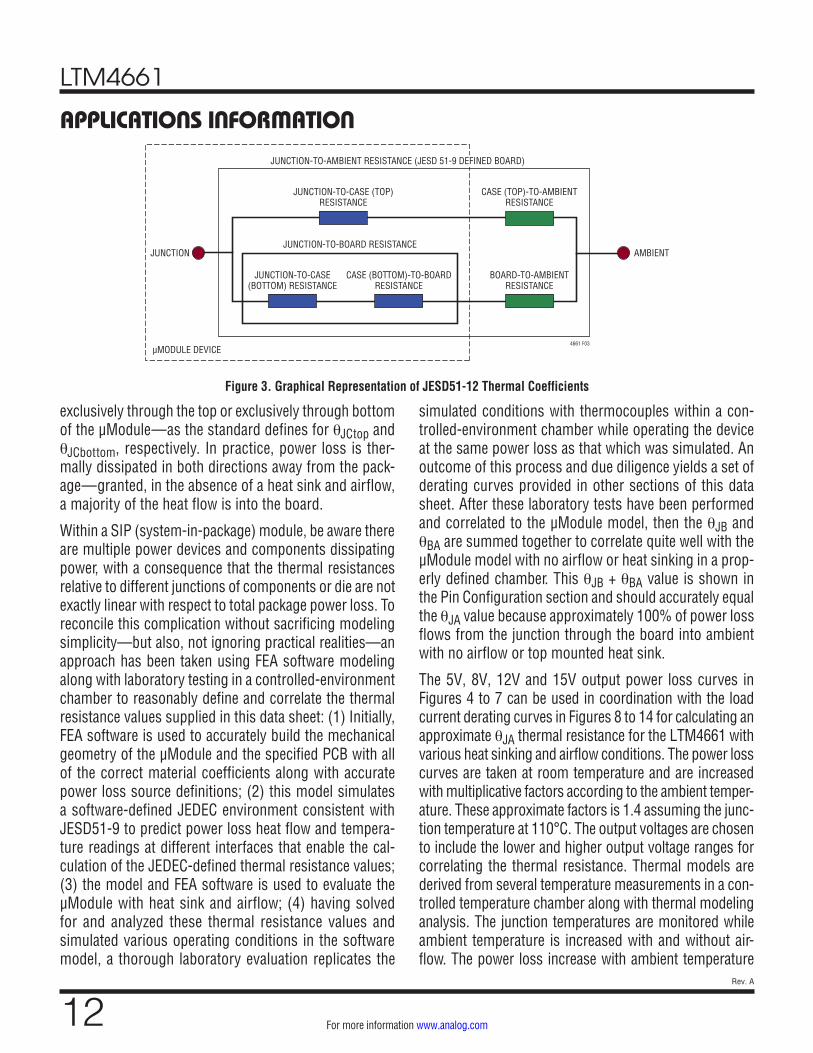
The thermal resistances reported in the Pin Configuration section of the data sheet are consistent with those param-eters defined by JESD51-9 and are intended for use with finite element analysis (FEA) software modeling tools that leverage the outcome of thermal modeling, simulation and correlation to hardware evaluation performed on a µModule package mounted to a hardware test board—also defined by JESD51-9 (“Test Boards for Area Array Surface Mount Package Thermal Measurements”). The motivation for providing these thermal coefficients in found in JESD51-12 (“Guidelines for Reporting and Using Electronic Package Thermal Information”).
Many designers may opt to use laboratory equipment and a test vehicle such as the demo board to anticipate the µModule regulator’s thermal performance in their appli-cation at various electrical and environmental operating conditions to compliment any FEA activities. Without FEA software, the thermal resistances reported in the Pin Configuration section are in and of themselves not relevant to providing guidance of thermal performance; instead, the derating curves provided in the data sheet can be used in a manner that yields insight and guidance per-taining to one’s application usage and can be adapted to correlate thermal performance to one’s own application.
The Pin Configuration section typically gives four thermal coefficients explicitly defined in JESD51-12; these coef-ficients are quoted or paraphrased below:
1. θJA, the thermal resistance from junction to ambient, is the natural convection junction-to-ambient air ther-mal resistance measured in a one cubic foot sealed enclosure. This environment is sometimes referred to as “still air” although natural convection causes the air to move. This value is determined with the part mounted to a JESD51-9 defined test board, which
does not reflect an actual application or viable operat-ing condition.
2. θJCbottom, the thermal resistance from junction to ambient, is the natural convection junction-to-ambi-ent air thermal resistance measured in a one cubic foot sealed enclosure. This environment is sometimes referred to as “still air” although natural convection causes the air to move. This value is determined with the part mounted to a JESD51-9 defined test board, which does not reflect an actual application or viable operating condition.
3. θJCtop, the thermal resistance from junction to top of the product case, is determined with nearly all of the component power dissipation flowing through the top of the package. As the electrical connections of the typical µModule are on the bottom of the package, it is rare for an application to operate such that most of the heat flows from the junction to the top of the part. As in the case of θJCbottom, this value may be useful for comparing packages but the test conditions don’t generally match the user’s application.
4. θJB, the thermal resistance from junction to the printed circuit board, is the junction-to-board thermal resistance where almost all of the heat flows through the bottom of the µModule and into the board, and is really the sum of the θJCbottom and the thermal resis-tance of the bottom of the part through the solder joints and through a portion of the board. The board temperature is measured a specified distance from the package, using a two sided, two layer board. This board is described in JESD51-9.
A graphical representation of the aforementioned ther-mal resistances is given in Figure 3; blue resistances are contained within the µModule regulator, whereas green resistances are external to the µModule.
As a practical matter, it should be clear to the reader that no individual or subgroup of the four thermal resis-tance parameters defined by JESD51-12 or provided in the Pin Configuration section replicates or conveys nor-mal operating conditions of a μModule. For example, in normal board-mounted applications, never does 100% of the device’s total power loss (heat) thermally conduct
APPLICATIONS INFORMATION
LTM4661
12Rev. A
For more information www.analog.com
exclusively through the top or exclusively through bottom of the µModule—as the standard defines for θJCtop and θJCbottom, respectively. In practice, power loss is ther-mally dissipated in both directions away from the pack-age—granted, in the absence of a heat sink and airflow, a majority of the heat flow is into the board.
Within a SIP (system-in-package) module, be aware there are multiple power devices and components dissipating power, with a consequence that the thermal resistances relative to different junctions of components or die are not exactly linear with respect to total package power loss. To reconcile this complication without sacrificing modeling simplicity—but also, not ignoring practical realities—an approach has been taken using FEA software modeling along with laboratory testing in a controlled-environment chamber to reasonably define and correlate the thermal resistance values supplied in this data sheet: (1) Initially, FEA software is used to accurately build the mechanical geometry of the µModule and the specified PCB with all of the correct material coefficients along with accurate power loss source definitions; (2) this model simulates a software-defined JEDEC environment consistent with JESD51-9 to predict power loss heat flow and tempera-ture readings at different interfaces that enable the cal-culation of the JEDEC-defined thermal resistance values; (3) the model and FEA software is used to evaluate the µModule with heat sink and airflow; (4) having solved for and analyzed these thermal resistance values and simulated various operating conditions in the software model, a thorough laboratory evaluation replicates the
simulated conditions with thermocouples within a con-trolled-environment chamber while operating the device at the same power loss as that which was simulated. An outcome of this process and due diligence yields a set of derating curves provided in other sections of this data sheet. After these laboratory tests have been performed and correlated to the µModule model, then the θJB and θBA are summed together to correlate quite well with the µModule model with no airflow or heat sinking in a prop-erly defined chamber. This θJB + θBA value is shown in the Pin Configuration section and should accurately equal the θJA value because approximately 100% of power loss flows from the junction through the board into ambient with no airflow or top mounted heat sink.
The 5V, 8V, 12V and 15V output power loss curves in Figures 4 to 7 can be used in coordination with the load current derating curves in Figures 8 to 14 for calculating an approximate θJA thermal resistance for the LTM4661 with various heat sinking and airflow conditions. The power loss curves are taken at room temperature and are increased with multiplicative factors according to the ambient temper-ature. These approximate factors is 1.4 assuming the junc-tion temperature at 110°C. The output voltages are chosen to include the lower and higher output voltage ranges for correlating the thermal resistance. Thermal models are derived from several temperature measurements in a con-trolled temperature chamber along with thermal modeling analysis. The junction temperatures are monitored while ambient temperature is increased with and without air-flow. The power loss increase with ambient temperature
APPLICATIONS INFORMATION
Figure 3. Graphical Representation of JESD51-12 Thermal Coefficients
4661 F03µMODULE DEVICE
JUNCTION-TO-CASE (TOP)RESISTANCE
JUNCTION-TO-BOARD RESISTANCE
JUNCTION-TO-AMBIENT RESISTANCE (JESD 51-9 DEFINED BOARD)
CASE (TOP)-TO-AMBIENTRESISTANCE
BOARD-TO-AMBIENTRESISTANCE
JUNCTION-TO-CASE(BOTTOM) RESISTANCE
JUNCTION AMBIENT
CASE (BOTTOM)-TO-BOARDRESISTANCE

LTM4661
13Rev. A
For more information www.analog.com
change is factored into the derating curves. The junctions are maintained at 110°C maximum while lowering output current or power with increasing ambient temperature. The decreased output current will decrease the internal module loss as ambient temperature is increased. The monitored junction temperature of 110°C minus the ambient operat-ing temperature specifies how much module temperature rise can be allowed. As an example, in Figure 13 the load current is derated to ~0.35A at ~80°C with no air or heat sink and the power loss for the 3.3V to 15V at 0.35A output is about 1.4W. The 1.4W loss is calculated with the ~1.0W room temperature loss from the 3.3V to 15V power loss curve at 0.35A, and the 1.4 multiplying factor. If the 80°C ambient temperature is subtracted from the 110°C junction temperature, then the difference of 30°C divided by 1.4W
equals a 21.4°C/W θJA thermal resistance. Table 3 speci-fies a 21°C/W value which is very close. Table 3 to Table 6 provide equivalent thermal resistances for 5V, 8V, 12V and 15V outputs with and without airflow and heat sinking. The derived thermal resistances in Tables 3 to 6 for the various conditions can be multiplied by the calculated power loss as a function of ambient temperature to derive temperature rise above ambient, thus maximum junction temperature. Room temperature power loss can be derived from the efficiency curves in the Typical Performance Characteristics section and adjusted with the above ambient temperature multiplicative factors. The printed circuit board is a 1.6mm thick four layer board with two ounce copper for the two outer layers and one ounce copper all four layers. The PCB dimensions are 65mm × 65mm.
APPLICATIONS INFORMATIONAPPLICATIONS INFORMATION
Figure 4. 5V Output Power Loss Figure 5. 8V Output Power Loss Figure 6. 12V Output Power Loss
Figure 7. 15V Output Power Loss Figure 8. 3.3V to 5V Derating Curve, No Heat Sink
Figure 9. 3.3V to 8V Derating Curve, No Heat Sink
LOAD CURRENT (A)0
POW
ER L
OSS
(W)
3
0.2
1.8
1.4
1
0.6
1.6
1.2
2.8
2.4
2
2.6
2.2
0.8
0.4
01 1.80.6 1.4
4661 F04
20.8 1.60.4 1.20.2
3.3V INPUT
LOAD CURRENT (A)0
POW
ER L
OSS
(W)
2
0.2
1.8
1.4
1
0.6
1.6
1.2
0.8
0.4
01 1.80.6 1.4
4661 F05
20.8 1.60.4 1.20.2
3.3V INPUT5V INPUT
AMBIENT TEMPERATURE (°C)30
LOAD
CUR
RENT
(A)
2.5
2
1
1.5
0.5
08060 100
4661 F08
1107050 9040
0LFM200LFM400LFM
LOAD CURRENT (A)0
POW
ER L
OSS
(W)
2
0.2
1.8
1.4
1
0.6
1.6
1.2
0.8
0.4
00.5 0.90.3 0.7
4661 F06
10.4 0.80.2 0.60.1
3.3V INPUT5V INPUT
AMBIENT TEMPERATURE (°C)30
LOAD
CUR
RENT
(A)
1.2
1
0.8
0.2
0.4
0.6
08060 100
4661 F09
1107050 9040
0LFM200LFM400LFM
LOAD CURRENT (A)0
POW
ER L
OSS
(W)
2
0.2
1.8
1.4
1
0.6
1.6
1.2
0.8
0.4
00.5 0.90.3 0.7
4661 F07
10.4 0.80.2 0.60.1
3.3V INPUT5V INPUT

LTM4661
14Rev. A
For more information www.analog.com
APPLICATIONS INFORMATION
Figure 10. 5V Input to 8V Output Derating Curve, No Heat Sink
Figure 11. 3.3V Input to 12V Output Derating Curve, No Heat Sink
Figure 12. 5V Input to 12V Output Derating Curve, No Heat Sink
Figure 13. 3.3V Input to 15V Output Derating Curve, No Heat Sink
Figure 14. 5V Input to 15V Output Derating Curve, No Heat Sink
AMBIENT TEMPERATURE (°C)30
LOAD
CUR
RENT
(A)
1.8
1.4
1.0
0.2
0.4
0.6
1.6
1.2
0.8
08060 100
4661 F10
1107050 9040
0LFM200LFM400LFM
AMBIENT TEMPERATURE (°C)30
LOAD
CUR
RENT
(A)
0.8
0.6
0.7
0.5
0.4
0.1
0.2
0.3
08060 100
4661 F11
1107050 9040
0LFM200LFM400LFM
AMBIENT TEMPERATURE (°C)30
LOAD
CUR
RENT
(A)
0.9
0.8
0.6
0.7
0.4
0.2
0.5
0.3
0.1
07050 90
4661 F14
11060 10040 80
0LFM200LFM400LFM
AMBIENT TEMPERATURE (°C)30
LOAD
CUR
RENT
(A)
1.2
1
0.6
0.8
0.4
0.2
07050 90
4661 F12
11060 10040 80
0LFM200LFM400LFM
AMBIENT TEMPERATURE (°C)30
LOAD
CUR
RENT
(A)
0.6
0.5
0.4
0.1
0.2
0.3
08060 100
4661 F13
1107050 9040
0LFM200LFM400LFM

LTM4661
15Rev. A
For more information www.analog.com
Table 3. 5V OutputDERATING CURVE VIN (V) POWER LOSS CURVE AIRFLOW (LFM) HEAT SINK θJA (°C/W)
Figure 8 3.3 Figure 4 0 None 21
Figure 8 3.3 Figure 4 200 None 19
Figure 8 3.3 Figure 4 400 None 18
Table 4. 8V OutputDERATING CURVE VIN (V) POWER LOSS CURVE AIRFLOW (LFM) HEAT SINK θJA (°C/W)
Figure 9, Figure 10 3.3, 5 Figure 5 0 None 21
Figure 9, Figure 10 3.3, 5 Figure 5 200 None 19
Figure 9, Figure 10 3.3, 5 Figure 5 400 None 18
Table 5. 12V OutputDERATING CURVE VIN (V) POWER LOSS CURVE AIRFLOW (LFM) HEAT SINK θJA (°C/W)
Figure 11, Figure 12 3.3, 5 Figure 6 0 None 21
Figure 11, Figure 12 3.3, 5 Figure 6 200 None 19
Figure 11, Figure 12 3.3, 5 Figure 6 400 None 18
Table 6. 15V OutputDERATING CURVE VIN (V) POWER LOSS CURVE AIRFLOW (LFM) HEAT SINK θJA (°C/W)
Figure 13, Figure 14 3.3, 5 Figure 7 0 None 21
Figure 13, Figure 14 3.3, 5 Figure 7 200 None 19
Figure 13, Figure 14 3.3, 5 Figure 7 400 None 18
APPLICATIONS INFORMATION

LTM4661
16Rev. A
For more information www.analog.com
Figure 15 shows a measured thermal picture of the LTM4661 running from 3.3V input to 12V output at 0.8A DC current with 200LFM airflow and no heat sink.
Figure 15. Thermal Image, 3.3V Input to 12V Output at 0.8A, 200LFM Airflow, No Heat Sink
Safety Considerations
The LTM4661 modules do not provide galvanic isolation from VIN to VOUT. There is no internal fuse. If required, a slow blow fuse with a rating twice the maximum input current needs to be provided to protect each unit from catastrophic failure. The device does support thermal shutdown and overcurrent protection.
Layout Checklist/Example
The high integration of LTM4661 makes the PCB board layout very simple and easy. However, to optimize its electrical and thermal performance, some layout consid-erations are still necessary.
• Use large PCB copper areas for high current paths, including VIN, GND and VOUT. It helps to minimize the PCB conduction loss and thermal stress.
• Place high frequency ceramic input and output capac-itors next to the VIN, PGND and VOUT pins to minimize high frequency noise.
• Place a dedicated power ground layer underneath the unit.
• To minimize the via conduction loss and reduce mod-ule thermal stress, use multiple vias for interconnec-tion between top layer and other power layers.
• Do not put vias directly on the pad, unless they are capped or plated over.
• For parallel modules, tie the VOUT, VFB and COMP pins together. Use an internal layer to closely connect these pins together.
• Bring out test points on the signal pins for monitoring.
Figure 16 gives a good example of the recommended layout.
APPLICATIONS INFORMATION
Figure 16. Recommended PCB Layout
VIN
GND
GND
VOUT
4661 F16

LTM4661
17Rev. A
For more information www.analog.com
APPLICATIONS INFORMATION
Figure 17. 3.3V Input to 5V Output, at 2A Design
Figure 18. 3.3V to 5V Input, 12V Output Design with External Clock
COUT22µF ×216V
CIN22µF ×26.3V
R131.6k
4661 F17
2.2µF
LTM4661 VOUT
FB
VOUT5V/2AVIN
SDB
MODE/SYNC
INTVCC
FREQ COMP
GND
VIN3.3V
COUT22µF ×225V
CIN22µF ×26.3V
R211k
140k
4661 F18
3MHz CLOCK
SWITCHING FREQUENCY = CLOCK FREQUENCY/2
2.2µF
LTM4661
VOUT
FB
VOUT12V/0.8AVIN
SDB
MODE/SYNC
INTVCC
FREQ COMP
GND
VIN3.3V TO 5V

LTM4661
18Rev. A
For more information www.analog.com
Figure 19. Two LTM4661 Module Parallel Design for 8V/2A Output Running at 1.2MHz
22µF ×225V
22µF ×26.3V
8.87k
4661 F19
22µF ×225V
22µF ×26.3V
LTC6802 SET TO 2-PHASE 2.4MHz CLOCK OUTPUT
SWITCHING FREQUENCY = CLOCK FREQUENCY/2
1µF
83.5k
2.2µF
2.2µF
LTM4661
VOUT
FB
VIN
SDB
MODE/SYNC
INTVCC
FREQ COMP
GND
LTM4661
VOUT
FB
VOUT8V/2AVIN
SDB
MODE/SYNC
INTVCC
LTC6902
V+
DIV
PH
OUT1
OUT2
10
9
8
7
6
SET
MOD
GND
OUT4
OUT3
1
2
3
4
5
FREQ COMP
COMP
COMP
GND
VIN3.3V TO 5V
INTVCCINTVCC
APPLICATIONS INFORMATION

LTM4661
19Rev. A
For more information www.analog.com
PACKAGE DESCRIPTIONPACKAGE ROW AND COLUMN LABELING MAY VARY AMONG µModule PRODUCTS. REVIEW EACH PACKAGE LAYOUT CAREFULLY.
LTM4661 Component BGA Pinout
PIN ID FUNCTION PIN ID FUNCTION PIN ID FUNCTION PIN ID FUNCTION PIN ID FUNCTION
A1 VIN A2 GND A3 GND A4 VOUT A5 VOUT
B1 VIN B2 GND B3 GND B4 GND B5 VOUT
C1 VIN C2 GND C3 GND C4 GND C5 VOUT
D1 VIN D2 SYNC/MODE D3 INTVCC D4 GND D5 SDB
E1 VIN E2 GND E3 FREQ E4 COMP E5 FB

LTM4661
20Rev. A
For more information www.analog.com
PACKAGE DESCRIPTION
PACK
AGE
TOP
VIEW
4
PIN
“A1”
CORN
ER
YX
aaa
Z
aaa
Z
DETA
IL A
PACK
AGE
BOTT
OM V
IEW
3
SEE
NOTE
S
SUGG
ESTE
D PC
B LA
YOUT
TOP
VIEW
0.00
0
2.54
0
1.27
0
1.27
0
2.54
00.
630
±0.0
25
2.540
1.270
2.540
1.270
0.3175
0.31750.000
EDCBA
12
34
5
PIN
1
NOTE
S:1.
DIM
ENSI
ONIN
G AN
D TO
LERA
NCIN
G PE
R AS
ME
Y14.
5M-1
994
2. A
LL D
IMEN
SION
S AR
E IN
MIL
LIM
ETER
S
BAL
L DE
SIGN
ATIO
N PE
R JE
SD M
S-02
8 AN
D JE
P95
43
DETA
ILS
OF P
IN #
1 ID
ENTI
FIER
ARE
OPT
IONA
L,BU
T M
UST
BE L
OCAT
ED W
ITHI
N TH
E ZO
NE IN
DICA
TED.
THE
PIN
#1 ID
ENTI
FIER
MAY
BE
EITH
ER A
MOL
D OR
M
ARKE
D FE
ATUR
E
Øb (2
5 PL
ACES
)
A
DETA
IL B
PACK
AGE
SIDE
VIE
W
MX
YZ
ddd
MZ
eee
A2
D
E
e
b
F
G
DETA
IL A
0.31
75
0.31
75
BGA
25 0
517
REV
A
LTM
XXXX
XXµM
odul
e
TRAY
PIN
1BE
VEL
PACK
AGE
IN T
RAY
LOAD
ING
ORIE
NTAT
ION
COM
PONE
NTPI
N “A
1”
BGA
Pack
age
25-L
ead
(6.2
5mm
× 6
.25m
m ×
2.4
2mm
)(R
efer
ence
LTC
DW
G #
05-0
8-15
02 R
ev A
)
6
SEE
NOTE
S
SYM
BOL
A A1 A2 b b1 D E e F G H1 H2 aaa
bbb
ccc
ddd
eee
MIN
2.22
0.50
1.72
0.60
0.60
0.27
1.45
NOM
2.42
0.60
1.82
0.75
0.63
6.25
6.25
1.27
5.08
5.08
0.32
1.50
MAX
2.62
0.70
1.92
0.90
0.66
0.37
1.55
0.15
0.10
0.20
0.30
0.15
TOTA
L NU
MBE
R OF
BAL
LS: 2
5
DIM
ENSI
ONS
NOTE
S
BALL
HT
BALL
DIM
ENSI
ONPA
D DI
MEN
SION
SUBS
TRAT
E TH
KM
OLD
CAP
HT
Z
5. P
RIM
ARY
DATU
M -Z
- IS
SEAT
ING
PLAN
E
6PA
CKAG
E RO
W A
ND C
OLUM
N LA
BELI
NG M
AY V
ARY
AMON
G µM
odul
e PR
ODUC
TS. R
EVIE
W E
ACH
PACK
AGE
LAYO
UT C
AREF
ULLY
!
DETA
IL B
SUBS
TRAT
E
A1
ccc
Z
Z
// bbb Z
H2H1
b1M
OLD
CAP
LTM4661
21Rev. A
For more information www.analog.com
Information furnished by Analog Devices is believed to be accurate and reliable. However, no responsibility is assumed by Analog Devices for its use, nor for any infringements of patents or other rights of third parties that may result from its use. Specifications subject to change without notice. No license is granted by implication or otherwise under any patent or patent rights of Analog Devices.
LTM4661 Component BGA Pinout
PIN ID FUNCTION PIN ID FUNCTION PIN ID FUNCTION PIN ID FUNCTION PIN ID FUNCTION
A1 VIN A2 GND A3 GND A4 VOUT A5 VOUT
B1 VIN B2 GND B3 GND B4 GND B5 VOUT
C1 VIN C2 GND C3 GND C4 GND C5 VOUT
D1 VIN D2 SYNC/MODE D3 INTVCC D4 GND D5 SDB
E1 VIN E2 GND E3 FREQ E4 COMP E5 FB
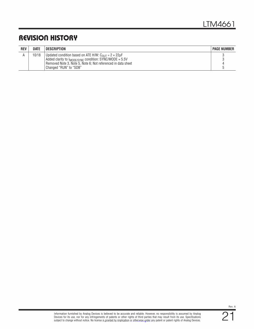
REVISION HISTORYREV DATE DESCRIPTION PAGE NUMBER
A 10/18 Updated condition based on ATE H/W: COUT = 2 × 22μF Added clarity to IMODE/SYNC condition: SYNC/MODE = 5.5V Removed Note 3, Note 5, Note 6; Not referenced in data sheet Changed “RUN” to “SDB”
3 3 4 5

LTM4661
22Rev. A
For more information www.analog.com ANALOG DEVICES, INC. 2017-2018
10/18(A)www.analog.com
DESIGN RESOURCES
RELATED PARTS
PACKAGE PHOTO
PART NUMBER DESCRIPTION COMMENTS
LTM8054 36VIN, 5.4A Buck-Boost µModule Regulator 5V ≤ VIN ≤ 36V, 1.2V ≤ VOUT ≤ 36V, 11.25mm × 15mm × 3.42mm BGA
LTM8045 SEPIC (Boost) or Inverting µModule Regulator 2.8V ≤ VIN ≤ 18V. ±2.5V ≤ VOUT ≤ ±15V, IOUT is Up to 700mA. 6.25mm × 11.25mm x 4.92mm BGA
LTM8049 Dual, SEPIC (Boost) and/or Inverting µModule Regulator
2.6V ≤ VIN ≤ 20V, ±2.5V ≤ VOUT ≤ ±24V, IOUT is Up to 1.5A, 9mm × 15mm × 2.42mm BGA
LTM4622 Ultrathin, 20VIN, Dual 2.5A Step-Down µModule Regulator
3.6V ≤ VIN ≤ 20V, 0.6V ≤ VOUT ≤ 5.5V, 6.25mm × 6.25mm × 1.82mm LGA, 6.25mm × 6.25mm × 2.42mm BGA
LTM4643 Ultrathin, 20VIN, Quad 3A Step-Down µModule Regulator
4V ≤ VIN ≤ 20V, 0.6V ≤ VOUT ≤ 3.3V, 9mm × 15mm × 1.82mm LGA, 9mm × 15mm × 2.42mm BGA
SUBJECT DESCRIPTION
µModule Design and Manufacturing Resources Design: • Selector Guides • Demo Boards and Gerber Files • Free Simulation Tools
Manufacturing: • Quick Start Guide • PCB Design, Assembly and Manufacturing Guidelines • Package and Board Level Reliability
µModule Regulator Products Search 1. Sort table of products by parameters and download the result as a spread sheet.2. Search using the Quick Power Search parametric table.
Digital Power System Management Analog Devices’ family of digital power supply management ICs are highly integrated solutions that offer essential functions, including power supply monitoring, supervision, margining and sequencing, and feature EEPROM for storing user configurations and fault logging.