Embed Size (px)
Citation preview

LT4295
14295f
For more information www.linear.com/LT4295
Typical applicaTion
FeaTures DescripTion
IEEE 802.3bt PD Interface with Forward/Flyback Controller
IEEE 802.3bt 71W (Class 8) PD Controller and Power Supply in Forward Mode
applicaTionsn High Power Wireless Data Systemsn Outdoor Security Camera Equipmentn Commercial and Public Information Displaysn High Temperature Applications
L, LT, LTC, LTM, LTPoE++, Linear Technology and the Linear logo are registered trademarks of Linear Technology Corporation. All other trademarks are the property of their respective owners.
n IEEE 802.3af/at/bt(Draft 2.0) Powered Device (PD) with Forward/Flyback Controllern Supports Up to 71 Watt PDsn 5-Event Classification Sensingn Superior Surge Protection (100V Absolute Maximum)n Wide Junction Temperature Range (–40°C to 125°C)n >94% End-to-End Efficiency with LT4321 Ideal Bridgen External Hot Swap N-Channel MOSFET for Lowest Power Dissipation and Highest System Efficiencyn No-Opto Flyback Operationn Auxiliary Power Support as Low as 9Vn Easy Migration of LTPoE++® PDs to IEEE 802.3bt PDsn Pin Compatible with LT4276A/B/Cn 28-Lead 4mm × 5mm QFN Package
The LT®4295 is an IEEE 802.3af/at/bt(Draft 2.0)-com-pliant powered device (PD) interface controller with a switching regulator controller. The T2P output indicates the number of classification events received during IEEE 802.3bt-compliant mutual identification and negotiation of available power.
The LT4295 supports both forward and flyback power supply topologies. The flyback topology supports No-Opto feedback. Auxiliary input voltages can be accurately sensed with just a resistor divider connected to the AUX pin.
The LT4295 utilizes an external, low RDS(on) N-channel hot swap MOSFET and supports the LT4320/LT4321 ideal diode bridges, to extend the end-to-end power delivery efficiency and eliminate costly heat sinks.
The LT4295 also includes an on-chip detection signature resistor, thermal protection, slope compensation, and many user configurable settings including classification signature, inrush current, switcher frequency, gate drive delay, soft-start, and load compensation.
••VPORT
VPORT
RCLASS
AUX
RCLASS++
SWVCC
VCCVINVCC
0.1µF
10µFBAV19WS(TRR ≤50ns)
22µF
HSGATE
HSSRC
FFSDLY
PG
SG
ITHB
TO MICROPROCESSOR
ISEN+
ISEN–
4295 TA01
GND FB31 ROSC T2PSS
100µH
AUX37V TO 57V
+
–
–
+
FMMT723
20mΩ
5V13A
+
–3.3k
10k0.1µF 100pF
10nF
100k
LT4295
OPTO
+
CLASSAVAILABLE
POWER
0 13W
1 3.84W
2 6.49W
3 13W
4 25.5W
5 40W
6 51W
7 62W
8 71W
LT4295
24295f
For more information www.linear.com/LT4295
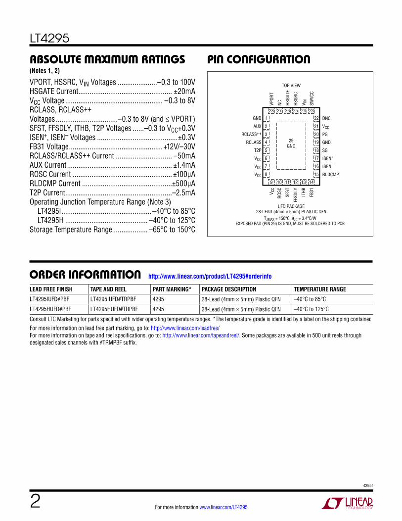
pin conFiguraTionabsoluTe MaxiMuM raTings
VPORT, HSSRC, VIN Voltages .....................–0.3 to 100VHSGATE Current.................................................. ±20mAVCC Voltage .................................................... –0.3 to 8VRCLASS, RCLASS++Voltages .................................–0.3 to 8V (and ≤ VPORT)SFST, FFSDLY, ITHB, T2P Voltages ......–0.3 to VCC+0.3VISEN+, ISEN– Voltages ...........................................±0.3VFB31 Voltage ..................................................+12V/–30VRCLASS/RCLASS++ Current .............................. –50mAAUX Current ........................................................ ±1.4mAROSC Current ..................................................... ±100µARLDCMP Current ................................................±500µAT2P Current .........................................................–2.5mAOperating Junction Temperature Range (Note 3) LT4295I ................................................–40°C to 85°C LT4295H ............................................ –40°C to 125°CStorage Temperature Range .................. –65°C to 150°C
(Notes 1, 2)
9 10
TOP VIEW
UFD PACKAGE28-LEAD (4mm × 5mm) PLASTIC QFN
11 12 13
28 27 26 25 24
14
23
6
5
4
3
2
1GND
AUX
RCLASS++
RCLASS
T2P
VCC
VCC
VCC
DNC
VCC
PG
GND
SG
ISEN+
ISEN–
RLDCMP
VPOR
T
NC HSGA
TE
HSSR
C
V IN
SWVC
C
V CC
ROSC
SFST
FFSD
LY
ITHB
FB31
7
17
18
19
20
21
22
16
8 15
29GND
TJMAX = 150°C, θJC = 3.4°C/W
EXPOSED PAD (PIN 29) IS GND, MUST BE SOLDERED TO PCB
LEAD FREE FINISH TAPE AND REEL PART MARKING* PACKAGE DESCRIPTION TEMPERATURE RANGE
LT4295IUFD#PBF LT4295IUFD#TRPBF 4295 28-Lead (4mm × 5mm) Plastic QFN –40°C to 85°C
LT4295HUFD#PBF LT4295HUFD#TRPBF 4295 28-Lead (4mm × 5mm) Plastic QFN –40°C to 125°C
Consult LTC Marketing for parts specified with wider operating temperature ranges. *The temperature grade is identified by a label on the shipping container.For more information on lead free part marking, go to: http://www.linear.com/leadfree/ For more information on tape and reel specifications, go to: http://www.linear.com/tapeandreel/. Some packages are available in 500 unit reels through designated sales channels with #TRMPBF suffix.
orDer inForMaTion http://www.linear.com/product/LT4295#orderinfo
LT4295
34295f
For more information www.linear.com/LT4295
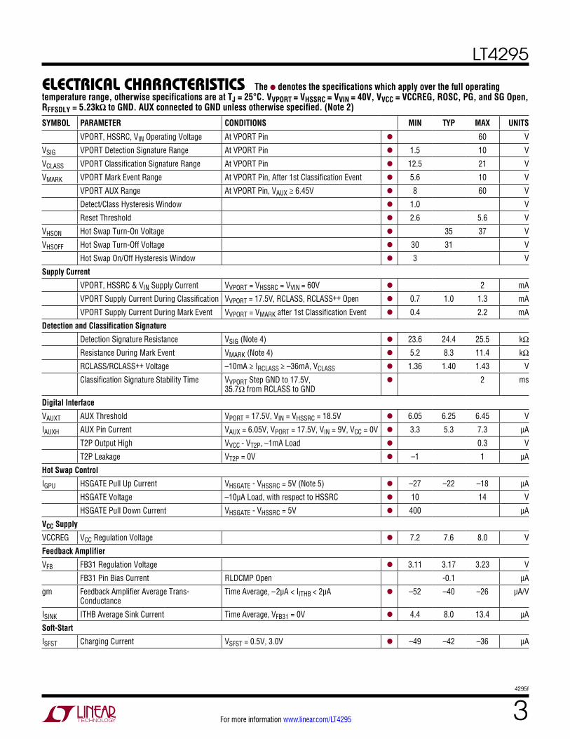
elecTrical characTerisTics
SYMBOL PARAMETER CONDITIONS MIN TYP MAX UNITS
VPORT, HSSRC, VIN Operating Voltage At VPORT Pin l 60 V
VSIG VPORT Detection Signature Range At VPORT Pin l 1.5 10 V
VCLASS VPORT Classification Signature Range At VPORT Pin l 12.5 21 V
VMARK VPORT Mark Event Range At VPORT Pin, After 1st Classification Event l 5.6 10 V
VPORT AUX Range At VPORT Pin, VAUX ≥ 6.45V l 8 60 V
Detect/Class Hysteresis Window l 1.0 V
Reset Threshold l 2.6 5.6 V
VHSON Hot Swap Turn-On Voltage l 35 37 V
VHSOFF Hot Swap Turn-Off Voltage l 30 31 V
Hot Swap On/Off Hysteresis Window l 3 V
Supply Current
VPORT, HSSRC & VIN Supply Current VVPORT = VHSSRC = VVIN = 60V l 2 mA
VPORT Supply Current During Classification VVPORT = 17.5V, RCLASS, RCLASS++ Open l 0.7 1.0 1.3 mA
VPORT Supply Current During Mark Event VVPORT = VMARK after 1st Classification Event l 0.4 2.2 mA
Detection and Classification Signature
Detection Signature Resistance VSIG (Note 4) l 23.6 24.4 25.5 kΩ
Resistance During Mark Event VMARK (Note 4) l 5.2 8.3 11.4 kΩ
RCLASS/RCLASS++ Voltage –10mA ≥ IRCLASS ≥ –36mA, VCLASS l 1.36 1.40 1.43 V
Classification Signature Stability Time VVPORT Step GND to 17.5V, 35.7Ω from RCLASS to GND
l 2 ms
Digital Interface
VAUXT AUX Threshold VPORT = 17.5V, VIN = VHSSRC = 18.5V l 6.05 6.25 6.45 V
IAUXH AUX Pin Current VAUX = 6.05V, VPORT = 17.5V, VIN = 9V, VCC = 0V l 3.3 5.3 7.3 µA
T2P Output High VVCC - VT2P, –1mA Load l 0.3 V
T2P Leakage VT2P = 0V l –1 1 µA
Hot Swap Control
IGPU HSGATE Pull Up Current VHSGATE - VHSSRC = 5V (Note 5) l –27 –22 –18 µA
HSGATE Voltage –10µA Load, with respect to HSSRC l 10 14 V
HSGATE Pull Down Current VHSGATE - VHSSRC = 5V l 400 µA
VCC Supply
VCCREG VCC Regulation Voltage l 7.2 7.6 8.0 V
Feedback Amplifier
VFB FB31 Regulation Voltage l 3.11 3.17 3.23 V
FB31 Pin Bias Current RLDCMP Open -0.1 µA
gm Feedback Amplifier Average Trans-Conductance
Time Average, –2µA < IITHB < 2µA l –52 –40 –26 µA/V
ISINK ITHB Average Sink Current Time Average, VFB31 = 0V l 4.4 8.0 13.4 µA
Soft-Start
ISFST Charging Current VSFST = 0.5V, 3.0V l –49 –42 –36 µA
The l denotes the specifications which apply over the full operating temperature range, otherwise specifications are at TJ = 25°C. VVPORT = VHSSRC = VVIN = 40V, VVCC = VCCREG, ROSC, PG, and SG Open, RFFSDLY = 5.23kΩ to GND. AUX connected to GND unless otherwise specified. (Note 2)

LT4295
44295f
For more information www.linear.com/LT4295
SYMBOL PARAMETER CONDITIONS MIN TYP MAX UNITS
Gate Outputs
PG, SG Output High Level I = –1mA l VCC –0.1 V
PG, SG Output Low Level I = 1mA l 1 V
PG Rise Time, Fall Time PG = 1000pF 15 ns
SG Rise Time, Fall Time SG = 400pF 15 ns
Current Sense/Overcurrent
VFAULT Overcurrent Fault Threshold VISEN+ - VISEN– l 125 140 155 mV
ΔVSENSE/ΔVITHB
Current Sense Comparator Threshold with Respect to VITHB
l –130 –111 –92 mV/V
VITHB(OS) VITHB Offset l 3.03 3.17 3.33 V
Timing
fOSC Default Switching Frequency ROSC Pin Open l 200 214 223 kHz
Switching Frequency 45.3kΩ from ROSC to GND l 280 300 320 kHz
fT2P T2P Signal Frequency fSW/256
T2P Duty Cycle in PoE Operation (Note 7) After 4-Event Classification After 5-Event Classification (RCLASS++ Has Resistor to GND)
50 25
% %
T2P Duty Cycle in Auxiliary Supply Operation (Note 7)
V(AUX) > VAUXT, and RCLASS++ Has Resistor to GND
25 %
tMIN Minimum PG On Time l 175 250 330 ns
DMAX Maximum PG Duty Cycle l 63 66 70 %
tPGDELAY PG Turn-On Delay-Flyback PG Turn-On Delay-Forward
5.23kΩ from FFSDLY to GND 52.3kΩ from FFSDLY to GND 10.5kΩ from FFSDLY to VCC 52.3kΩ from FFSDLY to VCC
45 171 92
391
ns ns ns ns
tFBDLY Feedback Amp Enable Delay Time 350 ns
tFB Feedback Amp Sense Interval 550 ns
tPGSG PG Falling to SG Rising Delay Time-Flyback PG Falling to SG Falling Delay Time- Forward
Resistor from FFSDLY to GND 10.5kΩ from FFSDLY to VCC 52.3kΩ from FFSDLY to VCC
20 67
301
ns ns ns
tSTART Start Timer (Note 6) Delay After Power Good l 80 86 93 ms
tFAULT Fault Timer (Note 6) Delay After Overcurrent Fault l 80 86 93 ms
IMPS MPS Current l 10 12 14 mA
elecTrical characTerisTics The l denotes the specifications which apply over the full operating temperature range, otherwise specifications are at TJ = 25°C. VVPORT = VHSSRC = VVIN = 40V, VVCC = VCCREG, ROSC, PG, and SG Open, RFFSDLY = 5.23kΩ to GND. AUX connected to GND unless otherwise specified. (Note 2)
Note 1: Stresses beyond those listed under Absolute Maximum Ratings may cause permanent damage to the device. Exposure to any Absolute Maximum Rating condition for extended periods may affect device reliability and lifetime.Note 2. All voltages with respect to GND unless otherwise noted. Positive currents are into pins; negative currents are out of pins unless otherwise noted. Note 3. This IC includes overtemperature protection that is intended to protect the device during momentary overload conditions. Junction temperature can exceed 150°C when overtemperature protection is active. Continuous operation above the specified maximum operating junction temperature may impair device reliability.
Note 4. Detection signature resistance specifications do not include resistance added by the external diode bridge which can add as much as 1.1kΩ to the port resistance.Note 5. IGPU available in PoE powered operation. That is, available after V(VPORT) > VHSON and V(AUX) < VAUXT, over the range where V(VPORT) is between VHSOFF and 60V.Note 6. Guaranteed by design, not subject to test.Note 7. Specified as the percentage of the period which T2P is low impedance with respect to VCC.

LT4295
54295f
For more information www.linear.com/LT4295
Typical perForMance characTerisTics
VFB31 vs TemperatureFeedback Amplifier Output Current vs VFB31
Switching Frequency vs Temperature
Current Sense Voltage vs Duty Cycle, ITHB
PG Delay Time vs Temperature in Flyback Mode
PG, SG Delay Time vs Temperature in Forward Mode
Input Current vs Input Voltage25k Detection Signature Range
Detection Signature Resistance vs Input Voltage VCC Current vs Temperature
VPORT VOLTAGE (V)0
0
VPOR
T CU
RREN
T (m
A)
0.4
0.3
0.2
0.1
0.5
6 8 102 4
4295 G01
125°C85°C25°C–40°C
VPORT VOLTAGE (V)1
23.75
SIGN
ATUR
E RE
SIST
ANCE
(kΩ
) 25.75
25.25
24.75
24.25
26.25
65 87 92 43
4295 G02
125°C85°C25°C–40°C
TEMPERATURE (°C)–50
0
V CC
CURR
ENT
(mA)
10
8
6
4
2
12
5025 10075 1250–25
4295 G03
214kHz
300kHz
TEMPERATURE (°C)–50
3.162
V FB3
1 (V
)
3.176
3.174
3.172
3.170
3.168
3.166
3.164
3.178
5025 10075 1250–25
4295 G04
FB31 VOLTAGE (V)2.57
–15
ITHB
CUR
RENT
(µA)
10
5
–5
0
–10
15
3.17 3.37 3.57 3.772.77 2.97
4295 G05
125°C85°C25°C–40°C
TEMPERATURE (°C)–50
0
DELA
Y TI
ME
(ns)
350
200
250
300
150
100
50
400
5025 10075 1250–25
4295 G09
TPGDELAY, 52.3k FROM FFSDLY TO VCC
TPGSG, 52.3k FROM FFSDLY TO VCC
TPGDELAY, 10.5k FROM FFSDLY TO VCC
TPGSG, 10.5k FROM FFSDLY TO VCC
TEMPERATURE (°C)–50
175
FREQ
UENC
Y (k
Hz)
300
275
250
225
200
325
5025 10075 1250–25
4295 G06
45.3k FROM ROSC TO GND
ROSC OPEN
VITHB = 1.8V
VITHB = 2.3V
VITHB = 2.6V
VITHB = 2.9V
DUTY CYCLE (%)0
0
V (IS
EN+
- ISE
N–) (
mV)
140
80
100
120
60
40
20
160
4030 6050 702010
4295 G07
VITHB = 0.96V (FB31 = 0V)
TEMPERATURE (°C)–50
0
PG D
ELAY
TIM
E (n
s)
200
150
100
50
250
5025 10075 1250–25
4295 G08
TPGDELAY, 5.23k FROM FFSDLY TO GND
TPGDELAY, 52.3k FROM FFSDLY TO GND

LT4295
64295f
For more information www.linear.com/LT4295
pin FuncTionsGND(Pins 1, 19, Exposed Pad Pin 29): Device Ground. Exposed Pad must be electrically and thermally connected to pins 1, 19 and PCB GND.
AUX (Pin 2): Auxiliary Sense. Assert AUX via a resistive divider from the auxiliary power input to set the voltage at which the auxiliary supply takes over. Asserting AUX pulls down HSGATE, disconnects the detection signature resistor and disables classification signature. The AUX pin sinks IAUXH when below its threshold voltage, of VAUXT, to provide hysteresis. Connect to GND if not used.
RCLASS++ (Pin 3): Class Select Input. Connect a resistor between RCLASS++ to GND per Table 1.
RCLASS (Pin 4): Class Select Input. Connect a resistor between RCLASS and GND per Table 1.
T2P (Pin 5): PSE Type Indicator. Open drain with respect to VCC. See the Applications Information section for pin behavior.
VCC (Pins 6, 7, 8, 9, 21): Switching Regulator Controller Supply Voltage. Connect a local ceramic capacitor from VCC pin 21 to GND pin 19 as close as possible to LT4295 as shown in Table 2.
ROSC (Pin 10): Programmable Frequency Adjustment. Resistor to GND programs operating frequency. Leave open for default frequency of 214kHz.
SFST (Pin 11): Soft-Start. Capacitor to GND sets soft- start timing.
FFSDLY (Pin 12): Forward/Flyback Select and Primary Gate Delay Adjustment. Resistor to GND adjusts gate drive delay for a flyback topology. Resistor to VCC adjusts gate drive delay for a forward topology.
ITHB (Pin 13): Current Threshold Control. The voltage on this pin corresponds to the peak current of the external primary FET. Note that the voltage gain from ITHB to the input of the current sense comparator (VSENSE) is negative.
FB31 (Pin 14): Feedback Input. In flyback mode, connect external resistive divider from the third winding feedback. Reference voltage is 3.17V. Connect to GND in forward mode.
RLDCMP (Pin 15): Load Compensation Adjustment. Op-tional resistor to GND controls output voltage set point as a function of peak switching current. Leave RLDCMP open if load compensation is not needed.
ISEN– (Pin 16): Current Sense, Negative Input. Route as a dedicated trace to the return side of the current sense resistor.
ISEN+ (Pin 17): Current Sense, Positive Input. Route as a dedicated trace to the sense side of the current sense resistor.
SG (Pin 18): Secondary (Synchronous) Gate Drive Output.
PG (Pin 20): Primary Gate Drive Output.
DNC (Pin 22): Do Not Connect. Leave pin open.
SWVCC (Pin 23): Switch Driver for VCC’s Buck Regulator. This pin drives the base of a PNP in a buck regulator to generate VCC.
VIN (Pin 24): Buck Regulator Supply Voltage. Usually separated from HSSRC by a pi filter.
HSSRC (Pin 25): External Hot Swap MOSFET Source. Connect to source of the external MOSFET.
HSGATE (Pin 26): External Hot Swap MOSFET Gate Control Output. Capacitance to GND determines inrush time.
NC (Pin 27): No Connection. Not internally connected.
VPORT (Pin 28): PD Interface Supply Voltage and External Hot Swap MOSFET Drain Connection.

LT4295
74295f
For more information www.linear.com/LT4295
block DiagraM
–+
–+
–+
+–
–+
–+–+
+ – + –
SLOPECOMP
OSC
TSD
CP
SWITCHING REGULATOR
CONTROLLER
PD INTERFACECONTROLLER
START-UPREGULATOR
INTERNAL BUCK
CONTROLLER
1.4V
1.4V
HSGATE
HSSRC
11V
VPORT
VPORT SWVCCVIN
VCC
ITHB
SFST
FFSDLY
ROSC
ISEN+
ISEN–
4295 BD
T2P
GND
PG
SG
VCC
VPORTRCLASS
RCLASS++
AUX
VAUXT
IAUXH
FB31
RLDCMP
FEEDBACK AMPgm = –40µA/V
LOADCOMP
CURRENTFAULT
COMPARATOR
CURRENTSENSE
COMPARATOR
VFB
VFAULT
AV = 10
AV = 1
VCC
VSENSE
VITHB(OS)
AV =∆VSENSE∆VITHB

LT4295
84295f
For more information www.linear.com/LT4295
OVERVIEW
Power over Ethernet (PoE) continues to gain popularity as products take advantage of the combination of DC power and high speed data available from a single RJ45 connector. The LT4295 is IEEE 802.3bt (Draft 2.0)-compli-ant and allows up to 71 watt operation while maintaining backwards compatibility with existing PSE systems. The LT4295 combines a PoE PD interface controller and a switching regulator controller capable of either flyback or forward isolated power supply operation.
SIGNIFICANT DIFFERENCES FROM PREVIOUS PRODUCTS
The LT4295 has several significant differences from pre-vious Linear Technology products. These differences are briefly summarized below.
IEEE 802.3bt vs LTPoE++ Available PD Power
The LT4295 supports IEEE 802.3bt PD power levels up to 71 Watts. A PD requiring more than 71 Watts is beyond the allowable power levels of IEEE 802.3bt.
The LT4275 and LT4276 are available to support PD power levels up to 90W under the LTPoE++ standard. See the Related Parts section for a list of LTPoE++ PSEs and PDs.
ITHB Is Inverted from the Usual ITH pin
The ITHB pin voltage has an inverse relationship to the cur-rent sense comparator threshold, VSENSE. Furthermore, the ITHB pin offset voltage, VITHB(OS), is 3.17V. See Figure 1.
applicaTions inForMaTion
Figure 1. VSENSE vs. VITHB
Duty-Cycle Based Soft-Start
The LT4295 uses a duty cycle ramp soft-start that injects charge into ITHB. This allows startup without appreciable overshoot using inexpensive external components.
The Feedback Pin FB31 is 3.17V Rather Than 1.25V
The error amp feedback voltage VFB is 3.17V.
Flyback/Forward Mode Is Pin Selectable
The LT4295 operates in flyback mode if FFSDLY is pulled down by a resistor to GND. It operates in forward mode if FFSDLY is pulled up by a resistor to VCC. The value of this resistor determines the tPGDELAY and tPGSG.
T2P Pin Response
The T2P pin outputs high impedance to VCC, low impedance to VCC, 50% duty cycle, or 25% duty cycle, responsive to the number of classification/mark event and responsive to
Table 1. Single-Signature Classification Codes, Power Levels and Resistor Selection
CLASS PD POWER AVAILABLE PD TYPE NOMINAL CLASS CURRENTRESISTOR (1%)
RCLS RCLS++0 13W Type 1 2.5mA 1.00kΩ Open1 3.84W Type 1 or 3 10.5mA 150Ω Open2 6.49W Type 1 or 3 18.5mA 80.6Ω Open3 13W Type 1 or 3 28mA 52.3Ω Open4 25.5W Type 2 or 3 40mA 35.7Ω Open5 40W Type 3 40mA/2.5mA 1.00kΩ 37.4Ω6 51W Type 3 40mA/10.5mA 150Ω 47.5Ω7 62W Type 4 40mA/18.5mA 80.6Ω 64.9Ω8 71W Type 4 40mA/28mA 52.3Ω 118Ω
VSENSE
∆VSENSE∆VITHB
VITHBVITHB(OS)
4295 F01

LT4295
94295f
For more information www.linear.com/LT4295
Figure 2. 1-Event Classification Signaling Waveform
Figure 3. 2-Event Classification/Mark Signaling Waveform
applicaTions inForMaTionPoE or auxiliary power operation. See T2P Output section in the Application Information.
VCC Is Powered by Internally Driven Buck Regulator
The LT4295 includes a buck regulator controller that must be used to generate the VCC supply voltage.
PoE MODES OF OPERATION
The LT4295 has several modes of operation, depending on the input voltage sequence applied to the VPORT pin.
Detection Signature
During detection, the PSE looks for a 25kΩ detection signature resistor which identifies the device as a PD. The LT4295 detection signature resistor is smaller than 25k to compensate for the additional series resistance introduced by the IEEE required diode bridge or the LT4321-based ideal diode bridge.
IEEE 802.3bt Single-Signature vs Dual-Signature PDs
IEEE 802.3bt defines two PD topologies: single-signature and dual-signature. The LT4295 primarily targets single-signature PD topologies, eliminating the need for a second PD controller. All PD descriptions and IEEE 802.3 standard references in this data sheet are limited in scope to single-signature PDs.
The LT4295 may be deployed in dual-signature PD appli-cations. For more information, contact Linear Technology Applications.
Classification Signature and Mark
The classification/mark process varies depending on the PSE type. A PSE, after a successful detection, may apply a classification probe voltage of 15.5V to 20.5V and mea-sure the PD classification signature current. Once the PSE applies a classification probe voltage, the PSE returns the PD voltage into the mark voltage range before applying another classification probe voltage, or powering up the PD.
An example of 1-Event classification is shown in Figure 2. In 2-Event classification, a PSE probes for power clas-sification twice as shown in Figure 3. An IEEE 802.3bt PSE may apply as many as 5 events before powering up the PD.
4295 F02
V POR
T
VHSON
VHSOFF
VCLASSMIN
VSIGMAX
VSIGMIN
VRESET
DETECT
1ST MARK
1ST CLASS
POWER ON
4295 F03
V POR
TVHSON
VHSOFF
VCLASSMIN
VSIGMAX
VSIGMIN
VRESET
DETECT
1ST CLASS
1ST MARK 2ND MARK
2ND CLASS
POWER ON
IEEE 802.3bt Physical Classification and Demotion
IEEE 802.3bt defines physical classification to allow a PD to communicate its power classification to the connected PSE and to allow the PSE to inform the PD of the PSE’s available power. Demotion is provided if the PD requested power level is not available at the PSE. If demoted, the PD must operate in a lower power state.
IEEE 802.3bt provides nine PD classes and four PD types, as shown in Table 1. The LT4295 class is configured by setting the RCLS and RCLS++ resistor values.
IEEE 802.3bt PSEs present a single classification event (see Figure 2) to Class 0 thru 3 PDs. A Class 0 thru 3 PD presents its class signature to the PSE and is then

LT4295
104295f
For more information www.linear.com/LT4295
applicaTions inForMaTionpowered on if sufficient power is available. Power limited IEEE 802.3bt PSEs may issue a single event to Class 4 and higher PDs in order to demote those PDs to 13W.
IEEE 802.3bt PSEs present up to three classification events depending on type to Class 4 PDs (see Figure 4). Class 4 PDs present a class signature 4 on all events. This third event differentiates a Class 4 PD from a higher class PD. Power limited IEEE 802.3bt PSEs may issue three events to Class 5 and higher PDs in order to demote those PDs to 25.5W.
Classification Resistors (RCLS and RCLS++)
The RCLS and RCLS++ resistors set the classification currents corresponding to the PD power classification. Select the value of RCLS and RCLS++ from Table 1 and connect the 1% resistor between the RCLASS, RCLASS++ pin and GND.
Detection Signature Corrupt During Mark Event
During the mark event, the LT4295 presents <11kΩ to the port as required by the IEEE 802.3 specification.
Inrush and Powered On
After the PSE detects and optionally classifies the PD, the PSE then powers on the PD. When the PD port voltage rises above the VHSON threshold, it begins to source IGPU out of the HSGATE pin. This current flows into an external
Figure 4. 3-Event Classification/Mark Signaling Waveform
Figure 5. 4-Event Classification/Mark Signaling Waveform
Figure 6. 5-Event Classification/Mark Signaling Waveform
4295 F04
V POR
T
VHSON
VHSOFF
VCLASSMIN
VSIGMAX
VSIGMIN
VRESET
DETECT
1ST CLASS
1ST MARK 2ND MARK 3RD MARK
2ND CLASS 3RD CLASS
POWER ON
IEEE 802.3bt PSEs present four classification events (see Figure 5) to Class 5 and 6 PDs. Class 5 and 6 PDs present a class signature 4 on the first two events. Class 5 and 6 PDs present a class signature 0 or 1, respectively, on the remaining events. Power limited IEEE 802.3bt PSEs may issue four events to Class 7 and higher PDs in order to demote those PDs to 51W.
IEEE 802.3bt PSEs present five classification events (see Figure 6) to Class 7 and 8 PDs. Class 7 and 8 PDs present a class signature 4 on the first two events. Class 7 and 8 PDs present a class signature 2 or 3 respectively, on the remaining events.
The PD must monitor the number of classification/mark events, which is communicated through the LT4295 T2P pin.
4295 F05
V POR
T
VHSON
VHSOFF
VCLASSMIN
VSIGMAX
VSIGMIN
VRESET
DETECT
1STCLASS
2NDCLASS
3RDCLASS
4THCLASS
POWER ON
1STMARK
2NDMARK
3RDMARK
4THMARK
4295 F06
V POR
TVHSON
VHSOFF
VCLASSMIN
VSIGMAX
VSIGMIN
VRESET
DETECT
1STCLASS
2NDCLASS
3RDCLASS
4THCLASS
5THCLASS
POWER ON
1STMARK
2NDMARK
3RDMARK
4THMARK
5THMARK

LT4295
114295f
For more information www.linear.com/LT4295
applicaTions inForMaTion
Figure 7. Programming IINRUSH
Figure 8. VCC Buck Regulator
The LT4295 internal charge pump enables an N-channel MOSFET solution, replacing a larger and more costly P-channel FET. The low RDS(ON) MOSFET also maximizes power delivery and efficiency, reduces power and heat dissipation, and eases thermal design.
DELAY START
After the HSGATE charges up to approximately 7V above HSSRC, fully enhancing the external hot swap MOSFET, the switching regulator controller operates after a delay of tSTART.
EXTERNAL VCC SUPPLY
The external VCC supply must be configured as a buck regulator shown in Figure 8. To optimize the buck regulator, use the external component values in Table 4 correspond-ing to the VIN operating range. This buck regulator runs in discontinuous mode with the inductor peak current considerably higher than average load current on VCC. Thus, the saturation current rating of the inductor must exceed the values shown in Table 2. Place the capacitor, C, as close as possible to VCC pin 21 and GND pin 19. For
optimal performance, place these components as close as possible to the LT4295.
Table 2 . Buck Regulator Component SelectionVIN C L ISAT Re D
9V-57V PoE
22µF 10µF
22µH 100µH
≥1.2A ≥300mA
1Ω 20Ω
Schottky Ultrafast Diode
capacitor CGATE in Figure 7 and causes a voltage to ramp up the gate of the external MOSFET. The external MOSFET acts as a source follower and ramps the voltage up on the output bulk capacitor, CPORT, thereby determining the inrush current, IINRUSH. To meet IEEE requirements, design IINRUSH to be ~100mA.
LT4295
HSGATE
GND4276 F07
VPORT HSSRC
CGATEIGPU
3.3k+
CPORT
VPORT
IINRUSH
IINRUSH = IGPU •CPORTCGATE
AUXILIARY SUPPLY OVERRIDE
If the AUX pin is held above VAUXT, the LT4295 enters auxiliary power operation. In this mode the detection sig-nature resistor is disconnected, classification is disabled, and HSGATE is pulled down.
The AUX pin allows for setting the auxiliary supply turn on (VAUXON) and turn off (VAUXOFF) voltage thresholds. The auxiliary supply hysteresis voltage, VAUXHYS, is set by sinking current, IAUXH, only when the AUX pin voltage is less than VAUXT. Use the following equations to set VAUXON and VAUXOFF via R1 and R2 in Figure 9. A capacitor up to 1000pF may be placed between the AUX pin and GND to improve noise immunity.
VAUXON must be lower than VHSOFF.
Figure 9. AUX Threshold and Hysteresis Calculation
LT4295
GND4295 F09
AUX
R1
VAUX
+
–
R2
R1=VAUXON − VAUXOFF
IAUXH=
VAUXHYSIAUXH
R2 = R1VAUXOFFVAUXT
− 1
R1≥VAUX(MAX) − VAUXT
1.4mA
VIN
Re
VCC
VIN
VCCGND
SWVCC
LT4295
FMMT723PBSS9110T
LD
C
4276 F08

LT4295
124295f
For more information www.linear.com/LT4295
applicaTions inForMaTion
Figure 10. PG and SG Timing Relationship in Flyback Mode
T2P OUTPUT
The LT4295 communicates the available power to the PD application via the T2P pin. The T2P pin state is deter-mined by the number of classification/mark events, the PD classification signature, and whether the PD is in PoE or auxiliary power operation. The LT4295 uses a 4-state encoding on the T2P pin.
During PoE operation after completing inrush, the T2P pin presents a high impedance (Hi-Z) to VCC to indicate 1-Event classifications. The T2P pin presents a low im-pedance (Low-Z) to VCC to indicate 2-Event or 3-Event classification. The T2P pin presents an alternating low/high impedance to VCC at 50% duty cycle to indicate 4-Event classification. The T2P pin presents an alternating 25% low/75% high impedance to VCC duty cycle to indicate 5-Event classification. The T2P pin toggles at a rate of fT2P. This feature is summarized in Table 3.
During auxiliary power operation, when configured for Class 4 or lower (i.e. RCLASS++ pin is floating), the T2P presents low impedance to VCC. When configured Class 5 or higher (i.e. with a resistor on the RCLASS++ pin to GND), the T2P presents a 25% duty cycle. This feature is summarized in Table 4.
Table 3. T2P Response vs Number of Class/Mark Events During PoE Operation
NUMBER OF CLASSIFICATION/
MARK EVENTS T2P WRT VCC PD POWER
1 2 or 3
4 5
Hi-Z Low-Z
50% Hi-Z/50% Low-Z 25% Low-Z, 75% Hi-Z
13W 25.5W
Minimum(PD Class, 51W) Minimum(PD Class, 71W)
Table 4. T2P Response During Auxiliary Power OperationPD CLASSIFICATION SIGNATURE T2P WRT VCC
0-4 5-8
Low-Z 25% Low-Z, 75% Hi-Z
SWITCHING REGULATOR CONTROLLER OPERATION
The switching regulator controller portion of the LT4295 is a current mode controller capable of implementing either a flyback or a forward power supply. When used in flyback mode, no opto-isolator is required for feedback Figure 11. Example PG and SG Connections in Flyback Mode
because the output voltage is sensed via the transformer’s third winding.
Flyback Mode
The LT4295 is programmed into flyback mode by placing a resistor RFFSDLY from the FFSDLY pin to GND. This resis-tor must be in the range of 5.23kΩ to 52.3kΩ. If using a potentiometer to adjust RFFSDLY, ensure the adjustment of the potentiometer does not exceed 52.3kΩ.The value of RFFSDLY determines tPGDELAY according to the following equations:
tPGDELAY ≈2.69ns /kΩ •RFFSDLY +30ns
tPGSG ≈20ns
The SG pin must be connected to the secondary side MOSFET through a gate drive transformer as shown in Figure 11. Add a Schottky diode from PG to GND as shown in Figure 11 to prevent PG from going negative.
PG
SG
4295 F10
tPGDELAY
tPGon
tPGSG
•
•
••
PG
SGGND
LT4295
4295 F11
FFSDLY
RFFSDLY
ISEN+
ISEN–
+

LT4295
134295f
For more information www.linear.com/LT4295
Forward Mode
The LT4295 is programmed into forward mode by placing a resistor RFFSDLY from the FFSDLY pin to VCC. The RFFSDLY resistor must be in the range of 10.5kΩ to 52.3kΩ. If using a potentiometer to adjust RFFSDLY ensure the adjustment of the potentiometer does not exceed 52.3kΩ.
The value of RFFSDLY determines tPGDELAY and tPGSG ac-cording to the following equations:
tPGDELAY ≈ 7.16ns/kΩ • RFFSDLY + 17ns
tPGSG ≈ 5.60ns/kΩ • RFFSDLY + 7.9ns
The PG and SG relationships in forward mode are shown in Figure 12.
In forward mode, the SG pin has the correct polarity to drive the active clamp P-channel MOSFET through a simple level shifter as shown in Figure 13. Add a Schottky diode from the PG to GND as shown in Figure 13 to prevent PG from going negative.
applicaTions inForMaTionFEEDBACK AMPLIFIER
In the flyback mode, the feedback amplifier senses the output voltage through the transformer’s third winding as shown in Figure 14. The amplifier is enabled only during the fixed interval, tFB, as shown in Figure 15. This eliminates the opto-isolator in isolated designs, thus greatly improving the dynamic response and stability over lifetime. Since tFB is a fixed interval, the time-averaged transconductance, gm, varies as a function of the user-selected switching frequency.
Figure 12. PG and SG Timing Relationship in Forward Mode
Figure 13. Example PG and SG Connections in Forward Mode
PG
SG
4295 F12
tPGDELAY tPGSG
Figure 14. Feedback and Load Compensation Connection
PG
FB31VOLTAGE
GND
SG4295 F15
tFBtFBDLY
VFB
Figure 15. Feedback Amplifier Timing Diagram
••
PG
VCC
VCC
SGGND
LT4295
4295 F13
FFSDLY
RFFSDLY
ISEN+
ISEN–
+–
+–
+–
•
•
•FEEDBACKFB31
LT4295THIRD
PRIMARY
4295 F14
SECONDARY
ITHB
PGISEN+
ISEN–
RLDCMP
RFB2VIN
VOUT
RSENSE
VFB
RFB1
RLDCMP
AV = 10

LT4295
144295f
For more information www.linear.com/LT4295
applicaTions inForMaTionFEEDBACK AMPLIFIER OUTPUT, ITHB
As shown in the Block Diagram, VSENSE is the input of the Current Sense Comparator. VSENSE is derived from the output of a linear amplifier whose input is the voltage on the ITHB pin, VITHB.
This linear amplifier inverts its input, VITHB, with a gain, ΔVSENSE/ΔVITHB, and with an offset voltage of VITHB(OS) to yield its output, VSENSE. This relationship is shown graphically in Figure 1. Note the slope ΔVSENSE/ΔVITHB is a negative number and is provided in the electrical characteristics table.
VITHB = VITHB(OS)+VSENSE •
ΔVSENSEΔVITHB
⎛⎝⎜
⎞⎠⎟
–1
The block diagram shows VSENSE is compared against the voltage across the current sense resistor, V(ISEN+)-V(ISEN–) modified by the internal slope compensation voltage discussed subsequently.
LOAD COMPENSATION
As can be seen in Figure 15, the voltage on the FB31 pin droops slightly during the flyback period. This is mostly caused by resistances of components of the secondary side such as: the secondary winding, RDS(ON) of the syn-chronous MOSFET, ESR of the output capacitor, etc. These resistances cause a feedback error that is proportional to the current in the secondary loop at the time of feedback sample window. To compensate for this error, the LT4295 places a voltage proportional to the peak current in the primary winding on the RLDCMP pin.
Determining Feedback and Load Compensation Resistors
Because the resistances of components on the secondary side are generally not well known, an empirical method must be used to determine the feedback and load com-pensation resistor values.
INITIALLY SET RFB2 = 2kΩ
RFB1≈RFB2VOUTVFB
NTHIRDNSECONDARY
–RFB2
Connect the resistor RLDCMP between the RLDCMP pin and GND. RLDCMP must be at least 10kΩ. Adjust RLDCMP for minimum change of VOUT over the full input and output load range. A potentiometer in series with 10kΩ may be initially used for RLDCMP and adjusted. The potentiometer+10kΩ may then be removed, measured, and replaced with the equivalent fixed resistor. The resulting VOUT differs from the desired VOUT due to offset injected by load compensa-tion. The change to RFB2 to correct this is predicted by:
ΔRFB2 =
ΔVOUTVFB
NTHIRDNSECONDARY
RFB22
RFB1
Where: ΔVOUT is the desired change to VOUT ΔRFB2 is the required change to RFB2
NTHIRD/NSECONDARY is the transformer third winding to secondary winding
OPTO-ISOLATOR FEEDBACK
For forward mode operation, the flyback voltage cannot be sensed across the transformer. Thus, opto-isolator feed-back must be used. When using opto-isolator feedback, connect the FB31 pin to GND and leave the RLDCMP pin open. In this condition, the feedback amplifier sinks an average current of ISINK into the ITHB pin. An example for feedback connections is shown in Figure 16. Note that since ISINK is time-averaged over the switching period, the sink current varies as a function of the user-selected switching frequency.
Figure 16. Opto-isolator Feedback Connections in the Forward Mode
LT4295ITHB
4295 F16
VCC VOUT
CXRX
FB31GND
SOFT-START
In PoE applications, a proper soft-start design is required to prevent the PD from drawing more current than the PSE can provide.

LT4295
154295f
For more information www.linear.com/LT4295
applicaTions inForMaTionLike most switching regulator controllers, the current sense comparator begins sensing the current tMIN after PG turns on. Then, the comparator turns PG off after the voltage across ISEN+ and ISEN– exceeds the current sense comparator threshold, VSENSE. Note that the voltage across ISEN+ and ISEN– is modified by LT4295’s internal slope compensation.
SLOPE COMPENSATION
The LT4295 incorporates current slope compensation. Slope compensation is required to ensure current loop stability when the duty cycle is greater than or near 50%. The slope compensation of the LT4295 does not reduce the maximum peak current at higher duty cycles.
CONTROL LOOP COMPENSATION
In flyback mode, loop frequency compensation is per-formed by connecting a resistor/capacitor network from the output of the feedback amplifier (ITHB pin) to GND as shown in Figure 14. In forward mode, loop compensation is performed by varying RX and CX in Figure 16.
ADJUSTABLE SWITCHING FREQUENCY
The LT4295 has a default switching frequency, fOSC, of 214 kHz when the ROSC pin is left open. If a higher switching frequency, fSW, is desired (up to 300kHz), a resistor no smaller than 45.3kΩ may be added between the ROSC pin to GND. The resistor can be calculated below:
ROSC =
3900kΩ •kHzfSW – fOSC( ) kΩ( )
SHORT CIRCUIT RESPONSE
If the power supply output voltage is shorted, overloaded, or if the soft-start capacitor is too small, an overcurrent fault event occurs when the voltage across the sense pins exceeds VFAULT (after the blanking period of tMIN). This begins the internal fault timer tFAULT. For the duration of tFAULT, the LT4295 turns off PG and SG and pulls the SFST pin to GND. After tFAULT expires, the LT4295 initi-ates soft-start.
The soft-start time, tSFST, is approximately the time in which the power supply output voltage, VOUT, is charging its output capacitance, COUT. This results in an inrush cur-rent at the port of the PD, Iport_inrush (not to be confused with IINRUSH discussed earlier in Applications Information section). Care must be taken in selecting tSFST to prevent the PD from drawing more current than the PSE can provide.
In the absence of an output load current, the Iport_inrush, is approximated by the following equation:
Iport_inrush≈ COUT •VOUT2
η• tSFST •VIN
where η is the power supply efficiency,
VIN is the input voltage of the PD
Iport_inrush plus the port current due to the load current must be below the current the PSE can provide. Note that the PSE current capability depends on the PSE operating standard.
The LT4295 contains a soft-start function that controls tSFST by connecting an external capacitor, CSFST, between the SFST pin and GND. The SFST pin is pulled up with ISFST when the LT4295 begins switching. The voltage ramp on the SFST pin is proportional to the duty cycle ramp for PG.
For flyback mode, the soft-start time is:
tSFST = 600µA
nFCSFSTISFST
⎛⎝⎜
⎞⎠⎟
tPGon + tPGDELAY – tMIN( )
where tPGon is the time when PG is high as shown in Figure 8 once the power supply is in steady-state.
In forward mode, each of the back page applications sche-matics provides a chart with tSFST vs. CSFST. Select the application and choose a value of CSFST that corresponds to the desired soft-start time.
CURRENT SENSE COMPARATOR
The LT4295 uses a differential current sense comparator to reduce the effects of stray resistance and inductance on the measurement of the primary current. ISEN+ and ISEN– must be Kelvin connected to the sense resistor pads.

LT4295
164295f
For more information www.linear.com/LT4295
The fault and soft-start sequence repeats as long as the short circuit or overload conditions persist. This condition is recognized by the PG waveform shown in Figure 17 re peating at an interval of tFAULT.
applicaTions inForMaTionparameters shown in the Electrical Characteristics are specified at the LT4295 package pins.
For high efficiency applications, the LT4295 supports an LT4321-based PoE ideal diode bridge that reduces the forward voltage drop from 0.7V to nearly 20mV per diode in normal operation, while maintaining IEEE 802.3 compliance.
Auxiliary Input Diode Bridge
Some PDs are required to receive AC or DC power from an auxiliary power source. A diode bridge is typically required to handle the voltage rectification and polarity correction.
In high efficiency applications, or in low auxiliary input voltage applications, the voltage drop across the rectifier cannot be tolerated. The LT4295 can be configured with an LT4320-based ideal diode bridge to recover the diode voltage drop and ease thermal design.
For applications with auxiliary input voltages below 10V, the LT4295 must be configured with an LT4320-based ideal diode bridge to recover the voltage drop and guarantee the minimum VPORT voltage is within the VPORT AUX range as specified in the Electrical Characteristics table.
Input Capacitor
A 0.1µF capacitor is needed from VPORT to GND to meet the input impedance requirement in IEEE 802.3 and to properly bypass the LT4295. This capacitor must be placed as close as possible to the VPORT and GND pins.
Transient Voltage Suppressor
The LT4295 specifies an absolute maximum voltage of 100V and is designed to tolerate brief overvoltage events due to Ethernet cable surges.
To protect the LT4295 from an overvoltage event, install a unidirectional transient voltage suppressor (TVS) such as an SMAJ58A between the VPORT and GND pins. This TVS must be placed as close as possible to the VPORT and GND pins of the LT4295. For PD applications that require an auxiliary power input, install a TVS between VIN and GND as close as possible to the LT4295.
For extremely high cable discharge and surge protection contact Linear Technology Applications.
tFAULT
4295 F17
Figure 17. PG Waveforms with Output Shorted
OVERTEMPERATURE PROTECTION
The IEEE 802.3 specification requires a PD to withstand any applied voltage from 0V to 57V indefinitely. During classification, however, the power dissipation in the LT4295 may be as high as 1.5W. The LT4295 can easily tolerate this power for the maximum IEEE classification timing but overheats if this condition persists abnormally.
The LT4295 includes an overtemperature protection feature which is intended to protect the device during momentary overload conditions. If the junction temperature exceeds the overtemperature threshold, the LT4295 pulls down HSGATE pin, disables classification, and disables the switching regulator operation.
MAXIMUM DUTY CYCLE
The maximum duty cycle of the PG pin is modified by the chosen tPGDELAY and fSW. It is calculated below:
MAX POWER SUPPLY DUTY CYCLE = DMAX – tPGDELAY • fSW
For an appropriate margin during transient operation, the forward or flyback power supply should be designed so that its maximum steady-state duty cycle should be about 10% lower than the LT4295 Maximum Power Supply Duty Cycle calculated above.
EXTERNAL INTERFACE AND COMPONENT SELECTION
PoE Input Diode Bridge
PDs are required to polarity-correct its input voltage. When diode bridges are used, the diode forward voltage drops affect the voltage at the VPORT pin. The LT4295 is designed to tolerate these voltage drops. The voltage

LT4295
174295f
For more information www.linear.com/LT4295
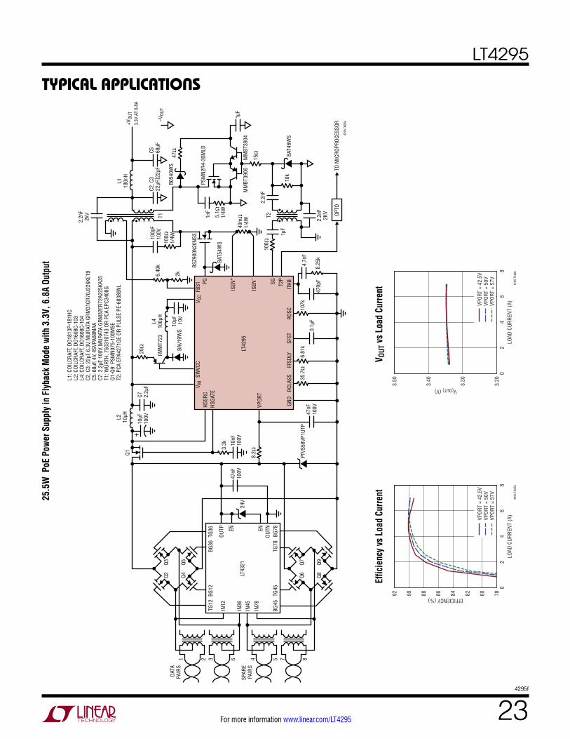
Typical applicaTions13W PoE Power Supply in Flyback Mode with 5V, 2.3A Output
Efficiency vs Load Current VOUT vs Load Current
++VOUT5V AT 2.3A
–VOUT
Q1
L1: COILCRAFT, DO1813P-181HCL2: COILCRAFT, DO1608C-103L4: COILCRAFT, DO1608C-104C2: 22µF, 6.3V, MURATA GRM31CR70J226KE19C5: 47µF, 6.3V, PANASONIC 6SVP47MC7: 2.2µF, 100V, MURATA GRM32ER72A225KA35T1: WÜRTH, 750313109Q1: PSMN075-100MSET2: PCA EPA4271GE OR PULSE PE-68386NL
VPORT
GND
L210µH
L1180nH
L4100µH
10µF100V
10nF100V
3.3k
10µF10V
HSSRC SWVCC FB31PG
SGITHBROSCSFSTFFSDLYRCLASSGND
VPORT
LT4295
HSGATE
ISEN+
ISEN–
VIN VCC
C72.2µF
FDN86246
BAT54WS
BAT46WS
T2
4295 TA02a
PSMN4R2-30MLD
MMBT3906 MMBT3904
T1
1nF
1µF
6.04k
20Ω
2k
270Ω1/4W
11Ω1/4W
60mΩ1/4W
15Ω
100Ω
1µF
330pF0.1µF
107k5.23k52.3Ω
8.2Ω
PTVS58VP1UTP
4.7nF
2.2nF2KV
20k
10k
2.2nF
C222µF
C547µF6.3V
47pF630V
0.1µF100V
2.2nF2kV
BAV19WS
••
•
•
•
FMMT723
LOAD CURRENT (A)
76
EFFI
CIEN
CY (%
)
90
88
86
84
82
80
78
92
0.5 2.51 1.5 20
4295 TA02b
VPORT = 37VVPORT = 48VVPORT = 57V
LOAD CURRENT (A)
4.80
V OUT
(V)
5.15
5.10
5.05
5.00
4.95
4.90
4.85
5.20
0.5 2.51 1.5 20
4295 TA02c
VPORT = 37VVPORT = 48VVPORT = 57V

LT4295
184295f
For more information www.linear.com/LT4295
Typical applicaTions
40W
PoE
Pow
er S
uppl
y in
Fly
back
Mod
e w
ith 1
2V, 3
A Ou
tput
Effic
ienc
y vs
Loa
d Cu
rren
tV O
UT v
s Lo
ad C
urre
nt
++V
OUT
12V
AT 3
A
–VOU
T
Q1
L2 10µH
L118
0nH
L410
0µH
10µF
100V
10nF
100V
3.3k
24V
8.2Ω
10µF 10V
HSSR
CSW
VCC
FB31 PG SG T2
PIT
HBRO
SCSF
STFF
SDLY
RCLA
SSRC
LASS
++GN
D
VPOR
T
LT42
95
HSGA
TE
ISEN
+
ISEN
–
V IN
V CC
C7 2.2µ
F
BSZ9
0020
NS3
BAT5
4WS
BAT4
6WS
MOC
207M
V OUT
TO M
ICRO
PROC
ESSO
R
4295
TA0
3a
TPN1
600A
NH
MM
BT39
06M
MBT
3904
T1
470p
F
1µF
6.65
k
2.00
kΩ
100Ω
1/2W
11Ω
1/2W
25m
Ω1/
4W
15Ω
100Ω
1µF
220p
F
0.1µ
F10
7k
7.5k
37.4
Ω
1.00
kΩPT
VS58
VP1U
TP3.
3nF
2.2n
F2K
V26
.1k
10k
2.2n
FC2, C
310
µFC5 33
µF10
0pF
630V
47nF
100V
2.2n
F2k
V
BG36
LT43
21
BG12
TG12
TG36
TG78
TG45
BG45
BG78
OUTP
OUTNEN EN
IN12
T2
Q2Q3
Q4Q5
Q6Q7
Q8Q9
1
DATA
PAIR
S
SPAR
EPA
IRS
2 3 6 4 5 7 8
IN36
IN45
IN78
47nF
100V
L1: C
OILC
RAFT
, DO1
813P
-181
HCL2
: COI
LCRA
FT, D
O160
8C-1
03L4
: COI
LCRA
FT, D
O160
8C-1
04C2
, C3:
10µ
F, 16
V, M
URAT
A GR
M31
CR61
C106
KA88
C5: 3
3µF,
25V,
PAN
ASON
IC E
EHZA
1E33
0RC7
: 2.2
µF, 1
00V,
MUR
ATA
GRM
32ER
72A2
25KA
35T1
: WÜR
TH, 7
5031
6115
OR
PCA
EPC3
634G
Q1-Q
9: P
SMN0
75-1
00M
SET2
: PCA
EPA
4271
GE O
R PU
LSE
PE-6
8386
NL
BAV1
9WS
5.1k
Ω10
k
20Ω
••
•
••
FMM
T723
VPOR
T =
44V
VPOR
T =
50V
VPOR
T =
57V
LOAD
CUR
RENT
(A)
00.
51
1.5
22.
53
8082848688909294 EFFICIENCY (%)
4295
TA0
3b
VPOR
T =
44V
VPOR
T =
50V
VPOR
T =
57V
LOAD
CUR
RENT
(A)
00.
51
1.5
22.
53
11.9
8
12.0
0
12.0
2
12.0
4
12.0
6
12.0
8
12.1
0
12.1
2
12.1
4
V(OUT) (V)
4295
TA0
3c

LT4295
194295f
For more information www.linear.com/LT4295
Typical applicaTions
Effic
ienc
y vs
Loa
d Cu
rren
tV O
UT v
s Lo
ad C
urre
nt
71W
PoE
Pow
er S
uppl
y in
For
war
d M
ode
with
5V,
13A
Out
put C S
FST (
µF)
t SFS
T (m
s)
0.10
1.2
0.33
3.8
1.0
12
3.3
38
Q1
10nF
100V
3.3k
L410
0µH
10µF 10V
BAV1
9WS
FMM
T723
8.2Ω
PTVS
58VP
1UTP
0.1µ
F10
0V
L12.
2µH
C5 100µ
F(×
2)
C8 100µ
F6H
VA10
0M
++
L24.
9µH
22µF
100V HS
SRC
SWVC
CFF
SDLY PG SG
ITHB
ROSC
SFST
RCLA
SS++
RCLA
SSGN
DFB
31
T2P
VPOR
T
LT42
95
HSGA
TE
ISEN
+
ISEN
–
V IN
V CC
V CC
+VOU
T
+VOU
T+5
V AT
13A
–VOU
TV C
C
C7 2.2µ
F(×
2)
BAT5
4WS
BSC1
90N1
2NS3
4295
TA0
4a
20m
1/2W
100Ω
1206
10nF
250V
5Ω
100n
F25
0V
750Ω
330Ω
240Ω
4.7n
ZR43
110
k10
.0k
10.0
k
1k
10Ω
10Ω
CMM
SH1-
40L
BSC0
54N0
4NS
BSC0
54N0
4NS
CMM
SH1-
40L
T1
CMM
SH1-
40L
8.2V
CMHZ
4694
18V
CMHZ
5248
B18
VCM
HZ52
48B
2.2n
F2k
V
33nF
0.1µ
F
0.1µ
F
10k
0.1µ
FFD
MC2
523P
CMM
SH1-
40L
M0C
207M
MM
BT39
04
VPOR
T
GND
13k
20Ω
80.6
Ω64
.9Ω
0.47
µF10
0pF
100k
107k
••
L1: C
OILC
RAFT
, XAL
-101
0-22
2ME
L2: W
ÜRTH
, 744
3144
90L4
: COI
LCRA
FT, D
O160
8C-1
04C5
, 100
µF, 6
.3V,
SUN
CON
6HVA
100M
C7: 2
.2µF
, 100
V, M
URAT
A GR
M32
ER72
A225
KA35
LC8
: 100
µF, 6
.3V,
SUN
CON
6HVA
100M
T1: W
ÜRTH
, 750
3130
95Q1
: PSM
N040
-100
MSE
TO M
ICRO
PROC
ESSO
ROP
TO
10nF
VPOR
T =
41V
VPOR
T =
50V
VPOR
T =
57V
LOAD
CUR
RENT
(A)
02
46
810
1214
76788082848688909294 EFFICIENCY (%)
4295
TA0
4b
VPOR
T =
41V
VPOR
T =
50V
VPOR
T =
57V
LOAD
CUR
RENT
(A)
02
46
810
1214
4.80
4.85
4.90
4.95
5.00
5.05
5.10
5.15
5.20
V(OUT) (V)
4295
TA0
4c

LT4295
204295f
For more information www.linear.com/LT4295
Effic
ienc
y vs
Loa
d Cu
rren
tV O
UT v
s Lo
ad C
urre
nt
Typical applicaTions
71W
PoE
Pow
er S
uppl
y in
For
war
d M
ode
with
12V
, 5.5
A Ou
tput
C SFS
T (µF
)t S
FST
(ms)
0.10
1.5
0.33
4.9
1.0
15
3.3
48
+
L26.
5µH
22µF
100V
HSSR
C
SWVC
CFF
SDLY PG SG
ITHB
ROSC
SFST
RCLA
SS++
RCLA
SSGN
DFB
31
T2P
VPOR
T
LT42
95
HSGA
TE
ISEN
+
ISEN
–
V IN
V CC
V CC
+VOU
T
+VOU
T+1
2V A
T5.
5A
–VOU
T
V CC
C7 2.2µ
F(×
2)
BAT5
4WS
BSC1
90N1
2NS3
4295
TA0
5a
15m
Ω1/
2W
100Ω
1206
33nF
250V
0.22
µF25
0V
750Ω
820Ω
20k
ZR43
1
10k
10.0
k
100p
F
38.3
k
13k
10Ω
CMM
SH1-
60
BSC1
23N0
8S3
BSC1
23N0
8S3
T1
CMM
SH1-
100
CMM
SH1-
100
13V
CMHZ
4700
7.5V
CMHZ
5236
B
2.2n
F2k
V
6.8n
F
0.1µ
F
0.1µ
F
10k
0.1µ
FFD
MC2
523P
CMM
SH1-
40L
M0C
207M
MM
BT39
04
29.4
k
V CC
BG36
LT43
21
BG12
TG12
TG36
TG78
TG45
BG45
BG78
OUTP
OUTNEN EN
IN12
T2
Q2Q3
Q4Q5
Q6Q7
Q8Q9
1
DATA
PAIR
S
SPAR
EPA
IRS
2 3 6 4 5 7 8
IN36
IN45
IN78
52.3
Ω
118Ω
1µF
100p
F
100p
F
100k
107k
330p
F
20Ω
••
7.5Ω
Q1
10nF
100V
47nF
100V
3.3k
L410
0µH
10µF 10V
8.2Ω
PTVS
58VP
1UTP
47nF
100V
L18.
2µH
22µF 16V
(×2)
C8 100µ
F
L1: C
OILC
RAFT
, XAL
-101
0-82
2ME
L2: W
ÜRTH
, 744
3146
50L4
: COI
LCRA
FT, D
O160
8C-1
04C7
: 2.2
µF, 1
00V,
MUR
ATA
GRM
32ER
72A2
25KA
35L
C8: 1
00µF
, 16V
, SUN
CON
16HV
A100
MT1
: PCA
EPC
3577
G-LF
T2: W
ÜRTH
, 749
0220
16Q1
: PSM
N040
-100
MSE
Q2-Q
9: P
SMN0
75-1
00M
SE
TO M
ICRO
PROC
ESSO
ROP
TO
FMM
T723
820p
F
100p
F
+VOU
T
+VOU
T
7.5V
CMHZ
5236
B
5.1k
FMM
T624
FMM
T624
5.1k
100p
F
BAV1
9WS
VPOR
T =
41V
VPOR
T =
50V
VPOR
T =
57V
LOAD
CUR
RENT
(A)
01
23
45
6788082848688909294 EFFICIENCY (%)
4295
TA0
5b
VPOR
T =
41V
VPOR
T =
50V
VPOR
T =
57V
LOAD
CUR
RENT
(A)
01
23
45
611
.60
11.7
0
11.8
0
11.9
0
12.0
0
12.1
0
12.2
0
12.3
0
12.4
0
V(OUT) (V)
4295
TA0
5c

LT4295
214295f
For more information www.linear.com/LT4295
Typical applicaTions
40W
PoE
Pow
er S
uppl
y in
Fly
back
Mod
e w
ith 5
V, 7
A Ou
tput
Effic
ienc
y vs
Loa
d Cu
rren
tV O
UT v
s Lo
ad C
urre
nt
+
+VOU
T5V
AT
7A
–VOU
T
Q1
L1: C
OILC
RAFT
, DO1
813P
-181
HCL2
: COI
LCRA
FT, D
O160
8C-1
03L4
: COI
LCRA
FT, D
O160
8C-1
04C2
, C3:
47µ
F, 6.
3V, G
RM31
CR60
J476
ME1
9LC5
: 47µ
F, 6.
3V, P
ANAS
ONIC
6SV
P47M
C7: 2
.2µF
, 100
V, M
URAT
A GR
M32
ER72
A225
KA35
LT1
: WÜR
TH, 7
5031
4783
OR
PCA
EPC3
586G
Q1-Q
9: P
SMN0
75-1
00M
SET2
: PCA
EPA
4271
GE O
R PU
LSE
PE-6
8386
NLL2 10µH
L118
0nH
L410
0µH
10µF
100V
10nF
100V
47nF
100V
3.3k
24V
8.2Ω
10µF 10V
HSSR
CSW
VCC
FB31 PG SG T2
PIT
HBRO
SCSF
STFF
SDLY
RCLA
SS++
RCLA
SS
GND
VPOR
T
LT42
95
HSGA
TE
ISEN
+
ISEN
–
V IN
V CC
C7 2.2µ
F
BSZ9
00N2
0NS
3G
BAT5
4WS
BAT4
6WS
TO M
ICRO
PROC
ESSO
R42
95 T
A06a
PSM
N2R4
-30M
LD
MM
BT39
06M
MBT
3904
T1 1nF
1µF
5.90
k
2.00
kΩ
80Ω
1/4W
5.1Ω
1/4W
40m
Ω1/
4W
15Ω
100Ω
20Ω
1µF
220p
F0.
1µF
107k
7.50
k
RLDC
MP
51k
37.4
Ω
1.00
kΩPT
VS58
VP1U
TP3.
3nF
2.2n
F2K
V20
k
10k
2.2n
FC2, C
347
µF|| 4
7µF
C5 47µF
100p
F10
0V
47nF
100V
2.2n
F2k
V OPTO
BG36
LT43
21
BG12
TG12
TG36
TG78
TG45
BG45
BG78
OUTP
OUTNEN EN
IN12
T2
Q2Q3
Q4Q5
Q6Q7
Q8Q9
1
DATA
PAIR
S
SPAR
EPA
IRS
2 3 6 4 5 7 8
IN36
IN45
IN78
BAV1
9WS
••
•
••
FMM
T723
VPOR
T =
50V
VPOR
T =
57V
LOAD
CUR
RENT
(A)
01
23
45
67
788082848688909294 EFFICIENCY (%)
4295
TA0
6b
VPOR
T =
50V
VPOR
T =
57V
LOAD
CUR
RENT
(A)
01
23
45
67
4.80
4.85
4.90
4.95
5.00
5.05
5.10
5.15
5.20
V(OUT) (V)
4295
TA0
6c

LT4295
224295f
For more information www.linear.com/LT4295
Typical applicaTions
25.5
W P
oE a
nd 9
V to
57V
Aux
iliar
y In
put P
ower
Sup
ply
in F
lyba
ck M
ode
with
12V
, 1.9
A Ou
tput
Effic
ienc
y vs
Loa
d Cu
rren
tV O
UT v
s Lo
ad C
urre
nt
++V
OUT
12V
AT 1
.9A
–VOU
T
Q1
L1: C
OILC
RAFT
, DO1
813P
-561
ML
L2: W
ÜRTH
, 744
3330
820
L3: M
URAT
A, L
QM21
PN2R
2NGC
D L4
: COI
LCRA
FT, D
O181
3H-2
23C2
, C3:
10µ
F, 16
V, M
URAT
A GR
M31
CR61
C106
KA88
C5: 3
3µF,
20V,
KEM
ET, T
494V
336M
020A
SC7
, C8:
3.3
µF, 1
00V,
TDK
C32
25X7
S2A3
35M
T1: P
CA E
PC36
01G
OR W
ÜRTH
750
3154
22Q1
-Q9:
PSM
N075
-100
MSE
T2: P
CA E
PA42
71GE
OR
PULS
E PE
-683
86NL
L28.
2µH
L32.
2µH
1µF
680µ
F63
V
L156
0nH
L4 22µH
10µF
100V
68nF
100V
0.1µ
F3.
3k15
8k
931k
24V
47nF
100V
8.2Ω
22µF 10V
PMEG
1001
0ELR
HSSR
CSW
VCC
FB31 PG SG T2P
ITHB
ROSC
SFST
FFSD
LYRC
LASS
GND
VPOR
T
AUX
LT42
95
HSGA
TE
ISEN
+
ISEN
–
V IN
V CC
C7, C
83.
3µF
FDM
C861
60
BAT5
4WS
BAT4
6WS
TO M
ICRO
PROC
ESSO
R42
95 T
A07a
BSZ9
00NF
20NS
3
CMLT
7820
GCM
LT38
20G
T1
220p
F
1µF
4.75
k
2.00
k
62Ω
1/4W
82Ω
||82Ω
1/4W
15m
Ω1/
2W
15Ω
100Ω
1µF
220p
F0.
1µF
107k
9.31
k
RLDC
MP
51k
35.7
Ω
PTVS
58VP
1UTP
4.7n
F
2.2n
F2K
V43
k
10k
2.2n
FC2, C
310
µF|| 1
0µF
C5 33µF
100p
F10
0V
47nF
100V
2.2n
F2k
V OPTO
BG36
LT43
21
BG12
TG12
TG36
TG78
TG45
BG45
BG78
OUTP
OUTNEN EN
IN12
TG2
TG1
OUTP
OUTN
IN1
IN2
BG2
BG1
T2
Q2Q3
Q4Q5
Q6Q7
Q8Q9
1
DATA
PAIR
S
SPAR
EPA
IRS
2 3 6 4 5 7 8
IN36
IN45
IN78
LT43
20
BSZ1
10N0
6NS3
x4
MM
SD41
48 x
3
V AUX
9V T
O 57
VDC
OR 2
4VAC
1Ω
••
•
••
+
FMM
T723
V AUX
= 9V
V AUX
= 24
VV A
UX=
42.5
VV A
UX=
57V
LOAD
CUR
RENT
(A)
00.
51
1.5
2727680848892 EFFICIENCY (%)
4295
TA0
7b
V AUX
= 9V
V AUX
= 24
VV A
UX=
42.5
VV A
UX=
57V
LOAD
CUR
RENT
(A)
00.
51
1.5
211
.50
11.7
5
12.0
0
12.2
5
12.5
0
V(OUT) (V)
4295
TA0
7c
LT4295
234295f
For more information www.linear.com/LT4295
Typical applicaTions
25.5
W P
oE P
ower
Sup
ply
in F
lyba
ck M
ode
with
3.3
V, 6
.8A
Outp
ut
Effic
ienc
y vs
Loa
d Cu
rren
tV O
UT v
s Lo
ad C
urre
nt
++V
OUT
3.3V
AT
6.8A
–VOU
T
Q1
L1: C
OILC
RAFT
, DO1
813P
-181
HCL2
: COI
LCRA
FT, D
O160
8C-1
03L4
: COI
LCRA
FT, D
O160
8C-1
04C2
, C3:
22µ
F, 6.
3V, M
URAT
A GR
M31
CR70
J226
KE19
C5: 6
8µF,
4V, 4
SVPA
68M
AAC7
: 2.2
µF, 1
00V,
MUR
ATA
GRM
32ER
72A2
25KA
35T1
: WÜR
TH, 7
5031
0743
OR
PCA
EPC3
408G
Q1-Q
9: P
SMN0
75-1
00M
SET2
: PCA
EPA
4271
GE O
R PU
LSE
PE-6
8386
NLL2 10µH
L118
0nH
L410
0µH
10µF
100V
10nF
100V
47nF
100V
3.3k
24V
8.2Ω
10µF 10V
HSSR
CSW
VCC
FB31 PG SG T2
PIT
HBRO
SCSF
STFF
SDLY
RCLA
SSGN
D
VPOR
T
LT42
95
HSGA
TE
ISEN
+
ISEN
–
V IN
V CC
C7 2.2µ
F
BSZ9
00N2
0NS3
BAT5
4WS
BAT4
6WS
TO M
ICRO
PROC
ESSO
R42
95 T
A08a
PSM
N2R4
-30M
LD
MM
BT39
06M
MBT
3904
T1 1nF
47Ω
1µF
6.49
k
2k
100Ω
1/4W
5.1Ω
1/4W
40m
Ω1/
4W
15Ω
100Ω
1µF
470p
F0.
1µF
107k
6.81
k35
.7Ω
PTVS
58VP
1UTP
4.7n
F
2.2n
F2K
V8.
25k
10k
2.2n
FC2, C
322
µF|| 2
2µF
C5 68µF
100p
F10
0V
47nF
100V
2.2n
F2k
V OPTO
BG36
LT43
21
BG12
TG12
TG36
TG78
TG45
BG45
BG78
OUTP
OUTNEN EN
IN12
T2
Q2Q3
Q4Q5
Q6Q7
Q8Q9
1
DATA
PAIR
S
SPAR
EPA
IRS
2 3 6 4 5 7 8
IN36
IN45
IN78
B054
0WS
BAV1
9WS
20Ω
••
•
••
FMM
T723
VPOR
T =
42.5
VVP
ORT
= 50
VVP
ORT
= 57
V
LOAD
CUR
RENT
(A)
02
46
87880828486889092 EFFICIENCY (%)
4295
TA0
8b
VPOR
T =
42.5
VVP
ORT
= 50
VVP
ORT
= 57
V
LOAD
CUR
RENT
(A)
02
46
83.
20
3.30
3.40
3.50
V(OUT) (V)
4295
TA0
8c

LT4295
244295f
For more information www.linear.com/LT4295
Typical applicaTions
25.5
W P
oE P
ower
Sup
ply
in F
lyba
ck M
ode
with
24V
, 1A
Outp
ut
Effic
ienc
y vs
Loa
d Cu
rren
tV O
UT v
s Lo
ad C
urre
nt
++V
OUT
24V
AT 1
A
–VOU
T
Q1
L2: C
OILC
RAFT
, DO1
608C
-103
L4: C
OILC
RAFT
, DO1
608C
-104
C2: 4
.7µF
, 50V
, MUR
ATA
GRM
31CR
71H4
75KA
12C5
: 22µ
F, 35
V, P
ANAS
ONIC
EEH
-ZA1
V220
RC7
: 2.2
µF, 1
00V,
MUR
ATA
GRM
32ER
72A2
25KA
35T1
: WÜR
TH, 7
5031
4782
OR
PCA
EPC3
603G
Q1-Q
9: P
SMN0
75-1
00M
SET2
: PCA
EPA
4271
GE O
R PU
LSE
PE-6
8386
NLL2 10µH
L410
0µH
10µF
100V
10nF
100V
3.3k
24V
8.2Ω
10µF 10V
HSSR
CSW
VCC
FB31 PG SG T2
PIT
HBRO
SCSF
STFF
SDLY
RCLA
SSGN
D
VPOR
T
LT42
95
HSGA
TE
ISEN
+
ISEN
–
V IN
V CC
C7 2.2µ
F
BSZ5
20N1
5NS3
G
BAT5
4WS
BAT4
6WS
TO M
ICRO
PROC
ESSO
R42
95 T
A09a
BSZ1
2DN2
0NS3
MM
BT39
06M
MBT
3904
T1 150p
F
0.1µ
F
6.49
k
2.00
kΩ
20Ω
100Ω
1/4W
120Ω
||120
Ω1/
4W
40m
Ω1/
4W
15Ω
100Ω
1µF
10pF
0.47
µF
107k
5.23
k
RLDC
MP
24k
35.7
ΩPT
VS58
VP1U
TP3.
3nF
2.2n
F2K
V16
0k
10k
2.2n
FC2, C
34.
7µF
50V
C5 22µF
47pF
100V
47nF
100V
2.2n
F2k
V OPTO
BG36
LT43
21
BG12
TG12
TG36
TG78
TG45
BG45
BG78
OUTP
OUTNEN EN
IN12
T2
Q2Q3
Q4Q5
Q6Q7
Q8Q9
1
DATA
PAIR
S
SPAR
EPA
IRS
2 3 6 4 5 7 8
IN36
IN45
IN78
47nF
100V
BAV1
9WS
••
•
••
FMM
T723
VPOR
T =
42.5
VVP
ORT
= 50
VVP
ORT
= 57
V
LOAD
CUR
RENT
(A)
00.
20.
40.
60.
81
80828486889092 EFFICIENCY (%)
4295
TA0
9b
VPOR
T =
42.5
VVP
ORT
= 50
VVP
ORT
= 57
V
LOAD
CUR
RENT
(A)
00.
20.
40.
60.
81
23.4
23.6
23.8
24.0
24.2
24.4
24.6
V(OUT) (V)
4295
TA0
9c

LT4295
254295f
For more information www.linear.com/LT4295
Typical applicaTions
62W
PoE
Pow
er S
uppl
y in
Fly
back
Mod
e w
ith 2
4V, 2
.4A
Outp
ut
Effic
ienc
y vs
Loa
d Cu
rren
tV O
UT v
s Lo
ad C
urre
nt
++V
OUT
24V
AT 2
.4A
–VOU
T
Q1
L1: C
OILC
RAFT
, DO1
813H
-122
ML
L2: W
URTH
, 744
3144
90L4
: COI
LCRA
FT, D
O160
8C-1
04C2
: MUR
ATA
GRM
32ER
61H1
06K
C5: 4
7µF,
35V,
EEE
-FT1
V470
ARC7
, C8:
2.2
µF, 1
00V,
MUR
ATA
GRM
32ER
72A2
25KA
35Q1
: NXP
PSM
N040
-100
MSE
Q2-Q
9: P
SMN0
75-1
00M
SET1
: PCA
EPC
3630
G OR
WUR
TH 7
5031
6231
T2: P
CA E
PA42
71GE
OR
PULS
E PE
-683
86NL
L24.
9µH
L410
0µH
L11.
2µH
22µF
100V
10nF
100V
3.3k
24V
8.2Ω
10µF 10V
HSSR
CSW
VCC
FB31 PG SG T2
PIT
HBRO
SCSF
STFF
SDLY
RCLA
SS++
RCLA
SSGN
D
VPOR
T
LT42
95
HSGA
TE
ISEN
+
ISEN
–
V IN
V CC
C7, C
82.
2µF
BSC1
90N1
5NS3
BAT5
4WS
BAT4
6WS
TO M
ICRO
PROC
ESSO
R42
95 T
A10a
BSC3
20N2
0NS3
PBSS
5140
TPB
SS41
40T
T1 330p
F
0.1µ
F
3.74
k
2.00
kΩ
20Ω
27Ω
1/2W
18Ω 1W
15m
Ω1/
2W
15Ω
100Ω
1µF
330p
F0.
47µF
107k
5.23
k
RLDC
MP
36k
80.6
Ω
64.9
ΩPT
VS58
VP1U
TP10
nF
2.2n
F2K
V22
k
10k
2.2n
FC2 10µF
50V
C5 47µF
220p
F10
0V
47nF
100V
4.7n
F2k
V OPTO
BG36
LT43
21
BG12
TG12
TG36
TG78
TG45
BG45
BG78
OUTP
OUTNEN EN
IN12
T2
Q2Q3
Q4Q5
Q6Q7
Q8Q9
1
DATA
PAIR
S
SPAR
EPA
IRS
2 3 6 4 5 7 8
IN36
IN45
IN78
47nF
100V
BAV1
9WS
••
•
••
FMM
T723
VPOR
T =
41V
VPOR
T =
50V
VPOR
T =
57V
LOAD
CUR
RENT
(A)
00.
51
1.5
22.
53
8082848688909294 EFFICIENCY (%)
4295
TA1
0b
VPOR
T =
41V
VPOR
T =
50V
VPOR
T =
57V
LOAD
CUR
RENT
(A)
00.
51
1.5
22.
53
24.0
24.1
24.2
24.3
24.4
24.5
V(OUT) (V)
4295
TA1
0c

LT4295
264295f
For more information www.linear.com/LT4295
Typical applicaTions
71W
PoE
Pow
er S
uppl
y in
For
war
d M
ode
with
24V
, 2.8
A Ou
tput
+
L26.
5µH
22µF
100V
HSSR
C
SWVC
CFF
SDLY PG SG
ITHB
ROSC
SFST
RCLA
SS++
RCLA
SSGN
DFB
31
T2P
VPOR
T
LT42
95
HSGA
TE
ISEN
+
ISEN
–
V IN
V CC
V CC
+VOU
T
+VOU
T
+VOU
T24
V AT
2.8A
–VOU
T
V CC
C7 2.2µ
F(×
2)
BAT5
4WS
BSC1
90N1
2NS3
4295
TA1
1a
15m
Ω1/
2W
82Ω
1206
10nF
250V
47nF
250V
750Ω
820Ω
1.2k
ZR43
1
10k
10.0
k
1nF
86.6
k
10k
TPH5
900C
NH
TPH5
900C
NH
T1
SMD1
200P
L-TP
SMD1
200P
L-TP
13V
CMHZ
4700
7.5V
CMHZ
5236
B
2.2n
F2k
V
6.8n
F
0.1µ
F
10k
0.1µ
FFD
MC2
523P
CMM
SH1-
40L
M0C
207M
MM
BT39
04
33k
V CC
BG36
LT43
21
BG12
TG12
TG36
TG78
TG45
BG45
BG78
OUTP
OUTNEN EN
IN12
T2
Q2Q3
Q4Q5
Q6Q7
Q8Q9
1
DATA
PAIR
S
SPAR
EPA
IRS
2 3 6 4 5 7 8
IN36
IN45
IN78
80.6
Ω
118Ω
1µF
100p
F
100k
107k
3.3n
F
20Ω
••
47Ω
Q1
10nF
100V
47nF
100V
3.3k
L410
0µH
10µF 10V
8.2Ω
PTVS
58VP
1UTP
47nF
100V
L1 22µH C2
10µF 35V
C1 47µF
35V
L1: P
ULSE
PA2
050.
223
L2: W
ÜRTH
, 744
3146
50L4
: COI
LCRA
FT, D
O160
8C-1
04C1
: PAN
ASON
IC E
EHZA
1V47
0PC2
: MUR
ATA
GRM
32ER
6YA1
06KA
12C7
: 2.2
µF, 1
00V,
MUR
ATA
GRM
32ER
72A2
25KA
35L
Q1: P
SMN0
40-1
00M
SEQ2
-Q9:
PSM
N075
-100
MSE
T1: P
CA E
PC36
36G
T2: W
ÜRTH
, 749
0220
16
TO M
ICRO
PROC
ESSO
ROP
TO
FMM
T723
220p
F
47pF
+VOU
T
+VOU
T
7.5V
CMHZ
5236
B
13k
FMM
T624
FMM
T624
13k
47pF
BAV1
9WS
C SFS
T (µF
)t S
FST
(ms)
0.10
1.4
0.22
2.4
0.47
4.4
1.0
15
3.3
46
V OUT
vs
Load
Cur
rent
Effic
ienc
y vs
Loa
d Cu
rren
t
VPOR
T =
41V
VPOR
T =
50V
VPOR
T =
57V
LOAD
CUR
RENT
(A)
00.
51
1.5
22.
53
8082848688909294 EFFICIENCY (%)
4295
TA1
1b
VPOR
T =
41V
VPOR
T =
50V
VPOR
T =
57V
LOAD
CUR
RENT
(A)
00.
51
1.5
22.
53
23.0
23.4
23.8
24.2
24.6
25.0
V(OUT) (V)
4295
TA1
1c

LT4295
274295f
For more information www.linear.com/LT4295
Information furnished by Linear Technology Corporation is believed to be accurate and reliable. However, no responsibility is assumed for its use. Linear Technology Corporation makes no representa-tion that the interconnection of its circuits as described herein will not infringe on existing patent rights.
package DescripTionPlease refer to http://www.linear.com/product/LT4295#packaging for the most recent package drawings.
4.00 ±0.10(2 SIDES)
2.50 REF
5.00 ±0.10(2 SIDES)
NOTE:1. DRAWING PROPOSED TO BE MADE A JEDEC PACKAGE OUTLINE MO-220 VARIATION (WXXX-X).2. DRAWING NOT TO SCALE3. ALL DIMENSIONS ARE IN MILLIMETERS4. DIMENSIONS OF EXPOSED PAD ON BOTTOM OF PACKAGE DO NOT INCLUDE MOLD FLASH. MOLD FLASH, IF PRESENT, SHALL NOT EXCEED 0.15mm ON ANY SIDE5. EXPOSED PAD SHALL BE SOLDER PLATED6. SHADED AREA IS ONLY A REFERENCE FOR PIN 1 LOCATION ON THE TOP AND BOTTOM OF PACKAGE
PIN 1TOP MARK(NOTE 6)
0.40 ±0.10
27 28
1
2
BOTTOM VIEW—EXPOSED PAD
3.50 REF
0.75 ±0.05 R = 0.115TYP
R = 0.05TYP
PIN 1 NOTCHR = 0.20 OR 0.35× 45° CHAMFER
0.25 ±0.05
0.50 BSC
0.200 REF
0.00 – 0.05
(UFD28) QFN 0506 REV B
RECOMMENDED SOLDER PAD PITCH AND DIMENSIONSAPPLY SOLDER MASK TO AREAS THAT ARE NOT SOLDERED
0.70 ±0.05
0.25 ±0.050.50 BSC
2.50 REF
3.50 REF4.10 ±0.055.50 ±0.05
2.65 ±0.05
3.10 ±0.054.50 ±0.05
PACKAGE OUTLINE
2.65 ±0.10
3.65 ±0.10
3.65 ±0.05
UFD Package28-Lead Plastic QFN (4mm × 5mm)
(Reference LTC DWG # 05-08-1712 Rev B)

LT4295
284295f
For more information www.linear.com/LT4295 LINEAR TECHNOLOGY CORPORATION 2016
LT 0816 • PRINTED IN USALinear Technology Corporation1630 McCarthy Blvd., Milpitas, CA 95035-7417(408) 432-1900 ● FAX: (408) 434-0507 ● www.linear.com/LT4295
relaTeD parTs
Typical applicaTion
PART NUMBER DESCRIPTION COMMENTSLTC4267/LTC4267-1/LTC4267-3
IEEE 802.3af PD Interface with Integrated Switching Regulator
Internal 100V, 400mA Switch, Programmable Class, 200/300kHz Constant Frequency PWM
LTC4269-1 IEEE 802.3af PD Interface with Integrated Flyback Switching Regulator
2-Event Classification, Programmable Class, Synchronous No-Opto Flyback Controller, 50kHz to 250kHz, Aux Support
LTC4269-2 IEEE 802.3af PD Interface with Integrated Forward Switching Regulator
2-Event Classification, Programmable Class, Synchronous Forward Controller, 100kHz to 500kHz, Aux Support
LT4275A/B/C LTPoE++/PoE+/PoE PD Controller External Switch, LTPoE++ SupportLT4276A/B/C LTPoE++/PoE+/PoE PD with Forward/
Flyback Switching Regulator ControllerExternal Switch, LTPoE++ Support, User-Configurable Class, Forward or No-Opto Flyback Operation, Frequency, PG/SG Delays, Soft-Start, and Aux Support as Low as 9V, Incl Housekeeping Buck, Slope Compensation
LTC4278 IEEE 802.3af PD Interface with Integrated Flyback Switching Regulator
2-Event Classification, Programmable Class, Synchronous No-Opto Flyback Controller, 50kHz to 250kHz, 12V Aux Support
LTC4290/LTC4271 8-Port PoE/PoE+/LTPoE++ PSE Controller Transformer Isolation, Supports IEEE 802.3af, IEEE 802.3at and LTPoE++ PDsLT4320/LT4320-1 Ideal Diode Bridge Controller 9V-72V, DC to 600Hz Input. Controls 4-NMOSFETs, Voltage Rectification without Diode DropsLT4321 PoE Ideal Diode Bridge Controller Controls 8-NMOSFETs for IEEE-required PD Voltage Rectification without Diode Drops
51W PoE Power Supply in Flyback Mode with 12V, 4A Output
Efficiency vs Load Current VOUT vs Load Current
+VOUT12V AT 4A
–VOUT
Q1
C5: 47µF, 35V, PANASONIC EEHZA1V470PC7, C8: 2.2µF, 100V, MURATA GRM32ER72A225KA35T1: WÜRTH, 750316116 OR PCA EPC3633GT2: PCA EPA4271GE OR PULSE PE-68386NLQ1: PSMN040-100MSEQ2-Q9: PSMN075-100MSE
L1
L4100µH
10nF100V
3.3k
24V
8.2Ω
10µF10V
HSSRCSWVCC FB31
PG
SGT2P
ITHBROSCSFSTFFSDLYRCLASSRCLASS++GND
VPORT
LT4295
HSGATE
ISEN+
ISEN–
VIN VCCTPH1500CNH
BAT54WS
BAT46WS
MOC207M
VOUT
TO MICROPROCESSOR
4295 TA12a
TPH1500CNH
PBSS514OT PBSS414OT
T1
330pF
1µF
5.62k
2.00kΩ
36Ω1/2W
20Ω1/2W
20mΩ1/2W
15Ω
100Ω
1µF
330pF0.1µF
107k5.23k47.5Ω
150Ω
PTVS58VP1UTP 3.3nF
2.2nF2KV
30k
10k
2.2nF
C2, C310µF
C547µF
220pF630V
47nF100V
2.2nF2kV
BG36
LT4321
BG12TG12 TG36
TG78TG45BG45 BG78
OUTP
OUTN
EN
EN
IN12
T2
Q2 Q3
Q4 Q5
Q6 Q7
Q8 Q9
1
DATAPAIRS
SPAREPAIRS
23
6
4
57
8
IN36IN45
IN78
47nF100V
L1: WURTH 744316022L2: WURTH 744316470L4: COILCRAFT, DO1608C-104C2, C3: 10µF, 16V, MURATA GRM32DR61C106KA01
BAV19WS
5.1kΩ
10k
20Ω
••
•
•
•L2
4.7µH
+ 10µF100V
C7, C82.2µF
FMMT723
VPORT = 42.5VVPORT = 50VVPORT = 57V
LOAD CURRENT (A)0 1 2 3 4
11.94
11.95
11.96
11.97
11.98
11.99
12.00
12.01
12.02
V (OU
T) (V
)
4295 TA12c
VPORT = 42.5VVPORT = 50VVPORT = 57V
LOAD CURRENT (A)0 1 2 3 4
70
74
78
82
86
90
94
EFFI
CIEN
CY (%
)
4295 TA12b


![Catalogue FLYBACK Equivalent - [PDF Document] FLYBACK Equivalent FlyBack Equivalent flyback reemplazo conversor Flyback tv fly-back Flyback Tester Flyback Converter conversor Flyback](https://img.dokumen.tips/doc/110x75/5a832a447f8b9a9d308e9416/catalogue-flyback-equivalent-pdf-document-flyback-equivalent-flyback-equivalent.jpg)