Embed Size (px)
Citation preview

LPV802(Amplified
Band-pass Filter)
TLV3691(Window
Comparator)
Interrupt CC1310(ARM + Sub-1 GHz)
Coin Cell Battery
(CR2032)
PIR
Vbatt
Sen
sor_
out
Copyright © 2016, Texas Instruments Incorporated
1TIDUDA8–July 2017Submit Documentation Feedback
Copyright © 2017, Texas Instruments Incorporated
Low-Power Wireless PIR Motion Detector Reference Design EnablingSensor-to-Cloud Networks
TI Designs: TIDA-01476Low-Power Wireless PIR Motion Detector ReferenceDesign Enabling Sensor-to-Cloud Networks
DescriptionThe TIDA-01476 reference design demonstrates howto create an industrial sensor-to-cloud end nodecapable of connecting to an IoT network gateway andcloud data provider. This design uses TexasInstruments’ nano-power operational amplifiers,comparators, and the SimpleLink™ ultra-low-powerSub-1 GHz wireless microcontroller (MCU) platform todemonstrate an ultra-low-power sensor-to-cloudmotion detector, leading to extremely long battery lifeand no required wiring.
Resources
TIDA-01476 Design FolderLPV802 Product FolderTLV3691 Product FolderCC1310 Product Folder
ASK Our E2E Experts
Features• Large Network-to-Cloud Connectivity Enabling
Long Range, Up to 1 km (Line of Sight)• IEEE 802.15.4e/g Standards-Based Sub-1 GHz
Solution With TI 15.4-Stack• Use of Nano-Power Analog for Ultra-Low-Power
Design, Resulting in 10-Year Battery Life FromSingle CR2032 Coin Cell
• Low Standby Current of 1.65 μA (PIR SensorRemains Active in Standby)
• Interrupt Driven Sub-1 GHz WirelessCommunication of Motion for Increased PowerSavings
• Motion Sensitivity up to 30 ft
Applications• Motion Detection• Lighting Sensors• Wireless Controls• Building Automation
An IMPORTANT NOTICE at the end of this TI reference design addresses authorized use, intellectual property matters and otherimportant disclaimers and information.

System Description www.ti.com
2 TIDUDA8–July 2017Submit Documentation Feedback
Copyright © 2017, Texas Instruments Incorporated
Low-Power Wireless PIR Motion Detector Reference Design EnablingSensor-to-Cloud Networks
1 System DescriptionMany industrial and building automation systems use motion detectors to control different functions basedon human presence, such as lighting, for achieving higher efficiency of those functions by turning them offwhen not needed. Additionally, these systems require increasing numbers of wireless sensor nodes toreduce the installation costs and the make the systems more flexible for future expansion by eliminatingwiring. However, one of the major limitations for a large wireless network is power. Because thesesystems are battery powered, the maintenance cost associated with periodic battery replacement canbecome prohibitive. Depending on the power consumption and battery configuration, typical battery-powered PIR motion detectors can run anywhere from four to seven years before the batteries need to bereplaced.
Enabled by Texas Instruments' nano-power amplifiers, comparators, and the SimpleLink ultra-low-powerwireless MCU platform, the Low-Power Wireless PIR Motion Detector Reference Design demonstrates amotion detector circuit solution requiring no wiring while also fully maximizing the battery life.
At a high level, this TI Design consists of a CR2032 coin cell battery, two nano-power op amps, two nano-power comparators, an ultra-low-power wireless MCU, and a PIR sensor with analog signal output. Thetwo op amps form an amplified band-pass filter with a high-input impedance, which allows it to beconnected directly to the sensor without loading it. The two comparators form a window comparator, whichis used to compare the amplified sensor output to fixed reference thresholds so that motion can bedistinguished from noise. The two outputs of the window comparator then serve as interrupts to thewireless MCU. This way, the MCU can operate in its lowest power sleep mode during times where there isno motion being detected and only wakes up to send messages back to a remote host when motion hasbeen detected. Due to the nano-amp operation of the analog signal chain components, this TI Designachieves a 10-year battery life from a single CR2032 coin cell battery.
This design guide addresses component selection, design theory, software and the testing results of thisTI Design system. The scope of this design guide gives system designers a head-start in integrating TI’snano-power analog components, and the SimpleLink ultra-low-power wireless MCU platform along with astarting point for sensor-to-cloud software integration.
The following subsections describe the various blocks within the TI Design system and whatcharacteristics are most critical to best implement the corresponding function.

www.ti.com System Description
3TIDUDA8–July 2017Submit Documentation Feedback
Copyright © 2017, Texas Instruments Incorporated
Low-Power Wireless PIR Motion Detector Reference Design EnablingSensor-to-Cloud Networks
1.1 Key System Specifications
Table 1. Key System Specifications
PARAMETER SPECIFICATIONS DETAILSInput power source CR2032 Lithium-ion coin cell battery (3.0-V nominal voltage) Section 2.2.4Sensor type PIR (Pyroelectric or Passive InfraRed) Section 2.2.5Transmit-state current consumption 14 mA Section 3.2.2.1Transmit-state duration 23 ms Section 3.2.2.1Average standby-state currentconsumption 2.6 µA Section 3.2.2.1
Standby-state duration 1 minute of no motion detected Section 2.4.4Sleep-state current consumption 1.65 µA Section 3.2.2.1Movements per hour assumed for lifetimecalculation 6 per hour average over the battery lifetime Section 3.2.2.2
Estimated battery life 10 years Section 3.2.2.2Motion sensing range 30 feet nominal Section 3.2.2.3.1Radio transmission range > 200 meters Section 3.2.2.3.2Operating temperature –30°C to 60°C (limited by CR2032 coin cell operating range) Section 2.2.4Operating humidity 20 to 70% Section 3.2.1.2.1Vibration — Section 3.2.2.3.4RF immunity 30 V/m from 10 kHz to 1 GHz Section 3.2.2.3.3Working environment Indoor and outdoor Section 2.2.4Form factor 35×75-mm rectangular PCB Section 4.3

LPV802(Amplified
Band-pass Filter)
TLV3691(Window
Comparator)
Interrupt CC1310(ARM + Sub-1 GHz)
Coin Cell Battery
(CR2032)
PIR
Vbatt
Sen
sor_
out
Copyright © 2016, Texas Instruments Incorporated
System Overview www.ti.com
4 TIDUDA8–July 2017Submit Documentation Feedback
Copyright © 2017, Texas Instruments Incorporated
Low-Power Wireless PIR Motion Detector Reference Design EnablingSensor-to-Cloud Networks
2 System Overview
2.1 Block Diagram
Figure 1. Wireless PIR System Block Diagram
2.2 Design Considerations
2.2.1 Operational AmplifiersIn this TI Design, it is necessary to amplify and filter the signal at the output of the PIR sensor so that thesignal amplitudes going into following stages in the signal chain are large enough to provide usefulinformation.
Typical signal levels at the output of a PIR sensor are in the micro-volt range for motion of distant objects,which exemplifies the need for amplification. The filtering function is necessary to primarily limit the noisebandwidth of the system before reaching the input to the window comparator. Secondarily, the filteringfunction also serves to set limits for the minimum and maximum speed at which the system will detectmovement.
For an extremely long battery life, this TI Design uses the LPV802 because of its low current consumptionof 320 nA (typical) per amplifier. Other considerations that make the LPV802 ideal for this TI Design areits low input voltage offset and low input bias current, which allows use of high value resistors, and rail-to-rail operation on both input and output. Additionally, the LPV802 integrates EMI protection to reducesensitivity to unwanted RF signals, which is useful for low-power designs because of their high-impedancenodes.
2.2.2 ComparatorsIn this TI Design, it is necessary to convert the amplified and filtered version of the sensor output intodigital signals, which can be used as inputs to the MCU. To accomplish this, a window comparator circuitis used.
The low current consumption of only 75 nA (typical) per comparator makes the TLV3691 in this TI Designideal. Other considerations for the comparator in this reference design include its low input voltage offsetand low input bias current. Additionally, the TLV3691 features a rail-to-rail input stage with an inputcommon mode range, which exceeds the supply rails by 100 mV, thereby preventing output phaseinversion when the voltage at the input pins exceed the supply. This translates not only into robustness tosupply noise, but also maximizes the flexibility in adjusting the window comparator thresholds in thisdesign.

www.ti.com System Overview
5TIDUDA8–July 2017Submit Documentation Feedback
Copyright © 2017, Texas Instruments Incorporated
Low-Power Wireless PIR Motion Detector Reference Design EnablingSensor-to-Cloud Networks
2.2.3 Ultra-Low-Power Wireless MCUIn this TI Design, transmitting the sensor information to some central location for processing is necessary.However, because power consumption is always a concern in battery-based applications, the radio andprocessor must be low power. Also, the wireless protocol required for the end-equipment system is animportant consideration for the selection of the radio device.
With TI’s SimpleLink ultra-low-power wireless MCU platform, low power with a combined radio and MCUenables an extremely long battery life for sensor end-nodes. Furthermore, the CC1310 is a multi-standarddevice with software stack support for wM-Bus and IEEE 802.15.4g. In this reference design, a TI 15.4-stack-based application handles the sensing algorithm and Sub-1 GHz communications between thegateway and the sensor node. The hardware as built can work with other protocols as well.
2.2.4 Coin Cell BatteryThe power source for this TI Design is a CR2032 lithium-ion coin cell. The selection of the CR2032 coincell battery as the power source was due to the ubiquity of that battery type, particularly in small formfactor systems such as a sensor end-node.
The voltage characteristics of a lithium-ion CR2032 coin cell battery are also ideal. The output voltageremains relatively flat throughout the discharge life until the cell is nearly depleted. When the cell isdepleted, the output voltage drops off relatively quickly.
The temperature characteristics of lithium-ion batteries are also superior to that of alkaline cells,particularly at lower temperatures. This superiority is due to lithium-ion cells having a non-aqueouselectrolyte that performs better than aqueous electrolytes commonly found in alkaline batteries. However,the CR2032 coin cell battery is still the limiting component in terms of the operating temperature range; allof the integrated circuits and other electrical components are specified to operate at a wider temperaturerange than the battery. Therefore, the specified operating temperature range of the TI Design system is−30°C to 60°C. Given an appropriate weather-proof enclosure, this TI Design system is suited for bothindoor and outdoor use.
Immediately following the battery is a low RDS_ON P-channel MOSFET and a bulk capacitor. The P-channelMOSFET prevents damage to the hardware if the coin cell battery is inserted backwards while minimizingthe forward voltage drop in normal operation. The bulk capacitor is sized to prevent too much voltagedroop, particularly during the transitions into the MCU on-state for radio transmissions.
2.2.5 PIR SensorThe sensor chosen for the TI Design is the Murata® IRS-B210ST01 PIR sensor. The choice of this sensorwas due to the fact that it is in a surface mount package and provides an analog output so that the low-power circuit in this TI Design could be demonstrated in an area efficient footprint.
While the test results collected for this TI Design are focused on a particular PIR sensor part number, it isexpected that similar results can be obtained with any similarly specified PIR sensor that is available whenthe techniques and circuit designs demonstrated in this TI Design are applied.
Lastly, for any PIR sensor, it is necessary to use a lens in front of the sensor to extend the detection rangeby focusing the infrared energy onto the sensor elements. Using a Fresnel lens, the infrared image for theviewing area is spread across all of the sensor elements. The lens shape and size, therefore, determinesthe overall detection angle and viewing area. For this TI Design, the Murata IML-0669 lens is used so thata maximum field of view and detection range could be demonstrated. Ultimately, the choice of lens will bedetermined by the field of view angle and detection range required by the application.

System Overview www.ti.com
6 TIDUDA8–July 2017Submit Documentation Feedback
Copyright © 2017, Texas Instruments Incorporated
Low-Power Wireless PIR Motion Detector Reference Design EnablingSensor-to-Cloud Networks
2.3 Highlighted ProductsThe Low-Power PIR Motion Detector Reference Design features the following devices:• LPV802 (Section 2.3.1): Nano-power, CMOS input, rail-to-rail IO operational amplifier• TLV3691 (Section 2.3.2): Nano-power, CMOS input, rail-to-rail input comparator• CC1310 (Section 2.3.3): SimpleLink multi-standard Sub-1 GHz ultra-low-power wireless MCU
For more information on each of these devices, see their respective product folders at www.TI.com.
2.3.1 LPV802
Features:• For VS = 3.3 V, typical unless otherwise noted
– Supply current at 320 nA– Operating voltage range: 1.6 to 5.5 V– Low TCVOS 1 µV/°C– VOS 3.5 mV (max)– Input bias current: 100 fA– PSRR: 115 dB– CMRR: 98 dB– Open-loop gain: 120 dB– Gain bandwidth product: 8 kHz– Slew rate: 2 V/ms– Input voltage noise at
f = 100 Hz 340 nV/√Hz– Temperature range: −40°C to 125°C
Applications:• Gas detectors (CO and O2)• PIR motion detectors• Ionization smoke detectors• Thermostats• IoT Remote Sensors• Active RFID readers and Tags• Portable medical equipment• Sensor network powered by energy scavenging
Figure 2. LPV802 Functional Block Diagram
The LPV802 is a dual nano-power amplifier designed for ultra-long life battery applications. The operatingvoltage range of 1.6 to 5.5 V coupled with typically 320 nA of supply current per channel make it wellsuited for remote sensor applications. The LPV802 has a carefully designed CMOS input stage thatoutperforms competitors with typically 100-fA IBIAS currents and CMRR of 98 dB. This low input currentsignificantly reduces IBIAS and IOS errors introduced in megohm resistance, high impedance photodiode,and charge sense situations. The LPV802 is a member of the PowerWise™ family and has an exceptionalpower-to-performance ratio.
EMI protection was designed into the device to reduce sensitivity to unwanted RF signals. The LPV802 isoffered in the 8-pin VSSOP 3-mm×3-mm package.

www.ti.com System Overview
7TIDUDA8–July 2017Submit Documentation Feedback
Copyright © 2017, Texas Instruments Incorporated
Low-Power Wireless PIR Motion Detector Reference Design EnablingSensor-to-Cloud Networks
2.3.2 TLV3691
Features:• Low quiescent current: 75 nA• Wide supply:
– 0.9 to 6.5 V– ±0.45 to ±3.25 V
• Micro packages: DFN-6 (1 × 1 mm),5-pin SC70
• Input common-mode range extends 100 mVbeyond both rails
• Response time: 24 µs• Low input offset voltage: ±3 mV• Push-pull output• Industrial temperature range:
–40°C to 125°C
Applications:• Overvoltage and undervoltage detection• Window comparators• Overcurrent detection• Zero-crossing detection• System monitoring:
– Smart phones– Tablets– Industrial sensors– Portable medical
The TLV3691 offers a wide supply range, low quiescent current 150 nA (maximum), and rail-to-rail inputs.All of these features come in industry-standard and extremely small packages, making this device anexcellent choice for low-voltage and low-power applications for portable electronics and industrial systems.
Available as a single channel, its low power, wide supply, and temperature range makes this deviceflexible enough to handle almost any application from consumer to industrial. The TLV3691 is available inSC70-5 and 1×1-mm DFN-6 packages. This device is specified for operation across the expandedindustrial temperature range of –40°C to 125°C.

System Overview www.ti.com
8 TIDUDA8–July 2017Submit Documentation Feedback
Copyright © 2017, Texas Instruments Incorporated
Low-Power Wireless PIR Motion Detector Reference Design EnablingSensor-to-Cloud Networks
2.3.3 CC1310Features:• MCU:
– Powerful ARM® Cortex®-M3– EEMBC CoreMark® score: 142– EEMBC ULPBench™ score: 158– Up to 48-MHz clock speed– 128KB of in-system programmable Flash– 8KB of SRAM for cache (or as general-purpose RAM)– 20 KB of ultra-low leakage SRAM– 2-pin cJTAG and JTAG debugging– Supports over-the-air (OTA) upgrade
• Ultra-low-power sensor controller:– Can run autonomous from the rest of the system– 16-bit architecture– 2KB of ultra-low leakage SRAM for code and data
• Efficient code-size architecture, placing TI-RTOS, drivers, Bluetooth® low energy controller, IEEE802.15.4 MAC, and Bootloader in ROM
• RoHS-compliant package:– 7×7-mm RGZ VQFN48 (30 GPIOs)– 5×5-mm RHB VQFN48 (15 GPIOs)– 4×4-mm RSM VQFN48 (10 GPIOs)
• Peripherals:– All digital peripheral pins can be routed to any GPIO– Four general-purpose timer modules
(Eight 16-bit or four 32-bit timers, PWM each)– 12-bit ADC, 200 ksps, 8-channel analog MUX– Continuous time comparator– Ultra-low-power clocked comparator– Programmable current source– UART– 2× SSI (SPI, MICROWIRE, TI)– I2C– I2S– Real-time clock (RTC)– AES-128 security module– True random number generator (TRNG)– Support for eight capacitive sensing buttons– Integrated temperature sensor
• External system:– On-chip internal DC-DC converter– Very few external components– Seamless integration with the SimpleLink CC1190 range extender

www.ti.com System Overview
9TIDUDA8–July 2017Submit Documentation Feedback
Copyright © 2017, Texas Instruments Incorporated
Low-Power Wireless PIR Motion Detector Reference Design EnablingSensor-to-Cloud Networks
• Low power:– Wide supply voltage range: 1.8 to 3.8 V– Active-Mode RX: 5.5 mA– Active-Mode TX at 10 dBm: 12.9 mA– Active-mode MCU 48 MHz running CoreMark: 2.5 mA (51 µA/MHz)– Active-mode MCU: 48.5 CoreMark/mA– Active-mode sensor controller at 24 MHz:
0.4 mA + 8.2 µA/MHz– Sensor controller, one wake up every second performing one 12-bit ADC sampling: 0.85 µA– Standby: 0.6 µA (RTC running and RAM and CPU retention)– Shutdown: 185 nA (wakeup on external events)
• RF section:– 2.4-GHz RF transceiver compatible with Bluetooth Low Energy (BLE) 4.1 specification and IEEE
802.15.4 PHY and MAC– Excellent receiver sensitivity –124 dBm using long-range mode, –110 dBm at 50 kbps, –89 dBm at
BLE– Excellent selectivity: 52 dB– Excellent blocking performance: 90 dB– Programmable output power up to 14 dBm– Single-ended or differential RF interface– Suitable for systems targeting compliance with worldwide radio frequency regulations:
• ETSI EN 300 220, EN 303 131,EN 303 204 (Europe)
• EN 300 440 Class 2 (Europe)• FCC CFR47 Part 15 (US)• ARIB STD-T108 (Japan)
– Wireless M-Bus and IEEE 802.15.4g PHY• Tools and development environment:
– Full-feature and low-cost development kits– Multiple Reference Designs for Different RF Configurations– Packet sniffer PC software– Sensor Controller Studio– SmartRF™ Studio– SmartRF Flash Programmer 2– IAR Embedded Workbench® for ARM– Code Composer Studio™

SimpleLink TM CC1310 Wireless MCU
Main CPU:
32/64/128 KB
Flash
Sensor Controller
cJTAG
20 KBSRAM
ROM
ARM®&RUWH[��03
DC/DC converter
RF core
ARM®&RUWH[��00
DSP Modem
4 KB SRAM
ROM
Sensor Controller Engine
2x Analog Comparators
12-bit ADC, 200ks/s
Constant Current Source
SPI / I2C Digital Sensor IF
2 KB SRAM
Time to Digital Converter
General Peripherals / Modules
4x 32-bit Timers
2x SSI (SPI,µW,TI)
Watchdog Timer
Temp. / Batt. Monitor
RTC
I2C
UART
I2S
10 / 15 / 30 GPIOs
AES
32 ch. PDMA
ADC
ADC
Digital PLL
TRNG
8 KBCache
System Overview www.ti.com
10 TIDUDA8–July 2017Submit Documentation Feedback
Copyright © 2017, Texas Instruments Incorporated
Low-Power Wireless PIR Motion Detector Reference Design EnablingSensor-to-Cloud Networks
Figure 3. CC1310 Functional Block Diagram
This device is a member of the CC26xx and CC13xx family of cost-effective, ultra-low-power, 2.4-GHz andSub-1 GHz RF devices. Very low active RF, MCU current, and low-power mode current consumptionprovide excellent battery lifetime and allow operation on small coin-cell batteries and in energy-harvestingapplications.
The CC1310 is the first part in a Sub-1 GHz family of cost-effective, ultra-low-power wireless MCUs. TheCC1310 device combines a flexible, very low-power RF transceiver with a powerful 48-MHz Cortex-M3MCU in a platform supporting multiple physical layers and RF standards. A dedicated radio controller(Cortex-M0) handles low-level RF protocol commands that are stored in ROM or RAM, thus ensuring ultra-low power and flexibility. The low-power consumption of the CC1310 does not come at the expense of RFperformance; the CC1310 has excellent sensitivity and robustness (selectivity and blocking) performance.
The CC1310 is a highly integrated, true single-chip solution incorporating a complete RF system and anon-chip DC-DC converter.
Sensors can be handled in a very low-power manner by a dedicated autonomous ultra-low-power MCUthat can be configured to handle analog and digital sensors; thus, the main MCU (Cortex-M3) is able tomaximize sleep time.
The CC1310 power and clock management and radio systems require specific configuration and handlingby software to operate correctly. This has been implemented in the TI SimpleLink CC13x0 SDK, and it istherefore recommended that this software framework is used for all application development on thedevice. The complete SimpleLink SDK and device drivers are offered in source code free of charge.

VIRVCC
IR Field
Movement
VIR
www.ti.com System Overview
11TIDUDA8–July 2017Submit Documentation Feedback
Copyright © 2017, Texas Instruments Incorporated
Low-Power Wireless PIR Motion Detector Reference Design EnablingSensor-to-Cloud Networks
2.4 System Design TheoryThe Low-Power Wireless PIR Motion Detector Reference Design senses motion by detecting differencesin infrared (IR) energy in the field of view of the sensor. Because the sensor output is a very small signal,amplification and filtering are necessary to boost the signal and at the same time filter noise so that arepresentation of the sensor output at a reasonable signal level is obtained while also minimizing falsetrigger events. The scaled analog output is then converted to digital signals by a window comparatorfunction whose outputs can be used as interrupts to the wireless MCU to save power by only waking upthe MCU when it is needed. The following sections discuss the details of the design for these differentcircuit sections that make up the design’s overall subsystem.
2.4.1 PIR SensorTo better understand the circuit, the user must understand how the PIR motion sensor operates. The PIRmotion sensor consists of two or more elements that output a voltage proportional to the amount ofincident infrared radiation. Each pair of pyroelectric elements are connected in series such that if thevoltage generated by each element is equal, as in the case of IR due to ambient room temperature or nomotion, then the overall voltage of the sensor elements is 0 V. Figure 4 shows an illustration of the PIRmotion sensor construction.
Figure 4. PIR Motion Sensor Illustration
The lower part of Figure 4 shows the output voltage signal resulting from movement of a body with adifferent temperature than the ambient parallel to the surface of the sensor and through the field of view ofboth sensor elements. The amplitude of this signal is proportional to the speed and distance of the objectrelative to the sensor and is in a range of low millivolts peak to peak to a few hundred microvolts peak topeak or less. A JFET transistor is used as a voltage buffer and provides a DC offset at the sensor output.
Because of the small physical size of the sensor elements, a Fresnel lens is typically placed in front of thePIR sensor to extend the range as well as expanding the field of view by multiplying and focusing the IRenergy onto the small sensor elements. In this manner, the shape and size of the lens determine theoverall detection angle and viewing area. The style of lens is typically chosen based on the applicationand choice of sensor placement in the environment. Based on this information, for best results, the sensorshould be placed so that movement is across the sensor instead of straight into the sensor and away fromsources of high or variable heat such as AC vents and lamps.
Also note that on initial power up of the sensor, it takes up to 30 s or more for the sensor output tostabilize. During this "warm up" time, the sensor elements are adjusting themselves to the ambientbackground conditions. This is a key realization in designing this subsystem for maximum battery life inthat the sensor itself must be continuously powered for proper operation, which means power cyclingtechniques applied to either the sensor or the analog signal path itself cannot be applied for properoperation and reliable detection of motion.

R51.3 M �
R26.81 k �
C233 �F
D1
C4
3.3 �F
R4
68.1 k
R1 1.5 M
0.01 �FC1
R3 15 M
1000 pFC3
C60.1 �F
R715 M �
R615 M �
R915 M �
R815 M �
C80.1 �F
C70.1 �F
0.1 �F
0.1 �F
VCC
Stage 1 Stage 2 Stage 3
A1
C1MCUI/O
PIR
VCC
AxCxPIR
= 2.4 to 3.8 V= LPV802= TLV3691= IRS-B210ST01
MCUI/O
100 �F
R10619 k �
D2
C5
0.1 �F
VCC
0.1 �F
A2
C2
VCC
VCC
VCC
VCC
System Overview www.ti.com
12 TIDUDA8–July 2017Submit Documentation Feedback
Copyright © 2017, Texas Instruments Incorporated
Low-Power Wireless PIR Motion Detector Reference Design EnablingSensor-to-Cloud Networks
2.4.2 Analog Signal PathThe analog signal conditioning section is shown in Figure 5. The first two stages in Figure 5 implement theamplified filter function whereas stage 3 implements the window comparator design. Components R10 andC5 serve as a low-pass filter to stabilize the supply voltage at the input to the sensor and are discussedfurther in Section 2.4.3.
Figure 5. PIR Motion Sensor Analog Signal Path Schematic
Resistor R5 sets the bias current in the JFET output transistor of the PIR motion sensor. To save power,R5 is larger than recommended and essentially current starves the sensor. This comes at the expense ofdecreased sensitivity and higher output noise at the sensor output, which is a fair tradeoff for increasedbattery lifetime. Some of the loss in sensitivity at the sensor output can be compensated by a gainincrease in the filter stages. Due to the higher gain in the filter stages and higher output noise from thesensor, carefully optimize the placement of the high-frequency filter pole and the window comparatorthresholds to avoid false detection.
2.4.2.1 Amplified Filter DesignComposed of stages 1 and 2 in Figure 5, the filter section implements a fourth-order band-pass filter usingsimple poles. Each stage implements identical second-order band-pass filter characteristics. The chosencutoff frequencies for the band-pass filter are set to 0.7 and 10.6 Hz. The passband gain of each stage is220 for an overall signal gain of ≈ 90 dB and was chosen to maximize the motion sensitivity range for thesensor bias point being used. The data collected for motion sensitivity range at different sensor bias andgain settings is shown in Section 3.2.2.3.1.
Generally, the filter bandwidth must be wide enough to detect a person walking or running by the sensor.At the same time, the filter bandwidth must be narrow to limit the peak-to-peak noise at the output of thefilter. In most cases, a bandwidth between 0.3 to 2 Hz is acceptable for this application; however, the useof simple poles means the filter Q is low, which leads to a large filter transition region. With the polesplaced this close, the overall passband gain is reduced, which reduces sensitivity and increases the noisefloor.
The low-frequency cutoff is critical because it has a major effect on the system noise floor by limiting theoverall impact of 1/f noise from the analog front end as well as setting the minimum speed of motion thatthe system can detect. The practical lower limit on the low-frequency cutoff is due to capacitor sizing at0.1 Hz. Due to the low bias current being used in the sensor for this TI Design, the low-frequency noisewill be worse than a normal higher current design, which means the low-frequency cutoff must be higherthan 0.3 Hz. Given a practical range of the low-frequency cutoff to be between 0.3 to 1 Hz, this designuses a low-frequency cutoff in the middle of this range.

2
R3 15 MG 220.26
R4 68.1k
W= - = - =
W
High2
1 1f 10.6 Hz
2 R3 C3 2 15 M 1000 pF= = =
p ´ ´ p ´ W ´
Low2
1 1f 0.71Hz
2 R4 C4 2 68.1k 3.3 F= = =
p ´ ´ p ´ W ´ m
1
R1 1.5 MG 1 1 221.26
R2 6.81k
W= + = + =
W
High1
1 1f 10.6 Hz
2 R1 C1 2 1.5 M 0.01 F= = =
p ´ ´ p ´ W ´ m
Low1
1 1f 0.71Hz
2 R2 C2 2 6.81k 33 F= = =
p ´ ´ p ´ W ´ m
www.ti.com System Overview
13TIDUDA8–July 2017Submit Documentation Feedback
Copyright © 2017, Texas Instruments Incorporated
Low-Power Wireless PIR Motion Detector Reference Design EnablingSensor-to-Cloud Networks
The high-frequency cutoff is mostly for reducing broadband noise. The range for its placement is a decadehigher than the low-frequency cutoff up to the bandwidth limit set by the open-loop bandwidth of the opamp being used. In this case, the LPV802 has a unity gain bandwidth (UGBW) of 8 kHz, which means fora maximum stage gain of 220, the bandwidth is limited to 36 Hz. Allowing for component tolerances andvariation in the UGBW of the LPV802, a practical range for the high-frequency cutoff is between 7 and 14Hz. Again, the choice was made to use a high-frequency cutoff in the middle of this range.
The first stage of the filter is arranged as a non-inverting gain stage. This provides a high-impedance loadto the sensor so its bias point remains fixed. Because this stage has an effective DC gain of one due toC2, the sensor output bias voltage provides the DC bias for the first filter stage. Feedback diodes, D1 andD2 provide clamping so that the op amps in both filter stages stay out of saturation for motion events,which are close to the sensor. Equation 1 to Equation 3 show the gain and cutoff frequencies for thisstage:
(1)
(2)
(3)
Because the second stage is AC coupled to the first stage, it is arranged as an inverting gain stage. Thisallows the DC bias to be set to VCC/2 easily by connecting the center point of the divider string in thewindow comparator to the non-inverting input of the op amp in this filter stage. Because the peak-to-peaknoise is present at the output of this stage, R3 is made as large as possible to minimize the dynamiccurrent of the system. Equation 4 to Equation 6 show the gain and cutoff frequencies for this stage:
(4)
(5)
(6)
The total circuit gain (not including any gain reduction due to pole placement) is given byG1 × G2 = 221.26 × 220.26 = 48810 = 93.77 dB. Figure 6 and Figure 7 show simulation results for thesetwo filter stages.
Figure 6. Amplified Filter Simulation Results (Ideal) Figure 7. Amplified Filter Simulation Results (Nonideal)

R10619 k �
C5100 �F
C1100 �F
Rint
Vbatt
VsensorCR2032
REF _Low CC CC
R9V V 0.25 V
R6 R7 R8 R9= = ´
+ + +
REF _High CC CC
R7 R8 R9V V 0.75 V
R6 R7 R8 R9
+ += = ´
+ + +
System Overview www.ti.com
14 TIDUDA8–July 2017Submit Documentation Feedback
Copyright © 2017, Texas Instruments Incorporated
Low-Power Wireless PIR Motion Detector Reference Design EnablingSensor-to-Cloud Networks
The responses shown in Figure 6 and Figure 7 illustrate the effect of finite UGBW for the amplifiers in thecircuit. Note that not only is the high-frequency response altered, but also the attenuation at the high-frequency cutoff is increased and the peak gain frequency is shifted slightly.
2.4.2.2 Window Comparator DesignThe window comparator circuit shown in stage 3 of Figure 5 converts the analog output of the filter todigital signals, which are used as interrupts to the MCU to tell it when motion has been detected.Composed of resistors R6 through R9, the resistor divider sets up the thresholds that determine a validmotion detection from the sensor. To save power, this resistor divider also provides the bias voltage forthe second stage of the filter. Capacitors C6, C7, and C8 are necessary to stabilize the threshold voltagesto prevent chatter at the output of the comparators. These capacitors do not need to be a large value dueto the large resistors being used in the resistor divider, but they must be low ESR and low leakage, withceramic being preferred.
The comparator chosen for this reference design is the TLV3691 due to its ultra-low supply currentrequirements. The TLV3691 comparator also has rail-to-rail input capability with an input common-moderange that exceeds the supply rails by 100 mV. This is not required for this TI Design, but it does allow theability to maximize the adjustment range of the window comparator thresholds. The comparator outputsare low when there is no motion detected. Typically, motion across the sensor generates a high pulse onone comparator output followed by a high pulse on the other comparator, which corresponds to theamplification of the S-curve waveform shown in the lower part of Figure 4. Which comparator triggers firstdepends on the direction of the motion being detected.
Equation 7 and Equation 8 are used to adjust the window comparator thresholds:
(7)
(8)
There is also a constraint that R6 + R7 = R8 + R9 so that the VCC/2 bias level is maintained at the centertap of the divider for use as the bias for the second stage of the filter.
The thresholds chosen for this design are a balance between sensitivity and noise immunity. Widening ofthe window improves noise immunity but reduces sensitivity. Making the window too small can lead tofalse triggers due to the peak-to-peak noise seen at the input to the window comparator.
2.4.3 Power Supply DesignBecause of the increasing battery impedance over the life of the battery supply and the low-power supplyrejection of the PIR sensor, it is important to design the power supply network to prevent current spikesgenerated by the MCU from causing false triggers through the analog signal path. While the algorithmimplemented in firmware helps to filter such problems, this unwanted power supply feedback loop canbecome an issue. Ideally, the sensor supply is regulated to break this loop; however, in this design, theextra quiescent current of a regulator reduces battery life, so other methods are explored.
Figure 8 shows a simplified schematic of the power supply network. The PMOS transistor is used in placeof the traditional Schottky diode for reversed battery protection. Because the peak currents are in the30-mA range when the radio transmits, using a low RDS_ON PMOS provides a much lower voltage dropcompared to a Schottky diode, which helps to maximize battery life by allowing the battery to decay to alower voltage before the circuit is no longer able to function (for more on this technique, see theapplication report Reverse Current/Battery Protection Circuits).
Figure 8. PIR Motion Sensor Simplified Power Supply Network Schematic

p MIN
p MAX
V V 2.7 V 2.4 Vt Rint C1 ln 1k 111.514 F ln 0.56 s
V V 2.7 V 2.698 V
æ ö- æ ö-= ´ ´ = W ´ m ´ =ç ÷ ç ÷ç ÷- -è øè ø
2.4 V38.32 C 6.1ms
1kC1 79.5 F
2.698 V 2.4 V
m - ´W
= = m-
disQ 23.2 mA 100 s 4 mA 3.5 ms 8.8 mA 2.5 ms 38.32 C= ´ m + ´ + ´ = m
dis n nQ i t= ´å
MIN
dis tot
VQ Q t
RintD = -
MAX MIN
QC1
V V
D=
-
www.ti.com System Overview
15TIDUDA8–July 2017Submit Documentation Feedback
Copyright © 2017, Texas Instruments Incorporated
Low-Power Wireless PIR Motion Detector Reference Design EnablingSensor-to-Cloud Networks
Capacitor C1 supplies the circuit during periods of high and fast peak current demand, which helps tomaximize the battery capacity and minimize voltage droop on the power supply rail, especially as thebattery approaches its end of life and its internal impedance increases (represented by Rint in Figure 8).The calculation for C1 is provided in Equation 9. For more details on this calculation and the effects ofhigh-current peaks on battery life and capacity, see the white paper Coin cells and peak current draw.
(9)
where:
•
•
VMAX is the voltage across the capacitor at the start of the current pulse at the end of the battery’s life, andVMIN is the circuit operating minimum, which is the sensor minimum plus the voltage drop across R10 dueto the sensor bias current (2 V + 0.6 μA × 619 kΩ ≈ 2.4 V). VMAX is taken to be 2.698 V assuming anunloaded end of life battery voltage of 2.7 V (VP). Based on the measured current profile during a radiotransmission, shown in Equation 10 and Equation 11:
(10)
For C1:
(11)
This design uses C1 = 100 μF and additional decades of capacitors in parallel for improved impedance athigher frequencies. The time required to recharge the composite C1 capacitor after the high-current eventis given in Equation 12 and is sufficiently low compared to the active and standby states of the devicewhere current consumption is in the low-microamp range.
(12)
With the value of C1 determined, R10 and C5 can be sized to prevent false triggers from occurring duringhigh-current events on the power supply. With R10 chosen based on the acceptable amount of voltagedrop due to the sensor bias, C5 was determined experimentally. If desired, R10 can be reduced in valueto be able to operate at slightly lower voltage; however, the time constant for R10 and C5 shown inFigure 8 needs to be maintained. This means C5 becomes larger and requires a different dielectric, whichin all likelihood would be more leaky or more costly and negate some of the advantage to reducing R10.Similar to what was done for C1, C5 has additional decades of capacitors in parallel to maintain a lowimpedance at higher frequencies.
Normal operation state
Interrupt source
6HQG�³0RYHPHQW�GHWHFWHG´�
packet
Pin interrupt
Set counter for 1 minute
Receive another comparator interrupt?
No
Yes
6HQG�³1R�PRUH�PRYHPHQW�
GHWHFWHG´�SDFNHW
Wait for 5 seconds for sensor to settle after RF
transmission
Setup pin interrupt wakeup
Sleep until interrupt
Are both comparators output
low?
Yes
Wait in idle mode to allow PIR to settle
No
Join sensor-to-cloud network. Negotiate
channel and configuration polling interval
Search for sensor-to-cloud gateway to join on
predetermined channel
First-time setup configuration state Request for messages
from gateway
Pole interval expired
Receive messages
Process messages and make changes to sensor
configuration
System Overview www.ti.com
16 TIDUDA8–July 2017Submit Documentation Feedback
Copyright © 2017, Texas Instruments Incorporated
Low-Power Wireless PIR Motion Detector Reference Design EnablingSensor-to-Cloud Networks
2.4.4 Firmware Control
Figure 9. Wireless PIR Firmware Flow Chart
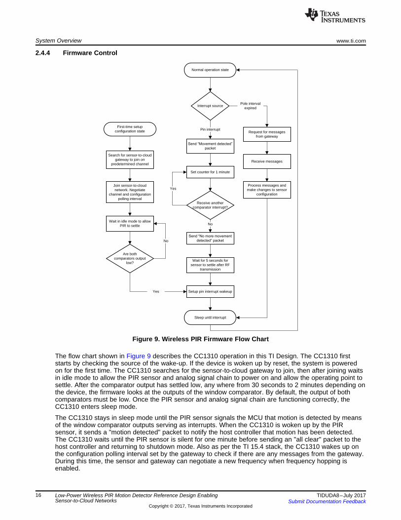
The flow chart shown in Figure 9 describes the CC1310 operation in this TI Design. The CC1310 firststarts by checking the source of the wake-up. If the device is woken up by reset, the system is poweredon for the first time. The CC1310 searches for the sensor-to-cloud gateway to join, then after joining waitsin idle mode to allow the PIR sensor and analog signal chain to power on and allow the operating point tosettle. After the comparator output has settled low, any where from 30 seconds to 2 minutes depending onthe device, the firmware looks at the outputs of the window comparator. By default, the output of bothcomparators must be low. Once the PIR sensor and analog signal chain are functioning correctly, theCC1310 enters sleep mode.
The CC1310 stays in sleep mode until the PIR sensor signals the MCU that motion is detected by meansof the window comparator outputs serving as interrupts. When the CC1310 is woken up by the PIRsensor, it sends a "motion detected" packet to notify the host controller that motion has been detected.The CC1310 waits until the PIR sensor is silent for one minute before sending an "all clear" packet to thehost controller and returning to shutdown mode. Also as per the TI 15.4 stack, the CC1310 wakes up onthe configuration polling interval set by the gateway to check if there are any messages from the gateway.During this time, the sensor and gateway can negotiate a new frequency when frequency hopping isenabled.

www.ti.com System Overview
17TIDUDA8–July 2017Submit Documentation Feedback
Copyright © 2017, Texas Instruments Incorporated
Low-Power Wireless PIR Motion Detector Reference Design EnablingSensor-to-Cloud Networks
2.4.5 Polling Intervals and Frequency HoppingTo increase battery life the Low-Power Wireless PIR Motion Detector Reference Design does not currentlyimplement a frequency hopping scheme. A frequency hopping device will lose synchronization if it doesnot get any collector data/ack within about 20 minute for the default 250 ms dwell interval. In frequencyhopping mode, an end device shall track the slot boundaries of collector and the synchronization ismaintained based on timing information on received Data/ACK. For the default 250 ms dwell timeparameter, it is imperative that a data /ack from collector is received at least once within 20 minutes. It isrecommended to either transmit a poll (and received ACK/Data from collector) or data (and receive ACK)within this period.

TP7, Window comparatorLow output
Reset J2, JTAG programming interface J3, User modeEnable
Sub-1GHzantenna
J4, Spare GPIOs
J1, Main power jumper
TP6, Window comparatorHigh output
CR2032 Battery holder(+ side up)
J6, Sensor supply jumper
Hardware, Firmware, Testing Requirements, and Test Results www.ti.com
18 TIDUDA8–July 2017Submit Documentation Feedback
Copyright © 2017, Texas Instruments Incorporated
Low-Power Wireless PIR Motion Detector Reference Design EnablingSensor-to-Cloud Networks
3 Hardware, Firmware, Testing Requirements, and Test Results
3.1 Required Hardware and Firmware
3.1.1 HardwareFigure 10 shows the hardware for the Low Power Wireless PIR Motion Detector Reference DesignEnabling Sensor-to-Cloud Networks. The printed circuit board (PCB) is in a 35×75-mm rectangular formfactor and comes with 0.5-in nylon standoffs to ensure ease of use while performing lab measurements.
Figure 10. Hardware Description of Low-Power Wireless PIR Motion Detector Reference Design
All the integrated circuits (CC1310, LPV802, and TLV3691), several test points, and jumpers are locatedon the top side of the PCB. The antenna is also located on the top side of the PCB.
The bottom side of the PCB contains the CR2032 coin cell battery holder, jumper J6, and the bottom halfof the antenna.
There are four unused GPIOs that have been brought out from the CC1310 to an unpopulated header tofacilitate future prototyping and debugging.

www.ti.com Hardware, Firmware, Testing Requirements, and Test Results
19TIDUDA8–July 2017Submit Documentation Feedback
Copyright © 2017, Texas Instruments Incorporated
Low-Power Wireless PIR Motion Detector Reference Design EnablingSensor-to-Cloud Networks
3.1.1.1 Jumper ConfigurationTo facilitate measuring critical parameters and debugging in this reference design, there are severaljumpers included. However, to properly operate the design, these jumpers must be installed correctly. Thejumper configuration for normal operation is as follows: J1 = Shorted, J2 = Open, J3 = Open,J6 = Shorted. The jumper configuration to program the CC1310 is as follows: J1 = Open (power applied toPin 2), J2 = Connected through ribbon cable to the SmartRF06 Evaluation Board (EVM), J3 = Open,J6 = Don’t care.
See Figure 10 for a brief description of the intended function of these different jumpers.
3.1.1.2 Test Point DescriptionThis design includes several test points to monitor critical signals. The following is a brief description ofthese test points:• TP1, TP2: Ground points for probes or common points for voltage measurements• TP6, TP7: Window comparator high threshold and low threshold outputs, respectively• TP8: Filtered battery supply forming input to the DC-DC converter in the CC1310• TP9: Filtered DC-DC converter output from the CC1310• TP13: Output of analog filter stage, which is also the input to the window comparator stage
3.1.1.3 Gateway HardwareThe first option for demonstrating the sensor-to-cloud system is to build TI's Sub-1 GHz Sensor to CloudIndustrial IoT Gateway Reference Design. The following items are required to build the sensor-to-cloudgateway:• A CC1310 or CC1350 LaunchPad™ to run the MAC coprocessor application• An AM335x-based BeagleBone Black board• A 5-V power supply for the BeagleBone Black• BeagleBone Black wireless connectivity cape to connect the gateway to the Internet• An 8GB microSD card (the TI processor SDK image requires at least 8GB of space)• A means to configure and set up the BeagleBone Black microSD card (Windows® or Linux machine)• A PC to host and run the web browser used to view the web application• A USB cable to connect the BeagleBone Black with the CC1310 or CC1350 LaunchPad

Hardware, Firmware, Testing Requirements, and Test Results www.ti.com
20 TIDUDA8–July 2017Submit Documentation Feedback
Copyright © 2017, Texas Instruments Incorporated
Low-Power Wireless PIR Motion Detector Reference Design EnablingSensor-to-Cloud Networks
Figure 11. BeagleBone Gateway Hardware Setup
3.1.1.4 Collector HardwareThe second and easier option for demonstrating the sensor-to-cloud system is to use a CC1310 orCC1350 LaunchPad running the Collector Example Application featured in the SimpleLink SDK to act asthe gateway device. The LaunchPad creates the TI 15.4-Stack network, allows sensor devices to join thenetwork, collects sensor information sent by devices running the sensor example application, and tracks ifthe devices are on the network or not by periodically sending tracking request messages. The onlyhardware required is the LaunchPad and a PC to view the UART output.
3.1.1.5 MiscellaneousNote that due to the number of sensitive high impedance nodes in this design, probing points aside fromthe ones with dedicated test points should be done so with the probe impedance in mind.
An example of this would be the probing of the reference inputs to the window comparator. Because thesereference thresholds are generated from a resistor divider composed of four 15-MΩ resistors, using astandard oscilloscope probe or voltmeter with a 10-MΩ input impedance effectively loads the circuit beingmeasured and provides a false measurement.

www.ti.com Hardware, Firmware, Testing Requirements, and Test Results
21TIDUDA8–July 2017Submit Documentation Feedback
Copyright © 2017, Texas Instruments Incorporated
Low-Power Wireless PIR Motion Detector Reference Design EnablingSensor-to-Cloud Networks
3.1.2 Firmware
3.1.2.1 Loading FirmwareThe firmware used on this TI Design was developed using TI’s Code Composer Studio (CCS) software(version 7.1.0). The IAR Embedded Workbench for ARM also supports the CC13xx line of SimpleLinkproducts.
Powering the board from 3.0 V is also necessary and is supplied at pin 2 of Jumper J1. Connecting theexternal power source at this location bypasses the reversed battery protection.
The TI Design hardware is programmed by connecting the 10-pin mini ribbon cable from J2 to theSmartRF06 EVM (10-pin ARM Cortex Debug Connector, P410). See Figure 12 for a photo of the correctsetup for connecting the TI Designs hardware to the SmartRF06 EVM.
Figure 12. Connection of SmartRF06 Evaluation Board and TI Designs Hardware forProgramming and Debugging
To run the LaunchPad collector, connect the CC13xx LaunchPad to the PC and open a serial connectionto the application UART. To restart the collector, hold BTN-2 while pressing the reset button. Press theBTN-2 button on the LaunchPad collector to allow new devices to join the network. Press the BTN-2 asecond time to close the network, which does not allow new devices to join the network.
Figure 13. CC1310 LaunchPad Collector UART Output

Hardware, Firmware, Testing Requirements, and Test Results www.ti.com
22 TIDUDA8–July 2017Submit Documentation Feedback
Copyright © 2017, Texas Instruments Incorporated
Low-Power Wireless PIR Motion Detector Reference Design EnablingSensor-to-Cloud Networks
3.1.2.2 Programming the CollectorThe SimpleLink SDK download includes a quick start guide to program and run the TI 15.4 Stack collector.The guide are in the SimpleLink SDK installation directory under docs (for example,"C:\ti\simplelink_cc13x0_sdk_1_30_00_06\docs\ti154stack"). Open the Software Developers Guide andnavigate to Example Applications on the left side bar.
Flash Programmer 2 is the easiest way to program the collector if .hex files are already generated. CCScan be used to make changes to the example code. Figure 14 shows the Flash Programmer settings afterplugging in the LaunchPad.
Figure 14. Flash Programmer 2 Setup

www.ti.com Hardware, Firmware, Testing Requirements, and Test Results
23TIDUDA8–July 2017Submit Documentation Feedback
Copyright © 2017, Texas Instruments Incorporated
Low-Power Wireless PIR Motion Detector Reference Design EnablingSensor-to-Cloud Networks
3.1.2.3 Receiving Data PacketsAs this reference guide previously describes, this TI Design is programmed to detect a person’s presenceby using the PIR sensor (see Section 2.2.5 and Section 2.4.1). The CC1310 broadcasts three possibleaction values:• A "Request for Data" packet when the polling interval timer has expired• A "Motion Detected" packet when the first motion is detected (see Figure 15)
Figure 15. Motion Detected Packet Data
• An "All Clear" packet one minute after the last motion is detected (see Figure 16)
Figure 16. All Clear Packet Data
To verify the proper operation of the radio transmission, a CC1350 or CC1310 LaunchPad board can beused as a packet sniffer device for TI 15.4-Stack radio packets. This feature enables easier developmentand debugging for those developing products with the TI 15.4-Stack. The TI 15.4-Stack installs theTiWsPc2, which uses TI hardware to capture OTA data before sending the packets to Wireshark or aPCAP file, and provides .dll files to dissect packets that follow the TI 802.15.4ge protocol to Wireshark.Figure 17 is an example of TI 15.4-Stack-based application OTA traffic being presented as a Wiresharkcapture.

Hardware, Firmware, Testing Requirements, and Test Results www.ti.com
24 TIDUDA8–July 2017Submit Documentation Feedback
Copyright © 2017, Texas Instruments Incorporated
Low-Power Wireless PIR Motion Detector Reference Design EnablingSensor-to-Cloud Networks
3.1.2.3.1 CC13xx LaunchPad SnifferThe SimpleLink SDK download includes quick start guides to install, program and run the TI 15.4 Stacksniffer (for example, "C:\ti\simplelink_cc13x0_sdk_1_30_00_06\docs\ti154stack"). Open the SoftwareDevelopers Guide and navigate to Example Applications on the left side bar. All the required softwareexcept for Wireshark is downloaded within the SimpleLink SDK.
Figure 17. Wireshark Packet Sniffer Software
Choose a packet to get detailed information on the data in that packet. The installed .dll file lets Wiresharkdissect the information in a TI 802.15.4GE packet for easy debugging.
3.2 Testing and Results
3.2.1 Test SetupThe Low-Power Wireless PIR Motion Detector Reference Design Enabling Sensor-to-Cloud Networks ischaracterized to support all of the critical specifications for this subsystem. The following subsectionsdescribe the test setups for these measurements, including the equipment used and the test conditionsunless otherwise noted.
3.2.1.1 Power ConsumptionThe power consumption measurements for this reference design are critical in balancing battery lifetimewith sensor bias current and motion sensitivity. An initial prototype allowed measurements of the differentcurrent paths in the design as a preliminary analysis. The results from that prototype are shown inSection 3.2.2.1. Measurements of supply current were then performed on the reference design hardware,which confirmed the prototype measurements. Further characterization was done on the reference designhardware over the voltage range of the design. The test setup for the supply current measurements isillustrated in Figure 18.

A
DUTAgilentE3644A
Agilent34410A
BT1+
BT1-
www.ti.com Hardware, Firmware, Testing Requirements, and Test Results
25TIDUDA8–July 2017Submit Documentation Feedback
Copyright © 2017, Texas Instruments Incorporated
Low-Power Wireless PIR Motion Detector Reference Design EnablingSensor-to-Cloud Networks
Figure 18. Test Circuit Used for Measuring Supply Current
To compute the battery life, the radio transmission intervals also need to be characterized as theseintervals have brief periods of high peak currents before settling to the low microamp current levelsmeasured using the setup in Figure 18. The measurement of the radio transmission interval involves usinga sense resistor that interfaces to an oscilloscope, which can then be used to trigger on the high currentevents. Data from this interval is then exported to Microsoft® Excel® to analyze the data. This setup isillustrated in Figure 19. A 3.4-Ω sense resistor was placed in series with the power supply on the positivebattery terminal. Oscilloscope probes were then attached to each side of the resistor to capture the currentwaveform during transmission.
Figure 19. Sense Resistor Used to Measure Supply Current During Radio Transmission Intervals
3.2.1.2 FunctionalThe following subsections describe the tests for functionality under various environmental conditions.These tests generally verify the limits of operation for the subsystem.
3.2.1.2.1 Temperature and Humidity RangeThis TI Design was stressed under temperature and humidity bias to ensure the design operates and doesnot produce false triggers under extremes of the targeted environment. The typical extended buildingenvironment temperature range is assumed to be 0°C to 50°C while additional testing was performed totest the limits of the design down to –30°C and up to 60°C. Similarly, the typical humidity range for abuilding environment is assumed to be 20% to 70%.

Hardware, Firmware, Testing Requirements, and Test Results www.ti.com
26 TIDUDA8–July 2017Submit Documentation Feedback
Copyright © 2017, Texas Instruments Incorporated
Low-Power Wireless PIR Motion Detector Reference Design EnablingSensor-to-Cloud Networks
The chamber used for the temperature and humidity stress was the CSZ ZH322-H/AC Temperature andHumidity Chamber and a Vaisala® HMP235 Humidity Probe to monitor humidity. A Watlow® F-4 Controllerwas used to automate the testing. The reference design PCB was placed in the chamber with a newEnergizer® CR2032 lithium-ion coin cell battery installed. The CC1111 USB dongle was placed near the TIDesign hardware inside the chamber and connected to a laptop outside of the chamber with a USB cableto monitor for false triggers during the test. Figure 20 shows a picture of the setup.
Figure 20. Wireless PIR Motion Detector Temperature and Humidity Test Setup
To prevent false detection due to rapid changes in ambient temperature and subsequent sensor settling,the temperature was slowly ramped during the test as would be expected in a typical operatingenvironment. The test was started with a 10-minute soak at 25°C followed by a 1°C per minute ramp up to50°C with a 5-minute soak, followed by a 5°C per minute ramp to 60°C, and back down to 50°C with a5-minute soak at 50°C, followed by a 1°C per minute ramp down to 0°C with a 5-minute soak. At 0°C, asimilar 5°C per minute ramp was applied down to –30°C and back up to 0°C with a 5-minute soak at 0°C,followed by a 1°C per minute ramp back up to 25°C.
Because of the physical construction of the chamber and its use of fans for air flow within the chamber,false triggers were observed during the temperature ramping periods. During the soaking periods, falsetriggering subsided over the entire temperature range tested, which proves the functionality of the designover the temperature extremes. This observation is common for PIR-based motion detectors and for thisreason are generally not recommended for installation near ventilation. The only known way to prevent thefalse triggering during this test is to cover the sensor so it could not be affected by thermal gradients dueto forced air flow and reflections off the walls of the chamber; however, this was not done as part of thismeasurement.
To prevent false detection due to rapid changes in humidity, the humidity was slowly ramped during thetest as would be expected in a typical operating environment. The test consisted of applying a 1% perminute ramp from 20% to 70% and then back down to 20% with a 30-minute initial soak. The temperaturewas held at 45°C to prevent condensation; however, condensation was observed at 68% and higherhumidity points.
The only anomaly observed during this test was at the point where condensation formed on the PCB,which produced false triggering. As the humidity dropped to a point where the PCB dried, the falsetriggering stopped and was not observed for the remainder of the test.

www.ti.com Hardware, Firmware, Testing Requirements, and Test Results
27TIDUDA8–July 2017Submit Documentation Feedback
Copyright © 2017, Texas Instruments Incorporated
Low-Power Wireless PIR Motion Detector Reference Design EnablingSensor-to-Cloud Networks
3.2.1.2.2 Motion SensitivityThe motion sensitivity range was measured by connecting a dual pulse stretcher design built on a genericprototyping PCB with LED outputs on each channel for visual indication. The inputs to the pulse stretcherare connected to the window comparator output test points of the reference design. Using this method, thePIR sensor was allowed to remain stationary at a fixed location while the LEDs indicate when motion isbeing detected. The pulse stretcher was powered using its own coin cell battery so that it does notinterfere with or modify the operation of the PIR sensor being tested. The farthest distance at whichreliable detection of motion was indicated was then measured and reported as the motion sensitivity.Pictures of this setup are shown in Figure 21.
Figure 21. Motion Sensitivity Test Setup(Top: No Motion; Bottom: Motion Detected)

Hardware, Firmware, Testing Requirements, and Test Results www.ti.com
28 TIDUDA8–July 2017Submit Documentation Feedback
Copyright © 2017, Texas Instruments Incorporated
Low-Power Wireless PIR Motion Detector Reference Design EnablingSensor-to-Cloud Networks
3.2.1.2.3 Wireless RF RangeThe range of the Wireless Sub-1 GHz RF was measured using the CC1111 USB dongle. For this test, thePIR PCB remained at a stationary location as a laptop with the CC1111 USB dongle attached andlistening was moved away from the PIR PCB. While the CC1111 was on the move, the PIR design wasbeing reset at regular short intervals to make sure there were radio packets constantly being transmitted.The distance at which packets were no longer received was then measured.
Different orientations of the PCB and the CC1111 USB dongle with respect to one another were usedduring the test. No discernable change in the Wireless RF range was observed.
3.2.1.2.4 RF ImmunityThe immunity of this TI Design with respect to radiated RF disturbances was measured according to IEC61000-4-3 with an extended low frequency range. The IEC standard is specified for a frequency range of80 MHz to 1 GHz; however, this testing was extended down to 10 kHz to look for susceptibility in thedesign for disturbances closer to the pass band of the circuit.
The setup consisted of connecting the pulse stretcher board used in Section 3.2.1.2.2 to the windowcomparator outputs and monitoring the LEDs for activity with a camera inside the anechoic chamber.Additionally, a field strength probe was placed near the board under test for control and monitoring of theRF field strength level being tested. This test setup is shown in Figure 22.
Figure 22. RF Immunity Test Setup
The biconical antenna shown in Figure 22 was used for the frequency range from 30 MHz to 1 GHz inboth the horizontal and vertical orientation (vertical orientation shown). For frequencies lower than30 MHz, it was necessary to use a rod antenna in a single orientation.

www.ti.com Hardware, Firmware, Testing Requirements, and Test Results
29TIDUDA8–July 2017Submit Documentation Feedback
Copyright © 2017, Texas Instruments Incorporated
Low-Power Wireless PIR Motion Detector Reference Design EnablingSensor-to-Cloud Networks
3.2.2 Test Results
NOTE: Unless otherwise noted, the test data in the following sections were measured with thesystem at room temperature. All of the measurements in this section were measured withcalibrated lab equipment.
3.2.2.1 Power CharacterizationThe supply current for the different circuit paths in this design was measured using an initial prototypedesign. This information was used early in the design process to balance the battery lifetime with motionsensitivity specifications and the sensor bias. This data was also compared to measurements made on thereference design hardware to make sure there was a good correlation between initial results and finalresults.
Table 2. Low-Power PIR Motion Detector Motion Sensitivity Results
CIRCUIT PATHSUPPLY CURRENT (IDLE)
NOMINAL MEASUREDSensor 600 nA 594 nAComparators (×2) 150 nA 150 nADivider 50 nA 50 nAOpamp1 374 nA 360 nAOpamp2 409 nA 380 nACC1310 100 nA 120 nATotal 1.683 µA 1.654 µA
The connection events contribute to the majority of the current consumption and therefore influencebattery life the most. On first power-up, the reference design must search for and join the network asdiscussed in Section 2.4.4. The connection event is approximately 49 ms long with an average current of12.77 mA as shown in Figure 23. This is quite a bit of current, but this only happens on initial start-up ofthe device or when the reference design is connected to a new network.
Figure 23. Join Sensor-to-Cloud Network Transmission

Hardware, Firmware, Testing Requirements, and Test Results www.ti.com
30 TIDUDA8–July 2017Submit Documentation Feedback
Copyright © 2017, Texas Instruments Incorporated
Low-Power Wireless PIR Motion Detector Reference Design EnablingSensor-to-Cloud Networks
Figure 24 shows the packet sniffer capture of the joining network transmission. The transmission consistsof a 14-byte data request packet from the sensor (0x0001), followed by an ACK from the gateway(0xaabb). The gateway sends data and the sensor node acknowledges. After that, the sensor sends thegateway its own data.
Figure 24. Join Network Packet Sniffer Capture
The next connection event occurs when movement is first detected or when an "all clear" packet is beingtransmitted when motion has not been detected for a minute. The "motion detected" and "all clear"packets are identical in length. The transmission takes approximately 23.28 ms with an average current of14 mA as shown in Figure 25.
Figure 25. Movement Status Update on Packet Transmit

www.ti.com Hardware, Firmware, Testing Requirements, and Test Results
31TIDUDA8–July 2017Submit Documentation Feedback
Copyright © 2017, Texas Instruments Incorporated
Low-Power Wireless PIR Motion Detector Reference Design EnablingSensor-to-Cloud Networks
The last connection event is the configuration transmission between the gateway and the sensor node.This occurs on the Configuration Polling interval discussed in Section 2.4.4. Figure 26 shows the singlepacket transmit and the following ACK being received. Other packets follow if there are messages fromthe gateway or if frequency hopping is enabled because a new frequency will be negotiated on eachconfiguration interval. To save power frequency hopping was disabled and the configuration pollinginterval was set to 20 min. The configuration polling event takes approximately 21.52 ms with an averagecurrent of 9.08 mA as shown in Figure 26.
Figure 26. Configuration Packet Transmission
The data values highlighted in this section are used in the following section to calculate the expectedbattery life for expected use conditions.

( )( )
240 mAh 1 yearBattery Lifetime years 0.85 10.1 years
8760 hrs1.65 A 1800 s 14mA 69.84 ms 9.08 mA 22 ms
1800 s
= ´ ´ =æ öm ´ + ´ + ´ç ÷ç ÷è ø
6
Data Totalt 38.8 1 0 t 69.84 ms-
= ´ ´ =
Data Total
Events 1 hrt 6 23.28 ms t
hr 3600 s
æ ö= ´ ´ ´ç ÷
è ø
Data Total DataPkt
Events 1 hrt n t t
hr 3600 s
æ ö= ´ ´ ´ç ÷
è ø
( ) ( )( ) ( ) ( ) ( ) ( ) ( )
( )Standby Standby Data Data Poll Poll
Total
Battery Capacity mAh 1 yearBattery Lifetime yr Derating Factor
8760 hoursI A t s I A t s I A t s
t s
= ´ ´æ öm ´ + m ´ + m ´ç ÷ç ÷è ø
Hardware, Firmware, Testing Requirements, and Test Results www.ti.com
32 TIDUDA8–July 2017Submit Documentation Feedback
Copyright © 2017, Texas Instruments Incorporated
Low-Power Wireless PIR Motion Detector Reference Design EnablingSensor-to-Cloud Networks
3.2.2.2 Battery Life CalculationsThe main parameters that affect the estimated battery life of the entire system are:• Capacity rating of the battery in milliamp-hours (mAh)• Average standby-state current consumption (μA)• Standby-state duration (s)• Average packet current consumption (mA)• Packet transmission duration (ms)• Polling rate
Equation 13 describes the estimated battery life of the system:
(13)
where:• tTotal is an arbitrary time interval• tData is the amount of time spent transmitting data packets• tPoll is the amount of time transmitting poll packets
If tTotal is set equal to the polling interval (30 min), then tPoll equals the time it takes to send a single pollpacket, 21.56 ms. The value for tData is calculated as:
(14)
where:• n is the number of movement event packets per hour• tDataPkt is the amount of time it takes to send a movement status update data packet, 23.28 ms
The number of motion events per hour depends entirely on the end-use case. However, for the purpose ofthis TI Design, the following use-case was defined:• Detector installation• Six events per hour• One minute active movement timer; if no movement after 1 minute of seeing motion, an "all clear"
packet is sent.• Polling interval of 30 minutes
Using these requirements, the tData can be calculated as follows:
(15)
Another available knob in the optimization of battery life for this reference design is the active timer value.The default value in firmware is 1 minute. Because this value can be modified, the battery life for Case 1and Case 3 are recalculated using a value of 30 seconds to show the expected improvement.
The equations for the expected battery life for the three cases in consideration are as follows.
General lifetime equation:
(16)

Polling Interval (minutes)
Life
Tim
e (y
ears
)
0 10 20 30 40 50 60 700
2
4
6
8
10
12
D001
www.ti.com Hardware, Firmware, Testing Requirements, and Test Results
33TIDUDA8–July 2017Submit Documentation Feedback
Copyright © 2017, Texas Instruments Incorporated
Low-Power Wireless PIR Motion Detector Reference Design EnablingSensor-to-Cloud Networks
The derating factor in these equations accounts for self aging of the battery. Based on these equations,Table 3 and Figure 27 show the average expected battery lifetime for this reference design with the activetimer set to 1 minute and the polling interval from 1 minute to 1 hour.
Table 3. Battery Lifetime versus Polling Interval
TPOLL (min) TPOLL (s) ISTANDBY (A) tSTANDBY (s) IPOLL (A) tPOLL (s) IDATA (A) tDATA (s) IAVG (A) BATT CAP(Ah) DERATING BATT LIFE
(yrs)
1.0E+0 60.0E+0 1.65E-6 59.98E+0 9.08E-3 22.00E-3 14.02E-3 2.33E-3 5.52E-6 240.0E-3 0.85 4.22
2.0E+0 120.0E+0 1.65E-6 119.97E+0 9.08E-3 22.00E-3 14.02E-3 4.66E-3 3.86E-6 240.0E-3 0.85 6.04
5.0E+0 300.0E+0 1.65E-6 299.97E+0 9.08E-3 22.00E-3 14.02E-3 11.64E-3 2.86E-6 240.0E-3 0.85 8.14
10.0E+0 600.0E+0 1.65E-6 599.95E+0 9.08E-3 22.00E-3 14.02E-3 23.28E-3 2.53E-6 240.0E-3 0.85 9.22
20.0E+0 1.2E+3 1.65E-6 1.20E+3 9.08E-3 22.00E-3 14.02E-3 46.56E-3 2.36E-6 240.0E-3 0.85 9.87
21.0E+0 1.3E+3 1.65E-6 1.26E+3 9.08E-3 22.00E-3 14.02E-3 48.89E-3 2.35E-6 240.0E-3 0.85 9.90
24.0E+0 1.4E+3 1.65E-6 1.44E+3 9.08E-3 22.00E-3 14.02E-3 55.87E-3 2.33E-6 240.0E-3 0.85 9.98
27.0E+0 1.6E+3 1.65E-6 1.62E+3 9.08E-3 22.00E-3 14.02E-3 62.86E-3 2.32E-6 240.0E-3 0.85 10.05
30.0E+0 1.8E+3 1.65E-6 1.80E+3 9.08E-3 22.00E-3 14.02E-3 69.84E-3 2.30E-6 240.0E-3 0.85 10.10
33.0E+0 2.0E+3 1.65E-6 1.98E+3 9.08E-3 22.00E-3 14.02E-3 76.82E-3 2.29E-6 240.0E-3 0.85 10.15
36.0E+0 2.2E+3 1.65E-6 2.16E+3 9.08E-3 22.00E-3 14.02E-3 83.81E-3 2.29E-6 240.0E-3 0.85 10.19
39.0E+0 2.3E+3 1.65E-6 2.34E+3 9.08E-3 22.00E-3 14.02E-3 90.79E-3 2.28E-6 240.0E-3 0.85 10.22
42.0E+0 2.5E+3 1.65E-6 2.52E+3 9.08E-3 22.00E-3 14.02E-3 97.78E-3 2.27E-6 240.0E-3 0.85 10.24
45.0E+0 2.7E+3 1.65E-6 2.70E+3 9.08E-3 22.00E-3 14.02E-3 104.76E-3 2.27E-6 240.0E-3 0.85 10.27
48.0E+0 2.9E+3 1.65E-6 2.88E+3 9.08E-3 22.00E-3 14.02E-3 111.74E-3 2.26E-6 240.0E-3 0.85 10.29
51.0E+0 3.1E+3 1.65E-6 3.06E+3 9.08E-3 22.00E-3 14.02E-3 118.73E-3 2.26E-6 240.0E-3 0.85 10.31
54.0E+0 3.2E+3 1.65E-6 3.24E+3 9.08E-3 22.00E-3 14.02E-3 125.71E-3 2.26E-6 240.0E-3 0.85 10.32
57.0E+0 3.4E+3 1.65E-6 3.42E+3 9.08E-3 22.00E-3 14.02E-3 132.70E-3 2.25E-6 240.0E-3 0.85 10.34
60.0E+0 3.6E+3 1.65E-6 3.60E+3 9.08E-3 22.00E-3 14.02E-3 139.68E-3 2.25E-6 240.0E-3 0.85 10.35
64.0E+0 3.8E+3 1.65E-6 3.84E+3 9.08E-3 22.00E-3 14.02E-3 148.99E-3 2.25E-6 240.0E-3 0.85 10.37
16.7E+3 1.0E+6 1.65E-6 999.96E+3 9.08E-3 22.00E-3 14.02E-3 38.80E+0 2.19E-6 240.0E-3 0.85 10.61
Figure 27. Battery Lifetime vs Polling Interval

Hardware, Firmware, Testing Requirements, and Test Results www.ti.com
34 TIDUDA8–July 2017Submit Documentation Feedback
Copyright © 2017, Texas Instruments Incorporated
Low-Power Wireless PIR Motion Detector Reference Design EnablingSensor-to-Cloud Networks
3.2.2.3 Functional
3.2.2.3.1 Motion SensitivityThe motion sensitivity was measured for multiple sensors with different bias conditions and two differentgain settings. Table 4 summarizes these measurement results.
Table 4. Low-Power PIR Motion Detector Motion Sensitivity Results
SENSOR SUPPLY CURRENT(IDLE) VOUT (DC) MAX. DISTANCE
(Av = 90 dB)MAX. DISTANCE
(Av = 70 dB)RS = 2.2 MΩ, RD = 1 MΩIRS-B210ST01 365 nA 0.78 V 20 ft 6 ftIRS-B340ST02 355 nA 0.764 V 25 ft 8 ftIRA-E700ST0 500 nA 1.093 V 12 ft 4.5 ftIRA-E712ST3 555 nA 1.204 V 13 ft 5 ftRS = 1.3 MΩ, RD = 620 kΩIRS-B210ST01 594 nA 0.77 V > 30 ft 6.5 ftIRS-B340ST02 572 nA 0.744 V 27 ft 8 ftIRA-E700ST0 838 nA 1.085 V 15 ft 5 ftIRA-E712ST3 920 nA 1.178 V 17 ft 7.5 ft
The highlighted cell in Table 4 illustrates the motion sensitivity of the circuit configuration implemented inthis TI Design.
3.2.2.3.2 Wireless RF RangeThe wireless RF range was measured to be 220 meters in a typical office environment with partial line ofsight. The measured signal strength at this distance was less than –100 dBm as measured by the CC1111packet sniffer dongle.
While this distance is outstanding considering the small footprint of the PCB antenna, there are ways toincrease this distance even further. Use of a whip antenna with gain instead of the passive PCB antennacould offer improvements in the wireless RF range. Another option would be to increase the transmitpower of the CC1310 to its maximum level at the expense of increased supply current during the radiotransmission intervals.

www.ti.com Hardware, Firmware, Testing Requirements, and Test Results
35TIDUDA8–July 2017Submit Documentation Feedback
Copyright © 2017, Texas Instruments Incorporated
Low-Power Wireless PIR Motion Detector Reference Design EnablingSensor-to-Cloud Networks
3.2.2.3.3 RF ImmunityThe RF immunity of this design was measured to be 30 V/m over the entire 10-kHz to 1-GHz frequencyrange. Immunity at field strengths higher than this were not tested due to equipment limitations in thefrequency range around 30 MHz. This level also corresponds to Class 3 in the IEC 61000-4-3 standard.
The only anomaly observed during this test was at the singular frequency step of 728.5 MHz, where thepassing immunity level dropped to 29.8 V/m in the horizontal antenna orientation. This drop was due tothe wiring connection between the PIR PCB and the pulse stretcher board used for monitoring.
3.2.2.3.4 VibrationVibration was not tested on this reference design in any official capacity. Part of the reasoning for this isthat finding vibration specifications on commercially available PIR motion detectors is difficult to find.Rudimentary vibration testing was performed in the lab by beating on the desk on which the PIR was alsoresting and looking for false trigger events at the output of the window comparator. Based on this test, nofalse triggers were observed as long as the PCB did not physically move. While crude, this test does showthat there is nothing systematic in the design itself that would cause false triggers in a normal applicationaside from the sensor construction itself.
A more informative test would include control over vibration frequency and amplitude with both of thesebeing varied. The results of such a test would illustrate potential harmonic sensitivities to vibration. PCBorientation could also be varied as part of this test for a complete picture of the sensitivity to vibration for agiven design in different installations. Because such an elaborate test would yield different results basedon the physical enclosure that would finally house the PCB design, it was determined that this was beyondthe scope of this reference design.
All PIR-based motion sensors are sensitive to vibration in some capacity due to the physical constructionof the sensor as well as the way it naturally operates. Because the PIR sensor is built using thermopiles,these elements have a crystal structure, which exhibits a piezoelectric effect if the amplitude andfrequency of vibration is such that the thermopiles themselves vibrate. A more prevalent effect is due tothe entire sensor itself moving. Because a Fresnel lens enlarges the effective field of view of the sensor atsubstantial distances away from the sensor by focusing IR energy onto the small area of the sensorelements, any small movement of the sensor will result in large movements in the field of view. Due tobackground IR energy, the sensor output will not be able to distinguish between changes in IR energy dueto motion with a static background or the background itself changing rapidly due to movements of the fieldof view.
In other words, the detection of motion is relative. If the sensor is assumed to be perfectly static, motiondetected will be relative to the sensor; however, motion will also be detected if the background is static butthe sensor is moving. In both cases, the output is valid because there is motion, but the task of narrowingthe output to what is desired falls upon the installation and enclosure design.

Design Files www.ti.com
36 TIDUDA8–July 2017Submit Documentation Feedback
Copyright © 2017, Texas Instruments Incorporated
Low-Power Wireless PIR Motion Detector Reference Design EnablingSensor-to-Cloud Networks
4 Design Files
4.1 SchematicsTo download the schematics, see the design files at TIDA-01476.
4.2 Bill of MaterialsTo download the bill of materials (BOM), see the design files at TIDA-01476.
4.3 PCB Layout RecommendationsTo ensure high performance, the Low-Power Wireless PIR Motion Detector Reference Design EnablingSensor-to-Cloud Networks TI Design was laid out using a four-layer PCB. The second layer is a solidGND pour, and the third layer is used for power rail routing with GND fills in unused areas. The top andbottom layers are used for general signal routing and also have GND fills in unused areas. For all of the TIproducts used in this TI Design, adhere to the layout guidelines detailed in their respective datasheets.
Additionally, because of the low-power design and the resulting high-impedance paths present in thedesign, keep the signal routes in the analog sensor path between the PIR sensor output and the windowcomparator input as short as possible with adequate GND fill around these signals.
If this design is to be used in an environment where dust or moisture accumulation is possible, be awarethat it may be necessary to include a conformal coating to eliminate additional leakage paths due to theoperating environment over time.
The antenna on this TI Design is the miniature helical PCB antenna for 868 MHz or 915 MHz. See theapplication note DN038 (SWRA416) for more details about layout and performance.

75.00mm
35.0
0mm
Solid ground plane on Layer 2Power routed on Layer 3
Via stitching to ensure a lowimpedance path is available forRF noise
No copper pour around theantenna section
For the integrated DC-DC converter in theCC1310, the input capacitors C37 andC39, inductor L2, and output capacitor C32are placed such that the current loop areaformed by these components is minimized.
www.ti.com Design Files
37TIDUDA8–July 2017Submit Documentation Feedback
Copyright © 2017, Texas Instruments Incorporated
Low-Power Wireless PIR Motion Detector Reference Design EnablingSensor-to-Cloud Networks
Figure 28. Low-Power PIR Motion Detector Reference Design Layout Guidelines
4.3.1 Layout PrintsTo download the layout prints, see the design files at TIDA-001476.
4.4 Altium ProjectTo download the Altium project files, see the design files at TIDA-01476.
4.5 Gerber FilesTo download the Gerber files, see the design files at TIDA-01476.
4.6 Assembly DrawingsTo download the assembly drawings, see the design files at TIDA-01476.

Software Files www.ti.com
38 TIDUDA8–July 2017Submit Documentation Feedback
Copyright © 2017, Texas Instruments Incorporated
Low-Power Wireless PIR Motion Detector Reference Design EnablingSensor-to-Cloud Networks
5 Software FilesTo download the software files, see the design files at TIDA-01476.
6 Related Documentation1. Texas Instruments, Sub-1 GHz Sensor to Cloud Industrial IoT Gateway Reference Design, TIDEP-
0084 Design Guide (TIDUCI9)2. Texas Instruments, Reverse Current/Battery Protection Circuits, Application Report (SLVA139)3. Texas Instruments, Coin Cells and Peak Current Draw, WP001 White Paper (SWRA349)4. Texas Instruments, Miniature Helical PCB Antenna for 868 MHz or 915/920 MHz, DN038 Application
Report (SWRA416)5. Texas Instruments, WEBENCH® Design Center (http://www.ti.com/webench)6. Texas Instruments, Low Power Wireless PIR Motion Detector Reference Design Enabling 10 Year
Coin Cell Battery Life, TIDA-00489 Design Guide (TIDUAU1)
6.1 TrademarksPowerWise, SmartRF, Code Composer Studio, LaunchPad, MSP430 are trademarks of TexasInstruments.WEBENCH is a registered trademark of Texas Instruments.ARM, Cortex, IAR Embedded Workbench are registered trademarks of ARM Ltd.Bluetooth is a registered trademark of Bluetooth SIG.ULPBench is a trademark of Embedded Microprocessor Benchmark Consortium.CoreMark is a registered trademark of Embedded Microprocessor Benchmark Consortium.Energizer is a registered trademark of Energizer Brands, LLC.Windows, Microsoft, Excel are registered trademarks of Microsoft.Murata is a registered trademark of Murata Manufacturing Co., Ltd.Vaisala is a registered trademark of Vaisala.Watlow is a registered trademark of Watlow Electric Manufacturing Company.All other trademarks are the property of their respective owners.
7 About the AuthorsJARROD KREBS is a systems designer at Texas Instruments, where he is responsible for developingreference designs in the industrial segment. Jarrod has experience with software and embeddedapplications implemented on ARM-based microcontrollers and TI’s MSP430™ platforms. Jarrod earnedhis bachelor of science in computer engineering from Kansas State University in Manhattan, KS. Jarrod isalso a member of the Institute of Electrical and Electronics Engineers (IEEE).
DAVID STOUT is a systems designer at Texas Instruments, where he is responsible for developingreference designs in the industrial segment. David has over 18 years of experience designing Analog,Mixed-Signal, and RF ICs with more than 14 years focused on products for the industrial semiconductormarket. David earned his bachelor of science in electrical engineering (BSEE) degree from LouisianaState University, Baton Rouge, Louisiana and a master of science in electrical engineering (MSEE) degreefrom the University of Texas at Dallas, Richardson, Texas.

IMPORTANT NOTICE FOR TI DESIGN INFORMATION AND RESOURCES
Texas Instruments Incorporated (‘TI”) technical, application or other design advice, services or information, including, but not limited to,reference designs and materials relating to evaluation modules, (collectively, “TI Resources”) are intended to assist designers who aredeveloping applications that incorporate TI products; by downloading, accessing or using any particular TI Resource in any way, you(individually or, if you are acting on behalf of a company, your company) agree to use it solely for this purpose and subject to the terms ofthis Notice.TI’s provision of TI Resources does not expand or otherwise alter TI’s applicable published warranties or warranty disclaimers for TIproducts, and no additional obligations or liabilities arise from TI providing such TI Resources. TI reserves the right to make corrections,enhancements, improvements and other changes to its TI Resources.You understand and agree that you remain responsible for using your independent analysis, evaluation and judgment in designing yourapplications and that you have full and exclusive responsibility to assure the safety of your applications and compliance of your applications(and of all TI products used in or for your applications) with all applicable regulations, laws and other applicable requirements. Yourepresent that, with respect to your applications, you have all the necessary expertise to create and implement safeguards that (1)anticipate dangerous consequences of failures, (2) monitor failures and their consequences, and (3) lessen the likelihood of failures thatmight cause harm and take appropriate actions. You agree that prior to using or distributing any applications that include TI products, youwill thoroughly test such applications and the functionality of such TI products as used in such applications. TI has not conducted anytesting other than that specifically described in the published documentation for a particular TI Resource.You are authorized to use, copy and modify any individual TI Resource only in connection with the development of applications that includethe TI product(s) identified in such TI Resource. NO OTHER LICENSE, EXPRESS OR IMPLIED, BY ESTOPPEL OR OTHERWISE TOANY OTHER TI INTELLECTUAL PROPERTY RIGHT, AND NO LICENSE TO ANY TECHNOLOGY OR INTELLECTUAL PROPERTYRIGHT OF TI OR ANY THIRD PARTY IS GRANTED HEREIN, including but not limited to any patent right, copyright, mask work right, orother intellectual property right relating to any combination, machine, or process in which TI products or services are used. Informationregarding or referencing third-party products or services does not constitute a license to use such products or services, or a warranty orendorsement thereof. Use of TI Resources may require a license from a third party under the patents or other intellectual property of thethird party, or a license from TI under the patents or other intellectual property of TI.TI RESOURCES ARE PROVIDED “AS IS” AND WITH ALL FAULTS. TI DISCLAIMS ALL OTHER WARRANTIES ORREPRESENTATIONS, EXPRESS OR IMPLIED, REGARDING TI RESOURCES OR USE THEREOF, INCLUDING BUT NOT LIMITED TOACCURACY OR COMPLETENESS, TITLE, ANY EPIDEMIC FAILURE WARRANTY AND ANY IMPLIED WARRANTIES OFMERCHANTABILITY, FITNESS FOR A PARTICULAR PURPOSE, AND NON-INFRINGEMENT OF ANY THIRD PARTY INTELLECTUALPROPERTY RIGHTS.TI SHALL NOT BE LIABLE FOR AND SHALL NOT DEFEND OR INDEMNIFY YOU AGAINST ANY CLAIM, INCLUDING BUT NOTLIMITED TO ANY INFRINGEMENT CLAIM THAT RELATES TO OR IS BASED ON ANY COMBINATION OF PRODUCTS EVEN IFDESCRIBED IN TI RESOURCES OR OTHERWISE. IN NO EVENT SHALL TI BE LIABLE FOR ANY ACTUAL, DIRECT, SPECIAL,COLLATERAL, INDIRECT, PUNITIVE, INCIDENTAL, CONSEQUENTIAL OR EXEMPLARY DAMAGES IN CONNECTION WITH ORARISING OUT OF TI RESOURCES OR USE THEREOF, AND REGARDLESS OF WHETHER TI HAS BEEN ADVISED OF THEPOSSIBILITY OF SUCH DAMAGES.You agree to fully indemnify TI and its representatives against any damages, costs, losses, and/or liabilities arising out of your non-compliance with the terms and provisions of this Notice.This Notice applies to TI Resources. Additional terms apply to the use and purchase of certain types of materials, TI products and services.These include; without limitation, TI’s standard terms for semiconductor products http://www.ti.com/sc/docs/stdterms.htm), evaluationmodules, and samples (http://www.ti.com/sc/docs/sampterms.htm).
Mailing Address: Texas Instruments, Post Office Box 655303, Dallas, Texas 75265Copyright © 2017, Texas Instruments Incorporated


![Blue Line Gen2 Quad PIR Motion Detector (12 m [40 ft] …resource.boschsecurity.com/documents/Data_sheet_enUS_2603527307… · Intrusion Systems | Blue Line Gen2 Quad PIR Motion Detector](https://img.dokumen.tips/doc/110x75/5a7432f77f8b9a4b538bae2f/blue-line-gen2-quad-pir-motion-detector-12-m-40-ft-intrusion-systems.jpg)


