Embed Size (px)
Citation preview

0 _I • ,
Low Power VLSI Implementation Schemes For DCT-Based Image
Compression
Shedden Masupe
I V E
ii
A thesis submitted for the degree of Doctor of Philosophy. The University of Edinburgh.
July 2001
UAI/
C)

Abstract
With the ever increasing need for portable electronic devices, there is a growing need for a new look at very large scale integration (VLSI) design in terms of power consumption. Most of the research and development efforts have focused on increasing the speed and complexity of single chip digital systems. In other words, focusing on systems that can perform most computations in given amount of time. However, area and time are not the only metrics that can measure implementation quality. Power consumption has now entered the field, so designers need to take another important parameter as a third dimension in order to enhance the device capabilities.
The Discrete Cosine Transform (DCT) is the basis for current video standards like H.261, JPEG and MPEG. Since the DCT involves matrix multiplication, it is a very computation-ally intensive operation. Matrix multiplication entails repetitive sum of products which are carried out numerous times during the DCT computation. Therefore, as a result of the mul-tiplications, a significant amount of switching activity takes place during the DCT process. This thesis proposes a number of new implementation schemes that reduce the switching capacitance within a DCT processor for either JPEG or MPEG environment.
A number of new generic schemes for low power VLSI implementation of the DCT are presented in this thesis. The schemes target reducing the effective switched capacitance within the datapath section of a DCT processor. Switched capacitance is reduced through manipulation and exploitation of correlation in pixel and cosine coefficients during the com-putation of the DCT coefficients. The first scheme concurrently processes blocks of cosine coefficient and pixel values during the multiplication procedure, with the aim of reducing the total switched capacitance within the multiplier circuit. The coefficients are presented to the multiplier inputs as a sequence, ordered according to bit correlation between successive co-sine coefficients. The ordering of the cosine coefficients is applied on the colunms. Hence the scheme is referred to as column-based processing. Column-Based processing exhibits power reductions of up to 50% within the multiplier unit.
Another scheme, termed order-based, is based on the ordering of the cosine coefficients based on row segments. The scheme also utilises bit correlation between successive cosine coefficients. The effectiveness of this scheme is reflected in power savings of up to 24%. The final scheme is based on manipulating data representation of the cosine coefficients, through cosine word coding, in order to facilitate for a shift-only computational process. This eliminates the need for the multiplier unit, which poses a significant overhead in terms of power consumption, in the processing element. A maximum power saving of 41% was achieved with this implementation.
11

Declaration of originality
I hereby declare that the research recorded in this thesis and the thesis itself was composed
and originated entirely by myself in the Department of Electronics and Electrical Engineering
at The University of Edinburgh.
SheddewMasu pe
111

Acknowledgements
I would like to thank my supervisor Dr T. Arslan, for his assistance and guidance throughout
the project.
I would also like to thank all the guys in the SLI activity for their continuous assistance in
the subject matter of various aspects of the project. In particular, Damon Thompson for his
ever keen assistance with VHDL/Verilog programming and nifty digital design tips. I have to
thank Dr Ahmet Erdogan for his inspirational assistance in the low power design techniques.
Baba Goni, he had so much faith in me even at times that I doubted myself, I appreciate
that. I thank Prof Alan F. Murray for his input in the thesis. The acknowledgements will
be incomplete if I do not mention Barnabas Gatsheni, his probing questions about image
processing solidified my understanding for the basic concepts. I have to thank Dr Joseph
Chuma for his support throughout the programme.
My thanks go to my sponsors, the University of Botswana and Edinburgh University.
I still feel the urge to thank my parents, they did a good job.
Finally I would like to thank Tiny, Yoav and Ails a. They were very patient and understanding
to my absence at home.
lv

Dedication
to my wife
Tiny

Contents
Abstract ................................... ii Declaration of originality .......................... iii Acknowledgements . . . . . . . . . . . . . . . . . . . . . . . . . . . . . iv Dedication .................................. v Contents .................................. vi List of figures . . . . . . . . . . . . . . . . . . . . . . . . . . . . . . . . ix List of tables ................................ xi Acronyms and abbreviations . . . . . . . . . . . . . . . . . . . . . . . xii Nomenclature ................................ xiv List of Publications . . . . . . . . . . . . . . . . . . . . . . . . . . . . . xv
1 Introduction 1
1.1 Introduction .................................1
1.2 Thesis Contribution ............................. 2
1.3 Thesis Layout ................................ 4
2 Low Power CMOS Design 6 2.1 Introduction ................................. 6 2.2 Sources of Power Consumption ....................... 6
2.2.1 Static Power Dissipation (Pstatj ) ................. 7 2.2.2 Dynamic Power Dissipation (Pdynam jc ) .............. 10
2.3 Switching Power Reduction Techniques ................. 16 2.3.1 Reducing Voltage ......................... 16 2.3.2 Reducing Physical Capacitance ................. 17 2.3.3 Reducing Switching Activity .................... 18
2.4 Power Estimation Techniques ....................... 21 2.4.1 Probabilistic Techniques ...................... 27 2.4.2 Statistical Techniques ....................... 33
2 .5 Summary .................................. 34
3 Algorithms and Architectures for Image Transforms 36
3.1 Introduction ................................. 36 3.2 Image Compression Fundamentals .................... 39
3.2.1 Image Transforms ......................... 41 3.3 The Discrete Cosine Transform ......................51
3.3.1 DCT Algorithms and Architectures ................52
3.4 Summary .................................. 62
4 Low Power DCT Research 64
4.1 Introduction ................................. 64
vi

Contents
4.2 Work so far . 64 4.3 A Case for Low-Power DCT ........................67 4.4 Summary ..................................69
5 Column-Based DCT Scheme 70 5.1 Introduction .................................70 5.2 Column Based Processing ........................70 5.3 Simulation Results and Analysis .....................77 5.4 Conclusions .................................81
6 Column-Based DCT Processor 82 6.1 Introduction .................................82 6.2 Column-Based Scheme Implementation .................82
6.2.1 Multipliers ..............................85
6.2.2 Adders ...............................92 6.2.3 Latch Bank .............................95
6.3 Synthesis and Simulation Results .....................99 6.4 Conclusions .................................105
7 Cosine Ordering Scheme 107 7.1 Introduction .................................107 7.2 Order-Based Processing ..........................108 7.3 Synthesis and Simulations Results ....................114 7.4 Conclusions .................................117
8 Cosine Coding Scheme 119 8.1 Introduction ................................. 119 8.2 Data Representation ............................ 119 8.3 Shift-Only Data Manipulation ....................... 121 8.4 Implementation ............................... 122 8.5 Results and Analysis ............................ 124 8.6 Conclusions ................................. 126
9 Conclusions 127 9.1 Conclusions and Discussion ........................127 9.2 Novel Outcomes of the Research .....................129 9.3 Future Work .................................131
A Image Compression Standards 133 A.0.1 JPEG ................................133 A.0.2 MPEG ................................137
B Cosine Coefficients 141
C Test Images 142
vii

Contents
D Synopsys DesignPower Analysis 143 D.1 Power Analysis Techniques ........................143 D.2 Simulation-Based Power Analysis .....................144
D.2.1 RTL Simultation Based Power Analysis .............144 D.2.2 Gate-Level Simulation-Based Power Analysis ..........145
E Program Listings 146 E.1 Pre-processing Programs .........................146 E.2 Some Design Files Examples .......................148
References
164
vii'

List of figures
2.1 Typical power consumption parameter profiles .............. 7 2.2 Input voltage and short circuit current .................. 12 2.3 Impact of load capacitance ........................ 13 2.4 Switching activity in synchronous systems ................ 19 2.5 A typical synchronous sequential design ................ 23 2.6 A power estimation flow .......................... 24 2.7 A typical BDD representation ....................... 30 2.8 An example signal probability waveform ................. 31 2.9 A simplified test case model ........................ 32 2.10 A typical timing diagram for the test case model ............. 33
3.1 from capture to compression ....................... 37 3.2 Video sequence example ......................... 38 3.3 Wavelet compression ........................... 47 3.4 Implementation of 2D DCT by 1 D DCTs ................. 52 3.5 Data flow graph for the Chen Algorithm ................. 55 3.6 DCT architecture based on four MAC processing units ......... 56 3.7 Data flow graph for the Arai Algorithm ................. 56 3.8 Lattice structure .............................. 57 3.9 Architecture of N input scalar product using DA ............. 61
5.1 Matrix multiplication process ....................... 71 5.2 Flowchart of the algorithm ......................... 73 5.3 Simplified architecture of the processor ................. 75 5.4 Framework for algorithm evaluation .................... 79
6.1 DCT processor modified for Column based processing ......... 83 6.2 Typical original DCT processor architecture ............... 83 6.3 Implementation of column based mac unit ................ 84 6.4 A signed Carry-save Array Multiplier example and implementation . 88 6.5 General architecture for Booth-coded Wallace Multiplier ........ 89 6.6 Typical Wallace tree reduction ...................... 91 6.7 Final Addition Using ripple adder ..................... 92 6.8 Brent-Kung Parallel Prefix Network ................... 96 6.9 Latch bank module ............................. 96 6.10 Demultiplexor ................................ 97 6.11 Gating example for first Latch ....................... 98 6.12 Latch .................................... 98
lx

List of flaures
6.13 Latch array ................................. 100 6.14 Multiplexor ................................. 101 6.15 Simulation environment .......................... 103
7.1 cosine coefficient with saved location ................... 108 7.2 Flowchart of cosine ordering scheme ................... 110 7.3 A simplified DCT processor architecture ................. 112 7.4 A simplified MAC unit architecture .................... 113 7.5 Example cosine matrix before and after ordering ............ 114 7.6 Simulation environment .......................... 116 7.7 Average percentages of cell internal power dissipation per module . 117
8.1 Data word partitioning ........................... 121 8.2 Implementation of cosine coding scheme ................ 123 8.3 Implementation of the compression unit ................. 124 8.4 Simulation environment .......................... 125
A.1 Block diagram of JPEG Compression .................. 134 A.2 Hierachy of video signals ......................... 138 A.3 Pand B frame predictions ......................... 140
C.1 Some of the tested images ........................ 142
x

List of tables
2.1 Power reduction techniques ........................ 21 2.2 Probabilistic techniques .......................... 28 2.3 intermediate and steady state expressions ................ 32 2.4 Statistical techniques ............................ 34
3.1 Common Values of digital image parameters .............. 38 3.2 Computation and Storage requirements for some DCT Algorithms . 62
5.1 Typical power savings ........................... 80
6.1 some of the DesignWare components used ............... 84 6.2 Booth Algorithm encoding scheme .................... 90 6.3 Column Based dct results for bk with csa ................ 102 6.4 Conventional dct results for csa with bk ................. 102 6.5 comparison of the multiplier units .................... 102 6.6 Column Based dct results for other implementations with hamming sort 104 6.7 Column Based dct results for other implementations with ascending sort 104 6.8 Wordlength variations: for csa and bk implementations with lena image 105
7.1 some DesignWare components ...................... 111 7.2 results for csa mult: ascending order .................. 116 7.3 results for wall mult: ascending order .................. 117 7.4 results for nbw mult: ascending order .................. 118 7.5 results for mac with csa mult and bk adder ............... 118
8.1 data word coding example ......................... 121 8.2 results for conventional mac with csa mult and bk adder ........ 125 8.3 results for cosine coding scheme ..................... 126
A.1 Typical MPEG standards specifications .................137
xi

Acronyms and abbreviations
ARPA Advanced Research Projects Agency CIP Cell Internal Power CMOS Complementary Metal Oxide Semiconductor CLA Carry Look Ahead CSA Carry Save Array DA Distributed Arithmetic DC Direct Current DCT Discrete Cosine Transform DIFT Discrete Fourier Transform DST Discrete Sine Transform FDCT Forward Discrete Cosine Transform FFT Fast Fourier Transform FSM Finite State Machine GOP Group of Pictures H.261 Recommendation of International Telegraph and Telephone Consultive Committee HIDTV High Defination Television IP Intellectual Property ISDN Integrated Services Digital Network JPEG Joint Photographic Expert Group KLT Karhunen-Loeve Transform LSI Linear Shift Invariant MAC Multiply and Accumulate MOPS Mega Operations Per Second MOS Metal Oxide Semiconductor MPEG Moving Photographic Expert Group MSB Most Significant Bit NMOS Negative-Channel Metal Oxide Semiconductor NSP Net Switching Power NTSC National Television Standards Committee Pixel Picture elements PMOS Positive-Channel Metal Oxide Semiconductor RAM Random Access Memory ROM Read Only Memory SAW Switching Activity Interchange Format TDP Total Dynamic Power VHDL Very-high-speed Hardware Description Language
xii

Acronyms and abbreviations
VLC Variable Length Coding VLSI Very Large Scale Intergration WHT Waish-Hadamard Transform
xl"

Nomenclature
Ceíi effective capacitance Cload load capacitance cis cell internal power
f switching frequency 'Sc short-circuit current I. switching current k switching activity factor L transistor length nsp net switching power Pstatic static power dissipation Pdynamic dynamic power dissipation Pt0t total power dissipation
switching power Psc short circuit power P5 (x) signal probability P(x) transition probability tdp total dynamic power Vdd supply voltage V95 gate-source voltage
input voltage V0 output voltage VT thermal voltage
threshold voltage for NMOS transistor V threshold voltage for PMOS transistor W transistor width
xiv

List of Publications
S. Masupe and T.Arslan. "Low Power DCT implementation approach for CMOS based
DSP Processors,"IEE Electronics Letters, volume 34, pp.2392-2394, Dec. 1998.
S. Masupe and T.Arslan. "Low Power DCT implementation approach for VLSI based
DSP Processors," in International Symposium on Circuits and Systems, IEEE, 30 May
- 2 June 1999.
T. Arslan, A. T. Erdogan, S. Masupe, C. Chan-Fu, D. Thompson, "Low Power IP
Design Methodology for Rapid Development of DSP-Intensive SoC Platform", 1P99
Europe, 2-3 November 1999, Edinburgh, UK. pp. 337-346
S. Masupe and T.Arslan. "Low Power VLSI implementation of the DCT on Single
Multiplier DSP Processors," VLSI Design: An International Journal of Custom-Chip
Design, Simulation and Testing, Volume 11, Number 4, pp. 397-403, 2000.
S. Masupe and T.Arslan. "Low Power Order Based DCT Processing Algorithrn,"in
International Symposium on Circuits and Systems, IEEE, Sydney, Australia, volume 2,
pp. 5-8, 7-9 May 2001.
xv

Chapter 1 Introduction
1.1 Introduction
With the ever increasing need for portable electronic devices, there is a growing need for a
new look at very large scale integration (VLSI) design in terms of power consumption. Most
of the research and development efforts have focused on increasing the speed and complexity
of single chip digital systems. In other words, focusing on systems that can perform most
computations in given amount of time. However, area and time are not the only metrics
that can measure implementation quality. Power consumption has now entered the field, so
designers need to take another important parameter as a third dimension in order to enhance
the device capabilities. Consumers would like their state of the art portable electronic devices
to operate for long periods of time without loss of power.
Some of the portable consumer electronic devices include lap-top computers, cellular phones
and pagers. Work has been done on battery technologies to increase the battery life. However,
some devices like the upcoming portable multi-media terminal, if built using off-shelf com-
ponents which are not designed for low power consumption, will require batteries of at least 3
kg in weight to operate for 10 hours without re-charge. Therefore, without low power design
techniques, existing and upcoming portable devices will be very bulky due to battery packs
or they will have a very short battery life if battery size is reduced[ 1]

Chapter 1: Introduction
A growing number of computer systems are incorporating multi-media capabilities for dis-
playing and manipulating video data. This interest in Multi-media combined with the great
popularity of portable computers and portable phones provides the impetus for creating a
portable video on demand system, This requires a bandwidth far greater than the ordinary
broadcast video, since a user can subscribe to different video programs at any time wherever
they are. Therefore an enormous bandwidth is required for storage and transmission, data
must be compressed in real time for the portable unit[1].
Digital video applications are some of the popular devices that have become part of the
every day life. For example, ISDN video-phone, video-conference systems, digital broad-
cast HDTV and remote surveillance [2]. The Discrete Cosine Transform (DCT) is the basis
for current video standards like H.261, JPEG and MPEG. Since the DCT involves matrix
multiplication, it is a very computationally intensive operation. Matrix multiplication entails
repetitive sum of products which are carried out numerous times during the DCT computa-
tion. Therefore, as a result of the multiplications, a significant amount of switching activity
takes place during the DCT process. This thesis proposes a number of new implementation
schemes that reduce the switching capacitance within a DCT processor for either JPEG or
MPEG environment.
1.2 Thesis Contribution
A number of new generic schemes for low power VLSI implementation of the DCT are
presented in this thesis. The schemes target reducing the effective switched capacitance
2

Chapter 1: Introduction
within the datapath section forward DCT processor(FDCT). Switched capacitance is reduced
through manipulation and exploitation of correlation in pixel and cosine coefficients during
the computation of the DCT coefficients. The techniques are generic and can be extended
to include other applications where matrix multiplication is required. Some DCT architec-
tures which suit the schemes are proposed as proof of concept, and some power dissipation
measures are given for the data path components.
The first scheme, column-based, reduces switched capacitance through manipulation and ex-
ploitation of correlation in pixel and cosine coefficients during the computation of the DCT
coefficients. The manipulation is of the form of ordering the cosine coefficients per column,
according to some ordering technique such as, ascending order or minimum hamming dis-
tance and processing the matrix multiplication using a column-column approach instead of
the usual row-column approach. This scheme achieves a power reduction of up-to 50% within
the multiplier section of the DCT implementation.
The second scheme, order-based, takes advantage of the rows in the cosine matrix. Ordering
the cosine coefficients in each row according to some ordering technique such as, ascending
order or minimum hamming distance, minimises the toggles at the inputs of the multiplier
unit in the DCT processor. The above techniques are generic and can be extended to include
other applications where matrix multiplication is required. The effectiveness of this scheme
is reflected in power savings of up-to 24% within the MAC unit of the DCT implementation.
The third scheme proposes coding cosine coefficients such that only shift operations are used
to process the DCT computation. In this scheme the need for a standard multiplication unit
3

Chapter 1: Introduction
is eliminated by formating the data representation of the cosine elements such that the pixel
values are processed using a shifter unit and an addition unit. Power savings resulting due to
this scheme can go up-to 41%.
1.3 Thesis Layout
Chapter 2 introduces the basic concepts of low power CMOS design. It provides definitions
and equations for static and dynamic power. Some of the techniques which can be used to
minimise power dissipation in CMOS circuits are also presented. These techniques are more
relevant to reducing power consumption which results from one of the major components of
dynamic power dissipation, switching power.
Fundamentals of image processing and image compression are introduced in chapter 3. The
chapter also goes on to cover some image transforms which are possible competitors of the
DCT. Since the DCT is key to the project, a more detailed introduction of the transform is
presented. This includes several algorithms and architectures which have been developed
since the creation of the DCT.
To conclude the literature review, chapter 4 presents a summary of low-power DCT research
covered before (or during the course of) this work.
The next four chapters introduce the three new schemes for low power implementation of the
DCT. Chapter 5 presents the first scheme, which is termed column-based. This involves the
power analysis of the multiplier section in the proposed scheme environment since this unit

Chapter 1: Introduction
is well-known for its computation intensive nature. Colunm-Based scheme is further invest-
igated in Chapter 6 by mapping the algorithm resulting from the scheme into an architecture
suitable for VLSI implementation.
The second scheme is presented in chapter 7 and this takes advantage of the rows in the
cosine matrix. This scheme is termed order-based. Ordering the cosine coefficients in each
row according to some ordering technique such as, ascending order or minimum hamming
distance, minimises the toggles at the inputs of the multiplier unit in the DCT processor.
Chapter 8 introduces the third and final scheme. This is a DCT implementation which codes
the cosine coefficients in order to reduce computational complexity by using shifters and
adders only in the processing.
Finally, chapter 9 concludes the thesis and puts forward some suggestions for future work to
be done in order to continue this research.
5

Chapter 2 Low Power CMOS Design
2.1 Introduction
This chapter introduces the basic concepts of Low Power CMOS Design. It provides defini-
tions and equations for static and dynaniic power. Some of the techniques which can be used
to minimise power dissipation in CMOS circuits are also presented. These techniques are
more relevant to reducing power consumption which results from one of the major compon-
ents of dynamic power dissipation, switching power. Some power estimation methodologies
are presented as well.
2.2 Sources of Power Consumption
The dominant source of power consumption in digital CMOS circuits is the switching power,
which is caused by periodic charging and discharging of nodal capacitances. There are two
kinds of power dissipation in CMOS circuits, static and dynamic. The total power consump-
tion can be categonsed as shown in Equation 2.1.
Pt.t = Pstatic + Pdynamic (2.1)
Rl

Chapter 2: Low Power CMOS Design
The static power can be ignored since it can be minimised using current technologies. The
Dynamic power however is still a major source of dissipation in CMOS circuits and it only
occurs when a node voltage is switched.
2.2.1 Static Power Dissipation (Psi atic)
Static power is the power dissipated by a gate when it is not in operation, that is when it is
not switching [3]
Ideally, CMOS circuits dissipate no static (DC) power since in the steady state there is no
direct path from Vdd to ground(see Figure 2.1). Of course, this scenario can never be realised
in practice since in reality the MOS transistor is not an ideal switch. Hence there will always
be some leakage currents and substrate injection currents which will give rise to a static
component of the CMOS power dissipation.
Vdd
CLoad
vout
Figure 2.1: Typical power consumption pa rameter profiles
7

Chapter 2: Low Power CMOS Design
Leakage Current Power
There are two types of leakage currents, -
reverse-bias diode leakage - at the transistor drains
sub-threshold leakage - through the channel of a device that is turned off.
The magnitudes of the leakage currents is determined mainly by the processing technology.
diode leakage
This occurs when a transistor is turned off. For the case of an inverter, when the PMOS
transistor is turned off with a high input voltage, there will be a voltage drop of —Vdd between
the drain and the bulk after the Vdd to 0 transition at the output. This results in the diode
leakage expressed as [4]:
= Is - i)
(2.2)
where I is the reverse saturation current, V is the diode voltage and VT is the thermal voltage.
A typical value of the leakage current is if A per device junction. The value is too small to
have any impact on the overall power consumption. For example, for a chip with a million
devices, the total power dissipation contributed due to the leakage current will be approx
0.01fLW [4,5].

Chapter 2: Low Power CMOS Design
sub-threshold leakage
This occures due to current diffusion between the source and the drain when the gate-source
voltage (V) exceeds the weak inversion point, but still being below the threshold voltage
(Vi ) [4,5].
- r l4Teff (Vm_VT)
1ds - Jo 10 S (2.3) W.
where
I. = I(1 - e)
(2.4)
and VT is the constant-current threshold voltage. W. and 10 are the gate width and the drain
current to define VT. S is the subthreshold swing parameter. The effective channel width is
referred to as We11 [5].
The magnitude of the sub-threshold is a function of the process (device sizing) and supply
voltage. The process parameter, V, predominantly affects the current. Reducing V has an
exponential increasing effect on the sub-threshold current. The sub-threshold current is a
proportional to E (device size), and is an exponential function of the input voltage. Hence,
the sub-threshold current can be minimised by the reduction of transistor size and the supply
voltage [4].

Chapter 2: Low Power CMOS Design
22.2 Dynamic Power Dissipation (Pdynarnic)
The dynamic power dissipation comprises of two main sources:-
Switching power (P3w ) due to the charging and discharging circuit capacitances
Short-circuit power (P) current due to finite signal rise/fall times.
Pdyna,nic = Psw + Fsc (2.5)
where
Psw =kCloadV,f (2.6)
and where k is the number of energy consuming transitions. Cload is the physical capacitance.
Vddis the supply voltage. f is the data rate, it describes how often on average switching could
occur. For synchronous systems, f might correspond with the clock frequency.
Short-circuit Power (P8 )
The dynamic part of power dissipation is a result of the transient switching behaviour of the
CMOS circuit. There exists a point whereby both the NMOS and PMOS in Figure 2.1 will be
on. During that moment, a short circuit exists between Vdd and the ground allowing currents
to flow. Figure 2.2 illustrates the transition from 0 to Vdd and Vdd to 0. The input voltage
10

Chapter 2: Low Power CMOS Design
obeys the following principle [4],
Vjn < yin <Vdd - (2.7)
where V and V are threshold voltages for NMOS and PMOS transistors respectively. A
long input rise or fall time implies that the short-circuit current will flow longer.
Short circuit power dissipation is especially significant when the output rise/fall time is less
than the input rise/fall time. This is the case when the load capacitance Cj oad (CL), is small.
In this situation, when the inverter gate makes a 0 to Vdd transition with a finite slope, the
drain terminal of the PMOS transistor is immediately grounded and a current from the power
supply to the ground flows through. On the one hand if CL is very high, the output rise/fall
time becomes much greater than the input rise/fall time. Hence during an input transition,
whereby the input follows the principle in Equation 2.7, the output remains at Vdd. Therefore,
there will be no voltage drop across the source and drain terminals of the PMOS transistor.
This implies that there will be no current drawn [4]. See Figure 2.3.
In conclusion, short circuit power dissipation can be reduced by making certain that the output
rise/fall time is larger than the input rise/fall time. There is, however, a problem with making
out rise/fall time too large. It slows down the circuit and can potentially cause short circuit
currents in the fan out gates.
11

Chapter 2: Low Power CMOS Design
VII,
Vd.j
Vdd. 1V61 I
Vt"
"C
'max
Figure 2.2: Input voltage and short circuit current
This short circuit dissipation can be kept below 10% of the total dynamic power dissipa-
tion with careful design. This is achieved by keeping the rise and fall times of all signals
throughout the design within a fixed range [6,7].
Switching Power (P3w )
The dominant component of the dynamic power is the switching power which is the result of
charging and discharging parasitic capacitances in the circuit. The case is modelled in Figure
2.3 where the parasitics are lumped together at the output in the capacitor C loadS
The average switching power required to charge and discharge the capacitance CL at a
switching frequency of f = can be computed as:
12

Chapter 2: Low Power CMOS Design
Vdd
± CLO.d
(a) Large capacitive load (b) Small capacitive load
Figure 23: Impact of load capacitance
1 T
= J i0(t)v0(t)dt
The current at the output during the charging phase can be presented as
dv 0 Z. = ip =
whereas while discharging the current is given by
(2.8)
(2.9)
13

Chapter 2: Low Power CMOS Design
dv 0 (2.10)
where i,, and ii,, are NIvIOS and PMOS currents respectively [4].
Substituting Equations 2.9 and 2.10 into the average switching power equation 2.8, results in
the average switching power for the inverter gate as:
P. = - 1 0 [fVddCL
VOdVO -
fVdd CLV O dV O I
T ]
- CLV, - CLV1 (2.11)
- T -
and the energy being drawn from the power supply is
E=fT
P(t)dt=CLV (2.12)
It can also be shown that the energy being drawn by the load capacitance CL is
14

Chapter 2: Low Power CMOS Design
tVdd dv0 EL = I CL--v 0dt
Jo dt p V dd
= CU VOdVO=CLVdI (2.13) 0
This implies that during a transition 0 to Vdd, one half of the energy drawn from the power
supply is stored in the capacitor and the other half is used up by the PMOS pull-up network.
The other transition Vdd to 0, results in the energy stored by the capacitor (Equation 2.13)
being used by the NMOS pulled down network. Therefore, from the above analysis, it can
be summarised that every time a capacitive node switches from ground to Vdd, an energy
equivalent to Equation 2.13 is consumed [4].
This leads to the conclusion that CMOS power consumption depends on the switching activity
of the signals involved. In this context, we define activity k, as the expected number of zero to
one transitions per data cycle. If this is coupled with the average data-rate, f, which may be
the clock frequency in a synchronous system, then the effective frequency of nodal charging
is given by the product of the activity and the data rate: kf This leads to the equation for
average CMOS power consumption shown in Equation 2.6 [4].
The resulting equation illustrates that the dynamic power is directly proportional to the switch-
ing activity, capacitive loading, and the square of the supply voltage [6]. This component of
dynamic power, switching power, is the most dominant of the total power dissipation. It can
amount to 80% of the total power consumption in circuit datapaths in modules like multipliers
15

Chapter 2: Low Power CMOS Design
and adders.
2.3 Switching Power Reduction Techniques
2.3.1 Reducing Voltage
With its quadratic relationship to power, voltage reduction offers the most direct and dramatic
means of minimising energy consumption. Without requiring any special circuits or techno-
logies, a factor of two reduction in supply voltage (Vdd) yields a factor of four decrease in
energy. This power reduction is a global effect, experienced not only in one sub-circuit or
block of the chip, but throughout the entire design. Because of this quadratic relationship,
designers are often willing to sacrifice increased physical capacitance or circuit activity for
reduced voltage. Despite the obvious advantage, voltage reduction is detrimental to perform-
ance of the system [8].
As the supply voltage is lowered, circuit delays increase leading to reduced system perform-
ance. For Vdd >> V delays increase linearly with decreasing voltage. In order to meet
system performance requirements, these delay increases cannot go unchecked. Some tech-
niques must be applied, either technological or architectural to compensate for this effect.
This works well until Vdd approaches the threshold voltage at which point delay penalties
simply become unmanageable. This tends to limit the advantageous range of the voltage
supplies to a minimum of about 214.
Performance is not, however the only limiting factor. When going to non-standard voltage
16

Chapter 2: Low Power CMOS Design
supplies, there is also the issue of compatibility and inter-operability. Most off-the-shelf
components operate either on 5V supply or 3.3 V. Unless the entire system is being designed
completely from scratch it is likely that some amount of communications will be required
with components operating at a standard voltage. The severity of this problem is reduced
by the availability of highly efficient DC-DC level converters, but still there is some cost
involved in supporting several different voltages [6].
Another issue that arises with the reduction of voltage is that, more designs are now im-
plemented as IP soft cores, this means that the operating voltage will be determined by the
foundry that supplied the library cells, hence it can not be altered [9].
2.3.2 Reducing Physical Capacitance
This is yet another degree of freedom which can be utilised to reduce the dynamic power dis-
sipation. In order to consider this possibility we must first understand what factors contribute
to the physical capacitance of a circuit.
The physical capacitance in CMOS circuits comes from two basic sources, devices and inter-
connect. Previous technologies had more problems with device capacitance than interconnect
parasitics. Since the technologies have scaled down a lot, interconnect parasitics contribute a
lot to the overall physical capacitance and hence they need to be addressed.
From the previous discussion, it can be recognised that capacitances can be kept at a mm-
imum by using less logic, smaller devices, fewer and shorter wires. Example techniques for
17

Chapter 2: Low Power CMOS Design
reducing the active area include resource sharing, logic minimisation and gate sizing. Ex-
ample techniques for reducing interconnect include register sharing, common sub-function
extraction, placement and routing. As with voltage however, there are disadvantages to ca-
pacitive loading reduction. For example, reducing device sizes not only reduces physical
capacitance, but also reduces the current drive of the transistors making the circuit operate
more slowly. This loss of performance might hinder the reduction of Vdd to a value which
would have otherwise been possible [6].
2.3.3 Reducing Switching Activity
Another candidate for dynamic power dissipation reduction in CMOS circuits is the reduction
of switching activity. A chip can contain a huge amount of physical capacitance, but if it does
not switch then no dynamic power will be consumed. The activity determines how often this
switching occurs. As mentioned before, there are two components to the switching activity,
the data rate (f), and the data activity (k). f describes how often on average switching could
occur. In synchronous systems, f might correspond with the clock frequency. See Figure
2.4. The other component, k, corresponds to the expected number of energy consuming
transitions that will be triggered by the arrival of each new piece of data. Hence while f
determines the average periodicity of data arrivals, k determines how many transitions each
arrival will spark. For circuits that do not experience glitching, k can be interpreted as the
probability that an energy consuming transition will occur during a single data period. Even
for these circuits, calculation of k is difficult as it depends not only on the switching activities
18

Chapter 2: Low Power CMOS Design
of the circuit inputs and the logic function computed by the circuit, but also on the spatial and
temporal correlations among the circuit inputs.
For certain logic styles, however, glitching can be an important source of signal activity
and therefore, deserves some mention here. Glitching refers to the spurious and unwanted
transitions that occur before a node settles down to its final steady-state value. Glitching
often arises when paths with unbalanced propagation delays converge at the same point in
the circuit. Calculation of this spurious activity in a circuit is very difficult and requires
careful logic and/or circuit level characterisation of the gates in a library as well as detailed
knowledge of the circuit structure. Since glitching can cause a node to make several power
consuming transitions instead of one, it should be avoided whenever possible [6].
IN
CLK J1J1JIJl
I/f
Vdd
k=1/4
1 OUT I I I I
Cioad
I I I I I I
Figure 2.4: Switching activity in synchronous systems
The data activity k can be combined with the physical capacitance Cload to obtain an effect-
ive capacitance which describes the average capacitance charged during each 1/f data
period. This reflects the fact that neither the physical capacitance nor the activity alone de-
termine dynamic-power consumption. Instead, it is the effective capacitance, which combines

Chapter 2: Low Power CMOS Design
the two, that truly determines the power consumed by a CMOS circuit. Therefore:
Vdd (2.14)
Evaluating the effective capacitance of a design is non-trivial as it requires a knowledge
of both the physical aspects of the design(ie technology parameters, circuit structure, delay
model) as well as the signal statistics(ie data activity and correlations). This explains why,
lacking proper tools, power analysis is often deferred to the latest stages of the design process
or is only obtained from measurements on the finished parts.
Some techniques for reducing switching activity include power-conscious state encoding and
multi-level logic optimisation for FSM's. Another example will be certain data representa-
tions such as sign magnitude have an inherently lower activity than two's compliment. Since
sign magnitude arithmetic is much more complex than two's compliment, however, there is
a price to be paid for the reduced activity in terms of higher physical capacitance. This is yet
another indication that low power design is a joint optimisation problem.
A summary of techniques that can be used to reduce effective switched capacitance is presen-
ted in Table 2.1.
20

Chapter 2: Low Power CMOS Design
Abstraction Level I Examples
System Power Down, System Partitioning Algorithm Complexity, Concurrency
Locality, Regularity Data representation
Architecture Concurrency, Data Representation Signal correlations Instruction set selection
Circuit'Logic Transistor Sizing, Power Down Physical Design Logic optimisation, layout Optiniisation Technology Advanced Packaging
Table 2.1: Power reduction techniques
2.4 Power Estimation Techniques
This section presents the case of power estimation and it introduces some of the probabilistic
and statistical measures used in power estimation.
Power estimation in general refers to the estimation of average power dissipation of a cir-
cuit. The most straight-forward method for power estimation is through simulation. That
is, performing a circuit simulation of the design and monitoring the power supply current
waveform. The average current is calculated and used to provide the average power. This
method has an advantage of accuracy and generality. The technique can be used to estimate
power of any circuit, regardless of the technology, design style, architecture etc. However,
complete and specific information about the input signals is required. Hence the simulation
based technique strongly depends on input patterns [7].
The pattern dependency poses a problem in the sense that often power estimation of a func-
tional block is performed before the rest of the design is complete. In this case, little is known
about the inputs to the functional block. Therefore, complete and specific information cannot
21

Chapter 2: Low Power CMOS Design
be provided.
Some methods of power estimation have been proposed [7, 10-12]. These techniques sim-
plify the problem by making three assumptions:
Assume that the power supply and ground voltage levels are fixed for the entire design.
- this makes it easier to compute the power by estimating the current drawn by every
sub-circuit assuming a fixed voltage.
Assume that the circuit is built up using logic gates and registers, see Figure 2.5
- for this case, the power dissipation of the circuit can be broken down into two corn-
ponents
. power consumed by registers
. power consumed by the combinational block
Assume it is sufficient to consider only the charging/discharging current drawn by a
logic gate
- neglecting short-circuit current
Referring to Figure 2.5, whenever the clock triggers the registers, some of them will make
transitions and hence draw power. Therefore the power consumed by registers depends on the
clock. For the combinational block, the internal gates may make several transitions before
settling down to their steady state values for that clock period. The additional transitions
22

Chapter 2: Low Power CMOS Design
x
x l
x
Xr
cli
fo
Figure 2.5: A typical synchronous sequential design
are called glitches. These are not necessarily design errors, but they are a problem for low-
power design since additional power is being dissipated. This additional power can easily go
up-to 20% of the total power dissipation in a circuit. Estimating the 'glitch power' can be
computationally expensive, this leads to most power estimation techniques ignoring it [7].
Instead of simulating the circuit for a large number of input patterns, and then averaging the
results, the fraction of cycles in which an input signal makes a transition can be computed
and used to estimate how often internal nodes make transitions. This fraction is a probability
measure. Figure 2.6 shows both the conventional circuit simulation-based power estimation
and the probability-based power estimation.
There are several ways of defining probability measures associated with the transitions made
23

Chapter 2: Low Power CMOS Desi
Randomly generated Input Vector sequences
Many circuit simulation runs A large
number Circuit of
Simulator current waveforms
Average
]]
tI[ Power
]]
Figure 2.6: A power estimation flow
by a logical signal. This is the case for both the primary inputs of the combinational block
and an internal node. These definitions are as follows:
signal probability P3 (x)
- at a node x, is the average fraction of the clock cycles in which the steady state value of x is
a logic high
transition probability P(x)
- at a node x, is the average fraction of clock cycles in which the steady state value of x is
different from its initial state
Both the above probability measures are not affected by the circuit internal delay. This implies
that they are the same even if a zero-delay timing model is assumed. However, when zero-
24

Chapter 2: Low Power CMOS Design
delay is assumed, the glitch power is excluded from the analysis.
When assuming zero-delay model and the transition probabilities are calculated, the power
can be computed as [7]:
Pay = Vd Ci Pt (x i ) (2.15) 1=1
where T is the clock period, n is the total number of nodes in the circuit and Ci is the total
capacitance at node x. Because this assumes at most a single transition per clock cycle, then
it is the lower limit on the true average power [7].
In practice, it may occur that two signals are never high simultaneously. Computing this type
of correlation can be very expensive, hence circuit input and internal nodes are usually as-
sumed independent. This is referred as spatial independence. Another independence issue
can be termed as temporal independence. This results in an assumption that the values of
the same signal in two consecutive clock cycles are independent. Assuming temporal inde-
pendence, the transition probability can be obtained from the signal probability as follows
[7]
Pt = 2P(x)P3() = 2P8 (x)[1 - P(x)] (2.16)

Chapter 2: Low Power CMOS Design
transition density
- if a logical signal x(t) makes n(T) transitions in a time interval of length T, then
n(T) urn (2.17)
T—+oo T
The transition density provides a useful measure of switching activity in logic circuits. If the
transition density of every node in a circuit can be computed, the overall power dissipation of
the circuit can be calculated as:
Pay = vc?cicjD(Xi) (2.18) t=1
where D(x 1 ) is the transition density at node x.
For a synchronous circuit, the relationship between transition density and transition probab-
ility is [7]:
D > P(x)
TC (2.19)
equilibrium probability

Chapter 2: Low Power CMOS Design
- the average fraction of time that the signal is high - if x(t) is a logical signal, then its
equilibrium probability is [7]:
T
1 f- 2
urn -x(t)dt (2.20) T—coT T
The equilibrium probability depends on the circuit internal delays since it describes the be-
haviour of the signal over time, not the steady state behaviour per clock. For steady state
conditions, the equilibrium probability reduces to signal probability [7].
Other techniques, which use traditional simulation models and simulate the circuit for a
limited number of randomly generated input vectors while monitoring power are named
'statistical-based'. The input vectors are generated from user specific probabilistic informa-
tion about the circuit inputs.
The techniques introduced above, probabilistic and statistical techniques, are only applicable
to combinational circuits. They require activity information at the register outputs to be
specified by the user.
2.4.1 Probabilistic Techniques
There are several power estimation approaches which have been proposed to alleviate the
input pattern dependency problem. These techniques use probabilities to solve the problem.
27

Chapter 2: Low Power CMOS Design
The techniques proposed are only applicable to combinational circuits and they require the
user to specify the typical behaviour of the circuits at the combinational circuit inputs. Sample
techniques evaluated are rated according to the following criteria [7]. See Table 2.2
glitch power handling
temporal correlation handling
complexity of the input specification
individual gate power provision
spatial correlation handling
speed
Approach Handle glitch Power
Handle temporal correlation
Input Specification
Individual I gate power Handle spatial I correlation
Speed
signal No No probability
Simple Yes No Fast
CREST Yes Yes Moderate Yes No Fast DENSIM Yes Yes Simple Yes No Fast BDD Yes Yes Simple Yes Yes slow Correlation Coefficients
Yes Yes Moderate Yes Yes Moderate
Table 2.2: Probabilistic techniques
All the techniques in Table 2.2 use simplified delay models for the circuit components and
require user-specified information about the input behaviour. Therefore their accuracy is
limited by the quality of the delay models and the input specification.
28

Chapter 2: Low Power CMOS Design
using signal probability
The easiest way to propagate signal probabilities throughout every node in a circuit is to
work with a gate-level description of the circuit. For example, if y = AND(x i , x 2 ), then
using basic probability theory we get P3 (y) = P8 (x i )P3 (x 2 ), assuming that x 1 and x 2 are
spatially independent. Using the same approach, other simple expressions can be derived for
other gate types. After calculating the signal probabilities of every node in the circuit, the
power can be computed using Equations 2.15 and 2.16 [7].
If a circuit is built from boolean components that are not a part of a predefined gate library, the
signal probability can be computed using a Binary Decision Diagram (BDD) to represent the
boolean functions. Figure 2.7 shows an example where the boolean function y = x 1 x 2 + x 3
using a BDD. As an example, assume that x 1 = 1, x 2 = 0, x3 = 1, to evaluate y begin at the
top node and branch to the right since x 1 = 1. Then branch to the left (x 2 = 0) and finally to
the right (x 3 = 1) to arrive at terminal node 1. The resulting value for y is 1 [12, 1 3].
For the general case, if y = f(x i , ..., x) is a boolean function, and the inputs x 2 are in-
dependent, then the signal probability of f can be obtained in linear time as follows: let
f = f(1 7 x 2) ..., x) and fj- = f(0, x 2 , . .. x) be cofactors off with respect to x 1 , then
P(y) = P(x1)P(f,) + P()P(f j-) (2.21)
where cofactors are defined by the Shannon decomposition of boolean functions [13].
Equation 2.21 shows how the BDD can be used to evaluate P(y).
29

Chapter 2: Low Power CMOS Design
Figure 2.7: A typical BDD representation
probabilistic simulation
The typical input signal behaviour of a circuit is provided in a form of waveforms for this
approach. Probability waveforms are sequences of values indicating the probability that a
signal is high for certain time periods and the probability that it makes a 0 to 1 transition at
specific time points. This allows the computation of the average current waveforms drawn
by individual gates in the design in a single simulation run. The average current waveforms
are then used to compute average power dissipated by each gate, which can in-turn be used
to calculate the total average power. An example of the signal probability waveform is given
in Figure 2.8 [ 1 4].
A program by [15] called CREST uses this approach to estimate power dissipation.
30

Chapter 2: Low Power CMOS Design
ti 12 t3 time
Figure 2.8: An example signal probability waveform
Transition Density
A program was presented in [16] which propagates the transition density values from the
inputs throughout the circuit. This was called DENSIM. To visualise the propagation of the
transition density, recall that if y is a boolean function that depends on x, then the Boolean
difference of y with respect to x is
yI=i ED YI=o (2.22)
If the inputs (x e ) to the Boolean module are spatially independent, then the transition density
of its outputs is given by [ 1 6]:
D(y) = >P Q-) D(x 1 ) (2.23)
Using a BDD
A BDD is used to represent the successive Boolean functions at every node in terms of the
31

Chapter 2: Low Power CMOS Design
primary inputs. These functions do not represent the intermediate values that the node takes
before reaching a steady state condition. However, the circuit delay information can be used
to construct boolean functions for some intermediate values, assuming that the delay of every
gate is a specified fixed constant [7].
X1 ->o-Y-::P
Figure 2.9: A simplified test case model
In Figure 2.9, let x 1 and x 2 in two consecutive clock periods be denoted by x i (1), x i (2) and
x 2 (1), x 2 (2). Assuming equivalent delays between the inverter and the AND gate, a typical
timing diagram can be shown as in Figure 2.10, where it can be seen that node z may make
two transitions before settling down [7].
The intermediate and the steady state values can be expressed as follows:
node I expressions
y y(l) =
y(2) =zi(2)
z z(1) =
=
= z1(2)x2(2)
Table 2.3: intermediate and steady state expressions
A BDD can be built for these functions which makes it possible to accurately compute the
intermediate state probabilities.
32

Chapter 2: Low Power CMOS Design
Xi(( Xi(2)
X2(1D( X2(2)
y(1) y(2)
Z(1) )( z(2) )< z(3)
Figure 2.10: A typical timing diagram for the test case model
This method can be quite slow since a BDD for the entire circuit will have to be built. In
some cases the resulting BDD may be too large [7].
Correlation Coefficients
For this approach, correlation coefficients between steady state signal values are used as
approximations to the correlation coefficients between the intermediate signal values [7].
2.4.2 Statistical Techniques
For the statistical technique, a simulation of the circuit is conducted repeatedly while mon-
itoring the power being consumed. A logic or timing simulator can be used for this. The
average power will be the final result. The main concern of their method is how the input pat-
terns are selected such that the measured power converges to the true average power. Usually
the input vectors are randomly generated based on some method, e.g Monte Carlo. Table 2.4
compares two such methods [7].
Total Power
The method in [17] estimates the total average power of the circuit by applying randomly gen-
33

Chapter 2: Low Power CMOS Design
Approach Handle glitch Power
Handle temporal correlation
Input Specification
I Individual gate power
Handle spatial correlation
Speed
McPower I Yes Yes Simple No only internally I Fast MED I Yes I Yes I Simple I Yes I only internally I Moderate
Table 2.4: Statistical techniques
erated input patterns and monitoring the energy dissipated per clock cycle using a simulator.
The program developed was named 'McPower'
The disadvantage of this method is that it does not provide the power consumed by individual
gates or a small group of gates.
Individual Gate Power
To deal with the disadvatange exhibited by the above method, [18] proposed a method that
not only provides the total power, but also the individual-gate power estimate. They named
their program 'MED'. Despite its improved accuracy, this method suffers from slow speed.
2.5 Summary
This chapter presented the basic of low power design and the underlying factors behind the
power estimation tools. Sources of power consumption were presented with the help of the
power consumption equation. Using the equation, the degrees of freedom for reducing power
consumption were evaluated, giving advantages and disadvantages of each technique. The
focus of this research is based on reducing the switching activity of a circuit. A summary of
techniques for reducing power consumption was presented in table 2.1. Some power estim-
34

Chapter 2: Low Power CMOS Design
ation techniques were described briefly, this gives the background of the techniques behind
the power estimation tools used in the research.
35

Chapter 3 Algorithms and Architectures for
Image Transforms
3.1 Introduction
This chapter introduces the basic concepts of Image Processing and Image Compression. The
image compression covered is the one that results due to image transformation. Some image
transforms are presented which compete with the DCT
An image processing system, in general, consists of a source of image data, a processing ele-
ment and a destination for the processed results. Figure 3.1 shows a typical image processing
system.
The source of image data can be any of the following: a camera, a scanner, a mathematical
equation, statistical data etc. That is, anything able to generate or acquire data that has a
two-dimensional structure is considered to be a valid source of image data. Furthermore, the
data may change as a function of time.
The processing element is usually a microprocessor. The microprocessor may be implemen-
ted in several ways. For example, the brain can be considered as some kind of a micropro-
cessor that is able to perform image processing. Another type of microprocessor that can
handle image processing is the digital computer.
36

Chapter 3: Algorithms and Architectures for Image Transforms
For the purpose of image processing, digitised video can be treated as a sequence of frames
(images) with each frame represented as an array of picture elements (pixels), See Figure 3.2.
For colour video, a pixel is represented by three primary components - Red(R), Green(G), and
Blue(B). For effective coding, the three colour components are converted to another coordin-
ate system, called YUV where Y denotes the luminance (brightness) and U and V, called
the chrominance, denote the strength and vividness of the colour [19,20]. This conversion is
described below:
Y= O.3R+O.6G+O.1B
U=B—Y
(3.1)
v=R — Y
Figure 3.1: from capture to compression
A 2D continuous image a(x, y) is divided into N rows and M columns, see Figure 3.2. The
intersection of a row and a column is normally termed a pixel. The value assigned to the
integer coordinates [m, n] with {m = 0, 1,2,... , M - 1} and {n = 0, 1,2,... , N - 11 is
a[m, n].
The image shown in Figure 3.2 has been divided into N = 19 rows and M = 26 columns.
The value assigned to every pixel is the average brightness in the pixel rounded to the nearest
integer value. The process of representing the amplitude of the 2D signal at a given coordinate
37

Chapter 3: Algorithms and Architectures for I
e Transforms
Frame 4
Frame 3
Frame 2
Frame 1
Time
Columns
0
Figure 3.2: Video sequence example
as an integer value with L different gray levels is usually referred to as amplitude quantisation
or simply quantisation.
There are standard values for the various parameters encountered in digital image processing.
These values can be dictated by video standards, by algorithmic requirements, or by the desire
to keep digital circuitry simple. Table 3.1 gives some of the commonly encountered values
[21].
Parameter I Symbol I Typical Value
Rows N 256, 512, 525, 625, 1024, 1035 Columns M 256, 512, 768, 1024, 1320 Gray Levels L 2, 64, 256, 1024, 4096, 16384
Table 3.1: Common Values of digital image parameters
Chapter 3: Algorithms and Architectures for Image Transforms
The number of distinct gray levels is usually a power of 2, that is, L = 2 where n is the
number of bits in the binary representation of the brightness levels. When n > 1, the image
is referred to as a gray-level image, whereas when n = 1, the image is a binary or bi-level
image. In a bi-level image there are just two gray levels which can be referred to, for example,
as "black" and "white" or "0" and "1".
3.2 Image Compression Fundamentals
Image compression operations reduce the data content of a digital image and represent the
image in a more compact form, usually before storage or transmission. Grey scale, colour or
bi-level images can be compressed and different types of compression may be used for differ-
ent applications such as in medical imaging, the internet, finger-printing/security, seismology
and astronomy.
Digital images can be compressed by eliminating some redundant information. There are
three basic types of redundancy that can be exploited by image compression:
Spatial Redundancy
- in natural images, the values of neighbouring pixels are strongly correlated
Spectral Redundancy
- some images are composed of more than one spectral band, hence the spectral values
for the same pixel location are sometimes correlated
3. Temporal Redundancy

Chapter 3: Algorithms and Architectures for Image Transforms
- adjacent frames in video sequences often show very little change
Transform coding, which uses some reversible linear transform to decorrelate the image data,
removes both spatial and spectral redundancies. Temporal redundancy is handled by tech-
niques that only encode the differences between adjacent frames in an image sequence. Mo-
tion prediction is an example of such techniques.
There are two types of image compression, 1)lossy and 2)lossless.
Lossy compression
This type of compression results in the decompressed image being similar but not the
same as the original image. This is because some of the original data has been corn-
pletely discarded and/or changed. Because of its 'lossy' nature, this technique offers
high compression ratios in the order of 12:1 and beyond, depending on how much data
one is willing to loose.
Lossless compression
Lossless compression on the other hand retains the exact data of the original image bit
for bit. Lossless compression ratios are much lower, achieving rates of approximately
3:1.
Image compression is normally a two-way process which involves both compression and de-
compression. This process may not be symmetrical, that is, the time taken and the computing
power for one process may differ from the other given the type of compression algorithm
used.
40

Chapter 3: Algorithms and Architectures for Image Transforms
3.2.1 Image Transforms
If a purely sinusoidal signal has to be transmitted over some media, the signal can be sampled
and each data point be transmitted sequentially. The number of points depend on how accur-
ate the reconstructed signal should be, more points result in a better reconstructed signal. To
construct a deterministic sinusoid, magnitude, phase, frequency, starting time and the fact
that it is sinusoid are required. Therefore only five pieces of information are required to re-
construct the exact sinusoid. From an information theoretic point of view, a sampled sinusoid
is highly correlated whereas the five pieces mentioned above are not correlated. Transform-
ation is an attempt to take N sampled points in the transmission and turn them into a few
uncorrelated information pieces [22].
Transforms are used widely in image processing for functions such as image filtering and
image data compression. Only a few of the commonly used compression transforms are
presented in this section.
Basics
Let an image d be represented as an MxN matrix of integer numbers
d(O,O) d(O,1) ... d(O,N-1)
d = (3.2)
d(M - 1,0) d(M - 1,1) . . . d(M - 1,N —1)
41
Chapter 3: Algorithms and Architectures for Image Transforms
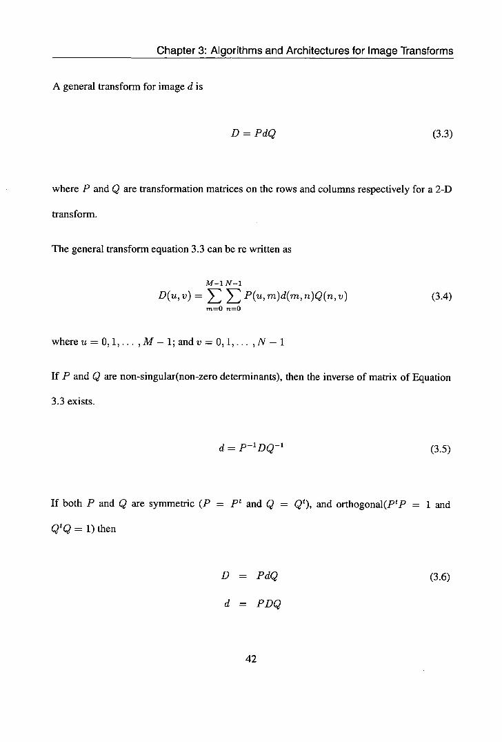
A general transform for image d is
(3.3)
where P and Q are transformation matrices on the rows and columns respectively for a 2-D
transform.
The general transform equation 3.3 can be re written as
M-1 N-i
D(u, v) = P(u, m)d(m, n)Q(n, v) (3.4) m=O n=O
whereu=O,1,...,M-1;andv=O,1,...,N-1
If P and Q are non-singular(non-zero determinants), then the inverse of matrix of Equation
3.3 exists.
d = P'DQ 1
(3.5)
If both P and Q are symmetric (P = Pt and Q = Qt), and orthogonal(PtP = 1 and
QtQ = 1) then
(3.6)
r
42

Chapter 3: Algorithms and Architectures for Image Transforms
and the transform is termed as an orthogonal transform [ 20].
Discrete Fourier Transform
The discrete Fourier transform is analogous to the continuous Fourier transform and may be
efficiently computed using the Fast Fourier transform algorithm. The properties of linearity,
shift of position, modulation, convolution, multiplication and correlation are similar to the
continuous one. The difference between them is the discrete periodic nature of the image and
its transform [23,24].
Let 4b jj be a transform matrix of size jxj
22 (k, 1) j
C (3.7) 1 (_i?kE)
-
-
wherek,1=0,1,... ,j-1
The discrete Fourier transform can be defined according to the following equation
F = MMI4'NN (3.8)
M-1 N-i / m flV
F(u, v) = f(m, n)e (-2iri(-u- + \
(3.9) tn=O n=O
43

Chapter 3: Algorithms and Architectures for Image Transforms
whereu=O,1,...,M—landv=O,1,...,N-1
The inverse transform matrix is given by
41(k,l) = (3.10)
and the inverse Fourier transform by
M-1 N-i
(27rz'( mu flv
f(m,n) = F(u,v)e--+-j.)) (3.11) u=O v=O
wherem=O,1,...,M—landn=O,1,...,N-1
Therefore, the kernel of the discrete Fourier transform is given by
e
(
.mu nv 27rz( M- + N )) (3.12)
When considering implementation of the discrete Fourier transform, equation 3.9 can be
modified to
M-1 r N-i (_2r.flu)
F(u,v) = e 2 )f(mn)]
tn =O L n=O
The term in the square brackets, which is actually a 1D Fourier transform of the mth line, can
be computed using the standard Fast Fourier Transform procedures. Each line is substituted
with its Fourier transform, and the 1D discrete Fourier transform of each column is computed

Chapter 3: Algorithms and Architectures for Image Transforms
[20].
Although the DFT offers a good energy compaction, it suffers from increased computational
complexity. Both real and imaginary components of the transform have to be computed as it
can be seen in Equation 3.13.
Hadamard Transform
The forward Hadamard kernel is defined as
1 g(x, u) = 7(_i)Eo' b1fr)b,(u) (3.14)
where the summation in the exponent is performed in modulo 2 arithmetic. Therefore a one
dimensional forward Hadamard transform is described by
N—i
H(u) = f(x)(-1)' b1(x)b(u) (3.15) a=O
where 1(x) is the image samples, N = 2h and u = 0,1,2,... , N - 1
A Hadamard matrix H is an nxn matrix with all entries +1 or -1(see Equation 3.16), such that
all rows are orthogonal and all columns are orthogonal [ 20].
The usual development starts with a defined 2x2 Hadamard matrix H22 , Equation 3.16. Each
step consists of multiplying each element in H22 by the previous matrix [20].
ER

Chapter 3: Algorithms and Architectures for Image Transforms
Ii 1 1 H22
= (3.16)
Hij H22 = [ JJ _2 ] (3.17)
Hj-j =Hjj (3.18)
F = HMMIHNN (3.19)
I = -JHMMFHNN
The Hadamard transform has no multiplications. This might seem like an advantage but it
turns out that it is very hard to analyse it.
Wavelet Transform
Wavelets are mathematical functions that divide data into different frequency components.
Each component is then studied with a resolution matched to its scale. Wavelets are suited
to modelling phenomena whose signals are not continuous. Wavelet compression algorithms
have achieved ratios of around 300:1 for still images [25]
The compression technique used in wavelets is using low-pass and high-pass filters to separ -
ate an image into images with low or high spatial frequencies respectively. Low frequency
images being those with gradual brightness change. This is the case for images like flat or
46

Chapter 3: Algorithms and Architectures for Image Transforms
rounded background areas. Such images appear soft and blurry. As for the high frequency
band, the images are sharp and crisp edged. To reconstruct the original image, the frequency
bands imaged are added together. This results in a near perfect image if the processing is
perfect [19,26].
Low pass
Filter
Low pass
Filter
Lowest pass Filter
QutlssUon 118 samplIng rate
Run-length fl- Huffman Coding if
High pass
Filter
High pass
Filter
Quantization 1/8 sampling rate Run-length i.+
luffman Coding
rate Run-iength
luttman Coding
Input
Highest pass Filter
Quantization 112 sampling rate Run-length
iuffman Coding
Figure 3.3: Wavelet compression
In figure 3.3, a pixel data stream from an input image is divided into several sub-bands by
a tree of low and high pass filters. Each filter allows a specific band of frequencies to pass.
There filters can be either digital or analogue.
Wavelet compression is a lossy process. The image quality is always compromised to some
extent. Higher compression rates results in high image distortion. This distortion is different
from the blocking effects arising from the DCT. Wavelet application areas include signal and
image compression [27], communications [25].
47

Chapter 3: Algorithms and Architectures for Image Transforms
Despite all the advantages exhibited by the wavelet transform, it has an inherent weakness.
This segmentation of an image into different frequency ranges requires that the resulting
images be stored in the interim before going through the quantisation stage. Therefore starting
of with a single image and ending up with several images costs in terms of storage space.
Karhunen-Loeve Transform
The Karhunen-Loeve Transform (KLT) is based on statistical properties of an image. Its
main applications are in image compression and rotation. A sample image I (x, y) can be
expressed in the form of an N 2 -dimensional vector x
xi l
xi 2
xi = (3.20) x ii
XjN 2
where x ij denotes the jth component vector x.
The covariance matrix of the x vectors is defined as
C. = E{(x - m)(x - mx)T} (3.21)
where m = E{x} is the mean vector and E is the expected value. Equation 3.21 can be
9.9

Chapter 3: Algorithms and Architectures for Image Transforms
approximated from image sample using the relations
m
(3.22)
and
M
C, (x - - mx)T (3.23) i=1
or
1
CX --- IxjxI _mxmxT M
(3.24) j
The mean vector is N 2 -Dimensional and C. is an N 2xN 2 matrix.
Let e j and ), i = 1, 2,... , N, be the eigenvectors and corresponding eigenvalues of C x .
The eigenvalues are arranged in decreasing order (\ I > ... > \Pp) for convenience. A
transformation matrix, A, whose rows are eigenvectors of C, is
e 11 e12 ... elN2
e2l e22 21%12 (3.25)
[ eN 2 1 eN22 ... 6N 2 N2
Me

Chapter 3: Algorithms and Architectures for Image Transforms
where e23 is the jth component of the ith eigenvector.
The discrete Karhunen-Loeve transform is simply a multiplication of the centralised image
vector (x - mr), by A to obtain a new image vector y:
y = A(x - m)
(3.26)
The KLT offers optimal energy compaction in the Mean Square error sense. That is €(k) =
E[(x - 5)T(x - )] is a minimum, where i is a representation of the truncated x in k terms. E
is the mathematical expectation operator. It also projects the data onto a basis that results in
complete decorrelation. Therefore, the KLT can reduce dimensionality if the data is of high
dimensionality [20,28].
As can be seen from the above presentation, the transform coefficients of the KLT vary from
image to image, hence they have to be computed on the fly. This can be very computationally
intensive for realtime and low power applications. Therefore, it is better to use the next best
efficient image transform.
Discrete Cosine Transform
The Discrete cosine transform and its inverse (IDCT) are the transforms for practical image
processing. Its energy compaction abilities are high. Another advantage over other transforms
is the existence of fast implementation algorithms. Because the DCT is the main subject of
50

Chapter 3: Atgorithms and Architectures for Image Transforms
this project, it will be discussed in detail in the next section. It is not the purpose of this thesis
to examine the IDCT, however the techniques proposed can be used to process the IDCT.
3.3 The Discrete Cosine Transform
Ever since it was discovered in 1974 by [29], the DCT has attracted attention from engin-
eering, scientific and research communities. This is indeed the least surprising because of
its energy packing capabilities which approach the statistically optimum transform, the KLT.
A number of fast DCT algorithms have been developed which also contributed to its hype
[22,30,31].
The following equation is a mathematical definition of an NxN DCT.
2 N-iN-i
GkGm (2i+1)klr ) ( (23+1)mlr N
) C(k,m)= >d(i,j)co.s(
2N CO3
2N (3.27)
i=O j=O
where Gk = Gm = 1 and G0 = 1/\/
in a matrix form, Equation 3.27 can be written as:
[Ce] = (3.28)
51

Chapter 3: Algorithms and Architectures for Image Transforms
where
[E] is the cosine matrix and [D] is the pixel matrix
An interesting quality of the DCT is that it is separable and orthogonal. The orthogonality
property implies that the energy of a signal is preserved under the transformation. The DCT's
separability principle implies that a multidimensional DCT can be implemented by a series
of one dimensional (1D) transforms. The advantage of this property is that fast algorithms
developed for 1D DCT can be directly extended to multidimensional transforms (Figure 3.4).
It should be observed that other forms of transformation do posses this separability quality.
Some examples are DFT, WHT, Haar etc [22].
PixelsCT data 1D DCT/IDCT
1D DCT/IDCT DCT data/Pixels
onrows
Figure 3.4: Implementation of 2D DCTby 10 DCTs
3.3.1 DCT Algorithms and Architectures
The development of efficient algorithms began soon after it inception. It was natural for
the initial attempts to focus on the computation of the DCT by using the EFT algorithms.
Although it was not developed as a discretised version of the FFT, the DCT's relation to the
DFT were exploited in the initial developments of its computational algorithms [22].
There are two main approaches for implementing the DCT. Firstly, there is the flowgraph
52

Chapter 3: Algorithms and Architectures for Image Transforms
based architecture, which has an advantage of minimising the total number of arithmetic op-
erations and also is the basis of the fast algorithms [32]. Secondly, there is the scalar product
based architectures, these have gained favour with designers for their regularity in nature
and can exploit the use of distributed arithmetic [33]. Several architectures are discussed in
literature, see [34-36]. This section introduces only fundamental architectures.
3.3.1.1 The Chen Algorithm
Consider the matrix E
E=I
dd d d d d d d
a c e g —g —e —c —a
b f -f —b —b -f f b
c —g —a —e e a g —c
d —d —d d d —d —d d
(3.29)
e —a g c —c —g a —e
f —b b -f -f b —b f
g —e c —a a —c e —g
where
it 37r it 37r it it a = cos,b = cos--,c = cos-,d = cos-,e = cos-,f = cos--,g = cos (3.30)
16
53

Chapter 3: Algorithms and Architectures for Image Transforms
The symmetry of matrix E can be exploited to represent the 1-D DCT as follows
[YO d d d
Y2I b f -f
d —d —d
[Y6j [1 —b b
d
—b xi+x6
d
-f j x3+x4
(3.31)
Yi a c e g
c —g —a —e
e —a g c
g —e c —a
The exploitation in. 3.31 results in the (NXN) multiplication matrix being replaced two
(N12)X(N/2) matrices which can be computed in parallel together with the sums and dif-
ferences on the right hand side of 3.31.
Implementations in [37],[38], [39], [40] and [41] are all derivatives of this algorithm. To
further reduce complexity, [37] observed that the first matrix processing in Equation 3.31
involves multiplication with only three cosine coefficients (b, d and f). Therefore, the multi-
plications can be reduced from 32 to 28 in total.
The Algorithm presented in [42] is derived from 3.31, however it only requires 16 multi-
plications with 2 Additions on the critical data path. Figure 3.5 depicts the data flow of this
54

0
1
2
3
4
5
6
7
0
4
2
6
1
5
3
7
Chapter 3: Algorithms and Architectures for Image Transforms
algorithm. The arrow (—)) in the figure represents subtraction. An example architecture that
can be used to implement this algorithm is depicted in Figure 3.6.
Figure 3.5: Data flow graph for the Chen Algorithm
3.3.1.2 The Arai Algorithm
Arai et al in [43] developed an algorithm that requires only 5 multiplications. This scheme is
shown in the flowgraph depicted in 3.7. This is only possible because the outputs are scaled.
To get the true values of the DCT coefficients, the output requires a further multiplication.
For some systems, this further multiplication can be incorporated in subsequent stages. For
example, the perceptual weights in the video encoding algorithm. This processing technique
is termed as scaled-DCT.
55

Hi \ \1
T G)
Reg
—~T, Reg
—~T,
0
1
2
3
4
5
6
7
0
4
2
6
5
1
7
3
Chapter 3: Algorithms and Architectures for Image Transforms
-- coefficient memory
Figure 3.6: DCT architecture based on four MAC processing units
Figure 3.7: Data flow graph for the Arai Algorithm
56

Chapter 3: Algorithms and Architectures for Image Transforms
3.3.1.3 The Chiu Algorithm
A different approach to the DCT implementation was proposed by Chiu et a! in [44,45]. They
propose a direct implementation whereby the DCT is computed recursively. The values of
the DCT are updated with each new sample. Each DCT utilises the results from a previous
DCT, ie the next DCT is obtained by adding the difference between it and the previous DCT
This method requires the Discrete Sine Transform (DST), therefore a computation of both
the DCT and the DST is necessary. Deriving the recursive expression from 3.32, we get 3.33
^ II1
(k,1)
,1)
Figure 3.8: Lattice structure
t+N-1 - 2G(k) (2(n - t) + 1)klr
C(k,t) )
- N > d(n)cos( 2N
(3.32)
n=t
57

Chapter 3: Algorithms and Architectures for Image Transforms
wherek=O,...,N-1
C(k, t + 1) = (C(k, t) + 2
[—d(t) + (_1)cd(t + N)] cos(j kir
))cos( kir -j -) (3.33)
+ (C8(k,t) + 2
[—d(t) + (_1)'d(t + N)] sin( ku-))sin( ku --)
where k 0; k = 0 is a special case. C3 (k, t + 1) is generated in the same manner as
Equation 3.33. The difference is that the first cosine and sine terms in Equation 3.33 are
swapped. C(k, t + 1) and C8 (k, t + 1) are obtained from C(k, t) and C3 (k, t) by subtracting
the effect of d(i) and adding the effect of d(i + N). This process is termed as time recursive
DCT.
Chiu et al proposed a fully pipelined architecture to compute the 2-D DCT from a frame-
recursive point of view. Two real-time lattice structures for successive frame and block 2-D
have been developed. These structures are fully pipelined with throughput rate N clock cycles
for an NxN successive input data frame. The resulting 2-D DCT architectures are modular,
regular, and locally connected and require only two 1 -D DCT blocks that are extended directly
from the 1-D DCT structure without transposition [44].
The 2-D DCT can be generated by using the lattice structure as in Figure 3.8. Depending
on the coefficients stored, the appropriate transform coefficient, Yk is computed. Every clock
unit, a new data input enters and gets processed. At the end of N cycles, the computations for
that set of N data elements are completed. By employing N such structures, all the transform

Chapter 3: Algorithms and Architectures for Image Transforms
coefficients are computed in parallel and made available at the end of N cycles. This parallel
computation of N coefficients represents the 1-D DCT.
Each kernel requires six multipliers for the computation of the forward transform alone.
Clearly, there are too many multipliers for the efficient VLSI implementation. The advantage
of this structure is its better numerical properties, being a normal form implementation as
opposed to the hR structure.
3.3.1.4 Distributed Arithmetic (DA) Implementation
Distributed arithmetic differs from conventional arithmetic in the order in which operations
are performed.
Consider a one dimensional N-point DCT defined as follows
C = >ejdj (3.34)
where ek's are W-bit constants and d's are coded in B bits using two's compliment repres-
entation, i.e
d1 = — d,0 + E d2 (3.35)
this leads to
59

Chapter 3: Algorithms and Architectures for Image Transforms
C = e(—d, o + jj d1 ,32) (3.36)
N-i B-i N-i = - ed,0 + i(2 e1d1,j23)
i=0 j=1 1=0
=
where
Et-o =e1 d1 , (3.37)
and
E0 = - ed1 ,o (3.38)
The change of summing the order in i and j characterises the DA scheme whereby the initial
multiplications are distributed to another computation pattern. Since the term E3 has only
2N possible values(that depend on the d,2 values), it is possible to store these 2N values
in a ROM. An input set of N bits {d 0,,, d1,,, ..., dNi,} is used as an address, allowing the
retrieval of E1 values. These intermediate results are accumulated in B clock periods, for
producing one C value. A typical architecture for DA computation is depicted in Figure 3.9.
The multipliers are replaced by a ROM followed by an accumulator [46,47].

Chapter 3: Algorithms and Architectures for Image Transforms
The DA takes advantage of ROM's in which the partial products are stored. This ROM's
need to be reset every internal clock. This is prone to increased power consumption since the
resets are implemented using a P-channel pull-up transistor. A direct path between VDD and
ground exists while the pull-ups are active [ 48].
D oj
D 11
D N-lJ
C o
C N-I
! I ! i ! I
Figure 3.9: Architecture of N input scalar product using DA
3.3.1.5 Bit-Serial Implementation
In cases where cost is an issue, where parallel implementations are too expensive in terms
of integration, bit serial implementation becomes a viable option. These are simply a direct
mapping of a data-flow graph. Some bit-serial DCT implementations are presented in [ 49],
[50], [51] and [52]. Balsara et al in [53] presented an overview of bit serial multipliers.
A detailed comparison of bit-serial and bit parallel implementations is presented in [54].
Another advantage of bit-serial is that wiring overheads are almost negligible because only
61

Chapter 3: Algorithms and Architectures for Image Transforms
1-2 wires need to be routed per interconnection [55]. However, the availability of more
routing layers, the impact of global interconnects on bit-parallel implementations may not be
so detrimental. In the context of power, bit-parallel implementations have the advantage of
being able to exploit data correlation for power reduction [56].
Multiplications additions, and ROM space
Number of Multiplications
Number of Additions
Number of ROM words
Number of RAM words
for Transposition
Per NxN Block Direct Computation N 4 N 4 - -
With Separability 2NO 2N 3 N 2 Fast Algorithm N 2 log2 N N 2 log2 N - N 2 PureDA - 32N 2N21v N 2 Mixed DA/FG - 34N N2 N 2
Per Pixel Direct Computation N 2 N 2 - -
With Separability 2N 2N - N 2 Fast Algorithm 1092 N 21092 N - N 2 PureDA - 2N2 2 N 2 Mixed DA/FG 2N3 17 N2 N 2
Table 3.2: Computation and Storage requirements for some DCTAlgorithms
3.4 Summary
This chapter presented the basics of image compression. It also highlighted relevant import-
ant features of some well known image transfonns and how they relate or compare with the
DCT. It is still fact that in terms of energy compaction, the DCT performs close to the optimal
KLT
There are several algorithms developed for the DCT ever since its invention. This goes to
show its continuing popularity amongst the image compression research and development.
Some algorithms are more suited for VLSI implementation than others, particularly the im-
62

Chapter 3: Algorithms and Architectures for Image Transforms
plementation using the separability principle of the DCT. This is so because of the regular
structure that results from implementation. Table 3.2 presents a summary of different imple-
mentation, which include computational complexity and ROMIRAM requirements.
63

Chapter 4 Low Power DCT Research
4.1 Introduction
Some of the work done by other researchers in order to address the problem of low power
DCT implementation is briefly summarised in this chapter. In addition it will also highlight
the need for DCTs and in particular, the low power DCT implementation.
Most research work considering low power implementation of the DCT have targeted redu-
cing the computational complexity of the design or modifying it for operation under a lower
supply voltage [57,58]. Both these techniques have a limited effect on power reduction. An-
other major contribution to power consumption is due to the effective switched capacitance
[56,59]. Only a few researchers have targeted reducing power of a DCT implementation
through a reduction in the amount of switched capacitance [60-62].
4.2 Work so far
Switched capacitance reduction has been achieved through techniques such as the adaptive
bitwidth reduction [61-63] and lookup table partitioning [60]. Xanthopoulos et al. [62]
demonstrated that bitwidth of arithmetic operations can be minimised dynamically in the
presence of data spatial correlation. This technique utilised the fact that image pixels are bc-

Chapter 4: Low Power DCT Research
ally highly correlated and they show a certain number of common most significant bits. These
MSB 's are only relevant for the DC component and can be rejected for all high frequency
coefficients. Hence the bitwidth is reduced, which in turn implies reduction of switching
activity.
For the lookup table partioning technique, Cho et al. [60] proposed a data driven variable
length decoder which exploits the signal statistics of variable length codes to reduce power.
The idea here is to minimise the average codeword length by exploiting the statistics of the
data. That is, shorter codewords are assigned to recurrent data while longer codewords are
assigned to sparsely occurring data. Therefore a minimum average codeword is experienced,
implying a reduction of switched capacitance.
Another circuit has been proposed in [63] which reduces signal transitions by adaptively
adjusting the number of the MSB 's to varying content of the input data. The scheme compares
the input pixels and dynamically shuts the MSB's values that have not changed.
Chen et al in [64,65] presented a low power architecture for video coding systems using a
combination of low power techniques such as multirate, look-ahead and pipelining. Multirate
in this context is defined as dividing the data stream into odd and even sequences and then
running the resulting modules at half the speed of the input data.
Targeting an asynchronous multiplier for the DCT, Kim et al [66] take advantage of the typ-
ically large fraction of zero and small valued data in the DCT application. Their design skips
multiplication by zero and dynamically deactivates bit slices that contain only sign extension
bits.
65

Chapter 4: Low Power DCT Research
The techniques here include removal of circuit blocks that computes the DCT coefficients
which will be quantised to zeroes, reordering of operations in constant-multipliers to reduce
transition probability, and re-designing cells for low-voltage operation. Power consumption
for an 8x8 2D DCT is estimated at 16.95mW [67].
The use of pipelining and parallelism for reducing power consumption is considered in [68]
for fast discrete cosine transforms. ROM-Based algorithms are also presented. In conclusion,
multiplier based implementations consumed less power than ROM based implementations.
But the ROM based Implementation was faster than the multiplier Implementation.
Chen et. al. in [58] presented a low power DCT chip. Their technique for power reduction
was based on reducing the complexity of the DCT by using the direct implementation of
the 2-D DCT. They also used a parallel distributed arithmetic approach with reduced power
supply voltage [58,69].
In [70], Masselos et al presented an approach for low power realisation of DSP algorithms
that are based on inner product computation. Their proposed methodology is based on an
architectural transformation that reorders the sequence of evaluation of the partial products
forming the inner products.
Although the methodology summarised above appears to be comparable to the schemes pro-
posed in this thesis, there are several key differences. The first difference worthy of noting is
that the methodology proposed by [70] is not generic, only the minimum Hanmiing distance
can be used with the methodology. This implies that no other ordering techniques can be used
even if it offers a better solution in terms of reducing switching activity. In [70], it is unclear
Chapter 4: Low Power DCT Research
how the data is being dealt with. This comes into consideration since when a matrix multi-
plication is to be processed, the row of the cosine matrix has to be multiplied with a column
of the data matrix. If the location of the entry in the row of the cosine matrix is changed, ap-
propriate measures have to be taken in the respective column entry so that the correct entries
are used. And finally, [70] proposes an architecture whereby data is transfered from the data
memory into a set of foreground registers. This foreground registers are configured in such
a way that they form a queue. That is when the second entry is being read from the data
memory, it pushes the first entry into the second register. This implementation suggests that
every time a new entry is being read from the data memory, all the registers are being written
to since data is being shifted into them. From our experience, this technique is very costly in
terms of switching activity.
This thesis presents a number of low power approaches for implementing the DCT. The low
power approach used is based on reducing the switching activity of circuit. The techniques
are generic and can be extended to include other applications where matrix multiplication
is required. Some DCT architectures which suit the schemes are proposed as proof of the
concept, and some power dissipation measures are given for the data path components.
4.3 A Case for Low-Power DCT
Until recently, dedicated signal processing hardware was a necessity for the DCT computa-
tion in real time video applications. MPEG2 compression for a 720 x480 frame size at 30
frames per second(fps) 4:2:0 requires approximately 132 mega operations per second worst
67

Chapter 4: Low Power DCT Research
case assuming that a fast computation algorithm is employed. Microprocessors (300M11z)
with instruction sets enhanced with multimedia extensions (ie Intel MMX) are capable of
perfonning multiple instructions per cycle by partitioning a single 64-bit integer datapath
into a two 32-bit, four 16-bit or eight 8-bit independent integer datapaths operating in par-
allel. Such instruction sets are ideal for the implementation of signal processing tasks that
involve multiple independent low precision integer operations. A 300 MIHz Intel Pentium
II can process 1.2 giga operations per second on 16-bit media data types. Therefore, it can
be observed that the DCT approximately occupies 11% of the processing resources avail-
able in commodity microprocessors today in a real time video application. The other 89%
of the machine resources may be allocated to other video processing tasks such as motion
compensation and entropy decoding or graphics computations for updating the display[61].
Some more figures reflecting the amount of data involved in video data are listed below.
• Five minutes of video
- 512x512 pixel colour image at 25 frames/sec requires 5.625 Gbytes
• Five still images
- 5 still images of size 512x512, 3 bytes for colour(RGB), requires 3.35Gbytes
This clearly calls for some form of compression in order to store data.
RN

Chapter 4: Low Power DCT Research
4.4 Summary
The chapter presented some of the work covered prior (or during) to this work in order to
address the problem of low power DCT implementation. The common technique witnessed
seems to be adaptively minimising the bitwidth of input pixel based on the statistics of image
content. This research proposes a different approach, unique to the DCT implementation,
whereby switched capacitance is reduced through manipulation and exploitation of correla-
tion in cosine coefficients during the computation of the DCT coefficients.
The need for low power DCT was also highlighted in this chapter. Some figures are given to
enhance the appreciation of how computation-costly the DCT can be.

Chapter 5 Column-Based DCT Scheme
5.1 Introduction
An exploration of the first scheme is presented by the use of the multiplier unit example. This
involves the power analysis of the multiplier section of the proposed scheme environment.
The multiplier unit is well-known for its computation intensive nature. This scheme is termed
Column-Based.
5.2 Column Based Processing
The computational bottleneck for the implementation of the DCT is the multiplication of the
cosine coefficients matrix [E], by the pixel matrix [D], in order to obtain the DCT coefficients
[C], i.e.
[C] = [E] * [D]
(5.1)
where each element CIk in [C] matrix of order n is given by:
70
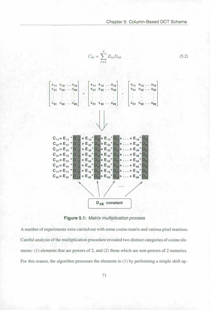
Chapter 5: Column-Based DCT Scheme
C2k
=
(5.2)
C 11 C 12 C18 E 11 E 12 .E18 D il 0 12 D 8
C 21 C 22 c28 E21 E E28 0 21 0 22
81 C 82 C E81 E 82 0 81 D 82
C ll =E ll *+ED2l ±E l3*+...+E,D8l
C 21 = E 21 * + E 2 . D21 ± E23 * +. . . + E 2 . 081
C 31 = E31 * + E 3 : D21t E33+. . . + E 3; D81
C 41 = E1 *+ E 4 021+ E 43 * + . . I + E 4 D81
C 51 = E 51 + E 5 021± E - D31 +. . . + D81
C 61 = E61 * + E6021 -- E * D31 + .. +E D81
C71= *
71 + E 7 . D21 + E73 * +. . . + E D81
C 81 =E 81 *+E* 021+ E*+. . .+E 6 D81
\ / ___Zz F Dxk constant I
Figure 5.1: Matrix multiplication process
A number of experiments were carried out with some cosine matrix and various pixel matrices.
Careful analysis of the multiplication procedure revealed two distinct categories of cosine ele-
ments: (1) elements that are powers of 2, and (2) those which are non-powers of 2 numerics.
For this reason, the algorithm processes the elements in (1) by performing a simple shift op-
71

r 5: Column-Based DCI Scheme
eration. It is well known that the switched capacitance of a shift is significantly less than that
of a multiplication[58].
Examination of the multiplication procedure embodied in Equation 5.2 can reveal more scope
for power optimisation. This can be demonstrated by expanding Equation 5.2 with n=8,
as shown in Figure 5.1. As could be deduced from the figure, when the computation is
performed on the basis of evaluating coefficients successively, i.e. G 11 -C81 , then new pixel
and coefficient values are processed at both inputs of the multiplier. If the multiplication
procedure is performed on a column-after-column basis (i.e. E 1 *D11 , E 2 *D21 , and so on)
then the value of Dk will be constant (for 8 multiplications) at the corresponding multiplier
input. This implies less switching activity at the multiplier inputs and memory buses.
For each column being processed, the multiplication procedure outlined above has the product
form (m*constant), where m are the cosine matrix elements in the column being processed.
The constant remains valid for only these values of m, if the column changes, a new constant
is activated.
The multiplication results are unchanged irrespective of the order in which the constant is
multiplied by the sequence of cosine coefficients in the column. For this reason, the algorithm
performs the multiplication of elements in (2) in a column-by-column fashion and orders the
elements, in the column being processed, according to some criteria. In this case, the criteria
being minimum switching activity (hamming distance) between consecutive coefficients mul-
tiplied by the constant. This guarantees that similar elements are subsequently applied to the
inputs of the multiplier causing minimum switching activity within the internal circuit of the
72

Chapter 5: Column-Based DCT Scheme
Figure 5.2: Flowchart of the algorithm
73
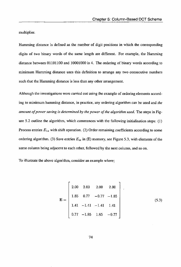
Chapter 5: Column-Based DCT Scheme
multiplier.
Hamming distance is defined as the number of digit positions in which the corresponding
digits of two binary words of the same length are different. For example, the Hamming
distance between 01101100 and 10001000 is 4. The ordering of binary words according to
minimum Hamming distance uses this definition to arrange any two consecutive numbers
such that the Hamming distance is less than any other arrangement.
Although the investigations were carried out using the example of ordering elements accord-
ing to minimum hamming distance, in practice, any ordering algorithm can be used and the
amount of power saving is determined by the power of the algorithm used. The steps in Fig-
ure 5.2 outline the algorithm, which commences with the following initialisation steps: (1)
Process entries E1 with shift operation. (2) Order remaining coefficients according to some
ordering algorithm. (3) Save entries Ei., in (E) memory, see Figure 5.3, with elements of the
same column being adjacent to each other, followed by the next column, and so on.
To illustrate the above algorithm, consider an example where;
2.00 2.00 2.00 2.00
1.85 0.77 —0.77 —1.85 E =
1.41 —1.41 —1.41 1.41
0.77 —1.85 1.85 —0.77
(5.3)
74

Chapter 5: Column-Based DCT Scheme
Demux
Multiplier Shifter
CosIne 1 Mux
Pixel I Matrix Ii Memory ii IMemory 1 V
(D) (E) \J 4 DCT Coel.
Control Register
Bank(R)
Figure 5.3: Simplified architecture of the processor
75

Chapter 5: Column-Based DCT Scheme
and
35 32 31 34
32 37 31 31 D =
29 28 27 31
26 28 31 34
After the first iteration (i=1, x=1, and k=1), the first column, E 1 , is ordered according to
minimum hamming distance to produce the ordered sequence (2.00, 0.77, 1.41, 1.85). The
original locations of these elements are stored. Next the above sequence is multiplied by the
first entry in D 1 , 35. The entries in registers Ri will be (70, 64.75, 49.35, 26.95), where
the first entry (70) is saved in R 1 and the second entry is saved in R 2 and so on. Similarly
at the end of iteration 2 (i=2, x=1, and k=1), Ri will contain (134, 89.39, 4.23, -32.25).
The last iteration (i=4, x=1, and k=1) for this particular column, results in R i containing the
first column of the DCT coefficient matrix [C], i.e. Ri = Cxj = (244, 18.96, 0, 1.35)T.This
procedure is carried out until x =k = n, at which case R 1 will contain C44
As it stands, the algorithm can be implemented on traditional DSPs without any loss in
throughput. However for high throughput applications, a modified processor architecture
is required. The architecture, a simplified version of which is shown in Figure 5.3, requires
an internal register bank in order to store the partial products, (R), which eventually result
(5.4)
76

Chapter 5: Column-Based DCT Scheme
in the DCT coefficients, [C]. In addition, a memory unit is allocated for both the cosine and
the pixel matrix elements, E and Dk respectively. A shifter is included to cope with the
additional shift operations. The multiplier and the adder units are included to perform the
normal multiply-add DSP operations. Since the outputs of both the multiplier and the shifter
have to share the same input of the register bank, a multiplexer is needed to resolve which
one output can use the register bank input. Another multiplexer is required to handle outputs
from multiplier/shifter and adder units since some of the inputs to the register bank proceed
directly to the bank without passing through the adder.
5.3 Simulation Results and Analysis
Figure 5.4 illustrates the framework utilised for the evaluation of the scheme with a number
of 512x512 pixel example benchmark images. These, which include Lena, Man and checked
images, are shown in Appendix C. The cosine coefficient matrix used was obtained using the
MATLAB signal processing toolbox [71].
The evaluation environment is based upon the JPEG standards, where images are processed
in blocks of W. For this reason our results are obtained with n=8, i.e. an 8x8 cosine matrix
is used with 512x512 pixel images being processed in blocks of 8x8. Some MPEG imple-
mentations subscribe to this processing. An 8x8-bit array Multiplier was constructed, using
the Cadence VLSI suite with ES2 0.7 CMOS Technology, and processed down to layout
level[72].
77

Chapter 5: Column-Based DCT Scheme
A C-program based test-fixture mapping system was developed to generate input simulation
files for the Verilog-XLTM digital simulator [73]. This involved forming the appropriate
image-pixel/cosine-coefficient pairs, in the order imposed by the multiplication algorithm, so
that they can be applied to the inputs of the hardware multiplier.
Three types of input simulation files are generated, representing the use of one of the follow-
ing: (1) Traditional cosine DCT multiplication (Traditional). (2) Column-based multiplica-
tion algorithm without ordering (Column-based). (3) Column-based multiplication algorithm
with ordering according to minimum hamming distance (Hamming). In each simulation, the
number of signal transitions (switching activity), at the output of each gate, is monitored. Ca-
pacitive information for each gate is extracted from the layout of the multiplier circuit. Both
of these are used to obtain a figure for the total switched capacitance of the multiplier.
Table 5.1 illustrates the results obtained with the different bench mark images. Clearly, power
saving is achieved in all cases with a maximum of 50% with the checked image using Ham-
ming, which reduces the amount of switched capacitance at both multiplier inputs. An aver-
age power saving of around 35% is achieved over all benchmark images.
The results illustrate that although the amount of power saving is proportional to the fre-
quency of pixel value variation across the image, significant power saving is achieved with
all image types. This includes those with sharp variation in pixel value, such as the checked
image, and those with continuous spectrum of pixel values, such as Lena, Man and Peppers
images (See Appendix Q. This in turn implies the suitability of the scheme for wide ranges
of images including coloured images.
im

Chapter 5: Column-Based DCT Scheme
Column-Based Hamming
HOL I I Simulator
Files
Circuit I Switching
Layout I Monitor
Capacitance
Informati Overall
Switched
Capacitance
Figure 5.4: Framework for algorithm evaluation
79

Chapter 5: Column-Based DCT Scheme
Image Ordering Switched Capacit- ance (pF) * 103
Switched Capa-citance reduction (%)
Horizontal Stripes Traditional 13.77 -
Column-Based 8.45 38.64 Hammtng 7.06 48.64
Vertical Stripes Traditional 7.70 -
Column-Based 7.55 1.97 Hamming 6.41 16.84
Blocks Traditional 9.25 -
Column-Based 7.65 17.27 Hamming 6.47 29.99
Checked Traditional 13.81 -
Column-Based 8.39 39.25 Hamming 6.83 50.50
Lena -
Traditional 39.01 -
Column-Based 29.51 24.35 Hamming 26.23 32.77
Man Traditional 40.05 -
Column-Based 30.08 24.91 Hamming 26.63 33.50
Peppers Traditional 39.57 -
Column-Based 29.75 24.84 Hamming 26.49 1 33.05
Table 5.1: Typical power savings
RE

Chapter 5: Column-Based DCT Scheme
5.4 Conclusions
The chapter presented an effective scheme for the low power implementation of the DCT
within an JPEG/MPEG based environment. The scheme reduces power through the utilisa-
tion of shift operations, where possible, together with sequencing coefficient and pixel multi-
plications in an order dictated by the bit correlation of their successive values. This results in
up-to 50% power reduction with a number of standard benchmark images. The investigations
revealed that the scheme provides a generic framework for power saving in that significant
power savings is achieved with a range of standard image types. These include those with
sharp, continuous, and low pixel variation frequency. The scheme can easily be extended
to the implementation of the 2D DCT. A full implementation of the scheme presented here
is the subject of the next chapter which will also address possible overheads resulting from
ordering of the cosine coefficients.
81

Chapter 6 Column-Based OCT Processor
6.1 Introduction
Based on the foundation laid by the previous chapter, this chapter maps the column-based
scheme into a DCT processor. The resulting architecture is then analysed for power con-
sumption with the results being compared with the power consumption of a conventional
DCT processor.
6.2 Column-Based Scheme Implementation
This section will discuss the implementation of the column-based scheme. A brief summary
of various components of the architecture will be given. If a component is built from other
sub-components, the sub-components will subsequently be discussed under the component
heading.
The proposed architecture for the column-based scheme is illustrated in Figure 6.1. The
reference architecture for the original implementation used for comparison with the column-
based scheme is shown in Figure 6.2. The original implementation is a direct mapping of the
1-D DCT equation in matrix form.
The emphasis of the implementation is on the data path of the proposed architecture. The
MN

Chapter 6: Column-Based DCT Processor
pIx
resi
cloi
Figure 6.1: DCT processor modified for Column based processing
)Ut
Figure 6.2: Typical original DCT processor architecture
83

Chapter 6: Column-Based DCT Processor
data path for the design is considered to be the Multiply-Accumulate (MAC) unit shown in
Figure 6.3. The column based MAC unit consists of the multiplier, an adder, and a latch
bank. (see Figure 6.3). It should be noted that the MAC unit in this design differs from a
conventional MAC unit in the sense that this one has a latch bank consisting of 8 latches
whereas a normal MAC unit will have a simple register in the place of the latch bank. For the
multiplier unit, two multiplier implementations were used, the csa, and Wallace architectures.
These are listed in Table 6.1. The adders used are also listed in Table 6.1.
pixel cosine
mac_out
Figure 6.3: Implementation of column based mac unit
Adders I Multipliers
Brent-Kung (bk) I Carry-save array (csa) Carry look-ahead (cia) I Booth-coded Wallace tree (wall)
Table 6.1: some of the Design Ware components used
84

Chapter 6: Column-Based DCT Processor
6.2.1 Multipliers
The multiplier unit in the DCT processor is the most power hungry component. The previous
section explored the scheme based only on the power consumption of the multiplier unit.
There are several multiplier implementations reported in literature [74], but for the purpose
of this project we used two implementations. It should be noted that since the project is
based on comparing conventional DCT with the new schemes, it should not matter which
component implementations are used, as long a the same modules are used in both designs.
The multipliers examined in the project are briefly introduced below.
Carry-save Array multiplier
The Carry-Save Array (csa) multiplier architecture used for the design is capable of pro-
cessing signed numbers (two's compliment). The Baugh-Wooley algorithm [75] was de-
veloped to perform regular direct two's complement multiplication. It does not need prior
converting of multiplicands/multipliers to unsigned numbers and then back to signed after
processing.
Consider two numbers A and B as follows:
A = (an_ i ... ao) = —a_ 12' + E a1 2 (6.1)

Chapter 6: Column-Based DCT Processor
B = (b_1 ... b0) = — b_ 1 2 1 +E b1 2 (6.2)
The product A.B is given by the following equation, see Equation 6.3
n-2 n-2 n-2 n-2
A.B = a_ 1 b_ 1 222 + abj2i - a_1 - b_ 1 E a2' (6.3) i=0 j=0 i=0 1=0
If using this form, it can be seen that subtraction operations are needed as well as additions.
However, negative terms may be written as shown in Equation 6.4.
—a_ 1 = a_i (-222 + 2' + E b2+1- ') (6.4)
For this approach, A.B becomes
n-2 n-2 n-2
A.B = a_1 b_ 1 22' 2 + aibj2t+3 +a_i (-222 + 2' +
:=0 j=0 i=0 n-2
+b_1 (-222 + 2' + 2' 1) (6.5)
1=0

r 6: Column-Based DCT Processor
Equation 6.5 can be put in a more convenient form with the recognition of
—(as 1 + b y)2n-2 = _22n_1 + (+)22n_2 (6.6) - n-1j'-
Therefore A.B becomes
A.B = _221 + + 1 + a_ib_i )22' 2
n-2 n-2
+EE abj2' + (an_i + b_1 )2 i=O j=O
n-2 n-2 7j2n+i1 + a_1 (6.7)
i=O i=O
Using the above equations, an n x n multiplier can be implemented using only adder units.
This is shown in Figure 6.4 for an 4x4 two's compliment multiplier. Figure 6.4(a) gives an
example of the multiplication for a 4x4 multiplication whereas 6.4(b) depicts an implantation
of the multiplier.
Booth-coded Wallace tree(wall)
This is a parallel implementation of a multiplier unit which combines two well-known ap-
proaches that enhance the speed of multiplication. These approaches are the Booth encoding
technique and the Wallace tree reduction. It is reported in [76,77] that the Booth encoding
87

p6 p5 P4 P3 P2 131 Po
0 b0
0 b1
Chapter 6: Column-Based DCT Processor
a3 bo t a1 L ao i
a3b1 a2 b a1 b1 a0 b1
a3b2 a2 b2 a1b a0t
a3 b3 a2 b3 • 1 b3 aO N
b3
+ 1 83
P, Pe P5 P4 P3 P2 P1 P3
(a) Example 01 Baugh-Wooley multiplication
(b) Baugh-Wooley multiplier Implementation
Figure 6.4: A signed Carry-save Array Multiplier example and implementation

Chapter 6: Column-Based DCT Processor
reduces the number of partial products by 50% while the Wallace tree increases the speed of
summing the partial products[74, 77-79]. The steps involved in the scheme are listed below:
See Figure 6.5
Booth encoding
Wallace tree reduction
final adder unit.
a b
Final addition
"U, Product
Figure 6.5: General architecture for Booth-coded Wallace Multiplier
1) Booth Encoding
Let the multiplier B be represented as
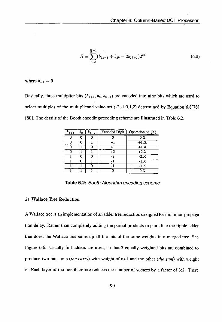
Chapter 6: Column-Based DCT Processor
B = 1(b2k_l + b2k - 2b2k+1 )22 k (6.8)
where b_ 1 = 0
Basically, three multiplier bits (bk+l , bk, bk_i) are encoded into nine bits which are used to
select multiples of the multiplicand value set (-2,-1,0,1,2) determined by Equation 6.8[78]
[80]. The details of the Booth encoding/recoding scheme are illustrated in Table 6.2.
bk+j I bk bk_i Encoded Digit j Operation on (X) o -ö-- 0 0 0.X o 0 1 +1 +1.x o -1- 0 +1 +1.x o 1 1 +2 +2.X 1 0 0 -2 -2.X 1 0 1 -1 -1.X 1 r o -1 1 I 1 0 0.x
Table 6.2: Booth Algorithm encoding scheme
2) Wallace Tree Reduction
A Wallace tree is an implementation of an adder tree reduction designed for minimum propaga-
tion delay. Rather than completely adding the partial products in pairs like the ripple adder
tree does, the Wallace tree sums up all the bits of the same weights in a merged tree, See
Figure 6.6. Usually full adders are used, so that 3 equally weighted bits are combined to
produce two bits: one (the carry) with weight of n+1 and the other (the sum) with weight
n. Each layer of the tree therefore reduces the number of vectors by a factor of 3:2. There
MI
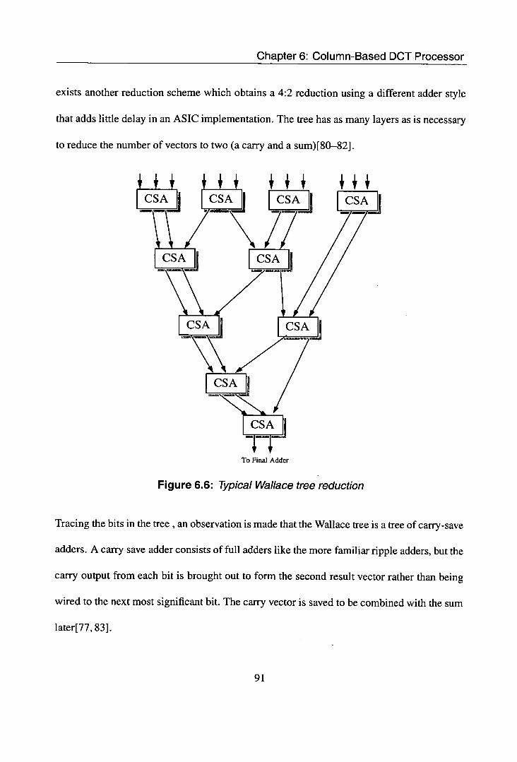
Chapter 6: Column-Based DCI Processor
exists another reduction scheme which obtains a 4:2 reduction using a different adder style
that adds little delay in an ASIC implementation. The tree has as many layers as is necessary
to reduce the number of vectors to two (a carry and a sum)[80-82].
To Final Adder
Figure 6.6: Typical Wallace tree reduction
Tracing the bits in the tree , an observation is made that the Wallace tree is a tree of carry-save
adders. A carry save adder consists of full adders like the more familiar ripple adders, but the
carry output from each bit is brought out to form the second result vector rather than being
wired to the next most significant bit. The carry vector is saved to be combined with the sum
later[77, 83].
91

Chapter 6: Column-Based DCI Processor
3) Final Adder Unit
After the Wallace tree reduction, there is a need for a final addition stage. The ripple adder is
used for this purpose. A typical ripple adder is depicted in Figure 6.7.
a3 b3 a2 12 a 1 b 1 a Q b0
Ac~C2~Ajl I~Ajl
i I co 1FA1jIS cm
C 3 S 3 S 2 S 1 S 0
Figure 6.7: Final Addition Using ripple adder
6.2.2 Adders
A brief overview of the adders used in the designs follows.
Carry look-ahead (cia)
The disadvantage of Ripple Carry Addition is that each carry is dependent on the previ-
ous carry, which results in a long delay. Carry-Lookahead Addition produces the carries in
parallel.
The CarryOut logic equation is
CarryOut = (a. b) (a ED Carr yIn) ED (b. Carr yIn) (6.9)
92

Chapter 6: Column-Based DCT Processor
This can be rewritten as
c[i + 1] = (a[i] b[i]) ED (a[i] c[i]) ED (b[i] c{i])
= (a[i] b[i]) (c[i] (a[i] e b[i])) (6.10)
where c[i] is the carry into the i-th full adder.
3. We define
g[i] = a[i] . b[i] (6.11)
p[i] = a[i] e b[i] (6.12)
and rewrite the carry equation as
c[i + 11 = g[i] (c[i] . p[i]) (6.13)
93

Chapter 6: Column-Based DCT Processor
4. For a 4-bit Carry-Lookahead Adder the carry equations are
c[l] = g[O] ED (c[OJ p[O})
= g[1] ED (c[1] p[l])
= 9[1] (p[l] g[O}) (p[l] p[O] cEO])
= g[2] ED (c[2]
= g[2] ED (p[2] g[1]) ED (p[2] p[l] g[O]) e (p[2] p[1] p[O] c[O]) (6.14)
The 4th carry can be produced using a regular full adder.
Brent-Kung(bk)
The Brent-Kung adder is identified by its regular layout [84]. This was first presented by
Brent and Kung in [85]. One of the distinct characteristics of the Brent-Kung Adder is that
computation time increases logarithmically as the number of bits increases linearly.
tadd o 1092 N
(6.15)
Define an operator o such that
(g,p)o(g',p') = (g+p.g',p.p') (6.16)
where g and g' are carry generate terms formed any two input bits [85].

(G1,P1) = I (gi, pi)
(gj,pj) (G1_ 1 ,P1 _ 1 ) if2 i < n
(6.17)
Chapter 6: Column-Based DOT Processor
p and p' are carry propagate terms.
Also
Equation 6.17 together with the fact that o is associative, is the fundamental key that supports
the Brent-Kung approach. The associative property allows the computation of (G e , P1 )'s in
any order. Hence Gi can be considered as a block carry generate signal and P1 as a block carry
propagate signal. The problem of computing (Ge, P1 ), for i = 0 to 16 can now be done in
the order defined a binary tree as in Figure 6.8. The main components of the carry generation
tree are the o operator denoted in the diagram by white circles.
6.2.3 Latch Bank
The latch bank module consists of a demultiplexor, gating module, 8 latches, and a multi-
plexor. See Figure 6.9. The components of this module are briefly described as follows.
Demux
The demux block is simply a 8 to 1 demultiplexor used to decode the write address. A single
data line can be connected to a number of output lines by appropriate choice of signal on
the select lines as shown in Figure 6.10. If a demultiplexor contains .s select lines, then the
number of possible output lines n to which data can be routed is n = 2. A demultiplexor
95

Level
1
2
S 15 S14 13 12 S 11 S IO S9 8 S7 6 5 4 S3 2 s S0
Chapter 6: Column-Based DCI Processor
Figure 6.8: Brent-Kung Parallel Prefix Network
read add
write ad
inpu
elk
)utput
Figure 6.9: Latch bank module
M.

Chapter 6: Column-Based DCT Processor
that contains an enable signal can serve as a decoder[86].
lutputfoJ
_0411
utput(2J
)utput(3J
utputf4J
ufput(5J
utput(6J
uu?7
Figure 6.10: Demultiplexor
Gating
The next module in the bank is the gating logic. Gating the clock is a powerful technique
used in low power design to disable unused modules of a circuit. Gating can create power
savings by both preventing unnecessary activity in the logic modules as well as eliminating
power dissipation in the clock distribution[87, 88].
This unit gates the clock such that only the latch which needs to be written is activated.. This
technique helps reduce the power consumption of the device by making sure that only the
one latch toggles at any given time. The example Figure 6.11 relates to the output of the
Demultiplexor for the first latch (at address 0). Gating signal cik with the address enable
in_0, this will produce latch enable enable_0 for the first latch only when both cik and in])
are asserted. Hence all other latches will not be activated within the current cik period.
97

Chapter 6: Column-Based DCT Processor
in
ci;4D- 0enabie_O
Figure 6.11: Gating example for first Latch
The Gating module consists of 8 sets of gating logic as in Figure 6.11. This implies that there
is gating logic for each Latch in the Bank.
Latches
A latch is a level sensitive device. The output of a latch (Q) is transparent to the input (D)
as long as enable signal is activated. If the enable signal is disabled the output (Q) remains
constant and any change that occurs in the input is ignored. See Figure 6.12 for the latch
diagram.
,flp'
rese
enabi
)utput
Figure 6.12: Latch
For this design a reset signal is required in the storage element because there is a need to clear
the contents and start a new computation when a fresh column from the pixel matrix [D] is
being processed.
The advantage of a latch based storage over register based storage is that they are considerably
smaller (gate count) than registers. Therefore they consume less power. But a designer has
KV

Chapter 6: Column-Based DCT Processor
to be aware of the pit-falls of latch based designs. They can be prone to glitches and hold
time violations. The glitches can be avoided by using a glitch free enable. For the hold time
violation, one should ensure that data is held for long enough as the latch is closed. Figure
6.13 illustrates a latch array. This is an array of 8 latches that will be required to implement
the storage element. Since the output of the multiplier is 16 bits in total, each latch in the
array should be capable of storing 16 bits. It should be noted that the precision of the data
path is 16 bits. This implies that as the wordlength of the result increases beyond 16 bits, it is
truncated. This truncation will affect the quality of the resulting image.
Mux
The function of the Mux is to multiplex the outputs of the 8 latches on to a single data bus
which is fed back to the adder module and/or output out of the DCT processor module. A
multiplexor routes 1 of many inputs to its output under the control of 1 or more select signals.
See Figure 6.14.[89].
6.3 Synthesis and Simulation Results
The data path for the DCT (MAC unit) and its test-bench were implemented in Verilog. The
input images that were used for the simulations were preprocessed to chop them into blocks of
8x8 matrices. The images tested can be found in Appendix C. The designs were synthesised
with Synopsys's Design Compiler using the Alcatel 0.35tm CMOS library.
The simulation environment is shown in figure 6.15. An image is segmented into blocks
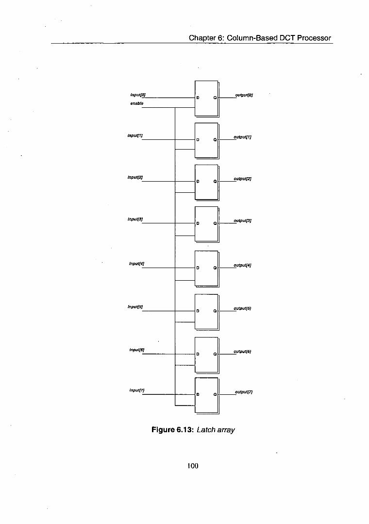
Chapter 6: Column-Based DCI Processor
Figure 6.13: Latch array
100

Chapter 6: Column-Based DCI Processor
)utpul
Figure 6.14: Multiplexor
of 8x8 using a perl script and this is input into the testbench environment. The temporary
storage of the test image is 64x8. On the other input channel, the cosine coefficients, another
array of 64x8 size is used. The elements in this memory module are sorted out according to
some algorithm, (either hamming, ascending, or any other algorithm) and then passed to the
testbench for processing. It should be noted that any algorithm that minimises the bit toggling
between any consecutive inputs can be used with this scheme.
During simulation, the toggle information is logged into a file as bits are being processed.
This is referred to as the SAIF/toggle file. The information is then annotated into Synopsys
DesignPower for the estimation of the power consumption. Appendix D summarises the
DesignPower strategy for power analysis.
Tables 6.3 and 6.4 presents the results for the Column-based DCT scheme and conventional
DCT respectively.
101

Chapter 6: Column-Based DCT Processor
Image Implementation Power(mW) cip nsp tdp
mult I (cip) add (cip)
latch bank (cip)
lena ascending 5.91 6.79 12.69 1.17 2.58 2.15 hamming 5.5 633 11.82 1.03 2.40 2.05
wallace ascending 7.30 8.41 15.71 1.91 3.17 2.20 hamming 7.18 8.25 15.43 1.81 3.16 2.20
checked ascending 6.42 7.42 13.84 1.58 2.68 2.15 hamming 6.24 7.17 13.42 1 1.36 2.66 2.20
Table 6.3: Column Based dct results for bk with csa
Image Power(mW) mult add reg cip I nsp I tdp I (cip) (cip) (cip)
lena 4.89 5.59 10.47 2.35 1.67 0.87 wallace 5.03 5.73 10.75 2.43 1.72 0.88 checked 5.41 6.45 1 11.87 3.03 1 1.63 0.76
Table 6.4: Conventional dct results for csa with bk
Image I Implementation [Power (mW) Power savings (%)
conventional 2.35 -
lena hamming 1.03 56.17 ascending 1.17 50.21
conventional 2.43 -
wallace hamming 1.81 25.51 ascending 1.91 21.40
conventional 3.03 -
checked hamming 1.36 55.11 ascending 1.58 47.85
Table 6.5: comparison of the multiplier units
102

Chapter 6: Column-Based DCT Processor
Input Image cosine matrix - elements
8X8 block I I Column
generation Based ordering
VHDLiVerilog Testbench
I VHDL/Verilogj
SAW/Toggle 1 ,
j [iesin Annotation
{ Design Power File
Figure 6.15: Simulation environment
Table 6.5 presents the power dissipation within the multiplier units. The power consump-
tion of the multiplier unit when using the scheme is compared to that of the conventional
implementation. A percentage of the difference relative to the conventional implementation
is presented. This reflects that although there is an overall overhead in the design, the multi-
plier section is still saving some energy compared to the conventional implementation. The
resulting overhead is due to extra logic required to implement this scheme. A set of 8 re-
gistersflatches is required compared to only one in the conventional implementation. The
overhead is not of too much concern since for the implementation of a 2D DCT, an interme-
diate memory unit is required for the transposition process. This transposition memory can
be reused as a temporary storage for the partial sums. Another source of extra circuitry comes
103

Chapter 6: Column-Based DCT Processor
from addressing the re-ordered cosine coefficients.
Image Implementation ________________
Power(mW) cip I nsp I tdp
mult (cip)
add (cip)
latch bank (cip)
wall+bk 5.59 6.28 11.88 0.97 2.24 2.21 lena wall+cla 5.15 5.84 11.00 0.97 1.96 2.23
csa+cla 4.53 5.08 9.61 0.95 1.85 1.73 wall+bk 6.16 6.87 13.03 1.26 2.52 2.38
wallace wall+cla 5.75 6.40 12.15 1.27 2.12 2.36 csa-i-cla 6.05 6.82 12.87 1.90 2.52 1.63 wall+bk 5.95 6.63 12.58 1.31 2.26 2.37
checked wall+cla 5.44 6.23 11.68 1.31 1.89 2.34 csa+cla 5.39 6.11 11.50 1.30 2.17 1.92
Table 6.6: Column Based dct results for other implementations with hamming sort
Image Implementation Power(mW) cip I nsp I tdp
mult (cip)
add (cip)
latch bank (cip)
wall+bk 6.26 7.03 13.26 1.18 2.72 2.74 lena wall-+-cla 5.66 6.37 12.00 1.18 2.15 2.33
csa+cla 5.08 5.71 10.79 1.11 2.13 1.83 wall+bk 6.52 7.32 13.84 1.52 2.62 2.39
wallace wall+cla 6.09 6.81 12.91 1.52 2.19 2.37 csa+cla 6.29 7.13 13.42 1.79 2.58 1.93 wall+bk 6.24 6.98 13.23 1.55 2.35 2.33
checked wall+cla 5.82 6.49 12.32 1.55 1.96 2.31 csa+cla 5.46 6.19 11.64 1.44 2.14 1.88
Table 6.7: Column Based dct results for other implementations with ascending sort
For other multiplier and adder combination implementations, the results are presented in
Tables 6.6 and 6.7. The effects of varying the word length of the inputs to the datapath are
presented in the Table 6.8. As can be seen from the results, the multiplier unit within the
MAC saves power despite the increased wordlength.
104

Chapter 6: Column-Based DCT Processor
Implematation Wordlength Power(mW) cip nsp tdp
mult I (cip) add (cip)
latch bank orreg(cip)
Column-based 8 bits 5.50 6.33 11.82 1.03 240 2.05 16 bits 9.63 8.61 18.24 TT 2.56 3.10 24 bits 12.94 13.73 26.68 34 3.83 3.77
Conventional 8 bits 4.89 5.59 10.47 2.35 1.67 0.87 16 bits 9.18 11.77 20.85 5.50 2.34 1.35 24 bits FTT28 15.37 32.64 1 9.87 4.45 2.95
Table 6.8: Wordlength variations: for csa and bk implementations with lena image
6.4 Conclusions
This chapter presented an implementation of the low power scheme for DCT processing in-
troduced in chapter 5. The scheme reduces power through the utilisation of sequencing coef-
ficient and pixel multiplications in an order dictated by the bit correlation of their successive
values. This results in up-to 56% power reduction within the multiplier unit for a number of
standard benchmark images.
Since the scheme requires saving of partial summations prior to outputting the DCT coeffi-
cients, a set of 8 registers is required compared to the conventional implementation which
requires only one. This register bank has a significant overhead on the overall power saving
such that the advantage revealed within the multiplier section is diminished. Theoretically,
only two registers/latches are expected to be switching when the scheme is in operation. One
read register and one write register, so the expected power overhead should be at least twice
the consumption of the single register in the conventional implementation. This however is
not completely unacceptable since in cases where a 2D DCT implementation is required, the
intermediate memory for transposition can be used to temporarily store these partial sums
and no extra circuitry will be required. Another source of overheads is the addressing of
105

Chapter 6: Column-Based DCT Processor
the ordered cosine coefficients. This requires extra circuitry in the control logic and also
the original location of the cosine coefficient entry to saved. Hence a wider storage unit is
required.
Different combinations of multiplier and adder units were analysed for power consumption.
In all combinations, the column-based implementation saved power within the multiplier unit.
106

Chapter 7 Cosine Ordering Scheme
7.1 Introduction
The scheme presented in this chapter takes advantage of the rows in the cosine matrix. Or-
dering the cosine coefficients in each row according to some ordering technique such as,
ascending order or minimum hamming distance, minimises the toggles at the inputs of the
multiplier unit in the DCT processor. Reducing the number of toggles at the inputs of the
multiplier reduces power consumption in the unit [4,90]. Since the multiplier unit is the most
computationally expensive unit in the data path of a DCT processor, it provides the most
advantage if it is targeted with a power conscious approach.
The scheme utilises the cosine coefficients ordering as in [90], however, the ordering is done
in the rows of the cosine matrix rather than the columns. The advantage of ordering the
coefficients in rows can be easily identified by the fact that no modification is needed in the
data path as in [90]. Therefore the overheads will be minimum since the same data path is
used as the one in the conventional implementation.
This chapter presents the implementation of the scheme, starting with the scheme exploration
at multiplier unit to the MAC unit. Some results are presented which reflect a power saving
of up-to 24%.
107

Chapter 7: Cosine Ordering Scheme
7.2 Order-Based Processing
The cosine coefficients [E] for any DCT implementation are constant, therefore ordering can
be done prior to loading them into a ROM unit. When the ordering is undertaken, the original
row location of the coefficient is tagged along with the corresponding cosine coefficient word.
The proposed cosine coefficient representation is shown in Figure 7.1. This consists of two
portions:
the original location of the cosine coefficients with a row in the cosine matrix.
the cosine coefficient value
This allows the saved location to be used as the address of the corresponding pixel element
to be computed. The three MSB 's of Figure 7.1 represent the pixel row location in the pixel
matrix, whereas the remaining bits represent the value of the cosine coefficient.
original cosine location element
Figure 7.1: cosine coefficient with saved location
The flowchart for the implementation is depicted in Figure 7.2. The flowchart assumes that
ordering of the cosine coefficients has already been done prior to commencement of the steps
in the chart. Note that the flowchart is for processing one block of the image (8x8). For the
processing of an entire image, the complete flowchart should be followed in order to process
each 8X8 block. The steps for the scheme are listed below.
108

Chapter 7: Cosine Ordering Scheme
Decode the cosine word nE into its constituent parts. ie , pixel location (n) and cosine
word(E)
Get the value pixel(D) from location specified by n in (1)
Multiply ; E * D and add the result to the accumulator
Repeat steps (1) to (3) for the remaining row entries
Obtain the DCT coefficient (C) and clear the accumulator
repeat 1) to 5) until the last row of cosine matrix is processed
Restart processing of the next image block
A simplified DCT processor for the proposed scheme is depicted in Figure 7.3. This differs
with the conventional implementation by the fact that a slice of the data coming from cosine
coeff memory is used as an address for the pixel memory. This slice is the original location
portion of the cosine word as depicted in Figure 7.1.
The depth of the pixel memory is 64, therefore a 6 bit address is required to access a memory
of this depth. This problem is alleviated by using a 3 bit counter for the rest of the 6 bit
address. The address from the counter is appended as the most significant bits of the pixel
memory address to make a 6 bit word. The counter is incremented after every 8 memory
accesses. The overhead for this extra circuitry is very minimum since ordinarily a 6 bit
counter would have been required to generate the address for the pixel memory. Another
issue that might arise from this design will be the larger data word size of the cosine coeff
109

Chapter 7: Cosine Ordering Scheme
Figure 7.2: Flowchart of cosine ordering scheme
110

Chapter 7: Cosine Ordering Scheme
memory compared to the conventional implementation. This is covered by the fact that on
a conventional implementation a 6 bit address bus will be required to connect between the
control and the pixel memory (the dashed connection in Figure 7.3, labelled p.iiddr). So, as
far as bus toggling is concerned, for the proposed implementation there are 3 bits that can
toggle compared to the 6 bits that would be generated otherwise.
The multiplier implementations that were used for the scheme exploration are the same as the
ones used in the previous chapter. These are listed here for better clarity; the csa, nbw and
wall.
The emphasis of the implementation is on the data path of the proposed architecture. The data
path for the design is considered to be the multiply and accumulate (MAC) unit shown in Fig-
ure 7.4. The column based MAC unit consists of the multiplier, an adder, and a register. For
the multiplier unit, several multiplier implementations were used, the csa, nbw, and wallace
architectures. This are listed in Table 7.1. The adders used are also listed in Table 7.1.
Adders I Multipliers II Brent-Kung (bk) Carry-save array (csa) Carry look-ahead (cia) Non-Booth coded Wallace tree (nbw)
Booth-coded Wallace tree (wall)
Table 7.1: some Design Ware components
The same MAC unit architecture (see Figure 7.4)was used for both the conventional imple-
mentation and the cosine ordering scheme. The modules in the MAC unit are mult, add and
reg. The module mult, was implemented using Baugh-Wooley multiplier. For the add module,
Brent-Kung adder implementation was used. After testing several adders, the Brent-Kung ad-
111

Chapter 7: Cosine Ordering Scheme
der proved to be more power efficient and suitable for high speed applications. An ordinary
register with reset, clock and enable signal was used for the module reg. The enable signal is
asserted after every 8 multiplications to clear the register.
)Ut
Figure 7.3: A simplified DCT processor architecture
To illustrate the above algorithm, consider an example where the cosine matrix is as shown
in Figure 7.5(a). After sorting, according to minimum hanmiing distance, the cosine matrix
will be as in Figure 7.5(b).
As an example consider the multiplication of nE (Figure 7.5(b)) with the following matrix.
35
32 D =
29
26
112

Chapter 7: Cosine Ordering Scheme
pixel cosine
mac_out
Figure 7.4: A simplified MAC unit architecture
113

Chapter 7: Cosine Order Scheme
64 64 64 64
84 35 -35 -84
64 -64 -64 64
35 -84 84 -35
Original Cosine Matrix (a)
64 164 264 364
084 35
64 364 1764 64
284 3 35 1-84
Sorted Cosine Matrix (nE) (b)
Figure 7.5: Example cosine matrix before and after ordering
Evaluation of the first row in Figure 7.5(b), the multiplication procedure between this row
and [D] will follow the same steps as conventional matrix multiplication since the order has
not been altered. The second row however has been ordered according to minimum hamming
distance. So the multiplication for the row will resume with 84*35. This is because the
first entry (84) in the second row has n=O which implies that the first entry in [D] should be
processed. The next entry to be processed is -35 which has n=2, hence the multiplication
.35*29 will be carried out. The third computation is 84*26. Finally 35 *32 is processed. The
multiplication procedure carries on to the next row of the cosine matrix and follows the same
technique.
7.3 Synthesis and Simulations Results
The multipliers used for the design exploration were implemented in Venlog and a test-bench
for each multiplier was created. The input images that were used for the simulations were
preprocessed to chop them into blocks of 8x8 matrices. Examples of the images tested can be
114

Chapter 7: Cosine Ordering Scheme
found in Appendix C. The designs were synthesised with Synopsys's Design Compiler using
the Alcatel 0.35im CMOS library. Both top-down and bottom-up strategies were carried for
the synthesis was bottom-up compile strategy.
The simulation environment is shown in figure 7.6. The same gate-level netlist for the multi-
pliers was used for the simulation of the conventional implementation and the cosine ordering
scheme. To also keep the level of fairness in comparison, the same netlist for the MAC unit
was used in simulations for both the conventional implementation and the cosine ordering
scheme.
Tables 7.2,7.3 and 7.4 illustrate the results obtained for the scheme exploration with differ-
ent multiplier implementations. It can be seen from the tables that the scheme exhibits a
maximum power saving of 24%.
Table 7.5 illustrates the results obtained with the different scenarios used to test the algorithm.
As the table shows, power savings are achieved with all examples, with a maximum of 29%
power saving for the MAC unit. The horizontal striped image provides the most power say-
ing. This is the result of the inherently low toggling of the pixels within the image. For
this image, the conventional MAC consumed a total dynamic power (tdp) of 6.57mW. This
is listed under conventional for the horizontal stripes image. Cosine ordering according to
'minimum hamming distance' results are termed hamming. For the horizontal stripes, the tdp
consumption for hamming is 4.75mW. Compared to conventional, a power saving of 22.25%
is experienced. And finally ascending is used to represent cosine ordering according to as-
cending order. This produces a power saving of 29%. The cell internal power (cip) of the
115

Chapter 7: Cosine Ordering Scheme
MAC components is also listed in Table 7.5. The power consumption at the multiplier section
of the MAC unit constitutes a larger part of the total power consumption. This affirms the
theory that the multiplier is the most power hungry unit in the data path of a DCT processor.
For the MAC unit design that was used, the multiplier unit consumed an average of 46% of
the total cell internal power. See Figure 7.7
I cosine elements
8X8 block I I Row
generation Based ordering
VHDL/Verilog Testbench
r~l SAIWFogge I _____ Design Annotation I >1 Design Power
File I
Figure 7.6: Simulation environment
Image Implementation Power(mW) cip I nsp I tdp
Power saving(%)
Lena conventional 2.33 2.74 5.07 22.09 cosine ordenng 1.83 2.12 3.95
Wallace conventional 2.41 2.76 5.17 20.31 cosine ordering 1.94 2.18 4.12
checked conventional 2.77 3.72 6.49 24.19 cosine ordering 1 2.13 1 2.79 1 4.92
Table 7.2: results for csa mult: ascending order
116

Chapter 7: Cosine Ordering Scheme
23 I LegendMult 01111111I 31% L Add
Reg
Figure 7.7: Average percentages of cell internal power dissipation per module
Image Implementation Power(mW) cip I nsp I tdp
Power I saving(%)
Lena conventional 2.50 3.80 6.30 10.48 cosine ordering 2.25 3.39 5.64
Wallace conventional 2.43 3.69 6.12 9.64 cosine ordering 2.20 3.33 5.53
checked conventional 1.23 2.39 3.62 22.10 cosine ordering 1 1.01 r_1._81J_T8_2J
Table 7.3: results for wall mult: ascending order
7.4 Conclusions
The chapter presented a simple but very effective low power scheme for the implementation
of the DCT. The scheme takes advantage of the rows in the cosine matrix by ordering the
cosine coefficients in each row according to some ordering technique such as minimum ham-
ming distance. This minimises the toggles at the inputs of the multiplier unit in the DCT
processor. Reducing the number of toggles at the inputs of the multiplier reduces power con-
sumption in the unit. This scheme is able to save up-to 24% power dissipation compared to
the conventional implementation of the DCT. Because the same implementation architecture
as the conventional DCT is used, the scheme can be used in conjunction with other tech-
117

Chapter 7: Cosine Ordering Scheme
Image Implementation Power(mW) cip I nsp tdp
Power saving(%)
Lena conventional 1.65 2.58 4.23 14.89 cosine ordering 1.42 2.18 3.60
Wallace conventional 1.77 2.75 4.52 11.73 cosine ordering 1.59 2.40 399
checked conventional 2.44 4.00 6.44 15.22 cosine ordering 1 2.14 3.32 5.46
Table 7.4: results for nbw mult: ascending order
Image Implementation Power(mW) cip I nsp tdp
mult I (cip) add (cip)
reg (cip)
Power saving(%)
conventional 5.25 459 9.84 2.33 1.75 1.17 -
Lena hamming 4.41 3.75 8.16 1.84 1.49 1.08 17.07 ascending 435 3.73 8.08 1.83 1.45 1.07 17.89
conventional 5.34 4.60 9.94 2.41 1.75 1.18 -
Wallace hamming 4.46 3.76 8.22 1.91 1.46 1.08 17.30 ascending 4.48 3.79 8.27 1.94 1.45 1.09 16.80
conventional 5.48 5.19 10.67 2.77 1.66 1.05 -
checked hamming 4.57 4.12 8.76 2.21 1.38 0.99 17.90 ascending 441 4.06 8.47 2.13 1.31 57 20.62
conventional 5.35 5.08 10.43 2.73 1.59 1.03 -
vertical hamming 4.60 4.21 8.81 2.27 1.35 0.98 15.53 stripes ascending 4.40 4.05 8.45 2.16 1. 0.96 19.01
conventional 3.54 3.03 6.57 1.56 1.06 0.92 -
horizontal hamming 2.62 2.13 4.75 0.98 0.79 0.85 22.25 stripes cosine ordering 2.55 2.09 4.63 0.963 0.75 083 29.53
Table 7.5: results for mac with csa mult and bk adder
niques in literature which reduce computational complexity of the DCT. It should be noted
that some overheads are possible due to the addressing of the ordered coefficients. This over-
head is minimised by using a 3 bit counter instead of the 6 bit address that is reqiured for the
conventional implementation.
118

Chapter 8 Cosine Coding Scheme
8.1 Introduction
It is a well known principle amongst the digital hardware design circles that a shift operation
is more energy efficient than a multiplication operation, hence the motivation for developing
a scheme which removes the burden of the multiplication operation and replacing it with a
more power conscious shift operation.
In this scheme the need for a multiplication unit is eliminated by fonnating the data repres-
entation of the cosine elements such that the pixel values are processed using a shifter unit
and an addition unit.
8.2 Data Representation
A close examination of the cosine elements reveals that in their fractional representation, they
are all numbers between -0.4904 and 0.4904, see Equations 8.1 and 8.2. The proposed data
representation scheme is as depicted in Figure 8.1. The MSB is used to indicate the sign of the
cosine coefficient. The MSB is high for a negative coefficient and low for a positive one. The
remaining bits are used to define the fractional part of the cosine coefficient. Depending on
the accuracy desired, the number of bits for the fractional part can be increased as appropriate.
119

Chapter 8: Cosine Coding Scheme
Therefore, wordlength affects quality of the results in this case. A reduced wordlength will
have negative impact on the image quality whereas an increase in wordlength will improve
the quality.
E=I
dd d d d d d d
a c e g —g —e —c —a
b f -f —b —b -f f b
C —g —a —e e a g —c
d —d —d d d —d —d d
(8.1)
e —a g c —c — g a —e
f —b b -f -f b —b f
g —e c —a a —c c —g
where
a = 0.4904,b = 0.4619,c = 0.4157,d = 0.3536,e = 0.2778,f = 0.1913,g = 0.0975
(8.2)
For example if the cosine element is 0.2778, the MSB will represent the sign bit, '0', and the
remaining bits will represent the fraction, 0.2778. For a 6 bit fractional part precision, 0.2778
will be represented as 010010. See table 8.1
120
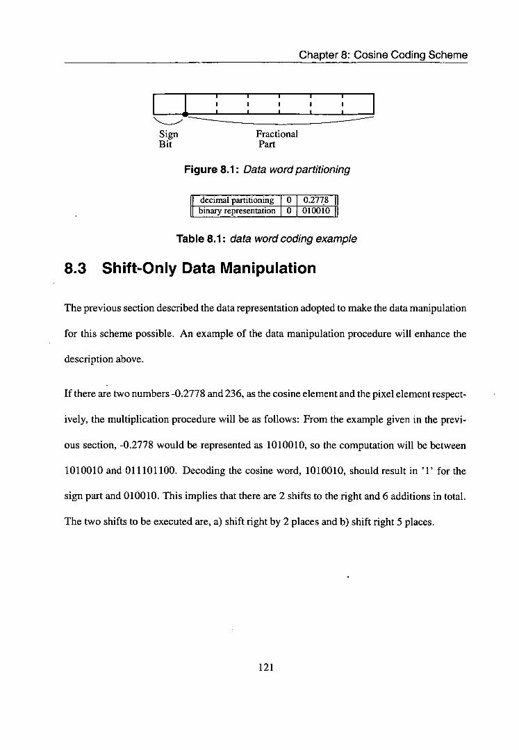
Chapter 8: Cosine Coding Scheme
I I I I I I
I I I I I I I I I
Sign Fractional Bit Part
Figure 8.1: Data word partitioning
decimal partitioning 0 0.2778 binary representation 0 010010
Table 8.1: data word coding example
8.3 Shift-Only Data Manipulation
The previous section described the data representation adopted to make the data manipulation
for this scheme possible. An example of the data manipulation procedure will enhance the
description above.
If there are two numbers -0.2778 and 236, as the cosine element and the pixel element respect-
ively, the multiplication procedure will be as follows: From the example given in the previ-
ous section, -0.2778 would be represented as 1010010, so the computation will be between
1010010 and 011101100. Decoding the cosine word, 10 100 10, should result in '1' for the
sign part and 010010. This implies that there are 2 shifts to the right and 6 additions in total.
The two shifts to be executed are, a) shift right by 2 places and b) shift right 5 places.
121

Chapter 8: Cosine Coding Scheme
8.4 Implementation
To reduce the computational complexity of the architecture, the addition is deferred until the
final addition stage, this ensures that there is only one final adder stage unit.
Decode
This module decodes the coded cosine coefficient. This is simply breaking it into the corn-
ponents Sign Bit and Fractional Part. Sign Bit is directed to the conversion module, while
Fractional Part is used by the shr unit to inform the unit of the required number of shifts.
convert
This module receives a signal from the decode module. If the signal is high, the input pixel
to be processed has to be converted using to negative two's compliment number.
shr unit
The shr units module, contains the right shifters. For the example shown in Figure 8.2,
there are four right shifters in total, that implies that the fractional part of the coded cosine
word has got a precision of four bits. Within the shifting modules there are multiplexors
which determine whether a shift has to be executed or not, otherwise the the value just passes
through without any shifting. If the sign bit in the coded cosine word is '1', then the input
pixel is converted to negative two's compliment by the conversion module before it gets
shifted.
Compression
In Figure 8.3, there is a module referred to as CSA, in this module a unit adder is used instead
122

Chapter 8: Cosine Coding Scheme
of a fulladder. Each unit adder adds four data inputs and one carry input. It generates one
sum bit and two carry outputs[9 1 ]. The carry signals are not used for the current addition, but
rather for its successor[92]
add
This is the final stage addition. The carry that was saved in the previous, compression unit, is
propagated within this module to produce the sums.
pixel cosine
__ 1 [ convert
[ decode
]
11 shr units
hi Compression
add
I reg
output
Figure 8.2: Implementation of cosine coding scheme
123

Chapter 8: Cosine Coding Scheme
from Shifters from Shifters from register
to adder
Figure 8.3: Implementation of the compression unit
8.5 Results and Analysis
The model was designed in VHDL and synthesised using 0.35tm technology from Alca-
tel. The input images that were used for the simulations were preprocessed to divide them
into smaller blocks of 8x8 matrices. Some examples of the images tested can be found in
Appendix C. The designs were synthesised with Synopsys's Design Compiler.
The simulation environment is shown in figure 8.4. This involves pre-coding of the cosine
coefficients before they are entered into a memory unit in the design. Cadence's VerilogXL
was used in conjuction with toggle count to capture the switching activity of the design during
gatelevel simulation. For the power analysis, DesignPower (See Appendix D) was used to
estimate the power estimation.
124

Chapter 8: Cosine Coding Scheme
Tables 8.3 illustrate the results obtained for the scheme with a number of images. The con-
vetional implementation results are given in Table 8.2. It can be seen from table 8.3 that the
scheme exhibits a maximum power saving of 41%.
Input Image
I cosine matrix
elements
8X8 block Cosine
generation coding
VHDIJVer11og Testbench
T~9 - SAiFlToggle I _____ Design Annotation >]
Design Power File I
Figure 8.4: Simulation environment
Image Power(mW) cip j n tdp
mult (cip)
I add (cip)
reg (cip)
lena 5.25 4.59 9.84 2.33 1.75 1.17 wallace 5.34 4.60 9.94 2.41 1.75 1.18 checked 5.48 5.19 10.67 2.77 1.66 1.05 vertical stripes 5.35 5.08 10.43 2.73 1.59 1.03 horizontal stripes 3.54 3.03 6.57 1.56 1.06 0.92
Table 8.2: results for conventional mac with csa mult and bk adder
125

Chapter 8: Cosine Coding Scheme
Image Power(mW) cip I nsp I tdp
compression (cip)
add (cip)
shifters (cip)
I reg (cip)
Power I saving(%)
lena 463 2.84 7.47 2.37 0.92 0.40 0.94 24.09 wallace 4.72 2.90 7.62 2.41 0.94 0.42 0.94 23.34 checked 5.28 3.51 8.79 2.94 0.74 0.82 0.79 17.62 vertical Stripes 4.88 3.22 8.09 2.63 0.71 0.75 0.79 22.44 horizontal Stripes 240 1.41 3.81 1.12 0.42 0.15 0.71 41.10
Table 8.3: results for cosine coding scheme
8.6 Conclusions
A new implementation scheme has been presented in this chapter which has an obvious ad-
vantage over conventional methods by using shift operators. The advantage was further en-
hanced by the use of compression units to defer the addition to the final stage accumulation
stage. This was made possible by intoducing a new data representation scheme where the co-
sine coefficients are coded as sign and fractional parts. A power saving of 41% was achieved
by the scheme over the conventional scheme. The accuracy of this implementation depends
largely on the wordlength chosen for the fractional part of the data representation. Choosing
a large fractional wordlength will result in a better image quality but reduced power savings.
Hence this implementation is better suited for applications where image quality is not the
main concern.
126

Chapter 9 Conclusions
A number of power saving schemes having been proposed and implemented in this project.
These schemes focus on the multiplier section of the DCT processor since it consumes more
power than the other components in the design. This chapter summarises the findings of the
various techniques employed. Potential future work suggestions to further enhance this work
are also presented.
9.1 Conclusions and Discussion
The literature review section, chapters 2,3 and 4, presented the basic of low power design and
the basics of image compression. It also highlighted relevant important features of some well
known image transforms and how they relate or compare with the DCT. It is still fact that
in terms of energy compaction, the DCT performs close to the optimal KLT. Some common
DCT algorithms and Architectures were presented. There are several algorithms developed
for the DCT ever since its invention. This goes to show its continuing popularity amongst the
image compression research and development community.
The Column-Based scheme was introduced in chapter 5. The scheme reduces power through
the utilisation of shift operations, where possible, together with sequencing coefficient and
pixel multiplications in an order dictated by the bit correlation of their successive values.
127
Chapter 9: Conclusions
This results in up-to 50% power reduction with a number of standard benchmark images.
The investigations revealed that that the scheme provides a generic framework for power
saving in that significant power savings is achieved with a range of standard image types.
These include those with sharp, continuous, and low pixel variation frequency. The scheme
can easily be extended to the implementation of the 2D DCT.
Chapter 6 presented an implementation of the low power scheme for DCT processing intro-
duced in chapter 5. The proposed architecture of the data-path was implemented in verilog.
The scheme reduces power through the utilisation of sequencing coefficient and pixel multi-
plications in an order dictated by the bit correlation of their successive values. This results
in up-to 56% power reduction within the multiplier unit for a number of standard benchmark
images.
Since the column-based scheme requires saving of partial summations prior to outputting the
DCT coefficients, a set of 8 registers is required compared to the conventional implement-
ation which requires only one. This register bank has a significant overhead on the overall
power saving such that the advantage revealed within the multiplier section is diminished.
Theoretically, only two registers/latches are expected to be switching when the scheme is in
operation. One read register and one write register, so the expected power overhead should
be at least twice the consumption of the single register in the conventional implementation.
This, however, can be avoided in cases where a 2D DCT implementation is required, the in-
termediate memory, for transposition can be used to temporarily store this partial sums and
no extra circuitry will be required.
128

Chapter 9: Conclusions
Chapter 7 presented a very effective low power scheme for the implementation of the DCT.
This scheme is able to save up-to 24% power dissipation compared to the conventional im-
plementation of the DCT. Because the same implementation architecture as the conventional
DCT is used, the scheme can be used in conjunction with other techniques in literature which
reduce computational complexity of the DCT. Although this scheme does not exhibit as much
power saving within the multiplier unit as the Column-based scheme, it does not have any
overheads.
Another implementation scheme has been presented in chapter 8 which has an obvious ad-
vantage over conventional methods by using shift operators. The advantage was further en-
hanced by the use of compression units to defer the addition to the final stage accumulation
stage. A power saving of 41% was achieved by the scheme over the conventional scheme.
This scheme can be used in conjunction with any of the two order based schemes to further
enhance the power saving of the DCT processor.
9.2 Novel Outcomes of the Research
Three new schemes for reducing the switched capacitance, within the multiplier section, of
the DCT processor were successfully developed. The first two schemes, column-based and
order-based, reduce switched capacitance through manipulation and exploitation of correl-
ation in pixel and cosine coefficients during the computation of the DCT coefficients. The
techniques are generic and can be extended to include other applications where matrix mul-
tiplication is required. The third scheme proposes coding cosine coefficients such that only
129

Chapter 9: Conclusions
shift operations are used to process the DCT computation.
The column-based scheme reduces switched capacitance through manipulation and exploita-
tion of correlation in pixel and cosine coefficients during the computation of the DCT coef-
ficients. The manipulation is of the form of ordering the cosine coefficients per colunm,
according to some ordering technique such as, ascending order or minimum hanuning dis-
tance and processing the matrix multiplication using a colunm-column approach instead of
the usual row-column approach. Several low power design techniques were used in imple-
menting this design. Some of the techniques used include clock gating and the use of latch-
based storage. A power saving of up-to 50% within the multiplier section was achieved with
this implementation.
The order-based scheme takes advantage of the rows in the cosine matrix. Ordering the
cosine coefficients in each row according to some ordering technique such as, ascending
order or minimum hamming distance, minimises the toggles at the inputs of the multiplier
unit in the DCT processor. The above techniques are generic and can be extended to include
other applications where matrix multiplication is required. This scheme is able to save up-to
24% power dissipation compared to the conventional implementation of the DCT.
The third scheme proposes coding cosine coefficients such that only shift operations are used
to process the DCT computation. In this scheme the need for a standard multiplication unit
is eliminated by fonnating the data representation of the cosine elements such that the pixel
values are processed using a shifter unit and an addition unit. With this scheme, a power
saving of up-to 41% can be achieved.
130

Chapter 9: Conclusions
9.3 Future Work
There are a few areas in which the work in this thesis can be further investigated. Some are
listed below.
For the Column-Based scheme, an implementation of the 2D DCT is needed. This
will enable the investigation of the proposed solution to the overhead incurred by the
scheme. The proposed solution is to reuse the matrix transposition memory as an inter-
mediate storage, therefore eliminating extra circuitry (latch bank).
For an increased power efficient DCT engine, a combination of the Order-Based and
Cosine-coding schemes should be considered. This should result in the advantages of
both schemes being experienced by the combined unit. Some overhead is expected due
to the increase of the cosine word wordlength.
A comparison of this implementation technique to other techniques such as RUM-
Based multipliers and digit-serial implementations should be considered.
The power estimation methodology used was pretty accurate, it was based on the gate-
level netlist after synthesis. A more accurate power reading can be achieved after cir-
cuit layout and back annotating the resulting parasitics. This will offer a reading that is
highly close to the actual value. This suggests that a layout of circuit should be carried
out.
An implementation of the IDCT using the proposed schemes can be considered as an
enhancement.
131

Chapter 9: Conclusions
A complete DCT engine Intellectual Property (IP) should be considered. This involves
all the components in the proposed architectures of the schemes. It would be an ad-
vantage if the IP is reconfigurable and/or programmable. The parameters could include
input wordlengths (both pixel word and cosine coefficient word), output wordlength,
data representations (e.g two's complement or sign-magnitude), internal data accur -
acy(wordlength, truncation, rounding).
The IP developed can be incorporated in a working environment for either JPEG or
MPEG standards and its performance observed relative to other implementations.
The multiplication schemes can be used in other applications where matrix multiplica-
tion is required
132

Appendix A Image Compression Standards
A.O.1 JPEG
JPEG(Joint Photographic Experts Group) is a standardized image compression mechanism.
The 'Group' reflects the original committee that wrote the standard.
JPEG is designed for compressing either full-colour or gray-scale images of natural, real-
world scenes. JPEG is designed to exploit known limitations of the human eye. For example,
the fact that small colour details aren't perceived as well as small details of light-and-dark.
Thus, JPEG is intended for compressing images that will be looked at with a human eye, not
for machine analysis [93-95 ].
A useful property of JPEG is that the degree of lossiness can be varied by adjusting corn-
pression parameters. This means that during image capture, trade off file size against output
image quality can be made. Image files can be made extremely small if high image quality
is of no importance. This is useful for applications like indexing image archives and view
finders. On the other hand, if output image quality is an issue, high compression ratios can
be sacrifised for satisfactory image quality [93,95].
133

Appendix A: Image Compression Standards
RR RIak
mpressed ge a
Figure A.1: Block diagram of JPEG Compression
134

Appendix A: Image Compression Standards
Why use JPEG
There are two fundamental reasons to use JPEG
to make the image files smaller
to store 24-bit-per-pixel colour data instead of 8-bit-per-pixel data
Making image files smaller is an advantage for transmitting files across networks and for
archiving libraries of images.
If the viewing software does not support JPEG directly, JPEG has to be converted to some
other format for viewing or manipulating images. Even with a JPEG-capable viewer, it takes
longer to decode and view a JPEG image than to view an image of a simpler format such as
GIF. Hence, using JPEG is essentially a tradeoff between time and space.
The second fundamental advantage of JPEG is that it can store full colour information: 24
bits/pixel (16 million colours). The other image format, GIF, widely used on Usenet, can
only store 8 bits/pixel (256 or fewer colours) [95].
Baseline JPEG (Lossy)
Steps involved in the baseline compression algorithm[93]:
1. Firstly an image is transformed into a suitable colour space. For greysc ale this step in
unnecessary, but for colour images RGB is transformed into a luminance and chromin-
135

Appendix A: Image Compression Standards
ance color space (YCbCr, YUV, etc). The luminance component represents gray scale
and the other two axes are colour information. The reason for changing colour spaces
is that more information can be lost in the chrominance components at acceptable costs
than in the luminance component. The human eye is not as sensitive to high-frequency
colour information as it is to high-frequency luminance.
Downsample each component by averaging together groups of pixels. This is an op-
tional step. The luminance component is left at original resolution, while the colour
components are usually reduced 2:1 horizontally and either 2:1 or 1:1 vertically. This
step immediately reduces the data volume by one-half or one-third, while having virtu-
ally no impact on perceived quality.
Group the pixel values for each component into blocks of 8x8. Transform each 8x8
block through a discrete cosine transform (DCT). The motivation for doing this is that
high-frequency information can be thrown away without affecting low-frequency in-
formation.
For each block, divide each of the 64 DCT coefficients by a separate quantization
coefficient, and round the results to integers. This is the fundamental Lossy step. A
quantisation coefficient of 1 loses no information, while larger ones lose successively
more. The higher frequencies are usually reduced much more than the lower.
Encode the resulting coefficients using Huffman. This step is lossless, therefore it does
not affect image quality.
6. Attach appropriate headers, etc, and output the result. In an interchange JPEG file, all
136

ix A: Image Compression Standards
of the compression parameters are included in the headers so that the decompressor can
be able to reverse the process.
The decompression algorithm reverses the above process, and normally adds some smoothing
steps to reduce pixel-to-pixel discontinuities.
A.O.2 MPEG
The MPEG standards are generic and universal in the sense that they specify a compressed
bitstream syntax. There are three main parts of the MPEG specifications. Namely systems,
video, and audio components. The video part defines the syntax and semantics of the corn-
pressed video bitstreams. The audio defines the same thing for audio bitstream, while the
system addresses the multiplexing of video and audio streams into a single stream with all
necessary timing information[19, 94].
Standard I Bit rate Function Screen size
MPEG-i 1.14 to 3.0 mbps delivery of video for 352x240 pets at 30 a CD-ROM for NTSC
MPEG-2 6 to 8 mbps broadcast quality 720x480 pets at compressed video 60 for NTSC and
720x576 pels at 50 for HDTV
MPEG-4 64 kbits/s tow bit rate video Under development phones, interactive databases, interactive newspapers etc
Table A.1: Typical MPEG standards specifications
At the top level of the hierachy (Figure A.2), the video bitstream consists of video sequences
MPEG-i allows only progressive sequences, while MPEG-2 allows both progressive and
137

Appendix A: Image Compression Standards
H Video Sequence 1
I Group of Pictures I
Picture /7
Slice Macroblock
I I I I LI I
Block
T 8 pixels
1-8 pixelsl
Figure A.2: Hierachy of video signals
interlaced sequences. Each video sequence contains a variable number of Group of Picures
(GOP). A GOP contains a variable number of pictures (P). A picture can either be a frame
picture or a field picture. In a frame picture, the fields (YUV) are coded together to form
a frame, while a field picture is a coded version of the individual field. In MPEG video
frames are broken down into 8x8 pixels regions called blocks. Four of these blocks can be
put together to create a 16x16 macroblock. The macroblocks are then grouped together into
runs of macroblocks called slices. The slice structure allows the receiver to resynchromse at
the beginning of a slice in case of data corruption because each slice begins with a unique
header [94,96].
Inside each GOP, two types of coding are permited, Intra frame and inter frame coding.
138

Appendix A: Image Compression Standards
The intra coding of frame proceeds without any references to other frames exploiting only
its spatial redundancy. The intra coded frames (I-frames) provides the access point to the
coded sequence. Inter frame coding uses motion compensation prediction from previous
or subsequent frames in order to exploit both spatial and temporal redundacny. In MPEG,
two kinds of inter coded frames are distinguished, P-frames and B-frames. P-frames are
motion compensated from the a past I-frame whereas B-frame require both past and future
reference frames for mption compensation. Since B-frames uses both future and past frames
for prediction, the highest degree of cpmpression is obtained for B-frames but they cannot be
used as a reference for prediction( Figure A.3)[96].
The MPEG derives its maximum compression from P and B-frames. This is done through a
technique named motion compensation based prediction. This exploits temporal redundancy.
Since framce are closely related, it is assumed that a current picture can be modelled as a
transition of the picture at a previous time. It is possible then to acurately predict the data of
one frame based on the data of a previous frame. The encoder searches the previous frame in
half pixel increments for other macroblock locations that are close match to the information
that is contained in the current macroblock. The displacement in the vertical and horizontal
directions of the match macroblock from the cosited macroblock are called motion vectors. If
a matching block is found in the search region the motion vectors are encoded. If no matching
is found in the neighbouring region, the macroblock is intra-coded and the DCT coefficients
are encoded [96].
The intra-frame coding involves the same process described in the JPEG standard.
139

dix A: Image Compression Standards
Forward Prediction
Bidirectional Prediction
E'l E, Figure A.3: Pand B frame predictions
140

where
Appendix B Cosine Coefficients
dd d d d d d d
a c e g —g —e —c —a
b f -f —b —b -f f b
c —g —a —e e a g —c E=I
(B.1)
d —d —d d d —d —d d
e —a g C —c —g a —e
f —b b -f -f b —b f
g —e C —a a —c e — g
37r 7r 37r it it (B.2)
141

('liecked
Appendix C
Test Images
Some of the test images that were used for the simulations.
TT. a
(e) Blocks
1) Vertical
Figure C.1: Some of the tested images
142

Appendix D Synopsys DesignPower Analysis
After the RTL model has been captured, the next level down the deisgn hierachy is obtaining
the gatelevel netlist through synthesis. When the netlist is finalized, DesignPower can use the
RTL simulation switching activity information to accurately determine a power estimation of
the design. DesignPower's accuracy can be further enhanced through the use of switching
activity generated from a gate-level simulation. The gate-level simulation supports power
dissipation due to glitching and can use the state-dependent and path-dependent library power
models [3,97].
Di Power Analysis Techniques
The power of a circuit can be determined by either using an RTL simulation approach or
a netlist simulation-based approach. RTL simulation-based power analysis can be used be-
fore synthesis and is based on switching activity captured from RTL simulation. Gate-level
simulation-based power analysis combines both state-dependent and path-dependent library
power models with state-dependent and path-dependent switching activity. This yields an
improved accuracy. However, the complexity of this analysis depends on the number of input
stimuli applied to the circuit inputs, as well as the size of the circuit being analyzed. Hence,
143

ix D: Synopsys Design Power Analysis
for large circuits with a large number of input stimuli, gate-level simulation-based power
estimation may require substantial computing resources [97].
D.2 Simulation-Based Power Analysis
D.2.1 RTL Simultation Based Power Analysis
For the RTL simulation based power analysis approach, the static probability and transition
density of each synthesis invariant element is captured from RTL simulation. The captured in-
formation is then propagated to all intermediate nodes in the circuit using an internal propaga-
tion engine. The internal propagation engine does not generate state-dependent and path-
dependent switching activity, so the library power models are not used to their full extent
[97].
The accuracy can also affected by the delay model chosen for the analysis. Analysis tech-
niques have been proposed using zero delay, unit delay, and full timing-delay models. With
zero-delay model, glitching is ignored while unit-delay and full timing-delay include the im-
pact of glitching on the average switching activity. The zero-delay model assumption simpli-
fies the computation of power estimate, therefore, it used in the switching activity propagation
engines [97].
144

Appendix D: Synopsys Design Power Analysis
D.2..2 Gate-Level Simulation-Based Power Analysis
Gate-level (or netlist) simulation-based power analysis is based upon switching activity data
captured by observing the transitions made by every net in the circuit during a gate-level
simulation run. Some of the commercially available netlist simulators can also count the
transitions based on pre-defined states of various nodes in the design. For example, they can
record the switching activity on the clock pin of a RAM when RW = 1 separated from those
when RW = 0. The switching information derived from the simulation is back-annotated and
combined with information from the library to compute the design's total power dissipation.
When using good quality library power models with good simulation models for interconnect,
glitching, and gate delays, the gate-level simulation-based technique can be very accurate.
The penalty for high accuracy, however, is lengthy gate-level simulation [97].
145

Appendix E Program Listings
E.1 Pre-processing Programs
#! /usr/local/bin/perl # This program arranges the vectors in array vector starting with the one # with minimum number of ones first, and then does a sort on minimum hamming # distance.
print stderr "Enter nput filename --> input :-$input = <stdin>; chop $input;
print stderr "Enter output filename --> hamming :-$output_ham = <stdin>; chop $output_ham;
open(FIN,"< $input'); open(FOUT, ">$output_ham"); open(FOUT_debug, ">debug.out");
@vector = <FIN>;
for ($i = 0 ; $i < 8 ;
for ($k = 0 ; $k < 8 ;
= ($k+($i*8)) ;
@vector_to_sort [$k] = @vector [$m]
@vectors = sort {($a=Th/l/l/g)<=>($b=Th/l/l/g)) vector_to_sort; while($#vectors+l)
push @sorted, shift(@vectors); @vectors = sort by_hamming @vectors;
print FOUT @sorted;
sub by_hainming()
(join ",sort split /I,@sorted[-l]$a) cmp (join ",sort split //,@sorted[-l]$b);
146
Appendix E: Program Listings
#! /usr/local/bin!perl # This program arranges the vectors in array vector in ascending order print stderr "Enter filename to be sorted $ input = <stdin>; chop $input;
print stderr "Enter output filename --> ascending :-$output_asc = <stdin>; chop $output_asc;
open(FIN, "<$input"); open(FOtJT_asc, ">$output_asc'); #open(FOUT_min, ">$output_min');
@vector = <FIN>;
#@vector_sort = sort { $a <=> $b } @vector; #this sorts the entire array @vector #print @vector; #print FOUT_asc "@vector sort";
for (Si = 0 ; $i < 8 ;
for ($k = 0 ; $k < 8 ;
$m = ($k+($i*8)) ;
@vectorto_sort ($k) = @vector [$m]
@vector_sorted = sort { $a <=> $b } @vector_to_sort; print FOUT_asc @vector_sorted;
147

Appendix E: Program Listings
E.2 Some Design Files Examples
Order Based Implementation
Filename cb_mac_sim.v II Description : column based mac unit for simulation II Author : Shedden Masupe
'define pixel_width 9 'define counter_width 3 'timescale ins / ins
II Lower hierachy modules
module mult_csa(a_in, b_in, mult_out);
parameter width = 'pixel_width;
output [(width*2)_i : 0] rnult_out; input [width-i : 0] a_in; input (width-i : 0) b_in;
assign muit_out = a_in * b_in;
endmodule /Jmutiplier
module adder_bk(a_in, b_in, adder_out);
parameter width = 'pixel_width;
output [(width*2)_l 01 adder_out; input [(width*2)_l 0] a_in; input ((width*2)_l : 01 b_in;
assign adder_out = a_in + b_in;
endmoduie I/adder
module mux(a_in, sel, mux_out); parameter width = 'pixel_width;
input [(width*2)_i 0] a_in; input sel; output [(width*2)_l 01 mux_out;
reg ((width*2)_l 0] mux_out;
always @(a_in or sel) if (sel) mux_out = 0;
else mux_out = a_in;
endmodule II mux
module out_reg(a_in, en, clk, reset, reg_out);
parameter width = 'pixel_width;
input ((width*2)_l 01 a_in; input clk, reset, en;
148

Appendix E: Program Listings
output [(width*2)_l : 0] reg_out;
reg [(width*2)_l : 01 reg_out;
always @(posedge clk or negedge reset) if( !reset) reg_out = 0;
else if(en) reg_out = a_in;
else reg_out = 0;
endmodule I/register
II Top module
module cos_order(a_in, b_in, en, clk, reset, mac_out);
parameter width = 'pixel_width; parameter addr_width = 'counter_width;
output [(width*2)_l 01 mac_out;
input [width-1 : 01 a_in; input (width-1 01 b_in; input clk, reset,en;
II signals wire ((width*2)_l 0) sum; wire ((width*2)_l 01 mux_out; wire [(width*2)_l : 01 product; wire c_in, c_out; wire clk, reset;
II multiplier used here is behavioural, basically (*)
mult_csa mult_l( .a_in(a_in), .b_in(b_in), .mult_out(product));
II the adder is behavioural as well (+)
adder_bk add_l ( a_in(mwc_out), .b_in(product), adder_out(sum));
/ /multiplexor mux miix_l( .a_in(sum) , .sel(en) , .mux_out(mux_out)); I/output register instantiation
out_rag reg_l ( .a_in(sum), .en(en), .clk(clk), .reset(reset), .reg_out(mac_out));
endmodule
149

Appendix E: Program Listings
If Filename : cb_mac_syn.v Description column based mac unit for synthesis
II Author Shedden Masupe
'define pixel_width 9 'define counter_width 3
1*
* Lower hierachy modules *1
module mult_csa(a_in, b_in, mult_out);
parameter a_width = 'pixel_width; parameter b_width = 'pixel_width;
output [(a_width + b_width)-1 01 mult_out; input [a_width-1 0] a_in; input [b_width-1 : 01 b_in;
wire tc_control = 1;
/ I synopsys dc_script_begin II set_implementation csa csal / / synopsys dc_script_end
DW02_mult #(a_width, b_width) csal( .A(a_in), .B(b_in), .TC(tc_control), PRODUCT(rnult_out));
endmodule //mult_csa
module adder_bk(a_in, b_in, adder_out );
parameter width = pixel_width*2 ;
input (width-l:O] a_in; input [width-1:0] b_in;
output [width-l:O] adder_out;
wire c_out; wire c_in = 0; / /synopsys dc_script_begin II set_implementation bk bkl / /synopsys dc_script_end
DW01_add #(width) bkl(.A(a_in), .B(b_in), .CI(c_in), .SUM(adder_out), .CO(c_out)); endmodule / /adder_bk
module mux(a_in, sel, mux_out); parameter width = 'pixel_width;
input [(width*2)_l : 0] a_in; input sel; output [(width*2)_l 01 mux_out;
reg [(width*2)_l : 0] mux_out;
always @(a_in or sel) if (sel) mux_out = 0;
else mux_out = a_in;
endmodule // mux
150

Appendix E: Program Listings
module out_reg(a_in, en, clk, reset, reg_out);
parameter width = 'pixel_width;
input ((width*2)_l 01 a_in; input cik, reset, en; output (( width*2)_l 0) reg_out;
reg ((width*2)_l : 01 reg_out;
always @(posedge cik or negedge reset) if( !reset)
reg_out = 0; else
if(en) reg_out = a_in;
else reg_out = 0;
endmodule I/register
1*
* Top module *1
module cos_order(a_in, b_in, en, clk, reset, mac_out);
parameter width = 'pixel_width; parameter addr_width = 'counter_width;
output [(width*2)_l 0] mac_out;
input (width-1 01 a_in; input (width-1 : 0) b_in; input clk, reset, en;
II signals wire [(width*2)_l 01 sum; wire [(width*2)_l : 01 mux_out; wire [(width*2)_l : 0] product;
wire clk, reset;
II multiplier used here is behavioural, basically (*)
mult_csa mult_l ( .a_in(a_in), .b_in(b_in), .mult_out(product));
II the adder is behavioural as well (+)
adder_bk add_l ( a_in(mux_out), .b_in(product), adder_out (sum));
I /multiplexor mux mux_l( .a_in(sum) , .sel(en), .mux_out(mux_out));
I/output register instantiation
out_reg reg_l(.a_in(sum), .en(en), .clk(clk), .reset(reset), .reg_out(mac_out));
endmodule
151

Appendix E: Program Listings
Filename cos_order_tb.v Description test bench for column based mac unit
II Author Shedden Masupe
'timescale ins / ins module cos_ord_sim_test
parameter pixel_width = 9; parameter image_order = 64; parameter matrix_order = 8; parameter addr_width = 3; parameter freq = 20;
reg (pixel_width-i 0) a_in, b_in; reg clk, reset, en; reg [pixel_width+2 01 cos_array[O:image_order]; reg [pixel_width-i 01 pel_array[0:image_order]; reg [addr_width-1:0] bc, d; reg [pixel_width+2 0] temp wire [(pixel_width*2)_l 01 mac_out; wire tc_control;
integer n, a, b; integer write_file;
I/instantiate dut cos_order dut( .a_in(a_in), .b_in (b_in), .en(en), .clk(clk), .reset(reset), .mac_out (mac_out));
I/initialisation initial begin reset = 0; en = 0; a_in = 0; b_in = 0; d = 6;
#50 reset = 1; II #15 write_addr = 7; II read_addr =0; end
II------------------------------------------------ I/read from file II------------------------------------------------ initial begin
wait(reset)
$readmemb(' ./input/ascending_l28.dat',cos_array); $readmemb( ./input/v_stripes.dat",pel_array);
$readmemb( /input/ones .dat , cos_array); II $readmemb(' ./input/twos.dat',pel_array);
write_file = $fopen( /output/cos_ord_out.dat"); II $set_toggle_region (dut); II $toggle_start;
$fwrite(write_file, time en a_in b_in mult_out adder_out mac_out\n");
I/read in vectors for(n = 0; n<matrix_order; n= n+1) I/counter for pel cols
152

Appendix E: Program Listings
begin for(b=O; b<matrix_order; b=b+l)//counter for cosine cols and pel rows begin
for(a=O; a< matrix_order; a=a+l) I/do the cosine rows begin
@(posedge cik);
temp = cos_array[a+(b* matrix_order)]; bc = temp[11:9);
b_in = temp[8:0); a_in = pel_array[loc +(n* matrix_order)]; $fwrite(write_file, $time,, " %d %d %d %d %d %d\n", en, a_in, b_in, dut.mult_l //$monitor($time,,"%d %d %d %d",d, a_in, b_in, mac_out);
end // counter a end II counter b
end I/counter n $toggle_stop; $toggle_report (" /output/cos_ord_norm. saif', 1. Oe-9, 'cos_ord_sim_test .dut');
$finish; end
/ /counter always @ (negedge clk) begin wait (reset) d = d + 1;
if (d==O) en = 1;
else en = 0;
end
II generate clock initial
clk = 0; always #(freq/2) clk = !clk;
endmodule II cos_ord_sjm_test
153

Appendix E: Program Listings
Column Based Implementation
II Filename : cb_mac_sim.v II Description column based mac unit for simulation II Author Shedden Masupe
'define pixel_width 8 'define counter_width 3
I -
/I Lower hierachy modules
module mult(a_in, b_in, mult_out);
parameter width = 'pixel_width;
output [(width*2)_l 0] mult_out; input [width-1 : 0) a_in; input [width-1 0] b_in;
assign mult_out = a_in * b_in;
endrnodule //mutiplier
module adder(a_in, b_in, adder_out)
parameter width = 'pixel_width;
output [(width*2)_l : 0] adder_out; input [(width*2)l : 01 a_in; input [( width*2)_l : 0] b_in;
assign adder_out = a_in + b_in;
endmodule I/adder
module latch(a_in, enable, reset, latch_out)
parameter width = 'pixel_width;
input [(width*2)l 0] a_in; input enable, reset; output [(width*2)_l 0) latch_out;
reg [(width*2)_l 0] latch_out;
reg q; always @(a_in or enable or reset) if( !reset)
latch_out = 0; else
if (enable) latch_out = a_in;
endinodule I/latch
module latch_bank(a_in, cik, en, reset, write_addr, read_addr, latch_out);
parameter width = 'pixel_width; parameter addr_width = 3;
input [(width*2)_l : 01 a_in; input [addr_width-1:0) write_addr, read_addr;
154

Appendix E: Program Listings
input reset, en, cik;
output [(width*2)_i : 01 latch_out;
reg [(width*2)_l : 0] latch_out;
wire enable_0, enable_i, enable_2, enable_3, enable_4, enable_5, enable_6, enable_7;
reg in, in 0,
in_7; I/signals for the latch enable gating signals
wire clk_n;
wire [(width*2)_l : 0] out_0, out 1, Out 2, Out 3, Out 4, Out 5, Out 6, out 7;
//demultiplexing the input to the latch_bank always @(write_addr or in)
begin if(write_addr == 3 1 bOOO)
in_0 = en; else in_0 = 0;
if(write_addr == 3 1 bO01) in_i = en;
else in_i = 0;
if(write_addr == 3'bOlO) in_2 = en;
else in_2 = 0;
if(write_addr == 3 1 b011) in_3 = en;
else in_3 = 0;
if(write_addr == 3 1 blOO) in_4 = en;
else in_4 = 0;
if(write_addr == 3 1 bl0l) in_S = en;
else in_5 = 0;
if(write_addr == 3 1 bllO) in_6 = en;
155
Appendix E: Program Listings
else in_6 = 0;
if(write_addr == 3'blli) in_7 = en;
else in_7 = 0; end I/always
liGating the cik signal with enable not inv_clk(cik_n, clk); and act_enO(enable_0, clk_n, in_O); and act_enl(enable_l, clk_n, in_i); and act_en2(enable_2, elk_n, in_2); and act_en3(enable_3, elk_n, in_3); and act_en4(enable_4, elk_n, in_4); and act_en5(enable_5, elk_n, in_5); and act_en6(enable_6, elk_n, in_6); and act_en7(enable_7, elk_n, in_7);
I/end of gated clock
I/instantiation of the latches required latch LO (.a_in(a_in) , .enable(enable_0), latch Li (.a_in(a_in) , .enable(enable_l), latch L2 (.a_in(a_in) , .enable(enable_2), latch L3 (.a_in(a_in) , .enable(enable_3), latch L4 (.a_in(a_in) , .enable(enable_4), latch L5 (.a_in(a_in) , .enable(enable_5), latch L6 (.a_in(a_in) , .enable(enable_6), latch L7 (.a_in(a_in) , .enable(enable_7),
reset(reset), .latch_out(out_0)); reset (reset), .latch_out (out_i)); reset (reset), .latch_out(out_2)); reset (reset) , .latch_out(out_3)); reset (reset), .iatch_out(out_4)); reset (reset) , .latch_out(out_5)); reset(reset), .latch_out(out_6)); reset (reset), latch_out (out_7));
i/multiplexing the output of the latch_bank always @(read_addr or out_0 or out_i or out_2 or out_3 or out_4 or
begin case (read_addr)
3'bOOO latch_out = out_0; 3'bOOi latch_out = out_i; 3'bOlO latch_out = out_2; 3'boll : latch_out = out_3; 3'blOO : latch_out = out_4; 3'biOl latch_out = out_5; 3'bllo latch_out = out_6; 3'blll latch_out = out_7; default : latch_out = 0;
endease end i/always
endmodule I/latch_bank
out_5 or out_6 or out_7)
I -
/I Top module II
module mac(a_in, b_in, write_addr, read_addr, en, elk, reset, mac_out);
parameter width = 'pixel_width; parameter addr_width = 'counter_width;
output ((width*2)_l : 01 mac_out;
input (addr_width-i : 0] write_addr; input [addr_width-1 01 read_addr; input [width-i : 0] a_in; input [width-i 0] b_in; input elk, reset, em;
II signals
156

Appendix E: Program Listings
wire ((width*2)_i 0) sum; wire ((width*2)_i 0) product; wire c_in, c_out; wire clk, reset;
II multiplier used here is behavioural, basically (*)
mult mult_l(.a_in(a_in), .b_in(b_in), .muit_out(product));
II the adder is behavioural as well (+)
adder add_i ( .a_in(mac_out), .b_in(product), .adder_out(sum));
f/the latch bank has been coded at RTL level
latch_bank latches ( .a_in(sum), .clk(clk), .en(en), .reset(reset), .write_addr(write_addr), .read_addr(rea
endmodule
157

Appendix E: Program Listings
II Filename : cb_mac_syn.v Description column based mac unit for synthesis Author : Shedden Masupe
'define pixel_width 8 'define counter_width 3
1* * Lower hierachy modules *1
module mult_csa(a_in, b_in, mult_out);
parameter a_width = 'pixel_width; parameter b_width = 'pixel_width;
output [(a_width + b_width)-1 : 0] mult_out; input [a_width-1 01 a_in; input [b_width-1 : 01 b_in; wire tc_control = 1;
/ / synopsys dc_script_begin II set_implementation csa csal / /synopsys dc_script_end
DW02_mult # (a_width, b_width) csal ( .A(a_in), .B(b_in), .TC(tc_control), .PRODUCT(mult_out));
endmodule //mult_csa
module adder_bk(a_in, b_in, adder_out);
parameter width = pixel_width*2 ;
input [width-1:0] a_in, b_in;
output [width-1:0] adder_out; wire c_out; wire c_in = 0; / /synopsys dc_script_begin // set_implementation bk bkl / /synopsys dc_script_end
DW01_add #(width) bkl(.A(a_in), .B(b_in), .CI(c_in), .SUM(adder_out), .CO(c_out)); endmodule / /adder_bk
module latch(a_in, enable, reset, latch_out);
parameter width = 'pixel_width;
input [(width*2)_l 01 a_in; input enable, reset; output [(width*2)_l : 01 latch_out;
reg [(width*2)_l 0] latch_out; always @(a_in or enable or reset) if( ! reset)
latch_out = 0; else
if (enable) latch_out = a_in;
endmodule I/latch
module latch_bank(a_in, cik, en, reset, write_addr, read_addr, latch_out);
158
Appendix E: Program Listings
parameter width = 'pixel_width; parameter addr_width = 3;
input [(width*2)_i 01 a_in; input [addr_width-l:O] write_addr, read_addr; input reset, en, elk;
output [(width*2)_i 0] latch_out;
reg [(width*2)_l : 0) latch_out;
wire enable_C, enable_i, enabie_2, enable_3, enable_4, enable_5, enable_6, enabie_7;
rag in, in 0,
in_7; I/signals for the latch enable gating signals
wire elk_n;
wire [(width*2)_l 0] out_0, out 1, out 2, out 3, out 4, out 5, Out 6, out 7;
//demultipiexing the input to the latch_bank always @(write_addr or en)
begin if(write_addr == 3 1 bOOO)
in_0 = en; else in_C = 0;
if(write_addr == 3'bOOl) in_i = en;
else in_l = 0;
if(write_addr == 3 1 bOlO) in_2 = en;
else in_2 = 0;
if(write_addr == 3 1 bOli) in_3 = en;
else in_3 = 0;
if(write_addr == 3 1 blOO) in_4 = en;
else in_4 = 0;
159

Appendix E: Program Listin
if(write_addr == 3'bl0l) in_5 = en;
else in_5 = 0;
if(write_addr == 3'bllO) in_6 = en;
else in_6 = 0;
if(write_addr == 3 1 blil) in_7 = en;
else in_7 = 0; end I/always
liGating the clk signal with enable not inv_clk(clk_n, clk); and act_enO(enable_O, clk_n, in_0); and act_enl(enable_l, clk_n, in_l); and act_en2(enable_2, clk_n, in_2); and act_en3(enable_3, clk_n, in_3); and act_en4(enable_4, clk_n, in_4); and act_en5(enable_5, clk_n, in_5); and act_en6(enable_6, clk_n, in_6); and act_en7(enable_7, clk_n, in_7);
i/end of gated clock
I/instantiation of the latches required latch LO (.a_in(a_in) , .enable(enable_0), latch Ll (.a_in(a_in) , .enable(enable_l), latch L2 (.a_in(a_in) , .enabie(enable_2), latch L3 (.a_in(a_in) , .enable(enabie_3), latch L4 (.a_in(a_in) , .enable(enable_4), latch L5 (.a_in(a_in) , .enable(enable_5), latch L6 (.a_in(a_in) , .enable(enabie_6), latch L7 (.a_in(a_in) , .enabie(enable_7),
.reset(reset) , .latch_out(out_0));
.reset(reset) , .latch_out(out_l));
.reset(reset) , .latch_out(out_2));
.reset(reset) , .latch_out(out_3));
.reset (reset), .latch_out(out_4));
.reset (reset), .latch_out(out_5));
.reset (reset), .latch_out(out_6));
.reset (reset), .latch_out(out_7));
i/multiplexing the output of the latch_bank always c3(read_addr or out_0 or out_i or out_2 or out_3 or out_4 or begin
case (read_addr) 3'bOOO latch_out = out_0; 3 1 bOO1 : latch_out = out_i; 3'bOlO latch_out = out_2; 3'b011 : latch_out = out_3; 3'blOO latch_out = out_4; 3'b101 latch_out = out_5; 3'bllO : latch_out = out_6; 3 1 blll : latch_out = out_7; default latch_out = 0;
endcase end I/always
endinodule / / latch_bank
out_5 or out_6 or out_7)
1* * Top module *1
module mac(a_in, b_in, write_addr, read_addr, en, clk, reset, mac_out);
parameter width = 'pixel_width; parameter addr_width = 'counter_width;
output ((width*2)_l 01 mac_out;
input [addr_width-1 0] write_addr;
160

Appendix E: Program Listi
input [addr_width-1 : 01 read_addr; input [width-i 01 a_in; input [width-i : 0) b_in; input cik, reset, en;
1* signals */ wire [(width*2)_l 01 sum; wire [(width*2)_l 0] product;
wire clk, reset;
1* multiplier used here is behavioural, basically
mult_csa mult_l ( .a_in(a_in), .b_in(b_in), .mult_out (product));
/* the adder is behavioural as well (+) *1
adder_bk add_l( a_in(mac_out), .b_in(product), .adder_out (sum));
/*the latch bank has been coded at RTL level */
latch_bank latches ( .a_in(suxn), .clk(clk), .en(en), .reset(reset), .write_addr(write_addr), .read_addr(rea
endmodule
161

Appendix E: Program Listings
II Filename cb_mac_tb-20ns.v II Description : test bench for column based mac unit II Author Shedderi Masupe
module cb_mac_sim_test
parameter pixel_width = 8; parameter image_order = 64; parameter matrix_order = 8; parameter addr_width = 3; parameter freq = 20;
reg (pixel_width-1 0] a_in, b_in; reg clk, reset, en; reg (pixel_width-1 : 0] cos_array[O:image_order]; reg [pixel_width-1 : 0] pel_array[O:image_order]; reg (addr_width-l:O] write_addr, read_addr;
wire [(pixel_width*2)_l 0] mac_out; wire tc_control;
integer n, a, b, d; integer write_file, latch_file;
assign tc_control = 1;
I/instantiate dut mac dut( .a_in(a_in), .b_in(b_in), .write_addr(write_addr),
.read_addr(read_addr), .en(en), . clk(clk),
.reset (reset), .mac_out(mac_out))
I/initialisation initial begin reset = 0; en = 0; a_in = 0; b_in = 0;
mac_out = 0;
#50 reset = 1; II #15 write_addr = 7; II read_addr =0; end
II------------------------------------------------ I/read from file //------------------------------------------------initial
begin wait (reset)
$readniemb(" . /input/col_cos_lOO_ham.dat" ,cos_array); $readmenib(" ./input/lena_part_8.dat" ,pel_array); //$readmemb( . /input/ones .dat" ,cos_array); //$readmernb(" . /input/twos .dat" ,pel_array); write_file = $fopen("./output/mac_out-20ns.dat"); latch_file = $fopen(./output/latch_out.dat"); $set_toggle_region (dut); $toggle_start; $fwrite(write_file, time w r a_in b_in mult_out adder_out mac_out\n"); $fwrite(latch_file, time L0 1.1 L2 L3 LA L5 L6
f/read in vectors
162

Appendix E: Program Listings
for(n = 0; n<matrix_order; n= n+l)//counter for pel cols begin
reset=0; for(b=0; b<matrix_order; b=b+l)//counter for cosine cols and pel rows begin
for(a=0; a< matrix_order; a=a+l) f/do the cosine rows begin
@(posedge clk); reset=l; en = 1;
b_in = cos_array(a+(b* matrix_order)); a_in = pel_array[b+(n* matrix_order)]-128;
write_addr=a; read_addr= a+l;
II write_addr= write_addr+l; II read_addr = read_addr + 1;
$fwrite(write_file, $time,, %d %d %d %d %d %d %d\n', write_addr, read_addr,a_in, b_in, dut.mult_l .mult_out, dut.add_l.adder_out, mac_out);
$fwrite(latch_file, $time,, %d %d %d %d %d %d %d %d\n", dut latches.L,0 latch_out, dut latches .Ll latch_out, dut latches.L2 .latch_out, dut. latches .L3 latch_out, dut. latches .L4 . latch_out, dut. latches .L5 . latch_out, dut. latches.L6 . latch_out, dut. latches .L7 . latch_out );
If $monitor($time,,"%d %d %d", a_in, b_in, mac_out); end II counter a
end II counter b end I/counter n
$ toggle_s top $toggle_report(" . /output/cb_rnac_norm-20ns .saif", 1. Oe-9, 'cb_mac_sim_test .dut'); $finish;
end
II generate clock initial
cik = 0; always #(freq/2) cik = !clk;
endmodule II cb_mac_sim_test
163

References
T. H. Meng, B. M. Gordon, E. K. Tsern, and A. C. Hung, "Portable video-on-demand in wireless communication," in Proceedings of the IEEE, pp. 659 - 680, IEEE, April 1995.
P. Pirsch, N. Demassieux, and W. Gehrke, "VLSI architectures for video compression - a survey," in Proceedings of the IEEE, pp. 220 - 246, IEEE, Feb 1995.
Synopsys Inc., 700 East Middlefield Road,Mountain View, CA 94043-4033, USA, Syn-opsys Online Documentation, Power products reference manual, 1998.
A. T. Erdogan, Low Power FIR Filter Implementations for VLSI Based DSP Systems. PhD Thesis, Cardiff University, UK, August 1999.
A. Bellaouar andM. I. Elmasry, Low-PowerDigital VLSIDesign: Circuits and Systems. Kiuwer Academic Publishing, 1995.
J. M. Rabaey and M. Pedram, Low Power Design Methodologies. Kiuwer Academic Publishers, 1996.
F. N. Najm, "A survey of power estimation techniques in VLSI circuits," in IEEE Trans-actions on Very Large Scale Integration (VLSi) Systems, IEEE, December 1994.
A. Chandrakasan, S. Sheng, and R. Brodersen, "Low-power cmos digital design," in JSSC, vol. 27, pp. 473-484, 1992.
G. Keane, J. R. Spanier, and R. Woods, "Low power design of signal processing sys-tems using characterisation of silicon IP cores," in Proceedings of the 33rd Asimolar Conference on Signals, Systems and Computers, pp. 767 - 771, Oct. 1999.
J. Monteiro, S. Devadas, and B. Lin, "A methodology for efficient estimation of switch- ing activity in sequential logic circuits," in Design Automation Conference, pp. 12-17, 1994.
C. Tsui, J. Monteiro, M. Pedram, S. Devadas, A. Despain, and B. Lin, "Power estimation for sequential logic circuits," in IEEE Trans. VLSI Systems, vol. 3, September 1995.
S. Iman and M. Pedram, Logic Synthesis for Low Power VLSI Designs. Kiuwer Aca-demic Publishing, 1998.
R. E. Bryant, "Graph-based algorithms for boolean function manipulation," in IEEE Transactions on Computers, pp. 677-691, IEEE, 1986.
164

References
F. N. Najm, "Estimating power dissipation in VLSI circuits," in IEEE Circuits and Devices Magazine, 1994.
F. N. Najm, R. Burch, and P. Y. I. Hajj, "CREST- a current estimator for CMOS cir- cuits," in IEEE International Conference on Computer-Aided Design, pp. 204-2-7, IEEE, November 1988.
F. N. Najm, "Transition density: A new measure of activity in digital circuits," in IEEE Transactions on Computer-Aided Design, vol. 12, pp. 310-323, IEEE, February 1993.
R. Burch, F. Najm, P. Yang, and T. Trick, "McPOWER: A monte carlo approach to power simulation," in IEEE/A CM International conference on Computer-Aided Design, pp. 90-97, IEEE, November 1992.
M. Xakellis and F. Najm, "Statistical estimation of switching activity in digital circuits," in 31st IEEE/ACM Design Automation conference, IEEE, 1994.
R. S. Clarke, Digital Compression of Still Images and Video. Academic Press, 1995.
R. C. Gonzalez and P. Wintz, Digital Image Processing. Addison-Wesley Publishing Company, second edition ed., 1987.
Pattern-Recognition-Group, "Image Processing Fundamentals." http:llwww.ph.tn.tudelft.nlJCoursesfFIP/frames/fip.html.
K. Rao and P. Yin, Discrete Cosine Transforms: Algorithms, Advantages and Applica-tions. New York Academic Press, 1990.
E. Ifeachor and B. Jervis, Digital Signal Processing: A Practical Approach. Addison-Wesley Publishing, 1993.
S. K. Mitra and J. F. Kaiser, Handbook for Digital Signal Processing. John Wiley and Sons, 1993.
M. L. Hilton, B. D. Jawerth, and A. Sengupta, "Compressing still and moving images with wavelets," Multimedia Systems, vol. 2, no. 5, pp. 2 18-227, 1994.
C. S. Burrus, R. A. Gopinath, and H. Guo, Introduction to Wavelets and Wavelets Trans-forms : A Primer. Prentice-Hall, 1998.
M. W. Marcellin, M. J. Gormish, A. Bilgin, and M. P. Boliek, "An overview of JPEG-2000," in Data Compression Conference, pp. 523-544, 2000. cite-seer.nj .nec.com/marcellinOOoverview.html.
J. Cardinal, "Fractal compression using the discrete karhunen-loeve transform." http:llciteseer.nj .nec.com/cardinal98fractal.html, Brussels Free University, Computer Science Department, Bld. du Triomphe CP212, B 1050 Brussels, Belgium, 1998.
165

References
N. Ahmed, T. Natarajan, and K. R. Rao, "Discrete cosine transform," in Transactions on Computing, vol. c, pp. 90-93, IEEE, Jan 1974.
V. Bhaskaran and K. Konstantinedes, Image and Video Compression Standards: Al-gorithms and Architectures. Kiuwer Academic Publishers, 1995.
J. F. Blinn, "What's the deal with the DCT," in IEEE Computer Graphics and Applica-tions, pp. 78 - 83, July. 1993.
T.-S. Chang, C.-S. Kung, and C. Jen, "A simple processor core design for DCTIIDCT," in IEEE Transactions on Circuits and Systems for Video Technology, vol. 10, pp. 439-447, IEEE, April 2000.
I. Sundsbo, G. L. Hansen, and E. J. Aas, "Comparison of two architectures for imple-mentation of the discrete cosine transform," in ICASSP 96, pp. 3272 - 3275, May 1996.
G. S. Taylor and G. M. Blair, "Design for the discrete cosine transform in VLSI," in IEEE Proceedings in Computer and Digital Tech, vol. 145, pp. 127 - 133, Mar. 1998.
N. Demassieux, G. Concordel, J.-P. Durandeau, and F. Jutand, "An optimised VLSI architecture for a multiformat discrete cosine transform," in Proceedings of ICSP '98, pp. 85 - 88, 1998.
F. A. McGovern, R. F. Woods, and M. Yan, "Novel VLSI implementation of (8x8) point 2-D DCT," lEE Electronics Letters, vol. 8, pp. 624 - 626, April 1994.
A. Madisetti and A. Willson, "A 100mhz 2-d 8x8 DCTJIDCT processor for HDTV applications," in lEE Transactions on Circuits and Systems for Video Technology, vol. 5, pp. 158-165, April 1995.
A. Madisetti and A. Willson, "DCTIIDCT processor design for FIDTV applications," in Proceedings of Signals, Systems and Electronics, ISSSE'95, vol. 5, pp. 63-66, April 1995.
S. Uramoto, Y. Inoue, A. Takabatake, J. Takeda, Y. Yamashita, H. Terane, and M. Yoshimoto, "A 100mhz 2-d discrete cosine transform processor," in IEEE Journal of Solid State Circuits, vol. 27, pp. 492-499, April 1992.
M. Matsui, H. Hara, Y. Uetani, L. Kim, T. Nagamatsu, Y. Watanabe, A. Chiba, K. Mat-suda, and T. Sakurai, "A 200mhz 13mm 2 2-d DCT macrocell using sense-ampliflying pipeline flip-flop scheme," in IEEE Journal of Solid State Circuits, vol. 29, pp. 1482-1490, December 1994.
Y. Jang, J. Kao, J. Yang, and P. Huang, "A 0.8mu 100mhz 2-d DCT core processor," in IEEE Transactions on Consumer Electronics, vol. 40, pp. 703-709, August 1994.
W. Chen, C. H. Smith, and S. Fralick, "A fast computation algorithm for the discrete cosine transform," in IEEE Transactions on Communications, vol. 25, pp. 1004-1009, September 1977.
166

References
Y. Arai, T Agui, and M. Nakajima, "A fast DCT-SQ scheme for images," in The Trans-actions of the IEICE, vol. E71, pp. 1095-1097, November 1988.
C. Chiu and K. J. Liu, "Real-time parallel and fully pipelined two-dimensional DCT lattice structures with applications to HDTV systems," IEEE Transactions on Circuits and Systems for 1'deo Technology, pp. 25 - 37, March 1992.
K. J. R. Liu and C. T. Chiu, "Unified parallel lattice structures for time-recursive dis-crete cosine/sine/hartley transforms," Technical Research Report TR 91-36, University of Maryland, College Park, EE Dept, Sysetems Research Center, University of Mary-land, College Park, MD 20742, 1991.
S. A. White, "Applications of distributed arithmetic to digital signal processing: A tu-torial review," IEEE ASSAP Magazine, pp. 5 - 19, July 1989.
Y.-H. Chan and W.-C. Siu, "On the realization of discrete cosine transform using the distributed arithmetic," in IEEE Transactions on Circuits and Systems-I: Fundamental Theory and Applications, vol. 39, pp. 705-7 12, IEEE, September 1992.
M. Kuhlmann and K. K. Parhi, "Power comparison of flow-graph and distributed arith-metic based DCT architectures," in Conference Record of the Thirty-Second Asimolar Conference on Signals, Systems and Computers, vol. 2, pp. 1214-1219, 1998.
G. Fettweis, J. Chiu, and B. Fraenkel, "A low-complexity bit-serial DCTIIDCT architec-ture," in IEEE International Conference on Communications, vol. 1, (Geneva), pp. 217-221, 1993.
M. Sanchez, J. D. Brugera, and E. L. Zapata, "Bit serial architecture for the two di-mensional DCT," in International conference on Signal Processing, Applications and Technology, ICSPAT'95, (Boston, USA), pp. 662-666, 1995.
V. Karunakaran, ASIC Design of Bit-Serial and Bit-Parallel Discrete Cosine Transform Processors. Msc thesis, University of Maryland, 1994.
S. Sachidanandan, Design, Implementation and Testing of an 8x8 DCT Chip. Master of science, University of Maryland, College Park, 1989.
P. T. Balsara and D. T. Harper, "Understanding VLSI bit serial multipliers," in IEEE Transactions on Education, vol. 39, pp. 19-28, February 1996.
D. Crook and J. Fulcher, "A comparison of bit serial and bit parallel DCT designs," in VLSI Design, vol. 3, pp. 59-65, 1995.
P. Denyer and D. Renshaw, VLSI Signal Pmcessing: A bit serial Appmach. Addison-Wesley, 1985.
A. P. Chandrakasan and R. W. Brodersen, Low Power Digital CMOS Design. Kiuwer Academic Publishers, 1995.
167

References
I.-M. Pao and M.-T. Sun, "Computation reduction for discrete cosine transform," in International Symposium on Circuits and Systems, pp. 285 - 288, IEEE, 31 May - 3 June 1998.
L. G. Chen, J. Y. Jiu, H. C. Cheng, Y. P.Lee, and C. W. Ku, "Low power 2D DCT chip design for wireless multimedia terminals," in International Symposium on Circuits and Systems, vol. 4, pp. 41 - 44, IEEE, 31 May to 3 June 1998.
A. T. Erdogan and T. Arslan, "Data block processing for low power implementation on single multiplier CMOS DSP processors," in International Symposium on Circuits and Systems, IEEE, 31 May - 3 June 1998.
S. Cho, T. Xanthopoulos, and A. P. Chandrakasan, "Ultra low power variable length decoder for MPEG-2 exploiting codeword distribution," in Proceedings of the 1998 IEEE Custom Integrated Circuits Conference, pp. 177 - 180, IEEE, May 1998.
T. Xanthopoulos, Low Power Data-Dependent Transform Video and Still Image Coding. Massachusetts Institute of Technology, PhD Thesis, 1999.
T. Xanthopoulos and A. P. Chandrakasan, "A low power DCT core using adapt-ive bitwidth and arithmetic exploiting signal correlations and quantisation," in IEEE Journal of Solid-State Circuits, vol. 35, pp. 740-750, May 1999.
V. G. Moshnyaga, "A MSB truncation scheme for low-power video processors," in In-ternational Symposium on Circuits and Systems, pp. IV-29 1 to IV-294, IEEE, 31 May - 3 June 1999.
J. Chen and K. J. R. Liu, "Cost-effective low-power architecture of video coding sys-tems," in International Symposium on Circuits and Systems, pp. 1-153 - 1-156, IEEE, 31 May - 3 June 1999.
J. Chen and K. J. R. Liu, "Low-power architectures for compressed domain video coding co-processor," in IEEE Transactions on Multimedia, vol. 2, pp. 111-128, IEEE, June 2000.
K. Kim, P. A. Beerel, and Y. Hong, "An asynchronous matrix-vector multiplier for dis-crete cosine transform," in Proceedings of the 2000 International Symposium on Low Power Electronics and Design, pp. 256-261,2000.
J. Li and S.-L. Lu, "Low power design of two-dimensional DCT," in Proceedings of the IEEE, pp. 309-312, IEEE, Feb 1996.
E. N. Farag and M. I. Elmasry, "Low power implementation of discrete cosine trans-form," in Sixth Great Lakes Symposium on VLSI, pp. 174-177, IEEE, 1996.
L. G. Chen, J. Y. Jiu, and H. C. Cheng, "Design and implementation of low power DCT chip for wireless multimedia terminals," in IEEE Workshop on Signal Processing Systems, pp. 85-93, IEEE, 1998.
168

References
K. Masselos, P. Merakos, T. Stouraitis, and G. E. Goutis, "A movel methodology for power consumption reduction in a class of dsp algorithms," in International Symposium on Circuits (ISCAS'98), vol. 6, pp. 199-202, IEEE, June 1998.
J. Little and L. Shure, Signal Processing toolbox for use with MATL4B. The Mathworks Inc., July 1992.
Cadence, Synergy HDL Synthesiser and Optimiser Modelling Style Guide. Cadence Design Systems, 555 River Oaks Parkway, San Jose, CA 95134, USA, version 3.0 ed., February 1997.
D. E. Thomas and P. R. Morby, The Verilog Hardware Description Language. Kiuwer Academic Publishers, 1995.
A. R. Omondi, Computer Arithmetic Systems: Algorithms, Architectures and imple-mentation. Prentice Hall, 1994.
C. R. Baugh and B. A. Wooley, "A two's complement parallel array multiplication al-gorithm," in IEEE Transactions on Computers, pp. 1045 - 1047, IEEE, 1973.
D. Dahan, "17x17 bit, high-performance, fully synthesizable multiplier," in IFIP Inter-national Workshop on Based Synthesis Design, Dec 1999.
G. W. Bewick, Fast Multiplication: Algorithms and Implementation. Phd thesis, Stan-ford University, Feb 1994.
P. Bonatto and V. G. Oklobdzija, "Evaluation of booth's algorithm for implementation in parallel multipliers," in Proceedings of ASILOMAR-29, vol. 1, pp. 608 - 610, IEEE, 1996.
J. Fadavi-Ardekani, "Mxn booth encoded multiplier generator using optimised wallace trees' in IEEE Transactions on VLSI, pp. 120-125, IEEE, 1993.
B. Parhami, Computer Arithmetic: Algorithms and Hardware Designs. Oxford Uni-versity Press, 2000.
P. C. H. Meier, Analysis and Design of Low Power Digital Multipliers. Phd, Carnegie Mellon University, Pittsburgh, PA, August 1999.
R. Zimmermann, "Lecture notes on computer arithmetic Principles, architectures, and VLSI design." http://www.iis.ee.ethz.ch/zimmilpublications/, Integrated Systems Laboratory, Swiss Federal Institute of Technology(ETH), CH-8092 Zurich, Switzer-land, March 1999.
H. A. Al-Twaijry, Area and Peiformance Optimised CMOS Multipliers. Phd, Stanford University, August 1997.
169

References
D. Duarte, J. Hezavei, and M. J. Irwin, "Power consumption and performance compar -ative study of logarithmic-time CMOS adders," in IEEE Workshop on Signal Processing Systems, pp. 467-476, 2000.
R. Brent and H. Kung, "A regular layout for parallel adders," in IEEE Transactions on Computers, pp. 260-264, March 1982.
B. Holdsworth, Digital Logic Design. Butterworth-Heinemann, third ed., 1993.
Q. Wu, M. Pedram, and X. Wu, "Clock-gating and its application to low power design of sequential circuits," in IEEE Transactions on Circuits and Systems-I: Fundamental Theory and Applications, vol. 47, pp. 415-420, IEEE, March 2000.
F. Theeuwen and E. Seelen, "Power reduction through clock gating by symbolic manip-ulation," in IFIP International Workshop on Logic and Architecture Synthesis, 1996.
C. H. Roth, Fundamentals of Logic Design. PWS Publishing Company, fourth ed., 1995.
S. Masupe and T. Arslan, "Low power DCT implementation approach for CMOS based DSP processors," lEE Electmnics Letters, vol. 34, pp. 2392 - 2394, Dec 1998.
K. Chang, Digital Systems Design with VHDL and Synthesis: And Integrated Approach. IEEE, Computer Society, 1999.
P. Pirsch, Architectures for Digital Signal Pmcessing. John Wiley and Sons Ltd, 1998.
G. K. Wallace, "The JPEG still picture compression standard' in IEEE Transactions on Consumer Electronics, vol. 38, pp. xviii - xxxiv, Feb. 1992.
K. Jack, Video demystified: A handbookfor the digital engineer. Eagle Rock VA 24085: LLH Technology Publishing, third ed., 2001.
T. Lane, "JPEG FAQ." http://www.faqs.orglfaqs/jpeg-faq/, March 1999.
F. Gadegast, "MPEG FAQ." http://www.faqs.org/faqs/mpeg-faq/, March 1999.
"Synopsys designpower and power compiler : Technology backgrounder." http://www.synopsys.com/products/power/power.ibkg.htm1, 700 East Middlefield Road,Mountain View, CA 94043-4033, USA, January 1998.
170