Embed Size (px)
Citation preview

CC1100E
SWRS082 Page 1 of 92
Low-Power Sub-GHz RF Transceiver
(470-510 MHz & 950-960 MHz)
Applications
Ultra low-power wireless applicationsoperating in the 470/950 MHz ISM/SRDbands
Wireless sensor networks Home and building automation
Advanced Metering Infrastructure (AMI) Wireless metering Wireless alarm and security systems
Product Description
The CC1100E is a Sub-GHz high performanceradio transceiver designed for very low powerRF applications. It is intended for theIndustrial, Scientific and Medical (ISM) andShort Range Device (SRD) frequency bandsat 470-510 MHz and 950-960 MHz. TheCC1100E is especially suited for wirelessapplications targeted at the Japanese ARIBSTD-T96 and the Chinese Short RangeDevice Regulations at 470-510 MHz.
The CC1100E is code, package and pin outcompatible with both the CC1101 [1] and CC1100[2] RF transceivers. The CC1100E, CC1101 andCC1100 support complementary frequencybands and can be used to cover RF designs atthe most commonly used sub-1 GHz licensefree frequencies around the world:
CC1100E : 470-510 MHz and 950-960 MHz
CC1101 : 300-348 MHz, 387-464 MHz and779-928 MHz
CC1100 : 300-348 MHz, 400-464 MHz and800-928 MHz
The CC1100E RF transceiver is integrated witha highly configurable baseband modem. Themodem supports various modulation formatsand has a configurable data rate of up to 500kBaud.
The CC1100E provides extensive hardwaresupport for packet handling, data buffering,burst transmissions, clear channelassessment, link quality indication, and wake-on-radio.
The main operating parameters and the 64-byte transmit/receive FIFOs of the CC1100E canbe controlled via an SPI interface. In a typicalsystem, the CC1100E will be used with amicrocontroller and a few additional passivecomponents.
This product shall not be used in any of the following products or systems without prior express written permission fromTexas Instruments:
(i) implantable cardiac rhythm management systems, including without limitation pacemakers,defibrillators and cardiac resynchronization devices,
(ii) external cardiac rhythm management systems that communicate directly with one or more implantablemedical devices; or
(iii) other devices used to monitor or treat cardiac function, including without limitation pressure sensors,biochemical sensors and neurostimulators.
Please contact [email protected] if your application might fall within the category described above.

CC1100E
SWRS082 Page 2 of 92
Key Features
RF Performance
High sensitivity (–112 dBm at 1.2 kBaud,480 MHz, 1% packet error rate)
Low current consumption (15.5 mA in RX,1.2 kBaud, 480 MHz)
Programmable output power up to +10dBm for all supported frequencies
Excellent receiver selectivity and blockingperformance
Programmable data rate from 1.2 to 500kBaud
Frequency bands: 470-510 MHz and 950-960 MHz
Analog Features
2-FSK, GFSK, and MSK supported as wellas OOK and flexible ASK shaping
Suitable for frequency hopping systemsdue to a fast settling frequencysynthesizer; 90 μs settling time
Automatic Frequency Compensation(AFC) can be used to align the frequencysynthesizer to the actual received signalcenter frequency
Integrated analog temperature sensor
Digital Features
Flexible support for packet orientedsystems; On-chip support for sync worddetection, address check, flexible packetlength, and automatic CRC handling
Efficient SPI interface; All registers can beprogrammed with one “burst” transfer
Digital RSSI output Programmable channel filter bandwidth Programmable Carrier Sense (CS)
indicator
Programmable Preamble Quality Indicator(PQI) for improved protection against falsesync word detection in random noise
Support for automatic Clear ChannelAssessment (CCA) before transmitting (forlisten-before-talk systems)
Support for per-package Link QualityIndication (LQI)
Optional automatic whitening and de-whitening of data
Low-Power Features
400 nA sleep mode current consumption Fast start-up time; 240 μs from sleep to
RX or TX mode (measured on EMreference design [3] and [4])
Wake-on-radio functionality for automaticlow-power RX polling
Separate 64-byte RX and TX data FIFOs(enables burst mode data transmission)
General
Few external components; Completely on-chip frequency synthesizer, no externalfilters or RF switch needed
Green package: RoHS compliant and noantimony or bromine
Small size (QFN 4x4 mm package, 20pins)
Suited for systems targeting compliancewith ARIB STD-T96
Suited for systems targeting compliancewith the Chinese Short Range DeviceRegulations at 470-510 MHz
Support for asynchronous andsynchronous serial receive/transmit modefor backwards compatibility with existingradio communication protocols

CC1100E
SWRS082 Page 3 of 92
Abbreviations
Abbreviations used in this data sheet are described below.
ACP Adjacent Channel Power MSK Minimum Shift Keying
ADC Analog to Digital Converter N/A Not Applicable
AFC Automatic Frequency Compensation NRZ Non Return to Zero (Coding)
AGC Automatic Gain Control OOK On-Off Keying
AMR Automatic Meter Reading PA Power Amplifier
ARIB Association of Radio Industries and Businesses PCB Printed Circuit Board
ASK Amplitude Shift Keying PD Power Down
BER Bit Error Rate PER Packet Error Rate
BT Bandwidth-Time product PLL Phase Locked Loop
CCA Clear Channel Assessment POR Power-On Reset
CFR Code of Federal Regulations PQI Preamble Quality Indicator
CRC Cyclic Redundancy Check PQT Preamble Quality Threshold
CS Carrier Sense PTAT Proportional To Absolute Temperature
CW Continuous Wave (Unmodulated Carrier) QFN Quad Leadless Package
DC Direct Current QPSK Quadrature Phase Shift Keying
DVGA Digital Variable Gain Amplifier RC Resistor-Capacitor
ESR Equivalent Series Resistance RF Radio Frequency
FEC Forward Error Correction RSSI Received Signal Strength Indicator
FIFO First-In-First-Out RX Receive, Receive Mode
FHSS Frequency Hopping Spread Spectrum SAW Surface Acoustic Wave
2-FSK Binary Frequency Shift Keying SMD Surface Mount Device
GFSK Gaussian shaped Frequency Shift Keying SNR Signal to Noise Ratio
IF Intermediate Frequency SPI Serial Peripheral Interface
I/Q In-Phase/Quadrature SRD Short Range Devices
ISM Industrial, Scientific, Medical TBD To Be Defined
LC Inductor-Capacitor T/R Transmit/Receive
LNA Low Noise Amplifier TX Transmit, Transmit Mode
LO Local Oscillator UHF Ultra High frequency
LSB Least Significant Bit VCO Voltage Controlled Oscillator
LQI Link Quality Indicator WOR Wake on Radio, Low power polling
MCU Microcontroller Unit XOSC Crystal Oscillator
MSB Most Significant Bit XTAL Crystal

CC1100E
SWRS082 Page 4 of 92
Table of Contents
APPLICATIONS.................................................................................................................................................. 1
PRODUCT DESCRIPTION................................................................................................................................ 1
KEY FEATURES ................................................................................................................................................. 1
KEY FEATURES ................................................................................................................................................. 2
RF PERFORMANCE .......................................................................................................................................... 2
ANALOG FEATURES ........................................................................................................................................ 2
DIGITAL FEATURES......................................................................................................................................... 2
LOW-POWER FEATURES................................................................................................................................ 2
GENERAL ............................................................................................................................................................ 2
ABBREVIATIONS............................................................................................................................................... 3
TABLE OF CONTENTS ..................................................................................................................................... 4
1 ABSOLUTE MAXIMUM RATINGS..................................................................................................... 7
2 OPERATING CONDITIONS ................................................................................................................. 7
3 GENERAL CHARACTERISTICS......................................................................................................... 7
4 ELECTRICAL SPECIFICATIONS ....................................................................................................... 84.1 CURRENT CONSUMPTION ............................................................................................................................ 84.2 RF RECEIVE SECTION ................................................................................................................................ 104.3 RF TRANSMIT SECTION ............................................................................................................................. 134.4 CRYSTAL OSCILLATOR .............................................................................................................................. 144.5 LOW POWER RC OSCILLATOR ................................................................................................................... 144.6 FREQUENCY SYNTHESIZER CHARACTERISTICS.......................................................................................... 154.7 ANALOG TEMPERATURE SENSOR .............................................................................................................. 154.8 DC CHARACTERISTICS .............................................................................................................................. 164.9 POWER-ON RESET ..................................................................................................................................... 16
5 PIN CONFIGURATION........................................................................................................................ 16
6 CIRCUIT DESCRIPTION .................................................................................................................... 18
7 APPLICATION CIRCUIT .................................................................................................................... 187.1 BIAS RESISTOR .......................................................................................................................................... 187.2 BALUN AND RF MATCHING....................................................................................................................... 187.3 CRYSTAL ................................................................................................................................................... 197.4 REFERENCE SIGNAL .................................................................................................................................. 197.5 ADDITIONAL FILTERING ............................................................................................................................ 197.6 POWER SUPPLY DECOUPLING.................................................................................................................... 197.7 ANTENNA CONSIDERATIONS ..................................................................................................................... 207.8 PCB LAYOUT RECOMMENDATIONS........................................................................................................... 22
8 CONFIGURATION OVERVIEW........................................................................................................ 23
9 CONFIGURATION SOFTWARE........................................................................................................ 25
10 4-WIRE SERIAL CONFIGURATION AND DATA INTERFACE .................................................. 2510.1 CHIP STATUS BYTE ................................................................................................................................... 2710.2 REGISTER ACCESS ..................................................................................................................................... 2710.3 SPI READ .................................................................................................................................................. 2810.4 COMMAND STROBES ................................................................................................................................. 2810.5 FIFO ACCESS ............................................................................................................................................ 2810.6 PATABLE ACCESS................................................................................................................................... 29
11 MICROCONTROLLER INTERFACE AND PIN CONFIGURATION .......................................... 3011.1 CONFIGURATION INTERFACE ..................................................................................................................... 3011.2 GENERAL CONTROL AND STATUS PINS ..................................................................................................... 3011.3 OPTIONAL RADIO CONTROL FEATURE ...................................................................................................... 30
12 DATA RATE PROGRAMMING.......................................................................................................... 31
13 RECEIVER CHANNEL FILTER BANDWIDTH .............................................................................. 31

CC1100E
SWRS082 Page 5 of 92
14 DEMODULATOR, SYMBOL SYNCHRONIZER, AND DATA DECISION.................................. 3214.1 FREQUENCY OFFSET COMPENSATION........................................................................................................ 3214.2 BIT SYNCHRONIZATION ............................................................................................................................. 3214.3 BYTE SYNCHRONIZATION.......................................................................................................................... 32
15 PACKET HANDLING HARDWARE SUPPORT .............................................................................. 3315.1 DATA WHITENING ..................................................................................................................................... 3315.2 PACKET FORMAT ....................................................................................................................................... 3415.3 PACKET FILTERING IN RECEIVE MODE ...................................................................................................... 3615.4 PACKET HANDLING IN TRANSMIT MODE................................................................................................... 3615.5 PACKET HANDLING IN RECEIVE MODE ..................................................................................................... 3715.6 PACKET HANDLING IN FIRMWARE............................................................................................................. 37
16 MODULATION FORMATS................................................................................................................. 3816.1 FREQUENCY SHIFT KEYING ....................................................................................................................... 3816.2 MINIMUM SHIFT KEYING........................................................................................................................... 3816.3 AMPLITUDE MODULATION ........................................................................................................................ 39
17 RECEIVED SIGNAL QUALIFIERS AND LINK QUALITY INFORMATION ............................ 3917.1 SYNC WORD QUALIFIER ............................................................................................................................ 3917.2 PREAMBLE QUALITY THRESHOLD (PQT) .................................................................................................. 3917.3 RSSI.......................................................................................................................................................... 4017.4 CARRIER SENSE (CS)................................................................................................................................. 4117.5 CLEAR CHANNEL ASSESSMENT (CCA) ..................................................................................................... 4317.6 LINK QUALITY INDICATOR (LQI) .............................................................................................................. 43
18 FORWARD ERROR CORRECTION WITH INTERLEAVING ..................................................... 4318.1 FORWARD ERROR CORRECTION (FEC)...................................................................................................... 4318.2 INTERLEAVING .......................................................................................................................................... 44
19 RADIO CONTROL................................................................................................................................ 4519.1 POWER-ON START-UP SEQUENCE ............................................................................................................. 4519.2 CRYSTAL CONTROL................................................................................................................................... 4619.3 VOLTAGE REGULATOR CONTROL.............................................................................................................. 4719.4 ACTIVE MODES ......................................................................................................................................... 4719.5 WAKE ON RADIO (WOR).......................................................................................................................... 4819.6 TIMING ...................................................................................................................................................... 4919.7 RX TERMINATION TIMER .......................................................................................................................... 49
20 DATA FIFO ............................................................................................................................................ 50
21 FREQUENCY PROGRAMMING........................................................................................................ 51
22 VCO ......................................................................................................................................................... 5222.1 VCO AND PLL SELF-CALIBRATION .......................................................................................................... 52
23 VOLTAGE REGULATORS ................................................................................................................. 52
24 OUTPUT POWER PROGRAMMING ................................................................................................ 52
25 SHAPING AND PA RAMPING............................................................................................................ 53
26 GENERAL PURPOSE / TEST OUTPUT CONTROL PINS ............................................................. 54
27 ASYNCHRONOUS AND SYNCHRONOUS SERIAL OPERATION .............................................. 5627.1 ASYNCHRONOUS SERIAL OPERATION........................................................................................................ 5627.2 SYNCHRONOUS SERIAL OPERATION .......................................................................................................... 56
28 SYSTEM CONSIDERATIONS AND GUIDELINES ......................................................................... 5728.1 SRD REGULATIONS................................................................................................................................... 5728.2 FREQUENCY HOPPING AND MULTI-CHANNEL SYSTEMS............................................................................ 5728.3 DATA BURST TRANSMISSIONS................................................................................................................... 5828.4 CONTINUOUS TRANSMISSIONS .................................................................................................................. 5828.5 LOW COST SYSTEMS ................................................................................................................................. 5928.6 BATTERY OPERATED SYSTEMS ................................................................................................................. 5928.7 INCREASING OUTPUT POWER .................................................................................................................... 59
29 CONFIGURATION REGISTERS........................................................................................................ 5929.1 CONFIGURATION REGISTER DETAILS – REGISTERS WITH PRESERVED VALUES IN SLEEP STATE............... 6429.2 CONFIGURATION REGISTER DETAILS – REGISTERS THAT LOOSE PROGRAMMING IN SLEEP STATE ......... 84

CC1100E
SWRS082 Page 6 of 92
29.3 STATUS REGISTER DETAILS....................................................................................................................... 85
30 PACKAGE DESCRIPTION (QFN 20)................................................................................................. 8930.1 RECOMMENDED PCB LAYOUT FOR PACKAGE (QFN 20)........................................................................... 8930.2 SOLDERING INFORMATION ........................................................................................................................ 8930.3 ORDERING INFORMATION .......................................................................................................................... 90
REFERENCES ................................................................................................................................................... 90
REFERENCES ................................................................................................................................................... 91
31 GENERAL INFORMATION................................................................................................................ 9231.1 DOCUMENT HISTORY ................................................................................................................................ 92
CC1100E
SWRS082 Page 7 of 92
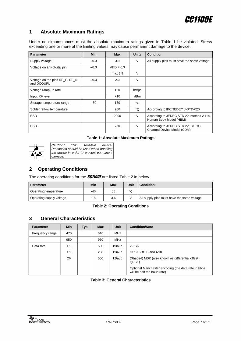
1 Absolute Maximum Ratings
Under no circumstances must the absolute maximum ratings given in Table 1 be violated. Stressexceeding one or more of the limiting values may cause permanent damage to the device.
Table 1: Absolute Maximum Ratings
Caution! ESD sensitive device.Precaution should be used when handlingthe device in order to prevent permanentdamage.
2 Operating Conditions
The operating conditions for the CC1100E are listed Table 2 in below.
Table 2: Operating Conditions
3 General Characteristics
Table 3: General Characteristics
Parameter Min Max Units Condition
Supply voltage –0.3 3.9 V All supply pins must have the same voltage
Voltage on any digital pin –0.3 VDD + 0.3
max 3.9 V
Voltage on the pins RF_P, RF_N,and DCOUPL
–0.3 2.0 V
Voltage ramp-up rate 120 kV/µs
Input RF level +10 dBm
Storage temperature range –50 150 C
Solder reflow temperature 260 C According to IPC/JEDEC J-STD-020
ESD 2000 V According to JEDEC STD 22, method A114,Human Body Model (HBM)
ESD 750 V According to JEDEC STD 22, C101C,Charged Device Model (CDM)
Parameter Min Max Unit Condition
Operating temperature -40 85 C
Operating supply voltage 1.8 3.6 V All supply pins must have the same voltage
Parameter Min Typ Max Unit Condition/Note
Frequency range 470 510 MHz
950 960 MHz
Data rate 1.2
1.2
26
500
250
500
kBaud
kBaud
kBaud
2-FSK
GFSK, OOK, and ASK
(Shaped) MSK (also known as differential offsetQPSK)
Optional Manchester encoding (the data rate in kbpswill be half the baud rate)

CC1100E
SWRS082 Page 8 of 92
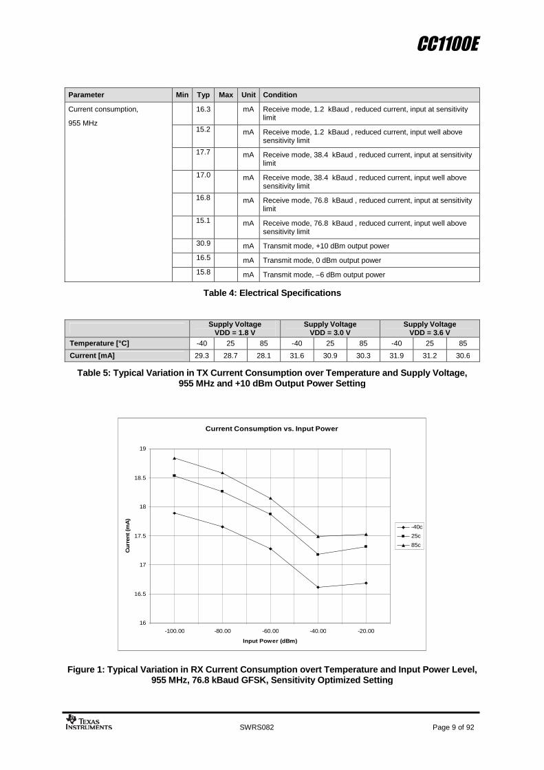
4 Electrical Specifications
4.1 Current Consumption
TA = 25C, VDD = 3.0 V if nothing else stated. All measurement results are obtained using the CC1100E EM reference designs([3] and[4]). Reduced current settings (MDMCFG2.DEM_DCFILT_OFF=1) gives a slightly lower current consumption at the costof a reduction in sensitivity. See Table 6: RF Receive Section for additional details on current consumption and sensitivity.
Parameter Min Typ Max Unit Condition
0.3 A Voltage regulator to digital part off, register values retained(SLEEP state). All GDO pins programmed to 0x2F (HW to 0)
0.7 A Voltage regulator to digital part off, register values retained, low-power RC oscillator running (SLEEP state with WOR enabled)
100 A Voltage regulator to digital part off, register values retained,XOSC running (SLEEP state with MCSM0.OSC_FORCE_ON set)
Current consumption in powerdown modes
165 A Voltage regulator to digital part on, all other modules in powerdown (XOFF state)
10.0 A Automatic RX polling once each second, using low-power RCoscillator, with 460 kHz filter bandwidth and 250 kBaud data rate,PLL calibration every 4th wakeup. Average current with signal inchannel below carrier sense level (MCSM2.RX_TIME_RSSI=1)
35 A Same as above, but with signal in channel above carrier senselevel, 1.95 ms RX timeout, and no preamble/sync word found
1.3 A Automatic RX polling every 15th second, using low-power RCoscillator, with 460 kHz filter bandwidth and 250 kBaud data rate,PLL calibration every 4th wakeup. Average current with signal inchannel below carrier sense level (MCSM2.RX_TIME_RSSI=1)
32 A Same as above, but with signal in channel above carrier senselevel, 29.3 ms RX timeout, and no preamble/sync word found
1.7 mA Only voltage regulator to digital part and crystal oscillator running(IDLE state)
Current consumption
9 mA Only the frequency synthesizer is running (FSTXON state). Thiscurrents consumption is also representative for the otherintermediate states when going from IDLE to RX or TX, includingthe calibration state
16.5 mA Receive mode, 1.2 kBaud, reduced current, input at sensitivitylimit
15.4 mA Receive mode, 1.2 kBaud, reduced current, input well abovesensitivity limit
16.6 mA Receive mode, 38.4 kBaud , reduced current, input at sensitivitylimit
15.5 mA Receive mode, 38.4 kBaud , reduced current, input well abovesensitivity limit
17.5 mA Receive mode, 250 kBaud, reduced current, input at sensitivitylimit
16.1 mA Receive mode, 250 kBaud, reduced current, input well abovesensitivity limit
20 mA Receive mode, 500 kBaud, input at sensitivity limit
18.7 mA Receive mode, 500 kBaud, input well above sensitivity limit
29.6 mA Transmit mode, +10 dBm output power
16.6 mA Transmit mode, 0 dBm output power
Current consumption,480 MHz
16.5 mA Transmit mode, –6 dBm output power
CC1100E
SWRS082 Page 9 of 92
Table 4: Electrical Specifications
Table 5: Typical Variation in TX Current Consumption over Temperature and Supply Voltage,955 MHz and +10 dBm Output Power Setting
Current Consumption vs. Input Power
16
16.5
17
17.5
18
18.5
19
-100.00 -80.00 -60.00 -40.00 -20.00
Input Power (dBm)
Cu
rren
t(m
A)
-40c
25c
85c
Figure 1: Typical Variation in RX Current Consumption overt Temperature and Input Power Level,955 MHz, 76.8 kBaud GFSK, Sensitivity Optimized Setting
Parameter Min Typ Max Unit Condition
16.3 mA Receive mode, 1.2 kBaud , reduced current, input at sensitivitylimit
15.2 mA Receive mode, 1.2 kBaud , reduced current, input well abovesensitivity limit
17.7 mA Receive mode, 38.4 kBaud , reduced current, input at sensitivitylimit
17.0 mA Receive mode, 38.4 kBaud , reduced current, input well abovesensitivity limit
16.8 mA Receive mode, 76.8 kBaud , reduced current, input at sensitivitylimit
15.1 mA Receive mode, 76.8 kBaud , reduced current, input well abovesensitivity limit
30.9 mA Transmit mode, +10 dBm output power
16.5 mA Transmit mode, 0 dBm output power
Current consumption,
955 MHz
15.8 mA Transmit mode, –6 dBm output power
Supply VoltageVDD = 1.8 V
Supply VoltageVDD = 3.0 V
Supply VoltageVDD = 3.6 V
Temperature [°C] -40 25 85 -40 25 85 -40 25 85
Current [mA] 29.3 28.7 28.1 31.6 30.9 30.3 31.9 31.2 30.6

CC1100E
SWRS082 Page 10 of 92
4.2 RF Receive Section
TA = 25C, VDD = 3.0 V if nothing else stated. All measurement results are obtained using the CC1100E EM reference designs([3] and[4]).
Parameter Min Typ Max Unit Condition/Note
Digital channelfilter bandwidth
58 812 kHz User programmable. The bandwidth limits areproportional to crystal frequency (given valuesassume a 26.0 MHz crystal)
480 MHz, 1.2 kBaud data rate, sensitivity optimized, MDMCFG2.DEM_DCFILT_OFF=0(GFSK with BT=1, 1% packet error rate, 20 bytes packet length, 5.2 kHz deviation, 58 kHz digital channel filter bandwidth)
Receiversensitivity
-112 dBm Sensitivity can be traded for current consumption bysetting MDMCFG2.DEM_DCFILT_OFF=1. The typicalcurrent consumption is then reduced from 17.9 mAto 16.5 mA at sensitivity limit. The sensitivity istypically reduced to -110 dBm
480 MHz, 38.4 kBaud data rate, sensitivity optimized, MDMCFG2.DEM_DCFILT_OFF=0(GFSK with BT=1, 1% packet error rate, 20 bytes packet length, 20 kHz deviation, 100 kHz digital channel filter bandwidth)
Receiversensitivity
–104 dBm Sensitivity can be traded for current consumption bysetting MDMCFG2.DEM_DCFILT_OFF=1. The typicalcurrent consumption is then reduced from 18mA to16.6 mA at sensitivity limit.
480 MHz, 250 kBaud data rate, sensitivity optimized, MDMCFG2.DEM_DCFILT_OFF=0(GFSK with BT=1, 1% packet error rate, 20 bytes packet length, 127 kHz deviation, 540 kHz digital channel filter bandwidth)
Receiversensitivity
-95 dBm Sensitivity can be traded for current consumption bysetting MDMCFG2.DEM_DCFILT_OFF=1. The typicalcurrent consumption is then reduced from 19.2mA to17.5 mA at sensitivity limit.
480 MHz, 500 kBaud data rate, sensitivity optimized, MDMCFG2.DEM_DCFILT_OFF=0(MSK, 1% packet error rate, 20 bytes packet length, 812 kHz digital channel filter bandwidth)
Receiversensitivity
-88 dBm Setting MDMCFG2.DEM_DCFILT_OFF=1 is not anvalid option at 500 kBaud dara rate
955 MHz, 1.2 kBaud data rate, sensitivity optimized, MDMCFG2.DEM_DCFILT_OFF=0(GFSK with BT=1, 1% packet error rate, 20 bytes packet length, 5.2 kHz deviation, 58 kHz digital channel filter bandwidth)
Receiversensitivity
–111 dBm Sensitivity can be traded for current consumption bysetting MDMCFG2.DEM_DCFILT_OFF=1. The typicalcurrent consumption is then reduced from 18.2 mAto 16.3 mA at sensitivity limit. The sensitivity istypically reduced to -109 dBm
Saturation -15 dBm FIFOTHR.CLOSE_IN_RX=0. See more in DN010[11]
Adjacent channelrejection
28 dB Desired channel 3 dB above the sensitivity limit. 200kHz channel spacing
Alternate channelrejection
37 dB Desired channel 3 dB above the sensitivity limit. 200kHz channel spacing
See Figure 2 for plot of selectivity versus frequencyoffset
Image channelrejection,955 MHz
32 dB IF frequency 152 kHz
Desired channel 3 dB above the sensitivity limit

CC1100E
SWRS082 Page 11 of 92
TA = 25C, VDD = 3.0 V if nothing else stated. All measurement results are obtained using the CC1100E EM reference designs([3] and[4])
Table 6: RF Receive Section
955 MHz, 38.4 kBaud data rate, sensitivity optimized, MDMCFG2.DEM_DCFILT_OFF=0(GFSK with BT=1, 1% packet error rate, 20 bytes packet length, 20 kHz deviation, 100 kHz digital channel filter bandwidth)
Receiversensitivity
-104 dBm Sensitivity can be traded for current consumption bysetting MDMCFG2.DEM_DCFILT_OFF=1. The typicalcurrent consumption is then reduced from 18.3mA to17.7 mA at sensitivity limit.
Saturation -18 dBm FIFOTHR.CLOSE_IN_RX=0. See more in DN010[11]
Adjacent channelrejection
12 dB Desired channel 3 dB above the sensitivity limit. 200kHz channel spacing
Alternate channelrejection
27 dB Desired channel 3 dB above the sensitivity limit. 200kHz channel spacing
See Figure 3 for plot of selectivity versus frequencyoffset
Image channelrejection,955 MHz
23 dB IF frequency 152 kHz
Desired channel 3 dB above the sensitivity limit
Parameter Min Typ Max Unit Condition/Note
955 MHz, 76.8 kBaud data rate, sensitivity optimized, MDMCFG2.DEM_DCFILT_OFF=0(GFSK with BT=1, 1% packet error rate, 20 bytes packet length, 32 kHz deviation, 232 kHz digital channel filter bandwidth)
Receiver sensitivity -100 dBm Sensitivity can be traded for current consumption by settingMDMCFG2.DEM_DCFILT_OFF=1. The typical currentconsumption is then reduced from 18.6mA to 16.8 mA atsensitivity limit.
Blocking
Blocking at ±2 MHz offset,1.2 kBaud, 955 MHz
-49 dBm Desired channel 3 dB above the sensitivity limit
Blocking at ±2 MHz offset,38.4 kBaud, 955 MHz
-49 dBm Desired channel 3 dB above the sensitivity limit
Blocking at ±10 MHzoffset, 1.2 kBaud, 955MHz
-39 dBm Desired channel 3 dB above the sensitivity limit
Blocking at ±10 MHzoffset, 38.4 kBaud, 955MHz
-40 dBm Desired channel 3 dB above the sensitivity limit
General
Spurious Emmissions -38
-32
dBm
dBm
25 MHz – 1 GHz
Excluding the 470-510 MHz band, signal at 960 MHz, 2nd
harmonicAbove 1 GHz
Typical radiated spurious emission is -49 dBm measured atthe VCO frequency
Data above is for the 470-510 MHz band, for spuriousemmisions at 950-960 MHz, look at section 28.
RX latency 9 BitSerial operation. Time from start of reception until data isavailable on the receiver data output pin is equal to 9 bits.

CC1100E
SWRS082 Page 12 of 92
Table 7: Typical Variation in Sensitivity over Temperature and Supply Voltage, 955 MHz, 76.8kBaud GFSK, Sensitivity Optimized Setting, 770 MHz notch filter Used
-20.0
-10.0
0.0
10.0
20.0
30.0
40.0
50.0
60.0
-1.0 -0.9 -0.8 -0.7 -0.6 -0.5 -0.4 -0.3 -0.2 -0.1 0.0 0.1 0.2 0.3 0.4 0.5 0.6 0.7 0.8 0.9 1.0
Frequency offset [MHz]
Sele
cti
vit
y[d
B]
Figure 2: Typical Selectivity at 1.2 kBaud Data Rate, 955 MHz, GFSK, 5.2 kHz Deviation. IFFrequency is 152.3 kHz and the Digital Channel Filter Bandwidth is 58 kHz
-20.0
-10.0
0.0
10.0
20.0
30.0
40.0
50.0
-1.0 -0.9 -0.8 -0.7 -0.6 -0.5 -0.4 -0.3 -0.2 -0.1 0.0 0.1 0.2 0.3 0.4 0.5 0.6 0.7 0.8 0.9 1.0
Frequency offset [MHz]
Sele
cti
vit
y[d
B]
Figure 3: Typical Selectivity at 38.4 kBaud Data Rate, 955 MHz, GFSK, 20 kHz Deviation. IFFrequency is 152.3 kHz and the Digital Channel Filter Bandwidth is 100 kHz
Supply VoltageVDD = 1.8 V
Supply VoltageVDD = 3.0 V
Supply VoltageVDD = 3.6 V
Temperature [°C] -40 25 85 -40 25 85 -40 25 85
Sensitivity [dBm] -101 -100 -96 -102 -100 -98 -102 -100 -98

CC1100E
SWRS082 Page 13 of 92
4.3 RF Transmit Section
TA = 25C, VDD = 3.0 V, +10dBm if nothing else stated. All measurement results are obtained using the CC1100E EMreference designs ([3] and[4]).
Parameter Min Typ Max Unit Condition/Note
Differential loadimpedance
480 MHz
955 MHz
132 – j2
59 – j67
Differential impedance as seen from the RF-port (RF_P andRF_N) towards the antenna. Follow the CC1100E EMreference designs ([3] and 0) available from the TI website
Output power, highestsetting
480 MHz
955 MHz
+10
+9
dBm
dBm
Output power is programmable, and full range is available in allfrequency bands. Output power may be restricted byregulatory limits.
Delivered to a 50 single-ended load via the CC1100E EMreference designs ([3] and 0) RF matching network
Output power, lowestsetting
-30 dBm Output power is programmable, and full range is available in allfrequency bands
Delivered to a 50 single-ended load via the CC1100E EMreference designs ([3] and 0) RF matching network
Harmonics, conducted480 MHz2nd Harm, 480 MHz3rd Harm, 480 MHz
955 MHz2nd Harm, 955 MHz3rd Harm, 955 MHz
-40-48
-34-50
dBmdBm
dBmdBm
Measured with 10 dBm CW, TX frequency at 480 / 955 MHz
Frequencies below 960 MHzFrequencies above 960 MHz
Spurious emissions,conducted, harmonicsnot included480 MHz955MHz
-39-50
dBmdBm
Measured with +10 dBm CW, TX frequency at 480 / 955 MHz
Frequencies below 1 GHz, outside 470-510 MHz bandFrequencies above 1 GHz
Refer to section 28.1 for information on Spurious Emissions
General
TX latency 8 bit Serial operation. Time from sampling the data on thetransmitter data input pin until it is observed on the RF outputports
Table 8: RF Transmit Section

CC1100E
SWRS082 Page 14 of 92
Table 9: Typical Variation in Output Power over Temperature and Supply Voltage, 480 MHz,+10 dBm Output Power Setting
Table 10: Typical Variation in Output Power over Temperature and Supply Voltage, 955 MHz,+10 dBm Output Power Setting
4.4 Crystal Oscillator
TA = 25C, VDD = 3.0 V if nothing else is stated. All measurement results obtained using the CC1100E EM reference designs([3] and[4]).
Table 11: Crystal Oscillator Parameters
4.5 Low Power RC Oscillator
TA = 25C, VDD = 3.0 V if nothing else is stated. All measurement results obtained using the CC1100E EM reference designs([3] and[4]).
Table 12: RC Oscillator Parameters
Supply VoltageVDD = 1.8 V
Supply VoltageVDD = 3.0 V
Supply VoltageVDD = 3.6 V
Temperature [°C] -40 25 85 -40 25 85 -40 25 85
Output Power [dBm] 10.1 10.8 10.8 10.2 10.4 10.5 9.2 9.9 9.9
Supply VoltageVDD = 1.8 V
Supply VoltageVDD = 3.0 V
Supply VoltageVDD = 3.6 V
Temperature [°C] -40 25 85 -40 25 85 -40 25 85
Output Power [dBm] 8.8 8.4 7.9 9.6 9.2 8.8 9.6 9.2 8.8
Parameter Min Typ Max Unit Condition/Note
Crystal frequency 26 26 27 MHz
Tolerance ±40 ppm This is the total tolerance including a) initial tolerance, b) crystalloading, c) aging, and d) temperature dependence. Theacceptable crystal tolerance depends on RF frequency andchannel spacing / bandwidth.
Load capacitance 10 13 20 pF Simulated over operating conditions
ESR 100
Start-up time 150 µs This parameter is to a large degree crystal dependent. Measuredon the CC1100E EM reference designs ([3] and[4]) using crystalAT-41CD2 from NDK
Parameter Min Typ Max Unit Condition/Note
Calibrated frequency 34.7 34.7 36 kHz Calibrated RC Oscillator frequency is XTALfrequency divided by 750
Frequency accuracy aftercalibration
±1 %
Temperature coefficient +0.5 % / C Frequency drift when temperature changes aftercalibration
Supply voltage coefficient +3 % / V Frequency drift when supply voltage changes aftercalibration
Initial calibration time 2 ms When the RC Oscillator is enabled, calibration iscontinuously done in the background as long asthe crystal oscillator is running

CC1100E
SWRS082 Page 15 of 92
4.6 Frequency Synthesizer Characteristics
TA = 25C, VDD = 3.0 V if nothing else is stated. All measurement results are obtained using the CC1100E EM referencedesigns ([3] and[4]). Min figures are given using a 27 MHz crystal. Typ and max figures are given using a 26 MHz crystal.
Table 13: Frequency Synthesizer Parameters
4.7 Analog Temperature Sensor
TA = 25C, VDD = 3.0 V if nothing else is stated. All measurement results obtained using the CC1100E EM reference designs([3] and[4]). Note that it is necessary to write 0xBF to the PTEST register to use the analog temperature sensor in the IDLEstate.
Table 14: Analog Temperature Sensor Parameters
Parameter Min Typ Max Unit Condition/Note
Programmed frequencyresolution
397 FXOSC/216
412 Hz 26-27 MHz crystal. The resolution (in Hz) is equalfor all frequency bands
Synthesizer frequencytolerance
±40 ppm Given by crystal used. Required accuracy(including temperature and aging) depends onfrequency band and channel bandwidth / spacing
RF carrier phase noise –92 dBc/Hz @ 50 kHz offset from carrier
RF carrier phase noise –92 dBc/Hz @ 100 kHz offset from carrier
RF carrier phase noise –92 dBc/Hz @ 200 kHz offset from carrier
RF carrier phase noise –98 dBc/Hz @ 500 kHz offset from carrier
RF carrier phase noise –107 dBc/Hz @ 1 MHz offset from carrier
RF carrier phase noise –113 dBc/Hz @ 2 MHz offset from carrier
RF carrier phase noise –119 dBc/Hz @ 5 MHz offset from carrier
RF carrier phase noise –129 dBc/Hz @ 10 MHz offset from carrier
PLL turn-on / hop time 85.1 88.4 88.4 s Time from leaving the IDLE state until arriving inthe RX, FSTXON or TX state, when notperforming calibration. Crystal oscillator running
PLL RX/TX settling time 9.3 9.6 9.6 s Settling time for the 1·IF frequency step from RXto TX
PLL TX/RX settling time 20.7 21.5 21.5 s Settling time for the 1·IF frequency step from TXto RX
PLL calibration time 694 721 721 s Calibration can be initiated manually orautomatically before entering or after leavingRX/TX
Parameter Min Typ Max Unit Condition/Note
Output voltage at –40C 0.651 V
Output voltage at 0C 0.747 V
Output voltage at +40C 0.847 V
Output voltage at +80C 0.945 V
Temperature coefficient 2.47 mV/C Fitted from –20 C to +80 C
Error in calculatedtemperature, calibrated
-2 *0 2 *
C From –20 C to +80 C when using 2.47 mV / C, after1-point calibration at room temperature
* The indicated minimum and maximum error with 1-point calibration is based on simulated values fortypical process parameters
Current consumptionincrease when enabled
0.3 mA
CC1100E
SWRS082 Page 16 of 92
4.8 DC Characteristics
TA = 25C if nothing else stated.
Table 15: DC Characteristics
4.9 Power-On Reset
When the power supply complies with the requirements in Table 16 below, proper Power-On-Resetfunctionality is guaranteed. Otherwise, the chip should be assumed to have unknown state untiltransmitting an SRES strobe over the SPI interface. See Section 19.1 on page 45 for further details.
Table 16: Power-On Reset Requirements
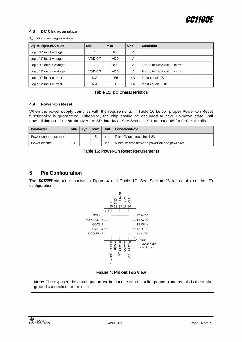
5 Pin Configuration
The CC1100E pin-out is shown in Figure 4 and Table 17. See Section 26 for details on the I/Oconfiguration.
1
20 19 18 17 16
15
14
13
12
11
109876
5
4
3
2
GNDExposed dieattach pad
SCLK
SO (GDO1)
GDO2
DVDD
DCOUPL
GD
O0
(AT
ES
T)
XO
SC
_Q
1
AVDD
XO
SC
_Q
2
AV
DD
RF_P
RF_N
GN
D
AVDD
RB
IAS
DG
UA
RD
GN
D
SI
CS
n
AVDD
Figure 4: Pin out Top View
.
Digital Inputs/Outputs Min Max Unit Condition
Logic "0" input voltage 0 0.7 V
Logic "1" input voltage VDD-0.7 VDD V
Logic "0" output voltage 0 0.5 V For up to 4 mA output current
Logic "1" output voltage VDD-0.3 VDD V For up to 4 mA output current
Logic "0" input current N/A –50 nA Input equals 0V
Logic "1" input current N/A 50 nA Input equals VDD
Parameter Min Typ Max Unit Condition/Note
Power-up ramp-up time 5 ms From 0V until reaching 1.8V
Power off time 1 ms Minimum time between power-on and power-off
Note: The exposed die attach pad must be connected to a solid ground plane as this is the mainground connection for the chip

CC1100E
SWRS082 Page 17 of 92
Pin # Pin Name Pin type Description
1 SCLK Digital Input Serial configuration interface, clock input
2 SO (GDO1) Digital Output Serial configuration interface, data output
Optional general output pin when CSn is high
3 GDO2 Digital Output Digital output pin for general use:
Test signals
FIFO status signals
Clear channel indicator
Clock output, down-divided from XOSC
Serial output RX data
4 DVDD Power (Digital) 1.8 - 3.6 V digital power supply for digital I/O’s and for the digital corevoltage regulator
5 DCOUPL Power (Digital) 1.6 - 2.0 V digital power supply output for decoupling
NOTE: This pin is intended for use only by the CC1100E. It can not be used toprovide supply voltage to other devices
6 GDO0
(ATEST)
Digital I/O Digital output pin for general use:
Test signals
FIFO status signals
Clear channel indicator
Clock output, down-divided from XOSC
Serial output RX data
Serial input TX data
Also used as analog test I/O for prototype/production testing
7 CSn Digital Input Serial configuration interface, chip select
8 XOSC_Q1 Analog I/O Crystal oscillator pin 1, or external clock input
9 AVDD Power (Analog) 1.8 - 3.6 V analog power supply connection
10 XOSC_Q2 Analog I/O Crystal oscillator pin 2
11 AVDD Power (Analog) 1.8 - 3.6 V analog power supply connection
12 RF_P RF I/O Positive RF input signal to LNA in receive mode
Positive RF output signal from PA in transmit mode
13 RF_N RF I/O Negative RF input signal to LNA in receive mode
Negative RF output signal from PA in transmit mode
14 AVDD Power (Analog) 1.8 - 3.6 V analog power supply connection
15 AVDD Power (Analog) 1.8 - 3.6 V analog power supply connection
16 GND Ground (Analog) Analog ground connection
17 RBIAS Analog I/O External bias resistor for reference current
18 DGUARD Power (Digital) Power supply connection for digital noise isolation
19 GND Ground (Digital) Ground connection for digital noise isolation
20 SI Digital Input Serial configuration interface, data input
Table 17: Pin out Overview

CC1100E
SWRS082 Page 18 of 92
6 Circuit Description
BIAS
PA
RBIAS XOSC_Q1 XOSC_Q2
CSn
SI
SO (GDO1)
XOSC
SCLK
LNA
090
FREQSYNTH
ADC
ADC
DE
MO
DU
LA
TO
R
FE
C/
INT
ER
LE
AV
ER
PA
CK
ET
HA
ND
LE
R
RX
FIF
O
MO
DU
LA
TO
R
TX
FIF
O
DIG
ITA
LIN
TE
RF
AC
ET
OM
CU
RADIO CONTROL
RF_P
RF_N
GDO2
GDO0 (ATEST)
RC OSC
Figure 5: CC1100E Simplified Block Diagram
A simplified block diagram of the CC1100E isshown in Figure 5.
The CC1100E features a low-IF receiver. Thereceived RF signal is amplified by the low-noise amplifier (LNA) and down-converted inquadrature (I and Q) to the intermediatefrequency (IF). At IF, the I/Q signals aredigitized by the ADCs. Automatic gain control(AGC), fine channel filtering and demodulationbit/packet synchronization are performeddigitally.
The transmitter part of the CC1100E is based ondirect synthesis of the RF frequency. The
frequency synthesizer includes a completelyon-chip LC VCO and a 90 degree phaseshifter for generating the I and Q LO signals tothe down-conversion mixers in receive mode.
A crystal is to be connected to XOSC_Q1 andXOSC_Q2. The crystal oscillator generates thereference frequency for the synthesizer, aswell as clocks for the ADC and the digital part.
A 4-wire SPI serial interface is used forconfiguration and data buffer access.
The digital baseband includes support forchannel configuration, packet handling, anddata buffering.
7 Application Circuit
Only a few external components are required forusing the CC1100E. The recommendedapplication circuits for the CC1100E are shown inFigure 6 and Figure 7. The external components
are described in Table 18, and typical valuesare given in Table 19.
7.1 Bias Resistor
The bias resistor R171 is used to set an accurate bias current.
7.2 Balun and RF Matching
The balanced RF input and output of theCC1100E share two common pins and aredesigned for a simple, low-cost matching andbalun network on the printed circuit board. Thereceive and transmit switching at the CC1100Efront-end is controlled by a dedicated on-chip
function, eliminating the need for an externalRX/TX-switch.
A few external passive components combinedwith the internal RX/TX switch/terminationcircuitry ensures match in both RX and TXmode. The components between theRF_N/RF_P pins and the point where the two

CC1100E
SWRS082 Page 19 of 92
signals are joined together (C131, C121, L121and L131 for the 470 MHz reference design[3], and L121, L131, C121, L122, C131, C122and L132 for the 950 MHz reference design[4]) form a balun that converts the differentialRF signal on the CC1100E to a single-ended RFsignal. C124 is needed for DC blocking.Together with an appropriate LC network, thebalun components also transform theimpedance to match a 50 load. C125provides DC blocking and is only needed ifthere is a DC path in the antenna. For the 950
MHz reference design, this component mayalso be used for additional filtering, seesection 7.5 below. Suggested values for 470MHz, and 950 MHz are listed in Table 19.
The balun and LC filter component values andtheir placement are important to keep theperformance optimized. It is highlyrecommended to follow the CC1100E EMreference design ([3] and 0). Gerber files andschematics for the reference designs areavailable for download from the TI website.
7.3 Crystal
A crystal in the frequency range 26-27 MHzmust be connected between the XOSC_Q1and XOSC_Q2 pins. The oscillator is designedfor parallel mode operation of the crystal. Inaddition, loading capacitors (C81 and C101)for the crystal are required. The loadingcapacitor values depend on the total loadcapacitance, CL, specified for the crystal. Thetotal load capacitance seen between thecrystal terminals should equal CL for thecrystal to oscillate at the specified frequency.
parasiticL C
CC
C
10181
111
The parasitic capacitance is constituted by pininput capacitance and PCB stray capacitance.Total parasitic capacitance is typically 2.5 pF.
The crystal oscillator is amplitude regulated.This means that a high current is used to startup the oscillations. When the amplitude buildsup, the current is reduced to what is necessaryto maintain approximately 0.4 Vpp signalswing. This ensures a fast start-up, and keepsthe drive level to a minimum. The ESR of thecrystal should be within the specification inorder to ensure a reliable start-up (see Section4.4 on page 14).
The initial tolerance, temperature drift, agingand load pulling should be carefully specifiedin order to meet the required frequencyaccuracy in a certain application.
7.4 Reference Signal
The chip can alternatively be operated with areference signal from 26 to 27 MHz instead ofa crystal. This input clock can either be a full-swing digital signal (0 V to VDD) or a sinewave of maximum 1 V peak-peak amplitude.The reference signal must be connected to the
XOSC_Q1 input. The sine wave must beconnected to XOSC_Q1 using a serialcapacitor. This capacitor can be omitted whenusing a full-swing digital signal. The XOSC_Q2line must be left un-connected. C81 and C101can be omitted when using a reference signal.
7.5 Additional Filtering
In the 950 MHz reference design, C126 andL125 together with C125 build an optional filterto reduce emission at 770 MHz. This filter isnecessary for applications with an externalantenna connector that target compliance withARIB STD-T96. If this filtering is notnecessary, C125 will work as a DC block (only
necessary if there is a DC path in theantenna). C126 and L125 should in that casebe left unmounted.
Additional external components (e.g. an RFSAW filter) may be used in order to improvethe performance in specific applications.
7.6 Power Supply Decoupling
The power supply must be properly decoupledclose to the supply pins. Note that decouplingcapacitors are not shown in the applicationcircuit. The placement and the size of the
decoupling capacitors are very important toachieve the optimum performance. TheCC1100E EM reference designs ([3] and 0)should be followed closely.

CC1100E
SWRS082 Page 20 of 92
7.7 Antenna Considerations
The reference designs ([3] and 0) contain anSMA connector and are matched for a 50 load. The SMA connector makes it easy toconnect evaluation modules and prototypes todifferent test equipment for example a
spectrum analyzer. The SMA connector canalso be replaced by an antenna suitable forthe desired application. Please refer to theantenna selection guide [14] for further detailsregarding antenna solutions provided by TI.
Table 18: Overview of External Components (excluding supply decoupling capacitors)
Component Description
C51 Decoupling capacitor for on-chip voltage regulator to digital part
C81/C101 Crystal loading capacitors
C121/C131 RF balun/matching capacitors
C122 RF LC filter/matching filter capacitor (470 MHz). RF balun/matching capacitor (950 MHz).
C123 RF LC filter/matching capacitor
C124 RF balun DC blocking capacitor
C125 RF LC filter DC blocking capacitor and part of optional RF LC filter (950 MHz)
C126 Part of optional RF LC filter and DC-block (950 MHz)
L121/L131 RF balun/matching inductors (wire wound or multi-layer type)
L122 RF LC filter/matching filter inductor (470 MHz). RF balun/matching inductor (950 MHz). (wire woundor multi-layer type)
L123 RF LC filter/matching filter inductor (wire wound or multi-layer type)
L124 RF LC filter/matching filter inductor (wire wound or multi-layer type)
L125 Optional RF LC filter/matching filter inductor (950 MHz) (wire wound or multi-layer type)
L132 RF balun/matching inductor. (wire wound or multi-layer type)
R171 Resistor for internal bias current reference
XTAL 26MHz - 27MHz crystal

CC1100E
SWRS082 Page 21 of 92
Antenna(50 Ohm)
Dig
italIn
tefa
ce1.8V-3.6V power supply
6G
DO
0
7C
Sn
8X
OS
C_Q
1
9A
VD
D
10
XO
SC
_Q
2
SI2
0
GN
D1
9
DG
UA
RD
18
RB
IAS
17
GN
D1
6
1 SCLK
2 SO(GDO1)
3 GDO2
4 DVDD
5 DCOUPL
AVDD 15
AVDD 14
RF_N 13
RF_P 12
AVDD 11
XTAL
L122 L123
C122 C123
C125
R171
C81 C101
C51
CSn
GDO0(optional)
GDO2(optional)
SO(GDO1)
SCLK
SI
CC1100EDIE ATTACH PAD:
C131
C121
L121
L131
C124
Figure 6: Typical Application and Evaluation Circuit 470 MHz (excluding supply decouplingcapacitors)
Dig
italIn
terf
ace
6G
DO
0
7C
Sn
8X
OS
C_Q
1
9A
VD
D
10
XO
SC
_Q
2
SI20
GN
D19
DG
UA
RD
18
RB
IAS
17
GN
D16
Figure 7: Typical Application and Evaluation Circuit 950 MHz (excluding supply decouplingcapacitors)

CC1100E
SWRS082 Page 22 of 92
Table 19: Bill Of Materials for the Application Circuit
7.8 PCB Layout Recommendations
The top layer should be used for signalrouting, and the open areas should be filledwith metallization connected to ground usingseveral vias.
The area under the chip is used for groundingand shall be connected to the bottom groundplane with several vias for good thermalperformance and sufficiently low inductance toground.
In the CC1100E EM reference designs ([3]and 0), 5 vias are placed inside the exposed
die attached pad. These vias should be“tented” (covered with solder mask) on thecomponent side of the PCB to avoid migrationof solder through the vias during the solderreflow process.
The solder paste coverage should not be100%. If it is, out gassing may occur during thereflow process, which may cause defects(splattering, solder balling). Using “tented” viasreduces the solder paste coverage below
Component Value at 470MHz Value at 950MHz Manufacturer
C51 100 nF ± 10%, 0402 X5R Murata GRM1555C series
C81 27 pF ± 5%, 0402 NP0 Murata GRM1555C series
C101 27 pF ± 5%, 0402 NP0 Murata GRM1555C series
C121 3.9 pF ± 0.25 pF,0402 NP0
1.0 pF ± 0.25 pF,0402 NP0
Murata GRM1555C series
C122 6.8 pF ± 5% pF,0402 NP0
1.5 pF ± 0.25 pF,0402 NP0
Murata GRM1555C series
C123 5.6 pF ± 0.5 pF,0402 NP0
2.7 pF ± 0.25 pF,0402 NP0
Murata GRM1555C series
C124 .220 pF pF ± 5%,0402 NP0
100 pF ± 5%, 0402NP0
Murata GRM1555C series
C125 220 pF ± 5%, 0402NP0
100 pF ± 5%, 0402NP0 or 11 pF ± 5%,
0402 NP0 whenpart of optional filter
Murata GRM1555C series
C126 47 pF ± 5%, 0402NP0
Murata GRM1555C series
C131 3.9 pF ± 0.25 pF,0402 NP0
1.5 pF ± 0.25 pF,0402 NP0
Murata GRM1555C series
L121 27 nH ± 5%, 0402wire wound
12 nH ± 5%, 0402wire wound
Murata LQW15 series
L122 22 nH ± 5%, 0402wire wound
18 nH ± 5%, 0402wire wound
Murata LQW15 series
L123 27 nH ± 5%, 0402wire wound
12 nH ± 5%, 0402wire wound
Murata LQW15 series
L124 12 nH ± 5%, 0402wire wound
Murata LQW15 series
L125 2.7 nH ± 0.2nH,0402 wire wound
Murata LQW15 series
L131 27 nH ± 5%, 0402wire wound
12 nH ± 5%, 0402wire wound
Murata LQW15 series
L132 18 nH ± 5%, 0402wire wound
Murata LQW15 series
R171 56k Ω, 0402, 1% Koa RK73 series
XTAL 26.0 MHz surface mount crystal NDK, AT-41CD2

CC1100E
SWRS082 Page 23 of 92
100%. See Figure 8 for top solder resist andtop paste masks.
Each decoupling capacitor should be placedas close as possible to the supply pin itdecouples. Each decoupling capacitor shouldbe connected to the power line (or powerplane) by separate vias. The best routing isfrom the power line (or power plane) to thedecoupling capacitor and then to the CC1100Esupply pin. Supply power filtering is veryimportant.
Each decoupling capacitor ground pad shouldbe connected to the ground plane by separatevias. Direct connections between neighboringpower pins will increase noise coupling andshould be avoided unless absolutelynecessary. Routing in the ground planeunderneath the chip or the balun/RF matchingcircuit, or between the chip’s ground vias andthe decoupling capacitor’s ground vias should
be avoided. This improves the grounding andensures the shortest possible current returnpath.
The external components should ideally be assmall as possible (0402 is recommended) andsurface mount devices are highlyrecommended. Please note that componentswith different sizes than those specified mayhave differing characteristics.
Precaution should be used when placing themicrocontroller in order to avoid noiseinterfering with the RF circuitry.
A CC1100E DK Development Kit with a fullyassembled CC1100E EM Evaluation Module isavailable. It is strongly advised that thisreference layout is followed very closely inorder to get the best performance. Theschematic, BOM and layout Gerber files are allavailable from the TI website ([3] and 0).
Figure 8: Left: Top Solder Resist Mask (Negative). Right: Top Paste Mask. Circles are Vias
8 Configuration Overview
The CC1100E can be configured to achieveoptimum performance for many differentapplications. Configuration is done using theSPI interface. See Section 10 below for moredescription of the SPI interface. The followingkey parameters can be programmed:
Power-down / power up mode Crystal oscillator power-up / power-down Receive / transmit mode RF channel selection Data rate Modulation format RX channel filter bandwidth RF output power Data buffering with separate 64-byte
receive and transmit FIFOs
Packet radio hardware support Forward Error Correction (FEC) with
interleaving Data whitening Wake-On-Radio (WOR)
Details of each configuration register can befound in Section 29, starting on page 59.
Figure 9 shows a simplified state diagram thatexplains the main CC1100E states together withtypical usage and current consumption. Fordetailed information on controlling the CC1100Estate machine, and a complete state diagram,see Section 19, starting on page 45.

CC1100E
SWRS082 Page 24 of 92
Transmit mode Receive mode
IDLE
Manual freq.synth. calibration
RX FIFOoverflow
TX FIFOunderflow
Frequencysynthesizer on
SFSTXON
SRX or wake-on-radio (WOR)
STX
STX
STX or RXOFF_MODE=10
RXOFF_MODE = 00
SFTX
SRX or TXOFF_MODE = 11
SIDLE
SCAL
SFRX
IDLE
TXOFF_MODE = 00
SFSTXON or RXOFF_MODE = 01
SRX or STX or SFSTXON or wake-on-radio (WOR)
Sleep
SPWD or wake-on-radio (WOR)
Crystaloscillator off
SXOFF
CSn = 0
CSn = 0
TXOFF_MODE = 01
Frequencysynthesizer startup,optional calibration,
settling
Optional freq.synth. calibration
Default state when the radio is notreceiving or transmitting. Typ.current consumption: 1.7 mA.
Lowest power mode. Mostregister values are retained.Current consumption typ300 nA, or typ 700 nA whenwake-on-radio (WOR) isenabled.
All register values areretained. Typ. currentconsumption; 165 µA.
Used for calibrating frequencysynthesizer upfront (enteringreceive or transmit mode canthen be done quicker).Transitional state. Typ. currentconsumption: 9 mA.
Frequency synthesizer is turned on, can optionally becalibrated, and then settles to the correct frequency.Transitional state. Typ. current consumption: 9 mA.
Frequency synthesizer is on,ready to start transmitting.Transmission starts veryquickly after receiving the STXcommand strobe.Typ. currentconsumption: 9 mA.
Typ. current consumption:15.8 mA at -6 dBm output,16.5 mA at 0 dBm output,30.9 mA at +10 dBm output.
Typ. currentconsumption:from 15.2 mA (stronginput signal) to 16.3 mA(weak input signal).
Optional transitional state. Typ.current consumption: 9 mA.In FIFO-based modes,
transmission is turned off andthis state entered if the TXFIFO becomes empty in themiddle of a packet. Typ.current consumption: 1.7 mA.
In FIFO-based modes,reception is turned off and thisstate entered if the RX FIFOoverflows. Typ. currentconsumption: 1.7 mA.
Figure 9: Simplified State Diagram, with Typical Current Consumption at 1.2 kBaud Data Rateand MDMCFG2.DEM_DCFILT_OFF=1 (current optimized). Frequency Band = 955 MHz

CC1100E
SWRS082 Page 25 of 92
9 Configuration Software
The CC1100E can be configured using theSmartRF Studio software [8]. The SmartRF
Studio software is highly recommended forobtaining optimum register settings, and forevaluating performance and functionality. Ascreenshot of the SmartRF Studio userinterface for the CC1100E is shown in Figure 10.
After chip reset, all the registers have defaultvalues as shown in the tables in Section 29.The optimum register setting might differ fromthe default value. After a reset all registers thatshall be different from the default valuetherefore needs to be programmed throughthe SPI interface.
Figure 10: SmartRF Studio [8] User Interface
10 4-wire Serial Configuration and Data Interface
The CC1100E is configured via a simple 4-wireSPI-compatible interface (SI, SO, SCLK andCSn) where the CC1100E is the slave. Thisinterface is also used to read and writebuffered data. All transfers on the SPI interfaceare done most significant bit first.
All transactions on the SPI interface start witha header byte containing an R/W;¯ bit, a burstaccess bit (B), and a 6-bit address (A5 – A0).
The CSn pin must be kept low during transferson the SPI bus. If CSn goes high during the
transfer of a header byte or during read/writefrom/to a register, the transfer will becancelled. The timing for the address and datatransfer on the SPI interface is shown in Figure11 with reference to Table 20.
When CSn is pulled low, the MCU must waituntil the CC1100E SO pin goes low beforestarting to transfer the header byte. Thisindicates that the crystal is running. Unless thechip was in the SLEEP or XOFF states, theSO pin will always go low immediately aftertaking CSn low.

CC1100E
SWRS082 Page 26 of 92
0 A5 A4 A3 A2 A0A1 DW7
1
Read from register:
Write to register:
Hi-Z
X
SCLK:
CSn:
SI
SO
SI
SO Hi-Z
tsp
tch
tcl
tsd
thd
tns
X X
Hi-Z
X
Hi-ZS7
X
DW6 DW5 DW4 DW3 DW2 DW1 DW0
B S5 S4 S3 S2 S1 S0 S7 S6 S5 S4 S3 S2 S1 S0
B
B A5 A4 A3 A2 A1 A0
S7 B S5 S4 S3 S2 S1 S0 DR7 DR6 DR5 DR4 DR3 DR2 DR1 DR0
Figure 11: Configuration Registers Write and Read Operations
Parameter Description Min Max Units
SCLK frequency100 ns delay inserted between address byte and data byte (single access), orbetween address and data, and between each data byte (burst access).
- 10
SCLK frequency, single accessNo delay between address and data byte
- 9
fSCLK
SCLK frequency, burst accessNo delay between address and data byte, or between data bytes
- 6.5
MHz
tsp,pd CSn low to positive edge on SCLK, in power-down mode 150 - s
tsp CSn low to positive edge on SCLK, in active mode 20 - ns
tch Clock high 50 - ns
tcl Clock low 50 - ns
trise Clock rise time - 5 ns
tfall Clock fall time - 5 ns
tsd Setup data (negative SCLK edge) topositive edge on SCLK(tsd applies between address and data bytes, and betweendata bytes)
Single access
Burst access
55
76
-
-
ns
thd Hold data after positive edge on SCLK 20 - ns
tns Negative edge on SCLK to CSn high. 20 - ns
Table 20: SPI Interface Timing Requirements
Note: The minimum tsp,pd figure in Table 20 can be used in cases where the user does not readthe CHIP_RDYn signal. CSn low to positive edge on SCLK when the chip is woken from power-down depends on the start-up time of the crystal being used. The 150 μs in Table 20 is thecrystal oscillator start-up time measured on CC1100E EM reference designs (0 and 0) usingcrystal AT-41CD2 from NDK.

CC1100E
SWRS082 Page 27 of 92
10.1 Chip Status Byte
When the header byte, data byte, or commandstrobe is sent on the SPI interface, the chipstatus byte is sent by the CC1100E on the SOpin. The status byte contains key statussignals, useful for the MCU. The first bit, s7, isthe CHIP_RDYn signal; this signal must go lowbefore the first positive edge of SCLK. TheCHIP_RDYn signal indicates that the crystal isrunning.
Bits 6, 5, and 4 comprise the STATE value.This value reflects the state of the chip. TheXOSC and power to the digital core are on inthe IDLE state, but all other modules are inpower down. The frequency and channelconfiguration should only be updated when thechip is in this state. The RX state will be activewhen the chip is in the receive mode.Likewise, TX is active when the chip istransmitting.
The last four bits (3:0) in the status bytecontains FIFO_BYTES_AVAILABLE. For readoperations (the R/W;¯ bit in the header byte isset to 1), the FIFO_BYTES_AVAILABLE fieldcontains the number of bytes available forreading from the RX FIFO. For writeoperations (the R/W;¯ bit in the header byte isset to 0), the FIFO_BYTES_AVAILABLE fieldcontains the number of bytes that can bewritten to the TX FIFO. WhenFIFO_BYTES_AVAILABLE=15, 15 or morebytes are available/free.
Table 21 gives a status byte summary.
Bits Name Description
7 CHIP_RDYn Stays high until power and crystal have stabilized. Should always be low when usingthe SPI interface.
6:4 STATE[2:0] Indicates the current main state machine mode
Value State Description
000 IDLE IDLE state(Also reported for some transitional states insteadof SETTLING or CALIBRATE)
001 RX Receive mode
010 TX Transmit mode
011 FSTXON Fast TX ready
100 CALIBRATE Frequency synthesizer calibration is running
101 SETTLING PLL is settling
110 RXFIFO_OVERFLOW RX FIFO has overflowed. Read out anyuseful data, then flush the FIFO with SFRX
111 TXFIFO_UNDERFLOW TX FIFO has underflowed. Acknowledge withSFTX
3:0 FIFO_BYTES_AVAILABLE[3:0] The number of bytes available in the RX FIFO or free bytes in the TX FIFO
Table 21: Status Byte Summary
10.2 Register Access
The configuration registers on the CC1100E arelocated on SPI addresses from 0x00 to 0x2E.Table 39 on page 61 lists all configurationregisters. It is highly recommended to useSmartRF
®Studio [8] to generate optimum
register settings. The detailed description ofeach register is found in Section 29.1 and29.2, starting on page 64. All configurationregisters can be both written to and read. The
R/W;¯ bit controls if the register should bewritten to or read. When writing to registers,the status byte is sent on the SO pin each timea header byte or data byte is transmitted onthe SI pin. When reading from registers, thestatus byte is sent on the SO pin each time aheader byte is transmitted on the SI pin.
Registers with consecutive addresses can beaccessed in an efficient way by setting the

CC1100E
SWRS082 Page 28 of 92
burst bit (B) in the header byte. The addressbits (A5 – A0) set the start address in aninternal address counter. This counter isincremented by one each new byte (every 8clock pulses). The burst access is either aread or a write access and must be terminatedby setting CSn high.
For register addresses in the range 0x30-0x3D, the burst bit is used to select between
status registers when burst bit is one, andbetween command strobes when burst bit iszero. See more in Section 10.3 below.Because of this, burst access is not availablefor status registers and they must be accessedone at a time. The status registers can only beread.
10.3 SPI Read
When reading register fields over the SPIinterface while the register fields are updatedby the radio hardware (e.g. MARCSTATE orTXBYTES), there is a small, but finite,probability that a single read from the register
is corrupt. As an example, the probability ofany single read from TXBYTES being corrupt,assuming the maximum data rate is used, isapproximately 80 ppm. Refer to the CC1100EErrata Note [5] for more details.
10.4 Command Strobes
Command Strobes may be viewed as singlebyte instructions to the CC1100E. By addressinga command strobe register, internalsequences will be started. These commandsare used to disable the crystal oscillator,enable receive mode, enable wake-on-radioetc. The 13 command strobes are listed inTable 38 on page 60.
The command strobe registers are accessedby transferring a single header byte (no data isbeing transferred). That is, only the R/W;¯ bit,the burst access bit (set to 0), and the six
address bits (in the range 0x30 through 0x3D)are written. The R/W;¯ bit can be either one orzero and will determine how theFIFO_BYTES_AVAILABLE field in the statusbyte should be interpreted.
When writing command strobes, the statusbyte is sent on the SO pin.
A command strobe may be followed by anyother SPI access without pulling CSn high.However, if an SRES strobe is being issued,one will have to wait for SO to go low againbefore the next header byte can be issued asshown in Figure 12. The command strobes areexecuted immediately, with the exception ofthe SPWD and the SXOFF strobes that areexecuted when CSn goes high.
Figure 12: SRES Command Strobe
10.5 FIFO Access
The 64-byte TX FIFO and the 64-byte RXFIFO are accessed through the 0x3F address.When the R/W;¯ bit is zero, the TX FIFO isaccessed, and the RX FIFO is accessed whenthe R/W;¯ bit is one.
The TX FIFO is write-only, while the RX FIFOis read-only.
The burst bit is used to determine if the FIFOaccess is a single byte access or a burstaccess. The single byte access method
Note: An SIDLE strobe will clear allpending command strobes until IDLEstate is reached. This means that if forexample an SIDLE strobe is issuedwhile the radio is in RX state, any othercommand strobes issued before theradio reaches IDLE state will beignored.

CC1100E
SWRS082 Page 29 of 92
expects a header byte with the burst bit set tozero and one data byte. After the data byte, anew header byte is expected; hence, CSn canremain low. The burst access method expectsone header byte and then consecutive databytes until terminating the access by settingCSn high.
The following header bytes access the FIFOs:
0x3F: Single byte access to TX FIFO
0x7F: Burst access to TX FIFO
0xBF: Single byte access to RX FIFO
0xFF: Burst access to RX FIFO
When writing to the TX FIFO, the status byte(see Section 10.1) is output on SO for eachnew data byte as shown in Figure 11. Thisstatus byte can be used to detect TX FIFOunderflow while writing data to the TX FIFO.
Note that the status byte contains the numberof bytes free before writing the byte inprogress to the TX FIFO. When the last bytethat fits in the TX FIFO is transmitted on SI,the status byte received concurrently on SOwill indicate that one byte is free in the TXFIFO.
The TX FIFO may be flushed by issuing aSFTX command strobe. Similarly, a SFRXcommand strobe will flush the RX FIFO. ASFTX or SFRX command strobe can only beissued in the IDLE, TXFIFO_UNDERFLOW, orRXFIFO_OVERFLOW states. Both FIFOs areflushed when going to the SLEEP state.
Figure 13 gives a brief overview of differentregister access types possible.
10.6 PATABLE Access
The 0x3E address is used to access thePATABLE, which is used for selecting PApower control settings. The SPI expects up toeight data bytes after receiving the address.By programming the PATABLE, controlled PApower ramp-up and ramp-down can beachieved, as well as ASK modulation shapingfor reduced bandwidth. See SmartRF
®Studio
[8] for recommended shaping / PA rampingsequences. See also Section 24 on page 52for details on output power programming.
The PATABLE is an 8-byte table that definesthe PA control settings to use for each of theeight PA power values (selected by the 3-bitvalue FREND0.PA_POWER). The table iswritten and read from the lowest setting (0) tothe highest (7), one byte at a time. An indexcounter is used to control the access to thetable. This counter is incremented each time abyte is read or written to the table, and set tothe lowest index when CSn is high. When the
highest value is reached the counter restartsat zero.
The access to the PATABLE is either singlebyte or burst access depending on the burstbit. When using burst access the index counterwill count up; when reaching 7 the counter willrestart at 0. The R/W;¯ bit controls whether theaccess is a read or a write access.
If one byte is written to the PATABLE and thisvalue is to be read out, CSn must be set highbefore the read access in order to set theindex counter back to zero.
Note that the content of the PATABLE is lostwhen entering the SLEEP state, except for thefirst byte (index 0).
Please referr to Design Note DN501 [17] formore information
Figure 13: Register Access Types

CC1100E
SWRS082 Page 30 of 92
11 Microcontroller Interface and Pin Configuration
In a typical system, the CC1100E will interface toa microcontroller. This microcontroller must beable to:
Program the CC1100E into different modes
Read and write buffered data
Read back status information via the 4-wireSPI-bus configuration interface (SI, SO,SCLK and CSn)
11.1 Configuration Interface
The microcontroller uses four I/O pins for theSPI configuration interface (SI, SO, SCLK and
CSn). The SPI is described in Section 10 onpage 25.
11.2 General Control and Status Pins
The CC1100E has two dedicated configurablepins (GDO0 and GDO2) and one shared pin(GDO1) that can output internal statusinformation useful for control software. Thesepins can be used to generate interrupts on theMCU. See Section 26 page 54 for more detailson the signals that can be programmed.
GDO1 is shared with the SO pin in the SPIinterface. The default setting for GDO1/SO is3-state output. By selecting any other of theprogramming options, the GDO1/SO pin willbecome a generic pin. When CSn is low, thepin will always function as a normal SO pin.
In the synchronous and asynchronous serialmodes, the GDO0 pin is used as a serial TXdata input pin while in transmit mode.
The GDO0 pin can also be used for an on-chipanalog temperature sensor. By measuring thevoltage on the GDO0 pin with an externalADC, the temperature can be calculated.Specifications for the temperature sensor arefound in Section 4.7 on page 15. With defaultPTEST register setting (0x7F), the temperaturesensor output is only available if the frequencysynthesizer is enabled (e.g. the MANCAL,FSTXON, RX, and TX states). It is necessaryto write 0xBF to the PTEST register to use theanalog temperature sensor in the IDLE state.Before leaving the IDLE state, the PTESTregister should be restored to its default value(0x7F).
11.3 Optional Radio Control Feature
The CC1100E has an optional way of controllingthe radio by reusing SI, SCLK, and CSn fromthe SPI interface. This feature allows for asimple three-pin control of the major states ofthe radio: SLEEP, IDLE, RX, and TX. Thisoptional functionality is enabled with theMCSM0.PIN_CTRL_EN configuration bit.
State changes are commanded as follows:
If CSn is high, the SI and SCLK are set tothe desired state according to Table 22.
If CSn goes low, the state of SI and SCLKis latched and a command strobe isgenerated internally according to the pinconfiguration.
It is only possible to change state with thelatter functionality. That means that forinstance RX will not be restarted if SI and
SCLK are set to RX and CSn toggles. WhenCSn is low the SI and SCLK has normal SPIfunctionality.
All pin control command strobes are executedimmediately except the SPWD strobe. The
SPWD strobe is delayed until CSn goes high.
CSn SCLK SI Function
1 X X Chip unaffected by SCLK/SI
0 0 Generates SPWD strobe
0 1 Generates STX strobe
1 0 Generates SIDLE strobe
1 1 Generates SRX strobe
0SPImode
SPImode
SPI mode (wakes up intoIDLE if in SLEEP/XOFF)
Table 22: Optional Pin Control Coding

CC1100E
SWRS082 Page 31 of 92
12 Data Rate Programming
The data rate used when transmitting, or thedata rate expected in receive is programmedby the MDMCFG3.DRATE_M and theMDMCFG4.DRATE_E configuration registers.The data rate is given by the formula below.As the formula shows, the programmed datarate depends on the crystal frequency.
XOSC
EDRATE
DATA fMDRATE
R
28
_
2
2_256
The following approach can be used to findsuitable values for a given data rate:
2562
2_
2log_
_
28
20
2
EDRATEXOSC
DATA
XOSC
DATA
f
RMDRATE
f
REDRATE
If DRATE_M is rounded to the nearest integerand becomes 256, increment DRATE_E anduse DRATE_M = 0.
The data rate can be set from 0.8 kBaud to500 kBaud with the minimum step sizeaccording to Table 23 below.
Min DataRate
[kBaud]
Typical DataRate
[kBaud]
Max DataRate
[kBaud]
Data rateStep Size[kBaud]
0.8 1.2 / 2.4 3.17 0.0062
3.17 4.8 6.35 0.0124
6.35 9.6 12.7 0.0248
12.7 19.6 25.4 0.0496
25.4 38.4 50.8 0.0992
50.8 76.8 101.6 0.1984
101.6 153.6 203.1 0.3967
203.1 250 406.3 0.7935
406.3 500 500 1.5869
Table 23: Data Rate Step Size
13 Receiver Channel Filter Bandwidth
In order to meet different channel widthrequirements, the receiver channel filter isprogrammable. The MDMCFG4.CHANBW_E andMDMCFG4.CHANBW_M configuration registerscontrol the receiver channel filter bandwidth,which scales with the crystal oscillatorfrequency.
The following formula gives the relationbetween the register settings and the channelfilter bandwidth:
ECHANBWXOSC
channelMCHANBW
fBW
_2)·_4(8
Table 24 lists the channel filter bandwidthssupported by the CC1100E.
For best performance, the channel filterbandwidth should be selected so that thesignal bandwidth occupies at most 80% of thechannel filter bandwidth. The channel centretolerance due to crystal inaccuracy should alsobe subtracted from the channel filterbandwidth. The following example illustratesthis:
With the channel filter bandwidth set to500 kHz, the signal should stay within 80% of
500 kHz, which is 400 kHz. Assuming955 MHz frequency and ±20 ppm frequencyuncertainty for both the transmitting device andthe receiving device, the total frequencyuncertainty is ±40 ppm of 955 MHz, which is±38.2 kHz. If the whole transmitted signalbandwidth is to be received within 400 kHz,the transmitted signal bandwidth should bemaximum 400 kHz – 2·38.2 kHz, which is323.6 kHz.
By compensating for a frequency offsetbetween the transmitter and the receiver, thefilter bandwidth can be reduced and thesensitivity can be improved, see more inDN005 [16] and in Section 14.1.
MDMCFG4.CHANBW_EMDMCFG4.
CHANBW_M 00 01 10 11
00 812 406 203 102
01 650 325 162 81
10 541 270 135 68
11 464 232 116 58
Table 24: Channel Filter Bandwidths [kHz](assuming a 26 MHz crystal)
CC1100E
SWRS082 Page 32 of 92
14 Demodulator, Symbol Synchronizer, and Data Decision
The CC1100E contains an advanced and highlyconfigurable demodulator. Channel filteringand frequency offset compensation isperformed digitally. To generate the RSSI level
(see Section 17.3 for more information), thesignal level in the channel is estimated. Datafiltering is also included for enhancedperformance.
14.1 Frequency Offset Compensation
The CC1100E has a very fine frequencyresolution (see Table 13). This feature can beused to compensate for frequency offset anddrift.
When using 2-FSK, GFSK, or MSKmodulation, the demodulator will compensatefor the offset between the transmitter andreceiver frequency within certain limits, byestimating the centre of the received data. Thefrequency offset compensation configuration iscontrolled from the FOCCFG register. Bycompensating for a large frequency offsetbetween the transmitter and the receiver, thesensitivity can be improved, see DN005 [16].
The tracking range of the algorithm isselectable as fractions of the channelbandwidth with the FOCCFG.FOC_LIMITconfiguration register.
If the FOCCFG.FOC_BS_CS_GATE bit is set,the offset compensator will freeze until carriersense asserts. This may be useful when theradio is in RX for long periods with no traffic,
since the algorithm may drift to the boundarieswhen trying to track noise.
The tracking loop has two gain factors, whichaffects the settling time and noise sensitivity ofthe algorithm. FOCCFG.FOC_PRE_K sets thegain before the sync word is detected, andFOCCFG.FOC_POST_K selects the gain afterthe sync word has been found.
The estimated frequency offset value isavailable in the FREQEST status register. Thiscan be used for permanent frequency offsetcompensation. By writing the value fromFREQEST into FSCTRL0.FREQOFF, thefrequency synthesizer will automatically beadjusted according to the estimated frequencyoffset. More details regarding this permanentfrequency compensation algorithm can befound in DN015 [12].
14.2 Bit Synchronization
The bit synchronization algorithm extracts theclock from the incoming symbols. Thealgorithm requires that the expected data rateis programmed as described in Section 12 on
page 31. Re-synchronization is performedcontinuously to adjust for error in the incomingsymbol rate.
14.3 Byte Synchronization
Byte synchronization is achieved by acontinuous sync word search. The sync wordis a 16 bit configurable field (can be repeatedto get a 32 bit) that is automatically inserted atthe start of the packet by the modulator intransmit mode. The MSB in the sync word issent first. The demodulator uses this field tofind the byte boundaries in the stream of bits.The sync word will also function as a systemidentifier; since only packets with the correctpredefined sync word will be received if thesync word detection in RX is enabled inregister MDMCFG2 (see Section 17.1). Thesync word detector correlates against theuser-configured 16 or 32 bit sync word. The
correlation threshold can be set to 15/16,16/16, or 30/32 bits match. The sync word canbe further qualified using the preamble qualityindicator mechanism described below and/or acarrier sense condition. The sync word isconfigured through the SYNC1 and SYNC0registers.
In order to make false detections of syncwords less likely, a mechanism calledpreamble quality indication (PQI) can be usedto qualify the sync word. A threshold value forthe preamble quality must be exceeded inorder for a detected sync word to be accepted.See Section 17.2 on page 39 for more details.
Note: Frequency offset compensation isnot supported for ASK or OOK modulation.

CC1100E
SWRS082 Page 33 of 92
15 Packet Handling Hardware Support
The CC1100E has built-in hardware support forpacket oriented radio protocols.
In transmit mode, the packet handler can beconfigured to add the following elements to thepacket stored in the TX FIFO:
A programmable number of preamblebytes
A two byte synchronization (sync) word.Can be duplicated to give a 4-byte syncword (recommended). It is not possible toonly insert preamble or only insert a syncword
A CRC checksum computed over the datafield.
The recommended setting is 4-byte preambleand 4-byte sync word, except for 500 kBauddata rate where the recommended preamblelength is 8 bytes. In addition, the following canbe implemented on the data field and theoptional 2-byte CRC checksum:
Whitening of the data with a PN9sequence
Forward Error Correction (FEC) by the useof interleaving and coding of the data(convolutional coding)
In receive mode, the packet handling supportwill de-construct the data packet byimplementing the following (if enabled):
Preamble detection Sync word detection CRC computation and CRC check One byte address check Packet length check (length byte checked
against a programmable maximum length) De-whitening De-interleaving and decoding
Optionally, two status bytes (see Table 25 andTable 26) with RSSI value, Link QualityIndication, and CRC status can be appendedin the RX FIFO.
Bit Field Name Description
7:0 RSSI RSSI value
Table 25: Received Packet Status Byte 1(first byte appended after the data)
Bit Field Name Description
7 CRC_OK 1: CRC for received data OK(or CRC disabled)
0: CRC error in received data
6:0 LQI Indicating the link quality
Table 26: Received Packet Status Byte 2(second byte appended after the data)
15.1 Data Whitening
From a radio perspective, the ideal over the airdata are random and DC free. This results inthe smoothest power distribution over theoccupied bandwidth. This also gives theregulation loops in the receiver uniformoperation conditions (no data dependencies).
Real data often contain long sequences ofzeros and ones. In these cases, performancecan be improved by whitening the data beforetransmitting, and de-whitening the data in thereceiver.
With the CC1100E, this can be doneautomatically. By settingPKTCTRL0.WHITE_DATA=1, all data, exceptthe preamble and the sync word will be XOR-ed with a 9-bit pseudo-random (PN9)sequence before being transmitted. This isshown in Figure 14. At the receiver end, thedata are XOR-ed with the same pseudo-random sequence. In this way, the whitening isreversed, and the original data appear in thereceiver. The PN9 sequence is initialized to all1’s.
Note: Register fields that control thepacket handling features should only bealtered when CC1100E is in the IDLE state.

CC1100E
SWRS082 Page 34 of 92
Figure 14: Data Whitening in TX Mode
15.2 Packet Format
The format of the data packet can beconfigured and consists of the following items(see Figure 15):
Preamble Synchronization word
Optional length byte Optional address byte Payload Optional 2 byte CRC
Preamble bits(1010...1010)
Sync
word
Length
field
Addre
ss
field
Data field
CR
C-1
6
Optional CRC-16 calculation
Optionally FEC encoded/decoded
8 x n bits 16/32 bits8
bits8
bits8 x n bits 16 bits
Optional data whiteningLegend:
Inserted automatically in TX,processed and removed in RX.
Optional user-provided fields processed in TX,processed but not removed in RX.
Unprocessed user data (apart from FECand/or whitening)
Figure 15: Packet Format
The preamble pattern is an alternatingsequence of ones and zeros (10101010…).The minimum length of the preamble isprogrammable through the value ofMDMCFG1.NUM_PREAMBLE. When enablingTX, the modulator will start transmitting thepreamble. When the programmed number ofpreamble bytes has been transmitted, themodulator will send the sync word and thendata from the TX FIFO if data is available. Ifthe TX FIFO is empty, the modulator willcontinue to send preamble bytes until the firstbyte is written to the TX FIFO. The modulatorwill then send the sync word and then the databytes.
The synchronization word is a two-byte valueset in the SYNC1 and SYNC0 registers. Thesync word provides byte synchronization of theincoming packet. A one-byte sync word can beemulated by setting the SYNC1 value to thepreamble pattern. It is also possible to emulatea 32 bit sync word by settingMDMCFG2.SYNC_MODE to 3 or 7. The syncword will then be repeated twice.
The CC1100E supports both constant packetlength protocols and variable length protocols.Variable or fixed packet length mode can beused for packets up to 255 bytes. For longer

CC1100E
SWRS082 Page 35 of 92
packets, infinite packet length mode must beused.
Fixed packet length mode is selected bysetting PKTCTRL0.LENGTH_CONFIG=0. The
desired packet length is set by the PKTLENregister.
In variable packet length mode,PKTCTRL0.LENGTH_CONFIG=1, the packetlength is configured by the first byte after thesync word. The packet length is defined as thepayload data, excluding the length byte andthe optional CRC. The PKTLEN register isused to set the maximum packet lengthallowed in RX. Any packet received with alength byte with a value greater than PKTLENwill be discarded.
With PKTCTRL0.LENGTH_CONFIG=2, thepacket length is set to infinite and transmissionand reception will continue until turned offmanually. As described in the next section,this can be used to support packet formatswith different length configuration than nativelysupported by the CC1100E. One should makesure that TX mode is not turned off during thetransmission of the first half of any byte. Referto the CC1100E Errata Note [5] for more details.
15.2.1 Arbitrary Length Field Configuration
The packet length register, PKTLEN, can bereprogrammed during receive and transmit. Incombination with fixed packet length mode(PKTCTRL0.LENGTH_CONFIG=0), this opensthe possibility to have a different length fieldconfiguration than supported for variablelength packets (in variable packet length modethe length byte is the first byte after the syncword). At the start of reception, the packetlength is set to a large value. The MCU readsout enough bytes to interpret the length field inthe packet. Then the PKTLEN value is setaccording to this value. The end of packet willoccur when the byte counter in the packet
handler is equal to the PKTLEN register. Thus,the MCU must be able to program the correctlength, before the internal counter reaches thepacket length.
15.2.2 Packet Length > 255
The packet automation control register,PKTCTRL0, can be reprogrammed during TXand RX. This opens the possibility to transmitand receive packets that are longer than 256bytes and still be able to use the packethandling hardware support. At the start of thepacket, the infinite packet length mode(PKTCTRL0.LENGTH_CONFIG=2) must beactive. On the TX side, the PKTLEN register isset to mod (length, 256). On the RX side theMCU reads out enough bytes to interpret thelength field in the packet and sets the PKTLENregister to mod (length, 256). When less than256 bytes remains of the packet, the MCUdisables infinite packet length mode andactivates fixed packet length mode. When theinternal byte counter reaches the PKTLENvalue, the transmission or reception ends (theradio enters the state determined byTXOFF_MODE or RXOFF_MODE). AutomaticCRC appending/checking can also be used(by setting PKTCTRL0.CRC_EN=1).
When for example a 600-byte packet is to betransmitted, the MCU should do the following(see also Figure 16)
Set PKTCTRL0.LENGTH_CONFIG=2.
Pre-program the PKTLEN register to mod(600, 256) = 88.
Transmit at least 345 bytes (600 - 255), forexample by filling the 64-byte TX FIFO sixtimes (384 bytes transmitted).
Set PKTCTRL0.LENGTH_CONFIG=0.
The transmission ends when the packetcounter reaches 88. A total of 600 bytesare transmitted.
Note: The minimum packet lengthsupported (excluding the optional lengthbyte and CRC) is one byte of payloaddata.

CC1100E
SWRS082 Page 36 of 92
0,1,..........,88,....................255,0,........,88,..................,255,0,........,88,..................,255,0,.......................
Internal byte counter in packet handler counts from 0 to 255 and then starts at 0 again
Length field transmitted and received. Rx and Tx PKTLEN value set to mod(600,256) = 88
Infinite packet length enabled Fixed packet lengthenabled when less than256 bytes remains ofpacket
600 bytes transmitted andreceived
Figure 16: Packet Length > 255
15.3 Packet Filtering in Receive Mode
The CC1100E supports three different types ofpacket-filtering; address filtering, maximumlength filtering, and CRC filtering.
15.3.1 Address Filtering
Setting PKTCTRL1.ADR_CHK to any othervalue than zero enables the packet addressfilter. The packet handler engine will comparethe destination address byte in the packet withthe programmed node address in the ADDRregister and the 0x00 broadcast address whenPKTCTRL1.ADR_CHK=10 or both the 0x00and 0xFF broadcast addresses whenPKTCTRL1.ADR_CHK=11. If the receivedaddress matches a valid address, the packetis received and written into the RX FIFO. If theaddress match fails, the packet is discardedand receive mode restarted (regardless of theMCSM1.RXOFF_MODE setting).
If the received address matches a validaddress when using infinite packet lengthmode and address filtering is enabled, 0xFFwill be written into the RX FIFO followed by theaddress byte and then the payload data.
15.3.2 Maximum Length Filtering
In variable packet length mode,PKTCTRL0.LENGTH_CONFIG=1, thePKTLEN.PACKET_LENGTH register value isused to set the maximum allowed packet
length. If the received length byte has a largervalue than this, the packet is discarded andreceive mode restarted (regardless of theMCSM1.RXOFF_MODE setting).
15.3.3 CRC Filtering
The filtering of a packet when CRC check failsis enabled by settingPKTCTRL1.CRC_AUTOFLUSH=1. The CRCauto flush function will flush the entire RXFIFO if the CRC check fails. After auto flushingthe RX FIFO, the next state depends on theMCSM1.RXOFF_MODE setting.
When using the auto flush function, themaximum packet length is 63 bytes in variablepacket length mode and 64 bytes in fixedpacket length mode. Note that whenPKTCTRL1.APPEND_STATUS is enabled, themaximum allowed packet length is reduced bytwo bytes in order to make room in the RXFIFO for the two status bytes appended at theend of the packet. Since the entire RX FIFO isflushed when the CRC check fails, thepreviously received packet must be read out ofthe FIFO before receiving the current packet.The MCU must not read from the currentpacket until the CRC has been checked asOK.
15.4 Packet Handling in Transmit Mode
The payload that is to be transmitted must bewritten into the TX FIFO. The first byte writtenmust be the length byte when variable packetlength is enabled. The length byte has a valueequal to the payload of the packet (includingthe optional address byte). If addressrecognition is enabled on the receiver, the
second byte written to the TX FIFO must bethe address byte.
If fixed packet length is enabled, the first bytewritten to the TX FIFO should be the address(assuming the receiver uses addressrecognition).

CC1100E
SWRS082 Page 37 of 92
The modulator will first send the programmednumber of preamble bytes. If data is availablein the TX FIFO, the modulator will send thetwo-byte (optionally 4-byte) sync word followedby the payload in the TX FIFO. If CRC isenabled, the checksum is calculated over allthe data pulled from the TX FIFO, and theresult is sent as two extra bytes following thepayload data. If the TX FIFO runs emptybefore the complete packet has beentransmitted, the radio will enterTXFIFO_UNDERFLOW state. The only way toexit this state is by issuing an SFTX strobe.
Writing to the TX FIFO after it has underflowedwill not restart TX mode.
If whitening is enabled, everything followingthe sync words will be whitened. This is donebefore the optional FEC/Interleave stage.Whitening is enabled by settingPKTCTRL0.WHITE_DATA=1.
If FEC/Interleaving is enabled, everythingfollowing the sync words will be scrambled bythe interleave and FEC encoded before beingmodulated. FEC is enabled by settingMDMCFG1.FEC_EN=1.
15.5 Packet Handling in Receive Mode
In receive mode, the demodulator and packethandler will search for a valid preamble andthe sync word. When found, the demodulatorhas obtained both bit and byte synchronismand will receive the first payload byte.
If FEC/Interleaving is enabled, the FECdecoder will start to decode the first payloadbyte. The interleaver will de-scramble the bitsbefore any other processing is done to thedata.
If whitening is enabled, the data will be de-whitened at this stage.
When variable packet length mode is enabled,the first byte is the length byte. The packethandler stores this value as the packet lengthand receives the number of bytes indicated by
the length byte. If fixed packet length mode isused, the packet handler will accept theprogrammed number of bytes.
Next, the packet handler optionally checks theaddress and only continues the reception if theaddress matches. If automatic CRC check isenabled, the packet handler computes CRCand matches it with the appended CRCchecksum.
At the end of the payload, the packet handlerwill optionally write two extra packet statusbytes (see Table 25 and Table 26) that containCRC status, link quality indication, and RSSIvalue.
15.6 Packet Handling in Firmware
When implementing a packet oriented radioprotocol in firmware, the MCU needs to knowwhen a packet has been received/transmitted.Additionally, for packets longer than 64 bytes,the RX FIFO needs to be read while in RX andthe TX FIFO needs to be refilled while in TX.This means that the MCU needs to know thenumber of bytes that can be read from orwritten to the RX FIFO and TX FIFOrespectively. There are two possible solutionsto get the necessary status information:
a) Interrupt Driven Solution
The GDO pins can be used in both RX and TXto give an interrupt when a sync word hasbeen received/transmitted or when a completepacket has been received/transmitted bysetting IOCFGx.GDOx_CFG=0x06. In addition,there are two configurations for theIOCFGx.GDOx_CFG register that can be usedas an interrupt source to provide informationon how many bytes are in the RX FIFO and
TX FIFO respectively. TheIOCFGx.GDOx_CFG=0x00 and theIOCFGx.GDOx_CFG=0x01 configurations areassociated with the RX FIFO while theIOCFGx.GDOx_CFG=0x02 and the
IOCFGx.GDOx_CFG=0x03 configurations areassociated with the TX FIFO. See Table 36 formore information.
b) SPI Polling
The PKTSTATUS register can be polled at agiven rate to get information about the currentGDO2 and GDO0 values respectively. TheRXBYTES and TXBYTES registers can bepolled at a given rate to get information aboutthe number of bytes in the RX FIFO and TXFIFO respectively. Alternatively, the number ofbytes in the RX FIFO and TX FIFO can beread from the chip status byte returned on theMISO line each time a header byte, data byte,or command strobe is sent on the SPI bus.
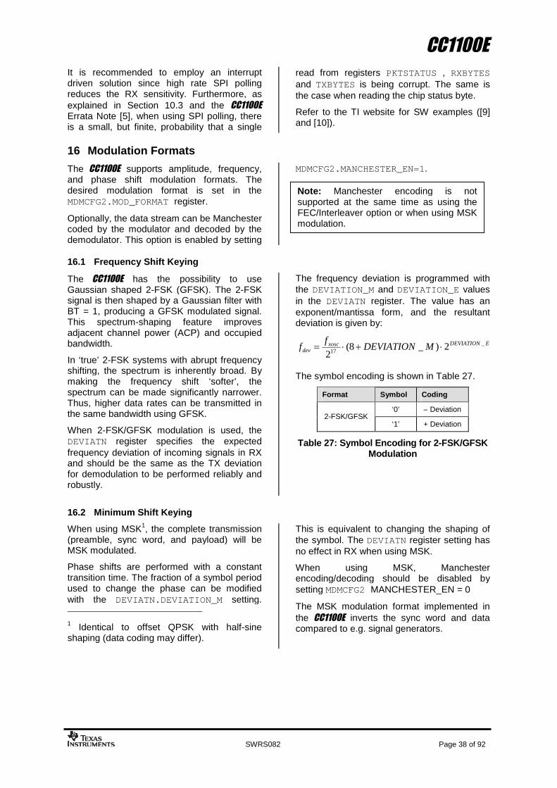
CC1100E
SWRS082 Page 38 of 92
It is recommended to employ an interruptdriven solution since high rate SPI pollingreduces the RX sensitivity. Furthermore, asexplained in Section 10.3 and the CC1100EErrata Note [5], when using SPI polling, thereis a small, but finite, probability that a single
read from registers PKTSTATUS , RXBYTESand TXBYTES is being corrupt. The same isthe case when reading the chip status byte.
Refer to the TI website for SW examples ([9]and [10]).
16 Modulation Formats
The CC1100E supports amplitude, frequency,and phase shift modulation formats. Thedesired modulation format is set in theMDMCFG2.MOD_FORMAT register.
Optionally, the data stream can be Manchestercoded by the modulator and decoded by thedemodulator. This option is enabled by setting
MDMCFG2.MANCHESTER_EN=1.
16.1 Frequency Shift Keying
The CC1100E has the possibility to useGaussian shaped 2-FSK (GFSK). The 2-FSKsignal is then shaped by a Gaussian filter withBT = 1, producing a GFSK modulated signal.This spectrum-shaping feature improvesadjacent channel power (ACP) and occupiedbandwidth.
In ‘true’ 2-FSK systems with abrupt frequencyshifting, the spectrum is inherently broad. Bymaking the frequency shift ‘softer’, thespectrum can be made significantly narrower.Thus, higher data rates can be transmitted inthe same bandwidth using GFSK.
When 2-FSK/GFSK modulation is used, theDEVIATN register specifies the expectedfrequency deviation of incoming signals in RXand should be the same as the TX deviationfor demodulation to be performed reliably androbustly.
The frequency deviation is programmed withthe DEVIATION_M and DEVIATION_E valuesin the DEVIATN register. The value has anexponent/mantissa form, and the resultantdeviation is given by:
EDEVIATIONxoscdev MDEVIATION
ff _
172)_8(
2
The symbol encoding is shown in Table 27.
Format Symbol Coding
‘0’ – Deviation2-FSK/GFSK
‘1’ + Deviation
Table 27: Symbol Encoding for 2-FSK/GFSKModulation
16.2 Minimum Shift Keying
When using MSK1, the complete transmission
(preamble, sync word, and payload) will beMSK modulated.
Phase shifts are performed with a constanttransition time. The fraction of a symbol periodused to change the phase can be modifiedwith the DEVIATN.DEVIATION_M setting.
1Identical to offset QPSK with half-sine
shaping (data coding may differ).
This is equivalent to changing the shaping ofthe symbol. The DEVIATN register setting hasno effect in RX when using MSK.
When using MSK, Manchesterencoding/decoding should be disabled bysetting MDMCFG2 MANCHESTER_EN = 0
The MSK modulation format implemented inthe CC1100E inverts the sync word and datacompared to e.g. signal generators.
Note: Manchester encoding is notsupported at the same time as using theFEC/Interleaver option or when using MSKmodulation.

CC1100E
SWRS082 Page 39 of 92
16.3 Amplitude Modulation
The CC1100E supports two different forms ofamplitude modulation: On-Off Keying (OOK)and Amplitude Shift Keying (ASK).
OOK modulation simply turns the PA on or offto modulate ones and zeros respectively.
The ASK variant supported by the CC1100Eallows programming of the modulation depth(the difference between 1 and 0), and shapingof the pulse amplitude. Pulse shaping
produces a more bandwidth constrainedoutput spectrum.
When using OOK/ASK, the AGC settings fromthe SmartRF
®Studio [8] preferred FSK/MSK
settings are not optimum. DN022 [15] giveguidelines on how to find optimum OOK/ASKsettings from the preferred settings inSmartRF
®Studio [8]. The DEVIATN register
setting has no effect in either TX or RX whenusing OOK/ASK.
17 Received Signal Qualifiers and Link Quality Information
The CC1100E has several qualifiers that can beused to increase the likelihood that a validsync word is detected:
Sync Word Qualifier
Preamble Quality Threshold
RSSI
Carrier Sense
Clear Channel Assessment
Link Quality Indicator
17.1 Sync Word Qualifier
If sync word detection in RX is enabled in the
MDMCFG2 register, the CC1100E will not startfilling the RX FIFO and perform the packetfiltering described in Section 15.3 before avalid sync word has been detected. The syncword qualifier mode is set byMDMCFG2.SYNC_MODE and is summarized inTable 28. Carrier sense in Table 28 isdescribed in Section 17.4.
MDMCFG2.
SYNC_MODESync Word Qualifier Mode
000 No preamble/sync
001 15/16 sync word bits detected
010 16/16 sync word bits detected
011 30/32 sync word bits detected
100 No preamble/sync + carrier senseabove threshold
101 15/16 + carrier sense above threshold
110 16/16 + carrier sense above threshold
111 30/32 + carrier sense above threshold
Table 28: Sync Word Qualifier Mode
17.2 Preamble Quality Threshold (PQT)
The Preamble Quality Threshold (PQT) syncword qualifier adds the requirement that thereceived sync word must be preceded with apreamble with a quality above theprogrammed threshold.
Another use of the preamble quality thresholdis as a qualifier for the optional RX terminationtimer. See Section 19.7 on page 49 for details.
The preamble quality estimator increases aninternal counter by one each time a bit isreceived that is different from the previous bit,and decreases the counter by eight each timea bit is received that is the same as the last bit.
The threshold is configured with the registerfield PKTCTRL1.PQT. A threshold of 4∙PQT forthis counter is used to gate sync worddetection. By setting the value to zero, thepreamble quality qualifier of the sync word isdisabled.
A “Preamble Quality Reached” signal can beobserved on one of the GDO pins by settingIOCFGx.GDOx_CFG=8. It is also possible todetermine if preamble quality is reached bychecking the PQT_REACHED bit in thePKTSTATUS register. This signal / bit assertswhen the received signal exceeds the PQT.
CC1100E
SWRS082 Page 40 of 92
17.3 RSSI
The RSSI value is an estimate of the signalpower level in the chosen channel. This valueis based on the current gain setting in the RXchain and the measured signal level in thechannel.
In RX mode, the RSSI value can be readcontinuously from the RSSI status registeruntil the demodulator detects a sync word(when sync word detection is enabled). At thatpoint the RSSI readout value is frozen until thenext time the chip enters the RX state.
The RSSI value is given in dBm with a ½ dBresolution. The RSSI update rate, fRSSI,depends on the receiver filter bandwidth(BWchannel is defined in Section 13) andAGCCTRL0.FILTER_LENGTH.
LENGTHFILTERchannel
RSSI
BWf
_28
2
If PKTCTRL1.APPEND_STATUS is enabled,the last RSSI value of the packet isautomatically added to the first byte appendedafter the payload.
The RSSI value read from the RSSI statusregister is a 2’s complement number. Thefollowing procedure can be used to convert theRSSI reading to an absolute power level(RSSI_dBm)
1) Read the RSSI status register
2) Convert the reading from a hexadecimalnumber to a decimal number (RSSI_dec)
3) If RSSI_dec ≥ 128 then RSSI_dBm =(RSSI_dec - 256)/2 – RSSI_offset
4) Else if RSSI_dec < 128 then RSSI_dBm =(RSSI_dec)/2 – RSSI_offset
Table 29 gives typical values for theRSSI_offset. Figure 17 and Figure 18 showtypical plots of RSSI readings as a function ofinput power level for different data rates.
Data rate [kBaud] RSSI_offset [dB], 490 MHz RSSI_offset [dB], 955 MHz
1.2 75 75
38.4 75 75
76.8 N/A 79
250 79 N/A
Table 29: Typical RSSI_offset Values
Note: It takes some time from the radioenters RX mode until a valid RSSI value ispresent in the RSSI register. Please seeDN505 [13] for details on how the RSSIresponse time can be estimated.

CC1100E
SWRS082 Page 41 of 92
-120
-110
-100
-90
-80
-70
-60
-50
-40
-30
-20
-10
0
-120 -110 -100 -90 -80 -70 -60 -50 -40 -30 -20 -10 0
Input Power (dBm)
RS
SI
Re
ad
ou
t(d
Bm
)
1.2 kBaud 38.4 kBaud 250 kBaud
Figure 17: Typical RSSI Value vs. Input Power Level for Different Data Rates at 480 MHz
-120.00
-110.00
-100.00
-90.00
-80.00
-70.00
-60.00
-50.00
-40.00
-30.00
-20.00
-10.00
0.00
-120 -110 -100 -90 -80 -70 -60 -50 -40 -30 -20 -10 0
Input Power (dBm)
RS
SI
Re
ad
ou
t(d
Bm
)
1.2 kBaud 38.4 kBaud 76.8 kBaud
Figure 18: Typical RSSI Value vs. Input Power Level for Different Data Rates at 955 MHz
17.4 Carrier Sense (CS)
Carrier sense (CS) is used as a sync wordqualifier and for Clear Channel Assessment(see Section 17.5). CS can be asserted basedon two conditions which can be individuallyadjusted:
CS is asserted when the RSSI is above aprogrammable absolute threshold, and de-asserted when RSSI is below the same
threshold (with hysteresis). See more inSection 17.4.1.
CS is asserted when the RSSI hasincreased with a programmable number ofdB from one RSSI sample to the next, andde-asserted when RSSI has decreasedwith the same number of dB. This settingis not dependent on the absolute signal

CC1100E
SWRS082 Page 42 of 92
level and is thus useful to detect signals inenvironments with time varying noise floor.See more in Section 17.4.2.
Carrier sense can be used as a sync wordqualifier that requires the signal level to behigher than the threshold for a sync wordsearch to be performed and is set by settingMDMCFG2 The carrier sense signal can beobserved on one of the GDO pins by settingIOCFGx.GDOx_CFG=14 and in the statusregister bit PKTSTATUS.CS.
Other uses of Carrier sense include the TX-if-CCA function (see Section 17.5 on page 43)and the optional fast RX termination (seeSection 19.7 on page 49).
CS can be used to avoid interference fromother RF sources in the ISM bands.
17.4.1 CS Absolute Threshold
The absolute threshold related to the RSSIvalue depends on the following register fields:
AGCCTRL2.MAX_LNA_GAIN
AGCCTRL2.MAX_DVGA_GAIN
AGCCTRL1.CARRIER_SENSE_ABS_THR
AGCCTRL2.MAGN_TARGET
For given AGCCTRL2.MAX_LNA_GAIN andAGCCTRL2.MAX_DVGA_GAIN settings, theabsolute threshold can be adjusted ±7 dB insteps of 1 dB usingCARRIER_SENSE_ABS_THR.
The MAGN_TARGET setting is a compromisebetween blocker tolerance/selectivity andsensitivity. The value sets the desired signallevel in the channel into the demodulator.Increasing this value reduces the headroomfor blockers, and therefore close-in selectivity.It is strongly recommended to use SmartRF
®
Studio [8] to generate the correctMAGN_TARGET setting. Table 30 and Table31 show the typical RSSI readout values at theCS threshold at 2.4 kBaud and 250 kBauddata rate respectively. The defaultCARRIER_SENSE_ABS_THR=0 (0 dB) andMAGN_TARGET=3 (33 dB) have been used.For other data rates, the user must generatesimilar tables to find the CS absolutethreshold.
MAX_DVGA_GAIN[1:0]
00 01 10 11
000 -97.5 -91.5 -85.5 -79.5
001 -94 -88 -82.5 -76
010 -90.5 -84.5 -78.5 -72.5
011 -88 -82.5 -76.5 -70.5
100 -85.5 -80 -73.5 -68
101 -84 -78 -72 -66
110 -82 -76 -70 -64MA
X_L
NA
_G
AIN
[2:0
]
111 -79 -73.5 -67 -61
Table 30: Typical RSSI Value in dBm at CSThreshold with Default MAGN_TARGET at 2.4
kBaud, 955 MHz
MAX_DVGA_GAIN[1:0]
00 01 10 11
000 -90.5 -84.5 -78.5 -72.5
001 -88 -82 -76 -70
010 -84.5 -78.5 -72 -66
011 -82.5 -76.5 -70 -64
100 -80.5 -74.5 -68 -62
101 -78 -72 -66 -60
110 -76.5 -70 -64 -58MA
X_L
NA
_G
AIN
[2:0
]
111 -74.5 -68 -62 -56
Table 31: Typical RSSI Value in dBm at CSThreshold with Default MAGN_TARGET at 250
kBaud, 955 MHz
If the threshold is set high, i.e. only strongsignals are wanted; the threshold should beadjusted upwards by first reducing theMAX_LNA_GAIN value and then the
MAX_DVGA_GAIN value. This will reducepower consumption in the receiver front end,since the highest gain settings are avoided.
17.4.2 CS Relative Threshold
The relative threshold detects sudden changesin the measured signal level. This setting doesnot depend on the absolute signal level and isthus useful to detect signals in environmentswith a time varying noise floor. The registerfield AGCCTRL1.CARRIER_SENSE_REL_THRis used to enable/disable relative CS, and toselect threshold of 6 dB, 10 dB, or 14 dB RSSIchange.

CC1100E
SWRS082 Page 43 of 92
17.5 Clear Channel Assessment (CCA)
The Clear Channel Assessment (CCA) is usedto indicate if the current channel is free orbusy. The current CCA state is viewable onany of the GDO pins by settingIOCFGx.GDOx_CFG=0x09.
MCSM1.CCA_MODE selects the mode to usewhen determining CCA.
When the STX or SFSTXON command strobe is
given while the CC1100E is in the RX state, theTX or FSTXON state is only entered if theclear channel requirements are fulfilled.Otherwise, the chip will remain in RX. If thechannel then becomes available, the radio will
not enter TX or FSTXON state before a newstrobe command is sent on the SPI interface.This feature is called TX-if-CCA. Four CCArequirements can be programmed:
Always (CCA disabled, always goes to TX)
If RSSI is below threshold
Unless currently receiving a packet
Both the above (RSSI below threshold andnot currently receiving a packet)
17.6 Link Quality Indicator (LQI)
The Link Quality Indicator is a metric of thecurrent quality of the received signal. IfPKTCTRL1.APPEND_STATUS is enabled, thevalue is automatically added to the last byteappended after the payload. The value canalso be read from the LQI status register. TheLQI gives an estimate of how easily a receivedsignal can be demodulated by accumulating
the magnitude of the error between idealconstellations and the received signal over the64 symbols immediately following the syncword. LQI is best used as a relativemeasurement of the link quality (a high valueindicates a better link than what a low valuedoes), since the value is dependent on themodulation format.
18 Forward Error Correction with Interleaving
18.1 Forward Error Correction (FEC)
The CC1100E has built in support for ForwardError Correction (FEC). To enable this option,set MDMCFG1.FEC_EN to 1. FEC is onlysupported in fixed packet length mode, i.e.when PKTCTRL0.LENGTH_CONFIG=0. FEC isemployed on the data field and CRC word inorder to reduce the gross bit error rate whenoperating near the sensitivity limit.Redundancy is added to the transmitted datain such a way that the receiver can restore theoriginal data in the presence of some biterrors.
The use of FEC allows correct reception at alower Signal-to-Noise Ratio (SNR), thusextending communication range if the receiverbandwidth remains constant. Alternatively, fora given SNR, using FEC decreases the biterror rate (BER). The packet error rate (PER)is related to BER by
lengthpacketBERPER _)1(1
A lower BER can therefore be used to allowlonger packets, or a higher percentage ofpackets of a given length, to be transmittedsuccessfully. Finally, in realistic ISM radioenvironments, transient and time-varying
phenomena will produce occasional errorseven in otherwise good reception conditions.FEC will mask such errors and, combined withinterleaving of the coded data, even correctrelatively long periods of faulty reception (bursterrors).
The FEC scheme adopted for the CC1100E isconvolutional coding, in which n bits aregenerated based on k input bits and the mmost recent input bits, forming a code streamable to withstand a certain number of bit errorsbetween each coding state (the m-bit window).
The convolutional coder is a rate ½ code witha constraint length of m = 4. The coder codesone input bit and produces two output bits;hence, the effective data rate is halved. Thismeans that in order to transmit at the sameeffective data rate when using FEC, it isnecessary to use twice as high over-the-airdata rate. This will require a higher receiverbandwidth, and thus reduce sensitivity. Inother words the improved reception by usingFEC and the degraded sensitivity from ahigher receiver bandwidth will becounteracting factors. Please see Design NoteDN504 [18] for more information
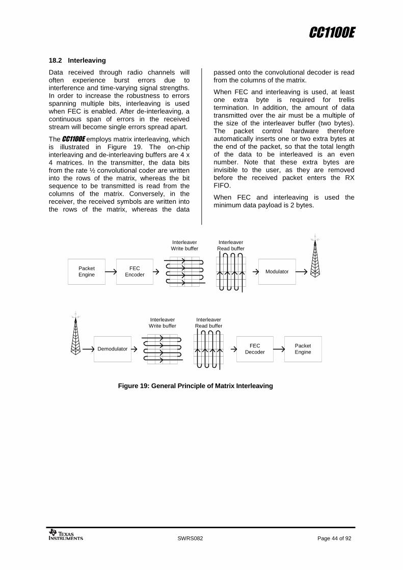
CC1100E
SWRS082 Page 44 of 92
18.2 Interleaving
Data received through radio channels willoften experience burst errors due tointerference and time-varying signal strengths.In order to increase the robustness to errorsspanning multiple bits, interleaving is usedwhen FEC is enabled. After de-interleaving, acontinuous span of errors in the receivedstream will become single errors spread apart.
The CC1100E employs matrix interleaving, whichis illustrated in Figure 19. The on-chipinterleaving and de-interleaving buffers are 4 x4 matrices. In the transmitter, the data bitsfrom the rate ½ convolutional coder are writteninto the rows of the matrix, whereas the bitsequence to be transmitted is read from thecolumns of the matrix. Conversely, in thereceiver, the received symbols are written intothe rows of the matrix, whereas the data
passed onto the convolutional decoder is readfrom the columns of the matrix.
When FEC and interleaving is used, at leastone extra byte is required for trellistermination. In addition, the amount of datatransmitted over the air must be a multiple ofthe size of the interleaver buffer (two bytes).The packet control hardware thereforeautomatically inserts one or two extra bytes atthe end of the packet, so that the total lengthof the data to be interleaved is an evennumber. Note that these extra bytes areinvisible to the user, as they are removedbefore the received packet enters the RXFIFO.
When FEC and interleaving is used theminimum data payload is 2 bytes.
PacketEngine
FECEncoder
Modulator
InterleaverWrite buffer
InterleaverRead buffer
DemodulatorFEC
DecoderPacketEngine
InterleaverWrite buffer
InterleaverRead buffer
Figure 19: General Principle of Matrix Interleaving

CC1100E
SWRS082 Page 45 of 92
19 Radio Control
TX19,20
RX13,14,15
IDLE1
CALIBRATE8
MANCAL3,4,5
SETTLING9,10,11
RX_OVERFLOW17
TX_UNDERFLOW22
RXTX_SETTLING21
FSTXON18
SFSTXON
FS_AUTOCAL = 00 | 10 | 11&
SRX | STX | SFSTXON | WOR
SRX | WORSTX
STX
TXFIFO_UNDERFLOW
STX | RXOFF_MODE = 10
RXOFF_MODE = 00&
FS_AUTOCAL = 10 | 11
SFTX
SRX | TXOFF_MODE = 11
SIDLE
SCAL
CAL_COMPLETE
FS_AUTOCAL = 01&
SRX | STX | SFSTXON | WOR
RXFIFO_OVERFLOW
CAL_COMPLETE
SFRX
CALIBRATE12
IDLE1
TXOFF_MODE = 00&
FS_AUTOCAL = 10 | 11
RXOFF_MODE = 00&
FS_AUTOCAL = 00 | 01
TXOFF_MODE = 00&
FS_AUTOCAL = 00 | 01
TXOFF_MODE = 10 RXOFF_MODE = 11
SFSTXON | RXOFF_MODE = 01
TXRX_SETTLING16
SRX | STX | SFSTXON | WOR
SLEEP0
SPWD | SWOR
XOFF2
SXOFF
CSn = 0
CSn = 0 | WOR
( STX | SFSTXON ) & CCA|
RXOFF_MODE = 01 | 10
TXOFF_MODE=01
FS_WAKEUP6,7
SRX
Figure 20: Complete Radio Control State Diagram
The CC1100E has a built-in state machine that isused to switch between different operationalstates (modes). The change of state is doneeither by using command strobes or byinternal events such as TX FIFO underflow.
A simplified state diagram, together withtypical usage and current consumption, is
shown in Figure 9 on page 24. The completeradio control state diagram is shown in Figure20. The numbers refer to the state numberreadable in the MARCSTATE status register.This register is primarily for test purposes.
19.1 Power-On Start-Up Sequence
When the power supply is turned on, thesystem must be reset. This is achieved by oneof the two sequences described below, i.e.Automatic power-on reset (POR) or manual
reset. After the automatic power-on reset ormanual reset, it is also recommended tochange the signal that is output on the GDO0pin. The default setting is to output a clock

CC1100E
SWRS082 Page 46 of 92
signal with a frequency of CLK_XOSC/192.However, to optimize performance in TX andRX, an alternative GDO setting from thesettings found in Table 36 on page 55 shouldbe selected.
19.1.1 Automatic POR
A power-on reset circuit is included in theCC1100E. The minimum requirements stated inTable 16 must be followed for the power-onreset to function properly. The internal power-up sequence is completed when CHIP_RDYngoes low. CHIP_RDYn is observed on the SOpin after CSn is pulled low. See Section 10.1for more details on CHIP_RDYn.
When the CC1100E reset is completed, the chipwill be in the IDLE state and the crystaloscillator will be running. If the chip has hadsufficient time for the crystal oscillator tostabilize after the power-on-reset, the SO pinwill go low immediately after taking CSn low. IfCSn is taken low before reset is completed,the SO pin will first go high, indicating that thecrystal oscillator is not stabilized, before goinglow as shown in Figure 21.
Figure 21: Power-On Reset
19.1.2 Manual Reset
The other global reset possibility on the
CC1100E uses the SRES command strobe. Byissuing this strobe, all internal registers andstates are set to the default, IDLE state. The
manual power-up sequence is as follows (seeFigure 22):
Set SCLK = 1 and SI = 0, to avoidpotential problems with pin control mode(see Section 11.3 on page 30).
Strobe CSn low / high.
Hold CSn low and then high for at least 40µs relative to pulling CSn low
Pull CSn low and wait for SO to go low(CHIP_RDYn).
Issue the SRES strobe on the SI line.
When SO goes low again, reset iscomplete and the chip is in the IDLE state.
Figure 22: Power-On Reset with SRES
19.2 Crystal Control
The crystal oscillator (XOSC) is eitherautomatically controlled or always on, ifMCSM0.XOSC_FORCE_ON is set.
In the automatic mode, the XOSC will beturned off if the SXOFF or SPWD commandstrobes are issued; the state machine thengoes to XOFF or SLEEP respectively. Thiscan only be done from the IDLE state. TheXOSC will be turned off when CSn is released(goes high). The XOSC will be automaticallyturned on again when CSn goes low. The
state machine will then go to the IDLE state.The SO pin on the SPI interface must bepulled low before the SPI interface is ready tobe used as described in Section 10.1 on page27.
If the XOSC is forced on, the crystal willalways stay on even in the SLEEP state.
Crystal oscillator start-up time depends oncrystal ESR and load capacitances. Theelectrical specification for the crystal oscillatorcan be found in Section 4.4 on page 14.
Note that the above reset procedure isonly required just after the power supply isfirst turned on. If the user wants to resetthe CC1100E after this, it is only necessaryto issue an SRES command strobe.

CC1100E
SWRS082 Page 47 of 92
19.3 Voltage Regulator Control
The voltage regulator to the digital core iscontrolled by the radio controller. When thechip enters the SLEEP state which is the statewith the lowest current consumption, thevoltage regulator is disabled. This occurs afterCSn is released when a SPWD commandstrobe has been sent on the SPI interface. The
chip is then in the SLEEP state. Setting CSnlow again will turn on the regulator and crystaloscillator and make the chip enter the IDLEstate.
When Wake on Radio is enabled, the WORmodule will control the voltage regulator asdescribed in Section19.5.
19.4 Active Modes
The CC1100E has two active modes: receiveand transmit. These modes are activateddirectly by the MCU by using the SRX and STXcommand strobes, or automatically by Wakeon Radio.
The frequency synthesizer must be calibratedregularly. The CC1100E has one manualcalibration option (using the SCAL strobe), andthree automatic calibration options that arecontrolled by the MCSM0.FS_AUTOCAL setting:
Calibrate when going from IDLE to eitherRX or TX (or FSTXON)
Calibrate when going from either RX or TXto IDLE automatically
Calibrate every fourth time when goingfrom either RX or TX to IDLE automatically
If the radio goes from TX or RX to IDLE byissuing an SIDLE strobe, calibration will not beperformed. The calibration takes a constantnumber of XOSC cycles; see Table 32 fortiming details regarding calibration.
When RX is activated, the chip will remain inreceive mode until a packet is successfullyreceived or the RX termination timer expires(see Section 19.7). The probability that a falsesync word is detected can be reduced byusing PQT, CS, maximum sync word length,and sync word qualifier mode as described inSection 17. After a packet is successfullyreceived, the radio controller goes to the stateindicated by the MCSM1.RXOFF_MODE setting.The possible destinations are:
IDLE
FSTXON: Frequency synthesizer on andready at the TX frequency. Activate TXwith STX
TX: Start sending preamble
RX: Start search for a new packet
Similarly, when TX is active the chip willremain in the TX state until the current packethas been successfully transmitted. Then thestate will change as indicated by theMCSM1.TXOFF_MODE setting. The possibledestinations are the same as for RX.
The MCU can manually change the state fromRX to TX and vice versa by using thecommand strobes. If the radio controller iscurrently in transmit and the SRX strobe isused, the current transmission will be endedand the transition to RX will be done.
If the radio controller is in RX when the STX orSFSTXON command strobes are used, the TX-if-CCA function will be used. If the channel isnot clear, the chip will remain in RX. TheMCSM1.CCA_MODE setting controls theconditions for clear channel assessment. SeeSection 17.5 on page 43 for details.
The SIDLE command strobe can always beused to force the radio controller to go to theIDLE state.
Note: When MCSM1.RXOFF_MODE=11and a packet has been received, it willtake some time before a valid RSSI valueis present in the RSSI register again evenif the radio has never exited RX mode.This time is the same as the RSSIresponse time discussed in DN505 [13].

CC1100E
SWRS082 Page 48 of 92
19.5 Wake On Radio (WOR)
The optional Wake on Radio (WOR)functionality enables the CC1100E to periodicallywake up from SLEEP and listen for incomingpackets without MCU interaction.
When the SWOR strobe command is sent on
the SPI interface, the CC1100E will go to theSLEEP state when CSn is released. The RCoscillator must be enabled before the SWORstrobe can be used, as it is the clock sourcefor the WOR timer. The on-chip timer will setthe CC1100E into IDLE state and then RX state.After a programmable time in RX, the chip willgo back to the SLEEP state, unless a packet isreceived. See Figure 23 and Section 19.7 fordetails on how the timeout works.
To exit WOR mode, set the CC1100E into theIDLE state
The CC1100E can be set up to signal the MCUthat a packet has been received by using theGDO pins. If a packet is received, theMCSM1.RXOFF_MODE will determine thebehaviour at the end of the received packet.When the MCU has read the packet, it can putthe chip back into SLEEP with the SWOR strobefrom the IDLE state.
The WOR timer has two events, Event 0 andEvent 1. In the SLEEP state with WORactivated, reaching Event 0 will turn on thedigital regulator and start the crystal oscillator.Event 1 follows Event 0 after a programmedtimeout.
The time between two consecutive Event 0 isprogrammed with a mantissa value given byWOREVT1.EVENT0 and WOREVT0.EVENT0,and an exponent value set byWORCTRL.WOR_RES. The equation is:
RESWOR
XOSC
Event EVENTf
t _50 20
750
The Event 1 timeout is programmed withWORCTRL.EVENT1. Figure 23 shows thetiming relationship between Event 0 timeoutand Event 1 timeout.
Figure 23: Event 0 and Event 1 Relationship
The time from the CC1100E enters SLEEP stateuntil the next Event0 is programmed toappear, tSLEEP in Figure 23, should be largerthan 11.08 ms when using a 26 MHz crystaland 10.67 ms when a 27 MHz crystal is used.If tSLEEP is less than 11.08 (10.67) ms, there isa chance that the consecutive Event 0 willoccur
128750
XOSCf
seconds
too early. Application Note AN047 [7] explainsin detail the theory of operation and thedifferent registers involved when using WOR,as well as highlighting important aspects whenusing WOR mode.
19.5.1 RC Oscillator and Timing
The frequency of the low-power RC oscillatorused for the WOR functionality varies withtemperature and supply voltage. In order tokeep the frequency as accurate as possible,the RC oscillator will be calibrated wheneverpossible, which is when the XOSC is runningand the chip is not in the SLEEP state. Whenthe power and XOSC are enabled, the clockused by the WOR timer is a divided XOSCclock. When the chip goes to the sleep state,the RC oscillator will use the last validcalibration result. The frequency of the RCoscillator is locked to the main crystalfrequency divided by 750.
In applications where the radio wakes up veryoften, typically several times every second, itis possible to do the RC oscillator calibrationonce and then turn off calibration to reduce thecurrent consumption. This is done by settingWORCTRL.RC_CAL=0 and requires that RCoscillator calibration values are read fromregisters RCCTRL0_STATUS andRCCTRL1_STATUS and written back toRCCTRL0 and RCCTRL1 respectively. If the
Note: The FIFO looses its content in theSLEEP state.

CC1100E
SWRS082 Page 49 of 92
RC oscillator calibration is turned off, it willhave to be manually turned on again if thetemperature and/or the supply voltage
changes. Refer to Application Note AN047 [7]for further details.
19.6 Timing
The radio controller controls most of the timingin the CC1100E, such as synthesizer calibration,PLL lock time, and RX/TX turnaround times.Timing from IDLE to RX and IDLE to TX isconstant, dependent on the auto calibrationsetting. RX/TX and TX/RX turnaround timesare constant. The calibration time is constant18739 clock periods. Table 32 shows timing incrystal clock cycles for key state transitions.
Power on time and XOSC start-up times arevariable, but within the limits stated in Table11.
Note that in a frequency hopping spreadspectrum or a multi-channel protocol thecalibration time can be reduced from 721 µs toapproximately 150 µs. This is explained inSection 28.2.
DescriptionXOSCPeriods
26 MHzCrystal
IDLE to RX, no calibration 2298 88.4μs
IDLE to RX, with calibration ~21037 809μs
IDLE to TX/FSTXON, nocalibration
2298 88.4μs
IDLE to TX/FSTXON, withcalibration
~21037 809μs
TX to RX switch 560 21.5μs
RX to TX switch 250 9.6μs
RX or TX to IDLE, no calibration 2 0.1μs
RX or TX to IDLE, with calibration ~18739 721μs
Manual calibration ~18739 721μs
Table 32: State Transition Timing
19.7 RX Termination Timer
The CC1100E has optional functions forautomatic termination of RX after aprogrammable time. The main use for thisfunctionality is Wake on Radio, but it may alsobe useful for other applications. Thetermination timer starts when in RX state. Thetimeout is programmable with theMCSM2.RX_TIME setting. When the timerexpires, the radio controller will check thecondition for staying in RX; if the condition isnot met, RX will terminate.
The programmable conditions are:
MCSM2.RX_TIME_QUAL=0: Continuereceive if sync word has been found
MCSM2.RX_TIME_QUAL=1: Continuereceive if sync word has been found, or ifthe preamble quality is above threshold(PQT)
If the system expects the transmission to havestarted when enabling the receiver, theMCSM2.RX_TIME_RSSI function can be used.The radio controller will then terminate RX ifthe first valid carrier sense sample indicatesno carrier (RSSI below threshold). See Section17.4 on page 41 for details on Carrier Sense.
For ASK/OOK modulation, lack of carriersense is only considered valid after eightsymbol periods. Thus, theMCSM2.RX_TIME_RSSI function can be usedin ASK/OOK mode when the distance between“1” symbols is eight or less.
If RX terminates due to no carrier sense whenthe MCSM2.RX_TIME_RSSI function is used,or if no sync word was found when using theMCSM2.RX_TIME timeout function, the chipwill always go back to IDLE if WOR is disabledand back to SLEEP if WOR is enabled.Otherwise, the MCSM1.RXOFF_MODE settingdetermines the state to go to when RX ends.This means that the chip will not automaticallygo back to SLEEP once a sync word has beenreceived. It is therefore recommended toalways wake up the microcontroller on syncword detection when using WOR mode. Thiscan be done by selecting output signal 6 (seeTable 36 on page 55) on one of theprogrammable GDO output pins, andprogramming the microcontroller to wake upon an edge-triggered interrupt from this GDOpin.

CC1100E
SWRS082 Page 50 of 92
20 Data FIFO
The CC1100E contains two 64 byte FIFOs, onefor received data and one for data to betransmitted. The SPI interface is used to readfrom the RX FIFO and write to the TX FIFO.Section 10.5 contains details on the SPI FIFOaccess. The FIFO controller will detectoverflow in the RX FIFO and underflow in theTX FIFO.
When writing to the TX FIFO it is theresponsibility of the MCU to avoid TX FIFOoverflow. A TX FIFO overflow will result in anerror in the TX FIFO content.
Likewise, when reading the RX FIFO the MCUmust avoid reading the RX FIFO past its emptyvalue since a RX FIFO underflow will result inan error in the data read out of the RX FIFO.
The chip status byte that is available on theSO pin while transferring the SPI header andcontains the fill grade of the RX FIFO if theaccess is a read operation and the fill grade ofthe TX FIFO if the access is a write operation.Section 10.1 on page 27 contains more detailson this.
The number of bytes in the RX FIFO and TXFIFO can be read from the status registersRXBYTES.NUM_RXBYTES andTXBYTES.NUM_TXBYTES respectively. If areceived data byte is written to the RX FIFO atthe exact same time as the last byte in the RXFIFO is read over the SPI interface, the RXFIFO pointer is not properly updated and thelast read byte will be duplicated. To avoid thisproblem, the RX FIFO should never beemptied before the last byte of the packet isreceived.
For packet lengths less than 64 bytes it isrecommended to wait until the completepacket has been received before reading it outof the RX FIFO.
If the packet length is larger than 64 bytes, theMCU must determine how many bytes can beread from the RX FIFO(RXBYTES.NUM_RXBYTES-1). The followingsoftware routine can be used:
1. Read RXBYTES.NUM_RXBYTESrepeatedly at a rate guaranteed to be atleast twice that of which RF bytes arereceived until the same value is returned
twice; store value in n.
2. If n < # of bytes remaining in packet, readn-1 bytes from the RX FIFO.
3. Repeat steps 1 and 2 until n = # of bytesremaining in packet.
4. Read the remaining bytes from the RXFIFO.
The 4-bit FIFOTHR.FIFO_THR setting is usedto program threshold points in the FIFOs.
Table 33 lists the 16 FIFO_THR settings andthe corresponding thresholds for the RX andTX FIFOs. The threshold value is coded inopposite directions for the RX FIFO and TXFIFO. This gives equal margin to the overflowand underflow conditions when the thresholdis reached.
FIFO_THR Bytes in TX FIFO Bytes in RX FIFO
0 (0000) 61 4
1 (0001) 57 8
2 (0010) 53 12
3 (0011) 49 16
4 (0100) 45 20
5 (0101) 41 24
6 (0110) 37 28
7 (0111) 33 32
8 (1000) 29 36
9 (1001) 25 40
10 (1010) 21 44
11 (1011) 17 48
12 (1100) 13 52
13 (1100E) 9 56
14 (1110) 5 60
15 (1111) 1 64
Table 33: FIFO_THR Settings and theCorresponding FIFO Thresholds
A signal will assert when the number of bytesin the FIFO is equal to or higher than theprogrammed threshold. This signal can beviewed on the GDO pins (see Table 36 onpage 55).
Figure 24 shows the number of bytes in boththe RX FIFO and TX FIFO when the thresholdsignal toggles in the case of FIFO_THR=13.Figure 25 shows the signal on the GDO pin asthe respective FIFO is filled above thethreshold, and then drained below in the caseof FIFO_THR=13.
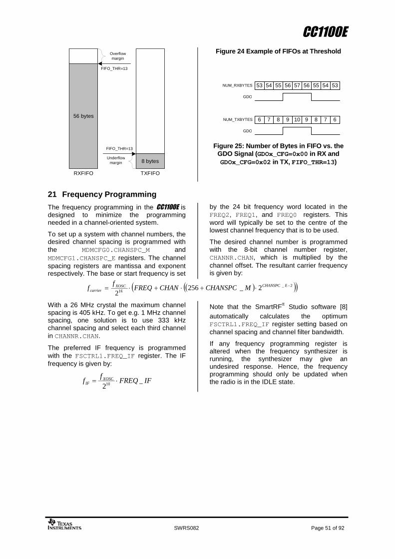
CC1100E
SWRS082 Page 51 of 92
56 bytes
8 bytes
Overflowmargin
Underflowmargin
FIFO_THR=13
FIFO_THR=13
RXFIFO TXFIFO
Figure 24 Example of FIFOs at Threshold
53 54 55 56 5354555657
6 7 8 9 678910
NUM_RXBYTES
GDO
NUM_TXBYTES
GDO
Figure 25: Number of Bytes in FIFO vs. theGDO Signal (GDOx_CFG=0x00 in RX andGDOx_CFG=0x02 in TX, FIFO_THR=13)
21 Frequency Programming
The frequency programming in the CC1100E isdesigned to minimize the programmingneeded in a channel-oriented system.
To set up a system with channel numbers, thedesired channel spacing is programmed withthe MDMCFG0.CHANSPC_M andMDMCFG1.CHANSPC_E registers. The channelspacing registers are mantissa and exponentrespectively. The base or start frequency is set
by the 24 bit frequency word located in theFREQ2, FREQ1, and FREQ0 registers. Thisword will typically be set to the centre of thelowest channel frequency that is to be used.
The desired channel number is programmedwith the 8-bit channel number register,CHANNR.CHAN, which is multiplied by thechannel offset. The resultant carrier frequencyis given by:
2_
162_256
2 ECHANSPCXOSC
carrier MCHANSPCCHANFREQf
f
With a 26 MHz crystal the maximum channelspacing is 405 kHz. To get e.g. 1 MHz channelspacing, one solution is to use 333 kHzchannel spacing and select each third channelin CHANNR.CHAN.
The preferred IF frequency is programmedwith the FSCTRL1.FREQ_IF register. The IFfrequency is given by:
IFFREQf
f XOSCIF _
210
Note that the SmartRF®
Studio software [8]
automatically calculates the optimumFSCTRL1.FREQ_IF register setting based onchannel spacing and channel filter bandwidth.
If any frequency programming register isaltered when the frequency synthesizer isrunning, the synthesizer may give anundesired response. Hence, the frequencyprogramming should only be updated whenthe radio is in the IDLE state.

CC1100E
SWRS082 Page 52 of 92
22 VCO
The VCO is completely integrated on-chip.
22.1 VCO and PLL Self-Calibration
The VCO characteristics vary with temperatureand supply voltage changes as well as thedesired operating frequency. In order toensure reliable operation, the CC1100E includesfrequency synthesizer self-calibration circuitry.This calibration should be done regularly, andmust be performed after turning on power andbefore using a new frequency (or channel).The number of XOSC cycles for completingthe PLL calibration is given in Table 32 onpage 49.
The calibration can be initiated automaticallyor manually. The synthesizer can beautomatically calibrated each time thesynthesizer is turned on, or each time thesynthesizer is turned off automatically. This isconfigured with the MCSM0.FS_AUTOCALregister setting. In manual mode, thecalibration is initiated when the SCALcommand strobe is activated in the IDLEmode.
To check that the PLL is in lock, the user canprogram register IOCFGx.GDOx_CFG to0x0A, and use the lock detector outputavailable on the GDOx pin as an interrupt forthe MCU (x = 0,1, or 2). A positive transitionon the GDOx pin means that the PLL is inlock. As an alternative the user can readregister FSCAL1. The PLL is in lock if theregister content is different from 0x3F. Referalso to the CC1100E Errata Note [5].
For more robust operation, the source codecould include a check so that the PLL is re-calibrated until PLL lock is achieved if the PLLdoes not lock the first time.
23 Voltage Regulators
The CC1100E contains several on-chip linearvoltage regulators that generate the supplyvoltages needed by low-voltage modules.These voltage regulators are invisible to theuser, and can be viewed as integral parts ofthe various modules. The user must howevermake sure that the absolute maximum ratingsand required pin voltages in Table 1 and Table17 are not exceeded.
By setting the CSn pin low, the voltageregulator to the digital core turns on and thecrystal oscillator starts. The SO pin on the SPIinterface must go low before the first positiveedge of SCLK (setup time is given in Table20).
If the chip is programmed to enter power-downmode (SPWD strobe issued), the power will beturned off after CSn goes high. The power andcrystal oscillator will be turned on again whenCSn goes low.
The voltage regulator for the digital corerequires one external decoupling capacitor.
The voltage regulator output should only beused for driving the CC1100E.
24 Output Power Programming
The RF output power level from the device hastwo levels of programmability as illustrated inFigure 26. The special PATABLE register canhold up to eight user selected output powersettings. The 3-bit FREND0.PA_POWER value
selects the PATABLE entry to use. This two-level functionality provides flexible PA powerramp up and ramp down at the start and endof transmission as well as ASK modulation
shaping. All the PA power settings in thePATABLE from index 0 up to theFREND0.PA_POWER value are used.
The power ramping at the start and at the endof a packet can be turned off by settingFREND0.PA_POWER=0 and then program thedesired output power to index 0 in thePATABLE.
Note: The calibration values aremaintained in SLEEP mode, so thecalibration is still valid after waking up fromSLEEP mode unless supply voltage ortemperature has changed significantly.

CC1100E
SWRS082 Page 53 of 92
If OOK modulation is used, the logic 0 andlogic 1 power levels shall be programmed toindex 0 and 1 respectively.
Table 33 contains recommended PATABLEsettings for various output levels andfrequency bands. DN013 Error! Referencesource not found. gives the complete tablesfor the different frequency bands. Using PAsettings from 0x61 to 0x6F is notrecommended.
Table 34 contains output power and currentconsumption for default PATABLE setting(0xC6).
See Section 10.6 on page 29 for PATABLEprogramming details. PATABLE must beprogrammed in burst mode if you want to writeto other entries than PATABLE[0].
Table 34: Optimum PATABLE Settings for Various Output Power Levels and FrequencyBands
Table 35: Output Power and Current Consumption for Default PATABLE Setting
25 Shaping and PA Ramping
With ASK modulation, up to eight powersettings are used for shaping. The modulatorcontains a counter that counts up whentransmitting a one and down when transmittinga zero. The counter counts at a rate equal to 8times the symbol rate. The counter saturates
at FREND0.PA_POWER and 0 respectively.This counter value is used as an index for alookup in the power table. Thus, in order toutilize the whole table, FREND0.PA_POWERshould be 7 when ASK is active. The shapingof the ASK signal is dependent on the
480 MHz 955 MHz
OutputPower[dBm]
SettingCurrent
Consumption,Typ. [mA]
SettingCurrent
Consumption,Typ. [mA]
-30 0x04 12.5 0x30 13.0
-20 0x0E 13.0 0x14 12.9
-15 0x1C 13.5 0x18 13.6
-10 0x26 14.9 0x24 14.6
-5 0x2B 16.9 0x28 16.2
0 0x60 16.6 0x60 16.5
5 0x86 19.8 0x86 19.1
7 0xCB 24.6 0xC7 26.3
10 (9) 0xC2 29.6 0xC0 30.9
480 MHz 955 MHz
DefaultPowerSetting
OutputPower[dBm]
CurrentConsumption,Typ. [mA]
OutputPower[dBm]
CurrentConsumption,Typ. [mA]
0xC6 8.8 26.9 7.3 26.7
Note: All content of the PATABLE exceptfor the first byte (index 0) is lost whenentering the SLEEP state.

CC1100E
SWRS082 Page 54 of 92
configuration of the PATABLE. Figure 27 shows some examples of ASK shaping.
e.g 6
PA_POWER[2:0]in FREND0 register
PATABLE(0)[7:0]
PATABLE(1)[7:0]
PATABLE(2)[7:0]
PATABLE(3)[7:0]
PATABLE(4)[7:0]
PATABLE(5)[7:0]
PATABLE(6)[7:0]
PATABLE(7)[7:0]
Index into PATABLE(7:0)
The PA uses thissetting.
Settings 0 to PA_POWER areused during ramp-up at start oftransmission and ramp-down atend of transmission, and forASK/OOK modulation.
The SmartRF® Studio softwareshould be used to obtain optimumPATABLE settings for variousoutput powers.
Figure 26: PA_POWER and PATABLE
Figure 27: Shaping of ASK Signal
26 General Purpose / Test Output Control Pins
The three digital output pins GDO0, GDO1,and GDO2 are general control pins configuredwith IOCFG0.GDO0_CFG,IOCFG1.GDO1_CFG, and IOCFG2.GDO2_CFGrespectively. Table 36 shows the differentsignals that can be monitored on the GDOpins. These signals can be used as inputs tothe MCU.
GDO1 is the same pin as the SO pin on theSPI interface, thus the output programmed onthis pin will only be valid when CSn is high.The default value for GDO1 is 3-stated whichis useful when the SPI interface is shared withother devices.
The default value for GDO0 is a 135-141 kHzclock output (XOSC frequency divided by192). Since the XOSC is turned on at power-on-reset, this can be used to clock the MCU insystems with only one crystal. When the MCUis up and running, it can change the clockfrequency by writing to IOCFG0.GDO0_CFG.
An on-chip analog temperature sensor isenabled by writing the value 128 (0x80) to theIOCFG0 register. The voltage on the GDO0pin is then proportional to temperature. SeeSection 4.7 on page 15 for temperature sensorspecifications.
If the IOCFGx.GDOx_CFG setting is less than0x20 and IOCFGx_GDOx_INV is 0 (1), theGDO0 and GDO2 pins will be hardwired to 0(1), and the GDO1 pin will be hardwired to 1(0) in the SLEEP state. These signals will behardwired until the CHIP_RDYn signal goeslow.
If the IOCFGx.GDOx_CFG setting is 0x20 orhigher, the GDO pins will work as programmedalso in SLEEP state. As an example, GDO1 ishigh impedance in all states ifIOCFG1.GDO1_CFG=0x2E.
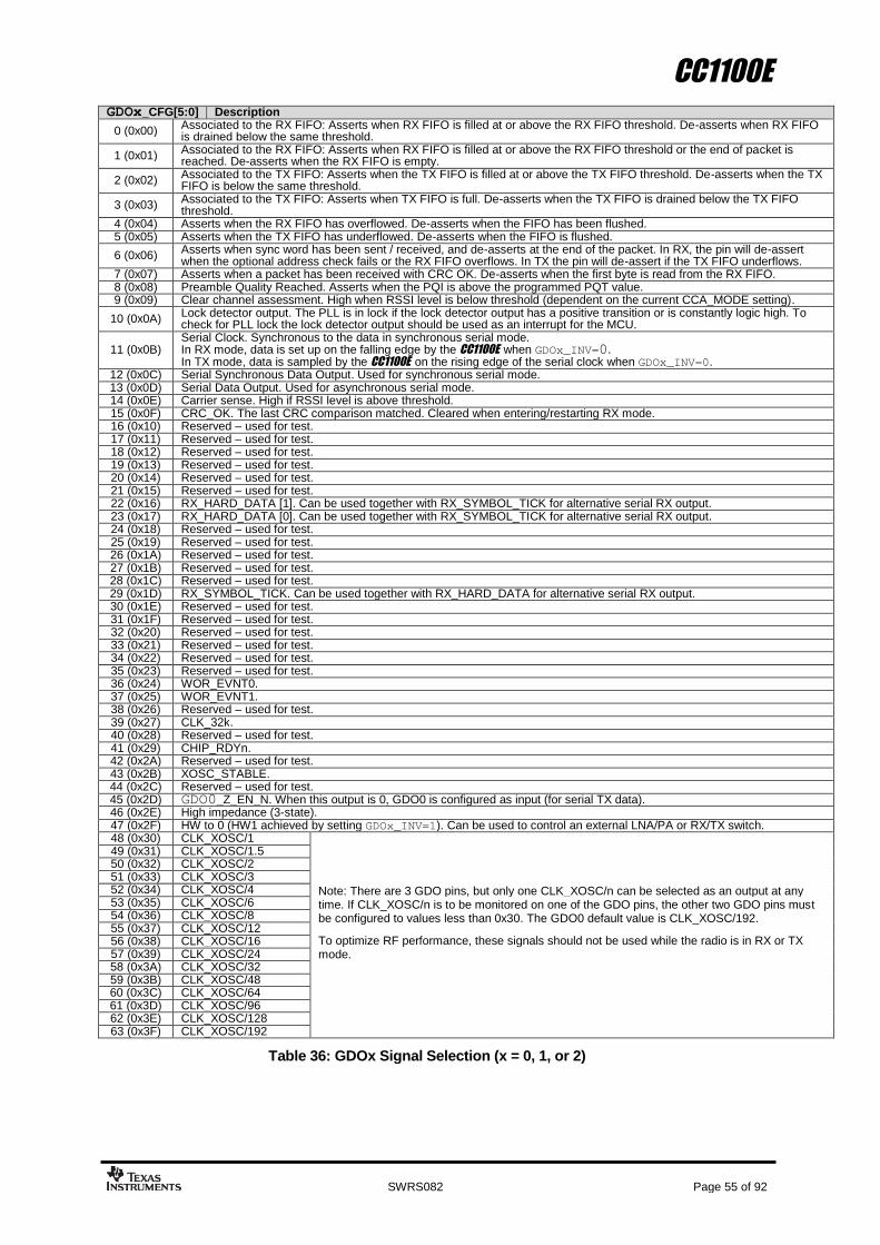
CC1100E
SWRS082 Page 55 of 92
GDOx_CFG[5:0] Description
0 (0x00) Associated to the RX FIFO: Asserts when RX FIFO is filled at or above the RX FIFO threshold. De-asserts when RX FIFOis drained below the same threshold.
1 (0x01) Associated to the RX FIFO: Asserts when RX FIFO is filled at or above the RX FIFO threshold or the end of packet isreached. De-asserts when the RX FIFO is empty.
2 (0x02) Associated to the TX FIFO: Asserts when the TX FIFO is filled at or above the TX FIFO threshold. De-asserts when the TXFIFO is below the same threshold.
3 (0x03) Associated to the TX FIFO: Asserts when TX FIFO is full. De-asserts when the TX FIFO is drained below the TX FIFOthreshold.
4 (0x04) Asserts when the RX FIFO has overflowed. De-asserts when the FIFO has been flushed.5 (0x05) Asserts when the TX FIFO has underflowed. De-asserts when the FIFO is flushed.
6 (0x06) Asserts when sync word has been sent / received, and de-asserts at the end of the packet. In RX, the pin will de-assertwhen the optional address check fails or the RX FIFO overflows. In TX the pin will de-assert if the TX FIFO underflows.
7 (0x07) Asserts when a packet has been received with CRC OK. De-asserts when the first byte is read from the RX FIFO.8 (0x08) Preamble Quality Reached. Asserts when the PQI is above the programmed PQT value.9 (0x09) Clear channel assessment. High when RSSI level is below threshold (dependent on the current CCA_MODE setting).
10 (0x0A) Lock detector output. The PLL is in lock if the lock detector output has a positive transition or is constantly logic high. Tocheck for PLL lock the lock detector output should be used as an interrupt for the MCU.
11 (0x0B)Serial Clock. Synchronous to the data in synchronous serial mode.In RX mode, data is set up on the falling edge by the CC1100E when GDOx_INV=0.In TX mode, data is sampled by the CC1100E on the rising edge of the serial clock when GDOx_INV=0.
12 (0x0C) Serial Synchronous Data Output. Used for synchronous serial mode.13 (0x0D) Serial Data Output. Used for asynchronous serial mode.14 (0x0E) Carrier sense. High if RSSI level is above threshold.15 (0x0F) CRC_OK. The last CRC comparison matched. Cleared when entering/restarting RX mode.16 (0x10) Reserved – used for test.17 (0x11) Reserved – used for test.18 (0x12) Reserved – used for test.19 (0x13) Reserved – used for test.20 (0x14) Reserved – used for test.21 (0x15) Reserved – used for test.22 (0x16) RX_HARD_DATA [1]. Can be used together with RX_SYMBOL_TICK for alternative serial RX output.23 (0x17) RX_HARD_DATA [0]. Can be used together with RX_SYMBOL_TICK for alternative serial RX output.24 (0x18) Reserved – used for test.25 (0x19) Reserved – used for test.26 (0x1A) Reserved – used for test.27 (0x1B) Reserved – used for test.28 (0x1C) Reserved – used for test.29 (0x1D) RX_SYMBOL_TICK. Can be used together with RX_HARD_DATA for alternative serial RX output.30 (0x1E) Reserved – used for test.31 (0x1F) Reserved – used for test.32 (0x20) Reserved – used for test.33 (0x21) Reserved – used for test.34 (0x22) Reserved – used for test.35 (0x23) Reserved – used for test.36 (0x24) WOR_EVNT0.37 (0x25) WOR_EVNT1.38 (0x26) Reserved – used for test.39 (0x27) CLK_32k.40 (0x28) Reserved – used for test.41 (0x29) CHIP_RDYn.42 (0x2A) Reserved – used for test.43 (0x2B) XOSC_STABLE.44 (0x2C) Reserved – used for test.45 (0x2D) GDO0_Z_EN_N. When this output is 0, GDO0 is configured as input (for serial TX data).46 (0x2E) High impedance (3-state).47 (0x2F) HW to 0 (HW1 achieved by setting GDOx_INV=1). Can be used to control an external LNA/PA or RX/TX switch.48 (0x30) CLK_XOSC/149 (0x31) CLK_XOSC/1.550 (0x32) CLK_XOSC/251 (0x33) CLK_XOSC/352 (0x34) CLK_XOSC/453 (0x35) CLK_XOSC/654 (0x36) CLK_XOSC/855 (0x37) CLK_XOSC/1256 (0x38) CLK_XOSC/1657 (0x39) CLK_XOSC/2458 (0x3A) CLK_XOSC/3259 (0x3B) CLK_XOSC/4860 (0x3C) CLK_XOSC/6461 (0x3D) CLK_XOSC/9662 (0x3E) CLK_XOSC/12863 (0x3F) CLK_XOSC/192
Note: There are 3 GDO pins, but only one CLK_XOSC/n can be selected as an output at anytime. If CLK_XOSC/n is to be monitored on one of the GDO pins, the other two GDO pins mustbe configured to values less than 0x30. The GDO0 default value is CLK_XOSC/192.
To optimize RF performance, these signals should not be used while the radio is in RX or TXmode.
Table 36: GDOx Signal Selection (x = 0, 1, or 2)

CC1100E
SWRS082 Page 56 of 92
27 Asynchronous and Synchronous Serial Operation
Several features and modes of operation havebeen included in the CC1100E to providebackward compatibility with previous Chipconproducts and other existing RF communicationsystems. For new systems, it is recommended
to use the built-in packet handling features, asthey can give more robust communication,significantly offload the microcontroller, andsimplify software development.
27.1 Asynchronous Serial Operation
Asynchronous transfer is included in theCC1100E for backward compatibility withsystems that are already using theasynchronous data transfer.
When asynchronous transfer is enabled,several of the support mechanisms for theMCU that are included in the CC1100E will bedisabled, such as packet handling hardware,buffering in the FIFO, and so on. Theasynchronous transfer mode does not allowfor the use of the data whitener, interleaver,and FEC, and it is not possible to useManchester encoding. MSK is not supportedfor asynchronous transfer.
Setting PKTCTRL0.PKT_FORMAT to 3enables asynchronous serial mode. In TX, theGDO0 pin is used for data input (TX data).Data output can be on GDO0, GDO1, orGDO2. This is set by theIOCFG0.GDO0_CFG, IOCFG1.GDO1_CFG
and IOCFG2.GDO2_CFG fields.
The CC1100E modulator samples the level ofthe asynchronous input 8 times faster than theprogrammed data rate. The timing requirementfor the asynchronous stream is that the error inthe bit period must be less than one eighth ofthe programmed data rate.
27.2 Synchronous Serial Operation
Setting PKTCTRL0.PKT_FORMAT to 1enables synchronous serial mode. In thesynchronous serial mode, data is transferredon a two-wire serial interface. The CC1100Eprovides a clock that is used to set up newdata on the data input line or sample data onthe data output line. Data input (TX data) is onthe GDO0 pin. This pin will automatically beconfigured as an input when TX is active. TheTX latency is 8 bits. The data output pin canbe any of the GDO pins. This is set by theIOCFG0.GDO0_CFG, IOCFG1.GDO1_CFG,and IOCFG2.GDO2_CFG fields. Time fromstart of reception until data is available on thereceiver data output pin is equal to 9 bit.
Preamble and sync word insertion/detectionmay or may not be active, dependent on thesync mode set by the MDMCFG2.SYNC_MODE.
If preamble and sync word is disabled, allother packet handler features and FEC shouldalso be disabled. The MCU must then handlepreamble and sync word insertion anddetection in software.
If preamble and sync word insertion/detectionis left on, all packet handling features and FECcan be used. One exception is that theaddress filtering feature is unavailable insynchronous serial mode.
When using the packet handling features insynchronous serial mode, the CC1100E willinsert and detect the preamble and sync wordand the MCU will only provide/get the datapayload. This is equivalent to therecommended FIFO operation mode.
An alternative serial RX output option is toconfigure any of the GD0 pins forRX_SYMBOL_TICK and RX_HARD_[1:0], seeTable 36. RX_HARD_[1:0] is the harddecision symbol. RX_HARD_[1:0] containdata for 4-ary modulation formats whileRX_HARD_DATA [1] contain data for 2-arymodulation formats. The RX_SYMBOL_TICKsignal is the symbol clock and is high for onehalf symbol period whenever a new symbol ispresented on the hard and soft data outputs.This option may be used for both synchronousand asynchronous interfaces.

CC1100E
SWRS082 Page 57 of 92
28 System Considerations and Guidelines
28.1 SRD Regulations
International regulations and national lawsregulate the use of radio receivers andtransmitters. The CC1100E is specificallydesigned for use in the license free 470-510MHz and 950-960 MHz frequency bands inChina and Japan, respectively.
28.1.1 ARIB STD-T96
The applicable regulatory requirements forusing the CC1100E at the 950-956 MHzfrequency band in Japan are specified by theARIB STD-T96 [6].
For applications targeting ARIB STD-T96,FSCAL3 [7:4] needs to be set to 0xA andFSCAL0 needs to be set to 0x07 for optimumperformance.
The CC1100E can support operation with one(200 kHz), two (400 kHz) and three (600 kHz)unit channels as defined by the ARIB STD-T96but will typically be used in wireless systems
with two and three unit channels. For datarates higher than 100 kbps, the frequencydeviation may have to be reduced comparedto the default settings in order to comply withthe ARIB STD-T96 transmit specifications.
Typical margins to the transmit spectrummask measured according to the ARIB STD-T96 using the CC1100E reference design at 0dBm output power are shown in Table 37.Higher margins can be achieved by reducingthe output power accordingly.
Please note that compliance with regulationsis dependent on the complete systemperformance. It is the customer’s responsibilityto ensure that the system complies withregulations.
Table 37: CC1100E typical performance values for ARIB STD-T96 using the CC1100E referencedesign, 25C and 3V (FSCAL3 [7:4] set to 0xA and FSCAL0 set to 0x07)
28.2 Frequency Hopping and Multi-Channel Systems
The 470 MHz and 950 MHz bands are sharedby many systems both in industrial, office, andhome environments. It is thereforerecommended to use frequency hoppingspread spectrum (FHSS) or a multi-channel
protocol because the frequency diversitymakes the system more robust with respect tointerference from other systems operating inthe same frequency band. FHSS also combatsmultipath fading.
Typical Margin [dB]DataRate
[kbps]
Deviation
[kHz]
TypicalSensitivity
[dBm]400 kHz 600 kHz
1.2 5.2 -111 3 4
4.8 25.4 -110 1.5 5.5
10 19 -106 3 4.5
38.4 20 -103 1.5 6.5
76.8 32 -100 3 6
100 47 -100 1 5.5
175 41 -91 2.5 5.5
200 100 -96 N/A 2
200 38 -89 1.5 4.5
250 70 -93 N/A 2.5

CC1100E
SWRS082 Page 58 of 92
The CC1100E is highly suited for FHSS or multi-channel systems due to its agile frequencysynthesizer and effective communicationinterface. Using the packet handling supportand data buffering is also beneficial in suchsystems as these features will significantlyoffload the host controller.
Charge pump current, VCO current, and VCOcapacitance array calibration data is requiredfor each frequency when implementingfrequency hopping for the CC1100E. There are 3ways of obtaining the calibration data from thechip:
1) Frequency hopping with calibration for eachhop. The PLL calibration time is approximately720 µs. The blanking interval between eachfrequency hop is then approximately 810 us.
2) Fast frequency hopping without calibrationfor each hop can be done by performing thenecessary calibrating at startup and saving theresulting FSCAL3, FSCAL2, and FSCAL1register values in MCU memory. The VCOcapacitance array calibration FSCAL1 registervalue must be found for each RF frequency tobe used. The VCO current calibration valueand the charge pump current calibration valueavailable in FSCAL2 and FSCAL3 respectivelyare not dependent on the RF frequency, so thesame value can therefore be used for all RFfrequencies for these two registers. Betweeneach frequency hop, the calibration processcan then be replaced by writing the FSCAL3,FSCAL2 and FSCAL1 register values thatcorresponds to the next RF frequency. ThePLL turn on time is approximately 90 µs. Theblanking interval between each frequency hopis then approximately 90 µs.
3) Run calibration on a single frequency atstartup. Next write 0 to FSCAL3 [5:4] todisable the charge pump calibration. Afterwriting to FSCAL3 [5:4], strobe SRX (orSTX) with MCSM0.FS_AUTOCAL=1 for eachnew frequency hop. That is, VCO current andVCO capacitance calibration is done, but notcharge pump current calibration. When chargepump current calibration is disabled thecalibration time is reduced from approximately720 µs to approximately 150 µs. The blankinginterval between each frequency hop is thenapproximately 240 µs.
There is a trade off between blanking time andmemory space needed for storing calibrationdata in non-volatile memory. Solution 2) abovegives the shortest blanking interval, butrequires more memory space to storecalibration values. This solution also requiresthat the supply voltage and temperature do notvary much in order to have a robust solution.Solution 3) gives approximately 570 µs smallerblanking interval than solution 1).
The recommended settings forTEST0.VCO_SEL_CAL_EN changes withfrequency. This means that one should alwaysuse SmartRF
®Studio [8] to get the correct
settings for a specific frequency before doing acalibration, regardless of which calibrationmethod is being used.
28.3 Data Burst Transmissions
The high maximum data rate of the CC1100Eopens up for burst transmissions. A lowaverage data rate link (e.g. 10 kBaud) can berealized by using a higher over-the-air datarate. Buffering the data and transmitting inbursts at high data rate (e.g. 500 kBaud) willreduce the time in active mode, and hencealso reduce the average current consumption
significantly. Reducing the time in active modewill reduce the likelihood of collisions withother systems in the same frequency range.
28.4 Continuous Transmissions
In data streaming applications, the CC1100Eopens up for continuous transmissions at a500 kBaud effective data rate. As themodulation is done with a closed loop PLL,there is no limitation in the length of a
transmission (open loop modulation used insome transceivers often prevents this kind ofcontinuous data streaming and reduces theeffective data rate).
Note: The content in the TESTn registers(n = 0, 1, or 2) are not retained in SLEEPstate, thus it is necessary to re-write theseregisters when returning from the SLEEPstate.
Note: The sensitivity and thus transmissionrange is reduced for high data rate burstscompared to lower data rates.

CC1100E
SWRS082 Page 59 of 92
28.5 Low Cost Systems
As the CC1100E provides 1.2 - 500 kBaud multi-channel performance without any externalSAW or loop filters, a very low cost systemcan be made.
A HC-49 type SMD crystal is used in theCC1100E EM reference designs ([3] and 0).
The crystal package strongly influences theprice. In a size constrained PCB design, asmaller, but more expensive, crystal may beused.
28.6 Battery Operated Systems
In low power applications, the SLEEP statewith the crystal oscillator core switched offshould be used when the CC1100E is notactive. It is possible to leave the crystal
oscillator core running in the SLEEP state ifstart-up time is critical. The WOR functionalityshould be used in low power applications.
28.7 Increasing Output Power
In some applications it may be necessary toextend the link range. Adding an externalpower amplifier is the most effective way ofdoing this. The power amplifier should be
inserted between the antenna and the balunand matching circuit. Two T/R switches areneeded to disconnect the PA in RX mode, seedetails in Figure 28.
Figure 28: Block Diagram of the CC1100E Usage with External Power Amplifier
29 Configuration Registers
The configuration of the CC1100E is done byprogramming 8-bit registers. The optimumconfiguration data based on selected systemparameters are most easily found by using theSmartRF Studio software [8]. Completedescriptions of the registers are given in thefollowing tables. After chip reset, all theregisters have default values as shown in thetables. The optimum register setting mightdiffer from the default value. After a reset, allregisters that shall be different from the defaultvalue therefore needs to be programmedthrough the SPI interface.
There are 13 command strobe registers, listedin Table 38. Accessing these registers willinitiate the change of an internal state ormode. There are 47 normal 8-bit configurationregisters listed in Table 39. Many of these
registers are for test purposes only, and neednot be written for normal operation of theCC1100E.
There are also 12 status registers that arelisted in Table 40. These registers, which areread-only, contain information about the statusof the CC1100E.
The two FIFOs are accessed through one 8-bitregister. Write operations write to the TX FIFO,while read operations read from the RX FIFO.
During the header byte transfer and whilewriting data to a register or the TX FIFO, astatus byte is returned on the SO line. Thisstatus byte is described in Table 21 on page27.
CC1100EBalunandMatching
Filter
Antenna
T/Rswitch
T/Rswitch
PA

CC1100E
SWRS082 Page 60 of 92
Table 41 summarizes the SPI address space.The address to use is given by adding thebase address to the left and the burst and
read/write bits on the top. Note that the burstbit has different meaning for base addressesabove and below 0x2F.
Address StrobeName
Description
0x30 SRES Reset chip.
0x31 SFSTXON Enable and calibrate frequency synthesizer (if MCSM0.FS_AUTOCAL=1). If in RX (with CCA):Go to a wait state where only the synthesizer is running (for quick RX / TX turnaround).
0x32 SXOFF Turn off crystal oscillator.
0x33 SCAL Calibrate frequency synthesizer and turn it off. SCAL can be strobed from IDLE mode withoutsetting manual calibration mode (MCSM0.FS_AUTOCAL=0)
0x34 SRX Enable RX. Perform calibration first if coming from IDLE and MCSM0.FS_AUTOCAL=1.
0x35 STX In IDLE state: Enable TX. Perform calibration first if MCSM0.FS_AUTOCAL=1.If in RX state and CCA is enabled: Only go to TX if channel is clear.
0x36 SIDLE Exit RX / TX, turn off frequency synthesizer and exit Wake-On-Radio mode if applicable.
0x38 SWOR Start automatic RX polling sequence (Wake-on-Radio) as described in Section 19.5 ifWORCTRL.RC_PD=0.
0x39 SPWD Enter power down mode when CSn goes high.
0x3A SFRX Flush the RX FIFO buffer. Only issue SFRX in IDLE or RXFIFO_OVERFLOW states.
0x3B SFTX Flush the TX FIFO buffer. Only issue SFTX in IDLE or TXFIFO_UNDERFLOW states.
0x3C SWORRST Reset real time clock to Event1 value.
0x3D SNOP No operation. May be used to get access to the chip status byte.
Table 38: Command Strobes

CC1100E
SWRS082 Page 61 of 92
Address Register DescriptionPreserved inSLEEP State
Details onPage Number
0x00 IOCFG2 GDO2 output pin configuration Yes 64
0x01 IOCFG1 GDO1 output pin configuration Yes 64
0x02 IOCFG0 GDO0 output pin configuration Yes 64
0x03 FIFOTHR RX FIFO and TX FIFO thresholds Yes 65
0x04 SYNC1 Sync word, high byte Yes 66
0x05 SYNC0 Sync word, low byte Yes 66
0x06 PKTLEN Packet length Yes 66
0x07 PKTCTRL1 Packet automation control Yes 66
0x08 PKTCTRL0 Packet automation control Yes 67
0x09 ADDR Device address Yes 67
0x0A CHANNR Channel number Yes 67
0x0B FSCTRL1 Frequency synthesizer control Yes 68
0x0C FSCTRL0 Frequency synthesizer control Yes 68
0x0D FREQ2 Frequency control word, high byte Yes 68
0x0E FREQ1 Frequency control word, middle byte Yes 68
0x0F FREQ0 Frequency control word, low byte Yes 68
0x10 MDMCFG4 Modem configuration Yes 69
0x11 MDMCFG3 Modem configuration Yes 69
0x12 MDMCFG2 Modem configuration Yes 70
0x13 MDMCFG1 Modem configuration Yes 71
0x14 MDMCFG0 Modem configuration Yes 71
0x15 DEVIATN Modem deviation setting Yes 72
0x16 MCSM2 Main Radio Control State Machine configuration Yes 73
0x17 MCSM1 Main Radio Control State Machine configuration Yes 74
0x18 MCSM0 Main Radio Control State Machine configuration Yes 75
0x19 FOCCFG Frequency Offset Compensation configuration Yes 76
0x1A BSCFG Bit Synchronization configuration Yes 77
0x1B AGCTRL2 AGC control Yes 78
0x1C AGCTRL1 AGC control Yes 79
0x1D AGCTRL0 AGC control Yes 80
0x1E WOREVT1 High byte Event 0 timeout Yes 80
0x1F WOREVT0 Low byte Event 0 timeout Yes 81
0x20 WORCTRL Wake On Radio control Yes 81
0x21 FREND1 Front end RX configuration Yes 82
0x22 FREND0 Front end TX configuration Yes 82
0x23 FSCAL3 Frequency synthesizer calibration Yes 82
0x24 FSCAL2 Frequency synthesizer calibration Yes 83
0x25 FSCAL1 Frequency synthesizer calibration Yes 83
0x26 FSCAL0 Frequency synthesizer calibration Yes 83
0x27 RCCTRL1 RC oscillator configuration Yes 83
0x28 RCCTRL0 RC oscillator configuration Yes 83
0x29 FSTEST Frequency synthesizer calibration control No 84
0x2A PTEST Production test No 84
0x2B AGCTEST AGC test No 84
0x2C TEST2 Various test settings No 84
0x2D TEST1 Various test settings No 84
0x2E TEST0 Various test settings No 85
Table 39: Configuration Registers Overview

CC1100E
SWRS082 Page 62 of 92
Address Register Description Details on page number
0x30 (0xF0) PARTNUM Part number for the CC1100E 85
0x31 (0xF1) VERSION Current version number 85
0x32 (0xF2) FREQEST Frequency Offset Estimate 85
0x33 (0xF3) LQI Demodulator estimate for Link Quality 85
0x34 (0xF4) RSSI Received signal strength indication 85
0x35 (0xF5) MARCSTATE Control state machine state 86
0x36 (0xF6) WORTIME1 High byte of WOR timer 86
0x37 (0xF7) WORTIME0 Low byte of WOR timer 86
0x38 (0xF8) PKTSTATUS Current GDOx status and packet status 87
0x39 (0xF9) VCO_VC_DACCurrent setting from PLL calibrationmodule
87
0x3A (0xFA) TXBYTESUnderflow and number of bytes in the TXFIFO
87
0x3B (0xFB) RXBYTESOverflow and number of bytes in the RXFIFO
87
0x3C (0xFC) RCCTRL1_STATUS Last RC oscillator calibration result 87
0x3D (0xFD) RCCTRL0_STATUS Last RC oscillator calibration result 88
Table 40: Status Registers Overview

CC1100E
SWRS082 Page 63 of 92
Write ReadSingle Byte Burst Single Byte Burst
+0x00 +0x40 +0x80 +0xC00x00 IOCFG20x01 IOCFG10x02 IOCFG00x03 FIFOTHR0x04 SYNC10x05 SYNC00x06 PKTLEN0x07 PKTCTRL10x08 PKTCTRL00x09 ADDR0x0A CHANNR0x0B FSCTRL10x0C FSCTRL00x0D FREQ20x0E FREQ10x0F FREQ00x10 MDMCFG40x11 MDMCFG30x12 MDMCFG20x13 MDMCFG10x14 MDMCFG00x15 DEVIATN0x16 MCSM20x17 MCSM10x18 MCSM00x19 FOCCFG0x1A BSCFG0x1B AGCCTRL20x1C AGCCTRL10x1D AGCCTRL00x1E WOREVT10x1F WOREVT00x20 WORCTRL0x21 FREND10x22 FREND00x23 FSCAL30x24 FSCAL20x25 FSCAL10x26 FSCAL00x27 RCCTRL10x28 RCCTRL00x29 FSTEST0x2A PTEST0x2B AGCTEST0x2C TEST20x2D TEST10x2E TEST00x2F
R/W
configura
tion
regis
ters
,burs
taccess
possib
le
0x30 SRES SRES PARTNUM0x31 SFSTXON SFSTXON VERSION0x32 SXOFF SXOFF FREQEST0x33 SCAL SCAL LQI0x34 SRX SRX RSSI0x35 STX STX MARCSTATE0x36 SIDLE SIDLE WORTIME10x37 WORTIME00x38 SWOR SWOR PKTSTATUS0x39 SPWD SPWD VCO_VC_DAC0x3A SFRX SFRX TXBYTES0x3B SFTX SFTX RXBYTES0x3C SWORRST SWORRST RCCTRL1_STATUS0x3D SNOP SNOP RCCTRL0_STATUS0x3E PATABLE PATABLE PATABLE PATABLE0x3F TX FIFO TX FIFO RX FIFO RX FIFO C
om
mand
Str
obes,
Sta
tus
regis
ters
(read
only
)and
multib
yte
regis
ters
Table 41: SPI Address Space
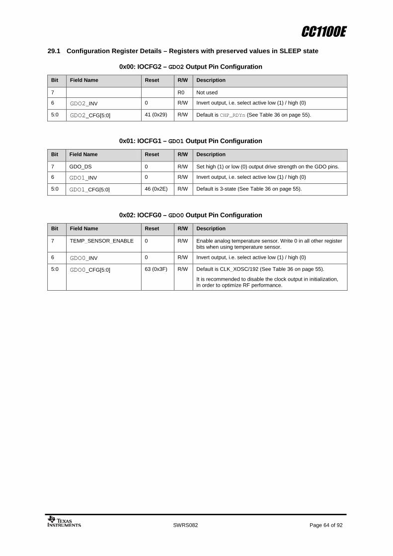
CC1100E
SWRS082 Page 64 of 92
29.1 Configuration Register Details – Registers with preserved values in SLEEP state
0x00: IOCFG2 – GDO2 Output Pin Configuration
Bit Field Name Reset R/W Description
7 R0 Not used
6 GDO2_INV 0 R/W Invert output, i.e. select active low (1) / high (0)
5:0 GDO2_CFG[5:0] 41 (0x29) R/W Default is CHP_RDYn (See Table 36 on page 55).
0x01: IOCFG1 – GDO1 Output Pin Configuration
Bit Field Name Reset R/W Description
7 GDO_DS 0 R/W Set high (1) or low (0) output drive strength on the GDO pins.
6 GDO1_INV 0 R/W Invert output, i.e. select active low (1) / high (0)
5:0 GDO1_CFG[5:0] 46 (0x2E) R/W Default is 3-state (See Table 36 on page 55).
0x02: IOCFG0 – GDO0 Output Pin Configuration
Bit Field Name Reset R/W Description
7 TEMP_SENSOR_ENABLE 0 R/W Enable analog temperature sensor. Write 0 in all other registerbits when using temperature sensor.
6 GDO0_INV 0 R/W Invert output, i.e. select active low (1) / high (0)
5:0 GDO0_CFG[5:0] 63 (0x3F) R/W Default is CLK_XOSC/192 (See Table 36 on page 55).
It is recommended to disable the clock output in initialization,in order to optimize RF performance.

CC1100E
SWRS082 Page 65 of 92
0x03: FIFOTHR – RX FIFO and TX FIFO Thresholds
Bit Field Name Reset R/W Description
7 0 R/W Reserved , write 0 for compatibility with possible future extensions
6 ADC_RETENTION 0 R/W 0: TEST1 = 0x31 and TEST2= 0x88 when waking up from SLEEP
1: TEST1 = 0x35 and TEST2 = 0x81 when waking up from SLEEP
Note that the changes in the TEST registers due to theADC_RETENTION bit setting are only seen INTERNALLY in theanalog part. The values read from the TEST registers when waking upfrom SLEEP mode will always be the reset value.
The ADC_RETENTION bit should be set to 1 before going into SLEEPmode if settings with an RX filter bandwidth below 325 kHz are wantedat time of wake-up.
5:4 CLOSE_IN_RX [1:0] 0 (00) R/W For more details, please see DN010 [11]
Setting RX Attenuation, Typical Values
0 (00) 0dB
1 (01) 6dB
2 (10) 12dB
3 (11) 18dB
3:0 FIFO_THR[3:0] 7 (0111) R/W Set the threshold for the TX FIFO and RX FIFO. The threshold isexceeded when the number of bytes in the FIFO is equal to or higherthan the threshold value.
Setting Bytes in TX FIFO Bytes in RX FIFO
0 (0000) 61 4
1 (0001) 57 8
2 (0010) 53 12
3 (0011) 49 16
4 (0100) 45 20
5 (0101) 41 24
6 (0110) 37 28
7 (0111) 33 32
8 (1000) 29 36
9 (1001) 25 40
10 (1010) 21 44
11 (1011) 17 48
12 (1100) 13 52
13(1100E)
9 56
14 (1110) 5 60
15 (1111) 1 64

CC1100E
SWRS082 Page 66 of 92
0x04: SYNC1 – Sync Word, High Byte
Bit Field Name Reset R/W Description
7:0 SYNC[15:8] 211 (0xD3) R/W 8 MSB of 16-bit sync word
0x05: SYNC0 – Sync Word, Low Byte
Bit Field Name Reset R/W Description
7:0 SYNC[7:0] 145 (0x91) R/W 8 LSB of 16-bit sync word
0x06: PKTLEN – Packet Length
Bit Field Name Reset R/W Description
7:0 PACKET_LENGTH 255 (0xFF) R/W Indicates the packet length when fixed packet length mode is enabled.If variable packet length mode is used, this value indicates themaximum packet length allowed.
0x07: PKTCTRL1 – Packet Automation Control
Bit Field Name Reset R/W Description
7:5 PQT[2:0] 0 (0x00) R/W Preamble quality estimator threshold. The preamble quality estimatorincreases an internal counter by one each time a bit is received that isdifferent from the previous bit, and decreases the counter by 8 each timea bit is received that is the same as the last bit.
A threshold of 4∙PQT for this counter is used to gate sync word detection.When PQT=0 a sync word is always accepted.
4 0 R0 Not Used.
3 CRC_AUTOFLUSH 0 R/W Enable automatic flush of RX FIFO when CRC is not OK. This requiresthat only one packet is in the RXIFIFO and that packet length is limited tothe RX FIFO size.
2 APPEND_STATUS 1 R/W When enabled, two status bytes will be appended to the payload of thepacket. The status bytes contain RSSI and LQI values, as well as CRCOK.
1:0 ADR_CHK[1:0] 0 (00) R/W Controls address check configuration of received packages.
Setting Address check configuration
0 (00) No address check
1 (01) Address check, no broadcast
2 (10) Address check and 0 (0x00) broadcast
3 (11) Address check and 0 (0x00) and 255 (0xFF)broadcast

CC1100E
SWRS082 Page 67 of 92
0x08: PKTCTRL0 – Packet Automation Control
Bit Field Name Reset R/W Description
7 R0 Not used
6 WHITE_DATA 1 R/W Turn data whitening on / off
0: Whitening off1: Whitening on
5:4 PKT_FORMAT[1:0] 0 (00) R/W Format of RX and TX data
Setting Packet format
0 (00) Normal mode, use FIFOs for RX and TX
1 (01)Synchronous serial mode, Data in on GDO0 anddata out on either of the GDOx pins
2 (10)Random TX mode; sends random data using PN9generator. Used for test.Works as normal mode, setting 0 (00), in RX
3 (11)Asynchronous serial mode, Data in on GDO0 anddata out on either of the GDOx pins
3 0 R0 Not used
2 CRC_EN 1 R/W 1: CRC calculation in TX and CRC check in RX enabled
0: CRC disabled for TX and RX
1:0 LENGTH_CONFIG[1:0] 1 (01) R/W Configure the packet length
Setting Packet length configuration
0 (00) Fixed packet length mode. Length configured inPKTLEN register
1 (01) Variable packet length mode. Packet lengthconfigured by the first byte after sync word
2 (10) Infinite packet length mode
3 (11) Reserved
0x09: ADDR – Device Address
Bit Field Name Reset R/W Description
7:0 DEVICE_ADDR[7:0] 0 (0x00) R/W Address used for packet filtration. Optional broadcast addresses are 0(0x00) and 255 (0xFF).
0x0A: CHANNR – Channel Number
Bit Field Name Reset R/W Description
7:0 CHAN[7:0] 0 (0x00) R/W The 8-bit unsigned channel number, which is multiplied by thechannel spacing setting and added to the base frequency.

CC1100E
SWRS082 Page 68 of 92
0x0B: FSCTRL1 – Frequency Synthesizer Control
Bit Field Name Reset R/W Description
7:6 R0 Not used
5 0 R/W Reserved
4:0 FREQ_IF[4:0] 15 (0x0F) R/W The desired IF frequency to employ in RX. Subtracted from FS basefrequency in RX and controls the digital complex mixer in the demodulator.
IFFREQf
f XOSCIF _
210
The default value gives an IF frequency of 381kHz, assuming a 26.0 MHzcrystal.
0x0C: FSCTRL0 – Frequency Synthesizer Control
Bit Field Name Reset R/W Description
7:0 FREQOFF[7:0] 0 (0x00) R/W Frequency offset added to the base frequency before being used by thefrequency synthesizer. (2s-complement).
Resolution is FXTAL/214 (1.59kHz-1.65kHz); range is ±202 kHz to ±210 kHz,
dependent of XTAL frequency.
0x0D: FREQ2 – Frequency Control Word, High Byte
Bit Field Name Reset R/W Description
7:6 FREQ[23:22] 0 (00) R FREQ[23:22] is always 0 (the FREQ2 register is less than 36 with 26-27MHz crystal)
5:0 FREQ[21:16] 30 (0x1E) R/W FREQ [23:0] is the base frequency for the frequency synthesiser inincrements of fXOSC/216.
0:23216
FREQf
f XOSCcarrier
0x0E: FREQ1 – Frequency Control Word, Middle Byte
Bit Field Name Reset R/W Description
7:0 FREQ[15:8] 196 (0xC4) R/W Ref. FREQ2 register
0x0F: FREQ0 – Frequency Control Word, Low Byte
Bit Field Name Reset R/W Description
7:0 FREQ[7:0] 236 (0xEC) R/W Ref. FREQ2 register

CC1100E
SWRS082 Page 69 of 92
0x10: MDMCFG4 – Modem Configuration
Bit Field Name Reset R/W Description
7:6 CHANBW_E[1:0] 2 (0x02) R/W
5:4 CHANBW_M[1:0] 0 (0x00) R/W Sets the decimation ratio for the delta-sigma ADC input stream and thusthe channel bandwidth.
ECHANBWXOSC
channelMCHANBW
fBW
_2)·_4(8
The default values give 203 kHz channel filter bandwidth, assuming a 26.0MHz crystal.
3:0 DRATE_E[3:0] 12 (0x0C) R/W The exponent of the user specified symbol rate
0x11: MDMCFG3 – Modem Configuration
Bit Field Name Reset R/W Description
7:0 DRATE_M[7:0] 34 (0x22) R/W The mantissa of the user specified symbol rate. The symbol rate isconfigured using an unsigned, floating-point number with 9-bit mantissaand 4-bit exponent. The 9th bit is a hidden ‘1’. The resulting data rate is:
XOSC
EDRATE
DATA fMDRATE
R
28
_
2
2_256
The default values give a data rate of 115.051 kBaud (closest setting to115.2 kBaud), assuming a 26.0 MHz crystal.

CC1100E
SWRS082 Page 70 of 92
0x12: MDMCFG2 – Modem Configuration
Bit Field Name Reset R/W Description
7 DEM_DCFILT_OFF 0 R/W Disable digital DC blocking filter before demodulator.
0 = Enable (better sensitivity)
1 = Disable (current optimized). Only for data rates≤ 250 kBaud
The recommended IF frequency changes when the DC blocking isdisabled. Please use SmartRF Studio [8] to calculate correct registersetting.
6:4 MOD_FORMAT[2:0] 0 (000) R/W The modulation format of the radio signal
Setting Modulation format
0 (000) 2-FSK
1 (001) GFSK
2 (010) -
3 (011) ASK/OOK
4 (100) -
5 (101) -
6 (110) -
7 (111) MSK
ASK is only supported for output powers up to -1 dBm
MSK is only supported for data rates above 26 kBaud
3 MANCHESTER_EN 0 R/W Enables Manchester encoding/decoding.
0 = Disable
1 = Enable
2:0 SYNC_MODE[2:0] 2 (010) R/W Combined sync-word qualifier mode.
The values 0 (000) and 4 (100) disables preamble and sync wordtransmission in TX and preamble and sync word detection in RX.
The values 1 (001), 2 (010), 5 (101) and 6 (110) enables 16-bit sync wordtransmission in TX and 16-bits sync word detection in RX. Only 15 of 16bits need to match in RX when using setting 1 (001) or 5 (101). The values3 (011) and 7 (111) enables repeated sync word transmission in TX and32-bits sync word detection in RX (only 30 of 32 bits need to match).
Setting Sync-word qualifier mode
0 (000) No preamble/sync
1 (001) 15/16 sync word bits detected
2 (010) 16/16 sync word bits detected
3 (011) 30/32 sync word bits detected
4 (100) No preamble/sync, carrier-senseabove threshold
5 (101) 15/16 + carrier-sense above threshold
6 (110) 16/16 + carrier-sense above threshold
7 (111) 30/32 + carrier-sense above threshold

CC1100E
SWRS082 Page 71 of 92
0x13: MDMCFG1– Modem Configuration
Bit Field Name Reset R/W Description
7 FEC_EN 0 R/W Enable Forward Error Correction (FEC) with interleaving forpacket payload
0 = Disable
1 = Enable (Only supported for fixed packet length mode, i.e.PKTCTRL0.LENGTH_CONFIG=0)
6:4 NUM_PREAMBLE[2:0] 2 (010) R/W Sets the minimum number of preamble bytes to be transmitted
Setting Number of preamble bytes
0 (000) 2
1 (001) 3
2 (010) 4
3 (011) 6
4 (100) 8
5 (101) 12
6 (110) 16
7 (111) 24
3:2 R0 Not used
1:0 CHANSPC_E[1:0] 2 (10) R/W 2 bit exponent of channel spacing
0x14: MDMCFG0– Modem Configuration
Bit Field Name Reset R/W Description
7:0 CHANSPC_M[7:0] 248 (0xF8) R/W 8-bit mantissa of channel spacing. The channel spacing ismultiplied by the channel number CHAN and added to the basefrequency. It is unsigned and has the format:
ECHANSPCXOSCCHANNEL MCHANSPC
ff _
182_256
2
The default values give 199.951 kHz channel spacing (theclosest setting to 200 kHz), assuming 26.0 MHz crystalfrequency.

CC1100E
SWRS082 Page 72 of 92
0x15: DEVIATN – Modem Deviation Setting
Bit Field Name Reset R/W Description
7 R0 Not used.
6:4 DEVIATION_E[2:0] 4 (100) R/W Deviation exponent.
3 R0 Not used.
TX
2-FSK/
GFSK
Specifies the nominal frequency deviation from the carrier fora ‘0’ (-DEVIATN) and ‘1’ (+DEVIATN) in a mantissa-exponentformat, interpreted as a 4-bit value with MSB implicit 1. Theresulting frequency deviation is given by:
EDEVIATIONxoscdev MDEVIATION
ff _
172)_8(
2
The default values give ±47.607 kHz deviation assuming 26.0MHz crystal frequency.
MSK Specifies the fraction of symbol period (1/8-8/8) during whicha phase change occurs (‘0’: +90deg, ‘1’:-90deg). Refer to theSmartRF Studio software [8] for correct DEVIATN settingwhen using MSK.
ASK/OOK This setting has no effect.
RX
2-FSK/
GFSK
Specifies the expected frequency deviation of incoming signal,must be approximately right for demodulation to be performedreliably and robustly.
2:0 DEVIATION_M[2:0] 7 (111) R/W
MSK/
ASK/OOKThis setting has no effect.

CC1100E
SWRS082 Page 73 of 92
0x16: MCSM2 – Main Radio Control State Machine Configuration
Bit Field Name Reset R/W Description
7:5 R0 Not used
4 RX_TIME_RSSI 0 R/W Direct RX termination based on RSSI measurement (carrier sense). ForASK/OOK modulation, RX times out if there is no carrier sense in the first 8symbol periods.
3 RX_TIME_QUAL 0 R/W When the RX_TIME timer expires, the chip checks if sync word is foundwhen RX_TIME_QUAL=0, or either sync word is found or PQI is set whenRX_TIME_QUAL=1.
RX_TIME[2:0] 7 (111) R/W Timeout for sync word search in RX for both WOR mode and normal RXoperation. The timeout is relative to the programmed EVENT0 timeout.
2:0
The RX timeout in µs is given by EVENT0·C(RX_TIME, WOR_RES) ·26/X, where C is given by the table below and X isthe crystal oscillator frequency in MHz:
Setting WOR_RES = 0 WOR_RES = 1 WOR_RES = 2 WOR_RES = 3
0 (000) 3.6058 18.0288 32.4519 46.8750
1 (001) 1.8029 9.0144 16.2260 23.4375
2 (010) 0.9014 4.5072 8.1130 11.7188
3 (011) 0.4507 2.2536 4.0565 5.8594
4 (100) 0.2254 1.1268 2.0282 2.9297
5 (101) 0.1127 0.5634 1.0141 1.4648
6 (110) 0.0563 0.2817 0.5071 0.7324
7 (111) Until end of packet
As an example, EVENT0=34666, WOR_RES=0 and RX_TIME=6 corresponds to 1.96 ms RX timeout, 1 s polling intervaland 0.195% duty cycle. Note that WOR_RES should be 0 or 1 when using WOR because using WOR_RES > 1 will give avery low duty cycle. In applications where WOR is not used all settings of WOR_RES can be used.
The duty cycle using WOR is approximated by:
Setting WOR_RES=0 WOR_RES=1
0 (000) 12.50% 1.95%
1 (001) 6.250% 9765ppm
2 (010) 3.125% 4883ppm
3 (011) 1.563% 2441ppm
4 (100) 0.781% NA
5 (101) 0.391% NA
6 (110) 0.195% NA
7 (111) NA
Note that the RC oscillator must be enabled in order to use setting 0-6, because the timeout counts RC oscillatorperiods. WOR mode does not need to be enabled.The timeout counter resolution is limited: With RX_TIME=0, the timeout count is given by the 13 MSBs of EVENT0,decreasing to the 7MSBs of EVENT0 with RX_TIME=6.
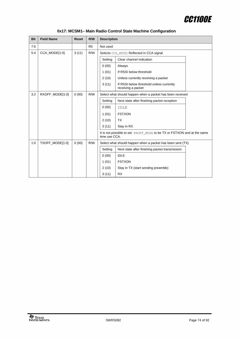
CC1100E
SWRS082 Page 74 of 92
0x17: MCSM1– Main Radio Control State Machine Configuration
Bit Field Name Reset R/W Description
7:6 R0 Not used
5:4 CCA_MODE[1:0] 3 (11) R/W Selects CCA_MODE; Reflected in CCA signal
Setting Clear channel indication
0 (00) Always
1 (01) If RSSI below threshold
2 (10) Unless currently receiving a packet
3 (11) If RSSI below threshold unless currentlyreceiving a packet
3:2 RXOFF_MODE[1:0] 0 (00) R/W Select what should happen when a packet has been received
Setting Next state after finishing packet reception
0 (00) IDLE
1 (01) FSTXON
2 (10) TX
3 (11) Stay in RX
It is not possible to set RXOFF_MODE to be TX or FSTXON and at the sametime use CCA.
1:0 TXOFF_MODE[1:0] 0 (00) R/W Select what should happen when a packet has been sent (TX)
Setting Next state after finishing packet transmission
0 (00) IDLE
1 (01) FSTXON
2 (10) Stay in TX (start sending preamble)
3 (11) RX

CC1100E
SWRS082 Page 75 of 92
0x18: MCSM0– Main Radio Control State Machine Configuration
Bit Field Name Reset R/W Description
7:6 R0 Not used
5:4 FS_AUTOCAL[1:0] 0 (00) R/W Automatically calibrate when going to RX or TX, or back to IDLE
Setting When to perform automatic calibration
0 (00) Never (manually calibrate using SCAL strobe)
1 (01) When going from IDLE to RX or TX (or FSTXON)
2 (10)When going from RX or TX back to IDLEautomatically
3 (11)Every 4th time when going from RX or TX to IDLEautomatically
In some automatic wake-on-radio (WOR) applications, using setting 3 (11)can significantly reduce current consumption.
3:2 PO_TIMEOUT 1 (01) R/W Programs the number of times the six-bit ripple counter must expire afterXOSC has stabilized before CHP_RDYn goes low.
If XOSC is on (stable) during power-down, PO_TIMEOUT should be set sothat the regulated digital supply voltage has time to stabilize beforeCHP_RDYn goes low (PO_TIMEOUT=2 recommended). Typical start-uptime for the voltage regulator is 50 μs.
If XOSC is off during power-down and the regulated digital supply voltagehas sufficient time to stabilize while waiting for the crystal to be stable,PO_TIMEOUT can be set to 0. For robust operation it is recommended touse PO_TIMEOUT=2.
Setting Expire count Timeout after XOSC start
0 (00) 1 Approx. 2.3 – 2.4 μs
1 (01) 16 Approx. 37 – 39 μs
2 (10) 64 Approx. 149 – 155 μs
3 (11) 256 Approx. 597 – 620 μs
Exact timeout depends on crystal frequency.
1 PIN_CTRL_EN 0 R/W Enables the pin radio control option
0 XOSC_FORCE_ON 0 R/W Force the XOSC to stay on in the SLEEP state.

CC1100E
SWRS082 Page 76 of 92
0x19: FOCCFG – Frequency Offset Compensation Configuration
Bit Field Name Reset R/W Description
7:6 R0 Not used
5 FOC_BS_CS_GATE 1 R/W If set, the demodulator freezes the frequency offset compensation and clockrecovery feedback loops until the CS signal goes high.
4:3 FOC_PRE_K[1:0] 2 (10) R/W The frequency compensation loop gain to be used before a sync word isdetected.
Setting Freq. compensation loop gain before sync word
0 (00) K
1 (01) 2K
2 (10) 3K
3 (11) 4K
2 FOC_POST_K 1 R/W The frequency compensation loop gain to be used after a sync word isdetected.
Setting Freq. compensation loop gain after sync word
0 Same as FOC_PRE_K
1 K/2
1:0 FOC_LIMIT[1:0] 2 (10) R/W The saturation point for the frequency offset compensation algorithm:
Setting Saturation point (max compensated offset)
0 (00) ±0 (no frequency offset compensation)
1 (01) ±BWCHAN/8
2 (10) ±BWCHAN/4
3 (11) ±BWCHAN/2
Frequency offset compensation is not supported for ASK/OOK; Always useFOC_LIMIT=0 with these modulation formats.

CC1100E
SWRS082 Page 77 of 92
0x1A: BSCFG – Bit Synchronization Configuration
Bit Field Name Reset R/W Description
7:6 BS_PRE_KI[1:0] 1 (01) R/W The clock recovery feedback loop integral gain to be used before a sync wordis detected (used to correct offsets in data rate):
Setting Clock recovery loop integral gain before sync word
0 (00) KI
1 (01) 2KI
2 (10) 3KI
3 (11) 4KI
5:4 BS_PRE_KP[1:0] 2 (10) R/W The clock recovery feedback loop proportional gain to be used before a syncword is detected.
Setting Clock recovery loop proportional gain before sync word
0 (00) KP
1 (01) 2KP
2 (10) 3KP
3 (11) 4KP
3 BS_POST_KI 1 R/W The clock recovery feedback loop integral gain to be used after a sync word isdetected.
Setting Clock recovery loop integral gain after sync word
0 Same as BS_PRE_KI
1 KI /2
2 BS_POST_KP 1 R/W The clock recovery feedback loop proportional gain to be used after a syncword is detected.
Setting Clock recovery loop proportional gain after sync word
0 Same as BS_PRE_KP
1 KP
1:0 BS_LIMIT[1:0] 0 (00) R/W The saturation point for the data rate offset compensation algorithm:
Setting Data rate offset saturation (max data rate difference)
0 (00) ±0 (No data rate offset compensation performed)
1 (01) ±3.125 % data rate offset
2 (10) ±6.25 % data rate offset
3 (11) ±12.5 % data rate offset

CC1100E
SWRS082 Page 78 of 92
0x1B: AGCCTRL2 – AGC Control
Bit Field Name Reset R/W Description
7:6 MAX_DVGA_GAIN[1:0] 0 (00) R/W Reduces the maximum allowable DVGA gain.
Setting Allowable DVGA settings
0 (00) All gain settings can be used
1 (01) The highest gain setting can not be used
2 (10) The 2 highest gain settings can not be used
3 (11) The 3 highest gain settings can not be used
5:3 MAX_LNA_GAIN[2:0] 0 (000) R/W Sets the maximum allowable LNA + LNA 2 gain relative to themaximum possible gain.
Setting Maximum allowable LNA + LNA 2 gain
0 (000) Maximum possible LNA + LNA 2 gain
1 (001) Approx. 2.6 dB below maximum possible gain
2 (010) Approx. 6.1 dB below maximum possible gain
3 (011) Approx. 7.4 dB below maximum possible gain
4 (100) Approx. 9.2 dB below maximum possible gain
5 (101) Approx. 11.5 dB below maximum possible gain
6 (110) Approx. 14.6 dB below maximum possible gain
7 (111) Approx. 17.1 dB below maximum possible gain
2:0 MAGN_TARGET[2:0] 3 (011) R/W These bits set the target value for the averaged amplitude from thedigital channel filter (1 LSB = 0 dB).
Setting Target amplitude from channel filter
0 (000) 24 dB
1 (001) 27 dB
2 (010) 30 dB
3 (011) 33 dB
4 (100) 36 dB
5 (101) 38 dB
6 (110) 40 dB
7 (111) 42 dB

CC1100E
SWRS082 Page 79 of 92
0x1C: AGCCTRL1 – AGC Control
Bit Field Name Reset R/W Description
7 R0 Not used
6 AGC_LNA_PRIORITY 1 R/W Selects between two different strategies for LNA and LNA 2gain adjustment. When 1, the LNA gain is decreased first.When 0, the LNA 2 gain is decreased to minimum beforedecreasing LNA gain.
5:4 CARRIER_SENSE_REL_THR[1:0] 0 (00) R/W Sets the relative change threshold for asserting carrier sense
Setting Carrier sense relative threshold
0 (00) Relative carrier sense threshold disabled
1 (01) 6 dB increase in RSSI value
2 (10) 10 dB increase in RSSI value
3 (11) 14 dB increase in RSSI value
3:0 CARRIER_SENSE_ABS_THR[3:0] 0(0000)
R/W Sets the absolute RSSI threshold for asserting carrier sense.The 2-complement signed threshold is programmed in steps of1 dB and is relative to the MAGN_TARGET setting.
Setting Carrier sense absolute threshold
(Equal to channel filter amplitude when AGChas not decreased gain)
-8 (1000) Absolute carrier sense threshold disabled
-7 (1001) 7 dB below MAGN_TARGET setting
… …
-1 (1111) 1 dB below MAGN_TARGET setting
0 (0000) At MAGN_TARGET setting
1 (0001) 1 dB above MAGN_TARGET setting
… …
7 (0111) 7 dB above MAGN_TARGET setting

CC1100E
SWRS082 Page 80 of 92
0x1D: AGCCTRL0 – AGC Control
Bit Field Name Reset R/W Description
7:6 HYST_LEVEL[1:0] 2 (10) R/W Sets the level of hysteresis on the magnitude deviation (internal AGCsignal that determine gain changes).
Setting Description
0 (00) No hysteresis, small symmetric dead zone, high gain
1 (01)Low hysteresis, small asymmetric dead zone, mediumgain
2 (10)Medium hysteresis, medium asymmetric dead zone,medium gain
3 (11)Large hysteresis, large asymmetric dead zone, lowgain
5:4 WAIT_TIME[1:0] 1 (01) R/W Sets the number of channel filter samples from a gain adjustmenthas been made until the AGC algorithm starts accumulating newsamples.
Setting Channel filter samples
0 (00) 8
1 (01) 16
2 (10) 24
3 (11) 32
3:2 AGC_FREEZE[1:0] 0 (00) R/W Control when the AGC gain should be frozen.
Setting Function
0 (00) Normal operation. Always adjust gain when required.
1 (01)The gain setting is frozen when a sync word has beenfound.
2 (10)Manually freeze the analogue gain setting andcontinue to adjust the digital gain.
3 (11)Manually freezes both the analogue and the digitalgain setting. Used for manually overriding the gain.
1:0 FILTER_LENGTH[1:0] 1 (01) R/W Sets the averaging length for the amplitude from the channel filter.Sets the OOK/ASK decision boundary for OOK/ASK reception.
Setting Channel filtersamples
OOK/ASK decision boundary
0 (00) 8 4 dB
1 (01) 16 8 dB
2 (10) 32 12 dB
3 (11) 64 16 dB
0x1E: WOREVT1 – High Byte Event0 Timeout
Bit Field Name Reset R/W Description
7:0 EVENT0[15:8] 135 (0x87) R/W High byte of EVENT0 timeout register
RESWOR
XOSC
Event EVENTf
t _50 20
750

CC1100E
SWRS082 Page 81 of 92
0x1F: WOREVT0 –Low Byte Event0 Timeout
Bit Field Name Reset R/W Description
7:0 EVENT0[7:0] 107 (0x6B) R/W Low byte of EVENT0 timeout register.
The default EVENT0 value gives 1.0s timeout, assuming a 26.0 MHzcrystal.
0x20: WORCTRL – Wake On Radio Control
Bit Field Name Reset R/W Description
7 RC_PD 1 R/W Power down signal to RC oscillator. When written to 0, automatic initialcalibration will be performed
6:4 EVENT1[2:0] 7 (111) R/W Timeout setting from register block. Decoded to Event 1 timeout. RCoscillator clock frequency equals FXOSC/750, which is 34.7 – 36 kHz,depending on crystal frequency. The table below lists the number of clockperiods after Event 0 before Event 1 times out.
Setting tEvent1
0 (000) 4 (0.111 – 0.115 ms)
1 (001) 6 (0.167 – 0.173 ms)
2 (010) 8 (0.222 – 0.230 ms)
3 (011) 12 (0.333 – 0.346 ms)
4 (100) 16 (0.444 – 0.462 ms)
5 (101) 24 (0.667 – 0.692 ms)
6 (110) 32 (0.889 – 0.923 ms)
7 (111) 48 (1.333 – 1.385 ms)
3 RC_CAL 1 R/W Enables (1) or disables (0) the RC oscillator calibration.
2 R0 Not used
1:0 WOR_RES 0 (00) R/W Controls the Event 0 resolution as well as maximum timeout of the WORmodule and maximum timeout under normal RX operation::
Setting Resolution (1 LSB) Max timeout
0 (00) 1 period (28 – 29 μs) 1.8 – 1.9 seconds
1 (01) 25 periods (0.89 – 0.92 ms) 58 – 61 seconds
2 (10) 210 periods (28 – 30 ms) 31 – 32 minutes
3 (11) 215 periods (0.91 – 0.94 s) 16.5 – 17.2 hours
Note that WOR_RES should be 0 or 1 when using WOR becauseWOR_RES > 1 will give a very low duty cycle.
In normal RX operation all settings of WOR_RES can be used.
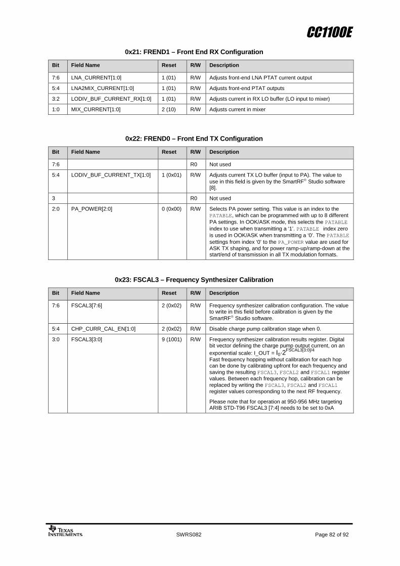
CC1100E
SWRS082 Page 82 of 92
0x21: FREND1 – Front End RX Configuration
Bit Field Name Reset R/W Description
7:6 LNA_CURRENT[1:0] 1 (01) R/W Adjusts front-end LNA PTAT current output
5:4 LNA2MIX_CURRENT[1:0] 1 (01) R/W Adjusts front-end PTAT outputs
3:2 LODIV_BUF_CURRENT_RX[1:0] 1 (01) R/W Adjusts current in RX LO buffer (LO input to mixer)
1:0 MIX_CURRENT[1:0] 2 (10) R/W Adjusts current in mixer
0x22: FREND0 – Front End TX Configuration
Bit Field Name Reset R/W Description
7:6 R0 Not used
5:4 LODIV_BUF_CURRENT_TX[1:0] 1 (0x01) R/W Adjusts current TX LO buffer (input to PA). The value touse in this field is given by the SmartRF Studio software[8].
3 R0 Not used
2:0 PA_POWER[2:0] 0 (0x00) R/W Selects PA power setting. This value is an index to thePATABLE, which can be programmed with up to 8 differentPA settings. In OOK/ASK mode, this selects the PATABLEindex to use when transmitting a ‘1’. PATABLE index zerois used in OOK/ASK when transmitting a ‘0’. The PATABLEsettings from index ‘0’ to the PA_POWER value are used forASK TX shaping, and for power ramp-up/ramp-down at thestart/end of transmission in all TX modulation formats.
0x23: FSCAL3 – Frequency Synthesizer Calibration
Bit Field Name Reset R/W Description
7:6 FSCAL3[7:6] 2 (0x02) R/W Frequency synthesizer calibration configuration. The valueto write in this field before calibration is given by theSmartRF Studio software.
5:4 CHP_CURR_CAL_EN[1:0] 2 (0x02) R/W Disable charge pump calibration stage when 0.
3:0 FSCAL3[3:0] 9 (1001) R/W Frequency synthesizer calibration results register. Digitalbit vector defining the charge pump output current, on an
exponential scale: I_OUT = I0·2FSCAL3[3:0]/4
Fast frequency hopping without calibration for each hopcan be done by calibrating upfront for each frequency andsaving the resulting FSCAL3, FSCAL2 and FSCAL1 registervalues. Between each frequency hop, calibration can bereplaced by writing the FSCAL3, FSCAL2 and FSCAL1register values corresponding to the next RF frequency.
Please note that for operation at 950-956 MHz targetingARIB STD-T96 FSCAL3 [7:4] needs to be set to 0xA

CC1100E
SWRS082 Page 83 of 92
0x24: FSCAL2 – Frequency Synthesizer Calibration
Bit Field Name Reset R/W Description
7:6 R0 Not used
5 VCO_CORE_H_EN 0 R/W Choose high (1) / low (0) VCO
4:0 FSCAL2[4:0] 10 (0x0A) R/W Frequency synthesizer calibration results register. VCO currentcalibration result and override value.Fast frequency hopping without calibration for each hop can be done bycalibrating upfront for each frequency and saving the resulting FSCAL3,FSCAL2 and FSCAL1 register values. Between each frequency hop,calibration can be replaced by writing the FSCAL3, FSCAL2 and FSCAL1register values corresponding to the next RF frequency.
0x25: FSCAL1 – Frequency Synthesizer Calibration
Bit Field Name Reset R/W Description
7:6 R0 Not used
5:0 FSCAL1[5:0] 32 (0x20) R/W Frequency synthesizer calibration results register. Capacitor arraysetting for VCO coarse tuning.Fast frequency hopping without calibration for each hop can be done bycalibrating upfront for each frequency and saving the resulting FSCAL3,FSCAL2 and FSCAL1 register values. Between each frequency hop,calibration can be replaced by writing the FSCAL3, FSCAL2 and FSCAL1register values corresponding to the next RF frequency.
0x26: FSCAL0 – Frequency Synthesizer Calibration
Bit Field Name Reset R/W Description
7 R0 Not used
6:0 FSCAL0[6:0] 13 (0x0D) R/W Frequency synthesizer calibration control. The value to use in thisregister is given by the SmartRF Studio software [8].
Please note that for operation at 950-956 MHz targeting ARIB STD-T96,FSCAL0 needs to be set to 0x07
0x27: RCCTRL1 – RC Oscillator Configuration
Bit Field Name Reset R/W Description
7 0 R0 Not used
6:0 RCCTRL1[6:0] 65 (0x41) R/W RC oscillator configuration.
0x28: RCCTRL0 – RC Oscillator Configuration
Bit Field Name Reset R/W Description
7 0 R0 Not used
6:0 RCCTRL0[6:0] 0 (0x00) R/W RC oscillator configuration.

CC1100E
SWRS082 Page 84 of 92
29.2 Configuration Register Details – Registers that Loose Programming in SLEEP State
0x29: FSTEST – Frequency Synthesizer Calibration Control
Bit Field Name Reset R/W Description
7:0 FSTEST[7:0] 89 (0x59) R/W For test only. Do not write to this register.
0x2A: PTEST – Production Test
Bit Field Name Reset R/W Description
7:0 PTEST[7:0] 127 (0x7F) R/W Writing 0xBF to this register makes the on-chip temperature sensoravailable in the IDLE state. The default 0x7F value should then bewritten back before leaving the IDLE state. Other use of this register isfor test only.
0x2B: AGCTEST – AGC Test
Bit Field Name Reset R/W Description
7:0 AGCTEST[7:0] 63 (0x3F) R/W For test only. Do not write to this register.
0x2C: TEST2 – Various Test Settings
Bit Field Name Reset R/W Description
7:0 TEST2[7:0] 136 (0x88) R/W The value to use in this register is given by the SmartRF Studiosoftware [8]. This register will be forced to 0x88 or 0x81 when it wakesup from SLEEP mode, depending on the configuration of FIFOTHR.ADC_RETENTION.
Note that the value read from this register when waking up from SLEEPalways is the reset value (0x88) regardless of the ADC_RETENTIONsetting. The inversion of some of the bits due to the ADC_RETENTIONsetting is only seen INTERNALLY in the analog part.
0x2D: TEST1 – Various Test Settings
Bit Field Name Reset R/W Description
7:0 TEST1[7:0] 49 (0x31) R/W The value to use in this register is given by the SmartRF Studiosoftware [8]. This register will be forced to 0x31 or 0x35 when it wakesup from SLEEP mode, depending on the configuration of FIFOTHR.ADC_RETENTION.
Note that the value read from this register when waking up from SLEEPalways is the reset value (0x31) regardless of the ADC_RETENTIONsetting. The inversion of some of the bits due to the ADC_RETENTIONsetting is only seen INTERNALLY in the analog part.

CC1100E
SWRS082 Page 85 of 92
0x2E: TEST0 – Various Test Settings
Bit Field Name Reset R/W Description
7:2 TEST0[7:2] 2 (0x02) R/W The value to use in this register is given by the SmartRF Studiosoftware [8].
1 VCO_SEL_CAL_EN 1 R/W Enable VCO selection calibration stage when 1
0 TEST0[0] 1 R/W The value to use in this register is given by the SmartRF Studiosoftware [8].
29.3 Status Register Details
0x30 (0xF0): PARTNUM – Chip ID
Bit Field Name Reset R/W Description
7:0 PARTNUM[7:0] 0 (0x00) R Chip part number
0x31 (0xF1): VERSION – Chip ID
Bit Field Name Reset R/W Description
7:0 VERSION[7:0] 5 (0x05) R Chip version number.
0x32 (0xF2): FREQEST – Frequency Offset Estimate from Demodulator
Bit Field Name Reset R/W Description
7:0 FREQOFF_EST R The estimated frequency offset (2’s complement) of the carrier. Resolution isFXTAL/2
14 (1.59 - 1.65 kHz); range is ±202 kHz to ±210 kHz, depending onXTAL frequency.
Frequency offset compensation is only supported for 2-FSK, GFSK, and MSKmodulation. This register will read 0 when using ASK or OOK modulation.
0x33 (0xF3): LQI – Demodulator Estimate for Link Quality
Bit Field Name Reset R/W Description
7 CRC OK R The last CRC comparison matched. Cleared when entering/restarting RXmode.
6:0 LQI_EST[6:0] R The Link Quality Indicator estimates how easily a received signal can bedemodulated. Calculated over the 64 symbols following the sync word
0x34 (0xF4): RSSI – Received Signal Strength Indication
Bit Field Name Reset R/W Description
7:0 RSSI R Received signal strength indicator

CC1100E
SWRS082 Page 86 of 92
0x35 (0xF5): MARCSTATE – Main Radio Control State Machine State
Bit Field Name Reset R/W Description
7:5 R0 Not used
4:0 MARC_STATE[4:0] R Main Radio Control FSM State
Value State name State (Figure 20, page 45)
0 (0x00) SLEEP SLEEP
1 (0x01) IDLE IDLE
2 (0x02) XOFF XOFF
3 (0x03) VCOON_MC MANCAL
4 (0x04) REGON_MC MANCAL
5 (0x05) MANCAL MANCAL
6 (0x06) VCOON FS_WAKEUP
7 (0x07) REGON FS_WAKEUP
8 (0x08) STARTCAL CALIBRATE
9 (0x09) BWBOOST SETTLING
10 (0x0A) FS_LOCK SETTLING
11 (0x0B) IFADCON SETTLING
12 (0x0C) ENDCAL CALIBRATE
13 (0x0D) RX RX
14 (0x0E) RX_END RX
15 (0x0F) RX_RST RX
16 (0x10) TXRX_SWITCH TXRX_SETTLING
17 (0x11) RXFIFO_OVERFLOW RXFIFO_OVERFLOW
18 (0x12) FSTXON FSTXON
19 (0x13) TX TX
20 (0x14) TX_END TX
21 (0x15) RXTX_SWITCH RXTX_SETTLING
22 (0x16) TXFIFO_UNDERFLOW TXFIFO_UNDERFLOW
Note: it is not possible to read back the SLEEP or XOFF state numbersbecause setting CSn low will make the chip enter the IDLE mode from theSLEEP or XOFF states.
0x36 (0xF6): WORTIME1 – High Byte of WOR Time
Bit Field Name Reset R/W Description
7:0 TIME[15:8] R High byte of timer value in WOR module
0x37 (0xF7): WORTIME0 – Low Byte of WOR Time
Bit Field Name Reset R/W Description
7:0 TIME[7:0] R Low byte of timer value in WOR module

CC1100E
SWRS082 Page 87 of 92
0x38 (0xF8): PKTSTATUS – Current GDOx Status and Packet Status
Bit Field Name Reset R/W Description
7 CRC_OK R The last CRC comparison matched. Cleared when entering/restarting RXmode.
6 CS R Carrier sense
5 PQT_REACHED R Preamble Quality reached
4 CCA R Channel is clear
3 SFD R Sync word found. Asserted when sync word has been sent / received,and de-asserted at the end of the packet. In RX, this bit will de-assertwhen the optional address check fails or the radio enterRX_OVERFLOW state. In TX this bit will de-assert if the radio entersTX_UNDERFLOW state.
2 GDO2 R Current GDO2 value. Note: the reading gives the non-inverted valueirrespective of what IOCFG2.GDO2_INV is programmed to.
It is not recommended to check for PLL lock by reading PKTSTATUS[2] with GDO2_CFG=0x0A.
1 R0 Not used
0 GDO0 R Current GDO0 value. Note: the reading gives the non-inverted valueirrespective of what IOCFG0.GDO0_INV is programmed to.
It is not recommended to check for PLL lock by reading PKTSTATUS[0] with GDO0_CFG=0x0A.
0x39 (0xF9): VCO_VC_DAC – Current Setting from PLL Calibration Module
Bit Field Name Reset R/W Description
7:0 VCO_VC_DAC[7:0] R Status register for test only.
0x3A (0xFA): TXBYTES – Underflow and Number of Bytes
Bit Field Name Reset R/W Description
7 TXFIFO_UNDERFLOW R
6:0 NUM_TXBYTES R Number of bytes in TX FIFO
0x3B (0xFB): RXBYTES – Overflow and Number of Bytes
Bit Field Name Reset R/W Description
7 RXFIFO_OVERFLOW R
6:0 NUM_RXBYTES R Number of bytes in RX FIFO
0x3C (0xFC): RCCTRL1_STATUS – Last RC Oscillator Calibration Result
Bit Field Name Reset R/W Description
7 R0 Not used
6:0 RCCTRL1_STATUS[6:0] R Contains the value from the last run of the RC oscillator calibrationroutine.
For usage description refer to AN047 [7]

CC1100E
SWRS082 Page 88 of 92
0x3D (0xFD): RCCTRL0_STATUS – Last RC Oscillator Calibration Result
Bit Field Name Reset R/W Description
7 R0 Not used
6:0 RCCTRL0_STATUS[6:0] R Contains the value from the last run of the RC oscillator calibrationroutine.
For usage description refer to Application Note AN047 [7].

CC1100E
SWRS082 Page 89 of 92
30 Package Description (QFN 20)
30.1 Recommended PCB Layout for Package (QFN 20)
Figure 29: Recommended PCB Layout for QFN 20 Package
30.2 Soldering Information
The recommendations for lead-free reflow in IPC/JEDEC J-STD-020 should be followed.
Note: Figure 29 is an illustration only and not to scale. There are five 10 mil via holesdistributed symmetrically in the ground pad under the package. See also the CC1100EEMreference designs ([3] and [4]).

CC1100E
SWRS082 Page 90 of 92
30.3 Ordering Information
OrderableDevice
Status(1)
PackageType
PackageDrawing
Pins PackageQty
Eco Plan (2) LeadFinish
MSL PeakTemp (3)
CC1100ERTKR Active QFN RTK 20 3000 Green (RoHS &no Sb/Br)
Cu NiPdAu LEVEL3-260C
1 YEAR
CC1100ERTKT Active QFN RTK 20 250 Green (RoHS &no Sb/Br)
Cu NiPdAu LEVEL3-260C
1 YEAR
Orderable Evaluation Module Description Minimum Order Quantity
CC1100E-EMK470 CC1100E Evaluation Module Kit, 470-510 MHz 1
CC1100E-EMK950 CC1100E Evaluation Module Kit, 950-960 MHz 1
Table 42: Ordering Information

CC1100E
SWRS082 Page 91 of 92
References
[1] CC1101 Datasheet
[2] CC1100 Datasheet
[3] CC1100E EM 470 MHz Reference Design
[4] CC1100E EM 950 MHz Reference Design
[5] CC1100E Errata Note
[6] ARIB STD-T96 ver.1.0
[7] AN047 CC1100/CC2500 – Wake-On-Radio (swra126.pdf)
[8] SmartRF®
Studio (swrc046.zip)
[9] CC1100 CC1101 CC1100E CC2500 Examples Libraries (swrc021.zip)
[10] CC1100/CC1150DK, CC1101DK, and CC2500/CC2550DK Examples and Libraries UserManual (swru109.pdf)
[11] DN010 Close-in Reception with CC1101 (and CC1100E) (swra147.pdf)
[12] DN015 Permanent Frequency Offset Compensation (swra159.pdf)
[13] DN505 RSSI Interpretation and Timing (swra114.pdf)
[14] AN058 Antenna Selection Guide (swra161.pdf)
[15] DN022 CC11xx OOK/ASK register settings (swra215.pdf)
[16] DN005 CC11xx Sensitivity versus Frequency Offset and Crystal Accuracy (swra122.pdf)
[17] DN501 PATABLE Access
[18] DN504 FEC Implementation

CC1100E
SWRS082 Page 92 of 92
31 General Information
31.1 Document History
Revision Date Description/Changes
SWRS082 April 2009 First data sheet release
Table 43: Document History


IMPORTANT NOTICE
Texas Instruments Incorporated (TI) reserves the right to make corrections, enhancements, improvements and other changes to itssemiconductor products and services per JESD46, latest issue, and to discontinue any product or service per JESD48, latest issue. Buyersshould obtain the latest relevant information before placing orders and should verify that such information is current and complete.TI’s published terms of sale for semiconductor products (http://www.ti.com/sc/docs/stdterms.htm) apply to the sale of packaged integratedcircuit products that TI has qualified and released to market. Additional terms may apply to the use or sale of other types of TI products andservices.Reproduction of significant portions of TI information in TI data sheets is permissible only if reproduction is without alteration and isaccompanied by all associated warranties, conditions, limitations, and notices. TI is not responsible or liable for such reproduceddocumentation. Information of third parties may be subject to additional restrictions. Resale of TI products or services with statementsdifferent from or beyond the parameters stated by TI for that product or service voids all express and any implied warranties for theassociated TI product or service and is an unfair and deceptive business practice. TI is not responsible or liable for any such statements.Buyers and others who are developing systems that incorporate TI products (collectively, “Designers”) understand and agree that Designersremain responsible for using their independent analysis, evaluation and judgment in designing their applications and that Designers havefull and exclusive responsibility to assure the safety of Designers' applications and compliance of their applications (and of all TI productsused in or for Designers’ applications) with all applicable regulations, laws and other applicable requirements. Designer represents that, withrespect to their applications, Designer has all the necessary expertise to create and implement safeguards that (1) anticipate dangerousconsequences of failures, (2) monitor failures and their consequences, and (3) lessen the likelihood of failures that might cause harm andtake appropriate actions. Designer agrees that prior to using or distributing any applications that include TI products, Designer willthoroughly test such applications and the functionality of such TI products as used in such applications.TI’s provision of technical, application or other design advice, quality characterization, reliability data or other services or information,including, but not limited to, reference designs and materials relating to evaluation modules, (collectively, “TI Resources”) are intended toassist designers who are developing applications that incorporate TI products; by downloading, accessing or using TI Resources in anyway, Designer (individually or, if Designer is acting on behalf of a company, Designer’s company) agrees to use any particular TI Resourcesolely for this purpose and subject to the terms of this Notice.TI’s provision of TI Resources does not expand or otherwise alter TI’s applicable published warranties or warranty disclaimers for TIproducts, and no additional obligations or liabilities arise from TI providing such TI Resources. TI reserves the right to make corrections,enhancements, improvements and other changes to its TI Resources. TI has not conducted any testing other than that specificallydescribed in the published documentation for a particular TI Resource.Designer is authorized to use, copy and modify any individual TI Resource only in connection with the development of applications thatinclude the TI product(s) identified in such TI Resource. NO OTHER LICENSE, EXPRESS OR IMPLIED, BY ESTOPPEL OR OTHERWISETO ANY OTHER TI INTELLECTUAL PROPERTY RIGHT, AND NO LICENSE TO ANY TECHNOLOGY OR INTELLECTUAL PROPERTYRIGHT OF TI OR ANY THIRD PARTY IS GRANTED HEREIN, including but not limited to any patent right, copyright, mask work right, orother intellectual property right relating to any combination, machine, or process in which TI products or services are used. Informationregarding or referencing third-party products or services does not constitute a license to use such products or services, or a warranty orendorsement thereof. Use of TI Resources may require a license from a third party under the patents or other intellectual property of thethird party, or a license from TI under the patents or other intellectual property of TI.TI RESOURCES ARE PROVIDED “AS IS” AND WITH ALL FAULTS. TI DISCLAIMS ALL OTHER WARRANTIES ORREPRESENTATIONS, EXPRESS OR IMPLIED, REGARDING RESOURCES OR USE THEREOF, INCLUDING BUT NOT LIMITED TOACCURACY OR COMPLETENESS, TITLE, ANY EPIDEMIC FAILURE WARRANTY AND ANY IMPLIED WARRANTIES OFMERCHANTABILITY, FITNESS FOR A PARTICULAR PURPOSE, AND NON-INFRINGEMENT OF ANY THIRD PARTY INTELLECTUALPROPERTY RIGHTS. TI SHALL NOT BE LIABLE FOR AND SHALL NOT DEFEND OR INDEMNIFY DESIGNER AGAINST ANY CLAIM,INCLUDING BUT NOT LIMITED TO ANY INFRINGEMENT CLAIM THAT RELATES TO OR IS BASED ON ANY COMBINATION OFPRODUCTS EVEN IF DESCRIBED IN TI RESOURCES OR OTHERWISE. IN NO EVENT SHALL TI BE LIABLE FOR ANY ACTUAL,DIRECT, SPECIAL, COLLATERAL, INDIRECT, PUNITIVE, INCIDENTAL, CONSEQUENTIAL OR EXEMPLARY DAMAGES INCONNECTION WITH OR ARISING OUT OF TI RESOURCES OR USE THEREOF, AND REGARDLESS OF WHETHER TI HAS BEENADVISED OF THE POSSIBILITY OF SUCH DAMAGES.Unless TI has explicitly designated an individual product as meeting the requirements of a particular industry standard (e.g., ISO/TS 16949and ISO 26262), TI is not responsible for any failure to meet such industry standard requirements.Where TI specifically promotes products as facilitating functional safety or as compliant with industry functional safety standards, suchproducts are intended to help enable customers to design and create their own applications that meet applicable functional safety standardsand requirements. Using products in an application does not by itself establish any safety features in the application. Designers mustensure compliance with safety-related requirements and standards applicable to their applications. Designer may not use any TI products inlife-critical medical equipment unless authorized officers of the parties have executed a special contract specifically governing such use.Life-critical medical equipment is medical equipment where failure of such equipment would cause serious bodily injury or death (e.g., lifesupport, pacemakers, defibrillators, heart pumps, neurostimulators, and implantables). Such equipment includes, without limitation, allmedical devices identified by the U.S. Food and Drug Administration as Class III devices and equivalent classifications outside the U.S.TI may expressly designate certain products as completing a particular qualification (e.g., Q100, Military Grade, or Enhanced Product).Designers agree that it has the necessary expertise to select the product with the appropriate qualification designation for their applicationsand that proper product selection is at Designers’ own risk. Designers are solely responsible for compliance with all legal and regulatoryrequirements in connection with such selection.Designer will fully indemnify TI and its representatives against any damages, costs, losses, and/or liabilities arising out of Designer’s non-compliance with the terms and provisions of this Notice.
Mailing Address: Texas Instruments, Post Office Box 655303, Dallas, Texas 75265Copyright © 2017, Texas Instruments Incorporated