Embed Size (px)
Citation preview
This document is downloaded from DR‑NTU (https://dr.ntu.edu.sg)Nanyang Technological University, Singapore.
Low power SAR ADC designs for sensingapplications
Yang, Yongkui
2017
Yang, Y. (2017). Low power SAR ADC designs for sensing applications. Doctoral thesis,Nanyang Technological University, Singapore.
http://hdl.handle.net/10356/70201
https://doi.org/10.32657/10356/70201
Downloaded on 13 Mar 2022 01:05:45 SGT
Equation Chapter 1 Section 1
LOW POWER SAR ADC DESIGNS FOR SENSING
APPLICATIONS
YANG YONGKUI
School of Electrical and Electronic Engineering
A thesis submitted to the Nanyang Technological University in partial fulfilment of the requirement for the degree of
Doctor of Philosophy
2017

I
Acknowledgement
This thesis would not have been possible without the help and support of
many people. I would first like to thank my supervisor, Associate Professor Goh
Wang Ling, for her valuable guidance and constant encouragement throughout
my research journey. She is a very nice and was willing to talk with me about
any problems I was facing, either in research or in my personal life.
I would also like to thank my co-supervisors, Dr. Liu Xin and Dr. Zhou Jun,
from Institute of Microelectronics, A*STAR, for advising me throughout my
PhD research. Their constructive advices and feedbacks had accelerated the
success of my research. The valuable discussion with them, both on idea
sharing and paper writing, benefits me a lot. I would like to thank Dr. Cheong
Jia Hao for answering all of the ADC-related questions.
I am also grateful to the help and discussion provided by my project partners
and research group members: Dr. Wang Chao, Dr. Yu Jun, Dr. Liu Lei, Dr.
Wang Yong, Dr. Wu Chundong, Chang Kah Hyong, Lan Jingjing, Dutta Rahul,
Wang Jiacheng, Hong Yan, Tang Tao, Chen Yejin, Zhou Wei, Hendika Fatkhi
Nurhuda, Chen Shao Jun and Zeng Zhe. I am very pleased to work with them
and be friends with them. I thank the staffs at the NTU VIRTUS IC Design
Centre of Excellence and also the staffs at the Integrated Circuits & Systems
Laboratory of the Institute of Microelectronics, for their help.
I also want to thank my friends who also have made my PhD life more
enjoyable: Yi Xiang, Lin Jiafu, Ye Wenbin, Yao Enyi, Huang Nan, Bai Xiaoyin,
Feng Guangyin, Qiu Lei, Feng Xiaohua, Zhang Le, Sun Junyi, Zhang Ying,

II
Meng Fanyi, Xu Shanshan, Chen Zihao, Wang Bo, Zhu Di, Abhik Das,
Neelakantan Narasimman, Liang Zhipeng, Yang Kaituo, Li Chenyang, Liu Bei,
Liu Xu, Yan Ruoxi and so on.
Last but not least, I give my heartiest thanks to my parents and sister for
their continued love and support.

III
Table of Contents
Acknowledgement ............................................................................................... I
Table of Contents ............................................................................................. III
List of Figures ................................................................................................... VI
List of Tables ................................................................................................. XIII
List of Abbreviations .................................................................................... XIV
Abstract ........................................................................................................ XV
Chapter 1 Introduction ......................................................................................... 1
1.1 Background ....................................................................................... 1
1.2 Motivation ........................................................................................ 4
1.3 Contribution ...................................................................................... 6
1.4 Organization ..................................................................................... 7
Chapter 2 Background and Literature Review ..................................................... 9
2.1 Conventional SAR ADC .................................................................. 9
2.2 Ultra-Low Power Design Considerations in Typical SAR ADC ... 11
2.2.1 Bootstrapped Switch .............. Error! Bookmark not defined.
2.2.2 Energy Efficient Capacitor Array Switching Method ........... 15
2.2.3 Low Voltage Comparator ...................................................... 21
2.3 Signal-based Low Power SAR ADC .............................................. 22
2.4 System Level Design Considerations of Low Power ADC ............ 26
IV
2.5 Calibration of Capacitor Mismatch in SAR ADC with Advanced
CMOS Technology Node .............................................................. 29
Chapter 3 Ultra-Low Power SAR ADC Design ................................................ 34
3.1 Proposed SAR ADC Architecture .................................................. 35
3.2 Proposed Bootstrapped Switch ....................................................... 35
3.3 Efficient Capacitor Array Design ................................................... 37
3.3.1 Redundant Algorithm ............................................................ 37
3.3.2 Capacitor Array Implementation ........................................... 39
3.4 Time-Domain Comparator Design ................................................. 41
3.5 Switching Logic Design ................................................................. 42
3.6 Measurement Results ...................................................................... 44
3.7 Sensor Node Processors Applications ............................................ 47
3.7.1 Near-Threshold Cognitive Multi-Functional ECG Processor 48
3.7.2 Sensor Node Processor for Intelligent Sensing in IoT .......... 50
Chapter 4 A 151-nW Adaptive Delta-Sampling ADC Design .......................... 54
4.1 Input Signal Analysis...................................................................... 55
4.2 Proposed Adaptive Delta-Sampling Architecture .......................... 56
4.3 Adaptive Delta-Sampling ............................................................... 59
4.4 Subtractor Design ........................................................................... 63
4.5 Power consumption analysis of proposed ADC ............................. 65
4.6 Wide Common-Mode Range Comparator ...................................... 66
4.7 Measurement Results ...................................................................... 70

V
Chapter 5 A 10-bit 300 kS/s Reference-Voltage Regulator Free Asynchronous
SAR ADC ........................................................................................ 76
5.1 Charge-Sharing SAR ...................................................................... 78
5.2 System Architecture of Proposed SAR ADC ................................. 80
5.3 Fully Asynchronous Operation ....................................................... 84
5.4 Charge Detector, Vref Generator and Current Source ..................... 86
5.5 Comparator ..................................................................................... 89
5.6 Measurement Results ...................................................................... 91
Chapter 6 Wide Input 12-bit SAR ADC with Digital Calibration ..................... 98
6.1 Architecture of Proposed ADC with Configurable Input Range .. 101
6.2 High Voltage Bootstrapped Switch .............................................. 103
6.3 Fast Convergence and Low Power Digital Calibration ................ 105
6.3.1 Principle of Perturbation-Based Calibration........................ 105
6.3.2 Low Power and Fast Convergence Calibration Scheme ..... 110
6.4 Circuit Implementation ................................................................. 113
6.5 Simulation Results ........................................................................ 114
Chapter 7 Conclusion and Future Work .......................................................... 118
7.1 Conclusion .................................................................................... 118
7.2 Future Work .................................................................................. 120
Publications ..................................................................................................... 127
Bibliography ................................................................................................... 129
VI
List of Figures
Fig. 1.1. Sensor nodes application in personal telehealth systems................. 1
Fig. 1.2. Tire monitoring system developed by Continental. ......................... 2
Fig. 1.3. Simplified block diagram of an intelligent sensor node. ................. 3
Fig. 1.4. Energy efficiency of various ADC architectures in the bandwidth-
resolution space. ................................................................................................... 5
Fig. 2.1. Block diagram of a 3-bit conventional SAR ADC. ....................... 10
Fig. 2.2. Waveforms of VDAC and VSH during the bit cycling period. ........... 10
Fig. 2.3. (a) CMOS transmission gate. (b) Model for effective resistance of a
transmission gate. ............................................................................................... 11
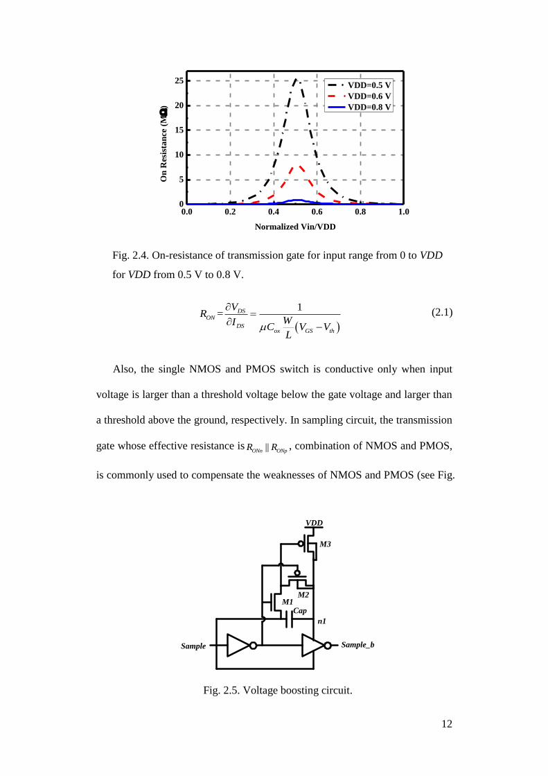
Fig. 2.4. On-resistance of transmission gate for input range from 0 to VDD
for VDD from 0.5 V to 0.8 V. ............................................................................ 12
Fig. 2.5. Voltage boosting circuit. ................................................................ 12
Fig. 2.6. Modified sampling switch. ............................................................ 13
Fig. 2.7. The schematic of LRBS. ................................................................ 14
Fig. 2.8. Block diagram of SAR ADC. ........................................................ 15
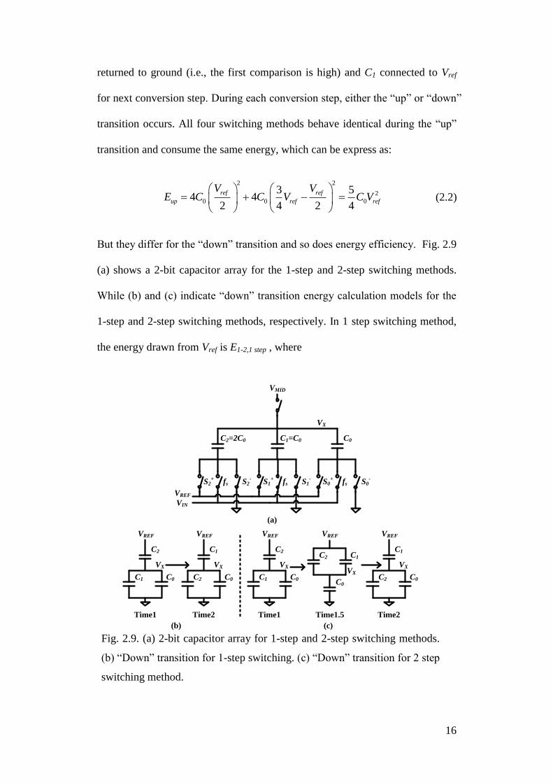
Fig. 2.9. (a) 2-bit capacitor array for 1-step and 2-step switching methods. (b)
“Down” transition for 1-step switching. (c) “Down” transition for 2 step
switching method. .............................................................................................. 16
Fig. 2.10. (a) 2-bit capacitor array. (b) “Down” transition for charge sharing
switching method. .............................................................................................. 18
Fig. 2.11. (a) 2-bit capacitor array, (b) “Down” transition for capacitor
splitting switching method. ................................................................................ 19

VII
Fig. 2.12. Schematic and timing diagram of the time-domain comparator
with flip-flop based phase detector. ................................................................... 21
Fig. 2.13. Block diagram of time-domain comparator. ................................ 22
Fig. 2.14. The architecture of this adaptive resolution asynchronous ADC
and example waveforms demonstrating its operation. ....................................... 23
Fig. 2.15. The architecture of DMSAR ADC. ............................................. 24
Fig. 2.16. Example of 5 bit conversions using LSB-first successive
approximation. ................................................................................................... 24
Fig. 2.17. Bitcycles per sample as a function of code charge per sample for a
10-bit LSB-first SAR ADC. ............................................................................... 25
Fig. 2.18. Top-level current-integrating SAR ADC architecture. ................ 26
Fig. 2.19. ADC with integrated reference, circuit diagram of the RVG and
architecture of the 10-bit SAR ADC. ................................................................. 27
Fig. 2.20. Power consumption of the ADC with RVG versus duty-cycling
rate. ..................................................................................................................... 28
Fig. 2.21. Block diagram of the asynchronous VCO-based sensor interface.
............................................................................................................................ 29
Fig. 2.22. On-chip digital calibration with additional calibration capacitor
DAC bank. ......................................................................................................... 30
Fig. 2.23. Digital-domain calibration of split-capacitor DAC without
additional analog circuits. .................................................................................. 31
Fig. 2.24. Block diagram of perturbation-based digital calibration technique.
............................................................................................................................ 32
Fig. 3.1. Architecture of the proposed ultra-low power SAR ADC. ............ 35
Fig. 3.2. Schematic of proposed clock boosting circuit. .............................. 36

VIII
Fig. 3.3. (a) Simulation waveform of clock boosting circuit; (b) Input and
output characteristics of transmission gate controlled by the normal and boosted
voltage signals, respectively............................................................................... 36
Fig. 3.4. Correction of decision error using redundant algorithm. ............... 38
Fig. 3.5. Capacitor array of the proposed ADC. .......................................... 40
Fig. 3.6. Block diagram of the time-domain comparator, and the VCDL
chain. .................................................................................................................. 41
Fig. 3.7. Circuit and timing diagrams of the binary phase detector. ............ 43
Fig. 3.8. Block diagram of SAR switching logic. ........................................ 43
Fig. 3.9. Photo micrograph of the chip. ....................................................... 44
Fig. 3.10. DNL and INL measured at 1kS/s and 0.5 V supply .................... 44
Fig. 3.11. Output spectrum with 449.95 Hz sinusoid input, operating at
1kS/s and 0.5 V supply voltage. ......................................................................... 45
Fig. 3.12. SNDR and ENOB versus input signal frequency with 1 kS/s
sampling rate 0.5 V supply voltage. ................................................................... 45
Fig. 3.13. SNDR and ENOB versus sampling rate with input signal
frequency near 30 Hz. ........................................................................................ 46
Fig. 3.14. System architecture of the proposed cognitive ECG processor. .. 48
Fig. 3.15. Chip micrograph of the proposed cognitive ECG processor. ...... 49
Fig. 3.16. Measurement results of the proposed cognitive ECG processor. 50
Fig. 3.17. System architecture of the proposed sensor node processor........ 51
Fig. 3.18. Chip micrograph of the proposed sensor node processor. ........... 51
Fig. 3.19. Measurement results from two applications. (a) Neural spike
classification. (b) Vehicle speed detection. ........................................................ 52
IX
Fig. 4.1. Digitalized sparse signals with 8 bits, first 4 MSB bits and last 4
LSB bits: (a) ECG signal sampled with 1 kHz sampling rate, (b) neural signal
sampled with 20 kHz sampling rate. .................................................................. 55
Fig. 4.2. Proposed ADC: (a) system architecture, (b) operation timing
diagram. .............................................................................................................. 57
Fig. 4.3. Block diagram of proposed ADC for accumulated error analysis. 58
Fig. 4.4. Proposed analog-front slope detector: (a) block diagram, (b) fully
differential amplifier, (c) peak points of input signal, (d) digital delay cell. ..... 59
Fig. 4.5. Measured timing mismatch between fast and slow clocks. ........... 62
Fig. 4.6. Circuit implementation of the proposed ADC core. ...................... 63
Fig. 4.7. Waveforms of: (a) conventional differential ADC switching
procedure and (b) proposed switching procedure. ............................................. 64
Fig. 4.8. Simulated power consumptions of the capacitor arrays in proposed
ADC and the capacitor splitting ADC with neural signal input......................... 65
Fig. 4.9. Schematic of conventional two-stage dynamic comparator. ......... 66
Fig. 4.10. Schematic of proposed two-stage dynamic comparator with
PMOS and NMOS input pairs............................................................................ 67
Fig. 4.11. Proposed comparator circuit consisting of P_comparator and
N_comparator and (b) simulated offset (500 MC runs). ................................... 69
Fig. 4.12. Micrograph of the proposed ADC chip. ...................................... 70
Fig. 4.13. Measured transient response of proposed ADC with neural signal
input: (a) input neural signal and zoomed-in neural spike, (b) sampling
frequency selection signal sl and adaptive sampling frequency fS, (c) output of
ADC Qout, input of 5-bit DAC Qfb and 6-bit ADC output Qd (except Sn). ......... 71
X
Fig. 4.14. Power reduction of proposed ADC. #1: Simulated power
consumption of capacitor splitting SAR ADC. #2: Measured power
consumption of proposed delta-sampling ADC. #3: Measured power
consumption of proposed adaptive delta-sampling ADC. ................................. 72
Fig. 4.15. Performance of proposed ADC: (a) output spectrum operating at
125 kS/s and (b) SNDR versus sampling frequency. ......................................... 73
Fig. 5.1. Block diagram of typical wireless implantable medical device. ... 77
Fig. 5.2. 3-bit charge-sharing SAR ADC. .................................................... 78
Fig. 5.3. Influence of reference voltage noise on ENOB for charge-sharing
SAR ADC with different resolution. .................................................................. 80
Fig. 5.4. Architecture of proposed reference-voltage regulator free SAR
ADC with self-timed pre-charging..................................................................... 81
Fig. 5.5. Self-timed pre-charging (a) ideal detector, (b) non-ideal detector
using one pre-charging phase with large current, (c) non-ideal detector using
one pre-charging phase with small current, (d) non-ideal detector using two pre-
charging phases. ................................................................................................. 82
Fig. 5.6. Timing diagram when the proposed ADC is operating in fully
asynchronous mode without external clocks...................................................... 85
Fig. 5.7. Schematic of proposed charge detector. ........................................ 86
Fig. 5.8. 2T voltage reference (a) schematic, (b) PSRR. ............................. 87
Fig. 5.9. Schematic of current source used for self-timed pre-charging. ..... 87
Fig. 5.10. Pre-charging currents, IchL and IchS, vary with VDD. ................... 88
Fig. 5.11. Schematic of two-stage dynamic comparator. ............................. 90
Fig. 5.12. Clock generator architecture. ....................................................... 90

XI
Fig. 5.13. Die photo of two SAR ADCs where Core1 is the proposed design
and Core2 is a conventional design. ................................................................... 91
Fig. 5.14. Measured output spectrum operating at 300 kS/s, when a
sinusoidal fluctuation of 50 mVpp is added to the 0.8 V power supply (a) 134.2
kHz sinusoidal fluctuation, (b) 13.56 MHz sinusoidal fluctuation. ................... 92
Fig. 5.15. The SNDR versus the amplitude of sinusoidal fluctuation added
to the 0.8 V power supply. ................................................................................. 92
Fig. 5.16 The measured DNL and INL with 50 mVpp sinusoidal fluctuation.
............................................................................................................................ 93
Fig. 5.17 Measured timing diagram (a) using external sampling clock,
fs_extfs, (b) using internal sampling clock, fs_intfs. ......................................... 94
Fig. 6.1. Block diagram of a generic wireless sensor nodes powered by Li-
ion battery........................................................................................................... 99
Fig. 6.2. The potential application of the ADC with configurable input range
to convert analog signals with different range. ................................................ 100
Fig. 6.3. The architecture of proposed differential SAR ADC. ................. 100
Fig. 6.4. The schematic of proposed HVBS. ............................................. 102
Fig. 6.5. Simulated waveforms of the proposed HVBS for a sinusoidal input
with range of 0~4.5 V, operating at a supply voltage of 1.2 V and fs = 500 kHz.
.......................................................................................................................... 103
Fig. 6.6. Transfer curves of three ADCs: (a) radix-2, (b) super-radix-2, (c)
sub-radix-2. ...................................................................................................... 106
Fig. 6.7. Illustrations of perturbation in linear transfer curve of SAR ADC.
.......................................................................................................................... 107
XII
Fig. 6.8. Illustrations of perturbation of a transfer curve with capacitor
mismatch in SAR ADC. ................................................................................... 107
Fig. 6.9. Block diagram of perturbation-based digital calibration scheme. 108
Fig. 6.10. Blocks of the ADC those are powered on after the optimal
weights are obtained. ........................................................................................ 109
Fig. 6.11. SNDR of the ADC after calibration for different number of LSBs
that are without weight calibration. .................................................................. 109
Fig. 6.12. SNDR of the ADC after calibration with 10 LSB, 15 LSB and 15
LSB/10 LSB analog offset. .............................................................................. 110
Fig. 6.13. Block diagram of the proposed low power and fast convergence
calibration scheme. ........................................................................................... 111
Fig. 6.14. Schematic of the two stage dynamic comparator. ..................... 112
Fig. 6.15. Layout of the proposed SAR ADC. ........................................... 114
Fig. 6.16. Output spectrum of the ADC with an input range of 2.4 Vpp
operating at 500 kS/s and 1.2 V: (a) before calibration, (b) after calibration. . 115
Fig. 6.17. Output spectrum of the ADC with an input range of 9.6 Vpp
operating at 500 kS/s and 1.2 V: (a) before calibration, (b) after calibration. . 115
Fig. 6.18. Simulated DNL and INL before calibration. ............................. 115
Fig. 6.19. Simulated DNL and INL after calibration. ................................ 115

XIII
List of Tables
Table 2.1 Switching Method Comparison ................................................... 20
Table 3.1 Redundant Code Pattern for The 9-bit SAR ADC ....................... 39
Table 3.2 ADC Performance Under Different Supply Voltages.................. 47
Table 3.3 ADC Performance Comparison ................................................... 47
Table 4.1 ADC Performance Comparison ................................................... 74
Table 5.1 ADC Performance Comparison ................................................... 95
Table 6.1 The Ideal Node Voltage of Each Node of The HVBS ............... 104
Table 6.2 The Values of The Capacitors .................................................... 113
Table 6.3 ADC Performance Summary ..................................................... 116
XIV
List of Abbreviations
ECG Electrocardiography
EEG Electroencephalography
EMG Electromyography
ADC Analog-to-Digital Converter
DAC Digital-to-Analog Converter
SAR Successive Approximation Register
MSB Most Significant Bit
LSB Least Significant Bit
SNDR Signal-to-Noise and Distortion Ratio
ENOB Effective Number of Bits
FOM Figure-of-Merit
DNL Differential Nonlinearity
INL Integral Nonlinearity
MOM Metal-Oxide-Metal
MIM Metal-Insulator-Metal
HVBS High Voltage Bootstrapped Switch
DFF D-Flip-Flop
LMS Least Mean Square
FPGA Field-Programmable Gate Array
ASIC Application-Specific Integrated Circuit
XV
Abstract
In sensing systems, ADCs are widely used in sensor interface circuits to
convert analog signals to digital signals. Many of the sensing systems require
ultra-low power consumption because of their limited power budget. Therefore,
the design of ultra-low power ADC that meets the intended performance is a
key design challenge for low power sensing applications, such as in healthcare
monitoring (e.g., ECG, EEG, neural signal, etc.) and environment monitoring.
Besides, a moderate sampling frequency and resolution can meet the
requirement of these sensing applications. Compared to Flash ADC, Pipelined
ADC and Delta-Sigma ADC, SAR ADC provides a good compromise among
energy efficiency, sampling frequency and conversion accuracy for these
sensing applications. In this thesis, SAR ADC is chosen as the main architecture
to develop low power SAR ADC and four different designs of SAR ADC are
proposed.
The first version SAR ADC consists mainly of clock boosting circuit, a
subtraction and an addition capacitor array, a time-domain comparator,
switching logic, output latches, level shifters and some buffers. To achieve
ultra-low power, the proposed ADC operates at 0.5 V, deploying a single-ended
structure and top plate sampling technique. In order to improve the linearity of
the sampling circuit at ultra-low supply voltage, clock boosting circuit with gate
signal swinging from 0 to 2VDD is proposed. A non-binary redundant algorithm
is applied to correct the inevitable decision errors in the first few conversion
steps. From the chip measurement results, it consumes only 16-nW of power

XVI
and achieves a SNDR of 50.4 dB, which is equivalent to an 8.08 ENOB, with 1
kS/s sampling rate at 0.5-V supply voltage.
The second version SAR ADC was designed to optimize on power
efficiency, for sparse signals such as the neural spike. Sparse signals have slow
varying or flat characteristic across most of the duty cycle, such that the MSBs
are the same if variation between two consecutive samples is small. A novel
ADC deploying M-bit ADC, N-bit DAC to realize (M+N-3) bits ADC while
reducing the power consumption and area is designed. The adaptive sampling
scheme has also been adopted to allow selection of either a higher or lower
sampling rate in event of sharp and gradual transitions, respectively. Adaptive
sampling not only ensures no overflow of input signal to the M-bit ADC but can
further reduce the power consumption. This 8-bit SAR ADC consists mainly of
a slope detector, 6-bit ADC capacitor array, 5-bit DAC capacitor array,
switching logic, dynamic comparator, latches and 8-bit full adder. The
measurement results show that it can realize a SNDR of 45.7 dB, which is
equivalent to a 7.3 ENOB, with 125 kS/s sampling rate at 1-V supply voltage.
When the input signals are neural spikes, the total power consumption of the
proposed ADC (at 2 kHz and 20 kHz sampling rates) is able to save about 88%
power compared to the conventional ADC (operating at 20 kHz sampling rate).
The third version SAR ADC was designed to optimize on power efficiency
in terms of system. A reference-voltage regulator-free SAR ADC with self-
timed pre-charging for wireless-powered implantable medical devices was
designed. Assisted by a self-timed pre-charging technique, the proposed SAR
ADC eliminates the power-hungry reference-voltage regulator and the area-
consuming decoupling capacitor while maintaining insensitivity to the supply
XVII
voltage fluctuation. Furthermore, with internally generated sampling clock and
asynchronous SAR logics, this SAR ADC can operate at a fully asynchronous
mode without any external clock source. Fabricated in the 0.18-µm CMOS
technology, the proposed SAR ADC achieves a SNDR of 53.32 dB at 0.8 V
with 50 mVpp supply voltage fluctuation, while consuming a total power of 2.72
µW at 300 kS/s sampling rate. The total FOM is 23.9 fJ/conversion-step and the
total area occupied is 0.105 mm2.
The fourth design is a wide input 12-bit SAR ADC with low power and fast
convergence digital background calibration. This SAR ADC is able to convert
input signal with a range of 0~4.8 V, operating at 1.2-V supply. By omitting the
calibration of 3 LSBs’ weights, the number of multipliers or product is reduced
to lower the power consumption. Besides, in order to accelerate the
convergence of digital background calibration, 10 LSB offset is injected to the
first 10000 samples, followed by 15 LSB offset. The ADC is designed and
simulated with a 65 nm CMOS technology, and the digital background is
implemented in Matlab. With background calibration, the SNDR of the ADC is
improved from 59.6 dB to 65.3 dB, operating at 500 kS/s. and power
consumption is 8.39 µW.

XVIII
1
Chapter 1
Introduction
1.1 Background
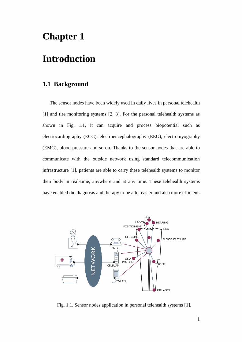
The sensor nodes have been widely used in daily lives in personal telehealth
[1] and tire monitoring systems [2, 3]. For the personal telehealth systems as
shown in Fig. 1.1, it can acquire and process biopotential such as
electrocardiography (ECG), electroencephalography (EEG), electromyography
(EMG), blood pressure and so on. Thanks to the sensor nodes that are able to
communicate with the outside network using standard telecommunication
infrastructure [1], patients are able to carry these telehealth systems to monitor
their body in real-time, anywhere and at any time. These telehealth systems
have enabled the diagnosis and therapy to be a lot easier and also more efficient.
Fig. 1.1. Sensor nodes application in personal telehealth systems [1].
2
Also, it can possibly help reduce the overall cost of healthcare monitoring and
diagnosis. In order to allow those sensor nodes to be wearable or even
implantable, many efforts have been made to reduce the size and power
consumption of the biomedical sensor nodes [4-8].
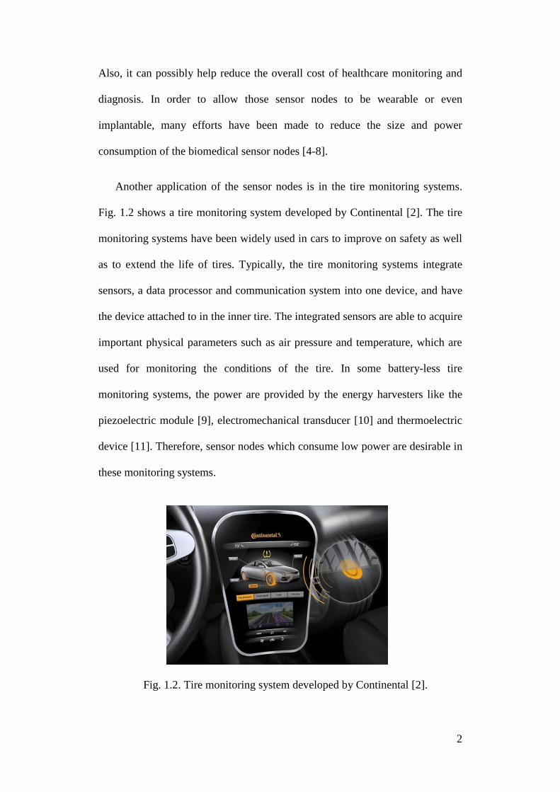
Another application of the sensor nodes is in the tire monitoring systems.
Fig. 1.2 shows a tire monitoring system developed by Continental [2]. The tire
monitoring systems have been widely used in cars to improve on safety as well
as to extend the life of tires. Typically, the tire monitoring systems integrate
sensors, a data processor and communication system into one device, and have
the device attached to in the inner tire. The integrated sensors are able to acquire
important physical parameters such as air pressure and temperature, which are
used for monitoring the conditions of the tire. In some battery-less tire
monitoring systems, the power are provided by the energy harvesters like the
piezoelectric module [9], electromechanical transducer [10] and thermoelectric
device [11]. Therefore, sensor nodes which consume low power are desirable in
these monitoring systems.
Fig. 1.2. Tire monitoring system developed by Continental [2].
3
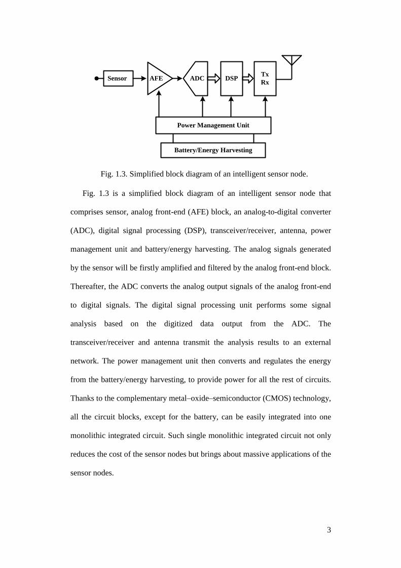
Fig. 1.3 is a simplified block diagram of an intelligent sensor node that
comprises sensor, analog front-end (AFE) block, an analog-to-digital converter
(ADC), digital signal processing (DSP), transceiver/receiver, antenna, power
management unit and battery/energy harvesting. The analog signals generated
by the sensor will be firstly amplified and filtered by the analog front-end block.
Thereafter, the ADC converts the analog output signals of the analog front-end
to digital signals. The digital signal processing unit performs some signal
analysis based on the digitized data output from the ADC. The
transceiver/receiver and antenna transmit the analysis results to an external
network. The power management unit then converts and regulates the energy
from the battery/energy harvesting, to provide power for all the rest of circuits.
Thanks to the complementary metal–oxide–semiconductor (CMOS) technology,
all the circuit blocks, except for the battery, can be easily integrated into one
monolithic integrated circuit. Such single monolithic integrated circuit not only
reduces the cost of the sensor nodes but brings about massive applications of the
sensor nodes.
Fig. 1.3. Simplified block diagram of an intelligent sensor node.
ADCTx
RxDSPAFESensor
Power Management Unit
Battery/Energy Harvesting

4
1.2 Motivation
As mentioned in Section 1.1 , the power consumption of the sensor nodes
should be low but ADC is one of its most power consuming building blocks. It
is therefore a major challenge to design a low power ADC for the sensor nodes,
especially for those powered by battery or energy harvesting, such as the
biomedical sensors and tire monitoring systems. The frequencies of those sensor
signals span from DC to a few kilohertz (Hz) [12, 13]. Besides, the normal
requirement of the ADC resolution is moderate, i.e., from 8 bits to 12 bits, for
these sensor nodes applications [7, 8, 13-21]. This thesis therefore focuses on
the design of low power ADCs with modest sampling frequency and accuracy.
The ADC architecture should be chosen based on the requirements as
discussed previously, which are low power consumption, moderate sampling
frequency and medium accuracy. Over the past few years, various ADC
architectures, such as the delta-sigma ADC, SAR ADC, pipeline ADC, folding
and interpolating ADC, and flash ADC, have been developed to minimize the
power consumption for different sampling frequencies and resolutions. Fig. 1.4
shows the region where common ADCs are most energy efficiency in both
bandwidth and resolution space [22]. Delta-sigma ADC consists of delta-sigma
modulator, digital filter and decimator. Delta-sigma modulator shifts
quantization noise to higher frequency domain, and low pass digital filter is
used to filter the shaped noise. Thanks to the noise shaping techniques, delta-
sigma ADC can realize extremely high resolution, typically more than 12 bits
[23]. Since delta-sigma ADCs operate at oversampling rate, it is normally used
to convert low frequency analog signals. The SAR ADC architecture is ideally

5
suited for moderate speed and medium resolution ADCs due to its simplicity
and highly digital nature. With proper calibration techniques, SAR ADC can
also achieve 16 bits [24]. Although pipeline ADCs can achieve high resolution,
one operational amplifier is required in each pipeline stage. Also, the
operational amplifier working in closed-loop must have wide bandwidth and
high gain. The pipeline ADCs are therefore relatively power hungry [25]. For
medium resolution and high sampling frequency applications, the folding and
interpolating ADCs can offer high energy efficient. This is because they are
based on nonlinear analog preprocessing where high linearity circuits are not
required. The flash ADCs with high speed and low resolution are typically used
for application such as radar detection, wide band radio receivers and flash
memory. As the number of comparator grows exponentially with its resolution,
flash ADC becomes unattractive for applications that require more than 8 bits
[25].
Fig. 1.4. Energy efficiency of various ADC architectures in the bandwidth-
resolution space.
Res
olu
tio
n (
bit
)
Sampling Frequency (Hz)
2
4
6
8
10
12
14
16
10k 100k 1M 10M 100M 1G 10G
Delta-Sigma ADC
SAR ADCPipeline ADC
Folding &
Interpolating
ADC
Flash
ADC
6
As discussed above, SAR ADC is the most attractive architecture for the
targeted application, which is the sensor nodes application. This thesis will
describe several novel SAR ADC designs, both on circuit and at the system
level, to achieve high energy efficiency.
1.3 Contribution
This thesis focuses on low power SAR ADC designs for sensor nodes
applications. Literature has shown that SAR ADC has higher energy efficiency
than other ADC architectures for moderate speed and medium resolution
applications. By exploring novel designs to minimize power consumption, a
number of contributions have been achieved:
A non-binary redundant SAR ADC operating at ultra-low supply voltage,
i.e., 0.5 V, is proposed. In order to improve the linearity of sampling circuit
at 0.5 V supply voltage, a clock boosting circuit with gate signal swinging
from 0 to 1 V is designed.
Adaptive delta-sampling ADC is designed to achieve high power
efficiency for sparse signals such as the neural spike. By sampling only the
incremental value of the input signal and adaptively adjusting the sampling
frequency, the proposed ADC can achieve the same resolution and
conversion range with less number of bits than the conventional ADC, and
thus the power consumption can be significantly reduced.
Reference-voltage regulator free SAR ADC is designed for wireless-
powered implantable medical devices. Assisted by a self-timed pre-charging

7
technique, the proposed SAR ADC eliminates the power-hungry reference-
voltage regulator and the area-consuming decoupling capacitor while
maintaining insensitivity to the supply voltage fluctuation. This SAR ADC
achieves higher FOM than other state-of-art designs in terms of system.
A wide-input range 12-bit SAR ADC with low power and fast
convergence digital background calibration is designed for sensor nodes
when battery voltage measurement is required. This SAR ADC is able to
convert input signal with a range of 9.6 Vpp, operating at 1.2 V supply
voltage. In order to sample such high input voltage, a high-voltage sampling
switch is proposed. Low power and fast convergence digital background
calibration is realized by omitting the calibration of 3 LSBs’ weights and
injecting different analog offset during calibration.
1.4 Organization
This thesis is organized as follows. Chapter 1 provides the background of
this research and presents an overview of various ADC architectures for
different sampling rates and resolutions applications, leading to the motivation
of this work. The contributions of this work are also listed.
Chapter 2 provides a literature review of the state-of-the-art low power SAR
ADCs both in circuit and at system levels. Besides, the calibration of capacitor
mismatch in SAR ADC is also reviewed.
Chapter 3 presents an ultra-low power SAR ADC designs. A 9-bit SAR
ADC design with non-binary generalized redundant algorithm, operating at 0.5
8
V supply voltage is described. Further to that, two sensor nodes using the
proposed SAR ADC as their analog to digital interface circuits are presented.
Chapter 4 presents an adaptive delta-sampling ADC that utilizes the
characteristics of the sparse signal. The characteristic of sparse signals including
EEG and neural spikes are analyzed. The measurement result verifying the
ADC’s conversion of pre-recorded neural signal is also given in Section 4.7 .
Chapter 5 presents a reference-voltage regulator-free SAR ADC with self-
timed pre-charging for wireless-powered implantable medical devices. The
effect of reference voltage fluctuation on SAR ADC is also evaluated.
Thereafter, a SAR ADC without the power-hungry reference-voltage regulator
and the area-consuming decoupling capacitor is proposed. The design is able to
remain insensitive to the supply voltage fluctuation.
Chapter 6 presents a wide input 12-bit SAR ADC with low power and fast
convergence digital background calibration. A high-voltage sampling switch is
then described. Simulation results are also provided to validate the proposed
low power and fast convergence digital background calibration.
Lastly in Chapter 7, the conclusions are drawn. Some future works on the
design of low power SAR ADC for sensing applications are then discussed.
Equation Chapter (Next) Section 1
9
Chapter 2
Background and Literature Review
As discussed in the previous chapter, SAR ADC is the most energy efficient
architecture for sensing application. This begins first by reviewing the
conventional SAR ADC. A brief discussion on several low power design
considerations in conventional SAR ADC is then given. Based on the
conventional SAR ADC, some energy efficient ADC architectures for sparse
signals acquisitions are described. These ADC architectures utilize some
characteristics of the input signals to reduce the power consumption. Following
which, some ADC designs look with focusses on optimizing the peripheral
circuits blocks that provide supply voltage and clock source to the ADC core
are described. In the last section, some calibration techniques for capacitor
mismatch in SAR ADC are detailed.
2.1 Conventional SAR ADC
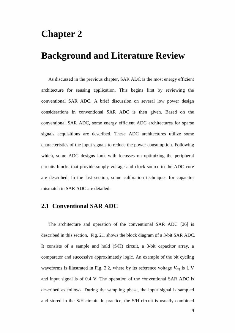
The architecture and operation of the conventional SAR ADC [26] is
described in this section. Fig. 2.1 shows the block diagram of a 3-bit SAR ADC.
It consists of a sample and hold (S/H) circuit, a 3-bit capacitor array, a
comparator and successive approximately logic. An example of the bit cycling
waveforms is illustrated in Fig. 2.2, where by its reference voltage Vref is 1 V
and input signal is of 0.4 V. The operation of the conventional SAR ADC is
described as follows. During the sampling phase, the input signal is sampled
and stored in the S/H circuit. In practice, the S/H circuit is usually combined
10
with a capacitor array through sampling the input signal into the capacitor array.
During the bit cycling period, the digital output bits are determined serially
from MSB to LSB. In the first bit cycle, the MSB b2 is set to ‘1’, while b1 and
b0 are both set to ‘0’. Thus, the MSB capacitor and the rest of the capacitors are
connected to Vref and ground. Consequently, the voltage of the capacitor array
VDAC is 0.5 V. Since VDAC is larger than the sampled and held voltage VSH, b2 is
returned and latched to ‘0’. After the first approximation, b1 and b0 are set to ‘1’
and ‘0’, respectively, generating VDAC = 0.25 V. Since VDAC is less than VSH, b1
Fig. 2.1. Block diagram of a 3-bit conventional SAR ADC.
2C0 4C0C0 C0
Vref
VSH
VDAC
Successive Approximation Logic
S/HInput
011
Fig. 2.2. Waveforms of VDAC and VSH during the bit cycling period.
VSH
VDAC
0
0.25
0.5
0.75
1
Volt
age
(V)
Timeb2=0 b1=1 b0=1
11
is latched to ‘1’. The approximation process is continued in this way until all
bits are determined. The final output code is b2b1b0 = 011.
2.2 Ultra-Low Power Design Considerations in Typical
SAR ADC
The power dissipation of conventional SAR ADC mainly includes the
power consumed by successive approximation logic, capacitor switching, and
the comparator. Therefore, the ADC power consumption benefits from the
scaling down of the operating voltage and by adopting an energy efficient
capacitor switching method.
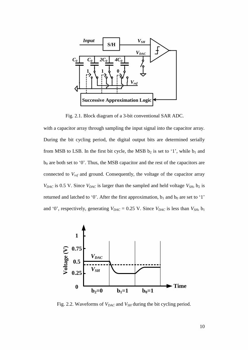
2.2.1 Clock Boosting
In the ideal sampling circuit, the on-resistance is zero and off-resistance is
infinite, respectively. However, for the single MOS transistor switch, the on-
resistance, given by Equation (2.1) depends on the gate-to-channel voltage VGS
minus the threshold voltage Vth, with a transistor size ratio W/L.
Fig. 2.3. (a) CMOS transmission gate. (b) Model for effective resistance of a
transmission gate.
Input OutputPMOS
NMOS
VDD
RONp
RONn
Input Output
(a) (b)
12
1= DS
ON
DSox GS th
VR
WIC V V
L
(2.1)
Also, the single NMOS and PMOS switch is conductive only when input
voltage is larger than a threshold voltage below the gate voltage and larger than
a threshold above the ground, respectively. In sampling circuit, the transmission
gate whose effective resistance is ||ONn ONpR R , combination of NMOS and PMOS,
is commonly used to compensate the weaknesses of NMOS and PMOS (see Fig.
Fig. 2.4. On-resistance of transmission gate for input range from 0 to VDD
for VDD from 0.5 V to 0.8 V.
0.0 0.2 0.4 0.6 0.8 1.00
5
10
15
20
25
On
Res
ista
nce
(M
)
Normalized Vin/VDD
VDD=0.5 V
VDD=0.6 V
VDD=0.8 V
Fig. 2.5. Voltage boosting circuit.
M1M2
M3
Cap
VDD
Sample Sample_b
n1
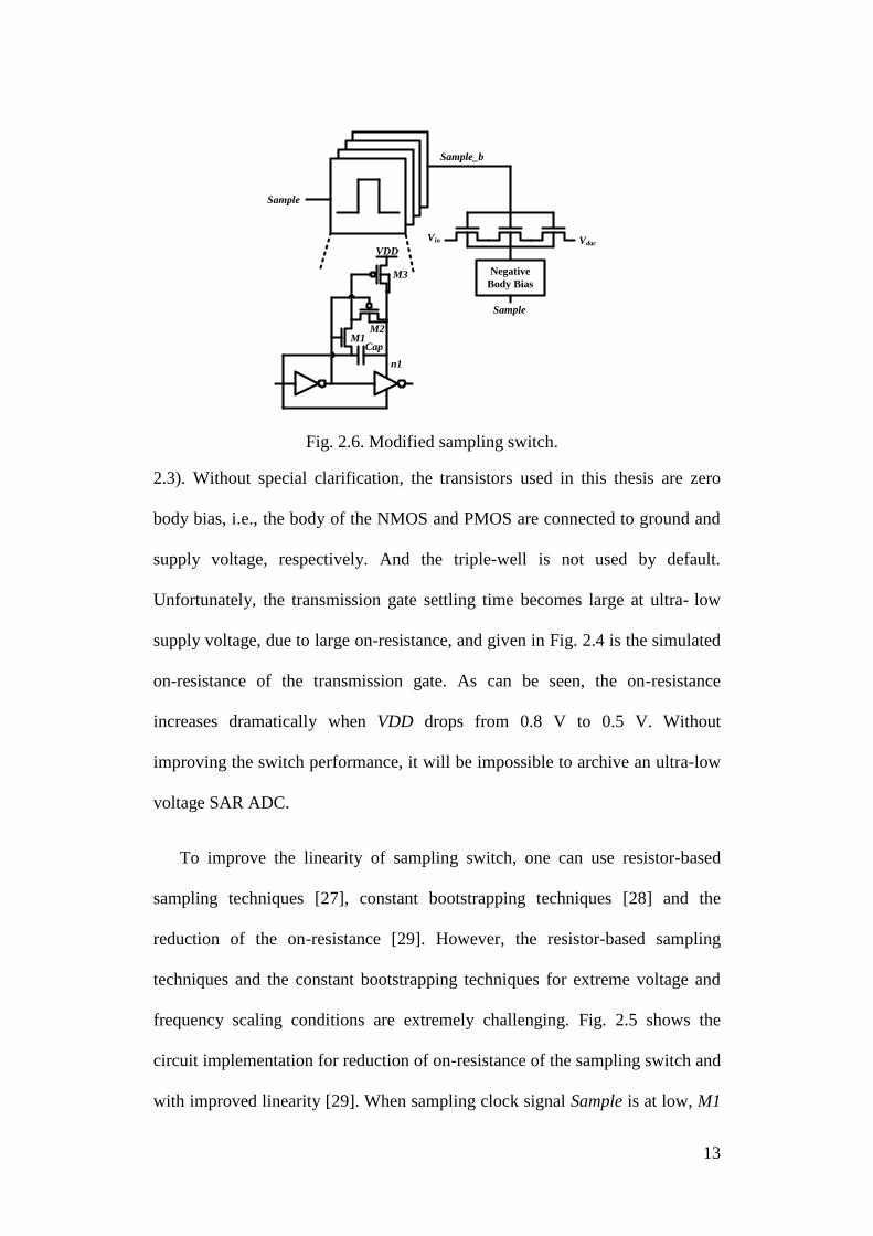
13
2.3). Without special clarification, the transistors used in this thesis are zero
body bias, i.e., the body of the NMOS and PMOS are connected to ground and
supply voltage, respectively. And the triple-well is not used by default.
Unfortunately, the transmission gate settling time becomes large at ultra- low
supply voltage, due to large on-resistance, and given in Fig. 2.4 is the simulated
on-resistance of the transmission gate. As can be seen, the on-resistance
increases dramatically when VDD drops from 0.8 V to 0.5 V. Without
improving the switch performance, it will be impossible to archive an ultra-low
voltage SAR ADC.
To improve the linearity of sampling switch, one can use resistor-based
sampling techniques [27], constant bootstrapping techniques [28] and the
reduction of the on-resistance [29]. However, the resistor-based sampling
techniques and the constant bootstrapping techniques for extreme voltage and
frequency scaling conditions are extremely challenging. Fig. 2.5 shows the
circuit implementation for reduction of on-resistance of the sampling switch and
with improved linearity [29]. When sampling clock signal Sample is at low, M1
Fig. 2.6. Modified sampling switch.
Negative
Body Bias
VDD
Sample_b
Sample
Sample
Vin Vdac
M1M2
M3
Cap
n1
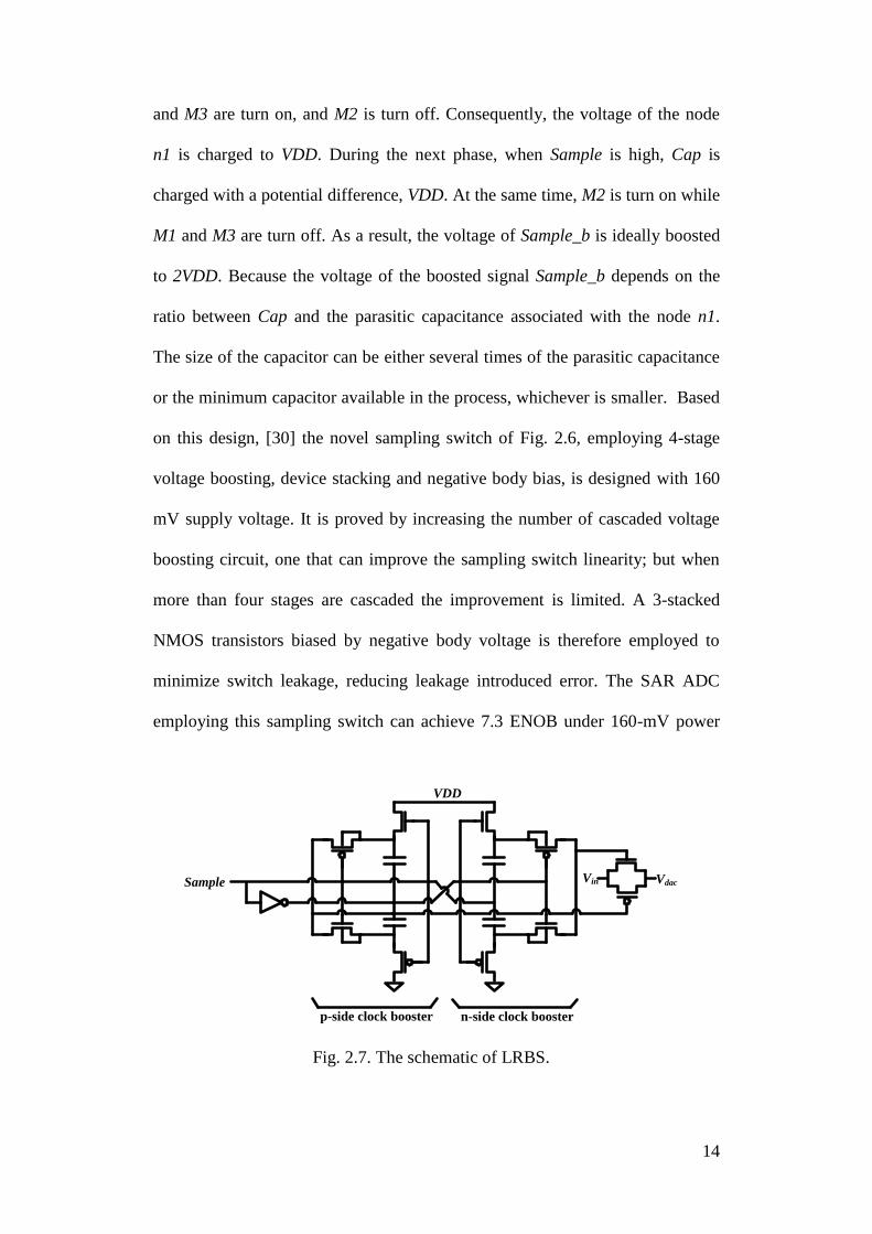
14
and M3 are turn on, and M2 is turn off. Consequently, the voltage of the node
n1 is charged to VDD. During the next phase, when Sample is high, Cap is
charged with a potential difference, VDD. At the same time, M2 is turn on while
M1 and M3 are turn off. As a result, the voltage of Sample_b is ideally boosted
to 2VDD. Because the voltage of the boosted signal Sample_b depends on the
ratio between Cap and the parasitic capacitance associated with the node n1.
The size of the capacitor can be either several times of the parasitic capacitance
or the minimum capacitor available in the process, whichever is smaller. Based
on this design, [30] the novel sampling switch of Fig. 2.6, employing 4-stage
voltage boosting, device stacking and negative body bias, is designed with 160
mV supply voltage. It is proved by increasing the number of cascaded voltage
boosting circuit, one that can improve the sampling switch linearity; but when
more than four stages are cascaded the improvement is limited. A 3-stacked
NMOS transistors biased by negative body voltage is therefore employed to
minimize switch leakage, reducing leakage introduced error. The SAR ADC
employing this sampling switch can achieve 7.3 ENOB under 160-mV power
Fig. 2.7. The schematic of LRBS.
Vin Vdac
VDD
Sample
p-side clock booster n-side clock booster
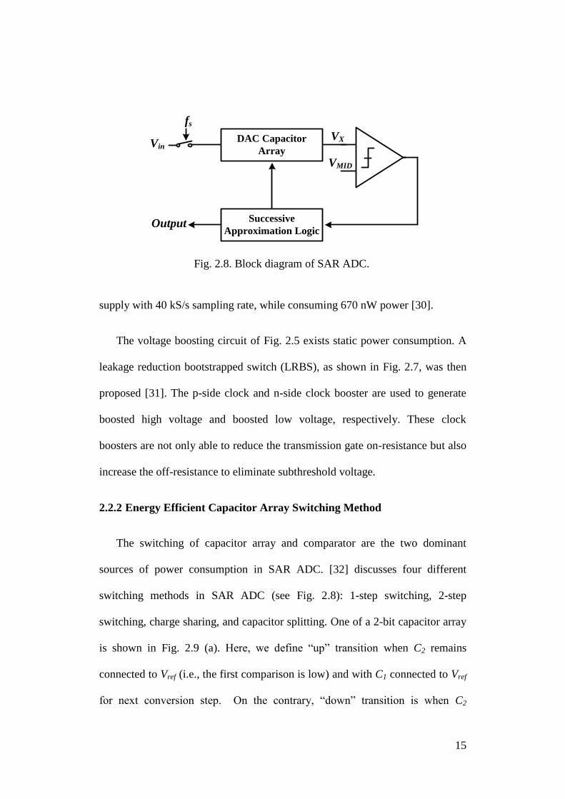
15
supply with 40 kS/s sampling rate, while consuming 670 nW power [30].
The voltage boosting circuit of Fig. 2.5 exists static power consumption. A
leakage reduction bootstrapped switch (LRBS), as shown in Fig. 2.7, was then
proposed [31]. The p-side clock and n-side clock booster are used to generate
boosted high voltage and boosted low voltage, respectively. These clock
boosters are not only able to reduce the transmission gate on-resistance but also
increase the off-resistance to eliminate subthreshold voltage.
2.2.2 Energy Efficient Capacitor Array Switching Method
The switching of capacitor array and comparator are the two dominant
sources of power consumption in SAR ADC. [32] discusses four different
switching methods in SAR ADC (see Fig. 2.8): 1-step switching, 2-step
switching, charge sharing, and capacitor splitting. One of a 2-bit capacitor array
is shown in Fig. 2.9 (a). Here, we define “up” transition when C2 remains
connected to Vref (i.e., the first comparison is low) and with C1 connected to Vref
for next conversion step. On the contrary, “down” transition is when C2
Fig. 2.8. Block diagram of SAR ADC.
Successive
Approximation Logic
DAC Capacitor
ArrayVin
Output
VX
VMID
fs
16
returned to ground (i.e., the first comparison is high) and C1 connected to Vref
for next conversion step. During each conversion step, either the “up” or “down”
transition occurs. All four switching methods behave identical during the “up”
transition and consume the same energy, which can be express as:
2 2
2
0 0 0
3 54 4
2 4 2 4
ref ref
up ref ref
V VE C C V C V
(2.2)
But they differ for the “down” transition and so does energy efficiency. Fig. 2.9
(a) shows a 2-bit capacitor array for the 1-step and 2-step switching methods.
While (b) and (c) indicate “down” transition energy calculation models for the
1-step and 2-step switching methods, respectively. In 1 step switching method,
the energy drawn from Vref is E1-2,1 step , where
Fig. 2.9. (a) 2-bit capacitor array for 1-step and 2-step switching methods.
(b) “Down” transition for 1-step switching. (c) “Down” transition for 2 step
switching method.
VMID
S2+
S2-
fs S1+
S1-
fs S0+
S0-
fs
VX
VREF
VIN
C2=2C0 C1=C0 C0
(a)
C2
C1 C0
VREF
Time1
VX
C1
C2 C0
VREF
Time2
VX
C2
C1 C0
VREF
Time1
VX
C0
C2 C1
VREF
Time1.5
VX
C1
C2 C0
VREF
Time2
VX
(b) (c)

17
1
1
(2 )2 2 2
11 2,1 1
( )
1 1
0
0
(2 ) ( ) ( 1)
2 1
4
c
c
Q TT T T
Cstep ref ref ref ref ref ref C
T T T Q T
ref c c
ref X ref X
ref
ref MID IN ref MI
dQE i t V dt V i t dt V dt V dQ
dt
V Q T Q T T is capacitor settling time and assumed as
V C V V V
VV C V V V V
2
0
2
5
4
ref
D IN
ref
VV
C V
(2.3)
For the 2-step switching method, the energy drawn from Vref be E1-1.5,2 step
from Time1 to Time1.5, and E1.5-2,2 step from Time1.5 to Time2.
1 1.5,2 2 2 1 1
0 0
0
0
1.5 1 + 1.5 1
= 2 1.5 1 1.5 1
3= 2
4 2
3
4
step ref C C C C
ref X ref X ref X ref X
ref ref
ref MID IN ref MID IN ref
ref ref
ref MID IN ref MID IN
E V Q Q Q Q
V C V V V V C V V V
V VV C V V V V V V
V VV C V V V V V
2
0
2
1=
4refC V
(2.4)
Thus, the total switching energy of 2 step switching method is:
1 2,2 1 1.5,2 1.5 2,2
2 2
0 0
2
0
1 1
4 2
3
4
step step step
ref ref
ref
E E E
C V C V
C V
(2.5)

18
The switching energy of 2-step is less than 1-step switching method. This is
because some of the charges from the largest capacitor are used to charge up the
second capacitor [32]. Charge sharing is an extension of this energy saving
method, as depicted in Fig. 2.10. During the first switching phase, C2 and C1 are
disconnected from both Vref and ground. Instead, these two capacitors are
connected each other through switch SCS. According to charge retribution, the
node voltage VC at Time1.5 is:
2
1.53
C refV V (2.6)
From Time1 to Time1.5, no energy is drawn from Vref; but C1 voltage is
charge to VC(1.5). In the second switching phase, C2 and C1 are connected to
Fig. 2.10. (a) 2-bit capacitor array. (b) “Down” transition for charge sharing
switching method.
VMID
S2+
S2-
fs S1+
S1-
fs S0+
S0-
fs
VX
VREF
VIN
C2=2C0 C1=C0 C0
(a)
SCS
C2
C1 C0
VREF
Time1
VX
C0
C2 C1
VC
Time1.5
VX
C1
C2 C0
VREF
Time2
VX
(b)
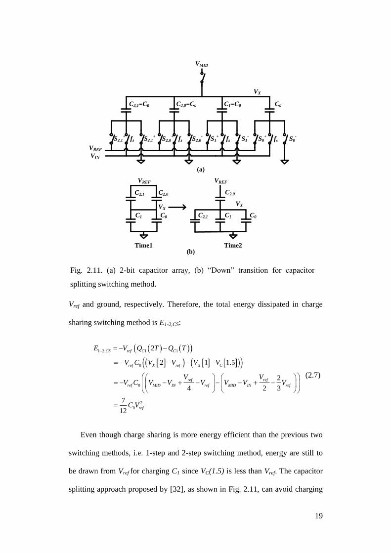
19
Vref and ground, respectively. Therefore, the total energy dissipated in charge
sharing switching method is E1-2,CS:
1 2, 1 1
0
0
2
0
2
2 1 1.5
2
4 2 3
7
12
CS ref C C
ref X ref X C
ref ref
ref MID IN ref MID IN ref
ref
E V Q T Q T
V C V V V V
V VV C V V V V V V
C V
(2.7)
Even though charge sharing is more energy efficient than the previous two
switching methods, i.e. 1-step and 2-step switching method, energy are still to
be drawn from Vref for charging C1 since VC(1.5) is less than Vref. The capacitor
splitting approach proposed by [32], as shown in Fig. 2.11, can avoid charging
Fig. 2.11. (a) 2-bit capacitor array, (b) “Down” transition for capacitor
splitting switching method.
C2,0
C1 C0
VREF
Time1
VX
C1 C0
VREF
Time2
VX
(b)
C2,1
C2,1
C2,0
VMID
S2,0-
S1+
S1-
fs S0+
S0-
fs
VX
VREF
VIN
C2,0=C0 C1=C0 C0
(a)
S2,0+
fsS2,1+
fs S2,1+
C2,1=C0
20
of any capacitor to Vref in the “down” transition. The MSB capacitor C2 is split
into two capacitors, C2.1, C2.2. During “up” transition, both C2.1 and C2.2 are
connected to Vref. But during “down” transition, instead of connecting C1 to Vref,
C2.1is simply connected directly to ground. Therefore, the energy dissipated in
“down” transition is E1-2,split:
1 2, 1 1
0
0
2
0
2
2 1
4 2
1
4
split ref C C
ref X ref X ref
ref ref
ref MID IN ref MID IN ref
ref
E V Q T Q T
V C V V V V
V VV C V V V V V V
C V
(2.8)
The capacitor splitting method dissipates only one fifth of energy for the
conventional 1-step switching method during “down” transition. In terms of
overall switching energy, the capacitor splitting consumes the least energy
among the previously discussed switching approaches, saving 37% of energy
compared to the conventional 1-step switching method [32].
Table 2.1 summarizes the power consumption and the number of switches
required in the four capacitor switching methods for a 2-bit SAR ADC as
Table 2.1 Switching Method Comparison
Method Energy consumed
by“up” transition
Energy consumed
by“down” transition
Number of
switches
1 step 2
05
4 refC V
2
05
4 refC V
3
2 step 2
05
4 refC V
2
03
4 refC V
3
Charge sharing 2
05
4 refC V
2
07
12 refC V
4
Splitting 2
05
4 refC V
2
01
4 refC V 4
21
described above. It can be seen that the split switching method is the most
energy efficient switching method.
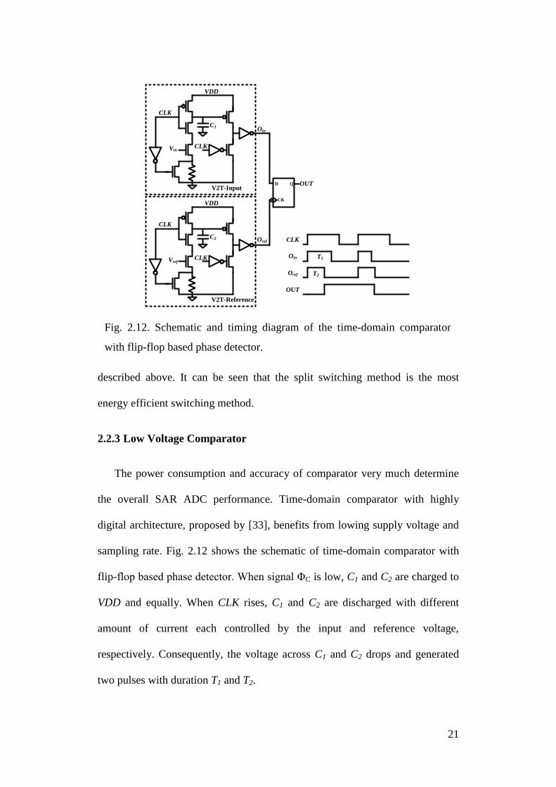
2.2.3 Low Voltage Comparator
The power consumption and accuracy of comparator very much determine
the overall SAR ADC performance. Time-domain comparator with highly
digital architecture, proposed by [33], benefits from lowing supply voltage and
sampling rate. Fig. 2.12 shows the schematic of time-domain comparator with
flip-flop based phase detector. When signal ΦC is low, C1 and C2 are charged to
VDD and equally. When CLK rises, C1 and C2 are discharged with different
amount of current each controlled by the input and reference voltage,
respectively. Consequently, the voltage across C1 and C2 drops and generated
two pulses with duration T1 and T2.
Fig. 2.12. Schematic and timing diagram of the time-domain comparator
with flip-flop based phase detector.
D Q
CK
VDD
Vin
CLK
CLK
C1
V2T-Input
VDD
Vref
CLK
CLK
C2
V2T-Reference
Oref
Oin
OUT
CLK
Oin
Oref
OUT
T1
T2
22
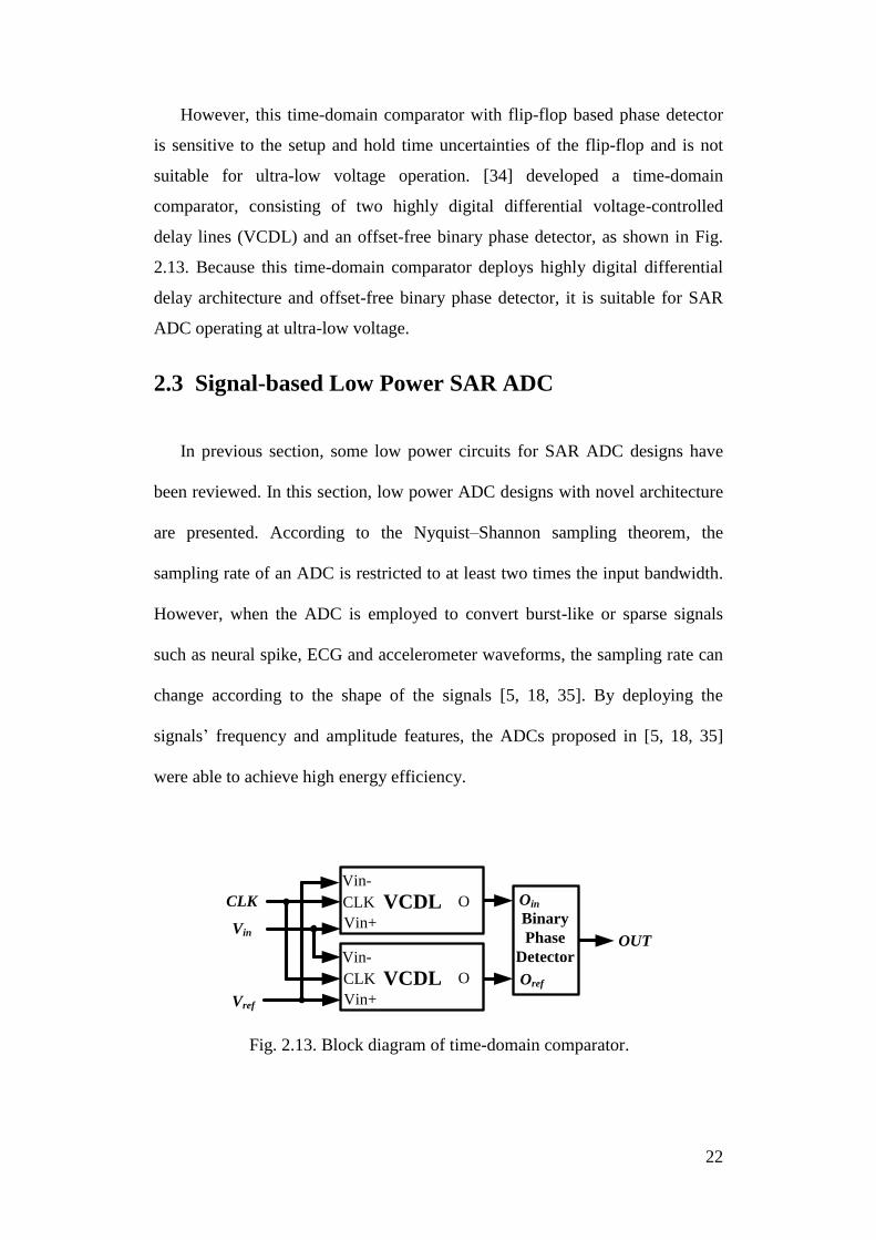
However, this time-domain comparator with flip-flop based phase detector
is sensitive to the setup and hold time uncertainties of the flip-flop and is not
suitable for ultra-low voltage operation. [34] developed a time-domain
comparator, consisting of two highly digital differential voltage-controlled
delay lines (VCDL) and an offset-free binary phase detector, as shown in Fig.
2.13. Because this time-domain comparator deploys highly digital differential
delay architecture and offset-free binary phase detector, it is suitable for SAR
ADC operating at ultra-low voltage.
2.3 Signal-based Low Power SAR ADC
In previous section, some low power circuits for SAR ADC designs have
been reviewed. In this section, low power ADC designs with novel architecture
are presented. According to the Nyquist–Shannon sampling theorem, the
sampling rate of an ADC is restricted to at least two times the input bandwidth.
However, when the ADC is employed to convert burst-like or sparse signals
such as neural spike, ECG and accelerometer waveforms, the sampling rate can
change according to the shape of the signals [5, 18, 35]. By deploying the
signals’ frequency and amplitude features, the ADCs proposed in [5, 18, 35]
were able to achieve high energy efficiency.
Fig. 2.13. Block diagram of time-domain comparator.
Vref
CLK
Vin
Vin-
Vin+
CLK OVCDL
Vin-
Vin+
CLK OVCDL
OUT
Binary
Phase
Detector
Oref
Oin
23
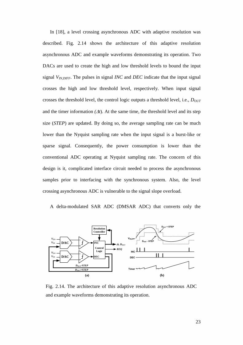
In [18], a level crossing asynchronous ADC with adaptive resolution was
described. Fig. 2.14 shows the architecture of this adaptive resolution
asynchronous ADC and example waveforms demonstrating its operation. Two
DACs are used to create the high and low threshold levels to bound the input
signal VIN,DIFF. The pulses in signal INC and DEC indicate that the input signal
crosses the high and low threshold level, respectively. When input signal
crosses the threshold level, the control logic outputs a threshold level, i.e., DOUT
and the timer information (t). At the same time, the threshold level and its step
size (STEP) are updated. By doing so, the average sampling rate can be much
lower than the Nyquist sampling rate when the input signal is a burst-like or
sparse signal. Consequently, the power consumption is lower than the
conventional ADC operating at Nyquist sampling rate. The concern of this
design is it, complicated interface circuit needed to process the asynchronous
samples prior to interfacing with the synchronous system. Also, the level
crossing asynchronous ADC is vulnerable to the signal slope overload.
A delta-modulated SAR ADC (DMSAR ADC) that converts only the
Fig. 2.14. The architecture of this adaptive resolution asynchronous ADC
and example waveforms demonstrating its operation.
(a)
INC
DEC
Control
Logic
DACVIN-
VIN+
DACVIN-
VIN+
Resolution
Controller
REQ
t, DOUT
DOUT-STEP
DOUT+STEP
(b)
24
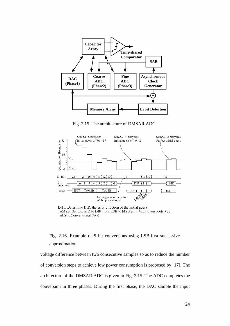
voltage difference between two consecutive samples so as to reduce the number
of conversion steps to achieve low power consumption is proposed by [17]. The
architecture of the DMSAR ADC is given in Fig. 2.15. The ADC completes the
conversion in three phases. During the first phase, the DAC sample the input
Fig. 2.15. The architecture of DMSAR ADC.
Fig. 2.16. Example of 5 bit conversions using LSB-first successive
approximation.
Capacitor
Array
Asynchronous
Clock
Generator
Fine
ADC
(Phase3)
Coarse
ADC
(Phase2)
DAC
(Phase1)
Level DetectionMemory Array
+
SAR
Time-shared
Comparator

25
signal and the previous sample stored in the memory. Also, the DAC generates
a voltage difference between these consecutive samples. Then, the coarse ADC
decides the range of this generated voltage difference. The LSBs are determined
during the third phase. Even though the conversion step is reduced, the circuit
needs to ensure oversampling at all time, which makes it not energy-efficient.
A LSB-first SAR ADC that made use of its previous sample as an initial
guess for its current sample is proposed in [35, 36]. Fig. 2.16 shows an example
of a 5-bit conversion using LSB-first successive approximation algorithm. The
conversion completes in three phases, i.e., INIT, ToMSB and ToLSB. In the
INIT phase, the previous sample is set as the initial guess. DIR is the error
direction of the initial guess, indicating the initial guess is larger or smaller than
the current sample, i.e., VIN. During the ToMSB phase, VDAC is moved to
approximate VIN until VDAC overshoots the target value VIN. The DAC step size
is set from LSB to MSB, which is inverted in conventional successive
approximation algorithm. In the ToLSB phase, the algorithm performs the same
bitcycling proceeds as in conventional successive approximation algorithm. The
bitcycles of the LSB-first successive approximation algorithm is from 2
Code Change Per Sample
Bit
cycl
es P
er S
am
ple
Fig. 2.17. Bitcycles per sample as a function of code charge per sample for a
10-bit LSB-first SAR ADC.
26
bitcycles to 2N+1 bitcycles for an N-bit SAR ADC. Fig. 2.17 indicates the
bitcycles required for each complete conversion as a function of code change
per sample. It can be seen that if the code change per sample is larger than 32,
the LSB-first SAR ADC will require more conversion steps than the
conventional SAR ADC.
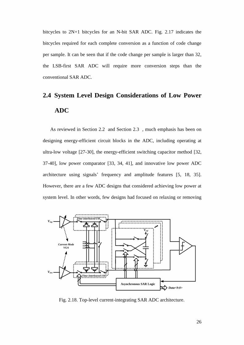
2.4 System Level Design Considerations of Low Power
ADC
As reviewed in Section 2.2 and Section 2.3 , much emphasis has been on
designing energy-efficient circuit blocks in the ADC, including operating at
ultra-low voltage [27-30], the energy-efficient switching capacitor method [32,
37-40], low power comparator [33, 34, 41], and innovative low power ADC
architecture using signals’ frequency and amplitude features [5, 18, 35].
However, there are a few ADC designs that considered achieving low power at
system level. In other words, few designs had focused on relaxing or removing
Fig. 2.18. Top-level current-integrating SAR ADC architecture.
Vinp
Vinn
Asynchronous SAR Logic
Data<9:0>
Current-Mode
VGA
Vref
Time-interleaved I/H
Time-interleaved I/H

27
the blocks that provide inputs to the ADC, i.e., the input signal [42], voltage
reference [43] and clock source [44].
In [42], a current-integrating SAR ADC was described to save on power
consumption for the circuits that provide input signal to the ADC. A power
efficient variable-gain transconductor is used to replace the power hungry input
voltage buffer in a charge-sharing SAR ADC to improve the overall power
efficiency. The top architecture of the ADC with variable gain amplifier (VGA)
is depicted in Fig. 2.18. The current-mode VGA converts input voltage to
current and this current is converted to a charge on the MOS capacitors by the
time-interleaved integrate-and-hold (I/H). Then, the MOS capacitors perform a
voltage passive amplification by switching the capacitor from inversion to
depletion mode, which relaxes the comparator noise requirement. After that, the
Fig. 2.19. ADC with integrated reference, circuit diagram of the RVG and
architecture of the 10-bit SAR ADC.
10-bit
SAR ADC LDORVG
Vref = 0.4V Vref = 0.4VDuty-Cycle
Block
VDDDAC =VDDDIG = 0.6V
VDD = 0.8V
Duty-Cycle CLK1
Duty-Cycle CLK2
Off-Chip
Capacitor
CLK1 CLK1 CLK1 CLK1
OPA
CLK1CLK1
Vref
VDD
Asynchronous
SAR Logic
DAC
Clock Boosting
Vinp
Vinn
fs
28
ADC performs quantization as that of the charging-sharing SAR ADC [45].
[43, 46] proposed a SAR ADC with integrated reference voltage generator
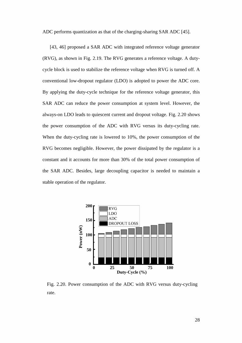
(RVG), as shown in Fig. 2.19. The RVG generates a reference voltage. A duty-
cycle block is used to stabilize the reference voltage when RVG is turned off. A
conventional low-dropout regulator (LDO) is adopted to power the ADC core.
By applying the duty-cycle technique for the reference voltage generator, this
SAR ADC can reduce the power consumption at system level. However, the
always-on LDO leads to quiescent current and dropout voltage. Fig. 2.20 shows
the power consumption of the ADC with RVG versus its duty-cycling rate.
When the duty-cycling rate is lowered to 10%, the power consumption of the
RVG becomes negligible. However, the power dissipated by the regulator is a
constant and it accounts for more than 30% of the total power consumption of
the SAR ADC. Besides, large decoupling capacitor is needed to maintain a
stable operation of the regulator.
Fig. 2.20. Power consumption of the ADC with RVG versus duty-cycling
rate.
0 25 50 75 100Duty-Cycle (%)
200
150
100
50
Po
wer
(n
W)
0
29
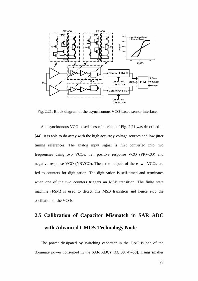
An asynchronous VCO-based sensor interface of Fig. 2.21 was described in
[44]. It is able to do away with the high accuracy voltage sources and low jitter
timing references. The analog input signal is first converted into two
frequencies using two VCOs, i.e., positive response VCO (PRVCO) and
negative response VCO (NRVCO). Then, the outputs of these two VCOs are
fed to counters for digitization. The digitization is self-timed and terminates
when one of the two counters triggers an MSB transition. The finite state
machine (FSM) is used to detect this MSB transition and hence stop the
oscillation of the VCOs.
2.5 Calibration of Capacitor Mismatch in SAR ADC
with Advanced CMOS Technology Node
The power dissipated by switching capacitor in the DAC is one of the
dominate power consumed in the SAR ADCs [33, 39, 47-53]. Using smaller
Fig. 2.21. Block diagram of the asynchronous VCO-based sensor interface.
Counter2<14:0>
Counter1<14:0>
Done_b RES<13:0>
OFF1<13:0>
RES<13:0>
OFF2<13:0>
FSMStart
Done
Winner
Output
A YVin
VDD
NRVCO
A YVin
VDD
PRVCO
Ou
tpu
t
Vin (V)
Vin
30
unit capacitor, the power consumption of the switching capacitor can be reduced.
However, small unit capacitor suffers from capacitor mismatch in modern
CMOS technology. The capacitor mismatch limits the accuracy of the SAR
ADC, especially for high resolution ADCs. Several works that address the issue
of the capacitor mismatch in the SAR ADC had been reported [48, 50, 52, 54-
59].
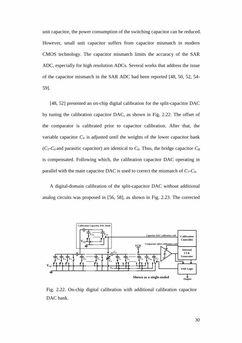
[48, 52] presented an on-chip digital calibration for the split-capacitor DAC
by tuning the calibration capacitor DAC, as shown in Fig. 2.22. The offset of
the comparator is calibrated prior to capacitor calibration. After that, the
variable capacitor CV is adjusted until the weights of the lower capacitor bank
(C5-C0 and parasitic capacitor) are identical to C6. Thus, the bridge capacitor CB
is compensated. Following which, the calibration capacitor DAC operating in
parallel with the main capacitor DAC is used to correct the mismatch of C7-C9.
A digital-domain calibration of the split-capacitor DAC without additional
analog circuits was proposed in [56, 58], as shown in Fig. 2.23. The corrected
Fig. 2.22. On-chip digital calibration with additional calibration capacitor
DAC bank.
Calibration
Controller
Internal
CLK
Generator
SAR Logic
CLCHC9C6Cx
CB
Vin
CV
C5C2C1C0C0
Vref
CC0CC4
Vref
VCM
Capacitor DAC calibration code
Comparator offset calibration code
OutputShown as a single-ended
Calibration Capacitor DAC Bank

31
digital output code DOUT can expressed as:
10 10
0 0
12
2
i
OUT i P.i N .i i
i i
D D D D D
(2.9)
where Di is the raw code of the ADC, and both DεP.i and DεN.i are the error
codes. During the estimation of DεP.i and DεN,i, the lower capacitors are
assumed to have no mismatch (i.e., DεP.4 =…= DεP.0 = 0, DεN.4 =…= DεN.0 = 0).
Take DεP.10 of the MSB capacitor DACP as an example of the error code
estimation. First, the residual voltage is generated by the same switching
scheme as that in the self-calibration technique [60, 61]. Then, the analog error
voltage is digitalized by the LSB bank of the DACN. Thus, the digital error code
DεP.10 can be expressed as:
4
10
1 12
2 2P.D LSB _bank _ code
(2.10)
Fig. 2.23. Digital-domain calibration of split-capacitor DAC without
additional analog circuits.
Capacitor DACP
Capacitor DACN
Conversion
SAR
Digital-domain
error correction
Comparator
calibration
FSM
DAC
error-code
estimation
FSM
Output
Vinp
Vinn
32
This procedure is repeated for DεP.9 __
DεP.5 in DACP branch and DεN.9 __
DεN.5 in DACN branch, where all the error codes are stored in the memory. The
final output code is calculated based on Equation (2.9) with the corresponding
raw codes and the error codes.
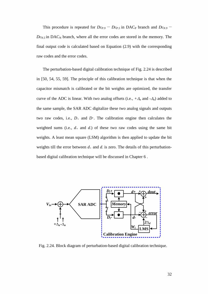
The perturbation-based digital calibration technique of Fig. 2.24 is described
in [50, 54, 55, 59]. The principle of this calibration technique is that when the
capacitor mismatch is calibrated or the bit weights are optimized, the transfer
curve of the ADC is linear. With two analog offsets (i.e., +a and -a) added to
the same sample, the SAR ADC digitalize these two analog signals and outputs
two raw codes, i.e., D+ and D_. The calibration engine then calculates the
weighted sums (i.e., d+ and d-) of these two raw codes using the same bit
weights. A least mean square (LSM) algorithm is then applied to update the bit
weights till the error between d+ and d- is zero. The details of this perturbation-
based digital calibration technique will be discussed in Chapter 6 .
Fig. 2.24. Block diagram of perturbation-based digital calibration technique.
SAR ADCVin
+∆a -∆a
LMSWi
+
+
Di+
Di-
d+
d-
2∆d
+_
_error
dout
Memory
Calibration Engine

33
2.6 Conclusion
This chapter presents the background and literature review of SAR ADC.
Several low power design considerations in conventional SAR ADC, including
operating at ultra-low voltage, energy efficient switching method and low
power comparator, have been discussed. Based on the conventional SAR ADC,
some energy efficient ADC architectures for sparse signals acquisitions are also
reviewed. These ADC architectures achieve low power consumption by
utilizing some characteristics of the input signals. Following which, some ADC
designs look with focusses on optimizing the peripheral circuits blocks that
provide supply voltage and clock source to the ADC core are presented. Also,
some calibration techniques for capacitor mismatch in high resolution SAR
ADC are reviewed.
Equation Chapter (Next) Section 1

34
Chapter 3
Ultra-Low Power SAR ADC Design
As mentioned in Section 2.2 , the power consumption of a SAR ADC
benefits from scaling down the operating voltage since most of its building
blocks are digital circuits. Also, several design considerations are discussed in
this chapter, including high linearity sampling switch, high energy efficient
capacitor switching method, and reliable comparator. This chapter presents an
ASIC design of an ultra-low power SAR ADC [62]. To achieve ultra-low power,
the proposed ADC operates at ultra-low voltage, deploying a single-ended
structure and top plate sampling technique. In order to improve the linearity of
the sampling circuit at ultra-low supply voltage, clock boosting circuit is
developed. A non-binary redundant algorithm is then applied to correct the
inevitable decision errors in the first few conversion steps. The proposed ADC
has been fabricated in a 0.18 μm CMOS process. From the measurement results,
it consumes only 16 nW and achieves a SNDR of 50.4 dB, which is equivalent
to an 8.08 ENOB, with 1 kS/s sampling rate at 0.5-V supply voltage. At the end
of this chapter, two sensor node processors deploying this proposed ultra-low
power SAR ADC are briefly described. One sensor node processor is a near-
threshold cognitive multi-functional ECG processor for long-term cardiac
monitoring, which consumes only 457 nW at 0.5 V for real-time ECG recording
and diagnosis. Another is a sensor node processor with diverse hardware
acceleration and cognitive sampling for intelligent sensing. It has been applied
to neural spike classification and vehicle speed detection.

35
3.1 Proposed SAR ADC Architecture
The proposed 9-bit SAR ADC architecture is presented in Fig. 3.1 . It
consists of clock boosting circuit, subtraction and addition capacitor array, a
time-domain comparator, switching logic and output latches, and some buffers.
To reduce power consumption and alleviate circuit complexity, the ADC
utilizes single-ended structure. The sampling method adopted in this design is
the top plate sampling technique, which is more power efficient than the bottom
sampling technique since it contains only one sampling switch. The sampling
switch connects the input signal to all capacitors’ top plate terminals during the
sampling phase, whereas the bottom sampling technique requires an array of
sampling switches to connect all the capacitors’ bottom plate to the input signal.
3.2 Proposed Clocking Boosting
As discussed in Section 2.2 static power consumption exists in the clock
boosting circuits designed both in [29] and [30]. We proposed a simplified
clock boosting circuit as depicted in Fig. 3.2. When sampling clock signal
Sample is at low, the boosted sampling clock signal Sample_b is at low and the
Fig. 3.1. Architecture of the proposed ultra-low power SAR ADC.
Subtraction Q<0:9>
Addition
CLK
Switching Logic
Vin
sampleAddition
Capacitor
Array
Subtraction
Capacitor
ArrayVcm
Vdac
Clock Boosting
Output
LatchesDONE
CMP
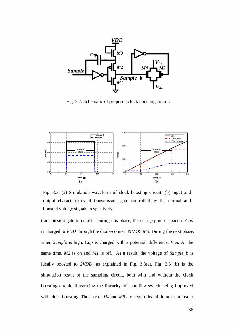
36
transmission gate turns off. During this phase, the charge pump capacitor Cap
is charged to VDD through the diode-connect NMOS M3. During the next phase,
when Sample is high, Cap is charged with a potential difference, VDD. At the
same time, M2 is on and M1 is off. As a result, the voltage of Sample_b is
ideally boosted to 2VDD, as explained in Fig. 3.3(a). Fig. 3.3 (b) is the
simulation result of the sampling circuit, both with and without the clock
boosting circuit, illustrating the linearity of sampling switch being improved
with clock boosting. The size of M4 and M5 are kept to its minimum, not just to
Fig. 3.2. Schematic of proposed clock boosting circuit.
Vin
Sample
Vdac
VDD
M1
M2
M3
M4 M5
Cap
Sample_b
Fig. 3.3. (a) Simulation waveform of clock boosting circuit; (b) Input and
output characteristics of transmission gate controlled by the normal and
boosted voltage signals, respectively.
0 50 100 150 200200
250
300
350
Vo
lta
ge
(V)
Time (s)
Vin
Vdac_boost
Vdac_normal
0 50 100 150 2000.0
0.3
0.6
0.9
1.2
Volt
age
(V)
Time (s)
Sample_b
Sample
Sampling
Phase
Sampling
Phase
(a) (b)
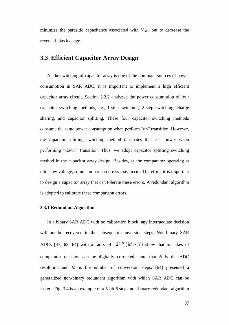
37
minimize the parasitic capacitance associated with Vadc, but to decrease the
reversed-bias leakage.
3.3 Efficient Capacitor Array Design
As the switching of capacitor array is one of the dominant sources of power
consumption in SAR ADC, it is important to implement a high efficient
capacitor array circuit. Section 2.2.2 analyzed the power consumption of four
capacitor switching methods, i.e., 1-step switching, 2-step switching, charge
sharing, and capacitor splitting. These four capacitor switching methods
consume the same power consumption when perform “up” transition. However,
the capacitor splitting switching method dissipates the least power when
performing “down” transition. Thus, we adopt capacitor splitting switching
method in the capacitor array design. Besides, as the comparator operating at
ultra-low voltage, some comparison errors may occur. Therefore, it is important
to design a capacitor array that can tolerate these errors. A redundant algorithm
is adopted to calibrate these comparison errors.
3.3.1 Redundant Algorithm
In a binary SAR ADC with no calibration block, any intermediate decision
will not be recovered in the subsequent conversion steps. Non-binary SAR
ADCs [47, 63, 64] with a radix of 2N M M N show that mistakes of
comparator decision can be digitally corrected; note that N is the ADC
resolution and M is the number of conversion steps. [64] presented a
generalized non-binary redundant algorithm with which SAR ADC can be
faster. Fig. 3.4 is an example of a 5-bit 6 steps non-binary redundant algorithm

38
that corrects decision errors. In this example, the value for addition or
subtraction in each step pi= {16, 7, 4, 2, 1, 1} where i = 1:6, and the input value
is 22.5. The red path shows that the decision error occurs in the second
conversion step but corrected in the subsequent steps. The value of output code
110111 and 111000 are both equal to 23, since 16+7-4+2+1+1=23 and 16+7+4-
2-1-1=23.
The conversion time of SAR ADC with generalized non-binary redundant
search algorithm can be less than that of the binary or conventional non-binary
search algorithm: if we assume that the capacitor array is a first-order system
with a time constant of τ, the settling time of each conversion step in a
generalized non-binary redundant SAR ADC can be expressed as follows:
Fig. 3.4. Correction of decision error using redundant algorithm.
No decision errors with
output code: 111000=23
Decision error occurs in second step
decision with output code: 110111=23
Input value=23.5
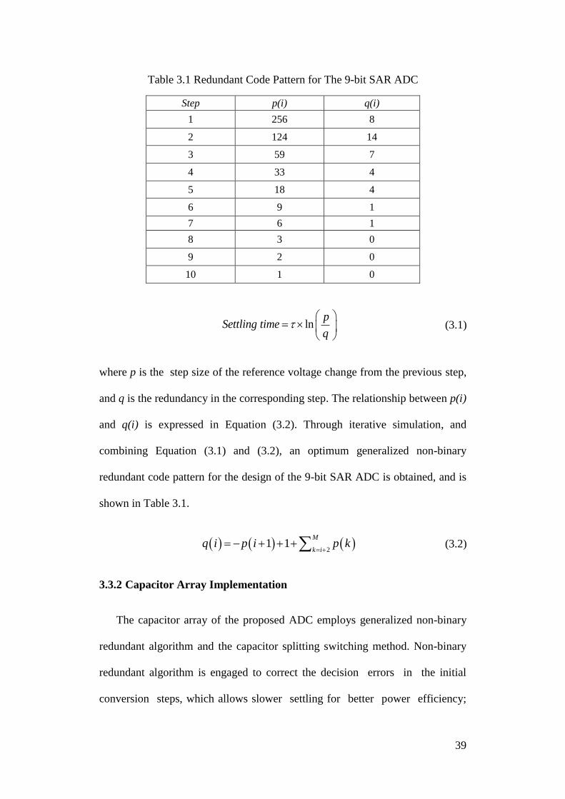
39
lnp
Settling timeq
(3.1)
where p is the step size of the reference voltage change from the previous step,
and q is the redundancy in the corresponding step. The relationship between p(i)
and q(i) is expressed in Equation (3.2). Through iterative simulation, and
combining Equation (3.1) and (3.2), an optimum generalized non-binary
redundant code pattern for the design of the 9-bit SAR ADC is obtained, and is
shown in Table 3.1.
2
1 1M
k iq i p i p k
(3.2)
3.3.2 Capacitor Array Implementation
The capacitor array of the proposed ADC employs generalized non-binary
redundant algorithm and the capacitor splitting switching method. Non-binary
redundant algorithm is engaged to correct the decision errors in the initial
conversion steps, which allows slower settling for better power efficiency;
Table 3.1 Redundant Code Pattern for The 9-bit SAR ADC
Step p(i) q(i)
1 256 8
2 124 14
3 59 7
4 33 4
5 18 4
6 9 1
7 6 1
8 3 0
9 2 0
10 1 0

40
but this is at the expense of additional redundant bit. A pair of capacitor
arrays (see Fig. 3.5) has been designed according to the redundant algorithm
code pattern in Table 3.1. The two split capacitor arrays are identical, to
perform addition and subtraction. The linearity error due to the capacitor
mismatching in the splitting capacitor DAC can be expressed as [65]:
-102
0
=2N
INL LSBC
(3.3)
-1
02
0
=2N
DNL LSBC
(3.4)
where σ0 is the standard deviation of the unit capacitor. In order to achieve 3-δ
capacitor matching at 9-bit level, the capacitor array uses 243 fF unit metal-
insulator-metal (MIM) capacitor. An attenuation capacitor is inserted in
between the MSB and LSB side of the array. Hence, the size of the MSB
capacitors can be reduced without having to change the effective capacitor
value. The attenuating capacitor Cc can be calculated as follows:
Fig. 3.5. Capacitor array of the proposed ADC.
2 3 6 91 1
VrefVdac
1 1.83 3.27 6.881.29
2 3 6 91 1 1 1.83 3.27 6.881.29
Attenuating Capacitor
Subtraction
Capacitor Array
Addition
Capacitor Array

41
0
_
0 0
1
1 1 2 3 6 91.29
18 1
c
MSB Least
LSB Side Subarray CapacitorsC C
C
C C
(3.5)
where C0 the is the unit capacitor and CMSB_Least is the smallest capacitor in the
MSB capacitor subarray before attenuation, which is 18 in this design. The total
capacitance value can be reduced from 511C0 to 35C0, and the area saving is
about 14 times.
3.4 Time-Domain Comparator Design
The power consumption and accuracy of comparator very much determine
the overall SAR ADC performance. In the ultra-low voltage SAR ADC design,
the voltage of 1LSB decreases as the supply voltage decreases. The
Fig. 3.6. Block diagram of the time-domain comparator, and the VCDL
chain.
Vref
CLK
Vin
Vin-
Vin+
CLK OVCDL
Vin-
Vin+
CLK OVCDL
OUTBinary
Phase
Detector
Oref
Oin
O
Vin+
CLK
Vin-
VDD
5 stage VCDL
M1
M2
M3
M4
M5
M6

42
conventional voltage-based comparator is not suitable for ultra-low supply
voltage in terms of power consumption and bandwidth. Time-domain
comparator with highly digital architecture, benefits from lowing supply voltage
and sampling rate [33, 34]. As mentioned in Section 2.2.3, time-domain
comparator with flip-flop based phase detector is not suitable for ultra-low
voltage operation. Because it is sensitive to the setup and hold time
uncertainties of the flip-flop. The time-domain comparator developed in [34]
can be used in SAR ADC operating at ultra-low voltage supply. Because it
deploys highly digital differential VCDL and offset-free binary phase detector.
The block diagram is reposted in chapter for convenience. Fig. 3.6 shows the
block diagram of the time-domain comparator and the VCDL chain. When CLK
is at active low, each stage output node of VCDL is discharged to ground.
During CLK rising to active high, the current-starving transistors provide
different currents due to unequal control voltages Vin+ and Vin-. Therefore, the
CLK propagation delay of these two differential VCDLs is different. This
different CLK delay is detected by the binary phase detector as indicated in Fig.
3.7. When IN1 and IN2 are both low, V1 and V2 are both locked to VDD. If the
rising edge of IN1 arrives earlier than IN2, then V1 is first discharged to ground,
resulting OUT set to high. If the rising edge of IN2 comes earlier than IN1, then
OUT is low. With symmetrical racing paths from both inputs, this binary phase
detector can be offset free.
3.5 Switching Logic Design
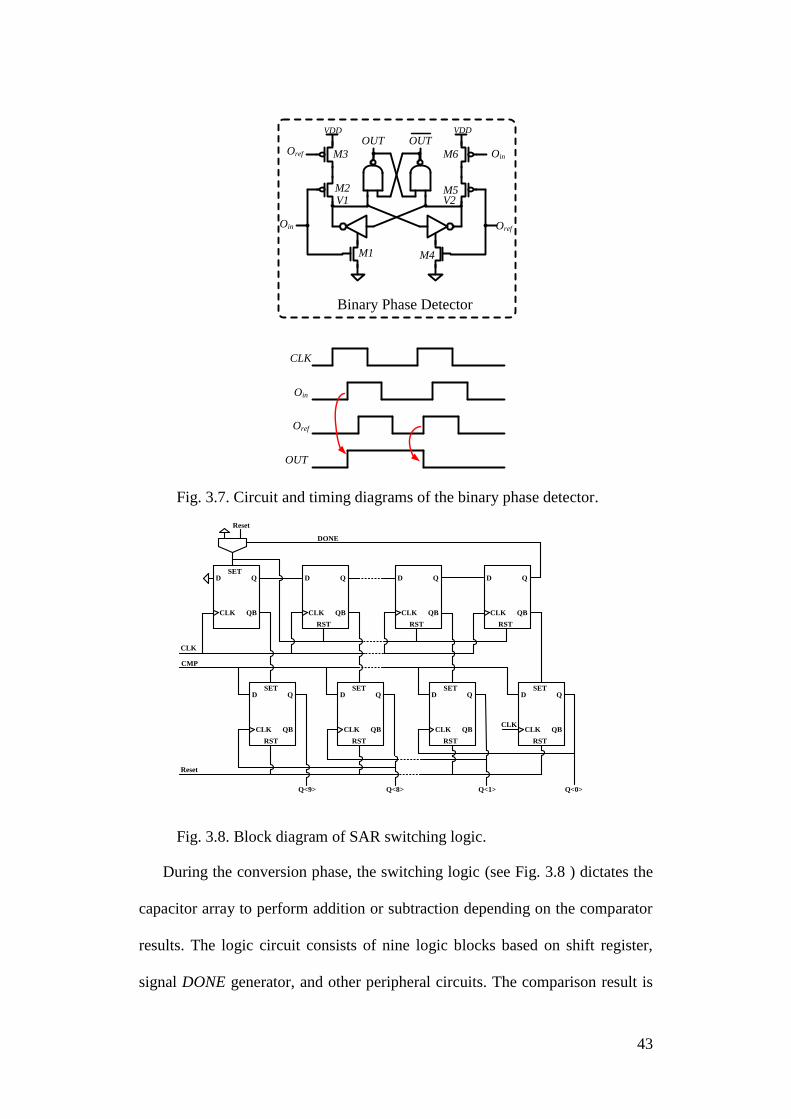
43
During the conversion phase, the switching logic (see Fig. 3.8 ) dictates the
capacitor array to perform addition or subtraction depending on the comparator
results. The logic circuit consists of nine logic blocks based on shift register,
signal DONE generator, and other peripheral circuits. The comparison result is
Fig. 3.7. Circuit and timing diagrams of the binary phase detector.
Fig. 3.8. Block diagram of SAR switching logic.
OUT
Oin
Oref
CLK
VDD
OUTVDD
OUT
V1 V2
Oin
Oin
Oref
Oref
Binary Phase Detector
M1
M2
M3
M4
M5
M6
D Q
CLK
SET
QB
D Q
CLK
RST
QB
D Q
CLK
RST
QB
D Q
CLK
RST
QB
CLK
CMP
Reset
D Q
CLK
SET
RST
QB
D Q
CLK
SET
RST
QB
D Q
CLK
SET
RST
QB
D Q
CLK
SET
RST
QB
Reset
CLK
Q<9> Q<8> Q<1> Q<0>
DONE
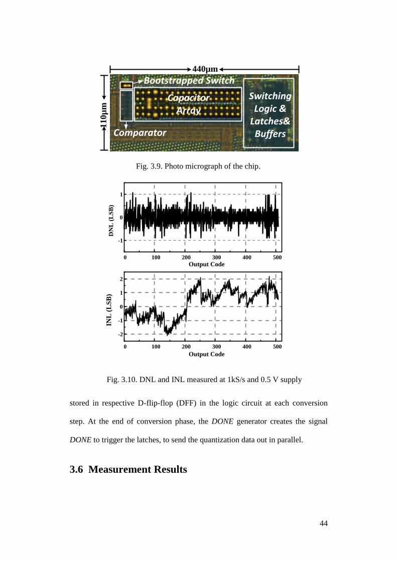
44
stored in respective D-flip-flop (DFF) in the logic circuit at each conversion
step. At the end of conversion phase, the DONE generator creates the signal
DONE to trigger the latches, to send the quantization data out in parallel.
3.6 Measurement Results
Fig. 3.9. Photo micrograph of the chip.
Fig. 3.10. DNL and INL measured at 1kS/s and 0.5 V supply
Capacitor Array
Switching Logic &
Latches&BuffersComparator
Bootstrapped Switch
11
0µ
m
440µm
0 100 200 300 400 500
-1
0
1
DN
L (
LS
B)
Output Code
0 100 200 300 400 500
-2
-1
0
1
2
INL
(L
SB
)
Output Code
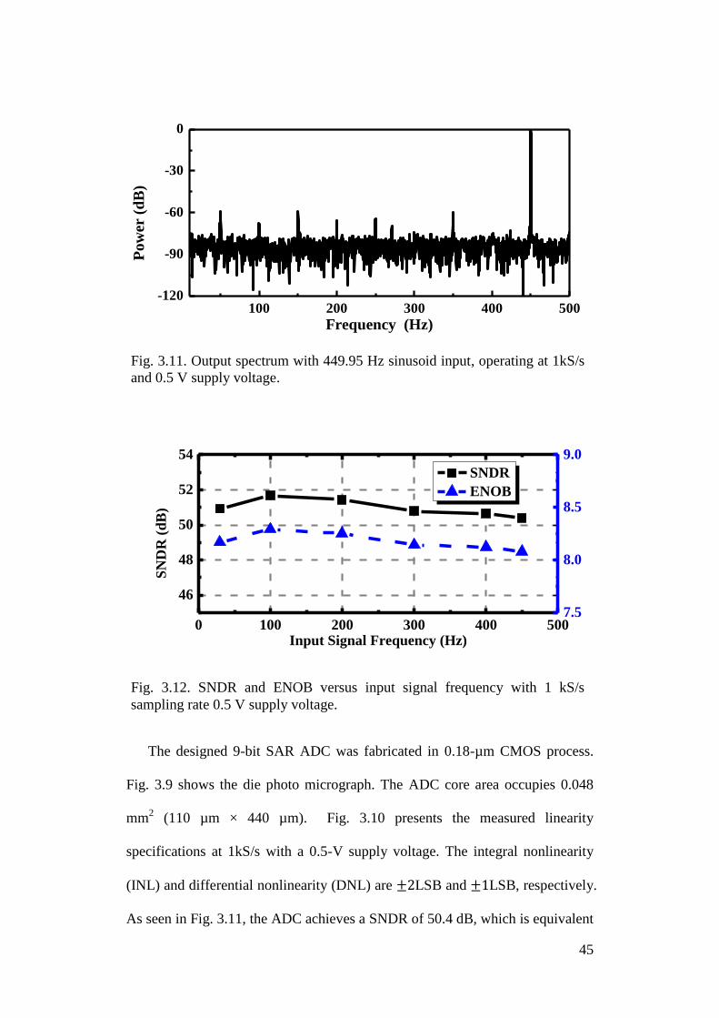
45
The designed 9-bit SAR ADC was fabricated in 0.18-µm CMOS process.
Fig. 3.9 shows the die photo micrograph. The ADC core area occupies 0.048
mm2 (110 µm × 440 µm). Fig. 3.10 presents the measured linearity
specifications at 1kS/s with a 0.5-V supply voltage. The integral nonlinearity
(INL) and differential nonlinearity (DNL) are ±2LSB and ±1LSB, respectively.
As seen in Fig. 3.11, the ADC achieves a SNDR of 50.4 dB, which is equivalent
Fig. 3.11. Output spectrum with 449.95 Hz sinusoid input, operating at 1kS/s
and 0.5 V supply voltage.
Fig. 3.12. SNDR and ENOB versus input signal frequency with 1 kS/s
sampling rate 0.5 V supply voltage.
100 200 300 400 500-120
-90
-60
-30
0
Pow
er (
dB
)
Frequency (Hz)
0 100 200 300 400 500
46
48
50
52
54
SNDR
ENOB
Input Signal Frequency (Hz)
SN
DR
(d
B)
7.5
8.0
8.5
9.0
EN
OB
(b
its)
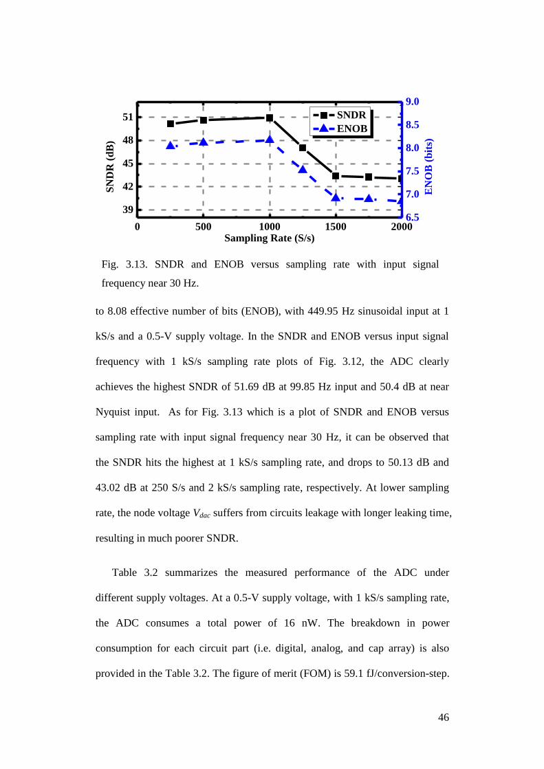
46
to 8.08 effective number of bits (ENOB), with 449.95 Hz sinusoidal input at 1
kS/s and a 0.5-V supply voltage. In the SNDR and ENOB versus input signal
frequency with 1 kS/s sampling rate plots of Fig. 3.12, the ADC clearly
achieves the highest SNDR of 51.69 dB at 99.85 Hz input and 50.4 dB at near
Nyquist input. As for Fig. 3.13 which is a plot of SNDR and ENOB versus
sampling rate with input signal frequency near 30 Hz, it can be observed that
the SNDR hits the highest at 1 kS/s sampling rate, and drops to 50.13 dB and
43.02 dB at 250 S/s and 2 kS/s sampling rate, respectively. At lower sampling
rate, the node voltage Vdac suffers from circuits leakage with longer leaking time,
resulting in much poorer SNDR.
Table 3.2 summarizes the measured performance of the ADC under
different supply voltages. At a 0.5-V supply voltage, with 1 kS/s sampling rate,
the ADC consumes a total power of 16 nW. The breakdown in power
consumption for each circuit part (i.e. digital, analog, and cap array) is also
provided in the Table 3.2. The figure of merit (FOM) is 59.1 fJ/conversion-step.
Fig. 3.13. SNDR and ENOB versus sampling rate with input signal
frequency near 30 Hz.
0 500 1000 1500 2000
39
42
45
48
51
SNDR
ENOB
Sampling Rate (S/s)
SN
DR
(d
B)
6.5
7.0
7.5
8.0
8.5
9.0
EN
OB
(b
its)
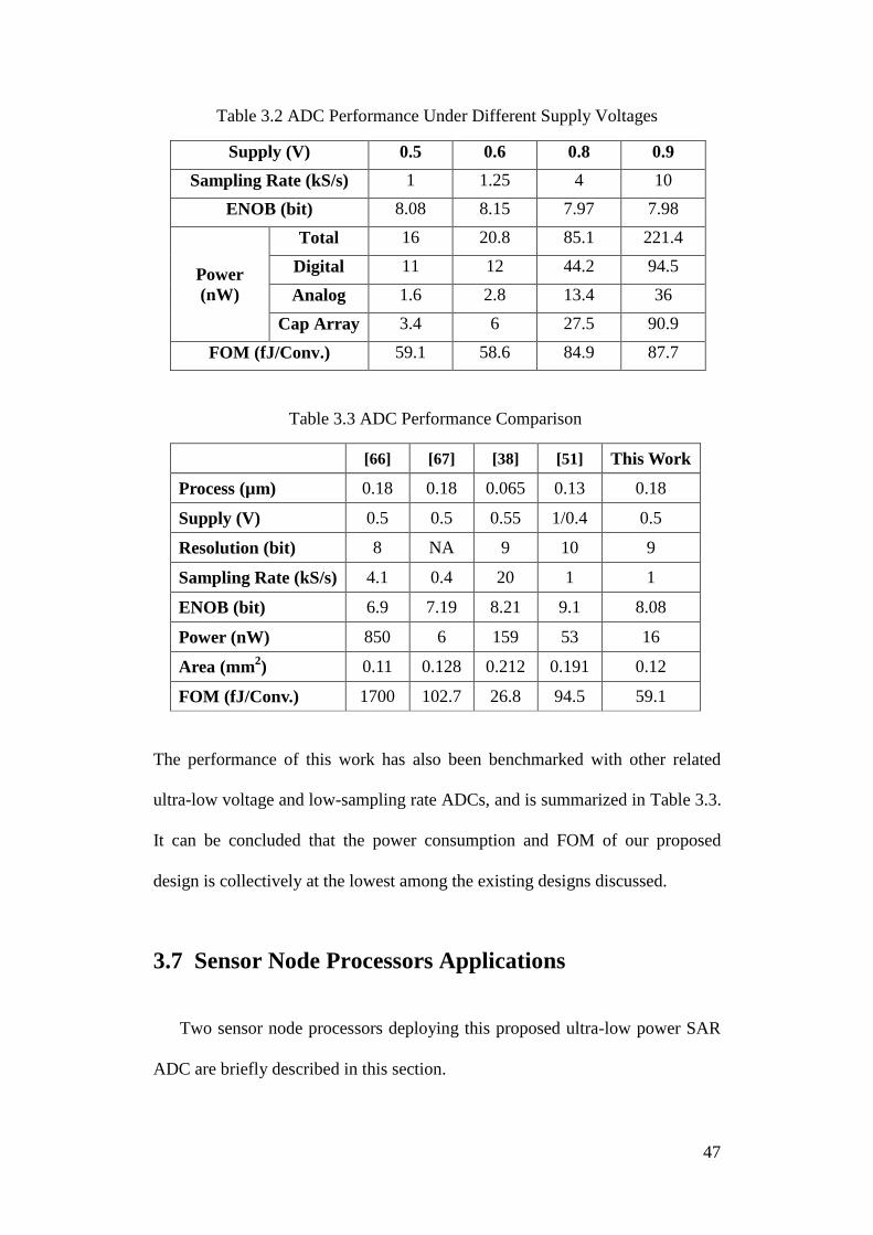
47
The performance of this work has also been benchmarked with other related
ultra-low voltage and low-sampling rate ADCs, and is summarized in Table 3.3.
It can be concluded that the power consumption and FOM of our proposed
design is collectively at the lowest among the existing designs discussed.
3.7 Sensor Node Processors Applications
Two sensor node processors deploying this proposed ultra-low power SAR
ADC are briefly described in this section.
Table 3.3 ADC Performance Comparison
[66] [67] [38] [51] This Work
Process (µm) 0.18 0.18 0.065 0.13 0.18
Supply (V) 0.5 0.5 0.55 1/0.4 0.5
Resolution (bit) 8 NA 9 10 9
Sampling Rate (kS/s) 4.1 0.4 20 1 1
ENOB (bit) 6.9 7.19 8.21 9.1 8.08
Power (nW) 850 6 159 53 16
Area (mm2) 0.11 0.128 0.212 0.191 0.12
FOM (fJ/Conv.) 1700 102.7 26.8 94.5 59.1
Table 3.2 ADC Performance Under Different Supply Voltages
Supply (V) 0.5 0.6 0.8 0.9
Sampling Rate (kS/s) 1 1.25 4 10
ENOB (bit) 8.08 8.15 7.97 7.98
Power
(nW)
Total 16 20.8 85.1 221.4
Digital 11 12 44.2 94.5
Analog 1.6 2.8 13.4 36
Cap Array 3.4 6 27.5 90.9
FOM (fJ/Conv.) 59.1 58.6 84.9 87.7
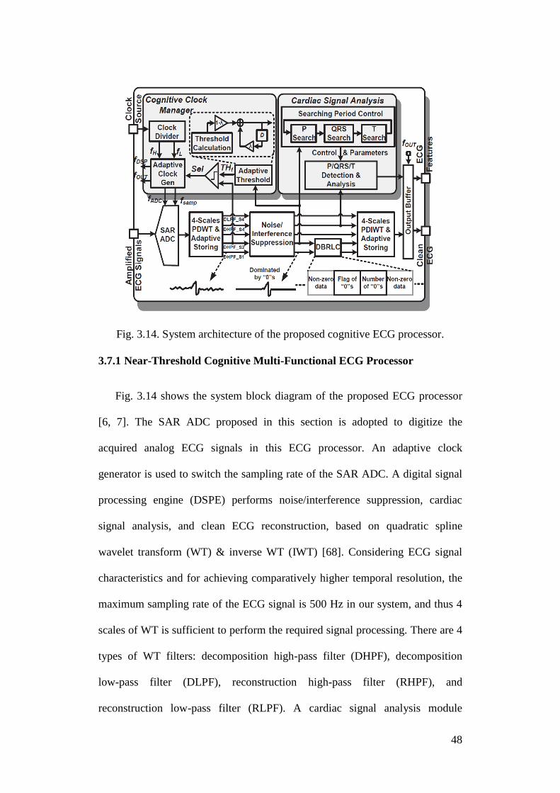
48
3.7.1 Near-Threshold Cognitive Multi-Functional ECG Processor
Fig. 3.14 shows the system block diagram of the proposed ECG processor
[6, 7]. The SAR ADC proposed in this section is adopted to digitize the
acquired analog ECG signals in this ECG processor. An adaptive clock
generator is used to switch the sampling rate of the SAR ADC. A digital signal
processing engine (DSPE) performs noise/interference suppression, cardiac
signal analysis, and clean ECG reconstruction, based on quadratic spline
wavelet transform (WT) & inverse WT (IWT) [68]. Considering ECG signal
characteristics and for achieving comparatively higher temporal resolution, the
maximum sampling rate of the ECG signal is 500 Hz in our system, and thus 4
scales of WT is sufficient to perform the required signal processing. There are 4
types of WT filters: decomposition high-pass filter (DHPF), decomposition
low-pass filter (DLPF), reconstruction high-pass filter (RHPF), and
reconstruction low-pass filter (RLPF). A cardiac signal analysis module
Fig. 3.14. System architecture of the proposed cognitive ECG processor.
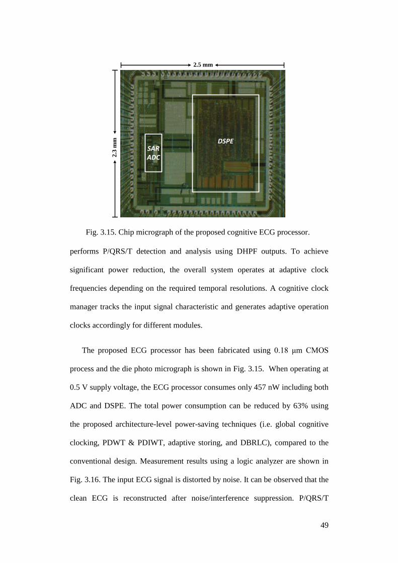
49
performs P/QRS/T detection and analysis using DHPF outputs. To achieve
significant power reduction, the overall system operates at adaptive clock
frequencies depending on the required temporal resolutions. A cognitive clock
manager tracks the input signal characteristic and generates adaptive operation
clocks accordingly for different modules.
The proposed ECG processor has been fabricated using 0.18 μm CMOS
process and the die photo micrograph is shown in Fig. 3.15. When operating at
0.5 V supply voltage, the ECG processor consumes only 457 nW including both
ADC and DSPE. The total power consumption can be reduced by 63% using
the proposed architecture-level power-saving techniques (i.e. global cognitive
clocking, PDWT & PDIWT, adaptive storing, and DBRLC), compared to the
conventional design. Measurement results using a logic analyzer are shown in
Fig. 3.16. The input ECG signal is distorted by noise. It can be observed that the
clean ECG is reconstructed after noise/interference suppression. P/QRS/T
Fig. 3.15. Chip micrograph of the proposed cognitive ECG processor.
SAR ADC
DSPE
2.3
mm
2.5 mm
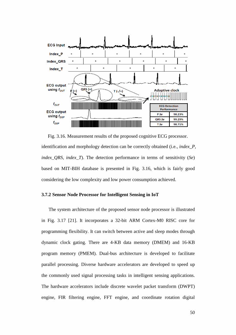
50
identification and morphology detection can be correctly obtained (i.e., index_P,
index_QRS, index_T). The detection performance in terms of sensitivity (Se)
based on MIT-BIH database is presented in Fig. 3.16, which is fairly good
considering the low complexity and low power consumption achieved.
3.7.2 Sensor Node Processor for Intelligent Sensing in IoT
The system architecture of the proposed sensor node processor is illustrated
in Fig. 3.17 [21]. It incorporates a 32-bit ARM Cortex-M0 RISC core for
programming flexibility. It can switch between active and sleep modes through
dynamic clock gating. There are 4-KB data memory (DMEM) and 16-KB
program memory (PMEM). Dual-bus architecture is developed to facilitate
parallel processing. Diverse hardware accelerators are developed to speed up
the commonly used signal processing tasks in intelligent sensing applications.
The hardware accelerators include discrete wavelet packet transform (DWPT)
engine, FIR filtering engine, FFT engine, and coordinate rotation digital
Fig. 3.16. Measurement results of the proposed cognitive ECG processor.
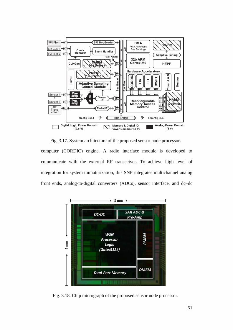
51
computer (CORDIC) engine. A radio interface module is developed to
communicate with the external RF transceiver. To achieve high level of
integration for system miniaturization, this SNP integrates multichannel analog
front ends, analog-to-digital converters (ADCs), sensor interface, and dc–dc
Fig. 3.17. System architecture of the proposed sensor node processor.
Fig. 3.18. Chip micrograph of the proposed sensor node processor.
DC-DCSAR ADC &
Pre-Amp
WSNProcessor
Logic(Gate:512k)
Dual-Port Memory
PM
EM
DMEM
5 mm
5 m
m
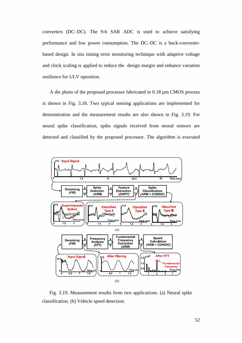
52
converters (DC–DC). The 9-b SAR ADC is used to achieve satisfying
performance and low power consumption. The DC–DC is a buck-converter-
based design. In situ timing error monitoring technique with adaptive voltage
and clock scaling is applied to reduce the design margin and enhance variation
resilience for ULV operation.
A die photo of the proposed processor fabricated in 0.18 µm CMOS process
is shown in Fig. 3.18. Two typical sensing applications are implemented for
demonstration and the measurement results are also shown in Fig. 3.19. For
neural spike classification, spike signals received from neural sensors are
detected and classified by the proposed processor. The algorithm is executed
Fig. 3.19. Measurement results from two applications. (a) Neural spike
classification. (b) Vehicle speed detection.
53
using the ARM core, FIR, DWPT and CORDIC engines with an average
efficiency of 39 pJ/cycle at 500 kHz and 0.5 V. For car speed estimation,
frequency analysis is performed for the data received from an accelerometer
sensor placed in a tire. The algorithm is mapped to the ARM core, FIR FFT
and CORDIC engines, consuming 29 pJ/cycle at 500 kHz and 0.5 V. The
proposed processor provides a solution for low-to-medium-data-rate intelligent
sensing applications requiring scalable performance and high energy efficiency.
3.8 Conclusion
This chapter presents an ultra-low power SAR ADC operating at 0.5 V
supply voltage. Several design considerations of ultra-low power SAR ADC are
discussed in this chapter, including high linearity sampling switch, high energy
efficient capacitor switching method, and reliable comparator. To reduce the
delay of the sampling circuit and improve on its linearity, we proposed a
bootstrapped switch. The proposed ADC achieves 16 nW power consumption
with 8.08-ENOB at 1 kS/s sampling rate. Two sensor node processors
deploying this proposed ultra-low power SAR ADC are briefly described in this
chapter. One sensor node processor is a near-threshold cognitive multi-
functional ECG processor for long-term cardiac monitoring, which consumes
only 457 nW at 0.5 V for real-time ECG recording and diagnosis. Another is a
sensor node processor with diverse hardware acceleration and cognitive
sampling for intelligent sensing.Equation Chapter (Next) Section 1
54
Chapter 4
A 151-nW Adaptive Delta-Sampling
ADC Design
As mentioned in Section 2.3 , some energy-efficient ADC architectures had
been reported to convert burst-like or sparse signals, such as neural spike, ECG
and accelerometer waveforms [17, 18, 35]. [18] described a level crossing
asynchronous ADC with adaptive resolution to achieve power reduction and
data compression. However, complicated interface design is required to process
the asynchronous samples prior to interfacing with the synchronous system.
Also, level crossing asynchronous ADC is vulnerable to signal slope overload.
A delta-modulated SAR ADC that converts only the voltage difference between
two consecutive samples so as to reduce the number of conversion steps to
achieve low power consumption is proposed by [17]. The circuit, however,
needs to ensure oversampling at all time, which is not energy-efficient. In [35],
the LSB-first SAR ADC makes use of its previous sample as an initial guess for
its current sample. For full range input signal, the oversampling ratio should be
larger than 32. Otherwise the LSB-first SAR ADC will require more conversion
steps than the conventional SAR ADC. In this chapter, we propose a novel
ADC with adaptive delta-sampling to reduce power consumption while meeting
the required resolution and conversion range [69].

55
4.1 Input Signal Analysis
One important characteristic of burst-like or sparse signals is that the signals
vary slowly during most of duty cycle. Fig. 4.1(a) shows the digitalized ECG
and neural signals using an 8 bits ideal ADC, sampled with 1 kHz and 20 kHz
sampling rate, respectively. It can be observed that the ECG signal varies
slowly except the QRS region which is about 11%. For neural signal, it varies
slowly except neural spike which is about only 0.85%. If we divide theses 8 bits
to the first 4 most significant bits (MSBs) and the last 4 least significant bits
(LSBs), as the shown in Fig. 4.1(b), it can be observed that the first 4 MSBs
remains the same during several consecutive samples both in ECG and neural
signals. In these ECG monitoring and neural recording applications, the
Fig. 4.1. Digitalized sparse signals with 8 bits, first 4 MSB bits and last 4
LSB bits: (a) ECG signal sampled with 1 kHz sampling rate, (b) neural
signal sampled with 20 kHz sampling rate.
0 2 4 6 8 100
50
100
150
200
250
Co
de
Time(ms)
MSBs(4 bits) LSBs (4 bits)
0 2 4 6 8 100
50
100
150
200
250
Co
de
Full (8 bits)
(b)
0 20
50
100
150
200
250
Co
de
Time(s)
MSBs(4 bits) LSBs (4 bits)
0 20
50
100
150
200
250
Co
de
Full (8 bits)
(a)
1
1

56
conventional SAR ADC with binary search from MSB to LSB is not energy-
efficient particularly for burst-like signals.
4.2 Proposed Adaptive Delta-Sampling Architecture
In the conventional N-bit SAR ADC, N number of conversion steps is
required to complete the binary search from the MSB to LSB. If the difference
between two consecutive samples is small, the conversion of the MSBs may not
be necessary since their MSBs are the same. Hence, power is wasted if binary
search is performed on every bit, from the MSB to LSB. Here we define the
resolution of an N-bit ADC as VLSB, which can be expressed as follows:
2
range
LSB N
VV
(4.1)
where Vrange is the full conversion range of the ADC. In conventional ADC,
Vrange is equal to the full voltage range of the input signal. When the difference
between two consecutive samples is small, only the difference between two
consecutive samples needs to be converted. Therefore, instead of following the
conventional approach, we convert only the increment of the input signal (we
call it delta-sampling). By doing so, the binary search range can be reduced to
achieve significant power reduction. An M-bit ADC (M < N) following this
method is able to realize the same VLSB resolution and the same conversion
range as an N-bit conventional ADC. As a result, the ADC power consumption
is reduced considerably. The concept will be further discussed in Section 4.5 .
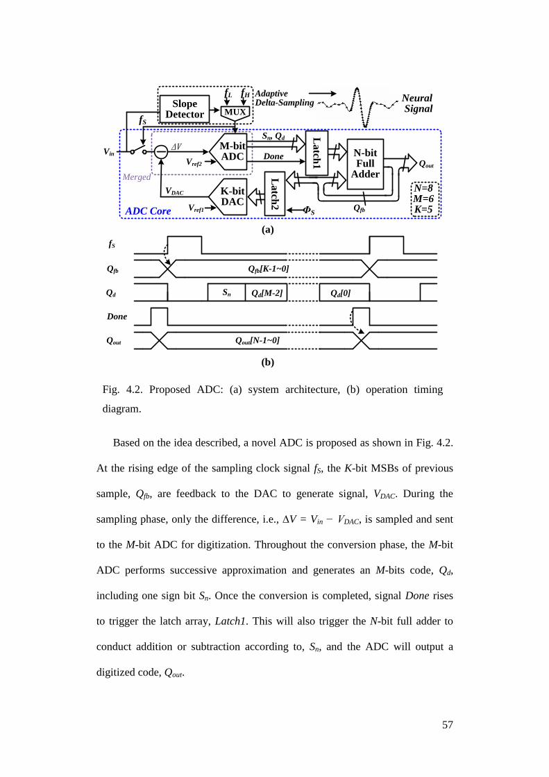
57
Based on the idea described, a novel ADC is proposed as shown in Fig. 4.2.
At the rising edge of the sampling clock signal fS, the K-bit MSBs of previous
sample, Qfb, are feedback to the DAC to generate signal, VDAC. During the
sampling phase, only the difference, i.e., ∆V = Vin − VDAC, is sampled and sent
to the M-bit ADC for digitization. Throughout the conversion phase, the M-bit
ADC performs successive approximation and generates an M-bits code, Qd,
including one sign bit Sn. Once the conversion is completed, signal Done rises
to trigger the latch array, Latch1. This will also trigger the N-bit full adder to
conduct addition or subtraction according to, Sn, and the ADC will output a
digitized code, Qout.
Fig. 4.2. Proposed ADC: (a) system architecture, (b) operation timing
diagram.
Sn, Qd
Vref2
Vref1
∆V
VDAC
Merged
Vin
AdaptiveDelta-Sampling
Qfb
Qout
Done
La
tch1
ADC Core
MUX
fL fH
La
tch2
N-bitFull
Adder
Slope Detector
Neural Signal
fS
M-bit ADC
K-bit DAC
ΦS
(a)
N=8M=6K=5
Sn Qd[M-2] Qd[0]
Qfb[K-1~0]
Qout[N-1~0]
Qfb
Qd
Qout
Done
fS
(b)

58
Different from the analog-front delta-sampling [70], which suffers from
accumulated error, the proposed delta-sampling ADC does not have
accumulated error even if there is error during data sampling/conversion. Fig.
4.3 shows a simplified block diagram of the proposed ADC, where the
quantizer represents M-bit ADC along with a conversion error Qerror. The
equations of voltage difference, ∆V, and digitized output code, Qout, can be
obtained as follows:
1in fbV n V n Q n (4.2)
( 1)out error fbQ n V n Q n Q n (4.3)
Substituting Equation (4.2) into Equation (4.3),
out in errorQ n V n Q n (4.4)
From Equation(4.4), we can conclude that the output error of the proposed
ADC contains only the current sampling/conversion error, Qerror(n), and there is
no accumulated error during operation.
Fig. 4.3. Block diagram of proposed ADC for accumulated error analysis.
Quantizer
DAC Delay
Qerror(n)
Vin (n)
Qfb(n)
∆V (n)
Qfb(n-1)Qfb(n-1)
∆V (n)+Qerror(n)Qout(n)
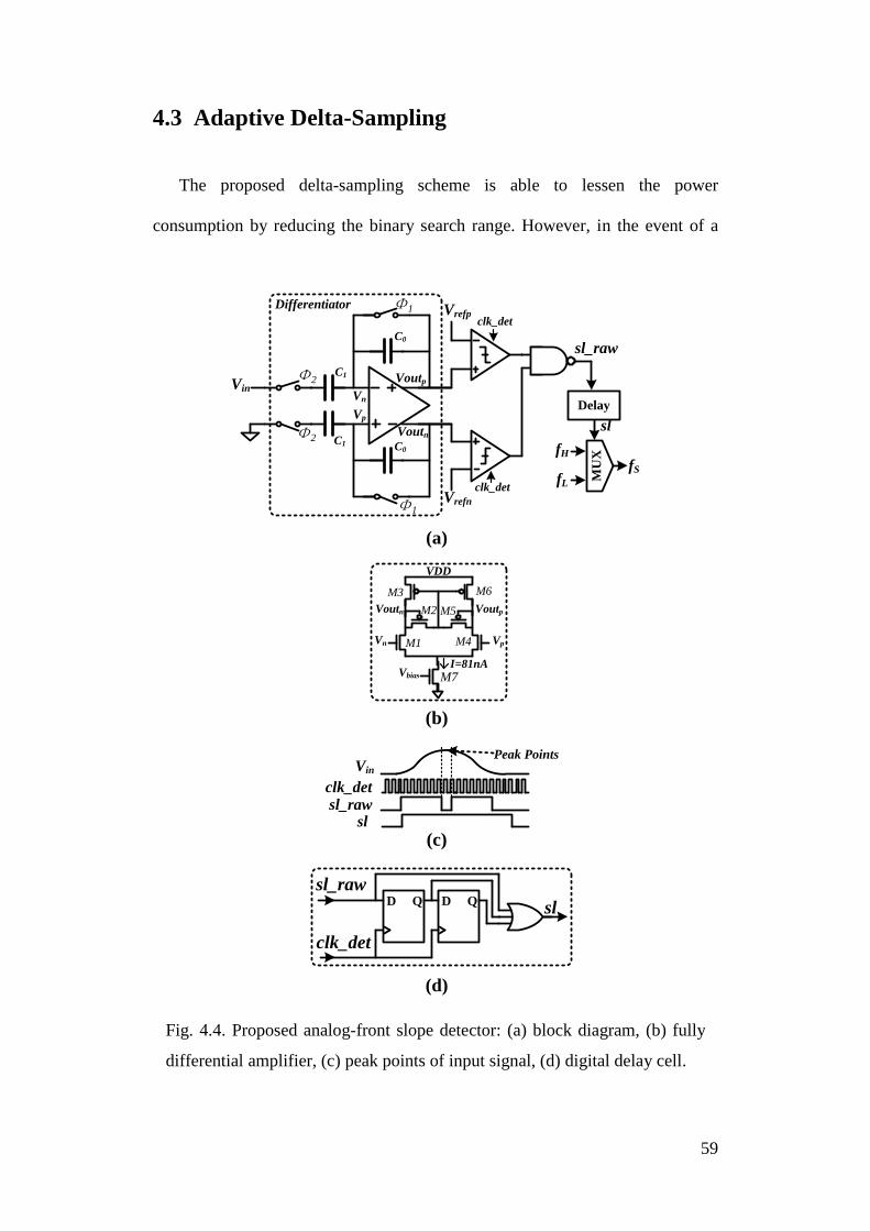
59
4.3 Adaptive Delta-Sampling
The proposed delta-sampling scheme is able to lessen the power
consumption by reducing the binary search range. However, in the event of a
Fig. 4.4. Proposed analog-front slope detector: (a) block diagram, (b) fully
differential amplifier, (c) peak points of input signal, (d) digital delay cell.
D QD Q
clk_det
sl
sl_raw
clk_detsl_raw
sl
Vin
Peak Points
Vp
VDD
Vbias
Voutn Voutp
I=81nA
Vn
Vn
Vin
Vrefp
Vrefn
Φ1
Φ1
Φ2
Φ2
MU
X
fL
fH
fS
sl
Delay
sl_raw
Vp
Voutp
Voutn
clk_det
clk_det
C0
C1
C1 C0
Differentiator
(a)
(b)
(c)
(d)
M4
M5
M6
M2
M1
M3
M7
60
sudden change in input signal, the difference voltage, |∆V|, will also change
abruptly. If |∆V| is larger than the conversion range of the M-bit ADC, overload
will occur in the ADC to cause conversion error. To address this issue, we
propose an adaptive delta-sampling scheme using a slope detector, as illustrated
in Fig. 4.2. Proposed ADC: (a) system architecture, (b) operation timing
diagram.Fig. 4.2. To illustrate the concept, the proposed adaptive delta-
sampling ADC is used to convert a pre-recorded neural signal from an
anesthetized rat [8]. During non-spike periods, the maximum amplitude of the
neural signal is limited to 24/255 of the full conversion range (i.e., 1 V) and its
bandwidth is less than 1 kHz. This means that the M-bit ADC with 31/255 V
conversion range (i.e., M = 5) will not overload and the Nyquist sampling
frequency (i.e., fL = 2 kHz in our case) can be used. According to the literatures
[8, 19, 20, 53], to conserve complete information of neural spikes, ADC needs
to operate at higher than 14 kHz. Considering that the 20 kHz sampling
frequency can achieve enough signal-to-noise and distortion ratio
(SNDR)/ENOB (45.3 dB/7.2 bits) and lower power consumption is preferred in
the neural recording system, we set the higher sampling frequency at 20 kHz
(i.e., fH = 20 kHz). Based on this sampling frequency and the maximum slope of
the input signal (i.e., 1.7 mV/µs in this case, which is calculated by performing
a differential of the neural signal reported in [8]), we are able to determine the
resolution of M-bit ADC. The maximum voltage difference between two
consecutive samples is 1.7 mV/µs × 50 µs = 85 mV, which is about 22/255 of
the full conversion range. As our target is 8 bits, i.e., N = 8, we select M = 5 so
that the conversion range of the M-bit ADC is 31/255 V (which is larger than
22/255 V). As there is still a difference between 31/255 V and 22/255 V, which
61
is 9/255 V, we can use partial number of bits instead of having all the bits of the
previous sample during the delta-sampling. In this case, the feedback bits, i.e.,
K, from the previous sample can be reduced from 8 to 5, which correspond to
9/255 V. This helps to reduce the complexity and power consumption of the K-
bit DAC. In addition, a sign bit is needed in the M–bit ADC to indicate either
signal rising or falling. Thus, we eventually settled with M = 6, K = 5.
The slope of the input signal is detected by the analog-front slope detector
of Fig. 4.4. The switched-capacitor differentiator in [71] is employed in the
proposed slope detector. A single stage fully differential amplifier (see Fig.
4.4(b)) with unity-gain bandwidth of 1.8 MHz is used in this differentiator,
consuming 81 nA of current. The output of differentiator can be represented as
[71]
0
1p
CVout T Vin t T Vin t
C
(4.5)
where C1/C0 = 8, T=50 µs. Voutp will be compared to a threshold voltage
through a coarse time-domain comparator [34]. The sampling frequency will
switch between a higher sampling frequency of fH = 20 kHz and a lower
sampling frequency of fL = 2 kHz according to the comparison results. As
shown in Fig. 4.4(c), the peak points of the input signal will cause a downward
pulse in the raw selection signal, resulting in lower sampling frequency which is
not desirable. To remove the downward pulse, we proposed a digital delay cell
as illustrated in Fig. 4.4(d). sl_raw and the outputs of the D-flip-flops are fed to
a OR gate to generate sl, which is then used to determine the sampling
frequency. Since the proposed ADC is of moderate resolution (8 bits) and has
low input signal bandwidth (1 kHz), the timing mismatch requirement between
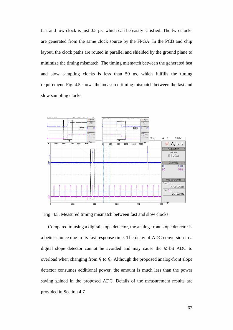
62
fast and low clock is just 0.5 µs, which can be easily satisfied. The two clocks
are generated from the same clock source by the FPGA. In the PCB and chip
layout, the clock paths are routed in parallel and shielded by the ground plane to
minimize the timing mismatch. The timing mismatch between the generated fast
and slow sampling clocks is less than 50 ns, which fulfills the timing
requirement. Fig. 4.5 shows the measured timing mismatch between the fast and
slow sampling clocks.
Compared to using a digital slope detector, the analog-front slope detector is
a better choice due to its fast response time. The delay of ADC conversion in a
digital slope detector cannot be avoided and may cause the M-bit ADC to
overload when changing from fL to fH. Although the proposed analog-front slope
detector consumes additional power, the amount is much less than the power
saving gained in the proposed ADC. Details of the measurement results are
provided in Section 4.7
Fig. 4.5. Measured timing mismatch between fast and slow clocks.
200ns 200ns
0 400 800 1200 1600 2000/ns
0 400 800 1200 1600 2000/ns
0 200 400 600 800 1000/µs

63
4.4 Subtractor Design
As the conventional analog subtractor with operational amplifier consumes
static power [70], the low power merged subtractor of Fig. 4.6 is proposed. The
merged subtractor is realized through configuring the top plate of a 6-bit
capacitor array and a 5-bit capacitor array, as the positive input Vp and negative
input Vn of a dynamic comparator, respectively. This is similar to the
differential ADC architecture [20], except that the positive and negative
capacitor arrays have asymmetrical switching. In conventional differential ADC
design, the voltages of the two capacitor arrays progressively approach each
other during the conversion, as illustrated in Fig. 4.7(a). In this way, the voltage
difference between the positive and negative inputs is converted. In our design
the switches in the 5-bit DAC are controlled by the five MSBs of its previous
sample which are updated at every sampling cycle. The capacitors in the 6-bit
Fig. 4.6. Circuit implementation of the proposed ADC core.
2C0 4C0 8C0 16C0C0 C0
Vref
Vp
Vn=VDAC
Vin
SAR Logic
CLK
fS
Done
Bootstrapped Switch
2C0 4C0 8C0 16C0C0 C0
2C0 4C0 8C0 16C0C0 C0
Vref/4
C0=240 fF MIM capacitor
Qn-1[7~3]
Signn, Qn[4~0]
Qn-1[7]
Merged Subtractor
6-bit DAC MSB Sub-Array
6-bit DAC Main Array
5-bit DAC
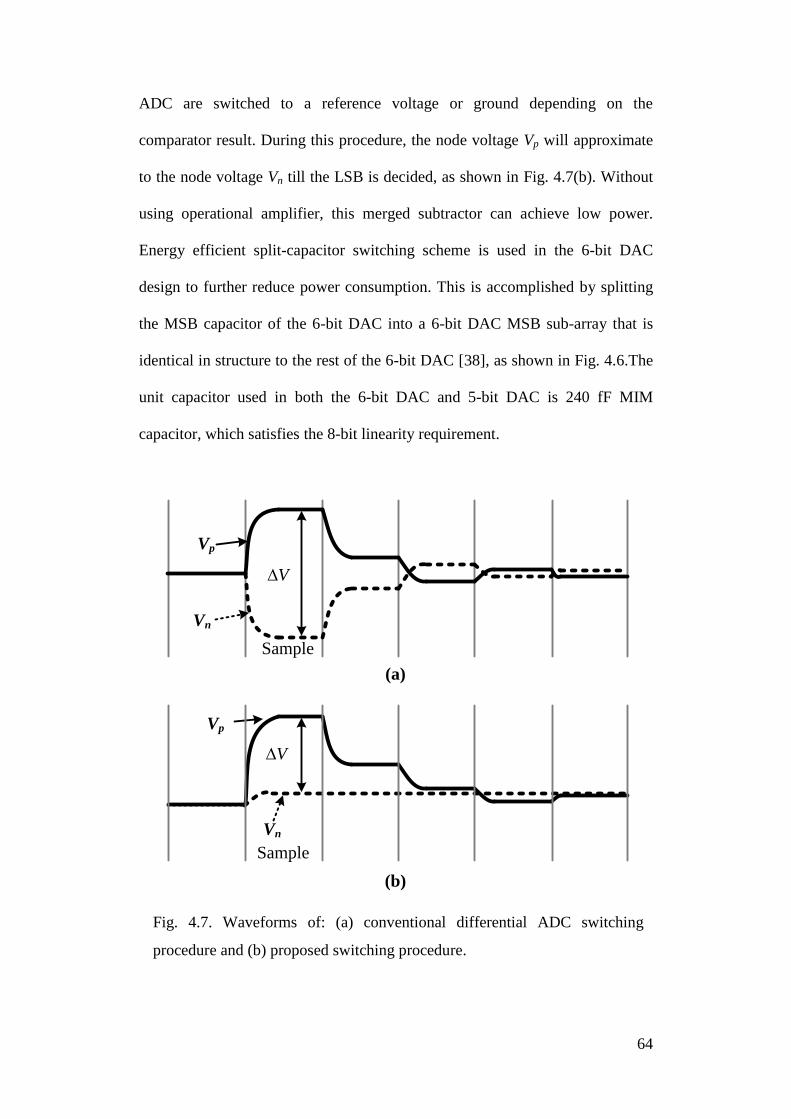
64
ADC are switched to a reference voltage or ground depending on the
comparator result. During this procedure, the node voltage Vp will approximate
to the node voltage Vn till the LSB is decided, as shown in Fig. 4.7(b). Without
using operational amplifier, this merged subtractor can achieve low power.
Energy efficient split-capacitor switching scheme is used in the 6-bit DAC
design to further reduce power consumption. This is accomplished by splitting
the MSB capacitor of the 6-bit DAC into a 6-bit DAC MSB sub-array that is
identical in structure to the rest of the 6-bit DAC [38], as shown in Fig. 4.6.The
unit capacitor used in both the 6-bit DAC and 5-bit DAC is 240 fF MIM
capacitor, which satisfies the 8-bit linearity requirement.
Fig. 4.7. Waveforms of: (a) conventional differential ADC switching
procedure and (b) proposed switching procedure.
(a)
(b)
Sample
Vp
Vn
∆V
∆V
Sample
Vp
Vn

65
4.5 Power consumption analysis of proposed ADC
The advantages of the proposed ADC in terms of power consumption can be
analyzed as follows: (1) The reference voltage is reduced from Vref to Vref/4 in
the 6-bit ADC due to the reduced binary search range, and hence 16× power
reduction in the capacitor array; (2) the total capacitance of the capacitor array
is reduced from 256C0 to 64C0, leading to a 4× power reduction in the capacitor
array; (3) the proposed ADC only requires six conversion steps as opposed to
eight steps in a conventional ADC. The saving of two conversion steps results
in substantial power reduction since each conversion step involves capacitor
array switching, analog comparison and SAR logic switching. It is noted that
the power consumption of the 5-bit capacitor array in the 5-bit DAC is low. The
reason is that the digitized MSBs between consecutive samples change slowly
or remain the same, and thus most of the capacitors in the 5-bit DAC do not
Fig. 4.8. Simulated power consumptions of the capacitor arrays in proposed
ADC and the capacitor splitting ADC with neural signal input.
Vin
Mean Power=4.4nW
Mean Power=26.1nW
Mean Power=1200nW
0 10 20 30 40
¼(mW)
0
1(mW)
0
1(V)
0
1(mW)
Switching Power of 5-bit Cap
Array in Proposed ADC
Time (ms)
Switching Power of 6-bit Cap
Array in Proposed ADC
Switching Power of Cap
Array in Capacitor Splitting
ADC
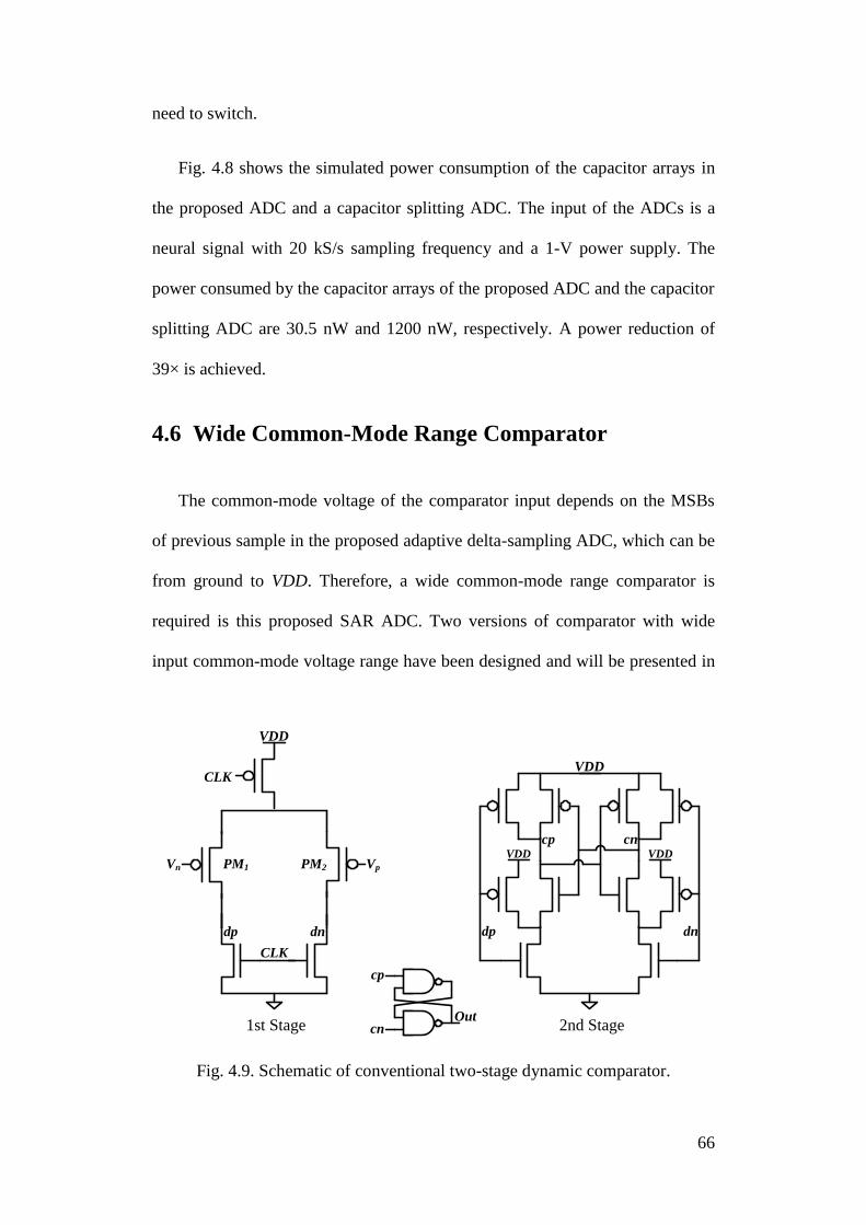
66
need to switch.
Fig. 4.8 shows the simulated power consumption of the capacitor arrays in
the proposed ADC and a capacitor splitting ADC. The input of the ADCs is a
neural signal with 20 kS/s sampling frequency and a 1-V power supply. The
power consumed by the capacitor arrays of the proposed ADC and the capacitor
splitting ADC are 30.5 nW and 1200 nW, respectively. A power reduction of
39× is achieved.
4.6 Wide Common-Mode Range Comparator
The common-mode voltage of the comparator input depends on the MSBs
of previous sample in the proposed adaptive delta-sampling ADC, which can be
from ground to VDD. Therefore, a wide common-mode range comparator is
required is this proposed SAR ADC. Two versions of comparator with wide
input common-mode voltage range have been designed and will be presented in
Fig. 4.9. Schematic of conventional two-stage dynamic comparator.
Out
cp
cn
VDD
cpVDD
cn
VDD
dp dn
2nd Stage1st Stage
Vn VpPM1 PM2
CLK
CLK
VDD
dp dn

67
this section. Both of these two versions are modified from a two-stage dynamic
comparator described in [41], as shown in Fig. 4.9. The input common-mode
voltage range of two-stage dynamic comparator as shown in Fig. 4.9 cannot
reach from ground to VDD. The comparator cannot work properly when the
input common-mode voltage is near VDD because the PMOS input pair, i.e.,
PM1 and PM2, is switched off.
To widen the common-mode input range of the dynamic comparator, a pair
of NMOS (i.e. M1 and M2) is added to the first stage, as depicted in Fig. 4.10.
The operation of the proposed comparator is explained as follows. When clock
CLK is high, dp and dn will be pulled down to ground through NMOS M6 and
M7. Then, cp and cn will be pulled up to the supply voltage VDD through
PMOS M8 and M9. On the falling edge of CLK, PMOS M5 in the first stage will
be switched on. Therefore, comparator input voltage Vp and Vn are transformed
Fig. 4.10. Schematic of proposed two-stage dynamic comparator with
PMOS and NMOS input pairs.
Out
cp
cn
VDD
cpVDD
cn
VDD
dp dn
2nd Stage
M8M9
M10M11
1st Stage
Vn
Vp
In1 Ip4Ip3 In2
M1 M4M3 M2
M5CLK
CLK
VDD
dp dn
M6M7
M12M13
M14M15
M16M17
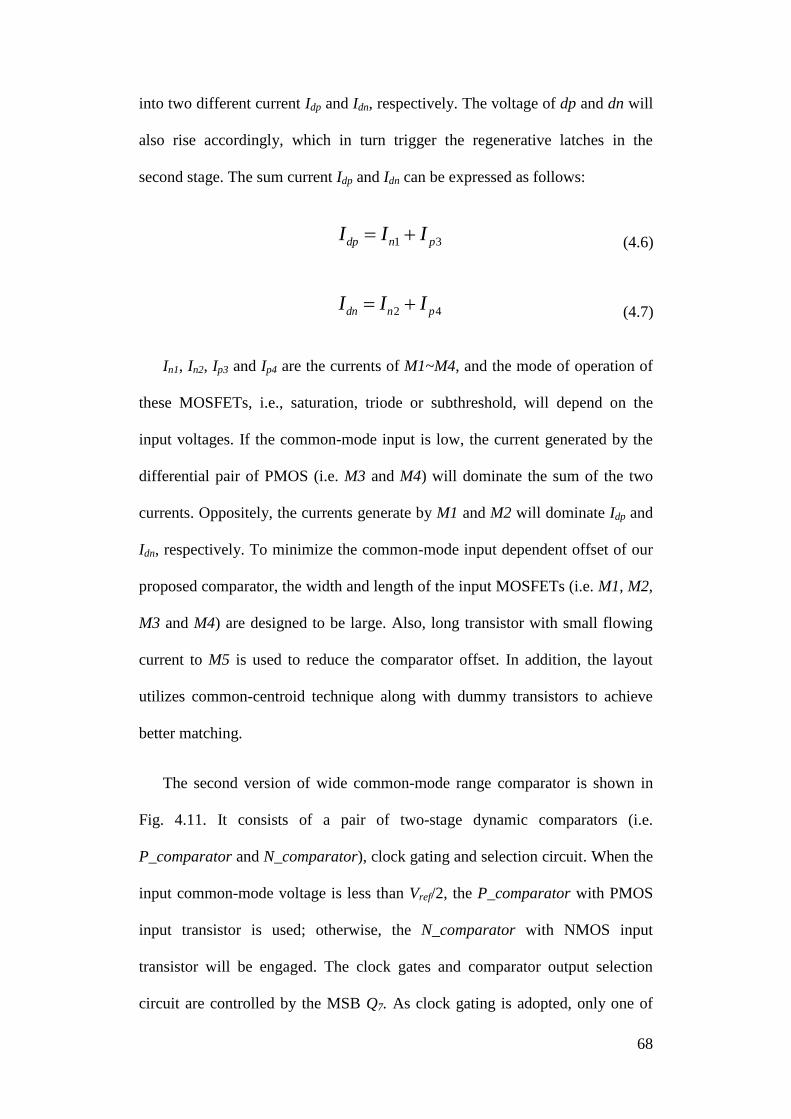
68
into two different current Idp and Idn, respectively. The voltage of dp and dn will
also rise accordingly, which in turn trigger the regenerative latches in the
second stage. The sum current Idp and Idn can be expressed as follows:
1 3dp n pI I I (4.6)
2 4dn n pI I I (4.7)
In1, In2, Ip3 and Ip4 are the currents of M1~M4, and the mode of operation of
these MOSFETs, i.e., saturation, triode or subthreshold, will depend on the
input voltages. If the common-mode input is low, the current generated by the
differential pair of PMOS (i.e. M3 and M4) will dominate the sum of the two
currents. Oppositely, the currents generate by M1 and M2 will dominate Idp and
Idn, respectively. To minimize the common-mode input dependent offset of our
proposed comparator, the width and length of the input MOSFETs (i.e. M1, M2,
M3 and M4) are designed to be large. Also, long transistor with small flowing
current to M5 is used to reduce the comparator offset. In addition, the layout
utilizes common-centroid technique along with dummy transistors to achieve
better matching.
The second version of wide common-mode range comparator is shown in
Fig. 4.11. It consists of a pair of two-stage dynamic comparators (i.e.
P_comparator and N_comparator), clock gating and selection circuit. When the
input common-mode voltage is less than Vref/2, the P_comparator with PMOS
input transistor is used; otherwise, the N_comparator with NMOS input
transistor will be engaged. The clock gates and comparator output selection
circuit are controlled by the MSB Q7. As clock gating is adopted, only one of
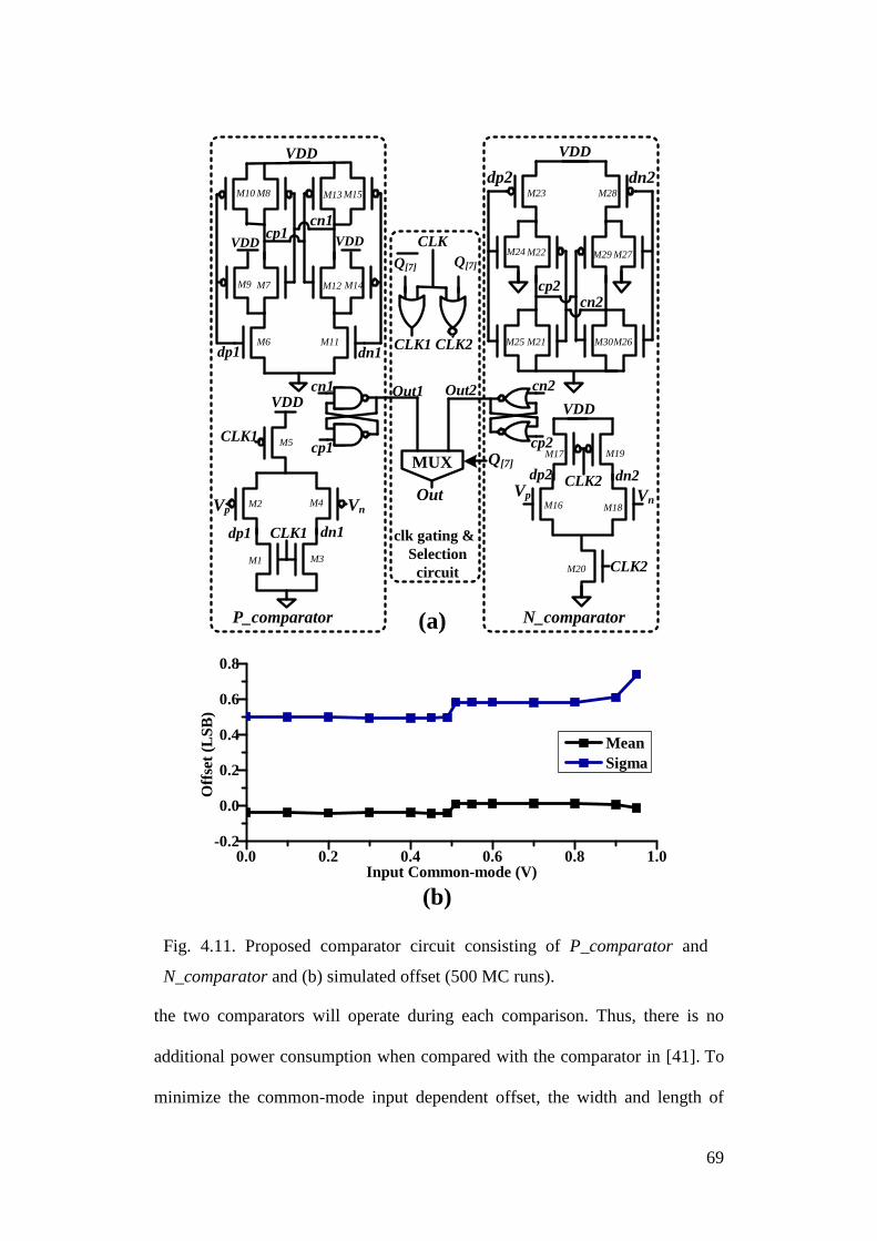
69
the two comparators will operate during each comparison. Thus, there is no
additional power consumption when compared with the comparator in [41]. To
minimize the common-mode input dependent offset, the width and length of
Fig. 4.11. Proposed comparator circuit consisting of P_comparator and
N_comparator and (b) simulated offset (500 MC runs).
(b)
Out1
MUX
Out
Q[7]
(a)
Vp Vn
VDD
CLK2
dp2 dn2CLK2
cp2cn2
VDD
dp2 dn2
cp2
cn2
cp1cn1
dp1 dn1
VDD VDD
VDD
cp1
cn1
Vn
VDD
Vp
CLK1
dp1 dn1CLK1
Out2
CLK2CLK1
CLK
Q[7]Q[7]
P_comparator N_comparator
clk gating &
Selection
circuit
0.0 0.2 0.4 0.6 0.8 1.0-0.2
0.0
0.2
0.4
0.6
0.8
Off
set
(LS
B)
Input Common-mode (V)
Mean
Sigma
M1
M2
M3
M4
M5
M9
M10
M11M6
M7
M8
M12
M13
M14
M22
M23
M19
M20
M21
M18
M15
M16
M17
M27M24
M25 M26
M28
M29
M30
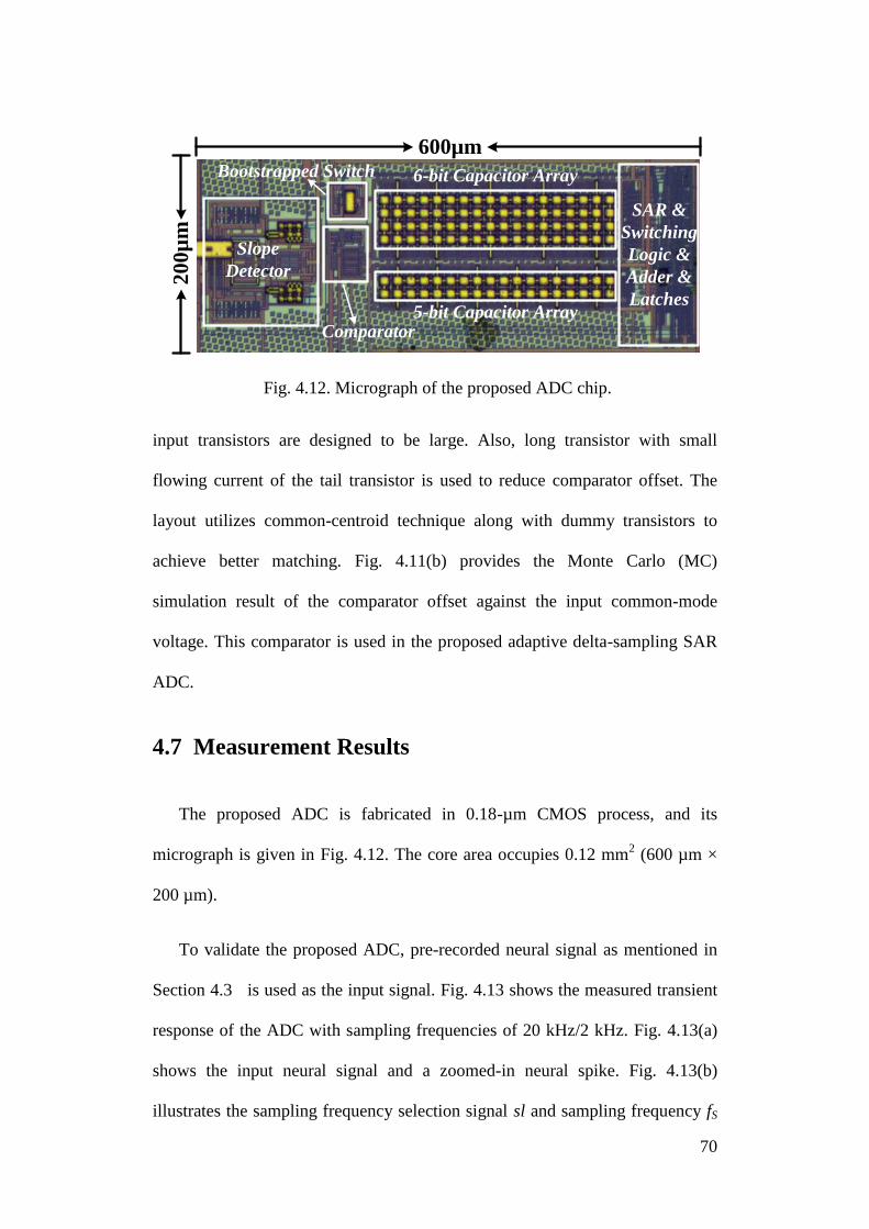
70
input transistors are designed to be large. Also, long transistor with small
flowing current of the tail transistor is used to reduce comparator offset. The
layout utilizes common-centroid technique along with dummy transistors to
achieve better matching. Fig. 4.11(b) provides the Monte Carlo (MC)
simulation result of the comparator offset against the input common-mode
voltage. This comparator is used in the proposed adaptive delta-sampling SAR
ADC.
4.7 Measurement Results
The proposed ADC is fabricated in 0.18-µm CMOS process, and its
micrograph is given in Fig. 4.12. The core area occupies 0.12 mm2 (600 µm ×
200 µm).
To validate the proposed ADC, pre-recorded neural signal as mentioned in
Section 4.3 is used as the input signal. Fig. 4.13 shows the measured transient
response of the ADC with sampling frequencies of 20 kHz/2 kHz. Fig. 4.13(a)
shows the input neural signal and a zoomed-in neural spike. Fig. 4.13(b)
illustrates the sampling frequency selection signal sl and sampling frequency fS
Fig. 4.12. Micrograph of the proposed ADC chip.
Slope
Detector
Comparator5-bit Capacitor Array
SAR &
Switching
Logic &
Adder &
Latches
6-bit Capacitor ArrayBootstrapped Switch2
00µ
m
600µm

71
of the ADC. It can be observed that the proposed ADC is adaptively switched
between 2 kHz and 20 kHz to prevent overload during instances of spikes. Fig.
4.13(c) shows the output data of the adaptive delta-sampling ADC. From the
waveform of Qd, we can see that the 6-bit ADC does not have an overload since
Qd is always less than 31.
Fig. 4.13. Measured transient response of proposed ADC with neural signal
input: (a) input neural signal and zoomed-in neural spike, (b) sampling
frequency selection signal sl and adaptive sampling frequency fS, (c) output
of ADC Qout, input of 5-bit DAC Qfb and 6-bit ADC output Qd (except Sn).
Vin
fS
Neural
Signal
(input)
sl
Neural Spike
(a)
(b)
Qout
Qfb
Qd
(c)
160 180 200 220 2400
100
200
160 180 200 220 2400
100
200
160 180 200 220 2400
20
31
40
t/ms
Overload Threshold
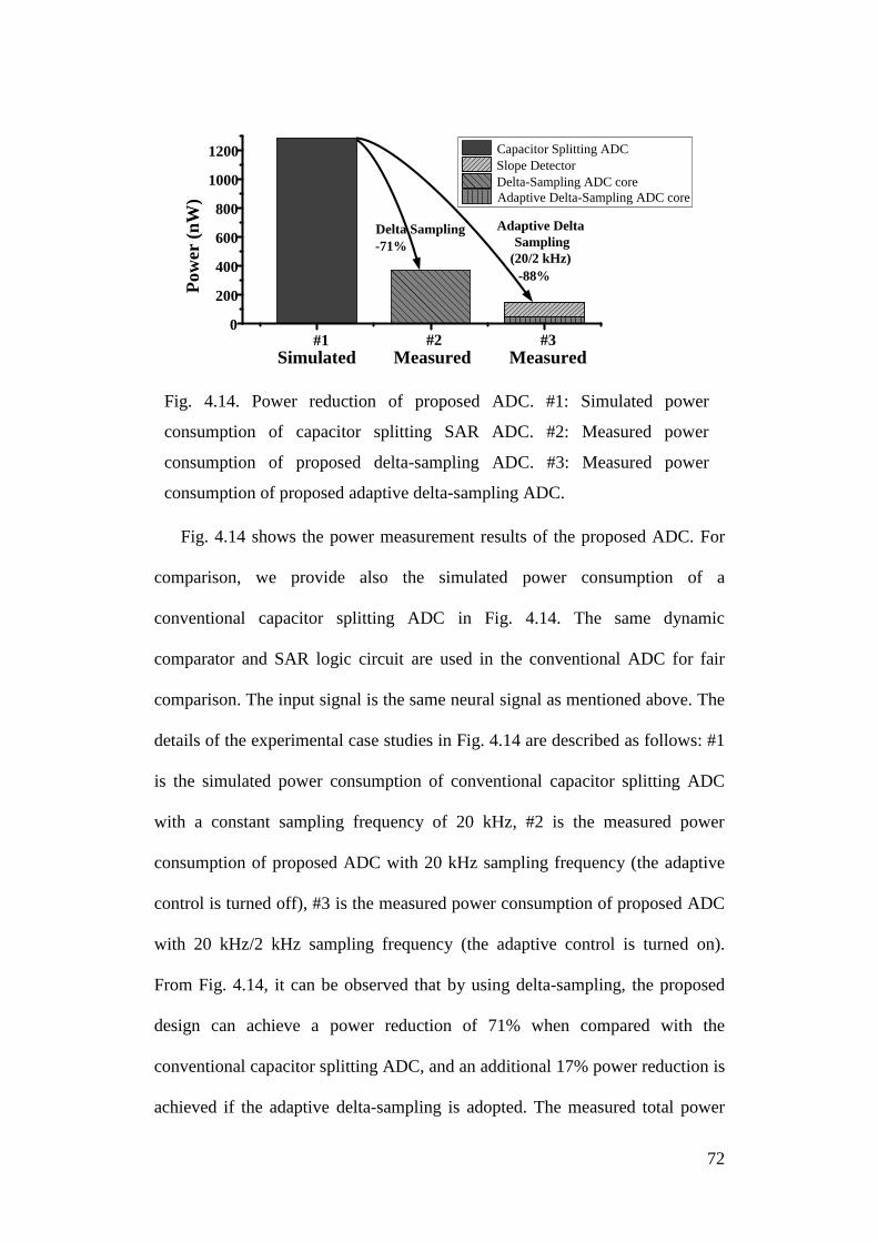
72
Fig. 4.14 shows the power measurement results of the proposed ADC. For
comparison, we provide also the simulated power consumption of a
conventional capacitor splitting ADC in Fig. 4.14. The same dynamic
comparator and SAR logic circuit are used in the conventional ADC for fair
comparison. The input signal is the same neural signal as mentioned above. The
details of the experimental case studies in Fig. 4.14 are described as follows: #1
is the simulated power consumption of conventional capacitor splitting ADC
with a constant sampling frequency of 20 kHz, #2 is the measured power
consumption of proposed ADC with 20 kHz sampling frequency (the adaptive
control is turned off), #3 is the measured power consumption of proposed ADC
with 20 kHz/2 kHz sampling frequency (the adaptive control is turned on).
From Fig. 4.14, it can be observed that by using delta-sampling, the proposed
design can achieve a power reduction of 71% when compared with the
conventional capacitor splitting ADC, and an additional 17% power reduction is
achieved if the adaptive delta-sampling is adopted. The measured total power
Fig. 4.14. Power reduction of proposed ADC. #1: Simulated power
consumption of capacitor splitting SAR ADC. #2: Measured power
consumption of proposed delta-sampling ADC. #3: Measured power
consumption of proposed adaptive delta-sampling ADC.
-71%
Delta Sampling
P
ow
er (
nW
)
Capacitor Splitting ADC
Slope Detector
Delta-Sampling ADC core
#1 #2 #3
Simulated Measured Measured
Adaptive Delta
Sampling
(20/2 kHz)
-88%
0
200
400
600
800
1000
1200
Adaptive Delta-Sampling ADC core
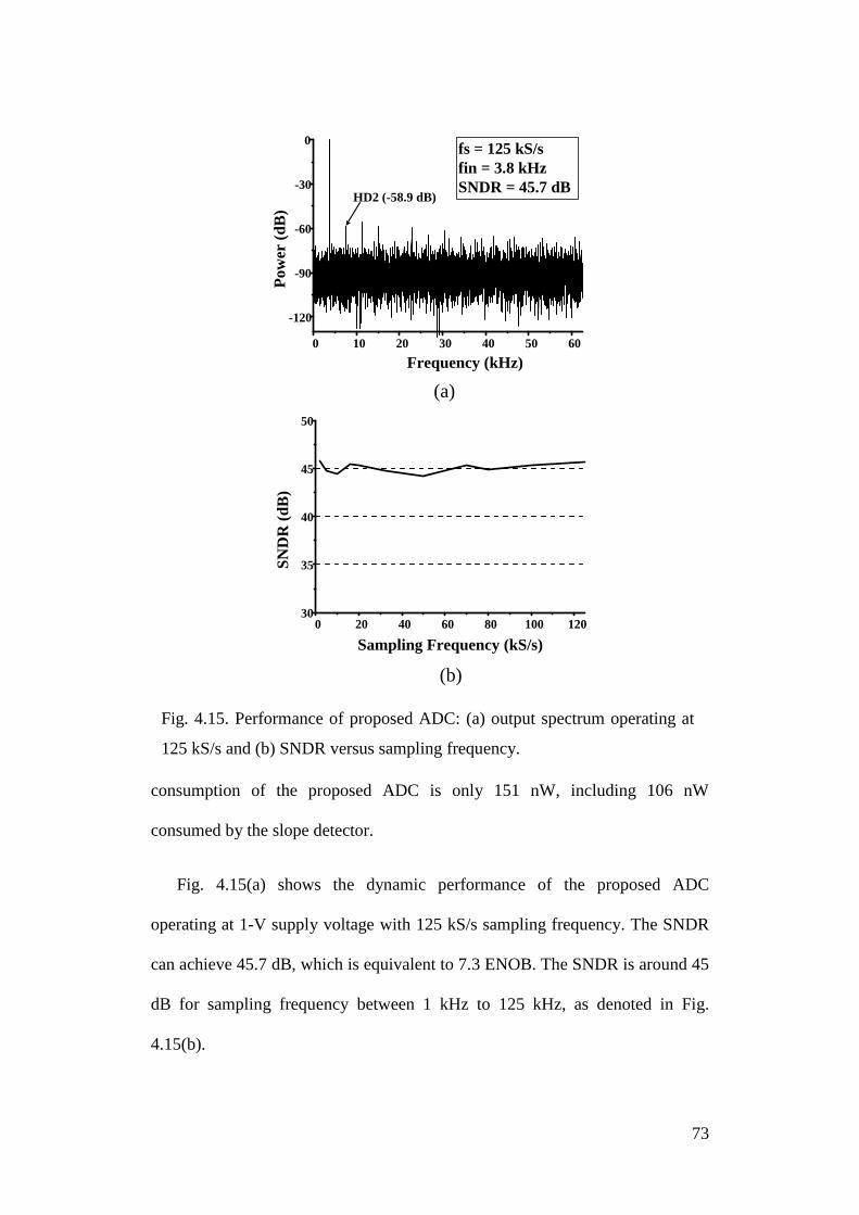
73
consumption of the proposed ADC is only 151 nW, including 106 nW
consumed by the slope detector.
Fig. 4.15(a) shows the dynamic performance of the proposed ADC
operating at 1-V supply voltage with 125 kS/s sampling frequency. The SNDR
can achieve 45.7 dB, which is equivalent to 7.3 ENOB. The SNDR is around 45
dB for sampling frequency between 1 kHz to 125 kHz, as denoted in Fig.
4.15(b).
Fig. 4.15. Performance of proposed ADC: (a) output spectrum operating at
125 kS/s and (b) SNDR versus sampling frequency.
0 10 20 30 40 50 60
-120
-90
-60
-30
0
Po
wer
(d
B)
Frequency (kHz)
fs = 125 kS/s
fin = 3.8 kHz
SNDR = 45.7 dB
(a)
HD2 (-58.9 dB)
0 20 40 60 80 100 12030
35
40
45
50
SN
DR
(d
B)
Sampling Frequency (kS/s)
(b)
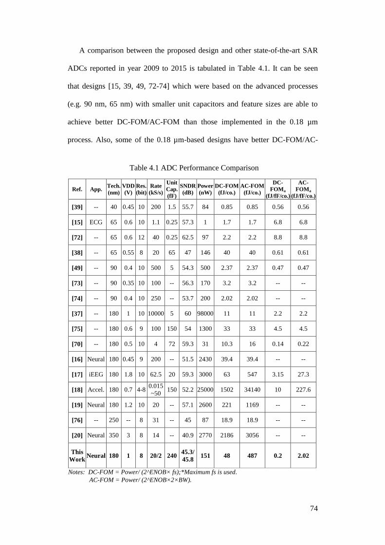
74
A comparison between the proposed design and other state-of-the-art SAR
ADCs reported in year 2009 to 2015 is tabulated in Table 4.1. It can be seen
that designs [15, 39, 49, 72-74] which were based on the advanced processes
(e.g. 90 nm, 65 nm) with smaller unit capacitors and feature sizes are able to
achieve better DC-FOM/AC-FOM than those implemented in the 0.18 µm
process. Also, some of the 0.18 µm-based designs have better DC-FOM/AC-
Table 4.1 ADC Performance Comparison
Ref. App. Tech.
(nm)
VDD
(V)
Res.
(bit)
Rate
(kS/s)
Unit
Cap.
(fF)
SNDR
(dB)
Power
(nW)
DC-FOM
(fJ/co.)
AC-FOM
(fJ/co.)
DC-
FOMa
(fJ/fF/co.)
AC-
FOMa
(fJ/fF/co.)
[39] -- 40 0.45 10 200 1.5 55.7 84 0.85 0.85 0.56 0.56
[15] ECG 65 0.6 10 1.1 0.25 57.3 1 1.7 1.7 6.8 6.8
[72] -- 65 0.6 12 40 0.25 62.5 97 2.2 2.2 8.8 8.8
[38] -- 65 0.55 8 20 65 47 146 40 40 0.61 0.61
[49] -- 90 0.4 10 500 5 54.3 500 2.37 2.37 0.47 0.47
[73] -- 90 0.35 10 100 -- 56.3 170 3.2 3.2 -- --
[74] -- 90 0.4 10 250 -- 53.7 200 2.02 2.02 -- --
[37] -- 180 1 10 10000 5 60 98000 11 11 2.2 2.2
[75] -- 180 0.6 9 100 150 54 1300 33 33 4.5 4.5
[70] -- 180 0.5 10 4 72 59.3 31 10.3 16 0.14 0.22
[16] Neural 180 0.45 9 200 -- 51.5 2430 39.4 39.4 -- --
[17] iEEG 180 1.8 10 62.5 20 59.3 3000 63 547 3.15 27.3
[18] Accel. 180 0.7 4-8 0.015
~50 150 52.2 25000 1502 34140 10 227.6
[19] Neural 180 1.2 10 20 -- 57.1 2600 221 1169 -- --
[76] -- 250 -- 8 31 -- 45 87 18.9 18.9 -- --
[20] Neural 350 3 8 14 -- 40.9 2770 2186 3056 -- --
This
Work Neural 180 1 8 20/2 240
45.3/
45.8 151 48 487 0.2 2.02
Notes: DC-FOM = Power/ (2^ENOB× fs);*Maximum fs is used.
AC-FOM = Power/ (2^ENOB×2×BW).
75
FOM than the proposed design and this is mainly due to the adoption of smaller
unit capacitor (5 fF in 20) or operating at ultra-low supply voltages (0.6-V in
[75], 0.5-V in [36] and 0.45-V in [16]). Comparing with designs [17-19], which
operate at the nominal supply voltage, the proposed design is able to attain a
better DC-FOM/AC-FOM. To compare the ADC efficiency independent of the
unit capacitor size, as introduced in [40], the DC-FOM/AC-FOM normalized to
the unit capacitor, i.e., DC-FOMa/AC-FOMa, can be considered. It can be seen
from Table 4.1 that the proposed design has a relative low DC-FOMa/AC-FOMa.
4.8 Conclusion
This chapter presents a novel ADC with adaptive delta-sampling for ultra-
low power sensing applications. The characteristic of burst-like or sparse
signals is analyzed and we find that that these signals vary slowly during most
of duty cycle. It can be observed that the first 4 MSBs remain the same during
several consecutive samples both in ECG and neural signals. By reducing the
binary search range through delta-sampling, the power consumption of ADC is
significantly reduced when applied for converting the sparse signals. In the
meanwhile, the overload of the ADC is avoided by adaptively adjusting the
sampling frequency according to the slope of the input signal. The ADC
consumes only 151 nW while achieving 7.3 ENOB with adaptive sampling
frequency of 20 kHz/2 kHz for a neural signal acquisition application.
Equation Chapter (Next) Section 1
76
Chapter 5
A 10-bit 300 kS/s Reference-Voltage
Regulator Free Asynchronous SAR
ADC
As one of the typical health monitoring applications, wireless implantable
medical devices are powered via wireless power transfer, as shown in Fig. 5.1.
A rectifier is mandatory to convert the coupled AC power into DC power. Even
with advanced rectifiers such as the reconfigurable resonant regulating rectifier
(R3 rectifier), the ripple of the rectified voltage can still be in tens of mV [77,
78]. For conventional SAR ADCs adopted in such systems [16, 40, 43, 45, 79-
82], a dedicated regulator is needed to stabilize the reference voltage to the
ADC core. However, the regulator consumes significant power consumption
[43, 79, 80]. Besides, decoupling capacitors of a few hundred pF or larger
values are needed to maintain a stable operation of the regulator [83, 84]. As
decoupling capacitors are preferred to be on chip in wireless implantable
medical devices for system miniaturization, the increase in silicon area and
hence cost are inevitable.
However, as mentioned in Section 2.4 , there are a few designs had looked
at optimizing the reference-voltage regulator and clock source for the ADC. It
has been found that if the power consumption of the reference-voltage regulator
77
is included, the FOM of ADC degrades from 100 fJ/c-s to 1000 fJ/c-s [79], or
from 25 fJ/c-s to 738 fJ/c-s [80]. In [43], a SAR ADC with energy-efficient
reference generation is proposed where the power saving is realized through
applying a duty-cycle technique in the reference generator. However, an
always-on low dropout regulator is needed to drive the ADC core, which leads
to quiescent current and dropout voltage. The power dissipated by the regulator
accounts for more than 30% of the total power consumption of the SAR ADC.
Besides, large decoupling capacitor is needed to maintain a stable operation of
the regulator.
In this paper, we present a reference-voltage regulator free asynchronous
SAR ADC using self-timed pre-charging for wireless-powered implantable
medical devices. It eliminates the power hungry reference-voltage regulator to
reduce the overall power consumption of the SAR ADC. Also, large on-chip
decoupling capacitor is eliminated to help reduce the silicon area. Besides, this
Fig. 5.1. Block diagram of typical wireless implantable medical device.
Rectifier
DSP ADCTransceiverReceiver
VDD Vref
PowerRelaxed/
Removable
Wireless Implantable Medical Device
Skin
Large RippleSmall Ripple
RegulatorRegulator Regulator
Analog
Front-End
Sen
sors
78
SAR ADC can operate in fully asynchronous mode, where the ADC can
function without any external clock source. The proposed design achieves good
SNDR under supply voltage fluctuation.
5.1 Charge-Sharing SAR
The charge-sharing SAR ADC of Fig. 5.2 uses passive charge sharing
instead of the active charge redistribution that is commonly deployed in
conventional SAR ADCs [45]. During the sampling period, the input signal is
sampled by sampling capacitors Cs. Meanwhile, the DAC capacitors are pre-
charged with binary-scaled charges, i.e. Ci×Vref. Once the sampling period is
completed, a comparator performs the first comparison and following the
comparison result, the MSB charge is added or subtracted to the sampling
capacitors, by turning on one of the pairs of switches Sp or Sn. By doing this, the
differential charge stored in the sampling capacitors will converge to zero. This
Fig. 5.2. 3-bit charge-sharing SAR ADC.
Q4Q 2Q
Vinp
Vinn
SAR Logic
Cs
Cs
Vref
DVDD
AVDDAVDD
Sp
Sp
Sn
fs
fs
Ci
79
operation is repeated until the LSB decision is obtained, which also symbolizes
that one conversion is completed.
In order to analyses the influence of power line ripples, we separate power
supply of charge-sharing SAR ADC into three power domains, i.e. AVDD,
DVDD and Vref. AVDD is used to supply the dynamic comparator and sampling
switch, while DVDD is for the supply SAR logic circuit. DAC capacitors are
powered from Vref. For the dynamic comparators [85], the variation on AVDD
will cause a different delay. With smaller AVDD, the delay will be longer. In
other words, if the minimum value of AVDD can satisfy the speed requirement,
a ripple of tens of mV will have minimum effects on the comparator to
influence the final performance of the ADC. The effects on the sampling switch
are the switch-on resistance and coupling effect. By using clock boosting
technique, the effect on switch-on resistance is also reduced to a minimum. The
coupling effect is lessened by using the minimum size of transistor to ensure
minute coupling capacitor.
For the SAR logic circuit powered by DVDD, the ripple with tens of mV
amplitude will affect only the delay of these digital circuits. If the minimum
DVDD satisfy the timing constrains, the output of the rectifier can be engaged
directly. Basically, the AVDD and DVDD can both be powered by the output of
the rectifier in the wireless implantable medical device. However, the output
voltage of the rectifier with large ripples cannot be used directly as the power
source, i.e. Vref, for charging the DAC capacitor. This because the DAC
capacitor are pre-charged with a charge which is Qi = Ci × Vref. Any disturbance
or error in the reference value Vref will cause a deviation of charges, i.e. Qi, pre-
charged in DAC capacitors. Consequently, the digitized output codes deviate
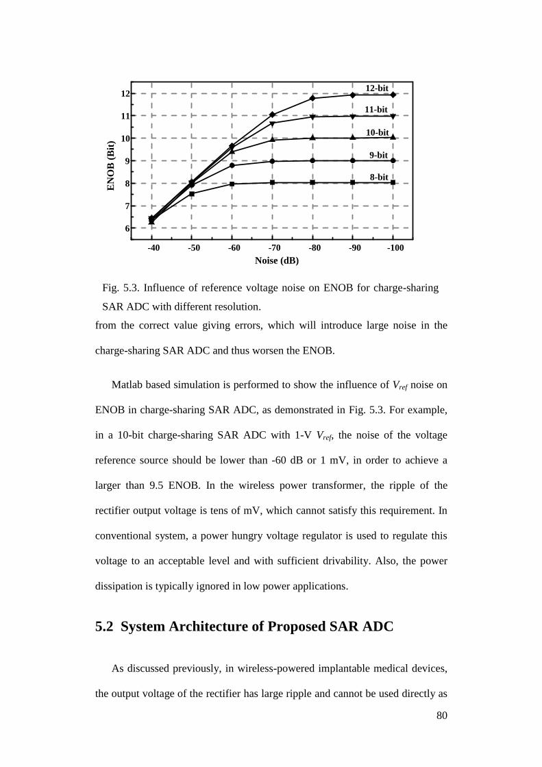
80
from the correct value giving errors, which will introduce large noise in the
charge-sharing SAR ADC and thus worsen the ENOB.
Matlab based simulation is performed to show the influence of Vref noise on
ENOB in charge-sharing SAR ADC, as demonstrated in Fig. 5.3. For example,
in a 10-bit charge-sharing SAR ADC with 1-V Vref, the noise of the voltage
reference source should be lower than -60 dB or 1 mV, in order to achieve a
larger than 9.5 ENOB. In the wireless power transformer, the ripple of the
rectifier output voltage is tens of mV, which cannot satisfy this requirement. In
conventional system, a power hungry voltage regulator is used to regulate this
voltage to an acceptable level and with sufficient drivability. Also, the power
dissipation is typically ignored in low power applications.
5.2 System Architecture of Proposed SAR ADC
As discussed previously, in wireless-powered implantable medical devices,
the output voltage of the rectifier has large ripple and cannot be used directly as
Fig. 5.3. Influence of reference voltage noise on ENOB for charge-sharing
SAR ADC with different resolution.
-40 -50 -60 -70 -80 -90 -100
6
7
8
9
10
11
12
8-bit
10-bit
9-bit
11-bit
12-bit
EN
OB
(B
it)
Noise (dB)
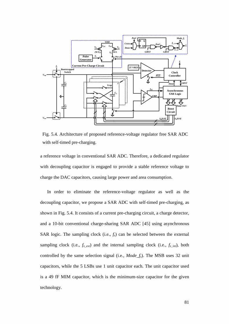
81
a reference voltage in conventional SAR ADC. Therefore, a dedicated regulator
with decoupling capacitor is engaged to provide a stable reference voltage to
charge the DAC capacitors, causing large power and area consumption.
In order to eliminate the reference-voltage regulator as well as the
decoupling capacitor, we propose a SAR ADC with self-timed pre-charging, as
shown in Fig. 5.4. It consists of a current pre-charging circuit, a charge detector,
and a 10-bit conventional charge-sharing SAR ADC [45] using asynchronous
SAR logic. The sampling clock (i.e., fs) can be selected between the external
sampling clock (i.e., fs_ext) and the internal sampling clock (i.e., fs_int), both
controlled by the same selection signal (i.e., Mode_fs). The MSB uses 32 unit
capacitors, while the 5 LSBs use 1 unit capacitor each. The unit capacitor used
is a 49 fF MIM capacitor, which is the minimum-size capacitor for the given
technology.
Fig. 5.4. Architecture of proposed reference-voltage regulator free SAR ADC
with self-timed pre-charging.
98
0
Vinp
Vinn
fs
Vcap
Detector
Asynchronous
SAR Logic
Bootstrapped
Switch
Done
Cu
Cs
Cs
CMP
Sn[0:9]Sp[0:9]
Clock
Controller
fs
Boost
Circuit
2T VREF
GRST
Data<9:0>
GRST
PreCCross
PreC
GRST
D Q
QBDone
Tc
IchL
VDD
VgIchS
Vd
Vg
Pulse
Generator
(W/L)L W/L
Pre-ch
Current Pre-Charge Circuit
PreC
fclk
Mode_fs
fs_ext
fs
fs_int
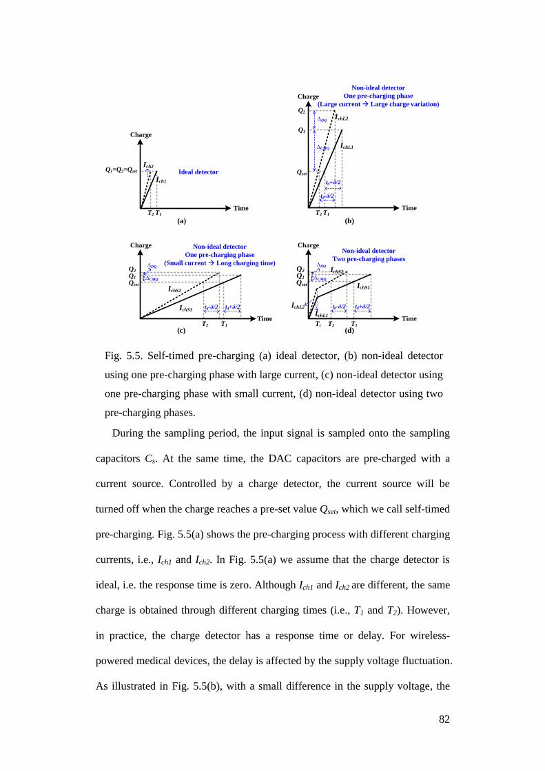
82
During the sampling period, the input signal is sampled onto the sampling
capacitors Cs. At the same time, the DAC capacitors are pre-charged with a
current source. Controlled by a charge detector, the current source will be
turned off when the charge reaches a pre-set value Qset, which we call self-timed
pre-charging. Fig. 5.5(a) shows the pre-charging process with different charging
currents, i.e., Ich1 and Ich2. In Fig. 5.5(a) we assume that the charge detector is
ideal, i.e. the response time is zero. Although Ich1 and Ich2 are different, the same
charge is obtained through different charging times (i.e., T1 and T2). However,
in practice, the charge detector has a response time or delay. For wireless-
powered medical devices, the delay is affected by the supply voltage fluctuation.
As illustrated in Fig. 5.5(b), with a small difference in the supply voltage, the
Fig. 5.5. Self-timed pre-charging (a) ideal detector, (b) non-ideal detector
using one pre-charging phase with large current, (c) non-ideal detector using
one pre-charging phase with small current, (d) non-ideal detector using two
pre-charging phases.
Time
Q1
T2 T1
Q2
Qset
td-δ/2 td+δ/2
∆CMQ
∆DQ
Tc
IchL1
(d)
IchS2
IchS1
IchL2
Time
Q1
T2 T1
Q2
Qset
td-δ/2
td+δ/2
∆DQ
(b)
TimeT2 T1
Q1=Q2=Qset
(a)
Time
Q1
T2 T1
Q2
Qset
td-δ/2 td+δ/2
∆CMQ
(c)
IchS2
IchS1
∆DQ
∆CMQ
IchL2
IchL1
Charge
Charge
Charge Charge
Ideal detector
Non-ideal detector
One pre-charging phase
(Small current Long charging time)
Non-ideal detector
Two pre-charging phases
Ich2
Ich1
Non-ideal detector
One pre-charging phase
(Large current Large charge variation)
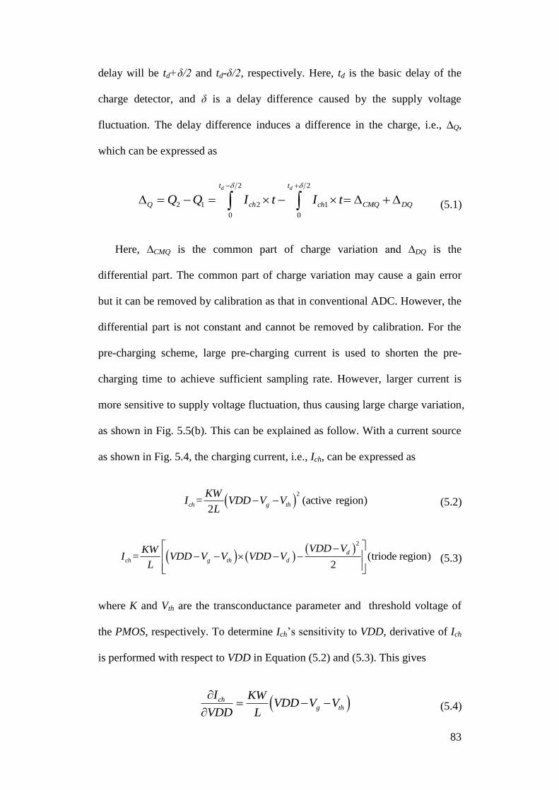
83
delay will be td+δ/2 and td-δ/2, respectively. Here, td is the basic delay of the
charge detector, and δ is a delay difference caused by the supply voltage
fluctuation. The delay difference induces a difference in the charge, i.e., ∆Q,
which can be expressed as
2 2
2 1 2 1
0 0
d dt t
Q ch ch CMQ DQQ Q I t I t
(5.1)
Here, ∆CMQ is the common part of charge variation and ∆DQ is the
differential part. The common part of charge variation may cause a gain error
but it can be removed by calibration as that in conventional ADC. However, the
differential part is not constant and cannot be removed by calibration. For the
pre-charging scheme, large pre-charging current is used to shorten the pre-
charging time to achieve sufficient sampling rate. However, larger current is
more sensitive to supply voltage fluctuation, thus causing large charge variation,
as shown in Fig. 5.5(b). This can be explained as follow. With a current source
as shown in Fig. 5.4, the charging current, i.e., Ich, can be expressed as
2
= (active region)2
ch g th
KWI VDD V V
L (5.2)
2
= (triode region)2
d
ch g th d
VDD VKWI VDD V V VDD V
L
(5.3)
where K and Vth are the transconductance parameter and threshold voltage of
the PMOS, respectively. To determine Ich’s sensitivity to VDD, derivative of Ich
is performed with respect to VDD in Equation (5.2) and (5.3). This gives
ch
g th
I KWVDD V V
VDD L
(5.4)

84
From Equation(5.4), it can be seen that with smaller (VDD-Vg-Vth) or current
Ich, the current’s sensitivity to VDD is smaller, which results in smaller charge
variation (see Fig. 5.5(c)). However, smaller pre-charging current needs longer
charging time, and this limits the sampling rate of the ADC.
To achieve sufficient sampling rate while ensuring a small charge variation
(less than 1 LSB charge), we proposed a pre-charging scheme with two
charging phases, as shown in Fig. 5.5(d). During the first charging phase, the
DAC capacitors are quickly charged with large charging current (i.e., IchL) and
constant charging time (i.e., Tc). In the second charging phase, small charging
current (i.e., IchS) is used to complete the rest of charging and is turned off when
the charge reaches the pre-set value Qset. By using the two-phase pre-charging
scheme, the charge variation is reduced and the charging time is also shortened.
5.3 Fully Asynchronous Operation
To further improve on the overall energy-efficiency of the SAR ADC, the
proposed SAR ADC is to operate without any external clock source. This can
be achieved by assigning internal sampling clock (fs_int) to fs, as shown in Fig.
5.4. fs_int is generated during the self-timed pre-charging process which acts as a
relaxation oscillator. The binary search algorithm is controlled by the
asynchronous SAR logic [85]. Fig. 5.6 shows the timing diagram of the
proposed SAR ADC. The active low global reset signal (GRST), which is an
off-chip signal, is used to reset all other signals in the SAR ADC. After the first
conversion is completed, a pulse Done is generated, which changes the phase of
the pre-charging signal PreC from low to high. During the pre-charging phase,
the DAC capacitors are charged by the proposed self-timed pre-charging
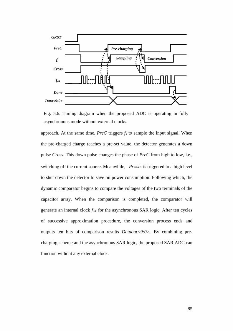
85
approach. At the same time, PreC triggers fs to sample the input signal. When
the pre-charged charge reaches a pre-set value, the detector generates a down
pulse Cross. This down pulse changes the phase of PreC from high to low, i.e.,
switching off the current source. Meanwhile, Pr ech is triggered to a high level
to shut down the detector to save on power consumption. Following which, the
dynamic comparator begins to compare the voltages of the two terminals of the
capacitor array. When the comparison is completed, the comparator will
generate an internal clock fclk for the asynchronous SAR logic. After ten cycles
of successive approximation procedure, the conversion process ends and
outputs ten bits of comparison results Dataout<9:0>. By combining pre-
charging scheme and the asynchronous SAR logic, the proposed SAR ADC can
function without any external clock.
Fig. 5.6. Timing diagram when the proposed ADC is operating in fully
asynchronous mode without external clocks.
PreC
fs
Cross
GRST
fclk
Done
Data<9:0>
Pre-charging
ConversionSampling
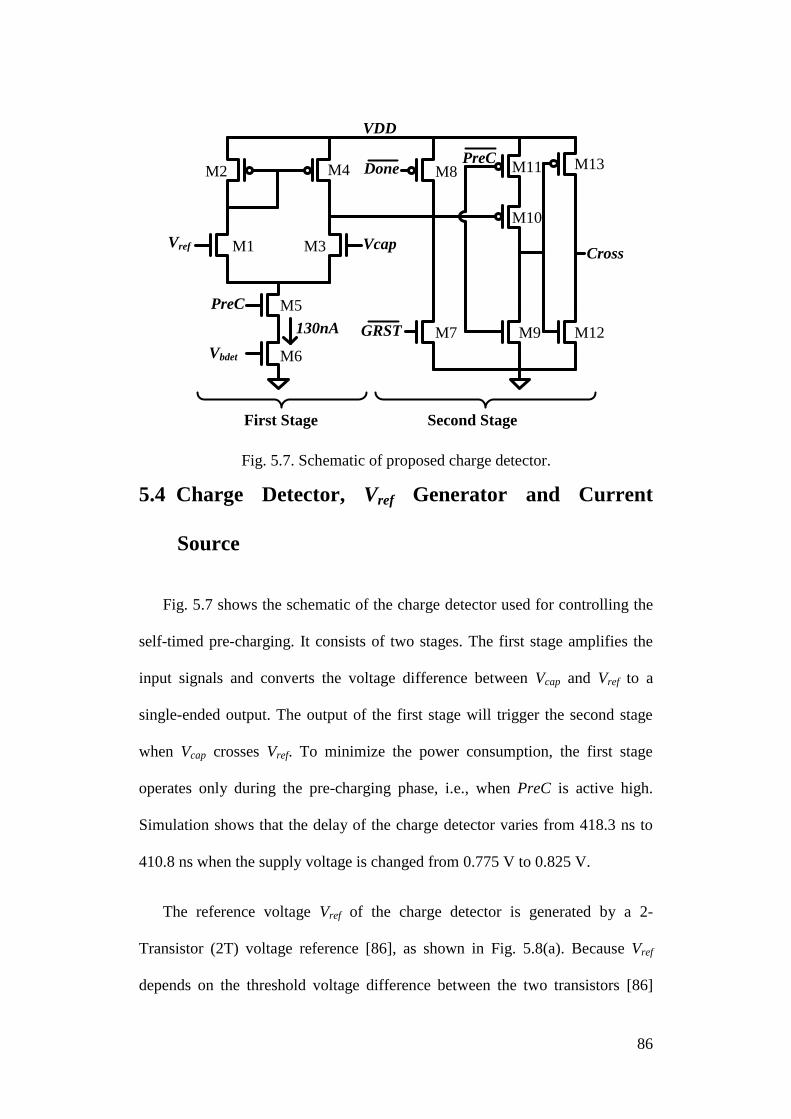
86
5.4 Charge Detector, Vref Generator and Current
Source
Fig. 5.7 shows the schematic of the charge detector used for controlling the
self-timed pre-charging. It consists of two stages. The first stage amplifies the
input signals and converts the voltage difference between Vcap and Vref to a
single-ended output. The output of the first stage will trigger the second stage
when Vcap crosses Vref. To minimize the power consumption, the first stage
operates only during the pre-charging phase, i.e., when PreC is active high.
Simulation shows that the delay of the charge detector varies from 418.3 ns to
410.8 ns when the supply voltage is changed from 0.775 V to 0.825 V.
The reference voltage Vref of the charge detector is generated by a 2-
Transistor (2T) voltage reference [86], as shown in Fig. 5.8(a). Because Vref
depends on the threshold voltage difference between the two transistors [86]
Fig. 5.7. Schematic of proposed charge detector.
VcapVref
Done
GRST
PreC
PreC
Cross
VDD
130nA
Vbdet
First Stage Second Stage
M4
M5
M6
M1
M2
M3
M8 M11
M12M9M7
M10
M13
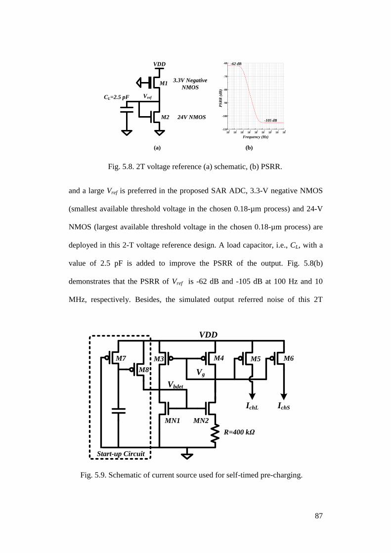
87
and a large Vref is preferred in the proposed SAR ADC, 3.3-V negative NMOS
(smallest available threshold voltage in the chosen 0.18-µm process) and 24-V
NMOS (largest available threshold voltage in the chosen 0.18-µm process) are
deployed in this 2-T voltage reference design. A load capacitor, i.e., CL, with a
value of 2.5 pF is added to improve the PSRR of the output. Fig. 5.8(b)
demonstrates that the PSRR of Vref is -62 dB and -105 dB at 100 Hz and 10
MHz, respectively. Besides, the simulated output referred noise of this 2T
Fig. 5.8. 2T voltage reference (a) schematic, (b) PSRR.
(b)(a)
VDD
Vref
3.3V Negative
NMOS
24V NMOS
CL=2.5 pF
100
101
102
103
104
105
106
107
108
-110
-100
-90
-80
-70
-60 -62 dB
PS
RR
(d
B)
Frequency (Hz)
-105 dB
M1
M2
Fig. 5.9. Schematic of current source used for self-timed pre-charging.
Vg
VDD
Vbdet
Start-up Circuit
IchL IchS
MN1 MN2
R=400 kΩ
M3 M4 M5 M6M7
M8

88
voltage reference is 41µV, which is negligible as compared to the 1 LSB.
The schematic of the current source used for pre-charging is given in Fig.
5.9. The circuit consists of a beta-multiplier reference, a start-up circuit and a
current mirror. The reference current, Iref, is equal to the difference of the
threshold voltage between MN1 and MN2 divided by the value of resistor R,
which is supply independent. The output currents IchL and IchS, are generated
from Iref through current mirror. The IchL is used as the first phase charging
current and is about 14 µA. The IchS is used as the second phase charging
current and is about 200 nA. The values of IchL and IchS are determined through
extensive simulation by considering both the charge variation and pre-charging
time. Fig. 5.10 shows that when VDD is larger than 0.6 V, the sensitivity of IchL
and IchS to VDD are 19 µA/V and 36 nA/V, respectively. With smaller current,
the sensitivity is much lower, which verified the previous analysis in Section
5.2 . To save power and area, the beta-multiplier reference also generates Vbdet
for the first stage amplifier in the charge detector.
Fig. 5.10. Pre-charging currents, IchL and IchS, vary with VDD.
(0.775,203.9)
(0.825,205.7)
0.0 0.2 0.4 0.6 0.8 1.00
2
4
6
8
10
12
14
16
4.2 /V
VDD (V)
0.0 0.2 0.4 0.6 0.8 1.00
40
80
120
160
200
240
36 nA/V
VDD (V)
(a) (b)
I ch
L (
µA
)
I ch
S (
nA
)
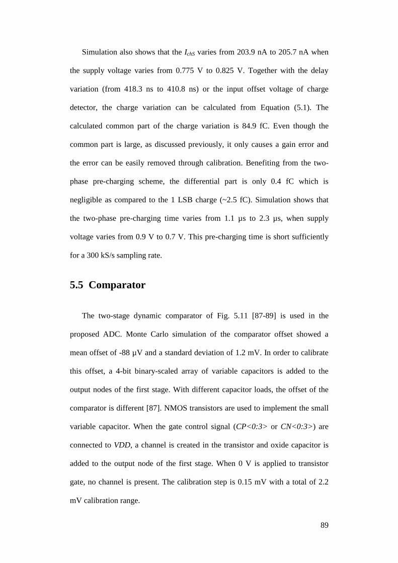
89
Simulation also shows that the IchS varies from 203.9 nA to 205.7 nA when
the supply voltage varies from 0.775 V to 0.825 V. Together with the delay
variation (from 418.3 ns to 410.8 ns) or the input offset voltage of charge
detector, the charge variation can be calculated from Equation (5.1). The
calculated common part of the charge variation is 84.9 fC. Even though the
common part is large, as discussed previously, it only causes a gain error and
the error can be easily removed through calibration. Benefiting from the two-
phase pre-charging scheme, the differential part is only 0.4 fC which is
negligible as compared to the 1 LSB charge (~2.5 fC). Simulation shows that
the two-phase pre-charging time varies from 1.1 µs to 2.3 µs, when supply
voltage varies from 0.9 V to 0.7 V. This pre-charging time is short sufficiently
for a 300 kS/s sampling rate.
5.5 Comparator
The two-stage dynamic comparator of Fig. 5.11 [87-89] is used in the
proposed ADC. Monte Carlo simulation of the comparator offset showed a
mean offset of -88 µV and a standard deviation of 1.2 mV. In order to calibrate
this offset, a 4-bit binary-scaled array of variable capacitors is added to the
output nodes of the first stage. With different capacitor loads, the offset of the
comparator is different [87]. NMOS transistors are used to implement the small
variable capacitor. When the gate control signal (CP<0:3> or CN<0:3>) are
connected to VDD, a channel is created in the transistor and oxide capacitor is
added to the output node of the first stage. When 0 V is applied to transistor
gate, no channel is present. The calibration step is 0.15 mV with a total of 2.2
mV calibration range.
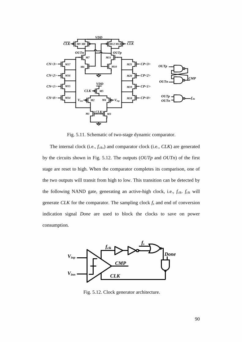
90
The internal clock (i.e., fclk,) and comparator clock (i.e., CLK) are generated
by the circuits shown in Fig. 5.12. The outputs (OUTp and OUTn) of the first
stage are reset to high. When the comparator completes its comparison, one of
the two outputs will transit from high to low. This transition can be detected by
the following NAND gate, generating an active-high clock, i.e., fclk. fclk will
generate CLK for the comparator. The sampling clock fs and end of conversion
indication signal Done are used to block the clocks to save on power
consumption.
Fig. 5.11. Schematic of two-stage dynamic comparator.
CMP
CLK
VinpVinn
VDD
VDD
CP<0>
CP<1>
CP<2>
CP<3>
CN<0>
CN<1>
CN<2>
CN<3>
OUTpOUTn
OUTp
OUTn
OUTp
OUTnfclk
CLK
CLK
CLKM1
M2
M3
M4
M6
M5
M7
M8M9
M10
M11
M12 M13
M15
M14
M16
M17
M18
M19
M20
M21
Fig. 5.12. Clock generator architecture.
fclk
CLK
CMP
fs
DoneVinp
Vinn
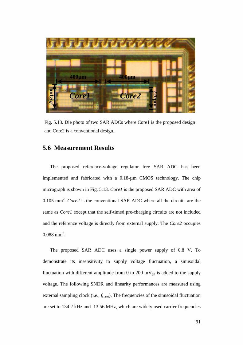
91
5.6 Measurement Results
The proposed reference-voltage regulator free SAR ADC has been
implemented and fabricated with a 0.18-µm CMOS technology. The chip
micrograph is shown in Fig. 5.13. Core1 is the proposed SAR ADC with area of
0.105 mm2. Core2 is the conventional SAR ADC where all the circuits are the
same as Core1 except that the self-timed pre-charging circuits are not included
and the reference voltage is directly from external supply. The Core2 occupies
0.088 mm2.
The proposed SAR ADC uses a single power supply of 0.8 V. To
demonstrate its insensitivity to supply voltage fluctuation, a sinusoidal
fluctuation with different amplitude from 0 to 200 mVpp is added to the supply
voltage. The following SNDR and linearity performances are measured using
external sampling clock (i.e., fs_ext). The frequencies of the sinusoidal fluctuation
are set to 134.2 kHz and 13.56 MHz, which are widely used carrier frequencies
Fig. 5.13. Die photo of two SAR ADCs where Core1 is the proposed design
and Core2 is a conventional design.
Core1 Core2
26
2µ
m
400µm
22
0µ
m
400µm
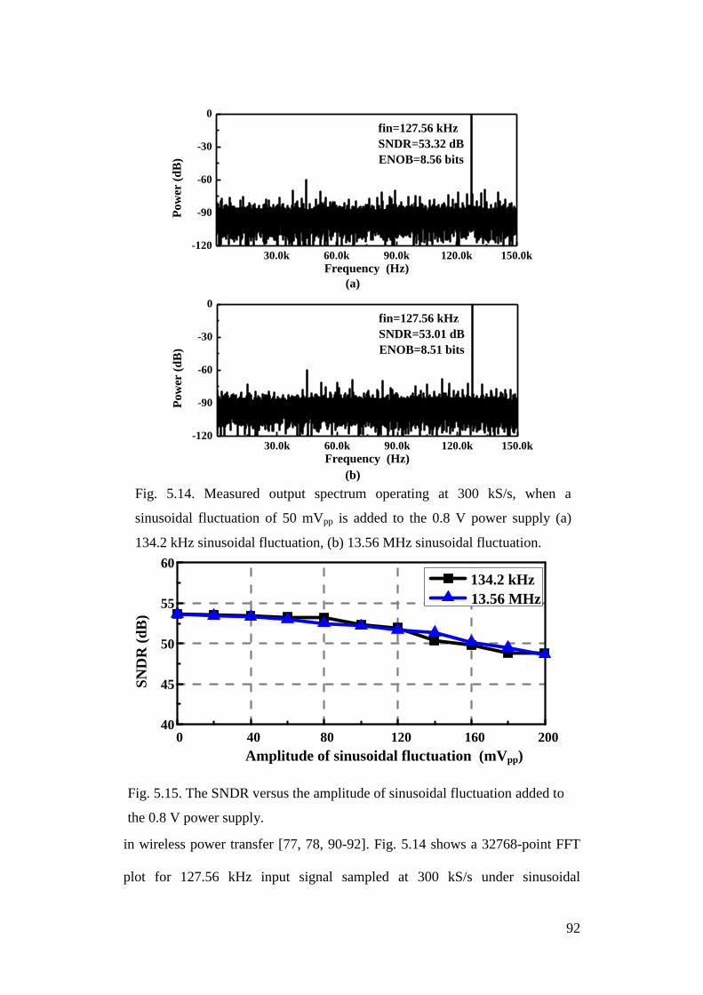
92
in wireless power transfer [77, 78, 90-92]. Fig. 5.14 shows a 32768-point FFT
plot for 127.56 kHz input signal sampled at 300 kS/s under sinusoidal
Fig. 5.14. Measured output spectrum operating at 300 kS/s, when a
sinusoidal fluctuation of 50 mVpp is added to the 0.8 V power supply (a)
134.2 kHz sinusoidal fluctuation, (b) 13.56 MHz sinusoidal fluctuation.
30.0k 60.0k 90.0k 120.0k 150.0k-120
-90
-60
-30
0
fin=127.56 kHz
SNDR=53.01 dB
ENOB=8.51 bits
Po
wer
(d
B)
Frequency (Hz)
(a)
(b)
30.0k 60.0k 90.0k 120.0k 150.0k-120
-90
-60
-30
0
fin=127.56 kHz
SNDR=53.32 dB
ENOB=8.56 bits
Pow
er (
dB
)
Frequency (Hz)
Fig. 5.15. The SNDR versus the amplitude of sinusoidal fluctuation added to
the 0.8 V power supply.
0 40 80 120 160 20040
45
50
55
60
SN
DR
(d
B)
Amplitude of sinusoidal fluctuation (mVpp)
134.2 kHz
13.56 MHz
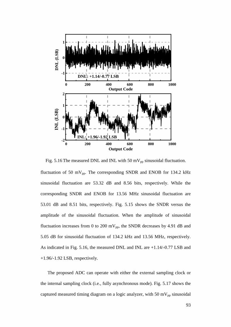
93
fluctuation of 50 mVpp. The corresponding SNDR and ENOB for 134.2 kHz
sinusoidal fluctuation are 53.32 dB and 8.56 bits, respectively. While the
corresponding SNDR and ENOB for 13.56 MHz sinusoidal fluctuation are
53.01 dB and 8.51 bits, respectively. Fig. 5.15 shows the SNDR versus the
amplitude of the sinusoidal fluctuation. When the amplitude of sinusoidal
fluctuation increases from 0 to 200 mVpp, the SNDR decreases by 4.91 dB and
5.05 dB for sinusoidal fluctuation of 134.2 kHz and 13.56 MHz, respectively.
As indicated in Fig. 5.16, the measured DNL and INL are +1.14/-0.77 LSB and
+1.96/-1.92 LSB, respectively.
The proposed ADC can operate with either the external sampling clock or
the internal sampling clock (i.e., fully asynchronous mode). Fig. 5.17 shows the
captured measured timing diagram on a logic analyzer, with 50 mVpp sinusoidal
Fig. 5.16 The measured DNL and INL with 50 mVpp sinusoidal fluctuation.
0 200 400 600 800 1000
-1
0
1
DNL: +1.14/-0.77 LSB
DN
L (
LS
B)
Output Code
0 200 400 600 800 1000-2
-1
0
1
2
INL: +1.96/-1.92 LSB
INL
(L
SB
)
Output Code

94
fluctuation. When an external sampling clock is applied to fs, the sampling clock
is kept constant while the pre-charging period (i.e., PreC) varies with the supply
voltage fluctuation, as shown in Fig. 5.17 (a). When the internal sampling clock
fs_int is applied to fs, i.e., operating in fully asynchronous mode, both the
sampling clock and the pre-charging period vary with the supply voltage
fluctuation (see Fig. 5.17 (b)). Without any external clock source, the proposed
ADC can save the power consumption and chip area at system level.
The measured total power consumption of the proposed SAR ADC (i.e.,
Core1) including the self-timed pre-charging circuits is 2.72 µW at 300 kS/s
and the corresponding FOM is 23.9 fJ/c-s. Under the same testing conditions,
the measured power consumption of the conventional SAR ADC (i.e., Core2) is
2.52 µW. Therefore, the power dissipation of the self-timed pre-charging
circuits is around 0.2 µW. This accounts for only 7.3% of the total power
consumption of ADC, while a reference-voltage regulator typically consumes at
least 30% [43] or even several times [79, 80] of the power consumption of ADC.
Fig. 5.17 Measured timing diagram (a) using external sampling clock, fs_extfs,
(b) using internal sampling clock, fs_intfs.
3.33 µs 3.33 µs2.22 µs
0.175 µs
1.66 µs
Done
PreCfs
fclk
Data<9:0>
2.68 µs
0.125 µs
2.21 µs 1.43 µs1.82 µs
Done
PreCfs
fclk
Data<9:0>(b)
(a)
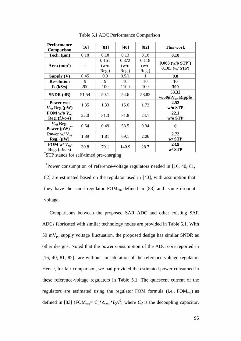
95
Comparisons between the proposed SAR ADC and other existing SAR
ADCs fabricated with similar technology nodes are provided in Table 5.1. With
50 mVpp supply voltage fluctuation, the proposed design has similar SNDR as
other designs. Noted that the power consumption of the ADC core reported in
[16, 40, 81, 82] are without consideration of the reference-voltage regulator.
Hence, for fair comparison, we had provided the estimated power consumed in
these reference-voltage regulators in Table 5.1. The quiescent current of the
regulators are estimated using the regulator FOM formula (i.e., FOMreg) as
defined in [83] (FOMreg= Cd*∆vout*IQ/I2, where Cd is the decoupling capacitor,
Table 5.1 ADC Performance Comparison
Performance
Comparison [16] [81] [40] [82] This work
Tech. (µm) 0.18 0.18 0.13 0.18 0.18
Area (mm2) --
0.151
(w/o
Reg.)
0.872
(w/o
Reg.)
0.118
(w/o
Reg.)
0.088 (w/o STP*)
0.105 (w/ STP)
Supply (V) 0.45 0.9 0.5/1 1 0.8
Resolution 9 9 10 10 10
fs (kS/s) 200 100 1100 100 300
SNDR (dB) 51.54 50.1 54.6 58.83 53.32
w/50mVpp Ripple
Power w/o
Vref Reg.(µW) 1.35 1.33 15.6 1.72
2.52
w/o STP
FOM w/o Vref
Reg. (fJ/c-s) 22.0 51.3 31.8 24.1
22.1
w/o STP
Vref Reg.
Power (µW)**
0.54 0.49 53.5 0.34 0
Power w/ Vref
Reg. (µW) 1.89 1.81 69.1 2.06
2.72
w/ STP
FOM w/ Vref
Reg. (fJ/c-s) 30.8 70.1 140.9 28.7
23.9
w/ STP *STP stands for self-timed pre-charging.
**Power consumption of reference-voltage regulators needed in [16, 40, 81,
82] are estimated based on the regulator used in [43], with assumption that
they have the same regulator FOMreg defined in [83] and same dropout
voltage.
96
∆vout is 1 LSB, IQ is the regulators’ quiescent current and I is the current used to
charge DAC capacitors). Assuming that all the designs have the same Cd and
FOMreg value as in [43], the quiescent current of the reference-voltage regulator
for each design can be calculated using the above FOMreg formula. Besides, we
assume a dropout voltage of 0.2 V as in [43]. Based on the quiescent current
and the dropout voltage, the total power consumption of regulator for each
design can be calculated as shown in Table 5.1. The results show that the
proposed self-timed pre-charging SAR ADC achieves a better FOM than the
other designs when taking into account the reference-voltage regulator.
Including the self-timed pre-charging circuits, the area of the proposed design is
similar to that of the other designs without reference-voltage regulator.
Moreover, decoupling capacitor is not required in our design, which helps
further reduce the total area and cost.
5.7 Conclusion
In this chapter, we had looked at optimizing the reference-voltage regulator
and clock source for the ADC. It has been found that if the power consumption
of the reference-voltage regulator is included, the FOM of ADC degrades
significantly. Therefore, a SAR ADC with self-timed pre-charging is proposed
to eliminate power- and area-consuming reference-voltage regulator and
decoupling capacitor for wireless-powered implantable medical devices.
Fabricated with a 0.18-µm CMOS technology, the proposed self-timed pre-
charging SAR ADC achieves a SNDR of 53.32 dB at 0.8 V with 50 mVpp
supply voltage fluctuation, while consuming a total power of 2.72 µW at 300

97
kS/s sampling rate. Including the self-timed pre-charging circuits, the total
FOM is 23.9 fJ/c-s and the total area is 0.105 mm2.
Equation Chapter (Next) Section 1
98
Chapter 6
Wide Input 12-bit SAR ADC with
Digital Calibration
For a generic wireless sensor node or biomedical device, it includes the
sensors/actuators, signal processing, communication and energy subsystem [44,
93-95], as shown in Fig. 6.1. The environmental or biopotential signals are
sensed by various sensors. The sensor interface circuits convert these sensed
signals into digital signals to be processed by the digital signal processing
subsystem. Some of the processed results are transmitted to external network
for deployment and some are used to control the actuators. To achieve the
features of wireless sensor nodes such as long life and small volume, energy-
and area- efficient electronic circuits have been popularly engaged, including
sensor interface circuits [14, 44, 51, 53, 69], digital signal processing [6, 7, 21]
and wireless communication subsystem [96-98]. On the other hand, an energy
subsystem with high-energy density is desired to efficiently power the
electronic circuitries in these size constrained systems. The Lithium ion (Li-ion)
cell with high energy density (80~125 Wh/kg and 200~450 Wh/kg [99])
among the available commercial battery types is suitable for size constrained
wireless sensor nodes. However, during charging and discharging, the voltage
of the Li-ion cell has to stay within specific maximum and minimum limits due
to its chemical properties. If the voltage limits are exceeded, the cycle life of the
battery may be shortened and even incurs possible risk of explosion [100-104].
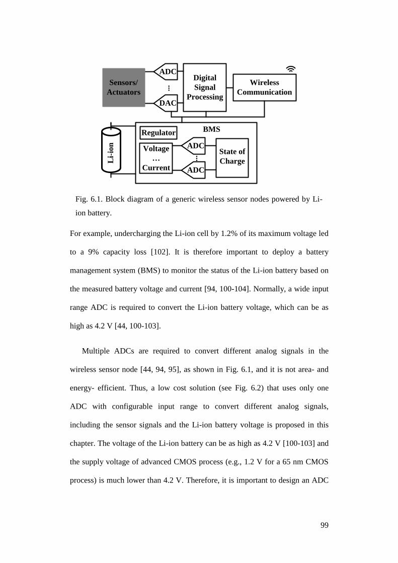
99
For example, undercharging the Li-ion cell by 1.2% of its maximum voltage led
to a 9% capacity loss [102]. It is therefore important to deploy a battery
management system (BMS) to monitor the status of the Li-ion battery based on
the measured battery voltage and current [94, 100-104]. Normally, a wide input
range ADC is required to convert the Li-ion battery voltage, which can be as
high as 4.2 V [44, 100-103].
Multiple ADCs are required to convert different analog signals in the
wireless sensor node [44, 94, 95], as shown in Fig. 6.1, and it is not area- and
energy- efficient. Thus, a low cost solution (see Fig. 6.2) that uses only one
ADC with configurable input range to convert different analog signals,
including the sensor signals and the Li-ion battery voltage is proposed in this
chapter. The voltage of the Li-ion battery can be as high as 4.2 V [100-103] and
the supply voltage of advanced CMOS process (e.g., 1.2 V for a 65 nm CMOS
process) is much lower than 4.2 V. Therefore, it is important to design an ADC
Fig. 6.1. Block diagram of a generic wireless sensor nodes powered by Li-
ion battery.
Wireless
Communication
BMS
Voltage
…
Current
State of
Charge
Regulator
ADC
...
DAC
Digital
Signal
Processing
Sensors/
Actuators
Li-
ion ADC
...
ADC

100
that can convert input signals with maximum voltage of 1.2 V or 4.2 V, while
operating at 1.2 V supply.
This chapter presents a configurable input range (i.e., 1.2 V or 4.2 V) 12-bit
SAR ADC with fast and low power digital background calibration. In
conventional SAR ADC, the reference voltage has to be at least equal to the
input range, i.e., the supply voltage should be at least 4.2 V to convert the 4.2-V
Fig. 6.2. The potential application of the ADC with configurable input range to
convert analog signals with different range.
Sensors
Battery
Current
Battery
Voltage
Vmax=1.2V…
....
Vmax=1.2V
or 4.2Vx1 or x4
ADC with
Configurable
Input Range
Output
IRC
Vmax=1.2V
Vmax=4.2V
Digital
Calibration
Engine
Vrefp Vrefn
Vrefp= 1.2V
Vrefn= 0V
dout
Fig. 6.3. The architecture of proposed differential SAR ADC.
VCM
CLK
Offset Injection
C0C13 C12 C1
Vref
15C010C0
fs
Vinn
CS1CS0
HVBS
IRC
C0C13 C12 C1
Vref
15C010C0
fs
Vinp
CS1CS0
HVBS
IRC
x1 or x4
Output
Digital
Calibration
Engine
SAR Logic
VDACp
VDACn
IRC
dout
101
Li-ion battery. However, in the proposed design, a supply voltage of 1.2 V can
be used to convert the 4.2-V input signal. Therefore, the power consumption
dissipated by the capacitor DAC and digital circuits in the ADC, which is
proportional to square of the reference voltage, is significantly reduced. A high
voltage bootstrapped switch (HVBS) is designed to sample the input signal that
is higher than the supply voltage. Besides, a low power and fast convergence
background digital calibration is used to moderate the capacitor mismatch in the
capacitor DAC. By skipping the lower LSBs calibration, the number of
multipliers used can be reduced, hence saving on power. By injecting different
offsets to the input, the convergence time of the background digital calibration
is shortened. This will be further discussed in Section 6.3.2.
6.1 Architecture of Proposed ADC with Configurable
Input Range
The architecture of the proposed differential SAR ADC is given in Fig. 6.3.
It is designed using the triple-well 65 nm CMOS process. It consists mainly of
high voltage bootstrapped switch (HVBS), 14-bit SAR ADC (with 2 redundant
bits for digital calibration) and a capacitor mismatch digital calibration engine.
The input signal is sampled onto the sampling capacitors, Cs0 and Cs1, where Cs1
= 3Cs0. Following which, the sampled charge on the sampling capacitors is
redistributed on the capacitor DAC. Thus, the internal nodes voltage, i.e., VDACp
and VDACn, can be limited to less than the supply voltage, protecting the internal
circuits from being exposed to high voltage. The sampled charge is adjusted by
the signal IRC according to the range of the input signal. When IRC = 1, both
Cs0 and Cs1 are used to sample the input signal, and the input range is

102
configured to 1.2 V. When IRC = 0, the switch controlling the Cs1 is blocked by
the AND gate. Only Cs0 is used to sample the input signal, which implies that
the input signal is attenuated by 4 due to the charge distribution between Cs0 and
Cs1 (Cs1 =3Cs0). This allows the maximum input signal can be as large as 4.8 V,
which covers the voltage of the Li-ion battery (i.e., 4.2 V). Using the proposed
ADC to convert Li-ion battery voltage can significantly reduce the power
consumption as compared to the conventional ADCs, which must be powered
by a supply of at least 4.2 V. This is because the energy dissipated by the
capacitor DAC and digital circuits in the ADC is proportional to the square of
the supply voltage. When the conversion process ends, the output raw codes are
sent to the digital calibration engine to calibrate the capacitor mismatch, i.e., the
weights of some bits are calibrated. After digital calibration, the codes remain
unchanged or will be multiplied by 4 before the final output, when IRC is set to
1 and 0, respectively.
Fig. 6.4. The schematic of proposed HVBS.
fs
fsb
n1 n2
n3
Vb1
M2
M6
n4
n5
n6
n7
M0 M1
M4
M5
M3
M7
n8
M8
M9n1
fs
M10
M11
M12
n10
n9
Vin
Vout
VDD
Vb1
Vb1 fsb
fsb
M13
M14
M15 M16
M17 M18 M19
M20 M21
M22
M23
M24
M25
n11
n12
n13 n14
n15
n16 n17
n2n1
Vb1
M26 M27
C0 C1
C2C3
Vb2
n11 n13
Vb2M28 M29
Self-generated Bias
3.3 V
PMOS
3.3 V
NMOS

103
6.2 High Voltage Bootstrapped Switch
Conventional high voltage bootstrapped switch utilizes drain-extended
NMOS (DNMOS) transistors and the input range is limited by the drain
terminal breakdown voltage [105, 106]. However, DNMOS is not available in
the 65-nm CMOS process chosen for this work. The highest voltage transistors
available in this process are 3.3-V IO triple well NMOS and 3.3-V PMOS.
Therefore, some improvements based on the designs in [105, 106] have been
made in the proposed high voltage bootstrapped switch (HVBS). Fig. 6.4 shows
Fig. 6.5. Simulated waveforms of the proposed HVBS for a sinusoidal input
with range of 0~4.5 V, operating at a supply voltage of 1.2 V and fs = 500 kHz.
0
1
2
3
4
5
6
f s (
V)
0
1
2
3
4
5
6
V
b2 (
V)
0
1
2
3
4
5
6
n11 (V
)
0
1
2
3
4
5
6
Vin
(V
)
0 10 20 30 40 500
1
2
3
4
5
6
Vou
t (V
)
Time (s)
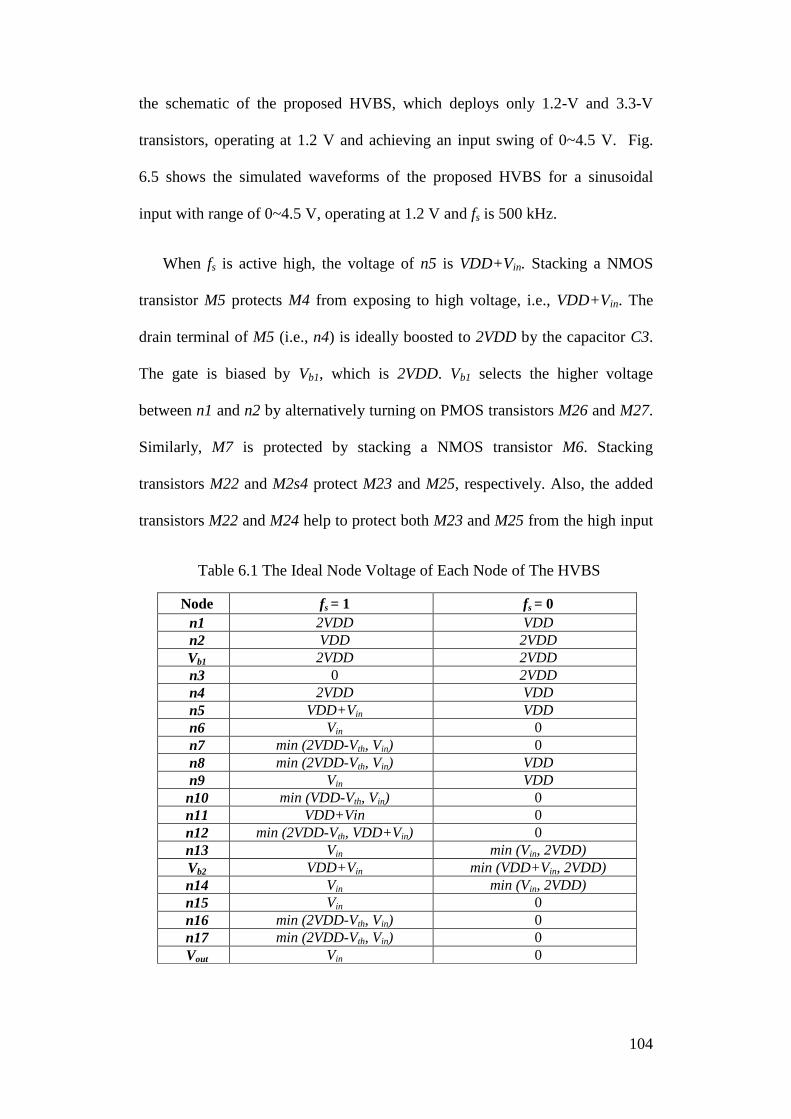
104
the schematic of the proposed HVBS, which deploys only 1.2-V and 3.3-V
transistors, operating at 1.2 V and achieving an input swing of 0~4.5 V. Fig.
6.5 shows the simulated waveforms of the proposed HVBS for a sinusoidal
input with range of 0~4.5 V, operating at 1.2 V and fs is 500 kHz.
When fs is active high, the voltage of n5 is VDD+Vin. Stacking a NMOS
transistor M5 protects M4 from exposing to high voltage, i.e., VDD+Vin. The
drain terminal of M5 (i.e., n4) is ideally boosted to 2VDD by the capacitor C3.
The gate is biased by Vb1, which is 2VDD. Vb1 selects the higher voltage
between n1 and n2 by alternatively turning on PMOS transistors M26 and M27.
Similarly, M7 is protected by stacking a NMOS transistor M6. Stacking
transistors M22 and M2s4 protect M23 and M25, respectively. Also, the added
transistors M22 and M24 help to protect both M23 and M25 from the high input
Table 6.1 The Ideal Node Voltage of Each Node of The HVBS
Node fs = 1 fs = 0
n1 2VDD VDD
n2 VDD 2VDD
Vb1 2VDD 2VDD
n3 0 2VDD
n4 2VDD VDD
n5 VDD+Vin VDD
n6 Vin 0
n7 min (2VDD-Vth, Vin) 0
n8 min (2VDD-Vth, Vin) VDD
n9 Vin VDD
n10 min (VDD-Vth, Vin) 0
n11 VDD+Vin 0
n12 min (2VDD-Vth, VDD+Vin) 0
n13 Vin min (Vin, 2VDD)
Vb2 VDD+Vin min (VDD+Vin, 2VDD)
n14 Vin min (Vin, 2VDD)
n15 Vin 0
n16 min (2VDD-Vth, Vin) 0
n17 min (2VDD-Vth, Vin) 0
Vout Vin 0
105
voltage. When fs is active low, the voltage of n11 is zero. Therefore, M18 and
M19 are added to protect M17 and M22 from the high voltage, i.e., Vin, which
can be larger than the overdrive voltage of the 3.3-V transistors. The proposed
HVBS is designed so that the maximum voltage between any two terminals of
each transistor is less than 3.3 V. The ideal voltages on the nodes of the HVBS
for both fs = 1 and fs = 0 are given in Table 6.1. The reliability of each transistor
can also be referred from Table 6.1.
6.3 Fast Convergence and Low Power Digital
Calibration
As discussed in Section 2.5 , smaller unit size capacitor is preferred in
capacitor DAC to achieve low power consumption. However, small unit size
capacitor suffers from capacitor mismatch, which must therefore be calibrated
for high resolution ADCs. Various calibration methods have been reported in
[48, 50, 52, 54-59]. In this design, we proposed a low power and fast
convergence digital background calibration scheme based on the perturbation-
based calibration [50]. The low power is achieved by skipping the calibration
for several LSBs. While the fast convergence is realised by injecting different
analog offset values during calibration.
6.3.1 Principle of Perturbation-Based Calibration
In conventional binary (i.e., radix-2) SAR ADC, each analog input is
mapped onto one unique digital code as shown in the transfer curve in Fig.
6.6(a). It is therefore not possible to correct the capacitor mismatch [50]. Fig.
6.6(b) and Fig. 6.6(c) present transfer curves of the super-radix-2 and sub-radix-
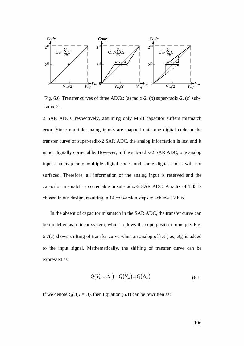
106
2 SAR ADCs, respectively, assuming only MSB capacitor suffers mismatch
error. Since multiple analog inputs are mapped onto one digital code in the
transfer curve of super-radix-2 SAR ADC, the analog information is lost and it
is not digitally correctable. However, in the sub-radix-2 SAR ADC, one analog
input can map onto multiple digital codes and some digital codes will not
surfaced. Therefore, all information of the analog input is reserved and the
capacitor mismatch is correctable in sub-radix-2 SAR ADC. A radix of 1.85 is
chosen in our design, resulting in 14 conversion steps to achieve 12 bits.
In the absent of capacitor mismatch in the SAR ADC, the transfer curve can
be modelled as a linear system, which follows the superposition principle. Fig.
6.7(a) shows shifting of transfer curve when an analog offset (i.e., a) is added
to the input signal. Mathematically, the shifting of transfer curve can be
expressed as:
in a in aQ V Q V Q (6.1)
If we denote Q(a) = d, then Equation (6.1) can be rewritten as:
Fig. 6.6. Transfer curves of three ADCs: (a) radix-2, (b) super-radix-2, (c) sub-
radix-2.
Code
214
213
0VrefVref/2
Vin
Code
214
213
0VrefVref/2
Vin
Code
214
213
0VrefVref/2
Vin
C13=ΣCi i=0
12
C13>ΣCi i=0
12
C13<ΣCi i=0
12

107
in in a dQ V Q V (6.2)
Equation (6.2) indicates that the analog offset a can be removed in digital
domain, provided the transfer curve of the ADC is a linear system or Q(a) = d.
Fig. 6.7(b) shows that the analog offset is preciously removed in digital domain.
However, with capacitor mismatch as demonstrated in Fig. 6.8, the analog
offset cannot be removed through simply shifting the transfer curve by d in the
SAR ADC. The shifted lines forms a discrepancy window with an error which
Fig. 6.7. Illustrations of perturbation in linear transfer curve of SAR ADC.
-a
Code
0VrefVref/2
Vin
C13=ΣCi i=0
12
a
Code
0VrefVref/2
Vin
C13=ΣCi i=0
12
-d
+d
214
213
214
213
(a) (b)
Fig. 6.8. Illustrations of perturbation of a transfer curve with capacitor
mismatch in SAR ADC.
Code
214
213
0VrefVref/2
Vin
C13<ΣCi i=0
12
+a -a
Code
214
213
0VrefVref/2
Vin
C13<ΣCi i=0
12
+d
-d
(a) (b)
error
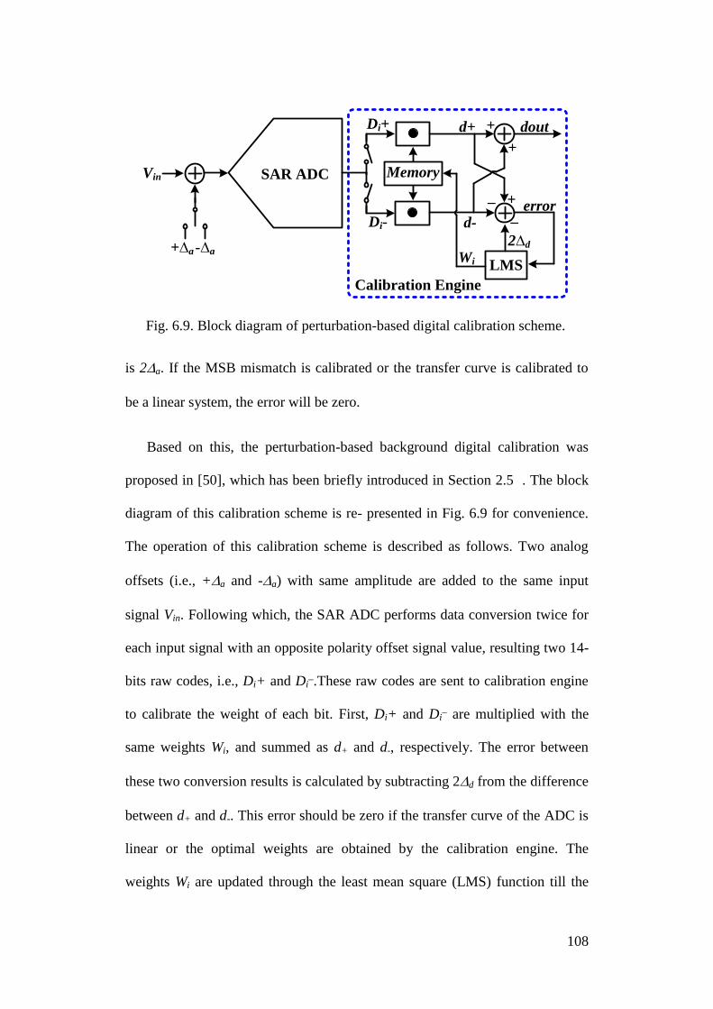
108
is 2a. If the MSB mismatch is calibrated or the transfer curve is calibrated to
be a linear system, the error will be zero.
Based on this, the perturbation-based background digital calibration was
proposed in [50], which has been briefly introduced in Section 2.5 . The block
diagram of this calibration scheme is re- presented in Fig. 6.9 for convenience.
The operation of this calibration scheme is described as follows. Two analog
offsets (i.e., +a and -a) with same amplitude are added to the same input
signal Vin. Following which, the SAR ADC performs data conversion twice for
each input signal with an opposite polarity offset signal value, resulting two 14-
bits raw codes, i.e., Di+ and Di_.These raw codes are sent to calibration engine
to calibrate the weight of each bit. First, Di+ and Di_ are multiplied with the
same weights Wi, and summed as d+ and d-, respectively. The error between
these two conversion results is calculated by subtracting 2d from the difference
between d+ and d-. This error should be zero if the transfer curve of the ADC is
linear or the optimal weights are obtained by the calibration engine. The
weights Wi are updated through the least mean square (LMS) function till the
Fig. 6.9. Block diagram of perturbation-based digital calibration scheme.
SAR ADCVin
+∆a -∆a
LMSWi
+
+
Di+
Di-
d+
d-
2∆d
+_
_error
dout
Memory
Calibration Engine
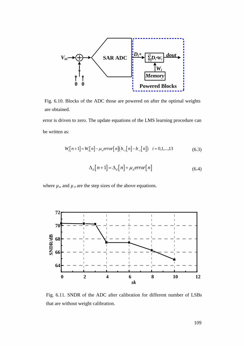
109
error is driven to zero. The update equations of the LMS learning procedure can
be written as:
1 0 1 13i i w ,i ,iW n W n error n b n b n i , ,..., (6.3)
1d dn n error n (6.4)
where µw and µ are the step sizes of the above equations.
Fig. 6.10. Blocks of the ADC those are powered on after the optimal weights
are obtained.
SAR ADCDi+ dout
Memory
ΣDi Wi
13
i=0Vin
0 0
Wi
Powered Blocks
Fig. 6.11. SNDR of the ADC after calibration for different number of LSBs
that are without weight calibration.
0 2 4 6 8 10 12
64
66
68
70
72
SN
DR
/dB
sk
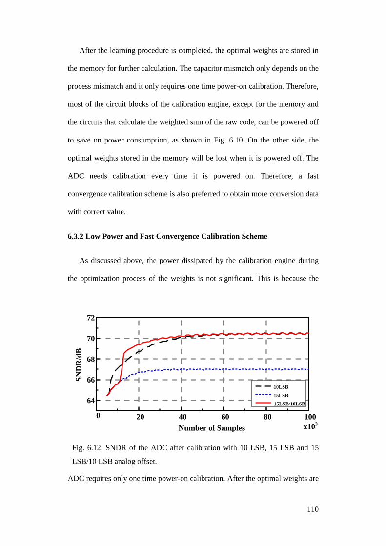
110
After the learning procedure is completed, the optimal weights are stored in
the memory for further calculation. The capacitor mismatch only depends on the
process mismatch and it only requires one time power-on calibration. Therefore,
most of the circuit blocks of the calibration engine, except for the memory and
the circuits that calculate the weighted sum of the raw code, can be powered off
to save on power consumption, as shown in Fig. 6.10. On the other side, the
optimal weights stored in the memory will be lost when it is powered off. The
ADC needs calibration every time it is powered on. Therefore, a fast
convergence calibration scheme is also preferred to obtain more conversion data
with correct value.
6.3.2 Low Power and Fast Convergence Calibration Scheme
As discussed above, the power dissipated by the calibration engine during
the optimization process of the weights is not significant. This is because the
ADC requires only one time power-on calibration. After the optimal weights are
Fig. 6.12. SNDR of the ADC after calibration with 10 LSB, 15 LSB and 15
LSB/10 LSB analog offset.
0 20 40 60 80 100
64
66
68
70
72
SN
DR
/dB
Number of Samples
10LSB
15LSB
15LSB/10LSB
x103
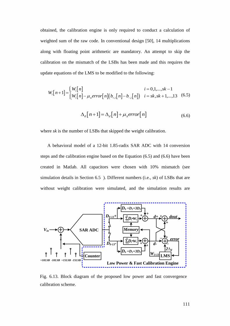
111
obtained, the calibration engine is only required to conduct a calculation of
weighted sum of the raw code. In conventional design [50], 14 multiplications
along with floating point arithmetic are mandatory. An attempt to skip the
calibration on the mismatch of the LSBs has been made and this requires the
update equations of the LMS to be modified to the following:
0 1 11
1 13
i
i
i w ,i ,i
W n i , ,...,skW n
W n error n b n b n i sk ,sk ,...,
(6.5)
1d dn n error n (6.6)
where sk is the number of LSBs that skipped the weight calibration.
A behavioral model of a 12-bit 1.85-radix SAR ADC with 14 conversion
steps and the calibration engine based on the Equation (6.5) and (6.6) have been
created in Matlab. All capacitors were chosen with 10% mismatch (see
simulation details in Section 6.5 ). Different numbers (i.e., sk) of LSBs that are
without weight calibration were simulated, and the simulation results are
Fig. 6.13. Block diagram of the proposed low power and fast convergence
calibration scheme.
SAR ADCVin
LMSW3-13
+
+
D0-13+
D0-13-
d+
d-
2∆d
+_
_error
dout
Memory
ΣDi Wi
13
i=3
ΣDi Wi
13
i=3
D0 +D1+3D2
+ +
++
D0 +D1+3D2
Counter+10LSB -10LSB +15LSB -15LSB
Low Power & Fast Calibration Engine

112
presented in Fig. 6.11. It can be seen that the SNDR has a minimum reduction
when sk is 3, i.e., the 3 LSBs skip weight calibration. Therefore, in our design
we skip calibration for the 3 LSBs. By doing this, the required multiplications
can be reduced from 14 to 11, saving power consumption after the optimal
weights are obtained.
From the update equations of the LMS algorithm, i.e., Equation (6.5) and
(6.6), it can be observed that with larger error, the convergence of the LMS is
faster. In other words, with larger analog offset a in Fig. 6.9, the LMS
converge sooner. However, the accuracy of the LMS is worsen when large
analog offset or error is applied. In order to speed up the LMS convergence
while maintaining the same accuracy, an adaptive analog offset perturbation
approach is proposed. 15-LSB analog offset is applied to the first 10000
samples while the rest of the samples are injected with 10-LSB analog offset.
The behavior of the adaptive analog offset perturbation is created in Matlab and
the simulation result is shown in Fig. 6.12. It can be seen that the proposed
Fig. 6.14. Schematic of the two stage dynamic comparator.
Out
cp
cn
VDACnVDACp
CLK
CLK
dp dn
cp cn
VDD
dp dn
1st Stage 2nd Stage
CLKCLK
M1
M2
M3
M4
M5
M7
M8
M6
M9
M11
M12
M10
M13
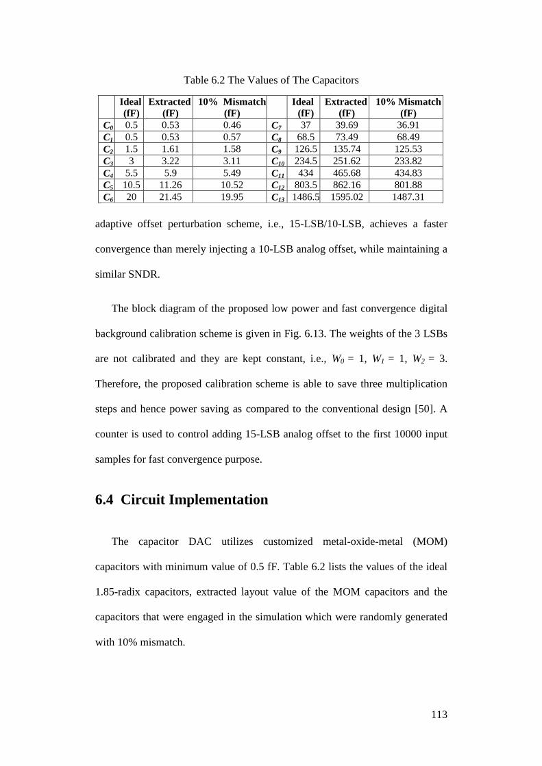
113
adaptive offset perturbation scheme, i.e., 15-LSB/10-LSB, achieves a faster
convergence than merely injecting a 10-LSB analog offset, while maintaining a
similar SNDR.
The block diagram of the proposed low power and fast convergence digital
background calibration scheme is given in Fig. 6.13. The weights of the 3 LSBs
are not calibrated and they are kept constant, i.e., W0 = 1, W1 = 1, W2 = 3.
Therefore, the proposed calibration scheme is able to save three multiplication
steps and hence power saving as compared to the conventional design [50]. A
counter is used to control adding 15-LSB analog offset to the first 10000 input
samples for fast convergence purpose.
6.4 Circuit Implementation
The capacitor DAC utilizes customized metal-oxide-metal (MOM)
capacitors with minimum value of 0.5 fF. Table 6.2 lists the values of the ideal
1.85-radix capacitors, extracted layout value of the MOM capacitors and the
capacitors that were engaged in the simulation which were randomly generated
with 10% mismatch.
Table 6.2 The Values of The Capacitors
Ideal
(fF)
Extracted
(fF)
10% Mismatch
(fF)
Ideal
(fF)
Extracted
(fF)
10% Mismatch
(fF)
C0 0.5 0.53 0.46 C7 37 39.69 36.91
C1 0.5 0.53 0.57 C8 68.5 73.49 68.49
C2 1.5 1.61 1.58 C9 126.5 135.74 125.53
C3 3 3.22 3.11 C10 234.5 251.62 233.82
C4 5.5 5.9 5.49 C11 434 465.68 434.83
C5 10.5 11.26 10.52 C12 803.5 862.16 801.88
C6 20 21.45 19.95 C13 1486.5 1595.02 1487.31
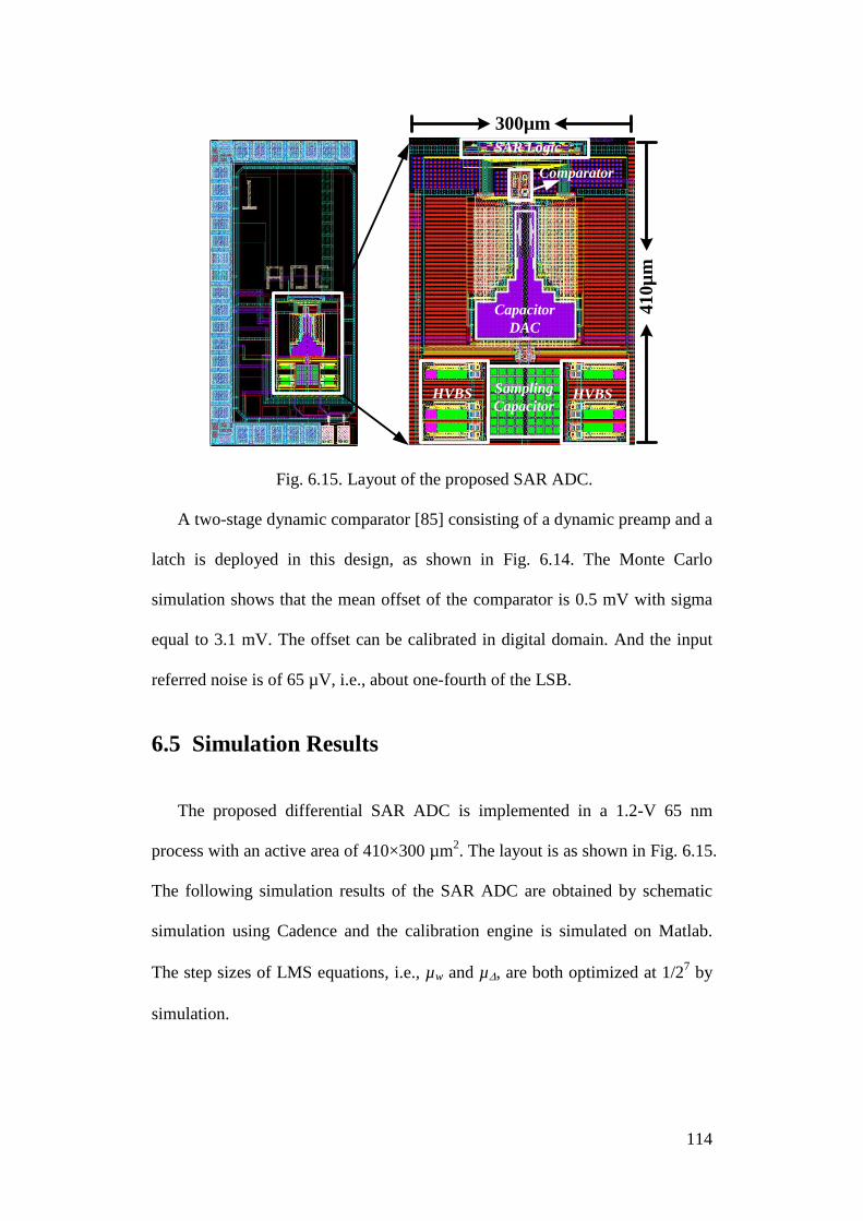
114
A two-stage dynamic comparator [85] consisting of a dynamic preamp and a
latch is deployed in this design, as shown in Fig. 6.14. The Monte Carlo
simulation shows that the mean offset of the comparator is 0.5 mV with sigma
equal to 3.1 mV. The offset can be calibrated in digital domain. And the input
referred noise is of 65 µV, i.e., about one-fourth of the LSB.
6.5 Simulation Results
The proposed differential SAR ADC is implemented in a 1.2-V 65 nm
process with an active area of 410×300 µm2. The layout is as shown in Fig. 6.15.
The following simulation results of the SAR ADC are obtained by schematic
simulation using Cadence and the calibration engine is simulated on Matlab.
The step sizes of LMS equations, i.e., µw and µ, are both optimized at 1/27 by
simulation.
Fig. 6.15. Layout of the proposed SAR ADC.
Sampling
CapacitorHVBS HVBS
Comparator
SAR Logic
Capacitor
DAC
300µm
41
0µ
m
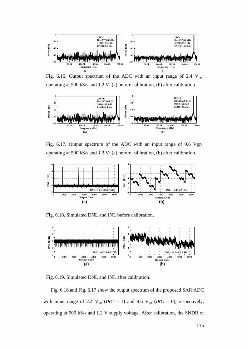
115
Fig. 6.16 and Fig. 6.17 show the output spectrum of the proposed SAR ADC
with input range of 2.4 Vpp (IRC = 1) and 9.6 Vpp (IRC = 0), respectively,
operating at 500 kS/s and 1.2 V supply voltage. After calibration, the SNDR of
Fig. 6.16. Output spectrum of the ADC with an input range of 2.4 Vpp
operating at 500 kS/s and 1.2 V: (a) before calibration, (b) after calibration.
Fig. 6.17. Output spectrum of the ADC with an input range of 9.6 Vpp
operating at 500 kS/s and 1.2 V: (a) before calibration, (b) after calibration.
Fig. 6.18. Simulated DNL and INL before calibration.
Fig. 6.19. Simulated DNL and INL after calibration.
50.0k 100.0k 150.0k 200.0k 250.0k-120
-90
-60
-30
0
IRC=1
SNDR=65.3 dB
ENOB=10.6 bits
fin=237.06 kHz
Pow
er (
dB
)
Frequency (Hz)
(b)
50.0k 100.0k 150.0k 200.0k 250.0k-120
-90
-60
-30
0
IRC=1
SNDR=59.6 dB
ENOB=9.6 bits
fin=237.06 kHz
Pow
er (
dB
)
Frequency (Hz)
(a)
50.0k 100.0k 150.0k 200.0k 250.0k-120
-90
-60
-30
0
IRC=0
SNDR=59.5 dB
ENOB=9.5 bits
fin=237.06 kHz
Pow
er (
dB
)
Frequency (Hz)
(a)
50.0k 100.0k 150.0k 200.0k 250.0k-120
-90
-60
-30
0IRC=0
SNDR=65.2 dB
ENOB=10.5 bits
fin=237.06 kHz
Pow
er (
dB
)
Frequency (Hz)
(b)
0 1000 2000 3000 4000 5000 6000-2
0
2
4
6
DNL: +5.1/-0.68 LSB
DN
L (
LS
B)
Output Code0 1000 2000 3000 4000 5000 6000
-6
-4
-2
0
2
4
6
INL: +5.4/-5.2 LSB
INL
(L
SB
)
Output Code
(a) (b)
0 1000 2000 3000 4000 5000 6000-2
-1
0
1
2
DNL: +0.2/-0.87 LSB
DN
L (
LS
B)
Output Code0 1000 2000 3000 4000 5000 6000
-2
-1
0
1
2
INL: +1.2/-1.2 LSB
INL
(L
SB
)
Output Code
(a) (b)

116
the ADC with input range of 2.4 Vpp and 9.6 Vpp are 65.3 dB (10.6 bits) and
65.2 dB (10.5 bits), respectively. The SNDR is improved by 5.7 dB using the
proposed low power and fast convergence background digital calibration
scheme. The linearity performance of the proposed ADC with input range of
9.6 Vpp was also simulated. Before calibration, the simulated DNL and INL are
+5.1/-0.68 LSB and +5.4/-5.2 LSB, respectively, as shown in Fig. 6.18. After
calibration, DNL and INL are improved to +0.2/-0.87 LSB and +1.2/-1.2 LSB
(see Fig. 6.19), respectively. The performance of the proposed SAR ADC is
summarized in Table 6.3.
6.6 Conclusion
This chapter presents a configurable input range 12-bit SAR ADC with fast
and low power digital background calibration. The power consumption of the
system can be reduced by utilizing only one ADC with configurable input range
to convert different analog signals, including the sensor signals and the Li-ion
battery voltage. We present a high voltage bootstrapped switch which operates
Table 6.3 ADC Performance Summary
Process (nm) 65
Power Supply (V) 1.2
Input Range (V) 0~1.2/0~4.8
Sampling Rate (kS/s) 500
SNDR (dB)
(fin=237.06 kHz) 65.3/65.2
ENOB (bits) 10.6/10.5
DNL (LSB) +0.2/-0.87
INL (LSB) +1.2/-1.2
Power (µW)
(Except Calibration)
HVBS 1.2
Vref 5.28
Comparator 1
SAR Logic 0.91
Total 8.39
Core Area (mm2) 0.123

117
at 1.2 V and achieves an input swing of 0~4.5 V. Besides, a low power and fast
convergence digital background calibration scheme based on the perturbation-
based calibration is presented. The low power is achieved by skipping the
calibration for several LSBs. While the fast convergence is realised by injecting
different analog offset values during calibration. The simulation results show
that the SNDR is improved by 5.7 dB using the proposed low power and fast
convergence background digital calibration scheme.

118
Chapter 7
Conclusion and Future Work
7.1 Conclusion
Successive approximation register analog-to-digital converters with high
energy efficiency have been widely used in the sensing applications. This thesis
focuses on designing low power SAR ADCs with various energy efficient
techniques. The first proposed technique is based on ultra-low supply voltage,
i.e., operating at 0.5 V. Clock boosting circuit is also designed to improve the
linearity of the sampling switch when powered by the ultra-low supply voltage.
The power consumption of the novel ADC is significantly reduced due to the
digital nature of the SAR ADC.
When the ADC is used to convert sparse signals, such as neural spike and
ECG, some of the MSBs of the conversion results are left unchanged between
two consecutive samples. By deploying this characteristic, we proposed a low
power architecture which we named an adaptive delta-sampling SAR ADC. By
sampling only the incremental value of the input signal and adaptively adjusting
the sampling frequency, the ADC can achieve the same resolution and
conversion range with less number of bits than the conventional ADC.
Meanwhile, the power consumption is also very much reduced. To validate the
proposed design, the SAR ADC has been used to convert pre-recorded neural
signals. The measurement results showed that the proposed SAR ADC achieves
119
a power reduction of 88% when compared with the conventional capacitor
splitting SAR ADC.
Even though the power consumption of the ADC itself is reduced both by
operating at ultra-low supply voltage and by adopting the adaptive delta-
sampling architecture, additional efforts to further reduce the power dissipated
by the peripheral circuits that provide the reference voltage to the ADC were
explored. A SAR ADC with self-timed pre-charging is proposed to eliminate
the power- and area-consuming reference-voltage regulator and decoupling
capacitor for wireless-powered implantable medical devices. The measurement
results showed that the SNDR of the SAR ADC did not decrease when the
supply voltage fluctuation is up to 50 mVpp. In other words, the proposed SAR
ADC is able to function without the reference-voltage regulator and decoupling
capacitor. Hence, the proposed SAR ADC achieves high energy efficiency at
the system level.
Lastly, a wide input 12-bit SAR ADC with low power and fast convergence
background digital calibration is presented in this thesis. A high voltage
bootstrapped switch is designed to sample the input signal with a voltage swing
of 0~4.8 V, and operating at 1.2 V supply voltage. In wireless sensor nodes
powered by Li-ion battery, the proposed ADC with configurable input range
can be used to convert different analog signals, including the sensor signals and
Li-ion battery voltage. For each input signal, the SAR ADC performs two
rounds of data conversion , each with opposite polarity offset. Following which,
the least mean square algorithm based calibration engine optimizes the weight
of each bit till the error between the two conversion results is driven to zero.
Optimization of the 3 LSBs is omitted in the proposed design. Hence, the
120
number of multiplication steps can be reduced by three to save on power
consumption, and this is with minimum disturbance to the SNDR.
An adaptive offset perturbation scheme, i.e., 15-LSB/10-LSB, to achieve a
faster convergence than merely injecting a 10-LSB analog offset while
maintaining a similar SNDR has also been designed. The schematic of the SAR
ADC is simulated on Cadence and the calibration engine is simulated on Matlab.
After calibration, the SNDR of the ADC is improved by 5.7 dB assuming that
the capacitor mismatch is 10%.
7.2 Future Work
Reducing the power consumption of the SAR ADC is one of the main
challenges in wireless sensor node. Operating at ultra-low voltage along with
minimally sufficient sampling rate is one of the circuit design approaches to
reduce the power consumption. The deployment of even lower supply voltage
(less than 0.5 V) can be explored to further reduce the power consumption. The
cascaded voltage boosting circuit [30] is able to improve the linearity of the
sampling switch even when it is operating at 160 mV supply voltage. Besides,
when the ADC operating at lower sampling rate (less than 1 kS/s), some
leakage control techniques would needed to be developed to reduce leakage of
the charges stored on the capacitor arrays. With the lowering of supply voltage,
both power gating and clock gating techniques can be adopted to minimize the
foreseeable leakage current of the circuits. In advanced 65 nm process, power
gating can use high threshold voltage transistors as switches to shut off power
supplies to parts of the SAR ADC that are in standby mode.

121
The architecture of the adaptive-delta sampling ADC can incorporate ultra-
low voltage design to further reduce the power consumption. The rail-to-rail
comparator and the fully differential amplifier based slope detector will be the
two challenging circuit blocks, when operating at ultra-low voltage. Low
threshold voltage NMOS transistors (available in advanced process) can be used
as the input transistors in the amplifier designs to enable the comparator and the
slope detector to function at ultra-low voltage. The integration of reference-
voltage regulator is also important to ensure that the adaptive-delta sampling
SAR ADC is compatible with the sensor node systems. The drivability
requirement of the reference-voltage regulator needed in the adaptive-delta
sampling SAR ADC is more relaxable than that needed in the conventional
SAR ADC. This is because the power consumed by the capacitor arrays of the
adaptive-delta sampling SAR and the conventional SAR ADC are 30.5 nW and
1200 nW, respectively, where the power reduction is of 39 times.
The charge-sharing SAR ADC featured with reference-voltage regulator
free is an attractive design with high energy efficiency at system level. Further
research to reduce power consumption of the input buffer of the ADC is a
potential approach to reduce the system power dissipation. A power efficient
variable-gain transconductor is able to replace the power hungry input voltage
buffer in a charge-sharing SAR ADC to improve the overall power efficiency
[42]. Besides, MOSFET used as the unit capacitor (MOSCAP) can significantly
reduce the power consumed by the capacitor DAC since the smallest available
MIM capacitor value in the used 0.18-µm process is 39 fF, which is about ten
times of that of the MOSCAP. [107] demonstrates a charge-sharing SAR ADC
122
that employs only MOSCAP in the capacitor DAC and achieves high energy
efficiency.
The low power and fast convergence calibration scheme for the wide input
12-bit SAR ADC is necessary to be implemented on FPGA or ASIC to verify
its performance. Because the 12-bit SAR ADC has a natural serial output, the
multiplier used in the calibration scheme can be a folding structure as suggested
in [50]. Besides, the tapeout of this 12-bit SAR ADC is important and the
measurement of the reliability of the HVBS is also necessary. The proposed
digital calibration is an effective method to calibrate the mismatch of the
capacitors in the capacitor DAC and hence improve the SNDR of the ADC.
Therefore, this calibration technique that is without additional analog circuits
can be incorporated in the proposed low power ADC architectures, i.e.,
adaptive-delta sampling ADC and reference-voltage regulator-free ADC, to
design 12-bit SAR ADCs that are with low power consumption.
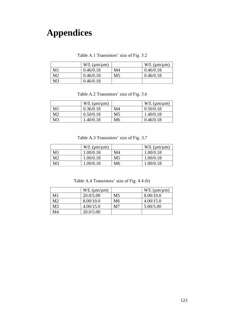
123
Appendices
Table A.2 Transistors’ size of Fig. 3.6
W/L (µm/µm) W/L (µm/µm)
M1 0.36/0.18 M4 0.50/0.18
M2 0.50/0.18 M5 1.40/0.18
M3 1.40/0.18 M6 0.46/0.18
Table A.1 Transistors’ size of Fig. 3.2
W/L (µm/µm) W/L (µm/µm)
M1 0.46/0.18 M4 0.46/0.18
M2 0.46/0.18 M5 0.46/0.18
M3 0.46/0.18
Table A.3 Transistors’ size of Fig. 3.7
W/L (µm/µm) W/L (µm/µm)
M1 1.00/0.18 M4 1.00/0.18
M2 1.00/0.18 M5 1.00/0.18
M3 1.00/0.18 M6 1.00/0.18
Table A.4 Transistors’ size of Fig. 4.4 (b)
W/L (µm/µm) W/L (µm/µm)
M1 20.0/5.00 M5 8.00/10.0
M2 8.00/10.0 M6 4.00/15.0
M3 4.00/15.0 M7 5.00/5.00
M4 20.0/5.00
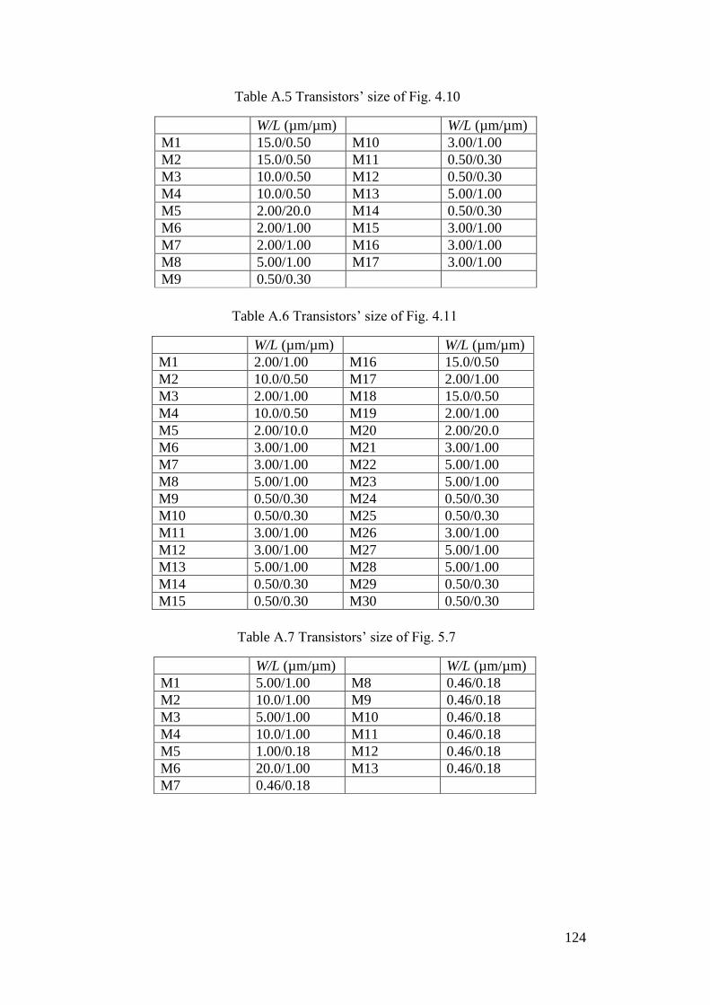
124
Table A.5 Transistors’ size of Fig. 4.10
W/L (µm/µm) W/L (µm/µm)
M1 15.0/0.50 M10 3.00/1.00
M2 15.0/0.50 M11 0.50/0.30
M3 10.0/0.50 M12 0.50/0.30
M4 10.0/0.50 M13 5.00/1.00
M5 2.00/20.0 M14 0.50/0.30
M6 2.00/1.00 M15 3.00/1.00
M7 2.00/1.00 M16 3.00/1.00
M8 5.00/1.00 M17 3.00/1.00
M9 0.50/0.30
Table A.6 Transistors’ size of Fig. 4.11
W/L (µm/µm) W/L (µm/µm)
M1 2.00/1.00 M16 15.0/0.50
M2 10.0/0.50 M17 2.00/1.00
M3 2.00/1.00 M18 15.0/0.50
M4 10.0/0.50 M19 2.00/1.00
M5 2.00/10.0 M20 2.00/20.0
M6 3.00/1.00 M21 3.00/1.00
M7 3.00/1.00 M22 5.00/1.00
M8 5.00/1.00 M23 5.00/1.00
M9 0.50/0.30 M24 0.50/0.30
M10 0.50/0.30 M25 0.50/0.30
M11 3.00/1.00 M26 3.00/1.00
M12 3.00/1.00 M27 5.00/1.00
M13 5.00/1.00 M28 5.00/1.00
M14 0.50/0.30 M29 0.50/0.30
M15 0.50/0.30 M30 0.50/0.30
Table A.7 Transistors’ size of Fig. 5.7
W/L (µm/µm) W/L (µm/µm)
M1 5.00/1.00 M8 0.46/0.18
M2 10.0/1.00 M9 0.46/0.18
M3 5.00/1.00 M10 0.46/0.18
M4 10.0/1.00 M11 0.46/0.18
M5 1.00/0.18 M12 0.46/0.18
M6 20.0/1.00 M13 0.46/0.18
M7 0.46/0.18
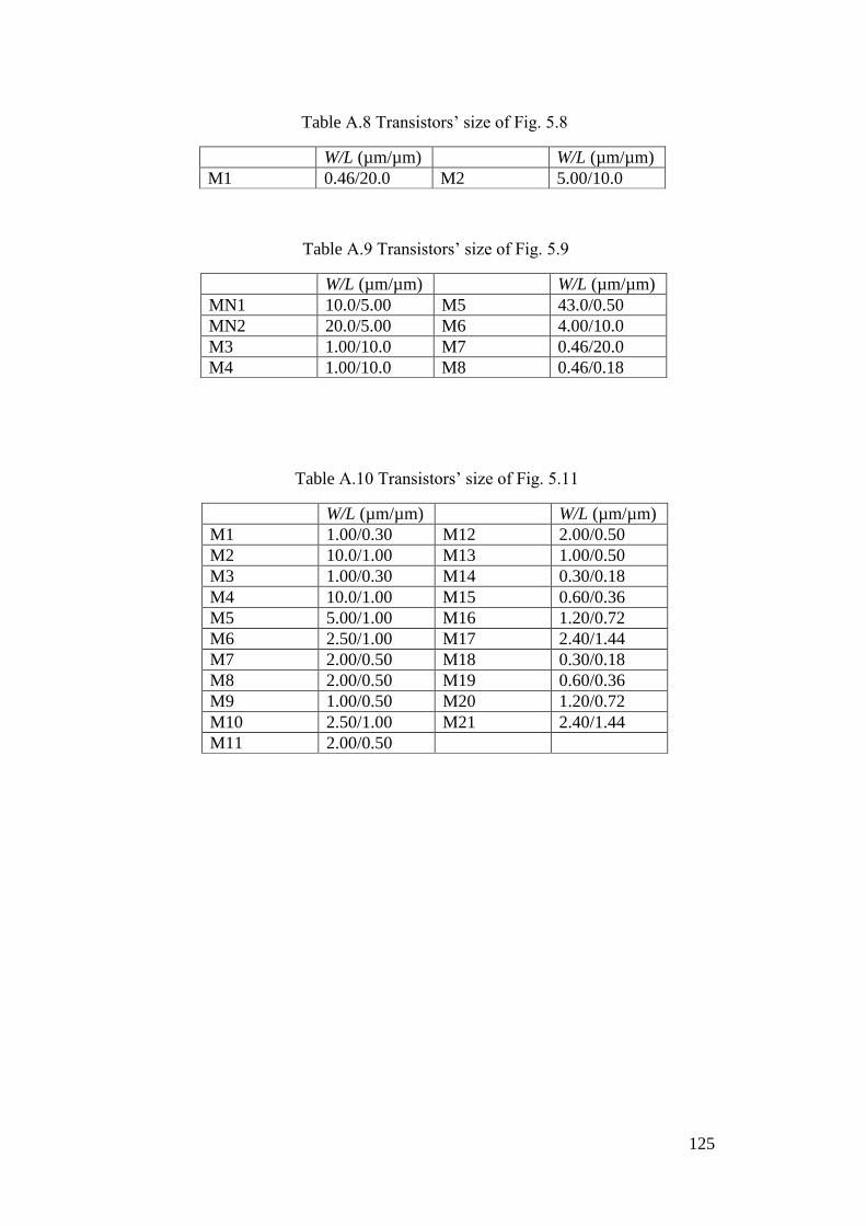
125
Table A.8 Transistors’ size of Fig. 5.8
W/L (µm/µm) W/L (µm/µm)
M1 0.46/20.0 M2 5.00/10.0
Table A.9 Transistors’ size of Fig. 5.9
W/L (µm/µm) W/L (µm/µm)
MN1 10.0/5.00 M5 43.0/0.50
MN2 20.0/5.00 M6 4.00/10.0
M3 1.00/10.0 M7 0.46/20.0
M4 1.00/10.0 M8 0.46/0.18
Table A.10 Transistors’ size of Fig. 5.11
W/L (µm/µm) W/L (µm/µm)
M1 1.00/0.30 M12 2.00/0.50
M2 10.0/1.00 M13 1.00/0.50
M3 1.00/0.30 M14 0.30/0.18
M4 10.0/1.00 M15 0.60/0.36
M5 5.00/1.00 M16 1.20/0.72
M6 2.50/1.00 M17 2.40/1.44
M7 2.00/0.50 M18 0.30/0.18
M8 2.00/0.50 M19 0.60/0.36
M9 1.00/0.50 M20 1.20/0.72
M10 2.50/1.00 M21 2.40/1.44
M11 2.00/0.50

126
Table A.11 Transistors’ size of Fig. 6.4
W/L (µm/µm) W/L (µm/µm)
M0 0.32/0.50 M15 0.32/0.50
M1 0.32/0.50 M16 0.32/0.50
M2 0.40/0.32 M17 0.32/0.50
M3 0.32/0.50 M18 1.00/0.50
M4 0.50/0.50 M19 10.0/0.50
M5 0.50/0.50 M20 10.0/0.50
M6 0.32/0.50 M21 10.0/0.50
M7 0.32/0.50 M22 0.32/0.50
M8 0.50/0.50 M23 0.32/0.50
M9 0.50/0.50 M24 5.00/0.50
M10 0.32/0.50 M25 5.00/0.50
M11 0.32/0.50 M26 0.50/0.50
M12 0.32/0.50 M27 0.50/0.50
M13 0.32/0.50 M28 1.00/0.50
M14 0.32/0.50 M29 10.0/0.50
Table A.12 Transistors’ size of Fig. 6.14
W/L (µm/µm) W/L (µm/µm)
M1 1.00/1.00 M8 0.50/0.20
M2 5.00/0.25 M9 0.20/0.06
M3 1.00/1.00 M10 0.50/0.20
M4 5.00/0.25 M11 1.00/0.50
M5 1.00/0.50 M12 0.50/0.20
M6 0.50/0.20 M13 0.20/0.06
M7 1.00/0.50

127
Publications
Journal
1. Y. Yang, J. Zhou, X. Liu, J. H. Cheong and W. L. Goh, “A 151-nW
Adaptive Delta-Sampling ADC for Ultra-Low Power Sensing
Applications,” IEEE Transactions on Circuits and Systems II, vol. 63,
no. 7, pp. 638-642, 2016.
2. X. Liu, J. Zhou, C. Wang, K. H. Chang, J. Luo, J. Lan, L. Liao, Y. Lam,
Y. Yang, B. Wang, X. Zhang, W. L. Goh, T. T. Kim and M. Je, “An
Ultralow-Voltage Sensor Node Processor With Diverse Hardware
Acceleration and Cognitive Sampling for Intelligent Sensing,” IEEE
Transactions on Circuits and Systems II, vol. 62, no. 12, pp. 1149-1153,
2015
3. X. Liu, J. Zhou, Y. Yang, B. Wang, J. Lan, C. Wang, J. Luo, W. L. Goh,
T. T. Kim and M. Je, “A 457 nW Near-Threshold Cognitive Multi-
Functional ECG Processor for Long-Term Cardiac Monitoring,” IEEE
Journal of Solid-State Circuit, vol. 49, no. 11, pp. 2422-2434, 2014.
Conference
4. C. Wu, W. L. Goh, Y. Yang, A. Chang, X, Zhu and L. Wang, “A Start-
Up Free 200 nW Bandgap Voltage Reference,” in New Circuits and
Systems Conference (NEWCAS), 2016 IEEE 14th International, 2016.
5. Y. Yang, W. L. Goh, J. Zhou, J. H. Cheong and X. Liu, “Ultra-Low
Power Delta Sampling SAR ADC for Sensing Applications,” in
128
Electron Devices and Solid-State Circuits (EDSSC), 2015 IEEE
International Conference on, 2015, pp.213-216.
6. J. Zhou, X. Liu, C. Wang, K. H. Chang, J. Luo, J. Lan, L. Liao, Y. Lam,
Y. Yang, B. Wang, X. Zhang, W. L. Goh, T. T. Kim and M. Je, “A 0.5V
29pJ/Cycle Sensor Node Processor for Intelligent Sensing Applications,”
in SoC Design Conference (ISOCC), 2014 International, 2014, pp. 70-
71.
7. Y. Yang, X. Liu, J. Zhou, J. H. Cheong, M. Je and W. L. Goh, “ A 0.5 V
16 nW 8.08-ENOB SAR ADC for Ultra-Low Power Sensor
Applications,” in Microwave Workshop Series on RF and Wireless
Technologies for Biomedical and Healthcare Applications (IMWS-BIO),
2013 IEEE MTT-S International, 2013, pp. 1-3.
8. X. Liu, J. Zhou, Y. Yang, B. Wang, J. Lan, C. Wang, J. Luo, W. L. Goh,
T. T. Kim and M. Je, “A 457-nW Cognitive Multi-Functional ECG
Processor,” in Solid-State Circuits Conference (A-SSCC), 2013 IEEE
Asian, 2013, pp. 141-144.
9. H. F. Nurhuda, Y. Yang and W. L. Goh, “A three-topology based, wide
input range switched-capacitor DC-DC converter with low-ripple and
enhanced load line regulations,” in 2014 International Symposium on
Integrated Circuits (ISIC), 2014, pp. 13-16.
129
Bibliography
[1] B. Gyselinckx, R. Vullers, C. V. Hoof, J. Ryckaert, R. F. Yazicioglu, P.
Fiorini, et al., "Human++: Emerging Technology for Body Area
Networks," in 2006 IFIP International Conference on Very Large Scale
Integration, 2006, pp. 175-180.
[2] ContiPressureCheck–The tire pressure monitoring system [Online]. Available:
http://www.continental-tires.com/car/technology/tpms
[3] B. Fleming, "Tire pressure-monitoring systems rollout [Automotive
Electronics]," IEEE Vehicular Technology Magazine, vol. 4, pp. 6-10,
2009.
[4] R. F. Yazicioglu, S. Kim, T. Torfs, H. Kim, and C. V. Hoof, "A 30 uW
Analog Signal Processor ASIC for Portable Biopotential Signal
Monitoring," IEEE Journal of Solid-State Circuits, vol. 46, pp. 209-223,
2011.
[5] W. M. Chen, H. Chiueh, T. J. Chen, C. L. Ho, C. Jeng, M. D. Ker, et al.,
"A Fully Integrated 8-Channel Closed-Loop Neural-Prosthetic CMOS
SoC for Real-Time Epileptic Seizure Control," IEEE Journal of Solid-
State Circuits, vol. 49, pp. 232-247, 2014.
[6] X. Liu, J. Zhou, Y. Yang, B. Wang, J. Lan, C. Wang, et al., "A 457-nW
cognitive multi-functional ECG processor," in Solid-State Circuits
Conference (A-SSCC), 2013 IEEE Asian, 2013, pp. 141-144.
[7] X. Liu, J. Zhou, Y. Yang, B. Wang, J. Lan, C. Wang, et al., "A 457 nW
Near-Threshold Cognitive Multi-Functional ECG Processor for Long-
Term Cardiac Monitoring," IEEE Journal of Solid-State Circuits, vol. 49,
pp. 2422-2434, 2014.
[8] X. Zou, L. Liu, J. H. Cheong, L. Yao, P. Li, M. Y. Cheng, et al., "A 100-
Channel 1-mW Implantable Neural Recording IC," IEEE Transactions
on Circuits and Systems I: Regular Papers, vol. 60, pp. 2584-2596,
2013.
130
[9] M.-L. S. Z. Gao, C. H. Chung "Piezoelectric Module for Energy
Harversting, Such As in a Tire Pressure Monitoring System," US Patent
8011237 B2, 2011.
[10] R. A. Blanchard, "Self-Powered Sensor System for Monitoring Tire
Pressure," US Patent 8742912 B2, 2014.
[11] C. Knight and J. Davidson, "Thermoelectric energy harvesting as a
wireless sensor node power source," in In Proceedings of the Active and
Passive Smart Structures and Integrated Systems, 2010.
[12] J. G.Webster, Medical Instrumentation: Application and Design, 3rd ed.:
New York: Wiley, 1998.
[13] Freescale, "Tire Pressure Monitoring Sensor Temperature Compensated
and Calibrated, Fully Integrated, Digital Output," MPXY8020 datasheet,
2003.
[14] X. Zou, X. Xu, L. Yao, and Y. Lian, "A 1-V 450-nW Fully Integrated
Programmable Biomedical Sensor Interface Chip," IEEE Journal of
Solid-State Circuits, vol. 44, pp. 1067-1077, 2009.
[15] P. Harpe, H. Gao, R. v. Dommele, E. Cantatore, and A. v. Roermund,
"21.2 A 3nW signal-acquisition IC integrating an amplifier with 2.1
NEF and a 1.5fJ/conv-step ADC," in 2015 IEEE International Solid-
State Circuits Conference - (ISSCC) Digest of Technical Papers, 2015,
pp. 1-3.
[16] D. Han, Y. Zheng, R. Rajkumar, G. Dawe, and M. Je, "A 0.45V 100-
channel neural-recording IC with sub uW/channel consumption in 0.18
um CMOS," in 2013 IEEE International Solid-State Circuits Conference
Digest of Technical Papers, 2013, pp. 290-291.
[17] W. M. Chen, H. Chiueh, T. J. Chen, C. L. Ho, C. Jeng, S. T. Chang, et
al., "A fully integrated 8-channel closed-loop neural-prosthetic SoC for
real-time epileptic seizure control," in 2013 IEEE International Solid-
State Circuits Conference Digest of Technical Papers, 2013, pp. 286-
287.
[18] M. Trakimas and S. R. Sonkusale, "An Adaptive Resolution
Asynchronous ADC Architecture for Data Compression in Energy
Constrained Sensing Applications," IEEE Transactions on Circuits and
Systems I: Regular Papers, vol. 58, pp. 921-934, 2011.

131
[19] M. Shoaran, M. H. Kamal, C. Pollo, P. Vandergheynst, and A. Schmid,
"Compact Low-Power Cortical Recording Architecture for Compressive
Multichannel Data Acquisition," IEEE Transactions on Biomedical
Circuits and Systems, vol. 8, pp. 857-870, 2014.
[20] F. Shahrokhi, K. Abdelhalim, D. Serletis, P. L. Carlen, and R. Genov,
"The 128-Channel Fully Differential Digital Integrated Neural
Recording and Stimulation Interface," IEEE Transactions on Biomedical
Circuits and Systems, vol. 4, pp. 149-161, 2010.
[21] X. Liu, J. Zhou, C. Wang, K. H. Chang, J. Luo, J. Lan, et al., "An
Ultralow-Voltage Sensor Node Processor With Diverse Hardware
Acceleration and Cognitive Sampling for Intelligent Sensing," IEEE
Transactions on Circuits and Systems II: Express Briefs, vol. 62, pp.
1149-1153, 2015.
[22] I. Ahmed, "ADC Architectures," in Pipelined ADC Design and
Enhancement Techniques, I. Ahmed, Ed., ed Dordrecht: Springer
Netherlands, 2010, pp. 7-17.
[23] Y. S. Shu, B. S. Song, and K. Bacrania, "A 65nm CMOS CT Delta-
Sigma Modulator with 81dB DR and 8MHz BW Auto-Tuned by Pulse
Injection," in 2008 IEEE International Solid-State Circuits Conference -
Digest of Technical Papers, 2008, pp. 500-631.
[24] J. A. McNeill, K. Y. Chan, M. C. W. Coln, C. L. David, and C.
Brenneman, "All-Digital Background Calibration of a Successive
Approximation ADC Using the Split ADC Architecture," IEEE
Transactions on Circuits and Systems I: Regular Papers, vol. 58, pp.
2355-2365, 2011.
[25] T. C. Carusone, D. A. Johns, and K. Martin, in Analog Integrated
Circuit Design, 2nd ed Canada: John Wiley & Sons., 2011.
[26] J. L. McCreary and P. R. Gray, "All-MOS charge redistribution analog-
to-digital conversion techniques. I," IEEE Journal of Solid-State
Circuits, vol. 10, pp. 371-379, 1975.
[27] A. Gil-Cho, C. Dong-Young, M. E. Brown, N. Ozaki, H. Youra, K.
Yamamura, et al., "A 0.6-V 82-dB delta-sigma audio ADC using
switched-RC integrators," IEEE Journal of Solid-State Circuits, vol. 40,
pp. 2398-2407, 2005.

132
[28] M. Dessouky and A. Kaiser, "Very low-voltage digital-audio Delta-
Sigma; modulator with 88-dB dynamic range using local switch
bootstrapping," IEEE Journal of Solid-State Circuits, vol. 36, pp. 349-
355, 2001.
[29] D. C. Daly and A. P. Chandrakasan, "A 6-bit, 0.2 V to 0.9 V Highly
Digital Flash ADC With Comparator Redundancy," IEEE Journal of
Solid-State Circuits, vol. 44, pp. 3030-3038, 2009.
[30] X. Zhou and Q. Li, "A 160mV 670nW 8-bit SAR ADC in 0.13um
CMOS," in Proceedings of the IEEE 2012 Custom Integrated Circuits
Conference, 2012, pp. 1-4.
[31] T. C. Lu, L. D. Van, C. S. Lin, and C. M. Huang, "A 0.5V 1KS/s 2.5nW
8.52-ENOB 6.8fJ/conversion-step SAR ADC for biomedical
applications," in 2011 IEEE Custom Integrated Circuits Conference
(CICC), 2011, pp. 1-4.
[32] B. P. Ginsburg and A. P. Chandrakasan, "An energy-efficient charge
recycling approach for a SAR converter with capacitive DAC," in 2005
IEEE International Symposium on Circuits and Systems, 2005, pp. 184-
187 Vol. 1.
[33] A. Agnes, E. Bonizzoni, P. Malcovati, and F. Maloberti, "A 9.4-ENOB
1V 3.8uW 100kS/s SAR ADC with Time-Domain Comparator," in 2008
IEEE International Solid-State Circuits Conference - Digest of
Technical Papers, 2008, pp. 246-610.
[34] S. K. Lee, S. J. Park, H. J. Park, and J. Y. Sim, "A 21 fJ/Conversion-
Step 100 kS/s 10-bit ADC With a Low-Noise Time-Domain Comparator
for Low-Power Sensor Interface," IEEE Journal of Solid-State Circuits,
vol. 46, pp. 651-659, 2011.
[35] F. M. Yaul and A. P. Chandrakasan, "A 10 bit SAR ADC With Data-
Dependent Energy Reduction Using LSB-First Successive
Approximation," IEEE Journal of Solid-State Circuits, vol. 49, pp.
2825-2834, 2014.
[36] F. M. Yaul and A. P. Chandrakasan, "11.3 A 10b 0.6nW SAR ADC with
data-dependent energy savings using LSB-first successive
approximation," in 2014 IEEE International Solid-State Circuits
Conference Digest of Technical Papers (ISSCC), 2014, pp. 198-199.
133
[37] C. C. Liu, S. J. Chang, G. Y. Huang, Y. Z. Lin, and C. M. Huang, "A 1V
11fJ/conversion-step 10bit 10MS/s asynchronous SAR ADC in 0.18um
CMOS," in 2010 Symposium on VLSI Circuits, 2010, pp. 241-242.
[38] M. Yip and A. P. Chandrakasan, "A resolution-reconfigurable 5-to-10b
0.4-to-1V power scalable SAR ADC," in 2011 IEEE International Solid-
State Circuits Conference, 2011, pp. 190-192.
[39] H. Y. Tai, Y. S. Hu, H. W. Chen, and H. S. Chen, "11.2 A
0.85fJ/conversion-step 10b 200kS/s subranging SAR ADC in 40nm
CMOS," in 2014 IEEE International Solid-State Circuits Conference
Digest of Technical Papers (ISSCC), 2014, pp. 196-197.
[40] L. Sun, B. Li, A. K. Y. Wong, W. T. Ng, and K. P. Pun, "A Charge
Recycling SAR ADC With a LSB-Down Switching Scheme," IEEE
Transactions on Circuits and Systems I: Regular Papers, vol. 62, pp.
356-365, 2015.
[41] M. Masaya, A. Yusuke, P. Daehwa, and M. Akira, "A low-noise self-
calibrating dynamic comparator for high-speed ADCs," in Solid-State
Circuits Conference, 2008. A-SSCC '08. IEEE Asian, 2008, pp. 269-272.
[42] B. Malki, T. Yamamoto, B. Verbruggen, P. Wambacq, and J. Craninckx,
"A 70 dB DR 10 b 0-to-80 MS/s Current-Integrating SAR ADC With
Adaptive Dynamic Range," IEEE Journal of Solid-State Circuits, vol.
49, pp. 1173-1183, 2014.
[43] M. Liu, P. Harpe, R. v. Dommele, and A. v. Roermund, "15.4 A 0.8V
10b 80kS/s SAR ADC with duty-cycled reference generation," in 2015
IEEE International Solid-State Circuits Conference - (ISSCC) Digest of
Technical Papers, 2015, pp. 1-3.
[44] L. Fick, D. Fick, M. Alioto, D. Blaauw, and D. Sylvester, "A 346um2
VCO-Based, Reference-Free, Self-Timed Sensor Interface for Cubic-
Millimeter Sensor Nodes in 28 nm CMOS," IEEE Journal of Solid-State
Circuits, vol. 49, pp. 2462-2473, 2014.
[45] J. Craninckx and G. v. d. Plas, "A 65fJ/Conversion-Step 0-to-50MS/s 0-
to-0.7mW 9b Charge-Sharing SAR ADC in 90nm Digital CMOS," in
2007 IEEE International Solid-State Circuits Conference. Digest of
Technical Papers, 2007, pp. 246-600.
134
[46] M. Liu, K. Pelzers, R. v. Dommele, A. v. Roermund, and P. Harpe,
"A106nW 10 b 80 kS/s SAR ADC With Duty-Cycled Reference
Generation in 65 nm CMOS," IEEE Journal of Solid-State Circuits, vol.
51, pp. 2435-2445, 2016.
[47] M. Hesener, T. Eicher, A. Hanneberg, D. Herbison, F. Kuttner, and H.
Wenske, "A 14b 40MS/s Redundant SAR ADC with 480MHz Clock in
0.13pm CMOS," in 2007 IEEE International Solid-State Circuits
Conference. Digest of Technical Papers, 2007, pp. 248-600.
[48] M. Yoshioka, K. Ishikawa, T. Takayama, and S. Tsukamoto, "A 10b
50MS/s 820 uW SAR ADC with on-chip digital calibration," in 2010
IEEE International Solid-State Circuits Conference - (ISSCC), 2010, pp.
384-385.
[49] C. Y. Liou and C. C. Hsieh, "A 2.4-to-5.2fJ/conversion-step 10b 0.5-to-
4MS/s SAR ADC with charge-average switching DAC in 90nm
CMOS," in 2013 IEEE International Solid-State Circuits Conference
Digest of Technical Papers, 2013, pp. 280-281.
[50] W. Liu, P. Huang, and Y. Chiu, "A 12-bit, 45-MS/s, 3-mW Redundant
Successive-Approximation-Register Analog-to-Digital Converter With
Digital Calibration," IEEE Journal of Solid-State Circuits, vol. 46, pp.
2661-2672, 2011.
[51] D. Zhang, A. Bhide, and A. Alvandpour, "A 53-nW 9.1-ENOB 1-kS/s
SAR ADC in 0.13-um CMOS for Medical Implant Devices," IEEE
Journal of Solid-State Circuits, vol. 47, pp. 1585-1593, 2012.
[52] M. Yoshioka, K. Ishikawa, T. Takayama, and S. Tsukamoto, "A 10-b
50-MS/s 820-uW SAR ADC With On-Chip Digital Calibration," IEEE
Transactions on Biomedical Circuits and Systems, vol. 4, pp. 410-416,
2010.
[53] Y. Tao and Y. Lian, "A 0.8-V, 1-MS/s, 10-bit SAR ADC for Multi-
Channel Neural Recording," IEEE Transactions on Circuits and Systems
I: Regular Papers, vol. 62, pp. 366-375, 2015.
[54] L. Wenbo and C. Yun, "An equalization-based adaptive digital
background calibration technique for successive approximation analog-
to-digital converters," in 2007 7th International Conference on ASIC,
2007, pp. 289-292.
135
[55] H. Nakane, R. Ujiie, T. Oshima, T. Yamamoto, K. Kimura, Y. Okuda, et
al., "A Fully Integrated SAR ADC Using Digital Correction Technique
for Triple-Mode Mobile Transceiver," IEEE Journal of Solid-State
Circuits, vol. 49, pp. 2503-2514, 2014.
[56] J. Y. Um, Y. J. Kim, E. W. Song, J. Y. Sim, and H. J. Park, "A Digital-
Domain Calibration of Split-Capacitor DAC for a Differential SAR
ADC Without Additional Analog Circuits," IEEE Transactions on
Circuits and Systems I: Regular Papers, vol. 60, pp. 2845-2856, 2013.
[57] G. Wang, F. Kacani, and Y. Chiu, "IRD Digital Background Calibration
of SAR ADC With Coarse Reference ADC Acceleration," IEEE
Transactions on Circuits and Systems II: Express Briefs, vol. 61, pp. 11-
15, 2014.
[58] J. Y. Um, J. H. Kim, J. Y. Sim, and H. J. Park, "Digital-domain
calibration of split-capacitor DAC with no extra calibration DAC for a
differential-type SAR ADC," in Solid State Circuits Conference (A-
SSCC), 2011 IEEE Asian, 2011, pp. 77-80.
[59] H. Nakane, R. Ujiie, T. Oshima, T. Yamamoto, K. Kimura, Y. Okuda, et
al., "A fully integrated SAR ADC using digital correction technique for
triple-mode mobile transceiver," in Solid-State Circuits Conference (A-
SSCC), 2013 IEEE Asian, 2013, pp. 73-76.
[60] A. N. Karanicolas, L. Hae-Seung, and K. L. Barcrania, "A 15-b 1-
Msample/s digitally self-calibrated pipeline ADC," IEEE Journal of
Solid-State Circuits, vol. 28, pp. 1207-1215, 1993.
[61] H. S. Lee, D. A. Hodges, and P. R. Gray, "A self-calibrating 15 bit
CMOS A/D converter," IEEE Journal of Solid-State Circuits, vol. 19, pp.
813-819, 1984.
[62] Y. K. Yang, X. Liu, J. Zhou, J. H. Cheong, M. Je, and W. L. Goh, "A
0.5V 16nW 8.08-ENOB SAR ADC for ultra-low power sensor
applications," in Microwave Workshop Series on RF and Wireless
Technologies for Biomedical and Healthcare Applications (IMWS-BIO),
2013 IEEE MTT-S International, 2013, pp. 1-3.
[63] T. Ogawa, H. Kobayashi, M. Hotta, Y. Takahashi, S. Hao, and T.
Nobukazu, "SAR ADC algorithm with redundancy," in Circuits and

136
Systems, 2008. APCCAS 2008. IEEE Asia Pacific Conference on, 2008,
pp. 268-271.
[64] F. Kuttner, "A 1.2V 10b 20MSample/s non-binary successive
approximation ADC in 0.13 um CMOS," in Solid-State Circuits
Conference, 2002. Digest of Technical Papers. ISSCC. 2002 IEEE
International, 2002, pp. 176-177 vol.1.
[65] M. Saberi, R. Lotfi, K. Mafinezhad, and W. A. Serdijn, "Analysis of
Power Consumption and Linearity in Capacitive Digital-to-Analog
Converters Used in Successive Approximation ADCs," IEEE
Transactions on Circuits and Systems I: Regular Papers, vol. 58, pp.
1736-1748, 2011.
[66] J. Sauerbrey, D. Schmitt-Landsiedel, and R. Thewes, "A 0.5-V 1-uW
successive approximation ADC," IEEE Journal of Solid-State Circuits,
vol. 38, pp. 1261-1265, 2003.
[67] R. Sekimoto, A. Shikata, and H. Ishikuro, "A power scalable SAR-ADC
in 0.18um-CMOS with 0.5V nano-watt operation," in Access Spaces
(ISAS), 2011 1st International Symposium on, 2011, pp. 89-94.
[68] L. Cuiwei, Z. Chongxun, and T. Changfeng, "Detection of ECG
characteristic points using wavelet transforms," IEEE Transactions on
Biomedical Engineering, vol. 42, pp. 21-28, 1995.
[69] Y. Yang, J. Zhou, X. Liu, J. H. Cheong, and W. L. Goh, "A 151-nW
Adaptive Delta-Sampling ADC for Ultra-Low Power Sensing
Applications," IEEE Transactions on Circuits and Systems II: Express
Briefs, vol. 63, pp. 638-642, 2016.
[70] S. J. Kim, L. Liu, L. Yao, W. L. Goh, Y. Gao, and M. Je, "A 0.5-V sub-
uW/channel neural recording IC with delta-modulation-based spike
detection," in Solid-State Circuits Conference (A-SSCC), 2014 IEEE
Asian, 2014, pp. 189-192.
[71] W. Chung-Yu, Y. Tsai-Chung, and C. Shin-Shi, "New monolithic
switched-capacitor differentiators with good noise rejection," IEEE
Journal of Solid-State Circuits, vol. 24, pp. 177-180, 1989.
[72] P. Harpe, E. Cantatore, and A. v. Roermund, "A 2.2/2.7fJ/conversion-
step 10/12b 40kS/s SAR ADC with Data-Driven Noise Reduction," in
137
2013 IEEE International Solid-State Circuits Conference Digest of
Technical Papers, 2013, pp. 270-271.
[73] H. Y. Tai, H. W. Chen, and H. S. Chen, "A 3.2fJ/c.-s. 0.35V 10b
100KS/s SAR ADC in 90nm CMOS," in 2012 Symposium on VLSI
Circuits (VLSIC), 2012, pp. 92-93.
[74] C. Yan-Jiun and C. C. Hsieh, "A 0.4V 2.02fJ/conversion-step 10-bit
hybrid SAR ADC with time-domain quantizer in 90nm CMOS," in 2014
Symposium on VLSI Circuits Digest of Technical Papers, 2014, pp. 1-2.
[75] S. K. Lee, S. J. Park, Y. Suh, H. J. Park, and J. Y. Sim, "A 1.3uW 0.6V
8.7-ENOB successive approximation ADC in a 0.18um CMOS," in
2009 Symposium on VLSI Circuits, 2009, pp. 242-243.
[76] S. I. Chang, K. AlAshmouny, M. McCormick, Y. C. Chen, and E. Yoon,
"BioBolt: A minimally-invasive neural interface for wireless epidural
recording by intra-skin communication," in VLSI Circuits (VLSIC), 2011
Symposium on, 2011, pp. 146-147.
[77] L. Xing, T. Chi-Ying, and K. Wing-Hung, "A 13.56MHz wireless power
transfer system with reconfigurable resonant regulating rectifier and
wireless power control for implantable medical devices," in 2014
Symposium on VLSI Circuits Digest of Technical Papers, 2014, pp. 1-2.
[78] X. Li, C. Y. Tsui, and W. H. Ki, "A 13.56 MHz Wireless Power
Transfer System With Reconfigurable Resonant Regulating Rectifier
and Wireless Power Control for Implantable Medical Devices," IEEE
Journal of Solid-State Circuits, vol. 50, pp. 978-989, 2015.
[79] F. Borghetti, J. H. Nielsen, V. Ferragina, P. Malcovati, P. Andreani, and
A. Baschirotto, "A Programmable 10b up-to-6MS/s SAR-ADC
Featuring Constant-FoM with On-Chip Reference Voltage Buffers," in
2006 Proceedings of the 32nd European Solid-State Circuits Conference,
2006, pp. 500-503.
[80] P. Harikumar and J. Wikner, "Design of a reference voltage buffer for a
10-bit 50 MS/s SAR ADC in 65 nm CMOS," in 2015 IEEE
International Symposium on Circuits and Systems, 2015, pp. 249 - 252.
[81] H. Tang, Z. C. Sun, K. W. R. Chew, and L. Siek, "A 1.33 uw 8.02-
ENOB 100 kS/s Successive Approximation ADC With Supply
Reduction Technique for Implantable Retinal Prosthesis," IEEE
138
Transactions on Biomedical Circuits and Systems, vol. 8, pp. 844-856,
2014.
[82] C. Yuan, K. A. Ng, Y. P. Xu, S. C. Yen, and N. V. Thakor, "A 1-V 9.8-
ENOB 100-kS/s single-ended SAR ADC with symmetrical DAC
switching technique for neural signal acquisition," in Solid-State
Circuits Conference (A-SSCC), 2015 IEEE Asian, 2015, pp. 1-4.
[83] P. Hazucha, T. Karnik, B. A. Bloechel, C. Parsons, D. Finan, and S.
Borkar, "Area-efficient linear regulator with ultra-fast load regulation,"
IEEE Journal of Solid-State Circuits, vol. 40, pp. 933-940, 2005.
[84] P. Hazucha, T. Karnik, B. Bloechel, C. Parsons, D. Finan, and S. Borkar,
"An area-efficient, integrated, linear regulator with ultra-fast load
regulation," in VLSI Circuits, 2004. Digest of Technical Papers. 2004
Symposium on, 2004, pp. 218-221.
[85] P. J. A. Harpe, C. Zhou, Y. Bi, N. P. v. d. Meijs, X. Wang, K. Philips, et
al., "A 26 uW 8 bit 10 MS/s Asynchronous SAR ADC for Low Energy
Radios," IEEE Journal of Solid-State Circuits, vol. 46, pp. 1585-1595,
2011.
[86] M. Seok, G. Kim, D. Blaauw, and D. Sylvester, "A Portable 2-Transistor
Picowatt Temperature-Compensated Voltage Reference Operating at 0.5
V," IEEE Journal of Solid-State Circuits, vol. 47, pp. 2534-2545, 2012.
[87] G. V. d. Plas, S. Decoutere, and S. Donnay, "A 0.16pJ/Conversion-Step
2.5mW 1.25GS/s 4b ADC in a 90nm Digital CMOS Process," in 2006
IEEE International Solid State Circuits Conference - Digest of
Technical Papers, 2006, p. 2310.
[88] P. J. A. Harpe, C. Zhou, K. Philips, and H. d. Groot, "A 0.8-mW 5-bit
250-MS/s Time-Interleaved Asynchronous Digital Slope ADC," IEEE
Journal of Solid-State Circuits, vol. 46, pp. 2450-2457, 2011.
[89] P. Harpe, C. Zhou, K. Philips, and H. d. Groot, "A 0.8mW 5bit 250MS/s
time-interleaved asynchronous digital slope ADC," in Solid State
Circuits Conference (A-SSCC), 2010 IEEE Asian, 2010, pp. 1-4.
[90] A Low-Power Batteryless Wireless Temperature and Humidity Sensor
with Passive Low Frequency RFID [Online]. Available:
http://www.ti.com/tool/TIDM-RFID-TEMPSENSOR

139
[91] D. T. Vuza, S. Chi, and P. Svasta, "An RFID tag simulator based on the
Atmel AT91SAM7S64 micro-controller," in 33rd International Spring
Seminar on Electronics Technology, ISSE 2010, 2010, pp. 427-432.
[92] V. Ranganathan, B. Mahoney, E. Pepin, M. D. Sunshine, C. T. Moritz, J.
C. Rudell, et al., "A high-voltage compliant neural stimulator with HF
wireless power and UHF backscatter communication," in 2016 IEEE
Wireless Power Transfer Conference (WPTC), 2016, pp. 1-4.
[93] A. P. Chandrakasan, N. Verma, and D. C. Daly, "Ultralow-power
electronics for biomedical applications," in Annual Review of
Biomedical Engineering. vol. 10, ed Palo Alto: Annual Reviews, 2008,
pp. 247-274.
[94] L. S. Y. Wong, S. Hossain, A. Ta, J. Edvinsson, D. H. Rivas, and H.
Naas, "A very low-power CMOS mixed-signal IC for implantable
pacemaker applications," IEEE Journal of Solid-State Circuits, vol. 39,
pp. 2446-2456, 2004.
[95] L. S. Y. Wong, S. Hossain, A. Ta, L. Weaver, G. Shaquer, A. Walker, et
al., "A very low power CMOS mixed-signal IC for implantable
pacemaker applications," in Solid-State Circuits Conference, 2004.
Digest of Technical Papers. ISSCC. 2004 IEEE International, 2004, pp.
318-530 Vol.1.
[96] J. Bae, K. Song, H. Lee, H. Cho, and H. J. Yoo, "A Low-Energy
Crystal-Less Double-FSK Sensor Node Transceiver for Wireless Body-
Area Network," IEEE Journal of Solid-State Circuits, vol. 47, pp. 2678-
2692, 2012.
[97] N. Cho, J. Bae, and H. J. Yoo, "A 10.8 mW Body Channel
Communication/MICS Dual-Band Transceiver for a Unified Body
Sensor Network Controller," IEEE Journal of Solid-State Circuits, vol.
44, pp. 3459-3468, 2009.
[98] A. S. Porret, T. Melly, D. Python, C. C. Enz, and E. A. Vittoz, "An
ultralow-power UHF transceiver integrated in a standard digital CMOS
process: architecture and receiver," IEEE Journal of Solid-State Circuits,
vol. 36, pp. 452-466, 2001.
[99] D. Linden and T. Reddy, Handbook of Batteries: New York: Mc-Graw
Hill, 2002.
140
[100] P. Li, J. C. Principe, and R. Bashirullah, "A Wireless Power Interface for
Rechargeable Battery Operated Neural Recording Implants," in
Engineering in Medicine and Biology Society, 2006. EMBS '06. 28th
Annual International Conference of the IEEE, 2006, pp. 6253-6256.
[101] B. D. Valle, C. T. Wentz, and R. Sarpeshkar, "An Area and Power-
Efficient Analog Li-Ion Battery Charger Circuit," IEEE Transactions on
Biomedical Circuits and Systems, vol. 5, pp. 131-137, 2011.
[102] M. Chen and G. A. Rincon-Mora, "Accurate, Compact, and Power-
Efficient Li-Ion Battery Charger Circuit," IEEE Transactions on
Circuits and Systems II: Express Briefs, vol. 53, pp. 1180-1184, 2006.
[103] P. Li and R. Bashirullah, "A Wireless Power Interface for Rechargeable
Battery Operated Medical Implants," IEEE Transactions on Circuits and
Systems II: Express Briefs, vol. 54, pp. 912-916, 2007.
[104] A. Manenti, A. Abba, A. Merati, S. M. Savaresi, and A. Geraci, "A New
BMS Architecture Based on Cell Redundancy," IEEE Transactions on
Industrial Electronics, vol. 58, pp. 4314-4322, 2011.
[105] D. Y. Aksin and I. Ozkaya, "25V sampling switch for power
management data converters in 0.35um CMOS with DNMOS," in
ESSCIRC, 2009. ESSCIRC '09. Proceedings of, 2009, pp. 136-139.
[106] L. Ozkaya, C. Gurleyuk, A. Ergul, A. Akkaya, and D. Y. Aksin, "A 50V
input range 14bit 250kS/s ADC with 97.8dB SFDR and 80.2dB SNR,"
in European Solid State Circuits Conference (ESSCIRC), ESSCIRC
2014 - 40th, 2014, pp. 71-74.
[107] T. Rabuske and J. Fernandes, "A 9-b 0.4-V charge-mode SAR ADC
with 1.6-V input swing and a MOSCAP-only DAC," in European Solid-
State Circuits Conference (ESSCIRC), ESSCIRC 2015 - 41st, 2015, pp.
311-314.