Embed Size (px)
Citation preview
Product
Folder
Order
Now
Technical
Documents
Tools &
Software
Support &Community
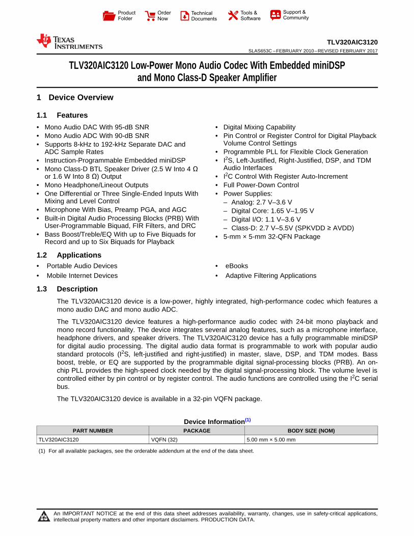
An IMPORTANT NOTICE at the end of this data sheet addresses availability, warranty, changes, use in safety-critical applications,intellectual property matters and other important disclaimers. PRODUCTION DATA.
TLV320AIC3120SLAS653C –FEBRUARY 2010–REVISED FEBRUARY 2017
TLV320AIC3120 Low-Power Mono Audio Codec With Embedded miniDSPand Mono Class-D Speaker Amplifier
1 Device Overview
1
1.1 Features1
• Mono Audio DAC With 95-dB SNR• Mono Audio ADC With 90-dB SNR• Supports 8-kHz to 192-kHz Separate DAC and
ADC Sample Rates• Instruction-Programmable Embedded miniDSP• Mono Class-D BTL Speaker Driver (2.5 W Into 4 Ω
or 1.6 W Into 8 Ω) Output• Mono Headphone/Lineout Outputs• One Differential or Three Single-Ended Inputs With
Mixing and Level Control• Microphone With Bias, Preamp PGA, and AGC• Built-in Digital Audio Processing Blocks (PRB) With
User-Programmable Biquad, FIR Filters, and DRC• Bass Boost/Treble/EQ With up to Five Biquads for
Record and up to Six Biquads for Playback
• Digital Mixing Capability• Pin Control or Register Control for Digital Playback
Volume Control Settings• Programmble PLL for Flexible Clock Generation• I2S, Left-Justified, Right-Justified, DSP, and TDM
Audio Interfaces• I2C Control With Register Auto-Increment• Full Power-Down Control• Power Supplies:
– Analog: 2.7 V–3.6 V– Digital Core: 1.65 V–1.95 V– Digital I/O: 1.1 V–3.6 V– Class-D: 2.7 V–5.5V (SPKVDD ≥ AVDD)
• 5-mm × 5-mm 32-QFN Package
1.2 Applications• Portable Audio Devices• Mobile Internet Devices
• eBooks• Adaptive Filtering Applications
1.3 DescriptionThe TLV320AIC3120 device is a low-power, highly integrated, high-performance codec which features amono audio DAC and mono audio ADC.
The TLV320AIC3120 device features a high-performance audio codec with 24-bit mono playback andmono record functionality. The device integrates several analog features, such as a microphone interface,headphone drivers, and speaker drivers. The TLV320AIC3120 device has a fully programmable miniDSPfor digital audio processing. The digital audio data format is programmable to work with popular audiostandard protocols (I2S, left-justified and right-justified) in master, slave, DSP, and TDM modes. Bassboost, treble, or EQ are supported by the programmable digital signal-processing blocks (PRB). An on-chip PLL provides the high-speed clock needed by the digital signal-processing block. The volume level iscontrolled either by pin control or by register control. The audio functions are controlled using the I2C serialbus.
The TLV320AIC3120 device is available in a 32-pin VQFN package.
Device Information(1)
PART NUMBER PACKAGE BODY SIZE (NOM)TLV320AIC3120 VQFN (32) 5.00 mm × 5.00 mm
(1) For all available packages, see the orderable addendum at the end of the data sheet.
Audio Output Stage
Power Management
RC CLK
Digital
Audio
Processing
and
Serial
InterfaceSDOUT
SDIN
BCLK
WCLK
MCLKPLL
7-Bit ADC P0/R117
Volume-Control RegisterP0/R116
Digital Vol24 dB to
Mute
P0/R64
miniDSPProcessing
Blocks
SPKP
SPKP
SPKM
SPKM
Class-D Speaker
Driver
6 dB to 24 dB (6-dB Steps)
Class A/BHeadphone/Lineout
Driver
0 dB to 9 dB (1-dB Steps)
Analog Attenuation0 dB to –78 dB and Mute(0.5-dB Steps / Nonlinear)
Analog Attenuation0 dB to –78 dB and Mute(0.5-dB Steps / Nonlinear)
HPVDDSPKVDD SPKVSS AVDD AVSSSPKVSSSPKVDD
VOL/
MICDET
HPOUT
SCL
SDA
GPIO GPIO1
MIX
MIX
MIC1LP
DAC
MIX
RESET
DVDD DVSS IOVDD IOVSS
OSC
RC CLK
MIC1LP
SelectableGain/InputImpedance
VCOM
SelectableGain/InputImpedance
P1/R470 to 59.5 dB
(0.5-dB steps)
AGC
MIC1RP
I C2
2 V/2.5 V/AVDDMICBIAS
Digital Vol–12..20 dB
Step = 0.5 dB
Mono ADC
Note: Normally,MCLK is PLL input;however, BCLKand GPIO1 canalso be PLL input.
D S-ADC
D S-DAC
De-PopandSoft-Start
P1/R33–R34
S
S
S
P1/R42
P1/R46
P1/R38
P1/R30
P1/R40
P1/R31
P1/R36
P0/R86–R93
P1/R48
P1/R49
Input CMP1/R50
B0205-06
P0/R82–R83
HPVSS
MIC1RP
MIC1LM
Mono DAC
Digtal MicInterface
Clock Data
Note: Digital MicClock and Datarouted to GPIO1and DIN pins.P0/R51 and R54
L Data
L Data
R Data
(L + R)/2 Data
P0/R63
miniDSPProcessing
Blocks
Copyright © 2016, Texas Instruments Incorporated
2
TLV320AIC3120SLAS653C –FEBRUARY 2010–REVISED FEBRUARY 2017 www.ti.com
Submit Documentation FeedbackProduct Folder Links: TLV320AIC3120
Device Overview Copyright © 2010–2017, Texas Instruments Incorporated
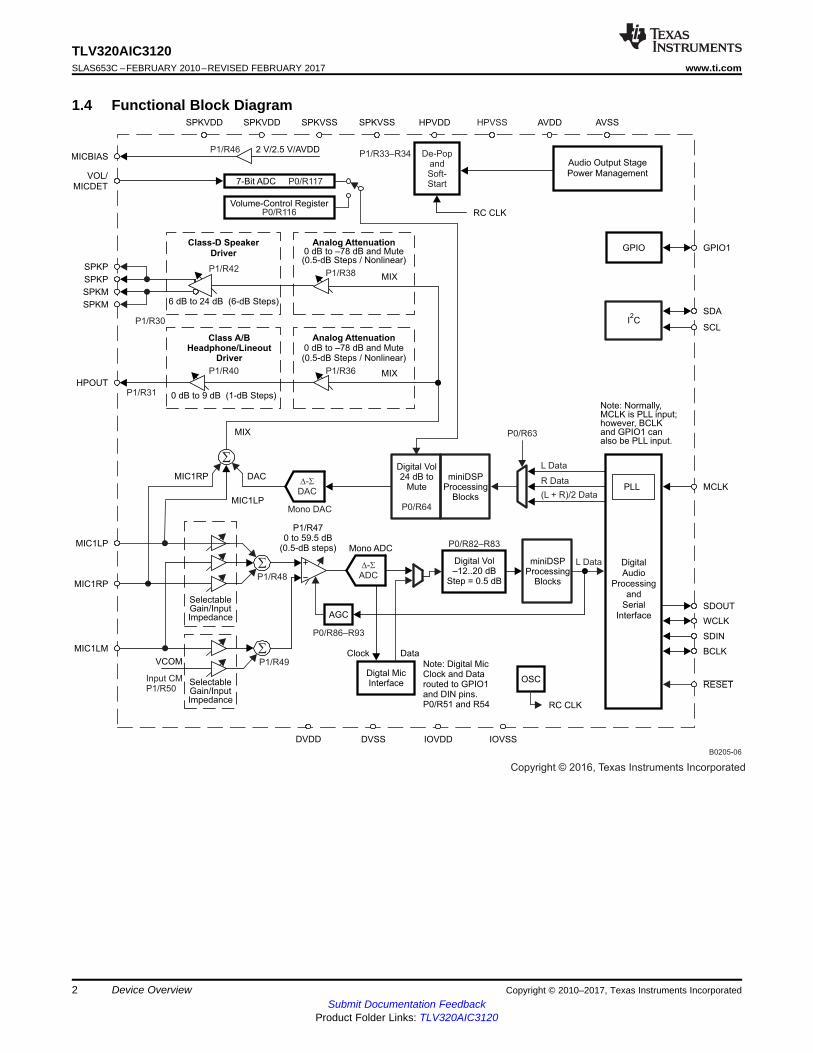
1.4 Functional Block Diagram
3
TLV320AIC3120www.ti.com SLAS653C –FEBRUARY 2010–REVISED FEBRUARY 2017
Submit Documentation FeedbackProduct Folder Links: TLV320AIC3120
Revision HistoryCopyright © 2010–2017, Texas Instruments Incorporated
Table of Contents1 Device Overview ......................................... 1
1.1 Features .............................................. 11.2 Applications........................................... 11.3 Description............................................ 11.4 Functional Block Diagram ............................ 2
2 Revision History ......................................... 33 Device Comparison ..................................... 54 Pin Configuration and Functions..................... 6
4.1 Pin Attributes ......................................... 65 Specifications ............................................ 8
5.1 Absolute Maximum Ratings .......................... 85.2 ESD Ratings.......................................... 85.3 Recommended Operating Conditions ................ 85.4 Thermal Information .................................. 95.5 Electrical Characteristics ............................. 95.6 Power Dissipation Ratings .......................... 115.7 I2S, LJF, and RJF Timing in Master Mode.......... 115.8 I2S, LJF, and RJF Timing in Slave Mode ........... 115.9 DSP Timing in Master Mode ........................ 115.10 DSP Timing in Slave Mode ......................... 125.11 I2C Interface Timing ................................. 125.12 Typical Characteristics .............................. 15
6 Parameter Measurement Information .............. 197 Detailed Description ................................... 20
7.1 Overview ............................................ 207.2 Functional Block Diagram........................... 217.3 Feature Description ................................. 217.4 Register Map ........................................ 81
8 Application and Implementation................... 1508.1 Application Information ............................ 1508.2 Typical Application ................................. 150
9 Power Supply Recommendations................. 15210 Layout................................................... 153
10.1 Layout Guidelines.................................. 15310.2 Layout Example.................................... 153
11 Device and Documentation Support.............. 15411.1 Receiving Notification of Documentation Updates. 15411.2 Community Resources............................. 15411.3 Trademarks ........................................ 15411.4 Electrostatic Discharge Caution ................... 15411.5 Glossary............................................ 154
12 Mechanical Packaging and OrderableInformation ............................................. 15412.1 Packaging Information ............................. 154
2 Revision HistoryNOTE: Page numbers for previous revisions may differ from page numbers in the current version.
Changes from Revision B (August 2016) to Revision C Page
• Added: Page 0 / Register 51 (0x33): GPIO1 In/Out Pin Control .............................................................. 93
Changes from Revision A (May 2012) to Revision B Page
• Added ESD Ratings table, Feature Description section, Device Functional Modes, Application andImplementation section, Power Supply Recommendations section, Layout section, Device and DocumentationSupport section, and Mechanical, Packaging, and Orderable Information section........................................... 1
• Deleted SPRVDD and SPRVSS pins from the Pin Functions table ........................................................... 6• Changed references to SPLVDD in Typical Performance graphs to SPKVDD ............................................. 15• Added Power-Supply Sequence section to the Device Initialization section ................................................ 21• Added the reference to the PGA Gain Versus Input Impedance table in the MICBIAS and Microphone
Preamplifier section ................................................................................................................. 26• Changed SDIN terminal to DIN in Figure 7-16 .................................................................................. 39• Changed Section 7.3.12.1.2 diagrams for PRB_P2/5/8/10/13/15/18/21/24/25 to reflect that the DRC_HPF filter
cannot be bypassed when the DRC is turned off .............................................................................. 45• Added sequence for inserting a beep in the middle of an already-playing signal and note text following script in
the Key-Click Functionality With Digital Sine-Wave Generator (PRB_P25) section........................................ 58• Changed references of HPLOUT to HPOUT in Section 7.3.12.12.1 section................................................ 62• Added PRB modes text to note for Page 0 / Register 20 ...................................................................... 86• Added PRB modes text to Page 0 / Register 21. Also added Page 0 / Register 21 programmed value note.......... 86• Added D(3:0) note to Page 0 / Register 22 ...................................................................................... 86• Changed last line to "10111-11000: Reserved. Do not use." "11001: DAC Signal Processing Block PRB_P25"
"11010-11111: Reserved. Do not use." .......................................................................................... 94• Changed values in Page 0 / Register 69 (0x45): DRC Control 2 ............................................................. 97• Changed Page 0, Register 70, bit D3-D0 decay rate value for 0000 from DR = 1.5625e–3 to DR = 0.015625 ........ 98• Switched D1 and D0 descriptions so that D1 is for SP and D0 is for HP in Page 1 / Register 30 table ............... 105
4
TLV320AIC3120SLAS653C –FEBRUARY 2010–REVISED FEBRUARY 2017 www.ti.com
Submit Documentation FeedbackProduct Folder Links: TLV320AIC3120
Revision History Copyright © 2010–2017, Texas Instruments Incorporated
• Changed Page 1 / Register 40, D1 to reserved ............................................................................... 107• Changed references to TLV320AIC3111 device to the TLV320AIC3120 device throughout the REGISTER MAP
section .............................................................................................................................. 122
Changes from Original (February 2010) to Revision A Page
• Added PGA Gain table to data sheet............................................................................................. 26• Added PRB_P25 and values to Table 7-20...................................................................................... 44• Added Section 7.3.12.1.2.9 and Signal Chain with beep generator image.................................................. 46• Added section Section 7.3.12.7 after Interrupts section ....................................................................... 57• Added D6-D0 to the Register Value columns, and changed the Analog Attenuation columns to Analog Gain ........ 61• Added table note to Analog Volume Control for Headphone and Speaker Outputs (for D7 = 1) table .................. 61• Changed "page 0 / register 44" to " page 1 / register 44" in Headphone Drivers section ................................ 62• Changed max AOSR values in Clock Distribution Tree image from 1023, 1024 to 255, 256. ............................ 67• Changed PLL conditions under Equation 10 and Equation 11................................................................ 71• Added Timer section ................................................................................................................ 72• Deleted the Page 0 / Register 71–Page 0 / Register 80 table and added Beep Generator bit registers from
SLAS659A (Page 0 / Register 71–80). ........................................................................................... 98• Modified Page 0 / Register 80 title from Page 0 / Register 80-115: Reserved to Page 0 / Register 80: Reserved. ... 99• Corrected values in Description column for bits D6–D0 of Page 0 / Register 83 ......................................... 100• Changed Bit D0 = 1 to Reserved. ............................................................................................... 106• Deleted references to Analog Volume Control (D7 = 0) table from Page 1 / Register 36 and Page 1 / Register 38 107• Changed Added table note following Page 1 / Register 40 .................................................................. 107• Deleted one of the table notes from Page 1/ Register 48 and Page 1 / Register 49 ..................................... 109• Deleted one of the table notes from Page 1/ Register 48 and Page 1 / Register 49 ..................................... 109
5
TLV320AIC3120www.ti.com SLAS653C –FEBRUARY 2010–REVISED FEBRUARY 2017
Submit Documentation FeedbackProduct Folder Links: TLV320AIC3120
Device ComparisonCopyright © 2010–2017, Texas Instruments Incorporated
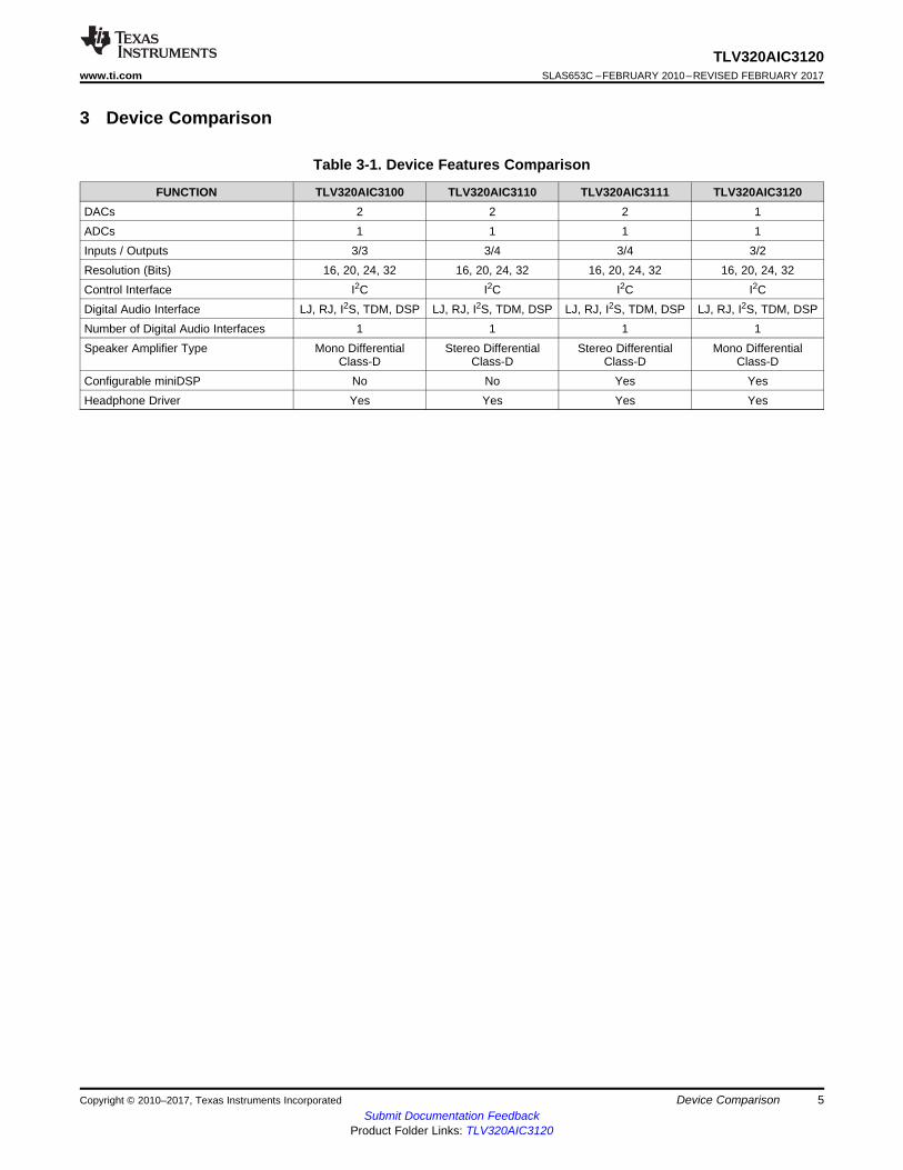
3 Device Comparison
Table 3-1. Device Features Comparison
FUNCTION TLV320AIC3100 TLV320AIC3110 TLV320AIC3111 TLV320AIC3120DACs 2 2 2 1ADCs 1 1 1 1Inputs / Outputs 3/3 3/4 3/4 3/2Resolution (Bits) 16, 20, 24, 32 16, 20, 24, 32 16, 20, 24, 32 16, 20, 24, 32Control Interface I2C I2C I2C I2CDigital Audio Interface LJ, RJ, I2S, TDM, DSP LJ, RJ, I2S, TDM, DSP LJ, RJ, I2S, TDM, DSP LJ, RJ, I2S, TDM, DSPNumber of Digital Audio Interfaces 1 1 1 1Speaker Amplifier Type Mono Differential
Class-DStereo Differential
Class-DStereo Differential
Class-DMono Differential
Class-DConfigurable miniDSP No No Yes YesHeadphone Driver Yes Yes Yes Yes
P0048-15
AVSSSPKVSS
IOV
SS
SP
KV
DD
24
1
23
2
22
3
21
4
20
5
19
6
18
7
17
8
1625
1526
1427
1328
1229
1130
1031
932
MIC1LM
SP
KM
MIC1RP
SP
KP
MIC1LP
SP
KV
DD
MICBIAS
SP
KV
SS
VOL/MICDET
SP
KM
SCL
DV
SS
SDA
AV
DD
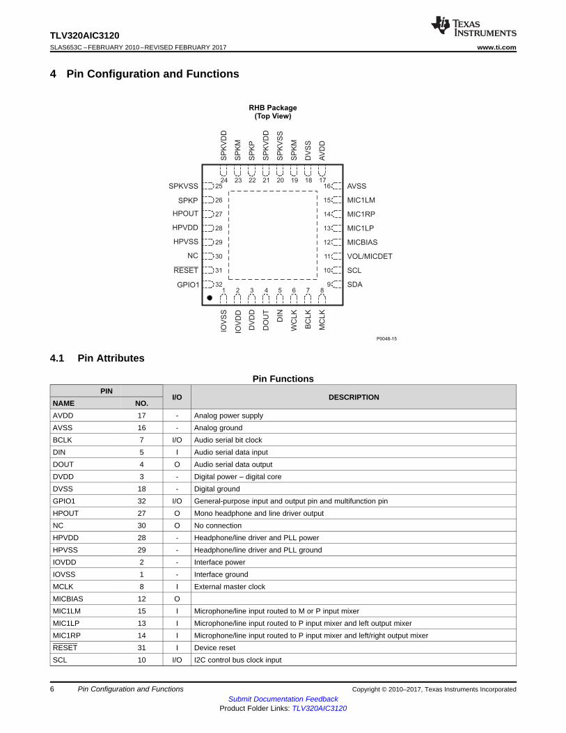
RHB Package(Top View)
SPKP
IOV
DD
HPOUT
DV
DD
HPVDD
DO
UT
HPVSS
DIN
NC
WC
LK
RESET
BC
LK
GPIO1
MC
LK
6
TLV320AIC3120SLAS653C –FEBRUARY 2010–REVISED FEBRUARY 2017 www.ti.com
Submit Documentation FeedbackProduct Folder Links: TLV320AIC3120
Pin Configuration and Functions Copyright © 2010–2017, Texas Instruments Incorporated
4 Pin Configuration and Functions
4.1 Pin Attributes
Pin FunctionsPIN
I/O DESCRIPTIONNAME NO.AVDD 17 - Analog power supplyAVSS 16 - Analog groundBCLK 7 I/O Audio serial bit clockDIN 5 I Audio serial data inputDOUT 4 O Audio serial data outputDVDD 3 - Digital power – digital coreDVSS 18 - Digital groundGPIO1 32 I/O General-purpose input and output pin and multifunction pinHPOUT 27 O Mono headphone and line driver outputNC 30 O No connectionHPVDD 28 - Headphone/line driver and PLL powerHPVSS 29 - Headphone/line driver and PLL groundIOVDD 2 - Interface powerIOVSS 1 - Interface groundMCLK 8 I External master clockMICBIAS 12 OMIC1LM 15 I Microphone/line input routed to M or P input mixerMIC1LP 13 I Microphone/line input routed to P input mixer and left output mixerMIC1RP 14 I Microphone/line input routed to P input mixer and left/right output mixerRESET 31 I Device resetSCL 10 I/O I2C control bus clock input
7
TLV320AIC3120www.ti.com SLAS653C –FEBRUARY 2010–REVISED FEBRUARY 2017
Submit Documentation FeedbackProduct Folder Links: TLV320AIC3120
Pin Configuration and FunctionsCopyright © 2010–2017, Texas Instruments Incorporated
Pin Functions (continued)PIN
I/O DESCRIPTIONNAME NO.SDA 9 I/O I2C control-bus data inputSPKM 19, 23 I/O Cass-D speaker driver inverting outputSPKP 22, 26 - Class-D speaker driver noninverting outputSPKVDD 21, 24 - Class-D speaker driver power supplySPKVSS 20, 25 - Class-D speaker driver power-supply groundVOL/MICDET 11 I Volume control or microphone detectionWCLK 6 I/O Audio serial word clock
8
TLV320AIC3120SLAS653C –FEBRUARY 2010–REVISED FEBRUARY 2017 www.ti.com
Submit Documentation FeedbackProduct Folder Links: TLV320AIC3120
Specifications Copyright © 2010–2017, Texas Instruments Incorporated
(1) Stresses beyond those listed under Absolute Maximum Ratings may cause permanent damage to the device. These are stress ratingsonly, and functional operation of the device at these or any other conditions beyond those indicated under Recommended OperatingConditions is not implied. Exposure to absolute-maximum-rated conditions for extended periods may affect device reliability.
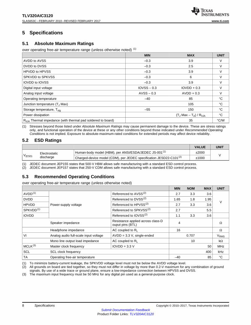
5 Specifications
5.1 Absolute Maximum Ratingsover operating free-air temperature range (unless otherwise noted) (1)
MIN MAX UNITAVDD to AVSS –0.3 3.9 VDVDD to DVSS –0.3 2.5 VHPVDD to HPVSS –0.3 3.9 VSPKVDD to SPKVSS –0.3 6 VIOVDD to IOVSS –0.3 3.9 VDigital input voltage IOVSS – 0.3 IOVDD + 0.3 VAnalog input voltage AVSS – 0.3 AVDD + 0.3 VOperating temperature –40 85 °CJunction temperature (TJ Max) 105 °CStorage temperature, Tstg –55 150 °CPower dissipation (TJ Max – TA) / RθJA °CRθJA Thermal impedance (with thermal pad soldered to board) 35 °C/W
(1) JEDEC document JEP155 states that 500-V HBM allows safe manufacturing with a standard ESD control process.(2) JEDEC document JEP157 states that 250-V CDM allows safe manufacturing with a standard ESD control process.
5.2 ESD RatingsVALUE UNIT
V(ESD)Electrostaticdischarge
Human-body model (HBM), per ANSI/ESDA/JEDEC JS-001 (1) ±2000V
Charged-device model (CDM), per JEDEC specification JESD22-C101 (2) ±1000
(1) To minimize battery-current leakage, the SPKVDD voltage level must not be below the AVDD voltage level.(2) All grounds on board are tied together, so they must not differ in voltage by more than 0.2-V maximum for any combination of ground
signals. By use of a wide trace or ground plane, ensure a low-impedance connection between HPVSS and DVSS.(3) The maximum input frequency must be 50 MHz for any digital pin used as a general-purpose clock.
5.3 Recommended Operating Conditionsover operating free-air temperature range (unless otherwise noted)
MIN NOM MAX UNITAVDD (1)
Power-supply voltage
Referenced to AVSS (2) 2.7 3.3 3.6
VDVDD Referenced to DVSS (2) 1.65 1.8 1.95HPVDD Referenced to HPVSS (2) 2.7 3.3 3.6SPKVDD (1) Referenced to SPKVSS (2) 2.7 5.5IOVDD Referenced to IOVSS (2) 1.1 3.3 3.6
Speaker impedance Resistance applied across class-Douput pins (BTL) 4 Ω
Headphone impedance AC coupled to RL 16 Ω
VI Analog audio full-scale input voltage AVDD = 3.3 V, single-ended 0.707 VRMS
Mono line output load impedance AC coupled to RL 10 kΩMCLK (3) Master clock frequency IOVDD = 3.3 V 50 MHzSCL SCL clock frequency 400 kHzTA Operating free-air temperature –40 85 °C
9
TLV320AIC3120www.ti.com SLAS653C –FEBRUARY 2010–REVISED FEBRUARY 2017
Submit Documentation FeedbackProduct Folder Links: TLV320AIC3120
SpecificationsCopyright © 2010–2017, Texas Instruments Incorporated
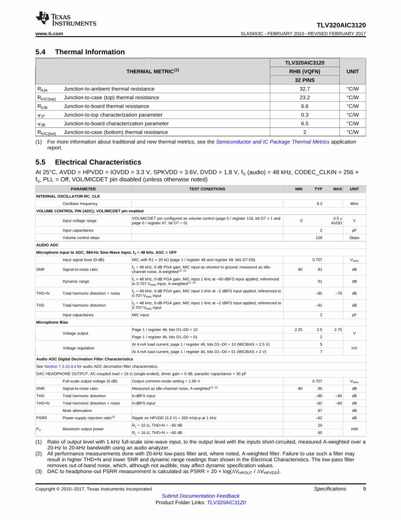
(1) For more information about traditional and new thermal metrics, see the Semiconductor and IC Package Thermal Metrics applicationreport.
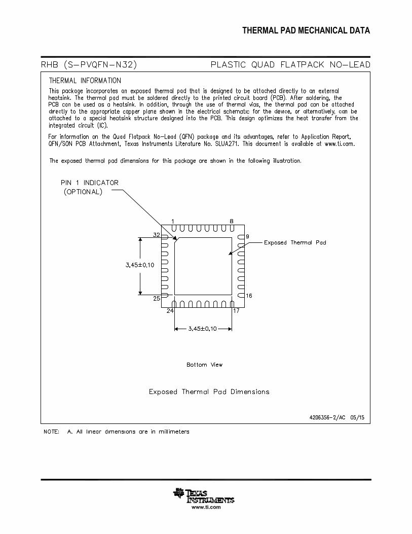
5.4 Thermal Information
THERMAL METRIC (1)TLV320AIC3120
UNITRHB (VQFN)32 PINS
RθJA Junction-to-ambient thermal resistance 32.7 °C/WRθJC(top) Junction-to-case (top) thermal resistance 23.2 °C/WRθJB Junction-to-board thermal resistance 6.6 °C/WψJT Junction-to-top characterization parameter 0.3 °C/WψJB Junction-to-board characterization parameter 6.5 °C/WRθJC(bot) Junction-to-case (bottom) thermal resistance 2 °C/W
(1) Ratio of output level with 1-kHz full-scale sine-wave input, to the output level with the inputs short-circuited, measured A-weighted over a20-Hz to 20-kHz bandwidth using an audio analyzer.
(2) All performance measurements done with 20-kHz low-pass filter and, where noted, A-weighted filter. Failure to use such a filter mayresult in higher THD+N and lower SNR and dynamic range readings than shown in the Electrical Characteristics. The low-pass filterremoves out-of-band noise, which, although not audible, may affect dynamic specification values.
(3) DAC to headphone-out PSRR measurement is calculated as PSRR = 20 × log(ΔVHPOUT / ΔVHPVDD).
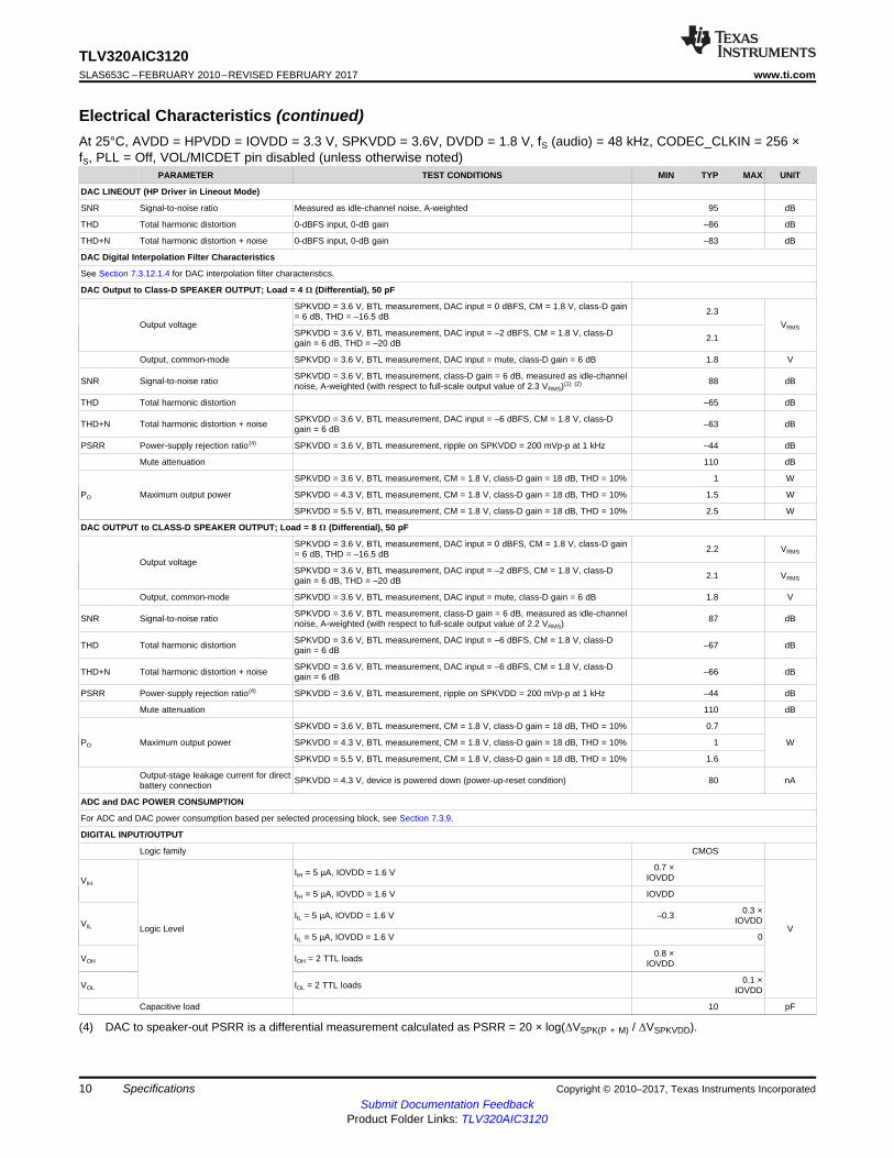
5.5 Electrical CharacteristicsAt 25°C, AVDD = HPVDD = IOVDD = 3.3 V, SPKVDD = 3.6V, DVDD = 1.8 V, fS (audio) = 48 kHz, CODEC_CLKIN = 256 ×fS, PLL = Off, VOL/MICDET pin disabled (unless otherwise noted)
PARAMETER TEST CONDITIONS MIN TYP MAX UNIT
INTERNAL OSCILLATOR-RC_CLK
Oscillator frequency 8.2 MHz
VOLUME CONTROL PIN (ADC); VOL/MICDET pin enabled
Input voltage range VOL/MICDET pin configured as volume control (page 0 / register 116, bit D7 = 1 andpage 0 / register 67, bit D7 = 0) 0 0.5 x
AVDD V
Input capacitance 2 pF
Volume control steps 128 Steps
AUDIO ADC
Microphone Input to ADC, 984-Hz Sine-Wave Input, fS = 48 kHz, AGC = OFF
Input signal level (0-dB) MIC with R1 = 20 kΩ (page 1 / register 48 and register 49, bits D7-D6) 0.707 VRMS
SNR Signal-to-noise ratio fS = 48 kHz, 0-dB PGA gain, MIC input ac-shorted to ground; measured as idle-channel noise, A-weighted (1) (2) 80 91 dB
Dynamic range fS = 48 kHz, 0-dB PGA gain, MIC input 1 kHz at –60-dBFS input applied, referencedto 0.707-VRMS input, A-weighted(1) (2) 91 dB
THD+N Total harmonic distortion + noise fS = 48 kHz, 0-dB PGA gain, MIC input 1 kHz at –2 dBFS input applied, referenced to0.707-VRMS input –85 –70 dB
THD Total harmonic distortion fS = 48 kHz, 0-dB PGA gain, MIC input 1 kHz at –2 dBFS input applied, referenced to0.707-VRMS input –91 dB
Input capacitance MIC input 2 pF
Microphone Bias
Voltage outputPage 1 / register 46, bits D1–D0 = 10 2.25 2.5 2.75
VPage 1 / register 46, bits D1–D0 = 01 2
Voltage regulationAt 4-mA load current, page 1 / register 46, bits D1–D0 = 10 (MICBIAS = 2.5 V) 5
mVAt 4-mA load current, page 1 / register 46, bits D1–D0 = 01 (MICBIAS = 2 V) 7
Audio ADC Digital Decimation Filter Characteristics
See Section 7.3.10.4.4 for audio ADC decimation filter characteristics.
DAC HEADPHONE OUTPUT, AC-coupled load = 16 Ω (single-ended), driver gain = 0 dB, parasitic capacitance = 30 pF
Full-scale output voltage (0 dB) Output common-mode setting = 1.65 V 0.707 VRMS
SNR Signal-to-noise ratio Measured as idle-channel noise, A-weighted(1) (2) 80 95 dB
THD Total harmonic distortion 0-dBFS input –85 –65 dB
THD+N Total harmonic distortion + noise 0-dBFS input –82 –60 dB
Mute attenuation 87 dB
PSRR Power-supply rejection ratio(3) Ripple on HPVDD (3.3 V) = 200 mVp-p at 1 kHz –62 dB
PO Maximum output powerRL = 32 Ω, THD+N = –60 dB 20
mWRL = 16 Ω, THD+N = –60 dB 60
10
TLV320AIC3120SLAS653C –FEBRUARY 2010–REVISED FEBRUARY 2017 www.ti.com
Submit Documentation FeedbackProduct Folder Links: TLV320AIC3120
Specifications Copyright © 2010–2017, Texas Instruments Incorporated
Electrical Characteristics (continued)At 25°C, AVDD = HPVDD = IOVDD = 3.3 V, SPKVDD = 3.6V, DVDD = 1.8 V, fS (audio) = 48 kHz, CODEC_CLKIN = 256 ×fS, PLL = Off, VOL/MICDET pin disabled (unless otherwise noted)
PARAMETER TEST CONDITIONS MIN TYP MAX UNIT
(4) DAC to speaker-out PSRR is a differential measurement calculated as PSRR = 20 × log(ΔVSPK(P + M) / ΔVSPKVDD).
DAC LINEOUT (HP Driver in Lineout Mode)
SNR Signal-to-noise ratio Measured as idle-channel noise, A-weighted 95 dB
THD Total harmonic distortion 0-dBFS input, 0-dB gain –86 dB
THD+N Total harmonic distortion + noise 0-dBFS input, 0-dB gain –83 dB
DAC Digital Interpolation Filter Characteristics
See Section 7.3.12.1.4 for DAC interpolation filter characteristics.
DAC Output to Class-D SPEAKER OUTPUT; Load = 4 Ω (Differential), 50 pF
Output voltage
SPKVDD = 3.6 V, BTL measurement, DAC input = 0 dBFS, CM = 1.8 V, class-D gain= 6 dB, THD = –16.5 dB 2.3
VRMSSPKVDD = 3.6 V, BTL measurement, DAC input = –2 dBFS, CM = 1.8 V, class-Dgain = 6 dB, THD = –20 dB 2.1
Output, common-mode SPKVDD = 3.6 V, BTL measurement, DAC input = mute, class-D gain = 6 dB 1.8 V
SNR Signal-to-noise ratio SPKVDD = 3.6 V, BTL measurement, class-D gain = 6 dB, measured as idle-channelnoise, A-weighted (with respect to full-scale output value of 2.3 VRMS)(1) (2) 88 dB
THD Total harmonic distortion –65 dB
THD+N Total harmonic distortion + noise SPKVDD = 3.6 V, BTL measurement, DAC input = –6 dBFS, CM = 1.8 V, class-Dgain = 6 dB –63 dB
PSRR Power-supply rejection ratio(4) SPKVDD = 3.6 V, BTL measurement, ripple on SPKVDD = 200 mVp-p at 1 kHz –44 dB
Mute attenuation 110 dB
PO Maximum output power
SPKVDD = 3.6 V, BTL measurement, CM = 1.8 V, class-D gain = 18 dB, THD = 10% 1 W
SPKVDD = 4.3 V, BTL measurement, CM = 1.8 V, class-D gain = 18 dB, THD = 10% 1.5 W
SPKVDD = 5.5 V, BTL measurement, CM = 1.8 V, class-D gain = 18 dB, THD = 10% 2.5 W
DAC OUTPUT to CLASS-D SPEAKER OUTPUT; Load = 8 Ω (Differential), 50 pF
Output voltage
SPKVDD = 3.6 V, BTL measurement, DAC input = 0 dBFS, CM = 1.8 V, class-D gain= 6 dB, THD = –16.5 dB 2.2 VRMS
SPKVDD = 3.6 V, BTL measurement, DAC input = –2 dBFS, CM = 1.8 V, class-Dgain = 6 dB, THD = –20 dB 2.1 VRMS
Output, common-mode SPKVDD = 3.6 V, BTL measurement, DAC input = mute, class-D gain = 6 dB 1.8 V
SNR Signal-to-noise ratio SPKVDD = 3.6 V, BTL measurement, class-D gain = 6 dB, measured as idle-channelnoise, A-weighted (with respect to full-scale output value of 2.2 VRMS) 87 dB
THD Total harmonic distortion SPKVDD = 3.6 V, BTL measurement, DAC input = –6 dBFS, CM = 1.8 V, class-Dgain = 6 dB –67 dB
THD+N Total harmonic distortion + noise SPKVDD = 3.6 V, BTL measurement, DAC input = –6 dBFS, CM = 1.8 V, class-Dgain = 6 dB –66 dB
PSRR Power-supply rejection ratio(4) SPKVDD = 3.6 V, BTL measurement, ripple on SPKVDD = 200 mVp-p at 1 kHz –44 dB
Mute attenuation 110 dB
PO Maximum output power
SPKVDD = 3.6 V, BTL measurement, CM = 1.8 V, class-D gain = 18 dB, THD = 10% 0.7
WSPKVDD = 4.3 V, BTL measurement, CM = 1.8 V, class-D gain = 18 dB, THD = 10% 1
SPKVDD = 5.5 V, BTL measurement, CM = 1.8 V, class-D gain = 18 dB, THD = 10% 1.6
Output-stage leakage current for directbattery connection SPKVDD = 4.3 V, device is powered down (power-up-reset condition) 80 nA
ADC and DAC POWER CONSUMPTION
For ADC and DAC power consumption based per selected processing block, see Section 7.3.9.
DIGITAL INPUT/OUTPUT
Logic family CMOS
VIH
Logic Level
IIH = 5 µA, IOVDD = 1.6 V 0.7 ×IOVDD
V
IIH = 5 µA, IOVDD = 1.6 V IOVDD
VIL
IIL = 5 µA, IOVDD = 1.6 V –0.3 0.3 ×IOVDD
IIL = 5 µA, IOVDD = 1.6 V 0
VOH IOH = 2 TTL loads 0.8 ×IOVDD
VOL IOL = 2 TTL loads 0.1 ×IOVDD
Capacitive load 10 pF
11
TLV320AIC3120www.ti.com SLAS653C –FEBRUARY 2010–REVISED FEBRUARY 2017
Submit Documentation FeedbackProduct Folder Links: TLV320AIC3120
SpecificationsCopyright © 2010–2017, Texas Instruments Incorporated
(1) Maximum power dissipation is TJMAX – TA) / RθJA
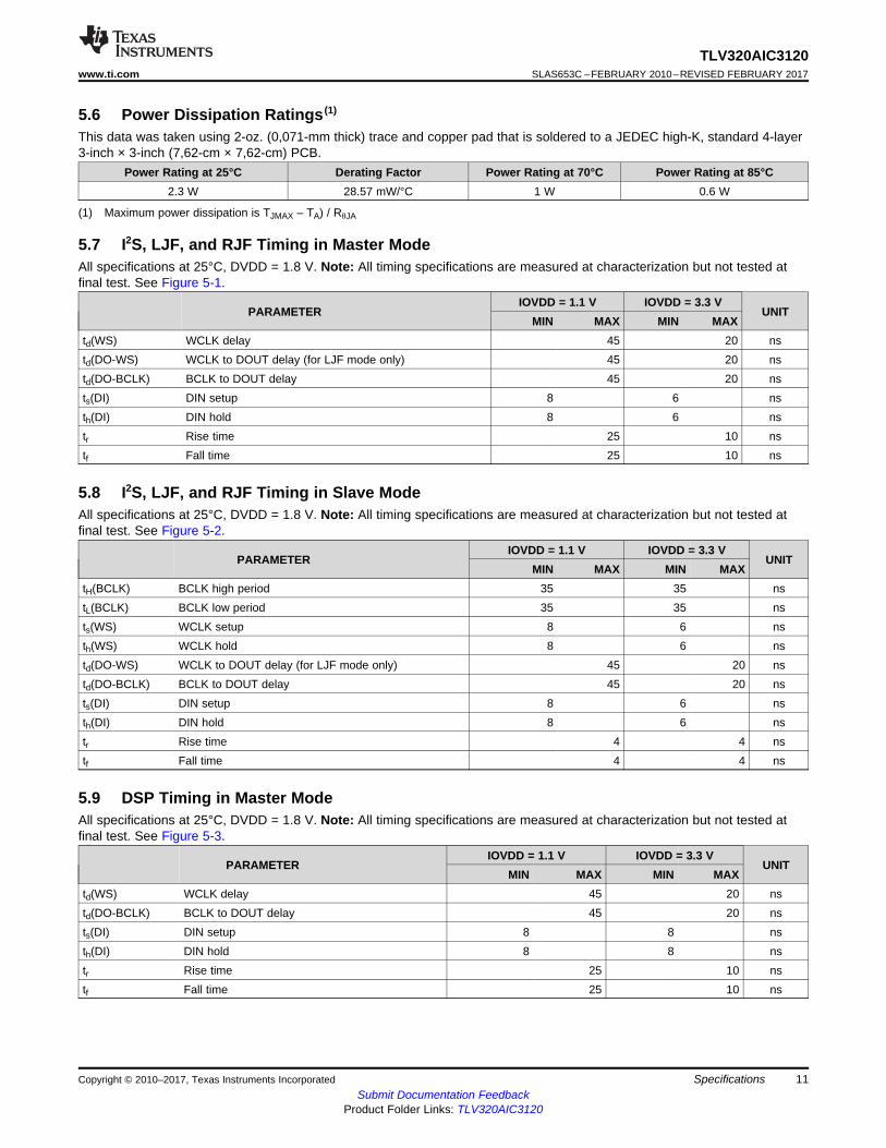
5.6 Power Dissipation Ratings (1)
This data was taken using 2-oz. (0,071-mm thick) trace and copper pad that is soldered to a JEDEC high-K, standard 4-layer3-inch × 3-inch (7,62-cm × 7,62-cm) PCB.
Power Rating at 25°C Derating Factor Power Rating at 70°C Power Rating at 85°C2.3 W 28.57 mW/°C 1 W 0.6 W
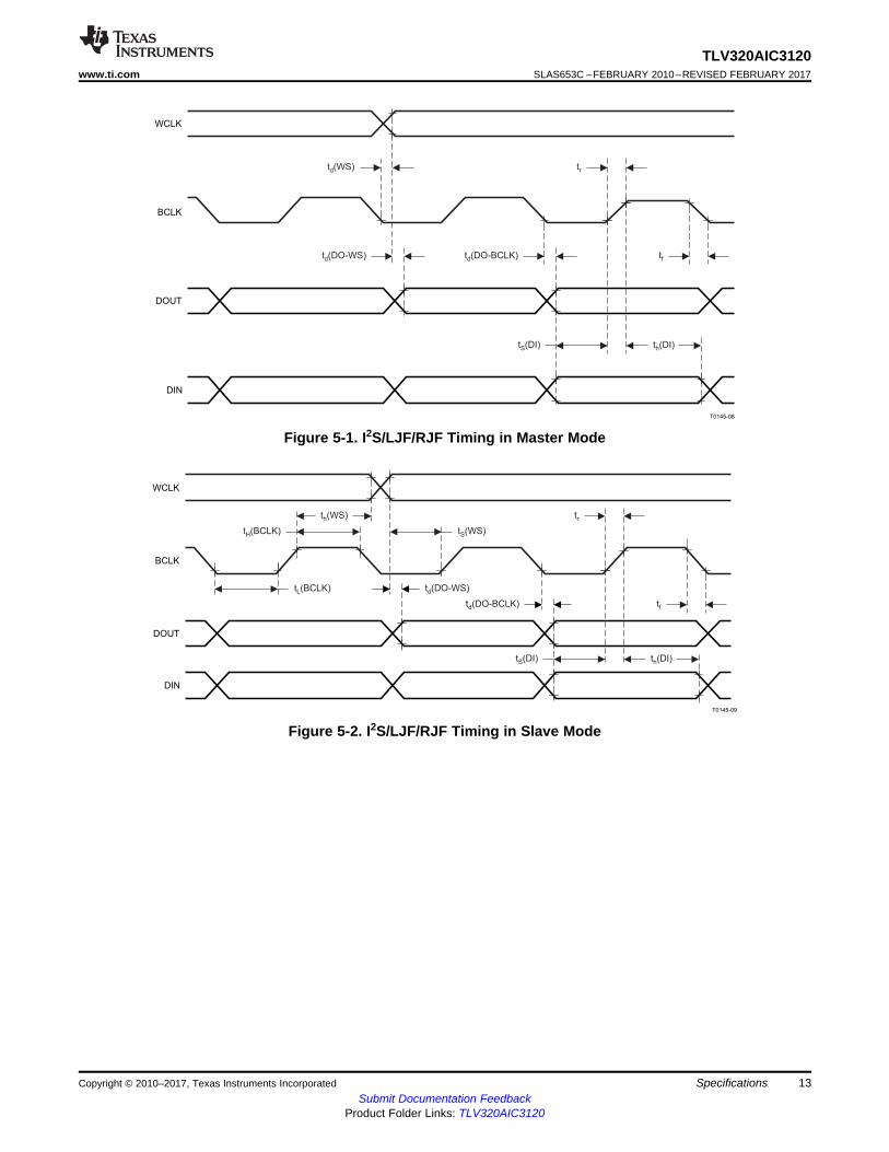
5.7 I2S, LJF, and RJF Timing in Master ModeAll specifications at 25°C, DVDD = 1.8 V. Note: All timing specifications are measured at characterization but not tested atfinal test. See Figure 5-1.
PARAMETERIOVDD = 1.1 V IOVDD = 3.3 V
UNITMIN MAX MIN MAX
td(WS) WCLK delay 45 20 nstd(DO-WS) WCLK to DOUT delay (for LJF mode only) 45 20 nstd(DO-BCLK) BCLK to DOUT delay 45 20 nsts(DI) DIN setup 8 6 nsth(DI) DIN hold 8 6 nstr Rise time 25 10 nstf Fall time 25 10 ns
5.8 I2S, LJF, and RJF Timing in Slave ModeAll specifications at 25°C, DVDD = 1.8 V. Note: All timing specifications are measured at characterization but not tested atfinal test. See Figure 5-2.
PARAMETERIOVDD = 1.1 V IOVDD = 3.3 V
UNITMIN MAX MIN MAX
tH(BCLK) BCLK high period 35 35 nstL(BCLK) BCLK low period 35 35 nsts(WS) WCLK setup 8 6 nsth(WS) WCLK hold 8 6 nstd(DO-WS) WCLK to DOUT delay (for LJF mode only) 45 20 nstd(DO-BCLK) BCLK to DOUT delay 45 20 nsts(DI) DIN setup 8 6 nsth(DI) DIN hold 8 6 nstr Rise time 4 4 nstf Fall time 4 4 ns
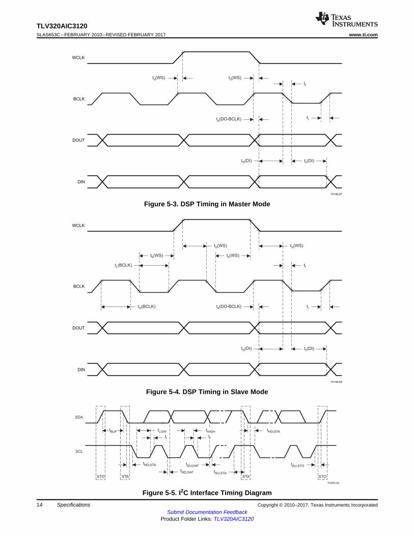
5.9 DSP Timing in Master ModeAll specifications at 25°C, DVDD = 1.8 V. Note: All timing specifications are measured at characterization but not tested atfinal test. See Figure 5-3.
PARAMETERIOVDD = 1.1 V IOVDD = 3.3 V
UNITMIN MAX MIN MAX
td(WS) WCLK delay 45 20 nstd(DO-BCLK) BCLK to DOUT delay 45 20 nsts(DI) DIN setup 8 8 nsth(DI) DIN hold 8 8 nstr Rise time 25 10 nstf Fall time 25 10 ns
12
TLV320AIC3120SLAS653C –FEBRUARY 2010–REVISED FEBRUARY 2017 www.ti.com
Submit Documentation FeedbackProduct Folder Links: TLV320AIC3120
Specifications Copyright © 2010–2017, Texas Instruments Incorporated
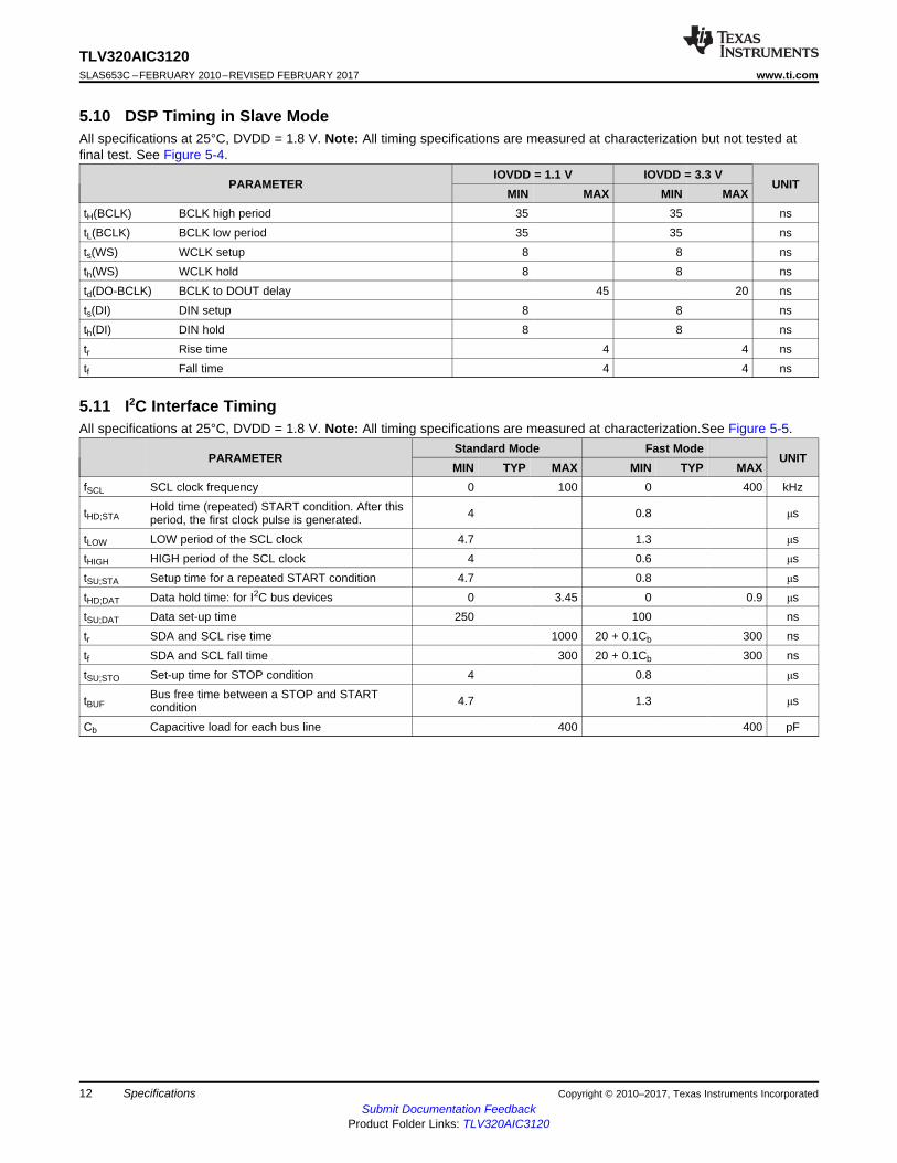
5.10 DSP Timing in Slave ModeAll specifications at 25°C, DVDD = 1.8 V. Note: All timing specifications are measured at characterization but not tested atfinal test. See Figure 5-4.
PARAMETERIOVDD = 1.1 V IOVDD = 3.3 V
UNITMIN MAX MIN MAX
tH(BCLK) BCLK high period 35 35 nstL(BCLK) BCLK low period 35 35 nsts(WS) WCLK setup 8 8 nsth(WS) WCLK hold 8 8 nstd(DO-BCLK) BCLK to DOUT delay 45 20 nsts(DI) DIN setup 8 8 nsth(DI) DIN hold 8 8 nstr Rise time 4 4 nstf Fall time 4 4 ns
5.11 I2C Interface TimingAll specifications at 25°C, DVDD = 1.8 V. Note: All timing specifications are measured at characterization.See Figure 5-5.
PARAMETERStandard Mode Fast Mode
UNITMIN TYP MAX MIN TYP MAX
fSCL SCL clock frequency 0 100 0 400 kHz
tHD;STAHold time (repeated) START condition. After thisperiod, the first clock pulse is generated. 4 0.8 μs
tLOW LOW period of the SCL clock 4.7 1.3 μstHIGH HIGH period of the SCL clock 4 0.6 μstSU;STA Setup time for a repeated START condition 4.7 0.8 μstHD;DAT Data hold time: for I2C bus devices 0 3.45 0 0.9 μstSU;DAT Data set-up time 250 100 nstr SDA and SCL rise time 1000 20 + 0.1Cb 300 nstf SDA and SCL fall time 300 20 + 0.1Cb 300 nstSU;STO Set-up time for STOP condition 4 0.8 μs
tBUFBus free time between a STOP and STARTcondition 4.7 1.3 μs
Cb Capacitive load for each bus line 400 400 pF
T0145-09
WCLK
BCLK
DOUT
DIN
t (WS)h
t (BCLK)H
t (DO-BCLK)d
t (DO-WS)d
t (DI)S
t (BCLK)L
t (DI)h
t (WS)S
tr
tf
T0145-08
WCLK
BCLK
DOUT
DIN
t (DO-BCLK)dt (DO-WS)d
t (WS)d
t (DI)S t (DI)h
tr
tf
13
TLV320AIC3120www.ti.com SLAS653C –FEBRUARY 2010–REVISED FEBRUARY 2017
Submit Documentation FeedbackProduct Folder Links: TLV320AIC3120
SpecificationsCopyright © 2010–2017, Texas Instruments Incorporated
Figure 5-1. I2S/LJF/RJF Timing in Master Mode
Figure 5-2. I2S/LJF/RJF Timing in Slave Mode
STO STA STA STO
SDA
SCL
tBUF tLOW
tSU;STA
tHIGH tHD;STA
tr
tHD;STA
tHD;DAT
tSU;DAT tSU;STO
tf
T0295-02
T0146-08
WCLK
BCLK
DOUT
DIN
t (WS)h t (WS)h
t (BCLK)L
t (DO-BCLK)d tr
tf
t (DI)S
t (BCLK)H
t (DI)h
t (WS)S t (WS)S
T0146-07
WCLK
BCLK
DOUT
DIN
t (DO-BCLK)d
t (WS)d t (WS)d
t (DI)S t (DI)h
tf
tr
14
TLV320AIC3120SLAS653C –FEBRUARY 2010–REVISED FEBRUARY 2017 www.ti.com
Submit Documentation FeedbackProduct Folder Links: TLV320AIC3120
Specifications Copyright © 2010–2017, Texas Instruments Incorporated
Figure 5-3. DSP Timing in Master Mode
Figure 5-4. DSP Timing in Slave Mode
Figure 5-5. I2C Interface Timing Diagram
Channel Gain − dB
50
55
60
65
70
75
80
85
90
95
100
−10 0 10 20 30 40 50 60 70 80
SN
R −
dB
G006
Diff = 10k
Diff = 20k
Diff = 40k
SE = 40k
SE = 20k
SE = 10k
f − Frequency − kHz
−100
−90
−80
−70
−60
−50
−40
−30
−20
−10
0
0 50 100 150 200
Am
plitu
de −
dB
FS
G005
AVDD = HPVDD = 3.3 VIOVDD = SPKVDD = 3.3 VDVDD = 1.8 V
f − Frequency − kHz
−160
−140
−120
−100
−80
−60
−40
−20
0
20
0 5 10 15 20
Am
plitu
de −
dB
FS
G003
AVDD = HPVDD = 3.3 VIOVDD = SPKVDD = 3.3 VDVDD = 1.8 V
f − Frequency − kHz
−160
−140
−120
−100
−80
−60
−40
−20
0
20
0 5 10 15 20
Am
plitu
de −
dB
FS
G004
AVDD = HPVDD = 3.3 VIOVDD = SPKVDD = 3.3 VDVDD = 1.8 V
f − Frequency − kHz
−160
−140
−120
−100
−80
−60
−40
−20
0
20
0 5 10 15 20
Am
plitu
de −
dB
FS
G001
AVDD = HPVDD = 3.3 VIOVDD = SPKVDD = 3.3 VDVDD = 1.8 V
f − Frequency − kHz
−160
−140
−120
−100
−80
−60
−40
−20
0
20
0 5 10 15 20
Am
plitu
de −
dB
FS
G002
AVDD = HPVDD = 3.3 VIOVDD = SPKVDD = 3.3 VDVDD = 1.8 V
15
TLV320AIC3120www.ti.com SLAS653C –FEBRUARY 2010–REVISED FEBRUARY 2017
Submit Documentation FeedbackProduct Folder Links: TLV320AIC3120
SpecificationsCopyright © 2010–2017, Texas Instruments Incorporated
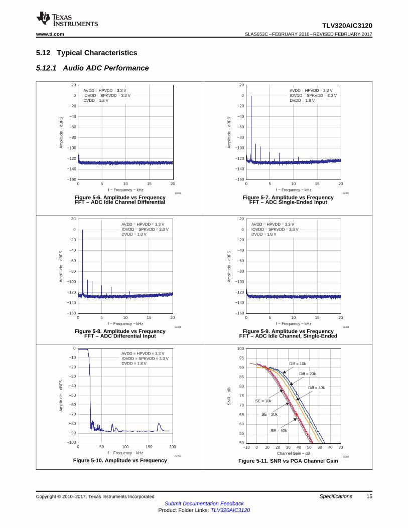
5.12 Typical Characteristics
5.12.1 Audio ADC Performance
Figure 5-6. Amplitude vs FrequencyFFT – ADC Idle Channel Differential
Added Text for Spacing
Figure 5-7. Amplitude vs FrequencyFFT – ADC Single-Ended Input
Figure 5-8. Amplitude vs FrequencyFFT – ADC Differential Input
Figure 5-9. Amplitude vs FrequencyFFT – ADC Idle Channel, Single-Ended
Figure 5-10. Amplitude vs Frequency Figure 5-11. SNR vs PGA Channel Gain
−100
−90
−80
−70
−60
−50
−40
−30
−20
−10
0
0.00 0.02 0.04 0.06 0.08 0.10 0.12 0.14
G025
TH
D+N
− T
otal
Har
mon
ic D
isto
rtio
n +
Noi
se −
dB
PO − Output Power − W
HPVDD = 3.3 VCM = 1.65 V
HPVDD = 3.6 VCM = 1.8 V
HPVDD = 3 VCM = 1.5 V
HPVDD = 2.7 VCM = 1.35 V
IOVDD = 3.3 VDVDD = 1.8 VGain = 9 dBRL = 16 Ω
f − Frequency − kHz
−160
−140
−120
−100
−80
−60
−40
−20
0
0 5 10 15 20
Am
plitu
de −
dB
FS
G023f − Frequency − kHz
−160
−140
−120
−100
−80
−60
−40
−20
0
0 5 10 15 20
Am
plitu
de −
dB
FS
G026
16
TLV320AIC3120SLAS653C –FEBRUARY 2010–REVISED FEBRUARY 2017 www.ti.com
Submit Documentation FeedbackProduct Folder Links: TLV320AIC3120
Specifications Copyright © 2010–2017, Texas Instruments Incorporated
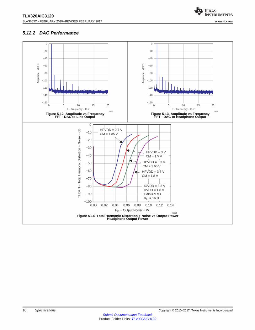
5.12.2 DAC Performance
Figure 5-12. Amplitude vs FrequencyFFT - DAC to Line Output
Figure 5-13. Amplitude vs FrequencyFFT - DAC to Headphone Output
Figure 5-14. Total Harmonic Distortion + Noise vs Output PowerHeadphone Output Power
−70
−60
−50
−40
−30
−20
−10
0
0.0 0.5 1.0 1.5 2.0 2.5
G012
TH
D+N
− T
otal
Har
mon
ic D
isto
rtio
n +
Noi
se −
dB
PO − Output Power − W
Driver Gain= 6 dB
Driver Gain= 12 dB
AVDD = HPVDD = 3.3 VIOVDD = 3.3 VSPKVDD = 5.5 VDVDD = 1.8 VRL = 8 Ω
Driver Gain= 24 dB
Driver Gain= 18 dB
−70
−60
−50
−40
−30
−20
−10
0
0.0 0.5 1.0 1.5 2.0 2.5 3.0
G013
TH
D+N
− T
otal
Har
mon
ic D
isto
rtio
n +
Noi
se −
dB
PO − Output Power − W
AVDD = 3.3 VHPVDD = 3.3 VIOVDD = 3.3 VDVDD = 1.8 VDriver Gain = 18 dBRL = 8 Ω
SPKVDD = 5.5 V
SPKVDD = 4.3 V
SPKVDD = 3.3 V
SPKVDD = 3.6 V
−70
−60
−50
−40
−30
−20
−10
0
0.0 0.5 1.0 1.5 2.0 2.5 3.0 3.5 4.0
G010
TH
D+N
− T
otal
Har
mon
ic D
isto
rtio
n +
Noi
se −
dB
PO − Output Power − W
Driver Gain= 6 dB
Driver Gain= 12 dB
AVDD = HPVDD = 3.3 VIOVDD = 3.3 VSPKVDD = 5.5 VDVDD = 1.8 VRL = 4 Ω
Driver Gain= 18 dB
Driver Gain= 24 dB
−70
−60
−50
−40
−30
−20
−10
0
0.0 0.5 1.0 1.5 2.0 2.5 3.0 3.5 4.0
G011
TH
D+N
− T
otal
Har
mon
ic D
isto
rtio
n +
Noi
se −
dB
PO − Output Power − W
AVDD = 3.3 VHPVDD = 3.3 VIOVDD = 3.3 VDVDD = 1.8 VDriver Gain = 18 dBRL = 4 Ω
SPKVDD = 5.5 V
SPKVDD = 4.3 V
SPKVDD = 3.3 V
SPKVDD = 3.6 V
17
TLV320AIC3120www.ti.com SLAS653C –FEBRUARY 2010–REVISED FEBRUARY 2017
Submit Documentation FeedbackProduct Folder Links: TLV320AIC3120
SpecificationsCopyright © 2010–2017, Texas Instruments Incorporated
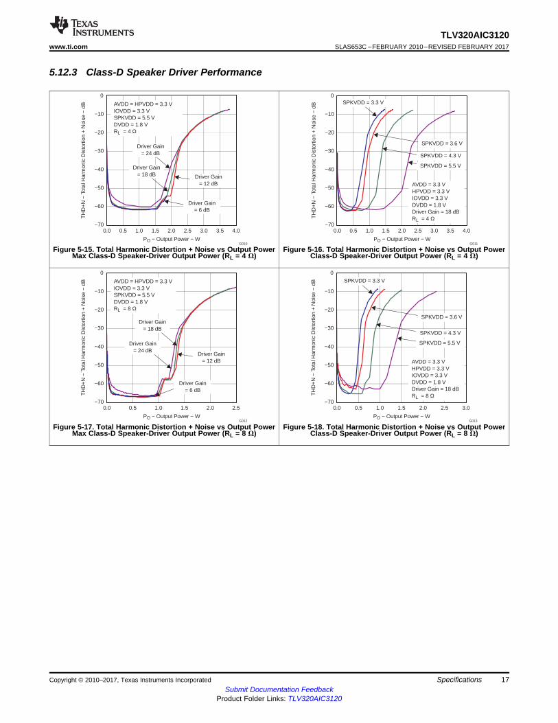
5.12.3 Class-D Speaker Driver Performance
Figure 5-15. Total Harmonic Distortion + Noise vs Output PowerMax Class-D Speaker-Driver Output Power (RL = 4 Ω)
Figure 5-16. Total Harmonic Distortion + Noise vs Output PowerClass-D Speaker-Driver Output Power (RL = 4 Ω)
Figure 5-17. Total Harmonic Distortion + Noise vs Output PowerMax Class-D Speaker-Driver Output Power (RL = 8 Ω)
Figure 5-18. Total Harmonic Distortion + Noise vs Output PowerClass-D Speaker-Driver Output Power (RL = 8 Ω)
I − Current − mA
0.0
0.5
1.0
1.5
2.0
2.5
3.0
3.5
0.0 0.5 1.0 1.5 2.0 2.5 3.0 3.5 4.0
V −
Vol
tage
− V
G016
Micbias = 2 V
Micbias = 2.5 V
Micbias = AVDD (3.3 V)
f − Frequency − kHz
−160
−140
−120
−100
−80
−60
−40
−20
0
0 5 10 15 20
Am
plitu
de −
dB
FS
G024f − Frequency − kHz
−160
−140
−120
−100
−80
−60
−40
−20
0
0 5 10 15 20
Am
plitu
de −
dB
FS
G027
18
TLV320AIC3120SLAS653C –FEBRUARY 2010–REVISED FEBRUARY 2017 www.ti.com
Submit Documentation FeedbackProduct Folder Links: TLV320AIC3120
Specifications Copyright © 2010–2017, Texas Instruments Incorporated
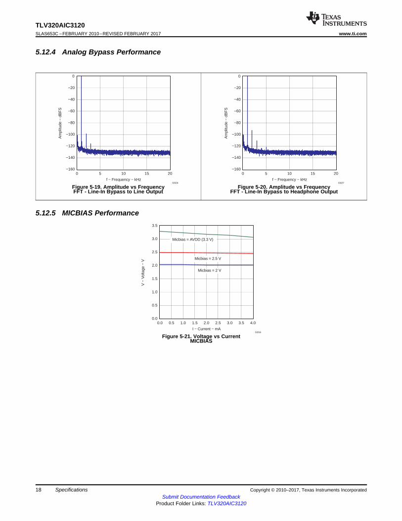
5.12.4 Analog Bypass PerformanceH
Figure 5-19. Amplitude vs FrequencyFFT - Line-In Bypass to Line Output
Figure 5-20. Amplitude vs FrequencyFFT - Line-In Bypass to Headphone Output
5.12.5 MICBIAS PerformanceH
Figure 5-21. Voltage vs CurrentMICBIAS
19
TLV320AIC3120www.ti.com SLAS653C –FEBRUARY 2010–REVISED FEBRUARY 2017
Submit Documentation FeedbackProduct Folder Links: TLV320AIC3120
Parameter Measurement InformationCopyright © 2010–2017, Texas Instruments Incorporated
6 Parameter Measurement Information
All parameters are measured according to the conditions described in Section 5.
20
TLV320AIC3120SLAS653C –FEBRUARY 2010–REVISED FEBRUARY 2017 www.ti.com
Submit Documentation FeedbackProduct Folder Links: TLV320AIC3120
Detailed Description Copyright © 2010–2017, Texas Instruments Incorporated
7 Detailed Description
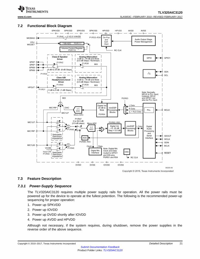
7.1 OverviewThe TLV320AIC3120 device is a highly integrated mono-audio DAC and mono ADC for portablecomputing, communication, and entertainment applications. A register-based architecture easesintegration with microprocessor-based systems through standard serial-interface buses. This devicesupports the two-wire I2C bus interface which provides full register access. All peripheral functions arecontrolled through these registers and the onboard state machines.
The TLV320AIC3120 device consists of the following blocks:• Microphone interfaces (analog and digital)• Audio codec (mono ADC and mono DAC)• AGC and DRC• Two miniDSP digital signal-processing blocks (record and playback paths)• Mono headphone and lineout amplifier• Class-D mono amplifier for 4-Ω or 8–Ω speakers• Pin-controlled or register-controlled volume level• Power-down de-pop and power-up soft start• Analog inputs• I2C control interface• Power-down control block
Following a toggle of the RESET pin or a software reset, the device operates in the default mode. The I2Cinterface is used to write to the control registers to configure the device.
The I2C address assigned to the TLV320AIC3120 device is 001 1000. This device always operates in anI2C slave mode. This device always operates in an I2C slave mode. All registers are 8-bit, and all writableregisters have read-back capability. The device auto-increments to support sequential addressing and canbe used with the I2C fast mode. When the device is reset, all appropriate registers are updated by the hostprocessor to configure the device as needed by the user.
Audio Output Stage
Power Management
RC CLK
Digital
Audio
Processing
and
Serial
InterfaceSDOUT
SDIN
BCLK
WCLK
MCLKPLL
7-Bit ADC P0/R117
Volume-Control RegisterP0/R116
Digital Vol24 dB to
Mute
P0/R64
miniDSPProcessing
Blocks
SPKP
SPKP
SPKM
SPKM
Class-D Speaker
Driver
6 dB to 24 dB (6-dB Steps)
Class A/BHeadphone/Lineout
Driver
0 dB to 9 dB (1-dB Steps)
Analog Attenuation0 dB to –78 dB and Mute(0.5-dB Steps / Nonlinear)
Analog Attenuation0 dB to –78 dB and Mute(0.5-dB Steps / Nonlinear)
HPVDDSPKVDD SPKVSS AVDD AVSSSPKVSSSPKVDD
VOL/
MICDET
HPOUT
SCL
SDA
GPIO GPIO1
MIX
MIX
MIC1LP
DAC
MIX
RESET
DVDD DVSS IOVDD IOVSS
OSC
RC CLK
MIC1LP
SelectableGain/InputImpedance
VCOM
SelectableGain/InputImpedance
P1/R470 to 59.5 dB
(0.5-dB steps)
AGC
MIC1RP
I C2
2 V/2.5 V/AVDDMICBIAS
Digital Vol–12..20 dB
Step = 0.5 dB
Mono ADC
Note: Normally,MCLK is PLL input;however, BCLKand GPIO1 canalso be PLL input.
D S-ADC
D S-DAC
De-PopandSoft-Start
P1/R33–R34
S
S
S
P1/R42
P1/R46
P1/R38
P1/R30
P1/R40
P1/R31
P1/R36
P0/R86–R93
P1/R48
P1/R49
Input CMP1/R50
B0205-06
P0/R82–R83
HPVSS
MIC1RP
MIC1LM
Mono DAC
Digtal MicInterface
Clock Data
Note: Digital MicClock and Datarouted to GPIO1and DIN pins.P0/R51 and R54
L Data
L Data
R Data
(L + R)/2 Data
P0/R63
miniDSPProcessing
Blocks
Copyright © 2016, Texas Instruments Incorporated
21
TLV320AIC3120www.ti.com SLAS653C –FEBRUARY 2010–REVISED FEBRUARY 2017
Submit Documentation FeedbackProduct Folder Links: TLV320AIC3120
Detailed DescriptionCopyright © 2010–2017, Texas Instruments Incorporated
7.2 Functional Block Diagram
7.3 Feature Description
7.3.1 Power-Supply SequenceThe TLV320AIC3120 requires multiple power supply rails for operation. All the power rails must bepowered up for the device to operate at the fullest potention. The following is the recommended power-upsequencing for proper operation:1. Power up SPKVDD2. Power up IOVDD3. Power up DVDD shortly after IOVDD4. Power up AVDD and HPVDD
Although not necessary, if the system requires, during shutdown, remove the power supplies in thereverse order of the above sequence.
22
TLV320AIC3120SLAS653C –FEBRUARY 2010–REVISED FEBRUARY 2017 www.ti.com
Submit Documentation FeedbackProduct Folder Links: TLV320AIC3120
Detailed Description Copyright © 2010–2017, Texas Instruments Incorporated
7.3.2 ResetThe TLV320AIC3120 internal logic must be initialized to a known condition for proper device function. Toinitialize the device to its default operating condition, the hardware reset pin (RESET) must be pulled lowfor at least 10 ns. For this initialization to work, both the IOVDD and DVDD supplies must be powered up.TI recommends that while the DVDD supply powers up, the RESET pin is pulled low.
The device can also be reset via software reset. Writing a 1 into page 0 / register 1, bit D0 resets thedevice.
7.3.3 Device Start-Up Lockout TimesAfter the TLV320AIC3120 is initialized through hardware reset at power up or software reset, the internalmemories are initialized to default values. This initialization takes place within 1 ms after pulling theRESET signal high. During this initialization phase, no register-read or register-write operation should beperformed on ADC or DAC coefficient buffers. Also, no block within the codec should be powered upduring the initialization phase.
7.3.4 PLL Start-UpWhenever the PLL is powered up, a start-up delay of approximately of 10 ms occurs after the power-upcommand of the PLL and before the clocks are available to the codec. This delay is to ensure stableoperation of the PLL and clock-divider logic.
7.3.5 Power-Stage ResetThe power-stage-only reset is used to reset the device after an overcurrent latching shutdown hasoccurred. Using this reset re-enables the output stage without resetting all of the registers in the device.Each of the two power stages has its own dedicated reset bit. The headphone power-stage reset isperformed by setting page 1 / register 31, bit D7 for HPOUT. The speaker power-stage reset is performedby setting page 1 / register 32, bit D7 for SPKP and SPKM.
7.3.6 Software Power DownBy default, all circuit blocks are powered down following a reset condition. Hardware power up of eachcircuit block can be controlled by writing to the appropriate control register. This approach allows thelowest power-supply current for the functionality required. However, when a block is powered down, all ofthe register settings are maintained as long as power is still being applied to the device.
7.3.7 Audio Analog I/OThe TLV320AIC3120 has a mono audio DAC and a mono ADC. The device supports a wide range ofanalog interfaces to support different headsets and analog outputs. The TLV320AIC3120 has features tointerface output drivers (8-Ω, 16-Ω, 32-Ω) and a microphone PGA with AGC control.
7.3.8 miniDSPThe TLV320AIC3120 device features two miniDSP cores. The first miniDSP core is tightly coupled to theADC; the second miniDSP core is tightly coupled to the DAC. The fully programmable algorithms for theminiDSP must be loaded into the device after power up. The miniDSPs have direct access to the digitalaudio stream on the ADC and on the DAC side, offering the possibility for advanced, very low-group-delayDSP algorithms.
The ADC miniDSP has 384 programmable instructions, 256 data memory locations, and 128programmable coefficients. The DAC miniDSP has 1024 programmable instructions, 896 data memorylocations, and 512 programmable coefficients (in the adaptive mode, there are two banks of 256programmable coefficients each).
23
TLV320AIC3120www.ti.com SLAS653C –FEBRUARY 2010–REVISED FEBRUARY 2017
Submit Documentation FeedbackProduct Folder Links: TLV320AIC3120
Detailed DescriptionCopyright © 2010–2017, Texas Instruments Incorporated
7.3.8.1 Software
Software development for the TLV320AIC3120 is supported through TI's comprehensive PurePath™Studio software development environment. PurePath is a powerful and easy-to-use tool designedspecifically to simplify software development on Texas Instruments miniDSP audio platforms. Thegraphical development environment consists of a library of common audio functions that can be draggedand dropped into an audio signal flow and graphically connected together. The DSP code can then beassembled from the graphical signal flow with the click of a mouse.
See the TLV320AIC3120 product folder on www.ti.com to learn more about PurePath Studio software andthe latest status on available, ready-to-use DSP algorithms.
7.3.9 Digital Processing Low-Power ModesThe TLV320AIC3120 device can be tuned to minimize power dissipation, to maximize performance, or toan operating point between the two extremes to best fit the application. The choice of processing blocks,PRB_P1 to PRB_P25 for mono playback and PRB_R4 to PRB_R18 for mono recording, also influencesthe power consumption. In fact, the numerous processing blocks have been implemented to offer a choiceamong configurations having a different balance of power optimization and signal-processing capabilities.
7.3.9.1 ADC, Mono, 48 kHz, DVDD = 1.8 V, AVDD = 3.3 V
AOSR = 128, Processing Block = PRB_R4 (Decimation Filter A)
Power consumption = 9.01 mW
Table 7-1. PRB_R4 Alternative Processing Blocks, 9.01 mW
PROCESSING BLOCK FILTER ESTIMATED POWER CHANGE (mW)PRB_R5 A 0.23PRB_R6 A 0.22
AOSR = 64, Processing Block = PRB_R11 (Decimation Filter B)
Power consumption = 7.99 mW
Table 7-2. PRB_R11 Alternative Processing Blocks, 7.99 mW
PROCESSING BLOCK FILTER ESTIMATED POWER CHANGE (mW)PRB_R4 A 0.43PRB_R5 A 0.67PRB_R6 A 0.66PRB_R10 B –0.14PRB_R12 B 0.04
7.3.9.2 ADC, Mono, 8 kHz, DVDD = 1.8 V, AVDD = 3.3 V
AOSR = 128, Processing Block = PRB_R4 (Decimation Filter A)
Power consumption = 6.77 mW
Table 7-3. PRB_R4 Alternative Processing Blocks, 6.77 mW
PROCESSING BLOCK FILTER ESTIMATED POWER CHANGE (mW)PRB_R5 A 0.03PRB_R6 A 0.03
24
TLV320AIC3120SLAS653C –FEBRUARY 2010–REVISED FEBRUARY 2017 www.ti.com
Submit Documentation FeedbackProduct Folder Links: TLV320AIC3120
Detailed Description Copyright © 2010–2017, Texas Instruments Incorporated
AOSR = 64, Processing Block = PRB_R11 (Decimation Filter B)
Power consumption = 6.61 mW
Table 7-4. PRB_R11 Alternative Processing Blocks, 6.61 mW
PROCESSING BLOCK FILTER ESTIMATED POWER CHANGE (mW)PRB_R4 A 0.07PRB_R5 A 0.11PRB_R6 A 0.11PRB_R10 B –0.02PRB_R12 B 0.01
7.3.9.3 DAC Playback on Headphones, Mono, 48 kHz, DVDD = 1.8 V, AVDD = 3.3 V,HPVDD = 3.3 V
DOSR = 128, Processing Block = PRB_P12 (Interpolation Filter B)
Power consumption = 15.4 mW
Table 7-5. PRB_P12 Alternative Processing Blocks, 15.4 mW
PROCESSING BLOCK FILTER ESTIMATED POWER CHANGE (mW)PRB_P4 A 0.57PRB_P5 A 1.48PRB_P6 A 1.08PRB_P13 B 0.56PRB_P14 B 0.27PRB_P15 B 0.89PRB_P16 B 0.31
DOSR = 64, Processing Block = PRB_P12 (Interpolation Filter B)
Power consumption = 15.54 mW
Table 7-6. PRB_P12 Alternative Processing Blocks, 15.54 mW
PROCESSING BLOCK FILTER ESTIMATED POWER CHANGE (mW)PRB_P4 A 0.37PRB_P5 A 1.23PRB_P6 A 1.15PRB_P13 B 0.43PRB_P14 B 0.13PRB_P15 B 0.85PRB_P16 B 0.21
7.3.9.4 DAC Playback on Headphones, Mono, 8 kHz, DVDD = 1.8 V, AVDD = 3.3 V,HPVDD = 3.3 V
DOSR = 768, Processing Block = PRB_P12 (Interpolation Filter B)
Power consumption = 14.49 mW
Table 7-7. PRB_P12 Alternative Processing Blocks, 14.49 mW
PROCESSING BLOCK FILTER ESTIMATED POWER CHANGE (mW)PRB_P4 A –0.04PRB_P5 A 0.2
25
TLV320AIC3120www.ti.com SLAS653C –FEBRUARY 2010–REVISED FEBRUARY 2017
Submit Documentation FeedbackProduct Folder Links: TLV320AIC3120
Detailed DescriptionCopyright © 2010–2017, Texas Instruments Incorporated
Table 7-7. PRB_P12 Alternative Processing Blocks, 14.49 mW (continued)PROCESSING BLOCK FILTER ESTIMATED POWER CHANGE (mW)
PRB_P6 A –0.01PRB_P13 B 0.1PRB_P14 B 0.05PRB_P15 B –0.03PRB_P16 B 0.07
DOSR = 384, Processing Block = PRB_P12 (Interpolation Filter B)
Power consumption = 14.42 mW
Table 7-8. PRB_P12 Alternative Processing Blocks, 14.42 mW
PROCESSING BLOCK FILTER ESTIMATED POWER CHANGE (mW)PRB_P4 A 0.16PRB_P5 A 0.3PRB_P6 A 0.2PRB_P13 B 0.15PRB_P14 B 0.07PRB_P15 B 0.18PRB_P16 B 0.09
7.3.10 Audio ADC and Analog Inputs
7.3.10.1 MICBIAS and Microphone Preamplifier
The TLV320AIC3120 device includes a microphone bias circuit that sources up to 4 mA of current and isprogrammable to a 2-V, 2.5-V, or AVDD level. The level is controlled by writing to page 1 / register 46, bitsD1–D0. Table 7-9 lists this functionality.
Table 7-9. MICBIAS Settings
D1 D0 FUNCTIONALITY0 0 MICBIAS output is powered down0 1 MICBIAS output is powered to 2 V1 0 MICBIAS output is powered to 2.5 V1 1 MICBIAS output is powered to AVDD
During normal operation, MICBIAS can be set to 2.5 V for better performance. However, based on themodel of the selected microphone, optimal performance can be obtained at another setting and thereforethe performance at a given setting must be verified.
The lowest current consumption occurs when MICBIAS is powered down. The next-lowest currentconsumption occurs when MICBIAS is set at AVDD. The highest current consumption occurs whenMICBIAS is set at 2 V.
Because of the oversampling nature of the audio ADC and the integrated digital-decimation filtering,requirements for analog anti-aliasing filtering are very relaxed. The TLV320AIC3120 device integrates asecond-order analog anti-aliasing filter with 20-dB attenuation at 1 MHz. This filter, combined with thedigital decimal filter, provides sufficient anti-aliasing filtering without requiring any external components.
26
TLV320AIC3120SLAS653C –FEBRUARY 2010–REVISED FEBRUARY 2017 www.ti.com
Submit Documentation FeedbackProduct Folder Links: TLV320AIC3120
Detailed Description Copyright © 2010–2017, Texas Instruments Incorporated
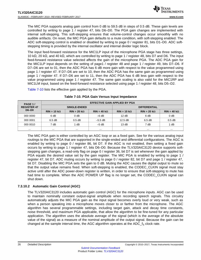
The MIC PGA supports analog gain control from 0 dB to 59.5 dB in steps of 0.5 dB. These gain levels arecontrolled by writing to page 1 / register 47, bits D6–D0. The PGA gain changes are implemented withinternal soft-stepping. This soft-stepping ensures that volume-control changes occur smoothly with noaudible artifacts. On reset, the MIC PGA gain defaults to a mute condition, with soft-stepping enabled. TheADC soft-stepping control is enabled or disabled by writing to page 0 / register 81, bits D1–D0. ADC soft-stepping timing is provided by the internal oscillator and internal divider logic block.
The input feed-forward resistance for the MIC1LP input of the microphone PGA stage has three settings,10 kΩ, 20 kΩ, and 40 kΩ, which are controlled by writing to page 1 / register 48, bits D7 and D6. The inputfeed-forward resistance value selected affects the gain of the microphone PGA. The ADC PGA gain forthe MIC1LP input depends on the setting of page1 / register 48 and page 1 / register 49, bits D7–D6. IfD7–D6 are set to 01, then the ADC PGA has 6 dB more gain with respect to the value programmed usingpage 1 / register 47. If D7–D6 are set to 10, then the ADC PGA has the same gain as programmed usingpage 1 / register 47. If D7–D6 are set to 11, then the ADC PGA has 6 dB less gain with respect to thevalue programmed using page 1 / register 47. The same gain scaling is also valid for the MIC1RP andMIC1LM input, based on the feed-forward resistance selected using page 1 / register 48, bits D5–D2.
Table 7-10 lists the effective gain applied by the PGA.
Table 7-10. PGA Gain Versus Input Impedance
PAGE 1 /REGISTER 47
D6–D0
EFFECTIVE GAIN APPLIED BY PGASINGLE-ENDED DIFFERENTIAL
RIN = 10 kΩ RIN = 20 kΩ RIN = 40 kΩ RIN = 10 kΩ RIN = 20 kΩ RIN = 40 kΩ000 0000 6 dB 0 dB –6 dB 12 dB 6 dB 0 dB000 0001 6.5 dB 0.5 dB –5.5 dB 12.5 dB 6.5 dB 0.5 dB000 0010 7 dB 1 dB –5 dB 13 dB 7 dB 1 dB
... ... ... ... ... ... ...
The MIC PGA gain is either controlled by an AGC loop or as a fixed gain. See for the various analog inputroutings to the MIC PGA that are supported in the single-ended and differential configurations. The AGC isenabled by writing to page 0 / register 86, bit D7. If the AGC is not enabled, then setting a fixed gainoccurs by writing to page 1 / register 47, bits D6–D0. Because the TLV320AIC3120 device supports soft-stepping gain changes, a read-only flag on page 0 / register 36, bit D7 is set whenever the gain applied byPGA equals the desired value set by the gain register. The MIC PGA is enabled by writing to page 1 /register 47, bit D7. ADC muting occurs by writing to page 0 / register 82, bit D7 and page 1 / register 47,bit D7. Disabling the MIC PGA sets the gain to 0 dB. Muting the ADC causes the digital output to mute sothat the output value remains fixed. When soft-stepping is enabled, the CODEC_CLKIN signal must stayactive until after the ADC power-down register is written, in order to ensure that soft-stepping to mute hashad time to complete. When the ADC POWER UP flag is no longer set, the CODEC_CLKIN signal canshut down.
7.3.10.2 Automatic Gain Control (AGC)
The TLV320AIC3120 includes automatic gain control (AGC) for the microphone inputs. AGC can be usedto maintain nominally constant output-signal amplitude when recording speech signals. This circuitryautomatically adjusts the MIC PGA gain as the input signal becomes overly loud or very weak, such aswhen a person speaking into a microphone moves closer to or farther from the microphone. The AGCalgorithm has several programmable settings, including target gain, attack and decay time constants,noise threshold, and maximum PGA applicable, that allow the algorithm to be fine-tuned for any particularapplication. The algorithm uses the absolute average of the signal (which is the average of the absolutevalue of the signal) as a measure of the nominal amplitude of the output signal. Because the gain can bechanged at the sample interval time, the AGC algorithm operates at the ADC_fS clock rate.
27
TLV320AIC3120www.ti.com SLAS653C –FEBRUARY 2010–REVISED FEBRUARY 2017
Submit Documentation FeedbackProduct Folder Links: TLV320AIC3120
Detailed DescriptionCopyright © 2010–2017, Texas Instruments Incorporated
Target level represents the nominal output level at which the AGC attempts to hold the ADC outputsignal. The TLV320AIC3120 allows programming of eight different target levels, which can beprogrammed from –5.5 dB to –24 dB relative to a full-scale signal. Because the TLV320AIC3120 reacts tothe signal absolute average and not to peak levels, TI recommends that the target level be set withenough margin to avoid clipping at the occurrence of loud sounds.
An AGC low-pass filter is used to help determine the average level of the input signal. This average levelis compared to the programmed detection levels in the AGC to provide the correct functionality. This low-pass filter is in the form of a first-order IIR filter. Programming this filter is done by writing to page 4 /register 2 through page 4 / register 7. Two 8-bit registers are used to form the 16-bit digital coefficient asshown on the register map. In this way, a total of six registers are programmed to form the three IIRcoefficients.
Attack time determines how quickly the AGC circuitry reduces the PGA gain when the input signal is tooloud. Programming the attack time is done by writing to page 0 / register 89, bits D7–D0.
Decay time determines how quickly the PGA gain is increased when the input signal is too low.Programming the decay time is done by writing to page 0 / register 90, bits D7–D0.
Noise threshold is a reference level. If the input speech average value falls below the noise threshold,the AGC considers it as a silence and hence brings down the gain to 0 dB in steps of 0.5 dB every sampleperiod and sets the noise-threshold flag. The gain stays at 0 dB unless the input speech signal averagerises above the noise-threshold setting. This ensures that noise is not amplified in the absence of speech.The noise-threshold level in the AGC algorithm is programmable from –30 dB to –90 dB for themicrophone input. When the AGC noise threshold is set to –70 dB, –80 db, or –90 dB, the microphoneinput maximum PGA applicable setting must be greater than or equal to 11.5 dB, 21.5 dB, or 31.5 dB,respectively. This operation includes debounce and hysteresis to prevent the AGC gain from cyclingbetween high gain and 0 dB when signals are near the noise threshold level. When the noise-thresholdflag is set, the status of the gain applied by the AGC and the saturation flag must be ignored by thesystem software. Programming the noise debounce is done by writing to page 0 / register 91, bits D4–D0.Programming the signal debounce is done by writing to page 0 / register 92, bits D3–D0.
Max PGA applicable allows the user to restrict the maximum gain applied by the AGC. This can be usedfor limiting PGA gain in situations where environmental noise is greater than the programmed noisethreshold. Microphone input maximum PGA can be programmed from 0 dB to 59.5 dB in steps of 0.5 dB.Programming the maximum PGA gain allowed by the AGC is done by writing to page 0 / register 88,bits D6–D0.
See Table 7-11 for various AGC programming options. AGC can be used only if the microphone input isrouted to the ADC channel.
(1) All registers shown in this table are located on page 0.
Table 7-11. AGC Settings (1)
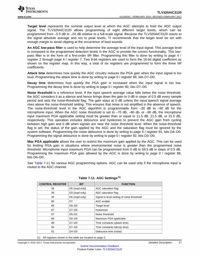
CONTROL REGISTER BIT FUNCTION36 D5 (read-only) AGC saturation flag39 D3 (read-only) ADC saturation flag45 D6 (read-only) Signal to level setting of noise threshold86 D7 AGC enable86 D6–D4 Target level87 D7–D6 Hysteresis87 D5–D1 Noise threshold88 D6–D0 Maximum PGA applicable89 D7–D0 Time constants (attack time)90 D7–D0 Time constants (decay time)91 D4–D0 Debounce time (noise)
W0002-01
Decay Time
TargetLevel
InputSignal
OutputSignal
AGCGain
AttackTime
28
TLV320AIC3120SLAS653C –FEBRUARY 2010–REVISED FEBRUARY 2017 www.ti.com
Submit Documentation FeedbackProduct Folder Links: TLV320AIC3120
Detailed Description Copyright © 2010–2017, Texas Instruments Incorporated
Table 7-11. AGC Settings(1) (continued)CONTROL REGISTER BIT FUNCTION
92 D3–D0 Debounce time (signal)93 D7–D0 (read-only) Gain applied by AGC
Figure 7-1. AGC Characteristics
The AGC settings should be set based on user and system conditions such as microphone selection andsensitivity, acoustics (plastics) around the microphone which affect the microphone pattern, expecteddistance and direction between microphone and sound source, and acoustic background noise.
29
TLV320AIC3120www.ti.com SLAS653C –FEBRUARY 2010–REVISED FEBRUARY 2017
Submit Documentation FeedbackProduct Folder Links: TLV320AIC3120
Detailed DescriptionCopyright © 2010–2017, Texas Instruments Incorporated
One example of AGC code follows, but actual use of code should be verified based on application usage.Note that the AGC code should be set up before powering up the ADC.
####################### AGC ENABLE EXAMPLE CODE ####################### Switch to page 0w 30 00 00# Set AGC enable and Target Level = -10 dB# Target level can be set lower if clipping occurs during speech# Target level is adjusted considering Max Gain alsow 30 56 A0 # AGC hysteresis=DISABLE, noise threshold = -90dB# Noise threshold should be set at higher level if noisy background is present in applicationw 30 57 FE # AGC maximum gain= 40 dB# Higher Max gain is a trade off between gaining up a low sensitivity MIC, and the background# acoustic noise# Microphone bias voltage (MICBIAS) level can be used to change the Microphone Sensitivityw 30 58 50# Attack time=864/Fs w 30 59 68# Decay time=22016/Fsw 30 5A A8# Noise debounce 0 ms# Noise debounce time can be increased if neededw 30 5B 00# Signal debounce 0 ms# Signal debounce time can be increased if neededw 30 5C 00######################## END of AGC SET UP #################################
7.3.10.3 Delta-Sigma ADC
The analog-to-digital converter has a delta-sigma modulator with an oversampling ratio (AOSR) up to 128.The ADC can support a maximum output rate of 192 kHz.
ADC power up is controlled by writing to page 0 / register 81, bit D7. An ADC power-up condition can beverified by reading page 0 / register 36, bit D6.
7.3.10.4 ADC Decimation Filtering and Signal Processing
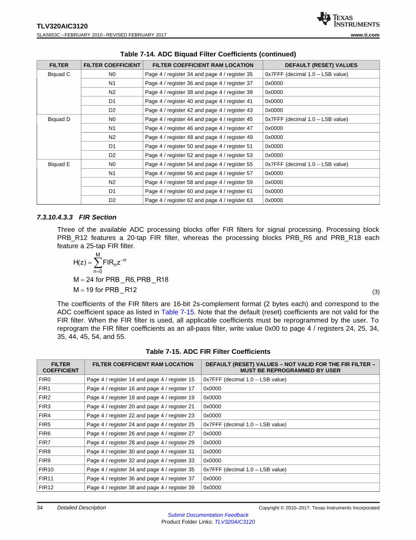
The TLV320AIC3120 ADC channel includes built-in digital decimation filters to process the oversampleddata from the delta-sigma modulator to generate digital data at the Nyquist sampling rate with highdynamic range. The decimation filter can be chosen from three different types, depending on the requiredfrequency response, group delay, and sampling rate.
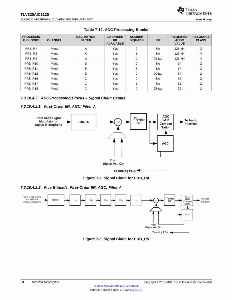
7.3.10.4.1 ADC Processing Blocks
The TLV320AIC3120 offers a range of processing blocks which implement various signal processingcapabilities along with decimation filtering. These processing blocks give users the choice of how muchand what type of signal processing they may use and which decimation filter is applied.
The choices among these processing blocks allow the system designer to balance power conservationand signal-processing flexibility. Less signal-processing capability reduces the power consumed by thedevice. Table 7-12 gives an overview of the available processing blocks of the ADC channel and theirproperties. The Resource Class (RC) column gives a relative indication of power consumption.
The signal processing blocks available are:• First-order IIR• Scalable number of biquad filters• Variable-tap FIR filter• AGC
The processing blocks are tuned for common cases and can achieve high anti-alias filtering or low groupdelay in combination with various signal-processing effects such as audio effects and frequency shaping.The available first-order IIR, biquad, and FIR filters have fully user-programmable coefficients.
1st
OrderIIR
AGCGain
Compensation
AGC
Filter A H EH DH CHBH ATo Audio
Interface
To Analog PGA
From Delta-SigmaModulator or
Digital Microphone
FromDigital Vol. Ctrl
´
To AudioInterface
1st
OrderIIR´
AGCGain
Compen
Sation
AGC
To Analog PGA
Filter A
From Delta-SigmaModulator or
Digital Microphone
FromDigital Vol. Ctrl
30
TLV320AIC3120SLAS653C –FEBRUARY 2010–REVISED FEBRUARY 2017 www.ti.com
Submit Documentation FeedbackProduct Folder Links: TLV320AIC3120
Detailed Description Copyright © 2010–2017, Texas Instruments Incorporated
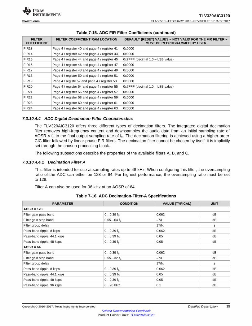
Table 7-12. ADC Processing Blocks
PROCESSING BLOCKS CHANNEL
DECIMATIONFILTER
1st-ORDERIIR
AVAILABLE
NUMBERBIQUADS FIR
REQUIREDAOSRVALUE
RESOURCECLASS
PRB_R4 Mono A Yes 0 No 128, 64 3PRB_R5 Mono A Yes 5 No 128, 64 4PRB_R6 Mono A Yes 0 25-tap 128, 64 4PRB_R10 Mono B Yes 0 No 64 2PRB_R11 Mono B Yes 3 No 64 2PRB_R12 Mono B Yes 0 20-tap 64 2PRB_R16 Mono C Yes 0 No 32 2PRB_R17 Mono C Yes 5 No 32 2PRB_R18 Mono C Yes 0 25-tap 32 2
7.3.10.4.2 ADC Processing Blocks – Signal Chain Details
7.3.10.4.2.1 First-Order IIR, AGC, Filter A
Figure 7-2. Signal Chain for PRB_R4
7.3.10.4.2.2 Five Biquads, First-Order IIR, AGC, Filter A
Figure 7-3. Signal Chain for PRB_R5
1st
OrderIIR
AGCGain
Compen
sation
AGC
Filter B 20-Tap FIR
From Delta-SigmaModulator or
Digital Microphone
FromDigital Vol. Ctrl
To Analog PGA
To Audio
Interface´
1st
OrderIIR
AGCGain
Compensation
AGC
Filter B HCHBHA
From Delta-SigmaModulator or
Digital Microphone
FromDigital Vol. Ctrl
To Analog PGA
To Audio
Interface´
To AudioInterface
1st
OrderIIR
AGCGain
Compen
sation
AGC
Filter B
FromDigital Vol. Ctrl
To AudioInterface
To Analog PGA
From Delta-SigmaModulator or
Digital Microphone´
1st
OrderIIR
AGCGain
Compen
sation
AGC
Filter A 25-Tap FIR
From Delta-SigmaModulator or
Digital Microphone
FromDigital Vol. Ctrl
To Analog PGA
To Audio
Interface´
31
TLV320AIC3120www.ti.com SLAS653C –FEBRUARY 2010–REVISED FEBRUARY 2017
Submit Documentation FeedbackProduct Folder Links: TLV320AIC3120
Detailed DescriptionCopyright © 2010–2017, Texas Instruments Incorporated
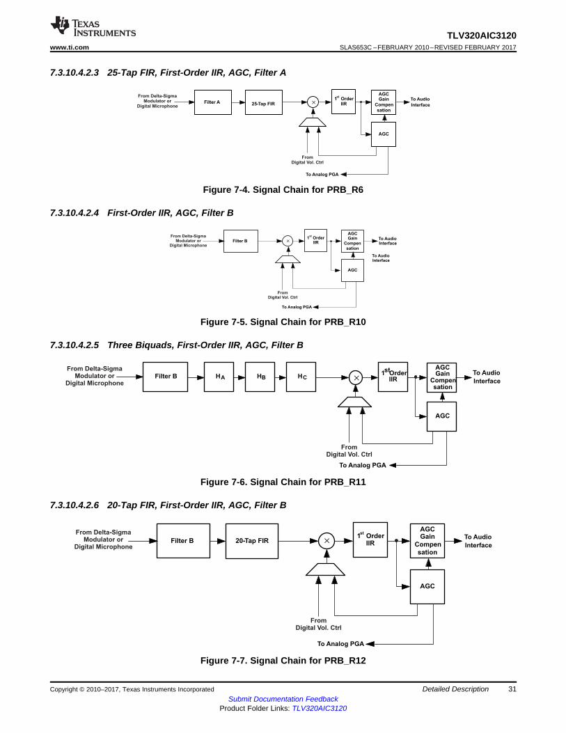
7.3.10.4.2.3 25-Tap FIR, First-Order IIR, AGC, Filter A
Figure 7-4. Signal Chain for PRB_R6
7.3.10.4.2.4 First-Order IIR, AGC, Filter B
Figure 7-5. Signal Chain for PRB_R10
7.3.10.4.2.5 Three Biquads, First-Order IIR, AGC, Filter B
Figure 7-6. Signal Chain for PRB_R11
7.3.10.4.2.6 20-Tap FIR, First-Order IIR, AGC, Filter B
Figure 7-7. Signal Chain for PRB_R12
1st
OrderIIR
AGCGain
Compen
sation
AGC
Filter C 25-Tap FIR
From Delta-SigmaModulator or
Digital Microphone
FromDigital Vol. Ctrl
To Analog PGA
To Audio
Interface´
1st
OrderIIR
AGCGain
Compensation
AGC
Filter C H EH DH CHBH A
From Delta-SigmaModulator or
Digital Microphone
FromDigital Vol. Ctrl
To Analog PGA
To Audio
Interface´
1st
OrderIIR
AGCGain
Compen
sation
AGC
Filter C
From Delta-SigmaModulator or
Digital Microphone
FromDigital Vol. Ctrl
To Analog PGA
To AudioInterface
´
32
TLV320AIC3120SLAS653C –FEBRUARY 2010–REVISED FEBRUARY 2017 www.ti.com
Submit Documentation FeedbackProduct Folder Links: TLV320AIC3120
Detailed Description Copyright © 2010–2017, Texas Instruments Incorporated
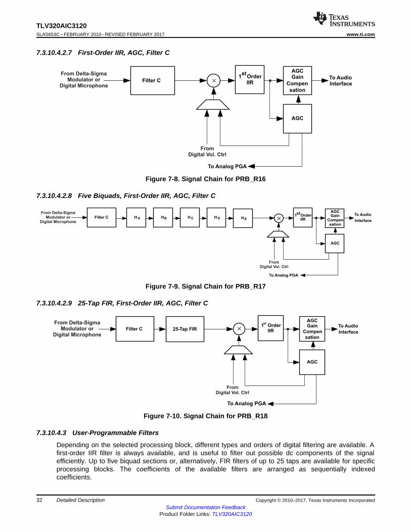
7.3.10.4.2.7 First-Order IIR, AGC, Filter C
Figure 7-8. Signal Chain for PRB_R16
7.3.10.4.2.8 Five Biquads, First-Order IIR, AGC, Filter C
Figure 7-9. Signal Chain for PRB_R17
7.3.10.4.2.9 25-Tap FIR, First-Order IIR, AGC, Filter C
Figure 7-10. Signal Chain for PRB_R18
7.3.10.4.3 User-Programmable Filters
Depending on the selected processing block, different types and orders of digital filtering are available. Afirst-order IIR filter is always available, and is useful to filter out possible dc components of the signalefficiently. Up to five biquad sections or, alternatively, FIR filters of up to 25 taps are available for specificprocessing blocks. The coefficients of the available filters are arranged as sequentially indexedcoefficients.
1 20 1 2
15 1 21 2
N 2 N z N zH(z)
2 2 D z D z
- -
- -
+ ´ +
=
- ´ -
10 1
15 11
N N zH(z)
2 D z
-
-
+
=
-
Largest Positive Number:= 0.111 1111 1111 111= 0.999969482421875 = 1.0 – 1 LSB
1
Largest Negative Number:= 1.0000 0000 0000 000= 0x8000 = –1.0 (by definition)
1 1 1
1 1 1
S . xxxx xxxx xxxx xxx. . x x x
Sign Bit
2 Bit–1
2 Bit–4
2 Bit–15
FractionPoint
33
TLV320AIC3120www.ti.com SLAS653C –FEBRUARY 2010–REVISED FEBRUARY 2017
Submit Documentation FeedbackProduct Folder Links: TLV320AIC3120
Detailed DescriptionCopyright © 2010–2017, Texas Instruments Incorporated
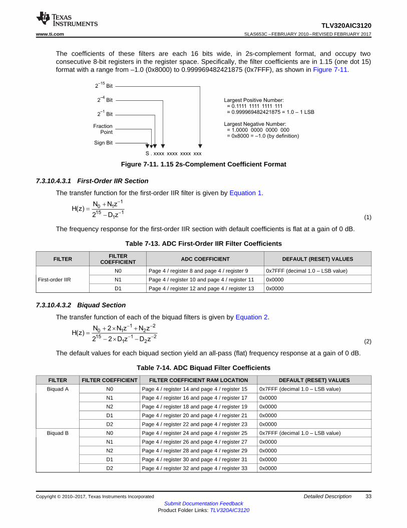
The coefficients of these filters are each 16 bits wide, in 2s-complement format, and occupy twoconsecutive 8-bit registers in the register space. Specifically, the filter coefficients are in 1.15 (one dot 15)format with a range from –1.0 (0x8000) to 0.999969482421875 (0x7FFF), as shown in Figure 7-11.
Figure 7-11. 1.15 2s-Complement Coefficient Format
7.3.10.4.3.1 First-Order IIR Section
The transfer function for the first-order IIR filter is given by Equation 1.
(1)
The frequency response for the first-order IIR section with default coefficients is flat at a gain of 0 dB.
Table 7-13. ADC First-Order IIR Filter Coefficients
FILTER FILTERCOEFFICIENT ADC COEFFICIENT DEFAULT (RESET) VALUES
First-order IIRN0 Page 4 / register 8 and page 4 / register 9 0x7FFF (decimal 1.0 – LSB value)N1 Page 4 / register 10 and page 4 / register 11 0x0000D1 Page 4 / register 12 and page 4 / register 13 0x0000
7.3.10.4.3.2 Biquad Section
The transfer function of each of the biquad filters is given by Equation 2.
(2)
The default values for each biquad section yield an all-pass (flat) frequency response at a gain of 0 dB.
Table 7-14. ADC Biquad Filter Coefficients
FILTER FILTER COEFFICIENT FILTER COEFFICIENT RAM LOCATION DEFAULT (RESET) VALUESBiquad A N0 Page 4 / register 14 and page 4 / register 15 0x7FFF (decimal 1.0 – LSB value)
N1 Page 4 / register 16 and page 4 / register 17 0x0000N2 Page 4 / register 18 and page 4 / register 19 0x0000D1 Page 4 / register 20 and page 4 / register 21 0x0000D2 Page 4 / register 22 and page 4 / register 23 0x0000
Biquad B N0 Page 4 / register 24 and page 4 / register 25 0x7FFF (decimal 1.0 – LSB value)N1 Page 4 / register 26 and page 4 / register 27 0x0000N2 Page 4 / register 28 and page 4 / register 29 0x0000D1 Page 4 / register 30 and page 4 / register 31 0x0000D2 Page 4 / register 32 and page 4 / register 33 0x0000
Mn
n
n 0
H(z) FIR z
M 24 for PRB _R6, PRB _R18
M 19 for PRB _R12
-
=
=
=
=
å
34
TLV320AIC3120SLAS653C –FEBRUARY 2010–REVISED FEBRUARY 2017 www.ti.com
Submit Documentation FeedbackProduct Folder Links: TLV320AIC3120
Detailed Description Copyright © 2010–2017, Texas Instruments Incorporated
Table 7-14. ADC Biquad Filter Coefficients (continued)FILTER FILTER COEFFICIENT FILTER COEFFICIENT RAM LOCATION DEFAULT (RESET) VALUES
Biquad C N0 Page 4 / register 34 and page 4 / register 35 0x7FFF (decimal 1.0 – LSB value)N1 Page 4 / register 36 and page 4 / register 37 0x0000N2 Page 4 / register 38 and page 4 / register 39 0x0000D1 Page 4 / register 40 and page 4 / register 41 0x0000D2 Page 4 / register 42 and page 4 / register 43 0x0000
Biquad D N0 Page 4 / register 44 and page 4 / register 45 0x7FFF (decimal 1.0 – LSB value)N1 Page 4 / register 46 and page 4 / register 47 0x0000N2 Page 4 / register 48 and page 4 / register 49 0x0000D1 Page 4 / register 50 and page 4 / register 51 0x0000D2 Page 4 / register 52 and page 4 / register 53 0x0000
Biquad E N0 Page 4 / register 54 and page 4 / register 55 0x7FFF (decimal 1.0 – LSB value)N1 Page 4 / register 56 and page 4 / register 57 0x0000N2 Page 4 / register 58 and page 4 / register 59 0x0000D1 Page 4 / register 60 and page 4 / register 61 0x0000D2 Page 4 / register 62 and page 4 / register 63 0x0000
7.3.10.4.3.3 FIR Section
Three of the available ADC processing blocks offer FIR filters for signal processing. Processing blockPRB_R12 features a 20-tap FIR filter, whereas the processing blocks PRB_R6 and PRB_R18 eachfeature a 25-tap FIR filter.
(3)
The coefficients of the FIR filters are 16-bit 2s-complement format (2 bytes each) and correspond to theADC coefficient space as listed in Table 7-15. Note that the default (reset) coefficients are not valid for theFIR filter. When the FIR filter is used, all applicable coefficients must be reprogrammed by the user. Toreprogram the FIR filter coefficients as an all-pass filter, write value 0x00 to page 4 / registers 24, 25, 34,35, 44, 45, 54, and 55.
Table 7-15. ADC FIR Filter Coefficients
FILTERCOEFFICIENT
FILTER COEFFICIENT RAM LOCATION DEFAULT (RESET) VALUES – NOT VALID FOR THE FIR FILTER –MUST BE REPROGRAMMED BY USER
FIR0 Page 4 / register 14 and page 4 / register 15 0x7FFF (decimal 1.0 – LSB value)FIR1 Page 4 / register 16 and page 4 / register 17 0x0000FIR2 Page 4 / register 18 and page 4 / register 19 0x0000FIR3 Page 4 / register 20 and page 4 / register 21 0x0000FIR4 Page 4 / register 22 and page 4 / register 23 0x0000FIR5 Page 4 / register 24 and page 4 / register 25 0x7FFF (decimal 1.0 – LSB value)FIR6 Page 4 / register 26 and page 4 / register 27 0x0000FIR7 Page 4 / register 28 and page 4 / register 29 0x0000FIR8 Page 4 / register 30 and page 4 / register 31 0x0000FIR9 Page 4 / register 32 and page 4 / register 33 0x0000FIR10 Page 4 / register 34 and page 4 / register 35 0x7FFF (decimal 1.0 – LSB value)FIR11 Page 4 / register 36 and page 4 / register 37 0x0000FIR12 Page 4 / register 38 and page 4 / register 39 0x0000
35
TLV320AIC3120www.ti.com SLAS653C –FEBRUARY 2010–REVISED FEBRUARY 2017
Submit Documentation FeedbackProduct Folder Links: TLV320AIC3120
Detailed DescriptionCopyright © 2010–2017, Texas Instruments Incorporated
Table 7-15. ADC FIR Filter Coefficients (continued)FILTER
COEFFICIENTFILTER COEFFICIENT RAM LOCATION DEFAULT (RESET) VALUES – NOT VALID FOR THE FIR FILTER –
MUST BE REPROGRAMMED BY USERFIR13 Page 4 / register 40 and page 4 / register 41 0x0000FIR14 Page 4 / register 42 and page 4 / register 43 0x0000FIR15 Page 4 / register 44 and page 4 / register 45 0x7FFF (decimal 1.0 – LSB value)FIR16 Page 4 / register 46 and page 4 / register 47 0x0000FIR17 Page 4 / register 48 and page 4 / register 49 0x0000FIR18 Page 4 / register 50 and page 4 / register 51 0x0000FIR19 Page 4 / registe 52 and page 4 / register 53 0x0000FIR20 Page 4 / register 54 and page 4 / register 55 0x7FFF (decimal 1.0 – LSB value)FIR21 Page 4 / register 56 and page 4 / register 57 0x0000FIR22 Page 4 / register 58 and page 4 / register 59 0x0000FIR23 Page 4 / register 60 and page 4 / register 61 0x0000FIR24 Page 4 / register 62 and page 4 / register 63 0x0000
7.3.10.4.4 ADC Digital Decimation Filter Characteristics
The TLV320AIC3120 offers three different types of decimation filters. The integrated digital decimationfilter removes high-frequency content and downsamples the audio data from an initial sampling rate ofAOSR × fS to the final output sampling rate of fS. The decimation filtering is achieved using a higher-orderCIC filter followed by linear-phase FIR filters. The decimation filter cannot be chosen by itself; it is implicitlyset through the chosen processing block.
The following subsections describe the properties of the available filters A, B, and C.
7.3.10.4.4.1 Decimation Filter A
This filter is intended for use at sampling rates up to 48 kHz. When configuring this filter, the oversamplingratio of the ADC can either be 128 or 64. For highest performance, the oversampling ratio must be setto 128.
Filter A can also be used for 96 kHz at an AOSR of 64.
Table 7-16. ADC Decimation-Filter-A Specifications
PARAMETER CONDITION VALUE (TYPICAL) UNITAOSR = 128Filter gain pass band 0…0.39 fS 0.062 dBFilter gain stop band 0.55…64 fS –73 dBFilter group delay 17/fS sPass-band ripple, 8 ksps 0…0.39 fS 0.062 dBPass-band ripple, 44.1 ksps 0…0.39 fS 0.05 dBPass-band ripple, 48 ksps 0…0.39 fS 0.05 dBAOSR = 64Filter gain pass band 0…0.39 fS 0.062 dBFilter gain stop band 0.55…32 fS –73 dBFilter group delay 17/fS sPass-band ripple, 8 ksps 0…0.39 fS 0.062 dBPass-band ripple, 44.1 ksps 0…0.39 fS 0.05 dBPass-band ripple, 48 ksps 0…0.39 fS 0.05 dBPass-band ripple, 96 ksps 0…20 kHz 0.1 dB
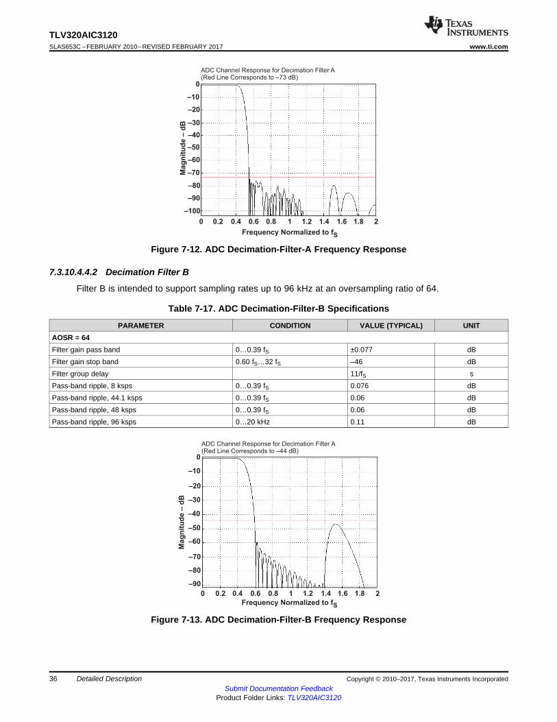
0
–10
–20
–30
–40
–50
–60
–70
–80
–90
0 0.2 0.4 0.6 0.8 1 1.2 1.4 1.6 1.8 2
Mag
nit
ud
e–
dB
Frequency Normalized to fS
ADC Channel Response for Decimation Filter A(Red Line Corresponds to –44 dB)
0
–10
–20
–30
–40
–50
–60
–70
–80
–90
–100
0 0.2 0.4 0.6 0.8 1 1.2 1.4 1.6 1.8 2
Frequency Normalized to fS
Mag
nit
ud
e–
dB
ADC Channel Response for Decimation Filter A(Red Line Corresponds to –73 dB)
36
TLV320AIC3120SLAS653C –FEBRUARY 2010–REVISED FEBRUARY 2017 www.ti.com
Submit Documentation FeedbackProduct Folder Links: TLV320AIC3120
Detailed Description Copyright © 2010–2017, Texas Instruments Incorporated
Figure 7-12. ADC Decimation-Filter-A Frequency Response
7.3.10.4.4.2 Decimation Filter B
Filter B is intended to support sampling rates up to 96 kHz at an oversampling ratio of 64.
Table 7-17. ADC Decimation-Filter-B Specifications
PARAMETER CONDITION VALUE (TYPICAL) UNITAOSR = 64Filter gain pass band 0…0.39 fS ±0.077 dBFilter gain stop band 0.60 fS…32 fS –46 dBFilter group delay 11/fS sPass-band ripple, 8 ksps 0…0.39 fS 0.076 dBPass-band ripple, 44.1 ksps 0…0.39 fS 0.06 dBPass-band ripple, 48 ksps 0…0.39 fS 0.06 dBPass-band ripple, 96 ksps 0…20 kHz 0.11 dB
Figure 7-13. ADC Decimation-Filter-B Frequency Response
0
–20
–40
–60
–80
–100
–120
0 0.2 0.4 0.6 0.8 1 1.2 1.4 1.6 1.8 2
Mag
nit
ud
e–
dB
Frequency Normalized to fS
ADC Channel Response for Decimation Filter C(Red Line Corresponds to –60 dB)
37
TLV320AIC3120www.ti.com SLAS653C –FEBRUARY 2010–REVISED FEBRUARY 2017
Submit Documentation FeedbackProduct Folder Links: TLV320AIC3120
Detailed DescriptionCopyright © 2010–2017, Texas Instruments Incorporated
7.3.10.4.4.3 Decimation Filter C
Filter C along with an AOSR of 32 is specially designed for 192-ksps operation for the ADC. The passband, which extends up to 0.11 × fS (corresponding to 21 kHz), is suited for audio applications.
Table 7-18. ADC Decimation-Filter-C Specifications
PARAMETER CONDITION VALUE (TYPICAL) UNITFilter gain from 0 to 0.11 fS 0…0.11 fS ±0.033 dBFilter gain from 0.28 fS to 16 fS 0.28 fS…16 fS –60 dBFilter group delay 11/fS sPass-band ripple, 8 ksps 0…0.11 fS 0.033 dBPass-band ripple, 44.1 ksps 0…0.11 fS 0.033 dBPass-band ripple, 48 ksps 0…0.11 fS 0.032 dBPass-band ripple, 96 ksps 0…0.11 fS 0.032 dBPass-band ripple, 192 ksps 0…20 kHz 0.086 dB
Figure 7-14. ADC Decimation-Filter-C Frequency Response
7.3.10.4.5 ADC Data Interface
The decimation filter and signal processing block in the ADC channel pass 32-bit data words to the audioserial interface once every cycle of ADC_fS. During each cycle of ADC_fS, a pair of data words (for leftand right channel) is passed. The audio serial interface rounds the data to the required word length of theinterface before converting to serial data. Because the TLV320AIC3120 has only a mono ADC, it passesthe same data to both the left and right channels of the audio serial interface.
7.3.10.5 Updating ADC Digital Filter Coefficients During Record
When it is required to update the ADC digital filter coefficients during record, care must be taken to avoidclick and pop noise or even a possible oscillation noise. These artifacts can occur if the ADC coefficientsare updated without following the proper update sequence. The correct sequence is shown in Figure 7-15.The values for the times listed are conservative and should be used for software purposes.
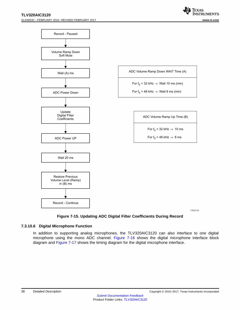
Record - Paused
ADC Power Down
UpdateDigital FilterCoefficients
ADC Power UP
Wait 20 ms
Volume Ramp DownSoft Mute
Restore PreviousVolume Level (Ramp)
in (B) ms
Record - Continue
Wait (A) ms
For f = 32 kHzS ® Wait 10 ms (min)
For f = 48 kHz Wait 8 ms (min)S ®
For = 32 kHz ®f 10 ms
For f = 48 kHz 8 ms
S
S ®
ADC Volume Ramp Down WAIT Time (A)
ADC Volume Ramp Up Time (B)
F0023-02
38
TLV320AIC3120SLAS653C –FEBRUARY 2010–REVISED FEBRUARY 2017 www.ti.com
Submit Documentation FeedbackProduct Folder Links: TLV320AIC3120
Detailed Description Copyright © 2010–2017, Texas Instruments Incorporated
Figure 7-15. Updating ADC Digital Filter Coefficients During Record
7.3.10.6 Digital Microphone Function
In addition to supporting analog microphones, the TLV320AIC3120 can also interface to one digitalmicrophone using the mono ADC channel. Figure 7-16 shows the digital microphone interface blockdiagram and Figure 7-17 shows the timing diagram for the digital microphone interface.
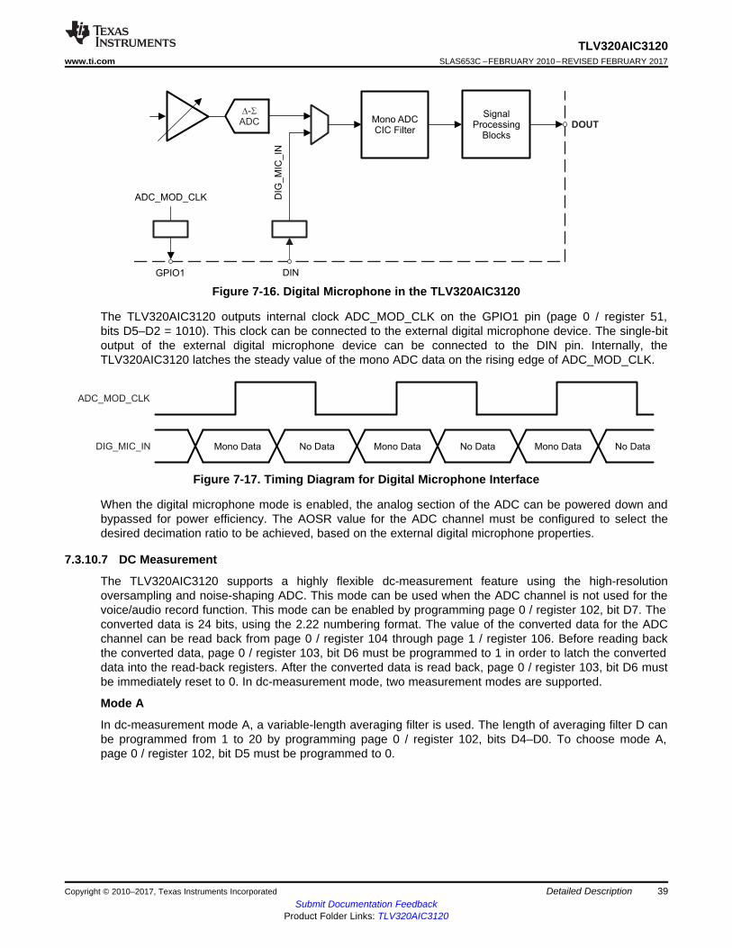
Mono Data No Data Mono Data No Data Mono Data No Data
ADC_MOD_CLK
DIG_MIC_IN
Mono ADCCIC Filter
SignalProcessing
Blocks
GPIO1 DIN
ADC_MOD_CLK DIG
_M
IC_IN
DOUT
D S-ADC
39
TLV320AIC3120www.ti.com SLAS653C –FEBRUARY 2010–REVISED FEBRUARY 2017
Submit Documentation FeedbackProduct Folder Links: TLV320AIC3120
Detailed DescriptionCopyright © 2010–2017, Texas Instruments Incorporated
Figure 7-16. Digital Microphone in the TLV320AIC3120
The TLV320AIC3120 outputs internal clock ADC_MOD_CLK on the GPIO1 pin (page 0 / register 51,bits D5–D2 = 1010). This clock can be connected to the external digital microphone device. The single-bitoutput of the external digital microphone device can be connected to the DIN pin. Internally, theTLV320AIC3120 latches the steady value of the mono ADC data on the rising edge of ADC_MOD_CLK.
Figure 7-17. Timing Diagram for Digital Microphone Interface
When the digital microphone mode is enabled, the analog section of the ADC can be powered down andbypassed for power efficiency. The AOSR value for the ADC channel must be configured to select thedesired decimation ratio to be achieved, based on the external digital microphone properties.
7.3.10.7 DC Measurement
The TLV320AIC3120 supports a highly flexible dc-measurement feature using the high-resolutionoversampling and noise-shaping ADC. This mode can be used when the ADC channel is not used for thevoice/audio record function. This mode can be enabled by programming page 0 / register 102, bit D7. Theconverted data is 24 bits, using the 2.22 numbering format. The value of the converted data for the ADCchannel can be read back from page 0 / register 104 through page 1 / register 106. Before reading backthe converted data, page 0 / register 103, bit D6 must be programmed to 1 in order to latch the converteddata into the read-back registers. After the converted data is read back, page 0 / register 103, bit D6 mustbe immediately reset to 0. In dc-measurement mode, two measurement modes are supported.
Mode A
In dc-measurement mode A, a variable-length averaging filter is used. The length of averaging filter D canbe programmed from 1 to 20 by programming page 0 / register 102, bits D4–D0. To choose mode A,page 0 / register 102, bit D5 must be programmed to 0.
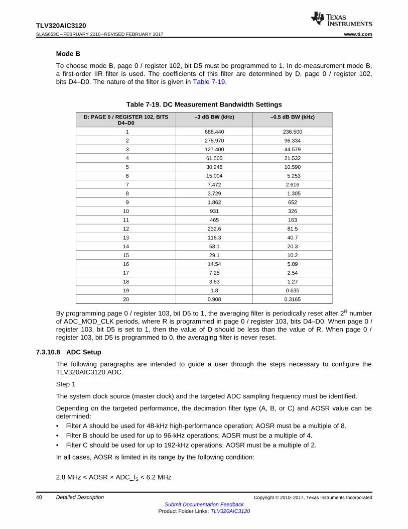
40
TLV320AIC3120SLAS653C –FEBRUARY 2010–REVISED FEBRUARY 2017 www.ti.com
Submit Documentation FeedbackProduct Folder Links: TLV320AIC3120
Detailed Description Copyright © 2010–2017, Texas Instruments Incorporated
Mode B
To choose mode B, page 0 / register 102, bit D5 must be programmed to 1. In dc-measurement mode B,a first-order IIR filter is used. The coefficients of this filter are determined by D, page 0 / register 102,bits D4–D0. The nature of the filter is given in Table 7-19.
Table 7-19. DC Measurement Bandwidth Settings
D: PAGE 0 / REGISTER 102, BITSD4–D0
–3 dB BW (kHz) –0.5 dB BW (kHz)
1 688.440 236.5002 275.970 96.3343 127.400 44.5794 61.505 21.5325 30.248 10.5906 15.004 5.2537 7.472 2.6168 3.729 1.3059 1.862 652
10 931 32611 465 16312 232.6 81.513 116.3 40.714 58.1 20.315 29.1 10.216 14.54 5.0917 7.25 2.5418 3.63 1.2719 1.8 0.63520 0.908 0.3165
By programming page 0 / register 103, bit D5 to 1, the averaging filter is periodically reset after 2R numberof ADC_MOD_CLK periods, where R is programmed in page 0 / register 103, bits D4–D0. When page 0 /register 103, bit D5 is set to 1, then the value of D should be less than the value of R. When page 0 /register 103, bit D5 is programmed to 0, the averaging filter is never reset.
7.3.10.8 ADC Setup
The following paragraphs are intended to guide a user through the steps necessary to configure theTLV320AIC3120 ADC.
Step 1
The system clock source (master clock) and the targeted ADC sampling frequency must be identified.
Depending on the targeted performance, the decimation filter type (A, B, or C) and AOSR value can bedetermined:• Filter A should be used for 48-kHz high-performance operation; AOSR must be a multiple of 8.• Filter B should be used for up to 96-kHz operations; AOSR must be a multiple of 4.• Filter C should be used for up to 192-kHz operations; AOSR must be a multiple of 2.
In all cases, AOSR is limited in its range by the following condition:
2.8 MHz < AOSR × ADC_fS < 6.2 MHz
41
TLV320AIC3120www.ti.com SLAS653C –FEBRUARY 2010–REVISED FEBRUARY 2017
Submit Documentation FeedbackProduct Folder Links: TLV320AIC3120
Detailed DescriptionCopyright © 2010–2017, Texas Instruments Incorporated
Based on the identified filter type and the required signal processing capabilities, the appropriateprocessing block can be determined from the list of available processing blocks (PRB_R4 to PRB_R18).
Based on the available master clock, the chosen AOSR and the targeted sampling rate, the clock dividervalues NADC and MADC can be determined. If necessary, the internal PLL can add a large degree offlexibility.
In summary, CODEC_CLKIN (derived directly from the system clock source or from the internal PLL)divided by MADC, NADC, and AOSR must be equal to the ADC sampling rate ADC_fS. TheCODEC_CLKIN clock signal is shared with the DAC clock-generation block.
CODEC_CLKIN = NADC × MADC × AOSR × ADC_fS
To a large degree, NADC and MADC can be chosen independently in the range of 1 to 128. In general,NADC should be as large as possible as long as the following condition can still be met:
MADC × AOSR / 32 ≥ RC
RC is a function of the chosen processing block and is listed in Table 7-20.
The common-mode voltage setting of the device is determined by the available analog power supply.
At this point, the following device specific parameters are known: PRB_Rx, AOSR, NADC, MADC, inputand output common-mode values. If the PLL is used, the PLL parameters P, J, D, and R are determinedas well.
Step 2
Setting up the device via register programming:
The following list gives a sequence of items that must be executed in the time between powering thedevice up and reading data from the device:1. Define starting point:
(a) Power up applicable external hardware power supplies(b) Set register page to 0(c) Initiate SW reset
2. Program clock settings(a) Program PLL clock dividers P, J, D, and R (if PLL is used)(b) Power up PLL (if PLL is used)(c) Program and power up NADC(d) Program and power up MADC(e) Program OSR value(f) Program I2S word length if required (e.g., 20 bits)(g) Program the processing block to be used
3. Program analog blocks(a) Set register page to 1(b) Program MICBIAS if applicable(c) Program MicPGA(d) Program routing of inputs/common mode to ADC input(e) Unmute analog PGAs and set analog gain
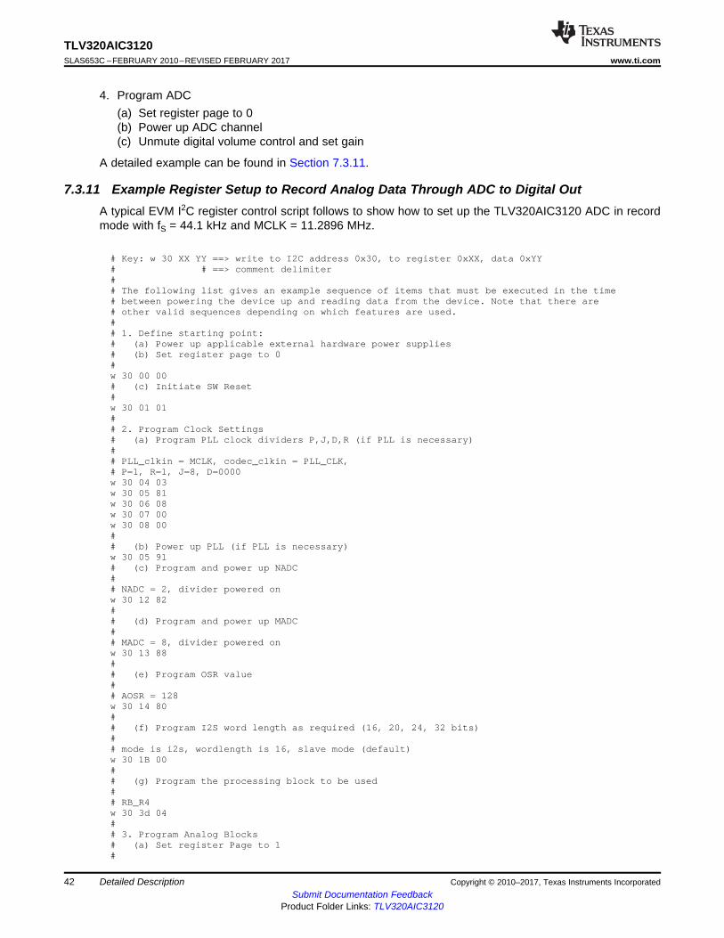
42
TLV320AIC3120SLAS653C –FEBRUARY 2010–REVISED FEBRUARY 2017 www.ti.com
Submit Documentation FeedbackProduct Folder Links: TLV320AIC3120
Detailed Description Copyright © 2010–2017, Texas Instruments Incorporated
4. Program ADC(a) Set register page to 0(b) Power up ADC channel(c) Unmute digital volume control and set gain
A detailed example can be found in Section 7.3.11.
7.3.11 Example Register Setup to Record Analog Data Through ADC to Digital OutA typical EVM I2C register control script follows to show how to set up the TLV320AIC3120 ADC in recordmode with fS = 44.1 kHz and MCLK = 11.2896 MHz.
# Key: w 30 XX YY ==> write to I2C address 0x30, to register 0xXX, data 0xYY# # ==> comment delimiter## The following list gives an example sequence of items that must be executed in the time# between powering the device up and reading data from the device. Note that there are# other valid sequences depending on which features are used.## 1. Define starting point:# (a) Power up applicable external hardware power supplies# (b) Set register page to 0#w 30 00 00# (c) Initiate SW Reset#w 30 01 01## 2. Program Clock Settings# (a) Program PLL clock dividers P,J,D,R (if PLL is necessary)## PLL_clkin = MCLK, codec_clkin = PLL_CLK,# P=1, R=1, J=8, D=0000w 30 04 03w 30 05 81w 30 06 08w 30 07 00w 30 08 00## (b) Power up PLL (if PLL is necessary)w 30 05 91# (c) Program and power up NADC## NADC = 2, divider powered onw 30 12 82## (d) Program and power up MADC## MADC = 8, divider powered onw 30 13 88## (e) Program OSR value## AOSR = 128w 30 14 80## (f) Program I2S word length as required (16, 20, 24, 32 bits)## mode is i2s, wordlength is 16, slave mode (default)w 30 1B 00## (g) Program the processing block to be used## RB_R4w 30 3d 04## 3. Program Analog Blocks# (a) Set register Page to 1#
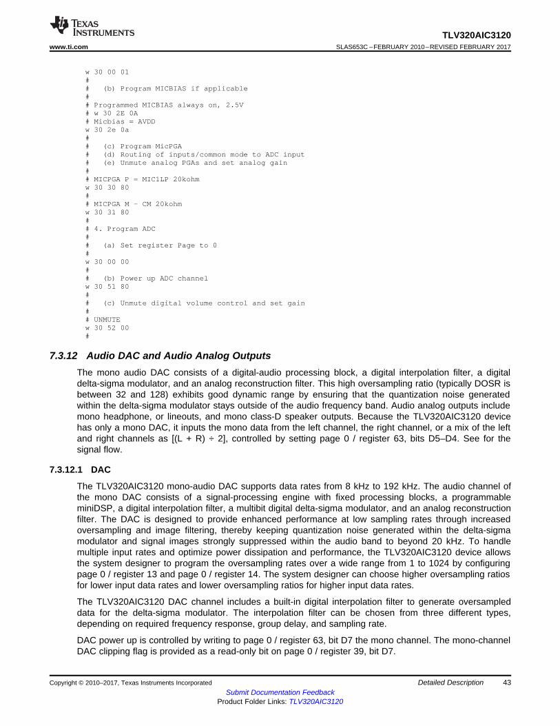
43
TLV320AIC3120www.ti.com SLAS653C –FEBRUARY 2010–REVISED FEBRUARY 2017
Submit Documentation FeedbackProduct Folder Links: TLV320AIC3120
Detailed DescriptionCopyright © 2010–2017, Texas Instruments Incorporated
w 30 00 01## (b) Program MICBIAS if applicable## Programmed MICBIAS always on, 2.5V# w 30 2E 0A# Micbias = AVDDw 30 2e 0a## (c) Program MicPGA# (d) Routing of inputs/common mode to ADC input# (e) Unmute analog PGAs and set analog gain## MICPGA P = MIC1LP 20kohmw 30 30 80## MICPGA M - CM 20kohmw 30 31 80## 4. Program ADC## (a) Set register Page to 0#w 30 00 00## (b) Power up ADC channelw 30 51 80## (c) Unmute digital volume control and set gain## UNMUTEw 30 52 00#
7.3.12 Audio DAC and Audio Analog OutputsThe mono audio DAC consists of a digital-audio processing block, a digital interpolation filter, a digitaldelta-sigma modulator, and an analog reconstruction filter. This high oversampling ratio (typically DOSR isbetween 32 and 128) exhibits good dynamic range by ensuring that the quantization noise generatedwithin the delta-sigma modulator stays outside of the audio frequency band. Audio analog outputs includemono headphone, or lineouts, and mono class-D speaker outputs. Because the TLV320AIC3120 devicehas only a mono DAC, it inputs the mono data from the left channel, the right channel, or a mix of the leftand right channels as [(L + R) ÷ 2], controlled by setting page 0 / register 63, bits D5–D4. See for thesignal flow.
7.3.12.1 DAC
The TLV320AIC3120 mono-audio DAC supports data rates from 8 kHz to 192 kHz. The audio channel ofthe mono DAC consists of a signal-processing engine with fixed processing blocks, a programmableminiDSP, a digital interpolation filter, a multibit digital delta-sigma modulator, and an analog reconstructionfilter. The DAC is designed to provide enhanced performance at low sampling rates through increasedoversampling and image filtering, thereby keeping quantization noise generated within the delta-sigmamodulator and signal images strongly suppressed within the audio band to beyond 20 kHz. To handlemultiple input rates and optimize power dissipation and performance, the TLV320AIC3120 device allowsthe system designer to program the oversampling rates over a wide range from 1 to 1024 by configuringpage 0 / register 13 and page 0 / register 14. The system designer can choose higher oversampling ratiosfor lower input data rates and lower oversampling ratios for higher input data rates.
The TLV320AIC3120 DAC channel includes a built-in digital interpolation filter to generate oversampleddata for the delta-sigma modulator. The interpolation filter can be chosen from three different types,depending on required frequency response, group delay, and sampling rate.
DAC power up is controlled by writing to page 0 / register 63, bit D7 the mono channel. The mono-channelDAC clipping flag is provided as a read-only bit on page 0 / register 39, bit D7.
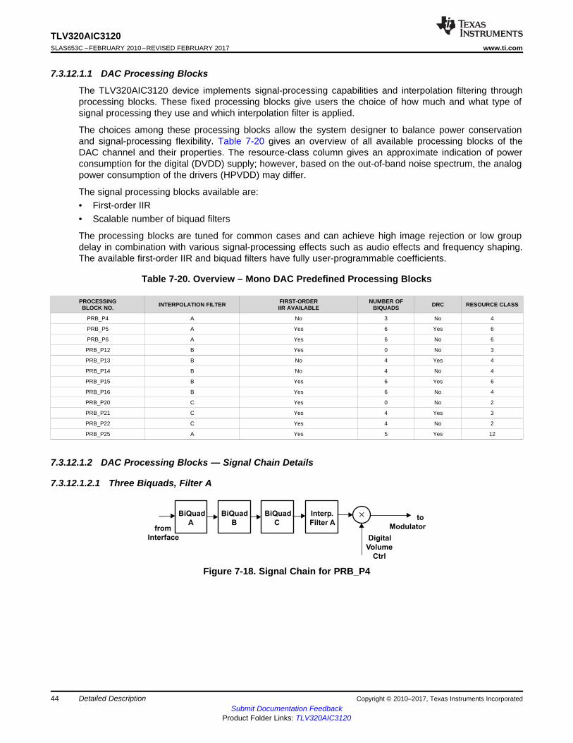
Interp.
Filter A
BiQuad
C
BiQuad
B
BiQuad
Ato
Modulator
Digital
Volume
Ctrl
from
Interface
´
44
TLV320AIC3120SLAS653C –FEBRUARY 2010–REVISED FEBRUARY 2017 www.ti.com
Submit Documentation FeedbackProduct Folder Links: TLV320AIC3120
Detailed Description Copyright © 2010–2017, Texas Instruments Incorporated
7.3.12.1.1 DAC Processing Blocks
The TLV320AIC3120 device implements signal-processing capabilities and interpolation filtering throughprocessing blocks. These fixed processing blocks give users the choice of how much and what type ofsignal processing they use and which interpolation filter is applied.
The choices among these processing blocks allow the system designer to balance power conservationand signal-processing flexibility. Table 7-20 gives an overview of all available processing blocks of theDAC channel and their properties. The resource-class column gives an approximate indication of powerconsumption for the digital (DVDD) supply; however, based on the out-of-band noise spectrum, the analogpower consumption of the drivers (HPVDD) may differ.
The signal processing blocks available are:• First-order IIR• Scalable number of biquad filters
The processing blocks are tuned for common cases and can achieve high image rejection or low groupdelay in combination with various signal-processing effects such as audio effects and frequency shaping.The available first-order IIR and biquad filters have fully user-programmable coefficients.
Table 7-20. Overview – Mono DAC Predefined Processing Blocks
PROCESSINGBLOCK NO. INTERPOLATION FILTER FIRST-ORDER
IIR AVAILABLENUMBER OF
BIQUADS DRC RESOURCE CLASS
PRB_P4 A No 3 No 4
PRB_P5 A Yes 6 Yes 6
PRB_P6 A Yes 6 No 6
PRB_P12 B Yes 0 No 3
PRB_P13 B No 4 Yes 4
PRB_P14 B No 4 No 4
PRB_P15 B Yes 6 Yes 6
PRB_P16 B Yes 6 No 4
PRB_P20 C Yes 0 No 2
PRB_P21 C Yes 4 Yes 3
PRB_P22 C Yes 4 No 2
PRB_P25 A Yes 5 Yes 12
7.3.12.1.2 DAC Processing Blocks — Signal Chain Details
7.3.12.1.2.1 Three Biquads, Filter A
Figure 7-18. Signal Chain for PRB_P4
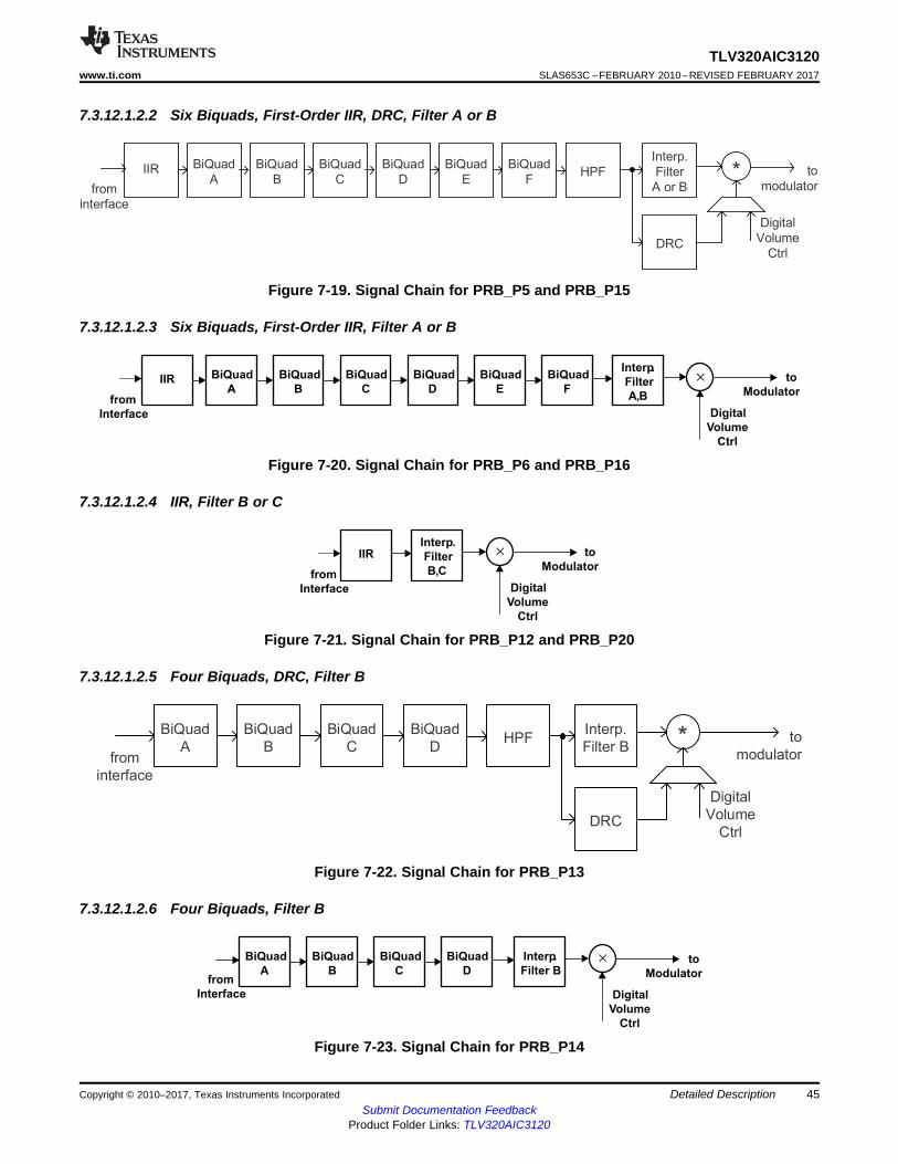
Interp.
Filter B
BiQuad
D
BiQuad
C
BiQuad
B
BiQuad
Ato
Modulator
Digital
Volume
Ctrl
from
Interface
´
Interp.
Filter
B,C
IIR to
Modulator
Digital
Volume
Ctrl
from
Interface
´
Interp.
Filter
A,B
BiQuad
F
BiQuad
E
BiQuad
D
BiQuad
C
BiQuad
B
BiQuad
AIIR to
Modulator
Digital
Volume
Ctrl
from
Interface
´
45
TLV320AIC3120www.ti.com SLAS653C –FEBRUARY 2010–REVISED FEBRUARY 2017
Submit Documentation FeedbackProduct Folder Links: TLV320AIC3120
Detailed DescriptionCopyright © 2010–2017, Texas Instruments Incorporated
7.3.12.1.2.2 Six Biquads, First-Order IIR, DRC, Filter A or B
Figure 7-19. Signal Chain for PRB_P5 and PRB_P15
7.3.12.1.2.3 Six Biquads, First-Order IIR, Filter A or B
Figure 7-20. Signal Chain for PRB_P6 and PRB_P16
7.3.12.1.2.4 IIR, Filter B or C
Figure 7-21. Signal Chain for PRB_P12 and PRB_P20
7.3.12.1.2.5 Four Biquads, DRC, Filter B
Figure 7-22. Signal Chain for PRB_P13
7.3.12.1.2.6 Four Biquads, Filter B
Figure 7-23. Signal Chain for PRB_P14
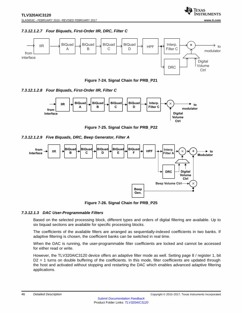
DRC
fromInterface
toModulator
DigitalVolume
Ctrl
BiQuadB ´
BiQuadC
BiQuadD
BiQuadE
BiQuadF
Interp.Filter A
+
BeepGen.
Beep Volume Ctrl ´
IIR HPF
Interp.
Filter C
BiQuad
D
BiQuad
C
BiQuad
B
BiQuad
AIIR to
modulator
Digital
Volume
Ctrl
from
Interface
´
46
TLV320AIC3120SLAS653C –FEBRUARY 2010–REVISED FEBRUARY 2017 www.ti.com
Submit Documentation FeedbackProduct Folder Links: TLV320AIC3120
Detailed Description Copyright © 2010–2017, Texas Instruments Incorporated
7.3.12.1.2.7 Four Biquads, First-Order IIR, DRC, Filter C
Figure 7-24. Signal Chain for PRB_P21
7.3.12.1.2.8 Four Biquads, First-Order IIR, Filter C
Figure 7-25. Signal Chain for PRB_P22
7.3.12.1.2.9 Five Biquads, DRC, Beep Generator, Filter A
Figure 7-26. Signal Chain for PRB_P25
7.3.12.1.3 DAC User-Programmable Filters
Based on the selected processing block, different types and orders of digital filtering are available. Up tosix biquad sections are available for specific processing blocks.
The coefficients of the available filters are arranged as sequentially-indexed coefficients in two banks. Ifadaptive filtering is chosen, the coefficient banks can be switched in real time.
When the DAC is running, the user-programmable filter coefficients are locked and cannot be accessedfor either read or write.
However, the TLV320AIC3120 device offers an adaptive filter mode as well. Setting page 8 / register 1, bitD2 = 1 turns on double buffering of the coefficients. In this mode, filter coefficients are updated throughthe host and activated without stopping and restarting the DAC which enables advanced adaptive filteringapplications.
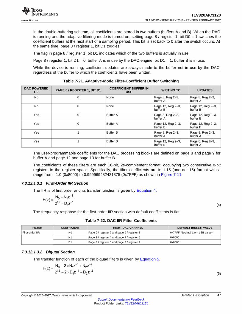
1 20 1 2
15 1 21 2
N 2 N z N zH(z)
2 2 D z D z
- -
- -
+ ´ +
=
- ´ -
10 1
15 11
N N zH(z)
2 D z
-
-
+
=
-
47
TLV320AIC3120www.ti.com SLAS653C –FEBRUARY 2010–REVISED FEBRUARY 2017
Submit Documentation FeedbackProduct Folder Links: TLV320AIC3120
Detailed DescriptionCopyright © 2010–2017, Texas Instruments Incorporated
In the double-buffering scheme, all coefficients are stored in two buffers (buffers A and B). When the DACis running and the adaptive filtering mode is turned on, setting page 8 / register 1, bit D0 = 1 switches thecoefficient buffers at the next start of a sampling period. This bit is set back to 0 after the switch occurs. Atthe same time, page 8 / register 1, bit D1 toggles.
The flag in page 8 / register 1, bit D1 indicates which of the two buffers is actually in use.
Page 8 / register 1, bit D1 = 0: buffer A is in use by the DAC engine; bit D1 = 1: buffer B is in use.
While the device is running, coefficient updates are always made to the buffer not in use by the DAC,regardless of the buffer to which the coefficients have been written.
Table 7-21. Adaptive-Mode Filter-Coefficient Buffer Switching
DAC POWEREDUP PAGE 8 / REGISTER 1, BIT D1 COEFFICIENT BUFFER IN
USE WRITING TO UPDATES
No 0 None Page 8, Reg 2–3,buffer A
Page 8, Reg 2–3,buffer A
No 0 None Page 12, Reg 2–3,buffer B
Page 12, Reg 2–3,buffer B
Yes 0 Buffer A Page 8, Reg 2–3,buffer A
Page 12, Reg 2–3,buffer B
Yes 0 Buffer A Page 12, Reg 2–3,buffer B
Page 12, Reg 2–3,buffer B
Yes 1 Buffer B Page 8, Reg 2–3,buffer A
Page 8, Reg 2–3,buffer A
Yes 1 Buffer B Page 12, Reg 2–3,buffer B
Page 8, Reg 2–3,buffer A
The user-programmable coefficients for the DAC processing blocks are defined on page 8 and page 9 forbuffer A and page 12 and page 13 for buffer B.
The coefficients of these filters are each 16-bit, 2s-complement format, occupying two consecutive 8-bitregisters in the register space. Specifically, the filter coefficients are in 1.15 (one dot 15) format with arange from –1.0 (0x8000) to 0.999969482421875 (0x7FFF) as shown in Figure 7-11.
7.3.12.1.3.1 First-Order IIR Section
The IIR is of first order and its transfer function is given by Equation 4.
(4)
The frequency response for the first-order IIR section with default coefficients is flat.
Table 7-22. DAC IIR Filter CoefficientsFILTER COEFFICIENT RIGHT DAC CHANNEL DEFAULT (RESET) VALUE
First-order IIR N0 Page 9 / register 2 and page 9 / register 3 0x7FFF (decimal 1.0 – LSB value)
N1 Page 9 / register 4 and page 9 / register 5 0x0000
D1 Page 9 / register 6 and page 9 / register 7 0x0000
7.3.12.1.3.2 Biquad Section
The transfer function of each of the biquad filters is given by Equation 5.
(5)
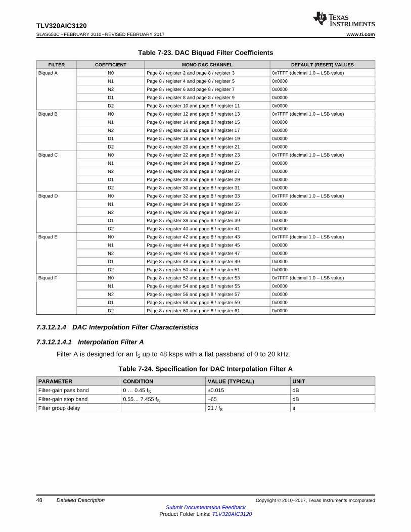
48
TLV320AIC3120SLAS653C –FEBRUARY 2010–REVISED FEBRUARY 2017 www.ti.com
Submit Documentation FeedbackProduct Folder Links: TLV320AIC3120
Detailed Description Copyright © 2010–2017, Texas Instruments Incorporated
Table 7-23. DAC Biquad Filter CoefficientsFILTER COEFFICIENT MONO DAC CHANNEL DEFAULT (RESET) VALUES
Biquad A N0 Page 8 / register 2 and page 8 / register 3 0x7FFF (decimal 1.0 – LSB value)
N1 Page 8 / register 4 and page 8 / register 5 0x0000
N2 Page 8 / register 6 and page 8 / register 7 0x0000
D1 Page 8 / register 8 and page 8 / register 9 0x0000
D2 Page 8 / register 10 and page 8 / register 11 0x0000
Biquad B N0 Page 8 / register 12 and page 8 / register 13 0x7FFF (decimal 1.0 – LSB value)
N1 Page 8 / register 14 and page 8 / register 15 0x0000
N2 Page 8 / register 16 and page 8 / register 17 0x0000
D1 Page 8 / register 18 and page 8 / register 19 0x0000
D2 Page 8 / register 20 and page 8 / register 21 0x0000
Biquad C N0 Page 8 / register 22 and page 8 / register 23 0x7FFF (decimal 1.0 – LSB value)
N1 Page 8 / register 24 and page 8 / register 25 0x0000
N2 Page 8 / register 26 and page 8 / register 27 0x0000
D1 Page 8 / register 28 and page 8 / register 29 0x0000
D2 Page 8 / register 30 and page 8 / register 31 0x0000
Biquad D N0 Page 8 / register 32 and page 8 / register 33 0x7FFF (decimal 1.0 – LSB value)
N1 Page 8 / register 34 and page 8 / register 35 0x0000
N2 Page 8 / register 36 and page 8 / register 37 0x0000
D1 Page 8 / register 38 and page 8 / register 39 0x0000
D2 Page 8 / register 40 and page 8 / register 41 0x0000
Biquad E N0 Page 8 / register 42 and page 8 / register 43 0x7FFF (decimal 1.0 – LSB value)
N1 Page 8 / register 44 and page 8 / register 45 0x0000
N2 Page 8 / register 46 and page 8 / register 47 0x0000
D1 Page 8 / register 48 and page 8 / register 49 0x0000
D2 Page 8 / register 50 and page 8 / register 51 0x0000
Biquad F N0 Page 8 / register 52 and page 8 / register 53 0x7FFF (decimal 1.0 – LSB value)
N1 Page 8 / register 54 and page 8 / register 55 0x0000
N2 Page 8 / register 56 and page 8 / register 57 0x0000
D1 Page 8 / register 58 and page 8 / register 59 0x0000
D2 Page 8 / register 60 and page 8 / register 61 0x0000
7.3.12.1.4 DAC Interpolation Filter Characteristics
7.3.12.1.4.1 Interpolation Filter A
Filter A is designed for an fS up to 48 ksps with a flat passband of 0 to 20 kHz.
Table 7-24. Specification for DAC Interpolation Filter A
PARAMETER CONDITION VALUE (TYPICAL) UNITFilter-gain pass band 0 … 0.45 fS ±0.015 dBFilter-gain stop band 0.55… 7.455 fS –65 dBFilter group delay 21 / fS s
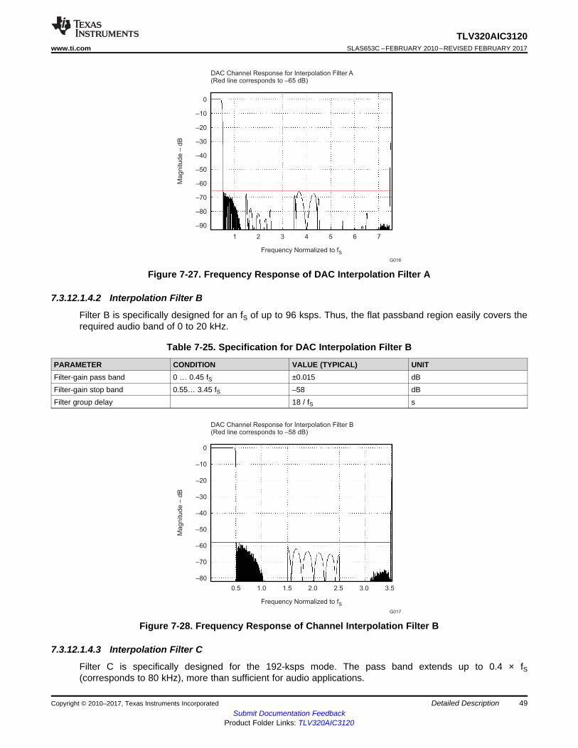
0
–10
–20
–30
–40
–50
–60
–70
–80
0.5 1.0 1.5 2.0 2.5 3.0 3.5
Frequency Normalized to fS
Magnitude
–dB
G017
DAC Channel Response for Interpolation Filter B(Red line corresponds to –58 dB)
0
–10
–20
–30
–40
–50
–60
–70
–80
–90
1 2 3 4 5 6 7
Frequency Normalized to fS
Magnitude
–dB
DAC Channel Response for Interpolation Filter A(Red line corresponds to –65 dB)
G016
49
TLV320AIC3120www.ti.com SLAS653C –FEBRUARY 2010–REVISED FEBRUARY 2017
Submit Documentation FeedbackProduct Folder Links: TLV320AIC3120
Detailed DescriptionCopyright © 2010–2017, Texas Instruments Incorporated
Figure 7-27. Frequency Response of DAC Interpolation Filter A
7.3.12.1.4.2 Interpolation Filter B
Filter B is specifically designed for an fS of up to 96 ksps. Thus, the flat passband region easily covers therequired audio band of 0 to 20 kHz.
Table 7-25. Specification for DAC Interpolation Filter B
PARAMETER CONDITION VALUE (TYPICAL) UNITFilter-gain pass band 0 … 0.45 fS ±0.015 dBFilter-gain stop band 0.55… 3.45 fS –58 dBFilter group delay 18 / fS s
Figure 7-28. Frequency Response of Channel Interpolation Filter B
7.3.12.1.4.3 Interpolation Filter C
Filter C is specifically designed for the 192-ksps mode. The pass band extends up to 0.4 × fS(corresponds to 80 kHz), more than sufficient for audio applications.
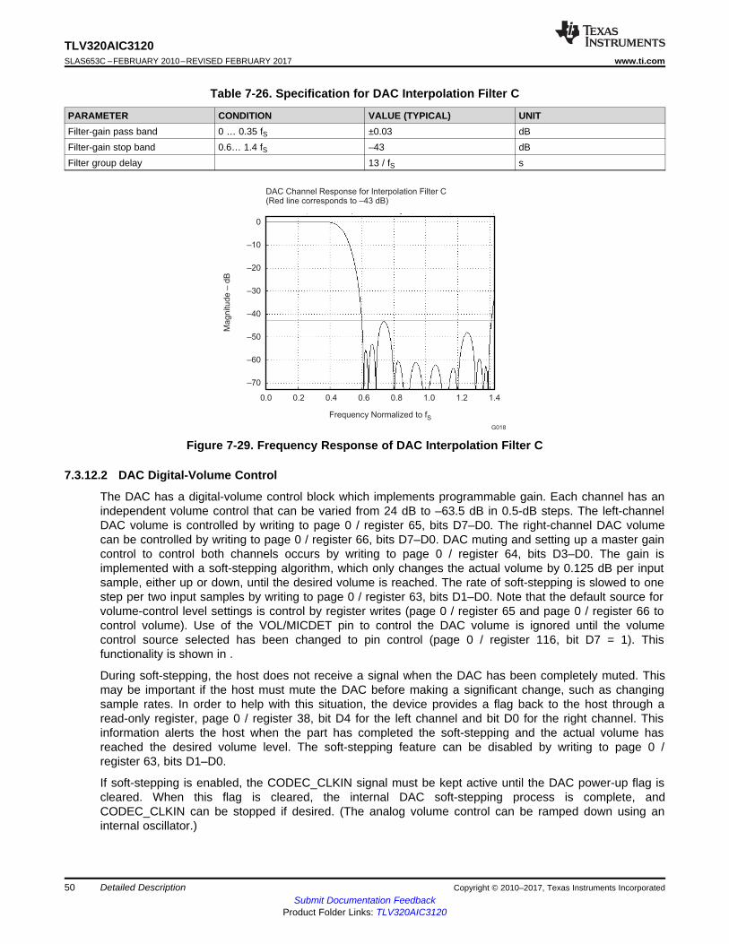
DAC Channel Response for Interpolation Filter C(Red line corresponds to –43 dB)
0
–10
–20
–30
–40
–50
–60
–70
0.0 0.2 0.4 0.6 0.8 1.0 1.4
Frequency Normalized to fS
Magnitude
–dB
G018
1.2
50
TLV320AIC3120SLAS653C –FEBRUARY 2010–REVISED FEBRUARY 2017 www.ti.com
Submit Documentation FeedbackProduct Folder Links: TLV320AIC3120
Detailed Description Copyright © 2010–2017, Texas Instruments Incorporated
Table 7-26. Specification for DAC Interpolation Filter C
PARAMETER CONDITION VALUE (TYPICAL) UNITFilter-gain pass band 0 … 0.35 fS ±0.03 dBFilter-gain stop band 0.6… 1.4 fS –43 dBFilter group delay 13 / fS s
Figure 7-29. Frequency Response of DAC Interpolation Filter C
7.3.12.2 DAC Digital-Volume Control
The DAC has a digital-volume control block which implements programmable gain. Each channel has anindependent volume control that can be varied from 24 dB to –63.5 dB in 0.5-dB steps. The left-channelDAC volume is controlled by writing to page 0 / register 65, bits D7–D0. The right-channel DAC volumecan be controlled by writing to page 0 / register 66, bits D7–D0. DAC muting and setting up a master gaincontrol to control both channels occurs by writing to page 0 / register 64, bits D3–D0. The gain isimplemented with a soft-stepping algorithm, which only changes the actual volume by 0.125 dB per inputsample, either up or down, until the desired volume is reached. The rate of soft-stepping is slowed to onestep per two input samples by writing to page 0 / register 63, bits D1–D0. Note that the default source forvolume-control level settings is control by register writes (page 0 / register 65 and page 0 / register 66 tocontrol volume). Use of the VOL/MICDET pin to control the DAC volume is ignored until the volumecontrol source selected has been changed to pin control (page 0 / register 116, bit D7 = 1). Thisfunctionality is shown in .
During soft-stepping, the host does not receive a signal when the DAC has been completely muted. Thismay be important if the host must mute the DAC before making a significant change, such as changingsample rates. In order to help with this situation, the device provides a flag back to the host through aread-only register, page 0 / register 38, bit D4 for the left channel and bit D0 for the right channel. Thisinformation alerts the host when the part has completed the soft-stepping and the actual volume hasreached the desired volume level. The soft-stepping feature can be disabled by writing to page 0 /register 63, bits D1–D0.
If soft-stepping is enabled, the CODEC_CLKIN signal must be kept active until the DAC power-up flag iscleared. When this flag is cleared, the internal DAC soft-stepping process is complete, andCODEC_CLKIN can be stopped if desired. (The analog volume control can be ramped down using aninternal oscillator.)
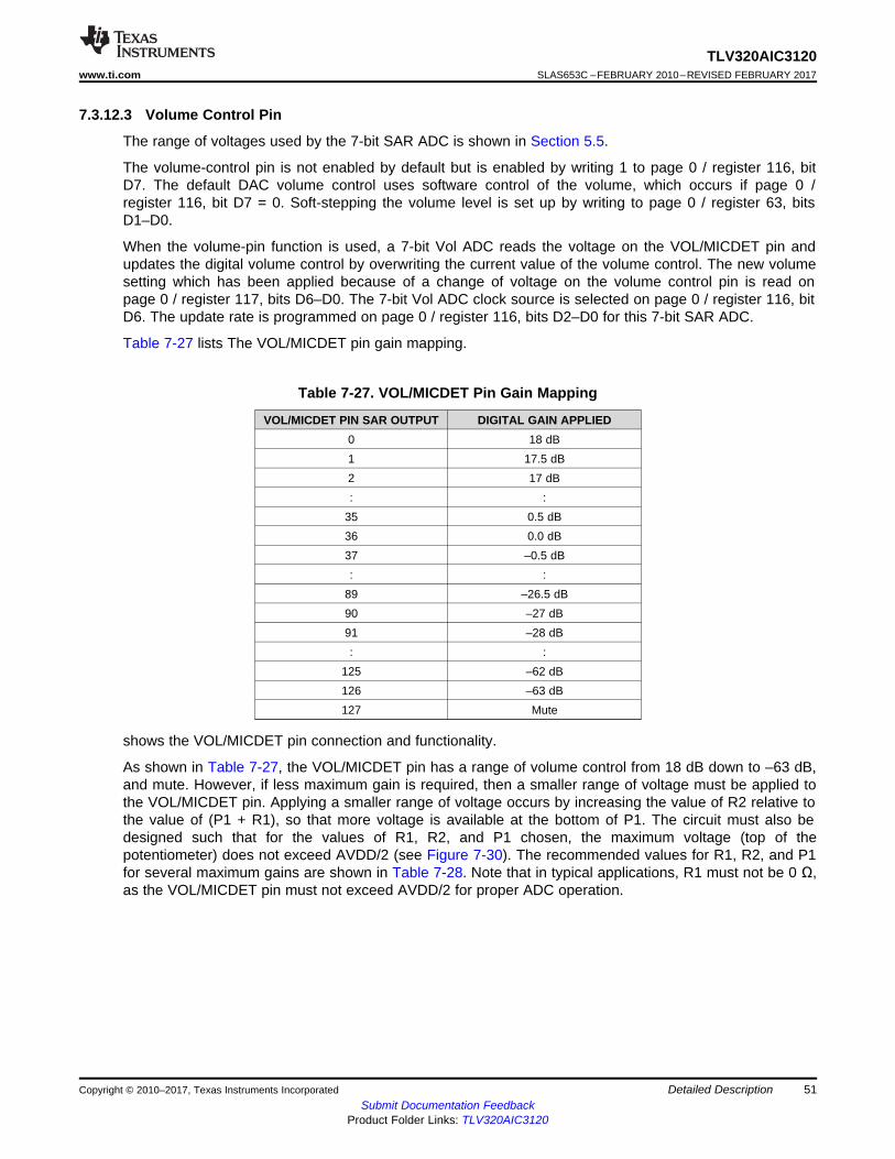
51
TLV320AIC3120www.ti.com SLAS653C –FEBRUARY 2010–REVISED FEBRUARY 2017
Submit Documentation FeedbackProduct Folder Links: TLV320AIC3120
Detailed DescriptionCopyright © 2010–2017, Texas Instruments Incorporated
7.3.12.3 Volume Control Pin
The range of voltages used by the 7-bit SAR ADC is shown in Section 5.5.
The volume-control pin is not enabled by default but is enabled by writing 1 to page 0 / register 116, bitD7. The default DAC volume control uses software control of the volume, which occurs if page 0 /register 116, bit D7 = 0. Soft-stepping the volume level is set up by writing to page 0 / register 63, bitsD1–D0.
When the volume-pin function is used, a 7-bit Vol ADC reads the voltage on the VOL/MICDET pin andupdates the digital volume control by overwriting the current value of the volume control. The new volumesetting which has been applied because of a change of voltage on the volume control pin is read onpage 0 / register 117, bits D6–D0. The 7-bit Vol ADC clock source is selected on page 0 / register 116, bitD6. The update rate is programmed on page 0 / register 116, bits D2–D0 for this 7-bit SAR ADC.
Table 7-27 lists The VOL/MICDET pin gain mapping.
Table 7-27. VOL/MICDET Pin Gain Mapping
VOL/MICDET PIN SAR OUTPUT DIGITAL GAIN APPLIED0 18 dB1 17.5 dB2 17 dB: :
35 0.5 dB36 0.0 dB37 –0.5 dB: :
89 –26.5 dB90 –27 dB91 –28 dB: :
125 –62 dB126 –63 dB127 Mute
shows the VOL/MICDET pin connection and functionality.
As shown in Table 7-27, the VOL/MICDET pin has a range of volume control from 18 dB down to –63 dB,and mute. However, if less maximum gain is required, then a smaller range of voltage must be applied tothe VOL/MICDET pin. Applying a smaller range of voltage occurs by increasing the value of R2 relative tothe value of (P1 + R1), so that more voltage is available at the bottom of P1. The circuit must also bedesigned such that for the values of R1, R2, and P1 chosen, the maximum voltage (top of thepotentiometer) does not exceed AVDD/2 (see Figure 7-30). The recommended values for R1, R2, and P1for several maximum gains are shown in Table 7-28. Note that in typical applications, R1 must not be 0 Ω,as the VOL/MICDET pin must not exceed AVDD/2 for proper ADC operation.
10 1
LPF 15 11
N N zH (z)
2 D z
-
-
+
=
-
10 1
HPF 15 11
N N zH (z)
2 D z
-
-
+
=
-
AVDD
VOL/MICDET
R1
34.8 kW
P1
25 kW
R2
9.76 kW
AVSS
1 Fm
52
TLV320AIC3120SLAS653C –FEBRUARY 2010–REVISED FEBRUARY 2017 www.ti.com
Submit Documentation FeedbackProduct Folder Links: TLV320AIC3120
Detailed Description Copyright © 2010–2017, Texas Instruments Incorporated
Figure 7-30. Example Analog Volume Control Circuit to VOL/MICDET Pin
Table 7-28. VOL/MICDET Pin Gain Scaling
R1(kΩ)
P1(kΩ)
R2(kΩ)
ADC VOLTAGEfor AVDD = 3.3 V
(V)DIGITAL GAIN RANGE
(dB)
25 25 0 0 to 1.65 18 to –6333 25 7.68 0.386 to 1.642 3 to –63
34.8 25 9.76 0.463 to 1.649 0 to –63
7.3.12.4 Dynamic Range Compression
Typical music signals are characterized by crest factors, the ratio of peak signal power to average signalpower, of 12 dB or more. To avoid audible distortions due to clipping of peak signals, the gain of the DACchannel must be adjusted so as not to cause hard clipping of peak signals. As a result, during nominalperiods, the applied gain is low, causing the perception that the signal is not loud enough. To overcomethis problem, dynamic range conpression (DRC) in the TLV320AIC3120 continuously monitors the outputof the DAC digital volume control to detect its power level relative to 0 dBFS. When the power level is low,DRC increases the input signal gain to make it sound louder. At the same time, if a peaking signal isdetected, it autonomously reduces the applied gain to avoid hard clipping. This results in sounds morepleasing to the ear as well as sounding louder during nominal periods.
The DRC functionality in the TLV320AIC3120 is implemented by a combination of processing blocks in theDAC channel as described in Section 7.3.12.1.2.
DRC can be disabled by writing to page 0 / register 68, bits D6–D5.
DRC typically works on the filtered version of the input signal. The input signals have no audio informationat dc and extremely low frequencies; however, they can significantly influence the energy estimationfunction in the dynamic range compressor (the DRC). Also, most of the information about signal energy isconcentrated in the low-frequency region of the input signal.
To estimate the energy of the input signal, the signal is first fed to the DRC high-pass filter and then to theDRC low-pass filter. These filters are implemented as first-order IIR filters given by
(6)
(7)
The coefficients for these filters are 16 bits wide in 2s-complement format and are user-programmablethrough register write as given in Table 7-29.
53
TLV320AIC3120www.ti.com SLAS653C –FEBRUARY 2010–REVISED FEBRUARY 2017
Submit Documentation FeedbackProduct Folder Links: TLV320AIC3120
Detailed DescriptionCopyright © 2010–2017, Texas Instruments Incorporated
Table 7-29. The DRC HPF and LPF Coefficients
COEFFICIENT LOCATIONHPF N0 C71 page 9 / register 14 and page 9 / register 15HPF N1 C72 page 9 / registers 16 and page 9 / register 17HPF D1 C73 page 9 / registers 18 and page 9 / register 19LPF N0 C74 page 9 / registers 20 and page 9 / register 21LPF N1 C75 page 9 / registers 22 and page 9 / register 23LPF D1 C76 page 9 / registers 24 and page 9 / register 25
The default values of these coefficients implement a high-pass filter with a cutoff at 0.00166 × DAC_fS,and a low-pass filter with a cutoff at 0.00033 × DAC_fS.
The output of the DRC high-pass filter is fed to the processing block selected for the DAC channel. Theabsolute value of the DRC LPF filter is used for energy estimation within the DRC.
The gain in the DAC digital volume control is controlled by page 0 / register 65 and page 0 / register 66.When the DRC is enabled, the applied gain is a function of the digital volume control register setting andthe output of the DRC.
The DRC parameters are described in sections that follow.
7.3.12.4.1 DRC Threshold
DRC threshold represents the level of the DAC playback signal at which the gain compression becomesactive. The output of the digital volume control in the DAC is compared with the set threshold. Thethreshold value is programmable by writing to page 0 / register 68, bits D4–D2. The threshold value canbe adjusted between –3 dBFS and –24 dBFS in steps of 3 dB. Keeping the DRC threshold value too highmay not leave enough time for the DRC block to detect peaking signals, and can cause excessivedistortion at the outputs. Keeping the DRC threshold value too low can limit the perceived loudness of theoutput signal.
The recommended DRC threshold value is –24 dB.
When the output signal exceeds the set DRC threshold, the interrupt flag bits at page 0 / register 44,bits D3–D2 are updated. These flag bits are sticky in nature, and are reset only after they are read backby the user. The non-sticky versions of the interrupt flags are also available at page 0 / register 46,bits D3–D2.
7.3.12.4.2 DRC Hysteresis
DRC hysteresis is programmable by writing to page 0 / register 68, bits D1–D0. These bits can beprogrammed to represent values between 0 dB and 3 dB in steps of 1dB. DRC hysteresis provides aprogrammable window around the programmed DRC threshold that must be exceeded for the disabledDRC to become enabled, or the enabled DRC to become disabled. For example, if the DRC threshold isset to –12 dBFS and the DRC hysteresis is set to 3 dB, then if the gain compression in the DRC isinactive, the output of the DAC digital volume control must exceed –9 dBFS before gain compression dueto the DRC is activated. Similarly, when the gain compression in the DRC is active, the output of the DACdigital volume control must fall below –15 dBFS for gain compression in the DRC to be deactivated. TheDRC hysteresis feature prevents the rapid activation and de-activation of gain compression in the DRC incases when the output of the DAC digital volume control rapidly fluctuates in a narrow region around theprogrammed DRC threshold. By programming the DRC hysteresis as 0 dB, the hysteresis action isdisabled.
The recommended value of DRC hysteresis is 3 dB.
54
TLV320AIC3120SLAS653C –FEBRUARY 2010–REVISED FEBRUARY 2017 www.ti.com
Submit Documentation FeedbackProduct Folder Links: TLV320AIC3120
Detailed Description Copyright © 2010–2017, Texas Instruments Incorporated
7.3.12.4.3 DRC Hold
DRC hold time is intended to slow the start of decay for a specified period of time in response to adecrease in energy level. To minimize audible artifacts, TI recommends to set the DRC hold time to 0through programming page 0 / register 69, bits D6–D3 = 0000.
7.3.12.4.4 DRC Attack Rate
When the output of the DAC digital volume control exceeds the programmed DRC threshold, the gainapplied in the DAC digital volume control is progressively reduced to avoid the signal from saturating thechannel. This process of reducing the applied gain is called attack. To avoid audible artifacts, the gain isreduced slowly with a rate equaling the attack rate, programmable via page 0 / register 70, bits D7–D4.Attack rates can be programmed from 4-dB gain change per 1/DAC_fS to 1.2207e–5-dB gain changeper 1/DAC_fS.
Attack rates should be programmed such that before the output of the DAC digital volume control can clip,the input signal should be sufficiently attenuated. High attack rates can cause audible artifacts, and too-slow attack rates may not be able to prevent the input signal from clipping.
The recommended DRC attack rate value is 1.9531e–4 dB per 1/DAC_fS.
7.3.12.4.5 DRC Decay Rate
When the DRC detects a reduction in output signal swing beyond the programmed DRC threshold, theDRC enters a decay state, where the applied gain in the digital-volume control is gradually increased toprogrammed values. To avoid audible artifacts, the gain is slowly increased with a rate equal to the decayrate programmed through page 0 / register 70, bits D3–D0. The decay rates can be programmed from1.5625e–3 dB per 1/DAC_fS to 4.7683e–7 dB per 1/DAC_fS. If the decay rates are programmed too high,then sudden gain changes can cause audible artifacts. However, if it is programmed too slow, then theoutput may be perceived as too low for a long time after the peak signal has passed.
The recommended value of DRC decay rate is 2.4414e–5 dB per 1/DAC_fS.
7.3.12.4.6 Example Setup for DRC• PGA gain = 12 dB• Threshold = –24 dB• Hysteresis = 3 dB• Hold time = 0 ms• Attack rate = 1.9531e–4 dB per 1/DAC_fS• Decay rate = 2.4414e–5 dB per 1/DAC_fSScript
#Go to Page 0w 30 00 00#DAC => 12 db gain leftw 30 41 18#DAC => 12 db gain rightw 30 42 18#DAC => DRC Enabled for both channels, Threshold = -24 db, Hysteresis = 3 dBw 30 44 7F#DRC Hold = 0 ms, Rate of Changes of Gain = 0.5 dB/Fs'w 30 45 00#Attack Rate = 1.9531e-4 dB/Frame , DRC Decay Rate =2.4414e-5 dB/Framew 30 46 B6#Go to Page 9w 30 00 09#DRC HPFw 30 0E 7F AB 80 55 7F 56#DRC LPF W 30 14 00 11 00 11 7F DE
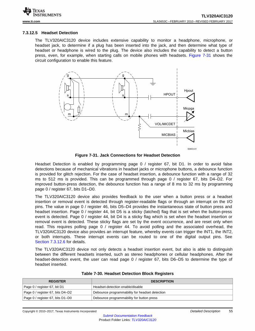
g
s
m
Micbias
m
s
g
MICBIAS
HPOUT
VOL/MICDET
Micpga
Hpout
S0403-01
55
TLV320AIC3120www.ti.com SLAS653C –FEBRUARY 2010–REVISED FEBRUARY 2017
Submit Documentation FeedbackProduct Folder Links: TLV320AIC3120
Detailed DescriptionCopyright © 2010–2017, Texas Instruments Incorporated
7.3.12.5 Headset Detection
The TLV320AIC3120 device includes extensive capability to monitor a headphone, microphone, orheadset jack, to determine if a plug has been inserted into the jack, and then determine what type ofheadset or headphone is wired to the plug. The device also includes the capability to detect a buttonpress, even, for example, when starting calls on mobile phones with headsets. Figure 7-31 shows thecircuit configuration to enable this feature.
Figure 7-31. Jack Connections for Headset Detection
Headset Detection is enabled by programming page 0 / register 67, bit D1. In order to avoid falsedetections because of mechanical vibrations in headset jacks or microphone buttons, a debounce functionis provided for glitch rejection. For the case of headset insertion, a debounce function with a range of 32ms to 512 ms is provided. This can be programmed through page 0 / register 67, bits D4–D2. Forimproved button-press detection, the debounce function has a range of 8 ms to 32 ms by programmingpage 0 / register 67, bits D1–D0.
The TLV320AIC3120 device also provides feedback to the user when a button press or a headsetinsertion or removal event is detected through register-readable flags or through an interrupt on the I/Opins. The value in page 0 / register 46, bits D5–D4 provides the instantaneous state of button press andheadset insertion. Page 0 / register 44, bit D5 is a sticky (latched) flag that is set when the button-pressevent is detected. Page 0 / register 44, bit D4 is a sticky flag which is set when the headset insertion orremoval event is detected. These sticky flags are set by the event occurrence, and are reset only whenread. This requires polling page 0 / register 44. To avoid polling and the associated overhead, theTLV320AIC3120 device also provides an interrupt feature, whereby events can trigger the INT1, the INT2,or both interrupts. These interrupt events can be routed to one of the digital output pins. SeeSection 7.3.12.6 for details.
The TLV320AIC3120 device not only detects a headset insertion event, but also is able to distinguishbetween the different headsets inserted, such as stereo headphones or cellular headphones. After theheadset-detection event, the user can read page 0 / register 67, bits D6–D5 to determine the type ofheadset inserted.
Table 7-30. Headset Detection Block Registers
REGISTER DESCRIPTIONPage 0 / register 67, bit D1 Headset-detection enable/disablePage 0 / register 67, bits D4–D2 Debounce programmability for headset detectionPage 0 / register 67, bits D1–D0 Debounce programmability for button press
56
TLV320AIC3120SLAS653C –FEBRUARY 2010–REVISED FEBRUARY 2017 www.ti.com
Submit Documentation FeedbackProduct Folder Links: TLV320AIC3120
Detailed Description Copyright © 2010–2017, Texas Instruments Incorporated
Table 7-30. Headset Detection Block Registers (continued)REGISTER DESCRIPTION
Page 0 / register 44, bit D5 Sticky flag for button-press eventPage 0 / register 44, bit D4 Sticky flag for headset-insertion or -removal eventPage 0 / register 46, bit D5 Status flag for button-press eventPage 0 / register 46, bit D4 Status flag for headset insertion and removalPage 0 / register 67, bits D6–D5 Flags for type of headset detected
The headset detection block requires AVDD to be powered. The headset detection feature in theTLV320AIC3120 device is achieved with very low power overhead, requiring less than 20 μA of additionalcurrent from the AVDD supply.
7.3.12.6 Interrupts
Some specific events in the TLV320AIC3120 device that can require host processor intervention are usedto trigger interrupts to the host processor. This avoids polling the status-flag registers continuously. TheTLV320AIC3120 device has two defined interrupts, INT1 and INT2, that are configured by programmingpage 0 / register 48 and page 0 / register 49. A user can configure interrupts INT1 and INT2 to betriggered by one or many events, such as:• Headset detection• Button press• DAC DRC signal exceeding threshold• Noise detected by AGC• Overcurrent condition in headphone drivers and speaker drivers• Data overflow in the ADC and DAC processing blocks and filters• DC measurement data available
Each of these INT1 and INT2 interrupts can be routed to output pins GPIO1 or DOUT. These interruptsignals can either be configured as a single pulse or a series of pulses by programming page 0 /register 48, bit D0 and page 0 / register 49, bit D0. If the user configures the interrupts as a series ofpulses, the events trigger the start of pulses that stop when the flag registers in page 0 / registers 44, 45,and 50 are read by the user to determine the cause of the interrupt.
7.3.12.7 Key-Click Functionality With Beep Generator (PRB_P25)
A special algorithm has been included in the digital signal processing block PRB_P25 for generating adigital sine-wave signal that is sent to the DAC.
This functionality is intended for generating key-click sounds for user feedback. The sine-wave generatoris very flexible (see Table 7-31) and is completely register programmable. Programming page 0 / register71 through page 0 / register 79 (8 bits each) completely controls the functionality of this generator andallows for differentiating sounds.
The two registers used for programming the 16-bit sine-wave coefficient are page 0 / register 76 andpage 0 / register 77. The two registers used for programming the 16-bit cosine-wave coefficient arepage 0 / register 78 and page 0 / register 79. This coefficient resolution allows virtually any frequency ofsine wave in the audio band to be generated, up to fS / 2.
The three registers used to control the length of the sine-burst waveform are page 0 / register 73 throughpage 0 / register 75. The resolution (bit) in the registers of the sine-burst length is one sample time, so thisallows great control on the overall time of the sine-burst waveform. This 24-bit length timer supports16 777 215 sample times. For example, if fS is set at 48 kHz, and the register value equals 96 000 d(01 7700h), then the sine burst lasts exactly 2 seconds. The default settings for the tone generator, basedon using a sample rate of 48 kHz, are 1-kHz (approximately) sine wave, with a sine-burst length of fivecycles (5 ms).
57
TLV320AIC3120www.ti.com SLAS653C –FEBRUARY 2010–REVISED FEBRUARY 2017
Submit Documentation FeedbackProduct Folder Links: TLV320AIC3120
Detailed DescriptionCopyright © 2010–2017, Texas Instruments Incorporated
Table 7-31. Beep Generator Register Locations (Page 00h)
LEFT BEEP CONTROL RIGHT BEEP CONTROLBEEP LENGTH SINE COSINE
MSB MID LSB MSB LSB MSB LSBREGISTER 71 72 73 74 75 76 77 78 79
(1) These are the default settings.
Table 7-32. Example Beep-Generator Settings for a 1000-Hz Tone
BEEP FREQUENCY BEEP LENGTH SINE COSINE SAMPLE RATE
Hz MSB(hex)
MID(hex)
LSB(hex)
MSB(hex)
LSB(hex)
MSB(hex)
LSB(hex) Hz
1000 (1) 0 0 EE 10 D8 7E E3 48 000
Two registers are used to control the left sine-wave volume and the right sine-wave volume independently.The 6-bit digital volume control used allows level control of 2 dB to –61 dB in 1-dB steps. The left-channelvolume is controlled by writing to page 0 / register 71, bits D5–D0. The right-channel volume is controlledby writing to page 0, register 72, bits D5–D0. A master volume control that controls the left and rightchannels of the beep generator are set up by writing to page 0 / register 72, bits D7–D6. The defaultvolume control setting is 2 dB, which provides the maximum tone-generator output level.
For generating other tones, the three tone-generator coefficients are found by running the following scriptusing MATLAB™ :
Sine = dec2hex(round(sin(2*π*Fin/Fs)*2^15))Cosine = dec2hex(round(cos(2*π*Fin/Fs)*2^15))Beep Length = dec2hex(floor(Fs*Cycle/Fin))
where,Fin = Beep frequency desiredFs = Sample rateCycle = Number of beep (sine wave) cycles that are requireddec2hex = Decimal to hexadecimal conversion function
NOTES:1. Fin must be less than Fs / 4.2. For the sine and cosine values, if the number of bits is less than the full 16-bit value, then the unused
MSBs must be written as 0s.3. For the beep-length values, if number of bits is less than the full 24-bit value, then the unused MSBs
must be written as 0s.
Following the beep-volume control is a digital mixer that mixes in a playback data stream whose level hasalready been set by the DAC volume control. Therefore, once the key-click volume level is set, the key-click volume is not affected by the DAC volume control, which is the main control available to the enduser. shows this functionality.
Following the DAC, the signal can be further scaled by the analog output volume control and power-amplifier level control.
To insert a beep in the middle of an already-playing signal over DAC, use the following sequence.
Before the beep is desired, program the desired beep frequency, volume, and length in the configurationregisters. When a beep is desired, use the example configuration script.
w 30 00 00 # change to Page 0w 30 40 0C # mute DACsf 30 26 xxx1xxx1 # wait for DAC gain flag to be setw 30 0B 02 # power down NDAC dividerw 30 47 80 # enable beep generator with left channel volume = 0dB, volume level could
# be different as per requirementw 30 0B 82 # power up NDAC divider, in this specific example NDAC = 2, but NDAC could
# be different value as per overall setup
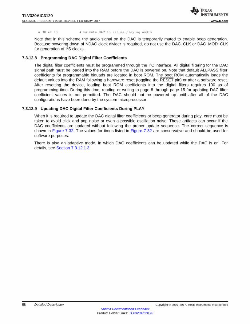
58
TLV320AIC3120SLAS653C –FEBRUARY 2010–REVISED FEBRUARY 2017 www.ti.com
Submit Documentation FeedbackProduct Folder Links: TLV320AIC3120
Detailed Description Copyright © 2010–2017, Texas Instruments Incorporated
w 30 40 00 # un-mute DAC to resume playing audio
Note that in this scheme the audio signal on the DAC is temporarily muted to enable beep generation.Because powering down of NDAC clock divider is required, do not use the DAC_CLK or DAC_MOD_CLKfor generation of I2S clocks.
7.3.12.8 Programming DAC Digital Filter Coefficients
The digital filter coefficients must be programmed through the I2C interface. All digital filtering for the DACsignal path must be loaded into the RAM before the DAC is powered on. Note that default ALLPASS filtercoefficients for programmable biquads are located in boot ROM. The boot ROM automatically loads thedefault values into the RAM following a hardware reset (toggling the RESET pin) or after a software reset.After resetting the device, loading boot ROM coefficients into the digital filters requires 100 μs ofprogramming time. During this time, reading or writing to page 8 through page 15 for updating DAC filtercoefficient values is not permitted. The DAC should not be powered up until after all of the DACconfigurations have been done by the system microprocessor.
7.3.12.9 Updating DAC Digital Filter Coefficients During PLAY
When it is required to update the DAC digital filter coefficients or beep generator during play, care must betaken to avoid click and pop noise or even a possible oscillation noise. These artifacts can occur if theDAC coefficients are updated without following the proper update sequence. The correct sequence isshown in Figure 7-32. The values for times listed in Figure 7-32 are conservative and should be used forsoftware purposes.
There is also an adaptive mode, in which DAC coefficients can be updated while the DAC is on. Fordetails, see Section 7.3.12.1.3.
Play - Paused
DAC Power Down
UpdateDigital FilterCoefficients
DAC Power UP
Wait 20 ms
Volume Ramp DownSoft Mute
Restore PreviousVolume Level (Ramp)
in (B) ms
Play - Continue
Wait (A) ms
For f = 32 kHzS ® Wait 25 ms (min)
For f = 48 kHz Wait 20 ms (min)S ®
For = 32 kHz ®f 25 ms
For f = 48 kHz 20 ms
S
S ®
DAC Volume Ramp Down WAIT Time (A)
DAC Volume Ramp Up Time (B)
F0024-02
59
TLV320AIC3120www.ti.com SLAS653C –FEBRUARY 2010–REVISED FEBRUARY 2017
Submit Documentation FeedbackProduct Folder Links: TLV320AIC3120
Detailed DescriptionCopyright © 2010–2017, Texas Instruments Incorporated
Figure 7-32. Example Flow For Updating DAC Digital Filter Coefficients During Play
7.3.12.10 Digital Mixing and Routing
The TLV320AIC3120 has four digital mixing blocks. Each mixer can provide either mixing or multiplexingof the digital audio data. The first mixer/multiplexer can be used to select input data for the mono DACfrom left channel, right channel, or a mix of the left and right channels [(L + R) / 2] . This digital routing canbe configured by writing to page 0 / register 63, bits D5–D4 for the DAC mono channel.
7.3.12.11 Analog Audio Routing
The TLV320AIC3120 has the capability to route the DAC output to either the headphone or the speakeroutput. If desirable, both output drivers can operate at the same time while playing at different volumelevels. The TLV320AIC3120 provides various digital routing capabilities, allowing digital mixing or evenchannel swapping in the digital domain. All analog outputs other than the selected ones can be powereddown for optimal power consumption.
60
TLV320AIC3120SLAS653C –FEBRUARY 2010–REVISED FEBRUARY 2017 www.ti.com
Submit Documentation FeedbackProduct Folder Links: TLV320AIC3120
Detailed Description Copyright © 2010–2017, Texas Instruments Incorporated
7.3.12.11.1 Analog Output Volume Control
The output volume control fine tunes the level of the mixer amplifier signal supplied to the headphonedriver or the speaker driver. This architecture supports separate and concurrent volume levels for each ofthe four output drivers. This volume control is also used as part of the output pop-noise reduction scheme.This feature is available even if the ADC and DAC are powered down.
7.3.12.11.2 Headphone Analog-Output Volume Control
For the headphone outputs, the analog volume control has a range from 0 dB to –78 dB in 0.5-dB stepsfor most of the useful range plus mute, which is shown in Table 7-33. This volume control includes soft-stepping logic. Routing the DAC output signal to the analog volume control occurs by writing to page 1 /register 35, bit D7-D6.
Changing the analog volume for the headphone is controlled by writing to page 1 / register 36, bitsD6–D0. Routing the signal from the output of the analog volume control to the input of the headphonepower amplifier occurs by writing to page 1 / register 36, bit D7.
The analog volume-control soft-stepping time is based on the setting in page 0 / register 63, bits D1–D0.
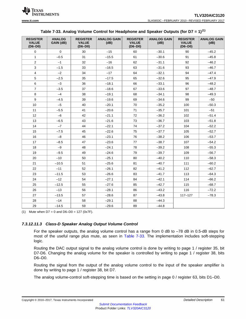
61
TLV320AIC3120www.ti.com SLAS653C –FEBRUARY 2010–REVISED FEBRUARY 2017
Submit Documentation FeedbackProduct Folder Links: TLV320AIC3120
Detailed DescriptionCopyright © 2010–2017, Texas Instruments Incorporated
(1) Mute when D7 = 0 and D6–D0 = 127 (0x7F).
Table 7-33. Analog Volume Control for Headphone and Speaker Outputs (for D7 = 1) (1)
REGISTERVALUE(D6–D0)
ANALOGGAIN (dB)
REGISTERVALUE(D6–D0)
ANALOG GAIN(dB)
REGISTERVALUE(D6–D0)
ANALOG GAIN(dB)
REGISTERVALUE(D6–D0)
ANALOG GAIN(dB)
0 0 30 –15 60 –30.1 90 –45.21 –0.5 31 –15.5 61 –30.6 91 –45.82 –1 32 –16 62 –31.1 92 –46.23 –1.5 33 –16.5 63 –31.6 93 –46.74 –2 34 –17 64 –32.1 94 –47.45 –2.5 35 –17.5 65 –32.6 95 –47.96 –3 36 –18.1 66 –33.1 96 –48.27 –3.5 37 –18.6 67 –33.6 97 –48.78 –4 38 –19.1 68 –34.1 98 –49.39 –4.5 39 –19.6 69 –34.6 99 –50
10 –5 40 –20.1 70 –35.2 100 –50.311 –5.5 41 –20.6 71 –35.7 101 –5112 –6 42 –21.1 72 –36.2 102 –51.413 –6.5 43 –21.6 73 –36.7 103 –51.814 –7 44 –22.1 74 –37.2 104 –52.215 –7.5 45 –22.6 75 –37.7 105 –52.716 –8 46 –23.1 76 –38.2 106 –53.717 –8.5 47 –23.6 77 –38.7 107 –54.218 –9 48 –24.1 78 –39.2 108 –55.319 –9.5 49 –24.6 79 –39.7 109 –56.720 –10 50 –25.1 80 –40.2 110 –58.321 –10.5 51 –25.6 81 –40.7 111 –60.222 –11 52 –26.1 82 –41.2 112 –62.723 –11.5 53 –26.6 83 –41.7 113 –64.324 –12 54 –27.1 84 –42.1 114 –66.225 –12.5 55 –27.6 85 –42.7 115 –68.726 –13 56 –28.1 86 –43.2 116 –72.227 –13.5 57 –28.6 87 –43.8 117–127 –78.328 –14 58 –29.1 88 –44.329 –14.5 59 –29.6 89 –44.8
7.3.12.11.3 Class-D Speaker Analog Output Volume Control
For the speaker outputs, the analog volume control has a range from 0 dB to –78 dB in 0.5-dB steps formost of the useful range plus mute, as seen in Table 7-33. The implementation includes soft-steppinglogic.
Routing the DAC output signal to the analog volume control is done by writing to page 1 / register 35, bitD7-D6. Changing the analog volume for the speaker is controlled by writing to page 1 / register 38, bitsD6–D0.
Routing the signal from the output of the analog volume control to the input of the speaker amplifier isdone by writing to page 1 / register 38, bit D7.
The analog volume-control soft-stepping time is based on the setting in page 0 / register 63, bits D1–D0.
62
TLV320AIC3120SLAS653C –FEBRUARY 2010–REVISED FEBRUARY 2017 www.ti.com
Submit Documentation FeedbackProduct Folder Links: TLV320AIC3120
Detailed Description Copyright © 2010–2017, Texas Instruments Incorporated
7.3.12.12 Analog Outputs
Various analog routings are supported for playback. All the options can be conveniently viewed on thefunctional block diagram, .
7.3.12.12.1 Headphone Drivers
The TLV320AIC3120 device features a mono headphone driver (HPOUT) that delivers up to 30 mW perchannel, at 3.3-V supply voltage, into a 16-Ω load. The headphones are used in a single-endedconfiguration where an ac-coupling capacitor (dc-blocking) is connected between the device output pinsand the headphones. The headphone driver also supports 32-Ω and 10-kΩ loads without changing anycontrol register settings.
The headphone drivers can be configured to optimize the power consumption in the lineout-drive mode bywriting 11 to page 1 / register 44, bits D2–D1.
The output common mode of the headphone and lineout drivers is programmed to 1.35 V, 1.5 V, 1.65 V,or 1.8 V by setting page 1 / register 31, bits D4–D3. Set the common-mode voltage to ≤ AVDD / 2.
The headphone driver can be powered on by writing to page 1 / register 31, bit D7. The HPOUT outputdriver gain can be controlled by writing to page 1 / register 40, bits D6–D3, and it can be muted by writingto page 1 / register 40, bit D2.
The TLV320AIC3120 device has a short-circuit protection feature for the headphone drivers, which isalways enabled to provide protection. The output condition of the headphone driver during short circuit isprogrammed by writing to page 1 / register 31, bit D1. If D1 = 0 when a short circuit is detected, the devicelimits the maximum current to the load. If D1 = 1 when a short circuit is detected, the device powers downthe output driver. The default condition for headphones is the current-limiting mode. In case of a shortcircuit on either channel, the output is disabled and a status flag is provided as read-only bits on page 1 /register 31, bit D0. If shutdown mode is enabled, then as soon as the short circuit is detected, page 1 /register 31, bit D7 (for HPOUT) clears automatically. Next, the device requires a reset to re-enable theoutput stage. Resetting occurs in two ways. First, the device master reset can be used, which requireseither toggling the RESET pin or using the software reset. If master reset is used, it resets all of theregisters. Second, a dedicated headphone power-stage reset can also be used to re-enable the outputstage, and that keeps all of the other device settings. The headphone power stage reset occurs by settingpage 1 / register 31, bit D7 for HPOUT. If the fault condition has been removed, then the device returns tonormal operation. If the fault is still present, then another shutdown occurs. Repeated resetting (more thanthree times) is not recommended, as this could lead to overheating.
7.3.12.12.2 Speaker Drivers
The TLV320AIC3120 device has an integrated class-D mono speaker driver (SPKP / SPKM) capable ofdriving an 8-Ω or 4-Ω differential load. The speaker driver can be powered directly from the battery supply(2.7 V to 5.5 V) on the SPKVDD pins; however, the voltage (including spike voltage) must be limited belowthe absolute-maximum voltage of 6 V.
The speaker driver is capable of supplying 400 mW per channel with a 3.6-V power supply. Through theuse of digital mixing, the device can connect one or both digital audio playback data channels to eitherspeaker driver; this also allows digital channel swapping if needed.
The class-D speaker driver can be powered on by writing to page 1 / register 32, bit D7. The class-Doutput driver gain can be controlled by writing to page 1 / register 42, bits D4–D3, and it can be muted bywriting to page 1 / register 42, bit D2.
The TLV320AIC3120 device has a short-circuit protection feature for the speaker drivers that is alwaysenabled to provide protection. If the output is shorted, the output stage shuts down on the overcurrentcondition. (Current limiting is not an available option for the higher-current speaker driver output stage.) Incase of a short circuit on either channel, the output is disabled and a status flag is provided as a read-onlybit on page 1 / register 32, bit D0.
63
TLV320AIC3120www.ti.com SLAS653C –FEBRUARY 2010–REVISED FEBRUARY 2017
Submit Documentation FeedbackProduct Folder Links: TLV320AIC3120
Detailed DescriptionCopyright © 2010–2017, Texas Instruments Incorporated
If shutdown occurs because of an overcurrent condition, then the device requires a reset to re-enable theoutput stage. Resetting occurs in two ways. First, the device master reset can be used, which requireseither toggling the RESET pin or using the software reset. If master reset is used, it resets all of theregisters. Second, a dedicated speaker power-stage reset can be used that keeps all of the other devicesettings. The speaker power-stage reset occurs by setting page 1 / register 32, bit D7 for SPKP andSPKM. If the fault condition has been removed, then the device returns to normal operation. If the fault isstill present, then another shutdown occurs. Repeated resetting (more than three times) is notrecommended as this could lead to overheating.
To minimize battery current leakage, the SPKVDD voltage levels must not be less than the AVDDvoltage level.
The TLV320AIC3120 device has a thermal protection (OTP) feature for the speaker drivers which isalways enabled to provide protection. If the device overheats, then the output stops switching. When thedevice cools down, the device resumes switching. An overtemperature status flag is provided as a read-only bit on page 0 / register 3, bit D1. The OTP feature is for self-protection of the device. If dietemperature can be controlled at the system or board level, then overtemperature does not occur.
7.3.12.13 Audio-Output Stage-Power Configurations
After the device has been configured (following a RESET) and the circuitry has been powered up, theaudio output stage can be powered up and powered down by register control.
These functions soft-start automatically. The two power stages can be powered up or powered downindependently..
See Table 7-34 for register control of audio output stage power configurations.
Table 7-34. Audio-Output Stage-Power Configurations
AUDIO OUTPUT PINS DESIRED FUNCTION PAGE 1 / REGISTER, BIT VALUES
HPOUTPower down HPOUT driver Page 1 / register 31, bit D7 = 0
Power up HPOUT driver Page 1 / register 31, bit D7 = 1
SPKP / SPKMPower down class-D drivers Page 1 / register 32, bit D7 = 0
Power up class-D drivers Page 1 / register 32, bit D7 = 1
7.3.12.14 DAC Setup
The following paragraphs are intended to guide a user through the steps necessary to configure theTLV320AIC3120.
Step 1
The system clock source (master clock) and the targeted DAC sampling frequency must be identified.
Depending on the targeted performance, the decimation filter type (A, B, or C) and DOSR value can bedetermined:• Filter A should be used for 48-kHz high-performance operation; DOSR must be a multiple of 8.• Filter B should be used for up to 96-kHz operations; DOSR must be a multiple of 4.• Filter C should be used for up to 192-kHz operations; DOSR must be a multiple of 2.
In all cases, DOSR is limited in its range by the following condition:
2.8 MHz < DOSR × DAC_fS < 6.2 MHz
Based on the identified filter type and the required signal-processing capabilities, the appropriateprocessing block can be determined from the list of available processing blocks (PRB_P1 to PRB_P25).
64
TLV320AIC3120SLAS653C –FEBRUARY 2010–REVISED FEBRUARY 2017 www.ti.com
Submit Documentation FeedbackProduct Folder Links: TLV320AIC3120
Detailed Description Copyright © 2010–2017, Texas Instruments Incorporated
Based on the available master clock, the chosen DOSR and the targeted sampling rate, the clock-dividervalues NDAC and MDAC can be determined. If necessary, the internal PLL can add a large degree offlexibility.
In summary, CODEC_CLKIN (derived directly from the system clock source or from the internal PLL)divided by MDAC, NDAC, and DOSR must be equal to the DAC sampling rate, DAC_fS. TheCODEC_CLKIN clock signal is shared with the DAC clock-generation block.
CODEC_CLKIN = NDAC × MDAC × DOSR × DAC_fS
To a large degree, NDAC and MDAC can be chosen independently in the range of 1 to 128. In general,NDAC should be as large as possible as long as the following condition can still be met:
MDAC × DOSR / 32 ≥ RC
RC is a function of the chosen processing block and is listed in Table 7-20.
The common-mode voltage setting of the device is determined by the available analog power supply.
At this point, the following device-specific parameters are known: PRB_Rx, DOSR, NDAC, MDAC, inputand output common-mode values. If the PLL is used, the PLL parameters P, J, D, and R are determinedas well.
Step 2
Setting up the device via register programming:
The following list gives an example sequence of items that must be executed in the time betweenpowering the device up and reading data from the device. Note that there are other valid sequences,depending on which features are used.1. Define starting point:
(a) Power up applicable external power supplies(b) Set register page to 0(c) Initiate SW reset
2. Program clock settings(a) Program PLL clock dividers P, J, D, and R (if PLL is used)(b) Power up PLL (if PLL is used)(c) Program and power up NDAC(d) Program and power up MDAC(e) Program OSR value(f) Program I2S word length if required (16, 20, 24, or 32 bits)(g) Program the processing block to be used(h) Micellaneous page 0 controls
65
TLV320AIC3120www.ti.com SLAS653C –FEBRUARY 2010–REVISED FEBRUARY 2017
Submit Documentation FeedbackProduct Folder Links: TLV320AIC3120
Detailed DescriptionCopyright © 2010–2017, Texas Instruments Incorporated
3. Program analog blocks(a) Set register page to 1(b) Program common-mode voltage(c) Program headphone-specific de-pop settings (in case headphone driver is used)(d) Program routing of DAC output to the output amplifier (headphone/lineout or speaker)(e) Unmute and set gain of output drivers(f) Power up output drivers
4. Apply waiting time determined by the de-pop settings and the soft-stepping settings of the driver gain,or poll page 1 / register 63
5. Power up DAC(a) Set register page to 0(b) Power up DAC channels and set digital gain(c) Unmute digital volume control
A detailed example can be found in Section 7.3.12.15.
7.3.12.15 Example Register Setup to Play Digital Data Through DAC and Headphone/Speaker Outputs
A typical EVM I2C register control script follows to show how to set up the TLV320AIC3120 in playbackmode with fS = 44.1 kHz and MCLK = 11.2896 MHz.
# Key: w 30 XX YY ==> write to I2C address 0x30, to register 0xXX, data 0xYY# # ==> comment delimiter## The following list gives an example sequence of items that must be executed in the time# between powering the device up and reading data from the device. Note that there are# other valid sequences depending on which features are used.## 1. Define starting point:# (a) Power up applicable external hardware power supplies# (b) Set register page to 0#w 30 00 00## (c) Initiate SW reset#w 30 01 01## 2. Program clock settings# (a) Program PLL clock dividers P, J, D, R (if PLL is used)## PLL_clkin = MCLK,codec_clkin = PLL_CLKw 30 04 03# J = 8w 30 06 08# D = 0000, D(13:8) = 0, D(7:0) = 0w 30 07 00 00## (b) Power up PLL (if PLL is used)# PLL Power up, P = 1, R = 1#w 30 05 91## (c) Program and power up NDAC## NDAC is powered up and set to 8w 30 0B 88## (d) Program and power up MDAC## MDAC is powered up and set to 2w 30 0C 82## (e) Program OSR value#
66
TLV320AIC3120SLAS653C –FEBRUARY 2010–REVISED FEBRUARY 2017 www.ti.com
Submit Documentation FeedbackProduct Folder Links: TLV320AIC3120
Detailed Description Copyright © 2010–2017, Texas Instruments Incorporated
# DOSR = 128, DOSR(9:8) = 0, DOSR(7:0) = 128w 30 0D 00 80## (f) Program I2S word length if required (16, 20, 24, 32 bits)# and master mode (BCLK and WCLK are outputs)## mode is i2s, wordlength is 16, slave modew 30 1B 00## (g) Program the processing block to be used## select DAC DSP Processing Block PRB_P16w 30 3C 10w 30 00 08w 30 01 04w 30 00 00## 3. Program analog blocks## (a) Set register page to 1#w 30 00 01## (b) Program common-mode voltage (defalut = 1.35 V)#w 30 1F 04# (c) Program headphone-specific depop settings (in case headphone driver is used)## De-pop, Power on = 800 ms, Step time = 4 msw 30 21 4E## (d) Program routing of DAC output to the output amplifier (headphone/lineout or speaker)## DAC routed to HPOUTw 30 23 40## (e) Unmute and set gain of output driver## Unmute HPOUT, set gain = 0 dbw 30 28 06# Unmute Class-D, set gain = 18 dBw 30 2A 1C## (f) Power up output drivers## HPOUT powered upw 30 1F 82# Power-up Class-D driversw 30 20 C6# Enable HPOUT output analog volume, set = -9 dBw 30 24 92# Enable Class-D output analog volume, set = -9 dBw 30 26 92## 4. Apply waiting time determined by the de-pop settings and the soft-stepping settings of# the driver gain or poll page 1 / register 63## 5. Power up DAC# (a) Set register page to 0#w 30 00 00## (b) Power up DAC channels and set digital gain## Powerup DAC (soft step enabled)w 30 3F 94## DAC gain = -22 dBw 30 41 D4## (c) Unmute digital volume control## Unmute DAC
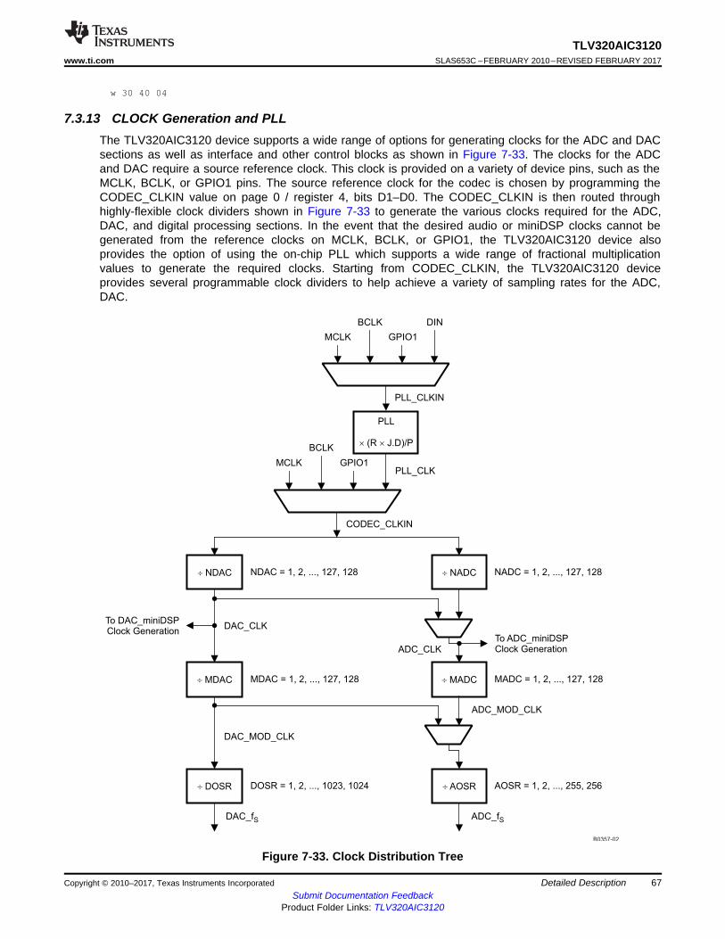
PLL
´ ´(R J.D)/P
PLL_CLKIN
CODEC_CLKIN
ADC_CLK
DAC_MOD_CLK
DAC_CLK
ADC_MOD_CLK
NDAC = 1, 2, ..., 127, 128
MDAC = 1, 2, ..., 127, 128
DOSR = 1, 2, ..., 1023, 1024 AOSR = 1, 2, ..., 255, 256
MADC = 1, 2, ..., 127, 128
NADC = 1, 2, ..., 127, 128
MCLK
BCLK
GPIO1
DIN
MCLK
BCLK
GPIO1PLL_CLK
¸ NADC
¸ MADC¸ MDAC
¸ DOSR ¸ AOSR
¸ NDAC
To DAC_miniDSPClock Generation
To ADC_miniDSPClock Generation
DAC_fS ADC_fS
B0357-02
67
TLV320AIC3120www.ti.com SLAS653C –FEBRUARY 2010–REVISED FEBRUARY 2017
Submit Documentation FeedbackProduct Folder Links: TLV320AIC3120
Detailed DescriptionCopyright © 2010–2017, Texas Instruments Incorporated
w 30 40 04
7.3.13 CLOCK Generation and PLLThe TLV320AIC3120 device supports a wide range of options for generating clocks for the ADC and DACsections as well as interface and other control blocks as shown in Figure 7-33. The clocks for the ADCand DAC require a source reference clock. This clock is provided on a variety of device pins, such as theMCLK, BCLK, or GPIO1 pins. The source reference clock for the codec is chosen by programming theCODEC_CLKIN value on page 0 / register 4, bits D1–D0. The CODEC_CLKIN is then routed throughhighly-flexible clock dividers shown in Figure 7-33 to generate the various clocks required for the ADC,DAC, and digital processing sections. In the event that the desired audio or miniDSP clocks cannot begenerated from the reference clocks on MCLK, BCLK, or GPIO1, the TLV320AIC3120 device alsoprovides the option of using the on-chip PLL which supports a wide range of fractional multiplicationvalues to generate the required clocks. Starting from CODEC_CLKIN, the TLV320AIC3120 deviceprovides several programmable clock dividers to help achieve a variety of sampling rates for the ADC,DAC.
Figure 7-33. Clock Distribution Tree

S
CODEC _ CLKINADC _ f
NADC MADC AOSR=
´ ´S
CODEC _ CLKINDAC _ f
NDAC MDAC DOSR=
´ ´
CODEC _ CLKINADC _MOD _ CLK
NADC MADC=
´
CODEC _ CLKINDAC _MOD _ CLK
NDAC MDAC=
´
68
TLV320AIC3120SLAS653C –FEBRUARY 2010–REVISED FEBRUARY 2017 www.ti.com
Submit Documentation FeedbackProduct Folder Links: TLV320AIC3120
Detailed Description Copyright © 2010–2017, Texas Instruments Incorporated
(8)
Table 7-35. CODEC CLKIN Clock Dividers
DIVIDER BITSNDAC Page 0 / register 11, bits D6–D0MDAC Page 0 / register 12, bits D6–D0DOSR Page 0 / register 13, bits D1–D0 and page 0 / register 14, bits D7–D0NADC Page 0 / register 18, bits D6–D0MADC Page 0 / register 19, bits D6–D0AOSR Page 0 / register 20, bits D7–D0
The DAC modulator is clocked by DAC_MOD_CLK. For proper power-up operation of the DAC channel,this clock must be enabled by configuring the NDAC and MDAC clock dividers (page 0 / register 11, bit D7= 1 and page 0 / register 12, bit D7 = 1). When the DAC channel is powered down, the device internallyinitiates a power-down sequence for proper shutdown. During this shutdown sequence, the NDAC andMDAC dividers must not be powered down, or else a proper low-power shutdown may not take place. Theuser can read back the power-status flag at page 0 / register 37, bit D7 and page 0 / register 37, bit D3.When both of the flags indicate power-down, the MDAC divider may be powered down, followed by theNDAC divider. Note that when the ADC clock dividers are powered down, the ADC clock is derived fromthe DAC clocks.
The ADC modulator is clocked by ADC_MOD_CLK. For proper power-up of the ADC channel, theseclocks are enabled by the NADC and MADC clock dividers (page 0 / register 18, bit D7 = 1 and page 0 /register 19, bit D7 = 1). When the ADC channel is powered down, the device internally initiates a power-down sequence for proper shutdown. During this shutdown sequence, the NADC and MADC dividers mustnot be powered down, or else a proper low-power shutdown may not take place. The user can read backthe power-status flag from page 0 / register 36, bit D6. When this flag indicates power down, the MADCdivider may be powered down, followed by NADC divider.
When ADC_CLK (ADC DSP clock) is derived from the NDAC divider output, the NDAC must be keptpowered up until the power-down status flags for ADC do not indicate power down. When the input to theAOSR clock divider is derived from DAC_MOD_CLK, then MDAC must be powered up when ADC_fS isneeded (for example, when WCLK is generated by the TLV320AIC3120 device or AGC is enabled) andcan be powered down only after the ADC power-down flags indicate power-down status.
In general, for proper operation, all the root clock dividers must power down only after the child clockdividers have powered down.
The TLV320AIC3120 device also has options for routing some of the internal clocks to the output pins ofthe device to be used as general-purpose clocks in the system. The feature is shown in Figure 7-35.
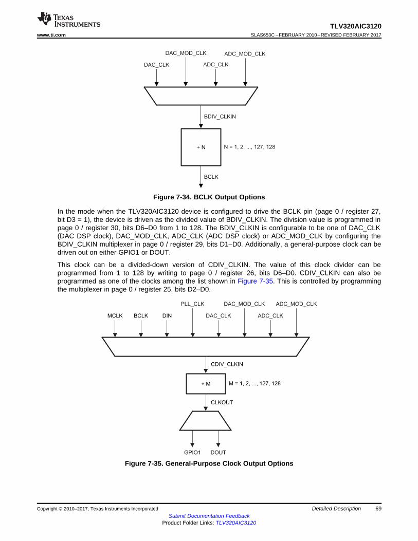
÷ M
CLKOUT
CDIV_CLKIN
MCLK BCLK DIN
PLL_CLK
DAC_CLK ADC_CLK
DAC_MOD_CLK ADC_MOD_CLK
M = 1, 2, ..., 127, 128
GPIO1 DOUT
÷ N
BCLK
DAC_CLK
ADC_MOD_CLKDAC_MOD_CLK
ADC_CLK
BDIV_CLKIN
N = 1, 2, ..., 127, 128
69
TLV320AIC3120www.ti.com SLAS653C –FEBRUARY 2010–REVISED FEBRUARY 2017
Submit Documentation FeedbackProduct Folder Links: TLV320AIC3120
Detailed DescriptionCopyright © 2010–2017, Texas Instruments Incorporated
Figure 7-34. BCLK Output Options
In the mode when the TLV320AIC3120 device is configured to drive the BCLK pin (page 0 / register 27,bit D3 = 1), the device is driven as the divided value of BDIV_CLKIN. The division value is programmed inpage 0 / register 30, bits D6–D0 from 1 to 128. The BDIV_CLKIN is configurable to be one of DAC_CLK(DAC DSP clock), DAC_MOD_CLK, ADC_CLK (ADC DSP clock) or ADC_MOD_CLK by configuring theBDIV_CLKIN multiplexer in page 0 / register 29, bits D1–D0. Additionally, a general-purpose clock can bedriven out on either GPIO1 or DOUT.
This clock can be a divided-down version of CDIV_CLKIN. The value of this clock divider can beprogrammed from 1 to 128 by writing to page 0 / register 26, bits D6–D0. CDIV_CLKIN can also beprogrammed as one of the clocks among the list shown in Figure 7-35. This is controlled by programmingthe multiplexer in page 0 / register 25, bits D2–D0.
Figure 7-35. General-Purpose Clock Output Options
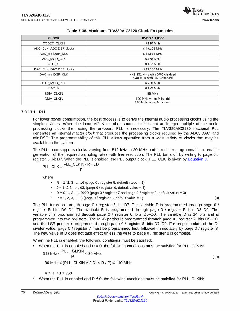
PLL _ CLKIN512 kHz 20 MHz
P£ £
PLL_CLKIN R J.DPLL_CLK
P
´ ´
=
70
TLV320AIC3120SLAS653C –FEBRUARY 2010–REVISED FEBRUARY 2017 www.ti.com
Submit Documentation FeedbackProduct Folder Links: TLV320AIC3120
Detailed Description Copyright © 2010–2017, Texas Instruments Incorporated
Table 7-36. Maximum TLV320AIC3120 Clock Frequencies
CLOCK DVDD ≥ 1.65 VCODEC_CLKIN ≤ 110 MHz
ADC_CLK (ADC DSP clock) ≤ 49.152 MHzADC_miniDSP_CLK ≤ 24.576 MHz
ADC_MOD_CLK 6.758 MHzADC_fS 0.192 MHz
DAC_CLK (DAC DSP clock) ≤ 49.152 MHzDAC_miniDSP_CLK ≤ 49.152 MHz with DRC disabled
≤ 48 MHz with DRC enabledDAC_MOD_CLK 6.758 MHz
DAC_fS 0.192 MHzBDIV_CLKIN 55 MHzCDIV_CLKIN 100 MHz when M is odd
110 MHz when M is even
7.3.13.1 PLL
For lower power consumption, the best process is to derive the internal audio processing clocks using thesimple dividers. When the input MCLK or other source clock is not an integer multiple of the audioprocessing clocks then using the on-board PLL is necessary. The TLV320AIC3120 fractional PLLgenerates an internal master clock that produces the processing clocks required by the ADC, DAC, andminiDSP. The programmability of this PLL allows operation from a wide variety of clocks that may beavailable in the system.
The PLL input supports clocks varying from 512 kHz to 20 MHz and is register-programmable to enablegeneration of the required sampling rates with fine resolution. The PLL turns on by writing to page 0 /register 5, bit D7. When the PLL is enabled, the PLL output clock, PLL_CLK, is given by Equation 9.
where• R = 1, 2, 3, ..., 16 (page 0 / register 5, default value = 1)• J = 1, 2,3, … , 63, (page 0 / register 6, default value = 4)• D = 0, 1, 2, …, 9999 (page 0 / register 7 and page 0 / register 8, default value = 0)• P = 1, 2, 3, …, 8 (page 0 / register 5, default value = 1) (9)
The PLL turns on through page 0 / register 5, bit D7. The variable P is programmed through page 0 /register 5, bits D6–D4. The variable R is programmed through page 0 / register 5, bits D3–D0. Thevariable J is programmed through page 0 / register 6, bits D5–D0. The variable D is 14 bits and isprogrammed into two registers. The MSB portion is programmed through page 0 / register 7, bits D5–D0,and the LSB portion is programmed thrugh page 0 / register 8, bits D7–D0. For proper update of the D-divider value, page 0 / register 7 must be programmed first, followed immediately by page 0 / register 8.The new value of D does not take effect unless the write to page 0 / register 8 is complete.
When the PLL is enabled, the following conditions must be satisfied:• When the PLL is enabled and D = 0, the following conditions must be satisfied for PLL_CLKIN:
(10)
80 MHz ≤ (PLL_CLKIN × J.D. × R / P) ≤ 110 MHz
4 ≤ R × J ≤ 259• When the PLL is enabled and D ≠ 0, the following conditions must be satisfied for PLL_CLKIN:
PLL _ CLKIN10 MHz 20 MHz
P£ £
71
TLV320AIC3120www.ti.com SLAS653C –FEBRUARY 2010–REVISED FEBRUARY 2017
Submit Documentation FeedbackProduct Folder Links: TLV320AIC3120
Detailed DescriptionCopyright © 2010–2017, Texas Instruments Incorporated
(11)
80 MHz ≤ PLL_CLKIN × J.D. × R / P ≤ 110 MHz
R = 1
The PLL can power up independently from the ADC and DAC blocks, and can also be used as a general-purpose PLL by routing the PLL output to the GPIO output. After powering up the PLL, PLL_CLK isavailable typically after 10 ms.
The clocks for the codec and various signal processing blocks, CODEC_CLKIN, are generated from theMCLK input, BCLK input, GPIO input, or PLL_CLK (page 0 / register 4, bits D1–D0).
If CODEC_CLKIN is derived from the PLL, then the PLL must be powered up first and powered down last.
Table 7-37 lists several example cases of typical PLL_CLKIN rates and how to program the PLL toachieve a sample rate fS of either 44.1 kHz or 48 kHz.
Table 7-37. PLL Example Configurations
PLL_CLKIN(MHz) PLLP PLLR PLLJ PLLD MADC NADC AOSR MDAC NDAC DOSR
fS = 44.1 kHz2.8224 1 3 10 0 3 5 128 3 5 1285.6448 1 3 5 0 3 5 128 3 5 128
12 1 1 7 560 3 5 128 3 5 12813 1 1 6 3504 2 9 104 6 3 10416 1 1 5 2920 3 5 128 3 5 12819.2 1 1 4 4100 3 5 128 3 5 12848 4 1 7 560 3 5 128 3 5 128
fS = 48 kHz2.048 1 3 14 0 2 7 128 7 2 1283.072 1 4 7 0 2 7 128 7 2 1284.096 1 3 7 0 2 7 128 7 2 1286.144 1 2 7 0 2 7 128 7 2 1288.192 1 4 3 0 2 8 128 4 4 128
12 1 1 7 1680 2 7 128 7 2 12816 1 1 5 3760 2 7 128 7 2 12819.2 1 1 4 4800 2 7 128 7 2 12848 4 1 7 1680 2 7 128 7 2 128
7.3.14 TimerThe internal clock runs nominally at 8.2 MHz. This is used for various internal timing intervals, de-bouncelogic, and interrupts. The MCLK divider must be set in such a way that the divider output is approximately1 MHz for the timers to be closer to the programmed value.
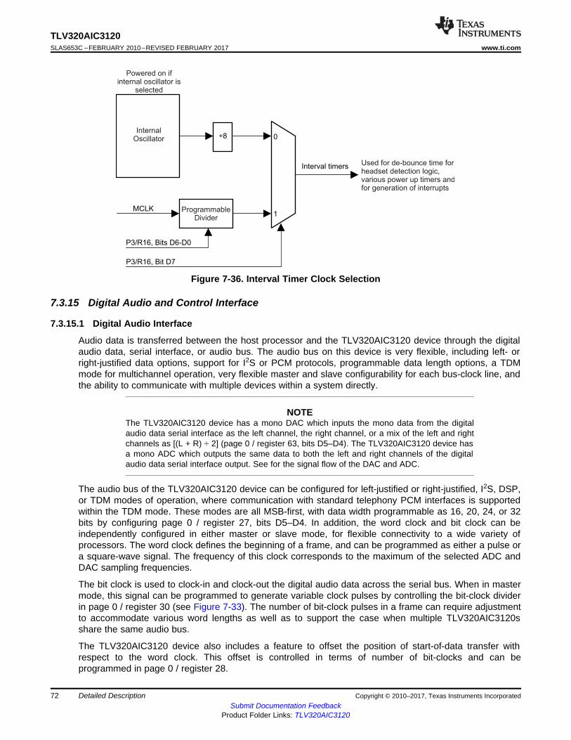
InternalOscillator ÷8 0
1
P3/R16, Bits D6-D0
MCLK
P3/R16, Bit D7
Interval timers
ProgrammableDivider
Powered on ifinternal oscillator is
selected
Used for de-bounce time forheadset detection logic,various power up timers andfor generation of interrupts
72
TLV320AIC3120SLAS653C –FEBRUARY 2010–REVISED FEBRUARY 2017 www.ti.com
Submit Documentation FeedbackProduct Folder Links: TLV320AIC3120
Detailed Description Copyright © 2010–2017, Texas Instruments Incorporated
Figure 7-36. Interval Timer Clock Selection
7.3.15 Digital Audio and Control Interface
7.3.15.1 Digital Audio Interface
Audio data is transferred between the host processor and the TLV320AIC3120 device through the digitalaudio data, serial interface, or audio bus. The audio bus on this device is very flexible, including left- orright-justified data options, support for I2S or PCM protocols, programmable data length options, a TDMmode for multichannel operation, very flexible master and slave configurability for each bus-clock line, andthe ability to communicate with multiple devices within a system directly.
NOTEThe TLV320AIC3120 device has a mono DAC which inputs the mono data from the digitalaudio data serial interface as the left channel, the right channel, or a mix of the left and rightchannels as [(L + R) ÷ 2] (page 0 / register 63, bits D5–D4). The TLV320AIC3120 device hasa mono ADC which outputs the same data to both the left and right channels of the digitalaudio data serial interface output. See for the signal flow of the DAC and ADC.
The audio bus of the TLV320AIC3120 device can be configured for left-justified or right-justified, I2S, DSP,or TDM modes of operation, where communication with standard telephony PCM interfaces is supportedwithin the TDM mode. These modes are all MSB-first, with data width programmable as 16, 20, 24, or 32bits by configuring page 0 / register 27, bits D5–D4. In addition, the word clock and bit clock can beindependently configured in either master or slave mode, for flexible connectivity to a wide variety ofprocessors. The word clock defines the beginning of a frame, and can be programmed as either a pulse ora square-wave signal. The frequency of this clock corresponds to the maximum of the selected ADC andDAC sampling frequencies.
The bit clock is used to clock-in and clock-out the digital audio data across the serial bus. When in mastermode, this signal can be programmed to generate variable clock pulses by controlling the bit-clock dividerin page 0 / register 30 (see Figure 7-33). The number of bit-clock pulses in a frame can require adjustmentto accommodate various word lengths as well as to support the case when multiple TLV320AIC3120sshare the same audio bus.
The TLV320AIC3120 device also includes a feature to offset the position of start-of-data transfer withrespect to the word clock. This offset is controlled in terms of number of bit-clocks and can beprogrammed in page 0 / register 28.
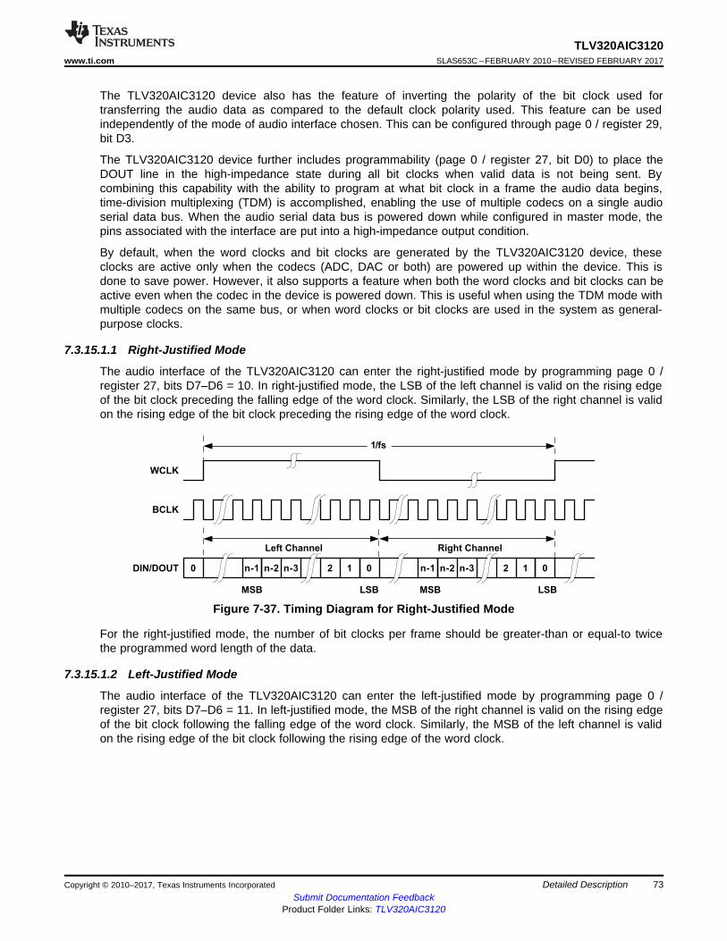
BCLK
WCLK
DIN/DOUT n-1 n-2 1 00 n-1 n-2 1 0
LSBMSB
Left Channel Right Channel
n-3 2 2n-3
LSBMSB
1/fs
73
TLV320AIC3120www.ti.com SLAS653C –FEBRUARY 2010–REVISED FEBRUARY 2017
Submit Documentation FeedbackProduct Folder Links: TLV320AIC3120
Detailed DescriptionCopyright © 2010–2017, Texas Instruments Incorporated
The TLV320AIC3120 device also has the feature of inverting the polarity of the bit clock used fortransferring the audio data as compared to the default clock polarity used. This feature can be usedindependently of the mode of audio interface chosen. This can be configured through page 0 / register 29,bit D3.
The TLV320AIC3120 device further includes programmability (page 0 / register 27, bit D0) to place theDOUT line in the high-impedance state during all bit clocks when valid data is not being sent. Bycombining this capability with the ability to program at what bit clock in a frame the audio data begins,time-division multiplexing (TDM) is accomplished, enabling the use of multiple codecs on a single audioserial data bus. When the audio serial data bus is powered down while configured in master mode, thepins associated with the interface are put into a high-impedance output condition.
By default, when the word clocks and bit clocks are generated by the TLV320AIC3120 device, theseclocks are active only when the codecs (ADC, DAC or both) are powered up within the device. This isdone to save power. However, it also supports a feature when both the word clocks and bit clocks can beactive even when the codec in the device is powered down. This is useful when using the TDM mode withmultiple codecs on the same bus, or when word clocks or bit clocks are used in the system as general-purpose clocks.
7.3.15.1.1 Right-Justified Mode
The audio interface of the TLV320AIC3120 can enter the right-justified mode by programming page 0 /register 27, bits D7–D6 = 10. In right-justified mode, the LSB of the left channel is valid on the rising edgeof the bit clock preceding the falling edge of the word clock. Similarly, the LSB of the right channel is validon the rising edge of the bit clock preceding the rising edge of the word clock.
Figure 7-37. Timing Diagram for Right-Justified Mode
For the right-justified mode, the number of bit clocks per frame should be greater-than or equal-to twicethe programmed word length of the data.
7.3.15.1.2 Left-Justified Mode
The audio interface of the TLV320AIC3120 can enter the left-justified mode by programming page 0 /register 27, bits D7–D6 = 11. In left-justified mode, the MSB of the right channel is valid on the rising edgeof the bit clock following the falling edge of the word clock. Similarly, the MSB of the left channel is validon the rising edge of the bit clock following the rising edge of the word clock.
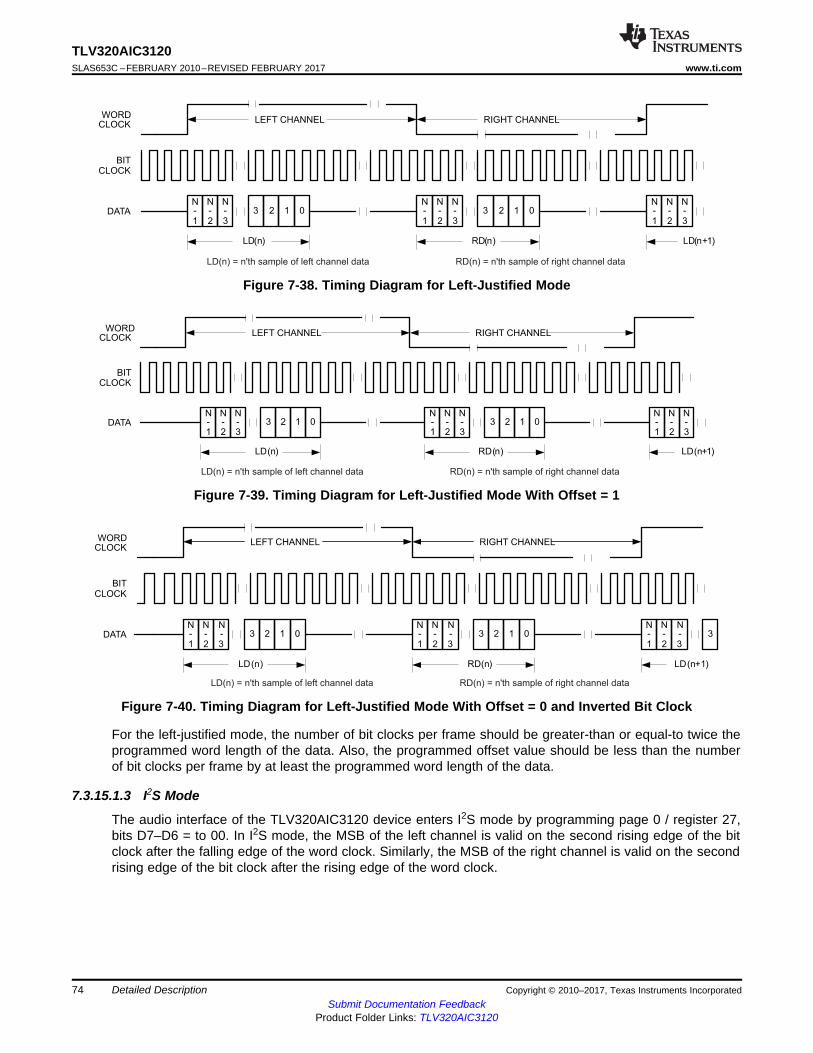
LD(n) LD(n+1)
WORDCLOCK
BITCLOCK
DATA 3N-1
N-2
N-3
2 1 03N-1
N-2
N-3
2 1 03N-1
N-2
N-3
RD(n)
LEFT CHANNEL RIGHT CHANNEL
LD(n) = n'th sample of left channel data RD(n) = n'th sample of right channel data
LD(n) LD(n+1)
WORDCLOCK
BITCLOCK
DATA -1
-2
-3
2 1 03 -1
-2
-3
2 1 03 -1
-2
N N N N N N N N N-3
RD(n)
LEFT CHANNEL RIGHT CHANNEL
LD(n) = n'th sample of left channel data RD(n) = n'th sample of right channel data
LD(n) LD(n+1)
WORDCLOCK
BITCLOCK
DATA -1
-2
-3
2 1 03 -1
-2
-3
2 1 03 -1
-2
N N N N N N N N N-3
RD(n)
LEFT CHANNEL RIGHT CHANNEL
LD(n) = n'th sample of left channel data RD(n) = n'th sample of right channel data
74
TLV320AIC3120SLAS653C –FEBRUARY 2010–REVISED FEBRUARY 2017 www.ti.com
Submit Documentation FeedbackProduct Folder Links: TLV320AIC3120
Detailed Description Copyright © 2010–2017, Texas Instruments Incorporated
Figure 7-38. Timing Diagram for Left-Justified Mode
Figure 7-39. Timing Diagram for Left-Justified Mode With Offset = 1
Figure 7-40. Timing Diagram for Left-Justified Mode With Offset = 0 and Inverted Bit Clock
For the left-justified mode, the number of bit clocks per frame should be greater-than or equal-to twice theprogrammed word length of the data. Also, the programmed offset value should be less than the numberof bit clocks per frame by at least the programmed word length of the data.
7.3.15.1.3 I2S Mode
The audio interface of the TLV320AIC3120 device enters I2S mode by programming page 0 / register 27,bits D7–D6 = to 00. In I2S mode, the MSB of the left channel is valid on the second rising edge of the bitclock after the falling edge of the word clock. Similarly, the MSB of the right channel is valid on the secondrising edge of the bit clock after the rising edge of the word clock.
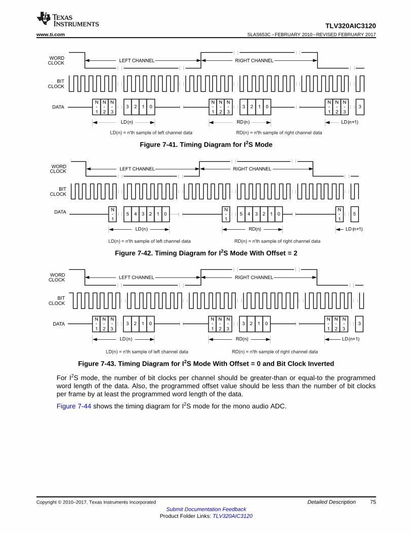
LD(n) LD(n+1)
WORDCLOCK
BITCLOCK
DATA -1
-2
-3
2 1 03 -1
-2
-3
2 1 03 -1
-2
N N N N N N N N N-3
3
RD(n)
LEFT CHANNEL RIGHT CHANNEL
LD(n) = n'th sample of left channel data RD(n) = n'th sample of right channel data
LD(n) LD (n+1)
WORDCLOCK
BITCLOCK
DATA -1
4 3 25 1 0 -1
4 3 25 1 0N N N
-1
5
RD(n)
LEFT CHANNEL RIGHT CHANNEL
LD(n) = n'th sample of left channel data RD(n) = n'th sample of right channel data
LD(n) LD(n+1)
WORDCLOCK
BITCLOCK
DATA -1
-2
-3
2 1 03 -1
-2
-3
2 1 03 -1
-2
N N N N N N N N N-3
3
RD(n)
LEFT CHANNEL RIGHT CHANNEL
LD(n) = n'th sample of left channel data RD(n) = n'th sample of right channel data
75
TLV320AIC3120www.ti.com SLAS653C –FEBRUARY 2010–REVISED FEBRUARY 2017
Submit Documentation FeedbackProduct Folder Links: TLV320AIC3120
Detailed DescriptionCopyright © 2010–2017, Texas Instruments Incorporated
Figure 7-41. Timing Diagram for I2S Mode
Figure 7-42. Timing Diagram for I2S Mode With Offset = 2
Figure 7-43. Timing Diagram for I2S Mode With Offset = 0 and Bit Clock Inverted
For I2S mode, the number of bit clocks per channel should be greater-than or equal-to the programmedword length of the data. Also, the programmed offset value should be less than the number of bit clocksper frame by at least the programmed word length of the data.
Figure 7-44 shows the timing diagram for I2S mode for the mono audio ADC.
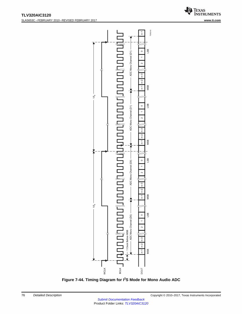
BC
LK
WC
LK
T0202-0
3
DO
UT
11
00
1/f
S
LS
BLS
BLS
BM
SB
MS
BM
SB
22
n–
1n
–1
n–
2n
–2
n–
3n
–3
AD
C M
ono C
hannel (D
0)
AD
C M
ono C
hannel (D
0)
1 C
lock B
efo
re M
SB
11
00
1/f
S
LS
BM
SB
22
n–
1n
–1
n–
1n
–2
n–
2n
–3
n–
3
AD
C M
ono C
hannel (D
1)
AD
C M
ono C
hannel (D
1)
76
TLV320AIC3120SLAS653C –FEBRUARY 2010–REVISED FEBRUARY 2017 www.ti.com
Submit Documentation FeedbackProduct Folder Links: TLV320AIC3120
Detailed Description Copyright © 2010–2017, Texas Instruments Incorporated
Figure 7-44. Timing Diagram for I2S Mode for Mono Audio ADC
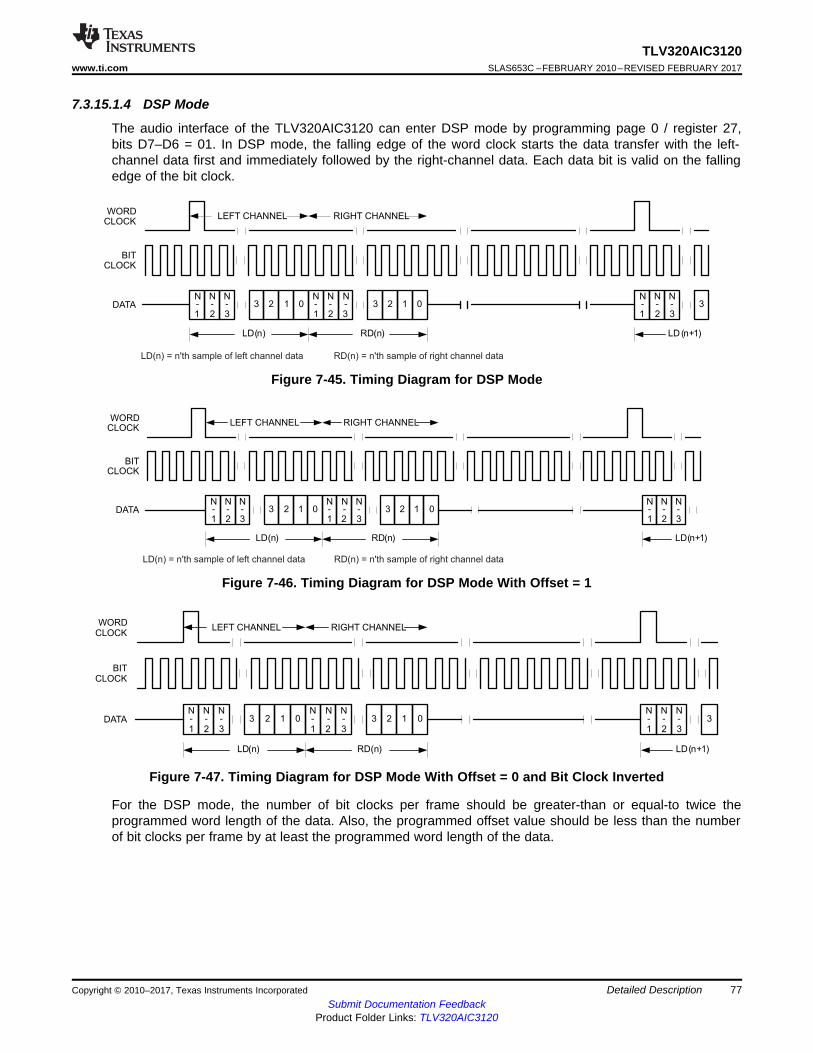
LD(n) LD(n+1)
BITCLOCK
DATAN-1
N-2
N-3
2 1 03N-1
N-2
N-3
03 2 1N-1
N-2
N-3
3
RD(n)
WORDCLOCK
LEFT CHANNEL RIGHT CHANNEL
LD(n) LD(n+1)
BITCLOCK
DATA -1
-2
-3
2 1 03 -1
-2
-3
03 2 1 -1
-2
N N N N N N N N N-3
RD(n)
WORDCLOCK
LEFT CHANNEL RIGHT CHANNEL
LD(n) = n'th sample of left channel data RD(n) = n'th sample of right channel data
LD(n) LD(n+1)
BITCLOCK
DATA -1
-2
-3
2 1 03 -1
-2
-3
03 2 1 -1
-2
N N N N N N N N N-3
3
RD(n)
WORDCLOCK
LEFT CHANNEL RIGHT CHANNEL
LD(n) = n'th sample of left channel data RD(n) = n'th sample of right channel data
77
TLV320AIC3120www.ti.com SLAS653C –FEBRUARY 2010–REVISED FEBRUARY 2017
Submit Documentation FeedbackProduct Folder Links: TLV320AIC3120
Detailed DescriptionCopyright © 2010–2017, Texas Instruments Incorporated
7.3.15.1.4 DSP Mode
The audio interface of the TLV320AIC3120 can enter DSP mode by programming page 0 / register 27,bits D7–D6 = 01. In DSP mode, the falling edge of the word clock starts the data transfer with the left-channel data first and immediately followed by the right-channel data. Each data bit is valid on the fallingedge of the bit clock.
Figure 7-45. Timing Diagram for DSP Mode
Figure 7-46. Timing Diagram for DSP Mode With Offset = 1
Figure 7-47. Timing Diagram for DSP Mode With Offset = 0 and Bit Clock Inverted
For the DSP mode, the number of bit clocks per frame should be greater-than or equal-to twice theprogrammed word length of the data. Also, the programmed offset value should be less than the numberof bit clocks per frame by at least the programmed word length of the data.
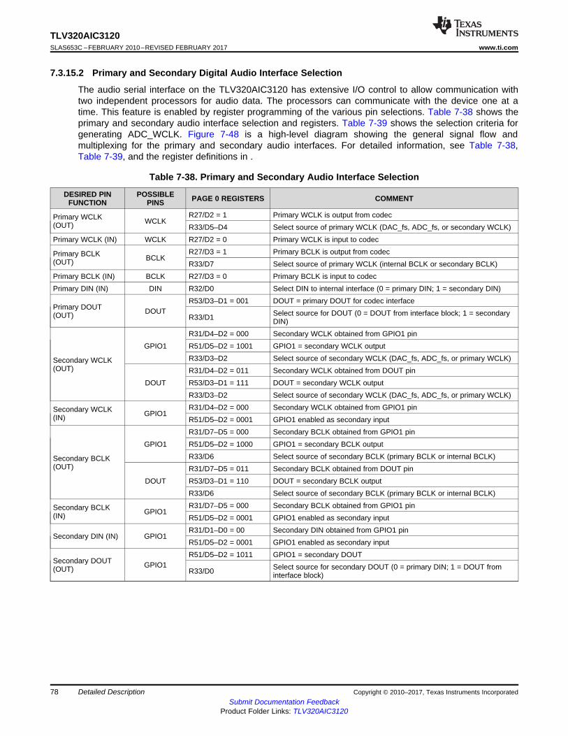
78
TLV320AIC3120SLAS653C –FEBRUARY 2010–REVISED FEBRUARY 2017 www.ti.com
Submit Documentation FeedbackProduct Folder Links: TLV320AIC3120
Detailed Description Copyright © 2010–2017, Texas Instruments Incorporated
7.3.15.2 Primary and Secondary Digital Audio Interface Selection
The audio serial interface on the TLV320AIC3120 has extensive I/O control to allow communication withtwo independent processors for audio data. The processors can communicate with the device one at atime. This feature is enabled by register programming of the various pin selections. Table 7-38 shows theprimary and secondary audio interface selection and registers. Table 7-39 shows the selection criteria forgenerating ADC_WCLK. Figure 7-48 is a high-level diagram showing the general signal flow andmultiplexing for the primary and secondary audio interfaces. For detailed information, see Table 7-38,Table 7-39, and the register definitions in .
Table 7-38. Primary and Secondary Audio Interface Selection
DESIRED PINFUNCTION
POSSIBLEPINS PAGE 0 REGISTERS COMMENT
Primary WCLK(OUT) WCLK
R27/D2 = 1 Primary WCLK is output from codecR33/D5–D4 Select source of primary WCLK (DAC_fs, ADC_fs, or secondary WCLK)
Primary WCLK (IN) WCLK R27/D2 = 0 Primary WCLK is input to codec
Primary BCLK(OUT) BCLK
R27/D3 = 1 Primary BCLK is output from codecR33/D7 Select source of primary WCLK (internal BCLK or secondary BCLK)
Primary BCLK (IN) BCLK R27/D3 = 0 Primary BCLK is input to codecPrimary DIN (IN) DIN R32/D0 Select DIN to internal interface (0 = primary DIN; 1 = secondary DIN)
Primary DOUT(OUT) DOUT
R53/D3–D1 = 001 DOUT = primary DOUT for codec interface
R33/D1 Select source for DOUT (0 = DOUT from interface block; 1 = secondaryDIN)
Secondary WCLK(OUT)
GPIO1R31/D4–D2 = 000 Secondary WCLK obtained from GPIO1 pinR51/D5–D2 = 1001 GPIO1 = secondary WCLK outputR33/D3–D2 Select source of secondary WCLK (DAC_fs, ADC_fs, or primary WCLK)
DOUTR31/D4–D2 = 011 Secondary WCLK obtained from DOUT pinR53/D3–D1 = 111 DOUT = secondary WCLK outputR33/D3–D2 Select source of secondary WCLK (DAC_fs, ADC_fs, or primary WCLK)
Secondary WCLK(IN) GPIO1
R31/D4–D2 = 000 Secondary WCLK obtained from GPIO1 pinR51/D5–D2 = 0001 GPIO1 enabled as secondary input
Secondary BCLK(OUT)
GPIO1R31/D7–D5 = 000 Secondary BCLK obtained from GPIO1 pinR51/D5–D2 = 1000 GPIO1 = secondary BCLK outputR33/D6 Select source of secondary BCLK (primary BCLK or internal BCLK)
DOUTR31/D7–D5 = 011 Secondary BCLK obtained from DOUT pinR53/D3–D1 = 110 DOUT = secondary BCLK outputR33/D6 Select source of secondary BCLK (primary BCLK or internal BCLK)
Secondary BCLK(IN) GPIO1
R31/D7–D5 = 000 Secondary BCLK obtained from GPIO1 pinR51/D5–D2 = 0001 GPIO1 enabled as secondary input
Secondary DIN (IN) GPIO1R31/D1–D0 = 00 Secondary DIN obtained from GPIO1 pinR51/D5–D2 = 0001 GPIO1 enabled as secondary input
Secondary DOUT(OUT) GPIO1
R51/D5–D2 = 1011 GPIO1 = secondary DOUT
R33/D0 Select source for secondary DOUT (0 = primary DIN; 1 = DOUT frominterface block)
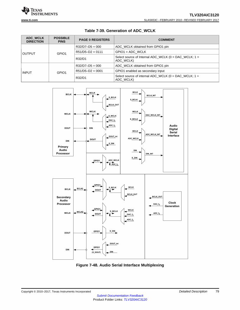
BCLK
WCLK
DOUT
DOUT_int
S_DIN
BCLK
DIN
WCLK
DIN
DOUT
Primary
Audio
Processor
S_WCLK
DAC_fS
ADC_fS
S_BCLK
BCLK_OUT
BCLK
S_BCLK
WCLK
S_WCLK
DIN
S_DIN
WCLK
ADC_WCLK
Audio
Digital
Serial
Interface
BCLK_INT
DAC_WCLK_INT
ADC_WCLK_INT
DIN_INT
GPIO1
GPIO1
DOUT
DOUT
S_BCLK BCLK
BCLK_OUT
S_WCLKWCLK
DAC_fS
ADC_fS
GPIO1 S_DIN
DOUT_int
DIN(S_DOUT)
Clock
Generation
BCLK_OUT
DAC_fS
ADC_fSWCLK
DIN
DOUT
Secondary
Audio
Processor
BCLK
GPIO1
ADC_fS
ADC_WCLK
BCLK2
WCLK2
GPIO1
79
TLV320AIC3120www.ti.com SLAS653C –FEBRUARY 2010–REVISED FEBRUARY 2017
Submit Documentation FeedbackProduct Folder Links: TLV320AIC3120
Detailed DescriptionCopyright © 2010–2017, Texas Instruments Incorporated
Table 7-39. Generation of ADC_WCLK
ADC_WCLKDIRECTION
POSSIBLEPINS PAGE 0 REGISTERS COMMENT
OUTPUT GPIO1
R32/D7–D5 = 000 ADC_WCLK obtained from GPIO1 pinR51/D5–D2 = 0111 GPIO1 = ADC_WCLK
R32/D1 Select source of Internal ADC_WCLK (0 = DAC_WCLK; 1 =ADC_WCLK)
INPUT GPIO1
R32/D7–D5 = 000 ADC_WCLK obtained from GPIO1 pinR51/D5–D2 = 0001 GPIO1 enabled as secondary input
R32/D1 Select source of internal ADC_WCLK (0 = DAC_WCLK; 1 =ADC_WCLK)
Figure 7-48. Audio Serial Interface Multiplexing
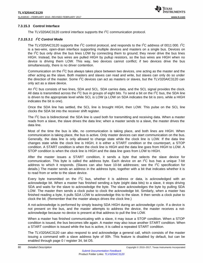
80
TLV320AIC3120SLAS653C –FEBRUARY 2010–REVISED FEBRUARY 2017 www.ti.com
Submit Documentation FeedbackProduct Folder Links: TLV320AIC3120
Detailed Description Copyright © 2010–2017, Texas Instruments Incorporated
7.3.15.3 Control Interface
The TLV320AIC3120 control interface supports the I2C communication protocol.
7.3.15.3.1 I2C Control Mode
The TLV320AIC3120 supports the I2C control protocol, and responds to the I2C address of 0011 000. I2Cis a two-wire, open-drain interface supporting multiple devices and masters on a single bus. Devices onthe I2C bus only drive the bus lines LOW by connecting them to ground; they never drive the bus linesHIGH. Instead, the bus wires are pulled HIGH by pullup resistors, so the bus wires are HIGH when nodevice is driving them LOW. This way, two devices cannot conflict; if two devices drive the bussimultaneously, there is no driver contention.
Communication on the I2C bus always takes place between two devices, one acting as the master and theother acting as the slave. Both masters and slaves can read and write, but slaves can only do so underthe direction of the master. Some I2C devices can act as masters or slaves, but the TLV320AIC3120 canonly act as a slave device.
An I2C bus consists of two lines, SDA and SCL. SDA carries data, and the SCL signal provides the clock.All data is transmitted across the I2C bus in groups of eight bits. To send a bit on the I2C bus, the SDA lineis driven to the appropriate level while SCL is LOW (a LOW on SDA indicates the bit is zero, while a HIGHindicates the bit is one).
Once the SDA line has settled, the SCL line is brought HIGH, then LOW. This pulse on the SCL lineclocks the SDA bit into the receiver shift register.
The I2C bus is bidirectional: the SDA line is used both for transmitting and receiving data. When a masterreads from a slave, the slave drives the data line; when a master sends to a slave, the master drives thedata line.
Most of the time the bus is idle, no communication is taking place, and both lines are HIGH. Whencommunication is taking place, the bus is active. Only master devices can start communication on the bus.Generally, the data line is only allowed to change state while the clock line is LOW. If the data linechanges state while the clock line is HIGH, it is either a START condition or the counterpart, a STOPcondition. A START condition is when the clock line is HIGH and the data line goes from HIGH to LOW. ASTOP condition is when the clock line is HIGH and the data line goes from LOW to HIGH.
After the master issues a START condition, it sends a byte that selects the slave device forcommunication. This byte is called the address byte. Each device on an I2C bus has a unique 7-bitaddress to which it responds. (Slaves can also have 10-bit addresses; see the I2C specification fordetails.) The master sends an address in the address byte, together with a bit that indicates whether it isto read from or write to the slave device.
Every byte transmitted on the I2C bus, whether it is address or data, is acknowledged with anacknowledge bit. When a master has finished sending a byte (eight data bits) to a slave, it stops drivingSDA and waits for the slave to acknowledge the byte. The slave acknowledges the byte by pulling SDALOW. The master then sends a clock pulse to clock the acknowledge bit. Similarly, when a master hasfinished reading a byte, it pulls SDA LOW to acknowledge this to the slave. It then sends a clock pulse toclock the bit. (Remember that the master always drives the clock line.)
A not-acknowledge is performed by simply leaving SDA HIGH during an acknowledge cycle. If a device isnot present on the bus, and the master attempts to address the device, the master receives a not-acknowledge because no device is present at that address to pull the line LOW.
When a master has finished communicating with a slave, it may issue a STOP condition. When a STOPcondition is issued, the bus becomes idle again. A master may also issue another START condition. Whena START condition is issued while the bus is active, it is called a repeated START condition.
The TLV320AIC3120 can also respond to and acknowledge a general call, which consists of the masterissuing a command with a slave address byte of 00h. This feature is disabled by default, but can beenabled through page 0 / register 34, bit D5.
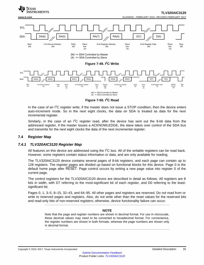
Start
(M)7-bit Device Address
(M)
Write
(M)
Slave
Ack
(S)
8-bit Register Address
(M)
Slave
Ack
(S)
SDA
SCL
7-bit Device Address
(M)
Read
(M)
Slave
Ack
(S)
DA(6) DA(0) RA(7) RA(0) DA(6) DA(0) D(7) D(0)
8-bit Register Data
(S)
Stop
(M)
Master
No Ack
(M)
Repeat
Start
(M)
(M) => SDA Controlled by Master
(S) => SDA Controlled by Slave
DA(6) DA(0) RA(7) RA(0) D(7) D(0)
Start
(M)
7-bit Device Address
(M)
Write
(M)
Slave
Ack
(S)
8-bit Register Address
(M)
Slave
Ack
(S)
8-bit Register Data
(M)
Stop
(M)
Slave
Ack
(S)
SDA
SCL
(M) => SDA Controlled by Master
(S) => SDA Controlled by Slave
81
TLV320AIC3120www.ti.com SLAS653C –FEBRUARY 2010–REVISED FEBRUARY 2017
Submit Documentation FeedbackProduct Folder Links: TLV320AIC3120
Detailed DescriptionCopyright © 2010–2017, Texas Instruments Incorporated
Figure 7-49. I2C Write
Figure 7-50. I2C Read
In the case of an I2C register write, if the master does not issue a STOP condition, then the device entersauto-increment mode. So in the next eight clocks, the data on SDA is treated as data for the nextincremental register.
Similarly, in the case of an I2C register read, after the device has sent out the 8-bit data from theaddressed register, if the master issues a ACKNOWLEDGE, the slave takes over control of the SDA busand transmits for the next eight clocks the data of the next incremental register.
7.4 Register Map
7.4.1 TLV320AIC3120 Register MapAll features on this device are addressed using the I2C bus. All of the writable registers can be read back.However, some registers contain status information or data, and are only available for reading.
The TLV320AIC3120 device contains several pages of 8-bit registers, and each page can contain up to128 registers. The register pages are divided up based on functional blocks for this device. Page 0 is thedefault home page after RESET. Page control occurs by writing a new page value into register 0 of thecurrent page.
The control registers for the TLV320AIC3120 device are described in detail as follows. All registers are 8bits in width, with D7 referring to the most-significant bit of each register, and D0 referring to the least-significant bit.
Pages 0, 1, 3–5, 8–15, 32–43, and 64–95. All other pages and registers are reserved. Do not read from orwrite to reserved pages and registers. Also, do not write other than the reset values for the reserved bitsand read-only bits of non-reserved registers; otherwise, device functionality failure can occur.
NOTENote that the page and register numbers are shown in decimal format. For use in microcode,these decimal values may need to be converted to hexadecimal format. For convenience,the register numbers are shown in both formats, whereas the page numbers are shown onlyin decimal format.
82
TLV320AIC3120SLAS653C –FEBRUARY 2010–REVISED FEBRUARY 2017 www.ti.com
Submit Documentation FeedbackProduct Folder Links: TLV320AIC3120
Detailed Description Copyright © 2010–2017, Texas Instruments Incorporated
Table 7-40. Summary of Register Map
PAGE NUMBER DESCRIPTION
0 Page 0 is the default page on power up. Configuration for serial interface, digital I/O, clocking, ADC, DAC, miniDSPsettings, and other circuitry.
1 Configuration for analog PGAs, ADC, DAC, output drivers, volume controls, and other circuitry.
3 Register 16 controls the MCLK divider that controls the interrupt pulse duration, debounce timing, and detection blockclock.
4–5 ADC AGC and filter coefficients8–11 DAC buffer A filter and DRC coefficients12–15 DAC buffer B filter and DRC coefficients32–43 ADC miniDSP instruction RAM locations64–95 DAC miniDSP instruction RAM locations
7.4.2 Registers
7.4.2.1 Control Registers, Page 0 (Default Page): Clock Multipliers, Dividers, Serial Interfaces, Flags,Interrupts, and GPIOs
Table 7-41. Page 0 / Register 0 (0x00): Page Control Register
BIT READ/WRITE
RESETVALUE DESCRIPTION
D7–D0 R/W 0000 0000 0000 0000: Page 0 selected0000 0001: Page 1 selected...1111 1110: Page 254 selected1111 1111: Page 255 selected
Table 7-42. Page 0 / Register 1 (0x01): Software Reset
BIT READ/WRITE
RESETVALUE DESCRIPTION
D7–D1 R/W 0000 000 Reserved. Write only zeros to these bits.D0 R/W 0 0: Don't care
1: Self-clearing software reset for control register
Table 7-43. Page 0 / Register 2 (0x02): Reserved
BIT READ/WRITE
RESETVALUE DESCRIPTION
D7–D0 R XXXX XXXX Reserved. Do not write to this register.
Table 7-44. Page 0 / Register 3 (0x03): OT FLAG
BIT READ/WRITE
RESETVALUE DESCRIPTION
D7-D2 R XXXX XX Reserved. Do not write to these bits.D1 R 1 0: Overtemperature protection flag (active-low). Valid only if speaker amplifier is powered up
1: Normal operationD0 R/W X Reserved. Do not write to these bits.
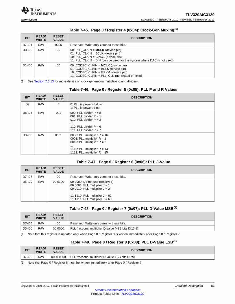
83
TLV320AIC3120www.ti.com SLAS653C –FEBRUARY 2010–REVISED FEBRUARY 2017
Submit Documentation FeedbackProduct Folder Links: TLV320AIC3120
Detailed DescriptionCopyright © 2010–2017, Texas Instruments Incorporated
(1) See Section 7.3.13 for more details on clock generation mutiplexing and dividers.
Table 7-45. Page 0 / Register 4 (0x04): Clock-Gen Muxing (1)
BIT READ/WRITE
RESETVALUE DESCRIPTION
D7–D4 R/W 0000 Reserved. Write only zeros to these bits.D3–D2 R/W 00 00: PLL_CLKIN = MCLK (device pin)
01: PLL_CLKIN = BCLK (device pin)10: PLL_CLKIN = GPIO1 (device pin)11: PLL_CLKIN = DIN (can be used for the system where DAC is not used)
D1–D0 R/W 00 00: CODEC_CLKIN = MCLK (device pin)01: CODEC_CLKIN = BCLK (device pin)10: CODEC_CLKIN = GPIO1 (device pin)11: CODEC_CLKIN = PLL_CLK (generated on-chip)
Table 7-46. Page 0 / Register 5 (0x05): PLL P and R Values
BIT READ/WRITE
RESETVALUE DESCRIPTION
D7 R/W 0 0: PLL is powered down.1: PLL is powered up.
D6–D4 R/W 001 000: PLL divider P = 8001: PLL divider P = 1010: PLL divider P = 2...110: PLL divider P = 6111: PLL divider P = 7
D3–D0 R/W 0001 0000: PLL multiplier R = 160001: PLL multiplier R = 10010: PLL multiplier R = 2...1110: PLL multiplier R = 141111: PLL multiplier R = 15
Table 7-47. Page 0 / Register 6 (0x06): PLL J-Value
BIT READ/WRITE
RESETVALUE DESCRIPTION
D7–D6 R/W 00 Reserved. Write only zeros to these bits.D5–D0 R/W 00 0100 00 0000: Do not use (reserved)
00 0001: PLL multiplier J = 100 0010: PLL multiplier J = 2...11 1110: PLL multiplier J = 6211 1111: PLL multiplier J = 63
(1) Note that this register is updated only when Page 0 / Register 8 is written immediately after Page 0 / Register 7.
Table 7-48. Page 0 / Register 7 (0x07): PLL D-Value MSB (1)
BIT READ/WRITE
RESETVALUE DESCRIPTION
D7–D6 R/W 00 Reserved. Write only zeros to these bits.D5–D0 R/W 00 0000 PLL fractional multiplier D-value MSB bits D[13:8]
(1) Note that Page 0 / Register 8 must be written immediately after Page 0 / Register 7.
Table 7-49. Page 0 / Register 8 (0x08): PLL D-Value LSB (1)
BIT READ/WRITE
RESETVALUE DESCRIPTION
D7–D0 R/W 0000 0000 PLL fractional multiplier D-value LSB bits D[7:0]
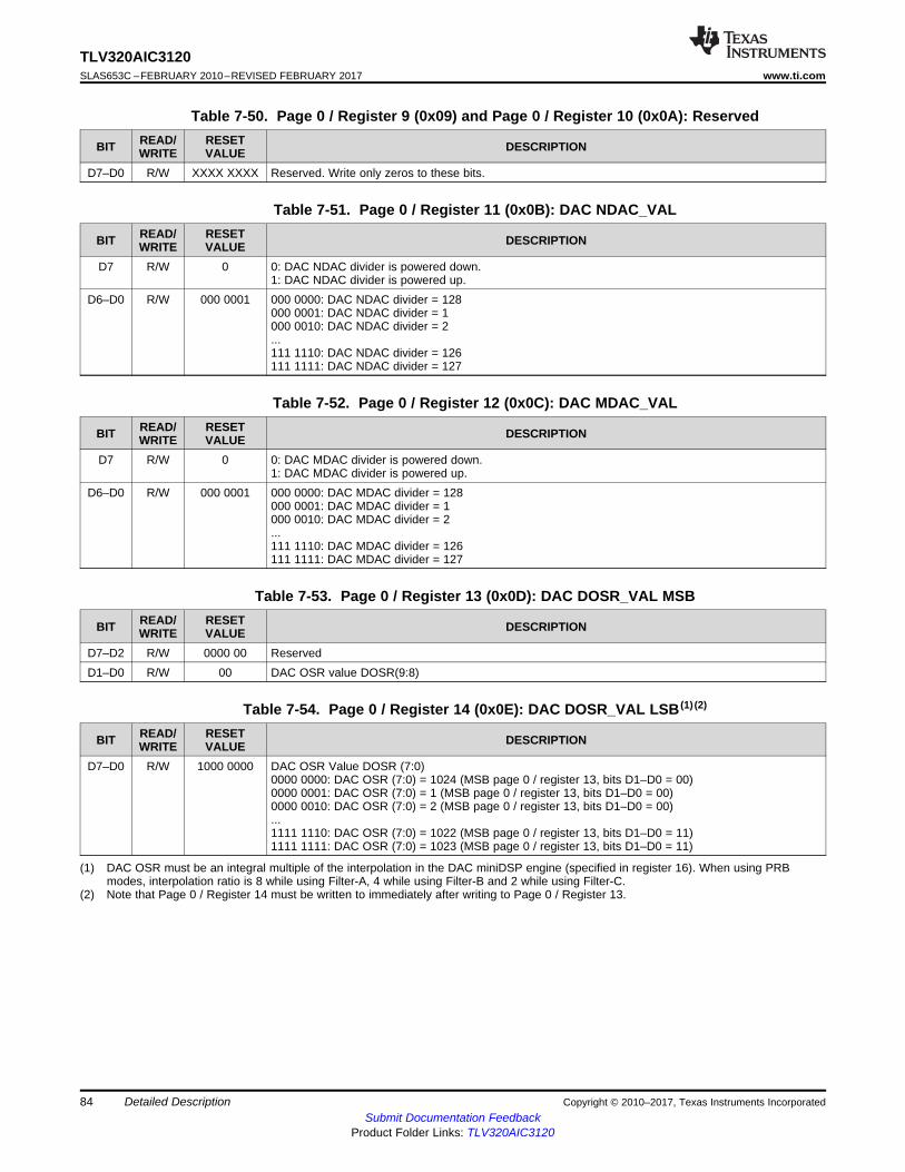
84
TLV320AIC3120SLAS653C –FEBRUARY 2010–REVISED FEBRUARY 2017 www.ti.com
Submit Documentation FeedbackProduct Folder Links: TLV320AIC3120
Detailed Description Copyright © 2010–2017, Texas Instruments Incorporated
Table 7-50. Page 0 / Register 9 (0x09) and Page 0 / Register 10 (0x0A): Reserved
BIT READ/WRITE
RESETVALUE DESCRIPTION
D7–D0 R/W XXXX XXXX Reserved. Write only zeros to these bits.
Table 7-51. Page 0 / Register 11 (0x0B): DAC NDAC_VAL
BIT READ/WRITE
RESETVALUE DESCRIPTION
D7 R/W 0 0: DAC NDAC divider is powered down.1: DAC NDAC divider is powered up.
D6–D0 R/W 000 0001 000 0000: DAC NDAC divider = 128000 0001: DAC NDAC divider = 1000 0010: DAC NDAC divider = 2...111 1110: DAC NDAC divider = 126111 1111: DAC NDAC divider = 127
Table 7-52. Page 0 / Register 12 (0x0C): DAC MDAC_VAL
BIT READ/WRITE
RESETVALUE DESCRIPTION
D7 R/W 0 0: DAC MDAC divider is powered down.1: DAC MDAC divider is powered up.
D6–D0 R/W 000 0001 000 0000: DAC MDAC divider = 128000 0001: DAC MDAC divider = 1000 0010: DAC MDAC divider = 2...111 1110: DAC MDAC divider = 126111 1111: DAC MDAC divider = 127
Table 7-53. Page 0 / Register 13 (0x0D): DAC DOSR_VAL MSB
BIT READ/WRITE
RESETVALUE DESCRIPTION
D7–D2 R/W 0000 00 ReservedD1–D0 R/W 00 DAC OSR value DOSR(9:8)
(1) DAC OSR must be an integral multiple of the interpolation in the DAC miniDSP engine (specified in register 16). When using PRBmodes, interpolation ratio is 8 while using Filter-A, 4 while using Filter-B and 2 while using Filter-C.
(2) Note that Page 0 / Register 14 must be written to immediately after writing to Page 0 / Register 13.
Table 7-54. Page 0 / Register 14 (0x0E): DAC DOSR_VAL LSB (1) (2)
BIT READ/WRITE
RESETVALUE DESCRIPTION
D7–D0 R/W 1000 0000 DAC OSR Value DOSR (7:0)0000 0000: DAC OSR (7:0) = 1024 (MSB page 0 / register 13, bits D1–D0 = 00)0000 0001: DAC OSR (7:0) = 1 (MSB page 0 / register 13, bits D1–D0 = 00)0000 0010: DAC OSR (7:0) = 2 (MSB page 0 / register 13, bits D1–D0 = 00)...1111 1110: DAC OSR (7:0) = 1022 (MSB page 0 / register 13, bits D1–D0 = 11)1111 1111: DAC OSR (7:0) = 1023 (MSB page 0 / register 13, bits D1–D0 = 11)
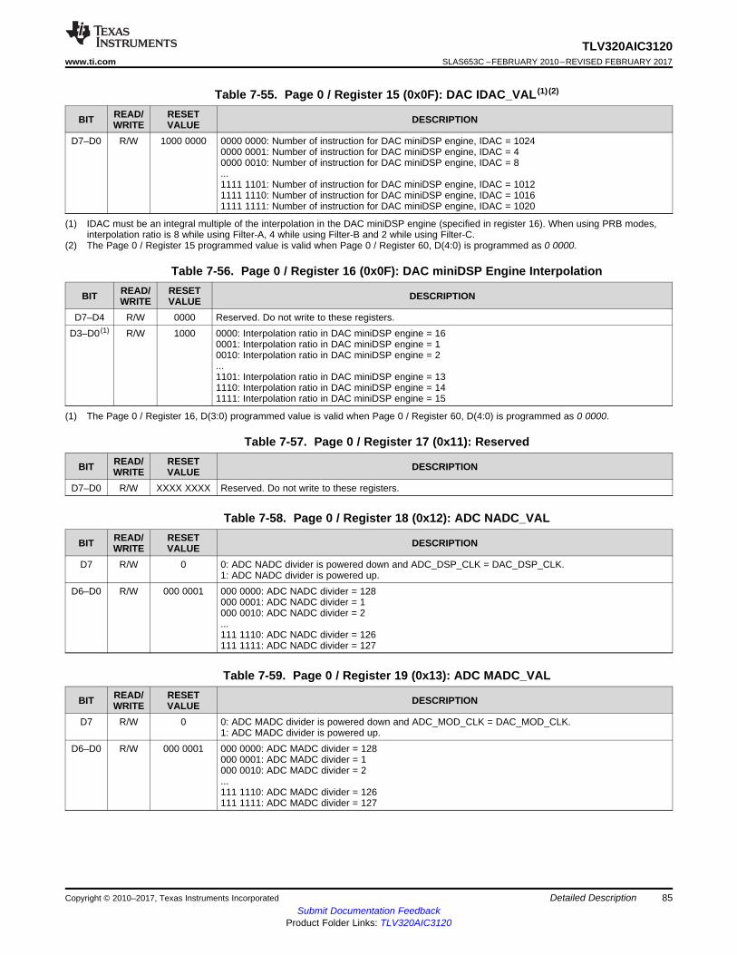
85
TLV320AIC3120www.ti.com SLAS653C –FEBRUARY 2010–REVISED FEBRUARY 2017
Submit Documentation FeedbackProduct Folder Links: TLV320AIC3120
Detailed DescriptionCopyright © 2010–2017, Texas Instruments Incorporated
(1) IDAC must be an integral multiple of the interpolation in the DAC miniDSP engine (specified in register 16). When using PRB modes,interpolation ratio is 8 while using Filter-A, 4 while using Filter-B and 2 while using Filter-C.
(2) The Page 0 / Register 15 programmed value is valid when Page 0 / Register 60, D(4:0) is programmed as 0 0000.
Table 7-55. Page 0 / Register 15 (0x0F): DAC IDAC_VAL (1) (2)
BIT READ/WRITE
RESETVALUE DESCRIPTION
D7–D0 R/W 1000 0000 0000 0000: Number of instruction for DAC miniDSP engine, IDAC = 10240000 0001: Number of instruction for DAC miniDSP engine, IDAC = 40000 0010: Number of instruction for DAC miniDSP engine, IDAC = 8...1111 1101: Number of instruction for DAC miniDSP engine, IDAC = 10121111 1110: Number of instruction for DAC miniDSP engine, IDAC = 10161111 1111: Number of instruction for DAC miniDSP engine, IDAC = 1020
(1) The Page 0 / Register 16, D(3:0) programmed value is valid when Page 0 / Register 60, D(4:0) is programmed as 0 0000.
Table 7-56. Page 0 / Register 16 (0x0F): DAC miniDSP Engine Interpolation
BIT READ/WRITE
RESETVALUE DESCRIPTION
D7–D4 R/W 0000 Reserved. Do not write to these registers.D3–D0 (1) R/W 1000 0000: Interpolation ratio in DAC miniDSP engine = 16
0001: Interpolation ratio in DAC miniDSP engine = 10010: Interpolation ratio in DAC miniDSP engine = 2...1101: Interpolation ratio in DAC miniDSP engine = 131110: Interpolation ratio in DAC miniDSP engine = 141111: Interpolation ratio in DAC miniDSP engine = 15
Table 7-57. Page 0 / Register 17 (0x11): Reserved
BIT READ/WRITE
RESETVALUE DESCRIPTION
D7–D0 R/W XXXX XXXX Reserved. Do not write to these registers.
Table 7-58. Page 0 / Register 18 (0x12): ADC NADC_VAL
BIT READ/WRITE
RESETVALUE DESCRIPTION
D7 R/W 0 0: ADC NADC divider is powered down and ADC_DSP_CLK = DAC_DSP_CLK.1: ADC NADC divider is powered up.
D6–D0 R/W 000 0001 000 0000: ADC NADC divider = 128000 0001: ADC NADC divider = 1000 0010: ADC NADC divider = 2...111 1110: ADC NADC divider = 126111 1111: ADC NADC divider = 127
Table 7-59. Page 0 / Register 19 (0x13): ADC MADC_VAL
BIT READ/WRITE
RESETVALUE DESCRIPTION
D7 R/W 0 0: ADC MADC divider is powered down and ADC_MOD_CLK = DAC_MOD_CLK.1: ADC MADC divider is powered up.
D6–D0 R/W 000 0001 000 0000: ADC MADC divider = 128000 0001: ADC MADC divider = 1000 0010: ADC MADC divider = 2...111 1110: ADC MADC divider = 126111 1111: ADC MADC divider = 127
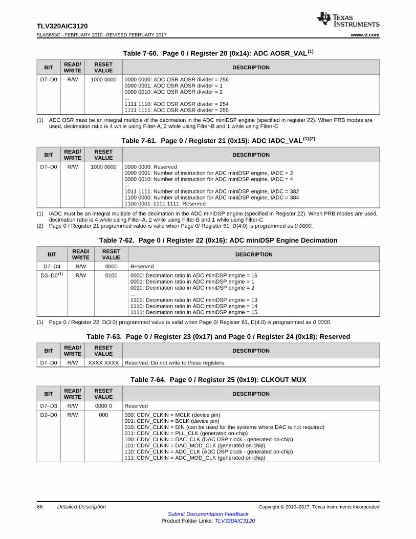
86
TLV320AIC3120SLAS653C –FEBRUARY 2010–REVISED FEBRUARY 2017 www.ti.com
Submit Documentation FeedbackProduct Folder Links: TLV320AIC3120
Detailed Description Copyright © 2010–2017, Texas Instruments Incorporated
(1) ADC OSR must be an integral multiple of the decimation in the ADC miniDSP engine (specified in register 22). When PRB modes areused, decimation ratio is 4 while using Filter-A, 2 while using Filter-B and 1 while using Filter-C
Table 7-60. Page 0 / Register 20 (0x14): ADC AOSR_VAL (1)
BIT READ/WRITE
RESETVALUE DESCRIPTION
D7–D0 R/W 1000 0000 0000 0000: ADC OSR AOSR divider = 2560000 0001: ADC OSR AOSR divider = 10000 0010: ADC OSR AOSR divider = 2...1111 1110: ADC OSR AOSR divider = 2541111 1111: ADC OSR AOSR divider = 255
(1) IADC must be an integral multiple of the decimation in the ADC miniDSP engine (specified in Register 22). When PRB modes are used,decimation ratio is 4 while using Filter-A, 2 while using Filter-B and 1 while using Filter-C
(2) Page 0 / Register 21 programmed value is valid when Page 0/ Register 61, D(4:0) is programmed as 0 0000.
Table 7-61. Page 0 / Register 21 (0x15): ADC IADC_VAL (1) (2)
BIT READ/WRITE
RESETVALUE DESCRIPTION
D7–D0 R/W 1000 0000 0000 0000: Reserved0000 0001: Number of instruction for ADC miniDSP engine, IADC = 20000 0010: Number of instruction for ADC miniDSP engine, IADC = 4...1011 1111: Number of instruction for ADC miniDSP engine, IADC = 3821100 0000: Number of instruction for ADC miniDSP engine, IADC = 3841100 0001–1111 1111: Reserved
(1) Page 0 / Register 22, D(3:0) programmed value is valid when Page 0/ Register 61, D(4:0) is programmed as 0 0000.
Table 7-62. Page 0 / Register 22 (0x16): ADC miniDSP Engine Decimation
BIT READ/WRITE
RESETVALUE DESCRIPTION
D7–D4 R/W 0000 ReservedD3–D0 (1) R/W 0100 0000: Decimation ratio in ADC miniDSP engine = 16
0001: Decimation ratio in ADC miniDSP engine = 10010: Decimation ratio in ADC miniDSP engine = 2...1101: Decimation ratio in ADC miniDSP engine = 131110: Decimation ratio in ADC miniDSP engine = 141111: Decimation ratio in ADC miniDSP engine = 15
Table 7-63. Page 0 / Register 23 (0x17) and Page 0 / Register 24 (0x18): Reserved
BIT READ/WRITE
RESETVALUE DESCRIPTION
D7–D0 R/W XXXX XXXX Reserved. Do not write to these registers.
Table 7-64. Page 0 / Register 25 (0x19): CLKOUT MUX
BIT READ/WRITE
RESETVALUE DESCRIPTION
D7–D3 R/W 0000 0 ReservedD2–D0 R/W 000 000: CDIV_CLKIN = MCLK (device pin)
001: CDIV_CLKIN = BCLK (device pin)010: CDIV_CLKIN = DIN (can be used for the systems where DAC is not required)011: CDIV_CLKIN = PLL_CLK (generated on-chip)100: CDIV_CLKIN = DAC_CLK (DAC DSP clock - generated on-chip)101: CDIV_CLKIN = DAC_MOD_CLK (generated on-chip)110: CDIV_CLKIN = ADC_CLK (ADC DSP clock - generated on-chip)111: CDIV_CLKIN = ADC_MOD_CLK (generated on-chip)
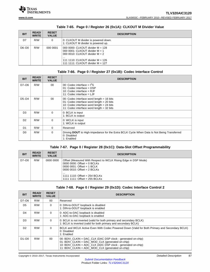
87
TLV320AIC3120www.ti.com SLAS653C –FEBRUARY 2010–REVISED FEBRUARY 2017
Submit Documentation FeedbackProduct Folder Links: TLV320AIC3120
Detailed DescriptionCopyright © 2010–2017, Texas Instruments Incorporated
Table 7-65. Page 0 / Register 26 (0x1A): CLKOUT M Divider Value
BIT READ/WRITE
RESETVALUE DESCRIPTION
D7 R/W 0 0: CLKOUT M divider is powered down.1: CLKOUT M divider is powered up.
D6–D0 R/W 000 0001 000 0000: CLKOUT divider M = 128000 0001: CLKOUT divider M = 1000 0010: CLKOUT divider M = 2...111 1110: CLKOUT divider M = 126111 1111: CLKOUT divider M = 127
Table 7-66. Page 0 / Register 27 (0x1B): Codec Interface Control
BIT READ/WRITE
RESETVALUE DESCRIPTION
D7–D6 R/W 00 00: Codec interface = I2S01: Codec Interface = DSP10: Codec interface = RJF11: Codec interface = LJF
D5–D4 R/W 00 00: Codec interface word length = 16 bits01: Codec interface word length = 20 bits10: Codec interface word length = 24 bits11: Codec interface word length = 32 bits
D3 R/W 0 0: BCLK is input1: BCLK is output
D2 R/W 0 0: WCLK is input1: WCLK is output
D1 R/W 0 ReservedD0 R/W 0 Driving DOUT to High-Impedance for the Extra BCLK Cycle When Data Is Not Being Transferred
0: Disabled1: Enabled
Table 7-67. Page 0 / Register 28 (0x1C): Data-Slot Offset Programmability
BIT READ/WRITE
RESETVALUE DESCRIPTION
D7–D0 R/W 0000 0000 Offset (Measured With Respect to WCLK Rising Edge in DSP Mode)0000 0000: Offset = 0 BCLKs0000 0001: Offset = 1 BCLK0000 0010: Offset = 2 BCLKs...1111 1110: Offset = 254 BCLKs1111 1111: Offset = 255 BCLKs
Table 7-68. Page 0 / Register 29 (0x1D): Codec Interface Control 2
BIT READ/WRITE
RESETVALUE DESCRIPTION
D7–D6 R/W 00 ReservedD5 R/W 0 0: DIN-to-DOUT loopback is disabled
1: DIN-to-DOUT loopback is enabledD4 R/W 0 0: ADC-to-DAC loopback is disabled
1: ADC-to-DAC loopback is enabledD3 R/W 0 0: BCLK is not inverted (valid for both primary and secondary BCLK)
1: BCLK is inverted (valid for both primary and secondary BCLK)D2 R/W 0 BCLK and WCLK Active Even With Codec Powered Down (Valid for Both Primary and Secondary BCLK)
0: Disabled1: Enabled
D1–D0 R/W 00 00: BDIV_CLKIN = DAC_CLK (DAC DSP clock - generated on-chip)01: BDIV_CLKIN = DAC_MOD_CLK (generated on-chip)10: BDIV_CLKIN = ADC_CLK (ADC DSP clock - generated on-chip)11: BDIV_CLKIN = ADC_MOD_CLK (generated on-chip)
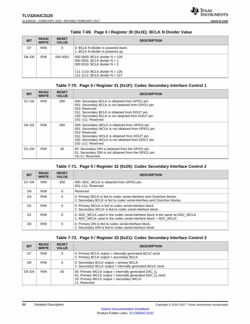
88
TLV320AIC3120SLAS653C –FEBRUARY 2010–REVISED FEBRUARY 2017 www.ti.com
Submit Documentation FeedbackProduct Folder Links: TLV320AIC3120
Detailed Description Copyright © 2010–2017, Texas Instruments Incorporated
Table 7-69. Page 0 / Register 30 (0x1E): BCLK N Divider Value
BIT READ/WRITE
RESETVALUE DESCRIPTION
D7 R/W 0 0: BCLK N-divider is powered down.1: BCLK N-divider is powered up.
D6–D0 R/W 000 0001 000 0000: BCLK divider N = 128000 0001: BCLK divider N = 1000 0010: BCLK divider N = 2...111 1110: BCLK divider N = 126111 1111: BCLK divider N = 127
Table 7-70. Page 0 / Register 31 (0x1F): Codec Secondary Interface Control 1
BIT READ/WRITE
RESETVALUE DESCRIPTION
D7–D5 R/W 000 000: Secondary BCLK is obtained from GPIO1 pin.001: Secondary BCLK is not obtained from GPIO1 pin.010: Reserved.011: Secondary BCLK is obtained from DOUT pin.100: Secondary BCLK is not obtained from DOUT pin.101–111: Reserved
D4–D2 R/W 000 000: Secondary WCLK is obtained from GPIO1 pin.001: Secondary WCLK is not obtained from GPIO1 pin.010: Reserved.011: Secondary WCLK is obtained from DOUT pin.100: Secondary WCLK is not obtained from DOUT pin.101–111: Reserved
D1–D0 R/W 00 00: Secondary DIN is obtained from the GPIO1 pin.01: Secondary DIN is not obtained from the GPIO1 pin.10–11: Reserved
Table 7-71. Page 0 / Register 32 (0x20): Codec Secondary Interface Control 2
BIT READ/WRITE
RESETVALUE DESCRIPTION
D7–D5 R/W 000 000: ADC_WCLK is obtained from GPIO1 pin.001–111: Reserved.
D4 R/W 0 ReservedD3 R/W 0 0: Primary BCLK is fed to codec serial-interface and ClockGen blocks.
1: Secondary BCLK is fed to codec serial-interface and ClockGen blocks.D2 R/W 0 0: Primary WCLK is fed to codec serial-interface block.
1: Secondary WCLK is fed to codec serial-interface block.D1 R/W 0 0: ADC_WCLK used in the codec serial-interface block is the same as DAC_WCLK.
1: ADC_WCLK used in the codec serial-interface block = ADC_WCLK.D0 R/W 0 0: Primary DIN is fed to codec serial-interface block.
1: Secondary DIN is fed to codec serial-interface block.
Table 7-72. Page 0 / Register 33 (0x21): Codec Secondary Interface Control 3
BIT READ/WRITE
RESETVALUE DESCRIPTION
D7 R/W 0 0: Primary BCLK output = internally generated BCLK clock1: Primary BCLK output = secondary BCLK
D6 R/W 0 0: Secondary BCLK output = primary BCLK1: Secondary BCLK output = internally generated BCLK clock
D5–D4 R/W 00 00: Primary WCLK output = internally generated DAC_fS01: Primary WCLK output = internally generated ADC_fS clock10: Primary WCLK output = secondary WCLK11: Reserved
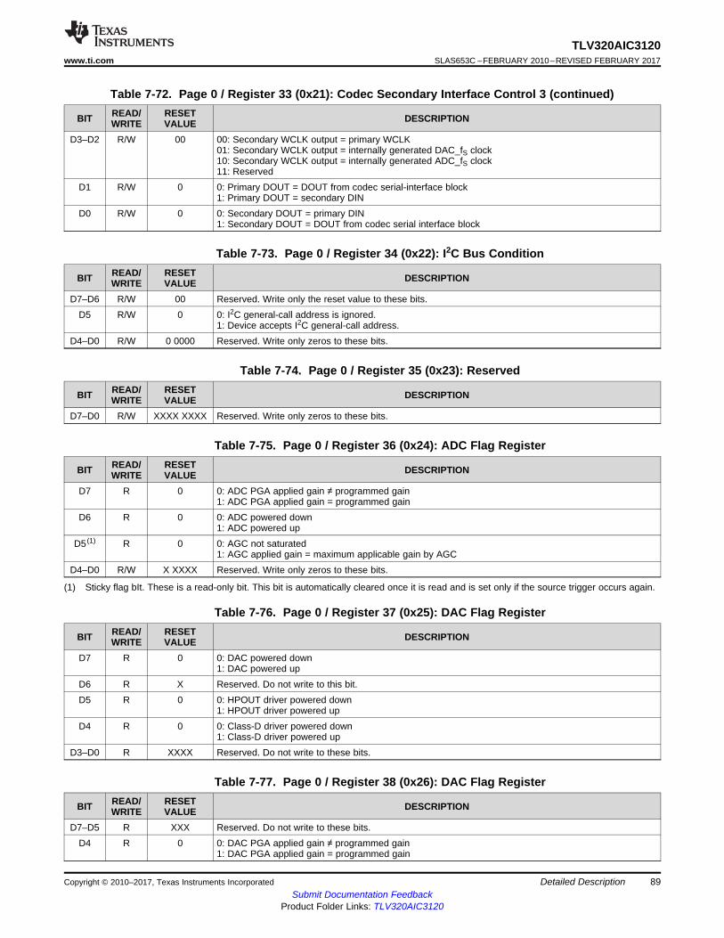
89
TLV320AIC3120www.ti.com SLAS653C –FEBRUARY 2010–REVISED FEBRUARY 2017
Submit Documentation FeedbackProduct Folder Links: TLV320AIC3120
Detailed DescriptionCopyright © 2010–2017, Texas Instruments Incorporated
Table 7-72. Page 0 / Register 33 (0x21): Codec Secondary Interface Control 3 (continued)
BIT READ/WRITE
RESETVALUE DESCRIPTION
D3–D2 R/W 00 00: Secondary WCLK output = primary WCLK01: Secondary WCLK output = internally generated DAC_fS clock10: Secondary WCLK output = internally generated ADC_fS clock11: Reserved
D1 R/W 0 0: Primary DOUT = DOUT from codec serial-interface block1: Primary DOUT = secondary DIN
D0 R/W 0 0: Secondary DOUT = primary DIN1: Secondary DOUT = DOUT from codec serial interface block
Table 7-73. Page 0 / Register 34 (0x22): I2C Bus Condition
BIT READ/WRITE
RESETVALUE DESCRIPTION
D7–D6 R/W 00 Reserved. Write only the reset value to these bits.D5 R/W 0 0: I2C general-call address is ignored.
1: Device accepts I2C general-call address.D4–D0 R/W 0 0000 Reserved. Write only zeros to these bits.
Table 7-74. Page 0 / Register 35 (0x23): Reserved
BIT READ/WRITE
RESETVALUE DESCRIPTION
D7–D0 R/W XXXX XXXX Reserved. Write only zeros to these bits.
(1) Sticky flag bIt. These is a read-only bit. This bit is automatically cleared once it is read and is set only if the source trigger occurs again.
Table 7-75. Page 0 / Register 36 (0x24): ADC Flag Register
BIT READ/WRITE
RESETVALUE DESCRIPTION
D7 R 0 0: ADC PGA applied gain ≠ programmed gain1: ADC PGA applied gain = programmed gain
D6 R 0 0: ADC powered down1: ADC powered up
D5 (1) R 0 0: AGC not saturated1: AGC applied gain = maximum applicable gain by AGC
D4–D0 R/W X XXXX Reserved. Write only zeros to these bits.
Table 7-76. Page 0 / Register 37 (0x25): DAC Flag Register
BIT READ/WRITE
RESETVALUE DESCRIPTION
D7 R 0 0: DAC powered down1: DAC powered up
D6 R X Reserved. Do not write to this bit.D5 R 0 0: HPOUT driver powered down
1: HPOUT driver powered upD4 R 0 0: Class-D driver powered down
1: Class-D driver powered upD3–D0 R XXXX Reserved. Do not write to these bits.
Table 7-77. Page 0 / Register 38 (0x26): DAC Flag Register
BIT READ/WRITE
RESETVALUE DESCRIPTION
D7–D5 R XXX Reserved. Do not write to these bits.D4 R 0 0: DAC PGA applied gain ≠ programmed gain
1: DAC PGA applied gain = programmed gain
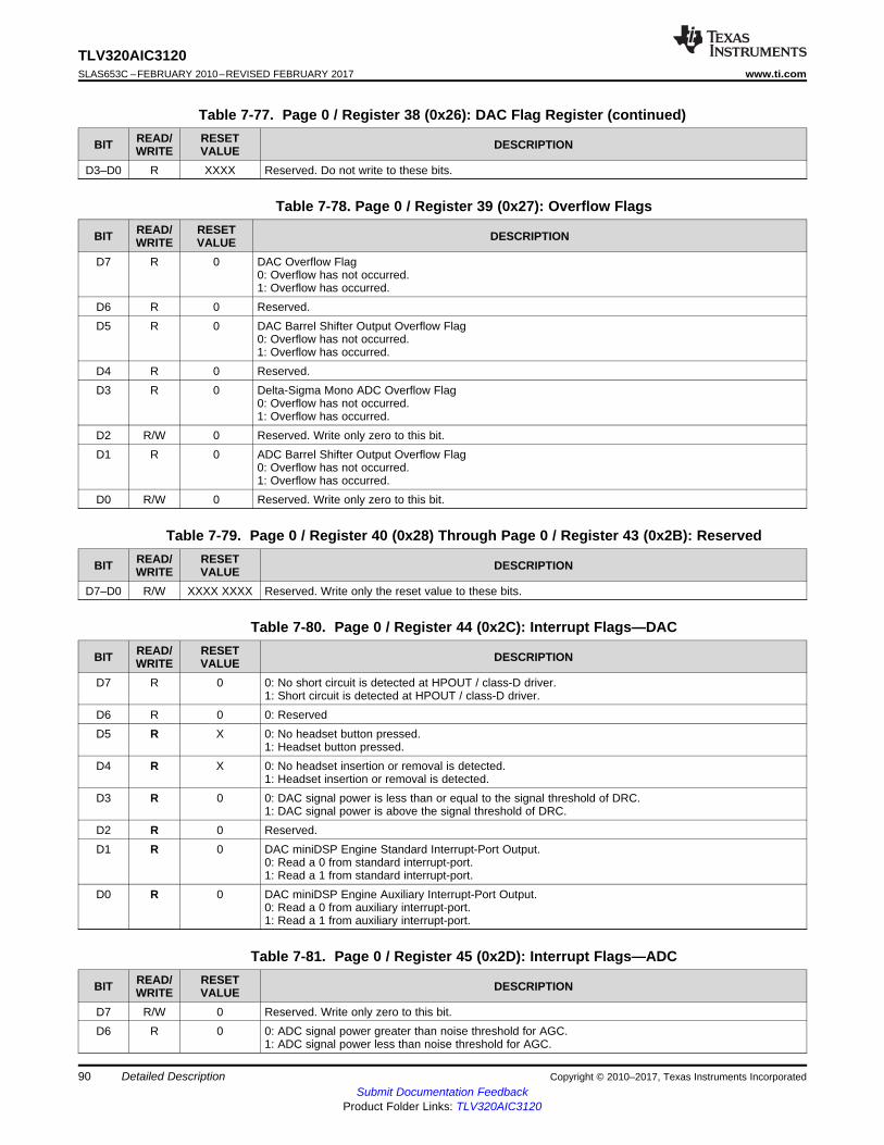
90
TLV320AIC3120SLAS653C –FEBRUARY 2010–REVISED FEBRUARY 2017 www.ti.com
Submit Documentation FeedbackProduct Folder Links: TLV320AIC3120
Detailed Description Copyright © 2010–2017, Texas Instruments Incorporated
Table 7-77. Page 0 / Register 38 (0x26): DAC Flag Register (continued)
BIT READ/WRITE
RESETVALUE DESCRIPTION
D3–D0 R XXXX Reserved. Do not write to these bits.
Table 7-78. Page 0 / Register 39 (0x27): Overflow Flags
BIT READ/WRITE
RESETVALUE DESCRIPTION
D7 R 0 DAC Overflow Flag0: Overflow has not occurred.1: Overflow has occurred.
D6 R 0 Reserved.D5 R 0 DAC Barrel Shifter Output Overflow Flag
0: Overflow has not occurred.1: Overflow has occurred.
D4 R 0 Reserved.D3 R 0 Delta-Sigma Mono ADC Overflow Flag
0: Overflow has not occurred.1: Overflow has occurred.
D2 R/W 0 Reserved. Write only zero to this bit.D1 R 0 ADC Barrel Shifter Output Overflow Flag
0: Overflow has not occurred.1: Overflow has occurred.
D0 R/W 0 Reserved. Write only zero to this bit.
Table 7-79. Page 0 / Register 40 (0x28) Through Page 0 / Register 43 (0x2B): Reserved
BIT READ/WRITE
RESETVALUE DESCRIPTION
D7–D0 R/W XXXX XXXX Reserved. Write only the reset value to these bits.
Table 7-80. Page 0 / Register 44 (0x2C): Interrupt Flags—DAC
BIT READ/WRITE
RESETVALUE DESCRIPTION
D7 R 0 0: No short circuit is detected at HPOUT / class-D driver.1: Short circuit is detected at HPOUT / class-D driver.
D6 R 0 0: ReservedD5 R X 0: No headset button pressed.
1: Headset button pressed.D4 R X 0: No headset insertion or removal is detected.
1: Headset insertion or removal is detected.D3 R 0 0: DAC signal power is less than or equal to the signal threshold of DRC.
1: DAC signal power is above the signal threshold of DRC.D2 R 0 Reserved.D1 R 0 DAC miniDSP Engine Standard Interrupt-Port Output.
0: Read a 0 from standard interrupt-port.1: Read a 1 from standard interrupt-port.
D0 R 0 DAC miniDSP Engine Auxiliary Interrupt-Port Output.0: Read a 0 from auxiliary interrupt-port.1: Read a 1 from auxiliary interrupt-port.
Table 7-81. Page 0 / Register 45 (0x2D): Interrupt Flags—ADC
BIT READ/WRITE
RESETVALUE DESCRIPTION
D7 R/W 0 Reserved. Write only zero to this bit.D6 R 0 0: ADC signal power greater than noise threshold for AGC.
1: ADC signal power less than noise threshold for AGC.
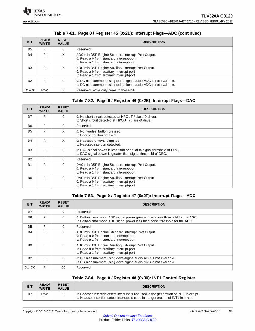
91
TLV320AIC3120www.ti.com SLAS653C –FEBRUARY 2010–REVISED FEBRUARY 2017
Submit Documentation FeedbackProduct Folder Links: TLV320AIC3120
Detailed DescriptionCopyright © 2010–2017, Texas Instruments Incorporated
Table 7-81. Page 0 / Register 45 (0x2D): Interrupt Flags—ADC (continued)
BIT READ/WRITE
RESETVALUE DESCRIPTION
D5 R 0 Reserved.D4 R X ADC miniDSP Engine Standard Interrupt Port Output.
0: Read a 0 from standard interrupt-port.1: Read a 1 from standard interrupt-port.
D3 R X ADC miniDSP Engine Auxiliary Interrupt Port Output.0: Read a 0 from auxiliary interrupt-port.1: Read a 1 from auxiliary interrupt-port.
D2 R 0 0: DC measurement using delta-sigma audio ADC is not available.1: DC measurement using delta-sigma audio ADC is not available.
D1–D0 R/W 00 Reserved. Write only zeros to these bits.
Table 7-82. Page 0 / Register 46 (0x2E): Interrupt Flags—DAC
BIT READ/WRITE
RESETVALUE DESCRIPTION
D7 R 0 0: No short circuit detected at HPOUT / class-D driver.1: Short circuit detected at HPOUT / class-D driver.
D6 R 0 Reserved.D5 R X 0: No headset button pressed.
1: Headset button pressed.D4 R X 0: Headset removal detected.
1: Headset insertion detected.D3 R 0 0: DAC signal power is less than or equal to signal threshold of DRC.
1: DAC signal power is greater than signal threshold of DRC.D2 R 0 ReservedD1 R 0 DAC miniDSP Engine Standard Interrupt Port Output.
0: Read a 0 from standard interrupt-port.1: Read a 1 from standard interrupt-port.
D0 R 0 DAC miniDSP Engine Auxiliary Interrupt Port Output.0: Read a 0 from auxiliary interrupt-port.1: Read a 1 from auxiliary interrupt-port.
Table 7-83. Page 0 / Register 47 (0x2F): Interrupt Flags – ADC
BIT READ/WRITE
RESETVALUE DESCRIPTION
D7 R 0 ReservedD6 R 0 0: Delta-sigma mono ADC signal power greater than noise threshold for the AGC
1: Delta-sigma mono ADC signal power less than noise threshold for the AGCD5 R 0 ReservedD4 R X ADC miniDSP Engine Standard Interrupt Port Output
0: Read a 0 from standard interrupt-port1: Read a 1 from standard interrupt-port
D3 R X ADC miniDSP Engine Auxiliary Interrupt Port Output0: Read a 0 from auxiliary interrupt-port1: Read a 1 from auxiliary interrupt-port
D2 R 0 0: DC measurement using delta-sigma audio ADC is not available1: DC measurement using delta-sigma audio ADC is not available
D1–D0 R 00 Reserved.
Table 7-84. Page 0 / Register 48 (0x30): INT1 Control Register
BIT READ/WRITE
RESETVALUE DESCRIPTION
D7 R/W 0 0: Headset-insertion detect interrupt is not used in the generation of INT1 interrupt.1: Headset-insertion detect interrupt is used in the generation of INT1 interrupt.
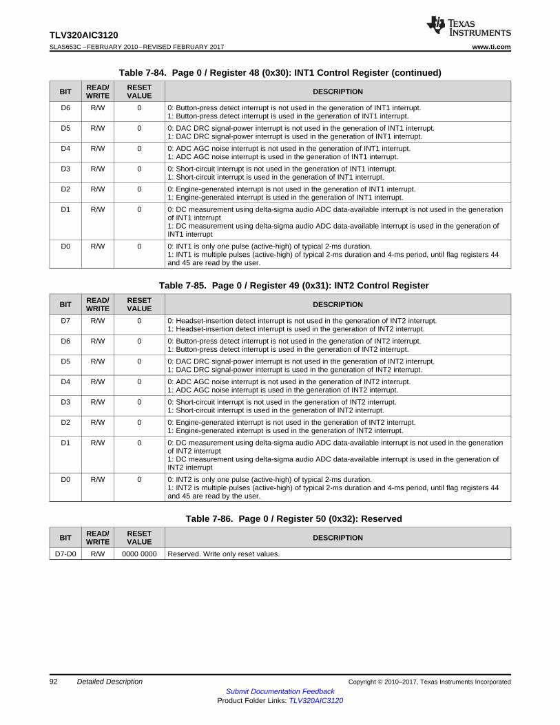
92
TLV320AIC3120SLAS653C –FEBRUARY 2010–REVISED FEBRUARY 2017 www.ti.com
Submit Documentation FeedbackProduct Folder Links: TLV320AIC3120
Detailed Description Copyright © 2010–2017, Texas Instruments Incorporated
Table 7-84. Page 0 / Register 48 (0x30): INT1 Control Register (continued)
BIT READ/WRITE
RESETVALUE DESCRIPTION
D6 R/W 0 0: Button-press detect interrupt is not used in the generation of INT1 interrupt.1: Button-press detect interrupt is used in the generation of INT1 interrupt.
D5 R/W 0 0: DAC DRC signal-power interrupt is not used in the generation of INT1 interrupt.1: DAC DRC signal-power interrupt is used in the generation of INT1 interrupt.
D4 R/W 0 0: ADC AGC noise interrupt is not used in the generation of INT1 interrupt.1: ADC AGC noise interrupt is used in the generation of INT1 interrupt.
D3 R/W 0 0: Short-circuit interrupt is not used in the generation of INT1 interrupt.1: Short-circuit interrupt is used in the generation of INT1 interrupt.
D2 R/W 0 0: Engine-generated interrupt is not used in the generation of INT1 interrupt.1: Engine-generated interrupt is used in the generation of INT1 interrupt.
D1 R/W 0 0: DC measurement using delta-sigma audio ADC data-available interrupt is not used in the generationof INT1 interrupt1: DC measurement using delta-sigma audio ADC data-available interrupt is used in the generation ofINT1 interrupt
D0 R/W 0 0: INT1 is only one pulse (active-high) of typical 2-ms duration.1: INT1 is multiple pulses (active-high) of typical 2-ms duration and 4-ms period, until flag registers 44and 45 are read by the user.
Table 7-85. Page 0 / Register 49 (0x31): INT2 Control Register
BIT READ/WRITE
RESETVALUE DESCRIPTION
D7 R/W 0 0: Headset-insertion detect interrupt is not used in the generation of INT2 interrupt.1: Headset-insertion detect interrupt is used in the generation of INT2 interrupt.
D6 R/W 0 0: Button-press detect interrupt is not used in the generation of INT2 interrupt.1: Button-press detect interrupt is used in the generation of INT2 interrupt.
D5 R/W 0 0: DAC DRC signal-power interrupt is not used in the generation of INT2 interrupt.1: DAC DRC signal-power interrupt is used in the generation of INT2 interrupt.
D4 R/W 0 0: ADC AGC noise interrupt is not used in the generation of INT2 interrupt.1: ADC AGC noise interrupt is used in the generation of INT2 interrupt.
D3 R/W 0 0: Short-circuit interrupt is not used in the generation of INT2 interrupt.1: Short-circuit interrupt is used in the generation of INT2 interrupt.
D2 R/W 0 0: Engine-generated interrupt is not used in the generation of INT2 interrupt.1: Engine-generated interrupt is used in the generation of INT2 interrupt.
D1 R/W 0 0: DC measurement using delta-sigma audio ADC data-available interrupt is not used in the generationof INT2 interrupt1: DC measurement using delta-sigma audio ADC data-available interrupt is used in the generation ofINT2 interrupt
D0 R/W 0 0: INT2 is only one pulse (active-high) of typical 2-ms duration.1: INT2 is multiple pulses (active-high) of typical 2-ms duration and 4-ms period, until flag registers 44and 45 are read by the user.
Table 7-86. Page 0 / Register 50 (0x32): Reserved
BIT READ/WRITE
RESETVALUE DESCRIPTION
D7-D0 R/W 0000 0000 Reserved. Write only reset values.
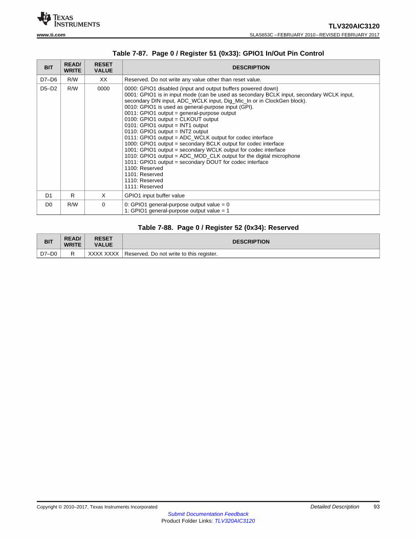
93
TLV320AIC3120www.ti.com SLAS653C –FEBRUARY 2010–REVISED FEBRUARY 2017
Submit Documentation FeedbackProduct Folder Links: TLV320AIC3120
Detailed DescriptionCopyright © 2010–2017, Texas Instruments Incorporated
Table 7-87. Page 0 / Register 51 (0x33): GPIO1 In/Out Pin Control
BIT READ/WRITE
RESETVALUE DESCRIPTION
D7–D6 R/W XX Reserved. Do not write any value other than reset value.D5–D2 R/W 0000 0000: GPIO1 disabled (input and output buffers powered down)
0001: GPIO1 is in input mode (can be used as secondary BCLK input, secondary WCLK input,secondary DIN input, ADC_WCLK input, Dig_Mic_In or in ClockGen block).0010: GPIO1 is used as general-purpose input (GPI).0011: GPIO1 output = general-purpose output0100: GPIO1 output = CLKOUT output0101: GPIO1 output = INT1 output0110: GPIO1 output = INT2 output0111: GPIO1 output = ADC_WCLK output for codec interface1000: GPIO1 output = secondary BCLK output for codec interface1001: GPIO1 output = secondary WCLK output for codec interface1010: GPIO1 output = ADC_MOD_CLK output for the digital microphone1011: GPIO1 output = secondary DOUT for codec interface1100: Reserved1101: Reserved1110: Reserved1111: Reserved
D1 R X GPIO1 input buffer valueD0 R/W 0 0: GPIO1 general-purpose output value = 0
1: GPIO1 general-purpose output value = 1
Table 7-88. Page 0 / Register 52 (0x34): Reserved
BIT READ/WRITE
RESETVALUE DESCRIPTION
D7–D0 R XXXX XXXX Reserved. Do not write to this register.
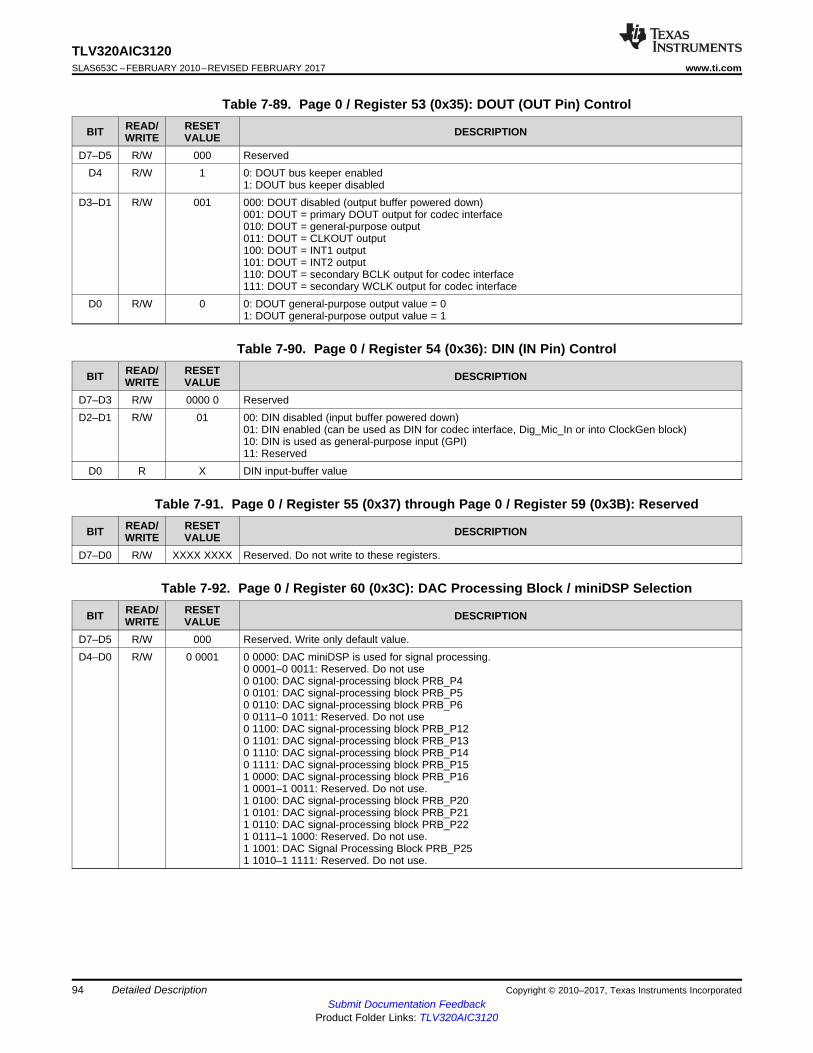
94
TLV320AIC3120SLAS653C –FEBRUARY 2010–REVISED FEBRUARY 2017 www.ti.com
Submit Documentation FeedbackProduct Folder Links: TLV320AIC3120
Detailed Description Copyright © 2010–2017, Texas Instruments Incorporated
Table 7-89. Page 0 / Register 53 (0x35): DOUT (OUT Pin) Control
BIT READ/WRITE
RESETVALUE DESCRIPTION
D7–D5 R/W 000 ReservedD4 R/W 1 0: DOUT bus keeper enabled
1: DOUT bus keeper disabledD3–D1 R/W 001 000: DOUT disabled (output buffer powered down)
001: DOUT = primary DOUT output for codec interface010: DOUT = general-purpose output011: DOUT = CLKOUT output100: DOUT = INT1 output101: DOUT = INT2 output110: DOUT = secondary BCLK output for codec interface111: DOUT = secondary WCLK output for codec interface
D0 R/W 0 0: DOUT general-purpose output value = 01: DOUT general-purpose output value = 1
Table 7-90. Page 0 / Register 54 (0x36): DIN (IN Pin) Control
BIT READ/WRITE
RESETVALUE DESCRIPTION
D7–D3 R/W 0000 0 ReservedD2–D1 R/W 01 00: DIN disabled (input buffer powered down)
01: DIN enabled (can be used as DIN for codec interface, Dig_Mic_In or into ClockGen block)10: DIN is used as general-purpose input (GPI)11: Reserved
D0 R X DIN input-buffer value
Table 7-91. Page 0 / Register 55 (0x37) through Page 0 / Register 59 (0x3B): Reserved
BIT READ/WRITE
RESETVALUE DESCRIPTION
D7–D0 R/W XXXX XXXX Reserved. Do not write to these registers.
Table 7-92. Page 0 / Register 60 (0x3C): DAC Processing Block / miniDSP Selection
BIT READ/WRITE
RESETVALUE DESCRIPTION
D7–D5 R/W 000 Reserved. Write only default value.D4–D0 R/W 0 0001 0 0000: DAC miniDSP is used for signal processing.
0 0001–0 0011: Reserved. Do not use0 0100: DAC signal-processing block PRB_P40 0101: DAC signal-processing block PRB_P50 0110: DAC signal-processing block PRB_P60 0111–0 1011: Reserved. Do not use0 1100: DAC signal-processing block PRB_P120 1101: DAC signal-processing block PRB_P130 1110: DAC signal-processing block PRB_P140 1111: DAC signal-processing block PRB_P151 0000: DAC signal-processing block PRB_P161 0001–1 0011: Reserved. Do not use.1 0100: DAC signal-processing block PRB_P201 0101: DAC signal-processing block PRB_P211 0110: DAC signal-processing block PRB_P221 0111–1 1000: Reserved. Do not use.1 1001: DAC Signal Processing Block PRB_P251 1010–1 1111: Reserved. Do not use.
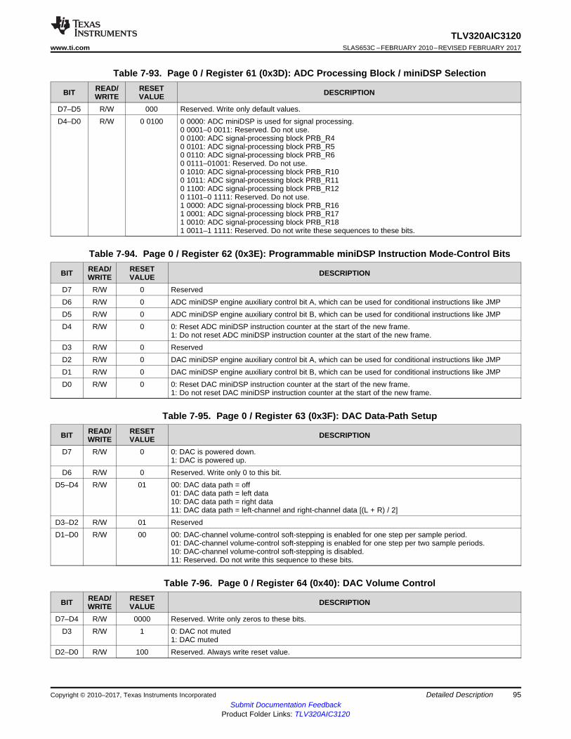
95
TLV320AIC3120www.ti.com SLAS653C –FEBRUARY 2010–REVISED FEBRUARY 2017
Submit Documentation FeedbackProduct Folder Links: TLV320AIC3120
Detailed DescriptionCopyright © 2010–2017, Texas Instruments Incorporated
Table 7-93. Page 0 / Register 61 (0x3D): ADC Processing Block / miniDSP Selection
BIT READ/WRITE
RESETVALUE DESCRIPTION
D7–D5 R/W 000 Reserved. Write only default values.D4–D0 R/W 0 0100 0 0000: ADC miniDSP is used for signal processing.
0 0001–0 0011: Reserved. Do not use.0 0100: ADC signal-processing block PRB_R40 0101: ADC signal-processing block PRB_R50 0110: ADC signal-processing block PRB_R60 0111–01001: Reserved. Do not use.0 1010: ADC signal-processing block PRB_R100 1011: ADC signal-processing block PRB_R110 1100: ADC signal-processing block PRB_R120 1101–0 1111: Reserved. Do not use.1 0000: ADC signal-processing block PRB_R161 0001: ADC signal-processing block PRB_R171 0010: ADC signal-processing block PRB_R181 0011–1 1111: Reserved. Do not write these sequences to these bits.
Table 7-94. Page 0 / Register 62 (0x3E): Programmable miniDSP Instruction Mode-Control Bits
BIT READ/WRITE
RESETVALUE DESCRIPTION
D7 R/W 0 ReservedD6 R/W 0 ADC miniDSP engine auxiliary control bit A, which can be used for conditional instructions like JMPD5 R/W 0 ADC miniDSP engine auxiliary control bit B, which can be used for conditional instructions like JMPD4 R/W 0 0: Reset ADC miniDSP instruction counter at the start of the new frame.
1: Do not reset ADC miniDSP instruction counter at the start of the new frame.D3 R/W 0 ReservedD2 R/W 0 DAC miniDSP engine auxiliary control bit A, which can be used for conditional instructions like JMPD1 R/W 0 DAC miniDSP engine auxiliary control bit B, which can be used for conditional instructions like JMPD0 R/W 0 0: Reset DAC miniDSP instruction counter at the start of the new frame.
1: Do not reset DAC miniDSP instruction counter at the start of the new frame.
Table 7-95. Page 0 / Register 63 (0x3F): DAC Data-Path Setup
BIT READ/WRITE
RESETVALUE DESCRIPTION
D7 R/W 0 0: DAC is powered down.1: DAC is powered up.
D6 R/W 0 Reserved. Write only 0 to this bit.D5–D4 R/W 01 00: DAC data path = off
01: DAC data path = left data10: DAC data path = right data11: DAC data path = left-channel and right-channel data [(L + R) / 2]
D3–D2 R/W 01 ReservedD1–D0 R/W 00 00: DAC-channel volume-control soft-stepping is enabled for one step per sample period.
01: DAC-channel volume-control soft-stepping is enabled for one step per two sample periods.10: DAC-channel volume-control soft-stepping is disabled.11: Reserved. Do not write this sequence to these bits.
Table 7-96. Page 0 / Register 64 (0x40): DAC Volume Control
BIT READ/WRITE
RESETVALUE DESCRIPTION
D7–D4 R/W 0000 Reserved. Write only zeros to these bits.D3 R/W 1 0: DAC not muted
1: DAC mutedD2–D0 R/W 100 Reserved. Always write reset value.
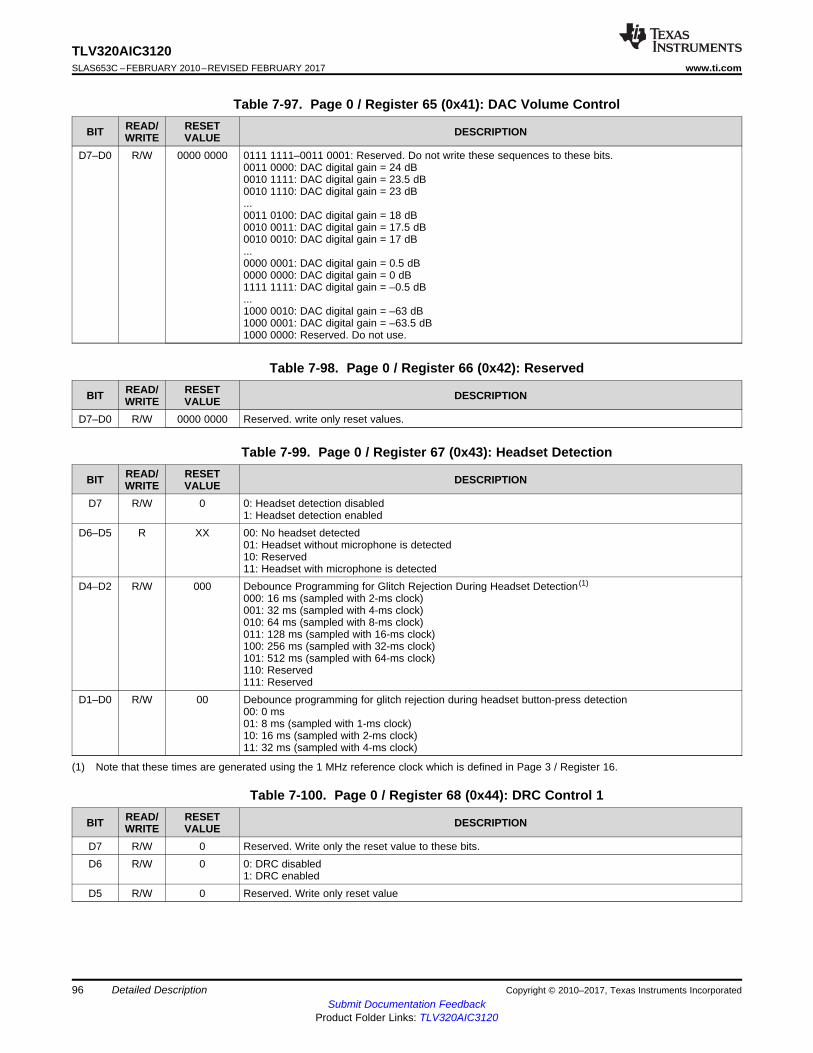
96
TLV320AIC3120SLAS653C –FEBRUARY 2010–REVISED FEBRUARY 2017 www.ti.com
Submit Documentation FeedbackProduct Folder Links: TLV320AIC3120
Detailed Description Copyright © 2010–2017, Texas Instruments Incorporated
Table 7-97. Page 0 / Register 65 (0x41): DAC Volume Control
BIT READ/WRITE
RESETVALUE DESCRIPTION
D7–D0 R/W 0000 0000 0111 1111–0011 0001: Reserved. Do not write these sequences to these bits.0011 0000: DAC digital gain = 24 dB0010 1111: DAC digital gain = 23.5 dB0010 1110: DAC digital gain = 23 dB...0011 0100: DAC digital gain = 18 dB0010 0011: DAC digital gain = 17.5 dB0010 0010: DAC digital gain = 17 dB...0000 0001: DAC digital gain = 0.5 dB0000 0000: DAC digital gain = 0 dB1111 1111: DAC digital gain = –0.5 dB...1000 0010: DAC digital gain = –63 dB1000 0001: DAC digital gain = –63.5 dB1000 0000: Reserved. Do not use.
Table 7-98. Page 0 / Register 66 (0x42): Reserved
BIT READ/WRITE
RESETVALUE DESCRIPTION
D7–D0 R/W 0000 0000 Reserved. write only reset values.
(1) Note that these times are generated using the 1 MHz reference clock which is defined in Page 3 / Register 16.
Table 7-99. Page 0 / Register 67 (0x43): Headset Detection
BIT READ/WRITE
RESETVALUE DESCRIPTION
D7 R/W 0 0: Headset detection disabled1: Headset detection enabled
D6–D5 R XX 00: No headset detected01: Headset without microphone is detected10: Reserved11: Headset with microphone is detected
D4–D2 R/W 000 Debounce Programming for Glitch Rejection During Headset Detection (1)
000: 16 ms (sampled with 2-ms clock)001: 32 ms (sampled with 4-ms clock)010: 64 ms (sampled with 8-ms clock)011: 128 ms (sampled with 16-ms clock)100: 256 ms (sampled with 32-ms clock)101: 512 ms (sampled with 64-ms clock)110: Reserved111: Reserved
D1–D0 R/W 00 Debounce programming for glitch rejection during headset button-press detection00: 0 ms01: 8 ms (sampled with 1-ms clock)10: 16 ms (sampled with 2-ms clock)11: 32 ms (sampled with 4-ms clock)
Table 7-100. Page 0 / Register 68 (0x44): DRC Control 1
BIT READ/WRITE
RESETVALUE DESCRIPTION
D7 R/W 0 Reserved. Write only the reset value to these bits.D6 R/W 0 0: DRC disabled
1: DRC enabledD5 R/W 0 Reserved. Write only reset value
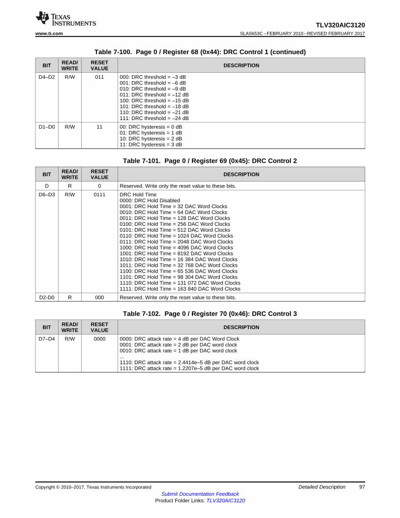
97
TLV320AIC3120www.ti.com SLAS653C –FEBRUARY 2010–REVISED FEBRUARY 2017
Submit Documentation FeedbackProduct Folder Links: TLV320AIC3120
Detailed DescriptionCopyright © 2010–2017, Texas Instruments Incorporated
Table 7-100. Page 0 / Register 68 (0x44): DRC Control 1 (continued)
BIT READ/WRITE
RESETVALUE DESCRIPTION
D4–D2 R/W 011 000: DRC threshold = –3 dB001: DRC threshold = –6 dB010: DRC threshold = –9 dB011: DRC threshold = –12 dB100: DRC threshold = –15 dB101: DRC threshold = –18 dB110: DRC threshold = –21 dB111: DRC threshold = –24 dB
D1–D0 R/W 11 00: DRC hysteresis = 0 dB01: DRC hysteresis = 1 dB10: DRC hysteresis = 2 dB11: DRC hysteresis = 3 dB
Table 7-101. Page 0 / Register 69 (0x45): DRC Control 2
BIT READ/WRITE
RESETVALUE DESCRIPTION
D R 0 Reserved. Write only the reset value to these bits.D6–D3 R/W 0111 DRC Hold Time
0000: DRC Hold Disabled0001: DRC Hold Time = 32 DAC Word Clocks0010: DRC Hold Time = 64 DAC Word Clocks0011: DRC Hold Time = 128 DAC Word Clocks0100: DRC Hold Time = 256 DAC Word Clocks0101: DRC Hold Time = 512 DAC Word Clocks0110: DRC Hold Time = 1024 DAC Word Clocks0111: DRC Hold Time = 2048 DAC Word Clocks1000: DRC Hold Time = 4096 DAC Word Clocks1001: DRC Hold Time = 8192 DAC Word Clocks1010: DRC Hold Time = 16 384 DAC Word Clocks1011: DRC Hold Time = 32 768 DAC Word Clocks1100: DRC Hold Time = 65 536 DAC Word Clocks1101: DRC Hold Time = 98 304 DAC Word Clocks1110: DRC Hold Time = 131 072 DAC Word Clocks1111: DRC Hold Time = 163 840 DAC Word Clocks
D2-D0 R 000 Reserved. Write only the reset value to these bits.
Table 7-102. Page 0 / Register 70 (0x46): DRC Control 3
BIT READ/WRITE
RESETVALUE DESCRIPTION
D7–D4 R/W 0000 0000: DRC attack rate = 4 dB per DAC Word Clock0001: DRC attack rate = 2 dB per DAC word clock0010: DRC attack rate = 1 dB per DAC word clock...1110: DRC attack rate = 2.4414e–5 dB per DAC word clock1111: DRC attack rate = 1.2207e–5 dB per DAC word clock
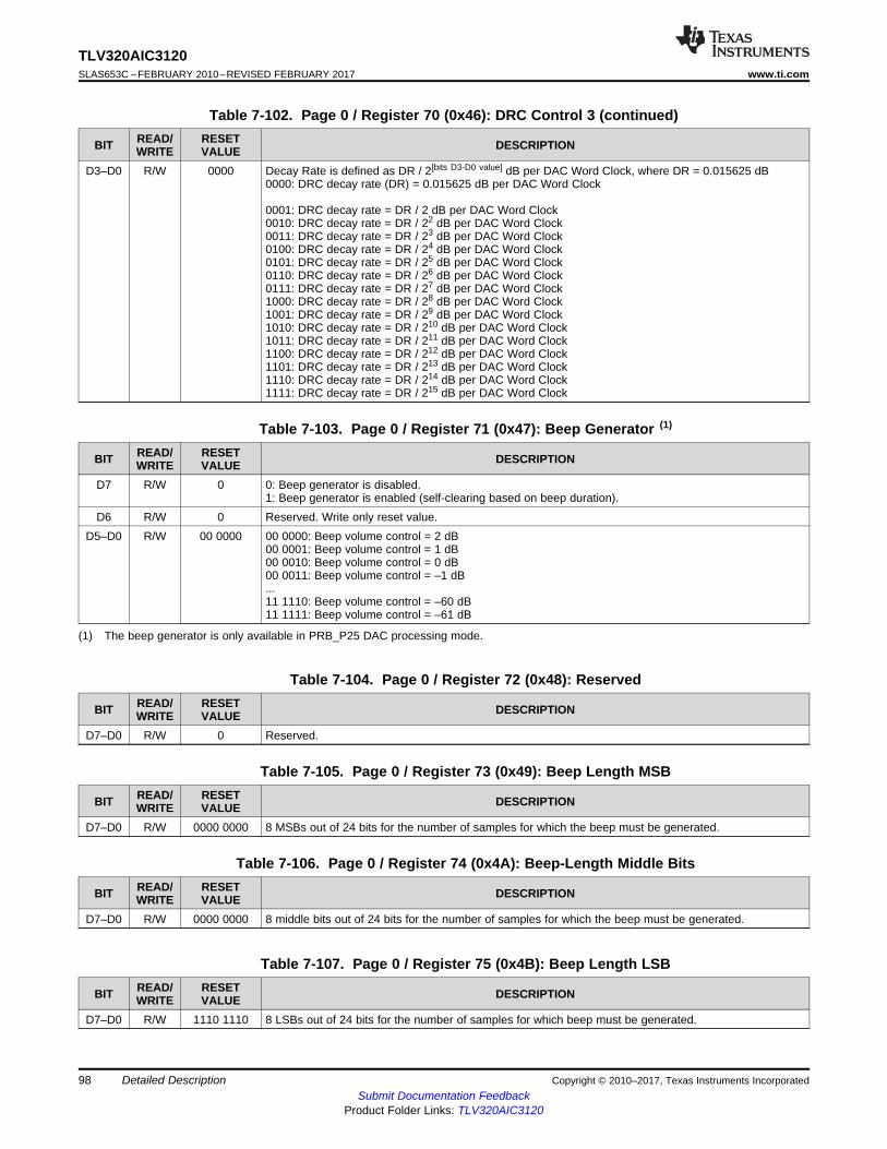
98
TLV320AIC3120SLAS653C –FEBRUARY 2010–REVISED FEBRUARY 2017 www.ti.com
Submit Documentation FeedbackProduct Folder Links: TLV320AIC3120
Detailed Description Copyright © 2010–2017, Texas Instruments Incorporated
Table 7-102. Page 0 / Register 70 (0x46): DRC Control 3 (continued)
BIT READ/WRITE
RESETVALUE DESCRIPTION
D3–D0 R/W 0000 Decay Rate is defined as DR / 2[bits D3-D0 value] dB per DAC Word Clock, where DR = 0.015625 dB0000: DRC decay rate (DR) = 0.015625 dB per DAC Word Clock
0001: DRC decay rate = DR / 2 dB per DAC Word Clock0010: DRC decay rate = DR / 22 dB per DAC Word Clock0011: DRC decay rate = DR / 23 dB per DAC Word Clock0100: DRC decay rate = DR / 24 dB per DAC Word Clock0101: DRC decay rate = DR / 25 dB per DAC Word Clock0110: DRC decay rate = DR / 26 dB per DAC Word Clock0111: DRC decay rate = DR / 27 dB per DAC Word Clock1000: DRC decay rate = DR / 28 dB per DAC Word Clock1001: DRC decay rate = DR / 29 dB per DAC Word Clock1010: DRC decay rate = DR / 210 dB per DAC Word Clock1011: DRC decay rate = DR / 211 dB per DAC Word Clock1100: DRC decay rate = DR / 212 dB per DAC Word Clock1101: DRC decay rate = DR / 213 dB per DAC Word Clock1110: DRC decay rate = DR / 214 dB per DAC Word Clock1111: DRC decay rate = DR / 215 dB per DAC Word Clock
(1) The beep generator is only available in PRB_P25 DAC processing mode.
Table 7-103. Page 0 / Register 71 (0x47): Beep Generator (1)
BIT READ/WRITE
RESETVALUE DESCRIPTION
D7 R/W 0 0: Beep generator is disabled.1: Beep generator is enabled (self-clearing based on beep duration).
D6 R/W 0 Reserved. Write only reset value.D5–D0 R/W 00 0000 00 0000: Beep volume control = 2 dB
00 0001: Beep volume control = 1 dB00 0010: Beep volume control = 0 dB00 0011: Beep volume control = –1 dB...11 1110: Beep volume control = –60 dB11 1111: Beep volume control = –61 dB
Table 7-104. Page 0 / Register 72 (0x48): Reserved
BIT READ/WRITE
RESETVALUE DESCRIPTION
D7–D0 R/W 0 Reserved.
Table 7-105. Page 0 / Register 73 (0x49): Beep Length MSB
BIT READ/WRITE
RESETVALUE DESCRIPTION
D7–D0 R/W 0000 0000 8 MSBs out of 24 bits for the number of samples for which the beep must be generated.
Table 7-106. Page 0 / Register 74 (0x4A): Beep-Length Middle Bits
BIT READ/WRITE
RESETVALUE DESCRIPTION
D7–D0 R/W 0000 0000 8 middle bits out of 24 bits for the number of samples for which the beep must be generated.
Table 7-107. Page 0 / Register 75 (0x4B): Beep Length LSB
BIT READ/WRITE
RESETVALUE DESCRIPTION
D7–D0 R/W 1110 1110 8 LSBs out of 24 bits for the number of samples for which beep must be generated.
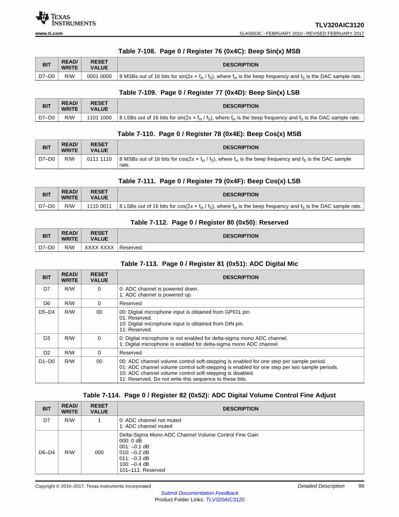
99
TLV320AIC3120www.ti.com SLAS653C –FEBRUARY 2010–REVISED FEBRUARY 2017
Submit Documentation FeedbackProduct Folder Links: TLV320AIC3120
Detailed DescriptionCopyright © 2010–2017, Texas Instruments Incorporated
Table 7-108. Page 0 / Register 76 (0x4C): Beep Sin(x) MSB
BIT READ/WRITE
RESETVALUE DESCRIPTION
D7–D0 R/W 0001 0000 8 MSBs out of 16 bits for sin(2π × fin / fS), where fin is the beep frequency and fS is the DAC sample rate.
Table 7-109. Page 0 / Register 77 (0x4D): Beep Sin(x) LSB
BIT READ/WRITE
RESETVALUE DESCRIPTION
D7–D0 R/W 1101 1000 8 LSBs out of 16 bits for sin(2π × fin / fS), where fin is the beep frequency and fS is the DAC sample rate.
Table 7-110. Page 0 / Register 78 (0x4E): Beep Cos(x) MSB
BIT READ/WRITE
RESETVALUE DESCRIPTION
D7–D0 R/W 0111 1110 8 MSBs out of 16 bits for cos(2π × fin / fS), where fin is the beep frequency and fS is the DAC samplerate.
Table 7-111. Page 0 / Register 79 (0x4F): Beep Cos(x) LSB
BIT READ/WRITE
RESETVALUE DESCRIPTION
D7–D0 R/W 1110 0011 8 LSBs out of 16 bits for cos(2π × fin / fS), where fin is the beep frequency and fS is the DAC sample rate.
Table 7-112. Page 0 / Register 80 (0x50): Reserved
BIT READ/WRITE
RESETVALUE DESCRIPTION
D7–D0 R/W XXXX XXXX Reserved.
Table 7-113. Page 0 / Register 81 (0x51): ADC Digital Mic
BIT READ/WRITE
RESETVALUE DESCRIPTION
D7 R/W 0 0: ADC channel is powered down.1: ADC channel is powered up.
D6 R/W 0 ReservedD5–D4 R/W 00 00: Digital microphone input is obtained from GPIO1 pin.
01: Reserved.10: Digital microphone input is obtained from DIN pin.11: Reserved.
D3 R/W 0 0: Digital microphone is not enabled for delta-sigma mono ADC channel.1: Digital microphone is enabled for delta-sigma mono ADC channel
D2 R/W 0 ReservedD1–D0 R/W 00 00: ADC channel volume control soft-stepping is enabled for one step per sample period.
01: ADC channel volume control soft-stepping is enabled for one step per two sample periods.10: ADC channel volume control soft-stepping is disabled.11: Reserved. Do not write this sequence to these bits.
Table 7-114. Page 0 / Register 82 (0x52): ADC Digital Volume Control Fine Adjust
BIT READ/WRITE
RESETVALUE DESCRIPTION
D7 R/W 1 0: ADC channel not muted1: ADC channel muted
D6–D4 R/W 000
Delta-Sigma Mono ADC Channel Volume Control Fine Gain000: 0 dB001: –0.1 dB010: –0.2 dB011: –0.3 dB100: –0.4 dB101–111: Reserved
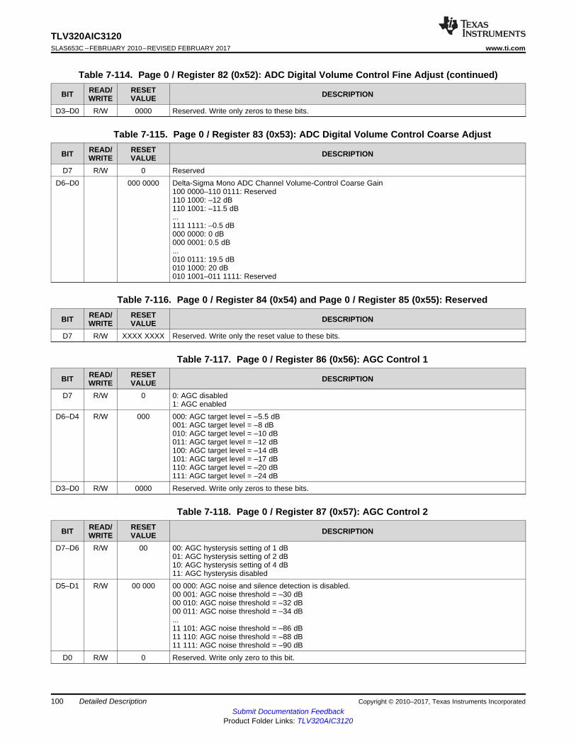
100
TLV320AIC3120SLAS653C –FEBRUARY 2010–REVISED FEBRUARY 2017 www.ti.com
Submit Documentation FeedbackProduct Folder Links: TLV320AIC3120
Detailed Description Copyright © 2010–2017, Texas Instruments Incorporated
Table 7-114. Page 0 / Register 82 (0x52): ADC Digital Volume Control Fine Adjust (continued)
BIT READ/WRITE
RESETVALUE DESCRIPTION
D3–D0 R/W 0000 Reserved. Write only zeros to these bits.
Table 7-115. Page 0 / Register 83 (0x53): ADC Digital Volume Control Coarse Adjust
BIT READ/WRITE
RESETVALUE DESCRIPTION
D7 R/W 0 ReservedD6–D0 000 0000 Delta-Sigma Mono ADC Channel Volume-Control Coarse Gain
100 0000–110 0111: Reserved110 1000: –12 dB110 1001: –11.5 dB...111 1111: –0.5 dB000 0000: 0 dB000 0001: 0.5 dB...010 0111: 19.5 dB010 1000: 20 dB010 1001–011 1111: Reserved
Table 7-116. Page 0 / Register 84 (0x54) and Page 0 / Register 85 (0x55): Reserved
BIT READ/WRITE
RESETVALUE DESCRIPTION
D7 R/W XXXX XXXX Reserved. Write only the reset value to these bits.
Table 7-117. Page 0 / Register 86 (0x56): AGC Control 1
BIT READ/WRITE
RESETVALUE DESCRIPTION
D7 R/W 0 0: AGC disabled1: AGC enabled
D6–D4 R/W 000 000: AGC target level = –5.5 dB001: AGC target level = –8 dB010: AGC target level = –10 dB011: AGC target level = –12 dB100: AGC target level = –14 dB101: AGC target level = –17 dB110: AGC target level = –20 dB111: AGC target level = –24 dB
D3–D0 R/W 0000 Reserved. Write only zeros to these bits.
Table 7-118. Page 0 / Register 87 (0x57): AGC Control 2
BIT READ/WRITE
RESETVALUE DESCRIPTION
D7–D6 R/W 00 00: AGC hysterysis setting of 1 dB01: AGC hysterysis setting of 2 dB10: AGC hysterysis setting of 4 dB11: AGC hysterysis disabled
D5–D1 R/W 00 000 00 000: AGC noise and silence detection is disabled.00 001: AGC noise threshold = –30 dB00 010: AGC noise threshold = –32 dB00 011: AGC noise threshold = –34 dB...11 101: AGC noise threshold = –86 dB11 110: AGC noise threshold = –88 dB11 111: AGC noise threshold = –90 dB
D0 R/W 0 Reserved. Write only zero to this bit.
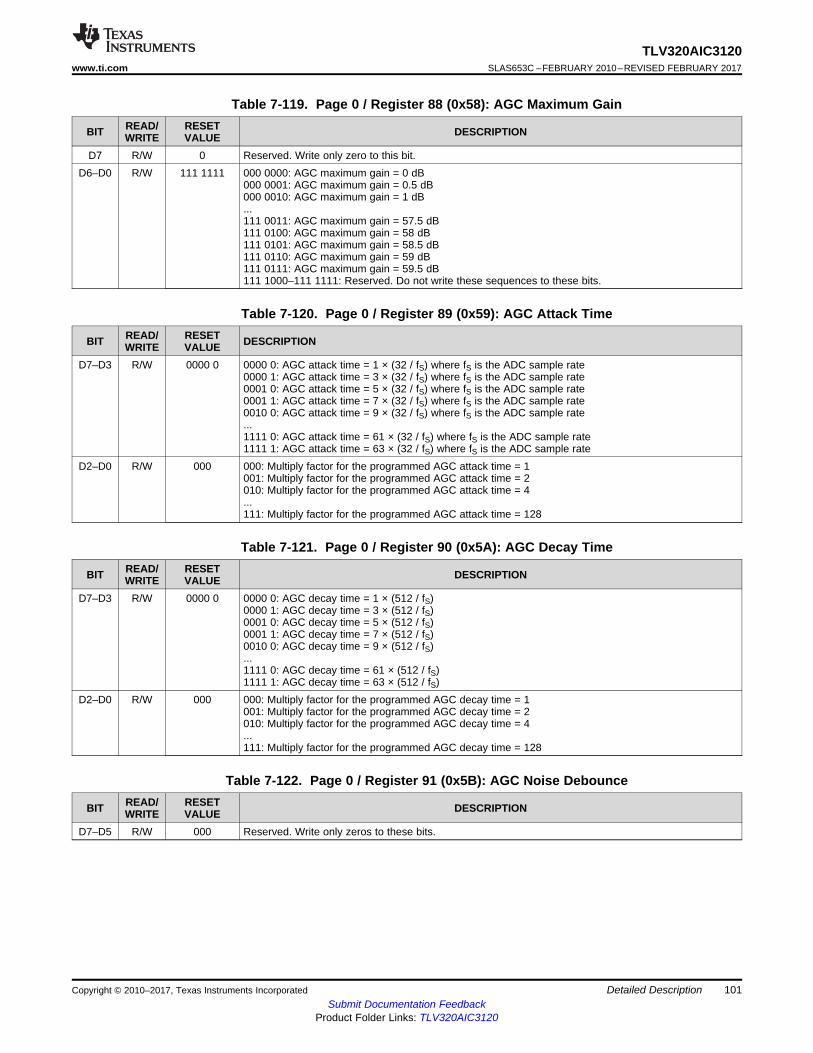
101
TLV320AIC3120www.ti.com SLAS653C –FEBRUARY 2010–REVISED FEBRUARY 2017
Submit Documentation FeedbackProduct Folder Links: TLV320AIC3120
Detailed DescriptionCopyright © 2010–2017, Texas Instruments Incorporated
Table 7-119. Page 0 / Register 88 (0x58): AGC Maximum Gain
BIT READ/WRITE
RESETVALUE DESCRIPTION
D7 R/W 0 Reserved. Write only zero to this bit.D6–D0 R/W 111 1111 000 0000: AGC maximum gain = 0 dB
000 0001: AGC maximum gain = 0.5 dB000 0010: AGC maximum gain = 1 dB...111 0011: AGC maximum gain = 57.5 dB111 0100: AGC maximum gain = 58 dB111 0101: AGC maximum gain = 58.5 dB111 0110: AGC maximum gain = 59 dB111 0111: AGC maximum gain = 59.5 dB111 1000–111 1111: Reserved. Do not write these sequences to these bits.
Table 7-120. Page 0 / Register 89 (0x59): AGC Attack Time
BIT READ/WRITE
RESETVALUE DESCRIPTION
D7–D3 R/W 0000 0 0000 0: AGC attack time = 1 × (32 / fS) where fS is the ADC sample rate0000 1: AGC attack time = 3 × (32 / fS) where fS is the ADC sample rate0001 0: AGC attack time = 5 × (32 / fS) where fS is the ADC sample rate0001 1: AGC attack time = 7 × (32 / fS) where fS is the ADC sample rate0010 0: AGC attack time = 9 × (32 / fS) where fS is the ADC sample rate...1111 0: AGC attack time = 61 × (32 / fS) where fS is the ADC sample rate1111 1: AGC attack time = 63 × (32 / fS) where fS is the ADC sample rate
D2–D0 R/W 000 000: Multiply factor for the programmed AGC attack time = 1001: Multiply factor for the programmed AGC attack time = 2010: Multiply factor for the programmed AGC attack time = 4...111: Multiply factor for the programmed AGC attack time = 128
Table 7-121. Page 0 / Register 90 (0x5A): AGC Decay Time
BIT READ/WRITE
RESETVALUE DESCRIPTION
D7–D3 R/W 0000 0 0000 0: AGC decay time = 1 × (512 / fS)0000 1: AGC decay time = 3 × (512 / fS)0001 0: AGC decay time = 5 × (512 / fS)0001 1: AGC decay time = 7 × (512 / fS)0010 0: AGC decay time = 9 × (512 / fS)...1111 0: AGC decay time = 61 × (512 / fS)1111 1: AGC decay time = 63 × (512 / fS)
D2–D0 R/W 000 000: Multiply factor for the programmed AGC decay time = 1001: Multiply factor for the programmed AGC decay time = 2010: Multiply factor for the programmed AGC decay time = 4...111: Multiply factor for the programmed AGC decay time = 128
Table 7-122. Page 0 / Register 91 (0x5B): AGC Noise Debounce
BIT READ/WRITE
RESETVALUE DESCRIPTION
D7–D5 R/W 000 Reserved. Write only zeros to these bits.
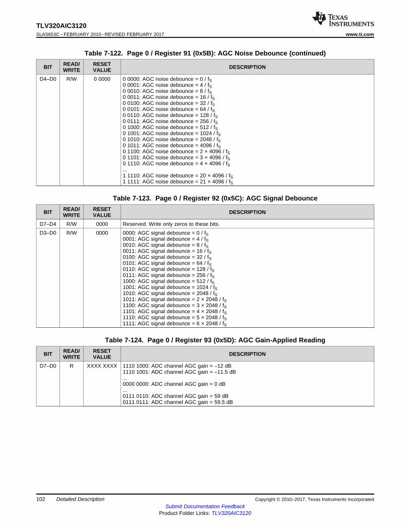
102
TLV320AIC3120SLAS653C –FEBRUARY 2010–REVISED FEBRUARY 2017 www.ti.com
Submit Documentation FeedbackProduct Folder Links: TLV320AIC3120
Detailed Description Copyright © 2010–2017, Texas Instruments Incorporated
Table 7-122. Page 0 / Register 91 (0x5B): AGC Noise Debounce (continued)
BIT READ/WRITE
RESETVALUE DESCRIPTION
D4–D0 R/W 0 0000 0 0000: AGC noise debounce = 0 / fS0 0001: AGC noise debounce = 4 / fS0 0010: AGC noise debounce = 8 / fS0 0011: AGC noise debounce = 16 / fS0 0100: AGC noise debounce = 32 / fS0 0101: AGC noise debounce = 64 / fS0 0110: AGC noise debounce = 128 / fS0 0111: AGC noise debounce = 256 / fS0 1000: AGC noise debounce = 512 / fS0 1001: AGC noise debounce = 1024 / fS0 1010: AGC noise debounce = 2048 / fS0 1011: AGC noise debounce = 4096 / fS0 1100: AGC noise debounce = 2 × 4096 / fS0 1101: AGC noise debounce = 3 × 4096 / fS0 1110: AGC noise debounce = 4 × 4096 / fS...1 1110: AGC noise debounce = 20 × 4096 / fS1 1111: AGC noise debounce = 21 × 4096 / fS
Table 7-123. Page 0 / Register 92 (0x5C): AGC Signal Debounce
BIT READ/WRITE
RESETVALUE DESCRIPTION
D7–D4 R/W 0000 Reserved. Write only zeros to these bits.D3–D0 R/W 0000 0000: AGC signal debounce = 0 / fS
0001: AGC signal debounce = 4 / fS0010: AGC signal debounce = 8 / fS0011: AGC signal debounce = 16 / fS0100: AGC signal debounce = 32 / fS0101: AGC signal debounce = 64 / fS0110: AGC signal debounce = 128 / fS0111: AGC signal debounce = 256 / fS1000: AGC signal debounce = 512 / fS1001: AGC signal debounce = 1024 / fS1010: AGC signal debounce = 2048 / fS1011: AGC signal debounce = 2 × 2048 / fS1100: AGC signal debounce = 3 × 2048 / fS1101: AGC signal debounce = 4 × 2048 / fS1110: AGC signal debounce = 5 × 2048 / fS1111: AGC signal debounce = 6 × 2048 / fS
Table 7-124. Page 0 / Register 93 (0x5D): AGC Gain-Applied Reading
BIT READ/WRITE
RESETVALUE DESCRIPTION
D7–D0 R XXXX XXXX 1110 1000: ADC channel AGC gain = –12 dB1110 1001: ADC channel AGC gain = –11.5 dB...0000 0000: ADC channel AGC gain = 0 dB...0111 0110: ADC channel AGC gain = 59 dB0111 0111: ADC channel AGC gain = 59.5 dB
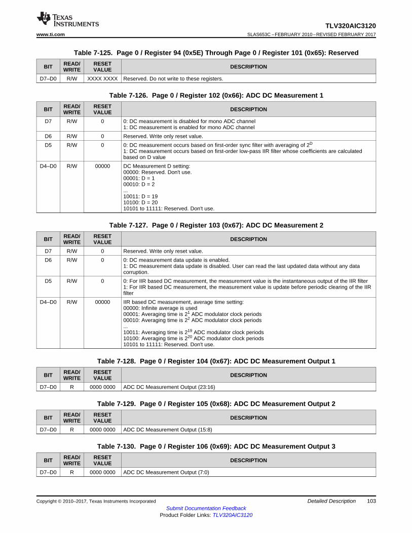
103
TLV320AIC3120www.ti.com SLAS653C –FEBRUARY 2010–REVISED FEBRUARY 2017
Submit Documentation FeedbackProduct Folder Links: TLV320AIC3120
Detailed DescriptionCopyright © 2010–2017, Texas Instruments Incorporated
Table 7-125. Page 0 / Register 94 (0x5E) Through Page 0 / Register 101 (0x65): Reserved
BIT READ/WRITE
RESETVALUE DESCRIPTION
D7–D0 R/W XXXX XXXX Reserved. Do not write to these registers.
Table 7-126. Page 0 / Register 102 (0x66): ADC DC Measurement 1
BIT READ/WRITE
RESETVALUE DESCRIPTION
D7 R/W 0 0: DC measurement is disabled for mono ADC channel1: DC measurement is enabled for mono ADC channel
D6 R/W 0 Reserved. Write only reset value.D5 R/W 0 0: DC measurement occurs based on first-order sync filter with averaging of 2D
1: DC measurement occurs based on first-order low-pass IIR filter whose coefficients are calculatedbased on D value
D4–D0 R/W 00000 DC Measurement D setting:00000: Reserved. Don't use.00001: D = 100010: D = 2...10011: D = 1910100: D = 2010101 to 11111: Reserved. Don't use.
Table 7-127. Page 0 / Register 103 (0x67): ADC DC Measurement 2
BIT READ/WRITE
RESETVALUE DESCRIPTION
D7 R/W 0 Reserved. Write only reset value.D6 R/W 0 0: DC measurement data update is enabled.
1: DC measurement data update is disabled. User can read the last updated data without any datacorruption.
D5 R/W 0 0: For IIR based DC measurement, the measurement value is the instantaneous output of the IIR filter1: For IIR based DC measurement, the measurement value is update before periodic clearing of the IIRfilter
D4–D0 R/W 00000 IIR based DC measurement, average time setting:00000: Infinite average is used00001: Averaging time is 21 ADC modulator clock periods00010: Averaging time is 22 ADC modulator clock periods...10011: Averaging time is 219 ADC modulator clock periods10100: Averaging time is 220 ADC modulator clock periods10101 to 11111: Reserved. Don't use.
Table 7-128. Page 0 / Register 104 (0x67): ADC DC Measurement Output 1
BIT READ/WRITE
RESETVALUE DESCRIPTION
D7–D0 R 0000 0000 ADC DC Measurement Output (23:16)
Table 7-129. Page 0 / Register 105 (0x68): ADC DC Measurement Output 2
BIT READ/WRITE
RESETVALUE DESCRIPTION
D7–D0 R 0000 0000 ADC DC Measurement Output (15:8)
Table 7-130. Page 0 / Register 106 (0x69): ADC DC Measurement Output 3
BIT READ/WRITE
RESETVALUE DESCRIPTION
D7–D0 R 0000 0000 ADC DC Measurement Output (7:0)
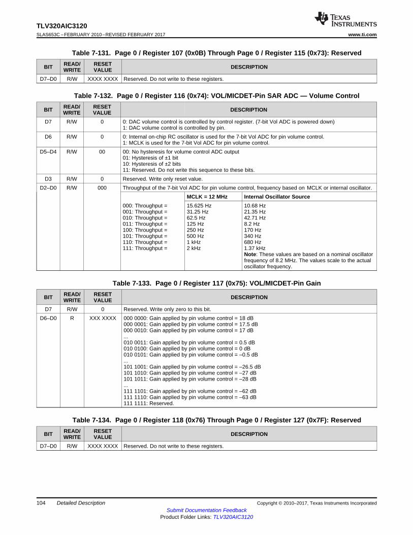
104
TLV320AIC3120SLAS653C –FEBRUARY 2010–REVISED FEBRUARY 2017 www.ti.com
Submit Documentation FeedbackProduct Folder Links: TLV320AIC3120
Detailed Description Copyright © 2010–2017, Texas Instruments Incorporated
Table 7-131. Page 0 / Register 107 (0x0B) Through Page 0 / Register 115 (0x73): Reserved
BIT READ/WRITE
RESETVALUE DESCRIPTION
D7–D0 R/W XXXX XXXX Reserved. Do not write to these registers.
Table 7-132. Page 0 / Register 116 (0x74): VOL/MICDET-Pin SAR ADC — Volume Control
BIT READ/WRITE
RESETVALUE DESCRIPTION
D7 R/W 0 0: DAC volume control is controlled by control register. (7-bit Vol ADC is powered down)1: DAC volume control is controlled by pin.
D6 R/W 0 0: Internal on-chip RC oscillator is used for the 7-bit Vol ADC for pin volume control.1: MCLK is used for the 7-bit Vol ADC for pin volume control.
D5–D4 R/W 00 00: No hysteresis for volume control ADC output01: Hysteresis of ±1 bit10: Hysteresis of ±2 bits11: Reserved. Do not write this sequence to these bits.
D3 R/W 0 Reserved. Write only reset value.D2–D0 R/W 000 Throughput of the 7-bit Vol ADC for pin volume control, frequency based on MCLK or internal oscillator.
MCLK = 12 MHz Internal Oscillator Source000: Throughput =001: Throughput =010: Throughput =011: Throughput =100: Throughput =101: Throughput =110: Throughput =111: Throughput =
15.625 Hz31.25 Hz62.5 Hz125 Hz250 Hz500 Hz1 kHz2 kHz
10.68 Hz21.35 Hz42.71 Hz8.2 Hz170 Hz340 Hz680 Hz1.37 kHzNote: These values are based on a nominal oscillatorfrequency of 8.2 MHz. The values scale to the actualoscillator frequency.
Table 7-133. Page 0 / Register 117 (0x75): VOL/MICDET-Pin Gain
BIT READ/WRITE
RESETVALUE DESCRIPTION
D7 R/W 0 Reserved. Write only zero to this bit.D6–D0 R XXX XXXX 000 0000: Gain applied by pin volume control = 18 dB
000 0001: Gain applied by pin volume control = 17.5 dB000 0010: Gain applied by pin volume control = 17 dB...010 0011: Gain applied by pin volume control = 0.5 dB010 0100: Gain applied by pin volume control = 0 dB010 0101: Gain applied by pin volume control = –0.5 dB...101 1001: Gain applied by pin volume control = –26.5 dB101 1010: Gain applied by pin volume control = –27 dB101 1011: Gain applied by pin volume control = –28 dB...111 1101: Gain applied by pin volume control = –62 dB111 1110: Gain applied by pin volume control = –63 dB111 1111: Reserved.
Table 7-134. Page 0 / Register 118 (0x76) Through Page 0 / Register 127 (0x7F): Reserved
BIT READ/WRITE
RESETVALUE DESCRIPTION
D7–D0 R/W XXXX XXXX Reserved. Do not write to these registers.
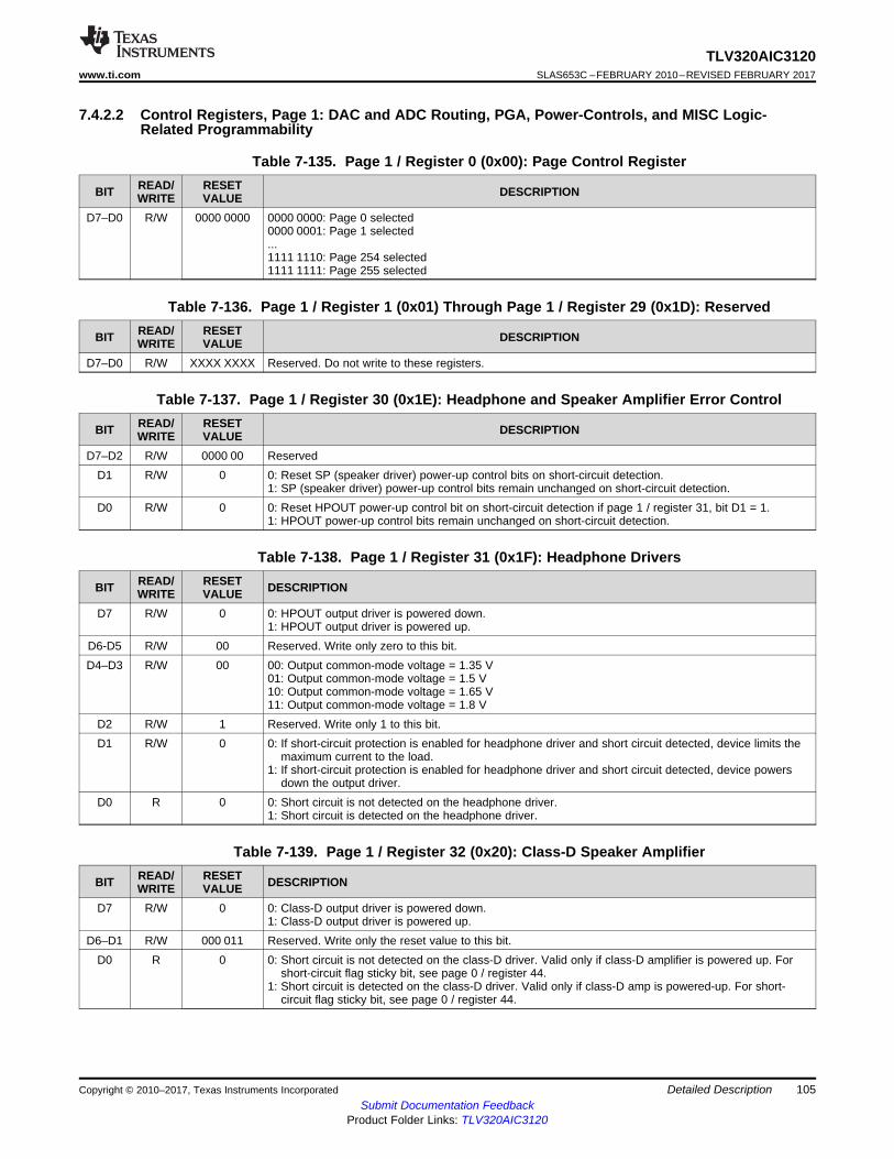
105
TLV320AIC3120www.ti.com SLAS653C –FEBRUARY 2010–REVISED FEBRUARY 2017
Submit Documentation FeedbackProduct Folder Links: TLV320AIC3120
Detailed DescriptionCopyright © 2010–2017, Texas Instruments Incorporated
7.4.2.2 Control Registers, Page 1: DAC and ADC Routing, PGA, Power-Controls, and MISC Logic-Related Programmability
Table 7-135. Page 1 / Register 0 (0x00): Page Control Register
BIT READ/WRITE
RESETVALUE DESCRIPTION
D7–D0 R/W 0000 0000 0000 0000: Page 0 selected0000 0001: Page 1 selected...1111 1110: Page 254 selected1111 1111: Page 255 selected
Table 7-136. Page 1 / Register 1 (0x01) Through Page 1 / Register 29 (0x1D): Reserved
BIT READ/WRITE
RESETVALUE DESCRIPTION
D7–D0 R/W XXXX XXXX Reserved. Do not write to these registers.
Table 7-137. Page 1 / Register 30 (0x1E): Headphone and Speaker Amplifier Error Control
BIT READ/WRITE
RESETVALUE DESCRIPTION
D7–D2 R/W 0000 00 ReservedD1 R/W 0 0: Reset SP (speaker driver) power-up control bits on short-circuit detection.
1: SP (speaker driver) power-up control bits remain unchanged on short-circuit detection.D0 R/W 0 0: Reset HPOUT power-up control bit on short-circuit detection if page 1 / register 31, bit D1 = 1.
1: HPOUT power-up control bits remain unchanged on short-circuit detection.
Table 7-138. Page 1 / Register 31 (0x1F): Headphone Drivers
BIT READ/WRITE
RESETVALUE DESCRIPTION
D7 R/W 0 0: HPOUT output driver is powered down.1: HPOUT output driver is powered up.
D6-D5 R/W 00 Reserved. Write only zero to this bit.D4–D3 R/W 00 00: Output common-mode voltage = 1.35 V
01: Output common-mode voltage = 1.5 V10: Output common-mode voltage = 1.65 V11: Output common-mode voltage = 1.8 V
D2 R/W 1 Reserved. Write only 1 to this bit.D1 R/W 0 0: If short-circuit protection is enabled for headphone driver and short circuit detected, device limits the
maximum current to the load.1: If short-circuit protection is enabled for headphone driver and short circuit detected, device powers
down the output driver.D0 R 0 0: Short circuit is not detected on the headphone driver.
1: Short circuit is detected on the headphone driver.
Table 7-139. Page 1 / Register 32 (0x20): Class-D Speaker Amplifier
BIT READ/WRITE
RESETVALUE DESCRIPTION
D7 R/W 0 0: Class-D output driver is powered down.1: Class-D output driver is powered up.
D6–D1 R/W 000 011 Reserved. Write only the reset value to this bit.D0 R 0 0: Short circuit is not detected on the class-D driver. Valid only if class-D amplifier is powered up. For
short-circuit flag sticky bit, see page 0 / register 44.1: Short circuit is detected on the class-D driver. Valid only if class-D amp is powered-up. For short-
circuit flag sticky bit, see page 0 / register 44.
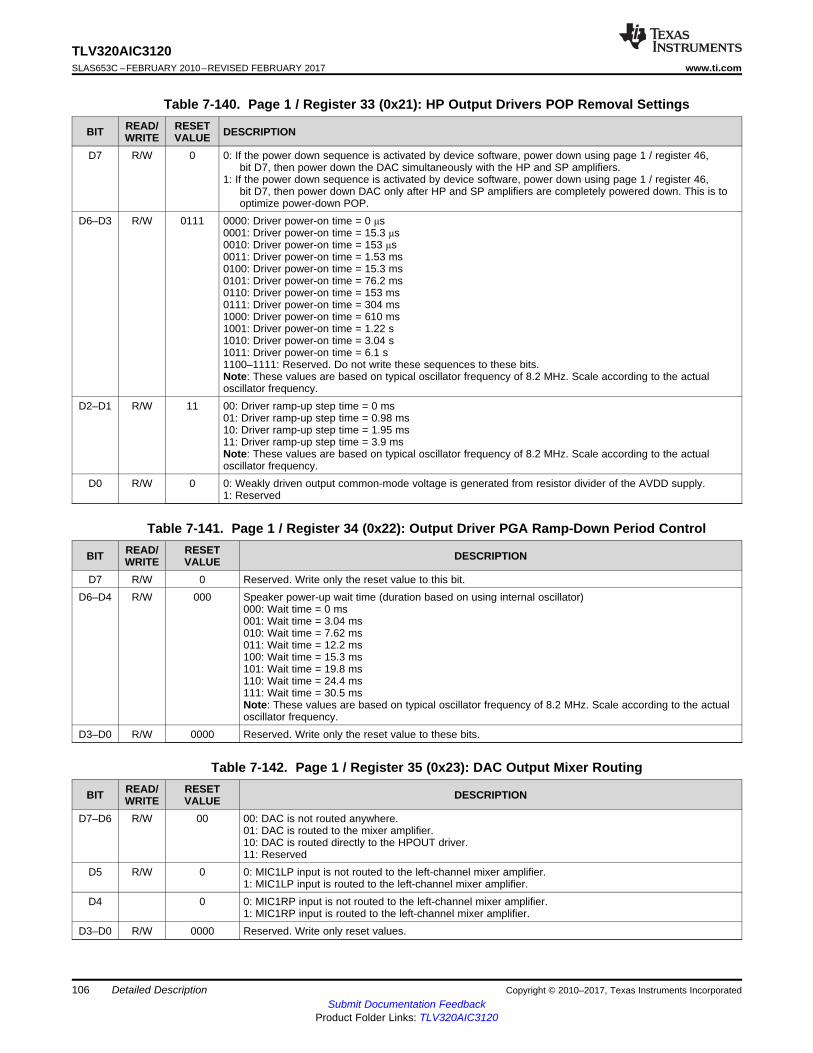
106
TLV320AIC3120SLAS653C –FEBRUARY 2010–REVISED FEBRUARY 2017 www.ti.com
Submit Documentation FeedbackProduct Folder Links: TLV320AIC3120
Detailed Description Copyright © 2010–2017, Texas Instruments Incorporated
Table 7-140. Page 1 / Register 33 (0x21): HP Output Drivers POP Removal Settings
BIT READ/WRITE
RESETVALUE DESCRIPTION
D7 R/W 0 0: If the power down sequence is activated by device software, power down using page 1 / register 46, bit D7, then power down the DAC simultaneously with the HP and SP amplifiers.1: If the power down sequence is activated by device software, power down using page 1 / register 46, bit D7, then power down DAC only after HP and SP amplifiers are completely powered down. This is to optimize power-down POP.
D6–D3 R/W 0111 0000: Driver power-on time = 0 μs0001: Driver power-on time = 15.3 μs0010: Driver power-on time = 153 μs0011: Driver power-on time = 1.53 ms0100: Driver power-on time = 15.3 ms0101: Driver power-on time = 76.2 ms0110: Driver power-on time = 153 ms0111: Driver power-on time = 304 ms1000: Driver power-on time = 610 ms1001: Driver power-on time = 1.22 s1010: Driver power-on time = 3.04 s1011: Driver power-on time = 6.1 s1100–1111: Reserved. Do not write these sequences to these bits.Note: These values are based on typical oscillator frequency of 8.2 MHz. Scale according to the actualoscillator frequency.
D2–D1 R/W 11 00: Driver ramp-up step time = 0 ms01: Driver ramp-up step time = 0.98 ms10: Driver ramp-up step time = 1.95 ms11: Driver ramp-up step time = 3.9 msNote: These values are based on typical oscillator frequency of 8.2 MHz. Scale according to the actualoscillator frequency.
D0 R/W 0 0: Weakly driven output common-mode voltage is generated from resistor divider of the AVDD supply.1: Reserved
Table 7-141. Page 1 / Register 34 (0x22): Output Driver PGA Ramp-Down Period Control
BIT READ/WRITE
RESETVALUE DESCRIPTION
D7 R/W 0 Reserved. Write only the reset value to this bit.D6–D4 R/W 000 Speaker power-up wait time (duration based on using internal oscillator)
000: Wait time = 0 ms001: Wait time = 3.04 ms010: Wait time = 7.62 ms011: Wait time = 12.2 ms100: Wait time = 15.3 ms101: Wait time = 19.8 ms110: Wait time = 24.4 ms111: Wait time = 30.5 msNote: These values are based on typical oscillator frequency of 8.2 MHz. Scale according to the actualoscillator frequency.
D3–D0 R/W 0000 Reserved. Write only the reset value to these bits.
Table 7-142. Page 1 / Register 35 (0x23): DAC Output Mixer Routing
BIT READ/WRITE
RESETVALUE DESCRIPTION
D7–D6 R/W 00 00: DAC is not routed anywhere.01: DAC is routed to the mixer amplifier.10: DAC is routed directly to the HPOUT driver.11: Reserved
D5 R/W 0 0: MIC1LP input is not routed to the left-channel mixer amplifier.1: MIC1LP input is routed to the left-channel mixer amplifier.
D4 0 0: MIC1RP input is not routed to the left-channel mixer amplifier.1: MIC1RP input is routed to the left-channel mixer amplifier.
D3–D0 R/W 0000 Reserved. Write only reset values.
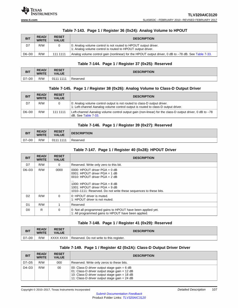
107
TLV320AIC3120www.ti.com SLAS653C –FEBRUARY 2010–REVISED FEBRUARY 2017
Submit Documentation FeedbackProduct Folder Links: TLV320AIC3120
Detailed DescriptionCopyright © 2010–2017, Texas Instruments Incorporated
Table 7-143. Page 1 / Register 36 (0x24): Analog Volume to HPOUT
BIT READ/WRITE
RESETVALUE DESCRIPTION
D7 R/W 0 0: Analog volume control is not routed to HPOUT output driver.1: Analog volume control is routed to HPOUT output driver.
D6–D0 R/W 111 1111 Analog volume control gain (nonlinear) for the HPOUT output driver, 0 dB to –78 dB. See Table 7-33.
Table 7-144. Page 1 / Register 37 (0x25): Reserved
BIT READ/WRITE
RESETVALUE DESCRIPTION
D7–D0 R/W 0111 1111 Reserved
Table 7-145. Page 1 / Register 38 (0x26): Analog Volume to Class-D Output Driver
BIT READ/WRITE
RESETVALUE DESCRIPTION
D7 R/W 0 0: Analog volume control output is not routed to class-D output driver.1: Left-channel Aanalog volume control output is routed to class-D output driver.
D6–D0 R/W 111 1111 Left-channel Aanalog volume control output gain (non-linear) for the class-D output driver, 0 dB to –78dB. See Table 7-33.
Table 7-146. Page 1 / Register 39 (0x27): Reserved
BIT READ/WRITE
RESETVALUE DESCRIPTION
D7–D0 R/W 0111 1111 Reserved
Table 7-147. Page 1 / Register 40 (0x28): HPOUT Driver
BIT READ/WRITE
RESETVALUE DESCRIPTION
D7 R/W 0 Reserved. Write only zero to this bit.D6–D3 R/W 0000 0000: HPOUT driver PGA = 0 dB
0001: HPOUT driver PGA = 1 dB0010: HPOUT driver PGA = 2 dB...1000: HPOUT driver PGA = 8 dB1001: HPOUT driver PGA = 9 dB1010–1111: Reserved. Do not write these sequences to these bits.
D2 R/W 0 0: HPOUT driver is muted.1: HPOUT driver is not muted.
D1 R/W 1 ReservedD0 R 0 0: Not all programmed gains to HPOUT have been applied yet.
1: All programmed gains to HPOUT have been applied.
Table 7-148. Page 1 / Register 41 (0x29): Reserved
BIT READ/WRITE
RESETVALUE DESCRIPTION
D7–D0 R/W XXXX XXXX Reserved. Do not write to this register.
Table 7-149. Page 1 / Register 42 (0x2A): Class-D Output Driver Driver
BIT READ/WRITE
RESETVALUE DESCRIPTION
D7–D5 R/W 000 Reserved. Write only zeros to these bits.D4–D3 R/W 00 00: Class-D driver output stage gain = 6 dB
01: Class-D driver output stage gain = 12 dB10: Class-D driver output stage gain = 18 dB11: Class-D driver output stage gain = 24 dB
108
TLV320AIC3120SLAS653C –FEBRUARY 2010–REVISED FEBRUARY 2017 www.ti.com
Submit Documentation FeedbackProduct Folder Links: TLV320AIC3120
Detailed Description Copyright © 2010–2017, Texas Instruments Incorporated
Table 7-149. Page 1 / Register 42 (0x2A): Class-D Output Driver Driver (continued)
BIT READ/WRITE
RESETVALUE DESCRIPTION
D2 R/W 0 0: Class-D driver is muted.1: Class-D driver is not muted.
D1 R/W 0 Reserved. Write only zero to this bit.D0 R 0 0: Not all programmed gains to the Class-D driver have been applied yet.
1: All programmed gains to the Class-D driver have been applied.
Table 7-150. Page 1 / Register 43 (0x2B): Reserved
BIT READ/WRITE
RESETVALUE DESCRIPTION
D7-D0 R/W XXXX XXXX Reserved. Write only zero to this bit.
(1) The clock used for the debounce has a clock period = debounce duration / 8.
Table 7-151. Page 1 / Register 44 (0x2C): HP Driver Control
BIT READ/WRITE
RESETVALUE DESCRIPTION
D7–D5 R/W 000 Debounce time for the headset short-circuit detection
(1)MCLK/DIV (Page 3 /register 16) = 1-MHzSource
Internal Oscillator Source
000: Debounce time =001: Debounce time =010: Debounce time =011: Debounce time =100: Debounce time =101: Debounce time =110: Debounce time =111: Debounce time =
0 μs8 μs16 μs32 μs64 μs128 μs256 μs512 μs
0 μs7.8 μs15.6 μs31.2 μs62.4 μs124.9 μs250 μs500 μsNote: These values are based on a nominal oscillatorfrequency of 8.2 MHz. The values scale to the actualoscillator frequency.
D4–D3 R/W 00 00: Default mode for the DAC01: DAC performance increased by increasing the current10: Reserved11: DAC performance increased further by increasing the current again
D2 R/W 0 0: HPOUT output driver is programmed as headphone driver.1: HPOUT output driver is programmed as lineout driver.
D1-D0 R/W 0 Reserved. Write only zero to this bit.
Table 7-152. Page 1 / Register 45 (0x2D): Reserved
BIT READ/WRITE
RESETVALUE DESCRIPTION
D7–D0 R/W XXXX XXXX Reserved. Do not write to these registers.
Table 7-153. Page 1 / Register 46 (0x2E): MICBIAS
BIT READ/WRITE
RESETVALUE DESCRIPTION
D7 R/W 0 0: Device software power down is not enabled.1: Device software power down is enabled.
D6–D4 R/W 000 Reserved. Write only zeros to these bits.D3 R/W 0 0: Programmed MICBIAS is not powered up if headset detection is enabled but headset is not inserted.
1: Programmed MICBIAS is powered up even if headset is not inserted.D2 R/W 0 Reserved. Write only zero to this bit.
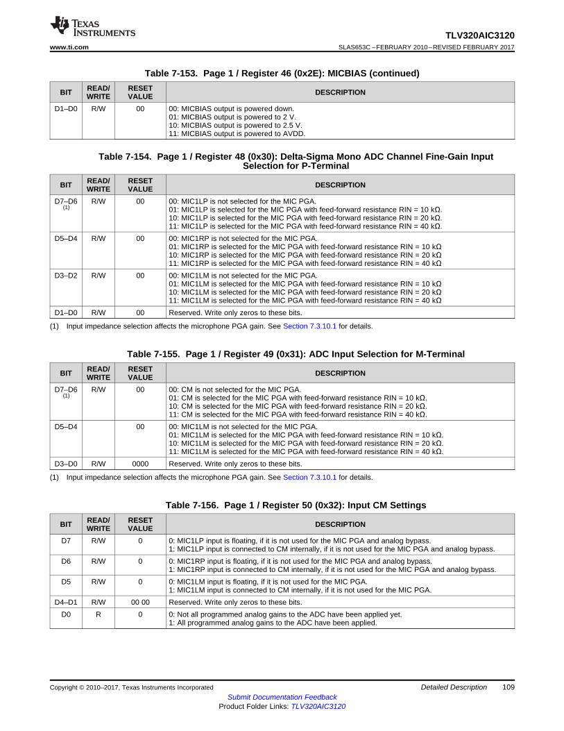
109
TLV320AIC3120www.ti.com SLAS653C –FEBRUARY 2010–REVISED FEBRUARY 2017
Submit Documentation FeedbackProduct Folder Links: TLV320AIC3120
Detailed DescriptionCopyright © 2010–2017, Texas Instruments Incorporated
Table 7-153. Page 1 / Register 46 (0x2E): MICBIAS (continued)
BIT READ/WRITE
RESETVALUE DESCRIPTION
D1–D0 R/W 00 00: MICBIAS output is powered down.01: MICBIAS output is powered to 2 V.10: MICBIAS output is powered to 2.5 V.11: MICBIAS output is powered to AVDD.
(1) Input impedance selection affects the microphone PGA gain. See Section 7.3.10.1 for details.
Table 7-154. Page 1 / Register 48 (0x30): Delta-Sigma Mono ADC Channel Fine-Gain InputSelection for P-Terminal
BIT READ/WRITE
RESETVALUE DESCRIPTION
D7–D6(1)
R/W 00 00: MIC1LP is not selected for the MIC PGA.01: MIC1LP is selected for the MIC PGA with feed-forward resistance RIN = 10 kΩ.10: MIC1LP is selected for the MIC PGA with feed-forward resistance RIN = 20 kΩ.11: MIC1LP is selected for the MIC PGA with feed-forward resistance RIN = 40 kΩ.
D5–D4 R/W 00 00: MIC1RP is not selected for the MIC PGA.01: MIC1RP is selected for the MIC PGA with feed-forward resistance RIN = 10 kΩ10: MIC1RP is selected for the MIC PGA with feed-forward resistance RIN = 20 kΩ11: MIC1RP is selected for the MIC PGA with feed-forward resistance RIN = 40 kΩ
D3–D2 R/W 00 00: MIC1LM is not selected for the MIC PGA.01: MIC1LM is selected for the MIC PGA with feed-forward resistance RIN = 10 kΩ10: MIC1LM is selected for the MIC PGA with feed-forward resistance RIN = 20 kΩ11: MIC1LM is selected for the MIC PGA with feed-forward resistance RIN = 40 kΩ
D1–D0 R/W 00 Reserved. Write only zeros to these bits.
(1) Input impedance selection affects the microphone PGA gain. See Section 7.3.10.1 for details.
Table 7-155. Page 1 / Register 49 (0x31): ADC Input Selection for M-Terminal
BIT READ/WRITE
RESETVALUE DESCRIPTION
D7–D6(1)
R/W 00 00: CM is not selected for the MIC PGA.01: CM is selected for the MIC PGA with feed-forward resistance RIN = 10 kΩ.10: CM is selected for the MIC PGA with feed-forward resistance RIN = 20 kΩ.11: CM is selected for the MIC PGA with feed-forward resistance RIN = 40 kΩ.
D5–D4 00 00: MIC1LM is not selected for the MIC PGA.01: MIC1LM is selected for the MIC PGA with feed-forward resistance RIN = 10 kΩ.10: MIC1LM is selected for the MIC PGA with feed-forward resistance RIN = 20 kΩ.11: MIC1LM is selected for the MIC PGA with feed-forward resistance RIN = 40 kΩ.
D3–D0 R/W 0000 Reserved. Write only zeros to these bits.
Table 7-156. Page 1 / Register 50 (0x32): Input CM Settings
BIT READ/WRITE
RESETVALUE DESCRIPTION
D7 R/W 0 0: MIC1LP input is floating, if it is not used for the MIC PGA and analog bypass.1: MIC1LP input is connected to CM internally, if it is not used for the MIC PGA and analog bypass.
D6 R/W 0 0: MIC1RP input is floating, if it is not used for the MIC PGA and analog bypass.1: MIC1RP input is connected to CM internally, if it is not used for the MIC PGA and analog bypass.
D5 R/W 0 0: MIC1LM input is floating, if it is not used for the MIC PGA.1: MIC1LM input is connected to CM internally, if it is not used for the MIC PGA.
D4–D1 R/W 00 00 Reserved. Write only zeros to these bits.D0 R 0 0: Not all programmed analog gains to the ADC have been applied yet.
1: All programmed analog gains to the ADC have been applied.
110
TLV320AIC3120SLAS653C –FEBRUARY 2010–REVISED FEBRUARY 2017 www.ti.com
Submit Documentation FeedbackProduct Folder Links: TLV320AIC3120
Detailed Description Copyright © 2010–2017, Texas Instruments Incorporated
Table 7-157. Page 1 / Register 51 (0x33) Through Page 1 / Register 127 (0x7F): Reserved
BIT READ/WRITE
RESETVALUE DESCRIPTION
D7–D0 R/W XXXX XXXX Reserved. Write only the reset value to these bits.
7.4.2.3 Control Registers, Page 3: MCLK Divider for Programmable Delay Timer
Default values shown for this page only become valid 100 μs following a hardware or software reset.
Table 7-158. Page 3 / Register 0: Page Control Register
BIT READ/WRITE
RESETVALUE DESCRIPTION
D7–D0 R/W 0000 0000 0000 0000: Page 0 selected0000 0001: Page 1 selected...1111 1110: Page 254 selected1111 1111: Page 255 selected
(1) External clock is used only to control the delay programmed between the conversions and not used for doing the actual conversion. Thisfeature is provided in case a more accurate delay is desired because the internal oscillator frequency varies from device to device.
The only register used in page 3 is register 16. The remaining page-3 registers are reserved and must notbe written to.
Table 7-159. Page 3 / Register 16: Timer Clock MCLK Divider
BIT READ/WRITE
RESETVALUE DESCRIPTION
D7 R/W 1 0: Internal oscillator is used for programmable delay timer.1: External MCLK (1) is used for programmable delay timer.
D6–D0 R/W 000 0001 MCLK Divider to Generate 1-MHz Clock for the Programmable Delay Timer000 0000: MCLK divider = 128000 0001: MCLK divider = 1000 0010: MCLK divider = 2...111 1110: MCLK divider = 126111 1111: MCLK divider = 127
7.4.2.4 Control Registers, Page 4: ADC Digital Filter Coefficients
Default values shown for this page only become valid 100 μs following a hardware or software reset.
Table 7-160. Page 4 / Register 0 (0x00): Page Control Register
BIT READ/WRITE
RESETVALUE DESCRIPTION
D7–D0 R/W 0000 0000 0000 0000: Page 0 selected0000 0001: Page 1 selected...1111 1110: Page 254 selected1111 1111: Page 255 selected
The remaining page-4 registers are either reserved registers or are used for setting coefficients for thevarious filters in the TLV320AIC3120. Reserved registers must not be written to.
The filter coefficient registers are arranged in pairs, with two adjacent 8-bit registers containing the 16-bitcoefficient for a single filter. The 16-bit integer contained in the MSB and LSB registers for a coefficientare interpreted as a 2s-complement integer, with possible values ranging from –32 768 to 32 767. Whenprogramming any coefficient value for a filter, the MSB register must always be written first, immediatelyfollowed by the LSB register. Even if only the MSB or LSB portion of the coefficient changes, bothregisters must be written in this sequence. is a list of the page-4 registers, excepting the previouslydescribed register 0.
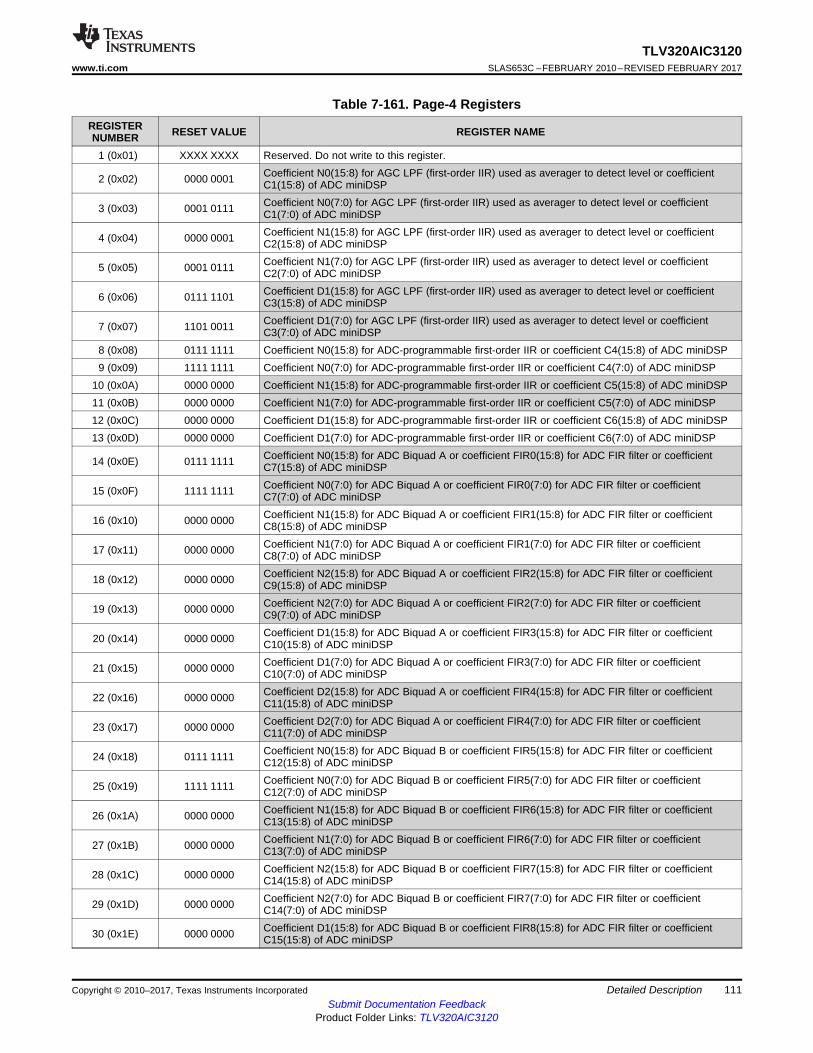
111
TLV320AIC3120www.ti.com SLAS653C –FEBRUARY 2010–REVISED FEBRUARY 2017
Submit Documentation FeedbackProduct Folder Links: TLV320AIC3120
Detailed DescriptionCopyright © 2010–2017, Texas Instruments Incorporated
Table 7-161. Page-4 RegistersREGISTERNUMBER RESET VALUE REGISTER NAME
1 (0x01) XXXX XXXX Reserved. Do not write to this register.
2 (0x02) 0000 0001 Coefficient N0(15:8) for AGC LPF (first-order IIR) used as averager to detect level or coefficientC1(15:8) of ADC miniDSP
3 (0x03) 0001 0111 Coefficient N0(7:0) for AGC LPF (first-order IIR) used as averager to detect level or coefficientC1(7:0) of ADC miniDSP
4 (0x04) 0000 0001 Coefficient N1(15:8) for AGC LPF (first-order IIR) used as averager to detect level or coefficientC2(15:8) of ADC miniDSP
5 (0x05) 0001 0111 Coefficient N1(7:0) for AGC LPF (first-order IIR) used as averager to detect level or coefficientC2(7:0) of ADC miniDSP
6 (0x06) 0111 1101 Coefficient D1(15:8) for AGC LPF (first-order IIR) used as averager to detect level or coefficientC3(15:8) of ADC miniDSP
7 (0x07) 1101 0011 Coefficient D1(7:0) for AGC LPF (first-order IIR) used as averager to detect level or coefficientC3(7:0) of ADC miniDSP
8 (0x08) 0111 1111 Coefficient N0(15:8) for ADC-programmable first-order IIR or coefficient C4(15:8) of ADC miniDSP9 (0x09) 1111 1111 Coefficient N0(7:0) for ADC-programmable first-order IIR or coefficient C4(7:0) of ADC miniDSP
10 (0x0A) 0000 0000 Coefficient N1(15:8) for ADC-programmable first-order IIR or coefficient C5(15:8) of ADC miniDSP11 (0x0B) 0000 0000 Coefficient N1(7:0) for ADC-programmable first-order IIR or coefficient C5(7:0) of ADC miniDSP12 (0x0C) 0000 0000 Coefficient D1(15:8) for ADC-programmable first-order IIR or coefficient C6(15:8) of ADC miniDSP13 (0x0D) 0000 0000 Coefficient D1(7:0) for ADC-programmable first-order IIR or coefficient C6(7:0) of ADC miniDSP
14 (0x0E) 0111 1111 Coefficient N0(15:8) for ADC Biquad A or coefficient FIR0(15:8) for ADC FIR filter or coefficientC7(15:8) of ADC miniDSP
15 (0x0F) 1111 1111 Coefficient N0(7:0) for ADC Biquad A or coefficient FIR0(7:0) for ADC FIR filter or coefficientC7(7:0) of ADC miniDSP
16 (0x10) 0000 0000 Coefficient N1(15:8) for ADC Biquad A or coefficient FIR1(15:8) for ADC FIR filter or coefficientC8(15:8) of ADC miniDSP
17 (0x11) 0000 0000 Coefficient N1(7:0) for ADC Biquad A or coefficient FIR1(7:0) for ADC FIR filter or coefficientC8(7:0) of ADC miniDSP
18 (0x12) 0000 0000 Coefficient N2(15:8) for ADC Biquad A or coefficient FIR2(15:8) for ADC FIR filter or coefficientC9(15:8) of ADC miniDSP
19 (0x13) 0000 0000 Coefficient N2(7:0) for ADC Biquad A or coefficient FIR2(7:0) for ADC FIR filter or coefficientC9(7:0) of ADC miniDSP
20 (0x14) 0000 0000 Coefficient D1(15:8) for ADC Biquad A or coefficient FIR3(15:8) for ADC FIR filter or coefficientC10(15:8) of ADC miniDSP
21 (0x15) 0000 0000 Coefficient D1(7:0) for ADC Biquad A or coefficient FIR3(7:0) for ADC FIR filter or coefficientC10(7:0) of ADC miniDSP
22 (0x16) 0000 0000 Coefficient D2(15:8) for ADC Biquad A or coefficient FIR4(15:8) for ADC FIR filter or coefficientC11(15:8) of ADC miniDSP
23 (0x17) 0000 0000 Coefficient D2(7:0) for ADC Biquad A or coefficient FIR4(7:0) for ADC FIR filter or coefficientC11(7:0) of ADC miniDSP
24 (0x18) 0111 1111 Coefficient N0(15:8) for ADC Biquad B or coefficient FIR5(15:8) for ADC FIR filter or coefficientC12(15:8) of ADC miniDSP
25 (0x19) 1111 1111 Coefficient N0(7:0) for ADC Biquad B or coefficient FIR5(7:0) for ADC FIR filter or coefficientC12(7:0) of ADC miniDSP
26 (0x1A) 0000 0000 Coefficient N1(15:8) for ADC Biquad B or coefficient FIR6(15:8) for ADC FIR filter or coefficientC13(15:8) of ADC miniDSP
27 (0x1B) 0000 0000 Coefficient N1(7:0) for ADC Biquad B or coefficient FIR6(7:0) for ADC FIR filter or coefficientC13(7:0) of ADC miniDSP
28 (0x1C) 0000 0000 Coefficient N2(15:8) for ADC Biquad B or coefficient FIR7(15:8) for ADC FIR filter or coefficientC14(15:8) of ADC miniDSP
29 (0x1D) 0000 0000 Coefficient N2(7:0) for ADC Biquad B or coefficient FIR7(7:0) for ADC FIR filter or coefficientC14(7:0) of ADC miniDSP
30 (0x1E) 0000 0000 Coefficient D1(15:8) for ADC Biquad B or coefficient FIR8(15:8) for ADC FIR filter or coefficientC15(15:8) of ADC miniDSP
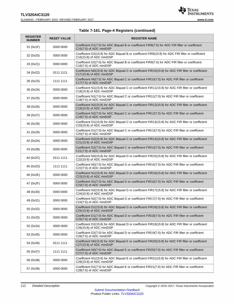
112
TLV320AIC3120SLAS653C –FEBRUARY 2010–REVISED FEBRUARY 2017 www.ti.com
Submit Documentation FeedbackProduct Folder Links: TLV320AIC3120
Detailed Description Copyright © 2010–2017, Texas Instruments Incorporated
Table 7-161. Page-4 Registers (continued)REGISTERNUMBER RESET VALUE REGISTER NAME
31 (0x1F) 0000 0000 Coefficient D1(7:0) for ADC Biquad B or coefficient FIR8(7:0) for ADC FIR filter or coefficientC15(7:0) of ADC miniDSP
32 (0x20) 0000 0000 Coefficient D2(15:8) for ADC Biquad B or coefficient FIR9(15:8) for ADC FIR filter or coefficientC16(15:8) of ADC miniDSP
33 (0x21) 0000 0000 Coefficient D2(7:0) for ADC Biquad B or coefficient FIR9(7:0) for ADC FIR filter or coefficientC16(7:0) of ADC miniDSP
34 (0x22) 0111 1111 Coefficient N0(15:8) for ADC Biquad C or coefficient FIR10(15:8) for ADC FIR filter or coefficientC17(15:8) of ADC miniDSP
35 (0x23) 1111 1111 Coefficient N0(7:0) for ADC Biquad C or coefficient FIR10(7:0) for ADC FIR filter or coefficientC17(7:0) of ADC miniDSP
36 (0x24) 0000 0000 Coefficient N1(15:8) for ADC Biquad C or coefficient FIR11(15:8) for ADC FIR filter or coefficientC18(15:8) of ADC miniDSP
37 (0x25) 0000 0000 Coefficient N1(7:0) for ADC Biquad C or coefficient FIR11(7:0) for ADC FIR filter or coefficientC18(7:0) of ADC miniDSP
38 (0x26) 0000 0000 Coefficient N2(15:8) for ADC Biquad C or coefficient FIR12(15:8) for ADC FIR filter or coefficientC19(15:8) of ADC miniDSP
39 (0x27) 0000 0000 Coefficient N2(7:0) for ADC Biquad C or coefficient FIR12(7:0) for ADC FIR filter or coefficientC19(7:0) of ADC miniDSP
40 (0x28) 0000 0000 Coefficient D1(15:8) for ADC Biquad C or coefficient FIR13(15:8) for ADC FIR filter or coefficientC20(15:8) of ADC miniDSP
41 (0x29) 0000 0000 Coefficient D1(7:0) for ADC Biquad C or coefficient FIR13(7:0) for ADC FIR filter or coefficientC20(7:0) of ADC miniDSP
42 (0x2A) 0000 0000 Coefficient D2(15:8) for ADC Biquad C or coefficient FIR14(15:8) for ADC FIR filter or coefficientC21(15:8) of ADC miniDSP
43 (0x2B) 0000 0000 Coefficient D2(7:0) for ADC Biquad C or coefficient FIR14(7:0) for ADC FIR filter or coefficientC21(7:0) of ADC miniDSP
44 (0x2C) 0111 1111 Coefficient N0(15:8) for ADC Biquad D or coefficient FIR15(15:8) for ADC FIR filter or coefficientC22(15:8) of ADC miniDSP
45 (0x2D) 1111 1111 Coefficient N0(7:0) for ADC Biquad D or coefficient FIR15(7:0) for ADC FIR filter or coefficientC22(7:0) of ADC miniDSP
46 (0x2E) 0000 0000 Coefficient N1(15:8) for ADC Biquad D or coefficient FIR16(15:8) for ADC FIR filter or coefficientC23(15:8) of ADC miniDSP
47 (0x2F) 0000 0000 Coefficient N1(7:0) for ADC Biquad D or coefficient FIR16(7:0) for ADC FIR filter or coefficientC23(7:0) of ADC miniDSP
48 (0x30) 0000 0000 Coefficient N2(15:8) for ADC Biquad D or coefficient FIR17(15:8) for ADC FIR filter or coefficientC24(15:8) of ADC miniDSP
49 (0x31) 0000 0000 Coefficient N2(7:0) for ADC Biquad D or coefficient FIR17(7:0) for ADC FIR filter or coefficientC24(7:0) of ADC miniDSP
50 (0x32) 0000 0000 Coefficient D1(15:8) for ADC Biquad D or coefficient FIR18(15:8) for ADC FIR filter or coefficientC25(15:8) of ADC miniDSP
51 (0x33) 0000 0000 Coefficient D1(7:0) for ADC Biquad D or coefficient FIR18(7:0) for ADC FIR filter or coefficientC25(7:0) of ADC miniDSP
52 (0x34) 0000 0000 Coefficient D2(15:8) for ADC Biquad D or coefficient FIR19(15:8) for ADC FIR filter or coefficientC26(15:8) of ADC miniDSP
53 (0x35) 0000 0000 Coefficient D2(7:0) for ADC Biquad D or coefficient FIR19(7:0) for ADC FIR filter or coefficientC26(7:0) of ADC miniDSP
54 (0x36) 0111 1111 Coefficient N0(15:8) for ADC Biquad E or coefficient FIR20(15:8) for ADC FIR filter or coefficientC27(15:8) of ADC miniDSP
55 (0x37) 1111 1111 Coefficient N0(7:0) for ADC Biquad E or coefficient FIR20(7:0) for ADC FIR filter or coefficientC27(7:0) of ADC miniDSP
56 (0x38) 0000 0000 Coefficient N1(15:8) for ADC Biquad E or coefficient FIR21(15:8) for ADC FIR filter or coefficientC28(15:8) of ADC miniDSP
57 (0x39) 0000 0000 Coefficient N1(7:0) for ADC Biquad E or coefficient FIR21(7:0) for ADC FIR filter or coefficientC28(7:0) of ADC miniDSP
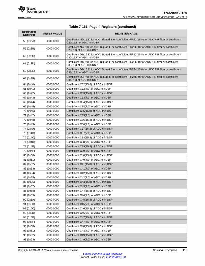
113
TLV320AIC3120www.ti.com SLAS653C –FEBRUARY 2010–REVISED FEBRUARY 2017
Submit Documentation FeedbackProduct Folder Links: TLV320AIC3120
Detailed DescriptionCopyright © 2010–2017, Texas Instruments Incorporated
Table 7-161. Page-4 Registers (continued)REGISTERNUMBER RESET VALUE REGISTER NAME
58 (0x3A) 0000 0000 Coefficient N2(15:8) for ADC Biquad E or coefficient FIR22(15:8) for ADC FIR filter or coefficientC29(15:8) of ADC miniDSP
59 (0x3B) 0000 0000 Coefficient N2(7:0) for ADC Biquad E or coefficient FIR22(7:0) for ADC FIR filter or coefficientC29(7:0) of ADC miniDSP
60 (0x3C) 0000 0000 Coefficient D1(15:8) for ADC Biquad E or coefficient FIR23(15:8) for ADC FIR filter or coefficientC30(15:8) of ADC miniDSP
61 (0x3D) 0000 0000 Coefficient D1(7:0) for ADC Biquad E or coefficient FIR23(7:0) for ADC FIR filter or coefficientC30(7:0) of ADC miniDSP
62 (0x3E) 0000 0000 Coefficient D2(15:8) for ADC Biquad E or coefficient FIR24(15:8) for ADC FIR filter or coefficientC31(15:8) of ADC miniDSP
63 (0x3F) 0000 0000 Coefficient D2(7:0) for ADC Biquad E or coefficient FIR24(7:0) for ADC FIR filter or coefficientC31(7:0) of ADC miniDSP
64 (0x40) 0000 0000 Coefficient C32(15:8) of ADC miniDSP65 (0x41) 0000 0000 Coefficient C32(7:0) of ADC miniDSP66 (0x42) 0000 0000 Coefficient C33(15:8) of ADC miniDSP67 (0x43) 0000 0000 Coefficient C33(7:0) of ADC miniDSP68 (0x44) 0000 0000 Coefficient C34(15:8) of ADC miniDSP69 (0x45) 0000 0000 Coefficient C34(7:0) of ADC miniDSP70 (0x46) 0000 0000 Coefficient C35(15:8) of ADC miniDSP71 (0x47) 0000 0000 Coefficient C35(7:0) of ADC miniDSP72 (0x48) 0000 0000 Coefficient C36(15:8) of ADC miniDSP73 (0x49) 0000 0000 Coefficient C36(7:0) of ADC miniDSP74 (0x4A) 0000 0000 Coefficient C37(15:8) of ADC miniDSP75 (0x4B) 0000 0000 Coefficient C37(7:0) of ADC miniDSP76 (0x4C) 0000 0000 Coefficient C38(15:8) of ADC miniDSP77 (0x4D) 0000 0000 Coefficient C38(7:0) of ADC miniDSP78 (0x4E) 0000 0000 Coefficient C39(15:8) of ADC miniDSP79 (0x4F) 0000 0000 Coefficient C39(7:0) of ADC miniDSP80 (0x50) 0000 0000 Coefficient C40(15:8) of ADC miniDSP81 (0x51) 0000 0000 Coefficient C40(7:0) of ADC miniDSP82 (0x52) 0000 0000 Coefficient C41(15:8) of ADC miniDSP83 (0x53) 0000 0000 Coefficient C41(7:0) of ADC miniDSP84 (0x54) 0000 0000 Coefficient C42(15:8) of ADC miniDSP85 (0x55) 0000 0000 Coefficient C42(7:0) of ADC miniDSP86 (0x56) 0000 0000 Coefficient C43(15:8) of ADC miniDSP87 (0x57) 0000 0000 Coefficient C43(7:0) of ADC miniDSP88 (0x58) 0000 0000 Coefficient C44(15:8) of ADC miniDSP89 (0x59) 0000 0000 Coefficient C44(7:0) of ADC miniDSP90 (0x5A) 0000 0000 Coefficient C45(15:8) of ADC miniDSP91 (0x5B) 0000 0000 Coefficient C45(7:0) of ADC miniDSP92 (0x5C) 0000 0000 Coefficient C46(15:8) of ADC miniDSP93 (0x5D) 0000 0000 Coefficient C46(7:0) of ADC miniDSP94 (0x5E) 0000 0000 Coefficient C47(15:8) of ADC miniDSP95 (0x5F) 0000 0000 Coefficient C47(7:0) of ADC miniDSP96 (0x60) 0000 0000 Coefficient C48(15:8) of ADC miniDSP97 (0x61) 0000 0000 Coefficient C48(7:0) of ADC miniDSP98 (0x62) 0000 0000 Coefficient C49(15:8) of ADC miniDSP99 (0x63) 0000 0000 Coefficient C49(7:0) of ADC miniDSP
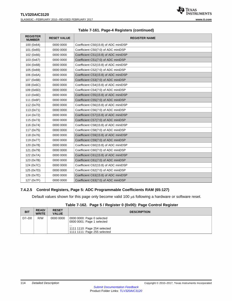
114
TLV320AIC3120SLAS653C –FEBRUARY 2010–REVISED FEBRUARY 2017 www.ti.com
Submit Documentation FeedbackProduct Folder Links: TLV320AIC3120
Detailed Description Copyright © 2010–2017, Texas Instruments Incorporated
Table 7-161. Page-4 Registers (continued)REGISTERNUMBER RESET VALUE REGISTER NAME
100 (0x64) 0000 0000 Coefficient C50(15:8) of ADC miniDSP101 (0x65) 0000 0000 Coefficient C50(7:0) of ADC miniDSP102 (0x66) 0000 0000 Coefficient C51(15:8) of ADC miniDSP103 (0x67) 0000 0000 Coefficient C51(7:0) of ADC miniDSP104 (0x68) 0000 0000 Coefficient C52(15:8) of ADC miniDSP105 (0x69) 0000 0000 Coefficient C52(7:0) of ADC miniDSP106 (0x6A) 0000 0000 Coefficient C53(15:8) of ADC miniDSP107 (0x6B) 0000 0000 Coefficient C53(7:0) of ADC miniDSP108 (0x6C) 0000 0000 Coefficient C54(15:8) of ADC miniDSP109 (0x6D) 0000 0000 Coefficient C54(7:0) of ADC miniDSP110 (0x6E) 0000 0000 Coefficient C55(15:8) of ADC miniDSP111 (0x6F) 0000 0000 Coefficient C55(7:0) of ADC miniDSP112 (0x70) 0000 0000 Coefficient C56(15:8) of ADC miniDSP113 (0x71) 0000 0000 Coefficient C56(7:0) of ADC miniDSP114 (0x72) 0000 0000 Coefficient C57(15:8) of ADC miniDSP115 (0x73) 0000 0000 Coefficient C57(7:0) of ADC miniDSP116 (0x74) 0000 0000 Coefficient C58(15:8) of ADC miniDSP117 (0x75) 0000 0000 Coefficient C58(7:0) of ADC miniDSP118 (0x76) 0000 0000 Coefficient C59(15:8) of ADC miniDSP119 (0x77) 0000 0000 Coefficient C59(7:0) of ADC miniDSP120 (0x78) 0000 0000 Coefficient C60(15:8) of ADC miniDSP121 (0x79) 0000 0000 Coefficient C60(7:0) of ADC miniDSP122 (0x7A) 0000 0000 Coefficient C61(15:8) of ADC miniDSP123 (0x7B) 0000 0000 Coefficient C61(7:0) of ADC miniDSP124 (0x7C) 0000 0000 Coefficient C62(15:8) of ADC miniDSP125 (0x7D) 0000 0000 Coefficient C62(7:0) of ADC miniDSP126 (0x7E) 0000 0000 Coefficient C63(15:8) of ADC miniDSP127 (0x7F) 0000 0000 Coefficient C63(7:0) of ADC miniDSP
7.4.2.5 Control Registers, Page 5: ADC Programmable Coefficients RAM (65:127)
Default values shown for this page only become valid 100 μs following a hardware or software reset.
Table 7-162. Page 5 / Register 0 (0x00): Page Control Register
BIT READ/WRITE
RESETVALUE DESCRIPTION
D7–D0 R/W 0000 0000 0000 0000: Page 0 selected0000 0001: Page 1 selected...1111 1110: Page 254 selected1111 1111: Page 255 selected
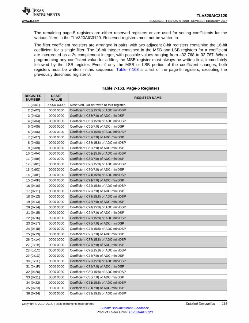
115
TLV320AIC3120www.ti.com SLAS653C –FEBRUARY 2010–REVISED FEBRUARY 2017
Submit Documentation FeedbackProduct Folder Links: TLV320AIC3120
Detailed DescriptionCopyright © 2010–2017, Texas Instruments Incorporated
The remaining page-5 registers are either reserved registers or are used for setting coefficients for thevarious filters in the TLV320AIC3120. Reserved registers must not be written to.
The filter coefficient registers are arranged in pairs, with two adjacent 8-bit registers containing the 16-bitcoefficient for a single filter. The 16-bit integer contained in the MSB and LSB registers for a coefficientare interpreted as a 2s-complement integer, with possible values ranging from –32 768 to 32 767. Whenprogramming any coefficient value for a filter, the MSB register must always be written first, immediatelyfollowed by the LSB register. Even if only the MSB or LSB portion of the coefficient changes, bothregisters must be written in this sequence. Table 7-163 is a list of the page-5 registers, excepting thepreviously described register 0.
Table 7-163. Page-5 Registers
REGISTERNUMBER
RESETVALUE REGISTER NAME
1 (0x01) XXXX XXXX Reserved. Do not write to this register.2 (0x02) 0000 0000 Coefficient C65(15:8) of ADC miniDSP3 (0x03) 0000 0000 Coefficient C65(7:0) of ADC miniDSP4 (0x04) 0000 0000 Coefficient C66(15:8) of ADC miniDSP5 (0x05) 0000 0000 Coefficient C66(7:0) of ADC miniDSP6 (0x06) 0000 0000 Coefficient C67(15:8) of ADC miniDSP7 (0x07) 0000 0000 Coefficient C67(7:0) of ADC miniDSP8 (0x08) 0000 0000 Coefficient C68(15:8) of ADC miniDSP9 (0x09) 0000 0000 Coefficient C68(7:0) of ADC miniDSP
10 (0x0A) 0000 0000 Coefficient C69(15:8) of ADC miniDSP11 (0x0B) 0000 0000 Coefficient C69(7:0) of ADC miniDSP12 (0x0C) 0000 0000 Coefficient C70(15:8) of ADC miniDSP13 (0x0D) 0000 0000 Coefficient C70(7:0) of ADC miniDSP14 (0x0E) 0000 0000 Coefficient C71(15:8) of ADC miniDSP15 (0x0F) 0000 0000 Coefficient C71(7:0) of ADC miniDSP16 (0x10) 0000 0000 Coefficient C72(15:8) of ADC miniDSP17 (0x11) 0000 0000 Coefficient C72(7:0) of ADC miniDSP18 (0x12) 0000 0000 Coefficient C73(15:8) of ADC miniDSP19 (0x13) 0000 0000 Coefficient C73(7:0) of ADC miniDSP20 (0x14) 0000 0000 Coefficient C74(15:8) of ADC miniDSP21 (0x15) 0000 0000 Coefficient C74(7:0) of ADC miniDSP22 (0x16) 0000 0000 Coefficient C75(15:8) of ADC miniDSP23 (0x17) 0000 0000 Coefficient C75(7:0) of ADC miniDSP24 (0x18) 0000 0000 Coefficient C76(15:8) of ADC miniDSP25 (0x19) 0000 0000 Coefficient C76(7:0) of ADC miniDSP26 (0x1A) 0000 0000 Coefficient C77(15:8) of ADC miniDSP27 (0x1B) 0000 0000 Coefficient C77(7:0) of ADC miniDSP28 (0x1C) 0000 0000 Coefficient C78(15:8) of ADC miniDSP29 (0x1D) 0000 0000 Coefficient C78(7:0) of ADC miniDSP30 (0x1E) 0000 0000 Coefficient C79(15:8) of ADC miniDSP31 (0x1F) 0000 0000 Coefficient C79(7:0) of ADC miniDSP32 (0x20) 0000 0000 Coefficient C80(15:8) of ADC miniDSP33 (0x21) 0000 0000 Coefficient C80(7:0) of ADC miniDSP34 (0x22) 0000 0000 Coefficient C81(15:8) of ADC miniDSP35 (0x23) 0000 0000 Coefficient C81(7:0) of ADC miniDSP36 (0x24) 0000 0000 Coefficient C82(15:8) of ADC miniDSP
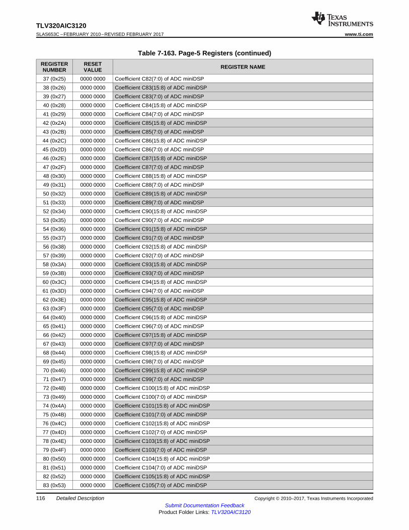
116
TLV320AIC3120SLAS653C –FEBRUARY 2010–REVISED FEBRUARY 2017 www.ti.com
Submit Documentation FeedbackProduct Folder Links: TLV320AIC3120
Detailed Description Copyright © 2010–2017, Texas Instruments Incorporated
Table 7-163. Page-5 Registers (continued)REGISTERNUMBER
RESETVALUE REGISTER NAME
37 (0x25) 0000 0000 Coefficient C82(7:0) of ADC miniDSP38 (0x26) 0000 0000 Coefficient C83(15:8) of ADC miniDSP39 (0x27) 0000 0000 Coefficient C83(7:0) of ADC miniDSP40 (0x28) 0000 0000 Coefficient C84(15:8) of ADC miniDSP41 (0x29) 0000 0000 Coefficient C84(7:0) of ADC miniDSP42 (0x2A) 0000 0000 Coefficient C85(15:8) of ADC miniDSP43 (0x2B) 0000 0000 Coefficient C85(7:0) of ADC miniDSP44 (0x2C) 0000 0000 Coefficient C86(15:8) of ADC miniDSP45 (0x2D) 0000 0000 Coefficient C86(7:0) of ADC miniDSP46 (0x2E) 0000 0000 Coefficient C87(15:8) of ADC miniDSP47 (0x2F) 0000 0000 Coefficient C87(7:0) of ADC miniDSP48 (0x30) 0000 0000 Coefficient C88(15:8) of ADC miniDSP49 (0x31) 0000 0000 Coefficient C88(7:0) of ADC miniDSP50 (0x32) 0000 0000 Coefficient C89(15:8) of ADC miniDSP51 (0x33) 0000 0000 Coefficient C89(7:0) of ADC miniDSP52 (0x34) 0000 0000 Coefficient C90(15:8) of ADC miniDSP53 (0x35) 0000 0000 Coefficient C90(7:0) of ADC miniDSP54 (0x36) 0000 0000 Coefficient C91(15:8) of ADC miniDSP55 (0x37) 0000 0000 Coefficient C91(7:0) of ADC miniDSP56 (0x38) 0000 0000 Coefficient C92(15:8) of ADC miniDSP57 (0x39) 0000 0000 Coefficient C92(7:0) of ADC miniDSP58 (0x3A) 0000 0000 Coefficient C93(15:8) of ADC miniDSP59 (0x3B) 0000 0000 Coefficient C93(7:0) of ADC miniDSP60 (0x3C) 0000 0000 Coefficient C94(15:8) of ADC miniDSP61 (0x3D) 0000 0000 Coefficient C94(7:0) of ADC miniDSP62 (0x3E) 0000 0000 Coefficient C95(15:8) of ADC miniDSP63 (0x3F) 0000 0000 Coefficient C95(7:0) of ADC miniDSP64 (0x40) 0000 0000 Coefficient C96(15:8) of ADC miniDSP65 (0x41) 0000 0000 Coefficient C96(7:0) of ADC miniDSP66 (0x42) 0000 0000 Coefficient C97(15:8) of ADC miniDSP67 (0x43) 0000 0000 Coefficient C97(7:0) of ADC miniDSP68 (0x44) 0000 0000 Coefficient C98(15:8) of ADC miniDSP69 (0x45) 0000 0000 Coefficient C98(7:0) of ADC miniDSP70 (0x46) 0000 0000 Coefficient C99(15:8) of ADC miniDSP71 (0x47) 0000 0000 Coefficient C99(7:0) of ADC miniDSP72 (0x48) 0000 0000 Coefficient C100(15:8) of ADC miniDSP73 (0x49) 0000 0000 Coefficient C100(7:0) of ADC miniDSP74 (0x4A) 0000 0000 Coefficient C101(15:8) of ADC miniDSP75 (0x4B) 0000 0000 Coefficient C101(7:0) of ADC miniDSP76 (0x4C) 0000 0000 Coefficient C102(15:8) of ADC miniDSP77 (0x4D) 0000 0000 Coefficient C102(7:0) of ADC miniDSP78 (0x4E) 0000 0000 Coefficient C103(15:8) of ADC miniDSP79 (0x4F) 0000 0000 Coefficient C103(7:0) of ADC miniDSP80 (0x50) 0000 0000 Coefficient C104(15:8) of ADC miniDSP81 (0x51) 0000 0000 Coefficient C104(7:0) of ADC miniDSP82 (0x52) 0000 0000 Coefficient C105(15:8) of ADC miniDSP83 (0x53) 0000 0000 Coefficient C105(7:0) of ADC miniDSP
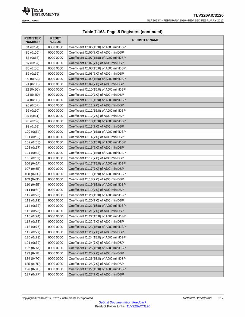
117
TLV320AIC3120www.ti.com SLAS653C –FEBRUARY 2010–REVISED FEBRUARY 2017
Submit Documentation FeedbackProduct Folder Links: TLV320AIC3120
Detailed DescriptionCopyright © 2010–2017, Texas Instruments Incorporated
Table 7-163. Page-5 Registers (continued)REGISTERNUMBER
RESETVALUE REGISTER NAME
84 (0x54) 0000 0000 Coefficient C106(15:8) of ADC miniDSP85 (0x55) 0000 0000 Coefficient C106(7:0) of ADC miniDSP86 (0x56) 0000 0000 Coefficient C107(15:8) of ADC miniDSP87 (0x57) 0000 0000 Coefficient C107(7:0) of ADC miniDSP88 (0x58) 0000 0000 Coefficient C108(15:8) of ADC miniDSP89 (0x59) 0000 0000 Coefficient C108(7:0) of ADC miniDSP90 (0x5A) 0000 0000 Coefficient C109(15:8) of ADC miniDSP91 (0x5B) 0000 0000 Coefficient C109(7:0) of ADC miniDSP92 (0x5C) 0000 0000 Coefficient C110(15:8) of ADC miniDSP93 (0x5D) 0000 0000 Coefficient C110(7:0) of ADC miniDSP94 (0x5E) 0000 0000 Coefficient C111(15:8) of ADC miniDSP95 (0x5F) 0000 0000 Coefficient C111(7:0) of ADC miniDSP96 (0x60) 0000 0000 Coefficient C112(15:8) of ADC miniDSP97 (0x61) 0000 0000 Coefficient C112(7:0) of ADC miniDSP98 (0x62) 0000 0000 Coefficient C113(15:8) of ADC miniDSP99 (0x63) 0000 0000 Coefficient C113(7:0) of ADC miniDSP100 (0x64) 0000 0000 Coefficient C114(15:8) of ADC miniDSP101 (0x65) 0000 0000 Coefficient C114(7:0) of ADC miniDSP102 (0x66) 0000 0000 Coefficient C115(15:8) of ADC miniDSP103 (0x67) 0000 0000 Coefficient C115(7:0) of ADC miniDSP104 (0x68) 0000 0000 Coefficient C117(15:8) of ADC miniDSP105 (0x69) 0000 0000 Coefficient C117(7:0) of ADC miniDSP106 (0x6A) 0000 0000 Coefficient C117(15:8) of ADC miniDSP107 (0x6B) 0000 0000 Coefficient C117(7:0) of ADC miniDSP108 (0x6C) 0000 0000 Coefficient C118(15:8) of ADC miniDSP109 (0x6D) 0000 0000 Coefficient C118(7:0) of ADC miniDSP110 (0x6E) 0000 0000 Coefficient C119(15:8) of ADC miniDSP111 (0x6F) 0000 0000 Coefficient C119(7:0) of ADC miniDSP112 (0x70) 0000 0000 Coefficient C120(15:8) of ADC miniDSP113 (0x71) 0000 0000 Coefficient C120(7:0) of ADC miniDSP114 (0x72) 0000 0000 Coefficient C121(15:8) of ADC miniDSP115 (0x73) 0000 0000 Coefficient C121(7:0) of ADC miniDSP116 (0x74) 0000 0000 Coefficient C122(15:8) of ADC miniDSP117 (0x75) 0000 0000 Coefficient C122(7:0) of ADC miniDSP118 (0x76) 0000 0000 Coefficient C123(15:8) of ADC miniDSP119 (0x77) 0000 0000 Coefficient C123(7:0) of ADC miniDSP120 (0x78) 0000 0000 Coefficient C124(15:8) of ADC miniDSP121 (0x79) 0000 0000 Coefficient C124(7:0) of ADC miniDSP122 (0x7A) 0000 0000 Coefficient C125(15:8) of ADC miniDSP123 (0x7B) 0000 0000 Coefficient C125(7:0) of ADC miniDSP124 (0x7C) 0000 0000 Coefficient C126(15:8) of ADC miniDSP125 (0x7D) 0000 0000 Coefficient C126(7:0) of ADC miniDSP126 (0x7E) 0000 0000 Coefficient C127(15:8) of ADC miniDSP127 (0x7F) 0000 0000 Coefficient C127(7:0) of ADC miniDSP
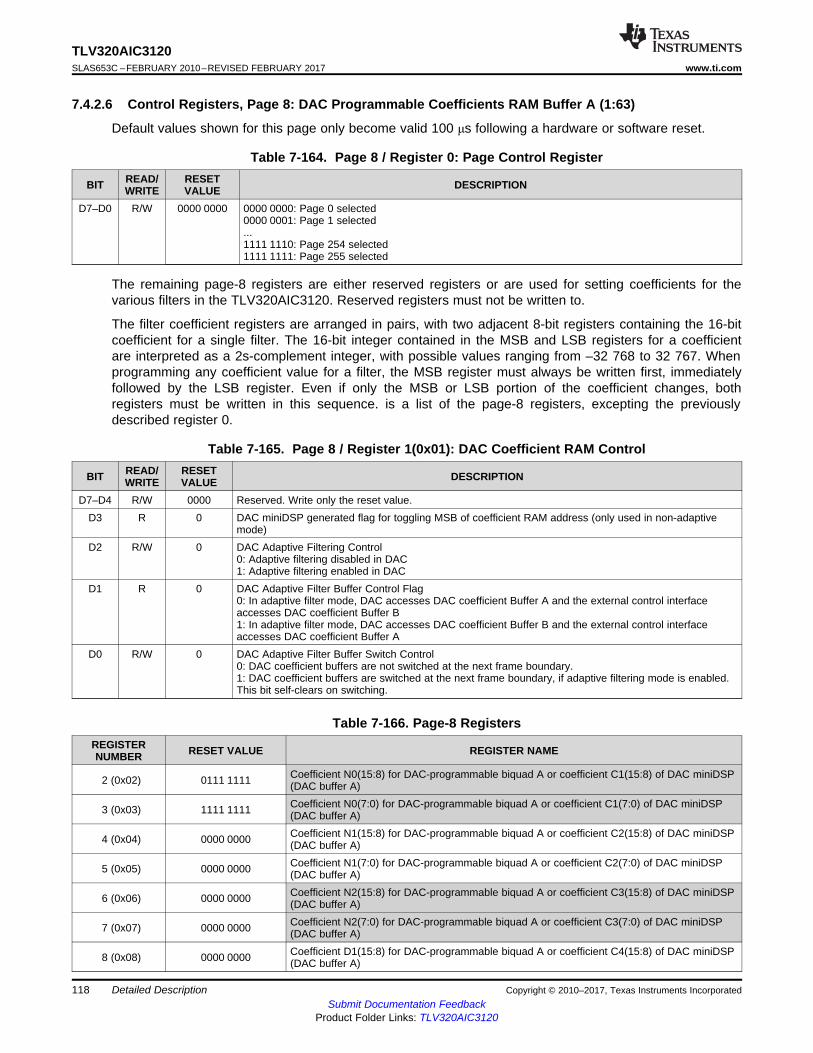
118
TLV320AIC3120SLAS653C –FEBRUARY 2010–REVISED FEBRUARY 2017 www.ti.com
Submit Documentation FeedbackProduct Folder Links: TLV320AIC3120
Detailed Description Copyright © 2010–2017, Texas Instruments Incorporated
7.4.2.6 Control Registers, Page 8: DAC Programmable Coefficients RAM Buffer A (1:63)
Default values shown for this page only become valid 100 μs following a hardware or software reset.
Table 7-164. Page 8 / Register 0: Page Control Register
BIT READ/WRITE
RESETVALUE DESCRIPTION
D7–D0 R/W 0000 0000 0000 0000: Page 0 selected0000 0001: Page 1 selected...1111 1110: Page 254 selected1111 1111: Page 255 selected
The remaining page-8 registers are either reserved registers or are used for setting coefficients for thevarious filters in the TLV320AIC3120. Reserved registers must not be written to.
The filter coefficient registers are arranged in pairs, with two adjacent 8-bit registers containing the 16-bitcoefficient for a single filter. The 16-bit integer contained in the MSB and LSB registers for a coefficientare interpreted as a 2s-complement integer, with possible values ranging from –32 768 to 32 767. Whenprogramming any coefficient value for a filter, the MSB register must always be written first, immediatelyfollowed by the LSB register. Even if only the MSB or LSB portion of the coefficient changes, bothregisters must be written in this sequence. is a list of the page-8 registers, excepting the previouslydescribed register 0.
Table 7-165. Page 8 / Register 1(0x01): DAC Coefficient RAM Control
BIT READ/WRITE
RESETVALUE DESCRIPTION
D7–D4 R/W 0000 Reserved. Write only the reset value.D3 R 0 DAC miniDSP generated flag for toggling MSB of coefficient RAM address (only used in non-adaptive
mode)D2 R/W 0 DAC Adaptive Filtering Control
0: Adaptive filtering disabled in DAC1: Adaptive filtering enabled in DAC
D1 R 0 DAC Adaptive Filter Buffer Control Flag0: In adaptive filter mode, DAC accesses DAC coefficient Buffer A and the external control interfaceaccesses DAC coefficient Buffer B1: In adaptive filter mode, DAC accesses DAC coefficient Buffer B and the external control interfaceaccesses DAC coefficient Buffer A
D0 R/W 0 DAC Adaptive Filter Buffer Switch Control0: DAC coefficient buffers are not switched at the next frame boundary.1: DAC coefficient buffers are switched at the next frame boundary, if adaptive filtering mode is enabled.This bit self-clears on switching.
Table 7-166. Page-8 RegistersREGISTERNUMBER RESET VALUE REGISTER NAME
2 (0x02) 0111 1111 Coefficient N0(15:8) for DAC-programmable biquad A or coefficient C1(15:8) of DAC miniDSP(DAC buffer A)
3 (0x03) 1111 1111 Coefficient N0(7:0) for DAC-programmable biquad A or coefficient C1(7:0) of DAC miniDSP(DAC buffer A)
4 (0x04) 0000 0000 Coefficient N1(15:8) for DAC-programmable biquad A or coefficient C2(15:8) of DAC miniDSP(DAC buffer A)
5 (0x05) 0000 0000 Coefficient N1(7:0) for DAC-programmable biquad A or coefficient C2(7:0) of DAC miniDSP(DAC buffer A)
6 (0x06) 0000 0000 Coefficient N2(15:8) for DAC-programmable biquad A or coefficient C3(15:8) of DAC miniDSP(DAC buffer A)
7 (0x07) 0000 0000 Coefficient N2(7:0) for DAC-programmable biquad A or coefficient C3(7:0) of DAC miniDSP(DAC buffer A)
8 (0x08) 0000 0000 Coefficient D1(15:8) for DAC-programmable biquad A or coefficient C4(15:8) of DAC miniDSP(DAC buffer A)
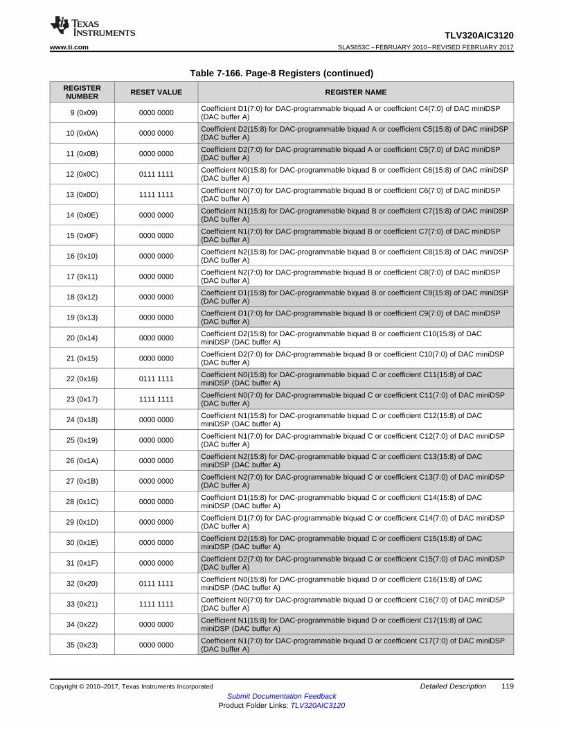
119
TLV320AIC3120www.ti.com SLAS653C –FEBRUARY 2010–REVISED FEBRUARY 2017
Submit Documentation FeedbackProduct Folder Links: TLV320AIC3120
Detailed DescriptionCopyright © 2010–2017, Texas Instruments Incorporated
Table 7-166. Page-8 Registers (continued)REGISTERNUMBER RESET VALUE REGISTER NAME
9 (0x09) 0000 0000 Coefficient D1(7:0) for DAC-programmable biquad A or coefficient C4(7:0) of DAC miniDSP(DAC buffer A)
10 (0x0A) 0000 0000 Coefficient D2(15:8) for DAC-programmable biquad A or coefficient C5(15:8) of DAC miniDSP(DAC buffer A)
11 (0x0B) 0000 0000 Coefficient D2(7:0) for DAC-programmable biquad A or coefficient C5(7:0) of DAC miniDSP(DAC buffer A)
12 (0x0C) 0111 1111 Coefficient N0(15:8) for DAC-programmable biquad B or coefficient C6(15:8) of DAC miniDSP(DAC buffer A)
13 (0x0D) 1111 1111 Coefficient N0(7:0) for DAC-programmable biquad B or coefficient C6(7:0) of DAC miniDSP(DAC buffer A)
14 (0x0E) 0000 0000 Coefficient N1(15:8) for DAC-programmable biquad B or coefficient C7(15:8) of DAC miniDSP(DAC buffer A)
15 (0x0F) 0000 0000 Coefficient N1(7:0) for DAC-programmable biquad B or coefficient C7(7:0) of DAC miniDSP(DAC buffer A)
16 (0x10) 0000 0000 Coefficient N2(15:8) for DAC-programmable biquad B or coefficient C8(15:8) of DAC miniDSP(DAC buffer A)
17 (0x11) 0000 0000 Coefficient N2(7:0) for DAC-programmable biquad B or coefficient C8(7:0) of DAC miniDSP(DAC buffer A)
18 (0x12) 0000 0000 Coefficient D1(15:8) for DAC-programmable biquad B or coefficient C9(15:8) of DAC miniDSP(DAC buffer A)
19 (0x13) 0000 0000 Coefficient D1(7:0) for DAC-programmable biquad B or coefficient C9(7:0) of DAC miniDSP(DAC buffer A)
20 (0x14) 0000 0000 Coefficient D2(15:8) for DAC-programmable biquad B or coefficient C10(15:8) of DACminiDSP (DAC buffer A)
21 (0x15) 0000 0000 Coefficient D2(7:0) for DAC-programmable biquad B or coefficient C10(7:0) of DAC miniDSP(DAC buffer A)
22 (0x16) 0111 1111 Coefficient N0(15:8) for DAC-programmable biquad C or coefficient C11(15:8) of DACminiDSP (DAC buffer A)
23 (0x17) 1111 1111 Coefficient N0(7:0) for DAC-programmable biquad C or coefficient C11(7:0) of DAC miniDSP(DAC buffer A)
24 (0x18) 0000 0000 Coefficient N1(15:8) for DAC-programmable biquad C or coefficient C12(15:8) of DACminiDSP (DAC buffer A)
25 (0x19) 0000 0000 Coefficient N1(7:0) for DAC-programmable biquad C or coefficient C12(7:0) of DAC miniDSP(DAC buffer A)
26 (0x1A) 0000 0000 Coefficient N2(15:8) for DAC-programmable biquad C or coefficient C13(15:8) of DACminiDSP (DAC buffer A)
27 (0x1B) 0000 0000 Coefficient N2(7:0) for DAC-programmable biquad C or coefficient C13(7:0) of DAC miniDSP(DAC buffer A)
28 (0x1C) 0000 0000 Coefficient D1(15:8) for DAC-programmable biquad C or coefficient C14(15:8) of DACminiDSP (DAC buffer A)
29 (0x1D) 0000 0000 Coefficient D1(7:0) for DAC-programmable biquad C or coefficient C14(7:0) of DAC miniDSP(DAC buffer A)
30 (0x1E) 0000 0000 Coefficient D2(15:8) for DAC-programmable biquad C or coefficient C15(15:8) of DACminiDSP (DAC buffer A)
31 (0x1F) 0000 0000 Coefficient D2(7:0) for DAC-programmable biquad C or coefficient C15(7:0) of DAC miniDSP(DAC buffer A)
32 (0x20) 0111 1111 Coefficient N0(15:8) for DAC-programmable biquad D or coefficient C16(15:8) of DACminiDSP (DAC buffer A)
33 (0x21) 1111 1111 Coefficient N0(7:0) for DAC-programmable biquad D or coefficient C16(7:0) of DAC miniDSP(DAC buffer A)
34 (0x22) 0000 0000 Coefficient N1(15:8) for DAC-programmable biquad D or coefficient C17(15:8) of DACminiDSP (DAC buffer A)
35 (0x23) 0000 0000 Coefficient N1(7:0) for DAC-programmable biquad D or coefficient C17(7:0) of DAC miniDSP(DAC buffer A)
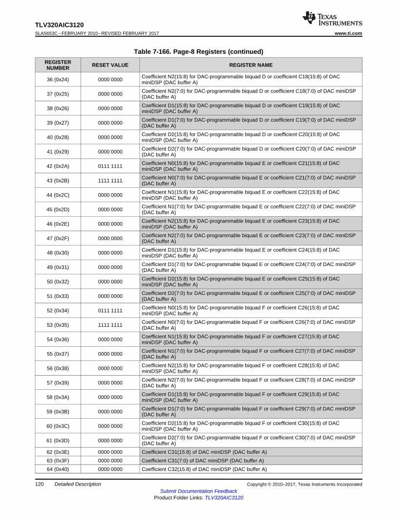
120
TLV320AIC3120SLAS653C –FEBRUARY 2010–REVISED FEBRUARY 2017 www.ti.com
Submit Documentation FeedbackProduct Folder Links: TLV320AIC3120
Detailed Description Copyright © 2010–2017, Texas Instruments Incorporated
Table 7-166. Page-8 Registers (continued)REGISTERNUMBER RESET VALUE REGISTER NAME
36 (0x24) 0000 0000 Coefficient N2(15:8) for DAC-programmable biquad D or coefficient C18(15:8) of DACminiDSP (DAC buffer A)
37 (0x25) 0000 0000 Coefficient N2(7:0) for DAC-programmable biquad D or coefficient C18(7:0) of DAC miniDSP(DAC buffer A)
38 (0x26) 0000 0000 Coefficient D1(15:8) for DAC-programmable biquad D or coefficient C19(15:8) of DACminiDSP (DAC buffer A)
39 (0x27) 0000 0000 Coefficient D1(7:0) for DAC-programmable biquad D or coefficient C19(7:0) of DAC miniDSP(DAC buffer A)
40 (0x28) 0000 0000 Coefficient D2(15:8) for DAC-programmable biquad D or coefficient C20(15:8) of DACminiDSP (DAC buffer A)
41 (0x29) 0000 0000 Coefficient D2(7:0) for DAC-programmable biquad D or coefficient C20(7:0) of DAC miniDSP(DAC buffer A)
42 (0x2A) 0111 1111 Coefficient N0(15:8) for DAC-programmable biquad E or coefficient C21(15:8) of DACminiDSP (DAC buffer A)
43 (0x2B) 1111 1111 Coefficient N0(7:0) for DAC-programmable biquad E or coefficient C21(7:0) of DAC miniDSP(DAC buffer A)
44 (0x2C) 0000 0000 Coefficient N1(15:8) for DAC-programmable biquad E or coefficient C22(15:8) of DACminiDSP (DAC buffer A)
45 (0x2D) 0000 0000 Coefficient N1(7:0) for DAC-programmable biquad E or coefficient C22(7:0) of DAC miniDSP(DAC buffer A)
46 (0x2E) 0000 0000 Coefficient N2(15:8) for DAC-programmable biquad E or coefficient C23(15:8) of DACminiDSP (DAC buffer A)
47 (0x2F) 0000 0000 Coefficient N2(7:0) for DAC-programmable biquad E or coefficient C23(7:0) of DAC miniDSP(DAC buffer A)
48 (0x30) 0000 0000 Coefficient D1(15:8) for DAC-programmable biquad E or coefficient C24(15:8) of DACminiDSP (DAC buffer A)
49 (0x31) 0000 0000 Coefficient D1(7:0) for DAC-programmable biquad E or coefficient C24(7:0) of DAC miniDSP(DAC buffer A)
50 (0x32) 0000 0000 Coefficient D2(15:8) for DAC-programmable biquad E or coefficient C25(15:8) of DACminiDSP (DAC buffer A)
51 (0x33) 0000 0000 Coefficient D2(7:0) for DAC-programmable biquad E or coefficient C25(7:0) of DAC miniDSP(DAC buffer A)
52 (0x34) 0111 1111 Coefficient N0(15:8) for DAC-programmable biquad F or coefficient C26(15:8) of DACminiDSP (DAC buffer A)
53 (0x35) 1111 1111 Coefficient N0(7:0) for DAC-programmable biquad F or coefficient C26(7:0) of DAC miniDSP(DAC buffer A)
54 (0x36) 0000 0000 Coefficient N1(15:8) for DAC-programmable biquad F or coefficient C27(15:8) of DACminiDSP (DAC buffer A)
55 (0x37) 0000 0000 Coefficient N1(7:0) for DAC-programmable biquad F or coefficient C27(7:0) of DAC miniDSP(DAC buffer A)
56 (0x38) 0000 0000 Coefficient N2(15:8) for DAC-programmable biquad F or coefficient C28(15:8) of DACminiDSP (DAC buffer A)
57 (0x39) 0000 0000 Coefficient N2(7:0) for DAC-programmable biquad F or coefficient C28(7:0) of DAC miniDSP(DAC buffer A)
58 (0x3A) 0000 0000 Coefficient D1(15:8) for DAC-programmable biquad F or coefficient C29(15:8) of DACminiDSP (DAC buffer A)
59 (0x3B) 0000 0000 Coefficient D1(7:0) for DAC-programmable biquad F or coefficient C29(7:0) of DAC miniDSP(DAC buffer A)
60 (0x3C) 0000 0000 Coefficient D2(15:8) for DAC-programmable biquad F or coefficient C30(15:8) of DACminiDSP (DAC buffer A)
61 (0x3D) 0000 0000 Coefficient D2(7:0) for DAC-programmable biquad F or coefficient C30(7:0) of DAC miniDSP(DAC buffer A)
62 (0x3E) 0000 0000 Coefficient C31(15:8) of DAC miniDSP (DAC buffer A)63 (0x3F) 0000 0000 Coefficient C31(7:0) of DAC miniDSP (DAC buffer A)64 (0x40) 0000 0000 Coefficient C32(15:8) of DAC miniDSP (DAC buffer A)

121
TLV320AIC3120www.ti.com SLAS653C –FEBRUARY 2010–REVISED FEBRUARY 2017
Submit Documentation FeedbackProduct Folder Links: TLV320AIC3120
Detailed DescriptionCopyright © 2010–2017, Texas Instruments Incorporated
Table 7-166. Page-8 Registers (continued)REGISTERNUMBER RESET VALUE REGISTER NAME
65 (0x41) 0000 0000 Coefficient C32(7:0) of DAC miniDSP (DAC buffer A)66 (0x42) 0111 1111 Coefficient C33(15:8) of DAC miniDSP (DAC buffer A)67 (0x43) 1111 1111 Coefficient C33(7:0) of DAC miniDSP (DAC buffer A)68 (0x44) 0000 0000 Coefficient C34(15:8) of DAC miniDSP (DAC buffer A)69 (0x45) 0000 0000 Coefficient C34(7:0) of DAC miniDSP (DAC buffer A)70 (0x46) 0000 0000 Coefficient C35(15:8) of DAC miniDSP (DAC buffer A)71 (0x47) 0000 0000 Coefficient C35(7:0) of DAC miniDSP (DAC buffer A)72 (0x48) 0000 0000 Coefficient C36(15:8) of DAC miniDSP (DAC buffer A)73 (0x49) 0000 0000 Coefficient C36(7:0) of DAC miniDSP (DAC buffer A)74 (0x4A) 0000 0000 Coefficient C37(15:8) of DAC miniDSP (DAC buffer A)75 (0x4B) 0000 0000 Coefficient C37(7:0) of DAC miniDSP (DAC buffer A)76 (0x4C) 0111 1111 Coefficient C38(15:8) of DAC miniDSP (DAC buffer A)77 (0x4D) 1111 1111 Coefficient C38(7:0) of DAC miniDSP (DAC buffer A)78 (0x4E) 0000 0000 Coefficient C39(15:8) of DAC miniDSP (DAC buffer A)79 (0x4F) 0000 0000 Coefficient C39(7:0) of DAC miniDSP (DAC buffer A)80 (0x50) 0000 0000 Coefficient C40(15:8) of DAC miniDSP (DAC buffer A)81 (0x51) 0000 0000 Coefficient C40(7:0) of DAC miniDSP (DAC buffer A)82 (0x52) 0000 0000 Coefficient C41(15:8) of DAC miniDSP (DAC buffer A)83 (0x53) 0000 0000 Coefficient C41(7:0) of DAC miniDSP (DAC buffer A)84 (0x54) 0000 0000 Coefficient C42(15:8) of DAC miniDSP (DAC buffer A)85 (0x55) 0000 0000 Coefficient C42(7:0) of DAC miniDSP (DAC buffer A)86 (0x56) 0111 1111 Coefficient C43(15:8) of DAC miniDSP (DAC buffer A)87 (0x57) 1111 1111 Coefficient C43(7:0) of DAC miniDSP (DAC buffer A)88 (0x58) 0000 0000 Coefficient C44(15:8) of DAC miniDSP (DAC buffer A)89 (0x59) 0000 0000 Coefficient C44(7:0) of DAC miniDSP (DAC buffer A)90 (0x5A) 0000 0000 Coefficient C45(15:8) of DAC miniDSP (DAC buffer A)91 (0x5B) 0000 0000 Coefficient C45(7:0) of DAC miniDSP (DAC buffer A)92 (0x5C) 0000 0000 Coefficient C461(15:8) of DAC miniDSP (DAC buffer A)93 (0x5D) 0000 0000 Coefficient C46(7:0) of DAC miniDSP (DAC buffer A)94 (0x5E) 0000 0000 Coefficient C47(15:8) of DAC miniDSP (DAC buffer A)95 (0x5F) 0000 0000 Coefficient C47(7:0) of DAC miniDSP (DAC buffer A)96 (0x60) 0111 1111 Coefficient C48(15:8) of DAC miniDSP (DAC buffer A)97 (0x61) 1111 1111 Coefficient C48(7:0) of DAC miniDSP (DAC buffer A)98 (0x62) 0000 0000 Coefficient C49(15:8) of DAC miniDSP (DAC buffer A)99 (0x63) 0000 0000 Coefficient C49(7:0) of DAC miniDSP (DAC buffer A)100 (0x64) 0000 0000 Coefficient C50(15:8) of DAC miniDSP (DAC buffer A)101 (0x65) 0000 0000 Coefficient C50(7:0) of DAC miniDSP (DAC buffer A)102 (0x66) 0000 0000 Coefficient C51(15:8) of DAC miniDSP (DAC buffer A)103 (0x67) 0000 0000 CoefficientC51(7:0) of DAC miniDSP (DAC buffer A)104 (0x68) 0000 0000 Coefficient C52(15:8) of DAC miniDSP (DAC buffer A)105 (0x69) 0000 0000 Coefficient C52(7:0) of DAC miniDSP (DAC buffer A)106 (0x6A) 0111 1111 Coefficient C53(15:8) of DAC miniDSP (DAC buffer A)107 (0x6B) 1111 1111 Coefficient C53(7:0) of DAC miniDSP (DAC buffer A)108 (0x6C) 0000 0000 Coefficient C54(15:8) of DAC miniDSP (DAC buffer A)109 (0x6D) 0000 0000 Coefficient C54(7:0) of DAC miniDSP (DAC buffer A)110 (0x6E) 0000 0000 Coefficient C55(15:8) of DAC miniDSP (DAC buffer A)111 (0x6F) 0000 0000 Coefficient C55(7:0) of DAC miniDSP (DAC buffer A)
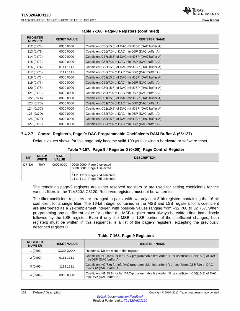
122
TLV320AIC3120SLAS653C –FEBRUARY 2010–REVISED FEBRUARY 2017 www.ti.com
Submit Documentation FeedbackProduct Folder Links: TLV320AIC3120
Detailed Description Copyright © 2010–2017, Texas Instruments Incorporated
Table 7-166. Page-8 Registers (continued)REGISTERNUMBER RESET VALUE REGISTER NAME
112 (0x70) 0000 0000 Coefficient C56(15:8) of DAC miniDSP (DAC buffer A)113 (0x71) 0000 0000 Coefficient C56(7:0) of DAC miniDSP (DAC buffer A)114 (0x72) 0000 0000 Coefficient C57(15:8) of DAC miniDSP (DAC buffer A)115 (0x73) 0000 0000 Coefficient C57(7:0) of DAC miniDSP (DAC buffer A)116 (0x74) 0111 1111 Coefficient C58(15:8) of DAC miniDSP (DAC buffer A)117 (0x75) 1111 1111 Coefficient C58(7:0) of DAC miniDSP (DAC buffer A)118 (0x76) 0000 0000 Coefficient C59(15:8) of DAC miniDSP (DAC buffer A)119 (0x77) 0000 0000 Coefficient C59(7:0) of DAC miniDSP (DAC buffer A)120 (0x78) 0000 0000 Coefficient C60(15:8) of DAC miniDSP (DAC buffer A)121 (0x79) 0000 0000 Coefficient C60(7:0) of DAC miniDSP (DAC buffer A)122 (0x7A) 0000 0000 Coefficient C61(15:8) of DAC miniDSP (DAC buffer A)123 (0x7B) 0000 0000 Coefficient C61(7:0) of DAC miniDSP (DAC buffer A)124 (0x7C) 0000 0000 Coefficient C62(15:8) of DAC miniDSP (DAC buffer A)125 (0x7D) 0000 0000 Coefficient C62(7:0) of DAC miniDSP (DAC buffer A)126 (0x7E) 0000 0000 Coefficient C63(15:8) of DAC miniDSP (DAC buffer A)127 (0x7F) 0000 0000 Coefficient C63(7:0) of DAC miniDSP (DAC buffer A)
7.4.2.7 Control Registers, Page 9: DAC Programmable Coefficients RAM Buffer A (65:127)
Default values shown for this page only become valid 100 μs following a hardware or software reset.
Table 7-167. Page 9 / Register 0 (0x00): Page Control Register
BIT READ/WRITE
RESETVALUE DESCRIPTION
D7–D0 R/W 0000 0000 0000 0000: Page 0 selected0000 0001: Page 1 selected...1111 1110: Page 254 selected1111 1111: Page 255 selected
The remaining page-9 registers are either reserved registers or are used for setting coefficients for thevarious filters in the TLV320AIC3120. Reserved registers must not be written to.
The filter-coefficient registers are arranged in pairs, with two adjacent 8-bit registers containing the 16-bitcoefficient for a single filter. The 16-bit integer contained in the MSB and LSB registers for a coefficientare interpreted as a 2s-complement integer, with possible values ranging from –32 768 to 32 767. Whenprogramming any coefficient value for a filter, the MSB register must always be written first, immediatelyfollowed by the LSB register. Even if only the MSB or LSB portion of the coefficient changes, bothregisters must be written in this sequence. is a list of the page-9 registers, excepting the previouslydescribed register 0.
Table 7-168. Page-9 RegistersREGISTERNUMBER RESET VALUE REGISTER NAME
1 (0x01) XXXX XXXX Reserved. Do not write to this register.
2 (0x02) 0111 1111 Coefficient N0(15:8) for left DAC-programmable first-order IIR or coefficient C65(15:8) of DACminiDSP (DAC buffer A)
3 (0x03) 1111 1111 Coefficient N0(7:0) for left DAC-programmable first-order IIR or coefficient C65(7:0) of DACminiDSP (DAC buffer A)
4 (0x04) 0000 0000 Coefficient N1(15:8) for left DAC-programmable first-order IIR or coefficient C66(15:8) of DACminiDSP (DAC buffer A)
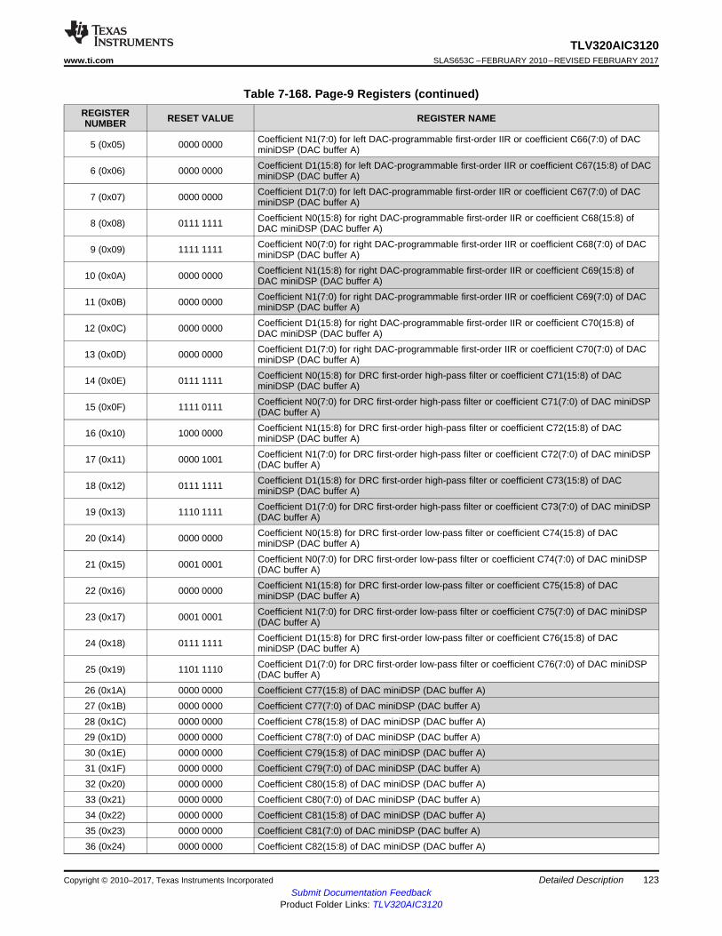
123
TLV320AIC3120www.ti.com SLAS653C –FEBRUARY 2010–REVISED FEBRUARY 2017
Submit Documentation FeedbackProduct Folder Links: TLV320AIC3120
Detailed DescriptionCopyright © 2010–2017, Texas Instruments Incorporated
Table 7-168. Page-9 Registers (continued)REGISTERNUMBER RESET VALUE REGISTER NAME
5 (0x05) 0000 0000 Coefficient N1(7:0) for left DAC-programmable first-order IIR or coefficient C66(7:0) of DACminiDSP (DAC buffer A)
6 (0x06) 0000 0000 Coefficient D1(15:8) for left DAC-programmable first-order IIR or coefficient C67(15:8) of DACminiDSP (DAC buffer A)
7 (0x07) 0000 0000 Coefficient D1(7:0) for left DAC-programmable first-order IIR or coefficient C67(7:0) of DACminiDSP (DAC buffer A)
8 (0x08) 0111 1111 Coefficient N0(15:8) for right DAC-programmable first-order IIR or coefficient C68(15:8) ofDAC miniDSP (DAC buffer A)
9 (0x09) 1111 1111 Coefficient N0(7:0) for right DAC-programmable first-order IIR or coefficient C68(7:0) of DACminiDSP (DAC buffer A)
10 (0x0A) 0000 0000 Coefficient N1(15:8) for right DAC-programmable first-order IIR or coefficient C69(15:8) ofDAC miniDSP (DAC buffer A)
11 (0x0B) 0000 0000 Coefficient N1(7:0) for right DAC-programmable first-order IIR or coefficient C69(7:0) of DACminiDSP (DAC buffer A)
12 (0x0C) 0000 0000 Coefficient D1(15:8) for right DAC-programmable first-order IIR or coefficient C70(15:8) ofDAC miniDSP (DAC buffer A)
13 (0x0D) 0000 0000 Coefficient D1(7:0) for right DAC-programmable first-order IIR or coefficient C70(7:0) of DACminiDSP (DAC buffer A)
14 (0x0E) 0111 1111 Coefficient N0(15:8) for DRC first-order high-pass filter or coefficient C71(15:8) of DACminiDSP (DAC buffer A)
15 (0x0F) 1111 0111 Coefficient N0(7:0) for DRC first-order high-pass filter or coefficient C71(7:0) of DAC miniDSP(DAC buffer A)
16 (0x10) 1000 0000 Coefficient N1(15:8) for DRC first-order high-pass filter or coefficient C72(15:8) of DACminiDSP (DAC buffer A)
17 (0x11) 0000 1001 Coefficient N1(7:0) for DRC first-order high-pass filter or coefficient C72(7:0) of DAC miniDSP(DAC buffer A)
18 (0x12) 0111 1111 Coefficient D1(15:8) for DRC first-order high-pass filter or coefficient C73(15:8) of DACminiDSP (DAC buffer A)
19 (0x13) 1110 1111 Coefficient D1(7:0) for DRC first-order high-pass filter or coefficient C73(7:0) of DAC miniDSP(DAC buffer A)
20 (0x14) 0000 0000 Coefficient N0(15:8) for DRC first-order low-pass filter or coefficient C74(15:8) of DACminiDSP (DAC buffer A)
21 (0x15) 0001 0001 Coefficient N0(7:0) for DRC first-order low-pass filter or coefficient C74(7:0) of DAC miniDSP(DAC buffer A)
22 (0x16) 0000 0000 Coefficient N1(15:8) for DRC first-order low-pass filter or coefficient C75(15:8) of DACminiDSP (DAC buffer A)
23 (0x17) 0001 0001 Coefficient N1(7:0) for DRC first-order low-pass filter or coefficient C75(7:0) of DAC miniDSP(DAC buffer A)
24 (0x18) 0111 1111 Coefficient D1(15:8) for DRC first-order low-pass filter or coefficient C76(15:8) of DACminiDSP (DAC buffer A)
25 (0x19) 1101 1110 Coefficient D1(7:0) for DRC first-order low-pass filter or coefficient C76(7:0) of DAC miniDSP(DAC buffer A)
26 (0x1A) 0000 0000 Coefficient C77(15:8) of DAC miniDSP (DAC buffer A)27 (0x1B) 0000 0000 Coefficient C77(7:0) of DAC miniDSP (DAC buffer A)28 (0x1C) 0000 0000 Coefficient C78(15:8) of DAC miniDSP (DAC buffer A)29 (0x1D) 0000 0000 Coefficient C78(7:0) of DAC miniDSP (DAC buffer A)30 (0x1E) 0000 0000 Coefficient C79(15:8) of DAC miniDSP (DAC buffer A)31 (0x1F) 0000 0000 Coefficient C79(7:0) of DAC miniDSP (DAC buffer A)32 (0x20) 0000 0000 Coefficient C80(15:8) of DAC miniDSP (DAC buffer A)33 (0x21) 0000 0000 Coefficient C80(7:0) of DAC miniDSP (DAC buffer A)34 (0x22) 0000 0000 Coefficient C81(15:8) of DAC miniDSP (DAC buffer A)35 (0x23) 0000 0000 Coefficient C81(7:0) of DAC miniDSP (DAC buffer A)36 (0x24) 0000 0000 Coefficient C82(15:8) of DAC miniDSP (DAC buffer A)
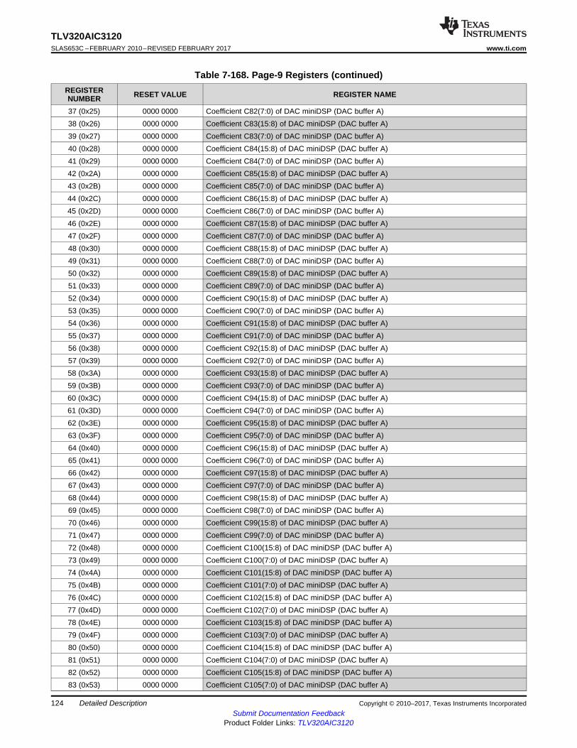
124
TLV320AIC3120SLAS653C –FEBRUARY 2010–REVISED FEBRUARY 2017 www.ti.com
Submit Documentation FeedbackProduct Folder Links: TLV320AIC3120
Detailed Description Copyright © 2010–2017, Texas Instruments Incorporated
Table 7-168. Page-9 Registers (continued)REGISTERNUMBER RESET VALUE REGISTER NAME
37 (0x25) 0000 0000 Coefficient C82(7:0) of DAC miniDSP (DAC buffer A)38 (0x26) 0000 0000 Coefficient C83(15:8) of DAC miniDSP (DAC buffer A)39 (0x27) 0000 0000 Coefficient C83(7:0) of DAC miniDSP (DAC buffer A)40 (0x28) 0000 0000 Coefficient C84(15:8) of DAC miniDSP (DAC buffer A)41 (0x29) 0000 0000 Coefficient C84(7:0) of DAC miniDSP (DAC buffer A)42 (0x2A) 0000 0000 Coefficient C85(15:8) of DAC miniDSP (DAC buffer A)43 (0x2B) 0000 0000 Coefficient C85(7:0) of DAC miniDSP (DAC buffer A)44 (0x2C) 0000 0000 Coefficient C86(15:8) of DAC miniDSP (DAC buffer A)45 (0x2D) 0000 0000 Coefficient C86(7:0) of DAC miniDSP (DAC buffer A)46 (0x2E) 0000 0000 Coefficient C87(15:8) of DAC miniDSP (DAC buffer A)47 (0x2F) 0000 0000 Coefficient C87(7:0) of DAC miniDSP (DAC buffer A)48 (0x30) 0000 0000 Coefficient C88(15:8) of DAC miniDSP (DAC buffer A)49 (0x31) 0000 0000 Coefficient C88(7:0) of DAC miniDSP (DAC buffer A)50 (0x32) 0000 0000 Coefficient C89(15:8) of DAC miniDSP (DAC buffer A)51 (0x33) 0000 0000 Coefficient C89(7:0) of DAC miniDSP (DAC buffer A)52 (0x34) 0000 0000 Coefficient C90(15:8) of DAC miniDSP (DAC buffer A)53 (0x35) 0000 0000 Coefficient C90(7:0) of DAC miniDSP (DAC buffer A)54 (0x36) 0000 0000 Coefficient C91(15:8) of DAC miniDSP (DAC buffer A)55 (0x37) 0000 0000 Coefficient C91(7:0) of DAC miniDSP (DAC buffer A)56 (0x38) 0000 0000 Coefficient C92(15:8) of DAC miniDSP (DAC buffer A)57 (0x39) 0000 0000 Coefficient C92(7:0) of DAC miniDSP (DAC buffer A)58 (0x3A) 0000 0000 Coefficient C93(15:8) of DAC miniDSP (DAC buffer A)59 (0x3B) 0000 0000 Coefficient C93(7:0) of DAC miniDSP (DAC buffer A)60 (0x3C) 0000 0000 Coefficient C94(15:8) of DAC miniDSP (DAC buffer A)61 (0x3D) 0000 0000 Coefficient C94(7:0) of DAC miniDSP (DAC buffer A)62 (0x3E) 0000 0000 Coefficient C95(15:8) of DAC miniDSP (DAC buffer A)63 (0x3F) 0000 0000 Coefficient C95(7:0) of DAC miniDSP (DAC buffer A)64 (0x40) 0000 0000 Coefficient C96(15:8) of DAC miniDSP (DAC buffer A)65 (0x41) 0000 0000 Coefficient C96(7:0) of DAC miniDSP (DAC buffer A)66 (0x42) 0000 0000 Coefficient C97(15:8) of DAC miniDSP (DAC buffer A)67 (0x43) 0000 0000 Coefficient C97(7:0) of DAC miniDSP (DAC buffer A)68 (0x44) 0000 0000 Coefficient C98(15:8) of DAC miniDSP (DAC buffer A)69 (0x45) 0000 0000 Coefficient C98(7:0) of DAC miniDSP (DAC buffer A)70 (0x46) 0000 0000 Coefficient C99(15:8) of DAC miniDSP (DAC buffer A)71 (0x47) 0000 0000 Coefficient C99(7:0) of DAC miniDSP (DAC buffer A)72 (0x48) 0000 0000 Coefficient C100(15:8) of DAC miniDSP (DAC buffer A)73 (0x49) 0000 0000 Coefficient C100(7:0) of DAC miniDSP (DAC buffer A)74 (0x4A) 0000 0000 Coefficient C101(15:8) of DAC miniDSP (DAC buffer A)75 (0x4B) 0000 0000 Coefficient C101(7:0) of DAC miniDSP (DAC buffer A)76 (0x4C) 0000 0000 Coefficient C102(15:8) of DAC miniDSP (DAC buffer A)77 (0x4D) 0000 0000 Coefficient C102(7:0) of DAC miniDSP (DAC buffer A)78 (0x4E) 0000 0000 Coefficient C103(15:8) of DAC miniDSP (DAC buffer A)79 (0x4F) 0000 0000 Coefficient C103(7:0) of DAC miniDSP (DAC buffer A)80 (0x50) 0000 0000 Coefficient C104(15:8) of DAC miniDSP (DAC buffer A)81 (0x51) 0000 0000 Coefficient C104(7:0) of DAC miniDSP (DAC buffer A)82 (0x52) 0000 0000 Coefficient C105(15:8) of DAC miniDSP (DAC buffer A)83 (0x53) 0000 0000 Coefficient C105(7:0) of DAC miniDSP (DAC buffer A)
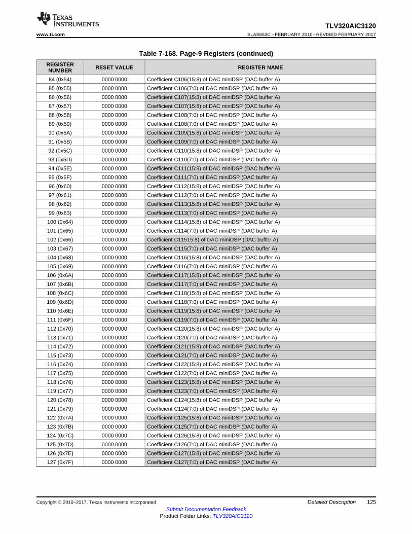
125
TLV320AIC3120www.ti.com SLAS653C –FEBRUARY 2010–REVISED FEBRUARY 2017
Submit Documentation FeedbackProduct Folder Links: TLV320AIC3120
Detailed DescriptionCopyright © 2010–2017, Texas Instruments Incorporated
Table 7-168. Page-9 Registers (continued)REGISTERNUMBER RESET VALUE REGISTER NAME
84 (0x54) 0000 0000 Coefficient C106(15:8) of DAC miniDSP (DAC buffer A)85 (0x55) 0000 0000 Coefficient C106(7:0) of DAC miniDSP (DAC buffer A)86 (0x56) 0000 0000 Coefficient C107(15:8) of DAC miniDSP (DAC buffer A)87 (0x57) 0000 0000 Coefficient C107(15:8) of DAC miniDSP (DAC buffer A)88 (0x58) 0000 0000 Coefficient C108(7:0) of DAC miniDSP (DAC buffer A)89 (0x59) 0000 0000 Coefficient C108(7:0) of DAC miniDSP (DAC buffer A)90 (0x5A) 0000 0000 Coefficient C109(15:8) of DAC miniDSP (DAC buffer A)91 (0x5B) 0000 0000 Coefficient C109(7:0) of DAC miniDSP (DAC buffer A)92 (0x5C) 0000 0000 Coefficient C110(15:8) of DAC miniDSP (DAC buffer A)93 (0x5D) 0000 0000 Coefficient C110(7:0) of DAC miniDSP (DAC buffer A)94 (0x5E) 0000 0000 Coefficient C111(15:8) of DAC miniDSP (DAC buffer A)95 (0x5F) 0000 0000 Coefficient C111(7:0) of DAC miniDSP (DAC buffer A)96 (0x60) 0000 0000 Coefficient C112(15:8) of DAC miniDSP (DAC buffer A)97 (0x61) 0000 0000 Coefficient C112(7:0) of DAC miniDSP (DAC buffer A)98 (0x62) 0000 0000 Coefficient C113(15:8) of DAC miniDSP (DAC buffer A)99 (0x63) 0000 0000 Coefficient C113(7:0) of DAC miniDSP (DAC buffer A)100 (0x64) 0000 0000 Coefficient C114(15:8) of DAC miniDSP (DAC buffer A)101 (0x65) 0000 0000 Coefficient C114(7:0) of DAC miniDSP (DAC buffer A)102 (0x66) 0000 0000 Coefficient C11515:8) of DAC miniDSP (DAC buffer A)103 (0x67) 0000 0000 Coefficient C115(7:0) of DAC miniDSP (DAC buffer A)104 (0x68) 0000 0000 Coefficient C116(15:8) of DAC miniDSP (DAC buffer A)105 (0x69) 0000 0000 Coefficient C116(7:0) of DAC miniDSP (DAC buffer A)106 (0x6A) 0000 0000 Coefficient C117(15:8) of DAC miniDSP (DAC buffer A)107 (0x6B) 0000 0000 Coefficient C117(7:0) of DAC miniDSP (DAC buffer A)108 (0x6C) 0000 0000 Coefficient C118(15:8) of DAC miniDSP (DAC buffer A)109 (0x6D) 0000 0000 Coefficient C118(7:0) of DAC miniDSP (DAC buffer A)110 (0x6E) 0000 0000 Coefficient C119(15:8) of DAC miniDSP (DAC buffer A)111 (0x6F) 0000 0000 Coefficient C119(7:0) of DAC miniDSP (DAC buffer A)112 (0x70) 0000 0000 Coefficient C120(15:8) of DAC miniDSP (DAC buffer A)113 (0x71) 0000 0000 Coefficient C120(7:0) of DAC miniDSP (DAC buffer A)114 (0x72) 0000 0000 Coefficient C121(15:8) of DAC miniDSP (DAC buffer A)115 (0x73) 0000 0000 Coefficient C121(7:0) of DAC miniDSP (DAC buffer A)116 (0x74) 0000 0000 Coefficient C122(15:8) of DAC miniDSP (DAC buffer A)117 (0x75) 0000 0000 Coefficient C122(7:0) of DAC miniDSP (DAC buffer A)118 (0x76) 0000 0000 Coefficient C123(15:8) of DAC miniDSP (DAC buffer A)119 (0x77) 0000 0000 Coefficient C123(7:0) of DAC miniDSP (DAC buffer A)120 (0x78) 0000 0000 Coefficient C124(15:8) of DAC miniDSP (DAC buffer A)121 (0x79) 0000 0000 Coefficient C124(7:0) of DAC miniDSP (DAC buffer A)122 (0x7A) 0000 0000 Coefficient C125(15:8) of DAC miniDSP (DAC buffer A)123 (0x7B) 0000 0000 Coefficient C125(7:0) of DAC miniDSP (DAC buffer A)124 (0x7C) 0000 0000 Coefficient C126(15:8) of DAC miniDSP (DAC buffer A)125 (0x7D) 0000 0000 Coefficient C126(7:0) of DAC miniDSP (DAC buffer A)126 (0x7E) 0000 0000 Coefficient C127(15:8) of DAC miniDSP (DAC buffer A)127 (0x7F) 0000 0000 Coefficient C127(7:0) of DAC miniDSP (DAC buffer A)
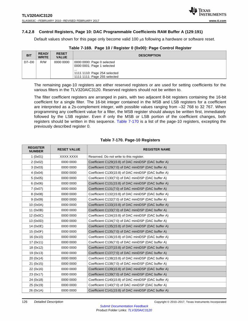
126
TLV320AIC3120SLAS653C –FEBRUARY 2010–REVISED FEBRUARY 2017 www.ti.com
Submit Documentation FeedbackProduct Folder Links: TLV320AIC3120
Detailed Description Copyright © 2010–2017, Texas Instruments Incorporated
7.4.2.8 Control Registers, Page 10: DAC Programmable Coefficients RAM Buffer A (129:191)
Default values shown for this page only become valid 100 μs following a hardware or software reset.
Table 7-169. Page 10 / Register 0 (0x00): Page Control Register
BIT READ/WRITE
RESETVALUE DESCRIPTION
D7–D0 R/W 0000 0000 0000 0000: Page 0 selected0000 0001: Page 1 selected...1111 1110: Page 254 selected1111 1111: Page 255 selected
The remaining page-10 registers are either reserved registers or are used for setting coefficients for thevarious filters in the TLV320AIC3120. Reserved registers should not be written to.
The filter coefficient registers are arranged in pairs, with two adjacent 8-bit registers containing the 16-bitcoefficient for a single filter. The 16-bit integer contained in the MSB and LSB registers for a coefficientare interpreted as a 2s-complement integer, with possible values ranging from –32 768 to 32 767. Whenprogramming any coefficient value for a filter, the MSB register should always be written first, immediatelyfollowed by the LSB register. Even if only the MSB or LSB portion of the coefficient changes, bothregisters should be written in this sequence. Table 7-170 is a list of the page-10 registers, excepting thepreviously described register 0.
Table 7-170. Page-10 Registers
REGISTERNUMBER RESET VALUE REGISTER NAME
1 (0x01) XXXX XXXX Reserved. Do not write to this register.2 (0x02) 0000 0000 Coefficient C129(15:8) of DAC miniDSP (DAC buffer A)3 (0x03) 0000 0000 Coefficient C129(7:0) of DAC miniDSP (DAC buffer A)4 (0x04) 0000 0000 Coefficient C130(15:8) of DAC miniDSP (DAC buffer A)5 (0x05) 0000 0000 Coefficient C130(7:0) of DAC miniDSP (DAC buffer A)6 (0x06) 0000 0000 Coefficient C131(15:8) of DAC miniDSP (DAC buffer A)7 (0x07) 0000 0000 Coefficient C131(7:0) of DAC miniDSP (DAC buffer A)8 (0x08) 0000 0000 Coefficient C132(15:8) of DAC miniDSP (DAC buffer A)9 (0x09) 0000 0000 Coefficient C132(7:0) of DAC miniDSP (DAC buffer A)
10 (0x0A) 0000 0000 Coefficient C133(15:8) of DAC miniDSP (DAC buffer A)11 (0x0B) 0000 0000 Coefficient C133(7:0) of DAC miniDSP (DAC buffer A)12 (0x0C) 0000 0000 Coefficient C134(15:8) of DAC miniDSP (DAC buffer A)13 (0x0D) 0000 0000 Coefficient C134(7:0) of DAC miniDSP (DAC buffer A)14 (0x0E) 0000 0000 Coefficient C135(15:8) of DAC miniDSP (DAC buffer A)15 (0x0F) 0000 0000 Coefficient C135(7:0) of DAC miniDSP (DAC buffer A)16 (0x10) 0000 0000 Coefficient C136(15:8) of DAC miniDSP (DAC buffer A)17 (0x11) 0000 0000 Coefficient C136(7:0) of DAC miniDSP (DAC buffer A)18 (0x12) 0000 0000 Coefficient C137(15:8) of DAC miniDSP (DAC buffer A)19 (0x13) 0000 0000 Coefficient C137(7:0) of DAC miniDSP (DAC buffer A)20 (0x14) 0000 0000 Coefficient C138(15:8) of DAC miniDSP (DAC buffer A)21 (0x15) 0000 0000 Coefficient C138(7:0) of DAC miniDSP (DAC buffer A)22 (0x16) 0000 0000 Coefficient C139(15:8) of DAC miniDSP (DAC buffer A)23 (0x17) 0000 0000 Coefficient C139(7:0) of DAC miniDSP (DAC buffer A)24 (0x18) 0000 0000 Coefficient C140(15:8) of DAC miniDSP (DAC buffer A)25 (0x19) 0000 0000 Coefficient C140(7:0) of DAC miniDSP (DAC buffer A)26 (0x1A) 0000 0000 Coefficient C141(15:8) of DAC miniDSP (DAC buffer A)
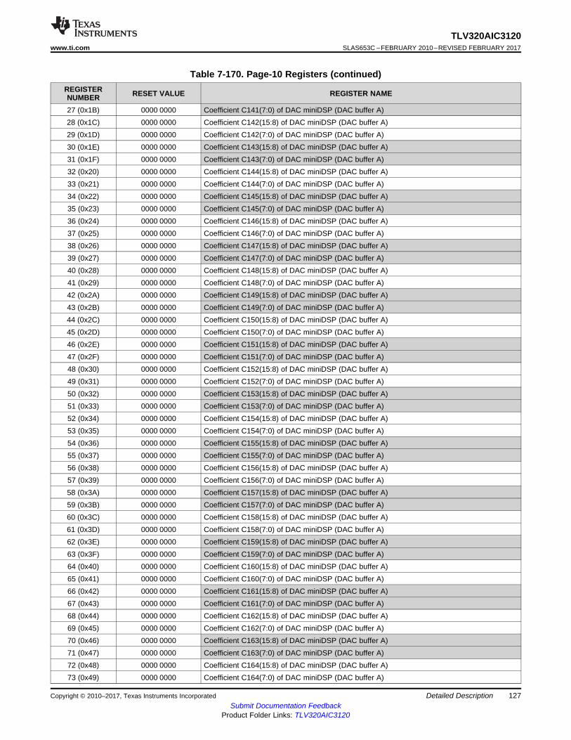
127
TLV320AIC3120www.ti.com SLAS653C –FEBRUARY 2010–REVISED FEBRUARY 2017
Submit Documentation FeedbackProduct Folder Links: TLV320AIC3120
Detailed DescriptionCopyright © 2010–2017, Texas Instruments Incorporated
Table 7-170. Page-10 Registers (continued)REGISTERNUMBER RESET VALUE REGISTER NAME
27 (0x1B) 0000 0000 Coefficient C141(7:0) of DAC miniDSP (DAC buffer A)28 (0x1C) 0000 0000 Coefficient C142(15:8) of DAC miniDSP (DAC buffer A)29 (0x1D) 0000 0000 Coefficient C142(7:0) of DAC miniDSP (DAC buffer A)30 (0x1E) 0000 0000 Coefficient C143(15:8) of DAC miniDSP (DAC buffer A)31 (0x1F) 0000 0000 Coefficient C143(7:0) of DAC miniDSP (DAC buffer A)32 (0x20) 0000 0000 Coefficient C144(15:8) of DAC miniDSP (DAC buffer A)33 (0x21) 0000 0000 Coefficient C144(7:0) of DAC miniDSP (DAC buffer A)34 (0x22) 0000 0000 Coefficient C145(15:8) of DAC miniDSP (DAC buffer A)35 (0x23) 0000 0000 Coefficient C145(7:0) of DAC miniDSP (DAC buffer A)36 (0x24) 0000 0000 Coefficient C146(15:8) of DAC miniDSP (DAC buffer A)37 (0x25) 0000 0000 Coefficient C146(7:0) of DAC miniDSP (DAC buffer A)38 (0x26) 0000 0000 Coefficient C147(15:8) of DAC miniDSP (DAC buffer A)39 (0x27) 0000 0000 Coefficient C147(7:0) of DAC miniDSP (DAC buffer A)40 (0x28) 0000 0000 Coefficient C148(15:8) of DAC miniDSP (DAC buffer A)41 (0x29) 0000 0000 Coefficient C148(7:0) of DAC miniDSP (DAC buffer A)42 (0x2A) 0000 0000 Coefficient C149(15:8) of DAC miniDSP (DAC buffer A)43 (0x2B) 0000 0000 Coefficient C149(7:0) of DAC miniDSP (DAC buffer A)44 (0x2C) 0000 0000 Coefficient C150(15:8) of DAC miniDSP (DAC buffer A)45 (0x2D) 0000 0000 Coefficient C150(7:0) of DAC miniDSP (DAC buffer A)46 (0x2E) 0000 0000 Coefficient C151(15:8) of DAC miniDSP (DAC buffer A)47 (0x2F) 0000 0000 Coefficient C151(7:0) of DAC miniDSP (DAC buffer A)48 (0x30) 0000 0000 Coefficient C152(15:8) of DAC miniDSP (DAC buffer A)49 (0x31) 0000 0000 Coefficient C152(7:0) of DAC miniDSP (DAC buffer A)50 (0x32) 0000 0000 Coefficient C153(15:8) of DAC miniDSP (DAC buffer A)51 (0x33) 0000 0000 Coefficient C153(7:0) of DAC miniDSP (DAC buffer A)52 (0x34) 0000 0000 Coefficient C154(15:8) of DAC miniDSP (DAC buffer A)53 (0x35) 0000 0000 Coefficient C154(7:0) of DAC miniDSP (DAC buffer A)54 (0x36) 0000 0000 Coefficient C155(15:8) of DAC miniDSP (DAC buffer A)55 (0x37) 0000 0000 Coefficient C155(7:0) of DAC miniDSP (DAC buffer A)56 (0x38) 0000 0000 Coefficient C156(15:8) of DAC miniDSP (DAC buffer A)57 (0x39) 0000 0000 Coefficient C156(7:0) of DAC miniDSP (DAC buffer A)58 (0x3A) 0000 0000 Coefficient C157(15:8) of DAC miniDSP (DAC buffer A)59 (0x3B) 0000 0000 Coefficient C157(7:0) of DAC miniDSP (DAC buffer A)60 (0x3C) 0000 0000 Coefficient C158(15:8) of DAC miniDSP (DAC buffer A)61 (0x3D) 0000 0000 Coefficient C158(7:0) of DAC miniDSP (DAC buffer A)62 (0x3E) 0000 0000 Coefficient C159(15:8) of DAC miniDSP (DAC buffer A)63 (0x3F) 0000 0000 Coefficient C159(7:0) of DAC miniDSP (DAC buffer A)64 (0x40) 0000 0000 Coefficient C160(15:8) of DAC miniDSP (DAC buffer A)65 (0x41) 0000 0000 Coefficient C160(7:0) of DAC miniDSP (DAC buffer A)66 (0x42) 0000 0000 Coefficient C161(15:8) of DAC miniDSP (DAC buffer A)67 (0x43) 0000 0000 Coefficient C161(7:0) of DAC miniDSP (DAC buffer A)68 (0x44) 0000 0000 Coefficient C162(15:8) of DAC miniDSP (DAC buffer A)69 (0x45) 0000 0000 Coefficient C162(7:0) of DAC miniDSP (DAC buffer A)70 (0x46) 0000 0000 Coefficient C163(15:8) of DAC miniDSP (DAC buffer A)71 (0x47) 0000 0000 Coefficient C163(7:0) of DAC miniDSP (DAC buffer A)72 (0x48) 0000 0000 Coefficient C164(15:8) of DAC miniDSP (DAC buffer A)73 (0x49) 0000 0000 Coefficient C164(7:0) of DAC miniDSP (DAC buffer A)
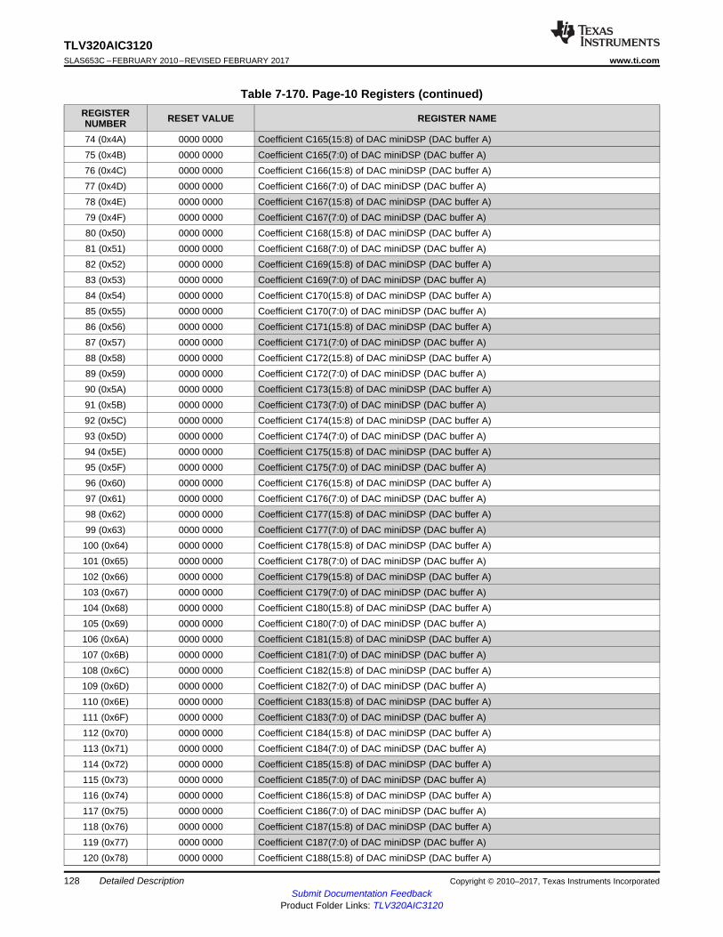
128
TLV320AIC3120SLAS653C –FEBRUARY 2010–REVISED FEBRUARY 2017 www.ti.com
Submit Documentation FeedbackProduct Folder Links: TLV320AIC3120
Detailed Description Copyright © 2010–2017, Texas Instruments Incorporated
Table 7-170. Page-10 Registers (continued)REGISTERNUMBER RESET VALUE REGISTER NAME
74 (0x4A) 0000 0000 Coefficient C165(15:8) of DAC miniDSP (DAC buffer A)75 (0x4B) 0000 0000 Coefficient C165(7:0) of DAC miniDSP (DAC buffer A)76 (0x4C) 0000 0000 Coefficient C166(15:8) of DAC miniDSP (DAC buffer A)77 (0x4D) 0000 0000 Coefficient C166(7:0) of DAC miniDSP (DAC buffer A)78 (0x4E) 0000 0000 Coefficient C167(15:8) of DAC miniDSP (DAC buffer A)79 (0x4F) 0000 0000 Coefficient C167(7:0) of DAC miniDSP (DAC buffer A)80 (0x50) 0000 0000 Coefficient C168(15:8) of DAC miniDSP (DAC buffer A)81 (0x51) 0000 0000 Coefficient C168(7:0) of DAC miniDSP (DAC buffer A)82 (0x52) 0000 0000 Coefficient C169(15:8) of DAC miniDSP (DAC buffer A)83 (0x53) 0000 0000 Coefficient C169(7:0) of DAC miniDSP (DAC buffer A)84 (0x54) 0000 0000 Coefficient C170(15:8) of DAC miniDSP (DAC buffer A)85 (0x55) 0000 0000 Coefficient C170(7:0) of DAC miniDSP (DAC buffer A)86 (0x56) 0000 0000 Coefficient C171(15:8) of DAC miniDSP (DAC buffer A)87 (0x57) 0000 0000 Coefficient C171(7:0) of DAC miniDSP (DAC buffer A)88 (0x58) 0000 0000 Coefficient C172(15:8) of DAC miniDSP (DAC buffer A)89 (0x59) 0000 0000 Coefficient C172(7:0) of DAC miniDSP (DAC buffer A)90 (0x5A) 0000 0000 Coefficient C173(15:8) of DAC miniDSP (DAC buffer A)91 (0x5B) 0000 0000 Coefficient C173(7:0) of DAC miniDSP (DAC buffer A)92 (0x5C) 0000 0000 Coefficient C174(15:8) of DAC miniDSP (DAC buffer A)93 (0x5D) 0000 0000 Coefficient C174(7:0) of DAC miniDSP (DAC buffer A)94 (0x5E) 0000 0000 Coefficient C175(15:8) of DAC miniDSP (DAC buffer A)95 (0x5F) 0000 0000 Coefficient C175(7:0) of DAC miniDSP (DAC buffer A)96 (0x60) 0000 0000 Coefficient C176(15:8) of DAC miniDSP (DAC buffer A)97 (0x61) 0000 0000 Coefficient C176(7:0) of DAC miniDSP (DAC buffer A)98 (0x62) 0000 0000 Coefficient C177(15:8) of DAC miniDSP (DAC buffer A)99 (0x63) 0000 0000 Coefficient C177(7:0) of DAC miniDSP (DAC buffer A)100 (0x64) 0000 0000 Coefficient C178(15:8) of DAC miniDSP (DAC buffer A)101 (0x65) 0000 0000 Coefficient C178(7:0) of DAC miniDSP (DAC buffer A)102 (0x66) 0000 0000 Coefficient C179(15:8) of DAC miniDSP (DAC buffer A)103 (0x67) 0000 0000 Coefficient C179(7:0) of DAC miniDSP (DAC buffer A)104 (0x68) 0000 0000 Coefficient C180(15:8) of DAC miniDSP (DAC buffer A)105 (0x69) 0000 0000 Coefficient C180(7:0) of DAC miniDSP (DAC buffer A)106 (0x6A) 0000 0000 Coefficient C181(15:8) of DAC miniDSP (DAC buffer A)107 (0x6B) 0000 0000 Coefficient C181(7:0) of DAC miniDSP (DAC buffer A)108 (0x6C) 0000 0000 Coefficient C182(15:8) of DAC miniDSP (DAC buffer A)109 (0x6D) 0000 0000 Coefficient C182(7:0) of DAC miniDSP (DAC buffer A)110 (0x6E) 0000 0000 Coefficient C183(15:8) of DAC miniDSP (DAC buffer A)111 (0x6F) 0000 0000 Coefficient C183(7:0) of DAC miniDSP (DAC buffer A)112 (0x70) 0000 0000 Coefficient C184(15:8) of DAC miniDSP (DAC buffer A)113 (0x71) 0000 0000 Coefficient C184(7:0) of DAC miniDSP (DAC buffer A)114 (0x72) 0000 0000 Coefficient C185(15:8) of DAC miniDSP (DAC buffer A)115 (0x73) 0000 0000 Coefficient C185(7:0) of DAC miniDSP (DAC buffer A)116 (0x74) 0000 0000 Coefficient C186(15:8) of DAC miniDSP (DAC buffer A)117 (0x75) 0000 0000 Coefficient C186(7:0) of DAC miniDSP (DAC buffer A)118 (0x76) 0000 0000 Coefficient C187(15:8) of DAC miniDSP (DAC buffer A)119 (0x77) 0000 0000 Coefficient C187(7:0) of DAC miniDSP (DAC buffer A)120 (0x78) 0000 0000 Coefficient C188(15:8) of DAC miniDSP (DAC buffer A)
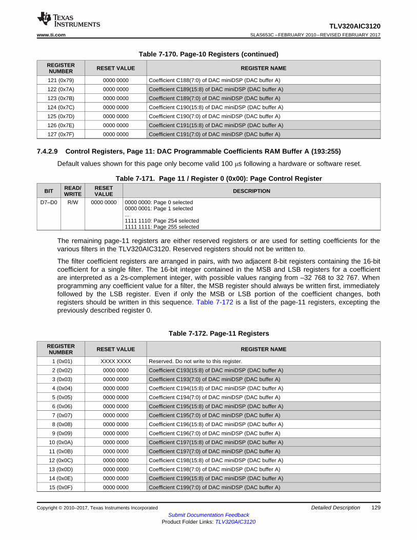
129
TLV320AIC3120www.ti.com SLAS653C –FEBRUARY 2010–REVISED FEBRUARY 2017
Submit Documentation FeedbackProduct Folder Links: TLV320AIC3120
Detailed DescriptionCopyright © 2010–2017, Texas Instruments Incorporated
Table 7-170. Page-10 Registers (continued)REGISTERNUMBER RESET VALUE REGISTER NAME
121 (0x79) 0000 0000 Coefficient C188(7:0) of DAC miniDSP (DAC buffer A)122 (0x7A) 0000 0000 Coefficient C189(15:8) of DAC miniDSP (DAC buffer A)123 (0x7B) 0000 0000 Coefficient C189(7:0) of DAC miniDSP (DAC buffer A)124 (0x7C) 0000 0000 Coefficient C190(15:8) of DAC miniDSP (DAC buffer A)125 (0x7D) 0000 0000 Coefficient C190(7:0) of DAC miniDSP (DAC buffer A)126 (0x7E) 0000 0000 Coefficient C191(15:8) of DAC miniDSP (DAC buffer A)127 (0x7F) 0000 0000 Coefficient C191(7:0) of DAC miniDSP (DAC buffer A)
7.4.2.9 Control Registers, Page 11: DAC Programmable Coefficients RAM Buffer A (193:255)
Default values shown for this page only become valid 100 μs following a hardware or software reset.
Table 7-171. Page 11 / Register 0 (0x00): Page Control Register
BIT READ/WRITE
RESETVALUE DESCRIPTION
D7–D0 R/W 0000 0000 0000 0000: Page 0 selected0000 0001: Page 1 selected...1111 1110: Page 254 selected1111 1111: Page 255 selected
The remaining page-11 registers are either reserved registers or are used for setting coefficients for thevarious filters in the TLV320AIC3120. Reserved registers should not be written to.
The filter coefficient registers are arranged in pairs, with two adjacent 8-bit registers containing the 16-bitcoefficient for a single filter. The 16-bit integer contained in the MSB and LSB registers for a coefficientare interpreted as a 2s-complement integer, with possible values ranging from –32 768 to 32 767. Whenprogramming any coefficient value for a filter, the MSB register should always be written first, immediatelyfollowed by the LSB register. Even if only the MSB or LSB portion of the coefficient changes, bothregisters should be written in this sequence. Table 7-172 is a list of the page-11 registers, excepting thepreviously described register 0.
Table 7-172. Page-11 Registers
REGISTERNUMBER RESET VALUE REGISTER NAME
1 (0x01) XXXX XXXX Reserved. Do not write to this register.2 (0x02) 0000 0000 Coefficient C193(15:8) of DAC miniDSP (DAC buffer A)3 (0x03) 0000 0000 Coefficient C193(7:0) of DAC miniDSP (DAC buffer A)4 (0x04) 0000 0000 Coefficient C194(15:8) of DAC miniDSP (DAC buffer A)5 (0x05) 0000 0000 Coefficient C194(7:0) of DAC miniDSP (DAC buffer A)6 (0x06) 0000 0000 Coefficient C195(15:8) of DAC miniDSP (DAC buffer A)7 (0x07) 0000 0000 Coefficient C195(7:0) of DAC miniDSP (DAC buffer A)8 (0x08) 0000 0000 Coefficient C196(15:8) of DAC miniDSP (DAC buffer A)9 (0x09) 0000 0000 Coefficient C196(7:0) of DAC miniDSP (DAC buffer A)
10 (0x0A) 0000 0000 Coefficient C197(15:8) of DAC miniDSP (DAC buffer A)11 (0x0B) 0000 0000 Coefficient C197(7:0) of DAC miniDSP (DAC buffer A)12 (0x0C) 0000 0000 Coefficient C198(15:8) of DAC miniDSP (DAC buffer A)13 (0x0D) 0000 0000 Coefficient C198(7:0) of DAC miniDSP (DAC buffer A)14 (0x0E) 0000 0000 Coefficient C199(15:8) of DAC miniDSP (DAC buffer A)15 (0x0F) 0000 0000 Coefficient C199(7:0) of DAC miniDSP (DAC buffer A)
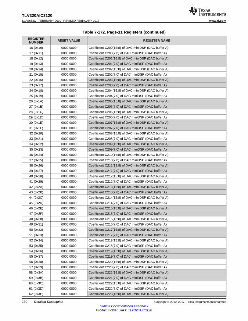
130
TLV320AIC3120SLAS653C –FEBRUARY 2010–REVISED FEBRUARY 2017 www.ti.com
Submit Documentation FeedbackProduct Folder Links: TLV320AIC3120
Detailed Description Copyright © 2010–2017, Texas Instruments Incorporated
Table 7-172. Page-11 Registers (continued)REGISTERNUMBER RESET VALUE REGISTER NAME
16 (0x10) 0000 0000 Coefficient C200(15:8) of DAC miniDSP (DAC buffer A)17 (0x11) 0000 0000 Coefficient C200(7:0) of DAC miniDSP (DAC buffer A)18 (0x12) 0000 0000 Coefficient C201(15:8) of DAC miniDSP (DAC buffer A)19 (0x13) 0000 0000 Coefficient C201(7:0) of DAC miniDSP (DAC buffer A)20 (0x14) 0000 0000 Coefficient C202(15:8) of DAC miniDSP (DAC buffer A)21 (0x15) 0000 0000 Coefficient C202(7:0) of DAC miniDSP (DAC buffer A)22 (0x16) 0000 0000 Coefficient C203(15:8) of DAC miniDSP (DAC buffer A)23 (0x17) 0000 0000 Coefficient C203(7:0) of DAC miniDSP (DAC buffer A)24 (0x18) 0000 0000 Coefficient C204(15:8) of DAC miniDSP (DAC buffer A)25 (0x19) 0000 0000 Coefficient C204(7:0) of DAC miniDSP (DAC buffer A)26 (0x1A) 0000 0000 Coefficient C205(15:8) of DAC miniDSP (DAC buffer A)27 (0x1B) 0000 0000 Coefficient C205(7:0) of DAC miniDSP (DAC buffer A)28 (0x1C) 0000 0000 Coefficient C206(15:8) of DAC miniDSP (DAC buffer A)29 (0x1D) 0000 0000 Coefficient C206(7:0) of DAC miniDSP (DAC buffer A)30 (0x1E) 0000 0000 Coefficient C207(15:8) of DAC miniDSP (DAC buffer A)31 (0x1F) 0000 0000 Coefficient C207(7:0) of DAC miniDSP (DAC buffer A)32 (0x20) 0000 0000 Coefficient C208(15:8) of DAC miniDSP (DAC buffer A)33 (0x21) 0000 0000 Coefficient C208(7:0) of DAC miniDSP (DAC buffer A)34 (0x22) 0000 0000 Coefficient C209(15:8) of DAC miniDSP (DAC buffer A)35 (0x23) 0000 0000 Coefficient C209(7:0) of DAC miniDSP (DAC buffer A)36 (0x24) 0000 0000 Coefficient C210(15:8) of DAC miniDSP (DAC buffer A)37 (0x25) 0000 0000 Coefficient C210(7:0) of DAC miniDSP (DAC buffer A)38 (0x26) 0000 0000 Coefficient C211(15:8) of DAC miniDSP (DAC buffer A)39 (0x27) 0000 0000 Coefficient C211(7:0) of DAC miniDSP (DAC buffer A)40 (0x28) 0000 0000 Coefficient C212(15:8) of DAC miniDSP (DAC buffer A)41 (0x29) 0000 0000 Coefficient C212(7:0) of DAC miniDSP (DAC buffer A)42 (0x2A) 0000 0000 Coefficient C213(15:8) of DAC miniDSP (DAC buffer A)43 (0x2B) 0000 0000 Coefficient C213(7:0) of DAC miniDSP (DAC buffer A)44 (0x2C) 0000 0000 Coefficient C214(15:8) of DAC miniDSP (DAC buffer A)45 (0x2D) 0000 0000 Coefficient C214(7:0) of DAC miniDSP (DAC buffer A)46 (0x2E) 0000 0000 Coefficient C215(15:8) of DAC miniDSP (DAC buffer A)47 (0x2F) 0000 0000 Coefficient C215(7:0) of DAC miniDSP (DAC buffer A)48 (0x30) 0000 0000 Coefficient C216(15:8) of DAC miniDSP (DAC buffer A)49 (0x31) 0000 0000 Coefficient C216(7:0) of DAC miniDSP (DAC buffer A)50 (0x32) 0000 0000 Coefficient C217(15:8) of DAC miniDSP (DAC buffer A)51 (0x33) 0000 0000 Coefficient C217(7:0) of DAC miniDSP (DAC buffer A)52 (0x34) 0000 0000 Coefficient C218(15:8) of DAC miniDSP (DAC buffer A)53 (0x35) 0000 0000 Coefficient C218(7:0) of DAC miniDSP (DAC buffer A)54 (0x36) 0000 0000 Coefficient C219(15:8) of DAC miniDSP (DAC buffer A)55 (0x37) 0000 0000 Coefficient C219(7:0) of DAC miniDSP (DAC buffer A)56 (0x38) 0000 0000 Coefficient C220(15:8) of DAC miniDSP (DAC buffer A)57 (0x39) 0000 0000 Coefficient C220(7:0) of DAC miniDSP (DAC buffer A)58 (0x3A) 0000 0000 Coefficient C221(15:8) of DAC miniDSP (DAC buffer A)59 (0x3B) 0000 0000 Coefficient C221(7:0) of DAC miniDSP (DAC buffer A)60 (0x3C) 0000 0000 Coefficient C222(15:8) of DAC miniDSP (DAC buffer A)61 (0x3D) 0000 0000 Coefficient C222(7:0) of DAC miniDSP (DAC buffer A)62 (0x3E) 0000 0000 Coefficient C223(15:8) of DAC miniDSP (DAC buffer A)
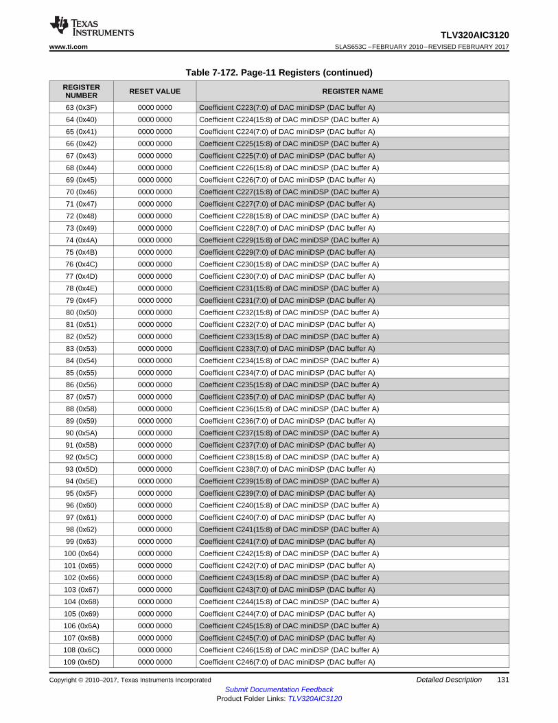
131
TLV320AIC3120www.ti.com SLAS653C –FEBRUARY 2010–REVISED FEBRUARY 2017
Submit Documentation FeedbackProduct Folder Links: TLV320AIC3120
Detailed DescriptionCopyright © 2010–2017, Texas Instruments Incorporated
Table 7-172. Page-11 Registers (continued)REGISTERNUMBER RESET VALUE REGISTER NAME
63 (0x3F) 0000 0000 Coefficient C223(7:0) of DAC miniDSP (DAC buffer A)64 (0x40) 0000 0000 Coefficient C224(15:8) of DAC miniDSP (DAC buffer A)65 (0x41) 0000 0000 Coefficient C224(7:0) of DAC miniDSP (DAC buffer A)66 (0x42) 0000 0000 Coefficient C225(15:8) of DAC miniDSP (DAC buffer A)67 (0x43) 0000 0000 Coefficient C225(7:0) of DAC miniDSP (DAC buffer A)68 (0x44) 0000 0000 Coefficient C226(15:8) of DAC miniDSP (DAC buffer A)69 (0x45) 0000 0000 Coefficient C226(7:0) of DAC miniDSP (DAC buffer A)70 (0x46) 0000 0000 Coefficient C227(15:8) of DAC miniDSP (DAC buffer A)71 (0x47) 0000 0000 Coefficient C227(7:0) of DAC miniDSP (DAC buffer A)72 (0x48) 0000 0000 Coefficient C228(15:8) of DAC miniDSP (DAC buffer A)73 (0x49) 0000 0000 Coefficient C228(7:0) of DAC miniDSP (DAC buffer A)74 (0x4A) 0000 0000 Coefficient C229(15:8) of DAC miniDSP (DAC buffer A)75 (0x4B) 0000 0000 Coefficient C229(7:0) of DAC miniDSP (DAC buffer A)76 (0x4C) 0000 0000 Coefficient C230(15:8) of DAC miniDSP (DAC buffer A)77 (0x4D) 0000 0000 Coefficient C230(7:0) of DAC miniDSP (DAC buffer A)78 (0x4E) 0000 0000 Coefficient C231(15:8) of DAC miniDSP (DAC buffer A)79 (0x4F) 0000 0000 Coefficient C231(7:0) of DAC miniDSP (DAC buffer A)80 (0x50) 0000 0000 Coefficient C232(15:8) of DAC miniDSP (DAC buffer A)81 (0x51) 0000 0000 Coefficient C232(7:0) of DAC miniDSP (DAC buffer A)82 (0x52) 0000 0000 Coefficient C233(15:8) of DAC miniDSP (DAC buffer A)83 (0x53) 0000 0000 Coefficient C233(7:0) of DAC miniDSP (DAC buffer A)84 (0x54) 0000 0000 Coefficient C234(15:8) of DAC miniDSP (DAC buffer A)85 (0x55) 0000 0000 Coefficient C234(7:0) of DAC miniDSP (DAC buffer A)86 (0x56) 0000 0000 Coefficient C235(15:8) of DAC miniDSP (DAC buffer A)87 (0x57) 0000 0000 Coefficient C235(7:0) of DAC miniDSP (DAC buffer A)88 (0x58) 0000 0000 Coefficient C236(15:8) of DAC miniDSP (DAC buffer A)89 (0x59) 0000 0000 Coefficient C236(7:0) of DAC miniDSP (DAC buffer A)90 (0x5A) 0000 0000 Coefficient C237(15:8) of DAC miniDSP (DAC buffer A)91 (0x5B) 0000 0000 Coefficient C237(7:0) of DAC miniDSP (DAC buffer A)92 (0x5C) 0000 0000 Coefficient C238(15:8) of DAC miniDSP (DAC buffer A)93 (0x5D) 0000 0000 Coefficient C238(7:0) of DAC miniDSP (DAC buffer A)94 (0x5E) 0000 0000 Coefficient C239(15:8) of DAC miniDSP (DAC buffer A)95 (0x5F) 0000 0000 Coefficient C239(7:0) of DAC miniDSP (DAC buffer A)96 (0x60) 0000 0000 Coefficient C240(15:8) of DAC miniDSP (DAC buffer A)97 (0x61) 0000 0000 Coefficient C240(7:0) of DAC miniDSP (DAC buffer A)98 (0x62) 0000 0000 Coefficient C241(15:8) of DAC miniDSP (DAC buffer A)99 (0x63) 0000 0000 Coefficient C241(7:0) of DAC miniDSP (DAC buffer A)100 (0x64) 0000 0000 Coefficient C242(15:8) of DAC miniDSP (DAC buffer A)101 (0x65) 0000 0000 Coefficient C242(7:0) of DAC miniDSP (DAC buffer A)102 (0x66) 0000 0000 Coefficient C243(15:8) of DAC miniDSP (DAC buffer A)103 (0x67) 0000 0000 Coefficient C243(7:0) of DAC miniDSP (DAC buffer A)104 (0x68) 0000 0000 Coefficient C244(15:8) of DAC miniDSP (DAC buffer A)105 (0x69) 0000 0000 Coefficient C244(7:0) of DAC miniDSP (DAC buffer A)106 (0x6A) 0000 0000 Coefficient C245(15:8) of DAC miniDSP (DAC buffer A)107 (0x6B) 0000 0000 Coefficient C245(7:0) of DAC miniDSP (DAC buffer A)108 (0x6C) 0000 0000 Coefficient C246(15:8) of DAC miniDSP (DAC buffer A)109 (0x6D) 0000 0000 Coefficient C246(7:0) of DAC miniDSP (DAC buffer A)
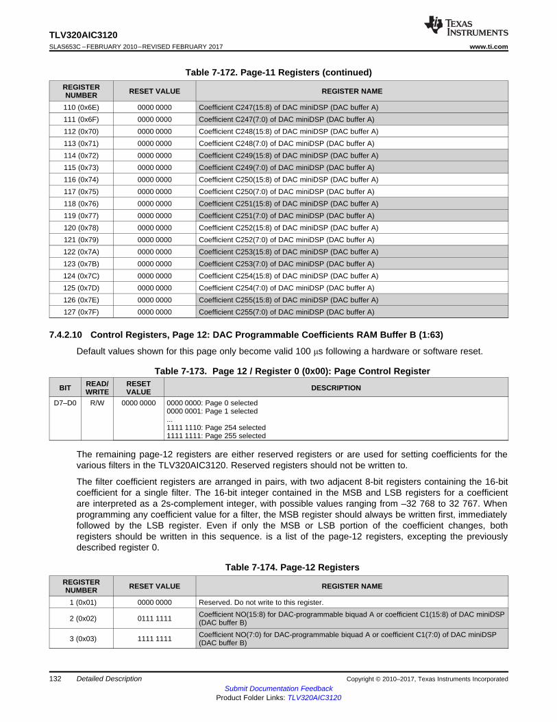
132
TLV320AIC3120SLAS653C –FEBRUARY 2010–REVISED FEBRUARY 2017 www.ti.com
Submit Documentation FeedbackProduct Folder Links: TLV320AIC3120
Detailed Description Copyright © 2010–2017, Texas Instruments Incorporated
Table 7-172. Page-11 Registers (continued)REGISTERNUMBER RESET VALUE REGISTER NAME
110 (0x6E) 0000 0000 Coefficient C247(15:8) of DAC miniDSP (DAC buffer A)111 (0x6F) 0000 0000 Coefficient C247(7:0) of DAC miniDSP (DAC buffer A)112 (0x70) 0000 0000 Coefficient C248(15:8) of DAC miniDSP (DAC buffer A)113 (0x71) 0000 0000 Coefficient C248(7:0) of DAC miniDSP (DAC buffer A)114 (0x72) 0000 0000 Coefficient C249(15:8) of DAC miniDSP (DAC buffer A)115 (0x73) 0000 0000 Coefficient C249(7:0) of DAC miniDSP (DAC buffer A)116 (0x74) 0000 0000 Coefficient C250(15:8) of DAC miniDSP (DAC buffer A)117 (0x75) 0000 0000 Coefficient C250(7:0) of DAC miniDSP (DAC buffer A)118 (0x76) 0000 0000 Coefficient C251(15:8) of DAC miniDSP (DAC buffer A)119 (0x77) 0000 0000 Coefficient C251(7:0) of DAC miniDSP (DAC buffer A)120 (0x78) 0000 0000 Coefficient C252(15:8) of DAC miniDSP (DAC buffer A)121 (0x79) 0000 0000 Coefficient C252(7:0) of DAC miniDSP (DAC buffer A)122 (0x7A) 0000 0000 Coefficient C253(15:8) of DAC miniDSP (DAC buffer A)123 (0x7B) 0000 0000 Coefficient C253(7:0) of DAC miniDSP (DAC buffer A)124 (0x7C) 0000 0000 Coefficient C254(15:8) of DAC miniDSP (DAC buffer A)125 (0x7D) 0000 0000 Coefficient C254(7:0) of DAC miniDSP (DAC buffer A)126 (0x7E) 0000 0000 Coefficient C255(15:8) of DAC miniDSP (DAC buffer A)127 (0x7F) 0000 0000 Coefficient C255(7:0) of DAC miniDSP (DAC buffer A)
7.4.2.10 Control Registers, Page 12: DAC Programmable Coefficients RAM Buffer B (1:63)
Default values shown for this page only become valid 100 μs following a hardware or software reset.
Table 7-173. Page 12 / Register 0 (0x00): Page Control Register
BIT READ/WRITE
RESETVALUE DESCRIPTION
D7–D0 R/W 0000 0000 0000 0000: Page 0 selected0000 0001: Page 1 selected...1111 1110: Page 254 selected1111 1111: Page 255 selected
The remaining page-12 registers are either reserved registers or are used for setting coefficients for thevarious filters in the TLV320AIC3120. Reserved registers should not be written to.
The filter coefficient registers are arranged in pairs, with two adjacent 8-bit registers containing the 16-bitcoefficient for a single filter. The 16-bit integer contained in the MSB and LSB registers for a coefficientare interpreted as a 2s-complement integer, with possible values ranging from –32 768 to 32 767. Whenprogramming any coefficient value for a filter, the MSB register should always be written first, immediatelyfollowed by the LSB register. Even if only the MSB or LSB portion of the coefficient changes, bothregisters should be written in this sequence. is a list of the page-12 registers, excepting the previouslydescribed register 0.
Table 7-174. Page-12 RegistersREGISTERNUMBER RESET VALUE REGISTER NAME
1 (0x01) 0000 0000 Reserved. Do not write to this register.
2 (0x02) 0111 1111 Coefficient NO(15:8) for DAC-programmable biquad A or coefficient C1(15:8) of DAC miniDSP(DAC buffer B)
3 (0x03) 1111 1111 Coefficient NO(7:0) for DAC-programmable biquad A or coefficient C1(7:0) of DAC miniDSP(DAC buffer B)
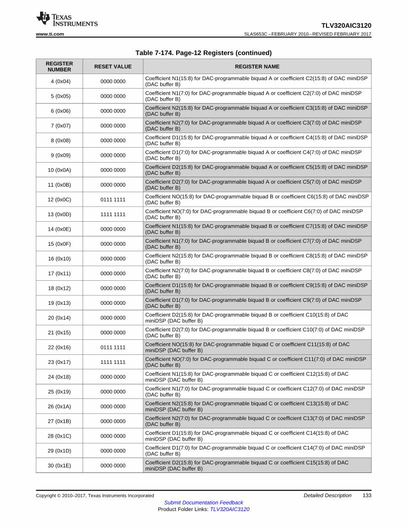
133
TLV320AIC3120www.ti.com SLAS653C –FEBRUARY 2010–REVISED FEBRUARY 2017
Submit Documentation FeedbackProduct Folder Links: TLV320AIC3120
Detailed DescriptionCopyright © 2010–2017, Texas Instruments Incorporated
Table 7-174. Page-12 Registers (continued)REGISTERNUMBER RESET VALUE REGISTER NAME
4 (0x04) 0000 0000 Coefficient N1(15:8) for DAC-programmable biquad A or coefficient C2(15:8) of DAC miniDSP(DAC buffer B)
5 (0x05) 0000 0000 Coefficient N1(7:0) for DAC-programmable biquad A or coefficient C2(7:0) of DAC miniDSP(DAC buffer B)
6 (0x06) 0000 0000 Coefficient N2(15:8) for DAC-programmable biquad A or coefficient C3(15:8) of DAC miniDSP(DAC buffer B)
7 (0x07) 0000 0000 Coefficient N2(7:0) for DAC-programmable biquad A or coefficient C3(7:0) of DAC miniDSP(DAC buffer B)
8 (0x08) 0000 0000 Coefficient D1(15:8) for DAC-programmable biquad A or coefficient C4(15:8) of DAC miniDSP(DAC buffer B)
9 (0x09) 0000 0000 Coefficient D1(7:0) for DAC-programmable biquad A or coefficient C4(7:0) of DAC miniDSP(DAC buffer B)
10 (0x0A) 0000 0000 Coefficient D2(15:8) for DAC-programmable biquad A or coefficient C5(15:8) of DAC miniDSP(DAC buffer B)
11 (0x0B) 0000 0000 Coefficient D2(7:0) for DAC-programmable biquad A or coefficient C5(7:0) of DAC miniDSP(DAC buffer B)
12 (0x0C) 0111 1111 Coefficient NO(15:8) for DAC-programmable biquad B or coefficient C6(15:8) of DAC miniDSP(DAC buffer B)
13 (0x0D) 1111 1111 Coefficient NO(7:0) for DAC-programmable biquad B or coefficient C6(7:0) of DAC miniDSP(DAC buffer B)
14 (0x0E) 0000 0000 Coefficient N1(15:8) for DAC-programmable biquad B or coefficient C7(15:8) of DAC miniDSP(DAC buffer B)
15 (0x0F) 0000 0000 Coefficient N1(7:0) for DAC-programmable biquad B or coefficient C7(7:0) of DAC miniDSP(DAC buffer B)
16 (0x10) 0000 0000 Coefficient N2(15:8) for DAC-programmable biquad B or coefficient C8(15:8) of DAC miniDSP(DAC buffer B)
17 (0x11) 0000 0000 Coefficient N2(7:0) for DAC-programmable biquad B or coefficient C8(7:0) of DAC miniDSP(DAC buffer B)
18 (0x12) 0000 0000 Coefficient D1(15:8) for DAC-programmable biquad B or coefficient C9(15:8) of DAC miniDSP(DAC buffer B)
19 (0x13) 0000 0000 Coefficient D1(7:0) for DAC-programmable biquad B or coefficient C9(7:0) of DAC miniDSP(DAC buffer B)
20 (0x14) 0000 0000 Coefficient D2(15:8) for DAC-programmable biquad B or coefficient C10(15:8) of DACminiDSP (DAC buffer B)
21 (0x15) 0000 0000 Coefficient D2(7:0) for DAC-programmable biquad B or coefficient C10(7:0) of DAC miniDSP(DAC buffer B)
22 (0x16) 0111 1111 Coefficient NO(15:8) for DAC-programmable biquad C or coefficient C11(15:8) of DACminiDSP (DAC buffer B)
23 (0x17) 1111 1111 Coefficient NO(7:0) for DAC-programmable biquad C or coefficient C11(7:0) of DAC miniDSP(DAC buffer B)
24 (0x18) 0000 0000 Coefficient N1(15:8) for DAC-programmable biquad C or coefficient C12(15:8) of DACminiDSP (DAC buffer B)
25 (0x19) 0000 0000 Coefficient N1(7:0) for DAC-programmable biquad C or coefficient C12(7:0) of DAC miniDSP(DAC buffer B)
26 (0x1A) 0000 0000 Coefficient N2(15:8) for DAC-programmable biquad C or coefficient C13(15:8) of DACminiDSP (DAC buffer B)
27 (0x1B) 0000 0000 Coefficient N2(7:0) for DAC-programmable biquad C or coefficient C13(7:0) of DAC miniDSP(DAC buffer B)
28 (0x1C) 0000 0000 Coefficient D1(15:8) for DAC-programmable biquad C or coefficient C14(15:8) of DACminiDSP (DAC buffer B)
29 (0x1D) 0000 0000 Coefficient D1(7:0) for DAC-programmable biquad C or coefficient C14(7:0) of DAC miniDSP(DAC buffer B)
30 (0x1E) 0000 0000 Coefficient D2(15:8) for DAC-programmable biquad C or coefficient C15(15:8) of DACminiDSP (DAC buffer B)
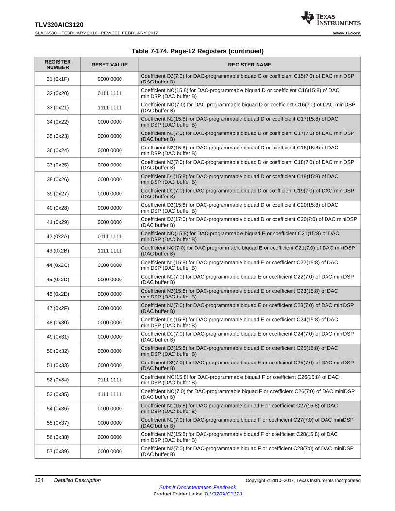
134
TLV320AIC3120SLAS653C –FEBRUARY 2010–REVISED FEBRUARY 2017 www.ti.com
Submit Documentation FeedbackProduct Folder Links: TLV320AIC3120
Detailed Description Copyright © 2010–2017, Texas Instruments Incorporated
Table 7-174. Page-12 Registers (continued)REGISTERNUMBER RESET VALUE REGISTER NAME
31 (0x1F) 0000 0000 Coefficient D2(7:0) for DAC-programmable biquad C or coefficient C15(7:0) of DAC miniDSP(DAC buffer B)
32 (0x20) 0111 1111 Coefficient NO(15:8) for DAC-programmable biquad D or coefficient C16(15:8) of DACminiDSP (DAC buffer B)
33 (0x21) 1111 1111 Coefficient NO(7:0) for DAC-programmable biquad D or coefficient C16(7:0) of DAC miniDSP(DAC buffer B)
34 (0x22) 0000 0000 Coefficient N1(15:8) for DAC-programmable biquad D or coefficient C17(15:8) of DACminiDSP (DAC buffer B)
35 (0x23) 0000 0000 Coefficient N1(7:0) for DAC-programmable biquad D or coefficient C17(7:0) of DAC miniDSP(DAC buffer B)
36 (0x24) 0000 0000 Coefficient N2(15:8) for DAC-programmable biquad D or coefficient C18(15:8) of DACminiDSP (DAC buffer B)
37 (0x25) 0000 0000 Coefficient N2(7:0) for DAC-programmable biquad D or coefficient C18(7:0) of DAC miniDSP(DAC buffer B)
38 (0x26) 0000 0000 Coefficient D1(15:8) for DAC-programmable biquad D or coefficient C19(15:8) of DACminiDSP (DAC buffer B)
39 (0x27) 0000 0000 Coefficient D1(7:0) for DAC-programmable biquad D or coefficient C19(7:0) of DAC miniDSP(DAC buffer B)
40 (0x28) 0000 0000 Coefficient D2(15:8) for DAC-programmable biquad D or coefficient C20(15:8) of DACminiDSP (DAC buffer B)
41 (0x29) 0000 0000 Coefficient D2(17:0) for DAC-programmable biquad D or coefficient C20(7:0) of DAC miniDSP(DAC buffer B)
42 (0x2A) 0111 1111 Coefficient NO(15:8) for DAC-programmable biquad E or coefficient C21(15:8) of DACminiDSP (DAC buffer B)
43 (0x2B) 1111 1111 Coefficient NO(7:0) for DAC-programmable biquad E or coefficient C21(7:0) of DAC miniDSP(DAC buffer B)
44 (0x2C) 0000 0000 Coefficient N1(15:8) for DAC-programmable biquad E or coefficient C22(15:8) of DACminiDSP (DAC buffer B)
45 (0x2D) 0000 0000 Coefficient N1(7:0) for DAC-programmable biquad E or coefficient C22(7:0) of DAC miniDSP(DAC buffer B)
46 (0x2E) 0000 0000 Coefficient N2(15:8) for DAC-programmable biquad E or coefficient C23(15:8) of DACminiDSP (DAC buffer B)
47 (0x2F) 0000 0000 Coefficient N2(7:0) for DAC-programmable biquad E or coefficient C23(7:0) of DAC miniDSP(DAC buffer B)
48 (0x30) 0000 0000 Coefficient D1(15:8) for DAC-programmable biquad E or coefficient C24(15:8) of DACminiDSP (DAC buffer B)
49 (0x31) 0000 0000 Coefficient D1(7:0) for DAC-programmable biquad E or coefficient C24(7:0) of DAC miniDSP(DAC buffer B)
50 (0x32) 0000 0000 Coefficient D2(15:8) for DAC-programmable biquad E or coefficient C25(15:8) of DACminiDSP (DAC buffer B)
51 (0x33) 0000 0000 Coefficient D2(7:0) for DAC-programmable biquad E or coefficient C25(7:0) of DAC miniDSP(DAC buffer B)
52 (0x34) 0111 1111 Coefficient NO(15:8) for DAC-programmable biquad F or coefficient C26(15:8) of DACminiDSP (DAC buffer B)
53 (0x35) 1111 1111 Coefficient NO(7:0) for DAC-programmable biquad F or coefficient C26(7:0) of DAC miniDSP(DAC buffer B)
54 (0x36) 0000 0000 Coefficient N1(15:8) for DAC-programmable biquad F or coefficient C27(15:8) of DACminiDSP (DAC buffer B)
55 (0x37) 0000 0000 Coefficient N1(7:0) for DAC-programmable biquad F or coefficient C27(7:0) of DAC miniDSP(DAC buffer B)
56 (0x38) 0000 0000 Coefficient N2(15:8) for DAC-programmable biquad F or coefficient C28(15:8) of DACminiDSP (DAC buffer B)
57 (0x39) 0000 0000 Coefficient N2(7:0) for DAC-programmable biquad F or coefficient C28(7:0) of DAC miniDSP(DAC buffer B)
135
TLV320AIC3120www.ti.com SLAS653C –FEBRUARY 2010–REVISED FEBRUARY 2017
Submit Documentation FeedbackProduct Folder Links: TLV320AIC3120
Detailed DescriptionCopyright © 2010–2017, Texas Instruments Incorporated
Table 7-174. Page-12 Registers (continued)REGISTERNUMBER RESET VALUE REGISTER NAME
58 (0x3A) 0000 0000 Coefficient D1(15:8) for DAC-programmable biquad F or coefficient C29(15:8) of DACminiDSP (DAC buffer B)
59 (0x3B) 0000 0000 Coefficient D1(7:0) for DAC-programmable biquad F or coefficient C29(7:0) of DAC miniDSP(DAC buffer B)
60 (0x3C) 0000 0000 Coefficient D2(15:8) for DAC-programmable biquad F or coefficient C30(15:8) of DACminiDSP (DAC buffer B)
61 (0x3D) 0000 0000 Coefficient D2(7:0) for DAC-programmable biquad F or coefficient C30(7:0) of DAC miniDSP(DAC buffer B)
62 (0x3E) 0000 0000 Coefficient C31(15:8) of DAC miniDSP (DAC buffer B)63 (0x3F) 0000 0000 Coefficient C31(7:0) of DAC miniDSP (DAC buffer B)64 (0x40) 0000 0000 Coefficient C32(15:8) of DAC miniDSP (DAC buffer B)65 (0x41) 0000 0000 Coefficient C32(7:0) of DAC miniDSP (DAC buffer B)66 (0x42) 0111 1111 Coefficient C33(15:8) of DAC miniDSP (DAC buffer B)67 (0x43) 1111 1111 Coefficient C33(7:0) of DAC miniDSP (DAC buffer B)68 (0x44) 0000 0000 Coefficient C34(15:8) of DAC miniDSP (DAC buffer B)69 (0x45) 0000 0000 Coefficient C34(7:0) of DAC miniDSP (DAC buffer B)70 (0x46) 0000 0000 Coefficient C35(15:8) of DAC miniDSP (DAC buffer B)71 (0x47) 0000 0000 Coefficient C35(7:0) of DAC miniDSP (DAC buffer B)72 (0x48) 0000 0000 Coefficient C36(15:8) of DAC miniDSP (DAC buffer B)73 (0x49) 0000 0000 Coefficient C36(7:0) of DAC miniDSP (DAC buffer B)74 (0x4A) 0000 0000 Coefficient C37(15:8) of DAC miniDSP (DAC buffer B)75 (0x4B) 0000 0000 Coefficient C37(7:0) of DAC miniDSP (DAC buffer B)76 (0x4C) 0111 1111 Coefficient C38(15:8) of DAC miniDSP (DAC buffer B)77 (0x4D) 1111 1111 Coefficient C38(7:0) of DAC miniDSP (DAC buffer B)78 (0x4E) 0000 0000 Coefficient C39(15:8) of DAC miniDSP (DAC buffer B)79 (0x4F) 0000 0000 Coefficient C39(7:0) of DAC miniDSP (DAC buffer B)80 (0x50) 0000 0000 Coefficient C40(15:8) of DAC miniDSP (DAC buffer B)81 (0x51) 0000 0000 Coefficient C40(7:0) of DAC miniDSP (DAC buffer B)82 (0x52) 0000 0000 Coefficient C41(15:8) of DAC miniDSP (DAC buffer B)83 (0x53) 0000 0000 Coefficient C41(7:0) of DAC miniDSP (DAC buffer B)84 (0x54) 0000 0000 Coefficient C42(15:8) of DAC miniDSP (DAC buffer B)85 (0x55) 0000 0000 Coefficient C42(7:0) of DAC miniDSP (DAC buffer B)86 (0x56) 0111 1111 Coefficient C43(15:8) of DAC miniDSP (DAC buffer B)87 (0x57) 1111 1111 Coefficient C43(7:0) of DAC miniDSP (DAC buffer B)88 (0x58) 0000 0000 Coefficient C44(15:8) of DAC miniDSP (DAC buffer B)89 (0x59) 0000 0000 Coefficient C44(7:0) of DAC miniDSP (DAC buffer B)90 (0x5A) 0000 0000 Coefficient C45(15:8) of DAC miniDSP (DAC buffer B)91 (0x5B) 0000 0000 Coefficient C45(7:0) of DAC miniDSP (DAC buffer B)92 (0x5C) 0000 0000 Coefficient C46(15:8) of DAC miniDSP (DAC buffer B)93 (0x5D) 0000 0000 Coefficient C46(7:0) of DAC miniDSP (DAC buffer B)94 (0x5E) 0000 0000 Coefficient C47(15:8) of DAC miniDSP (DAC buffer B)95 (0x5F) 0000 0000 Coefficient C47(7:0) of DAC miniDSP (DAC buffer B)96 (0x60) 0111 1111 Coefficient C48(15:8) of DAC miniDSP (DAC buffer B)97 (0x61) 1111 1111 Coefficient C48(7:0) of DAC miniDSP (DAC buffer B)98 (0x62) 0000 0000 Coefficient C49(15:8) of DAC miniDSP (DAC buffer B)99 (0x63) 0000 0000 Coefficient C49(7:0) of DAC miniDSP (DAC buffer B)100 (0x64) 0000 0000 Coefficient C50(15:8) of DAC miniDSP (DAC buffer B)101 (0x65) 0000 0000 Coefficient C50(7:0) of DAC miniDSP (DAC buffer B)
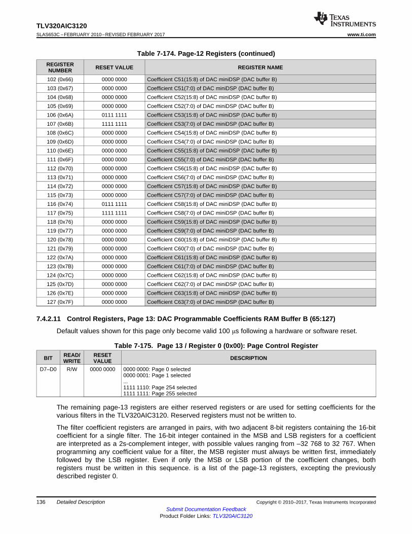
136
TLV320AIC3120SLAS653C –FEBRUARY 2010–REVISED FEBRUARY 2017 www.ti.com
Submit Documentation FeedbackProduct Folder Links: TLV320AIC3120
Detailed Description Copyright © 2010–2017, Texas Instruments Incorporated
Table 7-174. Page-12 Registers (continued)REGISTERNUMBER RESET VALUE REGISTER NAME
102 (0x66) 0000 0000 Coefficient C51(15:8) of DAC miniDSP (DAC buffer B)103 (0x67) 0000 0000 Coefficient C51(7:0) of DAC miniDSP (DAC buffer B)104 (0x68) 0000 0000 Coefficient C52(15:8) of DAC miniDSP (DAC buffer B)105 (0x69) 0000 0000 Coefficient C52(7:0) of DAC miniDSP (DAC buffer B)106 (0x6A) 0111 1111 Coefficient C53(15:8) of DAC miniDSP (DAC buffer B)107 (0x6B) 1111 1111 Coefficient C53(7:0) of DAC miniDSP (DAC buffer B)108 (0x6C) 0000 0000 Coefficient C54(15:8) of DAC miniDSP (DAC buffer B)109 (0x6D) 0000 0000 Coefficient C54(7:0) of DAC miniDSP (DAC buffer B)110 (0x6E) 0000 0000 Coefficient C55(15:8) of DAC miniDSP (DAC buffer B)111 (0x6F) 0000 0000 Coefficient C55(7:0) of DAC miniDSP (DAC buffer B)112 (0x70) 0000 0000 Coefficient C56(15:8) of DAC miniDSP (DAC buffer B)113 (0x71) 0000 0000 Coefficient C56(7:0) of DAC miniDSP (DAC buffer B)114 (0x72) 0000 0000 Coefficient C57(15:8) of DAC miniDSP (DAC buffer B)115 (0x73) 0000 0000 Coefficient C57(7:0) of DAC miniDSP (DAC buffer B)116 (0x74) 0111 1111 Coefficient C58(15:8) of DAC miniDSP (DAC buffer B)117 (0x75) 1111 1111 Coefficient C58(7:0) of DAC miniDSP (DAC buffer B)118 (0x76) 0000 0000 Coefficient C59(15:8) of DAC miniDSP (DAC buffer B)119 (0x77) 0000 0000 Coefficient C59(7:0) of DAC miniDSP (DAC buffer B)120 (0x78) 0000 0000 Coefficient C60(15:8) of DAC miniDSP (DAC buffer B)121 (0x79) 0000 0000 Coefficient C60(7:0) of DAC miniDSP (DAC buffer B)122 (0x7A) 0000 0000 Coefficient C61(15:8) of DAC miniDSP (DAC buffer B)123 (0x7B) 0000 0000 Coefficient C61(7:0) of DAC miniDSP (DAC buffer B)124 (0x7C) 0000 0000 Coefficient C62(15:8) of DAC miniDSP (DAC buffer B)125 (0x7D) 0000 0000 Coefficient C62(7:0) of DAC miniDSP (DAC buffer B)126 (0x7E) 0000 0000 Coefficient C63(15:8) of DAC miniDSP (DAC buffer B)127 (0x7F) 0000 0000 Coefficient C63(7:0) of DAC miniDSP (DAC buffer B)
7.4.2.11 Control Registers, Page 13: DAC Programmable Coefficients RAM Buffer B (65:127)
Default values shown for this page only become valid 100 μs following a hardware or software reset.
Table 7-175. Page 13 / Register 0 (0x00): Page Control Register
BIT READ/WRITE
RESETVALUE DESCRIPTION
D7–D0 R/W 0000 0000 0000 0000: Page 0 selected0000 0001: Page 1 selected...1111 1110: Page 254 selected1111 1111: Page 255 selected
The remaining page-13 registers are either reserved registers or are used for setting coefficients for thevarious filters in the TLV320AIC3120. Reserved registers must not be written to.
The filter coefficient registers are arranged in pairs, with two adjacent 8-bit registers containing the 16-bitcoefficient for a single filter. The 16-bit integer contained in the MSB and LSB registers for a coefficientare interpreted as a 2s-complement integer, with possible values ranging from –32 768 to 32 767. Whenprogramming any coefficient value for a filter, the MSB register must always be written first, immediatelyfollowed by the LSB register. Even if only the MSB or LSB portion of the coefficient changes, bothregisters must be written in this sequence. is a list of the page-13 registers, excepting the previouslydescribed register 0.
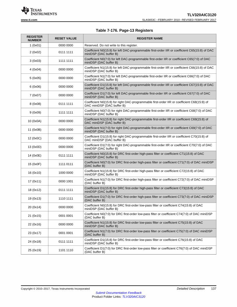
137
TLV320AIC3120www.ti.com SLAS653C –FEBRUARY 2010–REVISED FEBRUARY 2017
Submit Documentation FeedbackProduct Folder Links: TLV320AIC3120
Detailed DescriptionCopyright © 2010–2017, Texas Instruments Incorporated
Table 7-176. Page-13 RegistersREGISTERNUMBER RESET VALUE REGISTER NAME
1 (0x01) 0000 0000 Reserved. Do not write to this register.
2 (0x02) 0111 1111 Coefficient N0(15:8) for left DAC-programmable first-order IIR or coefficient C65(15:8) of DACminiDSP (DAC buffer B)
3 (0x03) 1111 1111 Coefficient N0(7:0) for left DAC-programmable first-order IIR or coefficient C65(7:0) of DACminiDSP (DAC buffer B)
4 (0x04) 0000 0000 Coefficient N1(15:8) for left DAC-programmable first-order IIR or coefficient C66(15:8) of DACminiDSP (DAC buffer B)
5 (0x05) 0000 0000 Coefficient N1(7:0) for left DAC-programmable first-order IIR or coefficient C66(7:0) of DACminiDSP (DAC buffer B)
6 (0x06) 0000 0000 Coefficient D1(15:8) for left DAC-programmable first-order IIR or coefficient C67(15:8) of DACminiDSP (DAC buffer B)
7 (0x07) 0000 0000 Coefficient D1(7:0) for left DAC-programmable first-order IIR or coefficient C67(7:0) of DACminiDSP (DAC buffer B)
8 (0x08) 0111 1111 Coefficient N0(15:8) for right DAC-programmable first-order IIR or coefficient C68(15:8) ofDAC miniDSP (DAC buffer B)
9 (0x09) 1111 1111 Coefficient N0(7:0) for right DAC-programmable first-order IIR or coefficient C68(7:0) of DACminiDSP (DAC buffer B)
10 (0x0A) 0000 0000 Coefficient N1(15:8) for right DAC-programmable first-order IIR or coefficient C69(15:8) ofDAC miniDSP (DAC buffer B)
11 (0x0B) 0000 0000 Coefficient N1(7:0) for right DAC-programmable first-order IIR or coefficient C69(7:0) of DACminiDSP (DAC buffer B)
12 (0x0C) 0000 0000 Coefficient D1(15:8) for right DAC-programmable first-order IIR or coefficient C70(15:8) ofDAC miniDSP (DAC buffer B)
13 (0x0D) 0000 0000 Coefficient D1(7:0) for right DAC-programmable first-order IIR or coefficient C70(7:0) of DACminiDSP (DAC buffer B)
14 (0x0E) 0111 1111 Coefficient N0(15:8) for DRC first-order high-pass filter or coefficient C71(15:8) of DACminiDSP (DAC buffer B)
15 (0x0F) 1111 0111 Coefficient N0(7:0) for DRC first-order high-pass filter or coefficient C71(7:0) of DAC miniDSP(DAC buffer B)
16 (0x10) 1000 0000 Coefficient N1(15:8) for DRC first-order high-pass filter or coefficient C72(15:8) of DACminiDSP (DAC buffer B)
17 (0x11) 0000 1001 Coefficient N1(7:0) for DRC first-order high-pass filter or coefficient C72(7:0) of DAC miniDSP(DAC buffer B)
18 (0x12) 0111 1111 Coefficient D1(15:8) for DRC first-order high-pass filter or coefficient C73(15:8) of DACminiDSP (DAC buffer B)
19 (0x13) 1110 1111 Coefficient D1(7:0) for DRC first-order high-pass filter or coefficient C73(7:0) of DAC miniDSP(DAC buffer B)
20 (0x14) 0000 0000 Coefficient N0(15:8) for DRC first-order low-pass filter or coefficient C74(15:8) of DACminiDSP (DAC buffer B)
21 (0x15) 0001 0001 Coefficient N0(7:0) for DRC first-order low-pass filter or coefficient C74(7:0) of DAC miniDSP(DAC buffer B)
22 (0x16) 0000 0000 Coefficient N1(15:8) for DRC first-order low-pass filter or coefficient C75(15:8) of DACminiDSP (DAC buffer B)
23 (0x17) 0001 0001 Coefficient N1(7:0) for DRC first-order low-pass filter or coefficient C75(7:0) of DAC miniDSP(DAC buffer B)
24 (0x18) 0111 1111 Coefficient D1(15:8) for DRC first-order low-pass filter or coefficient C76(15:8) of DACminiDSP (DAC buffer B)
25 (0x19) 1101 1110 Coefficient D1(7:0) for DRC first-order low-pass filter or coefficient C76(7:0) of DAC miniDSP(DAC buffer B)
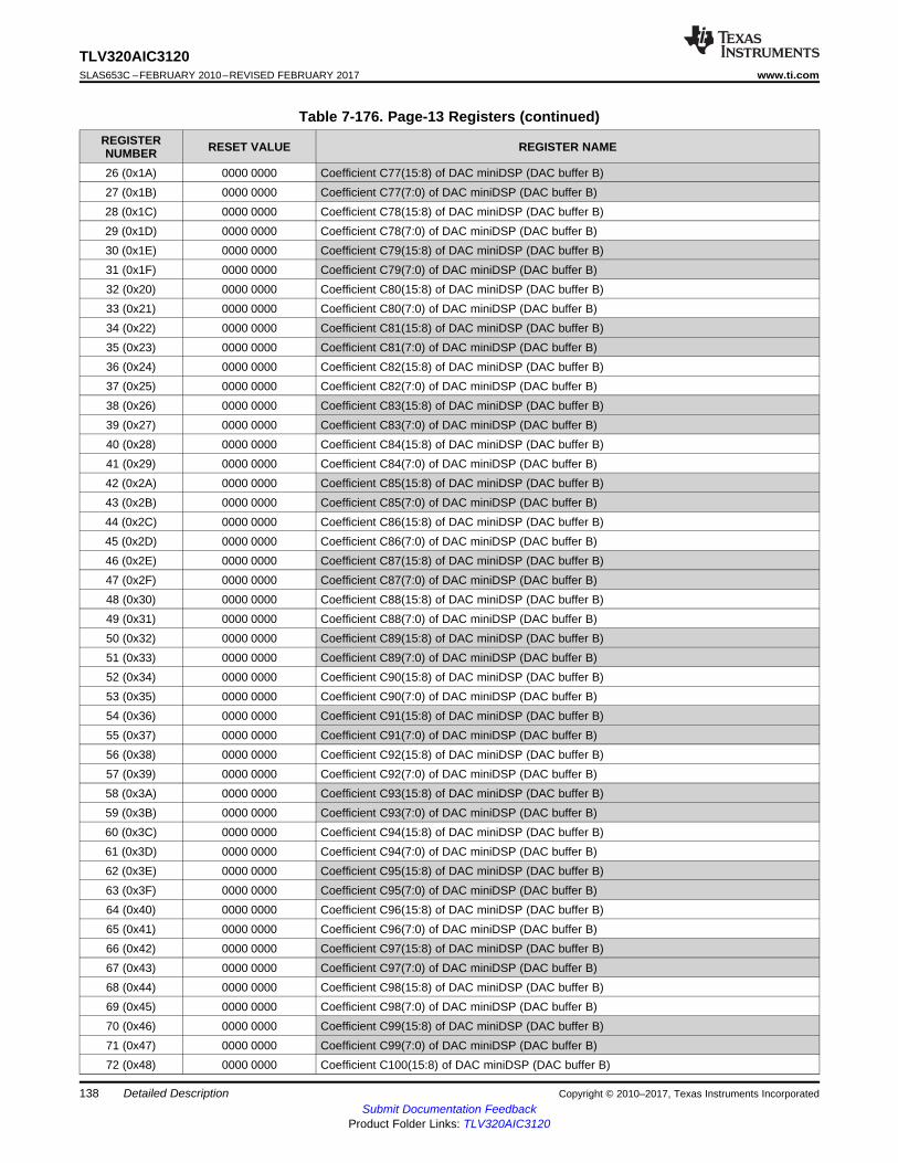
138
TLV320AIC3120SLAS653C –FEBRUARY 2010–REVISED FEBRUARY 2017 www.ti.com
Submit Documentation FeedbackProduct Folder Links: TLV320AIC3120
Detailed Description Copyright © 2010–2017, Texas Instruments Incorporated
Table 7-176. Page-13 Registers (continued)REGISTERNUMBER RESET VALUE REGISTER NAME
26 (0x1A) 0000 0000 Coefficient C77(15:8) of DAC miniDSP (DAC buffer B)27 (0x1B) 0000 0000 Coefficient C77(7:0) of DAC miniDSP (DAC buffer B)28 (0x1C) 0000 0000 Coefficient C78(15:8) of DAC miniDSP (DAC buffer B)29 (0x1D) 0000 0000 Coefficient C78(7:0) of DAC miniDSP (DAC buffer B)30 (0x1E) 0000 0000 Coefficient C79(15:8) of DAC miniDSP (DAC buffer B)31 (0x1F) 0000 0000 Coefficient C79(7:0) of DAC miniDSP (DAC buffer B)32 (0x20) 0000 0000 Coefficient C80(15:8) of DAC miniDSP (DAC buffer B)33 (0x21) 0000 0000 Coefficient C80(7:0) of DAC miniDSP (DAC buffer B)34 (0x22) 0000 0000 Coefficient C81(15:8) of DAC miniDSP (DAC buffer B)35 (0x23) 0000 0000 Coefficient C81(7:0) of DAC miniDSP (DAC buffer B)36 (0x24) 0000 0000 Coefficient C82(15:8) of DAC miniDSP (DAC buffer B)37 (0x25) 0000 0000 Coefficient C82(7:0) of DAC miniDSP (DAC buffer B)38 (0x26) 0000 0000 Coefficient C83(15:8) of DAC miniDSP (DAC buffer B)39 (0x27) 0000 0000 Coefficient C83(7:0) of DAC miniDSP (DAC buffer B)40 (0x28) 0000 0000 Coefficient C84(15:8) of DAC miniDSP (DAC buffer B)41 (0x29) 0000 0000 Coefficient C84(7:0) of DAC miniDSP (DAC buffer B)42 (0x2A) 0000 0000 Coefficient C85(15:8) of DAC miniDSP (DAC buffer B)43 (0x2B) 0000 0000 Coefficient C85(7:0) of DAC miniDSP (DAC buffer B)44 (0x2C) 0000 0000 Coefficient C86(15:8) of DAC miniDSP (DAC buffer B)45 (0x2D) 0000 0000 Coefficient C86(7:0) of DAC miniDSP (DAC buffer B)46 (0x2E) 0000 0000 Coefficient C87(15:8) of DAC miniDSP (DAC buffer B)47 (0x2F) 0000 0000 Coefficient C87(7:0) of DAC miniDSP (DAC buffer B)48 (0x30) 0000 0000 Coefficient C88(15:8) of DAC miniDSP (DAC buffer B)49 (0x31) 0000 0000 Coefficient C88(7:0) of DAC miniDSP (DAC buffer B)50 (0x32) 0000 0000 Coefficient C89(15:8) of DAC miniDSP (DAC buffer B)51 (0x33) 0000 0000 Coefficient C89(7:0) of DAC miniDSP (DAC buffer B)52 (0x34) 0000 0000 Coefficient C90(15:8) of DAC miniDSP (DAC buffer B)53 (0x35) 0000 0000 Coefficient C90(7:0) of DAC miniDSP (DAC buffer B)54 (0x36) 0000 0000 Coefficient C91(15:8) of DAC miniDSP (DAC buffer B)55 (0x37) 0000 0000 Coefficient C91(7:0) of DAC miniDSP (DAC buffer B)56 (0x38) 0000 0000 Coefficient C92(15:8) of DAC miniDSP (DAC buffer B)57 (0x39) 0000 0000 Coefficient C92(7:0) of DAC miniDSP (DAC buffer B)58 (0x3A) 0000 0000 Coefficient C93(15:8) of DAC miniDSP (DAC buffer B)59 (0x3B) 0000 0000 Coefficient C93(7:0) of DAC miniDSP (DAC buffer B)60 (0x3C) 0000 0000 Coefficient C94(15:8) of DAC miniDSP (DAC buffer B)61 (0x3D) 0000 0000 Coefficient C94(7:0) of DAC miniDSP (DAC buffer B)62 (0x3E) 0000 0000 Coefficient C95(15:8) of DAC miniDSP (DAC buffer B)63 (0x3F) 0000 0000 Coefficient C95(7:0) of DAC miniDSP (DAC buffer B)64 (0x40) 0000 0000 Coefficient C96(15:8) of DAC miniDSP (DAC buffer B)65 (0x41) 0000 0000 Coefficient C96(7:0) of DAC miniDSP (DAC buffer B)66 (0x42) 0000 0000 Coefficient C97(15:8) of DAC miniDSP (DAC buffer B)67 (0x43) 0000 0000 Coefficient C97(7:0) of DAC miniDSP (DAC buffer B)68 (0x44) 0000 0000 Coefficient C98(15:8) of DAC miniDSP (DAC buffer B)69 (0x45) 0000 0000 Coefficient C98(7:0) of DAC miniDSP (DAC buffer B)70 (0x46) 0000 0000 Coefficient C99(15:8) of DAC miniDSP (DAC buffer B)71 (0x47) 0000 0000 Coefficient C99(7:0) of DAC miniDSP (DAC buffer B)72 (0x48) 0000 0000 Coefficient C100(15:8) of DAC miniDSP (DAC buffer B)
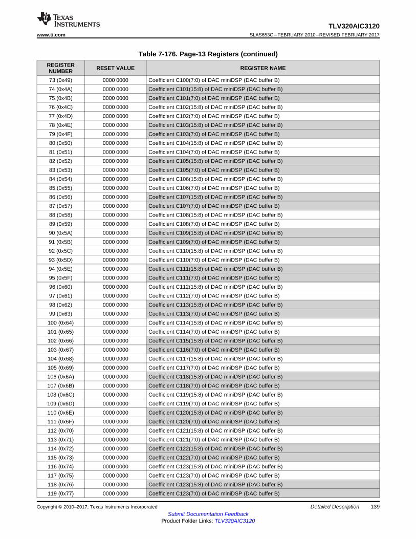
139
TLV320AIC3120www.ti.com SLAS653C –FEBRUARY 2010–REVISED FEBRUARY 2017
Submit Documentation FeedbackProduct Folder Links: TLV320AIC3120
Detailed DescriptionCopyright © 2010–2017, Texas Instruments Incorporated
Table 7-176. Page-13 Registers (continued)REGISTERNUMBER RESET VALUE REGISTER NAME
73 (0x49) 0000 0000 Coefficient C100(7:0) of DAC miniDSP (DAC buffer B)74 (0x4A) 0000 0000 Coefficient C101(15:8) of DAC miniDSP (DAC buffer B)75 (0x4B) 0000 0000 Coefficient C101(7:0) of DAC miniDSP (DAC buffer B)76 (0x4C) 0000 0000 Coefficient C102(15:8) of DAC miniDSP (DAC buffer B)77 (0x4D) 0000 0000 Coefficient C102(7:0) of DAC miniDSP (DAC buffer B)78 (0x4E) 0000 0000 Coefficient C103(15:8) of DAC miniDSP (DAC buffer B)79 (0x4F) 0000 0000 Coefficient C103(7:0) of DAC miniDSP (DAC buffer B)80 (0x50) 0000 0000 Coefficient C104(15:8) of DAC miniDSP (DAC buffer B)81 (0x51) 0000 0000 Coefficient C104(7:0) of DAC miniDSP (DAC buffer B)82 (0x52) 0000 0000 Coefficient C105(15:8) of DAC miniDSP (DAC buffer B)83 (0x53) 0000 0000 Coefficient C105(7:0) of DAC miniDSP (DAC buffer B)84 (0x54) 0000 0000 Coefficient C106(15:8) of DAC miniDSP (DAC buffer B)85 (0x55) 0000 0000 Coefficient C106(7:0) of DAC miniDSP (DAC buffer B)86 (0x56) 0000 0000 Coefficient C107(15:8) of DAC miniDSP (DAC buffer B)87 (0x57) 0000 0000 Coefficient C107(7:0) of DAC miniDSP (DAC buffer B)88 (0x58) 0000 0000 Coefficient C108(15:8) of DAC miniDSP (DAC buffer B)89 (0x59) 0000 0000 Coefficient C108(7:0) of DAC miniDSP (DAC buffer B)90 (0x5A) 0000 0000 Coefficient C109(15:8) of DAC miniDSP (DAC buffer B)91 (0x5B) 0000 0000 Coefficient C109(7:0) of DAC miniDSP (DAC buffer B)92 (0x5C) 0000 0000 Coefficient C110(15:8) of DAC miniDSP (DAC buffer B)93 (0x5D) 0000 0000 Coefficient C110(7:0) of DAC miniDSP (DAC buffer B)94 (0x5E) 0000 0000 Coefficient C111(15:8) of DAC miniDSP (DAC buffer B)95 (0x5F) 0000 0000 Coefficient C111(7:0) of DAC miniDSP (DAC buffer B)96 (0x60) 0000 0000 Coefficient C112(15:8) of DAC miniDSP (DAC buffer B)97 (0x61) 0000 0000 Coefficient C112(7:0) of DAC miniDSP (DAC buffer B)98 (0x62) 0000 0000 Coefficient C113(15:8) of DAC miniDSP (DAC buffer B)99 (0x63) 0000 0000 Coefficient C113(7:0) of DAC miniDSP (DAC buffer B)100 (0x64) 0000 0000 Coefficient C114(15:8) of DAC miniDSP (DAC buffer B)101 (0x65) 0000 0000 Coefficient C114(7:0) of DAC miniDSP (DAC buffer B)102 (0x66) 0000 0000 Coefficient C115(15:8) of DAC miniDSP (DAC buffer B)103 (0x67) 0000 0000 Coefficient C116(7:0) of DAC miniDSP (DAC buffer B)104 (0x68) 0000 0000 Coefficient C117(15:8) of DAC miniDSP (DAC buffer B)105 (0x69) 0000 0000 Coefficient C117(7:0) of DAC miniDSP (DAC buffer B)106 (0x6A) 0000 0000 Coefficient C118(15:8) of DAC miniDSP (DAC buffer B)107 (0x6B) 0000 0000 Coefficient C118(7:0) of DAC miniDSP (DAC buffer B)108 (0x6C) 0000 0000 Coefficient C119(15:8) of DAC miniDSP (DAC buffer B)109 (0x6D) 0000 0000 Coefficient C119(7:0) of DAC miniDSP (DAC buffer B)110 (0x6E) 0000 0000 Coefficient C120(15:8) of DAC miniDSP (DAC buffer B)111 (0x6F) 0000 0000 Coefficient C120(7:0) of DAC miniDSP (DAC buffer B)112 (0x70) 0000 0000 Coefficient C121(15:8) of DAC miniDSP (DAC buffer B)113 (0x71) 0000 0000 Coefficient C121(7:0) of DAC miniDSP (DAC buffer B)114 (0x72) 0000 0000 Coefficient C122(15:8) of DAC miniDSP (DAC buffer B)115 (0x73) 0000 0000 Coefficient C122(7:0) of DAC miniDSP (DAC buffer B)116 (0x74) 0000 0000 Coefficient C123(15:8) of DAC miniDSP (DAC buffer B)117 (0x75) 0000 0000 Coefficient C123(7:0) of DAC miniDSP (DAC buffer B)118 (0x76) 0000 0000 Coefficient C123(15:8) of DAC miniDSP (DAC buffer B)119 (0x77) 0000 0000 Coefficient C123(7:0) of DAC miniDSP (DAC buffer B)
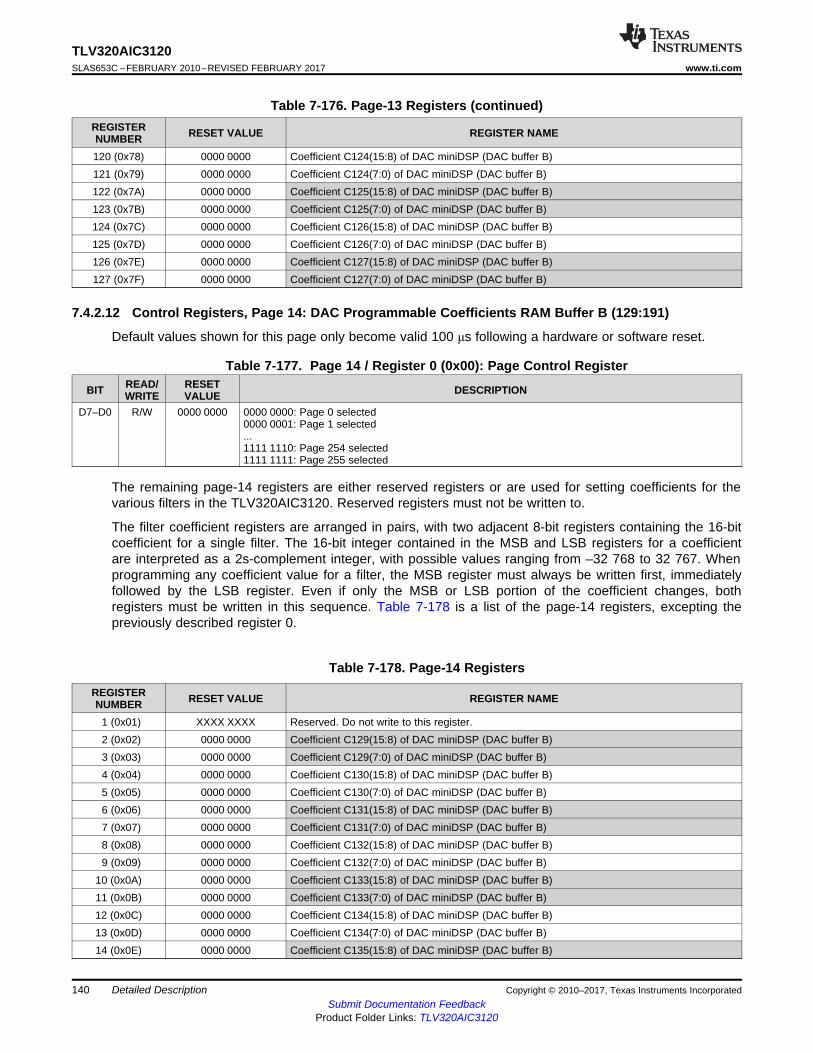
140
TLV320AIC3120SLAS653C –FEBRUARY 2010–REVISED FEBRUARY 2017 www.ti.com
Submit Documentation FeedbackProduct Folder Links: TLV320AIC3120
Detailed Description Copyright © 2010–2017, Texas Instruments Incorporated
Table 7-176. Page-13 Registers (continued)REGISTERNUMBER RESET VALUE REGISTER NAME
120 (0x78) 0000 0000 Coefficient C124(15:8) of DAC miniDSP (DAC buffer B)121 (0x79) 0000 0000 Coefficient C124(7:0) of DAC miniDSP (DAC buffer B)122 (0x7A) 0000 0000 Coefficient C125(15:8) of DAC miniDSP (DAC buffer B)123 (0x7B) 0000 0000 Coefficient C125(7:0) of DAC miniDSP (DAC buffer B)124 (0x7C) 0000 0000 Coefficient C126(15:8) of DAC miniDSP (DAC buffer B)125 (0x7D) 0000 0000 Coefficient C126(7:0) of DAC miniDSP (DAC buffer B)126 (0x7E) 0000 0000 Coefficient C127(15:8) of DAC miniDSP (DAC buffer B)127 (0x7F) 0000 0000 Coefficient C127(7:0) of DAC miniDSP (DAC buffer B)
7.4.2.12 Control Registers, Page 14: DAC Programmable Coefficients RAM Buffer B (129:191)
Default values shown for this page only become valid 100 μs following a hardware or software reset.
Table 7-177. Page 14 / Register 0 (0x00): Page Control Register
BIT READ/WRITE
RESETVALUE DESCRIPTION
D7–D0 R/W 0000 0000 0000 0000: Page 0 selected0000 0001: Page 1 selected...1111 1110: Page 254 selected1111 1111: Page 255 selected
The remaining page-14 registers are either reserved registers or are used for setting coefficients for thevarious filters in the TLV320AIC3120. Reserved registers must not be written to.
The filter coefficient registers are arranged in pairs, with two adjacent 8-bit registers containing the 16-bitcoefficient for a single filter. The 16-bit integer contained in the MSB and LSB registers for a coefficientare interpreted as a 2s-complement integer, with possible values ranging from –32 768 to 32 767. Whenprogramming any coefficient value for a filter, the MSB register must always be written first, immediatelyfollowed by the LSB register. Even if only the MSB or LSB portion of the coefficient changes, bothregisters must be written in this sequence. Table 7-178 is a list of the page-14 registers, excepting thepreviously described register 0.
Table 7-178. Page-14 Registers
REGISTERNUMBER RESET VALUE REGISTER NAME
1 (0x01) XXXX XXXX Reserved. Do not write to this register.2 (0x02) 0000 0000 Coefficient C129(15:8) of DAC miniDSP (DAC buffer B)3 (0x03) 0000 0000 Coefficient C129(7:0) of DAC miniDSP (DAC buffer B)4 (0x04) 0000 0000 Coefficient C130(15:8) of DAC miniDSP (DAC buffer B)5 (0x05) 0000 0000 Coefficient C130(7:0) of DAC miniDSP (DAC buffer B)6 (0x06) 0000 0000 Coefficient C131(15:8) of DAC miniDSP (DAC buffer B)7 (0x07) 0000 0000 Coefficient C131(7:0) of DAC miniDSP (DAC buffer B)8 (0x08) 0000 0000 Coefficient C132(15:8) of DAC miniDSP (DAC buffer B)9 (0x09) 0000 0000 Coefficient C132(7:0) of DAC miniDSP (DAC buffer B)
10 (0x0A) 0000 0000 Coefficient C133(15:8) of DAC miniDSP (DAC buffer B)11 (0x0B) 0000 0000 Coefficient C133(7:0) of DAC miniDSP (DAC buffer B)12 (0x0C) 0000 0000 Coefficient C134(15:8) of DAC miniDSP (DAC buffer B)13 (0x0D) 0000 0000 Coefficient C134(7:0) of DAC miniDSP (DAC buffer B)14 (0x0E) 0000 0000 Coefficient C135(15:8) of DAC miniDSP (DAC buffer B)
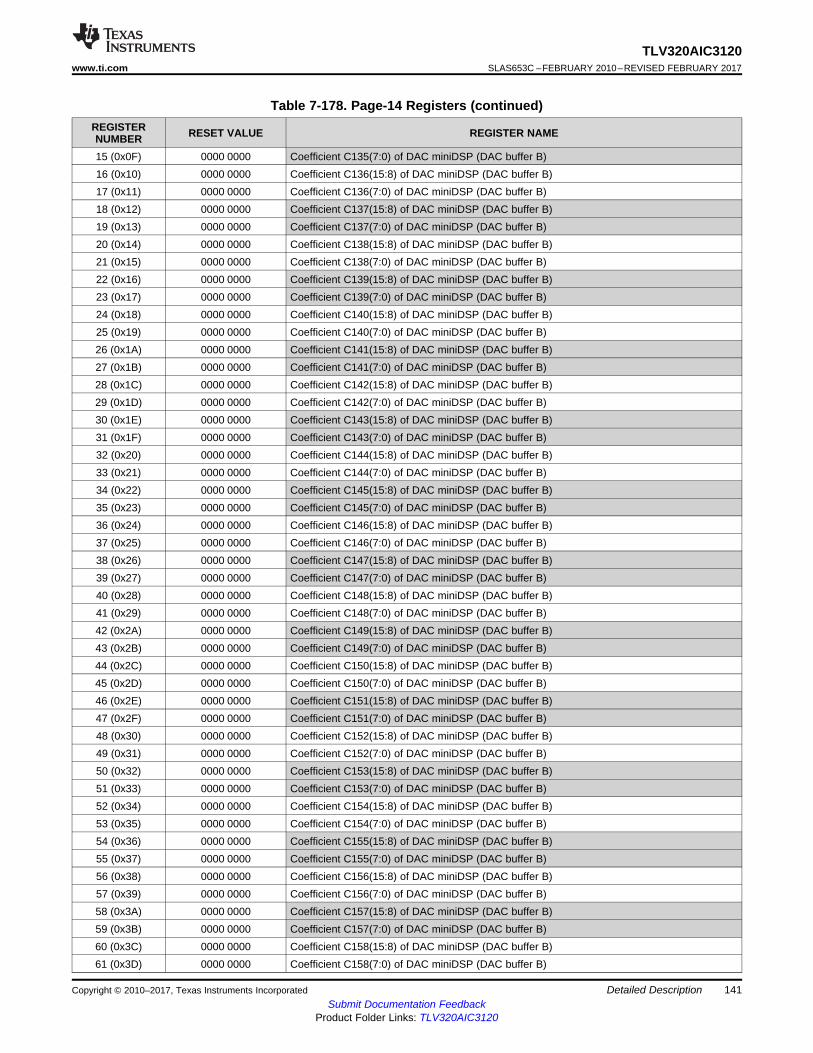
141
TLV320AIC3120www.ti.com SLAS653C –FEBRUARY 2010–REVISED FEBRUARY 2017
Submit Documentation FeedbackProduct Folder Links: TLV320AIC3120
Detailed DescriptionCopyright © 2010–2017, Texas Instruments Incorporated
Table 7-178. Page-14 Registers (continued)REGISTERNUMBER RESET VALUE REGISTER NAME
15 (0x0F) 0000 0000 Coefficient C135(7:0) of DAC miniDSP (DAC buffer B)16 (0x10) 0000 0000 Coefficient C136(15:8) of DAC miniDSP (DAC buffer B)17 (0x11) 0000 0000 Coefficient C136(7:0) of DAC miniDSP (DAC buffer B)18 (0x12) 0000 0000 Coefficient C137(15:8) of DAC miniDSP (DAC buffer B)19 (0x13) 0000 0000 Coefficient C137(7:0) of DAC miniDSP (DAC buffer B)20 (0x14) 0000 0000 Coefficient C138(15:8) of DAC miniDSP (DAC buffer B)21 (0x15) 0000 0000 Coefficient C138(7:0) of DAC miniDSP (DAC buffer B)22 (0x16) 0000 0000 Coefficient C139(15:8) of DAC miniDSP (DAC buffer B)23 (0x17) 0000 0000 Coefficient C139(7:0) of DAC miniDSP (DAC buffer B)24 (0x18) 0000 0000 Coefficient C140(15:8) of DAC miniDSP (DAC buffer B)25 (0x19) 0000 0000 Coefficient C140(7:0) of DAC miniDSP (DAC buffer B)26 (0x1A) 0000 0000 Coefficient C141(15:8) of DAC miniDSP (DAC buffer B)27 (0x1B) 0000 0000 Coefficient C141(7:0) of DAC miniDSP (DAC buffer B)28 (0x1C) 0000 0000 Coefficient C142(15:8) of DAC miniDSP (DAC buffer B)29 (0x1D) 0000 0000 Coefficient C142(7:0) of DAC miniDSP (DAC buffer B)30 (0x1E) 0000 0000 Coefficient C143(15:8) of DAC miniDSP (DAC buffer B)31 (0x1F) 0000 0000 Coefficient C143(7:0) of DAC miniDSP (DAC buffer B)32 (0x20) 0000 0000 Coefficient C144(15:8) of DAC miniDSP (DAC buffer B)33 (0x21) 0000 0000 Coefficient C144(7:0) of DAC miniDSP (DAC buffer B)34 (0x22) 0000 0000 Coefficient C145(15:8) of DAC miniDSP (DAC buffer B)35 (0x23) 0000 0000 Coefficient C145(7:0) of DAC miniDSP (DAC buffer B)36 (0x24) 0000 0000 Coefficient C146(15:8) of DAC miniDSP (DAC buffer B)37 (0x25) 0000 0000 Coefficient C146(7:0) of DAC miniDSP (DAC buffer B)38 (0x26) 0000 0000 Coefficient C147(15:8) of DAC miniDSP (DAC buffer B)39 (0x27) 0000 0000 Coefficient C147(7:0) of DAC miniDSP (DAC buffer B)40 (0x28) 0000 0000 Coefficient C148(15:8) of DAC miniDSP (DAC buffer B)41 (0x29) 0000 0000 Coefficient C148(7:0) of DAC miniDSP (DAC buffer B)42 (0x2A) 0000 0000 Coefficient C149(15:8) of DAC miniDSP (DAC buffer B)43 (0x2B) 0000 0000 Coefficient C149(7:0) of DAC miniDSP (DAC buffer B)44 (0x2C) 0000 0000 Coefficient C150(15:8) of DAC miniDSP (DAC buffer B)45 (0x2D) 0000 0000 Coefficient C150(7:0) of DAC miniDSP (DAC buffer B)46 (0x2E) 0000 0000 Coefficient C151(15:8) of DAC miniDSP (DAC buffer B)47 (0x2F) 0000 0000 Coefficient C151(7:0) of DAC miniDSP (DAC buffer B)48 (0x30) 0000 0000 Coefficient C152(15:8) of DAC miniDSP (DAC buffer B)49 (0x31) 0000 0000 Coefficient C152(7:0) of DAC miniDSP (DAC buffer B)50 (0x32) 0000 0000 Coefficient C153(15:8) of DAC miniDSP (DAC buffer B)51 (0x33) 0000 0000 Coefficient C153(7:0) of DAC miniDSP (DAC buffer B)52 (0x34) 0000 0000 Coefficient C154(15:8) of DAC miniDSP (DAC buffer B)53 (0x35) 0000 0000 Coefficient C154(7:0) of DAC miniDSP (DAC buffer B)54 (0x36) 0000 0000 Coefficient C155(15:8) of DAC miniDSP (DAC buffer B)55 (0x37) 0000 0000 Coefficient C155(7:0) of DAC miniDSP (DAC buffer B)56 (0x38) 0000 0000 Coefficient C156(15:8) of DAC miniDSP (DAC buffer B)57 (0x39) 0000 0000 Coefficient C156(7:0) of DAC miniDSP (DAC buffer B)58 (0x3A) 0000 0000 Coefficient C157(15:8) of DAC miniDSP (DAC buffer B)59 (0x3B) 0000 0000 Coefficient C157(7:0) of DAC miniDSP (DAC buffer B)60 (0x3C) 0000 0000 Coefficient C158(15:8) of DAC miniDSP (DAC buffer B)61 (0x3D) 0000 0000 Coefficient C158(7:0) of DAC miniDSP (DAC buffer B)
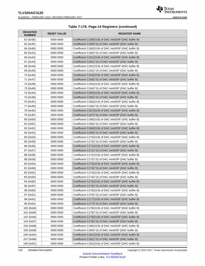
142
TLV320AIC3120SLAS653C –FEBRUARY 2010–REVISED FEBRUARY 2017 www.ti.com
Submit Documentation FeedbackProduct Folder Links: TLV320AIC3120
Detailed Description Copyright © 2010–2017, Texas Instruments Incorporated
Table 7-178. Page-14 Registers (continued)REGISTERNUMBER RESET VALUE REGISTER NAME
62 (0x3E) 0000 0000 Coefficient C159(15:8) of DAC miniDSP (DAC buffer B)63 (0x3F) 0000 0000 Coefficient C159(7:0) of DAC miniDSP (DAC buffer B)64 (0x40) 0000 0000 Coefficient C160(15:8) of DAC miniDSP (DAC buffer B)65 (0x41) 0000 0000 Coefficient C160(7:0) of DAC miniDSP (DAC buffer B)66 (0x42) 0000 0000 Coefficient C161(15:8) of DAC miniDSP (DAC buffer B)67 (0x43) 0000 0000 Coefficient C161(7:0) of DAC miniDSP (DAC buffer B)68 (0x44) 0000 0000 Coefficient C162(15:8) of DAC miniDSP (DAC buffer B)69 (0x45) 0000 0000 Coefficient C162(7:0) of DAC miniDSP (DAC buffer B)70 (0x46) 0000 0000 Coefficient C163(15:8) of DAC miniDSP (DAC buffer B)71 (0x47) 0000 0000 Coefficient C163(7:0) of DAC miniDSP (DAC buffer B)72 (0x48) 0000 0000 Coefficient C164(15:8) of DAC miniDSP (DAC buffer B)73 (0x49) 0000 0000 Coefficient C164(7:0) of DAC miniDSP (DAC buffer B)74 (0x4A) 0000 0000 Coefficient C165(15:8) of DAC miniDSP (DAC buffer B)75 (0x4B) 0000 0000 Coefficient C165(7:0) of DAC miniDSP (DAC buffer B)76 (0x4C) 0000 0000 Coefficient C166(15:8) of DAC miniDSP (DAC buffer B)77 (0x4D) 0000 0000 Coefficient C166(7:0) of DAC miniDSP (DAC buffer B)78 (0x4E) 0000 0000 Coefficient C167(15:8) of DAC miniDSP (DAC buffer B)79 (0x4F) 0000 0000 Coefficient C167(7:0) of DAC miniDSP (DAC buffer B)80 (0x50) 0000 0000 Coefficient C168(15:8) of DAC miniDSP (DAC buffer B)81 (0x51) 0000 0000 Coefficient C168(7:0) of DAC miniDSP (DAC buffer B)82 (0x52) 0000 0000 Coefficient C169(15:8) of DAC miniDSP (DAC buffer B)83 (0x53) 0000 0000 Coefficient C169(7:0) of DAC miniDSP (DAC buffer B)84 (0x54) 0000 0000 Coefficient C170(15:8) of DAC miniDSP (DAC buffer B)85 (0x55) 0000 0000 Coefficient C170(7:0) of DAC miniDSP (DAC buffer B)86 (0x56) 0000 0000 Coefficient C171(15:8) of DAC miniDSP (DAC buffer B)87 (0x57) 0000 0000 Coefficient C171(7:0) of DAC miniDSP (DAC buffer B)88 (0x58) 0000 0000 Coefficient C172(15:8) of DAC miniDSP (DAC buffer B)89 (0x59) 0000 0000 Coefficient C172(7:0) of DAC miniDSP (DAC buffer B)90 (0x5A) 0000 0000 Coefficient C173(15:8) of DAC miniDSP (DAC buffer B)91 (0x5B) 0000 0000 Coefficient C173(7:0) of DAC miniDSP (DAC buffer B)92 (0x5C) 0000 0000 Coefficient C174(15:8) of DAC miniDSP (DAC buffer B)93 (0x5D) 0000 0000 Coefficient C174(7:0) of DAC miniDSP (DAC buffer B)94 (0x5E) 0000 0000 Coefficient C175(15:8) of DAC miniDSP (DAC buffer B)95 (0x5F) 0000 0000 Coefficient C175(7:0) of DAC miniDSP (DAC buffer B)96 (0x60) 0000 0000 Coefficient C176(15:8) of DAC miniDSP (DAC buffer B)97 (0x61) 0000 0000 Coefficient C176(7:0) of DAC miniDSP (DAC buffer B)98 (0x62) 0000 0000 Coefficient C177(15:8) of DAC miniDSP (DAC buffer B)99 (0x63) 0000 0000 Coefficient C177(7:0) of DAC miniDSP (DAC buffer B)100 (0x64) 0000 0000 Coefficient C178(15:8) of DAC miniDSP (DAC buffer B)101 (0x65) 0000 0000 Coefficient C178(7:0) of DAC miniDSP (DAC buffer B)102 (0x66) 0000 0000 Coefficient C179(15:8) of DAC miniDSP (DAC buffer B)103 (0x67) 0000 0000 Coefficient C179(7:0) of DAC miniDSP (DAC buffer B)104 (0x68) 0000 0000 Coefficient C180(15:8) of DAC miniDSP (DAC buffer B)105 (0x69) 0000 0000 Coefficient C180(7:0) of DAC miniDSP (DAC buffer B)106 (0x6A) 0000 0000 Coefficient C181(15:8) of DAC miniDSP (DAC buffer B)107 (0x6B) 0000 0000 Coefficient C181(7:0) of DAC miniDSP (DAC buffer B)108 (0x6C) 0000 0000 Coefficient C182(15:8) of DAC miniDSP (DAC buffer B)
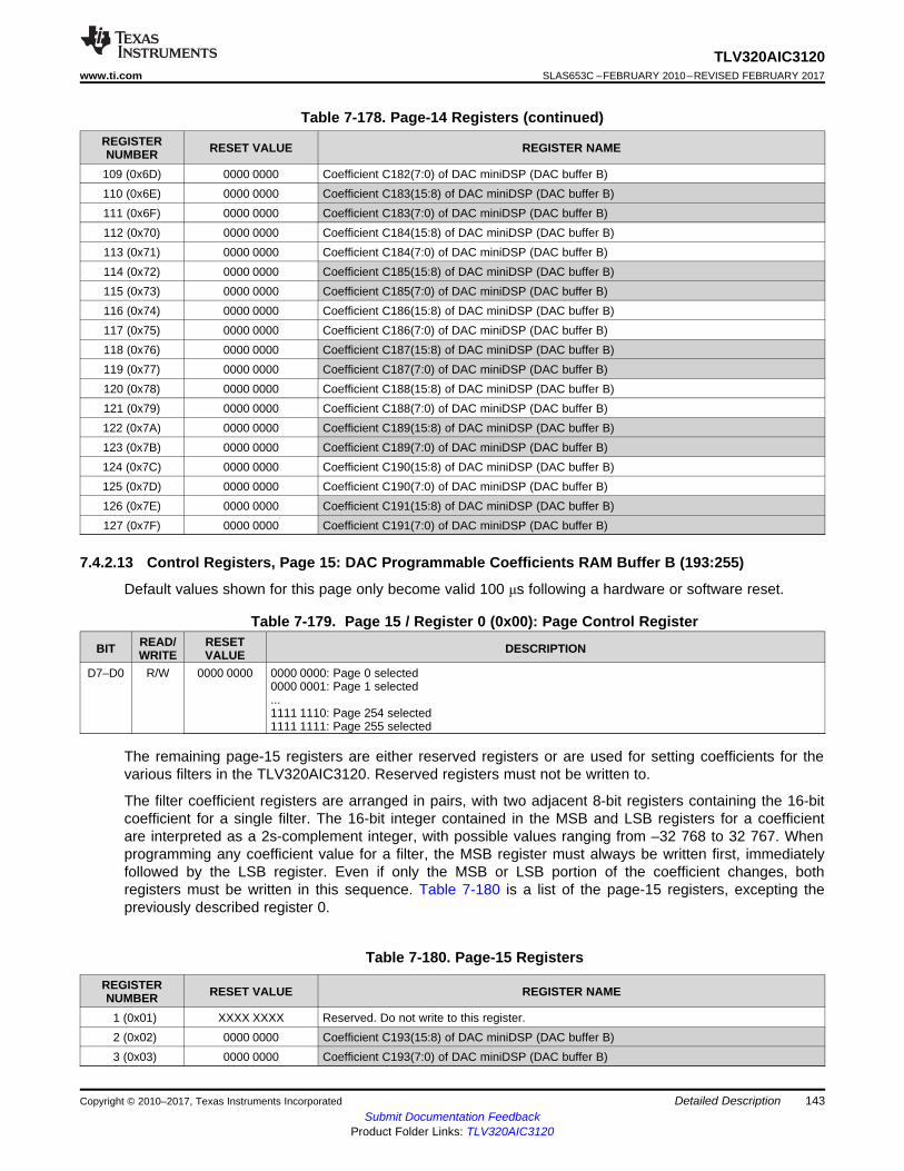
143
TLV320AIC3120www.ti.com SLAS653C –FEBRUARY 2010–REVISED FEBRUARY 2017
Submit Documentation FeedbackProduct Folder Links: TLV320AIC3120
Detailed DescriptionCopyright © 2010–2017, Texas Instruments Incorporated
Table 7-178. Page-14 Registers (continued)REGISTERNUMBER RESET VALUE REGISTER NAME
109 (0x6D) 0000 0000 Coefficient C182(7:0) of DAC miniDSP (DAC buffer B)110 (0x6E) 0000 0000 Coefficient C183(15:8) of DAC miniDSP (DAC buffer B)111 (0x6F) 0000 0000 Coefficient C183(7:0) of DAC miniDSP (DAC buffer B)112 (0x70) 0000 0000 Coefficient C184(15:8) of DAC miniDSP (DAC buffer B)113 (0x71) 0000 0000 Coefficient C184(7:0) of DAC miniDSP (DAC buffer B)114 (0x72) 0000 0000 Coefficient C185(15:8) of DAC miniDSP (DAC buffer B)115 (0x73) 0000 0000 Coefficient C185(7:0) of DAC miniDSP (DAC buffer B)116 (0x74) 0000 0000 Coefficient C186(15:8) of DAC miniDSP (DAC buffer B)117 (0x75) 0000 0000 Coefficient C186(7:0) of DAC miniDSP (DAC buffer B)118 (0x76) 0000 0000 Coefficient C187(15:8) of DAC miniDSP (DAC buffer B)119 (0x77) 0000 0000 Coefficient C187(7:0) of DAC miniDSP (DAC buffer B)120 (0x78) 0000 0000 Coefficient C188(15:8) of DAC miniDSP (DAC buffer B)121 (0x79) 0000 0000 Coefficient C188(7:0) of DAC miniDSP (DAC buffer B)122 (0x7A) 0000 0000 Coefficient C189(15:8) of DAC miniDSP (DAC buffer B)123 (0x7B) 0000 0000 Coefficient C189(7:0) of DAC miniDSP (DAC buffer B)124 (0x7C) 0000 0000 Coefficient C190(15:8) of DAC miniDSP (DAC buffer B)125 (0x7D) 0000 0000 Coefficient C190(7:0) of DAC miniDSP (DAC buffer B)126 (0x7E) 0000 0000 Coefficient C191(15:8) of DAC miniDSP (DAC buffer B)127 (0x7F) 0000 0000 Coefficient C191(7:0) of DAC miniDSP (DAC buffer B)
7.4.2.13 Control Registers, Page 15: DAC Programmable Coefficients RAM Buffer B (193:255)
Default values shown for this page only become valid 100 μs following a hardware or software reset.
Table 7-179. Page 15 / Register 0 (0x00): Page Control Register
BIT READ/WRITE
RESETVALUE DESCRIPTION
D7–D0 R/W 0000 0000 0000 0000: Page 0 selected0000 0001: Page 1 selected...1111 1110: Page 254 selected1111 1111: Page 255 selected
The remaining page-15 registers are either reserved registers or are used for setting coefficients for thevarious filters in the TLV320AIC3120. Reserved registers must not be written to.
The filter coefficient registers are arranged in pairs, with two adjacent 8-bit registers containing the 16-bitcoefficient for a single filter. The 16-bit integer contained in the MSB and LSB registers for a coefficientare interpreted as a 2s-complement integer, with possible values ranging from –32 768 to 32 767. Whenprogramming any coefficient value for a filter, the MSB register must always be written first, immediatelyfollowed by the LSB register. Even if only the MSB or LSB portion of the coefficient changes, bothregisters must be written in this sequence. Table 7-180 is a list of the page-15 registers, excepting thepreviously described register 0.
Table 7-180. Page-15 Registers
REGISTERNUMBER RESET VALUE REGISTER NAME
1 (0x01) XXXX XXXX Reserved. Do not write to this register.2 (0x02) 0000 0000 Coefficient C193(15:8) of DAC miniDSP (DAC buffer B)3 (0x03) 0000 0000 Coefficient C193(7:0) of DAC miniDSP (DAC buffer B)
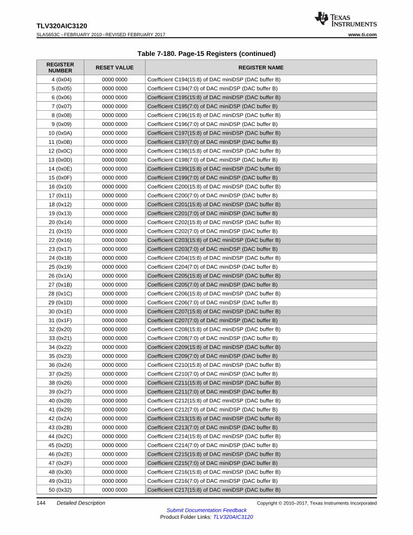
144
TLV320AIC3120SLAS653C –FEBRUARY 2010–REVISED FEBRUARY 2017 www.ti.com
Submit Documentation FeedbackProduct Folder Links: TLV320AIC3120
Detailed Description Copyright © 2010–2017, Texas Instruments Incorporated
Table 7-180. Page-15 Registers (continued)REGISTERNUMBER RESET VALUE REGISTER NAME
4 (0x04) 0000 0000 Coefficient C194(15:8) of DAC miniDSP (DAC buffer B)5 (0x05) 0000 0000 Coefficient C194(7:0) of DAC miniDSP (DAC buffer B)6 (0x06) 0000 0000 Coefficient C195(15:8) of DAC miniDSP (DAC buffer B)7 (0x07) 0000 0000 Coefficient C195(7:0) of DAC miniDSP (DAC buffer B)8 (0x08) 0000 0000 Coefficient C196(15:8) of DAC miniDSP (DAC buffer B)9 (0x09) 0000 0000 Coefficient C196(7:0) of DAC miniDSP (DAC buffer B)
10 (0x0A) 0000 0000 Coefficient C197(15:8) of DAC miniDSP (DAC buffer B)11 (0x0B) 0000 0000 Coefficient C197(7:0) of DAC miniDSP (DAC buffer B)12 (0x0C) 0000 0000 Coefficient C198(15:8) of DAC miniDSP (DAC buffer B)13 (0x0D) 0000 0000 Coefficient C198(7:0) of DAC miniDSP (DAC buffer B)14 (0x0E) 0000 0000 Coefficient C199(15:8) of DAC miniDSP (DAC buffer B)15 (0x0F) 0000 0000 Coefficient C199(7:0) of DAC miniDSP (DAC buffer B)16 (0x10) 0000 0000 Coefficient C200(15:8) of DAC miniDSP (DAC buffer B)17 (0x11) 0000 0000 Coefficient C200(7:0) of DAC miniDSP (DAC buffer B)18 (0x12) 0000 0000 Coefficient C201(15:8) of DAC miniDSP (DAC buffer B)19 (0x13) 0000 0000 Coefficient C201(7:0) of DAC miniDSP (DAC buffer B)20 (0x14) 0000 0000 Coefficient C202(15:8) of DAC miniDSP (DAC buffer B)21 (0x15) 0000 0000 Coefficient C202(7:0) of DAC miniDSP (DAC buffer B)22 (0x16) 0000 0000 Coefficient C203(15:8) of DAC miniDSP (DAC buffer B)23 (0x17) 0000 0000 Coefficient C203(7:0) of DAC miniDSP (DAC buffer B)24 (0x18) 0000 0000 Coefficient C204(15:8) of DAC miniDSP (DAC buffer B)25 (0x19) 0000 0000 Coefficient C204(7:0) of DAC miniDSP (DAC buffer B)26 (0x1A) 0000 0000 Coefficient C205(15:8) of DAC miniDSP (DAC buffer B)27 (0x1B) 0000 0000 Coefficient C205(7:0) of DAC miniDSP (DAC buffer B)28 (0x1C) 0000 0000 Coefficient C206(15:8) of DAC miniDSP (DAC buffer B)29 (0x1D) 0000 0000 Coefficient C206(7:0) of DAC miniDSP (DAC buffer B)30 (0x1E) 0000 0000 Coefficient C207(15:8) of DAC miniDSP (DAC buffer B)31 (0x1F) 0000 0000 Coefficient C207(7:0) of DAC miniDSP (DAC buffer B)32 (0x20) 0000 0000 Coefficient C208(15:8) of DAC miniDSP (DAC buffer B)33 (0x21) 0000 0000 Coefficient C208(7:0) of DAC miniDSP (DAC buffer B)34 (0x22) 0000 0000 Coefficient C209(15:8) of DAC miniDSP (DAC buffer B)35 (0x23) 0000 0000 Coefficient C209(7:0) of DAC miniDSP (DAC buffer B)36 (0x24) 0000 0000 Coefficient C210(15:8) of DAC miniDSP (DAC buffer B)37 (0x25) 0000 0000 Coefficient C210(7:0) of DAC miniDSP (DAC buffer B)38 (0x26) 0000 0000 Coefficient C211(15:8) of DAC miniDSP (DAC buffer B)39 (0x27) 0000 0000 Coefficient C211(7:0) of DAC miniDSP (DAC buffer B)40 (0x28) 0000 0000 Coefficient C212(15:8) of DAC miniDSP (DAC buffer B)41 (0x29) 0000 0000 Coefficient C212(7:0) of DAC miniDSP (DAC buffer B)42 (0x2A) 0000 0000 Coefficient C213(15:8) of DAC miniDSP (DAC buffer B)43 (0x2B) 0000 0000 Coefficient C213(7:0) of DAC miniDSP (DAC buffer B)44 (0x2C) 0000 0000 Coefficient C214(15:8) of DAC miniDSP (DAC buffer B)45 (0x2D) 0000 0000 Coefficient C214(7:0) of DAC miniDSP (DAC buffer B)46 (0x2E) 0000 0000 Coefficient C215(15:8) of DAC miniDSP (DAC buffer B)47 (0x2F) 0000 0000 Coefficient C215(7:0) of DAC miniDSP (DAC buffer B)48 (0x30) 0000 0000 Coefficient C216(15:8) of DAC miniDSP (DAC buffer B)49 (0x31) 0000 0000 Coefficient C216(7:0) of DAC miniDSP (DAC buffer B)50 (0x32) 0000 0000 Coefficient C217(15:8) of DAC miniDSP (DAC buffer B)

145
TLV320AIC3120www.ti.com SLAS653C –FEBRUARY 2010–REVISED FEBRUARY 2017
Submit Documentation FeedbackProduct Folder Links: TLV320AIC3120
Detailed DescriptionCopyright © 2010–2017, Texas Instruments Incorporated
Table 7-180. Page-15 Registers (continued)REGISTERNUMBER RESET VALUE REGISTER NAME
51 (0x33) 0000 0000 Coefficient C217(7:0) of DAC miniDSP (DAC buffer B)52 (0x34) 0000 0000 Coefficient C218(15:8) of DAC miniDSP (DAC buffer B)53 (0x35) 0000 0000 Coefficient C218(7:0) of DAC miniDSP (DAC buffer B)54 (0x36) 0000 0000 Coefficient C219(15:8) of DAC miniDSP (DAC buffer B)55 (0x37) 0000 0000 Coefficient C219(7:0) of DAC miniDSP (DAC buffer B)56 (0x38) 0000 0000 Coefficient C220(15:8) of DAC miniDSP (DAC buffer B)57 (0x39) 0000 0000 Coefficient C220(7:0) of DAC miniDSP (DAC buffer B)58 (0x3A) 0000 0000 Coefficient C221(15:8) of DAC miniDSP (DAC buffer B)59 (0x3B) 0000 0000 Coefficient C221(7:0) of DAC miniDSP (DAC buffer B)60 (0x3C) 0000 0000 Coefficient C222(15:8) of DAC miniDSP (DAC buffer B)61 (0x3D) 0000 0000 Coefficient C222(7:0) of DAC miniDSP (DAC buffer B)62 (0x3E) 0000 0000 Coefficient C223(15:8) of DAC miniDSP (DAC buffer B)63 (0x3F) 0000 0000 Coefficient C223(7:0) of DAC miniDSP (DAC buffer B)64 (0x40) 0000 0000 Coefficient C224(15:8) of DAC miniDSP (DAC buffer B)65 (0x41) 0000 0000 Coefficient C224(7:0) of DAC miniDSP (DAC buffer B)66 (0x42) 0000 0000 Coefficient C225(15:8) of DAC miniDSP (DAC buffer B)67 (0x43) 0000 0000 Coefficient C225(7:0) of DAC miniDSP (DAC buffer B)68 (0x44) 0000 0000 Coefficient C226(15:8) of DAC miniDSP (DAC buffer B)69 (0x45) 0000 0000 Coefficient C226(7:0) of DAC miniDSP (DAC buffer B)70 (0x46) 0000 0000 Coefficient C227(15:8) of DAC miniDSP (DAC buffer B)71 (0x47) 0000 0000 Coefficient C227(7:0) of DAC miniDSP (DAC buffer B)72 (0x48) 0000 0000 Coefficient C228(15:8) of DAC miniDSP (DAC buffer B)73 (0x49) 0000 0000 Coefficient C228(7:0) of DAC miniDSP (DAC buffer B)74 (0x4A) 0000 0000 Coefficient C229(15:8) of DAC miniDSP (DAC buffer B)75 (0x4B) 0000 0000 Coefficient C229(7:0) of DAC miniDSP (DAC buffer B)76 (0x4C) 0000 0000 Coefficient C230(15:8) of DAC miniDSP (DAC buffer B)77 (0x4D) 0000 0000 Coefficient C230(7:0) of DAC miniDSP (DAC buffer B)78 (0x4E) 0000 0000 Coefficient C231(15:8) of DAC miniDSP (DAC buffer B)79 (0x4F) 0000 0000 Coefficient C231(7:0) of DAC miniDSP (DAC buffer B)80 (0x50) 0000 0000 Coefficient C232(15:8) of DAC miniDSP (DAC buffer B)81 (0x51) 0000 0000 Coefficient C232(7:0) of DAC miniDSP (DAC buffer B)82 (0x52) 0000 0000 Coefficient C233(15:8) of DAC miniDSP (DAC buffer B)83 (0x53) 0000 0000 Coefficient C233(7:0) of DAC miniDSP (DAC buffer B)84 (0x54) 0000 0000 Coefficient C234(15:8) of DAC miniDSP (DAC buffer B)85 (0x55) 0000 0000 Coefficient C234(7:0) of DAC miniDSP (DAC buffer B)86 (0x56) 0000 0000 Coefficient C235(15:8) of DAC miniDSP (DAC buffer B)87 (0x57) 0000 0000 Coefficient C235(7:0) of DAC miniDSP (DAC buffer B)88 (0x58) 0000 0000 Coefficient C236(15:8) of DAC miniDSP (DAC buffer B)89 (0x59) 0000 0000 Coefficient C236(7:0) of DAC miniDSP (DAC buffer B)90 (0x5A) 0000 0000 Coefficient C237(15:8) of DAC miniDSP (DAC buffer B)91 (0x5B) 0000 0000 Coefficient C237(7:0) of DAC miniDSP (DAC buffer B)92 (0x5C) 0000 0000 Coefficient C238(15:8) of DAC miniDSP (DAC buffer B)93 (0x5D) 0000 0000 Coefficient C238(7:0) of DAC miniDSP (DAC buffer B)94 (0x5E) 0000 0000 Coefficient C239(15:8) of DAC miniDSP (DAC buffer B)95 (0x5F) 0000 0000 Coefficient C239(7:0) of DAC miniDSP (DAC buffer B)96 (0x60) 0000 0000 Coefficient C240(15:8) of DAC miniDSP (DAC buffer B)97 (0x61) 0000 0000 Coefficient C240(7:0) of DAC miniDSP (DAC buffer B)
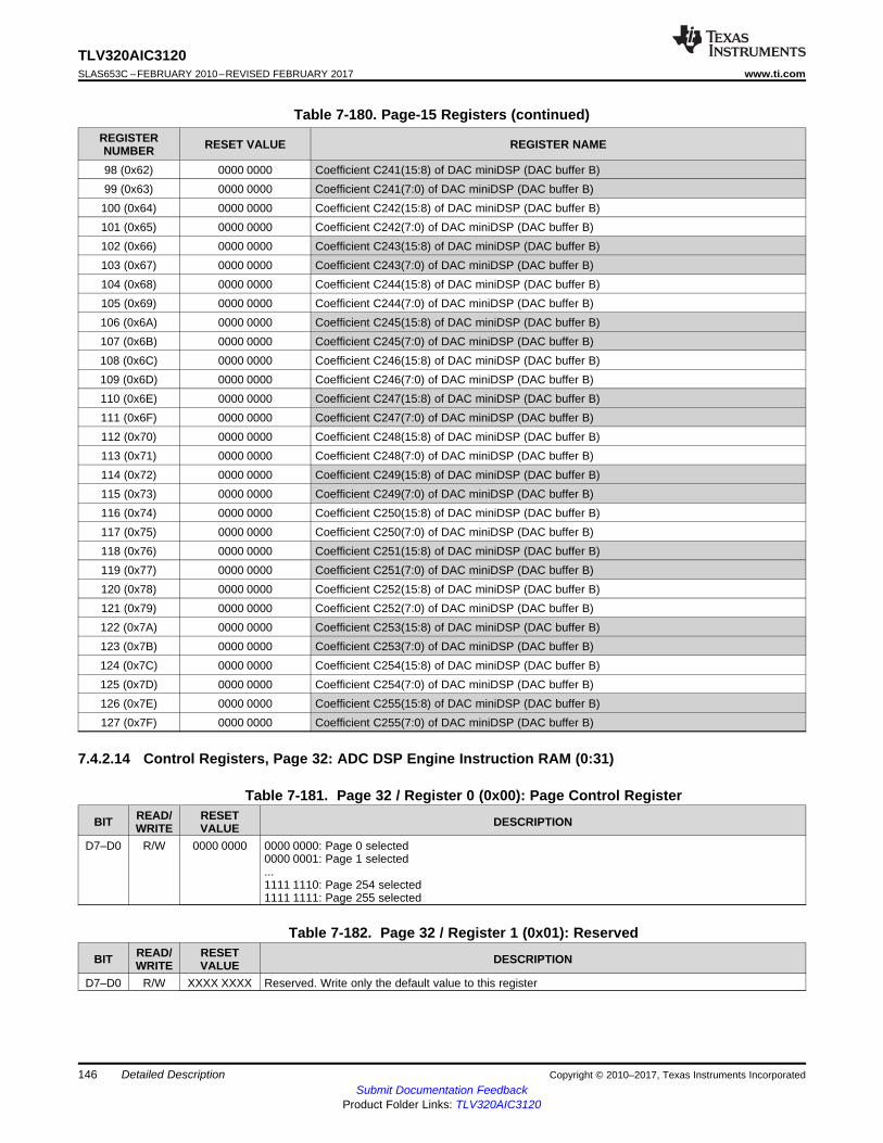
146
TLV320AIC3120SLAS653C –FEBRUARY 2010–REVISED FEBRUARY 2017 www.ti.com
Submit Documentation FeedbackProduct Folder Links: TLV320AIC3120
Detailed Description Copyright © 2010–2017, Texas Instruments Incorporated
Table 7-180. Page-15 Registers (continued)REGISTERNUMBER RESET VALUE REGISTER NAME
98 (0x62) 0000 0000 Coefficient C241(15:8) of DAC miniDSP (DAC buffer B)99 (0x63) 0000 0000 Coefficient C241(7:0) of DAC miniDSP (DAC buffer B)100 (0x64) 0000 0000 Coefficient C242(15:8) of DAC miniDSP (DAC buffer B)101 (0x65) 0000 0000 Coefficient C242(7:0) of DAC miniDSP (DAC buffer B)102 (0x66) 0000 0000 Coefficient C243(15:8) of DAC miniDSP (DAC buffer B)103 (0x67) 0000 0000 Coefficient C243(7:0) of DAC miniDSP (DAC buffer B)104 (0x68) 0000 0000 Coefficient C244(15:8) of DAC miniDSP (DAC buffer B)105 (0x69) 0000 0000 Coefficient C244(7:0) of DAC miniDSP (DAC buffer B)106 (0x6A) 0000 0000 Coefficient C245(15:8) of DAC miniDSP (DAC buffer B)107 (0x6B) 0000 0000 Coefficient C245(7:0) of DAC miniDSP (DAC buffer B)108 (0x6C) 0000 0000 Coefficient C246(15:8) of DAC miniDSP (DAC buffer B)109 (0x6D) 0000 0000 Coefficient C246(7:0) of DAC miniDSP (DAC buffer B)110 (0x6E) 0000 0000 Coefficient C247(15:8) of DAC miniDSP (DAC buffer B)111 (0x6F) 0000 0000 Coefficient C247(7:0) of DAC miniDSP (DAC buffer B)112 (0x70) 0000 0000 Coefficient C248(15:8) of DAC miniDSP (DAC buffer B)113 (0x71) 0000 0000 Coefficient C248(7:0) of DAC miniDSP (DAC buffer B)114 (0x72) 0000 0000 Coefficient C249(15:8) of DAC miniDSP (DAC buffer B)115 (0x73) 0000 0000 Coefficient C249(7:0) of DAC miniDSP (DAC buffer B)116 (0x74) 0000 0000 Coefficient C250(15:8) of DAC miniDSP (DAC buffer B)117 (0x75) 0000 0000 Coefficient C250(7:0) of DAC miniDSP (DAC buffer B)118 (0x76) 0000 0000 Coefficient C251(15:8) of DAC miniDSP (DAC buffer B)119 (0x77) 0000 0000 Coefficient C251(7:0) of DAC miniDSP (DAC buffer B)120 (0x78) 0000 0000 Coefficient C252(15:8) of DAC miniDSP (DAC buffer B)121 (0x79) 0000 0000 Coefficient C252(7:0) of DAC miniDSP (DAC buffer B)122 (0x7A) 0000 0000 Coefficient C253(15:8) of DAC miniDSP (DAC buffer B)123 (0x7B) 0000 0000 Coefficient C253(7:0) of DAC miniDSP (DAC buffer B)124 (0x7C) 0000 0000 Coefficient C254(15:8) of DAC miniDSP (DAC buffer B)125 (0x7D) 0000 0000 Coefficient C254(7:0) of DAC miniDSP (DAC buffer B)126 (0x7E) 0000 0000 Coefficient C255(15:8) of DAC miniDSP (DAC buffer B)127 (0x7F) 0000 0000 Coefficient C255(7:0) of DAC miniDSP (DAC buffer B)
7.4.2.14 Control Registers, Page 32: ADC DSP Engine Instruction RAM (0:31)
Table 7-181. Page 32 / Register 0 (0x00): Page Control Register
BIT READ/WRITE
RESETVALUE DESCRIPTION
D7–D0 R/W 0000 0000 0000 0000: Page 0 selected0000 0001: Page 1 selected...1111 1110: Page 254 selected1111 1111: Page 255 selected
Table 7-182. Page 32 / Register 1 (0x01): Reserved
BIT READ/WRITE
RESETVALUE DESCRIPTION
D7–D0 R/W XXXX XXXX Reserved. Write only the default value to this register
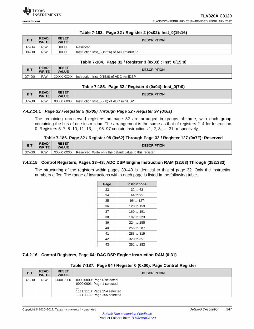
147
TLV320AIC3120www.ti.com SLAS653C –FEBRUARY 2010–REVISED FEBRUARY 2017
Submit Documentation FeedbackProduct Folder Links: TLV320AIC3120
Detailed DescriptionCopyright © 2010–2017, Texas Instruments Incorporated
Table 7-183. Page 32 / Register 2 (0x02): Inst_0(19:16)
BIT READ/WRITE
RESETVALUE DESCRIPTION
D7–D4 R/W XXXX ReservedD3–D0 R/W XXXX Instruction Inst_0(19:16) of ADC miniDSP
Table 7-184. Page 32 / Register 3 (0x03) : Inst_0(15:8)
BIT READ/WRITE
RESETVALUE DESCRIPTION
D7–D0 R/W XXXX XXXX Instruction Inst_0(15:8) of ADC miniDSP
Table 7-185. Page 32 / Register 4 (0x04): Inst_0(7:0)
BIT READ/WRITE
RESETVALUE DESCRIPTION
D7–D0 R/W XXXX XXXX Instruction Inst_0(7:0) of ADC miniDSP
7.4.2.14.1 Page 32 / Register 5 (0x05) Through Page 32 / Register 97 (0x61)
The remaining unreserved registers on page 32 are arranged in groups of three, with each groupcontaining the bits of one instruction. The arrangement is the same as that of registers 2–4 for Instruction0. Registers 5–7, 8–10, 11–13, ..., 95–97 contain instructions 1, 2, 3, ..., 31, respectively.
Table 7-186. Page 32 / Register 98 (0x62) Through Page 32 / Register 127 (0x7F): Reserved
BIT READ/WRITE
RESETVALUE DESCRIPTION
D7–D0 R/W XXXX XXXX Reserved. Write only the default value to this register
7.4.2.15 Control Registers, Pages 33–43: ADC DSP Engine Instruction RAM (32:63) Through (352:383)
The structuring of the registers within pages 33–43 is identical to that of page 32. Only the instructionnumbers differ. The range of instructions within each page is listed in the following table.
Page Instructions33 32 to 6334 64 to 9535 96 to 12736 128 to 15937 160 to 19138 192 to 22339 224 to 25540 256 to 28741 288 to 31942 320 to 35143 352 to 383
7.4.2.16 Control Registers, Page 64: DAC DSP Engine Instruction RAM (0:31)
Table 7-187. Page 64 / Register 0 (0x00): Page Control Register
BIT READ/WRITE
RESETVALUE DESCRIPTION
D7–D0 R/W 0000 0000 0000 0000: Page 0 selected0000 0001: Page 1 selected...1111 1110: Page 254 selected1111 1111: Page 255 selected
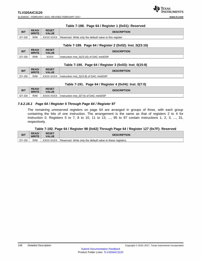
148
TLV320AIC3120SLAS653C –FEBRUARY 2010–REVISED FEBRUARY 2017 www.ti.com
Submit Documentation FeedbackProduct Folder Links: TLV320AIC3120
Detailed Description Copyright © 2010–2017, Texas Instruments Incorporated
Table 7-188. Page 64 / Register 1 (0x01): Reserved
BIT READ/WRITE
RESETVALUE DESCRIPTION
D7–D0 R/W XXXX XXXX Reserved. Write only the default value to this register
Table 7-189. Page 64 / Register 2 (0x02): Inst_0(23:16)
BIT READ/WRITE
RESETVALUE DESCRIPTION
D7–D0 R/W XXXX Instruction Inst_0(23:16) of DAC miniDSP
Table 7-190. Page 64 / Register 3 (0x03): Inst_0(15:8)
BIT READ/WRITE
RESETVALUE DESCRIPTION
D7–D0 R/W XXXX XXXX Instruction Inst_0(15:8) of DAC miniDSP
Table 7-191. Page 64 / Register 4 (0x04): Inst_0(7:0)
BIT READ/WRITE
RESETVALUE DESCRIPTION
D7–D0 R/W XXXX XXXX Instruction Inst_0(7:0) of DAC miniDSP
7.4.2.16.1 Page 64 / Register 5 Through Page 64 / Register 97
The remaining unreserved registers on page 64 are arranged in groups of three, with each groupcontaining the bits of one instruction. The arrangement is the same as that of registers 2 to 4 forInstruction 0. Registers 5 to 7, 8 to 10, 11 to 13, ..., 95 to 97 contain instructions 1, 2, 3, ..., 31,respectively.
Table 7-192. Page 64 / Register 98 (0x62) Through Page 64 / Register 127 (0x7F): Reserved
BIT READ/WRITE
RESETVALUE DESCRIPTION
D7–D0 R/W XXXX XXXX Reserved. Write only the default value to these registers.
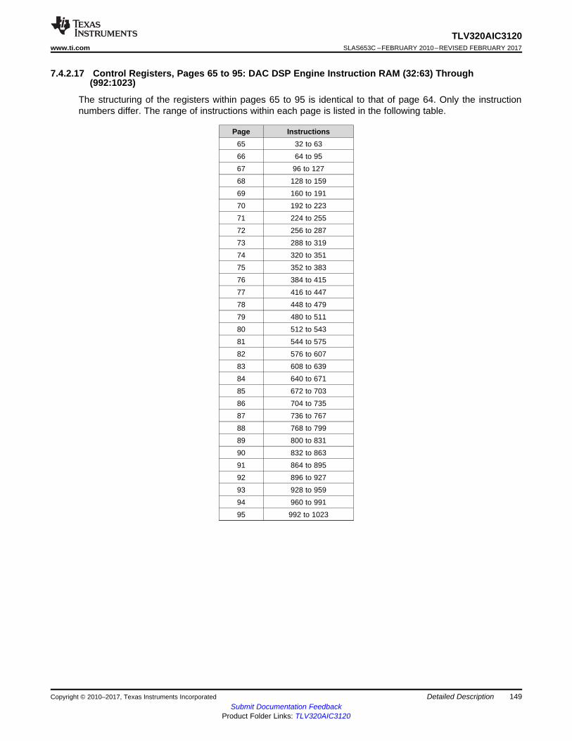
149
TLV320AIC3120www.ti.com SLAS653C –FEBRUARY 2010–REVISED FEBRUARY 2017
Submit Documentation FeedbackProduct Folder Links: TLV320AIC3120
Detailed DescriptionCopyright © 2010–2017, Texas Instruments Incorporated
7.4.2.17 Control Registers, Pages 65 to 95: DAC DSP Engine Instruction RAM (32:63) Through(992:1023)
The structuring of the registers within pages 65 to 95 is identical to that of page 64. Only the instructionnumbers differ. The range of instructions within each page is listed in the following table.
Page Instructions65 32 to 6366 64 to 9567 96 to 12768 128 to 15969 160 to 19170 192 to 22371 224 to 25572 256 to 28773 288 to 31974 320 to 35175 352 to 38376 384 to 41577 416 to 44778 448 to 47979 480 to 51180 512 to 54381 544 to 57582 576 to 60783 608 to 63984 640 to 67185 672 to 70386 704 to 73587 736 to 76788 768 to 79989 800 to 83190 832 to 86391 864 to 89592 896 to 92793 928 to 95994 960 to 99195 992 to 1023
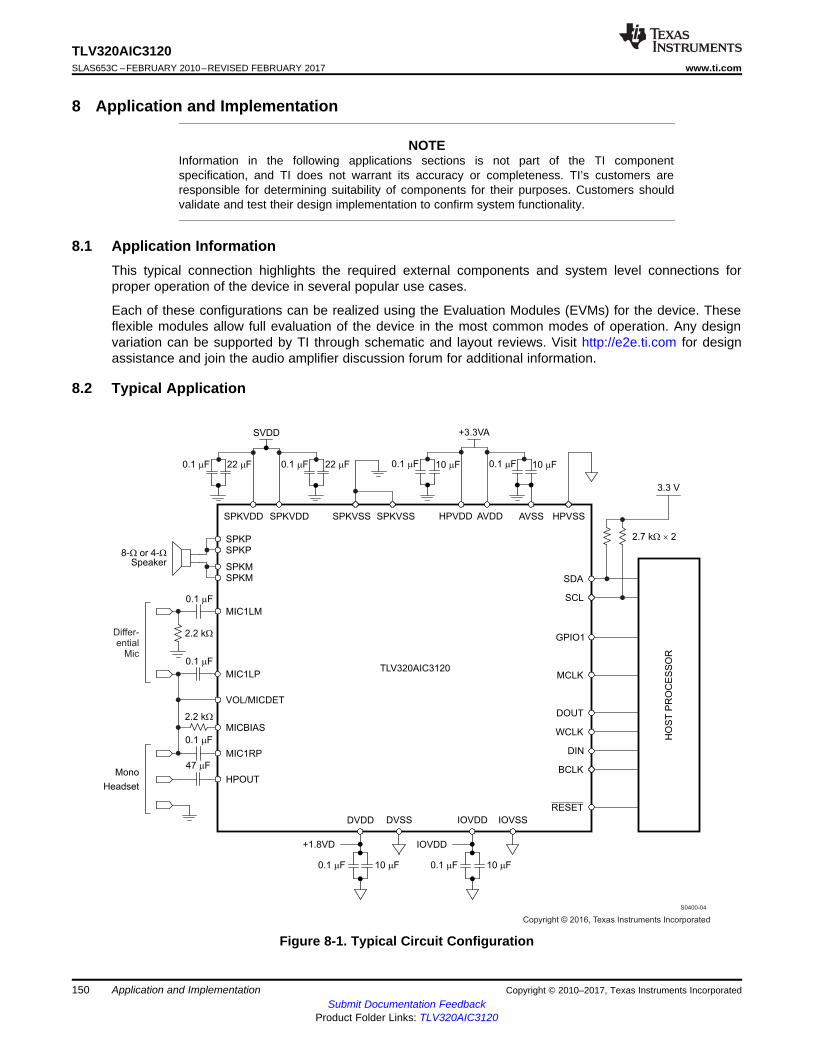
HPVDD HPVSS
3.3 V
SPKVDD SPKVSS AVDD AVSS
SPKP
SPKM
SPKP
SPKM
SPKVSS
VOL/MICDET
HPOUT
MICBIAS
MIC1LM
MIC1LP
MIC1RP
TLV320AIC3120
SPKVDD
22 Fm0.1 Fm0.1 Fm 22 Fm
SVDD
0.1 Fm 10 Fm0.1 Fm 10 Fm
+3.3VA
0.1 Fm
47 Fm
2.2 kW
2.7 k 2W ´
2.2 kW
Mono
Headset
8- or 4-W WSpeaker
0.1 Fm
0.1 Fm
DVDD DVSS IOVDD IOVSS
0.1 Fm 10 Fm
+1.8VD IOVDD
0.1 Fm 10 Fm
S0400-04
Differ-ential
Mic
HO
ST
PR
OC
ES
SO
R
DOUT
DIN
BCLK
WCLK
MCLK
SCL
SDA
RESET
GPIO1
Copyright © 2016, Texas Instruments Incorporated
150
TLV320AIC3120SLAS653C –FEBRUARY 2010–REVISED FEBRUARY 2017 www.ti.com
Submit Documentation FeedbackProduct Folder Links: TLV320AIC3120
Application and Implementation Copyright © 2010–2017, Texas Instruments Incorporated
8 Application and Implementation
NOTEInformation in the following applications sections is not part of the TI componentspecification, and TI does not warrant its accuracy or completeness. TI’s customers areresponsible for determining suitability of components for their purposes. Customers shouldvalidate and test their design implementation to confirm system functionality.
8.1 Application InformationThis typical connection highlights the required external components and system level connections forproper operation of the device in several popular use cases.
Each of these configurations can be realized using the Evaluation Modules (EVMs) for the device. Theseflexible modules allow full evaluation of the device in the most common modes of operation. Any designvariation can be supported by TI through schematic and layout reviews. Visit http://e2e.ti.com for designassistance and join the audio amplifier discussion forum for additional information.
8.2 Typical Application
Figure 8-1. Typical Circuit Configuration
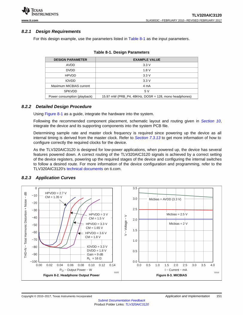
−100
−90
−80
−70
−60
−50
−40
−30
−20
−10
0
0.00 0.02 0.04 0.06 0.08 0.10 0.12 0.14
G025
TH
D+N
− T
otal
Har
mon
ic D
isto
rtio
n +
Noi
se −
dB
PO − Output Power − W
HPVDD = 3.3 VCM = 1.65 V
HPVDD = 3.6 VCM = 1.8 V
HPVDD = 3 VCM = 1.5 V
HPVDD = 2.7 VCM = 1.35 V
IOVDD = 3.3 VDVDD = 1.8 VGain = 9 dBRL = 16 Ω
I − Current − mA
0.0
0.5
1.0
1.5
2.0
2.5
3.0
3.5
0.0 0.5 1.0 1.5 2.0 2.5 3.0 3.5 4.0
V −
Vol
tage
− V
G016
Micbias = 2 V
Micbias = 2.5 V
Micbias = AVDD (3.3 V)
151
TLV320AIC3120www.ti.com SLAS653C –FEBRUARY 2010–REVISED FEBRUARY 2017
Submit Documentation FeedbackProduct Folder Links: TLV320AIC3120
Application and ImplementationCopyright © 2010–2017, Texas Instruments Incorporated
8.2.1 Design RequirementsFor this design example, use the parameters listed in Table 8-1 as the input parameters.
Table 8-1. Design Parameters
DESIGN PARAMETER EXAMPLE VALUEAVDD 3.3 VDVDD 1.8 V
HPVDD 3.3 VIOVDD 3.3 V
Maximum MICBIAS current 4 mASPKVDD 5 V
Power consumption (playback) 15.97 mW (PRB_P4, 48KHz, DOSR = 128, mono headphones)
8.2.2 Detailed Design ProcedureUsing Figure 8-1 as a guide, integrate the hardware into the system.
Following the recommended component placement, schematic layout and routing given in Section 10,integrate the device and its supporting components into the system PCB file.
Determining sample rate and master clock frequency is required since powering up the device as allinternal timing is derived from the master clock. Refer to Section 7.3.13 to get more information of how toconfigure correctly the required clocks for the device.
As the TLV320AIC3120 is designed for low-power applications, when powered up, the device has severalfeatures powered down. A correct routing of the TLV320AIC3120 signals is achieved by a correct settingof the device registers, powering up the required stages of the device and configuring the internal switchesto follow a desired route. For more information of the device configuration and programming, refer to theTLV320AIC3120's technical documents on ti.com.
8.2.3 Application Curves
Figure 8-2. Headphone Output Power Figure 8-3. MICBIAS
152
TLV320AIC3120SLAS653C –FEBRUARY 2010–REVISED FEBRUARY 2017 www.ti.com
Submit Documentation FeedbackProduct Folder Links: TLV320AIC3120
Power Supply Recommendations Copyright © 2010–2017, Texas Instruments Incorporated
9 Power Supply Recommendations
The TLV320AIC3120 has been designed to be extremely tolerant of power supply sequencing. However,in some rare cases, unexpected conditions and behaviors can be attributed to power supply sequencing.
It is important to consider that the digital activity must be separated from the analog and speaker activity.In order to separate the power supplies, the recommended power sequence is:1. Speaker supplies2. Digital supplies3. Analog supplies
First, turn on the speaker supplies. Once they are stabilized, turn on the digital power supplies. Finally,once the digital power supplies are stabilized, the analog power supplies must be turned on.
Also, TI recommends to add decoupling capacitors close to the power supplies pins (see Section 10 fordetails). These capacitors will ensure that the power pins will be stable. Additionally, undesired effectssuch pops will be avoided.
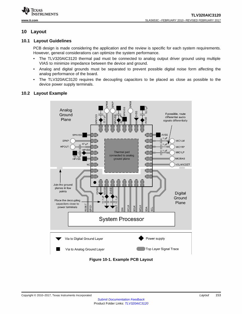
153
TLV320AIC3120www.ti.com SLAS653C –FEBRUARY 2010–REVISED FEBRUARY 2017
Submit Documentation FeedbackProduct Folder Links: TLV320AIC3120
LayoutCopyright © 2010–2017, Texas Instruments Incorporated
10 Layout
10.1 Layout GuidelinesPCB design is made considering the application and the review is specific for each system requirements.However, general considerations can optimize the system performance.• The TLV320AIC3120 thermal pad must be connected to analog output driver ground using multiple
VIAS to minimize impedance between the device and ground.• Analog and digital grounds must be separated to prevent possible digital noise form affecting the
analog performance of the board.• The TLV320AIC3120 requires the decoupling capacitors to be placed as close as possible to the
device power supply terminals.
10.2 Layout Example
Figure 10-1. Example PCB Layout
154
TLV320AIC3120SLAS653C –FEBRUARY 2010–REVISED FEBRUARY 2017 www.ti.com
Submit Documentation FeedbackProduct Folder Links: TLV320AIC3120
Mechanical Packaging and Orderable Information Copyright © 2010–2017, Texas Instruments Incorporated
11 Device and Documentation Support
11.1 Receiving Notification of Documentation UpdatesTo receive notification of documentation updates, navigate to the device product folder on ti.com. In theupper right corner, click on Alert me to register and receive a weekly digest of any product information thathas changed. For change details, review the revision history included in any revised document.
11.2 Community ResourcesThe following links connect to TI community resources. Linked contents are provided "AS IS" by therespective contributors. They do not constitute TI specifications and do not necessarily reflect TI's views;see TI's Terms of Use.TI E2E™ Online Community The TI engineer-to-engineer (E2E) community was created to foster
collaboration among engineers. At e2e.ti.com, you can ask questions, share knowledge,explore ideas and help solve problems with fellow engineers.
Design Support TI's Design Support Quickly find helpful E2E forums along with design support toolsand contact information for technical support.
11.3 TrademarksPurePath, E2E are trademarks of Texas Instruments.MATLAB is a trademark of The MathWorks, Inc.All other trademarks are the property of their respective owners.
11.4 Electrostatic Discharge CautionThis integrated circuit can be damaged by ESD. Texas Instruments recommends that all integrated circuits be handled withappropriate precautions. Failure to observe proper handling and installation procedures can cause damage.
ESD damage can range from subtle performance degradation to complete device failure. Precision integrated circuits may be moresusceptible to damage because very small parametric changes could cause the device not to meet its published specifications.
11.5 GlossaryTI Glossary This glossary lists and explains terms, acronyms, and definitions.
12 Mechanical Packaging and Orderable Information
12.1 Packaging InformationThe following pages include mechanical packaging and orderable information. This information is the mostcurrent data available for the designated devices. This data is subject to change without notice andrevision of this document. For browser-based versions of this data sheet, refer to the left-hand navigation.
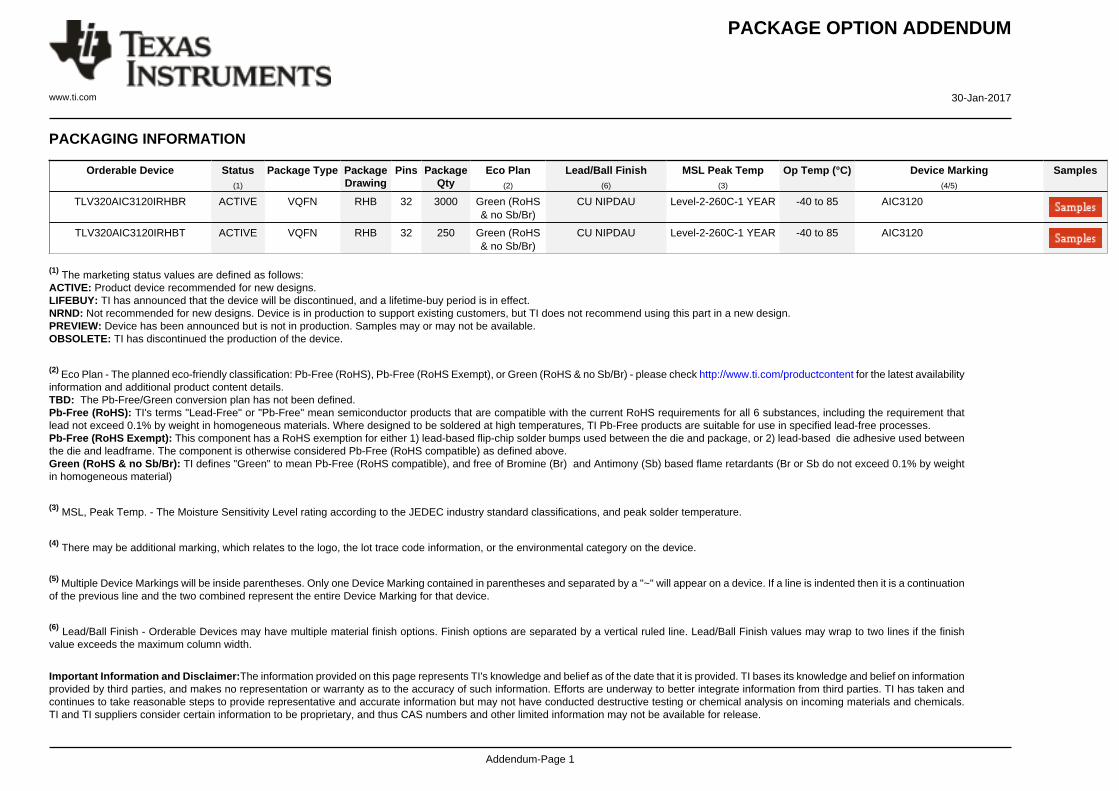
PACKAGE OPTION ADDENDUM
www.ti.com 30-Jan-2017
Addendum-Page 1
PACKAGING INFORMATION
Orderable Device Status(1)
Package Type PackageDrawing
Pins PackageQty
Eco Plan(2)
Lead/Ball Finish(6)
MSL Peak Temp(3)
Op Temp (°C) Device Marking(4/5)
Samples
TLV320AIC3120IRHBR ACTIVE VQFN RHB 32 3000 Green (RoHS& no Sb/Br)
CU NIPDAU Level-2-260C-1 YEAR -40 to 85 AIC3120
TLV320AIC3120IRHBT ACTIVE VQFN RHB 32 250 Green (RoHS& no Sb/Br)
CU NIPDAU Level-2-260C-1 YEAR -40 to 85 AIC3120
(1) The marketing status values are defined as follows:ACTIVE: Product device recommended for new designs.LIFEBUY: TI has announced that the device will be discontinued, and a lifetime-buy period is in effect.NRND: Not recommended for new designs. Device is in production to support existing customers, but TI does not recommend using this part in a new design.PREVIEW: Device has been announced but is not in production. Samples may or may not be available.OBSOLETE: TI has discontinued the production of the device.
(2) Eco Plan - The planned eco-friendly classification: Pb-Free (RoHS), Pb-Free (RoHS Exempt), or Green (RoHS & no Sb/Br) - please check http://www.ti.com/productcontent for the latest availabilityinformation and additional product content details.TBD: The Pb-Free/Green conversion plan has not been defined.Pb-Free (RoHS): TI's terms "Lead-Free" or "Pb-Free" mean semiconductor products that are compatible with the current RoHS requirements for all 6 substances, including the requirement thatlead not exceed 0.1% by weight in homogeneous materials. Where designed to be soldered at high temperatures, TI Pb-Free products are suitable for use in specified lead-free processes.Pb-Free (RoHS Exempt): This component has a RoHS exemption for either 1) lead-based flip-chip solder bumps used between the die and package, or 2) lead-based die adhesive used betweenthe die and leadframe. The component is otherwise considered Pb-Free (RoHS compatible) as defined above.Green (RoHS & no Sb/Br): TI defines "Green" to mean Pb-Free (RoHS compatible), and free of Bromine (Br) and Antimony (Sb) based flame retardants (Br or Sb do not exceed 0.1% by weightin homogeneous material)
(3) MSL, Peak Temp. - The Moisture Sensitivity Level rating according to the JEDEC industry standard classifications, and peak solder temperature.
(4) There may be additional marking, which relates to the logo, the lot trace code information, or the environmental category on the device.
(5) Multiple Device Markings will be inside parentheses. Only one Device Marking contained in parentheses and separated by a "~" will appear on a device. If a line is indented then it is a continuationof the previous line and the two combined represent the entire Device Marking for that device.
(6) Lead/Ball Finish - Orderable Devices may have multiple material finish options. Finish options are separated by a vertical ruled line. Lead/Ball Finish values may wrap to two lines if the finishvalue exceeds the maximum column width.
Important Information and Disclaimer:The information provided on this page represents TI's knowledge and belief as of the date that it is provided. TI bases its knowledge and belief on informationprovided by third parties, and makes no representation or warranty as to the accuracy of such information. Efforts are underway to better integrate information from third parties. TI has taken andcontinues to take reasonable steps to provide representative and accurate information but may not have conducted destructive testing or chemical analysis on incoming materials and chemicals.TI and TI suppliers consider certain information to be proprietary, and thus CAS numbers and other limited information may not be available for release.
PACKAGE OPTION ADDENDUM
www.ti.com 30-Jan-2017
Addendum-Page 2
In no event shall TI's liability arising out of such information exceed the total purchase price of the TI part(s) at issue in this document sold by TI to Customer on an annual basis.
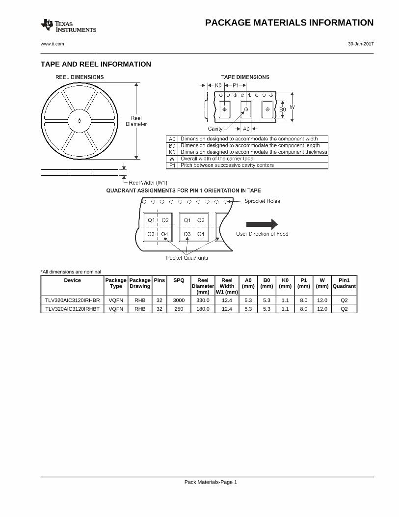
TAPE AND REEL INFORMATION
*All dimensions are nominal
Device PackageType
PackageDrawing
Pins SPQ ReelDiameter
(mm)
ReelWidth
W1 (mm)
A0(mm)
B0(mm)
K0(mm)
P1(mm)
W(mm)
Pin1Quadrant
TLV320AIC3120IRHBR VQFN RHB 32 3000 330.0 12.4 5.3 5.3 1.1 8.0 12.0 Q2
TLV320AIC3120IRHBT VQFN RHB 32 250 180.0 12.4 5.3 5.3 1.1 8.0 12.0 Q2
PACKAGE MATERIALS INFORMATION
www.ti.com 30-Jan-2017
Pack Materials-Page 1
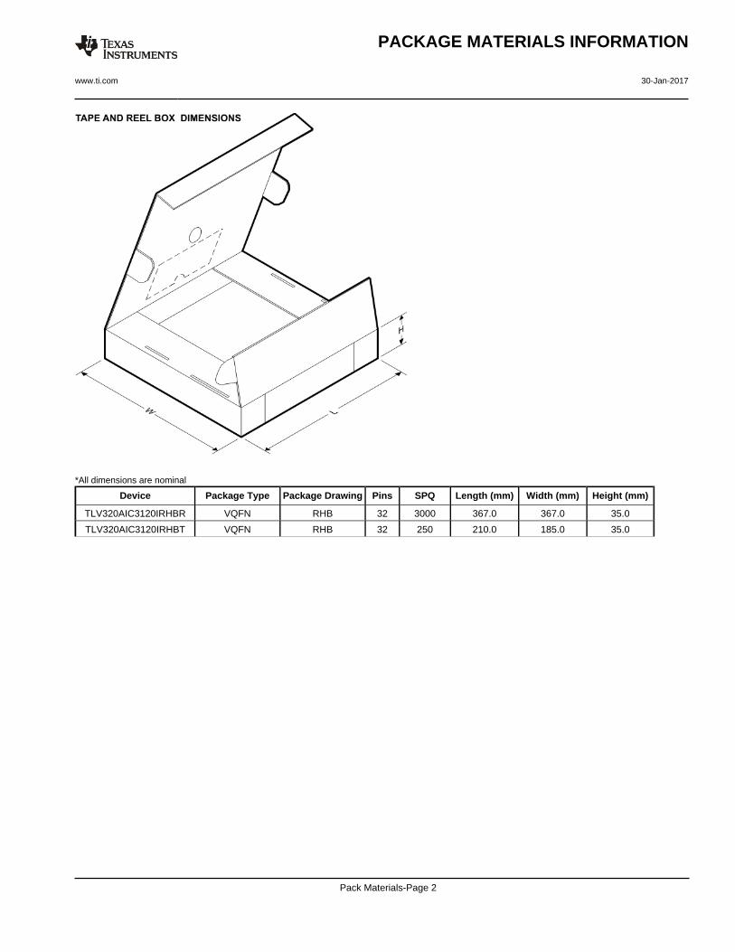
*All dimensions are nominal
Device Package Type Package Drawing Pins SPQ Length (mm) Width (mm) Height (mm)
TLV320AIC3120IRHBR VQFN RHB 32 3000 367.0 367.0 35.0
TLV320AIC3120IRHBT VQFN RHB 32 250 210.0 185.0 35.0
PACKAGE MATERIALS INFORMATION
www.ti.com 30-Jan-2017
Pack Materials-Page 2
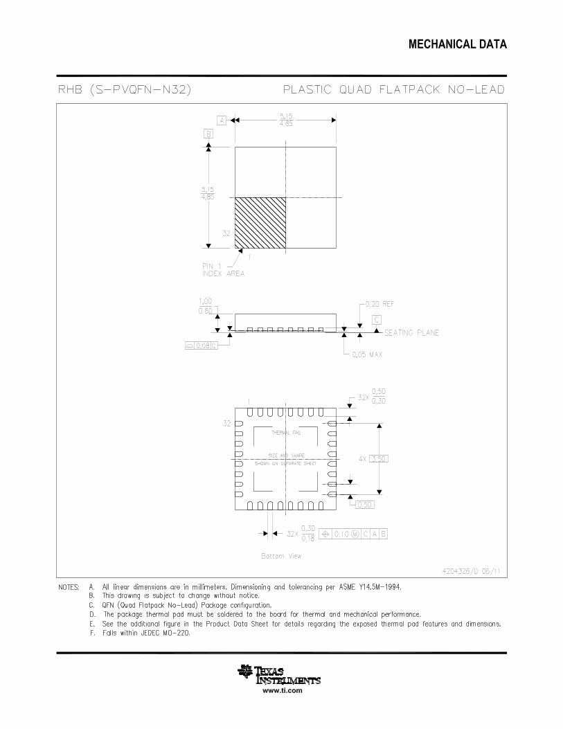
IMPORTANT NOTICE
Texas Instruments Incorporated (TI) reserves the right to make corrections, enhancements, improvements and other changes to itssemiconductor products and services per JESD46, latest issue, and to discontinue any product or service per JESD48, latest issue. Buyersshould obtain the latest relevant information before placing orders and should verify that such information is current and complete.TI’s published terms of sale for semiconductor products (http://www.ti.com/sc/docs/stdterms.htm) apply to the sale of packaged integratedcircuit products that TI has qualified and released to market. Additional terms may apply to the use or sale of other types of TI products andservices.Reproduction of significant portions of TI information in TI data sheets is permissible only if reproduction is without alteration and isaccompanied by all associated warranties, conditions, limitations, and notices. TI is not responsible or liable for such reproduceddocumentation. Information of third parties may be subject to additional restrictions. Resale of TI products or services with statementsdifferent from or beyond the parameters stated by TI for that product or service voids all express and any implied warranties for theassociated TI product or service and is an unfair and deceptive business practice. TI is not responsible or liable for any such statements.Buyers and others who are developing systems that incorporate TI products (collectively, “Designers”) understand and agree that Designersremain responsible for using their independent analysis, evaluation and judgment in designing their applications and that Designers havefull and exclusive responsibility to assure the safety of Designers' applications and compliance of their applications (and of all TI productsused in or for Designers’ applications) with all applicable regulations, laws and other applicable requirements. Designer represents that, withrespect to their applications, Designer has all the necessary expertise to create and implement safeguards that (1) anticipate dangerousconsequences of failures, (2) monitor failures and their consequences, and (3) lessen the likelihood of failures that might cause harm andtake appropriate actions. Designer agrees that prior to using or distributing any applications that include TI products, Designer willthoroughly test such applications and the functionality of such TI products as used in such applications.TI’s provision of technical, application or other design advice, quality characterization, reliability data or other services or information,including, but not limited to, reference designs and materials relating to evaluation modules, (collectively, “TI Resources”) are intended toassist designers who are developing applications that incorporate TI products; by downloading, accessing or using TI Resources in anyway, Designer (individually or, if Designer is acting on behalf of a company, Designer’s company) agrees to use any particular TI Resourcesolely for this purpose and subject to the terms of this Notice.TI’s provision of TI Resources does not expand or otherwise alter TI’s applicable published warranties or warranty disclaimers for TIproducts, and no additional obligations or liabilities arise from TI providing such TI Resources. TI reserves the right to make corrections,enhancements, improvements and other changes to its TI Resources. TI has not conducted any testing other than that specificallydescribed in the published documentation for a particular TI Resource.Designer is authorized to use, copy and modify any individual TI Resource only in connection with the development of applications thatinclude the TI product(s) identified in such TI Resource. NO OTHER LICENSE, EXPRESS OR IMPLIED, BY ESTOPPEL OR OTHERWISETO ANY OTHER TI INTELLECTUAL PROPERTY RIGHT, AND NO LICENSE TO ANY TECHNOLOGY OR INTELLECTUAL PROPERTYRIGHT OF TI OR ANY THIRD PARTY IS GRANTED HEREIN, including but not limited to any patent right, copyright, mask work right, orother intellectual property right relating to any combination, machine, or process in which TI products or services are used. Informationregarding or referencing third-party products or services does not constitute a license to use such products or services, or a warranty orendorsement thereof. Use of TI Resources may require a license from a third party under the patents or other intellectual property of thethird party, or a license from TI under the patents or other intellectual property of TI.TI RESOURCES ARE PROVIDED “AS IS” AND WITH ALL FAULTS. TI DISCLAIMS ALL OTHER WARRANTIES ORREPRESENTATIONS, EXPRESS OR IMPLIED, REGARDING RESOURCES OR USE THEREOF, INCLUDING BUT NOT LIMITED TOACCURACY OR COMPLETENESS, TITLE, ANY EPIDEMIC FAILURE WARRANTY AND ANY IMPLIED WARRANTIES OFMERCHANTABILITY, FITNESS FOR A PARTICULAR PURPOSE, AND NON-INFRINGEMENT OF ANY THIRD PARTY INTELLECTUALPROPERTY RIGHTS. TI SHALL NOT BE LIABLE FOR AND SHALL NOT DEFEND OR INDEMNIFY DESIGNER AGAINST ANY CLAIM,INCLUDING BUT NOT LIMITED TO ANY INFRINGEMENT CLAIM THAT RELATES TO OR IS BASED ON ANY COMBINATION OFPRODUCTS EVEN IF DESCRIBED IN TI RESOURCES OR OTHERWISE. IN NO EVENT SHALL TI BE LIABLE FOR ANY ACTUAL,DIRECT, SPECIAL, COLLATERAL, INDIRECT, PUNITIVE, INCIDENTAL, CONSEQUENTIAL OR EXEMPLARY DAMAGES INCONNECTION WITH OR ARISING OUT OF TI RESOURCES OR USE THEREOF, AND REGARDLESS OF WHETHER TI HAS BEENADVISED OF THE POSSIBILITY OF SUCH DAMAGES.Unless TI has explicitly designated an individual product as meeting the requirements of a particular industry standard (e.g., ISO/TS 16949and ISO 26262), TI is not responsible for any failure to meet such industry standard requirements.Where TI specifically promotes products as facilitating functional safety or as compliant with industry functional safety standards, suchproducts are intended to help enable customers to design and create their own applications that meet applicable functional safety standardsand requirements. Using products in an application does not by itself establish any safety features in the application. Designers mustensure compliance with safety-related requirements and standards applicable to their applications. Designer may not use any TI products inlife-critical medical equipment unless authorized officers of the parties have executed a special contract specifically governing such use.Life-critical medical equipment is medical equipment where failure of such equipment would cause serious bodily injury or death (e.g., lifesupport, pacemakers, defibrillators, heart pumps, neurostimulators, and implantables). Such equipment includes, without limitation, allmedical devices identified by the U.S. Food and Drug Administration as Class III devices and equivalent classifications outside the U.S.TI may expressly designate certain products as completing a particular qualification (e.g., Q100, Military Grade, or Enhanced Product).Designers agree that it has the necessary expertise to select the product with the appropriate qualification designation for their applicationsand that proper product selection is at Designers’ own risk. Designers are solely responsible for compliance with all legal and regulatoryrequirements in connection with such selection.Designer will fully indemnify TI and its representatives against any damages, costs, losses, and/or liabilities arising out of Designer’s non-compliance with the terms and provisions of this Notice.
Mailing Address: Texas Instruments, Post Office Box 655303, Dallas, Texas 75265Copyright © 2017, Texas Instruments Incorporated


![108dB 216kHz 32Bit CODEC with PLL - AKM · PDF file[AK4558] [AK4558] 015004500-E-03 2017/11 - 1 - 1. General Description The AK4558 is a low voltage 32bit 216kHz CODEC for high performance](https://img.dokumen.tips/doc/110x75/5a7e7d137f8b9a49588e7ad1/108db-216khz-32bit-codec-with-pll-akm-ak4558-ak4558-015004500-e-03-201711.jpg)