Embed Size (px)
Citation preview

Low Power, 12.65 mW, 2.3 V to 5.5 V, Programmable Waveform Generator
AD9833
Rev. D Information furnished by Analog Devices is believed to be accurate and reliable. However, no responsibility is assumed by Analog Devices for its use, nor for any infringements of patents or other rights of third parties that may result from its use. Specifications subject to change without notice. No license is granted by implication or otherwise under any patent or patent rights of Analog Devices. Trademarks and registered trademarks are the property of their respective owners.
One Technology Way, P.O. Box 9106, Norwood, MA 02062-9106, U.S.A.Tel: 781.329.4700 www.analog.com Fax: 781.461.3113 ©2003–2011 Analog Devices, Inc. All rights reserved.
FEATURES Digitally programmable frequency and phase 12.65 mW power consumption at 3 V 0 MHz to 12.5 MHz output frequency range 28-bit resolution: 0.1 Hz at 25 MHz reference clock Sinusoidal, triangular, and square wave outputs 2.3 V to 5.5 V power supply No external components required 3-wire SPI interface Extended temperature range: −40°C to +105°C Power-down option 10-lead MSOP package Qualified for automotive applications
APPLICATIONS Frequency stimulus/waveform generation Liquid and gas flow measurement Sensory applications: proximity, motion,
and defect detection Line loss/attenuation Test and medical equipment Sweep/clock generators Time domain reflectometry (TDR) applications
GENERAL DESCRIPTION The AD9833 is a low power, programmable waveform generator capable of producing sine, triangular, and square wave outputs. Waveform generation is required in various types of sensing, actuation, and time domain reflectometry (TDR) applications. The output frequency and phase are software programmable, allowing easy tuning. No external components are needed. The frequency registers are 28 bits wide: with a 25 MHz clock rate, resolution of 0.1 Hz can be achieved; with a 1 MHz clock rate, the AD9833 can be tuned to 0.004 Hz resolution.
The AD9833 is written to via a 3-wire serial interface. This serial interface operates at clock rates up to 40 MHz and is compatible with DSP and microcontroller standards. The device operates with a power supply from 2.3 V to 5.5 V.
The AD9833 has a power-down function (SLEEP). This function allows sections of the device that are not being used to be powered down, thus minimizing the current consumption of the part. For example, the DAC can be powered down when a clock output is being generated.
The AD9833 is available in a 10-lead MSOP package.
FUNCTIONAL BLOCK DIAGRAM
SERIAL INTERFACEAND
CONTROL LOGIC
SCLK SDATAFSYNC
CONTROL REGISTER
PHASE1 REGPHASE0 REG
MUX
SINROM
10-BIT DACMUX
FREQ0 REG
FREQ1 REG
12
ON-BOARDREFERENCE
AGND DGND VDD
AD9833
PHASEACCUMULATOR
(28-BIT)
REGULATOR
CAP/2.5V
2.5V
AVDD/DVDD
MUXDIVIDEBY 2
MSB
MUX
FULL-SCALECONTROL
COMP
VOUT
R200Ω
MCLK
0270
4-00
1
Figure 1.
AD9833
Rev. D | Page 2 of 24
TABLE OF CONTENTS Features .............................................................................................. 1
Applications ....................................................................................... 1
General Description ......................................................................... 1
Functional Block Diagram .............................................................. 1
Revision History ............................................................................... 2
Specifications ..................................................................................... 3
Timing Characteristics ................................................................ 4
Absolute Maximum Ratings ............................................................ 5
ESD Caution .................................................................................. 5
Pin Configuration and Function Descriptions ............................. 6
Typical Performance Characteristics ............................................. 7
Terminology .................................................................................... 10
Theory of Operation ...................................................................... 11
Circuit Description ......................................................................... 12
Numerically Controlled Oscillator Plus Phase Modulator ... 12
Sin ROM ...................................................................................... 12
Digital-to-Analog Converter (DAC) ....................................... 12
Regulator ...................................................................................... 12
Functional Description .................................................................. 13
Serial Interface ............................................................................ 13
Powering Up the AD9833 ......................................................... 13
Latency Period ............................................................................ 13
Control Register ......................................................................... 13
Frequency and Phase Registers ................................................ 15
Reset Function ............................................................................ 16
Sleep Function ............................................................................ 16
VOUT Pin ................................................................................... 16
Applications Information .............................................................. 17
Grounding and Layout .............................................................. 17
Interfacing to Microprocessors ..................................................... 20
AD9833 to 68HC11/68L11 Interface ....................................... 20
AD9833 to 80C51/80L51 Interface .......................................... 20
AD9833 to DSP56002 Interface ............................................... 20
Evaluation Board ............................................................................ 21
System Demonstration Platform .............................................. 21
AD9833 to SPORT Interface ..................................................... 21
Evaluation Kit ............................................................................. 21
Crystal Oscillator vs. External Clock ....................................... 21
Power Supply ............................................................................... 21
Evaluation Board Schematics ................................................... 22
Evaluation Board Layout ........................................................... 23
Outline Dimensions ....................................................................... 24
Ordering Guide .......................................................................... 24
Automotive Products ................................................................. 24
REVISION HISTORY 4/11—Rev. C to Rev. D
Change to Figure 13 ......................................................................... 8 Changes to Table 9 .......................................................................... 15 Deleted AD9833 to ADSP-2101/ADSP-2103 Interface Section .............................................................................................. 20 Changes to Evaluation Board Section .......................................... 21 Added System Demonstration Platform Section, AD9833 to SPORT Interface Section, and Evaluation Kit Section .......... 21 Changes to Crystal Oscillator vs. External Clock Section and Power Supply Section ............................................................. 21 Added Figure 32 and Figure 33; Renumbered Figures Sequentially ..................................................................................... 21 Deleted Prototyping Area Section and Figure 33 ....................... 22 Added Evaluation Board Schematics Section, Figure 34, and Figure 35 ................................................................................... 22 Deleted Table 16 .............................................................................. 23 Added Evaluation Board Layout Section, Figure 36, Figure 37, and Figure 38 ................................................................ 23 Changes to Ordering Guide .......................................................... 24
9/10—Rev. B to Rev. C
Changed 20 mW to 12.65 mW in Data Sheet Title and Features List ................................................................................ 1 Changes to Figure 6 Caption and Figure 7 ..................................... 7
6/10—Rev. A to Rev. B
Changes to Features Section ............................................................ 1 Changes to Serial Interface Section .............................................. 13 Changes to VOUT Pin Section ..................................................... 16 Changes to Grounding and Layout Section ................................ 17 Updated Outline Dimensions ....................................................... 24 Changes to Ordering Guide .......................................................... 24 Added Automotive Products Section .......................................... 24
6/03—Rev. 0 to Rev. A
Updated Ordering Guide ................................................................. 4

AD9833
Rev. D | Page 3 of 24
SPECIFICATIONS VDD = 2.3 V to 5.5 V, AGND = DGND = 0 V, TA = TMIN to TMAX, RSET = 6.8 kΩ for VOUT, unless otherwise noted.
Table 1. Parameter1 Min Typ Max Unit Test Conditions/Comments SIGNAL DAC SPECIFICATIONS
Resolution 10 Bits Update Rate 25 MSPS VOUT Maximum 0.65 V VOUT Minimum 38 mV VOUT Temperature Coefficient 200 ppm/°C DC Accuracy
Integral Nonlinearity ±1.0 LSB Differential Nonlinearity ±0.5 LSB
DDS SPECIFICATIONS (SFDR) Dynamic Specifications
Signal-to-Noise Ratio (SNR) 55 60 dB fMCLK = 25 MHz, fOUT = fMCLK/4096 Total Harmonic Distortion (THD) −66 −56 dBc fMCLK = 25 MHz, fOUT = fMCLK/4096
Spurious-Free Dynamic Range (SFDR) Wideband (0 to Nyquist) −60 dBc fMCLK = 25 MHz, fOUT = fMCLK/50 Narrow-Band (±200 kHz) −78 dBc fMCLK = 25 MHz, fOUT = fMCLK/50
Clock Feedthrough −60 dBc Wake-Up Time 1 ms
LOGIC INPUTS Input High Voltage, VINH 1.7 V 2.3 V to 2.7 V power supply 2.0 V 2.7 V to 3.6 V power supply 2.8 V 4.5 V to 5.5 V power supply Input Low Voltage, VINL 0.5 V 2.3 V to 2.7 V power supply 0.7 V 2.7 V to 3.6 V power supply 0.8 V 4.5 V to 5.5 V power supply Input Current, IINH/IINL 10 mA Input Capacitance, CIN 3 pF
POWER SUPPLIES fMCLK = 25 MHz, fOUT = fMCLK/4096 VDD 2.3 5.5 V IDD 4.5 5.5 mA IDD code dependent; see Figure 7
Low Power Sleep Mode 0.5 mA DAC powered down, MCLK running 1 Operating temperature range is −40°C to +105°C; typical specifications are at 25°C.
VOUT
COMP
12
AD9833
10-BIT DACSINROM
20pF
10nFVDD
REGULATOR
100nF
CAP/2.5V
0270
4-00
2
Figure 2. Test Circuit Used to Test Specifications

AD9833
Rev. D | Page 4 of 24
TIMING CHARACTERISTICS VDD = 2.3 V to 5.5 V, AGND = DGND = 0 V, unless otherwise noted.1
Table 2. Parameter Limit at TMIN to TMAX Unit Description t1 40 ns min MCLK period t2 16 ns min MCLK high duration t3 16 ns min MCLK low duration t4 25 ns min SCLK period t5 10 ns min SCLK high duration t6 10 ns min SCLK low duration t7 5 ns min FSYNC to SCLK falling edge setup time t8 min 10 ns min FSYNC to SCLK hold time t8 max t4 − 5 ns max t9 5 ns min Data setup time t10 3 ns min Data hold time t11 5 ns min SCLK high to FSYNC falling edge setup time 1 Guaranteed by design, not production tested.
Timing Diagrams
t2
t1
MCLK
t3 0270
4-00
3
Figure 3. Master Clock
t5 t4
t6t7 t8
t10t9
41D51DD0D1D2D14
SCLK
FSYNC
SDATA D15
t11
0270
4-00
4
Figure 4. Serial Timing
AD9833
Rev. D | Page 5 of 24
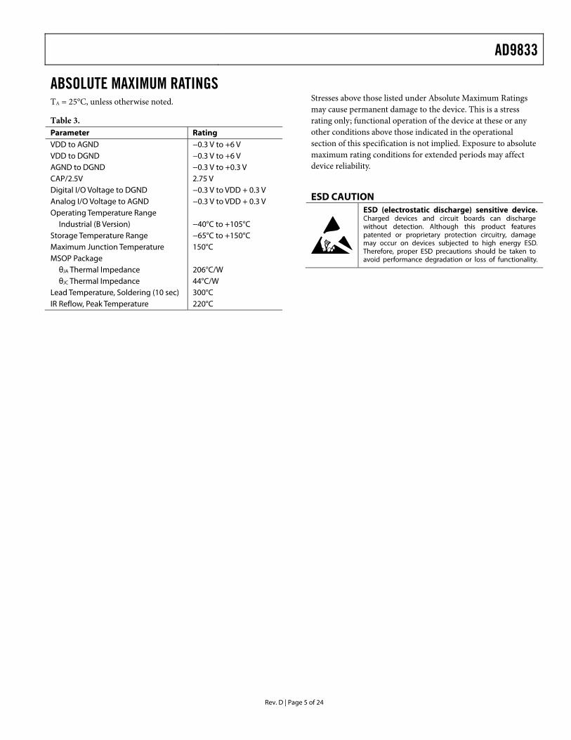
ABSOLUTE MAXIMUM RATINGS TA = 25°C, unless otherwise noted.
Table 3. Parameter Rating VDD to AGND −0.3 V to +6 V VDD to DGND −0.3 V to +6 V AGND to DGND −0.3 V to +0.3 V CAP/2.5V 2.75 V Digital I/O Voltage to DGND −0.3 V to VDD + 0.3 V Analog I/O Voltage to AGND −0.3 V to VDD + 0.3 V Operating Temperature Range
Industrial (B Version) −40°C to +105°C Storage Temperature Range −65°C to +150°C Maximum Junction Temperature 150°C MSOP Package
θJA Thermal Impedance 206°C/W θJC Thermal Impedance 44°C/W
Lead Temperature, Soldering (10 sec) 300°C IR Reflow, Peak Temperature 220°C
Stresses above those listed under Absolute Maximum Ratings may cause permanent damage to the device. This is a stress rating only; functional operation of the device at these or any other conditions above those indicated in the operational section of this specification is not implied. Exposure to absolute maximum rating conditions for extended periods may affect device reliability.
ESD CAUTION

AD9833
Rev. D | Page 6 of 24
PIN CONFIGURATION AND FUNCTION DESCRIPTIONS
COMP 1
VDD 2
CAP/2.5V 3
DGND 4
MCLK 5
VOUT10
AGND9
FSYNC8
SCLK7
SDATA6
AD9833TOP VIEW
(Not to Scale)
0270
4-00
5
Figure 5. Pin Configuration
Table 4. Pin Function Descriptions Pin No. Mnemonic Description 1 COMP DAC Bias Pin. This pin is used for decoupling the DAC bias voltage. 2 VDD Positive Power Supply for the Analog and Digital Interface Sections. The on-board 2.5 V regulator is also supplied
from VDD. VDD can have a value from 2.3 V to 5.5 V. A 0.1 μF and a 10 μF decoupling capacitor should be connected between VDD and AGND.
3 CAP/2.5V The digital circuitry operates from a 2.5 V power supply. This 2.5 V is generated from VDD using an on-board regulator when VDD exceeds 2.7 V. The regulator requires a decoupling capacitor of 100 nF typical, which is connected from CAP/2.5V to DGND. If VDD is less than or equal to 2.7 V, CAP/2.5V should be tied directly to VDD.
4 DGND Digital Ground. 5 MCLK Digital Clock Input. DDS output frequencies are expressed as a binary fraction of the frequency of MCLK. The
output frequency accuracy and phase noise are determined by this clock. 6 SDATA Serial Data Input. The 16-bit serial data-word is applied to this input. 7 SCLK Serial Clock Input. Data is clocked into the AD9833 on each falling edge of SCLK. 8 FSYNC Active Low Control Input. FSYNC is the frame synchronization signal for the input data. When FSYNC is taken low,
the internal logic is informed that a new word is being loaded into the device. 9 AGND Analog Ground. 10 VOUT Voltage Output. The analog and digital output from the AD9833 is available at this pin. An external load resistor
is not required because the device has a 200 Ω resistor on board.

AD9833
Rev. D | Page 7 of 24
TYPICAL PERFORMANCE CHARACTERISTICS
MCLK FREQUENCY (MHz)
I DD
(mA
)
5.5
5.0
3.0
3.5
4.0
4.5
0 5 10 15 20 25
TA = 25°C
0270
4-00
6
VDD = 5V
VDD = 3V
Figure 6. Typical Current Consumption (IDD) vs. MCLK Frequency for fOUT = MCLK/10
0
1
2
3
4
5
6
100 1k 10k 100k 1M 10M
I DD
(mA
)
fOUT (Hz)
VDD = 5VVDD = 3V
0270
4-00
7
Figure 7. Typical IDD vs. fOUT for fMCLK = 25 MHz
0 5 10 15 20 25MCLK FREQUENCY (MHz)
SFD
R (d
Bc)
–65
–60
–90
–70
–75
–80
–85
MCLK/7MCLK/50
VDD = 3VTA = 25°C
0270
4-00
8
Figure 8. Narrow-Band SFDR vs. MCLK Frequency
–45
–40
–705 7 9 11 13 15 17 19 21 23 25
–50
–55
–60
–65
MCLK FREQUENCY (MHz)
SFD
R (d
Bc) MCLK/7
MCLK/50
VDD = 3VTA = 25°C
0270
4-00
9
Figure 9. Wideband SFDR vs. MCLK Frequency
fOUT/fMCLK
–30
–90
–80
–70
–60
–50
–40
SFD
R (d
B)
0
–20
–10
fMCLK = 1MHz
fMCLK = 10MHz
0.001 0.01 0.1 1 10 100
fMCLK = 25MHz
VDD = 3VTA = 25°C
0270
4-01
0
fMCLK = 18MHz
Figure 10. Wideband SFDR vs. fOUT/fMCLK for Various MCLK Frequencies
MCLK FREQUENCY (MHz)1.0 5.0 10.0 12.5 25.0
SNR
(dB
)
–60
–65
–70
–50
–55
–40
–45VDD = 3VTA = 25°CfOUT = MCLK/4096
0270
4-01
1
Figure 11. SNR vs. MCLK Frequency

AD9833
Rev. D | Page 8 of 24
500
1000
700
650
600
550
850
750
800
900
950
–40 25 105TEMPERATURE (°C)
WA
KE-
UP
TIM
E (µ
s)
VDD = 5.5V
0270
4-01
2
VDD = 2.3V
Figure 12. Wake-Up Time vs. Temperature
–40 25 105TEMPERATURE (°C)
V REF
(V)
LOWER RANGE
UPPER RANGE
1.150
1.125
1.100
1.175
1.200
1.250
1.225
0270
4-01
3
Figure 13. VREF vs. Temperature
FREQUENCY (Hz)
POW
ER (d
B)
0
–20
–50
–90
–100
–80
–70
–60
–40
–30
–10
0 100kRWB 100 ST 100 SECVWB 30
0270
4-01
4
Figure 14. Power vs. Frequency, fMCLK = 10 MHz, fOUT = 2.4 kHz, Frequency Word = 0x000FBA9
FREQUENCY (Hz)
POW
ER (d
B)
0
–20
–50
–90
–100
–80
–70
–60
–40
–30
–10
0 5MRWB 1k ST 50 SECVWB 300
0270
4-01
5
Figure 15. Power vs. Frequency, fMCLK = 10 MHz, fOUT = 1.43 MHz = fMCLK/7, Frequency Word = 0x2492492
FREQUENCY (Hz)
POW
ER (d
B)
0
–20
–50
–90
–100
–80
–70
–60
–40
–30
–10
0 5MRWB 1k ST 50 SECVWB 300
0270
4-01
6
Figure 16. Power vs. Frequency, fMCLK = 10 MHz, fOUT = 3.33 MHz = fMCLK/3, Frequency Word = 0x5555555
FREQUENCY (Hz)
POW
ER (d
B)
0
–20
–50
–90
–100
–80
–70
–60
–40
–30
–10
0 100kRWB 100 ST 100 SECVWB 30
0270
4-01
7
Figure 17. Power vs. Frequency, fMCLK = 25 MHz, fOUT = 6 kHz, Frequency Word = 0x000FBA9

AD9833
Rev. D | Page 9 of 24
FREQUENCY (Hz)
POW
ER (d
B)
0
–20
–50
–90
–100
–80
–70
–60
–40
–30
–10
0 1MRWB 300 ST 100 SECVWB 100
0270
4-01
8
Figure 18. Power vs. Frequency, fMCLK = 25 MHz, fOUT = 60 kHz, Frequency Word = 0x009D495
FREQUENCY (Hz)
POW
ER (d
B)
0
–20
–50
–90
–100
–80
–70
–60
–40
–30
–10
0 12.5MRWB 1k ST 100 SECVWB 300
0270
4-01
9
Figure 19. Power vs. Frequency, fMCLK = 25 MHz, fOUT = 600 kHz, Frequency Word = 0x0624DD3
FREQUENCY (Hz)
POW
ER (d
B)
0
–20
–50
–90
–100
–80
–70
–60
–40
–30
–10
0 12.5MRWB 1k ST 100 SECVWB 300
0270
4-02
0
Figure 20. Power vs. Frequency, fMCLK = 25 MHz, fOUT = 2.4 MHz, Frequency Word = 0x189374D
FREQUENCY (Hz)
POW
ER (d
B)
0
–20
–50
–90
–100
–80
–70
–60
–40
–30
–10
0 12.5MRWB 1k ST 100 SECVWB 300
0270
4-02
1
Figure 21. Power vs. Frequency, fMCLK = 25 MHz, fOUT = 3.857 MHz = fMCLK/7, Frequency Word = 0x2492492
FREQUENCY (Hz)
POW
ER (d
B)
0
–20
–50
–90
–100
–80
–70
–60
–40
–30
–10
0 12.5MRWB 1k ST 100 SECVWB 300
0270
4-02
2
Figure 22. Power vs. Frequency, fMCLK = 25 MHz, fOUT = 8.333 MHz = fMCLK/3, Frequency Word = 0x5555555

AD9833
Rev. D | Page 10 of 24
TERMINOLOGY Integral Nonlinearity (INL) INL is the maximum deviation of any code from a straight line passing through the endpoints of the transfer function. The end-points of the transfer function are zero scale, a point 0.5 LSB below the first code transition (000 … 00 to 000 … 01), and full scale, a point 0.5 LSB above the last code transition (111 … 10 to 111 … 11). The error is expressed in LSBs.
Differential Nonlinearity (DNL) DNL is the difference between the measured and ideal 1 LSB change between two adjacent codes in the DAC. A specified DNL of ±1 LSB maximum ensures monotonicity.
Output Compliance Output compliance refers to the maximum voltage that can be generated at the output of the DAC to meet the specifications. When voltages greater than that specified for the output compli-ance are generated, the AD9833 may not meet the specifications listed in the data sheet.
Spurious-Free Dynamic Range (SFDR) Along with the frequency of interest, harmonics of the funda-mental frequency and images of these frequencies are present at the output of a DDS device. SFDR refers to the largest spur or harmonic present in the band of interest. The wideband SFDR gives the magnitude of the largest spur or harmonic relative to the magnitude of the fundamental frequency in the zero to Nyquist bandwidth. The narrow-band SFDR gives the attenuation of the largest spur or harmonic in a bandwidth of ±200 kHz about the fundamental frequency.
Total Harmonic Distortion (THD) THD is the ratio of the rms sum of harmonics to the rms value of the fundamental. For the AD9833, THD is defined as
1
26
25
24
23
22log20THD
VVVVVV ++++
=
where: V1 is the rms amplitude of the fundamental. V2, V3, V4, V5, and V6 are the rms amplitudes of the second through sixth harmonics.
Signal-to-Noise Ratio (SNR) SNR is the ratio of the rms value of the measured output signal to the rms sum of all other spectral components below the Nyquist frequency. The value for SNR is expressed in decibels.
Clock Feedthrough There is feedthrough from the MCLK input to the analog output. Clock feedthrough refers to the magnitude of the MCLK signal relative to the fundamental frequency in the output spectrum of the AD9833.

AD9833
Rev. D | Page 11 of 24
THEORY OF OPERATION Sine waves are typically thought of in terms of their magnitude form: a(t) = sin(ωt). However, these sine waves are nonlinear and not easy to generate except through piecewise construction. On the other hand, the angular information is linear in nature. That is, the phase angle rotates through a fixed angle for each unit of time. The angular rate depends on the frequency of the signal by the traditional rate of ω = 2πf.
MAGNITUDE
PHASE
+1
0
–1
2p
0
2π 4π6π
2π 4π 6π02
704-
023
Figure 23. Sine Wave
Knowing that the phase of a sine wave is linear and given a reference interval (clock period), the phase rotation for that period can be determined.
ΔPhase = ωΔt
Solving for ω,
ω = ΔPhase/Δt = 2πf
Solving for f and substituting the reference clock frequency for the reference period (1/fMCLK = Δt)
f = ΔPhase × fMCLK∕2π
The AD9833 builds the output based on this simple equation. A simple DDS chip can implement this equation with three major subcircuits: numerically controlled oscillator (NCO) and phase modulator, SIN ROM, and digital-to-analog converter (DAC).
Each subcircuit is described in the Circuit Description section.

AD9833
Rev. D | Page 12 of 24
CIRCUIT DESCRIPTION The AD9833 is a fully integrated direct digital synthesis (DDS) chip. The chip requires one reference clock, one low precision resistor, and decoupling capacitors to provide digitally created sine waves up to 12.5 MHz. In addition to the generation of this RF signal, the chip is fully capable of a broad range of simple and complex modulation schemes. These modulation schemes are fully implemented in the digital domain, allowing accurate and simple realization of complex modulation algorithms using DSP techniques.
The internal circuitry of the AD9833 consists of the following main sections: a numerically controlled oscillator (NCO), frequency and phase modulators, SIN ROM, a DAC, and a regulator.
NUMERICALLY CONTROLLED OSCILLATOR PLUS PHASE MODULATOR This consists of two frequency select registers, a phase accumulator, two phase offset registers, and a phase offset adder. The main component of the NCO is a 28-bit phase accumulator. Continuous time signals have a phase range of 0 to 2π. Outside this range of numbers, the sinusoid functions repeat themselves in a periodic manner. The digital implementation is no different. The accumulator simply scales the range of phase numbers into a multibit digital word. The phase accumulator in the AD9833 is implemented with 28 bits. Therefore, in the AD9833, 2π = 228. Likewise, the ΔPhase term is scaled into this range of numbers:
0 < ΔPhase < 228 − 1
With these substitutions, the previous equation becomes
f = ΔPhase × fMCLK∕228
where 0 < ΔPhase < 228 − 1.
The input to the phase accumulator can be selected from either the FREQ0 register or the FREQ1 register and is controlled by the FSELECT bit. NCOs inherently generate continuous phase signals, thus avoiding any output discontinuity when switching between frequencies.
Following the NCO, a phase offset can be added to perform phase modulation using the 12-bit phase registers. The contents of one of these phase registers are added to the most significant bits of the NCO. The AD9833 has two phase registers; their resolution is 2π/4096.
SIN ROM To make the output from the NCO useful, it must be converted from phase information into a sinusoidal value. Because phase information maps directly into amplitude, the SIN ROM uses the digital phase information as an address to a lookup table and converts the phase information into amplitude. Although the NCO contains a 28-bit phase accumulator, the output of the NCO is truncated to 12 bits. Using the full resolution of the phase accumulator is impractical and unnecessary, because this would require a lookup table of 228 entries. It is necessary only to have sufficient phase resolution such that the errors due to truncation are smaller than the resolution of the 10-bit DAC. This requires that the SIN ROM have two bits of phase resolution more than the 10-bit DAC.
The SIN ROM is enabled using the mode bit (D1) in the control register (see Table 15).
DIGITAL-TO-ANALOG CONVERTER (DAC) The AD9833 includes a high impedance, current source 10-bit DAC. The DAC receives the digital words from the SIN ROM and converts them into the corresponding analog voltages.
The DAC is configured for single-ended operation. An external load resistor is not required because the device has a 200 Ω resistor on board. The DAC generates an output voltage of typically 0.6 V p-p.
REGULATOR VDD provides the power supply required for the analog section and the digital section of the AD9833. This supply can have a value of 2.3 V to 5.5 V.
The internal digital section of the AD9833 is operated at 2.5 V. An on-board regulator steps down the voltage applied at VDD to 2.5 V. When the applied voltage at the VDD pin of the AD9833 is less than or equal to 2.7 V, the CAP/2.5V and VDD pins should be tied together, thus bypassing the on-board regulator.

AD9833
Rev. D | Page 13 of 24
FUNCTIONAL DESCRIPTION SERIAL INTERFACE The AD9833 has a standard 3-wire serial interface that is compatible with the SPI, QSPI™, MICROWIRE®, and DSP interface standards.
Data is loaded into the device as a 16-bit word under the control of a serial clock input, SCLK. The timing diagram for this operation is given in Figure 4.
The FSYNC input is a level-triggered input that acts as a frame synchronization and chip enable. Data can be transferred into the device only when FSYNC is low. To start the serial data transfer, FSYNC should be taken low, observing the minimum FSYNC-to-SCLK falling edge setup time, t7. After FSYNC goes low, serial data is shifted into the input shift register of the device on the falling edges of SCLK for 16 clock pulses. FSYNC may be taken high after the 16th falling edge of SCLK, observing the minimum SCLK falling edge to FSYNC rising edge time, t8. Alternatively, FSYNC can be kept low for a multiple of 16 SCLK pulses and then brought high at the end of the data transfer. In this way, a continuous stream of 16-bit words can be loaded while FSYNC is held low; FSYNC goes high only after the 16th SCLK falling edge of the last word loaded.
The SCLK can be continuous, or it can idle high or low between write operations. In either case, it must be high when FSYNC goes low (t11).
For an example of how to program the AD9833, see the AN-1070 Application Note on the Analog Devices, Inc., website.
POWERING UP THE AD9833 The flowchart in Figure 26 shows the operating routine for the AD9833. When the AD9833 is powered up, the part should be reset. This resets the appropriate internal registers to 0 to provide an analog output of midscale.
To avoid spurious DAC outputs during AD9833 initialization, the reset bit should be set to 1 until the part is ready to begin generating an output. A reset does not reset the phase, frequency, or control registers. These registers will contain invalid data and, therefore, should be set to known values by the user. The reset bit should then be set to 0 to begin generating an output. The data appears on the DAC output seven or eight MCLK cycles after the reset bit is set to 0.
LATENCY PERIOD A latency period is associated with each asynchronous write operation in the AD9833. If a selected frequency or phase register is loaded with a new word, there is a delay of seven or eight MCLK cycles before the analog output changes. The delay can be seven or eight cycles, depending on the position of the MCLK rising edge when the data is loaded into the destination register.
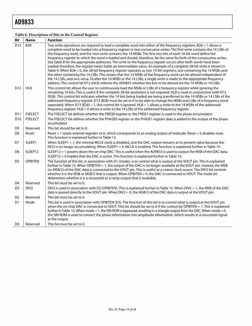
CONTROL REGISTER The AD9833 contains a 16-bit control register that allows the user to configure the operation of the AD9833. All control bits other than the mode bit are sampled on the internal falling edge of MCLK.
Table 6 describes the individual bits of the control register. The different functions and the various output options of the AD9833 are described in more detail in the Frequency and Phase Registers section.
To inform the AD9833 that the contents of the control register will be altered, D15 and D14 must be set to 0, as shown in Table 5.
Table 5. Control Register Bits D15 D14 D13 D0 0 0 Control Bits
SINROMPHASE
ACCUMULATOR(28-BIT)
AD9833
(LOW POWER)10-BIT DAC
0MUX1
SLEEP12
SLEEP1
RESET
MODE + OPBITEN
DIV2
OPBITEN
VOUT1MUX0
DIGITALOUTPUT
(ENABLE)DIVIDEBY 2
DB150
DB140
DB13B28
DB12HLB
DB11FSELECT
DB10PSELECT
DB90
DB8RESET
DB7SLEEP1
DB6SLEEP12
DB5OPBITEN
DB40
DB3DIV2
DB20
DB1MODE
DB00
0270
4-02
4
Figure 24. Function of Control Bits
AD9833
Rev. D | Page 14 of 24
Table 6. Description of Bits in the Control Register Bit Name Function D13 B28 Two write operations are required to load a complete word into either of the frequency registers. B28 = 1 allows a
complete word to be loaded into a frequency register in two consecutive writes. The first write contains the 14 LSBs of the frequency word, and the next write contains the 14 MSBs. The first two bits of each 16-bit word define the frequency register to which the word is loaded and should, therefore, be the same for both of the consecutive writes. See Table 8 for the appropriate addresses. The write to the frequency register occurs after both words have been loaded; therefore, the register never holds an intermediate value. An example of a complete 28-bit write is shown in Table 9. When B28 = 0, the 28-bit frequency register operates as two 14-bit registers, one containing the 14 MSBs and the other containing the 14 LSBs. This means that the 14 MSBs of the frequency word can be altered independent of the 14 LSBs, and vice versa. To alter the 14 MSBs or the 14 LSBs, a single write is made to the appropriate frequency address. The control bit D12 (HLB) informs the AD9833 whether the bits to be altered are the 14 MSBs or 14 LSBs.
D12 HLB This control bit allows the user to continuously load the MSBs or LSBs of a frequency register while ignoring the remaining 14 bits. This is useful if the complete 28-bit resolution is not required. HLB is used in conjunction with D13 (B28). This control bit indicates whether the 14 bits being loaded are being transferred to the 14 MSBs or 14 LSBs of the addressed frequency register. D13 (B28) must be set to 0 to be able to change the MSBs and LSBs of a frequency word separately. When D13 (B28) = 1, this control bit is ignored. HLB = 1 allows a write to the 14 MSBs of the addressed frequency register. HLB = 0 allows a write to the 14 LSBs of the addressed frequency register.
D11 FSELECT The FSELECT bit defines whether the FREQ0 register or the FREQ1 register is used in the phase accumulator. D10 PSELECT The PSELECT bit defines whether the PHASE0 register or the PHASE1 register data is added to the output of the phase
accumulator. D9 Reserved This bit should be set to 0. D8 Reset Reset = 1 resets internal registers to 0, which corresponds to an analog output of midscale. Reset = 0 disables reset.
This function is explained further in Table 13. D7 SLEEP1 When SLEEP1 = 1, the internal MCLK clock is disabled, and the DAC output remains at its present value because the
NCO is no longer accumulating. When SLEEP1 = 0, MCLK is enabled. This function is explained further in Table 14. D6 SLEEP12 SLEEP12 = 1 powers down the on-chip DAC. This is useful when the AD9833 is used to output the MSB of the DAC data.
SLEEP12 = 0 implies that the DAC is active. This function is explained further in Table 14. D5 OPBITEN The function of this bit, in association with D1 (mode), is to control what is output at the VOUT pin. This is explained
further in Table 15. When OPBITEN = 1, the output of the DAC is no longer available at the VOUT pin. Instead, the MSB (or MSB/2) of the DAC data is connected to the VOUT pin. This is useful as a coarse clock source. The DIV2 bit controls whether it is the MSB or MSB/2 that is output. When OPBITEN = 0, the DAC is connected to VOUT. The mode bit determines whether it is a sinusoidal or a ramp output that is available.
D4 Reserved This bit must be set to 0. D3 DIV2 DIV2 is used in association with D5 (OPBITEN). This is explained further in Table 15. When DIV2 = 1, the MSB of the DAC
data is passed directly to the VOUT pin. When DIV2 = 0, the MSB/2 of the DAC data is output at the VOUT pin. D2 Reserved This bit must be set to 0. D1 Mode This bit is used in association with OPBITEN (D5). The function of this bit is to control what is output at the VOUT pin
when the on-chip DAC is connected to VOUT. This bit should be set to 0 if the control bit OPBITEN = 1. This is explained further in Table 15. When mode = 1, the SIN ROM is bypassed, resulting in a triangle output from the DAC. When mode = 0, the SIN ROM is used to convert the phase information into amplitude information, which results in a sinusoidal signal at the output.
D0 Reserved This bit must be set to 0.

AD9833
Rev. D | Page 15 of 24
FREQUENCY AND PHASE REGISTERS The AD9833 contains two frequency registers and two phase registers, which are described in Table 7.
Table 7. Frequency and Phase Registers Register Size Description FREQ0 28 bits Frequency Register 0. When the FSELECT
bit = 0, this register defines the output frequency as a fraction of the MCLK frequency.
FREQ1 28 bits Frequency Register 1. When the FSELECT bit = 1, this register defines the output frequency as a fraction of the MCLK frequency.
PHASE0 12 bits Phase Offset Register 0. When the PSELECT bit = 0, the contents of this register are added to the output of the phase accumulator.
PHASE1 12 bits Phase Offset Register 1. When the PSELECT bit = 1, the contents of this register are added to the output of the phase accumulator.
The analog output from the AD9833 is
fMCLK/228 × FREQREG
where FREQREG is the value loaded into the selected frequency register. This signal is phase shifted by
2π/4096 × PHASEREG
where PHASEREG is the value contained in the selected phase register. Consideration must be given to the relationship of the selected output frequency and the reference clock frequency to avoid unwanted output anomalies.
The flowchart in Figure 28 shows the routine for writing to the frequency and phase registers of the AD9833.
Writing to a Frequency Register
When writing to a frequency register, Bit D15 and Bit D14 give the address of the frequency register.
Table 8. Frequency Register Bits D15 D14 D13 D0 0 1 MSB 14 FREQ0 REG bits LSB 1 0 MSB 14 FREQ1 REG bits LSB
If the user wants to change the entire contents of a frequency register, two consecutive writes to the same address must be performed because the frequency registers are 28 bits wide. The first write contains the 14 LSBs, and the second write contains the 14 MSBs. For this mode of operation, the B28 (D13) control bit should be set to 1. An example of a 28-bit write is shown in Table 9.
Table 9. Writing 0xFFFC000 to the FREQ0 Register SDATA Input Result of Input Word 0010 0000 0000 0000 Control word write
(D15, D14 = 00), B28 (D13) = 1, HLB (D12) = X
0100 0000 0000 0000 FREQ0 register write (D15, D14 = 01), 14 LSBs = 0x0000
0111 1111 1111 1111 FREQ0 register write (D15, D14 = 01), 14 MSBs = 0x3FFF
In some applications, the user does not need to alter all 28 bits of the frequency register. With coarse tuning, only the 14 MSBs are altered, while with fine tuning, only the 14 LSBs are altered. By setting the B28 (D13) control bit to 0, the 28-bit frequency register operates as two, 14-bit registers, one containing the 14 MSBs and the other containing the 14 LSBs. This means that the 14 MSBs of the frequency word can be altered independent of the 14 LSBs, and vice versa. Bit HLB (D12) in the control register identifies which 14 bits are being altered. Examples of this are shown in Table 10 and Table 11.
Table 10. Writing 0x3FFF to the 14 LSBs of the FREQ1 Register SDATA Input Result of Input Word 0000 0000 0000 0000 Control word write (D15, D14 = 00),
B28 (D13) = 0; HLB (D12) = 0, that is, LSBs 1011 1111 1111 1111 FREQ1 REG write (D15, D14 = 10),
14 LSBs = 0x3FFF
Table 11. Writing 0x00FF to the 14 MSBs of the FREQ0 Register SDATA Input Result of Input Word 0001 0000 0000 0000 Control word write (D15, D14 = 00),
B28 (D13) = 0, HLB (D12) = 1, that is, MSBs 0100 0000 1111 1111 FREQ0 REG write (D15, D14 = 01),
14 MSBs = 0x00FF
Writing to a Phase Register
When writing to a phase register, Bit D15 and Bit D14 are set to 11. Bit D13 identifies which phase register is being loaded.
Table 12. Phase Register Bits D15 D14 D13 D12 D11 D0 1 1 0 X MSB 12 PHASE0 bits LSB 1 1 1 X MSB 12 PHASE1 bits LSB
AD9833
Rev. D | Page 16 of 24
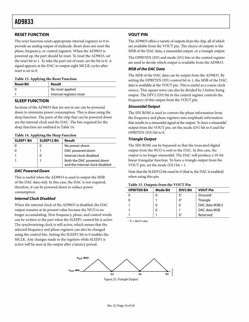
RESET FUNCTION VOUT PIN The reset function resets appropriate internal registers to 0 to provide an analog output of midscale. Reset does not reset the phase, frequency, or control registers. When the AD9833 is powered up, the part should be reset. To reset the AD9833, set the reset bit to 1. To take the part out of reset, set the bit to 0. A signal appears at the DAC to output eight MCLK cycles after reset is set to 0.
The AD9833 offers a variety of outputs from the chip, all of which are available from the VOUT pin. The choice of outputs is the MSB of the DAC data, a sinusoidal output, or a triangle output.
The OPBITEN (D5) and mode (D1) bits in the control register are used to decide which output is available from the AD9833.
MSB of the DAC Data
The MSB of the DAC data can be output from the AD9833. By setting the OPBITEN (D5) control bit to 1, the MSB of the DAC data is available at the VOUT pin. This is useful as a coarse clock source. This square wave can also be divided by 2 before being output. The DIV2 (D3) bit in the control register controls the frequency of this output from the VOUT pin.
Table 13. Applying the Reset Function Reset Bit Result 0 No reset applied 1 Internal registers reset
SLEEP FUNCTION Sinusoidal Output Sections of the AD9833 that are not in use can be powered
down to minimize power consumption. This is done using the sleep function. The parts of the chip that can be powered down are the internal clock and the DAC. The bits required for the sleep function are outlined in Table 14.
The SIN ROM is used to convert the phase information from the frequency and phase registers into amplitude information that results in a sinusoidal signal at the output. To have a sinusoidal output from the VOUT pin, set the mode (D1) bit to 0 and the OPBITEN (D5) bit to 0.
Table 14. Applying the Sleep Function Triangle Output SLEEP1 Bit SLEEP12 Bit Result
0 0 No power-down 0 1 DAC powered down 1 0 Internal clock disabled 1 1 Both the DAC powered down
and the internal clock disabled
The SIN ROM can be bypassed so that the truncated digital output from the NCO is sent to the DAC. In this case, the output is no longer sinusoidal. The DAC will produce a 10-bit linear triangular function. To have a triangle output from the VOUT pin, set the mode (D1) bit = 1.
DAC Powered Down Note that the SLEEP12 bit must be 0 (that is, the DAC is enabled) when using this pin. This is useful when the AD9833 is used to output the MSB
of the DAC data only. In this case, the DAC is not required; therefore, it can be powered down to reduce power consumption.
Table 15. Outputs from the VOUT Pin OPBITEN Bit Mode Bit DIV2 Bit VOUT Pin 0 0 X1 Sinusoid 0 1 X1 Triangle 1 0 0 DAC data MSB/2 1 0 1 DAC data MSB 1 1 X1 Reserved
Internal Clock Disabled
When the internal clock of the AD9833 is disabled, the DAC output remains at its present value because the NCO is no longer accumulating. New frequency, phase, and control words can be written to the part when the SLEEP1 control bit is active. The synchronizing clock is still active, which means that the selected frequency and phase registers can also be changed using the control bits. Setting the SLEEP1 bit to 0 enables the MCLK. Any changes made to the registers while SLEEP1 is active will be seen at the output after a latency period.
1 X = don’t care.
VOUT MIN
VOUT MAX
2π 4π 6π
0270
4-02
5
Figure 25. Triangle Output
AD9833
Rev. D | Page 17 of 24
APPLICATIONS INFORMATION Because of the various output options available from the part, the AD9833 can be configured to suit a wide variety of applications.
One of the areas where the AD9833 is suitable is in modulation applications. The part can be used to perform simple modulation, such as FSK. More complex modulation schemes, such as GMSK and QPSK, can also be implemented using the AD9833.
In an FSK application, the two frequency registers of the AD9833 are loaded with different values. One frequency represents the space frequency, while the other represents the mark frequency. Using the FSELECT bit in the control register of the AD9833, the user can modulate the carrier frequency between the two values.
The AD9833 has two phase registers, which enables the part to perform PSK. With phase-shift keying, the carrier frequency is phase shifted, the phase being altered by an amount that is related to the bit stream being input to the modulator.
The AD9833 is also suitable for signal generator applications. Because the MSB of the DAC data is available at the VOUT pin, the device can be used to generate a square wave.
With its low current consumption, the part is suitable for applications in which it can be used as a local oscillator.
GROUNDING AND LAYOUT The printed circuit board (PCB) that houses the AD9833 should be designed so that the analog and digital sections are separated and confined to certain areas of the board. This facilitates the use of ground planes that can be separated easily. A minimum etch technique is generally best for ground planes because it gives the best shielding. Digital and analog ground planes should be joined in one place only. If the AD9833 is the only device requiring an AGND-to-DGND connection, then the ground planes should be connected at the AGND and DGND pins of the AD9833. If the AD9833 is in a system where multiple devices require AGND-to-DGND connections, the connection should be made at one point only, a star ground point that should be established as close as possible to the AD9833.
Avoid running digital lines under the device as these couple noise onto the die. The analog ground plane should be allowed to run under the AD9833 to avoid noise coupling. The power supply lines to the AD9833 should use as large a track as possible to provide low impedance paths and reduce the effects of glitches on the power supply line. Fast switching signals, such as clocks, should be shielded with digital ground to avoid radiating noise to other sections of the board.
Avoid crossover of digital and analog signals. Traces on opposite sides of the board should run at right angles to each other. This reduces the effects of feedthrough through the board. A microstrip technique is by far the best, but it is not always possible with a double-sided board. In this technique, the component side of the board is dedicated to ground planes, and signals are placed on the other side.
Good decoupling is important. The AD9833 should have supply bypassing of 0.1 μF ceramic capacitors in parallel with 10 μF tantalum capacitors. To achieve the best performance from the decoupling capacitors, they should be placed as close as possible to the device, ideally right up against the device.

AD9833
Rev. D | Page 18 of 24
DATA WRITE(SEE FIGURE 28)
SELECT DATASOURCES
WAIT 7/8 MCLKCYCLES
VOUT = VREF × 18 × RLOAD / RSET × (1 + (SIN (2π (FREQREG × fMCLK × t/228 + PHASEREG / 212))))DAC OUTPUT
CHANGE PHASE?
CHANGE FREQUENCY?
CHANGE DAC OUTPUTFROM SIN TO RAMP?
CHANGE OUTPUT TOA DIGITAL SIGNAL?
CHANGEPSELECT?
CHANGE PHASEREGISTER?
CHANGEFSELECT?
CHANGE FREQUENCYREGISTER?
CONTROL REGISTERWRITE
(SEE TABLE 6)
INITIALIZATION(SEE FIGURE 27 BELOW)
NO
NO
NO
NO
YES
NO
YES
YESNO
YES
YES
YES
YES
YES
0270
4-02
6
Figure 26. Flowchart for AD9833 Initialization and Operation
INITIALIZATION
APPLY RESET
(CONTROL REGISTER WRITE)
RESET = 1
WRITE TO FREQUENCY AND PHASE REGISTERSFREQ0 REG = fOUT0/fMCLK × 228FREQ1 REG = fOUT1/fMCLK × 228
PHASE0 AND PHASE1 REG = (PHASESHIFT × 212)/2π
(SEE FIGURE 28)
SET RESET = 0SELECT FREQUENCY REGISTERS
SELECT PHASE REGISTERS
(CONTROL REGISTER WRITE)
RESET BIT = 0FSELECT = SELECTED FREQUENCY REGISTER
PSELECT = SELECTED PHASE REGISTER
0270
4-02
7
Figure 27. Flowchart for Initialization

AD9833
Rev. D | Page 19 of 24
NO
WRITE 14MSBs OR LSBsTO A FREQUENCY REGISTER?
(CONTROL REGISTER WRITE)B28 (D13) = 0
HLB (D12) = 0/1
WRITE A 16-BIT WORD
(SEE TABLE 10 AND TABLE 11FOR EXAMPLES)
WRITE 14MSBs OR LSBsTO A
FREQUENCY REGISTER?
WRITE TO PHASEREGISTER?
(16-BIT WRITE)D15, D14 = 11 D13 = 0/1 (CHOOSE THE PHASE REGISTER) D12 = XD11 ... D0 = PHASE DATA
WRITE TO ANOTHERPHASE REGISTER?
YES
WRITE ANOTHER FULL28-BIT WORD TO A
FREQUENCY REGISTER?
WRITE TWO CONSECUTIVE16-BIT WORDS
(SEE TABLE 9 FOR EXAMPLE)
(CONTROL REGISTER WRITE)
B28 (D13) = 1
WRITE A FULL 28-BIT WORDTO A FREQUENCY REGISTER?
DATA WRITE
NO
YES
YES
NO
YES
ONON
YES
YES
0270
4-02
8
Figure 28. Flowchart for Data Writes

AD9833
Rev. D | Page 20 of 24
INTERFACING TO MICROPROCESSORS The AD9833 has a standard serial interface that allows the part to interface directly with several microprocessors. The device uses an external serial clock to write the data or control information into the device. The serial clock can have a frequency of 40 MHz maximum. The serial clock can be continuous, or it can idle high or low between write operations. When data or control informa-tion is written to the AD9833, FSYNC is taken low and is held low until the 16 bits of data are written into the AD9833. The FSYNC signal frames the 16 bits of information that are loaded into the AD9833.
AD9833 TO 68HC11/68L11 INTERFACE Figure 29 shows the serial interface between the AD9833 and the 68HC11/68L11 microcontroller. The microcontroller is con-figured as the master by setting the MSTR bit in the SPCR to 1. This setting provides a serial clock on SCK; the MOSI output drives the serial data line SDATA. Because the microcontroller does not have a dedicated frame sync pin, the FSYNC signal is derived from a port line (PC7). The setup conditions for correct operation of the interface are as follows:
• SCK idles high between write operations (CPOL = 0) • Data is valid on the SCK falling edge (CPHA = 1)
When data is being transmitted to the AD9833, the FSYNC line is taken low (PC7). Serial data from the 68HC11/68L11 is trans-mitted in 8-bit bytes with only eight falling clock edges occurring in the transmit cycle. Data is transmitted MSB first. To load data into the AD9833, PC7 is held low after the first eight bits are transferred, and a second serial write operation is performed to the AD9833. Only after the second eight bits are transferred should FSYNC be taken high again.
AD9833
FSYNC
SDATA
SCLK
68HC11/68L11
PC7
MOSI
SCK
0270
4-03
0
Figure 29. 68HC11/68L11 to AD9833 Interface
AD9833 TO 80C51/80L51 INTERFACE Figure 30 shows the serial interface between the AD9833 and the 80C51/80L51 microcontroller. The microcontroller is oper-ated in Mode 0 so that TxD of the 80C51/80L51 drives SCLK of the AD9833, and RxD drives the serial data line SDATA. The FSYNC signal is derived from a bit programmable pin on the port (P3.3 is shown in Figure 30).
When data is to be transmitted to the AD9833, P3.3 is taken low. The 80C51/80L51 transmits data in 8-bit bytes, thus only eight falling SCLK edges occur in each cycle. To load the remaining eight bits to the AD9833, P3.3 is held low after the first eight bits are transmitted, and a second write operation is initiated to transmit the second byte of data. P3.3 is taken high following the completion of the second write operation. SCLK should idle high between the two write operations.
The 80C51/80L51 outputs the serial data in a format that has the LSB first. The AD9833 accepts the MSB first (the four MSBs are the control information, the next four bits are the address, and the eight LSBs contain the data when writing to a destination register). Therefore, the transmit routine of the 80C51/80L51 must take this into account and rearrange the bits so that the MSB is output first.
AD9833
FSYNC
SDATA
SCLK
80C51/80L51
P3.3
RxD
TxD
0270
4-03
1
Figure 30. 80C51/80L51 to AD9833 Interface
AD9833 TO DSP56002 INTERFACE Figure 31 shows the interface between the AD9833 and the DSP56002. The DSP56002 is configured for normal mode asyn-chronous operation with a gated internal clock (SYN = 0, GCK = 1, SCKD = 1). The frame sync pin is generated internally (SC2 = 1), the transfers are 16 bits wide (WL1 = 1, WL0 = 0), and the frame sync signal frames the 16 bits (FSL = 0). The frame sync signal is available on the SC2 pin, but it must be inverted before it is applied to the AD9833. The interface to the DSP56000/DSP56001 is similar to that of the DSP56002.
AD9833
FSYNC
SDATA
SCLK
DSP56002
SC2
STD
SCK
0270
4-03
2
Figure 31. DSP56002 to AD9833 Interface
AD9833
Rev. D | Page 21 of 24
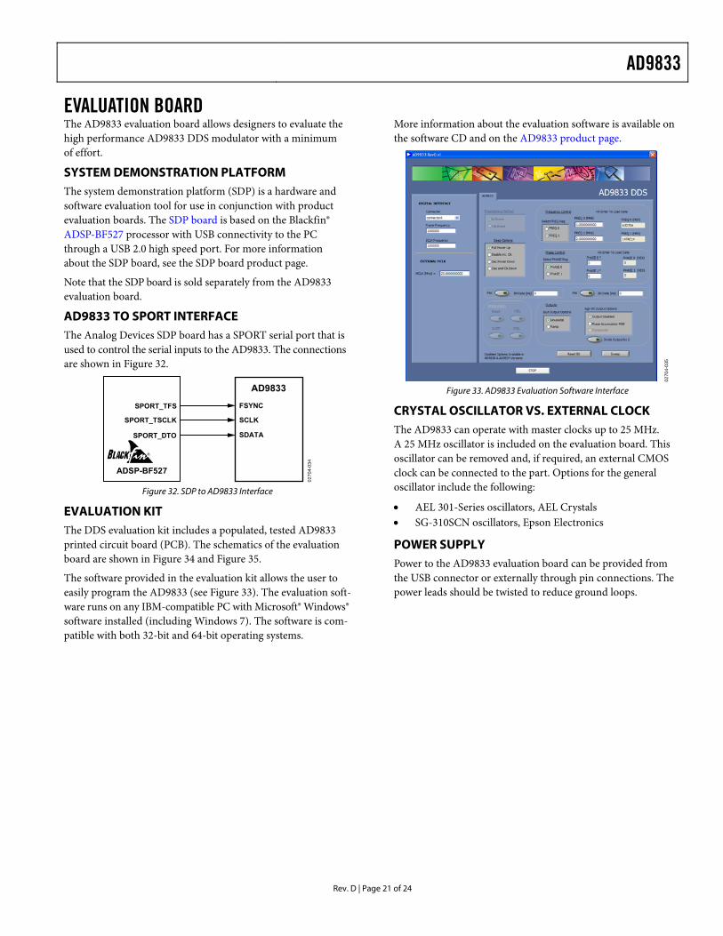
EVALUATION BOARD The AD9833 evaluation board allows designers to evaluate the high performance AD9833 DDS modulator with a minimum of effort.
SYSTEM DEMONSTRATION PLATFORM The system demonstration platform (SDP) is a hardware and software evaluation tool for use in conjunction with product evaluation boards. The SDP board is based on the Blackfin® ADSP-BF527 processor with USB connectivity to the PC through a USB 2.0 high speed port. For more information about the SDP board, see the SDP board product page.
Note that the SDP board is sold separately from the AD9833 evaluation board.
AD9833 TO SPORT INTERFACE The Analog Devices SDP board has a SPORT serial port that is used to control the serial inputs to the AD9833. The connections are shown in Figure 32.
AD9833
FSYNC
SDATA
SCLK
0270
4-03
4
SPORT_TFS
SPORT_TSCLK
SPORT_DTO
ADSP-BF527
Figure 32. SDP to AD9833 Interface
EVALUATION KIT The DDS evaluation kit includes a populated, tested AD9833 printed circuit board (PCB). The schematics of the evaluation board are shown in Figure 34 and Figure 35.
The software provided in the evaluation kit allows the user to easily program the AD9833 (see Figure 33). The evaluation soft-ware runs on any IBM-compatible PC with Microsoft® Windows® software installed (including Windows 7). The software is com-patible with both 32-bit and 64-bit operating systems.
More information about the evaluation software is available on the software CD and on the AD9833 product page.
0270
4-03
5
Figure 33. AD9833 Evaluation Software Interface
CRYSTAL OSCILLATOR VS. EXTERNAL CLOCK The AD9833 can operate with master clocks up to 25 MHz. A 25 MHz oscillator is included on the evaluation board. This oscillator can be removed and, if required, an external CMOS clock can be connected to the part. Options for the general oscillator include the following:
• AEL 301-Series oscillators, AEL Crystals • SG-310SCN oscillators, Epson Electronics
POWER SUPPLY Power to the AD9833 evaluation board can be provided from the USB connector or externally through pin connections. The power leads should be twisted to reduce ground loops.

AD9833
Rev. D | Page 22 of 24
EVALUATION BOARD SCHEMATICS
0270
4-03
6
Figure 34. Evaluation Board Schematic
0270
4-03
7
Figure 35. SDP Connector Schematic
AD9833
Rev. D | Page 23 of 24
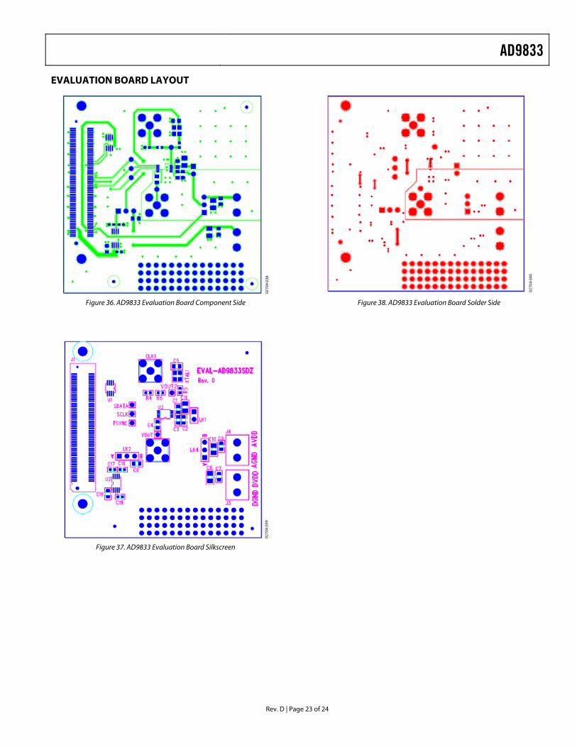
EVALUATION BOARD LAYOUT
0270
4-03
8
Figure 36. AD9833 Evaluation Board Component Side
0270
4-03
9
Figure 37. AD9833 Evaluation Board Silkscreen
0270
4-04
0
Figure 38. AD9833 Evaluation Board Solder Side

AD9833
Rev. D | Page 24 of 24
OUTLINE DIMENSIONS
COMPLIANT TO JEDEC STANDARDS MO-187-BA 0917
09-A
6°0°
0.700.550.40
5
10
1
6
0.50 BSC
0.300.15
1.10 MAX
3.103.002.90
COPLANARITY0.10
0.230.13
3.103.002.90
5.154.904.65
PIN 1IDENTIFIER
15° MAX0.950.850.75
0.150.05
Figure 39. 10-Lead Mini Small Outline Package [MSOP]
(RM-10) Dimensions shown in millimeters
ORDERING GUIDE Model1, 2, 3 Temperature Range Package Description Package Option Branding AD9833BRM −40°C to +105°C 10-Lead MSOP RM-10 DJB AD9833BRM-REEL −40°C to +105°C 10-Lead MSOP RM-10 DJB AD9833BRM-REEL7 −40°C to +105°C 10-Lead MSOP RM-10 DJB AD9833BRMZ −40°C to +105°C 10-Lead MSOP RM-10 D68 AD9833BRMZ-REEL −40°C to +105°C 10-Lead MSOP RM-10 D68 AD9833BRMZ-REEL7 −40°C to +105°C 10-Lead MSOP RM-10 D68 AD9833WBRMZ-REEL −40°C to +105°C 10-Lead MSOP RM-10 D68 EVAL-AD9833SDZ Evaluation Board 1 Z = RoHS Compliant Part. 2 W = Qualified for Automotive Applications. 3 The evaluation board for the AD9833 requires the system demonstration platform (SDP) board, which is sold separately.
AUTOMOTIVE PRODUCTS The AD9833WBRMZ-REEL model is available with controlled manufacturing to support the quality and reliability requirements of automotive applications. Note that this automotive model may have specifications that differ from the commercial models; therefore, designers should review the Specifications section of this data sheet carefully. Only the automotive grade product shown is available for use in automotive applications. Contact your local Analog Devices account representative for specific product ordering information and to obtain the specific Automotive Reliability reports for these models.
©2003–2011 Analog Devices, Inc. All rights reserved. Trademarks and registered trademarks are the property of their respective owners. D02704-0-4/11(D)