Embed Size (px)
Citation preview
Low Phase Noise, Fast Settling PLL Frequency Synthesizer
Data Sheet ADF4193
FEATURES New, fast settling, fractional-N PLL architecture Single PLL replaces ping-pong synthesizers Frequency hop across GSM band in 5 µs with phase settled
by 20 µs 0.5° rms phase error at 2 GHz RF output Digitally programmable output phase RF input range up to 3.5 GHz 3-wire serial interface On-chip, low noise differential amplifier Phase noise figure of merit: −216 dBc/Hz Loop filter design possible using ADIsimPLL™ Qualified for automotive applications
APPLICATIONS GSM/EDGE base stations PHS base stations Instrumentation and test equipment
GENERAL DESCRIPTION The ADF4193 frequency synthesizer can be used to implement local oscillators in the upconversion and downconversion sections of wireless receivers and transmitters. Its architecture is specifically designed to meet the GSM/EDGE lock time requirements for base stations. It consists of a low noise, digital phase frequency detector (PFD), and a precision differential charge pump. There is also a differential amplifier to convert the differential charge pump output to a single-ended voltage for the external voltage-controlled oscillator (VCO).
The Σ-Δ based fractional interpolator, working with the N divider, allows programmable modulus fractional-N division. Additionally, the 4-bit reference (R) counter and on-chip frequency doubler allow selectable reference signal (REFIN) frequencies at the PFD input. A complete phase-locked loop (PLL) can be implemented if the synthesizer is used with an external loop filter and a VCO. The switching architecture ensures that the PLL settles inside the GSM time slot guard period, removing the need for a second PLL and associated isolation switches. This decreases cost, complexity, PCB area, shielding, and characterization on previous ping-pong GSM PLL architectures.
FUNCTIONAL BLOCK DIAGRAM
0532
8-00
1
N COUNTER
SW1CPOUT+CPOUT–SW2
REFERENCE
DATALE
24-BITDATA
REGISTER
CLK
REFIN
AGND1 AGND2 DGND1 DGND2 DGND3 SDGND SWGND
VDDDGND
LOCK DETECT
RDIVNDIV
SDVDD DVDD1 DVDD2 DVDD3 AVDD1 VP1 VP2 VP3 RSET
OUTPUTMUXMUXOUT
–
+
HIGH Z
PHASEFREQUENCYDETECTOR
ADF4193
FRACTIONALINTERPOLATOR
MODULUSREG
FRACTIONREG
INTEGERREG
RFIN+
RFIN–
×2DOUBLER
4-BIT RCOUNTER
÷2DIVIDER CHARGE
PUMP –+
+
–DIFFERENTIAL
AMPLIFIER
CMR
AIN–
AIN+
AOUT
SW3
Figure 1.
Rev. G Document Feedback Information furnished by Analog Devices is believed to be accurate and reliable. However, no responsibility is assumed by Analog Devices for its use, nor for any infringements of patents or other rights of third parties that may result from its use. Specifications subject to change without notice. No license is granted by implication or otherwise under any patent or patent rights of Analog Devices. Trademarks and registered trademarks are the property of their respective owners.
One Technology Way, P.O. Box 9106, Norwood, MA 02062-9106, U.S.A. Tel: 781.329.4700 ©2005–2015 Analog Devices, Inc. All rights reserved. Technical Support www.analog.com
ADF4193 Data Sheet
TABLE OF CONTENTS Features .............................................................................................. 1 Applications ....................................................................................... 1 General Description ......................................................................... 1 Functional Block Diagram .............................................................. 1 Revision History ............................................................................... 3 Specifications ..................................................................................... 4
Timing Characteristics ................................................................ 5 Absolute Maximum Ratings ............................................................ 6
ESD Caution .................................................................................. 6 Pin Configuration and Function Descriptions ............................. 7 Typical Performance Characteristics ............................................. 9 Theory of Operation ...................................................................... 12
Reference Input Section ............................................................. 12 RF Input Stage ............................................................................. 12
Register Map .................................................................................... 15 FRAC/INT Register (R0) ........................................................... 16 MOD/R Register (R1) ................................................................ 17 Phase Register (R2) .................................................................... 18
Function Register (R3) .............................................................. 19 Charge Pump Register (R4) ...................................................... 20 Power-Down Register (R5) ....................................................... 21 Mux Register (R6) ...................................................................... 22
Programming .................................................................................. 23 Worked Example ........................................................................ 23 Spur Mechanisms ....................................................................... 23 Power-Up Initialization ............................................................. 24 Changing the Frequency of the PLL and the Phase Look-Up Table ............................................................................................. 24
Applications Information .............................................................. 26 Local Oscillator for A GSM Base Station ................................ 26 Interfacing ................................................................................... 28 PCB Design Guidelines for Chip Scale Package .................... 28
Outline Dimensions ....................................................................... 29 Ordering Guide .......................................................................... 29 Automotive Products ................................................................. 29
Rev. G | Page 2 of 29
Data Sheet ADF4193
REVISION HISTORY 1/15—Rev. F to Rev. G Moved Revision History Section ..................................................... 3 Changes to Figure 3........................................................................... 7 Changes to PCB Design Guidelines for Chip Scale Package Section ............................................................................... 28 Deleted CP-32-2, Figure 40 ............................................................ 29 Updated Outline Dimensions ........................................................ 29 Changes to Ordering Guide ........................................................... 29 3/13—Rev. E to Rev. F Added CP-32-2 Package .................................................... Universal Added Figure 40 .............................................................................. 28 Changes to Ordering Guide ........................................................... 28 2/13—Rev. D to Rev. E Changes to Phase Detector Frequency Parameter, Version C, Table 1 ................................................................................................. 3 Changes to Worked Example Section ........................................... 22 Changes to Avoid Integer Boundary Channels Section ............. 24 3/12—Rev. C to Rev. D Changes to Noise Characteristics Parameter, Table 1 .................. 4 Change to Table 4 .............................................................................. 6 Updated Outline Dimensions ........................................................ 28 Changes to Ordering Guide ........................................................... 28 1/11—Rev. B to Rev. C Changes to Features Section ............................................................ 1 Changes to Table 1 ............................................................................ 3 Changes to Table 2 ............................................................................ 4 Changes to Ordering Guide ........................................................... 28 Added Automotive Products Paragraph ...................................... 28
6/06—Rev A. to Rev. B Changes to Table 1 ............................................................................ 3 Changes to Figure 32 ...................................................................... 18 Changes to Power-Up Initialization Section ............................... 23 Changes to Timer Values for Tx Section and Timer Values for Rx Section ........................................................................................ 25 11/05—Rev 0. to Rev. A Updated Format ................................................................. Universal Changes to Features Section ............................................................ 1 Changes to Table 1 ............................................................................ 3 Changes to Reference Input Section ............................................. 11 Changes to RF N Divider Section ................................................. 11 Changes to the Lock Detect Section ............................................. 13 Changes to Figure 29 ...................................................................... 15 Changes to the 8-Bit INT Value Section ...................................... 15 Changes to Figure 33 ...................................................................... 19 Replaced Figure 35 .......................................................................... 21 Changes to the Σ-Δ and Lock Detect Modes Section ................ 21 Changes to the Power-Up Initialization Section ......................... 23 Changes to Table 8 .......................................................................... 23 Changes to the Local Oscillator for a GSM Base Station Section ........................................................................ 25 Changes to the Timer Values for Rx Section ............................... 25 Changes to Figure 36 ...................................................................... 26 Updates to the Outline Dimensions ............................................. 28 Changes to the Ordering Guide .................................................... 28 4/05—Revision 0: Initial Version
Rev. G | Page 3 of 29
ADF4193 Data Sheet
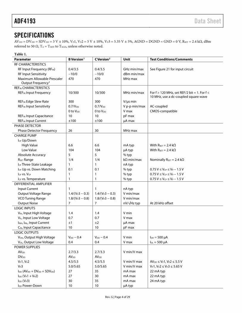
SPECIFICATIONS AVDD = DVDD = SDVDD = 3 V ± 10%, VP1, VP2 = 5 V ± 10%, VP3 = 5.35 V ± 5%, AGND = DGND = GND = 0 V, RSET = 2.4 kΩ, dBm referred to 50 Ω, TA = TMIN to TMAX, unless otherwise noted.
Table 1. Parameter B Version1 C Version2 Unit Test Conditions/Comments RF CHARACTERISTICS
RF Input Frequency (RFIN) 0.4/3.5 0.4/3.5 GHz min/max See Figure 21 for input circuit RF Input Sensitivity −10/0 −10/0 dBm min/max Maximum Allowable Prescaler
Output Frequency3 470 470 MHz max
REFIN CHARACTERISTICS REFIN Input Frequency 10/300 10/300 MHz min/max For f > 120 MHz, set REF/2 bit = 1. For f <
10 MHz, use a dc-coupled square wave REFIN Edge Slew Rate 300 300 V/µs min REFIN Input Sensitivity 0.7/VDD 0.7/VDD V p-p min/max AC-coupled 0 to VDD 0 to VDD V max CMOS-compatible REFIN Input Capacitance 10 10 pF max REFIN Input Current ±100 ±100 µA max
PHASE DETECTOR Phase Detector Frequency 26 30 MHz max
CHARGE PUMP ICP Up/Down
High Value 6.6 6.6 mA typ With RSET = 2.4 kΩ Low Value 104 104 µA typ With RSET = 2.4 kΩ
Absolute Accuracy 5 5 % typ RSET Range 1/4 1/4 kΩ min/max Nominally RSET = 2.4 kΩ ICP Three-State Leakage 1 1 nA typ ICP Up vs. Down Matching 0.1 0.1 % typ 0.75 V ≤ VCP ≤ VP – 1.5 V ICP vs. VCP 1 1 % typ 0.75 V ≤ VCP ≤ VP – 1.5 V ICP vs. Temperature 1 1 % typ 0.75 V ≤ VCP ≤ VP – 1.5 V
DIFFERENTIAL AMPLIFIER Input Current 1 1 nA typ Output Voltage Range 1.4/(VP3 − 0.3) 1.4/(VP3 − 0.3) V min/max VCO Tuning Range 1.8/(VP3 − 0.8) 1.8/(VP3 − 0.8) V min/max Output Noise 7 7 nV/√Hz typ At 20 kHz offset
LOGIC INPUTS VIH, Input High Voltage 1.4 1.4 V min VIL, Input Low Voltage 0.7 0.7 V max IINH, IINL, Input Current ±1 ±2 µA max CIN, Input Capacitance 10 10 pF max
LOGIC OUTPUTS VOH, Output High Voltage VDD − 0.4 VDD − 0.4 V min IOH = 500 µA VOL, Output Low Voltage 0.4 0.4 V max IOL = 500 µA
POWER SUPPLIES AVDD 2.7/3.3 2.7/3.3 V min/V max DVDD AVDD AVDD VP1, VP2 4.5/5.5 4.5/5.5 V min/V max AVDD ≤ VP1, VP2 ≤ 5.5 V VP3 5.0/5.65 5.0/5.65 V min/V max VP1, VP2 ≤ VP3 ≤ 5.65 V IDD (AVDD + DVDD + SDVDD) 27 35 mA max 22 mA typ IDD (VP1 + VP2) 27 30 mA max 22 mA typ IDD (VP3) 30 35 mA max 24 mA typ IDD Power-Down 10 10 µA typ
Rev. G | Page 4 of 29
Data Sheet ADF4193
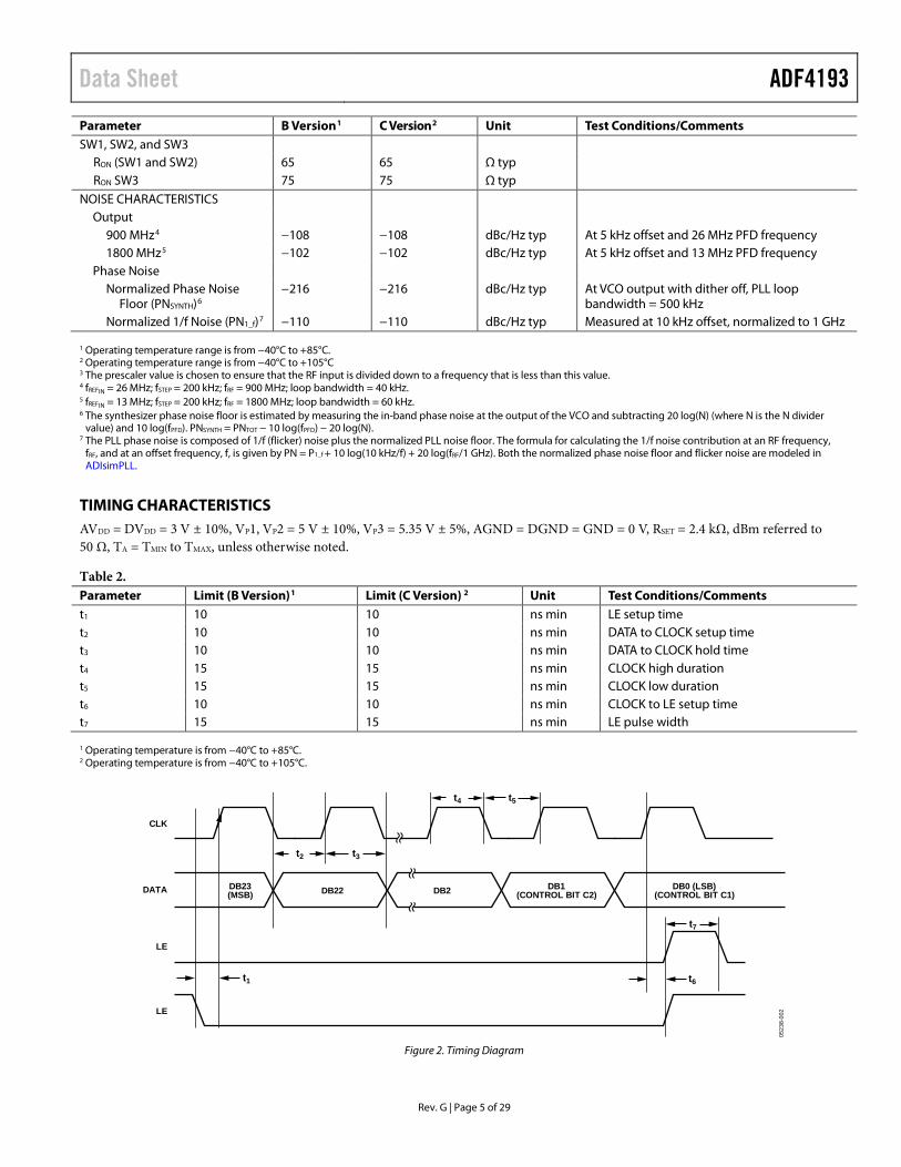
Parameter B Version1 C Version2 Unit Test Conditions/Comments SW1, SW2, and SW3
RON (SW1 and SW2) 65 65 Ω typ RON SW3 75 75 Ω typ
NOISE CHARACTERISTICS Output
900 MHz4 −108 −108 dBc/Hz typ At 5 kHz offset and 26 MHz PFD frequency 1800 MHz5 −102 −102 dBc/Hz typ At 5 kHz offset and 13 MHz PFD frequency
Phase Noise Normalized Phase Noise
Floor (PNSYNTH)6 −216 −216 dBc/Hz typ At VCO output with dither off, PLL loop
bandwidth = 500 kHz Normalized 1/f Noise (PN1_f)7 −110 −110 dBc/Hz typ Measured at 10 kHz offset, normalized to 1 GHz
1 Operating temperature range is from −40°C to +85°C. 2 Operating temperature range is from −40°C to +105°C 3 The prescaler value is chosen to ensure that the RF input is divided down to a frequency that is less than this value. 4 fREFIN = 26 MHz; fSTEP = 200 kHz; fRF = 900 MHz; loop bandwidth = 40 kHz. 5 fREFIN = 13 MHz; fSTEP = 200 kHz; fRF = 1800 MHz; loop bandwidth = 60 kHz. 6 The synthesizer phase noise floor is estimated by measuring the in-band phase noise at the output of the VCO and subtracting 20 log(N) (where N is the N divider
value) and 10 log(fPFD). PNSYNTH = PNTOT − 10 log(fPFD) − 20 log(N). 7 The PLL phase noise is composed of 1/f (flicker) noise plus the normalized PLL noise floor. The formula for calculating the 1/f noise contribution at an RF frequency,
fRF, and at an offset frequency, f, is given by PN = P1_f + 10 log(10 kHz/f) + 20 log(fRF/1 GHz). Both the normalized phase noise floor and flicker noise are modeled in ADIsimPLL.
TIMING CHARACTERISTICS AVDD = DVDD = 3 V ± 10%, VP1, VP2 = 5 V ± 10%, VP3 = 5.35 V ± 5%, AGND = DGND = GND = 0 V, RSET = 2.4 kΩ, dBm referred to 50 Ω, TA = TMIN to TMAX, unless otherwise noted.
Table 2. Parameter Limit (B Version)1 Limit (C Version) 2 Unit Test Conditions/Comments t1 10 10 ns min LE setup time t2 10 10 ns min DATA to CLOCK setup time t3 10 10 ns min DATA to CLOCK hold time t4 15 15 ns min CLOCK high duration t5 15 15 ns min CLOCK low duration t6 10 10 ns min CLOCK to LE setup time t7 15 15 ns min LE pulse width
1 Operating temperature is from −40°C to +85°C. 2 Operating temperature is from −40°C to +105°C.
05
238-
002
CLK
DATA DB23(MSB) DB22 DB2 DB1
(CONTROL BIT C2)DB0 (LSB)
(CONTROL BIT C1)
LE
LE
t2
t4 t5
t3
t7
t6t1
Figure 2. Timing Diagram
Rev. G | Page 5 of 29
ADF4193 Data Sheet
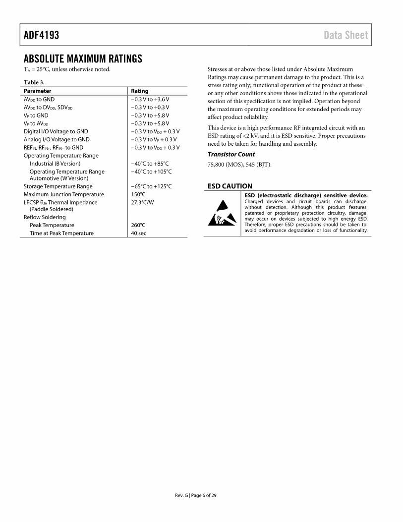
ABSOLUTE MAXIMUM RATINGS TA = 25°C, unless otherwise noted.
Table 3. Parameter Rating AVDD to GND −0.3 V to +3.6 V AVDD to DVDD, SDVDD −0.3 V to +0.3 V VP to GND −0.3 V to +5.8 V VP to AVDD −0.3 V to +5.8 V Digital I/O Voltage to GND −0.3 V to VDD + 0.3 V Analog I/O Voltage to GND −0.3 V to VP + 0.3 V REFIN, RFIN+, RFIN− to GND −0.3 V to VDD + 0.3 V Operating Temperature Range
Industrial (B Version) −40°C to +85°C Operating Temperature Range Automotive (W Version)
−40°C to +105°C
Storage Temperature Range −65°C to +125°C Maximum Junction Temperature 150°C LFCSP θJA Thermal Impedance
(Paddle Soldered) 27.3°C/W
Reflow Soldering Peak Temperature 260°C Time at Peak Temperature 40 sec
Stresses at or above those listed under Absolute Maximum Ratings may cause permanent damage to the product. This is a stress rating only; functional operation of the product at these or any other conditions above those indicated in the operational section of this specification is not implied. Operation beyond the maximum operating conditions for extended periods may affect product reliability.
This device is a high performance RF integrated circuit with an ESD rating of <2 kV, and it is ESD sensitive. Proper precautions need to be taken for handling and assembly.
Transistor Count
75,800 (MOS), 545 (BJT).
ESD CAUTION
Rev. G | Page 6 of 29

Data Sheet ADF4193
Rev. G | Page 7 of 29
PIN CONFIGURATION AND FUNCTION DESCRIPTIONS
0532
8-00
3
CMRAOUTSW3
NOTES:1. THE EXPOSED PAD MUST BE CONNECTED TO AGND.
AGND1RFIN–RFIN+
AVDD1
VP2RSETAGND2DGND3VP1LEDATACLKDVDD1
DG
ND
1D
VD
D2
RE
FIN
DG
ND
2D
VD
D3
SD
GN
DS
DV
DD
MU
XO
UT
VP
3A
IN+
CP
OU
T+
SW
1S
WG
ND
SW
2C
PO
UT
–A
IN–
2423222120191817
12345678
9 10 11 12 13 14 15 16
32 31 30 29 28 27 26 25
ADF4193TOP VIEW
(Not to Scale)
Figure 3. Pin Configuration
Table 4. Pin Function Descriptions Pin No. Mnemonic Description 1 CMR Common-Mode Reference Voltage for the Differential Amplifier’s Output Voltage Swing. Internally biased to
three-fifths of VP3. Requires a 0.1 μF capacitor to ground. 2 AOUT Differential Amplifier Output to Tune the External VCO. 3 SW3 Fast-Lock Switch 3. Closed while SW3 timeout counter is active. 4 AGND1 Analog Ground. This is the ground return pin for the differential amplifier and the RF section. 5 RFIN− Complementary Input to the RF Prescaler. This point must be decoupled to the ground plane with a small bypass
capacitor, typically 100 pF. 6 RFIN+ Input to the RF Prescaler. This small signal input is ac-coupled to the external VCO. 7 AVDD1 Power Supply Pin for the RF Section. Nominally 3 V. A 100 pF decoupling capacitor to the ground plane should be
placed as close as possible to this pin. 8 DVDD1 Power Supply Pin for the N Divider. Should be the same voltage as AVDD1. A 0.1 μF decoupling capacitor to ground
should be placed as close as possible to this pin. 9 DGND1 Ground Return Pin for DVDD1. 10 DVDD2 Power Supply Pin for the REFIN Buffer and R Divider. Nominally 3 V. A 0.1 μF decoupling capacitor to ground
should be placed as close as possible to this pin. 11 REFIN Reference Input. This is a CMOS input with a nominal threshold of VDD/2 and a dc equivalent input resistance of
100 kΩ (see Figure 15). This input can be driven from a TTL or CMOS crystal oscillator or it can be ac-coupled. 12 DGND2 Ground Return Pin for DVDD2 and DVDD3. 13 DVDD3 Power Supply Pin for the Serial Interface Logic. Nominally 3 V. 14 SDGND Ground Return Pin for the Σ-Δ Modulator. 15 SDVDD Power Supply Pin for the Digital Σ-Δ Modulator. Nominally 3 V. A 0.1 μF decoupling capacitor to the ground plane
should be placed as close as possible to this pin. 16 MUXOUT Multiplexer Output. This multiplexer output allows either the lock detect, the scaled RF, or the scaled reference
frequency to be accessed externally (see Figure 35). 17 CLK Serial Clock Input. Data is clocked into the 24-bit shift register on the CLK rising edge. This input is a high
impedance CMOS input. 18 DATA Serial Data Input. The serial data is loaded MSB first with the three LSBs as the control bits. This input is a high
impedance CMOS input. 19 LE Load Enable, CMOS Input. When LE goes high, the data stored in the shift register is loaded into the register that is
selected by the three LSBs. 20 VP1 Power Supply Pin for the Phase Frequency Detector (PFD). Nominally 5 V, should be at the same voltage at VP2.
A 0.1 μF decoupling capacitor to ground should be placed as close as possible to this pin. 21 DGND3 Ground Return Pin for VP1. 22 AGND2 Ground Return Pin for VP2.
ADF4193 Data Sheet
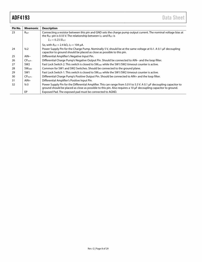
Pin No. Mnemonic Description 23 RSET Connecting a resistor between this pin and GND sets the charge pump output current. The nominal voltage bias at
the RSET pin is 0.55 V. The relationship between ICP and RSET is ICP = 0.25/RSET
So, with RSET = 2.4 kΩ, ICP = 104 µA. 24 VP2 Power Supply Pin for the Charge Pump. Nominally 5 V, should be at the same voltage at VP1. A 0.1 µF decoupling
capacitor to ground should be placed as close as possible to this pin. 25 AIN− Differential Amplifier’s Negative Input Pin. 26 CPOUT− Differential Charge Pump’s Negative Output Pin. Should be connected to AIN− and the loop filter. 27 SW2 Fast Lock Switch 2. This switch is closed to SWGND while the SW1/SW2 timeout counter is active. 28 SWGND Common for SW1 and SW2 Switches. Should be connected to the ground plane. 29 SW1 Fast Lock Switch 1. This switch is closed to SWGND while the SW1/SW2 timeout counter is active. 30 CPOUT+ Differential Charge Pump’s Positive Output Pin. Should be connected to AIN+ and the loop filter. 31 AIN+ Differential Amplifier’s Positive Input Pin. 32 VP3 Power Supply Pin for the Differential Amplifier. This can range from 5.0 V to 5.5 V. A 0.1 µF decoupling capacitor to
ground should be placed as close as possible to this pin. Also requires a 10 µF decoupling capacitor to ground. EP Exposed Pad. The exposed pad must be connected to AGND.
Rev. G | Page 8 of 29
Data Sheet ADF4193
Rev. G | Page 9 of 29
TYPICAL PERFORMANCE CHARACTERISTICS
0532
8-03
8
FREQ. UNIT GHz KEYWORD RPARAM TYPE S IMPEDANCE 50DATA FORMAT MA
FREQ. MAGS11 ANGS110.5 0.8897 –16.66910.6 0.87693 –19.92790.7 0.85834 –23.5610.8 0.85044 –26.95780.9 0.83494 –30.82011.0 0.81718 –34.94991.1 0.80229 –39.04361.2 0.78917 –42.36231.3 0.77598 –46.3221.4 0.75578 –50.34841.5 0.74437 –54.35451.6 0.73821 –57.37851.7 0.7253 –60.6951.8 0.71365 –63.91521.9 0.70699 –66.43652.0 0.7038 –68.44532.1 0.69284 –70.79862.2 0.67717 –73.7038
FREQ. MAGS11 ANGS112.3 0.67107 –75.82062.4 0.66556 –77.68512.5 0.6564 –80.31012.6 0.6333 –82.50822.7 0.61406 –85.56232.8 0.5977 –87.35132.9 0.5655 –89.76053.0 0.5428 –93.02393.1 0.51733 –95.97543.2 0.49909 –99.12913.3 0.47309 –102.2083.4 0.45694 –106.7943.5 0.44698 –111.6593.6 0.43589 –117.9863.7 0.42472 –125.623.8 0.41175 –133.2913.9 0.41055 –140.5854.0 0.40983 –147.97
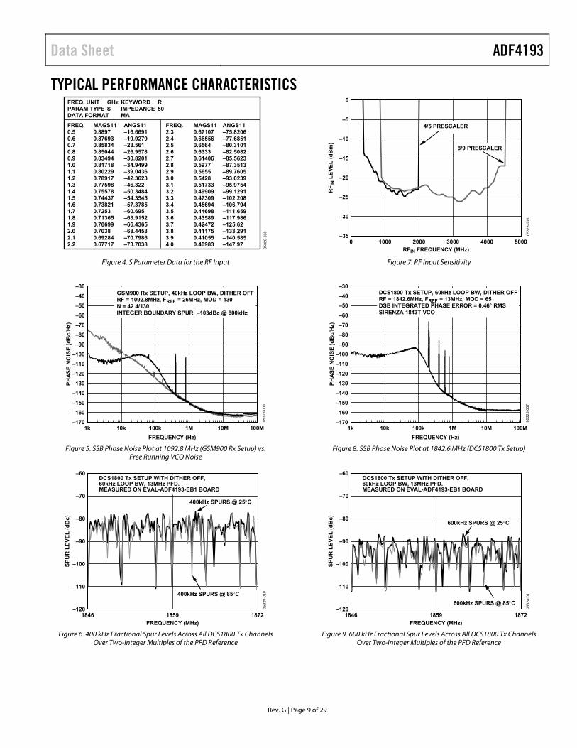
Figure 4. S Parameter Data for the RF Input
0532
8-00
6
FREQUENCY (Hz)
PH
AS
E N
OIS
E (
dB
c/H
z)
1k 10k 100k 1M 10M–170
–160
–150
–140
–130
–120
–110
–100
–90
–80
–70
–60
–50
–40
–30
100M
GSM900 Rx SETUP, 40kHz LOOP BW, DITHER OFFRF = 1092.8MHz, FREF = 26MHz, MOD = 130N = 42 4/130INTEGER BOUNDARY SPUR: –103dBc @ 800kHz
Figure 5. SSB Phase Noise Plot at 1092.8 MHz (GSM900 Rx Setup) vs. Free Running VCO Noise
0532
8-01
0
FREQUENCY (MHz)
SP
UR
LE
VE
L (
dB
c)
1846 1859–120
–110
–100
–90
–80
–70
–60
1872
400kHz SPURS @ 25C
400kHz SPURS @ 85C
DCS1800 Tx SETUP WITH DITHER OFF,60kHz LOOP BW, 13MHz PFD.MEASURED ON EVAL-ADF4193-EB1 BOARD
Figure 6. 400 kHz Fractional Spur Levels Across All DCS1800 Tx Channels Over Two-Integer Multiples of the PFD Reference
0532
8-00
5
RFIN FREQUENCY (MHz)
RF
IN L
EV
EL
(d
Bm
)
0 1000 2000 3000 4000–35
0
–5
–10
–15
–20
–25
–30
5000
4/5 PRESCALER
8/9 PRESCALER
Figure 7. RF Input Sensitivity
0532
8-00
7
FREQUENCY (Hz)
PH
AS
E N
OIS
E (
dB
c/H
z)
1k 10k 100k 1M 10M–170
–160
–150
–140
–130
–120
–110
–100
–90
–80
–70
–60
–50
–40
–30
100M
DCS1800 Tx SETUP, 60kHz LOOP BW, DITHER OFFRF = 1842.6MHz, FREF = 13MHz, MOD = 65DSB INTEGRATED PHASE ERROR = 0.46° RMSSIRENZA 1843T VCO
Figure 8. SSB Phase Noise Plot at 1842.6 MHz (DCS1800 Tx Setup)
0532
8-01
1
FREQUENCY (MHz)
SP
UR
LE
VE
L (
dB
c)
1846 1859–120
–110
–100
–90
–80
–70
–60
1872
600kHz SPURS @ 25C
600kHz SPURS @ 85C
DCS1800 Tx SETUP WITH DITHER OFF,60kHz LOOP BW, 13MHz PFD.MEASURED ON EVAL-ADF4193-EB1 BOARD
Figure 9. 600 kHz Fractional Spur Levels Across All DCS1800 Tx Channels Over Two-Integer Multiples of the PFD Reference
ADF4193 Data Sheet
Rev. G | Page 10 of 29
0532
8-04
0
TIME (s)
(V)
–10
1
2
3
4
5
9876543210
VTUNE
CPOUT+
CPOUT–
DCS1800 Tx SETUP, 60kHz LOOP BW.MEASURED ON EVAL-ADF4193-EB1EVALUATION BOARD.TIMERS: ICP = 28, SW1/SW2, SW3 = 35.FREQUENCY LOCK IN WIDE BW MODE @ 4s.
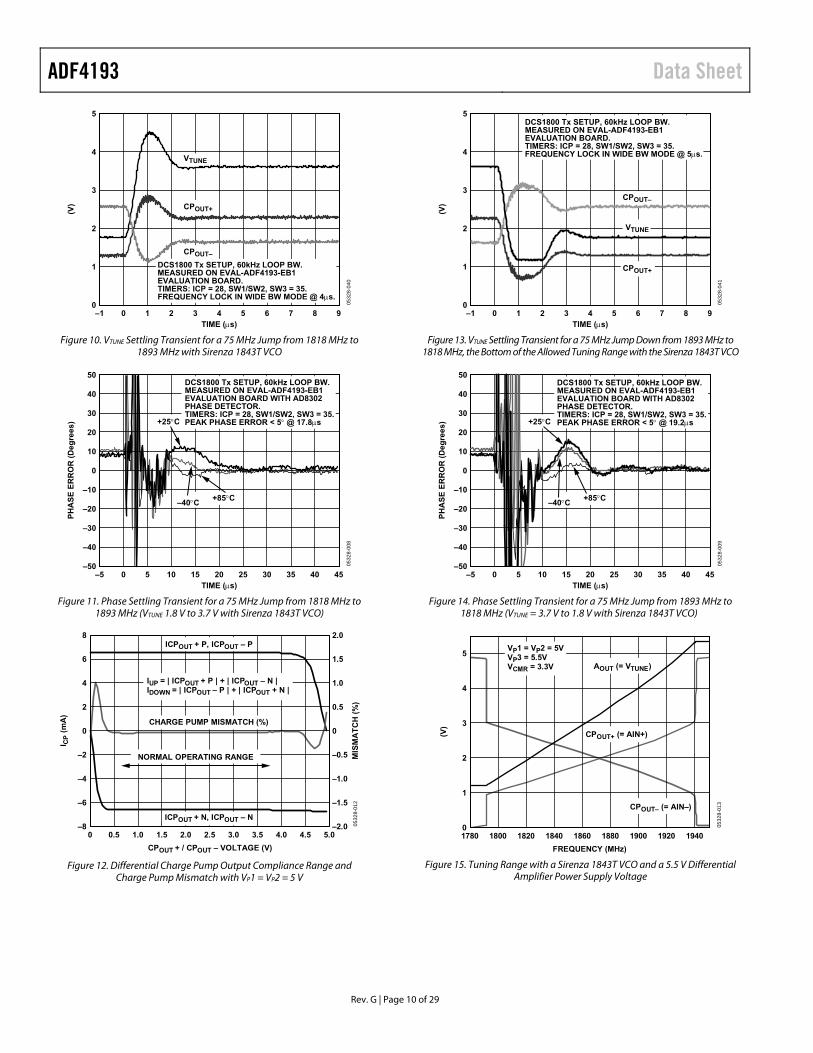
Figure 10. VTUNE Settling Transient for a 75 MHz Jump from 1818 MHz to 1893 MHz with Sirenza 1843T VCO
0532
8-00
8
TIME (s)
PH
AS
E E
RR
OR
(D
eg
ree
s)
–5 0 5 10 15 20 25 30 35 40–50
50
40
30
20
10
0
–10
–20
–30
–40
45
+25C
+85C–40C
DCS1800 Tx SETUP, 60kHz LOOP BW.MEASURED ON EVAL-ADF4193-EB1EVALUATION BOARD WITH AD8302PHASE DETECTOR.TIMERS: ICP = 28, SW1/SW2, SW3 = 35.PEAK PHASE ERROR < 5 @ 17.8s
Figure 11. Phase Settling Transient for a 75 MHz Jump from 1818 MHz to 1893 MHz (VTUNE 1.8 V to 3.7 V with Sirenza 1843T VCO)
0532
8-01
2
CPOUT + / CPOUT – VOLTAGE (V)
I CP
(m
A)
MIS
MA
TC
H (
%)
0 0.5 1.0 1.5 2.0 2.5 3.0 3.5 4.0 4.5–8
–6
–4
–2
0
2
4
6
8
–2.0
–1.5
–1.0
–0.5
0
0.5
1.0
1.5
2.0
5.0
ICPOUT + P, ICPOUT – P
CHARGE PUMP MISMATCH (%)
NORMAL OPERATING RANGE
ICPOUT + N, ICPOUT – N
IUP = | ICPOUT + P | + | ICPOUT – N |IDOWN = | ICPOUT – P | + | ICPOUT + N |
Figure 12. Differential Charge Pump Output Compliance Range and Charge Pump Mismatch with VP1 = VP2 = 5 V
0532
8-04
1
TIME (s)
(V)
–10
1
2
3
4
5
9876543210
VTUNE
CPOUT–
CPOUT+
DCS1800 Tx SETUP, 60kHz LOOP BW.MEASURED ON EVAL-ADF4193-EB1EVALUATION BOARD.TIMERS: ICP = 28, SW1/SW2, SW3 = 35.FREQUENCY LOCK IN WIDE BW MODE @ 5s.
Figure 13. VTUNE Settling Transient for a 75 MHz Jump Down from 1893 MHz to 1818 MHz, the Bottom of the Allowed Tuning Range with the Sirenza 1843T VCO
0532
8-00
9
TIME (s)
PH
AS
E E
RR
OR
(D
eg
ree
s)
–5 0 5 10 15 20 25 30 35 40–50
50
40
30
20
10
0
–10
–20
–30
–40
45
+25C
+85C–40C
DCS1800 Tx SETUP, 60kHz LOOP BW.MEASURED ON EVAL-ADF4193-EB1EVALUATION BOARD WITH AD8302PHASE DETECTOR.TIMERS: ICP = 28, SW1/SW2, SW3 = 35.PEAK PHASE ERROR < 5 @ 19.2s
Figure 14. Phase Settling Transient for a 75 MHz Jump from 1893 MHz to 1818 MHz (VTUNE = 3.7 V to 1.8 V with Sirenza 1843T VCO)
0532
8-01
3
FREQUENCY (MHz)
(V)
1780 1800 1820 1840 1860 1880 1900 1920 19400
2
1
3
4
5VP1 = VP2 = 5VVP3 = 5.5VVCMR = 3.3V
CPOUT– (= AIN–)
AOUT (= VTUNE)
CPOUT+ (= AIN+)
Figure 15. Tuning Range with a Sirenza 1843T VCO and a 5.5 V Differential Amplifier Power Supply Voltage
Data Sheet ADF4193
Rev. G | Page 11 of 29
0532
8-04
2
FREQUENCY (Hz)
NO
ISE
(n
V/
Hz)
1k 10k 100k 1M1
10
100
1000
10M
7nV/ Hz @ 20kHz
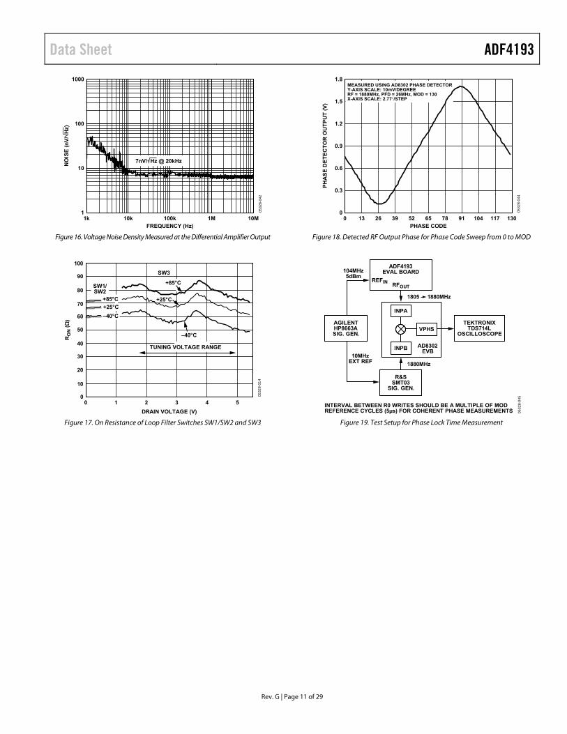
Figure 16. Voltage Noise Density Measured at the Differential Amplifier Output
0532
8-01
4
DRAIN VOLTAGE (V)
RO
N (Ω
)
0 1 2 3 40
100
70
90
80
60
50
40
30
20
10
5
+85°C
SW3
–40°C
+25°C
–40°C
+25°C
+85°CSW1/SW2
TUNING VOLTAGE RANGE
Figure 17. On Resistance of Loop Filter Switches SW1/SW2 and SW3
0532
8-04
4
PHASE CODE
PH
AS
E D
ET
EC
TO
R O
UT
PU
T (
V)
00
1.8
1.5
1.2
0.9
0.6
0.3
13011710491786552392613
MEASURED USING AD8302 PHASE DETECTORY-AXIS SCALE: 10mV/DEGREERF = 1880MHz, PFD = 26MHz, MOD = 130X-AXIS SCALE: 2.77/STEP
Figure 18. Detected RF Output Phase for Phase Code Sweep from 0 to MOD
0532
8-04
5
INTERVAL BETWEEN R0 WRITES SHOULD BE A MULTIPLE OF MODREFERENCE CYCLES (5µs) FOR COHERENT PHASE MEASUREMENTS
AGILENTHP8663ASIG. GEN.
TEKTRONIXTDS714L
OSCILLOSCOPE
ADF4193EVAL BOARD104MHz
5dBm
10MHzEXT REF 1880MHz
1805 1880MHz
RFOUTREFIN
R&SSMT03
SIG. GEN.
INPA
AD8302EVB
VPHS
INPB
Figure 19. Test Setup for Phase Lock Time Measurement
ADF4193 Data Sheet
Rev. G | Page 12 of 29
THEORY OF OPERATION The ADF4193 is targeted at GSM base station requirements, specifically to eliminate the need for ping-pong solutions. It works based on fast lock, using a wide loop bandwidth during a frequency change and narrowing the loop bandwidth once frequency lock is achieved. Widening the loop bandwidth is achieved by increasing the charge pump current. Switches are included to change the loop filter component values to maintain stability with the changing charge pump current. The narrow loop bandwidth ensures that phase noise and spur specifications are met. A differential charge pump and loop filter topology are used to ensure that the fast lock time benefit from widening the loop bandwidth is maintained when the loop is restored to narrow bandwidth mode for normal operation.
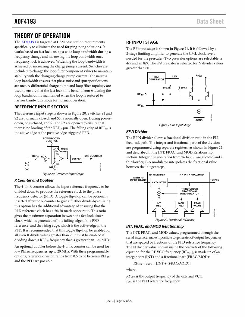
REFERENCE INPUT SECTION The reference input stage is shown in Figure 20. Switches S1 and S2 are normally closed, and S3 is normally open. During power-down, S3 is closed, and S1 and S2 are opened to ensure that there is no loading of the REFIN pin. The falling edge of REFIN is the active edge at the positive edge triggered PFD.
0532
8-01
6
BUFFERTO R COUNTERREFIN
100kNC
S2
S3NO
NC
S1
POWER-DOWNCONTROL
Figure 20. Reference Input Stage
R Counter and Doubler
The 4-bit R counter allows the input reference frequency to be divided down to produce the reference clock to the phase frequency detector (PFD). A toggle flip-flop can be optionally inserted after the R counter to give a further divide-by-2. Using this option has the additional advantage of ensuring that the PFD reference clock has a 50/50 mark-space ratio. This ratio gives the maximum separation between the fast lock timer clock, which is generated off the falling edge of the PFD reference, and the rising edge, which is the active edge in the PFD. It is recommended that this toggle flip-flop be enabled for all even R divide values greater than 2. It must be enabled if dividing down a REFIN frequency that is greater than 120 MHz.
An optional doubler before the 4-bit R counter can be used for low REFIN frequencies, up to 20 MHz. With these programmable options, reference division ratios from 0.5 to 30 between REFIN and the PFD are possible.
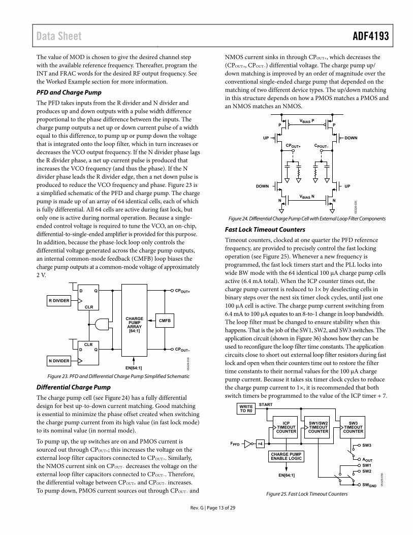
RF INPUT STAGE The RF input stage is shown in Figure 21. It is followed by a 2-stage limiting amplifier to generate the CML clock levels needed for the prescaler. Two prescaler options are selectable: a 4/5 and an 8/9. The 8/9 prescaler is selected for N divider values greater than 80.
0532
8-01
7
BIASGENERATOR
1.6V
AGND
AVDD
500 500
RFIN–
RFIN+
Figure 21. RF Input Stage
RF N Divider
The RF N divider allows a fractional division ratio in the PLL feedback path. The integer and fractional parts of the division are programmed using separate registers, as shown in Figure 22 and described in the INT, FRAC, and MOD Relationship section. Integer division ratios from 26 to 255 are allowed and a third-order, Σ-Δ modulator interpolates the fractional value between the integer steps.
0532
8-01
8
THIRD-ORDERFRACTIONAL
INTERPOLATOR
FRACVALUE
MODREG
INTREG
RF N DIVIDER N = INT + FRAC/MODFROM RF
INPUT STAGE TO PFDN COUNTER
Figure 22. Fractional-N Divider
INT, FRAC, and MOD Relationship
The INT, FRAC, and MOD values, programmed through the serial interface, make it possible to generate RF output frequencies that are spaced by fractions of the PFD reference frequency. The N divider value, shown inside the brackets of the following equation for the RF VCO frequency (RFOUT), is made up of an integer part (INT) and a fractional part (FRAC/MOD):
RFOUT = FPFD × [INT + (FRAC/MOD)]
where:
RFOUT is the output frequency of the external VCO. FPFD is the PFD reference frequency.
Data Sheet ADF4193
Rev. G | Page 13 of 29
The value of MOD is chosen to give the desired channel step with the available reference frequency. Thereafter, program the INT and FRAC words for the desired RF output frequency. See the Worked Example section for more information.
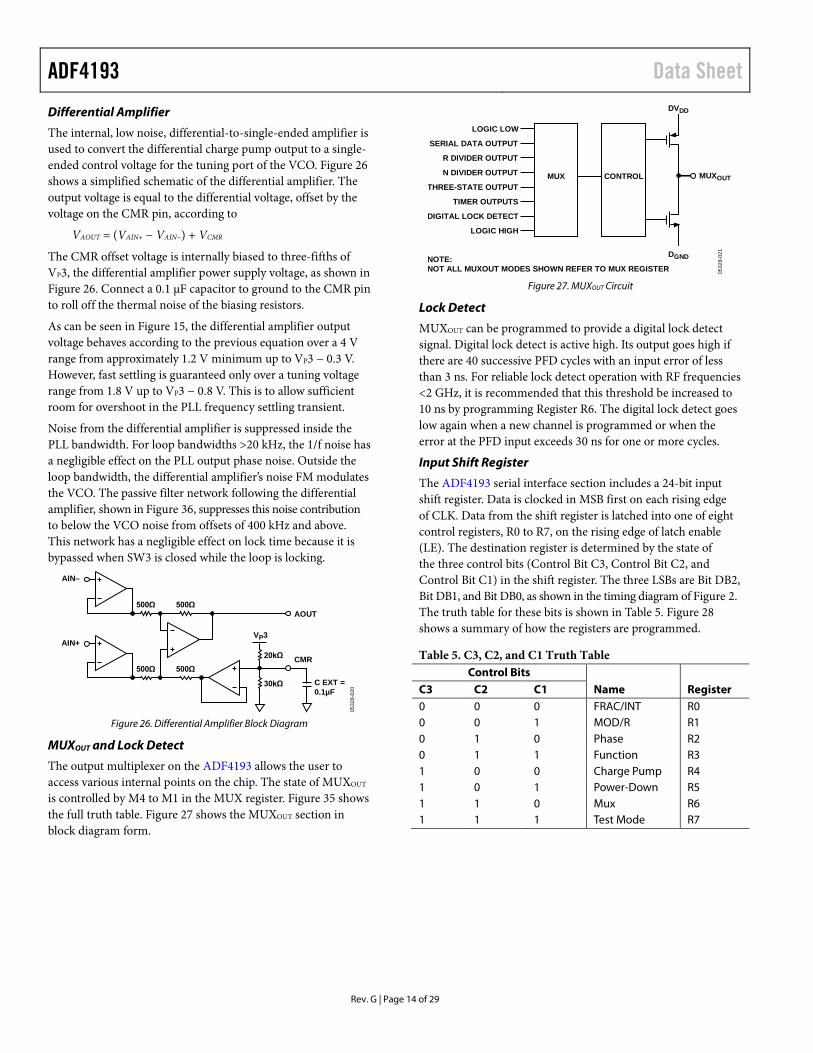
PFD and Charge Pump
The PFD takes inputs from the R divider and N divider and produces up and down outputs with a pulse width difference proportional to the phase difference between the inputs. The charge pump outputs a net up or down current pulse of a width equal to this difference, to pump up or pump down the voltage that is integrated onto the loop filter, which in turn increases or decreases the VCO output frequency. If the N divider phase lags the R divider phase, a net up current pulse is produced that increases the VCO frequency (and thus the phase). If the N divider phase leads the R divider edge, then a net down pulse is produced to reduce the VCO frequency and phase. Figure 23 is a simplified schematic of the PFD and charge pump. The charge pump is made up of an array of 64 identical cells, each of which is fully differential. All 64 cells are active during fast lock, but only one is active during normal operation. Because a single-ended control voltage is required to tune the VCO, an on-chip, differential-to-single-ended amplifier is provided for this purpose. In addition, because the phase-lock loop only controls the differential voltage generated across the charge pump outputs, an internal common-mode feedback (CMFB) loop biases the charge pump outputs at a common-mode voltage of approximately 2 V.
0532
8-01
9
CLRQD
R DIVIDER
N DIVIDER
CHARGEPUMP
ARRAY[64:1]
CMFB
EN[64:1]
CLR
QD CPOUT+
CPOUT–
Figure 23. PFD and Differential Charge Pump Simplified Schematic
Differential Charge Pump
The charge pump cell (see Figure 24) has a fully differential design for best up-to-down current matching. Good matching is essential to minimize the phase offset created when switching the charge pump current from its high value (in fast lock mode) to its nominal value (in normal mode).
To pump up, the up switches are on and PMOS current is sourced out through CPOUT+; this increases the voltage on the external loop filter capacitors connected to CPOUT+. Similarly, the NMOS current sink on CPOUT− decreases the voltage on the external loop filter capacitors connected to CPOUT−. Therefore, the differential voltage between CPOUT+ and CPOUT− increases. To pump down, PMOS current sources out through CPOUT− and
NMOS current sinks in through CPOUT+, which decreases the (CPOUT+, CPOUT−) differential voltage. The charge pump up/ down matching is improved by an order of magnitude over the conventional single-ended charge pump that depended on the matching of two different device types. The up/down matching in this structure depends on how a PMOS matches a PMOS and an NMOS matches an NMOS.
0532
8-03
5
VBIAS PP P
N N
UP DOWN
DOWN UP
VBIAS N
CPOUT+ CPOUT–
Figure 24. Differential Charge Pump Cell with External Loop Filter Components
Fast Lock Timeout Counters
Timeout counters, clocked at one quarter the PFD reference frequency, are provided to precisely control the fast locking operation (see Figure 25). Whenever a new frequency is programmed, the fast lock timers start and the PLL locks into wide BW mode with the 64 identical 100 μA charge pump cells active (6.4 mA total). When the ICP counter times out, the charge pump current is reduced to 1× by deselecting cells in binary steps over the next six timer clock cycles, until just one 100 μA cell is active. The charge pump current switching from 6.4 mA to 100 μA equates to an 8-to-1 change in loop bandwidth. The loop filter must be changed to ensure stability when this happens. That is the job of the SW1, SW2, and SW3 switches. The application circuit (shown in Figure 36) shows how they can be used to reconfigure the loop filter time constants. The application circuits close to short out external loop filter resistors during fast lock and open when their counters time out to restore the filter time constants to their normal values for the 100 μA charge pump current. Because it takes six timer clock cycles to reduce the charge pump current to 1×, it is recommended that both switch timers be programmed to the value of the ICP timer + 7.
0532
8-03
6
SW1/SW2TIMEOUTCOUNTER
SW3TIMEOUTCOUNTER
ICPTIMEOUTCOUNTER
EN[64:1]
÷4
START
FPFD SW3
AOUT
SW2
SWGND
SW1
WRITETO R0
CHARGE PUMPENABLE LOGIC
Figure 25. Fast Lock Timeout Counters
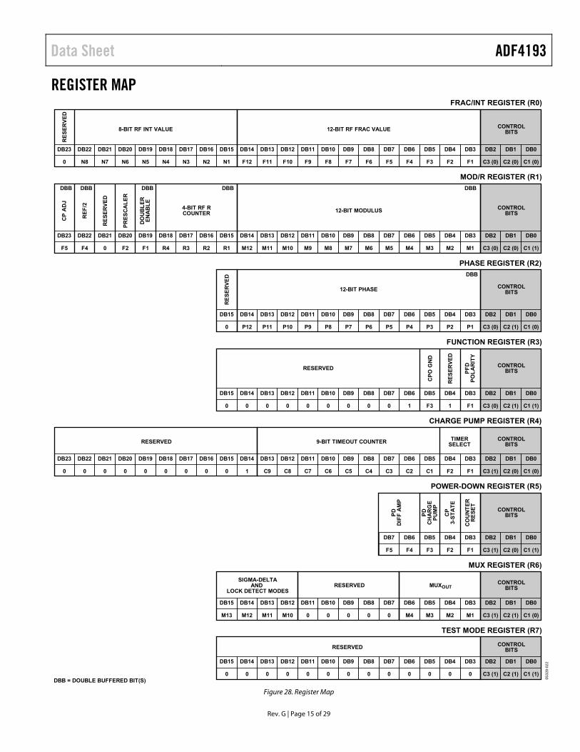
ADF4193 Data Sheet Differential Amplifier
The internal, low noise, differential-to-single-ended amplifier is used to convert the differential charge pump output to a single-ended control voltage for the tuning port of the VCO. Figure 26 shows a simplified schematic of the differential amplifier. The output voltage is equal to the differential voltage, offset by the voltage on the CMR pin, according to
VAOUT = (VAIN+ − VAIN−) + VCMR
The CMR offset voltage is internally biased to three-fifths of VP3, the differential amplifier power supply voltage, as shown in Figure 26. Connect a 0.1 µF capacitor to ground to the CMR pin to roll off the thermal noise of the biasing resistors.
As can be seen in Figure 15, the differential amplifier output voltage behaves according to the previous equation over a 4 V range from approximately 1.2 V minimum up to VP3 − 0.3 V. However, fast settling is guaranteed only over a tuning voltage range from 1.8 V up to VP3 − 0.8 V. This is to allow sufficient room for overshoot in the PLL frequency settling transient.
Noise from the differential amplifier is suppressed inside the PLL bandwidth. For loop bandwidths >20 kHz, the 1/f noise has a negligible effect on the PLL output phase noise. Outside the loop bandwidth, the differential amplifier’s noise FM modulates the VCO. The passive filter network following the differential amplifier, shown in Figure 36, suppresses this noise contribution to below the VCO noise from offsets of 400 kHz and above. This network has a negligible effect on lock time because it is bypassed when SW3 is closed while the loop is locking.
0532
8-02
0
AIN–
AOUT
AIN+
CMR
VP3
C EXT =0.1µF
20kΩ
30kΩ
500Ω 500Ω
500Ω 500Ω
Figure 26. Differential Amplifier Block Diagram
MUXOUT and Lock Detect
The output multiplexer on the ADF4193 allows the user to access various internal points on the chip. The state of MUXOUT is controlled by M4 to M1 in the MUX register. Figure 35 shows the full truth table. Figure 27 shows the MUXOUT section in block diagram form.
0532
8-02
1
R DIVIDER OUTPUT
N DIVIDER OUTPUT
SERIAL DATA OUTPUT
DGND
DVDD
CONTROLMUX MUXOUT
LOGIC LOW
THREE-STATE OUTPUT
TIMER OUTPUTS
DIGITAL LOCK DETECT
LOGIC HIGH
NOTE:NOT ALL MUXOUT MODES SHOWN REFER TO MUX REGISTER
Figure 27. MUXOUT Circuit
Lock Detect
MUXOUT can be programmed to provide a digital lock detect signal. Digital lock detect is active high. Its output goes high if there are 40 successive PFD cycles with an input error of less than 3 ns. For reliable lock detect operation with RF frequencies <2 GHz, it is recommended that this threshold be increased to 10 ns by programming Register R6. The digital lock detect goes low again when a new channel is programmed or when the error at the PFD input exceeds 30 ns for one or more cycles.
Input Shift Register
The ADF4193 serial interface section includes a 24-bit input shift register. Data is clocked in MSB first on each rising edge of CLK. Data from the shift register is latched into one of eight control registers, R0 to R7, on the rising edge of latch enable (LE). The destination register is determined by the state of the three control bits (Control Bit C3, Control Bit C2, and Control Bit C1) in the shift register. The three LSBs are Bit DB2, Bit DB1, and Bit DB0, as shown in the timing diagram of Figure 2. The truth table for these bits is shown in Table 5. Figure 28 shows a summary of how the registers are programmed.
Table 5. C3, C2, and C1 Truth Table Control Bits
C3 C2 C1 Name Register 0 0 0 FRAC/INT R0 0 0 1 MOD/R R1 0 1 0 Phase R2 0 1 1 Function R3 1 0 0 Charge Pump R4 1 0 1 Power-Down R5 1 1 0 Mux R6 1 1 1 Test Mode R7
Rev. G | Page 14 of 29
Data Sheet ADF4193
Rev. G | Page 15 of 29
REGISTER MAP
0532
8-02
2
DB23
F5
DB22
F4
DB21
0
DB20
F2
DB19
F1
DB18
R4
DB17
R3
DB16
R2
DB15
R1
DB14
M12
DB13
M11
DB12
M10
DB11
M9
DB10
M8
DB9
M7
DB8
M6
DB7
M5
DB6
M4
DB5
M3
DB4
M2
DB3
M1
DB2
C3 (0)
DB1
C2 (0)
DB0
C1 (1)
DBB DBB DBB DBB DBB
4-BIT RF RCOUNTER
CP
AD
J
RE
F/2
RE
SE
RV
ED
PR
ES
CA
LE
R
DO
UB
LE
RE
NA
BL
E
12-BIT MODULUS CONTROLBITS
MOD/R REGISTER (R1)
DB15
0
DB14
P12
DB13
P11
DB12
P10
DB11
P9
DB10
P8
DB9
P7
DB8
P6
DB7
P5
DB6
P4
DB5
P3
DB4
P2
DB3
P1
DB2
C3 (0)
DB1
C2 (1)
DB0
C1 (0)
DBB
RE
SE
RV
ED
12-BIT PHASE CONTROLBITS
PHASE REGISTER (R2)
DB15
0
DB14
0
DB13
0
DB12
0
DB11
0
DB10
0
DB9
0
DB8
0
DB7
0
DB6
1
DB5
F3
DB4
1
DB3
F1
DB2
C3 (0)
DB1
C2 (1)
DB0
C1 (1)
PF
DP
OL
AR
ITY
RE
SE
RV
ED
CP
O G
ND
RESERVED CONTROLBITS
FUNCTION REGISTER (R3)
DB15
M13
DB14
M12
DB13
M11
DB12
M10
DB11
0
DB10
0
DB9
0
DB8
0
DB7
0
DB6
M4
DB5
M3
DB4
M2
DB3
M1
DB2
C3 (1)
DB1
C2 (1)
DB0
C1 (0)
RESERVED MUXOUTCONTROL
BITS
SIGMA-DELTAAND
LOCK DETECT MODES
MUX REGISTER (R6)
DB15
0
DB14
0
DB13
0
DB12
0
DB11
0
DB10
0
DB9
0
DB8
0
DB7
0
DB6
0
DB5
0
DB4
0
DB3
0
DB2
C3 (1)
DB1
C2 (1)
DB0
C1 (1)
RESERVED CONTROLBITS
TEST MODE REGISTER (R7)
DB7
F5
DB6
F4
DB5
F3
DB4
F2
DB3
F1
DB2
C3 (1)
DB1
C2 (0)
DB0
C1 (1)
CO
UN
TE
RR
ES
ET
CP
3-S
TA
TE
PD
CH
AR
GE
PU
MP
PD
DIF
F A
MP
CONTROLBITS
POWER-DOWN REGISTER (R5)
DB23
0
DB22
0
DB21
0
DB20
0
DB19
0
DB18
0
DB17
0
DB16
0
DB15
0
DB14
1
DB13
C9
DB12
C8
DB11
C7
DB10
C6
DB9
C5
DB8
C4
DB7
C3
DB6
C2
DB5
C1
DB4
F2
DB3
F1
DB2
C3 (1)
DB1
C2 (0)
DB0
C1 (0)
9-BIT TIMEOUT COUNTERRESERVED CONTROLBITS
TIMERSELECT
CHARGE PUMP REGISTER (R4)
DBB = DOUBLE BUFFERED BIT(S)
DB23
0
DB22
N8
DB21
N7
DB20
N6
DB19
N5
DB18
N4
DB17
N3
DB16
N2
DB15
N1
DB14
F12
DB13
F11
DB12
F10
DB11
F9
DB10
F8
DB9
F7
DB8
F6
DB7
F5
DB6
F4
DB5
F3
DB4
F2
DB3
F1
DB2
C3 (0)
DB1
C2 (0)
DB0
C1 (0)
8-BIT RF INT VALUE 12-BIT RF FRAC VALUE CONTROLBITS
FRAC/INT REGISTER (R0)
RE
SE
RV
ED
Figure 28. Register Map
ADF4193 Data Sheet
FRAC/INT REGISTER (R0)
0532
8-02
3
DB23
RES
ERVE
D
0
DB22
N8
DB21
N7
DB20
N6
DB19
N5
DB18
N4
DB17
N3
DB16
N2
DB15
N1
DB14
F12
DB13
F11
DB12
F10
DB11
F9
DB10
F8
DB9
F7
DB8
F6
DB7
F5
DB6
F4
DB5
F3
DB4
F2
DB3
F1
DB2
C3 (0)
DB1
C2 (0)
DB0
C1 (0)
8-BIT RF INT VALUE 12-BIT RF FRAC VALUE CONTROLBITS
F120000...1111
F110000...1111
F100000...1111
..........
..........
..........
..........
..........
..........
..........
..........
..........
..........
..........
F30000...1111
F20011...0011
F10101...0101
FRACTIONAL VALUE (FRAC)0123...4092409340944095
N80...1
N70...1
N60...1
N51...1
N41...1
N30...1
N21...1
N10...1
INTEGER VALUE (INT)26...255
0 = < FRAC < MOD
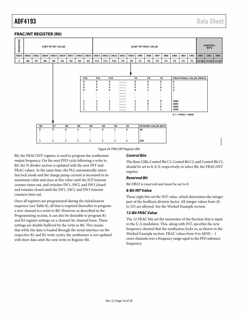
Figure 29. FRAC/INT Register (R0)
R0, the FRAC/INT register, is used to program the synthesizer output frequency. On the next PFD cycle following a write to R0, the N divider section is updated with the new INT and FRAC values. At the same time, the PLL automatically enters fast lock mode and the charge pump current is increased to its maximum value and stays at this value until the ICP timeout counter times out, and switches SW1, SW2, and SW3 closed and remains closed until the SW1, SW2, and SW3 timeout counters time out.
Once all registers are programmed during the initialization sequence (see Table 8), all that is required thereafter to program a new channel is a write to R0. However, as described in the Programming section, it can also be desirable to program R1 and R2 register settings on a channel-by-channel basis. These settings are double buffered by the write to R0. This means that while the data is loaded through the serial interface on the respective R1 and R2 write cycles, the synthesizer is not updated with their data until the next write to Register R0.
Control Bits
The three LSBs, Control Bit C3, Control Bit C2, and Control Bit C1, should be set to 0, 0, 0, respectively, to select R0, the FRAC/INT register.
Reserved Bit
Bit DB23 is reserved and must be set to 0.
8-Bit INT Value
These eight bits set the INT value, which determines the integer part of the feedback division factor. All integer values from 26 to 255 are allowed. See the Worked Example section.
12-Bit FRAC Value
The 12 FRAC bits set the numerator of the fraction that is input to the Σ-Δ modulator. This, along with INT, specifies the new frequency channel that the synthesizer locks to, as shown in the Worked Example section. FRAC values from 0 to MOD − 1 cover channels over a frequency range equal to the PFD reference frequency.
Rev. G | Page 16 of 29

Data Sheet ADF4193
Rev. G | Page 17 of 29
MOD/R REGISTER (R1)
0532
8-02
4
DB23
F5
DB22
F4
DB21
0
DB20
F2
DB19
F1
DB18
R4
DB17
R3
DB16
R2
DB15
R1
DB14
M12
DB13
M11
DB12
M10
DB11
M9
DB10
M8
DB9
M7
DB8
M6
DB7
M5
DB6
M4
DB5
M3
DB4
M2
DB3
M1
DB2
C3 (0)
DB1
C2 (0)
DB0
C1 (1)
4-BIT RFR COUNTERC
PA
DJ
RE
F/2
RE
SE
RV
ED
PR
ES
CA
LE
R
DO
UB
LE
RE
NA
BL
E
12-BIT MODULUS CONTROLBITS
01
NOMINALADJUSTED
CP ADJF5
01
DISABLEENABLE
REF/2F4
01
F2
4/58/9
PRESCALER
01
F1
DOUBLER DISABLEDDOUBLER ENABLED
DOUBLER ENABLE M12
000...1111
M11
000...1111
M10
000...1111
..........
..........
..........
..........
..........
..........
..........
..........
..........
..........
M3
111...1111
M2
011...0011
M1
101...0101
INTERPOLATOR MODULUS VALUE (MOD)
131415...4092409340944095
R4
0000...1111
R3
0001...1111
R2
0110...0011
R1
1010...0101
RF R COUNTER DIVIDE RATIO
1234...12131415
Figure 30. MOD/R Register (R1)
This register is used to set the PFD reference frequency and the channel step size, which is determined by the PFD frequency divided by the fractional modulus. Note that the MOD, R counter, REF/2, CP ADJ, and doubler enable bits are double buffered. They do not take effect until the next write to R0 (FRAC/INT register) is complete.
Control Bits
With C3, C2, and C1 set to 0, 0, 1, respectively, the MOD/R register (R1) is programmed.
CP ADJ
When this bit is set to 1, the charge pump current is scaled up 25% from its nominal value on the next write to R0. When this bit is set to 0, the charge pump current stays at its nominal value on the next write to R0. See the Programming section for more information on how this feature can be used.
REF/2
Setting this bit to 1 inserts a divide-by-2, toggle flip-flop between the R counter and PFD, which extends the maximum REFIN input rate.
Reserved Bit
Reserved Bit DB21 must be set to 0.
Doubler Enable
Setting this bit to 1 inserts a frequency doubler between REFIN and the 4-bit R counter. Setting this bit to 0 bypasses the doubler.
4-Bit RF R Counter
It allows the REFIN frequency to be divided down to produce the reference clock to the PFD. All integer values from 1 to 15 are allowed. See the Worked Example section.
12-Bit Interpolator Modulus
For a given PFD reference frequency, the fractional deno-minator or modulus sets the channel step resolution at the RF output. All integer values from 13 to 4095 are allowed. See the Programming section for additional information and guidelines for selecting the value of MOD.
ADF4193 Data Sheet
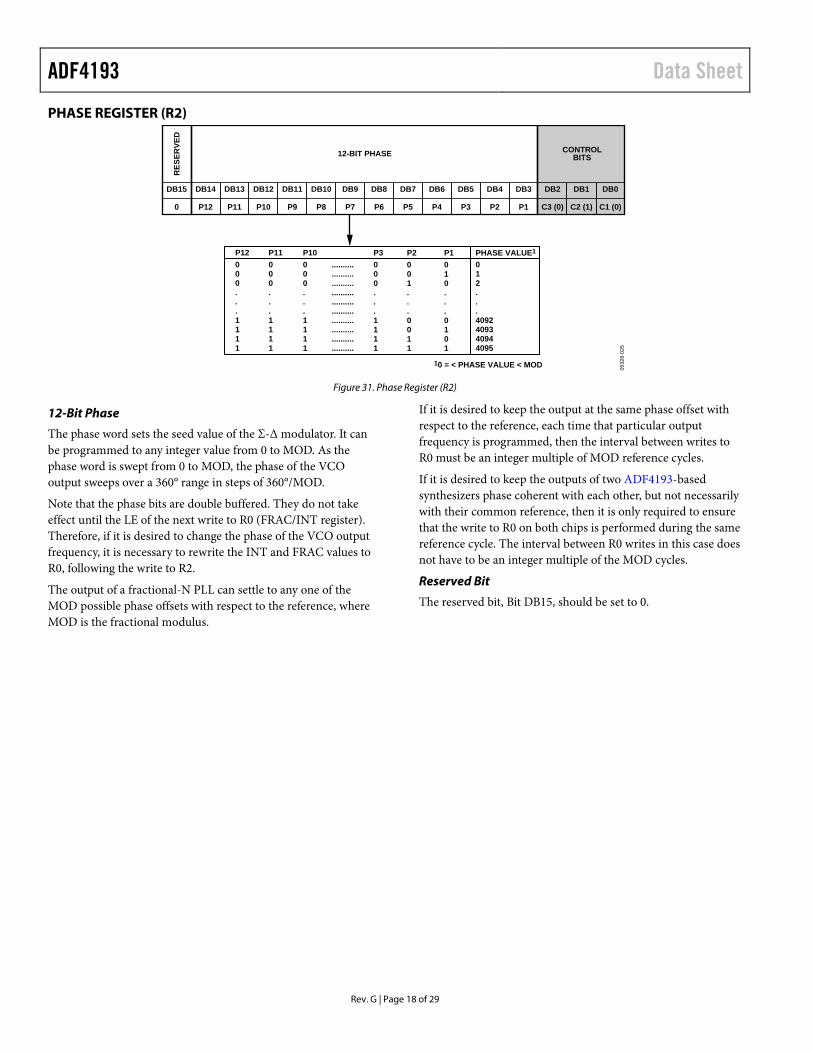
PHASE REGISTER (R2)
0532
8-02
5
DB15
0
DB14
P12
DB13
P11
DB12
P10
DB11
P9
DB10
P8
DB9
P7
DB8
P6
DB7
P5
DB6
P4
DB5
P3
DB4
P2
DB3
P1
DB2
C3 (0)
DB1
C2 (1)
DB0
C1 (0)
RES
ERVE
D
12-BIT PHASE CONTROLBITS
P12000...1111
P11000...1111
P10000...1111
..........
..........
..........
..........
..........
..........
..........
..........
..........
..........
P3000...1111
P2001...0011
P1010...0101
PHASE VALUE1
012...4092409340944095
10 = < PHASE VALUE < MOD
Figure 31. Phase Register (R2)
12-Bit Phase
The phase word sets the seed value of the Σ-Δ modulator. It can be programmed to any integer value from 0 to MOD. As the phase word is swept from 0 to MOD, the phase of the VCO output sweeps over a 360° range in steps of 360°/MOD.
Note that the phase bits are double buffered. They do not take effect until the LE of the next write to R0 (FRAC/INT register). Therefore, if it is desired to change the phase of the VCO output frequency, it is necessary to rewrite the INT and FRAC values to R0, following the write to R2.
The output of a fractional-N PLL can settle to any one of the MOD possible phase offsets with respect to the reference, where MOD is the fractional modulus.
If it is desired to keep the output at the same phase offset with respect to the reference, each time that particular output frequency is programmed, then the interval between writes to R0 must be an integer multiple of MOD reference cycles.
If it is desired to keep the outputs of two ADF4193-based synthesizers phase coherent with each other, but not necessarily with their common reference, then it is only required to ensure that the write to R0 on both chips is performed during the same reference cycle. The interval between R0 writes in this case does not have to be an integer multiple of the MOD cycles.
Reserved Bit
The reserved bit, Bit DB15, should be set to 0.
Rev. G | Page 18 of 29
Data Sheet ADF4193
Rev. G | Page 19 of 29
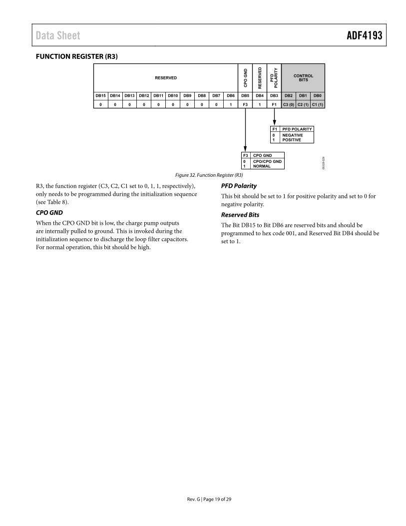
FUNCTION REGISTER (R3)
0532
8-02
6
DB15
0
DB14
0
DB13
0
DB12
0
DB11
0
DB10
0
DB9
0
DB8
0
DB7
0
DB6
1
DB5
F3
DB4
1
DB3
F1
DB2
C3 (0)
DB1
C2 (1)
DB0
C1 (1)
PF
DP
OL
AR
ITY
RE
SE
RV
ED
CP
O G
ND
RESERVED CONTROLBITS
01
F1
NEGATIVEPOSITIVE
PFD POLARITY
01
F3
CPO/CPO GNDNORMAL
CPO GND
Figure 32. Function Register (R3)
R3, the function register (C3, C2, C1 set to 0, 1, 1, respectively), only needs to be programmed during the initialization sequence (see Table 8).
CPO GND
When the CPO GND bit is low, the charge pump outputs are internally pulled to ground. This is invoked during the initialization sequence to discharge the loop filter capacitors. For normal operation, this bit should be high.
PFD Polarity
This bit should be set to 1 for positive polarity and set to 0 for negative polarity.
Reserved Bits
The Bit DB15 to Bit DB6 are reserved bits and should be programmed to hex code 001, and Reserved Bit DB4 should be set to 1.
ADF4193 Data Sheet
Rev. G | Page 20 of 29
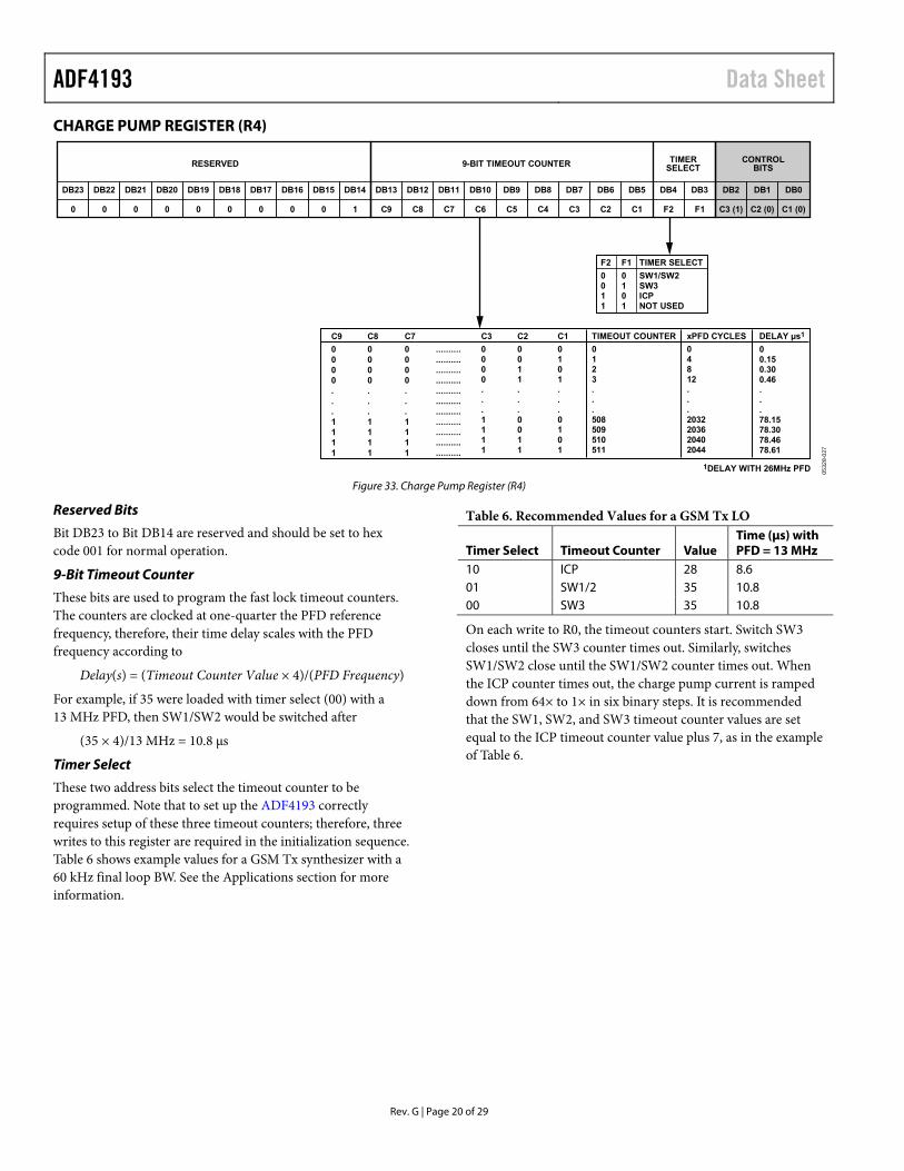
CHARGE PUMP REGISTER (R4)
0532
8-02
7
DB23
0
DB22
0
DB21
0
DB20
0
DB19
0
DB18
0
DB17
0
DB16
0
DB15
0
DB14
1
DB13
C9
DB12
C8
DB11
C7
DB10
C6
DB9
C5
DB8
C4
DB7
C3
DB6
C2
DB5
C1
DB4
F2
DB3
F1
DB2
C3 (1)
DB1
C2 (0)
DB0
C1 (0)
9-BIT TIMEOUT COUNTERRESERVED CONTROLBITS
TIMERSELECT
0011
F2
0101
F1
SW1/SW2SW3ICPNOT USED
TIMER SELECT
C9
0000...1111
C8
0000...1111
C7
0000...1111
..........
..........
..........
..........
..........
..........
..........
..........
..........
..........
..........
C3
0000...1111
C2
0011...0011
C1
0101...0101
TIMEOUT COUNTER
0123...508509510511
xPFD CYCLES
04812...2032203620402044
DELAY µs1
00.150.300.46...78.1578.3078.4678.61
1DELAY WITH 26MHz PFD Figure 33. Charge Pump Register (R4)
Reserved Bits
Bit DB23 to Bit DB14 are reserved and should be set to hex code 001 for normal operation.
9-Bit Timeout Counter
These bits are used to program the fast lock timeout counters. The counters are clocked at one-quarter the PFD reference frequency, therefore, their time delay scales with the PFD frequency according to
Delay(s) = (Timeout Counter Value × 4)/(PFD Frequency)
For example, if 35 were loaded with timer select (00) with a 13 MHz PFD, then SW1/SW2 would be switched after
(35 × 4)/13 MHz = 10.8 μs
Timer Select
These two address bits select the timeout counter to be programmed. Note that to set up the ADF4193 correctly requires setup of these three timeout counters; therefore, three writes to this register are required in the initialization sequence. Table 6 shows example values for a GSM Tx synthesizer with a 60 kHz final loop BW. See the Applications section for more information.
Table 6. Recommended Values for a GSM Tx LO
Timer Select Timeout Counter Value Time (μs) with PFD = 13 MHz
10 ICP 28 8.6 01 SW1/2 35 10.8 00 SW3 35 10.8
On each write to R0, the timeout counters start. Switch SW3 closes until the SW3 counter times out. Similarly, switches SW1/SW2 close until the SW1/SW2 counter times out. When the ICP counter times out, the charge pump current is ramped down from 64× to 1× in six binary steps. It is recommended that the SW1, SW2, and SW3 timeout counter values are set equal to the ICP timeout counter value plus 7, as in the example of Table 6.
Data Sheet ADF4193
Rev. G | Page 21 of 29
POWER-DOWN REGISTER (R5)
0532
8-02
8
DB7
F5
DB6
F4
DB5
F3
DB4
F2
DB3
F1
DB2
C3 (1)
DB1
C2 (0)
DB0
C1 (1)
CO
UN
TE
RR
ES
ET
CP
3-S
TA
TE
PD
CH
AR
GE
PU
MP
CONTROLBITS
PDDIFF AMP
01
F4
01
F5
DISABLEDENABLED
DIFF AMPPOWER-DOWN
01
F2
NORMAL OPERATION3-STATE ENABLED
CHARGE PUMP3-STATE
01
F1
NORMAL OPERATIONCOUNTER RESET
COUNTER RESET
01
F3
DISABLEDENABLED
CHARGE PUMPPOWER-DOWN
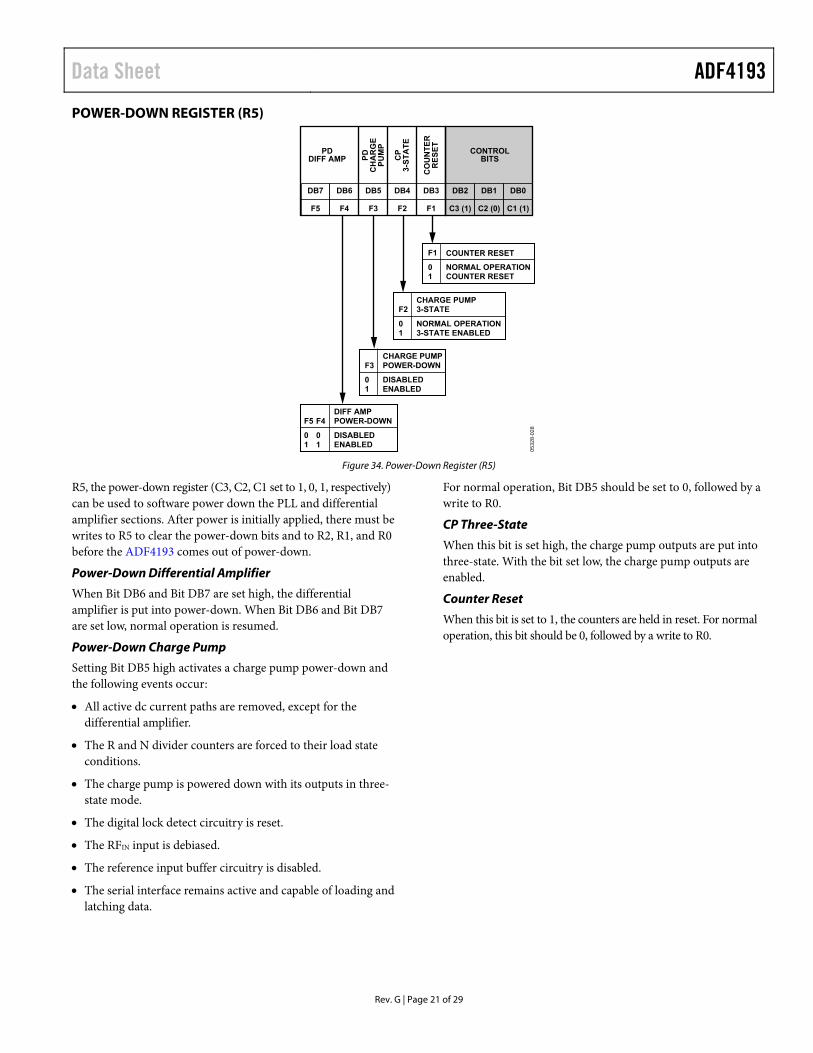
Figure 34. Power-Down Register (R5)
R5, the power-down register (C3, C2, C1 set to 1, 0, 1, respectively) can be used to software power down the PLL and differential amplifier sections. After power is initially applied, there must be writes to R5 to clear the power-down bits and to R2, R1, and R0 before the ADF4193 comes out of power-down.
Power-Down Differential Amplifier
When Bit DB6 and Bit DB7 are set high, the differential amplifier is put into power-down. When Bit DB6 and Bit DB7 are set low, normal operation is resumed.
Power-Down Charge Pump
Setting Bit DB5 high activates a charge pump power-down and the following events occur:
All active dc current paths are removed, except for the differential amplifier.
The R and N divider counters are forced to their load state conditions.
The charge pump is powered down with its outputs in three-state mode.
The digital lock detect circuitry is reset.
The RFIN input is debiased.
The reference input buffer circuitry is disabled.
The serial interface remains active and capable of loading and latching data.
For normal operation, Bit DB5 should be set to 0, followed by a write to R0.
CP Three-State
When this bit is set high, the charge pump outputs are put into three-state. With the bit set low, the charge pump outputs are enabled.
Counter Reset
When this bit is set to 1, the counters are held in reset. For normal operation, this bit should be 0, followed by a write to R0.
ADF4193 Data Sheet
Rev. G | Page 22 of 29
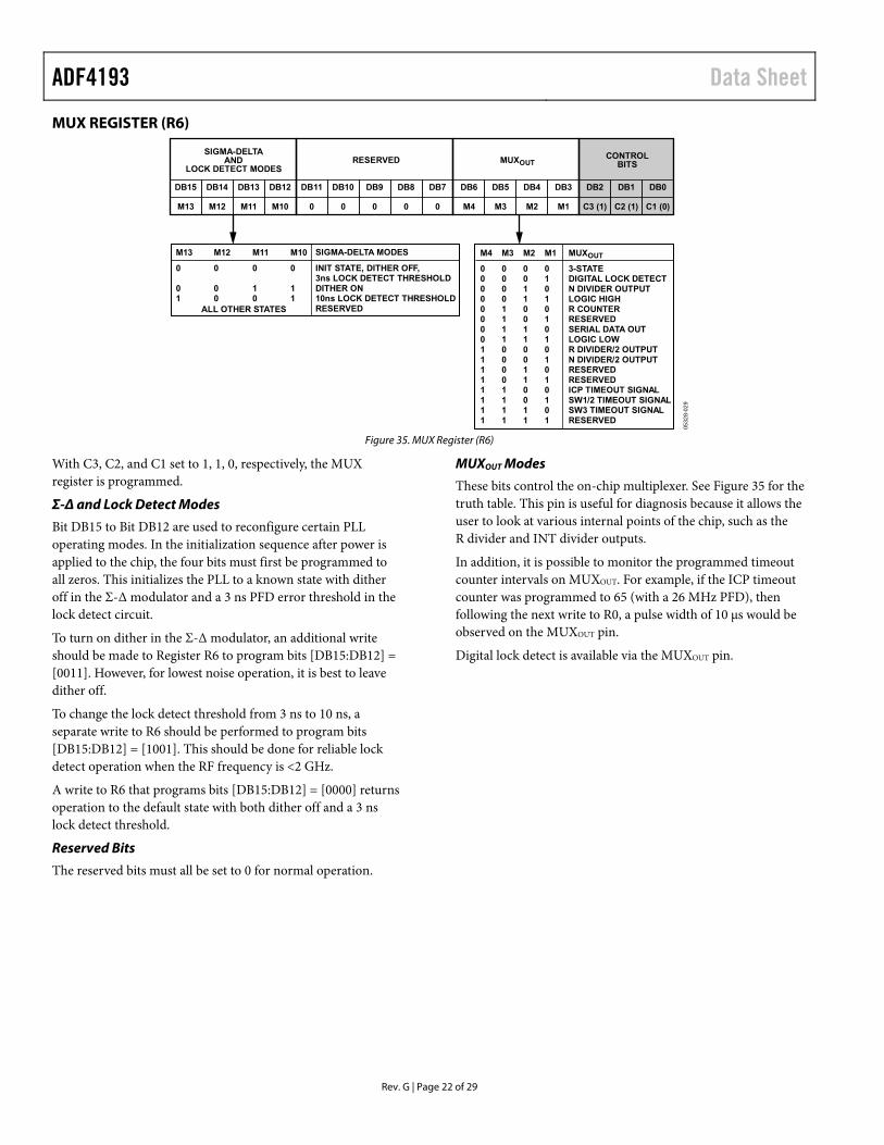
MUX REGISTER (R6)
0532
8-02
9
DB15
M13
DB14
M12
DB13
M11
DB12
M10
DB11
0
DB10
0
DB9
0
DB8
0
DB7
0
DB6
M4
DB5
M3
DB4
M2
DB3
M1
DB2
C3 (1)
DB1
C2 (1)
DB0
C1 (0)
RESERVED MUXOUTCONTROL
BITS
SIGMA-DELTAAND
LOCK DETECT MODES
0
11
M10
0
10
M11
0
00
ALL OTHER STATES
M12
0
01
M13
INIT STATE, DITHER OFF,3ns LOCK DETECT THRESHOLDDITHER ON10ns LOCK DETECT THRESHOLDRESERVED
SIGMA-DELTA MODES
0000000011111111
M4
0000111100001111
M3
0011001100110011
M2
0101010101010101
M1
3-STATEDIGITAL LOCK DETECTN DIVIDER OUTPUTLOGIC HIGHR COUNTERRESERVEDSERIAL DATA OUTLOGIC LOWR DIVIDER/2 OUTPUTN DIVIDER/2 OUTPUTRESERVEDRESERVEDICP TIMEOUT SIGNALSW1/2 TIMEOUT SIGNALSW3 TIMEOUT SIGNALRESERVED
MUXOUT
Figure 35. MUX Register (R6)
With C3, C2, and C1 set to 1, 1, 0, respectively, the MUX register is programmed.
Σ-Δ and Lock Detect Modes
Bit DB15 to Bit DB12 are used to reconfigure certain PLL operating modes. In the initialization sequence after power is applied to the chip, the four bits must first be programmed to all zeros. This initializes the PLL to a known state with dither off in the Σ-Δ modulator and a 3 ns PFD error threshold in the lock detect circuit.
To turn on dither in the Σ-Δ modulator, an additional write should be made to Register R6 to program bits [DB15:DB12] = [0011]. However, for lowest noise operation, it is best to leave dither off.
To change the lock detect threshold from 3 ns to 10 ns, a separate write to R6 should be performed to program bits [DB15:DB12] = [1001]. This should be done for reliable lock detect operation when the RF frequency is <2 GHz.
A write to R6 that programs bits [DB15:DB12] = [0000] returns operation to the default state with both dither off and a 3 ns lock detect threshold.
Reserved Bits
The reserved bits must all be set to 0 for normal operation.
MUXOUT Modes
These bits control the on-chip multiplexer. See Figure 35 for the truth table. This pin is useful for diagnosis because it allows the user to look at various internal points of the chip, such as the R divider and INT divider outputs.
In addition, it is possible to monitor the programmed timeout counter intervals on MUXOUT. For example, if the ICP timeout counter was programmed to 65 (with a 26 MHz PFD), then following the next write to R0, a pulse width of 10 μs would be observed on the MUXOUT pin.
Digital lock detect is available via the MUXOUT pin.
Data Sheet ADF4193
PROGRAMMING The ADF4193 can synthesize output frequencies with a channel step or resolution that is a fraction of the input reference frequency. For a given input reference frequency and a desired output frequency step, the first choice to make is the PFD reference frequency and the MOD. Once these are chosen, the desired output frequency channels are set by programming the INT and FRAC values.
WORKED EXAMPLE In this example of a GSM900 RX system, it is required to generate RF output frequencies with channel steps of 200 kHz. A 104 MHz reference frequency input (REFIN) is available. The R divider setting that set the PFD reference is shown in Equation 1.
FPFD = REFIN × [(1 + D)/(R × (1 + T))] (1)
where: REFIN is the input reference frequency. D is the doubler enable bit (0 or 1). R is the 4-bit R counter code (0…15). T is the REF/2 bit (0 or 1). A PFD frequency of 26 MHz is chosen and the following settings are programmed to give an R divider value of 4: Doubler enable = 0 R = 2 REF/2 = 1
Next, the modulus is chosen to allow fractional steps of 200 kHz.
MOD = 26 MHz/200 kHz = 130 (2)
Once the channel step is defined, the following equation shows how output frequency channels are programmed:
RFOUT = [INT + (FRAC/MOD] × [FPFD] (3)
where: RFOUT is the desired RF output frequency. INT is the integer part of the division. FRAC is the numerator part of the fractional division. MOD is the modulus or denominator part of the fractional division. For example, the frequency channel at 962.4 MHz is synthesized by programming the following values: INT = 37 FRAC = 2
SPUR MECHANISMS The Fractional Spurs, Integer Boundary Spurs, and Reference Spurs sections describe the three different spur mechanisms that arise with a fractional-N synthesizer and how the ADF4193 can be programmed to minimize them.
Fractional Spurs
The fractional interpolator in the ADF4193 is a third-order, Σ-Δ modulator (SDM) with a modulus (MOD) that is programmable to any integer value from 13 to 4095. If dither is enabled, then the minimum allowed value of MOD is 50. The SDM is clocked at the PFD reference rate (fPFD) that allows PLL output frequencies to be synthesized at a channel step resolution of fPFD/MOD.
With dither turned off, the quantization noise from the Σ-Δ modulator appears as fractional spurs. The interval between spurs is fPFD/L, where L is the repeat length of the code sequence in the digital Σ-Δ modulator. For the third-order modulator used in the ADF4193, the repeat length depends on the value of MOD, as shown in Table 7.
Table 7. Fractional Spurs with Dither Off Condition (Dither Off) Repeat Length Spur Interval If MOD is divisible by 2,
but not 3 2 × MOD Channel step/2
If MOD is divisible by 3, but not 2
3 × MOD Channel step/3
If MOD is divisible by 6 6 × MOD Channel step/6 Otherwise MOD Channel step
With dither enabled, the repeat length is extended to 221 cycles, regardless of the value of MOD, which makes the quantization error spectrum look like broadband noise. This can degrade the in-band phase noise at the PLL output by as much as 10 dB. Therefore, for the lowest noise, dither off is a better choice, particularly when the final loop BW is low enough to attenuate even the lowest frequency fractional spur. The wide loop bandwidth range available with the ADF4193 makes this possible in most applications.
Integer Boundary Spurs
Another mechanism for fractional spur creation involves interactions between the RF VCO frequency and the reference frequency. When these frequencies are not integer related, spur sidebands appear on the VCO output spectrum at an offset frequency that corresponds to the beat note or difference frequency between an integer multiple of the reference and the VCO frequency.
These spurs are attenuated by the loop filter and are more noticeable on channels close to integer multiples of the refer-ence where the difference frequency can be inside the loop bandwidth, thus the name integer boundary spurs.
Rev. G | Page 23 of 29
ADF4193 Data Sheet The 8:1 loop bandwidth switching ratio of the ADF4193 makes it possible to attenuate all spurs to sufficiently low levels for most applications. The final loop BW can be chosen to ensure that all spurs are far enough out of band while meeting the lock time requirements with the 8× bandwidth boost.
The ADF4193 programmable modulus and R divider can also be used to avoid integer boundary channels. This option is described in the Avoiding Integer Boundary Channels section.
Reference Spurs
Reference spurs are generally not a problem in fractional-N synthesizers as the reference offset is far outside the loop bandwidth. However, any reference feedthrough mechanism that bypasses the loop can cause a problem. One such mechanism is feedthrough of low levels of on-chip reference switching noise out through the RFIN pin back to the VCO, resulting in reference spur levels as high as –90 dBc. These spurs can be suppressed below –110 dBc by inserting sufficient reverse isolation, for example, through an RF buffer between the VCO and RFIN pin. In addition, care should be taken in the printed circuit board (PCB) layout to ensure that the VCO is well separated from the input reference to avoid a possible feedthrough path on the board.
POWER-UP INITIALIZATION After applying power to the ADF4193, a 14-step sequence is recommended, as described in Table 8.
The divider and timer setting used in the example in Table 8 is for a DCS1800 Tx synthesizer with a 104 MHz REFIN frequency.
Table 8. Power-Up Initialization Sequence
Step Register Bits
Hex Codes Description
1 R5 [7:0] FD Set all power-down bits. 2 R3 [15:0] 005B PD polarity = 1, ground CPOUT+/
CPOUT–. Wait 10 ms
Allow time for loop filter capacitors to discharge.
3 R7 [15:0] 0007 Clear test modes. 4 R6 [15:0] 000E Initialize PLL modes, digital lock
detect on MUXOUT. 5 R6 [15:0] 900E 10 ns lock detect threshold,
digital lock detect on MUXOUT. 6 R4 [23:0] 004464 SW1/SW2 timer = 10.8 µs. 7 R4 [23:0] 00446C SW3 timer = 10.8 µs. 8 R4 [23:0] 004394 ICP timer = 8.6 µs. 9 R2 [15:0] 00D2 Phase = 26. 10 R1 [23:0] 520209 8/9 prescaler, doubler disabled,
R = 4, toggle FF on, MOD = 65. 11 R0 [23:0] 480140 INT = 144, FRAC = 40 for
1880 MHz output frequency. 12 R3 [15:0] 007B PD polarity = 1, release CPOUT+/
CPOUT–. 13 R5 [7:0] 05 Clear all power-down bits. 14 R0 [23:0] 480140 INT = 144, FRAC = 40 for
1880 MHz output frequency.
The ADF4193 powers up after Step 13. It locks to the programmed channel frequency after Step 14.
CHANGING THE FREQUENCY OF THE PLL AND THE PHASE LOOK-UP TABLE Once the ADF4193 is initialized, a write to Register R0 is all that is required to program a new output frequency. The N divider is updated with the values of INT and FRAC on the next PFD cycle following the LE edge that latches in the R0 word. However, the settling time and spurious performance of the synthesizer can be further optimized by modifying R1 and R2 register settings on a channel-by-channel basis. These settings are double buffered by the write to R0. This means that while the data is loaded in through the serial interface on the respective R1 and R2 write cycles, the synthesizer is not updated with their data until the next write to Register R0.
The R2 register can be used to digitally adjust the phase of the VCO output relative to the reference edge. The phase can be adjusted over the full 360° range at RF with a resolution of 360°/MOD. In most frequency synthesizer applications, the actual phase offset of the VCO output with respect to the reference is unknown and does not matter. In such applications, the phase adjustment capability of the R2 register can instead be used to optimize the settling time performance, as described in the Phase Look-Up Table section.
Phase Look-Up Table
The ADF4193’s fast lock sequence is initiated following the write to Register R0. The fast lock timers are programmed so that after the PLL has settled in wide BW mode, the charge pump current is reduced and loop filter resistor switches are opened to reduce the loop BW. The reference cycle on which these events occur is deter-mined by the values preprogrammed into the timeout counters.
Figure 10 and Figure 13 show that the lock time to final phase is dominated by the phase swing that occurs when the BW is reduced. Once the PLL has settled to final frequency and phase, in wide BW mode, this phase swing is the same, regardless of the size of the synthesizer’s frequency jump. The amplitude of the phase swing is related to the current flowing through the loop filter zero resistors on the PFD reference cycle that the SW1/SW2 switches are opened. In an integer-N PLL, this current is zero once the PLL has settled. In a fractional-N PLL, the current is zero on average but varies from one reference cycle to the next, depending on the quantization error sequence output from the digital Σ-Δ modulator. Because the Σ-Δ modulator is all digital logic, clocked at the PFD reference rate, for a given value of MOD, the actual quantization error on any given reference cycle is determined by the value of FRAC and the PHASE word that the modulator is seeded with, following the write to R0. By choosing an appropriate value of PHASE, corresponding to the value of FRAC, that is programmed on the next write to R0, the size of the error current on the PFD reference cycle the SW1/SW2 switches opened, and thus the phase swing that occurs when the BW is reduced can be minimized.
Rev. G | Page 24 of 29
Data Sheet ADF4193 With dither off, the fractional spur pattern due to the SDM’s quantization noise also depends on the phase word the modulator is seeded with. Tables of optimized FRAC and phase values for popular SW1/SW2 and ICP timer settings can be down-loaded from the ADF4193 product page. If making use of a phase table, first write phase to double buffered Register R2, then write the INT and FRAC to R0.
Avoiding Integer Boundary Channels
A further option when programming a new frequency involves a write to Register R1 to avoid integer boundary spurs. If it is found that the integer boundary spur level is too high, an option is to move the integer boundary away from the desired channel by reprogramming the R divider to select a different PFD frequency. For example, if REFIN = 104 MHz and R = 4 for a 26 MHz PFD frequency and MOD = 130 for 200 kHz steps, the frequency channel at 910.2 MHz has a 200 kHz integer boundary spur because it is 200 kHz offset from 35 × 26 MHz. An alternative way to synthesize this channel is to set R = 5 for a 20.8 MHz PFD reference and MOD = 104 for 200 kHz steps. The 910.2 MHz channel is now 5 MHz offset from the nearest integer multiple of 20.8 MHz and the 5 MHz beat note spurs are well attenuated by the loop. Setting double buffered Bit R1 [23] = 1 (CP ADJ bit) increases the charge pump current by 25%, which
compensates for the 25% increase in N with the change to the 20.8 MHz PFD frequency. This maintains constant loop dynamics and settling time performance for jumps between the two PFD frequencies. The CP ADJ bit should be cleared again when jumping back to 26 MHz-based channels.
The Register R1 settings necessary for integer boundary spur avoidance are all double buffered and do not become active on the chip until the next write to Register R0. Register R0 should always be the last register written to when programming a new frequency.
Serial Interface Activity
The serial interface activity when programming the R2 or R1 registers causes no noticeable disturbance to the synthesizers settled phase or degradation in its frequency spectrum. Therefore, in a GSM application, it can be performed during the active part of the data burst. Because it takes just 10.2 µs to program the three registers, R2, R1, and R0, with the 6.5 MHz serial interface clock rate typically used, this programming can also be performed during the previous guard period with the LE edge to latch in the R0 data delayed until it’s time to switch frequency.
Rev. G | Page 25 of 29
ADF4193 Data Sheet
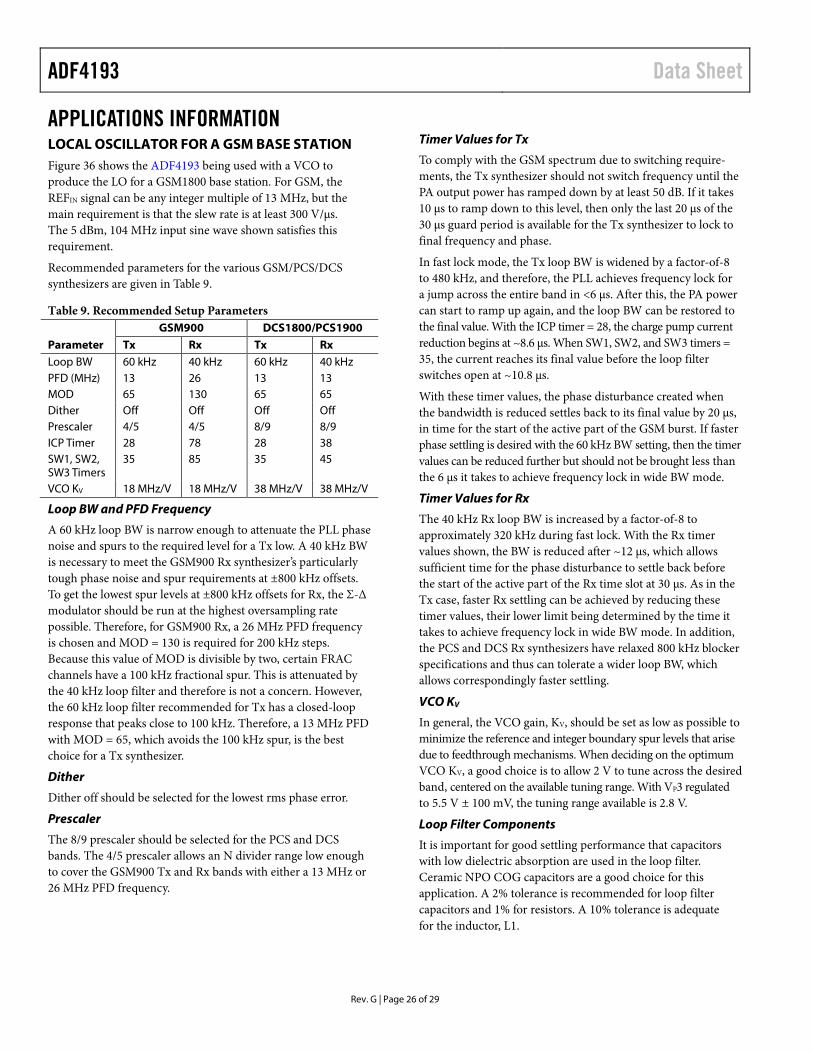
APPLICATIONS INFORMATION LOCAL OSCILLATOR FOR A GSM BASE STATION Figure 36 shows the ADF4193 being used with a VCO to produce the LO for a GSM1800 base station. For GSM, the REFIN signal can be any integer multiple of 13 MHz, but the main requirement is that the slew rate is at least 300 V/µs. The 5 dBm, 104 MHz input sine wave shown satisfies this requirement.
Recommended parameters for the various GSM/PCS/DCS synthesizers are given in Table 9.
Table 9. Recommended Setup Parameters GSM900 DCS1800/PCS1900 Parameter Tx Rx Tx Rx Loop BW 60 kHz 40 kHz 60 kHz 40 kHz PFD (MHz) 13 26 13 13 MOD 65 130 65 65 Dither Off Off Off Off Prescaler 4/5 4/5 8/9 8/9 ICP Timer 28 78 28 38 SW1, SW2, SW3 Timers
35 85 35 45
VCO KV 18 MHz/V 18 MHz/V 38 MHz/V 38 MHz/V
Loop BW and PFD Frequency
A 60 kHz loop BW is narrow enough to attenuate the PLL phase noise and spurs to the required level for a Tx low. A 40 kHz BW is necessary to meet the GSM900 Rx synthesizer’s particularly tough phase noise and spur requirements at ±800 kHz offsets. To get the lowest spur levels at ±800 kHz offsets for Rx, the Σ-Δ modulator should be run at the highest oversampling rate possible. Therefore, for GSM900 Rx, a 26 MHz PFD frequency is chosen and MOD = 130 is required for 200 kHz steps. Because this value of MOD is divisible by two, certain FRAC channels have a 100 kHz fractional spur. This is attenuated by the 40 kHz loop filter and therefore is not a concern. However, the 60 kHz loop filter recommended for Tx has a closed-loop response that peaks close to 100 kHz. Therefore, a 13 MHz PFD with MOD = 65, which avoids the 100 kHz spur, is the best choice for a Tx synthesizer.
Dither
Dither off should be selected for the lowest rms phase error.
Prescaler
The 8/9 prescaler should be selected for the PCS and DCS bands. The 4/5 prescaler allows an N divider range low enough to cover the GSM900 Tx and Rx bands with either a 13 MHz or 26 MHz PFD frequency.
Timer Values for Tx
To comply with the GSM spectrum due to switching require-ments, the Tx synthesizer should not switch frequency until the PA output power has ramped down by at least 50 dB. If it takes 10 µs to ramp down to this level, then only the last 20 µs of the 30 µs guard period is available for the Tx synthesizer to lock to final frequency and phase.
In fast lock mode, the Tx loop BW is widened by a factor-of-8 to 480 kHz, and therefore, the PLL achieves frequency lock for a jump across the entire band in <6 µs. After this, the PA power can start to ramp up again, and the loop BW can be restored to the final value. With the ICP timer = 28, the charge pump current reduction begins at ~8.6 µs. When SW1, SW2, and SW3 timers = 35, the current reaches its final value before the loop filter switches open at ~10.8 µs.
With these timer values, the phase disturbance created when the bandwidth is reduced settles back to its final value by 20 µs, in time for the start of the active part of the GSM burst. If faster phase settling is desired with the 60 kHz BW setting, then the timer values can be reduced further but should not be brought less than the 6 µs it takes to achieve frequency lock in wide BW mode.
Timer Values for Rx
The 40 kHz Rx loop BW is increased by a factor-of-8 to approximately 320 kHz during fast lock. With the Rx timer values shown, the BW is reduced after ~12 µs, which allows sufficient time for the phase disturbance to settle back before the start of the active part of the Rx time slot at 30 µs. As in the Tx case, faster Rx settling can be achieved by reducing these timer values, their lower limit being determined by the time it takes to achieve frequency lock in wide BW mode. In addition, the PCS and DCS Rx synthesizers have relaxed 800 kHz blocker specifications and thus can tolerate a wider loop BW, which allows correspondingly faster settling.
VCO KV
In general, the VCO gain, KV, should be set as low as possible to minimize the reference and integer boundary spur levels that arise due to feedthrough mechanisms. When deciding on the optimum VCO KV, a good choice is to allow 2 V to tune across the desired band, centered on the available tuning range. With VP3 regulated to 5.5 V ± 100 mV, the tuning range available is 2.8 V.
Loop Filter Components
It is important for good settling performance that capacitors with low dielectric absorption are used in the loop filter. Ceramic NPO COG capacitors are a good choice for this application. A 2% tolerance is recommended for loop filter capacitors and 1% for resistors. A 10% tolerance is adequate for the inductor, L1.
Rev. G | Page 26 of 29
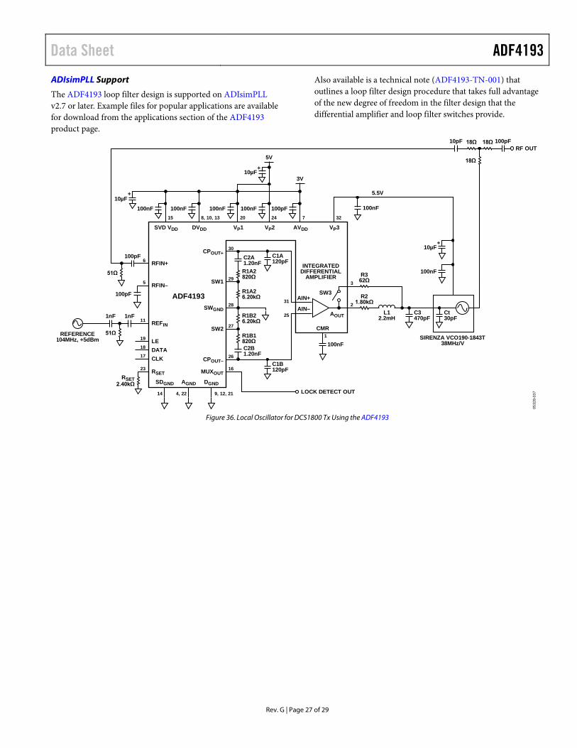
Data Sheet ADF4193 ADIsimPLL Support
The ADF4193 loop filter design is supported on ADIsimPLL v2.7 or later. Example files for popular applications are available for download from the applications section of the ADF4193 product page.
Also available is a technical note (ADF4193-TN-001) that outlines a loop filter design procedure that takes full advantage of the new degree of freedom in the filter design that the differential amplifier and loop filter switches provide.
0532
8-03
7
RSET23 MUXOUT
16
SW2 27
SWGND28
SW1 29
CPOUT+30
CPOUT–26
REFIN11
RFIN–5
RFIN+6
CLK17
SDGND
14
AGND
4, 22
DGND
9, 12, 21 LOCK DETECT OUT
DATA18LE19
REFERENCE104MHz, +5dBm
ADF4193
SVD VDD
15
DVDD
8, 10, 13
VP1
20
VP2
24
AVDD
7
VP3
32
RSET2.40kΩ
AIN+
AIN–31
25
3
2
AOUT
SW3
INTEGRATEDDIFFERENTIAL
AMPLIFIER
C1B120pF
C1A120pF
C3470pF
100nF1
CMR
Ct30pF
R1B1820Ω
R1B26.20kΩ
R1A26.20kΩ
R1A2820Ω
C2B1.20nF
C2A1.20nF
R362Ω
R21.80kΩ
L12.2mH
SIRENZA VCO190-1843T38MHz/V
100pF
100pF
1nF1nF
51Ω
51Ω
100nF
10µF+
10µF+
100nF 100nF 100nF 100pF
10µF+
100nF
100nF
3V
5V
5.5V
10pF 100pF18Ω 18Ω
18Ω
RF OUT
Figure 36. Local Oscillator for DCS1800 Tx Using the ADF4193
Rev. G | Page 27 of 29
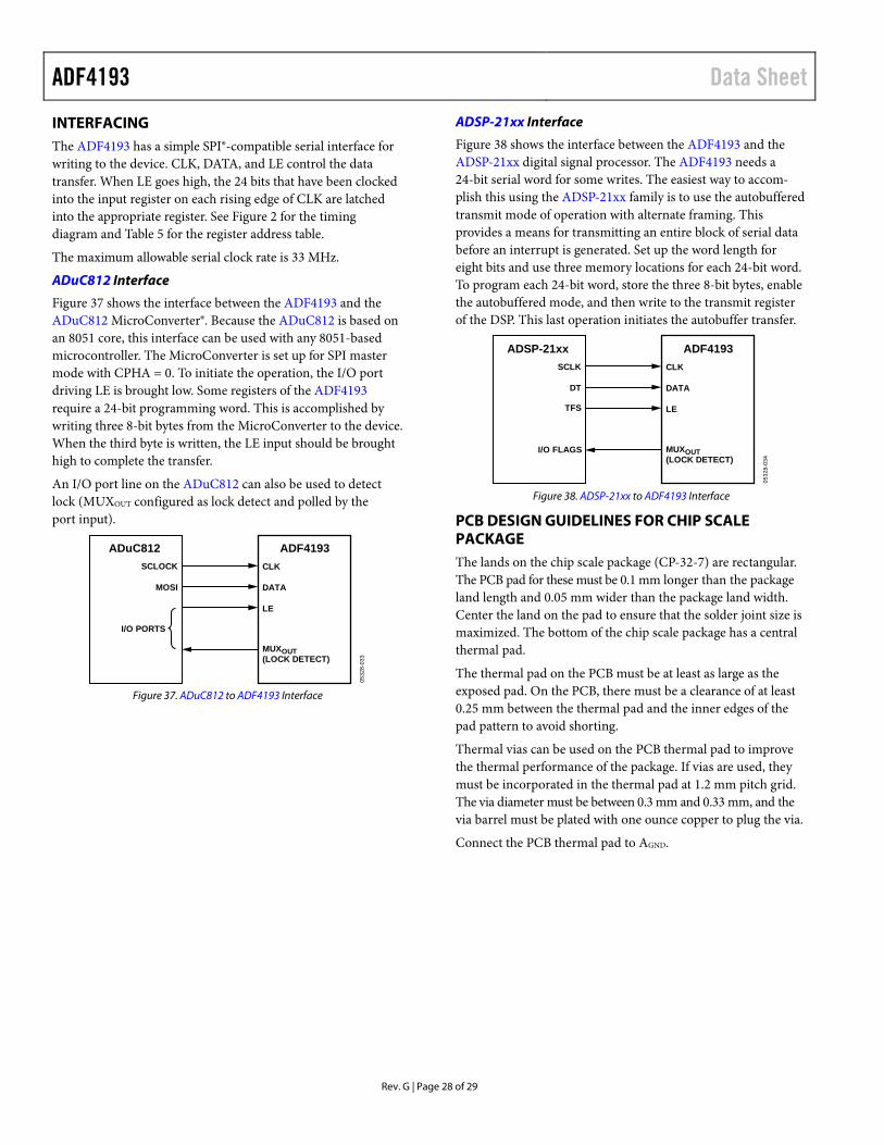
ADF4193 Data Sheet
INTERFACING The ADF4193 has a simple SPI®-compatible serial interface for writing to the device. CLK, DATA, and LE control the data transfer. When LE goes high, the 24 bits that have been clocked into the input register on each rising edge of CLK are latched into the appropriate register. See Figure 2 for the timing diagram and Table 5 for the register address table.
The maximum allowable serial clock rate is 33 MHz.
ADuC812 Interface
Figure 37 shows the interface between the ADF4193 and the ADuC812 MicroConverter®. Because the ADuC812 is based on an 8051 core, this interface can be used with any 8051-based microcontroller. The MicroConverter is set up for SPI master mode with CPHA = 0. To initiate the operation, the I/O port driving LE is brought low. Some registers of the ADF4193 require a 24-bit programming word. This is accomplished by writing three 8-bit bytes from the MicroConverter to the device. When the third byte is written, the LE input should be brought high to complete the transfer.
An I/O port line on the ADuC812 can also be used to detect lock (MUXOUT configured as lock detect and polled by the port input).
ADuC812 ADF4193SCLOCK CLK
DATA
LE
MUXOUT(LOCK DETECT)
MOSI
I/O PORTS
0532
8-03
3
Figure 37. ADuC812 to ADF4193 Interface
ADSP-21xx Interface
Figure 38 shows the interface between the ADF4193 and the ADSP-21xx digital signal processor. The ADF4193 needs a 24-bit serial word for some writes. The easiest way to accom-plish this using the ADSP-21xx family is to use the autobuffered transmit mode of operation with alternate framing. This provides a means for transmitting an entire block of serial data before an interrupt is generated. Set up the word length for eight bits and use three memory locations for each 24-bit word. To program each 24-bit word, store the three 8-bit bytes, enable the autobuffered mode, and then write to the transmit register of the DSP. This last operation initiates the autobuffer transfer.
ADSP-21xx ADF4193SCLK CLK
DATA
LE
MUXOUT(LOCK DETECT)
DT
TFS
I/O FLAGS
0532
8-03
4
Figure 38. ADSP-21xx to ADF4193 Interface
PCB DESIGN GUIDELINES FOR CHIP SCALE PACKAGE The lands on the chip scale package (CP-32-7) are rectangular. The PCB pad for these must be 0.1 mm longer than the package land length and 0.05 mm wider than the package land width. Center the land on the pad to ensure that the solder joint size is maximized. The bottom of the chip scale package has a central thermal pad.
The thermal pad on the PCB must be at least as large as the exposed pad. On the PCB, there must be a clearance of at least 0.25 mm between the thermal pad and the inner edges of the pad pattern to avoid shorting.
Thermal vias can be used on the PCB thermal pad to improve the thermal performance of the package. If vias are used, they must be incorporated in the thermal pad at 1.2 mm pitch grid. The via diameter must be between 0.3 mm and 0.33 mm, and the via barrel must be plated with one ounce copper to plug the via.
Connect the PCB thermal pad to AGND.
Rev. G | Page 28 of 29
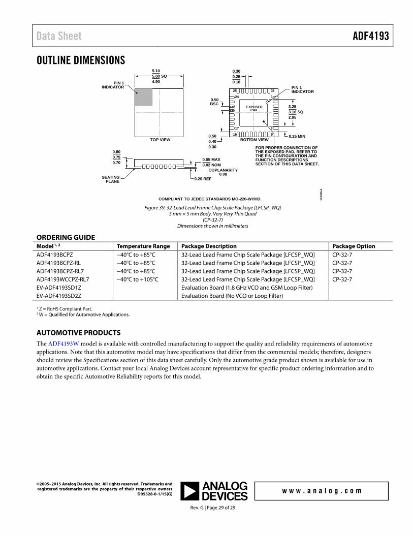
Data Sheet ADF4193
OUTLINE DIMENSIONS
COMPLIANT TO JEDEC STANDARDS MO-220-WHHD. 1124
08-A
10.50BSC
BOTTOM VIEWTOP VIEW
PIN 1INDICATOR
32
916
17
24
25
8
EXPOSEDPAD
PIN 1INDICATOR
3.253.10 SQ2.95
SEATINGPLANE
0.05 MAX0.02 NOM
0.20 REF
COPLANARITY0.08
0.300.250.18
5.105.00 SQ4.90
0.800.750.70
FOR PROPER CONNECTION OFTHE EXPOSED PAD, REFER TOTHE PIN CONFIGURATION ANDFUNCTION DESCRIPTIONSSECTION OF THIS DATA SHEET.
0.500.400.30
0.25 MIN
Figure 39. 32-Lead Lead Frame Chip Scale Package [LFCSP_WQ]
5 mm × 5 mm Body, Very Very Thin Quad (CP-32-7)
Dimensions shown in millimeters
ORDERING GUIDE Model1, 2 Temperature Range Package Description Package Option ADF4193BCPZ −40°C to +85°C 32-Lead Lead Frame Chip Scale Package [LFCSP_WQ] CP-32-7 ADF4193BCPZ-RL −40°C to +85°C 32-Lead Lead Frame Chip Scale Package [LFCSP_WQ] CP-32-7 ADF4193BCPZ-RL7 −40°C to +85°C 32-Lead Lead Frame Chip Scale Package [LFCSP_WQ] CP-32-7 ADF4193WCCPZ-RL7 −40°C to +105°C 32-Lead Lead Frame Chip Scale Package [LFCSP_WQ] CP-32-7 EV-ADF4193SD1Z Evaluation Board (1.8 GHz VCO and GSM Loop Filter) EV-ADF4193SD2Z Evaluation Board (No VCO or Loop Filter)
1 Z = RoHS Compliant Part. 2 W = Qualified for Automotive Applications.
AUTOMOTIVE PRODUCTS The ADF4193W model is available with controlled manufacturing to support the quality and reliability requirements of automotive applications. Note that this automotive model may have specifications that differ from the commercial models; therefore, designers should review the Specifications section of this data sheet carefully. Only the automotive grade product shown is available for use in automotive applications. Contact your local Analog Devices account representative for specific product ordering information and to obtain the specific Automotive Reliability reports for this model.
©2005–2015 Analog Devices, Inc. All rights reserved. Trademarks and registered trademarks are the property of their respective owners. D05328-0-1/15(G)
Rev. G | Page 29 of 29