Embed Size (px)
Citation preview

Optics Communications 355 (2015) 285–289
Contents lists available at ScienceDirect
Optics Communications
http://d0030-40
n CorrE-m
journal homepage: www.elsevier.com/locate/optcom
Low loss silicon microring resonator as comb filter
Qingzhong Deng, Huaxiang Yi, Qifeng Long, Xingjun Wang, Zhiping Zhou n
State Key Laboratory of Advanced Optical Communication Systems and Networks, Peking University, Beijing 100871, China
a r t i c l e i n f o
Article history:Received 13 March 2012Received in revised form9 February 2015Accepted 24 June 2015Available online 28 June 2015
Keywords:Optical resonatorWavelength filtering devicesMultimode waveguideScattering loss
x.doi.org/10.1016/j.optcom.2015.06.06018/& 2015 Elsevier B.V. All rights reserved.
esponding author. Fax: þ86 10 62759808.ail address: [email protected] (Z. Zhou).
a b s t r a c t
Scattering loss caused by roughness of waveguide sidewalls is a key problem for long circumferencemicroring based applications, such as comb filters. This paper presents a Si microring resonator in-corporated with the multimode waveguide and single-mode waveguide, which suppresses the unwantedresonance of high-order modes while allowing the fundamental mode resonance with low loss. Bothnumerical and experimental results proved that the proposed solution is capable to achieve �88.5%scattering loss reduction which is promising for narrow channel spacing comb filters.
& 2015 Elsevier B.V. All rights reserved.
1. Introduction
In high-speed large-capacity communication era, comb filtersare playing a more and more important role in the optical com-munications [1,2]. One example is that multi-wavelength lasers forwavelength division multiplexing (WDM) communication systemsuse comb filters as external filters assisting with broadband gainmedia [3]. Another example is to select and switch optical chan-nels in high-speed optical communication systems [4]. The combfilter can be constructed with gratings or microrings [5,6], whereSi microrings have smaller size and are more suitable for in-tegration [7]. A narrow channel spacing such as 10 GHz comb filteris required for Tb/s optical communication system [8]. In this case,the circumference of the Si microring would be 7 mm, and thescattering loss caused by sidewall roughness could be significant,which will prevent the realization of a practical microring-basedcomb filter. Decreasing roughness is one way to reduce the wa-veguide loss, but it exists limitation in the fabrication precision [9].The wide waveguide was introduced as another way to weakenthe scattering loss [10]. However, it has non-periodic resonancesspectrum caused by high-order modes in wide waveguide, whichmakes it not suitable for comb filters.
In this paper, we propose and experimentally demonstrate a Simicroring resonator incorporated with the multimode waveguide(MWG) and single-mode waveguide (SWG), which suppresses theunwanted resonance of high-order modes while allowing thefundamental mode resonance with low loss.
2. Design of low loss microring resonator
All the designs in this paper are based on silicon-on-insulator(SOI) material system with air-cladded 220 nm top silicon. Theoptical field distribution (TE0 mode) of such SOI waveguides areshown in Fig. 1, where Fig. 1(a) corresponds to the most commonlyused SOI SWG with waveguide width of 0.5 μm and Fig. 1(b) corresponds to the SOI MWG with waveguide width of 1 μm.Comparing these two modes, one can find that the MWG hassignificantly less light field near the sidewalls, which will result inless scattering loss under the same sidewall roughness. Mean-while, the MWG supports high-order modes as shown in Fig. 1(c),which is not acceptable in microring resonators since these
high-order modes will cause non-periodic transmission spec-trum (Fig. 2). To reduce the scattering loss of microring comb fil-ters by means of introducing MWG, the high-order mode re-sonances must be suppressed.
The schematic of the proposed low-loss microring resonator isshown in Fig. 3. Most part of the resonator is constructed withMWG except the area coupling with the input/output bus wave-guide. The coupling area consists of SWG with the same width asthe bus waveguide, and it is connected with the MWG throughtwo tapered waveguides (TWG). The TWG can convert light be-tween the fundamental eigenmode of SWG and MWG adiabati-cally, which allows low-loss propagation for the fundamental ei-genmode without exciting any high-order modes. Moreover, sincethe SWG only supports the fundamental eigenmode, no high-or-der mode can form resonance even if the bending and the sidewallroughness of the MWG may excite few high-order modes. Thesimulated transmission spectrum [Fig. 4(a)] has periodicallyspaced resonance peaks which confirm that no high-order mode
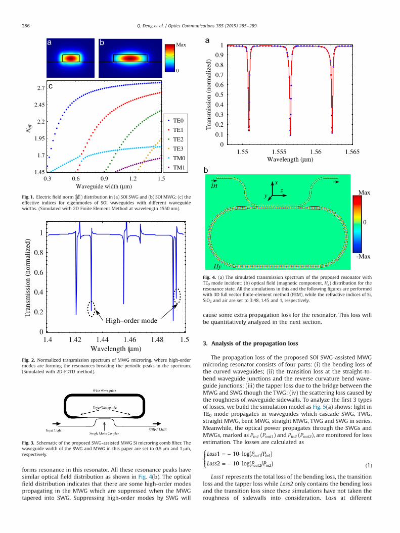
Fig. 3. Schematic of the proposed SWG-assisted MWG Si microring comb filter. Thewaveguide width of the SWG and MWG in this paper are set to 0.5 μm and 1 μm,respectively.
Waveguide width (µm)
N eff
0.3 0.6 0.9 1.2 1.51.45
1.7
1.95
2.2
2.45
2.7
TE0
TE1
TE2
TE3
TM0
TM1
Max
0
Fig. 1. Electric field norm (E ⃑ ) distribution in (a) SOI SWG and (b) SOI MWG; (c) theeffective indices for eigenmodes of SOI waveguides with different waveguidewidths. (Simulated with 2D Finite Element Method at wavelength 1550 nm).
Wavelength (µm)
Tra
nsm
issi
on (
norm
aliz
ed)
1.4 1.42 1.44 1.46 1.48 1.50
0.2
0.4
0.6
0.8
1
High−order mode
Fig. 2. Normalized transmission spectrum of MWG microring, where high-ordermodes are forming the resonances breaking the periodic peaks in the spectrum.(Simulated with 2D-FDTD method).
inMax
-Max
0
x
yz
Hy
Wavelength (µm)
Tra
nsm
issi
on (
norm
aliz
ed)
1.55 1.555 1.56 1.5650
0.1
0.2
0.3
0.4
0.5
0.6
0.7
0.8
0.9
1
Fig. 4. (a) The simulated transmission spectrum of the proposed resonator withTE0 mode incident; (b) optical field (magnetic component, Hy) distribution for theresonance state. All the simulations in this and the following figures are performedwith 3D full vector finite-element method (FEM), while the refractive indices of Si,SiO2 and air are set to 3.48, 1.45 and 1, respectively.
Q. Deng et al. / Optics Communications 355 (2015) 285–289286
forms resonance in this resonator. All these resonance peaks havesimilar optical field distribution as shown in Fig. 4(b). The opticalfield distribution indicates that there are some high-order modespropagating in the MWG which are suppressed when the MWGtapered into SWG. Suppressing high-order modes by SWG will
cause some extra propagation loss for the resonator. This loss willbe quantitatively analyzed in the next section.
3. Analysis of the propagation loss
The propagation loss of the proposed SOI SWG-assisted MWGmicroring resonator consists of four parts: (i) the bending loss ofthe curved waveguides; (ii) the transition loss at the straight-to-bend waveguide junctions and the reverse curvature bend wave-guide junctions; (iii) the tapper loss due to the bridge between theMWG and SWG though the TWG; (iv) the scattering loss caused bythe roughness of waveguide sidewalls. To analyze the first 3 typesof losses, we build the simulation model as Fig. 5(a) shows: light inTE0 mode propagates in waveguides which cascade SWG, TWG,straight MWG, bent MWG, straight MWG, TWG and SWG in series.Meanwhile, the optical power propagates through the SWGs andMWGs, marked as Pin1 (Pout1) and Pin2 (Pout2), are monitored for lossestimation. The losses are calculated as
⎪⎪⎧⎨⎩
Loss P P
Loss P P
1 10 log /
2 10 log / 1
out in
out in
1 1
2 2
( )( )
= − ⋅
= − ⋅ ( )
Loss1 represents the total loss of the bending loss, the transitionloss and the tapper loss while Loss2 only contains the bending lossand the transition loss since these simulations have not taken theroughness of sidewalls into consideration. Loss at different

Radius (µm)
Los
s (d
B)
3 5 7 9 11 13 150
0.5
1
1.5
2
Loss2Loss1
Radius (µm)
Los
s (d
B)
3 5 7 9 11 13 150
0.5
1
1.5
2
Pout
Pin
Pin1
Pout1
Pout2
TWG
StraightMWG
BentMWG
Pin2
SWG
Radius (µm)
Los
s (d
B)
3 5 7 9 11 13 150
0.5
1
1.5
2
Pin
Pout
Fig. 5. Electric field norm (E ⃑ , bending radius: 10 μm) distribution corresponding to the loss simulations of (a) MWG and (c) SWG; the simulated loss of (b) MWG and(d) SWG with different bending radii. The radius is defined as the central radius of the bending waveguide.
Q. Deng et al. / Optics Communications 355 (2015) 285–289 287
wavelength around 1550 nm is simulated and averaged as the finalvalue to eliminate the variations caused by numerical computationerrors and wavelength. The simulated final results of Loss1 andLoss2 with different bent waveguide radii is plotted in Fig. 5(b),which indicate that (i) the bending loss and the transition loss arenegligible; (ii) the tapper loss is the main loss since straight/bendwaveguides junction will excite some high-order modes and mostof the optical power in these modes cannot be rebuilt into theSWG fundamental mode when they propagate through the secondTWG; (iii) the tapper loss damps strongly (when the radius is lessthan 8 μm) due to the variation of coupling efficiency betweenhigh-order modes in MWG and the fundamental mode in SWG;(iv) the tapper loss varies slightly when the radius is greater than8 μm. Therefore, the radius of the MWG in the following fabricatedresonators are set to 10 μm whose tapper loss is 0.189 dB.
With a similar method, the losses in SWG are simulated andpresented in Fig. 5(c,d) which indicate that the bending loss, thetransition loss at the straight/bend waveguide junctions and thetransition loss at the reverse curvature bend waveguide junctionsin SWG are all negligible.
To compare the scattering loss of MWG and SWG, we fabricatedSWG microring resonator and SWG-assisted MWG microring re-sonators with the same fabrication process: fabricated on a SOIwafer, of 220 nm thick top silicon and 2 μm thick buried oxide, byelectron-beam lithography, followed by inductively coupled plas-ma etching. The top-view scanning electron microscope (SEM)pictures of the fabricated microrings, labeled as MR_a, MR_b andMR_c, are shown in Fig. 6(a, b and c), respectively. All the bendingradii of these fabricated microrings are set to be 10 μm, and thelength per straight SWG in MR_a is 12 μm. MR_a is fully con-structed with SWG while MR_b and MR_c are the SWG-assistedMWG microrings. The SWG in MR_b has the same length as MR_awhile the TWG has the length of 100 μm, and the straight MWG
has the total length of 300 μm. MR_c has the same structureparameters as MR_b except the total length of straight MWG is1500 μm longer.
Based on coupled mode theory, the transmission (Tr) of a mi-croring can be expressed as [11,12]
⎧⎨⎪
⎩⎪Tr
r a ira i
OL
exp1 exp
2 / 2
2φφ
φ π λ
= − ⋅ ( )− ⋅ ( )
= ⋅ ( )
where λ is the operating wavelength; r is the self-coupling coef-ficient of the SWG-coupler; a, φ and OL represents the transmis-sion factor, phase change and optical length of one round trip inthe microring, respectively. Rewriting the transmission factor (a)in dB format, we can get the transmission loss (Loss) per round tripin the microring
Loss a10 log 3= − ⋅ ( ) ( )
To characterize these microrings, a tunable CW laser of TE-polarization is butt-coupled into the bus waveguide and then butt-coupled out to an optical spectrum analyzer through tapered lensfibers. The measured transmission spectra are plotted in Fig. 6(d–f)where blue dots represent the measured values while red curvesare the fitted value based on Eq. (2). Even though the Fabry–Peroteffect caused by reflection of both end facets is significant in all themeasured transmission spectra, the periodically spaced resonancepeaks are clearly presented which confirm that the proposedSWG-assisted MWG microrings are able to achieve single-moderesonance. Moreover, the measured transmission spectra agreewell with the fitted values based on the theoretical expressions.According to the fitting parameters, we can get the round-triptransmission loss of these microrings as shown in Table 1. Theselosses are the total losses per round-trip of the corresponding
Table 1Loss parameters in these microrings.
Microrings Transmission factor Loss per round (dB)
MR_a 0.929 0.320MR_b 0.852 0.696MR_c 0.735 1.337
Wavelength (nm)
Tra
nsm
issi
on (
norm
aliz
ed)
1525 1530 1535 1540 1545−15
−10
−5
0
Wavelength (nm)
Tra
nsm
issi
on (
norm
aliz
ed)
1560 1562 1564 1566
−8
−6
−4
−2
0
2
Wavelength (nm)
Tra
nsm
issi
on (
norm
aliz
ed)
1568.5 1569 1569.5−6
−4
−2
0
2
d
e
f
Fig. 6. SEM of the three kinds of microrings, (a) MR_a, (b) MR_b, (c) MR_c; (d–f) the corresponding measured transmission spectra. Blue dots, the measured value; redcurves, the fitted spectra.
Q. Deng et al. / Optics Communications 355 (2015) 285–289288
microrings which consist of the scathing loss (for all microrings)and tapper loss (for SWG-assisted MWG microrings) while thebending loss and transition loss are negligible as analyzed
previously. Therefore, the losses can be expressed as
⎧⎨⎪
⎩⎪
Loss MR a S L
Loss MR b S L Tap S L MR b
Loss MR c S L Tap S L MR c 4
S S
S S M M
S S M M
( _ ) = ⋅( _ ) = ⋅ + + ⋅ ( _ )( _ ) = ⋅ + + ⋅ ( _ ) ( )
where SS (LS) and SM (LM) denote the scattering loss per unit length(propagating length) of SWG and MWG, respectively; Tap re-presents the taper loss.
Taking values of these microrings into Eq. (4), results areSS¼3.702 dB/mm, SM¼0.426 dB/mm and Tap¼0.222 dB. The

Q. Deng et al. / Optics Communications 355 (2015) 285–289 289
measured tapper loss (0.222 dB) is slightly higher than the simu-lated result (0.189 dB) since the roughness of sidewalls will excitesome high-order modes which causes some taper loss and havenot taken into consideration in simulation result. The scatteringloss of MWG is significantly lower than that of SWG, only 11.5% ofSWG scattering loss. Based on these measurements, if we re-construct MR_c using the SWG, the loss per round would be�6.896 dB which is much higher than the SWG-assisted MWGmicroring �1.337 dB. Thus, it can be concluded that the proposedSWG-assisted MWG microring is capable of reducing the scatter-ing loss efficiently while keeping the property of single-moderesonance.
4. Conclusion
This paper has proposed and experimentally demonstrated aSWG-assisted MWG microring resonator. The losses of this mi-croring resonator are categorized as bending loss, transition loss,tapper loss and scattering loss for numerical and experimentalcomparison with traditional SWG microring. The results of thisstudy proved that (i) both the SWG-assisted MWG microring andSWG microring have negligible bending loss and transition losswhile the bending radius is greater than 3 μm; (ii) the tapper loss,which only exists in the proposed resonator, is significant (simu-lated: 0.189 dB, measured; 0.222 dB) so that the SWG-assistedMWG microring has no superiority in loss when the resonatorcircumference is less than 100 μm; (iii) the scattering loss of MWG(0.426 dB/mm) is sufficiently lower than that of SWG (3.702 dB/mm) with the same sidewall roughness. When all of these lossesare taken into account, the proposed SWG-assisted MWG micror-ing is capable to reduce the loss efficiently for the applicationsbased on long circumference microrings, for example comb filters.What is more, the proposed SWG-assisted MWG microring keepsthe property of single-mode resonance. In summary, a SWG-as-sisted MWG microring with low round-trip loss and periodicallyspaced resonance peaks is demonstrated in this paper, which issuitable for narrow channel spacing comb filters and can be ex-tended to other comb applications [1].
Acknowledgments
This work is partially supported by the Major InternationalCooperation and Exchange Program of the National Natural Sci-ence Foundation of China (Grant no. 61120106012), the DoctoralProgram Foundation of Institutions of Higher Education of China(Grant no. 0100001110039), the China Postdoctoral Science Foun-dation (Grant no. 2011M500005), and the Peking University 985startup fund.
References
1 T.J. Kippenberg, R. Holzwarth, S.A. Diddams, Microresonator-based optical fre-quency combs, Science 332 (2011) 555–559.
2 W.J. Tomlinson, Evolution of passive optical component technologies for fiber-optic communication systems, J. Lightwave Technol. 26 (2008) 1046–1063.
3 G. Sun, D.S. Moon, A. Lin, W. Han, Y. Chung, Tunable multiwavelength fiber laserusing a comb filter based on erbium–ytterbium co-doped polarization main-taining fiber loop mirror, Opt. Express 16 (2008) 3652.
4 B.G. Lee, A. Biberman, P. Dong, M. Lipson, K. Bergman, All-optical comb switchfor multiwavelength message routing in silicon photonic networks, IEEE Pho-tonic Technol. Lett. 20 (2008) 767–769.
5 P. Dong, S.F. Preble, M. Lipson, All-optical compact silicon comb switch, Opt.Express 15 (2007) 9600–9605.
6 S. Bidnyk, A. Balakrishnan, A. Delâge, M. Gao, P.A. Krug, P. Muthukumaran,M. Pearson, Planar comb filters based on aberration-free elliptical grating facets,J. Lightwave Technol. 23 (2005) 1239.
7 D. Xu, A. Delâge, R. McKinnon, M. Vachon, R. Ma, J. Lapointe, A. Densmore,P. Cheben, S. Janz, J.H. Schmid, Archimedean spiral cavity ring resonators insilicon as ultra-compact optical comb filters, Opt. Express 18 (2010) 1937–1945.
8 X. Yi, N.K. Fontaine, R.P. Scott, S.J.B. Yoo, Tb/s coherent optical OFDM systemsenabled by optical frequency combs, J. Lightwave Technol. 28 (2010)2054–2061.
9 Y.A. Vlasov, S.J. McNab, Losses in single-mode silicon-on-insulator strip wave-guides and bends, Opt. Express 12 (2004) 1622.
10 P. Dong, W. Qian, S. Liao, H. Liang, C. Kung, N. Feng, R. Shafiiha, J. Fong, D. Feng,A.V. Krishnamoorthy, M. Asghari, Low loss silicon waveguides for application ofoptical interconnects, IEEE (2010) 191–192.
11 Q. Deng, X. Li, Z. Zhou, H. Yi, Athermal scheme based on resonance splitting forsilicon-on-insulator microring resonators, Photonics Res. 2 (2014) 71.
12 H. Yi, D.S. Citrin, Z. Zhou, Coupling-induced high-sensitivity silicon microringintensity-based sensor, J. Opt. Soc. Am. B 28 (2011) 1611.

![BAB III RESONATOR MEMS 3.1 OSILATORlib.ui.ac.id/file?file=digital/133505-T 27903-Perancangan...Gambar 3.4. Ilustrasi sebuah resonator micromachined folded-beam comb-drive.[28] Struktur](https://img.dokumen.tips/doc/110x75/60f7d0f4c37102649b347476/bab-iii-resonator-mems-31-27903-perancangan-gambar-34-ilustrasi-sebuah-resonator.jpg)


![090427 Lecture 5 (Comb resonator Intro).ppt [호환 모드]](https://img.dokumen.tips/doc/110x75/6255c555ceb4bb676d2dbbf7/090427-lecture-5-comb-resonator-introppt-.jpg)


![resonator - arxiv.org · resonator to increase the nonlinear interaction strength [15,16]. In a canonical resonator-based EO comb gen-erator, a CW laser is coupled to a bulk nonlinear](https://img.dokumen.tips/doc/110x75/5cd83eaa88c9938f428b4567/resonator-arxivorg-resonator-to-increase-the-nonlinear-interaction-strength.jpg)