Embed Size (px)
Citation preview

A Dissertation for the Degree of Master of Science
Low-frequency Noise Power Spectrum DensityCharacterizing of SiGe HBTs
Peng QiMay 2006
FACULTY OF SCIENCE
Department of Physics
University of Tromsø, NO-9037 Tromsø, Norway


To my parents


Abstract
The main purposes of this thesis are the Low-Frequency Noise measurement of Silicon-Germanium Heterojunction Bipolar Transistors and its Power Spectrum Density Char-acterizing.
The new generation 375 GHZ SiGe HBTs were measured in this work. We showthat most of PSDs of the new generation SiGe HBTs have very ”bumpy” spectra whichis contributed by GR noise sources. We investigated their basic characteristics of LFNsuch as the dominant noise source, base-current dependence, emitter geometrical scal-ing dependence and noise variation. They have similar LFN characteristic with the eldergeneration SiGe HBTs except for the emitter geometrical dependence.
The most important contribution of this work is that we particularly focused ondeveloping a totally automatic mechanism to fit the Low-Frequency Noise Power Spec-trum Density of SiGe HBTs so that we can use the magnitude of the fitting curve as thelow-frequency noise level at any frequency. A model based predictive and autonomousmethod was engaged for this purpose. This method offers the possibility that we canautomatically predict the noise sources of transistors to get good initial fitting parame-ters in advance instead of finding each of them by eyes. Experiments with the fittingmethod shows that:
• Always good fitting for most of the cases;
• Accurately locating each noise source;
• Sometimes meaningless fitting parameters but still good fitting.
Therefore, by using this method, we can find out how each noise source acts on thespectrum, which noise source dominates the spectrum, etc. And some careful inter-pretations will be presented based on this fitting procedure. Further, this method stillleaves large space to be extended, so it is a good basis for future work on fitting.

vi

Acknowledgements
I would like to express my most honest appreciation to all the people who ever gave mehelp during the last one year. Particularly, I would like to thank my supervisor Jarle. A.Johansen for his continual instruction and encouragement from cover to cover. I havegreatly benefited from his profound knowledge and charming personality. I am alsograteful the initial suggestions and guidance of my internal supervisor Alfred Hanssen.
I would like to thank my class fellow Anthony Doulgeris for his kind help and con-cern from the beginning of my study in Tromsø and wise advices for this work. AndI am really appreciate the spiritual support from my good Chinese fellow Ciren Yang-Zong, Li Chun, Zhang Qian and my soul mate Dong Yue.
Finally, I would like to thank my father Qi XiangHao and my mother Mao QiYu.Without their continuous support, great concern and thriving expectation, I can nothave this work done.

viii

Contents
1 Introduction 5
I Theoretical Part 7
2 Elementary Semiconductor Concepts 92.1 The Semiconductor Lattices . . . . . . . . . . . . . . . . . . . . . . . . . . . 9
2.1.1 The Unit Cell . . . . . . . . . . . . . . . . . . . . . . . . . . . . . . . 102.1.2 The Simple 3D Unit Cells . . . . . . . . . . . . . . . . . . . . . . . . 10
2.2 The Carriers . . . . . . . . . . . . . . . . . . . . . . . . . . . . . . . . . . . . 112.3 The Energy Band Model . . . . . . . . . . . . . . . . . . . . . . . . . . . . . 122.4 Intrinsic Semiconductors . . . . . . . . . . . . . . . . . . . . . . . . . . . . . 142.5 Extrinsic Semiconductors . . . . . . . . . . . . . . . . . . . . . . . . . . . . 14
2.5.1 n-Type Doping . . . . . . . . . . . . . . . . . . . . . . . . . . . . . . 152.5.2 p-Type Doping . . . . . . . . . . . . . . . . . . . . . . . . . . . . . . 16
2.6 The Diode and Band Bending . . . . . . . . . . . . . . . . . . . . . . . . . . 172.6.1 Depletion Region . . . . . . . . . . . . . . . . . . . . . . . . . . . . . 172.6.2 Band Bending . . . . . . . . . . . . . . . . . . . . . . . . . . . . . . . 19
2.7 npn Bipolar Junction Transistor . . . . . . . . . . . . . . . . . . . . . . . . . 202.7.1 The Active Operation Mode . . . . . . . . . . . . . . . . . . . . . . . 212.7.2 The Current Components . . . . . . . . . . . . . . . . . . . . . . . . 222.7.3 The Gain of BJT . . . . . . . . . . . . . . . . . . . . . . . . . . . . . . 232.7.4 The Minority Carrier Diffusion in The Base . . . . . . . . . . . . . . 232.7.5 The Energy Band Bending . . . . . . . . . . . . . . . . . . . . . . . . 25
3 SiGe Heterojunction Bipolar Transistors 273.1 The constraint of Si and III-V compounds . . . . . . . . . . . . . . . . . . . 283.2 The Advantages of SiGe HBTs . . . . . . . . . . . . . . . . . . . . . . . . . . 28

2
3.3 The Advantage of SiGe HBTs vs Si BJTs . . . . . . . . . . . . . . . . . . . . 293.4 Conclusion . . . . . . . . . . . . . . . . . . . . . . . . . . . . . . . . . . . . . 30
4 Low-Frequency Noise(LFN) Sources of Semiconductor 314.1 Thermal Noise . . . . . . . . . . . . . . . . . . . . . . . . . . . . . . . . . . . 314.2 Shot Noise . . . . . . . . . . . . . . . . . . . . . . . . . . . . . . . . . . . . . 324.3 Generation-Recombination Noise . . . . . . . . . . . . . . . . . . . . . . . . 344.4 1/f Noise . . . . . . . . . . . . . . . . . . . . . . . . . . . . . . . . . . . . . . 35
4.4.1 Mobility Fluctuation Flicker Noise . . . . . . . . . . . . . . . . . . . 354.4.2 Number Fluctuation Flicker Noise . . . . . . . . . . . . . . . . . . . 36
4.5 LFN Model of SiGe HBTs . . . . . . . . . . . . . . . . . . . . . . . . . . . . . 37
5 Power Spectrum Density Estimation 395.1 Periodogram . . . . . . . . . . . . . . . . . . . . . . . . . . . . . . . . . . . . 395.2 MultiTaper . . . . . . . . . . . . . . . . . . . . . . . . . . . . . . . . . . . . . 40
II Experimental Part 43
6 The Measurement Devices and Systems 456.1 Measurement Devices . . . . . . . . . . . . . . . . . . . . . . . . . . . . . . 456.2 DC Measurements . . . . . . . . . . . . . . . . . . . . . . . . . . . . . . . . 45
6.2.1 Gummel Measurement Set-up and Instrument . . . . . . . . . . . . 466.2.2 The Measured Gummel Plot . . . . . . . . . . . . . . . . . . . . . . 47
6.3 The LFN Measurement System . . . . . . . . . . . . . . . . . . . . . . . . . 486.3.1 Dynamic Signal Analyzer . . . . . . . . . . . . . . . . . . . . . . . . 486.3.2 The Operation Mechanism of Measurement System . . . . . . . . . 496.3.3 Time Series Sampling . . . . . . . . . . . . . . . . . . . . . . . . . . 50
7 LFN Power Spectrum Density Measurements 517.1 Searching The Dominant Noise Source . . . . . . . . . . . . . . . . . . . . . 51
7.1.1 The Noise Model of BJTs . . . . . . . . . . . . . . . . . . . . . . . . . 517.1.2 The Measurement and Result . . . . . . . . . . . . . . . . . . . . . . 54
7.2 The Base-Current Dependence of LFN . . . . . . . . . . . . . . . . . . . . . 557.2.1 A Theoretical Model for LFN IB Dependence . . . . . . . . . . . . . 567.2.2 The Measurements and Results . . . . . . . . . . . . . . . . . . . . . 56
7.3 The Emitter Geometrical Scaling Dependence of LFN . . . . . . . . . . . . 57
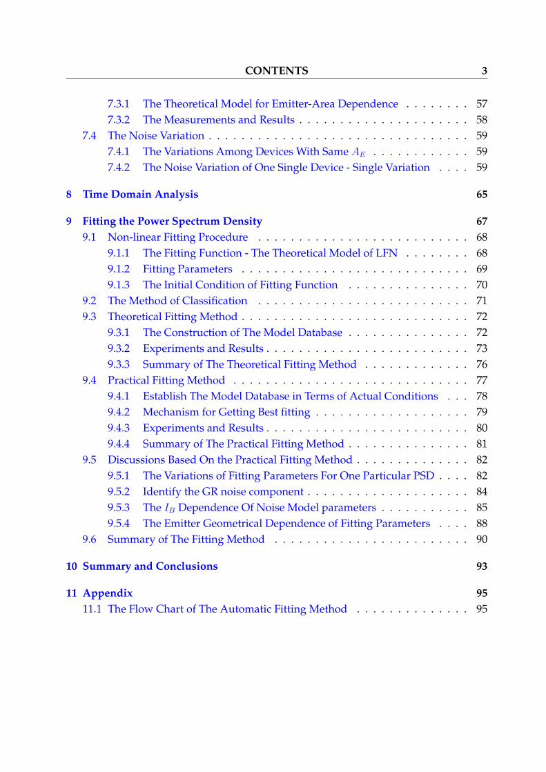
CONTENTS 3
7.3.1 The Theoretical Model for Emitter-Area Dependence . . . . . . . . 577.3.2 The Measurements and Results . . . . . . . . . . . . . . . . . . . . . 58
7.4 The Noise Variation . . . . . . . . . . . . . . . . . . . . . . . . . . . . . . . . 597.4.1 The Variations Among Devices With Same AE . . . . . . . . . . . . 597.4.2 The Noise Variation of One Single Device - Single Variation . . . . 59
8 Time Domain Analysis 65
9 Fitting the Power Spectrum Density 679.1 Non-linear Fitting Procedure . . . . . . . . . . . . . . . . . . . . . . . . . . 68
9.1.1 The Fitting Function - The Theoretical Model of LFN . . . . . . . . 689.1.2 Fitting Parameters . . . . . . . . . . . . . . . . . . . . . . . . . . . . 699.1.3 The Initial Condition of Fitting Function . . . . . . . . . . . . . . . 70
9.2 The Method of Classification . . . . . . . . . . . . . . . . . . . . . . . . . . 719.3 Theoretical Fitting Method . . . . . . . . . . . . . . . . . . . . . . . . . . . . 72
9.3.1 The Construction of The Model Database . . . . . . . . . . . . . . . 729.3.2 Experiments and Results . . . . . . . . . . . . . . . . . . . . . . . . . 739.3.3 Summary of The Theoretical Fitting Method . . . . . . . . . . . . . 76
9.4 Practical Fitting Method . . . . . . . . . . . . . . . . . . . . . . . . . . . . . 779.4.1 Establish The Model Database in Terms of Actual Conditions . . . 789.4.2 Mechanism for Getting Best fitting . . . . . . . . . . . . . . . . . . . 799.4.3 Experiments and Results . . . . . . . . . . . . . . . . . . . . . . . . . 809.4.4 Summary of The Practical Fitting Method . . . . . . . . . . . . . . . 81
9.5 Discussions Based On the Practical Fitting Method . . . . . . . . . . . . . . 829.5.1 The Variations of Fitting Parameters For One Particular PSD . . . . 829.5.2 Identify the GR noise component . . . . . . . . . . . . . . . . . . . . 849.5.3 The IB Dependence Of Noise Model parameters . . . . . . . . . . . 859.5.4 The Emitter Geometrical Dependence of Fitting Parameters . . . . 88
9.6 Summary of The Fitting Method . . . . . . . . . . . . . . . . . . . . . . . . 90
10 Summary and Conclusions 93
11 Appendix 9511.1 The Flow Chart of The Automatic Fitting Method . . . . . . . . . . . . . . 95

4

Chapter 1
Introduction
Since the transistor was born in December 1947, invented by John Bardeen, Walter Brat-tain and William Shockley in Bell Labs, efforts on searching new semiconductor mate-rials and studying the properties of them have never stopped.
Noise, as one of the essential properties, exists in all kinds of semiconductor ma-terials and acts an important role in the performance of semiconductors, not only foran individual diode or transistor, but also for the whole circuit, and represents an unex-pected random interference. This phenomenon limits the minimum signal level that anydevices can usefully work on, since there will always be a small but significant amountof noise arising. In another hand, noise also carry some useful information which canhelp scientists and engineers to characterize the properties of the devices and furthertake the advantage of it, such as probing the defect density, the material purity and reli-ability, the condition of circuits, etc. Therefore, studying noise will redound to identifythe characteristics of materials and improve the performance of circuits.
The characteristics of Low-Frequency Noise(LFN) which dominates the low-frequencypower spectrum in semiconductor transistors will be systematically discussed in thisthesis in terms of the analysis of their Power Spectra Density(PSD). Special efforts willbe focused on an automatic PSD fitting procedure. Silicon-Germanium HeterojunctionBipolar Transistors(SiGe HBTs) are the candidates to be tested in the experiment sinceSiGe HBTs are widely used for system-on-chips(SOC) and system-on-package with highfrequency and high speed applications in modern industry due to their high-level inte-gration, high speed, low cost, good matching and low noise.
In the theoretical part, we will introduce some element semiconductor concepts tohelp us understand the origin of the various kinds of noise sources which contribute theLFN PSD of semiconductor devices, diodes and bipolar junction transistors. The SiGe

6
HBT technology will be preselected. And we will briefly review semiconductor noisesources and state a model for LFN in SiGe HBTs.
Some modern statistical tools such as Multitaper(MT) will be presented to estimatePower Spectrum Density(PSD) from time series in this work as a comparison with theresult of the Dynamic Signal Analyzer HP 3561A.
In the experimental part, we will first present the DC and Low-frequency noise mea-surement system we used in laboratory.
The LFN measurement system employs a computer control mechanism so that wecan accurately and automatically set various measurement parameters we expect, suchas different base-current. Time series measurements can also be achieved by this system.
The PSDs we measured by using this system are then systematically analyzed to in-vestigate various characteristics of the LFN of SiGe HBTs, such as the dominant noisesource, base-current dependence, emitter geometrical scaling dependence and noisevariation. The Multitaper PSD estimation will also be done as a comparison of the PSDwhich is estimated by the dynamic signal analyzer.
Great efforts will be concentrated to an automatic fitting procedure. This procedureefficiently fits many kinds of LFN PSD by a model based method. By this method, wecan dramatically identify each noise component of the LFN and see which one is thedominant noise source.
The core of this fitting procedure is non-linear fitting method, and a noise model willbe introduced as the fitting function. The most important point in this procedure is thatwe innovatively choose the initial fitting parameters for this non-linear fitting functionby using the classification, that is, we automatically get the initial fitting parametersfrom a noise model database instead of estimating them by eyes every time. The noisemodel database actually contains a sequence of synthetic PSDs which can be establishedby either theoretical noise level or the actual noise level of the test PSDs themselves. Bycomparing the test PSD with the PSD models in the database, we can choose the para-meters of the closest model PSD as the initial fitting parameters. The final parameterswill schematically show all of the noise components of LFN. This method was initialdeveloped in order to find the PSD magnitude at any frequency when we analyze thePSDs. Latterly, it was proven as not only a efficient fitting method, but also a good pointto study the characteristics of LFN.

Part I
Theoretical Part


Chapter 2
Elementary Semiconductor Concepts
A semiconductor is a material with an electrical conductivity intermediate between thatof an insulator and a conductor. The electrical properties of semiconductors are drasti-cally influenced by the material, purity and structure. These characteristics have beenwell investigated and employed in many different applications. Commonly used semi-conductor materials are silicon(Si), germanium(Ge), and some compound semiconduc-tors such as gallium-arsenide (GaAs) and cadmium-telluride (CaTe). Silicon, due a largepart to the advanced state of its fabrication technology, is the most important semicon-ductor, and completely dominate the current commercial market. In this chapter, somebasic properties of semiconductors will be introduced in order to help us rather under-stand the noise sources later on.
2.1 The Semiconductor Lattices
The spatial arrangement of atoms inside a material acts an important role in deter-mining the properties of the material. In a broad sense, the structure of semiconduc-tor lattices can be classified as amorphous, polycrystalline and crystalline. An amor-phous Si thin-film transistor is used as the switching element in liquid crystal displays;polycrystalline Si gates are engaged in Metal-Oxide-Semiconductor Field-Effect Tran-sistors(MOSFET’s). However, the crystalline semiconductor has been employed to fab-ricate devices in the vast majority of modern industry. The main goal here is illustratingthe crystal structure of the principal semiconductor(crystalline) and how it works as aconductor. Most of the discussions and examples in this section will be based on Si,which is applicable to other semiconductors with different materials, such as Ge andthe compounds.

10
2.1.1 The Unit Cell
The unit cell is the most basic element of a given crystal. A two-dimensional latticeshown in figure 2.1(a). People can choose either of the two alternative unit cells shownin figure 2.1(b) for reproducing the crystal. Theoretically, there could be countless unitcells for a given crystal with different size or angle, but it is favorable to employ arelatively lager unit cell with orthogonal sides instead of a primitive cell(the possiblysmallest unit cell) with nonorthogonal sides. Especially in three-dimensional case, anon-cubic unit cell will make the problem more difficult.
Figure 2.1: The unit cell method of describing atomic arrangements inside the crystals.(a) A two-dimensional schematic lattice. (b) Two alternative unit cells.
2.1.2 The Simple 3D Unit Cells
Semiconductor crystals take three-dimensional forms in nature. Like the two-dimensionalcase, there are many alternative 3D unit cells. The simplest 3D unit cell is shown in fig-ure 2.2(a) which is called Simple cubic unit cell [Pierret, 1988]. Each of the eight atoms inthis simple cubic contribute its 1/8 fractional corner to the unit cell, and its other por-tions are shared with adjacent unit cell. Thereby, there is altogether one atom in a Simplecubic unit cell. Figure 2.2(b) and (c) show somewhat more complicate unit cells, bcc andfcc, which contains two and four atoms respectively. The lattice of Gray Sn(α− Sn) andelemental semiconductors like Si and Ge is well known as the diamond lattice unit cellshown in figure 2.2(d)[Kasap, 1997] since it shows the same structure with diamond.The diamond cubic unit cell has eight atoms.

Elementary Semiconductor Concepts 11
Figure 2.2: Examples of three-dimensional unit cells. (a) Simple cubic unit cell. (b) Bodycentered cubic unit cell. (c) Face centered cubic unit cell. (d) Diamond lattice unit cell.
2.2 The Carriers
Charge carriers are the entities inside any type of conductor that are responsible for thetransport of the charge within the material. For normal conductors such as metal, theelectron is the most commonly encountered carrier. In semiconductor, however, there isanother kind of carrier called a hole, which is effectively an empty electronic state in thevalence band and acts as if it is a positively charged ”particle”. A hole also possess theequal status with electron as the entity of the carrier.
Figure 2.3(a) presents the Bonding Model of the semiconductor, where each circlerepresents one core of semiconductor such as Si and Ge, and each line represents ashared valence electron. An electron becomes a carrier when it absorbs sufficient energyby which it can break away from the valence bond and wander about inside the lattice.Consequently, a hole carrier will be simultaneously generated with the same energy butopposite charge as the electron. The figure 2.3(b) shows the corresponding energy bandto illustrate the energy demand when a electron or a hole becomes a carrier, and it willbe further discussed in section 2.3.

12
Figure 2.3: Illustration of carriers by means of bonding model. (a) Breaking a valencebond and freeing of an electron, generating a hole simultaneously. (b) The energy banddiagram.
2.3 The Energy Band Model
A semiconductor behaves as an insulator at very low temperature, and has an appre-ciable electrical conductivity at room temperature although much lower conductivitythan a conductor. One model advisably interprets how the semiconductors act thesebehaviours in terms of energy band. The conduction band electrons in crystalline semi-conductor are not tied to any particular atom(semiconductor core). Instead, they areshared by all the atoms and the status of them changes as a function of time. Therefore,when we talk about the allowed electronic states of the semiconductor, the states are nolonger the atomic states, but are associated with the crystal as a whole. For a perfectcrystal under equilibrium conditions, a plot of the allowed electron energies versus dis-tance along any preselected crystalline direction(always called the x-direction) is shownin figure 2.4, where the upper band of these allowed states is called conduction band(CB);the lower band is valence band(VB) and the intervening gap is known as the forbidden gapor band gap. The introduced EC is the lowest possible conduction band energy, EV isthe highest possible valence band energy, and the intervening gap EG = EC −EV is the

Elementary Semiconductor Concepts 13
band gap energy. The vacuum level plotted by the dashed line is the energy level whereboth the potential energy(PE) and the kinetic energy(KE) of electrons are zero, whichmeans the electrons on this level is just free from the solid. The Fermi Energy Level(EF )is defined as that energy value below which all states are full and above which all statesare empty at absolute zero of temperature. It is actually the energy level where the prob-ability of the occupied energy states is 0.5. Its value is up to the semiconductor materialthemselves, specially decided by the doping condition. The EFi plotted in this figureis the Fermi Level for intrinsic semiconductor which will be introduced later on. Thiscited plot, a plot of allowed electron energy presents as a function of position, is thebasic energy band model [Pierret, 1988].
Figure 2.4: The energy band diagram of semiconductor.
The energy of the electron must be at least a little bigger than the EC so that theelectron could break away from the valence band to the conduction band to becomea charge carrier. The electrons staying inside the valence band are constrained by thevalence force, and can not be a carrier. At low temperature, few electrons can overcome
14
the valence force to become a free carrier since they do not have sufficient energy. On theother hand, higher temperature gives the electrons more thermal energy and can morelikely break loose from the valence bond and consequently increases the conductivity.At absolute zero, the uppermost filled electron energy band of the semiconductor will bethe fully filled VB, that is, no electron will be the conduction band and the semiconductorthen becomes an isolator. Further more, base on the foregoing theory, it is not surprisingthat the electrical resistance of semiconductor changes by voltage, and does not followthe Ohm’s law.
Recalling the energy band plot in figure 2.3(b) in section 2.2, the energy of the elec-trons become greater than the lowest conduction band energy EC after breaking fromthe valence bond in valence band for the sake of being a carrier, and the energy of thehole should be correspondingly lower than the highest valence band energy EV , that is,to be a carrier, the electron and hole should be in the conduction band and the valenceband respectively. If the absorbed energy is exactly equal to the gap energy EG, theelectron and hole will stay at their respective critical band energy and have no ability towander about.
2.4 Intrinsic Semiconductors
An intrinsic semiconductor is a pure semiconductor without any significant impurityspecies inside. The presence and type of charge carriers is therefore determined by thematerial itself instead of the impurities, and the amount of two kinds of carriers, elec-trons and holes, is roughly equal, that is, the number of electrons in the conduction bandis equal to the number of holes in the valence band. Moreover, intrinsic semiconductorsconductivity can be due to crystal defects or due to thermal excitation.
2.5 Extrinsic Semiconductors
Just as its name implies, an extrinsic semiconductor is an otherwise pure semiconduc-tor which has been doped with impurities such that the concentration of carriers of onepolarity exceeds the other type. The electronic properties of extrinsic semiconductorswill therefore be severely influenced by the characteristics of the impurities. Two typesof doping have been defined, n-type doping and p-type doping, due to the differenttype of carriers they introduce. The type and extent of the doping is decided by the re-quirement of the applications. For one particular purpose, the extrinsic semiconductor

Elementary Semiconductor Concepts 15
could be doped with the corresponding doping type and impurity concentration levelto achieve the requirement. For instance,a degenerate semiconductor, which is doped tosuch high levels that the dopant atoms are an appreciable fraction of the semiconductoratoms, acts more like a conductor than a semiconductor.
2.5.1 n-Type Doping
An n-type semiconductor is obtained by carrying out a process of doping more free neg-ative charge carriers, as a result the concentration of the electron will be much higherthan the hole, that is, the electrons are the majority carriers and the holes are the minor-ity carriers.
Figure 2.5: (a) Showing an As atom is doped into the pure silicon semiconductor interms of the bonding model. (b) the corresponding energy band model.
The doping material donates the weakly-bound outer electrons to the semiconduc-tor atoms. This type of doping agent is also known as donor material since it gives awaysome of its electrons. For example, doping with pentavalent atoms such as phospho-rus(P) or arsenic(As) into the silicon semiconductor, as shown in figure 2.5(a)[Kasap,1997], the As atom share four of its five outer electron with silicon atom just like Si,however the fifth is left orbiting the As site with the energy Ed which is close to the EC
and can therefore easily enter into the conduction band to be a carrier by a very smallenergy(EC − Ed) compared to the EG. As the schematics of energy bands shows in fig-ure 2.5(b), the fifth electron initially stay at the Ed energy level which is very close to thelowest conduction band level(EC) so that the room temperature is sufficient to excite

16
all of them into the CB to be a carrier. The doping-dependent Fermi energy(or level)in n-type (EFn)1 is lifted towards the CB, which lead to higher electron concentrationin the CB under the same temperature. Together, the n-type semiconductor has morecarriers available under the same temperature than that of the intrinsic semiconductor.On the other hand, if the temperature is lower, the concentration of the electrons in theconduction band will be significantly decrease since the thermal energy is insufficientsmall and unable to excite all of the fifth electrons into the CB.
2.5.2 p-Type Doping
A p-type semiconductor is obtained by carrying out a process of doping, that is addinga certain type of atoms, such as the trivalent atoms, to the semiconductor in order toincrease the number of free positive charge carriers(hole). Consequently, the concen-tration of the hole will be much higher than the electron. Therefore we get a oppositesituation comparing to the n-type doping, that is, the holes are the majority carrierswhile the electrons are the minority carriers.
Figure 2.6: (a) Showing an Boron atom is doped into the pure silicon semiconductor interms of bonding model. (b) The corresponding energy band.
Figure 2.6(a)[Kasap, 1997] shows that a doping material atom(Boron in this case)is added to the pure Si lattice, since Boron only has three valence electrons, when it
1For n-type semiconductor, the Fermi level will be higher than that of intrinsic semiconductor andclose to the conduction band since more extra electrons have been introduced and more energy stateswill then be filled in at the same energy level.

Elementary Semiconductor Concepts 17
substitute a Si atom and share the three electrons with four neighboring Si atoms, oneof the covalent bonds has a missing electron, which then becomes a hole. The dopantatom(Boron) can accept an electron from a neighboring atoms’ covalent bond(Suchdopants then are called acceptors) by tunneling to complete the fourth bond, whichdisplace the hole away from the B−. Since the hole is still attracted by the negativecharge left on the Boron(B− ion), it thereby takes an orbit around the B− ion. The bind-ing energy between the hole and the B− ion(Ea) is very small. Even though slightlygreater than the binding energy between the electron and the As+ in the n-type dop-ing, it is still can be overcome by the thermal energy in room temperature. Thereforethe holes can freely enter into the V B to be carriers under this condition. Figure 2.6(b)illustrates this procedure in terms of the energy band, where the hole energy level(Ea) isclose to the valence band and the Fermi Lever is lowered towards the VB, this conditionis just opposite to that of n-type semiconductor.
2.6 The Diode and Band Bending
The semiconductor diode is essentially a pn junction as shown in figure 2.7. The pn
junction are actually made from the same intrinsic semiconductor crystal such as Si inpractice by the fabrication process which creates the regions of different doping.
Figure 2.7: The pn junction.
2.6.1 Depletion Region
In figure 2.8(a), when the two types of regions stick together, the free electrons in n-typeand the free holes in p-type will diffuse across the junction to the p-type region and n-type region respectively, and the diffusion between the two regions forms the diffusioncurrent ID [Adel S. Sedra, 1998]. The electrons that diffuse across the junction into thep region soon recombine with some of the majority holes in p-type region. A similarsituation happens in the n-type region, with oppositely charged particles. Since the re-combination happens near the junction, it gets depleted of free carriers and uncovers

18
bound charges, positive charges2 in n-type side and negative charges3 in p-type side.The bound charges consequently cause an intrinsic electric field. The region where theintrinsic electric field exists is called depletion region. This electric field also acceler-ate the minority carriers, electrons in p-type and holes in n-type which are thermallygenerated and diffuse to the edge of the depletion region, and form the minority driftcurrent IS within the depletion region, the minority carriers are not shown in this figure.The minority drift current is independent of the value of the depletion-layer voltage V0
as shown in figure 2.8(b), but strongly dependent on temperature due to the thermallygenerated minority carriers.
Figure 2.8: (a) The depletion region of pn junction. (b) The energy band.
From the analysis above, the depletion region is growing by the diffusion current ID
and forced by the minority carrier drift current IS which is driven by the electric fieldof the depletion region itself. As long as these two part of current components is equal,i.e.
ID = IS (2.1)
the pn junction then reach the equilibrium condition.2The positive charge is the remaining part of pentavalent dopant atom that has lost its 5’th electron,
hence it has a net positive charge.3The trivalent dopant atom that has lost a hole, hence it has a net negtive charge.

Elementary Semiconductor Concepts 19
2.6.2 Band Bending
The EC and EV in the energy band model shown in figure 2.4 have been consistentlydrawn as the energies independent of the position coordinate x. This happens only if thematerial is electric field free, such as the intrinsic semiconductor. Otherwise, the bandenergies become a function of position when a electric field exists inside the materialsuch as the pn junction.
Figure 2.9: The energy band bending due to the electric field. (a) The band bendingdiagram with Kinetic energy(K.E.), Potential energy(P.E.) and total electron energy(E).(b) electrostatic potential. (c) the electric field corresponding the band bending in thepart (a) the band bending diagram.
The band bending is exhibited in figure 2.8(b) and figure 2.9(a) by a simple energyband diagram of pn junction. It takes place in the depletion region where the electricfield exists and the extent eV0 is apparently up to the depletion-layer voltage V0. Forsilicon, V0 is between 0.6v and 0.8v.
According to the foregoing energy band model theory, the electron should absorb an

20
energy in excess of EG so that it can get the kinetic energy to move around as well as thehole which is simultaneously generated. Then the kinetic energy of electron as shownin figure 2.9(a) is defined by:
K.E. = E − EC (2.2)
The corresponding hole kinetic energy is given:
K.E. = EV − Eh (2.3)
where the E and Eh are the total energy of the electron and hole respectively compare tothe reference energy Eref which is position-independent and could be chosen to be anyconvenient value[Pierret, 1988]. The potential energy(P.E.), which is defined by P.E. =
EC − Eref , is the key to explain the band bending which relates to the electric field. Inelementary physics, assuming the existing electric field is the only force associated withthe changing of the potential energy, then the potential energy of the electron with thecharge −q is given:
P.E. = −qV (2.4)
Due to the inside electric field(E ) located inside the depletion region shown in the fig-ure 2.9(c), the electrostatic potential(V ) at the corresponding position in figure 2.9(b)increase in terms of the definition E = −dV
dx. The same result if we visually discuss the
depletion region in figure 2.8(a) where the intrinsic electric field points to the p-typeregion and the electrostatic potential will grow along the opposite direction. Therefore,the correlative potential energy consequently decrease by the relationship equation (2.4)which consequently turns out the band bending.
2.7 npn Bipolar Junction Transistor
By definition, the bipolar junction transistor(BJT) is a kind of semiconductor device con-taining three adjoining, alternately doped regions in which the middle region is verynarrow compared with the minority carrier diffusion length for that region. The threeregions are,respectively, p type, n type and p type in a pnp transistor, and n type, p
type and n type in a npn transistor. And each region is directly connected to a termi-nal labeled: emitter(E), base(B) and collector(C). Figure 2.10(a), (b) show the schematicstructure of the two types of BJT. By variation of the donor and acceptor concentra-tion resulting from the fabrication process within the same crystal, different doping forthese regions are realized. Figure 2.10(c) is a simplified cross section of the npn transistor

Elementary Semiconductor Concepts 21
showing this kind of fabrication of the device.
Figure 2.10: (a),(b) the sketch map of pnp and npn corresponding to the terminal nameE(emitter), B(base) and C(collector); (c) The simplified cross section of npn bipolar tran-sistor.
In this section, we will mainly discuss the characteristics of npn BJT since all thedevices we used in the experiments are npn type.
As shown in figure 2.10(b) and (c), the npn BJT consists of one p-type(the acceptor isnormally Boron) doped base between two n-type(the donor is normally Arsenic) dopedregions emitter and collector. Furthermore, as will become obvious later, the emitter isgenerally much higher doped than that of base and the collector is even lower dopedthan the base.
2.7.1 The Active Operation Mode
The active operation mode is the mode that BJTs are generally functional in the circuits.Figure 2.11 shows the operation setup for npn bipolar transistors in active mode, wherethe BE junction is forward biased and the CB junction is reversely biased. To makethe transistor conduct appreciable current from C to E, VBE must be at least equal toor slightly greater than the cut-in voltage which is usually between 0.6v and 0.7v forsilicon based BJTs. Under the active operation mode, we will subsequently discuss theworking mechanism of the BJT.

22
Figure 2.11: The operation setup for active mode.
2.7.2 The Current Components
Figure 2.12: The carrier flux and current distribution within the BJT in the active mode.
The figure 2.12 shows the various carriers flux and current components of the npn
BJT under the active mode except the recombination-generation currents in the deple-tion regions. Together we have the current value for each region:
IE = IEn + IEp (2.5)
IC = ICn + ICp (2.6)
IB = IB1 + IB2 − IB3 (2.7)

Elementary Semiconductor Concepts 23
Both the electrons injected from emitter to base(IEn) and the holes injected from baseto emitter(IEp) contribute the emitter current which is opposite to the direction of theelectron flux and going out of the device. The IEp, the current from holes being injectedacross the forward biased BE junction from base into emitter, is very small compareto the IEn because of the lower doping and thin base. The IB1 in the base correspondsto the IEp, which is thereby also small. Since the very thin base width compare to thediffusion length of electron, most of the IEn will be diffuse through the base into thecollector and becomes the ICn. But still few electrons are recombined with the majoritycarriers holes in base and form the IB2 which exists for complementing the disappearedholes in base and is very small in terms of the few quantity of the recombined electrons.The current IB3 is a part of the collector current due to the thermally generated holes incollector, and it is very small too. To sum up above, the BJT have similar magnitude IE
and IC and both of which are stay at the much higher level than IB.
2.7.3 The Gain of BJT
The transistor’s current gain(β) is defined by:
β =IC
IB
(2.8)
The BJTs are normally expected that it should have high gain, that is, the IC IB
i.e. IE IB. There are two ways to achieve this goal, one of them try to increase thedifference between the IEn and IEp by heavily doping the emitter and slightly dopingthe base and the IB1 is therefore reduced; another way most decreases the width of thebase in order to decrease the number of electrons which is recombined by the holes inbase and reduce the IB2.
2.7.4 The Minority Carrier Diffusion in The Base
The minority carriers diffusion in the base is the key to accurately explain the relation-ship between the transistor’s gain and the fabrication of the BJT. Note that there is notany other force to push the electrons through the quasi-neutralize base to the collectorbut the diffusion, therefore this diffusion significantly influences all the current compo-nent and further affects the performance of the transistor such as gain.
Figure 2.13 shows the minority carrier concentration distribution of the BJT in activemode, where Pn0 and np0 are the thermal equilibrium value of the minority carrier con-

24
Figure 2.13: The minority carrier current in BJT.
centration in n-type region and p-type region respectively. The electrons injected fromemitter to base becomes minority carrier in p-type base, and then across the base intothe collector by means of diffusion. The concentration of these electrons is a straightline in the steady state if no recombination takes place. The electrons have the highestconcentration(np(0)) at the emitter side and lowest concentration(zero) at the collectorside. For any forward biased pn junction, the concentration np(0) will be proportionalto evBE/VT :
np(0) = np0evBE/VT (2.9)
where vBE is the forward BE junction bias voltage and VT is the thermal voltage. Thisdecline minority carrier concentration profile in the base causes the injected electronsfrom emitter diffusing through the base toward the collector. And this electron diffusioncurrent In in base is directly proportional to the slope of the straight line concentrationprofile[Adel S. Sedra, 1998], given by:
In = AEqDndnp(x)
dx
= AEqDn
(−np(0)
W
)(2.10)
where AE is the cross section area of BE junction, q is the magnitude of the electroncharge, Dn is the electron diffusivity in base and the W is the effective base width. Wesee that the In is reversely proportional to the base width(W ), that is, the thinner base the

Elementary Semiconductor Concepts 25
higher In. Since the BC junction is reversely biased, the diffusing electrons that reachthe edge of the collector will be swept across the CB junction and totally contributethe collector current iC , i.e. In = iC . Taking the positive direction of iC to be into thecollector terminal, the iC can be expressed:
iC = ISevBE/VT (2.11)
the IS is saturation current which is given by:
IS =AEqDnn
2i
NAW(2.12)
where the ni is the intrinsic carrier density and NA is the doping concentration of thebase.
Two parts of base current IB1 and IB2 as shown in figure 2.11 have been concernedfor calculating the iB, since the IB3 which comes of the thermally generated holes isrelatively very small. Then the iB is:
iB = IS
(Dp
Dn
NA
ND
W
Lp
+1
2
W 2
Dnτb
)evBE/VT (2.13)
where the Dp is the hole diffusivity in the emitter, Lp is the hole diffusion length inthe emitter, ND is the doping concentration of the emitter and τb is the minority-carrierlifetime in the base, that is, the average time for a minority electron to recombine with amajority hole in the base.
Together, we have the current gain of BJT:
β =iCiB
= 1/
(Dp
Dn
NA
ND
W
Lp
+1
2
W 2
Dnτb
)(2.14)
by which, we see that decreasing either the radio of NA/ND or the width W can increasethe current gain. So a high gain BJT need the base doping concentration NA is muchsmaller than the doping level of emitter ND and the width of base should simultane-ously be as thin as possible.
2.7.5 The Energy Band Bending
Figure 2.14[W.Neudeck and Pierret, 1989] shows the npn BJT energy band both for ac-tive region operation(the broken line) and for thermal equilibrium(the solid line). The

26
Figure 2.14: The energy band bending of npn BJT in active mode.
forward biased BE junction lowers the barrier for electrons entering into the p-type basefrom emitter and electrons therefore are allowed to be injected across the BE junctioninto the base and further diffuse through the very narrow base and slide down into thecollector by the potential hill. The magnitude difference of the energy barrier, which hasbeen lowered by the forward bias, is expressed by the potential energy qVBE as shownin figure.
The stronger reversely biased BC junction in the active mode has greater energydifference(q|VBC |) with the thermal equilibrium compare to qVBE which make the dif-fusion electrons from base more easily slide down into the collector by this deeper po-tential hill, at the meantime, it also increases the barrier for electrons in collector whichmay want to travel into the base.

Chapter 3
SiGe Heterojunction Bipolar Transistors
In modern industry, various applications require highly integrated and low cost ICs op-erating at very high frequencies, such as RF and microwave circuits. Therefore, it is nec-essary that the devices employed in these circuits not only should be suited for makinghighly integrated, low-cost ICs, but also can offer sufficiently high speed for the appli-cation at hand. In addition, more and more specific requirements emerge, which alsoneed the highly integrated and low-cost semiconductor material to do the work. Withall these expectations, the Silicon-Germanium Heterojunction Bipolar Transistors(SiGeHBTs) arise. Figure 3.1 shows the cross-section of a state-of-the-art 210GHZ SiGe HBT.We can see that only the base of this transistor employs the SiGe alloy, the reason of thiswill be soon apparent.
Figure 3.1: The schematic cross-section of the third generation SiGe HBTs.
28
3.1 The constraint of Si and III-V compounds
Silicon, as introduced in chapter 2, is the most wildly used semiconductor material andit totally dominates the current commercial market due to its advance state of fabri-cation, highly integration ability and abundant resource. However, its comparativelysmall carrier mobility for both electrons and holes excludes itself from the high fre-quency applications since the speed of a device ultimately depends on how fast thecharges can be transported across the device under sustainable operating voltages. Infact, the maximum velocity the carriers in Si can obtain under a high electric field is lim-ited to around 1× 107cm/sec under normal conditions, and is regarded as a ’slow’ semi-conductor [Cressler and Niu, 2002]. On the other hand, various III-V compounds(e.g.,GaAsand InP) enjoy much higher carrier mobilities and saturation velocity. Furthermore,the III-V compound devices can also handle many of specific applications by the wellknown bandgap engineering which dramatically offer many specific performances by al-tering their composition at atomic level [F.Capasso, 1987]. Nevertheless, the III-V de-vices lose the competition which is associated with making highly integrated and low-cost ICs.
3.2 The Advantages of SiGe HBTs
The emergence of the Silicon-Germanium alloy(Si1−xGex) in recent decades, which isfabricated by introducing Ge into Si, gives us a completely new way to fabricate a semi-conductor material with both the benefits of Si and III-V compounds, that is, the low-cost as Si and a comparable high speed as the III-V compounds. This idea is actuallyan old one by Kroemer [1957]. Due to the limitation of material growth technology,however, the first SiGe HBT was not born until 1987 [Iyer and et al., 1987]. Excitingly,with the emergence of the first generation SiGe HBTs, the rapid development of thistechnology was noticeable. Currently, the SiGe alloy has been commonly used in theIC manufacturing industry, where one important engagement of it is producing Silicon-Germanium Heterojunction Bipolar Transistors(SiGe HBTs). Some of the key points ofthe SiGe alloy and its heterojunction bipolar transistors include:
• The SiGe can be manufactured by the equipment which is used for the conven-tional silicon wafer. Therefore this process achieve costs that are similar with thesilicon manufacturing compared to other far more expensive technologies such asIII-V compounds;

SiGe Heterojunction Bipolar Transistors 29
• The SiGe allows state-of-the-art CMOS logic to be highly integrated with ultrahigh performance heterojunction bipolar transistors;
• The SiGe HBTs have significantly higher forward gain and lower reverse gainwhich leads to better low current and high frequency performance than that oftraditional bipolar transistors;
• The bandgap engineering, which is normally available to the compound semicon-ductors, can be employed to tune the band gap for any particular purposes interms of being a heterojunction technology.
3.3 The Advantage of SiGe HBTs vs Si BJTs
One important frequency response figure of merit of transistors is the unity-gain cut-offfrequency(fT ), given by:
1
2πfT
= τb + τe + τc +1
gm
(Cre + Crc) (3.1)
where the τb, τe and τc are the transit time of the base, emitter and collector respectively;gm is the transconductance; Cre and Crc are EB and CB junction depletion capacitances.
As the previous discussions in section 2.7, the bias conditions of EB and BC junc-tion in the active mode make both the transit time of electrons in emitter and collect aresignificantly small compare to the transit time in base which is purely depend on the dif-fusion whose velocity is directly decided by the carrier mobility of the semiconductormaterial. That is, the diffusion time (τb in equation (3.1)) is affected by the carrier mobil-ity. Thereby the comparatively small carrier mobility of conventional Si BJT makes largeτb and subsequently decreases the speed of the transistor. Nevertheless, the SiGe HBTs,by means of bandgap engineering, can offer the opportunity to significantly speed upthe velocity of the charge transport in the base and accordingly can produce far higherspeed transistors.
The SiGe alloy is fabricated by introducing Ge into Si. Since Ge has a larger latticeconstant and a smaller bandgap than Si(0.664 eV vs 1.12 eV ), the SiGe will have an ad-justable bandgap between Ge and Si determined by the specific content of Ge and Si.Therefore a grading of the Ge content in the base of SiGe HBTs, along the x-directionas shown in the figure 3.2(b), will produce a corresponding grading of the bandgap, asshown in figure 3.2(a). The different grading of bandgap sequently establishes a built-in
30
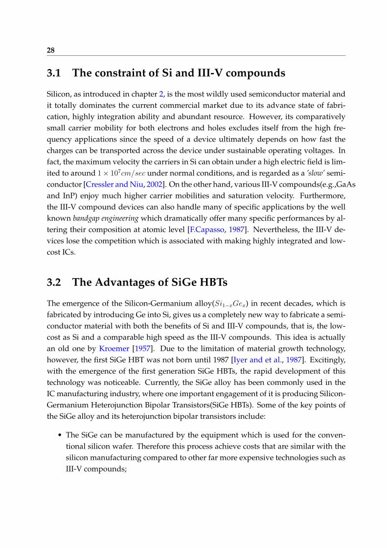
Figure 3.2: The energy band structure of SiGe HBT [Cressler and Niu, 2002].
electric field along the same direction in the base, which will force the electrons acrossthe base far more rapidly than that of pure diffusion. Hence the SiGe HBTs can achievea much higher speed of operation. Many different x values in Si1−xGex have been usedto investigate new characteristics of SiGe technology for achieving some particular re-quirements [Chen et al., 2001].
3.4 Conclusion
The SiGe HBTs have been more and more employed in virtually all analog and high-frequency applications recently, such as the cellular phone, wireless network and othercommunication systems in which the transistors with high speed, high-level integra-tion, low-cost, low-noise and good matching are necessary. In addtion, by seamlesslyintegrating with the conventional Si CMOS, the SiGe HBT BiCMOS technology, whichis perhaps the single most important advantage of SiGe HBTs, has over competed III-VHBT technologies by highly integrated ability and low-cost.
In this work, the fourth generation SiGe HBTs with 350 GHZ maximum unity-gaincutoff frequency(fT ), which was recently issued by IBM , will be the candidate of themeasurements to help us investigate the performance of SiGe HBTs, on which the Low-frequency noise characteristics will be systematically investigated by means of the studyof its Power Spectrum Density.

Chapter 4
Low-Frequency Noise(LFN) Sources ofSemiconductor
The reason why the LFN is so important are given by the following two aspects: First,the magnitude of LFN could be significantly high close to dc, therefore it is of concern forlow-noise analog circuits which need to operate at low frequency such as the amplifiersused in a zero intermediate frequency(IF); Second, the LFN can be upconverted to RFfrequencies and produce transistor phase noise through the nonlinear i− v relationshipof the transistor. Due to the low noise capability, the SiGe HBTs has a significant ad-vantage in many applications, such as the mobile receiver and typically its Low-NoiseAmplifier(LNA) in which the amount of added noise must be sufficiently low.
The physical LFN origins will be introduced in this chapter. Afterwards, we willhave a model expression for the LFN in terms of the noise sources which contribute allor part of the LFN along the frequency scale up to 10kHZ .
4.1 Thermal Noise
The thermal noise(or Nyquist noise) of a conductor is generated by the equilibrium fluc-tuations of the electric current regardless of any external power supply, due to the ran-dom thermal motion of the charge carriers. In general, the power spectral density(PSD)of the voltage across the conductor(R) is given by:
Sv(f) =2Rhf
ehf
kBT − 1(4.1)

32
where f is the frequency, h = 6.63×10⁻³⁴Js is Planck’s constant, kB = 1.38×10⁻²³JK−1
is Boltzmann’s constant and T is the absolute temperature of the conductor. In lowfrequency range, i.e.
f kBT
h
we have:Sv = 4kTR (4.2)
where the PSD of thermal noise has been presented as no frequency dependence, i.e.white noise. Thermal noise always there as long as the temperature does not becomeabsolute zero and it is generally the white noise floor observed at high frequencies forthe resistors.
4.2 Shot Noise
Shot noise comes up due to the fluctuations associate with dc current flow across apotential barrier. Solely the fact that the current is carried by discrete particles causesshot noise. This phenomenon was first observed in radio tubes by Schottky [1918].
The shot noise occurs in transistors when the current results from the discrete ran-dom emission of charged particles(electrons and holes) goes through the PN-junctionswhere the particles need overcome a potential barrier, therefore turn into a completelystochastic manner. The emission of these particles is assumed a Poisson stream. Baseon the conventional macroscopic views, the Power Spectrum Density of the base andcollector shot noises are:
SI = 2qI (4.3)
where I is the dc base or collector current, q = 1.6× 10⁻¹⁹ is the electron charge.In bipolar transistors, there is a very popular collector-base junction origin of the
2qIC shot noise theory, that is, any dc current flow across any pn junction has shotnoise[van der Ziel, 1955]. However, since the transition of the carriers go through theCB junction, which is normally reverse-biased for low-noise amplification, is a driftprocess, there is not any intrinsic shot noise when a dc current passing through such ajunction alone. By this means, the collector current shot noise shows up only when thecurrent being injected into the CB junction from the emitter has already had shot noise,that means the collector current shot noise results from the flow of emitter majority elec-trons over the potential barrier of EB junction, and has SIC
= 2qIC [Niu, 2005]. Sincethe theory that shot noise is EB junction origin has been established, the transport noise

Low-Frequency Noise(LFN) Sources of Semiconductor 33
Figure 4.1: Emitter-base junction origin of collector current shot noise in a bipolar tran-sistor.
model can be found as the illustration of figure 4.1. Both the electrons injection into thebase from emitter and the holes injection into the emitter from base independently con-tribute the emitter current shot noise. And the PSD of them are:
Sine =〈i2ne〉∆f
= 2qIC (4.4)
Sipe =
⟨i2pe
⟩∆f
= 2qIB (4.5)
which gives the same spectral expressions as the traditional view on shot-noise. In ad-dition, the 〈inei
∗pe〉 = 0 due to the independent processes of electron and hole injections.
The collector current shot noise SICis the transported version of the electron injection
into the base by EB junction. So we have:
ic = inc = inee−jωτ (4.6)
showing that the collector noise is a delayed version of the emitter-base junction noise.The ic = inc noise is a phase delayed version of the ine noise by a factor depending onfrequency(ω). For low frequencies with long wavelengths, ω 1
τ, the phase difference
between the noise in EB and BC junction is negligible. At high frequencies, however,when the wavelength becomes comparable to device size, this phase difference is sig-nificant.

34
4.3 Generation-Recombination Noise
The generation-recombination noise(GR noise) is due to the trapping-detrapping processesof carriers among energy states, mostly between an energy band and a discrete energylevel(trap) in the bandgap, which produce excess carriers through ’generation’ and re-duce the number of carriers by ’recombination’. This process turns out the fluctuationsin the number of the carriers, which are given by:
d∆N
dt= −∆N
τ(4.7)
where ∆N is the carrier fluctuation and τ is the release time during the trapping-detrappingprocess. For a two terminal sample with resistance R and voltage V , the PSD are:
SR
R2=
SV
V 2=
SN
〈N〉2=〈∆N2〉〈N〉2
4τ
1 + (2πfτ)2(4.8)
where the SR, SV and SN are PSD of resistance, voltage and number of carriers respec-tively. 〈N〉 is the average number of free carriers. This kind of PSD expression gives a
Figure 4.2: The Lorentzian.
Lorentzian noise spectrum as shown in figure 4.2 which is almost constant in the low-frequency range and rolls down as 1/f2 at high frequency [Jones, 1994].

Low-Frequency Noise(LFN) Sources of Semiconductor 35
4.4 1/f Noise
The 1/f noise, also called flicker noise, is a signal with a frequency spectrum such thatthe power spectral density is proportional to the reciprocal of the frequency. Peoplerealized that the 1/f noise is a fundamental noise which is intrinsic to the semiconductordevices after it had been found in many semiconductor materials and devices [van derZiel, 1979].
The common agreement about the origin of the 1/f noise is that it comes from thefluctuation of the conductivity(σ) which depends on both the mobility(µ) and number(N )of carriers. Their relationship is given by:
σ = q(µnn + µpp) (4.9)
where µn and µp are the mobility of electrons and holes, and the n and p are the densityof electron and hole respectively.
Hooge [1969] gave an empirical relation for 1/f noise base on homogenous samplesof semiconductors and metals:
SI
I2=
SV
V 2=
αH
fN(4.10)
where αH is well known as Hooge constant and initially given about 2 × 10⁻³, and N
is the carrier number. This relation also exclude the surface effect as the main source ofthe 1/f noise in homogenous samples since it is reversely proportional to the numberof mobile carriers. However strong surface 1/f noises have been observed in n-typesemiconductor [Vandamme, 1989] and BJT [Ziel, 1989] and present different αH value.
The debate about whether the mobility fluctuation or number fluctuation is the fun-damental 1/f noise mechanism has been lasted a long time and is still pendent.
4.4.1 Mobility Fluctuation Flicker Noise
This mobility fluctuation theory consider the origin of 1/f noise to be carrier scatteringby lattice vibrations. The Hooge relation equation (4.10) has been wide-spread em-ployed and connected to this theory, Hooge and Vandamme [1978] found that:
αmeas = αlatt
(µmeas
µlatt
)2
(4.11)

36
where αmeas is the measured Hooge constant and αlatt is Hooge constant when only lat-tice vibration exists in the test samples. The mobility subscript have the same meaning.By this relation, the Hooge constant in equation (4.10) can be derived from the mobilityfluctuation. And it also proved that the lattice scattering is the only reason which cause1/f noise. Later on, Hooge [1994] found that the αH vary between 10−7 and 10−2 whichindicates that the value of αH is very sensitive to material quality and relative noise levelof material and devices.
4.4.2 Number Fluctuation Flicker Noise
The number fluctuation is the fluctuation of the number of carriers in the conductor,which can be caused by the generation-recombination processes in the oxide-semiconductorsurface such as the polysilicon to crystal silicon interfacial oxide and the oxide spacersaround the emitter perimeter. If these independent GR-traps have a particular statis-tical distribution of characteristic time constant g(τ) ∝ 1/τ on a wide time scale, thenthe 1/f noise can be given by the superposition of these GR-traps [McWhorter, 1955] asshown in figure 4.3 which is similar with the model which was given by Surdin [1939]and Kingston and McWhorter [1956]:
SN(f) =
∫ ∞
0
4〈∆N2〉 τ
1 + (2πfτ)2g(τ)dτ (4.12)
Many works proved that the oxide-semiconductor surface is not the exclusive resource
Figure 4.3: The superposition of Lorentzian spectrum.
where the 1/τ distribution can be achieved, for example, D’yakonova et al. [1991] pro-
Low-Frequency Noise(LFN) Sources of Semiconductor 37
posed a model where an exponential tail of defect states near the CB causes this kind ofdistribution as well.
Hooge [2003] investigated that the addition of these individual traps is allowed onlywhen the number of free carriers is much larger than the sum of the carriers in all of thetraps. Otherwise, they mix together. The expressions of addition and mix are given:
• Addition: The GR noise spectra is the sum of two or more GR spectra:
S = SA + AB + . . .
• Mixing: the spectrum is one simple Lorentzian with τ is given by:
1
τ=
∑ 1
τi
4.5 LFN Model of SiGe HBTs
All these noise sources above contribute to the SiGe HBTs LFN spectrum independently.In addition, the contribution of thermal noise in the low-frequency range is very smallcompared to the other. Therefore we can express the LFN:
LFN = shotnoise +∑
GRnoise + 1/fnoise
where the sum of GR noise is not necessary to follow the 1/τ distribution. In terms ofthe equation (4.3), equation (4.8) and equation (4.10), this expression can be given:
SIB= 2qIB +
∑〈∆N2〉 4τ
1 + (2πfτ)2+
αH
f(4.13)
where SIBis the spectral density of the base current. Conventionally, the LFN of BJT
is denoted by SIBsince the base current is amplified by the transistors themselves and
normally constitutes the dominate noise source.

38
Chapter 5
Power Spectrum Density Estimation
Time series kind signals, such as voltage, current variation, can be collected by labora-tory work. These signals include all the information of devices under various workingconditions, such as different base current(IB), biasing and so on. A very important issuein signal process is to estimate the power spectrum density of these time series whichare based on a finite set of samples. The PSD can help us to identify the frequenciesthat carry the signal power or signal energy. Therefore the low-frequency noise PSDshows the signal power along the frequency range from 1 HZ to 10k HZ . During recentdecades, various digital spectral estimation technologies have been developed, such asPeriodogram, Multitaper and so on.
In this section, we will briefly introduce some of these estimation techniques whichwill be employed in this work later on. Note, using these advance estimation techniquesto estimate the PSD is not the main purpose of this thesis, we discussed them here torather understand the significance of the power spectrum density in this work.
5.1 Periodogram
For a given time series(a realization of stochastic process X(t)) based on a finite set ofsamples x[n], n = 0, 1, . . . , N − 1, the periodogram is given [Hanssen, 2003]:
S(per)XX (f) =
1
N∆t|∆t
N−1∑n=0
x[n]exp(−j2πfn∆t)|2 (5.1)
However, the raw periodogram is not a good spectral estimator since it suffers fromspectral bias and variance problems and therefore is treated as an inconsistent esti-

40
mator. The bias problem arises from a sharp truncation of the sequence, and can bereduced by many different ways, such as first multiplying the finite sequence by adata taper(window), dividing the finite sequence into many segments and averaging,weighted overlapped segment averaging, frequency smoothing and so forth.
5.2 MultiTaper
Multitaper(MT) estimator combines the use of optimal data tapers and average overa set of PSDs which are estimated by these tapers. These optimal tapers v[n], n =
0, 1, . . . , N−1, should follow the maximum ”spectral concentration” in which the energycontained in the mainlobe should be maximized relative to the total energy of the taper[Thomson, 1982]. Therefore they are chosen with a discrete Fourier transform V (f), thatmaximizes the window energy ratio:
λ =
∫ fB
−fB|V (f)|2df∫ 1/2
−1/2|V (f)|2df
(5.2)
where fB is the expected resolution half-bandwidth of the taper. λ ≈ 1 would thereforebe the value that the ideal tapers should have. Slepian [1978] found that the optimaltaper v = [v[0],v[1], . . . ,v[N− 1]]T obey the eigenvalue equation:
Av = λv (5.3)
where the A is a matrix with elements [A]nm = sin[2πfB(n − m)]/[π(n − m)], n, m =
0, 1, . . . , N − 1, corresponding to N pairs vk and λk, k = 0, 1, . . . , N − 1. From theseeigenvector and eigenvalue pairs, we obtain a set of orthogonal tapers(eigenvectors vk)with their corresponding spectral concentration(eigenvalues λk). And these orthogonaltapers maximize the ratio(λ) in equation (5.2). The so-called ”Discrete Prolate Spher-oidal Sequences”(DPSS) was consequently introduced by Slepian [1978] with the reso-lutions vk, vT
k vk′ = δk,k′ , where δk,k′ is the Kronecker delta. Once the bandwidth fB anddata length N is decided, one can obtain a sequence of orthogonal taper vk which couldbe employed in forming a Multitaper(MT) spectral estimator. The simplest definition ofthe MT estimator is the average of K tapered ”eigenspectra”:
SMT (f) =1
K
K−1∑k=0
S(k)MT (f) (5.4)

Power Spectrum Density Estimation 41
where S(k)MT is the ”eigenspectra” of order k:
S(k)MT =
∣∣∣∣∣N−1∑n=0
vk[n]x[n]exp(−j2πfn)
∣∣∣∣∣2
; |f | ≤ 1/2 (5.5)
where vk[n] is the kth element of DPSS taper.The sinusoidal tapers are a simple set of orthogonal tapers that minimize the local
bias of the spectral estimator, proposed by Riedel and Sidorenko [1995]:
vk[n] =
(2
N + 1
)1/2
sin
[π(k + 1)(n + 1)
N + 1
](5.6)
where k, n = 0, 1, . . . , N − 1. Note, the sinusoidal tapers have neither eigenvalues con-nected to, nor the bandwidth fB.
In practice, both the periodogram and multitaper are evaluated from a finite digitalsequence using the Fast Fourier Transform(FFT).

42

Part II
Experimental Part


Chapter 6
The Measurement Devices and Systems
6.1 Measurement Devices
The devices used in this work are the new generation 375 GHZ SiGe HBTs issued byIBM recently.
The emitter-area of them are from 0.048 µm2 to 1.8 µm2. These devices are arrangedon six dies, and 20 devices for each. Each terminal of the devices is connected with asquare pad so that we can make contact with device by it.
Remarkably, a part of devices are fabricated by several parallel individual SiGe HBTsso that the input current will be evenly separated to every individual transistor, then theoutput is the sum of every output of them. This structure reduces the influence fromeach individual transistor, in another word, it eliminates the interferences due to theinstability of each transistor in a certain extent. The number of individual transistors inthe parallel devices is not same for all of them. There are three types of parallel deviceconsist of 5, 10 and 30 individual transistors respectively. Except for the parallel devices,other devices are fabricated by a single transistor.
6.2 DC Measurements
A conventional way to present the current-voltage behavior of bipolar transistors is theGummel plot. By definition, the Gummel plot is the combined plot of the collector cur-rent, IC , and the base current, IB, of a transistor versus the base-emitter voltage, VBE ,on a semi-logarithmic scale. This plot is quiet useful in characterizing device figure-of-merit since it reflects on the quality of the emitter-base junction while the base-collector
46
bias, VCB, is kept at a constant. Moreover, other device parameters, such as the transis-tor’s gain β and leakage currents, can be garnered either quantitatively or qualitativelydirectly from the Gummel plot.
In this work, by using the Gummel plot of the SiGe HBTs in the measurement, wecan easily identify if the transistor is working well or if the probe and the device contacteach other tightly so that we can securely continue to do other measurements like LFNmeasurement following in next chapter.
6.2.1 Gummel Measurement Set-up and Instrument
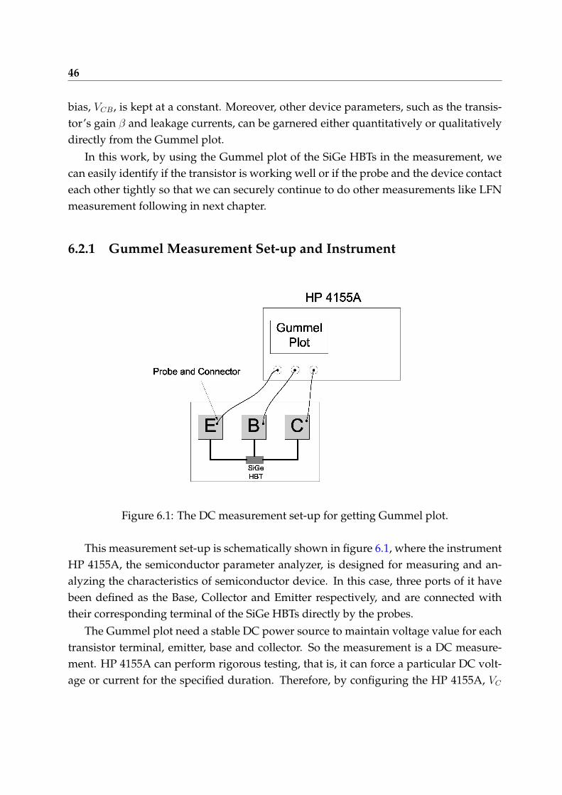
Figure 6.1: The DC measurement set-up for getting Gummel plot.
This measurement set-up is schematically shown in figure 6.1, where the instrumentHP 4155A, the semiconductor parameter analyzer, is designed for measuring and an-alyzing the characteristics of semiconductor device. In this case, three ports of it havebeen defined as the Base, Collector and Emitter respectively, and are connected withtheir corresponding terminal of the SiGe HBTs directly by the probes.
The Gummel plot need a stable DC power source to maintain voltage value for eachtransistor terminal, emitter, base and collector. So the measurement is a DC measure-ment. HP 4155A can perform rigorous testing, that is, it can force a particular DC volt-age or current for the specified duration. Therefore, by configuring the HP 4155A, VC

The Measurement Devices and Systems 47
and VB can be set to be constant zero all the way(then VCE = VBE), and the scale ofVBE = VB − VE , can be obtained by varying VE .
6.2.2 The Measured Gummel Plot
The Default configuration measure the values of VC , VB, VE , IC , IB and IE as well asshows the Gummel plot simultaneously on the screen by varying the VE from 0 v to −1
v with −0.002 v each step, that is, VBE varies from 0 v to 1 v.
Figure 6.2: DC Measurement.
Figure 6.2 shows one of the Gummel plots we got in many measurements. We seethat the device can get gain as long as the VBE is bigger than 0.4 v. And the gain doesnot vary significantly over a wide range, from 0.4 v to 1 v since the IC and IB seemparallel each other in this range. Furthermore, both IC and IB exponentially increase inthe semi-logarithmic scale as the linear rise of VBE . The limitation of the current whichthe device can handle seems to be reached when VBE is close to 1 v since the curves startto bend down.
This Gummel plot shows that this device is working fine and can be further usedin other measurements. On the other hand, the damaged devices or bad connectionswould give us a totally different Gummel plot, for example, the IB value of a damageddevice could immediately reach a very high current level despite of the IC once the VBE
is larger than zero, which indicates a damaged EB-junction.
Another advantage the Gummel plot offers us is that we can directly calculate thetransistor’s gain by equation (2.8) from it. Figure 6.3 shows the gain varying along the

48
VBE , from which we can see that the transistor will get maximum gain when VBE isaround 0.7 v which could be the value that people would like to let the device work on.
Figure 6.3: Current Gain.
6.3 The LFN Measurement System
A measurement system will be described in this chapter for characterizing the Low-Frequency Noise of SiGe HBTs. Such system is necessary to the measurement sinceit not only severely reduces the measurement time, but also efficiently increases themeasurement precision. A schematic circuit diagram of the measurement system, usingthe common emitter set-up similar to that of figure 2.11, is shown in figure 6.4.
6.3.1 Dynamic Signal Analyzer
In figure 6.4, the dynamic signal Analyzer HP 3561A is a single channel Fast FourierTransform(FFT) signal analyzer covering the frequency range from 1 HZ to 100k HZ
which is sufficient for the Low-Frequency Noise measurement. The self tests of HP3561A provide maximum confidence in the operation of the instrument. These tests, inconjunction with the internal calibration signal, make it possible to quickly verify thecalibration of the instrument before starting a critical measurement sequence. The re-markable performances of HP 3561A therefore can give us reliable measurement results.In this case, it is also configured to be controlled by the computer program(LabView)

The Measurement Devices and Systems 49
Computer
with LabView
200Ω
200ΩRB
RC
12V12V
SiGe HBT
C
B E
Control line
HP 3561A
Dynamic Signal Analyzer Pre-Amplifier
Time Series sampling card
Figure 6.4: Low-Frequency Noise Measurement System.
remotely, so that we can conveniently set all the measurement parameters in LabViewand send them to HP 3561A to do the measurement. Once the measurement has beendone, all the information will be transferred back to computer, and this information canbe used for further analysis.
6.3.2 The Operation Mechanism of Measurement System
From figure 6.4, we see that it is possible to realize many of voltage and current biasrequirements for the transistor by tuning the status of the wire-wound resistors. Andthe tuning procedure is totally automatic under the control of the computer as well.
The bias voltages come from batteries which can significantly lower the interfer-ences from the measurement system itself, because batteries are stable power sourcesand won’t disturb the noise measurements. Wire-wound resistors, which are driven byservo-motors, are used to adjust the IB and IC under the command of the computersoftware, LabView. A particular LabView program has been developed to set IB valueto a specified value and measure other values in the system simultaneously, such as

50
IC , IE , and the voltages of the batteries, etc. Once the measurement system has the IB
set, the collector voltage noise ∆VC will be amplified by a Low-Noise Pre-amplifier andthen sent into the computer controlled Dynamic Signal Analyzer HP 3561A. The dy-namic signal analyzer records the time series of a voltage/current fluctuation, and cal-culates the power spectrum density by the Fast Fourier Transform(FFT). Consequently,the measured PSD will be sent back to the computer and taken over by LabView againfor saving the data file as well as for displaying PSD on the screen simultaneously.
For measuring as pure as possible noise spectra of devices, we made the most ofvarious steps to avoid any possible interferences, for instance, shielding the devicesin a steel box, using as short as possible cable and shutting down all other irrelevantinstruments, even including the computer screen.
To sum up the above, this LFN measurement system can easily characterize the LFNof SiGe HBTs under various conditions, such as different IB. And we can adjust othercircuit parameters(e.g. RB) in case of necessary to achieve other purposes, for instance,looking for the dominant noise source which will be discussed in section 7.1.
6.3.3 Time Series Sampling
The time series sampling card, shown in the figure 6.4, is a equipment from which wecan sample the amplified collector voltages as a time series. The sampling frequencyand sampling time scale are also set by a particular LabView program. Generally, wemeasured 10 seconds time series using 300kHZ as the sampling frequency. This sam-pling frequency assure that we have not lost any information in the frequency range ofour interest.
These sampled time series then can be analyzed by other statistical tools, such asMultitaper and Wavelet, as a comparison of the FFT results from the Dynamic SignalAnalyzer HP 3561A.

Chapter 7
LFN Power Spectrum DensityMeasurements
In this chapter, by applying the LFN measurement system which we mentioned in sec-tion 6.3, a series of systematical PSD measurements have been done for investigating theperformances of the SiGe HBTs in various aspects, such as finding the dominant noisesource, current dependence, emitter-area dependence, noise variation and so on. It isnoticeable that most of these measured PSDs show very ”bumpy” behaviors instead ofthe normally expected 1/f behavior. That is, these new generation SiGe HBTs normallyhave strong GR noise spectra along the low-frequency scale.
7.1 Searching The Dominant Noise Source
There are many of noise sources possibly physically located in the regions of the SiGeHBTs. Processes like diffusion, recombination, tunneling, trapping or others could haveconnection with these noise sources. That is, for each kind of junction, emitter-base junc-tion, emitter-collector or base-collector, these processes may exist to produce the noise.The contribution of all these noise sources should be concerned in the measurement inorder to get a clean Power Spectrum Density.
7.1.1 The Noise Model of BJTs
Fortunately, just a few of these noise sources dominate the LFN of a transistor in aparticular situation and these noise sources can be put into a transistor model, suchas the model in figure 7.2 which shows the most likely noise sources in a small-signal

52
hybrid π model of one SiGe HBT, i.e. the base current noise, SIB, collector current noise,
SIC, and parasitic resistance noise, SVrb, SVrc and SVre.
Vre
VrcVrb
Figure 7.1: π model small-signal circuit with noise source in a SiGe HBT.
For investigating how these noise sources affect the LFN, we need look into the mea-surement system we actually used. For the measurement system shown in figure 6.4,with the help of figure 7.1, the equivalent circuit can be easily drawn as figure 7.2, wherethe parasitic resistance noises are not shown in this figure for the sake of brevity, but areconcluded in the noise calculation(equation (7.1) and equation (7.2)).
Figure 7.2: Common-emitter equivalent circuit.
Assuming all these noise sources are independent each other, then the spectrum of

LFN Power Spectrum Density Measurements 53
∆VC can be expressed as[Jin, 2004]:
SVC
R2C.eq
=1
m(mIB
SIB+ mIC
SIC+ nrbSVrb
+ nreSVre) (7.1)
m =[rO (rb + RB + rπ + (1 + β) re) + (RC + rc + re) (re + rb + rπ + RB)− r2
e
]2
mIB= [rOβ (RB + rb + re) + rπre]
2
mIC= [rO (RB + rb + re + rπ)]2
nrb = (βrO − re)2
nrc = (rb + re + rπ + RB)2
nre = (βrO + rπ + rb + RB)2
A accustomed way to find the dominate noise source is changing the external baseresistance RB.eq, that is the RB in figure 6.4. The contribution of SIB
, SIC, SVrb
, SVrc andSVre to the LFN as the changing of RB.eq can be calculated by:
SVC
R2C.eq
= kIBSIB
+ kICSIC
+ lrbSVrb+ lrcSVrc + lreSVre (7.2)
kIB=
[β
RB + rb + re
RB + rb + re(1 + β) + rπ
]2
kIC=
[RB + rb + re + rπ
RB + rb + re(1 + β) + rπ
]2
lrb =
[β
rb + RB + (1 + β)re + rπ
]2
lre =
[βrO + RB + rb
rO(rb + RB + (1 + β)re + rπ)
]2
lrc =
[RB + rb + re + rπ
rO(rb + RB + (1 + β)re + rπ)
]2
which is a simplification of equation (7.1) due to the usual condition rO RC,eq, rc, re.
If some typical number for circuit components(IB = 10µA, β = 100, RC = 1k, rO =
50k, rπ = 2.6k, rb = re = rc = 10) and noise spectra measured at 1 HZ(SIB= 1 × 10⁻²⁰
A2/HZ , SIC= 5 × 10⁻¹⁸ A2/HZ , SVrb
= 1.6 × 10⁻¹⁹ V 2/HZ , SVrc = 1.6 × 10⁻¹⁵ V 2/HZ ,and SVre = 1.7 × 10⁻¹⁵ V 2/HZ) are chosen [L.S.Vempati et al., 1996] [R. Brederlow andThewes, 2001], then we can plot the output noise spectra SIC
, which is calculated bythese typical values, as shown in Figure 7.3.
The situation, which is shown in this plot, where SICincreases by increasing RB,eq,

54
Figure 7.3: One typical noise output versus RB,eq.
states that the base current noise spectra SIBdominates the noise output. According to
the knowledge of elementary circuit principle, the current always would like to followthe way where smaller resistance exists, the lager RB,eq could force the current to choosethe easier way, that is, somewhat more current flow into the base and increase the partof SIB
which will be amplified to the collector by the transistor and contribute a partof SIC
. Many works such as S. P. O. Bruce and Rydberg [1999] and L.S.Vempati et al.[1996] show that the base current noise is usually the dominant noise source in common-emitter configuration since it is amplified by the transistor. This fact is represented moresignificantly in SiGe HBTs because of its characteristic of high gain(β). The relationshipbetween SIB
and SICcan be easily expressed as:
SIB=
SIC
β2(7.3)
where SIC=
SVC
R2C,eq
7.1.2 The Measurement and Result
A set of Power Spectrum Density have been measured at RB = 10k Ω, 20k Ω, 30k Ω · · ·100k Ω by using one particular device with AE = 1.8 µm2 under IB = 0.2 µA . The LFNmeasurement system somehow does not function to find any working point when wechoose the RB value which is less than 10k Ω. In addition, the maximum value of the
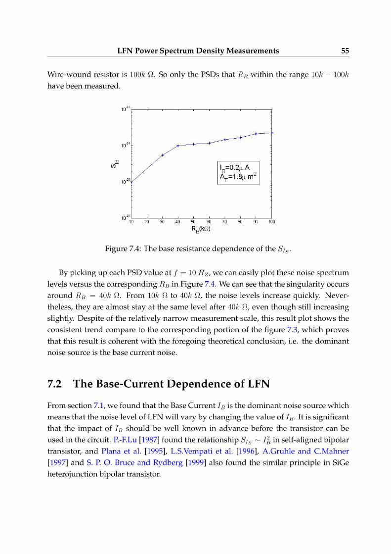
LFN Power Spectrum Density Measurements 55
Wire-wound resistor is 100k Ω. So only the PSDs that RB within the range 10k − 100k
have been measured.
Figure 7.4: The base resistance dependence of the SIB.
By picking up each PSD value at f = 10 HZ , we can easily plot these noise spectrumlevels versus the corresponding RB in Figure 7.4. We can see that the singularity occursaround RB = 40k Ω. From 10k Ω to 40k Ω, the noise levels increase quickly. Never-theless, they are almost stay at the same level after 40k Ω, even though still increasingslightly. Despite of the relatively narrow measurement scale, this result plot shows theconsistent trend compare to the corresponding portion of the figure 7.3, which provesthat this result is coherent with the foregoing theoretical conclusion, i.e. the dominantnoise source is the base current noise.
7.2 The Base-Current Dependence of LFN
From section 7.1, we found that the Base Current IB is the dominant noise source whichmeans that the noise level of LFN will vary by changing the value of IB. It is significantthat the impact of IB should be well known in advance before the transistor can beused in the circuit. P.-F.Lu [1987] found the relationship SIB
∼ I2B in self-aligned bipolar
transistor, and Plana et al. [1995], L.S.Vempati et al. [1996], A.Gruhle and C.Mahner[1997] and S. P. O. Bruce and Rydberg [1999] also found the similar principle in SiGeheterojunction bipolar transistor.

56
In this section, the PSD of the SiGe HBTs have been measured at several different IB,we also chose the devices with different emitter area to see if the IB has a similar impactfor those different candidates.
7.2.1 A Theoretical Model for LFN IB Dependence
For elucidating the experimental discovery, SIB∼ I2
B, a theoretical model is establishedin terms of unit area(AEU
). Assuming that both the base current density JB and the noisesources are homogenously distributed over the emitter and spatially uncorrelated, wecan divide the emitter into n independent unit areas and the JB is evenly distributedamong all these n unit areas. In each unit area, the noise spectrum is given by:
SIBU ∼ AEUJk
BU= AEU
(IB
n · AEU
)k
=IkB
nk · Ak−1EU
(7.4)
where the parameter k in this model is generally equal to 2 according to the observationsabove and the base current density JB is the fundamental mechanism in this model. Thetotal noise spectrum is therefore the sum of all these individual spectrum:
SIB= n · SIBU
=IkB
nk−1 · Ak−1EU
= IkB · A1−k
E
(7.5)
A similar theoretical model has been given by H.A.W.Markus and T.G.M.Kleinpenning[1995].
7.2.2 The Measurements and Results
Five IB values have been taken in this experiment, 0.2 µA, 0.5 µA, 0.8 µA, 1 µA and 2
µA. The SiGe HBTs with 0.3µm2 and 0.6µm2 were chosen, and there are several devicesfor each area in order to get better statistical results.
Figure 7.5 shows the magnitude of base current noise spectrum SIBversus the cor-
responding IB. The value of these SIBare picked up at 10 HZ . The gradients we got
for these two kinds of devices are 2.4750 and 2.0532 respectively which are close to the

LFN Power Spectrum Density Measurements 57
Figure 7.5: SIB∝ I2
B.
generally observed value k = 2. Thereby, we extrapolate that the PSD of SiGe HBTswith different emitter-area have a similar IB dependence, i.e. SIB
∼ I2B.
7.3 The Emitter Geometrical Scaling Dependence of LFN
In modern industry, transistors are greatly down scaled geometrically in order to im-prove their performance and adapt to higher integration level. One design factor asso-ciated with geometrical scale is that the Low-Frequency noise shows different frequencydependence and noise level from device to device with distinct geometrical property.
In this section, we will measure many devices with different type of geometricalscaling, the Emitter-Area and Emitter-Perimeter, to study the geometrical scaling de-pendence of LFN.
7.3.1 The Theoretical Model for Emitter-Area Dependence
In terms of the theoretical model shown in equation (7.5) in section 7.2 and the usualvalue k = 2, under the same IB value, the SIB
therefore is reversely proportional toAE , i.e. SIB
∼ A−1E . This trend also has been observed in many works [Jin et al., 2003]
[L.S.Vempati et al., 1996].

58
7.3.2 The Measurements and Results
Many of devices with different Emitter-Area(0.048 µm2, 0.12 µm2, 0.25 µm2, 0.3 µm2, 0.6
µm2, 1.28 µm2 and 1.8 µm2) and Emitter-Perimeter(0.88 µm, 1.6 µm, 2.5 µm, 3.3 µm, 4.8
µm, 6.15 µm, 8.4 µm, 12.4 µm, 16.8 µm) have been measured at IB = 1 µA.
(a) Emitter-Area dependence of LFN (b) Perimeter dependence of LFN
Figure 7.6: The Emitter Geometrical Scaling Dependence of LFN.
Figure 7.6(a) shows the emitter-area dependence of SIB, SIB
∝ A−0.2E , which is far
away from the theoretical model as well as the general observation, SIB∝ A−1
E . Thisdifference happened possibly due to two reasons. First, the general observation is ob-tained from either very big devices or old fabrication technologies. These new genera-tion ”bumpy” SiGe HBTs, however, are not necessary to follow this relation due to theirextremely down-scaled sizes and new fabrication technology; Second, we do not havesufficient number of the device for each kind of emitter-area to get good statistically av-erage results, moreover the devices we used sometimes behavior as very noisy or quietdevice compared to the noise level of other same size devices. The Emitter-Perimeter de-pendence presents a contrary trend compare to the Emitter-Area dependence as shownin figure 7.6(b) where the magnitude of the SIB
increases by the increasing of the emitterperimeter, which could be meaningful since the longer perimeter of emitter will intro-duce more GR traps [Jin et al., 2003] and consequently higher the noise level.

LFN Power Spectrum Density Measurements 59
7.4 The Noise Variation
The stability of the device should be concerned. Therefore, investigations about thenoise variation on various devices with different emitter-area or under different base-current will be systematically performed in this section. And the noise variation coefficient(δ)will be calculated for scaling the stability. This coefficient is given by [Johansen et al.,2003][Jin et al., 2002][Joseph et al., 2001]:
δ = 1SIB.avg
√1
N−1
∑Ni=1(SIB .i − SIB .avg)2
SIB .avg = 1N
∑Ni=1 SIB .i
(7.6)
where the N is the number of samples and i indicates the i′th sample.
7.4.1 The Variations Among Devices With Same AE
Under the same IB value, Low-Frequency Noise has been measured for several devices.It shows a larger statistical scatter in the very small devices compared to the largerdevices.
The Measurements and Results
The devices with two kinds of emitter-area, AE = 0.12 µm2 and AE = 1.8 µm2, have beenchosen as the small and large devices respectively, and are measured at IB = 1.0µA.
Figure 7.7 shows that the variation of the small devices, δ = 0.62, is much bigger thanthat of large devices, δ = 0.23. Therefore, the large devices with the same geometricalscaling offer good LFN stability. The LFN of small devices, however, could behave verydifferently from device to device even though they have the same geometrical scaling.
7.4.2 The Noise Variation of One Single Device - Single Variation
After investigating the variation from device to device, we want to know the variationamong several PSDs which are measured on one particular device at different time in-stead of one type of devices with the same AE . For the brevity and distinguishing fromthe variation we mentioned in section 7.4.1, we call this variation as single variation. TheIB and AE dependence of single variation will be investigated in this section.

60
(a) The noise variation on very small devices (b) The noise variation on large devices
Figure 7.7: The variation depended on emitter-area.
IB Dependence of Single Variation
Two devices with AE = 0.12 µm2 and AE = 1.8 µm2 respectively have been chosen. AtIB = 0.2, 0.5, 1.0 and 2.0 µA, eight PSD-samples have been respectively measured forboth of them.
The figure 7.8 shows the single variation of these two devices versus the base currentIB. We see that the larger IB offer smaller single variation for both of them, that is, theLFN of the devices is more stable under higher base current. In addition, comparing be-tween these two kinds AE of device, the small device shows a strong distinction amongthe single variations so that we can clearly see the IB dependence, that is, the variationdecreases by increasing IB. Therefore, the small device operates more steadily at largeIB. It is still hard to tell if the largest IB must most minimize the variation, but we mayuse the single variation to find the optimum IB. On the other hand, the single variationsof large device are actually not significantly affected by IB. Therefore, we believe thatthe large device would perform more reliably compared to small device under variousIB conditions.
AE Dependence of Single Variation
In last section, when we investigate the IB dependence of single variation, we foundthat the large device shows a better stability(smaller single variation) compared to thesmall device under every base current IB. Therefore it is clear that the single variation

LFN Power Spectrum Density Measurements 61
Figure 7.8: The noise deviation of a particular device under different IB value.
has AE dependence.Four devices with AE = 0.12, 0.64, 1.28 and 1.8 µm2 have been chosen. Under IB =
2µA, which is supposed to be the most stable condition we can get, eight samples foreach device have been measured and applied to calculate the noise variation coefficientof these four devices.
Figure 7.9(a) and figure 7.9(b) show the PSD of three of the samples for small andlarge device respectively. The solid lines is the average value of them. From equa-tion (7.6), the deviation of both of them can be calculated, the deviation of small device,δ =
0.356, is obviously bigger than the result of large device ,δ = 0.196.Figure 7.10 shows all these four single variations, we can see the trend that the
smaller devices show stronger single variations compared to the bigger devices.Note, we did not calculate the exact value of both the IB dependence and the AE
dependence because of the reason that we do not have sufficient number of good deviceto get the expected statistical results.
The Single Variation Due To The Fabrication of The Transistor
Comparing the single variation between the parallel and single devices, introduced insection 6.1, is another case which has been concerned. Two SiGe HBTs with the sameemitter area, AE = 1.28 µm2, have been chosen. One of them is fabricated by 10 parallelindividual transistors, and another one just include one single transistor. Again, eight

62
(a) The single variation of Small device (b) The single variation of Large device
Figure 7.9: The single variation of two devices with different AE .
PSD-samples have been measured for the statistical reason.Figure 7.11 shows the results of the comparison between the single and parallel de-
vices. Intuitively, the parallel device should have a smaller deviation compared to thesingle device because the output of the parallel device is averaged by its internal parallelindividual devices. In fact, the measurement results are consistent with this intuition.The single variation of the parallel device is 0.2 which has sufficient distinction from theresult of the single device, δ = 0.3.
LFN Power Spectrum Density Measurements 63
Figure 7.10: Under the same IB, the noise deviation changing by the AE .
(a) The single variation of Single device (b) The single variation of Parallel device
Figure 7.11: The single variation due to the transistor fabrications.

64

Chapter 8
Time Domain Analysis
In this chapter, we will use one of the PSD estimators, Multitaper(MT) introduced inchapter 5, to estimate the PSD of a time series which is sampled by the ”time seriessampling card” shown in figure 6.4. The estimation result shows the consistent PSDwith that of estimated by 3561A dynamic signal analyzer.
(a) Timeseries(100 ms)
(b) PSD estimated by 3561A (c) PSD estimated by Multitaper
Figure 8.1: PSD estimations.

66
A part of 10 sec time series sampled under 300k HZ is shown in Figure 8.1(a). Interms of the MT estimation method introduced in chapter 5, by using 10 sinusoidaltapers(equation (5.6)), we estimated the PSD in each 1 sec respectively and averagedthem in order to get a better statistical result. The estimated PSD is then shown infigure 8.1(c).
Comparing the PSD estimated by MT with the one measured by 3561A in figure 8.1(b),both of them give the similar PSD estimation. In laboratory, however, we prefer to usethe dynamic signal analyzer to measure the PSD instead of sampling the time seriesseparately because the time series are somehow difficult to be measured without in-terferences, on the other hand, as we introduced in section 6.3.1, HP 3561A providesmaximum confidence in the operation of the instrument by its self tests.

Chapter 9
Fitting the Power Spectrum Density
In this chapter, a method will be introduced to fit the power spectrum density based onthe established model in terms of a non-linear fitting method. The background of devel-oping this method is the requirement of investigating the various device properties suchas the IB dependence in section 7.2, the emitter geometrical scaling dependence and soon. As we already known, these investigations normally compare the magnitude of thePSD, which are measured from different conditions, at one particular frequency. There-fore, picking up the correct magnitude value for all the chosen PSD is the foundationof studying the device properties. However, the drastic fluctuation of the original PSDsis definitely disadvantageous for this purpose. So a smooth fitting curve of the originalPSD is necessary before we try to get the magnitude. Then the value of the fitting curvecan be used as the meaningful PSD magnitude. Moreover, we hope that the fitting curveshould be able to reflect the physical characteristics of the device in some sense in orderto help us study the noise property of each individual device.
Non-linear fitting method will be employed as the core fitting procedure. To makethis method work, a proper fitting function of the non-linear fitting procedure is nec-essary. For this purpose a theoretical model of low-frequency noise PSD mentioned inchapter 4, which consists of three noise levels, 1/f noise, GR noise and shot noise, willbe engaged as the fitting function. We will use these three noise levels and all the GRnoise centers as the fitting parameter. And the initial condition of the fitting parameterwill be chosen by using the classification between the test PSD and the PSD model data-base for the sake of having a automatical fitting mechanism instead of visually predictall the parameters every time. The PSD model database can be established by using the-oretical noise levels or practical noise level which will accordingly be called theoreticalfitting method and practical fitting method respectively. Consequently, the final condition

68
of the fitting parameter can not only give the fitting curve, but also clearly show theinformation of each noise component after the fitting procedure.
Furthermore, this fitting method can be applied to identify some parameters such asKF , C from device to device.
9.1 Non-linear Fitting Procedure
Normally both Polynomial fitting and Non-linear fitting can be employed to fit a dataset. Polynomial-fitting has been tested and it works only when the 1/f noise dominatethe Low Frequency noise. Once there are several strong GR-noise inside the PSD, theresult of the Polynomial-fitting can not be trusted any more. In addition, this methodcan not give any physical information about the device as we expected in its result. Onthe other hand, the non-linear fitting method can possibly fit any kinds of shape by find-ing its local minimizer as long as it has a proper fitting function and initial conditions.Moreover, with the help of the fitting function, we could easily get the approximatephysical property of the device if only the measured PSD can be fitted well. Becauseof these advantages of the Non-linear fitting method, we employed it as the core fittingmethod. In the next step, we should have a good fitting function for it. Based on thetheoretical LFN model we discussed in chapter 4, we now develop a functional form ofthis model to be used as the fitting function.
9.1.1 The Fitting Function - The Theoretical Model of LFN
From the Theoretical Part in chapter 4, we established that the Low-Frequency of semi-conductor consists of 1/f noise, GR-noise and shot noise, etc.
1/f noise
In circuit simulation programs like SPICE, SIBis given, modeled by two parameter KF
and AF :
SIB=
KF × IAFB
f(9.1)
In equation (9.1), KF is an empirical parameter which represent the magnitude of theflicker noise at 1HZ and 1A. It is a constant number for each device, but has the exper-imental relationship KF ∼ A−1
E [Sanden et al., 2002]. AF represent the current depen-dence of 1/f noise which normally is proportional to I2
B and thus AF = 2, but this value

Fitting the Power Spectrum Density 69
will be changed to 2.2 in the theoretical fitting method(section 9.3) in terms of someexperimental results.
Generation-Recombination noise
GR noise, from a number of independent sources can be represented by:
SIB=
NT∑i=1
CJ2
Bτi
1 + (2πfτi)2(9.2)
Where NT is the number of traps, C is a constant, JB = IB/AE is the base current density.
Shot noise
The level of shot noise is based on the current:
S = 2qI (9.3)
Low Frequency noise
Low Frequency noise is the superposition of 1/f noise, GR noise and shot noise, i.e.equation (9.1), equation (9.2) and equation (9.3):
SIB= 1/f +
∑GR + 2qI
=KF × IAF
B
f+
NT∑i=1
CJ2
Bτi
1 + (2πfτi)2+ 2qIB
(9.4)
The test PSD will be fitted by using this model as the fitting function for the non-linearprocedure.
9.1.2 Fitting Parameters
The non-linear fitting procedure uses the parameters in the fitting function to achievethe fitting purpose. The parameters are changed during the procedure to find the bestfitting result. In this case, the levels of each noise source type(1/f , GR and shot noise)are independent and need to be fitted respectively, therefore they all should be a part ofthe fitting parameters. For 1/f and shot noise, only the magnitude needs to be fitted.For GR noise, however, both the magnitude and the time constants of the GR noise

70
centers should be considered. Eventually, we have four types of fitting parameters in thefitting function, the magnitude of 1/f noise, GR noise, shot noise and the time constantsof the GR noise centers. In equation (9.4), they are KF × IAF
B , C × J2B, 2qIB and τi
respectively. Having the final conditions of these combined fitting parameters, we thencan calculate all the parameters in the model, i.e. KF , C, JB, IB, where the IB is actuallynot the measured IB but the fitted IB, and JB can be calculated by JB = IB/AE .
9.1.3 The Initial Condition of Fitting Function
The non-linear fitting procedure always need a threshold for its fitting parameters whenit starts to search the local minimizer. Here, this threshold is called initial condition.Correspondingly, final condition is used to name the end point of this fitting procedure.In this case, the initial condition becomes the initial assumption of the fitting parameterswhich are given in section 9.1.2. As we will present, a good initial condition(closer tothe real noise status of the test PSD) is necessary to quickly find the best fitting result.Since we already have the fitting function and its fitting parameter, the initial conditionbecomes the next important issue which should be addressed.
Testing the significance of the initial condition
Trials have been done in which we artificially built some PSDs with the preset fittingparameters, i.e. the known noise levels of 1/f noise, shot noise and GR noise, andthe GR time constants τi in equation (9.4). Since we know exactly each component ofthese synthetic PSDs, the non-linear fitting gave us a perfect fitting curve at all time ifonly the preset parameters themselves have been used directly as the initial conditionof the fitting parameters, and the final condition are consistent to the preset values. Formore widespread cases, we can still get the consistent result when the initial conditionsare offset within a certain extent. However, the fitting curves somehow show slightlydifferent behavior even they are still acceptable, and the better initial condition(closerto the real value) generally gives the better fitting result. Unacceptable results occurredwhen we used initial conditions out of a certain range. Therefore, we say that this fittingmethod is not very sensitive of the initial condition, but the initial condition should beas good as possible to get the best fitting.

Fitting the Power Spectrum Density 71
Establishing the initial condition model database
For a given PSD, according to the theoretical mode equation (9.4), it is possible to the-oretically predict the 1/f noise level, the shot noise level and even the GR noise levelin terms of the given IB, AE and the empirical KF , AF , C value. It is impossible, how-ever, to invisibly predict the GR noise centers since the distribution of the GR noisecenters vary from device to device due to the different physical conditions of the de-vices themselves which can not be predicted by any theory. Therefore, we developeda method which on beforehand establishes a model database for finding the best initialcondition. Here, the model is actually the synthetic PSDs established by the preset pa-rameters which we exactly know. For one particular test PSD, given the IB and AE , allthree noise level can be calculated by equation (9.4). Since the noise level can be wellpredicted this way, it is not necessary to consider other levels. Therefore the three noiselevel will be identical for all models within one database, the only difference amongthe models of the database are the different combinations of the GR noise centers. Fur-thermore, there is another database in which the corresponding preset fitting parame-ters are stored. Having this kind of model database, we can find the most analogicalmodel for the test PSD within the database by means of classification. It is supposedthat the corresponding fitting parameter of the chosen model can be taken as the bestestimated initial condition for the non-linear fitting method. Therefore, establishing aproper model database is significant.
Unfortunately, the empirical values of KF , AF , C change from device to device, andeven the actual value of IB and AE can not be trusted to determine the magnitude ofthe noise level in many cases, which will be shown in the following sections. Thereby,a totally automatical fitting procedure will be introduced in terms of all parameters ofequation (9.4) coming from the test PSD itself.
9.2 The Method of Classification
The Nearest Neighbor method is used as the method of classification in order to findthe best initial condition. This method can classify the test vectors to the nearest featureby calculating the distances among them. The distance is calculated by:
D =
√√√√ N∑i=1
|MODEL− PSD|2 (9.5)
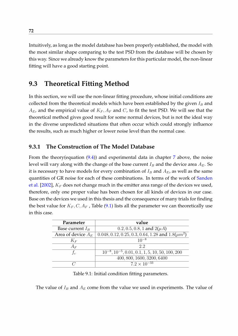
72
Intuitively, as long as the model database has been properly established, the model withthe most similar shape comparing to the test PSD from the database will be chosen bythis way. Since we already know the parameters for this particular model, the non-linearfitting will have a good starting point.
9.3 Theoretical Fitting Method
In this section, we will use the non-linear fitting procedure, whose initial conditions arecollected from the theoretical models which have been established by the given IB andAE , and the empirical value of KF , AF and C, to fit the test PSD. We will see that thetheoretical method gives good result for some normal devices, but is not the ideal wayin the diverse unpredicted situations that often occur which could strongly influencethe results, such as much higher or lower noise level than the normal case.
9.3.1 The Construction of The Model Database
From the theory(equation (9.4)) and experimental data in chapter 7 above, the noiselevel will vary along with the change of the base current IB and the device area AE . Soit is necessary to have models for every combination of IB and AE , as well as the samequantities of GR noise for each of these combinations. In terms of the work of Sandenet al. [2002], KF does not change much in the emitter area range of the devices we used,therefore, only one proper value has been chosen for all kinds of devices in our case.Base on the devices we used in this thesis and the consequence of many trials for findingthe best value for KF , C,AF , Table (9.1) lists all the parameter we can theoretically usein this case.
Parameter valueBase current IB 0.2, 0.5, 0.8, 1 and 2(µA)
Area of device AE 0.048, 0.12, 0.25, 0.3, 0.64, 1.28 and 1.8(µm2)KF 10−8
AF 2.2fc 10−8, 10−5, 0.01, 0.1, 1, 5, 10, 50, 100, 200
400, 800, 1600, 3200, 6400C 7.2× 10⁻³³
Table 9.1: Initial condition fitting parameters.
The value of IB and AE come from the value we used in experiments. The value of

Fitting the Power Spectrum Density 73
KF , AF and C are experimentally tested to be the best choice for our devices in terms ofsome empirical numerical value [Sanden et al., 2002]. fc are the centers of GR noise infrequency scale. The τ , in equation (9.4), will be decided by these fc with the relationshipτ = 1
2πfc.
From the data in table (9.1), we can build the model database and the correspond-ing fitting parameters database. However, for one particular combination of IB and AE ,the number of models in the model database is determined by the number of possiblecombinations of parameters, and will lead to millions of combinations if all of the pos-sibilities are considered. To reduce the complexity, we need to reduce the number ofGR centers in each model. To achieve a clear distinction between the sum of GR noiseand 1/f noise we allow only up to seven different GR noise centers in each model. Thedatabase then can be constructed by this set of models, and their corresponding presetfitting parameters are stored in another database.
9.3.2 Experiments and Results
Two devices with AE = 0.6 µm2 have been chosen to be tested under IB = 0.5 µA, IB =
1.0 µA and IB = 2.0 µA respectively. In terms of these actual value and possible combi-nation of IB and AE , three corresponding model databases are established. One of thedevices is classified as a normal device and another one is much quieter than the theo-retical noise level. They will be referred to as the normal and quiet device respectivelyduring the experiment. We will test our fitting method on these devices below.
Fitting the normal device by using the relevant model database
For the normal device, the test PSD, which is measured under IB = 1.0 µA, using the rel-evant model database which is built with IB = 1.0 µA, AE = 0.6 µm2, is perfectly fitted,as shown in figure 9.1. With this method, the initial condition and the final conditioncan be recorded during the procedure. Table (9.2) shows the value of these parameters,where JB = IB/AE is the base-current density. The initial and final conditions are closeeach other which means that we found the right model for this PSD and these parame-ters can be trusted to explain some physical properties of this device, such as the 1/f
Level and the number of GR center.For a more detailed view, figure 9.2(a) shows all the components which compose the
fitting curve in figure 9.1. We see that there are two GR noises at 0.5205 HZ and 1083.6541
HZ respectively mainly dominate the PSD, and the contributions of 1/f noise and other

74
Figure 9.1: Using relevant model database to fit Power Spectrum Density and gettingperfect fitting and meaningful parameters.
Initial FinalKF 1× 10⁻⁸ 8.83× 10⁻⁹
JB 1.67× 10⁶ 7.14× 10⁵
C 7.2× 10⁻³³ 7.1× 10⁻³²
GR Noise Center(HZ) 1× 10⁻¹⁰ 3.4871× 10⁻¹¹
0.001 1.6901× 10⁻⁴
0.1 0.5205800 1083.6541
Table 9.2: Consistent initial and final condition by using the relevant model database.
two GR noises are comparably much smaller. Therefore we can simply remove themand can still get a similar fitting curve as shown in figure 9.2(b). This advantage canefficiently help us to identify the noise origin for each device.
Unfortunately, also using the relevant model, we sometimes got meaningless finalcondition even if the test PSD can be fitted well. At IB = 2.0 µA for the same device, thisphenomenon shows up in figure 9.3, where a very good fitting result is presented withseveral meaningless final conditions which are listed in table (9.3). These meaninglessparameters present negative final condition include the GR noise level and two of theGR centers. In fact, the non-linear fitting procedure itself does not care about the sign ofthe value as long as it can get good fitting. It will be shown in section 9.4 that the finalparameters are sensitive to the initial parameters during the non-linear fit procedure,

Fitting the Power Spectrum Density 75
(a) All PSD components (b) The dominant PSD components
Figure 9.2: The LFN PSD components derived by theoretical fitting method.
so a slight difference of the initial condition could lead to meaningless results. On theother hand, it is also possible to get meaningful results by a slight offset of the initialcondition which led to the meaningless one.
Initial FinalKF 1× 10⁻⁸ 1.84× 10⁻⁸
JB 3.33× 10⁶ 6.32× 10⁶
C 7.2× 10⁻³³ −2.32× 10⁻³⁴
GR Noise Center(HZ) 0.1 −0.02490.5 0.07281 −0.68265 22.290610 244.8538
Table 9.3: Meaningless Final Condition when IB = 2.0 µA, AE = 0.6 µm2 by using therelevant model database.
Fitting the normal device by using an irrelevant model database
The so called irrelevant model we mentioned here is the model which has strong devia-tion in noise level from the theoretical noise level of the test PSD. This deviation lead tothe bad initial condition for the non-linear fitting and consequently a bad fitting curve.
For the normal device under IB = 2.0 µA again, when we change the model to theone which is established by IB = 1.0 µA, AE = 0.6 µm2, the fitting procedure return

76
Figure 9.3: Using relevant model database to fit Power Spectrum Density and gettinggood fitting but meaningless final conditions.
a worse fitting curve, shown in figure 9.4, than the one we got in figure 9.3, since themodel gave an initial condition with much lower noise level.
Fitting the quiet device by using a relevant model database
The quiet device shows much lower noise level than the normal one, even they havethe same physical fabrication parameter. The fitting result shown in figure 9.5 is ob-viously unacceptable. It happened since the test PSD is much lower than any modelsin the model database which has been established by the theoretical parameters a nor-mal device should have. Therefore the Nearest Neighbor Classification justly found theclosest model which only include 1/f noise and shot noise. However, the test PSD ap-parently shows strong GR noise around 1000 HZ which the non-linear fitting procedurecan never work it out if there is no GR components in the initial condition. Furthermore, some improper initial condition lead to totally unfit result which could includenegative values. Therefore, the initial condition is a critical issue.
9.3.3 Summary of The Theoretical Fitting Method
To sum up the above arguments, the theoretical fitting method can not be trusted tobe the automatical mechanism for fitting PSDs in all cases due to its constraint con-ditions. The so called constraint conditions of this method are actually its unreliable

Fitting the Power Spectrum Density 77
Figure 9.4: Using the improper model database.
assumptions for the initial condition since many interferences make the devices behav-iour deviate from the theoretical value. In fact, the model database has given the mostpossible combinations of the GR noise time constants whatever where the noise level is.So the problem becomes that this method sometimes can not offer the noise level whichthe test PSD really stay at.
9.4 Practical Fitting Method
In practice, there are many instabilities affecting the Low-Frequency Noise, which causesome devices to present much higher or lower Low-Frequency Noise level than whatthe theoretical model predicts. This unpredictable noise level is just the reason whythe theoretical method is not the ideal way to be the automatical mechanism as wediscussed in section 9.3.3. Therefore we develop a practical method which focus on themagnitude of each test PSD reality itself instead of the fixed theoretical parameter valueto avoid this disadvantage. However, selecting the true noise level for each particularPSD means that we have to establish the model database every time, which will severelyincrease the calculation time. Therefore strategies for reducing the calculation time willalso be concerned in this section.

78
Figure 9.5: Noise Level is too low to be fitted by using the relevant theoretical modeldatabase.
9.4.1 Establish The Model Database in Terms of Actual Conditions
The practical fitting method still uses the same parameters(the magnitude of 1/f noise,GR noise and shot noise, and the locations of the GR noise centers) to establish themodel database as the theoretical method did. The only difference is the way of gettingthe three noise levels for the model database.
Finding the 1/f noise, GR noise level
The magnitude of the PSD is mainly dominated by 1/f noise and GR noise at low fre-quency scale approximately up to 1000 HZ . Therefore we picked up the actual noiselevel at very low frequency, which is the average value of the first ten points of the testPSD, as the sum of 1/f and GR noise level. Then the next question becomes how to as-sign the proportion between the 1/f and the GR noise level since they both contributewithin the same frequency range. According to the experimental data of the simula-tions to many PSD which come from many different type of devices, we eventuallyfound that the 0.7 times the averaged value of the first ten points is the best quantity asthe 1/f noise level(KF × IAF
B ) for all these tested PSD(but not for every individual PSD),and 20 times 1/f noise level has been set to be the value of C × J2
B in equation (9.4)which contributes a portion of GR noise level. In fact, the 1/f noise level we found tobe 0.7, can sometimes be even bigger, and in some cases, the fitting procedure are also

Fitting the Power Spectrum Density 79
forced to choose a big value in order to get meaningful final condition.
Finding the shot noise level
The shot noise is much more stable than the 1/f noise and the GR noise because it onlyrelates to the base current. If we set the shot noise level as a constant, that is, excluding itfrom the fitting parameters, it could reduce the calculation time in a certain extent. Forthis reason, we tried to exclude it from the fitting parameter and just set the theoreticalvalue for the PSD model, equation (9.4). Unfortunately, in most of the trials we got theworse fitting even sometimes the fitting curve is still acceptable. For some noisy device,the results become totally unusable. Nevertheless, this does not mean that the shot noiseis unstable. In fact, the GR noise and cut-off frequency of the measurement set-up willmake the shot noise measurement difficult. So it is necessary to have the shot noise as afitting parameter since the measured PSD possibly would not show the true shot noise.
As we know, shot noise dominates the higher frequency range of LFN. So it is rea-sonable to use the mean value of the last ten points as the shot noise level of the initialcondition in practice.
The Combinations of GR noise centers
The combinations of the GR noise centers are preset in the same way as the theoreticalmethod since there is no way to predict them in practice either. However we just includeup to five GR noise centers for each model within the model database. This is sufficientto yield good results, and it reduces the calculation time to a reasonable amount.
Together, we have all the three noise levels and the combination of the GR noisecenters. Then the initial condition of the model is supposed to be able to automaticallyadapt to any test PSD in this way and overcome the disadvantage of the theoreticalmethod. The model database can consequently be established by these parameters wepractically get.
9.4.2 Mechanism for Getting Best fitting
Much work have been done above in order to get a good fitting curve which should haveminimum variation from the test PSD as well as a meaningful final condition. Thoughwe think that the best initial condition of the fitting parameter can be found in termsof the most proper model database we got, the non-linear fitting procedure sometimes

80
returns either bigger variation or meaningless parameters, or both of them. In order toavoid these outcomes, a mechanism have been developed.
In fact, the program has been modified to adjust the initial 1/f noise level and the GR
noise level simultaneously and reversely with a same preset ratio every time if the fittedcurve gives meaningless parameter or big variation1 from the test PSD and do the samefitting procedure again with the new initial condition. A maximum number of iterationhas been set if the procedure can not find a satisfactory fitting curve which should haveboth meaningful final parameters and small variation, and the best result among theseiterations will be picked up as the final parameters even they still could be meaninglessor have big variation. Despite of the condition of the final parameters, they can be usedanyway as a smooth fitting of the test PSD to pick up its value at any frequency as longas the fitting curve is visually acceptable. This procedure is schematically shown in theappendix in section 11.1.
9.4.3 Experiments and Results
This method has been tested on all the PSD measured at IB = 1 µA, which we got frommany different devices. The trial results show that this method can properly fit morethan 95% PSD with meaningful parameters and sufficiently small variation, the othersare also fitted well but with meaningless parameters. Furthermore, if we properly setthe 1/f noise level in terms of the actual mean value of the first ten points of PSD, theyfinally can be perfectly fitted and with meaningful final conditions as well.
We randomly chose a PSD with AE = 1.28 µm2 and measured at IB = 1 µA as thetest PSD to show a particular example. Using the proportion number 0.7 we have givenin section 9.4.1, the test PSD is perfectly fitted. Figure 9.6 and table (9.4) show the fittingresult and the corresponding parameters respectively. We see that the PSD shown infigure 9.6 is a little bit steeper than 1/f . As a good interpretation to this phenomenon,the final parameters in the table (9.4) show that all the GR noise centers, frequencyfc, centralize at very low frequency range(all below 7 HZ in the table), moreover wecould also extrapolate that there might be one very strong GR noise located there. Theδ in the figure is the variation between the fitting curve and the test PSD as defined byequation (7.6)2 and the variation at this extent is totally acceptable.
1The value of variation has been experimentally found that it normally should be smaller than 0.13 foran acceptable fitting curve.
2We can also use the conventional way, Euclidean distance, to calculate the variation between twocurves, i.e. δ =
√∑(A−B)2, where A and B are vectors.
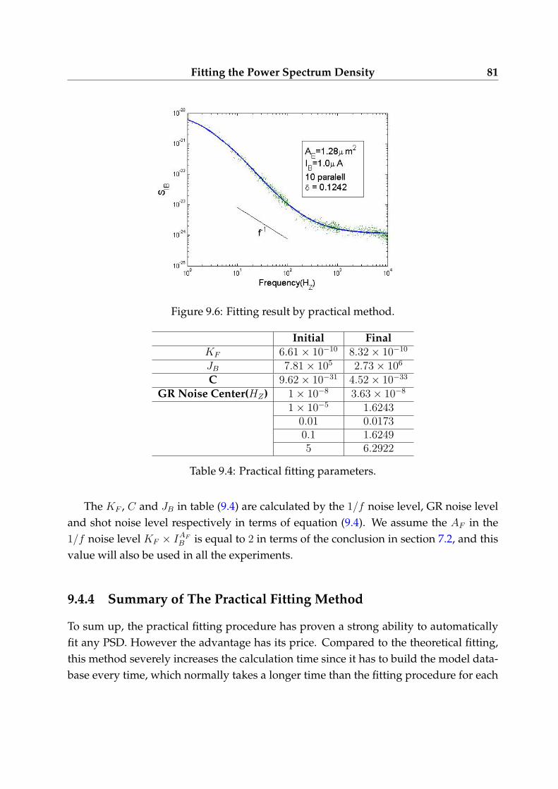
Fitting the Power Spectrum Density 81
Figure 9.6: Fitting result by practical method.
Initial FinalKF 6.61× 10⁻¹⁰ 8.32× 10⁻¹⁰
JB 7.81× 10⁵ 2.73× 10⁶
C 9.62× 10⁻³¹ 4.52× 10⁻³³
GR Noise Center(HZ) 1× 10⁻⁸ 3.63× 10⁻⁸
1× 10⁻⁵ 1.62430.01 0.01730.1 1.62495 6.2922
Table 9.4: Practical fitting parameters.
The KF , C and JB in table (9.4) are calculated by the 1/f noise level, GR noise leveland shot noise level respectively in terms of equation (9.4). We assume the AF in the1/f noise level KF × IAF
B is equal to 2 in terms of the conclusion in section 7.2, and thisvalue will also be used in all the experiments.
9.4.4 Summary of The Practical Fitting Method
To sum up, the practical fitting procedure has proven a strong ability to automaticallyfit any PSD. However the advantage has its price. Compared to the theoretical fitting,this method severely increases the calculation time since it has to build the model data-base every time, which normally takes a longer time than the fitting procedure for each

82
particular test PSD. The theoretical fitting method always has the model database builtin advance for all the PSD which come from the same IB and AE . Even though, thereare still some ways to reduce this disadvantage, for instance, choosing a more efficientdistribution and number of GR noise centers to get a robust and compact model data-base.
9.5 Discussions Based On the Practical Fitting Method
One important reason that the practical fitting method is said to be a robust fittingmethod is that this method can have the PSD fitted with different initial conditionsto a certain extent. Furthermore, these different initial conditions lead to different finalconditions by all of which the PSDs can be perfectly fitted. That is, in spite of differentparameters among these final conditions, they can achieve a similarly good fitting curveanyway. Then how about the empirical value KF and C? Do they change significantlyamong these final conditions for one particular PSD? Furthermore, do they have IB orAE dependence?
9.5.1 The Variations of Fitting Parameters For One Particular PSD
Here, we focus on the behavior of the fitting parameters, KF , JB and C, on one particu-lar PSD. By changing the proportion of the 1/f noise level compared to the actual meanvalue of the first ten points of PSD, we can easily get different initial fitting parametersand further the different final conditions. The proportional numbers are actually chosenfrom 0.5 to 3. Within this broad range, all the fitting result present identical good fittingcurves even they do not contain the same parameters.
Figure 9.7 shows two fitting curves3 with five and two GR noise centers respectively.We see that the 1/f noise dominates the lowest frequency range(1 HZ - 10 HZ) and GRnoise take over the rest. In addition, for all the fitting curves with other parameters, the1/f noise level always keeps its position as shown in this figure. Moreover, for one par-ticular PSD, the JB should be similar to each other. Therefore, in terms of equation (9.1),KF should be stable. As we have acclaimed in section 9.1.1, C is supposed to be a con-stant for one particular device in the noise model. Since it directly contribute the GRnoise level, its value then is related to the conditions of GR noise, the number and thepositions of GR noise centers. As the fact, the positions of GR noise traps physically ex-
3Using the proportional number 1 and 3 respectively to get the initial conditions
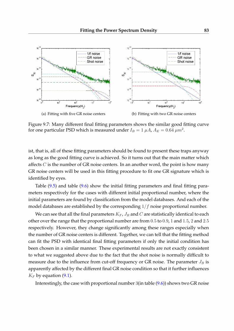
Fitting the Power Spectrum Density 83
(a) Fitting with five GR noise centers (b) Fitting with two GR noise centers
Figure 9.7: Many different final fitting parameters shows the similar good fitting curvefor one particular PSD which is measured under IB = 1 µA, AE = 0.64 µm2.
ist, that is, all of these fitting parameters should be found to present these traps anywayas long as the good fitting curve is achieved. So it turns out that the main matter whichaffects C is the number of GR noise centers. In an another word, the point is how manyGR noise centers will be used in this fitting procedure to fit one GR signature which isidentified by eyes.
Table (9.5) and table (9.6) show the initial fitting parameters and final fitting para-meters respectively for the cases with different initial proportional number, where theinitial parameters are found by classification from the model databases. And each of themodel databases are established by the corresponding 1/f noise proportional number.
We can see that all the final parameters KF , JB and C are statistically identical to eachother over the range that the proportional number are from 0.5 to 0.9, 1 and 1.5, 2 and 2.5
respectively. However, they change significantly among these ranges especially whenthe number of GR noise centers is different. Together, we can tell that the fitting methodcan fit the PSD with identical final fitting parameters if only the initial condition hasbeen chosen in a similar manner. These experimental results are not exactly consistentto what we suggested above due to the fact that the shot noise is normally difficult tomeasure due to the influence from cut-off frequency or GR noise. The parameter JB isapparently affected by the different final GR noise condition so that it further influencesKF by equation (9.1).
Interestingly, the case with proportional number 3(in table (9.6)) shows two GR noise

84
Proportion KF (10−10) JB(105) C(10−33) fc(HZ)0.5 2.15 5.26 1.55 1 5 50 100 2000.6 1.11 5.26 3.64 1 10 50 100 2000.7 1.44 5.26 3.91 1 50 100 200 4000.8 8.89 5.26 1.16 1 50 100 200 4000.9 11.1 5.26 1.2 1 100 200 400 8001 1.22 5.26 8.5 10 200 400 800 1600
1.5 4.23 5.26 6.5 100 400 800 1600 32002 1.77 5.26 21.9 200 800 3200 6400
2.5 1.99 5.26 29.8 800 1600 3200 64003 0.61 5.26 107 3200 6400
Table 9.5: The various initial fitting parameters.
Proportion KF (10−11) JB(106) C(10−33) fc(HZ)0.5 3.27 1.48 0.93 145 145 335 3510 35100.6 2.8 1.46 1.04 91 254 296 4049 40590.7 3.27 1.48 0.93 146 146 331 3496 34960.8 3.25 1.48 0.91 131 174 285 3286 32880.9 3.27 1.48 0.93 145 145 333 3503 35031 4.15 1.31 1.73 137 250 5451 5451 5451
1.5 4.15 1.31 1.73 137 249 5448 5448 54482 6.22 1.08 4.93 181 5990 9056 9056
2.5 6.24 1.08 4.94 181 6127 8943 89433 3.61 1.42 2.84 178 3813
Table 9.6: The various final fitting parameters.
centers which just locate at the position we can visually predict as shown in figure 9.7(b).Then it is considered as the most efficient parameters for the PSD model, equation (9.4).
To sum up, based on the practical fitting method, the fitting parameters KF , JB andC are statistically stable for one particular PSD to a certain initial condition extent.
9.5.2 Identify the GR noise component
By using the practical fitting procedure, we want to show if the PSD measured at dif-ferent base currents for the same device will show a similar GR noise component. Inanother word, if fluctuations of the base current will introduce fluctuations of the GRcenters.
Figure 9.8 shows two PSDs which are measured under different base current from

Fitting the Power Spectrum Density 85
the same device which is fabricated by 10 parallel transistors. Table (9.7) lists the finalconditions of this two fitting curve. Apparently, these two PSD have the similar GRnoise centers which means that the increased base current does not activate new GRtraps in this device.
Figure 9.8: For one parallel device, its PSD shows similar GR noise component underdifferent base current.
IB(µA) KF (10−10) JB(106) C(10−32) fc(HZ)1 1.32 1.38 3.71 2.762 0.67 3.43 1.46 2.87
Table 9.7: The two PSD with different IB conditions present the same GR noise centersin a parallel device.
The situation becomes different when we do the same experiment on a single devicewith the same emitter area, which is proven to be relatively unstable compared to theparallel device(section 7.4.2). In table (9.8), it is obvious that the higher base currentactivates more GR noise traps.
9.5.3 The IB Dependence Of Noise Model parameters
By definition, both KF and C are constant for one particular device. So only JB shouldhave IB dependence, JB ∝ IB. In this section, we will see if the practical fitting methodcan find this relationship.

86
Figure 9.9: For one single device, its PSDs show different GR noise component underdifferent base current.
IB(µA) KF (10−10) JB(105) C(10−32) fc(HZ)0.5 3.36 3.9 1.26 11.5 23.81 3.41 8.84 1.43 11.3 69.5 1172 1.18 18.8 1.38 13.2 91 93.5 314 1191
Table 9.8: The three PSD with different IB conditions present variant GR noise centersin a single device.
From foregoing discussion, the fitting parameters KF , JB and C are related to the1/f noise, shot noise and GR noise respectively. In section 7.2, we know that the PSDof 1/f noise and GR noise has IB dependence, SIB
∝ I2B, which are consistent with the
expression of noise model equation (9.4) where all the three noise sources are related toIB. Separately, the 1/f noise is proportional to IAF
B ; the GR noise is proportional to J2B
and the shot noise is directly related to IB.The practical fitting method, however, have KF and C as the fitting parameter, that
is, they will be fitted anyway. In spite of this, we prefer that they do not have any IB
dependence, and all the noise source level variations are contributed by the fitted IB asthe theory indicates above.
Here, we discovered two kinds of device, the LFN of one of them is mainly dom-inated by 1/f noise and GR noise dominate the LFN of another one, as shown in fig-ure 9.10.
By fitting their PSDs, which are measured at IB = 0.2, 0.5, 0.8, 1 and 2 µA, we got the

Fitting the Power Spectrum Density 87
(a) The 1/f noise dominate the PSD (b) The GR noise dominate the PSD
Figure 9.10: Two types of device with 1/f noise dominant and GR noise dominant re-spectively.
plots with KF , JB and C versus IB respectively.
(a) JB under 1/f noise dominant (b) JB under GR noise dominant
Figure 9.11: JB variation with 1/f noise dominant and GR noise dominant respectively.
In figure 9.11, we see that JB always approximately has the expected IB dependence,JB ∝ IB, despite which noise source dominates. Again, because of the large possibilitythat the shot noise could be affected by the cut-off frequency and GR noise, the fitted JB
therefore shows slightly offset from the expected relationship in both cases, especiallywhen GR noise dominates the PSD, the influence is even more obvious.
As shown in section 9.5.1, C and KF vary due to the situation of GR noise. In fig-

88
(a) C under 1/f noise dominant (b) C under GR noise dominant
Figure 9.12: C variation with 1/f noise dominant and GR noise dominant respectively.
ure 9.12 and figure 9.13, we see that C and KF are stable as we expect in the case inwhich the 1/f noise dominates the spectra. When GR noise dominates, however, C
and KF drastically show the IB dependence, which occurred due to the fitted JB. Fromfigure 9.11(b), we know that the fitted shot noise has been severely affected by the GRnoises since JB is proportional to I1.4
B . Once JB is affected, C and KF will be conse-quently affected by the relationships shown in equation (9.2) and equation (9.1) respec-tively. And the gradients of them exactly show these relations. In terms of these discus-sions, we can tell that the practical method could be engaged to identify if the GR noisesources influence the measurement of the shot noise.
9.5.4 The Emitter Geometrical Dependence of Fitting Parameters
Following the same idea in section 9.5.3, we will investigate the emitter geometrical(emitterarea and perimeter) dependence of these fitting parameters. Under the same base cur-rent IB = 1 µA, We measured many devices with different emitter areas(0.048, 0.12, 0.25, 0.3, 1.28
and 1.8 µm2) and different emitter perimeters(0.88, 1.6, 2.5, 3.3, 4.8, 6.15, 8.4, 12.4 and 16.8
µm) respectively. By fitting them, we got series of fitting parameters discussed below.
The Parameter KF
KF is normally found to be inversely proportional to AE [Sanden and Deen, 2002]. Fig-ure 9.14(a) shows KF which we calculated from the practical fitting method we devel-oped in section 9.4. The gradient shows that the KF is proportional to A−0.2
E instead of

Fitting the Power Spectrum Density 89
(a) KF under 1/f noise dominant (b) KF under GR noise dominant
Figure 9.13: KF variation with 1/f noise dominant and GR noise dominant respectively.
the commonly accepted, KF ∝ A−1E . This happened due a big part to a similar reason
when we discussed the AE dependence of LFN in section 7.3. Subsequently, this resultis almost consistent to the result of Emitter-Area dependence which we got previouslyin figure 7.6(a). The KF versus Emitter-Perimeter, shown in figure 9.14(b), shows thesimilar trend as the perimeter does. Since the emitter-perimeter is also a essential prop-erty of device like emitter-area, it is not surprised that KF also has emitter-perimeterdependence.
(a) KF versus AE (b) KF versus Emitter-Perimeter
Figure 9.14: The emitter geometrical dependence of KF .

90
The Parameter C
Knowing that C is related to the GR noise level of the devices and both the biggeremitter area and longer emitter perimeter could introduce more GR traps, therefore C
should have both these two kinds of dependence. In our fitting results, C increase asthe increasing of both the area and perimeter as shown in figure 9.15. From these result,we can argue that the larger device has bigger C.
(a) C versus AE (b) C versus Emitter-Perimeter
Figure 9.15: The emitter geometrical dependence of C.
The Parameter JB
Under the same base current(IB), JB should be proportional to the emitter area(AE) interms of the relationship JB = IB
AE. Figure 9.16 shows this relationship.
9.6 Summary of The Fitting Method
To sum up, the theoretical fitting method can only be used for normal devices, thereforeit is not useful in practice due to the various interferences. However, the practical fittingmethod has been proven to be an efficient and robust method to not only automaticallyfit any power spectrum density, but also dramatically show all of the noise sources of thetransistors. We simply summarize some advantages and disadvantages of the practicalfitting method below:
• Advantages

Fitting the Power Spectrum Density 91
Figure 9.16: JB versus AE .
– Automatic fitting;
– Identifying each noise component, 1/f noise, GR noises and shot noise;
– Lending itself to investigating the parameters in the noise model.
• Disadvantages
– Relatively long calculation time;
– Sometimes giving meaningless fitting parameters;
– Can not guarantee finding the most efficient fitting parameters as shown intable (9.6).
Whatever happens, this practical fitting method shows a strong potential that it canbe further developed to overcome these disadvantages, and to be employed by otherapplications.

92

Chapter 10
Summary and Conclusions
From a device perspective, the Low-frequency noise in the fourth generation 375 GHZ
SiGe HBTs was measured in this work. Investigating the power spectrum density char-acteristics of LFN is the most important issue we have worked on in this thesis, espe-cially by employing the automatic fitting procedure.
Some elementary semiconductor concepts were introduced in chapter 2. From in-trinsic semiconductor to extrinsic semiconductor, and from diode to bipolar junctiontransistor, we systematically illustrated the operation mechanism of semiconductor tran-sistors. In the meantime, each current component in the transistor under active modehas been represented schematically.
The following chapter then introduced the advantages and the fabrication of SiGeHBT whose primary difference from BJT in fabrication technology is that the base isunevenly doped by introducing Ge into Si for achieving higher speed.
In chapter 4, we investigated the origin of the thermal noise, shot noise, generation-recombination noise and 1/f noise respectively, especially the last three noises whichare supposed to be the dominating contributors of the LFN spectrum. Consequently,we got the LFN power spectrum density model in terms of them.
We introduced some spectrum estimators(Periodogram and Multitaper) in chapter 5.The significance that we represent the LFN by using PSD was illustrated as well.
In the experimental part, we firstly established a LFN measurement system. Thissystem was built based on the purpose that constructing a automatic, accurate and effi-cient measurement circumstance without any interferences.
By using this measurement system, we measured several sequences of PSD, de-scribed in chapter 7. By analyzing these PSDs, we therefore can investigate a varietyof properties of LFN of SiGe HBTs, such as the dominant noise source, the current and

94
geometrical scaling dependence, the variation related to the fabrication and emitter areaof devices, etc. These highly scaled devices show unpredictable LFN behaviour, andtherefore are very difficult to model using existing theory.
We put our special efforts in developing the fitting procedure in chapter 9. Thisprocedure realizes the expectation to automatically fit any power spectrum density ofLFN. Impressively, it shows all of the noise components(1/f noise, GR noise and shotnoise) in its final fitting parameters as shown in many figures of this work and visuallyhelp us understand the components of the PSD. Furthermore, it also shows its uniqueability to estimate the parameters of the noise model so that we can investigate theprinciple of them compared to previous works. However, this method is not perfectyet. For instance, it sometimes gives meaningless final parameter(negative value) andbig variation. The initial condition sensitivity, which generates many different finalparameter combinations, is another disadvantage of it. In any case, this method givesus a new way to fit PSD and can be further developed to be engaged to other relevantworks.
Future Work
The study about the new generation SiGe HBTs is far from finished yet. Due to the lim-ited number of device and tense time schedule, we can just do this far. The automatic fit-ting procedure, which has been introduced in this work, shows some interesting pointsfor studying the LFN and is therefore worth to be further perfected such as using morereasonable GR noise distribution, different noise model function for establishing themodel database and looking into the non-linear fitting procedure itself, etc.

Chapter 11
Appendix
11.1 The Flow Chart of The Automatic Fitting Method
The flow chart in figure 11.1 shows the core work mechanism of the fitting procedure.In the initialization part, all the initial information of this procedure require is the
test power spectrum density itself and the device emitter-area, from which we can ap-proximately estimate the 1/f noise level, GR noise level and shot noise level. The modeldatabase then can be established in terms of these noise level and various combinationsof GR noise centers.
The non-linear fitting part contains some control elements to assure the operationof this procedure. Essentially, we need the fitting result has both meaningful fittingparameters and as small as possible variation from the original PSD. In order to achievethis purpose, we have many iterations in each of which the 1/f noise and GR noiselevel have been slightly adjusted reversely because of the fact that only one noise sourcedominate in a certain frequency range.
Inevitably, this procedure can not find any fitting curve even a one with meaninglessfitting parameters in some extreme cases, such as the very noisy device where the cut-offfrequency occurred in the fitting frequency range.

96
Figure 11.1: Practical fitting method flow chart.

Bibliography
Adel S. Sedra, K. C. S. (1998). Microelectronic Circuits(Fourth Edition). Oxford UniversityPress, Inc.
A.Gruhle and C.Mahner (1997). Low 1/f noise sige hbt’s with application to low phasenoise microwave oscillators. Electronic Letters, 33:2050–2052.
Chen, X. Y., Johansen, J. A., Salm, C., and van Rheenen, A. D. (2001). On low-frequencynoise of polycrystalline GexSi1−x for sub-micron CMOS technologies. Solid-State Elec-tronics, 45(11):1967–1971.
Cressler, J. D. and Niu, G. (2002). Silicon-Germanium Heterojunction Bipolar Transistors.Artech House, Inc, 685 Canton Street Norwood, MA 02062.
D’yakonova, N. V., Levinshtein, M. E., and Rumyantsev, S. L. (1991). Temperature-dependence of the low-frequency noise in structurally perfect GaAs and after de-structive compression. Soviet Physics Semiconductors, 25(2):217–218.
F.Capasso (1987). Band-gap engineering: from physics and materials to new semicon-ductor devices. Science, 235:172–176.
Hanssen, A. (2003). Introduction to STATISTICAL SIGNAL PROCESSING AND DATAANALYSIS. Physics Department, University of Tromsø.
H.A.W.Markus and T.G.M.Kleinpenning (1995). Low-frequency noise in polysiliconemitter bipolar transistors. IEEE Transactions on Electron Devices, 42(4):720–727.
Hooge, F. N. (1969). 1/f noise is no surface effect. Physics Letters A, 29(3):139–140.
Hooge, F. N. (1994). 1/f noise sources. IEEE Transactions on Electron Devices, 41(11):1926–1935.
Hooge, F. N. (2003). On the additivity of generation-recombination spectra. Part 2: 1/f
noise. Physica B: Condensed Matter, 336(3-4):236–251.

98
Hooge, F. N. and Vandamme, L. K. J. (1978). Lattice scattering causes 1/f noise. PhysicsLetters A, 66A(4):315–316.
Iyer, S. S. and et al. (1987). Silicon-germanium base heterojunction bipolar transistorsby molecular beam epitaxy. Tech. Dig. IEEE Int. Elect. Dev. Meeting, pages 874–876.
Jin, Z. (2004). Low-Frequency Noise in SiGe BiCMOS Technology. PhD thesis, Shool ofElectrical and Computer Engineering Georgia Institute of Technology, Georgia, USA.
Jin, Z., Cressler, J. D., Niu, G., and Joseph, A. J. (2002). Low-frequency noise variationin scaled SiGe HBTs. In Proceedings of IEEE Bipolar/BiCMOS Circuits and TechnologyMeeting (BCTM), pages 224–227, Monterey, CA, USA.
Jin, Z., Cressler, J. D., Niu, G. F., and Joseph, A. J. (2003). Impact of geometrical scalingon low-frequency noise in SiGe HBTs. IEEE Transactions on Electron Devices, 50:676–682.
Johansen, J. A., Jin, Z., Cressler, J. D., and Joseph, A. J. (2003). Geometry-dependentlow-frequency noise variations in 120 GHz fT SiGe HBTs. In Ponchak, G. E., editor,Digest of Papers, Topical Meeting on Silicon Monolitic Integrated Circuits in RF Systems(SiRF), pages 57–59, Grainau, Germany.
Jones, B. K. (1994). Low-frequency noise spectroscopy. IEEE Transactions on ElectronDevices, 41(11):2188–2197.
Joseph, A., Coolbaugh, D., Zierak, M., Wuthrich, R., Geiss, P., He, Z., Liu, X., Orner, B.,Johnson, J., Freeman, G., Ahlgren, D., Jagannathan, B., Lanzerotti, L., Ramachandran,V., Malinowski, J., Chen, H., Chu, J., Gray, P., Johnson, R., Dunn, J., Subbanna, S.,Schonenberg, K., Harame, D., Groves, R., Watson, K., Jadus, D., Meghelli, M., andRylyakov, A. (2001). A 0.18 µm BiCMOS technology featuring 120/100 GHz (fT /fmax)HBT and ASIC-compatible CMOS using copper interconnect. In Proceedings of IEEEBipolar/BiCMOS Circuits and Technology Meeting (BCTM), pages 143–146, Minneapolis,MN, USA.
Kasap, S. O. (1997). Principles of Electrical Engineering Materials and Devices. Tom Casson.
Kingston, R. H. and McWhorter, A. L. (1956). Relaxation time of surface states on ger-manium. Physical Review, 103(3):534–540.
Kroemer, H. (1957). Theory of a wide-gap emitter for transistors. Proc. IRE, 45(11):1535–1537.

BIBLIOGRAPHY 99
L.S.Vempati, J.D.Cressler, F.A.Babcock, R.C.Jaeger, and D.L.Harame (1996). Low-frequency noise in uhv/cvd epitaxial si and sige bipolar transistors. IEEE Journalof Solid-State Circuits, 31(10):1458–1467.
McWhorter, A. L. (1955). Surface traps and 1-f noise in germanium. Physical Review,98:1191–1192.
Niu, G. (2005). Noise in sige hbt rf technology:physics, modeling, and circuit implica-tions. Proceedings of the IEEE, 93(9):1583–1597.
P.-F.Lu (1987). Low-frequency noise in self-aligned bipolar transistors. J.App.Phys.,62:1335–1339.
Pierret, R. F. (1988). Volume I Semiconductor Fundamentals(Second Edition). Addison-Wesley publishing Company.
Plana, R., Escotte, L., Roux, J. P., Graffeuil, J., Gruhle, A., and Kibbel, H. (1995). 1/f
noise in self-aligned Si/SiGe heterojunction bipolar transistor. IEEE Electron DeviceLetters, 16(2):58–60.
R. Brederlow, W. Weber, C. D. D. S.-L. and Thewes, R. (2001). Low-frequency noiseof integrated poly-silicon resistors. IEEE Transactions on Electron Devices, 48(6):1180–1187.
Riedel, K, S. and Sidorenko, A. (1995). Minimum bias multiple taper spectral estimation.IEEE Transactions on Signal Processing, (43):188–195.
S. P. O. Bruce, L. K. J. V. and Rydberg, A. (1999). Measurement of low-frequency base andcollector current noise and coherence in sige heterojunction bipolar transistors usingtransimpedance amplifiers. IEEE Transactions on Electron Devices, 46(5):993–1000.
Sanden, M. and Deen, M. (2002). Low-frequency noise in advanced si-based bipolartransistors and circuits. American Scientific Publishers, pages 235–247.
Sanden, M., Marinov, O., Deen, M. J., and Ostling, M. M. (2002). A new model for thelow-frequency noise and the noise level variation in polysilicon emitter BJTs. IEEETransactions on Electron Devices, 49(3):514–520.
Schottky, W. (1918). Uber spontane Stromschwankungen in verschiedenen Elek-trizitatsleitern. Annalen der Physik, 57:541–567.
Slepian, D. (1978). Prolate spheroidal wave functions, fourier analysis and uncertainty;v: The discrete case. Bell Syst. Tech., (5):1371–1429.

100
Surdin, M. (1939). Fluctuation of thermionic current and the ”flicker” effect. Journal dePhysique et le Radium, 10:188–189.
Thomson, D. J. (1982). Spectrum estimation and harmonic analysis. Proceedings of theIEEE, 70(9):1055–1096.
van der Ziel, A. (1955). Theory of shot noise in junction diodes and junction transistors.Proc.IRE, 43:1639–1646.
van der Ziel, A. (1979). Advanced Electronic Electron Physics. Academic Press, New York.
Vandamme, L. K. J. (1989). Bulk and surface 1/f noise. IEEE Transactions on ElectronDevices, 36(5).
W.Neudeck, G. and Pierret, R. F. (1989). Volume III Semiconductor Fundamentals(SecondEdition). Addison-Wesley publishing Company.
Ziel, A. V. D. (1989). Formulation of surface 1/f noise processes in bipolar junctiontransistor and in p− n diodes in hooge-type form. Solid-State Electronics, 32(1):91–93.