Embed Size (px)
Citation preview

WE3C-3
Tracking Phaselock Loop Characteristics with a VCO
Using a Barium Strontium Titanate (BST)
Thin-Film Varactor12 12 .2A. Victor' , Member IEEE, J. Nathl, Student Member IEEE, K. G. Gard , Member IEEE, J.-P. Maria
A. I. Kingon3, Member IEEE, and M. B. Steer2, Fellow IEEE
Microwave Communication Division, Harris Corporation, Morrisville, NC-27560, USA,2Electrical and Computer Engineering, North Carolina State University, Raleigh, NC-27695-7914,USA2Materials Science and Engineering, North Carolina State University, Raleigh, NC-27695-7919,USA,
Ph: +1-919-767-3277, Email: [email protected]
Abstract - Barium Strontium Titanate (BST) varactorsutilized in a VCO demonstrate unique tuning characteristicscompared to junction varactors. A 2.7 GHz microstrip line VCOoperates in a tracking phaselock loop configured as an X4frequency multiplier. BST oscillator tuning and the effect on loopdynamics is observed by the intentional design of an underdamped system. Oscillator noise correction and peaking is notedparticularly at low tune voltages. Loop dynamics are addressedthrough proper design of the loop compensator filter. Thedifferences between BST varactor and junction varactoroperation in frequency control are noted.
Index Terms - BST, VCO, PLL, loop filter, tracking loop,ferroelectric, resonator.
I. INTRODUCTION
Oscillators embedded in a phaselock loop (PLL) benefitfrom improved phase noise performance if the characteristicsof the loop are properly designed. Stringent phase noiserequirements are a challenge for high power oscillator designs,which emphasize DC conversion efficiency, output power,tune range, and harmonic content. Circuit phase noise,sensitivity to vibration and microphonics, and power supplynoise sensitivity are suppressed through the error feedbackfunction associated with the loop gain and dynamics [1].
This work addresses the influence of oscillator tunecharacteristics on loop performance. The tune characteristic ofa BST varactor displays a unique C-V curve, which unlike ajunction varactor, presents a non-monotonic tune response.This tune response coupled with the reduction in oscillatortune gain at zero volts is discussed. The effect on operatingperformance in a tracking phase loop configured as frequencymultiplier, a method of readily observing the loop dynamicsand required design modifications are presented.
II. BST Vs. JUNCTION VARACTOR PROPERTIES
The capacitance variation of a BST varactor was comparedwith that of a semiconductor junction varactor. BST varactorexhibits symmetrical tuning about 0 V (see Fig. 2) while thejunction varactor increases monotonically with decreasingreverse bias down to forward bias of 570 mV. Beyond that thejunction shows a positive reactance due to parasitic effects andhigh forward conduction (see Fig. 1). This is due to thefundamental difference in the tuning mechanism for the BSTand the junction varactor. The C-V curve for a junctionvaractor is asymmetrical about zero volts since the tuningmechanism relies on existence of a depletion region in thepresence of reverse bias and the change of depletion widthwith voltage. Capacitive tuning in a BST varactor is due todistortion of the unit cell as a function of applied electric fieldmagnitude and hence is independent of the sign of the appliedvoltage [2].
Fig. 1: Junction varactor reflection coefficient versus swept bias from -30V to+1V. Point (a) on the chart represents 570 mV forward bias. Themeasurement frequency is held constant at 50 MHz.
1-4244-0445-2/07/$20.00 ©2007 IEEE289
Authorized licensed use limited to: North Carolina State University. Downloaded on February 2, 2009 at 13:57 from IEEE Xplore. Restrictions apply.

0.05
0.04
0.03
0.02
I-0C,,C,,n
CD(D
The incremental Ko0 evaluated by measuring a smalldeviation in tune voltage about a nominal value is 400-550KHzNV below a tune voltage of 10 V. As the tune voltageapproaches zero this gain is reduced, see Fig. 3. Depending onresonator topology, varactor index of nonlinearity (y forjunction varactors or power law of the junction), and theinterface to the active device, it is possible to extend the tunevoltage [5] to lower values while maintaining KO.
0.01
0-30 -20 -10 0 10 20 30
Applied Voltage (V)Fig. 2: Representative C-V characteristics of a BST interdigital varactormeasured after dicing at 1 MHz.
III. BST VCO OPERATION
The VCO in this work operates at 2.7 GHz and is shown inFig. 4. The inductive portion of the resonator consists of a 60degree shorted 30-ohm microstrip line fabricated on Roger4350 material. The coupling elements to the active device andvaractor network are also mounted on the same board. Thisimplementation uses a single BST varactor located in theupper right corner of the card. The design card provides foradditional series stacked back-to-back BST varactors as wellas additional tune bias RF choke components [3]. Thisconfiguration will reduce the RF voltage across each varactorby a factor of N, where N is the total number of varactors inthe stack up, and hence improve linearity [4]. The averageoscillator tune gain, Ko for 0V << VTUNE < 30V (30V limitimposed by the active loop compensator) is 1 MHz/V. Openloop measurements to 60 V also demonstrates good linearity.Although the breakdown voltage of the BST varactor is 200 V,measurements are limited to 60 V due to on-chip ceramic onglass (COG) chip capacitor breakdown. The adjustment of thecapacitive coupling between the varactor, transmission line,and active device, will set Ko and linearity.
1400
i=-==112001000
3003
..--- - 600
.. I..... ..... 400
.--...200
276 0
10 0 10 20 30 40 50 60 70
Vtune(V)
Fig. 3: Measurement of tune frequency and K0 versus tuning voltage
Fig. 4: Microstrip VCO shown with tune line input on the right output powerobtained from matching transmission line on left. The BST varactor is locatedin upper right corner.
Evidence of the reduction in tune gain near zero volts for theVCO presented in this work is clear by inspection of loopbehavior discussed next.
IV. TRACKING LooP FRAMEWORK
The property of oscillator performance and correction by atracking loop is documented in a number of references[1, 6, 7]. The loop bandwidth is a function of the VCOgain, K0 and the loop control elements, which include thephase detector gain, K d' loop compensator, F(s), and counter,N. If the counter is absent, the loop acts as tracking filter, thefilter response set by the loop compensator. The VCO willtrack a reference source, fREF , which must be at the samefrequency as the VCO. Otherwise if a counter is present with acount value of N, the VCO will operate at NfREF. If the loophas sufficient open loop gain given by the product ofKoKdF (s) /sN then the phase noise of the reference istransferred to the controlled VCO. Although other sources ofnoise in the loop can dominate, for this analysis they areneglected. The transfer function assuming small signalanalysis, a stable locked loop and N=1 is given in terms of theLaplace variable S=jW as,
oo (s)= 0KKd (s) r(s) (1)s+KoKdF(s)
290
nsn0
0.
a)C
0.QC.)
0.85
0.80-
0.75-
0.70I0.65
0.60 _ el 0
0.55 00
0.50c
2.83
2.81
_/ 28
2.79
2.78
2 77
Authorized licensed use limited to: North Carolina State University. Downloaded on February 2, 2009 at 13:57 from IEEE Xplore. Restrictions apply.
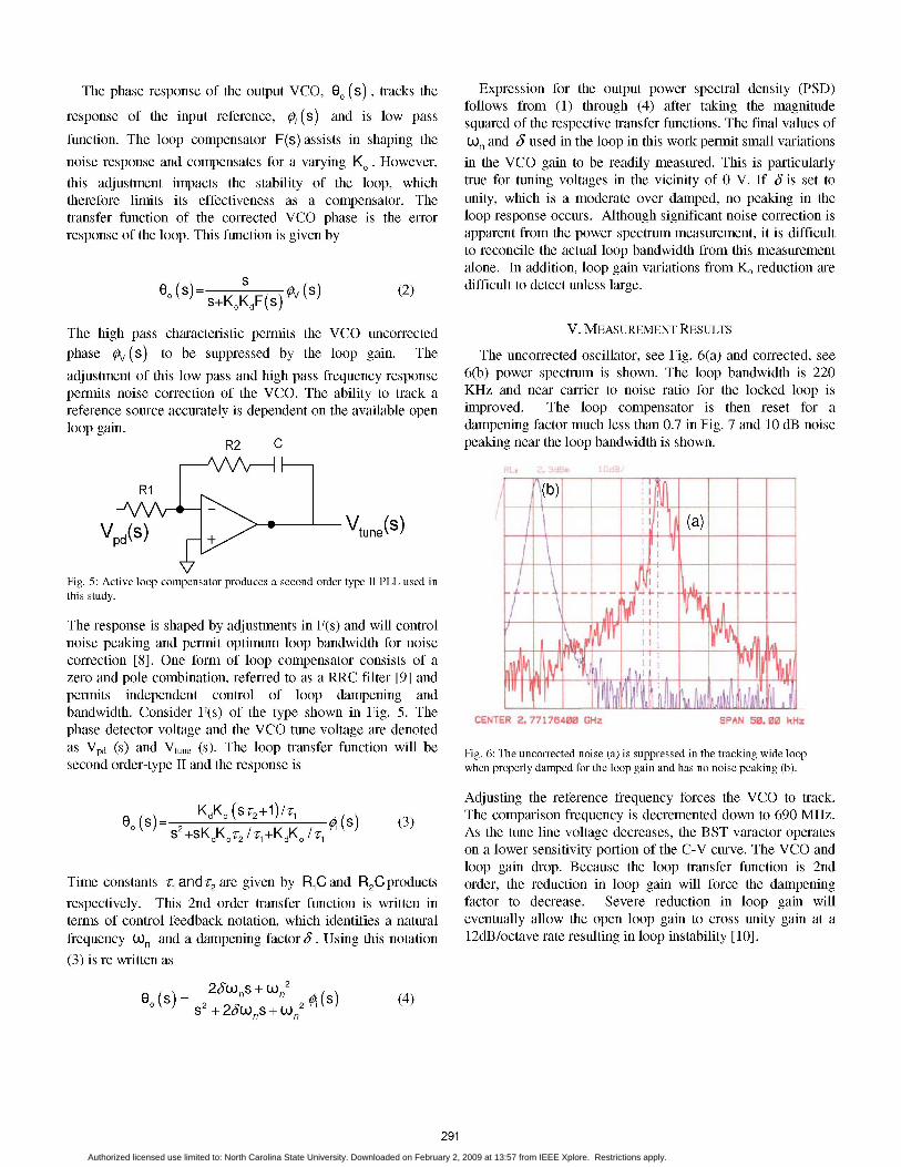
The phase response of the output VCO, E) (s), tracks the
response of the input reference, Oi (s) and is low pass
function. The loop compensator F(s) assists in shaping thenoise response and compensates for a varying KO. However,this adjustment impacts the stability of the loop, whichtherefore limits its effectiveness as a compensator. Thetransfer function of the corrected VCO phase is the errorresponse of the loop. This function is given by
e° () s+KoKdF(s) p(s)(2)
The high pass characteristic permits the VCO uncorrectedphase ov (s) to be suppressed by the loop gain. The
adjustment of this low pass and high pass frequency responsepermits noise correction of the VCO. The ability to track areference source accurately is dependent on the available openloop gain.
R2 C
-I~Rl
Vtune(S)Vpd(S)
Expression for the output power spectral density (PSD)follows from (1) through (4) after taking the magnitudesquared of the respective transfer functions. The final values ofWn and S used in the loop in this work permit small variationsin the VCO gain to be readily measured. This is particularlytrue for tuning voltages in the vicinity of 0 V. If 3 is set tounity, which is a moderate over damped, no peaking in theloop response occurs. Although significant noise correction isapparent from the power spectrum measurement, it is difficultto reconcile the actual loop bandwidth from this measurementalone. In addition, loop gain variations from Ko reduction aredifficult to detect unless large.
V. MEASUREMENT RESULTS
The uncorrected oscillator, see Fig. 6(a) and corrected, see6(b) power spectrum is shown. The loop bandwidth is 220KHz and near carrier to noise ratio for the locked loop isimproved. The loop compensator is then reset for adampening factor much less than 0.7 in Fig. 7 and 10 dB noisepeaking near the loop bandwidth is shown.
(a)
Fig. 5: Active loop compensator produces a second order type II PLL used inthis study.
The response is shaped by adjustments in F(s) and will controlnoise peaking and permit optimum loop bandwidth for noisecorrection [8]. One form of loop compensator consists of azero and pole combination, referred to as a RRC filter [9] andpermits independent control of loop dampening andbandwidth. Consider F(s) of the type shown in Fig. 5. Thephase detector voltage and the VCO tune voltage are denotedas Vpd (s) and Vtune (s). The loop transfer function will besecond order-type II and the response is
E. (s) = o2 .+1 (s) (3)52+sKdKO2r l/+KdKo Ir
Time constants z1 and r2 are given by Rj0 and R20 productsrespectively. This 2nd order transfer function is written interms of control feedback notation, which identifies a naturalfrequency Wn and a dampening factor 3. Using this notation(3) is re written as
e0 (s) 2+2WS+W 2 (s) (4)S 25w + n
Fig. 6: The uncorrected noise (a) is suppressed in the tracking wide loopwhen properly damped for the loop gain and has no noise peaking (b).
Adjusting the reference frequency forces the VCO to track.The comparison frequency is decremented down to 690 MHz.As the tune line voltage decreases, the BST varactor operateson a lower sensitivity portion of the C-V curve. The VCO andloop gain drop. Because the loop transfer function is 2ndorder, the reduction in loop gain will force the dampeningfactor to decrease. Severe reduction in loop gain willeventually allow the open loop gain to cross unity gain at a12dB/octave rate resulting in loop instability [10].
291Authorized licensed use limited to: North Carolina State University. Downloaded on February 2, 2009 at 13:57 from IEEE Xplore. Restrictions apply.
circuits. To eliminate this problem, the output of thecompensator should be clamped or the supply voltage -Vb notused.
VI. CONCLUSION
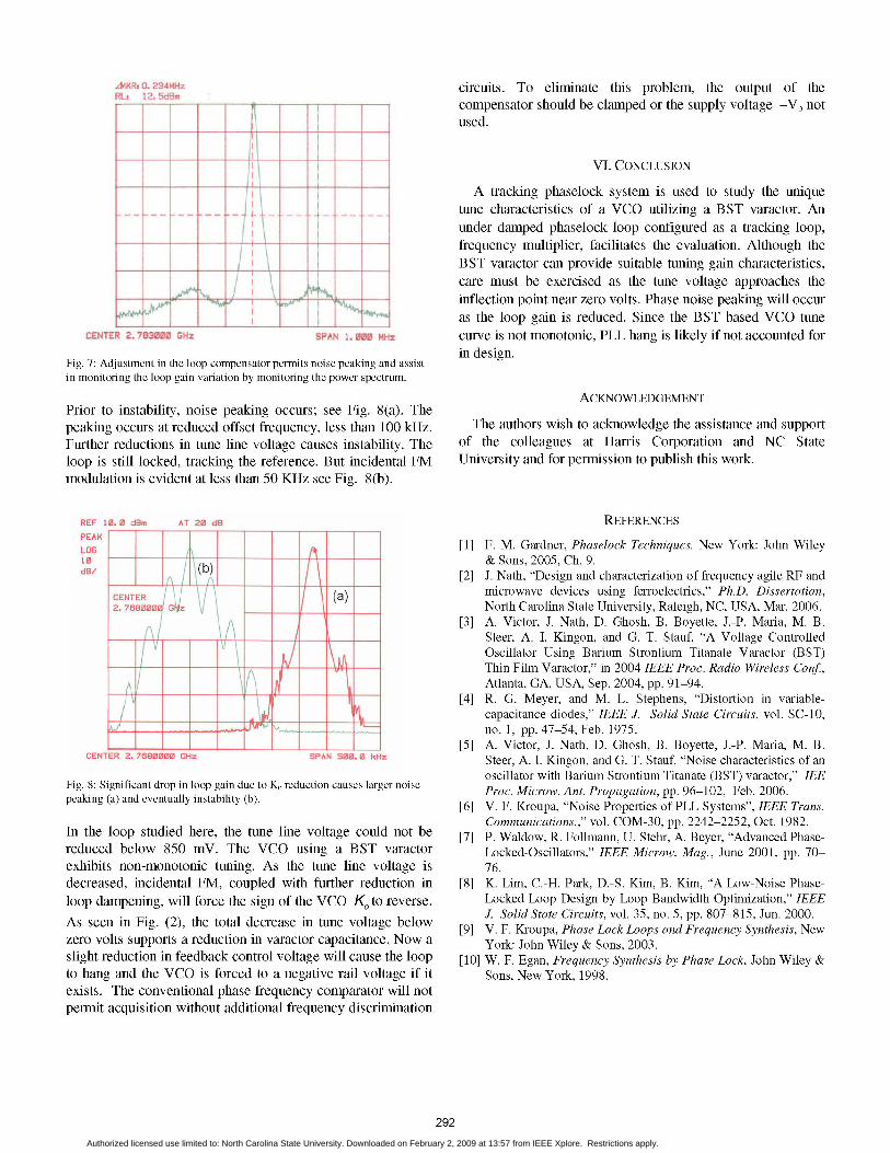
Fig. 7: Adjustment in the loop compensator permits noise peaking and assistin monitoring the loop gain variation by monitoring the power spectrum.
Prior to instability, noise peaking occurs; see Fig. 8(a). Thepeaking occurs at reduced offset frequency, less than 100 kHz.Further reductions in tune line voltage causes instability. Theloop is still locked, tracking the reference. But incidental FMmodulation is evident at less than 50 KHz see Fig. 8(b).
(b)
~ER I'g., . I I X I Iia)2. 7680Iog
Fig. 8: Significant drop in loop gain due to K0 reduction causes larger noisepeaking (a) and eventually instability (b).
In the loop studied here, the tune line voltage could not bereduced below 850 mV. The VCO using a BST varactorexhibits non-monotonic tuning. As the tune line voltage isdecreased, incidental FM, coupled with further reduction inloop dampening, will force the sign of the VCO K to reverse.
As seen in Fig. (2), the total decrease in tune voltage belowzero volts supports a reduction in varactor capacitance. Now a
slight reduction in feedback control voltage will cause the loopto hang and the VCO is forced to a negative rail voltage if itexists. The conventional phase frequency comparator will notpermit acquisition without additional frequency discrimination
A tracking phaselock system is used to study the uniquetune characteristics of a VCO utilizing a BST varactor. Anunder damped phaselock loop configured as a tracking loop,frequency multiplier, facilitates the evaluation. Although theBST varactor can provide suitable tuning gain characteristics,care must be exercised as the tune voltage approaches theinflection point near zero volts. Phase noise peaking will occuras the loop gain is reduced. Since the BST based VCO tunecurve is not monotonic, PLL hang is likely if not accounted forin design.
ACKNOWLEDGEMENT
The authors wish to acknowledge the assistance and supportof the colleagues at Harris Corporation and NC StateUniversity and for permission to publish this work.
REFERENCES
[1] F. M. Gardner, Phaselock Techniques. New York: John Wiley& Sons, 2005, Ch. 9.
[2] J. Nath, "Design and characterization of frequency agile RF andmicrowave devices using ferroelectrics," Ph.D. Dissertation,North Carolina State University, Raleigh, NC, USA, Mar. 2006.
[3] A. Victor, J. Nath, D. Ghosh, B. Boyette, J.-P. Maria, M. B.Steer, A. I. Kingon, and G. T. Stauf, "A Voltage ControlledOscillator Using Barium Strontium Titanate Varactor (BST)Thin Film Varactor," in 2004 IEEE Proc. Radio Wireless Conf.,Atlanta, GA, USA, Sep. 2004, pp. 91-94.
[4] R. G. Meyer, and M. L. Stephens, "Distortion in variable-capacitance diodes," IEEE J. Solid State Circuits, vol. SC-10,no. 1, pp. 47-54, Feb. 1975.
[5] A. Victor, J. Nath, D. Ghosh, B. Boyette, J.-P. Maria, M. B.Steer, A. I. Kingon, and G. T. Stauf, "Noise characteristics of anoscillator with Barium Strontium Titanate (BST) varactor," IEEProc. Microw. Ant. Propagation, pp. 96-102, Feb. 2006.
[6] V. F. Kroupa, "Noise Properties of PLL Systems", IEEE Trans.Communications.," vol. COM-30, pp. 2242-2252, Oct. 1982.
[7] P. Waldow, R. Follmann, U. Stehr, A. Beyer, "Advanced Phase-Locked-Oscillators," IEEE Microw. Mag., June 2001, pp. 70-76.
[8] K. Lim, C.-H. Park, D.-S. Kim, B. Kim, "A Low-Noise Phase-Locked Loop Design by Loop Bandwidth Optimization," IEEEJ. Solid State Circuits, vol. 35, no. 5, pp. 807-815, Jun. 2000.
[9] V. F. Kroupa, Phase Lock Loops and Frequency Synthesis, NewYork: John Wiley & Sons, 2003.
[10] W. F. Egan, Frequency Synthesis by Phase Lock, John Wiley &Sons, New York, 1998.
292Authorized licensed use limited to: North Carolina State University. Downloaded on February 2, 2009 at 13:57 from IEEE Xplore. Restrictions apply.