Embed Size (px)
Citation preview

RXAUI v4.4
LogiCORE IP Product Guide
Vivado Design SuitePG083 December 5, 2018NOTICE: This is the last release of this IP solution. While supported for Vivado® Design Suite 2018.3, this core will not be supported in the future releases. For more information, see AR 71455.

RXAUI v4.4 2PG083 December 5, 2018 www.xilinx.com
Table of ContentsIP Facts
Chapter 1: OverviewFeature Summary. . . . . . . . . . . . . . . . . . . . . . . . . . . . . . . . . . . . . . . . . . . . . . . . . . . . . . . . . . . . . . . . . . 5Applications . . . . . . . . . . . . . . . . . . . . . . . . . . . . . . . . . . . . . . . . . . . . . . . . . . . . . . . . . . . . . . . . . . . . . . 6Functional Description. . . . . . . . . . . . . . . . . . . . . . . . . . . . . . . . . . . . . . . . . . . . . . . . . . . . . . . . . . . . . . 6Licensing and Ordering . . . . . . . . . . . . . . . . . . . . . . . . . . . . . . . . . . . . . . . . . . . . . . . . . . . . . . . . . . . . . 7
Chapter 2: Product SpecificationStandards . . . . . . . . . . . . . . . . . . . . . . . . . . . . . . . . . . . . . . . . . . . . . . . . . . . . . . . . . . . . . . . . . . . . . . . . 8Performance. . . . . . . . . . . . . . . . . . . . . . . . . . . . . . . . . . . . . . . . . . . . . . . . . . . . . . . . . . . . . . . . . . . . . . 8Resource Utilization. . . . . . . . . . . . . . . . . . . . . . . . . . . . . . . . . . . . . . . . . . . . . . . . . . . . . . . . . . . . . . . . 9Port Descriptions . . . . . . . . . . . . . . . . . . . . . . . . . . . . . . . . . . . . . . . . . . . . . . . . . . . . . . . . . . . . . . . . . . 9Register Space . . . . . . . . . . . . . . . . . . . . . . . . . . . . . . . . . . . . . . . . . . . . . . . . . . . . . . . . . . . . . . . . . . . 22
Chapter 3: Designing with the CoreGeneral Design Guidelines . . . . . . . . . . . . . . . . . . . . . . . . . . . . . . . . . . . . . . . . . . . . . . . . . . . . . . . . . 56Shared Logic . . . . . . . . . . . . . . . . . . . . . . . . . . . . . . . . . . . . . . . . . . . . . . . . . . . . . . . . . . . . . . . . . . . . . 57Clocking. . . . . . . . . . . . . . . . . . . . . . . . . . . . . . . . . . . . . . . . . . . . . . . . . . . . . . . . . . . . . . . . . . . . . . . . . 59Resets . . . . . . . . . . . . . . . . . . . . . . . . . . . . . . . . . . . . . . . . . . . . . . . . . . . . . . . . . . . . . . . . . . . . . . . . . . 66Design Considerations . . . . . . . . . . . . . . . . . . . . . . . . . . . . . . . . . . . . . . . . . . . . . . . . . . . . . . . . . . . . . 66Protocol Description . . . . . . . . . . . . . . . . . . . . . . . . . . . . . . . . . . . . . . . . . . . . . . . . . . . . . . . . . . . . . . 67
Chapter 4: Design Flow StepsCustomizing and Generating the Core . . . . . . . . . . . . . . . . . . . . . . . . . . . . . . . . . . . . . . . . . . . . . . . . 74Output Generation. . . . . . . . . . . . . . . . . . . . . . . . . . . . . . . . . . . . . . . . . . . . . . . . . . . . . . . . . . . . . . . . 78Constraining the Core . . . . . . . . . . . . . . . . . . . . . . . . . . . . . . . . . . . . . . . . . . . . . . . . . . . . . . . . . . . . . 78Simulation . . . . . . . . . . . . . . . . . . . . . . . . . . . . . . . . . . . . . . . . . . . . . . . . . . . . . . . . . . . . . . . . . . . . . . 81Synthesis and Implementation . . . . . . . . . . . . . . . . . . . . . . . . . . . . . . . . . . . . . . . . . . . . . . . . . . . . . . 81
Chapter 5: Example DesignExample Design . . . . . . . . . . . . . . . . . . . . . . . . . . . . . . . . . . . . . . . . . . . . . . . . . . . . . . . . . . . . . . . . . . 82
Send Feedback

RXAUI v4.4 3PG083 December 5, 2018 www.xilinx.com
Chapter 6: Test Bench
Appendix A: Verification, Compliance, and InteroperabilitySimulation . . . . . . . . . . . . . . . . . . . . . . . . . . . . . . . . . . . . . . . . . . . . . . . . . . . . . . . . . . . . . . . . . . . . . . 85Hardware Testing. . . . . . . . . . . . . . . . . . . . . . . . . . . . . . . . . . . . . . . . . . . . . . . . . . . . . . . . . . . . . . . . . 85
Appendix B: UpgradingDevice Migration . . . . . . . . . . . . . . . . . . . . . . . . . . . . . . . . . . . . . . . . . . . . . . . . . . . . . . . . . . . . . . . . . 86Upgrading in the Vivado Design Suite . . . . . . . . . . . . . . . . . . . . . . . . . . . . . . . . . . . . . . . . . . . . . . . . 86
Appendix C: DebuggingFinding Help on Xilinx.com . . . . . . . . . . . . . . . . . . . . . . . . . . . . . . . . . . . . . . . . . . . . . . . . . . . . . . . . . 92Debug Tools . . . . . . . . . . . . . . . . . . . . . . . . . . . . . . . . . . . . . . . . . . . . . . . . . . . . . . . . . . . . . . . . . . . . . 93Simulation Debug. . . . . . . . . . . . . . . . . . . . . . . . . . . . . . . . . . . . . . . . . . . . . . . . . . . . . . . . . . . . . . . . . 94Hardware Debug . . . . . . . . . . . . . . . . . . . . . . . . . . . . . . . . . . . . . . . . . . . . . . . . . . . . . . . . . . . . . . . . . 95
Appendix D: Additional Resources and Legal NoticesXilinx Resources . . . . . . . . . . . . . . . . . . . . . . . . . . . . . . . . . . . . . . . . . . . . . . . . . . . . . . . . . . . . . . . . . 104Documentation Navigator and Design Hubs . . . . . . . . . . . . . . . . . . . . . . . . . . . . . . . . . . . . . . . . . . 104References . . . . . . . . . . . . . . . . . . . . . . . . . . . . . . . . . . . . . . . . . . . . . . . . . . . . . . . . . . . . . . . . . . . . . 104Revision History . . . . . . . . . . . . . . . . . . . . . . . . . . . . . . . . . . . . . . . . . . . . . . . . . . . . . . . . . . . . . . . . . 105Please Read: Important Legal Notices . . . . . . . . . . . . . . . . . . . . . . . . . . . . . . . . . . . . . . . . . . . . . . . 107
Send Feedback

RXAUI v4.4 4PG083 December 5, 2018 www.xilinx.com Product Specification
IntroductionThe Xilinx® LogiCORE™ IP RXAUI core is a high-performance, low pin count 10 Gb/s interface intended to allow physical separation between the data-link layer and physical layer devices in a 10 Gb/s Ethernet system.
The RXAUI core implements a single-speed full-duplex 10 Gb/s Ethernet Reduced Pin eXtended Attachment Unit Interface (RXAUI) solution for Xilinx® 7 series FPGAs and UltraScale architecture that comply with Dune Networks specifications.
The 7 series FPGA and UltraScale architecture in combination with the RXAUI core, enable the design of RXAUI-based interconnects whether they are chip-to-chip, over backplanes, or connected to 10 Gb/s optical modules.
Features• Designed to Dune Networks specifications• Uses two transceivers at 6.25 Gb/s line rate
to achieve 10 Gb/s data rate• Implements DTE XGXS, PHY XGXS, and
10GBASE-X PCS in a single encrypted HDL• IEEE 802.3-2012 clause 45 MDIO interface
(optional)• Available under the Xilinx End User License
Agreement• Connects seamlessly to the Xilinx 10G
Ethernet 64-bit MAC found in the Xilinx 10G/25G Ethernet Subsystem for UltraScale/UltraScale+
• Connects seamlessly to the Xilinx 10G Ethernet MAC for 7-series and UltraScale
IP Facts
LogiCORE IP Facts TableCore Specifics
Supported Device Family(1)
UltraScale+™UltraScale™
Zynq®-7000 SoC7 Series
Supported User Interfaces XGMII, MDIO
Resources Performance and Resource Utilization web page
Provided with CoreDesign Files Encrypted RTLExample Design Verilog/VHDLTest Bench Verilog/VHDLConstraints File XDCSimulation Model VHDL/Verilog
Supported S/W Driver N/A
Tested Design Flows(2)
Design Entry Vivado® Design Suite
Simulation For supported simulators, see theXilinx Design Tools: Release Notes Guide.
Synthesis Vivado Synthesis
SupportProvided by Xilinx at the Xilinx Support web page
Notes: 1. For a complete listing of supported devices, see the
Vivado IP catalog.2. For the supported versions of the tools, see the
Xilinx Design Tools: Release Notes Guide.
Send Feedback

RXAUI v4.4 5PG083 December 5, 2018 www.xilinx.com
Chapter 1
OverviewThe RXAUI standard was developed as a means to improve the 10-Gigabit Ethernet port density. The number of XAUI interfaces that could be implemented was limited by the number of available transceivers, with capacity and performance still to be utilized. RXAUI halves the number of transceivers required compared with a XAUI implementation.
RXAUI is a two-lane, 6.25 Gb/s-per-lane serial interface. It is intended to work with an existing XAUI implementation and multiplexes/demultiplexes the two physical RXAUI lanes into four logical XAUI lanes. Each RXAUI lane is a differential pair carrying current mode logic (CML) signaling, and the data on each lane is 8B/10B encoded before transmission.
In this document:
• Virtex®-7 and Kintex®-7 FPGAs GTX transceivers are abbreviated to GTX transceivers.• Virtex-7 FPGA GTH transceiver is abbreviated to GTH transceiver.• Artix®-7 FPGA GTP transceiver is abbreviated to GTP transceiver.• UltraScale architecture transceiver is abbreviated to UltraScale transceiver.
Feature SummaryThe RXAUI core can be configured in the following mode for Dune Networks. This RXAUI implementation maintains 8B/10B disparity on the RXAUI physical lane. The Dune Networks RXAUI standard is fully specified in DN-DS-RXAUI-Spec v.1.0.
For the management interface, the RXAUI core can be customized with either a two-wire low-speed serial MDIO interface, or a configuration and status vector interface.
Send Feedback
RXAUI v4.4 6PG083 December 5, 2018 www.xilinx.com
Chapter 1: Overview
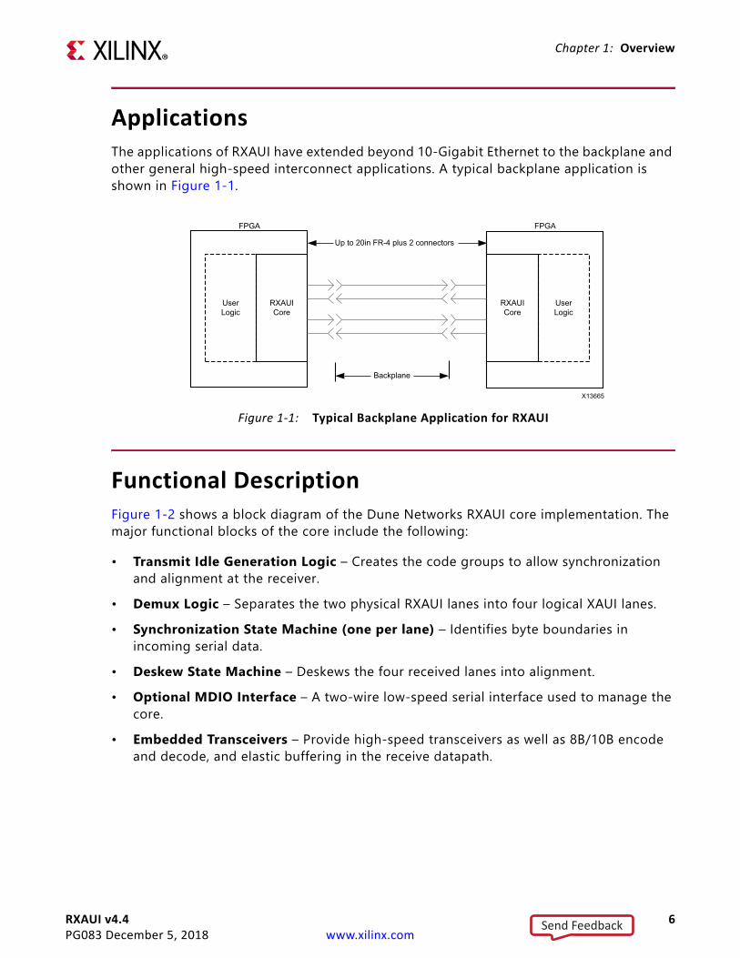
ApplicationsThe applications of RXAUI have extended beyond 10-Gigabit Ethernet to the backplane and other general high-speed interconnect applications. A typical backplane application is shown in Figure 1-1.
Functional DescriptionFigure 1-2 shows a block diagram of the Dune Networks RXAUI core implementation. The major functional blocks of the core include the following:
• Transmit Idle Generation Logic – Creates the code groups to allow synchronization and alignment at the receiver.
• Demux Logic – Separates the two physical RXAUI lanes into four logical XAUI lanes.• Synchronization State Machine (one per lane) – Identifies byte boundaries in
incoming serial data.• Deskew State Machine – Deskews the four received lanes into alignment.• Optional MDIO Interface – A two-wire low-speed serial interface used to manage the
core.• Embedded Transceivers – Provide high-speed transceivers as well as 8B/10B encode
and decode, and elastic buffering in the receive datapath.
X-Ref Target - Figure 1-1
Figure 1-1: Typical Backplane Application for RXAUI
X13665
RXAUICore
RXAUICore
Up to 20in FR-4 plus 2 connectors
UserLogic
UserLogic
Backplane
FPGA FPGA
Send Feedback

RXAUI v4.4 7PG083 December 5, 2018 www.xilinx.com
Chapter 1: Overview
Licensing and OrderingThis Xilinx® LogiCORE™ IP module is provided at no additional cost with the Xilinx Vivado® Design Suite under the terms of the Xilinx End User License. Information about this and other Xilinx LogiCORE IP modules is available at the Xilinx Intellectual Property page. For information about pricing and availability of other Xilinx LogiCORE IP modules and tools, contact your local Xilinx sales representative.
X-Ref Target - Figure 1-2
Figure 1-2: Implementation of Dune Networks RXAUI Core
TransceiverChannel
Lane 0
Lane 1
Demux
Demux
Synchronization
Synchronization
Synchronization
Synchronization
TransceiverChannel
Deskew64+8
Idle Generation64 + 8
Core Encrypted HDL
Core HDL
Management
MDC
MDIO
Core Clocking
clk156_out
X13610
Send Feedback
RXAUI v4.4 8PG083 December 5, 2018 www.xilinx.com
Chapter 2
Product Specification
StandardsThe LogiCORE™ IP RXAUI core is designed to the Dune Networks [Ref 1] specifications.
PerformanceLatencyThese measurements are for the core only — they do not include the latency through the transceiver. The latency through the transceiver can be obtained from the relevant user guide.
Transmit Path Latency
As measured from the input port xgmii_txd[63:0] of the transmitter side XGMII (until that data appears on mgt_txdata[63:0] on the internal transceiver interface), the latency through the core for the internal XGMII interface configuration in the transmit direction is 4 clock periods of the core input usrclk for Dune Networks mode.
Receive Path Latency
Measured from the transceiver output pins RXDATA[63:0] until the data appears on xgmii_rxdata[63:0] of the receiver side XGMII interface, the latency through the core in the receive direction for Dune Networks mode is equal to six to eight clock cycles of usrclk. The latency depends on comma alignment position and data positioning within the transceiver 4-byte interface.
Send Feedback
RXAUI v4.4 9PG083 December 5, 2018 www.xilinx.com
Chapter 2: Product Specification
Resource UtilizationFor full details about performance and resource utilization, visit the Performance and Resource Utilization web page.
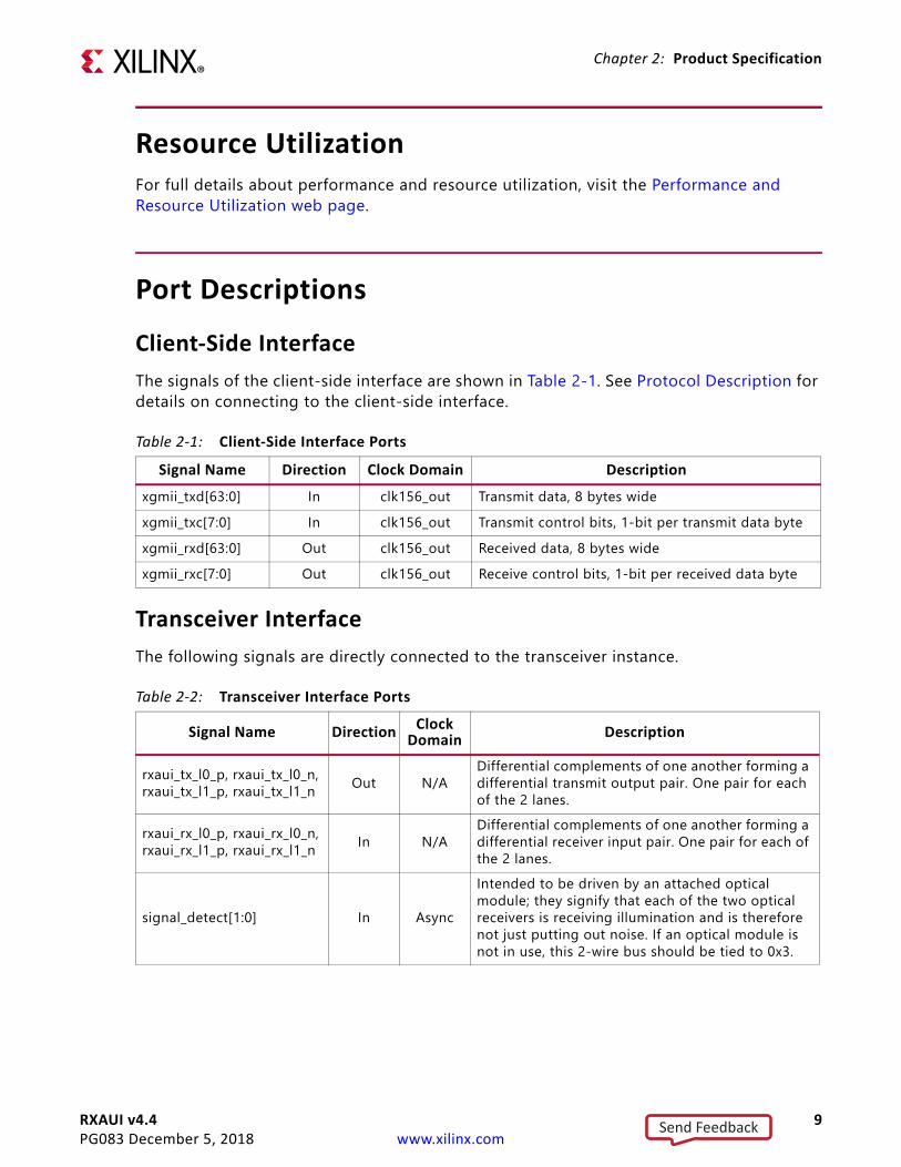
Port DescriptionsClient-Side InterfaceThe signals of the client-side interface are shown in Table 2-1. See Protocol Description for details on connecting to the client-side interface.
Transceiver InterfaceThe following signals are directly connected to the transceiver instance.
Table 2-1: Client-Side Interface PortsSignal Name Direction Clock Domain Description
xgmii_txd[63:0] In clk156_out Transmit data, 8 bytes widexgmii_txc[7:0] In clk156_out Transmit control bits, 1-bit per transmit data bytexgmii_rxd[63:0] Out clk156_out Received data, 8 bytes widexgmii_rxc[7:0] Out clk156_out Receive control bits, 1-bit per received data byte
Table 2-2: Transceiver Interface Ports
Signal Name Direction Clock Domain Description
rxaui_tx_l0_p, rxaui_tx_l0_n,rxaui_tx_l1_p, rxaui_tx_l1_n Out N/A
Differential complements of one another forming a differential transmit output pair. One pair for each of the 2 lanes.
rxaui_rx_l0_p, rxaui_rx_l0_n,rxaui_rx_l1_p, rxaui_rx_l1_n In N/A
Differential complements of one another forming a differential receiver input pair. One pair for each of the 2 lanes.
signal_detect[1:0] In Async
Intended to be driven by an attached optical module; they signify that each of the two optical receivers is receiving illumination and is therefore not just putting out noise. If an optical module is not in use, this 2-wire bus should be tied to 0x3.
Send Feedback

RXAUI v4.4 10PG083 December 5, 2018 www.xilinx.com
Chapter 2: Product Specification
MDIO PortsThe RXAUI core, when generated with an MDIO interface, implements an MDIO Interface Register block. The core responds to MDIO transactions as either a 10GBASE-X PCS, a DTE XS, or a PHY XS depending on the setting of the type_sel port (see Table 3-3). The MDIO Interface Ports are described in Table 2-3. More information about using this interface can be found in MDIO Interface.
Configuration and Status SignalsThe Configuration and Status Signals are shown in Table 2-16. See Configuration and Status Vectors for details on these signals, including a breakdown of the configuration and status vectors.
Clocking and Reset Signals and ModuleIncluded in the example design sources are circuits for clock and reset management. For the RXAUI core these comprise the transceiver Quad PLL and associated reset logic. Tables 2-5 to 2-9 shows the ports on the core that are associated with system clocks and resets.
Table 2-3: MDIO Management Interface Ports
Signal Name Direction Clock Domain Description
mdc In Async Management clock mdio_in In Async MDIO input mdio_out Out clk156_out MDIO output mdio_tri Out clk156_out MDIO 3-state. 1 disconnects the output driver from the
MDIO bus. type_sel[1:0] In clk156_out Type selectprtad[4:0] In clk156_out MDIO port address
Table 2-4: Configuration and Status Ports
Signal Name Direction Clock Domain Description
configuration_ vector[6:0] In clk156_out Configuration information for the core.status_vector[7:0] Out clk156_out Status information from the core.
Table 2-5: Clocking and Reset PortsSignal Name Direction Description
clk156_out Out 156.25 MHz clock derived from TXOUTCLK. Can be used for external logic. Cannot be connected to another RXAUI core.
clk156_lock In Indicates that clk156_out is stable and ready for use.
Send Feedback

RXAUI v4.4 11PG083 December 5, 2018 www.xilinx.com
Chapter 2: Product Specification
dclk In
Clock used as the DRP clock, and also as a stable reference clock for the detection of the feedback and reference clock signals to the QPLL. The input reference clock to the QPLL or any output clock generated from the QPLL (for example, TXOUTCLK) must not be used to drive this clock.For UltraScale devices, this clock is also used in the internal state machines for the configuration of the transceiver.
reset InAsynchronous reset connected to the transceiver Channel PLL or transceiver Quad PLL. This should be asserted if refclk or dclk is not valid.
Table 2-6: 7 Series and Zynq-7000 GTX and GTH Clocking Ports - Shared Logic Included in Example Design
Signal Name Direction Description
refclk In Transceiver reference clock. Must be driven from the appropriate transceiver differential clock buffer.
qplloutclk In Connect to the quad PLL output clock QPLLOUTCLK.qplllock In Connect to the quad PLL lock output QPLLLOCK.
qplloutrefclk In Connect to the quad PLL output reference clock QPLLOUTREFCLK.
Table 2-7: Artix-7 and Zynq-7000 GTP Clocking Ports - Shared Logic Included in Example DesignSignal Name Direction Description
common_pll_reset In Connect to the reset to the GTPE2_COMMON PLL.pll0outclk In Connect to the GTPE2_COMMON PLL port PLL0OUTCLK.pll0lock In Connect to the GTPE2_COMMON PLL lock port PLL0LOCK.
pll0outrefclk In Connect to the GTPE2_COMMON PLL REFCLK port PLL0OUTREFCLK.
pll1outclk In Connect to the GTPE2_COMMON PLL port PLL1OUTCLK.
pll1outrefclk In Connect to the GTPE2_COMMON PLL REFCLK port PLL1OUTREFCLK.
Table 2-8: 7 Series and Zynq-7000 GTX and GTH Clocking Ports - Shared Logic Included in CoreSignal Name Direction Description
refclk_p In Differential transceiver reference clock p. refclk_n In Differential transceiver reference clock n.
refclk_out Out Reference clock output from the differential transceiver clock buffer.
qplloutclk_out Out Output from the quad PLL port QPLLOUTCLK.
Table 2-5: Clocking and Reset Ports (Cont’d)
Signal Name Direction Description
Send Feedback

RXAUI v4.4 12PG083 December 5, 2018 www.xilinx.com
Chapter 2: Product Specification
Tables 2-10 to 2-11 shows the UltraScale ports on the core that are associated with system clocks and resets.
qplllock_out Out Output from the quad PLL port QPLLLOCK.qpllrefclk_out Out Output from the quad PLL port QPLLREFCLK.
Table 2-9: Artix-7 and Zynq-7000 GTP Clocking Ports - Shared Logic Included in CoreSignal Name Direction Description
common_pll_reset _out Out Output reset signal to the GTPE2_COMMON PLL and associated transceivers.
pll0outclk_out Out Output from the GTPE2_COMMON PLL port PLL0OUTCLK.pll0lock_out Out Output from the GTPE2_COMMON PLL port PLL0LOCK.pll0outrefclk_out Out Output from the GTPE2_COMMON PLL port PLL0OUTREFCLK.pll1outclk_out Out Output from the GTPE2_COMMON PLL port PLL1OUTCLKpll1outrefclk_out Out Output from the GTPE2_COMMON PLL port PLL1OUTREFCLK
Table 2-10: UltraScale Clocking Ports - Shared Logic Included in Example DesignSignal Name Direction Description
refclk In Transceiver reference clock. Must be driven from the appropriate transceiver differential clock buffer.
qpll0outclk In Connect to the quad PLL output clock QPLL0OUTCLK.qpll0lock In Connect to the quad PLL lock output QPLL0LOCK.
qpll0outrefclk In Connect to the quad PLL output reference clock QPLL0OUTREFCLK.
qpll0reset Out QPLL reset signal from the UltraScale GT Wizard reset logic.
Table 2-11: UltraScale Clocking Ports - Shared Logic Included in CoreSignal Name Direction Description
refclk_p In Differential transceiver reference clock p.refclk_n vIn Differential transceiver reference clock n.
refclk Out Reference clock output from the differential transceiver clock buffer.
qpll0outclk_out Out Output from the quad PLL port QPLL0OUTCLK.qpll0lock_out Out Output from the quad PLL port QPLL0LOCK.qpll0outrefclk_out Out Output from the quad PLL port QPLL0OUTREFCLK.
Table 2-8: 7 Series and Zynq-7000 GTX and GTH Clocking Ports - Shared Logic Included in Core Signal Name Direction Description
Send Feedback

RXAUI v4.4 13PG083 December 5, 2018 www.xilinx.com
Chapter 2: Product Specification
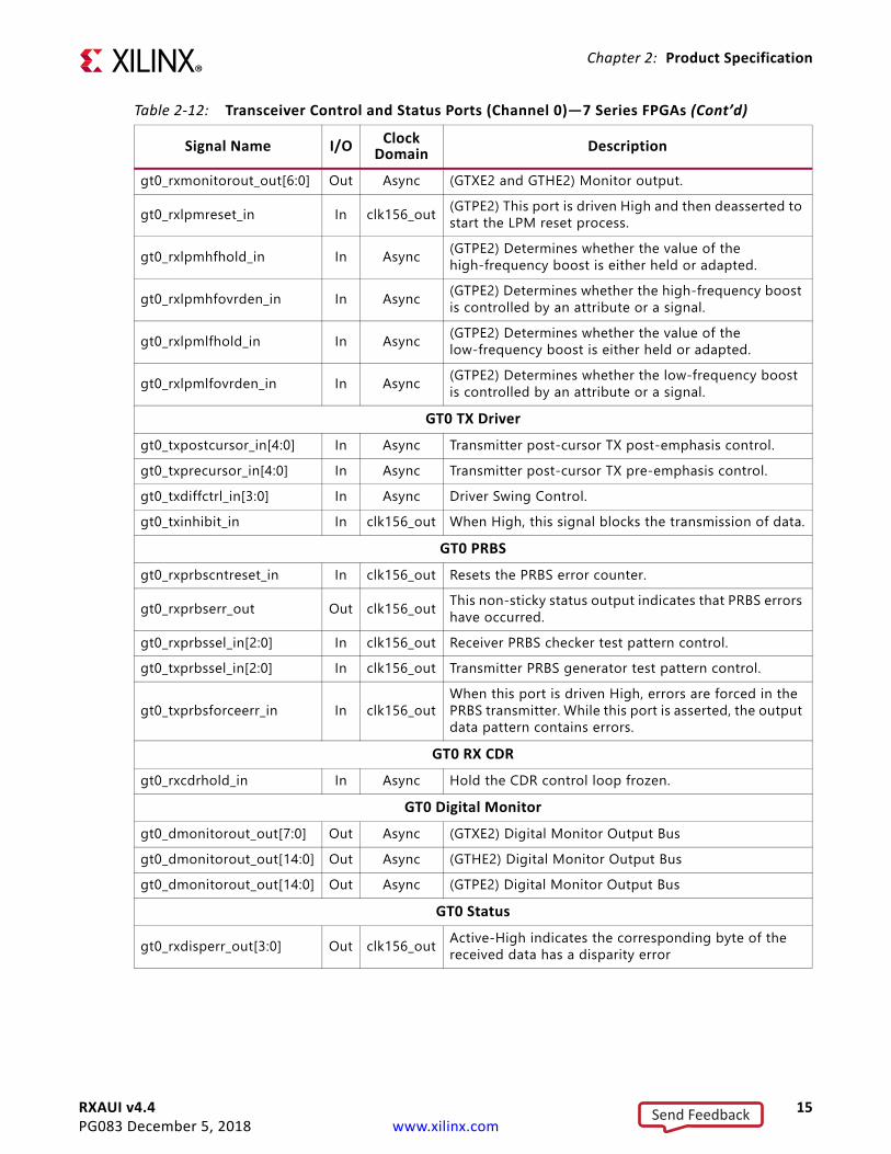
Transceiver Control and StatusThe transceiver interface is present if the Additional Transceiver Control and Status Ports option is selected. There are a number of ports that are directly connected to the transceivers. For a complete description of these signals, see the appropriate transceiver user guide (7 Series FPGAs GTX/GTH Transceivers User Guide (UG476) [Ref 2], 7 Series FPGAs GTP Transceivers User Guide (UG482) [Ref 3], the UltraScale Architecture GTH Transceivers User Guide (UG576) [Ref 4] and the UltraScale Architecture GTY Transceivers User Guide (UG578) [Ref 5]). Table 2-12 and Table 2-13 lists the ports for 7 series FPGAs. Ports are prefixed with GT0 for transceiver 0 and GT1 for transceiver 1.
IMPORTANT: The ports in the Transceiver Control And Status interface must be driven in accordance with the appropriate GT user guide. Using the input signals listed in Table 2-13 might result in unpredictable behavior of the IP core.
Table 2-12: Transceiver Control and Status Ports (Channel 0)—7 Series FPGAs
Signal Name I/O ClockDomain Description
GT0 DRPgt0_drpaddr[8:0] In dclk DRP address bus for channel 0
gt0_drpen In dclkDRP enable signal. 0: No read or write operation performed. 1: enables a read or write operation.
gt0_drpdi[15:0] In dclk Data bus for writing configuration data to the transceiver for channel 0.
gt0_drpdo[15:0] Out dclk Data bus for reading configuration data from the transceiver for channel 0.
gt0_drprdy Out dclk Indicates operation is complete for write operations and data is valid for read operations for channel 0.
gt0_drpwe In dclkDRP write enable for channel 0. 0: Read operation when drpen is 1. 1: Write operation when drpen is 1.
gt0_drp_busy Out dclk(GTPE2 all configurations or GTHE2 10G configuration). Indicates the DRP interface is being used internally by the serial transceiver and should not be driven until this signal is deasserted.
GT0 TX Reset and Initializationgt0_txpmareset_in In Async Starts the TX PMA reset process.gt0_txpcsreset_in In Async Starts the TX PCS reset process.
gt0_txresetdone_out Out clk156_out When asserted the serial transceiver TX has finished reset and is ready for use.
GT0 RX Reset and Initializationgt0_rxpmareset_in In Async Starts the RX PMA reset process.gt0_rxpcsreset_in In Async Starts the RX PCS reset process.
Send Feedback

RXAUI v4.4 14PG083 December 5, 2018 www.xilinx.com
Chapter 2: Product Specification
gt0_rxpmaresetdone_out Out Async (GTHE2 and GTPE2) This active-High signal indicates RX PMA reset is complete.
gt0_rxresetdone_out Out clk156_out When asserted the serial transceiver RX has finished reset and is ready for use.
GT0 Clockinggt0_rxbufstatus_out[2:0] Out clk156_out RX buffer status.gt0_txphaligndone_out Out Async TX phase alignment done.gt0_txphinitdone_out Out Async TX phase alignment initialization done.gt0_txdlysresetdone_out Out Async TX delay alignment soft reset done.
gt0_cplllock_out Out Async(GTHE2) This active-High PLL frequency lock signal indicates that the PLL frequency is within predetermined tolerance.
gt_qplllock_out Out Async(GTXE2 and GTPE2) This active-High PLL frequency lock signal indicates that the PLL frequency is within predetermined tolerance.
Signal Integrity and FunctionalityGT0 Eye scan
gt0_eyescantrigger_in In clk156_out Causes a trigger event.
gt0_eyescanreset_in In Async This port is driven High and then deasserted to start the EYESCAN reset process.
gt0_eyescandataerror_out Out AsyncAsserts High for one rec_clk cycle when an (unmasked) error occurs while in the COUNT or ARMED state.
gt0_rxrate_in[2:0] In Reserved This port dynamically controls the setting for the RX serial clock divider.
GT0 Loopbackgt0_loopback_in[2:0] In Async Determines the loopback mode.
GT0 Polarity
gt0_rxpolarity_in In clk156_out The rxpolarity port can invert the polarity of incoming data.
gt0_txpolarity_in In clk156_out The txpolarity port can invert the polarity of outgoing data.
GT0 RX Decision Feedback Equalizer (DFE)
gt0_rxlpmen_in In Async (GTXE2 and GTHE2) RX datapath. 0: DFE. 1: LPM.
gt0_rxdfelpmreset_in In Async (GTXE2 and GTHE2) Reset for LPM and DFE datapath.
gt0_rxmonitorsel_in[1:0] In Reserved (GTXE2 and GTHE2) Select signal for gt0_rxmonitorout_out.
Table 2-12: Transceiver Control and Status Ports (Channel 0)—7 Series FPGAs (Cont’d)
Signal Name I/O ClockDomain Description
Send Feedback
RXAUI v4.4 15PG083 December 5, 2018 www.xilinx.com
Chapter 2: Product Specification
gt0_rxmonitorout_out[6:0] Out Async (GTXE2 and GTHE2) Monitor output.
gt0_rxlpmreset_in In clk156_out (GTPE2) This port is driven High and then deasserted to start the LPM reset process.
gt0_rxlpmhfhold_in In Async (GTPE2) Determines whether the value of the high-frequency boost is either held or adapted.
gt0_rxlpmhfovrden_in In Async (GTPE2) Determines whether the high-frequency boost is controlled by an attribute or a signal.
gt0_rxlpmlfhold_in In Async (GTPE2) Determines whether the value of the low-frequency boost is either held or adapted.
gt0_rxlpmlfovrden_in In Async (GTPE2) Determines whether the low-frequency boost is controlled by an attribute or a signal.
GT0 TX Drivergt0_txpostcursor_in[4:0] In Async Transmitter post-cursor TX post-emphasis control.gt0_txprecursor_in[4:0] In Async Transmitter post-cursor TX pre-emphasis control.gt0_txdiffctrl_in[3:0] In Async Driver Swing Control.gt0_txinhibit_in In clk156_out When High, this signal blocks the transmission of data.
GT0 PRBSgt0_rxprbscntreset_in In clk156_out Resets the PRBS error counter.
gt0_rxprbserr_out Out clk156_out This non-sticky status output indicates that PRBS errors have occurred.
gt0_rxprbssel_in[2:0] In clk156_out Receiver PRBS checker test pattern control.gt0_txprbssel_in[2:0] In clk156_out Transmitter PRBS generator test pattern control.
gt0_txprbsforceerr_in In clk156_outWhen this port is driven High, errors are forced in the PRBS transmitter. While this port is asserted, the output data pattern contains errors.
GT0 RX CDRgt0_rxcdrhold_in In Async Hold the CDR control loop frozen.
GT0 Digital Monitorgt0_dmonitorout_out[7:0] Out Async (GTXE2) Digital Monitor Output Busgt0_dmonitorout_out[14:0] Out Async (GTHE2) Digital Monitor Output Busgt0_dmonitorout_out[14:0] Out Async (GTPE2) Digital Monitor Output Bus
GT0 Status
gt0_rxdisperr_out[3:0] Out clk156_out Active-High indicates the corresponding byte of the received data has a disparity error
Table 2-12: Transceiver Control and Status Ports (Channel 0)—7 Series FPGAs (Cont’d)
Signal Name I/O ClockDomain Description
Send Feedback

RXAUI v4.4 16PG083 December 5, 2018 www.xilinx.com
Chapter 2: Product Specification
gt0_rxnotintable_out[3:0] Out clk156_outActive-High indicates the corresponding byte of the received data was not a valid character in the 8B/10B table.
gt0_rxcommadet_out Out clk156_out This signal is asserted when the comma alignment block detects a comma.
Table 2-13: Transceiver Control and Status Ports (Channel 1)—7 Series FPGAs
Signal Name I/O ClockDomain Description
GT1 DRPgt1_drpaddr[8:0] In dclk DRP address bus for channel 1.
gt1_drpen In dclkDRP enable signal. 0: No read or write operation performed. 1: enables a read or write operation.
gt1_drpdi[15:0] In dclk Data bus for writing configuration data to the transceiver for channel 1.
gt1_drpdo[15:0] Out dclk Data bus for reading configuration data from the transceiver for channel 1.
gt1_drprdy Out dclk Indicates operation is complete for write operations and data is valid for read operations for channel 1.
gt1_drpwe In dclkDRP write enable for channel 1. 0: Read operation when drpen is 1. 1: Write operation when drpen is 1.
gt1_drp_busy Out dclk(GTPE2 all configurations or GTHE2 10G configuration). Indicates the DRP interface is being used internally by the serial transceiver and should not be driven until this signal is deasserted.
GT1 TX Reset and Initializationgt1_txpmareset_in In Async Starts the TX PMA reset process.gt1_txpcsreset_in In Async Starts the TX PCS reset process.
gt1_txresetdone_out Out clk156_out When asserted the serial transceiver TX has finished reset and is ready for use.
GT1 RX Reset and Initializationgt1_rxpmareset_in In Async Starts the RX PMA reset process.gt1_rxpcsreset_in In Async Starts the RX PCS reset process.
gt1_rxpmaresetdone_out Out Async (GTHE2 and GTPE2) This active-High signal indicates RX PMA reset is complete.
gt1_rxresetdone_out Out clk156_out When asserted the serial transceiver RX has finished reset and is ready for use.
Table 2-12: Transceiver Control and Status Ports (Channel 0)—7 Series FPGAs (Cont’d)
Signal Name I/O ClockDomain Description
Send Feedback

RXAUI v4.4 17PG083 December 5, 2018 www.xilinx.com
Chapter 2: Product Specification
GT1 Clockinggt1_rxbufstatus_out[2:0] Out clk156_out RX buffer status.gt1_txphaligndone_out Out Async TX phase alignment done.gt1_txphinitdone_out Out Async TX phase alignment initialization done.gt1_txdlysresetdone_out Out Async TX delay alignment soft reset done.
gt1_cplllock_out Out Async(GTHE2) This active-High PLL frequency lock signal indicates that the PLL frequency is within predetermined tolerance.
Signal Integrity and FunctionalityGT1 Eye scan
gt1_eyescantrigger_in In clk156_out Causes a trigger event.
gt1_eyescanreset_in In Async This port is driven High and then deasserted to start the EYESCAN reset process.
gt1_eyescandataerror_out Out AsyncAsserts High for one rec_clk cycle when an (unmasked) error occurs while in the COUNT or ARMED state.
gt1_rxrate_in[2:0] In Reserved This port dynamically controls the setting for the RX serial clock divider.
GT1 Loopbackgt1_loopback_in[2:0] In Async Determines the loopback mode.
GT1 Polarity
gt1_rxpolarity_in In clk156_out The rxpolarity port can invert the polarity of incoming data.
gt1_txpolarity_in In clk156_out The txpolarity port can invert the polarity of outgoing data.
GT1 RX Decision Feedback Equalizer (DFE)
gt1_rxlpmen_in In Async (GTXE2 and GTHE2) RX datapath. 0: DFE. 1: LPM.
gt1_rxdfelpmreset_in In Async (GTXE2 and GTHE2) Reset for LPM and DFE datapath.
gt1_rxmonitorsel_in[1:0] In Reserved (GTXE2 and GTHE2) Select signal for gt1_rxmonitorout_out.
gt1_rxmonitorout_out[6:0] Out Async (GTXE2 and GTHE2) Monitor output.
gt1_rxlpmreset_in In clk156_out (GTPE2) This port is driven High and then deasserted to start the LPM reset process.
gt1_rxlpmhfhold_in In Async (GTPE2) Determines whether the value of the high-frequency boost is either held or adapted.
gt1_rxlpmhfovrden_in In Async (GTPE2) Determines whether the high-frequency boost is controlled by an attribute or a signal.
Table 2-13: Transceiver Control and Status Ports (Channel 1)—7 Series FPGAs (Cont’d)
Signal Name I/O ClockDomain Description
Send Feedback

RXAUI v4.4 18PG083 December 5, 2018 www.xilinx.com
Chapter 2: Product Specification
gt1_rxlpmlfhold_in In Async (GTPE2) Determines whether the value of the low-frequency boost is either held or adapted.
gt1_rxlpmlfovrden_in In Async (GTPE2) Determines whether the low-frequency boost is controlled by an attribute or a signal.
GT1 TX Drivergt1_txpostcursor_in[4:0] In Async Transmitter post-cursor TX post-emphasis control.gt1_txprecursor_in[4:0] In Async Transmitter post-cursor TX pre-emphasis control.gt1_txdiffctrl_in[3:0] In Async Driver Swing Control.gt1_txinhibit_in In clk156_out When High, this signal blocks the transmission of data.
GT1 PRBSgt1_rxprbscntreset_in In clk156_out Resets the PRBS error counter.
gt1_rxprbserr_out Out clk156_out This non-sticky status output indicates that PRBS errors have occurred.
gt1_rxprbssel_in[2:0] In clk156_out Receiver PRBS checker test pattern control.gt1_txprbssel_in[2:0] In clk156_out Transmitter PRBS generator test pattern control.
gt1_txprbsforceerr_in In clk156_outWhen this port is driven High, errors are forced in the PRBS transmitter. While this port is asserted, the output data pattern contains errors.
GT1 RX CDRgt1_rxcdrhold_in In Async Hold the CDR control loop frozen.
GT1 Digital Monitorgt1_dmonitorout_out[7:0] Out Async (GTXE2) Digital Monitor Output Busgt1_dmonitorout_out[14:0] Out Async (GTHE2) Digital Monitor Output Busgt1_dmonitorout_out[14:0] Out Async (GTPE2) Digital Monitor Output Bus
GT1 Status
gt1_rxdisperr_out[3:0] Out clk156_out Active-High indicates the corresponding byte of the received data has a disparity error
gt1_rxnotintable_out[3:0] Out clk156_outActive-High indicates the corresponding byte of the received data was not a valid character in the 8B/10B table.
gt1_rxcommadet_out Out clk156_out This signal is asserted when the comma alignment block detects a comma.
Table 2-13: Transceiver Control and Status Ports (Channel 1)—7 Series FPGAs (Cont’d)
Signal Name I/O ClockDomain Description
Send Feedback

RXAUI v4.4 19PG083 December 5, 2018 www.xilinx.com
Chapter 2: Product Specification
Table 2-14 lists the ports for UltraScale devices.
Table 2-14: Transceiver Control and Status Ports — UltraScale ArchitecturesSignal Name Direction Clock Domain Description
GT0 DRPgt0_drpaddr[8:0] In dclk DRP address bus for channel 0
gt0_drpen In dclkDRP enable signal. 0: No read or write operation performed. 1: enables a read or write operation.
gt0_drpdi[15:0] In dclk Data bus for writing configuration data to the transceiver for channel 0.
gt0_drpdo[15:0] Out dclk Data bus for reading configuration data from the transceiver for channel 0.
gt0_drprdy Out dclkIndicates operation is complete for write operations and data is valid for read operations for channel 0.
gt0_drpwe In dclkDRP write enable for channel 0. 0: Read operation when drpen is 1. 1: Write operation when drpen is 1.
GT1 DRPgt1_drpaddr[8:0] In dclk DRP address bus for channel 1
gt1_drpen In dclkDRP enable signal. 0: No read or write operation performed. 1: enables a read or write operation.
gt1_drpdi[15:0] In dclk Data bus for writing configuration data to the transceiver for channel 1.
gt1_drpdo[15:0] Out dclk Data bus for reading configuration data from the transceiver for channel 1.
gt1_drprdy Out dclkIndicates operation is complete for write operations and data is valid for read operations for channel 1.
gt1_drpwe In dclkDRP write enable for channel 1. 0: Read operation when drpen is 1. 1: Write operation when drpen is 1.
DRP Reset
gt_pcsrsvdin[31:0] In AsyncBits 2 and 18 are connected to port pcsrsvdin[2] of GT lanes 0 and 1 respectively. See the appropriate transceiver user guide for more details.
Send Feedback

RXAUI v4.4 20PG083 December 5, 2018 www.xilinx.com
Chapter 2: Product Specification
TX Reset and Initializationgt_txpmareset[1:0] In Async Starts the TX PMA reset process.gt_txpcsreset[1:0] In Async Starts the TX PCS reset process.
gt_txresetdone[1:0] Out clk156_out When asserted the serial transceiver TX has finished reset and is ready for use.
RX Reset and Initializationgt_rxpmareset[1:0] In Async Starts the RX PMA reset process.gt_rxpcsreset[1:0] In Async Starts the RX PCS reset process.gt_rxpmaresetdone[1:0] Out Async
gt_rxresetdone[1:0] Out clk156_out When asserted the serial transceiver RX has finished reset and is ready for use.
Clockinggt_rxbufstatus[5:0] Out clk156_out RX buffer status.gt_txphaligndone[1:0] Out Async TX phase alignment done.gt_txphinitdone[1:0] Out Async TX phase alignment initialization done.gt_txdlysresetdone[1:0] Out Async TX delay alignment soft reset done.
gt_qplllock Out AsyncThis active-High PLL frequency lock signal indicates that the PLL frequency is within predetermined tolerance.
Signal Integrity and FunctionalityEye Scan
gt_eyescantrigger[1:0] In clk156_out Causes a trigger event.
gt_eyescanreset[1:0] In Async This port is driven High and then deasserted to start the EYESCAN reset process.
gt_eyescandataerror[1:0] Out AsyncAsserts High for one rec_clk cycle when an (unmasked) error occurs while in the COUNT or ARMED state.
gt_rxrate[5:0] In clk156_out This port dynamically controls the setting for the RX serial clock divider.
Loopbackgt_loopback[5:0] In Async Determines the loopback mode.
Polarity
gt_rxpolarity[1:0] In clk156_out The rxpolarity port can invert the polarity of incoming data.
gt_txpolarity[1:0] In clk156_out The txpolarity port can invert the polarity of outgoing data.
Table 2-14: Transceiver Control and Status Ports — UltraScale Architectures (Cont’d)
Signal Name Direction Clock Domain Description
Send Feedback

RXAUI v4.4 21PG083 December 5, 2018 www.xilinx.com
Chapter 2: Product Specification
RX Decision Feedback Equalizer (DFE)
gt_rxlpmen[1:0] In AsyncRX datapath. 0: DFE. 1: LPM.
gt_rxdfelpmreset[1:0] In Async Reset for LPM and DFE datapath.TX Driver
gt_txpostcursor[9:0] In Async Transmitter post-cursor TX post-emphasis control.
gt_txprecursor[9:0] In Async Transmitter post-cursor TX pre-emphasis control.
gt_txdiffctrl[7:0] In Async Driver Swing Control. The bus size is 20 bits for GTYE3 and 16 bits for GTHE3.
gt_txinhibit[1:0] In clk156_out When High, this signal blocks the transmission of data.
PRBSgt_rxprbscntreset[1:0] In clk156_out Resets the PRBS error counter.
gt_rxprbserr[1:0] Out clk156_out This non-sticky status output indicates that PRBS errors have occurred.
gt_rxprbssel[7:0] In clk156_out Receiver PRBS checker test pattern control.gt_txprbssel[7:0] In clk156_out Transmitter PRBS generator test pattern control.
gt_txprbsforceerr[1:0] In clk156_outWhen this port is driven High, errors are forced in the PRBS transmitter. While this port is asserted, the output data pattern contains errors.
RX CDRgt_rxcdrhold[1:0] In Async Hold the CDR control loop frozen.
Digital Monitorgt_dmonitorout[33:0] Out Async Digital Monitor Output Bus
Status
gt_rxdisperr[7:0] Out clk156_out Active-High indicates the corresponding byte of the received data has a disparity error.
gt_rxnotintable[7:0] Out clk156_outActive-High indicates the corresponding byte of the received data was not a valid character in the 8B/10B table.
gt_rxcommadet[1:0] Out clk156_out This signal is asserted when the comma alignment block detects a comma.
Table 2-14: Transceiver Control and Status Ports — UltraScale Architectures (Cont’d)
Signal Name Direction Clock Domain Description
Send Feedback

RXAUI v4.4 22PG083 December 5, 2018 www.xilinx.com
Chapter 2: Product Specification
Debug InterfaceA debug port is provided that contains easy access to some of the important core signals.
Alignment and Synchronization Status PortsIn addition to the configuration and status interfaces described in the previous section, there is some information on the debug output port signaling the alignment and synchronization status of the receiver (Table 2-16).
Register SpaceThis section describes the interfaces available for dynamically setting the configuration and obtaining the status of the RXAUI core. There are two interfaces for configuration; depending on the core customization, only one is available in a particular core instance. The interfaces are:
• MDIO Interface Registers• Configuration and Status Vectors
gt_powergood_out[1:0](2) Out Async Active-High indicates that the power is good.Notes: 1. If you are migrating from a 7 series to an UltraScale device, the prefixes of the optional transceiver debug ports for
single-lane cores are changed from “gt0”, “gt1” to “gt”, and the suffix “_in” and “_out” are dropped. For multi-lane cores, the prefixes of the optional transceiver debug ports gt(n) are aggregated into a single port. See Device Migration for more information.
2. The gt_powergood_out[1:0] signal is always present.
Table 2-15: Debug PortsSignal Name Direction Clock Domain Description
debug Out clk156_outDebug PortBit[5] = Align StatusBits[4:1] = Sync StatusBit[0] = TX Phase Align Complete
Table 2-16: Alignment Status and Synchronization Status PortsPort Name Description
debug[5] 1 when the RXAUI receiver is aligned across all four XAUI logical lanes, 0 otherwise.
debug[4:1] Each pin is 1 when the respective XAUI logical lane receiver is synchronized to byte boundaries, 0 otherwise.
Table 2-14: Transceiver Control and Status Ports — UltraScale Architectures (Cont’d)
Signal Name Direction Clock Domain Description
Send Feedback

RXAUI v4.4 23PG083 December 5, 2018 www.xilinx.com
Chapter 2: Product Specification
In addition, there are output ports on the core signaling alignment and synchronization status. These ports are described in Alignment and Synchronization Status Ports.
MDIO Interface RegistersFor a description of the MDIO Interface, see MDIO Interface.
10GBASE-X PCS/PMA Register Map
When the core is configured as a 10GBASE-X PCS/PMA, it occupies MDIO Device Addresses 1 and 3 in the MDIO register address map, as shown in Table 2-17.
Table 2-17: 10GBASE-X PCS/PMA MDIO RegistersRegister Address Register Name
1.0 PMA/PMD Control 11.1 PMA/PMD Status 11.2,1.3 PMA/PMD Device Identifier1.4 PMA/PMD Speed Ability1.5, 1.6 PMA/PMD Devices in Package1.7 10G PMA/PMD Control 21.8 10G PMA/PMD Status 21.9 Reserved1.10 10G PMD Receive Signal OK1.11 TO 1.13 Reserved1.14, 1.15 PMA/PMD Package Identifier1.16 to 1.65 535 Reserved3.0 PCS Control 13.1 PCS Status 13.2, 3.3 PCS Device Identifier3.4 PCS Speed Ability3.5, 3.6 PCS Devices in Package3.7 10G PCS Control 23.8 10G PCS Status 23.9 to 3.13 Reserved3.14, 3.15 Package Identifier3.16 to 3.23 Reserved3.24 10GBASE-X PCS Status3.25 10GBASE-X Test Control3.26 to 3.65 535 Reserved
Send Feedback

RXAUI v4.4 24PG083 December 5, 2018 www.xilinx.com
Chapter 2: Product Specification
MDIO Register 1.0: PMA/PMD Control 1
Figure 2-1 shows the MDIO Register 1.0: PMA/PMD Control 1.
Table 2-18 shows the PMA Control 1 register bit definitions.
X-Ref Target - Figure 2-1
Figure 2-1: PMA/PMD Control 1 Register
Table 2-18: PMA/PMD Control 1 Register Bit Definitions
Bits Name ResetValue
AccessType Description
1.0.15 Reset 0 R/WSelf-clearing
0 = Normal operation1 = Block resetThe RXAUI block is reset when this bit is set to 1. It returns to 0 when the reset is complete. The soft_reset pin is connected to this bit. This can be connected to the reset of any other MMDs.
1.0.14 Reserved 0 R The block always returns 0 for this bit and ignores writes.
1.0.13 Speed Selection 1 R The block always returns 1 for this bit and ignores writes.
1.0.12 Reserved 0 R The block always returns 0 for this bit and ignores writes.
1.0.11 Power-down 0 R/W
0 = Normal operation1 = Power-down modeWhen set to 1, the serial transceivers are placed in a low power state. Set to 0 to return to normal operation
1.0.10:7 Reserved All 0s R The block always returns 0 for these bits and ignores writes.
1.0.6 Speed Selection 1 R The block always returns 1 for this bit and ignores writes.
1.0.5:2 Speed Selection All 0s R The block always returns 0s for these bits and ignores writes.
1.0.1 Reserved All 0s R The block always returns 0 for this bit and ignores writes
1.0.0 Loopback 0 R/W
0 = Disable loopback mode1 = Enable loopback modeThe RXAUI block loops the signal in the serial transceivers back into the receiver. Near-end PMA loopback is always used.
X13627
RESET
RSVD
RSVD
RSVD
RSVD
POW
ER D
OW
N
LOO
PBACK
SPEED
SPEED
SPEED
15 14 13 12 11 10 7 6 5 2 1 0
Reg 1.0
Send Feedback

RXAUI v4.4 25PG083 December 5, 2018 www.xilinx.com
Chapter 2: Product Specification
MDIO Register 1.1: PMA/PMD Status 1
Figure 2-2 shows the MDIO Register 1.1: PMA/PMD Status 1.
Table 2-19 shows the PMA/PMD Status 1 register bit definitions.
X-Ref Target - Figure 2-2
Figure 2-2: PMA/PMD Status 1 Register
Table 2-19: PMA/PMD Status 1 Register Bit Definitions
Bits Name ResetValue
AccessType Description
1.1.15:8 Reserved 0 R The block always returns 0 for this bit.1.1.7 Local Fault 0 R The block always returns 0 for this bit.1.1.6:3 Reserved 0 R The block always returns 0 for this bit.1.1.2 Receive Link Status 1 R The block always returns 1 for this bit.1.1.1 Power-down Ability 1 R The block always returns 1 for this bit.1.1.0 Reserved 0 R The block always returns 0 for this bit.
X13628
RSVD
RSVD
RSVD
LOC
AL FAULT
POW
ERD
OW
N ABILITY
RX LIN
K STATUS
15 8 7 6 3 2 1 0
Reg 1.1
Send Feedback
RXAUI v4.4 26PG083 December 5, 2018 www.xilinx.com
Chapter 2: Product Specification
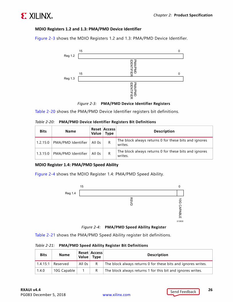
MDIO Registers 1.2 and 1.3: PMA/PMD Device Identifier
Figure 2-3 shows the MDIO Registers 1.2 and 1.3: PMA/PMD Device Identifier.
Table 2-20 shows the PMA/PMD Device Identifier registers bit definitions.
MDIO Register 1.4: PMA/PMD Speed Ability
Figure 2-4 shows the MDIO Register 1.4: PMA/PMD Speed Ability.
Table 2-21 shows the PMA/PMD Speed Ability register bit definitions.
X-Ref Target - Figure 2-3
Figure 2-3: PMA/PMD Device Identifier Registers
Table 2-20: PMA/PMD Device Identifier Registers Bit Definitions
Bits Name ResetValue
AccessType Description
1.2.15:0 PMA/PMD Identifier All 0s R The block always returns 0 for these bits and ignores writes.
1.3.15:0 PMA/PMD Identifier All 0s R The block always returns 0 for these bits and ignores writes.
X-Ref Target - Figure 2-4
Figure 2-4: PMA/PMD Speed Ability Register
Table 2-21: PMA/PMD Speed Ability Register Bit Definitions
Bits Name ResetValue
AccessType Description
1.4.15:1 Reserved All 0s R The block always returns 0 for these bits and ignores writes.1.4.0 10G Capable 1 R The block always returns 1 for this bit and ignores writes.
PMA/PM
D
IDEN
TIFIER
15 0Reg 1.2
PMA/PM
DID
ENTIFIER
15 0Reg 1.3
X13630
RSVD
10G C
APABLE
15 0
Reg 1.4
Send Feedback
RXAUI v4.4 27PG083 December 5, 2018 www.xilinx.com
Chapter 2: Product Specification
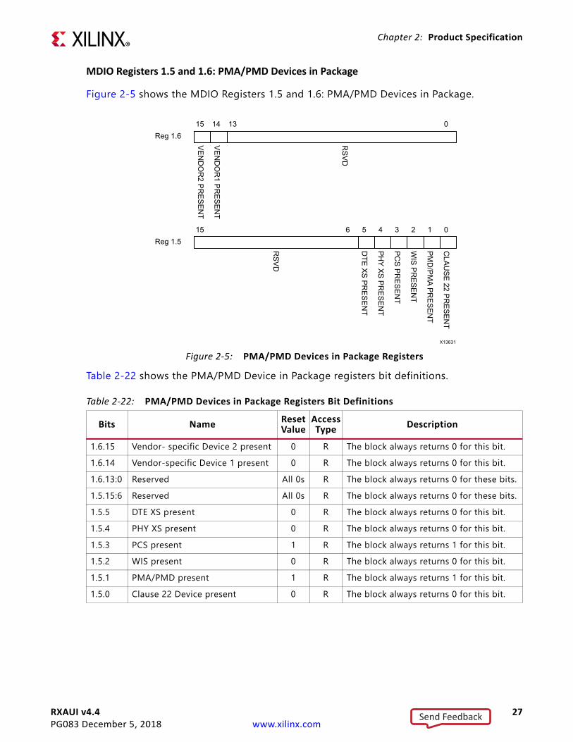
MDIO Registers 1.5 and 1.6: PMA/PMD Devices in Package
Figure 2-5 shows the MDIO Registers 1.5 and 1.6: PMA/PMD Devices in Package.
Table 2-22 shows the PMA/PMD Device in Package registers bit definitions.
X-Ref Target - Figure 2-5
Figure 2-5: PMA/PMD Devices in Package Registers
Table 2-22: PMA/PMD Devices in Package Registers Bit Definitions
Bits Name ResetValue
AccessType Description
1.6.15 Vendor- specific Device 2 present 0 R The block always returns 0 for this bit.1.6.14 Vendor-specific Device 1 present 0 R The block always returns 0 for this bit.1.6.13:0 Reserved All 0s R The block always returns 0 for these bits.1.5.15:6 Reserved All 0s R The block always returns 0 for these bits.1.5.5 DTE XS present 0 R The block always returns 0 for this bit.1.5.4 PHY XS present 0 R The block always returns 0 for this bit.1.5.3 PCS present 1 R The block always returns 1 for this bit.1.5.2 WIS present 0 R The block always returns 0 for this bit.1.5.1 PMA/PMD present 1 R The block always returns 1 for this bit.1.5.0 Clause 22 Device present 0 R The block always returns 0 for this bit.
X13631
VEND
OR
2 PRESEN
T
VEND
OR
1 PRESEN
T
RSVD
15 14 13 0Reg 1.6
RSVD
DTE XS PR
ESENT
PHY XS PR
ESENT
PCS PR
ESENT
WIS PR
ESENT
PMD
/PMA PR
ESENT
CLAU
SE 22 PRESEN
T
15 0123456Reg 1.5
Send Feedback

RXAUI v4.4 28PG083 December 5, 2018 www.xilinx.com
Chapter 2: Product Specification
MDIO Register 1.7: 10G PMA/PMD Control 2
Figure 2-6 shows the MDIO Register 1.7: 10G PMA/PMD Control 2.
Table 2-23 shows the PMA/PMD Control 2 register bit definitions.
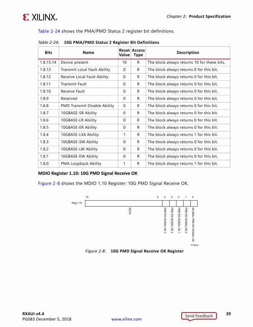
MDIO Register 1.8: 10G PMA/PMD Status 2
Figure 2-7 shows the MDIO Register 1.8: 10G PMA/PMD Status 2.
X-Ref Target - Figure 2-6
Figure 2-6: 10G PMA/PMD Control 2 Register
Table 2-23: 10G PMA/PMD Control 2 Register Bit Definitions
Bits Name ResetValue
AccessType Description
1.7.15:3 Reserved All 0s R The block always returns 0 for these bits and ignores writes.
1.7.2:0 PMA/PMD Type Selection 100 RThe block always returns 100 for these bits and ignores writes. This corresponds to the 10GBASE-X PMA/PMD.
X-Ref Target - Figure 2-7
Figure 2-7: 10G PMA/PMD Status 2 Register
X13632R
SVD
PMA/PM
D TYPE SELEC
TION
15 023
Reg 1.7
X13633
DEVIC
E PRESEN
T
TX FAULT ABILITY
RX FAU
LT ABILITY
TX FAULT
RX FAU
LT
RSVD
PMD
TX DISABLE ABILITY
10GBASE-SR
ABILITY
10GBASE-LR
ABILITY
10GBASE-ER
ABILITY
10GBASE-SW
ABILITY
10GBASE-LW
ABILITY
10GBASE-EW
ABILITY
PMA LO
OPBAC
K ABILITY
10GBASE-LX4 ABILITY
15 14 58 7 613 12 11 10 9 24 3 1 0
Reg 1.8
Send Feedback
RXAUI v4.4 29PG083 December 5, 2018 www.xilinx.com
Chapter 2: Product Specification
Table 2-24 shows the PMA/PMD Status 2 register bit definitions.
MDIO Register 1.10: 10G PMD Signal Receive OK
Figure 2-8 shows the MDIO 1.10 Register: 10G PMD Signal Receive OK.
Table 2-24: 10G PMA/PMD Status 2 Register Bit Definitions
Bits Name ResetValue
AccessType Description
1.8.15:14 Device present 10 R The block always returns 10 for these bits.1.8.13 Transmit Local Fault Ability 0 R The block always returns 0 for this bit.1.8.12 Receive Local Fault Ability 0 R The block always returns 0 for this bit.1.8.11 Transmit Fault 0 R The block always returns 0 for this bit.1.8.10 Receive Fault 0 R The block always returns 0 for this bit.1.8.9 Reserved 0 R The block always returns 0 for this bit.1.8.8 PMD Transmit Disable Ability 0 R The block always returns 0 for this bit.1.8.7 10GBASE-SR Ability 0 R The block always returns 0 for this bit.1.8.6 10GBASE-LR Ability 0 R The block always returns 0 for this bit.1.8.5 10GBASE-ER Ability 0 R The block always returns 0 for this bit.1.8.4 10GBASE-LX4 Ability 1 R The block always returns 1 for this bit.1.8.3 10GBASE-SW Ability 0 R The block always returns 0 for this bit.1.8.2 10GBASE-LW Ability 0 R The block always returns 0 for this bit.1.8.1 10GBASE-EW Ability 0 R The block always returns 0 for this bit.1.8.0 PMA Loopback Ability 1 R The block always returns 1 for this bit.
X-Ref Target - Figure 2-8
Figure 2-8: 10G PMD Signal Receive OK RegisterX13634
RSVD
PMD
RX SIG
NAL O
K 3
PMD
RX SIG
NAL O
K 2
PMD
RX SIG
NAL O
K 1
PMD
RX SIG
NAL O
K 0
GLO
BAL PMD
RX SIG
NAL O
K
15 5 24 3 1 0
Reg 1.10
Send Feedback

RXAUI v4.4 30PG083 December 5, 2018 www.xilinx.com
Chapter 2: Product Specification
Table 2-25 shows the 10G PMD Signal Receive OK register bit definitions.
MDIO Registers 1.14 and 1.15: PMA/PMD Package Identifier
Figure 2-9 shows the MDIO Registers 1.14 and 1.15: PMA/PMD Package Identifier register.
Table 2-26 shows the PMA/PMD Package Identifier registers bit definitions.
Table 2-25: 10G PMD Signal Receive OK Register Bit Definitions
Bits Name ResetValue
AccessType Description
1.10.15:5 Reserved All 0s R The block always returns 0s for these bits.
1.10.4 PMD Receive Signal OK 3 – R0 = Signal not OK on receive Lane 31 = Signal OK on receive Lane 3This is the value of the SIGNAL_DETECT[1] port.
1.10.3 PMD Receive Signal OK 2 – R0 = Signal not OK on receive Lane 21 = Signal OK on receive Lane 2This is the value of the SIGNAL_DETECT[1] port.
1.10.2 PMD Receive Signal OK 1 – R0 = Signal not OK on receive Lane 11 = Signal OK on receive Lane 1This is the value of the SIGNAL_DETECT[0] port.
1.10.1 PMD Receive Signal OK 0 – R0 = Signal not OK on receive Lane 01 = Signal OK on receive Lane 0This is the value of the SIGNAL_DETECT[0] port.
1.10.0 Global PMD Receive Signal OK – R 0 = Signal not OK on all receive lanes1 = Signal OK on all receive lanes
X-Ref Target - Figure 2-9
Figure 2-9: PMA/PMD Package Identifier Registers
Table 2-26: PMA/PMD Package Identifier Registers Bit Definitions
Bits Name ResetValue
AccessType Description
1.15.15:0 PMA/PMD Package Identifier All 0s R The block always returns 0 for these bits.1.14.15:0 PMA/PMD Package Identifier All 0s R The block always returns 0 for these bits.
X13635
PACKAG
EID
ENTIFIER
15 0
Reg 1.15
PACKAG
EID
ENTIFIER
15 0
Reg 1.14
Send Feedback
RXAUI v4.4 31PG083 December 5, 2018 www.xilinx.com
Chapter 2: Product Specification
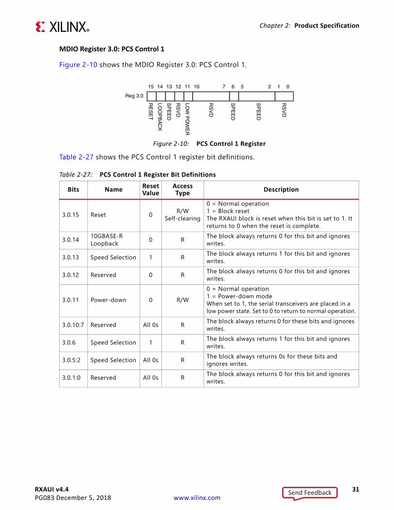
MDIO Register 3.0: PCS Control 1
Figure 2-10 shows the MDIO Register 3.0: PCS Control 1.
Table 2-27 shows the PCS Control 1 register bit definitions.
X-Ref Target - Figure 2-10
Figure 2-10: PCS Control 1 Register
Table 2-27: PCS Control 1 Register Bit Definitions
Bits Name ResetValue
AccessType Description
3.0.15 Reset 0 R/WSelf-clearing
0 = Normal operation1 = Block resetThe RXAUI block is reset when this bit is set to 1. It returns to 0 when the reset is complete.
3.0.14 10GBASE-R Loopback 0 R The block always returns 0 for this bit and ignores
writes.
3.0.13 Speed Selection 1 R The block always returns 1 for this bit and ignores writes.
3.0.12 Reserved 0 R The block always returns 0 for this bit and ignores writes.
3.0.11 Power-down 0 R/W0 = Normal operation1 = Power-down modeWhen set to 1, the serial transceivers are placed in a low power state. Set to 0 to return to normal operation.
3.0.10:7 Reserved All 0s R The block always returns 0 for these bits and ignores writes.
3.0.6 Speed Selection 1 R The block always returns 1 for this bit and ignores writes.
3.0.5:2 Speed Selection All 0s R The block always returns 0s for these bits and ignores writes.
3.0.1:0 Reserved All 0s R The block always returns 0 for this bit and ignores writes.
Send Feedback

RXAUI v4.4 32PG083 December 5, 2018 www.xilinx.com
Chapter 2: Product Specification
MDIO Register 3.1: PCS Status 1
Figure 2-11 shows the MDIO Register 3.1: PCS Status 1.
Table 2-28 show the PCS 1 register bit definitions.
X-Ref Target - Figure 2-11
Figure 2-11: PCS Status 1 Register
Table 2-28: PCS Status 1 Register Bit Definition
Bits Name ResetValue
AccessType Description
3.1.15:8 Reserved All 0s R The block always returns 0s for these bits and ignores writes.
3.1.7 Local Fault – R0 = No local fault detected1 = Local fault detectedThis bit is set to 1 whenever either of the bits 3.8.11 and 3.8.10 are set to 1.
3.1.6:3 Reserved All 0s R The block always returns 0s for these bits and ignores writes.
3.1.2 PCS Receive Link Status – RSelf-setting
0 = The PCS receive link is down1 = The PCS receive link is upThis is a latching Low version of bit 3.24.12. Latches 0 if Link Status goes down. Clears to current Link Status on read.
3.1.1 Power-down Ability 1 R The block always returns 1 for this bit.
3.1.0 Reserved 0 R The block always returns 0 for this bit and ignores writes.
Send Feedback

RXAUI v4.4 33PG083 December 5, 2018 www.xilinx.com
Chapter 2: Product Specification
MDIO Registers 3.2 and 3.3: PCS Device Identifier
Figure 2-12 shows the MDIO Registers 3.2 and 3.3: PCS Device Identifier..
Table 2-29 shows the PCS Device Identifier registers bit definitions.
MDIO Register 3.4: PCS Speed Ability
Figure 2-13 shows the MDIO Register 3.4: PCS Speed Ability.
Table 2-30 shows the PCS Speed Ability register bit definitions.
X-Ref Target - Figure 2-12
Figure 2-12: PCS Device Identifier Registers
Table 2-29: PCS Device Identifier Registers Bit Definition
Bits Name ResetValue
AccessType Description
3.2.15:0 PCS Identifier All 0s R The block always returns 0 for these bits and ignores writes.3.3.15:0 PCS Identifier All 0s R The block always returns 0 for these bits and ignores writes.
X-Ref Target - Figure 2-13
Figure 2-13: PCS Speed Ability Register
Table 2-30: PCS Speed Ability Register Bit Definition
Bits Name ResetValue
AccessType Description
3.4.15:1 Reserved All 0s R The block always returns 0 for these bits and ignores writes.3.4.0 10G Capable 1 R The block always returns 1 for this bit and ignores writes.
X13636D
EVICE
IDEN
TIFIER
15 0
Reg 3.2
DEVIC
EID
ENTIFIER
15 0
Reg 3.3
X13637
RSVD
15 0
Reg 3.4
Send Feedback

RXAUI v4.4 34PG083 December 5, 2018 www.xilinx.com
Chapter 2: Product Specification
MDIO Registers 3.5 and 3.6: PCS Devices in Package
Figure 2-14 shows the MDIO Registers 3.5 and 3.6: PCS Devices in Package.
Table 2-31 shows the PCS Devices in Package registers bit definitions.
X-Ref Target - Figure 2-14
Figure 2-14: PCS Devices in Package Registers
Table 2-31: PCS Devices in Package Registers Bit Definitions
Bits Name ResetValue
AccessType Description
3.6.15 Vendor-specific Device 2 present 0 R The block always returns 0 for this bit.3.6.14 Vendor- specific Device 1 present 0 R The block always returns 0 for this bit.3.6.13:0 Reserved All 0s R The block always returns 0 for these bits.3.5.15:6 Reserved All 0s R The block always returns 0 for these bits.3.5.5 PHY XS present 0 R The block always returns 0 for this bit.3.5.4 PHY XS present 0 R The block always returns 0 for this bit.3.5.3 PCS present 1 R The block always returns 1 for this bit.3.5.2 WIS present 0 R The block always returns 0 for this bit.3.5.1 PMA/PMD present 1 R The block always returns 1 for this bit.3.5.0 Clause 22 device present 0 R The block always returns 0 for this bit.
X13638
VEND
OR
2 PRESEN
T
VEND
OR
1 PRESEN
T
RSVD
15 14 13 0
Reg 3.6
RSVD
DTE XS PR
ESENT
PHY XS PR
ESENT
PCS PR
ESENT
WIS PR
ESENT
PMD
/PMA PR
ESENT
CLAU
SE 22 PRESEN
T
15 0123456
Reg 3.5
Send Feedback

RXAUI v4.4 35PG083 December 5, 2018 www.xilinx.com
Chapter 2: Product Specification
MDIO Register 3.7: 10G PCS Control 2
Figure 2-15 shows the MDIO Register 3.7: 10G PCS Control 2.
Table 2-32 shows the 10 G PCS Control 2 register bit definitions.
MDIO Register 3.8: 10G PCS Status 2
Figure 2-16 shows the MDIO Register 3.8: 10G PCS Status 2.
Table 2-33 shows the 10G PCS Status 2 register bit definitions.
X-Ref Target - Figure 2-15
Figure 2-15: 10G PCS Control 2 Register
Table 2-32: 10G PCS Control 2 Register Bit Definitions
Bits Name ResetValue
AccessType Description
3.7.15:2 Reserved All 0s R The block always returns 0 for these bits and ignores writes.
3.7.1:0 PCS Type Selection 01 R The block always returns 01 for these bits and ignores writes.
X-Ref Target - Figure 2-16
Figure 2-16: 10G PCS Status 2 Register
Table 2-33: 10G PCS Status 2 Register Bit Definitions
Bits Name ResetValue
AccessType Description
3.8.15:14 Device present 10 R The block always returns 10.3.8.13:12 Reserved All 0s R The block always returns 0 for these bits.
X13639
RSVD
PCS TYPESELEC
TION
15 012
Reg 3.7
X13640
DEVIC
E PRESEN
T
RSVD
TX FAULT
RX FAU
LT
RSVD
10GBASE-W
ABILITY
10GBASE-X ABILITY
10GBASE-R
ABILITY
15 14 13 12 11 10 9 23 1 0
Reg 3.8
Send Feedback

RXAUI v4.4 36PG083 December 5, 2018 www.xilinx.com
Chapter 2: Product Specification
MDIO Registers 3.14 and 3.15: PCS Package Identifier
Figure 2-17 shows the MDIO Registers 3.14 and 3.15: PCS Package Identifier.
Table 2-34 shows the PCS Package Identifier registers bit definitions.
3.8.11 Transmit local fault –
RLatching High. Automatically clears after a read unless the fault is
present.
0 = No fault condition on transmit path1 = Fault condition on transmit path
3.8.10 Receive local fault –
RLatching High. Automatically clears after a read unless the fault is
present.
0 = No fault condition on receive path1 = Fault condition on receive path
3.8.9:3 Reserved All 0s R The block always returns 0 for these bits.3.8.2 10GBASE-W Capable 0 R The block always returns 0 for this bit.3.8.1 10GBASE-X Capable 1 R The block always returns 1 for this bit.3.8.0 10GBASE-R Capable 0 R The block always returns 0 for this bit.
X-Ref Target - Figure 2-17
Figure 2-17: Package Identifier Registers
Table 2-34: PCS Package Identifier Register Bit Definitions
Bits Name ResetValue
AccessType Description
3.14.15:0 Package Identifier All 0s R The block always returns 0 for these bits.3.15.15:0 Package Identifier All 0s R The block always returns 0 for these bits.
Table 2-33: 10G PCS Status 2 Register Bit Definitions (Cont’d)
Bits Name ResetValue
AccessType Description
PACKAG
EID
ENTIFIER
15 0
Reg 3.15
PACKAG
EID
ENTIFIER
15 0
Reg 3.14
X13641
Send Feedback

RXAUI v4.4 37PG083 December 5, 2018 www.xilinx.com
Chapter 2: Product Specification
MDIO Register 3.24: 10GBASE-X Status
Figure 2-18 shows the MDIO Register 3.24: 10GBase-X Status.
Table 2-35 shows the 10GBase-X Status register bit definitions.
X-Ref Target - Figure 2-18
Figure 2-18: 10GBASE-X Status Register
Table 2-35: 10GBASE-X Status Register Bit Definitions
Bits Name ResetValue
AccessType Description
3.24.15:13 Reserved All 0s R The block always returns 0 for these bits.
3.24.12 10GBASE-X Lane Alignment Status – R 0 = 10GBASE-X receive lanes not aligned
1 = 10GBASE-X receive lanes aligned3.24.11 Pattern Testing Ability 1 R The block always returns 1 for this bit.3.24.10:4 Reserved All 0s R The block always returns 0 for these bits.
3.24.3 Lane 3 Sync – R 0 = Lane 3 is not synchronized1 = Lane 3 is synchronized
3.24.2 Lane 2 Sync – R 0 =Lane 2 is not synchronized1 =Lane 2 is synchronized
3.24.1 Lane 1 Sync – R 0 = Lane 1 is not synchronized1 = Lane 1 is synchronize
3.24.0 Lane 0 Sync – R 0 = Lane 0 is not synchronized1 = Lane 0 is synchronized
X13642
RSVD
RSVD
PATTERN
TEST ABILITY
ALIGN
STATUS
LANE 3 SYN
C
LANE 2 SYN
C
LANE 1 SYN
C
LANE 0 SYN
C
15 13 12 11 10 4 3 2 1 0
Reg 3.24
Send Feedback
RXAUI v4.4 38PG083 December 5, 2018 www.xilinx.com
Chapter 2: Product Specification
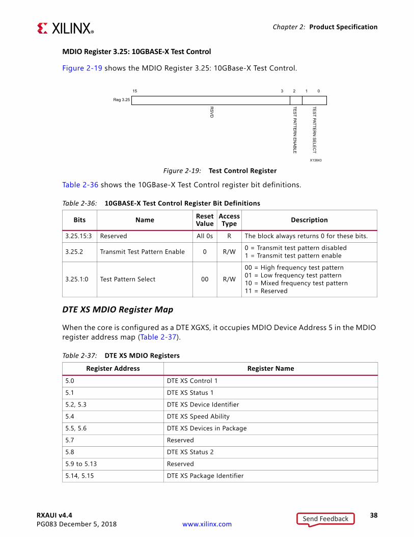
MDIO Register 3.25: 10GBASE-X Test Control
Figure 2-19 shows the MDIO Register 3.25: 10GBase-X Test Control.
Table 2-36 shows the 10GBase-X Test Control register bit definitions.
DTE XS MDIO Register Map
When the core is configured as a DTE XGXS, it occupies MDIO Device Address 5 in the MDIO register address map (Table 2-37).
X-Ref Target - Figure 2-19
Figure 2-19: Test Control Register
Table 2-36: 10GBASE-X Test Control Register Bit Definitions
Bits Name ResetValue
AccessType Description
3.25.15:3 Reserved All 0s R The block always returns 0 for these bits.
3.25.2 Transmit Test Pattern Enable 0 R/W 0 = Transmit test pattern disabled1 = Transmit test pattern enable
3.25.1:0 Test Pattern Select 00 R/W00 = High frequency test pattern01 = Low frequency test pattern10 = Mixed frequency test pattern11 = Reserved
Table 2-37: DTE XS MDIO RegistersRegister Address Register Name
5.0 DTE XS Control 15.1 DTE XS Status 15.2, 5.3 DTE XS Device Identifier5.4 DTE XS Speed Ability5.5, 5.6 DTE XS Devices in Package5.7 Reserved5.8 DTE XS Status 25.9 to 5.13 Reserved5.14, 5.15 DTE XS Package Identifier
X13643
RSVD
TEST PATTERN
ENABLE
TEST PATTERN
SELECT
15 3 2 1 0
Reg 3.25
Send Feedback
RXAUI v4.4 39PG083 December 5, 2018 www.xilinx.com
Chapter 2: Product Specification
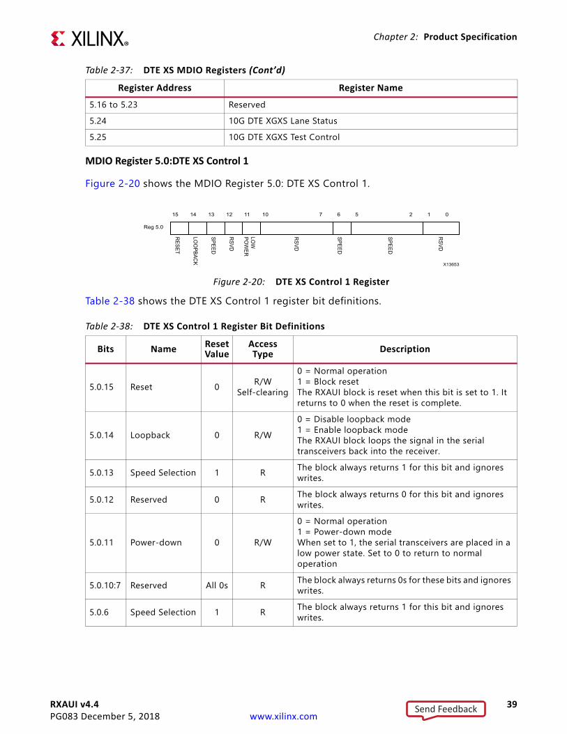
MDIO Register 5.0:DTE XS Control 1
Figure 2-20 shows the MDIO Register 5.0: DTE XS Control 1.
Table 2-38 shows the DTE XS Control 1 register bit definitions.
5.16 to 5.23 Reserved5.24 10G DTE XGXS Lane Status5.25 10G DTE XGXS Test Control
X-Ref Target - Figure 2-20
Figure 2-20: DTE XS Control 1 Register
Table 2-38: DTE XS Control 1 Register Bit Definitions
Bits Name ResetValue
AccessType Description
5.0.15 Reset 0 R/WSelf-clearing
0 = Normal operation1 = Block resetThe RXAUI block is reset when this bit is set to 1. It returns to 0 when the reset is complete.
5.0.14 Loopback 0 R/W0 = Disable loopback mode1 = Enable loopback modeThe RXAUI block loops the signal in the serial transceivers back into the receiver.
5.0.13 Speed Selection 1 R The block always returns 1 for this bit and ignores writes.
5.0.12 Reserved 0 R The block always returns 0 for this bit and ignores writes.
5.0.11 Power-down 0 R/W
0 = Normal operation1 = Power-down modeWhen set to 1, the serial transceivers are placed in a low power state. Set to 0 to return to normal operation
5.0.10:7 Reserved All 0s R The block always returns 0s for these bits and ignores writes.
5.0.6 Speed Selection 1 R The block always returns 1 for this bit and ignores writes.
Table 2-37: DTE XS MDIO Registers (Cont’d)
Register Address Register Name
X13653
RESET
LOO
PBACK
RSVD
RSVD
RSVD
LOW
PO
WER
SPEED
SPEED
SPEED
15 14 13 12 11 10 7 6 5 2 1 0
Reg 5.0
Send Feedback

RXAUI v4.4 40PG083 December 5, 2018 www.xilinx.com
Chapter 2: Product Specification
MDIO Register 5.1: DTE XS Status 1
Figure 2-21 shows the MDIO Register 5.1: DTE XS Status 1.
Table 2-39 shows the DET XS Status 1 register bit definitions.
5.0.5:2 Speed Selection All 0s R The block always returns 0s for these bits and ignores writes.
5.0.1:0 Reserved All 0s R The block always returns 0s for these bits and ignores writes.
X-Ref Target - Figure 2-21
Figure 2-21: DTE XS Status 1 Register
Table 2-39: DTE XS Status 1 Register Bit Definitions
Bits Name ResetValue
AccessType Description
5.1.15:8 Reserved All 0s R The block always returns 0s for these bits and ignores writes.
5.1.7 Local Fault – R0 = No Local Fault detected1 = Local fault detectedThis bit is set to 1 whenever either of the bits 5.8.11, 5.8.10 are set to 1.
5.1.6:3 Reserved All 0s R The block always returns 0s for these bits and ignores writes.
5.1.2 DTE XS Receive Link Status All 0sR
Self-setting
0 = The DTE XS receive link is down1 = The DTE XS receive link is upThis is a latching Low version of bit 5.24.12. Latches 0 if Link Status goes down. Clears to current Link Status on read.
5.1.1 Power-down Ability 1 R The block always returns 1 for this bit.
5.1.0 Reserved 0 R The block always returns 0 for this bit and ignores writes.
Table 2-38: DTE XS Control 1 Register Bit Definitions (Cont’d)
Bits Name ResetValue
AccessType Description
X13654
RSVD
RSVD
LOC
AL FAULT
LOW
POW
ER ABILITY
RX LIN
K STATUS
15 8 7 6 3 2 1 0
Reg 5.1
Send Feedback

RXAUI v4.4 41PG083 December 5, 2018 www.xilinx.com
Chapter 2: Product Specification
MDIO Registers 5.2 and 5.3: DTE XS Device Identifier
Figure 2-22 shows the MDIO Registers 5.2 and 5.3: DTE XS Device Identifier.
Table 2-40 shows the DTE XS Device Identifier registers bit definitions.
MDIO Register 5.4: DTE XS Speed Ability
Figure 2-23 shows the MDIO Register 5.4: DTE Speed Ability.
Table 2-41 shows the DTE XS Speed Ability register bit definitions.
X-Ref Target - Figure 2-22
Figure 2-22: DTE XS Device Identifier Registers
Table 2-40: DTE XS Device Identifier Register Bit Definitions
Bits Name ResetValue
AccessType Description
5.2.15:0 DTE XS Identifier All 0s R The block always returns 0 for these bits and ignores writes.
5.3.15:0 DTE XS Identifier All 0s R The block always returns 0 for these bits and ignores writes.
X-Ref Target - Figure 2-23
Figure 2-23: DTE XS Speed Ability Register
Table 2-41: DTE XS Speed Ability Register Bit Definitions
Bits Name ResetValue
AccessType Description
5.4.15:1 Reserved All 0s R The block always returns 0 for these bits and ignores writes.5.4.0 10G Capable 1 R The block always returns 1 for this bit and ignores writes.
X13655
DEVIC
EID
ENTIFIER
15 0
Reg 5.2
DEVIC
EID
ENTIFIER
15 0
Reg 5.3
RSVD
10G CAPABLE
15 0
Reg 5.4
X13656
Send Feedback

RXAUI v4.4 42PG083 December 5, 2018 www.xilinx.com
Chapter 2: Product Specification
MDIO Registers 5.5 and 5.6: DTE XS Devices in Package
Figure 2-24 shows the MDIO Registers 5.5 and 5.6: DTE XS Devices in Package.
Table 2-42 shows the DTE XS Devices in Package registers bit definitions.
X-Ref Target - Figure 2-24
Figure 2-24: DTE XS Devices in Package Register
Table 2-42: DTE XS Devices in Package Registers Bit Definitions
Bits Name ResetValue
AccessType Description
5.6.15 Vendor-specific Device 2 present 0 R The block always returns 0 for this bit.5.6.14 Vendor-specific Device 1 present 0 R The block always returns 0 for this bit.5.6.13:0 Reserved All 0s R The block always returns 0 for these bits.5.6.15:6 Reserved All 0s R The block always returns 0 for these bits.5.5.5 DTE XS present 1 R The block always returns 1 for this bit.5.5.4 PHY XS present 0 R The block always returns 0 for this bit.5.5.3 PCS present 0 R The block always returns 0 for this bit.5.5.2 WIS present 0 R The block always returns 0 for this bit.5.5.1 PMA/PMD present 0 R The block always returns 0 for this bit.5.5.0 Clause 22 Device present 0 R The block always returns 0 for this bit.
X13657
VEND
OR
2 PRESEN
T
VEND
OR
1 PRESEN
T
RSVD
15 14 13 0
Reg 5.6
RSVD
DTE XS PR
ESENT
PHY XS PR
ESENT
PCS PR
ESENT
WIS PR
ESENT
PMD
/PMA PR
ESENT
CLAU
SE 22 PRESEN
T
15 0123456
Reg 5.5
Send Feedback

RXAUI v4.4 43PG083 December 5, 2018 www.xilinx.com
Chapter 2: Product Specification
MDIO Register 5.8: DTE XS Status 2
Figure 2-25 shows the MDIO Register 5.8: DTE XS Status 2.
Table 2-43 show the DTE XS Status 2 register bits definitions.
X-Ref Target - Figure 2-25
Figure 2-25: DTE XS Status 2 Register
Table 2-43: DTE XS Status 2 Register Bit Definitions
Bits Name ResetValue
AccessType Description
5.8.15:14 Device present 10 R The block always returns 10.5.8.13:12 Reserved All 0s R The block always returns 0 for these bits.
5.8.11 Transmit Local Fault –
RLatching High. Automatically clears after a read unless the fault is
present.
0 = No fault condition on transmit path1 = Fault condition on transmit path
5.8.10 Receive Local Fault –
RLatching High. Automatically clears after a read unless the fault is
present.
0 = No fault condition on receive path1 = Fault condition on receive path
5.8.9:0 Reserved All 0s R The block always returns 0 for these bits.
X13658
DEVIC
E PRESEN
T
RSVD
TX FAULT
RX FAU
LT
RSVD
15 14 13 12 11 10 9 0
Reg 5.8
Send Feedback

RXAUI v4.4 44PG083 December 5, 2018 www.xilinx.com
Chapter 2: Product Specification
MDIO Registers 5.14 and 5.15: DTE XS Package Identifier
Figure 2-26 shows the MDIO Registers 5.14 and 5.15: DTE XS Package Identifier.
Table 2-44 shows the DTE XS Package Identifier registers bit definitions.
Test Patterns
The RXAUI core is capable of sending test patterns for system debug. These patterns are defined in Annex 48A of IEEE Std. 802.3-2012 and transmission of these patterns is controlled by the MDIO Test Control Registers.
There are three types of pattern available:
• High frequency test pattern of 1010101010.... at each device-specific transceiver output• Low frequency test pattern of 111110000011111000001111100000.... at each
device-specific transceiver output• mixed frequency test pattern of 111110101100000101001111101011000001010... at
each device-specific transceiver output.
X-Ref Target - Figure 2-26
Figure 2-26: DTE XS Package Identifier Registers
Table 2-44: DTE XS Package Identifier Register Bit Definitions
Bits Name ResetValue
AccessType Description
5.14.15:0 DTE XS Package Identifier All 0s R The block always returns 0 for these bits.5.15.15:0 DTE XS Package Identifier All 0s R The block always returns 0 for these bits.
X13659PAC
KAGE
IDEN
TIFIER
15 0
Reg 5.15
PACKAG
EID
ENTIFIER
15 0
Reg 5.14
Send Feedback

RXAUI v4.4 45PG083 December 5, 2018 www.xilinx.com
Chapter 2: Product Specification
MDIO Register 5.24: DTE XS Lane Status
Figure 2-27 shows the MDIO Register 5.24: DTE XS Lane Status.
Table 2-45 shows the DTE XS Lane Status register bit definitions.
X-Ref Target - Figure 2-27
Figure 2-27: DTE XS Lane Status Register
Table 2-45: DTE XS Lane Status Register Bit Definitions
Bits Name ResetValue
AccessType Description
5.24.15:13 Reserved All 0s R The block always returns 0 for these bits.
5.24.12 DTE XGXS Lane Alignment Status – R 0 = DTE XGXS receive lanes not aligned1 = DTE XGXS receive lanes aligned
5.24.11 Pattern testing ability 1 R The block always returns 1 for this bit.5.24.10:4 Reserved All 0s R The block always returns 0 for these bits.
5.24.3 Lane 3 Sync – R 0 = Lane 3 is not synchronized1 = Lane 3 is synchronized
5.24.2 Lane 2 Sync – R 0 = Lane 2 is not synchronized1 = Lane 2 is synchronized
5.24.1 Lane 1 Sync – R 0 = Lane 1 is not synchronized1 = Lane 1 is synchronized
5.24.0 Lane 0 Sync – R 0 = Lane 0 is not synchronized1 = Lane 0 is synchronized
X13660
RSVD
RSVD
PATTERN
TEST ABILITY
ALIGN
STATUS
LANE 3 SYN
C
LANE 2 SYN
C
LANE 1 SYN
C
LANE 0 SYN
C15 13 12 11 10 4 3 2 1 0
Reg 5.24
Send Feedback

RXAUI v4.4 46PG083 December 5, 2018 www.xilinx.com
Chapter 2: Product Specification
MDIO Register 5.25: 10G DTE XGXS Test Control
Figure 2-28 shows the MDIO Register 5.25: 10G DTE XGXS Test Control.
Table 2-46 shows the 10G DTE XGXS Test Control register bit definitions.
PHY XS MDIO Register Map
When the core is configured as a PHY XGXS, it occupies MDIO Device Address 4 in the MDIO register address map (Table 2-47).
X-Ref Target - Figure 2-28
Figure 2-28: 10G DTE XGXS Test Control Register
Table 2-46: 10G DTE XGXS Test Control Register Bit Definitions
Bits Name ResetValue
AccessType Description
5.25.15:3 Reserved All 0s R The block always returns 0 for these bits.
5.25.2 Transmit Test Pattern Enable 0 R/W 0 = Transmit test pattern disabled1 = Transmit test pattern enable
5.25.1:0 Test Pattern Select00 R/W 00 = High frequency test pattern
01 = Low frequency test pattern10 = Mixed frequency test pattern11 = Reserved
Table 2-47: PHY XS MDIO RegistersRegister Address Register Name
4.0 PHY XS Control 14.1 PHY XS Status 14.2, 4.3 Device Identifier4.4 PHY XS Speed Ability4.5, 4.6 Devices in Package4.7 Reserved4.8 PHY XS Status 24.9 to 4.13 Reserved4.14, 4.15 Package Identifier
RSVD
TEST PATTERN
ENABLE
TEST PATTERN
SELECT
15 3 2 1 0
Reg 5.25
X13661
Send Feedback

RXAUI v4.4 47PG083 December 5, 2018 www.xilinx.com
Chapter 2: Product Specification
MDIO Register 4.0: PHY XS Control 1
Figure 2-29 shows the MDIO Register 4.0: PHY XS Control 1.
Table 2-48 shows the PHY XS Control 1 register bit definitions.
4.16 to 4.23 Reserved4.24 10G PHY XGXS Lane Status4.25 10G PHY XGXS Test Control
X-Ref Target - Figure 2-29
Figure 2-29: PHY XS Control 1 Register
Table 2-48: PHY XS Control 1 Register Bit Definitions
Bits Name ResetValue
AccessType Description
4.0.15 Reset 0R/WSelf-
clearing
0 = Normal operation1 = Block resetThe RXAUI block is reset when this bit is set to 1.It returns to 0 when the reset is complete.
4.0.14 Loopback 0 R/W0 = Disable loopback mode1 = Enable loopback modeThe RXAUI block loops the signal in the serial transceivers back into the receiver.
4.0.13 Speed Selection 1 R The block always returns 1 for this bit and ignores writes.4.0.12 Reserved 0 R The block always returns 0 for this bit and ignores writes.
4.0.11 Power-down 0 R/W0 = Normal operation1 = Power-down modeWhen set to 1, the serial transceivers are placed in a low power state. Set to 0 to return to normal operation
4.0.10:7 Reserved All 0s R The block always returns 0s for these bits and ignores writes.
4.0.6 Speed Selection 1 R The block always returns 1 for this bit and ignores writes.
4.0.5:2 Speed Selection All 0s R The block always returns 0s for these bits and ignores writes.
4.0.1:0 Reserved All 0s R The block always returns 0s for these bits and ignores writes.
Table 2-47: PHY XS MDIO Registers (Cont’d)
Register Address Register Name
X13644
RESET
LOO
PBACK
RSVD
RSVD
RSVD
LOW
PO
WER
SPEED
SPEED
SPEED
15 14 13 12 11 10 7 6 5 2 1 0
Reg 4.0
Send Feedback
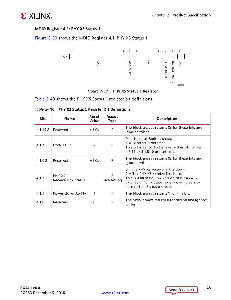
RXAUI v4.4 48PG083 December 5, 2018 www.xilinx.com
Chapter 2: Product Specification
MDIO Register 4.1: PHY XS Status 1
Figure 2-30 shows the MDIO Register 4.1: PHY XS Status 1.
Table 2-49 shows the PHY XS Status 1 register bit definitions.
X-Ref Target - Figure 2-30
Figure 2-30: PHY XS Status 1 Register
Table 2-49: PHY XS Status 1 Register Bit Definitions
Bits Name ResetValue
AccessType Description
4.1.15:8 Reserved All 0s R The block always returns 0s for these bits and ignores writes.
4.1.7 Local Fault – R0 = No Local Fault detected1 = Local fault detectedThis bit is set to 1 whenever either of the bits 4.8.11 and 4.8.10 are set to 1.
4.1.6:3 Reserved All 0s R The block always returns 0s for these bits and ignores writes.
4.1.2 PHY XS Receive Link Status – R
Self-setting
0 =The PHY XS receive link is down1 = The PHY XS receive link is up.This is a latching Low version of bit 4.24.12. Latches 0 if Link Status goes down. Clears to current Link Status on read.
4.1.1 Power-down Ability 1 R The block always returns 1 for this bit.
4.1.0 Reserved 0 R The block always returns 0 for this bit and ignores writes.
X13645
RSVD
RSVD
RSVD
LOC
AL FAULT
LOW
POW
ER ABILITY
RX LIN
K STATUS
15 8 7 6 3 2 1 0
Reg 4.1
Send Feedback

RXAUI v4.4 49PG083 December 5, 2018 www.xilinx.com
Chapter 2: Product Specification
MDIO Registers 4.2 and 4.3: PHY XS Device Identifier
Figure 2-31 shows the MDIO Registers 4.2 and 4.3: PHY XS Device Identifier.
Table 2-50 shows the PHY XS Devices Identifier registers bit definitions.
MDIO Register 4.4: PHY XS Speed Ability
Figure 2-32 shows the MDIO Register 4.4: PHY XS Speed Ability.
X-Ref Target - Figure 2-31
Figure 2-31: PHY XS Device Identifier Registers
Table 2-50: PHY XS Device Identifier Registers Bit Definitions
Bits Name ResetValue
AccessType Description
4.2.15:0 PHY XS Identifier All 0s R The block always returns 0 for these bits and ignores writes.
4.3.15:0 PHY XS Identifier All 0s R The block always returns 0 for these bits and ignores writes.
X-Ref Target - Figure 2-32
Figure 2-32: PHY XS Speed Ability Register
X13646D
EVICE
IDEN
TIFIER
15 0
Reg 4.2
DEVIC
EID
ENTIFIER
15 0
Reg 4.3
X13647
RS
VD
10G C
AP
AB
LE
15 0
Reg 4.4
Send Feedback

RXAUI v4.4 50PG083 December 5, 2018 www.xilinx.com
Chapter 2: Product Specification
Table 2-51 shows the PHY XS Speed Ability register bit definitions.
MDIO Registers 4.5 and 4.6: PHY XS Devices in Package
Figure 2-33 shows the MDIO Registers 4.5 and 4.6: PHY XS Devices in Package.
Table 2-52 shows the PHY XS Devices in Package registers bit definitions.
Table 2-51: PHY XS Speed Ability Register Bit Definitions
Bits Name ResetValue
AccessType Description
4.4.15:1 Reserved All 0s R The block always returns 0 for these bits and ignores writes. 4.4.0 10G Capable 1 R The block always returns 1 for this bit and ignores writes.
X-Ref Target - Figure 2-33
Figure 2-33: PHY XS Devices in Package Registers
Table 2-52: PHY XS Devices in Package Registers Bit Definitions
Bits Name ResetValue
AccessType Description
4.6.15 Vendor-specific Device 2 present 0 R The block always returns 0 for this bit.4.6.14 Vendor-specific Device 1 present 0 R The block always returns 0 for this bit.4.6.13:0 Reserved All 0s R The block always returns 0 for these bits.4.5.15:6 Reserved All 0s R The block always returns 0 for these bits.4.5.5 DTE XS present 0 R The block always returns 0 for this bit.4.5.4 PHY XS present 1 R The block always returns 1 for this bit.4.5.3 PCS present 0 R The block always returns 0 for this bit.4.5.2 WIS present 0 R The block always returns 0 for this bit.4.5.1 PMA/PMD present 0 R The block always returns 0 for this bit.4.5.0 Clause 22 device present 0 R The block always returns 0 for this bit.
X13648VEN
DO
R2 PR
ESENT
VEND
OR
1 PRESEN
T
RSVD
15 14 13 0
Reg 4.6
RSVD
DTE XS PR
ESENT
PHY XS PR
ESENT
PCS PR
ESENT
WIS PR
ESENT
PMD
/PMA PR
ESENT
CLAU
SE 22 PRESEN
T
15 0123456
Reg 4.5
Send Feedback

RXAUI v4.4 51PG083 December 5, 2018 www.xilinx.com
Chapter 2: Product Specification
MDIO Register 4.8: PHY XS Status 2
Figure 2-34 shows the MDIO Register 4.8: PHY XS Status 2.
Table 2-53 shows the PHY XS Status 2 register bit definitions.
X-Ref Target - Figure 2-34
Figure 2-34: PHY XS Status 2 Register
Table 2-53: PHY XS Status 2 Register Bit Definitions
Bits Name ResetValue
AccessType Description
4.8.15:14 Device present 10 R The block always returns 10.4.8.13:12 Reserved All 0s R The block always returns 0 for these bits.
4.8.11 Transmit local fault –
RLatching High. Automatically
clears after a read unless the fault is
present.
0 = No fault condition on transmit path1 = Fault condition on transmit path
4.8.10 Receive local fault –
RLatching High. Automatically
clears after a read unless the fault is
present.
0 = No fault condition on receive path1 = Fault condition on receive path
4.8.9:0 Reserved All 0s R The block always returns 0 for these bits.
X13649
DEVIC
E PRESEN
T
RSVD
TX FAULT
RX FAU
LT
RSVD
15 14 13 12 11 10 9 0
Reg 4.8
Send Feedback

RXAUI v4.4 52PG083 December 5, 2018 www.xilinx.com
Chapter 2: Product Specification
MDIO Registers 4.14 and 4.15: PHY XS Package Identifier
Figure 2-35 shows the MDIO 4.14 and 4.15 Registers: PHY XS Package Identifier.
Table 2-54 shows the Package Identifier registers bit definitions.
MDIO Register 4.24: 10G PHY XGXS Lane Status
Figure 2-36 shows the MDIO Register 4.24: 10G XGXS Lane Status.
X-Ref Target - Figure 2-35
Figure 2-35: PHY XS Package Identifier Registers
Table 2-54: Package Identifier Registers Bit Definitions
Bits Name ResetValue
AccessType Description
4.15.15:0 PHY XS Package Identifier All 0s R The block always returns 0 for these bits.4.14.15:0 PHY XS Package Identifier All 0s R The block always returns 0 for these bits.
X-Ref Target - Figure 2-36
Figure 2-36: 10G PHY XGXS Lane Status Register
X13659PAC
KAGE
IDEN
TIFIER
15 0
Reg 5.15
PACKAG
EID
ENTIFIER
15 0
Reg 5.14
X13651
RSVD
RSVD
PATTERN
TEST ABILITY
ALIGN
STATUS
LANE 3 SYN
C
LANE 2 SYN
C
LANE 1 SYN
C
LANE 0 SYN
C
15 13 12 11 10 4 3 2 1 0
Reg 4.24
Send Feedback

RXAUI v4.4 53PG083 December 5, 2018 www.xilinx.com
Chapter 2: Product Specification
Table 2-55 shows the 10G PHY XGXS Lane register bit definitions.
MDIO Register 4.25: 10G PHY XGXS Test Control
Figure 2-37 shows the MDIO Register 4.25: 10G XGXS Test Control.
Table 2-56 shows the 10G PHY XGXS Test Control register bit definitions.
Table 2-55: 10G PHY XGXS Lane Status Register Bit Definitions
Bits Name ResetValue
AccessType Description
4.24.15:13 Reserved All 0s R The block always returns 0 for these bits.
4.24.12 PHY XGXS Lane Alignment Status – R 0 = PHY XGXS receive lanes not aligned1 = PHY XGXS receive lanes aligned
4.24.11 Pattern Testing Ability 1 R The block always returns 1 for this bit.4.24.10:4 Reserved All 0s R The block always returns 0 for these bits.
4.24.3 Lane 3 Sync – R 0 = Lane 3 is not synchronized1 = Lane 3 is synchronized
4.24.2 Lane 2 Sync – R 0 = Lane 2 is not synchronized1 = Lane 2 is synchronized
4.24.1 Lane 1 Sync – R 0 = Lane 1 is not synchronized1 = Lane 1 is synchronized
4.24.0 Lane 0 Sync – R 0 = Lane 0 is not synchronized1 = Lane 0 is synchronized
X-Ref Target - Figure 2-37
Figure 2-37: 10G PHY XGXS Test Control Register
Table 2-56: 10G PHY XGXS Test Control Register Bit Definitions
Bits Name ResetValue
AccessType Description
4.25.15:3 Reserved All 0s R The block always returns 0 for these bits.
4.25.2 Transmit Test Pattern Enable 0 R/W 0 = Transmit test pattern disabled1 = Transmit test pattern enable
4.25.1:0 Test Pattern Select 00 R/W00 = High frequency test pattern01 = Low frequency test pattern10 = Mixed frequency test pattern11 = Reserved
RSVD
TEST PATTERN
ENABLE
TEST PATTERN
SELECT
15 3 2 1 0
Reg 4.25
X13652
Send Feedback
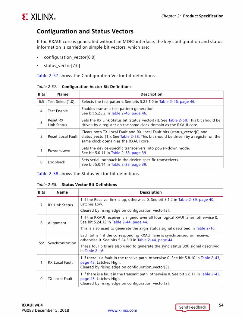
RXAUI v4.4 54PG083 December 5, 2018 www.xilinx.com
Chapter 2: Product Specification
Configuration and Status VectorsIf the RXAUI core is generated without an MDIO interface, the key configuration and status information is carried on simple bit vectors, which are:
• configuration_vector[6:0]• status_vector[7:0]
Table 2-57 shows the Configuration Vector bit definitions.
Table 2-58 shows the Status Vector bit definitions.
Table 2-57: Configuration Vector Bit DefinitionsBits Name Description6:5 Test Select[1:0] Selects the test pattern. See bits 5.25.1:0 in Table 2-46, page 46.
4 Test Enable Enables transmit test pattern generation. See bit 5.25.2 in Table 2-46, page 46.
3 Reset RXLink Status
Sets the RX Link Status bit (status_vector[7]). See Table 2-58. This bit should be driven by a register on the same clock domain as the RXAUI core.
2 Reset Local FaultClears both TX Local Fault and RX Local Fault bits (status_vector[0] and status_vector[1]). See Table 2-58. This bit should be driven by a register on the same clock domain as the RXAUI core.
1 Power-down Sets the device-specific transceivers into power-down mode.See bit 5.0.11 in Table 2-38, page 39.
0 Loopback Sets serial loopback in the device-specific transceivers.See bit 5.0.14 in Table 2-38, page 39.
Table 2-58: Status Vector Bit DefinitionsBits Name Description
7 RX Link Status1 if the Receiver link is up, otherwise 0. See bit 5.1.2 in Table 2-39, page 40. Latches Low. Cleared by rising edge on configuration_vector[3].
6 Alignment1 if the RXAUI receiver is aligned over all four logical XAUI lanes, otherwise 0. See bit 5.24.12 in Table 2-44, page 44. This is also used to generate the align_status signal described in Table 2-16.
5:2 SynchronizationEach bit is 1 if the corresponding RXAUI lane is synchronized on receive, otherwise 0. See bits 5.24.3:0 in Table 2-44, page 44. These four bits are also used to generate the sync_status[3:0] signal described in Table 2-16.
1 RX Local Fault1 if there is a fault in the receive path, otherwise 0. See bit 5.8.10 in Table 2-43, page 43. Latches High. Cleared by rising edge on configuration_vector[2].
0 TX Local Fault1 if there is a fault in the transmit path, otherwise 0. See bit 5.8.11 in Table 2-43, page 43. Latches High. Cleared by rising edge on configuration_vector[2].
Send Feedback

RXAUI v4.4 55PG083 December 5, 2018 www.xilinx.com
Chapter 2: Product Specification
Bits[1:0] of the status_vector port, the Local Fault bits, are latching-high and cleared low by Bit[2] of the configuration_vector port. Figure 2-38 shows how the status bits are cleared.
Bit[7] of the status_vector port, the RX Link Status bit, is latching-low and set high by Bit[3] of the configuration vector. Figure 2-39 shows how the status bit is set.
X-Ref Target - Figure 2-38
Figure 2-38: Clearing the Local Fault Status Bits
X-Ref Target - Figure 2-39
Figure 2-39: Setting the RX Link Status Bit
X13623
status_vector[0]or status_vector[1](TX Local Fault or
RX Local Fault)
configuration_vector[2]
status_vector[7](RX Link Status)
configuration_vector[3]
X13622
Send Feedback
RXAUI v4.4 56PG083 December 5, 2018 www.xilinx.com
Chapter 3
Designing with the CoreThis chapter includes guidelines and additional information to facilitate designing with the core.
General Design GuidelinesThis section describes the steps required to turn a RXAUI core into a fully-functioning design with user-application logic.
IMPORTANT: Not all implementations require all of the design steps listed in this chapter. Follow the logic design guidelines in this manual carefully.
Use the Example Design as a Starting PointThe RXAUI core has an example design that can be implemented in an FPGA and simulated. This design can be used as a starting point for your own design or can be used to sanity-check your application in the event of difficulty.
See Chapter 5, Example Design for information about using and customizing the example designs for the RXAUI core.
Know the Degree of DifficultyRXAUI designs are challenging to implement in any technology, and the degree of difficulty is further influenced by:
• Maximum system clock frequency• Targeted device architecture• Nature of your application
All RXAUI implementations need careful attention to system performance requirements. Pipelining, logic mapping, placement constraints, and logic duplication are all methods that help boost system performance.
Send Feedback

RXAUI v4.4 57PG083 December 5, 2018 www.xilinx.com
Chapter 3: Designing with the Core
Keep It RegisteredTo simplify timing and increase system performance in an FPGA design, keep all inputs and outputs registered between your application and the core. This means that all inputs and outputs from your application should come from, or connect to a flip-flop. While registering signals might not be possible for all paths, it simplifies timing analysis and makes it easier for the Xilinx® tools to place and route the design.
Recognize Timing Critical SignalsThe XDC provided with the example design for the core identifies the critical signals and the timing constraints that should be applied. See Constraining the Core for further information.
Use Supported Design FlowsThe core HDL is added to the open Vivado® project. The core is then synthesized along with the rest of the project as part of project synthesis.
Make Only Allowed ModificationsThe RXAUI core is not user-modifiable. Do not make modifications as they can have adverse effects on system timing and protocol compliance. Supported user configurations of the RXAUI core can only be made by selecting the options from within the Vivado Design Suite tool when the core is generated. See Customizing and Generating the Core.
Shared LogicShared Logic provides a flexible architecture that works both as a stand-alone core and as part of a larger design with one of more core instances. This minimizes the amount of HDL modifications required, but at the same time retains the flexibility for users of the core.
There is a level of hierarchy called <component_name>_support. Figure 3-1 and Figure 3-2 show two hierarchies where the shared logic is either contained in the core or in the example design. In these figures, <component_name> is the name of the generated core. The difference between the two hierarchies is the boundary of the core. it is controlled using the Shared Logic option in the RXAUI customization screen in the Vivado IDE.
Send Feedback
RXAUI v4.4 58PG083 December 5, 2018 www.xilinx.com
Chapter 3: Designing with the Core
The shared logic comprises IBUFDS_GT, and the GT quad PLL with associated reset logic for 7 series, and IBUFDS_GT and GT quad PLL for UltraScale architecture.
Shared Logic in CoreSelect this option if:
• You do not require direct control over the transceiver Quad PLL and transceiver differential clock buffer.
• You want to manage multiple customizations of the core for multi-core designs.• This is the first RXAUI core in a multi-core system.
These components are included in the core, and their output ports are also provided as core outputs.
X-Ref Target - Figure 3-1
Figure 3-1: Shared Logic Included in CoreX-Ref Target - Figure 3-2
Figure 3-2: Shared Logic Included in Example Design
<component_name>_example_design
<component_name>
<component_name>_support
<component_name>_blockShared Logic
X13670
<component_name>_example_design
<component_name>_support
<component_name>
<component_name>_blockShared Logic
X13671
Send Feedback

RXAUI v4.4 59PG083 December 5, 2018 www.xilinx.com
Chapter 3: Designing with the Core
Shared Logic in Example DesignSelect this option if either:
• This is the second RXAUI core in a multi-core design• You only want to manage one customization of the RXAUI core in your design• You want direct access to the transceiver quad PLL and differential reference clock
buffer.
To fully utilize a transceiver quad, customize one RXAUI core with shared logic in the core, and one with shared logic in the example design. You can connect the quad PLL outputs from the first RXAUI core to the second core.
If you want fine control - you can select 'Include shared logic in example design' and base your own logic on the shared logic produced in the example design.
ClockingThe clocking schemes in this section are illustrative only and might require customization for a specific application. See Table 2-5 for information on the clock ports.
The transceiver common PLL can be included as part of the core if the Include Shared Logic in Core option is selected in the Vivado IDE. If this option is deselected, it appears in the “support” layer in the example design for reference.
Transceiver DRPCLKA dedicated core input clock, dclk, is connected to the DRPCLK port of the transceivers in the core for all devices. This clock frequency is flexible, allowing for the sharing of DRPCLK across all transceivers in a device.
The dclk clock, provided to the core, must be a free running clock since it is also used to clock the logic for transceiver reset/initialization circuitry. The dclk clock must not be derived from any transceiver output clocks.
For UltraScale devices only, the frequency of dclk must be entered into the core customization screen prior to core generation; this frequency information is passed down to the UltraScale Transceiver Wizard contained within the RXAUI core, where it is used to generate correct timer durations for the transceiver reset/initialization circuitry.
Send Feedback

RXAUI v4.4 60PG083 December 5, 2018 www.xilinx.com
Chapter 3: Designing with the Core
Transceiver Reference Clock
Zynq-7000 and 7 Series
The transceivers require a differential reference clock of 156.25 MHz to operate at a line rate of 6.25 Gb/s.
UltraScale Architecture
The reference clock frequency is selectable from the core customization screen. Available reference clock frequencies are:
• 125 MHz• 156.25 MHz• 312.5 MHz
Transceiver Placement
A single IBUFDS_GTE2 (7 series FPGAs) or a single IBUFDS_GTE3 (UltraScale FPGA) is used to feed the reference clocks for both core transceivers, which must be in the same Quad. In addition, timing requirements are met if both transceivers are placed next to each other.
For details about transceiver clock distribution, see the 7 Series FPGAs GTX/GTH Transceivers User Guide (UG476) [Ref 2], 7 Series FPGAs GTP Transceivers User Guide (UG482) [Ref 3], and the UltraScale Architecture GTH Transceivers User Guide (UG576) [Ref 4].
Dune Networks RXAUIThe clocking scheme for the RXAUI core for each device transceiver type, with shared logic located either in the example design or in the core are shown in Figure 3-3 through Figure 3-12.
For all devices, a 156.25 MHz clock is derived from the transceiver TXOUTCLK port inside the core and used as the clock for the datapath logic of the RXAUI core. This clock should be used for user logic connecting to the core, using the clk156_out port; however, it cannot be used as a clock source for the user logic of a different RXAUI core because of problems with phase alignment.
Send Feedback

RXAUI v4.4 61PG083 December 5, 2018 www.xilinx.com
Chapter 3: Designing with the Core
Figure 3-3 shows the clocking scheme for 7 series and Zynq-7000 GTXE2 transceivers with Shared Logic included in the core.
Similarly, Figure 3-4 shows the clocking scheme for 7 series GTHE2 transceivers with Shared Logic included in the core.
X-Ref Target - Figure 3-3
Figure 3-3: Clock Scheme for 7 Series GTXE2 Transceivers
X-Ref Target - Figure 3-4
Figure 3-4: Clock Scheme for 7 Series GTHE2 Transceivers
REFCLK
GTHE2_COMMON
GTHE2_CHANNELQPLLOUTCLK
QPLLOUTREFCLK
QPLLCLK_IN
QPLLREFCLK_IN
GTREFCLK_IN
TXOUTCLKBUFH
TXUSRCLK2
RXUSRCLK2clk156_outdclk DRPCLK
refclk_prefclk_n
IBUFDS_GTE2
<component_name>
<component_name>_block
qplloutrefclk_out
refclk_out
qplloutclk_out
Send Feedback

RXAUI v4.4 62PG083 December 5, 2018 www.xilinx.com
Chapter 3: Designing with the Core
Figure 3-5 shows the clocking scheme for Artix-7 and Zynq-7000 GTPE2 transceivers with Shared Logic included in the core.
Figure 3-6 shows the clocking scheme for UltraScale GTHE3 transceivers with Shared Logic included in the core.
X-Ref Target - Figure 3-5
Figure 3-5: Clock Scheme for Artix-7 and Zynq-7000 GTPE2 Transceivers
X-Ref Target - Figure 3-6
Figure 3-6: Clock Scheme for UltraScale GTHE3 Transceivers
GTPE2_CHANNEL
PLL0CLK
PLL0REFCLK
TXOUTCLK
TXUSRCLKRXUSRCLK
clk156_out
PLL1CLK
PLL1REFCLK
MMCMTXUSRCLK2
RXUSRCLK2
312.5MHzBUFH
BUFH
BUFH156.25MHz
156.25MHz
DRPCLKdclk
X13666
GTREFCLK0
GTPE2_COMMON
PLL0OUTCLKPLL1OUTCLK
PLL0OUTREFCLK
PLL1OUTREFCLK
refclk_prefclk_n
IBUFDS_GTE2
Text
<component_name><component_name>_block
pll0outclk_outpll0outrefclk_out
pll1outclk_out
pll1outrefclk_out
Send Feedback

RXAUI v4.4 63PG083 December 5, 2018 www.xilinx.com
Chapter 3: Designing with the Core
Figure 3-7 shows the clocking scheme for UltraScale GTYE3 transceivers with shared logic included in the core.
Figure 3-8 shows the clocking scheme for 7 series and Zynq-7000 GTXE2 transceivers with Shared Logic included in the example design.
X-Ref Target - Figure 3-7
Figure 3-7: Clock Scheme for UltraScale GTYE3 Transceivers with Shared Logic
X-Ref Target - Figure 3-8
Figure 3-8: Clock Scheme for 7 Series and Zynq-7000 GTXE2 Transceivers
Send Feedback
RXAUI v4.4 64PG083 December 5, 2018 www.xilinx.com
Chapter 3: Designing with the Core
Figure 3-9 shows the clocking scheme for Artix-7 and Zynq-7000 GTPE2 transceivers with Shared Logic included in the example design.
Figure 3-10 shows the clocking scheme for 7 series GTHE2 transceivers with Shared Logic included in the example design.
X-Ref Target - Figure 3-9
Figure 3-9: Clock Scheme for Artix-7 and Zynq-7000 GTPE2 Transceivers
X-Ref Target - Figure 3-10
Figure 3-10: Clock Scheme for 7 Series GTHE2 Transceivers
GTPE2_CHANNEL
pll0outclkpll1outclk
PLL0CLK
PLL0REFCLK
TXOUTCLK
TXUSRCLKRXUSRCLK
pll0outrefclk
pll1outrefclk
PLL1CLK
PLL1REFCLK
MMCMTXUSRCLK2
RXUSRCLK2
312.5MHzBUFH
BUFH
BUFH156.25MHz
156.25MHz
dclk DRPCLK
clk156_out
X13667
<component_name>
GTHE2_CHANNEL
QPLLCLK_IN
QPLLREFCLK_INqplloutrefclk
GTREFCLK_IN
TXOUTCLKBUFH
TXUSRCLK2
RXUSRCLK2
clk156_out
refclk
DRPCLK
dclk
qplloutfclk
<component_name>
Send Feedback

RXAUI v4.4 65PG083 December 5, 2018 www.xilinx.com
Chapter 3: Designing with the Core
Figure 3-11 shows the clocking scheme for UltraScale GTHE3 transceivers with Shared Logic included in the example design.
Figure 3-12 shows the clocking scheme for UltraScale GTYE3 transceivers with shared logic included in the example design.
X-Ref Target - Figure 3-11
Figure 3-11: Clock Scheme for UltraScale GTHE3 Transceivers
X-Ref Target - Figure 3-12
Figure 3-12: Clock Scheme for UltraScale GTHY3 Transceivers
Send Feedback
RXAUI v4.4 66PG083 December 5, 2018 www.xilinx.com
Chapter 3: Designing with the Core
Changing the clk156 Clock Buffer for 7 Series and Zynq-7000 DevicesThe default clock buffer on TXOUTCLK is a BUFH. If you require a different clock buffer, for example a BUFG, unlink the IP and alter the HDL. The clock buffer is instanced in the <core name>_cl_clocking.v[hd] file.
For information about unlinking IP see the Vivado Design Suite User Guide, Designing with IP (UG896) [Ref 7].
ResetsSee Table 2-5 for information on the reset ports. The asynchronous reset is internally synchronized to reset registers within the RXAUI core.
Design ConsiderationsThis section describes considerations that can apply in particular design cases.
Multiple Core InstancesThere are several ways to instance 2 RXAUI cores:
1. The simplest way if all transceivers are to be located in the same QUAD is to customize one RXAUI core with shared logic in the core, and the other with shared logic in the example design. The common PLL ports can then be directly connected between the two cores allowing the transceiver common PLL to be shared between the two cores.
CAUTION! In UltraScale devices with this configuration, the RXAUI with shared logic in the core controls the reset of the quad PLL because the other RXAUI core is unable to issue a reset to the quad PLL.
2. For finer grained control, customize the core with shared logic in the example design. You then have to implement the common PLL in your own design, and connect it to the cores.
Due to the transceiver phase alignment procedure, clk156_out must be generated from the transceiver txoutclk port and is not shareable with another core instance. See the 7 Series FPGAs GTX/GTH Transceivers User Guide (UG476) [Ref 2], 7 Series FPGAs GTP Transceivers User Guide (UG482) [Ref 3], and UltraScale Architecture GTH Transceivers User Guide (UG576) [Ref 4] for details on sharing the reference clock and any limitations.
Send Feedback
RXAUI v4.4 67PG083 December 5, 2018 www.xilinx.com
Chapter 3: Designing with the Core
Figure 3-13 shows two RXAUI cores, showing the ports that are connected. RXAUI_1 core has the Shared Logic included in the core and RXAUI_0 has the Shared Logic included in the example design.
Receiver TerminationSee the 7 Series FPGAs GTX/GTH Transceivers User Guide (UG476) [Ref 2] and the 7 Series FPGAs GTP Transceivers User Guide (UG482) [Ref 3].
Protocol DescriptionInternal Data InterfacesThe 64-bit single-data rate (SDR) client-side interface is based upon the 32-bit XGMII-like interface. The bus is demultiplexed from 32- bits wide to 64-bits wide on a single rising clock edge. This demultiplexing is done by extending the bus upwards so that there are now eight lanes of data numbered 0-7; the lanes are organized such that data appearing on lanes 4–7 is transmitted or received later in time than that in lanes 0–3.
X-Ref Target - Figure 3-13
Figure 3-13: RXAUI Cores Showing the Two Possible Shared Logic Configurations for 7 Series
rxaui_0
RXAUI
mdio_interface
xgmii_interface
reset
dclk
clk156_out
clk156_lock
refclk
qplloutclk
qplllock
qplloutrefclk
rxaui_tx_l0_p
rxaui_tx_l0_n
rxaui_tx_l1_p
rxaui_tx_l1_n
rxaui_rx_l0_p
rxaui_rx_l0_n
rxaui_rx_l1_p
rxaui_rx_l1_n
signal_detect[1:0]
debug[5:0]
prtad[4:0]
type_sel[1:0]
rxaui_1
RXAUI
mdio_interface
xgmii_interface
reset
dclk
clk156_out
clk156_lock
refclk_out
refclk_p
refclk_n
qplloutclk_out
qplllock_out
qplloutrefclk_out
rxaui_tx_l0_p
rxaui_tx_l0_n
rxaui_tx_l1_p
rxaui_tx_l1_n
rxaui_rx_l0_p
rxaui_rx_l0_n
rxaui_rx_l1_p
rxaui_rx_l1_n
signal_detect[1:0]
debug[5:0]prtad[4:0]
type_sel[1:0]
X13672
Send Feedback

RXAUI v4.4 68PG083 December 5, 2018 www.xilinx.com
Chapter 3: Designing with the Core
The mapping of lanes to data bits is shown in Table 3-1. The lane number is also the index of the control bit for that particular lane; for example, XGMII_TXC[2] and XGMII_TXD[23:16] are the control and data bits respectively for lane 2.
Control Character DefinitionsReference is regularly made to certain XGMII control characters signifying Start, Terminate, Error and others. These control characters all have in common that the control line for that lane is 1 for the character and a certain data byte value. The relevant characters are defined in the IEEE Std. 802.3-2012 and are reproduced in Table 3-2 for reference.
Interfacing to the Transmit Client InterfaceThe timing of a data frame transmission using the internal 64-bit client-side interface is shown in Figure 3-14. The beginning of the data frame is shown by the presence of the Start character (the /S/ codegroup in lane 4 of Figure 3-14) followed by data characters in lanes 5, 6, and 7. Alternatively the start of the data frame can be marked by the occurrence of a Start character in lane 0, with the data characters in lanes 1 to 7.
Table 3-1: XGMII_TXD, XGMII_RXD Lanes for Internal 64-bit Client-Side InterfaceLane XGMII_TXD, XGMII_RXD Bits
0 7:01 15:82 23:163 31:244 39:325 47:406 55:487 63:56
Table 3-2: Partial list of XGMII CharactersData (Hex) Control Name, Abbreviation
00 to FF 0 Data (D)07 1 Idle (I)FB 1 Start (S)FD 1 Terminate (T)FE 1 Error (E)
Send Feedback

RXAUI v4.4 69PG083 December 5, 2018 www.xilinx.com
Chapter 3: Designing with the Core
When the frame is complete, it is completed by a Terminate character (the T in lane 1 of Figure 3-14). The Terminate character can occur in any lane; the remaining lanes are padded by XGMII idle characters.
Figure 3-15 depicts a similar frame to that in Figure 3-14, with the exception that this frame is propagating an error. The error code is denoted by the letter E, with the relevant control bits set.
X-Ref Target - Figure 3-14
Figure 3-14: Normal Frame Transmission Across the Internal 64-bit Client-Side I/F
X-Ref Target - Figure 3-15
Figure 3-15: Frame Transmission with Error Across Internal 64-bit Client-Side I/F
Send Feedback
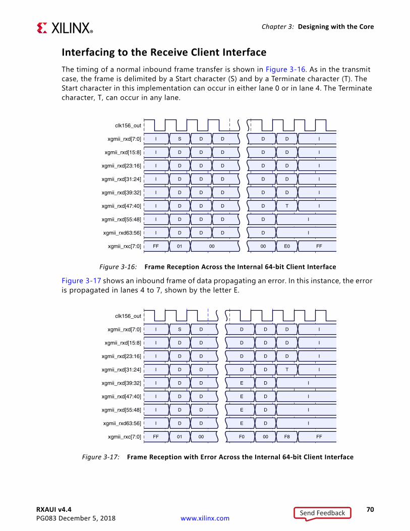
RXAUI v4.4 70PG083 December 5, 2018 www.xilinx.com
Chapter 3: Designing with the Core
Interfacing to the Receive Client InterfaceThe timing of a normal inbound frame transfer is shown in Figure 3-16. As in the transmit case, the frame is delimited by a Start character (S) and by a Terminate character (T). The Start character in this implementation can occur in either lane 0 or in lane 4. The Terminate character, T, can occur in any lane.
Figure 3-17 shows an inbound frame of data propagating an error. In this instance, the error is propagated in lanes 4 to 7, shown by the letter E.
X-Ref Target - Figure 3-16
Figure 3-16: Frame Reception Across the Internal 64-bit Client Interface
X-Ref Target - Figure 3-17
Figure 3-17: Frame Reception with Error Across the Internal 64-bit Client Interface
Send Feedback

RXAUI v4.4 71PG083 December 5, 2018 www.xilinx.com
Chapter 3: Designing with the Core
MDIO InterfaceThe Management Data Input/Output (MDIO) interface is a simple, low-speed 2-wire interface for management of the RXAUI core consisting of a clock signal and a bidirectional data signal. It is defined in clause 45 of IEEE Standard 802.3-2012.
An MDIO bus in a system consists of a single Station Management (STA) master management entity and several MDIO Managed Device (MMD) slave entities. Figure 3-18 illustrates a typical system. All transactions are initiated by the STA entity. The RXAUI core implements an MMD.
If implemented, the MDIO interface is implemented as four unidirectional signals. These can be used to drive a 3-state buffer either in the FPGA SelectIO™ interface buffer or in a separate device.
The type_sel port is registered into the core at FPGA configuration and core hard or soft reset; changes after that time are ignored by the core. Table 3-3 shows the mapping of the type_sel setting to the implemented register map.
The prtad[4:0] port sets the port address of the core instance. Multiple instances of the same core can be supported on the same MDIO bus by setting the prtad[4:0] to a unique value for each instance; the RXAUI core ignores transactions with the PRTAD field set to a value other than that on its prtad[4:0] port.
X-Ref Target - Figure 3-18
Figure 3-18: A Typical MDIO-Managed System
Table 3-3: Mapping of type_sel Port Settings to MDIO Register Typetype_sel setting MDIO Register Description
00 or 01 10GBASE-X PCS/PMA When driving a 10GBASE-X PHY 10 DTE XGXS When connected to a 10GMAC through XGMII11 PHY XGXS When connected to a PHY through XGMII
X13663
MAC 2MAC 1
STA mdc
mdio
MMD
MMD
MMD
MMD
MMD
MMD
Send Feedback

RXAUI v4.4 72PG083 December 5, 2018 www.xilinx.com
Chapter 3: Designing with the Core
MDIO Transactions
The MDIO interface should be driven from a STA master according to the protocol defined in IEEE Std. 802.3-2012. An outline of each transaction type is described in the following sections. In these sections, these abbreviations apply:
• PRE: preamble• ST: start• OP: operation code• PRTAD: port address• DEVAD: device address• TA: turnaround
Set Address Transaction
Figure 3-19 shows an Address transaction defined by OP = 00. Set Address is used to set the internal 16-bit address register of the RXAUI core for subsequent data transactions (called the current address in the following sections).
Write Transaction
Figure 3-20 shows a Write transaction defined by OP = 01. The RXAUI core takes the 16-bit word in the data field and writes it to the register at the current address.
X-Ref Target - Figure 3-19
Figure 3-19: MDIO Set Address Transaction
X-Ref Target - Figure 3-20
Figure 3-20: MDIO Write Transaction
X13662
Z1 1 1 0 0 0 P4 P3 P2 P1 P0 V4 V3 V2 V1 V0 1 0 D15D14
D13D12
D11D10
D9D8
D7D6
D5D4
D3D2
D1D0
0 ZZZ
mdc
mdio
IDLE IDLE32 bitsPRE ST OP PRTAD DEVAD TA 16-bit ADDRESS
STA drives MDIO
X13664
Z1 1 1 0 0 1 P4 P3 P2 P1 P0 V4 V3 V2 V1 V0 1 0 D15D14
D13D12
D11D10
D9D8
D7D6
D5D4
D3D2
D1D0
0 ZZZ
mdc
mdio
IDLE IDLE32 bitsPRE ST OP PRTAD DEVAD TA 16-bit WRITE DATA
STA drives MDIO
Send Feedback

RXAUI v4.4 73PG083 December 5, 2018 www.xilinx.com
Chapter 3: Designing with the Core
Read Transaction
Figure 3-21 shows a Read transaction defined by OP = 11. The RXAUI core returns the 16-bit word from the register at the current address.
Post-Read-increment-address Transaction
Figure 3-22 shows a Post-read-increment-address transaction, defined by OP = 10. The RXAUI core returns the 16-bit word from the register at the current address then increments the current address. This allows sequential reading or writing by a STA master of a block of register addresses.
For detail on the MDIO registers, see MDIO Interface Registers.
X-Ref Target - Figure 3-21
Figure 3-21: MDIO Read Transaction
X-Ref Target - Figure 3-22
Figure 3-22: MDIO Read-and-increment Transaction
X13625
Z1 1 1 0 1 1 P4 P3 P2 P1 P0 V4 V3 V2 V1 V0 Z 0 D15D14
D13D12
D11D10
D9D8
D7D6
D5D4
D3D2
D1D0
0 ZZZ
mdc
mdio
IDLE IDLE32 bitsPRE
ST OP PR TAD DEV AD TA 16-bit READ D ATA
STA dr ives MDIO MMD dr ives MDIO
X13626
Z1 1 1 0 1 1 P4 P3 P2 P1 P0 V4 V3 V2 V1 V0 Z 0 D15D14
D13D12
D11D10
D9D8
D7D6
D5D4
D3D2
D1D0
0 ZZZ
mdc
mdio
IDLE IDLE32 bitsPRE
ST OP PR TAD DEV AD TA 16-bit READ D ATA
STA dr ives MDIO MMD dr ives MDIO
Send Feedback

RXAUI v4.4 74PG083 December 5, 2018 www.xilinx.com
Chapter 4
Design Flow StepsThis chapter describes customizing and generating the core, constraining the core, and the simulation, synthesis and implementation steps that are specific to this IP core. More detailed information about the standard Vivado® design flows and the IP integrator can be found in the following Vivado Design Suite user guides:
• Vivado Design Suite User Guide: Designing IP Subsystems using IP Integrator (UG994) [Ref 6]
• Vivado Design Suite User Guide: Designing with IP (UG896) [Ref 7]• Vivado Design Suite User Guide: Getting Started (UG910) [Ref 8]• Vivado Design Suite User Guide: Logic Simulation (UG900) [Ref 9]
Customizing and Generating the CoreYou can customize the IP for use in your design by specifying values for the various parameters associated with the IP core using the following steps:
1. Select the IP from the IP catalog.2. Double-click on the selected IP or select the Customize IP command from the toolbar or
popup menu.
For details, see the Vivado Design Suite User Guide: Designing with IP (UG896) [Ref 7] and the Vivado Design Suite User Guide: Getting Started (UG910) [Ref 8].
Note: Figures in this chapter are illustrations of the RXAUI core in the Vivado Integrated Design Environment (IDE). This layout might vary from the current version.
Send Feedback

RXAUI v4.4 75PG083 December 5, 2018 www.xilinx.com
Chapter 4: Design Flow Steps
Figure 4-1 displays the main screen for customizing the RXAUI core.
For general help with starting and using the Vivado IDE, see the documentation supplied with the Vivado Design Suite.
Component NameThe component name is used as the base name of the output files generated for the core. Names must begin with a letter and must be composed from the following characters: a through z, 0 through 9 and “_” (underscore).
MDIO ManagementSelect this option to implement the MDIO interface for managing the core. De-select the option to remove the MDIO interface and expose a simple bit vector to manage the core. The MDIO interface is implemented by default.
Transceiver TypeThis option is only available for Virtex UltraScale devices that contain both GTHE3 and GTYE3 transceivers; select the transceiver type for these devices.
X-Ref Target - Figure 4-1
Figure 4-1: RXAUI Main Screen
Send Feedback

RXAUI v4.4 76PG083 December 5, 2018 www.xilinx.com
Chapter 4: Design Flow Steps
RXAUI Lane 0 Transceiver LocationThis option is only available for UltraScale devices. Select the X/Y coordinate for the lowest numbered transceiver in the Quad that is used by the RXAUI core. For example, selecting X0Y0 implements XAUI lane 0 in X0Y0; lane 1 in X0Y1. The selected transceivers are specified in both the core and example design XDC files. If needed, this placement selection can be overridden by using constraints in a user XDC file. See Transceiver Placement for more information.
Transceiver Reference Clock Frequency (MHz)This option is only available for UltraScale devices. Select the desired transceiver reference clock frequency from 125 MHz, 156.25 MHz or 312.5 MHz.
DRP Clock Frequency (MHz)Enter the frequency of the DRP clock (the dclk input of the core). For UltraScale, 7 Series, and Zynq-7000 SoC devices, this value is used to set the target frequency for Out of Context synthesis. Additionally, for UltraScale devices, this frequency information is passed down to the UltraScale Transceiver Wizard, contained within the RXAUI core, where it is used to generate correct timer durations for the transceiver reset/initialization circuitry.
Additional Transceiver Control and Status PortsSelect if GT control and status ports such as DRP, PRBS, RX Equalizer and TX Driver are required.
Shared LogicSelect whether the transceiver Quad PLL and differential reference clock buffer is included in the core itself or in the example design (see Shared Logic for more information).
Send Feedback
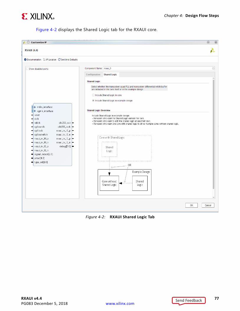
RXAUI v4.4 77PG083 December 5, 2018 www.xilinx.com
Chapter 4: Design Flow Steps
Figure 4-2 displays the Shared Logic tab for the RXAUI core.X-Ref Target - Figure 4-2
Figure 4-2: RXAUI Shared Logic Tab
Send Feedback

RXAUI v4.4 78PG083 December 5, 2018 www.xilinx.com
Chapter 4: Design Flow Steps
User ParametersTable 4-1 shows the relationship between the fields in the Vivado IDE and the User Parameters (which can be viewed in the Tcl console).
Output GenerationFor details, see the Vivado Design Suite User Guide: Designing with IP (UG896) [Ref 7]
Constraining the CoreThis chapter describes how to constrain a design containing the RXAUI core. An XDC file is applied to the core instance. This XDC is available through the IP Sources view under Synthesis. No modification is required to this file.
There are some additional constraints required that are design specific such as transceiver location constraints. These are detailed in this chapter and an example of such constraints can be found in the example design. See Chapter 5, Example Design, for a complete description of the Vivado Design Suite output files.
CAUTION! Not all constraints are relevant to specific implementations of the core; consult the XDC created with the core instance to see exactly what constraints are relevant.
Table 4-1: Vivado IDE Parameter to User Parameter RelationshipVivado IDE Parameter/Value(1) User Parameter/Value(1) Default Value
MDIO Management Mdio_Management trueShared Logic SupportLevel 0
Include Shared Logic in core 1Include Shared Logic in example design 0
Additional transceiver control and status ports TransceiverControl falseTransceiver Type vu_gt_type GTHE3Transceiver reference clock frequency (MHz) RefClkRate 156.25RXAUI lane 0 transceiver location Locations X0Y0DRP Clock Frequency (MHz) DRPCLK_FREQ 50.0
Notes: 1. Parameter values are listed in the table where the Vivado IDE parameter value differs from the user parameter
value. Such values are shown in this table as indented below the associated parameter.
Send Feedback
RXAUI v4.4 79PG083 December 5, 2018 www.xilinx.com
Chapter 4: Design Flow Steps
Required ConstraintsThis section defines the additional constraint requirements for the core. Constraints are provided with an XDC file. An XDC is provided with the HDL example design to give a starting point for constraints for your design. The following constraints are required.
Clock FrequenciesDCLK should be specified:
create_clock -name dclk -period 20.000 [get_ports dclk]
This constraint defines the frequency of DCLK that is supplied to the transceivers. The example design uses a nominal 50 MHz clock.
Clock ManagementThe Dune Networks RXAUI core has two clock domains:
• The clk156_out domain derived from the TXOUTCLK output of the transceiver. The core XDC applies a create_clock that propagates to the clk156_out output port. No user XDC is required.
• The dclk domain. This must be constrained outside of the core as described in Clock Frequencies.
Transceiver PlacementTo constrain the placement of the transceivers using X0Y0 terminology the following constraints should be used.
Shared Logic in Example Design
7 Series GTH Transceivers
set_property LOC GTHE2_CHANNEL_X0Y0 [get_cells rxaui_support_i/rxaui_i/*/gt0_wrapper_i/gthe2_i]set_property LOC GTHE2_CHANNEL_X0Y1 [get_cells rxaui_support_i/rxaui_i/*/gt1_wrapper_i/gthe2_i]
7 Series GTX Transceivers
set_property LOC GTXE2_CHANNEL_X0Y0 [get_cells rxaui_support_i/rxaui_i/*/gt0_wrapper_i/gtxe2_i]set_property LOC GTXE2_CHANNEL_X0Y1 [get_cells rxaui_support_i/rxaui_i/*/gt1_wrapper_i/gtxe2_i]
Send Feedback

RXAUI v4.4 80PG083 December 5, 2018 www.xilinx.com
Chapter 4: Design Flow Steps
7 Series GTP Transceivers
set_property LOC GTPE2_CHANNEL_X0Y0 [get_cells rxaui_support_i/rxaui_i/*/gt0_wrapper_i/gtpe2_i]set_property LOC GTPE2_CHANNEL_X1Y0 [get_cells rxaui_support_i/rxaui_i/*/gt1_wrapper_i/gtpe2_i]
UltraScale Transceivers
The following example illustrates the placement of GTHE3 transceivers when the shared logic is in the example design. To move the location of the RXAUI core using XDC constraints, change the X/Y coordinates to your chosen location. Alternatively the RXAUI core placement can be selected from the core customization screen in the Vivado IDE prior to core generation.
For GTYE3 transceivers: replace the GTHE3 string with GTYE3 and the gthe3 string with gtye3 in the following example syntax.
set_property LOC GTHE3_CHANNEL_X0Y0 [get_cells rxaui_support_i/rxaui_i/*/< CompName >_gt_i/inst/gen_gtwizard_gthe3_top.< CompName >_gt_gtwizard_gthe3_inst/gen_gtwizard_gthe3.gen_channel_container[*].gen_enabled_channel.gthe3_channel_wrapper_inst/channel_inst/gthe3_channel_gen.gen_gthe3_channel_inst[0].GTHE3_CHANNEL_PRIM_INST]set_property LOC GTHE3_CHANNEL_X0Y1 [get_cells rxaui_support_i/rxaui_i/*/< CompName >_gt_i/inst/gen_gtwizard_gthe3_top.< CompName >_gt_gtwizard_gthe3_inst/gen_gtwizard_gthe3.gen_channel_container[*].gen_enabled_channel.gthe3_channel_wrapper_inst/channel_inst/gthe3_channel_gen.gen_gthe3_channel_inst[1].GTHE3_CHANNEL_PRIM_INST]set_property LOC GTHE3_COMMON_X0Y0 [get_cells rxaui_support_i/rxaui_gt_common_i/< CompName >_gt_common_wrapper_i/common_inst/gthe3_common_gen.GTHE3_COMMON_PRIM_INST ]
Shared Logic in Core
7 Series GTH Transceivers
set_property LOC GTHE2_CHANNEL_X0Y0 [get_cells rxaui_i/rxaui_block_i/*/gt0_wrapper_i/gthe2_i]set_property LOC GTHE2_CHANNEL_X0Y1 [get_cells rxaui_i/rxaui_block_i/*/gt1_wrapper_i/gthe2_i]
7 Series GTX Transceivers
set_property LOC GTXE2_CHANNEL_X0Y0 [get_cells rxaui_i/rxaui_block_i/*/gt0_wrapper_i/gtxe2_i]set_property LOC GTXE2_CHANNEL_X0Y1 [get_cells rxaui_i/rxaui_block_i/*/gt1_wrapper_i/gtxe2_i]
7 Series GTP Transceivers
set_property LOC GTPE2_CHANNEL_X0Y0 [get_cells rxaui_i/rxaui_block_i/*/gt0_wrapper_i/gtpe2_i]set_property LOC GTPE2_CHANNEL_X1Y0 [get_cells rxaui_i/rxaui_block_i/*/gt1_wrapper_i/gtpe2_i]
Send Feedback

RXAUI v4.4 81PG083 December 5, 2018 www.xilinx.com
Chapter 4: Design Flow Steps
UltraScale Transceivers
The following example illustrates the placement of GTHE3 transceivers when the shared logic is in the core. To move the location of the RXAUI core using XDC constraints, change the X/Y coordinates to your chosen location. Alternatively the RXAUI core placement can be selected from the core customization screen in the Vivado IDE prior to core generation.
For GTYE3 transceivers, replace the GTHE3 string with GTYE3 and the gthe3 string with gtye3 in the following example syntax.
set_property LOC GTHE3_CHANNEL_X0Y0 [get_cells rxaui_i/*/rxaui_block_i/< CompName >_gt_i/inst/gen_gtwizard_gthe3_top.< CompName >_gt_gtwizard_gthe3_inst/gen_gtwizard_gthe3.gen_channel_container[*].gen_enabled_channel.gthe3_channel_wrapper_inst/channel_inst/gthe3_channel_gen.gen_gthe3_channel_inst[0].GTHE3_CHANNEL_PRIM_INST]set_property LOC GTHE3_CHANNEL_X0Y1 [get_cells rxaui_i/*/rxaui_block_i/< CompName >_gt_i/inst/gen_gtwizard_gthe3_top.< CompName >_gt_gtwizard_gthe3_inst/gen_gtwizard_gthe3.gen_channel_container[*].gen_enabled_channel.gthe3_channel_wrapper_inst/channel_inst/gthe3_channel_gen.gen_gthe3_channel_inst[1].GTHE3_CHANNEL_PRIM_INST]set_property LOC GTHE3_COMMON_X0Y0 [get_cells rxaui_i/*/rxaui_gt_common_i/< CompName >_gt_common_wrapper_i/common_inst/gthe3_common_gen.GTHE3_COMMON_PRIM_INST]
SimulationSimulation of the RXAUI solution at the core level is not supported without the addition of a test bench (not supplied). Simulation of the example design is supported.
For comprehensive information about Vivado simulation components, as well as information about using supported third party tools, see the Vivado Design Suite User Guide: Logic Simulation (UG900) [Ref 9].
Synthesis and ImplementationThe RXAUI solution this is a mix of both encrypted and unencrypted source. Only the unencrypted sources are visible and optionally editable by using the Unlink IP Vivado option.
For details about synthesis and implementation, see the Vivado Design Suite User Guide: Designing with IP (UG896) [Ref 7].
Send Feedback

RXAUI v4.4 82PG083 December 5, 2018 www.xilinx.com
Chapter 5
Example DesignThis chapter provides information about the example design, including a description of the files and the directory structure generated by the Xilinx® Vivado® Design Suite, the purpose and contents of the provided scripts, the contents of the example HDL wrappers, and the operation of the demonstration test bench.
Example DesignFigure 5-1 illustrates the clock and reset enabled configuration of the example design for 7 series devices with shared logic in the core.X-Ref Target - Figure 5-1
Figure 5-1: RXAUI Example Design Test Bench – Clock and Reset Enabled for 7 Series
PatternChecker
RXAUICore
Common PLL
tx_sync
Transceiver
component_name_gt_wrapper_gt.vhd
component_name_example_design.vhd
component_name_support.vhd
FPGA
component_name_block.vhd
component_name_gt_wrapper_gt.vhd
Transceiver
PatternGenerator
component_name.vhd
Core Clocking
component_name_cl_clocking.vhd
X13621
Send Feedback

RXAUI v4.4 83PG083 December 5, 2018 www.xilinx.com
Chapter 5: Example Design
Figure 5-1 illustrates the clock and reset enabled configuration of the example design for UltraScale architecture with shared logic in the core.
The RXAUI example design consists of the following:
• Clock buffers for dclk• Simple XGMII pattern generator and checker• An instance of the core (Shared Logic included in the core) or the support level module
which contains the core, common PLL, and shared reset module (7 series)
The RXAUI Design Example has been tested with Xilinx Vivado Design Suite and Mentor Graphics Questa Advanced Simulator (the versions of these tools are available in the Xilinx Design Tools: Release Notes Guide.
X-Ref Target - Figure 5-2
Figure 5-2: RXAUI Example Design and Test Bench – Clock and Reset Enabled for UltraScale Architecture
PatternChecker
RXAUICore
Common PLL
tx_sync
component_name_example_design.vhd
component_name_support.vhd
FPGA
component_name_block.vhd
UltraScaleWizard Subcore
PatternGenerator
component_name.vhd
Core Clocking
component_name_cl_clocking.vhd
• • • • • • •• • • • • •
Send Feedback
RXAUI v4.4 84PG083 December 5, 2018 www.xilinx.com
Chapter 6
Test BenchThe example design demonstration test bench is a simple VHDL or Verilog program to exercise the example design and the core itself. It simulates an instance of the example design that is externally looped back. It generates all the required clocks and resets and waits for successful pattern checking to complete. If it fails to detect successful pattern checking within the time limit defined in the test bench, it produces an error.
Send Feedback

RXAUI v4.4 85PG083 December 5, 2018 www.xilinx.com
Appendix A
Verification, Compliance, and Interoperability
The RXAUI core has been verified using both simulation and hardware testing.
SimulationA highly parameterizable transaction-based simulation test suite has been used to verify the core. Tests included:
• Register access over MDIO• Loss and re-gain of synchronization• Loss and re-gain of alignment• Frame transmission• Frame reception• Clock compensation• Recovery from error conditions
Hardware TestingThe core has been used in several hardware test platforms within Xilinx. In particular, the core has been used in a test platform design with the Xilinx® 10-Gigabit Ethernet MAC core. This design comprises the MAC, RXAUI, a ping loopback FIFO, and a test pattern generator all under embedded MicroBlaze ™ processor control. This design has been used for interoperability testing at Dune Networks.
Send Feedback

RXAUI v4.4 86PG083 December 5, 2018 www.xilinx.com
Appendix B
UpgradingThis appendix contains information about migrating a design from ISE® to the Vivado® Design Suite, and for upgrading to a more recent version of the IP core. For customers upgrading in the Vivado Design Suite, important details (where applicable) about any port changes and other impact to user logic are included.
Device MigrationIf you are migrating from a 7 series GTX or GTH device to an UltraScale GTH device, the prefixes of the optional transceiver debug ports for single-lane cores are changed from “gt0”, “gt1” to “gt”, and the suffix “_in” and “_out” are dropped. For multi-lane cores, the prefixes of the optional transceiver debug ports gt(n) are aggregated into a single port. For example: gt0_gtrxreset and gt1_gtrxreset now become gt_gtrxreset [1:0]. This is true for all ports, with the exception of the DRP buses which follow the convention of gt(n)_drpxyz.
It is important to update your design to use the new transceiver debug port names. For more information about migration to UltraScale devices, see the UltraScale Architecture Migration Methodology Guide (UG1026) [Ref 11].
Upgrading in the Vivado Design SuiteThis section provides information about any changes to the user logic or port designations that take place when you upgrade to RXAUI v4.3 in the Vivado Design Suite.
“Include common clocking and resets” is now mapped to “Include shared logic in core”. If this option was previously off this now maps to “Include shared logic in example design”.
Parameter ChangesThere are no parameter changes between RXAUI v4.0 and RXAUI v4.3.
The WRAPPER_SIM_GTRESET_SPEEDUP parameter was previously removed in RXAUI v4.0.
Send Feedback
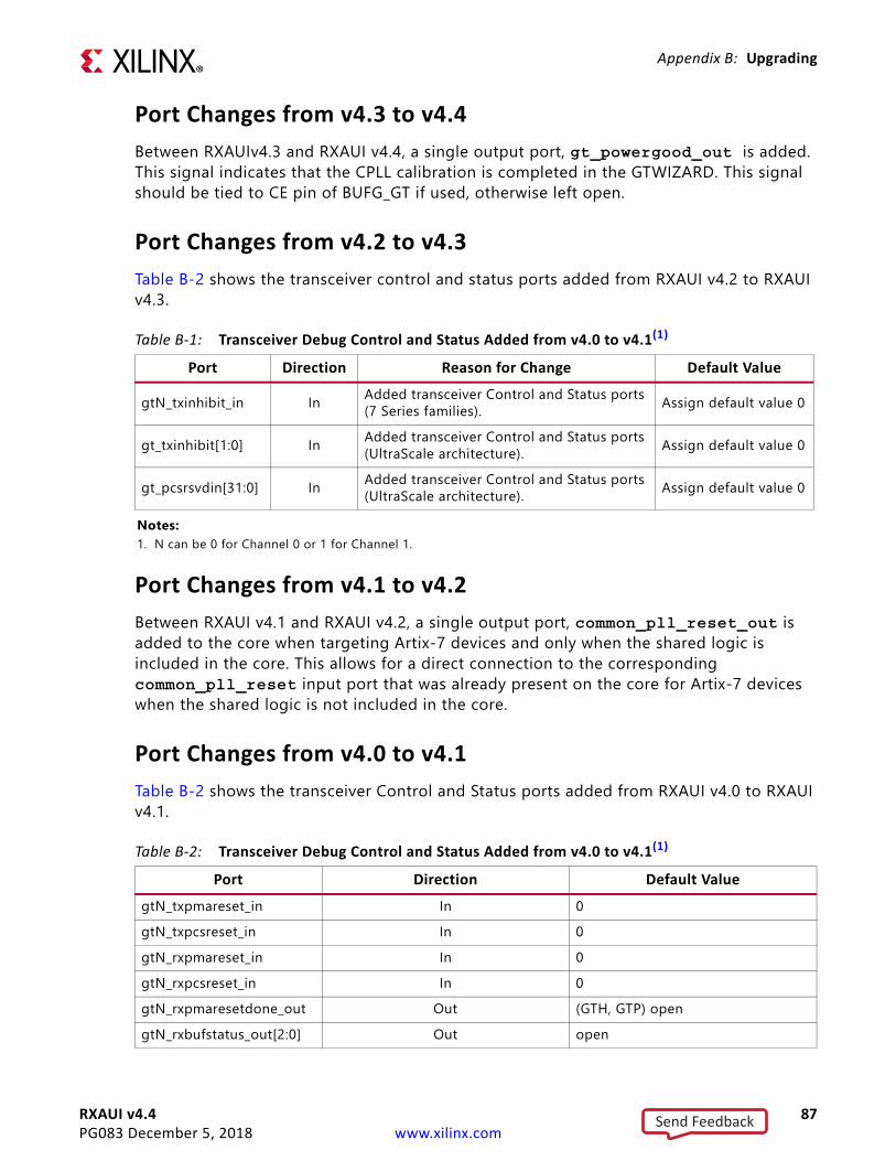
RXAUI v4.4 87PG083 December 5, 2018 www.xilinx.com
Appendix B: Upgrading
Port Changes from v4.3 to v4.4Between RXAUIv4.3 and RXAUI v4.4, a single output port, gt_powergood_out is added. This signal indicates that the CPLL calibration is completed in the GTWIZARD. This signal should be tied to CE pin of BUFG_GT if used, otherwise left open.
Port Changes from v4.2 to v4.3Table B-2 shows the transceiver control and status ports added from RXAUI v4.2 to RXAUI v4.3.
Port Changes from v4.1 to v4.2Between RXAUI v4.1 and RXAUI v4.2, a single output port, common_pll_reset_out is added to the core when targeting Artix-7 devices and only when the shared logic is included in the core. This allows for a direct connection to the corresponding common_pll_reset input port that was already present on the core for Artix-7 devices when the shared logic is not included in the core.
Port Changes from v4.0 to v4.1Table B-2 shows the transceiver Control and Status ports added from RXAUI v4.0 to RXAUI v4.1.
Table B-1: Transceiver Debug Control and Status Added from v4.0 to v4.1(1) Port Direction Reason for Change Default Value
gtN_txinhibit_in In Added transceiver Control and Status ports (7 Series families). Assign default value 0
gt_txinhibit[1:0] In Added transceiver Control and Status ports (UltraScale architecture). Assign default value 0
gt_pcsrsvdin[31:0] In Added transceiver Control and Status ports (UltraScale architecture). Assign default value 0
Notes: 1. N can be 0 for Channel 0 or 1 for Channel 1.
Table B-2: Transceiver Debug Control and Status Added from v4.0 to v4.1(1) Port Direction Default Value
gtN_txpmareset_in In 0gtN_txpcsreset_in In 0gtN_rxpmareset_in In 0gtN_rxpcsreset_in In 0gtN_rxpmaresetdone_out Out (GTH, GTP) opengtN_rxbufstatus_out[2:0] Out open
Send Feedback

RXAUI v4.4 88PG083 December 5, 2018 www.xilinx.com
Appendix B: Upgrading
Port Additions in v4.0Table B-3 shows the transceiver Control and Status ports added in RXAUI v4.0.
gtN_txphaligndone_out Out opengtN_txphinitdone_out Out opengtN_txdlysresetdone_out Out opengtN_cplllock_out Out (GTH) opengtN_qplllock_out Out (GTX, GTP) opengtN_rxcdrhold_in In 0gtN_dmonitorout_out Out opengtN_rxcommadet_out Out open
Notes: 1. N can be 0 for Channel 0 or 1 for Channel 1
Table B-3: Transceiver Control and Status Ports Added in v4.0(1)
Port Direction Default ValuegtN_txresetdone_out Out opengtN_rxresetdone_out Out opengtN_eyescantrigger_in In 0gtN_eyescanreset_in In 0gtN_eyescandataerror_out Out opengtN_rxrate_in In B"000"gtN_loopback_in In B"000"gtN_rxpolarity_in In 0gtN_txpolarity_in In 0gtN_rxlpmen_in In (GTX, GTH) 0gtN_rxdfelpmreset_in In (GTX, GTH) 0gtN_rxmonitorsel_in In (GTX, GTH) B"00"gtN_rxmonitorout_out Out (GTX, GTH) opengtN_rxlpmreset_in In (GTP) 0gtN_rxlpmhfhold_in In (GTP) 0gtN_rxlpmhfovrden_in In (GTP) 0gtN_rxlpmlfhold_in In (GTP) 0gtN_rxlpmlfovrden_in In (GTP) 0gtN_txdiffctrl_in In B"1010"
Table B-2: Transceiver Debug Control and Status Added from v4.0 to v4.1(1) Port Direction Default Value
Send Feedback

RXAUI v4.4 89PG083 December 5, 2018 www.xilinx.com
Appendix B: Upgrading
Port Changes from v3.0 to v4.0Table B-4 shows the ports that have been added, removed, or re-named between RXAUI v3.0 and RXAUI v4.0.
DRP Ports
Table B-5 shows the re-naming of DRP ports between versions 3.0 and 4.0.
gtN_txpostcursor_in In B"00000"gtN_txprecursor_in In B"00000"gtN_rxprbscntreset_in In 0gtN_rxprbserr_out Out opengtN_rxprbssel_in In B"000"gtN_txprbssel_in In B"000"gtN_txprbsforceerr_in In 0gtN_rxdisperr_out Out opengtN_rxnotintable_out Out open
Notes: 1. N can be 0 for Channel 0 or 1 for Channel 1.
Table B-4: Port ChangesAdded Removed Notes
clk156_out (output)
clk156 (input) clk156_out is a clock output that replaces the txoutclk and clk156 pins. It is driven by a BUFH. As before, this clock is not shared with another RXAUI core instance. Remove any clock buffer you had instanced previously in your design.
txoutclk (output)
reset156 (input) The core now generates its synchronous reset internally.mmcm_lock (input)clk312 (input) (GTP only) The MMCM is located inside the core.gt_control (input vector) Replaced by individual transceiver control pins.
clk156_lock txlock txlock output re-named as clk156_lock
debugThis output vector has been resized to 6 bits wide. These bits map to the old debug vector [5:0]. Individual transceiver ports have replaced the removed bits.
refclkout(output)
GTX/GTH: When “Shared logic in core” is selected, refclkout is a new output port than can be connected to the refclk input port of another core.
Table B-3: Transceiver Control and Status Ports Added in v4.0(1) (Cont’d)
Port Direction Default Value
Send Feedback

RXAUI v4.4 90PG083 December 5, 2018 www.xilinx.com
Appendix B: Upgrading
QPLL Ports
Table B-6 and Table B-7 shows the re-naming of QPLL ports (GTX/GTH only) between versions 3.0 and 4.0.
GTP Ports
Table B-8 and Table B-9 shows the re-naming of GTP ports between versions 3.0 and 4.0.
Table B-5: DRP Port Name Changes3.0 4.0
drp0_addr gt0_drpaddrdrp0_en gt0_drpendrp0_i gt0_drpdidrp0_o gt0_drpdodrp0_rdy gt0_drprdydrp0_we gt0_drpwedrp0_busy gt0_drp_busy (GTP only)drp1_addr gt1_drpaddrdrp1_en gt1_drpendrp1_i gt1_drpdidrp1_o gt1_drpdodrp1_rdy gt1_drprdydrp1_we gt1_drpwedrp1_busy gt1_drp_busy (GTP only)
Table B-6: QPLL Port Name Changes (Shared Logic in Core)3.0 4.0
common_pll_clk qplloutclk_outcommon_pll_lock qplllock_outcommon_pll_refclk qplloutrefclk_out
Table B-7: QPLL Port Name Changes (Shared Logic in Example Design)3.0 4.0
common_pll_clk qplloutclkcommon_pll_lock qplllockcommon_pll_refclk qplloutrefclk
Send Feedback

RXAUI v4.4 91PG083 December 5, 2018 www.xilinx.com
Appendix B: Upgrading
Table B-8: GTPE2_COMMON Port Name Changes (Shared Logic in Core)3.0 4.0
common_pll0_clk pll0outclk_outcommon_pll0_lock pll0lock_outcommon_pll0_refclk pll0outrefclk_outcommon_pll1_clk pll1outclk_outcommon_pll1_refclk pll1outrefclk_out
Table B-9: GTPE2_COMMON Ports (Shared Logic in Example Design)3.0 4.0
common_pll0_clk pll0outclkcommon_pll0_lock pll0lockcommon_pll0_refclk pll0refclkcommon_pll1_clk pll1outclkcommon_pll1_refclk pll1outrefclk
Send Feedback

RXAUI v4.4 92PG083 December 5, 2018 www.xilinx.com
Appendix C
DebuggingThis appendix includes details about resources available on the Xilinx Support website and debugging tools.
Finding Help on Xilinx.comTo help in the design and debug process when using the RXAUI core, the Xilinx Support web page contains key resources such as product documentation, release notes, answer records, information about known issues, and links for obtaining further product support.
DocumentationThis product guide is the main document associated with the RXAUI core. This guide, along with documentation related to all products that aid in the design process, can be found on the Xilinx Support web page or by using the Xilinx® Documentation Navigator.
Download the Xilinx Documentation Navigator from the Downloads page. For more information about this tool and the features available, open the online help after installation.
Solution CentersSee the Xilinx Solution Centers for support on devices, software tools, and intellectual property at all stages of the design cycle. Topics include design assistance, advisories, and troubleshooting tips.
The Solution Center specific to the RXAUI core is listed below:
• Xilinx Ethernet IP Solution Center
Answer RecordsAnswer Records include information about commonly encountered problems, helpful information on how to resolve these problems, and any known issues with a Xilinx product. Answer Records are created and maintained daily ensuring that users have access to the most accurate information available.
Send Feedback

RXAUI v4.4 93PG083 December 5, 2018 www.xilinx.com
Appendix C: Debugging
Answer Records for this core can be located by using the Search Support box on the main Xilinx support web page. To maximize your search results, use proper keywords such as
• Product name• Tool message(s)• Summary of the issue encountered
A filter search is available after results are returned to further target the results.
Master Answer Record for the RXAUI Core
AR: 54249
Technical SupportXilinx provides technical support in the Xilinx Support web page for this LogiCORE™ IP product when used as described in the product documentation. Xilinx cannot guarantee timing, functionality, or support if you do any of the following:
• Implement the solution in devices that are not defined in the documentation.• Customize the solution beyond that allowed in the product documentation. • Change any section of the design labeled DO NOT MODIFY.To contact Xilinx Technical Support, navigate to the Xilinx Support web page.
Debug ToolsThere are many tools available to address RXAUI design issues. It is important to know which tools are useful for debugging various situations.
Vivado Design Suite Debug FeatureThe Vivado® Design Suite debug feature inserts logic analyzer and virtual I/O cores directly into your design. The debug feature also allows you to set trigger conditions to capture application and integrated block port signals in hardware. Captured signals can then be analyzed. This feature in the Vivado IDE is used for logic debugging and validation of a design running in Xilinx devices.The Vivado logic analyzer is used to interact with the logic debug LogiCORE IP cores, including:• ILA 2.0 (and later versions)• VIO 2.0 (and later versions)
See the Vivado Design Suite User Guide, Programming and Debugging (UG908) [Ref 12].
Send Feedback

RXAUI v4.4 94PG083 December 5, 2018 www.xilinx.com
Appendix C: Debugging
Simulation DebugThe simulation debug flow for Questa Advanced Simulator is shown in Figure C-1. A similar approach can be used with other simulators.X-Ref Target - Figure C-1
Figure C-1: QuestaSim Debug Flow Diagram
Questa Advanced Simulator Simulation
Debug
No
No
Yes
Yes
NoSee the Simulation section.
Yes
X13619-042617
Update to this version.
Obtain a mixed-mode simulation license.
Need to compile and map the proper libraries. See "Compiling
Simulation Libraries” section.
For verilog simulations add the "-L" switch with the appropriate library reference to the vsim
command line. For example: -L secureip or -L unisims_ver. See the Example Design
simulate_mti.do for an example.
If problem is more design specific, opena case with Xilinx Technical Support
and include a wlf file dump of the simulation. For the best results, dump the entire design
hierarchy.
Check that the link status is OK: - Syncronization and Alignment have been achieved - Remote Faults are not being receivedSee the debug sections in the Product Guide for more details.
Yes
No
No
No
Are you able to transmit and recieve frames on the
XGMII interface?
Yes
Yes
Check for the latest supported versions of
Questa Advanced Simulator. Is this version
being used?
SecureIP models are used tosimulate the MGTs. To use these models, a
VerilogLRM-IEEE 1364-2005 encryption-compliant simulator is required.
If using VHDL, do you have a mixed-mode simulation license?
A Verilog license is required to simulate with the SecureIP
models. If the user design uses VHDL, a mixed-mode simulation
license is required.
Does simulating the RXAUI example design give the expected output?
The RXAUI example design should allow you to quickly determine if the simulator
is set up correctly; the RXAUI core should achieve Link OK status and
receive and transmit four frames.
Do you get errors indicatingGTXE1 or other elements like
BUFG not defined?
To model the MGTs, the SecureIP models are used. These models
must be referenced during the vsim call. Also, it is necessary to
reference the unisims library.
Do you get errors referring tofailing to access library?
If the libraries are not compiled and mapped correctly, errors will occur,such as:
# ** Error: (vopt-19) Failed to access library 'secureip' at "secureip".# No such file or directory. (errno = ENOENT)# ** Error: ../../example_design/ xaui_core_block.v(820): Library secureip not found.
Send Feedback
RXAUI v4.4 95PG083 December 5, 2018 www.xilinx.com
Appendix C: Debugging
Compiling Simulation LibrariesTo run simulation with third-party simulators, it is necessary to compile the Xilinx Simulation Libraries. For full details on how to perform this, see Appendix B of the Vivado Design Suite User Guide, Logic Simulation (UG900) [Ref 9].
If the debug suggestions listed previously do not resolve the issue, open a support case. To contact Xilinx Technical Support, navigate to the Xilinx Support web page.
To discuss possible solutions, use the Xilinx User Community: forums.xilinx.com/xlnx/
Hardware DebugHardware issues can range from link bring-up to problems seen after hours of testing. This section provides debug steps for common issues. The Vivado Analyzer tool is a valuable resource to use in hardware debug. The signal names mentioned in the following individual sections can be probed using the Vivado Analyzer tool for debugging the specific problems. Many of these common issues can also be applied to debugging design simulations.
General ChecksEnsure that all the timing constraints for the core were met during Place and Route.
• Does it work in timing simulation? If problems are seen in hardware but not in timing simulation, this could indicate a PCB issue.
• Ensure that all clock sources are clean. If using DCMs in the design, ensure that all DCMs have obtained lock by monitoring the LOCKED port.
Monitoring the RXAUI Core with Vivado Design Suite Debug Feature• A debug port is also provided so it can connect to external logic for debug (for
example, processor monitoring). This port contains transceiver and core debug information.
• XGMII signals and signals between RXAUI core and the transceiver can be added to monitor data transmitted and received. See Table 2-1, page 9 and Table 2-5, page 10 for a list of signal names.
• Status signals added to check status of link: STATUS_VECTOR[7:0], ALIGN_STATUS, SYNC_STATUS, and Debug port Bits[5:0].
• To interpret control codes in on the XGMII interface or the interface to the transceiver, see Table C-1 and Table C-2.
Send Feedback

RXAUI v4.4 96PG083 December 5, 2018 www.xilinx.com
Appendix C: Debugging
• An Idle (0x07) on the XGMII interface is encoded to be a randomized sequence of /K/ (Sync), /R/ (Skip), /A/(Align) codes on the RXAUI interface. For details on this encoding, see the IEEE 802.3-2012 specification (section 48.2.4.2) for more details.
Issues with Data Reception or Transmission Issues with data reception or transmission can be caused by a wide range of factors. Following is a flow diagram of steps to debug the issue. Each of the steps are discussed in more detail in the following sections.
Table C-1: XGMII Control CodesTXC TXD Description0 0x00 through 0xFF Normal data transmission1 0x07 Idle1 0x9C Sequence1 0xFB Start1 0xFD Terminate1 0xFE Error
Table C-2: RXAUI Control CodesCodegroup 8-bit Value DescriptionDxx.y 0xXX Normal data transmissionK28.5 0xBC /K/ (Sync)K28.0 0x1C /R/ (Skip)K28.3 0x7C /A/ (Align)K28.4 0x9C /Q/ (Sequence)K27.7 0xFB /S/ (Start)K29.7 0xFD /T/ (Terminate)K30.7 0xFE /E/ (Error)
Send Feedback

RXAUI v4.4 97PG083 December 5, 2018 www.xilinx.com
Appendix C: Debugging
What Can Cause a Local or Remote Fault?Local Fault and Remote Fault codes both start with the sequence TXD/RXD = 0x9C, TXC/RXC = 1 in XGMII lane 0. Fault conditions can also be detected by looking at the status vector or MDIO registers. The Local Fault and Link Status are defined as latching error indicators by the IEEE specification. This means that the Local Fault and Link Status bits in the status vector or MDIO registers must be cleared with the Reset Local Fault bits and Link Status bits in the Configuration vector or MDIO registers.
X-Ref Target - Figure C-2
Figure C-2: Flow Diagram for Debugging Problems with Data Reception or Transmission
Is RX Link Status = 0 (Link down)? If so, See the “Link Bring Up” section for more
details.
RemoveFault
Yes
Yes
X13620-091416
Is the data at the RXAUI input valid?
Check the MAC layer.
No
No
No
A received remote fault indicates that the link partner is down.
Check the status of the link partner.
No
Yes See the “What Can Cause the RXAUI Core to Insert Errors” section.
Local Fault
Yes
Is core in a local or remote fault condition? See the
“What Can Cause a Local or Remote Fault” section.
Check that the core is correctly configured using
either the configuration vector or the MDIO interface.
Is the link status OK in loopback?
Monitor XGMII data and data on transceiver interface. Are errors being inserted by the RXAUI core receiver?
See the “MDIO Issues” section.
See the “High Bit Error Rate Issues” section.
See the “General Checks” section.
Send Feedback

RXAUI v4.4 98PG083 December 5, 2018 www.xilinx.com
Appendix C: Debugging
Local Fault
The receiver outputs a local fault when the receiver is not up and operational. This RX local fault is also indicated in the status and MDIO registers. The most likely causes for an RX local fault are:
• The transceiver has not locked or the receiver is being reset.• At least one of the lanes is not synchronized – SYNC_STATUS• The lanes are not properly aligned – ALIGN_STATUSNote: The SYNC_STATUS and ALIGN_STATUS signals are not latching.
A TX local fault is indicated in the status and MDIO registers when the transceiver transmitter is in reset or has not yet completed any other initialization or synchronization procedures needed.
Remote Fault
Remote faults are only generated in the MAC reconciliation layer in response to a Local Fault message. When the receiver receives a remote fault, this means that the link partner is in a local fault condition.
When the MAC reconciliation layer receives a remote fault, it silently drops any data being transmitted and instead transmit IDLEs to help the link partner resolve its local fault condition. When the MAC reconciliation layer receives a local fault, it silently drops any data being transmitted and instead transmit a remote fault to inform the link partner that it is in a fault condition. Be aware that the Xilinx 10GEMAC core has an option to disable remote fault transmission.
Link Bring UpThe following link initialization stages describe a possible scenario of the Link coming up between device A and device B.
Stage 1: Device A Powered Up, but Device B Powered Down
• Device A is powered up and reset.• Device B powered down • Device A detects a fault because there is no signal received. The Device A RXAUI core
indicates an RX local fault. • The Device A MAC reconciliation layer receives the local fault. This triggers the MAC
reconciliation layer to silently drop any data being transmitted and instead transmit a remote fault.
• RX Link Status = 0 (link down) in Device A
Send Feedback

RXAUI v4.4 99PG083 December 5, 2018 www.xilinx.com
Appendix C: Debugging
Stage 2: Device B Powers Up and Resets
• Device B Powers Up and Resets.• Device B RXAUI completes Synchronization and Alignment.• Device A has not synchronized and aligned yet. It continues to send remote faults.• Device B RXAUI passes received remote fault to MAC.• Device B MAC reconciliation layer receives the remote fault. It silently drops any data
being transmitted and instead transmits IDLEs.• Link Status = 0 (link down) in both A and B.
Stage 3: Device A Receives Idle Sequence
• Device A RXAUI RX detects idles, synchronizes and aligns.• Device A reconciliation layer stops dropping frames at the output of the MAC
transmitter and stops sending remote faults to Device B.• Device A Link Status = 1 (Link Up)• After Device B stops receiving the remote faults, normal operation starts.
X-Ref Target - Figure C-3
Figure C-3: Device A Powered Up, but Device B Powered Down
MAC/RXAUI
TX Idle Sequence+RF Idle Sequence+RF RX
Device A Device B
RX No Signal No Signal TX
MAC/RXAUILinkDown
X13613
X-Ref Target - Figure C-4
Figure C-4: Device B Powers Up and Resets
MAC/RXAUI
TX Idle Sequence+RF Idle Sequence+RF RX
Device A Device B
RX No Signal Idle Sequence TX
MAC/RXAUILinkDown
LinkDown
X13614
Send Feedback

RXAUI v4.4 100PG083 December 5, 2018 www.xilinx.com
Appendix C: Debugging
Stage 4: Normal Operation
In Stage 4 shown in Figure C-6, Device A and Device B have both powered up and been reset. The link status is 1 (link up) in both A and B and in both the MAC can transmit frames successfully.
What Can Cause Synchronization and Alignment to Fail?Synchronization (SYNC_STATUS) occurs when each respective XAUI logical lane receiver is synchronized to byte boundaries. Alignment (ALIGN_STATUS) occurs when the RXAUI receiver is aligned across all four logical XAUI lanes.
Following are suggestions for debugging loss of Synchronization and Alignment:
• Monitor the state of the SIGNAL_DETECT[1:0] input to the core. This should either be:
° Connected to an optical module to detect the presence of light. Logic 1 indicates that the optical module is correctly detecting light; logic 0 indicates a fault. Therefore, ensure that this is driven with the correct polarity.
° Tied to logic 1 (if not connected to an optical module).Note: When signal_detect is set to logic 0, this forces the receiver synchronization state machine of the core to remain in the loss of sync state.• Loss of Synchronization can happen when invalid characters are received.
X-Ref Target - Figure C-5
Figure C-5: Device A Receives Idle SequenceX13612
MAC/RXAUI
TX Idle Sequence Idle Sequence+RF RX
Device A Device B
RX Idle Sequence Idle Sequence TX
MAC/RXAUILinkUp LinkDown
X-Ref Target - Figure C-6
Figure C-6: Normal Operation
X13611
MAC/RXAUI
TX Idle Sequence Idle Sequence RX
Device A Device B
RX Idle Sequence Idle Sequence TX
MAC/RXAUILinkUp LinkUp
Send Feedback

RXAUI v4.4 101PG083 December 5, 2018 www.xilinx.com
Appendix C: Debugging
• Loss of Alignment can happen when invalid characters are seen or if an /A/ code is not seen in all four XAUI logical lanes at the same time.
• See the section, High Bit Error Rate Issues.
Transceiver Specific
• Ensure that the polarities of the TXN/TXP and RXN/RXP lines are not reversed. If they are, these can be fixed by using the TXPOLARITY and RXPOLARITY ports of the transceiver.
• Check that the transceiver is not being held in reset or still be initialized by monitoring the mgt_tx_reset, mgt_rx_reset, and mgt_rxlock input signals to the RXAUI core. The mgt_rx_reset signal is also asserted when there is an RX buffer error. An RX buffer error means that the Elastic Buffer in the receiver path of the transceiver is either under or overflowing. This indicates a clock correction issue caused by differences between the transmitting and receiving ends. Check all clock management circuitry and clock frequencies applied to the core and to the transceiver.
What Can Cause the RXAUI Core to Insert Errors?On the receive path the RXAUI core inserts errors RXD = FE, RXC = 1, when disparity errors or invalid data are received or if the received interframe gap (IFG) is too small.
Disparity Errors or Invalid Data
Disparity Errors or Invalid data can be checked for by monitoring the mgt_codevalid input to the RXAUI core.
Small IFG
The RXAUI core inserts error codes into the Received XGMII data stream, RXD, when there are three or fewer IDLE characters (0x07) between frames. The error code (0xFE) precedes the frame “Terminate” delimiter (0xFD).
The IEEE 802.3-2012 specification (Section 46.2.1) requires a minimum interframe gap of five octets on the receive side. This includes the preceding frame Terminate control character and all Idles up to and immediately preceding the following frame Start control character. Because three (or fewer) Idles and one Terminate character are less than the required five octets, this would not meet the specification; therefore, the RXAUI core is expected to signal an error in this manner if the received frame does not meet the specification.
Send Feedback

RXAUI v4.4 102PG083 December 5, 2018 www.xilinx.com
Appendix C: Debugging
High Bit Error Rate Issues
Symptoms
If the link comes up but then goes down again or never comes up following a reset, the most likely cause for a RX Local Fault is a Bit Error Rate (BER) that is too high. A high BER causes incorrect data to be received, which leads to the lanes losing synchronization or alignment.
Debugging
Compare the issue across several devices or PCBs to ensure that the issue is not a one-off case.
• Try using an alternative link partner or test equipment and then compare results.• Try putting the core into loopback (both by placing the core into internal loopback, and
by looping back the optical cable) and compare the behavior. The core should always be capable of gaining synchronization and alignment when looping back with itself from transmitter to receiver so direct comparisons can be made. If the core exhibits correct operation when placed into internal loopback, but not when loopback is performed using an optical cable, this can indicate a faulty optical module or a PCB issue.
• Try swapping the optical module on a misperforming device and repeat the tests.
Transceiver Specific Checks
• Monitor the MGT_CODEVALID[7:0] input to the RXAUI core by triggering on it using the Vivado Analyzer tool. This input is a combination of the transceiver RX disparity error and RX not in table error outputs.
• These signals should not be asserted over the duration of a few seconds, minutes, or even hours. If they are frequently asserted, it can indicate an issue with the transceiver.
• Place the transceiver into parallel or serial near-end loopback.
° If correct operation is seen in the transceiver serial loopback, but not when loopback is performed using an optical cable, it can indicate a faulty optical module.
° If the core exhibits correct operation in the transceiver parallel loopback but not in serial loopback, this can indicate a transceiver issue.
• A mild form of bit error rate can be solved by adjusting the transmitter Pre-Emphasis and Differential Swing Control attributes of the transceiver.
Send Feedback
RXAUI v4.4 103PG083 December 5, 2018 www.xilinx.com
Appendix C: Debugging
MDIO IssuesSee MDIO Interface, page 71 for detailed information about performing MDIO transactions.
Things to check for:
• Ensure that the MDIO is driven properly. Check that the MDC clock is running and that the frequency is 2.5 MHz or less.
• Ensure that the RXAUI core is not held in reset. • Read from a Configuration register that does not have all 0s as a default. If all 0s are
read back, the read was unsuccessful. Check that the PRTAD field placed into the MDIO frame matches the value placed on the PRTAD[4:0] port of the RXAUI core.
• Verify in simulation and/or a Vivado Analyzer capture that the waveform is correct for accessing the host interface for a MDIO read/write.
If the debug suggestions listed previously do not resolve the issue, open a support case. To contact Xilinx Technical Support, navigate to the Xilinx Support web page.
To discuss possible solutions, use the Xilinx User Community: forums.xilinx.com/xlnx/
Send Feedback

RXAUI v4.4 104PG083 December 5, 2018 www.xilinx.com
Appendix D
Additional Resources and Legal Notices
Xilinx ResourcesFor support resources such as Answers, Documentation, Downloads, and Forums, see Xilinx Support.
Documentation Navigator and Design HubsXilinx® Documentation Navigator provides access to Xilinx documents, videos, and support resources, which you can filter and search to find information. To open the Xilinx Documentation Navigator (DocNav):
• From the Vivado® IDE, select Help > Documentation and Tutorials.• On Windows, select Start > All Programs > Xilinx Design Tools > DocNav.• At the Linux command prompt, enter docnav.
Xilinx Design Hubs provide links to documentation organized by design tasks and other topics, which you can use to learn key concepts and address frequently asked questions. To access the Design Hubs:
• In the Xilinx Documentation Navigator, click the Design Hubs View tab.• On the Xilinx website, see the Design Hubs page.Note: For more information on Documentation Navigator, see the Documentation Navigator page on the Xilinx website.
ReferencesThese documents provide supplemental material useful with this product guide:
1. Dune Networks DN-DS-RXAUI-Spec v1.0, RXAUI - Reduced Pin XAUI2. 7 Series FPGAs GTX/GTH Transceivers User Guide (UG476)
Send Feedback

RXAUI v4.4 105PG083 December 5, 2018 www.xilinx.com
Appendix D: Additional Resources and Legal Notices
3. 7 Series FPGAs GTP Transceivers User Guide (UG482)4. UltraScale Architecture GTH Transceivers User Guide (UG576)5. UltraScale Architecture GTY Transceivers User Guide (UG578)6. Vivado Design Suite User Guide: Designing IP Subsystems using IP Integrator (UG994)7. Vivado Design Suite User Guide, Designing with IP (UG896)8. Vivado Design Suite User Guide: Getting Started (UG910)9. Vivado Design Suite User Guide, Logic Simulation (UG900)10. ISE to Vivado Design Suite Migration Guide (UG911)11. UltraScale Architecture Migration Methodology Guide (UG1026)12. Vivado Design Suite User Guide, Programming and Debugging (UG908)13. IEEE Std. 802.3-2008, Carrier Sense Multiple Access with Collision Detection (CSMA/CD)
Access Method and Physical Layer Specifications
Revision HistoryThe following table shows the revision history for this document.
Date Version Revision12/05/2018 4.4 • Added a note on the cover page.09/30/2017 4.4 • Repaired incorrect link for the core performance and resource utilization web
page.06/07/2017 4.4 • Added new transceiver port gt_powergood_out.10/05/2016 4.3 • Performance and Resource Utilization moved to the web.
• Minor doc updates.11/18/2015 4.3 • Added UltraScale+ support.04/01/2015 4.3 • Updated to add support for UltraScale GTYE3 transceivers.
• Added clock domain information to the Port Descriptions.• Added new GUI Customization options for UltraScale devices, including
transceiver selection and reference clock frequency selection.• Added new transceiver Control and Status ports for gt_txinhibit and
gt_pcsrsvdin.11/19/2014 4.2 • Updated IEEE Std. 802.3-2012.
• Updated Register Bit Definitions.06/04/2014 4.2 • Added User Parameters to Design Flow Steps chapter.
• Added Device Migration to Migrating and Upgrading appendix.
Send Feedback
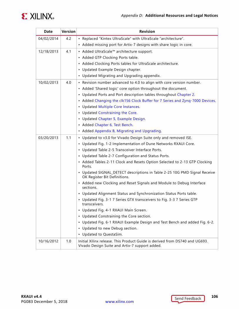
RXAUI v4.4 106PG083 December 5, 2018 www.xilinx.com
Appendix D: Additional Resources and Legal Notices
04/02/2014 4.2 • Replaced “Kintex UltraScale” with UltraScale “architecture”.• Added missing port for Artix-7 designs with share logic in core.
12/18/2013 4.1 • Added UltraScale™ architecture support.• Added GTP Clocking Ports table.• Added Clocking Ports tables for UltraScale architecture.• Updated Example Design chapter.• Updated Migrating and Upgrading appendix.
10/02/2013 4.0 • Revision number advanced to 4.0 to align with core version number.• Added 'Shared logic' core option throughout the document.• Updated Ports and Port description tables throughout Chapter 2.• Added Changing the clk156 Clock Buffer for 7 Series and Zynq-7000 Devices.• Updated Multiple Core Instances.• Updated Constraining the Core.• Updated Chapter 5, Example Design.• Added Chapter 6, Test Bench.• Added Appendix B, Migrating and Upgrading.
03/20/2013 1.1 • Updated to v3.0 for Vivado Design Suite only and removed ISE.• Updated Fig. 1-2 Implementation of Dune Networks RXAUI Core.• Updated Table 2-5 Transceiver Interface Ports.• Updated Table 2-7 Configuration and Status Ports.• Added Tables 2-11 Clock and Resets Option Selected to 2-13 GTP Clocking
Ports.• Updated SIGNAL_DETECT descriptions in Table 2-25 10G PMD Signal Receive
OK Register Bit Definitions.• Added new Clocking and Reset Signals and Module to Debug Interface
sections.• Updated Alignment Status and Synchronization Status Ports table.• Updated Fig. 3-1 7 Series GTX transceivers to Fig. 3-3 7 Series GTP
transceivers.• Updated Fig. 4-1 RXAUI Main Screen.• Updated Constraining the Core section.• Updated Fig. 6-1 RXAUI Example Design and Test Bench and added Fig. 6-2.• Updated to new Debug section.• Updated to QuestaSim.
10/16/2012 1.0 Initial Xilinx release. This Product Guide is derived from DS740 and UG693. Vivado Design Suite and Artix-7 support added.
Date Version Revision
Send Feedback

RXAUI v4.4 107PG083 December 5, 2018 www.xilinx.com
Appendix D: Additional Resources and Legal Notices
Please Read: Important Legal NoticesThe information disclosed to you hereunder (the "Materials") is provided solely for the selection and use of Xilinx products. To the maximum extent permitted by applicable law: (1) Materials are made available "AS IS" and with all faults, Xilinx hereby DISCLAIMS ALL WARRANTIES AND CONDITIONS, EXPRESS, IMPLIED, OR STATUTORY, INCLUDING BUT NOT LIMITED TO WARRANTIES OF MERCHANTABILITY, NON-INFRINGEMENT, OR FITNESS FOR ANY PARTICULAR PURPOSE; and (2) Xilinx shall not be liable (whether in contract or tort, including negligence, or under any other theory of liability) for any loss or damage of any kind or nature related to, arising under, or in connection with, the Materials (including your use of the Materials), including for any direct, indirect, special, incidental, or consequential loss or damage (including loss of data, profits, goodwill, or any type of loss or damage suffered as a result of any action brought by a third party) even if such damage or loss was reasonably foreseeable or Xilinx had been advised of the possibility of the same. Xilinx assumes no obligation to correct any errors contained in the Materials or to notify you of updates to the Materials or to product specifications. You may not reproduce, modify, distribute, or publicly display the Materials without prior written consent. Certain products are subject to the terms and conditions of Xilinx's limited warranty, please refer to Xilinx's Terms of Sale which can be viewed at https://www.xilinx.com/legal.htm#tos; IP cores may be subject to warranty and support terms contained in a license issued to you by Xilinx. Xilinx products are not designed or intended to be fail-safe or for use in any application requiring fail-safe performance; you assume sole risk and liability for use of Xilinx products in such critical applications, please refer to Xilinx's Terms of Sale which can be viewed at https://www.xilinx.com/legal.htm#tos.AUTOMOTIVE APPLICATIONS DISCLAIMERAUTOMOTIVE PRODUCTS (IDENTIFIED AS “XA” IN THE PART NUMBER) ARE NOT WARRANTED FOR USE IN THE DEPLOYMENT OF AIRBAGS OR FOR USE IN APPLICATIONS THAT AFFECT CONTROL OF A VEHICLE (“SAFETY APPLICATION”) UNLESS THERE IS A SAFETY CONCEPT OR REDUNDANCY FEATURE CONSISTENT WITH THE ISO 26262 AUTOMOTIVE SAFETY STANDARD (“SAFETY DESIGN”). CUSTOMER SHALL, PRIOR TO USING OR DISTRIBUTING ANY SYSTEMS THAT INCORPORATE PRODUCTS, THOROUGHLY TEST SUCH SYSTEMS FOR SAFETY PURPOSES. USE OF PRODUCTS IN A SAFETY APPLICATION WITHOUT A SAFETY DESIGN IS FULLY AT THE RISK OF CUSTOMER, SUBJECT ONLY TO APPLICABLE LAWS AND REGULATIONS GOVERNING LIMITATIONS ON PRODUCT LIABILITY.© Copyright 2012–2018 Xilinx, Inc. Xilinx, the Xilinx logo, Artix, ISE, Kintex, Spartan, Virtex, Vivado, Zynq, and other designated brands included herein are trademarks of Xilinx in the United States and other countries. All other trademarks are the property of their respective owners.
Send Feedback