Embed Size (px)
Citation preview

LogiCORE IP AXI4-Stream to Video Out v3.0Product Guide
Vivado Design Suite
PG044 April 1, 2014
LogiCORE IP Video In to AXI4-Stream v3.0 www.xilinx.com 2PG044 April 1, 2014
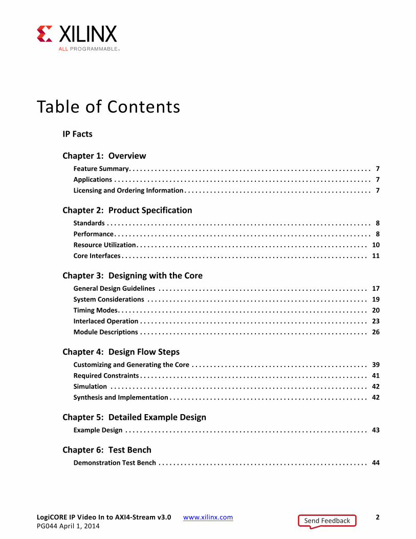
Table of ContentsIP Facts
Chapter 1: OverviewFeature Summary. . . . . . . . . . . . . . . . . . . . . . . . . . . . . . . . . . . . . . . . . . . . . . . . . . . . . . . . . . . . . . . . . . 7Applications . . . . . . . . . . . . . . . . . . . . . . . . . . . . . . . . . . . . . . . . . . . . . . . . . . . . . . . . . . . . . . . . . . . . . . 7Licensing and Ordering Information . . . . . . . . . . . . . . . . . . . . . . . . . . . . . . . . . . . . . . . . . . . . . . . . . . . 7
Chapter 2: Product SpecificationStandards . . . . . . . . . . . . . . . . . . . . . . . . . . . . . . . . . . . . . . . . . . . . . . . . . . . . . . . . . . . . . . . . . . . . . . . . 8Performance. . . . . . . . . . . . . . . . . . . . . . . . . . . . . . . . . . . . . . . . . . . . . . . . . . . . . . . . . . . . . . . . . . . . . . 8Resource Utilization. . . . . . . . . . . . . . . . . . . . . . . . . . . . . . . . . . . . . . . . . . . . . . . . . . . . . . . . . . . . . . . 10Core Interfaces . . . . . . . . . . . . . . . . . . . . . . . . . . . . . . . . . . . . . . . . . . . . . . . . . . . . . . . . . . . . . . . . . . . 11
Chapter 3: Designing with the CoreGeneral Design Guidelines . . . . . . . . . . . . . . . . . . . . . . . . . . . . . . . . . . . . . . . . . . . . . . . . . . . . . . . . . 17System Considerations . . . . . . . . . . . . . . . . . . . . . . . . . . . . . . . . . . . . . . . . . . . . . . . . . . . . . . . . . . . . 19Timing Modes. . . . . . . . . . . . . . . . . . . . . . . . . . . . . . . . . . . . . . . . . . . . . . . . . . . . . . . . . . . . . . . . . . . . 20Interlaced Operation . . . . . . . . . . . . . . . . . . . . . . . . . . . . . . . . . . . . . . . . . . . . . . . . . . . . . . . . . . . . . . 23Module Descriptions . . . . . . . . . . . . . . . . . . . . . . . . . . . . . . . . . . . . . . . . . . . . . . . . . . . . . . . . . . . . . . 26
Chapter 4: Design Flow StepsCustomizing and Generating the Core . . . . . . . . . . . . . . . . . . . . . . . . . . . . . . . . . . . . . . . . . . . . . . . . 39Required Constraints . . . . . . . . . . . . . . . . . . . . . . . . . . . . . . . . . . . . . . . . . . . . . . . . . . . . . . . . . . . . . . 41Simulation . . . . . . . . . . . . . . . . . . . . . . . . . . . . . . . . . . . . . . . . . . . . . . . . . . . . . . . . . . . . . . . . . . . . . . 42Synthesis and Implementation . . . . . . . . . . . . . . . . . . . . . . . . . . . . . . . . . . . . . . . . . . . . . . . . . . . . . . 42
Chapter 5: Detailed Example DesignExample Design . . . . . . . . . . . . . . . . . . . . . . . . . . . . . . . . . . . . . . . . . . . . . . . . . . . . . . . . . . . . . . . . . . 43
Chapter 6: Test BenchDemonstration Test Bench . . . . . . . . . . . . . . . . . . . . . . . . . . . . . . . . . . . . . . . . . . . . . . . . . . . . . . . . . 44
Send Feedback

LogiCORE IP Video In to AXI4-Stream v3.0 www.xilinx.com 3PG044 April 1, 2014
Appendix A: Verification, Compliance, and InteroperabilitySimulation . . . . . . . . . . . . . . . . . . . . . . . . . . . . . . . . . . . . . . . . . . . . . . . . . . . . . . . . . . . . . . . . . . . . . . 47Hardware Testing. . . . . . . . . . . . . . . . . . . . . . . . . . . . . . . . . . . . . . . . . . . . . . . . . . . . . . . . . . . . . . . . . 47Interoperability . . . . . . . . . . . . . . . . . . . . . . . . . . . . . . . . . . . . . . . . . . . . . . . . . . . . . . . . . . . . . . . . . . 47
Appendix B: Migrating and UpgradingMigrating to the Vivado Design Suite. . . . . . . . . . . . . . . . . . . . . . . . . . . . . . . . . . . . . . . . . . . . . . . . . 49Upgrading in Vivado Design Suite. . . . . . . . . . . . . . . . . . . . . . . . . . . . . . . . . . . . . . . . . . . . . . . . . . . . 49
Appendix C: DebuggingFinding Help on Xilinx.com . . . . . . . . . . . . . . . . . . . . . . . . . . . . . . . . . . . . . . . . . . . . . . . . . . . . . . . . . 51Debug Tools . . . . . . . . . . . . . . . . . . . . . . . . . . . . . . . . . . . . . . . . . . . . . . . . . . . . . . . . . . . . . . . . . . . . . 52Hardware Debug . . . . . . . . . . . . . . . . . . . . . . . . . . . . . . . . . . . . . . . . . . . . . . . . . . . . . . . . . . . . . . . . . 53Interface Debug . . . . . . . . . . . . . . . . . . . . . . . . . . . . . . . . . . . . . . . . . . . . . . . . . . . . . . . . . . . . . . . . . . 54
Appendix D: Additional Resources and Legal NoticesXilinx Resources . . . . . . . . . . . . . . . . . . . . . . . . . . . . . . . . . . . . . . . . . . . . . . . . . . . . . . . . . . . . . . . . . . 55References . . . . . . . . . . . . . . . . . . . . . . . . . . . . . . . . . . . . . . . . . . . . . . . . . . . . . . . . . . . . . . . . . . . . . . 55Revision History . . . . . . . . . . . . . . . . . . . . . . . . . . . . . . . . . . . . . . . . . . . . . . . . . . . . . . . . . . . . . . . . . . 56Please Read: Important Legal Notices . . . . . . . . . . . . . . . . . . . . . . . . . . . . . . . . . . . . . . . . . . . . . . . . 56
Send Feedback

LogiCORE IP Video In to AXI4-Stream v3.0 www.xilinx.com 4PG044 April 1, 2014 Product Specification
IntroductionThe Xilinx LogiCORE™ IP AXI4-Stream to Video Out core is designed to interface from the AXI4-Stream interface implementing a Video Protocol to a video source (parallel video data, video syncs, and blanks).This core works with the Xilinx Video Timing Controller (VTC) core. This core provides a bridge between video processing cores with AXI4-Stream interfaces and a video output.
Features• Video (clocked parallel video data with
synchronization signals - active video with either syncs, blanks or both) output
• AXI4 Stream slave interface for input
• In slave timing mode, interface to Xilinx Video Timing Controller core for video timing generation
• In master timing mode, automatically synchronizes AXI4-Stream Video to video timing.
• Automatically synchronizes video timing to AXI4-Stream video
• Handles asynchronous clock boundary crossing between AXI4-Stream clock domain and video clock domain
• Selectable FIFO depth from 64–8192 locations
• Selectable input data width of 8–256 bits
• Support for interlaced operation
IP Facts
LogiCORE IP Facts Table
Core SpecificsSupported Device Family(1)
UltraScale™ Architecture, Zynq®-7000,7 Series
Supported User Interfaces AXI4-Stream(2)
Resources See Table 2-1 to Table 2-3.
Provided with CoreDocumentation Product Guide
Design Files Verilog Source Code
Example Design Provided Separately (3)
See XAPP521 [Ref 3]
Test Bench Verilog
Constraints File XDC
Simulation Models Verilog Source Code
Supported Software Drivers N/A
Tested Design FlowsDesign Entry Tools
Vivado® Design SuiteIP Integrator
Simulation(4) For supported simulators, see theXilinx Design Tools: Release Notes Guide.
Synthesis Tools Vivado Synthesis
SupportProvided by Xilinx, Inc.
1. For a complete listing of supported devices, see the Vivado IP Catalog.
2. Video protocol as defined in the Video IP: AXI Feature Adoption section of (UG761) AXI Reference Guide [Ref 4].
3. Example designs are provided in FPGA device-specific application notes
4. For the supported versions of the tools, see the Xilinx Design Tools: Release Notes Guide.
Send Feedback

LogiCORE IP Video In to AXI4-Stream v3.0 www.xilinx.com 5PG044 April 1, 2014
Chapter 1
OverviewMany Xilinx video processing cores utilize the AXI-4 Stream Interface implementing a Video Protocol (as defined in the Video IP: AXI Feature Adoption section of the AXI Reference Guide (UG761) [Ref 4]) to transfer video between IP cores. Conversely, between systems, video is commonly transmitted with explicit blanking and sync signals for horizontal and vertical timing, and a data valid signal. DVI is an example of such a transmission mode. The AXI4-Stream to Video Out core converts AXI4-Stream Video protocol from Xilinx video processing cores that use this protocol to video output with explicit sync and timing to interface with common video systems that use timing information.
The AXI4-Stream to Video Out core input is an AXI4-Stream interface in slave mode. This interface consists of parallel video data, tdata, handshaking signals tvalid and tready, and two flags, tlast and tuser which serve to identify certain pixels in the video stream. The tlast signal designates the last valid pixel of each line, and is also known as the end of line (EOL). The tuser signal designates the first valid pixel of a frame, and is known as start of frame (SOF). These two flags are necessary to identify pixel locations on the AXI4 stream interface because there are no sync or blank signals. Only actives pixel are carried on the bus.
The AXI4-Stream to Video Out core outputs video. For the purposes of this document, video is defined as the following signals:
• Parallel video data
• Pixel clock
• Vsync
• Hsync
• Vbank
• Hblank
• Data Valid
• Field ID
The core is designed to be used in parallel with the generator functionality of the VTC. The VTC produces video timing signals based on video timing parameters such as the number of active pixels per line and the number of active lines through an AXI4-Lite interface. The Output Synchronizer section of the core synchronizes timing from the VTC to the video data from the AXI4-Stream Bus. A diagram of an AXI4Stream to Video Out core with a video
Send Feedback

LogiCORE IP Video In to AXI4-Stream v3.0 www.xilinx.com 6PG044 April 1, 2014
Chapter 1: Overview
timing generator is shown if Figure 1-1.
There are two timing modes supported: slave timing mode and master timing mode. Slave timing mode is used when the video source of the AXI4-Stream bus is the timing master. Master timing mode is used when the video source is within the processing pipeline and can be controlled by the VTC, for example, a frame buffer.
X-Ref Target - Figure 1-1
Figure 1-1: AXI4-Stream to Video Out Core with the Video Timing Controller
Send Feedback

LogiCORE IP Video In to AXI4-Stream v3.0 www.xilinx.com 7PG044 April 1, 2014
Chapter 1: Overview
Feature SummaryThe AXI4-Stream to Video Out core converts an AXI4-Stream Slave interface that conforms with the AXI4-Stream Video protocol to a video output, consisting or parallel video data, video syncs, blanks, and data valid. The core interfaces to the Xilinx VTC, which provides timing signals.
The core handles the asynchronous clock boundary crossing between the video clock domain and the AXI4-Stream clock domain. The data width is selectable from 8 to 256 depending on the number of components required for the video format, the number of bits per component, and the number of pixels per clock. Interlaced operation is supported. There is an output FIFO with selectable depth from 32 to 8192 locations.
Applications• Video input to AXI4-Stream Video Protocol interface for parallel, clocked video sources:
° DVI
° HDMI
° Other clocked, parallel video sources
Licensing and Ordering InformationThis Xilinx LogiCORE IP module is provided at no additional cost with the Xilinx Vivado Design Suite under the terms of the Xilinx End User License. Information about this and other Xilinx LogiCORE IP modules is available at the Xilinx Intellectual Property page. For information about pricing and availability of other Xilinx LogiCORE IP modules and tools, contact your local Xilinx sales representative.
Send Feedback
LogiCORE IP Video In to AXI4-Stream v3.0 www.xilinx.com 8PG044 April 1, 2014
Chapter 2
Product Specification
StandardsThe AXI4-Stream to Video Out core is compliant with the AXI4-Stream Video Protocol. Refer to the Video IP: AXI Feature Adoption section of the AXI Reference Guide (UG761) [Ref 4] for additional information.
PerformanceThe following sections detail the performance characteristics of the AXI4-Stream to Video Out core.
Maximum FrequenciesThis section contains typical clock frequencies for the target devices. The maximum achievable clock frequency can vary. The maximum achievable clock frequency and all resource counts can be affected by other tool options, additional logic in the FPGA device, using a different version of Xilinx tools and other factors. Refer to Table 2-1 and Table 2-3 for device-specif ic information.
Latency
Slave Timing Mode
When the upstream processing block on the AXI4-Stream bus can source data at the pixel rate or faster, the typical latency through the AXI4-Stream to Video Out core is 9 cycles of vid_io_out_clk + 3 cycles of aclk .
If the upstream block sources pixels at a slower rate, the FIFO is used to balance the mismatch in the input and output rates over the course of lines and frames. This storage of pixels in the FIFO adds to the latency and varies according to the data flow in and out of the core.
Send Feedback

LogiCORE IP Video In to AXI4-Stream v3.0 www.xilinx.com 9PG044 April 1, 2014
Chapter 2: Product Specification
Master Timing Mode
In master timing mode, the latency is generally a function of the FIFO size, if pixels are supplied on the AXI4-Stream bus at the output video rate or higher. The latency is relatively steady at approximately FIFO Size - 10 video clocks.
If the upstream block sources pixels at a slower rate, the FIFO is used to balance out the mismatch in the input and output rates over the course of lines and frames. This emptying of the FIFO reduces the latency of the core at the end of lines and or frames, and varies according to the data flow in and out of the core.
ThroughputThe average data rates of active pixels on the Video output bus matches the average rate of active pixels in on the AXI4-Stream bus. The data throughput is dictated by the video line standard and clock rate. However, the clock rates of the input need not match the output. Furthermore, since the AXI4-Stream bus does not carry blank pixels, the clock rate can be lower than the video clock rate and still have suff icient bandwidth to meet the average rate requirement. Additional FIFO depth is required in order to smooth the mismatch in instantaneous rates. Both the AXI4-Stream Clock (Faclk) and the rate of the AXI4-Stream Clock (Faclk) is limited by the overall Fmax.
If the sustained pixel rate available from the upstream AXI4-Stream (Faclk) is equal to or greater than Fvclk, only the minimum buffer size (32 locations) is required. In this scenario, the FIFO will go empty after the EOL on each line.
If Faclk is less than Fvclk, additional buffering is required. The FIFO must store enough pixels to supply pixels continuously throughout the active line. Additionally, due to phasing requirements, the horizontal active period on the output will overlap the effective blanking period of pixels coming in from the AXI4-Stream bus. This means that the output FIFO must also be large enough to provide output pixels continuously during this time.
For upstream bandwidth above the line average but below that of Fvclk, the minimum FIFO initial f ill level must be:
FIFO Initial Fill Level = 32+ Thblank/Fvclk + (Thactive – Thblank)*Fvclk/Faclk.
where Thblank is the duration of the horizontal blank and Thactive is the duration of the horizontal active period.
This is the level needed to keep the FIFO from running dry each line. This f ill level is automatically established by the output synchronization mechanism, and is not dependent on the Hysteresis Level of the generated core.
The total FIFO depth must be slightly larger than the initial f ill level to prevent overflow of the FIFO:
FIFO depth min = 32 + FIFO initial Fill Level
Send Feedback
LogiCORE IP Video In to AXI4-Stream v3.0 www.xilinx.com 10PG044 April 1, 2014
Chapter 2: Product Specification
In every case, this is less than a full line of data, so if a line buffer is provided, it will be suff icient. However, in many cases, a full line buffer is not required.
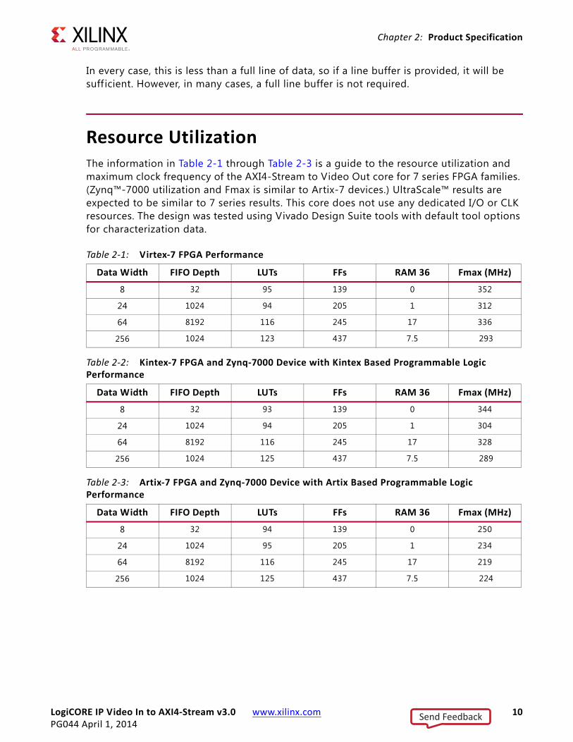
Resource UtilizationThe information in Table 2-1 through Table 2-3 is a guide to the resource utilization and maximum clock frequency of the AXI4-Stream to Video Out core for 7 series FPGA families. (Zynq™-7000 utilization and Fmax is similar to Artix-7 devices.) UltraScale™ results are expected to be similar to 7 series results. This core does not use any dedicated I/O or CLK resources. The design was tested using Vivado Design Suite tools with default tool options for characterization data.
Table 2-1: Virtex-7 FPGA Performance
Data Width FIFO Depth LUTs FFs RAM 36 Fmax (MHz)
8 32 95 139 0 352
24 1024 94 205 1 312
64 8192 116 245 17 336
256 1024 123 437 7.5 293
Table 2-2: Kintex-7 FPGA and Zynq-7000 Device with Kintex Based Programmable Logic Performance
Data Width FIFO Depth LUTs FFs RAM 36 Fmax (MHz)
8 32 93 139 0 344
24 1024 94 205 1 304
64 8192 116 245 17 328
256 1024 125 437 7.5 289
Table 2-3: Artix-7 FPGA and Zynq-7000 Device with Artix Based Programmable Logic Performance
Data Width FIFO Depth LUTs FFs RAM 36 Fmax (MHz)
8 32 94 139 0 250
24 1024 95 205 1 234
64 8192 116 245 17 219
256 1024 125 437 7.5 224
Send Feedback

LogiCORE IP Video In to AXI4-Stream v3.0 www.xilinx.com 11PG044 April 1, 2014
Chapter 2: Product Specification
Core Interfaces
Port DescriptionsThe AXI4-Stream to Video Out core uses industry-standard control and data interfaces to connect to other system components. The following sections describe the various interfaces available with the core. Figure 2-1 illustrates an I/O diagram of the AXI4-Stream to Video Out core. Not all of the timing signals are required by this core, however it also passes these signals to the Video output. Therefore all timing signals are present. The data valid and vertical sync input are required. It is recommended that the Xilinx Video Timing Controller be set to output all syncs and blanks.
X-Ref Target - Figure 2-1
Figure 2-1: AXI4-Stream to Video Out Top-Level Signaling Interface
Send Feedback

LogiCORE IP Video In to AXI4-Stream v3.0 www.xilinx.com 12PG044 April 1, 2014
Chapter 2: Product Specification
Common Interface
Video Timing Interface
IMPORTANT: All timing control signals are required for the proper operation of the AXI4-Stream to Video Out core. The only exception is vtg_field_id which is not required for non-interlace operation. Although all syncs and blanks may not be required at the video output, they are all required for the correct internal operation of the AXI4-Stream to Video Out core.
Table 2-4: Port Name I/O Width Description
Signal Name Direction Width Description
rst In 1 Core reset. Active High
wr_error Out 1 Active HIGH FIFO write error flag. Synchronous with vid_io_in_clk.1 = FIFO write was attempted when FIFO was full.
empty
Out 1
Active HIGH FIFO empty flag. Synchronous with aclk.1 = FIFO read was attempted when FIFO was empty. Due to EOL flushing, this flag will be asserted at the end of every line during normal operation.
locked Out 1 Flag indicating whether the output timing is locked to the output video. 1= locked.
vid_io_out_ce In 1 Clock enable for vid_io_out_clock. 1= enable. Tie HIGH if not used.
f id
In 1
Field ID for AXI4-Stream bus. Used only for interlace. 0= even field, 1= odd f ield. This bit is sampled coincident with the SOF on the AXI4-Stream bus.If the signal is not used, set the input to Low.
vtg_ce Out 1 VTC clock enable. Used to halt the timing generator for synchronization purposes.
vid_io_out_clk In 1 Video clock
Table 2-5: Port Name I/O Width Description
Signal Name Direction Width Description
vtg_vsync In 1 VTC vertical sync. Active High
vtg_hsync In 1 VTC horizontal sync. Active High
vtg_vblank In 1 VTC vertical blank. Active High
vtg_hblank In 1 VTC horizontal blank. Active High
vtg_act_vid In 1 VTC active video signal.1 = active video, 0 = blanked video
vtg_field_id In 1 VTC f ield ID. Used only for interlace. 0= even f ield, 1= odd f ield. Tie LOW for non-interlace operation.
Send Feedback

LogiCORE IP Video In to AXI4-Stream v3.0 www.xilinx.com 13PG044 April 1, 2014
Chapter 2: Product Specification
Data InterfaceThe AXI4-Stream to Video Out core receives video through the AXI4-Stream slave interface defined in the Video IP: AXI Feature Adoption section of the (UG761) AXI Reference Guide [Ref 4]. This video is output as parallel video data along with timing signals from a VTC.
Video Output Interface
AXI4-Stream Interface
AXI4-Stream Signal Names and Descriptions
Table 2-7 describes the AXI4-Stream signal names and descriptions. See AXI4-Stream Video IP and System Design Guide (UG934) [Ref 11] for more information.
Table 2-6: Video Output Interface
Signal Name Direction Width Description
vid_active_video Out 1 Video output data valid. 1 = active video, 0 = blanked video
vid_vsync Out 1 Video output vertical sync. Active HIGH
vid_hsync Out 1 Video output horizontal sync. Active HIGH
vid_vblank Out 1 Video output vertical blank. Active HIGH
vid_hblank Out 1 Video output horizontal blank. Active HIGH
vid_data Out 8-256 Parallel video output data. Active HIGH
vid_field_id Out 1 Video field. Used only for interlace. 0= even field, 1= odd field.
Table 2-7: AXI4-Stream Data Interface Signal Descriptions
Signal Name Direction Width Description
s_axis_video_tdata In 8,256 Input Video Data
s_axis_video_tvalid In 1 Input Video Valid Signal
s_axis_video_tready Out 1 Input Ready
s_axis_video_tuser In 1 Input Video Start Of Frame
s_axis_video_tlast In 1 Input Video End Of Line
ACLK In 1 AXI4-Stream Clock
ACLKEN In 1 AXI4-Stream Clock Enable
ARESETn In 1 AXI4-Stream Active Low synchronous
RESET In 1 AXI4-Stream Reset. Active Low synchronous
Send Feedback

LogiCORE IP Video In to AXI4-Stream v3.0 www.xilinx.com 14PG044 April 1, 2014
Chapter 2: Product Specification
The ACLK, ACLKEN, and ARESETn signals are shared between the core, the AXI4-Stream data interfaces, and AXI4-Lite control interfaces in the system.
ACLK
The AXI4-Stream interface must be synchronous to the clock signal ACLK. AXI4-Stream signals are sampled on the rising edge of ACLK. AXI4-Stream output signal changes occur after the rising edge of ACLK.
ACLKEN
The ACLKEN pin is an active-High, synchronous clock-enable input pertaining the AXI4-Stream interface. Setting ACLKEN Low (deasserted) halts the operation of the AXI4-Stream Bus despite rising edges on the ACLK pin. Internal states are maintained, and output signal levels are held until ACLKEN is asserted again. When ACLKEN is deasserted, core AXI4-Stream inputs are not sampled, except ARESETn, which supersedes ACLKEN.
ARESETn
The ARESETn pin is an active-low, synchronous reset input. ARESETn supersedes ACLKEN, and when set to 0, the core resets even if ACLKEN is deasserted.
Video Data
The AXI4-Stream interface specif ication restricts TDATA widths to integer multiples of 8 bits. Therefore, for some input video data widths, data must be padded with zeros on the MSB to form an N*8-bit wide vector before connecting to s_axis_video_tdata.
Data on the AXI-4 Stream input s_axis_video_tdata is packed and padded to multiples of 8 bits as necessary. Figure 2-2 shows an example for 12-bit RGB data with one pixel per clock. For multiple pixels per clock, the pixels are packed together, and padded to multiples of 8 bits as necessary. Figure 2-3 shows an example of three pixels per clock with 12-bit per component RGB data. Although this is the expected packing, the core itself does not parse the data. In other words, the video output data will be the AXI4-Stream Input data with zero padding truncated. The size of the core is affected by the width of the video data and by the amount of padding required.
X-Ref Target - Figure 2-2
Figure 2-2: RGB Data Encoding on s_axis_video_tdata
Send Feedback

LogiCORE IP Video In to AXI4-Stream v3.0 www.xilinx.com 15PG044 April 1, 2014
Chapter 2: Product Specification
READY/VALID Handshake
A valid transfer occurs whenever READY, VALID, ACLKEN, and ARESETn are high at the rising edge of ACLK. During valid transfers, DATA only carries active video data. Blank periods and ancillary data packets are not transferred via the AXI4-Stream Video protocol.
Guidelines on Driving s_axis_video_tvalid
Once s_axis_video_tvalid is asserted, no interface signals (except s_axis_video_tready) may change value until the transaction completes (s_axis_video_tready, s_axis_video_tvalid ACLKEN high on the rising edge of ACLK). Once asserted, s_axis_video_tvalid may only be de-asserted after a transaction has completed. Transactions may not be retracted or aborted. In any cycle following a transaction, s_axis_video_tvalid can either be de-asserted or remain asserted to initiate a new transfer.
SOF - s_axis_video_tuser
The SOF signal, physically transmitted over the AXI4-Stream tuser0 signal, marks the f irst pixel of a video frame. The SOF pulse is 1 valid transaction wide, and must coincide with the f irst pixel of the frame. SOF serves as a frame synchronization signal, which allows downstream cores to re-initialize, and detect the f irst pixel of a frame. The SOF signal may
X-Ref Target - Figure 2-3
Figure 2-3: Three Pixels per Clock Format on s_axis_video_tdata.
X-Ref Target - Figure 2-4
Figure 2-4: Example of READY/VALID Handshake, Start of a New Frame
Send Feedback

LogiCORE IP Video In to AXI4-Stream v3.0 www.xilinx.com 16PG044 April 1, 2014
Chapter 2: Product Specification
be asserted an arbitrary number of aclk cycles before the f irst pixel value is presented on tdata, as long as a tvalid is not asserted.
EOL Signal - s_axis_video_tlast
The EOL signal, physically transmitted over the AXI4-Stream tlast signal, marks the last pixel of a line. The EOL pulse is 1 valid transaction wide, and must coincide with the last pixel of a scanline, as seen in Figure 2-5.
X-Ref Target - Figure 2-5
Figure 2-5: Use of EOL and SOF Signals
Send Feedback

LogiCORE IP Video In to AXI4-Stream v3.0 www.xilinx.com 17PG044 April 1, 2014
Chapter 3
Designing with the Core
General Design GuidelinesThe video outputs of the AXI4 Stream to Video Out core should be connected to the output video sink; for example, a DVI interface chip that accepts parallel video data and timing signals. Not all of the timing signals supplied by the Video Timing Controller core are required internally by this core. However it also passes these signals out to the Video output. Therefore all timing signals are present. The data valid signal and vertical sync input are required. It is recommended that the Xilinx Video Timing Controller be configured to output all syncs and blanks (horizontal sync, horizontal blank, vertical sync, vertical blank, and active video).
The video data input of the core is a slave AXI-4 Stream Video Protocol interface that connects to upstream video processing blocks as shown in Figure 3-1. The master and slave interfaces share a common clock, reset and clock enable.
Figure 3-1 shows that the AXI4-Stream to Video Out core is used in conjunction with the Video Timing Controller, which generates the video timing used for the video output. The
X-Ref Target - Figure 3-1
Figure 3-1: ACLK Routing and AXI4-Stream Interconnect
Send Feedback

LogiCORE IP Video In to AXI4-Stream v3.0 www.xilinx.com 18PG044 April 1, 2014
Chapter 3: Designing with the Core
timing parameters for the Video Timing Controller must match the video line standard (active pixels per line and active lines per frame) of the video data on the AXI4-Stream interface. Otherwise, it is impossible for the output_sync section to lock the VTC timing to the incoming video. Also, the video clock must be synchronous with the original source of the video on the AXI4-Stream bus. That is, both the AXI4-Stream video and the video timing controller must be roughly isochronous such that the frame rates are identical, with no long term drift.
ClockingTwo clocks are used in this core.
• Video output pixel clock
• AXI4-Stream clock
The video output clock corresponds to the video line standard used on the input. It is part of the video line standard and is used by both the AXI4-Stream to Video Out core and by the corresponding Video Timing Controller core that is used to detect video timing.
The AXI4-Stream clock (aclk) is part of the AXI4-Stream bus. To minimize buffering requirements, this clock should be of equal or higher frequency than the video input clock. This clock can be slower than the video input clock, in which case, additional buffering is required to store pixels so that lines can be input at the burst rate of the video clock. This is discussed in the Buffer Requirements section. At a minimum, the aclk frequency must be higher than the average pixel rate.
ACLKENThe ACLKEN pin disables the AXI4-Stream side of the asynchronous FIFO, as seen in Figure 3-1.
The ACLKEN pin facilitates:
• Multi-cycle path designs (high speed clock division without clock gating)
• Standby operation of subsystems to save on power
• Hardware controlled bring-up of system components
IMPORTANT: When ACLKEN (clock enable) pins are used (toggled) in conjunction with a common clock source driving the master and slave sides of an AXI4-Stream interface, to prevent transaction errors the ACLKEN pins associated with the master and slave component interfaces must also be driven by the same signal (Figure 2-2).
IMPORTANT: When two cores connected through AXI4-Stream interfaces, where only the master or the slave interface has an ACLKEN port, which is not permanently tied high, the two interfaces should be connected through the AXI4-Stream Interconnect or AXI-FIFO cores to avoid data corruption
Send Feedback

LogiCORE IP Video In to AXI4-Stream v3.0 www.xilinx.com 19PG044 April 1, 2014
Chapter 3: Designing with the Core
(Figure 2-3).
Resets (ARESETn and rst)In general, the core does not need to be reset during normal operation. The core will continuously and automatically attempt to lock the video output to the incoming AXI4-video stream until successful. The state machine in the output synchronizer block detects when the video is not locked to the AXI4-Stream. It resets the FIFO and starts an initialization sequence. Whenever it is detected that the output is not locked, the reset and initialize sequence is repeated.
There are two external resets provided: rst, which resets the entire core, and aresetn, which resets the AXI4-stream interface. Both resets cause the FIFO to be reset. The rst additionally causes the state machine of the out_sync module to be reset to a condition that is ready to attempt to lock on to the incoming AXI4-Stream. When asserted, the reset should be held for least two clock periods of the lowest frequency clock.
System Considerations
Buffer RequirementsThe FIFO depth is selectable through the GUI when the core is generated. The buffering requirement for the asynchronous FIFO depends mainly on the relative data rate between the upstream processor through the AXI4-Stream clock (aclk) and the video output clock (vid_io_out_clk) frequency, and also the line standard being used. Basically, if the upstream AXI4-Stream source cannot provide data at a sustained rate equal to or greater than the video clock rate, then additional buffering is required to store up incoming pixels ahead of when they are required such that a continuous stream of pixels can be generated at the output without emptying the FIFO prematurely. The AXI4-Stream to Video Out core will accept AXI4-Stream data as soon as it is available (i.e. it will not apply back pressure) until its FIFO is almost full.
If the sustained pixel rate available from the AXI4-Stream clock (Faclk) is equal to or greater than Video Output pixel clock (Fvclk), only the minimum buffer size (32 locations) is required. In this scenario, the FIFO will go empty after the EOL on each line.
If Faclk is less than Fvclk , additional buffering is required. The FIFO must store enough pixels to supply them continuously throughout the active line. Due to phasing requirements, the horizontal active period on the output overlaps the effective blanking period of pixels coming in from the AXI4-Stream bus. This means that the input FIFO must also be large enough to provide output pixels continuously during this time.
Send Feedback

LogiCORE IP Video In to AXI4-Stream v3.0 www.xilinx.com 20PG044 April 1, 2014
Chapter 3: Designing with the Core
For upstream bandwidth above the line average but below that of vclk, the minimum FIFO initial f ill level must be:
FIFO Initial Fill Level = 32+ Thblank/Fvclk + (Thactive - Thblank)*Fvclk/Faclk.
where Thblank is the duration of the horizontal blank and Thactive is the duration of the horizontal active period.
This is the level needed to keep the FIFO from running dry each line. This f ill level is automatically established by the output synchronization mechanism, and is not dependent on the Hysteresis Level of the generated core.
The total FIFO depth must be slightly larger than the initial f ill level to prevent overflow of the FIFO:
FIFO depth min = 32 + FIFO initial Fill Level
In every case, this is less than a full line of data, so if a line buffer is provided, it will be suff icient. However, in many cases, a full line buffer is not required.
Additional Buffering Requirements for Master Timing Mode
In master timing mode, the FIFO must be large enough to accommodate pixels that arrive on the AXI4 Stream bus prior to their being output on the video bus. In this mode, the VTC cannot be halted. If the timing between the video source and the video output is tightly controlled then additional buffering may not be required. If, however, video data on the AXI4-Stream bus leads the video timing signals by many clock cycles, the FIFO must be sized to handle the storage of the incoming pixels until they are needed at the output, without overflowing the FIFO.
Timing ModesIn video processing, two basic configurations are used for output timing: with frame buffer, and without. For Xilinx reference designs, this usually means with VDMA or without VDMA. The configuration has implications for how the AXI4-Stream to Video Out (Video Out) core is configured, how the VTC operates, and how it interacts with Video Out. The presence or absence of the VDMA determines how the Video Out core synchronizes timing between the AXI4-Stream data and the VTC, and the timing mode in which the VTC operates.
There are two timing modes supported: slave timing mode and master timing mode. In slave mode, the VTC generator is a slave to the Video Out core which controls it through clock enable. In master mode, the VTC is the timing master for the output side of the VDMA, the output processing cores, and the Video Out core. In master mode, the Video Out core does not control the VTC generator timing; instead, it uses the VTC timing as a reference, and synchronizes the video pipeline to it.
Send Feedback

LogiCORE IP Video In to AXI4-Stream v3.0 www.xilinx.com 21PG044 April 1, 2014
Chapter 3: Designing with the Core
The timing mode (master or slave) is a configuration parameter of the Video Out core. When generating this core, this parameter must be set according to the configuration in which it will be used.
No VDMA - Slave ModeIn slave timing mode, the video source of the AXI4-Stream bus is the timing master. This is used when the video source is external and cannot be controlled. Figure 3-2 shows an example of slave timing mode.
In Slave mode, the Video Out core uses the clock enable to control the timing of the syncs from the VTC generator. Because there is no frame buffer, the video cannot be stopped without losing data. Therefore, the Video Out core regulates the syncs from the VTC generator so that they match the timing of the data in the pipeline.
When designing systems with no external frame buffer, it is important to consider EOL flushing by upstream AXI4-Stream sources. Although video timing is not embedded into the AXI4-Stream signal set, it is inherently carried in the stream by way of stall periods where TVALID is Low. In an ideal AXI4-Stream scanline in slave mode, video samples arrive back-to-back with no stalls in between subsequent pixels during active periods followed by blanking period where the stream is stalled for a consecutive number of clock cycles.
In imperfect AXI4-Stream sources, the stall period can become fragmented within a scanline, requiring the Video Out bridge to absorb fragments by establishing a f ill level as described earlier. Upstream AXI4-Stream sources should be designed to flush the EOL pixel as quickly as possible within the period of a scanline to avoid requiring multi-line buffering. Refer to AXI4-Stream Video IP and System Design Guide (UG934) [Ref 11] to understand active, line, and frame pixel rates. In general, when the AXI4-Stream source cannot maintain the line pixel rate, line buffering is not sufficient to handle stalls, and therefore the Video Out bridge is not able to synchronize to the stream.
X-Ref Target - Figure 3-2
Figure 3-2: Without VDMA - Slave Timing Mode
Send Feedback

LogiCORE IP Video In to AXI4-Stream v3.0 www.xilinx.com 22PG044 April 1, 2014
Chapter 3: Designing with the Core
With VDMA - Master ModeWhen a VDMA or other frame-buffer is present, Master timing mode is used. Figure 3-3 shows an example of Master timing mode.
In this case, the attached VTC generator is the timing master, and the Video Out core synchronizes the data in the processing pipeline to the video timing signals by applying back pressure to the processing pipeline. This means that you can deassert the tready signal to stop the flow of pixels. This back pressure is propagated through the processing pipe in the reverse direction of the data flow until it halts the frame buffer output. In this scenario, the video output processing pipeline, from the frame buffer onward, is synchronized with the VTC generator. The VDMA provides video data as it is requested by the Video Out core through the processing pipe.
Unlike prior use models for the VDMA and VTC, Fsync is not required and should not be used in this mode. Previously, the VTC issued a frame sync at the start of each frame, which was used in the VDMA to reset the output side of the frame buffer. Now, instead of resetting the frame buffer output at a certain time, the frame buffer output free runs. Synchronization is accomplished through AXI4-Stream back pressure, originating at the Video Out core. Because the feedback wiring and possible programming intricacies of Fsync timing are eliminated, the core is easier to use.
With VDMA and Genlock - Master ModeThe Master mode is also compatible with genlock. Figure 3-4 show a genlock configuration. In genlock, the VTC timing is synchronized to an external timing input via an Fsync signal into the VTC generator. The Video Out core synchronizes the video data to the VTC timing, and the upstream pipe including the frame buffer output is synchronized by back pressure on the AXI4-Stream.
X-Ref Target - Figure 3-3
Figure 3-3: With VDMA - Master Timing Mode
Send Feedback

LogiCORE IP Video In to AXI4-Stream v3.0 www.xilinx.com 23PG044 April 1, 2014
Chapter 3: Designing with the Core
Interlaced OperationTo support standard definition video input such as PAL and NTSC, the Video In to AXI4-Stream core supports interlace on the video (with timing) side, the video input has a field_id bit as part of its interface and embedded vertical blanks and horizontal blanks. The VTC has a corresponding field_id pin defined for this purpose.
Figure 3-5 shows the interfaces on Video In to AXI4-Stream, AXI4-Stream to Video Out, and VTC cores to support the video f ield ID with the interlace-related signals highlighted in red.
Most video processing cores are f ield-agnostic, and not aware of whether the picture being processed is an odd or even frame, or a progressive f ield. Therefore, interlace has no impact on these cores. The Video In to AXI4-Stream core has a frame ID output, fid, timed to the
X-Ref Target - Figure 3-4
Figure 3-4: Genlock with VDMA - Master Timing Mode
X-Ref Target - Figure 3-5
Figure 3-5: Interlace Signals on Video Cores
Send Feedback

LogiCORE IP Video In to AXI4-Stream v3.0 www.xilinx.com 24PG044 April 1, 2014
Chapter 3: Designing with the Core
AXI4-Stream bus. This signal can be used as needed in the system. The only cores that use this fid bit are the AXI4-Stream to Video Out, VDMA, and Video Deinterlacer cores.
The AXI4-Stream to Video Out core has a field ID input, fid, sampled in time with the AXI4-Stream input bus. This fid bit must be asserted by the upstream source of AXI4-Stream video. For systems without a frame buffer or de-interlacing, the f ield ID input originates from the Video In core, as shown in Figure 3-6.
For systems with a frame buffer, the field ID input can come from any core containing a frame buffer. The field ID from the Video In to AXI4-Stream core can be used by the frame buffer if necessary, shown in Figure 3-6.
Note: In Figure 3-6, the AXI4-Stream to Video Out core is operating in slave mode.
A deinterlacer can be used after the Video In to AXI4-Stream core to convert the video format from interlaced to progressive. In this case, the deinterlacer uses the f ield ID bit, fid, from the Video In to AXI4-Stream core, as shown in Figure 3-7.
X-Ref Target - Figure 3-6
Figure 3-6: Field ID Connections with a Frame Buffer
Send Feedback

LogiCORE IP Video In to AXI4-Stream v3.0 www.xilinx.com 25PG044 April 1, 2014
Chapter 3: Designing with the Core
On the Video In to AXI4-Stream core, the fid bit changes coincident with SOF and remains constant throughout the remainder of the f ield. On the AXI4-Stream to Video Out core, the fid bit is sampled coincident with SOF in Figure 3-8. Therefore, the Video In to AXI4-Stream can provide the f ield bit directly to the AXI4-Stream to Video Out core if no intervening frame buffer exists. When a deinterlacer or frame buffer is used, a similar scheme can be employed: generate the field ID coincident with the start of the f ield, and on the receiving side sample the f ield ID coincident with the f irst received pixel.
X-Ref Target - Figure 3-7
Figure 3-7: Field ID Connections with a DeInterlacer
X-Ref Target - Figure 3-8
Figure 3-8: Timing of Field ID for AXI4-Stream
Send Feedback

LogiCORE IP Video In to AXI4-Stream v3.0 www.xilinx.com 26PG044 April 1, 2014
Chapter 3: Designing with the Core
Module DescriptionsThe AXI4-Stream to Video Output core works with the generator portion of the Video Timing Controller (VTC) core.
The timing outputs of the VTC connect as inputs to the AXI4-Stream to Video Output core. When locked, these timing signals are output along with video data from the FIFO as part of the video interface. These signals are also used by the Output Synchronizer, to compare to flags from the FIFO in order to guide the control action for locking the timing generator with FIFO data.
There are three main blocks, the stream coupler, the data formatter, and the output synchronizer. The AXI4-Stream interface is on the left, and the video connections are on the right.
Data FormatterThe Data Formatter block receives data from the Stream Coupler, timing from the VTC, and control from the Output Synchronizer. It registers the video data and timing signals to form the video output interface. The locked signal from the output synchronizer is used to enable the video interface. Before lock is achieved, the video outputs are all forced low. When lock is achieved, the video outputs become active at the end of the frame in progress, noted by the rising edge of vblank .
Stream CouplerThe Stream Coupler block consists mainly of an asynchronous FIFO and write logic for the input side of the FIFO. The Output Synchronizer controls the reading of the FIFO. The FIFO serves two primary purposes:
1. Clock domain crossing.
2. Buffering of data between the AXI4-Stream input and the video output.
The buffering requirements are dependent on the ratio of the AXI4-Stream data rate to the video clock rate, described in System Considerations.
Asynchronous FIFO
The crossing of clock domains requires an asynchronous FIFO. The FIFO designed for this core has two distinguishing features:
1. Status flags and a f ill level output in both clock domains.
Send Feedback

LogiCORE IP Video In to AXI4-Stream v3.0 www.xilinx.com 27PG044 April 1, 2014
Chapter 3: Designing with the Core
2. An “invalid” (read_error) flag produced in parallel with output data for reads when the FIFO is empty. It also has pointer-inhibiting logic to prevent pointer crossings on underflow and overflow.
Asynchronous FIFO negatively impacts the f ill level indicators and the flags. The primary risk is that pointer values could error when sampled from one clock domain to another. Therefore, pointer synchronization is required across clock domains, and a handshake protocol must be used to ensure that all pointer updates are registered, even when the clock rates in the two domains are radically different. Figure 3-9 is a block diagram of the asynchronous FIFO.
IMPORTANT: Note the synchronizing logic and the handshake between clock domains. The size of the FIFO is set in the GUI when the core is generated.
Synchronized Gray codes are commonly used in asynchronous FIFOs to eliminate the problems of synchronizing multiple counter bits changing on the same clock edge. However, instead of Gray code pointers, the FIFO for the AXI4-Stream to Video Out core uses binary pointers synchronized through handshaking. Calculating the f ill level, which is used integrally in the read logic, is simple with binary pointers but impractical with Gray code pointers.
X-Ref Target - Figure 3-9
Figure 3-9: Block Diagram of Bridge Core Asynchronous FIFO
Send Feedback

LogiCORE IP Video In to AXI4-Stream v3.0 www.xilinx.com 28PG044 April 1, 2014
Chapter 3: Designing with the Core
Clock Domain Crossing of Pointers
The synchronization and handshaking for pointers is shown in detail in Figure 3-10. The f irst two register delays are required to resolve metastability. The third ensures that the register has time to receive the data before the handshake is returned. Otherwise, if the clock in one domain were several times faster than the other, the handshake could be returned before the pointer register is updated in the slower clock domain.
The extra delay for returning the handshake signal ensures that data is transferred reliably regardless of the relative clock rates. For example, if Fa > 2Fb, each “req”is still guaranteed to update the sync pointer in domain B. Likewise, if Fb > 2Fa, each ack is guaranteed to update the pointer sample in domain A. Figure 3-11 shows an example of pointer synchronization between clock domains, and the handshake scheme shown in Figure 3-10. This scheme uses two states: request and acknowledge. The request state denotes that Req and Ack are not equal, and acknowledge denotes that they are equal.
This sample and hold method with handshake delays the capture of the pointers by several clock edges in each domain, but the pointer transfers are always reliable and error-free.
X-Ref Target - Figure 3-10
Figure 3-10: Synchronization and Handshaking for Clock Domain Crossing of Pointers
X-Ref Target - Figure 3-11
Figure 3-11: Waveform Diagram of Handshaking and Clock Domain Crossing of Pointers
Send Feedback

LogiCORE IP Video In to AXI4-Stream v3.0 www.xilinx.com 29PG044 April 1, 2014
Chapter 3: Designing with the Core
Pointer latency causes negativity in the level outputs and the flags. The empty flag persists in the read domain for several clocks after a write has occurred. The level output is not necessarily monotonic and is accounted for in the bridge design by providing a small cushion or minimum fill level in the FIFOs so that the pointer negativity does not cause artifacts.
Underflow Prevention
In addition to synchronizing flags, signaling an empty condition is not suff icient because “reads” of the FIFO do not stop on empty. Additional read operations are performed so that the EOF is included in the output of the FIFO. This occurs automatically, and the FIFO must not lose any data. Underflow is not allowed. When new data is eventually written to the FIFO, reading must begin with the first new valid pixel. To do this, the read pointer is inhibited when the FIFO is empty.
The empty flag asserts coincides with the last available location clocked into the output register. The read pointer is not advanced to match the write pointer, but points to the last valid pixel that was read. When empty is asserted, subsequent reads cause the read_error flag to be asserted, flagging the pixel from the FIFO as invalid. The data output does not change.
When a read occurs to an empty FIFO, the invalid flag (read_error) is set, and the read pointer does not increment. The EOL can be advanced through the pipe by a series of reads on the empty FIFO. With each read, an invalid pixel backfills the advancing EOL, but the downstream logic can distinguish these from valid pixels.
Pointer Format
It is important to provide an accurate level, and to distinguish between full and empty conditions when the read and write pointers are equal. This is done by having “revolution” bits on the pointers, in addition to the address bits, as shown in Figure 3-12.
These extra bits in the pointers allow the level calculations and flags to be unambiguously determined in full and empty conditions.
Write Logic
The function of the write logic is to control the handshaking for the AXI4-Stream bus and to accept pixels from this bus as rapidly as possible. In general, the strategy for Video Over AXI4-Stream is downstream-greedy. That is, downstream modules take pixels as soon as they are available and there is buffer space to accommodate them. Because the
X-Ref Target - Figure 3-12
Figure 3-12: Pointer Format for a 32 Location FIFO
Send Feedback

LogiCORE IP Video In to AXI4-Stream v3.0 www.xilinx.com 30PG044 April 1, 2014
Chapter 3: Designing with the Core
AXI4-Stream to Video Out core is at the end of the pipeline, it strives to fill its FIFO as fast as possible.
The Write Logic controls the tready handshaking signal based on the full flag from the FIFO. Whenever there is room in the FIFO, tready is asserted. When tvalid becomes active while tready is asserted, the FIFO is written. The tready signal is asserted except when there is almost no space available in the FIFO. Usually the FIFO will empty at the end of the active line when the downstream core is still taking pixels, but the incoming video data is in the horizontal blanking period and no pixels are entering the FIFO.
At the end of each line, the EOL must be flushed through from the FIFO to the video output of the core. This enables the complete line of video to be output while input to the core may be stalled, waiting for pixels from the next line.
This flushing requirement presents a challenge since it is likely to happen when no data is coming into the FIFO. It requires generation of invalid pixels to flush out the valid pixels. These invalid pixels must be removed by the core prior to the start of the next active line on the output.
When the output synchronizer is locked, flushing of the EOL is accomplished by reading from the FIFO based on the active video flag from the VTC. In order to propagate the EOL pixel through to the output, this happens even if the FIFO is empty. When the FIFO is empty, and the last pixel has been read (the EOL pixel) the FIFO will mark subsequent pixels as invalid, but the EOL pixel will continue to propagate to the output. When new valid pixels are again available in the FIFO, they are read out to the output register during the blanking period. In this way, invalid pixels are swallowed before the next active line begins.
Output SynchronizerA major task for the AXI4-Stream to Video Out core is to synchronize the asynchronous and irregularly timed video data from AXI4-Stream interface with the periodic and repeatable timing signals from the VTC. In slave timing mode, the timing of the data in the pipeline on the AXI-Stream interface cannot be controlled. Therefore, the synchronization is done mainly by controlling the phase of the VTC. In master timing mode, synchronization is done by controlling when data exits the FIFO. When the FIFO is almost full, the core stops accepting data from the upstream source on the AXI4 Stream bus. The upstream core subsequently exerts back pressure on the core upstream from it, and so on such that the entire upstream pipe stays synchronized with the VTC at the output of the AXI4-Stream to Video Out core.
In either case, the synchronization function is performed by the Output Synchronizer block. Also, the data from the AXI4-Stream interface goes into a FIFO to be able to smooth out small and short-term latency variations that occur during the course of a frame. The phase of the VTC must have some additional lag, such that the FIFO will have a suff icient f ill level to cushion the short-term variations.
Send Feedback

LogiCORE IP Video In to AXI4-Stream v3.0 www.xilinx.com 31PG044 April 1, 2014
Chapter 3: Designing with the Core
For Slave timing mode, the cushion is controlled by the Hysteresis Level parameter when the core is generated. This specifies the level to which the FIFO must fill initially before reads begin. In Master Timing mode, the whole FIFO is essentially used for a cushion, since it is f illed at initialization time.
Since the video input source may be disconnected or change line standards, the Video Output Bridge must constantly compare the timing of incoming video data relative to the timing of the VTC. This makes it possible to detect timing mismatches so that it can re-synchronize after any type of interruption. It must be self monitoring and self synchronizing. Figure 3-17 shows a block diagram of the output synchronizer.
Algorithm
For either Slave or Master timing mode, the operation of the self synchronizing circuit can be broadly defined in two steps: initialization and run. In the run mode, alignment must be continually checked and if there is a discrepancy, a new initialization is required, as shown in Figure 3-13.
The initialization phase does an alignment of the VTC to the AXI4-Stream data, provides for some cushion in the FIFO, and precisely aligns the video data from the FIFO to the VTC generated video output signals. The main difference between slave and master timing mode is how the FIFO and/or VTC is used to align the pixels with the video timing signals. In slave timing mode, the output sync section controls both the reading of the FIFO and the VTC (by halting it). In master timing mode, the VTC generator is never halted. Only the reading of the FIFO is controlled by the output synchronizer module.
Algorithm Differences Between Slave and Master Timing Modes
This section specifics of the algorithm for slave timing mode. The master timing mode algorithm follows the same pattern except that there is no step to set the FIFO cushion in the initialization. Also, in master timing mode, the VTC is never halted. All alignment is done
X-Ref Target - Figure 3-13
Figure 3-13: Basic Self Synchronizer Flow Chart
Send Feedback

LogiCORE IP Video In to AXI4-Stream v3.0 www.xilinx.com 32PG044 April 1, 2014
Chapter 3: Designing with the Core
through control of the FIFO. The details of algorithm for this mode is shown in the state machine diagram in Figure 3-19.
Figure 3-14 shows the initialization steps. The initial alignment of VTC generated video output signals to the FIFO is done by letting the VTC free run until it reaches the point of the f irst valid pixel of the first line of the frame (SOF). At this point, the VTC is paused using the clock enable of the VTC. The FIFO is read as fast as possible, keeping it essentially empty, and the start of f ield (SOF) flag is monitored. When VTC SOF is asserted, the FIFO data and the VTC generated video output signals are roughly aligned. This is the initial alignment.
At this juncture, the FIFO is paused for some additional period, nominally about 16 clocks, such that when the FIFO output data and VTC generated video output signals are aligned, the FIFO has some pixels stored to cushion any short term variations in the input data rate.
With a rough alignment and a cushion set for the FIFO, the last step is to f ine tune the FIFO output/VTC generated video output signals alignment so that the end of line (EOL) flags read from the FIFO precisely match the last clock of Data Valid from the VTC before the horizontal blanking period. The f ine-tuning process is shown in more detail in Figure 3-15.
X-Ref Target - Figure 3-14
Figure 3-14: Self Synchronizer Flow Chart Showing Initialization Steps - Slave Timing Mode
Send Feedback

LogiCORE IP Video In to AXI4-Stream v3.0 www.xilinx.com 33PG044 April 1, 2014
Chapter 3: Designing with the Core
During the f irst frame time after rough alignment, the EOLs from the FIFO and from the VTC (or rather the EOL signal derived from Data Valid) are compared every line. If the VTC is leading, it is paused by one clock. If the FIFO is leading, the reading of the FIFO is delayed by one location. The EOLs are aligned after several lines, typically a dozen or two. Typically,
X-Ref Target - Figure 3-15
Figure 3-15: Self Synchronizer Flow Chart Showing Fine Tuning Process - Slave Timing Mode
Send Feedback

LogiCORE IP Video In to AXI4-Stream v3.0 www.xilinx.com 34PG044 April 1, 2014
Chapter 3: Designing with the Core
the FIFO are leading because the VTC has an additional pause after rough alignment, but due to startup idiosyncrasies, this is not guaranteed. Delaying the FIFO read has the effect of building up a cushion in the FIFO. Even though the FIFO delay is exercised most often, the VTC delay must be included to assure reliable synchronization in every situation.
At the end of the frame, the EOLs are aligned through the fine-tuning process, and there is a cushion of pixels in the FIFO. However, since the FIFO must empty completely at the end of each line in order to flush the EOL through to the video output, this cushion will be used up at the end of each line. The phase lag of the VTC generated video output signals ensures that the cushion is built up at the start of the next line to smooth out variations during the active line.
When the Vsync from the VTC becomes active, the EOLs from the FIFO and the VTC are aligned. If everything is stable, the SOFs are also aligned, and then the locked mode is entered. In this mode, the VTC free runs, and the FIFO is read as dictated by the VTC. The video output is enabled at the next rising edge of vblank and pixel data and timing signals are output from the bridge. This is the run state and can continue indefinitely.
The EOLs and SOFs are continuously compared while the output is locked. If they do not match the system is considered unlocked and a new initialization cycle begins. In the case of a disconnected or unstable input to the system, initialization cycles are repeated until the system is stable.
Figure 3-16 shows the flow charts and how the stages correspond in the various levels of detail.
Send Feedback

LogiCORE IP Video In to AXI4-Stream v3.0 www.xilinx.com 35PG044 April 1, 2014
Chapter 3: Designing with the Core
Implementation
The output synchronizer is shown in Figure 3-17. This is essentially a state machine that implements the algorithm described in Algorithm. The control outputs are all registered, and reflect the current state. This means the control outputs are pre-decoded, rather than being decoded based on the current state.
X-Ref Target - Figure 3-16
Figure 3-16: Flow Charts from Basic to Detailed Showing Equivalencies - Slave Timing Mode
Send Feedback

LogiCORE IP Video In to AXI4-Stream v3.0 www.xilinx.com 36PG044 April 1, 2014
Chapter 3: Designing with the Core
Besides the state machine, there is logic to create virtual EOL and SOF flags from the VTC generated video output signals. These flags are created based on edges of the act_vid or data_valid from the VTC. The vsync input is used to distinguish the SOF. Also there is additional logic to create the FIFO read_en signal based on the act_vid from the VTC as well as control bits from the state machine. The read_en output has a register after the state machine to ensure that all outputs of the module are registered.
Slave Timing Mode
Figure 3-18 is a state diagram of the state machine of the output synchronizer for slave timing mode. Figure 3-19 is a state diagram of the output synchronizer state machine for master timing mode. They both execute the initialize-run algorithm described in Algorithm. Initialization consists of a coarse alignment, setting additional lag, and f ine tuning. When the EOLs are aligned, and matching SOFs occur, the state machine goes to the “EOLs Matched” state. If matching SOFs occur a second time, the “Locked” state is entered, which concludes initialization. It will remain in this state as long the system is stable.
The initialization process is done over three frame times. The f irst is waiting for the FIFO SOF. The second is for the f ine tuning to align EOLs. The third is basically a double check that the EOLs and SOFs are aligned. If an SOF mismatch occurs during fine tuning, it means that f ine tuning has failed to align within the frame time. In this case, the initialization process is re-started. Also, in the “EOLs Matched” or “Locked” states, EOL and SOF matching is continuously checked. If there is any mismatch, it means the output is unlocked, and the initialization is re-started.
X-Ref Target - Figure 3-17
Figure 3-17: Output Synchronizer Block Diagram
Send Feedback

LogiCORE IP Video In to AXI4-Stream v3.0 www.xilinx.com 37PG044 April 1, 2014
Chapter 3: Designing with the Core
Figure 3-19 is a state diagram of the state machine of the output synchronizer for master timing mode.
X-Ref Target - Figure 3-18
Figure 3-18: Output Synchronizer State Diagram - Slave Timing Mode
Send Feedback

LogiCORE IP Video In to AXI4-Stream v3.0 www.xilinx.com 38PG044 April 1, 2014
Chapter 3: Designing with the Core
X-Ref Target - Figure 3-19
Figure 3-19: Self Synchronizer Flow Chart Showing Initialization Steps - Master Timing Mode
Send Feedback

LogiCORE IP Video In to AXI4-Stream v3.0 www.xilinx.com 39PG044 April 1, 2014
Chapter 4
Design Flow StepsThis chapter describes customizing and generating the core, constraining the core, and the simulation, synthesis and implementation steps that are specific to this IP core. More detailed information about the standard Vivado® design flows in the IP Integrator can be found in the following Vivado Design Suite user guides:
• Vivado Design Suite User Guide: Designing IP Subsystems using IP Integrator (UG994) [Ref 12]
• Vivado Design Suite User Guide: Designing with IP (UG896) [Ref 6]
• Vivado Design Suite User Guide: Getting Started (UG910) [Ref 10]
• Vivado Design Suite User Guide: Logic Simulation (UG900) [Ref 8]
Customizing and Generating the CoreThis chapter includes information about using Xilinx tools to customize and generate the core in the Vivado® Design Suite environment.
You can customize the IP for use in your design by specifying values for the various parameters associated with the IP core using the following steps:
1. Select the IP from the IP catalog.
2. Double-click on the selected IP or select the Customize IP command from the toolbar or popup menu.
For details, see the sections, “Working with IP” and “Customizing IP for the Design” in the Vivado Design Suite User Guide: Designing with IP (UG896) [Ref 6] and the “Working with the Vivado IDE” section in the Vivado Design Suite User Guide: Getting Started (UG910) [Ref 10].
If you are customizing and generating the core in the Vivado IP Integrator, see the Vivado Design Suite User Guide: Designing IP Subsystems Using IP Integrator (UG994) [Ref 12] for detailed information. IP Integrator might auto-compute certain configuration values when validating or generating the design. To check whether the values do change, see the description of the parameter in this chapter. To view the parameter value you can run the validate_bd_design command in the Tcl console.
Send Feedback

LogiCORE IP Video In to AXI4-Stream v3.0 www.xilinx.com 40PG044 April 1, 2014
Chapter 4: Design Flow Steps
Note: Figures in this chapter are illustrations of the Vivado IDE. This layout might vary from the current version.
Vivado Integrated Design Environment The AXI4-Stream to Video Out core is easily configured to meet the developer's specific needs through the Vivado Design Suite. This section provides a quick reference to parameters that can be configured at generation time.
The GUI displays a representation of the IP symbol on the left side, and the parameter assignments on the right side, which are described as follows:
• Component Name: The component name is used as the base name of output files generated for the module. Names must begin with a letter and must be composed of characters: a to z, 0 to 9 and “_”.
• Pixels Per Clock : Specif ies the number of pixels to be output in parallel. This parameter affects the data bus width of the input and output. The options for pixels per clock are 1 to 4.
• Component Data Width: Specif ies the bit width of input samples. This is used in conjunction with the Video Format to determine the width of the input video bus, vid_data, and the AXI4-Stream data bus, m_axis_video_tdata.
• Video Format: Specifies the video format used. The video formats are specified in the Video IP: AXI Feature Adoption section of the AXI Reference Guide (UG761) [Ref 4]. The format selected determines the number of components used. The number of
X-Ref Target - Figure 4-1
Figure 4-1: AXI4-Stream to Video Out Vivado GUI
Send Feedback

LogiCORE IP Video In to AXI4-Stream v3.0 www.xilinx.com 41PG044 April 1, 2014
Chapter 4: Design Flow Steps
components (1-4) is multiplied by pixels per clock and the component width to determine the width of the video data bus, v_data. In turn, this width is rounded up to the nearest factor of 8 to determine the width of the AXI4-Stream data bus, m_axis_video_tdata. For example, if the component width is 14, pixels per clock is 2, and the Video Format is RGB (3 components), the vid_data is 84 bits wide and m_axis_video_tdata is 88 bits. When using IP Integrator, this parameter is automatically computed based on the Video Format of the video IP core connected to the slave AXI-Stream video interface.
• FIFO Depth: Specifies the number of locations in the input FIFO. The options for FIFO depth are 32, 1024, 2048, 4096, and 8192.
• Hysteresis Level: Defines the “Cushion” level of the frame buffer. i.e. the number of locations that are considered the minimum fill level for FIFO operation to start. Generally, this value should be between 12 and 20. It must be at least 16 less than the depth of the FIFO, and at least 16 less than the number of active video lines.
Output GenerationFor details, see “Generating IP Output Products” in the Vivado Design Suite User Guide: Designing with IP (UG896) [Ref 6].
Required ConstraintsThe only constraints required are clock frequency constraints for the video clock, vid_io_out_clk , and the AXI4-Stream clock, aclk . Paths between the two clock domains should be constrained with a max_delay constraint and use the datapathonly flag, causing setup and hold checks to be ignored for signals that cross clock domains. These constraints are provided in the XDC constraints f ile included with the core.
Device, Package, and Speed Grade SelectionsThere are no device, package, or speed grade requirements for this core. This core has not been characterized for use in low-power devices.
Clock FrequenciesThe pixel clock frequency is the required frequency for this core. See Maximum Frequencies in Chapter 2.
Clock ManagementThere are two clock domains for this core. The clock crossing boundary is handled by the FIFO and a handshake system for passing pointers between domains.
Send Feedback

LogiCORE IP Video In to AXI4-Stream v3.0 www.xilinx.com 42PG044 April 1, 2014
Chapter 4: Design Flow Steps
Clock PlacementThere are no specific Clock placement requirements for this core.
BankingThere are no specific Banking rules for this core.
Transceiver PlacementThere are no Transceiver Placement requirements for this core.
I/O Standard and PlacementThere are no specific I/O standards and placement requirements for this core.
SimulationThis chapter contains information about simulating IP in the Vivado® Design Suite environment. For comprehensive information about Vivado simulation components, as well as information about using supported third party tools, see the Vivado Design Suite User Guide: Logic Simulation (UG900) [Ref 8].
Synthesis and ImplementationFor details about synthesis and implementation, see “Synthesizing IP” and “Implementing IP” in the Vivado Design Suite User Guide: Designing with IP (UG896) [Ref 6].
Send Feedback

LogiCORE IP Video In to AXI4-Stream v3.0 www.xilinx.com 43PG044 April 1, 2014
Chapter 5
Detailed Example DesignThis chapter contains information about the provided example design in the Vivado® Design Suite environment.
Example DesignThe Video In to AXI4-Stream core is used in several reference designs and application notes. For detailed examples of how to use this core, refer to the following:
• Creating a Video Design From Scratch Tutorial from Avnet Electronics Reference Design [Ref 2]
• Bridging Xilinx Streaming Video Interface with AXI4-Stream Protocol (XAPP521) [Ref 3]
For a comprehensive listing of Video and Imaging application notes, white papers, reference designs and related IP cores, see the Video and Imaging Resources page at:
http://www.xilinx.com/esp/video/refdes_listing.htm#ref_des
Send Feedback
LogiCORE IP Video In to AXI4-Stream v3.0 www.xilinx.com 44PG044 April 1, 2014
Chapter 6
Test BenchThis chapter contains information about the provided test bench in the Vivado® Design Suite environment.
For a comprehensive listing of Video and Imaging application notes, white papers, reference designs and related IP cores, see the Video and Imaging Resources page at:
http://www.xilinx.com/esp/video/refdes_listing.htm#ref_des.
Demonstration Test BenchA demonstration test bench is provided which enables you to observe core behavior in a typical use scenario. You can observe various signals to within the design to gain detailed insight into its operation. There are no stimulus or results f iles, but the test bench module generates both input and expected data, and performs the comparison of output data to the expected data. Several small frames of parallel video are generated with different timing parameters and applied to the core. The core processes the parallel data through to the video output. The resulting AXI4-Stream output bus is interfaced to an AXI4-Stream slave emulator. The data extracted by the emulator are compared to the expected parallel video data.
Directory and File ContentsThe following file is expected to be generated in the in the demonstration test bench output directory:
• tb_<IP_instance_name>.v
Included in this f ile are the following modules:
• tb_<IP_instance_name>
• timing_gen
• axis_gen
• test_vid_out
• phy_emulation
Send Feedback
LogiCORE IP Video In to AXI4-Stream v3.0 www.xilinx.com 45PG044 April 1, 2014
Chapter 6: Test Bench
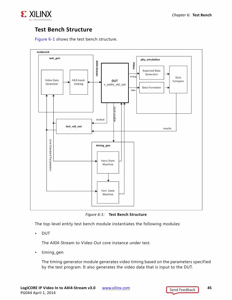
Test Bench StructureFigure 6-1 shows the test bench structure.
The top-level entity test bench module instantiates the following modules:
• DUT
The AXI4-Stream to Video Out core instance under test.
• timing_gen
The timing generator module generates video timing based on the parameters specified by the test program. It also generates the video data that is input to the DUT.
X-Ref Target - Figure 6-1
Figure 6-1: Test Bench Structure
Send Feedback

LogiCORE IP Video In to AXI4-Stream v3.0 www.xilinx.com 46PG044 April 1, 2014
Chapter 6: Test Bench
• axis_gen
AXI4-Stream generator. This module generates the video timing based on the parameters specif ied by the test program. It also emulates the AXI4-Stream master bus which interfaces to the DUT.
• test_vid_out
The test program. This program controls the operation of the test bench
• phy_emulation
The video PHY emulator simulates the video PHY interface driven by the DUT. It generates handshaking, and receives data from the core. It also generates expected values and compares these to incoming video data. Based on the syncs and blanks from the DUT, it creates an expected data value, and compares this to the incoming video.
Send Feedback

LogiCORE IP Video In to AXI4-Stream v3.0 www.xilinx.com 47PG044 April 1, 2014
Appendix A
Verification, Compliance, and Interoperability
SimulationA test bench incorporating randomization of timing parameters was used to test the AXI4-Stream to Data out Core. Testing included the following:
• Testing with multiple frames of data with many different timing parameters and frame sizes.
• Testing for locking in both slave and master timing modes.
• Testing of locking, and re-locking after input interruption and line standard changes.
In addition to stand alone simulation, simulation was done on a pass-through video system consisting of the AXI4-Stream to Video out core in a system with the Video to AXI4-Stream Core and the VTC.
Hardware TestingThe AXI4-Stream to Video Out core has been validated in hardware using a complete pass through design with an external HDMI video source as an input, and an HDMI video display to verify the output. Output re-synchronization was tested by removing and re-applying the video source multiple times.
InteroperabilityThe AXI4-Stream input interface is compatible with any video processing block that implements the Video Over AXI4-Stream protocol.
The video output is compatible with digital video PHYs such as DVI that accept data in the format provided: Component video data, syncs, blanks, and data valid. With the addition of
Send Feedback

LogiCORE IP Video In to AXI4-Stream v3.0 www.xilinx.com 48PG044 April 1, 2014
Appendix A: Verification, Compliance, and Interoperability
additional sync embed logic external to the core, it can also interface with many other digital standards such as HDMI and SDI.
Send Feedback

LogiCORE IP Video In to AXI4-Stream v3.0 www.xilinx.com 49PG044 April 1, 2014
Appendix B
Migrating and UpgradingThis appendix contains information about migrating from an ISE design to the Vivado Design Suite, and for upgrading to a more recent version of the IP core. For customers upgrading their IP core, important details (where applicable) about any port changes and other impact to user logic are included.
Migrating to the Vivado Design SuiteFor information about migration to Vivado Design Suite, see ISE to Vivado Design Suite Migration Guide (UG911) [Ref 5].
Upgrading in Vivado Design SuiteThis section provides information about any changes to the user logic or port designations that take place when you upgrade to a more current version of this IP core in the Vivado Design Suite.
Version 3.0 supports IP upgrade from version 2.01.a. It has the following changes from version 2.01.a:
Parameter ChangesThe Pixels Per Clock parameter has been added. The default for this parameter is 1. With the default value, the port widths do not change from the earlier version.
Port ChangesChanged the following signal names:
• vid_out_clk to vid_io_out_clk
• video_de to vid_active_video
• video_vsync to vid_vaync
• video_hsync to vdi_hsync
Send Feedback

LogiCORE IP Video In to AXI4-Stream v3.0 www.xilinx.com 50PG044 April 1, 2014
Appendix B: Migrating and Upgrading
• video_vblank to vid_vblank
• video_hblank to vid_hblank
• video_data to vid_data
• vtg_act_vid to vtg_active_video
Added interlace support and the following signals. Each input port has a default setting for progressive video:
• vid_io_out_ce input default = 1
• f id input default = 0
• vtg_field_id input default = 0
• vid_field_id output
The signal fsync was removed.
Because of the port differences, v3.0 is not directly compatible with the previous version.
Other ChangesIn the customization GUI, combined the video format options "Sensor" and "Luma Only" to single "Mono / Sensor" video format option.
Send Feedback

LogiCORE IP Video In to AXI4-Stream v3.0 www.xilinx.com 51PG044 April 1, 2014
Appendix C
DebuggingThis appendix includes details about resources available on the Xilinx Support website and debugging tools.
Finding Help on Xilinx.comTo help in the design and debug process when using the Video In to AXI4-Stream, the Xilinx Support web page (www.xilinx.com/support) contains key resources such as product documentation, release notes, answer records, information about known issues, and links for opening a Technical Support Web Case.
DocumentationThis product guide is the main document associated with the Video In to AXI4-Stream. This guide, along with documentation related to all products that aid in the design process, can be found on the Xilinx Support web page (www.xilinx.com/support) or by using the Xilinx Documentation Navigator.
Download the Xilinx Documentation Navigator from the Design Tools tab on the Downloads page (www.xilinx.com/download). For more information about this tool and the features available, open the online help after installation.
Answer RecordsAnswer Records include information about commonly encountered problems, helpful information on how to resolve these problems, and any known issues with a Xilinx product. Answer Records are created and maintained daily ensuring that users have access to the most accurate information available.
Answer Records for this core are listed below, and can also be located by using the Search Support box on the main Xilinx support web page. To maximize your search results, use proper keywords such as
• Product name
• Tool message(s)
• Summary of the issue encountered
Send Feedback

LogiCORE IP Video In to AXI4-Stream v3.0 www.xilinx.com 52PG044 April 1, 2014
Appendix C: Debugging
A filter search is available after results are returned to further target the results.
Answer Records for the AXI4-Stream to Video Out Core
AR 54517
Contacting Technical SupportXilinx provides technical support at www.xilinx.com/support for this LogiCORE™ IP product when used as described in the product documentation. Xilinx cannot guarantee timing, functionality, or support of product if implemented in devices that are not defined in the documentation, if customized beyond that allowed in the product documentation, or if changes are made to any section of the design labeled DO NOT MODIFY.
Xilinx provides premier technical support for customers encountering issues that require additional assistance.
To contact Xilinx Technical Support:
1. Navigate to www.xilinx.com/support.
2. Open a WebCase by selecting the WebCase link located under Support Quick Links.
When opening a WebCase, include:
• Target FPGA including package and speed grade.
• All applicable Xilinx Design Tools and simulator software versions.
• A block diagram of the video system that explains the video source, destination and IP (custom and Xilinx) used.
• Additional f iles based on the specif ic issue might also be required. See the relevant sections in this debug guide for guidelines about which f ile(s) to include with the WebCase.
Note: Access to WebCase is not available in all cases. Please login to the WebCase tool to see your specif ic support options.
Debug ToolsThere are many tools available to address AXI4-Stream to Video Out design issues. It is important to know which tools are useful for debugging various situations.
Send Feedback

LogiCORE IP Video In to AXI4-Stream v3.0 www.xilinx.com 53PG044 April 1, 2014
Appendix C: Debugging
Example DesignThe AXI4-Stream to Video Out core is used in several reference designs and application notes. Information about the example designs can be found in Chapter 6, Example Design for the Vivado™ Design Suite.
Vivado Lab EditionVivado® Lab Edition inserts logic analyzer and virtual I/O cores directly into your design. Vivado Lab Edition also allows you to set trigger conditions to capture application and integrated block port signals in hardware. Captured signals can then be analyzed. This feature in the Vivado IDE is used for logic debugging and validation of a design running in Xilinx.
The Vivado logic analyzer is used to interact with the logic debug LogiCORE IP cores, including:
• ILA 2.0 (and later versions)
• VIO 2.0 (and later versions)
Hardware DebugHardware issues can range from link bring-up to problems seen after hours of testing. This section provides debug steps for common issues. The Vivado Lab Tools is a valuable resource to use in hardware debug. The signal names mentioned in the following individual sections can be probed using the Vivado Lab Tools for debugging the specif ic problems.
Many of these common issues can also be applied to debugging design simulations. Details are provided on:
General Checks
General ChecksEnsure that all the timing constraints for the core were properly incorporated from the example design and that all constraints were met during implementation.
• Does it work in post-place and route timing simulation? If problems are seen in hardware but not in timing simulation, this could indicate a PCB issue. Ensure that all clock sources are active and clean.
• If using MMCMs in the design, ensure that all MMCMs have obtained lock by monitoring the LOCKED port.
• If your outputs go to 0, check your licensing.
Send Feedback

LogiCORE IP Video In to AXI4-Stream v3.0 www.xilinx.com 54PG044 April 1, 2014
Appendix C: Debugging
Interface Debug
AXI4-Stream InterfacesTable C-1 describes how to troubleshoot the AXI4-Stream interface.
If the AXI4-Stream communication is healthy, but the data seems corrupted, the next step is to f ind the correct configuration for this core.
Other InterfacesTable C-2 describes how to troubleshoot third-party interfaces.
Table C-1: Troubleshooting AXI4-Stream Interface
Symptom Solution
s_axis_video_tready stuck low, the upstream core cannot send data.
The tready signal is only de-asserted when the FIFO is almost full. This means it is not being read, or not read fast enough. In master mode, is the core receiving Active-High vsync, vblank, hsync, hblank and active_video signals from the VTC
No video is coming out. All of the video outputs are stuck LOW.
Video data and timing signal output is disabled until the output synchronization section is locked, as indicated by the locked signal. Outputs will become valid following the start of the field after locked asserts HIGH.Check that all video signals are present and active high from the VTC: vtg_vsync, vtg_hsync, vtg_vbalnk, vtg_hblank, vtg_active_video. In master timing mode, these will free run. In slave timing mode, they may be irregular due to the locking action during initialization. The output vtg_ce can be checked to see if the VTC is being stalled by the AXI4-Stream to Video out core.
Table C-2: Troubleshooting Third-Party Interfaces
Symptom Solution
Severe color distortion or color-swap when interfacing to third-party video IP.
Verify that the color component logical addressing on the AXI4-Stream TDATA signal is in according to Data Interface in Chapter 2. If misaligned: In HDL, break up the TDATA vector to constituent components and manually connect the slave and master interface sides.
Severe color distortion or color-swap when processing video written to external memory using the AXI-VDMA core.
Unless the particular software driver was developed with the AXI4-Stream TDATA signal color component assignments described in Data Interface in Chapter 2 in mind, there are no guarantees that the software correctly identif ies bits corresponding to color components. Verify that the color component logical addressing TDATA is in alignment with the data format expected by the software drivers reading/writing external memory. If misaligned: In HDL, break up the TDATA vector to constituent components, and manually connect the slave and master interface sides.
Send Feedback

LogiCORE IP Video In to AXI4-Stream v3.0 www.xilinx.com 55PG044 April 1, 2014
Appendix D
Additional Resources and Legal Notices
Xilinx ResourcesFor support resources such as Answers, Documentation, Downloads, and Forums, see Xilinx Support.
http://For a glossary of technical terms used in Xilinx documentation, see the Xilinx Glossary.
http://For a comprehensive listing of Video and Imaging application notes, white papers, reference designs and related IP cores, see the Video and Imaging Resources page at:
http://www.xilinx.com/esp/video/refdes_listing.htm#ref_des.
ReferencesThese documents provide supplemental material useful with this user guide:
1. Synthesis and Simulation Design Guide (UG626)
2. Creating a Video Design From Scratch Tutorial from Avnet Electronics.https://www.em.avnet.com/Support%20And%20Downloads/FMC_IMAGEON_Building_Video_Design_Tutorial_14_4_20130110.zip
3. Bridging Xilinx Streaming Video Interface with AXI4-Stream Protocol (XAPP521)
4. AXI Reference Guide (UG761)
5. ISE to Vivado Design Suite Migration Guide (UG911)
6. Vivado Design Suite User Guide: Designing with IP (UG896)
7. Video Timing Controller Product Guide (PG016)
8. Vivado Design Suite User Guide: Logic Simulation (UG900)
9. Vivado Design Suite User Guide: Programming and Debugging (UG908)
10. Vivado Design Suite User Guide: Getting Started (UG910)
Send Feedback

LogiCORE IP Video In to AXI4-Stream v3.0 www.xilinx.com 56PG044 April 1, 2014
Appendix D: Additional Resources and Legal Notices
11. AXI4-Stream Video IP and System Design Guide (UG934)
12. Vivado Design Suite User Guide: Designing IP Subsystems Using IP Integrator (UG994)
Revision HistoryThe following table shows the revision history for this document.
Please Read: Important Legal NoticesThe information disclosed to you hereunder (the "Materials") is provided solely for the selection and use of Xilinx products. To the maximum extent permitted by applicable law: (1) Materials are made available "AS IS" and with all faults, Xilinx hereby DISCLAIMS ALL WARRANTIES AND CONDITIONS, EXPRESS, IMPLIED, OR STATUTORY, INCLUDING BUT NOT LIMITED TO WARRANTIES OF MERCHANTABILITY, NON-INFRINGEMENT, OR FITNESS FOR ANY PARTICULAR PURPOSE; and (2) Xilinx shall not be liable (whether in contract or tort, including negligence, or under any other theory of liability) for any loss or damage of any kind or nature related to, arising under, or in connection with, the Materials (including your use of the Materials), including for any direct, indirect, special, incidental, or consequential loss or damage (including loss of data, profits, goodwill, or any type of loss or damage suffered as a result of any action brought by a third party) even if such damage or loss was reasonably foreseeable or Xilinx had been advised of the possibility of the same. Xilinx assumes no obligation to correct any errors contained in the Materials or to notify you of updates to the Materials or to product specifications. You may not reproduce, modify, distribute, or publicly display the Materials without prior written consent. Certain products are subject to the terms and conditions of Xilinx's limited warranty, please refer to Xilinx's Terms of Sale which can be viewed at http://www.xilinx.com/legal.htm#tos; IP cores may be subject to warranty and support terms contained in a license issued to you by Xilinx. Xilinx products are not designed or intended to be fail-safe or for use in any application requiring fail-safe performance; you assume sole risk and liability for use of Xilinx products in such critical applications, please refer to Xilinx's Terms of Sale which can be viewed at http://www.xilinx.com/legal.htm#tos.© Copyright 2012-2014 Xilinx, Inc. Xilinx, the Xilinx logo, Artix, ISE, Kintex, Spartan, Virtex, Vivado, Zynq, and other designated brands included herein are trademarks of Xilinx in the United States and other countries. All other trademarks are the property of their respective owners.
Date Version Revision
04/01/2014 3.0 Added support for multiple pixels per clock.
12/18/2013 3.0 Added UltraScale Architecture support.
10/02/2013 3.0 Synch document version with core version. Updated Constraints and Migration chapters.
03/20/2013 4.0 Updated for core version. Removed ISE chapters. Updated Debugging appendix. Updated Core Interfaces. Updated Designing with the Core chapter.
10/16/2012 3.0 Updated for core version. Updated for ISE v14.3 and Vivado v2012.3. Added Vivado test bench.
07/25/2012 2.0 Updated for core version. Added Vivado information.
04/24/2012 1.0 Initial Xilinx release of core.
Send Feedback
![AXI4-Stream FIFO v4 - All Programmable · PDF fileWhen using AXI4-Stream FIFO core with the AXI Ethernet core, ... [Ref 4]. The AXI4-Stream FIFO core uses one clock from the AXI4-Lite](https://img.dokumen.tips/doc/110x75/5ab6f6607f8b9a1a048e67de/axi4-stream-fifo-v4-all-programmable-using-axi4-stream-fifo-core-with-the-axi.jpg)