Embed Size (px)
Citation preview
1
Logic Solutionsfor IEEE Std 1284
SCEA013June 1999

IMPORTANT NOTICE
Texas Instruments and its subsidiaries (TI) reserve the right to make changes to their productsor to discontinue any product or service without notice, and advise customers to obtain the latestversion of relevant information to verify, before placing orders, that information being relied onis current and complete. All products are sold subject to the terms and conditions of sale suppliedat the time of order acknowledgement, including those pertaining to warranty, patentinfringement, and limitation of liability.
TI warrants performance of its semiconductor products to the specifications applicable at thetime of sale in accordance with TI’s standard warranty. Testing and other quality controltechniques are utilized to the extent TI deems necessary to support this warranty. Specific testingof all parameters of each device is not necessarily performed, except those mandated bygovernment requirements.
CERTAIN APPLICATIONS USING SEMICONDUCTOR PRODUCTS MAY INVOLVEPOTENTIAL RISKS OF DEATH, PERSONAL INJURY, OR SEVERE PROPERTY ORENVIRONMENTAL DAMAGE (“CRITICAL APPLICATIONS”). TI SEMICONDUCTORPRODUCTS ARE NOT DESIGNED, AUTHORIZED, OR WARRANTED TO BE SUITABLE FORUSE IN LIFE-SUPPORT DEVICES OR SYSTEMS OR OTHER CRITICAL APPLICATIONS.INCLUSION OF TI PRODUCTS IN SUCH APPLICATIONS IS UNDERSTOOD TO BE FULLYAT THE CUSTOMER’S RISK.
In order to minimize risks associated with the customer’s applications, adequate design andoperating safeguards must be provided by the customer to minimize inherent or proceduralhazards.
TI assumes no liability for applications assistance or customer product design. TI does notwarrant or represent that any license, either express or implied, is granted under any patent right,copyright, mask work right, or other intellectual property right of TI covering or relating to anycombination, machine, or process in which such semiconductor products or services might beor are used. TI’s publication of information regarding any third party’s products or services doesnot constitute TI’s approval, warranty or endorsement thereof.
Copyright 1999, Texas Instruments Incorporated

iii
ContentsTitle Page
Abstract 1. . . . . . . . . . . . . . . . . . . . . . . . . . . . . . . . . . . . . . . . . . . . . . . . . . . . . . . . . . . . . . . . . . . . . . . . . . . . . . . . . . . . . . . . . . .
Introduction 1. . . . . . . . . . . . . . . . . . . . . . . . . . . . . . . . . . . . . . . . . . . . . . . . . . . . . . . . . . . . . . . . . . . . . . . . . . . . . . . . . . . . . . .
Brief Overview of IEEE Std 1284 1. . . . . . . . . . . . . . . . . . . . . . . . . . . . . . . . . . . . . . . . . . . . . . . . . . . . . . . . . . . . . . . . . . . . . . Purpose and Benefits of IEEE Std 1284 1. . . . . . . . . . . . . . . . . . . . . . . . . . . . . . . . . . . . . . . . . . . . . . . . . . . . . . . . . . . . . . IEEE Std 1284 Data Transfer Modes 2. . . . . . . . . . . . . . . . . . . . . . . . . . . . . . . . . . . . . . . . . . . . . . . . . . . . . . . . . . . . . . . . IEEE Std 1284 Driver Specification 2. . . . . . . . . . . . . . . . . . . . . . . . . . . . . . . . . . . . . . . . . . . . . . . . . . . . . . . . . . . . . . . . IEEE Std 1284 Connectors 2. . . . . . . . . . . . . . . . . . . . . . . . . . . . . . . . . . . . . . . . . . . . . . . . . . . . . . . . . . . . . . . . . . . . . . . .
Device Information 6. . . . . . . . . . . . . . . . . . . . . . . . . . . . . . . . . . . . . . . . . . . . . . . . . . . . . . . . . . . . . . . . . . . . . . . . . . . . . . . . . Features and Benefits 8. . . . . . . . . . . . . . . . . . . . . . . . . . . . . . . . . . . . . . . . . . . . . . . . . . . . . . . . . . . . . . . . . . . . . . . . . . . . Performance Comparison 9. . . . . . . . . . . . . . . . . . . . . . . . . . . . . . . . . . . . . . . . . . . . . . . . . . . . . . . . . . . . . . . . . . . . . . . . .
Application Information 13. . . . . . . . . . . . . . . . . . . . . . . . . . . . . . . . . . . . . . . . . . . . . . . . . . . . . . . . . . . . . . . . . . . . . . . . . . . . Why the IEEE Std 1284 Driver is Needed 13. . . . . . . . . . . . . . . . . . . . . . . . . . . . . . . . . . . . . . . . . . . . . . . . . . . . . . . . . . . IEEE Std 1284 Parallel-Port Solutions Using TI Bus-Interface Devices 14. . . . . . . . . . . . . . . . . . . . . . . . . . . . . . . . . . .
Conclusion 17. . . . . . . . . . . . . . . . . . . . . . . . . . . . . . . . . . . . . . . . . . . . . . . . . . . . . . . . . . . . . . . . . . . . . . . . . . . . . . . . . . . . . . .
Acknowledgment 18. . . . . . . . . . . . . . . . . . . . . . . . . . . . . . . . . . . . . . . . . . . . . . . . . . . . . . . . . . . . . . . . . . . . . . . . . . . . . . . . . .
Commonly Asked Questions 18. . . . . . . . . . . . . . . . . . . . . . . . . . . . . . . . . . . . . . . . . . . . . . . . . . . . . . . . . . . . . . . . . . . . . . . . .
Glossary 18. . . . . . . . . . . . . . . . . . . . . . . . . . . . . . . . . . . . . . . . . . . . . . . . . . . . . . . . . . . . . . . . . . . . . . . . . . . . . . . . . . . . . . . . .
List of IllustrationsFigure Title Page
1. IEEE Std 1284-A (Host) to IEEE Std 1284-B (Peripheral) Wiring Diagram 3. . . . . . . . . . . . . . . . . . . . . . . . . . . . . . .
2. IEEE Std 1284-A (Host) to IEEE Std 1284-C (Peripheral) Wiring Diagram 4. . . . . . . . . . . . . . . . . . . . . . . . . . . . . . .
3. IEEE Std 1284-C (Host) to IEEE Std 1284-C (Peripheral) Wiring Diagram 5. . . . . . . . . . . . . . . . . . . . . . . . . . . . . . .
4. Pinout of SN54/SN74ACT1284 6. . . . . . . . . . . . . . . . . . . . . . . . . . . . . . . . . . . . . . . . . . . . . . . . . . . . . . . . . . . . . . . . .
5. Pinout of SN74LV161284 and SN74LVC161284 7. . . . . . . . . . . . . . . . . . . . . . . . . . . . . . . . . . . . . . . . . . . . . . . . . . . .
6. Test Setup for Back-Driving Current 9. . . . . . . . . . . . . . . . . . . . . . . . . . . . . . . . . . . . . . . . . . . . . . . . . . . . . . . . . . . . .
7. Back-Driving Current for LVC161284 for B1 to B8. (VCC = VCCCABLE = 5 V to 0 V) 10. . . . . . . . . . . . . . . . . . .
8. Back-Driving Current for Competitor’s 161284 for B1 to B8. (VCC = VCCCABLE = 5 V to 0 V) 10. . . . . . . . . . . .
9. Back-Driving Current for LVC161284 for C14 to C17. (VCC = VCCCABLE = 5 V to 0 V) 11. . . . . . . . . . . . . . . . .
10. Back-Driving Current for Competitor’s 161284 for C14 to C17. (VCC = VCCCABLE = 5 V to 0 V) 11. . . . . . . . . .
11. Pre-IEEE Std 1284 Parallel-Port Host Solution 13. . . . . . . . . . . . . . . . . . . . . . . . . . . . . . . . . . . . . . . . . . . . . . . . . . . . 12. Block Diagram of Parallel Interface Port Between the PC and Peripheral 14. . . . . . . . . . . . . . . . . . . . . . . . . . . . . . . .
13. IEEE Std 1284 Host Solution Using Two SN74ACT1284 Devices 14. . . . . . . . . . . . . . . . . . . . . . . . . . . . . . . . . . . . .
14. IEEE Std 1284 Peripheral Solution Using Two SN74ACT1284 Devices 15. . . . . . . . . . . . . . . . . . . . . . . . . . . . . . . .
15. IEEE Std 1284 Host Solution Using the SN74LV161284 or SN74LVC161284 16. . . . . . . . . . . . . . . . . . . . . . . . . . .
16. IEEE Std 1284 Peripheral Solution Using the SN74LV161284 or SN74LV161284 17. . . . . . . . . . . . . . . . . . . . . . . .
List of TablesTable Title Page
1. Function Table for SN74ACT1284 7. . . . . . . . . . . . . . . . . . . . . . . . . . . . . . . . . . . . . . . . . . . . . . . . . . . . . . . . . . . . . . .
2. Function Table for SN74LV161284 and SN74LVC161284 7. . . . . . . . . . . . . . . . . . . . . . . . . . . . . . . . . . . . . . . . . . . .
3. Features and Benefits of the SN74ACT1284 8. . . . . . . . . . . . . . . . . . . . . . . . . . . . . . . . . . . . . . . . . . . . . . . . . . . . . . .
4. Features and Benefits of the SN74LV161284 and SN74LVC161284 8. . . . . . . . . . . . . . . . . . . . . . . . . . . . . . . . . . . . .
5. Comparisons of Device Characteristics 12. . . . . . . . . . . . . . . . . . . . . . . . . . . . . . . . . . . . . . . . . . . . . . . . . . . . . . . . . . .

iv

1
Abstract
Since the creation of IEEE Std 1284, designers have been using this signaling method to interface between the personalcomputer and peripheral devices. Bulky discrete components, such as termination and pullup resistors and capacitors, wereused extensively. To integrate into single-chip solutions that comply with IEEE Std 1284, Texas Instruments (TI ) offersthree bus-interface devices that provide board-area savings and flexible level-type selection.
Introduction
This application report presents a brief overview of IEEE Std 1284-1994, provides information on each device availablefrom TI that is a bus-interface solution for this standard, and discusses how to use the devices in applications. TI offers theSN74ACT1284, which is a 7-bit bus-interface transceiver, and the SN74LVC161284 and SN74LV161284, which are 19-bitbus-interface transceivers, as discrete IEEE Std 1284 bus-interface solutions.
Brief Overview of IEEE Std 1284
IEEE Std 1284, “Standard Signaling Method for a Bidirectional Parallel Peripheral Interface for Personal Computers,” isa high-speed, high-integrity parallel-port method for a bidirectional peripheral interface for personal computers. Thisstandard was developed to provide an open path for communications between computers and peripherals. Furthermore, itrecommends new electrical interfaces, cabling, and interface hardware that provides improved performance, while retainingbackward compatibility.
Purpose and Benefits of IEEE Std 1284
With increased technology development in the personal computer (PC), a need for improved parallel-port performance hasemerged. Pre-existing methods used a wide variety of hardware and software products, each with unique and incompatiblesignaling schemes. Using existing parallel-port architecture, the maximum data transfer rate is about 150 kbyte/s, andexternal cables are limited to 6 feet.
IEEE Std 1284 was created because of the need for an existing defined standard for bidirectional parallel communicationbetween the PC and printing peripherals. Being backward compatible with the old Centronics specifications, this standardoffers more functionality and performance for new PC and peripheral products. Data rates are increased to greater than1Mbyte/s and maximum cable length is increased to 32 feet for the defined cable type.
TI is a trademark of Texas Instruments Incorporated.

2
IEEE Std 1284 Data Transfer Modes
IEEE Std 1284 defines five modes of data transfer. Not all modes are required in all peripherals; forward is defined as datatransfer from host to peripheral, and reverse is defined as data transfer from peripheral to host. The bidirectional modeprovides both forward and reverse transfer mode within the same operational mode. The modes are:
• Compatibility Mode: This is the basic mode of operation for all parallel communications. It is asynchronous, bytewide, forward direction, and offers 50-kbyte/s to 150-kbyte/s data-transfer rate.
• Nibble Mode: This asynchronous, reverse-channel mode provides two sequential, 4-bit nibbles to the host. It isused with the compatibility mode to implement a bidirectional channel. The data transfer rate is the same as inthe compatibility mode.
• Byte Mode: This mode allows the transfer of data in the reverse direction if the data lines are bidirectional. Thedata transfer rate is the same as in the compatibility and nibble modes.
• Enhanced Parallel Port (EPP): This mode allows high-speed transfers of bytes in either direction. EPP is ideal forreal-time-controlled peripherals, such as network adapters, data acquisition, portable hard drives, and otherdevices.
• Extended Capabilities Port (ECP): The ECP protocol was proposed as an advanced mode for communication withprinter and scanner peripherals. Like the EPP protocol, ECP provides a high-performance, bidirectionalcommunication path between the host and peripheral. ECP and EPP modes are ten times faster than thecompatibility, nibble, and byte modes.
IEEE Std 1284 Driver Specification
IEEE Std 1284 specifies characteristics of parallel-port drivers and receivers, and describes two types of interfaces:
• Level I (open drain): Level I devices are designed to be consistent with the pre-existing installed devices.Applications using Level I should not be operated in the high-speed advanced modes, but should take advantageof reverse-channel capabilities of the standard.
• Level II (totem pole): Level II devices have stronger drivers and inputs with hysteresis. They are designed tooperate in the advanced mode where a longer cable and higher data rates prevail. Level II offers betterperformance, while remaining compatible with the original interface.
IEEE Std 1284 Connectors
Three interface connectors defined in IEEE Std 1284 are:
• IEEE Std 1284-A: This is the existing DB25 connector, used primarily on the host side.
• IEEE Std 1284-B: This is the existing 36-pin, 0.085-inch centerline connector, used only on the peripheral side.
• IEEE Std 1284-C: This connector is a new 36-pin, 0.050-inch centerline connector recommended byIEEE Std 1284 that is used on both host and peripheral sides.
Since A- and B-type connectors do not have the same number of pins, Figures 1 and 2 detail pin connections forcommunication between the PC and peripheral. These connections (A host and B peripheral; A host and C peripheral) arethe most commonly accepted in the industry.
As recommended in IEEE Std 1284, using the C-type connector on both host and peripheral sides provides a high-speed,high-integrity parallel port for reliable bidirectional communication. Figure 3 shows the straightforward connectionbetween the two ports.

3
PError
HostIEEE Std 1284-A
PeripheralIEEE Std 1284-B
1 1nStrobe
Data 1
Data 2
Data 3
Data 4
Data 5
Data 6
Data 7
Data 8
nAck
Busy
Select
nAutoFd
nlnit
nFault
Signal Ground (nStrobe)
Signal Ground (Data 1, Data 2)
Signal Ground (Data 3, Data 4)
Signal Ground (Data 5, Data 6)
Signal Ground (Data 7, Data 8)
Signal Ground (Busy, nFault)
Signal Ground (Data 1)
Signal Ground (nStrobe)
Signal Ground (Data 2)
Signal Ground (Data 3)
Signal Ground (Data 4)
Signal Ground (Data 5)
Signal Ground (Data 6)
Signal Ground (Data 7)
Signal Ground (Data 8)
Signal Ground (PError, Select, nAck)
Signal Ground (Busy, nFault)
Signal Ground (nAutoFd, nSelectin, nlnit) Signal Ground (nAutoFd, nSelectin, nlnit)
nlnit
nFault
nSelectin
nStrobe
Data 2
Data 3
Data 4
Data 5
Data 6
Data 7
Data 8
nAck
Busy
PError
Chassis Ground
Select
Peripheral Logic High
Logic Ground
19
20
3
21
4
22
5
23
6
24
7
25
8
26
9
27
10
28
11
29
12
17
13
15
14
30
31
33
32
34
36
35
18
16
18
2
19
3
4
20
5
6
21
7
8
22
9
10
24
11
23
12
13
14
25
16
15
17
Shield Shield
nSelectin
NC–
NC–
NC–
NC–
NC–
NC–
Pin Pin
Not Defined
Not Defined
Not Defined
Not Defined
nAutoFd
2
NC–
Signal Ground (PError, Select, nAck)
Data 1
Figure 1. IEEE Std 1284-A (Host) to IEEE Std 1284-B (Peripheral) Wiring Diagram

4
PError
HostIEEE Std 1284-A
PeripheralIEEE Std 1284-C
11 1
nStrobe
Data 1
Data 2
Data 3
Data 4
Data 5
Data 6
Data 7
Data 8
nAutoFd
nlnit
nFault
Signal Ground (nStrobe)
Signal Ground (Data 1, Data 2)
Signal Ground (Data 3, Data 4)
Signal Ground (Data 5, Data 6)
Signal Ground (Data 7, Data 8)
Signal Ground (Busy, nFault)
Signal Ground (Data 1)
Signal Ground (Busy)
Signal Ground (Data 2)
Signal Ground (Data 3)
Signal Ground (Data 4)
Signal Ground (Data 5)
Signal Ground (Data 6)
Signal Ground (Data 7)
Signal Ground (Data 8)
Signal Ground (Select)
Signal Ground (nFault)
Signal Ground (nAutoFd, nSelectin, nlnit)
Data 2
Data 3
Data 4
Data 5
Data 6
Data 7
Data 8
nAck
Busy
PError
Peripheral Logic High
19
20
3
21
4
22
5
23
6
24
7
25
8
26
9
27
10
28
11
29
12
30
13
31
14
32
15
33
1634
17
35
18
36
10
24
15
12
2
19
3
4
20
5
6
21
7
8
22
23
9
16
1
18
1725
14
Shield Shield
Pin Pin
nAutoFd
2
Busy
Select
nAck
Signal Ground (PError, Select, nAck)
nSelectin
13 Select
Signal Ground (nAck)
nFault
Signal Ground (PError)
Data 1
nlnit
nStrobe
Signal Ground (nStrobe)
Signal Ground (nlnit)
nSelectinSignal Ground (nSelectin)
Signal Ground (nAutoFd)
Host Logic High
Figure 2. IEEE Std 1284-A (Host) to IEEE Std 1284-C (Peripheral) Wiring Diagram

5
HostIEEE Std 1284-C
PeripheralIEEE Std 1284-C
1
Signal Ground (Data 1)
Signal Ground (Busy)
Signal Ground (Data 2)
Signal Ground (Data 3)
Signal Ground (Data 4)
Signal Ground (Data 5)
Signal Ground (Data 6)
Signal Ground (Data 7)
Signal Ground (Data 8)
Signal Ground (Select)
Signal Ground (nFault)
Data 2
Data 3
Data 4
Data 5
Data 6
Data 7
Data 8
nAck
Busy
PError
Peripheral Logic High
19
20
3
21
4
22
5
23
6
24
7
25
8
26
9
27
10
28
11
29
12
30
13
31
14
32
15
33
1634
17
35
18
36
Shield
Pin
nAutoFd
2 Select
Signal Ground (nAck)
nFault
Signal Ground (PError)
Data 1
nlnit
nStrobe
Signal Ground (nStrobe)
Signal Ground (nlnit)
nSelectinSignal Ground (nSelectin)
Signal Ground (nAutoFd)
Host Logic High
Signal Ground (Data 1)
Signal Ground (Busy)
Signal Ground (Data 2)
Signal Ground (Data 3)
Signal Ground (Data 4)
Signal Ground (Data 5)
Signal Ground (Data 6)
Signal Ground (Data 7)
Signal Ground (Data 8)
Signal Ground (Select)
Signal Ground (nFault)
Data 2
Data 3
Data 4
Data 5
Data 6
Data 7
Data 8
nAck
Busy
PError
Peripheral Logic High
nAutoFd
Select
Signal Ground (nAck)
nFault
Signal Ground (PError)
Data 1
nlnit
nStrobe
Signal Ground (nStrobe)
Signal Ground (nlnit)
nSelectinSignal Ground (nSelectin)
Signal Ground (nAutoFd)
Host Logic High
1
19
20
3
21
4
22
5
23
6
24
7
25
8
26
9
27
10
28
11
29
12
30
13
31
14
32
15
33
1634
17
35
18
36
Shield
Pin
2
Figure 3. IEEE Std 1284-C (Host) to IEEE Std 1284-C (Peripheral) Wiring Diagram

6
Device Information
TI offers three bus-driver solutions that comply with the IEEE Std 1284 specification: SN74ACT1284, SN74LVC161284,and SN74LV161284. These devices can be used in the ECP mode to provide an asynchronous, bidirectional, parallelperipheral interface for personal computers. These devices allow data transmission in the A-to-B direction or B-to-Adirection, depending on the logic level of the direction-control (DIR) pin. The output drive mode is determined by thehigh-drive (HD) control pin. HD enables the outputs (B and Y side only) to switch from open collector to totem pole. TheA side outputs have totem-pole outputs only. This meets the drive requirements as specified in the IEEE Std 1284-I (level-1type) and IEEE Std 1284-II (level-2 type) parallel peripheral-interface specifications. All these devices have two supplyvoltages, one for the cable side, and the other for the logic side. To reduce the chance of faulty signals being transferred overthe system’s parallel port, all these devices feature a finely tuned Output Edge-Rate Control (OEC ) circuit and anenhanced input hysteresis circuit.
The pinouts and function tables of these devices are given in Figures 4 and 5 and in Tables 1 and 2, respectively.
1
2
3
4
5
6
7
8
9
10
20
19
18
17
16
15
14
13
12
11
A1A2A3A4
GNDGND
A5A6A7
DIR
B1B2B3B4VCCVCCB5B6B7HD
SN54ACT1284 . . . J OR W PACKAGESN74ACT1284 . . . DB, DW, N, OR PW PACKAGE
(TOP VIEW)
3 2 1 20 19
9 10 11 12 13
4
5
6
7
8
18
17
16
15
14
B3B4VCCVCCB5
A4GNDGND
A5A6
SN54ACT1284 . . . FK PACKAGE(TOP VIEW)
A3
A2
A1
B7
B6
B2
A7
DIR HD
B1
Figure 4. Pinout of SN54/SN74ACT1284
OEC is a trademark of Texas Instruments Incorporated.

7
DGG OR DL PACKAGE(TOP VIEW)
1
2
3
4
5
6
7
8
9
10
11
12
13
14
15
16
17
18
19
20
21
22
23
24
48
47
46
45
44
43
42
41
40
39
38
37
36
35
34
33
32
31
30
29
28
27
26
25
HDA9
A10A11A12A13VCC
A1A2
GNDA3A4A5A6
GNDA7A8
VCCPERI LOGIC IN
A14A15A16A17
HOST LOGIC OUT
DIRY9Y10Y11Y12Y13VCC CABLEB1B2GNDB3B4B5B6GNDB7B8VCC CABLEPERI LOGIC OUTC14C15C16C17HOST LOGIC IN
Figure 5. Pinout of SN74LV161284 and SN74LVC161284
Table 1. Function Table for SN74ACT1284
INPUTSOUTPUT MODE
DIR HDOUTPUT MODE
L LOpen drain A to B: Bits 5, 6, 7
L LTotem pole B to A: Bits 1, 2, 3, 4
L H Totem pole B to A: Bits 1, 2, 3, 4 and A to B: Bits 5, 6, 7
H L Open drain A to B: Bits 1, 2, 3, 4, 5, 6, 7
H H Totem pole A to B: Bits 1, 2, 3, 4, 5, 6, 7
Table 2. Function Table for SN74LV161284 and SN74LVC161284
INPUTSOUTPUT MODE
DIR HDOUTPUT MODE
L LOpen drain A9–A13 to Y9–Y13 and PERI LOGIC IN to PERI LOGIC OUT
L LTotem pole B1–B8 to A1–A8 and C14–C17 to A14–A17
L H Totem pole B1–B8 to A1–A8, A9–A13 to Y9–Y13, PERI LOGIC IN to PERI LOGIC OUT, and C14–C17 to A14–A17
H LOpen drain A1–A8 to B1–B8, A9–A13 to Y9–Y13, and PERI LOGIC IN to PERI LOGIC OUT
H LTotem pole C14–C17 to A14–A17
H H Totem pole A1–A8 to B1–B8, A9–A13 to Y9–Y13, C14–C17 to A14–A17, and PERI LOGIC IN to PERI LOGIC OUT

8
Features and Benefits
Tables 3 and 4 summarize the features and corresponding benefits for three TI devices that are IEEE Std 1284 compliant.
Table 3. Features and Benefits of the SN74ACT1284
FEATURES BENEFITS
Flow-through architecture Optimizes printed circuit board layout
Center-pin VCC and GND configuration Minimizes high-speed switching noise
Software configurable to IEEE Std 1284-I (level-1 type) and IEEE Std 1284-II (level-2 type) electrical specifications
Easy level-type selection
A-to-B and B-to-A transmission for bits 1, 2, 3, and 4 Configurable data flow
Table 4. Features and Benefits of the SN74LV161284 AND SN74LVC161284
FEATURES BENEFITS
Integrated 1.4-kΩ pullup resistors on all open-drain cable-side outputs† Eliminates the need for discrete resistors
Software-configurable to IEEE Std 1284-I (level-1 type) and IEEE Std 1284-II (level-2 type) electrical specifications
Easy level-type selection
Flow-through architecture Optimizes printed circuit board layout
VCCCABLE from 3 V to 5.5 V, VCC from 3 V to 3.6 V (SN74LVC161284 only) Wide voltage range
4.5-V to 5.5-V VCC and VCCCABLE (SN74LV161284 only) Single supply
Eight bidirectional data bits, five cable drivers and four receivers Complete peripheral solution
Integrated PMOS transistors between VCC and cable-side data and receiver outputs‡ Avoids back-drive current
Integrated 33-Ω termination resistors to all cable-side outputs Eliminates the need for discrete resistors
Dedicated buffers for Peripheral Logic High and Host Logic High signals§ Complete peripheral solution
† Pullup resistors ensure operation with a Level I compatible device and provide sufficient voltage and timing margins as specified byIEEE Std 1284. In addition, the pullup resistors add margin for noisy cable environments.
‡ Avoiding back-drive current keeps the peripheral from being powered up by the host when the peripheral is off and allows for a 5-V system tobe connected to the cable side. Laboratory experiments using TI’s SN74LVC161284 and a competitor’s 1284 transceiver show how the twodevices compare, while simulating a typical PC-to-peripheral application. In this situation, a ’161284 is used on the peripheral.
§ Hosts and peripherals indicate their readiness to communicate by asserting Host Logic High and Peripheral Logic High, respectively. All hostsand peripherals with IEEE Std 1284-C connectors shall provide Host Logic High and Peripheral Logic High. Because devices withIEEE Std 1284-A or IEEE Std 1284-B connectors may or may not support Host Logic High or Peripheral Logic High, there are no reliable meansof initiating a transfer.

9
Performance Comparison
As the Super I/O transmits a high level to the peripheral via the cable, the ’161284 on the printer side receives the signalbecause it is configured as a receiver. In TI’s laboratory, the host PC side is simulated by driving +5 V to the ’161284 receiver.Any back-drive current is measured and plotted as the peripheral device is being powered down and is receiving a high-levelinput (H level). The experiment is repeated for the competitor’s part. Figure 6 shows the test setup. Results, plotted onFigures 7, 8, 9, and 10, show the superior performance of the TI SN74LVC161284 vs a competitor’s equivalent device.
Back-Drive Current
Printer: Power Down Host PC: Powered Up
VCC / VCCCABLE = 5 V to 0 V V CC = 5 V
H Level
’161284 ASIC
Printer: Receiver Host PC: Driver
DIR: L LevelHD: H to L (Connect V CC)
Back-Drive Current
C14 – C17
H Level
B1 – B8
Figure 6. Test Setup for Back-Driving Current

10
12
10
6
4
20
8
0 1 2 3
I –
mA
16
14
18
LVC161284VCC vs I I (B1–B8)
4 5 60
2
I
VCC – V
Figure 7. Back-Driving Current for LVC161284 for B1 to B8. (VCC = VCCCABLE = 5 V to 0 V)
14
12
8
6
4
10
0 1 2 3
I –
mA
18
16
20
4 5 6
2
0
I
Competitor’s 161284VCC vs I I (B1–B8)
VCC – V
Figure 8. Back-Driving Current for Competitor’s 161284 for B1 to B8.(VCC = VCCCABLE = 5 V to 0 V)

11
14
12
8
6
4
10
0 1 2 3
I –
mA
18
16
20
4 5 6
2
0
I
LVC161284VCC vs I I (C14–C17)
VCC – V
Figure 9. Back-Driving Current for LVC161284 for C14 to C17.(VCC = VCCCABLE = 5 V to 0 V)
14
12
8
6
4
10
0 1 2 3
I –
mA
18
16
20
4 5 6
2
0
I
Competitor’s 161284VCC vs I I (C14–C17)
VCC – V
Figure 10. Back-Driving Current for Competitor’s 161284 for C14 to C17.(VCC = VCCCABLE = 5 V to 0 V)
12
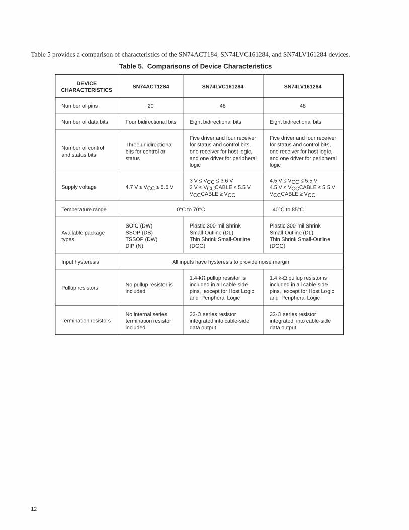
Table 5 provides a comparison of characteristics of the SN74ACT184, SN74LVC161284, and SN74LV161284 devices.
Table 5. Comparisons of Device Characteristics
DEVICECHARACTERISTICS
SN74ACT1284 SN74LVC161284 SN74LV161284
Number of pins 20 48 48
Number of data bits Four bidirectional bits Eight bidirectional bits Eight bidirectional bits
Number of control and status bits
Three unidirectionalbits for control orstatus
Five driver and four receiverfor status and control bits,one receiver for host logic,and one driver for peripherallogic
Five driver and four receiverfor status and control bits,one receiver for host logic,and one driver for peripherallogic
Supply voltage 4.7 V ≤ VCC ≤ 5.5 V3 V ≤ VCC ≤ 3.6 V3 V ≤ VCCCABLE ≤ 5.5 V VCCCABLE ≥ VCC
4.5 V ≤ VCC ≤ 5.5 V 4.5 V ≤ VCCCABLE ≤ 5.5 VVCCCABLE ≥ VCC
Temperature range 0°C to 70°C –40°C to 85°C
Available packagetypes
SOIC (DW)SSOP (DB)TSSOP (DW)DIP (N)
Plastic 300-mil Shrink Small-Outline (DL)Thin Shrink Small-Outline(DGG)
Plastic 300-mil ShrinkSmall-Outline (DL)Thin Shrink Small-Outline(DGG)
Input hysteresis All inputs have hysteresis to provide noise margin
Pullup resistorsNo pullup resistor isincluded
1.4-kΩ pullup resistor isincluded in all cable-sidepins, except for Host Logicand Peripheral Logic
1.4 k-Ω pullup resistor isincluded in all cable-sidepins, except for Host Logicand Peripheral Logic
Termination resistorsNo internal seriestermination resistorincluded
33-Ω series resistorintegrated into cable-sidedata output
33-Ω series resistorintegrated into cable-sidedata output

13
Application Information
Why the IEEE Std 1284 Driver is Needed
Before IEEE Std 1284, there was no defined electrical specification for driver, receiver, termination, and capacitancerequirements that required compatibility between devices. Host adapters and peripherals were built with different pullupvalues on the control lines, open-collectors or open-drains, and totem-pole drivers for the data and control lines. Often, upto 10,000-pF capacitors on the data and strobe lines were used. Figure 11 shows a typical pre-IEEE Std 1284 applicationhost solution. All capacitors and pullup and termination resistors are replaced by TI’s discrete integrated bus-interfacesolution (dashed box around components in Figure 11) that provides efficient designs of parallel-port communicationbetween the PC and peripheral.
SLCT
PE
BUSY
ACK
PD(7,0)
SLIN
INIT
ERROR
AFD
STB
1 kΩ
DB25
33 Ω
33 Ω
33 Ω
Replaced by discreteTI IEEE Std 1284 LogicSolutions
C
Figure 11. Pre-IEEE Std 1284 Parallel-Port Host Solution

14
IEEE Std 1284 Parallel-Port Solutions Using TI Bus-Interface Devices
Figure 12 is a basic block diagram of an IEEE Std 1284 parallel port. Only one SN74LV161284 or SN74LVC161284 is usedper side, but two SN74ACT1284 devices are required per port.
Host Peripheral
Super I/O’1284
Bus I/ODevice
ASIC’1284
Bus I/ODevice
Cable
IEEE Std 1284A, B, or C
Connectors
Figure 12. Block Diagram of Parallel Interface Port Between the PC and Peripheral
To illustrate how to apply the SN74ACT1284 as shown in Figure 12, Figures 13 and 14 explicitly show all data, control,and status lines from the Super I/O on the host side to the ASIC on the peripheral. The designer must decide which connectoris suitable for a particular application and to what level type to set the devices using the HD pin.
DIR
DIR
B1 – B4
2 Control
B5, B6, or B7
2 Control
4 Data
4 Data
B5, B6, or B7
B1 – B4
A5, A6, or A7
2 Control
4 Data
A1 – A4
A5, A6, or A7
2 Control
4 Data
A1 – A4
To Super I/OTo Peripheral
via IEEE Std 1284Connector and Cable
5 Status
SN74ACT1284
SN74ACT1284
Figure 13. IEEE Std 1284 Host Solution Using Two SN74ACT1284 Devices

15
DIR
DIR
B1 – B4
3 Status
B5, B6, or B7
2 Status
4 Data
B5 – B7
B1 – B4
A5, A6, or A7
2 Status
4 Data
A1 – A4
A5 – A7
3 Status
4 Data
A1 – A4
To ASICTo Host via
IEEE Std 1284Connector and
Cable
4 Control
SN74ACT1284
SN74ACT1284
4 Data
Figure 14. IEEE Std 1284 Peripheral Solution Using Two SN74ACT1284 Devices

16
While the SN74ACT1284 provides an acceptable two-chip solution, the SN74LV161284 and SN74LVC161284 devicesprovide optimum applicability––specifically, on the peripheral side. Figures 15 and 16 show all data, control, and status linesfrom the Super I/O on the host to the ASIC on the peripheral using these 19-bit bus interface devices.
Note that Host Logic In (pin 25) on the host side is connected via the IEEE Std 1284 connector and cable to Peri Logic Out(pin 30) on the peripheral. Likewise, Peri Logic Out (pin 30) on the host is connected the IEEE Std 1284 connector andcable to Host Logic In (pin 25) on the peripheral.
DIR
To Super I/O
To Peripheral viaIEEE Std 1284Connector and
Cable
SN74LV(C)161284
Host Logic Out (24)
Host LogicIn (25)
Peri Logic In (19)
Peri LogicOut (30)
A14 – A17
4 Control
A9, A10, A11,A12, or A13
8 Data
A1 – A8
4 Status
C14 – C17
4 Control
Y9, Y10, Y11, Y12, or Y13
8 Data
B1 – B8
4 Status
1 Status
Figure 15. IEEE Std 1284 Host Solution Using the SN74LV161284 or SN74LVC161284

17
DIR
To ASIC
To Host via IEEEStd 1284
Connector andCable
SN74LV(C)161284
Host Logic In (25)
Host LogicOut (24)
Peri Logic Out (30)
Peri LogicIn (19)
Y9 – Y13
4 Control
C14 – C17
8 Data
B1 – B8
5 Status
A9 – A13
4 Control
A14 – A17
8 Data
A1 – A8
5 Status
Figure 16. IEEE Std 1284 Peripheral Solution Using the SN74LV161284 or SN74LV161284
Conclusion
This report gives a brief description of IEEE Std 1284-1994 and TI’s logic solutions that conform to this standard. TI offersthe bus interface SN74ACT1284, SN74LVC161284, and SN74LV161284 devices as complete solutions for ahigh-performance parallel port, and, as shown by laboratory data, the ‘161284 devices offer superior performance inback-drive current generation when compared to the competition. Furthermore, this report guides designers in choosing thecorrect bus interface device in their IEEE Std 1284 applications.
Acknowledgment
The authors of this report are Nadira Sultana and Manny Soltero.

18
Commonly Asked Questions
1. How is the SN74LVC161284 used with a parallel port?
The Application Information section of this application report, in conjunction with Figures 15 and 16, explainshow to use the ’LVC161284 with the parallel port, whether it is on the host side or on the peripheral side.
2. If somebody wants an IEEE Std 1284 compliant design, is an IEEE Std 1284 transceiver required? What is so special about the SN74ACT1284, SN74LV161284, and SN74LVC161284?
To comply fully with IEEE Std 1284, one of TI’s IEEE Std 1284 transceiver solutions should be used. Separatedevice descriptions are discussed in full, and one can see that these devices are the optimum choice.
3. How does the back-drive current of these devices compare to our competition?
The Features and Benefits section of this application report shows the excellent performance of the back-drivingcurrent of the SN74LVC161284. The SN74LV61284 has similar performance.
4. IEEE Std 1284 calls for series termination resistors on the driver lines before the pullup resistors. What is TI’srecommendation for those termination resistors? Are they already included in the device (SN74ACT1284,SN74LVC161284, SN74LV161284)?
The SN74ACT1284 does not have any series termination resistors, but the other two parts have 33-Ω seriestermination resistors included in the part to conform to IEEE Std 1284. An external 33-Ω series resistor must beconnected if the SN74ACT1284 is used.
5. What is the driver configuration for an IEEE Std 1284 level-1 driver?
The driver configuration for an IEEE Std 1284 level-1 driver is open drain.
6. Can the SN74LVC161284 be used on the host as well as on the peripheral side?
Yes, the SN74LVC161284 can be used on the host side, but it is optimized for use on the peripheral side. However,on the host side, one status line cannot be buffered through the device. Figures 15 and 16 show this in detail.
7. If someone does not want to use Host Logic and Peri Logic, what should be done with those terminals––tie themhigh, or low, or leave them open?
If the signal from the transmitting side is not to be used on their end, leave it open on the receiving side. However,the other signal should be driven true so that the other end of the cable sees it and can use it for better signalreliability.

19
Glossary
A
ASIC Application-Specific Integrated Circuit
E
ECP Extended-Capabilities Port
EPP Enhanced Parallel Port
H
HD High Drive
O
OEC Output Edge-Rate Control
P
PC Personal Computer
OEC is a trademark of Texas Instruments Incorporated.