Embed Size (px)
Citation preview

Logic level Logic level sequential blockssequential blocks
Logic level Logic level sequential blockssequential blocks
Paolo PRINETTOPolitecnico di Torino (Italy)
University of Illinois at Chicago, IL (USA)
[email protected] [email protected]
www.testgroup.polito.it
Lecture
5.2

2 5.2
Goal
This lecture presents the set of functional sequential blocks that are usually considered to be “elementary” or “basic” at the logic level.

3 5.2
Prerequisites
Module 3 and 4

4 5.2
Homework
No particular homework is foreseen

5 5.2
Further readings
Students interested in making a reference to a text book on the arguments covered in this lecture can refer, for instance, to:
M. Morris Mano, C.R.Kime: “Logic and Computer Design Fundamentals,” 2nd edition updatedPrentice Hall, Upple Saddle River, NJ (USA), 2001, (chapter 4, pp. 182-201)

6 5.2
Further readings
or to:
J. P. Hayes:“Introduction to Digital Logic Design,”Addison Wesley, Reading, MA (USA), 1994, (chapter 6, pp. 390-453)

7 5.2
OutlineOutline
Latch
Flip-flop
Scannable Flip-flop

8 5.2
behavior structure physical
system
RT
logic
device
Logic level elementary sequential blocks
Devices capable of Devices capable of storing a single bit:storing a single bit:
• latchlatch• flip-flopflip-flop

9 5.2
CLK
D
Latch vs. Flip-flop

10 5.2
CLK
D
Q
latch
Latch vs. Flip-flop

11 5.2
CLK
D
Q
Q flip-floplatch
Latch vs. Flip-flop

12 5.2
Pro’s & Con’s
A latch is a Mealy machine
A flip-flop is a Moore machine
Flip-flops improve testability

13 5.2
LatchLatch
A latch is a single-bit storage device implemented as a Mealy machine.
The most widely used is the so called
D latch.
14 5.2
D latch
1D Q
QNC1IEEE Symbol

15 5.2
D latch
1D Q
QNC1IEEE Symbol
CharacteristicTable

16 5.2
D latch
1D Q
QNC1IEEE Symbol
CharacteristicTable
Describes the logical properties of the latch by
describing its operation in tabular form

17 5.2
D latch
1D Q
QNC1IEEE Symbol
C D Q QN
0 - Q-1 QN-1
1 0 0 11 1 1 0
CharacteristicTable
Previous value of Q
18 5.2
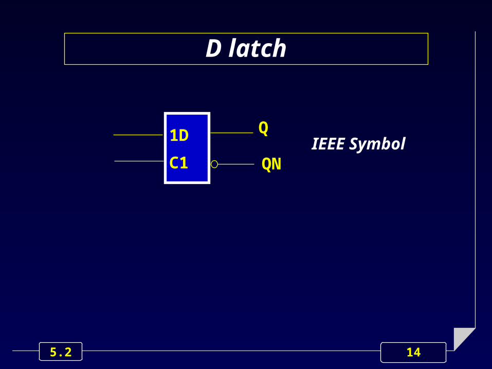
Waveforms
C
D
Q
C D 1S 1R Q QN
0 - 1 1 Q-1 QN-1
1 0 1 0 0 11 1 0 1 1 0

19 5.2
DC
Q
QN
Hazard-free polarity hold latch
Within the in-house developed LSSD design methodology, IBM uses the following implementation:
20 5.2
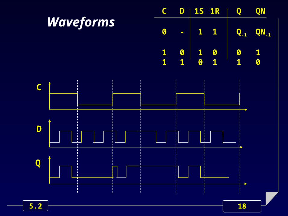
Set-Reset latch
The Set-Reset latch can be considered the elementary building block for the implementation of all synchronous sequential circuits.
It has:
2 inputs S and R
2 output Q and QN, such that QN = Q’.
S
R
Q
QN

21 5.2
Set-Reset latch
The Set-Reset latch can be considered the elementary building block for the implementation of all synchronous sequential circuits.
It has:
2 inputs S and R
2 output Q and QN, such that QN = Q’.
Of the 4 combinations of S and R: One forces Q QN = 0 1 (reset) One forces Q QN = 1 0 (set) One lets Q QN unchanged One is forbidden
S
R
Q
QN

22 5.2
Set-Reset latch
The Set-Reset latch can be considered the elementary building block for the implementation of all synchronous sequential circuits.
It has:
2 inputs S and R
2 output Q and QN, such that QN = Q’.
Of the 4 combinations of S and R: One forces Q QN = 0 1 (reset) One forces Q QN = 1 0 (set) One lets Q QN unchanged One is forbidden
S
R
Q
QN
The correspondenceinput combination performed operation
is technology and implementation dependent

23 5.2
Set-Reset latch (nand implementation)
S
R
Q
QN

24 5.2
Set-Reset latch (nand implementation)
S
R
S
R
Q
QN
QN
Q
Q-1

25 5.2
00 01 11 10
0 1 1 0 0
1 1 1 1 0
S R
Q
Q-1
Karnaugh Map Set-Reset latch
(nand implementation)

26 5.2
00 01 11 10
0 1 1 0 0
1 1 1 1 0
S R
Q
Q-1
S R Q QN
0 0 1 10 1 1 01 0 0 11 1 Q-1 QN-1
CharacteristicTable
Karnaugh Map Set-Reset latch
(nand implementation)

27 5.2
00 01 11 10
0 1 1 0 0
1 1 1 1 0
S RQ-1
S R Q QN
0 0 1 10 1 1 01 0 0 11 1 Q-1 QN-1
CharacteristicTable
Karnaugh Map Set-Reset latch
(nand implementation)
This combination is forbidden due to:
It forces both outputs to 1, thus preventing QN = Q’
a transition
S R = 00 S R = 11
forces the circuit to enter an unpredictable state, whose value depends from internal delays.
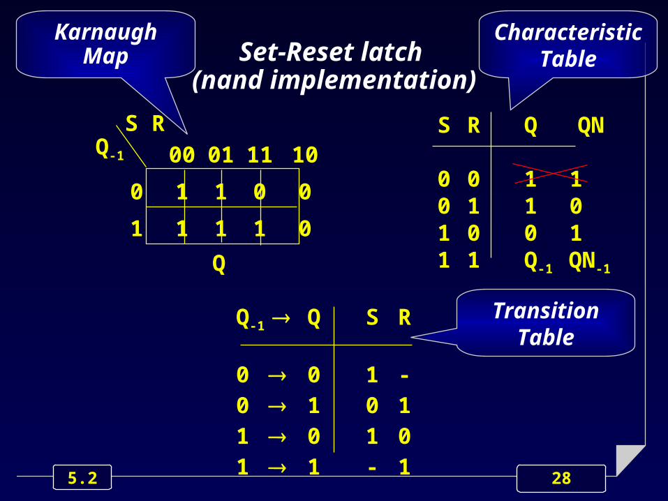
28 5.2
00 01 11 10
0 1 1 0 0
1 1 1 1 0
S R
Q
Q-1
S R Q QN
0 0 1 10 1 1 01 0 0 11 1 Q-1 QN-1
Q-1 Q S R
0 0 1 -0 1 0 11 0 1 01 1 - 1
TransitionTable
CharacteristicTable
Karnaugh Map Set-Reset latch
(nand implementation)

29 5.2
S
R
Q
QN
Set-Reset latch (nor implementation)

30 5.2
00 01 11 10
0 0 1 0 0
1 1 1 0 0
S R
Q
Q-1
S R Q QN
0 0 Q-1 QN-1
0 1 1 01 0 0 11 1 0 0
Q-1 Q S R
0 0 - 00 1 0 11 0 1 01 1 0 -
TransitionTable
CharacteristicTable
Karnaugh Map Set-Reset latch
(nor implementation)

31 5.2
Gated Set-Reset latch
It’s a variation of the Set-Reset latch, in which data are allowed to enter the latch when a given control signal C is asserted, only.
1S
1R
Q
QNC1 Symbol IEEE

32 5.2
Si
Ri
Q
QN
1S
1R
C1
Possible implementation

33 5.2
C1 1S 1R Si Ri Q QN
0 - - 1 1 Q-1 QN-1
1 0 0 1 1 Q-1 QN-1
1 0 1 1 0 0 11 1 0 0 1 1 0
1 1 1 0 0
Excitation table

34 5.2
OutlineOutline
Latch
Flip-flop
Scannable Flip-flop

35 5.2
behavior structure physical
system
RT
logic
device
Devices capable of Devices capable of storing a single bit:storing a single bit:
• latchlatch flip-flopflip-flop
Logic level elementary sequential blocks

36 5.2
Flip-FlopFlip-Flop
A flip-flop is a single-bit storage device implemented as a Moore machine.

37 5.2
Temporal constraints
Flip-flops works properly iff some temporal constraints are satisfied.

38 5.2
Set-up time
The time interval in which data inputs and control inputs must be stable before the clock event

39 5.2
Hold time
The time interval in which data inputs and control inputs must be stable after the clock event

40 5.2
FF classification w.r.t. data inputs
According to their behavior w.r.t. data inputs, flip-flops are usually classified as:
D
SR
JK
T.

41 5.2
D behavior
DQ
QN
CLK
D Q
0 01 1
CharacteristicTable
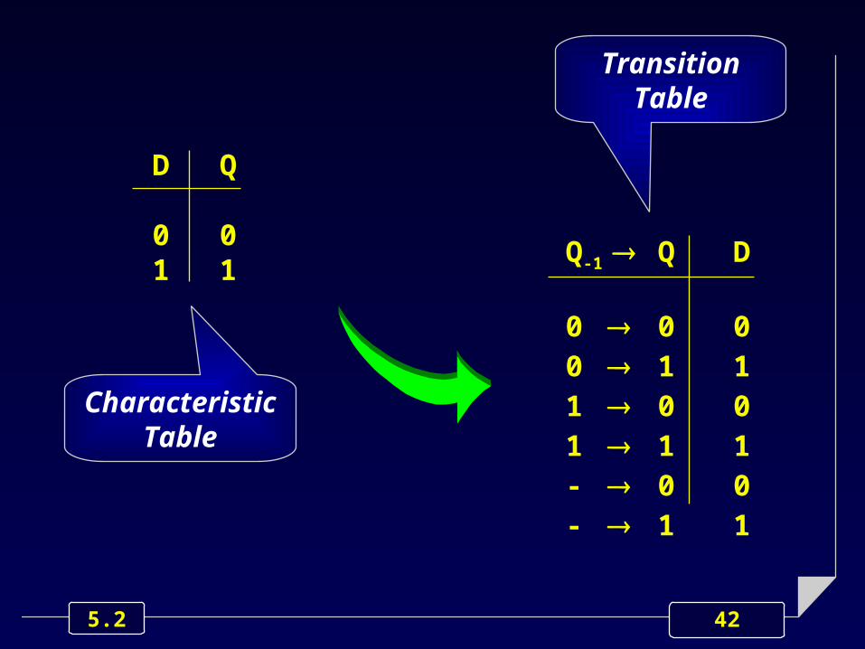
42 5.2
Q-1 Q D
0 0 00 1 11 0 01 1 1
- 0 0- 1 1
D Q
0 01 1
TransitionTable
CharacteristicTable

43 5.2
Caveat
Distinction between data inputs and control inputs is context and application dependent.

44 5.2
Example(D = data input)
At any CLK, it stores the input data
D Q
CLK

45 5.2
Example(D = control input)
If ( D = 0 ) then force Q=0 else force Q=1
D
Q
CLK

46 5.2
Set-Reset behavior
S
R
Q
QN
CLK
S R Q QN
0 0 1 10 1 1 01 0 0 11 1 Q-1 QN-1
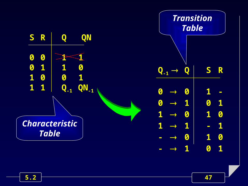
47 5.2
Q-1 Q S R
0 0 1 -0 1 0 11 0 1 01 1 - 1- 0 1 0- 1 0 1
S R Q QN
0 0 1 10 1 1 01 0 0 11 1 Q-1 QN-1
TransitionTable
CharacteristicTable

48 5.2
JK behavior
J
K
Q
QN
CLK
J K Q
0 0 Q-1
0 1 01 0 11 1 QN-1

49 5.2
Q-1 Q J K
0 0 0 -0 1 1 -1 0 - 11 1 - 0- 0 0 1- 1 1 0
J K Q
0 0 Q-1
0 1 01 0 11 1 QN-1
TransitionTable
CharacteristicTable

50 5.2
D FF implemented by a JK FF
D
KK
Q
QN
CLK
JJ

51 5.2
T behavior
TQ
QN
CLK
T Q
0 Q-1
1 QN-1
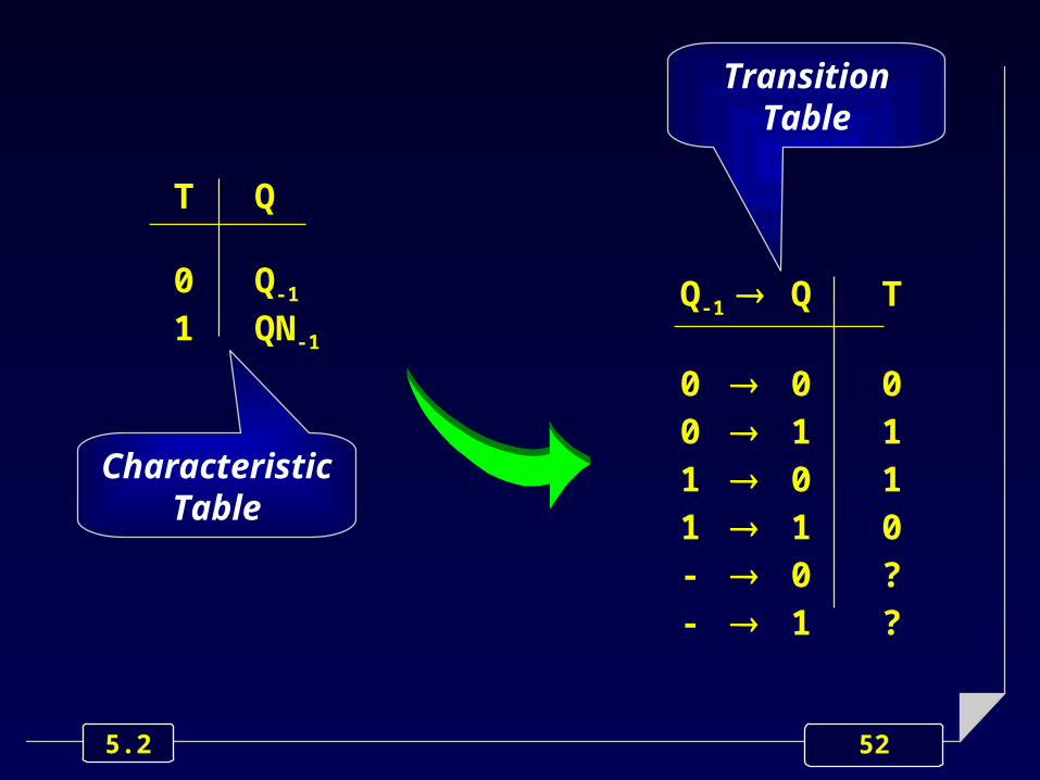
52 5.2
Q-1 Q T
0 0 00 1 11 0 11 1 0
- 0 ?- 1 ?
T Q
0 Q-1
1 QN-1
TransitionTable
CharacteristicTable

53 5.2
Caveat
A T type flip-flop cannot be initialized: if you don’t know the value of the output, acting only on the input T, you cannot state the value of the output.

54 5.2
T FF implemented by a JK FF
T
KK
Q
QN
CLK
JJ

55 5.2
T FF implemented by a D FF
T
DD
Q
QN
CLK

56 5.2
D FF implemented by a T FF
D
TT
Q
QN
CLK

57 5.2
DDlatchlatch
D FF positive edge triggered implemented by latches
Q
QN
CLK
DDDlatchlatch
D DA
Master-slave implementation

Waveforms
CLK
D
Q
A
DDlatchlatch
Q
QN
CLK
DDDlatchlatch
D D
A

59 5.2
D FF positive edge triggered implemented in
TTL logic (‘74)
preset
clear
CLK
D
Q
QN

60 5.2
The D FF as a library cellThe D FF as a library cell
A D flip flop is a sequential functional block able to perform the following operations:
asynchronous clear
synchronous clear
synchronous preset
data parallel load
stored data hold.

61 5.2
Flip flop D:Flip flop D: I/O signals
Input Data signals : D
Output Data signals : Q,
QN
Clock signal : CLK
Reset signal : ASYNC_CLR
Input Control signals : CLK_EN,SYNC_CLR,PRESET
Output Control signals: none

62 5.2
Flip flop D: symbol
DD
ASYNC_CLRASYNC_CLR
SYNC_CLRSYNC_CLR
CLK_ENCLK_EN
CLKCLK
QNQN
PRESETPRESET
63 5.2
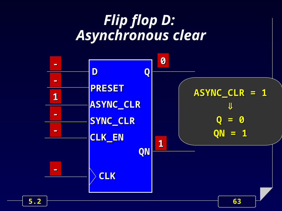
Flip flop D: Asynchronous clear
11
--
--
--
--
00DD
ASYNC_CLRASYNC_CLR
SYNC_CLRSYNC_CLR
CLK_ENCLK_EN
QNQN
PRESETPRESET--
11
ASYNC_CLR = 1ASYNC_CLR = 1
Q = 0Q = 0
QN = 1 = 1
CLKCLK

64 5.2
Flip flop D: Synchronous clear
00
--
11
11
00DD
ASYNC_CLRASYNC_CLR
SYNC_CLRSYNC_CLR
CLK_ENCLK_EN
QNQN
PRESETPRESET--
11
ASYNC_CLR = 0ASYNC_CLR = 0CLK_EN = 1CLK_EN = 1SYNC_CLR = 1SYNC_CLR = 1
CLOCKCLOCK
Q = 0Q = 0
QN = 1 = 1
CLKCLK

65 5.2
Flip flop D: Synchronous preset
00
--
00
11
11DD
ASYNC_CLRASYNC_CLR
SYNC_CLRSYNC_CLR
CLK_ENCLK_EN
QNQN
PRESETPRESET11
00
ASYNC_CLR = 0ASYNC_CLR = 0CLK_EN = 1CLK_EN = 1SYNC_CLR = 0SYNC_CLR = 0PRESET = 1PRESET = 1CLOCKCLOCK
Q = 1Q = 1
QN = 0 = 0
CLKCLK

66 5.2
Flip flop D: Data load
00
valuevalue
00
11
valuevalueDD
ASYNC_CLRASYNC_CLR
SYNC_CLRSYNC_CLR
CLK_ENCLK_EN
QNQN
PRESETPRESET00
Value’Value’
ASYNC_CLR = 0ASYNC_CLR = 0CLK_EN = 1CLK_EN = 1SYNC_CLR = 0SYNC_CLR = 0PRESET = 0PRESET = 0CLOCKCLOCK
Q = DQ = D
QN = D’ = D’CLKCLK

67 5.2
Flip flop D: Data hold
00
--
00
00
DD
ASYNC_CLRASYNC_CLR
SYNC_CLRSYNC_CLR
CLK_ENCLK_EN
QNQN
PRESETPRESET00
ASYNC_CLR = 0ASYNC_CLR = 0CLK_EN = 0CLK_EN = 0
QQt+1t+1 = Q = Qtt
QNQNt+1t+1 = QN = QNtt
CLKCLK

68 5.2
OutlineOutline
Latch
Flip-flop
Scannable Flip-flop

69 5.2
Scannable Flip-flopsScannable Flip-flops
Most cell libraries include particular FF families, particularly suited to improve testability, resorting to the so called Scan chains.
70 5.2
Flip-Flop

71 5.2
Flip-Flop
Scan Chain

72 5.2
Flip-flop scannable
D
SCAN_IN
CLK
Q
Control signal

73 5.2
Implementations
The control signal states value to be stored in the FF, i.e., the D or the SCAN_IN, respectively.
Two implementations are usually adopted: mux-scan
clock-scan.

74 5.2
Mux-scan approach
D
SCAN_IN
CLK
Q
Normal/~Scan

75 5.2
Clock-scan approach
D
SCAN_IN
CLK
Q
CLK_SCAN