Embed Size (px)
Citation preview

Product
Folder
Sample &Buy
Technical
Documents
Tools &
Software
Support &Community
LM158-N, LM258-N, LM2904-N, LM358-NSNOSBT3I –JANUARY 2000–REVISED DECEMBER 2014
LMx58-N Low-Power, Dual-Operational Amplifiers1 Features 3 Description
The LM158 series consists of two independent, high1• Available in 8-Bump DSBGA Chip-Sized Package,
gain, internally frequency compensated operational(See AN-1112, SNVA009)amplifiers which were designed specifically to operate
• Internally Frequency Compensated for Unity Gain from a single power supply over a wide range of• Large DC Voltage Gain: 100 dB voltages. Operation from split power supplies is also
possible and the low power supply current drain is• Wide Bandwidth (Unity Gain): 1 MHzindependent of the magnitude of the power supply(Temperature Compensated)voltage.
• Wide Power Supply Range:Application areas include transducer amplifiers, dc– Single Supply: 3V to 32Vgain blocks and all the conventional op-amp circuits
– Or Dual Supplies: ±1.5V to ±16V which now can be more easily implemented in single• Very Low Supply Current Drain (500 power supply systems. For example, the LM158
series can be directly operated off of the standardμA)—Essentially Independent of Supply Voltage3.3-V power supply voltage which is used in digital• Low Input Offset Voltage: 2 mVsystems and will easily provide the required interface
• Input Common-Mode Voltage Range Includes electronics without requiring the additional ±15VGround power supplies.
• Differential Input Voltage Range Equal to the The LM358 and LM2904 are available in a chip sizedPower Supply Voltage package (8-Bump DSBGA) using TI's DSBGA• Large Output Voltage Swing package technology.• Unique Characteristics:
Device Information(1)– In the Linear Mode the Input Common-Mode
PART NUMBER PACKAGE BODY SIZE (NOM)Voltage Range Includes Ground and theTO-CAN (8) 9.08 mm x 9.09 mmOutput Voltage Can Also Swing to Ground, LM158-NCDIP (8) 10.16 mm x 6.502 mmeven though Operated from Only a Single
LM258-N TO-CAN (8) 9.08 mm x 9.09 mmPower Supply Voltage.DSBGA (8) 1.31 mm x 1.31 mm– The Unity Gain Cross Frequency is
LM2904-N SOIC (8) 4.90 mm x 3.91 mmTemperature Compensated.PDIP (8) 9.81 mm x 6.35 mm– The Input Bias Current is also TemperatureTO-CAN (8) 9.08 mm x 9.09 mmCompensated.DSBGA (8) 1.31 mm x 1.31 mm• Advantages: LM358-NSOIC (8) 4.90 mm x 3.91 mm– Two Internally Compensated Op AmpsPDIP (8) 9.81 mm x 6.35 mm– Eliminates Need for Dual Supplies
(1) For all available packages, see the orderable addendum at– Allows Direct Sensing Near GND and VOUT the end of the datasheet.Also Goes to GND– Compatible with All Forms of Logic Voltage Controlled Oscillator (VCO)– Power Drain Suitable for Battery Operation
2 Applications• Active Filters• General Signal Conditioning and Amplification• 4- to 20-mA Current Loop Transmitters
1
An IMPORTANT NOTICE at the end of this data sheet addresses availability, warranty, changes, use in safety-critical applications,intellectual property matters and other important disclaimers. PRODUCTION DATA.
LM158-N, LM258-N, LM2904-N, LM358-NSNOSBT3I –JANUARY 2000–REVISED DECEMBER 2014 www.ti.com
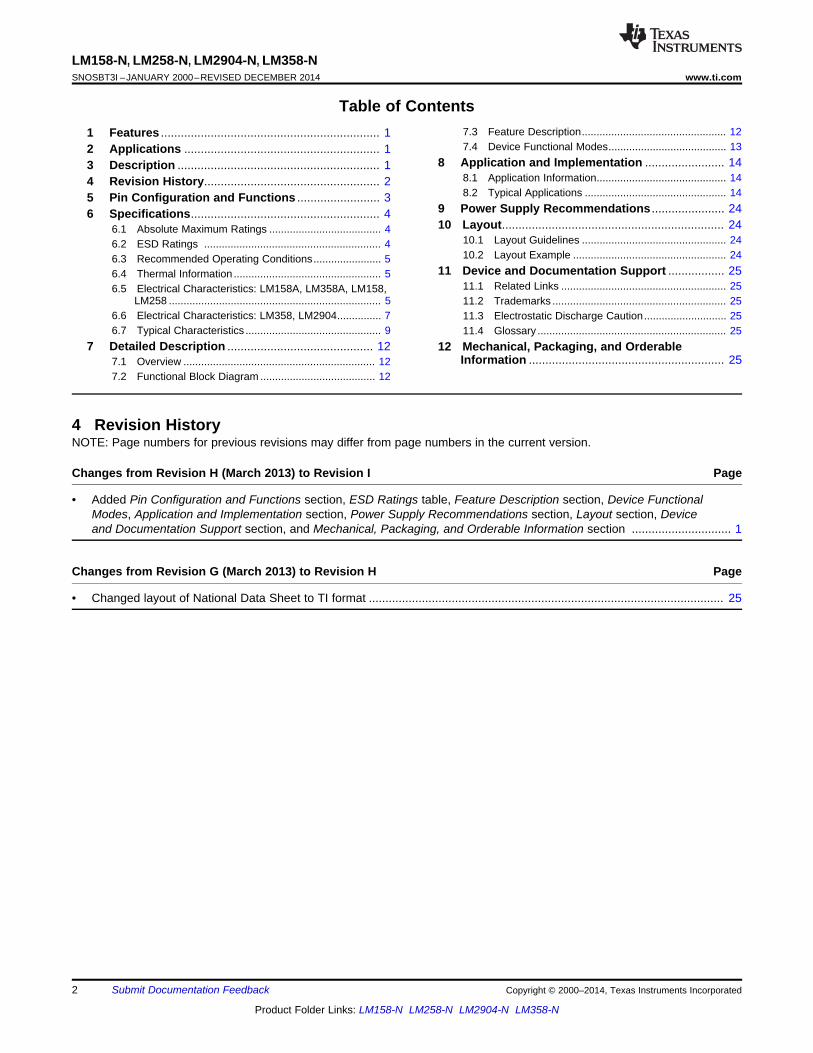
Table of Contents7.3 Feature Description................................................. 121 Features .................................................................. 17.4 Device Functional Modes........................................ 132 Applications ........................................................... 1
8 Application and Implementation ........................ 143 Description ............................................................. 18.1 Application Information............................................ 144 Revision History..................................................... 28.2 Typical Applications ................................................ 145 Pin Configuration and Functions ......................... 3
9 Power Supply Recommendations ...................... 246 Specifications......................................................... 410 Layout................................................................... 246.1 Absolute Maximum Ratings ...................................... 4
10.1 Layout Guidelines ................................................. 246.2 ESD Ratings ............................................................ 410.2 Layout Example .................................................... 246.3 Recommended Operating Conditions....................... 5
11 Device and Documentation Support ................. 256.4 Thermal Information .................................................. 511.1 Related Links ........................................................ 256.5 Electrical Characteristics: LM158A, LM358A, LM158,
LM258 ........................................................................ 5 11.2 Trademarks ........................................................... 256.6 Electrical Characteristics: LM358, LM2904............... 7 11.3 Electrostatic Discharge Caution............................ 256.7 Typical Characteristics .............................................. 9 11.4 Glossary ................................................................ 25
7 Detailed Description ............................................ 12 12 Mechanical, Packaging, and OrderableInformation ........................................................... 257.1 Overview ................................................................. 12
7.2 Functional Block Diagram ....................................... 12
4 Revision HistoryNOTE: Page numbers for previous revisions may differ from page numbers in the current version.
Changes from Revision H (March 2013) to Revision I Page
• Added Pin Configuration and Functions section, ESD Ratings table, Feature Description section, Device FunctionalModes, Application and Implementation section, Power Supply Recommendations section, Layout section, Deviceand Documentation Support section, and Mechanical, Packaging, and Orderable Information section .............................. 1
Changes from Revision G (March 2013) to Revision H Page
• Changed layout of National Data Sheet to TI format ........................................................................................................... 25
2 Submit Documentation Feedback Copyright © 2000–2014, Texas Instruments Incorporated
Product Folder Links: LM158-N LM258-N LM2904-N LM358-N
LM158-N, LM258-N, LM2904-N, LM358-Nwww.ti.com SNOSBT3I –JANUARY 2000–REVISED DECEMBER 2014
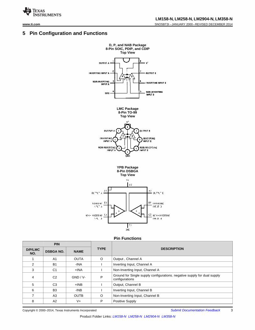
5 Pin Configuration and Functions
D, P, and NAB Package8-Pin SOIC, PDIP, and CDIP
Top View
LMC Package8-Pin TO-99
Top View
YPB Package8-Pin DSBGA
Top View
Pin FunctionsPIN
TYPE DESCRIPTIOND/P/LMC DSBGA NO. NAMENO.1 A1 OUTA O Output , Channel A2 B1 -INA I Inverting Input, Channel A3 C1 +INA I Non-Inverting Input, Channel A
Ground for Single supply configurations. negative supply for dual supply4 C2 GND / V- P configurations5 C3 +INB I Output, Channel B6 B3 -INB I Inverting Input, Channel B7 A3 OUTB O Non-Inverting Input, Channel B8 A2 V+ P Positive Supply
Copyright © 2000–2014, Texas Instruments Incorporated Submit Documentation Feedback 3
Product Folder Links: LM158-N LM258-N LM2904-N LM358-N

LM158-N, LM258-N, LM2904-N, LM358-NSNOSBT3I –JANUARY 2000–REVISED DECEMBER 2014 www.ti.com
6 Specifications
6.1 Absolute Maximum RatingsSee (1) (2) (3).
LM158, LM258,LM358, LM158A, LM2904
UNITLM258A, LM358AMIN MAX MIN MAX
Supply Voltage, V+ 32 26 VDifferential Input Voltage 32 26 VInput Voltage −0.3 32 −0.3 26 VPower Dissipation (4) PDIP (P) 830 830 mW
TO-99 (LMC) 550 mWSOIC (D) 530 530 mWDSBGA (YPB) 435 mW
Output Short-Circuit to V+ ≤ 15 V and TA = 25°C Continuous ContinuouGND (One sAmplifier) (5)
Input Current (VIN < −0.3V) (6) 50 50 mATemperature −55 125 °C
PDIP Package (P): Soldering (10 seconds) 260 260 °CSOIC Package (D) Vapor Phase (60 215 215 °C
seconds)Infrared (15 seconds) 220 220 °C
Lead Temperature PDIP (P): (Soldering, 10 seconds) 260 260 °CTO-99 (LMC): (Soldering, 10 seconds) 300 300 °C
Storage temperature, Tstg −65 150 −65 150 °C
(1) Absolute Maximum Ratings indicate limits beyond which damage to the device may occur. Recommended Operating Conditions indicateconditions for which the device is intended to be functional, but specific performance is not ensured. For ensured specifications and thetest conditions, see the Electrical Characteristics.
(2) Refer to RETS158AX for LM158A military specifications and to RETS158X for LM158 military specifications.(3) If Military/Aerospace specified devices are required, please contact the TI Sales Office/Distributors for availability and specifications.(4) For operating at high temperatures, the LM358/LM358A, LM2904 must be derated based on a 125°C maximum junction temperature
and a thermal resistance of 120°C/W for PDIP, 182°C/W for TO-99, 189°C/W for SOIC package, and 230°C/W for DSBGA, whichapplies for the device soldered in a printed circuit board, operating in a still air ambient. The LM258/LM258A and LM158/LM158A can bederated based on a +150°C maximum junction temperature. The dissipation is the total of both amplifiers—use external resistors, wherepossible, to allow the amplifier to saturate or to reduce the power which is dissipated in the integrated circuit.
(5) Short circuits from the output to V+ can cause excessive heating and eventual destruction. When considering short circuits to ground,the maximum output current is approximately 40 mA independent of the magnitude of V+. At values of supply voltage in excess of +15V, continuous short-circuits can exceed the power dissipation ratings and cause eventual destruction. Destructive dissipation can resultfrom simultaneous shorts on all amplifiers.
(6) This input current will only exist when the voltage at any of the input leads is driven negative. It is due to the collector-base junction ofthe input PNP transistors becoming forward biased and thereby acting as input diode clamps. In addition to this diode action, there isalso lateral NPN parasitic transistor action on the IC chip. This transistor action can cause the output voltages of the op amps to go tothe V+voltage level (or to ground for a large overdrive) for the time duration that an input is driven negative. This is not destructive andnormal output states will re-establish when the input voltage, which was negative, again returns to a value greater than −0.3 V (at 25°C).
6.2 ESD RatingsVALUE UNIT
V(ESD) Electrostatic discharge Human-body model (HBM), per ANSI/ESDA/JEDEC JS-001 (1) ±250 V
(1) JEDEC document JEP155 states that 500-V HBM allows safe manufacturing with a standard ESD control process.
4 Submit Documentation Feedback Copyright © 2000–2014, Texas Instruments Incorporated
Product Folder Links: LM158-N LM258-N LM2904-N LM358-N

LM158-N, LM258-N, LM2904-N, LM358-Nwww.ti.com SNOSBT3I –JANUARY 2000–REVISED DECEMBER 2014
6.3 Recommended Operating Conditionsover operating free-air temperature range (unless otherwise noted)
MIN MAX UNITSupply Voltage (V+ - V-):LM158. LM258, LM358 3 (±1.5) 32 (±16) VSupply Voltage (V+ - V-):LM2904 3 (±1.5) 26 (±13) VOperating Temperature: LM158 -55 125 °COperating Temperature: LM258 -25 85 °COperating Temperature: LM358 0 70 °COperating Temperature: LM2904 -40 85 °C
6.4 Thermal InformationLM158-N, LM158-N LM2904-N, LM358-NLM258-N,LM358-NTHERMAL METRIC (1) UNIT
LMC NAB YPB D P8 PINS
RθJA Junction-to-ambient thermal resistance 155 132 230 189 120 °C/W
(1) For more information about traditional and new thermal metrics, see the IC Package Thermal Metrics application report, SPRA953.
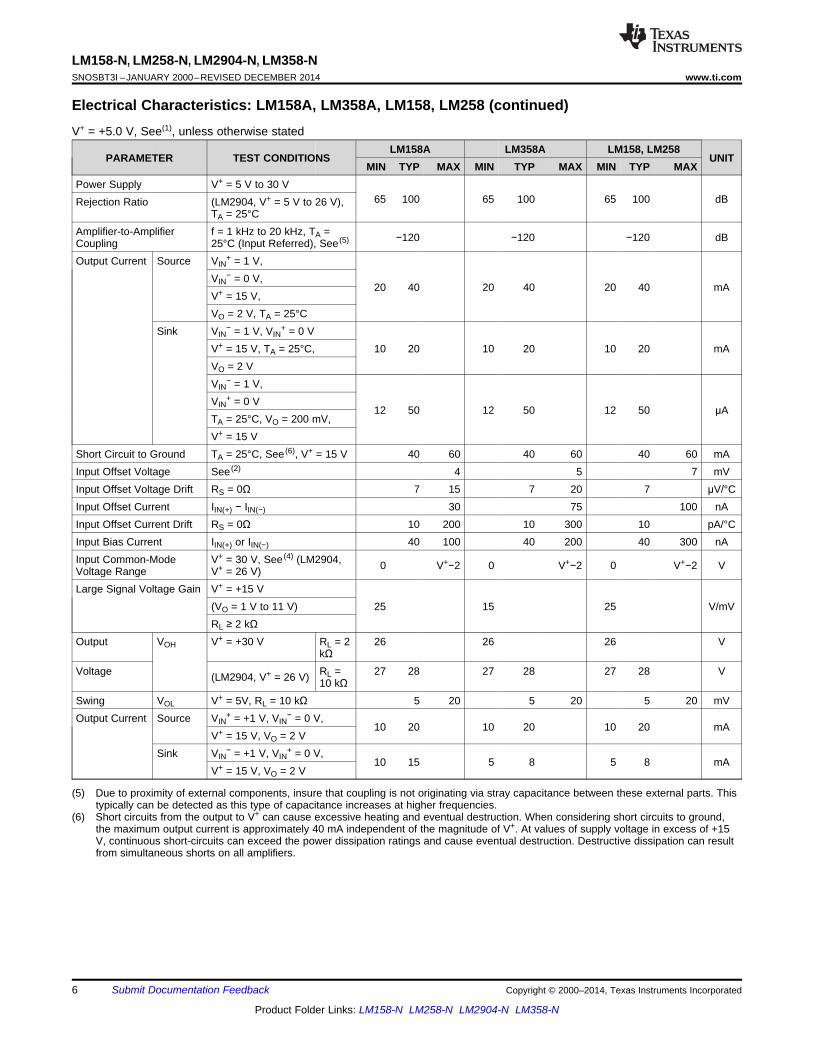
6.5 Electrical Characteristics: LM158A, LM358A, LM158, LM258V+ = +5.0 V, See (1), unless otherwise stated
LM158A LM358A LM158, LM258PARAMETER TEST CONDITIONS UNIT
MIN TYP MAX MIN TYP MAX MIN TYP MAXInput Offset Voltage See (2), TA = 25°C 1 2 2 3 2 5 mVInput Bias Current IIN(+) or IIN(−), TA = 25°C, 20 50 45 100 45 150 nA
VCM = 0 V, (3)
Input Offset Current IIN(+) − IIN(−), VCM = 0V, TA = 2 10 5 30 3 30 nA25°CInput Common-Mode V+ = 30 V, (4)
V+−1.0 0 V+−1.5 0 V+−1.5 VVoltage Range (LM2904, V+ = 26V), TA = 525°C
Supply Current Over Full TemperatureRangeRL = ∞ on All Op AmpsV+ = 30V (LM2904 V+ = 26V) 1 2 1 2 1 2 mAV+ = 5V 0.5 1.2 0.5 1.2 0.5 1.2 mA
Large Signal Voltage Gain V+ = 15 V, TA = 25°C,RL ≥ 2 kΩ, (For VO = 1 V to 50 100 25 100 50 100 V/mV11 V)
Common-Mode TA = 25°C,70 85 65 85 70 85 dB
Rejection Ratio VCM = 0 V to V+−1.5 VPower Supply V+ = 5 V to 30 V
65 100 65 100 65 100 dBRejection Ratio (LM2904, V+ = 5 V to 26 V),TA = 25°C
(1) These specifications are limited to –55°C ≤ TA ≤ +125°C for the LM158/LM158A. With the LM258/LM258A, all temperature specificationsare limited to −25°C ≤ TA ≤ 85°C, the LM358/LM358A temperature specifications are limited to 0°C ≤ TA ≤ 70°C, and the LM2904specifications are limited to –40°C ≤ TA ≤ 85°C.
(2) VO ≃ 1.4 V, RS = 0 Ω with V+ from 5 V to 30 V; and over the full input common-mode range (0 V to V+ −1.5 V) at 25°C. For LM2904, V+
from 5 V to 26 V.(3) The direction of the input current is out of the IC due to the PNP input stage. This current is essentially constant, independent of the
state of the output so no loading change exists on the input lines.(4) The input common-mode voltage of either input signal voltage should not be allowed to go negative by more than 0.3 V (at 25°C). The
upper end of the common-mode voltage range is V+ −1.5 V (at 25°C), but either or both inputs can go to 32 V without damage (26 V forLM2904), independent of the magnitude of V+.
Copyright © 2000–2014, Texas Instruments Incorporated Submit Documentation Feedback 5
Product Folder Links: LM158-N LM258-N LM2904-N LM358-N
LM158-N, LM258-N, LM2904-N, LM358-NSNOSBT3I –JANUARY 2000–REVISED DECEMBER 2014 www.ti.com
Electrical Characteristics: LM158A, LM358A, LM158, LM258 (continued)V+ = +5.0 V, See(1), unless otherwise stated
LM158A LM358A LM158, LM258PARAMETER TEST CONDITIONS UNIT
MIN TYP MAX MIN TYP MAX MIN TYP MAXPower Supply V+ = 5 V to 30 V
65 100 65 100 65 100 dBRejection Ratio (LM2904, V+ = 5 V to 26 V),TA = 25°C
Amplifier-to-Amplifier f = 1 kHz to 20 kHz, TA = −120 −120 −120 dBCoupling 25°C (Input Referred), See (5)
Output Current Source VIN+ = 1 V,
VIN− = 0 V,
20 40 20 40 20 40 mAV+ = 15 V,VO = 2 V, TA = 25°C
Sink VIN− = 1 V, VIN
+ = 0 VV+ = 15 V, TA = 25°C, 10 20 10 20 10 20 mAVO = 2 VVIN
− = 1 V,VIN
+ = 0 V12 50 12 50 12 50 μA
TA = 25°C, VO = 200 mV,V+ = 15 V
Short Circuit to Ground TA = 25°C, See (6), V+ = 15 V 40 60 40 60 40 60 mAInput Offset Voltage See (2) 4 5 7 mVInput Offset Voltage Drift RS = 0Ω 7 15 7 20 7 μV/°CInput Offset Current IIN(+) − IIN(−) 30 75 100 nAInput Offset Current Drift RS = 0Ω 10 200 10 300 10 pA/°CInput Bias Current IIN(+) or IIN(−) 40 100 40 200 40 300 nAInput Common-Mode V+ = 30 V, See (4) (LM2904, 0 V+−2 0 V+−2 0 V+−2 VVoltage Range V+ = 26 V)Large Signal Voltage Gain V+ = +15 V
(VO = 1 V to 11 V) 25 15 25 V/mVRL ≥ 2 kΩ
Output VOH V+ = +30 V RL = 2 26 26 26 VkΩ
Voltage RL = 27 28 27 28 27 28 V(LM2904, V+ = 26 V) 10 kΩSwing VOL V+ = 5V, RL = 10 kΩ 5 20 5 20 5 20 mVOutput Current Source VIN
+ = +1 V, VIN− = 0 V,
10 20 10 20 10 20 mAV+ = 15 V, VO = 2 V
Sink VIN− = +1 V, VIN
+ = 0 V,10 15 5 8 5 8 mA
V+ = 15 V, VO = 2 V
(5) Due to proximity of external components, insure that coupling is not originating via stray capacitance between these external parts. Thistypically can be detected as this type of capacitance increases at higher frequencies.
(6) Short circuits from the output to V+ can cause excessive heating and eventual destruction. When considering short circuits to ground,the maximum output current is approximately 40 mA independent of the magnitude of V+. At values of supply voltage in excess of +15V, continuous short-circuits can exceed the power dissipation ratings and cause eventual destruction. Destructive dissipation can resultfrom simultaneous shorts on all amplifiers.
6 Submit Documentation Feedback Copyright © 2000–2014, Texas Instruments Incorporated
Product Folder Links: LM158-N LM258-N LM2904-N LM358-N
LM158-N, LM258-N, LM2904-N, LM358-Nwww.ti.com SNOSBT3I –JANUARY 2000–REVISED DECEMBER 2014
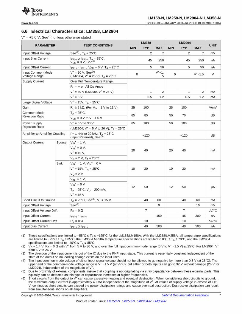
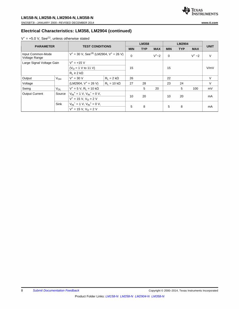
6.6 Electrical Characteristics: LM358, LM2904V+ = +5.0 V, See (1), unless otherwise stated
LM358 LM2904PARAMETER TEST CONDITIONS UNIT
MIN TYP MAX MIN TYP MAXInput Offset Voltage See (2) , TA = 25°C 2 7 2 7 mVInput Bias Current IIN(+) or IIN(−), TA = 25°C, 45 250 45 250 nAVCM = 0 V, See (3)
Input Offset Current IIN(+) − IIN(−), VCM = 0 V, TA = 25°C 5 50 5 50 nAInput Common-Mode V+ = 30 V, See (4) V+−1.0 0 V+−1.5 VVoltage Range (LM2904, V+ = 26 V), TA = 25°C 5Supply Current Over Full Temperature Range
RL = ∞ on All Op AmpsV+ = 30 V (LM2904 V+ = 26 V) 1 2 1 2 mAV+ = 5 V 0.5 1.2 0.5 1.2 mA
Large Signal Voltage V+ = 15V, TA = 25°C,Gain RL ≥ 2 kΩ, (For VO = 1 V to 11 V) 25 100 25 100 V/mVCommon-Mode TA = 25°C,
65 85 50 70 dBRejection Ratio VCM = 0 V to V+−1.5 VPower Supply V+ = 5 V to 30 V 65 100 50 100 dBRejection Ratio (LM2904, V+ = 5 V to 26 V), TA = 25°CAmplifier-to-Amplifier Coupling f = 1 kHz to 20 kHz, TA = 25°C −120 −120 dB(Input Referred), See (5)
Output Current Source VIN+ = 1 V,
VIN− = 0 V,
20 40 20 40 mAV+ = 15 V,VO = 2 V, TA = 25°C
Sink VIN− = 1 V, VIN
+ = 0 VV+ = 15V, TA = 25°C, 10 20 10 20 mAVO = 2 VVIN
− = 1 V,VIN
+ = 0 V12 50 12 50 μA
TA = 25°C, VO = 200 mV,V+ = 15 V
Short Circuit to Ground TA = 25°C, See (6), V+ = 15 V 40 60 40 60 mAInput Offset Voltage See (2) 9 10 mVInput Offset Voltage Drift RS = 0 Ω 7 7 μV/°CInput Offset Current IIN(+) − IIN(−) 150 45 200 nAInput Offset Current Drift RS = 0 Ω 10 10 pA/°CInput Bias Current IIN(+) or IIN(−) 40 500 40 500 nA
(1) These specifications are limited to –55°C ≤ TA ≤ +125°C for the LM158/LM158A. With the LM258/LM258A, all temperature specificationsare limited to −25°C ≤ TA ≤ 85°C, the LM358/LM358A temperature specifications are limited to 0°C ≤ TA ≤ 70°C, and the LM2904specifications are limited to –40°C ≤ TA ≤ 85°C.
(2) VO ≃ 1.4 V, RS = 0 Ω with V+ from 5 V to 30 V; and over the full input common-mode range (0 V to V+ −1.5 V) at 25°C. For LM2904, V+
from 5 V to 26 V.(3) The direction of the input current is out of the IC due to the PNP input stage. This current is essentially constant, independent of the
state of the output so no loading change exists on the input lines.(4) The input common-mode voltage of either input signal voltage should not be allowed to go negative by more than 0.3 V (at 25°C). The
upper end of the common-mode voltage range is V+ −1.5 V (at 25°C), but either or both inputs can go to 32 V without damage (26 V forLM2904), independent of the magnitude of V+.
(5) Due to proximity of external components, insure that coupling is not originating via stray capacitance between these external parts. Thistypically can be detected as this type of capacitance increases at higher frequencies.
(6) Short circuits from the output to V+ can cause excessive heating and eventual destruction. When considering short circuits to ground,the maximum output current is approximately 40 mA independent of the magnitude of V+. At values of supply voltage in excess of +15V, continuous short-circuits can exceed the power dissipation ratings and cause eventual destruction. Destructive dissipation can resultfrom simultaneous shorts on all amplifiers.
Copyright © 2000–2014, Texas Instruments Incorporated Submit Documentation Feedback 7
Product Folder Links: LM158-N LM258-N LM2904-N LM358-N
LM158-N, LM258-N, LM2904-N, LM358-NSNOSBT3I –JANUARY 2000–REVISED DECEMBER 2014 www.ti.com
Electrical Characteristics: LM358, LM2904 (continued)V+ = +5.0 V, See(1), unless otherwise stated
LM358 LM2904PARAMETER TEST CONDITIONS UNIT
MIN TYP MAX MIN TYP MAXInput Common-Mode V+ = 30 V, See (4) (LM2904, V+ = 26 V) 0 V+−2 0 V+ −2 VVoltage RangeLarge Signal Voltage Gain V+ = +15 V
(VO = 1 V to 11 V) 15 15 V/mVRL ≥ 2 kΩ
Output VOH V+ = 30 V RL = 2 kΩ 26 22 VVoltage (LM2904, V+ = 26 V) RL = 10 kΩ 27 28 23 24 VSwing VOL V+ = 5 V, RL = 10 kΩ 5 20 5 100 mVOutput Current Source VIN
+ = 1 V, VIN− = 0 V,
10 20 10 20 mAV+ = 15 V, VO = 2 V
Sink VIN− = 1 V, VIN
+ = 0 V,5 8 5 8 mA
V+ = 15 V, VO = 2 V
8 Submit Documentation Feedback Copyright © 2000–2014, Texas Instruments Incorporated
Product Folder Links: LM158-N LM258-N LM2904-N LM358-N
LM158-N, LM258-N, LM2904-N, LM358-Nwww.ti.com SNOSBT3I –JANUARY 2000–REVISED DECEMBER 2014
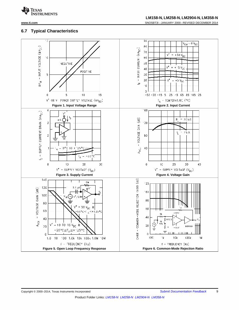
6.7 Typical Characteristics
Figure 1. Input Voltage Range Figure 2. Input Current
Figure 3. Supply Current Figure 4. Voltage Gain
Figure 6. Common-Mode Rejection RatioFigure 5. Open Loop Frequency Response
Copyright © 2000–2014, Texas Instruments Incorporated Submit Documentation Feedback 9
Product Folder Links: LM158-N LM258-N LM2904-N LM358-N
LM158-N, LM258-N, LM2904-N, LM358-NSNOSBT3I –JANUARY 2000–REVISED DECEMBER 2014 www.ti.com
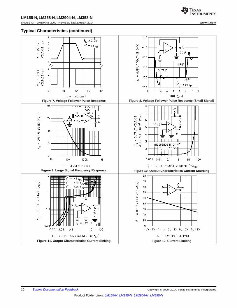
Typical Characteristics (continued)
Figure 8. Voltage Follower Pulse Response (Small Signal)Figure 7. Voltage Follower Pulse Response
Figure 9. Large Signal Frequency Response Figure 10. Output Characteristics Current Sourcing
Figure 11. Output Characteristics Current Sinking Figure 12. Current Limiting
10 Submit Documentation Feedback Copyright © 2000–2014, Texas Instruments Incorporated
Product Folder Links: LM158-N LM258-N LM2904-N LM358-N

LM158-N, LM258-N, LM2904-N, LM358-Nwww.ti.com SNOSBT3I –JANUARY 2000–REVISED DECEMBER 2014
Typical Characteristics (continued)
Figure 13. Input Current (LM2902 Only) Figure 14. Voltage Gain (LM2902 Only)
Copyright © 2000–2014, Texas Instruments Incorporated Submit Documentation Feedback 11
Product Folder Links: LM158-N LM258-N LM2904-N LM358-N

LM158-N, LM258-N, LM2904-N, LM358-NSNOSBT3I –JANUARY 2000–REVISED DECEMBER 2014 www.ti.com
7 Detailed Description
7.1 OverviewThe LM158 series are operational amplifiers which can operate with only a single power supply voltage, havetrue-differential inputs, and remain in the linear mode with an input common-mode voltage of 0 VDC. Theseamplifiers operate over a wide range of power supply voltage with little change in performance characteristics. At25°C amplifier operation is possible down to a minimum supply voltage of 2.3 VDC.
Large differential input voltages can be easily accommodated and, as input differential voltage protection diodesare not needed, no large input currents result from large differential input voltages. The differential input voltagemay be larger than V+ without damaging the device. Protection should be provided to prevent the input voltagesfrom going negative more than −0.3 VDC (at 25°C). An input clamp diode with a resistor to the IC input terminalcan be used.
7.2 Functional Block Diagram
Figure 15. (Each Amplifier)
7.3 Feature DescriptionThe amplifier's differential inputs consist of a non-inverting input (+IN) and an inverting input (–IN). The ampliferamplifies only the difference in voltage between the two inpus, which is called the differential input voltage. Theoutput voltage of the op-amp Vout is given by Equation 1:
VOUT = AOL (IN+ - IN-)
where• AOL is the open-loop gain of the amplifier, typically around 100dB (100,000x, or 10uV per Volt). (1)
To reduce the power supply current drain, the amplifiers have a class A output stage for small signal levels whichconverts to class B in a large signal mode. This allows the amplifiers to both source and sink large outputcurrents. Therefore both NPN and PNP external current boost transistors can be used to extend the powercapability of the basic amplifiers. The output voltage needs to raise approximately 1 diode drop above ground tobias the on-chip vertical PNP transistor for output current sinking applications.
For ac applications, where the load is capacitively coupled to the output of the amplifier, a resistor should beused, from the output of the amplifier to ground to increase the class A bias current and prevent crossoverdistortion. Where the load is directly coupled, as in dc applications, there is no crossover distortion.
Capacitive loads which are applied directly to the output of the amplifier reduce the loop stability margin. Valuesof 50 pF can be accommodated using the worst-case non-inverting unity gain connection. Large closed loopgains or resistive isolation should be used if larger load capacitance must be driven by the amplifier.
The bias network of the LM158 establishes a drain current which is independent of the magnitude of the powersupply voltage over the range of 3 VDC to 30 VDC.
Output short circuits either to ground or to the positive power supply should be of short time duration. Units canbe destroyed, not as a result of the short circuit current causing metal fusing, but rather due to the large increasein IC chip power dissipation which will cause eventual failure due to excessive junction temperatures. Puttingdirect short-circuits on more than one amplifier at a time will increase the total IC power dissipation to destructivelevels, if not properly protected with external dissipation limiting resistors in series with the output leads of theamplifiers. The larger value of output source current which is available at 25°C provides a larger output currentcapability at elevated temperatures (see Typical Characteristics) than a standard IC op amp.
12 Submit Documentation Feedback Copyright © 2000–2014, Texas Instruments Incorporated
Product Folder Links: LM158-N LM258-N LM2904-N LM358-N

LM158-N, LM258-N, LM2904-N, LM358-Nwww.ti.com SNOSBT3I –JANUARY 2000–REVISED DECEMBER 2014
7.4 Device Functional Modes
Figure 16. Schematic Diagram
The circuits presented in the Typical Single-Supply Applications emphasize operation on only a single powersupply voltage. If complementary power supplies are available, all of the standard op-amp circuits can be used.In general, introducing a pseudo-ground (a bias voltage reference of V+/2) will allow operation above and belowthis value in single power supply systems. Many application circuits are shown which take advantage of the wideinput common-mode voltage range which includes ground. In most cases, input biasing is not required and inputvoltages which range to ground can easily be accommodated.
Copyright © 2000–2014, Texas Instruments Incorporated Submit Documentation Feedback 13
Product Folder Links: LM158-N LM258-N LM2904-N LM358-N
LM158-N, LM258-N, LM2904-N, LM358-NSNOSBT3I –JANUARY 2000–REVISED DECEMBER 2014 www.ti.com
8 Application and Implementation
NOTEInformation in the following applications sections is not part of the TI componentspecification, and TI does not warrant its accuracy or completeness. TI’s customers areresponsible for determining suitability of components for their purposes. Customers shouldvalidate and test their design implementation to confirm system functionality.
8.1 Application InformationThe LM158 family bring performance, economy, and ease-of-use to a wide variety of op-amp applications.
8.2 Typical Applications
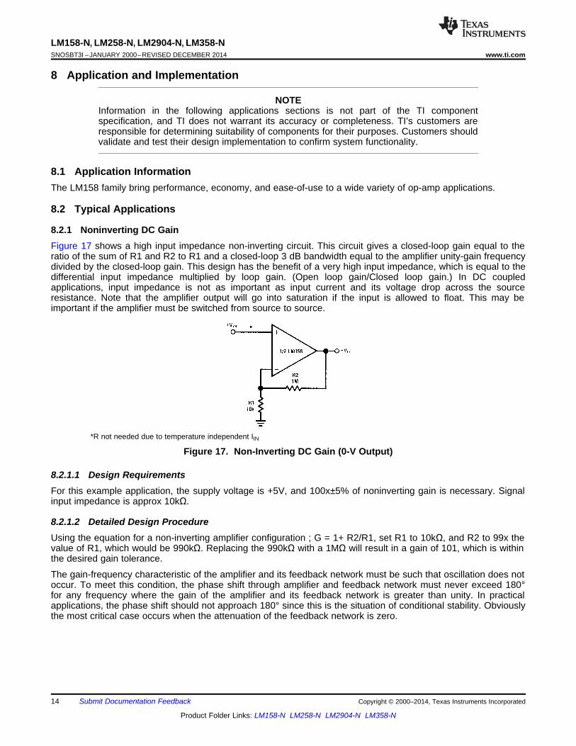
8.2.1 Noninverting DC GainFigure 17 shows a high input impedance non-inverting circuit. This circuit gives a closed-loop gain equal to theratio of the sum of R1 and R2 to R1 and a closed-loop 3 dB bandwidth equal to the amplifier unity-gain frequencydivided by the closed-loop gain. This design has the benefit of a very high input impedance, which is equal to thedifferential input impedance multiplied by loop gain. (Open loop gain/Closed loop gain.) In DC coupledapplications, input impedance is not as important as input current and its voltage drop across the sourceresistance. Note that the amplifier output will go into saturation if the input is allowed to float. This may beimportant if the amplifier must be switched from source to source.
*R not needed due to temperature independent IIN
Figure 17. Non-Inverting DC Gain (0-V Output)
8.2.1.1 Design RequirementsFor this example application, the supply voltage is +5V, and 100x±5% of noninverting gain is necessary. Signalinput impedance is approx 10kΩ.
8.2.1.2 Detailed Design ProcedureUsing the equation for a non-inverting amplifier configuration ; G = 1+ R2/R1, set R1 to 10kΩ, and R2 to 99x thevalue of R1, which would be 990kΩ. Replacing the 990kΩ with a 1MΩ will result in a gain of 101, which is withinthe desired gain tolerance.
The gain-frequency characteristic of the amplifier and its feedback network must be such that oscillation does notoccur. To meet this condition, the phase shift through amplifier and feedback network must never exceed 180°for any frequency where the gain of the amplifier and its feedback network is greater than unity. In practicalapplications, the phase shift should not approach 180° since this is the situation of conditional stability. Obviouslythe most critical case occurs when the attenuation of the feedback network is zero.
14 Submit Documentation Feedback Copyright © 2000–2014, Texas Instruments Incorporated
Product Folder Links: LM158-N LM258-N LM2904-N LM358-N

LM158-N, LM258-N, LM2904-N, LM358-Nwww.ti.com SNOSBT3I –JANUARY 2000–REVISED DECEMBER 2014
Typical Applications (continued)8.2.1.3 Application Curve
Figure 18. Transfer Curve for Non-Inverting Configuration
8.2.2 System Examples
8.2.2.1 Typical Single-Supply Applications(V+ = 5.0 VDC)
VO = 0 VDC for VIN = 0 VDCWhere: VO = V1 + V2 − V3 − V4
AV = 10(V1 + V2) ≥ (V3 + V4) to keep VO > 0 VDC
Figure 19. DC Summing Amplifier Figure 20. Power Amplifier(VIN'S ≥ 0 VDC and VO ≥ 0 VDC)
Copyright © 2000–2014, Texas Instruments Incorporated Submit Documentation Feedback 15
Product Folder Links: LM158-N LM258-N LM2904-N LM358-N

LM158-N, LM258-N, LM2904-N, LM358-NSNOSBT3I –JANUARY 2000–REVISED DECEMBER 2014 www.ti.com
Typical Applications (continued)(V+ = 5.0 VDC)
fo = 1 kHzQ = 50Av = 100 (40 dB)
Figure 21. “BI-QUAD” RC Active Bandpass Filter Figure 22. Lamp Driver
Figure 23. LED Driver Figure 24. Driving TTL
16 Submit Documentation Feedback Copyright © 2000–2014, Texas Instruments Incorporated
Product Folder Links: LM158-N LM258-N LM2904-N LM358-N
LM158-N, LM258-N, LM2904-N, LM358-Nwww.ti.com SNOSBT3I –JANUARY 2000–REVISED DECEMBER 2014
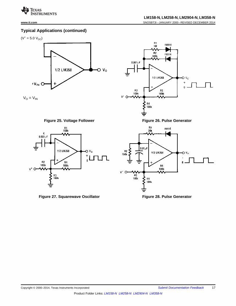
Typical Applications (continued)(V+ = 5.0 VDC)
VO = VIN
Figure 25. Voltage Follower Figure 26. Pulse Generator
Figure 27. Squarewave Oscillator Figure 28. Pulse Generator
Copyright © 2000–2014, Texas Instruments Incorporated Submit Documentation Feedback 17
Product Folder Links: LM158-N LM258-N LM2904-N LM358-N

LM158-N, LM258-N, LM2904-N, LM358-NSNOSBT3I –JANUARY 2000–REVISED DECEMBER 2014 www.ti.com
Typical Applications (continued)(V+ = 5.0 VDC)
HIGH ZIN
IO = 1 amp/volt VINLOW ZOUT
(Increase RE for IO small)
Figure 29. Low Drift Peak Detector Figure 30. High Compliance Current Sink
*WIDE CONTROL VOLTAGE RANGE: 0 VDC ≤ VC ≤2 (V+ −1.5V DC)
Figure 31. Comparator with Hysteresis Figure 32. Voltage Controlled Oscillator (VCO)
18 Submit Documentation Feedback Copyright © 2000–2014, Texas Instruments Incorporated
Product Folder Links: LM158-N LM258-N LM2904-N LM358-N

LM158-N, LM258-N, LM2904-N, LM358-Nwww.ti.com SNOSBT3I –JANUARY 2000–REVISED DECEMBER 2014
Typical Applications (continued)(V+ = 5.0 VDC)
fo = 1 kHzQ = 1AV = 2
Figure 33. Ground Referencing a Differential Input Figure 34. DC Coupled Low-Pass RC Active FilterSignal
fo = 1 kHzQ = 25
Figure 35. Bandpass Active Filter Figure 36. Photo Voltaic-Cell Amplifier
Copyright © 2000–2014, Texas Instruments Incorporated Submit Documentation Feedback 19
Product Folder Links: LM158-N LM258-N LM2904-N LM358-N

LM158-N, LM258-N, LM2904-N, LM358-NSNOSBT3I –JANUARY 2000–REVISED DECEMBER 2014 www.ti.com
Typical Applications (continued)(V+ = 5.0 VDC)
Figure 37. Using Symmetrical Amplifiers to Reduce Input Current (General Concept)
Figure 38. Fixed Current Sources
20 Submit Documentation Feedback Copyright © 2000–2014, Texas Instruments Incorporated
Product Folder Links: LM158-N LM258-N LM2904-N LM358-N

LM158-N, LM258-N, LM2904-N, LM358-Nwww.ti.com SNOSBT3I –JANUARY 2000–REVISED DECEMBER 2014
Typical Applications (continued)(V+ = 5.0 VDC)
*(Increase R1 for IL small)VL ≤ V+ −2V
Figure 39. Current Monitor
Figure 40. AC Coupled Inverting Amplifier
Copyright © 2000–2014, Texas Instruments Incorporated Submit Documentation Feedback 21
Product Folder Links: LM158-N LM258-N LM2904-N LM358-N

LM158-N, LM258-N, LM2904-N, LM358-NSNOSBT3I –JANUARY 2000–REVISED DECEMBER 2014 www.ti.com
Typical Applications (continued)(V+ = 5.0 VDC)
Av = 11 (As Shown)
Figure 41. AC Coupled Non-Inverting Amplifier
Figure 42. High Input Z, DC Differential Amplifier
Figure 43. Bridge Current Amplifier
22 Submit Documentation Feedback Copyright © 2000–2014, Texas Instruments Incorporated
Product Folder Links: LM158-N LM258-N LM2904-N LM358-N

LM158-N, LM258-N, LM2904-N, LM358-Nwww.ti.com SNOSBT3I –JANUARY 2000–REVISED DECEMBER 2014
Typical Applications (continued)(V+ = 5.0 VDC)
Figure 44. High Input Z Adjustable-Gain DC Instrumentation Amplifier
Copyright © 2000–2014, Texas Instruments Incorporated Submit Documentation Feedback 23
Product Folder Links: LM158-N LM258-N LM2904-N LM358-N
LM158-N, LM258-N, LM2904-N, LM358-NSNOSBT3I –JANUARY 2000–REVISED DECEMBER 2014 www.ti.com
9 Power Supply RecommendationsFor proper operation, the power supplies must be properly decoupled. For decoupling the supply pins it issuggested that 10 nF capacitors be placed as close as possible to the op-amp power supply pins. For singlesupply, place a capacitor between V+ and V−supply leads. For dual supplies, place one capacitor betweenV+ and ground, and one capacitor between V- and ground.Precautions should be taken to insure that the power supply for the integrated circuit never becomesreversed in polarity or that the unit is not inadvertently installed backwards in a test socket as an unlimitedcurrent surge through the resulting forward diode within the IC could cause fusing of the internal conductorsand result in a destroyed unit.
10 Layout
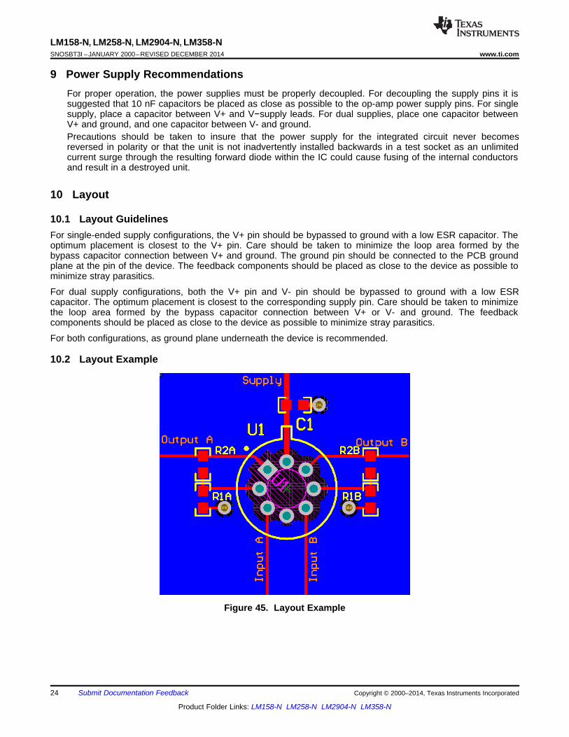
10.1 Layout GuidelinesFor single-ended supply configurations, the V+ pin should be bypassed to ground with a low ESR capacitor. Theoptimum placement is closest to the V+ pin. Care should be taken to minimize the loop area formed by thebypass capacitor connection between V+ and ground. The ground pin should be connected to the PCB groundplane at the pin of the device. The feedback components should be placed as close to the device as possible tominimize stray parasitics.
For dual supply configurations, both the V+ pin and V- pin should be bypassed to ground with a low ESRcapacitor. The optimum placement is closest to the corresponding supply pin. Care should be taken to minimizethe loop area formed by the bypass capacitor connection between V+ or V- and ground. The feedbackcomponents should be placed as close to the device as possible to minimize stray parasitics.
For both configurations, as ground plane underneath the device is recommended.
10.2 Layout Example
Figure 45. Layout Example
24 Submit Documentation Feedback Copyright © 2000–2014, Texas Instruments Incorporated
Product Folder Links: LM158-N LM258-N LM2904-N LM358-N

LM158-N, LM258-N, LM2904-N, LM358-Nwww.ti.com SNOSBT3I –JANUARY 2000–REVISED DECEMBER 2014
11 Device and Documentation Support
11.1 Related LinksThe table below lists quick access links. Categories include technical documents, support and communityresources, tools and software, and quick access to sample or buy.
Table 1. Related LinksTECHNICAL TOOLS & SUPPORT &PARTS PRODUCT FOLDER SAMPLE & BUY DOCUMENTS SOFTWARE COMMUNITY
LM158-N Click here Click here Click here Click here Click hereLM258-N Click here Click here Click here Click here Click hereLM2904-N Click here Click here Click here Click here Click hereLM358-N Click here Click here Click here Click here Click here
11.2 TrademarksAll trademarks are the property of their respective owners.
11.3 Electrostatic Discharge CautionThese devices have limited built-in ESD protection. The leads should be shorted together or the device placed in conductive foamduring storage or handling to prevent electrostatic damage to the MOS gates.
11.4 GlossarySLYZ022 — TI Glossary.
This glossary lists and explains terms, acronyms, and definitions.
12 Mechanical, Packaging, and Orderable InformationThe following pages include mechanical, packaging, and orderable information. This information is the mostcurrent data available for the designated devices. This data is subject to change without notice and revision ofthis document. For browser-based versions of this data sheet, refer to the left-hand navigation.
Copyright © 2000–2014, Texas Instruments Incorporated Submit Documentation Feedback 25
Product Folder Links: LM158-N LM258-N LM2904-N LM358-N

PACKAGE OPTION ADDENDUM
www.ti.com 21-Nov-2017
Addendum-Page 1
PACKAGING INFORMATION
Orderable Device Status(1)
Package Type PackageDrawing
Pins PackageQty
Eco Plan(2)
Lead/Ball Finish(6)
MSL Peak Temp(3)
Op Temp (°C) Device Marking(4/5)
Samples
LM158AH ACTIVE TO-99 LMC 8 500 TBD Call TI Call TI -55 to 125 ( LM158AH, LM158AH )
LM158AH/NOPB ACTIVE TO-99 LMC 8 500 Green (RoHS& no Sb/Br)
Call TI Level-1-NA-UNLIM -55 to 125 ( LM158AH, LM158AH )
LM158H ACTIVE TO-99 LMC 8 500 TBD Call TI Call TI -55 to 125 ( LM158H, LM158H)
LM158H/NOPB ACTIVE TO-99 LMC 8 500 Green (RoHS& no Sb/Br)
Call TI Level-1-NA-UNLIM -55 to 125 ( LM158H, LM158H)
LM158J ACTIVE CDIP NAB 8 40 TBD Call TI Call TI -55 to 125 LM158J
LM258H ACTIVE TO-99 LMC 8 500 TBD Call TI Call TI -25 to 85 ( LM258H, LM258H)
LM258H/NOPB ACTIVE TO-99 LMC 8 500 Green (RoHS& no Sb/Br)
Call TI Level-1-NA-UNLIM -25 to 85 ( LM258H, LM258H)
LM2904ITP/NOPB ACTIVE DSBGA YPB 8 250 Green (RoHS& no Sb/Br)
SNAGCU Level-1-260C-UNLIM -40 to 85 A09
LM2904ITPX/NOPB ACTIVE DSBGA YPB 8 3000 Green (RoHS& no Sb/Br)
SNAGCU Level-1-260C-UNLIM -40 to 85 A09
LM2904M LIFEBUY SOIC D 8 95 TBD Call TI Call TI -40 to 85 LM2904M
LM2904M/NOPB ACTIVE SOIC D 8 95 Green (RoHS& no Sb/Br)
CU SN Level-1-260C-UNLIM -40 to 85 LM2904M
LM2904MX NRND SOIC D 8 2500 TBD Call TI Call TI -40 to 85 LM2904M
LM2904MX/NOPB ACTIVE SOIC D 8 2500 Green (RoHS& no Sb/Br)
CU SN Level-1-260C-UNLIM -40 to 85 LM2904M
LM2904N/NOPB ACTIVE PDIP P 8 40 Green (RoHS& no Sb/Br)
CU SN Level-1-NA-UNLIM -40 to 85 LM2904N
LM358AM NRND SOIC D 8 95 TBD Call TI Call TI 0 to 70 LM358AM
LM358AM/NOPB ACTIVE SOIC D 8 95 Green (RoHS& no Sb/Br)
CU SN Level-1-260C-UNLIM 0 to 70 LM358AM
LM358AMX NRND SOIC D 8 2500 TBD Call TI Call TI 0 to 70 LM358AM

PACKAGE OPTION ADDENDUM
www.ti.com 21-Nov-2017
Addendum-Page 2
Orderable Device Status(1)
Package Type PackageDrawing
Pins PackageQty
Eco Plan(2)
Lead/Ball Finish(6)
MSL Peak Temp(3)
Op Temp (°C) Device Marking(4/5)
Samples
LM358AMX/NOPB ACTIVE SOIC D 8 2500 Green (RoHS& no Sb/Br)
CU SN Level-1-260C-UNLIM 0 to 70 LM358AM
LM358AN/NOPB ACTIVE PDIP P 8 40 Green (RoHS& no Sb/Br)
CU SN Level-1-NA-UNLIM 0 to 70 LM358AN
LM358H/NOPB ACTIVE TO-99 LMC 8 500 Green (RoHS& no Sb/Br)
Call TI Level-1-NA-UNLIM 0 to 70 ( LM358H, LM358H)
LM358M NRND SOIC D 8 95 TBD Call TI Call TI 0 to 70 LM358M
LM358M/NOPB ACTIVE SOIC D 8 95 Green (RoHS& no Sb/Br)
CU SN Level-1-260C-UNLIM 0 to 70 LM358M
LM358MX NRND SOIC D 8 2500 TBD Call TI Call TI 0 to 70 LM358M
LM358MX/NOPB ACTIVE SOIC D 8 2500 Green (RoHS& no Sb/Br)
CU SN Level-1-260C-UNLIM 0 to 70 LM358M
LM358N/NOPB ACTIVE PDIP P 8 40 Green (RoHS& no Sb/Br)
CU SN Level-1-NA-UNLIM 0 to 70 LM358N
LM358TP/NOPB ACTIVE DSBGA YPB 8 250 Green (RoHS& no Sb/Br)
SNAGCU Level-1-260C-UNLIM 0 to 70 A07
LM358TPX/NOPB ACTIVE DSBGA YPB 8 3000 Green (RoHS& no Sb/Br)
SNAGCU Level-1-260C-UNLIM 0 to 70 A07
(1) The marketing status values are defined as follows:ACTIVE: Product device recommended for new designs.LIFEBUY: TI has announced that the device will be discontinued, and a lifetime-buy period is in effect.NRND: Not recommended for new designs. Device is in production to support existing customers, but TI does not recommend using this part in a new design.PREVIEW: Device has been announced but is not in production. Samples may or may not be available.OBSOLETE: TI has discontinued the production of the device.
(2) RoHS: TI defines "RoHS" to mean semiconductor products that are compliant with the current EU RoHS requirements for all 10 RoHS substances, including the requirement that RoHS substancedo not exceed 0.1% by weight in homogeneous materials. Where designed to be soldered at high temperatures, "RoHS" products are suitable for use in specified lead-free processes. TI mayreference these types of products as "Pb-Free".RoHS Exempt: TI defines "RoHS Exempt" to mean products that contain lead but are compliant with EU RoHS pursuant to a specific EU RoHS exemption.Green: TI defines "Green" to mean the content of Chlorine (Cl) and Bromine (Br) based flame retardants meet JS709B low halogen requirements of <=1000ppm threshold. Antimony trioxide basedflame retardants must also meet the <=1000ppm threshold requirement.
(3) MSL, Peak Temp. - The Moisture Sensitivity Level rating according to the JEDEC industry standard classifications, and peak solder temperature.
PACKAGE OPTION ADDENDUM
www.ti.com 21-Nov-2017
Addendum-Page 3
(4) There may be additional marking, which relates to the logo, the lot trace code information, or the environmental category on the device.
(5) Multiple Device Markings will be inside parentheses. Only one Device Marking contained in parentheses and separated by a "~" will appear on a device. If a line is indented then it is a continuationof the previous line and the two combined represent the entire Device Marking for that device.
(6) Lead/Ball Finish - Orderable Devices may have multiple material finish options. Finish options are separated by a vertical ruled line. Lead/Ball Finish values may wrap to two lines if the finishvalue exceeds the maximum column width.
Important Information and Disclaimer:The information provided on this page represents TI's knowledge and belief as of the date that it is provided. TI bases its knowledge and belief on informationprovided by third parties, and makes no representation or warranty as to the accuracy of such information. Efforts are underway to better integrate information from third parties. TI has taken andcontinues to take reasonable steps to provide representative and accurate information but may not have conducted destructive testing or chemical analysis on incoming materials and chemicals.TI and TI suppliers consider certain information to be proprietary, and thus CAS numbers and other limited information may not be available for release.
In no event shall TI's liability arising out of such information exceed the total purchase price of the TI part(s) at issue in this document sold by TI to Customer on an annual basis.
OTHER QUALIFIED VERSIONS OF LM2904-N :
• Automotive: LM2904-Q1
• Enhanced Product: LM2904-EP
NOTE: Qualified Version Definitions:
• Automotive - Q100 devices qualified for high-reliability automotive applications targeting zero defects
• Enhanced Product - Supports Defense, Aerospace and Medical Applications

TAPE AND REEL INFORMATION
*All dimensions are nominal
Device PackageType
PackageDrawing
Pins SPQ ReelDiameter
(mm)
ReelWidth
W1 (mm)
A0(mm)
B0(mm)
K0(mm)
P1(mm)
W(mm)
Pin1Quadrant
LM2904ITP/NOPB DSBGA YPB 8 250 178.0 8.4 1.5 1.5 0.66 4.0 8.0 Q1
LM2904ITPX/NOPB DSBGA YPB 8 3000 178.0 8.4 1.5 1.5 0.66 4.0 8.0 Q1
LM2904MX SOIC D 8 2500 330.0 12.4 6.5 5.4 2.0 8.0 12.0 Q1
LM2904MX/NOPB SOIC D 8 2500 330.0 12.4 6.5 5.4 2.0 8.0 12.0 Q1
LM358AMX SOIC D 8 2500 330.0 12.4 6.5 5.4 2.0 8.0 12.0 Q1
LM358AMX/NOPB SOIC D 8 2500 330.0 12.4 6.5 5.4 2.0 8.0 12.0 Q1
LM358MX SOIC D 8 2500 330.0 12.4 6.5 5.4 2.0 8.0 12.0 Q1
LM358MX/NOPB SOIC D 8 2500 330.0 12.4 6.5 5.4 2.0 8.0 12.0 Q1
LM358TP/NOPB DSBGA YPB 8 250 178.0 8.4 1.5 1.5 0.66 4.0 8.0 Q1
LM358TPX/NOPB DSBGA YPB 8 3000 178.0 8.4 1.5 1.5 0.66 4.0 8.0 Q1
PACKAGE MATERIALS INFORMATION
www.ti.com 7-Oct-2014
Pack Materials-Page 1

*All dimensions are nominal
Device Package Type Package Drawing Pins SPQ Length (mm) Width (mm) Height (mm)
LM2904ITP/NOPB DSBGA YPB 8 250 210.0 185.0 35.0
LM2904ITPX/NOPB DSBGA YPB 8 3000 210.0 185.0 35.0
LM2904MX SOIC D 8 2500 367.0 367.0 35.0
LM2904MX/NOPB SOIC D 8 2500 367.0 367.0 35.0
LM358AMX SOIC D 8 2500 367.0 367.0 35.0
LM358AMX/NOPB SOIC D 8 2500 367.0 367.0 35.0
LM358MX SOIC D 8 2500 367.0 367.0 35.0
LM358MX/NOPB SOIC D 8 2500 367.0 367.0 35.0
LM358TP/NOPB DSBGA YPB 8 250 210.0 185.0 35.0
LM358TPX/NOPB DSBGA YPB 8 3000 210.0 185.0 35.0
PACKAGE MATERIALS INFORMATION
www.ti.com 7-Oct-2014
Pack Materials-Page 2
MECHANICAL DATA
NAB0008A
www.ti.com
J08A (Rev M)
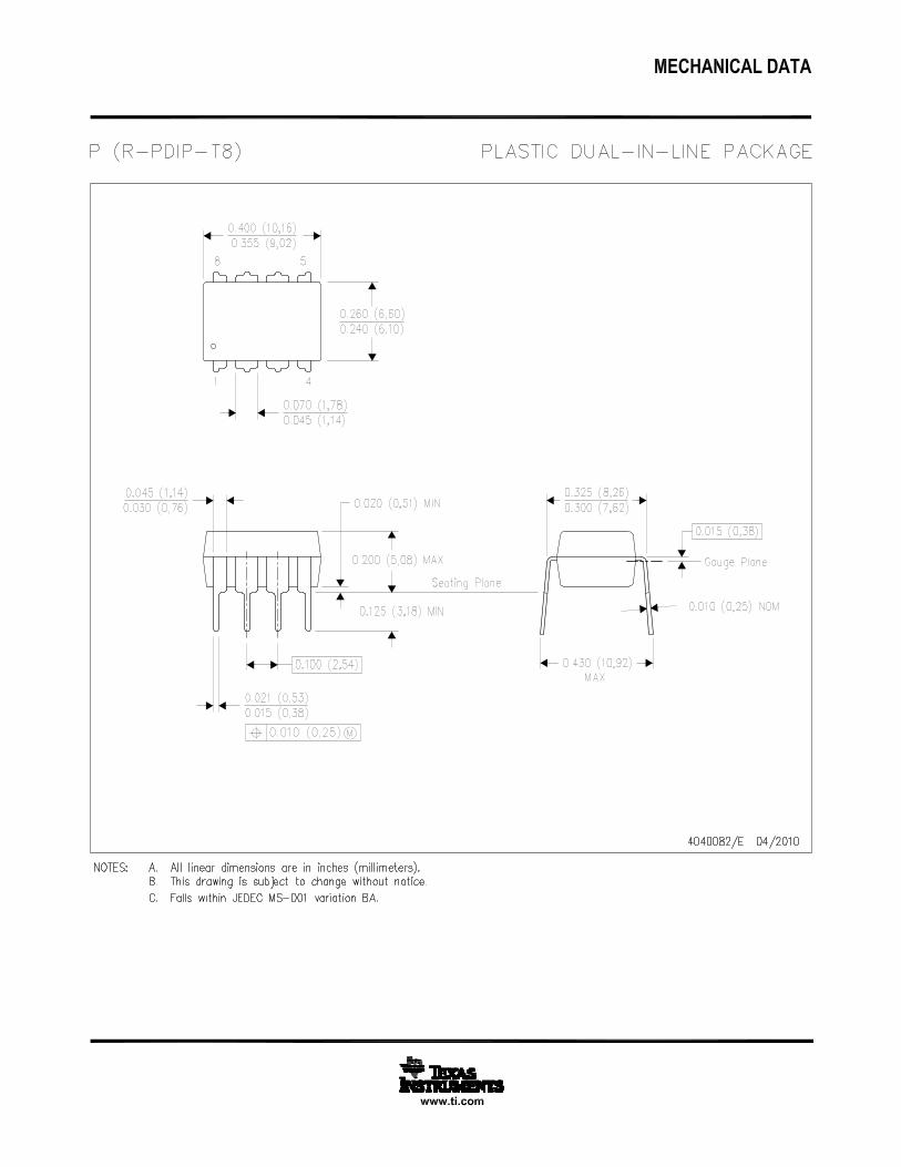

www.ti.com
PACKAGE OUTLINE
C0.575 MAX
0.150.11
1TYP
1TYP
8X 0.180.16
0.5TYP
0.5TYP
B E A
D
4215100/B 07/2016
DSBGA - 0.575 mm max heightYPB0008DIE SIZE BALL GRID ARRAY
NOTES: 1. All linear dimensions are in millimeters. Any dimensions in parenthesis are for reference only. Dimensioning and tolerancing per ASME Y14.5M.2. This drawing is subject to change without notice.
SYMM
SYMM
BALL A1CORNER
SEATING PLANE
BALL TYP0.05 C
1 2
0.015 C A B
A
B
C
3
SCALE 9.000
D: Max =
E: Max =
1.337 mm, Min =
1.337 mm, Min =
1.276 mm
1.276 mm

www.ti.com
EXAMPLE BOARD LAYOUT
8X ( 0.16)
( 0.16)METAL
0.05 MAX
SOLDER MASKOPENING
METAL UNDERSOLDER MASK
( 0.16)SOLDER MASKOPENING
0.05 MIN
(0.5) TYP
(0.5)TYP
4215100/B 07/2016
DSBGA - 0.575 mm max heightYPB0008DIE SIZE BALL GRID ARRAY
NOTES: (continued) 3. Final dimensions may vary due to manufacturing tolerance considerations and also routing constraints. See Texas Instruments Literature No. SNVA009 (www.ti.com/lit/snva009).
SOLDER MASK DETAILSNOT TO SCALE
1 2
A
B
SYMM
SYMM
LAND PATTERN EXAMPLESCALE:40X
C
3
NON-SOLDER MASKDEFINED
(PREFERRED)SOLDER MASK
DEFINED

www.ti.com
EXAMPLE STENCIL DESIGN
8X ( 0.3) (R0.05) TYP
METALTYP
(0.5) TYP
(0.5) TYP
4215100/B 07/2016
DSBGA - 0.575 mm max heightYPB0008DIE SIZE BALL GRID ARRAY
NOTES: (continued) 4. Laser cutting apertures with trapezoidal walls and rounded corners may offer better paste release.
1 2
A
B
C
3
SYMM
SYMM
SOLDER PASTE EXAMPLEBASED ON 0.125mm THICK STENCIL
SCALE:50X


IMPORTANT NOTICE
Texas Instruments Incorporated (TI) reserves the right to make corrections, enhancements, improvements and other changes to itssemiconductor products and services per JESD46, latest issue, and to discontinue any product or service per JESD48, latest issue. Buyersshould obtain the latest relevant information before placing orders and should verify that such information is current and complete.TI’s published terms of sale for semiconductor products (http://www.ti.com/sc/docs/stdterms.htm) apply to the sale of packaged integratedcircuit products that TI has qualified and released to market. Additional terms may apply to the use or sale of other types of TI products andservices.Reproduction of significant portions of TI information in TI data sheets is permissible only if reproduction is without alteration and isaccompanied by all associated warranties, conditions, limitations, and notices. TI is not responsible or liable for such reproduceddocumentation. Information of third parties may be subject to additional restrictions. Resale of TI products or services with statementsdifferent from or beyond the parameters stated by TI for that product or service voids all express and any implied warranties for theassociated TI product or service and is an unfair and deceptive business practice. TI is not responsible or liable for any such statements.Buyers and others who are developing systems that incorporate TI products (collectively, “Designers”) understand and agree that Designersremain responsible for using their independent analysis, evaluation and judgment in designing their applications and that Designers havefull and exclusive responsibility to assure the safety of Designers' applications and compliance of their applications (and of all TI productsused in or for Designers’ applications) with all applicable regulations, laws and other applicable requirements. Designer represents that, withrespect to their applications, Designer has all the necessary expertise to create and implement safeguards that (1) anticipate dangerousconsequences of failures, (2) monitor failures and their consequences, and (3) lessen the likelihood of failures that might cause harm andtake appropriate actions. Designer agrees that prior to using or distributing any applications that include TI products, Designer willthoroughly test such applications and the functionality of such TI products as used in such applications.TI’s provision of technical, application or other design advice, quality characterization, reliability data or other services or information,including, but not limited to, reference designs and materials relating to evaluation modules, (collectively, “TI Resources”) are intended toassist designers who are developing applications that incorporate TI products; by downloading, accessing or using TI Resources in anyway, Designer (individually or, if Designer is acting on behalf of a company, Designer’s company) agrees to use any particular TI Resourcesolely for this purpose and subject to the terms of this Notice.TI’s provision of TI Resources does not expand or otherwise alter TI’s applicable published warranties or warranty disclaimers for TIproducts, and no additional obligations or liabilities arise from TI providing such TI Resources. TI reserves the right to make corrections,enhancements, improvements and other changes to its TI Resources. TI has not conducted any testing other than that specificallydescribed in the published documentation for a particular TI Resource.Designer is authorized to use, copy and modify any individual TI Resource only in connection with the development of applications thatinclude the TI product(s) identified in such TI Resource. NO OTHER LICENSE, EXPRESS OR IMPLIED, BY ESTOPPEL OR OTHERWISETO ANY OTHER TI INTELLECTUAL PROPERTY RIGHT, AND NO LICENSE TO ANY TECHNOLOGY OR INTELLECTUAL PROPERTYRIGHT OF TI OR ANY THIRD PARTY IS GRANTED HEREIN, including but not limited to any patent right, copyright, mask work right, orother intellectual property right relating to any combination, machine, or process in which TI products or services are used. Informationregarding or referencing third-party products or services does not constitute a license to use such products or services, or a warranty orendorsement thereof. Use of TI Resources may require a license from a third party under the patents or other intellectual property of thethird party, or a license from TI under the patents or other intellectual property of TI.TI RESOURCES ARE PROVIDED “AS IS” AND WITH ALL FAULTS. TI DISCLAIMS ALL OTHER WARRANTIES ORREPRESENTATIONS, EXPRESS OR IMPLIED, REGARDING RESOURCES OR USE THEREOF, INCLUDING BUT NOT LIMITED TOACCURACY OR COMPLETENESS, TITLE, ANY EPIDEMIC FAILURE WARRANTY AND ANY IMPLIED WARRANTIES OFMERCHANTABILITY, FITNESS FOR A PARTICULAR PURPOSE, AND NON-INFRINGEMENT OF ANY THIRD PARTY INTELLECTUALPROPERTY RIGHTS. TI SHALL NOT BE LIABLE FOR AND SHALL NOT DEFEND OR INDEMNIFY DESIGNER AGAINST ANY CLAIM,INCLUDING BUT NOT LIMITED TO ANY INFRINGEMENT CLAIM THAT RELATES TO OR IS BASED ON ANY COMBINATION OFPRODUCTS EVEN IF DESCRIBED IN TI RESOURCES OR OTHERWISE. IN NO EVENT SHALL TI BE LIABLE FOR ANY ACTUAL,DIRECT, SPECIAL, COLLATERAL, INDIRECT, PUNITIVE, INCIDENTAL, CONSEQUENTIAL OR EXEMPLARY DAMAGES INCONNECTION WITH OR ARISING OUT OF TI RESOURCES OR USE THEREOF, AND REGARDLESS OF WHETHER TI HAS BEENADVISED OF THE POSSIBILITY OF SUCH DAMAGES.Unless TI has explicitly designated an individual product as meeting the requirements of a particular industry standard (e.g., ISO/TS 16949and ISO 26262), TI is not responsible for any failure to meet such industry standard requirements.Where TI specifically promotes products as facilitating functional safety or as compliant with industry functional safety standards, suchproducts are intended to help enable customers to design and create their own applications that meet applicable functional safety standardsand requirements. Using products in an application does not by itself establish any safety features in the application. Designers mustensure compliance with safety-related requirements and standards applicable to their applications. Designer may not use any TI products inlife-critical medical equipment unless authorized officers of the parties have executed a special contract specifically governing such use.Life-critical medical equipment is medical equipment where failure of such equipment would cause serious bodily injury or death (e.g., lifesupport, pacemakers, defibrillators, heart pumps, neurostimulators, and implantables). Such equipment includes, without limitation, allmedical devices identified by the U.S. Food and Drug Administration as Class III devices and equivalent classifications outside the U.S.TI may expressly designate certain products as completing a particular qualification (e.g., Q100, Military Grade, or Enhanced Product).Designers agree that it has the necessary expertise to select the product with the appropriate qualification designation for their applicationsand that proper product selection is at Designers’ own risk. Designers are solely responsible for compliance with all legal and regulatoryrequirements in connection with such selection.Designer will fully indemnify TI and its representatives against any damages, costs, losses, and/or liabilities arising out of Designer’s non-compliance with the terms and provisions of this Notice.
Mailing Address: Texas Instruments, Post Office Box 655303, Dallas, Texas 75265Copyright © 2017, Texas Instruments Incorporated