Embed Size (px)
Citation preview
October 2007
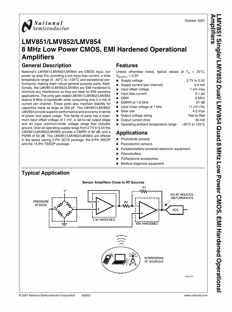
LMV851/LMV852/LMV8548 MHz Low Power CMOS, EMI Hardened OperationalAmplifiersGeneral DescriptionNational’s LMV851/LMV852/LMV854 are CMOS input, lowpower op amp ICs, providing a low input bias current, a widetemperature range of −40°C to +125°C and exceptional per-formance, making them robust general purpose parts. Addi-tionally, the LMV851/LMV852/LMV854 are EMI hardened tominimize any interference so they are ideal for EMI sensitiveapplications. The unity gain stable LMV851/LMV852/LMV854feature 8 MHz of bandwidth while consuming only 0.4 mA ofcurrent per channel. These parts also maintain stability forcapacitive loads as large as 200 pF. The LMV851/LMV852/LMV854 provide superior performance and economy in termsof power and space usage. This family of parts has a maxi-mum input offset voltage of 1 mV, a rail-to-rail output stageand an input common-mode voltage range that includesground. Over an operating supply range from 2.7V to 5.5V theLMV851/LMV852/LMV854 provide a CMRR of 92 dB, and aPSRR of 93 dB. The LMV851/LMV852/LMV854 are offeredin the space saving 5-Pin SC70 package, the 8-Pin MSOPand the 14-Pin TSSOP package.
FeaturesUnless otherwise noted, typical values at TA = 25°C,VSUPPLY = 3.3V
Supply voltage 2.7V to 5.5V
Supply current (per channel) 0.4 mA
Input offset voltage 1 mV max
Input bias current 0.1 pA
GBW 8 MHz
EMIRR at 1.8 GHz 87 dB
Input noise voltage at 1 kHz 11 nV/√Hz
Slew rate 4.5 V/µs
Output voltage swing Rail-to-Rail
Output current drive 30 mA
Operating ambient temperature range −40°C to 125°C
Applications Photodiode preamp
Piezoelectric sensors
Portable/battery-powered electronic equipment
Filters/buffers
PDAs/phone accessories
Medical diagnosis equipment
Typical Application
Sensor Amplifiers Close to RF Sources
20202101
© 2007 National Semiconductor Corporation 202021 www.national.com
LM
V851 S
ing
le/ L
MV
852 D
ual/ L
MV
854 Q
uad
8 M
Hz L
ow
Po
wer C
MO
S, E
MI H
ard
en
ed
Op
era
tion
al
Am
plifie
rs
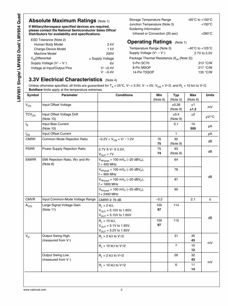
Absolute Maximum Ratings (Note 1)
If Military/Aerospace specified devices are required,please contact the National Semiconductor Sales Office/Distributors for availability and specifications.
ESD Tolerance (Note 2)
Human Body Model 2 kV
Charge-Device Model 1 kV
Machine Model 200V
VINDifferential ± Supply Voltage
Supply Voltage (V+ – V−) 6V
Voltage at Input/Output Pins V+ +0.4VV− −0.4V
Storage Temperature Range −65°C to +150°C
Junction Temperature (Note 3) +150°C
Soldering Information
Infrared or Convection (20 sec) +260°C
Operating Ratings (Note 1)
Temperature Range (Note 3) −40°C to +125°C
Supply Voltage (V+ – V−) 2.7V to 5.5V
Package Thermal Resistance (θJA (Note 3))
5-Pin SC70 313 °C/W
8-Pin MSOP 217 °C/W
14-Pin TSSOP 135 °C/W
3.3V Electrical Characteristics (Note 4)
Unless otherwise specified, all limits are guaranteed for TA = 25°C, V+ = 3.3V, V− = 0V, VCM = V+/2, and RL = 10 kΩ to V+/2.Boldface limits apply at the temperature extremes.
Symbol Parameter Conditions Min
(Note 6)
Typ
(Note 5)
Max
(Note 6)
Units
VOS Input Offset Voltage ±0.26
(Note 9)
±1
±1.2mV
TCVOS Input Offset Voltage Drift
(Note 10)
±0.4
(Note 9)
±2μV/°C
IB Input Bias Current
(Note 10)
0.1 10
500pA
IOS Input Offset Current 1 pA
CMRR Common Mode Rejection Ratio −0.2V < VCM < V+ - 1.2V 76
75
92
(Note 9)
dB
PSRR Power Supply Rejection Ratio 2.7V ≤ V+ ≤ 5.5V,
VOUT = 1V
75
74
93
(Note 9)
dB
EMIRR EMI Rejection Ratio, IN+ and IN−
(Note 8)
VRFpeak = 100 mVP (−20 dBVP),
f = 400 MHz
64
dB
VRFpeak = 100 mVP (−20 dBVP),
f = 900 MHz
78
VRFpeak = 100 mVP (−20 dBVP),
f = 1800 MHz
87
VRFpeak = 100 mVP (−20 dBVP),
f = 2400 MHz
90
CMVR Input Common-Mode Voltage Range CMRR ≥ 76 dB −0.2 2.1 V
AVOL Large Signal Voltage Gain
(Note 11)RL = 2 kΩ,VOUT = 0.15V to 1.65V,
VOUT = 3.15V to 1.65V
100
97
114
dBRL = 10 kΩ,VOUT = 0.1V to 1.65V,
VOUT = 3.2V to 1.65V
100
97
115
VO Output Swing High,
(measured from V+)RL = 2 kΩ to V+/2 31 35
43mV
RL = 10 kΩ to V+/2 7 10
12
Output Swing Low,
(measured from V−)RL = 2 kΩ to V+/2 26 32
43mV
RL = 10 kΩ to V+/2 6 11
14
www.national.com 2
LM
V851 S
ing
le/ L
MV
852 D
ual/ L
MV
854 Q
uad
Symbol Parameter Conditions Min
(Note 6)
Typ
(Note 5)
Max
(Note 6)
Units
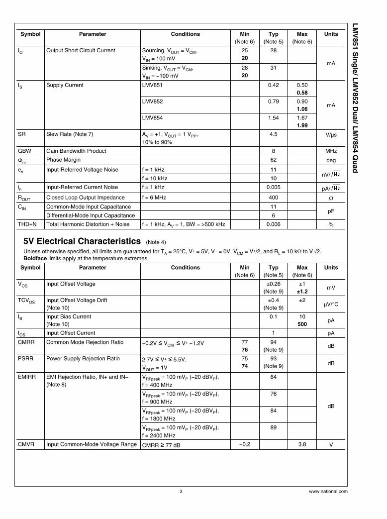
IO Output Short Circuit Current Sourcing, VOUT = VCM,
VIN = 100 mV
25
20
28
mASinking, VOUT = VCM,
VIN = −100 mV
28
20
31
IS Supply Current LMV851 0.42 0.50
0.58
mALMV852 0.79 0.90
1.06
LMV854 1.54 1.67
1.99
SR Slew Rate (Note 7) AV = +1, VOUT = 1 VPP,
10% to 90%
4.5 V/μs
GBW Gain Bandwidth Product 8 MHz
ΦmPhase Margin 62 deg
en Input-Referred Voltage Noise f = 1 kHz 11 nV/
f = 10 kHz 10
in Input-Referred Current Noise f = 1 kHz 0.005 pA/
ROUT Closed Loop Output Impedance f = 6 MHz 400 ΩCIN Common-Mode Input Capacitance 11
pFDifferential-Mode Input Capacitance 6
THD+N Total Harmonic Distortion + Noise f = 1 kHz, AV = 1, BW = >500 kHz 0.006 %
5V Electrical Characteristics (Note 4)
Unless otherwise specified, all limits are guaranteed for TA = 25°C, V+ = 5V, V− = 0V, VCM = V+/2, and RL = 10 kΩ to V+/2.Boldface limits apply at the temperature extremes.
Symbol Parameter Conditions Min
(Note 6)
Typ
(Note 5)
Max
(Note 6)
Units
VOS Input Offset Voltage ±0.26
(Note 9)
±1
±1.2mV
TCVOS Input Offset Voltage Drift
(Note 10)
±0.4
(Note 9)
±2μV/°C
IB Input Bias Current
(Note 10)
0.1 10
500pA
IOS Input Offset Current 1 pA
CMRR Common Mode Rejection Ratio −0.2V ≤ VCM ≤ V+ −1.2V 77
76
94
(Note 9)
dB
PSRR Power Supply Rejection Ratio 2.7V ≤ V+ ≤ 5.5V,
VOUT = 1V
75
74
93
(Note 9)
dB
EMIRR EMI Rejection Ratio, IN+ and IN−
(Note 8)
VRFpeak = 100 mVP (−20 dBVP),
f = 400 MHz
64
dB
VRFpeak = 100 mVP (−20 dBVP),
f = 900 MHz
76
VRFpeak = 100 mVP (−20 dBVP),
f = 1800 MHz
84
VRFpeak = 100 mVP (−20 dBVP),
f = 2400 MHz
89
CMVR Input Common-Mode Voltage Range CMRR ≥ 77 dB −0.2 3.8 V
3 www.national.com
LM
V851 S
ing
le/ L
MV
852 D
ual/ L
MV
854 Q
uad
Symbol Parameter Conditions Min
(Note 6)
Typ
(Note 5)
Max
(Note 6)
Units
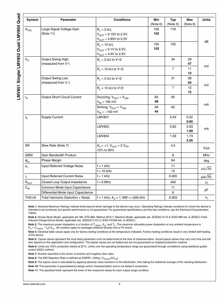
AVOL Large Signal Voltage Gain
(Note 11)RL = 2 kΩ,VOUT = 0.15V to 2.5V,
VOUT = 4.85V to 2.5V
105
102
118
dBRL = 10 kΩ,VOUT = 0.1V to 2.5V,
VOUT = 4.9V to 2.5V
105
102
120
VO Output Swing High,
(measured from V+)RL = 2 kΩ to V+/2 34 39
47mV
RL = 10 kΩ to V+/2 7 11
13
Output Swing Low,
(measured from V−)RL = 2 kΩ to V+/2 31 38
50mV
RL = 10 kΩ to V+/2 7 12
15
IO Output Short Circuit Current Sourcing, VOUT = VCM,
VIN = 100 mV
60
48
65
mASinking, VOUT = VCM,
VIN = −100 mV
58
44
62
IS Supply Current LMV851 0.43 0.52
0.60
mALMV852 0.82 0.93
1.09
LMV854 1.59 1.73
2.05
SR Slew Rate (Note 7) AV = +1, VOUT = 2 VPP,
10% to 90%
4.5 V/μs
GBW Gain Bandwidth Product 8 MHz
ΦmPhase Margin 64 deg
en Input-Referred Voltage Noise f = 1 kHz 11 nV/
f = 10 kHz 10
in Input-Referred Current Noise f = 1 kHz 0.005 pA/
ROUT Closed Loop Output Impedance f = 6 MHz 400 ΩCIN Common-Mode Input Capacitance 11
pFDifferential-Mode Input Capacitance 6
THD+N Total Harmonic Distortion + Noise f = 1 kHz, AV = 1, BW = >500 kHz 0.003 %
Note 1: Absolute Maximum Ratings indicate limits beyond which damage to the device may occur. Operating Ratings indicate conditions for which the device isintended to be functional, but specific performance is not guaranteed. For guaranteed specifications and the test conditions, see the Electrical CharacteristicsTables.
Note 2: Human Body Model, applicable std. MIL-STD-883, Method 3015.7. Machine Model, applicable std. JESD22-A115-A (ESD MM std. of JEDEC) Field-Induced Charge-Device Model, applicable std. JESD22-C101-C (ESD FICDM std. of JEDEC).
Note 3: The maximum power dissipation is a function of TJ(MAX), θJA, and TA. The maximum allowable power dissipation at any ambient temperature isPD = (TJ(MAX) - TA)/ θJA . All numbers apply for packages soldered directly onto a PC board.
Note 4: Electrical table values apply only for factory testing conditions at the temperature indicated. Factory testing conditions result in very limited self-heatingof the device.
Note 5: Typical values represent the most likely parametric norm as determined at the time of characterization. Actual typical values may vary over time and willalso depend on the application and configuration. The typical values are not tested and are not guaranteed on shipped production material.
Note 6: Limits are 100% production tested at 25°C. Limits over the operating temperature range are guaranteed through correlations using statistical qualitycontrol (SQC) method.
Note 7: Number specified is the slower of positive and negative slew rates.
Note 8: The EMI Rejection Ratio is defined as EMIRR = 20log ( VRFpeak/ΔVOS).
Note 9: The typical value is calculated by applying absolute value transform to the distribution, then taking the statistical average of the resulting distribution
Note 10: This parameter is guaranteed by design and/or characterization and is not tested in production.
Note 11: The specified limits represent the lower of the measured values for each output range condition.
www.national.com 4
LM
V851 S
ing
le/ L
MV
852 D
ual/ L
MV
854 Q
uad

Connection Diagrams
5-Pin SC70
20202102
Top View
8-Pin MSOP
20202103
Top View
14-Pin TSSOP
20202104
Top View
Ordering Information
Package Part Number Package Marking Transport Media NSC Drawing
5-Pin SC70LMV851MG
A981k Units Tape and Reel
MAA05ALMV851MGX 3k Units Tape and Reel
8-Pin MSOPLMV852MM
AB5A1k Units Tape and Reel
MUA08ALMV852MMX 3.5k Units Tape and Reel
14-Pin TSSOPLMV854MT
LMV854MT94 Units/Rail
MTC14LMV854MTX 2.5k Units Tape and Reel
5 www.national.com
LM
V851 S
ing
le/ L
MV
852 D
ual/ L
MV
854 Q
uad

Typical Performance Characteristics At TA = 25°C, RL = 10 kΩ, VS = 3.3V, unless otherwise specified.
VOS vs. VCM at 3.3V
20202110
VOS vs. VCM at 5.0V
20202111
VOS vs. Supply Voltage
20202112
VOS vs. Temperature
20202113
VOS vs. VOUT
20202114
Input Bias Current vs. VCM at 25°C
20202115
www.national.com 6
LM
V851 S
ing
le/ L
MV
852 D
ual/ L
MV
854 Q
uad

Input Bias Current vs. VCM at 85°C
20202116
Input Bias Current vs. VCM at 125°C
20202117
Supply Current vs. Supply Voltage Single LMV851
20202118
Supply Current vs. Supply Voltage Dual LMV852
20202119
Supply Current vs. Supply Voltage Quad LMV854
20202120
Supply Current vs. Temperature Single LMV851
20202121
7 www.national.com
LM
V851 S
ing
le/ L
MV
852 D
ual/ L
MV
854 Q
uad

Supply Current vs. Temperature Dual LMV852
20202122
Supply Current vs. Temperature Quad LMV854
20202123
Sinking Current vs. Supply Voltage
20202124
Sourcing Current vs. Supply Voltage
20202125
Output Swing High vs. Supply Voltage RL = 2 kΩ
20202126
Output Swing High vs. Supply Voltage RL = 10 kΩ
20202127
www.national.com 8
LM
V851 S
ing
le/ L
MV
852 D
ual/ L
MV
854 Q
uad

Output Swing Low vs. Supply Voltage RL = 2 kΩ
20202128
Output Swing Low vs. Supply Voltage RL = 10 kΩ
20202129
Output Voltage Swing vs. Load Current at 3.3V
20202155
Output Voltage Swing vs. Load Current at 5.0V
20202156
Open Loop Frequency Response vs. Temperature
20202131
Open Loop Frequency Response vs. Load Conditions
20202132
9 www.national.com
LM
V851 S
ing
le/ L
MV
852 D
ual/ L
MV
854 Q
uad
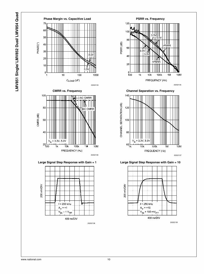
Phase Margin vs. Capacitive Load
20202133
PSRR vs. Frequency
20202135
CMRR vs. Frequency
20202136
Channel Separation vs. Frequency
20202137
Large Signal Step Response with Gain = 1
20202138
Large Signal Step Response with Gain = 10
20202139
www.national.com 10
LM
V851 S
ing
le/ L
MV
852 D
ual/ L
MV
854 Q
uad
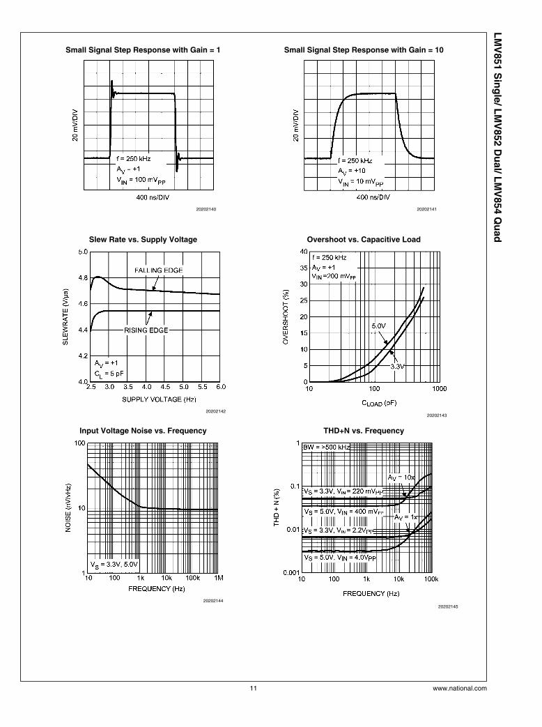
Small Signal Step Response with Gain = 1
20202140
Small Signal Step Response with Gain = 10
20202141
Slew Rate vs. Supply Voltage
20202142
Overshoot vs. Capacitive Load
20202143
Input Voltage Noise vs. Frequency
20202144
THD+N vs. Frequency
20202145
11 www.national.com
LM
V851 S
ing
le/ L
MV
852 D
ual/ L
MV
854 Q
uad

THD+N vs. Amplitude
20202146
ROUT vs. Frequency
20202148
EMIRR IN+ vs. Power at 400 MHz
20202149
EMIRR IN+ vs. Power at 900 MHz
20202150
EMIRR IN+ vs. Power at 1800 MHz
20202151
EMIRR IN+ vs. Power at 2400 MHz
20202152
www.national.com 12
LM
V851 S
ing
le/ L
MV
852 D
ual/ L
MV
854 Q
uad

EMIRR IN+ vs. Frequency at 3.3V
20202153
EMIRR IN+ vs. Frequency at 5.0V
20202154
13 www.national.com
LM
V851 S
ing
le/ L
MV
852 D
ual/ L
MV
854 Q
uad

Application Information
INTRODUCTION
The LMV851/LMV852/LMV854 are operational amplifierswith very good specifications, such as low offset, low noiseand a rail-to-rail output. These specifications make theLMV851/LMV852/LMV854 great choices to use in areas suchas medical and instrumentation. The low supply current isperfect for battery powered equipment. The small packages,SC-70 package for the LMV851, the MSOP package for thedual LMV852 and the TSSOP package for the quad LMV854,make any of these parts a perfect choice for portable elec-tronics. Additionally, the EMI hardening makes the LMV851/LMV852 or LMV854 a must for almost all op amp applications.Most applications are exposed to Radio Frequency (RF) sig-nals such as the signals transmitted by mobile phones orwireless computer peripherals. The LMV851/LMV852/LMV854 will effectively reduce disturbances caused by RFsignals to a level that will be hardly noticeable. This againreduces the need for additional filtering and shielding. Usingthis EMI resistant series of op amps will thus reduce the num-ber of components and space needed for applications that areaffected by EMI, and will help applications, not yet identifiedas possible EMI sensitive, to be more robust for EMI.
INPUT CHARACTERISTICS
The input common mode voltage range of the LMV851/LMV852/LMV854 includes ground, and can even sense wellbelow ground. The CMRR level does not degrade for inputlevels up to 1.2V below the supply voltage. For a supply volt-age of 5V, the maximum voltage that should be applied to theinput for best CMRR performance is thus 3.8V.
When not configured as unity gain, this input limitation willusually not degrade the effective signal range. The output israil-to-rail and therefore will introduce no limitations to thesignal range.
The typical offset is only 0.26 mV, and the TCVOS is0.4 μV/°C, specifications close to precision op amps.
CMRR MEASUREMENT
The CMRR measurement results may need some clarifica-tion. This is because different setups are used to measure theAC CMRR and the DC CMRR.
The DC CMRR is derived from ΔVOS versus ΔVCM. This valueis stated in the tables, and is tested during production testing.
The AC CMRR is measured with the test circuit shown inFigure 1.
20202164
FIGURE 1. AC CMRR Measurement Setup
The configuration is largely the usually applied balanced con-figuration. With potentiometer P1, the balance can be tunedto compensate for the DC offset in the DUT. The main differ-ence is the addition of the buffer. This buffer prevents theopen-loop output impedance of the DUT from affecting thebalance of the feedback network. Now the closed-loop outputimpedance of the buffer is a part of the balance. But as theclosed-loop output impedance is much lower, and by carefulselection of the buffer also has a larger bandwidth, the totaleffect is that the CMRR of the DUT can be measured muchmore accurately. The differences are apparent in the largermeasured bandwidth of the AC CMRR.
One artifact from this test circuit is that the low frequency CM-RR results appear higher than expected. This is because inthe AC CMRR test circuit the potentiometer is used to com-pensate for the DC mismatches. So, mainly AC mismatch isall that remains. Therefore, the obtained DC CMRR from thisAC CMRR test circuit tends to be higher than the actual DCCMRR based on DC measurements.
The CMRR curve in Figure 2 shows a combination of the ACCMRR and the DC CMRR.
20202136
FIGURE 2. CMRR Curve
www.national.com 14
LM
V851 S
ing
le/ L
MV
852 D
ual/ L
MV
854 Q
uad

OUTPUT CHARACTERISTICS
As already mentioned the output is rail to rail. When loadingthe output with a 10 kΩ resistor the maximum swing of theoutput is typically 7 mV from the positive and negative rail
The LMV851/LMV852/LMV854 can be connected as non-in-verting unity gain amplifiers. This configuration is the mostsensitive to capacitive loading. The combination of a capaci-tive load placed at the output of an amplifier along with theamplifier’s output impedance creates a phase lag, which re-duces the phase margin of the amplifier. If the phase marginis significantly reduced, the response will be under dampedwhich causes peaking in the transfer and, when there is toomuch peaking, the op amp might start oscillating. TheLMV851/LMV852/LMV854 can directly drive capacitive loadsup to 200 pF without any stability issues. In order to driveheavier capacitive loads, an isolation resistor, RISO, should beused, as shown in Figure 3. By using this isolation resistor,the capacitive load is isolated from the amplifier’s output, andhence, the pole caused by CL is no longer in the feedbackloop. The larger the value of RISO, the more stable the ampli-fier will be. If the value of RISO is sufficiently large, the feed-back loop will be stable, independent of the value of CL.However, larger values of RISO result in reduced output swingand reduced output current drive.
20202163
FIGURE 3. Isolating Capacitive Load
EMIRR
With the increase of RF transmitting devices in the world, theelectromagnetic interference (EMI) between those devicesand other equipment becomes a bigger challenge. TheLMV851/LMV852/LMV854 are EMI hardened op amps whichare specifically designed to overcome electromagnetic inter-ference. Along with EMI hardened op amps, the EMIRR pa-rameter is introduced to unambiguously specify the EMIperformance of an op amp. This section presents an overviewof EMIRR. A detailed description on this specification for EMIhardened op amps can be found in Application Note AN-1698.
The dimensions of an op amp IC are relatively small com-pared to the wavelength of the disturbing RF signals. As aresult the op amp itself will hardly receive any disturbances.The RF signals interfering with the op amp are dominantlyreceived by the PCB and wiring connected to the op amp. Asa result the RF signals on the pins of the op amp can be rep-resented by voltages and currents. This representation sig-nificantly simplifies the unambiguous measurement andspecification of the EMI performance of an op amp.
RF signals interfere with op amps via the non-linearity of theop amp circuitry. This non-linearity results in the detection ofthe so called out-of-band signals. The obtained effect is thatthe amplitude modulation of the out-of-band signal is down-converted into the base band. This base band can easilyoverlap with the band of the op amp circuit. As an exampleFigure 4 depicts a typical output signal of a unity-gain con-nected op amp in the presence of an interfering RF signal.
Clearly the output voltage varies in the rhythm of the on-offkeying of the RF carrier.
20202165
FIGURE 4. Offset Voltage Variation Due to an InterferingRF Signal
EMIRR Definition
To identify EMI hardened op amps, a parameter is neededthat quantitatively describes the EMI performance of opamps. A quantitative measure enables the comparison andthe ranking of op amps on their EMI robustness. Thereforethe EMI Rejection Ratio (EMIRR) is introduced. This param-eter describes the resulting input-referred offset voltage shiftof an op amp as a result of an applied RF carrier (interference)with a certain frequency and level. The definition of EMIRR isgiven by:
In which VRF_PEAK is the amplitude of the applied un-modu-lated RF signal (V) and ΔVOS is the resulting input-referredoffset voltage shift (V). The offset voltage depends quadrati-cally on the applied RF level, and therefore, the RF level atwhich the EMIRR is determined should be specified. Thestandard level for the RF signal is 100 mVP. Application NoteAN-1698 addresses the conversion of an EMIRR measuredfor an other signal level than 100 mVP. The interpretation ofthe EMIRR parameter is straightforward. When two op ampshave an EMIRR which differ by 20 dB, the resulting error sig-nals when used in identical configurations, differs by 20 dB aswell. So, the higher the EMIRR, the more robust the op amp.
Coupling an RF Signal to the IN+ Pin
Each of the op amp pins can be tested separately on EMIRR.In this section the measurements on the IN+ pin (which, basedon symmetry considerations, also apply to the IN− pin) arediscussed. In Application Note AN-1698 the other pins of theop amp are treated as well. For testing the IN+ pin the op ampis connected in the unity gain configuration. Applying the RFsignal is straightforward as it can be connected directly to theIN+ pin. As a result the RF signal path has a minimum of com-ponents that might affect the RF signal level at the pin. Thecircuit diagram is shown in Figure 5. The PCB trace fromRFIN to the IN+ pin should be a 50Ω stripline in order to matchthe RF impedance of the cabling and the RF generator. Onthe PCB a 50Ω termination is used. This 50Ω resistor is alsoused to set the bias level of the IN+ pin to ground level. Fordetermining the EMIRR, two measurements are needed: oneis measuring the DC output level when the RF signal is off;and the other is measuring the DC output level when the RFsignal is switched on. The difference of the two DC levels isthe output voltage shift as a result of the RF signal. As the opamp is in the unity gain configuration, the input referred offset
15 www.national.com
LM
V851 S
ing
le/ L
MV
852 D
ual/ L
MV
854 Q
uad

voltage shift corresponds one-to-one to the measured outputvoltage shift.
20202167
FIGURE 5. Circuit for Coupling the RF Signal to IN+
Cell Phone Call
The effect of electromagnetic interference is demonstrated ina setup where a cell phone interferes with a pressure sensorapplication (Figure 7). This application needs two op ampsand therefore a dual op amp is used. The experiment is per-formed on two different dual op amps: a typical standard opamp and the LMV852, EMI hardened dual op amp. The opamps are placed in a single supply configuration. The cellphone is placed on a fixed position a couple of centimetersfrom the op amps.
When the cell phone is called, the PCB and wiring connectedto the op amps receive the RF signal. Subsequently, the opamps detect the RF voltages and currents that end up at theirpins. The resulting effect on the output of the second op ampis shown in Figure 6.
20202168
FIGURE 6. Comparing EMI Robustness
The difference between the two types of dual op amps isclearly visible. The typical standard dual op amp has an outputshift (disturbed signal) larger than 1V as a result of the RFsignal transmitted by the cell phone. The LMV852, EMI hard-ened op amp does not show any significant disturbances.
DECOUPLING AND LAYOUT
Care must be given when creating a board layout for the opamp. For decoupling the supply lines it is suggested that10 nF capacitors be placed as close as possible to the opamp. For single supply, place a capacitor between V+ andV−. For dual supplies, place one capacitor between V+ andthe board ground, and a second capacitor between groundand V−. Even with the LMV851/LMV852/LMV854 inherenthardening against EMI, it is still recommended to keep theinput traces short and as far as possible from RF sources.Then the RF signals entering the chip are as low as possible,and the remaining EMI can be, almost, completely eliminatedin the chip by the EMI reducing features of the LMV851/LMV852/LMV854.
PRESSURE SENSOR APPLICATION
The LMV851/LMV852/LMV854 can be used for pressure sen-sor applications. Because of their low power the LMV851/LMV852/LMV854 are ideal for portable applications, such asblood pressure measurement devices, or portable barome-ters. This example describes a universal pressure sensor thatcan be used as a starting point for different types of sensorsand applications.
Pressure Sensor Characteristics
The pressure sensor used in this example functions as aWheatstone bridge. The value of the resistors in the bridgechange when pressure is applied to the sensor. This changeof the resistor values will result in a differential output voltage,depending on the sensitivity of the sensor and the appliedpressure. The difference between the output at full scalepressure and the output at zero pressure is defined as thespan of the pressure sensor. A typical value for the span is100 mV. A typical value for the resistors in the bridge is5 kΩ. Loading of the resistor bridge could result in incorrectoutput voltages of the sensor. Therefore the selection of thecircuit configuration, which connects to the sensor, shouldtake into account a minimum loading of the sensor.
Pressure Sensor Example
The configuration shown in Figure 7 is simple, and is veryuseful for the read out of pressure sensors. With two op ampsin this application, the dual LMV852 fits very well.
The op amp configured as a buffer and connected at the neg-ative output of the pressure sensor prevents the loading of thebridge by resistor R2. The buffer also prevents the resistorsof the sensor from affecting the gain of the following gainstage. Given the differential output voltage VS of the pressuresensor, the output signal of this op amp configuration, VOUT,equals:
To align the pressure range with the full range of an ADC, thepower supply voltage and the span of the pressure sensor areneeded. For this example a power supply of 5V is used andthe span of the sensor is 100 mV.
When a 100Ω resistor is used for R2, and a 2.4 kΩ resistor isused for R1, the maximum voltage at the output is 4.95V andthe minimum voltage is 0.05V. This signal is covering almostthe full input range of the ADC. Further processing can takeplace in the microprocessor following the ADC.
www.national.com 16
LM
V851 S
ing
le/ L
MV
852 D
ual/ L
MV
854 Q
uad

20202160
FIGURE 7. Pressure Sensor Application
THERMOCOUPLE AMPLIFIER
The following circuit is a typical example for a thermocoupleamplifier application using an LMV851/LMV852, or LMV854.A thermocouple converts a temperature into a voltage. Thissignal is then amplified by the LMV851/LMV852, or LMV854.An ADC can convert the amplified signal to a digital signal.For further processing the digital signal can be processed bya microprocessor and used to display or log the temperature.The temperature data can for instance be used in a fabricationprocess.
Characteristics of a Thermocouple
A thermocouple is a junction of two different metals. Thesemetals produce a small voltage that increases with tempera-ture.
The thermocouple used in this application is a K-type ther-mocouple. A K-type thermocouple is a junction between Nick-el-Chromium and Nickel-Aluminum. This is one of the mostcommonly used thermocouples. There are several reasonsfor using the K-type thermocouple, these include: tempera-ture range, the linearity, the sensitivity, and the cost.
A K-type thermocouple has a wide temperature range. Therange of this thermocouple is from approximately −200°C toapproximately 1200°C, as can be seen in Figure 8. This cov-ers the generally used temperature ranges.
Over the main part of the temperature range the output volt-age depends linearly on the temperature. This is important foreasily converting the measured signal levels to a temperaturereading.
The K-type thermocouple has good sensitivity when com-pared to many other types; the sensitivity is about 41 uV/°C.Lower sensitivity requires more gain and makes the applica-tion more sensitive to noise.
In addition, a K-type thermocouple is not expensive, manyother thermocouples consist of more expensive materials orare more difficult to produce.
20202162
FIGURE 8. K-Type Thermocouple Response
Thermocouple Example
For this example, suppose the range of interest is 0°C to500°C, and the resolution needed is 0.5°C. The power supplyfor both the LMV851/LMV852, or LMV854 and the ADC is3.3V.
The temperature range of 0°C to 500°C results in a voltagerange from 0 mV to 20.6 mV produced by the thermocouple.This is indicated in Figure 8 by the dotted lines.
To obtain the highest resolution, the full ADC range of 0 to3.3V is used. The gain needed for the full range can be cal-culated as follows:
AV = 3.3V / 0.0206V = 160
If RG is 2 kΩ, then the value for RF can be calculated for a gainof 160. Since AV = RF / RG, RF can be calculated as follows:
RF = AV x RG = 160 x 2 kΩ = 320 kΩTo get a resolution of 0.5°C, the LSB of the ADC should besmaller then 0.5°C / 500°C = 1/1000. A 10-bit ADC would besufficient as this gives 1024 steps. A 10-bit ADC such as thetwo channel 10-bit ADC102S021 can be used.
17 www.national.com
LM
V851 S
ing
le/ L
MV
852 D
ual/ L
MV
854 Q
uad

Unwanted Thermocouple Effect
At the point where the thermocouple wires are connected tothe circuit, usually copper wires or traces, an unwanted ther-mocouple effect will occur.
At this connection, this could be the connector on a PCB, thethermocouple wiring forms a second thermocouple with theconnector. This second thermocouple disturbs the measure-ments from the intended thermocouple.
Using an isothermal block as a reference enables correctionfor this unwanted thermocouple effect. An isothermal block isa good heat conductor. This means that the two thermocouple
connections both have the same temperature. The tempera-ture of the isothermal block can be measured, and therebythe temperature of the thermocouple connections. This isusually called the cold junction reference temperature.
In the example, an LM35 is used to measure this temperature.This semiconductor temperature sensor can accurately mea-sure temperatures from −55°C to 150°C.
The two channel ADC in this example also converts the signalfrom the LM35 to a digital signal. Now the microprocessor cancompensate the amplified thermocouple signal, for the un-wanted thermocouple effect.
20202161
FIGURE 9. Thermocouple Read Out Circuit
www.national.com 18
LM
V851 S
ing
le/ L
MV
852 D
ual/ L
MV
854 Q
uad

Physical Dimensions inches (millimeters) unless otherwise noted
5-Pin SC70NS Package Number MAA05A
8-Pin MSOPNS Package Number MUA08A
19 www.national.com
LM
V851 S
ing
le/ L
MV
852 D
ual/ L
MV
854 Q
uad

14-Pin TSSOPNS Package Number MTC14
www.national.com 20
LM
V851 S
ing
le/ L
MV
852 D
ual/ L
MV
854 Q
uad
Notes
21 www.national.com
LM
V851 S
ing
le/ L
MV
852 D
ual/ L
MV
854 Q
uad

Notes
LM
V851 S
ing
le/ L
MV
852 D
ual/ L
MV
854 Q
uad
8 M
Hz
Lo
w P
ow
er
CM
OS
, EM
I Hard
en
ed
Op
era
tio
nal
Am
plifi
ers
THE CONTENTS OF THIS DOCUMENT ARE PROVIDED IN CONNECTION WITH NATIONAL SEMICONDUCTOR CORPORATION(“NATIONAL”) PRODUCTS. NATIONAL MAKES NO REPRESENTATIONS OR WARRANTIES WITH RESPECT TO THE ACCURACYOR COMPLETENESS OF THE CONTENTS OF THIS PUBLICATION AND RESERVES THE RIGHT TO MAKE CHANGES TOSPECIFICATIONS AND PRODUCT DESCRIPTIONS AT ANY TIME WITHOUT NOTICE. NO LICENSE, WHETHER EXPRESS,IMPLIED, ARISING BY ESTOPPEL OR OTHERWISE, TO ANY INTELLECTUAL PROPERTY RIGHTS IS GRANTED BY THISDOCUMENT.
TESTING AND OTHER QUALITY CONTROLS ARE USED TO THE EXTENT NATIONAL DEEMS NECESSARY TO SUPPORTNATIONAL’S PRODUCT WARRANTY. EXCEPT WHERE MANDATED BY GOVERNMENT REQUIREMENTS, TESTING OF ALLPARAMETERS OF EACH PRODUCT IS NOT NECESSARILY PERFORMED. NATIONAL ASSUMES NO LIABILITY FORAPPLICATIONS ASSISTANCE OR BUYER PRODUCT DESIGN. BUYERS ARE RESPONSIBLE FOR THEIR PRODUCTS ANDAPPLICATIONS USING NATIONAL COMPONENTS. PRIOR TO USING OR DISTRIBUTING ANY PRODUCTS THAT INCLUDENATIONAL COMPONENTS, BUYERS SHOULD PROVIDE ADEQUATE DESIGN, TESTING AND OPERATING SAFEGUARDS.
EXCEPT AS PROVIDED IN NATIONAL’S TERMS AND CONDITIONS OF SALE FOR SUCH PRODUCTS, NATIONAL ASSUMES NOLIABILITY WHATSOEVER, AND NATIONAL DISCLAIMS ANY EXPRESS OR IMPLIED WARRANTY RELATING TO THE SALEAND/OR USE OF NATIONAL PRODUCTS INCLUDING LIABILITY OR WARRANTIES RELATING TO FITNESS FOR A PARTICULARPURPOSE, MERCHANTABILITY, OR INFRINGEMENT OF ANY PATENT, COPYRIGHT OR OTHER INTELLECTUAL PROPERTYRIGHT.
LIFE SUPPORT POLICY
NATIONAL’S PRODUCTS ARE NOT AUTHORIZED FOR USE AS CRITICAL COMPONENTS IN LIFE SUPPORT DEVICES ORSYSTEMS WITHOUT THE EXPRESS PRIOR WRITTEN APPROVAL OF THE CHIEF EXECUTIVE OFFICER AND GENERALCOUNSEL OF NATIONAL SEMICONDUCTOR CORPORATION. As used herein:
Life support devices or systems are devices which (a) are intended for surgical implant into the body, or (b) support or sustain life andwhose failure to perform when properly used in accordance with instructions for use provided in the labeling can be reasonably expectedto result in a significant injury to the user. A critical component is any component in a life support device or system whose failure to performcan be reasonably expected to cause the failure of the life support device or system or to affect its safety or effectiveness.
National Semiconductor and the National Semiconductor logo are registered trademarks of National Semiconductor Corporation. All otherbrand or product names may be trademarks or registered trademarks of their respective holders.
Copyright© 2007 National Semiconductor Corporation
For the most current product information visit us at www.national.com
National SemiconductorAmericas CustomerSupport CenterEmail:[email protected]: 1-800-272-9959
National Semiconductor EuropeCustomer Support CenterFax: +49 (0) 180-530-85-86Email: [email protected] Tel: +49 (0) 69 9508 6208English Tel: +49 (0) 870 24 0 2171Français Tel: +33 (0) 1 41 91 8790
National Semiconductor AsiaPacific Customer Support CenterEmail: [email protected]
National Semiconductor JapanCustomer Support CenterFax: 81-3-5639-7507Email: [email protected]: 81-3-5639-7560
www.national.com