Embed Size (px)
Citation preview
0.100
0.750
1.750
0.00
0.25
0.50
0.75
1.00
1.25
1.50
1.75
2.00
±50 ±25 0 25 50 75 100 125 150
Out
put
Vol
tage
(V
)
DUT Temperature (�C) C001
VO = (+10 mV/°C × T °C) + 500 mV
LMT90
+VS(4.5 V to 10 V)
Output
Product
Folder
Sample &Buy
Technical
Documents
Tools &
Software
Support &Community
LMT90SNIS177B –MARCH 2013–REVISED SEPTEMBER 2015
LMT90 SOT-23 Single-Supply Centigrade Temperature Sensor1 Features 3 Description
The LMT90 device is a precision integrated-circuit1• Cost-Effective Alternative to Thermistors
temperature sensor that can sense a −40°C to• Calibrated Directly in Degree Celsius (Centigrade) +125°C temperature range using a single positive• Linear + 10.0 mV/°C Scale Factor supply. The output voltage of LMT90 is linearly
proportional to Celsius (Centigrade) temperature (10• ±3°C Accuracy Guaranteed at 25°CmV/°C) and has a DC offset of 500 mV. The offset• Specified for Full −40° to 125°C range allows reading negative temperatures without the
• Suitable for Remote Applications need for a negative supply. The ideal output voltageof the LMT90 ranges from 100 mV to 1.75 V for a• Operates from 4.5 V to 10 V−40°C to 125°C temperature range. The LMT90 does• Less than 130-μA Current Drainnot require any external calibration or trimming to• Low Self-heating, Less Than 0.2°C in Still Air provide accuracies of ±3°C at room temperature and
• Non-linearity Less Than 0.8°C Over Temp ±4°C over the full −40°C to +125°C temperaturerange. Trimming and calibration of the LMT90 at thewafer level assure low cost and high accuracy. The2 Applicationslinear output, 500-mV offset, and factory calibration of• Industrial LMT90 simplify circuitry required in a single-supply
• HVAC environment where reading negative temperatures isrequired. The LMT90's quiescent current is less than• Disk Drives130 μA, thus self-heating is limited to a very low• Automotive 0.2°C in still air.
• Portable Medical InstrumentsThe LMT90 is a cost-competitive alternative to• Computers thermistors.
• Battery ManagementDevice Information(1)• Printers
PART NUMBER PACKAGE BODY SIZE (NOM)• Power Supply ModulesLMT90 SOT-23 (3) 2.92 mm × 1.30 mm• FAX Machines(1) For all available packages, see the orderable addendum at
the end of the data sheet.
Simplified Schematic Full-Range Centigrade Temperature Sensor(–40°C to +125°C)
1
An IMPORTANT NOTICE at the end of this data sheet addresses availability, warranty, changes, use in safety-critical applications,intellectual property matters and other important disclaimers. PRODUCTION DATA.

LMT90SNIS177B –MARCH 2013–REVISED SEPTEMBER 2015 www.ti.com
Table of Contents7.4 Device Functional Modes.......................................... 71 Features .................................................................. 1
8 Application and Implementation .......................... 82 Applications ........................................................... 18.1 Application Information.............................................. 83 Description ............................................................. 18.2 Typical Application .................................................... 94 Revision History..................................................... 28.3 System Examples ................................................... 105 Pin Configuration and Functions ......................... 3
9 Power Supply Recommendations ...................... 106 Specifications......................................................... 310 Layout................................................................... 106.1 Absolute Maximum Ratings ...................................... 3
10.1 Layout Guidelines ................................................. 106.2 ESD Ratings.............................................................. 310.2 Layout Examples................................................... 116.3 Recommended Operating Conditions....................... 3
11 Device and Documentation Support ................. 126.4 Thermal Information .................................................. 411.1 Community Resources.......................................... 126.5 Electrical Characteristics........................................... 411.2 Trademarks ........................................................... 126.6 Typical Characteristics .............................................. 511.3 Electrostatic Discharge Caution............................ 127 Detailed Description .............................................. 711.4 Glossary ................................................................ 127.1 Overview ................................................................... 7
12 Mechanical, Packaging, and Orderable7.2 Functional Block Diagram ......................................... 7Information ........................................................... 127.3 Feature Description................................................... 7
4 Revision HistoryNOTE: Page numbers for previous revisions may differ from page numbers in the current version.
Changes from Revision A (March 2013) to Revision B Page
• Added Pin Configuration and Functions section, ESD Ratings table, Feature Description section, Device FunctionalModes, Application and Implementation section, Power Supply Recommendations section, Layout section, Deviceand Documentation Support section, and Mechanical, Packaging, and Orderable Information section ............................... 1
2 Submit Documentation Feedback Copyright © 2013–2015, Texas Instruments Incorporated
Product Folder Links: LMT90

1+VS
VO
GND
2
3
LMT90www.ti.com SNIS177B –MARCH 2013–REVISED SEPTEMBER 2015
5 Pin Configuration and Functions
DBZ Package3-Pin SOT-23
Top View
Pin FunctionsPIN
TYPE DESCRIPTIONNO. NAME1 +VS POWER Positive power supply pin2 VO OUTPUT Temperature sensor analog output3 GND GND Device ground pin, connected to power supply negative terminal
6 Specifications
6.1 Absolute Maximum Ratingsover operating free-air temperature range (unless otherwise noted) (1)
MIN MAX UNITSupply Voltage –0.2 12 VOutput Voltage −1 (+VS + 0.6) VOutput Current 10 mAMaximum Junction Temperature, TJMAX 150 °CStorage temperature, Tstg −65 150 °C
(1) Stresses beyond those listed under Absolute Maximum Ratingsmay cause permanent damage to the device. These are stress ratingsonly, which do not imply functional operation of the device at these or any other conditions beyond those indicated under RecommendedOperating Conditions. Exposure to absolute-maximum-rated conditions for extended periods may affect device reliability.
6.2 ESD RatingsVALUE UNIT
Human body model (HBM) (1) 2000V(ESD) Electrostatic discharge V
Machine Model (1) 250
(1) The human body model is a 100-pF capacitor discharged through a 1.5-kΩ resistor into each pin. Machine model is a 200-pF capacitordischarged directly into each pin.
6.3 Recommended Operating Conditionsover operating free-air temperature range (unless otherwise noted) (1)
MIN MAX UNITLMT90 (TMIN ≤ TA ≤ TMAX) −40 125 °COperating Temperature Range (Device is functional but performance is not specified) −40 150 °CSupply Voltage Range (+VS) 4.5 10 V
(1) Soldering process must comply with the Reflow Temperature Profile specifications. Reflow temperature profiles are different for lead-free and non-lead-free packages. Refer to www.ti.com/packaging.
Copyright © 2013–2015, Texas Instruments Incorporated Submit Documentation Feedback 3
Product Folder Links: LMT90
LMT90SNIS177B –MARCH 2013–REVISED SEPTEMBER 2015 www.ti.com
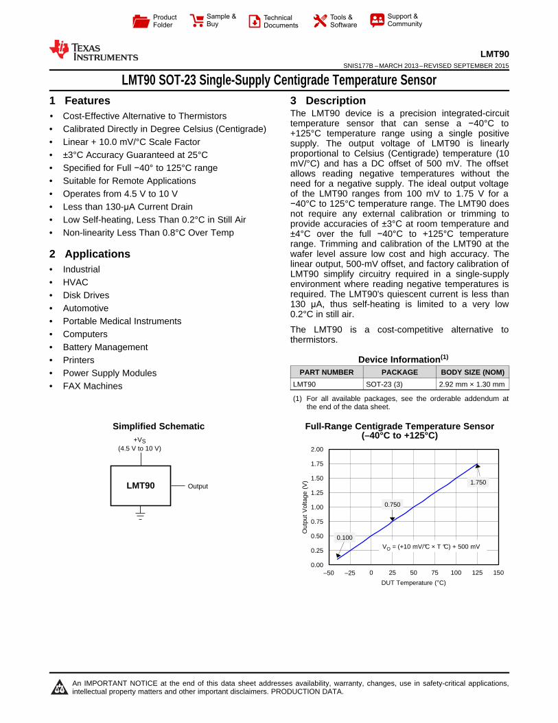
6.4 Thermal InformationLMT90
THERMAL METRIC (1) DBZ (SOT-23) UNIT3 PINS
RθJA Junction-to-ambient thermal resistance 450 °C/W
(1) For more information about traditional and new thermal metrics, see the Semiconductor and IC Package Thermal Metrics applicationreport, SPRA953.
6.5 Electrical CharacteristicsUnless otherwise noted, these specifications apply for VS = 5 VDC and ILOAD = 0.5 μA, in the circuit of Figure 14. All limits TA =TJ = 25°C, unless otherwise noted.
PARAMETER TEST CONDITIONS MIN TYP MAX (1) UNIT–3 3 °C
Accuracy (2) TA = TMAX –4 4 °CTA = TMIN –4 4 °C
Non-linearity (3) TA = TJ = TMIN to TMAX –0.8 0.8 °CSensor Gain (Average Slope) TA = TJ = TMIN to TMAX 9.7 10.3 mV/°COutput Resistance 2000
ΩTA = TJ = TMIN to TMAX 40004.5 V ≤ VS ≤ 10 V –0.8 0.8 mV/V
Line Regulation (4)TA = TJ = TMIN to TMAX –1.2 1.2 mV/V
Quiescent Current (5) 4.5 V ≤ VS ≤ 10 V 130 μA4.5 V ≤ VS ≤ 10 V 180 μATA = TJ = TMIN to TMAX
Change of Quiescent Current (5) 4.5 V ≤ VS ≤ 10 V 2 μATA = TJ = TMIN to TMAX
Temperature Coefficient of Quiescent Current TA = TJ = TMIN to TMAX 2 μA/°CLong Term Stability (6) TJ = 125°C, for 1000 hours ±0.08 °C
(1) Limits are specific to TI's AOQL (Average Outgoing Quality Level).(2) Accuracy is defined as the error between the output voltage and 10 mv/°C times the device's case temperature plus 500 mV, at
specified conditions of voltage, current, and temperature (expressed in °C).(3) Non-linearity is defined as the deviation of the output-voltage-versus-temperature curve from the best-fit straight line, over the device's
rated temperature range.(4) Regulation is measured at constant junction temperature, using pulse testing with a low duty cycle. Changes in output due to heating
effects can be computed by multiplying the internal dissipation by the thermal resistance.(5) Quiescent current is defined in the circuit of Figure 14.(6) For best long-term stability, any precision circuit will give best results if the unit is aged at a warm temperature, and/or temperature
cycled for at least 46 hours before long-term life test begins. This is especially true when a small (Surface-Mount) part is wave-soldered;allow time for stress relaxation to occur. The majority of the drift will occur in the first 1000 hours at elevated temperatures. The drift after1000 hours will not continue at the first 1000 hour rate.
4 Submit Documentation Feedback Copyright © 2013–2015, Texas Instruments Incorporated
Product Folder Links: LMT90

LMT90www.ti.com SNIS177B –MARCH 2013–REVISED SEPTEMBER 2015
6.6 Typical CharacteristicsTo generate these curves the LMT90 was mounted to a printed circuit board as shown in Figure 19.
Figure 1. Thermal Resistance Junction to Air Figure 2. Thermal Time Constant
Figure 4. Thermal Response in Stirred Oil Bath With HeatFigure 3. Thermal Response in Still Air With Heat SinkSink(Figure 19)
Figure 6. Thermal Response in Still Air Without a Heat SinkFigure 5. Startup Voltage vs Temperature
Copyright © 2013–2015, Texas Instruments Incorporated Submit Documentation Feedback 5
Product Folder Links: LMT90

LMT90SNIS177B –MARCH 2013–REVISED SEPTEMBER 2015 www.ti.com
Typical Characteristics (continued)To generate these curves the LMT90 was mounted to a printed circuit board as shown in Figure 19.
Figure 7. Quiescent Current vs Temperature (Figure 14) Figure 8. Accuracy vs Temperature
Figure 10. Supply Voltage vs Supply CurrentFigure 9. Noise Voltage
Figure 11. Start-Up Response
6 Submit Documentation Feedback Copyright © 2013–2015, Texas Instruments Incorporated
Product Folder Links: LMT90

LMT90www.ti.com SNIS177B –MARCH 2013–REVISED SEPTEMBER 2015
7 Detailed Description
7.1 OverviewThe LMT90 is a precision integrated-circuit temperature sensor that can sense a −40°C to 125°C temperaturerange using a single positive supply. The output voltage of the LMT90 has a positive temperature slope of10 mV/°C. A 500-mV offset is included enabling negative temperature sensing when biased by a single supply.
The temperature-sensing element is comprised of a delta-VBE architecture. The temperature-sensing element isthen buffered by an amplifier and provided to the VO pin. The amplifier has a simple class A output stage withtypical 2-kΩ output impedance as shown in the Functional Block Diagram. The output impedance has atemperature coefficient of approximately 1300 ppm/°C. Over temperature the output impedance will max out at 4kΩ.
7.2 Functional Block Diagram
*R2 ≈ 2k With a typical 1300 ppm/°C Drift.
7.3 Feature Description
7.3.1 LMT90 Transfer FunctionThe LM60 follows a simple linear transfer function in order to achieve the accuracy as listed in ElectricalCharacteristics:
VOUT = 10 mV/°C × T °C + 500 mV
where• T is the temperature in °C• VOUT is the LMT90 output voltage (1)
7.4 Device Functional ModesThe LMT90's only functional mode is that it has an analog output directly proportional to temperature.
Copyright © 2013–2015, Texas Instruments Incorporated Submit Documentation Feedback 7
Product Folder Links: LMT90

OUT
Heavy Capacitive Load, Wiring, Etc.
LMT90
+
d�1 µF
0.1 µF Bypass
Optional
OUT
Heavy Capacitive Load, Wiring, Etc.
LMT90
+
d�
To A High-Impedance Load
LMT90SNIS177B –MARCH 2013–REVISED SEPTEMBER 2015 www.ti.com
8 Application and Implementation
NOTEInformation in the following applications sections is not part of the TI componentspecification, and TI does not warrant its accuracy or completeness. TI’s customers areresponsible for determining suitability of components for their purposes. Customers shouldvalidate and test their design implementation to confirm system functionality.
8.1 Application InformationThe LMT90 has a wide supply range and a 10 mV/°C output slope with a 500-mV DC offset at 25 °C. Therefore,it can easily be applied in many temperature-sensing applications where a single supply is required for positiveand negative temperatures.
8.1.1 Capacitive Loads
The LMT90 handles capacitive loading very well. Without any special precautions, the LMT90 can drive anycapacitive load. The LMT90 has a nominal 2-kΩ output impedance (as can be seen in the Functional BlockDiagram). The temperature coefficient of the output resistors is around 1300 ppm/°C. Taking into account thistemperature coefficient and the initial tolerance of the resistors the output impedance of the LMT90 will notexceed 4 kΩ. In an extremely noisy environment it may be necessary to add some filtering to minimize noisepickup. TI recommends that 0.1 μF be added from VIN to GND to bypass the power supply voltage, as shown inFigure 13. In a noisy environment, it may be necessary to add a capacitor from the output to ground. A 1-μFoutput capacitor with the 4-kΩ output impedance will form a 40-Hz lowpass filter. Because the thermal timeconstant of the LMT90 is much slower than the 25-ms time constant formed by the RC, the overall response timeof the LMT90 will not be significantly affected. For much larger capacitors this additional time lag will increase theoverall response time of the LMT90.
Figure 12. LMT90 No Decoupling Required for Capacitive Load
Figure 13. LMT90 With Filter for Noisy Environment
8 Submit Documentation Feedback Copyright © 2013–2015, Texas Instruments Incorporated
Product Folder Links: LMT90

0.100
0.750
1.750
0.00
0.25
0.50
0.75
1.00
1.25
1.50
1.75
2.00
±50 ±25 0 25 50 75 100 125 150
Out
put
Vol
tage
(V
)
DUT Temperature (�C) C001
VO = (+10 mV/°C × T °C) + 500 mV
LMT90
+VS(4.5 V to 10 V)
Output
LMT90www.ti.com SNIS177B –MARCH 2013–REVISED SEPTEMBER 2015
8.2 Typical Application
Figure 14. Full-Range Centigrade Temperature Sensor (−40°C to 125°C)
8.2.1 Design RequirementsFor this design example, use the following design parameters in Table 1.
Table 1. Design ParametersPARAMETER VALUE UNIT
Accuracy at 25°C ±3.0 (maximum) °CAccuracy Over –40°C to 125°C ±4.0 (maximum) °CTemperature slope 10 mV/°CPower Supply Voltage Range 4.5 to 10 VOutput Impedance 4 (maximum) kΩ
8.2.2 Detailed Design ProcedureThe LMT90 is a simple temperature sensor that provides an analog output. Therefore design requirementsrelated to layout out weigh other requirements in importance, refer to Layout for a detailed description.
8.2.3 Application Curve
Figure 15. Plot of Output Transfer Function
Copyright © 2013–2015, Texas Instruments Incorporated Submit Documentation Feedback 9
Product Folder Links: LMT90
LMT90SNIS177B –MARCH 2013–REVISED SEPTEMBER 2015 www.ti.com
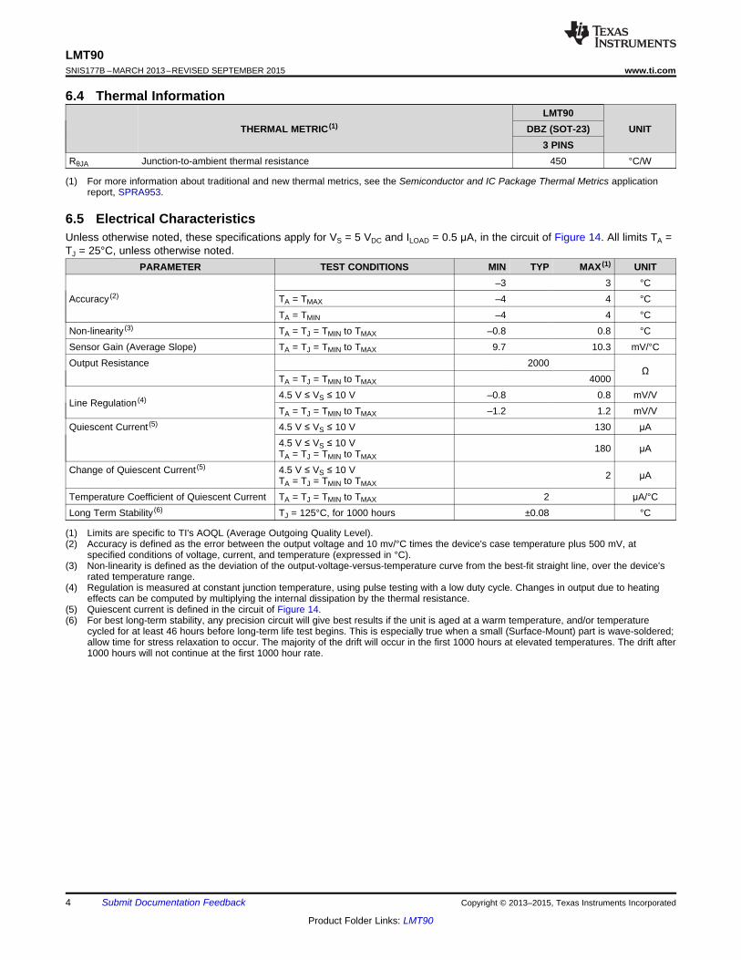
8.3 System Examples
Figure 16. Centigrade Thermostat / Fan Controller Figure 17. Temperature to Digital Converter (SerialOutput) (125°C Full Scale)
Figure 18. LMT90 With Voltage-To-Frequency Converter and Isolated Output(−40°C to 125°C; 100 Hz to 1750 Hz)
9 Power Supply RecommendationsIn an extremely noisy environment, it may be necessary to add some filtering to minimize noise pickup. TIrecommends that 0.1 μF be added from VIN to GND to bypass the power supply voltage, as shown in Figure 13.
10 Layout
10.1 Layout Guidelines
The LMT90 can be applied easily in the same way as other integrated-circuit temperature sensors. It can beglued or cemented to a surface and its temperature will be within about 0.2°C of the surface temperature.
This presumes that the ambient air temperature is almost the same as the surface temperature; if the airtemperature were much higher or lower than the surface temperature, the actual temperature of the LMT90 diewould be at an intermediate temperature between the surface temperature and the air temperature.
To ensure good thermal conductivity the backside of the LMT90 die is directly attached to the GND pin. Thelands and traces to the LMT90 will, of course, be part of the printed-circuit-board, which is the object whosetemperature is being measured. These printed-circuit-board lands and traces will not cause the LMT90temperature to deviate from the desired temperature.
10 Submit Documentation Feedback Copyright © 2013–2015, Texas Instruments Incorporated
Product Folder Links: LMT90

1+VS
VO
GND
Via to ground plane
Via to power plane
2
3
LMT90www.ti.com SNIS177B –MARCH 2013–REVISED SEPTEMBER 2015
Layout Guidelines (continued)Alternatively, the LMT90 can be mounted inside a sealed-end metal tube, and can then be dipped into a bath orscrewed into a threaded hole in a tank. As with any IC, the LMT90 and accompanying wiring and circuits must bekept insulated and dry, to avoid leakage and corrosion. This is especially true if the circuit may operate at coldtemperatures where condensation can occur. Printed-circuit coatings and varnishes such as a conformal coatingand epoxy paints or dips are often used to ensure that moisture cannot corrode the LMT90 or its connections.
Table 2. Temperature Rise of LMT90 Due to Self-Heating (Thermal Resistance, RΘJA)SOT-23 SOT-23
no heat sink (1) small heat fin (2)
Still air 450°C/W 260°C/WMoving air — 180°C/W
(1) Part soldered to 30 gauge wire.(2) Heat sink used is 1/2-inch square printed circuit board with 2-oz. foil with part attached as shown in Figure 19.
10.2 Layout Examples
1/2-inch square printed-circuit-board with 2-oz. foil or similar
Figure 19. PCB Layout
Figure 20. PCB Used for Heat Sink to Generate Thermal Response Curves
Copyright © 2013–2015, Texas Instruments Incorporated Submit Documentation Feedback 11
Product Folder Links: LMT90

LMT90SNIS177B –MARCH 2013–REVISED SEPTEMBER 2015 www.ti.com
11 Device and Documentation Support
11.1 Community ResourcesThe following links connect to TI community resources. Linked contents are provided "AS IS" by the respectivecontributors. They do not constitute TI specifications and do not necessarily reflect TI's views; see TI's Terms ofUse.
TI E2E™ Online Community TI's Engineer-to-Engineer (E2E) Community. Created to foster collaborationamong engineers. At e2e.ti.com, you can ask questions, share knowledge, explore ideas and helpsolve problems with fellow engineers.
Design Support TI's Design Support Quickly find helpful E2E forums along with design support tools andcontact information for technical support.
11.2 TrademarksE2E is a trademark of Texas Instruments.All other trademarks are the property of their respective owners.
11.3 Electrostatic Discharge CautionThese devices have limited built-in ESD protection. The leads should be shorted together or the device placed in conductive foamduring storage or handling to prevent electrostatic damage to the MOS gates.
11.4 GlossarySLYZ022 — TI Glossary.
This glossary lists and explains terms, acronyms, and definitions.
12 Mechanical, Packaging, and Orderable InformationThe following pages include mechanical, packaging, and orderable information. This information is the mostcurrent data available for the designated devices. This data is subject to change without notice and revision ofthis document. For browser-based versions of this data sheet, refer to the left-hand navigation.
12 Submit Documentation Feedback Copyright © 2013–2015, Texas Instruments Incorporated
Product Folder Links: LMT90

PACKAGE OPTION ADDENDUM
www.ti.com 2-Oct-2014
Addendum-Page 1
PACKAGING INFORMATION
Orderable Device Status(1)
Package Type PackageDrawing
Pins PackageQty
Eco Plan(2)
Lead/Ball Finish(6)
MSL Peak Temp(3)
Op Temp (°C) Device Marking(4/5)
Samples
LMT90DBZR ACTIVE SOT-23 DBZ 3 3000 Green (RoHS& no Sb/Br)
CU SN Level-1-260C-UNLIM -40 to 125 T8C
LMT90DBZT ACTIVE SOT-23 DBZ 3 250 Green (RoHS& no Sb/Br)
CU SN Level-1-260C-UNLIM -40 to 125 T8C
(1) The marketing status values are defined as follows:ACTIVE: Product device recommended for new designs.LIFEBUY: TI has announced that the device will be discontinued, and a lifetime-buy period is in effect.NRND: Not recommended for new designs. Device is in production to support existing customers, but TI does not recommend using this part in a new design.PREVIEW: Device has been announced but is not in production. Samples may or may not be available.OBSOLETE: TI has discontinued the production of the device.
(2) Eco Plan - The planned eco-friendly classification: Pb-Free (RoHS), Pb-Free (RoHS Exempt), or Green (RoHS & no Sb/Br) - please check http://www.ti.com/productcontent for the latest availabilityinformation and additional product content details.TBD: The Pb-Free/Green conversion plan has not been defined.Pb-Free (RoHS): TI's terms "Lead-Free" or "Pb-Free" mean semiconductor products that are compatible with the current RoHS requirements for all 6 substances, including the requirement thatlead not exceed 0.1% by weight in homogeneous materials. Where designed to be soldered at high temperatures, TI Pb-Free products are suitable for use in specified lead-free processes.Pb-Free (RoHS Exempt): This component has a RoHS exemption for either 1) lead-based flip-chip solder bumps used between the die and package, or 2) lead-based die adhesive used betweenthe die and leadframe. The component is otherwise considered Pb-Free (RoHS compatible) as defined above.Green (RoHS & no Sb/Br): TI defines "Green" to mean Pb-Free (RoHS compatible), and free of Bromine (Br) and Antimony (Sb) based flame retardants (Br or Sb do not exceed 0.1% by weightin homogeneous material)
(3) MSL, Peak Temp. - The Moisture Sensitivity Level rating according to the JEDEC industry standard classifications, and peak solder temperature.
(4) There may be additional marking, which relates to the logo, the lot trace code information, or the environmental category on the device.
(5) Multiple Device Markings will be inside parentheses. Only one Device Marking contained in parentheses and separated by a "~" will appear on a device. If a line is indented then it is a continuationof the previous line and the two combined represent the entire Device Marking for that device.
(6) Lead/Ball Finish - Orderable Devices may have multiple material finish options. Finish options are separated by a vertical ruled line. Lead/Ball Finish values may wrap to two lines if the finishvalue exceeds the maximum column width.
Important Information and Disclaimer:The information provided on this page represents TI's knowledge and belief as of the date that it is provided. TI bases its knowledge and belief on informationprovided by third parties, and makes no representation or warranty as to the accuracy of such information. Efforts are underway to better integrate information from third parties. TI has taken andcontinues to take reasonable steps to provide representative and accurate information but may not have conducted destructive testing or chemical analysis on incoming materials and chemicals.TI and TI suppliers consider certain information to be proprietary, and thus CAS numbers and other limited information may not be available for release.
PACKAGE OPTION ADDENDUM
www.ti.com 2-Oct-2014
Addendum-Page 2
In no event shall TI's liability arising out of such information exceed the total purchase price of the TI part(s) at issue in this document sold by TI to Customer on an annual basis.

TAPE AND REEL INFORMATION
*All dimensions are nominal
Device PackageType
PackageDrawing
Pins SPQ ReelDiameter
(mm)
ReelWidth
W1 (mm)
A0(mm)
B0(mm)
K0(mm)
P1(mm)
W(mm)
Pin1Quadrant
LMT90DBZR SOT-23 DBZ 3 3000 178.0 8.4 3.3 2.9 1.22 4.0 8.0 Q3
LMT90DBZT SOT-23 DBZ 3 250 178.0 8.4 3.3 2.9 1.22 4.0 8.0 Q3
PACKAGE MATERIALS INFORMATION
www.ti.com 3-Oct-2014
Pack Materials-Page 1

*All dimensions are nominal
Device Package Type Package Drawing Pins SPQ Length (mm) Width (mm) Height (mm)
LMT90DBZR SOT-23 DBZ 3 3000 210.0 185.0 35.0
LMT90DBZT SOT-23 DBZ 3 250 210.0 185.0 35.0
PACKAGE MATERIALS INFORMATION
www.ti.com 3-Oct-2014
Pack Materials-Page 2

4203227/C

www.ti.com
PACKAGE OUTLINE
C
TYP0.200.08
0.25
2.642.10
1.12 MAX
TYP0.100.01
3X 0.50.3
TYP0.60.2
1.9
0.95
TYP-80
A
3.042.80
B1.41.2
(0.95)
SOT-23 - 1.12 mm max heightDBZ0003ASMALL OUTLINE TRANSISTOR
4214838/C 04/2017
NOTES: 1. All linear dimensions are in millimeters. Any dimensions in parenthesis are for reference only. Dimensioning and tolerancing per ASME Y14.5M.2. This drawing is subject to change without notice.3. Reference JEDEC registration TO-236, except minimum foot length.
0.2 C A B
1
3
2
INDEX AREAPIN 1
GAGE PLANE
SEATING PLANE
0.1 C
SCALE 4.000

www.ti.com
EXAMPLE BOARD LAYOUT
0.07 MAXALL AROUND
0.07 MINALL AROUND
3X (1.3)
3X (0.6)
(2.1)
2X (0.95)
(R0.05) TYP
4214838/C 04/2017
SOT-23 - 1.12 mm max heightDBZ0003ASMALL OUTLINE TRANSISTOR
NOTES: (continued) 4. Publication IPC-7351 may have alternate designs. 5. Solder mask tolerances between and around signal pads can vary based on board fabrication site.
SYMM
LAND PATTERN EXAMPLESCALE:15X
PKG
1
3
2
SOLDER MASKOPENINGMETAL UNDER
SOLDER MASK
SOLDER MASKDEFINED
METALSOLDER MASKOPENING
NON SOLDER MASKDEFINED
(PREFERRED)
SOLDER MASK DETAILS

www.ti.com
EXAMPLE STENCIL DESIGN
(2.1)
2X(0.95)
3X (1.3)
3X (0.6)
(R0.05) TYP
SOT-23 - 1.12 mm max heightDBZ0003ASMALL OUTLINE TRANSISTOR
4214838/C 04/2017
NOTES: (continued) 6. Laser cutting apertures with trapezoidal walls and rounded corners may offer better paste release. IPC-7525 may have alternate design recommendations. 7. Board assembly site may have different recommendations for stencil design.
SOLDER PASTE EXAMPLEBASED ON 0.125 THICK STENCIL
SCALE:15X
SYMM
PKG
1
3
2

IMPORTANT NOTICE
Texas Instruments Incorporated (TI) reserves the right to make corrections, enhancements, improvements and other changes to itssemiconductor products and services per JESD46, latest issue, and to discontinue any product or service per JESD48, latest issue. Buyersshould obtain the latest relevant information before placing orders and should verify that such information is current and complete.TI’s published terms of sale for semiconductor products (http://www.ti.com/sc/docs/stdterms.htm) apply to the sale of packaged integratedcircuit products that TI has qualified and released to market. Additional terms may apply to the use or sale of other types of TI products andservices.Reproduction of significant portions of TI information in TI data sheets is permissible only if reproduction is without alteration and isaccompanied by all associated warranties, conditions, limitations, and notices. TI is not responsible or liable for such reproduceddocumentation. Information of third parties may be subject to additional restrictions. Resale of TI products or services with statementsdifferent from or beyond the parameters stated by TI for that product or service voids all express and any implied warranties for theassociated TI product or service and is an unfair and deceptive business practice. TI is not responsible or liable for any such statements.Buyers and others who are developing systems that incorporate TI products (collectively, “Designers”) understand and agree that Designersremain responsible for using their independent analysis, evaluation and judgment in designing their applications and that Designers havefull and exclusive responsibility to assure the safety of Designers' applications and compliance of their applications (and of all TI productsused in or for Designers’ applications) with all applicable regulations, laws and other applicable requirements. Designer represents that, withrespect to their applications, Designer has all the necessary expertise to create and implement safeguards that (1) anticipate dangerousconsequences of failures, (2) monitor failures and their consequences, and (3) lessen the likelihood of failures that might cause harm andtake appropriate actions. Designer agrees that prior to using or distributing any applications that include TI products, Designer willthoroughly test such applications and the functionality of such TI products as used in such applications.TI’s provision of technical, application or other design advice, quality characterization, reliability data or other services or information,including, but not limited to, reference designs and materials relating to evaluation modules, (collectively, “TI Resources”) are intended toassist designers who are developing applications that incorporate TI products; by downloading, accessing or using TI Resources in anyway, Designer (individually or, if Designer is acting on behalf of a company, Designer’s company) agrees to use any particular TI Resourcesolely for this purpose and subject to the terms of this Notice.TI’s provision of TI Resources does not expand or otherwise alter TI’s applicable published warranties or warranty disclaimers for TIproducts, and no additional obligations or liabilities arise from TI providing such TI Resources. TI reserves the right to make corrections,enhancements, improvements and other changes to its TI Resources. TI has not conducted any testing other than that specificallydescribed in the published documentation for a particular TI Resource.Designer is authorized to use, copy and modify any individual TI Resource only in connection with the development of applications thatinclude the TI product(s) identified in such TI Resource. NO OTHER LICENSE, EXPRESS OR IMPLIED, BY ESTOPPEL OR OTHERWISETO ANY OTHER TI INTELLECTUAL PROPERTY RIGHT, AND NO LICENSE TO ANY TECHNOLOGY OR INTELLECTUAL PROPERTYRIGHT OF TI OR ANY THIRD PARTY IS GRANTED HEREIN, including but not limited to any patent right, copyright, mask work right, orother intellectual property right relating to any combination, machine, or process in which TI products or services are used. Informationregarding or referencing third-party products or services does not constitute a license to use such products or services, or a warranty orendorsement thereof. Use of TI Resources may require a license from a third party under the patents or other intellectual property of thethird party, or a license from TI under the patents or other intellectual property of TI.TI RESOURCES ARE PROVIDED “AS IS” AND WITH ALL FAULTS. TI DISCLAIMS ALL OTHER WARRANTIES ORREPRESENTATIONS, EXPRESS OR IMPLIED, REGARDING RESOURCES OR USE THEREOF, INCLUDING BUT NOT LIMITED TOACCURACY OR COMPLETENESS, TITLE, ANY EPIDEMIC FAILURE WARRANTY AND ANY IMPLIED WARRANTIES OFMERCHANTABILITY, FITNESS FOR A PARTICULAR PURPOSE, AND NON-INFRINGEMENT OF ANY THIRD PARTY INTELLECTUALPROPERTY RIGHTS. TI SHALL NOT BE LIABLE FOR AND SHALL NOT DEFEND OR INDEMNIFY DESIGNER AGAINST ANY CLAIM,INCLUDING BUT NOT LIMITED TO ANY INFRINGEMENT CLAIM THAT RELATES TO OR IS BASED ON ANY COMBINATION OFPRODUCTS EVEN IF DESCRIBED IN TI RESOURCES OR OTHERWISE. IN NO EVENT SHALL TI BE LIABLE FOR ANY ACTUAL,DIRECT, SPECIAL, COLLATERAL, INDIRECT, PUNITIVE, INCIDENTAL, CONSEQUENTIAL OR EXEMPLARY DAMAGES INCONNECTION WITH OR ARISING OUT OF TI RESOURCES OR USE THEREOF, AND REGARDLESS OF WHETHER TI HAS BEENADVISED OF THE POSSIBILITY OF SUCH DAMAGES.Unless TI has explicitly designated an individual product as meeting the requirements of a particular industry standard (e.g., ISO/TS 16949and ISO 26262), TI is not responsible for any failure to meet such industry standard requirements.Where TI specifically promotes products as facilitating functional safety or as compliant with industry functional safety standards, suchproducts are intended to help enable customers to design and create their own applications that meet applicable functional safety standardsand requirements. Using products in an application does not by itself establish any safety features in the application. Designers mustensure compliance with safety-related requirements and standards applicable to their applications. Designer may not use any TI products inlife-critical medical equipment unless authorized officers of the parties have executed a special contract specifically governing such use.Life-critical medical equipment is medical equipment where failure of such equipment would cause serious bodily injury or death (e.g., lifesupport, pacemakers, defibrillators, heart pumps, neurostimulators, and implantables). Such equipment includes, without limitation, allmedical devices identified by the U.S. Food and Drug Administration as Class III devices and equivalent classifications outside the U.S.TI may expressly designate certain products as completing a particular qualification (e.g., Q100, Military Grade, or Enhanced Product).Designers agree that it has the necessary expertise to select the product with the appropriate qualification designation for their applicationsand that proper product selection is at Designers’ own risk. Designers are solely responsible for compliance with all legal and regulatoryrequirements in connection with such selection.Designer will fully indemnify TI and its representatives against any damages, costs, losses, and/or liabilities arising out of Designer’s non-compliance with the terms and provisions of this Notice.
Mailing Address: Texas Instruments, Post Office Box 655303, Dallas, Texas 75265Copyright © 2017, Texas Instruments Incorporated