Embed Size (px)
Citation preview
LME49740
www.ti.com SNAS377B –FEBRUARY 2007–REVISED APRIL 2013
LME49740 Quad High-Performance, High-Fidelity Audio Operational AmplifierCheck for Samples: LME49740
1FEATURES DESCRIPTIONThe LME49740 is part of the ultra-low distortion, low
2• Easily Drives 600Ω Loadsnoise, high slew rate operational amplifier series
• Optimized for Superior Audio Signal Fidelity optimized and fully specified for high-performance,• Output Short Circuit Protection high-fidelity applications. Combining advanced
leading-edge process technology with state-of-the-art• PSRR and CMRR Exceed 120dB (Typ)circuit design, the LME49740 audio operational• SOIC and PDIP Packages amplifiers deliver superior audio signal amplificationfor outstanding audio performance. The LME49740
APPLICATIONS combines extremely low voltage noise density(2.7nV/√HZ) with vanishingly low THD+N (0.00003%)• Ultra High-Quality Audio Amplificationto easily satisfy the most demanding audio• High-Fidelity Preamplifiersapplications. To ensure that the most challenging
• High-Fidelity Multimedia loads are driven without compromise, the LME49740has a high slew rate of ±20V/μs and an output current• State-of-the-Art Phono Pre Ampscapability of ±26mA. Further, dynamic range is• High-Performance Professional Audiomaximized by an output stage that drives 2kΩ loads
• High-Fidelity Equalization and Crossover to within 1V of either power supply voltage and toNetworks within 1.4V when driving 600Ω loads.
• High-Performance Line Drivers The LME49740's outstanding CMRR (120dB), PSRR• High-Performance Line Receivers (120dB), and VOS (0.1mV) give the amplifier excellent
operational amplifier DC performance.• High-Fidelity Active Filters
The LME49740 has a wide supply range of ±2.5V toKEY SPECIFICATIONS ±17V. Over this supply range the LME49740’s input
circuitry maintains excellent common-mode and• Power Supply Voltage Range: ±2.5V to ±17Vpower supply rejection, as well as maintaining its low
• THD+N (AV = 1, VOUT = 3VRMS, fIN = 1kHz) input bias current. The LME49740 is unity gain– RL = 2kΩ: 0.00003% (typ) stable. The Audio Operational Amplifier achieves
outstanding AC performance while driving complex– RL = 600Ω: 0.00003% (typ)loads with values as high as 100pF.• Input Noise Density: 2.7nV/√Hz (typ)The LME49740 is available in 14-lead narrow body• Slew Rate: ±20V/μs (typ)SOIC and 14-lead PDIP. Demonstration boards are
• Gain Bandwidth Product: 55MHz (typ) available for each package.• Open Loop Gain (RL = 600Ω): 140dB (typ)• Input Bias Current: 10nA (typ)• Input Offset Voltage: 0.1mV (typ)• DC Gain Linearity Error: 0.000009%
1
Please be aware that an important notice concerning availability, standard warranty, and use in critical applications ofTexas Instruments semiconductor products and disclaimers thereto appears at the end of this data sheet.
2All trademarks are the property of their respective owners.
PRODUCTION DATA information is current as of publication date. Copyright © 2007–2013, Texas Instruments IncorporatedProducts conform to specifications per the terms of the TexasInstruments standard warranty. Production processing does notnecessarily include testing of all parameters.

-
+
-
+
LME49740
-
+
-
+10pF
+
+INPUT
OUTPUT
Note: 1% metal film resistors, 5% polypropylene capacitors
47 k:
3320:150:
909:
26.1 k:
3.83 k:
100:
150:
22 nF//4.7 nF//500 pF
3320:
47 nF//33 nF
LME49740
LME49740
SNAS377B –FEBRUARY 2007–REVISED APRIL 2013 www.ti.com
TYPICAL APPLICATION
Figure 1. Passively Equalized RIAA Phono Preamplifier
CONNECTION DIAGRAM
Figure 2. 14-Lead SOIC (D Package)14-Lead PDIP (NFF Package)
These devices have limited built-in ESD protection. The leads should be shorted together or the device placed in conductive foamduring storage or handling to prevent electrostatic damage to the MOS gates.
2 Submit Documentation Feedback Copyright © 2007–2013, Texas Instruments Incorporated
Product Folder Links: LME49740

LME49740
www.ti.com SNAS377B –FEBRUARY 2007–REVISED APRIL 2013
ABSOLUTE MAXIMUM RATINGS (1) (2) (3)
Power Supply Voltage(VS = V+ - V-) 36V
Storage Temperature −65°C to 150°C
Input Voltage (V-) - 0.7V to (V+) + 0.7V
Output Short Circuit (4) Continuous
Power Dissipation Internally Limited
ESD Susceptibility (5) 2000V
ESD Susceptibility (6) 200V
Junction Temperature 150°C
Thermal Resistance
θJA (MA) 107°C/W
θJA (NA) 74°C/W
Temperature Range
TMIN ≤ TA ≤ TMAX –40°C ≤ TA ≤ 85°C
Supply Voltage Range ±2.5V ≤ VS ≤ ± 17V
(1) Absolute Maximum Ratings indicate limits beyond which damage to the device may occur.(2) Operating Ratings indicate conditions for which the device is functional, but do not ensure specific performance limits. For ensured
specifications and test conditions, see the Electrical Characteristics. The ensured specifications apply only for the test conditions listed.Some performance characteristics may degrade when the device is not operated under the listed test conditions.
(3) If Military/Aerospace specified devices are required, please contact the Texas Instruments Sales Office/Distributors for availability andspecifications.
(4) Amplifier output connected to GND, any number of amplifiers within a package.(5) Human body model, 100pF discharged through a 1.5kΩ resistor.(6) Machine Model ESD test is covered by specification EIAJ IC-121-1981. A 200pF cap is charged to the specified voltage and then
discharged directly into the IC with no external series resistor (resistance of discharge path must be under 50Ω).
Copyright © 2007–2013, Texas Instruments Incorporated Submit Documentation Feedback 3
Product Folder Links: LME49740

LME49740
SNAS377B –FEBRUARY 2007–REVISED APRIL 2013 www.ti.com
ELECTRICAL CHARACTERISTICS (1) (2)
The following specifications apply for VS = ±15V, RL = 2kΩ, fIN = 1kHz, and TA = 25C, unless otherwise specified.
LME49740 UnitsSymbol Parameter Conditions (Limits)Typical (3) Limit (4) (5)
AV = 1, VOUT = 3VRMS % (max)THD+N Total Harmonic Distortion + Noise RL = 2kΩ 0.00003 % (max)RL = 600Ω 0.00003 0.00009
AV = 1, VOUT = 3VRMSIMD Intermodulation Distortion 0.00005 % (max)Two-tone, 60Hz & 7kHz 4:1
GBWP Gain Bandwidth Product 55 45 MHz (min)
SR Slew Rate ±20 ±15 V/μs (min)
VOUT = 1VP-P, –3dBFPBW Full Power Bandwidth referenced to output magnitude 10 MHz
at f = 1kHz
AV = 1, 10V step, CL = 100pFts Settling time 0.1% error range 1.2 μs
Equivalent Input Noise Voltage fBW = 20Hz to 20kHz 0.34 0.65 μVRMS
en f = 1kHz 2.7 4.7 nV/√HzEquivalent Input Noise Density f = 10Hz 6.4 nV/√Hz
f = 1kHz 1.6 pA/√Hzin Current Noise Density f = 10Hz 3.1 pA/√Hz
VOS Offset Voltage ±0.1 ±0.7 mV (max)
Average Input Offset Voltage Drift vsΔVOS/ΔTemp 40°C ≤ TA ≤ 85°C 0.2 μV/°CTemperature
Average Input Offset Voltage Shift vsPSRR ΔVS = 20V (6) 120 110 dB (min)Power Supply Voltage
fIN = 1kHz 118 dBISOCH-CH Channel-to-Channel Isolation fIN = 20kHz 112 dB
IB Input Bias Current VCM = 0V 10 72 nA (max)
Input Bias Current Drift vsΔIOS/ΔTemp –40°C ≤ TA ≤ 85°C 0.1 nA/°CTemperature
IOS Input Offset Current VCM = 0V 11 65 nA (max)
+14.1 (V+)–2.0 V (min)VIN-CM Common-Mode Input Voltage Range –13.9 (V-)+2.0 V (min)
CMRR Common-Mode Rejection –10V<VCM<10V 120 110 dB (min)
Differential Input Impedance 30 kΩZIN
Common Mode Input Impedance –10V<VCM<10V 1000 MΩ–10V<VOUT<10V, RL = 600Ω 140 dB (min)
AVOL Open Loop Voltage Gain –10V<VOUT<10V, RL = 2kΩ 140 dB (min)
–10V<VOUT<10V, RL = 10kΩ 140 125 dB (min)
RL = 600Ω ±13.6 ±12.5 V (min)
VOUTMAX Maximum Output Voltage Swing RL = 2kΩ ±14.0 V (min)
RL = 10kΩ ±14.1 V (min)
IOUT Output Current RL = 600Ω, VS = ±17V ±26 ±23 mA (min)
+30 mAIOUT-CC Short Circuit Current –38 mA
fIN = 10kHzROUT Output Impedance Closed-Loop 0.01 Ω
Open-Loop 13 Ω
(1) Absolute Maximum Ratings indicate limits beyond which damage to the device may occur.(2) Operating Ratings indicate conditions for which the device is functional, but do not ensure specific performance limits. For ensured
specifications and test conditions, see the Electrical Characteristics. The ensured specifications apply only for the test conditions listed.Some performance characteristics may degrade when the device is not operated under the listed test conditions.
(3) Typical specifications are specified at +25ºC and represent the most likely parametric norm.(4) Tested limits are specified to AOQL (Average Outgoing Quality Level).(5) Datasheet min/max specification limits are specified by design, test, or statistical analysis.(6) PSRR is measured as follows: VOS is measured at two supply voltages, ±5V and ±15V. PSRR = |20log(ΔVOS/ΔVS)|.
4 Submit Documentation Feedback Copyright © 2007–2013, Texas Instruments Incorporated
Product Folder Links: LME49740

LME49740
www.ti.com SNAS377B –FEBRUARY 2007–REVISED APRIL 2013
ELECTRICAL CHARACTERISTICS(1)(2) (continued)The following specifications apply for VS = ±15V, RL = 2kΩ, fIN = 1kHz, and TA = 25C, unless otherwise specified.
LME49740 UnitsSymbol Parameter Conditions (Limits)Typical (3) Limit (4) (5)
CLOAD Capacitive Load Drive Overshoot 100pF 16 %
IS Total Quiescent Current IOUT = 0mA 18.5 20 mA (max)
Copyright © 2007–2013, Texas Instruments Incorporated Submit Documentation Feedback 5
Product Folder Links: LME49740

LME49740
SNAS377B –FEBRUARY 2007–REVISED APRIL 2013 www.ti.com
TYPICAL PERFORMANCE CHARACTERISTICS
THD+N vs Output Voltage THD+N vs Output VoltageVCC = 15V, VEE = –15V, RL = 2kΩ VCC = 17V, VEE = –17V, RL = 2kΩ
Figure 3. Figure 4.
THD+N vs Frequency THD+N vs FrequencyVCC = 15V, VEE = –15V, RL = 2kΩ, VOUT = 3VRMS VCC = 17V, VEE = –17V, RL = 2kΩ, VOUT = 3VRMS
Figure 5. Figure 6.
THD+N vs Frequency THD+N vs FrequencyVCC = 15V, VEE = –15V, RL = 600Ω, VOUT = 3VRMS VCC = 17V, VEE = –17V, RL = 600Ω, VOUT = 3VRMS
Figure 7. Figure 8.
6 Submit Documentation Feedback Copyright © 2007–2013, Texas Instruments Incorporated
Product Folder Links: LME49740

FREQUENCY (Hz)
CM
RR
(dB
)
10 100 10k 100k1k-130
-120-110
-100-90
-80
-70-60
-50
-40-30
-20-10
0
20 100 1k 10k 20k-160
-150
-140
-130
-120
-110
-100
-90
-80
-70
-60
PS
RR
(dB
)
FREQUENCY (Hz)
20 100 1k 10k 20k-160
-150
-140
-130
-120
-110
-100
-90
-80
-70
-60
PS
RR
(dB
)
FREQUENCY (Hz)
0.00002
0.00005
0.0002
0.0005
0.002
0.005
0.00001
0.0001
0.001
0.01
VRMS
IMD
(%
)
10m 100m 1 10 20
0.00002
0.00005
0.0002
0.0005
0.002
0.005
0.00001
0.0001
0.001
0.01
VRMS
IMD
(%
)
10m 100m 1 10 20
LME49740
www.ti.com SNAS377B –FEBRUARY 2007–REVISED APRIL 2013
TYPICAL PERFORMANCE CHARACTERISTICS (continued)IMD vs Output Voltage IMD vs Output Voltage
VCC = 15V, VEE = –15V, RL = 2kΩ VCC = 17V, VEE = –17V, RL = 2kΩ
Figure 9. Figure 10.
PSRR+ vs Frequency PSRR- vs FrequencyVCC = 15V, VEE = –15V, VCC = 15V, VEE = –15V, RL = 2kΩ
RL = 2kΩ, VRIPPLE = 200mVpp RL = 2kΩ, VRIPPLE = 200mVpp
Figure 11. Figure 12.
CMRR vs Frequency Crosstalk vs FrequencyVCC = 15V, VEE = –15V, RL = 2kΩ VCC = 15V, VEE = –15V, RL = 2kΩ
Figure 13. Figure 14.
Copyright © 2007–2013, Texas Instruments Incorporated Submit Documentation Feedback 7
Product Folder Links: LME49740

10
1
100
FREQUENCY (Hz)
VO
LTA
GE
NO
ISE
(nV
/ H
z)
1 10 100 100k1k 10k
VS = 30V
VCM = 15V
FREQUENCY (Hz)
GA
IN (
dB),
PH
AS
E L
AG
(q
10k1k100 100k 1M 10M100
180
20
40
60
80
100
120
140
160
FREQUENCY (Hz)
MA
GN
ITU
DE
(dB
)
100 10k 100M1k10 100k 1M 10M1-14
-12
-10
-8
-6
-4
-2
0
2
0 dB = 1 VPP
LME49740
SNAS377B –FEBRUARY 2007–REVISED APRIL 2013 www.ti.com
TYPICAL PERFORMANCE CHARACTERISTICS (continued)Output Voltage vs Supply Voltage Output Voltage vs Load Resistance
RL = 2kΩ, THD+N = 1% THD+N = 1%
Figure 15. Figure 16.
Supply Current vs Supply VoltageRL = 2kΩ, THD+N = 1% Full Power Bandwidth vs Frequency
Figure 17. Figure 18.
Gain Phase vs Frequency Voltage Noise Density vs Frequency
Figure 19. Figure 20.
8 Submit Documentation Feedback Copyright © 2007–2013, Texas Instruments Incorporated
Product Folder Links: LME49740

LME49740
www.ti.com SNAS377B –FEBRUARY 2007–REVISED APRIL 2013
TYPICAL PERFORMANCE CHARACTERISTICS (continued)Small-Signal Transient Response Large-Signal Transient Response
AV = 1, CL = 100pF AV = 1, CL = 100pF
Figure 21. Figure 22.
Copyright © 2007–2013, Texas Instruments Incorporated Submit Documentation Feedback 9
Product Folder Links: LME49740

Distortion Signal Gain = 1+(R2/R1)
+
-
LME49740
1000:
R110:
R2
Analyzer Input
Audio Precision System Two
Cascade
Generator Output
Actual Distortion = AP Value/100
LME49740
SNAS377B –FEBRUARY 2007–REVISED APRIL 2013 www.ti.com
APPLICATION INFORMATION
DISTORTION MEASUREMENTS
The vanishingly low residual distortion produced by LME49740 is below the capabilities of all commerciallyavailable equipment. This makes distortion measurements just slightly more difficult than simply connecting adistortion meter to the amplifier’s inputs and outputs. The solution, however, is quite simple: an additionalresistor. Adding this resistor extends the resolution of the distortion measurement equipment.
The LME49740’s low residual distortion is an input referred internal error. As shown in Figure 23, adding the 10Ωresistor connected between the amplifier’s inverting and non-inverting inputs changes the amplifier’s noise gain.The result is that the error signal (distortion) is amplified by a factor of 101. Although the amplifier’s closed-loopgain is unaltered, the feedback available to correct distortion errors is reduced by 101, which means thatmeasurement resolution increases by 101. To ensure minimum effects on distortion measurements, keep thevalue of R1 low as shown in Figure 23.
This technique is verified by duplicating the measurements with high closed loop gain and/or making themeasurements at high frequencies. Doing so produces distortion components that are within the measurementequipment’s capabilities. This datasheet’s THD+N and IMD values were generated using the above describedcircuit connected to an Audio Precision System Two Cascade.
Figure 23. THD+N and IMD Distortion Test Circuit
APPLICATION HINTS
The LME49740 is a high-speed op amp with excellent phase margin and stability. Capacitive loads up to 100pFwill cause little change in the phase characteristics of the amplifiers and are therefore allowable.
Capacitive loads greater than 100pF must be isolated from the output. The most straightforward way to do this isto put a resistor in series with the output. This resistor will also prevent excess power dissipation if the output isaccidentally shorted.
10 Submit Documentation Feedback Copyright © 2007–2013, Texas Instruments Incorporated
Product Folder Links: LME49740

10 100 1k 10k 100k
FREQUENCY (Hz)
20
30
40
50
60
70
80
90
VO
LTA
GE
GA
IN (
dB)
-1
0
+1
0
10
20
30
40
50
20 100 1k 10k 20k
FREQUENCY (Hz)
VO
LTA
GE
GA
IN (
dB)
DE
VIA
TIO
N (
dB)
RIA
A-VEE+VCC
0.47 PF
LME49740
V1
99k
0.47 PF
27 pF
16k200k
15 nF 4.7 nF
+
+
V2+
-+
-
+
- 4.7 PF+ VO
99k
27 pF
FLAT AMP. 40 dB + 40 dBRIAA PREAMP35 dB, f = 1 kHz
47 PF 47 PF
390
390
1k
39k
39k
1k
AVERAGE RESPONDINGAC VOLT METER
LME49740
www.ti.com SNAS377B –FEBRUARY 2007–REVISED APRIL 2013
NOISE MEASUREMENT CIRCUIT
A. Complete shielding is required to prevent induced pick up from external sources. Always check with oscilloscope forpower line noise.
Figure 24. Total Gain: 115 dB at f = 1 kHzInput Referred Noise Voltage: en = VO/560,000 (V)
RIAA Preamp Voltage Gain,RIAA Deviation vs Frequency Flat Amp Voltage Gain vs Frequency
VIN = 10mV, AV = 35.0dB, f = 1kHz VO = 0dB, AV = 80.0dB, f = 1kHz
Figure 25. Figure 26.
Copyright © 2007–2013, Texas Instruments Incorporated Submit Documentation Feedback 11
Product Folder Links: LME49740

-
+
LME49740 VO
R
R
R
V2
V1
R
14
20 100 1k 20k
FREQUENCY (Hz)
0
10
20
30
40
50
60
70
VO
LTA
GE
GA
IN (
dB)
10k
+
-
LME49740 VO
3.6k15 nF
200k
200
+47 PF
VI
TAPEHEAD
14
LME49740
SNAS377B –FEBRUARY 2007–REVISED APRIL 2013 www.ti.com
TYPICAL APPLICATIONS
AV = 34.5F = 1 kHzEn = 0.38 μVA Weighted
Figure 27. NAB Preamp
Figure 28. NAB Preamp Voltage Gain vs FrequencyVIN = 10mV, AV = 34.5dB, f = 1kHz
VO = V1–V2
Figure 29. Balanced to Single-Ended Converter
12 Submit Documentation Feedback Copyright © 2007–2013, Texas Instruments Incorporated
Product Folder Links: LME49740

+
-
LME49740
VI
VO
R111k
C10.01 PF
C20.01 PF
R222k
14
+
-
LME49740 VO
R
C
14 mA @ 10V
750
C R
14
+
-
VO
R
R
RV1
RV2
RV3
RV4
14LME49740
LME49740
www.ti.com SNAS377B –FEBRUARY 2007–REVISED APRIL 2013
VO = V1 + V2 − V3 − V4
Figure 30. Adder/Subtracter
Figure 31. Sine Wave Oscillator
Illustration is f0 = 1 kHz
Figure 32. Second-Order High-Pass Filter(Butterworth)
Copyright © 2007–2013, Texas Instruments Incorporated Submit Documentation Feedback 13
Product Folder Links: LME49740

-
+
LME49740 VHP
R2
RG
R0
R2 R1
R2
-
+
LME49740 VBP
0.01 PFC1
R1
-
+
LME49740 VLP
0.01 PFC1
VIN
14
14
14
+
-
LME49740
VI
VO
R210k
C10.022 PF
C20.011 PF
R110k
14
LME49740
SNAS377B –FEBRUARY 2007–REVISED APRIL 2013 www.ti.com
Illustration is f0 = 1 kHz
Figure 33. Second-Order Low-Pass Filter(Butterworth)
Figure 34. State Variable Filter
14 Submit Documentation Feedback Copyright © 2007–2013, Texas Instruments Incorporated
Product Folder Links: LME49740
-
+
LME49740 VO1
3.41R151k
R115k
R115k
0.707R110k
-
+
LME49740 VO2
3.41R151k
R115k
R115k
VI
14
14
-
+
LME49740
R220k
R120k
R615k
D11S1588
R520k
D21S1588
R310k
VIN -
+
LME49740
R420k
R76.2k
C110 PF
14
14 VO = |VIN|
LME49740
www.ti.com SNAS377B –FEBRUARY 2007–REVISED APRIL 2013
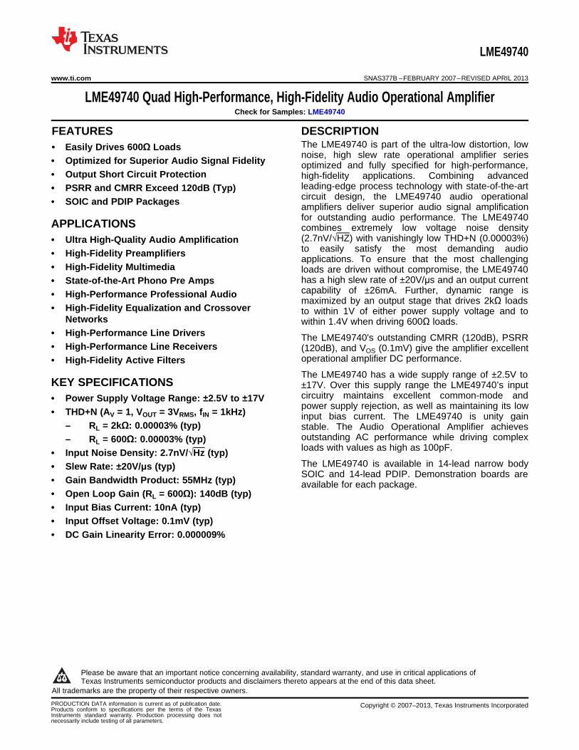
Figure 35. AC/DC Converter
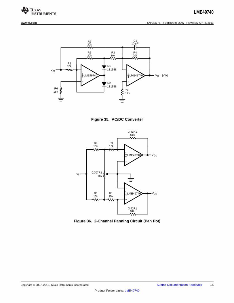
Figure 36. 2-Channel Panning Circuit (Pan Pot)
Copyright © 2007–2013, Texas Instruments Incorporated Submit Documentation Feedback 15
Product Folder Links: LME49740

R4
R2R1
0.05 PFC1
R1
-
+
LME49740 VO
VI
R5
0.05 PFC1
R5
0.005 PFC2
R3
BOOST TREBLE CUT
BOOST BASS CUT
14
-
+
LME49740
R2
R1VI
R310k
R910k
R510kBIAS
R610k
VCC
R733
R833
-VEE
Q1
Q2
VO
14
LME49740
SNAS377B –FEBRUARY 2007–REVISED APRIL 2013 www.ti.com
Figure 37. Line Driver
Figure 38. Tone Control
16 Submit Documentation Feedback Copyright © 2007–2013, Texas Instruments Incorporated
Product Folder Links: LME49740

-
+
LME49740
R510k
R
10k 10k
-
+
LME49740 VO
R410k
R6 R7
10kR3
R210k
+
-
LME49740R
R1200
VI
V2
14
14
14
47010 PF
4.7 nF 15 nF
16k 200k
33 PF
400 pF47k
390
100 PF
100k
+
-
LME49740Phono
Cartridge
14
LME49740
www.ti.com SNAS377B –FEBRUARY 2007–REVISED APRIL 2013
Av = 35 dBEn = 0.33 μVS/N = 90 dBf = 1 kHzA WeightedA Weighted, VIN = 10 mV@f = 1 kHz
Figure 39. RIAA Preamp
Illustration is:V0 = 101(V2 − V1)
Figure 40. Balanced Input Mic Amp
Copyright © 2007–2013, Texas Instruments Incorporated Submit Documentation Feedback 17
Product Folder Links: LME49740

+
-
LME49740 VO
+
-
LME49740
C2
C1
20k
R2
3k
3k
VI
CUT BOOST
R1
14
f01
f02
f03
f04
f05
f06
f07
f08
f09
f010
14
LME49740
SNAS377B –FEBRUARY 2007–REVISED APRIL 2013 www.ti.com
A. See Table 1.
Figure 41. 10-Band Graphic Equalizer
Table 1. C1, C2, R1, and R2 Values for Figure 41(1)
fo (Hz) C1 C2 R1 R2
32 0.12μF 4.7μF 75kΩ 500Ω64 0.056μF 3.3μF 68kΩ 510Ω125 0.033μF 1.5μF 62kΩ 510Ω250 0.015μF 0.82μF 68kΩ 470Ω500 8200pF 0.39μF 62kΩ 470Ω1k 3900pF 0.22μF 68kΩ 470Ω2k 2000pF 0.1μF 68kΩ 470Ω4k 1100pF 0.056μF 62kΩ 470Ω8k 510pF 0.022μF 68kΩ 510Ω16k 330pF 0.012μF 51kΩ 510Ω
(1) At volume of change = ±12 dB Q = 1.7
18 Submit Documentation Feedback Copyright © 2007–2013, Texas Instruments Incorporated
Product Folder Links: LME49740

LME49740
www.ti.com SNAS377B –FEBRUARY 2007–REVISED APRIL 2013
REVISION HISTORY
Rev Date Description
1.0 02/28/07 Initial WEB release.
Fixed the captions on the LME4970MA package (from Dual-In-Line1.01 02/08/08 to Molded Package (SO).
B 04/04/13 Changed layout of National Data Sheet to TI format.
Copyright © 2007–2013, Texas Instruments Incorporated Submit Documentation Feedback 19
Product Folder Links: LME49740

PACKAGE OPTION ADDENDUM
www.ti.com 16-Oct-2015
Addendum-Page 1
PACKAGING INFORMATION
Orderable Device Status(1)
Package Type PackageDrawing
Pins PackageQty
Eco Plan(2)
Lead/Ball Finish(6)
MSL Peak Temp(3)
Op Temp (°C) Device Marking(4/5)
Samples
LME49740MA/NOPB LIFEBUY SOIC D 14 55 Green (RoHS& no Sb/Br)
CU SN Level-1-260C-UNLIM -40 to 85 LME49740MA
LME49740MAX/NOPB LIFEBUY SOIC D 14 2500 Green (RoHS& no Sb/Br)
CU SN Level-1-260C-UNLIM -40 to 85 LME49740MA
LME49740NA/NOPB LIFEBUY PDIP NFF 14 25 Green (RoHS& no Sb/Br)
CU SN Level-1-NA-UNLIM -40 to 85 LME49740NA
(1) The marketing status values are defined as follows:ACTIVE: Product device recommended for new designs.LIFEBUY: TI has announced that the device will be discontinued, and a lifetime-buy period is in effect.NRND: Not recommended for new designs. Device is in production to support existing customers, but TI does not recommend using this part in a new design.PREVIEW: Device has been announced but is not in production. Samples may or may not be available.OBSOLETE: TI has discontinued the production of the device.
(2) Eco Plan - The planned eco-friendly classification: Pb-Free (RoHS), Pb-Free (RoHS Exempt), or Green (RoHS & no Sb/Br) - please check http://www.ti.com/productcontent for the latest availabilityinformation and additional product content details.TBD: The Pb-Free/Green conversion plan has not been defined.Pb-Free (RoHS): TI's terms "Lead-Free" or "Pb-Free" mean semiconductor products that are compatible with the current RoHS requirements for all 6 substances, including the requirement thatlead not exceed 0.1% by weight in homogeneous materials. Where designed to be soldered at high temperatures, TI Pb-Free products are suitable for use in specified lead-free processes.Pb-Free (RoHS Exempt): This component has a RoHS exemption for either 1) lead-based flip-chip solder bumps used between the die and package, or 2) lead-based die adhesive used betweenthe die and leadframe. The component is otherwise considered Pb-Free (RoHS compatible) as defined above.Green (RoHS & no Sb/Br): TI defines "Green" to mean Pb-Free (RoHS compatible), and free of Bromine (Br) and Antimony (Sb) based flame retardants (Br or Sb do not exceed 0.1% by weightin homogeneous material)
(3) MSL, Peak Temp. - The Moisture Sensitivity Level rating according to the JEDEC industry standard classifications, and peak solder temperature.
(4) There may be additional marking, which relates to the logo, the lot trace code information, or the environmental category on the device.
(5) Multiple Device Markings will be inside parentheses. Only one Device Marking contained in parentheses and separated by a "~" will appear on a device. If a line is indented then it is a continuationof the previous line and the two combined represent the entire Device Marking for that device.
(6) Lead/Ball Finish - Orderable Devices may have multiple material finish options. Finish options are separated by a vertical ruled line. Lead/Ball Finish values may wrap to two lines if the finishvalue exceeds the maximum column width.
Important Information and Disclaimer:The information provided on this page represents TI's knowledge and belief as of the date that it is provided. TI bases its knowledge and belief on informationprovided by third parties, and makes no representation or warranty as to the accuracy of such information. Efforts are underway to better integrate information from third parties. TI has taken and

PACKAGE OPTION ADDENDUM
www.ti.com 16-Oct-2015
Addendum-Page 2
continues to take reasonable steps to provide representative and accurate information but may not have conducted destructive testing or chemical analysis on incoming materials and chemicals.TI and TI suppliers consider certain information to be proprietary, and thus CAS numbers and other limited information may not be available for release.
In no event shall TI's liability arising out of such information exceed the total purchase price of the TI part(s) at issue in this document sold by TI to Customer on an annual basis.

TAPE AND REEL INFORMATION
*All dimensions are nominal
Device PackageType
PackageDrawing
Pins SPQ ReelDiameter
(mm)
ReelWidth
W1 (mm)
A0(mm)
B0(mm)
K0(mm)
P1(mm)
W(mm)
Pin1Quadrant
LME49740MAX/NOPB SOIC D 14 2500 330.0 16.4 6.5 9.35 2.3 8.0 16.0 Q1
PACKAGE MATERIALS INFORMATION
www.ti.com 17-Sep-2013
Pack Materials-Page 1

*All dimensions are nominal
Device Package Type Package Drawing Pins SPQ Length (mm) Width (mm) Height (mm)
LME49740MAX/NOPB SOIC D 14 2500 367.0 367.0 35.0
PACKAGE MATERIALS INFORMATION
www.ti.com 17-Sep-2013
Pack Materials-Page 2

MECHANICAL DATA
N0014A
www.ti.com
N14A (Rev G)


IMPORTANT NOTICE
Texas Instruments Incorporated and its subsidiaries (TI) reserve the right to make corrections, enhancements, improvements and otherchanges to its semiconductor products and services per JESD46, latest issue, and to discontinue any product or service per JESD48, latestissue. Buyers should obtain the latest relevant information before placing orders and should verify that such information is current andcomplete. All semiconductor products (also referred to herein as “components”) are sold subject to TI’s terms and conditions of salesupplied at the time of order acknowledgment.TI warrants performance of its components to the specifications applicable at the time of sale, in accordance with the warranty in TI’s termsand conditions of sale of semiconductor products. Testing and other quality control techniques are used to the extent TI deems necessaryto support this warranty. Except where mandated by applicable law, testing of all parameters of each component is not necessarilyperformed.TI assumes no liability for applications assistance or the design of Buyers’ products. Buyers are responsible for their products andapplications using TI components. To minimize the risks associated with Buyers’ products and applications, Buyers should provideadequate design and operating safeguards.TI does not warrant or represent that any license, either express or implied, is granted under any patent right, copyright, mask work right, orother intellectual property right relating to any combination, machine, or process in which TI components or services are used. Informationpublished by TI regarding third-party products or services does not constitute a license to use such products or services or a warranty orendorsement thereof. Use of such information may require a license from a third party under the patents or other intellectual property of thethird party, or a license from TI under the patents or other intellectual property of TI.Reproduction of significant portions of TI information in TI data books or data sheets is permissible only if reproduction is without alterationand is accompanied by all associated warranties, conditions, limitations, and notices. TI is not responsible or liable for such altereddocumentation. Information of third parties may be subject to additional restrictions.Resale of TI components or services with statements different from or beyond the parameters stated by TI for that component or servicevoids all express and any implied warranties for the associated TI component or service and is an unfair and deceptive business practice.TI is not responsible or liable for any such statements.Buyer acknowledges and agrees that it is solely responsible for compliance with all legal, regulatory and safety-related requirementsconcerning its products, and any use of TI components in its applications, notwithstanding any applications-related information or supportthat may be provided by TI. Buyer represents and agrees that it has all the necessary expertise to create and implement safeguards whichanticipate dangerous consequences of failures, monitor failures and their consequences, lessen the likelihood of failures that might causeharm and take appropriate remedial actions. Buyer will fully indemnify TI and its representatives against any damages arising out of the useof any TI components in safety-critical applications.In some cases, TI components may be promoted specifically to facilitate safety-related applications. With such components, TI’s goal is tohelp enable customers to design and create their own end-product solutions that meet applicable functional safety standards andrequirements. Nonetheless, such components are subject to these terms.No TI components are authorized for use in FDA Class III (or similar life-critical medical equipment) unless authorized officers of the partieshave executed a special agreement specifically governing such use.Only those TI components which TI has specifically designated as military grade or “enhanced plastic” are designed and intended for use inmilitary/aerospace applications or environments. Buyer acknowledges and agrees that any military or aerospace use of TI componentswhich have not been so designated is solely at the Buyer's risk, and that Buyer is solely responsible for compliance with all legal andregulatory requirements in connection with such use.TI has specifically designated certain components as meeting ISO/TS16949 requirements, mainly for automotive use. In any case of use ofnon-designated products, TI will not be responsible for any failure to meet ISO/TS16949.
Products ApplicationsAudio www.ti.com/audio Automotive and Transportation www.ti.com/automotiveAmplifiers amplifier.ti.com Communications and Telecom www.ti.com/communicationsData Converters dataconverter.ti.com Computers and Peripherals www.ti.com/computersDLP® Products www.dlp.com Consumer Electronics www.ti.com/consumer-appsDSP dsp.ti.com Energy and Lighting www.ti.com/energyClocks and Timers www.ti.com/clocks Industrial www.ti.com/industrialInterface interface.ti.com Medical www.ti.com/medicalLogic logic.ti.com Security www.ti.com/securityPower Mgmt power.ti.com Space, Avionics and Defense www.ti.com/space-avionics-defenseMicrocontrollers microcontroller.ti.com Video and Imaging www.ti.com/videoRFID www.ti-rfid.comOMAP Applications Processors www.ti.com/omap TI E2E Community e2e.ti.comWireless Connectivity www.ti.com/wirelessconnectivity
Mailing Address: Texas Instruments, Post Office Box 655303, Dallas, Texas 75265Copyright © 2015, Texas Instruments Incorporated