Embed Size (px)
Citation preview

FB
VIN VCC
RT/ SYNC
HB
EN L
LM5116
COMP
AGND
CSG
RAMPSS
CS
PGND
LO
VOUT
HO
SW
UVLO
VCCX
DEMB
CSYNC
C VCC
VIN
CHB
COUT
VOUT
RFB2
RS
CRAMPCSS
CHF
RT
CCOMP
RCOMP
RUV1
RUV2
VIN
CIN
RFB1
Product
Folder
Order
Now
Technical
Documents
Tools &
Software
Support &Community
ReferenceDesign
An IMPORTANT NOTICE at the end of this data sheet addresses availability, warranty, changes, use in safety-critical applications,intellectual property matters and other important disclaimers. PRODUCTION DATA.
LM5116SNVS499H –FEBRUARY 2007–REVISED JULY 2015
LM5116 Wide Range Synchronous Buck Controller
1
1 Features1• Emulated Peak Current Mode• Wide Operating Range Up to 100 V• Low IQ Shutdown (< 10 µA)• Drives Standard or Logic Level MOSFETs• Robust 3.5-A Peak Gate Drive• Free-run or Synchronous Operation to 1 MHz• Optional Diode Emulation Mode• Programmable Output from 1.215 V to 80 V• Precision 1.5% Voltage Reference• Programmable Current Limit• Programmable Soft-Start• Programmable Line Undervoltage Lockout• Automatic Switch to External Bias Supply• HTSSOP-20 Exposed Pad• Thermal Shutdown• Create a Custom Design Using the LM5116 with
the WEBENCH Power Designer
2 Applications• Automotive Infotainment• Industrial DC-DC Motor Drivers• Automotive USB Adapters• Telecom Servers
3 DescriptionThe LM5116 is a synchronous buck controllerintended for step-down regulator applications from ahigh-voltage or widely varying input supply. Thecontrol method is based upon current mode controlutilizing an emulated current ramp. Current modecontrol provides inherent line feed-forward, cycle-by-cycle current limiting, and ease-of-loopcompensation. The use of an emulated control rampreduces noise sensitivity of the pulse-widthmodulation circuit, allowing reliable control of verysmall duty cycles necessary in high-input voltageapplications.
The operating frequency is programmable from 50kHz to 1 MHz. The LM5116 drives external high-sideand low-side NMOS power switches with adaptivedead-time control. A user-selectable diode emulationmode enables discontinuous mode operation, forimproved efficiency at light load conditions. A lowquiescent current shutdown disables the controllerand consumes less than 10 µA of total input current.
Additional features include a high-voltage biasregulator, automatic switch-over to external bias forimproved efficiency, thermal shutdown, frequencysynchronization, cycle-by-cycle current limit, andadjustable line undervoltage lockout. The device isavailable in a power enhanced HTSSOP-20 packagefeaturing an exposed die attach pad to aid thermaldissipation.
Device Information(1)
PART NUMBER PACKAGE BODY SIZE (NOM)LM5116 HTSSOP (20) 6.50 mm × 4.40 mm
(1) For all available packages, see the orderable addendum atthe end of the data sheet.
Typical Application

2
LM5116SNVS499H –FEBRUARY 2007–REVISED JULY 2015 www.ti.com
Product Folder Links: LM5116
Submit Documentation Feedback Copyright © 2007–2015, Texas Instruments Incorporated
Table of Contents1 Features .................................................................. 12 Applications ........................................................... 13 Description ............................................................. 14 Revision History..................................................... 25 Pin Configuration and Functions ......................... 36 Specifications......................................................... 4
6.1 Absolute Maximum Ratings ...................................... 46.2 ESD Ratings.............................................................. 56.3 Recommended Operating Conditions....................... 56.4 Thermal Information .................................................. 56.5 Electrical Characteristics........................................... 66.6 Switching Characteristics .......................................... 86.7 Typical Performance Characteristics ........................ 9
7 Detailed Description ............................................ 137.1 Overview ................................................................. 137.2 Functional Block Diagram ....................................... 137.3 Feature Description................................................. 14
7.4 Device Functional Modes........................................ 198 Application and Implementation ........................ 21
8.1 Application Information............................................ 218.2 Typical Application ................................................. 21
9 Power Supply Recommendations ...................... 3310 Layout................................................................... 33
10.1 Layout Guidelines ................................................. 3310.2 Layout Example .................................................... 33
11 Device and Documentation Support ................. 3411.1 Custom Design with WEBENCH Tools................. 3411.2 Receiving Notification of Documentation Updates 3411.3 Device Support...................................................... 3411.4 Community Resources.......................................... 3411.5 Trademarks ........................................................... 3411.6 Electrostatic Discharge Caution............................ 3411.7 Glossary ................................................................ 35
12 Mechanical, Packaging, and OrderableInformation ........................................................... 35
4 Revision HistoryNOTE: Page numbers for previous revisions may differ from page numbers in the current version.
Changes from Revision G (March 2013) to Revision H Page
• Added ESD Ratings table, Feature Description section, Device Functional Modes, Application and Implementationsection, Power Supply Recommendations section, Layout section, Device and Documentation Support section, andMechanical, Packaging, and Orderable Information section. ................................................................................................. 1
Changes from Revision F (March 2013) to Revision G Page
• Changed layout of National Data Sheet to TI format ........................................................................................................... 21

CS
VOUT
FB
COMP
RAMP
AGND
SS
RT/SYNC
VCC
LO
PGND
SW
HO
HB
VIN
DEMB
UVLO
VCCXEN
CSG
EP
1
2
3
4
5
6
7
8
9
10 11
12
13
14
15
16
17
18
19
20
TSSOP- 20
3
LM5116www.ti.com SNVS499H –FEBRUARY 2007–REVISED JULY 2015
Product Folder Links: LM5116
Submit Documentation FeedbackCopyright © 2007–2015, Texas Instruments Incorporated
(1) G = Ground, I = Input, O = Output, P = Power
5 Pin Configuration and Functions
PWP Package20-Pin HTSSOP
Top View
Pin FunctionsPIN
I/O (1) DESCRIPTIONNAME NO.
AGND 6 G Analog ground.Connect to PGND through the exposed pad ground connection under theLM5116.
COMP 9 O Output of the internal error amplifier. The loop compensation network should be connectedbetween this pin and the FB pin.
CS 12 I Current sense amplifier input. Connect to the top of the current sense resistor or the drain ofthe low-sided MOSFET if RDS(ON) current sensing is used.
CSG 13 G Current sense amplifier input. Connect to the bottom of the sense resistor or the source ofthe low-side MOSFET if RDS(ON) current sensing is used.
DEMB 11 I
Low-side MOSFET source voltage monitor for diode emulation. For start-up into a pre-biasedload, tie this pin to ground at the CSG connection. For fully synchronous operation, use anexternal series resistor between DEMB and ground to raise the diode emulation thresholdabove the low-side SW on-voltage.
EN 4 IIf the EN pin is below 0.5 V, the regulator is in a low-power state, drawing less than 10 µAfrom VIN. EN must be pulled above 3.3 V for normal operation. The maximum EN transitiontime for proper operation is one switching period.
FB 8 I Feedback signal from the regulated output. This pin is connected to the inverting input of theinternal error amplifier. The regulation threshold is 1.215 V.
HB 18 P
High-side driver supply for bootstrap gate drive. Connect to the cathode of the bootstrapdiode and the positive terminal of the bootstrap capacitor. The bootstrap capacitor suppliescurrent to charge the high-side MOSFET gate and should be placed as close to thecontroller as possible.
HO 19 O Connect to the gate of the high-side synchronous MOSFET through a short, low inductancepath
LO 15 O Connect to the gate of the low-side synchronous MOSFET through a short, low inductancepath.
PGND 14 G Power ground. Connect to AGND through the exposed pad ground connection under theLM5116
RAMP 5 I Ramp control signal. An external capacitor connected between this pin and the AGND pinsets the ramp slope used for current mode control.
RT/SYNC 3 IThe internal oscillator is set with a single resistor between this pin and the AGND pin. Therecommended frequency range is 50 kHz to 1 MHz. The internal oscillator can besynchronized to an external clock by AC coupling a positive edge onto this node.

4
LM5116SNVS499H –FEBRUARY 2007–REVISED JULY 2015 www.ti.com
Product Folder Links: LM5116
Submit Documentation Feedback Copyright © 2007–2015, Texas Instruments Incorporated
Pin Functions (continued)PIN
I/O (1) DESCRIPTIONNAME NO.
SS 7 IAn external capacitor and an internal 10-µA current source set the soft start time constant forthe rise of the error amp reference. The SS pin is held low during VCC < 4.5 V, UVLO <1.215 V, EN input low, or thermal shutdown.
SW 20 O Switch node. Connect to the negative terminal of the bootstrap capacitor and the sourceterminal of the high-side MOSFET.
VIN 1 P Chip supply voltage, input voltage monitor, and input to the VCC regulator.
UVLO 2 I
If the UVLO pin is below 1.215 V, the regulator is in standby mode (VCC regulator running,switching regulator disabled). If the UVLO pin voltage is above 1.215 V, the regulator isoperational. An external voltage divider can set an undervoltage shutdown threshold. Thereis a fixed 5-µA pullup current on this pin when EN is high. UVLO is pulled to ground when acurrent limit condition exists for 256 clock cycles.
VCC 16 P Locally decouple to PGND using a low ESR/ESL capacitor located as close to the controlleras possible.
VCCX 17 POptional input for an externally supplied VCC. If VCCX > 4.5 V, VCCX is internally connectedto VCC and the internal VCC regulator is disabled. If VCCX is unused, it should beconnected to ground.
VOUT 10 I Output monitor. Connect directly to the output voltage.EP EP — Exposed pad. Solder to ground plane.
(1) Stresses beyond those listed under Absolute Maximum Ratings may cause permanent damage to the device. These are stress ratingsonly, which do not imply functional operation of the device at these or any other conditions beyond those indicated under RecommendedOperating Conditions. Exposure to absolute-maximum-rated conditions for extended periods may affect device reliability.
(2) These pins must not exceed VIN.
6 Specifications
6.1 Absolute Maximum Ratingsover operating free-air temperature range (unless otherwise noted) (1)
MIN MAX UNITVIN to GND –0.3 100 VVCC, VCCX, UVLO to GND (2) –0.3 16 VSW, CS to GND –3.0 100 VHB to SW –0.3 16 VHO to SW –0.3 HB +0.3 VVOUT to GND –0.3 100 VCSG to GND –1 1 VLO to GND –0.3 VCC + 0.3 VSS to GND –0.3 7 VFB to GND –0.3 7 VDEMB to GND –0.3 VCC VRT to GND –0.3 7 VEN to GND –0.3 100 VJunction Temperature 150 °CStorage Temperature –55 150 °C

5
LM5116www.ti.com SNVS499H –FEBRUARY 2007–REVISED JULY 2015
Product Folder Links: LM5116
Submit Documentation FeedbackCopyright © 2007–2015, Texas Instruments Incorporated
(1) JEDEC document JEP155 states that 500-V HBM allows safe manufacturing with a standard ESD control process.(2) The human body model is a 100-pF capacitor discharged through a 1.5-kΩ resistor into each pin. 2-kV rating for all pins except VIN
which is rated for 1.5 kV.(3) JEDEC document JEP157 states that 250-V CDM allows safe manufacturing with a standard ESD control process.
6.2 ESD RatingsVALUE UNIT
V(ESD) Electrostatic dischargeHuman-body model (HBM), per ANSI/ESDA/JEDEC JS-001 (1) (2) ±2000
VCharged-device model (CDM), per JEDEC specification JESD22-C101 (3) ±750
(1) RAMP, COMP are output pins. As such they are not specified to have an external voltage applied.(2) Recommended Operating Ratings do not imply performance limits. For specified performance limits and associated test conditions, see
the Electrical Characteristics tables.
6.3 Recommended Operating Conditionsover operating free-air temperature range (unless otherwise noted) (1) (2)
MIN MAX UNITVIN 6 100 VVCC, VCCX 4.75 15 VHB to SW 4.75 15 VDEMB to GND –0.3 2 VJunction Temperature –40 125 °C
(1) For more information about traditional and new thermal metrics, see the Semiconductor and IC Package Thermal Metrics applicationreport, SPRA953.
6.4 Thermal Information
THERMAL METRIC (1)LM5116
UNITPWP (HTSSOP)20 PINS
RθJA Junction-to-ambient thermal resistance 40.6 °C/WRθJC(top) Junction-to-case (top) thermal resistance 20.9 °C/WRθJB Junction-to-board thermal resistance 17.7 °C/WψJT Junction-to-top characterization parameter 0.5 °C/WψJB Junction-to-board characterization parameter 17.4 °C/WRθJC(bot) Junction-to-case (bottom) thermal resistance 1.7 °C/W

6
LM5116SNVS499H –FEBRUARY 2007–REVISED JULY 2015 www.ti.com
Product Folder Links: LM5116
Submit Documentation Feedback Copyright © 2007–2015, Texas Instruments Incorporated
6.5 Electrical CharacteristicsTypical limits are for TJ = 25°C only, represent the most likely parametric norm at TJ = 25°C, and are provided for referencepurposes only; minimum and maximum limits apply over the junction temperature range of –40°C to 125°C. Unless otherwisespecified, the following conditions apply: VIN = 48 V, VCC = 7.4 V, VCCX = 0 V, EN = 5 V, RT = 16 kΩ, no load on LO andHO.
PARAMETER TEST CONDITIONS MIN TYP MAX UNITVIN SUPPLY
IBIAS VIN Operating CurrentVCCX = 0 V, VIN = 48 V 5 7
mAVCCX = 0 V, VIN = 100 V 5.9 8
IBIASX VIN Operating CurrentVCCX = 5 V, VIN = 48 V 1.2 1.7
mAVCCX = 5 V, VIN = 100 V 1.6 2.3
ISTDBY VIN Shutdown CurrentEN = 0 V, VIN = 48 V 1 10
µAEN = 0 V, VIN = 100 V 1
VCC REGULATORVCC(REG) VCC Regulation 7.1 7.4 7.7 V
VCC LDO Mode Turnoff 10.6 VVCC Regulation VIN = 6 V 5 5.9 6 VVCC Sourcing Current Limit VCC = 0 V 15 26 mAVCCX Switch Threshold VCCX Rising 4.3 4.5 4.7 VVCCX Switch Hysteresis 0.25 VVCCX Switch RDS(ON) ICCX = 10 mA 3.8 6.2 ΩVCCX Leakage VCCX = 0 V –200 nAVCCX Pull- down Resistance VCCX = 3 V 100 kΩVCC Undervoltage Threshold VCC Rising 4.3 4.5 4.7 VVCC Undervoltage Hysteresis 0.2 VHB DC Bias Current HB – SW = 15 V 125 200 µA
EN INPUTVIL max EN Input Low Threshold 0.5 VVIH min EN Input High Threshold 3.3 V
EN Input Bias Current VEN = 3 V –7.5 –3 1 µAEN Input Bias Current VEN = 0.5 V –1 0 1 µAEN Input Bias Current VEN = 100 V 20 90 µA
UVLO THRESHOLDSUVLO Standby Threshold UVLO Rising 1.170 1.215 1.262 VUVLO Threshold Hysteresis 0.1 VUVLO Pull-up Current Source UVLO = 0 V 5.4 µAUVLO Pull-down RDS(ON) 80 210 Ω
SOFT-STARTSS Current Source SS = 0 V 8 11 14 µASS Diode Emulation Ramp DisableThreshold
SS Rising 3 V
SS to FB Offset FB = 1.25 V 160 mVSS Output Low Voltage Sinking 100 µA, UVLO = 0 V 45 mV
ERROR AMPLIFIERVREF FB Reference Voltage Measured at FB pin, FB = COMP 1.195 1.215 1.231 V
FB Input Bias Current FB = 2 V 15 500 nACOMP Sink/Source Current 3 mA
AOL DC Gain 80 dBfBW Unity Gain Bandwidth 3 MHz

7
LM5116www.ti.com SNVS499H –FEBRUARY 2007–REVISED JULY 2015
Product Folder Links: LM5116
Submit Documentation FeedbackCopyright © 2007–2015, Texas Instruments Incorporated
Electrical Characteristics (continued)Typical limits are for TJ = 25°C only, represent the most likely parametric norm at TJ = 25°C, and are provided for referencepurposes only; minimum and maximum limits apply over the junction temperature range of –40°C to 125°C. Unless otherwisespecified, the following conditions apply: VIN = 48 V, VCC = 7.4 V, VCCX = 0 V, EN = 5 V, RT = 16 kΩ, no load on LO andHO.
PARAMETER TEST CONDITIONS MIN TYP MAX UNIT
(1) Guaranteed at TJ = 25°C.
OSCILLATORfSW1 Frequency 1 RT = 16 kΩ 180 200 220 kHzfSW2 Frequency 2 RT = 5 kΩ 480 535 590 kHz
RT output voltage 1.191 1.215 1.239 VRT sync positive threshold 3 3.5 4 V
CURRENT LIMIT
VCS(TH)Cycle-by-cycle Sense VoltageThreshold (CSG - CS) VCCX = 0 V, RAMP = 0 V 94 110 126 mV
VCS(THX)Cycle-by-cycle Sense VoltageThreshold (CSG - CS) VCCX = 5 V, RAMP = 0 V 105 122 139 mV
CS Bias Current CS = 100 V –1 1 (1) µACS Bias Current CS = 0 V 90 125 µACSG Bias Current CSG = 0 V 90 125 µA
RAMP GENERATORIR1 RAMP Current 1 VIN = 60 V, VOUT=10 V 235 285 335 µAIR2 RAMP Current 2 VIN = 10 V, VOUT = 10 V 21 28 35 µA
VOUT Bias Current VOUT = 36 V 200 µARAMP Output Low Voltage VIN = 60 V, VOUT = 10 V 265 mV
DIODE EMULATIONSW Zero Cross Threshold –6 mVDEMB Output Current DEMB = 0 V, SS = 1.25 V 1.6 2.7 3.8 µADEMB Output Current DEMB =0 V, SS = 2.8 V 28 38 48 µADEMB Output Current DEMB = 0 V, SS = Regulated by FB 45 65 85 µA
LO GATE DRIVERVOLL LO Low-state Output Voltage ILO = 100 mA 0.08 0.17 VVOHL LO High-state Output Voltage ILO = -100 mA, VOHL = VCC - VLO 0.25 VIOHL Peak LO Source Current VLO = 0 V 1.8 AIOLL Peak LO Sink Current VLO = VCC 3.5 AHO GATE DRIVERVOLH HO Low-state Output Voltage IHO = 100 mA 0.17 0.27 VVOHH HO High-state Output Voltage IHO = -100 mA, VOHH = VHB – VHO 0.45 VIOHH Peak HO Source Current VHO = 0 V 1 AIOLH Peak HO Sink Current VHO = VCC 2.2 A
HB to SW undervoltage 3 VTHERMALTSD Thermal Shutdown Rising 170 °C
Thermal Shutdown Hysteresis 15 °C

8
LM5116SNVS499H –FEBRUARY 2007–REVISED JULY 2015 www.ti.com
Product Folder Links: LM5116
Submit Documentation Feedback Copyright © 2007–2015, Texas Instruments Incorporated
6.6 Switching Characteristicsover operating free-air temperature range (unless otherwise noted)
PARAMETER TEST CONDITIONS MIN TYP MAX UNITPWM COMPARATORStHO(OFF) Forced HO Off-time 320 450 580 nstON(min) Minimum HO On-time VIN = 80 V, CRAMP = 50 pF 100 nsCURRENT LIMIT
Current Limit Fault Timer RT = 16 kΩ, (200 kHz), (256 clockcycles) 1.28 ms
LO GATE DRIVERLO Rise Time C-load = 1000 pF 18 nsLO Fall Time C-load = 1000 pF 12 ns
HO GATE DRIVERHO Rise Time C-load = 1000 pF 19 nsHO High-side Fall Time C-load = 1000 pF 13 ns
SWITCHING CHARACTERISTICSLO Fall to HO Rise Delay C-load = 0 75 nsHO Fall to LO Rise Delay C-load = 0 70 ns

9
LM5116www.ti.com SNVS499H –FEBRUARY 2007–REVISED JULY 2015
Product Folder Links: LM5116
Submit Documentation FeedbackCopyright © 2007–2015, Texas Instruments Incorporated
6.7 Typical Performance Characteristics
Figure 1. Typical Application Circuit Efficiency Figure 2. Driver Source Current vs VCC
Figure 3. Driver Dead-time vs Temperature Figure 4. HO High RDS(ON) vs VCC
Figure 5. Driver Sink Current vs VCC Figure 6. HO Low RDS(ON) vs VCC

10
LM5116SNVS499H –FEBRUARY 2007–REVISED JULY 2015 www.ti.com
Product Folder Links: LM5116
Submit Documentation Feedback Copyright © 2007–2015, Texas Instruments Incorporated
Typical Performance Characteristics (continued)
Figure 7. LO High RDS(ON) vs VCC Figure 8. EN Input Threshold vs Temperature
Figure 9. LO Low RDS(ON) vs VCC Figure 10. HB to SW UVLO vs Temperature
Figure 11. Forced HO Off-time vs Temperature VCCX = 5 V Figure 12. HB DC Bias Current vs Temperature

11
LM5116www.ti.com SNVS499H –FEBRUARY 2007–REVISED JULY 2015
Product Folder Links: LM5116
Submit Documentation FeedbackCopyright © 2007–2015, Texas Instruments Incorporated
Typical Performance Characteristics (continued)
Figure 13. Frequency vs RT Figure 14. Error Amp Gain vs Frequency
Figure 15. Frequency vs Temperature Figure 16. Error Amp Phase vs Frequency
Figure 17. Frequency vs Temperature Figure 18. Current Limit Threshold vs Temperature

12
LM5116SNVS499H –FEBRUARY 2007–REVISED JULY 2015 www.ti.com
Product Folder Links: LM5116
Submit Documentation Feedback Copyright © 2007–2015, Texas Instruments Incorporated
Typical Performance Characteristics (continued)
Figure 19. VIN Operating Current vs Temperature Figure 20. VCC vs Temperature
Figure 21. VCC UVLO vs Temperature Figure 22. VCC vs VIN
Figure 23. VCC vs ICC Figure 24. VCCX Switch RDS(ON) vs VCCX

FB
VIN VCCREGULATOR
DRIVER
HB
ADAPTIVE
TIMER
EN
UVLO
UVLO
ERRORAMP
DIS
COMP
CLK
S
R
Q
Q
OSCILLATOR
AGND
CLK
CSG
RAMP GENERATOR
+
SLEEP
MODE
SHUTDOWN
PWM
CURRENTLIMIT
RAMP
SS
VIN
10 x RS V/A
5 Aμ
1 V
10 Aμ
CS
DRIVER
PGND
LO
VOUT
HO
SW
1
2
3
4
5 146
15
10
13
12
20
19
18
+-
4.5 V
17
HICCUP FAULT TIMER256 CLOCK CYCLES
UVLOLOGIC
STANDBY
UVLO
7
8
9
16
VCCX
RT
A =10
VCC
DEMB 11
TRACK
SAMPLE
and
HOLD
CLK
DIODE
EMULATION
CONTROLSS
SW
THERMAL
SHUTDOWN
3 V
VCCX
EN
SYNC
1.215 V
CCOMP
RCOMP
CHF
1
0.5 VRS
CSNUB
VOUT
RSNUB
COUT
Q2
Q1L1
RFB1
RFB2
IR
D1CVCC
CVCCX
VIN
CHB
RT/SYNC
CRAMP
CSYNC
1.215 V
7. 4 V
LM 5116
REN
RUV2
RUV1
CIN
CFT
CSS
VIN 6 V-100 V
D2
IR = 5 A (VIN - VOUT )+25μ V x/
.6 V
μA
13
LM5116www.ti.com SNVS499H –FEBRUARY 2007–REVISED JULY 2015
Product Folder Links: LM5116
Submit Documentation FeedbackCopyright © 2007–2015, Texas Instruments Incorporated
7 Detailed Description
7.1 OverviewThe LM5116 high voltage switching regulator features all of the functions necessary to implement an efficienthigh voltage buck regulator using a minimum of external components. This easy to use regulator integrates high-side and low-side MOSFET drivers capable of supplying peak currents of 2 Amps. The regulator control methodis based on current mode control utilizing an emulated current ramp. Emulated peak current mode controlprovides inherent line feed-forward, cycle by cycle current limiting and ease of loop compensation. The use of anemulated control ramp reduces noise sensitivity of the pulse-width modulation circuit, allowing reliable processingof the very small duty cycles necessary in high input voltage applications. The operating frequency is userprogrammable from 50 kHz to 1 MHz. An oscillator/synchronization pin allows the operating frequency to be setby a single resistor or synchronized to an external clock. Fault protection features include current limiting, thermalshutdown and remote shutdown capability. An undervoltage lockout input allows regulator shutdown when theinput voltage is below a user selected threshold, and an enable function will put the regulator into an extremelylow current shutdown via the enable input. The HTSSOP-20 package features an exposed pad to aid in thermaldissipation.
7.2 Functional Block Diagram

VIN
VIN
0.1 PF
AGND
1
6
L
COUT
SW
VCCX
VOUT
CVCCX
14
LM5116SNVS499H –FEBRUARY 2007–REVISED JULY 2015 www.ti.com
Product Folder Links: LM5116
Submit Documentation Feedback Copyright © 2007–2015, Texas Instruments Incorporated
7.3 Feature Description
7.3.1 High Voltage Start-Up RegulatorThe LM5116 contains a dual mode internal high voltage startup regulator that provides the VCC bias supply forthe PWM controller and a boot-strap gate drive for the high-side buck MOSFET. The input pin (VIN) can beconnected directly to an input voltage source as high as 100 volts. For input voltages below 10.6 V, a lowdropout switch connects VCC directly to VIN. In this supply range, VCC is approximately equal to VIN. For VINvoltages greater than 10.6 V, the low dropout switch is disabled and the VCC regulator is enabled to maintainVCC at approximately 7.4 V. The wide operating range of 6 V to 100 V is achieved through the use of this dualmode regulator.
Upon power-up, the regulator sources current into the capacitor connected to the VCC pin. When the voltage atthe VCC pin exceeds 4.5 V and the UVLO pin is greater than 1.215 V, the output switch is enabled and a soft-start sequence begins. The output switch remains enabled until VCC falls below 4.5 V, EN is pulled low, theUVLO pin falls below 1.215 V, or the die temperature exceeds the thermal limit threshold.
Figure 25. VCCX Bias Supply with Additional Inductor Winding
An output voltage derived bias supply can be applied to the VCCX pin to reduce the IC power dissipation. If thebias supply voltage is greater than 4.5 V, the internal regulator will essentially shut off, reducing the IC powerdissipation. The VCC regulator series pass transistor includes a diode between VCC and VIN that should not beforward biased in normal operation. For an output voltage between 5 V and 15 V, VOUT can be connecteddirectly to VCCX. For VOUT < 5 V, a bias winding on the output inductor can be added to VOUT. If the biaswinding can supply VCCX greater than VIN, an external blocking diode is required from the input power supply tothe VIN pin to prevent VCC from discharging into the input supply.
The output of the VCC regulator is current limited to 15 mA minimum. The VCC current is determined by theMOSFET gate charge, switching frequency and quiescent current (see MOSFETs). If VCCX is powered by theoutput voltage or an inductor winding, the VCC current should be evaluated during startup to ensure that it is lessthan the 15 mA minimum current limit specification. If VCCX is powered by an external regulator derived fromVIN, there is no restriction on the VCC current.
Figure 26. Input Blocking Diode for VCCX > VIN
In high voltage applications extra care should be taken to ensure the VIN pin does not exceed the absolutemaximum voltage rating of 100 V. During line or load transients, voltage ringing on the VIN line that exceeds theAbsolute Maximum Ratings can damage the IC. Both careful PC board layout and the use of quality bypasscapacitors located close to the VIN and GND pins are essential.

RT =T - 450 ns
284 pF
Internal 5 V rail
EN
6 V
3 Aμ
15
LM5116www.ti.com SNVS499H –FEBRUARY 2007–REVISED JULY 2015
Product Folder Links: LM5116
Submit Documentation FeedbackCopyright © 2007–2015, Texas Instruments Incorporated
Feature Description (continued)7.3.2 EnableThe LM5116 contains an enable function allowing a very low input current shutdown. If the enable pin is pulledbelow 0.5 V, the regulator enters shutdown, drawing less than 10 µA from the VIN pin. Raising the EN inputabove 3.3 V returns the regulator to normal operation. The maximum EN transition time for proper operation isone switching period. For example, the enable rise time must be less than 4 μs for 250-kHz operation.
A 1-MΩ pullup resistor to VIN can be used to interface with an open collector control signal. At low input voltagethe pullup resistor may be reduced to 100 kΩ to speed up the EN transition time. The EN pin can be tied directlyto VIN if this function is not needed. It must not be left floating. If low-power shutdown is not needed, the UVLOpin should be used as an on/off control.
Figure 27. Enable Circuit Figure 28. EN Bias Current vs Voltage
7.3.3 UVLOAn undervoltage lockout pin is provided to disable the regulator without entering shutdown. If the UVLO pin ispulled below 1.215 V, the regulator enters a standby mode of operation with the soft-start capacitor dischargedand outputs disabled, but with the VCC regulator running. If the UVLO input is pulled above 1.215 V, thecontroller will resume normal operation. A voltage divider from input to ground can be used to set a VIN thresholdto disable the supply in brown-out conditions or for low input faults. The UVLO pin has a 5-µA internal pull upcurrent that allows this pin to left open if the input undervoltage lockout function is not needed. For applicationswhich require fast on/off cycling, the UVLO pin with an open collector control signal may be used to ensureproper start-up sequencing.
The UVLO pin is also used to implement a “hiccup” current limit. If a current limit fault exists for more than 256consecutive clock cycles, the UVLO pin will be internally pulled down to 200 mV and then released, and a newSS cycle initiated. A capacitor to ground connected to the UVLO pin will set the timing for hiccup mode currentlimit. When this feature is used in conjunction with the voltage divider, a diode across the top resistor may beused to discharge the capacitor in the event of an input undervoltage condition. There is a 5-µs filter at the inputto the fault comparator. At higher switching frequency (greater than approximately 250 kHz) the hiccup timer maybe disabled if the fault capacitor is not used.
7.3.4 Oscillator and Sync CapabilityThe LM5116 oscillator frequency is set by a single external resistor connected between the RT/SYNC pin andthe AGND pin. The resistor should be located very close to the device and connected directly to the pins of theIC (RT/SYNC and AGND). To set a desired oscillator frequency (fSW), the necessary value for the resistor can becalculated from the following equation:
where• T = 1 / fSW and RT is in ohms (1)
450 ns represents the fixed minimum off time.

RAMP
Sample and Hold
DC Level
(5 A/V x (VIN-VOUT) + 25 A) xμ μ
10 x RS V/A
tON
tON
CRAMP
16
LM5116SNVS499H –FEBRUARY 2007–REVISED JULY 2015 www.ti.com
Product Folder Links: LM5116
Submit Documentation Feedback Copyright © 2007–2015, Texas Instruments Incorporated
Feature Description (continued)The LM5116 oscillator has a maximum programmable frequency that is dependent on the VCC voltage. If VCC isabove 6 V, the frequency can be programmed up to 1 MHz. If VCCX is used to bias VCC and VCCX < 6 V, themaximum programmable oscillator frequency is 750 kHz.
The RT/SYNC pin can be used to synchronize the internal oscillator to an external clock. The external clock mustbe a higher frequency than the free-running frequency set by the RT resistor. The internal oscillator can besynchronized to an external clock by AC coupling a positive edge into the RT/SYNC pin. The voltage at theRT/SYNC pin is nominally 1.215 V and must exceed 4 V to trip the internal synchronization pulse detection. A 5-V amplitude signal and 100-pF coupling capacitor are recommended. The free-running frequency should be setnominally 15% below the external clock. Synchronizing above twice the free-running frequency may result inabnormal behavior of the pulse width modulator.
7.3.5 Error Amplifier and PWM ComparatorThe internal high-gain error amplifier generates an error signal proportional to the difference between theregulated output voltage and an internal precision reference (1.215 V). The output of the error amplifier isconnected to the COMP pin allowing the user to provide loop compensation components, generally a type IInetwork. This network creates a pole at very low frequency, a mid-band zero, and a noise reducing highfrequency pole. The PWM comparator compares the emulated current sense signal from the RAMP generator tothe error amplifier output voltage at the COMP pin.
7.3.6 Ramp GeneratorThe ramp signal used in the pulse width modulator for current mode control is typically derived directly from thebuck switch current. This switch current corresponds to the positive slope portion of the inductor current. Usingthis signal for the PWM ramp simplifies the control loop transfer function to a single pole response and providesinherent input voltage feed-forward compensation. The disadvantage of using the buck switch current signal forPWM control is the large leading edge spike due to circuit parasitics that must be filtered or blanked. Also, thecurrent measurement may introduce significant propagation delays. The filtering, blanking time and propagationdelay limit the minimal achievable pulse width. In applications where the input voltage may be relatively large incomparison to the output voltage, controlling small pulse widths and duty cycles is necessary for regulation. TheLM5116 utilizes a unique ramp generator which does not actually measure the buck switch current but ratherreconstructs the signal. Representing or emulating the inductor current provides a ramp signal to the PWMcomparator that is free of leading edge spikes and measurement or filtering delays. The current reconstruction iscomprised of two elements, a sample-and-hold DC level and an emulated current ramp.
Figure 29. Composition of Current Sense Signal
The sample-and-hold DC level is derived from a measurement of the recirculating current through either the low-side MOSFET or current sense resistor. The voltage level across the MOSFET or sense resistor is sampled andheld just prior to the onset of the next conduction interval of the buck switch. The current sensing and sample-and-hold provide the DC level of the reconstructed current signal. The positive slope inductor current ramp isemulated by an external capacitor connected from the RAMP pin to the AGND and an internal voltage controlledcurrent source. The ramp current source that emulates the inductor current is a function of the VIN and VOUTvoltages per the following equation:
IR = 5 µA/V x (VIN - VOUT) + 25 µA (2)

A ,10k
1k + RG
CSG
CS
LO
SW
RG
DEMB
RDEMB
RG
RS x A =gm x LCRAMP
, so
A x RS
gm x LCRAMP =
17
LM5116www.ti.com SNVS499H –FEBRUARY 2007–REVISED JULY 2015
Product Folder Links: LM5116
Submit Documentation FeedbackCopyright © 2007–2015, Texas Instruments Incorporated
Feature Description (continued)Proper selection of the RAMP capacitor (CRAMP) depends upon the value of the output inductor (L) and thecurrent sense resistor (RS). For proper current emulation, the DC sample and hold value and the ramp amplitudemust have the same dependence on the load current. That is:
where• gm is the ramp generator transconductance (5 µA/V)• A is the current sense amplifier gain (10 V/V) (3)
The ramp capacitor should be located very close to the device and connected directly to the pins of the IC(RAMP and AGND).
The difference between the average inductor current and the DC value of the sampled inductor current cancause instability for certain operating conditions. This instability is known as sub-harmonic oscillation, whichoccurs when the inductor ripple current does not return to its initial value by the start of next switching cycle.Sub-harmonic oscillation is normally characterized by observing alternating wide and narrow pulses at the switchnode. Adding a fixed slope voltage ramp (slope compensation) to the current sense signal prevents thisoscillation. The 25 µA of offset current provided from the emulated current source adds the optimal slopecompensation to the ramp signal for a 5-V output. For higher output voltages, additional slope compensation maybe required. In these applications, a resistor is added between RAMP and VCC to increase the ramp slopecompensation.
Figure 30. RDS(ON) Current Sensing without Diode Emulation
The DC current sample is obtained using the CS and CSG pins connected to either a source sense resistor (RS)or the RDS(ON) of the low-side MOSFET. For RDS(ON) sensing, RS = RDS(ON) of the low-side MOSFET. In this caseit is sometimes helpful to adjust the current sense amplifier gain (A) to a lower value in order to obtain thedesired current limit. Adding external resistors RG in series with CS and CSG, the current sense amplifier gain Abecomes:
(4)
7.3.7 Current LimitThe LM5116 contains a current limit monitoring scheme to protect the circuit from possible over-currentconditions. When set correctly, the emulated current sense signal is proportional to the buck switch current with ascale factor determined by the current limit sense resistor. The emulated ramp signal is applied to the currentlimit comparator. If the emulated ramp signal exceeds 1.6 V, the current cycle is terminated (cycle-by-cyclecurrent limiting). Since the ramp amplitude is proportional to VIN - VOUT, if VOUT is shorted, there is an immediatereduction in duty cycle. To further protect the external switches during prolonged current limit conditions, aninternal counter counts clock pulses when in current limit. When the counter detects 256 consecutive clockcycles, the regulator enters a low power dissipation hiccup mode of current limit. The regulator is shut down bymomentarily pulling UVLO low, and the soft-start capacitor discharged. The regulator is restarted with a full soft-start cycle once UVLO charges back to 1.215 V. This process is repeated until the fault is removed. The hiccup

IPEAK =1.22V
A x RS
25 PACRAMP
-x tON
1.22VA x RS
,
IPEAK =1.1V
A x RS
25 PACRAMP
-x tON
1.1VA x RS
,
CSG
CS
IL
LO
RG
RAMP
1 k RG
1 k
RS+
-
10 k
10 k
0.5V
1.6 V
CRAMP
CURRENT LIMIT
COMPARATOR
gm x (VIN - VOUT) + 25 Aμ
CURRENT SENSE
AMPLIFIER
A =10 k
1 k + RG
-
+
-
+
HO
18
LM5116SNVS499H –FEBRUARY 2007–REVISED JULY 2015 www.ti.com
Product Folder Links: LM5116
Submit Documentation Feedback Copyright © 2007–2015, Texas Instruments Incorporated
Feature Description (continued)off-time can be controlled by a capacitor to ground on the UVLO pin. In applications with low output inductanceand high input voltage, the switch current may overshoot due to the propagation delay of the current limitcomparator. If an overshoot should occur, the sample-and-hold circuit will detect the excess recirculating current.If the sample-and-hold DC level exceeds the internal current limit threshold, the buck switch will be disabled andskip pulses until the current has decayed below the current limit threshold. This approach prevents currentrunaway conditions due to propagation delays or inductor saturation since the inductor current is forced to decayfollowing any current overshoot.
Figure 31. Current Limit and Ramp Circuit
Using a current sense resistor in the source of the low-side MOSFET provides superior current limit accuracycompared to RDS(ON) sensing. RDS(ON) sensing is far less accurate due to the large variation of MOSFET RDS(ON)with temperature and part-to-part variation. The CS and CSG pins should be Kelvin connected to the currentsense resistor or MOSFET drain and source.
The peak current which triggers the current limit comparator is:
where• tON is the on-time of the high-side MOSFET (5)
The 1.1-V threshold is the difference between the 1.6-V reference at the current limit comparator and the 0.5-Voffset at the current sense amplifier. This offset at the current sense amplifier allows the inductor ripple current togo negative by 0.5 V / (A x RS) when running full synchronous operation.
Current limit hysteresis prevents chatter around the threshold when VCCX is powered from VOUT. When 4.5 V <VCC < 5.8 V, the 1.6-V reference is increased to 1.72 V. The peak current which triggers the current limitcomparator becomes:
(6)
This has the effect of a 10% fold-back of the peak current during a short circuit when VCCX is powered from a 5-V output.
7.3.8 HO OuputThe LM5116 contains a high current, high-side driver and associated high voltage level shift. This gate drivercircuit works in conjunction with an external diode and bootstrap capacitor. A 1-µF ceramic capacitor, connectedwith short traces between the HB pin and SW pin, is recommended. During the off-time of the high-sideMOSFET, the SW pin voltage is approximately –0.5 V and the bootstrap capacitor charges from VCC through theexternal bootstrap diode. When operating with a high PWM duty cycle, the buck switch will be forced off eachcycle for 450 ns to ensure that the bootstrap capacitor is recharged.

DEMB
RDEMBSW
RS
SS
1.215 V
SS Latch
COMPARATOR
DIODE EMULATION
5 V
40 k
+
-
+
-
19
LM5116www.ti.com SNVS499H –FEBRUARY 2007–REVISED JULY 2015
Product Folder Links: LM5116
Submit Documentation FeedbackCopyright © 2007–2015, Texas Instruments Incorporated
Feature Description (continued)The LO and HO outputs are controlled with an adaptive deadtime methodology which insures that both outputsare never enabled at the same time. When the controller commands HO to be enabled, the adaptive block firstdisables LO and waits for the LO voltage to drop below approximately 25% of VCC. HO is then enabled after asmall delay. Similarly, when HO turns off, LO waits until the SW voltage has fallen to ½ of VCC. LO is thenenabled after a small delay. In the event that SW does not fall within approximately 150 ns, LO is asserted high.This methodology insures adequate dead-time for appropriately sized MOSFETs.
In some applications it may be desirable to slow down the high-side MOSFET turnon time in order to controlswitching spikes. This may be accomplished by adding a resistor is series with the HO output to the high-sidegate. Values greater than 10 Ω should be avoided so as not to interfere with the adaptive gate drive. Use of anHB resistor for this function should be carefully evaluated so as not cause potentially harmful negative voltage tothe high-side driver, and is generally limited to 2.2-Ω maximum.
7.3.9 Thermal ProtectionInternal thermal shutdown circuitry is provided to protect the integrated circuit in the event the maximum junctiontemperature is exceeded. When activated, typically at 170°C, the controller is forced into a low power reset state,disabling the output driver and the bias regulator. This is designed to prevent catastrophic failures fromaccidental device overheating.
7.4 Device Functional Modes
7.4.1 Soft-Start and Diode EmulationThe soft-start feature allows the regulator to gradually reach the initial steady state operating point, thus reducingstart-up stresses and surges. The LM5116 will regulate the FB pin to the SS pin voltage or the internal 1.215-Vreference, whichever is lower. At the beginning of the soft-start sequence when SS = 0 V, the internal 10-µA soft-start current source gradually increases the voltage of an external soft-start capacitor (CSS) connected to the SSpin resulting in a gradual rise of FB and the output voltage.
Figure 32. Diode Emulation Control
During this initial charging of CSS to the internal reference voltage, the LM5116 will force diode emulation. Thatis, the low-side MOSFET will turn off for the remainder of a cycle if the sensed inductor current becomesnegative. The inductor current is sensed by monitoring the voltage between SW and DEMB. As the SS capacitorcontinues to charge beyond 1.215 V to 3 V, the DEMB bias current will increase from 0 µA up to 40 µA. With theuse of an external DEMB resistor (RDEMB), the current sense threshold for diode emulation will increase resultingin the gradual transition to synchronous operation. Forcing diode emulation during soft-start allows the LM5116to start up into a pre-biased output without unnecessarily discharging the output capacitor. Full synchronousoperation is obtained if the DEMB pin is always biased to a higher potential than the SW pin when LO is high.RDEMB = 10 kΩ will bias the DEMB pin to 0.45V minimum, which is adequate for most applications. The DEMBbias potential should always be kept below 2V. At very light loads with larger values of output inductance andMOSFET capacitance, the switch voltage may fall slowly. If the SW voltage does not fall below the DEMBthreshold before the end of the HO fall to LO rise dead-time, switching will default to diode emulation mode.When RDEMB = 0 Ω, the LM5116 will always run in diode emulation.

20
LM5116SNVS499H –FEBRUARY 2007–REVISED JULY 2015 www.ti.com
Product Folder Links: LM5116
Submit Documentation Feedback Copyright © 2007–2015, Texas Instruments Incorporated
Device Functional Modes (continued)Once SS charges to 3 V the SS latch is set, increasing the DEMB bias current to 65 µA. An amplifier is enabledthat regulates SS to 160 mV above the FB voltage. This feature can prevent overshoot of the output voltage inthe event the output voltage momentarily dips out of regulation. When a fault is detected (VCC undervoltage,UVLO pin < 1.215, or EN = 0 V) the soft-start capacitor is discharged. Once the fault condition is no longerpresent, a new soft-start sequence begins.

21
LM5116www.ti.com SNVS499H –FEBRUARY 2007–REVISED JULY 2015
Product Folder Links: LM5116
Submit Documentation FeedbackCopyright © 2007–2015, Texas Instruments Incorporated
8 Application and Implementation
NOTEInformation in the following applications sections is not part of the TI componentspecification, and TI does not warrant its accuracy or completeness. TI’s customers areresponsible for determining suitability of components for their purposes. Customers shouldvalidate and test their design implementation to confirm system functionality.
8.1 Application InformationThe LM5116 device is a step-down DC-DC controller. The device is typically used to convert a higher DC-DCvoltage to a lower DC voltage. Use the following design procedure to select component values. Alternately, usethe WEBENCH® software to generate a complete design. The WEBENCH software uses an iterative designprocedure and assesses a comprehensive database of components when generating a design.
8.2 Typical Application
Figure 33. 5-V 7-A Typical Application Schematic
8.2.1 Design RequirementsThe procedure for calculating the external components is illustrated with the following design example. The Bill ofMaterials for this design is listed in Table 1. The circuit shown in Figure 33 is configured for the followingspecifications:• Output voltage = 5 V• Input voltage = 7 V to 60 V• Maximum load current = 7 A• Switching frequency = 250 kHz
Simplified equations are used as a general guideline for the design method. See Comprehensive Equations.

22
LM5116SNVS499H –FEBRUARY 2007–REVISED JULY 2015 www.ti.com
Product Folder Links: LM5116
Submit Documentation Feedback Copyright © 2007–2015, Texas Instruments Incorporated
Typical Application (continued)Table 1. Bill of Materials for 7V-60V Input, 5V 7A Output, 250kHz
ID Part Number Type Size Parameters Qty VendorC1, C2, C14 C2012X7R1E105K Capacitor, Ceramic 0805 1µF, 25V, X7R 3 TDK
C3 VJ0603Y103KXAAT Capacitor, Ceramic 0603 0.01µF, 50V, X7R 1 VishayC4 VJ0603A271JXAAT Capacitor, Ceramic 0603 270pF, 50V, COG, 5% 1 Vishay
C5, C15 VJ0603Y101KXATW1BC Capacitor, Ceramic 0603 100pF, 50V, X7R 2 Vishay
C6 VJ0603Y332KXXAT Capacitor, Ceramic 0603 3300pF, 25V, X7R 1 VishayC7 Capacitor, Ceramic 0603 Not Used 0
C8, C9, C10,C11 C4532X7R2A225M Capacitor, Ceramic 1812 2.2µF, 100V X7R 4 TDK
C12 C3225X7R2A105M Capacitor, Ceramic 1210 1µF, 100V X7R 1 TDKC13 C2012X7R2A104M Capacitor, Ceramic 0805 0.1µF, 100V X7R 1 TDK
C16, C17, C18,C19, C20 C4532X6S0J107M Capacitor, Ceramic 1812 100µF, 6.3V, X6S, 105°C 5 TDK
C21, C22 Capacitor, Tantalum D Case Not Used 0C23 Capacitor, Ceramic 0805 Not Used 0
D1 CMPD2003 Diode, Switching SOT-23 200mA, 200V 1 CentralSemi
D2 CMPD2003 Diode, Switching SOT-23 Not Used 0 CentralSemi
JMP1 Connector, Jumper 2 pin sq. post 1L1 HC2LP-6R0 Inductor 6µH, 16.5A 1 Cooper
P1-P4 1514-2 Turret Terminal .090” dia. 4 KeystoneTP1-TP5 5012 Test Point .040” dia. 5 Keystone
Q1, Q2 Si7850DP N-CH MOSFET SO-8 Power PAK 10.3A, 60V 2 VishaySiliconix
R1 CRCW06031023F Resistor 0603 102kΩ, 1% 1 VishayR2 CRCW06032102F Resistor 0603 21.0kΩ, 1% 1 VishayR3 CRCW06033741F Resistor 0603 3.74kΩ, 1% 1 VishayR4 CRCW06031211F Resistor 0603 1.21kΩ, 1% 1 VishayR5 Resistor 0603 Not Used 0
R6, R7 CRCW06030R0J Resistor 0603 0Ω 2 VishayR8 CRCW0603103J Resistor 0603 10kΩ, 5% 1 VishayR9 CRCW06031242F Resistor 0603 12.4kΩ, 1% 1 VishayR10 CRCW0603183J Resistor 0603 18kΩ, 5% 1 Vishay
R11 LRC-LRF2010-01-R010-F Resistor 2010 0.010Ω, 1% 1 IRC
R12 Resistor 0603 Not Used 0R13 CRCW0603105J Resistor 0603 1MΩ, 5% 1 VishayR14 Resistor 1206 Not Used 0
U1 LM5116MHX Synchronous BuckController HTSSOP-20 1 TI
8.2.2 Detailed Design Procedure
8.2.2.1 Custom Design with WEBENCH ToolsClick here to create a custom design using the LM5116 device with the WEBENCH® Power Designer.1. Start by entering your VIN, VOUT and IOUT requirements.2. Optimize your design for key parameters like efficiency, footprint and cost using the optimizer dial and
compare this design with other possible solutions from Texas Instruments.

0.4 x 7A x 250kHz
5VL = x
5V
60V1 - = 6.5PH
IPP x fSW
VOUTL = x
VOUT
VIN(MAX)1 -
IPPIO
0
T =1
fSW
RT =
- 450 ns
284 pF
1250 kHz
= 12.5 k:
23
LM5116www.ti.com SNVS499H –FEBRUARY 2007–REVISED JULY 2015
Product Folder Links: LM5116
Submit Documentation FeedbackCopyright © 2007–2015, Texas Instruments Incorporated
3. WEBENCH Power Designer provides you with a customized schematic along with a list of materials with realtime pricing and component availability.
4. In most cases, you will also be able to:– Run electrical simulations to see important waveforms and circuit performance,– Run thermal simulations to understand the thermal performance of your board,– Export your customized schematic and layout into popular CAD formats,– Print PDF reports for the design, and share your design with colleagues.
5. Get more information about WEBENCH tools at www.ti.com/webench.
8.2.2.2 Timing ResistorRT sets the oscillator switching frequency. Generally, higher frequency applications are smaller but have higherlosses. Operation at 250 kHz was selected for this example as a reasonable compromise for both small size andhigh efficiency. The value of RT for 250 kHz switching frequency can be calculated as follows:
(7)
The nearest standard value of 12.4 kΩ was chosen for RT.
8.2.2.3 Output InductorThe inductor value is determined based on the operating frequency, load current, ripple current and the input andoutput voltages.
Figure 34. Inductor Current
Knowing the switching frequency (fSW), maximum ripple current (IPP), maximum input voltage (VIN(MAX)) and thenominal output voltage (VOUT), the inductor value can be calculated:
(8)
The maximum ripple current occurs at the maximum input voltage. Typically, IPP is 20% to 40% of the full loadcurrent. When running diode emulation mode, the maximum ripple current should be less than twice theminimum load current. For full synchronous operation, higher ripple current is acceptable. Higher ripple currentallows for a smaller inductor size, but places more of a burden on the output capacitor to smooth the ripplecurrent for low output ripple voltage. For this example, 40% ripple current was chosen for a smaller sizedinductor.
(9)

'VOUT = IPP x 18 x fSW x COUT
ESR2 +2
10V/V x 10 m:
5 PA/V x 6 PHCRAMP = = 300 pF
A x RS
gm x LCRAMP ,
5V7A +
0.11VRS
2 x 6 PH x 250 kHz
5V7V
1 +x
0.011:d d
VOUTIO +
VCS(TH)RS
2 x L x fSW
VOUT
VIN(MIN)1 +x
d
ILIM =VCS(TH)
RS
24
LM5116SNVS499H –FEBRUARY 2007–REVISED JULY 2015 www.ti.com
Product Folder Links: LM5116
Submit Documentation Feedback Copyright © 2007–2015, Texas Instruments Incorporated
The nearest standard value of 6 µH will be used. The inductor must be rated for the peak current to preventsaturation. During normal operation, the peak current occurs at maximum load current plus maximum ripple.During overload conditions with properly scaled component values, the peak current is limited to VCS(TH) / RS(See Current Sense Resistor). At the maximum input voltage with a shorted output, the valley current must fallbelow VCS(TH) / RS before the high-side MOSFET is allowed to turn on. The peak current in steady state willincrease to VIN(MAX) x tON(min) / L above this level. The chosen inductor must be evaluated for this condition,especially at elevated temperature where the saturation current rating may drop significantly.
8.2.2.4 Current Sense ResistorThe current limit is set by the current sense resistor value (RS).
(10)
For a 5V output, the maximum current sense signal occurs at the minimum input voltage, so RS is calculatedfrom:
(11)
For this example VCCX = 0 V, so VCS(TH) = 0.11 V. The current sense resistor is calculated as:
(12)
The next lowest standard value of 10 mΩ was chosen for RS.
8.2.2.5 Ramp CapacitorWith the inductor and sense resistor value selected, the value of the ramp capacitor (CRAMP) necessary for theemulation ramp circuit is:
where• L is the value of the output inductor in Henrys• gm is the ramp generator transconductance (5 µA/V)• A is the current sense amplifier gain (10 V/V) (13)
For the 5-V output design example, the ramp capacitor is calculated as:
(14)
The next lowest standard value of 270 pF was selected for CRAMP. A COG-type capacitor with 5% or bettertolerance is recommended.
8.2.2.6 Output CapacitorsThe output capacitors smooth the inductor ripple current and provide a source of charge for transient loadingconditions. For this design example, five 100-µF ceramic capacitors where selected. Ceramic capacitors providevery low equivalent series resistance (ESR), but can exhibit a significant reduction in capacitance with DC bias.From the manufacturer’s data, the ESR at 250 kHz is 2 mΩ / 5 = 0.4 mΩ, with a 36% reduction in capacitance at5 V. This is verified by measuring the output ripple voltage and frequency response of the circuit. Thefundamental component of the output ripple voltage is calculated as:
(15)
With typical values for the 5-V design example:

RIN + ESR+G =
ZS21
ZIN
ZS
POUT
VIN2
ZIN = -
ZS = fS =1
2S LIN x CIN
LIN
CIN
4 x fSW x CIN
IOUT'VIN = =
4 x 250 kHz x 7 PF
7A= 1V
'VOUT = 3A x1
8 x 250 kHz x 3200.4 m:
2 +2
PF
'VOUT = 4.8 mV
25
LM5116www.ti.com SNVS499H –FEBRUARY 2007–REVISED JULY 2015
Product Folder Links: LM5116
Submit Documentation FeedbackCopyright © 2007–2015, Texas Instruments Incorporated
(16)
8.2.2.7 Input CapacitorsThe regulator supply voltage has a large source impedance at the switching frequency. Good quality inputcapacitors are necessary to limit the ripple voltage at the VIN pin while supplying most of the switch currentduring the on-time. When the buck switch turns on, the current into the switch steps to the valley of the inductorcurrent waveform, ramps up to the peak value, and then drops to zero at turnoff. The input capacitors should beselected for RMS current rating and minimum ripple voltage. A good approximation for the required ripple currentrating is IRMS > IOUT / 2.
Quality ceramic capacitors with a low ESR were selected for the input filter. To allow for capacitor tolerances andvoltage rating, four 2.2-µF, 100-V ceramic capacitors were used for the typical application circuit. With ceramiccapacitors, the input ripple voltage will be triangular and peak at 50% duty cycle. Taking into account thecapacitance change with DC bias, the input ripple voltage is approximated as:
(17)
When the converter is connected to an input power source, a resonant circuit is formed by the line impedanceand the input capacitors. If step input voltage transients are expected near the maximum rating of the LM5116, acareful evaluation of the ringing and possible overshoot at the device VIN pin should be completed. To minimizeovershoot make CIN > 10 x LIN. The characteristic source impedance and resonant frequency are:
(18)
The converter exhibits a negative input impedance which is lowest at the minimum input voltage:
(19)
The damping factor for the input filter is given by:
where• RIN is the input wiring resistance• ESR is the series resistance of the input capacitors (20)
The term ZS / ZIN will always be negative due to ZIN.
When δ = 1, the input filter is critically damped. This may be difficult to achieve with practical component values.With δ < 0.2, the input filter will exhibit significant ringing. If δ is zero or negative, there is not enough resistancein the circuit and the input filter will sustain an oscillation. When operating near the minimum input voltage, analuminum electrolytic capacitor across CIN may be needed to damp the input for a typical bench test setup. Anyparallel capacitor should be evaluated for its RMS current rating. The current will split between the ceramic andaluminum capacitors based on the relative impedance at the switching frequency.
8.2.2.8 VCC CapacitorThe primary purpose of the VCC capacitor (CVCC) is to supply the peak transient currents of the LO driver andbootstrap diode (D1) as well as provide stability for the VCC regulator. These current peaks can be severalamperes. The recommended value of CVCC should be no smaller than 0.47 µF, and should be a good quality, lowESR, ceramic capacitor located at the pins of the IC to minimize potentially damaging voltage transients causedby trace inductance. A value of 1 µF was selected for this design.

tOFF = -RUV1 x RUV2
RUV1 + RUV2x CFT x ln 1 -
1.215 x (RUV1 + RUV2)
VIN x RUV1
RUV1 = 1.215 xRUV2
VIN(MIN) + (5 PA x RUV2) - 1.215
VOUT
1.215V
RFB2
RFB1= - 1
tSS x 10 PACSS =
1.215V
'VHB
QgCHB t
26
LM5116SNVS499H –FEBRUARY 2007–REVISED JULY 2015 www.ti.com
Product Folder Links: LM5116
Submit Documentation Feedback Copyright © 2007–2015, Texas Instruments Incorporated
8.2.2.9 Bootstrap CapacitorThe bootstrap capacitor (CHB) between the HB and SW pins supplies the gate current to charge the high-sideMOSFET gate at each cycle’s turnon as well as supplying the recovery charge for the bootstrap diode (D1).These current peaks can be several amperes. The recommended value of the bootstrap capacitor is at least 0.1µF, and should be a good quality, low ESR, ceramic capacitor located at the pins of the IC to minimize potentiallydamaging voltage transients caused by trace inductance. The absolute minimum value for the bootstrapcapacitor is calculated as:
where• Qg is the high-side MOSFET gate charge• ΔVHB is the tolerable voltage droop on CHB (21)
CHB is typically less than 5% of VCC. A value of 1 µF was selected for this design.
8.2.2.10 Soft Start CapacitorThe capacitor at the SS pin (CSS) determines the soft-start time, which is the time for the reference voltage andthe output voltage to reach the final regulated value. The soft-start time tSS should be substantially longer thanthe time required to charge COUT to VOUT at the maximum output current. To meet this requirement:
tSS > VOUT x COUT / (ICURRENT LIMIT – IOUT) (22)
The value of CSS for a given time is determined from:
(23)
For this application, a value of 0.01 µF was chosen for a soft-start time of 1.2 ms.
8.2.2.11 Output Voltage DividerRFB1 and RFB2 set the output voltage level, the ratio of these resistors is calculated from:
(24)
RFB1 is typically 1.21 kΩ for a divider current of 1 mA. The divider current can be reduced to 100 µA withRFB1=12.1 kΩ. For the 5V output design example used here, RFB1 = 1.21 kΩ and RFB2 = 3.74 kΩ.
8.2.2.12 UVLO DividerA voltage divider and filter can be connected to the UVLO pin to set a minimum operating voltage VIN(MIN) for theregulator. If this feature is required, the following procedure can be used to determine appropriate resistor valuesfor RUV2, RUV1 and CFT.1. RUV2 must be large enough such that in the event of a current limit, the internal UVLO switch can pull UVLO
< 200 mV. This can be accomplished if: RUV2 > 500 x VIN(MAX)Where VIN(MAX) is the maximum input voltageand RUV2 is in ohms.
2. With an appropriate value for RUV2, RUV1 can be selected using the following equation:
Where VIN(MIN) is the desired shutdown voltage.3. Capacitor CFT provides filtering for the divider and determines the off-time of the “hiccup” duty cycle during
current limit. When CFT is used in conjunction with the voltage divider, a diode across the top resistor shouldbe used to discharge CFT in the event of an input undervoltage condition.
If undervoltage shutdown is not required, RUV1 and RUV2 can be eliminated and the off-time becomes:

5 PAtOFF = CFT x
1.215V
27
LM5116www.ti.com SNVS499H –FEBRUARY 2007–REVISED JULY 2015
Product Folder Links: LM5116
Submit Documentation FeedbackCopyright © 2007–2015, Texas Instruments Incorporated
(25)
The voltage at the UVLO pin should never exceed 16 V when using an external set-point divider. It may benecessary to clamp the UVLO pin at high input voltages. For the design example, RUV2 = 102 kΩ and RUV1 = 21kΩ for a shut-down voltage of 6.6 V. If sustained short circuit protection is required, CFT ≥ 1 µF will limit the shortcircuit power dissipation. D2 may be installed when using CFT with RUV1 and RUV2.
8.2.2.13 MOSFETsSelection of the power MOSFETs is governed by the same tradeoffs as switching frequency. Breaking down thelosses in the high-side and low-side MOSFETs is one way to determine relative efficiencies between differentdevices. When using discrete SO-8 MOSFETs the LM5116 is most efficient for output currents of 2A to 10A.Losses in the power MOSFETs can be broken down into conduction loss, gate charging loss, and switching loss.Conduction, or I2R loss PDC, is approximately:
PDC(HO-MOSFET) = D x (IO2 x RDS(ON) x 1.3) (26)PDC(LO-MOSFET) = (1 - D) x (IO2 x RDS(ON) x 1.3) (27)
Where D is the duty cycle. The factor 1.3 accounts for the increase in MOSFET on-resistance due to heating.Alternatively, the factor of 1.3 can be ignored and the on-resistance of the MOSFET can be estimated using theRDS(ON) vs Temperature curves in the MOSFET datasheet. Gate charging loss, PGC, results from the currentdriving the gate capacitance of the power MOSFETs and is approximated as:
PGC = n x VCC x Qg x fSW (28)
Qg refer to the total gate charge of an individual MOSFET, and ‘n’ is the number of MOSFETs. If different typesof MOSFETs are used, the ‘n’ term can be ignored and their gate charges summed to form a cumulative Qg.Gate charge loss differs from conduction and switching losses in that the actual dissipation occurs in the LM5116and not in the MOSFET itself. Further loss in the LM5116 is incurred as the gate driving current is supplied bythe internal linear regulator. The gate drive current supplied by the VCC regulator is calculated as:
IGC =(Qgh + Qgl) x fSW
where• Qgh + Qgl represent the gate charge of the HO and LO MOSFETs at VGS = VCC (29)
To ensure start-up, IGC should be less than the VCC current limit rating of 15 mA minimum when powered by theinternal 7.4-V regulator. Failure to observe this rating may result in excessive MOSFET heating and potentialdamage. The IGC run current may exceed 15 mA when VCC is powered by VCCX.
PSW = 0.5 x VIN x IO x (tR + tF) x fSW
where• tR and tF are the rise and fall times of the MOSFET (30)
Switching loss is calculated for the high-side MOSFET only. Switching loss in the low-side MOSFET is negligiblebecause the body diode of the low-side MOSFET turns on before the MOSFET itself, minimizing the voltage fromdrain to source before turnon. For this example, the maximum drain-to-source voltage applied to either MOSFETis 60 V. VCC provides the drive voltage at the gate of the MOSFETs. The selected MOSFETs must be able towithstand 60 V plus any ringing from drain to source, and be able to handle at least VCC plus ringing from gateto source. A good choice of MOSFET for the 60-V input design example is the Si7850DP. It has an RDS(ON) of 20mΩ, total gate charge of 14 nC, and rise and fall times of 10 ns and 12 ns, respectively. In applications where ahigh step-down ratio is maintained for normal operation, efficiency may be optimized by choosing a high-sideMOSFET with lower Qg, and low-side MOSFET with lower RDS(ON).
For higher voltage MOSFETs which are not true logic level, it is important to use the UVLO feature. Choose aminimum operating voltage which is high enough for VCC and the bootstrap (HB) supply to fully enhance theMOSFET gates. This will prevent operation in the linear region during power-on or power-off which can result inMOSFET failure. Similar consideration must be made when powering VCCX from the output voltage. For thehigh-side MOSFET, the gate threshold should be considered and careful evaluation made if the gate thresholdvoltage exceeds the HO driver UVLO.

28
LM5116SNVS499H –FEBRUARY 2007–REVISED JULY 2015 www.ti.com
Product Folder Links: LM5116
Submit Documentation Feedback Copyright © 2007–2015, Texas Instruments Incorporated
8.2.2.14 MOSFET SnubberA resistor-capacitor snubber network across the low-side MOSFET reduces ringing and spikes at the switchingnode. Excessive ringing and spikes can cause erratic operation and couple spikes and noise to the output.Selecting the values for the snubber is best accomplished through empirical methods. First, make sure the leadlengths for the snubber connections are very short. Start with a resistor value between 5 Ω and 50 Ω. Increasingthe value of the snubber capacitor results in more damping, but higher snubber losses. Select a minimum valuefor the snubber capacitor that provides adequate damping of the spikes on the switch waveform at high load.
8.2.2.15 Error Amplifier CompensationRCOMP, CCOMP and CHF configure the error amplifier gain characteristics to accomplish a stable voltage loop gain.One advantage of current mode control is the ability to close the loop with only two feedback components, RCOMPand CCOMP. The voltage loop gain is the product of the modulator gain and the error amplifier gain. For the 5-Voutput design example, the modulator is treated as an ideal voltage-to-current converter. The DC modulator gainof the LM5116 can be modeled as:
DC Gain(MOD) = RLOAD / (A x RS) (31)
The dominant low frequency pole of the modulator is determined by the load resistance (RLOAD) and outputcapacitance (COUT). The corner frequency of this pole is:
fP(MOD) = 1 / (2π x RLOAD x COUT) (32)
For RLOAD = 5 V / 7 A = 0.714 Ω and COUT = 320 µF (effective) then fP(MOD) = 700 Hz
DC Gain(MOD) = 0.714 Ω / (10 x 10 mΩ) = 7.14 = 17 dB
For the 5-V design example the modulator gain vs. frequency characteristic was measured as shown inFigure 35.
Figure 35. Modulator Gain and Phase
Components RCOMP and CCOMP configure the error amplifier as a type II configuration. The DC gain of theamplifier is 80 dB which has a pole at low frequency and a zero at fZEA = 1 / (2π x RCOMP x CCOMP). The erroramplifier zero cancels the modulator pole leaving a single pole response at the crossover frequency of thevoltage loop. A single pole response at the crossover frequency yields a very stable loop with 90° of phasemargin. For the design example, a target loop bandwidth (crossover frequency) of one-tenth the switchingfrequency or 25 kHz was selected. The compensation network zero (fZEA) should be selected at least an order ofmagnitude less than the target crossover frequency. This constrains the product of RCOMP and CCOMP for adesired compensation network zero 1 / (2π x RCOMP x CCOMP) to be 2.5 kHz. Increasing RCOMP, whileproportionally decreasing CCOMP, increases the error amp gain. Conversely, decreasing RCOMP whileproportionally increasing CCOMP, decreases the error amp gain. For the design example CCOMP was selected as3300 pF and RCOMP was selected as 18 kΩ. These values configure the compensation network zero at 2.7 kHz.The error amp gain at frequencies greater than fZEA is: RCOMP / RFB2, which is approximately 4.8 (13.6 dB).

RS =VCS(TH)
IOUT -VOUT x T
2 x Lx+1 -
VOUT
VIN(MIN)
VOUT x T
L1 +
5 - VOUT
VIN(MAX)
1 +5 - VOUT
VIN(MIN)x
29
LM5116www.ti.com SNVS499H –FEBRUARY 2007–REVISED JULY 2015
Product Folder Links: LM5116
Submit Documentation FeedbackCopyright © 2007–2015, Texas Instruments Incorporated
Figure 36. Error Amplifier Gain and Phase
The overall voltage loop gain can be predicted as the sum (in dB) of the modulator gain and the error amp gain.
Figure 37. Overall Voltage Loop Gain and Phase
If a network analyzer is available, the modulator gain can be measured and the error amplifier gain can beconfigured for the desired loop transfer function. If a network analyzer is not available, the error amplifiercompensation components can be designed with the guidelines given. Step load transient tests can beperformed to verify acceptable performance. The step load goal is minimum overshoot with a damped response.CHF can be added to the compensation network to decrease noise susceptibility of the error amplifier. The valueof CHF must be sufficiently small since the addition of this capacitor adds a pole in the error amplifier transferfunction. This pole must be well beyond the loop crossover frequency. A good approximation of the location ofthe pole added by CHF is: fP2 = fZEA x CCOMP / CHF. The value of CHF was selected as 100 pF for the designexample.
8.2.2.16 Comprehensive Equations
8.2.2.16.1 Current Sense Resistor and Ramp Capacitor
T = 1 / fSW, gm = 5 µA/V, A = 10 V/V. IOUT is the maximum output current at current limit.
General Method for VOUT < 5 V:
(33)

RAMP
10 nF
LO
-VCC
CRAMP
RRAMP 10 nF
1N914
RRAMP =VCC ± 0.5V + VRAMP
25 PA - IOS
RAMP
VCC
CRAMP
RRAMP
RRAMP =VCC - VRAMP
IOS - 25 PA
VRAMP =((VIN ± VOUT) x gm + IOS) x TVOUT
VIN CRAMPx
RS =VCS(TH)
IOUT +VOUT x T
L
CRAMP =IOS x L
VOUT x A x RS
CRAMP =gm x L
A x RSx 1 +
5 - VOUT
VIN(MIN)
RS =VCS(TH)
IOUT -VOUT x T
2 x L+1 -
VOUT
VIN(MIN)
VOUT x T
Lx
CRAMP =gm x L
A x RSx 1 +
5 - VOUT
VIN(MAX)
30
LM5116SNVS499H –FEBRUARY 2007–REVISED JULY 2015 www.ti.com
Product Folder Links: LM5116
Submit Documentation Feedback Copyright © 2007–2015, Texas Instruments Incorporated
(34)
General Method for 5 V < VOUT < 7.5 V:
(35)
(36)
Best Performance Method:
This minimizes the current limit deviation due to changes in line voltage, while maintaining near optimal slopecompensation.
Calculate optimal slope current, IOS = (VOUT / 3) x 10 µA/V. For example, at VOUT = 7.5 V, IOS = 25 µA.
(37)
Calculate VRAMP at the nominal input voltage.
(38)
For VOUT > 7.5 V, install a resistor from the RAMP pin to VCC.
(39)
Figure 38. RRAMP to VCC for VOUT > 7.5 V
For VOUT < 7.5 V, a negative VCC is required. This can be made with a simple charge pump from the LO gateoutput. Install a resistor from the RAMP pin to the negative VCC.
(40)
Figure 39. RRAMP to -VCC for VOUT < 7.5 V
If a large variation is expected in VCC, say for VIN < 11 V, a Zener regulator may be added to supply a constantvoltage for RRAMP.

ZZEA =1
CCOMP x RCOMPZO =
1
(CHF + CCOMP) x RFB2
ZHF =CHF x CCOMP x RCOMP
(CHF + CCOMP)
x
GEA(S) =
1 +s s
ZZEA1 +
s
ZO ZHF
KFB =RFB1
RFB1 + RFB2
x
1-GEA(S) x=
VCOMP
1 ++1
AOL
s
ZBW
VOUT(FB) 1 +GEA(S)
KFB
Se =(VIN ± VOUT) x KSL + VSL
TSn =
VIN x A x RS
L
mC =Se
Sn
1
S x (mC ± 0.5)Q =
ZZ =1
COUT x ESRZn =
S
TZP =1
COUTx
1
RLOAD+
1Km x A x RS
VSL =IOS x T
CRAMPKSL =
gm x T
CRAMP
Km =(D ± 0.5) x A x RS x T
L+ (1 - 2 x D) x KSL +
1
VSL
VIN
RLOAD
A x RSx
x
1 +sZZ
x=VOUT
VCOMP1 +
sZP
+1 +s
Zn x Q
s2
Zn21 +
RLOAD
Km x A x RS
1
31
LM5116www.ti.com SNVS499H –FEBRUARY 2007–REVISED JULY 2015
Product Folder Links: LM5116
Submit Documentation FeedbackCopyright © 2007–2015, Texas Instruments Incorporated
8.2.2.16.2 Modulator Transfer Function
The following equations can be used to calculate the control-to-output transfer function:
(41)
(42)
(43)
(44)
(45)
Km is the effective DC gain of the modulating comparator. The duty cycle D = VOUT / VIN. KSL is the proportionalslope compensation term. VSL is the fixed slope compensation term. Slope compensation is set by mc, which isthe ratio of the external ramp to the natural ramp. The switching frequency sampling gain is characterized by ωnand Q, which accounts for the high frequency inductor pole.
For VSL without RRAMP, use IOS = 25 µA
For VSL with RRAMP to VCC, use IOS = 25 µA + VCC/RRAMP
For VSL with RRAMP to -VCC, use IOS = 25 µA - VCC/RRAMP
8.2.2.16.3 Error Amplifier Transfer Function
The following equations are used to calculate the error amplifier transfer function:
(46)
(47)
(48)
Where AOL = 10,000 (80 dB) and ωBW = 2π x fBW. GEA(S) is the ideal error amplifier gain, which is modified at DCand high frequency by the open loop gain of the amplifier and the feedback divider ratio.

32
LM5116SNVS499H –FEBRUARY 2007–REVISED JULY 2015 www.ti.com
Product Folder Links: LM5116
Submit Documentation Feedback Copyright © 2007–2015, Texas Instruments Incorporated
8.2.3 Application Curves
Figure 40. Efficiency With 6-µH Copper Inductor Figure 41. Short Circuit Recovery Into Resistive Load WithC7 = 1 µF and D2 Installed

Controller
VOUTGNDGNDVIN
Inductor
CIN
CIN
COUT
COUT
RSENSE
QH
QLPlace controller as
close to the switches
33
LM5116www.ti.com SNVS499H –FEBRUARY 2007–REVISED JULY 2015
Product Folder Links: LM5116
Submit Documentation FeedbackCopyright © 2007–2015, Texas Instruments Incorporated
9 Power Supply RecommendationsThe LM5116 is a power management device. The power supply for the device is any DC voltage source withinthe specified input range (see Design Requirements).
10 Layout
10.1 Layout GuidelinesIn a buck regulator, the primary switching loop consists of the input capacitor, MOSFETs, and current senseresistor. Minimizing the area of this loop reduces the stray inductance and minimizes noise and possible erraticoperation. The input capacitor should be placed as close as possible to the MOSFETs, with the VIN side of thecapacitor connected directly to the high-side MOSFET drain, and the GND side of the capacitor connected asclose as possible to the low-side source or current sense resistor ground connection. A ground plane in the PCboard is recommended as a means to connect the quiet end (input voltage ground side) of the input filtercapacitors to the output filter capacitors and the PGND pin of the regulator. Connect all of the low power groundconnections (CSS, RT, CRAMP) directly to the regulator AGND pin. Connect the AGND and PGND pins togetherthrough to a topside copper area covering the entire underside of the device. Place several vias in this undersidecopper area to the ground plane.
The highest power dissipating components are the two power MOSFETs. The easiest way to determine thepower dissipated in the MOSFETs is to measure the total conversion losses (PIN – POUT), then subtract thepower losses in the output inductor and any snubber resistors. The resulting power losses are primarily in theswitching MOSFETs.
If a snubber is used, the power loss can be estimated with an oscilloscope by observation of the resistor voltagedrop at both turnon and turnoff transitions. Assuming that the RC time constant is << 1 / fSW.
P = C x V2 x fSW (49)
The regulator has an exposed thermal pad to aid power dissipation. Selecting MOSFETs with exposed pads willaid the power dissipation of these devices. Careful attention to RDS(ON) at high temperature should be observed.Also, at 250 kHz, a MOSFET with low gate capacitance will result in lower switching losses.
10.2 Layout Example
Figure 42. Layout Example

34
LM5116SNVS499H –FEBRUARY 2007–REVISED JULY 2015 www.ti.com
Product Folder Links: LM5116
Submit Documentation Feedback Copyright © 2007–2015, Texas Instruments Incorporated
11 Device and Documentation Support
11.1 Custom Design with WEBENCH ToolsClick here to create a custom design using the LM5116 device with the WEBENCH® Power Designer.1. Start by entering your VIN, VOUT and IOUT requirements.2. Optimize your design for key parameters like efficiency, footprint and cost using the optimizer dial and
compare this design with other possible solutions from Texas Instruments.3. WEBENCH Power Designer provides you with a customized schematic along with a list of materials with real
time pricing and component availability.4. In most cases, you will also be able to:
– Run electrical simulations to see important waveforms and circuit performance,– Run thermal simulations to understand the thermal performance of your board,– Export your customized schematic and layout into popular CAD formats,– Print PDF reports for the design, and share your design with colleagues.
5. Get more information about WEBENCH tools at www.ti.com/webench.
11.2 Receiving Notification of Documentation UpdatesTo receive notification of documentation updates, navigate to the device product folder on ti.com. In the upperright corner, click on Alert me to register and receive a weekly digest of any product information that haschanged. For change details, review the revision history included in any revised document.
11.3 Device Support
11.3.1 Third-Party Products DisclaimerTI'S PUBLICATION OF INFORMATION REGARDING THIRD-PARTY PRODUCTS OR SERVICES DOES NOTCONSTITUTE AN ENDORSEMENT REGARDING THE SUITABILITY OF SUCH PRODUCTS OR SERVICESOR A WARRANTY, REPRESENTATION OR ENDORSEMENT OF SUCH PRODUCTS OR SERVICES, EITHERALONE OR IN COMBINATION WITH ANY TI PRODUCT OR SERVICE.
11.3.2 Design SupportWEBENCH software uses an iterative design procedure and accesses comprehensive databases ofcomponents. For more details, go to www.ti.com/webench.
11.4 Community ResourcesThe following links connect to TI community resources. Linked contents are provided "AS IS" by the respectivecontributors. They do not constitute TI specifications and do not necessarily reflect TI's views; see TI's Terms ofUse.
TI E2E™ Online Community TI's Engineer-to-Engineer (E2E) Community. Created to foster collaborationamong engineers. At e2e.ti.com, you can ask questions, share knowledge, explore ideas and helpsolve problems with fellow engineers.
Design Support TI's Design Support Quickly find helpful E2E forums along with design support tools andcontact information for technical support.
11.5 TrademarksE2E is a trademark of Texas Instruments.WEBENCH is a registered trademark of Texas Instruments.All other trademarks are the property of their respective owners.
11.6 Electrostatic Discharge CautionThese devices have limited built-in ESD protection. The leads should be shorted together or the device placed in conductive foamduring storage or handling to prevent electrostatic damage to the MOS gates.

35
LM5116www.ti.com SNVS499H –FEBRUARY 2007–REVISED JULY 2015
Product Folder Links: LM5116
Submit Documentation FeedbackCopyright © 2007–2015, Texas Instruments Incorporated
11.7 GlossarySLYZ022 — TI Glossary.
This glossary lists and explains terms, acronyms, and definitions.
12 Mechanical, Packaging, and Orderable InformationThe following pages include mechanical, packaging, and orderable information. This information is the mostcurrent data available for the designated devices. This data is subject to change without notice and revision ofthis document. For browser-based versions of this data sheet, refer to the left-hand navigation.

PACKAGE OPTION ADDENDUM
www.ti.com 15-Jun-2015
Addendum-Page 1
PACKAGING INFORMATION
Orderable Device Status(1)
Package Type PackageDrawing
Pins PackageQty
Eco Plan(2)
Lead/Ball Finish(6)
MSL Peak Temp(3)
Op Temp (°C) Device Marking(4/5)
Samples
LM5116MH NRND HTSSOP PWP 20 73 TBD Call TI Call TI -40 to 150 LM5116MH
LM5116MH/NOPB ACTIVE HTSSOP PWP 20 73 Green (RoHS& no Sb/Br)
CU SN Level-1-260C-UNLIM -40 to 150 LM5116MH
LM5116MHX NRND HTSSOP PWP 20 2500 TBD Call TI Call TI -40 to 150 LM5116MH
LM5116MHX/NOPB ACTIVE HTSSOP PWP 20 2500 Green (RoHS& no Sb/Br)
CU SN Level-1-260C-UNLIM -40 to 150 LM5116MH
(1) The marketing status values are defined as follows:ACTIVE: Product device recommended for new designs.LIFEBUY: TI has announced that the device will be discontinued, and a lifetime-buy period is in effect.NRND: Not recommended for new designs. Device is in production to support existing customers, but TI does not recommend using this part in a new design.PREVIEW: Device has been announced but is not in production. Samples may or may not be available.OBSOLETE: TI has discontinued the production of the device.
(2) Eco Plan - The planned eco-friendly classification: Pb-Free (RoHS), Pb-Free (RoHS Exempt), or Green (RoHS & no Sb/Br) - please check http://www.ti.com/productcontent for the latest availabilityinformation and additional product content details.TBD: The Pb-Free/Green conversion plan has not been defined.Pb-Free (RoHS): TI's terms "Lead-Free" or "Pb-Free" mean semiconductor products that are compatible with the current RoHS requirements for all 6 substances, including the requirement thatlead not exceed 0.1% by weight in homogeneous materials. Where designed to be soldered at high temperatures, TI Pb-Free products are suitable for use in specified lead-free processes.Pb-Free (RoHS Exempt): This component has a RoHS exemption for either 1) lead-based flip-chip solder bumps used between the die and package, or 2) lead-based die adhesive used betweenthe die and leadframe. The component is otherwise considered Pb-Free (RoHS compatible) as defined above.Green (RoHS & no Sb/Br): TI defines "Green" to mean Pb-Free (RoHS compatible), and free of Bromine (Br) and Antimony (Sb) based flame retardants (Br or Sb do not exceed 0.1% by weightin homogeneous material)
(3) MSL, Peak Temp. - The Moisture Sensitivity Level rating according to the JEDEC industry standard classifications, and peak solder temperature.
(4) There may be additional marking, which relates to the logo, the lot trace code information, or the environmental category on the device.
(5) Multiple Device Markings will be inside parentheses. Only one Device Marking contained in parentheses and separated by a "~" will appear on a device. If a line is indented then it is a continuationof the previous line and the two combined represent the entire Device Marking for that device.
(6) Lead/Ball Finish - Orderable Devices may have multiple material finish options. Finish options are separated by a vertical ruled line. Lead/Ball Finish values may wrap to two lines if the finishvalue exceeds the maximum column width.

PACKAGE OPTION ADDENDUM
www.ti.com 15-Jun-2015
Addendum-Page 2
Important Information and Disclaimer:The information provided on this page represents TI's knowledge and belief as of the date that it is provided. TI bases its knowledge and belief on informationprovided by third parties, and makes no representation or warranty as to the accuracy of such information. Efforts are underway to better integrate information from third parties. TI has taken andcontinues to take reasonable steps to provide representative and accurate information but may not have conducted destructive testing or chemical analysis on incoming materials and chemicals.TI and TI suppliers consider certain information to be proprietary, and thus CAS numbers and other limited information may not be available for release.
In no event shall TI's liability arising out of such information exceed the total purchase price of the TI part(s) at issue in this document sold by TI to Customer on an annual basis.
OTHER QUALIFIED VERSIONS OF LM5116 :
NOTE: Qualified Version Definitions:
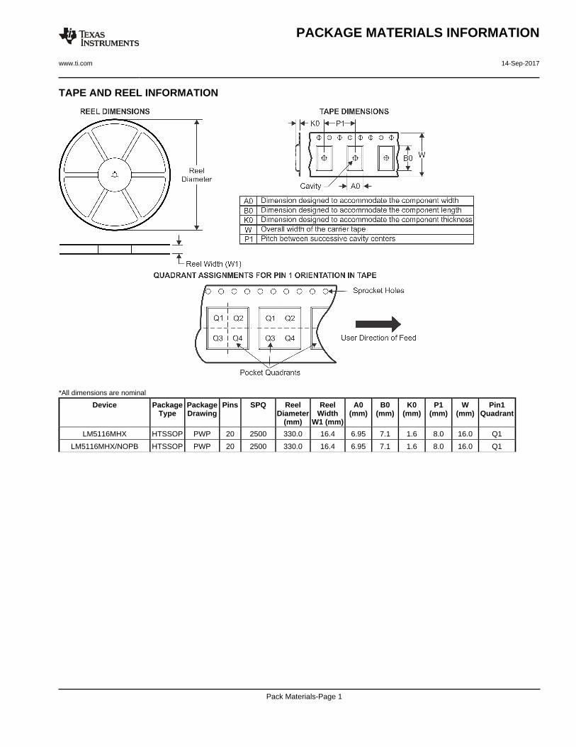
TAPE AND REEL INFORMATION
*All dimensions are nominal
Device PackageType
PackageDrawing
Pins SPQ ReelDiameter
(mm)
ReelWidth
W1 (mm)
A0(mm)
B0(mm)
K0(mm)
P1(mm)
W(mm)
Pin1Quadrant
LM5116MHX HTSSOP PWP 20 2500 330.0 16.4 6.95 7.1 1.6 8.0 16.0 Q1
LM5116MHX/NOPB HTSSOP PWP 20 2500 330.0 16.4 6.95 7.1 1.6 8.0 16.0 Q1
PACKAGE MATERIALS INFORMATION
www.ti.com 14-Sep-2017
Pack Materials-Page 1

*All dimensions are nominal
Device Package Type Package Drawing Pins SPQ Length (mm) Width (mm) Height (mm)
LM5116MHX HTSSOP PWP 20 2500 367.0 367.0 35.0
LM5116MHX/NOPB HTSSOP PWP 20 2500 367.0 367.0 35.0
PACKAGE MATERIALS INFORMATION
www.ti.com 14-Sep-2017
Pack Materials-Page 2

MECHANICAL DATA
PWP0020A
www.ti.com
MXA20A (Rev C)

IMPORTANT NOTICE AND DISCLAIMER
TI PROVIDES TECHNICAL AND RELIABILITY DATA (INCLUDING DATASHEETS), DESIGN RESOURCES (INCLUDING REFERENCEDESIGNS), APPLICATION OR OTHER DESIGN ADVICE, WEB TOOLS, SAFETY INFORMATION, AND OTHER RESOURCES “AS IS”AND WITH ALL FAULTS, AND DISCLAIMS ALL WARRANTIES, EXPRESS AND IMPLIED, INCLUDING WITHOUT LIMITATION ANYIMPLIED WARRANTIES OF MERCHANTABILITY, FITNESS FOR A PARTICULAR PURPOSE OR NON-INFRINGEMENT OF THIRDPARTY INTELLECTUAL PROPERTY RIGHTS.These resources are intended for skilled developers designing with TI products. You are solely responsible for (1) selecting the appropriateTI products for your application, (2) designing, validating and testing your application, and (3) ensuring your application meets applicablestandards, and any other safety, security, or other requirements. These resources are subject to change without notice. TI grants youpermission to use these resources only for development of an application that uses the TI products described in the resource. Otherreproduction and display of these resources is prohibited. No license is granted to any other TI intellectual property right or to any thirdparty intellectual property right. TI disclaims responsibility for, and you will fully indemnify TI and its representatives against, any claims,damages, costs, losses, and liabilities arising out of your use of these resources.TI’s products are provided subject to TI’s Terms of Sale (www.ti.com/legal/termsofsale.html) or other applicable terms available either onti.com or provided in conjunction with such TI products. TI’s provision of these resources does not expand or otherwise alter TI’s applicablewarranties or warranty disclaimers for TI products.
Mailing Address: Texas Instruments, Post Office Box 655303, Dallas, Texas 75265Copyright © 2018, Texas Instruments Incorporated