Embed Size (px)
Citation preview

SLVS063E − NOVEMBER 1988 − REVISED OCTOBER 2003
1POST OFFICE BOX 655303 • DALLAS, TEXAS 75265
Low Temperature Coefficient
Wide Operating Current . . . 400 µAto 10 mA
0.27-Ω Dynamic Impedance
±1% Tolerance Available
Specified Temperature Stability
Easily Trimmed for Minimum TemperatureDrift
Fast Turnon
description/ordering information
The LM236-2.5, LM336-2.5, and LM336B-2.5integrated circuits are precision 2.5-V shuntregulator diodes. These reference circuitsoperate as low-temperature-coefficient 2.5-VZener diodes with a 0.2-Ω dynamic impedance. Athird terminal provided on the circuit allows thereference voltage and temperature coefficient tobe trimmed easily.
The series is useful as precision 2.5-V low-voltage references (VZ) for digital voltmeters, power supplies, oroperational-amplifier circuitry. The 2.5-V voltage reference makes it convenient to obtain a stable reference from5-V logic supplies. Devices in this series operate as shunt regulators, and can be used as either positive ornegative voltage references.
The LM236-2.5 is characterized for operation from −25°C to 85°C. The LM336-2.5 and LM336B-2.5 arecharacterized for operation from 0°C to 70°C.
ORDERING INFORMATION
TA PACKAGE † ORDERABLEPART NUMBER
TOP-SIDEMARKING
Tube of 75 LM336D-2-5336-25
SOIC (D)Reel of 2500 LM336DR-2-5
336-25
SOIC (D)Tube of 75 LM336BD-2-5
336B25
0°C to 70°CReel of 2500 LM336BDR−2-5
336B25
0°C to 70°CBulk of 1000 LM336LP-2-5
336-25
TO-226 / TO-92 (LP)Reel of 2000 LM336LPR-2-5
336-25
TO-226 / TO-92 (LP)Bulk of 1000 LM336BLP-2-5
336B25Reel of 2000 LM336BLPR-2-5
336B25
−25°C to 85°C SOIC (D)Tube of 75 LM236D-2-5
236-25−25°C to 85°C SOIC (D)Reel of 2500 LM236DR-2-5
236-25
† Package drawings, standard packing quantities, thermal data, symbolization, and PCB design guidelines areavailable at www.ti.com/sc/package.
Copyright 2003, Texas Instruments Incorporated !" # $%&" !# '%()$!" *!"&*%$"# $ " #'&$$!"# '& "+& "&# &,!# #"%&"##"!*!* -!!". *%$" '$&##/ *&# " &$&##!). $)%*&"&#"/ !)) '!!&"&#
1
2
3
4
8
7
6
5
NCNCNC
ANODE
CATHODENCNCADJ
D PACKAGE(TOP VIEW)
LM336-2.5, LM336B-2.5 . . . LP PACKAGE(TOP VIEW)
NC − No internal connection
ANODE
CATHODE
ADJ
Please be aware that an important notice concerning availability, standard warranty, and use in critical applications ofTexas Instruments semiconductor products and disclaimers thereto appears at the end of this data sheet.

SLVS063E − NOVEMBER 1988 − REVISED OCTOBER 2003
2 POST OFFICE BOX 655303 • DALLAS, TEXAS 75265
symbol
CATHODEANODE
ADJ
schematic diagram
CATHODE
Q11
6.6 kΩ24kΩ
24kΩ
Q14
Q8
Q7
Q2
20 pF
10 kΩ30 pF
Q10
Q3
Q1
Q5
Q4
Q6
Q9
Q12
Q13
500 Ω
30 kΩ
6.6 kΩ
720 Ω
ADJ
ANODE
NOTE A: All component values are nominal.
absolute maximum ratings over operating free-air temperature range (unless otherwise noted) †
Reverse current, IR 20 mA. . . . . . . . . . . . . . . . . . . . . . . . . . . . . . . . . . . . . . . . . . . . . . . . . . . . . . . . . . . . . . . . . . . . . . Forward current, IF 10 mA. . . . . . . . . . . . . . . . . . . . . . . . . . . . . . . . . . . . . . . . . . . . . . . . . . . . . . . . . . . . . . . . . . . . . . . Package thermal impedance, θJA (see Notes 1 and 2): D package 97°C/W. . . . . . . . . . . . . . . . . . . . . . . . . . . .
LP package 140°C/W. . . . . . . . . . . . . . . . . . . . . . . . . . Operating virtual junction temperature, TJ 150°C. . . . . . . . . . . . . . . . . . . . . . . . . . . . . . . . . . . . . . . . . . . . . . . . . . . Storage temperature range, Tstg −65°C to 150°C. . . . . . . . . . . . . . . . . . . . . . . . . . . . . . . . . . . . . . . . . . . . . . . . . . .
† Stresses beyond those listed under “absolute maximum ratings” may cause permanent damage to the device. These are stress ratings only, andfunctional operation of the device at these or any other conditions beyond those indicated under “recommended operating conditions” is notimplied. Exposure to absolute-maximum-rated conditions for extended periods may affect device reliability.
NOTES: 1. Maximum power dissipation is a function of TJ(max), θJA, and TA. The maximum allowable power dissipation at any allowableambient temperature is PD = (TJ(max) − TA)/θJA. Operating at the absolute maximum TJ of 150°C can impact reliability.
2. The package thermal impedance is calculated in accordance with JESD 51-7.
recommended operating conditionsMIN MAX UNIT
TA Operating free-air temperatureLM236-2.5 −25 85
°CTA Operating free-air temperatureLM336-2.5, LM336B-2.5 0 70
°C
SLVS063E − NOVEMBER 1988 − REVISED OCTOBER 2003
3POST OFFICE BOX 655303 • DALLAS, TEXAS 75265
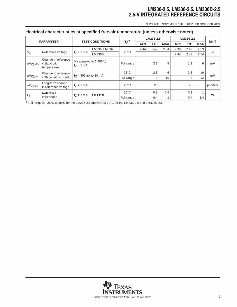
electrical characteristics at specified free-air temperature (unless otherwise noted)
PARAMETER TEST CONDITIONS TA†LM236-2.5 LM336-2.5
UNITPARAMETER TEST CONDITIONS TA†MIN TYP MAX MIN TYP MAX
UNIT
VZ Reference voltage IZ = 1 mALM236, LM336
25°C2.44 2.49 2.54 2.39 2.49 2.59
VVZ Reference voltage IZ = 1 mALM336B
25°C2.44 2.49 2.54
V
∆VZ(∆T)
Change in referencevoltage withtemperature
VZ adjusted to 2.490 V,IZ = 1 mA
Full range 3.5 9 1.8 6 mV
∆VZ( I)Change in reference
IZ = 400 A to 10 mA25°C 2.6 6 2.6 10
mV∆VZ(∆I)Change in referencevoltage with current IZ = 400 µA to 10 mA
Full range 3 10 3 12mV
∆VZ(∆t)Long-term changein reference voltage
IZ = 1 mA 25°C 20 20 ppm/khr
zzReference
IZ = 1 mA, f = 1 kHz25°C 0.2 0.6 0.2 1
WzzReferenceimpedance
IZ = 1 mA, f = 1 kHzFull range 0.4 1 0.4 1.4
W
† Full range is −25°C to 85°C for the LM236-2.5 and 0°C to 70°C for the LM336-2.5 and LM336B-2.5.

SLVS063E − NOVEMBER 1988 − REVISED OCTOBER 2003
4 POST OFFICE BOX 655303 • DALLAS, TEXAS 75265
TYPICAL CHARACTERISTICS
Figure 1
∆V
−
Cha
nge
in R
efer
ence
Vol
tage
− m
VZ
1.5
1
0.5
00 2 4 6
2
CHANGE IN REFERENCE VOLTAGEvs
REFERENCE CURRENT
2.5
8 10IZ − Reference Current − mA
TA = 25°C
Figure 2
150
100
5010 100 1 k
200
f − Frequency − Hz
NOISE VOLTAGEvs
FREQUENCY250
10 k 100 k
IZ = 1 mATA = 25°C
− N
oise
Vol
tage
−V
nnV
/H
z
0.01 0.1 1
f − Frequency − kHz
10 100
REFERENCE IMPEDANCEvs
FREQUENCY
10
1
0.1
100
IZ = 1 mATA = −55°C to 125°C
Ωz z
− R
efer
ence
Impe
danc
e −
Figure 3
SLVS063E − NOVEMBER 1988 − REVISED OCTOBER 2003
5POST OFFICE BOX 655303 • DALLAS, TEXAS 75265
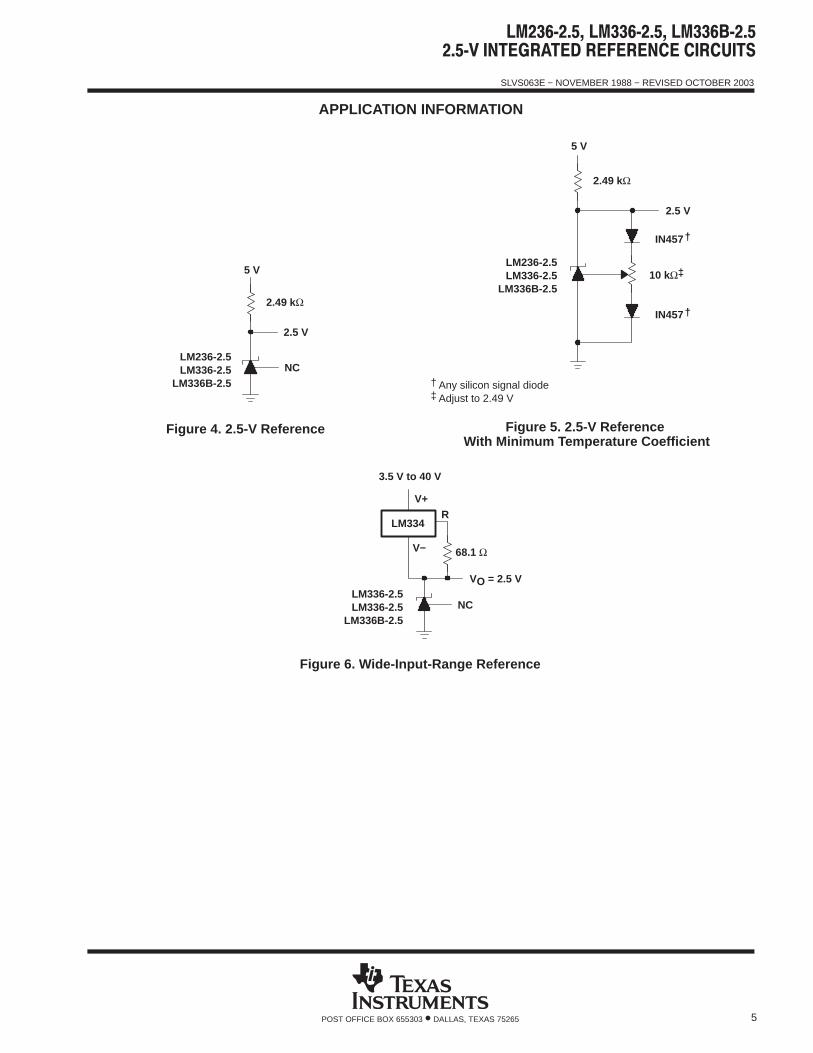
APPLICATION INFORMATION
2.49 kΩ
2.5 V
LM236-2.5LM336-2.5
LM336B-2.5
5 V
NC
Figure 4. 2.5-V Reference
2.49 kΩ
LM236-2.5LM336-2.5
LM336B-2.5
IN457†
IN457†
10 kه
5 V
† Any silicon signal diode‡ Adjust to 2.49 V
2.5 V
Figure 5. 2.5-V Reference With Minimum Temperature Coefficient
LM336-2.5LM336-2.5
LM336B-2.5
LM334
V+
V−
3.5 V to 40 V
68.1 Ω
VO = 2.5 V
R
NC
Figure 6. Wide-Input-Range Reference
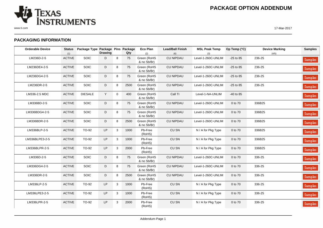
PACKAGE OPTION ADDENDUM
www.ti.com 17-Mar-2017
Addendum-Page 1
PACKAGING INFORMATION
Orderable Device Status(1)
Package Type PackageDrawing
Pins PackageQty
Eco Plan(2)
Lead/Ball Finish(6)
MSL Peak Temp(3)
Op Temp (°C) Device Marking(4/5)
Samples
LM236D-2-5 ACTIVE SOIC D 8 75 Green (RoHS& no Sb/Br)
CU NIPDAU Level-1-260C-UNLIM -25 to 85 236-25
LM236DE4-2-5 ACTIVE SOIC D 8 75 Green (RoHS& no Sb/Br)
CU NIPDAU Level-1-260C-UNLIM -25 to 85 236-25
LM236DG4-2-5 ACTIVE SOIC D 8 75 Green (RoHS& no Sb/Br)
CU NIPDAU Level-1-260C-UNLIM -25 to 85 236-25
LM236DR-2-5 ACTIVE SOIC D 8 2500 Green (RoHS& no Sb/Br)
CU NIPDAU Level-1-260C-UNLIM -25 to 85 236-25
LM336-2.5 MDC ACTIVE DIESALE Y 0 400 Green (RoHS& no Sb/Br)
Call TI Level-1-NA-UNLIM -40 to 85
LM336BD-2-5 ACTIVE SOIC D 8 75 Green (RoHS& no Sb/Br)
CU NIPDAU Level-1-260C-UNLIM 0 to 70 336B25
LM336BDG4-2-5 ACTIVE SOIC D 8 75 Green (RoHS& no Sb/Br)
CU NIPDAU Level-1-260C-UNLIM 0 to 70 336B25
LM336BDR-2-5 ACTIVE SOIC D 8 2500 Green (RoHS& no Sb/Br)
CU NIPDAU Level-1-260C-UNLIM 0 to 70 336B25
LM336BLP-2-5 ACTIVE TO-92 LP 3 1000 Pb-Free(RoHS)
CU SN N / A for Pkg Type 0 to 70 336B25
LM336BLPE3-2-5 ACTIVE TO-92 LP 3 1000 Pb-Free(RoHS)
CU SN N / A for Pkg Type 0 to 70 336B25
LM336BLPR-2-5 ACTIVE TO-92 LP 3 2000 Pb-Free(RoHS)
CU SN N / A for Pkg Type 0 to 70 336B25
LM336D-2-5 ACTIVE SOIC D 8 75 Green (RoHS& no Sb/Br)
CU NIPDAU Level-1-260C-UNLIM 0 to 70 336-25
LM336DG4-2-5 ACTIVE SOIC D 8 75 Green (RoHS& no Sb/Br)
CU NIPDAU Level-1-260C-UNLIM 0 to 70 336-25
LM336DR-2-5 ACTIVE SOIC D 8 2500 Green (RoHS& no Sb/Br)
CU NIPDAU Level-1-260C-UNLIM 0 to 70 336-25
LM336LP-2-5 ACTIVE TO-92 LP 3 1000 Pb-Free(RoHS)
CU SN N / A for Pkg Type 0 to 70 336-25
LM336LPE3-2-5 ACTIVE TO-92 LP 3 1000 Pb-Free(RoHS)
CU SN N / A for Pkg Type 0 to 70 336-25
LM336LPR-2-5 ACTIVE TO-92 LP 3 2000 Pb-Free(RoHS)
CU SN N / A for Pkg Type 0 to 70 336-25
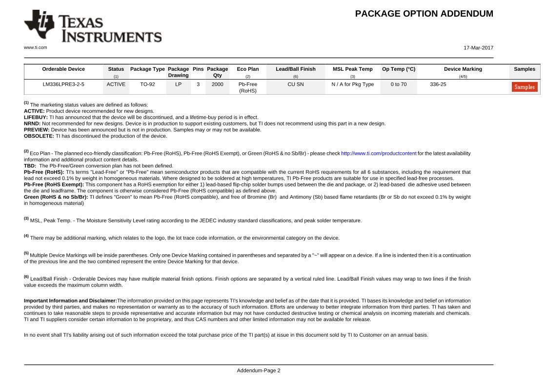
PACKAGE OPTION ADDENDUM
www.ti.com 17-Mar-2017
Addendum-Page 2
Orderable Device Status(1)
Package Type PackageDrawing
Pins PackageQty
Eco Plan(2)
Lead/Ball Finish(6)
MSL Peak Temp(3)
Op Temp (°C) Device Marking(4/5)
Samples
LM336LPRE3-2-5 ACTIVE TO-92 LP 3 2000 Pb-Free(RoHS)
CU SN N / A for Pkg Type 0 to 70 336-25
(1) The marketing status values are defined as follows:ACTIVE: Product device recommended for new designs.LIFEBUY: TI has announced that the device will be discontinued, and a lifetime-buy period is in effect.NRND: Not recommended for new designs. Device is in production to support existing customers, but TI does not recommend using this part in a new design.PREVIEW: Device has been announced but is not in production. Samples may or may not be available.OBSOLETE: TI has discontinued the production of the device.
(2) Eco Plan - The planned eco-friendly classification: Pb-Free (RoHS), Pb-Free (RoHS Exempt), or Green (RoHS & no Sb/Br) - please check http://www.ti.com/productcontent for the latest availabilityinformation and additional product content details.TBD: The Pb-Free/Green conversion plan has not been defined.Pb-Free (RoHS): TI's terms "Lead-Free" or "Pb-Free" mean semiconductor products that are compatible with the current RoHS requirements for all 6 substances, including the requirement thatlead not exceed 0.1% by weight in homogeneous materials. Where designed to be soldered at high temperatures, TI Pb-Free products are suitable for use in specified lead-free processes.Pb-Free (RoHS Exempt): This component has a RoHS exemption for either 1) lead-based flip-chip solder bumps used between the die and package, or 2) lead-based die adhesive used betweenthe die and leadframe. The component is otherwise considered Pb-Free (RoHS compatible) as defined above.Green (RoHS & no Sb/Br): TI defines "Green" to mean Pb-Free (RoHS compatible), and free of Bromine (Br) and Antimony (Sb) based flame retardants (Br or Sb do not exceed 0.1% by weightin homogeneous material)
(3) MSL, Peak Temp. - The Moisture Sensitivity Level rating according to the JEDEC industry standard classifications, and peak solder temperature.
(4) There may be additional marking, which relates to the logo, the lot trace code information, or the environmental category on the device.
(5) Multiple Device Markings will be inside parentheses. Only one Device Marking contained in parentheses and separated by a "~" will appear on a device. If a line is indented then it is a continuationof the previous line and the two combined represent the entire Device Marking for that device.
(6) Lead/Ball Finish - Orderable Devices may have multiple material finish options. Finish options are separated by a vertical ruled line. Lead/Ball Finish values may wrap to two lines if the finishvalue exceeds the maximum column width.
Important Information and Disclaimer:The information provided on this page represents TI's knowledge and belief as of the date that it is provided. TI bases its knowledge and belief on informationprovided by third parties, and makes no representation or warranty as to the accuracy of such information. Efforts are underway to better integrate information from third parties. TI has taken andcontinues to take reasonable steps to provide representative and accurate information but may not have conducted destructive testing or chemical analysis on incoming materials and chemicals.TI and TI suppliers consider certain information to be proprietary, and thus CAS numbers and other limited information may not be available for release.
In no event shall TI's liability arising out of such information exceed the total purchase price of the TI part(s) at issue in this document sold by TI to Customer on an annual basis.

TAPE AND REEL INFORMATION
*All dimensions are nominal
Device PackageType
PackageDrawing
Pins SPQ ReelDiameter
(mm)
ReelWidth
W1 (mm)
A0 (mm) B0 (mm) K0 (mm) P1(mm)
W(mm)
Pin1Quadrant
LM236DR-2-5 SOIC D 8 2500 330.0 12.4 6.4 5.2 2.1 8.0 12.0 Q1
LM336BDR-2-5 SOIC D 8 2500 330.0 12.4 6.4 5.2 2.1 8.0 12.0 Q1
LM336DR-2-5 SOIC D 8 2500 330.0 12.4 6.4 5.2 2.1 8.0 12.0 Q1
PACKAGE MATERIALS INFORMATION
www.ti.com 19-Mar-2008
Pack Materials-Page 1

*All dimensions are nominal
Device Package Type Package Drawing Pins SPQ Length (mm) Width (mm) Height (mm)
LM236DR-2-5 SOIC D 8 2500 340.5 338.1 20.6
LM336BDR-2-5 SOIC D 8 2500 340.5 338.1 20.6
LM336DR-2-5 SOIC D 8 2500 340.5 338.1 20.6
PACKAGE MATERIALS INFORMATION
www.ti.com 19-Mar-2008
Pack Materials-Page 2


www.ti.com
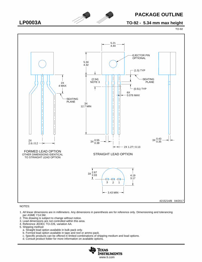
PACKAGE OUTLINE
3X 2.672.03
5.214.44
5.344.32
3X12.7 MIN
2X 1.27 0.13
3X 0.550.38
4.193.17
3.43 MIN
3X 0.430.35
(2.54)NOTE 3
2X2.6 0.2
2X4 MAX
SEATINGPLANE
6X0.076 MAX
(0.51) TYP
(1.5) TYP
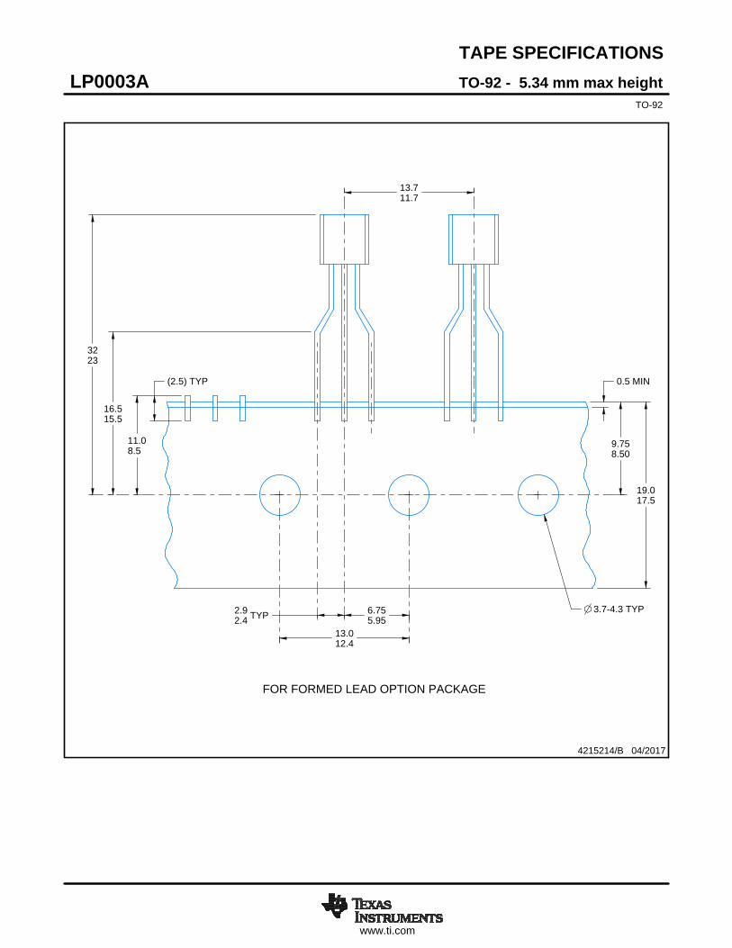
TO-92 - 5.34 mm max heightLP0003ATO-92
4215214/B 04/2017
NOTES: 1. All linear dimensions are in millimeters. Any dimensions in parenthesis are for reference only. Dimensioning and tolerancing per ASME Y14.5M.2. This drawing is subject to change without notice.3. Lead dimensions are not controlled within this area.4. Reference JEDEC TO-226, variation AA.5. Shipping method: a. Straight lead option available in bulk pack only. b. Formed lead option available in tape and reel or ammo pack. c. Specific products can be offered in limited combinations of shipping medium and lead options. d. Consult product folder for more information on available options.
EJECTOR PINOPTIONAL
PLANESEATING
STRAIGHT LEAD OPTION
3 2 1
SCALE 1.200
FORMED LEAD OPTIONOTHER DIMENSIONS IDENTICAL
TO STRAIGHT LEAD OPTION
SCALE 1.200

www.ti.com
EXAMPLE BOARD LAYOUT
0.05 MAXALL AROUND
TYP
(1.07)
(1.5) 2X (1.5)
2X (1.07)(1.27)
(2.54)
FULL RTYP
( 1.4)0.05 MAXALL AROUND
TYP
(2.6)
(5.2)
(R0.05) TYP
3X ( 0.9) HOLE
2X ( 1.4)METAL
3X ( 0.85) HOLE
(R0.05) TYP
4215214/B 04/2017
TO-92 - 5.34 mm max heightLP0003ATO-92
LAND PATTERN EXAMPLEFORMED LEAD OPTIONNON-SOLDER MASK DEFINED
SCALE:15X
SOLDER MASKOPENING
METAL
2XSOLDER MASKOPENING
1 2 3
LAND PATTERN EXAMPLESTRAIGHT LEAD OPTIONNON-SOLDER MASK DEFINED
SCALE:15X
METALTYP
SOLDER MASKOPENING
2XSOLDER MASKOPENING
2XMETAL
1 2 3
www.ti.com
TAPE SPECIFICATIONS
19.017.5
13.711.7
11.08.5
0.5 MIN
TYP-4.33.7
9.758.50
TYP2.92.4
6.755.95
13.012.4
(2.5) TYP
16.515.5
3223
4215214/B 04/2017
TO-92 - 5.34 mm max heightLP0003ATO-92
FOR FORMED LEAD OPTION PACKAGE

IMPORTANT NOTICE
Texas Instruments Incorporated (TI) reserves the right to make corrections, enhancements, improvements and other changes to itssemiconductor products and services per JESD46, latest issue, and to discontinue any product or service per JESD48, latest issue. Buyersshould obtain the latest relevant information before placing orders and should verify that such information is current and complete.TI’s published terms of sale for semiconductor products (http://www.ti.com/sc/docs/stdterms.htm) apply to the sale of packaged integratedcircuit products that TI has qualified and released to market. Additional terms may apply to the use or sale of other types of TI products andservices.Reproduction of significant portions of TI information in TI data sheets is permissible only if reproduction is without alteration and isaccompanied by all associated warranties, conditions, limitations, and notices. TI is not responsible or liable for such reproduceddocumentation. Information of third parties may be subject to additional restrictions. Resale of TI products or services with statementsdifferent from or beyond the parameters stated by TI for that product or service voids all express and any implied warranties for theassociated TI product or service and is an unfair and deceptive business practice. TI is not responsible or liable for any such statements.Buyers and others who are developing systems that incorporate TI products (collectively, “Designers”) understand and agree that Designersremain responsible for using their independent analysis, evaluation and judgment in designing their applications and that Designers havefull and exclusive responsibility to assure the safety of Designers' applications and compliance of their applications (and of all TI productsused in or for Designers’ applications) with all applicable regulations, laws and other applicable requirements. Designer represents that, withrespect to their applications, Designer has all the necessary expertise to create and implement safeguards that (1) anticipate dangerousconsequences of failures, (2) monitor failures and their consequences, and (3) lessen the likelihood of failures that might cause harm andtake appropriate actions. Designer agrees that prior to using or distributing any applications that include TI products, Designer willthoroughly test such applications and the functionality of such TI products as used in such applications.TI’s provision of technical, application or other design advice, quality characterization, reliability data or other services or information,including, but not limited to, reference designs and materials relating to evaluation modules, (collectively, “TI Resources”) are intended toassist designers who are developing applications that incorporate TI products; by downloading, accessing or using TI Resources in anyway, Designer (individually or, if Designer is acting on behalf of a company, Designer’s company) agrees to use any particular TI Resourcesolely for this purpose and subject to the terms of this Notice.TI’s provision of TI Resources does not expand or otherwise alter TI’s applicable published warranties or warranty disclaimers for TIproducts, and no additional obligations or liabilities arise from TI providing such TI Resources. TI reserves the right to make corrections,enhancements, improvements and other changes to its TI Resources. TI has not conducted any testing other than that specificallydescribed in the published documentation for a particular TI Resource.Designer is authorized to use, copy and modify any individual TI Resource only in connection with the development of applications thatinclude the TI product(s) identified in such TI Resource. NO OTHER LICENSE, EXPRESS OR IMPLIED, BY ESTOPPEL OR OTHERWISETO ANY OTHER TI INTELLECTUAL PROPERTY RIGHT, AND NO LICENSE TO ANY TECHNOLOGY OR INTELLECTUAL PROPERTYRIGHT OF TI OR ANY THIRD PARTY IS GRANTED HEREIN, including but not limited to any patent right, copyright, mask work right, orother intellectual property right relating to any combination, machine, or process in which TI products or services are used. Informationregarding or referencing third-party products or services does not constitute a license to use such products or services, or a warranty orendorsement thereof. Use of TI Resources may require a license from a third party under the patents or other intellectual property of thethird party, or a license from TI under the patents or other intellectual property of TI.TI RESOURCES ARE PROVIDED “AS IS” AND WITH ALL FAULTS. TI DISCLAIMS ALL OTHER WARRANTIES ORREPRESENTATIONS, EXPRESS OR IMPLIED, REGARDING RESOURCES OR USE THEREOF, INCLUDING BUT NOT LIMITED TOACCURACY OR COMPLETENESS, TITLE, ANY EPIDEMIC FAILURE WARRANTY AND ANY IMPLIED WARRANTIES OFMERCHANTABILITY, FITNESS FOR A PARTICULAR PURPOSE, AND NON-INFRINGEMENT OF ANY THIRD PARTY INTELLECTUALPROPERTY RIGHTS. TI SHALL NOT BE LIABLE FOR AND SHALL NOT DEFEND OR INDEMNIFY DESIGNER AGAINST ANY CLAIM,INCLUDING BUT NOT LIMITED TO ANY INFRINGEMENT CLAIM THAT RELATES TO OR IS BASED ON ANY COMBINATION OFPRODUCTS EVEN IF DESCRIBED IN TI RESOURCES OR OTHERWISE. IN NO EVENT SHALL TI BE LIABLE FOR ANY ACTUAL,DIRECT, SPECIAL, COLLATERAL, INDIRECT, PUNITIVE, INCIDENTAL, CONSEQUENTIAL OR EXEMPLARY DAMAGES INCONNECTION WITH OR ARISING OUT OF TI RESOURCES OR USE THEREOF, AND REGARDLESS OF WHETHER TI HAS BEENADVISED OF THE POSSIBILITY OF SUCH DAMAGES.Unless TI has explicitly designated an individual product as meeting the requirements of a particular industry standard (e.g., ISO/TS 16949and ISO 26262), TI is not responsible for any failure to meet such industry standard requirements.Where TI specifically promotes products as facilitating functional safety or as compliant with industry functional safety standards, suchproducts are intended to help enable customers to design and create their own applications that meet applicable functional safety standardsand requirements. Using products in an application does not by itself establish any safety features in the application. Designers mustensure compliance with safety-related requirements and standards applicable to their applications. Designer may not use any TI products inlife-critical medical equipment unless authorized officers of the parties have executed a special contract specifically governing such use.Life-critical medical equipment is medical equipment where failure of such equipment would cause serious bodily injury or death (e.g., lifesupport, pacemakers, defibrillators, heart pumps, neurostimulators, and implantables). Such equipment includes, without limitation, allmedical devices identified by the U.S. Food and Drug Administration as Class III devices and equivalent classifications outside the U.S.TI may expressly designate certain products as completing a particular qualification (e.g., Q100, Military Grade, or Enhanced Product).Designers agree that it has the necessary expertise to select the product with the appropriate qualification designation for their applicationsand that proper product selection is at Designers’ own risk. Designers are solely responsible for compliance with all legal and regulatoryrequirements in connection with such selection.Designer will fully indemnify TI and its representatives against any damages, costs, losses, and/or liabilities arising out of Designer’s non-compliance with the terms and provisions of this Notice.
Mailing Address: Texas Instruments, Post Office Box 655303, Dallas, Texas 75265Copyright © 2017, Texas Instruments Incorporated


![jan 2012 · 2017-07-19 · phot 2" x 2.5" photo 2" x 2.5" C) PageMaps photo 2.5" x 2.5" photo 2.5" x 2.5" photo 2.5" x 2.5" photo 2" x 2.5" photo 2.5" x 2.5" C] PageMaps photo 2.5"](https://img.dokumen.tips/doc/110x75/5f4cb42409b5fa18f7093d11/jan-2012-2017-07-19-phot-2-x-25-photo-2-x-25-c-pagemaps.jpg)


![Courtesy of Steven Engineering, Inc. - 230 Ryan Way, South ... · 2 x 0.5 mm2 403 PTDA series ... Rated surge voltage [kV] 2.5 2.5 2.5 2.5 2.5 2.5 Approval data (UL/CUL) Use Group](https://img.dokumen.tips/doc/110x75/5c78029809d3f21d538c775a/courtesy-of-steven-engineering-inc-230-ryan-way-south-2-x-05-mm2-403.jpg)