Embed Size (px)
Citation preview

Application ReportSLUA733–February 2015
LLC Design for UCC29950
Dr. J M Leisten................................................................................................................ Power Stage
ABSTRACTFirst Harmonic Approximation (FHA) is the conventional approach used when analyzing the LLC convertertopology. This approach requires a minimum of math to generate a reasonable approximation to the LLCpower converter operating characteristic. On the other hand, FHA analysis is less than ideal whendesigning an LLC power converter to meet 'real world' specifications. One reason is that FHA is accuratewhen operating close to the resonant frequency, but becomes less accurate as the switching frequencymoves away from resonance. Another failing is that FHA analysis results cannot be compared directly withobserved waveforms from the physical LLC converter. For example, the FHA characteristic has loadexpressed in terms of LLC damping or 'Q-factor' while the power stage load is typically expressed in termsof current and voltage.
In an age of powerful computing, it is possible to generate the LLC operating characteristic without the aidof FHA. An LLC operating characteristic based upon this numerical approach has the advantage ofaccuracy across the whole range of switching frequencies. This operating characteristic can also berelated directly to current and voltage waveforms and quantities measured in the physical LLC convertercircuit.
The first part of this application note presents a summary of the analysis method used to generate theLLC operating characteristic. Subsequent sections show how the resulting LLC operating characteristiccan be used to select the LLC power components needed to achieve a variety of common power supplyspecification requirements.
An objective of this document is to provide the designer with all the tools needed to select the LLC powercomponents required to meet his/her specification requirement.
The design process outlined here is suitable only for LLC converters with diode rectifiers, or SynchronousRectifiers (SR) that operate in diode equivalent mode. Use of other Synchronous Rectification methodseffectively alter the LLC characteristic in a way that depends upon the particular driver timing employed forthe SR switches.
Contents1 LLC Analysis Method........................................................................................................ 2
1.1 Steady-State Operating Modes ................................................................................... 51.2 Steady-State Operating Point ..................................................................................... 9
2 LLC Design.................................................................................................................. 152.1 Current Loss Factor ............................................................................................... 152.2 LLC Design Approach ............................................................................................ 17
Appendix A Design Example (Fixed Output Voltage Variable Input Voltage)............................................ 22Appendix B Normalized Steady-State LLC Design Curves ................................................................ 26
List of Figures
1 LLC Power Converter Schematic.......................................................................................... 22 LLC Power Converter Simplified Equivalent Circuit ..................................................................... 33 LLC Power Converter Normalized Simplified Equivalent Circuit ...................................................... 34 S-States Equivalent Circuit ................................................................................................. 45 P-States Equivalent Circuit ................................................................................................. 4
All trademarks are the property of their respective owners.
1SLUA733–February 2015 LLC Design for UCC29950Submit Documentation Feedback
Copyright © 2015, Texas Instruments Incorporated

+
Vin
Lr
Lm
Cr
Im(t)
VPSN(t)
VPRS(t)
n:1
Vout
Cout Rload
Transformer
Ir(t)
Vr(t)
LLC Analysis Method www.ti.com
6 LLC Normalized Resonant Waveforms for AH Region (x = 0.3, lm = 5, ∆Vrn = 1.642) ............................ 67 LLC Normalized Resonant Waveforms for AL Region (x = 0.4 7, lm = 5 , ∆Vrn = 0.1) ............................ 78 LLC Normalized Resonant Waveforms for BH Region (x = 1, lm = 5, ∆Vrn = 2.4) ................................. 89 LLC Normalized Resonant Waveforms for BL Region (x = 1, lm = 5, ∆Vrn = 0.7).................................. 910 LLC Normalized Resonant Waveforms for ZCS Boundary Condition (x = 1.3, lm = 7, ∆Vrn = 3.88) ........... 1111 LLC Normalized Resonant Waveforms for AH/BH Boundary Condition (x = 0.5, lm = 5, ∆Vrn = 0.6).......... 1212 LLC Combined Boundary Solution ∆Vrn vs Voltage Gain (x) and Inductor Ratio (lm)............................ 1313 Steady-State Input Average Current (Iinavno) vs Switching Period (Tpn) for Range of Voltage Gain (x),
Inductor Ratio lm = 5....................................................................................................... 1414 Current Loss Factor (CLF) vs Switching Period (Tpn) for Range of Voltage Gain (x), Inductor Ratio lm = 5 . 1715 CLF vs x for Range of lm at ZCS/RR Boundary Operation........................................................... 1816 LLC Normalized Equivalent Circuit for Dead-Time at Zero Load Power............................................ 2017 LLC Simplified Normalized Equivalent Circuit for Dead-Time at Zero Load Power ............................... 2018 LLC Steady-State Normalized Operating Characteristic for Fixed Output Voltage lm = 5 ....................... 2319 LLC Normalized Design Curves for Inductor Ratio lm = 3 ............................................................ 2720 LLC Normalized Design Curves for Inductor Ratio lm = 5 ............................................................ 2821 LLC Normalized Design Curves for Inductor Ratio lm = 7 ............................................................ 2922 LLC Normalized Design Curves for Inductor Ratio lm = 9 ............................................................ 3023 LLC Normalized Design Curves for Inductor Ratio lm = 15 .......................................................... 31
1 LLC Analysis MethodA typical LLC power converter schematic is presented in Figure 1. The LLC power stage requires threereactive elements (Lr, Lm, and Cr) and a transformer to provide isolation. As shown in Figure 1 it iscommon to employ the transformer parasitic components of leakage and magnetizing inductance toprovide the two LLC inductive elements (Lr and Lm).
Figure 1. LLC Power Converter Schematic
The secondary side of the LLC power converter can be referred into the primary side to give the simplifiedequivalent circuit in Figure 2. It is also convenient to normalize the LLC equivalent circuit, to an inputvoltage of 1, by making the following variable substitutions. Once this is done, we arrive at the normalizedequivalent circuit in Figure 3.
2 LLC Design for UCC29950 SLUA733–February 2015Submit Documentation Feedback
Copyright © 2015, Texas Instruments Incorporated

D2
D1
Vrn( )θ
Irn( )θ Imn( )θ
1
S1
S2
VPRSn( )θ
VPSNn( )θ
+
+
+
x
x
Lr Lm
Cr
+
+
+
n . Vout
n . Vout
Lr Lm
Cr Vr(t)
Ir(t) Im(t)
Vin
VPRS(t)
VPSN(t)
ZnIrn( ) Ir( )
Vin
ZnImn( ) Im( )
Vin
1Vrn( ) Vr( )
Vin
t
1
Lr Cr
LrZn
Cr
n Voutx
Vin
Lmlm
Lr
q = q ´
q = q ´
q = q ´
q = w´
w =
´
=
´=
=
www.ti.com LLC Analysis Method
(1)
Figure 2. LLC Power Converter Simplified Equivalent Circuit
Figure 3. LLC Power Converter Normalized Simplified Equivalent Circuit
3SLUA733–February 2015 LLC Design for UCC29950Submit Documentation Feedback
Copyright © 2015, Texas Instruments Incorporated

+
Lr Lm
Cr VrPn( )θ
IrPn( )θ
VPSNn
State_No S0 S1 S2 S3
VPSNn 1 1 0 0
VPRSn x x x x
æ ö æ öç ÷ ç ÷
=ç ÷ ç ÷ç ÷ ç ÷- -è ø è ø
VPRSnImSn( ) +ImS0n
lm
´ qq =
+
+
Lr Lm
Cr VrSn( )θ
IrSn( )θ ImSn( )θ
VPRSn
VPSNn
LLC Analysis Method www.ti.com
Analysis proceeds by breaking down each switching cycle into a series of intervals, based upon the statesof the semiconductor devices that are conducting during the interval. There are four possible switch statesthat include conduction of an output rectifier diode. These are referred to as the S-States. There are twopossible switch states that do not include conduction of an output rectifier diode. These are referred to asthe P-States.
Figure 4. S-States Equivalent Circuit
The equivalent circuit during the S-states is presented in Figure 4. The resonant current and voltagewaveforms during one of these states can be expressed as follows:IrSn(θ) = (VPSNn − VPRSn − VrS0n) × sin(θ) + IrS0n × cos(θ) (2)
(3)VrSn(θ) = (VPSNn − VPRSn) − (VPSNn − VPRSn − VrS0n) × cos(θ) + IrS0n × sin(θ) (4)
IrS0n, ImS0n, and VrA0n are the initial values of resonant current, magnetising current, and resonantcapacitor voltage at the start of the current S-State.
The variable VPSNn is set to 1 if the upper primary MOSFET (or body diode) is conducting during thecurrent S-State. It is set to 0 if the lower primary MOSFET (or body diode) is conducting in the current S-State.
The variable VPRSn is set to +x if the Primary Referred Secondary voltage is positive (as defined by thearrow in Figure 4) during the current S_State. It is set to –x if the VPRSn voltage is negative. Thefollowing table gives the results for all four possible S-States.
The equivalent circuit during the P-states is presented in Figure 5. The resonant current and voltagewaveforms during one of these states can be expressed as follows:
Figure 5. P-States Equivalent Circuit
4 LLC Design for UCC29950 SLUA733–February 2015Submit Documentation Feedback
Copyright © 2015, Texas Instruments Incorporated

State_No P0 P1
VPSNn 1 0
VPRSn na na
æ ö æ öç ÷ ç ÷
=ç ÷ ç ÷ç ÷ ç ÷è ø è ø
( )
VPSNn VrP0nIrPn( ) sin IrP0n cos
1 lm 1 lm 1 lm
VrBn( ) VPSNn VPSNn VrP0n cos IrP0n 1 lm sin1 lm 1 lm
æ ö æ ö- q qq = ´ + ´ç ÷ ç ÷
+ + +è ø è ø
æ ö æ öq qq = - - ´ + ´ + ´ç ÷ ç ÷
+ +è ø è ø
www.ti.com LLC Analysis Method
(5)
1.1 Steady-State Operating ModesOver the normal region of interest, the LLC converter can operate in one of four different operating modes.An operating mode is defined as a particular sequence of states over the period of a switching cycle. Thefour operating modes of interest are listed below:1. Above Resonance High Power (AH)2. Above Resonance Low Power (AL)3. Below Resonance High Power (BH)4. Below Resonance Low Power (BL)
The sequence of states and corresponding resonant component waveforms for each mode/region arepresented in Section 1.1.1 through Section 1.1.4.
5SLUA733–February 2015 LLC Design for UCC29950Submit Documentation Feedback
Copyright © 2015, Texas Instruments Incorporated

�1�0 �2 �3
S1S0 S3S2
'Vrn
0
0.5
Vrn(�)
Irn(�)
Imn(�)
Vr0n
Vr1n
Vr2n
Ir0n
Ir1n
Ir2n
Im2n
Im0n
State_Seq S0 S1 S2 S3
VPSNn 1 1 0 0
VPRSn x x x x
æ ö æ öç ÷ ç ÷
=ç ÷ ç ÷ç ÷ ç ÷- -è ø è ø
LLC Analysis Method www.ti.com
1.1.1 Above Resonance High Power (AH)In this region only the S-States occur. The sequence of states that defines this region is as follows:
Figure 6. LLC Normalized Resonant Waveforms for AH Region (x = 0.3, lm = 5, ∆Vrn = 1.642)
6 LLC Design for UCC29950 SLUA733–February 2015Submit Documentation Feedback
Copyright © 2015, Texas Instruments Incorporated

Vrn(�)
�0S0
0
0.5
Irn(�) Imn(�)
Vr0nVr2n
Ir0n
Im3n
�1P0
�3S2
�4P1
�2S1
�5S3
Vr1n
Vr2n
Im0n Ir2n
Ir1n
Ir3n
'Vrn
State_Seq S0 P0 S1 S2 P1 S3
VPSNn 1 1 1 0 0 0
VPRSn x na x x na x
æ ö æ öç ÷ ç ÷
=ç ÷ ç ÷ç ÷ ç ÷- -è ø è ø
www.ti.com LLC Analysis Method
1.1.2 Above Resonance, Low Power (AL)In this region each half-cycle contains three states. The sequence of states that defines this region is asfollows:
Figure 7. LLC Normalized Resonant Waveforms for AL Region (x = 0.4 7, lm = 5 , ∆Vrn = 0.1)
7SLUA733–February 2015 LLC Design for UCC29950Submit Documentation Feedback
Copyright © 2015, Texas Instruments Incorporated

�1�0 �2 �3
P0S1 P1S3
'Vrn
0
0.5
Vrn(�)
Irn(�)
Imn(�)
Vr0n
Vr1n
Vr2n
Ir0n
Ir1n Ir2n
State_Seq S1 P0 S3 P1
PSN_n 1 1 0 0
VPRS_n x na x na
æ ö æ öç ÷ ç ÷
=ç ÷ ç ÷ç ÷ ç ÷-è ø è ø
LLC Analysis Method www.ti.com
1.1.3 Below Resonance High Power (BH)In this region each half-cycle contains two states. The sequence of states defining this region is as follows:
Figure 8. LLC Normalized Resonant Waveforms for BH Region (x = 1, lm = 5, ∆Vrn = 2.4)
8 LLC Design for UCC29950 SLUA733–February 2015Submit Documentation Feedback
Copyright © 2015, Texas Instruments Incorporated

�1�0 �2 �4�3 �5
P0 P0S1 P1 P1S3
'Vrn
0
0.5
Vrn(�)
Irn(�)
Imn(�)Vr0n
Vr1n
Vr2n
Vr3n
Ir0n
Ir1n
Ir2n
Ir3n
State_Seq P0 S1 P0 P1 S3 P1
PSN_n 1 1 1 0 0 0
PRS_n na x na na x na
æ ö æ öç ÷ ç ÷
=ç ÷ ç ÷ç ÷ ç ÷-è ø è ø
www.ti.com LLC Analysis Method
1.1.4 Below Resonance Low Power (BL)In this region each half-cycle contains three states. The sequence of states defining this region is asfollows:
Figure 9. LLC Normalized Resonant Waveforms for BL Region (x = 1, lm = 5, ∆Vrn = 0.7)
1.2 Steady-State Operating PointA steady-state operating point is calculated for a given voltage gain (x), inductor ratio (lm), and normalizedinput cycle charge (∆Vrn). The steady-state solution is achieved by equating the cycle energy drawn fromthe input capacitor to the cycle energy delivered to the output capacitor. For each operating mode, someof the state boundary reactive current/voltage levels are known and the remaining boundary values andstate angular durations can be determined by numerical solution. This method can be repeated for arange of different x, lm, and ∆Vrn to evaluate the complete LLC converter characteristic.
Solution of the steady-state operating point can be streamlined if we know in which operating mode oursteady-state solution exists, or indeed if a useful steady-state solution exists before starting the numericalsolution. This information can be obtained by pre-calculating the steady-state solution at the boundaries ofeach operating mode and at the boundaries of useful operation. Typically at the mode boundaries areadditional constraints and these make the steady-state boundary solution relatively easy to compute. Thenext sections look in turn at how to obtain solutions for the mode boundaries and the boundaries of theuseful operating regions.
9SLUA733–February 2015 LLC Design for UCC29950Submit Documentation Feedback
Copyright © 2015, Texas Instruments Incorporated

lm 1 Vrn 1Vr2n x 1
lm 2
lm 1Vrn 2 x 1
lm
+ D +æ ö= ´ + =ç ÷
è ø
+æ öD = ´ ´ +ç ÷
è ø
LLC Analysis Method www.ti.com
1.2.1 ZCS/RR Boundary ConditionAn important advantage of the LLC converter topology is its ability to operate the half-bridge MOSFETs insoft-switched or Zero Voltage Switched mode. The reduced switching energy that results allows LLCconverters to operate efficiently at higher switching frequencies than alternative hard-switched powerconverter topologies. Not all regions of the LLC characteristic benefit from ZVS, and it is important that apractical LLC power converter is not allowed to stray into these non-ZVS regions.
As the name suggests the ZCS/RR Boundary Condition is actually two different boundary conditions. Bothof these boundaries are closely associated with the loss of ZVS switching. For this reason, the boundarythat occurs at lowest input power is taken as the effective boundary of the BH mode or region.
1.2.1.1 Resonant Reversal (RR) BoundaryResonant Reversal occurs when an S0 State can occur before the end of the first BH half-cycle. Theboundary condition occurs when the secondary winding voltage is just sufficient to forward bias the nextpair of rectifier diodes at the end of the first BH half-cycle. This boundary condition may be expressed innormalized form as follows:
(6)
In other words, the resonant reversal boundary for a given value of x and lm is obtained by setting thenormalized input cycle charge (∆Vrn) to the value returned by the expression in Equation 6. Note that ZVSoperation is actually lost when the reverse resonant current amplitude is sufficient for it to cross the zeroaxis. In reality, this occurs slightly above the RR boundary.
In theory, it is possible to operate above the RR boundary when in the AH region. The reason being thatsince the S1 resonant current does not reach zero before the end of the half-cycle, it is not possible for itto reverse before the end of the half-cycle. Despite this, the RR boundary is used to constrain averageinput power. This ensures there is not a problem under transient conditions if the switching frequency isdropped through resonance.
1.2.1.2 Zero Current Switched (ZCS) BoundaryThe Zero Current Switched (ZCS) boundary occurs when the resonant current falls to zero at the end ofthe first BH half-cycle. If the resonant current has fallen to zero, then ZVS operation cannot occur becausethere is no current to discharge the PSN node capacitance during dead time.
The condition for ZCS Boundary operation may be expressed as follows:Ir2n = −Ir0n = 0 (7)
Fixing the initial resonant inductor current as indicated in the previous equation, in addition to the otherrequirements for steady-state operation, allows the ZCS Boundary to be defined. This can be done for arange of x and lm values and returns the normalized input cycle charge (∆Vrn) that delivers steady-stateoperation at the ZCS boundary. Note that full ZVS operation is lost before the ZCS boundary is crossed.
10 LLC Design for UCC29950 SLUA733–February 2015Submit Documentation Feedback
Copyright © 2015, Texas Instruments Incorporated
0Ir0n x Ir1n Ir0n
lm
0
xIr0n
2 lm
1 VrnVr0n
2
q+ ´ = = -
q = p
´ p=
´
- D=
�1�0S1
0
0.5
Vrn(�)
Irn(�)
Imn(�)
Vr1n
Ir0n
�2 �3P0 S3 P1
'Vrn
Ir1n
Vr0n
Ir2n
Vr2n
www.ti.com LLC Analysis Method
Figure 10. LLC Normalized Resonant Waveforms for ZCS Boundary Condition (x = 1.3, lm = 7, ∆Vrn =3.88)
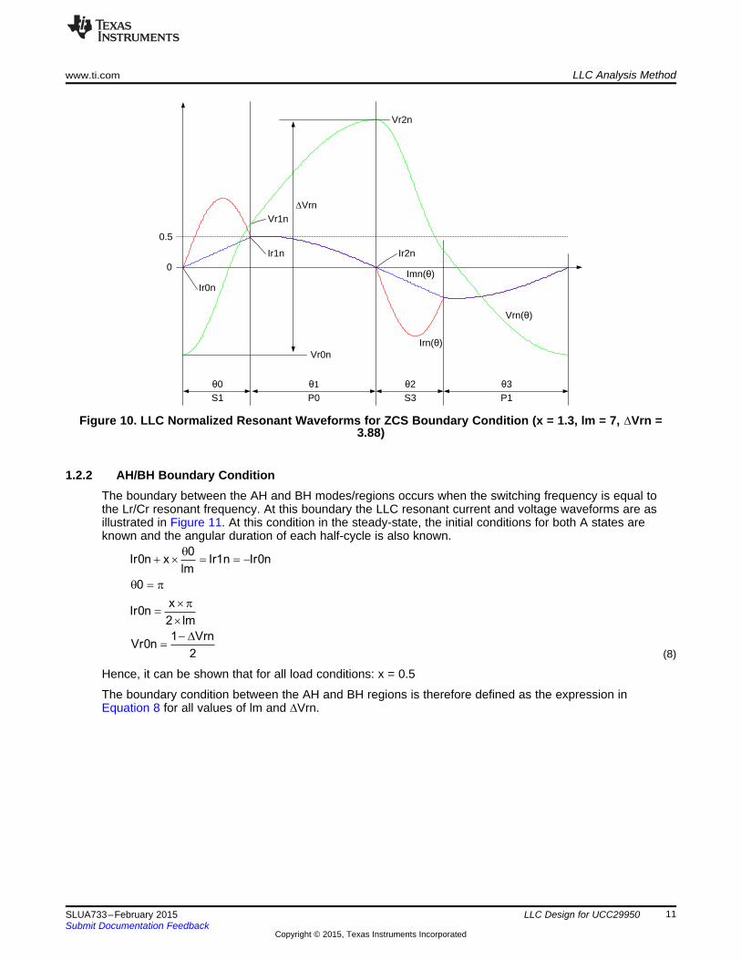
1.2.2 AH/BH Boundary ConditionThe boundary between the AH and BH modes/regions occurs when the switching frequency is equal tothe Lr/Cr resonant frequency. At this boundary the LLC resonant current and voltage waveforms are asillustrated in Figure 11. At this condition in the steady-state, the initial conditions for both A states areknown and the angular duration of each half-cycle is also known.
(8)
Hence, it can be shown that for all load conditions: x = 0.5
The boundary condition between the AH and BH regions is therefore defined as the expression inEquation 8 for all values of lm and ∆Vrn.
11SLUA733–February 2015 LLC Design for UCC29950Submit Documentation Feedback
Copyright © 2015, Texas Instruments Incorporated

lm 1Vr1n 1 x
lm
+æ ö= - ç ÷
è ø
lm 11 x Vr0n
lm
1 VrnVr0n
2
lm 1Vrn 2 x 1
lm
+æ ö= +ç ÷
è ø
- D=
+æ öD = ´ -ç ÷
è ø
�1�0
S1 S3
'Vrn
0
0.5
Vrn(�)
Irn(�)
Imn(�)
Vr0n
Vr1n
Ir0n
Ir1n
LLC Analysis Method www.ti.com
Figure 11. LLC Normalized Resonant Waveforms for AH/BH Boundary Condition (x = 0.5, lm = 5, ∆Vrn =0.6)
1.2.3 BH/BL Boundary ConditionThe boundary between the BH and BL modes occurs when the voltage at the start of the first half-cycle isjust insufficient to forward bias the secondary rectifier diodes. For this reason, the switching cycle startswith a P0, rather than an S1 state. The condition at the boundary of operation can be determined asfollows:
(9)
This expression determines the ∆Vrn value at the boundary condition for a given value of x and lm.
1.2.4 AH/AL Boundary ConditionThe boundary condition between the AH and AL modes occurs when there is just insufficient voltage toforward bias the secondary rectifier diodes at the start of the A1 state (as observed from the AH region).This condition may be expressed as follows:
(10)
Replacing the initial condition with this expression in the steady-state solution for the AH operating regionprovides us with a solution for the boundary condition.
12 LLC Design for UCC29950 SLUA733–February 2015Submit Documentation Feedback
Copyright © 2015, Texas Instruments Incorporated

= = ´ ´ = ´
´ ´
Iinavn Zn Vin ZnIinavno Iinav Iinav
x Vin n Vout n Vout
Region BLMode AH
Mode AL
Region BH
ZCS/RR
Boundary
BH/BL
Boundarylm=9lm=15
lm=7lm=5
lm=3
lm=15
lm=9
lm=7
lm=5
lm=3
AH/BH
Boundary
AH/AL
Boundary
0 0.5 1.0 1.5 2.0x
'Vrn
1
2
3
4
5
6
www.ti.com LLC Analysis Method
1.2.5 Combined Boundary SolutionThe graphic in Figure 12 shows the boundary values for ∆Vrn versus voltage gain for a range of lmvalues. Based upon this data the operating mode of any given operating point (lm, x, ∆Vrn) can bepredicted; therefore, the correct sequence of states for which to obtain a steady-state solution can beselected.
Figure 12. LLC Combined Boundary Solution ∆Vrn vs Voltage Gain (x) and Inductor Ratio (lm)
1.2.6 Steady-State Operating Characteristic Normalized to Output VoltageBased upon the complete Boundary solution, it is now possible to compute steady-state operating pointsover a range of inductor ratio (lm), voltage gain (x), and normalized input charge (∆Vrn) values. At eachsteady-state operating point, parameters of interest such as input power and switching frequency can becomputed. Figure 13 presents the LLC input average current characteristic, normalized to output voltage,vs normalized period for an inductor ratio lm = 5.
(11)
The most common power supply requirement comes from the need to deliver constant output voltage inthe face of varying load current and input voltage. At maximum load current, the operating trajectory of theLLC converter is represented in Figure 13 by the blue curve. As the input voltage changes, the LLCoperating point moves left or right along this operating trajectory. This operating trajectory spans the twovoltage gain curves that define the extremes of input voltage range.
Reduced power operating trajectories can be obtained by sliding this Blue curve down the Y-axis, whileensuring that it still spans the same two voltage gain curves.
The horizonal orange line in Figure 13 respresents LLC operation with constant average input current. Theovercurrent protection feature provided by the UCC29950 (OCP2) will ensure that steady-state LLCoperation cannot stray above this orange line.
13SLUA733–February 2015 LLC Design for UCC29950Submit Documentation Feedback
Copyright © 2015, Texas Instruments Incorporated

0 0.226 0.452 0.678 0.904 1.13 1.356 1.582 1.808 2.034 2.260
0.1
0.2
0.3
0.4
0.5
0.6
0.7
0.8
0.9
1
Iinnn
Tpn
x=2
.0
x=0
.7 x=0
.75 x=
0.8
x=0
.9 x=1
.0 x=1
.2
x=1
.4
x=1
.6
x=1
.8
x=0
.59
x=0
.60
5
x=0
.62
x=0
.63
5
x=0
.65
x=0
.55
x=0
.56
x=0
.57
5
x=0.505x=0.51
x=0
.52 x=
0.5
3
x=0
.54
x=0.5x=0.495
x=0.49x=0.48
x=0.47x=0.45
x=0.43
x=0.41
x=0.38
x=0.35
x=0.3
x=0.
25x=
0.2
ZCS/RR Boundary
x=0.1
x=0.0
5
x=0.0
1
TpMaxn=1.4TpMinn=0.255
Iinavno
IinavMaxno=0.453
IinavScno=0.122
Constant Input Average Current
Constant Input Power
Iinnn
LLC Analysis Method www.ti.com
Figure 13. Steady-State Input Average Current (Iinavno) vs Switching Period (Tpn) for Range of VoltageGain (x),
Inductor Ratio lm = 5
14 LLC Design for UCC29950 SLUA733–February 2015Submit Documentation Feedback
Copyright © 2015, Texas Instruments Incorporated

2 2
2
IpriRms n IsecRmsn CLF
Iinavgn
+=
+= ´ ´ + ´
2 22
2
IpriRmsn IsecRmsn PLTot RprisecEq Iinav Ioutavg VfdEq
Iinavgn
2 22
2
IpriRmsn RpriEq IsecRmsn RsecEqPLTot Iinavg Ioutavg VfdEq
Iinavgn
´ + ´= ´ + ´
2 2
2
Zn ZnIpriRms RpriEq IsecRms RsecEq
Vin VinPLTot Ioutavg VfdEq
Zn
Vin
æ ö æ ö´ ´ + ´ ´ç ÷ ç ÷
è ø è ø= + ´æ öç ÷è ø
www.ti.com LLC Design
2 LLC DesignThe previous section described how LLC operation can be broken down into different operating regionsbased upon the sequence of switch states. Numerically solving the system of equations that describeoperation within each region and combining the results allows us to generate the complete steady-statenormalized operating characteristic of the LLC converter. Once a steady-state operating point has beenobtained, it is possible to calculate any other parameters of interest for this operating point, including theresonant current and voltage waveforms. The design process used here is to calculate a 'figure of merit'for all the possible LLC converter designs and to use this to help make the component selections that leadto the best possible performance in achieving the target specification.
Section 2.1 details the calculation of Current Loss Factor. This provides a measure of relative resistiveconduction loss between different possible LLC component selections. Section 2.2 provides a top-levelview of the design process. In this process, a series of informed decisions are taken to shrink the array ofpossible designs down to the final choice of components.
2.1 Current Loss FactorThe LLC converter design process consists of selecting the transformer turns ratio (n), the characteristicimpedance (Zn), the resonant frequency (ω0), and the inductor ratio (lm). There are a number of possibledesigns that meet the specification requirement, our job as designers is to select the design that offersbest operating efficiency. For this we need a way of comparing the operating efficiency of a range ofdifferent designs.
The power lost in the primary and secondary circuits (PLTot) can be approximated as follows:PLTot = PLPri + PLSec = IpriRms2 × RpriEq + IsecRms2 × RsecEq + Ioutavg × VfdEq (12)
(13)
(14)
RpriEq is the total effective resistance in the primary circuit. For a half-bridge, it includes the ON-stateresistance of each arm of the bridge.
RsecEq is the total effective resistance in the secondary circuit.
VfdEq is the total effective forward voltage drop of the output rectifier diodes. For a full-wave rectifier, thisis twice the forward voltage drop of the rectifier diodes employed.
Consider the special case that Vout is equal to Vin/2 and we are delivering a constant power. In otherwords, the transformer turns ratio is only being adjusted to compensate for the LLC voltage gain (x) at ouroperating point. Also assume that the primary and secondary circuit resistance values are equal and areindependent of transformer turns ratio. For this special case, modify the total loss expression as follows:
(15)
For our special case, all parameters in the loss expression are constant except the sum of squares of therms over average current. This term is referred to as the Current Loss Factor (CLF) of the design, definedas follows:
(16)
At any given steady-state operating condition, the Primary and Secondary normalized RMS currents canbe calculated as follows:
15SLUA733–February 2015 LLC Design for UCC29950Submit Documentation Feedback
Copyright © 2015, Texas Instruments Incorporated

( )S 2
0S
S P
22
S Pd
nIsecRmsn IrSn( ) ImSn( )
q
q + qq
æ ö= ´ q - qç ÷ç ÷
è øåòå å
q q
q + qq q + q q
æ ö= ´ ç ÷ç ÷
è øå åò ò
å åS P2 2
0 0S P
S P
2
S PIrSn( ) d IrPn( ) d
1IpriRmsn
LLC Design www.ti.com
(17)
(18)
S represents the number of S-States in a switching cycle of the current operating region.
P represents the number of P-States in a switching cycle of the current operating region.
The Current Loss Factor (CLF) has been evaluated for each steady-state operating point from Figure 13and the results are presented in Figure 14. Each point on this characteristic represents an LLC design thatis delivering the required specification in terms of Vin, Vout, and Pout. This characteristic allowscomparison of the resistive power losses associated with each design.
The current loss factor characteristic of Figure 14 provides a number of useful insights:1. The most efficient operating point occurs when operating at resonance with a voltage gain of x = 0.5
(for a half-bridge design).2. There is a gradual increase in resistive power loss as the operating point is moved down below
resonance (x > 0.5).3. Resistive power loss increases much more rapidly as the operating point is moved above resonance (x
< 0.5). Resistive power losses become very severe once the voltage gain drops below x = 0.35.Designs that normally operate in this region should be avoided.
4. On any voltage gain curve, the resistive power loss is always a minimum at or close to the ZCS/RRBoundary. Resistive power loss increases rapidly as we move away from this ZCS/RR boundary. Themost efficient design should therefore always operate as close as possible to the ZCS/RR boundary.
16 LLC Design for UCC29950 SLUA733–February 2015Submit Documentation Feedback
Copyright © 2015, Texas Instruments Incorporated

www.ti.com LLC Design
Figure 14. Current Loss Factor (CLF) vs Switching Period (Tpn) for Range of Voltage Gain (x),Inductor Ratio lm = 5
2.2 LLC Design ApproachA typical LLC converter application delivers fixed output voltage while the input voltage and load currentvary over some defined range. As designers, our primary interest is normally to maximize the LLCconverter efficiency at maximum load power. This is because the thermal circuit must be sized to copewith the maximum power loss in the LLC converter.
The top-level design steps are outlined in the following list. Each of these design steps are examined inmore detail in the following sub-sections:1. Select the inductor ratio. This narrows the 'design space' to just one set of the LLC characteristic
curves illustrated in Appendix B.2. Select the transformer turns ratio. This narrows the 'design space' to the area between two voltage
gain curves on the selected LLC characteristic.3. Select the Iinavno value that corresponds to maximum output power. This locates our maximum power
regulation curve to a single curve on the selected LLC characteristic. Having selected the maximumpower operating curve, the required LLC reactive components can be determined.
17SLUA733–February 2015 LLC Design for UCC29950Submit Documentation Feedback
Copyright © 2015, Texas Instruments Incorporated

0.2 0.4 0.6 0.83
4
5
6
7
8
x
lm = 3
lm = 5
lm = 7
lm = 9
lm = 15
CLF
LLC Design www.ti.com
2.2.1 Inductor Ratio SelectionMany effects of adjusting the inductor ratio are expected:1. When operating below resonance a bigger inductor ratio requires a lower switching frequency to
achieve the same voltage gain. The bigger the inductor ratio used, the greater the range of switchingfrequencies required to achieve the same voltage gain range. Observe the change in axis scalerequired for normalized period across the characteristic curves of Appendix B.
2. The secondary RMS/Average current also increases with increasing inductor ratio. This occursbecause the secondary diode conduction interval becomes a smaller fraction of the switching cycle.For this reason, the resistive conduction power losses increase with inductor ratio when operatingbelow resonance (x > 0.5).
3. When operating above resonance, dropping the inductor ratio causes an increase in the Current LossFactor (CLF). Figure 15 shows how the Current Loss Factor varies with LLC voltage gain and inductorratio when operating on the ZCS/RR Boundary. This graphic illustrates that higher inductor ratios offerslightly lower conduction loss above resonance but higher conduction loss below resonance. Once theinductor ratio falls below lm = 5, the increase in conduction loss around the resonant frequencybecomes noticeable.
4. The dead-time required to discharge the switched node capacitance (CPSNe) at maximum switchingfrequency is directly related to inductor ratio. It is important that the time required to discharge the PSNat maximum switching frequency does not exceed the dead-time provided by UCC29950 or ZVSoperation is lost. This calculation for PSN discharge time is included in Section 2.2.1.1. For all designsthis requirement should be checked and the inductor ratio selection adjusted, if necessary.
For most applications, an inductor ratio in the range of 3–7 works best with the UCC29950.
Figure 15. CLF vs x for Range of lm at ZCS/RR Boundary Operation
18 LLC Design for UCC29950 SLUA733–February 2015Submit Documentation Feedback
Copyright © 2015, Texas Instruments Incorporated

é ùé ù é ù´ + ´q + -ê úê ú= = ´ - ê úê úê úw ê ú+ + ´ ´ ë ûë ûë û
2 2
IrpkUln (1 lm) cpsnefsmax 1 0.5Tdfsmax acos a tan
0 cpsne 0.50.5 (1 lm) cpsne (IrpkUln)
lm
é ù é ù= + q ´ - ´ + ´ q ´ê ú ê ú
+ +ê ú ê úë û ë´
û
cpsne cpsne0 0.5 0.5cos fsmax IrpkUl lmn (1 sin fsmax
(1 lm) (1 lmn
)) cps e
é ù é ùq = + q ´ - + ´ ´ q ´ê ú ê ú
+ +ê ú ê úë û ë û´
cpsne cpsneVpsnn( ) 0.5 0.5 cos (1 lm) cp IrpkUln sin
(1 lm) (1 lm)sne
Crcpsne
Cpsne=
TpMinnIrpkUln
4 (1 lm)=
´ +
www.ti.com LLC Design
2.2.1.1 Dead Time Required at Maximum Switching FrequencyThe dead time at maximum switching frequency delivered by the UCC29950 LLC controller is fixed. Thissection shows how to check that this maximum frequency dead time is suitable for our LLC design. Forthis calculation, it is assumed that no load is being drawn from the output so the secondary rectifiers donot conduct for any portion of the switching cycle. With this assumption, our LLC converter can berepresented by the equivalent circuit shown in Figure 16.
With no current flowing into the secondary circuit, the resonant and magnetizing inductors are effectivelyconnected in series. At the same time, they are being driven at a frequency that is well above the resonantfrequency. The inductive impedance is much greater than the resonant capacitor impedance. The voltageon the resonant capacitor may therefore be approximated to a constant value of Vin/2 (0.5). In this case,the peak inductor current at the end of the positive half-cycle can be calculated as follows:
(19)
Since no power is being delivered to the load, the cycle charge drawn from the input must be close tozero. The resonant capacitor voltage during the dead-time must therefore be close to half the inputvoltage. During the dead-time, the LLC converter may be represented by the equivalent circuit shown inFigure 17. Cpsne is the total effective capacitance attached to the PSN node of the LLC half-bridge. Itincludes parallel combination of the effective drain-source capacitance of all the half-bridge switchingMOSFETs. It also includes the parasitic capacitance across the primary winding of the transformer.
Cpsne = 2 × Cdse + Ctxpri (20)
Define a variable for the ratio of the resonant capacitor to the effective switched node capacitance asfollows:
(21)
The normalized switched node voltage during the dead-time is described by the following equation:
(22)
The dead-time can end as soon as the switched node voltage reaches zero. Hence, the followingexpression can be written for the required dead-time conduction angle at maximum switching frequency:
(23)
Hence, the maximum dead-time required for full ZVS operation at maximum switching frequency can bedetermined:
(24)
It is important to use Equation 24 to check that the dead-time provided by UCC29950 at maximumswitching frequency is sufficient. The required dead-time can be decreased, if required, by reducing theinductor ratio used for the design, or increasing the capacitor ratio (cpsne) by reducing the effectiveswitched-node capacitance of the primary half-bridge.
19SLUA733–February 2015 LLC Design for UCC29950Submit Documentation Feedback
Copyright © 2015, Texas Instruments Incorporated

´=
+
xNMin VinNMaxn
VOutReg VfdEq
+
Lr + Lm
CrCpsne 0.5
Irn( )θ
Vpsnn( )θ
+Lr + Lm
Cr
Cdse
Cdse0.5
Irn( )θ
1
Ctxpri
LLC Design www.ti.com
Figure 16. LLC Normalized Equivalent Circuit for Dead-Time at Zero Load Power
Figure 17. LLC Simplified Normalized Equivalent Circuit for Dead-Time at Zero Load Power
2.2.2 Turns Ratio SelectionLLC converter input to output ratio is the product of LLC voltage gain and turns ratio. Fixing thetransformer turns ratio sets the range of LLC voltage gain over which the LLC converter must operate.
An LLC converter provides its lowest conduction loss when operating at resonance on the ZCS/RRboundary. This is clear from the Current Loss Factor curves of ( Appendix B). Applications that have afixed input and output voltage should be designed to operate at this point.
The LLC converter is normally required to be able to deliver fixed output voltage at maximum output powerfrom a range of input voltage levels. This normal input voltage range (VinNMax, VinNMin) includesregulation tolerance of the PFC stage and twice line frequency ripple on the PFC output capacitor, forexample. It is important that LLC power losses are minimized when working within this normal inputvoltage range.
The LLC converter is also expected to be able to deliver regulated output voltage, at maximum load powerover an extended input voltage range. This extended input voltage range (VinEMax, VinEMin) allows theLLC converter to cope with transient and abnormal events such as line sags or surges, transientover/undershoot of the PFC output voltage, and hold-up requirements. Only transient operation is requiredover this extended input voltage range and therefore, LLC converter power loss in this region is not soimportant.
The transformer turns-ratio should be selected so that the normal input voltage range maps onto the LLCvoltage gain range that offers minimum conduction loss. The LLC voltage gain range selected should lieon or very close to the resonant frequency. It may extend above or below resonance but should lie in therange 0.35 < x < 2.
Having selected the gain range to cover the normal input voltage range, the transformer turns ratiorequired can be calculated as follows:
(25)
20 LLC Design for UCC29950 SLUA733–February 2015Submit Documentation Feedback
Copyright © 2015, Texas Instruments Incorporated

ZnLr
0
1Cr
Zn 0
Lm lm Lr
=
w
=
´ w
= ´
´ ´ +=n
IinavMaxno n (VOutReg Vfd
Ii
Eq)Z
nOCP2
= ´h
=
LLC
CS _ OCP2CLS _LLC
1 POutMaxIinOCP2
VinEMin
VR
IinOCP2
www.ti.com LLC Design
2.2.3 Calculating LLC Resonant Component ValuesMaximum normalized input average current (IinavMaxno) is chosen to be as close as possible to theintersection of the xEMin curve with the ZCR/RR boundary. The characteristic impedance of the LLCresonant components are chosen such that the second level over-current limit (OCP2) level is mappedonto this IinavMaxno line. The resonant frequency of the LLC resonant components is chosen so that theUCC29950 minimum switching frequency (LLCFMIN) is mapped onto the Tpn axis at the intersection of thexEMin curve and the ZCS/RR boundary. In this way, the UCC29950 minimum frequency limit and second-level overcurrent limit will ensure that the ZCS/RR boundary curve cannot be crossed.
The UCC29950 overcurrent limits are applied to the average current flowing into the LLC converter. As aconsequence, the output power, and hence output current, that can be delivered increases with PFCoutput voltage. Normally, this does not present a problem because the PFC output voltage is regulatedand therefore varies over a small range. It does mean; however, that the overcurrent limit level should beset to deliver the peak output power at the minimum bulk capacitor voltage. The LLC current senseresistor is selected to ensure that the second-level current limit (OCP2) does not allow ZCS/RR operationto persist if the output is overloaded.
(26)
The coordinates of the intersection between the xEMax curve and the ZCS/RR boundary curve (TpMaxn,IinavMaxno) are now used to compute LLC reactive component values:
(27)ω0 = 2 × π × TpMaxn × LLCFMIN (28)
Hence we have the LLC converter resonant component values:
(29)
21SLUA733–February 2015 LLC Design for UCC29950Submit Documentation Feedback
Copyright © 2015, Texas Instruments Incorporated

= =
42n 1.024
41
æ ö æ ö=ç ÷ ç ÷
è øè ø
FMIN
FMAX
LLC 63.7 kHz
LLC 350 kHz
VinEMin 350
VinNMin 350.35
Vin VVinReg 385
VinNMax 419.65
VinEMax 450
æ ö æ öç ÷ ç ÷ç ÷ ç ÷ç ÷ ç ÷= =ç ÷ ç ÷ç ÷ ç ÷ç ÷ ç ÷è ø è ø
Appendix ASLUA733–February 2015
Design Example(Fixed Output Voltage Variable Input Voltage)
A.1 Design Example IntroductionFor this design example, an LLC converter is designed that delivers a fixed regulated output voltage. Theinput voltage comes from the PFC pre-regulator stage. To cope with line surges, transient overload, andtwice-line frequency ripple, the LLC converter must be able deliver regulated output over a range of inputvoltage levels. The target specification can be summarized as follows:
A.1.1 Input Data/Target SpecificationOutput Power Requirement: POutMax = 512 W
Input Voltage Range
Switching Frequency Range. This is fixed within the UCC29950 controller device. These parameters aretaken from the datasheet:
Output Voltage: VoutReg = 208 V
Secondary Rectifier Diode Forward Voltage Drop: VfdSec = 1 V
A.1.2 Design ProcessOn the basis of the previous discussion, start by selecting to use an inductor ratio of lm = 5. This allows usto choose the LLC steady-state Iinavno characteristic to employ for the design.
In this case, we aim to work just below resonance over the normal input voltage range (VinNMax,VinNMin). This ensures good efficiency while in normal regulation and ensures that we benefit from soft-switching of the output rectifier diodes. To do this, we must select a transformer turns ratio that is justabove one.
Based on the selected turns ratio we can work out both the normal and extended range of LLC voltagegain that is required:
22 LLC Design for UCC29950 SLUA733–February 2015Submit Documentation Feedback
Copyright © 2015, Texas Instruments Incorporated

0 0.226 0.452 0.678 0.904 1.13 1.356 1.582 1.808 2.034 2.260
0.1
0.2
0.3
0.4
0.5
0.6
0.7
0.8
0.9
1
Iinnn
Tpn
x=2
.0
x=0
.7 x=0
.75 x=
0.8
x=0
.9 x=1
.0 x=1
.2
x=1
.4
x=1
.6
x=1
.8
x=0
.59
x=0
.60
5
x=0
.62
x=0
.63
5
x=0
.65
x=0
.55
x=0
.56
x=0
.57
5
x=0.505x=0.51
x=0
.52 x=
0.5
3
x=0
.54
x=0.5x=0.495
x=0.49x=0.48
x=0.47x=0.45
x=0.43
x=0.41
x=0.38
x=0.35
x=0.3
x=0.
25x=
0.2
ZCS/RR Boundary
x=0.1
x=0.0
5
x=0.0
1
TpMaxn=1.4TpMinn=0.255
Iinavno
IinavMaxno=0.453
IinavScno=0.122
Constant Input Average Current
Constant Input Power
Iinnn
xEMax 0.615
xNMax 0.614VoutReg 2 VfdSec
nx 0.559Vin
xNMin 0.513
xEMin 0.478
æ ö æ öç ÷ ç ÷ç ÷ ç ÷+ ´ç ÷ ç ÷= ´ =ç ÷ ç ÷ç ÷ ç ÷ç ÷ ç ÷è ø è ø
www.ti.com Design Example Introduction
To continue with the design process, select the closest voltage gain curves from Figure 18 that contain therequired gain range calculated in the previous equation.
xEMin = 0.47xEMax = 0.62
Figure 18. LLC Steady-State Normalized Operating Characteristic for Fixed Output Voltage lm = 5
Clearly, there are a range of constant power curves running between these two gain curves that could beused to deliver the required input voltage regulation range. For a particular input power, the curve that ishighest up the Y-axis delivers the highest characteristic impedance (Zn) and hence the lowest total RMScurrent. To avoid excess switching power loss (and possibly damage to the primary MOSFETs) avoidhaving the peak power regulation curve cross the ZCS /RR Boundary curve. This forces us to place thepeak power regulation curve no higher than the position of the blue curve indicated in Figure 18.
23SLUA733–February 2015 LLC Design for UCC29950Submit Documentation Feedback
Copyright © 2015, Texas Instruments Incorporated

=
= ´ =
IinavScno 0.122
VinEMaxIoutsc IinavScno n 930 mA
Zn
VoutSc 2 VfdSec 2 V
n VoutScxSc 0.005
VinEMax
= ´ =
´
= =
FMAX
1 0TpMinn 0.255
LLC 2
w
= ´ =
´ p
= = mw
= =´ w
= ´ = m
ZnLr 107 H
0
1Cr 30 nF
Zn 0
Lm lm Lr 535 H
´ ´ + ´= = W
IinavMaxno n (VoutReg 2 VfdSec)Zn 60
IinOCP2
CS _ OCP2
CS _ OCP2CS _LLC
V 0.6V
VR 0.369
IinOCP2
=
= = W
LLC
LLC
90%
1 POutMaxlinOCP2 1.625 A
VinEMin
h =
= ´ =h
Design Example Introduction www.ti.com
UCC29950 provides two mechanisms to ensure that the ZCS/RR boundary is not crossed by the LLCconverter. Initially, the minimum switching frequency is limited to 63.7 kHz. Once the resonant period hasbeen set, this prevents the LLC converter from operating to the right of the vertical TpMaxn line. Secondly,an input overcurrent protection (OCP2) limit is designed to prevent the LLC converter from operatingabove the orange line. This prevents the design from straying over the ZCS/RR Boundary curve in thevertical direction.
Assume that the LLC converter efficiency at maximum output power is 90%. The average input currentlimit needed to ensure that we cannot exceed the peak power target at minimum input voltage iscalculated as follows:
(30)
The OCP2 current limit threshold voltage can be obtained from the UCC29950 datasheet:
(31)
The coordinates of the intersection between the xEMax curve and the ZCS/RR boundary curve (TpMaxn,IinavMaxno) are used to compute LLC reactive component values:
IinavMaxno = 0.453TpMaxn = 1.4
Based upon the parameters, the LLC controller resonant components may be determined as follows:
(32)ω0 = 2 × π × TpMaxn × LLCFMIN = 8.9 × 10⁴ Hza (33)
Hence, we have the LLC converter resonant component values:
(34)
A.1.3 Short-Circuit Current EstimationHaving set the LLC converter resonant frequency, we have also set TpMin.
(35)
A short circuit applied to the LLC converter can be approximated as an output voltage of two forwardvoltage diode drops. Assume that the highest short-circuit current occurs at maximum input voltage.Assuming a full-wave bridge rectifier on the transformer secondary we get:
(36)
Applying a vertical line on Figure 18 corresponding to TpnMin and looking for the intersection with thecorrect voltage gain curve (xSc) allows us to read off the normalized average input current value:
(37)
24 LLC Design for UCC29950 SLUA733–February 2015Submit Documentation Feedback
Copyright © 2015, Texas Instruments Incorporated

= =
+ -= ´ ´ ´ - ´ = m
++ ´
+
é ùé ùê úê ú
é ùê úê úê úê úê úë ûæ öê úê úç ÷ê úê úè øë ûë û
22
Crcpsne 101.755
Cpsne
1 lm 0.5 TpMinn cpsneTdfsmax Lr Cr acos a tan 0.943 s
c psne 2 (1 lm)cpsne TpMinn0.5
(1 lm) 4
www.ti.com Design Example Introduction
A.1.4 Maximum Dead-Time EstimationThe next step in the design process is to check that the dead-time at maximum switching frequencyrequired by our LLC design matches the dead-time provided by the UCC29950 controller. The first step isto estimate the effective total capacitance associated with the PSN node. This can be approximated as thesum of the primary bridge MOSFETs drain to source capacitance and the parasitic capacitance across thetransformer primary winding. This assumes that the resonant inductor is made up entirely of thetransformer leakage inductance.
Cdse = 130 pFCpri = 30 pFCpsne = 2 × Cdse + Cpri = 290 pF
The dead-time required by the LLC design for full ZVS operation at maximum switching frequency andzero load can be calculated as follows:
(38)
The dead-time required is slightly greater than the value programmed into UCC29950, but it is sufficientlyclose that the no-load switching loss is acceptable. Keep in mind that the drivers for the LLC half-bridgeare slightly asymmetric and this means that effective dead-time is slightly greater than the publisheddatasheet parameter.
25SLUA733–February 2015 LLC Design for UCC29950Submit Documentation Feedback
Copyright © 2015, Texas Instruments Incorporated

Appendix BSLUA733–February 2015
Normalized Steady-State LLC Design Curves
Figure 19 through Figure 23 illustrate the normalized steady-state LLC design curves.
26 LLC Design for UCC29950 SLUA733–February 2015Submit Documentation Feedback
Copyright © 2015, Texas Instruments Incorporated

www.ti.com Appendix B
Figure 19. LLC Normalized Design Curves for Inductor Ratio lm = 3
27SLUA733–February 2015 LLC Design for UCC29950Submit Documentation Feedback
Copyright © 2015, Texas Instruments Incorporated

Appendix B www.ti.com
Figure 20. LLC Normalized Design Curves for Inductor Ratio lm = 5
28 LLC Design for UCC29950 SLUA733–February 2015Submit Documentation Feedback
Copyright © 2015, Texas Instruments Incorporated

www.ti.com Appendix B
Figure 21. LLC Normalized Design Curves for Inductor Ratio lm = 7
29SLUA733–February 2015 LLC Design for UCC29950Submit Documentation Feedback
Copyright © 2015, Texas Instruments Incorporated

Appendix B www.ti.com
Figure 22. LLC Normalized Design Curves for Inductor Ratio lm = 9
30 LLC Design for UCC29950 SLUA733–February 2015Submit Documentation Feedback
Copyright © 2015, Texas Instruments Incorporated

www.ti.com Appendix B
Figure 23. LLC Normalized Design Curves for Inductor Ratio lm = 15
31SLUA733–February 2015 LLC Design for UCC29950Submit Documentation Feedback
Copyright © 2015, Texas Instruments Incorporated

IMPORTANT NOTICE
Texas Instruments Incorporated and its subsidiaries (TI) reserve the right to make corrections, enhancements, improvements and otherchanges to its semiconductor products and services per JESD46, latest issue, and to discontinue any product or service per JESD48, latestissue. Buyers should obtain the latest relevant information before placing orders and should verify that such information is current andcomplete. All semiconductor products (also referred to herein as “components”) are sold subject to TI’s terms and conditions of salesupplied at the time of order acknowledgment.TI warrants performance of its components to the specifications applicable at the time of sale, in accordance with the warranty in TI’s termsand conditions of sale of semiconductor products. Testing and other quality control techniques are used to the extent TI deems necessaryto support this warranty. Except where mandated by applicable law, testing of all parameters of each component is not necessarilyperformed.TI assumes no liability for applications assistance or the design of Buyers’ products. Buyers are responsible for their products andapplications using TI components. To minimize the risks associated with Buyers’ products and applications, Buyers should provideadequate design and operating safeguards.TI does not warrant or represent that any license, either express or implied, is granted under any patent right, copyright, mask work right, orother intellectual property right relating to any combination, machine, or process in which TI components or services are used. Informationpublished by TI regarding third-party products or services does not constitute a license to use such products or services or a warranty orendorsement thereof. Use of such information may require a license from a third party under the patents or other intellectual property of thethird party, or a license from TI under the patents or other intellectual property of TI.Reproduction of significant portions of TI information in TI data books or data sheets is permissible only if reproduction is without alterationand is accompanied by all associated warranties, conditions, limitations, and notices. TI is not responsible or liable for such altereddocumentation. Information of third parties may be subject to additional restrictions.Resale of TI components or services with statements different from or beyond the parameters stated by TI for that component or servicevoids all express and any implied warranties for the associated TI component or service and is an unfair and deceptive business practice.TI is not responsible or liable for any such statements.Buyer acknowledges and agrees that it is solely responsible for compliance with all legal, regulatory and safety-related requirementsconcerning its products, and any use of TI components in its applications, notwithstanding any applications-related information or supportthat may be provided by TI. Buyer represents and agrees that it has all the necessary expertise to create and implement safeguards whichanticipate dangerous consequences of failures, monitor failures and their consequences, lessen the likelihood of failures that might causeharm and take appropriate remedial actions. Buyer will fully indemnify TI and its representatives against any damages arising out of the useof any TI components in safety-critical applications.In some cases, TI components may be promoted specifically to facilitate safety-related applications. With such components, TI’s goal is tohelp enable customers to design and create their own end-product solutions that meet applicable functional safety standards andrequirements. Nonetheless, such components are subject to these terms.No TI components are authorized for use in FDA Class III (or similar life-critical medical equipment) unless authorized officers of the partieshave executed a special agreement specifically governing such use.Only those TI components which TI has specifically designated as military grade or “enhanced plastic” are designed and intended for use inmilitary/aerospace applications or environments. Buyer acknowledges and agrees that any military or aerospace use of TI componentswhich have not been so designated is solely at the Buyer's risk, and that Buyer is solely responsible for compliance with all legal andregulatory requirements in connection with such use.TI has specifically designated certain components as meeting ISO/TS16949 requirements, mainly for automotive use. In any case of use ofnon-designated products, TI will not be responsible for any failure to meet ISO/TS16949.
Products ApplicationsAudio www.ti.com/audio Automotive and Transportation www.ti.com/automotiveAmplifiers amplifier.ti.com Communications and Telecom www.ti.com/communicationsData Converters dataconverter.ti.com Computers and Peripherals www.ti.com/computersDLP® Products www.dlp.com Consumer Electronics www.ti.com/consumer-appsDSP dsp.ti.com Energy and Lighting www.ti.com/energyClocks and Timers www.ti.com/clocks Industrial www.ti.com/industrialInterface interface.ti.com Medical www.ti.com/medicalLogic logic.ti.com Security www.ti.com/securityPower Mgmt power.ti.com Space, Avionics and Defense www.ti.com/space-avionics-defenseMicrocontrollers microcontroller.ti.com Video and Imaging www.ti.com/videoRFID www.ti-rfid.comOMAP Applications Processors www.ti.com/omap TI E2E Community e2e.ti.comWireless Connectivity www.ti.com/wirelessconnectivity
Mailing Address: Texas Instruments, Post Office Box 655303, Dallas, Texas 75265Copyright © 2015, Texas Instruments Incorporated