Embed Size (px)
Citation preview

Liquid Crystal Waveguides: New Devices Enabled by >1000 Waves of
Optical Phase Control
Scott R. Davis,* George Farca, Scott D. Rommel, Seth Johnson and Michael H. Anderson Vescent Photonics Inc., 4865 E. 41st Ave., Denver CO 80216
ABSTRACT A new electro-optic waveguide platform, which provides unprecedented voltage control over optical phase delays (> 2mm), with very low loss (< 0.5 dB/cm) and rapid response time (sub millisecond), will be presented. This technology, developed by Vescent Photonics, is based upon a unique liquid-crystal waveguide geometry, which exploits the tremendous electro-optic response of liquid crystals while circumventing their historic limitations. The waveguide geometry provides nematic relaxation speeds in the 10’s of microseconds and LC scattering losses that are reduced by orders of magnitude from bulk transmissive LC optics. The exceedingly large optical phase delays accessible with this technology enable the design and construction of a new class of previously unrealizable photonic devices. Examples include: 2-D analog non-mechanical beamsteerers, chip-scale widely tunable lasers, chip-scale Fourier transform spectrometer (< 5 nm resolution demonstrated), widely tunable micro-ring resonators, tunable lenses, ultra-low power (< 5 microWatts) optical switches, true optical time delay devices for phased array antennas, and many more. All of these devices may benefit from established manufacturing technologies and ultimately may be as inexpensive as a calculator display. Furthermore, this new integrated photonic architecture has applications in a wide array of commercial and defense markets including: remote sensing, micro-LADAR, OCT, FSO, laser illumination, phased array radar, etc. Performance attributes of several example devices and application data will be presented. In particular, we will present a non-mechanical beamsteerer that steers light in both the horizontal and vertical dimensions. Keywords: liquid crystal waveguides, electro-optic waveguides, LC optics, tunable micro-ring, non-mechanical beamsteerer, tunable laser
1. INTRODUCTION
Numerous applications require active control over light including: robotic-vision, optical computing, telecommunications, holographic data-storage, remote sensing, cold-atom optics, industrial process analysis, and many more. In response to this need a diverse array of technologies have been investigated and developed over the past several decades: micro-electro mechanical systems (MEMs),1 photonic crystals,2 thermo-optics,3 and electro-optic materials such as inorganic crystals and organic poled-polymers.4 While tremendous progress has been made, there are still numerous applications, such as beamsteering and large optical phase delay, where bulky and power-consumptive macroscopic opto-mechanical techniques are still the best. This is, at least in part, because typical electro-optic approaches do not realize sufficient control over light (R matrix values of typically < 300 pm/V) to replace traditional opto-mechanics. MEMs techniques are still inherently mechanical, which imposes vibration and inertia design challenges, and developing MEMs architectures that provide macroscopic (> 1mm) control over optical phase has been challenging. Furthermore, non-diffractive MEMs devices have inherent limitations on aperture size (a 1 cm steerable mirror is no longer a MEMs) and scan angle. Notably, the LC-waveguide geometry has enabled the demonstration of an EO scanner that redirected a light beam over 270o.
Vescent’s proprietary liquid-crystal (LC) waveguide architecture5-13 provides unprecedented voltage control over optical phase (> 2 mm), orders of magnitude more than any other technology, e.g., liquid crystal optical phased arrays 14 or MEMs. This previously unrealizable level of control makes possible new devices with remarkable performance attributes. To date we have demonstrated: ultra-wide field of view (270o demonstrated) non-mechanical laser
* Corresponding author. Tel.: 303-296-6766; fax: 303-296-6783.
Email address: [email protected]
Invited Paper
Emerging Liquid Crystal Technologies V, edited by Liang-Chy Chien, Proc. of SPIE Vol. 7618, 76180E · © 2010 SPIE · CCC code: 0277-786X/10/$18 · doi: 10.1117/12.851788
Proc. of SPIE Vol. 7618 76180E-1

beamsteerers, FTIR spectrometers on a chip with < 5 nm resolution, chip-scale widely tunable lasers (nearly 40 nm
tunability demonstrated), ultra-low power (< 5 �Watts) tunable micro-ring filters and Mach-Zehnder switches, and many more.10-13 All of these devices may be in small LCD-like packages that can ultimately be as low cost as a calculator display.
As one pertinent example, in this paper we will present a new electro-optic (EO) laser scanner. EO scanners that provide high-speed, wide field-of-views (FOVs), are compact and simple have been a long-standing dream of the optical community. Unfortunately, despite both the tremendous desire and the significant amount of resources and time expended they are still not available. This is not for lack of trying; for example liquid crystal (LC) based optical phased arrays have been in development for more than three decades.15, 16 While incremental progress continues on diffractive EO scanners,17 the fundamental limitations imposed by basic laws of physics has not changed over the last 35 years. Whether the diffractive element is generated by an LC array,14 a MEMs array,18 an electro-wetting array,19 or any other grating element, the problem of grating efficiency drop with increased scan angle inherently challenges all of these approaches. In this older approaches this has often necessitated complicated multi-stage designs for wide FOVs.17 Rather than continue down this well trodden “diffractive-path” we take an entirely different and new approach to this long-standing problem. The top left side of Figure 1 shows our refractive, not diffractive, wide FOV EO scanner17, the steerable electro-evanescent optical refractor or SEEOR. The input may be voltage steered (current designs provide 45o, though much larger is possible) as a collimated output beam. A promising application for EO scanners is new free space optical (FSO) components (top right of Fig. 1) that will in turn enable new multi-access FSO networks.
Figure 1: TOP LEFT) Pictures of Vescent 1-D EO beamsteering devices. Shown is a device wherein a 1 mm collimated Gaussian laser output is controllably voltage steered. TOP RIGHT) Possible EO scanned FSO links. BOTTOM LEFT) Frames from a movie showing a steered IR spot across a parking lot. BOTTOM RIGHT) The unprecedented low SWaP of these devices will enable ladar deployment on previously inaccessible platforms.
Since our refractive EO scanner is a new approach this provides some unique advantages over the historical diffractive approaches, including:
� True Refractive Steering (high pointing accuracy): Since SEEORs are not diffractive (there are no side lobes), efficiency is independent of angular steer range. Single devices with angular coverage of 180o or more are possible.
This also provides continuous angular coverage (diffractive OPA scanners must step in increments of 2� resets,
Proc. of SPIE Vol. 7618 76180E-2

which limits their pointing precision); our pointing accuracy is only limited by voltage noise. Sub micro-radian accuracy is relatively straightforward.
� High Optical Power Capabilities: Since the light does not transmit through and ITO layer, higher optical powers are possible without the need for exotic transparent electrodes. We have demonstrated peak power handling in excess of 500 Watts/cm2 and expect the limit to be higher.
� Rapid Scanning: The electro-evanescent architecture provides scanning rates across the full FOV from 2 kHz (current scanners) to 10’s of kHz (scanners under development).
� Simple Control Electrodes: Refractive steering keeps the electrode count to typically less than 10 (current scanners have three electrodes). By comparison optical phased arrays often require thousands to tens of thousands of phase electrodes.
� Extremely Wide Angular Coverage: Unprecedented voltage control over optical phase enables single devices with remarkable angular coverage (270o demonstrated in one dimension). This eliminates the need for complicated stacks of small-angle and large-angle steerers as sometimes required by diffractive approaches.
� Very Low SWaP: The simplicity of the approach minimizes SWaP. Current scanners use only microwatts of electrical power, weigh less than 10 grams, take up less than 10 cm3 of volume, and don’t require multi-stages of small-angle and then large-angle steering elements.
� High Data Rate: The SEEOR single mode optical waveguide geometry is similar to telecom components that have demonstrated >100 Gbit bandwidths. We have transmitted four high-definition video signals through one of our scanners in an FSO demo. These also naturally mate to single mode fibers, which is especially convenient for FSO applications.
� High Resolution: The ultimate metric for an EO scanner is the number of far-field resolvable spots, or the related Lagrange number. The SEEOR architecture enables wide aperture (several centimeters) and wide angle scanners with tens of thousands of resolvable spots (Lagrange numbers > 4 cm) in a remarkably simple device.
� Low Cost: The inherent simplicity of the SEEOR device will enable dramatic cost savings in volume.
1.1. The Enabling Innovation
Over the past several decades one of the most technically and commercially successful approaches for light control has
been liquid-crystal (LC) optics. LCs have the world largest electro-optic response (�n > 0.2 over 5 volts for a typical LC, which corresponds to 105-106 pm/V, i.e., several orders of magnitude larger than any other approach), are environmentally stable, amenable to high-volume manufacturing, and inexpensive.20 This has enabled the now > $70 billion a year display market. A typical “display-like” LC-optic is shown in Figure 2. The light traverses a thin
(< 20 �m) LC layer that is sandwiched between glass sheets. Transparent electrodes are used to apply an electric field, which, in combination with polarizers, may be used to either block or transmit the light.
While undeniably potent for information displays, this traditional LC-optic has two significant limitations. First, the light must transmit through transparent electrodes, which in turn limits the total optical power that may be controlled. Second, and arguably more significant, the LC layer must be extremely thin. The LC- material is rendered a single-domain crystal via thin alignment layers. The LC-molecules adjacent these alignment layers are highly ordered, which means low scattering loss, and fast response to changes in voltage. If one were to make the LC cell thicker, the bulk LC material would become prohibitively slow and opaque. Therefore, even though the LC material has a tremendous electro-optic effect, the necessarily short
Figure 2: A Typical LC-Optic, such as is used in the ubiquitous LC-Display.
Proc. of SPIE Vol. 7618 76180E-3

interaction length mitigates this effect. In order to circumvent these limitations we have invented and are developing the LC-clad waveguide architecture.
1.2. Giant control over optical phase: LC-waveguides
Rather than transmit through an LC cell, which by design must be thin (typically < 20 �m), we utilize the LC as an active cladding layer in a waveguide architecture, i.e., the light skims along the surface of an LC layer, as shown in Figure 3. This electro-evanescent architecture circumvents limitations of traditional LC-optics: i) the light never crosses a transparent electrode, ii) the light only interacts with the well-behaved LC-surface layer via the evanescent field, and iii) the interaction length is now decoupled from the LC-layer thickness.
For a given liquid crystal and waveguide structure we have modeled the LC upper cladding and the voltage dependent field profile of the guided light. This is shown in Figure 5. Specifically, our model includes: LC surface energy, pre-tilt, elastic coefficients of the LC, electrical properties of the LC (dielectric constants), optical properties of the LC (birefringence), electrode spacing, and electrical properties of the waveguide materials. With this information we have numerically solved for the LC upper cladding index profile as a function of voltage, following an established routine outlined by S. T. Wu.20 Then, for a given index profile we solve Maxwell’s equation for the guided mode and determine the effective waveguide index. The index modulation is the magnitude of the difference between the effective index at zero volts and the effective index and a higher voltage. This model does an excellent job of predicting the experimental
results. Furthermore, the model shows that �neff � 0 05. is possible by using highly-birefringent liquid crystals and by
keeping the ratio of core thickness to wavelength less than one. While this represents a four-fold decrease in birefringence from the raw liquid crystal, this is more than offset by a possible 10,000-fold increase in the interaction length.
Example operation of an LC-waveguide optical phase shifter is given in Figure 5. The core of the waveguide is LPCVD deposited Si3N4 (n=2.0) and was approximately 500 nm thick, the sub-cladding is SiO2 and the substrate is a P-doped Si wafer. This device exhibited more than 1 millimeter of voltage tunability over optical phase. We know of no other technology that can provide similar performance. Furthermore, the LC waveguide switching time is faster than normal liquid crystals by about one order of magnitude. Typical relaxation times for LC waveguides are on the order of 500
�sec, though as will be shown this can be further reduced via choice of operational voltages and device design.
Figure 3: A) The basic geometry of an LC-waveguide. The light is confined to a core and the LC is an electro-optic upper cladding. As the index of refraction of the upper cladding is tuned the “effective index” of the guided mode is also tuned. B) A side view of a liquid crystal waveguide. In a slab waveguide the light is guided in the x dimension, but is free to propagate as Gaussian beams, sheets, or even 1D images in the plane.
Proc. of SPIE Vol. 7618 76180E-4

2. NEW PHOTONIC DEVICES
This extremely large OPD makes possible a whole new class of photonic devices. Figure 6 illustrates a few possibilities, all of which have been reduced to various levels of prototypes.10-13 In addition to these, LC-waveguides may also be used for optical coherence tomography, true optical time delays, tunable lenses, optical switches, and many more. In the rest of this proceedings we provide some examples of new photonic devices that are enabled by LC-waveguides: i) a chip-scale non-mechanical Fourier Transform Spectrometer, ii) non-mechanical wide angle beamsteerers, iii) chip-scale widely tunable lasers, iv) ultra-low power optical switch, and v) voltage tunable micro-ring resonator. These are only some of the devices that we are developing at Vescent and only a small subset of possible LC-waveguide devices.
Figure 6:The unprecedented electro-optic phase delays provided by LC-waveguides enable a vast array of new photonic devices. Some examples shown here are: chip-scale polarization based FTIR, telecom tunable optical add/drops (ROADMS), tunable lasers (non-mechanical ECDLs), multiplexed Mach-Zehnder bio sensors, and a new type of non-mechanical beamsteerers. We have demonstrated prototypes for all of these applications.
Figure 4: The green lines show the calculated index profile of an LC clad waveguide for different applied voltages. As the voltage is increased the index of the upper cladding also increases. The blue lines show the intensity profile for TM light as a function of voltage. This was obtained by direct solving of Maxwell’s equations for the waveguide boundary conditions.
Figure 5: The performance of an LC waveguide filled with a
nematic liquid crystal with a birefringence of about �n~0.2. A) The transmission of the LC waveguide between polarizers. The figure was recorded over a longer sweep time so that individual waves could be observed. B) The tunable optical phase delay versus applied voltage. For this device greater
than one millimeter of OPD was achieved.
Proc. of SPIE Vol. 7618 76180E-5

2.1. 1-D EO Scanners
The new architecture of LC waveguides provides a natural solution to the historically intractable problem of EO beamsteering. For example, in the plane of the waveguide we can simply pattern an electrode into the shape of a prism. The LC waveguide enables the index inside the prism to be tuned relative to the index in the surrounding areas as shown in Figure 7. At the non-normal interface we can thus tune refraction by Snell’s law. The steering is non-diffractive and analog; the pointing precision is only limited by the noise on the control voltage. By adding prisms in series the deflection can be built up, as shown in the middle of Figure 7.
steer downelectrode
steer upelectrode
Figure 7: (Left) A 1-D LC-waveguide beamsteerer. A control voltage is applied to a prism-shaped electrode having a non-normal interface to the beam propagation direction. As voltage is applied, the index under the patterned electrode is changed relative to the surrounding area and the beam is steered via Snell’s law refraction. (Middle) An electrode pattern that gives wide-angle steering for up to a 5 mm beam. (Right) example beam profiles for steered light, the pixelation is due to the IR imager- the beams are nearly diffraction limited.
The middle of Figure 7 shows a shape-optimized “horn” pattern that accrues deflection as the beam passes through the prisms. This design is fundamentally non-diffractive with only two distinct electrodes. Our current devices (funded by AFRL STTR) exhibit as much as 85% throughput efficiency and excellent beam quality in a small compact package. With new electrode designs we have demonstrated in-plane beam steering of 270o (an unheard of amount for any technology) in a package that is smaller than a dime, as shown in Figure 8. These incredibly wide-angle scanners utilize a proprietary electrode geometry that is fundamentally aperture scalable, i.e., we can realize both wide angle and large aperture. The product of aperture and field-of-regard is related to the number of resolvable spots in the far-field, which is also related to the optical Lagrange number. Both the number of resolvable spots in the far-field (Nspots) and the
Lagrange number scale with the product of �n�L, where �n is the amount that the index can be changed with voltage
and L is the path length through the EO material. Since the LC-waveguide technology can provide �n�L products that are orders of magnitude larger than any other technology, then EO scanners constructed with this technology can provide EO scanners with Nspots or Lagrange numbers that are similarly larger as well.
Figure 8: Example data from a new electrode pattern that exhibited steering of 1550 nm light by 270 degrees in a package that is smaller than a dime. Using the “racetrack” electrode pattern discussed below the aperture for this can be increased to cm’s. This demonstration did not include integrated optical couplers for preservation of output beam quality, but this is easy to implement as we have done in our products.
2.2. 2-D EO Scanners
Realizing wide-angle 1-D EO scanners is itself an achievement. 1-D scanners are already useful for an array of devices (e.g., push-broom mapping, ground based collision avoidance, etc.). That said, there are applications that require 2-D EO scanning. We designed, built, and tested full 2-D EO scanners. In this next section first we introduce the out-of-
Proc. of SPIE Vol. 7618 76180E-6

plane scanner and then we discuss how it may be added in series with the in-plane scanner to provide for full 2-D EO scanners.
The out-of-plane beam steerer is based on the waveguide coupler designed by R. Ulrich at Bell Labs in 1971.21 In any waveguide, if the cladding is too thin light will leak out of the guided mode. In a planar slab waveguide Snell’s law gives the propagation angle of the escaping light, since we can tune the effective index of the waveguide we can therefore tune the angle of the escaping light. Figure 9 shows the basic design. Viewed in reverse, the light comes in at
angle � to the surface normal, and is refracted along the surface, which is just the condition for total internal reflection and is also the condition for phase matching to the guided mode.
Normally, in a leaky waveguide the intensity of the leaked light is proportional to the intensity in the waveguide, which gives rise to an exponential beam profile for the output beam. To render the output beam Gaussian, the lower cladding is tapered or profiled. As shown in Figure 10 this can provide an extremely Gaussian output beam.
Figure 9. Basic idea for the voltage tunable Ulrich coupler.
As the subcladding tapers thinner, the evanescent field of the guided wave touches the silicon substrate and is tapped out to form a directional beam as indicated in the figure. The direction the beam exits is given by
.335.3
9.1~sin eff ��� ��
n
n
We determined we could directly polish the silicon substrate for easy out coupling. Figure 11 shows the silicon polished to give forward emission. Alternatively, a simple fixed mirror could be used to re-direct the scanned beam.
Gaussian
output
Gaussian
output
Figure 10. Theoretical comparison of Ulrich output with LC index of 1.6 to a Gaussian beam. The output beams from these devices can be extremely Gaussian.
Figure 11 also shows the completed wafer after waveguide deposition to form the tapered sub-cladding. The tapers appear as colored fringes due to thin film interference.
Proc. of SPIE Vol. 7618 76180E-7
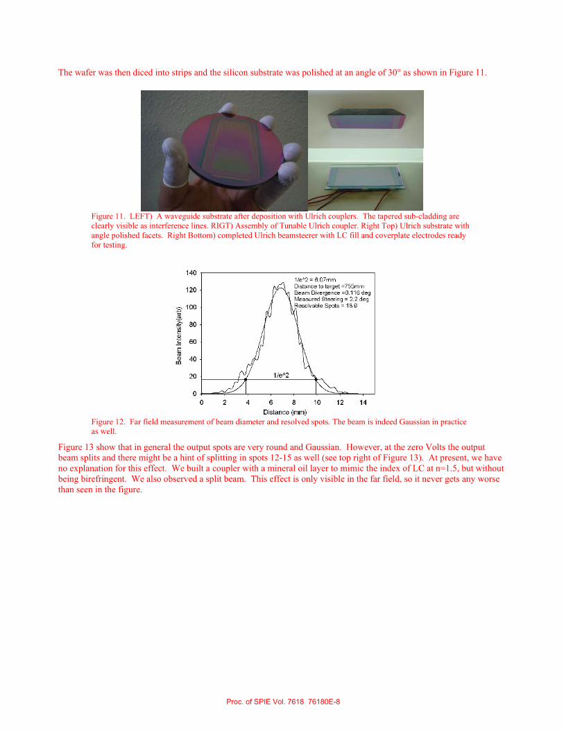
The wafer was then diced into strips and the silicon substrate was polished at an angle of 30 as shown in Figure 11.
Figure 11. LEFT) A waveguide substrate after deposition with Ulrich couplers. The tapered sub-cladding are clearly visible as interference lines. RIGT) Assembly of Tunable Ulrich coupler. Right Top) Ulrich substrate with angle polished facets. Right Bottom) completed Ulrich beamsteerer with LC fill and coverplate electrodes ready for testing.
Figure 12. Far field measurement of beam diameter and resolved spots. The beam is indeed Gaussian in practice as well.
Figure 13 show that in general the output spots are very round and Gaussian. However, at the zero Volts the output beam splits and there might be a hint of splitting in spots 12-15 as well (see top right of Figure 13). At present, we have no explanation for this effect. We built a coupler with a mineral oil layer to mimic the index of LC at n=1.5, but without being birefringent. We also observed a split beam. This effect is only visible in the far field, so it never gets any worse than seen in the figure.
Proc. of SPIE Vol. 7618 76180E-8

Figure 13: VIDEO 1 LEFT) Pictures of 3-electrode devices for providing full 2-D EO steering. These devices take a collimated input beam and provide a voltage steerable collimated output beam. RIGHT TOP) Frames of the out-of-plane scanning spot. RIGHT BOTTOM) A compilation of frames from movies depicting 2-D EO steering of 1550 nm light. In this example both the outer field of regard is shown (series of dots) and some higher-speed scanning in the middle (a Lissajous pattern). Since the EO scan rate can be significantly faster than the video refresh rate the scanned spot may cross several low-speed camera pixels. Also, in this image the camera was saturated and therefore the spot size was artificially enlarged, which artificially reduces the actual spot resolution. This field of view provided 20 x 60 resolvable spots, with the full scanner capabilities at 60 x 400 resolvable spots. Much more resolution (100’s by 1000’s) is possible. http://dx.doi.org/10.1117/12.851788.1
2.3. Demonstration of EO Scanned Micro-Ladar
We combined our 1-D beamsteerers with a LADAR transceiver to build an EO-scanned LADAR shown in Figure 14. The 905 nm LADAR module was positioned in front of the beamsteerer. The laser from the LADAR unit was coupled into the beamsteerer. The LADAR receive aperture is set to receive return photons from a wide field of view. The conditioning optics were required to align the polarization of the laser to be perpendicular to the beamsteerer’s plane and to collimate the beam for easy waveguide in-coupling.
Proc. of SPIE Vol. 7618 76180E-9

Figure 14: Scanning LADAR setup. The laser beam is coupled inside the beamsteerer and the LADAR receiver is set to capture return photons from a wide field of view.
Figure 15 show some example LADAR data taken with this benchtop unit. The unit is capable of scanning across our largest indoor areas, which at Vescent are only about 10 meters. A simple outdoor test indicated ranging, dependent on the target, of up to approximately 20 meters. This limited range is due to the limited, single stripe, diode laser power.
EO Scanned Range Data
EO Scan Angle (degrees)
-10 -8 -6 -4 -2 0 2 4 6 8 10
Range
(m
ete
rs)
0
1
2
3
4
5
6
7
8
9
10
Figure 15. Another set of EO scanned LADAR tests, though conducted in the back, warehouse area of our facility. As shown on the left, the EO ladar unit scans across a topology, which it faithfully maps. In this case the furthest distance was bout 9 meters. Depending on the target, this unit could range up to about 20 meters. This was limited by the single stripe laser diode.
The important point of these breadboard prototypes is to unequivocally demonstrate the feasibility of utilizing these new EO scanners for micro-Ladar devices.
Proc. of SPIE Vol. 7618 76180E-10

2.4. FTS Spectrometer
A preliminary E-O FTS, operational in the near-IR band, has been built 10 using our LC waveguide technology. The current device, along with an exploded view schematic and a total spectrometer system picture, is shown in Figure 16. All of the elements are included, but they are coupled as separate discrete elements. Integration into a monolithic assembly, and utilizing micro-controller electronics, will reduce size/mass and increase durability.
Figure 16: The prototype LC-Waveguide FTS system for operation in the near-IR. This current prototype utilizes a bulky electronics driver and laptop for control and data analysis. This may be replaced with mircro-electronics.
Example performance of the prototype device is shown in Figure 17. The left figure depicts LC-waveguide obtained interferograms of narrow-band light sources. The bottom interferogram is for a single frequency laser. The top
Figure 17: The figure on the left shows an LC waveguide Fourier transform interferogram. The upper trace shows the interferogram (truncated for clarity) of a multimode diode laser. The lower trace shows the interferogram of a pure wavelength source. The “beat-note” for the multimode laser is clearly visible in the top trace. The figure on the right shows the interferogram from a broadband SLD along with the FFT spectra for a variety of absorption features.
interferogram is for two lasers. The beat pattern of the two lasers is clearly visible in the interferogram. The insets show the spectrum of the light sources. The figure on the right shows interferograms and FFT obtained spectra of a broadband SLD with some broadband spectral absorption features. In these experiments both filter and acetylene absorption spectra were recorded. For these current devices the spectral resolution is only about 3-5 nm. New designs will improve the resolution to <0.5 nm.
2.5. Ultra-Low Power Optical Switch
LC-waveguide may also be used to provide a low power alternative to thermo-optic waveguide devices. 13 As an example we have built prototype LC-waveguide 2×2 Mach Zehnder Interferometer (MZI) switches. A microscope picture of the device and experimental operation is shown in Figure 18. In this example light from a single frequency
Proc. of SPIE Vol. 7618 76180E-11

laser was coupled into one of the entrance ports. While voltage to the LC-waveguide was ramped the intensity at an exit port was monitored. As can be seen from the plot the index modulation was sufficient to scan through several minima and maxima, i.e., it was enough to switch the device several times. Further device performance is shown in Figure 19. This device, developed in collaboration with LioniX photonics, utilized a Triplex22 LPCVD channel waveguide structure, with an active LC cladding. These devices provide substantial improvements over thermo-optic designs: i) larger index modulation which permits a more compact switch, ii) faster switching time by more than an order of magnitude over thermo-optics, and iii) a factor of 10,000 less electrical power consumption. The electrical driving requirements for LC-waveguide devices are equivalent to driving a small capacitor, typically a few nanofarads.
Figure 18: Left: Close-up view of a single voltage tunable MZI switch. This is analogous to a single pixel on an LC display. The planar waveguide sub-structure is constructed from well established silica on silicon technology. The top cladding contains liquid crystal, which may be voltage tuned, thereby tuning the optical phase delay of the
MZI tune arm. Right: Example performance and picture (inset) of a voltage tunable 2�2 MZI optical switch. The
separation between the reference and tune arm was 500 �m. Light was fiber coupled into the top left port and the bottom right port was monitored as a function of voltage. The light wavelength was 1550 nm.
Index M
odula
tion
0
1e-3
2e-3
3e-3
4e-3
5e-3
6e-3
7e-3
8e-3
9e-3
Optical Phase Delay for Chip Ten MZI
Voltage (Vrms
)
0 10 20 30 40 50 60 70 80
OP
D (
Wa
ve
s @
15
50
nm
)
0
2
4
6
8
10
12
14
16
18
20
22
24
Figure 19: Shown on the left is the voltage tunable optical phase delay and index modulation realized with this LC-waveguide architecture. Shown on the right are switching times. The control voltage is a DC balanced square wave, whose amplitude is altered. For this switching data the amplitude was altered between approximately 100
and 80 volts. Voltage driving at lower values will yield a slower response (�400 �sec), but still faster than typical thermo-optics (e.g. 5 milliseconds).
2.6. Voltage Tunable Micro-Ring Resonator
Finally, another type of thermo-optic device that may be rendered electro-optic with the LC-waveguide architecture is the tunable micro-ring resonator. The left side of Figure 20 shows the basic architecture of the voltage tunable LC-waveguide micro-ring. The right of Figure 20 shows a microscope picture of the micro-ring device along with the resonance spectrum of the micro-ring. The channel structures were constructed using the triplex waveguide design (this was on the same wafer as the MZI switches). The input and output channels were three microns wide and the channel in the ring was 15 microns wide and a lateral coupling scheme was used. While the ring channel width was not single mode it is our experience that improper coupling between the input channel and the rings
Proc. of SPIE Vol. 7618 76180E-12

Drop Port Signal as a Function of Laser Wavelength
Wavelength (nm)
1550 1551 1552 1553 1554 1555
Dro
p P
ort
Sig
nal (a
rb.)
0
1
2
3
4
FSR approx. 0.33 nmFinesse approx. 40
Figure 20: Left: Close-up view of a single voltage tunable micro-ring resonator. This is analogous to a single pixel on an LC display. The planar waveguide sub-structure is constructed from silica on silicon technology. The top cladding contains liquid crystal, which may be voltage tuned, thereby tuning the effective index of the waveguide ring. When tuned to resonance for a given wavelength of light within an input channel, the light can be transferred from one straight channel, through the ring, to the other straight channel. Right: A prototype LC-waveguide micro-ring demonstration. The inset shows a microscope image of the device, and the plot shows the intensity of the drop-port signal as a function of input port wavelength (we used a single mode tunable laser). In this case the voltage to the LC was held at zero. The ring design only provided a finesse of 40, and the ring was multi-modal. Nevertheless, we were able to use this device to demonstrate voltage tuning of the LC-waveguide ring architecture.
is the most common failure mode for first designs. The large channel width in the ring and the large ring diameter were specifically chosen to help mitigate this risk. The spectral response of the ring was measured both with and without LC in the top cladding with no noticeable change in the finesse, indicating that LC scattering losses were minimal.
Voltage tunability of the device is shown in Figure 21. With the wavelength held fixed at 1550 nm, the intensity of the drop port was monitored as a function of voltage. It can be seen the device tuned over nine resonances (> 3 nm), with
extremely minimal power consumption (< 50 �Watts). The reason that the peak widths appear to broaden at higher voltages is due to the non-linear index modulation with voltage. Measurement of finesse as a function of voltage showed no discernable change. Also, this finesse was the same with SiO2 as a top cladding, indicating that LC induced losses are not yet contributing.
Voltage Applied to LC-Clad Ring (Vrms
)
0 20 40 60 80 100
Dro
p P
ort
Sig
nal (a
rb.)
0.5
1.0
1.5
2.0
1 2 3 4 5 6 7 8 9
Figure 21: The wavelength is held fixed at 1550 nm. The voltage on the LC-clad ring is swept from 0 to 100
Volts. As can be seen, > 9 FSR (> 3 nm) are tuned across. This is for a 600 �m radius ring.
3. CONCLUSIONS
The devices presented in this paper demonstrate the potency of our LC waveguide architecture. More applications of this technology are currently being investigated. Wherever macroscopic or microscopic control over the optical phase is required our technology is fit to eliminate mechanical assemblies with an EO alternative.
Proc. of SPIE Vol. 7618 76180E-13

4. ACKNOWLEDGMENTS
This work has been supported by the Air Force Office of Scientific Research, the National Science Foundation, the National Institute of Standards and Technology, the National Aeronautics and Space Administration, Air Force Research Labs, and the Environmental Protection Agency. The authors also wish to acknowledge the Colorado Advanced Photonics Technology Center (http://www.captcenter.org), Charles Lee at AFOSR, and Don Snyder at AFRL for their help with the beamsteerer development, David Walba and Eva Korblova at the University of Colorado Boulder for help with custom liquid crystal chemistries, and Tien-Hsin Chao and Jet Propulsion Laboratory for help with the FTS development. The authors also wish to acknowledge Rene Heideman and Arne Leinse at LioniX Photonics for their invaluable help with the micro-ring and MZI switch design and fabrication.
5. REFERENCES
[1] Wu, M. C., Solgaard, O., and Ford, J. E., "Optical MEMS for Lightwave Communication," Journal of Lightwave Technology 24, 4433-4454 (2006).
[2] Summers, C. J., Neff, C. W., and Park, W., "Active Photonic Crystal Nano-Architectures," Journal of Nonlinear Optical Physics and Materials 12, 587-597 (2003).
[3] Brainard, R., Fondeur, B., and Dougherty, D. J., "Advances in Planar Lightwave Circuits for Wavelength Routing Applications," in OSA Integrated Optics Conference, (2006).
[4] Jin, D., Dinu, R., Parker, T. C., Barklund, A., Bintz, L., Chen, B., Flaherty, C., Guan, H. W., Huang, D., Kressbach, J., Londergan, T., Mino, T. D., Todorova, G., and Yang, S., "Material development and processing for electro-optic device systems," Proceedings of SPIE, Organic Photonic Materials and Devices V 4991, 610-620 (2003).
[5] Anderson, M., Davis, S., and Rommel, S., "Liquid Crystal Waveguide having Refractive Shapes for Dynamically Controlling Light," (Vescent Photonics, Inc., US, 2004).
[6] Anderson, M., Davis, S., and Rommel, S., "Tunable laser having liquid crystal waveguide," (Vescent Photonics, Inc., US, 2005).
[7] Anderson, M., Rommel, S., and Davis, S., "Liquid Crystal Waveguide for Dynamically Controlling Polarized Light," USPTO, ed. (Vescent Photonics, USA, 2005).
[8] Anderson, M., Rommel, S., and Davis, S., "Liquid Crystal Waveguide Having Electric Field Oriented for Controlling Light," USPTO, ed. (Vescent Photonics, USA, 2006).
[9] Anderson, M., Rommel, S., and Davis, S., "Liquid Crystal Waveguide Having Two or More Control Voltages for Controlling Polarized Light," USPTO, ed. (Vescent Photonics, USA, 2006).
[10] Chao, T.-H., Lu, T. T., Davis, S. R., Rommel, S. D., Farca, G., Luey, B., Martin, A. W., and Anderson, M. H., "Compact Liquid Crystal Waveguide Based Fourier Transform Spectrometer for In-Situ and Remote Gas and Chemical Sensing," Optical Pattern Recognition XIX, Proc. of SPIE 6977, 69770P (2008).
[11] Davis, S. R., Farca, G., Rommel, S. D., Martin, A. W., and Anderson, M. H., "Analog, Non-Mechanical Beam-Steerer with 80 Degree Field of Regard," in SPIE Defense And Security Symposium, (SPIE, Orlando, FL, 2008), p. 69710G.
[12] Davis, S. R., Rommel, S. D., Farca, G., and anderson, M. H., "A New Electro-Optic Waveguide Architecture and The Unprecedented Devices It Enables," in SPIE Defense and Security Symposium, (SPIE, Orlando, FL, 2008), pp. 697503-697501.
[13] Davis, S. R., Rommel, S. D., Farca, G., and Anderson, M. H., "A New Generation of Previously Unrealizable Photonics Devices as Enabled by a Unique Electro-Optic Waveguide Architecture," SPIE Optics and Photonics Conference Proceeding 7050, DOI:10.1117/1112.793130 (2008).
[14] McManamon, P., "An overview of optical phased array technology and status," Liquid Crystals: Optics and Applications 5947, (2005).
[15] Borel, J., Deutch, J.-C., Labrunie, G., and Robert, J., "Liquid Crystal Diffraction Grating," U. S. P. Office, ed. (Commissariat A L'Energie Atomique, 1974).
[16] Huignard, J. P., Malard, M., and Corlieu, G. d., "Static Deflector Device for An Infrared Beam," U. S. P. a. T. Office, ed. (Thomson-CSF, USA, 1987).
[17] McManamon, P., Bos, P. J., Escuti, M. J., Heikenfeld, J., Serati, S. A., Xie, H., and Watson, E. A., "A Review of Phased Array Steering for Narrow-Band Electrooptical Systems," Proceedings of the IEEE 97, 1078-1096 (2009).
[18] Ryf, R., Stuard, H. R., and Giles, C. R., "MEMS tip/tilt & piston mirror arrays as diffractive optical elements," Proceeding of SPIE, Bellingham, WA 5894, 58940C-58941-58911 (2005).
[19] Smith, N. R., Abeysinghe, D. C., Haus, J. W., and Heikenfeld, J., "Agile wide-angle beam steering with electrowetting microprisms," Optics Express 14, 6557-6563 (2006).
[20] Khoo, I.-C., and Wu, S.-T., Optics and nonlinear optics of liquid crystals (World Scientific Publishing, 1993). [21] Ulrich, R., "Optimum Excitation of Optical Surface Waves," Journal of the Optical Society of America 61, 1467 (1971). [22] Heideman, R. G., Melloni, A., Hoekman, M., Borreman, A., Leinse, A., and Morichetti, F., "Low loss, high contrast optical
waveguides based on CMOS compatible LPCVD processing: technology and experimental results.," in LEOS Benelux, (2006).
Proc. of SPIE Vol. 7618 76180E-14