Embed Size (px)
Citation preview
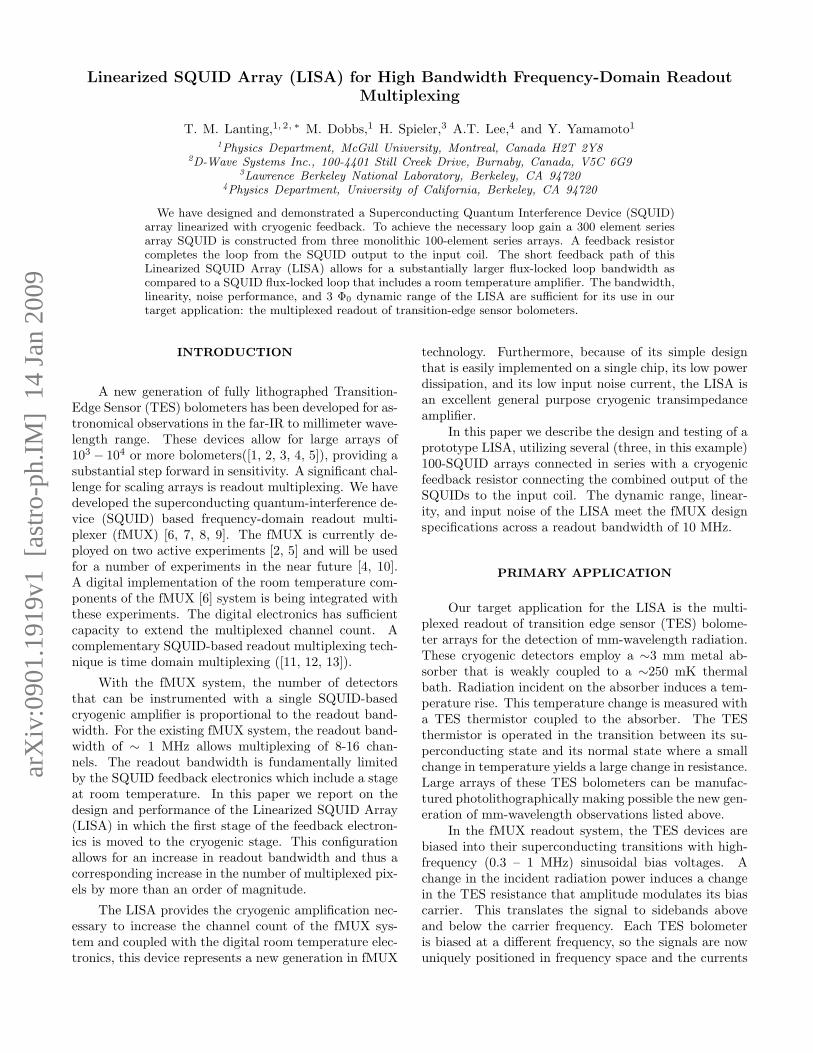
Linearized SQUID Array (LISA) for High Bandwidth Frequency-Domain ReadoutMultiplexing
T. M. Lanting,1, 2, ∗ M. Dobbs,1 H. Spieler,3 A.T. Lee,4 and Y. Yamamoto1
1Physics Department, McGill University, Montreal, Canada H2T 2Y82D-Wave Systems Inc., 100-4401 Still Creek Drive, Burnaby, Canada, V5C 6G9
3Lawrence Berkeley National Laboratory, Berkeley, CA 947204Physics Department, University of California, Berkeley, CA 94720
We have designed and demonstrated a Superconducting Quantum Interference Device (SQUID)array linearized with cryogenic feedback. To achieve the necessary loop gain a 300 element seriesarray SQUID is constructed from three monolithic 100-element series arrays. A feedback resistorcompletes the loop from the SQUID output to the input coil. The short feedback path of thisLinearized SQUID Array (LISA) allows for a substantially larger flux-locked loop bandwidth ascompared to a SQUID flux-locked loop that includes a room temperature amplifier. The bandwidth,linearity, noise performance, and 3 Φ0 dynamic range of the LISA are sufficient for its use in ourtarget application: the multiplexed readout of transition-edge sensor bolometers.
INTRODUCTION
A new generation of fully lithographed Transition-Edge Sensor (TES) bolometers has been developed for as-tronomical observations in the far-IR to millimeter wave-length range. These devices allow for large arrays of103 − 104 or more bolometers([1, 2, 3, 4, 5]), providing asubstantial step forward in sensitivity. A significant chal-lenge for scaling arrays is readout multiplexing. We havedeveloped the superconducting quantum-interference de-vice (SQUID) based frequency-domain readout multi-plexer (fMUX) [6, 7, 8, 9]. The fMUX is currently de-ployed on two active experiments [2, 5] and will be usedfor a number of experiments in the near future [4, 10].A digital implementation of the room temperature com-ponents of the fMUX [6] system is being integrated withthese experiments. The digital electronics has sufficientcapacity to extend the multiplexed channel count. Acomplementary SQUID-based readout multiplexing tech-nique is time domain multiplexing ([11, 12, 13]).
With the fMUX system, the number of detectorsthat can be instrumented with a single SQUID-basedcryogenic amplifier is proportional to the readout band-width. For the existing fMUX system, the readout band-width of ∼ 1 MHz allows multiplexing of 8-16 chan-nels. The readout bandwidth is fundamentally limitedby the SQUID feedback electronics which include a stageat room temperature. In this paper we report on thedesign and performance of the Linearized SQUID Array(LISA) in which the first stage of the feedback electron-ics is moved to the cryogenic stage. This configurationallows for an increase in readout bandwidth and thus acorresponding increase in the number of multiplexed pix-els by more than an order of magnitude.
The LISA provides the cryogenic amplification nec-essary to increase the channel count of the fMUX sys-tem and coupled with the digital room temperature elec-tronics, this device represents a new generation in fMUX
technology. Furthermore, because of its simple designthat is easily implemented on a single chip, its low powerdissipation, and its low input noise current, the LISA isan excellent general purpose cryogenic transimpedanceamplifier.
In this paper we describe the design and testing of aprototype LISA, utilizing several (three, in this example)100-SQUID arrays connected in series with a cryogenicfeedback resistor connecting the combined output of theSQUIDs to the input coil. The dynamic range, linear-ity, and input noise of the LISA meet the fMUX designspecifications across a readout bandwidth of 10 MHz.
PRIMARY APPLICATION
Our target application for the LISA is the multi-plexed readout of transition edge sensor (TES) bolome-ter arrays for the detection of mm-wavelength radiation.These cryogenic detectors employ a ∼3 mm metal ab-sorber that is weakly coupled to a ∼250 mK thermalbath. Radiation incident on the absorber induces a tem-perature rise. This temperature change is measured witha TES thermistor coupled to the absorber. The TESthermistor is operated in the transition between its su-perconducting state and its normal state where a smallchange in temperature yields a large change in resistance.Large arrays of these TES bolometers can be manufac-tured photolithographically making possible the new gen-eration of mm-wavelength observations listed above.
In the fMUX readout system, the TES devices arebiased into their superconducting transitions with high-frequency (0.3 – 1 MHz) sinusoidal bias voltages. Achange in the incident radiation power induces a changein the TES resistance that amplitude modulates its biascarrier. This translates the signal to sidebands aboveand below the carrier frequency. Each TES bolometeris biased at a different frequency, so the signals are nowuniquely positioned in frequency space and the currents
arX
iv:0
901.
1919
v1 [
astr
o-ph
.IM
] 1
4 Ja
n 20
09

2
from the individual thermistors can be summed into onewire. The summed currents are fed to the input of atransimpedance amplifier utilizing a DC SQUID operat-ing in a flux-locked loop (FLL) configuration (see Fig.1). The TES thermistor typically has an impedance of∼ 0.5 − 2 Ω, a noise current of 10-50 pA/
√Hz, and re-
quires a bias voltage of ∼ 5 µVRMS.The SQUID electronics performance requirements
for this application are: (1) white noise lower than theTES noise (< 10 pA/
√Hz), (2) sufficient bandwidth(
1 MHz) to accommodate many carriers, (3) inputimpedance much lower than the TES impedance (0.5Ω) across the entire bandwidth to maintain constant-voltage bias, (4) sufficient transimpedance (ZLISA >150Ω) to override the 1 nV/
√Hz noise of a warm am-
plifier which follows the system, (5) large (> 10 µARMS)dynamic range in order to accommodate a single carriersignal, and (6) sufficient linearity to amplify large carriersignals and to reduce intermodulation between multiplecarriers. Low frequency noise in the SQUID electronics isnot an issue as the signals of interest have been translatedto frequencies above 0.3 MHz.
The dynamic range requirement allows the system tohandle at least one full sized carrier. This allows a userto tune the system in a straight forward manner (tuningtypically involves choosing the appropriate bias voltagelevel for a particular sensor). After tuning a single sen-sor, the carrier is nulled with a 180 unmodulated copy ofthe carrier signal injected at the input coil of the SQUID.This does not affect the original signals, as all of their in-formation is in the sidebands. Once the first carrier isnulled, a second one can be added without increasing thedynamic range requirement. Thus, the number of chan-nels that can be multiplexed with a single set of SQUIDelectronics is fundamentally limited by the bandwidth ofthese electronics and not by the dynamic range.
FIG. 1: Schematic of eight-channel fMUX system. [7]
LINEARIZED SQUID ARRAY
The response of a SQUID has traditionally been lin-earized with a feedback loop that includes a transistoramplifier operating at 300K. The bandwidth of this flux-locked loop circuit is limited by propagation delays alongthe wires connecting this amplifier to the SQUID whichoperates at the cold stage temperature (∼ 4K). The cur-rent fMUX bandwidth of 1 MHz is achieved by constrain-ing the wire length between 300K and 4K to be < 0.15m.Further reductions in wire length are not cryogenicallyfeasible.
A significant increase in bandwidth can be achievedby either moving the transistor amplifier to the cold stageor eliminating it entirely from the feedback loop. The lat-ter is preferable, since a transistor amplifier would dissi-pate significant power on the cold stage. With the ampli-fier removed from the circuit, a configuration of SQUIDdevices can be used to produce the necessary loop gainwhile maintaining the circuit’s transimpedance.
One such configuration, referred to as the ‘SQUIDop-amp’, has been demonstrated [14]. That device usesa parallel cascade of SQUIDs to increase the loop gainof the circuit. While each of the SQUIDs in the parallelcascade contributes to the loop gain and linearizes thecircuit, the dynamic range of the circuit is limited by thefinal stage SQUIDs. For the multiplexed readout of TESbolometers, we require a configuration that extends boththe linearity and dynamic range of the SQUID system.
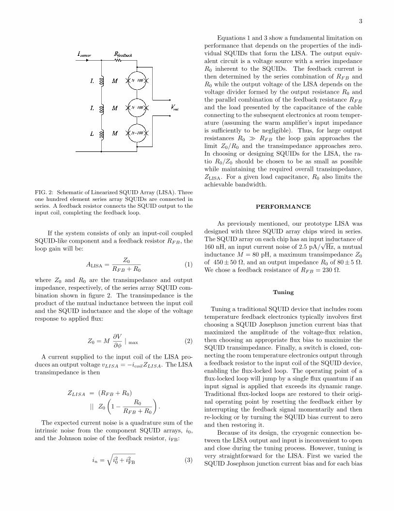
To meet our requirements, we have developed andtested the Linearized SQUID Array (LISA) concept (Fig-ure 2). The LISA eliminates the warm transistor ampli-fier from the flux locked loop by using a series configu-ration of SQUIDs to simultaneously linearize the circuitand extend the dynamic range. The LISA prototype wediscuss in this paper consists of three monolithic seriesarray SQUID chips [15], each consisting of 100 series-connected SQUID, themselves connected in series to forma 300 element series array. The output voltage of theLISA is coupled back to the input coil with a feedbackresistor to complete the feedback loop (see figure 2) andreduce the input impedance to meet the requirements ofconstant voltage bias to the thermistor.
In designing and testing any SQUID FLL, we focuson four figures of merit: the closed loop gain ALISA, theforward gain, or transimpedance, ZLISA, the input noisecurrent in, and the closed loop bandwidth of the system.The closed loop gain quantifies the ability of the feedbackelectronics to extend the dynamic range and linearity ofthe SQUIDs that form the LISA. The transimpedancemeasures the ratio of the LISA’s output voltage to theinput current. The input noise current determines thesensitivity with which currents can be read out with theLISA. The closed loop bandwidth determines the numberof sensors that can be multiplexed.
3
FIG. 2: Schematic of Linearized SQUID Array (LISA). Threeone hundred element series array SQUIDs are connected inseries. A feedback resistor connects the SQUID output to theinput coil, completing the feedback loop.
If the system consists of only an input-coil coupledSQUID-like component and a feedback resistor RFB , theloop gain will be:
ALISA =Z0
RFB +R0(1)
where Z0 and R0 are the transimpedance and outputimpedance, respectively, of the series array SQUID com-bination shown in figure 2. The transimpedance is theproduct of the mutual inductance between the input coiland the SQUID inductance and the slope of the voltageresponse to applied flux:
Z0 = M∂V
∂φ| max (2)
A current supplied to the input coil of the LISA pro-duces an output voltage vLISA = −icoilZLISA. The LISAtransimpedance is then
ZLISA = (RFB +R0)
|| Z0
(1− R0
RFB +R0
).
The expected current noise is a quadrature sum of theintrinsic noise from the component SQUID arrays, i0,and the Johnson noise of the feedback resistor, iFB:
in =√i20 + i2FB (3)
Equations 1 and 3 show a fundamental limitation onperformance that depends on the properties of the indi-vidual SQUIDs that form the LISA. The output equiv-alent circuit is a voltage source with a series impedanceR0 inherent to the SQUIDs. The feedback current isthen determined by the series combination of RFB andR0 while the output voltage of the LISA depends on thevoltage divider formed by the output resistance R0 andthe parallel combination of the feedback resistance RFB
and the load presented by the capacitance of the cableconnecting to the subsequent electronics at room temper-ature (assuming the warm amplifier’s input impedanceis sufficiently to be negligible). Thus, for large outputresistances R0 RFB the loop gain approaches thelimit Z0/R0 and the transimpedance approaches zero.In choosing or designing SQUIDs for the LISA, the ra-tio R0/Z0 should be chosen to be as small as possiblewhile maintaining the required overall transimpedance,ZLISA. For a given load capacitance, R0 also limits theachievable bandwidth.
PERFORMANCE
As previously mentioned, our prototype LISA wasdesigned with three SQUID array chips wired in series.The SQUID array on each chip has an input inductance of160 nH, an input current noise of 2.5 pA/
√Hz, a mutual
inductance M = 80 pH, a maximum transimpedance Z0
of 450± 50 Ω, and an output impedance R0 of 80± 5 Ω.We chose a feedback resistance of RFB = 230 Ω.
Tuning
Tuning a traditional SQUID device that includes roomtemperature feedback electronics typically involves firstchoosing a SQUID Josephson junction current bias thatmaximized the amplitude of the voltage-flux relation,then choosing an appropriate flux bias to maximize theSQUID transimpedance. Finally, a switch is closed, con-necting the room temperature electronics output througha feedback resistor to the input coil of the SQUID device,enabling the flux-locked loop. The operating point of aflux-locked loop will jump by a single flux quantum if aninput signal is applied that exceeds its dynamic range.Traditional flux-locked loops are restored to their origi-nal operating point by resetting the feedback either byinterrupting the feedback signal momentarily and thenre-locking or by turning the SQUID bias current to zeroand then restoring it.
Because of its design, the cryogenic connection be-tween the LISA output and input is inconvenient to openand close during the tuning process. However, tuning isvery straightforward for the LISA. First we varied theSQUID Josephson junction current bias and for each bias

4
current setting we measured the DC voltage-flux relationof the LISA. We chose the current bias that maximizesthe dynamic range of the LISA (this ensures that weare biasing the constituent SQUIDs at a point close tothe maximum of their individual voltage-flux responses).Then we used the measured optimum voltage-flux rela-tion to determine the flux bias signal that moves the LISAto the middle of its dynamic range and applied this fluxto the device. If the operating point of the LISA jumpedin response to a signal that exceeded its dynamic range,the LISA was reset by momentarily interrupting its cur-rent bias.
Dynamic Range and Linearity
Once the LISA is tuned, we measure its dynamicrange (maximum peak-to-peak applied signal) by apply-ing a series of DC currents to the input coil and measur-ing the output voltages (voltage-current or voltage-fluxrelation). Figure 3 shows this measured relation for threeSQUID devices in series without feedback, and the samerelation for the LISA. The simulated response is also plot-ted in figure 3 [16]. The intrinsic sinusoidal responsehas been linearized over a dynamic range of 37± 1 µApp
and agrees well with the simulated response. Note thatthis measurement of dynamic range with a direct inputcurrent does not exactly apply to the high frequency re-sponse because of the 160 nH inductance of the input coilof each SQUID array. At 10 MHz, this corresponds to areactance of 10 Ω from each SQUID array which slightlylowers the closed loop gain.
FIG. 3: LISA response to applied input current with andwithout application of cold feedback.
We expect that the dynamic range of the LISA, mea-sured as a peak-to-peak current applied to the input coil,will be [8]
ipp =Φo
M
(12
+2ALISA
2π
), (4)
where Φ0 is the quantum of magnetic flux, M is the mu-tual inductance between the input coil and each one ofthe constituent SQUIDs, and Aloop is the closed loop out-put impedance of the cold FLL as defined in section . Forthe demonstration, we wired three 100-element series ar-ray SQUID chips in series. For an arbitrary number, n,of series array SQUID chips, the loop gain becomes:
ALISA =nZsingle
RFB + nRsingle(5)
where Zsingle and Rsingle are the transimpedance and out-put resistance of the individual series array SQUID de-vices. As mentioned in section , for a large number ofdevices in series, the loop gain approaches the limitingvalue of Zsingle/Rsingle = 6.2.
Using the properties of the individual LISA compo-nents used in this demonstration, we expect Aloop = 3.2.This loop gain predicts, using equation 4, a dynamicrange of 39 µApp in good agreement with measurement.
FIG. 4: Measured LISA transimpedance (using sinusoidalinput of 2 µARMS) over three decades of frequency.
The LISA has high linearity across most of its dynamicrange, but exhibits gain suppression for large signals. Wemeasure compression of 0.3±0.1 dB at±19 µA with muchsmaller deviations from linearity for smaller signals.
Bandwidth
We measured the bandwidth of the LISA with a net-work analyser [17]. We applied a current of 2 µARMS atthe LISA input and measured the output voltage across

5
three decades of frequency (0.1 MHz to 100 MHz). Thecurrent was applied differentially to the input coil of theLISA and the output voltage was amplified with roomtemperature electronics and then measured with a net-work analyser. We measure a small-signal bandwidth of14 ± 1 MHz (see figure 4). We measure the large-signalbandwidth by recording the size of input current signalneeded to induce flux jumping in the LISA as a func-tion of frequency. The large-signal bandwidth achievedwith the prototype setup is 10 MHz. For our setup, themeasured bandwidth is currently limited by several roomtemperature components: a stray capacitance of 50 pFat the input of the room temperature amplifier and theroom temperature amplifier itself. Using a well-matchedroom temperature amplifier with low input capacitanceand a larger designed bandwidth will increase the avail-able LISA bandwidth.
Noise
We coupled the output voltage of the LISA to a spec-trum analyser and measured the noise from 1 to 100 MHzwith the junction bias current on and off. The noise mea-sured with the bias current off, 1.3 nV/
√Hz, measures
the baseline noise of the room temperature readout elec-tronics. With the bias current on, the noise increases by25% to 1.65 nV/
√Hz. Figure 5 shows the measured noise
spectra with the LISA bias current on and off. The ex-pected combination of the Nyquist current noise from thefeedback resistor and the intrinsic current noise from theindividual SQUID devices predicts a total input voltagenoise of 1.55 nV/
√Hz, which is in agreement with the
measured noise level. Referred to the input of the LISA,this measured noise is 8.25 pA/
√Hz. This noise is cur-
rently dominated by the room temperature electronicsand by increasing the transimpedance of the LISA, thereferred current noise can be decreased.
CONCLUSIONS
The performance of the prototype LISA is such thatit meets the requirements for reading out multiplexedTES bolometers. The bandwidth is increased by an orderof magnitude from current SQUID electronics, allowingthe multiplexed channel count to increase by this samefactor and the noise and dynamic range meet the designrequirements. Finally, although the prototype consistedof three separate SQUID array chips, the underlying cir-cuit is very simple. Future versions of this device caneasily be integrated and manufactured on a single chip.The constituent SQUIDs should be designed to minimizethe ratio Ro/Zo to maximize the closed loop gain of theLISA.
FIG. 5: Measured output voltage noise of the LISA with andwithout junction bias current.
ACKNOWLEDGEMENTS
We thank J. Clarke, D. Doering, and P. Richards foruseful discussions. We also thank LBNL engineers JohnJoseph and Chinh Vu for their work on the room tem-perature electronics. Work at LBNL is supported by theDirector, Office of Science, Office of High Energy and Nu-clear Physics, of the U.S. Department of Energy underContract No. DE-AC02-05CH11231.
∗ Electronic address: [email protected][1] M. D. Audley, W. Holland, D. Atkinson, M. Cliffe, M. El-
lis, X. Gao, D. Gostick, T. Hodson, D. Kelly, M. Macin-tosh, et al., SCUBA-2: A Large-Format CCD-Style Im-ager for Submillimeter Astronomy (Exploring the CosmicFrontier: Astrophysical Instruments for the 21st Century,2007), pp. 45–+.
[2] D. Schwan for the APEX-SZ Collaboration, New Astron-omy Review 47, 933 (2003).
[3] W. Grainger, A. M. Aboobaker, P. Ade, F. Aubin,
C. Baccigalupi, E. Bissonnette, J. Borrill, M. Dobbs,S. Hanany, C. Hogen-Chin, et al., in Society of Photo-Optical Instrumentation Engineers (SPIE) ConferenceSeries (2008), vol. 7020 of Presented at the Society ofPhoto-Optical Instrumentation Engineers (SPIE) Con-ference.
[4] H. T. Tran, in Bulletin of the American AstronomicalSociety (2007), vol. 38 of Bulletin of the American As-tronomical Society, pp. 271–+.
[5] J. Ruhl, P. A. R. Ade, J. E. Carlstrom, H.-M. Cho,T. Crawford, M. Dobbs, C. H. Greer, N. w. Halver-son, W. L. Holzapfel, T. M. Lanting, et al., in Soci-ety of Photo-Optical Instrumentation Engineers (SPIE)Conference Series, edited by C. M. Bradford, P. A. R.Ade, J. E. Aguirre, J. J. Bock, M. Dragovan, L. Duband,

6
L. Earle, J. Glenn, H. Matsuhara, B. J. Naylor, et al.(2004), vol. 5498 of Society of Photo-Optical Instrumen-tation Engineers (SPIE) Conference Series, pp. 11–29.
[6] M. Dobbs, E. Bissonnette, and H. Spieler, ArXiv e-prints708 (2007), 0708.2762.
[7] T. M. Lanting, H. Cho, J. Clarke, M. Dobbs, A. T.Lee, M. Lueker, P. L. Richards, A. D. Smith, and H. G.Spieler, Nuclear Instruments and Methods in Physics Re-search A 520, 548 (2004).
[8] H. Spieler, in Monterey Far-IR, Sub-mm and mm Detec-tor Technology Workshop proceedings, edited by J. Wolf,J. Farhoomand, and C. McCreight (2002), pp. 243–249,nASA/CP-2003-21140 and LBNL-49993, http://www-library.lbl.gov/docs/LBNL/499/93/PDF/LBNL-49993.pdf, URL http://www-library.lbl.gov/docs/
LBNL/499/93/PDF/LBNL-49993.pdf.[9] J. Yoon, J. Clarke, J. M. Gildemeister, A. T.
Lee, M. J. Myers, P. L. Richards, and J. T.Skidmore, Applied Physics Letters 78, 371 (2001),URL http://adsabs.harvard.edu/cgi-bin/nph-bib_
query?bibcode=2001ApPhL..78..371Y&db_key=PHY.[10] P. Oxley, P. A. Ade, C. Baccigalupi, P. deBernardis,
H.-M. Cho, M. J. Devlin, S. Hanany, B. R. Johnson,T. Jones, A. T. Lee, et al., in Infrared Spaceborne Remote
Sensing XII. Edited by Strojnik, Marija. Proceedings ofthe SPIE, Volume 5543, pp. 320-331 (2004)., edited byM. Strojnik (2004), vol. 5543 of Presented at the Soci-ety of Photo-Optical Instrumentation Engineers (SPIE)Conference, pp. 320–331.
[11] J. A. Chervenak, E. N. Grossman, K. D. Irwin, J. M.Martinis, C. D. Reintsema, C. A. Allen, D. I. Bergman,S. H. Moseley, and R. Shafer, Nuclear Instruments andMethods in Physics Research A 444, 107 (2000).
[12] J. A. Chervenak, K. D. Irwin, E. N. Grossman,J. M. Martinis, C. D. Reintsema, and M. E.Huber, Applied Physics Letters 74, 4043 (1999),URL http://adsabs.harvard.edu/cgi-bin/nph-bib_
query?bibcode=1999ApPhL..74.4043C&db_key=PHY.[13] M. Halpern, Proceedings of LTD 12 03 (2007).[14] K. D. Irwin and M. E. Huber, IEEE Transactions on
Applied Superconductivity 11(1), 1265 (2001).[15] M. E. Huber, P. A. Neil, R. G. Benson, D. A. Burns, A. F.
Corey, C. S. Flynn, Y. Kitaygorodskaya, O. Massihzadeh,J. M. Martinis, and G. C. Hilton, IEEE Transactions onApplied Superconductivity 11(2), 4048 (2001).
[16] T. M. Lanting (2006).[17] Hewlett-Packard, Hp4195a network/impedance analyzer.