Embed Size (px)
Citation preview

Laser Photonics Rev., 1600145 (2017) / DOI 10.1002/lpor.201600145
LASER& PHOTONICSREVIEWS
REVIEWARTICLE
The demonstration of high efficiency and color tunability hasbrought organic light-emitting devices (OLEDs) into the lightingand display market. High efficiency is one of the key issues fortheir commercial applications, for which much effort has beendevoted to developing novel materials and device structures. Itis well known that around 80% of the generated photons aretrapped in OLED structure, so that there is still the greatestscope for significant improvements in its efficiency. This hasdriven the research towards the integration of micro/nano pat-terns into device structures that benefit from their abilities inmanipulating the generation and propagation of photons. Mi-cro/nano patterns with random or periodic morphologies havedemonstrated their effect on the outcoupling of the trappedphotons within the device. Moreover, the emitting propertiesother than the light extraction could be manipulated by intro-ducing the micro/nano patterns. This article reviews the recentprogresses in improving the light extraction and manipulatingthe emission properties of the OLEDs through the introductionof the micro/nano patterns by various fabrication strategies.The light manipulation of the micro/nano patterns in organic
photovoltaics is briefly discussed considering its similar work-ing principle and fabrication strategies to that of the OLEDs.
Light manipulation in organic light-emitting devicesby integrating micro/nano patterns
Jing Feng, Yue-Feng Liu, Yan-Gang Bi, and Hong-Bo Sun∗
1. Introduction
Intense academic research and substantial commercial ef-forts on organic light-emitting devices (OLEDs) have im-proved their promising applications in displays as well asfor solid-state lightings [1–7]. The key characteristics ofthe OLEDs are their self-emitting property, wide viewingangle, high luminous efficiency associated with low powerconsumption, high contrast and fast switching speed. Con-siderable efforts have been made to improve OLED effi-ciency, because it is one of the most important requirementsfor the practical and commercial applications. However,very low light extraction efficiency is one of the main bot-tlenecks for its high efficiency. Around 80% of internallygenerated photons is trapped in form of waveguide (WG)modes in indium-tin-oxide (ITO) anode and organic lay-ers (ITO/organic mode), and in surface plasmon-polariton(SPP) mode associated with the metallic cathode/organicinterface, and also trapped in the substrate due to the totalinternal reflection at the glass/air interface (substrate mode)[8, 9]. The overall power lost even reaches to � 95% forthe inorganic LEDs due to higher refractive index of inor-ganic semiconductors [10, 11]. Considering the significantpower loss, it’s therefore not surprising that the works onthe light manipulation in the OLEDs is mainly focused onthe improving of the light extraction by internal or external
State Key Laboratory on Integrated Optoelectronics, College of Electronic Science and Engineering, Jilin University, 2699 Qianjin Street, Changchun130012, People’s Republic of China∗Corresponding author: e-mail: [email protected]
structure modification, which has been an active area ofresearch over recent years.
The substrate mode can be extracted by introducing asurface modification on the back side of the glass substrate,for example, attaching a commercial microlens array or alight extraction film [12–18]. However, it is more challeng-ing to achieve the extraction of the power loss due to thelight waveguiding in the ITO/organic layer or lost to SPPmode at the electrode surface without deteriorating the de-vice performance, because a modification of the internalstructure inside the device is required. Various techniqueshave been proposed to improve the light extraction by in-ternal device structure modification with non-patterned orpatterned profile. Using a non-patterned low refractive in-dex layer as host for the emitters [19] would result in animproved outcoupling of the WG modes in the ITO/organiclayers. On the other hand, a non-patterned high refractiveindex layer as substrate [20–22], and scattering particle withhigh refractive index embedded film as substrate [23, 24]or inserted between the transparent electrode and the glasssubstrate [24, 25] has demonstrated their effect on reduc-ing the light trapping in the ITO/organic layers. No ex-tra structuring or special optical elements is required forthe simple and low-cost non-patterned strategy, except thatlight trapped in SPP mode at the metallic cathode/organicinterface cannot be outcoupled by this method.
C© 2017 by WILEY-VCH Verlag GmbH & Co. KGaA, Weinheim

LASER&PHOTONICSREVIEWS
1600145 (2 of 20) J. Feng et al.: Light manipulation in organic light-emitting devices by integrating micro/nano patterns
Micro/nano patterns with random or periodic morpholo-gies have demonstrated their effect on the extraction of thetrapped modes within the device [26–45]. Introducing amicro/nano pattern onto the metallic electrode/organic in-terface to provide an additional momentum to couple theSPP modes into light is especially crucial for recovering thepower lost to the associated SPP modes [46–48]. Fabrica-tion of the micro/nano patterns requires the simple and lowcost manufacturing. The scope of this article is to reviewongoing efforts to realize the enhanced light extraction ofthe OLEDs by using the micro/nano patterns. The effect ofthe micro/nano pattern-induced light manipulation on thelight extraction, light emitting properties and the fabrica-tion technique of the micro/nano patterns in the OLEDs willbe discussed. The micro/nano patterns are widely used inorganic photovoltaics (OPVs) for light harvesting [49–52],which will be roughly discussed in this review article be-cause of its similar light manipulation principle and fabri-cation strategies to that of the OLEDs.
2. Fundamental principle of micro/nanopatterns on light manipulation
2.1. Power lost in OLEDs
The operation of the OLEDs involves charge injection andtransport followed by radiative recombination of injectedopposite charges to generate light inside the device. The ex-ternal quantum efficiency (EQE) ηext is defined as the ratioof the total number of photons emitted by the OLED intothe viewing direction to the number of electrons injectedinto the OLED device [9]:
ηext = γ ηr qe f f ηout = ηintηout (1)
where γ represents the charge carrier balance, ηr is the frac-tion of the excitons that is allowed to decay radiatively byspin statistics, and qeff is the effective quantum efficiencyspecifying the fraction of spin allowed excited states thatactually decay by emitting a photon. It can be split into aninternal quantum efficiency ηint times the external couplingefficiency ηout (the fraction of the total number of photonsthat can escape the device). Statistically, 75% of injectedcharges are in the three-fold degenerate triplet state, whileonly 25% are in the singlet excited state, except that theratio of the singlet exciton formation for polymer materialscould be higher [53–55]. The triplet states of the fluores-cent materials do not emit light, so that the ηint is lim-ited to 25% for the singlet–harvesting fluorescent organicmaterials. Much effort has been devoted to develop elec-trophosphorescent materials, which have significant spin-orbit coupling [56,57]. Nearly 100% ηint of the OLEDs canbe achieved by means of harvesting both singlet and tripletexcitation states using phosphorescent emitting materials[58–60], as well as a balanced carrier injection and recom-bination and suppressed non-radiative exciton quenching.On the other hand, using thermally activated up-conversion
Figure 1 Schematic diagram of optical modes in OLEDs.
of triplet into singlet states to give thermally activated de-layed fluorescence provide a new triplet harvesting methodwithout the need of the phosphorescent materials [61–63].Consequently, the ηext of the OLEDs is no longer limitedby the emission efficiency of the organic material itself,but the light extraction efficiency of their device structure.Considering the 25% extraction efficiency of the conven-tional OLED device, the maximum EQE is limited to lessthan 25% despite achieving nearly 100% internal quantumefficiency.
The typical device structure of a conventional OLEDconsists of glass substrate coated with transparent conduct-ing oxide as anode, an organic light-emitting layer sand-wiched between hole-transport and electron-transport lay-ers and a metal cathode is deposited on the top of the device.Frequently, the anode of the OLED consists of ITO withhigh transparency and good electrical conductivity. The re-fractive index of the glass substrate (n�1.5) is usually lowerthan that of the organic (n�1.7) and ITO (n�2.0) layers,which results in the power lost in form of ITO/organicmode trapped inside the organic and ITO layers due to thetotal internal reflection. The total internal reflection also oc-curs at the glass/air interface and contributes to the powerlost to the substrate mode. Therefore, the light is emittedinto four types of modes: air mode where the light escapesthe substrate, and trapped modes of substrate, ITO/organic(WG) and SPP modes as shown in Fig. 1. Several analyticalmodels have been employed to quantitatively calculate thepower lost to the four types of modes, for example, ray-optics model [64], wave optical methods [9] and radiativetransport model [65]. The power lost within the device de-pends on the structure parameters such as the thickness ofthe ITO and organic layers, the location of the emissionzone and the dipole orientation [66–68]. Most of the re-sults up to now have predicted light extraction efficiency ofaround 25% for bottom-emitting OLEDs [9,64,66,69]. Asan example, the contribution of the air, substrate, SPP andITO/organic modes for a prototypical Alq3-based OLEDstack are 15.3%, 24.3%, 43.7% and 11.0%, respectively[9].
2.2. SPP loss in OLEDs
SPPs are guided electromagnetic surface modes with trans-verse magnetic (TM) polarization that occur at the interface
C© 2017 by WILEY-VCH Verlag GmbH & Co. KGaA, Weinheim www.lpr-journal.org
REVIEWARTICLE
Laser Photonics Rev. (2017) (3 of 20) 1600145
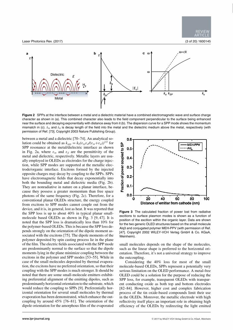
Figure 2 SPPs at the interface between a metal and a dielectric material have a combined electromagnetic wave and surface chargecharacter as shown in (a). This combined character also leads to the field component perpendicular to the surface being enhancednear the surface and decaying exponentially with distance away from it (b). The dispersion curve for a SPP mode shows the momentummismatch in (c). δm and δd is decay length of the field into the metal and the dielectric medium above the metal, respectively (withpermission of Ref. [73]. Copyright 2003 Nature Publishing Group).
between a metal and a dielectric [70–74]. An analytical so-lution could be obtained as kspp = k0(εmεd/(εm+εd))1/2 forSPP resonance at the metal/dielectric interface as shownin Fig. 2a, where εm and εd are the permittivity of themetal and dielectric, respectively. Metallic layers are usu-ally employed in OLEDs as electrodes for the charge injec-tion, while SPP modes are supported at the metallic elec-trode/organic interface. Excitons formed by the injectedopposite charges may decay by coupling to the SPPs. SPPshave electromagnetic fields that decay exponentially intoboth the bounding metal and dielectric media (Fig. 2b).They are nonradiative in nature on a planar interface, be-cause they possess a greater momentum than free spacephotons of the same frequency (Fig. 2c). Therefore, for aconventional planar OLEDs structure, the energy coupledfrom excitons to SPP modes cannot couple out from thedevice, and it is, in general, lost as heat. It was reported thatthe SPP loss is up to about 40% in typical planar small-molecule based OLEDs as shown in Fig. 3 [9, 47]. It isnoted that the SPP loss is dramatically less than 10% forthe polymer-based OLEDs. This is because the SPP loss de-pends strongly on the orientation of the dipole moment as-sociated with the excitons [75]. The dipole moments of thepolymer deposited by spin casting process lie in the planeof the film. The electric fields associated with the SPP modeare predominantly normal to the surface so that the dipolemoments lying in the plane minimize coupling between theexcitons in the polymer and SPP modes [53–55]. While incase of the small molecules deposited by thermal evapora-tion, the excitons have no preferred orientation, so that theircoupling with the SPP modes is much stronger. It should benoted that there are some small-molecule emitters exhibit-ing preferential alignment of the emitting dipoles, such aspredominantly horizontal orientation to the substrate, whichwould reduce the coupling to SPPs [9]. Preferentially hor-izontal orientation for several small molecules by thermalevaporation has been demonstrated, which enhance the out-coupling by around 45% [76–81]. The orientation of thedipole orientation for the amorphous film of the evaporated
Figure 3 The calculated fraction of power lost from radiativeexcitions to surface plasmon modes is shown as a function ofposition of the excition within the organic layer. Data are shownfor the two generic OLED structures based on the small moleculeAlq3 and conjugated polymer MEH-PPV (with permission of Ref.[47]. Copyright 2002 WILEY-VCH Verlag GmbH & Co. KGaA,Weinheim).
small molecules depends on the shape of the molecules,such as the linear shape is preferred to the horizontal ori-entation. Therefore, it’s not a universal strategy to improvethe outcoupling.
Considering the 40% loss for most of the smallmolecule-based OLEDs, SPPs represent a potentially veryserious limitation on the OLED performance. A metal-freeOLED could be a solution for the purpose of reducing theSPP loss, for example, transparent OLEDs with transpar-ent conducting oxide as both top and bottom electrodes[82–84]. However, higher cost and complex fabricationprocess of the tin oxide-based compounds limit their usein the OLEDs. Moreover, the metallic electrode with highreflectivity itself plays an important role in obtaining highefficiency of the OLEDs by redirecting the light emitted
www.lpr-journal.org C© 2017 by WILEY-VCH Verlag GmbH & Co. KGaA, Weinheim

LASER&PHOTONICSREVIEWS
1600145 (4 of 20) J. Feng et al.: Light manipulation in organic light-emitting devices by integrating micro/nano patterns
Figure 4 Schematic of the SPP dispersion on a periodicallystructured surface (period D) demonstrating SPP band-gap for-mation. SPP dispersion on a smooth surface is shown by the thinsolid line (with permission of Ref. [74]. Copyright 2004 ElsevierB.V.).
from the opposite transparent electrode. On the other hand,ITO-free OLEDs by employing metallic film with high elec-trical conductivity and optical transmission as both top andbottom electrodes to replace tin oxide [85, 86] could notonly realize a lower-cost fabrication process but also elim-inate the power lost to the WG modes in high-refractive-index ITO film. In this case, light trapped in the SPP modesbecome the main power loss for this type of OLEDs. TheSPP loss can be directly reduced by increasing the distancebetween the emitter and the metallic electrode by increasingthe thickness of the emitting or transporting layers as shownin Fig. 3, which results in a reduced coupling between theemitter and the SPP mode due to the exponential decayof the SPP field in the dielectric medium. However, con-sidering the low carrier mobility of the organic thin film,increased thickness of the emitting or transporting layerswould result in a decreased internal quantum efficiency ofthe OLEDs.
2.3. Light extraction by the micro/nano patterns
Micro/nano patterns with both periodic and random struc-ture could be used to increase light extraction of an OLED.An appropriate periodicity such that waveguided light isBragg-scattered into the forward direction is required forthe periodic micro/nano patterns by satisfying the Braggscattering condition [9, 87]. The appropriate periodicity ofthe micro/nano pattern integrated on the metallic electrodeis crucial for outcoupling the power lost to the associatedSPP modes at the desired light-emitting wavelength (Fig. 4).SPP resonance at the periodically corrugated metal surfaceis tunable by adjusting the grating period as the followingcondition, when the energy and momentum of the incidentlight match to that of the SPP mode along the metal/organicinterface [74].
kspp =∣∣∣∣klight sin α ± 2πm
�
∣∣∣∣
(2)
Where, kS P P is the in-plane wavevector of the SPP, klight isthe wavevector of the emitted light, � is the period of thecorrugation, αis the emission angle, and m is an integer. Theappropriate period of the micro/nano patterns is required toextract the WG or SPP modes in normal emission, so thattheir resonance at the normal direction could be close tothe emission peak wavelength of the emitter in the OLEDs.However, SPP and WG modes would be coupled out of thestructure at different wavelengths because of their differentdispersion relation. Therefore, it’s crucial to tune both SPPand WG to be within the emission wavelength region bydesigning the parameters of the device structure.
Micro/nano patterns with random structure suchas nanoporous alumina [35, 36], spontaneously formednanofacet-structured MgO and buckles [34,37,88], and ran-dom nanostructure scattering layers [89,90] have been em-ployed in OLEDs to realize the enhanced light extraction.Unlike the periodic structure to outcouple the photons at aparticular wavelength region by satisfying the Bragg con-dition, the random structure with directional randomnessand broad distribution can enhance the light outcouplingwithout introducing spectra changes and directionality.
3. The fabrication of micro/nano patternsin OLEDs
A simple and low cost manufacturing technique is cru-cial for introducing the micro/nano patterns into the OLEDstructure. Various lithography-based technologies are ef-fective in fabricating periodic corrugation. However, theseapproaches are applicable in inorganic LEDs due to the highchemical and physical stability of the inorganic semicon-ductors, while difficult to apply to OLEDs because organicmaterials are soluble generally in the solvents used in thelithography, and they experience electrical and/ or opti-cal deterioration when exposed to oxygen, water or high-energy electrons. The feasible approaches to introduce themicro/nano patterns into the OLEDs will be discussed inthis section. The fabrication techniques for integrating themicro/nano patterns in the OLEDs are mostly applicable toOPVs owing to their similar materials and device fabrica-tion processes.
3.1. The fabrication of the periodic micro/nanopatterns in OLEDs
3.1.1. Holographic lithography for the micro/nanopatterns
Usually, the micro/nano patterning has to start from thesubstrate to avoid the degradation of the OLEDs, so thatpattern transmits through the organic layer to the oppo-site electrode. Holographic lithography (or interference
C© 2017 by WILEY-VCH Verlag GmbH & Co. KGaA, Weinheim www.lpr-journal.org

REVIEWARTICLE
Laser Photonics Rev. (2017) (5 of 20) 1600145
Figure 5 Scheme of introducing periodic corrugation into aTOLED by holographic lithography (a), and AFM images of the1D (b) and 2D (c) grating on the photoresist surface and 1D grat-ing on the Ag cathode surface (d) (with permission of Ref. [96].Copyright 2012 WILEY-VCH Verlag GmbH & Co. KGaA, Wein-heim).
lithography) is commonly used technique for fabricatingthe periodic micro/nano patterns. The photoresist-coatedsubstrate was exposed by interference fringes. After devel-opment, the substrate was etched by RIE (reactive-ion etch-ing) dry etching, and then the photoresist was removed. Incase of the ITO coated substrate was used, the patterns canbe directly introduced to the layer of the ITO anode by RIEetching [91]. Alternatively, The ITO or metallic anode wasdeposited onto the micro/nano patterned substrate and fol-lowed by organic and cathode layers to complete the device.Periodically corrugated OLEDs on silica substrates by holo-graphic lithography followed with RIE dry etching havebeen reported [92–95]. Otherwise the periodic micro/nanopatterned photoresist coated on the substrate can be directlyused for the OLED deposition without the RIE dry etch-ing (Fig. 5), which significantly simplified the fabricatingprocess [46, 90, 96]. On the other hand, 2-D SiO2/SiNxphotonic crystals have been fabricated by the holographiclithography and RIE etching (Fig. 6) [28–30]. The photoniccrystals are inserted at the interface between the ITO layerand the glass substrate. In this case, the surface of the 2-D SiO2/SiNx photonic crystals is planar, and the patternwas not introduced to the following electrode and organiclayers. Inserting a vacuum nanohole array into OLEDs byusing a robust reverse-transfer process also maintained aplanar profile of the functional layers [97].
The fabrication of the micro/nano patterns from thesubstrate is encountered with problems such as electronicdegradation, because the surface roughness of the ITO an-ode sputtered on the corrugated substrate is increased. It isobvious that the problem may be solved if direct patterning
Figure 6 (a) The layer structure of a PC-OLED with SiNx andSiO2 /SiNx PC layers. Scanning electron micrographs: (b) topview and (c) cross-sectional view of the PC-OLED layers (withpermission of Ref. [29]. Copyright 2003 American Institute ofPhysics).
Figure 7 Scheme of introducing periodic corrugation into OLEDby laser ablation (a), and AFM images of the ablated corrugation,1-D (b) and 2-D (c) grating with period of 350 nm on the HTLsurface (with permission of Ref. [101]. Copyright 2011 ElsevierB.V.).
www.lpr-journal.org C© 2017 by WILEY-VCH Verlag GmbH & Co. KGaA, Weinheim

LASER&PHOTONICSREVIEWS
1600145 (6 of 20) J. Feng et al.: Light manipulation in organic light-emitting devices by integrating micro/nano patterns
of a certain organic functional layers of the OLEDs can berealized without affecting the flatness of the ITO film. Mostpolymers are strongly sensitivity to UV laser ablation con-dition with low ablation thresholds, so that a corrugationcan be directly recorded on the functional layers of OLEDsvia laser ablation. The one-step fabrication of the periodiccorrugation can be faster and highly reproducible with theperiod from microns to sub 100 nm through combining witha multi-beam interference [98–100]. The periodic corruga-tion with appropriate depth and period for Bragg scatteringin OLEDs are easily obtained by adjusting the laser flu-ence and the angle of the two laser beams, as shown inFig. 7 [101]. The one-step laser ablation on organic func-tional layers provides a facile and simple approach withhigh controllabiliy, high resolution and reproducibility toobtain periodically micro/nano patterned OLEDs. The one-step directly laser ablating of the hole-transporting layerof the OLEDs to introduce the micro/nano patterns hasdemonstrated three times efficiency enhancement [101].
3.1.2. Nanoimprint lithography in OLEDs
Nanoimprint lithography (NIL) as another one-step fab-rication approach provides a simple way of micro/nanopatternning the functional layers of the OLEDs. High-resolution patterning of both polymer light-emitting mediaand small molecule by using the thermal, vacuum or ul-traviolet NIL has been reported [102–105]. Reboud et al.[105] reported that the patterned functional polymer layerscan be reversely imprinted onto metallic electrode by usingthe thermal NIL techniques (Fig. 8). The Alq3 (8- hydrox-yquinoline aluminum) /DCMII gratings with a period of200 and 300 nm by the nanoimprint exhibited no degrada-tion in the luminescent efficiency [106]. The patterns wereintroduced to dendrimer-based OLEDs by the NIL [48].Polymer distributed feedback lasers were demonstrated byusing the NIL-fabricated wavelength-scale microstructures[107]. The close-packed array of polystyren microspherecan be used as template for the PDMS replica [35]. Whilefor the NIL-induced micro/nano patterns in the OLEDs,the effects of the temperature and pressure environment onthe optical and electrical property of the organic materialsshould be considered.
3.1.3. Other methods
Several methods other than the above mentioned techniquehave been reported to introduce the periodic micro/nanopatterns into the OLEDs. microlens array was usually madeby using a mold transfer process, which is typically a com-bination of lithography, thermal reflow, molding and UV orthermal forming methods [12, 108–110]. Periodic changeof the refractive index without surface-relief structure hasbeen inscribed in the active materials in the OLEDs by holo-graphic setup to modify the output characteristics of theOLEDs [111]. However, this method is limited by realizinga polymer with both charge-transporting and photosensitive
qualities to undergo a photoisomerization and act as func-tional layer in OLEDs. Colloidal lithography was employedto integrate a monolayer of SiO2 microsperes on the sub-strate of the OLEDs to extract the substrate mode [15–17].The functional films of the OLEDs can be direct patternedby the colloidal lithography. A close-packed monolayer ar-ray of polystyren microsphere was etched into a non-closelypacked monolayer array, and a thermal deposition of WO3[36,112] on the PS monolayer results in a hexagonally per-forated anode modification layer on the ITO anode. Usingthe monolayer colloidal crystal as template for the chemicaletching of the ITO resulted in a large-area nano-structuredITO anode [113]. E-beam lithography–fabricated periodicarrays of Al nanorods [114] and circular metallic gratings[115] and focused ion beam milling-fabricated Ag gratings[116] have explored their applications in OLEDs or OPVs.Both methods have high resolution in generating nanoscalestructures, while have the disadvantages of low throughputand high cost. Photolithography could be used for pixila-tion of the OLEDs with micro size for displays [117], whileit’s difficult to realize the patterns in sub-wavelength scale.
3.2. Fabrication of random micro/nano patternsin OLEDs
Several simple and low-cost processes without an addi-tional lithography or patterning process have been reportedto obtain the spontaneously formed random micro/nanopatterns. MgO nanofacets as random micro/nano patterns(Fig. 9) can be formed spontaneously due to the anisotropicmaterial characteristics of MgO between crystal orienta-tions [38]. A thin film of MgO was inserted between theITO layer and the glass substrate by electron-beam evap-oration. The MgO facet was formed due to anisotropy ofthe properties between (111) and the other main planes ofMgO, (200) and (220). The nanofacet-structured MgO filmacted as a refractive-index-modulating layer to reduce thetotal internal reflection at the ITO/glass interface. Takezeoet al. [41,45] reported spontaneously formed buckles as an-other kind of random micro/nano patterns introduced intothe OLEDs. Buckling patterns are realized by thermallyevaporating aluminium films on PDMS substrates, whichis preheated to 100°C using an external radiation source.After cooling to ambient temperature, buckling sponta-neously occurred. Using nanoporous anodic aluminium ox-ide [39,40,118], alumina nanohole array [119] or randomlydistributed dewetting Ag droplets as a hard mask [42, 44]are alternative methods to introduce the random micro/nanopatterns into the OLEDs.
From a practical point of view, high-resolution, simple,low-cost and high-throughput techniques to fabricate themicro/nano patterns are required for the commercializationand need to be pursued and developed. Holographic lithog-raphy [90–96] and nanoimprint lithography [102–107] de-liver high quality, inexpensive and large area periodic mi-cro/nano patterns, and could be easily applied to OLEDs.For random pattern fabrication, spontaneously formed
C© 2017 by WILEY-VCH Verlag GmbH & Co. KGaA, Weinheim www.lpr-journal.org

REVIEWARTICLE
Laser Photonics Rev. (2017) (7 of 20) 1600145
Figure 8 Schematic of process steps based on reverse nanoimprint for the fabrication of OLEDs. (a) The silicon stamp is placed ona spin-coater, (b) light-emitting polymer (PPV) is spin-coated on the stamp, (c) PEDOT is spin-coated on top of the PPV layer, (d) thespin-coated stamp is reverse imprinted on a unpatterned or patterned pre-treated metallic surface fabricated by conventional thermalNIL techniques, (e) the stamp is carefully separated leaving the polymer multi-layers on the metallic electrodes and (f) the cathodeis evaporated to form the OLEDs. Devices IV and V incorporate an unpatterned and patterned anode (with permission of Ref. [105].Copyright 2012 The Royal Society of Chemistry).
Figure 9 (a) Schematic diagram of bottom-emitting OLEDs withthe embedded nanofacet-structured refractive index modulationlayers (RIML) at the glass/ITO interface. The RIML is compositedof electron-beam-evaporated MgO and MgO/ZrO2. (b) Schematicexplanation of the mechanism for improving device out-couplingefficiency with a microfacet-structured RIML. Diagrams are not toscale (with permission of Ref. [38]. Copyright 2010 WILEY-VCHVerlag GmbH & Co. KGaA, Weinheim).
random patterns [38, 41] and hard mask template [39, 40]provide inexpensive and simple methods for the potentialindustry applications.
4. Enhanced device performance bymicro/nano patterns
4.1. External light extraction from OLEDs by themicro/nano patterns
To outcouple the photons trapped inside the substrate of thebottom-emitting OLEDs due to the total internal reflectionat the glass/air interface, a modification of the external sur-face of the glass substrate are often preferable since they donot induce any alteration either in the functioning or in thearchitecture of the device. In particular, there is neither anychange on device electrical properties nor spectral variationwith viewing angle. The effect of the micro/nano patterns,with different feature size and geometries, in the light ex-traction has been discussed by different authors. Microlensarrays [120–125], micrometric conical pillars [126], micro-metric and millimeter size pyramids [127,128] have alreadybeen employed to this purpose. Among these geometries,microlens array is simple to fabricate and can be easily ap-plied to large area substrates. Theoretical and experimentalworks have been developed to quantitatively analyze theperformance of the microlens array with various shapes
www.lpr-journal.org C© 2017 by WILEY-VCH Verlag GmbH & Co. KGaA, Weinheim

LASER&PHOTONICSREVIEWS
1600145 (8 of 20) J. Feng et al.: Light manipulation in organic light-emitting devices by integrating micro/nano patterns
Figure 10 SEM of a PDMS microlens array fabricated from the mold. The detailed side view of the lenses (inset) shows that the PDMSaccurately images the mold shape. External quantum and power efficiency vs current density of an Ir(ppy)3 doped phosphorescentOLED (with permission of Ref. [13]. Copyright 2002 American Institute of Physics).
and sizes for the light extraction enhancement of planarOLEDs by comparing the efficiency of the devices withand without the microlens array. The enhancement of lightextraction of up to 85% was theoretically predicted from anoptimized lens pattern with a hemispherical structure [109].Experimentally, Forrest et al. [13] demonstrated a 50% EQEenhancement with the EQE increasing from 9.5% to 14.5%by using a 10 μm diam PDMS lenses attached to the glasssubstrates of a fac tris(2-phenylpyridine)Iridium (Ir(ppy)3)-based OLED (Fig. 10). Uniform 2 μ-pitch microlens arraysresulted in a 100% EQE enhancement [110].
In addition to the microlens array, incorporation ofother micro/nano patterns to the back side of the sub-strate to outcouple the substrate mode was investigated.The submicrometer-size silica spheres with monolayer ofhexagonally closed-packed arrays [15–17] attached to aglass substrate effectively scatter waveguided light withina glass substrate and resulted in a 60% enhancement inluminous efficiency for the Alq3-based OLEDs [17]. 22%enhancement in outcoupling efficiency by using a diffusivelayer [129] and 40% enhancement in current efficiency byusing pillar arrays [130] have been observed, respectively.Shaping of the device into a mesa structure demonstrated90% improvement in the EQE [64]. It should be pointed outthat the incorporation of the micro/nano pattern to the backside of the substrate induces blurring of the image due tothe light rays are outcoupled from the non-emissive region.This may not be desirable for high resolution displays.
4.2. Internal light extraction frombottom-emitting OLEDs
The modification of the internal structure inside the deviceis required to achieve the internal extraction of the powerloss to the light waveguiding in the ITO/organic layer or theSPP mode at the organic/electrode interface. The effect ofthe internal structure modification by the micro/nano pat-
terns on the internal light extraction of the bottom-emittingOLEDs will be discussed in this section.
4.2.1. Outcoupling of the WG and SPP mode in OLEDs
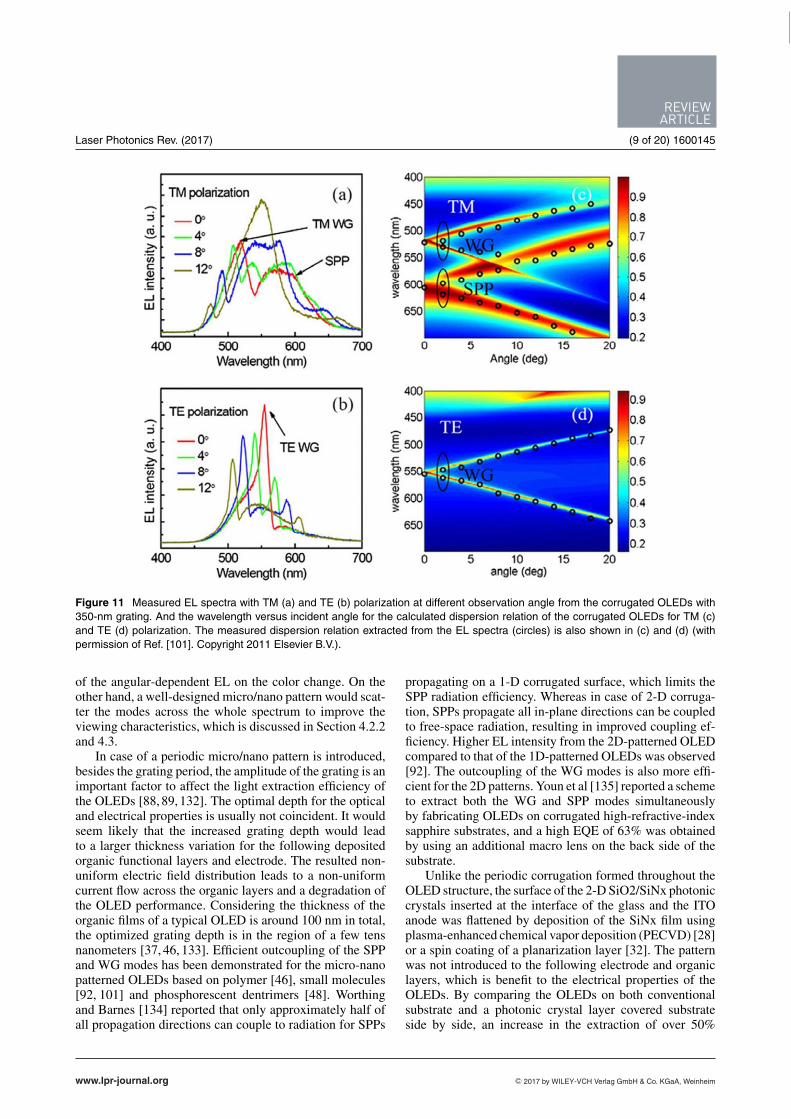
If the micro/nano patterning starts from the substrate, thefollowing deposited organic layers and electrode by ther-mal evaporation duplicate morphology of the substrate. Thetransmission of the corrugation through the organic layersto the opposite electrode is crucial for the simultaneousoutcoupling of the WG and SPP mode. Additional peakscorresponding to the SPP or WG resonance can be observedfrom the EL spectra of the OLEDs, which indicate an ef-ficiently outcoupling of photons from these optical modes[90,92,101,131]. For emission normal to the OLED struc-ture, an additional peak corresponding to the SPP or WGresonance at the normal direction can be observed withinthe emission wavelength region of the OLEDs, and at otherangles the peak splits into two features-one at shorter wave-length and the other at longer wavelength for both SPP andWG modes, as can be seen in Fig. 11 [101]. These opticalmodes can be identified by the simulated spatial magneticfield distribution across the device structure as a functionof position with the normal incident light [46,96,101]. Thefield intensity corresponding to the SPP resonance is withmaximum at the metallic electrode/organic interface anddecay along the direction perpendicular to it (Fig. 2). Onthe other hand, the field confined mainly within the or-ganic and ITO layers should be assigned to the TE andTM polarized WG modes due to the high refractive indexof the organic and ITO layers. It should be noted that theangular-dependent resonant wavelength of both WG andSPP modes would result in an angular dependence of theEL spectra, which may cause an angular-dependent colorchange as this would be undesirable for display applica-tions. While, only the resonant wavelength within the emis-sion wavelength region of the emitter can be coupled outfor both SPP and WG mode, which weaken the influence
C© 2017 by WILEY-VCH Verlag GmbH & Co. KGaA, Weinheim www.lpr-journal.org
REVIEWARTICLE
Laser Photonics Rev. (2017) (9 of 20) 1600145
Figure 11 Measured EL spectra with TM (a) and TE (b) polarization at different observation angle from the corrugated OLEDs with350-nm grating. And the wavelength versus incident angle for the calculated dispersion relation of the corrugated OLEDs for TM (c)and TE (d) polarization. The measured dispersion relation extracted from the EL spectra (circles) is also shown in (c) and (d) (withpermission of Ref. [101]. Copyright 2011 Elsevier B.V.).
of the angular-dependent EL on the color change. On theother hand, a well-designed micro/nano pattern would scat-ter the modes across the whole spectrum to improve theviewing characteristics, which is discussed in Section 4.2.2and 4.3.
In case of a periodic micro/nano pattern is introduced,besides the grating period, the amplitude of the grating is animportant factor to affect the light extraction efficiency ofthe OLEDs [88, 89, 132]. The optimal depth for the opticaland electrical properties is usually not coincident. It wouldseem likely that the increased grating depth would leadto a larger thickness variation for the following depositedorganic functional layers and electrode. The resulted non-uniform electric field distribution leads to a non-uniformcurrent flow across the organic layers and a degradation ofthe OLED performance. Considering the thickness of theorganic films of a typical OLED is around 100 nm in total,the optimized grating depth is in the region of a few tensnanometers [37, 46, 133]. Efficient outcoupling of the SPPand WG modes has been demonstrated for the micro-nanopatterned OLEDs based on polymer [46], small molecules[92, 101] and phosphorescent dentrimers [48]. Worthingand Barnes [134] reported that only approximately half ofall propagation directions can couple to radiation for SPPs
propagating on a 1-D corrugated surface, which limits theSPP radiation efficiency. Whereas in case of 2-D corruga-tion, SPPs propagate all in-plane directions can be coupledto free-space radiation, resulting in improved coupling ef-ficiency. Higher EL intensity from the 2D-patterned OLEDcompared to that of the 1D-patterned OLEDs was observed[92]. The outcoupling of the WG modes is also more effi-cient for the 2D patterns. Youn et al [135] reported a schemeto extract both the WG and SPP modes simultaneouslyby fabricating OLEDs on corrugated high-refractive-indexsapphire substrates, and a high EQE of 63% was obtainedby using an additional macro lens on the back side of thesubstrate.
Unlike the periodic corrugation formed throughout theOLED structure, the surface of the 2-D SiO2/SiNx photoniccrystals inserted at the interface of the glass and the ITOanode was flattened by deposition of the SiNx film usingplasma-enhanced chemical vapor deposition (PECVD) [28]or a spin coating of a planarization layer [32]. The patternwas not introduced to the following electrode and organiclayers, which is benefit to the electrical properties of theOLEDs. By comparing the OLEDs on both conventionalsubstrate and a photonic crystal layer covered substrateside by side, an increase in the extraction of over 50%
www.lpr-journal.org C© 2017 by WILEY-VCH Verlag GmbH & Co. KGaA, Weinheim

LASER&PHOTONICSREVIEWS
1600145 (10 of 20) J. Feng et al.: Light manipulation in organic light-emitting devices by integrating micro/nano patterns
Figure 12 (a) Schematic diagrams of the structure of the transparent OLED and the microstructures for light extraction. (b-c) Externalquantum efficiencies and power efficiencies of the OLEDs (with permission of Ref. [12]. Copyright 2013 WILEY-VCH Verlag GmbH &Co. KGaA, Weinheim).
was achieved experimentally, and over 80% is expectedtheoretically [28, 29, 31–33]. For example, the current ef-ficiency in the normal direction at 20 mA/cm2 was im-proved from 10.9 cd/A for the conventional OLED to16.4 cd/A for the 2D PC OLED corresponding to a 52%enhancement [31]. The improved outcoupling originatesfrom the liberation of the photons trapped in the high-indexITO/organic WG mode. Meanwhile, with appropriate pa-rameters of the PC structure, light waves tend to diffractmore into shallow angles, which results in the light extrac-tion from the substrate mode by reducing the total internalreflection, so that a high outcoupling efficiency is achiev-able. While the corrugation was not introduced to the elec-trode/organic interface, the SPP mode cannot be effectivelyoutcoupled.
In case of the ITO-free OLEDs with two metallic elec-trodes, a metallic film with high electrical conductivityand optical transmission is used to replace ITO as anode.Highly efficient light extraction could be expected by ex-citation and outcoupling of the SPP modes in the OLEDs,since light trapped in the SPP modes becomes one of themain power lost [90, 131, 136]. A 30% current efficiency
enhancement was obtained by increasing the efficiencyfrom 3.2 to 4.19 cd/A for the Alq3-based OLEDs with twometallic electrodes of Au anode and Ag cathode, wherethe SPP losses at the Ag cathode/organic interface were ef-fectively extracted by introducing the periodic micro/nanopatterns [137]. On the other hand, a metal-free OLED withgood transparency combined with a method to extract thelight efficiently from the device could be another solutionfor the purpose of reducing the SPP loss [138]. Kim et al.[12] reported the transparent OLEDs with the indium zincoxide (IZO) and ITO layers as the top and bottom elec-trodes, respectively. A high refractive index light extractionpattern was additionally fabricated on the transparent topelectrode using a simple evaporation method and a mi-crolens array sheet was attached on the bottom side of theglass substrate to extract the confined light inside the device,as shown in Fig. 12a. The resulted EQE of the OLEDs wasincreased from 18.2% to 47.3%. It was further improved to62.9% by attaching an index-matched hemisphere lens in-stead of the microlens array on the glass substrate to extractthe remaining light guiding losses inside of the device (Fig.12b and c).
C© 2017 by WILEY-VCH Verlag GmbH & Co. KGaA, Weinheim www.lpr-journal.org

REVIEWARTICLE
Laser Photonics Rev. (2017) (11 of 20) 1600145
Figure 13 (a–c) Schematic of the broadband light extraction byusing dual-periodic corrugation. (d–f) AFM images of surfacemorphologies of photoresist with 1D period of (d) 225 and (e)325 nm, and (f) 2D dual-periodic corrugation (with permissionof Ref. [139]. Copyright 2013 WILEY-VCH Verlag GmbH & Co.KGaA, Weinheim).
4.2.2. Broadband internal light extraction from OLEDsby micro-nano patterns
Broadband light extraction is important for the efficientoutcoupling of the photons trapped in the white organiclight-emitting devices (WOLEDs) with spectra coveringthe whole visible wavelength. Broadband extraction ofthe substrate modes can be easily realized by attach-ing a microlens array on the outside of the substrate.While broadband extraction is difficult to be obtainedfor the WG and SPP modes inside of the OLEDs byintroducing the structure modification inside the devicestructure. Micro/nano patterns with monoperiodicity in-troduced into the OLEDs are suitable for specific nar-row range of wavelength by satisfying the Bragg scat-tering condition, and applicable only for monochromaticOLEDs.
Broadband excitation and outcoupling of the SPPs inthe WOLEDs have been obtained by introducing a 2-Dpattern with dual-periodic corrugation into the WOLEDs[139]. The 2-D pattern consisted two sets of corrugationswith different periods can broaden the SPP resonance com-pared to that of the monoperiodic pattern (Fig. 13). Theblue and orange emission are both efficiently extractedfrom the two complementary color-based WOLEDs bytuning appropriate periods of the dual-periodic patterns.The maximum current efficiency was improved from 16.27cd/A for the conventional planar devices to 22.33 cd/Afor the dual-periodic corrugated device corresponding to37% enhancement. Broadband lambertian emitters havebeen obtained by using defective hexagonal-closed-packedgrating for light extraction due to the periodicity broad-ening and the random orientation in the gratings, whichresulted in enhancements in current efficiencies by a factorof 1.7 (from 2.57 to 4.38 cd/A) [35]. Random micro/nanopattern [140–142], such as nanoporous [39] or sponta-neously formed quasi-periodic buckling [41, 143, 144],metal oxide nanostructures [145] or nanofacet structures
[38] have a broad distribution to enhance the light extrac-tion efficiency without introducing spectral changes anddirectionality. Koo et al. [41] reported an EL spectrumenhanced by at least a factor of two across the entire vis-ible wavelength regime by using the quasi-periodic buck-les (Fig. 14). In the Alq3-based devices with and with-out buckling, the current efficiency was 1.67 and 3.65cd/A, respectively, corresponding to an enhancement of120%. Metal nanoparticles induced localized surface plas-mon resonance also support the broadband SPP excitationand can be embedded into the OLEDs [146–153]. Imple-menting quasi-periodic subwavelength nanofunnel arrayson the hole-injection layer of PEDOT:PSS via soft nanoim-printing lithography enhance broadband light extraction inWOLEDs [154, 155]. Inserting a nanosized strip auxiliaryelectrode layer between the substrate and ITO layer [156]or a plasmonic cavity having deep subwavelength nanos-tructures [157] is also able to enhance light extraction ofWOLEDs.
In case of flexible OLEDs, broadband light extractionhas been obtained by using an ameliorated low-refractive-index PET substrate consisting of a built-in transparent con-ductive electrode of Ag network and a bioinspired opticalcoupling layer of moth-eye nanostructure [158]. A compos-ite electrode to replace ITO comprising a layer of single-walled carbon nanotube and a layer of silver nanowiresembedded in the surface of a barium strontium titanatenanoparticle-polymer composite is also effective in flexiblepolymer-based OLEDs to realize broadband light extrac-tion [159].
4.3. Light extraction from top-emitting OLEDs
Another way of outcoupling the trapped light is the use ofmicrocavity structure to direct light emission to air. For thebottom-emitting OLEDs, aperiodic dielectric stacks wereplaced between transparent anode and glass substrate to in-crease the outcoupling efficiency by confining the emissionwithin the narrowed viewing cone [160,161]. In case of top-emitting organic light-emitting devices (TOLEDs), the topsemi-transparent metallic electrode and the bottom metallicelectrode together with the organic layers form a Febry-Perot resonator, and the resulting microcavity resonancehas a positive effect on the light outcoupling efficiency inthe resonance region [162, 163]. However the microcav-ity structures usually resulted in non-Lambertian emissioncharacteristics with obvious spectra shifts as a function ofthe viewing angle. TOLEDs are attracting much attentionsince light outcoupling from the top allows the fabricationof OLEDs on opaque substrates. It is particularly suitablefor active matrix displays with high resolution and highinformation content due to the higher aperture ratio anddisplay image quality. The simultaneous achievement ofenhanced efficiency, enhanced color saturation and stablespectra with the viewing angles in the same device designis one of the main challenges for the practical applicationsof the TOLEDs [164–168].
www.lpr-journal.org C© 2017 by WILEY-VCH Verlag GmbH & Co. KGaA, Weinheim

LASER&PHOTONICSREVIEWS
1600145 (12 of 20) J. Feng et al.: Light manipulation in organic light-emitting devices by integrating micro/nano patterns
Figure 14 (a–c) AFM analysis of buckling patterns. Inset: FFT patterns of each image. (d) Current efficiency and power efficiency asa function of luminance for OLEDs without buckling (black) and with double (red) and triple (blue) buckling (with permission of Ref.[41]. Copyright 2010 Nature Publishing Group).
The metallic film is used as semi-transparent top cath-ode of the TOLEDs, and thinner metallic film ensures ahigher transparency. However, more pinholes are formedin the very thin film due to its poor film continuity, whichresults in decreased electrical conductivity and lowered de-vice efficiency. Thicker metallic film offers higher film con-tinuity and thereafter higher electrical conductivity, how-ever, the efficiency is still lowered due to the decreasedoptical transmittance. Jin et al. [96] reported an enhancedlight transmission through a thick metallic cathode bycross coupling occurring between the SPP modes associ-ated with the top surface of the cathode and the microcavitymodes within the device induced by the periodic micro/nanopatterns. An emitting layer of (4-(dicyanomethylene)-2-t-butyl-6-(1, 1, 7, 7-tetramethyljulolidyl)-4H-pyran (DCJTB)doped Alq3 was employed for the red-emitting TOLEDs.As a result, the current efficiency at the current density of100 mA/cm2 is increased from 5.3 cd/A for the planar de-vice to 7.1 and 7.4 cd/A for the 1-D and 2-D corrugateddevices, respectively, which corresponded to 30% and 40%efficiency enhancement to the planar device by using the1-D and 2-D corrugation. The half-luminance lifetime was
also much enhanced due to the increase of the cathodethickness.
Enhanced outcoupling efficiency of the TOLED hasalso been demonstrated by integrating a refractive index-matched microlens array on the top cathode [169,170]. Themicrolens film with a higher index of refraction allows alarge portion of the WG modes in the organic/transparentelectrode layers to enter the microlens and be subsequentlyextracted. As we have discussed in Section 4.1, the mi-crolens array on the glass substrate of the bottom-emittingOLEDs results in serious image blurring. In contrast, theblurring of pixel emission is substantially reduced for thecase of TOLEDs laminated with microlens array. Realizingwhite emissions from TOLEDs has been encountered withchallenges in not only the light extraction but also the highquality of the white color. The microcavity (MC) effect ofthe TOLEDs induces a narrow bandwidth of the EL spec-trum as well as a blue shift of the emission color as the view-ing angle increases. Broadband light extraction and stablecolors with viewing angles have been obtained by using themicrolens array in the TOLEDs. Therefore, this method isapplicable to the white TOLEDs [124]. Another simple and
C© 2017 by WILEY-VCH Verlag GmbH & Co. KGaA, Weinheim www.lpr-journal.org
REVIEWARTICLE
Laser Photonics Rev. (2017) (13 of 20) 1600145
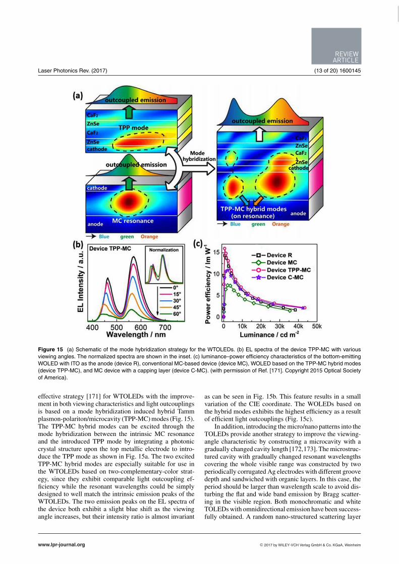
Figure 15 (a) Schematic of the mode hybridization strategy for the WTOLEDs. (b) EL spectra of the device TPP-MC with variousviewing angles. The normalized spectra are shown in the inset. (c) luminance–power efficiency characteristics of the bottom-emittingWOLED with ITO as the anode (device R), conventional MC-based device (device MC), WOLED based on the TPP-MC hybrid modes(device TPP-MC), and MC device with a capping layer (device C-MC). (with permission of Ref. [171]. Copyright 2015 Optical Societyof America).
effective strategy [171] for WTOLEDs with the improve-ment in both viewing characteristics and light outcouplingsis based on a mode hybridization induced hybrid Tammplasmon-polariton/microcavity (TPP-MC) modes (Fig. 15).The TPP-MC hybrid modes can be excited through themode hybridization between the intrinsic MC resonanceand the introduced TPP mode by integrating a photoniccrystal structure upon the top metallic electrode to intro-duce the TPP mode as shown in Fig. 15a. The two excitedTPP-MC hybrid modes are especially suitable for use inthe WTOLEDs based on two-complementary-color strat-egy, since they exhibit comparable light outcoupling ef-ficiency while the resonant wavelengths could be simplydesigned to well match the intrinsic emission peaks of theWTOLEDs. The two emission peaks on the EL spectra ofthe device both exhibit a slight blue shift as the viewingangle increases, but their intensity ratio is almost invariant
as can be seen in Fig. 15b. This feature results in a smallvariation of the CIE coordinate. The WOLEDs based onthe hybrid modes exhibits the highest efficiency as a resultof efficient light outcouplings (Fig. 15c).
In addition, introducing the micro/nano patterns into theTOLEDs provide another strategy to improve the viewing-angle characteristic by constructing a microcavity with agradually changed cavity length [172,173]. The microstruc-tured cavity with gradually changed resonant wavelengthscovering the whole visible range was constructed by twoperiodically corrugated Ag electrodes with different groovedepth and sandwiched with organic layers. In this case, theperiod should be larger than wavelength scale to avoid dis-turbing the flat and wide band emission by Bragg scatter-ing in the visible region. Both monochromatic and whiteTOLEDs with omnidirectional emission have been success-fully obtained. A random nano-structured scattering layer
www.lpr-journal.org C© 2017 by WILEY-VCH Verlag GmbH & Co. KGaA, Weinheim

LASER&PHOTONICSREVIEWS
1600145 (14 of 20) J. Feng et al.: Light manipulation in organic light-emitting devices by integrating micro/nano patterns
in TOLEDs is also effective in improving the out-couplingefficiency and spectra angular independency [174]. Com-pared to the micro/nano patterns, introducing a cappinglayer on top of the thin metallic cathode [164,165] is anothereffective method to improve the outcoupling efficiency andviewing characteristics by broadening the MC resonance.A broadened EL spectrum and increased outcoupling effi-ciency could be obtained by using the capping layer. Anappropriate thickness and refractive index for the cappinglayer is required for the light outcoupling at specific wave-length or broadband light extraction.
The reported enhancement in the outcoupling efficiencyof the OLEDs integrated with various micr/nano patternshas been summarized in Table 1. There exist variations inthe materials, structure design and the fabrication process ofthe micro/nano-patterned OLEDs, and these factors shouldbe taken into account for evaluating the varous patterns onthe light extraction. Despite the benefits of the micro/nanopattern-enabled light extraction discussed in the above sec-tions, it should be noted that the performance reported formany micro/nano pattern-integrated OLEDs is still lowerthan the experimentally achieved efficiency records forOLEDs employing the same materials, as the largest en-hancement factors were observed when comparing withrelatively poor reference devices. A combination of the ex-ternal and internal light extraction method would result in amaximum outcoupling efficiency of the OLEDs [12, 145].
4.4. Manipulation of the emitting propertiesby the micro/nano patterns
Besides the manipulation of the micro/nano patterns onthe light extraction and emission spectra, the manipulationon the polarization, energy transfer [175–177], and highlydirectional light beam [178–182] can be obtained in theOLEDs. Highly directional EL have been achieved in theTOLEDs by using a 2D periodically patterned silver filmas a cathode and an organic dye with a narrow bandwidthof emission spectrum as an emitter [93]. The TEOLEDsexhibited beam divergence of less than 4° and the beamdirection is controllable by tuning the periodicity of thecorrugation. The resonant excitation of the SPPs associatedat the silver film interfaces contributes to the light trans-mission through the silver cathode and to the directionalemission.
Andrew et al. [183] reported that energy transfer fromdonor to acceptor molecules can be enhanced by the medi-ation of the SPPs through the coupling of the SPPs on theopposite interfaces of a metal film. For the SPP-mediatedenergy transfer, acceptor and donor molecules can be lo-cated at opposite sides of a metallic film, which allows ra-diative energy transfer over distances of more than 100 nm.This energy transfer process is quite different from theForster or Dexter nonradiative energy transfer, where thedistance between donor and acceptor molecules should beless than 10 nm. The SPP-mediated radiative energy transferhas been employed in the TOLEDs [95]. The EL intensity
from the patterned TOLEDs shows 10 times enhancementcompared to that of the flat TOLEDs, because the coupledSPPs on the opposite interfaces of the micro/nano patternedsilver cathode act as an efficient energy transfer mediatorfrom the donor to the acceptor. This energy transfer mech-anism has been applied into organic photovoltaics with anexternal antenna layer to realize broadband enhanced ab-sorption by mediating the energy transfer from the antennalayer to the active layer [184].
5. Micro/nano patterns in organicphotovoltaics
Micro/nano patterns are widely used in OPVs, while theyplay a different role in manipulating light in OPVs com-pared to that of the light extraction in the OLEDs, i.e. lighttrapping. The active layer in the OPVs is inherently verythin due to the low charge-carrier mobility and small exci-ton diffusion length of most small molecular and polymericmaterials [185, 186]. The thickness of the active layer is inturn limited, which lead to poor solar light absorption andlow power conversion efficiency (PCE). Localized SPs ex-cited in metal nanoparticles [187–189] or SPPs propagatingat the metal/organic interface can concentrate and foldedlight into the thin absorber layer and increase the absorptionby proper engineering the micro/nano patterns [190–194].It yields new options for solar-cell design by permitting aconsiderable reduction in the physical thickness of solarphotovoltaic absorber layers. The micro/nano patterns em-ployed in the OLEDs are mostly applicable to the OPVs innot only the fabrication techniques but the effect of the lightmanipulation. Unlike the SPP-enabled absorption enhance-ment by the metallic NPs or gratings, dielectric NPs havebeen employed in the OPVs to improve the light harvest-ing. High refractive index TiO2 NPs are commonly usedto form the light-scattering film by inserting it between theelectrode and active layer [195,196], or embedded it in PE-DOT: PSS as light-trapping electrode [197]. Compared tothe dielectric NPs-based light scattering, plasmonic nanos-tructures have been more extensively investigated, becauseSPPs are strongly confined at the metal/organic interfaceand results in an efficient incoupling of light into the ab-sorbers [198, 199].
Tuning the SPP resonance to the absorption region ofthe absorber layer is crucial for the most absorption en-hancement for efficiently utilizing the SPP-enhanced lighttrapping. In contrast to metallic nanoparticles, periodicallymicro/nano patterned metal film forms a particularly inter-esting class, since their periodicity can be tuned to easilyadjust the SPP resonance so that a coincidence betweenthe SPP resonance and the absorption wavelength region ofthe absorber layer can be obtained to realize a maximumabsorption enhancement. Therefore, using the periodicallymicro/nano patterned metal to excite SPP may provide apossible way to release the tradeoff between photon ab-sorption and exciton harvesting efficiency. 1-D or 2-D pe-riodic micro/nano patterned metallic electrode with wave
C© 2017 by WILEY-VCH Verlag GmbH & Co. KGaA, Weinheim www.lpr-journal.org

REVIEWARTICLE
Laser Photonics Rev. (2017) (15 of 20) 1600145
Table 1 Reported enhancement in the outcoupling efficiency of the OLEDs integrated with various micr/nano patterns
Micro/nano patterns Efficiency enhancement Ref. No.
Microlens array on back side of the substrate 50% (in EQE) [13]
100% (in EQE) [110]
Microlens array on top electrode of TOLEDs 120% (in EQE) [170]
51% (in EQE) [124]
Silica sphere on back side of the substrate 60% (in cd/A) [7]
Pillar array on back side of the substrate 40% (in cd/A) [130]
Mesa shaping of the device 90% (in EQE) [64]
Periodic gratings inside the device structure 30% (in cd/A) [137]
37% (in cd/A) [139]
70% (in cd/A) [35]
40% (in cd/A) [96]
2-D photonic crystals at the interface of theglass and the ITO anode
38% (in cd/A) [28]
52% (in cd/A) [31]
Random patterns inside the device structure 120% (in cd/A) [41]
34.7% (in lm/W) [38]
40% (in EQE) [140]
70% (in EQE) [145]
Top microcones array combined with bottommicrolens array
160% (in EQE) [12]
Random buckling inside the device structurecombined with a hemispherical lens onback side of the substrate
150% (in EQE) [145]
length-scale periodicity has been integrated into the OPVstructure to excite the SPP at the metal/organic interfacewith tunable resonance. Yu Jin et al. demonstrated 35%enhancement in the PCE by employing a 1-D periodic mi-cro/nano patterns [190, 191]. Various fabrication approachhas been employed to introduce the 1-D and 2-D patternsinto the OPVs, where the various grating conditions, suchas dimensions, period and depth on the OPV performancewas investigated [200–206].
Broadband excitation of the SPPs supported by the mi-cro/nano patterns is highly desirable for the broadband ab-sorption enhancement to improve the PCE of the OPVs.Dual plasmonic nanostructures with combined metallic NPsand metallic grating electrode [207, 208], and combinedmetallic grating and photonic crystal [209] have been re-ported to realize multiple SPP excitation. The micro/nanopatterns with 2D dual periodic [210], aperiodic [211] andquasi-periodic corrugations [206], and hexagonal pyramidarrays [212] capable of light trapping with broadband spec-tra response by the effect of anti-reflection, light scatter-ing as well as SPPs. 3-D ITO nanohelix array fabricatedby an olique-angle deposition techique has been appliedin the OPVs as a multifunctional electrode for simulta-neously improving light absorption and charge transport[213]. Using an external antenna layer with complemen-tary absorption property to the active layer is another exam-
ple of the SPP-resulted broadband absorption enhancement[184]. The antenna layer absorbs the photons at shorterwavelength, which is coupled to the active layer by SPPmediated energy transfer through the micro/nano patternedmetallic electrode. As a result, the absorption was enhancedin a wide wavelength range from 400 nm to 700 nm.
6. Conclusions and outlook
In this review, we have discussed the major advances thathave recently been achieved in the light manipulation inOLEDs by integrating micro/nano patterns. By incorpo-rating the micro/nano patterns with random or periodicmorphologies inside and outside the device structure, theOLEDs show enhanced light extraction performance com-pared to the conventional planar devices for both bottomand top-emitting OLEDs. The photons trapped in the sub-strate of the bottom-emitting OLEDs due to the total in-ternal reflection at the glass/air interface can be effectivelyoutcoupled by a micro/nano patterned external surface ofthe glass substrate, while the power lost to the WG and SPPmodes can be effectively outcoupled by the modification ofthe internal structure inside the device with the micro/nanopatterns. Broadband light extraction in OLEDs and light
www.lpr-journal.org C© 2017 by WILEY-VCH Verlag GmbH & Co. KGaA, Weinheim

LASER&PHOTONICSREVIEWS
1600145 (16 of 20) J. Feng et al.: Light manipulation in organic light-emitting devices by integrating micro/nano patterns
absorption in OPVs both can be obtained by micro/nanopattern-induced broadband excitation of the SPPs. In caseof the TOLEDs, the micro/nano patterns play an importantrole in not only light extraction but improving the viewing-angle characteristic. We have further discussed emittingproperties other than the light extraction could be manipu-lated by introducing the micro/nano patterns.
Due to the progress made in material development anddevice optimization, OLEDs have demonstrated remark-able success in the past few years with the recent advancein display industry. In the long term, research is movingfrom developing the materials to optimizing the light out-coupling from the design of the device structure. For furtherprogress, the focus on the science and technology of mi-cro/nano patterns for light manipulation offers the potentialof achieving higher-efficiency devices, which is particularlyimportant for lighting applications where high efficiency iscritically required. We should also keep in mind that a sim-ple and low cost manufacturing technique of the micro/nanopatterned OLEDs is crucial for commercial applications.The authors hope that the subject of this review, summariz-ing the knowledge of light manipulation by the micro/nanopattern in the OLEDs, would be instrumental in optimizingstructure design and, consequently, high-efficiency devices.
Acknowledgements. This work was supported by the NationalNature Science Foundation of China (NSFC) and National Ba-sic Research Program of China (973 Program) under Grants#61675085, #2013CBA01700, #61505065, and #61595930.
Received: 30 June 2016, Revised: 25 June 2016,Accepted: 2 February 2017
Published online: 27 February 2017
Key words: Organic light-emitting devices, light extraction,micro/nano pattern, organic photovoltaics, light trapping.
Jing Feng received the B.S. and Ph.D.degrees in microelectronics and solid-state electronics from Jilin University,Changchun, China, in 1997 and 2003,respectively. From 2003 to 2006, shewas a Postdoctoral Researcher withRIKEN, Japan. In 2006, she joined JilinUniversity, where she is currently a pro-fessor at the College of Electronic Sci-ence and Engineering and State Key
Laboratoryon Integrated Optoelectronics. Her research inter-ests have been focused on organic optoelectronic devices.
Yue-Feng Liu received the B.S. degreein electronics science and technologyand the Ph.D. degree in microelectron-ics and solidstate electronics from theCollege of Electronic Science and En-gineering, Jilin University, Changchun,China, in 2008 and 2014, respectively.In 2014, he joined Jilin University, wherehe is currently an assistant professor atthe College of Electronic Science and
Engineering and State Key Laboratoryon Integrated Optoelec-tronics. He has published more than 20 scientific papers inacademic journals. His research interest includes organic op-toelectronic devices.
Yan-Gang Bi received his B.S. degreein microelectronics (2010) from Jilin Uni-versity. Now, he is a Ph.D. student inCollege of Electronic Science and Engi-neering, Jilin University. His current re-search is focused on the fabrication ofmicrostructures via holographic lithog-raphy technique and the applications ofmicrostructures in organic light-emittingdevices and organic solar cells.
Hong-Bo Sun received the B.S. andPh.D. degrees in electronics from JilinUniversity, China, in 1992 and 1996, re-spectively. He worked as a postdoctoralresearcher in Satellite Venture BusinessLaboratory, the University of Tokushima,Japan, from 1996 to 2000, and then asan assistant professor in Department ofApplied Physics, Osaka University, Os-aka, Japan. In 2005, he was promoted
as a full professor (Changjiang Scholar) in Jilin University,China. His research interests have been focused on ultrafastoptoelectronics, particularly on laser nanofabrication and ul-trafast spectroscopy.
References
[1] C. W. Tang and S. A. VanSlyke, Appl. Phys. Lett. 51, 913–915 (1987).
[2] F. So and D. Kondakov, Adv. Mater. 22, 3762–3777 (2010).[3] V. Coropceanu, J. Cornil, D. A. S. da Filho, Y. Olivier, R.
Silbey, and J.-L. Bredas, Chem. Rev. 107, 926–952 (2007).[4] C. Rothe, Laser & Photon. Rev. 1, 303–306 (2007).[5] S. D. Yambem, M. Ullah, K. Tandy, P. L. Burn, and E. B.
Namdas, Laser Photon. Rev. 8, 165–171 (2014).[6] F. L. M. Sam, C. A. Mills, L. J. Rozanski, and S. R. P. Silva,
Laser Photon. Rev. 8, 172–179 (2014).[7] G. Xie, M. Chen, M. Mazilu, S. Zhang, A. K. Bansal1,
K. Dholakia, and I. D. W. Samuel, Laser Photon. Rev. 10,82–90 (2016).
[8] K. Saxena, V. K. Jain, and D. S. Mehta, Opt. Mater. 32,221–233 (2009).
[9] W. Brutting, J. Frischeisen, T. D. Schmidt, B. J. Scholz, andC. MayrPhys, Status Solidi A 210, 44–65 (2013).
[10] A. A. Erchak, D. J. Ripin, S. Fan, P. Rakich, J. D.Joannopoulos, E. P. Ippen, G. S. Petrich, and L. A.Kolodziejski, Appl. Phys. Lett. 78, 563–565 (2001).
[11] D.-H. Kim, C.-O. Cho, Y.-G. Roh, H. Jeon, and Y. S. Park,Appl. Phys. Lett. 87(1–3), 203508 (2005).
[12] J.-B. Kim, J.-H. Lee, C.-K. Moon, S.-Y. Kim, and J.-J. Kim,Adv. Mater. 25, 3571–3577 (2013).
[13] S. Moller and S. R. Forrest, J. Appl. Phys. 91, 3324–3327(2002).
C© 2017 by WILEY-VCH Verlag GmbH & Co. KGaA, Weinheim www.lpr-journal.org

REVIEWARTICLE
Laser Photonics Rev. (2017) (17 of 20) 1600145
[14] J. Lim, S. S. Oh, D. Y. Kim, S. H. Cho, I. T. Kim, S. H.Han, H. Takezoe, E. H. Choi, G. S. Cho, Y. H. Seo, S. O.Kang, and B. Park, Opt. Exp. 14, 6564–6571 (2006).
[15] Y. F. Li, F. Li, J. H. Zhang, C. L. Wang, S. J. Zhu, H. J.Yu, Z. H. Wang, and B. Yang, Appl. Phys. Lett. 96(1–3),153305 (2010).
[16] T. Yamasaki, K. Sumioka, and T. Tsutsui, Appl. Phys. Lett.76, 1243–1245 (2000).
[17] F. Li, X. Li, J. H. Zhang, and B. Yang, Org. Electron. 8,635–639 (2007).
[18] H. W. Chang, J. Lee, T. W. Koh, S. Hofmann1, B. Lussem,S. Yoo, C. C. Wu, K. Leo, and M. C. Gather, Laser Photon.Rev. 7, 1079–1087 (2013).
[19] L. H. Smith and W. L. Barnes, Org. Electron. 7, 490–494(2006).
[20] E. Kim, H. Cho, K. Kim, T. W. Koh, J. Chung, J. Lee, Y.K. Park and S. Yoo, Adv. Mater. 27, 1624–1631 (2015).
[21] T. W. Koh, J. A. Spechler, K. M. Lee, C. B. Arnold and B.P. Rand, ACS Photon. 2, 1366−1372 (2015).
[22] S. Mladenovski, K. Neyts, D. Pavicic, A. Werner and C.Rothe, Opt. Express 17, 7562–7570 (2009).
[23] T. Nakamura, H. Fujii, N. Juni and N. Tsutsumi, Opt. Rev.13, 104–110 (2006).
[24] C. H. Chang, K. Y. Chang, Y. J. Lo, S. J. Chang, H. H.Chang, Org. Electron. 13, 1073–1080 (2012).
[25] D. Riedel, T. Wehlus, T. C. G. Reusch, C. J. Brabec, Org.Electron. 32, 27–33 (2016).
[26] Y. Sun and S. R. Forrest, Nature Photon. 2, 483–487 (2008).[27] M. Slootsky and S. R. Forrest, Opt. Lett. 35, 1052–1054
(2010).[28] Y. R. Do, Y. C. Kim, Y.-W. Song, C.-O. Cho, H. Jeon, Y.-J.
Lee, S.-H. Kim, and Y.-H. Lee, Adv. Mater. 15, 1214–1218(2003).
[29] Y.-J. Lee, S.-H. Kim, J. Huh, G.-H. Kim, Y.-H. Lee, S.-H. Cho, Y.-C. Kim, and Y. R. Do, Appl. Phys. Lett. 82,3779–3781 (2003).
[30] M. Kitamura, S. Iwamoto, and Y. Arakawa, Jpn. J. Appl.Phys. 44, 2844–2848 (2005).
[31] Y. R. Do, Y.-C. Kim, Y.-W. Song, and Y.-H. Lee, J. Appl.Phys. 96, 7629–7936 (2004).
[32] S.-J. Park, Y. D. Kim, H. W. Lee, H. J. Yang, J.-Y. Cho, Y.K. Kim, and H. Lee, Opt. Exp. 22, 12392–12397 (2014).
[33] Y.-J. Lee, S.-H. Kim, G.-H. Kim, and Y.-H. Lee, Opt. Exp.13, 5864–5870 (2005).
[34] L. Zschiedrich, H. J. Greiner, S. Burger, and F. Schmidt,Conference on Light-Emitting Diodes-Materials, Devices,and Applications for Solid State Lighting, 86410B, (SanFrancisco, CA, 2013).
[35] W. H. Koo, W. Youn, P. Zhu, X.-H. Li, N. Tansu, and F. So,Adv. Funct. Mater. 22, 3454–3459 (2012).
[36] C. S. Choi, S.-M. Lee, M. S. Lim, K. C. Choi, D. Kim, D. Y.Jeon, Y. Yang, and O. O. Park, Opt. Exp. 20, A309–A318(2012).
[37] Y.-C. Kim and Y. R. Do, Opt. Exp. 13, 1598–1603 (2005).[38] K. Hong, H. K. Yu, I. Lee, K. Kim, S. Kim, and J.-L. Lee,
Adv. Mater. 22, 4890–4894 (2010).[39] Z. Wang, Z. J Chen, Z. H. Lan, X. F. Zhai, W. M. Du, and
Q. H. Gong, Appl. Phys. Lett. 90(1–3), 151119 (2007).[40] H. J. Peng, Y. L. Ho, X. J. Yu, and H. S. Kwok, J. Appl.
Phys. 96, 1649–1654 (2004).
[41] W. H. Koo, S. M. Jeong, F. Araoka, K. Ishikawa, S.Nishimura, T. Toyooka, and H. Takezoe, Nature Photon.4, 222–226 (2010).
[42] J.-W. Shin, D.-H. Cho, J. Moon, C. W. Joo, J. Lee, J. W.Huh, S. K. Park, J.-H. Han, N. S. Cho, J. Hwang, H. Y. Chu,and J.-I. Lee, Opt. Lett. 39, 3527–3530 (2014).
[43] H.-Y. Lin, J.-H. Lee, M.-K. Wei, C.-L. Dai, C.-F. Wu, Y.-H.Ho, H.-Y. Lin, and T.-C. Wu, Opt. Commun. 275, 464–469(2007).
[44] J.-W. Shin, D.-H. Cho, J. Moon, C. W. Joo, S. K. Park, J.Lee, J.-H. Han, N. S. Cho, J. Hwang, J. W. Huh, H. Y. Chu,and J.-I. Lee, Org. Electron. 15, 196–202 (2014).
[45] W. H. Koo, S. M. Jeong, S. Nishimura, F. Araoka, K.Ishikawa, T. Toyooka, and H. Takezoe, Adv. Mater. 23,1003–1007 (2011).
[46] B. J. Matterson, J. M. Lupton, A. F. Safonov, M. G. Salt, W.L. Barnes, and I. D. W. Samuel, Adv. Mater. 13, 123–127(2001).
[47] P. A. Hobson, S. Wedge, J. A. E. Wasey, I. Sage, and W. L.Barnes, Adv. Mater. 14, 1393–1396 (2002).
[48] C. J. Yates, I. D. W. Samuel, P. L. Burn, S. Wedge, and W.L. Barnes, Appl. Phys. Lett. 88(1–3), 161105 (2006).
[49] H. A. Atwater, and A. Polman, Nature Mater. 9, 205–213(2010).
[50] Q. Gan, F. J. Bartoli, and Z. H. Kafafi, Adv. Mater. 25,2385–2396 (2013).
[51] J. Weickert, R. B. Dunbar, H. C. Hesse, W. Wiedemann,and L. S. Mende, Adv. Mater. 23, 1810–1828 (2011).
[52] Z. Tang, W Tress and O Inganas, Mater. Today 17, 389–396(2014).
[53] M. Wohlgenannt, K. Tandon, S. Mazumdar, S. Ramasesha,and Z. V. Vardeny, Nature 409, 494–497 (2001).
[54] L. C. Lin, H. F. Meng, J. T. Shy, S. F. Horng, L. S. Yu, C.H. Chen, H. H. Liaw, C. C. Huang, K. Y. Peng, and S. A.Chen, Phys. Rev. Lett. 90(1–4), 036601 (2003).
[55] J. S. Wilson, A. S. Dhoot, A. J. A. B. Seeley, M. S.Khan, A. Kohler, and R. H. Friend, Nature 413, 828–831(2001).
[56] A. Kohler, J. S. Wilson, and R. H. Friend, Adv. Mater. 14,701–707 (2002).
[57] L. Xiao, Z. J. Chen, B. Qu, J. X. Luo, S. Kong, Q. H. Gong,and J. J. Kido, Adv. Mater. 23, 926–952 (2011).
[58] L. X. Xiao, S.-J. Su, Y. Agata, H. Lan, and J. Kido, Adv.Mater. 21, 1271–1274 (2009).
[59] E. L. Williams, K. Haavisto, J. Li, and G. E. Jabbour, Adv.Mater. 19, 197–202 (2007).
[60] Q. Wang, J. Q. Ding, D. G. Ma, Y. X. Cheng, L. X. Wang,X. B. Jing, and F. S. Wang, Adv. Funct. Mater. 19, 84–95(2009).
[61] F. B. Dias, K. N. Bourdakos, V. Jankus, K. C. Moss, K.T. Kamtekar, V. Bhalla, J. Santos, M. R. Bryce, and A. P.Monkman, Adv. Mater. 25, 3707–3714 (2013).
[62] H. Uoyama, K. Goushi, K. Shizu, H. Nomura, and C.Adachi, Nature 492, 234–238 (2012).
[63] S. Hirata, Y. Sakai, K. Masui, H. Tanaka, S. Y. Lee, H.Nomura, N. Nakamura, M. Yasumatsu, H. Nakanotani, Q.S. Zhang, K. Shizu, H. Miyazaki, and C. Adachi, NatureMater. 14, 330–336 (2015).
[64] G. Gu, D. Z. Garbuzov, P. E. Burrows, S. Venkatesh, andS. R. Forrest, Opt. Lett. 22, 396–398 (1997).
www.lpr-journal.org C© 2017 by WILEY-VCH Verlag GmbH & Co. KGaA, Weinheim
LASER&PHOTONICSREVIEWS
1600145 (18 of 20) J. Feng et al.: Light manipulation in organic light-emitting devices by integrating micro/nano patterns
[65] J. J. Shiang and A. R. Duggal, J. Appl. Phys. 95, 2880–2888(2004).
[66] S.-Y. Kim and J.-J. Kim, Org. Electron. 11, 1010–1015(2010).
[67] S. K. So, W. K. Choi, L. M. Leung, and K. Neyts, Appl.Phys. Lett. 74, 1939–1941 (1999).
[68] T. Tsutsui and K. Yamamato, Jpn. J. Appl. Phys. 38, 2799–2803 (1999).
[69] M. H. Lu and J. C. Sturm, Appl. Phys. Lett. 78, 1927–1929(2001).
[70] E. Ozbay, Science 311, 189–193 (2006).[71] J. M. Pitarke, V. M. Silkin, E. V. Chulkov, and P. M.
Echenique, Rep. Prog. Phys. 70, 1–87 (2007).[72] H. Raether, Surface Plasmons on Smooth and Rough Sur-
faces and on Gratings.[73] W. L. Barnes, A. Dereux, and T. W. Ebbesen, Nature
424,824–830 (2003).[74] A. V. Zayatsa, I. I. Smolyaninov, and A. A. Maradudin,
Phys. Rep. 408, 131–314 (2005).[75] A. Giannattasio, S. Wedge, and W. L. Barnes, J. Mod. Opt.
53, 429–436 (2006).[76] S. Y. Kim, W. I. Jeong, C. Mayr, Y. S. Park, K. H. Kim, J.
H. Lee, C. K. Moon, W. Brutting and J. J. Kim, Adv. Funct.Mater. 23, 3896–3900 (2013).
[77] J. Frischeisen, D. Yokoyama, A. Endo, C. Adachi and W.Brutting, Org. Electron. 12, 809–817 (2011).
[78] C. Mayr, M. Taneda, C. Adachi and W. Brutting, Org.Electron. 15, 3031–3037 (2014).
[79] J. Y. Kim, T. Yasuda, Y. S. Yang and C. Adachi, Adv. Mater.25, 2666–2671 (2013).
[80] C. Mayr, S. Y. Lee, T. D. Schmidt, T. Yasuda, C. Adachiand W. Brutting, Adv. Funct. Mater. 24, 5232–5239 (2014).
[81] D. Yokoyama, Y. Setoguchi, A. Sakaguchi, M. Suzuki andC. Adachi, Adv. Funct. Mater. 20, 386–391 (2010).
[82] G. Gu, V. Bulovic, P. E. Burrows, S. R. Forrest, and M. E.Thompson, Appl. Phys. Lett. 68, 2606–2608 (1996).
[83] P. Gorrn, M. Sander, J. Meyer, M. Kroger, E. Becker, H.-H. Johannes, W. Kowalsky, and T. Riedl, Adv. Mater. 18,738–741 (2006).
[84] J. Meyer, T. Winkler, S. Hamwi, S. Schmale, H.-H. Jo-hannes, T. Weimann, P. Hinze, W. Kowlasky, and T. Riedl,Adv. Mater. 20, 3839–3843 (2008).
[85] P. Kuang, J.-M. Park, W. Leung, R. C. Mahadevapuram,K. S. Nalwa, T.-G. Kim, S. Chaudhary, K.-M. Ho, and K.Constant, Adv. Mater. 23, 2469–2473 (2011).
[86] M. G. Helander, Z.-B. Wang, M. T. Greiner, Z.-W.Liu, J. Qiu, and Z.-H. Lu, Adv. Mater. 22, 2037–2040(2010).
[87] S. M. Jeong and H. Takezoe, InTech Chapter 4, 66–104(2012).
[88] J. Henson, J. DiMaria, and R. Paiella, J. Appl. Phys. 106(1–6), 093111 (2009).
[89] E. Popov, N. Bonod, and S. Enoch, Opt. Exp. 15, 4224–4237 (2007).
[90] D. K. Gifford and D. G. Hall, Appl. Phys. Lett. 81, 4315–4317 (2002).
[91] M. Fujita, T. Ueno, K. Ishihara, T. Asano, S. Nodab, H.Ohata, T. Tsuji, and H. Nakada, Appl. Phys. Lett. 85, 5769–5771 (2004).
[92] J. Feng and T. Okamoto, Opt. Lett. 30, 2302–2304 (2005).[93] J. Feng, T. Okamoto, and S. Kawata, Appl. Phys. Lett.
87(1–3), 241109 (2005).[94] J. Feng, T. Okamoto, J. Simonen, and S. Kawata, Appl.
Phys. Lett. 90(1–3), 081106 (2007).[95] J. Feng, T. Okamoto, R. Naraoka, and S. Kawata, Appl.
Phys. Lett. 93(1–3), 051106 (2008).[96] Y. Jin, J. Feng, X.-L. Zhang, Y.-G. Bi, Y. Bai, L. Chen, T.
Lan, Y.-F. Liu, Q.-D. Chen, and H.-B. Sun, Adv. Mater. 24,1187–1191 (2012).
[97] S. Jeon, J.-H. Lee, J.-H. Jeong, Y. S. Song, C.-K. Moon,J.-J. Kim, and J. R. Youn, Sci. Rep. 5(1–7), 8685 (2015).
[98] D. Y. Kim, S. K. Tripathy, L. Li, and J. Kumar, Appl. Phys.Lett. 66, 1166–1168 (1995).
[99] T. Lippert, T. Gerber, A. Wokaun, D. J. Funk, H. Fukumura,and M. Goto, Appl. Phys. Lett. 75, 1018–1020 (1999).
[100] F. Yu, P. Li, H. Shen, S. Mathur, C. M. Lehr, U. Bakowsky,and F. Mucklich, Biomaterials 26, 2307–2312 (2005).
[101] Y. Bai, J. Feng, Y.-F. Liu, J.-F. Song, J. Simonen, Y. Jin,Q.-D. Chen, J. Zi, and H.-B. Sun, Org. Electron. 12, 1927–1935 (2011).
[102] A. O. Altun, S. Jeon, J. Shim, J.-H. Jeong, D.-G. Choi, K.-D. Kim, J.-H. Choi, S.-W. Lee, E.-S. Lee, H.-D. Park, J. R.Youn, J.-J. Kim, Y.-H. Lee, and J.-W. Kang, Org. Electron.11, 711–716 (2010).
[103] E. Kint, Y. Xict, X.-M. Zhao, and G. M. Whitesides, Adv.Mater. 9, 651–654 (1997).
[104] Y. X. Lu, X. L. Chen, W. Hu, N. Lu, J. Q. Sun, and J. C.Shen, Langmuir 23, 3254–3259 (2007).
[105] V. Reboud, A. Z. Khokhar, B. Sepulveda, D. Dudek, T. Ke-hoe, J. Cuffe, N. Kehagias, M. Lira-Cantu, N. Gadegaard,V. Grasso, V. Lambertinif, and C. M. S. Torres, Nanoscale4, 3495–3500 (2012).
[106] J. Wang, X. Y. Sun, L. Chen, and S. Y. Chou, Appl. Phys.Lett. 75, 2767–2769 (1999).
[107] J. R. Lawrence, G. A. Turnbull, and I. D. W. Samuel, Appl.Phys. Lett. 82, 4023–4025 (2003).
[108] F. Galeotti, W. Mroz, G. Scavia, and C. Botta, Org. Electron.14, 212–218 (2013).
[109] H.-J. Peng, Y. L. Ho, X.-J. Yu, M. Wong, and H.-S. Kwok,J. Disp. Tech. 1, 278–282 (2005).
[110] J.-M. Park, Z. Q. Gan, W. Y. Leung, R. Liu, Z. Ye, K.Constant, J. Shinar, R. Shinar, and K.-M. Ho, Opt. Exp. 19,A786–A792 (2011).
[111] T. Hofler, M. Weinberger, W. Kern, S. Rentenberger, andA. Pogantsch, Adv. Funct. Mater. 16, 2369–2373 (2006).
[112] D.-Y. Kim, C. S. Choi, J. Y. Kim, D. H. Kim, and K. C.Choi, Org. Electron. 15, 1222–1228 (2014).
[113] X.-B. Shi, M. Qian, Z.-K. Wang, and L.-S. Liao, Appl.Phys. Lett. 106(1–4), 223301 (2015).
[114] R. F. Garcia, L. Zeng, S. Khadir, M. Chakaroun, A. P. A.Fischer and A. Boudrioua, J. Opt. Soc. Am. B 33, 246–252(2016).
[115] N. F. Chiu, C. H. Hou, C. J. Cheng and F. Y. Tsai, Int. J.Photoenergy 2013, 502576 (2013).
[116] N. C. Lindquist, W. A. Luhman, S. H. Oh and R. J. Holmes,Appl. Phys. Lett. 93, 123308 (2008).
[117] M. C. Gather, A. Kohnen, A. Falcou, H. Becker and K.Meerholz, Adv. Funct. Mater. 17, 191–200 (2007).
C© 2017 by WILEY-VCH Verlag GmbH & Co. KGaA, Weinheim www.lpr-journal.org

REVIEWARTICLE
Laser Photonics Rev. (2017) (19 of 20) 1600145
[118] M. Jung, D. M. Yoon, M. Kim, C. Kim, T. Lee, J. H. Kim,S. Lee, S.-H. Lim, and D. Woo, Appl. Phys. Lett. 105(1–5),013306 (2014).
[119] K. Endo and C. Adachi, Appl. Phys. Lett. 104(1–4), 121102(2014).
[120] S. Moller and S. R. Forrest, J. Appl. Phys. 91, 3324–3327(2002).
[121] Y. Sun and S. R. Forrest, J. Appl. Phys. 100(1–6), 073106(2006).
[122] J. P. Yang, Q. Y. Bao, Z. Q. Xu, Y. Q. Li, J. X. Tang, and S.Shen, Appl. Phys. Lett. 97(1–3), 223303 (2010).
[123] S.-H. Eom, E. Wrzesniewski, and J. Xue, Org. Electron.12, 472–476 (2011).
[124] M. Thomschke, S. Reineke, B. Lussem, and K. Leo, NanoLett. 12, 424–428 (2012).
[125] J. H. Lee, Y. H. Ho, K. Y. Chen, H. Y. Lin, J. H. Fang, S. C.Hsu, J. R. Lin, and M. K. Wei, Opt. Exp. 16, 21184–21190(2008).
[126] X. X. Fu, X. N. Kang, B. Zhang, C. Xiong, X. Z. Jiang,D. S. Xu, W. M. Du, and G. Y. Zhang, J. Mater. Chem. 21,9576–9581 (2011).
[127] S. Reineke, F. Lindner, G. Schwartz, N. Seidler, K.Walzer, B. Lussem, and K. Leo, Nature 459, 234–238(2009).
[128] J. S. Lin, S. H. Lin, N. P. Chen, C. H. Ko, Z. S. Tsai, F.S. Juang, C. M. Chen, and L. C. Liu, Synth. Met. 160,1493–1500 (2010).
[129] R. Bathelt, D. Buchhauser, C. Garditz, R. Paetzold, and P.Wellmann, Org. Electron. 8, 293–297 (2007).
[130] S. W. Liu, J. X. Wang, Y. Divayana, K. Dev, S. T. Tan, H. V.Demir, and X. W. Sun, Appl. Phys. Lett. 102(1–4), 053305(2013).
[131] D. K. Gifford and D. G. Hall, Appl. Phys. Lett. 80, 3679–3681 (2002).
[132] T. Okamoto and K. Shinotsuka, Appl. Phys. Lett. 104(1–4),093301 (2014).
[133] X.-L. Zhang, J.-F. Song, J. Feng, and H.-B. Sun, Opt. Lett.38, 4382–4385 (2013).
[134] P. T. Worthing and W. L. Barnes, Appl. Phys. Lett. 79,3035–3037 (2001).
[135] W. Youn, J. Lee, M. Xu, R. Singh, and F. So, ACS Appl.Mater. Interfaces 7, 8974–8978 (2015).
[136] S.-M. Lee, J.-S. Chae, D.-Y. Kim, and K. C. Choi, Org.Electron. 15, 3354–3361 (2014).
[137] Y.-G. Bi, J. Feng, Y.-F. Li, Y. Jin, Y.-F. Liu, Q.-D.Chen, and H.-B. Sun, Appl. Phys. Lett. 100(1–4), 053304(2012).
[138] J.-W. Park, G.-H. Lee, Y. Y. Kwon, K.-W. Park, J. Lee, Y. W.Jin, Y.-C. Nah, and H. Kim, Org. Electron. 15, 2178–2183(2014).
[139] Y.-G. Bi, J. Feng, Y.-F. Li, X.-L. Zhang, Y.-F. Liu, Y. Jin,and H.-B. Sun, Adv. Mater. 25, 6969–6974 (2013).
[140] S. J. Shin, T. H. Park, J. H. Choi, E. H. Song, H. Kim, H. J.Lee, J.-I. Lee, H. Y. Chu, K. B. Lee, Y. W. Park, and B.-K.Ju, Org. Electron. 14, 187–192 (2013).
[141] T. Bocksrocker, J. Hoffmann, C. Eschenbaum, A. Pargner,J. Preinfalk, F. Maier-Flaig, and U. Lemmer, Org. Electron.14, 396–401 (2013).
[142] J. Y. Kim, W. H. Kim, D. H. Kim, and K. C. Choi, Org.Electron. 15, 260–265 (2014).
[143] J. Moona, E. Kim, S. K. Park, K. Lee, J.-W. Shin, D.-H.Cho, J. Lee, C. W. Joo, N. S. Cho, J.-H. Han, B.-G. Yu, S.Yoo, and J.-I. Lee, Org. Electron. 26, 273–278 (2015).
[144] W. H. Koo, S. Y. Boo, S. M. Jeong, S. Nishimura, F. Araoka,K. Ishikawa, T. Toyooka, and H. Takezoe, Org. Electron.12, 1177–1183 (2011).
[145] Y. H. Kim, J. Lee, W. M. Kim, C. Fuchs, S. Hofmann, H.-W. Chang, M. C. Gather, L. Muller-Meskamp, and K. Leo,Adv. Funct. Mater. 24, 2553–2559 (2014).
[146] M. Heo, H. Cho, J.-W. Jung, J.-R. Jeong, S. Park, and J. Y.Kim, Adv. Mater. 23, 5689–5693 (2011).
[147] S. H. Kim, T.-S. Bae, W. Heo, T. Joo, K.-D. Song, H.-G. Park, and S. Y. Ryu, ACS Appl. Mater. Interfaces 7,15031−15041 (2015).
[148] B. Riedel, J. Hauss, U. Geyer, J. Guetlein, U. Lemmer, andM. Gerken, Appl. Phys. Lett. 96(1–3), 243302 (2010).
[149] Y. Xiao, J. P. Yang, P. P. Cheng, J. J. Zhu, Z. Q. Xu, Y. H.Deng, S. T. Lee, Y. Q. Li, and J. X. Tang, Appl. Phys. Lett.100(1–4), 013308 (2012).
[150] A. Kumar, R. Srivastava, P. Tyagi, D. S. Mehta, and M. N.Kamalasanan, Org. Electron. 13, 159–165 (2012).
[151] H. Sung, J. Lee, K. Han, J.-K. Lee, J. Sung, D. Kim, M.Choi, and C. Kim, Org. Electron. 15, 491–499 (2014).
[152] D.-D. Zhang, R. Wang, Y.-Y. Ma, H.-X. Wei, Q.-D. Ou,Q.-K. Wang, L. Zhou, S.-T. Lee, Y.-Q. Li, and J.-X. Tang,Org. Electron. 15, 961–967 (2014).
[153] W. Y. Ji, H. F. Zhao, H. G. Yang, and F. R. Zhu, Org.Electron. 22, 154–159 (2015).
[154] Q.-D. Ou, L. Zhou, Y.-Q. Li, S. Shen, J.-D. Chen, C. Li,Q.-K. Wang, S.-T. Lee, and J.-X. Tang, Adv. Funct. Mater.24, 7249–7256 (2014).
[155] L. Zhou, Q.-D. Ou, Y.-Q. Li, H.-Y. Xiang, L.-H. Xu, J.-D.Chen, C. Li, S. Shen, S.-T. Lee, and J.-X. Tang, Adv. Funct.Mater. 25, 2660–2668 (2015).
[156] Y. S. Shim, J. H. Hwang, H. J. Lee, K. B. Choi, K. N. Kim,C. H. Park, S.-G. Jung, Y. W. Park, and B.-K. Ju, Adv.Funct. Mater. 24, 6414–6421 (2014).
[157] W. Ding, Y. X. Wang, H. Chen, and S. Y. Chou, Adv. Funct.Mater. 24, 6329–6339 (2014).
[158] H.-Y. Xiang, Y.-Q. Li, L. Zhou, H.-J. Xie, C. Li, Q.-D.Ou, L.-S. Chen, C.-S. Lee, S.-T. Lee, and J.-X. Tang, ACSNANO 9, 7553–7562 (2015).
[159] L. Li, J. J. Liang, S.-Y. Chou, X. D. Zhu, X. F. Niu, Z. B.Yu, and Q. B. Pei, Sci. Rep. 4(1–8), 4307 (2014).
[160] R. H. Jordan, A. Dodabalapur, and R. E. Slusher, Appl.Phys. Lett. 69, 1997 (1996).
[161] M. Agrawal, Y. Sun, S. R. Forrest and P. Peumans, Appl.Phys. Lett. 90, 241112 (2007).
[162] S. Chen, L. Deng, J. Xie, L. Peng, L. Xie, Q. Fan, and W.Huang, Adv. Mater. 22, 5227–5239 (2010).
[163] S. Hofmann, M. Thomschke, B. Lussem, and K. Leo, Opt.Exp. 19, A1250–A1264 (2011).
[164] M. Thomschke, R. Nitsche, M. Furno, and K. Leo, Appl.Phys. Lett. 94, 083303 (2009).
[165] P. Freitag, S. Reineke, S. Olthof, M. Furno, B. Lussem, andK. Leo, Org. Electron. 11, 1676–1682 (2010).
[166] T. Schwab, S. Schubert, L. Muller-Meskamp, K. Leo, andM. C. Gather, Adv. Opt. Mater. 1, 921–925 (2013).
[167] W. Ji, L. Zhang, T. Zhang, G. Liu, W. Xie, S. Liu, H. Zhang,L. Zhang, and B. Li, Opt. Lett. 34, 2703–2705 (2009).
www.lpr-journal.org C© 2017 by WILEY-VCH Verlag GmbH & Co. KGaA, Weinheim

LASER&PHOTONICSREVIEWS
1600145 (20 of 20) J. Feng et al.: Light manipulation in organic light-emitting devices by integrating micro/nano patterns
[168] D. S. Leem, S. Y. Kim, J. H. Lee and J. J. Kim, J. Appl.Phys. 106, 063114 (2009).
[169] C.-J. Yang, S.-H. Liu, H.-H. Hsieh, C.-C. Liu, T.-Y. Cho,and C.-C. Wua, Appl. Phys. Lett. 91(1–3), 253508 (2007).
[170] E. Wrzesniewski, S.-H. Eom, W. Cao, W. T. Hammond, S.Lee, E. P. Douglas, and J. Xue, Small 8, 2647–2651 (2012).
[171] X.-L. Zhang, J. Feng, X.-C. Han, Y.-F. Liu, Q.-D. Chen,J.-F. Song, and H.-B. Sun, Optica 2, 579–584 (2015).
[172] Y.-F. Liu, J. Feng, D. Yin, H.-F. Cui, X.-L. Zhang, Y.-G. Bi,D.-D. Zhang, L.-S. Liu, A.-W. Li, J.-F. Song, Q.-D. Chen,and H.-B. Sun, Org. Electron. 14, 1597–1601 (2013).
[173] Y.-F. Liu, J. Feng, Y.-G. Bi, J.-F. Song, Y. Jin, Y. Bai, Q.-D.Chen, and H.-B. Sun, Opt. Lett. 37, 124–126 (2012).
[174] J. W. Huh, J.-W. Shin, D.-H. Cho, J. Moon, C. W. Joo, S.K. Park, J. Hwang, N. S. Cho, J. Lee, J.-H. Han, H. Y. Chu,and J.-I. Lee, Nanoscale 6, 10727–10733 (2014).
[175] W. H. Weber and C. F. Eagen, Opt. Lett. 4, 236–238 (1979).[176] K. Y. Yang, K. C. Choi, and C. W. Ahn, Opt. Exp. 17,
11495–11504 (2009).[177] T. Nakamura, M. Fujii, K. Imakita, and S. Hayashi, Phys.
Rev. B 72(1–6), 235412 (2005).[178] T. Tsutsui, N. Takada, S. Saito, and E. Ogino, Appl. Phys.
Lett. 65, 1868–1870 (1994).[179] J.-J. Greffet, R. Carminati, K. Joulain, J.-P. Mulet, S. Main-
guy, and Y. Chen, Nature, 416, 61–64 (2002).[180] D. Z. Lin, C. K. Chang, Y. C. Chen, D. L. Yang, M. W. Lin,
J. T. Yeh, J. M. Liu, C. H. Kuan, C. S. Yeh, and C. K Lee,Opt. Exp. 14, 3503–3511 (2006).
[181] L. Martın-Moreno, F. J. Garcıa-Vidal, H. J. Lezec, A. Deg-iron, and T. W. Ebbesen, Phys. Rev. Lett. 90(1–4), 167401(2003).
[182] H. J. Lezec, A. Degiron, E. Devaux, R. A. Linke, L. Martin-Moreno, F. J. Garcia-Vidal, and T. W. Ebbesen, Science297, 820–822 (2002).
[183] P. Andrew and W. L. Barnes, Science 306, 1002–1005(2004).
[184] Y. Jin, J. Feng, X.-L. Zhang, M. Xu, Q.-D. Chen, Z.-J. Wu,and H.-B. Sun, Appl. Phys. Lett. 106(1–5), 223303 (2015).
[185] P. W. M. Blom, V. D. Mihailetchi, L. J. A. Koster, and D.E. Markov, Adv. Mater. 19, 1551–1566 (2007).
[186] L. M. Chen, Z. Hong, G. Li, and Y. Yang, Adv. Mater. 21,1434–1449 (2009).
[187] M. Xu, J. Feng, Y. S. Liu, Y. Jin, H. Y. Wang, and H. B.Sun, Appl. Phys. Lett. 105, 153303 (2014).
[188] A. J. Morfa, K. L. Rowlen, T. H. Reilly III, M. J. Romero,and J. Lagemaat, Appl. Phys. Lett. 92, 013504 (2008).
[189] S. Soon Kim, S. I. Na, J. Jo, D. Y. Kim, and Y. C. Nah,Appl. Phys. Lett. 93, 073307 (2008).
[190] Y. Jin, J. Feng, X. L. Zhang, M. Xu, Y. G. Bi, Q. D. Chen,H. Y. Wang, and H. B. Sun, Appl. Phys. Lett. 101, 163303(2012).
[191] Y. Jin, J. Feng, Y. H. Wang, M. Xu, T. Lan, Y. G. Bi, Q.D. Chen, H. Y. Wang, and H. B. Sun, IEEE Photon. J. 4,1737–1743 (2012).
[192] Y. Jin, J. Feng, M. Xu, X. L. Zhang, L. Wang, Q. D. Chen,
H. Y. Wang, and H. B. Sun, Adv. Optical Mater. 1, 809–813(2013).
[193] M. G. Kang, T. Xu, H. J. Park, X. Luo, and L. J. Guo, Adv.Mater. 22, 4378–4383 (2010).
[194] C. Min, J. Li, G. Veronis, J. Y. Lee, S. Fan, and P. Peumans,Appl. Phys. Lett. 96, 133302 (2010).
[195] H. W. Chang, J. Lee, S. Hofmann, Y. H. Kim, L. M.Meskamp, B. Lussem, C. C. Wu, K. Leo and M. C. Gather,J. Appl. Phys. 113, 204502 (2013).
[196] J. Xiong, B. Yang, J. Yuan, L. Fan, X Hu, H. Xie, L. L. Yu,R. Cui, Y. Zou, C. Zhou, D. Niu, Y. Gao and J. Yang, Org.Electron. 17, 253–261 (2015).
[197] Y. Park, L. M. Meskamp, K. Vandewal and K. Leo, Appl.Phys. Lett. 108, 253302 (2016).
[198] H. A. Atwater and A. Polman, Nat. Mater. 9, 205–213(2010).
[199] Q. Gan, F. J. Bartoli and Z. H. Kafafi, Adv. Mater. 25,2385–2396 (2013).
[200] S. I. Na, S. S. Kim, J. Jo, S. H. Oh, J. Kim, and D. Y. Kim,Adv. Funct. Mater. 18, 3956–3963 (2008).
[201] M. A. M. Teridi, M. Sookhakian, W. J. Basirun, R. Zakaria,F. K. Schneider, W. J. d. Silva, J. Kim, S. J. Lee, H. P. Kim,A. R. b. M. Yusoff and J. Jang, Nanoscale, 7, 7091–7100(2015).
[202] A. K. Pandey, M. Aljada, M. Velusamy, P. L. Burn, and P.Meredith, Adv. Mater. 24, 1055–1061 (2012).
[203] D. H. Ko, J. R. Tumbleston, L. Zhang, S. Williams, J. M.DeSimone, R. Lopez, and E. T. Samulski, Nano Lett. 9,2742–2746 (2009).
[204] J. W. Leem, S. Kim, S. H. Lee, J. A. Rogers, E. Kim, andJ. S. Yu, Adv. Energy Mater. 4, 1301315 (2014).
[205] L. M. Meskamp, Y. H. Kim, T. Roch, S. Hofmann, R.Scholz, S. Eckardt, K. Leo, and A. F. Lasagni, Adv. Mater.24, 906–910 (2012).
[206] J. D. Chen, L. Zhou, Q. D. Ou, Y. Q. Li, S. Shen, S. T. Lee,and J. X. Tang, Adv. Energy Mater. 4, 1301777 (2014).
[207] X. Li, W. C. H. Choy, L. Huo, F. Xie, W. E. I. Sha, B. Ding,X. Guo, Y. Li, J. Hou, J. You, and Y. Yang, Adv. Mater. 24,3046–3052 (2012).
[208] X. Li, X. Ren, F. Xie, Y. Zhang, T. Xu, B. Wei, and W. C.H. Choy, Adv. Optical Mater. 3, 1220–1231 (2015).
[209] A. S. Hall, M. Faryad, G. D. Barber, L. Liu, S. Erten, T.S. Mayer, A. Lakhtakia, and T. E. Mallouk, ACS Nano 7,4995–5007 (2013).
[210] Y. G. Bi, J. Feng, Y. Chen, Y. S. Liu, X. L. Zhang, Y. F. Li,M. Xu, Y. F. Liu, X. C. Han, H. B. Sun, Org. Electron. 27,167–172 (2015).
[211] J. D. Chen, C. Cui, Y. Q. Li, L. Zhou, Q. D. Ou, C.Li, Y. Li, and J. X. Tang, Adv. Mater. 27, 1035–1041(2015).
[212] J. Ham, W. J. Dong, J. Y. Park, C. J. Yoo, I. Lee, and J. L.Lee, Adv. Mater. 27, 4027–4033 (2015).
[213] H. Kwon, J. Ham, D. Y. Kim, S. J. Oh, S. Lee, S. H. Oh, E.F. Schubert, K. G. Lim, T. W. Lee, S. Kim, J. L. Lee, and J.K. Kim, Adv. Energy Mater. 4, 1301566 (2014).
C© 2017 by WILEY-VCH Verlag GmbH & Co. KGaA, Weinheim www.lpr-journal.org